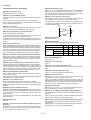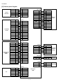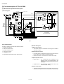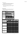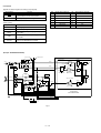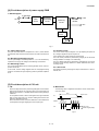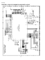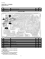
1
UX-A260U
SERVICE MANUAL
No. 00ZUXA260USME
FACSIMILE
MODEL
MODEL
UX-A260
Illustration: UX-A260U
UX-A260
SELECTION CODE DESTINATION
U
U.S.A.
Chapters 1, 2, 3, 7 and 8 of this manual are omitted because they are partly common to the UX-P100U.
Please refer to previous service manual (00ZUXP100USME) for these chapters.
CONTENTS
CHAPTER 1. GENERAL DESCRIPTION
[1] Specifications ............................................ 1-1
[2] Operation panel ......................................... 1-2
[3] Refer to the service manual of UX-P100U.
[4] Refer to the service manual of UX-P100U.
[5] Quick setup guide ..................................... 1-3
[6] Quick reference guide ............................... 1-4
[7] Option imaging film specifications
(UX-5CR) ............................................1-4
CHAPTER 2. ADJUSTMENTS
[1] Adjustments ............................................... 2-1
[2] Diagnostics and service soft switch .......... 2-2
[3] Refer to the service manual of UX-P100U.
[4] Refer to the service manual of UX-P100U.
CHAPTER 3. MECHANISM BLOCKS
[1] Refer to the service manual of UX-P100U.
[2] Refer to the service manual of UX-P100U.
CHAPTER 4. DIAGRAMS
[1] Block diagram ............................................4-1
[2] Wiring diagram .......................................... 4-2
[3] Point-to-point diagram ............................... 4-3
CHAPTER 5. CIRCUIT DESCRIPTION
[1] Circuit description ...................................... 5-1
[2] Circuit description of control PWB ..............5-2
[3] Circuit description of TEL/LIU PWB ........ 5-10
[4] Circuit description of
power supply PWB ............................5-13
[5] Circuit description of CIS unit ...................5-13
CHAPTER 6. CIRCUIT SCHEMATICS AND
PARTS LAYOUT
[1] Control PWB circuit ................................... 6-1
[2] TEL/LIU PWB circuit ................................. 6-9
[3] Power supply PWB circuit ...................... 6-14
[4] Operation panel PWB circuit ................... 6-16
CHAPTER 7. OPERATION FLOWCHART
[1] Refer to the service manual of UX-P100U.
[2] Refer to the service manual of UX-P100U.
CHAPTER 8. OTHERS
[1] Service tools .............................................. 8-1
[2] Refer to the service manual of UX-P100U.
[3] Refer to the service manual of UX-P100U.
PARTS GUIDE
Parts marked with " " are important for maintaining the safety of the set. Be sure to replace these parts with specified ones for
maintaining the safety and performance of the set.
SHARP CORPORATION
This document has been published to be used
for after sales service only.
The contents are subject to change without notice.
UX-A260U
CAUTION FOR BATTERY REPLACEMENT
(Danish)
ADVARSEL !
Lithiumbatteri-Eksplosionsfare ved fejlagtig håndtering.
Udskiftning må kun ske med batteri af samme fabrikat og type.
Levér det brugte batteri tilbage til leverandoren.
(English)
Caution !
Danger of explosion if battery is incorrectly replaced.
Replace only with the same or equivalent type
recommended by the equipment manufacturer.
Discard used batteries according to manufacturer’s
instructions.
(Finnish)
VAROITUS
Paristo voi räjähtää, jos se on virheellisesti asennettu.
Vaihda paristo ainoastaan laitevalmistajan suosittelemaan
tyyppiin. Hävitä käytetty paristo valmistajan ohjeiden
mukaisesti.
(French)
ATTENTION
Il y a danger d’explosion s’ il y a remplacement incorrect
de la batterie. Remplacer uniquement avec une batterie du
même type ou d’un type recommandé par le constructeur.
Mettre au rébut les batteries usagées conformément aux
instructions du fabricant.
(Swedish)
VARNING
Explosionsfare vid felaktigt batteribyte.
Använd samma batterityp eller en ekvivalent
typ som rekommenderas av apparattillverkaren.
Kassera använt batteri enligt fabrikantens
instruktion.
(German)
Achtung
Explosionsgefahr bei Verwendung inkorrekter Batterien.
Als Ersatzbatterien dürfen nur Batterien vom gleichen Typ oder
vom Hersteller empfohlene Batterien verwendet werden.
Entsorgung der gebrauchten Batterien nur nach den vom
Hersteller angegebenen Anweisungen.
UX-A260U
CHAPTER 1. GENERAL DESCRIPTION
[1] Specifications
Automatic dialing:
40 numbers
Imaging film:
Initial starter roll: (included with
machine): 32 ft. (10 m) (approx. 30
letter-size pages)
Compatibility:
ITU-T (CCITT) G3 mode
Input document size:
Automatic feeding:
Width: 5.8 to 8.5"
(148 to 216 mm)
Length: 5.5 to 11"
(140 to 279 mm)
Manual feeding:
Width: 5.8 to 8.5"
(148 to 216 mm)
Length: 5.5 to 23.6"
(140 to 600 mm)
Effective scanning width:
8.3" (210 mm) max.
Effective printing width:
8.3" (210 mm) max.
Contrast control:
Automatic/Dark selectable
Reception modes:
TEL/FAX/TAD
Copy function:
Single/Multi (99 copies/page)
Telephone function:
Yes
(cannot be used if power fails)
Power requirements:
120 V AC, 60 Hz
Operating temperature:
41 - 95°F (5 - 35°C)
Humidity:
25 - 85 % RH
Power consumption:
Stand-by: 3.6 W
Maximum: 100 W
Dimensions (without
attachments):
Width: 12.9" (327 mm)
Depth: 7.6" (193 mm)
Height: 6.4" (163 mm)
Approx. 6.2 lbs. (2.8 kg)
Replacement roll (not included):
UX-5CR 164 ft. (50 m) roll (one roll
yields approx. 150 letter-size pages)
Memory size* :
448 KB (approx. 24 average pages
with no voice messages recorded, or 20
minutes of voice message (including
OGMs) with no documents in memory)
Modem speed:
14,400 bps with automatic fallback to
lower speed
Transmission time* :
Approx. 6 seconds
(only when ECM is on)
Resolution:
Horizontal:
203 pixels/inch (8 dots/mm)
Vertical:
Standard: 98 lines/inch
(3.85 lines/mm)
Fine/Halftone: 196 lines/inch
(7.7 lines/mm)
Super fine: 391 lines/inch
(15.4 lines/mm)
Automatic document feeder: 10 pages max. (letter/A4, 20 lb paper)
Recording system:
Thermal transfer recording
Halftone (grayscale):
64 levels
Compression scheme:
MH, MR, MMR
Display:
16-digit LCD display
Weight (without
attachments):
Applicable telephone line:
Public switched telephone network
*
Paper tray capacity:
Letter: Approx. 50 sheets (20-lb. copier
paper at room temperature; maximum
stack height should not be higher than
the line on the tray)
Legal: 5 sheets
Recommended paper weight is 20-lb.
Copy Bond
Based on Sharp Standard No.1 Chart at standard resolution, excluding time for protocol signals (i.e., ITU-T phase C time only).
As a part of our policy of continuous improvement, SHARP reserves the right to make design and specification changes for product
improvement without prior notice. The performance specifications figures indicated are nominal values of production units. There may be some
deviations from these values in individual units.
1–1
UX-A260U
[2] Operation panel
2
1
SPEAKER
3 4 5
6
8
7
ABC
RESOLUTION/
RECEPTION MODE
TEL FAX
1
GHI
STOP
TAD
FLASH
COPY/HELP/POLL
START/MEMORY
PQRS
7
Z
REDIAL
A
12
13
2
3
MNO
5
TUV
6
WXYZ
8
9
FUNCTION
0
REPEAT
10 11
DEF
JKL
4
REC/
MEMO
PLAY/
HOLD
SPEED
9
15
14
1. SPEAKER key
SKIP
DELETE
16 17 18
9. Panel release
Press this key to listen to the line and fax tones through the
speaker when faxing a document.
Note: This is not a speakerphone. You must pick up the
handset to talk with the other party.
2. RESOLUTION / RECEPTION MODE key
Press this release to open the operation panel.
10. STOP key
Press this key to cancel operations before they are completed.
11. COPY/HELP/POLL key
When a document is in the feeder, press this key to make a
copy of a document. When a document is not in the feeder,
press this key to print out the Help List, a quick reference
guide to the operation of your fax machine. This key is also
used after dialing to poll (request fax transmission from)
another machine.
When a document is in the feeder, press this key to adjust the
resolution for faxing or copying. At any other time, press this
key to select the reception mode (an arrow in the display will
point to the currently selected reception mode).
3. FLASH key
This key is used for Call Waiting and other special services
that require subscription from your phone company. Your
phone company will provide you with details on how to use the
key.
12. START/MEMORY key
Press this key after dialing to begin fax transmission. Press
this key before dialing to send a fax through memory. The
key can also be pressed in the date and time display to show
the percentage of memory currently used.
4. REC/MEMO key
Press this key to record an outgoing message, phone
conversation, or memo.
13. SPEED key
Press this key to dial a fax or voice number using an
abbreviated 2-digit Speed Dial number.
5. PLAY/HOLD key
Press this key to play recorded messages. At any other time,
press this key to put the other party on hold during a phone
conversation.
14. Left and right arrow keys
Auto-dial numbers: When sending a fax or making a phone
call, press these keys to scroll through your auto-dial
numbers, the "REVIEW CALLS" list (only available if you
have Caller ID), and the last number dialed (redial).
FUNCTION key settings: Press the right arrow key after
scrolling with the up and down arrow keys to select a
FUNCTION key setting.
6. Display
This displays messages and prompts to help you operate the
machine.
7. UP and DOWN arrow keys
Enlarge/Reduce setting: When marking a copy of a
document, press these keys to select an enlarge/reduce
setting.
Volume setting: When a document is not in the feeder, press
these keys to change the handset volume when the handset is
lifted, the speaker volume when the SPEAKER key has been
pressed, or the ringer volume at any other time.
FUNCTION key setting: Press these keys after pressing the
FUNCTION key to scroll through the FUNCTION MODE
settings.
8. Number keys
15. FUNCTION key
Press this key to followed by the arrow keys select special
functions and setting.
16. REPEAT key
Press this key while listening to a message to play it again.
17. SKIP key
Press this key while listening to a message to skip to the next
message.
18. DELETE key
Use these keys to dial numbers, and enter numbers and
letters when storing auto-dial numbers.
1–2
Press this key to erase recorded messages.
UX-A260U
[4] Installation
[3] Transmittable documents
Refer to the service manual of UX-P100U.
Refer to the service manual of UX-P100U.
Note: To enter your name and fax number and set the date and time so that they
appear at the top of each fax you send, see pages 17 - 20 of your operation manual.
[5] Quick setup guide
1
2
Connect the handset
and place it on the
handset rest.
3
Plug the power cord
into a 120 V grounded
outlet.
4
Connect the telephone
line cord to the TEL.
LINE jack and a wall
telephone jack.
Attach the paper tray
and document support.
TE
L.L
INE
Click!
Note: If the
support does
not go in,
turn it over.
5
Load the imaging film.
1. Open the operation panel (press
1
).
3. Insert the green gears.
2. Remove the imaging film from its packaging.
Cut the band that holds the rolls together.
IMPORTANT: Do NOT discard the
green gears. They are not included
with replacement imaging film.
1 slot
2
Make sure
the gears fit
into the slots
in the ends of
the rolls.
1
5. Rotate the front spool as shown
until the film is taut.
4. Insert the film into the print compartment.
2 slots
6. Close the operation panel (press
down on both sides to make sure it
clicks into place).
Fit ends of
rolls onto hubs
6
Load paper.
The stack
should not
be higher
than this line
Insert the paper
print side down.
7
Record an outgoing
message (greeting) for TAD
mode inviting callers to leave
a message.
(Note: ìTADî stands for
ìTelephone Answering
Deviceî.)
1. Press
REC/
MEMO
,
, and
.
2. Lift the handset, press
START/MEMORY
•
GENTLY LOAD PAPER INTO THE PAPER TRAY.
• DO
8
Select the reception mode for incoming faxes
and voice calls:
FAX mode: The machine automatically
answers all calls and begins fax reception.
TEL mode: Lift the handset when the machine
rings. Press
RESOLUTION/
RECEPTION MODE
JAN-01 10:30
TAD
NOT FORCE IT DOWN INTO THE FEED SLOT.
Note: If you loaded legal paper, see page 16 of the
operation manual to change the paper size setting
to LEGAL.
to begin fax reception.
TEL FAX
, and speak into the
handset.
START/MEMORY
TAD mode: Select this mode when you go out
to receive both voice messages and faxes.
(Note: To select TAD mode, you must first
record an outgoing message.)
TEL FAX
3. When finished, press
STOP
.
JAN-01 10:30
TAD
TEL FAX
JAN-01 10:30
TAD
1–3
The arrow in the
display points to
the selected
reception mode.
;;
;;;;
UX-A260U
[6] Quick reference guide
[7] Option imaging film specifications
(UX-5CR)
SENDING FAXES
Place your document (up to 10 pages) face down in the document feeder.
1. Structure
This article is composed of polyester film coated with heat-resistant layer,
matt layer and hot melt ink layer, leader film and paper core. Ink film
specification is "DNP standard ink film HC".
Normal Dialing
1. Lift the handset or press
SPEAKER
.
2. Dial the fax number.
3. Wait for the reception tone (if a person answers, ask them to press
their Start key).
4. Press
START/MEMORY
START/MEMORY
1
2
.
Search Dialing
1. Press or
until the desired destination appears in the display.
2. Press
;;;;
3
4
.
2. Details of compositions
Speed Dialing
SPEED
1. Press
and enter the Speed Dial number.
2. Press
START/MEMORY
2-1. Base film
.
RECORDING AN OGM
1. Press
REC/
MEMO
,
, and
2. Lift the handset, press
3. When finished, press
RESOLUTION/
RECEPTION MODE
Heading
Requirements
Measuring method
Material
Polyethyleneterephthalate
–
.
START/MEMORY
STOP
2-2. Heat resistant layer
, and speak into the handset.
.
RECEIVING FAXES
Press the
ception mode.
Heat Resistant Layer
Base Film
Matt Layer
Hot melt Ink Layer
until the arrow in the display points to the desired re-
Heading
Requirements
Measuring method
Grade
HR Mixer P-5
–
2-3. Matt layer
TEL FAX
JAN-01 10:30
Heading
Requirements
Measuring method
Grade
ML Sumi
–
TAD
TEL FAX
RESOLUTION/
RECEPTION MODE
JAN-01 10:30
TAD
TEL FAX
2-4. Hot melt ink layer
JAN-01 10:30
TAD
FAX mode: The fax machine automatically answers and receives faxes.
TEL mode: Answer all calls (even faxes) by picking up the handset. To
begin fax reception, press START/MEMORY .
TAD mode: Select this mode when you go out to receive both voice
messages and faxes.
STORING AUTO DIAL NUMBERS
1. Press
FUNCTION
once and
once.
2. Enter a 2-digit Speed Dial number (01 to 40).
3. Enter the fax number and press START/MEMORY .
4. Enter the name by pressing number keys. (To enter two letters in
succession that require the same key, press after entering the first
letter.)
G=
N=
A=
H=
O=
V=
B=
I =
P=
W=
SPACE =
U=
C=
J=
Q=
X=
D=
K=
R=
Y=
E=
L=
S=
Z=
F=
M=
T=
5. Press
START/MEMORY
and then
STOP
.
1–4
Heading
Requirements
Measuring method
Grade
#507W
–
1
2
3
4
UX-A260U
3. Settings
CHAPTER 2. ADJUSTMENTS
(1) Dial mode selector
[1] Adjustments
DIAL mode (Soft Switch No. SW-B4 DATA No. 3)
(step 1) Select "OPTION SETTING".
General
KEY :
Since the following adjustments and settings are provided for this model,
make adjustments and/or setup as necessary.
DISPLAY:
FUNCTION
OPTION SETTING
(step 2) Select "DIAL MODE".
1. Adjustments of output voltage (FACTORY ONLY)
KEY:
Push until DIAL MODE
indicated because the number of
's changes by the model.
1. Install the power supply unit in the machine.
2. Set the recording paper and document.
DISPLAY:
3. When the document is loaded, power is supplied to the output lines.
Confirm that outputs are within the limits below.
(step 3) Select, using "1" or "2".
Output voltage settings
POWER
SUPPLY
PWB
(BOTTOM SIDE)
NUMBER OF RING
TEL/LIU PWB
(BOTTOM SIDE)
DIAL MODE
KEY:
1
DISPLAY:
TONE SELECTED
KEY:
2
DISPLAY:
PULSE SELECTED
is
1=TONE, 2=PULSE
(step 4) End, using the "STOP" key.
KEY:
STOP
CNLIUA
CNPS
CNPW
4. Volume adjustment
CNLIUA
CNPRG
CNTH
CONTROL
PWB
(TOP SIDE)
You can adjust the volume of the speaker, handset, and ringer using the
UP and DOWN arrow keys.
CNMT
CNCSW
CNSP
(1) Speaker
1. Press the SPEAKER key.
CNCIS
CNPN
2. Press the UP or DOWN key until the display shows the desired volume level.
• Press SPEAKER key again to turn off the speaker.
Connector
No.
CNPW
(2) Handset
Pin No.
1
2
3
4
5
6
1. When talking through the handset, press UP or DOWN key until the
display shows the desired volume level.
+24V
+24V
MG
MG
DG
+5V
Display:
RECEIVER: HIGH
↔
Voltage limits
4.25V ~ 5.75V
23.3V ~ 24.7V
RECEIVER: MIDDLE
↔
Output
+5V
+24V
• Note: The volume reverts to
MIDDLE each time you
replace the handset.
RECEIVER: LOW
2. IC protectors replacement
(3) Ringer
ICPs (IC Protectors) are installed to protect the motor driver circuit.
ICPs protect various ICs and electronic circuits from an overcurrent condition.
1. Press the UP or DOWN key. (Make sure SPEAKER key has not been
pressed, the handset is not lifted, and a document is not loaded in the
feeder.)
Display:
The location of ICPs are shown below:
↔
RINGER: HIGH
CNPW
RINGER: MIDDLE
↔
CNLIUA
RINGER: LOW
↔
FU100
CONTROL PWB
(BOTTOM SIDE)
RINGER OFF: OK?
• The ringer will ring once at the
selected level, then the date
and time will reappear in the
display.
2. If you selected RINGER OFF: OK?, press START/MEMORY key.
(1) FU100 (KAB3202) is installed in order to protect IC’s from an overcurrent generated in the motor drive circuit. If FU100 is open, replace it with a new one.
2–1
UX-A260U
[2] Diagnostics and service soft switch
1. Operating procedure
(1) Entering the diagnostic mode
Press FUNC → 9 →
ROM Ver. TB40
→ 8 → # → 7 , and the following display will appear.
After 2 sec: DIAG MODE
TB40
Then press the START key. Select the desired item with the
key or the # key or select with the rapid key. Enter the mode with the START key.
(Diag•specifications)
FUNC
9
8
TB40
7
DIAG MODE
START
Soft switch mode
START
START Flash memory clear
ROM & RAM check
START
START Flash memory check
Aging mode
START
START
Entry data receive
Panel key test
START
START
Entry data send
Check pattern
START
START
Auto feeder mode
Signal send mode
START
START
All black print
Memory clear
START
START
Shading mode
If the diag mode cannot be set, repeat the diag mode operation, performing the following operation.
After the power is turned on and "WAIT A MOMENT" is indicated, press
the STOP key.
STOP
KEY
START
KEY
"Power ON" +
In relation with the process response (request from Production
Engineering) "WAIT A MOMENT" clock indication may appear depending
on STOP key timing. If the STOP key is held down, "MEMORY CLEAR?"
appears.
Memory clear
(Work + Backup)
2. Diagnostic items
ITEM No.
Contents
Function
1
SOFT SWITCH MODE
Soft switches are displayed and changed. List can be output.
2
ROM & RAM CHECK
ROM is sum-checked, and RAM is matched. Result list is output.
3
AGING MODE
10 sheets of check patterns are output every 5 minutes per sheet.
4
PANEL KEY TEST
Panel keys are tested. Result list is output.
5
CHECK PATTERN
Check pattern is output.
6
SIGNAL SEND MODE
Various signals of FAX communication are output.
7
MEMORY CLEAR
Back-up memory is cleared, and is set at delivery.
8
SHADING MODE
Shading compensation is performed in this mode.
9
ALL BLACK PRINT
To check the print head, whole dots are printed over the interval of 2 m.
10
AUTO FEEDER MODE
Insertion and discharge of document are tested.
11
ENTRY DATA SEND
Registered content is sent.
12
ENTRY DATA RECEIVE
Registered content is received, and its list is output.
13
FLASH MEMORY CHECK
Checks flash memory write/read.
14
FLASH MEMORY CLEAR
Checks flash memory clearing.
2–2
UX-A260U
3. Diagnostic items description
3. 1. Soft switch mode
3. 6. Signal send mode
This mode is used to send various signals to the circuit during FAX communication. Every push of START key sends a signal in the following
sequence. Moreover, the signal sound is also output to the speaker when
the line monitor of the soft switch is on.
Used to change the soft switch settings.
The soft switch which is stored internally is set by using the keys.
The available soft switches are SW-A1 to SW-O6.
[1] No signals
The content of soft switches is shown in page 2-5 to 2-19.
[2] 14400BPS (V.33)
The contents are set to factory default settings.
[3] 12000BPS (V.33)
[4] 14400BPS (V.17)
3. 2. ROM & RAM check
[5] 12000BPS (V.17)
ROM executes the sum check, and RAM executes the matching test.
The result will be notified with the number of short sounds of the buzzer
as well as by printing the ROM & RAM check list.
Number of short sounds of buzzer 0 → No error
[6] 9600BPS (V.17)
[7] 7200BPS (V.17)
[8] 9600BPS (V.29)
1 → ROM error
[9] 7200BPS (V.29)
2 → RAM error (4 Kbyte SRAM or
512 Kbyte DRAM)
[10] 4800BPS (V27ter)
[11] 2400BPS (V27ter)
3. 3. Aging mode
[12] 300BPS (FLAG)
If any document is present, copying will be executed sheet by sheet. If
no document is present, the check pattern will be printed sheet by sheet.
This operation will be executed at a rate of one sheet per 5 minutes, and
will be ended at a total of 10 sheets.
[13] 2100Hz (CED)
[14] 1100Hz (CNG)
3. 7. Memory clear
3. 4. Panel key test
This mode is used to clear the backup memory and reset to the default
settings.
This mode is used to check whether each key operates properly. Press
the key on the operation panel, and the key will be displayed on the
display. Therefore, press all keys. At this time, finally press the STOP
key.
3. 8. Shading mode
The mode is used for the shading compensation. For reading, set up the
special original paper.
The compensation memorizes the reference data of white and black for
reading.
Moreover, the memorized data is not erased even if memory clear mode
is executed.
When the STOP key is pressed, the keys which are not judged as
"pressed" will be printed on the result list.
• LED part of the contact image sensor (CIS) is kept on during the term
from when "START" of the panel test mode to end with the STOP key.
3. 5. Check pattern
3. 9. All black print
This mode is used to check the state of the printing head. It is ended
with the following pattern printed on one printing sheet.
This mode is used to check the state of the printing head and to intentionally overheat it. Whole dots are printed over the interval of 2 m. If it is
overheated or the printing sheet is jammed, press STOP key for the end.
1 DOT
1
B B B B B B B B B B B B B B B B B B B BB B B B B B B B B B B B B B B B B B B BB
B B B B B B B B B B B B B B B B B B B BB B B B B B B B B B B B B B B B B B B BB
B B B B B B B B B B B B B B B B B B B BB B B B B B B B B B B B B B B B B B B BB
2
3. 10. Auto feeder mode
2 DOTS
In this mode, a document is inserted and discharged to check the auto
feed function.
B B B B B B B B B B B B B B B B B B B BB B B B B B B B B B B B B B B B B B B BB
B B B B B B B B B B B B B B B B B B B BB B B B B B B B B B B B B B B B B B B BB
B B B B B B B B B B B B B B B B B B B BB B B B B B B B B B B B B B B B B B B BB
3
3 DOTS
After this mode is started, set a document, and the document feed will
be automatically tested.
B B B B B B B B B B B B B B B B B B B BB B B B B B B B B B B B B B B B B B B BB
B B B B B B B B B B B B B B B B B B B BB B B B B B B B B B B B B B B B B B B BB
B B B B B B B B B B B B B B B B B B B BB B B B B B B B B B B B B B B B B B B BB
4
4 DOTS
3. 11. Entry data send
B B B B B B B B B B B B B B B B B B B BB B B B B B B B B B B B B B B B B B B BB
B B B B B B B B B B B B B B B B B B B BB B B B B B B B B B B B B B B B B B B BB
B B B B B B B B B B B B B B B B B B B BB B B B B B B B B B B B B B B B B B B BB
This mode is used to send the registered data to another machine and
make the other machine copy the registered content.
Before sending in this mode, it is necessary to set the other machine at
the entry data receive mode.
The following, information will be sent to the remote machine:
1. Telephone list data
2. Sender register data
3. Optional setting content
4. Soft switch content
5. Junk fax number list
6. Recording setting list data
2–3
UX-A260U
3. 12. Entry data receive
3. 13. Flash memory check
In this mode, the registered data sent from the other machine is received and the received data is registered in the machine. When this mode
is used for receiving, the other machine must be in the entry data send
mode.
Data is written into and read from the flash memory to check data conformity. When the unit enters this mode, the check is started.
After receiving is completed, the following lists are printed.
1. Telephone list data
Data in the flash memory is cleared (memory clear). When the unit enters this mode, the check is started.
*Operation of hardware and signal in the flash memory check mode and
flash memory clear mode, and the result of check.
The result is announced by the buzzer beeps. The result of check is
printed.
Beeps
0 → No error
1 → Memory error
3. 14. Flash memory clear
2. Sender register data (*)
3. Optional setting list (*)
4. Soft switch content
5. Junk fax number list (*)
6. Recording setting list data (*)
(*): Refer to SETUP LIST
4. How to make soft switch setting
To enter the soft switch mode, press the following key entries in sequence.
Press FUNCTION
DATA No.
9
8
7
START
START
1 2 3 4 5 6 7 8
S F T SW-A1 = 0 0 0 0 0 0 0 0
Press FUNCTION key.
S F T SW-A1 = 1 0 0 0 0 0 0 0
Press
key.
Press
key.
S F T SW-A1 = 1 0 0 0 0 0 0 0
S F T SW-A1 = 1 0 0 0 0 0 0 0
Bit1 - 8 are set.
S F T SW-A1 = 1 0 0 0 0 0 0 0
Press START key during setting.
S F T SW-A2 = 0 0 0 0 0 0 0 0
Soft SW-A2 - SW-O6 are set.
S F T SW-O6 = 0 0 0 0 0 0 0 0
To finish the settings halfway between
SW-A1 and SW-O6, press the STOP
key. In this case, the setting being done
to the SW No. on display will be nullified
while settings done to the preceding
SW No. remain in effect.
When the COPY key is pressed, the
contents of soft switches are printed.
The soft switch mode is terminated.
2–4
UX-A260U
5. Soft switch description
• Soft switch
SW
NO.
SW
l
A1
DATA
NO.
1
Protect from echo
Forced 4800 BPS reception
Footer print
No
Yes
Yes
Yes
No
No
0
0
0
4
Length limitation of copy/send/receive
No limit
Copy/send: 60cm
Receive: 1m
0
5
CSI transmission
No transmitted
Transmitted
0
6
DIS receive acknowledgement during G3
transmission
Twice
NSF: Once
DIS: Twice
0
7
Non-modulated carrier for V29 transmission
mode
Yes
No
0
8
EOL detect timer
25 s
13 s
0
1
2
3
4
5
Sender’s information transmit
6
Reserved
7
8
0
1
0
0
1
1
1
0
0
1
0
1
1
0
0
0
0
0
0
1
0
0
0
0
0
1
0
0
1
0
0
0
1
0
0
1
1
1
0
0
0
Yes
Communication error treatment in RTN
sending mode (reception)
No communication error
Communication error
0
CNG transmission
CED tone signal interval
No
0
No. 1
1000ms
1
No. 2
1
0
Yes
750ms
1
500ms
0
75ms
0
0
0
0
1
0
0
3
MR coding
No
Yes
0
4
ECM mode
No
Yes
0
5
ECM MMR mode
No
Yes
6
Reserved
0
7
Reserved
0
8
Reserved
1
2
3
4
5
Signal transmission level
6
Protocol monitor (error print)
Printed at com. error
Not printed
0
7
Protocol monitor
Yes
No
0
8
Line monitor
Yes
No. =
1
2
No. 1
No. 2
(Transmission)
4
input
4 2 1
3 4 5
0 0 0
0
1
0
0
0
No
Digital line equalization setting
3
0
0
Binary
16 8
1 2
0 1
Digital line equalization setting (Reception)
SW
l
A5
1
0
1
No
2
SW
l
A4
Remarks
V.33
V.17
V.29
V.27 ter
14400 12000 14400 12000 9600 7200 9600 7200 4800 2400
1
SW
l
A3
Initial
setting
0
1
2
3
Modem speed
SW
l
A2
Switch setting and function
ITEM
0
7.2km
3.6km
1.8km
0km
1
1
1
0
0
1
0
0
0
1
7.2km
3.6km
1.8km
0km
No. 3
1
1
0
0
0
No. 4
1
0
1
0
1
Digital cable equalizer setting (Reception
No. 5
No. 6
7.2km
0km
1
1
0
0
5
6
for Caller ID)
7
Error criterion
10 ~ 20 %
5 ~ 10 %
0
8
Anti junk fax check
Yes
No
1
2–5
0
0
OPTION
UX-A260U
SW
NO.
SW
l
A6
DATA
NO.
Switch setting and function
ITEM
1
Initial
setting
0
1
Reserved
2
End Buzzer
Yes
No
1
3
Disconnect the line when DIS is received in
RX mode
No
Yes
1
4
5
Equalizer freeze control (MODEM)
Equalizer freeze control 7200 BPS only
On
No
Off
Yes
0
0
6
7
8
CNG transmission in manual TX mode
Reserved
Modem speed automatic fallback when RX
Yes
No
Yes
No
1
0
0
Remarks
0
level is under -40dBm
SW
l
B1
1
2
3
4
Recall interval
5
Recall times
No. =
6
SW
l
B2
SW
l
B3
SW
l
B4
SW
l
B5
No. =
Binary input
8 4 2 1
1 2 3 4
0 1 0 1
0
1
0
1
Binary input
0
8
4
2
1
0
5
0
6
0
7
1
8
1
1
1
0
7
8
1
Dial pausing (sec/pause)
4 sec
2 sec
2
3
Dial tone detection (before auto dial)
Reserved
No
Yes
4
Busy tone detection (after auto dial)
Waiting time after dialing
No
1
0
Yes
45 seconds 55 seconds 90 seconds 140 seconds
0
0
1
1
0
5
No.5
6
7
No.6
Reserved
0
0
8
1
Reserved
Reserved
0
0
2
3
Reserved
Reserved
0
0
4
5
Reserved
Reserved
0
0
6
Auto dial mode delay timer of before line
connect
7
8
Hold key
1
Auto dial mode delay timer of after line
connect
0 second
0
No.6
No.7
Enable
Dial mode
Pulse → Tone change function by
Dial pulse make/break ratio (%)
6
7
Reserved
Reserved
8
Recalling fixed only one time when dialing was Yes
unsuccessful without detecting busy tone signal
1
DTMF signal transmission level (Low)
key
1
0
1
1.5 seconds 3.0 seconds 4.5 seconds
0
1
1
0
1
Disable
0
1
1.7 seconds 3.0 seconds 3.6 seconds 4.0 seconds
0
0
1
1
No.1
2
3
4
5
2
3
4
0
No.2
Tone
Enable
40/60
0
1
Pulse
Disable
33/67
0
1
0
0
0
1
0
0
1
1
1
0
0
No
No. =
1
Binary input
0
16 8 4 2 1
1 2 3 4 5
0 1 0 0 1
1
0
0
5
1
6
7
Reserved
Reserved
0
0
8
Reserved
0
2–6
OPTION
UX-A260U
SW
NO.
DATA
NO.
1
Switch setting and function
ITEM
1
DTMF signal transmission level (High)
2
SW
l
B6
No. =
Initial
setting
0
Binary input
0
16 8 4 2 1
0
1 2 3 4 5
0 0 1 0 1
1
0
1
3
4
5
6
7
8
0
Reserved
Reserved
0
0
Reading slice (Binary)
1
2
Factory
setting
Light
Dark
Darker in
dark
No. 1
No. 2
0
0
Factory
setting
1
0
Light
0
1
Dark
1
1
Darker in
dark
0
0
No. 3
0
1
0
1
0
No. 4
0
1
1
0
0
0
Reading slice (Half tone)
SW
l
C1
3
4
5
6
Line density selection
Reserved
Fine
0
Standard
7
8
MTF correction in half tone mode
Reserved
No
Yes
1
Number of rings for auto receive
2
3
No. =
4
SW
l
D1
5
6
Automatic switching manual to auto receive
mode
Reserved
0
8
1
4
2
2
3
1
4
1
0
0
1
0
0
0
Reception after 5 rings
SW
l
D3
No reception
No.7
8
No.8
0
As PTT
0
0
No. 1
0
OFF
11.5Hz
0
13.0Hz
1
1
0
20.0Hz
1
No. 2
0
1
No. 3
0
0
0
OPTION
STANDARD
0
0
1
PATTERN1
0
1
0
PATTERN2
0
1
1
1
PATTERN3
1
0
0
0
2
PATTERN4
1
0
1
0
3
PATTERN5
1
1
0
0
4
Reserved
5
6
Caller ID function
Caller ID detect during CI off
7
8
1
Reserved
Reserved
Cl off detection timer (0-1550ms setting by
2
50ms step)
OPTION
0
7
Distinctive ringing setting
(PATTERN 4 and 5 are for CANADA only)
0
0
Binary input
Cl detect frequency
SW
l
D2
Remarks
0
Yes
All times
No
Only first
Binary input
No. =
0
0
0
0
0
16 8 4 2 1
1
1 2 3 4 5
0 1 1 1 0
1
1
0
3
4
5
6
7
Reserved
Reserved
0
0
8
Reserved
0
2–7
OPTION
UX-A260U
SW
NO.
SW
l
E1
SW
l
E2
SW
l
E3
DATA
NO.
Switch setting and function
ITEM
1
1
Reserved
0
2
3
Reserved
Reserved
0
0
4
Reserved
0
5
Reserved
0
6
7
Reserved
Reserved
0
0
8
Reserved
0
1
Reserved
0
2
3
Reserved
Reserved
0
0
4
Reserved
0
5
Reserved
0
6
7
Reserved
Reserved
0
0
8
Reserved
0
1
Reserved
0
2
3
Reserved
Reserved
0
0
4
Reserved
0
5
Reserved
0
6
7
Reserved
Reserved
0
0
8
Reserved
0
DTMF detection time
SW
l
F1
1
No. 1
50ms
0
2
3
No. 2
0
Protection of remote reception (5
4
Remote reception with GE telephone
5
6
Remote operation code figure by external
TEL (0~9)
1
CNG detection in STAND-BY mode
Number of CNG detect (AM mode)
2
3
SW
l
G1
1
No
Compatible
No. =
100ms
1
120ms
1
0
1
Not compatible
0
1
1
0
1
5
0
0
1
6
1
7
0
Yes
Number of CNG detect (STAND-BY mode)
No. 4
No. 5
8
1
1pulse
0
0
No
2pulses
0
1
3pulses
1
0
4pulses
1
1
1
1pulse
2pulses
3pulses
4pulses
0
0
0
1
1
0
1
1
0
1
0
1
6
Reserved
0
7
Reserved
0
8
Reserved
0
1
Reserved
0
2
3
Reserved
Reserved
0
0
4
Reserved
0
5
Reserved
0
6
Reserved
0
7
Reserved
0
8
Reserved
0
2–8
Remarks
0
Binary input
8 4 2 1
No. 2
No. 3
4
5
80ms
0
) detect Yes
7
8
SW
l
F2
Initial
setting
0
OPTION
UX-A260U
SW
NO.
SW
l
G2
SW
l
G3
DATA
NO.
Switch setting and function
ITEM
1
1
2
Reserved
Reserved
0
0
3
4
Reserved
Reserved
0
0
5
6
Reserved
Reserved
0
0
7
Reserved
0
8
1
2
Reserved
Reserved
Reserved
0
0
0
3
4
Reserved
Reserved
0
0
5
6
Reserved
Reserved
0
0
7
Reserved
0
8
Reserved
Busy tone detection ON/OFF time (Lower
1
2
duration)
No. 1
No. 2
No. 3
No. 4
250ms
350ms
0
0
0
1
1
0
1
1
650ms
900ms
1500ms
2700ms
0
0
0
1
1
0
1
1
0
1
5
Busy tone detect continuation sound detect
during OGM
Busy tone detect continuation sound detect
No
Yes
0
No
Yes
0
7
Busy tone detect intermittent sound detect
during OGM
No
Yes
0
8
Busy tone detect intermittent sound detect
No
1
2
3
Yes
0
4pulses
6pulses
10pulses
No. 1
0
0
1
1
0
No. 2
0
0
1
1
0
Fax switching when A.M. full
Yes
1
No
320Hz - 570Hz
320Hz - 460Hz
5
Busy tone detect continuation sound detect
frequency
Reserved
6
7
Reserved
AM OGM announce only mode
Yes
8
Busy tone continuous sound detect time
5s
4
0
1
2pulses
OPTION
0
0
1
2
10s
No. 1
No. 2
A.M. quiet time 1
3
4
No. 3
No. 4
A.M. quiet time 2
5
6
0
0
No
ICM recording time
SW
l
I1
200ms
duration)
Busy tone detection pulse number
SW
l
H2
150ms
3
4
6
Remarks
0
Busy tone detection ON/OFF time (Upper
SW
l
H1
Initial
setting
0
No. 5
No. 6
1
4min
15s
30s
60s
0
0
0
1
1
0
1
1
2s
3s
4s
5s
0
0
0
1
1
0
1
1
0s
1s
2s
3s
0
0
0
1
1
0
1
1
OPTION
0
0
0
0
1
0
7
Key input buzzer on/off switch (Two way
recording mode)
On
Off
0
8
CPC signal detection
Yes
No
1
2–9
OPTION
OPTION
UX-A260U
SW
NO.
DATA
NO.
1
SW
l
I2
A.M. quiet detect time
3
4
5
1
0
2 3 4 5
0 1 1 0
1
1
0
CPC detection time
4ms 20ms 40ms 70ms 140ms 160ms 200ms 290ms
No.6
No.7
No.8
0
0
0
0
0
1
0
1
1
1
0
0
1
0
1
1
1
0
1
1
1
1
1
1
Reserved
Max OGM record time
15s
60s
0
0
3
4
Two way record function
Toll saver
Disable
Disable
Enable
Enable
0
0
5
6
Reserved
Reserved
7
8
Reserved
Transfer dial recall
1
AGC maximum gain (line)
3
4
5
6
3
4
5
6
7
8
1
3
4
5
0
0
No
(10 ~ 25 dB) (1 dB step)
Binary input
No. =
No. =
AGC energy refrence level access code (line)
(-0 ~ -30 dB) (2 dB step)
No. =
AGC energy refrence level access code (Mic)
(-0 ~ -30 dB) (2 dB step)
No. =
AGC again adaptation threshold (line)
No. =
AGC again adaptation threshold (Mic)
6
No. =
7
8
8
1
1 2 3 4
0 1 0 1
Binary input
0
1
0
4 2 1
1
5 6 7 8
0 1 1 0
Binary input
8
1
0
1
4 2 1
0
1 2 3 4
1 0 1 1
Binary input
8
1
1
1
8
4 2 1
1
5 6 7 8
1 1 0 1
Binary input
0
1
1
8
4 2 1
1
1 2 3 4
1 1 1 1
Binary input
1
1
1
8
4 2 1
1
5
1
6 7 8
1 1 1
Slow
1
1
No. 1
No. 2
AGC slew rate (Mic)
3
4
0
4 2 1
AGC slew rate (line)
1
2
0
0
Yes
AGC maximum gain (Mic)
2
SW
l
I7
0
1
0
1
2
(10 ~ 25 dB) (1 dB step)
Remarks
0
0
2
SW
l
I6
Binary input
8 4 2 1
7
8
1
SW
l
I5
Initial
setting
0
No. = 16
2
SW
l
I4
1
2
6
7
8
SW
l
I3
Switch setting and function
ITEM
No. 3
No. 4
Normal
Little fast
Fast
0
0
0
1
1
0
1
1
Slow
Normal
Little fast
Fast
0
0
0
1
1
0
1
1
0
1
1
1
5
6
Reserved
Reserved
0
0
7
8
Reserved
Reserved
0
0
2 – 10
OPTION
UX-A260U
SW
NO.
SW
l
J1
DATA
NO.
Switch setting and function
ITEM
1
Reserved
2
Reserved
3
4
Sender’s phone number setting
Reserved
5
6
Reserved
Summer time setting
1
0
Cannot change
Change allowed
No
Yes
7
No. 7
Off
0
8
No. 8
0
Low
0
Middle
1
High
1
1
1
0
1
0
0
Reserved
0
3
Reserved
0
Low
0
No. 4
5
No. 5
Low
0
0
Middle
1
1
0
1
OPTION
1
0
6
No. 6
Very Low
0
7
No. 7
0
0
1
1
0
1
8
1
No. 8
0
1
0
1
0
Reserved
0
0
2
Communication results printout
(Transaction report)
No. 2
E/T/M
0
3
No. 3
0
4
5
No. 4
6
OGM/ICM output level to speaker
(0 dB ~ -15 dB) (1 dB step)
No. =
Low
0
Middle
0
High
0
Very High
1
0
OPTION
OPTION
1
0
1
1
0
0
0
1
Binary input
0
1
0
0
0
8
4 2 1
0
5
0
6 7 8
0 1 1
7
8
1
Reserved
1
1
0
2
Reserved
0
3
OGM/ICM output level
4
(0 dB ~ -32 dB) (1 dB step)
No. =
Binary input
0
32 16 8 4 2 1
0
5
6
7
3
0
4 5 6 7 8
0 1 0 0 1
8
SW
l
L1
High
1
Send only Always No print Err only
0
0
0
1
OPTION
OPTION
Reserved
Speaker volume (5 stages)
SW
l
K1
0
1
2
Handset receiver volume
SW
l
J3
0
0
1
4
Remarks
0
Ringer volume
SW
l
J2
Initial
setting
0
1
0
0
1
1
Reserved
0
2
Reserved
0
3
4
5
6
Reserved
Reserved
Cut off mode (COPY mode)
A4 paper enable
Yes
Enable
No
Disable
0
0
1
0
7
LEGAL & LETTER paper enable
Enable
Disable
1
8
Reserved
0
2 – 11
OPTION
UX-A260U
SW
NO.
DATA
NO.
Switch setting and function
ITEM
1
Paper set size
1
2
3
SW
l
L2
SW
l
M1
SW
l
M2
SW
l
N1
SW
l
N2
SW
l
N3
Automatic reduce of receive
Print contrast
Initial
setting
0
No. 1
LETTER
0
LEGAL
0
A4
1
No. 2
0
1
0
Auto
100 %
Lighter
Light
0
0
OPTION
0
0
1
4
No. 4
Normal
0
5
No. 5
0
0
1
1
0
0
6
7
8
0
1
0
1
0
Reception reduction ratio in case of memory ful
Reserved
No. 6
100 %
0
0
0
1
2
Reserved
Reserved
0
0
3
4
5
Reserved
Reserved
Reserved
0
0
0
6
Reserved
0
7
8
Reserved
Reserved
0
0
1
Reserved
0
2
3
Reserved
Reserved
0
0
4
Reserved
0
5
6
7
Reserved
Reserved
Reserved
0
0
0
8
1
2
Reserved
Reserved
Reserved
0
0
0
3
4
5
Reserved
Reserved
Reserved
0
0
0
6
Reserved
0
7
8
Reserved
Reserved
0
0
1
Reserved
0
2
3
Reserved
Reserved
0
0
4
Reserved
0
5
6
7
Reserved
Reserved
Reserved
0
0
0
8
1
2
Reserved
Reserved
Reserved
0
0
0
3
4
5
Reserved
Reserved
Reserved
0
0
0
6
Reserved
0
7
8
Reserved
Reserved
0
0
2 – 12
93 %
Remarks
Dark
0
Darker
1
1
OPTION
OPTION
UX-A260U
SW
NO.
SW
l
O1
SW
l
O2
SW
l
O3
SW
l
O4
SW
l
O5
SW
l
O6
DATA
NO.
ITEM
Switch setting and function
1
0
Initial
setting
1
2
Reserved
Reserved
0
0
3
4
5
Reserved
Reserved
Reserved
0
0
0
6
Reserved
0
7
8
Reserved
Reserved
0
0
1
Reserved
0
2
3
Reserved
Reserved
0
0
4
Reserved
0
5
6
7
Reserved
Reserved
Reserved
0
0
0
8
1
2
Reserved
Reserved
Reserved
0
0
0
3
4
5
Reserved
Reserved
Reserved
0
0
0
6
Reserved
0
7
8
Reserved
Reserved
0
0
1
Reserved
0
2
3
Reserved
Reserved
0
0
4
Reserved
0
5
6
7
Reserved
Reserved
Reserved
0
0
0
8
1
2
Reserved
Reserved
Reserved
0
0
0
3
4
5
Reserved
Reserved
Reserved
0
0
0
6
Reserved
0
7
8
Reserved
Reserved
0
0
1
2
Reserved
Reserved
0
0
3
4
5
Reserved
Reserved
Reserved
0
0
0
6
Reserved
0
7
8
Reserved
Reserved
0
0
2 – 13
Remarks
UX-A260U
SW-A2 No. 8 CNG transmission
• Soft switch function description
When set to "0" , this model allows CNG transmission by pressing the
Start key in the key pad dialing mode. When set to "1", CNG transmission in the key pad dialing mode cannot be performed. In either case.
CNG transmission can be performed in the auto dial mode.
SW-A1 No. 1 Protect from echo
Used to protect from echo in reception.
SW-A1 No. 2 Forced 4800BPS reception
SW-A3 No. 1, No. 2 CED tone signal interval
When line conditions warrant that receptions take place at 4800 BPS
repeatedly.
For international communication, the 2100Hz CED tone may act as an
echo suppression switch, causing a communication problem.
It may improve the success of receptions by setting at 4800BPS.
Though SW-A3 No. 1 and No. 2 are normally set to 0, this setting is used
to change the time between the CED tone signal to eliminate the communication caused by echo.
This improves the receiving document quality and reduces handshake
time due to fallback during training.
SW-A1 No. 3 Footer print
TX
When set to "1", the date of reception, the sender machine No., and the
page No. are automatically recorded at the end of reception.
RX
CED
T
SW-A1 No. 4 Length limitation of copy/send/receive
Used to set the maximum page length.
DIS
To avoid possible paper jam, the page length is normally limited to 0.6
meter for copy or transmit, and 1 meters for receive.
SW-A3 No. 3 MR Coding
It is possible to set it to "No limit" to transmit a long document, such as a
computer print form, etc. (In this case, the receiver must also be set to
no limit.)
MR Coding is enable.
SW-A1 No. 5 CSI transmission
Used to determine ECM mode function. Refer to following table.
SW-A3 No. 4 ECM mode
(CSI TRANSMISSION) is a switch to set whether the machine sends or
does not send the signal (CSI signal) informing its own telephone No. to
the remote fax machine when information is received. When "nonsending"
is set, the telephone No. is not output on the remote transmitting machine if the remote transmitting machine has the function to display or
print the telephone No. of receiving machine, using this CSI signal.
SW-A3 No.4 ECM MODE
0
0
1
1
SW-A3 No.5 ECM MMR MODE
0
1
0
1
Compression ECM MMR mode
ECM MH mode
method
Yes
No
No
No
Yes
Yes
No
No
Yes
Yes
Yes
Yes
MR Mode
SW-A1 No. 6 DIS receive acknowledgment during G3 transmission
(Depending on remote machine)
Used to make a choice of whether reception of DIS (NSF) is acknowledged after receiving two DISs (NSFs) or receiving one DIS (two NSFs).
It may be useful for overseas communication to avoid an echo suppression problem, if set to 1.
SW-A3 No. 5 ECM MMR mode
See SW-A3 No. 4.
SW-A3 No. 6 ~ No. 8 Reserved
SW-A1 No. 7 Non-modulated carrier for V29 transmission mode
Set to "0".
Though transmission of a non-modulated carrier is not required for transmission by the V29 modem according to the CCITT recommendation, it
may be permitted to a send non-modulated carrier before the image
signal to avoid an echo suppression problem. It may be useful for overseas communication to avoid an echo suppression problem, if set to 1.
SW-A4 No. 1 ~ No. 5 Signal transmission level
Used to control the signal transmission level in the range of-0dB to31dB.
SW-A4 No. 6 Protocol monitor (Error print)
SW-A1 No. 8 EOL (End Of Line) detect timer
If set to "1", protocol is printed at communication error.
Used to make a choice of whether to use the 25-second or 13-second
timer for detection of EOL.
This is effective to override communication failures with some facsimile
models that have longer EOL detection.
SW-A4 No. 7 Protocol monitor
Normally set to "0". If set to "1", communication can be checked, in case
of trouble, without using a G3 tester or other tools.
When communication FSK data transmission or reception is made, the
data is taken into the buffer. When communication is finished, the data
is analyzed and printed out. When data is received with the line monitor
(SW-A4 No. 8) set to "1" the reception level is also printed out.
SW-A2 No. 1 ~ No. 4 Modem speed
Used to set the initial modem speed. The default is 14400BPS.
It may be necessary to program it to a slower speed when frequent line
fallback is encountered, in order to save the time required for fallback
procedure.
SW-A4 No. 8 Line monitor
Normally set to "0". If set to "1", the transmission speed and the reception level are displayed on the LCD. Used for line tests.
SW-A2 No. 5 Sender’s information transmit
(SENDER’S INFORMATION TRANSMISSION) is a switch to set the
function to print the content of HEADER PRINT described in the passcode
list at the front end of receiver’s original when original is sent to the
remote machine.
SW-A5 No. 1, No. 2 Digital line equalization setting (Reception)
Line equalization when reception is to be set according to the line characteristics.
If this switch is set to "NO", the HEADER PRINT is not output at the
receiving machine.
Setting should be made according to distance between the telephone
and the telephone company central switching station.
SW-A2 No. 6 Reserved
SW-A5 No. 3, No. 4 Digital line equalization setting (Transmission)
Set to "0".
Line equalization when transmitter is to be set according to the line
characteristics.
Setting should be made according to distance between the telephone
and the telephone company central switching station.
SW-A2 No. 7 Communication error treatment in RTN sending mode
(Reception)
Used to determine communication error treatment when RTN is sent by
occurrence of a received image error in G3 reception. When it is set to
"1", communication error is judged as no error.
2 – 14
UX-A260U
SW-A5 No. 5, No. 6 Digital cable equalizer setting
(Reception for Caller ID)
SW-B2 No. 7, No. 8 Reserved
Set to "0".
Line equalization when reception for CALLER ID is to be set according
to the line characteristics.
Setting should be made according to distance between the telephone
and the telephone company central switching station.
SW-B3 No. 1 ~ No. 5 Reserved
Set to "0".
SW-A5 No. 7 Error criterion
SW-B3 No. 6, No. 7 Auto dial mode Delay timer of before line connect
Used to select error criterion for sending back RTN when receiving image data.
Delay time between the dial key input and line connection under the
auto dial mode.
RAPID01
SW-A5 No. 8 Anti junk fax check
When using the Anti junk fax function, set to "1".
CML RELAY ON
DIALLING
SW-A6 No. 1 Reserved
Set to "0".
No.6
No.7
0
0
1
1
0
1
0
1
SW-A6 No. 2 End buzzer
Setting this bit to 0 will disable the end buzzer (including the error buzzer/
on-hook buzzer).
0sec
1.5sec
3.0sec
4.5sec
SW-B3 No. 8 Hold key
SW-A6 No. 3 Disconnect the line when DIS is received in RX mode
Used to set YES/NO of holding function by the Hold key.
Bit1= 0: When DIS signal is received during RX mode, the line is disconnected immediately.
SW-B4 No. 1, No. 2 Auto dial mode Delay timer of after line connect
Delay time between the line connection and dial data output under the
auto dial mode.
Bit1= 1: When DIS signal is received during RX mode, the line is disconnected on the next tone.
DIAL DATA
RAPID01
SW-A6 No. 4 Equalizer freeze control (MODEM)
CML RELAY ON
This switch is used to perform reception operation by fixing the equalizer control of modem for the line which is always in an unfavorable
state and picture cannot be received.
* Usually, the control is executed according to the state of line where
the equalizer setting is changed always.
SW-A6 No. 5 Equalizer freeze control 7200BPS only
Setting which specifies SW-A3 No. 6 control only in the condition of
7200BPS modem speed.
No.1
No.2
0
0
1
1
0
1
0
1
1.7sec
3.0sec
3.6sec
4.0sec
SW-B4 No. 3 Dial mode
When using the pulse dial, set to 1. When using the tone dial, set to 0.
SW-A6 No. 6 CNG transmission in manual TX mode
SW-B4 No. 4 Pulse → Tone change function by
When set to "1", fax transmit the CNG signal in case of manual transmission mode (User press the START key after waiting for the fax answering signal from handset or speaker).
key
When setting to 1, the mode is changed by pressing the
pulse dial mode to the tone dial mode.
SW-A6 No. 7 Reserved
SW-B4 No. 5 Dial pulse make/break ratio (%)
Set to "0".
When using the 33% make ratio pulse dial, set to "0".
When using the 40% make ratio pulse dial, set to "1".
SW-A6 No. 8 Modem speed automatic fallback when RX level is
under -40dBm
key from the
SW-B4 No. 6, No. 7 Reserved
Set to "0".
When set to "1", if fax signal level is under -40dBm during reception,
machine selects the slower modem speed automatically.
It is effective when noises occur on the received document due to the
long distance communications.
SW-B4 No. 8 Recalling fixed only one time when dialing was unsuccessful without detecting busy tone signal
When dialing results in failure since the busy tone cannot be detected,
recalling is fixed to one time.
SW-B1 No. 1 ~ No. 4 Recall interval
Choice is made for a redial interval for speed and rapid dial calls.
Use a binary number to program this. If set to 0 accidentally, 1 will be
assumed.
Supplementary explanation
If time-out termination is made when dialing, only single recall is possible even if the setting time of recalls (SW-B1 No. 5 - No. 8) has been set
to some times. This soft switch is added in order to meet FCC regulations.
SW-B1 No. 5 ~ No. 8 Recall times
Choice is made as to how many redials there should be.
SW-B5 No. 1 ~ No. 5 DTMF signal transmission level (Low)
The transmission level of DTMF signal is adjusted. (lower frequency)
SW-B2 No. 1 Dialing pause (sec/pause)
Pauses can be inserted between telephone numbers of direct dial connection. Selection of 4 sec or 2 sec pause is available.
00000: 0dBm
↓
SW-B2 No. 2 Dial tone detection (before auto dial)
Used to set YES/NO of dial tone detection in auto dialing.
11111: -15.5dBm (-0.5dBm x 31)
SW-B2 No. 3 Reserved
SW-B5 No. 6 ~ No. 8 Reserved
Set to "0".
Set to "0".
SW-B2 No. 4 Busy tone detection (after auto dial)
SW-B6 No. 1 ~ No. 5 DTMF signal transmission level (High)
Used to set busy tone detection in auto dialing.
The transmission level of DTMF signal is adjusted. (higher frequency)
SW-B2 No. 5, No. 6 Waiting time after dialing
00000: 0dBm
This is time waiting for the opponent’s signals after dialing.
↓
11111: -15.5 dBm (-0.5dBm x 31)
2 – 15
UX-A260U
SW-B6 No. 6 ~ No. 8 Reserved
<Example of use>
Set to "0".
Phone Number
Intended
Purpose
SW-C1 No. 1, No. 2 Reading slice (Binary)
Ring Pattern
Ring Pattern
555-1234
Voice Calls
Standard
555-1235
Facsimile Calls
Pattern 1
SW-C1 No. 3, No. 4 Reading slice (Half tone)
555-1236
Pattern 2
Used to determine the set value of reading density in half tone mode.
The standard setting is "00" (Factory setting is "00")
Answering
Machine
555-1237
PC Modem
Pattern 3
Used to determine the set value of reading density in standard/fine mode.
The standard setting is "00" (Factory setting is "00")
SW-C1 No. 5 Line density selection
<Distinctive Ringing Timing Specifications>
1) USA
Used to set the transmission mode which is automatically selected when
the Resolution key is not pressed. In the copy mode, however, the fine
mode is automatically selected unless the Resolution key is manually
set to another mode.
DISTINCTIVE RING → 1:RING PATTERN 1 → 2:RING PATTERN 2
↑
↓
5:OFF SETTING
← 4:STANDARD RING ← 3:RING PATTERN 3
2) Canada
SW-C1 No. 6 Reserved
DISTINCTIVE RING → 1:RING PATTERN 1 → 2:RING PATTERN 2
↑
↓
7:OFF SETTING
3:RING PATTERN 3
↑
↓
6:STANDARD RING ← 5:RING PATTERN 5 ← 4:RING PATTERN 4
Set to "0".
SW-C1 No. 7 MTF correction in half tone mode
This allows selection of MTF correction (dimness correction) in the half
tone mode.
When "NO" (=1) is selected, the whole image becomes soft and mild.
Clearness of characters will be reduced. Normally set to "YES" (=0).
•
Ring Pattern
STANDARD has 5 ring patterns, and DISTINCTIVE has 9 patterns.
Ring patterns ~ for USA, and ~ for Canada.
However, to make the setting procedure as easy as possible for the
user to understand these patterns are grouped as follows:
<Optional Setting>
1) RING PATTERN 1
RING PATTERN
for USA
RING PATTERN
for USA
RING PATTERN
for Canada
2) RING PATTERN 2
RING PATTERN
for USA
RING PATTERN
for Canada
3) RING PATTERN 3
RING PATTERN
for USA
RING PATTERN
for Canada
4) RING PATTERN 4
RING PATTERN
for Canada
5) RING PATTERN 5
RING PATTERN
for Canada
6) STANDARD RING
7) OFF SETTING
14
SW-C1 No. 8 Reserved
Set to "0".
SW-D1 No. 1 ~ No. 4 Number of rings for auto receive
59
1
4
5
2
6
3
7
8
9
When the machine is set in the auto receive mode, the number of rings
before answering can be selected. It may be set from one to four rings
using a binary number. Since the facsimile telephone could be used as
an ordinary telephone if the handset is taken off the hook, it should be
programmed to the user’s choice. If the soft switch was set to 1, direct
connection is made to the facsimile. If a facsimile calling beep was heard
when the handset is taken off the hook, press the START key and put
the handset on the hook to have the facsimile start receiving. If it was
set to 0 accidentally, receive ring is set to 1.
NOTE: If the machine is set to answer after a large number of rings, it
may not be able to receive faxes successfully. If you have difficulty receiving faxes, reduce the number of rings to a maximum
of 6.
SW-D1 No. 5 Automatic switching manual to auto receive mode
2S ring
This soft switch is used to select whether the machine should switch to
the auto receive mode after 5 rings in the manual receive mode or remain in the same way as SW-D1 No. 1, No. 2, No. 3 and No. 4 "0"1"0"1"(5
rings).
STANDARD
4S ring
2S ring
2S ring
1.5S ring
SW-D1 No. 6 Reserved
3S ring
1S ring
Set to "0".
4S ring
SW-D1 No. 7, No. 8 CI detect frequency
0.5S
1.5S ring
Detection frequency of ring signal for auto reception is set.
When set to No. 6=0, No. 7=0, frequency is set to PTT recommendation.
When set to No. 6=0, No. 7=1, frequency is set to 11.5Hz or more.
When set to No. 6=1, No. 7=0, frequency is set to 13.0Hz or more.
When set to No. 6=1, No. 7=1, frequency is set to 20.0Hz or more.
0.5S
RING
PATTERN 1
for USA
RING
PATTERN 2
for USA
RING
PATTERN 3
for USA
SW-D2 No. 1 ~ No. 3 Distinctive ringing setting (PATTERN 4 and 5
are for CANADA only)
RING
PATTERN 4
for USA
This function allows reception of services offered by USA and Canada
telephone companies in which the customer contracts with the telephone
company to have up to 4 telephone numbers (USA) or 6 telephone numbers (Canada) established for one line.
Each telephone number is signaled by a different ringing pattern, and
the customer can allocate each number to a specific use.
RING
PATTERN 5
for CANADA
RING
PATTERN 6
for CANADA
RING
PATTERN 7
for CANADA
RING
PATTERN 8
for CANADA
RING
PATTERN 9
for CANADA
4S ring
0.8S
0.8S
0.4S
1S
0.3S
0.2S
4S ring
0.3S
0.2S
4S ring
0.4S 0.4S 0.8S
0.2S 0.2S
1S
4S ring
1S
4S ring
1S
1S
1S
0.5S
0.5S
1S
0.5S
0.5S
0.5S
0.5S
0.5S
0.5S
1S
0.5S
0.25S 0.25S 0.25S
0.2S 0.2S
0.25S 0.25S
0.2S
6S
2 – 16
UX-A260U
SW-D2 No. 4 Reserved
SW-F1 No. 5 ~ No. 8 Remote operation code figure by external TEL
(0 ~ 9)
Set to "0".
Remote operation codes can be changed from 0 through 9. If set to
greater than 9, it defaults to 9. The "5
" is not changed.
Ex-7
(Default: 5
)
SW-D2 No. 5 Caller ID function
Used for Caller ID function.
SW-D2 No. 6 Caller ID detect during CI off
Detection of caller ID signal is performed as follows:
0:First CI OFF only
1:All of CI OFF
SW-F2 No. 1 CNG detection in STAND-BY mode
SW-D2 No. 7, No. 8 Reserved
Used for detection of CNG in 1 to 4 pulses.
When setting to "1", the CNG signal detection function during stand-by
stops.
SW-F2 No. 2, No. 3 Number of CNG detect (AM mode)
Set to "0".
SW-F2 No. 4, No. 5 Number of CNG detect (STAND-BY mode)
SW-D3 No. 1 ~ No. 5 CI off detection timer (0-1550ms setting by
50ms step)
Used for detection of CNG in 1 to 4 pulses.
Set the minimum time period of CI signal interruption.
(Example)
SW-F2 No. 6 ~ No. 8 Reserved
A
Set to "0".
SW-G1 No. 1 ~ No. 8 Reserved
Set to "0".
B
SW-G2 No. 1 ~ No. 8 Reserved
400msec
2000msec
1
2
Set to "0".
SW-G3 No. 1 ~ No. 8 Reserved
01110 (50ms ~ 14):
700ms (CI interruption>700ms:Judged as a CI OFF section)
The section 1 is not judged as a CI OFF section, the CI signal A
is counted as one signal.
The section 2 is judged as a CI OFF section, the CI signal B is
considered as the second signal.
00111 (50ms ~ 7):
350ms (CI interruption>350ms:Judged as a CI OFF section)
The section 1 is judged as a CI OFF section, and the CI signal A
is counted as two signals.
The section 2 is judged as a CI OFF section, and the CI signal B
is considered as the third signal.
Set to "0".
SW-H1 No. 1, No. 2 Busy tone detection ON/OFF time (Lower duration)
The initial value of detection is set according to electric condition.
The set value is changed according to the local switch board. (Erroneous detection of sound is reduced.)
Normally the upper limit is set to 900msec, and the lower limit to 200msec.
If erroneous detection is caused by sound, etc., adjust the detection
range.
The lower limit can be set in the range of 350msec to 150msec.
SW-D3 No. 6 ~ No. 8 Reserved
Set to "0".
SW-H1 No. 3, No. 4 Busy tone detection ON/OFF time (Upper duration)
SW-E1 No. 1 ~ No. 8 Reserved
Similarly to SW-H1 No. 1, the set value can be varied.
Set to "0".
The upper limit can be set in the range of 650msec to 2700msec.
SW-E2 No. 1 ~ No. 8 Reserved
Set to "0".
SW-E3 No. 1 ~ No. 8 Reserved
Set to "0".
SW-F1 No. 1, No. 2 DTMF detect time
Used to set detect time of DTMF (Dual Tone Multi Frequency) used in
remote reception (5
).
SW-H1
SW-H1
SW-H1
SW-H1
No. 1
No. 2
No. 3
No. 4
0
0
0
0
0
0
0
1
150msec ~ 900msec
0
0
1
0
150msec ~ 1500msec
Detection range
150msec ~ 650msec
0
0
1
1
150msec ~ 2700msec
The longer the detect time is, the less the error detection is caused by
noises.
0
1
0
0
200msec ~ 650msec
0
1
0
1
200msec ~ 900msec
SW-F1 No. 3 Protection of remote reception (5
0
1
1
0
200msec ~ 1500msec
0
1
1
1
200msec ~ 2700msec
1
0
0
0
250msec ~ 650msec
1
0
0
1
250msec ~ 900msec
1
0
1
0
250msec ~ 1500msec
1
0
1
1
250msec ~ 2700msec
1
1
0
0
350msec ~ 650msec
1
1
0
1
350msec ~ 900msec
1
1
1
0
350msec ~ 1500msec
1
1
1
1
350msec ~ 2700msec
Used to set the function of remote reception (5
the remote reception function is disabled.
) detect
). When set to "1",
SW-F1 No. 4 Remote reception with GE telephone
(Corresponding to TEL made by GE) P. B. X.
"1": Compatible with TEL mode by GE
"0": Not compatible
•
•
When sending (5
) for remote reception with a GE manufactured
telephone remote reception may not take place because of special
specifications in their DTMF.
To overcome this, a soft SW is provided to change the modem setting to allow for remote reception.
If this soft SW is set to "1", other telephone sets may be adversely
affected.
2 – 17
UX-A260U
SW-H1 No. 5 Busy tone detect continuation sound detect during
OGM
SW-I3 No. 3 Two way record function
If this switch is set to "1", the machine disables two way recording.
Used to detect the continuous tone of specific frequency during OGM
output.
SW-I3 No. 4 Toll saver
Used to turn on the toll saver function. If it is off, the reception frequency
in the AM mode is the same as in the FAX mode.
SW-H1 No. 6 Busy tone detect continuation sound detect
Used to select detection of the continuous sound of certain frequency.
SW-I3 No. 5 ~ No. 7 Reserved
SW-H1 No. 7 Busy tone detect intermittent sound detect during
OGM
Set to "0".
Used to detect the intermittent tone of specific frequency during OGM
output.
SW-I3 No. 8 Transfer dial recall
SW-H1 No. 8 Busy tone detect intermittent sound detect
Used to select detection of the intermittent sound of certain frequency.
SW-I4 No. 1 ~ No. 4 AGC maximum gain (Line)
(10 ~ 25dB) (1dB step)
SW-H2 No. 1, No. 2 Busy tone detection pulse number
The AGC Maximum Gain limits the gain applied by the AGC. Messages
with average energy below the AGC Energy Reference Level will have
their average energy level increased by no more than the AGC Maximum
Gain. The AGC Maximum Gain should average energy of the message
with the lowest average energy to the AGC Energy Reference Level.
If this switch is set to "1", machine disables redial in Transfer function.
Used to set detection of Busy tone intermittent sounds.
SW-H2 No. 3 Fax switching when A.M. full
If the answering machine’s memory is full and there is no response, the
machine automatically switches to Fax reception.
SW-I4 No. 5 ~ No. 8 AGC maximum gain (Mic)
(10 ~ 25dB) (1dB step)
SW-H2 No. 4 Busy tone detect continuation sound detect frequency
The AGC Maximum Gain limits the gain applied by the AGC. Messages
with average energy below the AGC Energy Reference Level will have
their average energy level increased by no more than the AGC Maximum
Gain. The AGC Maximum Gain should average energy of the message
with the lowest average energy to the AGC Energy Reference Level.
Set detecting frequency of busy tone continuation sound for 320 ~ 570
Hz of 320 ~ 460 Hz.
SW-H2 No. 5, No. 6 Reserved
Set to "0".
SW-I5 No. 1 ~ No. 4 AGC energy reference level access code (Line)
(-0 ~ -30dB) (2dB step)
The AGC Energy Reference Level controls the playback level. Any
message having average speech energy above the energy reference
level has its playback level attenuated, and any level has its playback
level increased. If the playback level is too high (low), then decreasing
(increasing) the AGC Energy Reference Level will achieve the desired
level.
SW-H2 No. 7 AM OGM announce only mode
If this switch is set to 1, the machine will not record ICM.
(disconnect the line after OGM output)
SW-H2 No. 8 Busy tone continuous sound detect time
Set detecting time busy tone continuous sound for 5 or 10 seconds.
SW-I1 No. 1, No. 2 ICM recording time
Used to select the incoming message recording time to 15sec/30sec/
60sec/4min.
SW-I5 No. 5 ~ No. 8 AGC energy reference level access code (Mic)
(-0 ~ -30dB) (2dB step)
SW-I1 No. 3, No. 4 A.M. quiet time 1
The AGC Energy Reference Level controls the playback level. Any
message having average speech energy above the energy reference
level has its playback level attenuated, and any level has its playback
level increased. If the playback level is too high (low), then decreasing
(increasing) the AGC Energy Reference Level will achieve the desired
level.
Used to select four kinds of no sound time (2 sec ~ 5 sec) after reception
in the T.A.D mode until OGM is output.
Reception
OGM output
ICM recording
SW-I6 No. 1 ~ No. 4 AGC gain adaptation threshold (Line)
2 sec~ 5 sec ( SW-I1No. 3, No. 4)
The AGC adjusts the amount of gain applied to the incoming message
only when the average energy exceeds the AGC Gain Adaptation
Threshold. The AGC Gain Adaptation Threshold prevents message
background noise from corrupting the gain provided that the AGC Gain
Adaptation Threshold is greater than the background noise energy. In
the event that a message has background noise energy greater than
the AGC Gain Adaptation Threshold, the AGC Gain can be no greater
than the AGC Maximum Gain. Note that the AGC Gain Adaptation
Threshold must always be greater than the RPACS VOX Turn-On
Threshold.
SW-I1 No. 5, No. 6 A.M. quiet time 2
Used to select four kinds of no sound time (0 sec ~ 3 sec) after OGM
output the T.A.D mode until ICM recording is started.
Reception
OGM output
ICM recording
0 sec~3 sec (SW-I1 No. 5, No. 6)
SW-I1 No. 7 Key input buzzer on/off switch (Two way recording mode)
SW-I6 No. 5 ~ No. 8 AGC gain adaptation threshold (Mic)
Used to turn ON/OFF key input buzzer in the TWO-WAY recording mode.
Used to set the CPC (Calling Party Control) signal detect time.
The AGC adjusts the amount of gain applied to the incoming message
only when the average energy exceeds the AGC Gain Adaptation
Threshold. The AGC Gain Adaptation Threshold prevents message
background noise from corrupting the gain provided that the AGC Gain
Adaptation Threshold is greater than the background noise energy. In
the event that a message has background noise energy greater than
the AGC Gain Adaptation Threshold, the AGC Gain can be no greater
than the AGC Maximum Gain. Note that the AGC Gain Adaptation
Threshold must always be greater than the RPACS VOX Turn-On
Threshold.
SW-I3 No. 1 Reserved
SW-I7 No. 1, No. 2 AGC slew rate (Line)
Set to "0".
The AGC Slew Rate controls the convergence of the message playback
level to the desired playback level. A large slew rate will allow faster
convergence and a small slew rate will allow slower convergence.
SW-I1 No. 8 CPC signal detection
Used to turn ON/OFF the CPC (Calling Party Control) signal detection.
SW-I2 No. 1 ~ No. 5 A.M. quiet detect time
Used to set no sound time (0 sec ~ 32 sec) during the T.A.D. mode
operation.
SW-I2 No. 6 ~ No. 8 CPC detection time
SW-I3 No. 2 Max OGM record time
Used select the outgoing message recording time to 60sec or 15sec.
2 – 18
UX-A260U
SW-I7 No. 3, No. 4 AGC slew rate (Mic)
SW-L1 No. 8 Reserved
The AGC Slew Rate controls the convergence of the message playback
level to the desired playback level. A large slew rate will allow faster
convergence and a small slew rate will allow slower convergence.
Set to "0".
SW-L2 No. 1, No. 2 Paper set size
At present size of the recording paper.
SW-I7 No. 5 ~ No. 8 Reserved
SW-L2 No. 3 Automatic reduce of receive
If set to 1, it is reduced automatically when receiving.
Set to "0".
SW-J1 No. 1, No. 2 Reserved
SW-L2 No. 4 ~ No. 6 Print contrast
Set to "0".
Used for adjustment of print contrast.
SW-J1 No. 3 Sender’s phone number setting
Used to make a choice of whether the registered sender’s phone number
can be changed or not. If the switch is set to "1", new registration of the
sender’s phone number is disabled to prevent accidental wrong input.
SW-L2 No. 7 Reception reduction ratio in case of memory full
This model is designed so that the print is started according to the setting of SW-L2 No.3 when reception of one page is completed. However,
if the memory is filled with data before completion of reception of one
page, the print is started with the reduction ratio which is set with this
switch.
SW-J1 No. 4, No. 5 Reserved
Set to "0".
SW-L2 No. 8 Reserved
Set to "0".
SW-J1 No. 6 Summer time setting
This is used to set YES/NO of automatic clock adjustment for daylight
saving time.
SW-M1 No. 1 ~ No. 8 Reserved
SW-J1 No. 7, No. 8 Ringer volume
Set to "0".
Used to adjust ringing volume.
SW-M2 No. 1 ~ No. 8 Reserved
SW-J2 No. 1 ~ No. 3 Reserved
Set to "0".
Set to "0".
SW-N1 No. 1 ~ No. 8 Reserved
SW-J2 No. 4, No. 5 Handset receiver volume
Set to "0".
Used to adjust the a handset receiver volume.
SW-N2 No. 1 ~ No. 8 Reserved
SW-J2 No. 6 ~ No. 8 Speaker volume (5 stages)
Used to adjust sound volume from a speaker.
Set to "0".
SW-N3 No. 1 ~ No. 8 Reserved
Set to "0".
SW-J3 No. 1 Reserved
Set to "0".
SW-O1 No. 1 ~ No. 8 Reserved
SW-J3 No. 2 ~ No. 4 Communication result printout (Transaction
report)
Set to "0".
SW-O2 No. 1 ~ No. 8 Reserved
Every communication, the result can be output. As usual, it is set to print
the timer sending communication error alone. If No. 2: 0 No. 3: 1 No. 4:
0 are set, printing is always on (printed even if it is normally ended).
Set to "0".
SW-O3 No. 1 ~ No. 8 Reserved
000: Error, timer and memory sending/receiving
Set to "0".
001: Sending
SW-O4 No. 1 ~ No. 8 Reserved
010: Continuous printing
Set to "0".
011: Not printed
SW-O5 No. 1 ~ No. 8 Reserved
100: Communication error
Set to "0".
SW-J3 No. 5 ~ No. 8 OGM/ICM output level to speaker
(0dB ~ -15dB) (1dB step)
SW-O6 No. 1 ~ No. 8 Reserved
Set to "0".
Used to control OGM and ICM output level to speaker.
SW-K1 No.1, No. 2 Reserved
Set to "0".
SW-K1 No. 3 ~ No. 8 OGM/ICM output level to Line
(0dB ~ -32dB) (1dB step)
Used to control OGM and ICM output level to Line.
[3] Troubleshooting
SW-L1 No. 1 ~ No. 4 Reserved
Set to "0".
Refer to the service manual of UX-P100U.
[4] Error code table
SW-L1 No. 5 Cut off mode (COPY mode)
Refer to the service manual of UX-P100U.
Whether the excessive part is printed on the next recording paper or
discarded is selected to copy a document which is longer than the recording paper.
SW-L1 No. 6 A4 Paper enable
CHAPTER 3. MECHANISM BLOCKS
The use of recording paper of A4 is enabled.
[1] General description
Refer to the service manual of UX-P100U.
SW-L1 No. 7 LEGAL and LETTER paper enable
The use of recording paper of LEGAL and LETTER is enabled.
[2] Disassembly and assembly procedures
Refer to the service manual of UX-P100U.
2 – 19
4–1
LINE
HANDSET
SPEAKER
AMPLIFIER
SURGE
PROTECT/
FILTER
CNPRG
CONTROL PWB UNIT
CML
CI
AMPLIFIER
FLASH MEMORY
4Mbit
TEL/LIU
PWB UNIT
CLOCK
32.768kHz
FLASH ROM
2Mbit
TRANSFORMER
CLOCK
32.256MHz
VBT
DRAM
4Mbit
PIO
FAX MODEM
DSP CORE
IA(CX20438)
CPU
RTC
S-RAM(32kbit)
+3.3V
SURGE
TRANS
ABSORBER
RECTIFIER
DIODE
TRANSFORMER
RECTIFIER
+24V
FILM
SENSOR
THERMAL
HEAD
FILTER
POWER SUPPLY
PWB UNIT
LCD
PM
MOTOR
IMAGING
FILM
P-IN
SENSOR
RECORDING PAPER
DRIVER
CONTACT
IMAGE
SENSOR
DOCUMENT
SENSOR
FRONT
SENSOR
OPERATION
PANEL
PANEL
FET
STABILIZER
REGULATOR
PANEL I/F
WATCHDOG
TIMER
SIO
THERMAL
HEAD I/F
SENSOR I/F
MOTOR I/F
CIS I/F
VIDEO
PROCESSING
TIMER
SIO
INTERRUPT
CONTROLLER
CPU I/F
1CHIP FAX ENGINE (SCE214V)
UX-A260U
CHAPTER 4. DIAGRAMS
[1] Block diagram
4–2
CNLCD
CNPN-A
7
15
16
CNCIS
CNTH
CNPN
CNMT
6
SPEAKER
3
CNSP
CONTROL PWB UNIT
CNCSW
2
CNPW
CNLIUA
6
14
CNLNJ
POWER SUPPLY
PWB UNIT
CNPS
CNLIUA
TEL/LIU
PWB UNIT
CNHJ
4
TEL LINE
HANDSET
AC CORD
[2] Wiring diagram
OPERATION
PANEL PWB
NUIT
14
LCD UNIT
CONTACT IMAGE SENSOR
THERMAL HEAD
TX/RX MOTOR
CAM SW
UX-A260U
UX-A260U
[3] Point-to-point diagram
CNMT
TX/RX
MOTOR
TPBDTPADTPBD
TPAD
VMT
VMT
1
2
3
4
5
6
THERMAL
HEAD
VTH
VTH
STRB1STRB2THI
RANK
THG
THG
THG
THVDD
STRB3STRB4LATCHPCLK
DATA
VTH
1
2
3
4
5
6
7
8
9
10
11
12
13
14
15
16
OPERATION
PANEL
PWB
CIS
CNPN-A
KEN4A
1
KEN3A
2
KEN2A
3
KEN1A
4
DG
5
+3.3V
6
ORGSNS- 7
FRSNS8
E
9
SEN0
10
SEN1
11
SEN2
12
SEN3
13
SEN4
14
SEN5
15
SEN6
16
VO
VG
CISVDD
øT
CISCLK
GLED
+24V
1
2
3
4
5
6
7
1
2
3
4
5
6
CNLIUA
1
RHS2
DG
3
+24VL
MICMUTE 4
5
TELIN
TELMUTE 6
7
RXIN
8
TXOUT
9
CML
10
PIN
11
FILM
12
CI13
HSTELOUT 14
TPBDTPADTPBD
TPAD
VMT
VMT
CNTH
VTH
1
STRB12
STRB23
THI
4
RANK
5
THG
6
THG
7
THG
8
THVDD
9
10 STRB311 STRB412 LATCHPCLK
13
DATA
14
VTH
15
CNPN
1
KEN4A
2
KEN3A
3
KEN2A
4
KEN1A
5
DG
6
+3.3V
7 ORGSNS8
FRSNS9
E
10
SEN0
11
SEN1
12
SEN2
13
SEN3
14
SEN4
15
SEN5
16
SEN6
CNPW
+24V
1
+24V
2
MG
3
MG
4
DG
5
VREG
6
CNCIS
1
VO
2
VG
3
CISVDD
4
øT
5
CISCLK
6
GLED
7
+24V
CNPS
+24V
1
+24V
2
MG
3
MG
4
DG
5
VREG
6
CNCSW
1
CSW2
DG
1
2
CSWDG
CNSP
1
SP+
2
N.C.
3
SP-
1
2
3
SP+
N.C.
SP-
CONTROL
PWB
4–3
CNLIUA
1
RHS2
DG
3
+24VL
4 MICMUTE
5
TELIN
6 TELMUTE TEL/LIU
PWB
7
RXIN
8
TXOUT
9
CML
10
PIN
11
FILM
12
CI13
HS14 TELOUT
POWER
SUPPLY
PWB
CAM
SWITCH
SPEAKER
UX-A260U
3. Operational description
CHAPTER 5. CIRCUIT DESCRIPTION
Operational descriptions are given below:
•
[1] Circuit description
When a document is loaded in stand-by mode, the state of the document sensor is sensed via the 1 chip fax engine (SCE214V). With
depression of the START key in the off-hook state, transmission takes
place. Then, the procedure is sent out from the modem and the motor is rotated to move the document down to the scan line. In the
scan processor, the signal scanned by the CIS is sent to the internal
image processor and the AD converter to convert the analog signal
into binary data. This binary data is transferred from the scan processor to the image buffer within the RAM and encoded and stored in
the transmit buffer of the RAM. The data is then converted from parallel to serial form by the modem where the serial data is modulated
and sent onto the line.
1. General description
The compact design of the control PWB is obtained by using CONEXANT
fax engine in the main control section and high density printing of surface mounting parts. Each PWB is independent according to its function
as shown in Fig. 1.
2. PWB configuration
MOTOR
•
TEL/LIU
PWB
CONTROL
PWB
First, the SCE214V controls the procedure signals from the modem
to be ready to receive data. When the program goes into phase C,
the serial data from the modem is converted to parallel form in the
modem interface of the 1 chip fax engine (SCE214V) which is stored
in the receive buffer of the RAM. The data in the receive buffer is
decoded software-wise to reproduce it as binary image data in the
image buffer. The data is DMA transferred to the recording processor
within the SCE214V which is then converted from parallel to serial
form to be sent to the thermal head. The data is printed line by line by
the SCE214V which is assigned to control the motor rotation and
strobe signal.
POWER
SUPPLY
PWB
PANEL
PWB
Receive operation
There are two ways of starting reception, manual and automatic.
Depression of the START key in the off-hook mode in the case of
manual receive mode, or CI signal detection by the LIU in the automatic receive mode.
CIS
LCD
PWB
Transmission operation
AC CORD
Fig. 1
1) Control PWB
•
The control PWB controls peripheral PWBs, mechanical parts, transmission, and performs overall control of the unit.
This machine employs a 1-chip modem (SCE214V) which is installed
on the control PWB.
Copy operation
To make a copy on this facsimile, the COPY key is pressed when the
machine is in stand-by with a document on the document table and
the telephone set is in the on-hook state. First, depression of the
COPY key advances the document to the scan line. Similar to the
transmitting operation, the image signal from the CIS is converted to
a binary signal in the DMA mode via the 1 chip fax engine (SCE214V)
which is then sent to the image buffer of the RAM. Next, the data is
transferred to the recording processor in the DMA mode to send the
image data to the thermal head which is printed line by line. The
copying takes place as the operation is repeated.
2) TEL/LIU PWB
This PWB controls connection of the telephone line to the unit.
3) Power supply PWB
This PWB provides voltages of +5V and +24V to the other PWBs.
4) Panel PWB
The panel PWB allows input of the operation keys.
5) LCD PWB
This PWB controls the LCD display.
5–1
UX-A260U
[2] Circuit description of control PWB
3) DMA Channels
1. General description
Six internal DMA channels support memory access for scanner, T.4/T.6,
and resolution conversion. DMA Channel 2 can be reprogrammed for
external access to thermal printing, thermal transfer, or plain paper inkjet
printing.
Fig. 2 shows the functional blocks of the control PWB, which is composed of 4 blocks.
(1) SCE214V
IA(20438)
MEMORY(SRAM)
4) External RAM and ROM
(2) FLASH
ROM
Moveable and programmable size external SRAM memory of up to 1
MB, DRAM memory of up to 4 MB, and ROM of up to 2 MB can be
directly connected to the SCE214V. By using an external address decoder, the size of SRAM and/or ROM can be extended. The ROM stores
all the program object code.
(3) DRAM
5) Flash Memory Controller
(4) FLASH
MEMORY
The SCE214V includes a flash memory controller that supports NOR,
NAND, and Serial NAND-type flash memory. The supported size of NORtype memory is up to 1 MB and the supported size of NAND-type memory
is unlimited.
6) Stepper Motor Control
Fig. 2 Control PWB functional block diagram
Eight outputs are provided to external current drivers: four to the scanner motor and four to the printer motor. The stepping patterns are programmable and selectable line times are supported. A timeout circuit
controls the power control of the motors. The printer or scanner motor
outputs can be programmed as GPOs for applications using single motor or paper printers.
2. Description of each block
(1) Main control block
The main control block is composed of CONEXANT 1 chip fax engine
(SCE214V), FLASH ROM (2Mbit), DRAM (4Mbit) and FLASH MEMORY
(4Mbit).
Devices are connected to the bus to control the whole unit.
7) T.4/T.6 Compression/Decompression
1 chip fax engine has Internal Integrated Analog (20438) and Internal
memory (SRAM : 32kbit).
MH, MR and MMR compression and decompression are provided in
hardware. T.4 line lengths of up to 8192 pixels are supported. MMR and
Alternating Compression/Decompression (ACD) on a line by line basis
provide support for up to three independent compression and decompression processes.
2) SST39VF020P (IC1): pin-32 TSOP (FLASH ROM)
8) Bi-level Resolution Conversion
FLASH of 2Mbit equipped with software for the main CPU.
• Image memory for recording process.
One independent programmable bi-level 1D-resolution conversion block
is provided to perform expansion or reduction on the T.4 decompressed
data and scan image data. Image expansion can be programmed up to
200% and reduction down to 33%. Vertical line O-Ring and data output
bit order reversal is also provided.
4) SST39VF040P (IC13): pin-32 TSOP (FLASH MEMORY)
9) Printer IF
A 512 k x 8bit FLASH MEMORY to store the voice and image data when
using memory function.
The Printer Interface provides a standard connection between the
SCE214V and a thermal printhead to support thermal printing or thermal
transfer. The thermal printer interface consists of programmable data,
latch, clock, and up to four strobe signals. Programmable timing supports traditional thermal printers, as well as the latchless split mode printers, and line lengths of up to 2048 pixels. Line times from 5 ms to 40 ms
are supported.
The SCE214V includes a thermal ADC (TADC) function utilizing a D/A
converter and a comparator to monitor the printhead temperature. External terminating resistors must be supplied; the values are determined
by the specific printhead selected.
As an option, plain paper inkjet printing can be supported.
1) SCE214V (IC3) : pin-176 QFP (FAX CONTROLLER)
3) MSM51V4800E (IC2): pin-28 SOJ (DRAM) (OKI) or
IS41LV85125 (IC2): pin-28 SOJ (DRAM) (ISSI)
(2) IC3 (SCE214V) Hardware description
A) CONTROL BLOCK
1) Integrated Controller (SCC)
10) TPH Hardware Timer
The Controller contains an internal MC24 Processor with a 16-MB address space and dedicated circuitry optimized for facsimile image
processing and monitoring and for thermal or thermal transfer printer
support.
The CPU provides fast instruction (up to 10 MHz clock speed) execution and memory efficient input/output bit manipulation. The CPU connects to other internal functions over an 8-bit data bus and 24-bit address bus and dedicated control lines.
The 24-bit external address bus, 8-bit data bus, control, status and decoded chip select signals support connection to external ROM, SRAM,
DRAM, and FLASH memory.
The TPH hardware timer provides a 500 ms timer that can be re-triggered or reset.
11) Scanner and Video Control
Five programmable control and timing signals support common CCD
and CIS scanners. The video control function provides signals for controlling the scanner and for processing its video output. Three programmable control signals (START, CLK1n, and CLK2) provide timing related to line and pixel timing. These are programmable with regard to
start time, relative delay and pulse width.
Two video control output signals (VIDCTL[1:0]) provide digital control
for external signal pre-processing circuitry. These signals provide a per
pixel period, or per line period, timing with programmable polarity control for each signal.
2) DRAM Controller
The CX06835 includes a DRAM controller with signal and page mode
access support which supports fast, normal, or slow refresh time. DRAM
memory space is provided in one block up to 4 MB. A maximum of 4 MB
of DRAM is supported. This space has a programmable size and starting address. Refresh is performed automatically and is supported in
stand-by mode. CAS and RAS signal support is provided for one-DRAM
banks for both 4-bit and 8-bit organizations. Access speeds from 50ns
to 70ns can be supported.
5–2
UX-A260U
12) Video Processing
20) Power Up/Down Control
The CX06835 supports two modes of shading correction for scanner
data non-uniformity arising from uneven sensor output or uneven illumination. Corrections are provided on either an 8-pixel group or are applied separately to each pixel. Dark level correction and gamma correction are also provided.
Two-dimensional Error Diffusion/Dithering is performed on halftone images.
The CX06835 includes an 8 x 8 dither table, which is programmable and
stored internally (8-bit per table entry). The table is arranged in a matrix
of 8 rows by 8 columns. The video processing circuit provides mixedmode detection/processing and multi-level Resolution Conversion for
the scanner multi-level data. The conversion ratio of the multi-level Resolution Conversion is fixed to B4-A4 conversion.
Power Up/Down detection is provided internally. The threshold voltages
are:
• Power Up detection level = 2.83V to 2.95V.
An internally generated power down signal controls internal switching
between primary and battery power. This control signal is also provided
as an output on the PWRDWNn pin. An externally generated power
down detector (optional) can be provided as an input on the PWRDWNn
pin by setting the INTPWRDWNEn pin.
21) Stand-by and Sleep Modes
Two power saving modes are provided to reduce the power consumption. In stand-by mode, the CPU is functional, but the modem clock is
turned off to save power. When this occurs, the modem may be activated by software under different conditions. In sleep mode, the clock is
cut off from both the modem and the CPU to increase the power savings.
The system can be activated by paper insertion, key pressing events,
and telephone ring detection.
13) Operator Panel Interface
Operation Panel functions are supported by the operator output bus
OPO[6:0], the operator input bus OP[3:0], and two control outputs
(LCDCS and LEDCTRL).
The CX06835 can directly interface to a 28-key keypad.
A 2-line LCD display module with 20 characters per line can be supported.
22) Embedded Modem DSP
The embedded modem DSP is a synchronous 14400 bps half-duplex
modem with error detection and DTMF generation/reception. It provides
data transmission/reception from regular PSTN lines, PBX, or private
lines.
The modem can operate at any standard V.29 data speed up to 9600
bps as well as in V.21 and V.23 modes.
The modem is designed for use in Group 3 facsimile machines. It satisfies the requirements specified in ITU-T recommendations V.29, V.27ter,
V.21 Channel 2, and T.4 , and meets the signaling requirements of T.30.
It also performs HDLC framing according to T.30 at all speeds.
14) Synchronous Serial Interface (SSIF)
One or optionally two Synchronous only Serial Interfaces (SSIF) are
built into the CX06835, which allows it to communicate with external
peripherals. Each SSIF provides separate signals for Data (SSTXD,
SSRXD), Clock (SSCLK), and Status (SSSTAT). Each SSIF is a duplex,
three-wire system. The SSIF may be configured to operate as either a
master or a slave interface. The bit rate, clock polarity, clock phase, and
data shifting order are programmable.
15) Synchronous/Asynchronous Serial Interface (SASIF)
Note: For technical details, refer to the FM209/FM214 Designer’s Guide,
(document 1175).
One or optionally two Synchronous/Asynchronous Serial Interface
(SASIF) performs the following:
• Serial-parallel conversion of data received from a peripheral device.
• Parallel-to-serial conversion of data for transmission to a peripheral
device.
This interface consists of serial transmit data (SASTXD), serial receive
data (SASRXD), and a serial clock(SASCLK). The SASIF includes a
programmable bit rate generator for asynchronous and synchronous
operations. The data shifting order, data bit number, and the SASCLK
polarity are programmable.
The optional SASIF 2 has an additional pin called DSS_AVAIL. This
signal can be used to tristate the SASCLK2 and SASTXD2 signals.
23) Software and Firmware Support Features
Available software and embedded firmware provides the following:
• Modem support for speeds up to 14400 bps.
• ECM under conditional assembly.
• DRAM memory support under conditional assembly.
• MH, MR and MMR support.
• Page memory receiving.
• 5 ms minimum scan line time.
• Conditional Error Diffusion or Dither table (8x8) support.
• Dark Level Correction support.
• Single motor support.
• 28-key operator panel support.
• Call progress support for Europe and U.S.A.
• Monochrome inkjet print engine support.
16) Real Time Clock (RTC)
The CX06835 includes a battery backup real time clock. The RTC will
automatically maintain the proper date and time for 32 years. Leap year
compensation is included. A 32.768 kHz or 65.536 kHz crystal is required by the RTC.
17) Tone Generator (ALT_TONE)
The CX06835 provides a programmable tone generator output. The frequency of the tone generator is programmable from 400 Hz to 4 kHz. By
using a PWM programmable high frequency as a modulation frequency,
the output level can be made programmable.
18) Watchdog Timer
The Programmable Watchdog Timer is intended to guard against
firmware lockup on the part of either executive-controlled background
tasks or interrupt-driven tasks, and can only be enabled by a sequence
of events under control of the Watchdog Control Logic. Once the Watchdog Timer has been enabled, it can not be disabled unless a system
reset occurs.
19) Reset and Power Control
The RESETn I/O pin provides an internally generated reset output to
external circuits, or it can accept an externally generated reset signal.
This reset signal will not reset the RTC. Separate RTC battery power
inputs are provided for battery-backup functions. A BATRSTn pin is provided, which resets the RTC circuits and other SCC circuits.
5–3
UX-A260U
B) Modem block
4) Features
1) Facsimile Modem
•
Group 3 facsimile transmission/reception
The modem can operate at 14400, 12000, 9600, 7200, 4800, 2400, or
300 bps, and can perform HDLC framing per T.30 at all rates. A programmable DTMF detector, three programmable tone detectors, V.21
Channel 2 FSK 7E flag detector, Caller ID demodulator and ring detector are provided.
-
ITU-T V.17 and V.33
-
ITU-T V.29, V.27 ter, T.30, V.21 Channel 2, T.4
-
ITU-T V.17 and V.27 ter short train
-
HDLC framing at all speeds
2) Voice and Audio Codecs
-
Receive dynamic range: 0 dBm to -43 dBm
-
Automatic adaptive equalization
-
Fixed and programmable digital compromise equalization
-
DTMF detect and tone detect
-
ITU-T V.21 Channel 2 FSK 7E Flag Detect
-
Ring detector
Programmable transmits level
-
Programmable single/dual tone transmission
The voice coder/decoder (codec) compresses voice at an average rate of
2.9 kbps which provides 24 minutes of stored voice messages in 4 Mbits
of memory. But for UX-A260U, a part of memory is used for other uses. So
the total recording time is shortened at about 20 minutes. This voice codec
allows the host controller to efficiently store and playback digital incoming
messages (ICMs), outgoing messages (OGMs).
The ADPCM audio codec compresses audio signals (music/voice) at 32
kbps or 24 kbps and the PCM audio codec records audio signals at 128
kbps or 64 kbps for highest fidelity coding and reproduction.
•
Voice codec
Selectable error correction coding allows storage in audio grade RAMs
(ARAMs). Echo cancellation techniques employed during playback
allow DTMF tone and Type II Caller ID CAS detection during voice/audio
codec operation to support user selectable features. The coder can record
messages from the PIA or SIA. The decoder can playback messages to
the PIA or both the PIA and SIA. Dual/signal tone transmission is available when the decoder is disabled.
-
24 minutes of voice storage per 4 Mbit memory
-
Near toll quality voice recording and playback
-
Programmable AGCs
-
Programmable line/microphone input and line/speaker output filters
-
Error correction coding allows ARAM usage
3) V.23 Full-duplex Modem and Caller ID
-
DTMF detect, tone detect, and tone transmit
Both full-duplex transmit and receive (with asymmetric 1200/75 bps connection) and half-duplex (1200 bps) asynchronous V.23 are supported,
as will as both serial and parallel interfaces to the modem. The V.23
algorithm includes an optional, programmable. receive compromise
equalizer which is active in both V.23 and Caller ID (V.23 Receive only)
modes.
-
Type II Caller ID CAS detection
-
Pitch synchronized fast and slow playback
-
Near-end echo cancellation
•
Common applications for V.23 include France’s Minitel and Japan’s Lowest
Cost Routing.
•
•
ADPCM Audio codec
-
High fidelity recording and playback of audio signals
-
32 kbps and 24 kbps
-
Programmable AGCs
-
Programmable line/microphone input and line/speaker output filters
-
DTMF detect, tone detect, and tone transmit
-
Type II Caller ID CAS detection
-
Near-end echo cancellation
PCM audio codec
-
128 kbps and 64 kbps
-
DTMF detect and tone detect
-
Type II Caller ID CAS detection
-
Near-end echo cancellation
V.23 and Type I Caller ID
-
Full-duplex modes:
TX = 75 bps. RX = 1200 bps
TX = 1200 bps. RX = 75 bps
-
Half-duplex mode:
TX = RX = 1200 bps
•
5–4
-
Serial and parallel data modes
Programmable parallel data mode
-
5, 6, 7, or 8 data bits
-
1 or 2 Stop bits
-
Mark, Space, Even, or Odd Parity
-
Break function
-
Transmitter squelch
-
Compromise equalizer
3.3V/5V operation
UX-A260U
5) Integrated Analog Control Resisters for 20438
The 20438 IA can be used as a Primary Integrated Analog (PIA) codec or as a Secondary Integrated Analog (SIA) codec, depending on the signal
connection with the SCE Controller ASIC device. In the SCE100 product, both the PIA and the SIA are packaged external to the SCE Controller device,
whereas in the SCE214V, the PIA is packaged with the SCE214V Controller and the SIA is external.
The 20438 IA provides gain, filtering, internal analog switching, and an internally sourced microphone bias output. The IA is controlled by three control
registers and an address register located in internal RAM space which are accessed via the modem interface memory. These registers provide individual controls for the IA’s inputs, outputs, gain settings, and switching.
The registers are located in internal DSP RAM. Each bit of each 8-bit IA control register has exactly the same meaning for the PIA and the SIA. The LSB
of each 16-bit address contents is used to control the PIA. The MSB of each 16-bit address contents is used to control the SIA.
The following table the PIA/SIA control register RAM access code.
Register
SBRAMx
BRx
Crx
IOx
AREXx
ADDx
PIA Reg*
SIA Reg*
IACR1
0
0
0
0
0
D0
0
1
IACR2
0
0
0
0
0
D4
0
1
IACR3
0
0
0
0
0
D5
0
1
IAADD
0
0
0
0
0
CE
0, 1
0, 1
NOTES: *Registers to use when x=1. When x=2, add 10h.
• For changes made to IACR1 to be effective, the host must write to IAADD with a value of 0002h.
• For changes made to IACR2 to be effective, the host must write to IAADD with a value of 0006h.
• For changes made to IACR3 to be effective, the host must write to IAADD with a value of 0007h.
Configuration default values are shown below.
DEFAULT VALUE
CONFIGURATION
IACR1
IACR2
IACR3
V.17/V.33
1D9Eh
0008h
0000h
V.29
1D9Eh
0008h
0000h
V.27ter
1D9Eh
0008h
0000h
V.21 Ch. 2
1D9Eh
0008h
0000h
V.23/Caller ID
1D9Eh
0008h
0000h
Tone Transmit/Detect
1D9Eh
0008h
0000h
Voice/Audio Codec
0D16h
0008h
0000h
Speakerphone
0D16h
0008h
0000h
The following signal flow block diagram is for a signal IA and it applies to both PIA and SIA.
LINE IN ENABLE MIC ENABLE
MICM
LINEIN
MIC/LINE SELECT
MICP
GAIN
LPF
ADC
0, 20, 25, 30 dB(MIC IN)
0dB(LINE IN)
SOUT
0, +4 dB
LINE OUT ENABLE
(1,0)
(1,1)
LINE OUT
LINE IN
SELECT
LINE
DRIVER
(0,0)
Mute, 0, -6, -12 dB
SPKRP
SPEAKER
DRIVER
(0,0)
RT
Loop
SPKRM
DAC
(1,0)
(0,1)
0, 6 dB
SPEAKER OUT ENABLE
(1,1)
Fig. 3 PIA/SIA Signal Flow Control
5–5
SIN
UX-A260U
SCE214V (IC3) Terminal descriptions
Pin
No.
1
2
3
4
5
6
7
8
9
10
11
12
13
14
15
16
17
18
19
20
21
22
23
24
25
26
27
28
29
30
31
32
33
34
35
36
37
38
39
40
41
42
43
44
45
46
47
48
49
50
51
52
53
54
55
56
57
58
59
60
61
62
63
Pin List
VDDPLL
VSSPLL
ROMCSn
SYNC/GPO[20]
WRn
RDn
DEBUGn
TSTCLK
VSS
SXIN
SXOUT
OPO[0]/GPO[8]/SMPWRCTRL
OPO[1]/GPO[9]/PMPWRCTRL
OPO[2]/GPO[10]/RINGER
OPO[3]/GPO[11]
OPO[4]/GPO[12]/SSTXD1
OPO[5]/GPO[13]
OPO[6]/GPO[14]
OPI[0]/GPIO[21]/SSRXD1
OPI[1]/GPIO[22]/SSSTAT1
OPI[2]/GPIO[23]/SSCLK1
OPI[3]/GPIO[24]
LCDCS/GPO[17]
VDD
RASn
CAS[0]n
DWRn
VBAT
XIN
XOUT
WRPROTn
TEST[1]
TEST[0]
BATRSTn
INTPWRDWNEn
PWRDWNn
N.C.
ADGA
VREFn/CLREF
VIN
ADGA
ADVA
ADXG
VREFp
VSS
IVREFn
IVREFp
VDD
THADI
VSS
GPIO[17]/DSPIRQn
GPIO[16]/IRQ[8]
GPIO[15]/CS[5]n
GPIO[13]/CS[3]n
GPIO[37]/IRQ15n/DSPCSn
GPIO[4]/CPCIN/TPHPWRCTRL/DMAREQ
STRB[0]
STRB[1]
STRB[2]
STRB[3]
PLAT
PDAT
PCLK/DMAACK
I/O
Input
Type
Output
Type
—
—
O
O
O
O
I
O
—
I
O
O
O
OZ
O
O
O
O
I/O
I/O
I/O
I/O
O
—
O
O
O
—
I
O
O
I
I
I
I
I/O
—
—
I
I
—
—
—
I
—
O
O
—
I
—
I/O
I/O
I/O
I/O
I
I/O
O
O
O
O
O
O
O
—
—
—
—
—
—
Hu
—
—
Osc0
—
—
—
—
—
—
—
—
Hu
Hu
Hu
Hu
—
—
—
—
—
—
Osc1
—
—
Hd
Hd
H
H
H
—
VADG
VRVA
VADG
VADV
VXG
VR
—
—
—
—
Analog
—
Hu
Hu
Hu
Hu
Hu
Hu
—
—
—
—
—
—
—
—
—
13Xs
13Xs
13Xs
13Xs
—
13Xs
—
—
Osc0
13Xs
13Xs
13Xs
13Xs
13Xs
13Xs
13Xs
13Xs
13Xs
13Xs
13Xs
1XC
—
13Xs
13Xs
13Xs
—
—
Osc1
1XC
—
—
—
—
13Xs
—
—
—
—
—
—
—
—
—
VRVR+
—
—
—
13Xs
13Xs
13Xs
13Xs
13Xs
13Xs
1XC
1XC
1XC
1XC
3XC
2XC
3XC
Pin Description
PLL Power
PLL GND
—
—
—
—
—
—
Digital GND
—
—
—
—
—
—
—
—
—
—
—
—
—
—
Digital Power
—
—
—
RTC Battery Power
—
—
—
—
—
—
—
—
—
PADC Analog GND
PADC
PADC
PADC Analog GND
PADC Analog Power
PADC
PADC
VSS Digital GND
PADC
PADC
Digital Power
TADC
Digital GND
—
—
—
—
—
—
—
—
—
—
—
—
—
5–6
UX-A260U
SCE214V (IC3) Terminal descriptions
Pin
No.
64
65
66
67
68
69
70
71
72
73
74
75
76
77
78
79
80
81
82
83
84
85
86
87
88
89
90
91
92
93
94
95
96
97
98
99
100
101
102
103
104
105
106
107
108
109
110
111
112
113
114
115
116
117
118
119
120
121
122
123
124
125
126
Pin List
VDD
GPIO[11]/BE/SERINP/SR4IN
GPIO[19]/RDY/SEROUT
START
CLK1n/GPO[25]
CLK2/GPO[24]
GND
MCLK
CTRLI
TESTC
SOUT
SIN
FSYNC
POR
GND
LINE_INP
MIC_INP
MIC_INM
MIC_BIAS
BG
VC
AVDD
GND
LINE_OUTP
SPKR_OUTP
SPKR_OUTM
DVDD
MODE_0
ICLK
VSS
FCSn[1]/VIDCTL[0]/GPO[23]
IARESET
IACLK
VDD
IA1CLK
SR3IN/DSPIRQn
SR4OUT
SR1IO
SA1CLK
GPIO[7]/SSRXD2/SASRXD2
GPIO[6]/SSTXD2/SASTXD2
GPIO[5]/SSCLK2/SASCLK2
GPIO[10]/SSSTAT2/DSS_AVAIL
VSS
RESETn
GPIO[3]/SASCLK
GPIO[2]/SASRXD
GPIO[1]/SASTXD
GPIO[9]/FRDn
GPIO[8]/FWRn
A[0]
A[1]
A[2]
A[3]
A[4]
VDD
A[5]
A[6]
A[7]
A[8]
A[9]
A[10]
A[11]
I/O
—
I/O
I/O
O
O
O
—
ID
ID
ID
OD
ID
I/OD
IA
—
IA
IA
IA
OA
OA
OA
PWR
—
OA
OA
OA
PWD
ID
I/OD
—
O
O
O
—
I
I
O
O
I
I/O
I/O
I/O
I/O
—
I/O
I/O
I/O
I/O
I/O
I/O
I/O
I/O
I/O
I/O
I/O
—
I/O
I/O
I/O
I/O
I/O
I/O
I/O
Input
Type
Output
Type
—
Hu
Hu
—
—
—
—
—
d
d
—
d
d
d
—
—
—
—
—
—
—
—
—
—
—
—
—
u
—
—
—
—
—
—
H
H
—
—
H
Hu
Hu
Hu
Hu
—
Hu
Hu
Hu
Hu
Hu
Hu
Tu
Tu
Tu
Tu
Tu
—
Tu
Tu
Tu
Tu
Tu
Tu
Tu
—
13Xs
13Xs
2XC
13Xs
13Xs
—
—
—
—
T
—
—
—
—
—
—
—
—
—
—
—
—
—
—
—
—
—
—
—
13Xs
13Xs
13Xs
—
—
—
13Xs
13Xs
—
13Xs
13Xs
13Xs
13Xs
—
2XC
13Xs
13Xs
13Xs
13Xs
13Xs
13Xs
13Xs
13Xs
13Xs
13Xs
—
13Xs
13Xs
13Xs
13Xs
13Xs
13Xs
13Xs
Pin Description
Digital Power
—
—
—
—
—
IA GND
Main Clock from DSP
Control Data from DSP
IA Test
Serial Data to DSP
Serial Data to DSP
Frame Sync Signal (IA)
Hardware Reset
IA GND
Analog Input to Line Pre-Amp.
Positive differential Analog Input to Microphone Pre-Amp.
Negative differential Analog Input to Microphone Pre-Amp.
2.2 V Nominal DC Bias Source for Electret Microphone
Analog reference Voltage Output
Analog Ground Bias Output
IA Analog Power
IA GND
Line Driver Output
Positive Speaker Driver Output
Negative Speaker Driver Output
IA Digital Power
Connect to VSS (IA Mode Selection)
IA Bit Clock Input/Output
VSS Digital GND
—
DSP to EXTIA POR
DSP to EXTIA MCLK
Digital Power
DSP from EXTIA ICLK
DSP from primary EXTIA SOUT/EXT. Modem IRQn
DSP to primary EXTIA SIN
DSP to EXTIA CTRL1
DSP from EXTIA FSYNC
—
—
—
—
Digital GND
—
—
—
—
—
—
CPU Address Bus
CPU Address Bus
CPU Address Bus
CPU Address Bus
CPU Address Bus
Digital power
CPU Address Bus
CPU Address Bus
CPU Address Bus
CPU Address Bus
CPU Address Bus
CPU Address Bus
CPU Address Bus
5–7
UX-A260U
SCE214V (IC3) Terminal descriptions
Pin
No.
127
128
129
130
131
132
133
134
135
136
137
138
139
140
141
142
143
144
145
146
147
148
149
150
151
152
153
154
155
156
157
158
159
160
161
162
163
164
165
166
167
168
169
170
171
172
173
174
175
176
Pin List
A[12]
A[13]
A[14]
A[15]
A[16]
VDD
VSS
A[17]
A[18]
A[19]
A[20]
A[21]/EYECLK
A[22]/EYESYNC
A[23]/EYEXY
D[0]
D[1]
D[2]
D[3]
D[4]
D[5]
D[6]
D[7]
GPIO[20]/ALTTONE
GPIO[26]
GPIO[27]
GPIO[28]
GPO[26]
GPO[27]
GPO[28]
GPO[29]
GPO[30]/SR3OUT
GPIO[29]
GPIO[31]
GPIO[32]
VDD
GPIO[34]
GPIO[35]
GPIO[36]
Vss
VDD
PM[0]/GPO[0]
PM[1]/GPO[1]
PM[2]/GPO[2]
PM[3]/GPO[3]
SM[0]/GPO[4]
SM[1]/GPO[5]
SM[2]/GPO[6]
SM[3]/GPO[7]
REGDMA/GPO[18]/CLKDIV[0]
WAITn/GPO[19]/CLKDIV[1]
I/O
I/O
I/O
I/O
I/O
I/O
—
—
I/O
I/O
I/O
I/O
I/O
I/O
I/O
I/O
I/O
I/O
I/O
I/O
I/O
I/O
I/O
I/O
I/O
I/O
I/O
O
O
O
O
O
I/O
I/O
I/O
—
I/O
I/O
I/O
—
—
O
O
O
O
O
O
O
O
I/O
I/O
Input
Type
Output
Type
Tu
Tu
Tu
Tu
Tu
—
—
Tu
Tu
Tu
Tu
Tu
Tu
Tu
Tu
Tu
Tu
Tu
Tu
Tu
Tu
Tu
Hu
Hu
Hu
Hu
—
—
—
—
—
Hu
Hu
Hu
—
Hu
Hu
Hu
—
—
—
—
—
—
—
—
—
—
T
T
13Xs
13Xs
13Xs
13Xs
13Xs
—
—
13Xs
13Xs
13Xs
13Xs
13Xs
13Xs
13Xs
13Xs
13Xs
13Xs
13Xs
13Xs
13Xs
13Xs
13Xs
13Xs
13Xs
13Xs
13Xs
13Xs
13Xs
13Xs
13Xs
13Xs
13Xs
13Xs
13Xs
—
13Xs
13Xs
13Xs
—
—
13Xs
13Xs
13Xs
13Xs
13Xs
13Xs
13Xs
13Xs
13Xs
13Xs
Pin Description
CPU Address Bus
CPU Address Bus
CPU Address Bus
CPU Address Bus
CPU Address Bus
Digital Power
Digital GND
CPU Address Bus
CPU Address Bus
CPU Address Bus
CPU Address Bus
CPU Address Bus
CPU Address Bus
CPU Address Bus
CPU Data Bus
CPU Data Bus
CPU Data Bus
CPU Data Bus
CPU Data Bus
CPU Data Bus
CPU Data Bus
CPU Data Bus
—
—
—
—
—
—
—
—
—
—
—
—
Digital power
—
—
—
Digital GND
Digital Power
—
—
—
—
—
—
—
—
—
—
5–8
UX-A260U
(3) Panel control block
The following controls are performed by the SCE214V.
•
Operation panel key scanning
•
Operation panel LCD display
(4) Mechanism/recording control block
•
Recording control block diagram (1)
OPERATOR
PANEL,
KEYPAD,
LEDS & LCD
PRINTER DATA
CONTROL &
SENSORS
OPO[7:0]*
OPI[3:0]*
LEDCTL*
LCDCS*
STRB[3:0]
STRBPOL
THADI
PDAT
PCLK
PLAT
TEST[1:0]
BATRSTN
RESETN
TONE
ALTTONE
TSTCLK
REGDMA
WAITN
SYNC
PWRDWNN
INTPWRDWNEN
XIN
XOUT
RTC
CRYSTAL
SXIN
SXOUT
SYSCLK
CRYSTAL
TELEPHONE
LINE
PM[3:0]*
PRINTER &
SCANNER
MOTOR DRIVERS
SM[3:0]*
INTERNAL
IA
SCE214V
1-CHIP
FAX ENGINE
SCANNER
CONTROLS &
SENSORS
SCANNER
VIDEO
PREPROCESSING
SERIAL SYNC
PORTS
(SSIF)
GENERAL
PURPOSE I/O
SYNC/ASYNC
SERIAL PORT
SASIF
RXIN
TXOUT
LINE
INTERFACE
START
CLK2
CLK1
CLK1N
VIDCTL[1:0]
VIN
VREFP
VREFN
IVREFP
IVREFN
SSCLK[2:1]*
SSTXD[2:1]*
SSRXD[2:1]*
SSSTAT[2:1]*
GPIO
SASCLK*
SASTXD*
SASRXD*
A[23:0]
D[7:0]
RDN
WRN
ROMCSN
CS[5:0]N*
WRPROTN
FRDN*
FRWN*
FCLE*
FCSN[2:0]
DEBUGN
VDD
VDRAM
VBAT
VSS
ADVA
ADGA
Fig. 4
5–9
EXTERNAL BUS
RDN, ROMCSN
FLASH
ROM
CAS[0,1]N, RASN, DWRN
CS3N,
CS4N**
D7[7:0]
DRAM
FLASH MEMORY
(OPTION)
NOTES: * ALTERNATIVE GPO, GPI OR GPIO LINES
**FOR SAMSUNG NAND-TYPE FLASH
UX-A260U
[3] Circuit description of TEL/LIU PWB
(1) TEL/LIU block operational description
1) Block diagram
TEL/LIU PWB
CONTROL PWB
RTLOOP
MODEM BLOCK
(20438 I/A)
IC101-A
LINE
SIGTX
H
0,1
0,0
1,0
1,1
SPKRP
TXOUT
L
0,6dB
SIN
DAC
MIC ENABLE
CML
SP OUT ENABLE
CI DETECTOR
SIGRX
RXIN
MICP
PC2A
LINEIN
IC101-B
MIC
/LINE
SELECT
LPF
LINE IN ENABLE
Q101
0,20,25,30dB
Q105
IC101-D
ADC
RX
TEL IN
TEL MUTE
(H:MUTE)
TX
LINE OUT ENABLE
0,+4dB
LINESEL
HANDSET
MIC MUTE
(H:MUTE)
Q102
Q104
IC101-C
1,1
0,0
1,0
SPOUT
LINE
OUT
SPEAKER
IC5
MUTE,0,-6,-12dB
DTMFMUTE
RCVOL
SP MUTE
TEL MUTE
CI
CML
MIC MUTE
IC7
SP MUTE
(H:MUTE)
SOUT
BZOUT1
IC3 SCE214V
FAX CONTROLLER
VOL-A
VOL-B
VOL-C
+24VL
DG
Fig. 5
2) Circuit description
3) Block description
The TEL/LIU PWB is composed of the following 6 blocks.
1. Speech circuit section
1. Speech circuit section
•
2. Dial transmission section
3. Speaker amplifier section
The receiver volume is an electronic volume type, this model is
switched in 3 steps.
2. Dial transmission section
4. Ringer circuit section
5. CI detection circuit
•
D.P. transmission: The CML relay is turned on and off for control in
the DP calling system. (Refer to the attached sheet.)
•
DTMF transmission: It is formed in the modem, and is output.
6. Signal/DTMF transmission level & receiving level
3. Speaker amplifier section
•
Ringer volume
•
Speaker volume :It is controlled by the attenuator value of the
IC5 and IC3 (VOL-A,B,C)
:It is controlled by the combination of the
attenuator value of the LINE DRIVER in the
modem and the ringer sending level sent from
the modem.
4. Ringer circuit section
•
5 – 10
The ringer sound is formed in the tone of modem when CI signal is
detected. The amplifier circuit drives the speaker of the main body.
UX-A260U
5. CI detection circuit
•
CI is detected by the photo coupler which is integrated in series in
the primary side TEL circuit well proven in the existing unit.
6. Signal/DTMF transmission level & receiving level
•
Signal transmission level setting: ATT -8 dB Circuit output: -11 dBm.
•
DTMF transmission level setting: HF -2.5 dBm
Thus, set the level.
LF -4.5 dBm
4) Signal selection
The following signals are used to control the transmission line of TEL/
FAX signal. For details, refer to the signal selector matrix table.
[Control signals from output port]
Signal Name
Description
CML
Line connecting relay and DP generating relay
(The circuit is located H: Line make
in the TEL/LIU PWB.) L: Line break
SP MUTE
(The circuit is located
in the TEL/LIU PWB.)
TELMUTE
Speaker tone mute control signal
H: Muting (Power down mode)
L: Muting cancel (Normal operation)
Handset reception mute control signal
H: Muting
L: Muting cancel
Handset receiver volume control signal
RCVOL
DTMFMUTE
(The circuit is located
in the control PWB.)
Volume
RCVOL
DTMFMUTE
High Middle
L
L
H
L
Low DTMF sending
H
H
H
H
Note: The DTMF sending listed above is DTMF signal
sending in the handset OFF-HOOK mode.
LINEOUT A RCVOL DTME VOL A
(HIGH) (LOW)
MUTE
VOLUME SETTING
Receiver volume setting
Low
Middle
High
Fixed
DTMF Transmission
volume setting (Receiver)
Key buzzer volume setting Fixed
Speaker volume setting
Level1
Level2
Level3
Level4
Level5
Ringer volume setting
Low
Middle
High
DTMF speaker volume
Level1
setting
Level2
Level3
Level4
Level5
OGM playback speaker
Level1
volume setting
Level2
Level3
Level4
Level5
ICM record speaker
Level1
volume setting
Level2
Level3
Level4
Level5
1
1
0
1
VOL B
VOL C
1
1
0
1
1
0
1
0
0
0
0
0
0
0
0
1
1
0
0
0
1
1
0
0
1
1
1
0
0
0
1
1
0
1
1
1
1
1
1
0
0
0
0
1
0
0
0
0
1
0
0
1
1
0
0
1
0
1
1
0
0
1
1
1
1
1
0
1
0
1
0
0
1
0
1
0
5 – 11
UX-A260U
[Signals for status recognition according to input signals]
Signal Name
Function
RHS
CI
NO
Signal Name (CNLIUA)
NO
Signal Name (CNLIUA)
H:The handset is in the on-hook state.
1
RHS-
8
TXOUT
L: The handset is in the off-hook state.
2
3
DG
+24VL
9
10
CML
PIN
4
5
MICMUTE
11
12
FILM
TELIN
6
7
TELMUTE
RXIN
13
14
HSTELOUT
Incoming call (CI) detection signal
[Other signals]
Signal Name
Function
TEL IN
Receiving signal from line or modem
SPOUT
CI-
Speaker output signal
Transmission (DTMF) analog signal output
TXOUT
from modem
Reception (DTMF, others) analog signal input
RXIN
into modem
TELOUT
Voice input to MODEM from handset.
(Example: SENDING/RECEIVING)
TEL/LIU PWB
CONTROL PWB
RTLOOP
MODEM BLOCK
(20438 I/A)
IC101-A
LINE
SIGTX
H
0,1
0,0
1,0
1,1
SPKRP
TXOUT
L
0,6dB
SIN
DAC
MIC ENABLE
CML
SP OUT ENABLE
CI DETECTOR
SIGRX
RXIN
MICP
PC2A
LINEIN
IC101-B
MIC
/LINE
SELECT
LINE IN ENABLE
Q101
LPF
0,20,25,30dB
Q105
IC101-D
ADC
RX
TEL IN
TEL MUTE
(H:MUTE)
TX
LINE OUT ENABLE
0,+4dB
LINESEL
HANDSET
MIC MUTE
(H:MUTE)
Q102
Q104
IC101-C
1,1
0,0
1,0
SPOUT
LINE
OUT
SPEAKER
IC5
BZOUT1
MUTE,0,-6,-12dB
DTMFMUTE
RCVOL
SP MUTE
TEL MUTE
CI
CML
MIC MUTE
IC7
SP MUTE
(H:MUTE)
: FAX SENDING/RECEIVING
VOL-A
VOL-B
VOL-C
+24VL
DG
Fig. 6
5 – 12
IC3 SCE214V
FAX CONTROLLER
SOUT
UX-A260U
[4] Circuit description of power supply PWB
1. Block diagram
3.15A/125V
AC IN
Noise
Filter
Circuit
Rectifying
Smoothing
Circuit
+24V
FUSE
4A/32V
Switching
Circuit
+5V
Control
Circuit
Photo Coupler
Fig. 7
2-1. Noise filter circuit
2-4. Control circuit
The input noise filter section is composed of L1 and C1, which reduces
normal mode noise from the AC line and common mode noise to the AC
line.
This circuit controls output voltage of +24V by adjusting ON period of
Q1, looking at signal from photo coupler PC1.
2-2. Rectifying/smoothing circuit
The over current protection is performed by bringing Q1 to OFF state
through detection of voltage of T1 Subwinding.
In this operation PC1 takes charge of important part.
The AC input voltage is rectified by diode D1, 2, 3, 4 and smoothed by
capacitor C2 to supply DC voltage to the switching circuit section.
The over voltage protection is performed by operating the over current
protection circuit through detection of Zener diode ZD4 and shortcircuiting of load.
2-3. Switching circuit
This circuit includes MOS FET Q1 and the gate drive circuit, and components around Q1.
2-5. +5V circuit
DC voltage supplied by rectifying the output of transformer T1 with diode D8, C10.
In this circuit, the DC voltage supplied from the rectifying/smoothing
section is converted into high Frequency pulses by ON/OFF repetition
of Q1.
[5] Circuit description of CIS unit
1. CIS
2. Waveforms
CIS is an image sensor which puts the original paper in close contact
with the full-size sensor for scanning, being a monochromatic type
with the pixel number of 1,728 dots and the main scanning density of
8 dots/mm.
The following clock is supplied from SCE214V of the control board,
and VO is output.
5ms
It is composed of sensor, rod lens, LED light source, light-conductive
plate, control circuit and so on, and the reading line and focus are
previously adjusted as the unit.
Due to the full-size sensor, the focus distance is so short that the set
is changed from the light weight type to the compact type.
Approx.3.3V
øT
0V
2µs
CISCLK
VO
0.8V~2.9V
(White original paper)
Fig. 8
5 – 13
1
2
3
4
5
CNCIS-5
CNTH-12
CNTH-14
CNTH-13
CNTH-2
CNTH-3
CNTH-10
CNTH-11
CNCIS-4
A
DG
LATCH-
DATA
PCLK
STRB1-
STRB2-
STRB3-
<øT>
STRB4-
øT
<CISCLK>
CISCLK
DG
C195 C197 C177
C176 C196
C194 C198
N.M.
C118
DG
270
R173
B
0
270
470
RA3
R175
8
7
6
5
270
150
R155
100p/50VX7
R116
R117
N.M.
C116
DG
DG
C107
N.M.
1M
32.256MHz
DG
100
N.M.
DG
R187
C
C143
1u/10V
STRB3
STRB2
STRB1
STRB0
PCLK
PDAT
PLAT
START
CLK2
SXOUT
SXIN
TEST1
SEN4
C145
1u/10V
+3.3V
DG
1u/10V
C166
RA2
470
D
RA1
470
E
C122
0.1u/50V
0.1u/50V
C168
0.1u/50V
C141
0.1u/50V
C138
0.1u/50V
C129
0.1u/50V
C119
0.1u/50V
C121
0.1u/50V
C130
F
DG
E
N.M.
F
IC 3
SCE214V(1/2)
FAX CONTROLLER
119
D
42
ADVA
TEST0
100pFX5
60
59
58
57
63
62
61
67
69
C131
15p/50V
R134
300
11
10
32
33
+3.3V
C108
C111
C109
C112
C110
1000p/50VX2
1
2
3
4
C132
33p/50V
X1
R133
C
132
VDD
6
C115
100p
161
VDD
B
[1] Control PWB circuit
Main control block
R108
470
SEN6
CNPN-16
R106
470
SEN5
CNPN-15
38,41
ADGA
CNPN-14
C113
100p
43
ADXG
SEN3
CNPN-13
SEN2
CNPN-12
C167
46
SEN0
C200
C199
47
IVREFn
4
3
2
1
5
6
7
8
SEN1
CNPN-11
166
VDD
C103
1
C123
0.1u/50V
VDDPLL
C170
1u/10V
24
IVREFp
R104
18
17
16
15
14
13
12
23
R105
470
E
0
OPO6
OPO5
OPO4
OPO3
OPO2
OPO1
OPO0
LCDCS
48
CNPN-9
C140
VDD
C104
C101
C102
VDD
CNPN-10
DG
DG
R157
2
VSSPLL
SM3
SM2
SM1
SM0
174
173
172
171
(5-5E)
(5-5E)
(5-5E)
(5-5E)
VDD
KEN4A
9
VSS
DG
DG
G
C142
1u/10V
DG
G
C146
C149
20p/50V 20p/50V
X2
10M
29
97
KEN3A
45
VSS
(5-6D) VIN
XIN
64
CNPN-1
50
VSS
(5-2I) THADI
XOUT
30
VDD
CNPN-2
70
VSS
149
(6-1E) BZOUT1
TPBTPATPB
TPA
22
21
20
19
107
VSS
1u/10V
4
3
2
1
5
6
7
8
ALTTONE (BZ)
133
THADI
VIN
VREFn/CLREF
49
40
39
VSS
VREFp
44
165
VSS
+3.3V
OPI3
OPI2
OPI1
OPI0
KEN2A
CNPN-3
DG
270
VDD
KEN1A
CNPN-4
32.768KHz
<K>
7
DEBUGn
<M>
8
<L>
108
RESET
RAS
CAS
DWR
RD
WR
ROMCS
A3
A2
A1
A0
A7
A6
A5
A4
A11
A10
A9
A8
A15
A14
A13
A12
A23
A22
A21
A20
A19
A18
A17
A16
H
DG
C144
1u/10V
DG
DG
H
C147 1u/10V
R128
220K
SYNC
WRPROT
WAIT/GPO19/CLKDIV1
REGDMA/GPO18/CLKDIV0
INTPWRDOWNE
35
R156
PWRDWN
36
(4-2D) PWRDWN-
VBAT
28
VBAT
TSTCLK
D7
D6
D5
D4
148
147
146
145
D7
D6
D5
D4
D3
D2
D1
D0
144
143
142
141
D3
D2
D1
D0
34
6–1
BATRST
A
<G>
<J>
C148
1u/10V
4
31
176 <I>
175<H>
25
26
27
6
5
3
117
116
115
114
122
121
120
118
126
125
124
123
130
129
128
127
140
139
138
137
136
135
134
131
10K
R101
<A>
<B>
<C>
<D>
<E>
<F>
DG
DG
<BATRST>
A3
A2
A1
A0
A7
A6
A5
A4
A11
A10
A9
A8
A15
A14
A13
A12
A18
A17
A16
I
A[18:0] (2-6A)
1/6
RAS- (2-4G)
CAS- (2-4G)
DWR- (2-4G)
RD- (2-3A)
W R- (2-3A)
ROMCS- (2-4A)
D[7:0] (2-5A)
I
1
2
3
4
5
6
UX-A260U
CHAPTER 6. CIRCUIT SCHEMATICS AND PARTS LAYOUT
6–2
B
7
32
C
DG
C126
0.1u/50V
+3.3V
D0
D1
D2
D3
D4
D5
D6
D7
(1-3I) FCS-
D
R206
10k
+3.3V
E
30
20
19
18
17
16
15
14
13
3
2
31
1
12
4
5
11
10
6
9
WE
OE
GND
VDD
D0
D1
D2
D3
D4
D5
D6
D7
7
32
24
8
21
22
23
25
26
27
28
29
SST39VF040P
CE
A0
A1
A2
A3
A4
A5
A6
A7
A8
A9
A10
A11
A12
A13
A14
A15
A16
A17
N.C.(A18)
F
DG
C218
0.1u/50V
+3.3V
(1-3I) RAS-
(1-3I)DWR-
(1-3I) CAS-
R204
10k
G
+3.3V
G
R205
10k
DG
A0
A1
A2
A3
A4
A5
A6
A7
A8
A9
N.M.
C210
22
7
23
8
6
10
11
12
13
16
17
18
19
20
9
GND
GND
NC
VCC
VCC
DQ0
DQ1
DQ2
DQ3
DQ4
DQ5
DQ6
DQ7
28
15
21
1
14
2
3
4
5
24
25
26
27
DG
Vender
H
OKI
ISSI
IC2
+3.3V
N.M.
R204
N.M.
R205
I
D0
D1
D2
D3
D4
D5
D6
D7
2/6
RH-iX2321XHZZ 10KΩ 10KΩ
RH-iX2168SCZZ
I
C100
0.1u/50V
MSM51V4800E(OKI)
IS41LV85125(ISSI)
OE
WE
CAS
RAS
NC
A0
A1
A2
A3
A4
A5
A6
A7
A8
A9
IC2
DRAM
H
4
5
6
1
A
WE
OE
24
8
21
22
23
25
26
27
28
29
SST39VF020P
CE
GND
VDD
D0
D1
D2
D3
D4
D5
D6
D7
F
1
30
A0
A1
A2
A3
A4
A5
A6
A7
A8
A9
A10
A11
A12
A13
A14
A15
A16
A17
N.C.(A18)
IC13
FLASH MEMORY
E
2
0
N.M.
R114
R115
N.M.
20
19
18
17
16
15
14
13
3
2
31
1
12
4
5
11
10
6
9
D
2
R113
R112
10k
+3.3V
R125
10k
+3.3V
A0
A1
A2
A3
A4
A5
A6
A7
A8
A9
A10
A11
A12
A13
A14
A15
A16
A17
A18
IC1
FLASH ROM
C
3
(1-4I) RD-
(1-4I) WR-
(1-3I) ROMCS-
(1-6I) D[7:0]
(1-5I) A[18:0]
B
3
4
5
6
Memory block
A
UX-A260U
6–3
1
2
3
4
5
6
A
B
<CS5>
THCHK
C190
DG
DG
C209
4
3
2
1
C
DG
C169
1000p/50V
N.M.
THLOOK
270
55
168
156
167
160
A
CNLIUA-4
(5-1i) TMICHK
(6-1G) VOLA
(6-1G) VOLB
(6-1G) VOLC
(4-6C) PHTSNSi
(2-4D) FCS-
CNPRG-3
CNPRG-1
(6-2D) W-TONE
MICMUTE
B
R189
270
N.M.
FLRXD
R199
150
R191
DG
150
R190
FLTXD
D
158
105
104
103
106
150
169
170
94
112
113
152
153
151
110
111
109
163
164
65
66
C128
DG
N.M.
R176
C202
R186
157
155
(4-3C) FRSNS(4-4C) ORGSNS(4-5C) DR/RBN
(4-6C)
CSWI
C127
DG
C204
R177
270
470
159
154
68
162
54
51
52
53
D
56
DPMUTE
DPON
THRANK
R183
RA4
270
R178
C206
N.M.
5
6
7
8
TELMUTE
N.M.
DG
C203
CML
PIN
RHS-
HS-
CI-
C205
(5-3D) VTHON
(5-5E) LEDON
CNLIUA-16
(5-5E)
CNLIUA-15
CNTH-5
CNLIUA-9
CNLIUA-6
(6-3E) RCVOL
(6-3E) DTMFMUTE
(6-1A) SIGMUTE
(6-1I) SPMUTE
CNLIUA-10
CNLIUA-1
CNLIUA-13
CNL IUA-12
<CS5A>
C
GPIO29
SASCLK2
SASTXD2
SASRXD2
DSS_PARK
VOL-A
VOL-B
VOL-C
FCS
GPIO9
GPIO8
GPIO28
GPO26
GPIO27
SASRXD
SASTXD
GPIO3
GPIO35
GPIO36
GPIO11
GPIO19
VTHON
GPO1
GPO29
GPO0
GPIO32
GPIO37
GPO28
GPO30
GPIO31
GPO27
GPO25
GPIO34
GPIO13
GPIO17
GPIO16
GPIO15 / CS5
E
MIC_BIAS (IIA)
MIC_INM (IIA)
MIC_INP (IIA)
TESTC
MCDE0
N.C.
POR (IIA)
IARESET
SOUT (IIA)
SR3IN
SIN (IIA)
SR4OUT
CTRLI (IIA)
SR1IO
MCLK (IIA)
IACLK
ICLK (IIA)
IA1CLK
FSYNC (IIA)
SA1CLK
DVSS(IIA)
DVDD (IIA)
AGND (IIA)
VREF (IIA)
AVSS2 (IIA)
AVSS1 (IIA)
AVDD (IIA)
LINE_OUTP (IIA)
LINE_INP (IIA)
SPKR_OUTM (IIA)
SPKR_OUTP (IIA)
IC3
SCE214V(2/2)
MODEM BLOCK
E
93
90
84
83
78
86
85
87
79
89
88
82
81
80
73
91
37
77
95
74
99
75
C162
0.1u/50V
F
C139
0.1u/50V
+
C6
10u/50V
C4
10u/50V
DG
+3.3V
C163
0.1u/50V
1K
R153
+
C7
C165
0.1u/50V 10u/50V
2.2K
R154
0.1u/16V-K
N.M.
C137
C164
DG
DG
DG
100
72
101
71
96
92
98
76
102
F
+
FAX Modem block
15
L104
G
G
DG
+3.3V
(6-3E)
(6-5E)
SPOUT
H
(6-2E)
TELOUTi (6-6E)
SIGTX
SIGRX
H
I
I
3/6
1
2
3
4
5
6
UX-A260U
6–4
1
2
3
4
5
6
A
CNPHT-3
CNPN-8
CNPN-7
CNLIUA-11
CNCSW-1
DG
+3.3V
+3.3V
R147
R202
C211
470p/50V
+3.3V
PHTSNS
FRSNS-
ORGSNS-
FILM
CSW-
B
R201
51K
R127
DG
270
R102
270
R103
270
R179
270
R168
C157
R181
3 +
1 -
IC10
2
5
4
DG
DG
DG
DG
C
DG
C158
+3.3V
PWRDWN- (1-1G)
C105
1000p/50V
C106
1000p/50V
C207
1000p/50V
C171
100p/50V
R166
20k
+3.3V
Sensor/Reset/Power supply block
C
(3-3A)
PHTSNSi
N.M.
FRSNSi-
(3-2A)
(3-3A)
ORGSNSi- (3-3A)
DR/RBN (3-3A)
CSWi-
D
D
E
CNPW-4
CNPW-3
CNPW-2
CNPW-1
CNPW-5
CNPW-6
E
MG
MG
+24V
+24V
DG
VREG
+
N.M.
R170
DG
F
CR2032
BAT1
F
N.M.
R109
C192
0.1u/50V
5.6K
R100
MG
C193
0.1u/50V
FG
N.M.
R111
3
Vin
K
K
REG1
D101
1SS355
HRW0202
G
+ C10
22u/50V
+24V
DG
S-814A33AUA
+ C9
47u/25V
VREG
A2
D100
+3.3V
G
A1
B
VSS
2
A
A
<DG>
Vout
1
<VBT>
C159
1u/10V
<VBT1>
H
0
L102
H
PHTVDD
<DG>
DG
DG
DG
DG
DG
DG
DG
+3.3V
<+3.3V>
R203
+ C8
220u/6.3V
+3.3V
VBAT
I
I
N.M.
CNPHT-2
CNLIUA-2
CNDSS-2
CNDSS-1
CNPRG-2
CNCSW-2
CNPN-5
CNPN-6
CNPHT-1
N.M.
4/6
1
2
3
4
5
6
UX-A260U
1
2
3
4
5
VO
0
1000p/50V
0.01u/50V
C124
0
R192
R1
DG
VG
N.M.
L100
0
C1
220u/6.3V
B
VG
DG
<VG>
C114
0.1u/50V
A
B
C
CNCIS-6
CNCIS-7
CNCIS-2
CNCIS-3
<VIN>
C117
0.1u/50V
GLED
+24V
VG
CISVDD
0.01u/50V
CISVDD
2SA1530A
Q100
C124
NOTE:
This mark indicates a safety-critical part(s).
0Ω
N.M.
R192
R119
N.M.
R1
VG
R107
10K
300Ω(2W)
+24V
+3.3V
D YNA
ROHM
CIS
Maker
(5-5I) LEDON-
CNCIS-1
<VO>
R120
5.1K
CISVDD
E
C
6
D
VIN
(3-2A) LEDON
(3-4A) THCHK
TPATPB-
(1-1E)
(1-1E)
(3-2B) THLOOK
(5-5H) THCHK-
D
TPA
TPB
(1-1F)
(1-1E)
(3-3A) VTHON
(1-2F)
Video processing/Motor driver/Thermal block
C
Q102
DG
E
R149
E
C
10k
DG
C174
RT1N141C
C
1K
R129
B
1K
R174
1K
1K
R118
R130
1K
1K
R132
R135
E
C175
C152
C154
DG
E
B
10k
Q110
RT1N141C
B
B
R151
120K
R171
F
1
4
3
2
1
8
7
6
5
4
3
2
F
+3.3V
1B
E
7B
6B
5B
4B
3B
2B
7C
6C
5C
4C
3C
2C
1C
COM
IC6
10
11
12
13
14
15
16
9
+24V
0
THG
R150
470K
R152
20K
G
L103
D2 6
D1 5
S3
SI4431ADY
D4 8
D3 7
S2
MG
S1
Q108
ULN2001A
RT1P141C
Q111
+24V
MG
02CZ18-Y
ZD100
N.M.
E
C
6–5
G
MG
KAB3202
FU100
G
+ C3
10u/50V
DG
R163
0.1u/50V
C
R207
100k
THG
1N4748
ZD1
N.M.
C161
N.M.
C5
R172
22K
DG
E
+
A
B
DG
DG
THG
H
Q113
RT1N141C
H
N.M.
C178
THI
THVDD
THG
THG
THG
VTH
VTH
(1-2F)
5/6
I
TMICHK (3-1A)
CNTH-4
THADI
CNTH-9
CNTH-8
CNTH-7
CNTH-6
CNTH-15
CNTH-1
LEDON- (5-3A)
THCHK- (5-3D)
CNMT-1
CNMT-2
CNMT-3
CNMT-4
CNLIUA-3
CNMT-6
CNMT-5
THADI
C160
1u/10V
TPBD-
TPAD-
TPBD
TPAD
+24VL
VMT
VMT
I
1
2
3
4
5
6
UX-A260U
1
2
3
4
5
A
(3-5A) SIGMUTE
CNLIUA-8
CNLIUA-7
CNLIUA-14
TXOUT
RXIN
TELOUT
0
B
R195
C182
1u/10V-K
N.M.
DG
Q103
RT1N141C
C
1u/10V-K
C208
DG
ZD101
B
R180
39K
DG
C
(3-3A) W-TONE
C180
R182
DG
R164
1M
C
0
N.M.
DG
+3.3V
R160
C155
DG
1
3
2
D
TC4S66
5
4
IC4
SPOUT
DG
N.M.
(1-1F) BZOUT1
(3-2H)
TELIN
CML
1SS355
D102
D103
1SS355
+3.3V
+3.3V
1u/10V-K
C179
B
C
DG
B
Q112
Q105
RT1N141C
B
C
C181
DG
DG
N.M.
B
Q104
RT1N141C
0.1u/16V-K
R167
4.7K
0.1u/16V-K
Q106
1u/10V
C189
R200
C
C188
R194
R184
C187
R165
6.8K
0
C186
E
6
E
E
E
E
(3-2H)
E
DG
C151
4700p/50V
20K
R137
SIGTX (3-3H)
RCVOL (3-5A)
DTMFMUTE (3-5A)
CNLIUA-5
CNLIUA-9 (3-4A)
SIGRX (3-3H)
TELOUTi
E
DG
R131
15K
0.01u/50V
C133
1u/10V
C150
150K
R121
3K
R136
F
F
470K
1.5M
R140
R141
200K
220K
R139
R142
39K
91K
R143
24K
6.2K
R146
R144
R145
4
2
5
1
12
15
14
13
C
B
A
G
GND
VEE
E-
VDD
X
LV4051
X7
X6
X5
X4
X3
X2
X1
X0
IC5
N.M.
R138
G
9
10
11 DG
8
7
6
16
3
+3.3V
0.1u/50V
C156
R122
100K
220K
C125
1u/10V
3 +
DG
H
VOLC (3-1A)
VOLB (3-1A)
VOLA (3-1A)
DG
4 2
VREG
220p/50V
IC7
NJM2113
R124
C134
H
1
D
6
Analog signal block
C
7
B
8
6–6
5
1
C212
0.1u/50V
N.C
DG
2
A
I
SP-
SP+
C2
47u/25V
I
SPMUTE (3-5A)
CNSP-3
CNSP-2
CNSP-1
6/6
1
2
3
4
5
6
UX-A260U
UX-A260U
Control PWB parts layout (Top side)
6–7
UX-A260U
Control PWB parts layout (Bottom side)
6–8
A
B
C
D
L1
T1
C11
E
E
S
S
EX-T1
T2
L2
AR2
AR1
N.M.
RA501P-C6
ARG
N.M.
JP2
JP
JP
N.M.
L2
L3
JP3
JP7
L7
N.M.
N.M.
L6
JP6
5
NOTE:
This mark indicates a safety-critical part(s).
CNTLJ-5
CNLNJ-1
CNTLJ-2
CNLNJ-6
N.M.
CNTLJ-3
CNLNJ-2
CNLNJ-3
CNLNJ-4
CNLNJ-5
EX-T2
N.M.
N.M.
RA 391P-V6-2
AR3
CNTLJ-4
RA501P-C6
[2] TEL/LIU PWB circuit
JP
4
4
5
CML(1/3)
A5X-24E-908
3
N.M.
L5
C137(2125&1608)
JP5
0.82u/250V
C10
HZ27
ZD5
2
1
ZD10
PC814X
PC3A
91(1/4W)
HZ2A1(12.5mm)
PC817X4
PC4A
1N4148
D2
22k
R133(2125&1608)
R7
ZD9
30(1/4W)
R8
HZ2A1(12.5mm)
JP(1W)
R13
C4
R12
ZD4
N.M.
22k(1/2W)
J.P.
3
3
~ -
REC1
~ +
N.M.
VA1
0(2125&1608)
R132
C9
N.M.
C7
R10
JP
0.01u
R135
ZD3
2
2
C13 +
PC1A
i2164
T1
C109
R4
HZ2C1
B
R6
Q1
R3
ZD2
HZ2C1
4
4
3
ZD6
ZD7
C
E
PC2A
R5
C5
G
Q2
DG
+
1
R11
B
R9
100
R111
1
22u/50
D
S
1
2
6–9
C
E
5
KTD2092
Q3
Vref_A
IN/OUT
(2-5D)
1/3
A
B
C
D
UX-A260U
ZD8(12.5mm)
1000p
N.M.
C 122
C14
A
B
C
Vref_A
CNHJ-3
CNHJ-2
CNLIUA-4
CNHJ-1
CNHJ-4
( 1-1D)
RX-
C140
5
MICMUTE
RX+
TX-
TX+
620
C139
N.M.
E
C138
N.M.
B
Q106
R114
N.M.
JP4
1.5k
N.M.
JP8
J.P.
L1
N.M.
JP1
HSDG
(3-2A)
L4
LSHSR02C-001
0
L8
LSHSR02C-001
C
RT1N436
C123
R125
C124
0.1u
C119
DG
R127
C12
Vref_B
4.7u/50V
Vref_A
1k
NOT MOUNTED
4
N.M.
IN/OUT
R128
D101
N.M.
R123
1N4148
D100
R115
1K
DG
N.M.
C136
B
Q105
2SC3052
R118
DG
+
DG
C133
D
2200p
82K
470p
O
+
-
3
2
E
Q103
DG
16k
+
O
N.M.
R134
NJM2902
10
9
8
IC101C
R110
1000p
RT1P141C
C108
C
Vref_A
NJM2902
1
220p
R113
C118
C114
N.M.
IC101A
1000p
N.M.
C
DG
C127
R117
N.M.
+
DG
E
R130
3
B
C134
R122
O
+
-
12
NJM2902
14
13
220k
220p
Vref_A
C130
0
C125
0.1u/16V
IC101D
Vref_A
C8
10u/50V
1k
R131
3.6k
R116
8.2k
DG
3
R104
Q104
RT1N436
3.3k
R126
N.M.
TEL/LIU PWB circuit
1N4148
C6
N.M.
R14
C120
+
C135
R129
C
E
22u/50V
C116
150(1/4W)
C132
B
3.3k
C117
1000p
6 – 10
C104
C112
R107
R109
R106
B
C129
N.M.
C128
820p
22k
24k
39k
C107
N.M.
C131
0
DG
R105
DG
R121
8.2k
C113
N.M.
C126
3.3k(2125&1608)
N.M.
C110
4
2
DG
2
R108
C111
15k
33p
O
7
R119
8.2k
13k
NJM2902
+
-
R120
5
6
IC101B
N.M.
5
3.3k
Vref_B
DG
0
N.M.
R102
C100
B
DG
RXIN
TXOUT
1
TELMUTE
TELIN
TELOUT
1
CNLIUA-6
CNLIUA-5
CNLIUA-14
CNLIUA-7
CNLIUA-8
2/3
A
B
C
D
UX-A260U
HZ9C3
ZD1
R103
N.M.
A
B
C
+24VL
N.M.
PC2B
PC4B
PC817X4
DG
4
DG
3
4
3
5
A5X-24E-908
CML(3/3)
1N4148
D3
DG
PC3B
PC814X
R101(2125/1608)
4
3
1
C105
C
DG
RT1N436
B
1000p
C106
1000p
Q102
DG
DG
2
Q100
B
CNLIUA-9
CNLIUA-12
CNLIUA-13
N.M.
DG
E
CML
Ci
HS-
C
4
DPMUTE
Vref_B
CNLIUA-16
Vref_A
+24VA
SW1
1
2
DG
3
R124
R112
0
HOOK SW
3
DG
+
C102
C2
SG206S
SG206S
DG
DG
PH1
0.1u (2125&1608)
PC1B
C101
PH2
C121
Vref A
1.2k(1W)
N.M.
C103
R1
100u/50V
D
+24VL
DG
+
Vref_A
N.M.
C3
0.1u (2125&1608)
3
C1
4
+
TP1
3
2
CNLIUA-1
CNLIUA-11
CNLIUA-3
DG
2
4
DG
CNLIUA-2
N JM 78L 05A
REG1
+24VL
2
CNLIUA-10
+24VA
RHS-
FILM
PIN
Vin
Vout
GND
HSDG
1
14148
100(1/2W)
D1
R2
+24VL
JP
TP2
JP
22u/50V
TEL/LIU PWB circuit
E
IC101
HA17324A
6 – 11
11
5
0.1u (2125&1608)
C115
3/3
1
NOTE:
This mark indicates a safety-critical part(s).
1
A
B
C
D
UX-A260U
UX-A260U
TEL/LIU PWB parts layout (Top side)
6 – 12
UX-A260U
TEL/LIU PWB parts layout (Bottom side)
6 – 13
6 – 14
1
A
CNAC
2
B
C
D
R7
N.M.
18K
PC1
PS2501-1L
C5
0.015
R6
C17 18K
2.7K
R5
C24
390P
L2
RS912
R4
680
C6
0Ω
R30
100K
(7)
(8)
(10)
N.M.
D6
D5
1S2076A
1
R8
47K
C4
1000P
(1) (2)
E
C18
560/35
(6)
F
R14
1K
C12
0.1
R15
330K
Q4
2SC1740S
R17
3.3K
R13
4.7K
G
G
VR1
2.2K
R16
10K
R27
6.8K
FB3
(BP53RB052025050)
ZD5
RD6.2SAB2-T1
R18
3.3K
C10
330/16
D8
ERA81-004V3
(3) (4) (5)
D7
S3L20U
C13
2200P
F
PC1
PS2501-1L
2
R10
0.15/1W
R9
47
ZD1
27HSB-26
Q1
2SK3306
ZD2
RD4.3SAB
F1
3.15A/125V
V1
S07K150GA
C3
470P
D9
ERA22-06V3
C31
4700P
(12)
T1
PTTN146-KTT
E
C30
OPTION
R11
330K
R12
330K
C27
0.01
C26
0.01
C2
220/200
R2
470K
R3
470K
D
R29
6.8K
FB2
3A
F3
4A/32V
H
ZD8
RD10ESAB-T1
H
C32
OPTION
R28
6.8K
N.M.
C33
C1
0.22
R1
330K
L1
33mH/0.5A
D2 D4
D1 D3
10EDB60 x 4
C
C34
3
4
5
6
B
[3] Power supply PWB circuit
A
I
I
6 +5V
5 GND
4 GND
3 GND
2 +24V
1 +24V
CNP5
1/1
1
2
3
4
5
6
UX-A260U
ZD9
RD9.1ESAB2-T1
ZD4
HZ30CPTK
Q2
2SC4115S
Q3
2SC1741AS
UX-A260U
Power supply PWB parts layout (Top side)
Power supply PWB parts layout (Bottom side)
6 – 15
6 – 16
A
B
C
CNPN- 8
CNPN- 7
CNPN- 5
CNPN- 6
CNPN- 9
CNPN- 1
CNPN- 2
CNPN- 3
CNPN- 4
CNPN-16
CNPN-15
CNPN-14
CNPN-13
CNPN-12
CNPN-11
FRSNS
ORGSNS
DG
+3.3V
E
KEN4A
KEN3A
KEN2A
KEN1A
SEN6
SEN5
SEN4
SEN3
SEN2
SEN1
4
FRSNS
ORGSNS
DG
D3
D4
D6
D7
C1
0.022u/50V
A
A
A
A
A
A
+3.3V
1SS133
K
1SS133
K
1SS133
K
D5
1SS133
K
1SS133
K
1SS133
K
D2
A
(10k )
R4
D
D1
1SS133
K
(10k)
R1
SEN0
sw22
sw 7
8
sw10
0
sw13
UP
sw19
DOWN
sw23
KEY-1
sw26
sw 6
7
sw 9
*
sw12
STOP
sw17
REDIAL
sw16
KEY-2
sw24
DG
START
5
4
3
N.M.
R2
(6.2k)
R3
JP(1k)
DG
KEY-3
sw27
A
sw20
sw15
C2
LD0
CNLCD-11
DG
N.M.
LD1
DG
+3.3V
VO
E
R/W
RS
LD3
LD2
CNLCD-1
CNLCD-2
CNLCD-3
CNLCD-6
CNLCD-5
CNLCD-4
CNLCD-14
CNLCD-13
CNLCD-12
DG
E
LD1
LD2
LD3
12
13
14
N.C
LD0
10
11
N.C
N.C
9
8
E
N.C
7
6
RS
R/W
4
5
+3.3V
VO
3
DG
1
2
CNLCD
SEN5
SEN6
15
SEN3
SEN4
13
14
16
SEN1
SEN2
11
12
SEN0
9
10
ORGSNS
FRSNS
7
8
+3.3V
6
5
KEN2A
KEN1A
3
4
COPY
sw28
KEN4A
KEN3A
1
2
SPEAKER
CNPN
#
sw14
3
2
1
1/1
1
NOTE:
This mark indicates a safety-critical part(s).
sw21
FLASH
sw25
RESOLUTION
sw18
FUNCTION
2
sw11
8
sw 8
6
sw 5
2
sw 4
1
sw 3
3
Note: Since the parts of PWB cannot be supplied, change it as a unit.
(10k)
R5
CNPN-10
(10k)
R6
[4] Operation Panel PWB circuit
N.M.
4
A
B
C
D
UX-A260U
UX-A260U
Operation panel PWB parts layout
(Top side)
Operation panel PWB parts layout
(Bottom side)
Note: Since the parts of PWB cannot be supplied, change it as a unit.
6 – 17
UX-A260U
CHAPTER 7. OPERATION FLOWCHART
[1] Protocol
Refer to the service manual of UX-P100U.
[2] Power on sequence
Refer to the service manual of UX-P100U.
6 – 18
UX-A260U
CHAPTER 8. OTHERS
[1] Service tools
1. List
NO.
1
2
PARTS CODE
DESCRIPTION
CPWBF3201SCS1
PSHEZ3579SCZZ
Extension board unit (TEL/LIU PWB)
Shading wave memory standard paper
Extension board unit
PH2
K A
Q’TY
1
1
PRICE
RANK
BA
AD
TEL/LIU PWB
TP1
PIN
(BROWN)
PH1
TP3
DG
(ORANGE)
C
E
C E
R30
K
A
TP2
FILM
(RED)
TP4
+24VL
(YELLOW)
NO.
PARTS CODE
DESCRIPTION
Q’TY
PRICE
RANK
1
QCNWG471BSCZZ
SPEAKER RELAY CABLE
1
2
QCNWG206BSCZZ
PANEL RELAY CABLE
1
AT
3
QCNWG202BSCZZ
CIS RELAY CABLE
1
AN
4
QCNWG205BSCZZ
HEAD RELAY CABLE
1
AS
5
QCNWG204BSCZZ
CAM SWITCH RELAY CABLE
1
AG
6
QCNWG242BSCZZ
MOTOR RELAY CABLE
1
AM
7
QCNWG201BSCZZ
SENSOR RELAY CABLE
1
BB
8
VRS-RE3AA122J
RESISTOR (1W 1.2KΩ ±5%)[R30]
1
AC
9
VHPSG206S//-1
PHOTO TRANSISTOR [PH1]
1
AG
10
VHPSG206S//-1
PHOTO TRANSISTOR [PH2]
1
AG
2. Description
Refer to the service manual of UX-P100U.
3. Shading paper
Refer to the service manual of UX-P100U.
[2] IC signal name
Refer to the service manual of UX-P100U.
[3] Changing the record paper size
Refer to the service manual of UX-P100U.
8–1
UX-A260U
PARTS GUIDE
MODEL
MODEL
UX-A260
UX-A260
SELECTION CODE DESTINATION
U
U.S.A.
CONTENTS
1
Cabinet, etc.
6
Control PWB unit
2
Top cover/Sub frame
7
TEL/LIU PWB unit
3
Upper cabinet/Document guide upper
8
Power supply PWB unit
4
Drive unit
9
Operation panel PWB unit
5
Packing material & Accessories
Index
Because parts marked with " " are indispensable for the machine safety maintenance and operation, it must be
replaced with the parts specific to the product specification.
UX-A260U
[1] Cabinet,etc.
62
OPERATION
PANEL UNIT
16
DOCUMENT
GUIDE UPPER
27
22
B1
30
63
31 33
TOP COVER/
SUB FRAME
64
23
34
28
25
25
32
24
B2
26
B2
26
29
68
B2
41
49
42
B4
B1
29
65
4
57
45
66
55
36
44
39
38
B3
39
43
40
W1
59
66
7
35
B1
37
61
58
3
48
B1
47
46
52
54
50
6
51
B1
53
5
67 W2
B1
DRIVE
UNIT
16
B1
B5
–1–
8
69
17
UX-A260U
NO.
PARTS CODE
PRICE
RANK
NEW
MARK
PART
RANK
AP
AD
AQ
BY
BF
AQ
AR
AA
AC
AC
AP
AB
AD
AC
AD
AD
AR
AD
AD
AL
BM
AZ
AD
AD
AB
AB
AD
AE
AD
AD
AM
BP
AL
AD
AF
AD
AD
AD
AB
AB
AD
AB
AG
AD
AP
BG
AL
AN
AD
AD
AD
AD
AH
AE
AA
AA
AB
AA
AC
AA
AE
N
C
C
C
E
E
E
C
C
C
C
C
C
C
C
C
C
C
C
C
C
B
D
C
C
C
C
C
C
C
C
C
B
D
C
C
C
C
C
C
C
C
C
C
C
B
E
D
C
C
C
C
C
D
B
C
C
C
C
C
C
C
DESCRIPTION
[1] Cabinet,etc.
1
1
1
3
4
5
6
7
8
16
17
22
23
24
25
26
27
28
29
30
31
32
33
34
35
36
37
38
39
40
41
42
43
44
45
46
47
48
49
50
51
52
53
54
55
57
58
59
61
62
63
64
65
66
67
68
69
B1
B2
B3
B4
B5
W1
W2
CCNWN395BXH01
CLEVP2358XH01
CROLR2481XH01
DCEKC481SXHZZ
DCEKL498CXH01
QPWBF3368XHZ2
QCNWN425BXHZZ
LBNDJ2006XHZZ
LBSHP2140XHZA
LBSHP2143XHZZ
LFRM-2225XHVA
MSPRC3295XHZZ
MSPRD3379XHZZ
NGERH2569XHZZ
NGERH2570XHZZ
NROLP2332XHZZ
NROLR2482XHZZ
PGIDM2617XHZZ
PGIDM2618XHZZ
QCNWN419BXHZZ
RUNTZ2124XHZZ
GCABB2393XHSH
LHLDZ2227XHZZ
LHLDZ2228XHZZ
MSPRC3287XHZZ
MSPRC3288XHZZ
MSPRC3340XHZA
PCOVP2130XHZZ
PGIDM2615XHZZ
PGIDM2616XHZZ
QCNWN486AXHZZ
RHEDZ2065XHZZ
GCOVA2447XHVA
GLEGG2078XHZZ
LPLTM3178XHZZ
LPLTP3177XHZZ
MLEVP2357XHZZ
MLEVP2356XHZA
MSPRD3286XHZA
MSPRD3285XHZZ
MSPRD3291XHZZ
MSPRD3292XHZA
PCOVP2131XHVA
PCOVP2132XHZZ
QACCD2072XHZZ
RDENT2198XHZZ
HPNLH2420XHSM
PBRS-2055XHZZ
PSHEZ3687XHZZ
MSPRD3341XHZZ
MSPRC3346XHZZ
MSPRC3357XHZZ
TLABH498FXHZZ
RCORF2125XHZZ
XEBSD30P10000
XEBSD30P12000
LX-BZ2282XHZZ
XEPSD30P08000
LX-BZ2205XHZZ
XWHSN40-08100
LX-WZ2290XHZZ
N
N
N
N
N
N
N
N
N
N
N
N
N
Speaker ass’y
Hook switch lever ass’y
PO roller ass’y
Control PWB unit(Within ROM)
TEL/LIU PWB unit
Wire holder(PWB only)
Panel cable
Band(100mm)
Back bearing,left
Back bearing,right
Scanner frame
CIS spring
PO pinch roller spring
Back gear
Reduction gear,21/37Z
PO pinch roller
Back roller
CIS guide,left
CIS guide,right
CIS cable
CIS unit
Lower cabinet
Ink ribbon spool 1
Ink ribbon spool 2
Head spring A
Head spring B
Head spring C
Head cover
Head guide,left
Head guide,right
Head cable
Thermal head
Front cover
Rubber leg
Bottom plate
Stopper plate
Film sensor lever
P-IN sensor lever,lower
Film sensor lever spring
P-IN sensor lever spring,lower
Speaker hold spring
Head earth spring
Panel cable cover
Control PWB cover
AC cord ass’y
Power supply PWB unit
Decoration panel
Static brush
Earth sheet
Up spring
Head spring D
PO roller spring
Imaging film set label
Core
Screw(3x10)
Screw(3x12)
Screw
Screw(3x8)
Screw
Washer
Washer
–2–
UX-A260U
[2] Top cover/Sub frame
27
25
16
28
26
15
B1 12
B2
30
6
11
1
B1
20
B2
19
23
13
B2
4
24
29
3
NO.
2
PARTS CODE
B3
24
22
9
NEW
MARK
PART
RANK
AX
AB
AD
AG
AG
AQ
AT
AD
AB
AB
AC
AC
AL
AL
AG
AG
AF
AL
AD
AD
AH
AH
AB
AB
AE
AE
AD
AQ
AA
AD
AD
AA
AC
N
C
C
C
C
C
C
C
C
C
C
C
C
C
C
C
C
C
C
C
C
C
C
C
C
C
C
C
C
C
C
C
C
C
B2
DESCRIPTION
[2] Top cover/Sub frame
1
2
3
4
5
6
7
8
9
10
11
12
13
14
15
16
17
18
19
20
21
22
23
24
25
26
27
28
29
30
B1
B2
B3
GCOVA2448XHVA
MSPRC3301XHZZ
NGERP2318XHZZ
PGIDM2619XHVA
PGIDM2620XHVA
LFRM-2227XHZZ
LFRM-2232XHZZ
MLEVP2363XHZZ
MSPRC3305XHZZ
MSPRD3302XHZZ
NGERH2580XHZZ
NGERH2581XHZZ
NROLR2483XHZZ
NROLR2504XHZZ
NSFTP2357XHZZ
NSFTP2374XHZZ
PGIDM2621XHSA
LHLDZ2224XHZZ
LPLTG3181XHZZ
LPLTP3179XHZZ
LPLTP3180XHZZ
LPLTP3182XHZZ
MSPRC3299XHZZ
MSPRC3300XHZZ
LBSHP2148XHZA
LBSHP2149XHZA
NGERH2579XHZZ
NROLR2485XHZZ
LBNDJ2006XHZZ
MSPRC3335XHZZ
LX-BZ2234XHZZ
XEBSD30P10000
LX-BZ2222XHZZ
N
N
N
N
7
17
B2
PRICE
RANK
10
21
22
18
5
14
8
Top cover
Hopper spring
Pinion gear
Hopper guide,left
Hopper guide,right
Sub frame
Sub frame plate
P-IN sensor lever,upper
Release lever spring
P-IN sensor lever spring,upper
Reduction gear,15/22Z
Idler gear,25Z
Paper feed roller
PU roller
Paper feed roller shaft
PU roller shaft
Release lever
RP feed plate holder
RP separate rubber
RP separate base
RP separate plate
RP feed plate
RP separate spring
RP feed spring
Platen bearing,left
Platen bearing,right
Platen gear
Platen roller
Band
Paper feed roller spring
Screw
Screw(3x10)
Screw
–3–
UX-A260U
[3] Upper cabinet/Document guide upper
21
901
9
10
5
1
6
13
7
12
19
3
15
4
B1
8
17
2
11
18
14
16
NO.
PARTS CODE
PRICE
RANK
NEW
MARK
PART
RANK
BA
AK
AQ
AH
BG
AE
AH
AE
AR
BC
AE
AD
AD
AB
AB
AL
AE
AH
AM
AL
AA
N
N
N
N
N
N
D
C
C
C
E
C
C
C
C
E
C
C
C
C
C
C
C
C
C
D
C
Panel case
12 key
Start key
Function key
Operation panel PWB unit
Tact switch
FRSNS sensor
ORGSNS sensor
Panel cable
LCD unit
Separate rubber
Separate plate
Feed plate
Separate spring
Feed spring
Document guide upper
Separate rubber sheet
Speed key
Function 2 key
Decoration panel
Screw(2x6)
BG
N
E
Operation panel unit
DESCRIPTION
[3] Upper cabinet/Document guide upper
1
1
1
2
3
4
5
6
7
8
9
10
11
12
13
14
15
16
17
18
19
21
B1
901
GCASP2173XHSB
JBTN-2357XHSB
JBTN-2359XHSF
JBTN-2358XHSB
DCEKP478CXH02
QSW-Q2331XHZZ
QSW-M2246AXZZ
QSW-M2294XHZZ
QCNWN425BXHZZ
RUNTZ2127XH01
LPLTG2911XHZZ
LPLTP3175XHZZ
LPLTP3176XHZZ
MSPRD3293XHZZ
MSPRT3294XHZZ
PGIDM2614XHSA
PSHEP3660XHZZ
JBTN-2360XHSC
JBTN-2361XHSD
HPNLH2420XHSM
XEBSD20P06000
(Unit)
DCEKP480CXH03
N
N
N
N
N
–4–
[SW]
UX-A260U
[4] Drive unit
1
15
16
4
18
11
8
15
21
14
23
B1
7
22
20
3
6
9
10 2
12
19
13
5
PARTS CODE
NO.
PRICE
RANK
NEW
MARK
PART
RANK
CGERH2314XH05
CLEVP2359XH01
CLEVP2360XH01
CLEVP2361XH01
CLEVP2362XH01
LFRM-2226XHZZ
LPLTM3190XHZZ
MCAMP2028XHZZ
MSPRD3298XHZZ
NGERH2380XHZZ
NGERH2409XHZZ
NGERH2571XHZZ
NGERH2572XHZZ
NGERH2573XHZZ
NGERH2574XHZZ
NGERH2575XHZZ
NGERH2576XHZZ
NGERH2577XHZZ
NGERH2582XHZZ
QCNWN483AXHZZ
QSW-F2224SCZZ
RMOTS2175XHZZ
MSPRP3297XHZZ
XEBSD30P08000
AS
AD
AD
AD
AD
AQ
AG
AE
AE
AC
AB
AD
AD
AD
AD
AD
AD
AD
AC
AD
AE
AX
AD
AA
C
C
C
C
C
C
C
C
C
C
C
C
C
C
C
C
C
C
C
C
C
B
C
C
17
DESCRIPTION
[4] Drive unit
1
2
3
4
5
6
7
8
9
10
11
12
13
14
15
16
17
18
19
20
21
22
23
B1
10
Slip gear ass’y
Planet gear lever ass’y A
Planet gear lever ass’y B
Planet gear lever ass’y C
Planet gear lever ass’y D
Drive unit frame
Motor plate
Cam
Cam hold spring
Reduction gear,17/36Z
Idler gear,23Z
Slip gear
Reduction gear,25/63Z
Reduction gear,20/40Z
Reduction gear,15/30Z
Idler gear,40Z
Idler gear,21Z
Idler gear,20Z
Idler gear,15Z
Cam switch cable
Cam switch
Motor
Earth spring
Screw(3x8)
–5–
UX-A260U
[5] Packing material & Accessories
12
14
TAPE
4
2
6
21
TAPE
TAPE
16
15
3
TAPE
11 8
18
7
AC CORD
R
17
5
1
(1)
(4)
20
R
NO.
PARTS CODE
PRICE
RANK
NEW
MARK
PART
RANK
AY
AH
AQ
AB
AV
AF
AH
AF
AY
AP
AF
AF
AD
AT
AF
AV
AG
N
E
C
C
C
S
C
D
D
D
D
D
D
D
D
D
C
C
DESCRIPTION
[5] Packing material & Accessories
1
1
1
2
3
4
5
6
7
8
11
12
14
15
16
17
18
20
21
DUNTK497CXHFW
QCNWG209BXHOW
CPLTP3222XHR2
NGERH2568XHZZ
PRBNN2038SC10
QCNWG208BXHZZ
TCADZ3598XHZZ
TCADZ2891XHZZ
TINSE4356XHTZ
TCADZ3599XHZZ
SPAKA465CXHZZ
SPAKA466CXHZZ
SPAKA467CXHZZ
CPAKC222FXH01
SPAKP329DXHZZ
CPLTP3183XHRF
CGERH2566XH01
N
N
N
N
N
N
N
N
Handset
Handset cord
Paper tray extension
Imaging film gear
Imaging film(Initial starter film 10m)
Telephone line cord
Setup guide
Registration card
Operation manual
Pop label
Packing add.,left
Packing add.,right
Packing add.,accessories
Packing case with label
Vinyl cover
Paper tray ass’y
Imaging film gear ass’y
–6–
(3)
(2)
UX-A260U
NO.
PARTS CODE
PRICE
RANK
NEW
MARK
PART
RANK
DESCRIPTION
[6] Control PWB unit
1
2
3
4
5
6
7
8
9
10
11
12
13
14
15
16
17
18
19
20
21
22
23
24
25
26
27
28
29
30
31
32
33
34
35
36
37
38
39
40
41
42
43
44
45
46
47
48
49
50
51
52
53
54
55
56
57
58
59
60
61
62
63
64
65
66
67
68
69
70
71
72
73
74
75
76
77
78
79
80
UBATL2049SCZZ
VCEAGA0JW227M
VCEAGA1EW476M
VCEAGA1HW106M
VCEAGA1HW106M
VCEAGA1HW106M
VCEAGA1HW106M
VCEAGA0JW227M
VCEAGA1EW476M
VCEAGA1HW226M
VCKYCY1HF104Z
VCKYCY1HB102K
VCKYCY1HB102K
VCCCCY1HH101J
VCCCCY1HH101J
VCCCCY1HH101J
VCCCCY1HH101J
VCCCCY1HH101J
VCCCCY1HH101J
VCKYCY1HF104Z
VCCCCY1HH101J
VCKYCY1HF104Z
VCKYCY1HF104Z
VCKYCY1HF104Z
VCKYCY1HF104Z
VCKYCY1HF104Z
VCKYCY1HB103K
VCKYCY1AF105Z
VCKYCY1HF104Z
VCKYCY1HF104Z
VCKYCY1HF104Z
VCCCCY1HH150J
VCCCCY1HH330J
VCKYCY1HB103K
VCCCCY1HH221J
VCKYCY1HF104Z
VCKYCY1HF104Z
VCKYCY1AF105Z
VCKYCY1HF104Z
VCKYCY1AF105Z
VCKYCY1AF105Z
VCKYCY1AF105Z
VCKYCY1AF105Z
VCCCCY1HH200J
VCKYCY1AF105Z
VCKYCY1AF105Z
VCCCCY1HH200J
VCKYCY1AF105Z
VCKYCY1HB472K
VCKYCY1HF104Z
VCKYCY1AF105Z
VCKYCY1AF105Z
VCKYCY1HF104Z
VCKYCY1HF104Z
VCKYCY1CB104K
VCKYCY1HF104Z
VCKYCY1AF105Z
VCKYCY1HF104Z
VCKYCY1HB102K
VCKYCY1AF105Z
VCCCCY1HH101J
VCCCCY1HH101J
VCCCCY1HH101J
VCKYCY1AB105K
VRS-CY1JB000J
VCKYCY1AB105K
VRS-CY1JB000J
VCKYCY1CB104K
VCKYCY1CB104K
VCKYCY1AF105Z
VCKYCY1HF104Z
VCKYCY1HF104Z
VCCCCY1HH101J
VCCCCY1HH101J
VCCCCY1HH101J
VCCCCY1HH101J
VCCCCY1HH101J
VCKYCY1HB102K
VCKYCY1HB102K
VCKYCY1HB102K
AF
AD
AA
AA
AA
AA
AA
AD
AA
AB
AA
AA
AA
AA
AA
AA
AA
AA
AA
AA
AA
AA
AA
AA
AA
AA
AA
AC
AA
AA
AA
AB
AA
AA
AA
AA
AA
AC
AA
AC
AC
AC
AC
AA
AC
AC
AA
AC
AA
AA
AC
AC
AA
AA
AB
AA
AC
AA
AA
AC
AA
AA
AA
AB
AA
AB
AA
AB
AB
AC
AA
AA
AA
AA
AA
AA
AA
AA
AA
AA
B
C
C
C
C
C
C
C
C
C
C
C
C
C
C
C
C
C
C
C
C
C
C
C
C
C
C
C
C
C
C
C
C
C
C
C
C
C
C
C
C
C
C
C
C
C
C
C
C
C
C
C
C
C
C
C
C
C
C
C
C
C
C
C
C
C
C
C
C
C
C
C
C
C
C
C
C
C
C
C
Battery(CR2032T23)
Capacitor(6.3WV 220µF)
Capacitor(25WV 47µF)
Capacitor(50WV 10µF)
Capacitor(50WV 10µF)
Capacitor(50WV 10µF)
Capacitor(50WV 10µF)
Capacitor(6.3WV 220µF)
Capacitor(25WV 47µF)
Capacitor(50WV 22µF)
Capacitor(50WV 0.1µF)
Capacitor(50WV 1000PF)
Capacitor(50WV 1000PF)
Capacitor(50WV 100PF)
Capacitor(50WV 100PF)
Capacitor(50WV 100PF)
Capacitor(50WV 100PF)
Capacitor(50WV 100PF)
Capacitor(50WV 100PF)
Capacitor(50WV 0.1µF)
Capacitor(50WV 100PF)
Capacitor(50WV 0.1µF)
Capacitor(50WV 0.1µF)
Capacitor(50WV 0.1µF)
Capacitor(50WV 0.1µF)
Capacitor(50WV 0.1µF)
Capacitor(50WV 0.01µF)
Capacitor(10WV 1µF)
Capacitor(50WV 0.1µF)
Capacitor(50WV 0.1µF)
Capacitor(50WV 0.1µF)
Capacitor(50WV 15PF)
Capacitor(50WV 33PF)
Capacitor(50WV 0.01µF)
Capacitor(50WV 220PF)
Capacitor(50WV 0.1µF)
Capacitor(50WV 0.1µF)
Capacitor(10WV 1µF)
Capacitor(50WV 0.1µF)
Capacitor(10WV 1µF)
Capacitor(10WV 1µF)
Capacitor(10WV 1µF)
Capacitor(10WV 1µF)
Capacitor(50WV 20PF)
Capacitor(10WV 1µF)
Capacitor(10WV 1µF)
Capacitor(50WV 20PF)
Capacitor(10WV 1µF)
Capacitor(50WV 4700PF)
Capacitor(50WV 0.1µF)
Capacitor(10WV 1µF)
Capacitor(10WV 1µF)
Capacitor(50WV 0.1µF)
Capacitor(50WV 0.1µF)
Capacitor(16WV 0.1µF)
Capacitor(50WV 0.1µF)
Capacitor(10WV 1µF)
Capacitor(50WV 0.1µF)
Capacitor(50WV 1000PF)
Capacitor(10WV 1µF)
Capacitor(50WV 100PF)
Capacitor(50WV 100PF)
Capacitor(50WV 100PF)
Capacitor(10WV 1.0µF)
Resistor(1/16W 0Ω ±5%)
Capacitor(10WV 1.0µF)
Resistor(1/16W 0Ω ±5%)
Capacitor(16WV 0.1µF)
Capacitor(16WV 0.1µF)
Capacitor(10WV 1µF)
Capacitor(50WV 0.1µF)
Capacitor(50WV 0.1µF)
Capacitor(50WV 100PF)
Capacitor(50WV 100PF)
Capacitor(50WV 100PF)
Capacitor(50WV 100PF)
Capacitor(50WV 100PF)
Capacitor(50WV 1000PF)
Capacitor(50WV 1000PF)
Capacitor(50WV 1000PF)
–7–
[BAT1]
[C1]
[C2]
[C3]
[C4]
[C6]
[C7]
[C8]
[C9]
[C10]
[C100]
[C105]
[C106]
[C108]
[C109]
[C110]
[C111]
[C112]
[C113]
[C114]
[C115]
[C117]
[C119]
[C121]
[C122]
[C123]
[C124]
[C125]
[C126]
[C129]
[C130]
[C131]
[C132]
[C133]
[C134]
[C138]
[C139]
[C140]
[C141]
[C142]
[C143]
[C144]
[C145]
[C146]
[C147]
[C148]
[C149]
[C150]
[C151]
[C156]
[C159]
[C160]
[C162]
[C163]
[C164]
[C165]
[C166]
[C168]
[C169]
[C170]
[C171]
[C176]
[C177]
[C179]
[C181]
[C182]
[C186]
[C187]
[C188]
[C189]
[C192]
[C193]
[C194]
[C195]
[C196]
[C197]
[C198]
[C199]
[C200]
[C207]
UX-A260U
NO.
PARTS CODE
PRICE
RANK
NEW
MARK
PART
RANK
DESCRIPTION
[6] Control PWB unit
1
81
82
83
84
85
86
87
88
89
90
91
92
93
94
95
96
97
98
99
100
101
102
103
104
105
106
107
108
109
110
111
112
113
114
115
116
117
118
119
120
121
122
123
124
125
126
127
128
129
130
131
132
133
134
135
136
137
138
139
140
141
142
143
144
145
146
147
148
149
150
151
152
153
154
155
156
157
158
159
VCKYCY1AB105K
VCKYCY1HB471K
VCKYCY1HF104Z
VCKYCY1HF104Z
QCNCM2666XH0G
QCNCM7014SC0B
QCNCM2508SC1D
QCNCM7014SC0F
QCNCM2666XH1F
QCNCM7014SC0C
QCNCM2638SC0F
QCNCM2666XH0C
QCNCM7014SC1E
VHDHRW0202B-1
VHD1SS355//-1
VHD1SS355//-1
VHD1SS355//-1
QFS-L1037YCZZ
VHIF002/TB40C
RH-IX2168SCZZ
RH-IX2321XHZZ
VHISCE214V/-1
RH-IX2270XHZZ
RH-IX2356XHZZ
VHINJM2113M-1
RH-IX2263XHZZ
VRS-CY1JB000J
VRS-CY1JB000J
VRS-CY1JB000J
VRS-CY1JB150J
VS2SA1530AS-1
VSRT1N141C/-1
VSRT1N141C/-1
VSRT1N141C/-1
VSRT1N141C/-1
VSSI4431ADY-1
VSRT1N141C/-1
VSRT1P141C+-1
VSRT1N141C/-1
VRS-CY1JB562J
VRS-CY1JB103J
VRS-CY1JB271J
VRS-CY1JB271J
VRS-CY1JB000J
VRS-CY1JB471J
VRS-CY1JB471J
VRS-CY1JB103J
VRS-CY1JB471J
VRS-CY1JB103J
VRS-CY1JB000J
VRS-CY1JB271J
VRS-CY1JB151J
VRS-CY1JB102J
VRS-CY1JB000J
VRS-CY1JB512J
VRS-CY1JB154J
VRS-CY1JB104J
VRS-CY1JB224J
VRS-CY1JB103J
VRS-CY1JB513J
VRS-CY1JB224J
VRS-CY1JB102J
VRS-CY1JB102J
VRS-CY1JB153J
VRS-CY1JB102J
VRS-CY1JB105J
VRS-CY1JB301J
VRS-CY1JB102J
VRS-CY1JB302J
VRS-CY1JB203J
VRS-CY1JB224J
VRS-CY1JB474J
VRS-CY1JB155J
VRS-CY1JB204J
VRS-CY1JB393J
VRS-CY1JB243J
VRS-CY1JB622J
VRS-CY1JB913J
VRS-CY1JB103J
VRS-CY1JB474J
AB
AB
AA
AA
AE
AD
AF
AB
AF
AA
AE
AD
AC
AD
AB
AB
AB
AD
BA
BB
AX
AF
AL
AL
AG
BF
AA
AA
AA
AA
AC
AB
AB
AB
AB
AF
AB
AB
AB
AA
AA
AA
AA
AA
AA
AA
AA
AA
AA
AA
AA
AA
AA
AA
AA
AA
AA
AA
AA
AA
AA
AA
AA
AA
AA
AA
AA
AA
AA
AA
AA
AA
AB
AA
AA
AA
AA
AA
AA
AA
N
N
N
N
N
N
N
C
C
C
C
C
C
C
C
C
C
C
C
C
B
B
B
B
A
B
B
B
B
B
B
B
B
C
C
C
C
B
B
B
B
B
B
B
B
B
C
C
C
C
C
C
C
C
C
C
C
C
C
C
C
C
C
C
C
C
C
C
C
C
C
C
C
C
C
C
C
C
C
C
C
C
C
C
C
C
C
Capacitor(10WV 1.0µF)
Capacitor(50WV 470PF)
Capacitor(50WV 0.1µF)
Capacitor(50WV 0.1µF)
Connector(7pin)
Connector(2pin)
Connector(14pin)
Connector(6pin)
Connector(16pin)
Connector(3pin)
Connector(6pin)
Connector(3pin)
Connector(15pin)
Diode(HRW0202B)
Diode(1SS355)
Diode(1SS355)
Diode(1SS355)
IC protector(KAB3202)
IC,FLASH ROM(2MB)(Ver.:TB40C)(DROM-481SXH0A)
IC(MSM51V4800E)
IC(IS41LV85125)
IC(SCE214V)
IC(SN74LV4051ANSR)
IC(ULN2001A)
IC(NJM2113M)
IC(SST39VF040P)
Resistor(1/16W 0Ω ±5%)
Resistor(1/16W 0Ω ±5%)
Resistor(1/16W 0Ω ±5%)
Resistor(1/16W 15Ω ±5%)
Transistor(2SA1530AS)
Transistor(RT1N141C)
Transistor(RT1N141C)
Transistor(RT1N141C)
Transistor(RT1N141C)
FET(SI4431ADY)
Transistor(RT1N141C)
Transistor(RT1P141C)
Transistor(RT1N141C)
Resistor(1/16W 5.6KΩ ±5%)
Resistor(1/16W 10KΩ ±5%)
Resistor(1/16W 270Ω ±5%)
Resistor(1/16W 270Ω ±5%)
Resistor(1/16W 0Ω ±5%)
Resistor(1/16W 470Ω ±5%)
Resistor(1/16W 470Ω ±5%)
Resistor(1/16W 10KΩ ±5%)
Resistor(1/16W 470Ω ±5%)
Resistor(1/16W 10KΩ ±5%)
Resistor(1/16W 0Ω ±5%)
Resistor(1/16W 270Ω ±5%)
Resistor(1/16W 150Ω ±5%)
Resistor(1/16W 1KΩ ±5%)
Resistor(1/16W 0Ω ±5%)
Resistor(1/16W 5.1KΩ ±5%)
Resistor(1/16W 150KΩ ±5%)
Resistor(1/16W 100KΩ ±5%)
Resistor(1/16W 220KΩ ±5%)
Resistor(1/16W 10KΩ ±5%)
Resistor(1/16W 51KΩ ±5%)
Resistor(1/16W 220KΩ ±5%)
Resistor(1/16W 1KΩ ±5%)
Resistor(1/16W 1KΩ ±5%)
Resistor(1/16W 15KΩ ±5%)
Resistor(1/16W 1KΩ ±5%)
Resistor(1/16W 1.0MΩ ±5%)
Resistor(1/16W 300Ω ±5%)
Resistor(1/16W 1KΩ ±5%)
Resistor(1/16W 3KΩ ±5%)
Resistor(1/16W 20KΩ ±5%)
Resistor(1/16W 220KΩ ±5%)
Resistor(1/16W 470KΩ ±5%)
Resistor(1/16W 1.5MΩ ±5%)
Resistor(1/16W 200KΩ ±5%)
Resistor(1/16W 39KΩ ±5%)
Resistor(1/16W 24KΩ ±5%)
Resistor(1/16W 6.2KΩ ±5%)
Resistor(1/16W 91KΩ ±5%)
Resistor(1/16W 10KΩ ±5%)
Resistor(1/16W 470KΩ ±5%)
–8–
[C208]
[C211]
[C212]
[C218]
[CNCIS]
[CNCSW]
[CNLIUA]
[CNMT]
[CNPN]
[CNPRG]
[CNPW]
[CNSP]
[CNTH]
[D100]
[D101]
[D102]
[D103]
[FU100]
[IC1]
[IC2][OKI’S DRAM]
[IC2][ISSI’S DRAM]
[IC3]
[IC5]
[IC6]
[IC7]
[IC13]
[L100]
[L102]
[L103]
[L104]
[Q100]
[Q102]
[Q103]
[Q104]
[Q105]
[Q108]
[Q110]
[Q111]
[Q113]
[R100]
[R101]
[R102]
[R103]
[R104]
[R105]
[R106]
[R107]
[R108]
[R112]
[R113]
[R116]
[R117]
[R118]
[R119]
[R120]
[R121]
[R122]
[R124]
[R125]
[R127]
[R128]
[R129]
[R130]
[R131]
[R132]
[R133]
[R134]
[R135]
[R136]
[R137]
[R139]
[R140]
[R141]
[R142]
[R143]
[R144]
[R145]
[R146]
[R149]
[R150]
UX-A260U
NO.
PARTS CODE
PRICE
RANK
NEW
MARK
PART
RANK
DESCRIPTION
[6] Control PWB unit
160
161
162
163
164
165
166
167
168
169
170
171
172
173
174
175
176
177
178
179
180
181
182
183
184
185
186
187
188
189
190
191
192
193
194
195
196
197
198
199
200
201
901
VRS-CY1JB103J
VRS-CY1JB203J
VRS-CY1JB102J
VRS-CY1JB222J
VRS-CY1JB000J
VRS-CY1JB103J
VRS-CY1JB106J
VCKYCY1HF104Z
VRS-CY1JB105J
VRS-CY1JB682J
VRS-CY1JB203J
VRS-CY1JB472J
VRS-CY1JB271J
VRS-CY1JB124J
VRS-CY1JB223J
VRS-CY1JB271J
VRS-CY1JB102J
VRS-CY1JB271J
VRS-CY1JB471J
VRS-CY1JB271J
VRS-CY1JB393J
VRS-CY1JB271J
VRS-CY1JB271J
VRS-CY1JB101J
VRS-CY1JB271J
VRS-CY1JB151J
VRS-CY1JB151J
VRS-CY1JB000J
VRS-CY1JB000J
VRS-CY1JB103J
VRS-CY1JB103J
VRS-CY1JB103J
VRS-CY1JB104J
RR-TZ3018SCZZ
RR-TZ3018SCZZ
RR-TZ3018SCZZ
RR-TZ3017SCZZ
RH-IX2357XHZZ
RCRSP2176SCZZ
RCRSB0297AFZZ
VHE1N4748A/-1
VHE02CZ180Y-1
(Unit)
DCEKC481SXHZZ
AA
AA
AA
AA
AA
AA
AA
AA
AA
AA
AA
AA
AA
AA
AA
AA
AA
AA
AA
AA
AA
AA
AA
AA
AA
AA
AA
AA
AA
AA
AA
AA
AA
AC
AC
AC
AC
AH
AG
AD
AC
AC
BY
N
C
C
C
C
C
C
C
C
C
C
C
C
C
C
C
C
C
C
C
C
C
C
C
C
C
C
C
C
C
C
C
C
C
C
C
C
C
B
B
B
B
B
Resistor(1/16W 10KΩ ±5%)
Resistor(1/16W 20KΩ ±5%)
Resistor(1/16W 1KΩ ±5%)
Resistor(1/16W 2.2KΩ ±5%)
Resistor(1/16W 0Ω ±5%)
Resistor(1/16W 10KΩ ±5%)
Resistor(1/16W 10MΩ ±5%)
Capacitor(50WV 0.1µF)
Resistor(1/16W 1.0MΩ ±5%)
Resistor(1/16W 6.8KΩ ±5%)
Resistor(1/16W 20KΩ ±5%)
Resistor(1/16W 4.7KΩ ±5%)
Resistor(1/16W 270Ω ±5%)
Resistor(1/16W 120KΩ ±5%)
Resistor(1/16W 22KΩ ±5%)
Resistor(1/16W 270Ω ±5%)
Resistor(1/16W 1KΩ ±5%)
Resistor(1/16W 270Ω ±5%)
Resistor(1/16W 470Ω ±5%)
Resistor(1/16W 270Ω ±5%)
Resistor(1/16W 39KΩ ±5%)
Resistor(1/16W 270Ω ±5%)
Resistor(1/16W 270Ω ±5%)
Resistor(1/16W 100Ω ±5%)
Resistor(1/16W 270Ω ±5%)
Resistor(1/16W 150Ω ±5%)
Resistor(1/16W 150Ω ±5%)
Resistor(1/16W 0Ω ±5%)
Resistor(1/16W 0Ω ±5%)
Resistor(1/16W 10KΩ ±5%)
Resistor(1/16W 10KΩ ±5%)
Resistor(1/16W 10KΩ ±5%)
Resistor(1/16W 100KΩ ±5%)
Block resistor(470Ωx4)
Block resistor(470Ωx4)
Block resistor(470Ωx4)
Block resistor(270Ωx4)
IC(S-814A33AUA)
Crystal(32.256MHz)
Crystal(32.768kHz)
Diode(1N4748A)
Zener diode(02CZ180Y)
E
Control PWB unit(Within ROM)
B
B
B
C
C
C
C
C
C
C
C
C
C
C
C
C
C
C
C
C
C
C
C
C
C
C
C
C
C
B
C
C
C
B
Varistor(RA-391P-V6-2)
Varistor(RA501P-C6)
Varistor(RA501P-C6)
Capacitor(50WV 22µF)
Capacitor(50WV 100µF)
Capacitor(50WV 22µF)
Capacitor(50WV 22µF)
Capacitor(50WV 10µF)
Capacitor(250WV 0.82µF)
Capacitor(50WV 4.7µF)
Capacitor(50WV 0.01µF)
Capacitor(50WV 0.1µF)
Capacitor(50WV 0.1µF)
Capacitor(50WV 1000PF)
Capacitor(50WV 1000PF)
Capacitor(50WV 1000PF)
Capacitor(50WV 1000PF)
Capacitor(50WV 33PF)
Capacitor(50WV 820PF)
Capacitor(50WV 0.1µF)
Capacitor(50WV 1000PF)
Capacitor(50WV 220PF)
Capacitor(50WV 1000PF)
Capacitor(50WV 0.1µF)
Resistor(1/16W 0Ω ±5%)
Capacitor(50WV 470PF)
Capacitor(50WV 220PF)
Capacitor(16WV 0.1µF)
Capacitor(50WV 2200PF)
Relay(A5X-24E-908)
Jack
Connector(14pin)
Jack
Diode(1N4148)
[R151]
[R152]
[R153]
[R154]
[R155]
[R156]
[R157]
[R163]
[R164]
[R165]
[R166]
[R167]
[R168]
[R171]
[R172]
[R173]
[R174]
[R175]
[R178]
[R179]
[R180]
[R183]
[R186]
[R187]
[R189]
[R190]
[R191]
[R192]
[R195]
[R204]
[R205]
[R206]
[R207]
[RA1]
[RA2]
[RA3]
[RA4]
[REG1]
[X1]
[X2]
[ZD1]
[ZD100]
[7] TEL/LIU PWB unit
1
2
3
4
5
6
7
8
9
10
11
12
13
14
15
16
17
18
19
20
21
22
23
24
25
26
27
28
29
30
31
32
33
34
VHVRA391PV6-1
VHVRA501PC6-1
VHVRA501PC6-1
VCEAGA1HW226M
VCEAGA1HW107M
VCEAGA1HW226M
VCEAGA1HW226M
VCEAGA1HW106M
RC-FZ3024SCZZ
VCEAGA1HW475M
VCKYPA1HB103K
VCKYCY1HF104Z
VCKYCY1HF104Z
VCKYCY1HB102K
VCKYCY1HB102K
VCKYCY1HB102K
VCKYCY1HB102K
VCCCCY1HH330J
VCKYCY1HB821K
VCKYCY1HF104Z
VCKYCY1HB102K
VCCCCY1HH221J
VCKYCY1HB102K
VCKYCY1HF104Z
VRS-CY1JB000J
VCKYCY1HB471K
VCCCCY1HH221J
VCKYCY1CB104K
VCKYCY1HB222K
RRLYD3436XHZZ
QJAKZ2079XH0D
QCNCW715PAFZZ
QJAKZ2060SC0B
VHD1N4148//-1
AE
AG
AG
AB
AA
AB
AB
AA
AG
AA
AA
AA
AA
AA
AA
AA
AA
AA
AA
AA
AA
AA
AA
AA
AA
AB
AA
AB
AA
AP
AD
AG
AD
AA
–9–
[AR1]
[AR2]
[AR3]
[C1]
[C2]
[C5]
[C6]
[C8]
[C10]
[C12]
[C14]
[C101]
[C103]
[C105]
[C106]
[C108]
[C109]
[C111]
[C112]
[C115]
[C116]
[C117]
[C118]
[C119]
[C125]
[C126]
[C130]
[C134]
[C140]
[CML]
[CNHJ]
[CNLIUA]
[CNLNJ]
[D1]
UX-A26U
NO.
PARTS CODE
PRICE
RANK
NEW
MARK
PART
RANK
DESCRIPTION
[7] TEL/LIU PWB unit
1
1
1
35
36
37
38
39
40
41
42
43
44
45
46
47
48
49
50
51
52
53
54
55
56
57
58
59
60
61
62
63
64
65
66
67
68
69
70
71
72
73
74
75
76
77
78
79
80
81
82
83
84
85
86
87
88
89
90
901
VHD1N4148//-1
VHD1N4148//-1
VHD1N4148//-1
VHD1N4148//-1
VHINJM2902M-1
RFILN2035XHZZ
RFILN2035XHZZ
VHPPC814X//-1
VHPPC817X4/-1
VHPSG206S//-1
VHPSG206S//-1
VSRT1N436C/-1
VSRT1P141C+-1
VSRT1N436C/-1
VS2SC3052F/-1
VSRT1N436C/-1
VRS-RE3AA122J
VRS-RE2HA101J
VRD-HT2EY910J
VRD-HT2EY300J
VRD-HT2HY223J
VRD-HT2EY151J
VRS-CY1JB000J
VRS-CY1JB332J
VRS-CY1JB332J
VRS-CY1JB000J
VRS-CY1JB393J
VRS-CY1JB223J
VRS-CY1JB153J
VRS-CY1JB243J
VRS-CY1JB163J
VRS-CY1JB101J
VRS-CY1JB000J
VRS-CY1JB621J
VRS-CY1JB823J
VRS-CY1JB102J
VRS-CY1JB822J
VRS-CY1JB133J
VRS-CY1JB822J
VRS-CY1JB224J
VRS-CY1JB102J
VRS-CY1JB152J
VRS-CY1JB332J
VRS-CY1JB822J
VRS-CY1JB102J
VRS-CY1JB000J
VRS-TS2AD223J
VHINJM78L05A1
QSW-Z2317XHZZ
RTRNI2164XHZZ
VHEHZ9C3///-1
VHEHZ27-1//-1
VHEHZ2C1///-1
VHEHZ2C1///-1
VHEHZ2A1///-1
VHEHZ2A1///-1
(Unit)
DCEKL498CXH01
AA
AA
AA
AA
AF
AF
AF
AE
AC
AG
AG
AD
AB
AD
AD
AD
AC
AB
AA
AA
AA
AA
AA
AA
AA
AA
AA
AA
AA
AA
AA
AA
AA
AA
AD
AA
AA
AA
AA
AA
AA
AA
AA
AA
AA
AA
AA
AD
AF
AG
AE
AB
AA
AA
AC
AC
BF
N
B
B
B
B
B
C
C
B
B
B
B
B
B
B
B
B
C
C
C
C
C
C
C
C
C
C
C
C
C
C
C
C
C
C
C
C
C
C
C
C
C
C
C
C
C
C
C
B
C
B
B
B
B
B
B
B
Diode(1N4148)
Diode(1N4148)
Diode(1N4148)
Diode(1N4148)
IC(NJM2902M)
Coil(LSHSR02C-001)
Coil(LSHSR02C-001)
Photo coupler(PC814X)
Photo coupler(PC817X4)
Photo transistor(SG206S)
Photo transistor(SG206S)
Transistor(RT1N436C)
Transistor(RT1P141C)
Transistor(RT1N436C)
Transistor(2SC3052F)
Transistor(RT1N436C)
Resistor(1W 1.2KΩ ±5%)
Resistor(1/2W 100Ω ±5%)
Resistor(1/4W 91Ω ±5%)
Resistor(1/4W 30Ω ±5%)
Resistor(1/2W 22KΩ ±5%)
Resistor(1/4W 150Ω ±5%)
Resistor(1/16W 0Ω ±5%)
Resistor(1/16W 3.3KΩ ±5%)
Resistor(1/16W 3.3KΩ ±5%)
Resistor(1/16W 0Ω ±5%)
Resistor(1/16W 39KΩ ±5%)
Resistor(1/16W 22KΩ ±5%)
Resistor(1/16W 15KΩ ±5%)
Resistor(1/16W 24KΩ ±5%)
Resistor(1/16W 16KΩ ±5%)
Resistor(1/16W 100Ω ±5%)
Resistor(1/16W 0Ω ±5%)
Resistor(1/16W 620Ω ±5%)
Resistor(1/16W 82KΩ ±5%)
Resistor(1/16W 1KΩ ±5%)
Resistor(1/16W 8.2KΩ ±5%)
Resistor(1/16W 13KΩ ±5%)
Resistor(1/16W 8.2KΩ ±5%)
Resistor(1/16W 220KΩ ±5%)
Resistor(1/16W 1KΩ ±5%)
Resistor(1/16W 1.5KΩ ±5%)
Resistor(1/16W 3.3KΩ ±5%)
Resistor(1/16W 8.2KΩ ±5%)
Resistor(1/16W 1KΩ ±5%)
Resistor(1/16W 0Ω ±5%)
Resistor(1/10W 22KΩ ±5%)
IC(NJM78L05A)
Hook switch
Transformer(I2164)
Zener diode(HZ9C3)
Zener diode(HZ27)
Zener diode(HZ2C1)
Zener diode(HZ2C1)
Zener diode(HZ2A1)
Zener diode(HZ2A1)
E
TEL/LIU PWB unit
C
C
C
C
C
C
C
C
C
C
C
C
C
C
C
C
B
B
B
B
Capacitor(275WV 0.22µF)
Capacitor(200WV 220µF)
Capacitor(1KWV 470PF)
Capacitor(50WV 1000PF)
Capacitor(50WV 0.015µF)
Resistor(1/16W 0Ω ±5%)
Capacitor(35WV 560µF)
Capacitor(16WV 330µF)
Capacitor(25WV 0.1µF)
Capacitor(500WV 2200PF)
Capacitor(50WV 390PF)
Capacitor(250WV 0.01µF)
Capacitor(250WV 0.01µF)
Capacitor(1KWV 4700PF)
Base post ass’y(B 2P3-VH)
Connector(IMSA-9110S-06)
Diode(10EDB60)
Diode(10EDB60)
Diode(10EDB60)
Diode(10EDB60)
[D2]
[D3]
[D100]
[D101]
[IC101]
[L4]
[L8]
[PC3]
[PC4]
[PH1]
[PH2]
[Q102]
[Q103]
[Q104]
[Q105]
[Q106]
[R1]
[R2]
[R7]
[R8]
[R12]
[R14]
[R102]
[R103]
[R104]
[R105]
[R106]
[R107]
[R108]
[R109]
[R110]
[R111]
[R112]
[R113]
[R117]
[R118]
[R119]
[R120]
[R121]
[R122]
[R123]
[R125]
[R126]
[R130]
[R131]
[R132]
[R133]
[REG1]
[SW1]
[T1]
[ZD1]
[ZD5]
[ZD6]
[ZD7]
[ZD9]
[ZD10]
[8] Power supply PWB unit
1
2
3
4
5
6
7
8
9
10
11
12
13
14
15
16
17
18
19
20
0CBUGFM224KR/
0CBUGA0291ZZ/
0CBUGCU471EL/
0CBUGXJQF102/
0CBUGXHWF153/
0CBUEXBAF000/
0CBUGA0315ZZ/
0CBUGA0302ZZ/
0CBUGXJXD104/
0CBUGCS222AJ/
0CBUGXHPF391/
0CBUGCM103BH/
0CBUGCM103BH/
0CBUGCU472BW/
0CBPKZ0194ZZ/
0CBPCZ0307ZZ/
0CBUBF0002AK/
0CBUBF0002AK/
0CBUBF0002AK/
0CBUBF0002AK/
AF
AC
AF
AC
AF
AC
AL
AK
AD
AD
AD
AD
AD
AD
AC
AD
AD
AD
AD
AD
N
N
N
N
N
N
N
N
N
– 10 –
[C1]
[C2]
[C3]
[C4]
[C5]
[C6]
[C8]
[C10]
[C12]
[C13]
[C24]
[C26]
[C27]
[C31]
[CNAC]
[CNPS]
[D1]
[D2]
[D3]
[D4]
UX-A260U
NO.
PARTS CODE
PRICE
RANK
NEW
MARK
PART
RANK
AD
AL
AG
AE
AH
AH
AD
AD
AH
AN
AQ
AG
AQ
AD
AD
AD
AC
AC
AC
AC
AC
AC
AC
AC
AC
AE
AC
AC
AC
AC
AC
AC
AC
AC
AC
AC
AC
AE
BF
AD
AD
AD
AD
AE
AC
AE
AD
N
B
B
B
B
A
A
C
C
C
C
C
B
B
B
B
B
C
C
C
C
C
C
C
C
C
C
C
C
C
C
C
C
C
C
C
C
C
C
B
B
C
B
B
B
B
B
B
Diode(1S2076A)
Diode(S3L20U)
Diode(ERA81-004V3)
Diode(ERA22-06V3)
Fuse(3.15A/AC125V)
Circuit protector(4A/32V)
Beads core(3A)
Beads inductor(BP53RB052025050)
Filter(33mH/0.5A)
Inductor(RS912)
Heat sink(MN210-5001AT)
Photo coupler(PS2501-1L)
FET(2SK3306)
Transistor(2SC4115S)
Transistor(2SC1741AS)
Transistor(2SC1740S)
Resistor(1/4W 330KΩ ±5%)
Resistor(1/4W 470KΩ ±5%)
Resistor(1/4W 470KΩ ±5%)
Resistor(1/4W 680Ω ±5%)
Resistor(1/10W 2.7KΩ ±5%)
Resistor(1/16W 18KΩ ±5%)
Resistor(1/16W 18KΩ ±5%)
Resistor(1/16W 47KΩ ±5%)
Resistor(1/16W 47Ω ±5%)
Metal film resistor(1W 0.15Ω ±5%)
Resistor(1/4W 330KΩ ±5%)
Resistor(1/4W 330KΩ ±5%)
Resistor(1/4W 4.7KΩ ±5%)
Resistor(1/16W 1KΩ ±5%)
Resistor(1/16W 330KΩ ±5%)
Resistor(1/16W 10KΩ ±5%)
Resistor(1/16W 3.3KΩ ±5%)
Resistor(1/4W 3.3KΩ ±5%)
Resistor(1/4W 6.8KΩ ±5%)
Resistor(1/4W 6.8KΩ ±5%)
Resistor(1/4W 6.8KΩ ±5%)
Metal film resistor(2W 100KΩ ±5%)
Transformer(PTTN146-KTT)
Varistor(S07K150GA)
Variable resistor(2.2KΩ)
Zener diode(27HSB-26)
Zener diode(RD4.3SAB)
Zener diode(HZ30CPTK)
Zener diode(RD6.2SAB2-T1)
Zener diode(RD10ESAB-T1)
Zener diode(RD9.1ESAB2-T1)
DESCRIPTION
[8] Power supply PWB unit
21
22
23
24
25
26
27
28
29
30
31
32
33
34
35
36
37
38
39
40
41
42
43
44
45
46
47
48
49
50
51
52
53
54
55
56
57
58
59
60
61
62
63
64
65
66
67
1
901
0CBUBA0003BL/
0CBUBC0336AZ/
0CBUBC0070AM/
0CBUBC0169CL/
0CBPJCEJ3151/
0CBPZZ1008ZZ/
0CBBFZ89902Z/
0CBBFZ89633Z/
0CBUKZ1186ZZ/
0CBUZZ0213ZZ/
0CBLRZ6987ZA/
0CBUDC0062MZ/
0CBUAG0213AC/
0CBUAC0255AM/
0CBUAC0264AK/
0CBUAC0034EL/
0CBUEXDAW334/
0CBUEXDAW474/
0CBUEXDAW474/
0CBUEEB681CT/
0CBUEXCAP272/
0CBUEXBAF183/
0CBUEXBAF181/
0CBUEXBAF473/
0CBUEXBAF470/
0CBUEFDR15DB/
0CBUEXDAW334/
0CBUEXDAW334/
0CBUEEB472CT/
0CBUEXCAP102/
0CBUEXBAF334/
0CBUEXBAF103/
0CBUEXBAF332/
0CBUEEB332CT/
0CBUEEB682CT/
0CBUEEB682CT/
0CBUEEB682CT/
0CBUEFE104DS/
0CB829653001/
0CBUEZ0666ZZ/
0CBUFBA222EQ/
0CBUBDQR270A/
0CBUBDBE4R3C/
0CBUBDDA300A/
0CBUBDBE6R2C/
0CBUBDBE100C/
0CBUBDBE9R1C/
(Unit)
RDENT2198XHZZ
N
N
N
N
N
N
N
N
N
N
N
N
N
N
N
N
N
N
N
N
BG
N
E
Power supply PWB unit
AE
AH
AE
N
C
C
C
Tact switch
FRSNS sensor
ORGSNS sensor
BG
N
E
Operation panel PWB unit
[D5]
[D7]
[D8]
[D9]
[F1]
[F3]
[FB2]
[FB3]
[L1]
[L2]
[MT2]
[PC1]
[Q1]
[Q2]
[Q3]
[Q4]
[R1]
[R2]
[R3]
[R4]
[R5]
[R6]
[R7]
[R8]
[R9]
[R10]
[R11]
[R12]
[R13]
[R14]
[R15]
[R16]
[R17]
[R18]
[R27]
[R28]
[R29]
[R30]
[T1]
[V1]
[VR1]
[ZD1]
[ZD2]
[ZD4]
[ZD5]
[ZD8]
[ZD9]
[9]Operation panel PWB unit
1
1
1
2
3
901
QSW-Q2331XHZZ
QSW-M2246AXZZ
QSW-M2294XHZZ
(Unit)
DCEKP478CXH02
– 11 –
[SW]
UX-A260U
Index
PARTS CODE
[C]
CCNWN395BXH01
CGERH2314XH05
CGERH2566XH01
CLEVP2358XH01
CLEVP2359XH01
CLEVP2360XH01
CLEVP2361XH01
CLEVP2362XH01
CPAKC222FXH01
CPLTP3183XHRF
CPLTP3222XHR2
CROLR2481XH01
[D]
DCEKC481SXHZZ
″
DCEKL498CXH01
″
DCEKP478CXH02
″
DCEKP480CXH03
DUNTK497CXHFW
[G]
GCABB2393XHSH
GCASP2173XHSB
GCOVA2447XHVA
GCOVA2448XHVA
GLEGG2078XHZZ
[H]
HPNLH2420XHSM
″
[J]
JBTN-2357XHSB
JBTN-2358XHSB
JBTN-2359XHSF
JBTN-2360XHSC
JBTN-2361XHSD
[L]
LBNDJ2006XHZZ
″
LBSHP2140XHZA
LBSHP2143XHZZ
LBSHP2148XHZA
LBSHP2149XHZA
LFRM-2225XHVA
LFRM-2226XHZZ
LFRM-2227XHZZ
LFRM-2232XHZZ
LHLDZ2224XHZZ
LHLDZ2227XHZZ
LHLDZ2228XHZZ
LPLTG2911XHZZ
LPLTG3181XHZZ
LPLTM3178XHZZ
LPLTM3190XHZZ
LPLTP3175XHZZ
LPLTP3176XHZZ
LPLTP3177XHZZ
LPLTP3179XHZZ
LPLTP3180XHZZ
LPLTP3182XHZZ
LX-BZ2205XHZZ
LX-BZ2222XHZZ
LX-BZ2234XHZZ
LX-BZ2282XHZZ
LX-WZ2290XHZZ
[M]
MCAMP2028XHZZ
MLEVP2356XHZA
MLEVP2357XHZZ
MLEVP2363XHZZ
MSPRC3287XHZZ
MSPRC3288XHZZ
MSPRC3295XHZZ
MSPRC3299XHZZ
MSPRC3300XHZZ
MSPRC3301XHZZ
MSPRC3305XHZZ
MSPRC3335XHZZ
MSPRC3340XHZA
No.
PRICE NEW PART
RANK MARK RANK
1-3
4-1
5-21
1-4
4-2
4-3
4-4
4-5
5-17
5-20
5-3
1-5
AP
AS
AG
AD
AD
AD
AD
AD
AT
AV
AQ
AQ
1-6
6-901
1-7
7-901
3-5
9-901
3-901
5-1
BY
BY
BF
BF
BG
BG
BG
AY
N
N
N
N
N
N
N
N
E
E
E
E
E
E
E
E
1-35
3-1
1-46
2-1
1-47
AZ
BA
AL
AX
AD
N
N
N
D
D
D
C
C
1-62
3-21
AL
AL
N
N
D
D
3-2
3-4
3-3
3-18
3-19
AK
AH
AQ
AH
AM
N
N
N
N
N
C
C
C
C
C
1-17
2-29
1-22
1-23
2-25
2-26
1-24
4-6
2-6
2-7
2-18
1-36
1-37
3-11
2-19
1-48
4-7
3-12
3-13
1-49
2-20
2-21
2-22
1-B5
2-B3
2-B1
1-B3
1-W2
AA
AA
AC
AC
AE
AE
AP
AQ
AQ
AT
AL
AD
AD
AE
AD
AF
AG
AD
AD
AD
AD
AH
AH
AC
AC
AD
AB
AE
4-8
1-51
1-50
2-8
1-38
1-39
1-25
2-23
2-24
2-2
2-9
2-30
1-40
AE
AD
AD
AD
AB
AB
AB
AB
AB
AB
AB
AD
AD
N
N
N
N
N
N
N
N
C
C
C
C
C
C
C
C
D
C
C
C
C
C
C
C
C
C
C
C
C
C
C
C
C
C
C
C
C
C
C
C
C
C
C
C
C
C
C
C
C
C
C
C
C
C
C
C
C
C
C
C
C
PARTS CODE
MSPRC3346XHZZ
MSPRC3357XHZZ
MSPRD3285XHZZ
MSPRD3286XHZA
MSPRD3291XHZZ
MSPRD3292XHZA
MSPRD3293XHZZ
MSPRD3298XHZZ
MSPRD3302XHZZ
MSPRD3341XHZZ
MSPRD3379XHZZ
MSPRP3297XHZZ
MSPRT3294XHZZ
[N]
NGERH2380XHZZ
NGERH2409XHZZ
NGERH2568XHZZ
NGERH2569XHZZ
NGERH2570XHZZ
NGERH2571XHZZ
NGERH2572XHZZ
NGERH2573XHZZ
NGERH2574XHZZ
NGERH2575XHZZ
NGERH2576XHZZ
NGERH2577XHZZ
NGERH2579XHZZ
NGERH2580XHZZ
NGERH2581XHZZ
NGERH2582XHZZ
NGERP2318XHZZ
NROLP2332XHZZ
NROLR2482XHZZ
NROLR2483XHZZ
NROLR2485XHZZ
NROLR2504XHZZ
NSFTP2357XHZZ
NSFTP2374XHZZ
[P]
PBRS-2055XHZZ
PCOVP2130XHZZ
PCOVP2131XHVA
PCOVP2132XHZZ
PGIDM2614XHSA
PGIDM2615XHZZ
PGIDM2616XHZZ
PGIDM2617XHZZ
PGIDM2618XHZZ
PGIDM2619XHVA
PGIDM2620XHVA
PGIDM2621XHSA
PRBNN2038SC10
PSHEP3660XHZZ
PSHEZ3687XHZZ
[Q]
QACCD2072XHZZ
QCNCM2508SC1D
QCNCM2638SC0F
QCNCM2666XH0C
QCNCM2666XH0G
QCNCM2666XH1F
QCNCM7014SC0B
QCNCM7014SC0C
QCNCM7014SC0F
QCNCM7014SC1E
QCNCW715PAFZZ
QCNWG208BXHZZ
QCNWG209BXHOW
QCNWN419BXHZZ
QCNWN425BXHZZ
″
QCNWN483AXHZZ
QCNWN486AXHZZ
QFS-L1037YCZZ
QJAKZ2060SC0B
QJAKZ2079XH0D
QPWBF3368XHZ2
QSW-F2224SCZZ
QSW-M2246AXZZ
″
No.
PRICE NEW PART
RANK MARK RANK
1-66
1-67
1-53
1-52
1-54
1-55
3-14
4-9
2-10
1-65
1-26
4-23
3-15
AD
AD
AB
AB
AD
AB
AB
AE
AB
AD
AD
AD
AB
C
C
C
C
C
C
C
C
C
C
C
C
C
4-10
4-11
5-4
1-27
1-28
4-12
4-13
4-14
4-15
4-16
4-17
4-18
2-27
2-11
2-12
4-19
2-3
1-29
1-30
2-13
2-28
2-14
2-15
2-16
AC
AB
AB
AC
AD
AD
AD
AD
AD
AD
AD
AD
AD
AC
AC
AC
AD
AD
AR
AL
AQ
AL
AG
AG
C
C
C
C
C
C
C
C
C
C
C
C
C
C
C
C
C
C
C
C
C
C
C
C
1-63
1-41
1-57
1-58
3-16
1-42
1-43
1-31
1-32
2-4
2-5
2-17
5-5
3-17
1-64
AN
AE
AG
AD
AL
AD
AD
AD
AD
AG
AG
AF
AV
AE
AD
1-59
6-87
6-91
6-92
6-85
6-89
6-86
6-90
6-88
6-93
7-32
5-6
5-2
1-33
1-16
3-9
4-20
1-44
6-98
7-33
7-31
1-8
4-21
3-7
9-2
AP
AF
AE
AD
AE
AF
AD
AA
AB
AC
AG
AF
AH
AL
AR
AR
AD
AM
AD
AD
AD
AQ
AE
AH
AH
– 12 –
N
N
N
N
N
N
N
N
N
N
N
N
C
C
C
C
C
C
C
C
C
C
C
C
S
C
C
B
C
C
C
C
C
C
C
C
C
C
C
C
C
C
C
C
C
A
C
C
E
C
C
C
PARTS CODE
QSW-M2294XHZZ
″
QSW-Q2331XHZZ
″
QSW-Z2317XHZZ
[R]
RC-FZ3024SCZZ
RCORF2125XHZZ
RCRSB0297AFZZ
RCRSP2176SCZZ
RDENT2198XHZZ
″
RFILN2035XHZZ
″
RH-IX2168SCZZ
RH-IX2263XHZZ
RH-IX2270XHZZ
RH-IX2321XHZZ
RH-IX2356XHZZ
RH-IX2357XHZZ
RHEDZ2065XHZZ
RMOTS2175XHZZ
RR-TZ3017SCZZ
RR-TZ3018SCZZ
″
″
RRLYD3436XHZZ
RTRNI2164XHZZ
RUNTZ2124XHZZ
RUNTZ2127XH01
[S]
SPAKA465CXHZZ
SPAKA466CXHZZ
SPAKA467CXHZZ
SPAKP329DXHZZ
[T]
TCADZ2891XHZZ
TCADZ3598XHZZ
TCADZ3599XHZZ
TINSE4356XHTZ
TLABH498FXHZZ
[U]
UBATL2049SCZZ
[V]
VCCCCY1HH101J
″
″
″
″
″
″
″
″
″
″
″
″
″
″
VCCCCY1HH150J
VCCCCY1HH200J
″
VCCCCY1HH221J
″
″
VCCCCY1HH330J
″
VCEAGA0JW227M
″
VCEAGA1EW476M
″
VCEAGA1HW106M
″
″
″
″
VCEAGA1HW107M
VCEAGA1HW226M
″
″
No.
PRICE NEW PART
RANK MARK RANK
3-8
9-3
3-6
9-1
7-83
AE
AE
AE
AE
AF
7-9
1-69
6-199
6-198
1-61
8-901
7-40
7-41
6-100
6-105
6-102
6-100
6-103
6-197
1-45
4-22
6-196
6-193
6-194
6-195
7-30
7-84
1-34
3-10
AG
AE
AD
AG
BG
BG
AF
AF
BB
BF
AL
AX
AL
AH
BP
AX
AC
AC
AC
AC
AP
AG
BM
BC
5-14
5-15
5-16
5-18
AF
AF
AD
AF
5-8
5-7
5-12
5-11
1-68
AF
AH
AP
AY
AH
6-1
AF
B
6-14
6-15
6-16
6-17
6-18
6-19
6-21
6-61
6-62
6-63
6-73
6-74
6-75
6-76
6-77
6-32
6-44
6-47
6-35
7-22
7-27
6-33
7-18
6-2
6-8
6-3
6-9
6-4
6-5
6-6
6-7
7-8
7-5
6-10
7-4
7-6
AA
AA
AA
AA
AA
AA
AA
AA
AA
AA
AA
AA
AA
AA
AA
AB
AA
AA
AA
AA
AA
AA
AA
AD
AD
AA
AA
AA
AA
AA
AA
AA
AA
AB
AB
AB
C
C
C
C
C
C
C
C
C
C
C
C
C
C
C
C
C
C
C
C
C
C
C
C
C
C
C
C
C
C
C
C
C
C
C
C
N
N
N
N
N
N
N
N
C
C
C
C
C
C
B
B
B
E
E
C
C
B
B
B
B
B
B
B
B
C
C
C
C
B
B
B
E
D
D
D
D
N
N
N
N
N
D
D
D
D
D
UX-A260U
PARTS CODE
No.
VCEAGA1HW226M
VCEAGA1HW475M
VCKYCY1AB105K
″
″
VCKYCY1AF105Z
″
″
″
″
″
″
″
″
″
″
″
″
″
VCKYCY1CB104K
″
″
″
VCKYCY1HB102K
″
″
″
″
″
″
″
″
″
″
″
VCKYCY1HB103K
″
VCKYCY1HB222K
VCKYCY1HB471K
″
VCKYCY1HB472K
VCKYCY1HB821K
VCKYCY1HF104Z
″
″
″
″
″
″
″
″
″
″
″
″
″
″
″
″
″
″
″
″
″
″
″
″
″
″
VCKYPA1HB103K
VHDHRW0202B-1
VHD1N4148//-1
″
″
″
″
VHD1SS355//-1
″
″
VHEHZ2A1///-1
7-7
7-10
6-64
6-66
6-81
6-28
6-38
6-40
6-41
6-42
6-43
6-45
6-46
6-48
6-51
6-52
6-57
6-60
6-70
6-55
6-68
6-69
7-28
6-12
6-13
6-59
6-78
6-79
6-80
7-14
7-15
7-16
7-17
7-21
7-23
6-27
6-34
7-29
6-82
7-26
6-49
7-19
6-11
6-20
6-22
6-23
6-24
6-25
6-26
6-29
6-30
6-31
6-36
6-37
6-39
6-50
6-53
6-54
6-56
6-58
6-71
6-72
6-83
6-84
6-167
7-12
7-13
7-20
7-24
7-11
6-94
7-34
7-35
7-36
7-37
7-38
6-95
6-96
6-97
7-89
PRICE NEW PART
RANK MARK RANK
AB
AA
AB
AB
AB
AC
AC
AC
AC
AC
AC
AC
AC
AC
AC
AC
AC
AC
AC
AB
AB
AB
AB
AA
AA
AA
AA
AA
AA
AA
AA
AA
AA
AA
AA
AA
AA
AA
AB
AB
AA
AA
AA
AA
AA
AA
AA
AA
AA
AA
AA
AA
AA
AA
AA
AA
AA
AA
AA
AA
AA
AA
AA
AA
AA
AA
AA
AA
AA
AA
AD
AA
AA
AA
AA
AA
AB
AB
AB
AC
C
C
C
C
C
C
C
C
C
C
C
C
C
C
C
C
C
C
C
C
C
C
C
C
C
C
C
C
C
C
C
C
C
C
C
C
C
C
C
C
C
C
C
C
C
C
C
C
C
C
C
C
C
C
C
C
C
C
C
C
C
C
C
C
C
C
C
C
C
C
B
B
B
B
B
B
B
B
B
B
PARTS CODE
No.
VHEHZ2A1///-1
VHEHZ2C1///-1
″
VHEHZ27-1//-1
VHEHZ9C3///-1
VHE02CZ180Y-1
VHE1N4748A/-1
VHIF002/TB40C
VHINJM2113M-1
VHINJM2902M-1
VHINJM78L05A1
VHISCE214V/-1
VHPPC814X//-1
VHPPC817X4/-1
VHPSG206S//-1
″
VHVRA391PV6-1
VHVRA501PC6-1
″
VRD-HT2EY151J
VRD-HT2EY300J
VRD-HT2EY910J
VRD-HT2HY223J
VRS-CY1JB000J
″
″
″
″
″
″
″
″
″
″
″
″
″
″
″
VRS-CY1JB101J
″
VRS-CY1JB102J
″
″
″
″
″
″
″
″
″
VRS-CY1JB103J
″
″
″
″
″
″
″
″
″
VRS-CY1JB104J
″
VRS-CY1JB105J
″
VRS-CY1JB106J
VRS-CY1JB124J
VRS-CY1JB133J
VRS-CY1JB150J
VRS-CY1JB151J
″
″
VRS-CY1JB152J
VRS-CY1JB153J
″
VRS-CY1JB154J
VRS-CY1JB155J
VRS-CY1JB163J
VRS-CY1JB203J
″
7-90
7-87
7-88
7-86
7-85
6-201
6-200
6-99
6-104
7-39
7-82
6-101
7-42
7-43
7-44
7-45
7-1
7-2
7-3
7-56
7-54
7-53
7-55
6-65
6-67
6-106
6-107
6-108
6-123
6-129
6-133
6-164
6-187
6-188
7-25
7-57
7-60
7-67
7-80
6-183
7-66
6-132
6-141
6-142
6-144
6-147
6-162
6-176
7-70
7-75
7-79
6-120
6-126
6-128
6-138
6-158
6-160
6-165
6-189
6-190
6-191
6-136
6-192
6-145
6-168
6-166
6-173
7-72
6-109
6-131
6-185
6-186
7-76
6-143
7-63
6-135
6-152
7-65
6-149
6-161
– 13 –
PRICE NEW PART
RANK MARK RANK
AC
AA
AA
AB
AE
AC
AC
BA
AG
AF
AD
AF
AE
AC
AG
AG
AE
AG
AG
AA
AA
AA
AA
AA
AA
AA
AA
AA
AA
AA
AA
AA
AA
AA
AA
AA
AA
AA
AA
AA
AA
AA
AA
AA
AA
AA
AA
AA
AA
AA
AA
AA
AA
AA
AA
AA
AA
AA
AA
AA
AA
AA
AA
AA
AA
AA
AA
AA
AA
AA
AA
AA
AA
AA
AA
AA
AB
AA
AA
AA
N
B
B
B
B
B
B
B
B
B
B
B
B
B
B
B
B
B
B
B
C
C
C
C
C
C
C
C
C
C
C
C
C
C
C
C
C
C
C
C
C
C
C
C
C
C
C
C
C
C
C
C
C
C
C
C
C
C
C
C
C
C
C
C
C
C
C
C
C
C
C
C
C
C
C
C
C
C
C
C
C
PRICE NEW PART
RANK MARK RANK
PARTS CODE
No.
VRS-CY1JB203J
VRS-CY1JB204J
VRS-CY1JB222J
VRS-CY1JB223J
″
VRS-CY1JB224J
″
″
″
VRS-CY1JB243J
″
VRS-CY1JB271J
″
″
″
″
″
″
″
″
″
VRS-CY1JB301J
VRS-CY1JB302J
VRS-CY1JB332J
″
″
VRS-CY1JB393J
″
″
VRS-CY1JB471J
″
″
″
VRS-CY1JB472J
VRS-CY1JB474J
″
VRS-CY1JB512J
VRS-CY1JB513J
VRS-CY1JB562J
VRS-CY1JB621J
VRS-CY1JB622J
VRS-CY1JB682J
VRS-CY1JB822J
″
″
VRS-CY1JB823J
VRS-CY1JB913J
VRS-RE2HA101J
VRS-RE3AA122J
VRS-TS2AD223J
VSRT1N141C/-1
″
″
″
″
″
VSRT1N436C/-1
″
″
VSRT1P141C+-1
″
VSSI4431ADY-1
VS2SA1530AS-1
VS2SC3052F/-1
[X]
XEBSD20P06000
XEBSD30P08000
XEBSD30P10000
″
XEBSD30P12000
XEPSD30P08000
XWHSN40-08100
[0]
0CBBFZ89633Z/
0CBBFZ89902Z/
0CBLRZ6987ZA/
0CBPCZ0307ZZ/
0CBPJCEJ3151/
0CBPKZ0194ZZ/
0CBPZZ1008ZZ/
6-170
6-153
6-163
6-174
7-62
6-137
6-140
6-150
7-74
6-155
7-64
6-121
6-122
6-130
6-172
6-175
6-177
6-179
6-181
6-182
6-184
6-146
6-148
7-58
7-59
7-77
6-154
6-180
7-61
6-124
6-125
6-127
6-178
6-171
6-151
6-159
6-134
6-139
6-119
7-68
6-156
6-169
7-71
7-73
7-78
7-69
6-157
7-52
7-51
7-81
6-111
6-112
6-113
6-114
6-116
6-118
7-46
7-48
7-50
6-117
7-47
6-115
6-110
7-49
AA
AA
AA
AA
AA
AA
AA
AA
AA
AA
AA
AA
AA
AA
AA
AA
AA
AA
AA
AA
AA
AA
AA
AA
AA
AA
AA
AA
AA
AA
AA
AA
AA
AA
AA
AA
AA
AA
AA
AA
AA
AA
AA
AA
AA
AD
AA
AB
AC
AA
AB
AB
AB
AB
AB
AB
AD
AD
AD
AB
AB
AF
AC
AD
C
C
C
C
C
C
C
C
C
C
C
C
C
C
C
C
C
C
C
C
C
C
C
C
C
C
C
C
C
C
C
C
C
C
C
C
C
C
C
C
C
C
C
C
C
C
C
C
C
C
B
B
B
B
B
B
B
B
B
B
B
B
B
B
3-B1
4-B1
1-B1
2-B2
1-B2
1-B4
1-W1
AA
AA
AA
AA
AA
AA
AA
C
C
C
C
C
C
C
8-28
8-27
8-31
8-16
8-25
8-15
8-26
AD
AD
AQ
AD
AH
AC
AH
N
N
N
C
C
C
C
A
C
A
UX-A260U
PARTS CODE
0CBUAC0034EL/
0CBUAC0255AM/
0CBUAC0264AK/
0CBUAG0213AC/
0CBUBA0003BL/
0CBUBC0070AM/
0CBUBC0169CL/
0CBUBC0336AZ/
0CBUBDBE100C/
0CBUBDBE4R3C/
0CBUBDBE6R2C/
0CBUBDBE9R1C/
0CBUBDDA300A/
0CBUBDQR270A/
0CBUBF0002AK/
″
″
″
0CBUDC0062MZ/
0CBUEEB332CT/
0CBUEEB472CT/
0CBUEEB681CT/
0CBUEEB682CT/
″
″
0CBUEFDR15DB/
0CBUEFE104DS/
0CBUEXBAF000/
0CBUEXBAF103/
0CBUEXBAF181/
0CBUEXBAF183/
0CBUEXBAF332/
0CBUEXBAF334/
0CBUEXBAF470/
0CBUEXBAF473/
0CBUEXCAP102/
0CBUEXCAP272/
0CBUEXDAW334/
″
″
0CBUEXDAW474/
″
0CBUEZ0666ZZ/
0CBUFBA222EQ/
0CBUGA0291ZZ/
0CBUGA0302ZZ/
0CBUGA0315ZZ/
0CBUGCM103BH/
″
0CBUGCS222AJ/
0CBUGCU471EL/
0CBUGCU472BW/
0CBUGFM224KR/
0CBUGXHPF391/
0CBUGXHWF153/
0CBUGXJQF102/
0CBUGXJXD104/
0CBUKZ1186ZZ/
0CBUZZ0213ZZ/
0CB829653001/
No.
8-36
8-34
8-35
8-33
8-21
8-23
8-24
8-22
8-66
8-63
8-65
8-67
8-64
8-62
8-17
8-18
8-19
8-20
8-32
8-54
8-49
8-40
8-55
8-56
8-57
8-46
8-58
8-6
8-52
8-43
8-42
8-53
8-51
8-45
8-44
8-50
8-41
8-37
8-47
8-48
8-38
8-39
8-60
8-61
8-2
8-8
8-7
8-12
8-13
8-10
8-3
8-14
8-1
8-11
8-5
8-4
8-9
8-29
8-30
8-59
PRICE NEW PART
RANK MARK RANK
AD
AD
AD
AQ
AD
AG
AE
AL
AE
AD
AC
AD
AE
AD
AD
AD
AD
AD
AG
AC
AC
AC
AC
AC
AC
AE
AE
AC
AC
AC
AC
AC
AC
AC
AC
AC
AC
AC
AC
AC
AC
AC
AD
AD
AC
AK
AL
AD
AD
AD
AF
AD
AF
AD
AF
AC
AD
AH
AN
BF
N
N
N
N
N
N
N
N
N
N
N
N
N
N
N
N
N
N
N
N
N
N
N
N
N
N
N
PARTS CODE
No.
B
B
B
B
B
B
B
B
B
B
B
B
B
B
B
B
B
B
B
C
C
C
C
C
C
C
C
C
C
C
C
C
C
C
C
C
C
C
C
C
C
C
B
C
C
C
C
C
C
C
C
C
C
C
C
C
C
C
C
B
– 14 –
PRICE NEW PART
RANK MARK RANK
PARTS CODE
No.
PRICE NEW PART
RANK MARK RANK
UX-A260U
COPYRIGHT © 2003 BY SHARP CORPORATION
ALL RIGHTS RESERVED.
No part of this publication may be reproduced,
stored in a retrieval system, or transmitted in
any form or by any means, electronic, mechanical,
photocopying, recording, or otherwise, without
prior written permission of the publisher.
SHARP CORPORATION
Communication Systems Group
Quality & Reliability Control Center
Higashihiroshima, Hiroshima 739-0192, Japan
Printed in U.S.A.
A0308-1100DS•IS•T