1
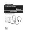
MD-MT821/W
SERVICE MANUAL
No. S4913MDMT821/
MD-MT821(GL)
MD-MT821W(BL)
MD-MT821W(GL)
Illustration: MD-MT821
• In the interests of user-safety the set should be restored to its
original condition and only parts identical to those specified be
used.
Illustration: MD-MT821W
CONTENTS
Page
SAFETY PRECAUTION FOR SERVICE MANUAL (MD-MT821W ONLY) ............................................................................ 2
SPECIFICATIONS ................................................................................................................................................................. 3
NAMES OF PARTS ............................................................................................................................................................... 4
OPERATION MANUAL .......................................................................................................................................................... 5
QUICK GUIDE (MD-MT821 ONLY) ....................................................................................................................................... 8
DISASSEMBLY .................................................................................................................................................................... 10
REMOVING AND REINSTALLING THE MAIN PARTS ....................................................................................................... 11
ADJUSTMENT ...................................................................................................................................................................... 12
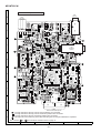
NOTES ON SCHEMATIC DIAGRAM .................................................................................................................................. 28
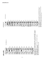
BLOCK DIAGRAM ............................................................................................................................................................... 29
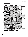
SCHEMATIC DIAGRAM/WIRING SIDE OF P.W.BOARD ................................................................................................... 30
WAVEFORMS OF MD CIRCUIT ......................................................................................................................................... 37
TROUBLE SHOOTING ........................................................................................................................................................ 38
FUNCTION TABLE OF IC .................................................................................................................................................... 41
PARTS GUIDE/EXPLODED VIEW
PACKING OF THE SET (MD-MT821 ONLY)
SHARP CORPORATION
–1–
This document has been published to be used
for after sales service only.
The contents are subject to change without notice.
MD-MT821/W
SAFETY PRECAUTION FOR SERVICE MANUAL
(MD-MT821W ONLY)
Precaution to be taken when replacing and servicing the
Laser Pickup.
CAUTION
The AEL (Accessible Emission Level) of Laser Power Output
for this model is specified to be lower than Class I Requirements. However, the following precautions must be observed
during servicing to protect your eyes against exposure to the
laser beam.
(1) When the cabinet has been removed, the power is
turned on without a compact disc, and the Pickup is on
a position outer than the lead-in position, the Laser will
light for several seconds to detect a disc. Do not look
into the Pickup Lens.
(2) The Laser Power Output of the Pickup inside the unit
and replacement service parts have already been
adjusted prior to shipping.
(3) No adjustment to the Laser Power should be attempted
when replacing or servicing the Pickup.
(4) Under no circumstances look directly into the Pickup
Lens at any time.
(5) CAUTION - Use of controls or adjustments, or
performance of procedures other than those specified
herein may result in hazardous radiation exposure.
● This Portable MiniDisc Recorder is classified as a CLASS 1 LASER product.
● The CLASS 1 LASER PRODUCT label is located on the bottom.
● Use the portable minidisc recorder only in accordance with the instructions given in
this manual and do not attempt to interfere with the interlock switch or make any
other adjustment as this may result in exposure to hazardous radiation.
Laser Diode Properties
● Material: GaAIAs
● Wavelength: 785 nm
● Pulse time:
Read mode; 0.8 mW Continuous
Write mode; max. 10 mW 0.5S
min. cycle 1.5S
Repetition
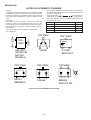
Precaution to be taken when replacing and servicing the laser pickup.
The following precautions must be observed during servicing to protect your eyesagainst exposure to the laser.
Warning of possible eye damage when repairing:
If the AC adaptor or batteries are connected when the top houising (disc cover) of the unit is removed, and the PLAY key is
pressed, the laser will light up during docus access (2-3 seconds). (Fig. 2-1) During the operation, the laser will lesk from the
opening btween the magnetic head and the mechanical chassis (Fig. 2-2). In order to protect your eyes, you most not look
at the laser durnd repaor. Before repaoring be sure to disconnect the AC adaptor and remove the batteries.
Magnet Head
Magnet head
Lasar Beam
Mechanism
Chassis
Optical pick-up
Main PWB
Top Cabinet
Spindle motor
Figure 2-1
Figure 2-2
–2–
Optical Pick-Up
MD-MT821/W
FOR A COMPLETE DESCRIPTION OF THE OPERATION OF THIS UNIT, PLEASE REFER TO
THE OPERATION MANUAL.
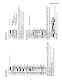
SPECIFICATIONS
General
Output level:
(MT821)
Power source:
(MT821)
DC 3.6 V : Rechargeable lithium-ion
battery x 1
DC 5 V : AC adaptor (AC 120V, 60 Hz)
DC 3.4V: Battery case
(commercially available, "AA"
size, alkaline battery x 1)
DC 4.5V: Separately available car
adaptor, AD-CA20X
(for cars with a 12-24V DC
negative ground electrical
system)
Power source:
DC 3.6 V : Rechargeable lithium-ion
(MT821W)
battery x 1
DC 5 V : AC adaptor
(AC 110 - 240V, 50/60 Hz)
DC 3.4V: Battery case
(commercially available, "AA"
size, alkaline battery x 1)
DC 4.5V: Separately available car
adaptor, AD-CA20X
(for cars with a 12-24V DC
negative earth electrical system)
Power consumption: 7 W (AC adaptor)
(MT821)
Power consumption: 0.15A (AC adaptor)
(MT821W)
Output power:
RMS; 20 mW (10 mW + 10mW)
(0.2% T.H.D.)
Charging time:
Approx. 3 hours
(When using the AC adaptor included
with the unit)
Battery life:
When using the
rechargeable battery (fully
charged) included with the
unit
When using one,
commercially available,
high capacity, "AA" size,
alkaline battery (in the
battery case)
Continuous recording:
Approx. 8 hours
Continuous recording:
Approx. 3 hours
Continuous recording:
Approx. 11 hours
Continuous play:
Approx. 11.5 hours
Continuous play:
Approx. 6.5 hours
Continuous play:
Approx. 18 hours
Headphones
LINE
Output level:
(MT821W)
Earphones
LINE
Dimensions:
Weight:
Input socket:
Output socket:
(MT821)
Output socket:
(MT821W)
Recording level
MIC H
Audio channels:
Frequency response:
Rotation speed:
Error correction:
When using one,
commercially available,
high capacity, "AA" size
battery with the rechargeable battery (fully charged)
Coding:
Recording method:
Sampling frequency:
Wow and flutter:
10 k ohms
MIC L
2.5 mV
10 k ohms
LINE
100 mV
20 k ohms
Load
impedance
—
10 mW +
10 mW
16 ohms
250 mV
(-12dB)
—
10 k ohms
Specified
output
Maximum
output level
Load
impedance
—
10 mW +
10 mW
32 ohms
250 mV
(-12dB)
—
10 k ohms
Width: 3-1/4" (82.5 mm)
Height: 13/16" (20.7 mm)
Depth: 3-1/16" (77.9 mm)
0.39 lbs. (177 g) with rechargeable
battery
Line/optical digital, microphone
(powered by the main unit)
Headphones (impedance: 19 ohms)/
remote control unit
Earphones (impedance: 32 ohms)/
remote control unit
Portable MiniDisc recorder
Non-contact, 3-beam semi-conductor
laser pick-up
Stereo 2 channels/monaural (longplay mode) 1 channel
20 - 20,000 Hz (± 3 dB)
Approx. 400 - 900 rpm
ACIRC (Advanced Cross Interleave
Reed-Solomon Code)
ATRAC (Adaptive TRansform
Acoustic Coding), 24-bit computed
type
Magnetic modulation overwrite
method
44.1 kHz (32 kHz and 48 kHz signals
are converted to 44.1 kHz, and then
recorded.)
Unmeasurable (less than ±0.001%
W.peak)
Specifications for this model are subject to change without prior
notice
Reference input level Input impedance
0.25 mV
Maximum
output level
MiniDisc Recorder
Type:
Signal readout:
The continuous recording time is for analogue inputs when the
volume level is set to "VOL 0".
The continuous play time shows the value when the volume level is
set to "VOL 15".
The above values are the standard values when the unit is charged
and used at an ambient temperature of 20oC.
The operating time when using an alkaline battery may be different,
depending on the type and manufacturer of the battery, and on the
operating temperature.
Input sensitivity:
Specified
output
–3–
MD-MT821/W
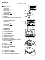
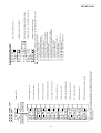
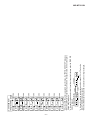
NAMES OF PARTS
2
1
Remote control unit
1. Synchro Recording Indicator
2. Character/Time Information Indicator
3. Record Indicator
4. Repeat Indicator:
5. Random Indicator
6. Disc Mode Indicator
7. Total Track Number Indicator
8. Track Number Indicator
9. Battery Indicator:
10. Headphones Jack (MT821)
10. Earphones Socket (MT821W)
11. Display/Volume Shuttle Switch
12. Hold Switch
13. Play/Pause/Fast Reverse/ Fast Forward Shuttle Switch
14. Stop/Power Off/Bass/Play Mode Shuttle Switch
6
3
SYNC REC
1
RANDOM
8
9
4
5
TOTAL
7
10
13
11
14
12
1
Main unit
1. Monaural Long-Play Mode Indicator
2. Record Indicator
3. Level Meter
4. Repeat Indicator:
5. TOC Indicator
6. Battery Indicator:
7. Random Indicator
8. Track Number Indicator
9. Character/Time Information Indicator
10. Synchro Recording Indicator
11. Disc Mode Indicator
12. Disc Name Indicator
13. Track Name Indicator
14. Remaining Recording Time Indicator
15. Total Track Number Indicator
2
3 4
5
6
10
11
12
13
7
8
9
14 15
ED
IT
DISP
DE
B
L
VE
LE
REC
YN
C
MO
REC
VOL
FF
A
SS
16. Record/Track Mark Button
17. Mode Button
18. Bass/Delete Button
19. Enter/Fast Play/Synchro Button
20. Volume/Cursor Up Button: +
21. Volume/Cursor Down Button: 22. Edit/Auto Mark/Time Mark Button
23. Display/Character Select Button
24. Fast Reverse/Fast Forward/Record-ing Level Control/
Name Select Shuttle Switch
25. Stop/Power Off Button: /:OFF
26. Play/Pause Button:
EN
TE
R
S
16 17 18 19
:O
20
21
22 23 24 25 26
27. Open Lever
28. Headphones Jack (MT821)
28. Earphones Socket (MT821W)
29. Optical/Line Input Jack (MT821)
29. Optical/Line Input Socket (MT821W)
30. Handstrap Holder
27
28
29
30
31
31. Hold Switch
32. Battery Case Connection Terminals
33. Microphone Input Jack (MT821)
33. Microphone Input Socket (MT821W)
34. 5V DC Input Jack (MT821)
34. 5V DC Input Socket (MT821W)
35. Rechargeable Lithium-lon Battery Compartment
32
–4–
33
34
35
–5–
EN
OP
EN
OP
EN
OP
Mark
EN
OP
EN
OP
Notes:
● After charging has been completed, the
AC adaptor may be left connected.
(For example, when charging at night)
● If the rechargeable battery is in the unit,
it will be charged, even whilst operating
the unit. (Float charge)
Insert securely, all the
way in.
AC 110-240V, 50/60 Hz
To the DC IN 5V socket
4
2
1
● Do not force open the rechargeable battery cover too wide.
● When the AC adaptor plug is inserted
and a MiniDisc has already been inserted, playback may start automatically.
In this case, press the ■ / :OFF button
twice to turn the power off.
and then insert the plug on the AC adaptor lead into the DC IN 5V socket.
” will
● About 4 seconds later, “
flash, and the battery will begin charging.
● Battery charging will be complete in
3.0 hours. When the charging is complete, “
” will go out.
4 Plug the AC adaptor into the AC socket,
ment cover.
3 Close the rechargeable battery compart-
● Insert the side with the arrow first.
2 Insert the rechargeable battery.
ment cover.
1 Open the rechargeable battery compart-
When the rechargeable battery is used for
the first time or when you want to use it after a long period of disuse, be sure to charge
it fully.
■ Rechargeable battery power
This unit can be used with 4 different power sources: a rechargeable battery, an AC
adaptor, a battery case, and a separately available car adaptor (AD-CA20X).
POWER SOURCE
Charging is
needed.
When you attempt to make a new digital
recording from a track that was digitally recorded on a MiniDisc.
● MiniDiscs are designed so that only first
generation digital copies can be made.
Further digital copies are prevented by
the SCMS (Serial Copy Management
System).
In the following cases digital recording is
impossible, even if you are using digital
cables.
There are cases where digital
recording may be impossible.
Playback
Digital cable
Recording
Analogue recording is
possible.
Digital cable
Digitally recorded MiniDisc
CD player, MD
player, etc.
Playback
Recording
Notes:
● When using the unit with an alkaline battery or a rechargeable battery, the battery
indicator will not correctly display the remaining capacity for approximately 20 seconds
after the power has been turned on.
● When the AC adaptor included with this unit
or a separately available car adaptor is
used, the battery indicator will not be shown.
● The number of bars shown in the battery
indicator may increase or decrease, depending on the operation being performed.
This is normal.
● When the rechargeable battery and the alkaline battery are used at the same time,
the rechargeable battery is used first, then
the alkaline battery.
Since the battery indicator shows the remaining amount of the particular battery
being used, the number of bars will increase when the unit switches to the alkaline battery.
RECORDING USING THE OPTICAL DIGITAL CABLE
● When the battery is completely discharged,
the whole battery indicator will flash. Recharge the battery or replace the alkaline
battery with a new one.
● When the battery has run completely out,
“BATT EMPTY” (main unit) and “Lo BATT”
(remote control unit) will appear. Then, the
power will be disconnected automatically.
When the battery needs charging, it is
impossible to start recording or editing.
When the battery is
completely charged
< How to read the battery indicator >
Battery indicator
The remaining amount of battery charge
is shown by the battery indicator (
)
during operation.
■ Checking the remaining amount
of battery charge
CONVENIENT OPERATION OF THE UNIT
MD-MT821/W
OPERATION MANUAL
CAUSE
Is the AC adaptor disconnected?
Is the battery exhausted?
Is the unit in the hold mode?
Has condensation formed inside the unit?
Is the unit being influenced by mechanical shock or by
static electricity?
–6–
● Has the track number or character information been
written on the disc yet?
● Is the unit in the recording or editing mode?
The MiniDisc cannot be
ejected.
When this product is subjected to strong
external interference (mechanical shock,
excessive static electricity, abnormal supply voltage due to lightning, etc.) or if it is
operated incorrectly, it may malfunction. If
such a problem occurs, do the following:
1. Unplug the AC adaptor from the AC
socket.
2. Remove the battery.
3. Leave the unit completely unpowered for
approximately 30 seconds.
■ If trouble occurs
Recording and editing
are impossible.
● Is the battery exhausted?
● Is the unit being subjected to excessive vibration?
Some sounds are
skipped.
If strange sounds, smell or smoke come out
of the unit or an object is dropped into the
unit, remove the AC adaptor from the AC
socket immediately and contact an
authorised SHARP service centre.
4. Plug the AC adaptor back into the AC
socket and retry the operation.
● Is the MiniDisc protected against accidental erasure?
● Is the unit connected properly to the other equipment?
● Is the AC adaptor unplugged or did a power failure
occur whilst recording or editing?
● Is the unit in the hold mode?
● Is an optical signal being output from the external
equipment?
Read the operation manual for the external equipment.
● Is the unit in the hold mode?
● Is the battery exhausted?
● Is the remote control unit plug or the earphone plug inserted firmly?
● Is the volume set too low?
● Is the remote control unit or the earphones plugged in?
● Are you trying to play a MiniDisc with data on it instead
of a MiniDisc containing music?
●
●
●
●
●
When the operation
buttons are pressed, the
unit does not respond.
No sound is heard from
the earphones.
The unit does not turn
on.
PROBLEM
When the unit has condensation
inside, the disc signals cannot be
read, and the unit may not function
● Shortly after turning on a heater.
properly.
● When the unit is placed in a room where
● If this happens, remove the disc.
there is excessive steam or moisture.
The condensation should evaporate in
● When the unit is moved from a cool
approximately 1 hour. The unit will then
place to a warm place.
function properly.
Many potential “problems” can be resolved by the owner without calling a service technician.
If something seems to be wrong with this product, check the following before calling your
authorised SHARP dealer or service centre.
In the following cases, condensation
may form inside the unit.
■ Moisture condensation
TROUBLESHOOTING
For MiniDiscs on which repeated
recording and editing were performed,
some sounds may be skipped whilst
cueing and reviewing.
If there are scratches or dust on a
MiniDisc, the track numbers following
that track will be increased by one.
When recorded tracks are played
back using the cue and review operations, some sounds may be
skipped.
A track number can be created in
the middle of a track.
For MiniDiscs on which repeated
recording and editing operations were
performed, the COMBINE function
may not work.
Two tracks may not be combined
in editing.
The total of the recorded time and
time remaining on a disc may not
add up to the maximum possible
recording time.
When the remaining recording time of
a disc is displayed, short tracks less
than 12 seconds long may not be
included in the total.
Even if several short tracks are
erased, the remaining recording
time may not show an increase.
A cluster (about 2 seconds) is normally
the minimum unit of recording. So, even
if a track is less than 2 seconds long, it
will use about 2 seconds of space on the
disc.
Therefore, the time actually available for
recording may be less than the
remaining time displayed.
If there are scratches on discs, those
sections will be automatically avoided
(no recording will be placed in those
sections). Therefore, the recording time
will be reduced.
If there are scratches on a disc, the unit
will automatically avoid recording in
those areas. The recording time will be
reduced.
Even if the number of tracks and
the recording time have not
reached the limit, “DISC FULL”
may be displayed.
Even if the maximum recording
time of a MiniDisc has not been
reached, “DISC FULL” or “TOC
FULL” may be displayed.
When the number of tracks used
reaches the limit, regardless of the
remaining recording time, further
recording will be impossible.
(Maximum number of tracks: 255)
If a MiniDisc has been recorded or
edited repeatedly or if a MiniDisc has
scratches on it, it may not be possible
to record the maximum number of
tracks on it.
MiniDiscs are recorded using a different system than is used for cassette tapes or DAT
recordings. Therefore, the following conditions may be encountered, depending on how
the disc has been recorded or edited. These are due to system limitations, and should be
considered normal.
MINIDISC SYSTEM LIMITATIONS
MD-MT821/W
–7–
(
● A large portion of the disc has been
damaged.
● There is no space left for recording
character information (track names,
disc names, etc.).
● The track has been protected from
being erased.
● A large portion of the disc has been
damaged.
● There is an error in the recorded signal.
● A disc which contains data other than
music was played.
● There is an error in the signal from the
disc.
● Since a track number is currently being
located or written to, the unit cannot
accept your command.
● You have come to the conclusion that
the unit is out of order.
● The temperature is too high.
● The MD is write protected.
● You tried to record without loading an
MD.
● A playback-only MD was loaded and
the REC button was pressed when the
power was off.
● The disc is damaged.
● The EJECT lever was moved during
recording or editing.
● A disc has not been loaded.
● You tried to record on a playback- only
disc.
● Improper power is being supplied.
● The unit is in the hold mode.
● The disc is out of recording space.
● Poor connection of the digital cable.
● Recording cannot be performed
correctly due to vibration or shock in
the unit.
● Editing is impossible.
● The disc is scratched.
● No copy can be made because of the
SCMS copyright system.
● A track cannot be edited.
● Nothing is recorded.
): Error messages seen on the remote control.
? DISC
(?DISC)
U TOC ERROR
(E-UTOC)
Tr. Protect
TOC FULL
SYSTEM ERR
(E-SYS)
TEMP OVER
(E-TEMP)
TOC ERROR
(E-TOC)
READ ERROR
(E-READ)
SORRY
(SORRY)
PROTECTED
POWER ?
PB DISC
HOLD
(HOLD)
LOCKED
LOCK ERROR
NO DISC
DISC FULL
Din UNLOCK
(UNLOCK)
DEFECT
(DEFECT)
Can’t WRITE
Can’t REC
(Not REC)
BLANK DISC
(BLANK)
Can’t COPY
(Not REC)
Can’t EDIT
Error messages
Meaning
BATT EMPTY ● The battery run down.
(Lo BATT)
ERROR MESSAGES
Remedy
● Edit the track with the device on which
it was recorded.
● Replace it with another recorded disc.
● Erase all of the signal errors, and then
try recording again.
● A disc which contains non-music data
cannot be played.
● Replace it with another recorded disc.
● Replace it with another recordable disc.
● Replace it with another recorded disc.
● To have it repaired, go to the distributor
where you purchased the unit.
● Turn off the power, and wait for a while.
● Reload the disc or replace it.
● Replace it with another recorded disc.
● Wait for a while and try the operation
again.
● Use one of the specified power
sources.
● Move the write protection knob back to
its original position.
● Load a recordable MD.
● Replace it with a recordable MD.
● Return the HOLD switch to its original
position.
● Turn off the power and remove the
MiniDisc.
● Load a disc.
● Replace it with a recordable disc.
● Replace it with another recordable disc.
● Check the number of tracks.
● If the sound you hear is not right, try
recording again.
● Replace the disc with another
recordable disc.
● Connect the digital cable securely.
● Change the stop position of the track
and then try editing it.
● Re-record or replace it with another
recordable disc.
● Record using the analog cable.
● Charge the rechargeable battery or
replace the alkaline battery (or use the
AC adaptor for power).
● Replace the disc with a recorded disc.
MD-MT821/W
● Analog Cable x 1
● Cable analógico x 1
● Optical Digital Cable
x1
● Cable óptico digital x
1
–8–
EN
OP
EN
OP
EN
OP
EN
OP
■ AC power
■ Alimentación de CA
● Make sure that a fully charged
rechargeable battery is inserted.
● Do not use the unit if it only has an
alkaline battery in it.
● Asegúrese de que se ha insertado una
batería completamente cargada.
● No emplee el aparato si sólo tiene una
pila alcalina instalada.
■ Alkaline battery power
■ Alimentación de la pila alcalina
1
1
■ Rechargeable battery power
■ Alimentación de la batería recargable
2
Mark
Marca
3
3
● Handstrap x 1
● Correa para la
muñeca x 1
● Rechargeable
Lithium-Ion Battery x 1
● Batería recargable de
litio-ion x 1
Printed in Japan
Impreso en Japón
• AC 120V, 60Hz
• 120V CA, 60Hz
1 Press.
Pulsar.
2 Open.
Abrir.
2
EN
OP
● Carrying Bag x 1
● Caja para el
transporte x 1
● AC Adaptor x 1
● Adaptador de CA x 1
2 Power source / Alimentación
● Headphones x 1
● Auriculares x 1
● Remote Control Unit
x1
● Controlador remoto
x1
RELEASE
LOCK
• Back of the MD recorder
• Parte posterior de la
grabadora de MD
• AC 120V,
60Hz
• 120V CA,
60Hz
● Battery Case x 1
● Caja de la pila x 1
1 Check the supplied accessories / Compruebe los accesorios suministrados
PORTABLE MINIDISC RECORDER
Quick Guide/Guía rápida MD-MT821
Playback side
Lado de reproducción
■ Digital recording
■ Grabación digital
Stereo microphone
Micrófono estéreo
■ Microphone
■ Micrófono
(RIGHT)
(DERECHO)
DIGITAL OUT
• To the line output jacks
on a stereo
• A los enchufes de
salida de línea de un
equipo estéreo
Playback side
Lado de reproducción
■ Analog recording
■ Grabación analógica
3 Connection / Conexión
R
(LEFT)
(IZQUIERDO)
MIC IN
PLUG IN
POWER
Recording side
Lado de grabación
• Optical digital cable
(supplied)
• Cable óptico digital
(suministrado)
Recording side
Lado de grabación
• Analog cable included with this unit
• Cable analógico suministrado con este
L
Recording side
Lado de grabación
OPTICAL/
LINE IN
OPTICAL/
LINE IN
MD-MT821/W
QUICK GUIDE (MD-MT821 ONLY)
3
Inserte un minidisco grabable.
6
5
4
Insert a recordable MiniDisc.
EL
EV
CL
RE
REC
Inicie la reproducción en el equipo fuente.
Begin playback on the source equipment.
Pulse el botón ENTER/SYNC.
Press the ENTER/SYNC button.
Mientras se reproduce el sonido del equipo
externo conectado a este aparato, mueva el
selector de mando de lanzadera hacia arriba o
abajo para ajustar el nivel de grabación.
While playing sound from the external
equipment connected to this unit, move the
shuttle switch up or down to adjust the
recording level.
Pulse el botón ● REC.
Press the ● REC button.
1
1
2
3
Turn off the power and move
the OPEN lever in the direction
indicated by the arrow.
Desconecte la alimentación y
mueva la palanca OPEN en el
sentido indicado por la flecha.
3
Insert a recordable MiniDisc.
Inserte un minidisco grabable.
To remove the MiniDisc:
Para extraer el minidisco:
2
2
Conecte el micrófono estéreo al
enchufe MIC IN del aparato principal.
Connect the stereo microphone to
the MIC IN jack.
5
4
3
When a noise, such as a person speaking, is
picked up by the microphone, recording will
begin automatically.
Cuando el micrófono capte un ruido, el de una
persona que hable por ejemplo, la grabación
empezará automáticamente.
Pulse el botón ENTER/SYNC para seleccionar el
nivel de la grabación sincronizada. (Este nivel
podrá cambiarse incluso durante la grabación.)
Press the ENTER/SYNC button to select the
synchro recording level. (This level can be
changed, even while recording.)
Mueva el selector de mando de lanzadera hacia
arriba o abajo para ajustar el nivel de grabación.
Move the shuttle switch up or down to adjust
the recording level.
Pulse el botón ● REC.
Press the ● REC button.
Press the ■/:OFF button while in the stop mode.
Pulse el botón ■/:OFF estando en el modo de parada.
After recording:
Después de la grabación:
Press the ■/:OFF button.
Pulse el botón ■/:OFF.
To stop recording:
Para detener la grabación:
6
REC
EL
EV
CL
RE
EN
TE
R
–9–
SY
NC
1
■ Recording from the microphone (Mic synchro recording)
■ Grabación de un micrófono (Grabación sincronizada con micrófono)
1
2
2
3
Conecte el equipo externo.
EN
T
1
ER
SY
NC
Connect the external equipment.
■ Recording from CDs or MDs (Synchro recording)
■ Grabación de discos compactos o minidiscos (Grabación sincronizada)
4 Recording / Grabación
Cargue un minidisco en el sentido indicado
por la flecha del minidisco, con el lado de la
etiqueta hacia arriba.
Load a MiniDisc in the direction indicated
by the arrow on the MiniDisc, with the label
side facing up.
Enchufe el controlador remoto en el enchufe
del aparato principal. Empuje completamente
hacia adentro la clavija.
Plug the remote control unit into the jack
on the main unit. Push the plug all the way in.
Inserte firmemente la clavija de los auriculares
en el enchufe de auriculares del controlador
remoto.
Insert the headphones plug firmly into the
headphones jack on the remote control unit.
3
• Volume (0 - 30)
• Volumen (0 - 30)
Adjust the volume.
From the main unit:
Press the + button to increase the volume and the –
button to decrease the volume.
From the remote control unit:
Move the shuttle switch up once to increase the volume,
and move it down once to decrease the volume.
Ajuste el volumen.
Desde el aparato principal:
Pulse el botón + para aumentar el volumen y el botón –
para reducirlo.
Desde el controlador remoto:
Mueva el selector de mando de lanzadera una vez hacia
arriba para aumentar el volumen, y muévalo hacia abajo
para reducirlo.
6 Sound control / Control del sonido
● The power will be turned on automatically, and
playback will start from the first track.
(Auto-play function)
● La alimentación se conectará automáticamente, y
la reproducción empezará desde la primera pista.
(Función de reproducción automática)
3
2
1
1
2
REMOTE
BASS OFF ---- El realce de los graves se cancela.
BASS 3 ------- Los sonidos graves se realzan aún más.
BASS 2 ------- Los sonidos graves se realzan más.
BASS 1 ------- Los sonidos graves se realzan ligeramente.
BASS OFF ---- Bass emphasiz is canceled.
BASS 3 ------- Bass sounds are emphasized even more.
BASS 2 ------- Bass sounds are emphasized more.
BASS 1 ------- Bass sounds are emphasized slightly.
Adjust the bass level.
Each time the BASS button is pressed, the tone will be
switched as follows:
Ajuste el nivel de los graves.
Cada vez que pulse el botón BASS, el tono cambiará de
la forma siguiente:
Press the ■/:OFF button while in the stop mode.
Pulse el botón ■ /:OFF estando en el modo de parada.
To turn off the power:
Para desconectar la alimentación:
Press the ■/:OFF button.
Pulse el botón ■ /:OFF.
To stop playback:
Para detener la reproducción:
Pulse el botón 06 durante la reproducción.
● Para reanudar la reproducción, pulse de nuevo el botón
06
Press the 06 button during playback.
● To resume playback, press the 06 button again.
To interrupt playback:
Para interrumpir la reproducción:
Pulse el botón 06 .
En los casos siguientes, la función de reproducción
automática no se activará.
● Cuando esté cerrada la lengüeta de protección contra
escritura del minidisco grabable
● Cuando haya sido cancelada la función de reproducción
automática
Playback does not start when a MiniDisc is inserted:
La reproducción no empieza cuando se inserta un
minidisco:
Press the 06 button.
In the following cases, the auto-play function will not work.
● When the recordable MiniDisc write protection tab is
closed
● When the auto-play function has been canceled
5 Playing a MiniDisc / Reproducción de un minidisco
MD-MT821/W
MD-MT821/W
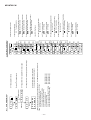
DISASSEMBLY
Cares before disassembling
When assembling the machine after disassembling or
repair, observe the following requirements so as to
ensure safety and performance.
1. Remove the batteries from the machine, and take out the
mini-disc.
2. When assembling after repair, be sure to restore the
initial location of wires.
Since the screws are small, incorrect fixing may result in
malfunction.
3. When repairing, pay utmost attention to static electricity
of IC.
STEP
PROCEDURE
REMOVAL
(B1)x2
ø1.4x2mm
(A1)x2
ø1.4x2mm
Bottom Lid
1. Screw ..................... (A1) x5
10-1
2
Top Cabinet
1. Open the disc lid
2. Screw ..................... (B1) x4
3. Flexible PWB .......... (B2) x2
10-1
3
Center Cabinet A 1. Hook ...................... (C1) x2
10-2
4
Center Cabinet B 1. Remove in the arrow direction.
10-2
5
Main PWB
1. Flexible PWB ......... (D1) x2
2. Soldering ............... (D2) x2
3. Screw .................... (D3) x1
10-3
6
Mechanism Unit
1. Raise the rear part, and remove
in the arrow direction.
10-4
Top Cabinet
OPEN
Lever
FIGURE
1
(A1)x1
ø1.4x2mm
(B1)x2
ø1.4x2mm
Bottom Lid
(A1)x2
ø1.4x2mm
Figu re 10-1
10-3
Remove the hook
Center
Cabinet B
Note
Remove the hook
Open or close the battery cover as shown below.
Center
Cabinet A
2
EN
OP
Slide the battery cover.
Open it.
(C1)x2
Precision Driver
Push down the lever of center
chassis outwards , and move
the mechanism unit to remove it.
O
P
E
N
1
O
P
E
N
To open
Do not raise the battery
cover upward.
1
2
EN
OP
O
P
E
N
To close
EN
OP
Figure 10-2
Raise the battery cover.
Slide it to close.
Mechanism Unit
Do not force open the
battery cover too wide.
Put the fold on the connector, and
apply with the felt. Sagging may
result in contact with the sheet metal.
Felt
(B2)x2
Main PWB
(D3)x1
ø1.7x2.5mm
Pull
Pull
Pull
Pull
Pull
Pull
Pull
(D2)x1
(D1)x*1
(D1)x1
Flexible PWB
for optical pickup
(D2)x3
Caution:
Carefully handle the main PWB and flexible PWB. After removing the
flexible PWB (*1) for the optical pickup from the connector, do not
touch directly the front end of flexible PWB with your hand so as to
prevent damage of optical pickup by static electricity.
Figure 10-4
Figure 10-3
– 10 –
MD-MT821/W
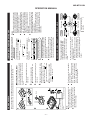
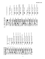
REMOVING AND REINSTALLING THE MAIN PARTS
(A2)x3
ø1.4x2.8mm
Remove the mechanism according to the disassembling methods 1 to 6. (See Page 10.)
How to remove the spindle motor (See Fig. 11-1.)
1. Remove the solder joint (A1) x 1 of flexible PWB.
2. Remove the screws (A2) x 3 pcs., and remove the spindle
motor.
Spindle Motor
Mechanism Flexible
PWB Solder joint
(A1)x1
How to remove the lift motor (See Fig. 11-2.)
1. Remove the solder joint (B1) x 2 of lift motor lead wire.
2. Remove the screw (B2) x 1 pc., and remove the flexible
PWB.
3. Remove the screw (B3) x 1 pc., and remove the lift motor.
Note:
Take care so that the motor gear is not damaged.
(If the gear is damaged, noise is caused.)
MD Mechanism
Figure 11-1
(B3)x1
ø1.4x5.5mm
(B2)x1
ø1.4x1.5mm
Remove the
solder joint
(B1)x2
How to remove the sled motor (See Fig. 11-3.)
1. Remove the stop washer (C1) x 1 pc., and remove the drive
gear (C2) x 1 pc.
2. Remove the screws (C3) x 2 pcs., and remove the sled
motor.
3. Remove the solder joints (C4) x 2 of flexible PWB.
Note:
Take care so that the motor gear is not damaged.
(If the gear is damaged, noise is caused.)
Lift Motor
How to remove the magnetic head (See Fig. 11-4.)
1. Remove the screws (D1) x4 which connects the magnetic
head to the head relay flexible PWB, remove the spring
washers (D2) x 2 and remove the soldering joints (D3) x 2.
Note:
Mount carefully so as not to damage the magnetic head.
(If the gear is damaged, noise is caused.)
MD Mechanism
Figure 11-2
Stop Washer
(C1)x1
(C3)x2
ø1.4x1.2mm
Sled Motor
Drive Gear
(C2)x1
Mechanism Flexible PWB
Solder Joint (C4)x2
How to reinstall the optical pickup unit
(See Fig. 11-5.)
1. Remove the screw (E1) x 1 pc.
2. Slowly raise the optical pickup.
MD Mechanism
(E1)x1
ø1.7x3mm
Figure 11-3
(D1)x2
ø1.4x2.2mm
Spring Washer
(D2)x2
Shft
Pickup Unit
Magnetic Head
(D1)x1
Solder joint
ø1.4x1.5mm
(D3)x2
(D1)x1
ø1.2x1.6mm
MD Mechanism
MD Mechanism
Figure 11-5
Figure 11-4
– 11 –
MD-MT821/W
ADJUSTMENT
Test disc
MD adjustment needs two types of disc, namely recording disc (low reflection disc) and playback-only disc (high
reflection disc).
Type
Test disc
Parts No.
1
High reflection disc MMD-110 (TEAC Test MD)
88GMMD-110
2
Low reflection disc
MMD-212 (TEAC Test MD)
88GMMD-212
3
Low reflection disc
Recording minidisc
UDSKM0001AFZZ
Note: Use the low reflection disc on which music has been recorded.
Entering the TEST mode
1. Setting at port (in standby state, disc-free state or power nonconnected state)
(1) Set the port as follows.
TEST1 : "Low"
TEST0 : "High"
(2) Press the PLAY button in the standby state (it is allowed to insert the disc or to connect the power supply).
(3) Test Mode STOP [ T E S T _ ]
2. Setting by special button operation (in standby state)
(1) Holding down the DISP button and ENTER button, press the PLAY button.
(2) Normal mode setting initialization (BASS setting, VOL setting, etc.)
*Since the unit is changed to the setting for production line inspection , be sure to set it to the default setting state in the following default
setting procedure before returning it to the user.
(3) Indication of microcomputer version for one second [ X X X X X X ]
Destination
Microcomputer version
EEPROM version
(4) Whole LCD lighting for 2 seconds
(5) Test Mode STOP [ T E S T _ ]
*When the PLAY button is pressed during indication (3) and (4), the process proceeds to (5).
Leaving the TEST mode
(1) Press the STOP button in the TEST mode stop state or version indicating state or whole LCD lighting state.
(2) EEPROM rewrite-enable area updating, adjustment error setting .
(3) Change to standby state
Shipping setting method
Holding down simultaneously the VOLUME-DOWN Button and PLAY Button of the set unit without disc, supply the power from the DC IN plug.
After the indication "INIT" -> "BYE OK" disappears, release the power supply of DC IN.
Test Mode
1. AUTO 1 Mode
2. AUTO 2 Mode
3. TEST-PLAY Mode
4. TEST-REC Mode
5. MANUAL 1 Mode
6. MANUAL 2 Mode
• Perform preliminary automatic adjustment.
• If the combination of mechanism and pickup
PWB has been changed, be sure to start from
AUTO1.
• Perform ATT (attenuator) automatic adjustment.
• Perform continuous playback (error rate display,
jump test)
• Continuous playback from the specified address
is performed.
• 1 line, 10 lines or 384 lines manual jump is
performed.
• C1 error rate display (pit section), ADIP error
rate display (groove section)
• The temperature correction is performed only when
servo start is performed, but the posture correction
is not performed during continuous playback.
• Continuous record from the specified address
is performed.
• Change of record laser output(servo gain is also
changed according to laser output).
• The temperature correction is performed only
when servo start is performed, but the posture
correction is not performed during continuous
recording.
• Temperature is displayed. (Updating in real time)
• Seeing the displayed adjustment value, perform
preliminary manual adjustment.
(Error rate indication, jump test)
• Temperature is displayed. (Updating in real time)
• Seeing the displayed adjustment value perform
manfully the preliminary adjustment.
(Error rate indication, jump test)
• Continuous playback is performed
(error rate display, jump test).
7. RESULT 1 Mode
• The value adjusted in AUTO1 or MANUAL1 is
indicated.
• (Execution in servo "OFF" state").
8. RESULT 2 Mode
• The value adjusted in AUTO 2 or MANUAL 2 is
indicated.
• Adjustment value is changed manually.
(error rate display, jump test).
9. DIGITAL INPUT Mode
• Digital input information is displayed.
10. ERROR INFORMATION • Error information is displayed.
Mode
• Error information is initialized
11. NORMAL Mode
• The mode is changed from the TEST mode to
the normal mode without adjustment.
• In the normal mode the internal operation mode,
memory capacity, etc. areindicated.
• In the normal mode both temperature correction
and posture correction are perfomed.
12. EEPROM Mode
• Factors of digital servo are changed manually.
(Each servo is turned on individually.)
• Cut-off frequency of BASS1, BASS2 and BASS3
is selected manually.
• Temperature detection terminal voltage is
measured, and the reference value is set.
• Defaults are selected and set.
• Setting of EEPROM protect area is updated.
(In case of protect releasing)
13. INNER Mode
• Determine the position where the INNER switch
is turned on. (only high reflection disc).
• The temperature correction is performed only
when servo start is performed, but the posture
correction is not performed.
– 12 –
MD-MT821/W
Operation in each TEST mode
1. AUTO1 Mode
• When the STOP button is pressed while the AUTO1 menu appears or during automatic adjustment, the mode changes to the TEST mode
stop state. At this time the adjustment value is not output.
• Be sure to adjust, using the specified disc MMD-212.
At this time release the EEPROM (IC402) protection. (Refer to EEPROM write procedure.)
• Adjustment NG; Adjustment item out of range, focus ON failure, and adjustment error
• When the PLAY button is pressed while ADJ. OK is displayed, AUTO2 is executed.
2. AUTO2 Mode
• When the STOP button is pressed while the AUTO2 menu appears or during automatic adjustment, the mode changes to the TEST mode
stop state. At this time the adjustment value is not output.
• Adjustment NG; Adjustment item out of range, and adjustment error.
• When the PLAY button is pressed while ADJ. OK is displayed,TEST_PLAY is executed.
3. MANUAL1 Mode
• Adjustment item to be made in AUTO1 mode is performed manually.
• When the VOL UP button is pressed during adjustment, the setting increases, and the new setting is output.
• If the VOL DOWN button is pressed during adjustment, the setting decreases and the new setting is output.
• If the VOL UP/DOWN button is held down, the setting changes continuously with 100 ms cycle.
*In this operation, the setting change is performed for each digit. The digit is changed by pressing the MODE button.
• If the setting is within the allowable range, the RANDOM display lights.
• When the STOP button is pressed during MANUAL1 MENU or measurement or adjustment, the state is changed to the TEST mode stop
state.
4. MANUAL2 Mode
• Adjustment item to be made in AUTO2 mode is performed manually.
• When the VOL UP button is pressed during adjustment, the setting increases, and the new setting is output.
• If the VOL DOWN button is pressed during adjustment, the setting decreases and the new setting is output.
• If the VOL UP/DOWN button is held down, the setting changes continuously with 100 ms cycle.
*In this operation, the setting change is performed for each digit. The digit is changed by pressing the MODE button.
• If the setting is within the allowable range, the RANDOM display lights.
• When the STOP button is pressed during MANUAL2 MENU or measurement or adjustment, the state is changed to the TEST mode stop
state.
• When the PLAY button is pressed in B-ATT set state, the mode is changed to the continuous playback mode.
• As for operation during continuous playback refer to "TEST-PLAY mode explanation".
5. RESULT1 Mode
• The measurement value and set value of adjustment items for AUTO1 and MANUAL 1 are displayed.
• If the VOL UP button is pressed during setting indication, the setting increases. If the VOL DOWN button is pressed, the setting reduces.
And then the new setting is stored in the RAM.
• When the VOL UP/DOWN button is held down, the setting changes continuously, one cycle being 100 ms.
*In this operation, the setting change is performed for each digit. The digit is changed by pressing the MODE button.
• If the STOP button is pressed during RESULT1 menu or measurement value indication or set value indication, the state is changed to the
TEST mode STOP state.
6. RESULT2 Mode
• The measurement value and set value of adjustment items for AUTO2 and MANUAL 2 are displayed.
• If the VOL UP button is pressed during setting indication, the setting increases. If the VOL DOWN button is pressed, the setting reduces.
And then the new setting is stored in the RAM.
• When the VOL UP/DOWN button is held down, the setting changes continuously, one cycle being 100 ms.
*In this operation, the setting change is performed for each digit. The digit is changed by pressing the MODE button.
• If the STOP button is pressed during RESULT2 menu or measurement value indication or set value indication, the state is changed to the
TEST mode STOP state.
7. TEST-PLAY Mode
• When the STOP button is pressed while the TEST-PLAY menu appears, or in TEST-PLAY or continuous playback mode, the mode
changes to the TEST mode stop state.
• When the PLAY button is pressed while the TEST-PLAY menu appears,continuous playback is initiated from the current pickup position.
• Whenever the DISP button is pressed in the TEST-PLAY menu, the target address changes as follows.
0050 — 03C0 — 0700 — 08A0 — 0950— 0050 —
When the PLAY button is pressed while a target address is displayed, continuous playback is performed after searching that address.
• Each time the MODE button is pressed while the TEST-PLAY mode target address is displayed, the digit which is changed by pressing the
SKIP UP/DOWN button is changed as follows.
0050 — 0050 — 0050 — 0050 —
• When the SKIP UP button is pressed in the TEST-PLAY mode target address is displayed, the digit of address specified by the MODE
button is set to +1h. (0 to F)
• When the SKIP DOWN button is pressed in the TEST-PLAY mode target address is displayed, the digit of address specified by the MODE
button is set to -1h. (0 to F)
* When the SKIP UP/DOWN button is held down, the setting changes continuously, one cycle being 100 ms.
• When the BASS button is pressed in the continuous playback mode, the number of jump lines changes as follows.
1 — 10 — 384 — 1
* After the number of jump lines is indicated for one second, the address indication is restored.
[
T R _ ]
– 13 –
MD-MT821/W
• When the SKIP UP button is pressed in the continuous playback mode, the specified number of lines is jumped in the FWD direction.
• When the SKIP DOWN button is pressed in the continuous playback mode, the specified number of lines is jumped in the REV direction.
* When the SKIP UP/DOWN button is held down, jump is repeated every approx. 100 ms.
•Whenever the DISP button is pressed in the continuous playback mode, the indication changes as follows.
* Pre-mastered disc
Continuous playback (SUBQ address indication)
[ S Q
]
|
Continuous playback (C1 error indication)
[ C E
]
|
Continuous playback (SUBQ address indication)
[ S Q
]
* Recordabl disk
Continuous playback (ADIP address indication)
[ A P
]
|
Continuous playback (C1 error indication)
[ C E
]
|
Continuous playback (ADIP error indication)
[ A E
]
|
Continuous playback (ADIP address indication)
[ A P
]
8. TEST-REC Mode
• When the STOP button is pressed while the TEST-REC menu appears, or in the TEST-REC mode or continuous record mode, the mode
changes to the TEST mode stop state.
• When the PLAY button is pressed while the TEST-REC menu appears, the continuous record is initiated from the current pickup position.
• Whenever the DISP button is pressed in the TEST-REC menu, the target address changes as follows.
0032 — 03C0 — 0700 — 08A0 —0950 — 0032 —
When the PLAY button is pressed while a target address is displayed, continuous playback is performed after searching that address.
• Whenever the MODE button is pressed in the TEST-REC mode target address is displayed, the digit which is changed by the SKIP UP/
DOWN button changes as follows.
0032 — 0032 — 0032 — 0320 —
• When the SKIP UP button s pressed in the TEST-REC mode target address is displayed, the digit of address specified by the BASS button
is set to +1h.(0 to F)
• When the SKIP DOWN button is pressed in the TEST-REC mode target address is displayed, the digit of address specified by the BASS
button is set to -1h. (0 to F)
* When the SKIP UP/DOWN button is held down, the setting changes continuously, one cycle being 100 ms.
• When the VOL UP/DOWN button is pressed in the TEST-REC mode or continuous record mode, the laser record power changes.
(Servo gain changes also according to record power.)
* After the laser record power is indicated for one second, the address indication is restored.
[ R P W_
]
•
: Address
•
: Laser power cord
• Operation is disabled if the premastered disc or disc is in miserase-protected state.
9. NORMAL Mode
• When the STOP button is pressed while the NORMAL menu appears, the mode changes to the TEST mode stop state.
• Indication during operation
Indication of memory capacity on main unit LCD [
] + Level meter
: Internal mode
: Address (Cluster section)
: Address (Sector section)
• Selection of sound volume, BASS, etc. is possible (without indication)
• Recording is also possible.
• If the STOP button is pressed during operation in the NORMAL mode, the NORMAL mode is canceled, and the power is turned off.
10. Digital input display Mode (Din Mon)
• When the STOP button is pressed while the digital input indication menu appears or during digital input information indication, the mode
changes to the TEST mode stop state.
• In case of analog input or digital input unlocking the indication data is _.
11. Error data display Mode
• Reversing when SKIP DOWN button is pressed
• When the STOP button is pressed while the error data indication menu appears or during error data indication, the mode changes to the
TEST mode stop state.
• Error data 0 is the latest error.
• Error which occurred in the TEST mode is also stored in the memory.
• When the DISP button is pressed while the error data indication menu appears, the error data is initialized. [ C L E A R _ ]
•
: Error Code
Explanation of error history code
21h : Focus retraction completion allowable time-over
23h : Track search completion allowable time-over
24h : Disc linear speed measurement failure
32h : P-TOC read failure
42h : U-TOC read failure
12h : RF side FG, TG, and TCRS adjustment termination failure
13h : Adjustment servo retraction excessive retrial
16h : C. IN detection time-over
17h : A, B, E, F, and TCRSO offset measurement value out of
tolerable range
– 14 –
MD-MT821/W
44h : U-TOC write data write disabled/read check error
52h : SD write data write disabled
71h : Pickup position initialization time-over
72h : EEPROM data read check sum error
73h : Record head drive disabled (by EJECT lever)
82h : Power overvoltage detection
91h : Ambient temperature is higher that the allowable temperature.
12. INNER Mode
• when the STOP button is pressed on the INNER menu (SQ______ ), the state is changed to the TEST mode STOP state.
•
: Address
EEPROM (IC402) writing procedure
1. Procedure to replace EEPROM and write initial value of microcomputer in EEPROM
(1)
(2)
(3)
(4)
(5)
Replace EEPROM.
Deprive EEPROM of protection (connect the pins 8 and 6 of IC402).
Refer to the latest EEPROM data list.
Press the Display/Lower-case Character button, Enter/Synchro button and Play/Pause button to start the test mode.
Version display
[Ver.
]
EEPROM version (C ~ Z)
Microcomputer ROM version
(6) The whole LCD lights.
(7) Test mode stop state.
[ T E S T ]
(8) Press the "BASS" button, and press twice the "SKIP DOWN" button.
[ E E P R O M ]
(9) Perform the operation to display "EEPROM SETTING MODE CHART", compare the EEPROM DATA LIST with the display,
and set according to the EEPROM DATA LIST with the VOL UP or VOL DOWN key.
(10) Set the temperature reference. (Refer to the Temperature Reference Setting Method.)
(11) Set according to the EEPROM DATA LIST.
(12) Press the Stop button.
[ T E S T ]
(13) Press the Stop button.
(14) After data is written in EEPROM, turn off power .
(15) Restore protection of EEPROM (Disconnect connection made in Step (2) above).
2. Temperature reference setting method
[1] Measurement, calculation and setting procedure
(1) Set the TEST mode.
• Set TEST 1, 0 = '01', and turn on power (or set PLAY ON in standby state).
(2) Start the EEPROM mode 'Temp' menu.
• Key operation in order of BASS, SKIP-DOWN x 2 times, PLAY, PLAY in the test mode STOP state.
• 'TM$$%%' is displayed. ($$= Temperature code, %% = Temperature reference)
(3) Once press SKIP-UP, and determine the displayed microcomputer TEMP input AD value.
• 'TPin##' is displayed. (## = TEMP input AD value)
(4) At the ambient temperature, determine the temperature corrected value from the temperature measurement value
correction table.
(5) Determine the temperature reference, using the following formula.
• Temperature reference = Microcomputer TEMP input AD value + Temperature corrected value
(6) Set the temperature reference value by button operation , and check whether the temperature code indication corresponds to "Temperature
Code Identification Table".
[2] Temperature measurement value correction table
Ambient
temperature
+ 9oC ~ +11oC
+12oC ~ +14oC
+15oC ~ +16oC
Temperature
correction
- 05h
- 04h
- 03h
Center
temperature
+ 10.0oC
+ 12.7oC
+ 15.4oC
+17oC ~ +19oC
+20oC ~ +22oC
+23oC ~ +24oC
- 02h
- 01h
± 00h
+ 18.2oC
+ 20.9oC
+ 23.6oC
+25oC ~ +27oC
+28oC ~ +30oC
+31oC ~ +33oC
+ 01h
+ 02h
+ 03h
+ 26.3oC
+ 29.0oC
+ 31.8oC
Ambient
temperature
Temperature
correction
Center
temperature
- 9oC ~ +10oC
08h
+ 0.5oC
07h
06h
05h
+ 12.5oC
+ 23.6oC
+ 35.0oC
o
o
+ 3 C ~ +21 C
+15oC ~ +33oC
+26oC ~ +43oC
– 15 –
MD-MT821/W
EEPROM DATA LIST (EEPROM version d)
Sled setting
TEMP setting
Item display
T M _ _
Item display
Set values
Calculate values
Fucus setting
Item display
Set values
Set values
S L G _
8D
H
S L 2 _
20
H
S L M _
6F
H
S L V _
87
H
F G _ _
63
H
S K k _
48
H
F F 1 _
70
H
S K t _
48
H
F F 2 _
E8
H
S K m _
4D
H
F Z H _
ED
H
W T m _
24
H
H
F L n _
0A
H
M V 1 _
4A
D J G _
14
H
M V 2 _
AA
F L V _
20
H
S R V _
00
W T f _
20
H
F S S _
AA
ADJ. SET setting
H
Item display
Tracking setting
Item display
H
H
Set values
Set values
C O K _
A0
F A T _
C0
H
H
T G _ _
26
H
T A T _
3E
H
T F 1 _
70
H
C A T _
20
H
T F 2 _
E0
H
F A B _
E0
H
T F S _
00
H
T B o _
2B
H
T B t _
14
H
T K o _
2B
H
T K t _
12
H
T D o _
67
H
T D t _
34
H
T G R _
00
H
S C t _
40
H
S C m _
53
H
C L p _
18
H
C L r _
28
H
J P I _
00
H
K 1 0 _
65
H
EQ. SET setting
Item display
Spindle setting
Item display
S P G _
S P i
_
79
S P o _
4F
S P 1 _
10
S P 2 _
60
S P 3 _
F2
H
H
H
H
F2
H
S P 5 _
10
H
S P D _
48
H
6BH
BASS setting
Item display
H
H S G _
11
H
H S O _
FD
L Q 1 _
90
H
L Q 2 _
90
H
L S G _
11
H
L S O _
00
H
G Q 1 _
98
H
G Q 2 _
84
H
G S G _
11
H
F L p _
09
H
Item display
H
S P 4 _
S P K _
H
90
H
Set values
H
AAH
S P m _
90
H Q 2 _
Control setting
Set values
14
Set values
H Q 1 _
Set values
B S 1 _
00
H
B S 2 _
2D
H
B S 3 _
4BH
– 16 –
C T 0 _
03
H
C T 1 _
11
H
C T 2 _
40
H
C T 3 _
30
H
R C 0 _
C0
H
R C 1 _
FE
H
S Y C _
A6
H
P W C _
12
H
P W L _
26
H
D R 1 _
09
H
D R 2 _
85
H
I N 1 _
54
H
I N 2 _
9D
H
I N H _
64
H
D R H _
74
H
P L E _
96
H
R C E _
94
H
E L T _
70
H
S L T _
44
H
S P M _
00
H
M S L _
00
H
U S 0 _
00
H
U S 1 _
00
H
U S 2 _
00
H
TEST
REC
– 17 –
SKIP DOWN
SKIP DOWN
SKIP DOWN
SKIP DOWN
SKIP DOWN
SKIP DOWN
SKIP DOWN
SKIP DOWN
DATA
SKIP DOWN
SKIP DOWN
: INNER switch position measurement menu
: EEPROM setting menu
: Error history display menu
: Digital input signal monitor menu
: Test mode normal playback menu
: Continuous record menu
: Continuous playback menu
: ATT adjustment value check menu
: Pre-adjustment value check menu
: ATT manual adjustment menu
: Pre-manual adjustment menu
: ATT auto adjustment menu
: Pre-auto adjustment menu
: Test Mode STOP
* When the [STOP] button is pressed in specific menu, the "TEST MODE STOP" state is set.
* When the [PLAY] button operation is performed in the specific menu, the operation of this
menu is executed.
SKIP UP
INNER
SKIP UP
EEPROM
SKIP UP
NORMAL
SKIP UP
E
SKIP UP
Din Mon
SKIP UP
RSLT2
SKIP UP
RSLT1
SKIP UP
MANU2
SKIP UP
SKIP DOWN
SKIP DOWN
SKIP DOWN
PLAY
MANU1
SKIP UP
T
SKIP UP
T
SKIP UP
AUTO2
SKIP UP
SKIP DOWN
Slide internal
periphery move
AUTO1
BASS
Slide external
periphery move
SKIP UP
Test Mode Change Chart
Tset Mode Menu
ADJ. NG
Adjustment error
: During ATT automatic adjustment
: Preadjustment normal end (adjustment value output)
: Preadjustment error (adjustment value output)
: During preadjustment adjustment
: Preautomatic Adjustment menu
* When the [STOP] button is pressed in specific menu, the "TEST MODE STOP" state is set.
*"
" represent the adjustment number as follows.
0 0 : Innermost periphery move
0 2 : ABEF offset tentative measurement
0 4 : RF side focus gain coarse adjustment
0 5 : Focus ATT tentative setting
0 6 : RF side bit section tracking gain adjustment
0 7 : COUT level setting for pit section adjustment
0 8 : External periphery move
0 9 : RF side groove section tracking gain adjustment
1 0 : COUT level setting for groove section adjustment
1 1 : RF side TCRS gain adjustment
1 2 : Tracking ATT initial setting
1 3 : RF side focus gain minor adjustment
1 4 : Focus ATT initial setting
1 5 : S gain "High" ABEF offset measurement
1 6 : TCRS offset measurement
1 7 : S gain "Low" ABEF offset measurement
AT2
PLAY
ADJ. OK
Normal end
AT1
PLAY
AUTO1
Preautomatic Adjustment
MD-MT821/W
ADJ. NG
Adjustment error
: Continuous playback (high reflection)
: Continuous playback (low reflection)
: ATT adjustment normal end (adjustment value output)
: ATT adjustment error (adjustment value output)
: During ATT autoadjustment
: ATT Autoadjustment menu
* When the [STOP] button is pressed in specific menu, the "TEST MODE STOP" state is set.
*"
" represent the adjustment number as follows.
0 0 : Innermost periphery move
0 3 : Pit section tracking ATT setting
0 4 : Pit section focus ATT setting
0 6 : External periphery move
(low reflection only)
0 7 : TCRS ATT setting
(low reflection only)
0 8 : Groove section tracking ATT setting
(low reflection only)
0 9 : Groove section focus ATT setting
(low reflection only)
SQ####
AP####
PLAY
ADJ. OK
Normal end
AT2
PLAY
AUTO2
ATT Auto Adjustment
– 18 –
SKIP DOWN
SKIP DOWN
SKIP DOWN
SKIP DOWN
SKIP DOWN
SKIP DOWN
SKIP DOWN
SKIP DOWN
SKIP DOWN
SKIP DOWN
SKIP DOWN
P
SKIP DOWN
SKIP DOWN
SKIP DOWN
SKIP DOWN
SKIP DOWN
$ $
Continued to
the next page
SKIP UP
SF
SKIP UP
SE
SKIP UP
RCG
SKIP UP
GCH
SKIP UP
GTG
SKIP UP
PCH
SKIP UP
PTG
SKIP UP
Sb
SKIP UP
Sa
SKIP UP
RFg
SKIP UP
LON
SKIP UP
Fh
SKIP UP
Eh
SKIP UP
Bh
SKIP UP
Ah
SKIP UP
TMP
PLAY
MANU1
Pre-Manual Adjustment
: F-ATT (tracking) initial setting
: ATT setting
: E-ATT (tracking) initial setting
: ATT setting
: RF side TCRS gain adjustment
: Gain setting
: Groove section adjustment COUT level setting
: COUT level setting
RF side groove section tracking gain adjustment
: Gain setting
: Pit section adjustment COUT level setting
: COUT level setting
: RF side pit section tracking gain adjustment
: Gain setting
: B-ATT (focus) tentative setting
: ATT setting
: A-ATT (focus) tentative setting
: ATT setting
: RF side focus gain coarse adjustment
: Gain setting
: Laser ON (Play Power)
: F signal offset (FINO) tentative measurement
: Measurement value
: E signal offset (EINO) tentative measurement
: Measurement value
: B signal offset (BINO) tentative measurement
: Measurement value
: A signal offset (AINO) tentative measurement
: Measurement value
: Temperature code display
$ $ : Temperature code
: Pre-Manual Adjustment menu
MD-MT821/W
– 19 –
FL
SKIP UP
EL
SKIP UP
BL
SKIP UP
AL
SKIP UP
TH
SKIP UP
FH
SKIP UP
EH
SKIP UP
BH
SKIP UP
AH
SKIP UP
SB
SKIP UP
SA
SKIP UP
RFG
SKIP UP
SKIP DOWN
SKIP DOWN
SKIP DOWN
SKIP DOWN
SKIP DOWN
SKIP DOWN
SKIP DOWN
SKIP DOWN
SKIP DOWN
SKIP DOWN
SKIP DOWN
SKIP DOWN
Continued from the
preceding page
: S gain "Low" F signal offset (FINO) measurement
: Measurement value
: S gain "Low" E signal offset (EINO) measurement
: Measurement value
: S gain "Low" B signal offset (BINO) measurement
: Measurement value
: S gain "Low" A signal offset (AINO) measurement
: Measurement value
TCRS signal offset (TCRSO) measurement
: ATT setting
: S gain "High" F signal offset (FINO) measurement
: Measurement value
: S gain "High" E signal offset (EINO) measurement
: Measurement value
: S gain "High" B signal offset (BINO) measurement
: Measurement value
: S gain "High" A signal offset (AINO) measurement
: Measurement value
: B-ATT (focus) initial setting
: ATT setting
: A-ATT (focus) initial setting
: ATT setting
: RF side focus gain minor adjustment
: Gain setting
LB
SKIP UP
LA
SKIP UP
GF
SKIP UP
GE
SKIP UP
GC
SKIP UP
HB
Lb
SKIP UP
HA
La
SKIP UP
PF
SKIP UP
PE
SKIP UP
LON
SKIP UP
TMP
PLAY
SKIP DOWN
SKIP DOWN
SKIP DOWN
SKIP DOWN
SKIP DOWN
SKIP DOWN
SKIP DOWN
SKIP DOWN
SKIP DOWN
P
SKIP DOWN
$ $
MANU2
ATT Manual Adjustment
: Low reflection: B-ATT (focus) setting
: ATT setting
: Low reflection: A-ATT (focus) setting
: ATT setting
:Groove section F-ATT (tracking) setting
: ATT setting
:Groove section E-ATT (tracking) setting
: ATT setting
: TCRS ATT setting
: ATT setting
: High reflection: B-ATT (focus) setting
: Low reflection: B-ATT (focus) setting
: ATT setting
: High reflection: A-ATT (focus) setting
: Low reflection: A-ATT (focus) setting
: ATT setting
: Pit section F-ATT (tracking) setting
: ATT setting
: Pit section E-ATT (tracking) setting
: ATT setting
: Laser ON (Play Power)
: Temperature code display
$ $
: Temperature code
: ATT manual adjustment menu
MD-MT821/W
– 20 –
SKIP DOWN
SKIP DOWN
SKIP DOWN
SKIP DOWN
SKIP DOWN
SKIP DOWN
SKIP DOWN
SKIP DOWN
SKIP DOWN
SKIP DOWN
SKIP DOWN
SKIP DOWN
SKIP DOWN
SKIP DOWN
SKIP DOWN
SKIP DOWN
Continued to
the next
SKIP UP
SA
SKIP UP
GCH
SKIP UP
PCH
SKIP UP
RFG
SKIP UP
RCG
SKIP UP
GTG
SKIP UP
PTG
SKIP UP
TH
SKIP UP
FL
SKIP UP
EL
SKIP UP
BL
SKIP UP
AL
SKIP UP
FH
SKIP UP
EH
SKIP UP
BH
SKIP UP
AH
PLAY
RSLT1
: A-ATT (focus) initial setting
: Groove section adjustment COUT level setting
: Pit section adjustment COUT level setting
: RF side focus gain setting
: RF side TCRS gain setting
: RF side groove section tracking gain setting
: RF side pit section tracking gain setting
: TCRS signal offset measurement value
: S gain "Low" F signal offset measurement value (setting)
: S gain "Low" E signal offset measurement value (setting)
: S gain "Low" B signal offset measurement value (setting)
: S gain "Low" A signal offset measurement value (setting)
: S gain "High" F signal offset measurement value (setting)
: S gain "High" E signal offset measurement value (setting)
: S gain "High" B signal offset measurement value (setting)
: S gain "High" A signal offset measurement value (setting)
: Pre-Adjustment Value Check menu
Pre-Adjustment Value Check
SKIP DOWN
SKIP DOWN
SKIP DOWN
GC
SKIP UP
LB
SKIP UP
LA
SKIP UP
HB
SKIP UP
HA
SKIP UP
GF
SKIP UP
GE
SKIP UP
PF
SKIP UP
PE
PLAY
RSLT2
SKIP DOWN
SKIP DOWN
SKIP DOWN
SKIP DOWN
SKIP DOWN
SKIP DOWN
SKIP DOWN
SKIP DOWN
ATT Setting Check
SF
SKIP UP
SE
SKIP UP
SB
SKIP UP
Continued from
the preceding
: TCRS-ATT setting
: Low-reflection B-ATT (focus) setting
: Low-reflection A-ATT (focus) setting
: High-reflection B-ATT (focus) setting
: High-reflection A-ATT (focus) setting
: Groove section F-ATT (tracking) setting
: Groove section E-ATT (tracking) setting
: Pit section F-ATT (tracking) setting
: Pit section E-ATT (tracking) setting
: ATT Setting Check menu
: F-ATT (tracking) initial setting
: E-ATT (tracking) initial setting
: B-ATT (focus) initial setting
MD-MT821/W
PLAY
: Continuous playback menu
PLAY
: Continuous playback (pit section)
: Continuous playback (groove section)
# # # # : Address
: Start address setting
: Continuous playback menu
MODE
DISP
Ad0 3 C 0
MODE
DISP
Ad0 7 0 0
DISP
DISP
0950H
Ad0 8 A 0
– 21 –
BASS
Ad0 0 3 2
BASS
MODE
Ad0 0 3 2
10TR
BASS
3 8 4TR
* When the [SKIP UP] button is pressed in the continued playback mode, jump of specified
number of lines occurs in the external periphery direction.
If the key is held down jump occurs continuously (100 ms cycle).
* When the [SKIP DOWN] button is pressed in the continuous playback mode, jump of
specified number of lines occurs in the internal periphery direction.
If the key is held down, jump occurs continuously (100 ms cycle).
1TR
* In the start address set state the value of selection digit changes in the range of "0h to Fh"
when the [SKIP UP/DOWN] button is pressed
* In the continuous playback state the number of jump lines changes as follows shown
the [BASS] button is pressed.
1 (initial value)
10
384
Ad0 0 3 2
* In the start address setting state the start address change digit changes when the [BASS] button is pressed.
1st digit (initial value)
2nd digit
3rd digit
Ad0 0 3 2
* When the [STOP] button is pressed in specific menu, the "TEST MODE STOP" state is set.
* In the start address set state the start address changes as follows when the [DISP] button is pressed.
03C0H
0 0 3 2 H (initial value)
0700H
08A0H
SQ####
AP####
PLAY
Ad 0 0 3 2
DISP
T
: Continuous playback (pit section)
: Continuous playback (groove section)
# # # # : Address
• Continuous playback from any address
SQ####
AP####
PLAY
T
• Continuous playback from current pickup position
Continuous Playback
REC
PLAY
: Continuous record menu
REC
PLAY
Ad0 3 c 0
Ad0 7 0 0
Ad0 8 A 0
DISP
MODE
Ad0 0 3 2
2nd digit
MODE
MODE
Ad0 0 3 2
3rd digit
* In the start address set state the value of selection digit changes in the range of 0h to Fh when
the [SKIP UP/DOWN] button is pressed.
* In the continuous record state and start address set state the record laser power changes in the
range of "0h to Fh" when the [VOL UP/DOWN] button is pressed.
Ad0 0 3 2
1st digit (initial value)
* In the start address setting state the start address change digit changes when the [BASS] button is pressed.
Ad0 0 3 2
: Continuous record
# # # #: Address
: Start address setting
: Continuous record menu
* When the [STOP] button is pressed in specific menu, the "TEST MODE STOP" state is set.
* In the start address set state the start address changes as follows when the [DISP] button is pressed.
0 0 3 2 H (initial value)
03C0H
0700H
08A0H
DISP
DISP
DISP
AP# # # #
PLAY
Ad 0 0 3 2
T
AP# # # #
: Continuous record
# # # #: Address
• Continuous record playback from any address
T
• Continuous record from the current pickup position
Continuous Rrecord
MD-MT821/W
: TEST mode normal playback menu
– 22 –
C
SKIP DOWN
SKIP DOWN
: U bit 2 data display
: TIME (min.)
: TIME (sec.)
: U bit 1 data display
: TNO
: INDEX
: FS code, C bit data display
: Address
: Control code
: Category code
: Digital input single monitor menu
* When the [STOP] button is pressed in specific menu, the "TEST MODE STOP" state is set.
U2
SKIP UP
U1
SKIP UP
PLAY
DinMon
Digital Input Signal Monitor
: Continuous playback
@@@@@@: Mode and address display
* When the [STOP] button is pressed in specific menu, the "TEST MODE STOP" state is set.
* When the NORMAL mode is canceled, the power is turned off.
@@@@@@
PLAY
NORMAL
Test Mode Normal Playback
: Continuous playback (pit section)
# # # # : Address
* When the [STOP] button is pressed in specific menu, the "TEST MODE STOP" state is set.
SQ####
PLAY
INNER
: INNER switch position measurement menu
Inner Switch Position Measurement
DATA
SKIP DOWN
SKIP DOWN
SKIP DOWN
SKIP DOWN
SKIP DOWN
SKIP DOWN
SKIP DOWN
SKIP DOWN
: Error history 9 display
§ § : Error code
: Error history 8 display
§ § : Error code
: Error history 7 display
§ § : Error code
: Error history 6 display
§ § : Error code
: Error history 5 display
§ § : Error code
: Error history 4 display
§ § : Error code
: Error history 3 display
§ § : Error code
: Error history 2 display
§ § : Error code
: Error history 1 display
§ § : Error code
: Error history 0 display
§ § : Error code
: Error history display menu
: Error history clear
: Error history display menu
* When the [STOP] button is pressed in specific menu, the "TEST MODE STOP" state is set.
E9§§
SKIP UP
E8§§
SKIP UP
E7§§
SKIP UP
E6§§
SKIP UP
E5§§
SKIP UP
E4§§
SKIP UP
E3§§
SKIP UP
E2§§
SKIP UP
E1§§
SKIP UP
E0§§
SKIP DOWN
DATA
PLAY
E
• Error history display
CLEAR
PLAY
E
• Error history clear
Error History Display
MD-MT821/W
SKIP DOWN
SKIP DOWN
SKIP DOWN
SKIP DOWN
SKIP DOWN
SKIP DOWN
– 23 –
SKIP DOWN
: Control setting menu
: Digital EQ setting menu
: Adjustment setting menu
: BASS setting menu
: Sled setting menu
: Spin setting menu
: Tracking setting menu
: Focus setting menu
: TEMP setting menu
: EEPROM setting menu
SKIP DOWN
SKIP DOWN
: BASS setting menu
* When the [STOP] button is pressed in specific menu, the "TEST MODE STOP" state is set.
* When the [DISP] button operation is performed in the specific state, the menu changes to
"TEMP SETTING menu".
* In the specific state the setting changes in the range of "00h to FFh" when the
[VOL UP/DOWN] button is pressed.
(The upper limit varies depending on the items)
* When the [MODE] button is pressed in each state, the set digit is changed.
BS3
SKIP UP
BS2
SKIP UP
BS1
PLAY
Bass
BASS Setting
* When the [STOP] button is pressed in specific menu, the "TEST MODE STOP" state is set.
* When the [PLAY] button operation is performed in the specific state, the specific setting menu is set.
CTRL
SKIP UP
SKIP UP
DEQSET
SKIP UP
SKIP DOWN
SKIP DOWN
ADJSET
SKIP UP
Bass
SKIP UP
Sled
SKIP UP
Spin
SKIP UP
Track
SKIP UP
Focus
SKIP UP
TEMP
PLAY
EEPROM
EEPROM Setting
SKIP DOWN
SKIP DOWN
SKIP DOWN
SKIP DOWN
SKIP DOWN
SKIP DOWN
SKIP DOWN
SKIP DOWN
: Focus setting menu
* When the [STOP] button is pressed in specific menu, the "TEST MODE STOP" state is set.
* When the [DISP] button operation is performed in the specific state, the menu changes to "TEMP SETTING menu".
* In specific state the setting changed in the range of "00h to FFh" when the [VOL UP/DOWN] button is pressed.
(The upper limit varies depending on the items)
* When the [MODE] button is pressed in each state, the set digit is changed.
FSS
SKIP UP
WTf
SKIP UP
FLV
SKIP UP
DJG
SKIP UP
FLn
SKIP UP
FZH
SKIP UP
FF2
SKIP UP
FF1
SKIP UP
FG
PLAY
Focus
Focus Setting
MD-MT821/W
– 24 –
SKIP DOWN
SKIP DOWN
SKIP DOWN
SKIP DOWN
SKIP DOWN
SKIP DOWN
SKIP DOWN
SKIP DOWN
SKIP DOWN
SKIP DOWN
: Spin setting menu
* When the [STOP] button is pressed in specific menu, the "TEST MODE STOP" state is set.
* When the [DISP] button operation is performed in the specific state, the menu changes to
"TEMP SETTING menu".
* In specific state the setting changed in the range of "00h to FFh" when the
[VOL UP/DOWN] button is pressed.
(The upper limit varies depending on the items)
SPK
SKIP UP
SPD
SKIP UP
SP5
SKIP UP
SP4
SKIP UP
SP3
SKIP UP
SP 2
SKIP UP
SP 1
SKIP UP
SP o
SKIP UP
SP m
SKIP UP
SP i
SKIP UP
SPG
PLAY
S p i n
Spin Setting
SKIP DOWN
SKIP DOWN
SKIP DOWN
SKIP DOWN
SKIP DOWN
SKIP DOWN
SKIP DOWN
SKIP DOWN
SKIP DOWN
SKIP DOWN
SKIP DOWN
SKIP DOWN
SKIP DOWN
SKIP DOWN
SKIP DOWN
SKIP DOWN
: Tracking setting menu
* When the [STOP] button is pressed in specific menu, the "TEST MODE STOP" state is set.
* When the [DISP] button operation is performed in the specific state, the menu changes to
"TEMP SETTING menu".
* In the specific state the setting changes in the range of "00h to FFh" when the [VOL UP/DOWN]
button is pressed. (The upper limit varies depending on the items)
K10
SKIP UP
JPI
SKIP UP
CLr
SKIP UP
CLp
SKIP UP
SCm
SKIP UP
SC t
SKIP UP
TGR
SKIP UP
TDt
SKIP UP
TDo
SKIP UP
TKt
SKIP UP
TKo
SKIP UP
TB t
SKIP UP
TB o
SKIP UP
TFS
SKIP UP
TF 2
SKIP UP
TF 1
SKIP UP
TG
PLAY
T r a c k
Tracking Setting
MD-MT821/W
– 25 –
SKIP DOWN
SKIP DOWN
SKIP DOWN
SKIP DOWN
SKIP DOWN
SKIP DOWN
SKIP DOWN
SKIP DOWN
SKIP DOWN
SKIP DOWN
: Slide setting menu
* When the [STOP] button is pressed in specific menu, the "TEST MODE STOP" state is set.
* When the [DISP] button operation is performed in the specific state, the menu changes to
"TEMP SETTING menu".
* In the specific state the setting changes in the range of "00h to FFh" when the
[VOL UP/DOWN] button is pressed.
(The upper limit varies depending on the items)
* When the [MODE] button is pressed in each state, the set digit is changed.
SRV
SKIP UP
MV2
SKIP UP
MV1
SKIP UP
WTm
SKIP UP
SKm
SKIP UP
SKt
SKIP UP
SKk
SKIP UP
SLV
SKIP UP
SLM
SKIP UP
SL2
SKIP UP
SLG
PLAY
S l e d
Sled Setting
SKIP DOWN
: TEMP reference
: Reference
§ § : Temperature code
: TEMP A/D input value
: Measurement value
: Temp setting menu
P-MODE
SKIP DOWN
SKIP DOWN
SKIP DOWN
SKIP DOWN
: Adjustment setting menu
* In the specific state the setting changes in the range of "0h to Fh" when the [VOL UP/DOWN]
button is pressed.
* When the [MODE] button is pressed in each state, the set digit is changed.
P-MODE
* When the [STOP] button is pressed in specific menu, the "TEST MODE STOP" state is set.
* When the [DISP] button operation is performed in the specific state, the menu changes to
"TEMP SETTING menu".
* In the specific setting display state the setting change digit changes when the [P-MODE]
button is pressed.
1st digit (initial value)
2nd digit
FAB
SKIP UP
CAT
SKIP UP
TAT
SKIP UP
FAT
SKIP UP
COK
PLAY
ADJSET
Adjustment Setting
* When the [STOP] button is pressed in specific menu, the "TEST MODE STOP" state is set.
* When the [DISP] button operation is performed in the specific state, the menu changes to
"TEMP SETTING menu".
* In the specific state the setting changes in the range of "00h to FFh" when the
[VOL UP/DOWN] button is pressed.
* When the [MODE] button is pressed in each state, the set digit is changed.
T p i n
SKIP UP
TM§§
PLAY
Temp
TEMP Setting
MD-MT821/W
– 26 –
SKIP DOWN
SKIP DOWN
SKIP DOWN
SKIP DOWN
SKIP DOWN
SKIP DOWN
SKIP DOWN
SKIP DOWN
SKIP DOWN
SKIP DOWN
SKIP DOWN
: Digital EQ setting menu
* In the specific state the setting changes in the range of "0h to Fh" when the [VOL UP/DOWN]
button is pressed.
* When the [MODE] button is pressed in each state, the set digit is changed.
P-MODE
P-MODE
* When the [STOP] button is pressed in specific menu, the "TEST MODE STOP" state is set.
* When the [DISP] button operation is performed in the specific state, the menu changes to
"TEMP SETTING menu".
* In the specific setting display state the setting change digit changes
when the [P-MODE] button is pressed.
1st digit (initial value)
2nd digit
FLp
SKIP UP
GSG
SKIP UP
GQ2
SKIP UP
GQ 1
SKIP UP
LSO
SKIP UP
LSG
SKIP UP
LQ 2
SKIP UP
LQ 1
SKIP UP
HSO
SKIP UP
HSG
SKIP UP
HQ2
SKIP UP
HQ 1
PLAY
DEQSET
Digital EQ Setting
SKIP DOWN
SKIP DOWN
SKIP DOWN
SKIP DOWN
SKIP DOWN
SKIP DOWN
SKIP DOWN
SKIP DOWN
SKIP DOWN
SKIP DOWN
SKIP DOWN
SKIP DOWN
SKIP DOWN
SKIP DOWN
Continued to
the next page
SKIP UP
I N H
SKIP UP
I N 2
SKIP UP
I N 1
SKIP UP
DR2
SKIP UP
DR1
SKIP UP
PWL
SKIP UP
PWC
SKIP UP
SYC
SKIP UP
RC1
SKIP UP
RC0
SKIP UP
CT3
SKIP UP
CT2
SKIP UP
CT1
SKIP UP
CT0
PLAY
CTRL
Control Setting
: Control setting menu
MD-MT821/W
– 27 –
SKIP DOWN
SKIP DOWN
SKIP DOWN
SKIP DOWN
SKIP DOWN
SKIP DOWN
SKIP DOWN
SKIP DOWN
SKIP DOWN
SKIP DOWN
P-MODE
* In the specific state the setting changes in the range of "0h to Fh" when the
[VOL UP/DOWN] button is pressed.
* When the [MODE] button is pressed in each state, the set digit is changed.
P-MODE
* When the [STOP] button is pressed in specific menu, the "TEST MODE STOP" state is set.
* When the [DISP] button operation is performed in the specific state, the menu changes to
"TEMP SETTING menu".
* In the specific setting display state the setting change digit changes when the [P-MODE]
button is pressed.
1st digit (initial value)
2nd digit
US2
SKIP UP
US1
SKIP UP
US0
SKIP UP
MSL
SKIP UP
SPM
SKIP UP
SLT
SKIP UP
ELT
SKIP UP
RCE
SKIP UP
PLE
SKIP UP
DRH
SKIP UP
Continued from
the preceding page
MD-MT821/W
MD-MT821/W
NOTES ON SCHEMATIC DIAGRAM
• Resistor:
To differentiate the units of resistors, such symbol as K and
M are used: the symbol K means 1000 ohm and the symbol
M means 1000 kohm and the resistor without any symbol is
ohm-type resistor. Besides, the one with “Fusible” is a fuse
type.
• Capacitor:
To indicate the unit of capacitor, a symbol P is used: this
symbol P means micro-micro-farad and the unit of the
capacitor without such a symbol is microfarad. As to electrolytic capacitor, the expression “capacitance/withstand voltage” is used.
(CH), (TH), (RH), (UJ): Temperature compensation
(ML): Mylar type
B
(G)
(3)
E
(S)
1
• The indicated voltage in each section is the one measured
by Digital Multimeter between such a section and the chassis with no signal given.
• Parts marked with “
”(
) are important for
maintaining the safety of the set. Be sure to replace these
parts with specified ones for maintaining the safety and
performance of the set.
DESCRIPTION
REF. NO
SW401
EJECT
SW402
HOLD
OFF—ON
OFF—ON
SW403
DISC IN
OFF—ON
SW902
DISC PROTECT
OFF—ON
TOP VIEW
TOP
VIEW
2SA17457
2SC4213 B
RN1104
RN1444 A
TOP VIEW
C
(D)
(2)
1SS361
F10J2E
SB10015 C
TOP VIEW
TOP VIEW
TOP VIEW
MA793
SB0209CP
1SS360
SBE803
2SA1873 GR
Figure 28 TYPES OF TRANSISTOR AND DIODE
– 28 –
POSITION
Figure 29 BLOCK DIAGRAM
– 29 –
M902
SLED
MOTOR
M901
SPINDLE
MOTOR
F
PICK
OPIC
LASER
HEAD
MOTOR
LIFT
M903
T
1,6
19,20
+2.5V
+2.7V
16
+2.5V
IC901
3-PHASE BRUSH
LEESS DRIVER
BA6966FV
17
+B
+B
13
35
VCC
6,8
40
8,11
14
3,4
+4.7V
HOLD
EEPROM
NC
+B
8
1-3
3
2
17-24
52,53
50
+2.7V
1,12
14-16
4
55
2
VDD
+2.0V
62
1-3
9, 82 74
10,
13
OPERATION UNIT
DISPLAY UNIT
69,
83,
84
IC401
SYSTEM
MICROCOMPUTER
IX2792AF
+2.5V
SERIES
REGULATOR
3
SW403
DISC IN
SW401
EJECT
73
74
7
97
57,66
SERIES
REGULATOR
82-84,86,
89-100
IC201
ENDEC LSI
LR37811
26-30,
32-37,
39-46
2-5,
7-11,
14-23
IC202
16BIT D-RAM
IC202 IX2723AF Serrial 903xxxxx
IX2735AF Serrial 904xxxxx~
2,15-17,
19-22 SW402
+4.5V
SW902
DISC
PROTECT
5,9,10,14
23,27,28,32
VM
IC601
PWM DRIVER
17A39TD
+2.5V
13,14
24,42
IC101
RF SIGNAL
PROCESSOR
IR3R55
1,13
VS
IC351 VCC
HEAD DRIVER
74ACT02T
1
VCC
IC651
MOTOR DRIVER
LB1930M
+2.5V
1-2
24,26
29,31
+2.7V
4
+2.7V
7,9
AVCC
+2.5V
PLAYBACK SIGNAL
RECORD SIGNAL
+2.5
3
8
18,23
5
10
(DOWN)
4
(UP/DOWN)
6
17
@ VEE
20
VCC
23
20
8
+B
17
@ VEE
IC703
AUDIO AMP
IR3R54N
20
VCC
IC701
AUDIO AMP
IR3R54N
+6~8V
IC830
IR3M12N VCC
DC/DC
CONVERTER
5
19
6
–2.5V
SERIES
REGULATOR
+2.5V
SERIES
REGULATOR
19,20
+2.35V
+B
+2.7V
5
4
1,2,23,24
IC501
AD/DA CONVERTER
AK4519VF
5
12
+B
19
22,24
+B
J801
DC JACK
(4~5.5V)
J703
REMOTE
CONTROL
J703
HEADPHONES
LINE
(3.4V)
BATTERY CASE
(BOOSTER CIRCUIT
BUILT-IN)
(2.9~4.1V)
RECHARGEABLE
BATTERY
OVER VOLTAGE
REVERSE-CONNECTION
PROTECTION CIRCUIT
1,5
J701
LINE IN
OPTICAL IN
J702
MIC IN
(READY FOR
PLUG/IN
POWER)
4.5V
REGULATOR
(ON/OFF)
4
+4.5V
Q721
RIPPLE
FILTER
+2.7V
OPTICAL IN
UNIT
MD-MT821/W
MD-MT821/W
P30 P31 P32
C112
0.033
TP139
R101
22K
CK106
TP151
TP145
CK104
CK103
CK102
C121
270P
(CH)
TP100
C130
0.1
C123
390P
AUDATA
AUSCLK
RFLAT
TEMP
LDON
R161 LDVAR
1.2K OPICGA
C124
390P
FOK
SENSE CK204
CK205
CIN
MCCK CK206
DINT
C203
0.1
XRT
SYD0 R204
1K
SYD1
SYD2
SYD3
SYD4
SYD5
SYD6
SYD7
SYWR
SYRD
SYRS
R207
680
TOTMON
TEMON
SBCK
SBO
SBSY
SFSY
FOK
SENSE
COUT
MCCK
DINTX
VDD1
DGND
RSTX
SYSD0
SYSD1
SYSD2
SYSD3
SYSD4
SYSD5
SYSD6
SYSD7
SYWRX
SYRDX
SYRS
DFCK
BCLK
LRCK
DGND
VDD3
DOUT
DIN
X1O
X1I
DGND
VDD1
VPD @NC
VXI
ADPON
DAPON
OPTCNT
NC
EMPH1
NC
CK201
CK202
CK203
76
77
78
79
80
81
82
83
84
85
86
87
88
89
90
91
92
93
94
95
96
97
98
99
100
73 ADDATA
74 DADATA
75 FEMON
53 LDCNT2
52 LDCNT1
51 X700KO
IC201
LR37811
ENDEC LSI
1 EFMMON
2 AVCC
3 EFMI
24 SPDRF
25 SPDRR
CK224
TP203
CK222
TP201
C205 TP206
0.1
R206
270K
C100
10/6.3
R205
680K
A
B
COM
CVCC
VCC
DGND
DGND
LDON
LDVAR
RF2
MP/R
AGND
VCC
RF4
RF3
F
E
RF1
T+
F–
T–
F+
1 2 3 4 5 6 7 8 9 10 11 12 13 14 15 16 17 18 19 20 21 22
C171
33/6.3
C172
33/6.3
L171
10µH
TP207
C165
0.033
C201
22/6.3
1 2 3 4 5 6 7 8 9 10 11 12 13 14 15 16 17 18 19 20 21 22 23 24 25
VCCENDEC
TP122
1 2 3 4 5 6 7 8 9 10 11 12 13 14 15 16 17 18 19 20 21 22
FLEXIBLE
PWB
EFMO 50
PLCK 49
ACRCER 48
TCRS 47
RAD0 46
RAD1 45
RAWEX 44
RARASX 43
RAA9 42
RAD3 41
RAD2 40
RACASX 39
DGND 38
RAOEX 37
RAA8 36
RAA7 35
RAA6 34
RAA5 33
RAA4 32
VDD2 31
RAA10 30
RAA0 29
RAA1 28
RAA2 27
RAA3 26
X176KO
FODRF
FODRR
TRDRF
TRDRR
SLDRF
SLDRR
SPDRF
SPDRR
CK101
R154
1.2K
Q101
2SA17457
IC2
TP205
AGND
AIN
EIN
TCG
BIN
FIN
VBAT
WBI
VDD1
DGND
TEST0
TEST1
TEST2
X176KO
FODRF
FODRR
TRDRF
TRDRR
SLDRF
SLDRR
DVCC
DATA
CLOCK
LATCH
DTEMP
DGND
AGND
SGAIN
DISC
STBY
TP130
F–
F+
T+
T–
TP114
TP115
TP116
TP117
TP118
TP119
TP120
TP121
TP108
TP109
TP110
TP111
TP105
TP106
TP101
TP102
TP103
TP131
C122
270P
(CH)
18
CN101
27
26
25
13 14 15 16 17 18 19 20 21 22 23 24
+B
C
FOUT
TP209
TP210
R104
22K
R103
22K
R102
22K
TP132
TP212
75 74 73 72 71 70 69 68 67 66 65 64 63 62 61 60 59 58 57 56 55 54 53 52 51
CK108
CK107
TP133
XL201
33.8688MHz
TP208
C207
0.1
C161
1
AVCC
IC101
RF SIGNAL,
PROCESSOR
EOUT
LOGIC
BIAS
10
EIN
11
12 FIN
B
BOUT
C204
0.47
CK109
9
BIN
TP211
2.0V
16
IC101
IR3R55
R222 C211
1M 5P(CH)
EFMO
R106
56K
RF2 and
LDCNT2
LDCNT1
ADAG
EFMO
AGND
AVCC
EFMI
NC
TTR
RF2-1
48 47 46 45 44 43 42 41 40 39 38 37
ADAGC
ROUT
EFM
ADIPI
36
AGC
ADIPO
EFMAGI
35
2
EFMAGC
DIFF
NC 34
3 RF3 SW
ADLPFO
DIFF
4 RF4
NC 33
ADIP
C102 1 REFI
22KO 32
5
AGC
C103 1 TP144
22KI 31
6 REFO
WBO
RFADD
C104
BIAS
30
7
LPF
HPF
0.027
TCGO
TCGI
29
8
R105
AIN
390K
AOUT 28
1 RF1 R
C212
8P
(CH)
C106
0.22
CK207
C107
0.012
C109
1
TP204
C110
0.22
CK112
PLAYBACK SIGNAL
RECORD SIGNAL
TP202
C111
0.0033
L204
MAIN PWB-A
GOUT
A
L100
10µH
+B
TP487
+B
OPIC
GND 7
C361
0.039
13
C608 TP601
1
C609
1
C610
1
LIFT
MOTOR
PH901
GP1S93K
+
–
IC401
IX2792AF
SPIN
CIN
DISCPR
HDO
PCN
VC
EJS
CKST
CIN
XRS
SPIN
FO
SENS
DCN
SWPUP N
MCMO
P24 N
VS
AVS
LDVA
TEM
HKEY
HKEY
APQD
RKE
IRQ1
PLVIN
PLVD
PLVDR
V
AVC
IRQ
SYSTEM
MICROCOMPUTER
74
75
51 ELONL
52 REC
L608
47µH
SLDRR
SLDRF
SPDRF
R408
100K
SW402
HOLD
L604
47µH F+
L603
47µH
F–
TP610
L602
47µH T–
C600
22/6.3
T+
FODRR
FODRF
TRDRF
TRDRR
L601
47µH
L600
2.2µH
M902
OPEN
+B
1
NC
2
SW403
DISC IN NC
4
TP441
3
MECHANISM FLEXIBLE
PWB ASS'Y
H
• NOTES ON SCHEMATIC DIAGRAM can be found on page 28.
2
3
4
Figure 30 SCHEMATIC DIAGRAM (1/4)
– 30 –
5
6
R426
EMPH0
XL401
HSTOP
TP403
TP404
R407
10K
BEEP
PBMUTE
TP412
ELON
AUSCLK
AUDATA
ELLVL
TP400
INNSW
SLED MOTOR
1
PDCNT
DSPSCK
SYD0
SYWR
SYRD
SYRS
PCNT1
VSS
PE3 NC
EEPK
EEPD
EPCS
DSPSCK
SCK0 NC
P33 NC
DSPSTB
DSPDAT
RMDAT
VSS
PDCNT
SPWDS
DISCPR
P14 NC
PBLAT
LDON
OPICGA
RFLAT
RACLK
RADAT
VSS
ELONH
1
2
NC
C605
0.1
L610
47µH
M903
AGND
VG 36
CLK
VC 35
PS
LG NC 34
OE
GND 33
VD1
VD3 32
FO1
FO3 31
PGND
PGND 30
RO1
RO3 29
VD1
VD3 28
VD2
VD4 27
NC RO2
RO4 26
PGND
PGND 25
FO2
FO4 24
VD2
VD4 23
RI3 22
RI1
FI1
FI3 21
FI2
FI4 20
RI2
RI4 19
C604
1
M
IC601
17A39TD
PWM DRIVER
1
2
3
4
5
6
7
8
9
10
11
12
13
14
15
16
17
18
C622
0.1 C651
1
X176KO
R601
56K
HEAD
SW902
DISC
PROTECT
M
L609
47µH
+ –
M
43
44
45
46
47
48
49
50
24 SYD1
25 SYD2
C601
1
C602
1
C603
1
CN601
+2.7V
L651
56
TP666
TP665
TP664
TP663
TP662
TP661
TP660
TP659
TP658
TP657
TP656
TP655
TP654
TP653
TP652
TP651
IC651
LB1930M
MOTOR DRIVER
+B
1
COM
W
U
V
5
4
3
2
1
LDCNT2
LDCNT1
G
G
O2 I2
NC I1
O1 NC
10 NC VCC
DCNT1
16
M901
PBAULT
LDON
OPICGA
RFLAT
TP602
6
7
8
9
14
16 15 14 13 12 11 10 9 8 7 6 5 4 3 2 1
SPINDLE
MOTOR
TP416
TP417
26 SYD3
27 SYD4
28 SYD5
29 SYD6
30 SYD7
31 VSS
32 RCLAT
33 MCPGI
34 INPGI
35 INPGCK
36 RCPCNT
37 TEST1
38 TEST0
39 JPNP
40 VCC
41 NC (JOG0)
42 NC (JOG1)
51 52 53 54 55 56 57 58 59 60 61 62 63 64 65 66 67 68 69 70 71 72 73 74 7
R921
330
FLEXIBLE
PWB
G
RCAULT
MCPGIN
INPGIN
INPGCK
RCPCNT2
R922
100K
F
15
25 24 23 22 21 20 19 18 17 16 15 14 13 12 11 10 9 8 7 6 5 4 3 2 1
R422
100K
R904
33K
R403
1K
INNSW
PDCNT
C910
0.033
C909
0.033
C908
0.22
C905
0.0022
C906
0.0022
DISCPR
R404
100K
IC354
HAT2050T
FEX 2
PACKAGE IC
GND 5
TP410
R908
100K
C911
0.1
IC353
HAT2051T
FEX 2 PACKAGE IC
R361
15
GND 10
CSL2 9
CSL1 8
CST 7
COM 6
WIN 5
VIN 4
UIN 3
RF 2
UOUT 1
3-PHASE BRUSH
LEESS DRIVER
1 2 3 4
1 2 3 4
FG
BRK–
BRK+
STBY
RIB
VCC
VM
NC
WOUT
VOUT
4 DI
TP409
PBOPON
RPLAY
KHOLD
BUZOUT
MD0
MD1
INNSW
WDTOVF
MD2
RESET
NMI
uSTBY
VCC
XTAL
EXTAL
VSS
STOP
PLAY
EMPH0
NC PF4
DINT
R906
270K
11
12
13
14
15
16
17
18
19
20
R414
1K
SPDRR
SPIN
HDON
D2
S2
S2
G2
TP901
R351
5.6
R905
100K
R903
330
C903
3.3
8 7 6 5
IC901
BA6966FV
D1
S1
S1
G1
C351
18P
(CH)
D2
S2
S2
G2
D1
S1
S1
G1
D351
SBE803
3
NC 2
1
5
TP351
C354
0.1
C353
10/6.3
4
C902
0.01
R909
10K
HEAD DRIVER
8 7 6 5
R907
180K
DSPSTB
DSPDAT
Q901
RN1104
R902
1
R901
1
C907
0.0022
6
5
4
3
2
1
IC351
74ACT02T
E
R411
100K
1 CS VCC 8
TP408
SK
NC 7 NC
2
R415 R412
1K 10K
3 DO PRTCT 6
R413
1K
TP411
R920
100K
8
9
10
11
12
13
14 VCC
C357
0.1
SYD7
SYD6
SYD5
SYD4
SYD3
EFMO
TP407
+B
D
IC402
S29L294A
EEPROM
SYD2
SYD1
SYD0
SYWR
SYRD
SYRS
TP413
PCNT1
OPTICAL PICKUP UNIT
MD-MT821/W
DADATA
ADDATA
DFCK
BCLK
LRCK
DIN
ADPON
DAPON
OPTCNT
XL201
33.8688MHz
EFMO
LDCNT2
LDCNT1
C212
8P
(CH)
CK207
L204
C204
0.47
R222 C211
1M 5P(CH)
R207
680
2.0V
16
TP204
TP202
TP139
TP211
CN451
P30 P31 P32
TP212
IC202 IX2723AF Serrial 903xxxxx
IX2735AF Serrial 904xxxxx~
TP205
TP451
TP452
TP453
TP454
TP455
TP456
TP457
TP458
TP459
TP461
R457 R458 TP462
18K 56K TP463
HREC
HSTOP
HPLAY
HKEY2
HKEY1
R455
5.6K
R451 R452 R453
5.6K 8.2K 18K
EMPH1
R456
8.2K
1
2
3
4
5
6
7
8
9
10
11
12
13
TP208
A8
A7
A6
A5
A4
GND
18
17
16
15
14
13
+B
+2.7V
C501
0.0022
R500
4.7
2.0V
4
C773
0.22
18
19
20
+2.7V
C601
1
C602
1
C603
1
+B
TP441
3
• The numbers 1 to 18 are waveform numbers shown in page 37.
7
8
9
RCAULT
BEEP
D836
OSC
EIP1
23
10
Figure 31 SCHEMATIC DIAGRAM (2/4)
– 31 –
11
OSCI
VCC
EIP2
LVS
22
24
C
1
(
C823
0.1
C826
220/4
2
L600
2.2µH
SW403
DISC IN NC
4
1
VREF
21
C831
1
R826
220K
3
2
2
RDB OSC
OSC
OSCPLS OSCI
R821
100K
+2.5V
IC200
62FP2002
POWER DRIVE
1
1
3
DELAY
VREF
+
–
4
12
C822
10P
(CH)
L821
22µH
D821
F10J2E
17
–
+
EO2
16
5
–
+
R823
100K
C600
22/6.3
NC
RESET
PBMUTE
R852
100K
R858
33K
C859
100P(CH)
EO1 47P(CH)
C858
R408
100K
C200
1
OPEN
C759
0.027
C771
47/6.3
C868
1
GND
15
PVCC
14
O2
PGND
13
Buf
6
+
–
R825
10M
R407
10K
C605
0.1
Buf
C821
56P
(CH)
T+
C604
1
7
9
Buf
DINT
TP610
L601
47µH
8
OD1
NC
O1
PGND
VREG1
REG1
RKEY
10
11
–
+
SW402
HOLD
L602
47µH T–
C8
0
R851
10K
12
C836
0.1
R857
100K
POWER DRIVE
R855
300K
NC
F–
L851
4.7µH
C854
0.01
IC851
NDS331N
DELAY
L604
47µH F+
C856
1
L852
10µH
LVCC
XL401
R853
300K
INN
DCI
DRY
C857
10
CTL1
RDB
LDVAR
TEMP
HKEY2
HKEY1
C853
47P(CH)
TP401
C401
0.1
R423
22K
R426
22K
HSTOP
D852
U1FWJ44N
EMPH0
TP403
TP404
BEEP
PBMUTE
TP412
ELON
AUSCLK
AUDATA
ELLVL
V
C861
1
D861
F10J2E
TP402
TP400
+B
TP415
51 52 53 54 55 56 57 58 59 60 61 62 63 64 65 66 67 68 69 70 71 72 73 74 75
INNSW
L87
0.47µ
CTL2
74
75
NC
1
R406
100K TP406
XRT
FOK
SENSE
SYSTEM
MICROCOMPUTER
51 ELONL
52 REC
C869
47/6.3
L862
100µH
CHG1
NC
PBLAT
LDON
OPICGA
RFLAT
RACLK
RADAT
VSS
ELONH
NC
R425
22K
R424
22K
43
44
45
46
47
48
49
50
IC401
IX2792AF
TP772
EMPH0
HDON
TP414
SPIN
CIN
DISCPR
PDCNT
DSPSTB
DSPDAT
DSPSCK
SYD0
SYWR
SYRD
SYRS
PCNT1
VSS
PE3 NC
EEPK
EEPD
EPCS
DSPSCK
SCK0 NC
P33 NC
DSPSTB
DSPDAT
RMDAT
VSS
PDCNT
SPWDS
DISCPR
P14 NC
R422
100K
PBAULT
LDON
OPICGA
RFLAT
1
2
2
L771
100µH
IC203
62FP2002
2V REGULATOR
R405 TP405
10K
PBOPON
RPLAY
KHOLD
BUZOUT
MD0
MD1
INNSW
WDTOVF
MD2
RESET
NMI
uSTBY
VCC
XTAL
EXTAL
VSS
STOP
PLAY
EMPH0
NC PF4
DINT
TP416
TP417
24 SYD1
25 SYD2
HDON 100
PCNT2 99
VCC 98
EJSW 97
CKSTP 96
CIN
XRST 95
SPIN
FOK 94
SENSE 93
DCNT1 92
SWPUP NC 91
MCMON 90
P24 NC 89
VSS 88
AVSS 87
LDVAR 86
TEMP 85
HKEY2 84
HKEY1 83
APQD
RKEY 82
IRQ1
PLVINN 81
PLVDCI 80
PLVDRY 79
Vref 78
AVCC 77
IRQ0 76
3
TP771
3
2
SW401
EJECT
4
25 24 23 22 21 20 19 18 17 16 15 14 13 12 11 10 9 8 7 6 5 4 3 2 1
RCAULT
MCPGIN
INPGIN
INPGCK
RCPCNT2
1
4
IC404
SN1G00DC
NAND GATE
TP410
26 SYD3
27 SYD4
28 SYD5
29 SYD6
30 SYD7
31 VSS
32 RCLAT
33 MCPGI
34 INPGI
35 INPGCK
36 RCPCNT
37 TEST1
38 TEST0
39 JPNP
40 VCC
41 NC (JOG0)
42 NC (JOG1)
C206
1
VCC 5
RDATA
GND 5
TP411
4 DI
TP409
1
2
3 GND
C775
0.01
IC771
TK71225M
2.5V REGULATOR
+B
R411
100K
1 CS VCC 8
TP408
NC 7 NC
2 SK
R415 R412
1K 10K
3 DO PRTCT 6
R414
1K
RR
TP407
SYD2
SYD1
SYD0
SYWR
SYRD
SYRS
TP413
PCNT1
SYD7
SYD6
SYD5
SYD4
SYD3
R413
1K
3
2
1
5
IC402
S29L294A
EEPROM
R756
27K
R757
27K
C774
1
C761
2.2
C760
0 027
DCNT1
C507
10/6.3
O
C502
0.0022
C762
2.2
+2.7V
B
C504
3.3/10
13 14 1 5 16 17 18 19 20 21 22 23 24
+B
TP487
+B
C511
1
TP500
L100
10µH
C
R502
470
L500
22µH
C201
22/6.3
12 11 10 9 8 7 6 5 4 3 2 1
R824
270K
C100
10/6.3
X176KO
FODRF
FODRR
TRDRF
TRDRR
SLDRF
SLDRR
SPDRF
SPDRR
VCC2R5V
R205
680K
R501
470
VCCDRAM C202
47/6.3
L202
22
IC501
AK4519VF
AD/DA
CONVERTER
R206
270K
TP207
C207
0.1
C205 TP206
0.1
7
6
5
4
3
2
1
CN482
TP485
TP484
TP483
TP482
TP481
C481
0.1
6 7 8
IC202
16 BIT D-RAM
1 2 3 4 5 6 7 8 9 10 11 12 13 14 15 16 17 18 19 20 21 22 23 24 25
VCCENDEC
TP201
R481
33K
C500
10/6.3
24 SPDRF
25 SPDRR
7 A10
8 A0
9 A1
10 A2
11 A3
12 VCC
R482
33K
DSPSTB
DSPSCK
DSPDAT
D851
1SS389
1 EFMMON
2 AVCC
3 EFMI
24
23
22
21
20
19
C825
2.2
C124
390P
GND
I/O4
I/O3
CAS
OE
A9
EIN1
C123
390P
VCC
I/O1
I/O2
WE
RAS
NC
EIN2
C122
270P
(CH)
IC201
LR37811
ENDEC LSI
TP486
1
2
3
4
5
6
C508
1
C121
270P
(CH)
CK224
TP203
CK222
DGND SDTO
VD
SCLK
LRCK
SDTI
CMODE MCLK
DEM1 PWDA
DEM0 PWAD
AOUTL AINL
AOUTR VCML
VCOM VCMR
AGND
AINR
VB
VRAD
VA
VRDA
C503
3.3/10
R101
22K
53 LDCNT2
52 LDCNT1
51 X700KO
C506
0.001
C505
0.001
FOK
SENSE CK204
CK205
CIN
MCCK CK206
DINT
C203
0.1
XRT
SYD0 R204
1K
SYD1
SYD2
SYD3
SYD4
SYD5
SYD6
SYD7
SYWR
SYRD
SYRS
73 ADDATA
74 DADATA
75 FEMON
EFMO 50
PLCK 49
ACRCER 48
TCRS 47
RAD0 46
RAD1 45
RAWEX 44
RARASX 43
RAA9 42
RAD3 41
RAD2 40
RACASX 39
DGND 38
RAOEX 37
RAA8 36
RAA7 35
RAA6 34
RAA5 33
RAA4 32
VDD2 31
RAA10 30
RAA0 29
RAA1 28
RAA2 27
RAA3 26
TP200
CK201
CK202
CK203
TOTMON
TEMON
SBCK
SBO
SBSY
SFSY
FOK
SENSE
COUT
MCCK
DINTX
VDD1
DGND
RSTX
SYSD0
SYSD1
SYSD2
SYSD3
SYSD4
SYSD5
SYSD6
SYSD7
SYWRX
SYRDX
SYRS
AGND
AIN
EIN
TCG
BIN
FIN
VBAT
WBI
VDD1
DGND
TEST0
TEST1
TEST2
X176KO
FODRF
FODRR
TRDRF
TRDRR
SLDRF
SLDRR
R104
22K
103
22K
R102
22K
76
77
78
79
80
81
82
83
84
85
86
87
88
89
90
91
92
93
94
95
96
97
98
99
100
DFCK
BCLK
LRCK
DGND
VDD3
DOUT
DIN
X1O
X1I
DGND
VDD1
VPD @NC
VXI
ADPON
DAPON
OPTCNT
NC
EMPH1
NC
75 74 73 72 71 70 69 68 67 66 65 64 63 62 61 60 59 58 57 56 55 54 53 52 51
TP209
TP210
N
MD-MT821/W
P30 P31 P32
DADATA
ADDATA
DFCK
BCLK
LRCK
DIN
ADPON
DAPON
OPTCNT
Serrial 903xxxxx
Serrial 904xxxxx~
TP451
TP452
TP453
TP454
TP455
TP456
TP457
TP458
TP459
TP461
R457 R458 TP462
18K 56K TP463
HREC
HSTOP
HPLAY
HKEY2
HKEY1
R455
5.6K
R451 R452 R453
5.6K 8.2K 18K
EMPH1
R456
8.2K
1
2
3
4
5
6
7
8
9
1
2
3
4
5
6
7
8
9
10
11
12
13
10
11
12
13
7
6
5
4
3
2
1
CN482
7
6
5
4
3
2
1
TP486
TP485
TP484
TP483
TP482
TP481
C481
0.1
*
R717
1K
C725
3.3/10
C726
3.3/10
R724
6.8K
C723
0.001
D492
15AZ7.5Y
D491
015Z5.1Y
J703
ELLVL
ELON
POWER
TRANSISTOR
6
5
4
IC801
HN1C01FU
TERMINAL,
BATTERY+
TP808
R806
300K
TP804
TERMINAL,
BATTERY–
TP810
R807
100K
TP809
C808
1
C842
1
NC
3
TP803
R805
680K
D803
1SS400
C807
0.01
1
2
3
J801
DC JACK
1
2
TP802
D800
1SS360
IC841
XC66DS01
TP811
R808
1M
TP812
EXTENSION
BATTERY
TERMINAL
D841
RB731U
3
4
2
5
1
6
HREC
RPLAY
HPLAY
R844
560K
Q841
RN1104
R841 100K
R842
100K
DCI
1
7
8
REMOTE CONTROL/
HEAD-PHONES
TP805 TP801
R809
C800
2.2K
1
R810
5.6K
C805
100/6.3
R811
100K
IC821
NDS332P
POWER DRIVE
C491
0.1
D494
15AZ7.5Y
R894
22
RESET
R801
2.2K
R802
1K
F800
T1A L
25VDC
3
R891
1K
R804
680
3
4
R893
1K
VCC1
R843
100K
R821
100K
R831
180K
C822
10P
(CH)
L821
22µH
4
2
5
2
4
5
1 2 3
1
5
2
3
4
RESET 2.35V
REGULATOR
PCNT1
C826
220/4
2
R824
270K
+2.7V
3
C825
2.2
1
5
1
!
C855
24 180P
(CH)
C831
1
R826
220K
R825
10M
+2.5V
IC200
62FP2002
POWER DRIVE
6
D801
SB10015C
C806
3.3
OSC
23
OSCI
VCC
22
R816
24K
C823
0.1
21
LVS
R823
100K
C200
1
G
VREF
R815
56K
R812
100K
20
EIP1
EIN1
19
1
C833
0.33
18
C821
56P
(CH)
2
RDB OSC
OSC
OSCPLS OSCI
R832
200K
17
+
–
3
DELAY
D821
F10J2E
16
–
+
4
EIP2
PGND
15
5
–
+
VREF
LVCC
14
Buf
PVCC
CTL2
13
DELAY
O2
CHG1
NC
DINT
6
+
–
R860
33K
R852
100K
R858
33K
C859
100P(CH)
EO1 47P(CH)
C858
Buf
EO2
9
Buf
EIN2
7
GND
PGND
VREG1
REG1
8
OD1
NC
O1
R424
22K
10
–
+
TP807
IC802
FDC634P
CONSTRANT
CURRENT DRIVE
C837
0.1
R851
10K
11
C871
1
IC830
IR3M12N
DC/DC CONVERTER
POWER DRIVE
12
D836
MA793
R857
100K
IC851
NDS331N
R855
300K
R872
100K
C836
0.1
C801
0.1
L851
4.7µH
C854
0.01
CTL1
RDB
INN
DCI
DRY
C857
10
C856
1
L852
10µH
D851
1SS389
R853
300K
C853
47P(CH)
LDVAR
TEMP
HKEY2
HKEY1
R431
330K
D802
015Z5.1Y
3
2
1
D804
1SS400
4
5
D852
U1FWJ44N
C841
10/6.3
C861
1
D861
F10J2E
15
TP728
L458
6
R892
82
C891
0.47
Q891
2SA1873GR
SE
D431
1SS361
C431
0.47
R800
22K
IC871
TK71345M
4.5V REGULATOR
(ON/OFF)
+B
RCPCNT2
TP406
R492
1K
C751
0.082
*
L871
0.47µH
R405 TP405
10K
TP723
L453
TP721
RDATA L457 TP727
R-DH
R766
NC
1
TP725
*
R764
68
L456 TP726
L452 TP729TP722
L454 TP724
L-CH
R765
C765
0.33
R763
68
J702
L714 TP714 MIC IN
4
L-CH L713 TP713
2
R-CH L712 TP712
3
TP711
1
C724
0.001
L711
D493
015Z5.1Y
C755
0.01
KEY
PLAY
R753
100K
L752
10µH
R727
8.2K
R723
6.8K
C731
0.22
R770
15K
C722
3.3/10
C738
1
NC
NC
LI
2
C752
0.082
5
R725
100
Q721
2SC4213 B
INN
DRY
VCC
R701
22
R703
100K
R769
15K
RI
L751
10µH
C872
10/10
R714
10K
C721
3.3/10
R730
2.7K
3
C766
0.33
R767
1K
PBAULT
L862
100µH
RCAULT
AUSCLK
AUDATA
C869
47/6.3
BEEP
RESET
PBMUTE
C868
1
EMPH0
NC
TP772
RDATA
SW401
EJECT
4
C754
1
INPGIN R716
100K
C714
1
C703
0.01
C758
3.3/10
C756
0.68
C757
0.68
LOUT
RIHP
ROUT
4
R768
1K
IC203
62FP2002
2V REGULATOR
IC404
1G00DC
ND GATE
C771
47/6.3
L771
100µH
R713
10K
L702
L703
C712 C711
100P 100P
(CH) (CH) L704
L-CH
R-CH
INPGCK R715
100K
MCPGIN
R728
1K
R729
2.7K
DGND
VCC
VEE
13 14 15 16 17 18 19 20 21 22 23 24
C759
0.027
TP771
3
2
C753
1
1
4
F
6
7
IC701
IR3R54N
AUDIO AMP
C206
1
VCC 5
E
8
9
12 11 10
LIHP
IC771
TK71225M
2.5V REGULATOR
+B
D
C775
0.01
R756
27K
R757
27K
2.0V
3
2
1
5
Q711
RN1444 A
C713
1
R726
39K
R761
4.3K
R754
270K
AGND
C761
2.2
4
C773
0.22
2
RKEY
RPLAY
VEE
C702
10/6.3
R702
22
R762
4.3K
C760
0.027
DCNT1
C774
1
3
J701
OPTICAL/
LINE IN
TP707 7
TP709 9 VCC
TP708 8 Vout
GND
6
TP701 1 NC
TP702 2
L
TP703 3
R
TP704 4
GND
TP705 5
C715
0.1
IC703
IR3R54N
AUDIO AMP
C501
0.0022
C701
10/6.3
L500
22µH
C500
10/6.3
R500
4.7
4
5
L710
47
C733
0.1
1
RI LI
C762
2.2
C507
10/6.3
R711
5.6K
DGND
NC NC
13 14 15 16 17 18 19 20 21 22 23 24
13 14 1 5 16 17 18 19 20 21 22 23 24
C508
1
6
7
TP500
DGND SDTO
VD
SCLK
SDTI
LRCK
CMODE MCLK
DEM1 PWDA
DEM0 PWAD
AOUTL AINL
AOUTR VCML
VCOM VCMR
AGND
AINR
VB
VRAD
VA
VRDA
C503
3.3/10
C2R5V
8
9
12 11 10
C511
1
R712
5.6K
R720
8.2K
R719
8.2K
C510
2.2
R502
470
C504
3.3/10
C506
0.001
C505
0.001
IC501
AK4519VF
AD/DA
CONVERTER
C
12 11 10 9 8 7 6 5 4 3 2 1
C509
2.2
C734
0.1
R501
470
AGND
+2.7V
C202
7/6.3
2
R765,766
8.2Ω
18Ω
MD-MT821
MD-MT821W
6 7 8
202
D-RAM
3
LCD
LCD
DRIVER
LOUT
18
17
16
15
14
13
+B
R481
33K
LIHP
A8
A7
A6
A5
A4
GND
R482
33K
DSPSTB
DSPSCK
DSPDAT
EDIT
DISPLAY
SKIP DOWN
SKIP UP
REC
MODE
STOP
VOLUME DOWN
PLAY
BASS
VOLUME UP
ENTER
GND
RIHP
24
23
22
21
20
19
ROUT
GND
I/O4
I/O3
CAS
OE
A9
C502
0.0022
B
LCD ASS'Y
KEY SWITCH
FLEXIBLE PWB ASS'Y
CN451
A
H
• The numbers 1 to 18 are waveform numbers shown in page 37.
• NOTES ON SCHEMATIC DIAGRAM can be found on page 28.
1
2
3
4
Figure 32 SCHEMATIC DIAGRAM (3/4)
– 32 –
5
6
MD-MT821/W
IC101
PIN
NO.
1
2
3
4
5
6
7
8
9
10
11
12
13
14
15
16
17
18
19
20
21
22
23
24
25
26
27
28
29
30
31
32
33
34
35
36
37
38
39
40
41
42
43
44
45
46
47
48
VOLTAGE
0.4V
0.4V
0.4V
0.4V
1.25V
1.26V
0.4V
1.26V
1.26V
1.26V
1.26V
1.26V
2.5V
2.5V
0.18V
2.5V
2.5V
0V
0V
1.49V
2.37V
0V
0V
2.5V
1.26V
1.26V
1.26V
1.26V
1.26V
1.58V
1.26V
1.26V
1.26V
NC
1.26V
1.26V
0V
1.25V
1.26V
1.27V
1.25V
2.5V
0V
0V
1.26V
1.25V
1.26V
0V
PIN
NO.
1
2
3
4
5
6
7
8
9
10
11
12
13
14
15
16
17
18
19
20
21
22
23
24
25
26
27
28
29
30
31
32
33
34
35
36
37
38
39
40
41
42
43
44
45
46
47
48
49
50
IC201
VOLTAGE PIN
NO.
51
0.88V
52
2.5V
53
1.27V
54
0V
1.25V
55
1.25V
56
57
1.26V
1.25V
58
59
1.26V
60
1.3V
61
1.58V
2V
62
63
0V
64
0V
65
0V
66
0V
67
1V
68
0V
0V
69
70
0V
71
0V
72
0V
0V
73
0V
74
0V
75
0.51V
76
77
0.51V
78
0.49V
1.44V
79
1.13V
80
2.56V
81
0.52V
82
83
0.82V
0.8V
84
0.199V
85
0.199V
86
1.85V
87
1.92V
88
3.1V
89
1.69V
90
1.56V
91
1.1V
92
1.75V
93
2.57V
94
1.74V
95
1.19V
96
0V
97
1.93V
98
1V
99
100
0.91V
VOLTAGE
1V
0V
0V
0V
0V
2V
0V
0V
0V
0V
0.14V
2V
0V
0.9V
0.89V
1.66V
1V
2V
0V
1V
1V
0V
0V
0V
1V
1V
1V
2V
0V
2V
1V
2V
0V
0V
1V
2V
2V
0V
2.36V
1.41V
1.65V
0V
0.1V
0.37V
0V
1.76V
0.32V
2.27V
2.36V
0V
IC401
VOLTAGE PIN
NO.
51
0V
52
2.5V
0V
53
54
2.35V
NC
55
0V
56
0V
57
0.23V
58
0V
59
60
2.24V
61
0V
2.04V
62
2.31V
63
2.32V
64
0.35V
65
0V
66
0V
67
0V
68
2.36V
69
0V
70
2.36V
71
2.27V
72
1.4V
73
–1.65V
74
0V
75
0.1V
76
0.37V
77
0V
78
1.76V
79
0.32V
80
0V
81
0V
82
2.16V
83
2.71V
84
2.71V
85
0V
86
0V
87
2.36V
88
2.35V
89
2.37V
90
2.36V
91
2.36V
92
2.37V
93
0V
94
0V
95
2.37V
96
0V
97
0V
98
0V
99
2.18V
100
PIN
NO.
1
2
3
4
5
6
7
8
9
10
11
12
13
14
15
16
17
18
19
20
21
22
23
24
25
26
27
28
29
30
31
32
33
34
35
36
37
38
39
40
41
42
43
44
45
46
47
48
49
50
IC501
VOLTAGE
0V
0V
2.37V
0V
2.34V
0V
2.37V
2.37V
2.69V
2.37V
2.37V
2.3V
2.37V
2.37V
2.37V
1.07V
1.15V
0V
2.36V
2.35V
0V
0V
2.0V
2.35V
0V
0.64V
2.37V
2.37V
0V
1.51V
1.42V
2.14V
2.36V
2.36V
1.49V
0V
0V
0V
0V
0V
0V
2.35V
0V
2V
0V
0V
0V
2.37V
–
0V
PIN
NO.
1
2
3
4
5
6
7
8
9
10
11
12
13
14
15
16
17
18
19
20
21
22
23
24
VOLTAGE
2.59V
1.2V
1.55V
2.42V
1.92V
NC
0.93V
1.43V
0.59V
0.61V
0.60V
2.56V
0V
0.52V
0.82V
0.99V
0.99V
0.99V
1.13V
1.85V
2.1V
1.69V
1.73V
0V
7
IC404
IC351
PIN
NO.
1
2
3
4
5
6
7
8
9
10
11
12
13
14
VOLTAGE
0V
0V
4.51V
0V
0V
4.51V
0V
0.91V
4.51V
0V
0.91V
4.46V
0V
4.55V
VOLTAGE
0.22V
0.22V
0V
2.24V
2.51V
IC871
PIN
NO.
1
2
3
4
5
IC402
PIN
NO.
1
2
3
4
5
6
7
8
PIN
NO.
1
2
3
4
5
VOLTAGE
2.37V
0V
0.3V
0.36V
0V
0V
0.26V
2.37V
8
IC354
PIN
NO.
1
2
3
4
5
6
7
8
VOLTAGE
–
0V
0V
0V
0V
0V
0V
–
VOLTAGE
0V
0V
0V
4.56V
11.56V
9
2.51V
2.51V
0V
0V
0V
0V
0V
0V
1V
1V
1V
0V
0V
2.51V
0V
0V
0V
0V
0V
0V
0V
0V
2.51V
2.51V
IC701
PIN
NO.
1
2
3
4
5
6
7
8
9
10
11
12
13
14
15
16
17
18
19
20
21
22
23
24
VOLTAGE
0V
1V
2.35V
0V
4.72V
0V
0V
0V
4.72V
4.72V
0V
0V
0V
4.72V
0V
0V
0V
0V
0V
0V
0V
0V
4.72V
0V
0V
0V
4.72V
4.72V
0V
0V
0V
4.72V
0V
0V
2.72V
11.56V
PIN
NO.
1
2
3
4
5
6
7
8
9
10
VOLTAGE
2.73V
0.12V
0V
0V
0V
0V
0V
2.73V
VOLTAGE
10
Figure 33 SCHEMATIC DIAGRAM (4/4)
– 33 –
2.73V
0V
0V
0V
0V
0V
–
0V
0V
0V
VOLTAGE
0V
0V
0V
0V
0V
0V
0V
0V
0V
0V
0V
0V
0V
0V
0V
0V
–2.45V
0V
0V
2.37V
0.97V
0V
0V
0V
IC830
PIN
NO.
1
2
3
4
5
6
7
8
9
10
11
12
13
14
15
16
17
18
19
20
21
22
23
24
IC703
PIN
NO.
1
2
3
4
5
6
7
8
9
10
11
12
13
14
15
16
17
18
19
20
21
22
23
24
VOLTAGE
0V
0V
0V
0V
0V
0V
0V
0.97V
0V
0V
0V
0V
2.37V
0V
0V
0V
–2.45V
0V
0V
2.37V
0.85V
0V
0V
0V
PIN
NO.
1
2
3
4
5
VOLTAGE
1.26V
0V
0V
2.51V
2.73V
IC801
PIN
NO.
1
2
3
4
5
6
11
VOLTAGE
1.25V
1.23V
2.37V
1.22V
1.25V
1.06V
0V
0.53V
0V
0V
0V
0V
0.87V
2.36V
0V
0V
2.0V
4.7V
1.22V
1.25V
1.22V
1.24V
4.7V
0.38V
IC841
PIN
NO.
1
2
3
4
5
VOLTAGE
2.37V
0V
2.37V
4.7V
2.37V
IC802
PIN
NO.
1
2
3
4
5
6
VOLTAGE
0V
5.1V
0V
5.1V
5.1V
5.1V
IC901
IC771
IC651
IC353
PIN
NO.
1
2
3
4
5
6
7
8
VOLTAGE
IC601
PIN
NO.
1
2
3
4
5
6
7
8
9
10
11
12
13
14
15
16
17
18
19
20
21
22
23
24
25
26
27
28
29
30
31
32
33
34
35
36
Preform the measurement on
the IC401 pin 37 in the TEST
mode with GND short-circuited.
(LCD is in "TEST" state.)
IC202
PIN
NO.
1
2
3
4
5
6
7
8
9
10
11
12
13
14
15
16
17
18
19
20
21
22
23
24
VOLTAGE
0V
0.2V
0V
0V
0.73V
0.73V
PIN
NO.
1
2
3
4
5
6
7
8
9
10
11
12
13
14
15
16
17
18
19
20
VOLTAGE
0V
0V
0V
0V
0V
0V
0.9V
2.34V
2V
0V
2.51V
0.67V
0V
2.35V
0V
2.5V
0V
0V
0V
0V
12
MD-MT821/W
MAIN PWB-A (BOTTOM VIEW)
J702
MIC IN
J801
DC Jack
C872
L871
C733
4
5
3
6
L500
C506
C501
C651
10
5
R207
L651
30
L702
IC501
R204
15
20
IC601
CK207
13
1
C507
C608
L608
E
CK202
CK204
CK205
76
CK203
XL401
L610
65
60
C212
CK222
80
45
6
40
5
1
5
10
R904
C908
1
R763
R764
C910
C351
C906
R361
R767
C907
C905
C121
R101
25
R102
R205
C122
CK107
R765
C124
CK103
C130
Q101
C204
24
13
CK101
C104
12
15
20
12
R105
10
30
C103
IC101
35
36
R106
40
5
45
1 C112
48
C107
R768
C106
R766
R902
R103
R104
5
C903
C123
13
CK104 CK106
25
CK108
4
C909
12
26
20
R206
C491
IC901
5
8
IC354
R908
C205
C353
15
R901
1
D351
1
15
C752 C751
3
10
C161
Q901
C902
R909
20
R154
5
100
C766 C765
R907
R903
IC353
R906 R905 R920
11
30
8
4
C911
G
R351
1
4
8
35
95
C207
C610
C609
C357
10
7
IC201
IC200
14
5
F
90
18
IC202
7
C354
IC351
19
85
L609
1
C726
50 CK224
55
CK206
3
24
1
XL201
51
70
5
R769
C511
75
CK201
C200
C622
4
R222
R500
36
C757
C756
R770
24
C508
R601
5
35
C714
R762
CK102
D
C762
C211
10
C713
L204
C203
25
C725
R701
C503
1
12
R761
15
C509
Q711
20
J701
OPTICAL/
LINE IN
C502
C505
D852
18
R501
R717
C500
19
8
1
C600
6
1
C775
C504
C826
3
R720
4
4
C773
C
C701
C702
R702
C761
4
3
IC802
13
R703
C510
C801
R719
Q841
6
IC771
R810
R502
IC801
5
1
C856
R801
4
R811
R816
1
C774
R804
3
C842
R711
IC841
D803
7
C703
R712
6
R843
R815
C712
D841
R842
1
D800
15
12
R844
D802
D804
1
R872
4
C711
3
C800
R841
R809
R802
5
IC701
10
R812
R800
20
5
C734
C871
C841
B
3
IC871
C805
C806
24
1
C102
A
C110
37C109
CK112 C111
C361
17 16
J703
Remote Control/Head-phones
: Through-hole where the top, bottom and +B patterns are connected.
: Through-hole where the top, bottom and hround patterns are connected.
: Through-hole where the top and bottom patterns are connected.
: Through-hole connected to any items other than the ground in 6-layer PWB and the +B pattern.
H
• The numbers 1 to 18 are waveform numbers shown in page 37.
1
2
3
4
Figure 34 WIRING OF P.W.BOARD (1/3)
– 34 –
5
6
MD-MT821/W
MAIN PWB-A(TOP VIEW)
To Key Switch Flexible Ass'y
P36 2-E
J702
MIC IN
13
1
TP459
TP457 TP455 TP453 TP451 TP485
R457
R456
C858
R825
TP410
75
80
15
60
40
TP122
22
TP651
TP652
R407
2
7
18
8
D494
4
SW401
EJECT
TP661 TP663
10
C431
1
IC651
TP803
5
TP721
TP725
D492
TP726
J703
Remote Control/Head -phones
9
6
5
6
TP722
22
To Optical Pickup Unit
P36 1-D
D491
TP729
TP727 2
C807
TP659
3
L456
7
TP728
1
L710
R892
R891
TP144
8
D493
L752
TP666
TP664
TP660
TP655
L457 L453 TP723
L458
13
TP658
1
R492
C172
TP662
TP406
TP724
L454
C891
14
R405
TP100
L751
L452
L171
TP105
5
Q891
R893
4
C171
R894
L100
TP601
TP901
CN601
3
4
15
16 TP205
1
TP653
SW402
HOLD
TP120
1
C604
TP657
TP133
3
C601
R404 R403
TP656
TP602
TP351
TP416
TP211
TP121
CN101
R921
TP151
TP207
R161
1
C603
C602
TP808
TP654
R806
TP119
TP111
11
TP404
TP201
TP139
TP102
C201
R422
TP118
TP117
L604
R406
TP109
TP108
L602
50
TP417
TP114
TP101
C100
51
45
26
C759
TP103
TP209
D431
35
R408
R757
C755
R756
55
30
L603
R431
20
1
L601
R922
R414
IC401
25
C760 TP206
TP110 TP115 TP116
C202
TP132
TP402
R426
65
8 TP203 TP145
5
TP106
TP212
TP811
R807
C808
TP208
10
TP413
13
C753 C754 R753
TP665
70
5
1
R415
12
TP487
R824
R852
R858
85
Extension battery
Terminal
(217)
C854
C825
C836
C837
TP403 TP400
TP409
IC402
15
TP131
C831
C869
C833
TP204
90
TP809
76
L600
D851
R808
TP411
L202
R425
R857
L821
R851
R826
C822
TP807
TP405
95
4
5
R413 TP210
1
4
IC703
10
C853
R855
R423
R424
1
IC404
3
12
TP610
R412
20
TP401
R411
24
TP408
R754
TP200
1
TP407
TP412
C758
R715
IC821
D821
R853
10
TP202
R831 TP414
C401
TP500
100
TP805
C857
D836
R713
1
R832
TP707
3
TP415
TP771
TP702
2
C165
D801
IC203
C206
C771
L703
TP703
SW403
DISC IN
TP130
15
C605
1
R860
C859
2
3
TP772
L852
13
5
C868
L851
TP812
R823
IC830
4
9
R821
20
7
TP709
1
TP804
C821
C855
24
8
2
R805
R452
R455
R453
R451
R728
L862
C715
TP708
9
TP701
TP801
IC851
D861
C823
R716
J701
OPTICAL/
LINE IN
10
1 TP810
6
R714
5
R481
R482
R729
Q721
C738
7
C861
R458
L771
TP704
3
TP802
TP441
1
R726
R725
CN482
CN451
13
L704
Terminal ,Battery –
(213)
L802
TP486
C721
R727
C731
TP454
R730
C723
L713
TP484 TP483 TP482
C481
2
5 TP705 4
TP452
C724
R723
L714
TP456
C722
TP463 TP461 TP458
R724
L712 TP713
TP714
J801
DC Jack
1
TP481
L711
1
7
1
3
4
TP462
TP711
TP712
To LCD Ass'y
P36 5-E
Terminal , Battery +
(212)
2
16
1
To Mechanism Flexible PWB Ass'y
P36 6-C
10
Figure 35 WIRING OF P.W.BOARD (2/3)
– 35 –
11
12
MD-MT821/W
Magnetic Head Flexible PWB (23)
A
M901
Spindle Motor
Optical Pickup
Unit (15)
Magnetic Head (30)
B
SW902
Disc
Protect
Mechanism Flexible
PWB Ass'y (8)
C
PH901
Phote
Interrupter
M902
Sled Motor
D
CN101
To MAIN PWB
P35 7-H
CN601
To Main PWB
P35 10-H
M903
Lift Motor
To MAIN PWB
P35 9-A
CN451
To MAIN PWB
P35 10-A
CN482
E
F
G
Key Switch Flexible PWB Ass'y(218)
H
1
2
3
LCD Ass'y (219)
4
Figure 36 WIRING OF P.W.BOARD (3/3)
– 36 –
5
6
MD-MT821/W
WAVEFORMS OF MD CIRCUIT
T
Stopped
CH1=1mV
DC 10:1
1
CH2=500mV
DC 10:1
CH3=5V
DC 10:1
TP208
(FEOUT)
5
SDTi
6
SCLK
3
CK205
(SENSE)
9
4
CK204
(FOK)
LRCK
8
1994 / 12 / 16 01:03:40
2ms/div
(2ms/div)
ENV
T
TP209
(TOTAL)
MCLK
4
4
=Filter=
Smoothiing : OFF
BW : FULL
=Offset=
CH1 :
0.00V
CH2 :
0.000V
CH3 :
0.00V
CH4 :
0.00V
=Record Length=
Main :
10K
Zoom : 10K
T
Stopped
CH1=2V
DC 10:1
CH2=2V
DC 10:1
=Trigger=
Mode : NORMAL
Type : EDGE CH4
Detay :
0.0ns
Hold OFF :
MINIMUM
=Filter=
Smoothiing : OFF
BW : FULL
1994 / 12 / 15 23:31:21
50ms/div
(50ms/div)
ENV
Stopped
CH1=2V
DC 10:1
T
1
SPDRR
1
TP601
(VM)
CH3=500mV
DC 10:1
2
11
3
3
T
CH2=2V
DC 10:1
TP201
(EFM)
TP210
10 (TEOUT)
T
7
T
Stopped
CH1=1V
DC 10:1
1994 / 12 / 16 00:24:17
CH4=2V
50us/div
DC 10:1
(50us/div)
NORM:100MS / s
2
2
13
CH3=2V
DC 10:1
1
TP122
(F+)
12
CH2=2V
DC 10:1
1
1
2
T
Stopped
CH1=2V
DC 10:1
1994 / 12 / 15 22:54:19
CH4=2V
50ms/div
DC 10:1
(50ms/div)
NORM:200kS / s
CH1
CH2
CH3
CH4
=Offset=
:
0.00V
:
0.00V
:
0.00V
:
0.00V
CH2=2V
DC 10:1
=Record Length=
Main :
5K
Zoom : 5K
CH3=2V
DC 10:1
=Trigger=
Mode : AUTO
Type : EDGE CH3
Detay :
0.0ns
Hold OFF :
MINIMUM
=Filter=
Smoothiing : OFF
BW : FULL
1994 / 12 / 18 09:26:46
CH4=2V
1s/div
DC 10:1
(1s/div)
ENV
Stopped
CH1=2V
DC 10:1
=Offset=
CH1 :
0.00V
CH2 :
0.00V
CH3 :
0.000V
CH4 :
0.00V
=Record Length=
Main :
10K
Zoom : 10K
=Trigger=
Mode : NORMAL
Type : EDGE CH2
Detay :
0.0ns
Hold OFF :
MINIMUM
1994 / 12 / 16 01:23:16
500ms/div
(500ms/div)
MORM:200MS/s
TP208
(FEOUT)
1
10
TP210
(TEOUT)
14
TP656
(SL+)
15
TP657
(SL-)
9
T
TP201
(EFM)
T
2
2
3
1
=Tracel=
4
Bandwidth
FULL
20MHz
=Filter=
Smoothiing : OFF
BW : FULL
CH1
CH2
CH3
CH4
=Offset=
:
0.00V
:
0.00V
:
0.00V
:
0.00V
=Record Length=
Main :
10K
Zoom : 10K
T
Stopped
CH1=2V
DC 10:1
CH2=2V
DC 10:1
CH3=500mV
DC 10:1
=Filter=
Smoothiing : OFF
BW : FULL
=Trigger=
Mode : NORMAL
Type : EDGE CH1
Detay :
0.0ns
Hold OFF :
MINIMUM
1994 / 12 / 15 08:57:26
2ms/div
(2ms/div)
ENV
CH1
CH2
CH3
CH4
Stopped
CH1=2V
DC 10:1
P-P
1.280V
Smooth
OFF ON
=Offset=
:
0.00V
:
0.00V
:
0.00V
:
0.00V
CH2=2V
DC 10:1
=Record Length=
Main :
10K
Zoom : 10K
CH3=2V
DC 10:1
=Trigger=
Mode : AUTO
Type : EDGE CH2
Detay :
0.0ns
Hold OFF :
MINIMUM
=Filter=
Smoothiing : OFF
BW : FULL
CH1
CH2
CH3
CH4
Stopped
CH1=2V
DC 10:1
1994 / 12 / 15 09:58:45
CH4=2V
1s/div
DC 10:1
(1s/div)
ENV
=Offset=
:
0.000V
:
0.00V
:
0.00V
:
0.00V
CH2=2V
DC 10:1
=Record Length=
Main :
1K
Zoom : 1K
CH3=2V
DC 10:1
=Trigger=
Mode : AUTO
Type : EDGE CH1
Detay :
0.0ns
Hold OFF :
MINIMUM
1994 / 12 / 15 08:39:46
1s/div
(1s/div)
NORM:1kS/s
T
9
1
TP201
(EFM)
TP208
(FEOUT)
1
TP210
10 (TEOUT)
2
10
TP210
(TEOUT)
11
TP209
(TOTAL)
10
TP210
(TEOUT)
12
SPDRR
T
1
2
T
1
13
=Filter=
Smoothiing : OFF
BW : FULL
CH1
CH2
CH3
CH4
=Offset=
:
0.00V
:
0.00V
:
0.000V
:
0.0V
Stopped
CH1=500mV
DC 10:1
=Record Length=
Main :
10K
Zoom : 10K
CH2=2V
DC 10:1
3
TP601
(VM)
14
TP656
(SL+)
15
TP657
(SL-)
2
3
4
=Trigger=
Mode : NORMAL
Type : EDGE CH1
Detay :
0.0ns
Hold OFF :
MINIMUM
=Filter=
Smoothiing : OFF
BW : FULL
1994 / 12 / 15 09:10:03
20us/div
(20us/div)
ENV
Stopped
CH1=2V
DC 10:1
9
TP201
(EFM)
10
TP210
(TEOUT)
CH1
CH2
CH3
CH4
=Offset=
:
0.00V
:
0.00V
:
0.00V
:
0.00V
=Record Length=
Main :
10K
Zoom : 10K
T
CH2=2V
DC 10:1
CH3=1V
DC 10:1
=Trigger=
Mode : AUTO
Type : EDGE CH1
Detay :
0.0ns
Hold OFF :
MINIMUM
=Filter=
Smoothiing : OFF
BW : FULL
CH1
CH2
CH3
CH4
=Offset=
:
0.00V
:
0.00V
:
0.00V
:
0.0V
=Record Length=
Main :
10K
Zoom : 10K
=Trigger=
Mode : AUTO
Type : EDGE CH1
Detay :
0.0ns
Hold OFF :
MINIMUM
1994 / 12 / 15 21:54:52
CH4=1V
500us/div
DC 10:1
(500us/div)
ENV
1
16
CK109
(HPFO)
T
T
2
1
17
CK108
(WBO)
3
2
18
=Filter=
Smoothiing : OFF
BW : FULL
CH1
CH2
CH3
CH4
=Offset=
:
0.000V
:
0.00V
:
0.000V
:
0.0V
=Record Length=
Main :
4K
Zoom : 4K
=Trigger=
Mode : NORMAL
Type : EDGE CH1
Detay :
0.0ns
Hold OFF :
MINIMUM
TP121
(T-)
4
=Filter=
Smoothiing : OFF
BW : FULL
CH1
CH2
CH3
CH4
For TP208, TP209, and TP210, use the specific LPF, and
observe the waveform.
10K
=Offset=
:
0.00V
:
0.00V
:
0.00V
:
0.00V
=Record Length=
Main :
10K
Zoom : 10K
=Trigger=
Mode : NORMAL
Type : EDGE CH2
Detay :
0.0ns
Hold OFF :
MINIMUM
When watching the EEM monitor (TP201)
Set MSL from 00H to 80H with EEPROM control setting. After
completion restore 00H.
Measurement
TP
1000P
– 37 –
MD-MT821/W
TROUBLE SHOOTING
It is advisable to use the TEST mode (refer to Error Data Display Mode, P13) indicating the causes of troubles before
starting repair. Causes of operation errors (up to 10 errors) are recorded as error codes. This information is useful
for repair.
When does not function
When the CD section does not operate When the objective lens of the optical pickup is dirty,this section may not operate.Clean
the objective lens,and check the playback operation.When this section does not operate even after the above step is taken,check
the following items.
Remove the cabinet and follow the troubleshooting instructions.
"Track skipping and/or no TOC(Table Of Contents) may be caused by build up of dust other foreign matter on the laser pickup lens.
Before attempting any adjustment make certain that the lens is clean. If not, clean it as mentioned below."
Turn the power off.
Gently clean the lens with a lens cleaning tissue and a small amount of isopropyl alcohol.
Do not touch the lens with the bare hand.
Is the power supply turned on when the remote control
button or main unit
button is pressed?
No
Perform the check stated in item "Power is not turned on
when the PLAY button is pressed".
Yes
Does the display operate normally?
Perform the check stated in item "Abnormal display".
No
Yes
Is playback state set?
No
Yes
Perform the check stated in item "Playback state connot be
set".
Perform the check stated in item "Audio playback circuit".
Is audio output normal?
No
Yes
Is recording/playback operation normal?
• Power is not turned on when the
is pressed.
Is power turned on when the remote control
pressed?
/
No
Perform the check stated in item "Recording/playback
operation".
Yes
Check the periphery of remote controller and main unit
headphone terminal (J703) and IC401.
button
button is
No
Is operation normal when the main body button is pressed?
No
Is the pin 55 of IC401 in H state?
Check the position of Hold switch.
No
Yes
Does the pin 66 of IC401 oscillate?
No
– 38 –
Replace XL401.
MD-MT821/W
• Abnormal display
Is waveform output from CN482 pins 1 to 3?
Are the pin7 (VCC) and pin 6 (GND) normal?
Is waveform output from IC401 pins 9,10,13?
No
No
Yes
Check the periphery of IC401.
Check between IC401 and
CN482.
Yes
Check for pattern breakage of flexible PWB, check for
defects of display microcomputer (replace the display unit).
• Playback state cannot be set
When it has been ascertained that the address up to cluster address is normal in the TEST mode.
Is initialization performed normally in case of high- reflection
disc playback?
Yes
Does the playback time display advance?
No
No
Check IC201 and IC202 connection line.
Is the lead-in photointerrupter set to OFF when the optical
pickup moves to the innermost periphery in NORMAL mode?
(Is TP660 in H level?).
No
Check the lead-in photointerrupter, mechanical flex
PWB soldering and CN601 connection.
Yes
Ia an attempt to repeat repeatedly the TOC part performed
on the low-reflection disc?
No
Replace the disc.
Yes
Position check in INNER mode
• Audio playback clrcult
Although the playback time display is acting., no sound is given during playback in the normal mode.
Is audio wavefrom output from IC501 pins 19 and 20?
No
Check IC201 pins 70 to 72, pin 74 and IC501 pins 9, 10, 11,
15
Yes
Is audio wavefrom output from IC703 pins 18 and 19.
No
Check the pins 5 and 6 of IC703.
Yes
Is audio wavefrom output from J703 pins 3 and 4.
No
Yes
Check headphones jack,and periphery of headphone.
– 39 –
Check whether there is defective solder joint of audio signal
line between IC703 and J703
MD-MT821/W
• The spindle motor fails to run.Does the head move
Does the waveform appear on the IC201 pins 24 and 25 after
TEST mode AUTO2 completion and in this state?
No
Check the IC201 periphery.
Yes
Does waveform appear on the IC601 pin 13?
No
Replace. IC601
Yes
Does waveform appear on IC901 pins 1, 19 and 20?
No
L608, IC201, IC901, CN601 and flex, etc. soldering check
Yes
Replace the spindle motor.
• Recording/playback operation
Insert a low reflection disc, and ascertain audio output by normal playback, and then set TEST REC mode.
Does the head move down, failing to start record even
when the continuous record mode is set after address?
Yes
Check voltage of pins 52 and 53 of IC201, pins 3, 4, 7, and 9 of
IC651, pins 1 and 2 of CN601. Check whether disc is recordinhibited.
No
Does the RF waveform of TP201 appear when playback is
Yes
No
Does level of pins 86 of IC401 and pin 17 of IC101 change
depending on record and playback?
No
Check periphery of IC401 and IC101.
Yes
Is RF pattern output from IC201 pin 50?
No
Check for soldering failure of IC201 .
Yes
Check whether there is any damage in IC101, periphery of
laser diode.
Check for defects of IC351 in head drive flexible PWB,head,
flexible PWB.
Is audio monitor output given in normal mode LINE IN
record?
Yes
Check waveforms of pins 9 to 12 of IC501, pins 70 to 73 of
IC201.
No
Is waveform obtained on IC501 pins 3 and 6?
Yes
Check whether the pin 7 of IC501 and the pin 59 of IC201 are in
H state.
No
Does voltage on the IC701 pins 13 to 15 change in case of
record VOLUME UP/DOWN?
No
Is audio waveform observed on the pins 18 and 19 of
IC703?
Yes
Check whether input waveform is observed on the pins 5
and 6 of IC703.
– 40 –
MD-MT821/W
FUNCTION TABLE OF IC
IC401 RH-iX2792AF02(IX2792AF):System Microcomputer (1/2)
Pin No.
Port Name
Terminal Name Input/Output
Function
1
P12/TCLKA
CIN
Input
Track cross signal/focus drive detection
2
TCLKB
SPIN
Input
Spindle motor FG pulse detection input
3*
P14
P14
Output
4
P15
DISCPR
Input
Disc record inhibition switch input
5*
TIOCA2
SPWDS
Input
Spindle motor FG pulse width detection
6
P17
PDCNT
Output
7
Vss
VSS
8
TxD0
RMDAT
Output
Remote control indication data output
9
TxD1
DSPDAT
Output
Unit indication data output
—
(not used)
Inner detection PD current control output
Ground potential
10
P32
DSPSTB
Output
Unit indication strobe output
11*
P33
P33
Output
Spare(not used)
12*
SCK0
SCK0
Output
Serial I/O clock output (not used)
13
SCK1
DSPSCK
Output
Unit indication data clock output
14
PE0
_EPCS
Output
EEPROM chip selection output
15
PE1
EEPD
Input/Output
EEPROM serial data input/output
16
PE2
EEPK
Output
EEPROM serial clock output
17*
PE3
PE3
Output
(not used)
18
Vss
VSS
—
19
PE4
PCNT1
Outout
20
PE5
SYRS
Output
System LSI register selection output
21
PE6
_SYRD
Output
System LSI read enable output
22
PE7
_SYWR
23-30
PD0-PD7
SYD0-SYD7
31
Vss
VSS
32
PC0
PCLAT
33
PC1
_MCPGI
Input
Microphone plug insertion detection input
34
PC2
_INPGI
Input
Line/digital plug insertion detection
35
PC3
INPGCK
Input
Line/digital plug type detection
36
PC4
RCPCNT
Input/Output
37
PC5
TEST1
Input
Test mode setting input 1
38
PC6
TEST0
Input
Test mode setting input 0
39
PC7
JPNP
Input
40
Vcc
VCC
—
41*
PB0
JOG0
Input
A spare 0 for JOG
42*
PB1
JOG1
Input
A spare 1 for JOG
43
PB2
PBLAT
Output
Audio IC data latch output
44
PB3
LDON
Output
P.U. laser ON/OFF control output
45
PB4
OPICGA
Output
P.U. detection sensitivity selection output
46
PB5
RFLAT
Output
RF amplifier IC data latch output
47
PB6
RACLK
Output
RF/Audio IC data clock output
48
PB7
RADAT
Output
RF/Audio IC serial data output
49
Vss
VSS
50
PA0
_ELONH
Output
EL lighting control output H
51
PA1
_ELONL
Output
EL lighting control output L
52
PA2
_REC
53
PA3
PBOPON
54
P20
RPLAY
55
P21
_KHOLD
Input
Unit key hold switch input
56
TIOCC3
BUZOUT
Output
Beep sound pulse output
57
MD0
MD0
Output
Input/Output
—
Output
—
Input
Output
Input
Input
Ground potential
Vref supply control output of power IC
System LSI write enable output
System LSI parallel data bus
Ground potential
Record audio IC data latch output
Record circuit power control output
Kana conversion/Kana input existence/nonexistence discrimination
Positive power supply
Ground potential
Unit REC button operation detection input
Audio IC output stage control output
Remote control PLAY button operation detection input
Operation mode selection input 0
In this unit, the terminal with asterisk mark (*) is (open) terminal which is not connected to the outside.
– 41 –
MD-MT821/W
IC401 RH-iX2792AF02(IX2792AF):System Microcomputer (2/2)
Pin No.
Port Name
Terminal Name Input/Output
Function
58
MD1
MD1
Input
Operation mode selection input 1
59
P23
INNSW
60
WDTOVF
WDTOVF
Input
Mechanism inner SW position detection input
61
MD2
MD2
Input
Operation mode selection input 2
62
RES
_RESET
Input
Microcomputer hard reset input
63
NMI
_NMI
Input
Nonmaskable interruption (not used)
64
STBY
_STBY
Input
Microcomputer standby input (not used)
65
Vcc
VCC
—
Positive power supply
66
XTAL
XTAL
—
Crystal connection terminal
67
EXTAL
EXTAL
—
Crystal connection terminal
68
Vss
VSS
—
Ground potential
69
PF7
_STOP
Input
70
PF6
_PLAY
Input
71
PF5
EMPH0
Output
72*
PF4
PF4
Output
73
PF3
_DINT
Input
System LSI interruption
74
PF2
_ARQD
Input
Disk cap opens and closes detection/it is started and required
75
PF1
_ARQP
Input
It is started by DC-IN, requirement
76
IRQ0
_ARQK
Input
It is started by the button input, requirement
77
AVcc
AVCC
—
A/D and D/A converter positive power supply
78
Vref
VREF
—
A/D and D/A converter reference voltage
79
AN0
PLVDRY
Input
Dry battery voltage detection input
80
AN1
PLVDCI
Input
DC jack voltage detection input
81
AN2
PLVINN
Input
Lithium battery voltage detection input
82
AN3
RKEY
Input
Remote control key operation detection input
83
AN4
HKEY1
Input
Unit key operation detection input 1
84
AN5
HKEY2
Input
Unit key operation detection input 2
85
AN6
TEMP
Input
86
DA1
LDVAR
Output
87
AVss
AVSS
Output
—
Watch dog timer (not used)
Unit STOP button operation detection input
Unit PLAY button operation detection input
Audio emphasis control output 0
Spare
Ambient temperature detection input
P.U. laser power setting output
A/D and D/A converter ground potential
88
Vss
VSS
—
89*
P24
P24
Output
(not used)
Ground potential
90
TIOCB4
MCMON
Output
Internal operation status monitor
91*
P26
P26
Output
Spare
92
P27
DCNT1M
Output
Mechanism driver enable output
93
PG0
SENSE
94
PG1
_FOK
95
PG2
_XRST
Output
System LSI hard reset output
96
PG3
CKSTP
Output
Microcomputer standby operation monitor output
97
PG4
_EJSW
Input
98
Vcc
VDD
99
P10
PCNT2
Output
Vcc supply control output of power IC
100
P11
HDON
Output
Recording head current control output
Input
System LSI servo sense input
Input
Focus OK signal input
—
Ejection lever operation detection input
Positive power supply
In this unit, the terminal with asterisk mark (*) is (open) terminal which is not connected to the outside.
– 42 –
MD-MT821/W
PARTS GUIDE
MODEL
MD-MT821(GL)
MD-MT821W(BL)
MD-MT821W(GL)
“HOW TO ORDER REPLACEMENT PARTS”
To have your order filled promptly and correctly, please furnish the
following information.
1. MODEL NUMBER
2. REF. No.
3. PART NO.
4. DESCRIPTION
For U.S.A. only
Contact your nearest SHARP Parts Distributor to order.
For location of SHARP Parts Distributor,
Please call Toll-Free;
1-800-BE-SHARP
MARK: SPARE PARTS-DELIVERY SECTION
Explanation of capacitors/resistors parts codes
Capacitors
Resistors
VCC ....................... Ceramic type
VCK ........................ Ceramic type
VCT ........................ Semiconductor type
VC • • MF ............... Cylindrical type (without lead wire)
VC • • MN ............... Cylindrical type (without lead wire)
VC • • TV ................ Square type (without lead wire)
VC • • TQ ............... Square type (without lead wire)
VC • • CY ............... Square type (without lead wire)
VC • • CZ ............... Square type (without lead wire)
VC • • • • • • • • • J .. The 13th character represents capacity difference.
("J" ±5%, "K" ±10%, "M" ±20%, "N" ±30%,
"C" ±0.25 pF, "D" ±0.5 pF, "Z" +80-20%.)
VRD ....................... Carbon-film type
VRS ........................ Carbon-film type
VRN ....................... Metal-film type
VR • • MF ............... Cylindrical type (without lead wire)
VR • • MN ............... Cylindrical type (without lead wire)
VR • • TV ................ Square type (without lead wire)
VR • • TQ ............... Square type (without lead wire)
VR • • CY ............... Square type (without lead wire)
VR • • CZ ............... Square type (without lead wire)
VR • • • • • • • • • J .. The 13th character represents error.
("J" ±5%, "F" ±1%, "D" ±0.5%.)
If there are no indications for the electrolytic capacitors, error is ±20%.
If there are no indications for other parts, the resistors are ±5%
carbon-film type.
NOTE:
Parts marked with “
” are important for maintaining the safety of the set.
Be sure to replace parts with specified ones for maintaining the safety and performance of the set.
– 43 –
MD-MT821/W
NO.
PRICE
RANK
PARTS CODE
DESCRIPTION
INTEGRATED CIRCUITS
IC101
IC200
IC201
IC202
VHIIR3R55//-1
VHI62FP2502-1
VHILR37811/-1
RH-IX2723AFZZ
J
J
J
J
AQ
AE
BB
BC
RF Signal,Processor,IR3R55
Power Drive,62FP2002
ENDEC LSI,LR37811
16Bit D-RAM,IX2723AF
(Serial 903×××××)
16Bit D-RAM,IX2735AF
(Serial 904×××××~)
2V Regulator,62FP2002
Head Driver,74ACT02T
FET X2 Package IC,HAT2051T
FET X2 Package IC,HAT2050T
System Microcomputer,
IX2792AF
EEPROM,S29L294A
NAND Gate,SN1G00DC
AD/DA Converter,AK4519VF
PWM Driver,17A39TD
Motor Driver,LB1930M
Audio Amp.,IR3R54N
Audio Amp.,IR3R54N
2.5V Regulator,TK71225M
Power Transistor,HN1C01FU
Constant Current Drive,
FDC634P
Power Drive,NDS332P
DC/DC Converter,IR3M12N
Reset 2.35V
Regulator,XC66DS01
Power Drive,NDS331N
4.5V Regulator (ON/OFF),
TK71345M
3-Phase Brush Leess Driver,
BA6966FV
IC202
RH-IX2735AFZZ
J
AX
IC203
IC351
IC353
IC354
IC401
VHI62FP2002-1
VHI74ACT02T-1
VHIHAT2051T-1
VHIHAT2050T-1
RH-IX2792AF02
J
J
J
J
J
AE
AE
AF
AF
AW
IC402
IC404
IC501
IC601
IC651
IC701
IC703
IC771
IC801
IC802
VHIS29L294A-1
VHISN1G00DC-1
VHIAK4519VF-1
VHI17A39TD/-1
VHILB1930M/-1
VHIIR3R54N/-1
VHIIR3R54N/-1
VHITK71225M-1
VHIHN1C01FU-1
VHIFDC634P/-1
J
J
J
J
J
J
J
J
J
J
AH
AD
AQ
AP
AH
AQ
AQ
AE
AD
AG
IC821
IC830
IC841
VHINDS332P/-1
VHIIR3M12N/-1
VHIXC66DS01-1
J
J
J
AD
AM
AF
IC851
IC871
VHINDS331N/-1
VHITK71345M-1
J
J
AD
AE
IC901
VHIBA6966FV-1
J
AM
VS2SA17457/-1
VSRN1444A//-1
VS2SC4213B/-1
VSRN1104///-1
VS2SA1873GR-1
VSRN1104///-1
J
J
J
J
J
J
AB
AC
AC
AB
AC
AB
Silicon,PNP,2SA17457
Digital,NPN,RN1444 A
Silicon,NPN,2SC4213 B
Digital,NPN,RN1104
Silicon,PNP,2SA1873 GR
Digital,NPN,RN1104
VHDSBE803//-1
VHD1SS361//-1
VHE015Z5R1Y-1
VHE15AZ7R5Y-1
VHE015Z5R1Y-1
VHE15AZ7R5Y-1
VHD1SS360//-1
VHDSB10015C-1
VHE015Z5R1Y-1
VHD1SS400//-1
VHDF10J2E//-1
VHDMA793///-1
VHDRB731U//-1
VHD1SS389//-1
VHDU1FWJ44N-1
VHDF10J2E//-1
VHPGP1S93K/-1
J
J
J
J
J
J
J
J
J
J
J
J
J
J
J
J
J
AD
AB
AD
AC
AD
AC
AB
AD
AD
AB
AC
AC
AC
AB
AD
AC
AF
Silicon,SBE803
Silicon,1SS361
Zener,5.1V,015Z5.1Y
Zener,7.5V,15AZ7.5Y
Zener,5.1V,015Z5.1Y
Zener,7.5V,15AZ7.5Y
Silicon,1SS360
Silicon,SB10015C
Zener,5.1V,015Z5.1Y
Silicon,1SS400
Silicon,F10J2E
Silicon,MA793
Silicon,RB731U
Silicon,1SS389
Silicon,U1FWJ44N
Silicon,F10J2E
Phote Interrupter,GP1S93K
VPBNN100M0000
RCILC0356AFZZ
RCILC0353AFZZ
RCILC0352AFZZ
RCILC0353AFZZ
RCILC0353AFZZ
VPCBM220K0000
RCILC0331AFZZ
RCILC0358AFZZ
RCILC0358AFZZ
RCILC0353AFZZ
RCILC0352AFZZ
RCILC0352AFZZ
RCILC0353AFZZ
J
J
J
J
J
J
J
J
J
J
J
J
J
J
AC
AC
AB
AB
AB
AB
AC
AC
AC
AC
AB
AB
AB
AB
10 µH
10 µH,Choke
Tip Solid Induction,100mA
Tip Impeder,150mA
Tip Solid Induction,100mA
Tip Solid Induction,100mA
22 µH
2.2 µH,Choke
47 µH,Choke
47 µH,Choke
Tip Solid Induction,100mA
Tip Impeder,150mA
Tip Impeder,150mA
Tip Solid Induction,100mA
TRANSISTORS
Q101
Q711
Q721
Q841
Q891
Q901
DIODES
D351
D431
D491
D492
D493
D494
D800
D801
D802
D803,804
D821
D836
D841
D851
D852
D861
PH901
COILS
L100
L171
L204
L452
L453,454
L456~458
L500
L600
L601~604
L608~610
L702,703
L704
L711
L712~714
NO.
L751,752
L771
L821
L851
L852
L862
L871
PRICE
RANK
PARTS CODE
VPBNN100M0000
RCILC0359AFZZ
RCILC0282AFZZ
RCILC0332AFZZ
RCILC0333AFZZ
RCILC0359AFZZ
VPBNNR47M0000
DESCRIPTION
10 µH
100 µH,Choke
22 µH,Choke
4.7 µH,Choke
10 µH,Choke
100 µH,Choke
0.47 µH
J
J
J
J
J
J
J
AC
AC
AC
AC
AC
AC
AC
J
J
AH Crystal,33.8688 MHz
AD Ceramic,4.194 MHz
J
J
J
J
J
J
J
J
J
J
J
J
J
J
J
J
J
J
J
J
J
J
J
J
J
J
J
J
J
J
J
J
J
J
J
J
J
J
J
J
J
J
J
J
J
J
J
J
J
J
J
J
J
J
J
J
J
J
J
J
J
J
J
J
J
J
J
AD
AC
AB
AB
AB
AC
AB
AA
AA
AA
AA
AB
AC
AA
AD
AC
AD
AD
AB
AC
AB
AC
AB
AA
AA
AA
AD
AB
AB
AB
AB
AC
AB
AB
AD
AA
AB
AA
AD
AC
AC
AC
AC
AC
AB
AC
AC
AB
AB
AC
AA
AA
AC
AB
AB
AA
AB
AB
AB
AB
AB
AB
AA
AC
AB
AA
AC
VIBRATORS
XL201
XL401
RCRSC0027AFZZ
RCRM-0199AFZZ
CAPACITORS
C100
C102,103
C104
C106
C107
C109
C110
C111
C112
C121,122
C123,124
C130
C161
C165
C171,172
C200
C201
C202
C203
C204
C205
C206
C207
C211
C212
C351
C353
C354
C357
C361
C401
C431
C481
C491
C500
C501,502
C503,504
C505,506
C507
C508
C509,510
C511
C600
C601~604
C605
C608
C609,610
C622
C651
C701,702
C703
C711,712
C713,714
C715
C721,722
C723,724
C725,726
C731
C733,734
C738
C751,752
C753,754
C755
C756,757
C758
C759,760
C761,762
–1–
VCSATA0JJ106M
RC-KZ1183AFZZ
VCKYTV1EB273K
RC-KZ1204AFZZ
VCKYTV1EB123K
RC-KZ1184AFZZ
RC-KZ1204AFZZ
VCKYCY1HB332K
VCKYCY1CB333K
VCCCCY1HH271J
VCCSCY1HL391J
VCKYCY1CB104K
RC-KZ1183AFZZ
VCKYCY1CB333K
RC-SZ1144AFZZ
RC-KZ1183AFZZ
VCSATA0JJ226M
VCSATE0JJ476M
VCKYCY1CB104K
VCKYCY1AB474K
VCKYCY1CB104K
RC-KZ1183AFZZ
VCKYCY1CB104K
VCCCCY1HH5R0C
VCCCCY1HH8R0D
VCCCCY1HH180J
VCSAFA0JJ106M
VCKYCY1CB104K
VCKYCY1CB104K
VCKYTV1HB393K
VCKYCY1CB104K
RC-KZ1206AFZZ
VCKYCY1CB104K
RC-KZ1182AFZZ
VCSATA0JJ106M
VCKYCY1HB222K
VCSATA1AJ335M
VCKYCY1HB102K
VCSATA0JJ106M
RC-KZ1183AFZZ
VCKYTV1CF225Z
RC-KZ1183AFZZ
VCEAPW0JW226M
RC-KZ1183AFZZ
VCKYCY1CB104K
RC-KZ1184AFZZ
RC-KZ1183AFZZ
VCKYCY1CB104K
VCKYTV1CF105Z
VCSATN0JJ106M
VCKYCY1EB103K
VCCCCY1HH101J
RC-KZ1183AFZZ
VCKYCY1CB104K
VCSATA1AJ335M
VCKYCY1HB102K
VCSATA1AJ335M
VCKYCY1CF224Z
RC-KZ1182AFZZ
VCKYCY1EB223K
VCKYTV1CB823K
VCKYTV1CF105Z
VCKYCY1EB103K
VCKYTV1AB684K
VCSATA1AJ335M
VCKYCY1CB273K
VCKYTV1CF225Z
10 µF,6.3V,Electrolytic,Tantalum
1 µF,10V
0.027 µF,25V
0.22 µF,10V
0.012 µF,25V
1 µF,16V
0.22 µF,10V
0.0033 µF,50V
0.033 µF,16V
270 pF (CH),50V
390 pF,50V
0.1 µF,16V
1 µF,10V
0.033 µF,16V
33 µF,6.3V,Electrolytic,Tantalum
1 µF,10V
22 µF,6.3V,Electrolytic,Tantalum
47 µF,6.3V,Electrolytic,Tantalum
0.1 µF,16V
0.47 µF,10V
0.1 µF,16V
1 µF,10V
0.1 µF,16V
5 pF (CH),50V
8 pF (CH),50V
18 pF (CH),50V
10 µF,6.3V,Electrolytic,Tantalum
0.1 µF,16V
0.1 µF,16V
0.039 µF,50V
0.1 µF,16V
0.47 µF,10V
0.1 µF,16V
0.1 µF,16V
10 µF,6.3V,Electrolytic,Tantalum
0.0022 µF,50V
3.3 µF,10V,Electrolytic,Tantalum
0.001 µF,50V
10 µF,6.3V,Electrolytic,Tantalum
1 µF,10V
2.2 µF,16V
1 µF,10V
22 µF,6.3V,Electrolytic
1 µF,10V
0.1 µF,16V
1 µF,16V
1 µF,10V
0.1 µF,16V
1 µF,16V
10 µF,6.3V,Electrolytic,Tantalum
0.01 µF,25V
100 pF (CH),50V
1 µF,10V
0.1 µF,16V
3.3 µF,10V,Electrolytic,Tantalum
0.001 µF,50V
3.3 µF,10V,Electrolytic,Tantalum
0.22 µF,16V
0.1 µF,16V
0.022 µF,25V
0.082 µF,16V
1 µF,16V
0.01 µF,25V
0.68 µF,10V
3.3 µF,10V,Electrolytic,Tantalum
0.027 µF,16V
2.2 µF,16V
MD-MT821/W
NO.
C765,766
C771
C773
C774
C775
C800
C801
C805
C806
C807
C808
C821
C822
C823
C825
C826
C831
C833
C836,837
C841
C842
C853
C854
C855
C856
C857
C858
C859
C861
C868
C869
C871
C872
C891
C902
C903
C905~907
C908
C909,910
C911
PRICE
RANK
PARTS CODE
RC-KZ1205AFZZ
VCSATE0JJ476M
RC-KZ1204AFZZ
VCKYTV1CF105Z
VCKYCY1EB103K
RC-KZ1183AFZZ
VCKYCY1CB104K
VCEAPW0JW107M
RC-KZ1186AFZZ
VCKYTV1EB103K
RC-KZ1183AFZZ
VCCCCY1HH560J
VCCCCY1HH100D
VCKYCY1CB104K
RC-KZ1185AFZZ
VCEAPW0GW227M
RC-KZ1183AFZZ
RC-KZ1205AFZZ
VCKYCY1CB104K
VCSAFA0JJ106M
RC-KZ1183AFZZ
VCCCCY1HH470J
VCKYCY1EB103K
VCCCCY1HH181J
RC-KZ1184AFZZ
VCKYTQ0JB106K
VCCCCY1HH470J
VCCCCY1HH101J
RC-KZ1184AFZZ
VCKYTV1CF105Z
VCSATE0JJ476M
RC-KZ1184AFZZ
VCSATA1AJ106M
VCKYCY1AB474K
VCKYCY1EB103K
RC-KZ1186AFZZ
VCKYCY1HB222K
RC-KZ1204AFZZ
VCKYCY1CB333K
VCKYCY1CB104K
DESCRIPTION
NO.
0.33 µF,10V
47 µF,6.3V,Electrolytic,Tantalum
0.22 µF,10V
1 µF,16V
0.01 µF,25V
1 µF,10V
0.1 µF,16V
100 µF,6.3V,Electrolytic
3.3 µF,10V
0.01 µF,25V
1 µF,10V
56 pF (CH),50V
10 pF (CH),50V
0.1 µF,16V
2.2 µF,10V
220 µF,4.0V,Electrolytic
1 µF,10V
0.33 µF,10V
0.1 µF,16V
10 µF,6.3V,Electrolytic,Tantalum
1 µF,10V
47 pF (CH),50V
0.01 µF,25V
180 pF (CH),50V
1 µF,16V
10 µF,6.3V
47 pF (CH),50V
100 pF (CH),50V
1 µF,16V
1 µF,16V
47 µF,6.3V,Electrolytic,Tantalum
1 µF,16V
10 µF,10V,Electrolytic,Tantalum
0.47 µF,10V
0.01 µF,25V
3.3 µF,10V
0.0022 µF,50V
0.22 µF,10V
0.033 µF,16V
0.1 µF,16V
J
J
J
J
J
J
J
J
J
J
J
J
J
J
J
J
J
J
J
J
J
J
J
J
J
J
J
J
J
J
J
J
J
J
J
J
J
J
J
J
AB
AD
AB
AB
AA
AC
AB
AD
AD
AA
AC
AA
AA
AB
AD
AD
AC
AB
AB
AD
AC
AA
AA
AA
AC
AE
AA
AA
AC
AB
AD
AC
AE
AC
AA
AD
AA
AB
AA
AB
VRS-CY1JB000J
J
VRS-TV2AB000J
VRS-TV2AB220J
VRS-TV2AB560J
VRS-TV2AB470J
VRS-CY1JB223J
VRS-CY1JB394J
VRS-CY1JB563J
VRS-CY1JB122J
VRS-CY1JB122J
VRS-CY1JB102J
VRS-CY1JB684D
VRS-CY1JB274D
VRS-CY1JB681J
VRS-CY1JB105J
VRS-TV2AB5R6J
VRS-TQ2BB150J
VRS-CY1JB102J
VRS-CY1JB104J
VRS-CY1JB103J
VRS-CY1JB104J
VRS-CY1JB103J
VRS-CY1JB104J
VRS-CY1JB104J
VRS-CY1JB103J
VRS-CY1JB102J
VRS-CY1JB104J
VRN-CY1JD223D
VRS-CY1JB223J
VRN-CY1JD223D
VRS-CY1JB334J
VRS-CY1JB562J
VRS-CY1JB822J
VRS-CY1JB183J
VRS-CY1JB562J
VRS-CY1JB822J
VRS-CY1JB183J
VRS-CY1JB563J
J
J
J
J
J
J
J
J
J
J
J
J
J
J
J
J
J
J
J
J
J
J
J
J
J
J
J
J
J
J
J
J
J
J
J
J
J
AA 0 ohm,Jumper,0.8×1.55mm,
Green
AA 0 ohm,Jumper,1.25×2mm,Green
AA 22 ohms,1/10W
AA 56 ohms,1/10W
AA 47 ohms,1/10W
AA 22 kohms,1/16W
AA 390 kohms,1/16W
AA 56 kohms,1/16W
AA 1.2 kohms,1/16W
AA 1.2 kohms,1/16W
AA 1 kohm,1/16W
AA 680 kohms,1/16W
AA 270 kohms,1/16W
AA 680 ohms,1/16W
AA 1 Mohm,1/16W
AA 5.6 ohms,1/10W
AA 15 ohms,1/8W
AA 1 kohm,1/16W
AA 100 kohm,1/16W
AA 10 kohm,1/16W
AA 100 kohm,1/16W
AA 10 kohm,1/16W
AA 100 kohm,1/16W
AA 100 kohm,1/16W
AA 10 kohm,1/16W
AA 1 kohm,1/16W
AA 100 kohm,1/16W
AA 22 kohms,1/16W,1%,Metal Film
AA 22 kohms,1/16W
AA 22 kohms,1/16W,1%,Metal Film
AA 330 kohms,1/16W
AA 5.6 kohms,1/16W
AA 8.2 kohms,1/16W
AA 18 kohms,1/16W
AA 5.6 kohms,1/16W
AA 8.2 kohms,1/16W
AA 18 kohms,1/16W
AA 56 kohms,1/16W
R481,482
R492
R500
R501,502
R601
R701,702
R703
R711,712
R713,714
R715,716
R717
R719,720
R723,724
R725
R726
R727
R728
R729,730
R753
R754
R756,757
R761,762
R763,764
R765,766
R765,766
R767,768
R769,770
R800
R801
R802
R804
R805
R806
R807
R808
R809
R810
R811,812
R815
R816
R821
R823
R824
R825
R826
R831
R832
R841~843
R844
R851
R852
R853
R855
R857
R858
R860
R872
R891
R892
R893
R894
R901,902
R903
R904
R905
R906
R907
R908
R909
R920
R921
R922
RESISTORS
L202
L651
L710
R101~104
R105
R106
R154
R161
R204
R205
R206
R207
R222
R351
R361
R403
R404
R405
R406
R407
R408
R411
R412
R413~415
R422
R423
R424,425
R426
R431
R451
R452
R453
R455
R456
R457
R458
–2–
PRICE
RANK
PARTS CODE
VRN-CY1JD333D
VRS-CY1JB102J
VRS-CY1JB4R7J
VRS-CY1JB471J
VRS-CY1JB563J
VRS-CY1JB220J
VRS-CY1JB104J
VRS-CY1JB562J
VRS-CY1JB103J
VRS-CY1JB104J
VRS-CY1JB102J
VRS-CY1JB822J
VRS-CY1JB682J
VRS-CY1JB101J
VRS-CY1JB393J
VRS-CY1JB822J
VRS-CY1JB102J
VRS-CY1JB272J
VRS-CY1JB104J
VRS-CY1JB274J
VRS-CY1JB273J
VRS-CY1JB432J
VRS-CY1JB680J
VRS-CY1JB180J
VRS-CY1JB8R2J
VRS-CY1JB102J
VRS-CY1JB153J
VRS-TV2AB223J
VRN-CY1JD222D
VRS-CY1JB102J
VRN-CY1JD681D
VRS-CY1JB684D
VRS-CY1JB304D
VRN-CY1JD104D
VRS-CY1JB105D
VRS-CY1JB222J
VRS-CY1JB562J
VRN-CY1JD104D
VRN-CY1JD563D
VRN-CY1JD243D
VRS-CY1JB104J
VRS-CY1JB104J
VRN-CY1JD274D
VRS-CY1JB106J
VRN-CY1JD224D
VRN-CY1JD184D
VRN-CY1JD204D
VRN-CY1JD104D
VRS-CY1JB564J
VRS-CY1JB103J
VRS-CY1JB104J
VRN-CY1JD304D
VRN-CY1JD304D
VRS-CY1JB104J
VRS-CY1JB333J
VRS-CY1JB333J
VRS-CY1JB104J
VRS-CY1JB102J
VRS-CY1JB820J
VRS-CY1JB102J
VRS-CY1JB220J
VRS-CY1JB1R0J
VRS-CY1JB331J
VRS-CY1JB333J
VRS-CY1JB104J
VRS-CY1JB274J
VRS-CY1JB184J
VRS-CY1JB104J
VRS-CY1JB103J
VRS-CY1JB104J
VRS-CY1JB331J
VRS-CY1JB104J
J
J
J
J
J
J
J
J
J
J
J
J
J
J
J
J
J
J
J
J
J
J
J
J
J
J
J
J
J
J
J
J
J
J
J
J
J
J
J
J
J
J
J
J
J
J
J
J
J
J
J
J
J
J
J
J
J
J
J
J
J
J
J
J
J
J
J
J
J
J
J
J
DESCRIPTION
AA
AA
AA
AA
AA
AA
AA
AA
AA
AA
AA
AA
AA
AA
AA
AA
AA
AA
AA
AA
AA
AA
AA
AA
AA
AA
AA
AA
AA
AA
AA
AA
AA
AA
AA
AA
AA
AA
AA
AA
AA
AA
AA
AA
AA
AA
AA
AA
AA
AA
AA
AA
AA
AA
AA
AA
AA
AA
AA
AA
AA
AA
AA
AA
AA
AA
AA
AA
AA
AA
AA
AA
33 kohms,1/16W,1%,Metal Film
1 kohm,1/16W
4.7 ohms,1/16W
470 ohms,1/16W
56 kohms,1/16W
22 ohms,1/16W
100 kohm,1/16W
5.6 kohms,1/16W
10 kohm,1/16W
100 kohm,1/16W
1 kohm,1/16W
8.2 kohms,1/16W
6.8 kohms,1/16W
100 ohm,1/16W
39 kohms,1/16W
8.2 kohms,1/16W
1 kohm,1/16W
2.7 kohms,1/16W
100 kohm,1/16W
270 kohms,1/16W
27 kohms,1/16W
4.3 kohms,1/16W
68 ohms,1/16W
18 ohms,1/16W [MT821W]
8.2 ohms,1/16W [MT821]
1 kohm,1/16W
15 kohms,1/16W
22 kohms,1/10W
2.2 kohms,1/16W,1%,Metal Film
1 kohm,1/16W
680 ohms,1/16W,1%,Metal Film
680 kohms,1/16W
300 kohms,1/16W
100 kohm,1/16W,1%,Metal Film
1 Mohm,1/16W
2.2 kohms,1/16W
5.6 kohms,1/16W
100 kohm,1/16W,1%,Metal Film
56 kohms,1/16W,1%,Metal Film
24 kohms,1/16W,1%,Metal Film
100 kohm,1/16W
100 kohm,1/16W
270 kohms,1/16W,1%,Metal Film
10 Mohm,1/16W
220 kohms,1/16W,1%,Metal Film
180 kohms,1/16W,1%,Metal Film
200 kohms,1/16W,1%,Metal Film
100 kohm,1/16W,1%,Metal Film
560 kohms,1/16W
10 kohm,1/16W
100 kohm,1/16W
300 kohms,1/16W,1%,Metal Film
300 kohms,1/16W,1%,Metal Film
100 kohm,1/16W
33 kohms,1/16W
33 kohms,1/16W
100 kohm,1/16W
1 kohm,1/16W
82 ohms,1/16W
1 kohm,1/16W
22 ohms,1/16W
1 ohm,1/16W
330 ohms,1/16W
33 kohms,1/16W
100 kohm,1/16W
270 kohms,1/16W
180 kohms,1/16W
100 kohm,1/16W
10 kohm,1/16W
100 kohm,1/16W
330 ohms,1/16W
100 kohm,1/16W
AH
AE
AD
AF
AE
AQ
AE
Socket,22Pin
Socket,13Pin
Socket,7Pin
Socket,16Pin
Fuse,T1A L 250V
Jack,Optical/LINE IN
Jack,MIC IN
OTHER CIRCUITRY PARTS
!
CN101
CN451
CN482
CN601
F800
J701
J702
QCNCW801XAFZZ
QCNCW804NAFZZ
QCNCW804GAFZZ
QCNCW716RAFZZ
QFS-L102AAFNO
VHLGP1FB201-1
QJAKM0189AFZZ
J
J
J
J
J
J
J
MD-MT821/W
NO.
PRICE
RANK
PARTS CODE
J703
QJAKM0205AFZZ
J
J801
M901
M902
M903
SW401
SW402
SW403
SW902
QJAKC0142AFZZ
RMOTV0524AFZZ
RMOTV0511AFZZ
RMOTV0512AFM1
QSW-M0001AWZZ
QSW-S0948AFZZ
QSW-M0172AFZZ
QSW-M0170AFZZ
J
J
J
J
J
J
J
J
DESCRIPTION
NO.
AH Jack,Remote Control/Headphones
AE Jack,DC
AS Motor Ass'y [Spindle]
AT Motor Ass'y [Sled]
AR Motor Ass'y [Lift]
AD Switch,Push Type [EJECT]
AC Switch,Slide Type [HOLD]
AD Switch,Push Type [Disc In]
AD Switch,Push Type [Disc Protect]
MECHANICAL PARTS
!
!
1
2
3
4
5
6
7
8
8- 1
NGERH0597AFZZ
NSFTD0334AFZZ
LHLDX3141AFM1
MSPRT1625AFFJ
LANGF1610AFFW
LCHSM0944AFM1
PCUSG0599AFZZ
QPWBH0337AFM1
————
J
J
J
J
J
J
J
J
AC
AD
AP
AD
AD
AT
AB
AN
—
Wheel,Drive
Screw,Drive
Cartridge Holder Ass'y
Spring,Eject Lever
Bracket,Cancel
Main Chassis Ass'y
Cushion
Mechanism Flexible PWB Ass'y
Mechanism Flexible PWB
(Not Replacement Item)
Switch,Push Type [Disc Protect]
Phote Interrupter,GP1S93K
Bracket,Driver Screw
Cover,Mechanism
Magnetic Field Block
Gear,Drive
Optical Pickup Unit [MT821W]
Optical Pickup Unit [MT821]
Spring,Drive Grip
Spring,Thrust Plate
Shaft,Guide
Lever,Eject
Magnetic Head Flexible PWB
Lift Working Lever Ass'y
Lever,Block
Lever,Lift Joint
Lever,Lift
Spring,Lift Lever
Magnetic Head
Screw,ø1.4×2.2mm
Screw,ø1.4×2.8mm
Screw,ø1.4×1.2mm
Washer,ø0.8×ø2.4×0.2mm
Screw,ø1.4×2.5mm
Screw,ø1.4×1.5mm
Screw,ø1.7×3mm
Washer,ø1.4×0.5mm
Screw,ø1.4×1.5mm
Washer,ø1.5×ø3.5×0.25mm
Screw,ø1.4×5.5mm
Screw,ø1.2×1.6mm
Motor Ass'y [Spindle]
Motor Ass'y [Sled]
Motor Ass'y [Lift]
8- 2(SW902)
8- 3(PH901)
9
10
11
13
15
15
16
17
18
20
23
25
26
27
28
29
30
501
502
503
504
505
506
508
509
510
511
512
513
M901
M902
M903
QSW-M0170AFZZ
VHPGP1S93K/-1
MSPRP0925AFFJ
PCOVP1339AFZZ
MARMM0170AFM1
NGERH0603AFZZ
RCTRH8175AFZZ
RCTRH8175AF10
MSPRP0922AFFJ
MSPRP0923AFFJ
NSFTM0292AFFW
MLEVF2641AFFW
QPWBH0338AFZZ
MLEVF2637AFM1
MLEVF2638AFFW
MLEVF2639AFFW
MLEVF2640AFFW
MSPRD1362AFFJ
RCILH0112AFZZ
LX-BZ0804AFFF
LX-JZ0154AFZZ
LX-BZ0823AFZZ
LX-WZ9290AFZZ
LX-BZ0800AFZZ
XSPSN14P01500
LX-JZ0148AFZZ
XWSSD14-05000
LX-BZ0960AFZZ
LX-WZ9296AFZZ
LX-BZ0974AFZZ
LX-BZ0991AFZZ
RMOTV0524AFZZ
RMOTV0511AFZZ
RMOTV0512AFM1
J
J
J
J
J
J
J
J
J
J
J
J
J
J
J
J
J
J
J
J
J
J
J
J
J
J
J
J
J
J
J
J
J
J
AD
AF
AD
AD
AK
AE
BM
BM
AD
AD
AC
AD
AH
AH
AD
AD
AE
AD
AM
AA
AA
AA
AA
AA
AA
AA
AA
AB
AA
AB
AB
AS
AT
AR
AX Top Cabinet Ass'y
[MT821W(BL)]
AX Top Cabinet Ass'y
[MT821 (GL)/MT821W (GL)]
AN Center Cabinet A
AH Center Cabinet B
Bottom Lid Ass'y [MT821 (GL)]
Bottom Lid Ass'y [MT821W (BL)]
Bottom Lid Ass'y [MT821W (GL)]
— Bottom Lid
(Not Replacement Item)
AC Cover,DC Jack
AE Knob,Hold
AC Sheet,Insulation
AC Cover,Extension Battery
Terminal
AE Knob,Eject
AC Cover,+ Terminal
AS Main Frame Ass'y
AC Insulator
AB Insulator
PRICE
RANK
PARTS CODE
211
PSHEZ1022AFZZ
J
212
213
214
215
215
QTANB9401AFFQ
QTANB9402AFFQ
PFLT-1145AFZZ
GFTAB1365AFSC
GFTAB1365AFSF
J
J
J
J
J
216
217
218
219
221
222
223
225
226
227
228
229
230
231
232
233
234
235
236
238
239
240
241
242
244
PCUSG0690AFZZ
QTANZ9168AFFQ
RUNTK0504AFZZ
RUNTZ0719AFZZ
PCUSG0689AFZZ
PSHET0419AFZZ
HDECQ0595AFSA
JKNBZ2173AFSA
JKNBZ2170AFSA
JKNBZ2171AFSA
JKNBZ2172AFSA
JKNBZ2175AFSA
PSHEZ1018AFZZ
PSHEZ1019AFZZ
PSHEZ1020AFZZ
LANGT1957AFM1
PCUSG0688AFZZ
PFLT-1127AFZZ
PFLT-1147AFZZ
PSHET0421AFZZ
PCUSG0691AFZZ
PSHET0423AFZZ
PSHEZ1068AFZZ
PSHEZ1070AFZZ
TLABS0504AFZZ
J
J
J
J
J
J
J
J
J
J
J
J
J
J
J
J
J
J
J
J
J
J
J
J
J
246
601
602
603
604
TLABS0505AFZZ
LX-BZ0908AFF3
LX-BZ0805AFFN
LX-BZ0967AFFC
LX-CZ0107AFFF
J
J
J
J
J
AB Sheet,Extension Battery
Terminal
AC Terminal,Battery +
AB Terminal,Battery AB Pickup Flexible PWB Protect Felt
AE Lid,Battery [MT821W (BL)]
AE Lid,Battery [MT821 (GL)/
MT821W (GL)]
AB Cushion,Mechanism A
AG Extension Battery Terminal
AT Key Switch Flexible PWB Ass'y
AY LCD Ass'y
AB Cushion,Preventive Vibration
AB Sheet,Insulation
AH Plate,Decoration
AH Knob,Search
AH Button,Function A
AH Button,Function B
AH Button,Function C
AC Button,REC
AB Sheet,Function Button A
AB Sheet,Function Button B
AB Sheet,Function Button C
AG Bracket,Display Ass'y
AB Cushion,Display Bracket
AA Flexible Felt
AB IC Felt
AB Sheet,Search Knob
AB Cushion Mechanism B
AB Sheet,Display Bracket
AB Sheet,LCD
AB Sheet,LCD Insulation
AD Caution,Laser
[For MT821W Only]
AD Label,Laser [For MT821W Only]
AA Screw,ø1.4×2.0mm
AB Screw,ø1.7×2.5mm
AB Screw,ø1.4×2mm
AA Screw,ø1.2×2.5mm
PACKING PARTS (MD-MT821W Only)
SPAKA2679AFZZ
SPAKA2704AFZZ
SPAKC6691AFZZ
SPAKC6790AFZZ
SPAKZ0465AFZZ
SPAKZ0489AFZZ
J
J
J
J
J
J
AD Packing Add. [MT821W]
AD Packing Add. [MT821]
Packing Case [MT821W (GL)]
Packing Case [MT821W (BL)]
AD Pad,AC Adaptor [MT821W]
Pad,AC Adaptor [MT821]
GCASZ0086AFSA
PCAPH8107AFZZ
QCNWG0382AFZZ
QCNWG0422AFZZ
QPLGA0250AFZZ
J
J
J
J
J
AX
AD
AK
AQ
AF
!
RADPA3489AFZZ
RADPA5402AFZZ
J
J
AV
BF
!
RADPA5403AFZZ
J
BF
!
RADPA8493AFZZ
J
BH
RPHOH0176AFZZ
RPHOH0185AFZZ
RRMCW0043AFSC
RRMCW0043AFSD
J
J
J
J
AR
AW
BB
BB
TCAUH0341AFZZ
TCAUZ0450AFZZ
J
J
AD
AD
TCAUZ0475AFZZ
TGANE1230AFZZ
J
J
AD
TGANZ1096AF05
J
TGANZ1096AF06
J
ACCESSORIES
CABINET PARTS
!
201
GFTAC3147AFM3
J
201
GFTAC3147AFM4
J
202
203
204
204
204
204- 1
GCABA2898AFSA
GCABA2899AFSA
CCABD4395AF05
CCABD4401AF03
CCABD4401AF05
————
J
J
J
J
J
204- 2
204- 3
204- 4
205
GCOVA2307AFSA
JKNBZ2113AFSA
PSHET0413AFZZ
GCOVA2306AFSA
J
J
J
J
206
207
208
209
210
JKNBZ2178AFSA
LHLDZ1756AFSA
LHLDZ3186AFM1
PCUSG0534AFZZ
PCUSG0641AFSA
J
J
J
J
J
DESCRIPTION
–3–
Battery Case
Headphones Rubber Cap
Connecting Cord,RCA Type
Connecting Cord,Optical Type
Plug,AC Adaptor
[MT821W for Central South
America/Saudi Arabia/
Philippines/Brasil Only]
AC Adaptor [MT821]
AC Adaptor
[MT821W Except for Taiwan/
Hong Kong]
AC Adaptor
[MT821W for Taiwan]
AC Adaptor
[MT821W for Hong Kong]
Earphones [MT821W]
Headphones [MT821]
Remote Control [MT821W (BL)]
Remote Control
[MT821/MT821W (GL)]
Caution,Headphones [MT821]
Label,Operation Manual
[MT821W for Taiwan]
Lid Battery Attention Card
Warranty Card
[MT821W for Philippines]
Warranty Card
[MT821W (BL) for Taiwan]
Warranty Card
[MT821W (GL) for Taiwan]
MD-MT821/W
NO.
PRICE
RANK
PARTS CODE
TINSZ1393AFZZ
TINSZ1394AFZZ
TINSZ1395AFZZ
TLABG0527AFZZ
J
J
J
J
AH
AE
AR
AC
TLABG0527AFZ1
J
AC
TLABH0699AFZZ
J
TLABM0659AFZZ
J
TLABM0660AFZZ
J
TLABR1049AFZZ
J
TLABR1050AFZZ
J
TLABS0478AFZZ
TLABZ2560AFZZ
J
J
TLABZ2561AFZZ
J
TLSTS0126AFZZ
J
TLSTS0127AFZZ
J
UBAGC0083AFSA
UBATI0088AFSA
UBNDT0086AFSA
J
J
J
AH
BD
AF
UBNDT0086AFSD
J
AF
AC
DESCRIPTION
NO.
Operation Manual [MT821]
Quick Guide [MT821 Only]
Operation Manual [MT821W]
Label,Hong Kong
[MT821W for Hong Kong]
Label,Hong Kong
[MT821W for Hong Kong]
Label,Translation
[MT821W for Taiwan]
Label,Specification
[MT821W (BL)]
Label,Specification
[MT821W (GL)]
Label,Bar Code
[MT821W (GL) for Central
South America/Brasil]
Label,Bar Code
[MT821W (BL) for Central
South America/Brasil]
Label,CPA [MT821W]
Label,Import Company
[MT821W (BL) for Taiwan]
Label,Import Company
[MT821W (GL) for Taiwan]
Service Station
[MT821W for Taiwan]
Service Station
[MT821W for Philippines]
Carrying Case
Rechargeable,Battery
Strap
[MT821/MT821W (GL)]
Strap [MT821W (BL)]
P.W.B. ASSEMBLY (Not Replacement Item)
PWB-A
PWB-A
DCYO-3103AF93
DCYO-3105AF93
J
J
—
—
Main (Combined Ass'y) [MT821]
Main (Combined Ass'y)
[MT821W]
OTHER SERVICE PARTS
UDSKM0001AFZZ
88GMMD-110
J
J
88GMMD-212
J
AZ Recording Mini Disc
BV High Reflection Disc MMD-110
(TEAC Test MD)
BU Low Reflection Disc MMD-212
(TEAC Test MD)
–4–
PARTS CODE
PRICE
RANK
DESCRIPTION
MD-MT821/W
501x2
509x2
506
A
11
505
8
30
8-3(PH901)
B
8-1
16
18
C
502x3
8-2
(SW902)
23
510
513
503
2
15
508
9
508
25
1
512
D
17
M901
511
M903
7
27
503x2
504
E
13
6
503
26
10
F
M902
5
3
G
28
20
29
H
4
1
2
3
4
Figure 5 MD MECHANISM EXPLODED VIEW
–5–
5
6
MD-MT821/W
MD MECHANISM
A
223
225
B
203
201
603x2
202
206
C
238x2
603x2
230
229
232
210x2
231
228
226
D
215
205
217
209
227
242
211
219
239
216
241
207
218
213
212
E
214
246
204
236
For MT821W
Only
233
208
221
234
F
PWB-A
602
240
222
204-4
235
204-2
603x2
603
601
604
G
For MT821W
Only
204-1
244
204-3
603x2
H
1
2
3
4
Figure 6 CABINET EXPLODED VIEW
–6–
5
6
MD-MT821/W
PACKING OF THE SET (MD-MT821 ONLY)
SETTING POSITION OF SWITCHES AND KNOBS
UNIT
HOLD
OFF
Remote Control
HOLD
CANSEL
Connecting Cord, Optical Type
Caution, Headphones
Lid Battery Attention Card
Operation Manual
Remote Control
Rechargeable,
Battery
Battery Case
Quick Guide
AC Adaptor
Carrying Case
Strap
Headphones
Packing Add.
SPAKA2704AFZZ
Connecting Cord,
RCA Type
Pad, AC Adaptor
SPAKZ0489AFZZ
Packing Case
SPAKC6785AFZZ
: Not Replacement Item
–7–
MD-MT821/W
—MEMO—
–8–
MD-MT821/W
COPYRIGHT
©
1999 BY SHARP COPORATION
ALL RIGHTS RESERVED.
No part of this publication may be reproduced,
stored in a retrieval system, or transmitted in
any from or by any means, electronic, mechanical,
photocopying, recording, or otherwise, without
prior written permission of the publisher.
SHARP CORPORATION
Communication Systems Group
Quality & Reliability Control Center
Higashihiroshima, Hiroshima 739-0192, Japan
Printed in Japan
A9904-1565NS•HA•M
SC•EX