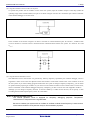
1
User’s Manual
M30870T-EPB
User's Manual
Supported Devices:
M16C Family / M32C/80 Series
M32C/87 Group
All information contained in these materials, including products and product specifications,
represents information on the product at the time of publication and is subject to change by
Renesas Electronics Corporation without notice. Please review the latest information published
by Renesas Electronics Corporation through various means, including the Renesas Electronics
Corporation website (http://www.renesas.com).
www.renesas.com
Rev.4.00
Aug 2012
M30870T-EPB User’s Manual
Preface
Preface
The M30870T-EPB is an emulation probe for M32C/87 Group MCUs. The M30870T-EPB is used by connecting to the
PC7501 emulator main unit.
This user's manual mainly describes specifications of the M30870T-EPB emulation probe and how to setup it. For details on
the following products, which are used with the M30870T-EPB, refer to each product's user's manual.
All the components of this product are shown in "1.1 Package components" (page 14). If there is any question or doubt about
this product, contact your local distributor.
The related manuals for using this product are listed below. You can download the latest manuals from the Renesas Tools
homepage (http://www.renesas.com/tools).
Related manuals
Item
Accessory Tools
Emulator main unit
Emulator debugger
C compiler
Assembler
Integrated development environment
*1 Discontinued products
R20UT0209EJ0400 Rev.4.00
Aug 16, 2012
Manual
M3T-100LCC-DMS User’s Manual
M3T-DUMMY100S User’s Manual *1
M3T-DIRECT100S User’s Manual *1
M3T-FLX-100NRB User’s Manual
M3T-100LCC-QSD User’s Manual
M3T-FLX-100NSD User’s Manual
M3T-F160-100NSD User’s Manual
M3T-FLX-144NSD User’s Manual
PC7501 User’s Manual
M32C PC7501 Emulator Debugger User’s Manual
M3T-PD308F User’s Manual
C Compiler Package for M32C Series
C Compiler User’s Manual
C Compiler Package for M32C Series
Assembler User’s Manual
High-performance Embedded Workshop User’s Manual
Page 3 of 106
M30870T-EPB User’s Manual
Important
Important
Before using this product, be sure to read this user’s manual carefully.
Keep this user’s manual, and refer to this when you have questions about this product.
Emulator:
"Emulator" in this document in this document collectively refers to the following products manufactured by Renesas
Electronics Corporation
(1) PC7501 main unit (2) Emulation probe (3) Package converter board for connecting the user system
"Emulator" herein encompasses neither the customer's user system nor the host machine.
Purpose of use of the emulator:
This emulator is a device to support the development of a system that uses the M16C Family M32C/80 Series M32C/87 Group
of Renesas 16/32-bit single-chip MCUs. It provides support for system development in both software and hardware.
Be sure to use this emulator correctly according to said purpose of use. Please avoid using this emulator for other than its
intended purpose of use.
For those who use this emulator:
This emulator can only be used by those who have carefully read the user’s manual and know how to use it.
Use of this emulator requires the basic knowledge of electric circuits, logical circuits, and MCUs.
When using the emulator:
(1) This emulator is a development-support unit for use in your program development and evaluation stages. When a program
you have finished developing is to be incorporated in a mass-produced product, the judgment as to whether it can be put
to practical use is entirely your own responsibility, and should be based on evaluation of the device on which it is
installed and other experiments.
(2) In no event shall Renesas Electronics Corporation be liable for any consequence arising from the use of this emulator.
(3) Renesas Electronics Corporation strives to provide workarounds for and correct trouble with products malfunctions, with
some free and some incurring charges. However, this does not necessarily mean that Renesas Electronics Corporation
guarantees the provision of a workaround or correction under any circumstances.
(4) This emulator covered by this document has been developed on the assumption that it will be used for program
development and evaluation in laboratories. Therefore, it does not fall within the scope of applicability of the Electrical
Appliance and Material Safety Law and protection against electromagnetic interference when used in Japan.
(5) Renesas Electronics Corporation cannot predict all possible situations and possible cases of misuse that carry a potential
for danger. Therefore, the warnings in this user's manual and the warning labels attached to this emulator do not
necessarily cover all such possible situations and cases. The customer is responsible for correctly and safely using this
emulator.
(6) The emulator covered by this document has not been through the process of checking conformance with UL or other
safety standards and IEC or other industry standards. This fact must be taken into account when the product is taken from
Japan to some other country.
(7) Renesas Electronics Corporation will not assume responsibility of direct or indirect damage caused by an accidental
failure or malfunction in this product.
When disposing of this product:
Penalties may be applicable for incorrect disposal of this waste, in accordance with your national legislation.
R20UT0209EJ0400 Rev.4.00
Aug 16, 2012
Page 4 of 106
M30870T-EPB User’s Manual
Important
Usage restrictions:
This emulator has been developed as a means of supporting system development by users. Therefore, do not use it as an
embedded device in other equipment. Also, do not use it to develop systems or equipment for use in the following fields.
(1) Transportation and vehicular
(2) Medical (equipment that has an involvement in human life)
(3) Aerospace
(4) Nuclear power control
(5) Undersea repeaters
If you are considering the use of this emulator for one of the above purposes, please be sure to consult your local distributor.
About product changes:
We are constantly making efforts to improve the design and performance of this emulator. Therefore, the specification or
design of this emulator, or this user's manual, may be changed without prior notice.
About rights:
(1) We assume no responsibility for any damage or infringement on patent rights or any other rights arising from the use of
any information, products or circuits presented in this user’s manual.
(2) The information or data in this user’s manual does not implicitly or otherwise grant a license to patent rights or any other
rights belonging to Renesas or to a third party.
(3) This user’s manual and this emulator are copyrighted, with all rights reserved by Renesas. This user’s manual may not be
copied, duplicated or reproduced, in whole or part, without prior written consent from Renesas.
About diagrams:
Some diagrams in this user’s manual may differ from the objects they represent.
R20UT0209EJ0400 Rev.4.00
Aug 16, 2012
Page 5 of 106
M30870T-EPB User’s Manual
Precautions for Safety
Precautions for Safety
This chapter describes the precautions which should be taken in order to use this product safely and properly. Be sure to read
and understand this chapter before using this product.
Contact us if you have any questions about the precautions described here.
WARNING
WARNING indicates a potentially dangerous situation that will cause death or heavy
wound unless it is avoided.
CAUTION
CAUTION indicates a potentially dangerous situation that will cause a slight injury, a
medium-degree injury or a property damage unless it is avoided.
In addition to the two above, the following are also used as appropriate.
means WARNING or CAUTION.
Example:
CAUTION AGAINST AN ELECTRIC SHOCK
means PROHIBITION.
Example:
DISASSEMBLY PROHIBITED
means A FORCIBLE ACTION.
Example:
UNPLUG THE POWER CABLE FROM THE RECEPTACLE.
R20UT0209EJ0400 Rev.4.00
Aug 16, 2012
Page 6 of 106
M30870T-EPB User’s Manual
Precautions for Safety
WARNING
Warnings for AC Power Supply:
If the attached AC power cable does not fit the receptacle, do not alter the AC power cable and do not
plug it forcibly. Failure to comply may cause electric shock and/or fire.
Use an AC power cable which complies with the safety standard of the country.
Do not touch the plug of the AC power cable when your hands are wet. This may cause electric shock.
This emulator is connected signal ground with frame ground. If your developing product is transformless (not having isolation transformer of AC power), this may cause electric shock. Also, this may give
an un-repairable damage to this product and your developing one.
While developing, connect AC power of the product to commercial power through isolation transformer
in order to avoid these dangers.
If other equipment is connected to the same branch circuit, care should be taken not to overload the
circuit.
When installing this equipment, insure that a reliable ground connection is maintained.
If you smell a strange odor, hear an unusual sound, or see smoke coming from this product, then
disconnect power immediately by unplugging the AC power cable from the outlet.
Do not use this as it is because of the danger of electric shock and/or fire. In this case, contact your
local distributor.
Before setting up this emulator and connecting it to other devices, turn off power or remove a power
cable to prevent injury or product damage.
Warnings to Be Taken for Handling:
Do not disassemble or modify this product. Personal injury due to electric shock may occur if this
product is disassembled and modified. Disassembling and modifying the product will void your warranty.
Make sure nothing falls into the cooling fan on the top panel, especially liquids, metal objects, or
anything combustible.
Warning for Installation:
Do not set this product in water or areas of high humidity. Make sure that the product does not get wet.
Spilling water or some other liquid into the product may cause un-repairable damage.
Warning for Use Temperature:
This equipment is to be used in an environment with a maximum ambient temperature of 35°C.
Care should be taken that this temperature is not exceeded.
R20UT0209EJ0400 Rev.4.00
Aug 16, 2012
Page 7 of 106
M30870T-EPB User’s Manual
Precautions for Safety
CAUTION
Cautions to Be Taken for the AC Adapter:
Use only the AC adapter included in this emulator.
Do not use the AC adapter for other equipment.
Cautions to Be Taken for Turning On the Power:
Turn ON/OFF the power of the emulator and user system as simultaneously as possible.
If you cannot turn on the powers simultaneously, turn on the emulator first and then the user system
Do not leave either the emulator or user system powered on, because of leakage current the internal
circuits may be damaged.
When turning ON the power again after shutting OFF the power, wait about 10 seconds.
Cautions to Be Taken for Handling This Emulator:
Use caution when handling the emulator. Be careful not to apply a mechanical shock.
Do not touch the connector pins of the emulator and the target MCU connector pins directly. Static
electricity may damage the internal circuits.
When attaching and removing the cable, hold the plug of the cable and do not touch the cable. Do not
pull the emulator by the communications interface cable or the flexible cable. And, excessive flexing or
force may break conductors.
Do not flex the flexible cable excessively. The cable may cause a break.
Do not use inch-size screws for this emulator. The screws used in this emulator are all ISO (meter-size)
type screws. When replacing screws, use same type screws as equipped before.
Note on Transporting the Product:
When sending your product for repair, use the packing box and cushioning material supplied with the
product when it was delivered to you and specify caution in handling (handling as precision equipment).
If packing of your product is not complete, it may be damaged during transportation. When you pack
your product in a bag, make sure to use the conductive plastic bag supplied with the product (usually a
blue bag). If you use a different bag, it may lead to further trouble with your product due to static
electricity.
R20UT0209EJ0400 Rev.4.00
Aug 16, 2012
Page 8 of 106
M30870T-EPB User’s Manual
Precautions for Safety
CAUTION
Caution to Be Taken for System Malfunctions:
If the emulator malfunctions because of interference like external noise, do the following to remedy the
trouble.
(1) Press the RESET switch on the emulator upper panel.
(2) If normal operation is not restored after step (1), shut OFF power to the emulator once and then
reactivate it.
Caution to Be Taken for Disposal:
Penalties may be applicable for incorrect disposal of this waste, in accordance with your national
legislation.
European Union regulatory notices:
The WEEE (Waste Electrical and Electronic Equipment) regulations put responsibilities on producers for
the collection and recycling or disposal of electrical and electronic waste. Return of WEEE under these
regulations is applicable in the European Union only. This equipment (including all accessories) is not
intended for household use. After use the equipment cannot be disposed of as household waste, and
the WEEE must be treated, recycled and disposed of in an environmentally sound manner.
Renesas Electronics Europe GmbH can take back end of life equipment, register for this service at
“http://www.renesas.eu/weee”.
R20UT0209EJ0400 Rev.4.00
Aug 16, 2012
Page 9 of 106
M30870T-EPB User’s Manual
Contents
Contents
Page
Preface..........................................................................................................................................................................3
Important.......................................................................................................................................................................4
Precautions for Safety ..................................................................................................................................................6
Contents......................................................................................................................................................................10
User Registration ........................................................................................................................................................12
Terminology ................................................................................................................................................................13
1. Outline.....................................................................................................................................................................14
1.1 Package Components ...................................................................................................................................14
1.2 Other Tool Products Required for Development ...........................................................................................14
1.3 System Configuration ....................................................................................................................................15
1.3.1 System Configuration ..........................................................................................................................15
1.3.2 Names and Functions of the PC7501 Upper Panel LEDs ..................................................................16
1.4 Specifications ................................................................................................................................................18
1.4.1 Product Specifications.........................................................................................................................18
1.4.2 Regulatory Compliance Notices..........................................................................................................19
1.4.3 Operating Environment .......................................................................................................................20
2. Setup.......................................................................................................................................................................21
2.1 Flowchart of Starting Up the Emulator ..........................................................................................................21
2.2 Installing the Emulator Debugger ..................................................................................................................22
2.3 Connecting the Host Machine .......................................................................................................................23
2.4 Connecting the PC7501 ................................................................................................................................24
2.5 Connecting the Power Supply for the Emulator ............................................................................................25
2.6 Turning ON the Power...................................................................................................................................26
2.6.1 Checking the Connections of the Emulator System............................................................................26
2.6.2 Turning ON/OFF the Power ................................................................................................................26
2.6.3 Power Supply to the User System ......................................................................................................26
2.6.4 LED Display When the Emulator Starts Up Normally .........................................................................27
2.7 Downloading Firmware..................................................................................................................................28
2.7.1 When It is Necessary to Download Firmware .....................................................................................28
2.7.2 Downloading Firmware in Maintenance Mode....................................................................................28
2.8 Self-check ......................................................................................................................................................29
2.8.1 Self-check Procedure ..........................................................................................................................29
2.8.2 If an Error is Detected in the Self-check..............................................................................................30
2.9 Connecting the User System.........................................................................................................................31
2.9.1 Connecting to a 100-pin LCC Socket..................................................................................................32
2.9.2 Connecting to a 100-pin 0.65-mm-pitch Foot Pattern (Part 1)............................................................33
2.9.3 Connecting to a 100-pin 0.65-mm-pitch Foot Pattern (Part 2)............................................................34
2.9.4 Connecting to a 100-pin 0.65-mm-pitch Foot Pattern (Part 3)............................................................35
2.9.5 Connecting to a 100-pin 0.5-mm-pitch Foot Pattern (Part 1)..............................................................36
2.9.6 Connecting to a 100-pin 0.5-mm-pitch Foot Pattern (Part 2)..............................................................37
2.9.7 Connecting to a 100-pin 0.5-mm-pitch Foot Pattern (Part 3)..............................................................38
2.9.8 Connecting to a 144-pin 0.5-mm-pitch Foot Pattern ...........................................................................39
2.10 Setting Switches ..........................................................................................................................................40
2.10.1 Setting Switches of Emulation Probe ..................................................................................................40
2.10.2 Selecting Clock Supply .....................................................................................................................45
2.10.3 A/D Conversion Bypass Capacitors ..................................................................................................50
3. Usage (Emulator Debugger)...................................................................................................................................52
3.1 Starting Up the Emulator Debugger (Init Dialog Box) ...................................................................................52
3.2 Starting Up the Emulator Debugger (EMEM Dialog Box) .............................................................................59
3.3 Program Window ...........................................................................................................................................64
3.4 Hardware Breakpoint Setting Window...........................................................................................................68
3.5 Trace Window................................................................................................................................................73
R20UT0209EJ0400 Rev.4.00
Aug 16, 2012
Page 10 of 106
M30870T-EPB User’s Manual
Contents
Page
3.6 RAM Monitor Window....................................................................................................................................78
4. Hardware Specifications .........................................................................................................................................81
4.1 Target MCU Specifications............................................................................................................................81
4.2 Differences between the Actual MCU and Emulator.....................................................................................82
Note on Differences between the Actual MCU and Emulator: .....................................................................82
Note on RESET* Input: ................................................................................................................................82
Note on RDY* Input:.....................................................................................................................................82
Note on HOLD* Input: ..................................................................................................................................82
Note on NMI* Input:......................................................................................................................................82
Notes on Reset Vector Area: .......................................................................................................................83
Notes on Stack Area: ...................................................................................................................................83
Note on Maskable Interrupts: .......................................................................................................................83
Notes on Access Prohibited Area: ...............................................................................................................83
Note on DMA Transfer: ................................................................................................................................83
Note on DMAC II Transfer Completion Interrupts: .......................................................................................83
Note on Final Evaluation: .............................................................................................................................83
4.3 Connection Diagrams ....................................................................................................................................84
4.4 External Dimensions......................................................................................................................................87
4.4.1 External Dimensions of the Emulation Probe .....................................................................................87
4.4.2 External Dimensions of the M30800T-PTC ........................................................................................88
4.4.3 External Dimensions of the M3T-F160-100NSD.................................................................................89
4.4.4 External Dimensions of the M3T-FLX-144NSD ..................................................................................89
4.5 Notes on Using This Product.........................................................................................................................90
Notes on Downloading Firmware: ................................................................................................................90
Note on Quitting the Emulator Debugger: ....................................................................................................90
Notes on Power Supply to the User System: ...............................................................................................90
Notes on Using This Product When the Voltage of VCC1 is Higher than That of VCC2:............................90
Notes on Clock Supply to an MCU:..............................................................................................................91
Notes on Using the CPU Clock at Less than 10 MHz:.................................................................................91
Notes on Address-Match Interrupt: ..............................................................................................................91
Notes on EMEM Dialog Box:........................................................................................................................92
Notes on Watchdog Function:......................................................................................................................92
Notes on Debugging in CPU Rewrite Mode:................................................................................................93
Note on Software Break: ..............................................................................................................................93
Notes on Service-Life of the MCU's Internal Flash ROM:............................................................................93
Note on Protect Resistor: .............................................................................................................................94
Note on Memory Access: .............................................................................................................................94
Notes on MCU File: ......................................................................................................................................94
Note on Intelligent I/O Resistor Access:.......................................................................................................94
Note on Voltage Detect Circuit:....................................................................................................................94
Notes on A/D Conversion:............................................................................................................................95
5. Troubleshooting ......................................................................................................................................................96
5.1 Flowchart to Remedy the Troubles ...............................................................................................................96
5.2 When the Emulator Debugger Does Not Start Up Properly ..........................................................................97
5.3 How to Request Support .............................................................................................................................100
6. Maintenance and Warranty...................................................................................................................................101
6.1 User Registration.........................................................................................................................................101
6.2 Maintenance ................................................................................................................................................101
6.3 Warranty ......................................................................................................................................................101
6.4 Repair Provisions ........................................................................................................................................102
6.5 How to Make Request for Repair ................................................................................................................102
R20UT0209EJ0400 Rev.4.00
Aug 16, 2012
Page 11 of 106
M30870T-EPB User’s Manual
User Registration
User Registration
When you install debugger software, a text file for user registration is created on your PC. Fill it in and email it to your local
distributor. If you have replaced an emulator main unit or emulation probe, rewrite an emulator name and serial number in the
text file you filled in earlier to register your new hardware products.
Your registered information is used for only after-sale services, and not for any other purposes. Without user registration, you
will not be able to receive maintenance services such as a notification of field changes or trouble information. So be sure to
carry out the user registration.
For more information about user registration, please contact your local distributor.
R20UT0209EJ0400 Rev.4.00
Aug 16, 2012
Page 12 of 106
M30870T-EPB User’s Manual
Terminology
Terminology
Some specific words used in this user's manual are defined below.
Emulator system
This means an emulator system built around the PC7501 emulator. The PC7501 emulator system is configured with an
emulator main unit, emulation probe, host machine and emulator debugger.
Emulator main unit (Hereafter PC7501)
This means an emulator main unit for M16C Family MCUs.
Emulation probe
This means the emulation probe (this product) for the M32C/87 Group MCUs.
Emulator debugger (M32C PC7501 Emulator Debugger or M3T-PD308F)
This means a software tool to control the PC7501 emulator and this product and enable debugging.
Firmware
Program that analyzes contents of communication with the emulator debugger and controls the emulator hardware. This
program is installed in the flash memory in the emulator main unit. This program is downloadable from the emulator debugger
to upgrade the firmware or to support other MCUs.
Host machine
This means a personal computer used to control the emulator main unit and emulation probe.
Software break
A software break is a function to break the program before the system executes an instruction at the specified address. The
instruction at the preset address will not be executed.
Hardware break
A hardware break is a function to break the program when the system detects a write/read of data to/from memory or a
leading/trailing edge of the signal entered from the external trace cable. The former break function is called address break; and
the latter break function is called trigger break. While the instruction at the address where the software break is set is not
executed, a hardware break is performed after the specified instruction is executed.
Target MCU
This means the program to be debugged.
User system
This means a user's application system in which the MCU to be debugged is used.
User program
This means the program you are going to debug.
Evaluation MCU
This means the MCU mounted on the emulation probe which is operated in the specific mode for tools.
*
This symbol indicates that a signal is active-low (e.g. RESET*).
R20UT0209EJ0400 Rev.4.00
Aug 16, 2012
Page 13 of 106
M30870T-EPB User’s Manual
1. Outline
1. Outline
This chapter describes the package components, the system configuration, the specifications of the emulator functions and the
operating environment.
1.1 Package Components
The M30870T-EPB package consists of the following items. After you have unpacked the box, check if your M30870T-EPB
contains all of these items.
Table 1.1 Package components
Item
Quantity
M30870T-EPB emulation probe
1
M30800T-PTC (pre-mounted) converter board for 100-pin LCC
1
IC61-1004-051 100-pin LCC socket made by Yamaichi Electronics Co., Ltd.
1
OSC-3 (32MHz) oscillator circuit board
1
OSC-2 oscillator circuit bare board
1
M30870T-EPB Supplementary Document (English)
1
M30870T-EPB Supplementary Document (Japanese)
1
M30870T-EPB User’s Manual (this manual)
1
M30870T-EPB User’s Manual (Japanese)
1
* Please keep the M30870T-EPB's packing box and cushion material in your place for reuse at a later time when sending your
product for repair or other purposes. Always use these packing box and cushion material when transporting this product.
* If there is any question or doubt about the packaged product, contact your local distributor.
* For purchasing the IC61-1004-051 or for technical information, contact Yamaichi Electronics Co., Ltd.
http://www.yamaichi.co.jp/index_e.shtml
1.2 Other Tool Products Required for Development
To bring forward programs development on the M32C/87 Group MCUs, the products listed below are necessary in addition to
those contained package above. Get them separately.
Table 1.2 Other tool products required for development
Converter board
Product
Emulator main unit
Emulator debugger
144-pin 0.5-mm-pitch LQFP
(144P6Q-A)
Product name
PC7501
M32C PC7501 Emulator Debugger
M3T-PD308F V.3.20 Release 1
R20UT0209EJ0400 Rev.4.00
Aug 16, 2012
Required
M3T-FLX-144NSD
M3T-100LCC-QSD
M3T-100LCC-DMS + M3T-FLX-100NSD
M3T-F160-100NSD
M3T-100LCC-DMS + M3T-DUMMY100S *1
100-pin 0.65-mm-pitch QFP
M3T-100LCC-DMS + M3T-DIRECT100S *1
(100P6S-A)
M3T-100LCC-DMS + M3T-FLX-100NRB
* To purchase these products, contact your local distributor.
*1 Discontinued products
100-pin 0.5-mm-pitch LQFP
(100P6Q-A)
Notes
Required
Required according to the foot
pattern of the user system
(see "2.9 Connecting the User
System" on page 31)
Page 14 of 106
M30870T-EPB User’s Manual
1. Outline
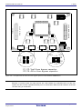
1.3 System Configuration
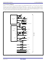
1.3.1 System Configuration
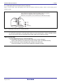
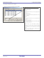
Figure 1.1 shows a configuration of the M30870T-EPB system.
Figure 1.1 System configuration
(1) Emulation probe M30870T-EPB (this product)
This emulation probe contains an evaluation MCU.
(2) Converter board M30800T-PTC (included)
This is a converter board for connecting to the user system (for 100-pin 0.65-mm-pitch LCC socket). For details, refer to
"2.9 Connecting the User System" (page 31).
R20UT0209EJ0400 Rev.4.00
Aug 16, 2012
Page 15 of 106
M30870T-EPB User’s Manual
1. Outline
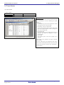
1.3.2 Names and Functions of the PC7501 Upper Panel LEDs
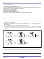
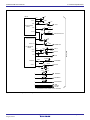
Figure 1.2 shows the names of the LEDs on the upper panel of the emulator.
Figure 1.2 Names of the LEDs on the upper panel of the PC7501
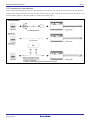
(1) System Status LEDs
The system status LEDs indicate the emulator PC7501's power supply, firmware operating status, etc. Table 1.3 lists the
definition of each system status LED.
Table 1.3 Definitions of the system status LEDs
Name
POWER
SAFE
ERROR
Status
ON
OFF
ON
Flashing
OFF
ON
Flashing
OFF
Meaning
Emulator system power supply is turned ON.
Emulator system power supply is turned OFF.
Emulator system is operating normally.
Special mode (maintenance mode) for downloading firmware. The emulator
system does not operate except for downloading firmware and the self-check.
Emulator system is not operating normally.
Emulator system is not operating normally.
Downloading firmware.
Emulator system is operating normally.
R20UT0209EJ0400 Rev.4.00
Aug 16, 2012
Page 16 of 106
M30870T-EPB User’s Manual
1. Outline
(2) Target Status LEDs
The target status LEDs indicate the target MCU's operating status and target board's power supply. Table 1.4 lists the definition
of each target status LED.
Table 1.4 Definitions of the target status LEDs
Name
POWER
CLOCK
RESET
RUN
WARNING
Status
ON
OFF
ON
OFF
ON
OFF
ON
OFF
ON
OFF
Meaning
Power is supplied to the target MCU.
Power is not supplied to the target MCU.
Target MCU clock is oscillating.
Target MCU clock is not oscillating.
Target MCU is being reset.
Target MCU is not being reset.
User program is being executed.
User program has been halted.
Target MCU internal clock is not oscillating.
Target MCU internal clock is oscillating.
CAUTION
Caution for Target Status POWER LED:
If your MCU has two or more power supply terminals (VCC), you need to supply power to all the
terminals.
R20UT0209EJ0400 Rev.4.00
Aug 16, 2012
Page 17 of 106
M30870T-EPB User’s Manual
1. Outline
1.4 Specifications
1.4.1 Product Specifications
Tables 1.5 and 1.6 list the specifications of the M30870T-EPB.
Table 1.5 M30870T-EPB specifications (1/2)
Applicable MCUs
Evaluation MCU
Usable mode
Maximum operating frequency*
Applicable power supply
Basic debugging functions
Real-time trace function
Real-time RAM monitor function
Hardware break function
Execution time measurement function
C0 coverage
External trigger input/event output
Expansion emulation memory
Maximum operating frequency
Specifiable areas
Area size
Emulation memory size
Specifiable bank
M32C/87 Group
M3087BFLGP
ROM size: 1024 KB + 4 KB, RAM size: 48 KB
Single-chip mode
Memory expansion mode
Microprocessor mode
VCC1 = VCC2 = 4.2 to 5.5 V: 32 MHz
VCC1 = VCC2 = 3.0 to 5.5 V: 24 MHz
Dual-power supply specification
(4.8 V ≤ VCC1 ≤ 5.5 V and 3.0 V ≤ VCC2 < VCC1): 24MHz
3.0--5.5 V
- Download
- Software break (max. 64 points)
- Program execution/stop (allows free-run execution supporting software breaks)
- Memory reference/setting (reference/setting C-variables, run-time execution)
- Register reference/setting
- Disassemble display
- C-level debugging, etc.
- 256K-cycle bus information recordable
(Bus, external trigger, time stamp)
- 5 trace modes supported (Break/Before/About/After/Full)
- Can be recorded ON/OFF by events
- 4,096 bytes (256 bytes x16)
- Data/last access result
8 points (Execution address, bus detection, interrupt, external trigger signal)
Time between program start and stop
Maximum/minimum/average execution time and pass count of specified four
zones.
Count clock: Equal to MCU Clock or 16 MHz
8,192 KB (256 KB x 32 blocks)
External trigger input (MCU-dependent-voltage CMOS level x8) or event output
(break x1, event x7)
32 MHz 1Φ + 1Φ
Max. 4 areas
Contiguous 256 KB range or contiguous 1 MB range
(mixed setting of 256 KB range and 1 MB range is available)
4 MB for 4 areas
- For area size 256 KB
X0h, X4h, X8h, XCh banks
e.g.) 20 bank, 64 bank, A8 bank, EC bank etc.
- For area size 1 MB
X0h hank
e.g.) 20 bank, 40 bank, 80 bank, A0 bank etc.
* Notes on Using This Product
If using this product when the voltage of VCC1 is higher than that of VCC2, the CPU clock must be 24 MHz or less.
If using a CPU clock of more than 24MHz, set the SFR area of the intelligent I/O function to 2-wait (set the PM13 bit to "1")
when reading this area.
These precautions only need to be observed when using an emulator, and does not apply for the actual MCU.
R20UT0209EJ0400 Rev.4.00
Aug 16, 2012
Page 18 of 106
M30870T-EPB User’s Manual
1. Outline
Table 1.6 M30870T-EPB specifications (2/2)
Host machine interface
Power supply to emulator
Connection to user system
(see "2.9 Connecting the User System"
on page 31)
EMC
- LPT parallel (ECP, EPP, Byte/compatibility and Nibble/compatibility modes)
- USB (USB 1.1, full-speed)
- LAN (10BASE-T)
Supplied from included AC adapter (power supply voltage: 100--240 V, 50/60 Hz)
For 144-pin 0.5-mm-pitch LQFP (144P6Q-A):
M3T-FLX-144NSD (not included)
For 100-pin 0.5-mm-pitch LQFP (100P6Q-A):
(1) M30800T-PTC (included) + M3T-100LCC-QSD (not included)
(2) M30800T-PTC (included) + M3T-100LCC-DMS (not included)
+ M3T-FLX-100NSD (not included)
(3) M3T-F160-100NSD (not included)
For 100-pin 0.65-mm-pitch QFP (100P6S-A):
(1) M30800T-PTC (included) + M3T-100LCC-DMS (not included)
+ M3T-FLX-100NRB (not included)
(2) M30800T-PTC (included) + M3T-100LCC-DMS (not included)
+ M3T-DUMMY100S (not included) *1
(3) M30800T-PTC (included) + M3T-100LCC-DMS (not included)
+ M3T-DIRECT100S (not included) *1
For 100-pin LCC socket:
M30800T-PTC (included) + IC61-1004-051 (included)
EU: EN 55022 Class A, EN 55024
USA: FCC part 15 Class A
*1 Discontinued products
1.4.2 Regulatory Compliance Notices
European Union regulatory notices
This product complies with the following EU Directives. (These directives are only valid in the European Union.)
CE Certifications:
• Electromagnetic Compatibility (EMC) Directive 2004/108/EC
EN 55022 Class A
WARNING: This is a Class A product. In a domestic environment this product may cause radio
interference in which case the user may be required to take adequate measures.
EN 55024
• Information for traceability
• Authorised representative
Name:
Renesas Electronics Corporation
Address:
1753, Shimonumabe, Nakahara-ku, Kawasaki, Kanagawa, 211-8668, Japan
• Manufacturer
Name:
Renesas Solutions Corp.
Address:
Nippon Bldg., 2-6-2, Ote-machi, Chiyoda-ku, Tokyo 100-0004, Japan
• Person responsible for placing on the market
Name:
Renesas Electronics Europe GmbH
Address:
Arcadiastrasse 10, 40472 Dusseldorf, Germany
• Trademark and Type name
Trademark:
Renesas
Product name:
M32C/87 Group Emulation Probe
Type name:
M30870T-EPB
Environmental Compliance and Certifications:
• Restriction of the Use of Certain Hazardous Substances in Electrical and Electronic Equipment (RoHS) Directive
2002/95/EC
• Waste Electrical and Electronic Equipment (WEEE) Directive 2002/96/EC
R20UT0209EJ0400 Rev.4.00
Aug 16, 2012
Page 19 of 106
M30870T-EPB User’s Manual
1. Outline
United States Regulatory notices
This product complies with the following EMC regulation. (This is only valid in the United States.)
FCC Certifications:
This equipment has been tested and found to comply with the limits for a Class A digital device, pursuant to Part 15 of
the FCC Rules. These limits are designed to provide reasonable protection against harmful interference when the
equipment is operated in a commercial environment. This equipment generates, uses, and can radiate radio frequency
energy and, if not installed and used in accordance with the instruction manual, may cause harmful interference to radio
communications. Operation of this equipment in a residential area is likely to cause harmful interference in which case
the user will be required to correct the interference at his own expense.
This device complies with Part 15 of the FCC Rules. Operation is subject to the following two conditions:
(1) this device may not cause harmful interference, and (2) this device must accept any interference received, including
interference that may cause undesired operation.
CAUTION:
Changes or modifications not expressly approved by the party responsible for
compliance could void the user's authority to operate the equipment.
1.4.3 Operating Environment
Be sure to use this emulator with the operating environmental of the emulator and host machine listed in Tables 1.7 and 1.8.
Table 1.7 Operating environmental conditions
Item
Operating temperature
Storage temperature
Description
5 to 35°C (no dew)
-10 to 60°C (no dew)
Table 1.8 Operating environment of the host machine
Item
Host machine
OS
CPU
Memory
Pointing device such as mouse
Description
IBM PC/AT compatibles
Windows Me
Windows 98
Windows XP
Windows 2000
Pentium III 600 MHz or more recommended
128 MB or more recommended
Mouse or any other pointing device usable with the above OS
that can be connected to the main body of the host machine.
* Windows and Windows NT are either registered trademarks or trademarks of Microsoft Corporation in the United States
and other countries.
R20UT0209EJ0400 Rev.4.00
Aug 16, 2012
Page 20 of 106
M30870T-EPB User’s Manual
2. Setup
2. Setup
This chapter describes the preparation for using this product, the procedure for starting up the emulator and how to change
settings.
2.1 Flowchart of Starting Up the Emulator
The procedure for starting up the emulator is shown in Figure 2.1. For details, refer to each section hereafter. And, when the
emulator does not start up normally, refer to “5. Troubleshooting” (page 96).
Check the package components.
Refer to “1.1 Package Components (page 14).
▼
User registration
Refer to “User Registration” (page 12).
▼
Install the M32C PC7501 Emulator Debugger
or M3T-PD308F.
▼
Install the M32C PC7501 Emulator Debugger or M3T-PD308F for
this product.
Connect the host machine.
Connect the PC7501 to the host machine with the LPT parallel
interface cable, USB interface cable or LAN interface cable.
Set the interface selection switch on the rear panel of the PC7501 to
the using interface.
▼
Connect the power supply for the emulator.
Connect a power supply for the emulator.
▼
Connect the user system.
Connect the user system as occasion demands.
▼
Turning on the power supply.
Turn ON the power to the emulator and the user system as
simultaneously as possible.
▼
Check the LED display of the emulator.
Check that the system status LED, and POWER CLOCK, RESET
and WARNING of target status LED are lighting. When the user
system is not connected, the POWER LED does not light up.
▼
Start up the emulator debugger.
▼
Set the operating environment
of the emulator debugger.
▼
Debug a program with various functions of
the emulator debugger.
Start up the emulator debugger.
Set the INIT dialog box and EMEM dialog box of the emulator
debugger.
For how to use the emulator debugger, refer to the emulator
debugger’s online manual.
Figure 2.1 Flowchart of starting up the emulator
R20UT0209EJ0400 Rev.4.00
Aug 16, 2012
Page 21 of 106
M30870T-EPB User’s Manual
2. Setup
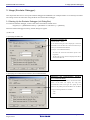
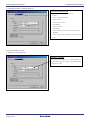
2.2 Installing the Emulator Debugger
If the OS used in your host machine is Windows XP or 2000, this installation must be executed by a user with administrator
rights. Be aware that users without administrator rights cannot complete the installation.
Install the emulator debugger (M32C PC7501 Emulator Debugger or M3T-PD308F) following the procedure described below.
(1) Downloading the emulator debugger (as occasion demands)
Download the emulator debugger from the URL below (free of charge).
http://www.renesas.com/download
(2) Launching the installer
Start the “setup.exe” program.
(3) Entering the user information
In the “user information” dialog box, enter the user information (contractor, section, contact address, and host machine).
The supplied information will be turned into a format by which technical support will be provided by e-mail.
(4) Selecting components
In the “component selection” dialog box, select the components you want to install. In this dialog box you can change the
directory in which to install.
(5) Completing the installation
A dialog box will be displayed indicating that setup has been completed. It means that the installation you made is
completed.
R20UT0209EJ0400 Rev.4.00
Aug 16, 2012
Page 22 of 106
M30870T-EPB User’s Manual
2. Setup
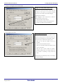
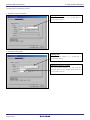
2.3 Connecting the Host Machine
When connecting the emulator PC7501 to a host machine, you can choose your desired interface from LPT parallel interface,
USB interface and LAN interface. Use the interface selection switch on the emulator PC7501's rear panel to specify your
desired interface. Figure 2.2 shows the outline to connect each interface cable.
Figure 2.2 Outline for interface cable connections
R20UT0209EJ0400 Rev.4.00
Aug 16, 2012
Page 23 of 106
M30870T-EPB User’s Manual
2. Setup
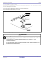
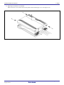
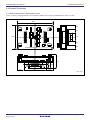
2.4 Connecting the PC7501
Figure 2.3 shows how to connect the PC7501 and the emulation probe.
M3T-FLX160-EPB
M30870T-EPB
Note: Connect the PCA7501EPBA board side to the M3T-FLX160-EPB.
Figure 2.3 Connecting the PC7501 and emulation probe
CAUTION
Cautions for Connecting the PC7501:
When connecting the emulation probe, be sure to hold the both sides of the emulation probe
horizontally and insert it directly.
Connect the PCA7501EPBA board to the M3T-FLX160-EPB.
Always shut OFF power before connecting the emulation probe. Otherwise, internal circuits may be
damaged.
R20UT0209EJ0400 Rev.4.00
Aug 16, 2012
Page 24 of 106
M30870T-EPB User’s Manual
2. Setup
2.5 Connecting the Power Supply for the Emulator
The power is supplied from AC adapter to the emulator PC7501. Here following explains how to connect the AC adapter.
(1)
(2)
(3)
(4)
Turn OFF the power to the PC7501.
Connect the DC cable of AC adapter to the PC7501.
Connect the AC power cable to the AC adapter.
Connect the AC power cable to the receptacle.
CAUTION
Cautions for AC Adapter:
Use only the AC adapter included in PC7501 package.
The included AC adapter is for PC7501. Do not use it for other product.
Before installing this equipment or connecting it to other equipment, disconnect the AC power cable
from its outlet to prevent injury or accident.
The DC plug on the included AC adapter has the below polarity.
The included AC adapter has no power supply switch. The AC adapter is always active while
connecting the AC power cable. Check if the power is supplied by the LED of AC adapter.
R20UT0209EJ0400 Rev.4.00
Aug 16, 2012
Page 25 of 106
M30870T-EPB User’s Manual
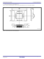
2. Setup
2.6 Turning ON the Power
2.6.1 Checking the Connections of the Emulator System
Before turning the power ON, check the connection of the interface cable with host machine, PC7501, emulation probe, and
user system.
2.6.2 Turning ON/OFF the Power
Turn ON the power of the emulator and user system as simultaneously as possible.
Turn OFF the power of the emulator and user system as simultaneously as possible.
Do not leave either the emulator or user system powered on, because of leakage current the internal circuits may be
damaged.
When turning ON the power again after shutting OFF the power, wait for about 10 seconds.
Notes on Power Supply:
The emulator's pin Vcc is connected to the user system in order to monitor user system voltage. For this
reason, the emulator cannot supply power to the user system. Therefore, provide the user system with
a separate power supply from that of the emulator.
Keep user system power supply voltage within the MCU's specified range (3.0 to 5.5 V).
Do not change user system power supply voltage after power has been activated.
2.6.3 Power Supply to the User System
This emulator cannot supply the power to the user system, therefore design your system so that the user system is powered
separately.
The voltage of the user system should be within the following. And do not change the voltage after activating the system.
(1) When JP1 is set as VCC1 = 2:
3.0 V ≤ VCC1 = VCC2 ≤ 5.5 V
(2) When JP1 is set as VCC1 > 2:
4.8 V ≤ VCC1 ≤ 5.2 V
3.0 V ≤ VCC2 < VCC1
R20UT0209EJ0400 Rev.4.00
Aug 16, 2012
Page 26 of 106
M30870T-EPB User’s Manual
2. Setup
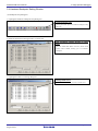
2.6.4 LED Display When the Emulator Starts Up Normally
Figure 2.4 shows upper panel LED lighting status when the emulator started up properly. Check it when starting up the
emulator system.
- If this LED does not light, check the voltage of the user system.
- Check power is supplied to all the power terminals.
- When the user system is not connected, this LED does not light.
POWER
POWER
SAFE
CLOCK
ERROR
RESET
RUN
WARNING
SYSTEM
STATUS
TARGET
STATUS
: ON
: OFF
: Flashing
Figure 2.4 LED display when the power turned on PC7501
Note on Memory Expansion and Microprocessor Modes:
To use memory expansion or microprocessor mode, be sure to set pins RDY*, HOLD* and NMI* so that
they are not active at start-up. Otherwise the emulator system will not start up correctly.
Note on CLOCK LED:
If CLOCK LED does not turn on, check the following:
(1) Immediately after starting PC7501 (before starting the emulator debugger)
Check if the oscillation circuit within the PC7501 emulator main unit oscillates normally.
(2) After starting the emulator debugger (after setting the Init dialog box)
Check the oscillation circuit set in the Init dialog box oscillates normally.
R20UT0209EJ0400 Rev.4.00
Aug 16, 2012
Page 27 of 106
M30870T-EPB User’s Manual
2. Setup
2.7 Downloading Firmware
2.7.1 When It is Necessary to Download Firmware
It is necessary to download the firmware in the cases listed below. Normally, the following are automatically detected when
the emulator debugger is started up, and the firmware is downloaded.
(1) When you use this product for the first time
(2) When the firmware has been upgraded
(3) When the emulator debugger has been upgraded
(4) When you use this product with a PC7501 which was used with other emulation probe before
If downloading firmware is not completed in the cases below, redownload the firmware.
- When the power is unexpectedly shut down during a download from the emulator debugger
- When a communications interface cable is unexpectedly pulled out
2.7.2 Downloading Firmware in Maintenance Mode
Download the firmware in maintenance mode as explained here following. The user system must not be connected when
downloading the firmware.
(1) Set the interface select switch on the rear panel of the PC7501 to the LPT side and connect the LPT parallel interface cable
to the PC7501 and the host machine.
(2) Within 2 seconds of activating power to the emulator, press the RESET switch on the PC7501 upper panel to switch to
maintenance mode.
Switched to maintenance mode, the SAFE SYSTEM STATUS LED begins to flash.
(3) Start up the emulator debugger. When the Init dialog box setup is complete, the dialog which urges to download the
firmware will appear. Download the firmware following messages. Required time for downloading the firmware is about
60 seconds.
POWER
SAFE
ERROR
POWER
POWER
CLOCK
SAFE
RESET
ERROR
RUN
STATUS
TARGET
STATUS
POWER
SAFE
RESET
ERROR
RUN
WARNING
SYSTEM
POWER
CLOCK
STATUS
WARNING
TARGET
SYSTEM
STATUS
STATUS
Maintenance mode started
POWER
SAFE
ERROR
SYSTEM
STATUS
POWER
POWER
CLOCK
SAFE
RESET
ERROR
WARNING
STATUS
Downloading firmware started
RESET
WARNING
SYSTEM
STATUS
POWER
RUN
STATUS
TARGET
CLOCK
RUN
TARGET
RESET
RUN
WARNING
SYSTEM
POWER
CLOCK
TARGET
STATUS
: ON
: OFF
: Flashing
Download terminated
Figure 2.5 Downloading firmware in maintenance mode
Note on Downloading Firmware:
Do not shut OFF power while the firmware is being downloaded. Doing so, the emulator will not start up
properly. If power is shut OFF by mistake, redownload the firmware in maintenance mode.
R20UT0209EJ0400 Rev.4.00
Aug 16, 2012
Page 28 of 106
M30870T-EPB User’s Manual
2. Setup
2.8 Self-check
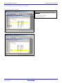
2.8.1 Self-check Procedure
To run the emulator self-check, do so as explained here below. While the self-check is in progress, LEDs will change as shown
in Figure 2.6.
(1) If the user system is connected, disconnect it.
(2) Set the switches as the factory-settings to execute the self-check (see Table 2.1).
(3) Within 2 seconds of activating power to the emulator, press the system reset switch on the emulator upper panel to switch
the emulator to maintenance mode.
(4) Check the "SAFE" LED starts flashing and then press the system reset switch again.
(5) The self-check will start. If the normal result is displayed in about 20 seconds, the self-check terminated normally.
Table 2.1 Switch settings at self-check
Switch
AVCC/AVSS switch (SW1)
P87 switch (SW2)
P86 switch (SW3)
XOUT switch (SW4)
A/D conversion bit selection switch (SW5)
VDDIO switch (JP1)
POWER
SAFE
ERROR
POWER
Setting
EXT side
P87 side
P86 side
NC side
All lower side
VCC1=2 side
POWER
POWER
CLOCK
SAFE
CLOCK
RESET
ERROR
RUN
RUN
WARNING
SYSTEM
STATUS
TARGET
STATUS
Maintenance mode started
WARNING
SYSTEM
STATUS
TARGET
STATUS
Self-check terminated normally
POWER
SAFE
ERROR 1
SAFE and ERROR flash
RESET
: ON
: OFF
: Flashing
ERROR
POWER
CLOCK
RESET
RUN
- When the firmware does not support the emulation probe
- When the emulation probe is not connected properly
WARNING
SYSTEM
STATUS
TARGET
STATUS
Emulation probe and firmware
do not match
POWER
ERROR 2
SAFE flashes and
ERROR lights
POWER
SAFE
CLOCK
ERROR
RESET
- When the PC7501 system is not working properly
RUN
WARNING
SYSTEM
STATUS
TARGET
STATUS
PC7501 system status error
POWER
ERROR 3
SAFE and ERROR
light alternately
POWER
SAFE
CLOCK
ERROR
RESET
- When a clock is not supplied to the emulation probe
RUN
WARNING
SYSTEM
STATUS
TARGET
STATUS
Emulation probe initialization error
POWER
ERROR 4
SAFE goes out and
ERROR lights
POWER
SAFE
CLOCK
ERROR
RESET
- When the emulation probe is not working properly
RUN
WARNING
SYSTEM
STATUS
TARGET
STATUS
Emulation probe status error
Figure 2.6 Self-check procedure
R20UT0209EJ0400 Rev.4.00
Aug 16, 2012
Page 29 of 106
M30870T-EPB User’s Manual
2. Setup
2.8.2 If an Error is Detected in the Self-check
If the self-check does not result normally (ERROR 1 to ERROR 4 in Figure 2.6), check the following.
(1) Recheck the connection of the emulation probe and PC7501.
(2) Redownload the proper firmware.
Note on the Self-check:
If the self-check does not result normally (excluding user system errors), the emulation probe may be
damaged. Then contact your local distributor.
R20UT0209EJ0400 Rev.4.00
Aug 16, 2012
Page 30 of 106
M30870T-EPB User’s Manual
2. Setup
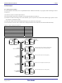
2.9 Connecting the User System
There are eight ways available to connect the emulation probe to user systems as shown in Figure 2.7.
Emulation probe
100-pin
144-pin 0.5-mm-pitch
0.65-mm-pitch
0.5-mm-pitch
M30800T-PTC
(included)
M30800T-PTC
(included)
M3T-100LCC-DMS
(not included)
M3T-100LCC-DMS
(not included)
M30800T-PTC
(included)
M3T-FLX100-R
(not included)
M3T-FLX100-T
(not included)
M3T-FLX100-T
(not included)
M3T-FLX100-R
(not included)
*1
LCC socket
100-pin LCC
(included)
M3T-DIRECT100S
100-pin QFP *2
(not included)
M3T-DUMMY100S
100-pin QFP
*2
(not included)
M3T-FLX-100NRB
100-pin QFP
(not included)
M3T-F160-100NSD
100-pin LQFP
(not included)
M3T-100LCC-QSD
100-pin QFP
(not included)
: No. 1 pin
*1: These items are available in one package.
M3T-FLX-100NSD
100-pin QFP
(not included)
M3T-FLX-144NSD
144-pin LQFP
(not included)
*2 Discontinued products
Figure 2.7 Connection of the M30870T-EPB and user system
CAUTION
Note on Connecting the User System:
Take care not to attach the converter board in a wrong direction. It may cause a fatal damage to the
emulator and user system.
R20UT0209EJ0400 Rev.4.00
Aug 16, 2012
Page 31 of 106
M30870T-EPB User’s Manual
2. Setup
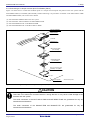
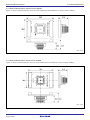
2.9.1 Connecting to a 100-pin LCC Socket
When connecting the emulation probe to a 100-pin LCC socket (Yamaichi Electronics Co., Ltd.: IC61-1004-051 etc.) on the
user system, following the procedure below.
(1) Attach the CN2 side of the M30870T-EPB to the CN2 side of the M30800T-PTC.
(2) Attach the M30800T-PTC to the 100-pin LCC socket.
M3T-FLX160-EPB
M30870T-EPB
CN2 side
(1)
M30800T-PTC
(2)
100 -pin LCC socket
No. 1 pin
User system
Figure 2.8 Connecting to a 100-pin LCC socket
CAUTION
Notes on Connecting the User System:
Take care not to attach the converter board in a wrong direction. It may cause a fatal damage to the
emulator and user system.
The small connectors of the M30870T-EPB and M30800T-PTC are guaranteed for only 50
insertion/removal iterations.
For purchasing the IC61-1004-051 or for technical information, contact Yamaichi Electronics Co., Ltd.
http://www.yamaichi.co.jp/index_e.shtml
R20UT0209EJ0400 Rev.4.00
Aug 16, 2012
Page 32 of 106
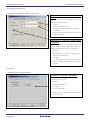
M30870T-EPB User’s Manual
2. Setup
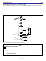
2.9.2 Connecting to a 100-pin 0.65-mm-pitch Foot Pattern (Part 1)
Figure 2.9 shows how to connect the emulation probe to a 100-pin 0.65-mm-pitch foot pattern on the user system with the
M3T-DUMMY100S (not included) (discontinued), and here following is its procedure.
For details on the M3T-100LCC-DMS and M3T-DUMMY100S, refer to each user's manual.
(1)
(2)
(3)
(4)
Attach the M3T-DUMMY100S to the user system.
Attach the M3T-100LCC-DMS to the M3T-DUMMY100S.
Attach the M30800T-PTC to the M30870T-EPB.
Attach the M30800T-PTC to the M3T-100LCC-DMS.
M3T-FLX160-EPB
M30870T-EPB
CN2 side
(3)
M30800T-PTC
(4)
M3T-100LCC-DMS
(not included)
On-board evaluation
(2)
M3T-DUMMY100S
(not included) *
FLASH MCU etc.
(1)
100 -pin 0.65-mm- pitch
(100P6S) foot pattern
No. 1 pin
User system
* Discontinued product
Figure 2.9 Connecting to a 100-pin 0.65-mm-pitch foot pattern (1/3)
CAUTION
Notes on Connecting the User System:
Take care not to attach the converter board in a wrong direction. It may cause a fatal damage to the
emulator and user system.
The small connectors of the M3T-100LCC-DMS and M3T-DUMMY100S are guaranteed for only 20
insertion/removal iterations.
The small connectors of the M30870T-EPB and M30800T-PTC are guaranteed for only 50
insertion/removal iterations.
R20UT0209EJ0400 Rev.4.00
Aug 16, 2012
Page 33 of 106
M30870T-EPB User’s Manual
2. Setup
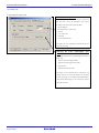
2.9.3 Connecting to a 100-pin 0.65-mm-pitch Foot Pattern (Part 2)
Figure 2.10 shows how to connect the emulation probe to a 100-pin 0.65-mm-pitch foot pattern on the user system with the
M3T-DIRECT100S (not included) (discontinued), and here following is its procedure. For details on the M3T-100LCC-DMS
and M3T-DIRECT100S, refer to each user's manual.
(1)
(2)
(3)
(4)
Attach the M3T-DIRECT100S to the user system.
Attach the M3T-100LCC-DMS to the M3T-DIRECT100S.
Attach the M30800T-PTC to the M30870T-EPB.
Attach the M30800T-PTC to the M3T-100LCC-DMS.
M3T-FLX160-EPB
M30870T-EPB
CN2 side
(3)
M30800T-PTC
(4)
M3T-100LCC-DMS
(not included)
(2)
M3T-DIRECT100S
(not included) *
100 -pin 0.65-mm -pitch
(100P6S) foot pattern
(1)
No. 1 pin
User system
* Discontinued product
Figure 2.10 Connecting to a 100-pin 0.65-mm-pitch foot pattern (2/3)
CAUTION
Notes on Connecting the User System:
Take care not to attach the converter board in a wrong direction. It may cause a fatal damage to the
emulator and user system.
The small connectors of the M3T-100LCC-DMS and M3T-DIRECT100S are guaranteed for only 20
insertion/removal iterations.
The small connectors of the M30870T-EPB and M30800T-PTC are guaranteed for only 50
insertion/removal iterations.
R20UT0209EJ0400 Rev.4.00
Aug 16, 2012
Page 34 of 106
M30870T-EPB User’s Manual
2. Setup
2.9.4 Connecting to a 100-pin 0.65-mm-pitch Foot Pattern (Part 3)
Figure 2.11 shows how to connect the emulation probe to a 100-pin 0.65-mm-pitch foot pattern on the user system with the
M3T-FLX-100NRB (not included), and here following is its procedure. For details on the M3T-100LCC-DMS and M3T-FLX100NRB, refer to each user's manual.
(1)
(2)
(3)
(4)
Attach the M3T-FLX-100NRB to the user system.
Attach the M3T-100LCC-DMS to the M3T-FLX-100NRB.
Attach the M30800T-PTC to the M30870T-EPB.
Attach the M30800T-PTC to the M3T-100LCC-DMS.
M3T-FLX160-EPB
M30870T-EPB
CN2
(3)
M30800T-PTC
(4)
M3T-100LCC-DMS
(not included)
(2)
M3T-FLX-100NRB
(not included)
On-board evaluation
YQ-GUIDE(x4)
HQPACK100RB
(not included)
*
YQPACK100RB
NQPACK100RB
FLASH MCU etc.
These corners are not round.
(1)
100-pin 0.65-mm-pitch
(100P6S) foot pattern
No. 1 pin
*:These four items are available in one package.
User system
Figure 2.11 Connecting to a 100-pin 0.65-mm-pitch foot pattern (3/3)
CAUTION
Notes on Connecting the User System:
Take care not to attach the converter board in a wrong direction. It may cause a fatal damage to the
emulator and user system.
The small connectors of the M3T-100LCC-DMS and M3T-FLX-100NRB are guaranteed for only 20
insertion/removal iterations.
The small connectors of the M30870T-EPB and M30800T-PTC are guaranteed for only 50
insertion/removal iterations.
* NQPACK, YQPACK, YQSOCKET, YQ-GUIDE, HQPACK, TQPACK and TQSOCKET are trademarks of Tokyo Eletech Corporation.
R20UT0209EJ0400 Rev.4.00
Aug 16, 2012
Page 35 of 106
M30870T-EPB User’s Manual
2. Setup
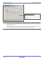
2.9.5 Connecting to a 100-pin 0.5-mm-pitch Foot Pattern (Part 1)
Figure 2.12 shows how to connect the emulation probe to a 100-pin 0.5-mm-pitch foot pattern on the user system with the
M3T-100LCC-QSD (not included), and here following is its procedure. For details on the M3T-100LCC-QSD, refer to its
user's manual.
(1) Attach the M3T-100LCC-QSD to the user system.
(2) Attach the M30800T-PTC to the M30870T-EPB.
(3) Attach the M30800T-PTC to the M3T-100LCC-QSD.
M3T-FLX160-EPB
M30870T-EPB
CN2 side
(2)
M30800T-PTC
(3)
M3T-100LCC-QSD
(not included)
(1)
100 -pin 0.5-mm -pitch
(100P6Q) foot pattern
No. 1 pin
User system
Figure 2.12 Connecting to a 100-pin 0.5-mm-pitch foot pattern (1/3)
CAUTION
Notes on Connecting the User System:
Take care not to attach the converter board in a wrong direction. It may cause a fatal damage to the
emulator and user system.
The small connectors of the M30870T-EPB and M30800T-PTC are guaranteed for only 50
insertion/removal iterations.
R20UT0209EJ0400 Rev.4.00
Aug 16, 2012
Page 36 of 106
M30870T-EPB User’s Manual
2. Setup
2.9.6 Connecting to a 100-pin 0.5-mm-pitch Foot Pattern (Part 2)
Figure 2.13 shows how to connect the emulation probe to a 100-pin 0.5-mm-pitch foot pattern on the user system with the
M3T-FLX-100NSD (not included), and here following is its procedure. For details on the M3T-100LCC-DMS and M3T-FLX100NSD, refer to each user's manual.
(1)
(2)
(3)
(4)
Attach the M3T-FLX-100NSD to the user system.
Attach the M3T-100LCC-DMS to the M3T-FLX-100NSD.
Attach the M30800T-PTC to the M30870T-EPB.
Attach the M30800T-PTC to the M3T-100LCC-DMS.
M3T-FLX160-EPB
M30870T-EPB
CN2 side
(3)
M30800T-PTC
(4)
M3T-100LCC-DMS
(not included)
(2)
M3T-FLX-100NSD
(not included)
On-board evaluation
YQ-GUIDE (x4)
*
HQPACK100SD
(not included)
YQPACK100SD
NQPACK100SD
These corners are not round.
(1)
FLASH MCU etc.
100-pin 0.5-mm-pitch
(100P6Q) foot pattern
No. 1 pin
*: These four items are available in one package.
User system
Figure 2.13 Connecting to a 100-pin 0.5-mm-pitch foot pattern (2/3)
CAUTION
Notes on Connecting the User System:
Take care not to attach the converter board in a wrong direction. It may cause a fatal damage to the
emulator and user system.
The small connectors of the M3T-100LCC-DMS and M3T-FLX-100NSD are guaranteed for only 20
insertion/removal iterations.
The small connectors of the M30870T-EPB and M30800T-PTC are guaranteed for only 50
insertion/removal iterations.
R20UT0209EJ0400 Rev.4.00
Aug 16, 2012
Page 37 of 106
M30870T-EPB User’s Manual
2. Setup
2.9.7 Connecting to a 100-pin 0.5-mm-pitch Foot Pattern (Part 3)
Figure 2.14 shows how to connect the emulation probe to a 100-pin 0.5-mm-pitch foot pattern on the user system with the
M3T-F160-100NSD (not included), and here following is its procedure. For details on the M3T-F160-100NSD, refer to its
user's manual.
(1)
(2)
(3)
(4)
(5)
Mount the NQPACK100SD included with the M3T-F160-100NSD to the user system.
Attach the YQPACK100SD included with the M3T-F160-100NSD to the NQPACK100SD.
Insert the YQ-GUIDE's included with the YQPACK100SD to the YQPACK100SD.
Attach the M3T-F160-100NSD to the YQPACK100SD.
Attach the M30870T-EPB to the M3T-F160-100NSD.
M3T-FLX160-EPB
M30870T-EPB
CN2 side
M3T-F160-100NSD
(not included)
(5)
On-board evalution
(4)
YQ-GUIDE (x4)
*
HQPACK100SD
(not included)
YQPACK100SD
(3)
These corners are not round.
NQPACK100SD
(2)
FLASH MCU etc.
100 -pin 0.5-mm -pitch
(100P6Q) foot pattern
(1)
No. 1 pin
*: These four items are available in one package.
User system
Figure 2.14 Connecting to a 100-pin 0.5-mm-pitch foot pattern (3/3)
CAUTION
Notes on Connecting the User System:
Take care not to attach the converter board in a wrong direction. It may cause a fatal damage to the
emulator.
The small connectors of the M30870T-EPB and M3T-F160-100NSD are guaranteed for only 50
insertion/removal iterations.
R20UT0209EJ0400 Rev.4.00
Aug 16, 2012
Page 38 of 106
M30870T-EPB User’s Manual
2. Setup
2.9.8 Connecting to a 144-pin 0.5-mm-pitch Foot Pattern
Figure 2.15 shows how to connect the emulation probe to a 144-pin 0.5-mm-pitch foot pattern on the user system with the
M3T-FLX-144NSD (not included), and here following is its procedure. For details on the M3T-FLX-144NSD, refer to its
user's manual.
(1)
(2)
(3)
(4)
(5)
Attach the NQPACK144SD included with the M3T-FLX-144NSD to the user system.
Attach the YQPACK144SD included with the M3T-FLX-144NSD to the NQPACK144SD.
Insert the YQ-GUIDE's included with the YQPACK144SD to the YQPACK144SD.
Attach the M3T-FLX-144NSD to the YQPACK144SD.
Attach the M30870T-EPB to the M3T-FLX-144SD.
M3T-FLX160-EPB
M30870T-EPB
CN2 side
(5)
M3T-FLX-144NSD
(not included)
On-board evaluation
(4)
YQ-GUIDE (x4)
*
HQPACK144SD
(not included)
YQPACK144SD
(3)
These corners are not round.
(2)
(1)
NQPACK144SD
FLASH MCU etc.
144 -pin 0.5-mm -pitch
(144P6Q) foot pattern
No. 1 pin
*: These four items are available in one package.
User system
Figure 2.15 Connecting to a 144-pin 0.5-mm-pitch foot pattern
CAUTION
Notes on Connecting the User System:
Take care not to attach the converter board in a wrong direction. It may cause a fatal damage to the
emulator.
The small connectors of the M30870T-EPB and M3T-FLX-144NSD are guaranteed for only 50
insertion/removal iterations.
R20UT0209EJ0400 Rev.4.00
Aug 16, 2012
Page 39 of 106
M30870T-EPB User’s Manual
2. Setup
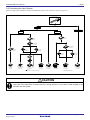
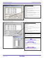
2.10 Setting Switches
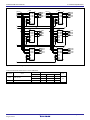
2.10.1 Setting Switches of Emulation Probe
O
N
Set the switches of the emulation probe according to the condition. Figure 2.16 shows the positions of the switches of the
M30870T-EPBM REV.B, and Figure 2.17 shows the positions of the switches of the M30870T-EPBM REV.C.
M30870T-EPBM REV.B
C4
C3
C1
C2
RENESAS
MADE IN JAPAN
1
2
3
4
5
6
7
8
SW5
JP1
AVCC
AVSS EXT
INT
P87
XCIN VCONT P86
SW4
NC
VSS
NC
XOUT
VCC1>2
SW3
SW2
VCC1=2
SW1
O
N
Figure 2.16 Positions of the switches of the M30870T-EPBM REV.B
M30870T-EPBM REV.C
C1
C2
NC
NC
XOUT
VCC1>2
P86
JP1
VCC1=2
XCIN
SW4
P87
SW3
INT
SW2
AVCC
AVSS EXT
C3
C4
SW1
RENESAS
MADE IN JAPAN
1
2
3
4
5
6
7
8
SW5
Figure 2.17 Positions of the switches of the M30870T-EPBM REV.C
R20UT0209EJ0400 Rev.4.00
Aug 16, 2012
Page 40 of 106
M30870T-EPB User’s Manual
2. Setup
(1) Setting JP1, SW1 to SW4 on the M30870T-EPBM
Table 2.2 shows the settings of JP1, SW1 to SW4 on the M30870T-EPBM REV.B, and Table 2.3 shows the settings of JP1,
SW1 to SW4 on the M30870T-EPBM REV.C.
Table 2.2 Switch settings of the M30870T-EPBM REV.B (JP1, SW1 to SW4)
Setting
AVCC
AVSS EXT
SW1
AVCC
AVSS
3.0 V ≤ VCC1 = VCC2 ≤ 5.5 V
(Factory-setting)
VCC1>2
VDDIO
VCC1=2
JP1
Description
VCC1>2
Switch name
VCC1=2
Switch
4.8 V ≤ VCC1 ≤ 5.2 V and 3.0 V ≤ VCC2 < VCC1
Connects pins AVCC and AVSS of the MCU to the user system.
INT
(Factory-setting)
AVCC
AVSS EXT
INT
Connects pin AVCC of the MCU to the internal power supply of the
emulator, and connects pin AVSS to the GND in the emulator.
Connects pin P87 of the MCU to the user system.
P87
XCIN
VCONT
(Factory-setting)
SW2
VCONT
Connects pin P87 of the MCU to the sub-clock oscillator circuit
(32.768 kHz).
VCONT
Do not set to VCONT.
Pin P87 is disconnected.
P87
P87
P87
XCIN
XCIN
Connects pin P86 of the MCU to the user system.
P86
NC
VSS
(Factory-setting)
SW3
P86
Does not connect pin P86 of the MCU.
P86
P86
NC
NC
VSS
VSS
Do not set to VSS.
Connects pin P86 to the VSS in the emulation probe.
Does not connect pin XOUT of the MCU.
NC
SW4
XOUT
XOUT
(Factory-setting)
Connects pin XOUT of the MCU to the user system.
NC
R20UT0209EJ0400 Rev.4.00
Aug 16, 2012
XOUT
Page 41 of 106
M30870T-EPB User’s Manual
2. Setup
Table 2.3 Switch settings of the M30870T-EPBM REV.C (JP1, SW1 to SW4)
Setting
Description
VCC1>2
Switch name
VCC1=2
Switch
3.0 V ≤ VCC1 = VCC2 ≤ 5.5 V
(Factory-setting)
AVCC
AVSS EXT
SW1
AVCC
AVSS
VCC1>2
VDDIO
VCC1=2
JP1
4.8 V ≤ VCC1 ≤ 5.2 V and 3.0 V ≤ VCC2 < VCC1
Connects pins AVCC and AVSS of the MCU to the user system.
INT
(Factory-setting)
AVCC
AVSS EXT
INT
Connects pin AVCC of the MCU to the internal power supply of the
emulator, and connects pin AVSS to the GND in the emulator.
Connects pin P87 of the MCU to the user system.
P87
XCIN
(Factory-setting)
SW2
P87
P87
XCIN
P86
NC
Connects pin P87 of the MCU to the sub-clock oscillator circuit
(32.768 kHz).
Connects pin P86 of the MCU to the user system.
(Factory-setting)
SW3
P86
Does not connect pin P86 of the MCU.
P86
NC
Does not connect pin XOUT of the MCU.
NC
SW4
XOUT
XOUT
(Factory-setting)
Connects pin XOUT of the MCU to the user system.
NC
R20UT0209EJ0400 Rev.4.00
Aug 16, 2012
XOUT
Page 42 of 106
M30870T-EPB User’s Manual
2. Setup
(2) Setting SW5 on the M30870T-EPBM
Table 2.4 lists the examples of setting the switch SW5 on the M30870T-EPBM. It is necessary to change the setting if
using the analog input port selection function of the A/D converter when selecting the MCU file "m30870_ad.mcu"*1 in the
Init dialog box of the emulator debugger.
Setting the SW5 enables to set each analog input pin for selecting an analog input port. When selecting AN00 to AN07 or
AN20 to AN27 for the analog input port select bits (bit 2 and bit 1 of 0394h), set the pins used for A/D conversion to ON,
the pins not used to OFF.
However, when selecting the MCU file “m30870.mcu”*2 in the Init dialog box of the emulator debugger, set the switch
SW5 as the factory-settings (all lower side).
*1 When using the M3T-PD308F, select the MCU file "m30870_ad_a.mcu".
*2 When using the M3T-PD308F, select the MCU file “m30870_a.mcu”.
Table 2.4 Switch settings of the M30870T-EPBM (SW5)
Analog input port
Setting
AD ON 0
7
8
7
6
5
4
3
2
1
O
N
When not using the
analog input port
selection function
OFF 0
7
Description
This is the setting when not using the analog input port selection
function. When using this product with the conditions below, use
this setting.
- When using the memory expansion mode
- When using the microprocessor mode
- When using the multi-port sweep mode
- When selecting AN0 to AN7 for analog input port select bits
- When selecting AN150 to AN157 for analog input port select bits
AD23 to AD27 used: ON
7
8
7
6
5
4
3
1
When using AN23 to
AN27
2
O
N
AD ON 0
OFF 0
7
This is a setting when using the analog input port selection function
and using AN23 to AN27 for analog input pins.
Set the analog input pins to ON.
With this setting, set the direction registers of ports P153 to P157 to
input. Pins P150 to P152 can be used for I/O port, ISTxD0, ISCLK0
and ISRxD0.
AD20 to AD22 unused: OFF
AD20 to AD27 used: ON
7
8
7
6
5
4
3
2
O
N
AD ON 0
1
When using AN20 to
AN27
OFF 0
7
This is a setting when using the analog input port selection function
and using AN20 to AN27 for analog input pins.
Set the analog input pins to ON.
With this setting, set the direction registers of ports P150 to P157 to
input. Pins P150 to P157 cannot be used for I/O port, ISTxD0,
ISCLK0 and ISRxD0.
AD04 to AD07 used: ON
7
8
7
6
5
4
3
1
When using AN04 to
AN07
2
O
N
AD ON 0
OFF 0
7
This is a setting when using the analog input port selection function
and using AN04 to AN07 for analog input pins.
Set the analog input pins to ON.
With this setting, set the direction registers of ports P154 to P157 to
input. Pins P150 to P153 can be used for I/O port, ISTxD0, ISCLK0
and ISRxD0.
AD00 to AD03 unused: OFF
AD03 to AD05 used: ON
AD25 to AD27 used: ON
AD ON 0
OFF 0
8
7
6
5
4
3
2
1
O
N
When using AN03 to
AN05 and AN25 to
AN27
7
7
This is a setting when using the analog input port selection function
and using AN03 to AN05 and AN25 to AN27 for analog input pins.
Set the analog input pins to ON.
With this setting, set the direction registers of ports P153 to P157 to
input. Pins P150 to P152 can be used for I/O port, ISTxD0, ISCLK0
and ISRxD0.
AD00 to AD02 unused: OFF
AD20 to AD22 unused: OFF
R20UT0209EJ0400 Rev.4.00
Aug 16, 2012
Page 43 of 106
M30870T-EPB User’s Manual
2. Setup
Notes on Switch JP1:
If using this product when the voltage of VCC1 is higher than that of VCC2, set the JP1 to VCC1>2.
If using this product when the voltage of VCC1 is higher than that of VCC2, the CPU clock must be 24
MHz or less.
Notes on Switch SW5:
When selecting the following MCU files in the Init dialog box of the emulator debugger to execute the
A/D conversion debug, note the following.
M32C PC7501 Emulator Debugger: m30870_ad.mcu
M3T-PD308F:
m30870_ad_a.mcu
When using this product in memory expansion mode or microprocessor mode, be sure to set the all
SW5 to ON.
When setting the register below to use the analog input port selection function, you need to set the
direction register of port P15 for a pin that performs A/D conversion to "input".
And you need to set the function selection register of port P15 for a pin that performs A/D conversion to
"I/O port".
A/D0 control register 2 (address 394h)
b2,
b1
1,
0 : AN00 to AN07
1,
1 : AN20 to AN27
Also, when the P0 group and P2 group are selected for A/D input, port P15 cannot be used as an I/O
port. When setting the register above, port P15 cannot be used as an I/O port even if A/D conversion is
halting.
When using the A/D converter in multi-port sweep mode, be sure to set the all SW5 to ON. When
setting the register below to use multi-port sweep mode, you need to set the direction register of port
P15 for a pin that performs A/D conversion to "input".
And you need to set the function selection register of port P15 for a pin that performs A/D conversion to
"I/O port".
A/D0 control register 4 (address 392h)
b3,
b2
1,
0 : AN0 to AN7, AN00 to AN07
1,
1 : AN0 to AN7, AN20 to AN27
Also, when the P0 group and P2 group are used for multi-port sweep mode, port P15 cannot be used
as an I/O port. When setting the register above, port P15 cannot be used as an I/O port even if A/D
conversion is halting.
Because a converter board and other devices are used between the evaluation MCU and the user
system, the A/D converter operates differently from an actual MCU. Make the final evaluation of the A/D
converter using an actual MCU.
R20UT0209EJ0400 Rev.4.00
Aug 16, 2012
Page 44 of 106
M30870T-EPB User’s Manual
2. Setup
2.10.2 Selecting Clock Supply
There are two ways to supply a clock to the MCU, using the oscillator circuit of the emulator or using the oscillator circuit on
the user system. Table 2.5 lists the factory-settings of each clock supply.
Table 2.5 Clock supply to the MCU and default settings
Clock
Display of emulator debugger
Internal
Main XIN-XOUT
External
Generated
Sub XCIN-XCOUT
Internal
External
Description
Internal oscillator circuit
(OSC-3 or OSC-2)
Oscillator of user system
Internal generator circuit
(1.0 to 32.0 MHz)
Internal oscillator circuit
(32.768 kHz)
Oscillator of user system
Default setting
Yes
Yes
Notes on Changing the Clock Supply:
The clock supply can be set by the Init dialog box when starting up the emulator debugger or inputting
CLK command on the script window.
For XCIN-XCOUT, it is necessary to set switches in the emulator. For details, refer to "2.10.1 Setting
Switches of Emulation Probe" (page 40).
(1) Using an Internal Oscillator Circuit Board
1) Kinds of Oscillator Circuit Boards
The PC7501 comes with an oscillator circuit board OSC-3 (30 MHz). And an oscillator circuit board OSC-3 (32 MHz)
and an oscillator circuit board OSC-2 (bare board) are included with this product. If you use the internal oscillator
circuit board OSC-3 (32 MHz) or OSC-2 of the PC7501 as a main clock, choose "Internal" in the emulator debugger
after replacing oscillator circuit boards to change a clock supplied to an MCU.
R20UT0209EJ0400 Rev.4.00
Aug 16, 2012
Page 45 of 106
M30870T-EPB User’s Manual
2. Setup
2) Replacing an Oscillator Circuit Board
Remove the four screws of both sides of this product and lift off the upper cover (see Figure 2.18).
Figure 2.18 Removing the upper cover
R20UT0209EJ0400 Rev.4.00
Aug 16, 2012
Page 46 of 106
M30870T-EPB User’s Manual
2. Setup
Unscrew the screw of the oscillator circuit board of the PC7501 and replace it (see Figure 2.19).
The oscillator circuit board of the PC7501 is in the lower right corner of the
board.
Unscrew the screw securing the oscillator circuit board.
Lift off the oscillator circuit board.
Attach another oscillator circuit board to the connector.
Secure the new oscillator circuit board with the screw.
Figure 2.19 Replacing oscillator circuit boards
Reinstall the upper cover once removed and secure the four screws of the PC7501.
CAUTION
Note on Removing the Upper Cover:
Always shut OFF power when removing the upper cover or changing the oscillator circuit board.
Otherwise the internal circuit may be damaged.
R20UT0209EJ0400 Rev.4.00
Aug 16, 2012
Page 47 of 106
M30870T-EPB User’s Manual
2. Setup
3) Using the Oscillator Circuit Bare Board
To use this product at a frequency you like, build a desired oscillator circuit on the included OSC-2 oscillator circuit
bare board. Figure 2.20 shows an external view of the OSC-2 oscillator circuit bare board and the connector pin
locations. Figure 2.21 shows the circuitry of the oscillator circuit bare board OSC-2. Use the number of oscillator
circuits recommended by the oscillator manufacturer.
J1-4: GND
J1-3: Oscillation output
J1-2: GND
J1-1: VCC
Figure 2.20 External view of the oscillator board OSC-2 (bare board) and connector pin assignments
IC1
11
IC1
10
9
C LK
8
J1-3
R1
X1* ,X2*
C2
X3*
Vcc
1
2
3
4
5
6
7
13
12
GND
J1-1
R2
C1
IC1
C3
14
IC1
J1-2
J1-4
GND
*.X1:5.08-mm-pitch 2-pin oscillator
X2:2.54-mm-pitch 2-pin oscillator
X3:2.54-mm-pitch 3-pin oscillator
IC1:Inverter (Unbuffer)
Figure 2.21 Circuit of the oscillator board OSC-2 (bare board)
R20UT0209EJ0400 Rev.4.00
Aug 16, 2012
Page 48 of 106
M30870T-EPB User’s Manual
2. Setup
(2) Using the Oscillator Circuit on the User System
To operate this product with an oscillator circuit of the user system, input the oscillator output at 50% duty (within the
operating range of the evaluation MCU) into pin XIN as shown in Figure 2.22. Pin XOUT should be open. Choose "External"
in the emulator debugger to use this clock.
Figure 2.22 External oscillator circuit
In the oscillator circuit shown in Figure 2.23 where a resonator is connected between pins XIN and XOUT, oscillation does
not occur because a converter board is used between the evaluation MCU and the user system. It is same for XCIN and
XCOUT.
Figure 2.23 Circuit in which oscillation does not occur
(3) Using the Internal Oscillator Circuit
The dedicated circuit in the PC7501 can generate any arbitrary frequency specified by the emulator debugger, and it is
supplied as a main clock. It does not depend on either the oscillator circuit board in the PC7501 or the oscillator circuit on
the user system. If you want to debug programs without the user system or change a frequency temporarily, you can check
its operation before preparing an oscillator. If you want to use the internal oscillator circuit of the PC7501 as a main clock,
choose "Generated" in the emulator debugger and specify a frequency you like to use for this clock supplied to an MCU.
Although you can change a frequency between 1.0 and 99.9 MHz by 0.1 MHz for the PC7501, do not specify a value
exceeding the maximum input frequency of the XIN of the MCU.
Notes on Internal Oscillator Circuit:
The internal generator circuit is equipped for temporary debugging purposes. Temperature
characteristics of frequencies are not guaranteed.
Be sure to evaluate your system with an oscillator or oscillator module whose frequency is same as that
of the internal oscillator circuit (internal clock) for final evaluation purposes.
R20UT0209EJ0400 Rev.4.00
Aug 16, 2012
Page 49 of 106
M30870T-EPB User’s Manual
2. Setup
2.10.3 A/D Conversion Bypass Capacitors
O
N
There is a foot pattern on the M30870T-EPBM board for mounting bypass capacitors for the A/D conversion circuit near the
MCU. Mount applicable bypass capacitors as occasion demands. Figure 2.24 shows the mounting location of the A/D
conversion bypass capacitors on the M30870T-EPBM REV.B and structure of this product, and Figure 2.25 shows the
mounting location of the A/D conversion bypass capacitors on the M30870T-EPBM REV.C and structure of this product
M30870T-EPBM REV.B
8
7
6
5
4
3
2
C4
C3
C1
C2
RENESAS
MADE IN JAPAN
1
SW5
JP1
INT
P87
AVss
V RE F
C1 C2
XCIN VCONT P86
NC
VSS
NC
AVss
AVcc
AVCC
AVss
XOUT
VCC1>2
AVCC
AVSS EXT
SW4
SW3
SW2
VCC1=2
SW1
V REF
C4 C3
AVss
C1, C3: Vref-Avss bypass capacitor
C2, C4: AVcc-Avss bypass capacitor
Figure 2.24 Foot pattern for the A/D conversion bypass capacitor on the M30870T-EPBM REV.B
R20UT0209EJ0400 Rev.4.00
Aug 16, 2012
Page 50 of 106
2. Setup
O
N
M30870T-EPB User’s Manual
M30870T-EPBM REV.C
8
7
6
5
4
3
2
C1
C2
RENESAS
MADE IN JAPAN
1
SW5
AVss
AVss
VREF
AVCC
C1 C2
NC
NC
XOUT
AVss
VCC1>2
P86
JP1
VCC1=2
XCIN
SW4
P87
SW3
INT
SW2
AVCC
AVSS EXT
SW1
C3
C4
V REF
C3
C4
AVss
AVcc
C1, C3: Vref-Avss bypass capacitor
C2, C4: AVcc-Avss bypass capacitor
Figure 2.25 Foot pattern for the A/D conversion bypass capacitor on the M30870T-EPBM REV.C
Note on the A/D Converter:
Because a converter board and other devices are used between the evaluation MCU and the user
system, the A/D converter operates differently from an actual MCU. Make the final evaluation of the A/D
converter using an actual MCU.
R20UT0209EJ0400 Rev.4.00
Aug 16, 2012
Page 51 of 106
M30870T-EPB User’s Manual
3. Usage (Emulator Debugger)
3. Usage (Emulator Debugger)
This chapter describes how to start up the emulator debugger M3T-PD308F as an example and how to use the major windows.
The settings will be the same when using the M32C PC7501 Emulator Debugger.
3.1 Starting Up the Emulator Debugger (Init Dialog Box)
To launch the emulator debugger, click the Start menu of Windows and then select
Program (P) >> [RENESAS-TOOLS] >> [PD308F V.xx.xx Release x] >> [PD308F].
When the emulator debugger started up, the Init dialog box appears.
(1) MCU tab
1. Specifying the MCU file
Specifying the MCU file
Click the “Refer...” button.
A file selection dialog box will be displayed, so select the
desired MCU file. The MCU file is stored in the directory in
which you installed the M3T-PD308F.
(Example: c:\mtool\PD308F\mcufiles)
- The MCU file contains the information specific to the
target MCU.
- The MCU file you have selected is displayed in the MCU
section of the MCU tab.
2. Specifying the communication interface (LPT communication)
Specifying the communication interface
(LPT communication)
For selecting the LPT communication, click the radio button
“LPT” of the MCU tab. Specify the using LPT
communication mode at the Type area. Specify the I/O
address of the parallel port at the I/O address area. For BIOS
setup, the following addresses are available.
- 378h
- 278h
R20UT0209EJ0400 Rev.4.00
Aug 16, 2012
Page 52 of 106
M30870T-EPB User’s Manual
3. Usage (Emulator Debugger)
3. Specifying the communication interface (LAN communication)
Specifying the communication interface
(LAN communication)
For selecting the LAN communication, click the radio
button “LAN” of the MCU tab. Specify the IP address of the
emulator at the IP address area. Specify the IP address by
one byte of decimal number separating each four bytes with
a period. Specify the port number at the Port area.
4. Specifying the communication interface (USB communication)
Specifying the communication interface
(USB communication)
For selecting the USB communication, click the radio
button “USB” of the MCU tab. The emulators connected by
USB cable are shown at Serial No. area. Select the serial
No. of the emulator you are going to connect.
R20UT0209EJ0400 Rev.4.00
Aug 16, 2012
Page 53 of 106
M30870T-EPB User’s Manual
3. Usage (Emulator Debugger)
5. Using or not using the address match break function
Using or not using the address match break
function
Specify whether or not to use the address match break
function.
- To use the address match break function (default), select
the check box (marked by a check mark when selected).
In this case, the address match interrupt is used by the
emulator, and cannot be used in the user program.
- When not using the address match break function,
deselect the check box (check mark cleared). In this case,
the address match interrupt can be used in the user
program.
This option can be selected or deselected only when you are
starting up the emulator debugger.
6. Using or not using the watchdog function
Using or not using the watchdog function
Specify whether or not to debug the program which uses the
watchdog function. When debugging the user system which
uses the watchdog function, select the check box.
Notes on Selection of Whether or Not to Use the Watchdog Timer:
If the check box “Debug the program using the Watchdog Timer” is selected, while the user program
remains idle the emulator is performing refresh processing (by writing to the watchdog timer start
register) within the emulator control program.
Therefore, the watchdog timer starts after the user program has stopped.
To use the watchdog timer to debug the user program, select this check box. If this check box is
unselected, the emulator may run out of control after the user program has stopped.
To debug a user system that does not use the watchdog timer, do not select this check box. If this
check box is selected, the watchdog timer starts after the user program has stopped, so that if the user
program is reexecuted, the watchdog timer underflows generating a watchdog timer interrupt or a reset.
R20UT0209EJ0400 Rev.4.00
Aug 16, 2012
Page 54 of 106
M30870T-EPB User’s Manual
3. Usage (Emulator Debugger)
7. Using or not using the CPU rewrite mode
Using or not using CPU rewrite mode
Specify whether or not to debug in CPU rewrite mode. To
debug the user system that uses CPU rewrite mode, select
the check box. This option can be selected or deselected
only when you are starting up the emulator debugger.
[Supplementary explanation]
When debugging in CPU rewrite mode is enabled, the
following functions cannot be used:
- Setting the address match breakpoint
- Software breakpoint setting in the internal ROM area
- Execution of COME in the internal ROM area
8. Executing the self-check
Executing the self-check
Enable this function when you want the emulator to be selfchecked at startup. Be sure to select the check box only
when you want the emulator to be self-checked at startup.
This function may be enabled in the following cases:
- When you are using the emulator you have just
purchased
- When you fail to download the firmware
- When you successfully download the firmware, but fail
to start up the emulator
- When you want to confirm whether the emulator is
operating normally because, for example, the MCU runs
out of control or something is wrong with the trace
results
This function can be enabled only when you are starting up
the emulator debugger.
R20UT0209EJ0400 Rev.4.00
Aug 16, 2012
Page 55 of 106
M30870T-EPB User’s Manual
3. Usage (Emulator Debugger)
(2) Debugging Information tab
1. Specifying the compiler used and the object format
Specifying the compiler used and the object
format
Specify the compiler you are using and the format of the
object file output by the compiler.
- Compiler
Select the compiler you are using.
(By default, the C compiler from Renesas is selected.)
- Object Format
Select the format of the object file that is output by the
compiler you are using.
Specifying the method for storing debug
information
There are two methods for storing debug information: onmemory method where data is held in memory and an ondemand method where data is held in a temporary file.
- On Memory
This method helps to speed up processing if your
computer has sufficient memory.
- On Demand
This method helps to reduce the amount of memory
needed. To use this method, select the “On Demand”
check box.
(3) Reset tab
1. Resetting the target after downloading
Resetting the target after downloading
Specify whether or not to reset the target immediately after
downloading the user program.
- Do Reset
Resets the target (default).
- Do Not Reset
Does not reset the target.
The option you have specified here remains effective the
next time you start up.
R20UT0209EJ0400 Rev.4.00
Aug 16, 2012
Page 56 of 106
M30870T-EPB User’s Manual
3. Usage (Emulator Debugger)
(4) Emulator tab
1. Specifying the target clock
Specifying the target clock
Specify the clock sources supplied to the MCU (main clock
and sub clock). Select the appropriate clock sources
according to the clock used by your target MCU.
- Internal (default)
EmulatorPC7501’s internal clock
- External
User system clock
- Generated
Clock created in PC7501
The option you have specified here remains effective the
next time you start up.
Selecting the event output/trigger input
cable
Select input/output of the event output/trigger input cable of
the PC7501.
- Input from External Trigger (default)
Inputs the external trigger from the cable
- Output Events
Outputs events from the cable
The option you have specified here is reflected at only
startup. However, if you reset the option in the Init dialog
box after starting up, it is not effective (reboot the PD308F).
“Input from External Trigger” is set at startup (the previous
setting becomes null).
R20UT0209EJ0400 Rev.4.00
Aug 16, 2012
Page 57 of 106
M30870T-EPB User’s Manual
3. Usage (Emulator Debugger)
(5) Resume tab
1. Automatically executing a script command
Automatically executing a script command
To automatically execute a script command when starting
up the debugger, click the “Refer...” button and specify the
script file to be executed.
Clicking the “Refer...” button brings up a file selection
dialog box. The script file you have selected is displayed in
the Init File: section of the dialog box shown here. If you do
not want to automatically execute a script command, delete
the character string displayed in the Init File: section of the
dialog box.
What you specify here is reflected at only startup. If you
specify back again in the Init dialog box after startup,
whatever you specified has no effect. (Be sure to restart the
emulator debugger.)
2. Restoring the last window state
Restoring the last window state
To restore the window state (window position and window
size) in which you last closed the debugger, select the
“Resume” check box. (This check box is by default
selected.)
Downloading the load module again
To download the load module (user program) again, select
the “AutoDownLoad” check box. (This check box is by
default deselected.)
R20UT0209EJ0400 Rev.4.00
Aug 16, 2012
Page 58 of 106
M30870T-EPB User’s Manual
3. Usage (Emulator Debugger)
3.2 Starting Up the Emulator Debugger (EMEM Dialog Box)
(1) Status tab
1. Specifying the processor mode
Specifying the processor mode
Select the appropriate processor mode that suits your
system.
Notes on Selecting a Processor Mode:
When setting single-chip mode or memory expansion mode, the level of pin CNVSS of the MCU status
should be "L". The MCU status shows the pin level of the user system.
When setting microprocessor mode, the level of pin CNVSS of the MCU status should be "H".
When setting memory expansion mode or microprocessor mode, pins RDY* and HOLD* of the user
system should be "H".
When the user system is not connected, all modes are available.
R20UT0209EJ0400 Rev.4.00
Aug 16, 2012
Page 59 of 106
M30870T-EPB User’s Manual
3. Usage (Emulator Debugger)
2. Referring to the MCU Status
Referring to the MCU Status
It shows the status of each MCU pin. Check it to see if the
MCU status matches the selected processor mode. If a slider
of any pin is at the center, it means that the pin status is
indeterminate.
Notes on Selecting a Processor Mode:
The MCU status is shown in “MCU Status” of the EMEM dialog box. Check that it is matching the
specified processor mode.
Check that the RDY* and HOLD* are “H” level. If they are “L” level, as the MCU enters a wait status and
the emulator debugger cannot receive the signal from the MCU, an error is displayed.
R20UT0209EJ0400 Rev.4.00
Aug 16, 2012
Page 60 of 106
M30870T-EPB User’s Manual
3. Usage (Emulator Debugger)
(2) Emulation Memory tab
1. Setting the Bank Address of the Debug Monitor
Setting the Bank Address of the Debug
Monitor
The debug monitor uses contiguous 64 KB as a work area of
the emulator. Specify the bank address of the debug
monitor.
(e.g.: If D0 is specified, 64 KB area from D00000H address
is used by the debug monitor)
Automatically Allocating the
Memory of the Internal ROM
Emulation
When selecting the single-chip mode or memory expansion
mode, an emulation memory is automatically allocated to an
internal ROM area. The automatically allocated addresses of
the internal ROM are shown here.
Notes on Setting a Debug Monitor Bank Address:
It is not possible to view or set the content of the specified area. Even on the memory window or in the
reverse assemble area of the program/source windows, the content of this area is not displayed
correctly though it can be displayed.
The below bank addresses cannot be set for the debug monitor.
(1) MCU internal resources (ROM, RAM and SFR areas)
(2) Multiplex areas
(3) Interrupt vector area
R20UT0209EJ0400 Rev.4.00
Aug 16, 2012
Page 61 of 106
M30870T-EPB User’s Manual
3. Usage (Emulator Debugger)
2. Emulation Memory Allocation as Expansion Area
Emulation Memory Allocation as Expansion
Area
When
selecting
the
memory
expansion
mode
and
microprocessor mode, it is possible to allocate the emulation
memory at the expansion area for debugging (max. 4 areas).
In this dialog box, set the memory allocation at the area for
debugging and specify the mapping information.
- Setting bank address (Bank):
Specify the bank address of the area to be allocated for
expansion as a hexadecimal number.
For example, specifying "C0" allocates the bank from
address C00000h.
- Specifying area size (Length):
Specify the size of the specified expansion area (256 KB
or 1 MB). When “256 KB” is specified for Length, 00,
04, 08 and -FC (by 4 banks) can be specified for Bank.
When “1 MB” is specified for Length, 00, 10, 20 and –
F0 (by 16 banks) can be specified for Bank.
- Specifying area map (Map):
Specify the mapping information (“INTERNAL” or
“EXTERNAL”). When not using the specified area,
select “No Use”.
Internal: This bank is allocated as an internal area
(emulation memory)
External: This bank is allocated as an external area
(external resource on user system).
Notes on Using Emulation Memory for Expansion:
When single-chip mode or memory expansion mode is set as a processor mode, internal ROM area is
automatically allocated to the internal flash ROM. Therefore, it is not necessary to deliberately specify
emulation memory as expansion area in order to allocate the internal ROM area.
The 4MB memory mounted in the product can be allocated out. Set memory allocation so that the total
of the 4 length values does not exceed the emulation memory size (4 MB). However, the emulation
memory is 3.00 MB in memory expansion mode.
Be careful that the specified areas do not overlap one another.
Do not set the following areas for memory allocation of the MCU. Set these areas referring the
specifications of the MCU.
(1) Area allocated for multiplex bus
(2) Unusable area
Memory in the emulator is automatically selected as reset vector area regardless of settings.
Except for the SFR, RAM, ROM and internally reserved areas, all areas other than the set area are
externally accessible.
MCU internal resources are automatically selected as SFR and RAM areas regardless of settings.
When “No Use” is selected or nothing is selected in “Map”, the specified area is allocated to an external
area. The difference between these cases and selecting “EXTERNAL” is a download speed only.
R20UT0209EJ0400 Rev.4.00
Aug 16, 2012
Page 62 of 106
M30870T-EPB User’s Manual
3. Usage (Emulator Debugger)
(3) Flash Clear tab
1. Setting to clear the MCU’s internal flash ROM
Setting to clear the MCU’s internal flash
ROM
Specify whether or not you want the MCU’s internal flash
ROM to be cleared when downloading the user program or
data. (When cleared, the content of the flash ROM is
initialized to 0xFF.) The MCU’s internal flash ROM is
listed in block units.
- Any block which has had its check box selected is not
cleared when downloading. The memory content of this
block remains intact unless overwritten by downloading.
- Any block which has had its check box deselected is
cleared when downloading.
- Click the Select All button, and all blocks will be
selected (marked by a check mark, so that none of the
blocks is cleared when downloading).
- Click the Clear All button, and all blocks will be
deselected (check marks removed, so that all of them are
cleared when downloading).
The option you have specified here remains effective the
next time you start up.
R20UT0209EJ0400 Rev.4.00
Aug 16, 2012
Page 63 of 106
M30870T-EPB User’s Manual
3. Usage (Emulator Debugger)
3.3 Program Window
(1) Downloading the program
1. Initial screen of the program window
Initial screen of the program window
The program window is a window that always shows the
content of the source file corresponding to the current
position of the program counter. It automatically opens
when the emulator starts up. The program counter position
is identified by the yellow background color. Here, you can
execute the program up to the cursor position, set or clear
software breakpoints, and line-assemble the source file.
Because the present emulator uses the MCU’s internal flash
ROM, the initial value for the ROM area data at the time of
purchase is “FFh.”
2. Downloading the program
Menu
Menu item
File
Download
Load Module...
Memory Image...
Symbol...
Rom Data...
Reload...
Upload...
Save Disasm...
Function
Downloads the user program.
Downloads machine language data and debug information.
Downloads only machine language data.
Downloads only debug information.
Downloads machine language data additionally.
Reloads the user program.
Uploads the user program.
Saves the disassembled result.
Display after downloading the program
The program window has the following three display
modes.
- Source display mode
Displays the source file of the user program. The source
file can be edited.
- Disassemble display mode
Displays the disassembled result of the user program.
- MIX display mode
Displays the source file of the user program along with
the disassembled result for that part of the program.
R20UT0209EJ0400 Rev.4.00
Aug 16, 2012
Page 64 of 106
M30870T-EPB User’s Manual
3. Usage (Emulator Debugger)
(2) Program execution
1. Resetting the user program
RESET
Resets the program.
2. Executing the user program
GO
Executes the program from the current PC position.
STEP
Single-steps the program, stepping subroutines.
OVER
Single-steps the program, skipping over subroutines.
RETURN
Executes the program up to the high-order subroutine.
3. Stopping the user program
STOP
Stops the program.
4. Program window screen after the user program has stopped
Program window screen
The program position at which the program has stopped is
identified by the yellow background color.
R20UT0209EJ0400 Rev.4.00
Aug 16, 2012
Page 65 of 106
M30870T-EPB User’s Manual
3. Usage (Emulator Debugger)
(3) Setting breakpoints
1. Screen after breakpoint setup
Breakpoint setup screen
There are three types of breakpoints as described below.
- Address match breakpoint (A)
This breakpoint can be set only when you chose to use
the address match break function on the MCU tab of the
Init dialog box.
A breakpoint can be set or cleared by double-clicking in
the breakpoint display area.
Up to eight breakpoints can be set. When this limit is
exceeded, software breakpoints are set.
The address match break causes the program to stop
before executing the address at which a breakpoint is set.
- Software breakpoint (B)
A software breakpoint can be set or cleared by doubleclicking the breakpoint display area.
This is rewritten to a break instruction, therefore, because
of rewriting flash ROM, program execution starts with a
delay of several seconds after setting ROM area.
Breakpoint display area
If the breakpoint you set is a software breakpoint, the
program stops before executing the instruction at the set
breakpoint.
- Hardware breakpoint (H)
A hardware breakpoint can be set or cleared by rightclicking the breakpoint display area.
If the breakpoint you set is a hardware breakpoint, the
program stops after executing the instruction at the set
breakpoint (after several cycles).
R20UT0209EJ0400 Rev.4.00
Aug 16, 2012
Page 66 of 106
M30870T-EPB User’s Manual
3. Usage (Emulator Debugger)
(4) Executing up to the cursor position (Come command)
1. Specifying the Come command
Setup procedure for executing COME
command
(1) Click the line in the program display area at which you
want the program to execute.
(2) Click the Come button.
2. After the Come command has finished
R20UT0209EJ0400 Rev.4.00
Aug 16, 2012
Page 67 of 106
M30870T-EPB User’s Manual
3. Usage (Emulator Debugger)
3.4 Hardware Breakpoint Setting Window
(1) Breakpoint setup dialog box
1. Opening the hardware breakpoint setup dialog box
Hardware Break Point
Clicking this button opens the hardware breakpoint setup
dialog box.
2. Hardware Break Point Setting Window in initial state
H/W breakpoint Setting Window in initial
state
Select the “Enable H/W Break” check box, and this break
function will be enabled, allowing you to set hardware
breakpoints.
3. Opening the break event setting dialog box
Setting Break Event
Click the event line at which you want set a break event.
R20UT0209EJ0400 Rev.4.00
Aug 16, 2012
Page 68 of 106
M30870T-EPB User’s Manual
3. Usage (Emulator Debugger)
4. Opening the break event setting dialog box
Specifying the event type
Click to select the event type you want to set.
- FETCH
Detects an instruction prefetch.
- DATA ACCESS
Detects a memory access.
- BIT SYMBOL
Detects a bit access.
- INTERRUPT
Detects an interrupt occurrence or interrupt termination.
- TRIGGER
Detects a signal from the external trace signal input
cable.
(2) When FETCH is selected
1. Window for setting addresses
Setting the address
You can set eight conditions, e.g., a specified address, a
specified address range, etc. When you have finished setting
the address, click OK.
R20UT0209EJ0400 Rev.4.00
Aug 16, 2012
Page 69 of 106
M30870T-EPB User’s Manual
3. Usage (Emulator Debugger)
(3) When DATA ACCESS is selected
1. Window for setting the address
Setting the address
You can set eight conditions, e.g., a specified address, a
specified address range, etc.
2. Window for setting data
Setting data
You can set eight conditions, e.g., a specified data, a
specified data range, etc.
Setting the access condition
You can set three conditions, e.g., read, write, and
read/write. When you have finished setting the data and
access condition, click OK.
R20UT0209EJ0400 Rev.4.00
Aug 16, 2012
Page 70 of 106
M30870T-EPB User’s Manual
3. Usage (Emulator Debugger)
3. Example Data Settings
Event setting for even-address word access
Setting a break event
MOV.W
A1
R0,512h(R0=0203h)
High-order and low-order data effective
Event setting for odd-address word access
MOV.W
R0,519h(R0=0203h)
Odd-address high-order data effective
Even-address low-order data effective
Address 1
: 000512
Data 1
: 0203
MASK
: FFFF
Access
: WRITE
Setting a break event (using 2 events)
A1
A2
Address 1
: 000519
Address 1
: 00051A
Data 1
: 0300
Data 1
: 0002
MASK
: FF00
MASK
: 00FF
Access
: WRITE
Access
: WRITE
Set the combinatorial events to AND.
Event setting for even-address byte access
Setting a break event
MOV.B R0L,516h(R0L=03h)
A1
Address 1
Low-order data effective
: 000516
Data 1
: 0003
MASK
: 00FF
Access
: WRITE
Event setting for odd-address byte access
MOV.B R0L,515h(R0L=03h)
Setting a break event
A1
High-order data effective
R20UT0209EJ0400 Rev.4.00
Aug 16, 2012
Address 1
: 000515
Data 1
: 0300
MASK
: FF00
Access
: WRITE
Page 71 of 106
M30870T-EPB User’s Manual
3. Usage (Emulator Debugger)
(4) Setting the combinatorial event condition
1. Window for setting the combinatorial event condition
Setting the combinatorial event condition
There are following four conditions that you can choose for
the combinatorial events.
- AND
The program breaks when all of the specified events
occur.
- AND (Same Time)
The program breaks when the specified events occur at
the same time.
- OR
The program breaks when one of the specified events
occurs.
- STATE TRANSITION
The program breaks when the state transition diagram
goes into the break state.
For each event, a pass count (number of passing) is
specifiable (1--255). When “AND” (same time) is specified
for Combination, you can not specify the pass count (fixed
to one).
When you have finished setting the combinatorial event
condition, click the “Set” button.
R20UT0209EJ0400 Rev.4.00
Aug 16, 2012
Page 72 of 106
M30870T-EPB User’s Manual
3. Usage (Emulator Debugger)
3.5 Trace Window
(1) Trace window
1. Trace window
Menu
OptionalWindows
Menu item
Trace Window
Function
Opens the trace window.
Trace window
The trace window is used to show the results of real-time
trace measurements. It has the following four display
modes:
- Bus mode
Bus information per cycle can be inspected. The contents
are displayed in order of execution paths.
- Disassemble + data access mixed mode
The executed instruction and the content of the accessed
data can be inspected together. Contents are displayed in
order of the execution paths.
- Disassemble mode
The execution paths of the executed instructions can be
inspected. The contents are displayed in order of
execution paths.
- Source mode
The execution paths of the source program can be
inspected.
These modes can be switched over using the respective
toolbar buttons.
The trace window shows the measurement result when a
real-time trace measurement has finished. The trace window
remains blank until the real-time trace measurement in
progress finishes.
R20UT0209EJ0400 Rev.4.00
Aug 16, 2012
Page 73 of 106
M30870T-EPB User’s Manual
2. Trace window (bus display)
Bus display
3. Usage (Emulator Debugger)
Explanation of the trace window (bus display)
The following explains the displayed contents, from left to
right.
- Address
Shows the status of the address bus.
- Data
Shows the status of the data bus.
- BUS
Shows the width of the external data bus. In the present
emulator, only “16b” for 16 bits wide bus is displayed.
- BHE*
Shows the status (0 or 1) of the BHE (Byte High Enable)
signal. If this signal = 0, the odd-address data is valid.
- BIU
Shows the status between the BIU (Bus Interface Unit) and
Disassemble display
memory or I/O.
Symbol Status
-
No change
WAIT
Executing the wait instruction
RBML Read (bytes) ML on
F
Fetch
QC
Discontinuous fetch
RWML Read (words) ML on
Source display
INT
Interrupt acknowledge cycle
RB
Read (bytes)
WB
Write (bytes)
DRB
Read (bytes) by DMA
DWB
Write (bytes) by DMA
RW
Read (words)
WW
Write (words)
DRW
Read (words) by DMA
DWW
Write (words) by DMA
- R/W
Shows the status of the data bus.
Displayed as “R” for Read, “W” for Write, and “–” for no
access.
- RWT
This is the signal to indicate a valid bus cycle. When valid,
RWT = 0. The Address, Data, and the BIU signals are
effective when this signal is 0.
- CPU
Shows the status between the CPU and BIU (Bus Interface
Unit).
- OPC
Shows the op-code size in the read data.
- OPR
Shows the code size except op-code.
- QN
Shows the byte count stored in the instruction queue buffer.
The display range is 0 to 8.
- B-T
Shows the level of the trigger signal for break event
(EXTIN7 pin of external trace signal input cable, purple).
- Q-T
Shows the level of the trigger signal for trace event
(EXTIN6 pin of external trace signal input cable, blue).
- 76543210
Shows the level of external trace signal input cable EXTIN0
to EXTIN7.
- h” m’ s: ms. us
Shows the elapsed time after starting the user program.
R20UT0209EJ0400 Rev.4.00
Aug 16, 2012
Page 74 of 106
M30870T-EPB User’s Manual
3. Usage (Emulator Debugger)
(2) Suspending and resuming trace measurement
1. Suspending trace measurement
Stop
Click this toolbar button to suspend the trace measurement
in progress.
2. Resuming trace measurement
Re-Start
Click this toolbar button to resume the trace measurement in
progress.
R20UT0209EJ0400 Rev.4.00
Aug 16, 2012
Page 75 of 106
M30870T-EPB User’s Manual
3. Usage (Emulator Debugger)
(3) Trace point setup dialog box
1. Opening the trace point setup dialog box
Trace Point
Clicking this toolbar button opens the trace point setting
window.
2. Trace Point Setting Window in initial state
Trace Point Setting Window in initial state
Be sure to enable the trace point function in the Init dialog
box before you set up in this window. Here, you can set
events in the same way as for the hardware breakpoints.
R20UT0209EJ0400 Rev.4.00
Aug 16, 2012
Page 76 of 106
M30870T-EPB User’s Manual
3. Usage (Emulator Debugger)
3. Specifying a trace range
Specifying a trace range
You can specify a trace range for the trace event.
- Break
256K cycles of instruction execution before the user
program stopped is recorded.
- Before
256K cycles of instruction execution before a trace point
condition was met is recorded.
- About
128K cycles of instruction execution before and after a
trace point condition was met is recorded.
- After
256K cycles of instruction execution after a trace point
condition was met is recorded.
- Full
256K cycles of instruction execution after a trace began is
recorded.
4. Setting the trace write condition
Setting the trace write condition
You can specify a condition for the cycles to be written into
the trace memory.
- Total
All cycles are written into memory.
- Pick up
Only the cycles in which the specified condition was met
are written into memory.
- Exclude
Only the cycles in which the specified condition was not
met are written into memory.
When you have finished setting the trace write condition,
click this button. The Realtime-trace Write Condition dialog
box shown below will appear.
Write mode
Only the cycle in which the specified Start event occurred
A range of cycles from when the specified Start event
occurred to when the specified Start event became
nonexistent
A range of cycles from when the specified Start event
occurred to when the specified End event occurred
R20UT0209EJ0400 Rev.4.00
Aug 16, 2012
Page 77 of 106
M30870T-EPB User’s Manual
3. Usage (Emulator Debugger)
3.6 RAM Monitor Window
(1) RAM monitor window
1. RAM monitor window
Menu
Menu item
BasicWindows
RAM Monitor Window
Function
Opening the RAM monitor window
RAM monitor window
This window shows changes of memory contents while the
user program is executed. This is accomplished by using the
real-time RAM monitor function, and the memory contents
corresponding to the RAM monitor area are displayed in
dump form. The memory contents displayed here are
updated at given intervals (by default, every 100 ms) during
user program execution.
R20UT0209EJ0400 Rev.4.00
Aug 16, 2012
Page 78 of 106
M30870T-EPB User’s Manual
3. Usage (Emulator Debugger)
(2) RAM monitor area setting window
1. Opening RAM monitor area setting window
Base
Clicking this toolbar button opens the RAM monitor area
setting window.
2. RAM monitor area setting window in initial state
RAM Monitor Area Setting Window in initial
state
By default, the monitor area is set to 000400h through
0007FFh. To change it, click the line you want to set.
R20UT0209EJ0400 Rev.4.00
Aug 16, 2012
Page 79 of 106
M30870T-EPB User’s Manual
3. Usage (Emulator Debugger)
3. RAM monitor area setting dialog box
Specifying the start address
You can set the start address of the RAM area to be
monitored.
Specifying the size
You can set the size to be monitored by specifying the
number of blocks from the start address. One block is 256
bytes in size.
4. RAM monitor area setting dialog box when RAM monitor area is changed from 400h to 1 block
Specifying the start address
You can set the start address of the RAM area to be
monitored. To add a RAM monitor area, click the "Add..."
button. The RAM Monitor Area Setting Window will be
displayed.
5. RAM monitor area setting dialog box
Changing the RAM monitor display area
You can change the manner in which the RAM monitor area
you have set in the above dialog box is displayed.
- Up
: Shows the blocks at the preceding addresses.
- Down : Shows the blocks at the following addresses.
The background colors of the data display and the code
display sections change with the access attribute as
described below.
- Green : Addresses accessed for read
- Red
: Addresses accessed for write
- White : Addresses not accessed
The background colors can be changed as necessary.
R20UT0209EJ0400 Rev.4.00
Aug 16, 2012
Page 80 of 106
M30870T-EPB User’s Manual
4. Hardware Specifications
4. Hardware Specifications
This chapter describes specifications of this product.
4.1 Target MCU Specifications
Table 4.1 lists the specifications of target MCUs which can be debugged with this product.
Table 4.1 Specifications of target MCUs for the M30870T-EPB
Item
Applicable MCU
Applicable MCU mode
Maxi. ROM/RAM capacity
Operating voltage/frequency*
Description
M32C/87 Group
Single-chip mode, memory expansion mode,
microprocessor mode
1. Internal flash ROM: 1028 KB
0F000h--0FFFFh, F00000h--FFFFFFh
2. Internal RAM: 48 KB
00400h--0C3FFh
VCC1=VCC2=4.2--5.5 V: 32 MHz
VCC1=VCC2=3.0--5.5 V: 24 MHz
* If using this product when the voltage of VCC1 is higher than that of VCC2, the CPU clock must be 24 MHz or less.
R20UT0209EJ0400 Rev.4.00
Aug 16, 2012
Page 81 of 106
M30870T-EPB User’s Manual
4. Hardware Specifications
4.2 Differences between the Actual MCU and Emulator
Differences between the actual MCU and emulator are shown below. When debugging the MCU using this product, be careful
about the following precautions.
Note on Differences between the Actual MCU and Emulator:
Operations of the emulator system differ from those of actual MCUs as listed below.
(1) Reset condition
(2) Initial values of internal resource data of an MCU at power-on
(3) Interrupt stack pointer (ISP) after a reset is released
(4) Capacities of the internal memories (ROM and RAM)
The MCU whose RAM size is 48 KB (400h--C3FFh) is mounted on this product. The internal
flash memory is automatically allocated to F000h--FFFFh and F00000h--FFFFFFh in the singlechip mode and memory expansion mode.
(5) Oscillator circuit
- Make note of the fact that in the oscillator circuit where a resonator is connected between pins
XIN and XOUT, oscillation does not occur because a converter board and other devices are
used between the evaluation MCU and the user system. It is same for a sub-clock oscillator
(XCIN and XCOUT).
- For notes on when using the oscillator circuit on the user system, refer to "(2) Using the
Oscillator Circuit on the User System" (page 49).
(6) A/D conversion
As a converter board and other devices are used between the evaluation MCU and the user
system, some characteristics are slightly different from those of an actual MCU.
(7) Port P15
As one of I/O ports (P15) is connected to the user system through the analog switch circuit,
electric characteristics slightly differ from those of an actual MCU.
(8) When the SW4 is set to XOUT in stop mode, a clock is output from the XOUT pin.
Note on RESET* Input:
A low input to pin RESET* from the user system is accepted only when a user program is being
executed (only while the RUN status LED on the emulator's upper panel is lit).
Note on RDY* Input:
Be sure to input "L" to pin RDY* of the user system during the user program executing (when the RUN
status LED on the PC7501's upper panel is lit). Inputting "L" to pin RDY* during the user program
stopping may cause a malfunction of the emulator.
Note on HOLD* Input:
Be sure to input "L" to pin HOLD* of the user system during the user program executing (when the RUN
status LED on the PC7501's upper panel is lit). Inputting "L" to pin HOLD* during the user program
stopping may cause a malfunction of the emulator.
Note on NMI* Input:
A low input to pin NMI* from the user system is accepted only when a user program is being executed
(only while the RUN status LED on the C7501's upper panel is lit).
R20UT0209EJ0400 Rev.4.00
Aug 16, 2012
Page 82 of 106
M30870T-EPB User’s Manual
4. Hardware Specifications
Notes on Reset Vector Area:
For a reset vector area, memory of the emulator is always selected regardless of the setting of the
EMEM dialog box. Therefore when setting a microprocessor mode, to use a ROM of the user system
etc. as an area including a reset vector area, set a reset vector using a dump window etc.
A reset vector area can be changed only when a program is stopped.
Notes on Stack Area:
With this product, a maximum 20 bytes of the user stack is consumed as a work area. Therefore,
ensure the +20 byte maximum capacity used by the user program as the user stack area. If the user
stack does not have enough area, do not use areas which cannot be used as stack (SFR area, RAM
area which stores data, or ROM area) as work area. Using areas like this is a cause of user program
crashes and destabilized emulator control.
With this product, the interrupt stack pointer (ISP) is set to 00500h and used as stack area after the
reset is released.
Note on Maskable Interrupts:
Even if a user program is not being executed (including when run-time debugging is being performed),
the evaluation MCU keeps running so as to control the emulator, so the function such as timer is
operated. Take note that when the user program is not being executed (including when run-time
debugging is being performed), a peripheral I/O interruption is not accepted.
Notes on Access Prohibited Area:
The emulator control register (000020h--00003Fh) in the SFR is read- and write-protected. When this
register is accessed, emulator control cannot be utilized.
With this product, address FFFFFFh cannot be read or written in correctly.
Note on DMA Transfer:
With this product, the user program is stopped with a loop program to a specific address. Therefore, if a
DMA request is generated by a timer or other source while the user program is stopped, DMA transfer
is executed. However, make note of the fact that DMA transfer while the program is stopped may not be
performed correctly. Also note that the below registers have been changed to generate DMA transfer as
explained here even when the user program is stopped.
(1) DMA0 transfer count register DCT0
(2) DMA1 transfer count register DCT1
(3) DMA0 memory address register DMA0
(4) DMA1 memory address register DMA1
(5) DMA2 transfer count register DCT2 (R0)
(6) DMA3 transfer count register DCT3 (R1)
(7) DMA2 memory address register DMA2 (A0)
(8) DMA3 memory address register DMA3 (A1)
Note on DMAC II Transfer Completion Interrupts:
You can use DMAC II transfer completion interrupts during program execution only. Do not generate
DMAC II transfer completion interrupts when you use any function but program execution.
Note on Final Evaluation:
Be sure to evaluate your system with an evaluation MCU. Before starting mask production, evaluate
your system and make final confirmation with a CS (Commercial Sample) version MCU.
R20UT0209EJ0400 Rev.4.00
Aug 16, 2012
Page 83 of 106
M30870T-EPB User’s Manual
4. Hardware Specifications
4.3 Connection Diagrams
Figures 4.1, 4.2 and 4.3 show the connection diagrams of the M30870T-EPB. Figures 4.1 and 4.2 show the connection
diagrams using the M30870T-EPBM REV.B and M30870T-EPBM REV.C, respectively. These connection diagrams mainly
show the interface section. The signals not shown in Figures 4.1, 4.2 and 4.3 connect the evaluation MCU and the user system
directly. The circuits not connected to the user system such as the emulator's control system are omitted in Figures 4.1, 4.2 and
4.3. Table 4.2 shows IC electric characteristics of this product for reference purposes.
Vcc
IC15
143
AVcc
C4
140
AVss
GND
Vcc
C3
142
Vref
Vref
JP1
CPU Emulate
VCONT
MCU
Xcin
XCIN
*
SW2
18
Xcout
NC
17
VCONT
XCIN
P87
NC
*
P87/Xcin/Vcont
IC1
17
P87/Xcin/Vcont
VSS
NC
NC
SW3
VSS
NC
18
P86/Xcout
P86
I/O Emulate
MCU
P86/Xcout
Vcc
AVcc
SW1
143
AVcc
C2
AVss
140
AVss
C1
142
Vref
AVss
GND
Vref
Vcc
24
P85/NMI*
User system
AVcc
R17
100k
R18
100
P85/NMI*
*
SW4
20
XOUT
XOUT
XOUT
NC
NC
NC
NC
R14
100k
Vcc
*
RESET*
R16
100k
Vcc
*
P55/RDY*
R15
100k
Vcc
*
P57/HOLD*
XIN
*
*
CNVss
*
BYTE
*: Connected to the inside of the emulator
Figure 4.1 Connection diagram (when using M30870T-EPBM REV.B) (1/3)
R20UT0209EJ0400 Rev.4.00
Aug 16, 2012
Page 84 of 106
M30870T-EPB User’s Manual
4. Hardware Specifications
Vcc
IC15
143
AVcc
C4
140
AVss
GND
142
Vref
Vcc
C3
Vref
JP1
CPU Emulate
MCU
Xcin
Xcout
17
XCIN
*
SW2
18
XCIN
P87
*
P87/Xcin/Vcont
IC1
P87/Xcin/Vcont
17
NC
NC
SW3
P86/Xcout
NC
P86
18
P86/Xcout
AVcc
AVss
Vref
143
140
SW1
AVcc
AVcc
C2
AVss
AVss
GND
C1
142
Vref
R17
100k
R18
24 100
P85/NMI*
Vcc
User system
Vc
c
I/O Emulate
MCU
P85/NMI*
*
SW4
20
XOUT
XOUT
XOUT
NC
NC
NC
NC
R14
100k
Vcc
*
RESET*
R16
100k
*
R15
100k
Vcc
Vcc
P55/RDY*
*
P57/HOLD*
*
*
*
XIN
CNVss
BYTE
*: Connected to the inside of the emulator
Figure 4.2 Connection diagram (when using M30870T-EPBM REV.C) (2/3)
R20UT0209EJ0400 Rev.4.00
Aug 16, 2012
Page 85 of 106
M30870T-EPB User’s Manual
AP150
4. Hardware Specifications
1
4
8
11
13
5
6
12
* AP15
1
* AP15
2
* AP153
*
IC5
2
XA QA
XB QB 3
XC QC 9
XD QD 10
CA
CB
CC
CD
74HC4066
P0 0
P0 1
P0 2
P0 3
AP15 4
* AP15
5
* AP15
6
* AP15 7
*
1
4
8
11
13
5
6
12
IC6
2
XA QA
XB QB 3
XC QC 9
XD QD 10
CA
CB
CC
CD
74HC4066
P04
P05
P06
P07
*
*
1
4
8
11
13
5
6
12
IC7
XA QA 2
XB QB 3
XC QC 9
XD QD 10
CA
CB
CC
CD
74HC4066
P20
P21
P22
P23
1
4
8
11
13
5
6
12
IC8
XA QA 2
XB QB 3
XC QC 9
XD QD 10
CA
CB
CC
CD
74HC4066
P2 4
P2 5
P2 6
P2 7
*
*
1
4
8
11
13
5
6
12
IC9
XA QA 2
XB QB 3
XC QC 9
XD QD 10
CA
CB
CC
CD
74HC4066
P15 0
P15 1
P15 2
P15 3
1
4
8
11
13
5
6
12
IC10
XA QA 2
XB QB 3
XC QC 9
XD QD 10
CA
CB
CC
CD
74HC4066
P15 4
P15 5
P15 6
P15 7
*
Figure 4.3 Connection diagram (3/3)
Table 4.2 Electrical characteristics of the 74HC4066
Symbol
RON
ΔRON
IIN
Item
ON resistor
ON resistor difference
Switch input leak current
R20UT0209EJ0400 Rev.4.00
Aug 16, 2012
Condition
Vcc
2.0
4.5
4.5
12.0
Standard values
Min.
Standard
Max.
160
70
100
10
±100
Unit
Ω
nA
Page 86 of 106
M30870T-EPB User’s Manual
4. Hardware Specifications
4.4 External Dimensions
4.4.1 External Dimensions of the Emulation Probe
Figure 4.4 shows external dimensions of the M30870T-EPB connected with the M30800T-PTC and LCC socket.
85.0
10.0
9.0
60.0
21.0
9.0
10.0
PCA7501EPBA REV.A
MADE IN JAPAN
30.0
5.5
10.8
15.0
55.0
16.3
15.0
Unit : mm
Figure 4.4 External dimensions of the emulation probe
R20UT0209EJ0400 Rev.4.00
Aug 16, 2012
Page 87 of 106
M30870T-EPB User’s Manual
4. Hardware Specifications
4.4.2 External Dimensions of the M30800T-PTC
Figure 4.5 shows external dimensions of the converter board M30800T-PTC for a 100-pin QFP (100P6S).
Unit : mm
Figure 4.5 External dimensions of the M30800T-PTC
R20UT0209EJ0400 Rev.4.00
Aug 16, 2012
Page 88 of 106
M30870T-EPB User’s Manual
4. Hardware Specifications
4.4.3 External Dimensions of the M3T-F160-100NSD
Figure 4.6 shows external dimensions of the converter board M3T-F160-100NSD for a 100-pin LQFP (100P6Q).
Unit : mm
Figure 4.6 External dimensions of the M3T-F160-100NSD
4.4.4 External Dimensions of the M3T-FLX-144NSD
Figure 4.7 shows external dimensions of the converter board M3T-FLX-144NSD for a 144-pin LQFP (144P6Q).
Unit : mm
Figure 4.7 External dimensions of the M3T-F160-100NSD
R20UT0209EJ0400 Rev.4.00
Aug 16, 2012
Page 89 of 106
M30870T-EPB User’s Manual
4. Hardware Specifications
4.5 Notes on Using This Product
Notes on using this product are listed below. When debugging the MCU using this product, be careful about the following
precautions.
Notes on Downloading Firmware:
Before using this product for the first time, it is necessary to download the dedicated firmware (control
software built into the PC7501). Please note that, to do this, it is necessary to start up the PC7501 in
maintenance mode. For firmware download procedures, see "2.7 Downloading Firmware" (page 28).
Once the firmware has been downloaded, the product can be used by simply turning on the power.
Do not shut off the power while downloading the firmware. If this happens, the product will not start up
properly. If power is shut off unexpectedly, redownload the firmware.
Except when a target status error occurs, if the self-check is not completed successfully, there may be
trouble with the product. In such case, contact your sales representative.
Perform the self-check while not connecting the user system.
Note on Quitting the Emulator Debugger:
To restart the emulator debugger after it ends, always shut power to the emulator module off once and
then on again.
Notes on Power Supply to the User System:
Pin Vcc of the emulator is connected to the user system to observe the voltage of the user system.
Therefore design your system so that the user system is powered separately.
The voltage of the user system should be within the following.
(1) When JP1 is set as VCC1 = 2:
3.0 V ≤ VCC1 = VCC2 ≤ 5.5 V
(2) When JP1 is set as VCC1 > 2:
4.8 V ≤ VCC1 ≤ 5.2 V
3.0 V ≤ VCC2 < VCC1
Do not change the voltage of the user system after turning on the power.
Notes on Using This Product When the Voltage of VCC1 is Higher than That of VCC2:
If using this product when the voltage of VCC1 is higher than that of VCC2, set the JP1 to VCC1>2. For
the switch JP1, refer to "2.10 Setting Switches" (page 40).
If using this product when the voltage of VCC1 is higher than that of VCC2, the CPU clock must be 24
MHz or less.
R20UT0209EJ0400 Rev.4.00
Aug 16, 2012
Page 90 of 106
M30870T-EPB User’s Manual
4. Hardware Specifications
Notes on Clock Supply to an MCU:
Clock can be supplied to the evaluation MCU in one of the following three ways. This is determined by
emulator debugger clock selection.
(1) When Internal is selected:
The clock generated by the oscillation circuit in the PC7501 is supplied to the evaluation MCU.
The clock is continually supplied to the evaluation MCU regardless of "user system clock status"
and "user program execution status".
(2) When External is selected:
The clock oscillating on the user system is supplied to the evaluation MCU. Clock supply to the
evaluation MCU depends on oscillation status (oscillate/off) of the user system.
(3) When Generate is selected:
A clock generated by the dedicated circuit in the PC7501 is supplied to the evaluation MCU. The
clock is continually supplied to the evaluation MCU regardless of "user system clock status" and
"user program execution status".
When operating this product with a sub clock, be sure to set the SW2 and SW3 to XCIN and NC,
respectively.
Notes on Using the CPU Clock at Less than 10 MHz:
To use the CPU clock at less than 10 MHz, execute the command shown below in the Script Window
after starting the emulator debugger.
[Command]
_settimeout ,600
Once this command is executed, it remains effective the next time you start the emulator debugger.
Therefore, you do not need to execute this command again.
When you use the CPU clock at less than 1 MHz, contact your local distributor.
Notes on Address-Match Interrupt:
Do not single-step an address where an address-match interrupt occurs.
When using an address-match interrupt, do not select the check box of "Enable the Address Match
Interrupt Break Function" in the MCU tab of the Init dialog box. When not using an address-match
interrupt, select the check box.
When you use address-match breaks, if a low reset is input during a user program execution, a debug
monitor program (about 100 cycles) is executed after a reset is released. Take note that it has effects
on the user program execution time and the result of a trace.
R20UT0209EJ0400 Rev.4.00
Aug 16, 2012
Page 91 of 106
M30870T-EPB User’s Manual
4. Hardware Specifications
Notes on EMEM Dialog Box:
Observe the following when setting up EMEM dialog box of the emulator debugger.
(1) Debug Monitor Bank Address
The default value of Debug Monitor Bank Address is "F0". To set single-chip mode or memory
expansion mode, internal flash memory is automatically allocated in F000h--FFFFh and F00000h-FFFFFFh. Therefore, change the Debug Monitor Bank Address to the area which does not start
from "F0". The specified value becomes effective after restarting the system.
When "D0" is specified, 64 KB of area starting from D00000h are allocated for use by the debug
monitor.
The 64 KB allocated for the debug monitor cannot be used.
The below areas cannot be set for the debug monitor.
1) MCU internal resources (ROM/RAM/SFR area)
2) Multiplex area
3) Interrupt vector area
It is not possible to view or set the content of the specified area. Even on the memory window or
in the reverse assemble area of the program/source windows, the content of this area is not
displayed correctly though it can be displayed.
(2) Processor Mode
Set a processor mode for the target MCU.
To set single-chip mode or memory expansion mode, pin CNVSS used with MCU status must be
"L". MCU status indicates pin level of the user system.
To set microprocessor mode, pin CNVSS used with MCU status must be "H".
To set memory expansion mode or microprocessor mode, pins RDY* and HOLD* used with MCU
status must be "H".
When the user system is not connected, all modes are available.
(3) Emulation Memory Allocation
The memory mounted in the PC7501 can be allocated out.
When single-chip mode or memory expansion mode is set as a processor mode, ROM area is
automatically allocated to the internal Flash ROM of an MCU. Therefore, it is not necessary to
deliberately specify the emulation memory as expansion area in order to allocate the ROM area.
Except for the SFR, RAM, ROM and internally reserved areas, all areas other than the set area
are externally accessible.
MCU internal resources are automatically selected for SFR, RAM and ROM areas regardless of
settings.
Be careful that the specified areas do not overlap one another.
Set memory allocation so that the total of the 4 length values does not exceed the emulation
memory size (4 MB).
Do not set a multiplex bus area and unusable areas for memory allocation.
Emulator main unit's memory is automatically selected as a reset vector area regardless of
settings.
Notes on Watchdog Function:
When using the watchdog function, select the check box of "Debug the program using the Watchdog
Timer" in the MCU tab of the Init dialog box. When not using the watchdog function, clear the check
box.
If the reset circuit of the user system has a watchdog timer, disable it when using the emulator.
R20UT0209EJ0400 Rev.4.00
Aug 16, 2012
Page 92 of 106
M30870T-EPB User’s Manual
4. Hardware Specifications
Notes on Debugging in CPU Rewrite Mode:
To debug a program in CPU rewrite mode, select the check box "Debug the program using the CPU
Rewrite Mode" in the MCU tab of the Init dialog box. When you do not debug a program in CPU rewrite
mode, clear the check box.
When you debug a program in CPU rewrite mode, the block 0 area (FFF000h--FFFFFFh) must not be
rewritten. Otherwise, the emulator will be out of control.
When debugging in CPU rewrite mode is enabled, you cannot use the following functions.
(1) Setting an address match breakpoint
(2) Setting a software breakpoint to the internal ROM area
(3) Executing COME to the internal ROM area
Do not use the following functions to the rewrite control program area (from setting CPU rewrite mode
select bit to releasing it). If any of these are used, malfunctions may occur (e.g. The emulator cannot
shift to CPU rewrite mode or contents of ROM cannot be read out properly.).
(1) Single stepping
(2) Setting a software breakpoint
(3) Setting a hardware breakpoint
(4) Executing COME
When CPU rewrite program is allocated to the expansion emulation memory, the program may run out
of control. For the CPU rewrite program, use an internal RAM area or external resource on the use
system. These precautions only need to be observed when using an emulator, and do not apply for the
actual MCU.
Note on Software Break:
A software break generates a break interruption by forcibly inserting a BRK instruction "08h" instead of
an instruction code. Therefore, when referencing the result of a trace in bus mode, "08h" is displayed for
the instruction fetch address where a software break is set.
Notes on Service-Life of the MCU's Internal Flash ROM:
With the M30870T-EPB, programs are downloaded to the MCU's flash ROM when debugging in singlechip mode or memory expansion mode. Because the number of write/erase cycles of this ROM is
limited, the ROM must be replaced when at the end of its service-life.
If the following errors occur frequently during program download, replace the emulation probe or
request for repair.
(1) Flash ROM erase error occurred ERROR (16258)
(2) Flash ROM verify error occurred ERROR (16259)
To purchase the product for replacement or request for repair, contact your local distributor.
R20UT0209EJ0400 Rev.4.00
Aug 16, 2012
Page 93 of 106
M30870T-EPB User’s Manual
4. Hardware Specifications
Note on Protect Resistor:
A protect is not canceled when protect register bit 2 (PRC2), which enables writing in the port P9
direction register and the function select register A3, is changed with the below procedure.
(1) Step execution of an instruction setting ("1") PRC2
(2) Setting a break point from an instruction setting ("1") PRC2 to where the port P9 direction register
or the function select register A3 is set
(3) Setting ("1") PRC2 from the dump window or script window during user program execution
Note on Memory Access:
When setting memory expansion mode as a processor mode, it may be changed to memory expansion
mode temporarily before the user program itself changes from single-chip mode to memory expansion
mode.
Take due consideration on this phenomenon in the following cases:
(1) Immediately before executing the program after setting a software break
(2) Immediately after stopping the program when a software break is set
Notes on MCU File:
Two types of MCU file are available for when using this product with the M32C PC7501 Emulator
Debugger. Please use one of them as occasion demands.
(1) Using the MCU file "m30870.mcu"
When selecting AN00-AN07 or AN20-AN27 for analog input port select bits (bit2 and bit1 of 0394h),
port P15 can be used as an I/O port and intelligent I/O pin. However, external trigger mode (ADtrg
and three-phase timer B2) cannot be used. When using the "m30870.mcu ", set all the SW5
switches of the M30870T-EPBM to "OFF".
(2) Using the MCU file "m30870_ad.mcu"
For external trigger mode, use the "m30870_ad.mcu".
In this case, set analog input port select bits (bit2 and bit1 of 0394h) as follows.
- To select AN0-AN7 or AN150-AN157 for analog input port select bits:
Set all the SW5 switches of the M30870T-EPBM to "ON".
- To select AN00-AN07 or AN20-AN27 for analog input port select bits:
Setting the SW5 switches of the M30870T-EPBM enables to set analog input pin by each
individual pin.
Set the pins used for the A/D conversion to ON and the pins not used to OFF.
Port P15 corresponding to a selected bit needs to be set to "input".
Two types of MCU file (m30870_a.mcu and m30870_ad_a.mcu) are available for when using this
product with the M3T-PD308F, the notes are the same as above.
Note on Intelligent I/O Resistor Access:
If using a CPU clock of more than 24MHz, set the SFR area of the intelligent I/O function to 2-wait (set
the PM13 bit to "1") when reading this area. This precaution only needs to be observed when using an
emulator, and does not apply for the actual MCU.
Note on Voltage Detect Circuit:
As the power voltage cannot be changed after powering on the user system, the voltage detect circuit
(voltage down detect interrupt and hardware reset 2) cannot be used with this product.
R20UT0209EJ0400 Rev.4.00
Aug 16, 2012
Page 94 of 106
M30870T-EPB User’s Manual
4. Hardware Specifications
Notes on A/D Conversion:
When selecting the following MCU files in the Init dialog box of the emulator debugger to execute the
A/D conversion debug, note the following.
M32C PC7501 Emulator Debugger: m30870_ad.mcu
M3T-PD308F:
m30870_ad_a.mcu
When setting the register below to use the analog input port selection function, you need to set the
direction register of port P15 for a pin that performs A/D conversion to "input".
And you need to set the function selection register of port P15 for a pin that performs A/D conversion to
"I/O port".
A/D0 control register 2 (address 394h)
b2,
b1
1,
0
: AN00 to AN07
1,
1
: AN20 to AN27
Also, when the P0 and P2 groups are selected for A/D input, port P15 cannot be used as an I/O port.
When setting the register above, port P15 cannot be used as an I/O port even if A/D conversion is
halting.
For the switch SW5, refer to "2.10.1 Setting Switches of Emulation Probe" (page 40).
When setting the register below to use multi-port sweep mode, you need to set the direction register of
port P15 for a pin that performs A/D conversion to "input".
And you need to set the function selection register of port P15 for a pin that performs A/D conversion to
"I/O port".
A/D0 control register 4 (address 392h)
b3,
b2
1,
0
: AN0 to AN7, AN00 to AN07
1,
1
: AN0 to AN7, AN20 to AN27
Also, when the P0 and P2 groups are used for multi-port sweep mode, port P15 cannot be used as an
I/O port. When setting the register above, port P15 cannot be used as an I/O port even if A/D
conversion is halting.
Because a converter board and other devices are used between the evaluation MCU and the user
system, the A/D converter operates differently from an actual MCU. Make the final evaluation of the A/D
converter using an actual MCU.
R20UT0209EJ0400 Rev.4.00
Aug 16, 2012
Page 95 of 106
M30870T-EPB User’s Manual
5. Troubleshooting
5. Troubleshooting
This chapter describes how to troubleshoot when this product does not work properly.
5.1 Flowchart to Remedy the Troubles
Figure 5.1 shows the flowchart to remedy the troubles from when power to the emulator is activated until the emulator
debugger starts up. Check this while the user system is disconnected. For the latest FAQs visit the Renesas Tools Homepage.
http://www.renesas.com/tools
Turning on emulator
Front panel LED
of emulator
Normal
Not normal
1. Check connection of the power supply cable.
See “2.5 Connecting the Power Supply for the Emulator” (page 25).
2. Check that the power is properly supplied to the user system.
See “ Turning ON the Power” (page 26).
Init dialog box of emulator
debugger displayed
Normal
EMEM dialog box of
emulator debugger
Normal
Program window of emulator
debugger displayed
Normal
Not normal/Error displayed
1. Check the operating environment etc. of the emulator debugger.
See the user’s manual of the emulator debugger.
2. Reinstall the emulator debugger.
Not normal/Error displayed
See “5.2 (2) EMEM Dialog Box Does Not Appear at Debugger Startup”
(page 98).
Error displayed
See “5.2 (3) Errors Occur at Debugger Startup” (page 99).
Emulator debugger startup completed
Figure 5.1 Flowchart to remedy the troubles
R20UT0209EJ0400 Rev.4.00
Aug 16, 2012
Page 96 of 106
M30870T-EPB User’s Manual
5. Troubleshooting
5.2 When the Emulator Debugger Does Not Start Up Properly
(1) When the LEDs of the PC7501 Do Not Display Normally
Table 5.1 Errors LEDs show and their checkpoints
LEDs do not light up.
Connection to
the user system
-
All LEDs remain lit.
-
Error
Checkpoint
Check that the power cable is connected.
See "2.5 Connecting the Power Supply for the Emulator" (page 25)
and the user's manual of the PC7501.
Recheck the connection between the PC7501 and this product.
See "2.4 Connecting the PC7501" (page 24).
The POWER LED of "STATUS
OF TARGET" does not light up.
Connected
Check that power (Vcc) is properly supplied to the user system and
that the user system is properly grounded.
The CLOCK LED of "STATUS
OF TARGET" does not light up.
Not connected
(1) Check that both the main and sub clocks of the emulator
debugger are not set to "EXT".
See the CLK command of the emulator debugger.
(2) Check the oscillation circuit in the emulator is oscillating.
See "2.10.2 Selecting Clock Supply" (page 45).
Connected
(1) When the clock is supplied from an external oscillator, check
that the oscillator circuit in the user system is oscillating
properly.
(2) Check the switches in the emulation probe is properly set..
See "2.10.1 Setting Switches of Emulation Probe" (page 40).
Connected
Check that the reset pin of the user system is pulled up.
The RESET LED of "STATUS
OF TARGET" does not go out.
R20UT0209EJ0400 Rev.4.00
Aug 16, 2012
Page 97 of 106
M30870T-EPB User’s Manual
5. Troubleshooting
(2) EMEM Dialog Box Does Not Appear at Debugger Startup
Table 5.2 Checkpoints of errors at debugger startup
Error
Communication error occurred.
Data was not sent to the target.
Checkpoint
Check all emulator debugger settings, interface cable settings and
switches on the rear of the PC7501 match.
See the user's manuals of PC7501 and emulator debugger.
User system cannot be properly built.
(1) Download the proper firmware.
See "2.7 Downloading Firmware" (page 28).
(2) Recheck the connection between the PC7501 and this product.
See "2.4 Connecting the PC7501" (page 24).
M3T-PD308F version is not the same version as Download the proper firmware.
the firmware in the target.
See "2.7 Downloading Firmware" (page 28).
Target MCU is in the reset state.
(1) Check the reset pin of the user system is pulled up.
(2) Check the reset pin of the user system has changed from "L" to "H"
level.
Target MCU cannot be reset.
(1) Check pin NMI* is held high.
(2) If in memory expansion mode or microprocessor mode, check pins
RDY* and HOLD* are held high.
(3) If the reset circuit of the user system has a watchdog timer, disable
the watchdog timer.
(4) Check that power is properly supplied to the user system and that the
user system is properly grounded.
(5) The program may be uncontrollable in areas where memory is not
allocated. Recheck the map setting.
Target is in "HOLD" state.
(1) The MCU is either in stop mode or wait mode. Either reset the MCU
or cancel the mode with an interrupt.
See MCU specifications.
(2) The program may be uncontrollable in areas where memory is not
allocated. Recheck the map setting.
Target clock is stopped.
(1) When the clock is supplied from an external oscillator, check that the
oscillator circuit in the user system is oscillating properly.
(2) Check the switches in the emulation probe are correctly set.
See "2.10.1 Setting Switches of Emulation Probe" (page 40).
Target MCU is not receiving power.
Check that power is properly supplied to the user system and that the
user system is properly grounded.
R20UT0209EJ0400 Rev.4.00
Aug 16, 2012
Page 98 of 106
M30870T-EPB User’s Manual
5. Troubleshooting
(3) Errors Occur at Debugger Startup
Table 5.3 Checkpoints of errors at debugger startup
Error
Target MCU is uncontrollable.
R20UT0209EJ0400 Rev.4.00
Aug 16, 2012
Checkpoint
(1) Check that the NQPACK etc. mounted on the user system is soldered
properly.
(2) Check that the connector is installed properly to the user system.
(3) Check pin NMI* is held high.
(4) If in memory expansion mode or microprocessor mode, check pins
RDY* and HOLD* are held high.
(5) The program may be uncontrollable in areas where memory is not
allocated. Recheck the map setting.
Page 99 of 106
M30870T-EPB User’s Manual
5. Troubleshooting
5.3 How to Request Support
After checking the items in "5 Troubleshooting", contact us from the following URL.
http://www.renesas.com/inquiry
For prompt response, please specify the following information:
(1) Operating environment
- Operating voltage:
[V]
[MHz]
- Operating frequency:
- User-system:
Connected/Disconnected
- Clock supply to the MCU:
Emulator/User-system
(2) Condition
- The emulator debugger starts up/does not start up
- The error is detected/not detected in the self-check
- Frequency of errors: always/frequency (
(3) Problem
R20UT0209EJ0400 Rev.4.00
Aug 16, 2012
)
Page 100 of 106
M30870T-EPB User’s Manual
6. Maintenance and Guarantee
6. Maintenance and Warranty
This chapter describes how to perform maintenance, warranty information, provisions for repair and the procedures for
requesting a repair.
6.1 User Registration
When you purchase our product, be sure register as a user. For user registration, refer to “User registration” (page 12) of this
user's manual.
6.2 Maintenance
(1) If dust or dirt collects on this product, wipe it off with a dry soft cloth. Do not use thinner or other solvents because these
chemicals can cause the surface coating to separate.
(2) When you do not use this product for a long period, disconnect it from the power supply, host machine and user system.
6.3 Warranty
(1) This product comes with a one-year warranty after purchase.
Should the product break down or be damaged while you’re using it under normal condition based on its user’s manual, it
will be repaired or replaced free of cost.
(2) However, if the following failure or damage occurs to the product under warranty, the product will be repaired or replaced
at cost.
a) Failure or damage attributable to the misuse or abuse of the product or its use under other abnormal conditions.
b) Failure or damage attributable to improper handling of the product after purchase, such as dropping of the product
when it is transported or moved.
c) Failure or damage to the product caused by other pieces of equipment connected to it.
d) Failure or damage attributable to fire, earthquakes, thunderbolts, floods, or other natural disasters or abnormal
voltages, etc.
e) Failure or damage attributable to modifications, repairs, adjustments, or other acts made to the product by other
than Renesas Electronics Corporation.
(3) Consumables (e.g., sockets and adapters) are not covered by the aforementioned repair.
In the above cases, contact your local distributor. If your product is being leased, consult the leasing company or the
owner.
R20UT0209EJ0400 Rev.4.00
Aug 16, 2012
Page 101 of 106
M30870T-EPB User’s Manual
6. Maintenance and Guarantee
6.4 Repair Provisions
(1) Repairs not covered by warranty
Problems arising in products for which more than one year has elapsed since purchase are not covered by warranty.
(2) Replacement not covered by warranty
If your product's fault falls into any of the following categories, the fault will be corrected by replacing the entire product
instead of repairing it, or you will be advised to purchase a new product, depending on the severity of the fault.
- Faulty or broken mechanical portions
- Flaws, separation, or rust in coated or plated portions
- Flaws or cracks in plastic portions
- Faults or breakage caused by improper use or unauthorized repair or modification
- Heavily damaged electric circuits due to overvoltage, overcurrent or shorting of power supply
- Cracks in the printed circuit board or burnt-down patterns
- A wide range of faults that make replacement less expensive than repair
- Faults that are not locatable or identifiable
(3) Expiration of the repair period
When a period of one year has elapsed after production of a given model ceased, repairing products of that model may
become impossible.
(4) Carriage fees for sending your product to be repaired
Carriage fees for sending your product to us for repair are at your own expense.
6.5 How to Make Request for Repair
If your product is found faulty, fill in a Repair Request Sheet downloadable from the following URL. And email the sheet
and send the product to your local distributor.
http://www.renesas.com/repair
CAUTION
Note on Transporting the Product:
When sending your product for repair, use the packing box and cushion material supplied with this
product when delivered to you and specify handling caution for it to be handled as precision equipment.
If packing of your product is not complete, it may be damaged during transportation. When you pack
your product in a bag, make sure to use conductive polyvinyl supplied with this product (usually a blue
bag). When you use other bags, they may cause a trouble on your product because of static electricity.
R20UT0209EJ0400 Rev.4.00
Aug 16, 2012
Page 102 of 106
M30870T-EPB User's Manual
Publication Date:
Aug. 16, 2012
Rev.4.00
Published by:
Renesas Electronics Corporation
Edited by:
Microcomputer Tool Development Department 2
Renesas Solutions Corp.
© 2012 Renesas Electronics Corporation and Renesas Solutions Corp. All rights reserved.
Colophon 1.3
M30870T-EPB
User’s Manual
R20UT0209EJ0400
(Previous Number:
REJ10J0482-0300)