1
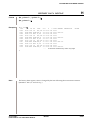
MF599-06
CMOS 4-BIT SINGLE CHIP MICROCOMPUTER
S1C62 Family
Development Tool Reference Manual
NOTICE
No part of this material may be reproduced or duplicated in any form or by any means without the written permission of Seiko
Epson. Seiko Epson reserves the right to make changes to this material without notice. Seiko Epson does not assume any
liability of any kind arising out of any inaccuracies contained in this material or due to its application or use in any product or
circuit and, further, there is no representation that this material is applicable to products requiring high level reliability, such
as medical products. Moreover, no license to any intellectual property rights is granted by implication or otherwise, and there
is no representation or warranty that anything made in accordance with this material will be free from any patent or copyright
infringement of a third party. This material or portions thereof may contain technology or the subject relating to strategic
products under the control of the Foreign Exchange and Foreign Trade Law of Japan and may require an export license from
the Ministry of International Trade and Industry or other approval from another government agency.
MS-DOS, Windows, Windows 95, Windows 98 and Windows NT are registered trademarks of Microsoft Corporation, U.S.A.
PC-DOS, PC/AT, PS/2, VGA, EGA and IBM are registered trademarks of International Business Machines Corporation, U.S.A.
NEC PC-9800 Series and NEC are registered trademarks of NEC Corporation.
All other product names mentioned herein are trademarks and/or registered trademarks of their respective owners.
© SEIKO EPSON CORPORATION 2001 All rights reserved.
S1C62 Family Development Tool Reference Manual
Preface
The explanation covering the outline and operation of the development support tools for the CMOS 4-bit
Single Chip Microcomputer S1C62 Family has been divided into the following parts.
I.
II.
III.
IV.
V.
VI.
VII.
VIII.
IX.
INTRODUCTION
DEVELOPMENT TOOL MANAGEMENT SYSTEM DMS6200
CROSS ASSEMBLER ASM62XX
MELODY ASSEMBLER MLA628X
FUNCTION OPTION GENERATOR FOG62XX
SEGMENT OPTION GENERATOR SOG62XX
EVALUATION BOARD S5U1C62XXXE
ICE CONTROL SOFTWARE ICS62XX
MASK DATA CHECKER MDC62XX
Before Reading . . .
This manual indicates the model name as "S1C62XXX" and source file and output files as "C2XXYYY" for
purposes of explanation of the common content in each model of the S1C62 Family. You should substitute
the "XXX" parts for the various model names. Please allow Seiko Epson to specify the "YYY" section for
each customer.
Example: When the development model is S1C6S460, and the "YYY" section is to be specified as "0A0".
S1C6XXXX
CXXXYYY
→
→
S1C6S460
CS460A0
Reference Manual
The peculiar content of each model, device details and the like are explained in the below manual. You
should refer to it as required.
Development Tools
☞
S5U1C62xxxD Manual (Development Software Tool for S1C62xxx)
S5U1C62xxxE Manual (Evaluation Board for S1C62xxx)
S5U1C62000H Manual (S1C60/62 Family In-Circuit Emulator)
Device (S1C62xxx)
☞
☞
S1C62xxx Technical Manual
Instructions
∗
S1C6200/6200A Core CPU Manual
In this manual, "ICE" and "evaluation board" indicate S5U1C62000H and S5U1C62xxxE, respectively.
The information of the product number change
Starting April 1, 2001, the product number will be changed as listed below. To order from April 1,
2001 please use the new product number. For further information, please contact Epson sales
representative.
Configuration of product number
Devices
S1
C
60N01
F
0A01
00
Packing specification
Specification
Package (D: die form; F: QFP)
Model number
Model name (C: microcomputer, digital products)
Product classification (S1: semiconductor)
Development tools
C
60R08
S5U1
D1
1
00
Packing specification
Version (1: Version 1 ∗2)
Tool type (D1: Development Tool ∗1)
Corresponding model number (60R08: for S1C60R08)
Tool classification (C: microcomputer use)
Product classification
(S5U1: development tool for semiconductor products)
∗1: For details about tool types, see the tables below. (In some manuals, tool types are represented by one digit.)
∗2: Actual versions are not written in the manuals.
Comparison table between new and previous number
S1C60 Family processors
Previous No.
E0C6001
E0C6002
E0C6003
E0C6004
E0C6005
E0C6006
E0C6007
E0C6008
E0C6009
E0C6011
E0C6013
E0C6014
E0C60R08
New No.
S1C60N01
S1C60N02
S1C60N03
S1C60N04
S1C60N05
S1C60N06
S1C60N07
S1C60N08
S1C60N09
S1C60N11
S1C60N13
S1C60140
S1C60R08
S1C62 Family processors
Previous No.
E0C621A
E0C6215
E0C621C
E0C6S27
E0C6S37
E0C623A
E0C623E
E0C6S32
E0C6233
E0C6235
E0C623B
E0C6244
E0C624A
E0C6S46
New No.
S1C621A0
S1C62150
S1C621C0
S1C6S2N7
S1C6S3N7
S1C6N3A0
S1C6N3E0
S1C6S3N2
S1C62N33
S1C62N35
S1C6N3B0
S1C62440
S1C624A0
S1C6S460
Previous No.
E0C6247
E0C6248
E0C6S48
E0C624C
E0C6251
E0C6256
E0C6292
E0C6262
E0C6266
E0C6274
E0C6281
E0C6282
E0C62M2
E0C62T3
New No.
S1C62470
S1C62480
S1C6S480
S1C624C0
S1C62N51
S1C62560
S1C62920
S1C62N62
S1C62660
S1C62740
S1C62N81
S1C62N82
S1C62M20
S1C62T30
Comparison table between new and previous number of development tools
Development tools for the S1C60/62 Family
Previous No.
ASM62
DEV6001
DEV6002
DEV6003
DEV6004
DEV6005
DEV6006
DEV6007
DEV6008
DEV6009
DEV6011
DEV60R08
DEV621A
DEV621C
DEV623B
DEV6244
DEV624A
DEV624C
DEV6248
DEV6247
New No.
S5U1C62000A
S5U1C60N01D
S5U1C60N02D
S5U1C60N03D
S5U1C60N04D
S5U1C60N05D
S5U1C60N06D
S5U1C60N07D
S5U1C60N08D
S5U1C60N09D
S5U1C60N11D
S5U1C60R08D
S5U1C621A0D
S5U1C621C0D
S5U1C623B0D
S5U1C62440D
S5U1C624A0D
S5U1C624C0D
S5U1C62480D
S5U1C62470D
Previous No.
DEV6262
DEV6266
DEV6274
DEV6292
DEV62M2
DEV6233
DEV6235
DEV6251
DEV6256
DEV6281
DEV6282
DEV6S27
DEV6S32
DEV6S37
EVA6008
EVA6011
EVA621AR
EVA621C
EVA6237
EVA623A
New No.
S5U1C62620D
S5U1C62660D
S5U1C62740D
S5U1C62920D
S5U1C62M20D
S5U1C62N33D
S5U1C62N35D
S5U1C62N51D
S5U1C62560D
S5U1C62N81D
S5U1C62N82D
S5U1C6S2N7D
S5U1C6S3N2D
S5U1C6S3N7D
S5U1C60N08E
S5U1C60N11E
S5U1C621A0E2
S5U1C621C0E
S5U1C62N37E
S5U1C623A0E
Previous No.
EVA623B
EVA623E
EVA6247
EVA6248
EVA6251R
EVA6256
EVA6262
EVA6266
EVA6274
EVA6281
EVA6282
EVA62M1
EVA62T3
EVA6S27
EVA6S32R
ICE62R
KIT6003
KIT6004
KIT6007
New No.
S5U1C623B0E
S5U1C623E0E
S5U1C62470E
S5U1C62480E
S5U1C62N51E1
S5U1C62N56E
S5U1C62620E
S5U1C62660E
S5U1C62740E
S5U1C62N81E
S5U1C62N82E
S5U1C62M10E
S5U1C62T30E
S5U1C6S2N7E
S5U1C6S3N2E2
S5U1C62000H
S5U1C60N03K
S5U1C60N04K
S5U1C60N07K
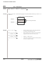
I
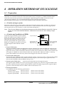
S1C62 FAMILY DEVELOPMENT TOOL
INTRODUCTION
This part explains the composition of the development support tool for the 4-bit Single Chip Microcomputer S1C62 Family and the developmental
environment.
INTRODUCTION
INTRODUCTION
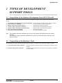
Contents
1 TYPES OF DEVELOPMENT SUPPORT TOOLS ____________________ I-1
1.1
1.2
Composition of the Software Development Tools S5U1C62xxxD ........................... I-1
Composition of the Hardware Tools .......................................................................I-1
2 DEVELOPMENTAL ENVIRONMENT _____________________________ I-2
3 DEVELOPMENT FLOW ________________________________________ I-2
4 INSTALLATION _______________________________________________ I-4
5 DIFFERENCES FROM MODEL TO MODEL AND PRECAUTIONS ___ I-5
6 TROUBLESHOOTING __________________________________________ I-6
S1C62 FAMILY
DEVELOPMENT TOOL REFERENCE MANUAL
EPSON
I-i
INTRODUCTION
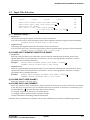
1 TYPES OF DEVELOPMENT
SUPPORT TOOLS
Here we will explain the composition of the software and hardware for the development support tools.
1.1 Composition of the Software Development Tools S5U1C62xxxD
The below software are included in the software development support tools used in each S1C62XXX
model.
1.
2.
3.
4.
5.
6.
7.
Development Tool Management System DMS6200 .. Menu selections for each software / start-up software
Cross Assembler ASM62XX ...................................... Cross assembler for program preparation
Melody Assembler MLA628X (Note) .......................... Melody data preparation program
Function Option Generator FOG62XX ....................... Function option data preparation program
Segment Option Generator SOG62XX (Note) ........... Segment option data preparation program
ICE Control Software ICS62XX .................................. ICE control program
Mask Data Checker MDC62XX .................................. Mask data preparation program
Note
The 3 Melody Assembler MLA628X are only set in the models (S1C62N8X) that have melody
functions.
The 5 Segment Option Generator SOG62XX are only set in models that have LCD driver and
segment options.
1.2 Composition of the Hardware Tools
The following two types have been prepared for all types as hardware development support systems.
1. In-Circuit Emulator S5U1C62000H ..... In-circuit emulator permitting high level debugging (common to each
model)
2. Evaluation Board S5U1C62xxxE ........ Evaluation board that has the same functions as the actual IC (different
for each model)
S1C62 FAMILY
DEVELOPMENT TOOL REFERENCE MANUAL
EPSON
I-1
INTRODUCTION
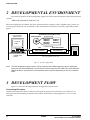
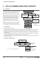
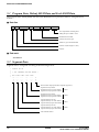
2 DEVELOPMENTAL ENVIRONMENT
The software product of the development support tool S5U1C62xxxD operates on the following host
systems:
• IBM PC/AT (at least PC-DOS Ver. 2.0)
When developing the S1C62XXX, the above-mentioned host computer, editor, P-ROM writer, printer, etc.
must be prepared by the user in addition to the development tool which is normally supported by Seiko
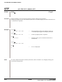
Epson.
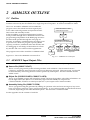
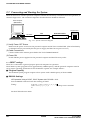
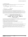
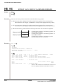
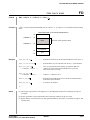
S1C62xxx Development Tool
Host computer
(IBM PC/AT)
S5U1C62000A
Software tools
S5U1C62xxxD
DMS6200
ASM62xx
MLA628x
FOG62xx
PC-DOS
Editor
ICE
RS-232C
• P-ROM writer
• Printer
SOG62xx
ICS62xx
MDC62xx
Target board
Hardware tools
Evaluation Board
S5U1C62000H
S5U1C62xxxE
To be prepared by the user
Fig. 2.1 System configuration
Note
The S5U1C62xxxD system requires a host computer with a RAM capacity of about 140K bytes.
Since the ICE (S5U1C62000H) is connected to the host computer with a RS-232C serial interface,
adapter board for asynchronous communication will be required depending on the host computer
used.
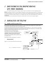
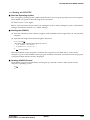
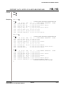
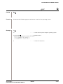
3 DEVELOPMENT FLOW
Figure 3.1 shows the development flow through the S5U1C62xxxD.
Concerning file names
All the input-output file name for the each development support tool commonly use "C2XXYYY". In
principle each file should be produced in this manner. Seiko Epson will designate the "YYY" for each
customer.
I-2
EPSON
S1C62 FAMILY
DEVELOPMENT TOOL REFERENCE MANUAL
INTRODUCTION
*1, *2
*1
Determination of
software specifications
Determination of
hardware specifications
*2, *3, *4
*4, *5
Flow chart generation
and coding
*4, *5
Development support tool
selection on menu of
Development Tool
Management System DMS6200
Coding
sheet
Coding
sheet
Source file generation
by using editor
Source file generation
by using editor
C2XXYYY
.DAT
*4, *5
Melody generation
and coding
Program
source file
Function
option
list
C2XXYYY
.PRN
Segment
option
list
Source file generation
by using editor
C2XXYYY
.SEG
*4, *5
Melody Assembler
MLA628X execution
*1, *6
Creation of
target board
Segment option list
generation
Melody
source file
C28XYYY
.MDT
*4, *5
Cross Assembler
ASM62XX execution
*4, *5
Function option list
generation
*4, *5
Segment option
source file
*4, *5
Function Option Generator
FOG62XX execution
Segment Option Generator
SOG62XX execution
C28XYYY
.MPR
Assembly list
Melody
assembly list
C2XXYYYL Object file
.HEX
C2XXYYYH
.HEX
C28XYYYA
.DOC
C2XXYYYF
.DOC
C2XXYYYS
.DOC
Melody
document file
Function option
document file
Segment option
document file
Function
C2XXYYYF option
.HEX
HEX file
C28XYYYA Melody
.HEX
HEX file
Segment
C2XXYYYS option
.HEX
HEX file
Segment
option ROM
(two)
Function
option ROM
(one)
Target board
*4, *5
Debugging with
ICE Control Software
ICS62XX
ICE
Evaluation Board
S5U1C62000H
S5U1C62xxxE
*4, *7
*6
Debugging
completion
*4, *5
Mask Data Checker
MDC62XX execution
Note
C62XXYYY File for
submission
.PAn
The melody and segment option flow are
only valid in models possessing those
functions.
SEIKO EPSON
Fig. 3.1 S5U1C62xxxD development flow
☞ Reference manual
*1
*2
*3
*4
S1C62xxx Technical Manual (Hardware)
S1C62xxx Technical Manual (Software)
S1C6200/6200A Core CPU Manual
S1C62 Family Development Tool Reference Manual (this manual)
S1C62 FAMILY
DEVELOPMENT TOOL REFERENCE MANUAL
EPSON
*5 S5U1C62xxxD Manual
*6 S5U1C62xxxE Manual
*7 S5U1C62000H Manual
I-3
INTRODUCTION
4 INSTALLATION
The S5U1C62xxxD tools are included on the CD-ROM of the S5U1C62000A (S1C60/62 Family Assembler
Package), and they can be installed in your hard disk using the installer (Setup.exe) on the CD-ROM.
Refer to the "S5U1C62000A Manual" for how to install the S5U1C62xxxD tools.
Note
I-4
The DMS6200 configures a menu from files that are located in the current directory. Therefore, do
not move the development tools from the directory in which the DMS6200 exists.
To invoke an editor (DOS version) or other programs from the DMS6200, copy those executable
files to the directory in which the DMS6200 exists.
EPSON
S1C62 FAMILY
DEVELOPMENT TOOL REFERENCE MANUAL
INTRODUCTION
5 DIFFERENCES FROM MODEL TO
MODEL AND PRECAUTIONS
There may be some models in which the following two types software tools contained in the
S5U1C62xxxD are not included.
(1) Segment Option Generator SOG62XX
This is not included in the software tools of models in which the segment option has not been set.
(2) Melody Assembler MLA628X
This is not included in the software tools for the models (Other than S1C62N8X) that do not have the
melody function.
Please be aware of the following points in setting the host system.
(1) The S5U1C62xxxD system requires a host computer with a RAM capacity of about 140K bytes.
(2) Since the ICE is connected to the host computer with a RS-232C serial interface, adapter board for
asynchronous communication will be required depending on the host computer used.
(3) In order for the MDC62XX to handle numerous files, set the number of files described in the
CONFIG.SYS to 10 or more (e.g., FILES = 20).
S1C62 FAMILY
DEVELOPMENT TOOL REFERENCE MANUAL
EPSON
I-5
INTRODUCTION
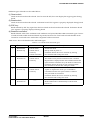
6 TROUBLESHOOTING
Tool
ICE
S5U1C62000H
Problem
Nothing appears on the screen, or
nothing works, after activation.
The ICE fuse cut immediately after
activation.
<ILLEGAL VERSION ICE6200>
appears on the screen immediately after
activation.
<ILLEGAL VERSION PARAMETER
FILE> appears on the screen immediately after activation.
Immediate values A (10) and B (11)
cannot be entered correctly with the A
command.
<UNUSED AREA> is displayed by the
SD command.
SOG62XX
I-6
You can not do a real-time run in
break-trace mode.
Output from the evaluation board is
impossible when data is written to the I/
O memory for Buzzer and Fout output
with the ICE command.
An R error occurs although the address
is correctly set in the segment source
file.
Remedy measures
Check the following and remedy if necessary:
• Is the RS-232C cable connected correctly?
• Is the RS-232C driver installed?
• Is MODE.COM on the disk?
• Is the execution file correct?
PC-DOS
ICS62XXW.EXE
• Is the DOS version correct?
PC-DOS
Ver. 2.1 or later
• Is the DIP switches that set the baud rate of the main ICE
unit set correctly?
• Is the fuse of the ICE cut off?
Check the following and remedy if necessary:
• Are connectors F1 and F5 connected to the evaluation
board correctly?
• Is the target board power short-circuiting?
The wrong version of ICE is being used. Use the latest
version.
The wrong version of ICS62XXP.PAR is being used. Use
the latest version.
The A and B registers are reserved for the entry of A and B.
Write 0A and 0B when entering A (10) and B (11).
Example: LD
A, B
Data in the B register is
loaded into the A register.
LD
B, 0A
Immediate value A is loaded
into the B register.
This massage is output when the address following one in
which data is written is unused. It does not indicates
problem. Data is correctly set in areas other than the readonly area.
Since the CPU stops temporarily when breaking conditions
are met, executing in a real-time is not performed.
Output is possible only in the real-time run mode.
Check the following and remedy if necessary:
• Does the address symbol use capital letters?
• Are the output ports set for every two terminals?
EPSON
S1C62 FAMILY
DEVELOPMENT TOOL REFERENCE MANUAL
INTRODUCTION
Tool
ASM62XX
Problem
An R error occurs although the final
page is passed.
MDC62XX Activation is impossible.
MLA628X
No melody is output.
Evaluation The evaluation board does not work
when it is used independently.
board
S5U1C62xxxE
Target segment does not light.
S1C62 FAMILY
DEVELOPMENT TOOL REFERENCE MANUAL
Remedy measures
The cross assembler is designed to output "R error" every
time the page is changed. Use a pseudo-instruction to set the
memory, such as ORG or PAGE, to change the page. See
"Memory setting pseudo-instructions" in the cross assembler manual.
Check the following and remedy if necessary:
• Is the number of files set at ten or more in OS environment file CONFIG.SYS?
Check the following and remedy if necessary:
• Has the OPTLD command of the ICE been executed? (When
the ICE is connected to the evaluation board)
• Is the MELODY ROM installed? (When the evaluation
board is used independently)
• Is the attack bit of the melody data set to "1"?
Check the following and remedy if necessary:
• Has the EPROM for F.HEX and S.HEX been replaced by
the EPROM for the target?
• Is the EPROM for F.HEX and S.HEX installed correctly?
• Is the appropriate voltage being supplied? (5V DC, 3 A,
or more)
• Are the program ROMs (H and L) installed correctly?
• Is data written from address 4000H? (When the 27C256
is used as the program ROM)
• Is the EN/DIS switch on the evaluation board set to EN?
Check the following and remedy if necessary:
• Is an EPROM with an access time of 170 ns or less being
used for S.HEX.
• Has the VADJ VR inside the evaluation board top cover
been turned to a lower setting?
EPSON
I-7
II
DEVELOPMENT TOOL MANAGEMENT SYSTEM
DMS6200
This part mainly explains how to operate the Development Tool Management System DMS6200.
DEVELOPMENT TOOL MANAGEMENT SYSTEM DMS6200
DEVELOPMENT TOOL MANAGEMENT SYSTEM
Contents
1 DIFFERENCES DEPENDING ON THE MODEL __________________ II-1
2 DMS6200 OUTLINE ___________________________________________ II-1
3 DMS6200 OPERATION PROCEDURE ___________________________ II-2
S1C62 FAMILY
DEVELOPMENT TOOL REFERENCE MANUAL
EPSON
II-i
DEVELOPMENT TOOL MANAGEMENT SYSTEM DMS6200
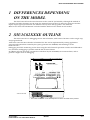
1 DIFFERENCES DEPENDING
ON THE MODEL
The DMS6200 is a software tool that is common to the all models of the S1C62 Family and there is
no difference in operating procedure. However, the content of such things as the menu screen may vary
due to differences in the configuration of the software for each model and differences in the directory
content in the DMS6200.
The below two types that are included in the explanation and display screen examples may not be present
in certain models.
(1) The SOG62XX and C2XXYYYS.* are only available in models offering the segment option.
(2) The MLA628X, C28XYYY.M* and C28XYYYA.* are only available in models offering the melody
function.
When models that do not have the above functions are used, disregard the respective program names and
file names indicated in the manual.
Refer to the "S5U1C62xxxD Manual" for the software tools included in the S5U1C62xxxD.
2 DMS6200 OUTLINE
The DMS6200 (Development Tool Management System) is a software which selects the
S5U1C62xxxD software development support tool and the program such as an editor in menu form and
starts it.
In this way the various software frequently executed during debugging can be effectively activated.
Figure 2.1 shows the DMS6200 execution flow.
DMS6200
Menu
selections
ASM62XX
MLA628X
FOG62XX
SOG62XX
ICS62XX
MDC62XX
Editor etc.
To DOS
Fig. 2.1 DMS6200 execution flow
S1C62 FAMILY
DEVELOPMENT TOOL REFERENCE MANUAL
EPSON
II-1
DEVELOPMENT TOOL MANAGEMENT SYSTEM DMS6200
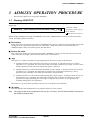
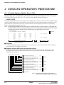
3 DMS6200 OPERATION PROCEDURE
Set the directory containing the respective software development support tools into the current
directory prior to activating the DMS6200.
Since the development support tools each require input files (e.g., source file), first create the input files
according to the support tool manuals and then perform the following operations:
(1) The following is entered on the current drive:
indicates the return key.
DMS6200
The title is then displayed. To return to DOS at this point, press ^C (CTRL + C).
Initial screen
*** E0C6200 Development tool Management System. --- Ver 1.0 ***
EEEEEEEEEE
EEEEEEEEEE
EEE
EEE
EEEEEEEEEE
EEEEEEEEEE
EEE
EEE
EEEEEEEEEE
EEEEEEEEEE
PPPPPPPP
PPPPPPPPPP
PPP
PPP
PPP
PPP
PPPPPPPPPP
PPPPPPPP
PPP
PPP
PPP
PPP
SSSSSSS
SSS
SSSS
SSS
SSS
SSS
SSSSSS
SSSS
SSS
SSS
SSS
SSSS
SSS
SSSSSSS
OOOOOOOO
OOO
OOO
OOO
OOO
OOO
OOO
OOO
OOO
OOO
OOO
OOO
OOO
OOO
OOO
OOO
OOO
OOOOOOOO
NNN
NNN
NNNN
NNN
NNNNN
NNN
NNNNNN NNN
NNN NNN NNN
NNN NNNNNN
NNN
NNNNN
NNN
NNNN
NNN
NNN
NNN
NN
(C) Copyright 1991 SEIKO EPSON CORP.
STRIKE ANY KEY.
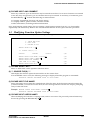
(2) Press any key and the following menu screen will be displayed. A list of all executable files having
"EXE", "COM" and "BAT" extensions will appear on this menu screen; if any execution file other than
S5U1C62xxxD were copied to the current drive for execution, it will differ from the displays shown
below.
Menu screen
DMS6200 Version 1.0
1)
2)
3)
4)
5)
6)
7)
Copyright(C) SEIKO EPSON CORP. 1991.
ASM62XX .EXE
FOG62XX .EXE
ICS62XXB.BAT
ICS62XXW.EXE
MDC62XX .EXE
MLA628X .EXE
SOG62XX .EXE
Input Number ? [
]
To return to DOS at this point, press the "ESC" key.
II-2
EPSON
S1C62 FAMILY
DEVELOPMENT TOOL REFERENCE MANUAL
DEVELOPMENT TOOL MANAGEMENT SYSTEM DMS6200
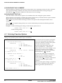
(3) Input the number of the development support tool you wish to start and then press the "RETURN" key.
Next, the screen for entering the source file will be displayed.
Input Number ? [1
]
(4) The following sample screen is the screen which will be displayed when ASM62XX is selected.
Input the number of the source file.
Pressing the "ESC" key here will return the previous screen.
When the source file is selected by number, the edit line enclosed in [ ] will appear; enter the option
parameter if necessary. The "BS" key is valid on the edit line. Press the "RETURN" key when input is
completed.
Source file selection screen
DMS6200 Version 1.0
1)
2)
3)
4)
5)
6)
7)
8)
9)
10)
11)
12)
13)
14)
Copyright(C) SEIKO EPSON CORP. 1991.
C2XXYYY .DAT
C28XYYY .MDT
C28XYYY .MPR
C2XXYYY .PRN
C2XXYYY .SEG
C28XYYYA.DOC
C28XYYYA.HEX
C2XXYYYF.DOC
C2XXYYYF.HEX
C2XXYYYH.HEX
C2XXYYYL.HEX
C2XXYYYS.DOC
C2XXYYYS.HEX
C62XXYYY.PA0
Input Number ? [1
]
Edit > [ASM62XX C2XXYYY
]
The above operation will activate the ASM62XX. (The MLA628X will also activate with the same
operation.)
When the source file is in another file or directory it will not be displayed in the menu. In such cases
you skip the number input using the return key and input the drive/directory and source file name in
the edit line.
When starting, press the "RETURN" key twice particularly for the support tools which do not require
source files (except the ASM62XX and the MLA628X).
Refer to the support manuals regarding operations after starting.
(5) When execution of the development support tool is completed, the following message will appear:
Input Any Key ...
Press any key and the first menu screen will be returned.
S1C62 FAMILY
DEVELOPMENT TOOL REFERENCE MANUAL
EPSON
II-3
III
CROSS ASSEMBLER
ASM62XX
This part mainly explains how to operate the
Cross Assembler ASM62XX for the S1C62
Family, and how to generate source files.
CROSS ASSEMBLER ASM62XX
CROSS ASSEMBLER ASM62XX
Contents
1 DIFFERENCES DEPENDING ON THE MODEL __________________ III-1
2 ASM62XX OUTLINE __________________________________________ III-2
2.1
2.2
Outline ................................................................................................................... III-2
ASM62XX Input/Output Files ................................................................................ III-2
3 ASM62XX OPERATION PROCEDURE __________________________ III-3
3.1
3.2
3.3
Starting ASM62XX ................................................................................................ III-3
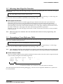
Selecting Auto-Page-Set Function ......................................................................... III-5
Generating a Cross-Reference Table .................................................................... III-5
4 SOURCE FILE FORMAT _____________________________________ III-6
4.1
4.2
Source File Name .................................................................................................. III-6
Statements .............................................................................................................. III-6
4.2.1 Label field ....................................................................................................
4.2.2 Mnemonic field ............................................................................................
4.2.3 Operand field ...............................................................................................
4.2.4 Comment field ..............................................................................................
4.3
III-6
III-7
III-7
III-7
Index ...................................................................................................................... III-7
4.3.1 Label ............................................................................................................ III-7
4.3.2 Symbol ......................................................................................................... III-8
4.4
Constant and Operational Expression .................................................................. III-8
4.4.1 Numeric constant ......................................................................................... III-8
4.4.2 Character constant ...................................................................................... III-8
4.4.3 Operator ...................................................................................................... III-9
4.4.4 Location counter ......................................................................................... III-10
4.5
Pseudo-Instructions .............................................................................................. III-11
4.5.1 Data definition pseudo-instructions ........................................................... III-11
4.5.2 Memory setting pseudo-instructions ........................................................... III-12
4.5.3 Assembler control pseudo-instructions ...................................................... III-15
4.6
Macro-Functions .................................................................................................. III-15
4.6.1 Macro-instructions ..................................................................................... III-15
4.6.2 Macro-definitions ....................................................................................... III-16
4.6.3 Macro-calls ................................................................................................. III-17
5 ERROR MESSAGES __________________________________________ III-19
APPENDIX ASM62XX EXECUTION EXAMPLE __________________ III-20
1) Source file (C2XX0A0.DAT) ...........................................................................
2) Running the assembler (display on the console) .............................................
3) Assembly listing file (C2XX0A0.PRN) ............................................................
4) Object files (C2XX0A0H.HEX, C2XX0A0L.HEX) ..........................................
S1C62 FAMILY
DEVELOPMENT TOOL REFERENCE MANUAL
EPSON
III-20
III-21
III-22
III-23
III-i
CROSS ASSEMBLER ASM62XX
1 DIFFERENCES DEPENDING
ON THE MODEL
Since the memory capacity will vary with each model of the S1C62 Family you must pay attention
to the following points when preparing a program.
The limiting items for each model are indicated in the "S5U1C62xxxD Manual".
■ ROM area
The ROM capacity will vary depending on the model.
The number of banks (16 pages/bank) and the number of pages (256 steps/page) are determined by
this ROM capacity and the memory setting pseudo-instruction and the "PSET" instruction is limited to
within its range.
Valid specification range
ORG pseudo-instruction:
0000H–ROM final step
PAGE pseudo-instruction:
00H–number of page - 1
BANK pseudo-instruction:
1 bank configuration model → 0H only
2 bank configuration model → 0H and 1H
PSET instruction:
00H–number of page - 1
When a specification beyond this valid specification range is made to the ASM62XX an error is produced.
■ RAM area
The RAM capacity varies depending on the model.
The number of pages (256 words/page) is determined according to the RAM capacity. Also, the
undefined area includes from the 0 address to the final RAM address.
When an undefined address is set in the index register, memory access to it becomes invalid, but be
careful that no errors develop in the ASM62XX.
■ Undefined code
In the S1C62 Family, the instruction set is not different from model to model. However, you may not be
able to use instructions such as the SLP instruction and those that access the page section (XP and YP)
of the index register depending on the RAM content.
S1C62 FAMILY
DEVELOPMENT TOOL REFERENCE MANUAL
EPSON
III-1
CROSS ASSEMBLER ASM62XX
2 ASM62XX OUTLINE
2.1 Outline
The ASM62XX cross assembler (the ASM62XX in this manual) is an assembler program for generating the
machine code used by the S1C62XXX 4-bit, single-chip microcomputers. It can be used under PC-DOS.
The Cross Assembler ASM62XX will assemble the
program source files which have been input by the
user's editor and will generate an object file in IntelHex format and assembly list file.
In this assembler, program modularization has been
made possible through macro definition functions and
programming independent of the ROM page structure
has been made possible through the auto page set
function. In addition, consideration has also been given
to precise error checks for program capacity (ROM
capacity) overflows, undefined codes and the like, and
for debugging of such things as label tables for assembly list files and cross reference table supplements.
The program name of the assembler is ASM62XX.EXE.
A>EDLIN C2XXYYY.DAT
Create the source file
C2XXYYY
.DAT
A>ASM62XX C2XXYYY
Execute the cross assembler
Error
message
Error
message
C2XXYYY
.PRN
Assembly
listing file
C2XXYYYL
.HEX
C2XXYYYH
.HEX
Object file
Figure 2.1.1 shows the ASM62XX execution flow.
Fig. 2.1.1 ASM62XX execution flow
2.2 ASM62XX Input/Output Files
ASM62XX reads a source file, assembles it, and outputs object files and an assembly listing file.
■ Source file (C2XXYYY.DAT)
This is a source program file produced using an editor such as EDLIN. The file name format is
C2XXYYY, and the file name must not exceed seven characters in length. Character string YYY should
be determined by referencing the device name specified by Seiko Epson. The file extension must be
added ".DAT".
■ Object file (C2XXYYYH.HEX, C2XXYYYL.HEX)
This is an assembled program file in Intel hex format. Because the machine code of the S1C62XXX is 12bit, the high-order bytes (bits 9 to 12 suffixed by high-order bits 0000B) are output to file
C2XXYYYH.HEX, and the low-order bytes (bits 8 to 1) are output to file C2XXYYYL.HEX.
■ Assembly listing file (C2XXYYY.PRN)
This is a program listing file generated by adding an operation codes and error messages (if any errors
have occurred) to respective source program statements. A cross-reference table is generated at the end
of the file, depending on the label table and options. The file name is C2XXYYY.PRN.
See the Appendix for the contents of each file.
III-2
EPSON
S1C62 FAMILY
DEVELOPMENT TOOL REFERENCE MANUAL
CROSS ASSEMBLER ASM62XX
3 ASM62XX OPERATION PROCEDURE
This section explains how to operate ASM62XX.
3.1 Starting ASM62XX
When starting ASM62XX, enter the following at DOS command level (when a prompt such as A> is being
displayed):
ASM62XX _ [drive-name:] source-file-name [.shp] _ [-N]
_ indicates a blank.
A parameter enclosed by [ ]
can be omitted.
indicates the return key.
When starting ASM62XX through the DMS6200, selects the "ASM62XX.EXE" and source file in the menu
screen, and input options necessary.
■ Drive name
If the source file is not on the same disk as ASM62XX.EXE, specify a disk drive mounted the floppy disk
storing the source file before input the source file name. If the source file is on the same disk as
ASM62XX.EXE, it does not need to specify the disk drive.
■ Source file name
This is the name of the source file to be entered for ASM62XX. The source file name must not exceed
seven characters in length. File extension .DAT must not be entered.
■ .shp
Characters s, h, and p are options for specifying the file I/O drives, and can be omitted.
s: Specifies the drive from which the source file is to be input. A character from A to P can be
specified. If @ is specified, the source file in the current drive (directory) is input. Even if a drive
name is prefixed to the source file name, this option is effective.
h: Specifies the drive to which the object file (HEX) is to be output. A character from A to P can be
specified. If @ is specified, the object file is output to the current drive (directory). If Z is
specified, only assembly is executed; the object file is not generated.
p: Specifies the drive to which the assembly listing file is to be output. A character from A to P can
be specified. If @ is specified, the object file is output to the current drive (directory). If X is
specified, a listing containing error messages is output to the console. If Z is specified, the
assembly listing file is not generated.
Characters s, h, p must all be specified; only one or two of them is not sufficient.
■ -N option
The code (FFH) in the undefined area of program memory is not created.
Note
The program data to be provided does not use the "-N" option. The FFH data should be inserted into
the undefined program area.
S1C62 FAMILY
DEVELOPMENT TOOL REFERENCE MANUAL
EPSON
III-3
CROSS ASSEMBLER ASM62XX
Example 1: Basic assembly example
A>ASM62XX C2XXYYY
The source file "C2XXYYY.DAT" is input from drive A, and the
object files "C2XXYYYH.HEX" and "C2XXYYYL.HEX" and
the assembly listing file "C2XXYYY.PRN" are output to drive A.
A>ASM62XX B:C2XXYYY
The source file "C2XXYYY.DAT" is input from drive B, and the
object files "C2XXYYYH.HEX" and "C2XXYYYL.HEX" and
the assembly listing file "C2XXYYY.PRN" are output to drive B.
A>ASM62XX C2XXYYY.BBZ
The source file "C2XXYYY.DAT" is input from drive B, and the
object files "C2XXYYYH.HEX" and "C2XXYYYL.HEX" are
output to drive B. The assembly listing file is not generated.
Example 2: -N option use
A>ASM62XX C2XXYYY -N
No undefined program area is generated in the created object files
(C2XXYYYH.HEX, C2XXYYYL.HEX).
Refer to APPENDIX, "ASM62XX EXECUTION EXAMPLE".
A>ASM62XX C2XXYYY
In this case, FFH data is inserted into the undefined program area
of the object files.
When ASM62XX is started, the following start-up message is displayed.
Example: When assembling C2XX0A0.DAT
A>ASM62XX C2XX0A0
*** E0C62XX CROSS ASSEMBLER. --- Ver 2.00 ***
EEEEEEEEEE
EEEEEEEEEE
EEE
EEE
EEEEEEEEEE
EEEEEEEEEE
EEE
EEE
EEEEEEEEEE
EEEEEEEEEE
PPPPPPPP
PPPPPPPPPP
PPP
PPP
PPP
PPP
PPPPPPPPPP
PPPPPPPP
PPP
PPP
PPP
PPP
SSSSSSS
SSS
SSSS
SSS
SSS
SSS
SSSSSS
SSSS
SSS
SSS
SSS
SSSS
SSS
SSSSSSS
OOOOOOOO
OOO
OOO
OOO
OOO
OOO
OOO
OOO
OOO
OOO
OOO
OOO
OOO
OOO
OOO
OOO
OOO
OOOOOOOO
NNN
NNN
NNNN
NNN
NNNNN
NNN
NNNNNN NNN
NNN NNN NNN
NNN NNNNNN
NNN
NNNNN
NNN
NNNN
NNN
NNN
NNN
NN
(C) COPYRIGHT 1991 SEIKO EPSON CORP.
SOURCE FILE NAME IS " C2XXYYY.DAT "
THIS SOFTWARE MAKES NEXT FILES.
C2XXYYYH.HEX
C2XXYYYL.HEX
C2XXYYY .PRN
III-4
...
...
...
HIGH BYTE OBJECT FILE.
LOW BYTE OBJECT FILE.
ASSEMBLY LIST FILE.
EPSON
S1C62 FAMILY
DEVELOPMENT TOOL REFERENCE MANUAL
CROSS ASSEMBLER ASM62XX
3.2 Selecting Auto-Page-Set Function
After the start-up message, the following message is displayed, prompting the user to select the auto-pageset function.
DO YOU NEED AUTO PAGE SET?(Y/N)
Press the "Y" key if selecting the auto-page-set function, or the "N" key if not selecting it. At this stage, the
user can also return to the DOS command level by entering "CTRL" + "C" key.
■ Auto-page-set function
When the program branches to another page through a branch instruction such as JP, the branchdestination page must be set using the PSET instruction before executing the branch instruction.
The auto-page-set function automatically inserts this PSET instruction. It checks whether the branch
instruction page is the same as the branch-destination one. If the page is different, the function inserts
the "PSET" instruction. If the page is the same, the function performs no operation.
Therefore, do not select the auto-page-set function if "PSET" instructions have been correctly included
in the source file.
Note
When auto-page-set is selected, there are restricted items related to source programming. See
"4.3.1 Label".
3.3 Generating a Cross-Reference Table
After the auto-page-set function has been selected, the following message is output, prompting the user to
select cross-reference table generation.
DO YOU NEED CROSS REFERENCE TABLE?(Y/N)
Press the "Y" key if generating the cross-reference table, or the "N" key if not generating it. At this stage,
the user can also return to DOS command level by entering "CTRL" + "C" key.
Note
If the assembly listing file output destination (p option) is specified as Z (listing not generated) at the
start of ASM62XX, the above message is not output and the cross-reference table is not generated.
■ Cross-reference table
The cross-reference table lists the symbols and their locations in the source file, and is output at the end
of the assembly listing file in the following format:
CROSS REFERENCE TABLE
LABEL1 4#
29
LABEL2 15#
40
:
:
:
Symbol
PAGE X36
1
....
Number of the program statement
(# indicates the number of the statement at which the symbol was defined)
This table should be referenced during debugging. An error such as duplicate definition of a symbol can
be easily detected.
S1C62 FAMILY
DEVELOPMENT TOOL REFERENCE MANUAL
EPSON
III-5
CROSS ASSEMBLER ASM62XX
4 SOURCE FILE FORMAT
The source file contains the source program consisting of S1C62XXX instructions (mnemonics) and
pseudo-instructions, and is produced using an editor such as EDLIN.
Refer to the "S1C6200/6200A Core CPU Manual" and the "S1C6xxx Technical Manual (Software)" for
instruction sets.
4.1 Source File Name
A desired file name not exceeding seven characters in length can be assigned to each source file. The
format must be as follows:
C2XXYYY.DAT
"YYY" of the "C2XXYYY.DAT" is an alphanumeric character string of up to three characters, and should be
determined by referencing the device name specified by Seiko Epson. The file extension must be ".DAT".
4.2 Statements
Each source program statement must be written using the following format.
Basic format:
<Index>[:]
Example:
ON
START:
Label
field
<Instruction> <Expression> <; comment>
EQU
ORG
JP
Mnemonic
field
1
100H
INIT
;To init.
Operand
field
Comment
field
A statement consists of four fields: label, mnemonic, operand, and comment. Up to 132 characters can be
used for one statement. Fields must be delimited by one or more blanks or tabs.
The label and comment fields are optional. Blank lines consisting only of a carriage return (CR) code are
also allowed.
Although each statement and field (excluding the label field) can begin at any desired column. The
program becomes easier to understand if the heads of corresponding fields are aligned.
4.2.1
Label field
The label field can contain a label for referencing the memory address, a symbol that defines a constant, or
a macro name. This field can be omitted if the statement name is not required. The label field must begin
at column 1 and satisfy the following conditions.
• The length must not exceed 14 characters.
• The same name as a mnemonic or register name must not be used.
• The following alphanumeric characters can be used, but the first character must not be a digit:
A to Z, a to z, 0 to 9, _ , ?
• The uppercase and lowercase forms of a letter are equivalent.
• ??nnnn (n is a digit) cannot be used as a name.
A colon ":" can be used as a delimiter between a label field and the mnemonic field. If a colon is used,
neither blanks nor tabs need to be written subsequently.
Statements consisting of only a label field are also allowed.
III-6
EPSON
S1C62 FAMILY
DEVELOPMENT TOOL REFERENCE MANUAL
CROSS ASSEMBLER ASM62XX
4.2.2
Mnemonic field
The mnemonic field is used for an instruction mnemonic or a pseudo-instruction.
4.2.3
Operand field
The operand field is used for the operands of the instruction. The form of each operand and the number of
operands depend on the kind of instruction. The form of expressions specifying values must be one of the
following:
• A numeric constant, a character constant, or a symbol that defines a constant
• A label indicating a memory address
• An operational expression for obtaining the specified value
If the operand consists of two or more expressions, the expressions must be separated by commas ",".
4.2.4
Comment field
The comment field is used for comment data such as program headers and descriptions of processing. The
contents of this field do not affect assembly or the object files generated by assembly.
The part of the statement from a semicolon ";" to the CR code at the end of the statement is considered to be
the comment field. Statements consisting of only a comment field are also allowed. When a comment
spans multiple lines, a semicolon must be written at the beginning of each line.
4.3 Index
ASM62XX allows values to be referenced by their indexes.
Refer to Section 4.2.1, "Label field", for the restrictions on index descriptions.
4.3.1
Label
A label is an index for referencing a location in the program, and can be used as an operand that specifies a
memory address as immediate data in an instruction. For example, a label can be used as the operand of
an instruction such as JP by writing the label in the branch-destination statement.
The name written in the label field of an EQU or SET instruction is considered to be a symbol, not a label.
Example:
LABEL1:
:
JP
:
:
LD
NZ,LABEL1
A,0
A label can be assigned to any statement, but the label assigned to the following pseudo-instructions is
ignored:
ORG, BANK, PAGE, SECTION, END, LABEL, ENDM
Note
When selecting the auto-page-set function (see Section 3.2), a statement consisting of only a label
must be written immediately before the JP or CALL instructions.
Example:
PGSET:
JP
LABEL
S1C62 FAMILY
DEVELOPMENT TOOL REFERENCE MANUAL
EPSON
III-7
CROSS ASSEMBLER ASM62XX
4.3.2
Symbol
A symbol is an index that indicates a numeric or character constant, and must be defined before its value is
referenced (usually at the beginning of the program). The defined symbol can be used as the operand that
specifies immediate data in an instruction.
Example:
ON
OFF
EQU
EQU
:
LD
:
LD
:
1
0
(See Section 4.5 for EQU.)
A,ON
; = LD A,1
A,OFF
; = LD A,0
4.4 Constant and Operational Expression
This section explains the immediate data description formats.
4.4.1
Numeric constant
A numeric constant is processed as a 13-bit value by ASM62XX. If a numeric constant greater than 13 bits
is written, bit 13 and subsequent high-order bits are ignored.
Note that the number of actual significant bits depends on the operand of each instruction. If the value of a
constant is greater than the value that can be accommodated by the actual number of significant digits, an
error occurs.
Example:
ABC
EQU
LD
0FFFFH
A,65535
→
→
ABC is defined as 1FFFH.
An error occurs because it exceeds the significant digit
count (4 bits).
The default radix is decimal. The radix description formats are as follows:
Binary numeral:
A numeral suffixed with B, such as 1010B (=10) or 01100100B (=100).
Octal numeral:
A numeral suffixed with O or Q, such as 012O (=10) or 144Q (=100).
Decimal numeral:
A numeral alone or a numeral suffixed with D, such as 10 or 100D (=100).
Hexadecimal numeral: A numeral suffixed with H, such as 0AH (=10) or 64H (=100).
If the value begins with a letter from A to F, it must be prefixed with 0 to distinguish
it from a name.
4.4.2
Character constant
A character constant is one or two ASCII characters enclosed by apostrophes (' '). A single ASCII character
is processed as eight-bit data. If two or more ASCII characters are written, only the last two characters are
significant as 13-bit data.
Examples:
'A' (=41H), 'BC' (=0243H), 'PQ' (=1051H), 'DEFGH' → 'GH' (=0748H; DEF is ignored.)
The apostrophe itself cannot be processed as a character constant, so it must be written as a numeric
constant, such as 27H or 39.
III-8
EPSON
S1C62 FAMILY
DEVELOPMENT TOOL REFERENCE MANUAL
CROSS ASSEMBLER ASM62XX
4.4.3
Operator
When specifying a value for an item such as an operand, an operational expression can be written instead
of a constant, and its result can be used as the value.
Labels and symbols as well as constants can be used as terms in expressions. These values are processed as
13-bit data (bit 14 and subsequent high-order bits are ignored); the operation result also consists of 13 bits.
If the result exceeds the number of significant digits of the instruction operand, an error occurs.
There are three types of operator—arithmetic, logical, and relational—as listed below (a and b represent
terms, and _ represents one or more blanks).
■ Arithmetic operators
There are 11 arithmetic operators including the ones for addition, subtraction, multiplication, division,
bit shifting, and bit separation.
+a
Monadic positive (indicates the subsequent value is positive)
-a
Monadic negative (indicates the subsequent value is negative)
a+b
Addition (unsigned)
a-b
Subtraction (unsigned)
a*b
Multiplication (unsigned)
a/b
Division (unsigned)
a_MOD_b
Remainder of a/b
a_SHL_b
Shifts a b bits to the left. ←[b7<<<<<<b1]←0
Example: 00000011B SHL 2 → 00001100B
a_SHR_b
Shifts a b bits to the right. 0→[b7>>>>>>b0]→
Example: 11000011B SHR 2 → 00110000B
HIGH_a
Separates the high-order eight bits from a (13 bits).
Example: HIGH 1234H → 12H
LOW_a
Separates the low-order eight bits from a (13 bits).
Example: LOW 1234H → 34H
■ Logical operators
There are four logical operators as listed below. The logical operator returns the result of logical
operation on the specified terms.
a_AND_b
Logical product
Example: 00001111B AND 00000011B → 00000011B
a_OR_b
Logical sum
Example: 00001111B OR 11110000B → 11111111B
a_XOR_b
Exclusive logical sum
Example: 00001111B XOR 00000011B → 00001100B
NOT_a
Logical negation
Example: NOT 00001111B → 11110000B
S1C62 FAMILY
DEVELOPMENT TOOL REFERENCE MANUAL
EPSON
III-9
CROSS ASSEMBLER ASM62XX
■ Relational operators
A logical operator compares two terms; if the relationship between the terms is as the operator
specifies, 1FFFH (true) is returned; if not, 0 (false) is returned.
a_EQ_b
True when a is equal to b
a_NE_b
True when a is not equal to b
a_LT_b
True when a is less than b
a_LE_b
True when a is less than or equal to b
a_GT_b
True when a is greater than b
a_GE_b
True when a is greater than or equal to b
Be sure to insert one or more blanks for symbol "_" between terms. All operators must be entered in
uppercase letters.
An expression can contain one or more operators and pairs of parenthesis. In this case, operators are
basically evaluated from left to right. However, an operation stipulated by an operator with higher priority
or by parentheses is executed earlier. Every left parenthesis must have a corresponding right parenthesis.
The following table shows the priority of operators.
Operator
)
OR, XOR
AND
EQ, NE, LT, LE, GT, GE
+ (addition), - (subtraction)
*, /, MOD, SHL, SHR
(
HIGH, LOW, NOT
- (monadic negative), + (monadic positive)
4.4.4
Priority
Examples: Operational expressions (ABC = 1, BCD = 3)
Low
:
LD A,BCD*(ABC+1) ;A-register <- 6
LD
A,ABC LT BCD
;A-register <- 0FH (1111B)
OR
B,ABC SHL BCD
;Set bit 3 in B-register
;(=OR B,1000B)
AND B,ABC SHL BCD XOR 0FH
;Reset bit 3 in B-register
;(=AND B,0111B)
:
High
Location counter
The start address of each instruction code is set in the location counter when a statement is assembled. A
label or $ can be used when referencing the location counter value in a program.
■ Location counter
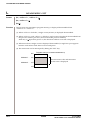
The location counter consists of 13 bits: one bit for the bank field, four bits for the page counter field,
and eight bits for the step counter field.
Bank
Bit
12
Contents Bank
BNK
Example:
11
Page counter
10
9
Page address
PCP
8
7
6
5
Step counter
4
3
Step address
PCS
2
1
0
Location counter
(BNK) (PCP) (PCS)
0
1
02
JP
$+3
The location counter indicates the start address of the JP instruction, and the PCS value (02) is assigned to $.
Consequently, the statement is assembled as "JP 5", and the program sequence jumps to the location three
steps before (PCS=05) when it is executed.
III-10
EPSON
S1C62 FAMILY
DEVELOPMENT TOOL REFERENCE MANUAL
CROSS ASSEMBLER ASM62XX
4.5 Pseudo-Instructions
There are four types of pseudo-instruction: data definition, memory setting, assembler control, and macro.
These pseudo-instructions as well as operational expressions can be used to govern assembly, and are not
executed in the developed program.
In the subsequent explanations, the items enclosed by < > in the pseudo-instruction format must be written
in the statement (do not write the < > characters themselves). Symbol _ represents one or more blanks or
tabs. One or more symbols and constants or an operational expression can be used in <expression>. See
Section 4.6 for macro functions.
4.5.1
Data definition pseudo-instructions
There are three data definition pseudo-instructions: EQU, SET, and DW. The EQU and SET pseudoinstructions each define a symbol, and the DW pseudo-instruction presets data in program memory.
■ EQU (Equate)
<Symbol>_EQU_<Expression>
To define a symbol
The EQU pseudo-instruction defines <symbol> (written in the label field) as having the value of
<expression> (written in the operand field).
If a value greater than 13 bits is specified in <expression>, bit 14 and subsequent high-order bits are
ignored.
This definition must be made before the symbol is referenced in the program. A U-error occurs if an
attempt is made to reference a symbol that has not been defined.
The same symbol cannot be defined more than once. A P-error occurs if an attempt is made to define a
symbol that has already been defined.
Examples:
ZERO
ONE
ONE
FOUR
EQU
EQU
EQU
EQU
30H
ZERO+1
31H
TWO*2
← P-error because ONE has been defined more than twice
← U-error because TWO has not been defined
■ SET
<Symbol>_SET_<Expression>
To define a symbol
Like EQU, the SET pseudo-instruction defines the value of <symbol> as being <expression>. The SET
pseudo-instruction allows a symbol to be redefined.
Examples:
ZERO
BIT
BIT
BIT
EQU
SET
:
SET
:
SET
30H
1
2
← Redefinition possible
BIT SHL 1 ← Previously-defined items can be referenced
S1C62 FAMILY
DEVELOPMENT TOOL REFERENCE MANUAL
EPSON
III-11
CROSS ASSEMBLER ASM62XX
■ DW (Define Word)
<Label>_DW_<Expression>
To preset data
The DW pseudo-instruction assigns the value of <expression> (the low-order 12 bits when the value is
greater than 12 bits) to the current memory location, indicated by the location counter.
Examples:
Location counter
(BNK) (PCP) (PCS)
0
0
0
2
2
2
0A
0B
0C
TABLE
DW
DW
DW
:
141H
142H
143H
; = RETD 'A'
; = RETD 'B'
; = RETD 'C'
<label> can be omitted.
4.5.2
Memory setting pseudo-instructions
The program memory mounted at the S1C62XXX is divided into 256-step pages. Memory management
(including the setting of the program location and page boundaries) during program generation must be
controlled by the source program.
The memory setting pseudo-instructions are used to specify memory management. The assembler sets the
location counter according to these pseudo-instructions.
If a memory area that has already been used is specified or a statement that exceeds the page is used
without specifying that the statement is to exceed the page, the assembler displays an exclamation mark "!",
indicating a warning, and ignores all subsequent statements until the next correct statement. This should
be taken into account.
When using the auto-page-set function, the space for insertion of the "PSET" pseudo-instruction must be
allocated in each page.
■ ORG (Origin)
ORG_<Expression>
To set the location counter
The ORG pseudo-instruction sets the location counter to the value of <expression>.
If the ORG pseudo-instruction is not written at the beginning of the program, the location counter is set
to 0 (BNK=0, PCP=0, PCS=0) and assembly is started.
The ORG pseudo-instruction can be used at multiple locations in the program. However, it cannot be
used to set the location to a value before the current location. If this is attempted, an exclamation mark
"!", indicating a warning, is displayed, and all subsequent statements until the next correct statement are
ignored.
A label can be written before the ORG statement, but it cannot be referenced because it is not cataloged
in the label table. In this case, write the label in the statement following the ORG pseudo-instruction.
Example:
START
ORG
:
0100H
; BNK=0, PCP=1, PCS=00H
An R-error occurs if a value is specified exceeding the ROM capacity.
Note
III-12
The upper limit of program memory depends on the model. (Refer to the "S5U1C62xxxD
Manual".)
EPSON
S1C62 FAMILY
DEVELOPMENT TOOL REFERENCE MANUAL
CROSS ASSEMBLER ASM62XX
■ BANK
BANK_<Expression>
To set the bank (BNK)
The BANK pseudo-instruction sets the value of <expression> in the bank (BNK) field, and sets the page
counter (PCP) and step counter (PCS) to 00H.
The BANK pseudo-instruction can be written at multiple locations in the program. However, it cannot
be used to specify the current bank (excluding the specification in page 00, step 00) or a previous bank.
If it is used to specify the current bank or a previous bank, an exclamation mark "!", indicating a
warning, is displayed, and all subsequent statements until the next correct statement are ignored.
A label can be written before the BANK statement, but it cannot be referenced because it is not
cataloged in the label table. In this case, write the label in the statement after the BANK pseudoinstruction.
■ PAGE
PAGE_<Expression>
To set the page counter (PCP)
The PAGE pseudo-instruction sets the value of <expression> in the page counter (PCP) and sets the
step counter (PCS) to 00H.
The PAGE pseudo-instruction can be written at multiple locations in the program. However, it cannot
be used to specify the current page (excluding the specification in step 00) or a previous page. If it is
used to specify the current page or a previous page, an exclamation mark "!", indicating a warning, is
displayed, and all subsequent statements until the next correct statement are ignored.
A label can be written before the PAGE statement, but it cannot be referenced because it is not
cataloged in the label table. In this case, write the label in the statement after the PAGE pseudoinstruction.
Example:
Location counter
(BNK) (PCP) (PCS)
:
0
0
:
0
:
0
0
:
0
:
1AH
1BH
:
F0H
0
0
:
2
2
:
00H
01H
:
!
!
0
0
:
SUB1:
SUB2:
3
3
:
00H
01H
:
SUB3:
:
LD
LD
:
JP
:
X,0
Y,0
:
xxx
PAGE
LD
LD
:
2
A,MX
B,MY
:
Ineffective because a previous page
was specified
PAGE
LD
LD
:
1
A,MX
B,MY
:
Effective
PAGE
LD
LD
:
3
A,0
B,1
:
An R-error occurs if a value is specified that exceeds the last page.
Note
The last page depends on the model. (Refer to the "S5U1C62xxxD Manual".)
S1C62 FAMILY
DEVELOPMENT TOOL REFERENCE MANUAL
EPSON
III-13
CROSS ASSEMBLER ASM62XX
■ SECTION
SECTION
To change the section
The SECTION pseudo-instruction sets the first address of the subsequent section in the location counter. Sections are 16-step areas starting from the beginning of the program memory.
(BNK) (PCP) (PCS)
0
1
00H
0
1
10H
0
1
20H
:
:
:
0
1
F0H
0
2
00H
0
2
20H
:
:
:
0
3
F0H
Section 1
16 steps
Section 2
:
:
Section 16
Section 17
:
:
Section 48
A SECTION pseudo-instruction written in the last section of the page not only clears the step counter
but also updates the page counter, so a new page need not be specified.
A label can be written before the SECTION pseudo-instruction, but it cannot be referenced because it is
not cataloged in the label table. In this case, write the label in the statement following the SECTION
pseudo-instruction.
Example:
Location counter
(BNK) (PCP) (PCS)
III-14
:
0
0
0
0
:
1
1
1
1
:
09H
0AH
0BH
0CH
0
0
:
0
1
1
:
1
10H
11H
:
FAH
0
0
:
2
2
:
00H
01H
:
:
JPBA
LD
LD
LD
TABLE
:
X,0
Y,0
MX,4
SECTION
LD
A,1
ADD
A,1
:
:
RET
SECTION
LOOP
SCF
ADD
A,MY
:
:
EPSON
S1C62 FAMILY
DEVELOPMENT TOOL REFERENCE MANUAL
CROSS ASSEMBLER ASM62XX
4.5.3
Assembler control pseudo-instructions
■ END
END
To terminate assembly
The END statement terminates assembly. All statements following the END statement are ignored. Be
sure to write this statement at the end of the program. If it is missing, assembly may not terminate.
A label can be written before the END statement, but it cannot be referenced because it is not cataloged
in the label table.
4.6 Macro-Functions
When using the same statement block at multiple locations in a program, the statement block can be called
using a name defined beforehand. A statement block that has been so defined is called a macro.
Unlike a subroutine, the statement block is expanded at all locations where it is called, so the programmer
should consider the statement block size and frequency of use and determine whether a macro or a subroutine is more appropriate.
4.6.1
Macro-instructions
ASM62XX provides the macroinstructions listed below so that
branching between pages is possible
without specifying the destination
page using the PSET instruction.
Macroinstruction
JPM
ps
JPM
Character string ps represents 13-bit
immediate data that indicates the
branch-destination address. A label
can be used for it.
JPM
JPM
JPM
CALLM
Example:
Mnemonic
after expansion 11 10 9
8
7
Code
6 5
4
3
2
1
0
1
0
1
1
1
1
1
1
1
1
1
0
0
0
0
0
0
1
0
0
0
1
0
0
0
s7
0
s7
0
s7
0
s7
0
s7
0
s7
1
s6
1
s6
1
s6
1
s6
1
s6
1
s6
0
s5
0
s5
0
s5
0
s5
0
s5
0
s5
p4
s4
p4
s4
p4
s4
p4
s4
p4
s4
p4
s4
p3
s3
p3
s3
p3
s3
p3
s3
p3
s3
p3
s3
p2
s2
p2
s2
p2
s2
p2
s2
p2
s2
p2
s2
p1
s1
p1
s1
p1
s1
p1
s1
p1
s1
p1
s1
p0
s0
p0
s0
p0
s0
p0
s0
p0
s0
p0
s0
PSET
JP
C,ps PSET
JP
NC,ps PSWT
JP
Z,ps PSET
JP
NZ,ps PSET
JP
PSET
ps
CALL
p
s
p
C,s
p
NC,s
p
Z,s
p
NZ,s
p
s
1
0
1
0
1
0
1
0
1
0
1
0
1
0
1
0
1
0
1
1
1
1
1
1
Source file
LABEL2
:
JPM
:
PAGE
LD
:
LABEL2
2
A,0
Assembly list file after expansion
+
+
LABEL2
:
JPM
PSET
JP
:
PAGE
LD
:
S1C62 FAMILY
DEVELOPMENT TOOL REFERENCE MANUAL
LABEL2
LABEL2
LABEL2
2
A,0
EPSON
III-15
CROSS ASSEMBLER ASM62XX
4.6.2
Macro-definitions
The macro-definition should be done by using the MACRO and the ENDM instructions (pseudo-instruction).
■ MACRO ~ ENDM
<Macro-name>_ MACRO_ [<Dummy-argument>, ...]
Statement
:
ENDM
The statement block enclosed by a MACRO pseudo-instruction and an ENDM pseudo-instruction is
defined as a macro. Any name can be assigned to the macro as long as it conforms to the rules regarding the characters, length, and label field.
A macro can have an argument passed to it when it is called. In this case, any symbol can be used as a
dummy argument in the macro definition where the actual argument is to be substituted and the same
symbol must be written after the MACRO pseudo-instruction. Multiple dummy arguments must be
separated by commas (,).
Be sure to write the ENDM statement at the end of a macro-definition.
Example: This macro loads data from the memory location specified by ADDR into the A or B register specified
by REG. Sample call: LDM A,10H
LDM
MACRO
LD
LD
ENDM
REG,ADDR
X,ADDR
REG,MX
These dummy arguments are replaced by actual arguments when the macro is expanded.
■ LOCAL
If a macro having a label is expanded at multiple locations, the label duplicates, causing an error. The
LOCAL pseudo-instruction prevents this error occurring.
LOCAL_<Label-name>[,<Label-name>...]
The label specified by the LOCAL pseudo-instruction is replaced by "??nnnn" when the macro is
expanded. Field nnnn is a four-digit decimal field, to which values 0001 to 9999 are assigned
sequentially.
The LOCAL pseudo-instruction must be written at the beginning of the macro. The LOCAL pseudoinstruction is ignored if another instruction precedes it.
Example:
WAIT
LOOP
III-16
MACRO
LOCAL
LD
SBC
JP
ENDM
CNT
LOOP
A,CNT
A,1
NZ,LOOP
←
Replaces LOOP with ??nnnn at expansion.
EPSON
S1C62 FAMILY
DEVELOPMENT TOOL REFERENCE MANUAL
CROSS ASSEMBLER ASM62XX
4.6.3
Macro-calls
The defined macro-name can be called from any location in the program by using the following format:
[<Label>]_<Macro-name>_ [<Actual-argument>, ...]
The MACRO can be called by using the macro-name.
When arguments are required, write actual arguments corresponding to the dummy arguments used in the
macro-definition. Multiple actual arguments must be separated by commas (,).
Actual and dummy arguments correspond sequentially from left to right. If the number of actual arguments is greater than the number of dummy arguments, the excess actual arguments are ignored. If the
number of actual arguments is less than the number of dummy arguments, the excess dummy arguments
are replaced by nulls (00H).
Any label can be written before the macro-name.
Example:
Source file
ORG
0200H
CTAS
CTAE
CAFSET
CAFRST
CTBS
CTBE
CBFSET
CBFRST
EQU
EQU
EQU
EQU
EQU
EQU
EQU
EQU
00H
02H
0101B
0000B
10H
08H
0001B
0100B
COUNT
MACRO
LOCAL
SET
RST
LD
LD
ACPX
CP
JP
ENDM
FSET,FRST,CTS,CTE
LOOP1
F,FSET
F,FRST
A,0
X,CTS
MX,A
XL,CTE
NZ,LOOP1
COUNTA
COUNT
RET
CAFSET,CAFRST,CTAS,CTAE
COUNTB
COUNT
RET
CBFSET,CBFRST,CTBS,CTBE
LOOP1
END
The assembly listing file after assembly is shown on the next page.
S1C62 FAMILY
DEVELOPMENT TOOL REFERENCE MANUAL
EPSON
III-17
CROSS ASSEMBLER ASM62XX
Assembly listing file
LISTING OF ASM62XX
LINE BANK PCP PCS
1
2
3
4
5
6
7
8
9
10
11
12
13
14
15
16
17
18
19
20
21
22
23
24
0
2 00
25
0
2 01
26
0
2 02
27
0
2 03
28
0
2 04
29
0
2 05
30
0
2 06
31
0
2 07
32
33
34
0
2 08
35
0
2 09
36
0
2 0A
37
0
2 0B
38
0
2 0C
39
0
2 0D
40
0
2 0E
41
0
2 0F
42
43
III-18
C2XX0A1.PRN
OBJ
0000=
0002=
0005=
0000=
0010=
0008=
0001=
0004=
........ PAGE
1
SOURCE STATEMENT
ORG
0200H
CTAS
CTAE
CAFSET
CAFRST
CTBS
CTBE
CBFSET
CBFRST
EQU
EQU
EQU
EQU
EQU
EQU
EQU
EQU
00H
02H
0101B
0000B
10H
08H
0001B
0100B
COUNT
MACRO
LOCAL
SET
RST
LD
LD
ACPX
CP
JP
ENDM
FSET,FRST,CTS,CTE
LOOP1
F,FSET
F,FRST
A,0
X,CTS
MX,A
XL,CTE
NZ,LOOP1
COUNTA
+
+
+
+
+ ??0001
+
+
COUNT
SET
RST
LD
LD
ACPX
CP
JP
RET
CAFSET,CAFRST,CTAS,CTAE
F,CAFSET
F,CAFRST
A,0
X,CTAS
MX,A
XL,CTAE
NZ,??0001
COUNTB
+
+
+
+
+ ??0002
+
+
COUNT
SET
RST
LD
LD
ACPX
CP
JP
RET
CBFSET,CBFRST,CTBS,CTBE
F,CBFSET
F,CBFRST
A,0
X,CTBS
MX,A
XL,CTBE
NZ,??0002
LOOP1
F45
F50
E00
B00
F28
A52
704
FDF
F41
F54
E00
B10
F28
A58
70C
FDF
END
EPSON
S1C62 FAMILY
DEVELOPMENT TOOL REFERENCE MANUAL
CROSS ASSEMBLER ASM62XX
5 ERROR MESSAGES
If an error occurs during assembly, ASM62XX outputs the appropriate error symbol or error
message listed below to the console and assembly listing file.
Only a single error symbol is output at the beginning (column 1) of the statement that caused the error. (If
two or more errors occurred, only the error with highest priority is output.)
The following error symbols are listed in order of priority, starting with the one with the highest priority.
S (Syntax Error) ............................................. An unrecoverable syntax error was encountered.
U (Undefined Error) ...................................... The label or symbol of the operand has not been defined.
M (Missing Label) .......................................... The label field has been omitted.
O (Operand Error) ......................................... A syntax error was encountered in the operand, or the operand
could not be evaluated.
P (Phase Error) ............................................... The same label or symbol was defined more than once.
R (Range Error) .............................................. • The location counter value exceeded the upper limit of the
program memory, or a location exceeding the upper limit was
specified.
• A value greater than that which the number of significant
digits of the operand will accommodate was specified.
! (Warning) ..................................................... • Memory areas overlapped because of a "PAGE" or "ORG"
pseudo-instruction or both.
• A statement exceeded a page boundary although its location
was not specified.
FILE NAME ERROR ................................. The source file name was longer than 8 characters.
FILE NOT PRESENT ................................ The specified source file was not found.
DIRECTORY FULL ................................... No space was left in the directory of the specified disk.
FATAL DISK WRITE ERROR ............... The file could not be written to the disk.
LABEL TABLE OVERFLOW ................ The number of defined labels and symbols exceeded the label
table capacity (4000).
CROSS REFERENCE TABLE OVERFLOW
........... The label/symbol reference count exceeded the cross- reference
table capacity (only when the cross-reference table is generated).
S1C62 FAMILY
DEVELOPMENT TOOL REFERENCE MANUAL
EPSON
III-19
CROSS ASSEMBLER ASM62XX
APPENDIX
ASM62XX EXECUTION EXAMPLE
1) Source file (C2XX0A0.DAT)
A>TYPE C2XX0A0.DAT
;
;*******<< SAMPLE PROGRAM :E0C62XX >>*******
;
ABC
EQU
0F0H
TEN
EQU
10
;
START
LD
A,0
LD
X,8
LD
Y,3
LDPX
A,MX
;
ORG
0E0H
;
NEXT
ADD
B,TEN
LD
MX,XH
AND
A,101B
FAN
MY,A
RCF
SCPX
MX,B
JP
C,NEXT
;
;-------<<
ERROR
>>------EQU
0CH-2
ERROR
EQU
4
ERROR
LD
A,3
SBD
MX,A
INC
Z
JP
UNDEF
ORG
11100000B
NOP5
SECTION
ORG
ABC+0FH
NOP7
NOP7
END
III-20
EPSON
S1C62 FAMILY
DEVELOPMENT TOOL REFERENCE MANUAL
CROSS ASSEMBLER ASM62XX
2) Running the assembler (display on the console)
A>ASM62XX C2XX0A0
*** E0C62XX CROSS ASSEMBLER. --- VERSION 2.00 ***
EEEEEEEEEE
EEEEEEEEEE
EEE
EEE
EEEEEEEEEE
EEEEEEEEEE
EEE
EEE
EEEEEEEEEE
EEEEEEEEEE
PPPPPPPP
PPPPPPPPPP
PPP
PPP
PPP
PPP
PPPPPPPPPP
PPPPPPPP
PPP
PPP
PPP
PPP
(C) COPYRIGHT 1991
SSSSSSS
SSS
SSSS
SSS
SSS
SSS
SSSSSS
SSSS
SSS
SSS
SSS
SSSS
SSS
SSSSSSS
OOOOOOOO
OOO
OOO
OOO
OOO
OOO
OOO
OOO
OOO
OOO
OOO
OOO
OOO
OOO
OOO
OOO
OOO
OOOOOOOO
NNN
NNN
NNNN
NNN
NNNNN
NNN
NNNNNN NNN
NNN NNN NNN
NNN NNNNNN
NNN
NNNNN
NNN
NNNN
NNN
NNN
NNN
NN
SEIKO EPSON CORP.
SOURCE FILE NAME IS " C2XXYYY.DAT "
THIS SOFTWARE MAKES NEXT FILES.
C2XXYYYH.HEX
C2XXYYYL.HEX
C2XXYYY .PRN
...
...
...
HIGH BYTE OBJECT FILE.
LOW BYTE OBJECT FILE.
ASSEMBLY LIST FILE.
DO YOU NEED AUTO PAGE SET?(Y/N) N
DO YOU NEED CROSS REFERENCE TABLE?(Y/N) Y
M
23
000A=
EQU
P
24
0004=
ERROR
EQU
P
25
0
0 E7
E03
ERROR
LD
S
26
0
0 E8
FFF
SBD
O
27
0
0 E9
FFF
INC
U
28
0
0 EA
000
JP
!
30
NOP5
R
34
0
1 00
NOP7
0CH-2
4
A,3
MX,A
Z
UNDEF
8 ERROR OR WARNING(S) DETECTED
USED : 6/2000 SYMBOLS
A>
S1C62 FAMILY
DEVELOPMENT TOOL REFERENCE MANUAL
EPSON
III-21
CROSS ASSEMBLER ASM62XX
3) Assembly listing file (C2XX0A0.PRN)
A>TYPE C2XX0A0.PRN
LISTING OF ASM62XX
LINE BANK PCP PCS
1
2
3
4
5
6
7
0
0 00
8
0
0 01
9
0
0 02
10
0
0 03
11
12
13
14
0
0 E0
15
0
0 E1
16
0
0 E2
17
0
0 E3
18
0
0 E4
19
0
0 E5
20
0
0 E6
21
22
M
23
P
24
P
25
0
0 E7
S
26
0
0 E8
O
27
0
0 E9
U
28
0
0 EA
29
!
30
31
32
33
0
0 FF
R
34
0
1 00
35
C2XX0A0.PRN ........ PAGE
1
OBJ
SOURCE STATEMENT
;
;*******<< SAMPLE PROGRAM :E0C62XX >>*******
;
00F0=
ABC
EQU
0F0H
000A=
TEN
EQU
10
;
E00
START
LD
A,0
B08
LD
X,8
803
LD
Y,3
EE2
LDPX
A,MX
;
ORG
0E0H
;
C1A
NEXT
ADD
B,TEN
EA6
LD
MX,XH
C85
AND
A,101B
F1C
FAN
MY,A
F5E
RCF
F39
SCPX
MX,B
2E0
JP
C,NEXT
;
;-------<<
ERROR
>>------000A=
EQU
0CH-2
0004=
ERROR
EQU
4
E03
ERROR
LD
A,3
FFF
SBD
MX,A
FFF
INC
Z
000
JP
UNDEF
ORG
11100000B
NOP5
SECTION
ORG
ABC+0FH
FFF
NOP7
NOP7
END
8 ERROR OR WARNING(S) DETECTED
LABEL TABLE
ABC
=00F0
TEN
=000A
CROSS
ABC
ERROR
NEXT
START
TEN
UNDEF
III-22
PAGE L- 1
ERROR
=0004
U UNDEF
0-0-00
REFERENCE TABLE
4#
32
24#
25#
14#
20
7#
5#
14
28
PAGE X-
NEXT
0-0-E0
START
0-0-00
1
EPSON
S1C62 FAMILY
DEVELOPMENT TOOL REFERENCE MANUAL
CROSS ASSEMBLER ASM62XX
4) Object files (C2XX0A0H.HEX, C2XX0A0L.HEX)
A>TYPE C2XX0A0L.HEX
:10000000000803E2FFFFFFFFFFFFFFFFFFFFFFFF0F
:10001000FFFFFFFFFFFFFFFFFFFFFFFFFFFFFFFFF0
:10002000FFFFFFFFFFFFFFFFFFFFFFFFFFFFFFFFE0
:10003000FFFFFFFFFFFFFFFFFFFFFFFFFFFFFFFFD0
:10004000FFFFFFFFFFFFFFFFFFFFFFFFFFFFFFFFC0
:10005000FFFFFFFFFFFFFFFFFFFFFFFFFFFFFFFFB0
:10006000FFFFFFFFFFFFFFFFFFFFFFFFFFFFFFFFA0
:10007000FFFFFFFFFFFFFFFFFFFFFFFFFFFFFFFF90
:10008000FFFFFFFFFFFFFFFFFFFFFFFFFFFFFFFF80
:10009000FFFFFFFFFFFFFFFFFFFFFFFFFFFFFFFF70
:1000A000FFFFFFFFFFFFFFFFFFFFFFFFFFFFFFFF60
:1000B000FFFFFFFFFFFFFFFFFFFFFFFFFFFFFFFF50
:1000C000FFFFFFFFFFFFFFFFFFFFFFFFFFFFFFFF40
:1000D000FFFFFFFFFFFFFFFFFFFFFFFFFFFFFFFF30
:1000E0001AA6851C5E39E003FFFF00FFFFFFFFFF3C
:1000F000FFFFFFFFFFFFFFFFFFFFFFFFFFFFFFFF10
:10010000FFFFFFFFFFFFFFFFFFFFFFFFFFFFFFFFFF
:10011000FFFFFFFFFFFFFFFFFFFFFFFFFFFFFFFFEF
:10012000FFFFFFFFFFFFFFFFFFFFFFFFFFFFFFFFDF
:10013000FFFFFFFFFFFFFFFFFFFFFFFFFFFFFFFFCF
:10014000FFFFFFFFFFFFFFFFFFFFFFFFFFFFFFFFBF
:10015000FFFFFFFFFFFFFFFFFFFFFFFFFFFFFFFFAF
:10016000FFFFFFFFFFFFFFFFFFFFFFFFFFFFFFFF9F
:10017000FFFFFFFFFFFFFFFFFFFFFFFFFFFFFFFF8F
:10018000FFFFFFFFFFFFFFFFFFFFFFFFFFFFFFFF7F
:10019000FFFFFFFFFFFFFFFFFFFFFFFFFFFFFFFF6F
:1001A000FFFFFFFFFFFFFFFFFFFFFFFFFFFFFFFF5F
:1001B000FFFFFFFFFFFFFFFFFFFFFFFFFFFFFFFF4F
:1001C000FFFFFFFFFFFFFFFFFFFFFFFFFFFFFFFF3F
:1001D000FFFFFFFFFFFFFFFFFFFFFFFFFFFFFFFF2F
:1001E000FFFFFFFFFFFFFFFFFFFFFFFFFFFFFFFF1F
:1001F000FFFFFFFFFFFFFFFFFFFFFFFFFFFFFFFF0F
:10020000FFFFFFFFFFFFFFFFFFFFFFFFFFFFFFFFFE
:10021000FFFFFFFFFFFFFFFFFFFFFFFFFFFFFFFFEE
:10022000FFFFFFFFFFFFFFFFFFFFFFFFFFFFFFFFDE
:10023000FFFFFFFFFFFFFFFFFFFFFFFFFFFFFFFFCE
:10024000FFFFFFFFFFFFFFFFFFFFFFFFFFFFFFFFBE
:10025000FFFFFFFFFFFFFFFFFFFFFFFFFFFFFFFFAE
:10026000FFFFFFFFFFFFFFFFFFFFFFFFFFFFFFFF9E
:10027000FFFFFFFFFFFFFFFFFFFFFFFFFFFFFFFF8E
:10028000FFFFFFFFFFFFFFFFFFFFFFFFFFFFFFFF7E
:10029000FFFFFFFFFFFFFFFFFFFFFFFFFFFFFFFF6E
:1002A000FFFFFFFFFFFFFFFFFFFFFFFFFFFFFFFF5E
:1002B000FFFFFFFFFFFFFFFFFFFFFFFFFFFFFFFF4E
:1002C000FFFFFFFFFFFFFFFFFFFFFFFFFFFFFFFF3E
:1002D000FFFFFFFFFFFFFFFFFFFFFFFFFFFFFFFF2E
:1002E000FFFFFFFFFFFFFFFFFFFFFFFFFFFFFFFF1E
:1002F000FFFFFFFFFFFFFFFFFFFFFFFFFFFFFFFF0E
:10030000FFFFFFFFFFFFFFFFFFFFFFFFFFFFFFFFFD
:10031000FFFFFFFFFFFFFFFFFFFFFFFFFFFFFFFFED
:10032000FFFFFFFFFFFFFFFFFFFFFFFFFFFFFFFFDD
:10033000FFFFFFFFFFFFFFFFFFFFFFFFFFFFFFFFCD
:10034000FFFFFFFFFFFFFFFFFFFFFFFFFFFFFFFFBD
:10035000FFFFFFFFFFFFFFFFFFFFFFFFFFFFFFFFAD
:10036000FFFFFFFFFFFFFFFFFFFFFFFFFFFFFFFF9D
:10037000FFFFFFFFFFFFFFFFFFFFFFFFFFFFFFFF8D
:10038000FFFFFFFFFFFFFFFFFFFFFFFFFFFFFFFF7D
:10039000FFFFFFFFFFFFFFFFFFFFFFFFFFFFFFFF6D
:1003A000FFFFFFFFFFFFFFFFFFFFFFFFFFFFFFFF5D
:1003B000FFFFFFFFFFFFFFFFFFFFFFFFFFFFFFFF4D
:1003C000FFFFFFFFFFFFFFFFFFFFFFFFFFFFFFFF3D
:1003D000FFFFFFFFFFFFFFFFFFFFFFFFFFFFFFFF2D
:1003E000FFFFFFFFFFFFFFFFFFFFFFFFFFFFFFFF1D
:1003F000FFFFFFFFFFFFFFFFFFFFFFFFFFFFFFFF0D
:00000001FF
A>TYPE C2XX0A0H.HEX
:100000000E0B080EFFFFFFFFFFFFFFFFFFFFFFFFCD
:10001000FFFFFFFFFFFFFFFFFFFFFFFFFFFFFFFFF0
:10002000FFFFFFFFFFFFFFFFFFFFFFFFFFFFFFFFE0
:10003000FFFFFFFFFFFFFFFFFFFFFFFFFFFFFFFFD0
:10004000FFFFFFFFFFFFFFFFFFFFFFFFFFFFFFFFC0
:10005000FFFFFFFFFFFFFFFFFFFFFFFFFFFFFFFFB0
:10006000FFFFFFFFFFFFFFFFFFFFFFFFFFFFFFFFA0
:10007000FFFFFFFFFFFFFFFFFFFFFFFFFFFFFFFF90
:10008000FFFFFFFFFFFFFFFFFFFFFFFFFFFFFFFF80
:10009000FFFFFFFFFFFFFFFFFFFFFFFFFFFFFFFF70
:1000A000FFFFFFFFFFFFFFFFFFFFFFFFFFFFFFFF60
:1000B000FFFFFFFFFFFFFFFFFFFFFFFFFFFFFFFF50
:1000C000FFFFFFFFFFFFFFFFFFFFFFFFFFFFFFFF40
:1000D000FFFFFFFFFFFFFFFFFFFFFFFFFFFFFFFF30
:1000E0000C0S1C0F0F0F020E0F0F00FFFFFFFFFF94
:1000F000FFFFFFFFFFFFFFFFFFFFFFFFFFFFFF0F00
:10010000FFFFFFFFFFFFFFFFFFFFFFFFFFFFFFFFFF
:10011000FFFFFFFFFFFFFFFFFFFFFFFFFFFFFFFFEF
:10012000FFFFFFFFFFFFFFFFFFFFFFFFFFFFFFFFDF
:10013000FFFFFFFFFFFFFFFFFFFFFFFFFFFFFFFFCF
:10014000FFFFFFFFFFFFFFFFFFFFFFFFFFFFFFFFBF
:10015000FFFFFFFFFFFFFFFFFFFFFFFFFFFFFFFFAF
:10016000FFFFFFFFFFFFFFFFFFFFFFFFFFFFFFFF9F
:10017000FFFFFFFFFFFFFFFFFFFFFFFFFFFFFFFF8F
:10018000FFFFFFFFFFFFFFFFFFFFFFFFFFFFFFFF7F
:10019000FFFFFFFFFFFFFFFFFFFFFFFFFFFFFFFF6F
:1001A000FFFFFFFFFFFFFFFFFFFFFFFFFFFFFFFF5F
:1001B000FFFFFFFFFFFFFFFFFFFFFFFFFFFFFFFF4F
:1001C000FFFFFFFFFFFFFFFFFFFFFFFFFFFFFFFF3F
:1001D000FFFFFFFFFFFFFFFFFFFFFFFFFFFFFFFF2F
:1001E000FFFFFFFFFFFFFFFFFFFFFFFFFFFFFFFF1F
:1001F000FFFFFFFFFFFFFFFFFFFFFFFFFFFFFFFF0F
:10020000FFFFFFFFFFFFFFFFFFFFFFFFFFFFFFFFFE
:10021000FFFFFFFFFFFFFFFFFFFFFFFFFFFFFFFFEE
:10022000FFFFFFFFFFFFFFFFFFFFFFFFFFFFFFFFDE
:10023000FFFFFFFFFFFFFFFFFFFFFFFFFFFFFFFFCE
:10024000FFFFFFFFFFFFFFFFFFFFFFFFFFFFFFFFBE
:10025000FFFFFFFFFFFFFFFFFFFFFFFFFFFFFFFFAE
:10026000FFFFFFFFFFFFFFFFFFFFFFFFFFFFFFFF9E
:10027000FFFFFFFFFFFFFFFFFFFFFFFFFFFFFFFF8E
:10028000FFFFFFFFFFFFFFFFFFFFFFFFFFFFFFFF7E
:10029000FFFFFFFFFFFFFFFFFFFFFFFFFFFFFFFF6E
:1002A000FFFFFFFFFFFFFFFFFFFFFFFFFFFFFFFF5E
:1002B000FFFFFFFFFFFFFFFFFFFFFFFFFFFFFFFF4E
:1002C000FFFFFFFFFFFFFFFFFFFFFFFFFFFFFFFF3E
:1002D000FFFFFFFFFFFFFFFFFFFFFFFFFFFFFFFF2E
:1002E000FFFFFFFFFFFFFFFFFFFFFFFFFFFFFFFF1E
:1002F000FFFFFFFFFFFFFFFFFFFFFFFFFFFFFFFF0E
:10030000FFFFFFFFFFFFFFFFFFFFFFFFFFFFFFFFFD
:10031000FFFFFFFFFFFFFFFFFFFFFFFFFFFFFFFFED
:10032000FFFFFFFFFFFFFFFFFFFFFFFFFFFFFFFFDD
:10033000FFFFFFFFFFFFFFFFFFFFFFFFFFFFFFFFCD
:10034000FFFFFFFFFFFFFFFFFFFFFFFFFFFFFFFFBD
:10035000FFFFFFFFFFFFFFFFFFFFFFFFFFFFFFFFAD
:10036000FFFFFFFFFFFFFFFFFFFFFFFFFFFFFFFF9D
:10037000FFFFFFFFFFFFFFFFFFFFFFFFFFFFFFFF8D
:10038000FFFFFFFFFFFFFFFFFFFFFFFFFFFFFFFF7D
:10039000FFFFFFFFFFFFFFFFFFFFFFFFFFFFFFFF6D
:1003A000FFFFFFFFFFFFFFFFFFFFFFFFFFFFFFFF5D
:1003B000FFFFFFFFFFFFFFFFFFFFFFFFFFFFFFFF4D
:1003C000FFFFFFFFFFFFFFFFFFFFFFFFFFFFFFFF3D
:1003D000FFFFFFFFFFFFFFFFFFFFFFFFFFFFFFFF2D
:1003E000FFFFFFFFFFFFFFFFFFFFFFFFFFFFFFFF1D
:1003F000FFFFFFFFFFFFFFFFFFFFFFFFFFFFFFFF0D
:00000001FF
(When ROM capacity is in 1,024 steps)
Note The size of the object file differs depending on the device and the ROM capacity. Refer to the
"S5U1C62xxxD Manual".
S1C62 FAMILY
DEVELOPMENT TOOL REFERENCE MANUAL
EPSON
III-23
IV
MELODY ASSEMBLER
MLA628X
This part mainly explains how to operate the
Melody Assembler MLA628X for the
S1C62 Family, and how to generate source
files.
MELODY ASSEMBLER MLA628X
MELODY ASSEMBLER MLA628X
Contents
1 DIFFERENCES DEPENDING ON THE MODEL __________________ IV-1
2 MLA628X OUTLINE ___________________________________________ IV-1
2.1
2.2
Outline and Execution Flow .................................................................................. IV-1
MLA628X Input/Output Files ................................................................................ IV-1
3 STARTING MLA628X __________________________________________ IV-2
4 FORMAT OF SOURCE FILE ___________________________________ IV-4
4.1
4.2
Source File Name .................................................................................................. IV-4
Statement (line) ...................................................................................................... IV-4
5 PSEUDO-INSTRUCTIONS _____________________________________ IV-6
5.1
5.2
Address-Setting Pseudo-Instruction ...................................................................... IV-6
Option-Setting Pseudo-Instructions ...................................................................... IV-6
6 ERROR MESSAGES ___________________________________________ IV-7
APPENDIX SAMPLE FILES _____________________________________ IV-8
S1C62 FAMILY
DEVELOPMENT TOOL REFERENCE MANUAL
EPSON
IV-i
MELODY ASSEMBLER MLA628X
1
DIFFERENCES DEPENDING ON THE MODEL
The MLA628X is not included in the software tools for models (other than the S1C62N8X) that do
not have the melody function.
The melody ROM capacity varies depending on the model in models (S1C62N8X) having the melody
function. You should be aware that the number of melody data and their bit structure will vary, as a result.
The limiting items for each model are indicated in the "S5U1C62N8xD Manual".
2 MLA628X OUTLINE
2.1 Outline and Execution Flow
The Melody Assembler MLA628X is an assembler that
outputs melody ROM data of the 4-bit single-chip microcomputers S1C628XX Series. MLA628X assembles the
source file which has been input by the user's editor and
outputs the object file in Intel-HEX format as well as the
assembly list file and document file.
The Melody Assembler's program name is
"MLA628X.EXE".
Figure 2.1.1 shows the flow of executing MLA628X.
A>EDLIN C28XYYY.MDT
Create the source file
C28XYYY
.MDT
Source file
A>MLA628X C28XYYY
Execute the melody assembler
Error
message
Fig. 2.1.1 MLA628X execution flow
Error
message
C28XYYY
.MPR
C28XYYYA
.HEX
C28XYYYA
.DOC
Melody
Melody
Melody
assembly
Hex file
document file
list file
for evaluation board use
2.2 MLA628X Input/Output Files
MLA628X inputs the source file, and after assembly it outputs the melody HEX file, assembly list file and
document file.
■ Source file (C28XYYY.MDT)
This is a source program file of the melody data. Generate the source file using an editor such as
EDLIN while referencing the Chapter 3.
■ Melody HEX file (C28XYYYA.HEX)
This is a melody data file (Intel hexa format) used for the evaluation board (S5U1C62N8xE). One
melody ROM is generated by writing this file with the ROM writer.
Also, this file can be loaded into the evaluation board through the ICE by using the OPTLD command.
Note: Set all unused ROM areas to FFH when writing the HEX file into EPROM.
When loaded with ICE, the file format is checked, and an error results when it outside the specifiable
range is specified. Refer to the "S5U1C62N8xD Manual" for the restrictions of each models.
■ Melody assembly list file (C28XYYY.MPR)
Melody ROM list file with melody ROM data and error messages (if any) added to each line of the
source file. The scale ROM table can be created at the end of the file.
■ Melody document file (C28XYYYA.DOC)
This is a data file used to generate the mask patterns. Combine the completed document file with the
program files and option document files using the mask data checker MDC628X, and submit to Seiko
Epson.
S1C62 FAMILY
DEVELOPMENT TOOL REFERENCE MANUAL
EPSON
IV-1
MELODY ASSEMBLER MLA628X
3 STARTING MLA628X
To starting MLA628X, enter the following at the DOS command level (when a prompt such as A> is
being displayed):
_ indicates a blank.
A parameter enclosed by [ ]
MLA628X_[drive name:]source filename[.shp]_[-H]
can be omitted.
indicates the return key.
When starting MLA628X through the DMS6200, selects the "MLA628X.EXE" and source file in the menu
screen, and input options necessary.
■ Drive name
When the source file is in a different drive from MLA628X.MDT, the drive name is input before the
source filename. If in the same drive, then it may be omitted.
■ Source filename
The source file to input to MLA628X.
Note Make the source filename up to seven characters long, and do not input the extension (".MDT").
■ .shp
Characters s, h, and p are options specifying the file's input/output drive, as explained below. These
may be omitted, and input is valid for both upper- and lower-case.
s: Specifies the drive from A through P that inputs the source file.
When "@" is specified, the source file on the current drive (directory) is input.
The "s" specification is valid when the drive name is input before the source filename.
h: Specifies the drive from A through P that outputs the melody HEX file and melody document file.
When "@" is specified, output is made to the current drive (directory).
When "Z" is specified, only assembly is performed and the melody HEX file and melody document
file are not created.
p: Specifies the drive from A through P that outputs the assembly list file.
When "@" is specified, output is made to the current drive (directory).
When "X" is specified the list including error messages is output from the console.
When "Z" is specified, the assembly list file is not created.
Specify s, h and p at the same time. These cannot be specified separately.
■ -H option
"-H" is the option to indicate activation of the conversion program from the melody document file to the
melody HEX file.
When this option is specified, the [shp] option is disabled. The melody document file of the current
drive is input and the melody HEX file is created for the current drive. Input can be in upper- and
lower-case.
IV-2
EPSON
S1C62 FAMILY
DEVELOPMENT TOOL REFERENCE MANUAL
MELODY ASSEMBLER MLA628X
Examples:
A>MLA628X C28XYYY
In this example, the source file "C28XYYY.MDT" is input from drive A, and the melody HEX file
"C28XYYYA.HEX", melody assembly list file "C28XYYY.MPR", and melody document file
"C28XYYYA.DOC" are created on drive A.
A>MLA628X B:C28XYYY
In this example, the source file "C28XYYY.MDT" is input from drive B, and the melody HEX file
"C28XYYYA.HEX", melody assembly list file "C28XYYY.MPR", and melody document file
"C28XYYYA.DOC" are created on drive B.
A>MLA628X C28XYYY.BBZ
In this example, the source file "C28XYYY.MDT" is input from drive B, and the melody HEX file
"C28XYYYA.HEX" and melody document file "C28XYYYA.DOC" are created on drive B. The melody
assembly list is not created.
When MLA628X is activated, the activation messages appear as shown below.
A>MLA628X C28X0A0
*** MLA628X MELODY ASSEMBLER. --- Ver 3.10
EEEEEEEEEE
EEEEEEEEEE
EEE
EEE
EEEEEEEEEE
EEEEEEEEEE
EEE
EEE
EEEEEEEEEE
EEEEEEEEEE
PPPPPPPP
PPPPPPPPPP
PPP
PPP
PPP
PPP
PPPPPPPPPP
PPPPPPPP
PPP
PPP
PPP
PPP
SSSSSSS
SSS
SSSS
SSS
SSS
SSS
SSSSSS
SSSS
SSS
SSS
SSS
SSSS
SSS
SSSSSSS
***
OOOOOOOO
OOO
OOO
OOO
OOO
OOO
OOO
OOO
OOO
OOO
OOO
OOO
OOO
OOO
OOO
OOO
OOO
OOOOOOOO
NNN
NNN
NNNN
NNN
NNNNN
NNN
NNNNNN NNN
NNN NNN NNN
NNN NNNNNN
NNN
NNNNN
NNN
NNNN
NNN
NNN
NNN
NN
(C) COPYRIGHT 1991 SEIKO EPSON CORP.
SOURCE FILE NAME IS " C28XYYYA.MDT ".
THIS SOFTWARE MAKES NEXT FILES.
C28XYYYA.HEX
C28XYYYA.DOC
C28XYYY .MPR
...
...
...
Example:
When assembling C28X0A0.MDT
(Basic assembly)
With the message "STRIKE ANY
KEY", the program is requesting
key input for confirmation.
The program will proceed when
any key is pressed.
To cancel the program, press the
"CTRL" and "C" keys together. This
will return you to the DOS command level.
MELODY HEX FILE.
MELODY DOCUMENT FILE.
MELODY ASSEMBLY FILE.
STRIKE ANY KEY
A>MLA628X C28X0A0 -H
*** MLA628X MELODY ASSEMBLER. --- Ver 3.10
EEEEEEEEEE
EEEEEEEEEE
EEE
EEE
EEEEEEEEEE
EEEEEEEEEE
EEE
EEE
EEEEEEEEEE
EEEEEEEEEE
PPPPPPPP
PPPPPPPPPP
PPP
PPP
PPP
PPP
PPPPPPPPPP
PPPPPPPP
PPP
PPP
PPP
PPP
SSSSSSS
SSS
SSSS
SSS
SSS
SSS
SSSSSS
SSSS
SSS
SSS
SSS
SSSS
SSS
SSSSSSS
***
OOOOOOOO
OOO
OOO
OOO
OOO
OOO
OOO
OOO
OOO
OOO
OOO
OOO
OOO
OOO
OOO
OOO
OOO
OOOOOOOO
NNN
NNN
NNNN
NNN
NNNNN
NNN
NNNNNN NNN
NNN NNN NNN
NNN NNNNNN
NNN
NNNNN
NNN
NNNN
NNN
NNN
NNN
NN
(C) COPYRIGHT 1991 SEIKO EPSON CORP.
THIS SOFTWARE MAKES NEXT FILES.
...
With the message "STRIKE ANY
KEY", the program is requesting
key input for confirmation. Check
the source filename and option that
you have input.
The program will proceed when
any key is pressed. To cancel the
program, press the "CTRL" and "C"
keys together. This will return you
to the DOS command level.
SOURCE FILE NAME IS " C28XYYYA.DOC ".
C28XYYYA.HEX
Example:
-H option use (activation of program
to convert melody document file to
melody HEX file)
MELODY HEX FILE.
STRIKE ANY KEY
S1C62 FAMILY
DEVELOPMENT TOOL REFERENCE MANUAL
EPSON
IV-3
MELODY ASSEMBLER MLA628X
4 FORMAT OF SOURCE FILE
Contents of the source file, created with an editor such as EDLIN, are configured from the
S1C628XX melody codes and the pseudo-instructions described later.
4.1 Source File Name
The source file can be named with a maximum of any seven characters. As a rule, keep to the following
format.
C28XYYY.MDT
Three alphanumerics are entered in the "YYY" part. Refer to the model name from Seiko Epson. The
extension must be ".MDT".
4.2 Statement (line)
Write each of the source file statements (lines) as follows:
Basic format: <Attack>
Example:
<Note>
<Scale>
<End bit>
.TEMPC0=5
.TEMPC1=8
.OCTAVE=32
;
1
1
:
:
0
6
:
:
C3
:
A4#
:
1
;1st Melody
Attack field
Scale field
End bit field
Comment field
Note field
<; comment>
The statement is made up of the five fields: attack field, note field, scale field, end bit field, and comment
field. Up to 80 characters can be written in the statement. The fields are separated by one or more spaces
or by inserting tabs.
The end bit fields and comment fields can be filled in on an as-needed basis.
A blank line is also permitted for the CR (carriage return) code only. However, it is not permitted on the
last line. Each of the fields can be started from any column.
(1) Attack field
Control of the attack output is written.
When "1" is written, attack output is performed. When "0" is written, attack output is not performed.
(2) Note field
Table 4.2.1 Notes and corresponding codes
No.
1
2
3
4
5
6
7
8
Eight notes can be specified with the 3 bits
melody data. Fill in the note field with
numbers from 1 to 8.
7
8
When the "RR" (rest) is described in scale
field, the rest may be selected from among 8
types as shown in Table 4.2.2.
Note
Table 4.2.2 Rests and corresponding codes
No.
1
2
3
4
5
6
Rest
IV-4
EPSON
S1C62 FAMILY
DEVELOPMENT TOOL REFERENCE MANUAL
MELODY ASSEMBLER MLA628X
(3) Scale field
The scale field can be filled in with any scale (C3 through C6#).
When inputting the scale data directly, prefix the data with "$". In this case, the input data range is 00H
through FDH.
Moreover, the rest may be selected by describes "RR" in the scale field.
The number of specifiable scales varies depending on the model.
(Refer to the "S5U1C62N8xD Manual".)
(4) End bit field
The instruction indicating the end of the melody is written in the end bit field. When "1" is written, the
melody finishes with the melody data of that address. Otherwise, write "0", or omit it altogether.
(5) Comment field
Any comment, such as the program index or processing details, can be written in the comment field,
with no affect on the object file created with the assembler.
The comment field is the area between the semicolon ";" and the CR code at the end of the line.
A line can be made up of a comment field alone. However, if the comment extends into two or more
lines, each line must be headed with a semicolon.
(6) Fields and corresponding melody data
* Melody data
MSB
3 bits
1/0
0–8
Attack
Note
data
data
Number of bit is difference depending the model
0–X (Refer to the "S5U1C62N8xD Manual".)
Scale address
data
LSB
1/0
End
data
Becomes "0" when "0" is entered or no entry is made; otherwise, "1".
• End data
• Scale address data
Scale
C3
C3#
D3
D3#
E3
F3
F3#
G3
G3#
A3
A3#
B3
C4
C4#
D4
D4#
E4
F4
F4#
Scale Data
S7 S6 S5 S4 S3 S2 S1 S0
0
0
0
0
0
0
0
0
0
0
0
0
1
1
1
1
1
1
1
0
0
0
0
0
1
1
1
1
1
1
1
0
0
0
0
0
0
0
0
0
1
1
1
0
0
0
1
1
1
1
0
0
0
0
0
1
1
0
1
0
0
1
0
1
1
0
0
1
1
0
0
1
1
1
0
0
0
0
0
1
1
0
0
1
0
1
0
1
0
1
0
1
1
0
1
1
0
0
1
0
1
0
0
1
1
1
1
1
1
0
0
1
1
0
0
1
0
1
1
0
0
1
0
0
0
0
0
0
1
0
1
0
1
0
0
0
1
1
0
1
1
1
0
0
0
0
1
0
0
0
0
1
Hex.
04
12
20
2F
3B
44
51
5B
65
6C
74
7C
84
8D
92
98
9E
A4
AB
Scale
G4
G4#
A4
A4#
B4
C5
C5#
D5
D5#
E5
F5
F5#
G5
G5#
A5
A5#
B5
C6
C6#
Scale Data
S7 S6 S5 S4 S3 S2 S1 S0
1
1
1
1
1
1
1
1
1
1
1
1
1
1
1
1
1
1
1
0
0
0
0
1
1
1
1
1
1
1
1
1
1
1
1
1
1
1
1
1
1
1
0
0
0
0
0
0
0
0
0
0
0
1
1
1
1
1
1
1
1
0
0
0
0
0
1
1
1
1
1
1
0
0
0
0
0
0
1
1
0
0
1
1
1
0
0
1
1
1
1
0
0
0
0
0
1
0
1
0
1
0
1
1
0
1
0
0
1
1
0
0
1
1
0
0
0
0
0
0
0
0
1
1
0
0
1
0
1
0
1
0
1
1
1
0
0
0
0
0
1
0
1
0
1
1
0
0
0
0
0
0
Hex.
B1
B5
B8
BC
C0
C4
C8
CD
CE
D3
D4
D9
DB
DC
DE
E0
E2
E4
E6
• Note data
Note Data
111
110
101
100
011
010
001
000
Note
• Attack data
Table 4.2.3
Correspondence between scale and scale data
The scale or scale data written in the scale
field is loaded into the scale ROM, and the
address of the loaded scale data becomes
the scale address data.
Table 4.2.4
Correspondence between notes and note data
The correspondence between notes and
note data are as follows.
"0" or "1" written in the attack field becomes the attack data.
S1C62 FAMILY
DEVELOPMENT TOOL REFERENCE MANUAL
EPSON
IV-5
MELODY ASSEMBLER MLA628X
5 PSEUDO-INSTRUCTIONS
The pseudo-instruction is for the assembler, and cannot be executed by the melody data after
development.
In the explanations below, the symbols "<" and ">" used in the pseudo-instruction format indicate the
contents of the statement. These symbols are not actually written. "_" indicates one or more spaces or tabs.
The symbol, constant, arithmetic expression and so forth is written in "<expression>".
5.1 Address-Setting Pseudo-Instruction
■ ORG (ORIGIN)
ORG_<Expression>
Sets location counter
The ORG instruction sets the value of <expression> in the location counter.
If the ORG instruction does not head the source file, the location counter is set to 0 and assembly is
performed. The ORG instruction can be used in multiple places in the program. However, it cannot be
set in a location ahead of the current location counter, otherwise all the statements will be invalid until
the next correct setting is performed, and "!" (Warning) is displayed.
When a value exceeding the ROM capacity is specified, an R error results.
5.2 Option-Setting Pseudo-Instructions
■ Tempo selection
The 2 types of tempo may be selected from
among 16 types by using the option-setting
pseudo-instructions (".TEMPC0 = n") and
(".TEMPC1 = n").
The option-setting pseudo-instructions and
the corresponding tempo generated are
shown in Table 5.2.1.
The 2 types of tempo for TEMPC0 and
TEMPC1 are selected by specifying n.
The proper use of the 2 types of tempo
selected is specified through the software.
The 2 types of tempo which may selected
are: TEMPC0 to be played when "0" is
written on the TEMPC register (address:
F2H, data bit: D1) and the TEMPC1 to be
played when "1" is written on the said
register.
Table 5.2.1 Tempo setting
Tempo
symbol
30
32
34.3
36.9
40
43.6
48
53.3
Option-setting
pseudo-instruction
.TEMPC0 = 0
.TEMPC1 = 0
.TEMPC0 = 1
.TEMPC1 = 1
.TEMPC0 = 2
.TEMPC1 = 2
.TEMPC0 = 3
.TEMPC1 = 3
.TEMPC0 = 4
.TEMPC1 = 4
.TEMPC0 = 5
.TEMPC1 = 5
.TEMPC0 = 6
.TEMPC1 = 6
.TEMPC0 = 7
.TEMPC1 = 7
Tempo
symbol
60
68.6
80
96
120
160
240
480
Option-setting
pseudo-instruction
.TEMPC0 = 8
.TEMPC1 = 8
.TEMPC0 = 9
.TEMPC1 = 9
.TEMPC0 = 10
.TEMPC1 = 10
.TEMPC0 = 11
.TEMPC1 = 11
.TEMPC0 = 12
.TEMPC1 = 12
.TEMPC0 = 13
.TEMPC1 = 13
.TEMPC0 = 14
.TEMPC1 = 14
.TEMPC0 = 15
.TEMPC1 = 15
■ .TEMPC0
.TEMPC0=n
Sets TEMPC0 (n = 0–15)
The TEMPC0 option is set by specifying n as an integer in the range 0 to 15.
This setting cannot be omitted.
IV-6
EPSON
S1C62 FAMILY
DEVELOPMENT TOOL REFERENCE MANUAL
MELODY ASSEMBLER MLA628X
■ .TEMPC1
.TEMPC1 = n
Sets TEMPC1 (n = 0–15)
The TEMPC1 option is set by specifying n as an integer in the range 0 to 15.
This setting cannot be omitted.
■ .OCTAVE
.OCTAVE = m
Sets scale range (m = 32 or 64)
Decides the scale range by selecting the specification of the melody multiplier circuit.
The specification becomes 32 kHz for m = 32, and the range becomes (C3–C6#).
The specification becomes 64 kHz for m = 64, enabling output of notes one octave higher (C4–C7#) than
can be done with the 32 kHz specification.
For instance, even if the scale in the source file is C5, the actual sound generated will be C6.
This setting cannot be omitted.
6 ERROR MESSAGES
When errors occur during assembly, MLA628X outputs the following error symbols or error
messages to the console and assembly list file.
Just one error symbol is output at the head (first column) of the statement that generated an error. (When
multiple errors have been generated, the symbol for the error of highest priority is output.)
The following error symbols are shown in order from highest priority.
■ Error symbol (errors that can be assembled)
• S (Syntax error) ................................. Major syntax error.
Error in scale field ......... Exceeded scale range: C3–C6#
Error in note field .......... Exceeded note range: 1–8
Error in attack field ....... Number other than 0 or 1 was input.
Error in end bit field ...... Number other than 0 or 1 was input.
• O (Scale ROM overflow) ................. The definition exceeded the scale ROM capacity.
• R (Range error) ............................. The value of the location counter exceeded the upper limit of the
melody ROM capacity. Otherwise, the specified location exceeded
the upper limit.
■ Error messages
(Fatal errors preventing assembly or output of assembly results)
• OPTION COMMAND MISSING .... Options cannot be set.
• FILE NAME ERROR ..................... The source filename has eight or more characters.
• FILE NOT PRESENT .................... The specified source file is not there.
• DIRECTORY FULL ....................... No more room in the directory of the specified disk.
• FATAL DISK WRITE ERROR ....... The file cannot be written to the disk.
S1C62 FAMILY
DEVELOPMENT TOOL REFERENCE MANUAL
EPSON
IV-7
MELODY ASSEMBLER MLA628X
APPENDIX
SAMPLE FILES
The following input/output files are an example for the MLA6282 case and the data size, etc. will
vary depending on the model.
■ Example of Source File
.TEMPC0=5
.TEMPC1=8
.OCTAVE=32
;
1 1 C3
0 4 D4
0 4 F4
0 2 F5
0 3 G5#
1 7 A4
1 5 B4
0 6 A4# 1
;
ORG 10H
;
1 2 $C3
0 3 $45
0 7 $E3
1 6 $97
0 5 C6
0 7 A5#
1 3 $42 1
;
;
;
;
;
;
;
;
1st Melody
;
;
;
;
;
;
;
2nd Melody
■ Example of Assembly List
LISTING OF MLA6282
ADRS
CODE
00
01
02
03
04
05
06
07
3C0
102
104
186
148
24A
2CC
08F
10
11
12
13
14
15
16
390
152
054
296
0D8
05A
35D
C282YYY.MPR
SOURCE
.TEMPC0 = 5
.TEMPC1 = 8
.OCTAVE = 32
;
1 1 C3
;
0 4 D4
;
0 4 F4
;
0 2 F5
;
0 3 G5#
;
1 7 A4
;
1 5 B4
;
0 6 A4# 1 ;
;
ORG 10H
;
1 2 $C3
;
0 3 $45
;
0 7 $E3
;
1 6 $97
;
0 5 C6
;
0 7 A5#
;
1 3 $42 1 ;
1991-6-01 14:25...PAGE
1
Time
Date
File specifier of melody assembly list
1st Melody
2nd Melody
0 ERROR(S) DETECTED
IV-8
EPSON
S1C62 FAMILY
DEVELOPMENT TOOL REFERENCE MANUAL
MELODY ASSEMBLER MLA628X
SCALE ROM TABLE
PAGE S-1
ADRS
SCALE
CODE
C3
D4
F4
F5
G5#
A4
B4
A4#
$C3
$45
$E3
$97
C6
A5#
$42
----------------RR
04
92
A4
D4
DC
B8
C0
BC
C3
45
E3
97
E4
E0
42
FF
FF
FF
FF
FF
FF
FF
FF
FF
FF
FF
FF
FF
FF
FF
FF
C4
00000
00001
00010
00011
00100
00101
00110
00111
01000
01001
01010
01011
01100
01101
01110
01111
10000
10001
10010
10011
10100
10101
10110
10111
11000
11001
11010
11011
11100
11101
11110
11111
Example of scale ROM table
- Hyphens "--" indicate unused code.
- When unused, the code is FFH.
- The last location, ADRS = "11111", of the scale
ROM is fixed at SCALE = "RR" and CODE = "C4".
■ Example of Melody Hex File Data Format
:100000000101010101020200FFFFFFFFFFFFFFFFEF
:1000100001010002000003FFFFFFFFFFFFFFFFFFE2
:10002000FFFFFFFFFFFFFFFFFFFFFFFFFFFFFFFFE0
:10003000FFFFFFFFFFFFFFFFFFFFFFFFFFFFFFFFD0
:10004000FFFFFFFFFFFFFFFFFFFFFFFFFFFFFFFFC0
:10005000FFFFFFFFFFFFFFFFFFFFFFFFFFFFFFFFB0
:10006000FFFFFFFFFFFFFFFFFFFFFFFFFFFFFFFFA0
:10007000FFFFFFFFFFFFFFFFFFFFFFFFFFFFFFFF90
:10008000C0020486484ACC8FFFFFFFFFFFFFFFFF3F
:1000900090525496D85A5DFFFFFFFFFFFFFFFFFF0E
:1000A000FFFFFFFFFFFFFFFFFFFFFFFFFFFFFFFF60
:1000B000FFFFFFFFFFFFFFFFFFFFFFFFFFFFFFFF50
:1000C000FFFFFFFFFFFFFFFFFFFFFFFFFFFFFFFF40
:1000D000FFFFFFFFFFFFFFFFFFFFFFFFFFFFFFFF30
:1000E000FFFFFFFFFFFFFFFFFFFFFFFFFFFFFFFF20
:1000F000FFFFFFFFFFFFFFFFFFFFFFFFFFFFFFFF10
:100100000492A4D4DCB8C0BCC345E397E4E042FF4A
:10011000FFFFFFFFFFFFFFFFFFFFFFFFFFFFFFC42A
:100120000508FFFFFFFFFFFFFFFFFFFFFFFFFFFFD0
:1001300000FFFFFFFFFFFFFFFFFFFFFFFFFFFFFFCE
:00000001FF
S1C62 FAMILY
DEVELOPMENT TOOL REFERENCE MANUAL
EPSON
Main ROM high-order (D8, D9)
Main ROM low-order (D0–D7)
Scale ROM (D0–D7)
Option
- Tempo
- Octave
IV-9
MELODY ASSEMBLER MLA628X
■ Example of Assembly List When Error Occurs
When an error occurs the code is made FFF forcibly. A value is not entered for the scale ROM.
LISTING OF MLA6282
ADRS
CODE
0
1
2
3
4
5
6
7
000
062
064
FFF
048
FFF
FFF
0A9
10
11
12
13
14
15
16
17
18
19
O 1A
1B
02A
06C
0CE
1B0
092
0D4
056
078
09A
07C
FFF
15F
S
S
S
C282YYY.MPR
1991-6-01 17:30...PAGE
SOURCE
.TEMPC0 = 5
.TEMPC1 = 8
.OCTAVE = 32
;
0 1 C3
;
0 4 D4
;
0 4 F4
;
0 2 F6
;
0 3 G5#
;
2 7 A4
;
1 9 B4
;
0 6 A4# 1 ;
;
ORG 10H
;
0 2 $C3
;
0 3 $17
;
0 7 $E3
;
1 6 $97
;
0 5 C6
;
0 7 A5#
;
0 3 E3
;
0 4 G5
;
0 5 G4
;
0 4 G4#
;
0 3 A4
;
1 3 RR 1
;
1st Melody
2nd Melody
:
:
:
4E
4F
R 50
S 51
R 52
05A
05A
FFF
FFF
FFF
0
0
0
4
0
3
3
3
3
3
G4
G4
G4
G4
G4 1
;
;
;
;
;
7 ERROR(S) DETECTED
IV-10
1
EPSON
SCALE ROM TABLE
PAGE S-1
ADRS
SCALE
CODE
C3
D4
F4
F5
G5#
A4
B4
A4#
$C3
$45
$E3
$97
C6
A5#
$42
----------------RR
04
92
A4
D4
DC
B8
C0
BC
C3
45
E3
97
E4
E0
42
FF
FF
FF
FF
FF
FF
FF
FF
FF
FF
FF
FF
FF
FF
FF
FF
C4
00000
00001
00010
00011
00100
00101
00110
00111
01000
01001
01010
01011
01100
01101
01110
01111
10000
10001
10010
10011
10100
10101
10110
10111
11000
11001
11010
11011
11100
11101
11110
11111
S1C62 FAMILY
DEVELOPMENT TOOL REFERENCE MANUAL
MELODY ASSEMBLER MLA628X
■ Example of Melody Document File Format
:100000000101010101020200FFFFFFFFFFFFFFFFEF
:1000100001010002000003FFFFFFFFFFFFFFFFFFE2
:10002000FFFFFFFFFFFFFFFFFFFFFFFFFFFFFFFFE0
:10003000FFFFFFFFFFFFFFFFFFFFFFFFFFFFFFFFD0
:10004000FFFFFFFFFFFFFFFFFFFFFFFFFFFFFFFFC0
:10005000FFFFFFFFFFFFFFFFFFFFFFFFFFFFFFFFB0
:10006000FFFFFFFFFFFFFFFFFFFFFFFFFFFFFFFFA0
:10007000FFFFFFFFFFFFFFFFFFFFFFFFFFFFFFFF90
:00000001FF
:10000000C0020486484ACC8FFFFFFFFFFFFFFFFFBF
:1000100090525496D85A5DFFFFFFFFFFFFFFFFFF8E
:10002000FFFFFFFFFFFFFFFFFFFFFFFFFFFFFFFFE0
:10003000FFFFFFFFFFFFFFFFFFFFFFFFFFFFFFFFD0
:10004000FFFFFFFFFFFFFFFFFFFFFFFFFFFFFFFFC0
:10005000FFFFFFFFFFFFFFFFFFFFFFFFFFFFFFFFB0
:10006000FFFFFFFFFFFFFFFFFFFFFFFFFFFFFFFFA0
:10007000FFFFFFFFFFFFFFFFFFFFFFFFFFFFFFFF90
:00000001FF
:100000000492A4D4DCB8C0BCC345E397E4E042FF4B
:10001000FFFFFFFFFFFFFFFFFFFFFFFFFFFFFFC42B
:00000001FF
*
E0C6282 MELODY OPTION DOCUMENT V.3.10
*
* OPTION NO.20
*
OCTAVE CIRCUIT
*
32KHZ -------------------- SELECTED
OPT2001 01
*
* OPTION NO.21
*
< MELODY TEMPO SELECTION >
*
TEMPC0 TEMPO 5 ------------ SELECTED
*
TEMPC1 TEMPO 8 ------------ SELECTED
OPT2101 03
OPT2102 04
OPT2103 02
OPT2104 04
\\END
Note
Main ROM (high side)
Intel hexadecimal format
Main ROM (low side)
Intel hexadecimal format
Scale ROM
Intel hexadecimal format
Option selection
End mark "¥¥END" may be used instead of "\\END" depending on the PC used.
(Because the code of both \ and ¥ is 5CH.)
S1C62 FAMILY
DEVELOPMENT TOOL REFERENCE MANUAL
EPSON
IV-11
V
FUNCTION OPTION GENERATOR
FOG62XX
This part mainly explains how to operate the Function Option Generator FOG62XX for setting the
hardware options of the S1C62 Family.
FUNCTION OPTION GENERATOR FOG62XX
FUNCTION OPTION GENERATOR FOG62XX
Contents
1 DIFFERENCES DEPENDING ON THE MODEL __________________ V-1
2 FOG62XX OUTLINE __________________________________________ V-1
2.1
2.2
Outline of Function Option Generator ................................................................... V-1
FOG62XX Input/Output Files ................................................................................ V-1
3 OPTION LIST GENERATION ___________________________________ V-2
3.1
3.2
Option List Recording Procedure .......................................................................... V-2
Option List Example ............................................................................................... V-2
4 FOG62XX OPERATION PROCEDURE ___________________________ V-3
4.1
4.2
4.3
4.4
4.5
4.6
Starting FOG62XX ................................................................................................. V-3
Setting New Function Options ................................................................................ V-4
Modifying Function Option Settings ...................................................................... V-5
Selecting Function Options .................................................................................... V-6
HEX File Generation and EPROM Selection ........................................................ V-7
End Procedure ........................................................................................................ V-7
S1C62 FAMILY
DEVELOPMENT TOOL REFERENCE MANUAL
EPSON
V-i
FUNCTION OPTION GENERATOR FOG62XX
1
DIFFERENCES DEPENDING ON THE MODEL
The set option content will vary depending on the model.
Here only the operation will be explained, so you should refer to the "S5U1C62xxxD Manual" concerning
the option specifications and the selection screen.
2 FOG62XX OUTLINE
2.1 Outline of Function Option Generator
With the 4-bit single-chip S1C62XXX microcomputers, the customer may select hardware options. By
modifying the mask patterns of the S1C62XXX according to the selected options, the system can be customized to meet the specifications of the target system.
Option list
The FOG62XX Option Generator (hereinafter called
generation
FOG62XX) is a software tool for generating data files used
to generate mask patterns. It enables the customer to
Start FOG62XX
interactively select and specify pertinent items for each
hardware option. From the data file created with FOG62XX,
the S1C62XXX mask pattern is automatically generated by a
Set function
general purpose computer.
option
The HEX file for the evaluation board (S5U1C62xxxE)
hardware option ROM is simultaneously generated with the
data file. By writing the contents of the HEX file into the
C2XXYYYF
C2XXYYYF
EPROM and mounting it on the evaluation board, option
.HEX
.DOC
functions can be executed on the evaluation board.
Evaluation
board
The program name of FOG62XX is as follows:
EPROM
FOG62XX.EXE
Seiko Epson
Figure 2.1.1 shows the FOG62XX execution flow.
Floppy disk
Fig. 2.1.1 FOG62XX execution flow
2.2 FOG62XX Input/Output Files
Function options can be interactively selected, so an input file need not be generated. Select the hardware
options that meet the specifications of the target system and record them in the option list (paper for
recording items in preparation for input operation; explained later).
FOG62XX outputs the following data files:
• Function option document file (C2XXYYYF.DOC)
This is a data file used to generate the mask patterns for such items as I/O ports. This file must be sent
with the completed program file. Already selected options can be modified.
• Function option HEX file (C2XXYYYF.HEX)
This is a function option file (Intel hexa format) used for evaluation board. One evaluation board
function option ROM is generated by writing this file with the ROM writer.
Remarks:
• File name "YYY" is specified for each customer by Seiko Epson.
• Combine the document files with the program files (C2XXYYYH.HEX and C2XXYYYL.HEX) using the mask
data checker (MDC62XX): copy the combined file into another diskette and submit to Seiko Epson.
• Set all unused ROM areas to FFH when writing the HEX file into the EPROM. (Refer to "S5U1C62xxxE
Manual" for the ROM installation location.)
S1C62 FAMILY
DEVELOPMENT TOOL REFERENCE MANUAL
EPSON
V-1
FUNCTION OPTION GENERATOR FOG62XX
3 OPTION LIST GENERATION
3.1 Option List Recording Procedure
Multiple specifications are available in each option item as indicated in the Option List Example in Section
3.2. Using the "S5U1C62xxxD Manual" as reference, select the specifications that meet the target system and
check the appropriate box. Be sure to record the specifications for unused ports too, according to the
instructions provided.
Select the function options on the screen while referencing the option list.
3.2 Option List Example
The following is an example of option list. Refer to the "S5U1C62xxxD Manual" for the option list of each
model.
1. DEVICE TYPE
■ 1. E0C62XX
■ 2. E0C62LXX
2. MULTIPLE KEY ENTRY RESET
- COMBINATION ................................... ■
■
■
■
1. Not Use
2. Use K00, K01
3. Use K00, K01, K02
4. Use K00, K01, K02, K03
3. INTERRUPT NOISE REJECTOR
- K00–K03 .................................................. ■ 1. Use
■ 2. Not Use
4. INPUT PORT PULL DOWN RESISTOR
- K00 ........................................................... ■
- K01 ........................................................... ■
- K02 ........................................................... ■
- K03 ........................................................... ■
1. With Resistor
1. With Resistor
1. With Resistor
1. With Resistor
■
■
■
■
2. Gate Direct
2. Gate Direct
2. Gate Direct
2. Gate Direct
5. R00 SPECIFICATION
- OUTPUT TYPE ...................................... ■ 1. D.C.
■ 2. Buzzer Inverted Output (Control bit is R00)
■ 3. Buzzer Inverted Output (Control bit is R01)
- OUTPUT SPECIFICATION ................. ■ 1. Complementary
■ 2. Pch Open Drain
6. R01 SPECIFICATION
- OUTPUT TYPE ...................................... ■ 1. D.C.
■ 2. Buzzer Output
- OUTPUT SPECIFICATION ................. ■ 1. Complementary
■ 2. Pch Open Drain
7. OUTPUT PORT OUTPUT SPECIFICATION (R02, R03)
- R02 ........................................................... ■ 1. Complementary
- R03 ........................................................... ■ 1. Complementary
:
V-2
EPSON
■ 2. Pch Open Drain
■ 2. Pch Open Drain
S1C62 FAMILY
DEVELOPMENT TOOL REFERENCE MANUAL
FUNCTION OPTION GENERATOR FOG62XX
4 FOG62XX OPERATION PROCEDURE
4.1 Starting FOG62XX
To start FOG62XX, enter the following at DOS command level (state in which a prompt such as A> is
displayed):
indicates the return key.
A>FOG62XX
When starting FOG62XX through the DMS6200, selects the "FOG62XX.EXE" in the menu screen.
When FOG62XX is started, the following message is displayed.
***
E0C62XX FUNCTION OPTION GENERATOR. --- Ver 3.02
EEEEEEEEEE
EEEEEEEEEE
EEE
EEE
EEEEEEEEEE
EEEEEEEEEE
EEE
EEE
EEEEEEEEEE
EEEEEEEEEE
PPPPPPPP
PPPPPPPPPP
PPP
PPP
PPP
PPP
PPPPPPPPPP
PPPPPPPP
PPP
PPP
PPP
PPP
SSSSSSS
SSS
SSSS
SSS
SSS
SSS
SSSSSS
SSSS
SSS
SSS
SSS
SSSS
SSS
SSSSSSS
(C) COPYRIGHT 1991
OOOOOOOO
OOO
OOO
OOO
OOO
OOO
OOO
OOO
OOO
OOO
OOO
OOO
OOO
OOO
OOO
OOO
OOO
OOOOOOOO
***
NNN
NNN
NNNN
NNN
NNNNN
NNN
NNNNNN NNN
NNN NNN NNN
NNN NNNNNN
NNN
NNNNN
NNN
NNNN
NNN
NNN
NNN
NN
SEIKO EPSON CORP.
THIS SOFTWARE MAKES NEXT FILES.
C2XXYYYF.HEX
C2XXYYYF.DOC
...
...
FUNCTION OPTION HEX FILE.
FUNCTION OPTION DOCUMENT FILE.
STRIKE ANY KEY.
For "STRIKE ANY KEY," press any key to advance the program execution. To suspend execution, press the
"CTRL" and "C" keys together: the sequence returns to the DOS command level. (It is possible by pressing
"STOP" key depending on the PC used.)
Following the start message, the date currently set in the personal computer is displayed, prompting entry
of a new date.
*** E0C62XX USER'S OPTION SETTING. --- Ver 3.02 ***
CURRENT DATE IS 91/07/19
PLEASE INPUT NEW DATE :
91/07/22
When modifying the date, enter the 2-digit year, month, and day of the month by delimiting them with a
slash ("/").
When not modifying the date, press the RETURN key " " to continue.
S1C62 FAMILY
DEVELOPMENT TOOL REFERENCE MANUAL
EPSON
V-3
FUNCTION OPTION GENERATOR FOG62XX
When the date is set, the following operation selection menu is displayed on the screen.
*** OPERATION SELECT MENU ***
1. INPUT NEW FILE
2. EDIT FILE
3. RETURN TO DOS
PLEASE SELECT NO.?
Enter a number from 1 to 3 to select a subsequent operation. The items indicate the following.
1. INPUT NEW FILE:
Used to set new function options.
2. EDIT FILE:
Used to read the already-generated function option document file and set or
modify the option contents. In this case, the work disk must contain the function
option document file (C2XXYYYF.DOC) generated by "1. INPUT NEW FILE".
3. RETURN TO DOS: Used to terminate FOG62XX and return to the DOS command level.
4.2 Setting New Function Options
This section explains how to set new function options.
*** OPERATION SELECT MENU ***
1. INPUT NEW FILE
2. EDIT FILE
3. RETURN TO DOS
PLEASE SELECT NO.? 1
PLEASE INPUT FILE NAME? C2XXYYY
PLEASE INPUT USER'S NAME? SEIKO EPSON CORP.
PLEASE INPUT ANY COMMENT
(ONE LINE IS 50 CHR)? TOKYO DESIGN CENTER
? 421-8 HINO HINO-SHI TOKYO 191 JAPAN
?
. . (1)
. . (2)
. . (3)
. . (4)
(1) PLEASE SELECT NO.?
Select "1. INPUT NEW FILE" on the operation selection menu.
(2) PLEASE INPUT FILE NAME?
Enter the file name. Do not enter the extended part of the file name. In case a function option document
file (C2XXYYY.DOC) with the same name as the file name specified in the current drive exists, the user
is asked whether overwrition is desired. Enter "Y" or "N" accordingly.
Example: PLEASE INPUT FILE NAME? C2XXYYY
EXISTS OVERWRITE (Y/N)?
(3) PLEASE INPUT USER'S NAME?
Enter the customer's company name.
V-4
EPSON
S1C62 FAMILY
DEVELOPMENT TOOL REFERENCE MANUAL
FUNCTION OPTION GENERATOR FOG62XX
(4) PLEASE INPUT ANY COMMENT
Enter any comment. Up to 50 characters may be entered in one line. If 51 or more characters are entered
in one line, they are ignored. Up to 10 comment lines may be entered. To end entry of comments, press
the RETURN key " ". Include the following in comment lines:
• Company, department, division, and section names
• Company address, phone number, and FAX number
• Other information, including technical information
Next, start function option setting. For new settings, select function options from No. 1 to last number
sequentially and interactively. Refer to the "S5U1C62xxxD Manual" for the option selection procedure.
4.3 Modifying Function Option Settings
This section explains how to modify the function option settings.
*** OPERATION SELECT MENU ***
1. INPUT NEW FILE
2. EDIT FILE
3. RETURN TO DOS
. . (1)
PLEASE SELECT NO.? 2
*** SOURCE FILE(S) ***
C2XX0A0
PLEASE INPUT
PLEASE INPUT
PLEASE INPUT
(ONE LINE IS
PLEASE INPUT
C2XX0B0
C2XX0C0
FILE NAME? C2XXYYY
USER'S NAME?
ANY COMMENT
50 CHR)?
EDIT NO.? 4
. . (2)
. . (3)
. . (4)
. . (5)
. . (6)
(1) PLEASE SELECT NO.?
Select "2. EDIT FILE" on the operation selection menu.
(2) *** SOURCE FILE(S) ***
Will display the function option document files on the current drive.
If no modifiable source exists, the following message is displayed and the program is terminated.
FUNCTION OPTION DOCUMENT FILE IS NOT FOUND.
(3) PLEASE INPUT FILE NAME?
Enter a file name. Do not enter the extended part of the file name. If the function option document file
(C2XXYYYF.DOC) is not in the current drive, an error message like the one below is output, prompting
entry of other file name.
Example: PLEASE INPUT FILE NAME? C2XX0N0
FUNCTION OPTION DOCUMENT FILE IS NOT FOUND.
(4) PLEASE INPUT USER'S NAME?
When modifying the customer's company name, enter a new name. The previously entered name may
be used by pressing the RETURN key " ".
S1C62 FAMILY
DEVELOPMENT TOOL REFERENCE MANUAL
EPSON
V-5
FUNCTION OPTION GENERATOR FOG62XX
(5) PLEASE INPUT ANY COMMENT
When modifying a comment, enter all the comment lines anew, beginning with the first line; comment
data cannot be partially modified. Previously entered comment data can be used by pressing the
RETURN key " ". The input condition are the same as for new settings.
(6) PLEASE INPUT EDIT NO.?
Enter the number of the function option to be modified, then start setting the option contents.
When selection of one option is complete, the system prompts entry of another function option number.
Repeat selection until all options to be modified are selected.
If the " " key is pressed without entering a number, the option of the subsequent number can be
selected.
Enter "E " to end option setting. Then, move to the confirmation procedure for HEX file generation
(See Section 4.5).
Example: • When modifying the settings of the function option of No. 9
PLEASE INPUT EDIT NO.? 9
• When ending setting
PLEASE INPUT EDIT NO.? E
4.4 Selecting Function Options
Option selection is done interactively. For new settings, set Options 1 to last sequentially; to modify
settings, the specified option number may be set directly.
*** OPTION
NO.3 ***
--- MULTIPLE KEY ENTRY RESET --COMBINATION
PLEASE SELECT
Not Use
Use K00,K01
Use K00,K01,K02
Use K00,K01,K02,K03
NO.(1) ? 2
COMBINATION
*** OPTION
1.
2.
3.
4.
2. Use
K00,K01
SELECTED
NO.4 ***
When you wish to modify previously set
function options in the new setting
process, enter "B " to return 1 step back to
the previous function option setting
operation.
1. Use
2. Not Use
PLEASE SELECT NO.(1) ? B
*** OPTION
NO.3 ***
--- MULTIPLE KEY ENTRY RESET --COMBINATION
PLEASE SELECT
V-6
1.
2.
3.
4.
In the message that prompts entry, the
value in parentheses ( ) indicates the
default value in case of new settings, or the
previously set value in case of setting
modification. This value is set when only
the RETURN key " " is pressed.
In return, the confirmation is displayed.
--- INTERRUPT NOISE REJECTOR --K00-K03
The selections for each option correspond
one to one to the option list. While referring to the contents recorded in the option
list, enter the selection number.
Not Use
Use K00,K01
Use K00,K01,K02
Use K00,K01,K02,K03
When function option setting is completed,
move to the confirmation procedure for
HEX file generation (See Section 4.5).
NO.(1) ?
EPSON
S1C62 FAMILY
DEVELOPMENT TOOL REFERENCE MANUAL
FUNCTION OPTION GENERATOR FOG62XX
4.5 HEX File Generation and EPROM Selection
When setting function options setting is completed, the following message is output to ask the operator
whether to generate the HEX file.
END OF OPTION SETTING.
DO YOU MAKE HEX FILE (Y/N) ? Y
When debugging the program with evaluation
board, HEX file C2XXYYYF.HEX is needed.
. . (1)
*** OPTION EPROM SELECT MENU ***
1.
2.
3.
4.
Note
27C64
27C128
27C256
27C512
. . (2)
PLEASE SELECT NO.? 2
2. 27C128
The EPROM to be mounted on the
evaluation board must satisfy the following
conditions:
EPROM for setting function options:
Tacc ≤ 250 ns
(Tacc: Access time)
SELECTED
(1) DO YOU MAKE HEX FILE (Y/N)?
When debugging the program with evaluation board, HEX file C2XXYYYF.HEX is needed, so enter "Y".
If "N" is entered, no HEX files are generated and only document files C2XXYYYF.DOC is generated.
(2) PLEASE SELECT NO.?
For the option ROM selection menu displayed when "Y" is entered in Step (1), select the EPROM to be
used for setting evaluation board options. This menu is not displayed when "N" is entered in Step (1).
One EPROM is required for setting function options (27C128 is selected in the above example).
When the above operation is completed,
FOG62XX generates files. If no error is committed
while setting segment options, the following
message is output and the sequence returns to the
operation selection menu.
MAKING FILE(S) IS COMPLETED.
4.6 End Procedure
This section explains how to end FOG62XX execution.
*** OPERATION SELECT MENU ***
1. INPUT NEW FILE
2. EDIT FILE
3. RETURN TO DOS
PLEASE SELECT NO.? 3
A>
When a series of operations are complete, the
sequence returns to the operation selection menu.
Execution of FOG62XX can be ended by selecting
"3. RETURN TO DOS" on this menu. If "1. INPUT
NEW FILE" or
"2. EDIT FILE" is selected, setting function options
can be performed again.
FOG62XX can be forcibly terminated by pressing the "CTRL" and "C" keys together during program
execution. (It is possible by pressing "STOP" key depending on the PC used.)
S1C62 FAMILY
DEVELOPMENT TOOL REFERENCE MANUAL
EPSON
V-7
VI
SEGMENT OPTION GENERATOR
SOG62XX
This part mainly explains how to operate the Segment Option Generator SOG62XX for setting the
segment options of the S1C62 Family.
SEGMENT OPTION GENERATOR SOG62XX
SEGMENT OPTION GENERATOR SOG62XX
Contents
1 DIFFERENCES DEPENDING ON THE MODEL __________________ VI-1
2 SOG62XX OUTLINE ___________________________________________ VI-1
2.1
2.2
Outline and Execution Flow .................................................................................. VI-1
SOG62XX Input/Output Files ................................................................................ VI-2
3 OPTION LIST GENERATION ___________________________________ VI-3
3.1
3.2
Example of Option List .......................................................................................... VI-3
Segment Ports Output Specifications .................................................................... VI-3
4 SOG62XX OPERATION PROCEDURE ___________________________ VI-4
4.1
4.2
4.3
4.4
4.5
Creating Segment Option Source File ................................................................... VI-4
Starting SOG62XX ................................................................................................ VI-6
Input File Selection ............................................................................................... VI-7
HEX File Generation and EPROM Selection ....................................................... VI-8
End Procedure ....................................................................................................... VI-8
5 ERROR MESSAGES ___________________________________________ VI-9
S1C62 FAMILY
DEVELOPMENT TOOL REFERENCE MANUAL
EPSON
VI-i
SEGMENT OPTION GENERATOR SOG62XX
1 DIFFERENCES DEPENDING
ON THE MODEL
The segment output specific, display memory capacity and address will vary depending on the
model.
Here the explanation will focus on the method of operation. For the optional specifications, we will provide
an outline explanation as an example for the case of models with standard segment specifications that are
set by the four terminal common output, so you should refer to the "S5U1C62xxxD Manual" for details on
each model.
The SOG62XX is not included in the software for models that are not set by the segment option.
2 SOG62XX OUTLINE
2.1 Outline and Execution Flow
With the 4-bit single-chip S1C62XXX microcomputers, the customer may select the LCD segment options.
By modifying the mask patterns of the S1C62XXX according to the selected options, the system can be
customized to meet the specifications of the target system.
The SOG62XX Segment Option Generator (hereinafter called SOG62XX) is a software tool for generating
data files used to generate mask patterns. From the data file created with SOG62XX, the S1C62XXX mask
pattern is automatically generated by a general purpose computer.
The HEX file for the evaluation board
(S5U1C62xxxE) segment option ROM is
Option list
Segment source
simultaneously generated with the data file. By
generation
file generation
writing the contents of the HEX file into the
EPROM and mounting it on the evaluation
board, option functions can be executed on the
evaluation board.
C2XXYYY
.SEG
The program name of SOG62XX is as follows:
Start SOG62XX
SOG62XX.EXE
Figure 2.1.1 shows the SOG62XX execution flow.
C2XXYYYS
.HEX
Evaluation
board
C2XXYYYS
.DOC
EPROM
Fig. 2.1.1 SOG62XX execution flow
Seiko Epson
Floppy disk
S1C62 FAMILY
DEVELOPMENT TOOL REFERENCE MANUAL
EPSON
VI-1
SEGMENT OPTION GENERATOR SOG62XX
2.2 SOG62XX Input/Output Files
SOG62XX reads a source file containing segment port specification, and output following files.
■ Segment option source file (C2XXYYY.SEG)
The specifications of segment ports must be set in the segment source file (input file for SOG62XX). If
the segment source file is not generated, SOG62XX stops execution.
Generate the segment source file using an editor such as EDLIN while referencing the option list.
■ Segment option document file (C2XXYYYS.DOC)
This is a data file used to generate the mask patterns of the segment decoder and segment output port.
■ Segment option HEX file (C2XXYYYS.HEX)
This is a segment option file for evaluation board (Intel hexa format). Evaluation board segment option
ROMs are generated by writing this file with the ROM writer.
Remarks:
• File name "YYY" is specified for each customer by Seiko Epson.
• Combine the segment option document file (C2XXYYYS.DOC) with the program files (C2XXYYYH.HEX
and C2XXYYYL.HEX) and the function option document file (C2XXYYYF.DOC) using the mask data
checker (MDC62XX): copy the combined file into another diskette and submit to Seiko Epson.
• Set all unused ROM areas to FFH when writing the HEX file into the EPROM. (Refer to "S5U1C62xxxE
Manual" for the ROM installation location.)
VI-2
EPSON
S1C62 FAMILY
DEVELOPMENT TOOL REFERENCE MANUAL
SEGMENT OPTION GENERATOR SOG62XX
3 OPTION LIST GENERATION
3.1 Example of Option List
The following table shows an example of the option list in case of the four commons. Refer to the
"S5U1C62xxxD Manual" for the option list of each model.
Example of option list
TERMINAL
NAME
SEG0
SEG1
SEG2
SEG3
SEG4
SEG5
:
Legend:
H
COM0
L D
ADDRESS
COM1
COM2
H L D H L D
H
COM3
L D
<ADDRESS>
H: High order address
L: Low order address
D: Data bit
OUTPUT SPECIFICATION
SEG output
DC output
C
P
SEG output
DC output
C
P
SEG output
DC output
C
P
:
:
<OUTPUT SPECIFICATION>
C: Complementary output
P: Pch open drain output
Multiple specifications are available in
segment option item as indicated in the
following example. Using "S5UC62xxxD
Manual" as reference, select the specifications that meet the target system and
check the appropriate box. Be sure to
record the specifications for unused ports
too, according to the instructions provided.
Furthermore, write the segment memory
addresses as well as the selected output
specifications.
Create a segment option source file by
using the option list as reference.
3.2 Segment Ports Output Specifications
For the output specification of the segment output ports (SEG0–SEG*), segment output and DC output can
be selected in units of two terminals. When used for liquid crystal panel drives, select segment output;
when used as regular output port, select DC output. When DC output is selected, either complementary
output or Pch open drain (Nch open drain is set depending on the model used) may further be selected.
However, for segment output ports that will not be used, select segment output.
■ When segment output is selected
The segment output port has a segment decoder built-in, and the data bit of the optional address in the
segment memory area can be allocated to the optional segment.
The segment memory may be allocated only one segment and multiple setting is not possible.
Segment allocation is set to H for high address, to L for low address (0–F), and to D for data bit (0–3)
and are recorded in their respective column in the option list. For segment ports that will not be used,
write a hyphen ("-") each on the H, L, and D columns.
The allocated segment displays when the bit for this segment memory is set to "1", and goes out when
bit is set to "0".
■ When DC output is selected
The DC output can be selected in units of two terminals. Also, either complementary output or open
drain output is likewise selected in units of two terminals. When the bit for the selected segment
memory is set to "1", the segment output port goes high (VDD), and goes low (VSS) when set to "0".
Segment allocation is the same as when segment output is selected but for the while the segment
memory allocated to COM1–COM3 becomes ineffective. Write three hyphens ("---") in the COM1–
COM3 columns in the option list.
Note
The configuration of the common terminals (COM0–COM3) may vary depending on the model.
S1C62 FAMILY
DEVELOPMENT TOOL REFERENCE MANUAL
EPSON
VI-3
SEGMENT OPTION GENERATOR SOG62XX
4 SOG62XX OPERATION PROCEDURE
4.1 Creating Segment Option Source File
The SOG62XX needs, as an input file, a segment option source file containing the specifications for the
segment output ports. Using the editor, generate this source file by referencing the contents of the option
list. Use the following file name. For "YYY", enter the string distributed by Seiko Epson.
C2XXYYY.SEG
Write the output specifications (SEG output, DC complementary output, or DC open drain output) and the
segment memory-SEG ports correspondence data (data that associates segment memory addresses to SEG
ports) in the file. Comments may also be written in the file. The description procedure is explained by
using a sample segment option source file.
Note
In the following examples, there are cases of models where the common output is 4 terminals and
the 900H–AFFH is set in the display memory area. You should be aware of the fact that the number
of output ports and the display memory address may vary depending on the model.
; C2XXYYY.SEG
; LCD SEGMENT DECODE TABLE
;
0
901
900
932
1
912
911
910
2
913
920
921
3
A00
902
930
4
AE0
----5
AF0
----:
:
:
:
Comment
A20
923
922
931
----:
S
S
S
S
C
C
:
Segment memory-SEG ports
correspondence data
;1st DIGIT
;DC OUTPUT
Output
Comment
specification data
■ Comment
A statement beginning with a semicolon (";") is considered a comment. Such items as date, summary,
and version may be written in such a line.
■ Segment memory-SEG ports correspondence data
This data indicates correspondence between segment memory addresses and segment ports. The
arrangement is the same as that of the option list, so write the data in the following format while
referencing the option list.
0_901_900_932_A20
:_:::_:::_:::_:::
Segment memory data bit (D)
Segment memory low-order address (L)
Segment memory high-order address (H)
0–3
0–F
9–A*
COM3
Segment memory data bit (D)
Segment memory low-order address (L)
Segment memory high-order address (H)
0–3
0–F
9–A*
COM2
Segment memory data bit (D)
Segment memory low-order address (L)
Segment memory high-order address (H)
0–3
0–F
9–A*
COM1
Segment memory data bit (D)
Segment memory low-order address (L)
Segment memory high-order address (H)
0–3
0–F
9–A*
COM0
SEG port number
Note
VI-4
EPSON
The high-order address of the segment
memory may vary depending on the model.
S1C62 FAMILY
DEVELOPMENT TOOL REFERENCE MANUAL
SEGMENT OPTION GENERATOR SOG62XX
• Each SEG port number corresponds to an actual device, so it must be unique. Moreorve, data descriptions in accordance with the following format are required for segments SEG0–SEG25.
• Off areas COM0 to COM3, write three successive "---" (3 hyphens) as data for unused areas. SEG port
numbers are needed even if the ports themselves will not be used, so write "---" (3 hyphens) for all areas
COM0 to COM3.
Example: When not using COM2 in SEG8
8_981_980_---_A22
Example: When not using SEG12
12_---_---_---_--• When "DC output" is selected, write the segment memory-SEG ports correspondence data for COM0;
"---" (hyphens) for COM1 to COM3.
Example: When outputting SEG20 and SEG21 as DC output
20_933_---_---_--21_A33_---_---_--• Symbol "_" indicates a blank or tab. Be sure to write one or more blanks or a tab between the SEG port
number, COM0, COM1, COM2, and COM3.
■ Output specification selection data
This data is used to specify whether the SEG port will be used as a segment output port, a DC complementary output port, or a DC open drain output port.
Write data after inserting one or more blanks or a tab after the segment memory-SEG ports correspondence data.
S:
C:
P:
N:
Segment output
DC complementary output
DC Pch open drain output
DC Nch open drain output
Either one is set, depending on the model.
• The SEG port output specifications must be selected in units of two ports, so write the selection data
carefully while referencing the option list.
Example: When outputting SEG22 and SEG23 as DC complementary output
22_AE0_---_---_---_C
23_AF0_---_---_---_C
• Select "SEG output" for the segment ports that will not be used.
Example: When not using SEG18
18_---_---_---_---_S
Note
Only complementary output is enabled as the DC output of the SEG ports of evaluation board.
Therefore, complementary output is enabled even if open drain output is selected. Respond to it by
adding external circuits as required.
Generate the segment option source file according to the formats and restrictions above.
S1C62 FAMILY
DEVELOPMENT TOOL REFERENCE MANUAL
EPSON
VI-5
SEGMENT OPTION GENERATOR SOG62XX
4.2 Starting SOG62XX
To start SOG62XX, enter the following at the DOS command level (state in which a prompt such as A> is
displayed):
_ indicates a blank.
A parameter enclosed by [ ] can be omitted.
A>SOG62XX_[-H]
indicates the return key.
When starting SOG62XX through the DMS6200, selects the "SOG62XX.EXE" in the menu screen, and input
options necessary.
The current drive must contain the segment option source file (C2XXYYY.SEG).
-H: Specifies the segment option document file (C2XXYYY.DOC) for input file of SOG62XX.
When SOG62XX is started, the following message is displayed.
***
EEEEEEEEEE
EEEEEEEEEE
EEE
EEE
EEEEEEEEEE
EEEEEEEEEE
EEE
EEE
EEEEEEEEEE
EEEEEEEEEE
E0C62XX SEGMENT OPTION GENERATOR. --- Ver 3.00
PPPPPPPP
PPPPPPPPPP
PPP
PPP
PPP
PPP
PPPPPPPPPP
PPPPPPPP
PPP
PPP
PPP
PPP
SSSSSSS
SSS
SSSS
SSS
SSS
SSS
SSSSSS
SSSS
SSS
SSS
SSS
SSSS
SSS
SSSSSSS
(C) COPYRIGHT 1991
OOOOOOOO
OOO
OOO
OOO
OOO
OOO
OOO
OOO
OOO
OOO
OOO
OOO
OOO
OOO
OOO
OOO
OOO
OOOOOOOO
***
NNN
NNN
NNNN
NNN
NNNNN
NNN
NNNNNN NNN
NNN NNN NNN
NNN NNNNNN
NNN
NNNNN
NNN
NNNN
NNN
NNN
NNN
NN
SEIKO EPSON CORP.
SEGMENT OPTION SOURCE FILE NAME IS " C2XXYYY.SEG ".
THIS SOFTWARE MAKES NEXT FILES.
C2XXYYYS.HEX
C2XXYYYS.DOC
...
...
SEGMENT OPTION HEX FILE.
SEGMENT OPTION DOCUMENT FILE.
STRIKE ANY KEY.
For "STRIKE ANY KEY.", press any key to advance the program execution. To suspend execution, press the
"CTRL" and "C" keys together: the sequence returns to the DOS command level. (It is possible by pressing
"STOP" key depending on the PC used.)
Following the start message, the date currently set in the personal computer is displayed, prompting entry
of a new date.
*** E0C62XX USER'S OPTION SETTING. --- Ver 3.00 ***
CURRENT DATE IS 91/07/19
PLEASE INPUT NEW DATE :
91/07/22
When modifying the date, enter the 2-digit year, month, and day of the month by delimiting them with a
slash ("/").
When not modifying the date, press the RETURN key " " to continue.
VI-6
EPSON
S1C62 FAMILY
DEVELOPMENT TOOL REFERENCE MANUAL
SEGMENT OPTION GENERATOR SOG62XX
4.3 Input File Selection
*** SOURCE FILE(S) ***
C2XX0A0
PLEASE INPUT
PLEASE INPUT
PLEASE INPUT
(ONE LINE IS
C2XX0B0
C2XX0B1
C2XX0C0
SEGMENT SOURSE FILE NAME? C2XX0A0
USER'S NAME? SEIKO EPSON CORP.
ANY COMMENT
50 CHR)? TOKYO DESIGN CENTER
? 421-8 HINO HINO-SHI TOKYO 191 JAPAN
?
. . (1)
. . (2)
. . (3)
. . (4)
(1) *** SOURCE FILE(S) ***
• H option use
Will display the segment option source files on the current drive.
If no source files exists, the following message will be displayed and the program will be terminated.
SEGMENT OPTION SOURCE FILE IS NOT FOUND.
• H option not use
Will display the segment option document files on the current drive.
If no document files exists, the following message will be displayed and the program will be terminated.
SEGMENT OPTION DOCUMENT FILE IS NOT FOUND.
(2) PLEASE INPUT SEGMENT SOURCE FILE NAME?
• H option use
Enter the segment option source file name. Do not enter the extended part of the file name. If the
specified file name is not found in the current drive, an error message like the one below is output,
prompting entry of another file name:
Example:
PLEASE INPUT SEGMENT SOURCE FILE NAME? C2XX0N0
SEGMENT OPTION SOURCE FILE IS NOT FOUND.
• H option not use
Enter the segment option document file name. Do not enter the extended part of the file name. If the
specified file name is not found in the current drive, an error message like the one below is output,
prompting entry of another file name:
Example:
PLEASE INPUT SEGMENT DOCUMENT FILE NAME? C2XX0N0
SEGMENT OPTION DOCUMENT FILE IS NOT FOUND.
(3) PLEASE INPUT USER'S NAME?
Enter the customer's company name.
(4) PLEASE INPUT ANY COMMENT
Enter any comment. Up to 50 characters may be entered in one line. If 51 or more characters are entered
in one line, they are ignored. Up to 10 comment lines may be entered. To end entry of comments, press
the RETURN key " ". Include the following in comment lines:
• Company, department, division, and section names
• Company address, phone number, and FAX number
• Other information, including technical information
When the above operations are complete, move to the confirmation procedure for HEX file generation.
S1C62 FAMILY
DEVELOPMENT TOOL REFERENCE MANUAL
EPSON
VI-7
SEGMENT OPTION GENERATOR SOG62XX
4.4 HEX File Generation and EPROM Selection
When input file selection is completed, the following message is output to ask the operator whether to
generate the HEX file.
END OF OPTION SETTING.
DO YOU MAKE HEX FILE (Y/N) ? Y
. . (1)
*** OPTION EPROM SELECT MENU ***
1.
2.
3.
4.
27C64
27C128
27C256
27C512
. . (2)
PLEASE SELECT NO.? 2
2. 27C128
SELECTED
(1) DO YOU MAKE HEX FILE (Y/N)?
When debugging the program with evaluation board, HEX file C2XXYYYS.HEX is needed, so enter "Y".
If "N" is entered, no HEX file is generated and only document file C2XXYYYS.DOC is generated.
However, when H option is used, HEX file is generated without any conditions. Therefore, this menu is
not displayed.
(2) PLEASE SELECT NO.?
For the option ROM selection menu displayed when "Y" is entered in Step (1), select the EPROM to be
used for setting evaluation board options. This menu is not displayed when "N" is entered in Step (1).
"27C128" is selected in the above example.
When the above operation is completed, SOG62XX generates files. If no error is committed while setting
segment options, the following message is output and the SOG62XX program will be terminated.
MAKING FILE IS COMPLETED.
Note
The EPROM to be mounted on the evaluation board must satisfy the following conditions:
EPROM for setting segment option:Tacc ≤ 170 ns (Tacc: Access time)
4.5 End Procedure
When a series of operations are complete, the SOG62XX program will be terminated.
SOG62XX can be forcibly terminated by pressing the "CTRL" and "C" keys together during program
execution. (It is possible by pressing "STOP" key depending on the PC used.)
VI-8
EPSON
S1C62 FAMILY
DEVELOPMENT TOOL REFERENCE MANUAL
SEGMENT OPTION GENERATOR SOG62XX
5 ERROR MESSAGES
If an error is detected in the segment option source file, an error message is displayed. In this case,
the segment option HEX file is not generated, and the segment option document file consisting of the
segment option source file and an error message is generated.
Note
In the following examples, there are cases of models where the common output is 4 terminals, the segment
output is 26 terminals and the 900H–AFFH is set in the display memory area. You should be aware of the
fact that the number of output ports and the display memory address may vary depending on the model.
N
S
D
N
D
R
12
16
20
22
23
25
66
15
19
42
22
24
9B0
9F0MSD
A30
A50
A60
A80
Duplication is
Duplication is
Duplication is
SEG NO. 19
SEG NO. 22
SEG NO. 22
9B1
9F1
A31
A51
A61
881
9B2
9F2
A32
A52
A31
A82
9B3
9F3
A31
A53
A31
A83
S
S
S
S
S
S
COM NO. 3
COM NO. 2
COM NO. 3
7 ERROR(S)
STRIKE ANY KEY.
MAKING SEGMENT OPTION FILES IS NOT COMPLETED BY SOURCE FILE ERROR-(S).
If one or more errors are detected, error symbols are output in column 0 and the source lists containing the
errors are output in subsequent columns. The following four error symbols are used for SOG62XX:
S:
N:
R:
D:
Syntax error
Segment number selection error
RAM address selection error
Duplication error
The priority order is S, N, R, and D.
Each type of error is explained here.
S: Syntax error
This type of error occurs when the data was written in an invalid format. Correct the segment option
source file format.
Example: S 16
15
9F0MSD 9F1
9F2
↑
This format is invalid
9F3
S
N: Segment number selection error
This type of error occurs when a segment number outside the specificable range is specified. Correct the
segment option source file so that all segment numbers are in the specificable range.
Example: N 12
N 22
66
9B0
9B1
9B2
42
A50
A51
A52
↑
These values exceeds the range
9B3
A53
S
S
R: RAM address selection error
This type of error occurs when the segment memory address or data bit outside the specificable range.
Correct the segment option source file so that all addresses are in the specificable range and all data bits
are 0 to 3.
Example: R 25
24
A80
S1C62 FAMILY
DEVELOPMENT TOOL REFERENCE MANUAL
881
A82
A83
↑
This value exceeds the range
EPSON
S
VI-9
SEGMENT OPTION GENERATOR SOG62XX
D: Duplication error
This type of error occurs when the same data (SEG port No., segment memory address, or data bit) is
specified more than once. Correct the segment option source file so that each data item is unique in the
description.
Example: D 20
19
A30
A31
A32
A31
S
D 23
22
A60
A61
A31
A31
S
"A31" is used more then once
Duplication is SEG NO. 19 COM NO. 3
Duplication is SEG NO. 22 COM NO. 3
Message "Duplication is ..." is output only for the second and subsequent duplicated data items.
In some cases, the following error message is output.
Out Port Set Error
This error occurs when the output specifications were not set in units of two ports. Correct the segment
option source file to satisfy this condition.
Example: Segment No. 18 - 19 Out Port Set Error
This error is not checked when one of the above four errors (S, N, R, or D) is detected. Therefore, this
error may occur after the above error are corrected.
If an error occurs, the displayed message can be checked by referencing the segment option document file.
Correct the segment option source file by comparing it with the option list, then rerun the program.
The following is an example of the segment option document file when some errors occurred.
LINE
N
S
D
N
D
R
1
2
3
4
5
6
7
8
9
10
11
12
13
14
15
16
17
18
19
20
21
22
23
24
25
26
S
N
R
D
SOURCE STATEMENT
0
1
2
3
4
5
6
7
8
9
10
66
12
13
14
15
16
17
18
19
20
42
22
23
24
25
---------
901
911
921
931
941
951
961
971
981
991
9A1
9B1
9C1
9D1
9E1
9F1
A01
A11
A21
A31
A41
A51
A61
A71
881
A91
902
912
922
932
942
952
962
972
982
992
9A2
9B2
9C2
9D2
9E2
9F2
A02
A12
A22
A32
A42
A52
A31
A72
A82
A92
903
913
923
933
943
953
963
973
983
993
9A3
9B3
9C3
9D3
9E3
9F3
A03
A13
A23
A31
A43
A53
A31
A73
A83
A93
S
S
S
S
S
S
S
S
S
S
S
S
S
S
S
S
S
S
S
S
S
S
S
S
S
S
Syntax Error
Segment No. Select Error
RAM Address Select Error
Duplication Error
Duplication is
Duplication is
VI-10
900
910
920
930
940
950
960
970
980
990
9A0
9B0
9C0
9D0
9E0
9F0MSD
A00
A10
A20
A30
A40
A50
A60
A70
A80
A90
SEG NO. 19
SEG NO. 22
COM NO. 3
COM NO. 3
EPSON
S1C62 FAMILY
DEVELOPMENT TOOL REFERENCE MANUAL
VII
EVALUATION BOARD
S5U1C62xxxE
This part explains the function of the Evaluation
Board S5U1C62xxxE, a debugging tool for the
S1C62XXX, and the operation of the evaluation
board.
EVALUATION BOARD S5U1C62XXXE
EVALUATION BOARD S5U1C62xxxE
Contents
1 DIFFERENCES DEPENDING ON THE MODEL __________________ VII-1
2 S5U1C62XXXE OUTLINE ______________________________________ VII-1
3 PRECAUTIONS _______________________________________________ VII-2
3.1
3.2
Precautions for Operation ..................................................................................... VII-2
Differences from Actual IC .................................................................................... VII-2
4 NAMES AND FUNCTIONS OF PARTS ___________________________ VII-3
4.1
4.2
4.3
4.4
4.5
4.6
Basic Functions ..................................................................................................... VII-3
Operating Panel (Top view) .................................................................................. VII-3
Under Top Cover ................................................................................................... VII-5
Front Panel ............................................................................................................ VII-5
Rear Panel ............................................................................................................. VII-6
Under Bottom Cover ............................................................................................. VII-6
5 CABLE CONNECTION ________________________________________ VII-7
5.1
5.2
5.3
Connection to ICE (S5U1C62000H) ..................................................................... VII-7
Power Cable Connection ....................................................................................... VII-7
Connection to Target System ................................................................................. VII-7
6 OPERATION METHOD OF S5U1C62XXXE _______________________ VII-8
6.1
Preparation ........................................................................................................... VII-8
6.1.1 Creation of target system ............................................................................. VII-8
6.1.2 Creation and installation of ROMs ............................................................. VII-8
6.2
Independent Use of S5U1C62xxxE ........................................................................ VII-9
6.2.1 Power on/off ................................................................................................ VII-9
6.2.2 Debugging ................................................................................................... VII-9
6.3
Operation When ICE (S5U1C62000H) is Connected .......................................... VII-10
6.3.1 Power on/off ............................................................................................... VII-10
6.3.2 Debugging .................................................................................................. VII-10
7 OPERATING TEST ___________________________________________ VII-10
S1C62 FAMILY
DEVELOPMENT TOOL REFERENCE MANUAL
EPSON
VII-i
EVALUATION BOARD S5U1C62XXXE
1 DIFFERENCES DEPENDING
ON THE MODEL
The S5U1C62xxxE has the same functions as the actual IC (S1C62XXX). Although the method of
operation and other functions are the same, the terminal layout of the I/O and LCD connectors and the
input/output signal specifications are different. The layout in the top panel is also different.
Refer to the "S5U1C62xxxE Manual" included with the hardware for details on each model.
2 S5U1C62XXXE OUTLINE
The S5U1C62xxxE is a debugging tool for the S1C62XXX, with various functions such as single step
and program break.
Almost the same functions that the S1C62XXX CPU has can be implemented by writing application
program and option data created by the option generator into EPROM, and installing it in the
S5U1C62xxxE.
Debugging and CPU monitoring can be done using the S5U1C62xxxE operation switches and LED indicators; therefore, debugging is possible with the S5U1C62xxxE alone.
In addition, the S5U1C62xxxE can interface with the ICE (S5U1C62000H) in-circuit emulator, and so
perform a higher level of debugging.
OFF
ON
POWER
F5
DC IN
5V
FUSE
3A
F1
EVA62XX
E0C62XX EVALUATION BOARD
H
L
3
RAM
2 1
0
7
6
3
2
1
0
B
A
9
8
7
6
IR
B A
EN
9
5
4
SP
3
2
1
0
F
IF DF ZF CF
5
4
3
2
1
0
3
2
3
2
A
X
8
7
6
5
4
A
PCP
9 8
7
6
5
PCS
4 3
2
1
0
B
A
9
8
7
6
5
4
3
2
1
0
BB 3
2
BP
1 0
7
6
5
4
BS
3
2
1
0
B
A
9
8
7
SA
6 5
4
3
2
1
0
DIS
BREAK POINT
1
0
B
Y
PCB B
RUN
1
0
STEP
RAM ADDRESS
SEIKO EPSON
CORP.
I/O #0
I/O #1
S5U1C62xxxE
LCD #0
LCD #1
∗ The name 'EVA62XX' on the development tool is the old name of the product.
S1C62 FAMILY
DEVELOPMENT TOOL REFERENCE MANUAL
EPSON
VII-1
EVALUATION BOARD S5U1C62XXXE
3 PRECAUTIONS
Take the following precautions when using the S5U1C62xxxE:
3.1 Precautions for Operation
• Turn the power of all equipment off before connecting or disconnecting cables.
• To turn the POWER switch of the S5U1C62xxxE off, then on again, wait for at least 10 seconds after
turning off before turning on.
• When ROMs are inserted into the L and H ROM sockets, lock the lever securely by positioning it
horizontally. After the ROMs have been removed from the sockets, lock the lever at the same position
above. If the lever is left upright, poor contact may result.
• Confirm that the ROMs have been installed correctly, then operate the S5U1C62xxxE.
• If the S5U1C62xxxE does not operate normally, perform the operation test. (See "S5U1C62xxxE
Manual".)
3.2 Differences from Actual IC
There are some differences in functions between the S5U1C62xxxE and the actual IC.
■ I/O differences
The response time has been changed by the differences in logic level (5 V for the S5U1C62xxxE), output
drive capability, and pull-down/up resistance. When creating key scan routines, especially, pay
attention to the response time.
■ LCD differences
• The LCD contrast is adjusted by the VADJ control. However, the contrast level of each actual IC is
fixed, so it cannot be adjusted.
• No Pch/Nch open drain option can be selected.
• The output drive capability is different.
■ Power-on sequence differences
The S5U1C62xxxE performs configuration and determines the internal state when the power is
switched on. Then, it works as the IC does. Therefore, the I/O state of the S5U1C62xxxE is unstable
until configuration has completed. This affects the power-on reset time.
■ Function differences
The oscillation start and stop times are different from those of the IC.
Because the logic level of S5U1C62xxxE is higher than it of actual IC.
Functions may differ depending on the model, so you should refer to the "S5U1C62xxxE Manual" for other
differences.
VII-2
EPSON
S1C62 FAMILY
DEVELOPMENT TOOL REFERENCE MANUAL
EVALUATION BOARD S5U1C62XXXE
4 NAMES AND FUNCTIONS OF PARTS
This section describes the names and functions of the parts of the S5U1C62xxxE.
4.1 Basic Functions
The S5U1C62xxxE has the following basic functions:
■ Program execution (Run function)
Install the EPROM containing the application program and execute the program.
■ Single-step program operation (Single-step function)
Programs may be run instruction by instruction to check the internal state of the CPU as it changes with
each instruction.
■ Program execution suspension at a given address (Break function)
A breakpoint may be set at an address at which it is desired to suspend program execution. After
execution has stopped at the breakpoint, it can be restarted with the program run function.
■ Displaying program addresses and instruction codes during a break
Program addresses and instruction codes may be displayed on the LED indicators.
■ Displaying the contents of RAM, registers, and flags during a break
The contents of RAM, the A, B, X, and Y registers, the stack pointers, and the flags may be displayed on
the LED indicators during a break.
■ Interface with ICE
The S5U1C62xxxE can interface with the ICE so that a higher level debugging environment may be
established.
■ Setting hardware options by installing function option and segment option ROMs
Hardware options, i.e., I/O ports and segments, can be specified by writing option data for the functions created by the function option generator and the segment option created by the segment option
generator into EPROM, and installing the EPROM.
4.2 Operating Panel (Top view)
OFF ON
POWER
F5
DC IN
5V
FUSE
3A
■ Switches and keys
F1
• EN/DIS switch
This switch enables or disables the setting of
breakpoints. When the switch is in the EN
(Enable) position, the setting of breakpoints is
enabled. When it is in the DIS (Disable)
position, the setting of breakpoints is
disabled. Normally, set the switch to the DIS
position.
EVA62XX
E0C62XX EVALUATION BOARD
H
L
RAM
SP
F
3210
76543210
IFDFZF CF
X
A
BA9 876543210
BA9 876543210
321 0
IR
PCP
PCB
BP
EN
DIS
PCS
321 076543210
BS
BB 321 076543210
BREAK POINT
Y
B
BA9 876543210
321 0
SA
BA9 876543210
RUN STEP
Fig. 4.2.1 Operating panel
RAM ADDRESS
Position of pin 1
S1C62 FAMILY
DEVELOPMENT TOOL REFERENCE MANUAL
EPSON
VII-3
EVALUATION BOARD S5U1C62XXXE
• BREAK POINT switches (BB, BP, BS)
These switches set a breakpoint address at which program execution stops. BB, BP, and BS are switches
that set the bank, page, and step, respectively, of the breakpoint address. When a switch is in the upper
position, it represents "1"; when it is in the lower position, it represents "0".
The breakpoint address set with the BREAK POINT switches is valid when the EN/DIS switch is in the
EN position. When the set address matches the current address of the program being executed, the
program breaks, i.e., it stops immediately before executing the instruction at the current address. This
function does not work when the EN/DIS switch is in the DIS position.
• RAM ADDRESS switches (SA)
These switches are used to set RAM addresses and to check the contents of RAM after a program break.
When a switch is in the upper position, it represents "1"; when it is in the lower position, it represents
"0". The contents of the address set with these switches are displayed on the RAM display LEDs.
• RUN key
This key restarts the program after a break. When it is pressed, the program continues, starting with the
instruction at the break address.
• STEP key
When this key is pressed, the program breaks immediately. If the key is pressed during a break, the
instruction step at the break address is executed, and the program breaks again. Thus, the program can
be executed step by step.
■ LEDs
The internal state of the CPU is indicated by the LEDs. An LED lit indicates "1"; an LED not lit indicates "0".
• RAM (3210)
The contents of the RAM address, which are fixed by the RAM ADDRESS switch,
are displayed.
• IR (BA9876543210) The instruction at the current address is displayed. If the program has stopped at
a breakpoint, the instruction is displayed before execution.
• PCB
The bank address is displayed.
• PCP (3210)
The page address is displayed.
• PCS (76543210)
The step address is displayed.
• SP (76543210)
The value of the stack pointer is displayed.
• X (BA9876543210) The contents of the X index register are displayed.
• Y (BA9876543210) The contents of the Y index register are displayed.
• F/IF
The state of the interrupt flag is displayed.
• F/DF
The state of the decimal flag is displayed.
• F/ZF
The state of the zero flag is displayed.
• F/CF
The state of the carry flag is displayed.
• A (3210)
The contents of the A register are displayed.
• B (3210)
The contents of the B register are displayed.
■ ROM sockets
• L (low) and H (high)
These are IC sockets for target program ROMs. Insert the ROM (L.HEX) containing the 8 low-order bits
(I7 to I0) of the machine code into the L socket, and the ROM (H.HEX) containing the 4 high-order bits
(IB to I8) into the H socket. Insert the diagnostic ROM into a socket when an operation test is performed.
■ Connectors
• F1 and F5
VII-4
Connectors for the ICE interface cable.
EPSON
S1C62 FAMILY
DEVELOPMENT TOOL REFERENCE MANUAL
EVALUATION BOARD S5U1C62XXXE
4.3 Under Top Cover
The layout and content within the top cover will vary depending on the model.
The below content is laid out here in a basic manner. Refer to the "S5U1C62xxxE Manual" for details.
• RESET switch
This switch resets the CPU and starts the target program from page 01H, step 00H.
• VADJ
This is the control for adjusting the LCD contrast.
(Refer to the "S5U1C62xxxE Manual".)
• VSVD
This is the control for varying the power supply voltage in simulation to check SVD operation.
(Refer to the "S5U1C62xxxE Manual".)
This control is not present in models that do not have the SVD function.
• DONE
This LED lights when the S5U1C62xxxE has completed configuration at power-on and is ready for
debugging. If this LED is not lit several seconds after power-on, switch the power off and then on again.
• F.HEX (ROM sockets)
This is the IC socket into which the ROM (F.HEX) is inserted. This ROM includes the function options
generated by the function option generator (FOG62XX).
• LED and CHK pin
LEDs that display the value ("1" or "0") of the special I/O registers and a terminals for confirmation by
oscilloscope or a like device have been provided.
4.4 Front Panel
There are several connectors on the front panel for connecting the S5U1C62xxxE to the target system.
• I/O #0, I/O #1
Connector for the I/O cable. The I/O cable is used
to connect the S5U1C62xxxE to the target system.
• LCD #0, LCD #1
Connector for the LCD cable. The LCD cable is
used to connect the S5U1C62xxxE to the target
system.
I/O #0
I/O #1
LCD #0, #1
▼ Position of pin 1
Fig. 4.4.1 Front panel
S1C62 FAMILY
DEVELOPMENT TOOL REFERENCE MANUAL
EPSON
VII-5
EVALUATION BOARD S5U1C62XXXE
4.5 Rear Panel
The external power input section is on the rear panel.
• POWER switch (on/off)
This is a switch to turn on or off the external power
supply to S5U1C62xxxE. (Please turn off the POWER
switch when ICE is connected.)
FUSE
DC
IN 5 V
• FUSE
This is 3 A of the 3 A tubular fuse for external power
supply, and is blown off by current of 3 A or more.
POWER ON/OFF
1 0
DC INPUT
• DC IN 5 V
This is a connector with external power supply source.
The external power supply should be in direct current of
5 V for 3 A or more.
GND +5 V
Fig. 4.5.1 Rear panel
Note: Be sure to disconnect external power source before
connection with ICE, because power is supplied from
ICE when you connect S5U1C62xxxE to ICE.
4.6 Under Bottom Cover
• ROM sockets
This is the IC sockets into which the ROM is inserted.
These ROMs (S.HEX) include the assignment of LCD
segments generated by the segment option generator
(SOG62XX). The mark indicates the position of pin 1.
Insert the same ROMs (two) into the sockets.
This socket is not present in models that do not have the
segment option.
<Under Bottom Cover>
S.HEX
S.HEX
Fig. 4.6.1 Under bottom cover
ROM sockets
Position of pin 1
VII-6
EPSON
S1C62 FAMILY
DEVELOPMENT TOOL REFERENCE MANUAL
EVALUATION BOARD S5U1C62XXXE
5 CABLE CONNECTION
This section describes how to connect the power cable to the S5U1C62xxxE, and the S5U1C62xxxE to
the ICE and the target system.
Note: Turn the power of all equipment off before connecting or disconnecting cables.
5.1 Connection to ICE (S5U1C62000H)
The S5U1C62xxxE is connected to the ICE by connecting the two interface cables (F1 and F5). Use
S5U1C62xxxE connectors F1 and F5 with the projections facing outwards. Use ICE connectors F1 and F5
with the projections facing inwards (cable side).
Figures 5.1.1 and 5.1.2 show the external view and connection diagram of the ICE interface cable.
S5U1C62xxxE
ICE
F1
2 1
: :
: :
: :
: :
: :
50 49
ICE side
2 1
: :
: :
: :
: :
: :
50 49
S5U1C62xxxE side
F5
Red mark
Fig. 5.1.1 External view of the ICE interface cable
Fig. 5.1.2 Connection diagram
Note: The S5U1C62xxxE has an external power input connector for +5 V (VDD) and GND (VSS). Leave
these connectors unconnected when the S5U1C62xxxE is connected to the ICE.
5.2 Power Cable Connection
When using the S5U1C62xxxE on its own, it
must be supplied with power (5 V DC, 3 A or
more) from an external source through the
Connect to the
power cable.
external power
supply
When the S5U1C62xxxE is connected to the
ICE, power is supplied by the ICE; therefore,
the power cable is not necessary. Disconnect
the power cable if it is already connected.
Figure 5.2.1 shows the connection of the power cable pins.
Black
-
+
Connect to the
power connector
of the S5U1C62xxxE
Red
Fig. 5.2.1 Connection of power cable pins
5.3 Connection to Target System
The I/O #0, I/O #1, LCD #0 and LCD #1
connectors are used to connect the
S5U1C62xxxE to the target system.
The signals output from the LCD #0 and
LCD #1 connectors are the same as those of
the actual IC at the function level. Therefore, the S5U1C62xxxE may be connected to
the LCD of the target system without any
changes. The LCD contrast (LCD drive
voltage) is adjusted by the VADJ control.
Refer to the "S5U1C62xxxE Manual" for the
configuration and pins of the connectors.
S1C62 FAMILY
DEVELOPMENT TOOL REFERENCE MANUAL
S5U1C62xxxE
I/O cable
I/O
connector
I/O #0, #1
LCD #0, #1
Target
system
LCD
connector
Front
LCD cable
Fig. 5.3.1 Connection of target system
EPSON
VII-7
EVALUATION BOARD S5U1C62XXXE
6 OPERATION METHOD OF S5U1C62XXXE
6.1 Preparation
This section describes the common preparation work necessary when the S5U1C62xxxE is used by itself
and when it is connected to the ICE. Connection method, refer to Chapter 5, "CABLE CONNECTION".
Check the S5U1C62xxxE operation by mounting the supplied diagnostic ROMs as instructed in the
"S5U1C62xxxE Manual". It is recommended that this test be performed periodically.
Before doing the following, be sure to turn the POWER switch of the S5U1C62xxxE off.
6.1.1
Creation of target system
Mount the LCD panel, keys, and switches on the board to build a target system. Use the I/O connectors
and LCD connectors supplied with the S5U1C62xxxE to connect the S5U1C62xxxE to the target system.
(For the pin layout of each connector, see the "S5U1C62xxxE Manual".)
Note: There is some difference in specifications between the S5U1C62xxxE and the actual CPU. Refer to
Section 2.2 in the "S5U1C62xxxE Manual", "Differences from Actual IC" when building a target
system.
6.1.2 Creation and installation of ROMs
Create the program ROMs, function option
ROM and segment option ROMs, and insert
them into the sockets of the S5U1C62xxxE.
When the S5U1C62xxxE is delivered, the
function option ROM and segment option
ROMs for a diagnostic program are already
installed. Replace them with the created
ROMs.
Program ROMs (two)
H
L
Top of S5U1C62xxxE
Segment option ROMs
(two, behind the
bottom cover, S.HEX)
Function option ROM
(one, behined the top
cover, F.HEX)
Fig. 6.1.2.1 Installation of ROMs
• Program ROMs (two)
The program ROMs contain the application program machine code. Write the HEX files output by the
ASM62XX cross-assembler into EPROMs to create program ROMs. Since two HEX files containing the
high-order section (C2XXYYYH.HEX) and the low-order section (C2XXYYYL.HEX) of the machine code
are output, two ROMs are created. Insert H.HEX into socket H and L.HEX into socket L on the top
panel. These ROMs are not necessary when connecting the S5U1C62xxxE to the ICE.
• Function option ROM (one)
The function option ROM is used to specify function options, such as I/O ports. Create the option ROM
from the function option HEX file (C2XXYYYF.HEX) output by the function option generator, and
insert it into the ROM1 socket (F.HEX) in the top cover.
• Segment option ROMs (two)
...Only for the models that have the segment option.
The segment option ROMs are used to specify segment output ports. Create two segment ROMs (with
the same contents) from the segment option HEX file (C2XXYYYS.HEX) output by the segment option
generator, and insert them into two S.HEX sockets in the bottom cover.
• EPROM specifications
Use EPROMs with the following specifications:
Program ROM:
Function option ROM:
Segment option ROM:
VII-8
27C64 to 27C512
27C64 to 27C512
27C64 to 27C512
(250 ns or less access time)
(250 ns or less access time)
(170 ns or less access time)
EPSON
S1C62 FAMILY
DEVELOPMENT TOOL REFERENCE MANUAL
EVALUATION BOARD S5U1C62XXXE
6.2 Independent Use of S5U1C62xxxE
This section describes operation when using the S5U1C62xxxE by itself.
The S5U1C62xxxE may be used independently by connecting a power supply to it. Use a 5 V DC regulator
(more than 3 A) as an external power supply. Connect it with the correct polarity (+ and -).
(Refer to Section 5.2, "Power Cable Connection".)
6.2.1
Power on/off
Before turning the POWER switch of the S5U1C62xxxE on, confirm the following:
(1) The power cable is connected correctly.
(2) The target system is connected correctly.
(3) The ROMs have been installed correctly.
After confirming the above items, turn the POWER switch of the S5U1C62xxxE on using the following procedure:
(1) Turn the regulator on. If the regulator is of the variable-voltage type, set the output voltage to 5 V.
(2) Turn the POWER switch of the S5U1C62xxxE on.
Note: To turn the POWER switch of the S5U1C62xxxE off, then on, turn it off, wait for 10 seconds or more,
and then turn it on.
After the POWER switch of the S5U1C62xxxE has been turned on, the DONE LED (green) on the top cover
lights after several seconds to indicate that debugging may proceed. If the DONE LED is still off 10 seconds
or more after the POWER switch has been turned on, do the following:
(1)
(2)
(3)
(4)
Turn the POWER switch of the S5U1C62xxxE off.
Confirm that the ROMs have been installed properly, and the cables connected properly.
Check the fuse.
Turn the POWER switch of the S5U1C62xxxE on.
If the DONE LED still does not light, do a self-diagnosis.
For the self-diagnosis method, refer to the "S5U1C62xxxE Manual".
6.2.2
Debugging
When the S5U1C62xxxE is used alone, it provides the following debugging functions. The method of
operation is given below.
• Program free run
When the RESET switch (on the top cover) is pressed, the S5U1C62xxxE enters the program run state,
and executes the application program from page 1, step 0. Before pressing the RESET switch after the
power to the S5U1C62xxxE has been switched on, make sure that the DONE LED is lit.
• Program break
The program may be stopped at the address set by the BREAK POINT switches. This function is valid
when the EN/DIS switch is in the EN position. The program stops at the program address where the
breakpoint is set. It stops before the instruction at the breakpoint is executed. The program may be
stopped by pressing the STEP key.
When the program is stopped, the LED indicators for the internal state of the CPU show the current
state. So debug by checking this state against the program.
To restart the program after a break, set the next breakpoint, and press the RUN key.
The single-step operation (described below) can be performed by pressing the STEP key instead of the
RUN key.
S1C62 FAMILY
DEVELOPMENT TOOL REFERENCE MANUAL
EPSON
VII-9
EVALUATION BOARD S5U1C62XXXE
• Single step
By pressing the STEP key after a program break, the one instruction at the current address can be
executed, and the program stopped at the next address (program break). Using this function, the
program run state can be confirmed.
For the other functions, refer to the "S5U1C62xxxE Manual".
6.3 Operation When ICE (S5U1C62000H) is Connected
This section explains the operation and use of the S5U1C62xxxE when it is connected to the ICE.
Set up the S5U1C62xxxE as follows when it is connected to the ICE:
(1) Do not connect the power supply.
(2) Keep on turning the POWER switch off.
(3) Set all the switches on the operation panel to their lower positions.
6.3.1
Power on/off
Power to the S5U1C62xxxE is supplied by the ICE, and the power is switched on and off by pressing the
POWER switch of the ICE. Keep the POWER switch of the S5U1C62xxxE off.
Note: To turn the POWER switch of the ICE off, then on, turn it off, wait for 10 seconds or more, and then
turn it on.
After the POWER switch of the ICE has been turned on, the DONE LED (green) on the top cover of the
S5U1C62xxxE lights after several seconds to indicate that debugging may proceed. If the DONE LED is still
off 10 seconds or more after the POWER switch has been turned on, do the following:
(1)
(2)
(3)
(4)
Turn the POWER switch of the ICE off.
Confirm that the circuit breaker of the ICE is on.
Confirm that the ROMs have been installed properly and the cables connected properly.
Turn the POWER switch of the ICE on.
If the DONE LED still does not light, do a self-diagnosis.
For the self-diagnosis method, refer to the "S5U1C62xxxE Manual".
6.3.2
Debugging
Debugging is done with the host computer, and the S5U1C62xxxE is controlled by the ICE. For the method
of operation, refer to Part VIII, "ICE Control Software ICS62XX".
The switches except the reset switch and LEDs are invalid. Do not operate the switches of the S5U1C62xxxE
side. The target program ROM is invalid when the ROM is installed.
7 OPERATING TEST
Self-diagnosis of the S5U1C62xxxE can be performed with the following operating tests. To perform
these tests, the function option ROM, two segment ROMs and two program ROMs (supplied) are required.
If these ROMs have not been installed, insert them into the sockets. To use the S5U1C62xxxE
independently, connect the external power supply (5 V DC, 3 A).
Refer to the "S5U1C62xxxE Manual" for details of the operating test.
VII-10
EPSON
S1C62 FAMILY
DEVELOPMENT TOOL REFERENCE MANUAL
VIII
ICE CONTROL SOFTWARE
ICS62XX
This part mainly explains the function of
S5U1C62000H, a software development
support system for the S1C62XXX 4-bit
Single Chip Microcomputer, and the
operation of ICS62XX, its ICE control
software.
ICE CONTROL SOFTWARE ICS62XX
ICE CONTROL SOFTWARE ICS62XX
Contents
1 DIFFERENCES DEPENDING ON THE MODEL _________________ VIII-1
2 S5U1C62000H SPECIFICATIONS ______________________________ VIII-2
2.1
Features ................................................................................................................ VIII-2
2.1.1 Description ..................................................................................................
2.1.2 Software configuration ................................................................................
2.1.3 Function table ..............................................................................................
2.1.4 Function-differentiated command list .........................................................
2.1.5 Alphabetical listing of commands ...............................................................
2.2
VIII-2
VIII-2
VIII-3
VIII-4
VIII-6
Connecting and Starting the System ..................................................................... VIII-8
2.2.1 HOST settings .............................................................................................. VIII-8
2.2.2 Starting the ICS62XX .................................................................................. VIII-9
2.3
S5U1C62000H Operation and Functions ........................................................... VIII-10
2.3.1 Operating features ......................................................................................
2.3.2 Break mode and break function ..................................................................
2.3.3 SYNC pin and HALT pin output .................................................................
2.3.4 Display during run mode and during break ...............................................
2.3.5 Break assigning commands ........................................................................
2.3.6 Target interrupt and break .........................................................................
2.3.7 History function ..........................................................................................
2.3.8 Break delay function ...................................................................................
2.3.9 Coverage function ......................................................................................
2.3.10 Measurement during command execution ................................................
2.3.11 Self-diagnostic function ............................................................................
2.3.12 Starting the printer ...................................................................................
2.3.13 Limitations during emulation ...................................................................
VIII-10
VIII-10
VIII-12
VIII-12
VIII-13
VIII-14
VIII-14
VIII-15
VIII-15
VIII-16
VIII-16
VIII-17
VIII-17
3 COMMAND DETAILS _______________________________________ VIII-18
3.1
Display Command Group .................................................................................... VIII-19
L command ......................................................................................................... VIII-20
DP command ...................................................................................................... VIII-22
DD command ...................................................................................................... VIII-24
DR command ...................................................................................................... VIII-26
H command ......................................................................................................... VIII-27
HB, HG commands ............................................................................................. VIII-30
HS, HSR, HSW commands .................................................................................. VIII-32
HP, HPS commands ........................................................................................... VIII-33
CHK command ................................................................................................... VIII-34
DXY command .................................................................................................... VIII-35
CVD, CVR commands ......................................................................................... VIII-36
3.2
Set Command Group ........................................................................................... VIII-37
A command ......................................................................................................... VIII-38
FP command ....................................................................................................... VIII-40
FD command ...................................................................................................... VIII-41
S1C62 FAMILY
DEVELOPMENT TOOL REFERENCE MANUAL
EPSON
VIII-i
ICE CONTROL SOFTWARE ICS62XX
MP command ...................................................................................................... VIII-42
MD command ..................................................................................................... VIII-43
SP command ....................................................................................................... VIII-44
SD command ....................................................................................................... VIII-45
SR command ....................................................................................................... VIII-46
SXY command ..................................................................................................... VIII-47
HC command ...................................................................................................... VIII-48
HA, HAD, HAR commands ................................................................................. VIII-49
3.3
Break and Go Command Group .......................................................................... VIII-51
BA, BAR commands ............................................................................................ VIII-52
BD, BDR commands ........................................................................................... VIII-53
BR, BRR commands ............................................................................................ VIII-54
BM, BMR commands .......................................................................................... VIII-56
BC command ....................................................................................................... VIII-58
BRES command .................................................................................................. VIII-59
G command ......................................................................................................... VIII-60
T command ......................................................................................................... VIII-63
U command ......................................................................................................... VIII-65
BE, BSYN commands .......................................................................................... VIII-66
BT command ....................................................................................................... VIII-67
BRKSEL command ............................................................................................. VIII-68
3.4
File Command Group .......................................................................................... VIII-69
RF, RFD commands ........................................................................................... VIII-70
VF, VFD commands ........................................................................................... VIII-71
WF, WFD commands .......................................................................................... VIII-72
CL, CS commands ............................................................................................... VIII-73
OPTLD command ............................................................................................... VIII-74
3.5
ROM Command Group ....................................................................................... VIII-75
RP command ....................................................................................................... VIII-76
VP command ....................................................................................................... VIII-77
ROM command ................................................................................................... VIII-78
3.6
Control Command Group .................................................................................... VIII-79
I command .......................................................................................................... VIII-80
TIM command ..................................................................................................... VIII-81
OTF command .................................................................................................... VIII-82
Q command ......................................................................................................... VIII-83
3.7
HELP Command .................................................................................................. VIII-85
HELP command .................................................................................................. VIII-86
4 ERROR MESSAGE SUMMARY _______________________________ VIII-90
APPENDIX HEX FILE FORMAT _______________________________ VIII-91
VIII-ii
EPSON
S1C62 FAMILY
DEVELOPMENT TOOL REFERENCE MANUAL
ICE CONTROL SOFTWARE ICS62XX
1 DIFFERENCES DEPENDING
ON THE MODEL
Be sure to pay close attention to the following points, since the memory capacity will vary with the
different models of the S1C62 Family, due to program preparation.
The limiting items for each model are indicated in the "S5U1C62xxxD Manual".
■ ROM area
The ROM capacity will vary depending on the model.
ICE command specifications that exceed the final ROM address will be errors.
■ RAM area
The RAM capacity and area used will vary depending on the model.
ICE command specifications that exceed the final RAM address and specifications for unused area will
be errors.
■ Undefined code
In the S1C62 Family, the instruction set is not different from model to model. However, you may not be
able to use instructions such as the SLP instruction and those that access the page section (XP and YP)
of the index register depending on the RAM content. When specified it results in an error.
■ OPTLD command
The OPTLD command is the command that loads such things as melody HEX files and the models
where it can be used are limited.
S1C62 FAMILY
DEVELOPMENT TOOL REFERENCE MANUAL
EPSON
VIII-1
ICE CONTROL SOFTWARE ICS62XX
2 S5U1C62000H SPECIFICATIONS
2.1 Features
The ICE (S5U1C62000H) is a microcomputer
software development support tool that increases
the efficiency of software development for the
S1C62 Family of 4-bit single chip microcomputers.
The ICE and the S1C62 Family evaluation board
(S5U1C62xxxE), when used in combination,
provide an exceptionally powerful hardware and
software development support environment.
The following flow chart shows the creation
sequence of the single chip microcomputer
system from development through mass production.
Determination of specifications
Hardware
Prototype operation
Operation of target
system connected to
an evaluation board
Software
development
General purpose
personal computers,
cross assemblers, etc
Debugging and
system evaluation
Debug procedure with
ICE, evaluation board,
target and peripheral
devices connected
Sample order
Use of the ICE and evaluation board can greatly
shorten the development process time required
for debugging and system evaluation procedures.
2.1.1
Software
Sample evaluation
Mass production order
Fig. 2.1.1
Development flow
Mass production
Description
A description of the ICE follows.
(1) The ICE operates by connecting to a general purpose personal computer (IBM PC/XT, PC/AT). The
debugging environment is constructed by the user's personal computer acting as the host system.
(2) High-performance emulation commands are provided. A variety of commands are supplied, such as a
register value implemented break function, on-the-fly data display, history display, and other highlevel functions.
(3) The ICE is equipped with a special power supply. This power source supplies VDD to the evaluation
board, making additional power supply from the user side unnecessary.
(4) The ICE can also be used to analyze hardware. Hardware debugging is supported through the SYNC
and HALT terminals.
2.1.2
Software configuration
OS (Operating System)
PC-DOS
General
Purpose
Editor
ASM62XX
Cross
Assembler
ICS62XX
ICE Control
Software
ICE control software
runs on personal
computer (FD)
Cross Assembler
leased the S1C62XXX (FD)
ICE
Firmware
Fig. 2.1.2.1 Software configuration
VIII-2
Application
Program
EPSON
Control program
mounted on
the ICE
Customer's application
program mounted on
the ICE (ROM)
S1C62 FAMILY
DEVELOPMENT TOOL REFERENCE MANUAL
ICE CONTROL SOFTWARE ICS62XX
2.1.3
Function table
Table 2.1.3.1 shows the functions supported by the ICE (S5U1C62000H).
Table 2.1.3.1 ICE (S5U1C62000H) functions
Item
number
Item
1
Real-time break
2
History
3
Real-time
execution
Real-time
measurement
Target memory
referenced or
modified
4
5
6
Trace
7
Assemble/
Disassemble
FD loaded,
saved or
verified
8
9
10
11
12
ROM read or
verify
Execution
supervision
Coverage
Other
Brief description of function
Comments
The target program is interrupted under optional conditions
(1) Break by program counter (PC)
(2) RAM address, data, R/W break
(3) Break by register value
(4) Break via a combination of items (1)–(3) (AND, OR)
(5) Forced break by RESET or BREAK switch settings
(6) Forced break by host system Escape key input
Evaluation board CPU data collection during emulation
(1) Collection of PC, instruction code, RAM R/W, or CPU
register values
(2) Approx. 2048 instruction bus data collections
(3) Collects information up to the hit of break condition, or before
or after the hit
(4) Collects history information within the specified program area
(5) Searches for history information
Target program is run in real time at frequencies up to 4 MHz
Emulation run in real time (up to approx. 425 msec) or
step number count
(1) ICE packaged target program memory is referenced, modified,
or dumped
(2) Target program memory-mapped I/O is referenced or modified
(3) Internal CPU registers are referenced or modified
Target program is executed step by step and register contents are
displayed
Mnemonic input is converted to machine language and stored in
program memory; contents of memory are disassembled
(1) Data from FD is loaded to the program or verified
(2) Program data is saved to FD
(3) ICE interim results are loaded or saved to FD
(4) Data from FD memory is loaded, saved or verified
Program is loaded to program memory from the ICE ROM socket
and verified
During G command execution, the program counter and
halt state are displayed
Acquire coverage information
(1) Printer start and stop
(2) ICE command display
(3) Evaluation board CPU reset
(4) Evaluation board CPU status on LED display
(5) Execution with SYNC pulse output at breakpoint, but without
break
(6) 2764 to 27512 EPROM (target) support
(7) ICE hardware check
S1C62 FAMILY
DEVELOPMENT TOOL REFERENCE MANUAL
EPSON
VIII-3
ICE CONTROL SOFTWARE ICS62XX
2.1.4
Function-differentiated command list
Tables 2.1.4.1(a) and (b) show the function-differentiated command list for the ICE.
Table 2.1.4.1(a) Function-differentiated command list
Item
number
Function
Command
configuration
1
Assemble
#A,a
2
Disassemble
#L,a1,a2
3
Dump
4
Fill
5
Set
Run Mode
6
Trace
#DP,a1,a2
#DD,a1,a2
#FP,a1,a2,d
#FD,a1,a2,d
#G,a
#TIM
#OTF
#T,a,n
7
Break
#U,a,n
#BA,a
#BAR,a
#BD
#BDR
#BR
#BRR
#BM
#BMR
8
Move
#BRES
#BC
#BE
#BSYN
#BT
#BRKSEL,REM
#MP,a1,a2,a3
#MD,a1,a2,a3
9
Data Set
10
Change CPU
Internal
Registers
VIII-4
#SP,a
#SD,a
#DR
#SR
#I
#DXY
#SXY
Description of operation
Assemble command mnemonic code and store at
address "a"
Contents of addresses a1 to a2 are disassembled
and displayed
Contents of program area a1 to a2 are displayed
Content of data area a1 to a2 are displayed
Data d is set in addresses a1 to a2 (program area)
Data d is set in addresses a1 to a2 (data area)
Program is executed from the "a" address
Execution time and step counter selection
On-the-fly display selection
Executes program while displaying results of step
instruction from "a" address
Displays only the final step of #T,a,n
Sets Break at program address "a"
Breakpoint is canceled
Break condition is set for data RAM
Breakpoint is canceled
Break condition is set for evaluation board CPU internal registers
Breakpoint is canceled
Combined break conditions set for program
data RAM address and registers
Cancel combined break conditions for program
data ROM address and registers
All break conditions canceled
Break condition displayed
Enter break enable mode
Enter break disable mode
Set break stop/trace modes
Set BA condition clear/remain modes
Contents of program area addresses a1 to a2
are moved to addresses a3 and after
Contents of data area addresses a1 to a2 are
moved to addresses a3 and after
Data from program area address "a" are written to memory
Data from data area address "a" are written to memory
Display evaluation board CPU internal registers
Set evaluation board CPU internal registers
Reset evaluation board CPU
Display X, Y, MX and MY
Set data for X and Y display and MX, MY
EPSON
Reference
page
VIII-38
VIII-20
VIII-22
VIII-24
VIII-40
VIII-41
VIII-60
VIII-81
VIII-82
VIII-63
VIII-65
VIII-52
VIII-53
VIII-54
VIII-56
VIII-59
VIII-58
VIII-66
VIII-66
VIII-67
VIII-68
VIII-42
VIII-43
VIII-44
VIII-45
VIII-26
VIII-46
VIII-80
VIII-35
VIII-47
S1C62 FAMILY
DEVELOPMENT TOOL REFERENCE MANUAL
ICE CONTROL SOFTWARE ICS62XX
Table 2.1.4.1(b) Function-differentiated command list
Item
number
11
Function
History
Command
configuration
VIII-27
#ROM
#Q
#HELP
Display ICE instruction
VIII-86
#CHK
Report results of ICE self diagnostic test
VIII-34
#HAR,a1,a2
#HAD
#HS,a
File
13
Coverage
14
ROM Access
15
16
17
Terminate
ICE
Command
Display
Self
Diagnosis
Reference
page
Display history data for pointer 1 and pointer 2
Display upstream history data
Display 21 line history data
Display history pointer
Set history pointer
Sets up the history information acquisition
before (S), before/after (C) and after (E)
Sets up the history information acquisition
from program area a1 to a2
Sets up the prohibition of the history information
acquisition from program area a1 to a2
Indicates history acquisition program area
Retrieves and indicates the history information
which executed a program address "a"
Retrieves and indicates the history information
which wrote or read the data area address "a"
Move program file to memory
Move data file to memory
Compare program file and contents of memory
Compare data file and contents of memory
Save contents of memory to program file
Save contents of memory to data file
Load ICE set condition from file
Save ICE set condition to file
Load HEXA data from file
Indicates coverage information
Clears coverage information
Move contents of ROM to program memory
Compare contents of ROM with contents of
program memory
Set ROM type
Terminate ICE and return to operating system control
#H,p1,p2
#HB
#HG
#HP
#HPS,a
#HC,S/C/E
#HA,a1,a2
12
Description of operation
#HSW,a
#HSR,a
#RF,file
#RFD,file
#VF,file
#VFD,file
#WF,file
#WFD,file
#CL,file
#CS,file
#OPTLD,n,file
#CVD
#CVR
#RP
#VP
S1C62 FAMILY
DEVELOPMENT TOOL REFERENCE MANUAL
EPSON
VIII-30
VIII-30
VIII-33
VIII-33
VIII-48
VIII-49
VIII-49
VIII-49
VIII-32
VIII-32
VIII-70
VIII-70
VIII-71
VIII-71
VIII-72
VIII-72
VIII-73
VIII-73
VIII-74
VIII-36
VIII-36
VIII-76
VIII-77
VIII-78
VIII-83
VIII-5
ICE CONTROL SOFTWARE ICS62XX
2.1.5
Alphabetical listing of commands
Tables 2.1.5.1(a) and (b) show an alphabetical listing of ICE commands.
Table 2.1.5.1(a) Alphabetical listing of commands
Item
number
VIII-6
Command
configuration
1
2
3
4
5
6
7
8
#A,a
#BA,a
#BAR,a
#BC
#BD
#BDR
#BE
#BM
9
10
11
12
13
14
15
16
17
18
19
20
21
22
23
24
25
26
27
28
29
30
31
#BMR
#BR
#BRR
#BRES
#BRKSEL,REM
#BSYN
#BT
#CHK
#CL,file
#CS,file
#CVD
#CVR
#DD,a1,a2
#DP,a1,a2
#DR
#DXY
#FD,a1,a2,d
#FP,a1,a2,d
#G,a
#H,p1,p2
#HA,a1,a2
#HAD
#HAR,a1,a2
32
33
#HB
#HC,S/C/E
34
35
#HELP
#HG
Description of operation
Reference
page
Assemble mnemonic instruction and store in address "a"
Set break at program address "a"
Cancel breakpoint
Display break condition
Set break condition for RAM data
Cancels the data RAM break condition
Break enable mode
Assign multiple break condition for program address, RAM data
and registers
Cancels the multiple break condition
Break condition set for evaluation board CPU registers
Cancels the register break condition
All break conditions canceled
Sets BA clear/remain modes
Break disable mode
Sets break stop/trace mode
Reports results of ICE self diagnostic tests
Loads ICE set condition from file
Saves ICE set condition to file
Indicates coverage information
Clears coverage information
Displays contents of addresses a1 to a2 in the data area
Displays contents of addresses a1 to a2 in the program area
Displays evaluation board CPU internal registers
Displays X, Y and MX, MY
Sets d to addresses a1 to a2 in the data area
Sets d to addresses a1 to a2 in the program area
Executes the program from the "a" address
Displays history data for pointers 1 and 2
Sets up the history information acquisition from program area a1 to a2
Indicates the history acquisition program area
Sets up the prohibition of the history information acquisition
from program area a1 to a2
Displays upstream history data
Sets up the history information acquisition before
(S), before/after (C) and after (E) the break hit
Display ICE instructions
Display history data in 21 lines
VIII-38
EPSON
VIII-52
VIII-52
VIII-58
VIII-53
VIII-53
VIII-66
VIII-56
VIII-56
VIII-54
VIII-54
VIII-59
VIII-68
VIII-66
VIII-67
VIII-34
VIII-73
VIII-73
VIII-36
VIII-36
VIII-24
VIII-22
VIII-26
VIII-35
VIII-41
VIII-40
VIII-60
VIII-27
VIII-49
VIII-49
VIII-49
VIII-30
VIII-48
VIII-86
VIII-30
S1C62 FAMILY
DEVELOPMENT TOOL REFERENCE MANUAL
ICE CONTROL SOFTWARE ICS62XX
Table 2.1.5.1(b) Alphabetical listing of commands
Item
number
Command
configuration
36
37
38
#HP
#HPS,a
#HS,a
39
#HSR,a
40
#HSW,a
41
42
43
#I
#L,a1,a2
#MD,a1,a2,a3
44
#MP,a1,a2,a3
45
46
47
48
49
50
51
52
53
54
55
56
57
58
59
60
61
62
63
#OPTLD,n,file
#OTF
#Q
#RF,file
#RFD,file
#ROM
#RP
#SD,a
#SP,a
#SR
#SXY
#T,a,n
#TIM
#U,a,n
#VF,file
#VFD,file
#VP
#WF,file
#WFD,file
Description of operation
Display history pointer
Set history pointer
Retrieves and indicates the history information which executed
the program address "a"
Retrieves and indicates the history information which read the
data area address "a"
Retrieves and indicates the history information which wrote the
data area address "a"
Reset evaluation board CPU
Display disassembled contents of addresses a1 to a2
Move contents of data area addresses a1 to a2 to address a3
and after
Move contents of program area addresses a1 to a2 to address a3
and after
Load HEXA data from file
Select on-the-fly display
Terminate ICE and return to operating system control
Move program file to memory
Move data file to memory
Select ROM type
Move ROM contents to program memory
Write data from address "a" of the data area
Write data from address "a" of the program area
Set evaluation board CPU internal registers
Display X, Y and set data to MX, MY
Execute while displaying n step instruction results from address "a"
Select execution time and step counter
Display only final step of #T,a,n
Compare program file and memory contents
Compare data file and memory contents
Compare contents of ROM and contents of program memory
Save content of memory to the program file
Save content of memory to the data file
S1C62 FAMILY
DEVELOPMENT TOOL REFERENCE MANUAL
EPSON
Reference
page
VIII-33
VIII-33
VIII-32
VIII-32
VIII-32
VIII-80
VIII-20
VIII-43
VIII-42
VIII-74
VIII-82
VIII-83
VIII-70
VIII-70
VIII-78
VIII-76
VIII-45
VIII-44
VIII-46
VIII-47
VIII-63
VIII-81
VIII-65
VIII-71
VIII-71
VIII-77
VIII-72
VIII-72
VIII-7
ICE CONTROL SOFTWARE ICS62XX
2.2 Connecting and Starting the System
The ICE connects to common personal computers and the S1C62 Family evaluation board for operation, as
shown in Figure 2.2.1. The connection sequence described below should be followed.
Host computer
(IBM PC/AT)
Target board
RS-232C
ICE
Evaluation Board
S5U1C62000H
S5U1C62xxxE
Fig. 2.2.1 System connection diagram
(1) Verify Power OFF Status
Make sure the power sources for the personal computer and ICE are switched OFF. (The S1C62 Family
evaluation board is powered by the ICE power supply and thus has no power source.)
(2) Cable Connections
Connect cables in the manner prescribed in the "S5U1C62000H Manual".
(3) Power ON
Switch ON the power supplies for the personal computer and the ICE in any order.
2.2.1
HOST settings
The ICE is connected to a general purpose personal computer for operation.
The ICS62XX system program has an approximately 140KB capacity, and the personal computer must be
set to proper operating parameters for the ICS62XX to operate. An example follows.
■ Program Capacity
The ICS62XX system program requires a host system with a RAM capacity of about 140KB.
■ RS232C Settings
ICE Operation Using a PC/XT, PC/AT System with PC-DOS v. 2.10
Execute MODE command soon after starting PC-DOS.
Setting:
A>MODE COM1:4800,n,8,1,P
COM1:4800,n,8,1,P
... Settings can be confirmed.
A>
Set the ICE baud rate to 4800.
VIII-8
EPSON
S1C62 FAMILY
DEVELOPMENT TOOL REFERENCE MANUAL
ICE CONTROL SOFTWARE ICS62XX
2.2.2
Starting the ICS62XX
■ Start the Operating System
First, call up the operating system (abbreviated OS below) for your general purpose personal computer.
The ICS62XX can operate in the following OS environments.
PC-DOS version 2.10 or higher
Refer to your OS manual for procedures on loading the system. After loading the system, set the HOST
setting as described in Section 2.2.1, "HOST settings".
■ Starting the ICS62XX
(1) Insert the ICS62XX system software (supplied with CD-ROM) to the assigned drive in your personal
computer.
(2) Input the following information through the keyboard.
B>ICS62XX
...The Epson logo is displayed for about one second...
* ICE POWER ON RESET *
* DIAGNOSTIC TEST OK *
# _
Cursor position
When the ICS62XX system program is loaded in the computer as described above, control of the
computer is given to the ICS62XX system program. ICS62XX commands are awaited when the program
is properly loaded and the # mark is displayed.
■ Quitting ICS62XX Control
The ICS62XX program is terminated by entering the Q command; control is then returned to the
computer's operating system.
#Q
B>
S1C62 FAMILY
DEVELOPMENT TOOL REFERENCE MANUAL
EPSON
VIII-9
ICE CONTROL SOFTWARE ICS62XX
2.3 S5U1C62000H Operation and Functions
ICE operations, details on functions and emulation limitations are discussed in this section.
2.3.1 Operating features
Figure 2.3.1.1 shows a block
diagram of ICE functions.
The ICE has a built-in control
processor which processes ICE
commands.
ICE control
processor
Emulation control portion
Emulation program memory
RS-232C host
interface
Emulation data memory
History control portion
Evaluation board
interface
Emulation consists of executing
Break control portion
and terminating functions of the
Target monitor portion
To the evaluation board
evaluation boardCPU and is
ICE firmware
controlled via the emulation
ROM sockets (H, L)
control portion. The evaluation
board CPU is halted unless the
Fig. 2.3.1.1 Block diagram of ICE functions
run (G command) or single step
(T command) operations are
invoked. In this condition the
emulation lamp on the ICE display is OFF and the HALT lamp is ON to indicate the set-up mode. Thus, the
A command, etc., are executed during the set-up mode.
The emulation program memory is set-up by instructions which activate the evaluation board CPU.
In the set-up mode, such operations as loading from the ROM sockets by the ICE control processor and
program setting by the host processor are executed.
Similarly, the evaluation board CPU data RAM is allocated to the emulation data memory.
The history control portion records the execution bus cycles of the evaluation board CPU and consists of a
8192 word × 88 bit memory. The large memory capacity allows evaluation board CPU register values to be
recorded in real time. The history is written in target run mode, and is analyzed by the ICE control
processor in the set-up mode.
The break control portion has the functions which check the evaluation board CPU bus condition whether
it is at a break point or not, and will stop the execution at the break point. Breaking at CPU register values
is also possible in real time. The ICE control processor monitors the evaluation board CPU on the target
monitor during target run mode. Results are displayed as on-the-fly information.
2.3.2
Break mode and break function
Breaks are supported in many modes.
(1) Break enable mode:
Makes the break function valid. Actions during break are decided according to the mode setting of
break-trace/stop.
(2) Break disable mode:
Makes the break function invalid. ICE SYNC pin pulse output mode which does not terminate the G
command when in break condition. This function can be used as an oscilloscope synchronous signal to
measure the target circuit timing using the pulse as a reference.
(3) Break trace mode:
Temporarily stops the target run during break condition, and quickly restarts the program after
displaying the CPU register and execution time. Effective for viewing the program operation timing,
but not in true real time.
(4) Break stop mode:
A mode to break programs when they are consistent with break conditions.
VIII-10
EPSON
S1C62 FAMILY
DEVELOPMENT TOOL REFERENCE MANUAL
ICE CONTROL SOFTWARE ICS62XX
Different types of breaks are described below.
(1) Reset switch:
Need not be in break mode to break. Used to reset the ICE; does not display the target register during
break.
(2) Break switch:
Need not be in break mode to break. evaluation board CPU register is properly displayed during break.
(3) ESC key:
Break induced by ESC key input from the host. Need not be in break mode to break. Evaluation board
CPU register is properly displayed during break.
(4) Break set command:
Break induced when CPU conditions and conditions set by BA, BD, BR or BM commands agree. Causes
a break in break enable mode and break stop mode, but does not cause break in break disable mode.
Cannot be set in break trace mode after completion of the instruction.
Table 2.3.2.1 shows the break modes and break types.
Table 2.3.2.1 Break modes and break types
Item
Break mode
Break method
Description
1
Break enable
& break stop
2
Break enable
& break trace
* Reset switch
* Break switch
* ESC key
* Break instruction
* Reset switch
* Break switch
* ESC key
3
Break disable
& break stop
4
Break disable
& break trace
Normal use mode.
Start up mode at power on.
Evaluation board CPU runs in real time by entering
GO command after setting this mode.
Activates the break trace function.
This mode is set by the BE command or BT command.
Register data is displayed when the evaluation board CPU
agrees with the conditions set by the break set instruction.
Evaluation board CPU does not run in real time when
GO command is entered after setting this mode.
The SYNC output function is executed.
A pulse is output to the SYNC pin via the BSYN
command when the CPU agrees with the condition
set by the break set instruction.
Evaluation board CPU runs in real time by entering
GO command after setting this mode.
Automatically sets to break disable and break trace.
Break enable mode is automatically set when break
trace is set.
* Reset switch
* Break switch
* ESC key
____
S1C62 FAMILY
DEVELOPMENT TOOL REFERENCE MANUAL
EPSON
VIII-11
ICE CONTROL SOFTWARE ICS62XX
2.3.3
SYNC pin and HALT pin output
(1) SYNC Pin Output
When the instruction cycle
conforms to a break condition,
a low level pulse is output by
the first half of the subsequent
instruction fetch cycle.
Evaluation board
clock
Fetch signal
5 clock instruction
Instruction cycle
Correspond to
break condition
SYNC output
About 1 µsec (clock 455 kHz)
About 15.6 µsec (clock 32 kHz)
Fig. 2.3.3.1 SYNC pin output
(2) HALT Pin Output
A low level pulse is output
HALT output
when the evaluation board
CPU is stopped (e.g., when
the HALT or SLP instructions
Fig. 2.3.3.2 HALT pin output
are executed).
2.3.4
Indicate the CPU halt
Display during run mode and during break
During run mode, the ICE control processor monitors the state of the evaluation board CPU. Monitored
data evaluation board CPU's executed program are displayed at intervals of about 500 msec when the onthe-fly display mode is set (by the OTF command).
#G
*PC=0120
*PC=HALT
*PC=0200
Note
. . . Underlined portion is displayed in succession.
. . . Enter HALT mode, line feed, and HALT is displayed.
. . . HALT is canceled, operation is restarted, and PC is redisplayed.
HALT indicates execution of the HALT or SLP instruction.
When the printer is online and started, the PC values are printed in succession. PC is not displayed
during on-the-fly inhibit mode.
During a break, the cause of the break, post break PC (the next executed program address), the
contents of the CPU registers, and execution time are displayed.
#G
*PC=xxxx
*EMULATION END STATUS=BREAK HIT
*PC=0201 A=0 B=0 X=070 Y=071 F=IDZC SP=10
*RUN TIME=425.097mS
. . . (1)
. . . (2)
. . . (3)
(1) There are three statuses possible after completing the emulation: BREAK HIT, ESC KEY, OR BREAK
SW. When a number of conditions prevail, only the highest priority position is displayed in the following priority ranking: BREAK SW > ESC KEY > BREAK HIT. A break may also be initiated by the reset
switch; a reset switch break causes " *ICE6200 RESET SW TARGET* " to be displayed and
instructions are awaited. The register display and execution time display are not active in this mode.
(2) The displayed PC shows the next executed value. Register values following "A" indicate the values
during a break. In the above example, the values (indicated 2) results from completing to execute the
instruction of address 0200.
VIII-12
EPSON
S1C62 FAMILY
DEVELOPMENT TOOL REFERENCE MANUAL
ICE CONTROL SOFTWARE ICS62XX
(3) Execution time mode and step number mode can be set during run time (using the #TIM command).
Millisecond is abbreviated to "mS". In step number mode, decimal values describe the run time, as in :
" *RUN TIME=501 STEPS ".
When the execution time or step counters overflow, the message " *RUN TIME=TIMEOVER " is
displayed. For more details, see Section 2.3.10, "Measurement during command execution".
2.3.5
Break assigning commands
The ICE has a variety of break setting functions.
(1) Set break by PC:
Set by the BA command. The instruction is executed when the evaluation board CPU PC and the set
values agree, thus inducing a break. When the PSET command is entered at the set address, the PSET
and subsequent instruction are executed, then processing is halted. (When multiple PSET commands
are specified, the instructions are executed until a command other than PSET is encountered.)
Breaks can be set for multiple PC's (to the maximum capacity of program memory).
(2) Set break by RAM data:
Set by the BD command. A break is induced by the RAM data address, data, or R/W AND condition.
Also, masks can be set for address, data and R/W respectively.
When a break is induced by writing F data at address 10, the settings are: address=10, data=F, R/W=W.
Any data can be used with the following settings: address=10, data=mask, R/W=W. A break will occur
after execution of the memory access instruction which equals the set conditions. The break point can be
set to one point through these settings.
(3) Set break by register value:
Set by BR command. When the register values of the evaluation board CPU coincide with the set break
values, a break is initiated following execution of the instruction.
A break is induced by and AND condition set in the A, B, FI, FD, FZ, FC, X, or Y registers. Also, a mask
can be set in any of the registers. When a break is induced with register A=5, X=70, and Y=0A, the other
registers may be masked.
Example:
LD
LD
LD
A,5
X,70
Y,0A . . . A break is induced when the above instruction is executed.
These settings will allow the operation to run in real time. The break point can be set at only one point.
Items (1), (2) and (3) above can be set independently.
When BA, BD and BR are set concurrently, a break will occur when any of the conditions coincide.
(4) Set compound break:
Set by BM command. A compound break occurs when breaks (1), (2) and (3) include AND statements.
Breaks can have the following elements masked: (coincide with PC), (coincide with RAM data address,
data, R/W), (register value). The break point can be set at only one point. At the current setting, setting
(1) through (3) are automatically canceled. If settings (1) through (3) follow the current setting, the BM
condition is canceled.
Note
Since the RAM data condition is a break element, the break will not be initiated without instructions
which access the RAM data.
S1C62 FAMILY
DEVELOPMENT TOOL REFERENCE MANUAL
EPSON
VIII-13
ICE CONTROL SOFTWARE ICS62XX
2.3.6
Target interrupt and break
When a target interrupt occurs the moment of a break it is given priority over the break. The break is then
induced after the interrupt process is stacked. Next, the interrupt routine is executed from the top when the
run mode commences.
The PC displayed during a break is the top interrupt address.
When a break is set by the BR command with FI=1, the break and interrupt are generated simultaneously,
but due to the interrupt process, the register values after the break are:
*PC=0000
A=....
F=.DZC
|
X=000
Y=010
FI reset
so as to reset the FI flag status.
2.3.7
History function
The evaluation board CPU information (PC, instruction code, RAM data address and data content, and
CPU internal registers) while running an emulation are fetched to the history memory region with each
CPU bus cycle. The history memory has a capacity of 8291 cycles, and can store 2730 (5 clock instructions
only) to 1365 (12 clock instructions only) new instructions executed by the evaluation board.
History memory
History memory
Oldest instruction
(HP=0)
Effective
history
Effective
history
Program
execution
Space
(HP=2730)
Instruction
immediately
prior to break
Oldest instruction
(HP=0)
Instruction
immediately
prior to break
(HP=700)
Effective
history
Fig. 2.3.7.1 History function diagram
Figure 2.3.7.1 shows a diagram of the history function. When the history memory is filled, old data is
overwritten by new data.
The history pointer (HP) normally displays the oldest instruction at position 0, but during a break it
displays the newest instruction. The maximum value of the HP is about 2730 when 5 clock instructions are
executed.
History data
HP=0
Oldest
instruction
The HP can display optional positions via the H, HB,
and HG commands.
HP data from 1980 to 1986 is displayed by entering:
#H, 1980, 1986
Newest
HP=2700
instruction
Fig. 2.3.7.2 History data display
VIII-14
EPSON
S1C62 FAMILY
DEVELOPMENT TOOL REFERENCE MANUAL
ICE CONTROL SOFTWARE ICS62XX
#H, 1980,
LOC
PC
1980 0200
1981 0201
1982 0223
1983 0202
* 1984
1985
1986 00FE
(a)
(b)
1986
IR OP
FC1 PUSH
423 CALL
FDF RET
FD1 PDP
OPR. A B X
B
0 0 03F
23
0 0 03F
0 0 03F
B
0 0 03F
FFF NOP7
(c)
Y
03F
03F
03F
03F
IDZC
1111
1111
1111
1111
MEMORY
W010=0
W00F=8
R00D=2
R010=0
W010=8
OPERATION
OTHER
W00E=0 W00D=2
R00E=0 R00F=8
. . . (1)
W00F=0 W00E=2 INT1
INT2
0 0 0FF 0FF 0111
(d)
(e)
(f)
(g)
(h)
(a) History pointer displayed
(b) Executed instruction address displayed
(c) Instruction code displayed
(d) Mnemonic instruction displayed
(e) Register value displayed when instruction completed
(f) When each flag is set, 1 is reset to 0 and displayed
(g) When a data memory R/W operation occurs during execution of an instruction, the data
sequence write 8 to 0F address write 0 to 0E address write 2 to 0D address is sequentially
displayed (1).
(h) During the interrupt process, INT1 (stack) and INT2 (vector) are displayed. The INT1 memory
operation indicates the stack cycle.
Note
2.3.8
* During interrupt processing, two HP are renewed. Otherwise, HP is renewed by the instruction
unit.
Break delay function
Users can refer to the programs until break by the history function mentioned in the previous section. In
the ICE this function has been expanded so that the history information before hitting the break condition
or before and after hitting break condition can be acquired and referred. To realize this function, this
system is designed not to terminate the program right after the hit of break condition, but to terminate the
program after acquiring specified history data. This specification is executed by the #HC command.
Note
2.3.9
When specifying the break delay by using the break enable & break stop mode (see Section 2.3.2,
"Break mode and break function"), be sure that break is not made at the specified break condition.
Coverage function
ICE can acquire and indicate the address information of the program which was accessed during the
execution of the program. One can confirm which parts have completed troubleshooting and debugging by
referring to coverage information which is a result of executing programs for a long period of time. This
coverage function is specified by #CVD, and #CVR commands.
S1C62 FAMILY
DEVELOPMENT TOOL REFERENCE MANUAL
EPSON
VIII-15
ICE CONTROL SOFTWARE ICS62XX
2.3.10
Measurement during command execution
The ICS62XX possesses a counting function which counts the time or the number of steps from starting the
target program to the occurrence of a break.
The counting range is described below.
(1) Time counting mode
6.5 µsec to 6.5 × 65535 µsec (=425.977 msec)
Measurement error : ±6.5 µsec
(The display is in millisecond units: msec)
(2) Step counting mode
Step 1 to step 65535
Measurement error : 0 steps
(error of 1 step may be presumed during interrupt process)
When the measurement range is exceeded, the following message is displayed:
*RUN TIME=TIMEOVER.
2.3.11
Self-diagnostic function
The ICE performs a self-check at power ON. When a check instruction (#CHK ) is input from the host
system, the self-test results are sent to the host.
#CHK
#
...System awaits instruction unless an error occurs.
A check instruction is automatically input when the ICS62XX system program is loaded.
B>ICS62XX
* ICE POWER ON RESET *
* DIAGNOSTIC TEST OK *
#
(Epson logo appears)
(Check instruction is automatically input; if no anomaly occurs, the
following message appears)
When the above display appears, it indicates that the ICE and host are connected properly and the ICE is
operating correctly.
If the ICE is power supply is OFF or the the cable to the host is not connected at the prompt, the following
message appears:
B>ICS62XX
*COMMUNICATION ERROR OR ICE NOT READY*
Then, when the ICE power supply is switched ON, a self-test is automatically performed and the following
message is displayed:
* ICE POWER ON RESET *
* DIAGNOSTIC TEST OK *
#
When an error message is displayed after entering the check instruction, it is likely to be due to hardware
failure. Contact customer support.
VIII-16
EPSON
S1C62 FAMILY
DEVELOPMENT TOOL REFERENCE MANUAL
ICE CONTROL SOFTWARE ICS62XX
2.3.12
Starting the printer
The printer is controlled by the operating system. The printer can be started and stopped by entering
"CTRL"+"P" key even while the ICS62XX system is running.
#BA,100
#"CTRL"+"P" T
PC=300 IR=FFF
:
:
#"CTRL"+"P"
2.3.13
. . . The monitor display following the "CTRL"+"P" key input is printed.
. . . SP=010
. . . Stops the printer
Limitations during emulation
When running emulations with the ICE and evaluation board connected, the evaluation board CPU is
normally stopped, as described in Section 2.3.1, "Operating features" (set up mode).
In the set up mode, the evaluation board CPU and peripherals are stopped, and inappropriate operations
cannot be initiated. Until the set up mode is canceled and the target program is executed, the evaluation
board CPU executes instructions provided by the command program of the ICE. The command program
continues to operate when the emulation is completed and returns to the set up mode.
CPU operation
(Evaluation board)
About 30 step
About 30 step
Prepare mode
(CPU halt)
Execute the emulation
(Running the target program)
Prepare mode
Fig. 2.3.13.1 Evaluation board CPU operation
You should be aware that when the command program takes over, the timers and counters are enabled and
started from initial settings. Also, the watchdog timer is cleared immediately prior to the ICE switching to
emulation mode while under command program control.
Accordingly, the following points should be noted when using the ICE.
(1) When execution of the trace instruction (T,U) is prolonged
Evaluation board timer values can be renewed while the command program is operative.
(2) When the run is halted and restarted
The watchdog timer is cleared by the ICE before and after the emulation, thus the watchdog timer is not
continuous. The target program operates in real time when the run time is sufficiently long.
The command program runs approximately 30 steps before and after an emulation. When operating at 32
kHz clock speed, these steps require 6 msec + 6 msec = 12 msec. While at a clock speed of 455 kHz, the
command program steps before and after emulation require 400 µsec + 400 µsec = 800 µsec.
When the dump data command (#DD) is invoked, the I/O area interrupt condition flag is read but not
cleared.
S1C62 FAMILY
DEVELOPMENT TOOL REFERENCE MANUAL
EPSON
VIII-17
ICE CONTROL SOFTWARE ICS62XX
3 COMMAND DETAILS
Detailed particulars on ICE commands and explanations of functions are described in this section.
Commands are divided into six categories.
DISPLAY:
This command group displays the contents of program memory and data memory, and
history information.
SET:
This group of commands modifies the contents of memory (program and data
memories).
BREAK and GO: Sets break conditions and starts emulations.
FILE:
Controls transfer of files from the host to the ICE.
ROM:
Controls the transfer of program memory and ROM (high and low) used by the evaluation board CPU.
CONTROL:
Sets the ICE operation mode (including initialization of the target system).
An S1C6S3N7/6S3B7/6S3L7 program is used in the examples, but output error messages may differ with
the type of device used.
The methods for entering instructions described in Section 3.1 are as follows:
• A # mark is displayed when the program awaits instructions.
• Upper and lower case letters may be used to enter instructions.
• Individual instructions delineated by < > marks in the text should be separated by a comma when
entering instructions.
• Interactive instructions imbeded in commands are displayed by key input. The interactive portions of
instructions in the following examples are underlined in the text.
• The toggle instruction is set to reverse upon each command input.
• Notes indicates points for caution when using the described commands.
VIII-18
EPSON
S1C62 FAMILY
DEVELOPMENT TOOL REFERENCE MANUAL
ICE CONTROL SOFTWARE ICS62XX
3.1 Display Command Group
Format
L
DP
DD
DR
H
HB
HG
HS
HSR
HSW
HP
HPS
CHK
DXY
CVD
CVR
DISASSEMBLE LIST ..................................................... VIII-20
DUMP PROGRAM ........................................................ VIII-22
DUMP DATA RAM ....................................................... VIII-24
DISPLAY CPU REGISTER ........................................... VIII-26
HISTORY DATA DISPLAY ........................................... VIII-27
HISTORY DATA DISPLAY BACKWARD .................... VIII-30
HISTORY DATA DISPLAY FORWARD ...................... VIII-30
HISTORY SEARCH PC ................................................. VIII-32
HISTORY SEARCH MEMORY READ ......................... VIII-32
HISTORY SEARCH MEMORY WRITE ....................... VIII-32
HISTORY POINTER DISPLAY ..................................... VIII-33
HISTORY POINTER SET .............................................. VIII-33
CHECK ICE HARDWARE ............................................ VIII-34
DISPLAY X, Y REGISTER & MX, MY CONTENT .. VIII-35
DISPLAY COVERAGE ................................................... VIII-36
RESET COVERAGE ....................................................... VIII-36
S1C62 FAMILY
DEVELOPMENT TOOL REFERENCE MANUAL
EPSON
VIII-19
ICE CONTROL SOFTWARE ICS62XX
L
Format
DISASSEMBLE LIST
#L,<address 1>,<address 2>
#L,<address 1>
#L
Function
The program area (emulation program memory) is displayed disassembled from
<address 1> to <address 2>.
(1) When <address 2> defaults, a single screen (22 lines) is displayed disassembled.
(2) When <address 1> and <address 2> default, a single screen is displayed disassembled from
the previous address plus one (one more than the previous address).
With only L input after power on, the data from address 0 onward is displayed.
(3) When more than a single screen is displayed disassembled, a single line space appears
between each 22 lines with about a one second pause.
(4) The instruction can be interrupted by hitting the "ESC" key.
Program area (for S1C6S3N7/6S3B7/6S3L7)
000
Address 1 . . . 100
The instruction code and mnemonic
for this area is displayed.
Address 2 . . . 2FF
3FF
VIII-20
EPSON
S1C62 FAMILY
DEVELOPMENT TOOL REFERENCE MANUAL
ICE CONTROL SOFTWARE ICS62XX
L
DISASSEMBLE LIST
Format
#L,<address 1>,<address 2>
#L,<address 1>
#L
Examples
#L,100,1FF
0100 FDF RET
0101 2FF JP C,FF
:
:
:
01FF FFF NOP7
...
Contents of addresses 100 to 1FF of the program are
displayed disassembled
#L,200
0200 E00 LD A,0
0201 E6F LDPX MX,F
:
:
:
0215 FFF NOP7
...
Contents from address 200 onward (22 lines) are displayed
#L
0216 FDF RET
0217 E05 LD A,5
:
:
:
022B FFB NOP5
...
One more than the previous address at which the program
stopped are displayed
#L,100,FFF
0100 FDF RET
:
:
:
0201 E6F LDPX MX,F
...
Interrupt via "ESC" key input
#L,100,50
* COMMAND ERROR *
...
Address 1 > address 2 error
#L,100,100
0100 FDF RET
...
Contents of address 100 are disassembled, and executed
normally
...
Last program area (3FF address in the case of S1C6S3N7/
6S3B7/6S3L7) is passed, and instruction terminates
#L,3FC
03FC E00 LD A,0
:
03FF 20F JP C,F
#
S1C62 FAMILY
DEVELOPMENT TOOL REFERENCE MANUAL
EPSON
VIII-21
ICE CONTROL SOFTWARE ICS62XX
DP
Format
DUMP PROGRAM
#DP,<address 1>,<address 2>
#DP,<address 1>
#DP
Function
The program area (emulation program memory) from <address 1> to <address 2> is displayed
in hexadecimal format.
(1) When <address 2> defaults, the contents of <address 1> are displayed in a single screen (21
lines, 21×8=168 addresses).
(2) When <address 1> and <address 2> default, a single screen is displayed from the previous
address plus one (one more than the previous address).
When DP alone is entered after power on, the data from address 0 are displayed.
(3) When more than one screen of data is displayed, a one line space appears between every
21 lines with about a one second pause.
(4) Hexadecimal and ASCII codes can be displayed together, but the ASCII data operands
are converted by the RETD and LBPX instructions before display.
Example:
Data content 142 ... ASCII display B
(Instruction: RETD 42)
(5) When the last program area passes, the operation terminates.
(6) Commands can be interrupted by input from the "ESC" key.
Program area (for S1C6S3N7/6S3B7/6S3L7)
000
Address 1 . . . 100
Program data from this area are
displayed.
Address 2 . . . 2FF
3FF
VIII-22
EPSON
S1C62 FAMILY
DEVELOPMENT TOOL REFERENCE MANUAL
ICE CONTROL SOFTWARE ICS62XX
DP
DUMP PROGRAM
Format
#DP,<address 1>,<address 2>
#DP,<address 1>
#DP
Examples
#DP,104,121
ADDR
0
1
0100
0108 FFF FFF
:
:
:
0118 FFF FFF
0120 131 145
... Specified area is displayed
2
3
4
5
6
FFF FFB 930
FFF FFF FFB 931 142
:
:
:
:
:
FFF FFF FFB FFB FFB
7
142
944
:
FFB
ASCII
..0B
.....1BD
#DP
ADDR
0120
:
:
... 21 lines are displayed
2
3
4
5
6
131 132 145 FFF FFB
:
:
:
:
:
:
:
:
:
:
7
FFB
:
:
ASCII
12E...
0
1
:
:
:
:
........
1E
21 line display
#DP,0,FFF
ADDR
0
0000 FFF
:
:
:
:
1
FFF
:
:
2
3
4
5
6
7
ASCII
FFF FFF FFF FFF FFF FFF .......
:
:
:
:
:
:
:
:
:
:
:
:
... Command interrupt via "ESC" key input
#DP,100,50
...
* COMMAND ERROR *
Address 1 > address 2 error
#DP,400,FFF
...
* COMMAND ERROR *
Error due to exceeding maximum value of program
area (3FF address in the case of S1C6S3N7/6S3B7/6S3L7)
#
S1C62 FAMILY
DEVELOPMENT TOOL REFERENCE MANUAL
EPSON
VIII-23
ICE CONTROL SOFTWARE ICS62XX
DD
Format
DUMP DATA RAM
#DD,<address 1>,<address 2>
#DD,<address 1>
#DD
Function
Data in the RAM area from <address 1> to <address 2> are displayed in hexadecimal format.
(1) When <address 2> defaults, the contents of <address 1> are displayed in a single screen (21
lines or the last RAM address).
(2) When <address 1> and <address 2> default, a single screen is displayed from the previous
address plus one (one more than the previous address). When DD alone is entered after
power on, the data from address 0 are displayed.
(3) The contents from the WRITE ONLY I/O area cannot be read.
(4) The I/O address with mixed R/W data is read and displayed with a ! mark.
(5) Commands can be interrupted by input from the "ESC" key.
00
Data RAM
Address 1 . . . 4F
Data from this area is displayed
LCD RAM
Address 2 . . . AF
I/O area
FD
(for S1C6S3N7/6S3B7/6S3L7)
Examples
#DD,80,BE
ADDR 0 1
0080 5 2
0090 - 00A0 - 00B0 5 A
2
3
3
3
4
F
4
A
0
5
B
5
#DD,100,FFF
* COMMAND ERROR *
6
B
6
7
C
F
8
D
4
9
0
4
A
F
4
...
B
F
0
C
F
5
D
F
A
E
F
A
F
F
-
... Write only area is displayed
Error results when RAM address exceeds 7E
(in the case of S1C6S3N7/6S3B7/6S3L7)
#DD,0
ADDR 0 1 2 3 4 5 6 7 8 9 A B C D E F
0000 F F F F F 0 0 0 0 0 0 1 1 1 2 3
:
:
:
:
00AF 5 A 3 F 0 5 6 F 4 4 4 0 5 A A
... 21 lines or last RAM address is displayed
VIII-24
EPSON
S1C62 FAMILY
DEVELOPMENT TOOL REFERENCE MANUAL
ICE CONTROL SOFTWARE ICS62XX
DUMP DATA RAM
Format
DD
#DD,<address 1>,<address 2>
#DD,<address 1>
#DD
Examples
#DD
...
Display again from address 0 since last address
exceeded (same as "#DD,0 ")
#DD,50,40
* COMMAND ERROR *
...
Address 1 > address 2 error
#DD,0,7E
ADDR 0 1 2 3 4 5 6 7 8 9 A
0000 F F F F F 0 0 0 0 0 0
:
...
#DD,E40,F1F
ADDR 0 1 2 3 4 5 6 7 8 9 A
0E40 F 0 1 5 7 4 A 0 0 0 E
B C D E F
1 1 1 2 3
Instruction terminated by "ESC" key input
B C D E F
F 3 2 0 1
...
0E80
0E90
0EA0
0EBC
0EC0
0
1
0
4
5
0
5
0
3
5
3
7
0
2
4
2
6
1
7
1
7
C
4
6
0
6
F
0
B
2
C
3
5
A
3
1
2
0
0
6
1
0
0
1
0
2
1
0
5
0
0
0
3
D
0
0
1
0
3
1
6
E
0
2
5
5
A
1
7
6
4
C
5
4
7
9
0
2
3
F
0F00 ! ! ! ! ! ! / / / / / / / / / / ...
0F10 F 0 1 0 F F / / / / / / / / / /
When the unused area is one
entire line, the display skips
that line (for S1C6S460)
When addresses in the displayed
lines are unused they are displayed
as slashes (for S1C6S460)
#
Note
The read operation is invalid when the I/O address is set to write only.
S1C62 FAMILY
DEVELOPMENT TOOL REFERENCE MANUAL
EPSON
VIII-25
ICE CONTROL SOFTWARE ICS62XX
DR
DISPLAY CPU REGISTER
Format
#DR
Function
Displays the value of the current register of the evaluation board CPU.
(1) PC: Displays the address which starts the next emulation.
(2) A, B, X, Y, F, SP: Displays the current value (break or after break value).
(3) IR, Mnemonic: Displays the mnemonic code for the PC program area command code.
Example
#DR
* PC=0100 IR=FFF NOP7 A=0 B=0 X=06F Y=03A F=IDZC SP=10
|
#
VIII-26
Displays characters when F is set,
or (.) mark when F is reset
EPSON
S1C62 FAMILY
DEVELOPMENT TOOL REFERENCE MANUAL
ICE CONTROL SOFTWARE ICS62XX
H
HISTORY DATA DISPLAY
Format
#H,<pointer 1>,<pointer 2>
#H,<pointer 1>
Function
Displays history data.
(1) Displays history data from <pointer 1> to <pointer 2>.
(2) When <pointer 2> defaults, displays history data of <pointer 1> in 21 lines.
(3) Numerals displayed in <pointer 1> and <pointer 2> are decimal, from 0 to 9999.
(4) The following contents are displayed for each instruction:
LOC:
History pointer (decimal)
PC:
Program counter (hexadecimal)
When a break, "PC" is displayed.
IR:
Command code (hexadecimal)
OP:
Command mnemonic
OPR:
Command operand
A,B,X,Y: Contents of A, B (Xp, Xh, Xl), (Yp, Yh, Yl) registers
IDZC:
Binary display of flag bit (1 when set, 0 when clear)
Other:
During execution of an instruction, the memory R/W cycle and data are
displayed. Also, data interrupts INT1 (stack data) and INT2 are displayed
(5) History memory has a capacity of 8192 bus cycles. One the other hand, the S1C62 Family
has 5, 7 and 12 clock instructions. The 5 clock instructions require three bus cycles, 7 clock
instructions require four bus cycles, and 12 clock instructions require six bus cycles. Thus,
the final value of the history pointer is changed according to the executed instruction. The
maximum final value of the execution time for only a 5 clock instruction is approximately
2700, while the execution time for a 12 clock instruction is about 1300. When a break
occurs before the history memory reaches the end, the last value of the history pointer is
reduced.
(6) The history memory receives new data until a break occurs. Old data is erased when
number of executed GO commands exceeds 2700.
(7) The top of the history pointer is 0. When the last value of <pointer 2> is set, the values are
displayed to the last value.
(8) When there are no history data (Before GO command, after GO command execution,
during T command execution, or during HAR command execution), the following
message is displayed:
* NO HISTORY DATA *
(9) The HB command can be used to view history data immediately prior to a break.
S1C62 FAMILY
DEVELOPMENT TOOL REFERENCE MANUAL
EPSON
VIII-27
ICE CONTROL SOFTWARE ICS62XX
H
Format
HISTORY DATA DISPLAY
#H,<pointer 1>,<pointer 2>
#H,<pointer 1>
Examples
...
#H,200,205
LOC
PC
0200 0128
0201 0129
0202 012A
0203 012B
0204 012C
0205 0121
IR
FDO
F70
722
F71
721
F80
OP
POP
DEC
JP
DEC
JP
LD
OPR.
A
M0
NZ,22
M1
NZ,21
M0,A
A
F
0
0
0
0
0
#H,300
LOC
0300
0301
0302
:
0319
0320
PC
000F
0010
000E
:
0124
0125
IR
C1F
70E
EE8
:
E10
BD0
OP
ADD
JP
LDPX
:
LD
LD
OPR.
B,OF
NZ,OE
MX,A
A
F
F
F
#H,0,100
LDC
PC
0000 0000
0001 0001
0002 0002
0003 0003
0004 0004
0005 0005
0006 0006
0007 0007
0008* 0008
IR
E1C
E16
822
EF0
EF3
90A
C05
D52
17F
OP
LD
LD
LD
INC
LDPY
LBPX
ADD
SBC
RETD
B
0
0
0
0
0
0
X
020
020
020
020
020
020
...
Set range displayed
Y
021
021
021
021
021
021
IDZC
0011
0010
0010
0000
0000
0000
MEMORY OPERATION
R01F=0
R000=1 W000=0
OTHER
R001=2 W001=1
W000=0
21 lines displayed
OTHER
B,00
X,D0
B
X
Y IDZC MEMORY OPERATION
4 02D 031 0001
3 02D 031 0001
3 02D 031 0001 W02D=F
:
F 0 030 031 0001
F 0 010 031 0001
OPR.
A,B
B,06
Y,22
Y
A,MY
MX,0A
A,05
B,02
7F
A
5
4
4
4
4
0
0
5
5
OTHER
B
4
4
6
6
6
6
6
6
4
X
000
000
000
000
000
001
002
002
003
Y
024
024
022
022
023
024
024
024
024
IDZC
0000
0000
0000
0000
0000
0000
0000
0000
0000
MEMORY OPERATION
R023=0
W000=A W001=0
R01A=C R01B=9 R01C=1 W002=F W003=7
* Instruction terminates after exceeding last history memory
#H,310,3000
LDC
PC
0310 0010
0311 0011
0312 0012
:
:
2430 0172
2431 0173
2432 0174
2433
2434
2435* 0108
IR
70E
8F1
E38
:
E32
F48
FF8
OP
JP
LD
LD
:
LD
EI
HALT
0E6 JP
OPR.
NZ,0E
Y,21
MY,08
A
F
F
F
:
MY,02 7
7
7
E6
B
0
0
0
:
6
6
6
X
020
020
020
:
024
024
024
IDZC MEMORY OPERATION
OTHER
0011
0011
0011 W021=8
:
0000 W026=2
0000
1000
W01F=1 W01E=7 W01D=5 INT1
INT2
7 6 024 026 0000
...
VIII-28
Y
021
021
021
:
026
026
026
INT1 or INT2 displayed when interrupt only occurs
EPSON
S1C62 FAMILY
DEVELOPMENT TOOL REFERENCE MANUAL
ICE CONTROL SOFTWARE ICS62XX
H
HISTORY DATA DISPLAY
Format
#H,<pointer 1>,<pointer 2>
#H,<pointer 1>
Examples
#H,0,500
LOC
PC
0000 0010
0001 000E
0002 000F
0003 0010
0004 000E
0005 000F
0006 0010
0007 000E
0008 000F
0009 0010
0010 000E
IR
70E
EE8
C1F
70E
EE8
C1F
70E
EE8
C1F
70E
EE8
OP
JP
LDPX
ADD
JP
LDPX
ADD
JP
LDPX
ADD
JP
LDPX
OPR.
NZ,0E
MX,A
B,0F
NZ,0E
MX,A
B,0F
NZ,0E
MX,A
B,0F
NZ,0E
MX,A
A
F
F
F
F
F
F
F
F
F
F
F
B
B
B
B
A
A
A
9
9
9
8
8
...
X
015
015
016
016
016
017
017
017
018
018
018
Y
021
021
021
021
021
021
021
021
021
021
021
IDZC
0001
0001
0001
0001
0001
0001
0001
0001
0001
0001
0001
MEMORY OPERATION
OTHER
W015=F
W016=F
W017=F
W018=F
Instruction terminated by "ESC" key input
#
Note
The history data register value is changed by the line following the instruction execution
(limited to "LD X,x" and "LD Y,y").
S1C62 FAMILY
DEVELOPMENT TOOL REFERENCE MANUAL
EPSON
VIII-29
ICE CONTROL SOFTWARE ICS62XX
HB, HG
Format
HISTORY DATA DISPLAY BACKWARD/FORWARD
#HB
#HG
Function
Indicates the history information before and after the history pointer.
(1) HB: 21 instructions displayed from the current history pointer. The current pointer
decrements 21 after display. (Validated in vicinity of last displayed history value.)
(2) HG: 21 instructions displayed from the current history pointer. The current pointer
increments 21 after display. (Validated from old displayed history value by a screen.)
(3) The current history pointer indicates the last pointer after GO command completion.
←
Examples
Displayed by HB
21 lines
Displayed by HB
21 lines
←
←
Current history pointer = last history pointer - 42
(Second HB execution)
Current history pointer = last history pointer - 21
(First HB execution)
Current history pointer = last history pointer
(immediately after GO command)
#BA,108
#G,R
*PC=
*PC=HALT
*EMULATION END STATUS = BREAK HIT
*PC=01E6 A=7 B=6 X=024 Y=026 F=.... SP=4D
*RUN TIME=TIMEOVER
#HB
LOC
2415
2416
2417
:
2432
2433
2434
2435*
PC
0423
0424
0425
:
0174
IR
83A
CF1
FDF
:
FF8
OP
OPR.
LD
Y,3A
OR
MY,01
RET
:
HALT
0108 0E6 JP
E6
A
7
7
7
:
7
B
6
6
6
:
6
IDZC MEMORY OPERATION
OTHER
0010
0000 R03A=0 W03A=1
0000 R01D=6 R01E=6 R01F=1
:
1000
W01F=1 W01E=7 W01D=5 INT1
INT2
7 6 024 026 0000
...
VIII-30
X
056
056
056
:
024
Y
03A
03A
03A
:
026
When an HB command is executed after a break hit, 21
lines are displayed from the break address onward
EPSON
S1C62 FAMILY
DEVELOPMENT TOOL REFERENCE MANUAL
ICE CONTROL SOFTWARE ICS62XX
HISTORY DATA DISPLAY BACKWARD/FORWARD
Format
HB, HG
#HB
#HG
Examples
#HPS,200
#HG
LOC
0200
0201
0202
0203
:
0218
0219
0220
...
PC
0128
0129
012A
012B
:
000F
0010
000E
IR
FD0
F70
722
F71
:
C1F
70E
EE8
OP
POP
DEC
JP
DEC
:
ADD
JP
LDPX
OPR.
A
M0
NZ,22
M1
A
F
0
0
0
:
B,0F F
NZ,0E F
MX,A F
B
0
0
0
0
:
E
D
D
21 history pointer instructions displayed from 200
X
020
020
020
020
:
013
013
013
Y
021
021
021
021
:
011
011
011
IDZC
0011
0010
0010
0000
:
0001
0001
0001
MEMORY OPERATION
R01F=0
R000=1 W000=0
OTHER
R001=2 W001=1
W013=F
#HPS,200
...
21 history pointer instructions displayed from 200
#HB
LDC
0180
0181
0182
0183
:
0198
0199
0200
PC
000F
0010
000E
000F
:
0012
0013
0128
IR
C1F
70E
EE8
C1F
:
E38
FDF
FDO
OP
ADD
JP
LDPX
ADD
:
LD
RET
POP
OPR.
B,0F
NZ,0E
MX,A
B,0F
A
F
F
F
F
:
MY,08 F
F
A
F
B
6
5
5
5
:
0
0
0
X
03B
03B
03B
03C
:
020
020
020
Y
021
021
021
021
:
021
021
021
IDZC
0001
0001
0001
0001
:
0011
0011
0011
#HG
LDC
2418
2419
2420
2421
2422
2423
2424
PC
0166
0167
0168
0169
016A
016B
016C
IR
B3A
CAE
BFE
E20
BF0
980
9C1
OP
LD
AND
LD
LD
LD
LBPX
LBPX
OPR.
Y,3A
MX,0E
X,2E
MX,00
X,20
MX,B0
MX,C1
B
6
6
6
6
6
6
6
X
03A
03A
02E
02E
020
021
023
Y
03A
03A
03A
03A
03A
03A
03A
IDZC
0000
0010
0010
0010
0010
0010
0010
A
7
7
7
7
7
7
7
...
MEMORY OPERATION
OTHER
W03B=F
W021=8
R01C=8 R01D=2 R01E=1
R01F=0
MEMORY OPERATION
OTHER
R03A=1 W03A=0
W02E=0
W020=0 W021=8
W022=1 W023=C
Instruction terminated by "ESC" key input
#
S1C62 FAMILY
DEVELOPMENT TOOL REFERENCE MANUAL
EPSON
VIII-31
ICE CONTROL SOFTWARE ICS62XX
HS, HSR, HSW
Format
HISTORY SEARCH PC/MEMORY READ/MEMORY WRITE
#HS,<address>
#HSR,<address>
#HSW,<address>
Function
Retrieves and indicates history information under the following conditions.
(1) HS:
Indicates the history information of the PC address specified by <address>.
(2) HSR: Indicates the history information which read the memory specified by <address>.
(3) HSW: Indicates the history information which wrote the memory specified by <address>.
Examples
#HS,0700
...
LOC
PC IR OP
1980 0700 FC1 PUSH
2038 0700 FC1 PUSH
:
:
Retrieves and indicates the history information of PC = 700
OPR. A B
X
Y IDZC MEMORY OPERATION
B
0 0 0FE 0FF 1111 W0F0=0
B
5 1 0FE 0F0 1001 W0FE=1
...
#HSR,30
LOC
PC IR OP
0820 0640 EC2 LD
0950 084F EC6 LD
:
:
Retrieves and indicates the history information which read address 30
OPR. A B
X
Y IDZC MEMORY OPERATION
OTHER
A,MX 0 0 030 0FF 1111 R030=0
B,MY 0 F 030 0FF 1111 R030=F
...
#HSW,30
LOC
PC IR OP
0838 0650 E60 LDPX
0950 084F E71 LDPY
:
:
Retrieves and indicates the history information which wrote address 30
OPR. A B
X
Y IDZC MEMORY OPERATION
OTHER
MX,0 0 0 030 0FF 1111 W030=0
MY,1 0 0 0FF 030 1111 W030=1
OTHER
#
VIII-32
EPSON
S1C62 FAMILY
DEVELOPMENT TOOL REFERENCE MANUAL
ICE CONTROL SOFTWARE ICS62XX
HISTORY POINTER DISPLAY/SET
Format
HP, HPS
#HP
#HPS,<history pointer>
Function
(1) HP:
Displays current history pointer value.
(2) HPS: Sets the displayed history pointer value in the current history pointer. When a
value is input which exceeds the last history pointer, the last pointer value is set to
the current history pointer.
(3) The history pointer is displayed in four lines of decimal code, and set.
Examples
#HP
* LOC=2058
...
Pointer (last value) displayed at break
#HPS,1000
...
Pointer set to 1000
#HP
* LOC=1000
...
Pointer value = 1000
#HPS,9999
* LOC=2058
...
Return to last pointer value
Last pointer value is validated when last value is exceeded
#HP
* LOC=2058
#
S1C62 FAMILY
DEVELOPMENT TOOL REFERENCE MANUAL
EPSON
VIII-33
ICE CONTROL SOFTWARE ICS62XX
CHK
CHECK ICE HARDWARE
Format
#CHK
Function
Displays the results of the ICE initial test. (ICE executes the initial test at power on.)
The test consists of the following:
(1) Sum check test of ICE firmware
(2) ICE RAM R/W test
Examples
#CHK
* ROM CHECK ERROR 5F=>FF *
* RAM CHECK ERROR 001111 55=>FF *
Message is displayed when an
error is detected
#CHK
#
Note
VIII-34
...
A waits command under normal conditions
When an error message is displayed, avoid further use of the device since it is likely due to
hardware failure.
EPSON
S1C62 FAMILY
DEVELOPMENT TOOL REFERENCE MANUAL
ICE CONTROL SOFTWARE ICS62XX
DISPLAY X, Y REGISTER & MX, MY CONTENT
DXY
Format
#DXY
Function
Displays current X register (Xp, Xh, Xl) and Y register (Yp, Yh, Yl), as well as MX and MY
(contents of memory specified by codes X and Y).
Examples
#DXY
X=070
Y=07C
#DXY
X=200
Y=050
#DXY
X=E73
Y=252
MX=
MY=
5
F
MX=-:OV
... Indicates the RAM area has been exceeded;
MY=read operation not viable
:.......... Indicates write only area; read operation not viable
MX=
MY=
/
F
...
...
Shows that E73 is unused area
Read operation not viable
#
S1C62 FAMILY
DEVELOPMENT TOOL REFERENCE MANUAL
EPSON
VIII-35
ICE CONTROL SOFTWARE ICS62XX
CVD, CVR
Format
DISPLAY/RESET COVERAGE
#CVD,<address 1>,<address 2>
#CVD
#CVR
Function
Indicates and clears coverage information.
(1) CVD: Indicates the coverage information ranging from <address 1> to <address 2>.
Indicates all coverage information when address are omitted.
(2) CVR: Clears coverage information.
Examples
VIII-36
#CVD,100,110
*CV 0100
*CV 0109..0110
#
...
Indicates the coverage information ranging
from address 100 to 110
#CVD
*CV 0100
*CV 0109..02FF
*CV 0400..04FF
#
...
Indicates the whole coverage information
#CVR
#
...
Clear coverage information
EPSON
S1C62 FAMILY
DEVELOPMENT TOOL REFERENCE MANUAL
ICE CONTROL SOFTWARE ICS62XX
3.2 Set Command Group
Format
A
FP
FD
MP
MD
SP
SD
SR
SXY
HC
HA
HAD
HAR
ASSEMBLE PROGRAM ................................................. VIII-38
FILL PROGRAM ............................................................ VIII-40
FILL DATA RAM .......................................................... VIII-41
MOVE PROGRAM ......................................................... VIII-42
MOVE DATA RAM ....................................................... VIII-43
SET PROGRAM ............................................................. VIII-44
SET DATA RAM ............................................................ VIII-45
SET REGISTER .............................................................. VIII-46
SET MX, MY DATA ...................................................... VIII-47
SET HISTORY CONDITION ......................................... VIII-48
SET HISTORY RANGE ................................................. VIII-49
DISPLAY HISTORY RANGE ........................................ VIII-49
RESET HISTORY RANGE ............................................ VIII-49
S1C62 FAMILY
DEVELOPMENT TOOL REFERENCE MANUAL
EPSON
VIII-37
ICE CONTROL SOFTWARE ICS62XX
A
ASSEMBLE PROGRAM
Format
#A,<address>
Function
The mnemonic command is assembled and stored at the address indicated by <address>.
(With guidance)
(1) Supports the mnemonics and operands in the instruction list used in the S1C62 Family.
(2) Operand expressions follow the configurations below:
p:
00 to 03 values
s:
00 to FF values
l:
00 to FF values
i:
00 to 0F values
r,q:
A, B, MX or MY
In general, hexadecimal expressions do not have "H" appended at the end.
Three digit data can be input starting from the 0 column.
0FF input:
Validates FF
00FF input: Causes an error
An error is generated by invalidated values entered for p, s, l or i.
Only binary expressions (xxxxB) are allowed in the input area. The x in this case has a
fixed length of from one to four digits comprised either of 0 or 1, with "B" input last.
When less than three digits are input, the expression is handled as a binary expression or
an error.
(3) Either upper or lower case letters may be used for input.
(4) Mnemonic and operand codes should be separated by one or more character spaces or by
a tab code.
(5) An error is generated when an unsupported instruction is entered.
(6) A or B input gains register priority. Input 0A or 0B when entering immediate value
settings.
LD A,B
Contents of B register are input to A register.
LD B,0A
Immediate value A is loaded to B register.
VIII-38
EPSON
S1C62 FAMILY
DEVELOPMENT TOOL REFERENCE MANUAL
ICE CONTROL SOFTWARE ICS62XX
A
ASSEMBLE PROGRAM
Format
#A,<address>
Examples
#A,100
0100 LD A,0F
0101 /
(With guidance)
...
...
...
Instruction entered by key input
Address displayed; mnemonic input awaited (mnemonic
instruction, operand input)
/ input cancels instruction
#A,200
0200 PUSH XP
* ERROR *
...
Error generated by unapproved mnemonic input
(for S1C62XXX); same address is redisplayed
with mnemonic request
0200 NOP5
0201 JJJ 0FF
* ERROR *
0201 LD A,FF
* ERROR *
0201 LD A,0F
0202 /
...
Error generated when valid operand range is exceeded
...
Return to previous address (current address less one) via
^ key input
#A,202
0202 ^
0201 /
#
Note
"ESC" key nonfunctional; cancel operation by entering / .
S1C62 FAMILY
DEVELOPMENT TOOL REFERENCE MANUAL
EPSON
VIII-39
ICE CONTROL SOFTWARE ICS62XX
FP
FILL PROGRAM
Format
#FP,<address 1>,<address 2>,<program data>
Function
Data <program data> is stacked in the program area (ICE emulation memory) at <address 1> to
<address 2>.
Program area (for S1C6S3N7/6S3B7/6S3L7)
000
Address 1 . . . 100
Program data
Reloads with specified data
Address 2 . . . 2FF
3FF
Examples
#FP,0,3FF,FFB
...
Data from addresses 000 to 3FF of the program area
are stacked to the FFB (NOP5 code)
#FP,100,200,FF9
* COMMAND ERROR *
...
When undefined code is detected, an error message is
displayed and the instruction will not execute
#FP,200,100,FFF
* COMMAND ERROR *
...
Address 1 > address 2 error
#FP,200,200,FFF
...
Address 200 is modified to instruction code FFF (NOP7);
instruction completes normally
#
VIII-40
EPSON
S1C62 FAMILY
DEVELOPMENT TOOL REFERENCE MANUAL
ICE CONTROL SOFTWARE ICS62XX
FILL DATA RAM
FD
Format
#FD,<address 1>,<address 2>,<data>
Function
<data> is stacked in the data RAM area at <address 1> to <address 2> in hexadecimal or binary
code.
Data RAM area (for S1C6S3N7/6S3B7/6S3L7)
00
Address 1 . . . 06
Data
Reloads with specified data
Address 2 . . . 40
70
7E
Examples
LCD RAM
I/O
#FD,60,7E,A
...
Reloads the contents of the data RAM addresses 60 to 7E to A
#FD,10,2F,0101B
...
Reloads address 10 to 2F with data 0101 (binary) = 5 (hexadecimal)
#FD,50,1FF,0
...
* COMMAND ERROR *
#FD,70,60,0
* COMMAND ERROR * ...
Error is generated because settings exceed the RAM area
(address 7E for S1CS1C6S3N7/6S3B7/6S3L7) and the
instruction will not execute
Address 1 > address 2 error
#FD,0,7E,B
...
Reloads the entire RAM area (for S1C6S3N7/6S3B7/6S3L7)
with data B (hexadecimal)
#FD,40,40,0
...
0 written to 40 address
#
Notes
(1) For binary expressions, four digit 0 (or 1) and B input (total of five characters) only are
accepted.
(2) Write operation is not performed to the read only address of the I/O area.
(3) When there is an unused area in the specified address, the data is rewritten except for the
unused area.
S1C62 FAMILY
DEVELOPMENT TOOL REFERENCE MANUAL
EPSON
VIII-41
ICE CONTROL SOFTWARE ICS62XX
MP
MOVE PROGRAM
Format
#MP,<address 1>,<address 2>,<address 3>
Function
Contents of program area <address 1> to <address 2> are transferred to <address 3> and above.
Program area (for S1C6S3N7/6S3B7/6S3L7)
Address 1 . . . 000
A
Address 2 . . . 0FF
Address 3 . . . 100
←
A
1FF
3FF
Examples
#MP,0,FF,100
...
#MP,100,2FF,300
* COMMAND ERROR *
...
Contents of program area addresses 000 to 0FF are
transferred to addresses 100 to 1FF
When the transfer area surpasses address 3FF, an error
message is displayed and the instruction will not execute
#MP,200,100,300
* COMMAND ERROR *
...
Address 1 > address 2 error
#MP,200,200,300
...
Contents of address 200 are copied to address 300, then
the instruction is executed normally
#
VIII-42
EPSON
S1C62 FAMILY
DEVELOPMENT TOOL REFERENCE MANUAL
ICE CONTROL SOFTWARE ICS62XX
MOVE DATA RAM
MD
Format
#MD,<address 1>,<address 2>,<address 3>
Function
Contents of <address 1> to <address 2> in the data RAM area are transferred to <address 3>
and above.
Data RAM area (for S1C6S3N7/6S3B7/6S3L7)
Address 1 . . . 00
A
Address 2 . . . 3F
Address 3 . . . 50
←
A
4F
7E
Examples
#MD,10,1F,30
...
Contents of data RAM addresses 10 to 1F are moved to
addresses 30 to 3F
#MD,00,3F,70
* COMMAND ERROR *
...
When the transfer area exceeds the RAM area (7E for
S1C6S3N7/6S3B7/6S3L7), an error is indicated and
commands are not executed
#MD,30,20,50
* COMMAND ERROR *
...
Address 1 > address 2 error
#MD,30,30,50
...
Contents of address 30 are copied to address 50, then
instruction is executed normally
#MD,E00,E1F,E60
* UNUSED AREA *
...
When there is an unused area in the transfer area (either
sending or receiving side), an unused area error
message is displayed (for S1C6S460)
#
Notes
(1) A write operation cannot execute when the top transferred address coincides with the
I/O area read only region.
(2) A read operation cannot execute when the bottom transferred address coincides with the
I/O area write only region. In this case a 0 is written to the top address.
(3) When the transfer address coincides with an I/O address of mixed readable bits and
write only bits, either read or write operations can execute.
S1C62 FAMILY
DEVELOPMENT TOOL REFERENCE MANUAL
EPSON
VIII-43
ICE CONTROL SOFTWARE ICS62XX
SP
SET PROGRAM
Format
#SP,<address>
Function
Contents of the specified program area <address> are displayed or modified.
Examples
#SP,100
0100 FFF:
0101 FFF:FFB
0102 FFF:FF9
* CODE ERROR *
(With guidance)
...
...
Contents of address 100 are read, and cannot be modified
by a alone
New data is written
...
Error message is displayed when undefined code is
detected; contents are written unchanged to the same
address
...
Operation returns to previous address (one less than
current address) via input by entering ^
...
Error is generated by data setting error; message displayed
...
/
#SP,400
* COMMAND ERROR *
...
Since it exceeds the program area (3FF for S1C6S3N7/
6S3B7/6S3L7), an error is indicated
#SP,3FE
3FE FFF:011
3FF FFF:FFB
...
Instruction is completed after last address in input
0102 FFF:F05
0103 FFF:A6B
0104 FFF:^
0103 A6B:^
0102 F05:F06
0103 A6B:
0104 FFF:ABx
* COMMAND ERROR *
0104 FFF:ABC
0105 FFF:/
input terminates instruction
#
VIII-44
EPSON
S1C62 FAMILY
DEVELOPMENT TOOL REFERENCE MANUAL
ICE CONTROL SOFTWARE ICS62XX
SD
SET DATA RAM
Format
#SD,<address>
Function
Contents of the data RAM area <address> are displayed or modified.
(With guidance)
(1) Data cannot be written to the read only area.
(2) Data in the write only area cannot be read.
Examples
#SD,20
20 5:A
21 5:^
20 A:B
21 5:F
22 5:/
...
...
Contents of address 20 are modified and stored to A
Return to previous address (one less than the current
address) by entering ^
...
Instruction terminated by /
...
When specification exceeds the maximum value of the
RAM area (7F for S1C6S3N7/66S3B7/6S3L7), an
error is indicated
...
Hyphen only displayed due to read only address;
data input not accepted
...
Command terminates after last address entered
#SD,E50
* UNUSED AREA *
...
When an unused area has been specified, "UNUSED
AREA" is displayed (for S1C6S460)
#SD,ECE
ECE 0:F
ECF 4:F
* UNUSED AREA *
...
When an unused area is entered into during data setting,
"UNUSED AREA" is displayed (for S1C6S460)
#SD,FFF
* COMMAND ERROR *
#SD,70
70 4:71 F:72 5:73 6:74 6:5
75 8:4
76 5:A
77 8:9
78 8:5
79 A:7A B:: : :
7E F:-
S1C62 FAMILY
DEVELOPMENT TOOL REFERENCE MANUAL
EPSON
VIII-45
ICE CONTROL SOFTWARE ICS62XX
SR
Format
SET REGISTER
(With guidance)
#SR
#SR,<register name>,<data>
Function
#
Evaluation board CPU registers are displayed and modified.
(1) <data> is set in specified registers.
Examples
(2) <register name> can be specified as: PC, A, B, X, Y, FI, FD, FZ, FC, and SP.
#SR
PC=0100:0105
A=
5:
B=
A:5
X= 02F:20
Y= 010:1A
FI=
0:1
FD=
1:
FZ=
0:
FC=
1:0
SP= 4F:^
FC=
0:1
SP= 4F:
#SR,X,AA
#SR
PC= 105:
A=
5:
B=
5:
X= 2A:
Y= 2A:
:
SP= 4F:
Note
VIII-46
...
Input data and to registers you wish to modify enter
only to skip to the next register
...
Entering the ^ returns operation to previous register
(one less than the current register)
...
X register only is changed to AA
...
Current value is saved with
key input
#
EPSON
S1C62 FAMILY
DEVELOPMENT TOOL REFERENCE MANUAL
ICE CONTROL SOFTWARE ICS62XX
SXY
SET MX, MY DATA
Format
#SXY
Function
Instruction will not complete with / input; use up to the last register.
Current contents of the X register (Xp, Xh, Xl), Y register (Yp, Yh, Yl), and MX and MY
Examples
(contents specify memory X, Y) are displayed. Contents of MX and MY can also be modified.
#SXY
... Display only; alone continues operation
(With guidance)
X=040 MX=5:
Y=030 MY=A:
#SXY
X=040 MX=5:0
Y=030 MY=A:F
...
Sets new data to MX, MY
#SXY
X=070 MX=3:Y=FFF MY=-:OV
...
...
Data to read only area not accepted
Input not accepted if RAM area is exceeded
#SXY
X=E52 MX * UNUSED AREA *
Y=1A7 MY=1:3
...
An unused area error message is displayed
for E52 (for S1C6S460)
S1C62 FAMILY
DEVELOPMENT TOOL REFERENCE MANUAL
EPSON
VIII-47
ICE CONTROL SOFTWARE ICS62XX
HC
SET HISTORY CONDITION
Format
#HC,S/C/E
Function
#
Sets up the area for history extraction by means of the break point.
Examples
VIII-48
"[ ]" is added to the break point.
#HC,S
...
Extracts the history from the break point
#HC,C
...
Extracts the history before and after the break point
#HC,E
...
Extracts the history up to the break point (default value)
EPSON
S1C62 FAMILY
DEVELOPMENT TOOL REFERENCE MANUAL
ICE CONTROL SOFTWARE ICS62XX
SET/DISPLAY/RESET HISTOY RANGE
Format
HA, HAD, HAR
#HA,<address 1>,<address 2>/ALL
#HAD
#HAR,<address 1>,<address 2>/ALL
Function
#
Sets up, indicates and clears PC address within the history extraction area.
(1) HA:
Extract the range specified by <address 1> and <address 2>.
When specifying ALL, all addresses will be specified.
(2) HAD: Indicates the address of history extraction area.
(3) HAR: Do not extract the range specified by <address 1> and <address 2>.
When specifying ALL, history isn't extracted.
... Clears the entire history extraction area
Examples
#HAR,ALL
#HA,300,400
...
Specifies history extraction area
...
Indicates history extraction area
#HA,100,200
#HA,500,500
#HAD
*HA 0100..0200
*HA 0300..0400
*HA 0500
#
S1C62 FAMILY
DEVELOPMENT TOOL REFERENCE MANUAL
EPSON
VIII-49
ICE CONTROL SOFTWARE ICS62XX
Format
VIII-50
EPSON
S1C62 FAMILY
DEVELOPMENT TOOL REFERENCE MANUAL
ICE CONTROL SOFTWARE ICS62XX
3.3 Break and Go Command Group
Format
BA
BAR
BD
BDR
BR
BRR
BM
BMR
BC
BRES
G
T
U
SET BREAK ADDRESS CONDITION ....................... VIII-52
RESET BREAK ADDRESS CONDITION .................. VIII-52
SET BREAK DATA CONDITION .............................. VIII-53
RESET BREAK DATA CONDITION ......................... VIII-53
SET BREAK REGISTER CONDITION ...................... VIII-54
RESET BREAK REGISTER CONDITION ................. VIII-54
SET BREAK MULTIPLE CONDITION ..................... VIII-56
RESET BREAK MULTIPLE CONDITION ................ VIII-56
BREAK CONDITION DISPLAY ................................. VIII-58
RESET ALL BREAK CONDITION ............................ VIII-59
GO TARGET PROGRAM ........................................... VIII-60
SINGLE STEP TRACE ................................................ VIII-63
SINGLE STEP TRACE
& LAST INFORMATION DISPLAY .......................... VIII-65
BE
BREAK ENABLE MODE SET ................................... VIII-66
BSYN
BREAK DISABLE & SYNC MODE SET ................. VIII-66
BT
BREAK TRACE MODE SET ...................................... VIII-67
BRKSEL BREAK ADDRESS MODE SELECT ......................... VIII-68
S1C62 FAMILY
DEVELOPMENT TOOL REFERENCE MANUAL
EPSON
VIII-51
ICE CONTROL SOFTWARE ICS62XX
BA, BAR
Format
SET/RESET BREAK ADDRESS CONDITION
#BA,<address 1>,<address 2>,<address 3>,<address 4>
#BAR,<address 1>,<address 2>,<address 3>,<address 4>
Function
Sets break condition for the PC.
(1) BA:
The value indicated at the specified <address> is set to the break condition.
Multiple addresses are set by using commas to divide them. Consecutive addresses are set by separating entries with two period marks (.). Entering <address
3>..<address 4> sets a break condition such that <address 3> ≤ PC ≤ <address 4>.
(2) BAR: Can be cleared separately from break condition set by BA.
(3) Addresses which can be entered by a single BA or BAR instruction can be set multiple
times in a single line (80 columns).
(4) When the BA command is executed several times, previous settings are valid.
(5) When the BM command is executed, all BA conditions are canceled.
(6) When entering the GO command at a break, the BA condition may enter the clear mode
or a condition retaining mode. (Refer to the BRKSEL command.)
Examples
#BA,100,200,101,1FF
...
Break condition set at addresses 100, 200, 101 and 1FF
#BA,300..3FF
...
Break conditions set at addresses 300 to 3FF
#BAR,100,200..3FF
...
Break conditions canceled at address 100 and addresses
200 to 3FF (although break conditions were not set at
addresses 201 to 2FF, no error occurs even with BAR
setting)
...
BA condition is displayed by BC command
#BC
BA
BA
BD
BR
:
#
VIII-52
0201
02FF
NONE
NONE
EPSON
S1C62 FAMILY
DEVELOPMENT TOOL REFERENCE MANUAL
ICE CONTROL SOFTWARE ICS62XX
SET/RESET BREAK DATA CONDITION
Format
BD, BDR
(With guidance)
#BD
#BDR
Function
Break condition set for data RAM read/write area.
(1) BD:
Break condition set for RAM data address, data, and R/W. Address can be set at
one point, data set from addresses 0 to F or masked, and the R/W area set to read,
write, or masked. A break is generated when the three conditions specified by
address, data, and R/W coincide.
(2) BDR: Cancels the condition set by BD command.
(3) A break condition set by the BD command is functional at one point only, but can be
mixed with BA and BR commands.
(4) A BD condition can be canceled by executing the BM command.
Examples
#BD
ADDR ---:074
DATA
-:5
R/W
-:*
...
A hyphen (-) is displayed when the BD condition is absent
At address 74, the number 5 is entered as data and the R/W
is masked (*)
In the above example, a break is set for when the number 5 is written to or read from the data RAM
address 074.
#BD
ADDR 074:
DATA
R/W
5 :1*1*B
* :W
...
...
...
When no setting modification is made, hitting the
continues the operation to the next setting
Data is masked
Sets the R/W function to write
key
At the current settings, a break is generated when 1 is written to 23 bit and 21 bit at data RAM address 74.
#BDR
...
All BD conditions are cleared
#BD
ADDR ---:
...
Entering
after canceling BD setting confirms cancellation
#
S1C62 FAMILY
DEVELOPMENT TOOL REFERENCE MANUAL
EPSON
VIII-53
ICE CONTROL SOFTWARE ICS62XX
BR, BRR
Format
SET/RESET BREAK REGISTER CONDITION
(With guidance)
#BR
#BRR
Function
A break condition is set in the evaluation board CPU registers A, B, FLAG, X (Xp, Xh, Xl,) or
Y (Yp, Yh, Yl).
(1) BR:
A break condition is set in the target registers A, B, FLAG, X (Xp, Xh, Xl,) or Y
(Yp, Yh, Yl). The break condition in each register can be masked (a masked
register can generate a break in another register, whatever the specified value).
Break is induced when the values of each register correspond to the set values in
the internal CPU registers.
(2) BRR: Cancels a break condition set by BR command.
(3) A break set by the BR command is operative at one point. BA and BD settings can be
mixed.
(4) A BR condition can be canceled by executing the BM command.
Examples
#BR
A
B
FI
FD
FZ
FC
X
Y
X
Y
-:C
-:*
-:1
-:*
-:0
-:*
---:040
---:^
---:041
---:030
...
A hyphen (-) is displayed when a BR condition is not set
Break condition is sequentially set
...
Enter an asterisk (*) mark to indicate masking
This induces a break unrelated to the FD value
...
If a parameter is mis-set, entering the ^ key will return
the operation to the previous setting (one less than the
current setting)
A break condition set as described above, where A=C, FI=1, FZ=0, X=41, and Y=30.
#BR
A
B
FI
FD
FZ
FC
X
Y
C:
*:
1:*
*:
0:*
*:
041:042
030:*
...
Reads a previously set break condition
When no setting modification is made, hitting the
continues the operation to the next setting
key
Two break conditions where A=C and X=42 are described above.
VIII-54
EPSON
S1C62 FAMILY
DEVELOPMENT TOOL REFERENCE MANUAL
ICE CONTROL SOFTWARE ICS62XX
SET/RESET BREAK REGISTER CONDITION
Format
BR, BRR
(With guidance)
#BR
#BRR
Examples
#BRR
#BR
A
-:
#BR
A
B
FI
FD
FZ
FC
X
Y
-:0
-:0
-:*
-:*
-:*
-:*
---:40
---:30
...
A BR condition is cleared by the BRR command
...
Entering
after canceling BR setting confirms cancellation
A break condition is set wherein A=0, B=0, X=40, and Y=30.
#BR
A
B
FI
0:
0:5
*:/
...
Entering / when no further setting changes are desired
completes the instruction
A break condition is set where A=0, B=5, X=40, and Y=30.
#
Notes
(1) The target system operates in real time even when a GO command is executed after
setting a BR condition.
(2) Each model has a different RAM area, and XY settings in a BR command can be set to
FFF.
S1C62 FAMILY
DEVELOPMENT TOOL REFERENCE MANUAL
EPSON
VIII-55
ICE CONTROL SOFTWARE ICS62XX
BM, BMR
Format
SET/RESET BREAK MULTIPLE CONDITION
(With guidance)
#BM
#BMR
Function
Sets the compound break function for multiple breaks when all conditions for the evaluation
board CPU PC, data RAM access, and register values coincide.
(1) Although the BA, BD and BR conditions can be set independently, the BM command
generates a break when all conditions for the PC, data RAM access, and register values
coincide. In other words, it can be thought of as the AND setting for the BA, BD and BR
commands.
(2) Previously set BA, BD and BR conditions are canceled by the BM command. Also, the BM
setting is canceled when the BA, BD and/or BR conditions are set after the BM condition
is set.
(3) The BMR command cancels the BM condition.
(4) A break is set at only one point by the BM command. Each register setting can be masked.
Examples
VIII-56
#BM
PC
----:100
ADDR ---:70
DATA
-:A
R/W
-:*
A
-:*
B
-:*
FI
-:*
FD
-:1
FZ
-:*
FC
-:1
X
---:*
Y
---:3E
...
A hyphen (-) is displayed when a BM condition is canceled.
Break condition is set where PC=100, RAM access=70,
RAM data=A, D and C flags=1, and Y register=3E.
During execution of the instructions at address 100, a break
occurs when the following conditions coincide:
RAM at address 70 is accessed, read/write data A, FD and FC
are set, and Y register is 3E. (Valid for break during program
loop.)
...
The point at which the break is placed is masked by an
asterisk (*) mark.
EPSON
S1C62 FAMILY
DEVELOPMENT TOOL REFERENCE MANUAL
ICE CONTROL SOFTWARE ICS62XX
SET/RESET BREAK MULTIPLE CONDITION
Format
BM, BMR
(With guidance)
#BM
#BMR
Examples
#BM
PC
ADDR
DATA
ADDR
DATA
R/W
A
B
FI
FD
FZ
FC
X
Y
100:*
70:71
A:^
71:72
A:
*:W
*:
*:
*:
1:
*:
1:
*:70
7E:
...
PC mask
...
Enables return to previous operation when ^ key is entered
...
Previous setting retained when
alone is entered
As shown above, a break is generated when data A is written to RAM address 72 if CPU register
X=70, Y=7E, FD=1 and FC=1.
#BM
PC
ADDR
*:100
71:/
#BMR
#BM
PC
----:
...
...
Entering / does not alter later settings; adds PC=100 to
above conditions
Cancels condition set by BM command
...
Entering
after canceling BM setting confirms cancellation
#
Notes
(1) Use of the BM command automatically cancels BA, BD and BR commands.
(2) This instruction runs a break comparison only during execution with memory access. The
above described limitations remain even when ADDR, data and R/W are masked.
Therefore, a break will not occur when the instruction does not access data memory even
if the PC and register values coincide.
(3) Each model has a different RAM area, and XY settings in a BM command can be set to
FFF.
S1C62 FAMILY
DEVELOPMENT TOOL REFERENCE MANUAL
EPSON
VIII-57
ICE CONTROL SOFTWARE ICS62XX
BC
BREAK CONDITION DISPLAY
Format
#BC
Function
Displays the current break condition.
Examples
#BC
* BA NONE
* BD NONE
* BR NONE
* BM NONE
* BREAK ENABLE MODE
* BREAK STOP MODE
* TIME COUNT MODE
...
Break condition is verified after power on. All break
conditions are canceled.
...
...
...
Enters break enable mode
Enters break stop mode
Enters real-time mode
...
Reads after address break condition set Break condition
confirmed
...
Displays multiple executions of BA condition when
addresses are not consecutive
#BA,100,101
#BC
* BA 0100..0101
* BD NONE
* BR NONE
* BM NONE
* BREAK ENABLE MODE
* BREAK STOP MODE
* TIME COUNT MODE
#BRES
#BA,100,102
#BC
* BA 0100
* BA 0102
:
#
VIII-58
EPSON
S1C62 FAMILY
DEVELOPMENT TOOL REFERENCE MANUAL
ICE CONTROL SOFTWARE ICS62XX
RESET ALL BREAK CONDITION
Format
#BRES
Function
All break conditions (BA, BD, BR, or BM settings) are canceled.
Examples
#BRES
BRES
#BC
* BA NONE
* BD NONE
* BR NONE
* BM NONE
* BREAK ENABLE MODE
* BREAK STOP MODE
* TIME COUNT MODE
#
Note
Although the break condition is canceled, the break mode (enable/disable, trace, stop,
time/stop) is still operative.
S1C62 FAMILY
DEVELOPMENT TOOL REFERENCE MANUAL
EPSON
VIII-59
ICE CONTROL SOFTWARE ICS62XX
G
Format
GO TARGET PROGRAM
#G
#G,<address >
#G,R
Function
This instruction runs the target program. When a break condition is detected, program
execution is halted and the break status is displayed to complete the instruction.
■ Setting the Starting Address
(1) When an <address> is entered, the run starts from that address.
(2) With an R setting the evaluation board CPU is reset, and the run starts from the reset
address 0100.
(3) When the <address> and R setting are defaulted, the run starts from the current
address (PC which displays the status during the previous break).
When G is entered after power on, the run starts from address 0100, but the
evaluation board CPU is not reset.
■ Break Mode and Break Condition
Item Break mode (note)
1
2
3
Break condition
* Reset switch
* Break switch
* Break set commands
(BA, BD, BR, BM)
* ESC input
Break enable mode * Reset switch
& break trace mode * Break switch
* ESC input
Break enable mode
& break stop mode
BSYN mode
& break stop mode
* Reset switch
* Break switch
* ESC input
Comments
Mode at power on.
When the break condition and evaluation
board CPU executed cycle coincide,
the bleak status alone is displayed and
the GO command is restarted.
When the break condition and evaluation
board CPU executed cycle coincide,
a pulse is output to the SYNC pin.
Note: Refer to Section 2.3.2, "Break mode and break function" for more information on the
break mode.
VIII-60
EPSON
S1C62 FAMILY
DEVELOPMENT TOOL REFERENCE MANUAL
ICE CONTROL SOFTWARE ICS62XX
G
GO TARGET PROGRAM
Format
#G
#G,<address >
#G,R
Function
■ Display During Execution of GO Instruction
Item
Display mode (note)
1
On-the-fly display mode
2
On-the-fly inhibit mode
Display method
#G
*PC=xxxx... Sampling of the PC is displayed
#G
about every 500 msec.
HALT message is displayed during halt.
Exection status is not displayed.
Note: Refer to Section 2.3.4, "Display during run mode and during break" for information on
the display modes.
■ Break Display
#G
*PC=xxxx
*EMULATION END STATUS = BREAK HIT
*PC=0100 A=0 B=0 X=70 Y=00 F=ID.C SP=10
*RUN TIME=xxx mS
... (A)
... (B)
... (C)
→ The break status is displayed.
(A) BREAK HIT, ESC KEY, BREAK SW displays appear in parts. When the reset switch is
depressed, the message, *ICE6200 RESET SW TARGET*, is displayed without
displaying the break status, and the next instruction is awaited.
(B) Register contents are displayed in part when PC (next executed address) is stopped.
(C) The execution time or executed number of steps set by TIM command are displayed
in part. (Refer to the TIM command.)
S1C62 FAMILY
DEVELOPMENT TOOL REFERENCE MANUAL
EPSON
VIII-61
ICE CONTROL SOFTWARE ICS62XX
G
Format
GO TARGET PROGRAM
#G
#G,<address >
#G,R
Examples
#OTF
* ON THE FLY ON *
...
On-the-fly set command
#BE
...
Break enable set command
#BT
* BREAK STOP MODE *
...
Break stop mode set command
#G,R
...
* BREAK ENABLE MODE *
These settings
are set at power
on; default is
command input
Target and evaluation board is reset; run starts from
reset address (0100)
*PC=xxxx
... PC display is cyclic
*EMULATION END STATUS = BREAK HIT
... (A)
*PC=01FF A=5 B=0 X=70 Y=05 F=..ZC SP=20 ... (B)
*RUN TIME=100mS
... (C)
(A) Break displayed through break condition (BA condition set at 01FE)
(B) F is expresses reset bit and (.) bit as English letter
(C) Run time is 100mS
#
VIII-62
EPSON
S1C62 FAMILY
DEVELOPMENT TOOL REFERENCE MANUAL
ICE CONTROL SOFTWARE ICS62XX
T
SINGLE STEP TRACE
Format
#T,<address >,<step number>
#T,<address >
#T,,<step number>
#T
Function
Executes trace, and single step actions of programs.
(1) The specified portion of the target program executes with a frequency indicated by the
<step number> from the specified <address> (65535 possible in decimal code). The PC,
instruction word and register contents are displayed with each execution.
(2) When the <step number> is defaulted, only one step is executed.
(3) When the <address> is defaulted, the specified number of steps is executed from the
current PC (PC at which the previous T command completed).
(4) When both <address> and <step number> are defaulted, only one step is executed from the
current PC. When this setting occurs after power on, one step is executed from PC=0100.
(5) When the <step number> is one (#T, <address> or #T), the instruction does not terminate
after one step, but a further step is executed by the "SP" key input, at which time the
instruction can be terminated by the "ESC" key input.
(6) In (1) above, the instruction is terminated by "ESC" key input.
Examples
#T,100,3
*PC=0100 IR=FFF NOP7
A=0 B=0 X=00F Y=00F F=IDZC SP=10
*PC=0101 IR=E05 LD
A,5 A=5 B=0 X=00F Y=00F F=IDZC SP=10
*PC=0102 IR=B05 ADC XH,5 A=5 B=0 X=051 Y=00F F=IDZC SP=10
|
|
|
Executed PC
is displayed
Command code
and mnemonic
are displayed
Correctors displayed when the flag is set
and/or reset (After executing three steps,
the current PC is 0103)
#
S1C62 FAMILY
DEVELOPMENT TOOL REFERENCE MANUAL
EPSON
VIII-63
ICE CONTROL SOFTWARE ICS62XX
T
SINGLE STEP TRACE
Format
#T,<address >,<step number>
#T,<address >
#T,,<step number>
#T
Examples
#T
Program executes sequentially in steps from current PC (=103) via "SP" key.
*PC=0103 IR=FDF RET
A=5 B=0 X=04F Y=03F F=IDZC SP=013 ... "SP"
*PC=01AA IR=AD1 OR
A,B A=5 B=0 X=04F Y=03F F=ID.C SP=013 ... "ESC"
Instruction is terminated by "ESC" key.
#T
*PC=01AB IR=xxx PSET 2 A=x B=x X=xxx Y=xxx F=xxxx SP=013
*PC=01AC IR=xxx JP
10 A=x B=x X=xxx Y=xxx F=xxxx SP=013
#
... "ESC"
Because the PSET command is used in relation to the subsequent instruction,
two command executions can be set by invoking the T command once.
#T
*PC=01AD IR=xxx HALT _
Cursor
#
When the HALT command is executed by the T command, the command mnemonics are displayed
until the target interrupt as described above, but the register value is not displayed. When an interrupt
is properly input, the register is displayed and the next "SP" is awaited. The "SP" input restarts the
program after the interrupt routine.
When the target interrupt never occurs, the instruction can be forced to terminate by using the "ESC"
key. At that point, the HALT and T commands terminate, but the HALT command executes from the
next address when the T command is operative.
Notes
(1) The T command does not operate in real time. Therefore, the target timer is renewed. (For
details refer to Section 2.3.13, "Limitations during emulation".)
(2) When the H command is input after executing this command, the message, *NO HISTORY DATA*, is displayed. Therefore, the G command must be used to analyze history
data.
VIII-64
EPSON
S1C62 FAMILY
DEVELOPMENT TOOL REFERENCE MANUAL
ICE CONTROL SOFTWARE ICS62XX
U
SINGLE STEP TRACE & LAST INFORMATION DISPLAY
Format
#U,<address >,<step number>
#U,,<step number>
Function
Executes trace and single step actions of programs and indicates final results alone.
(1) The target program is executed from the address specified in <address> for the frequency
specified in <step number> (65535 possible in decimal code), but the results are not
displayed until after the final instruction is completed.
(2) When the <address> is defaulted, execution starts from the current PC for the specified
number of steps.
Examples
#U,100,5
*PC=01AA IR=ADI OR
A,B
A=5 B=0 X=04F T=03F F=ID.C SP=13
#U,,1
*PC=01AB IR=FFF NOP7
A=5 B=0 X=04F Y=03F F=ID.C SP=13
#
Notes
(1) The U command does not run in real time, so the target timer is renewed. (For details
refer to Section 2.3.13, "Limitations during emulation".)
(2) When the H command is input after executing this command, the message, *NO HISTORY DATA*, is displayed. Therefore, the G command must be used to analyze history
data.
S1C62 FAMILY
DEVELOPMENT TOOL REFERENCE MANUAL
EPSON
VIII-65
ICE CONTROL SOFTWARE ICS62XX
BE, BSYN
Format
BREAK ENABLE MODE SET/BREAK DISABLE & SYNC MODE SET
#BE
#BSYN
Function
Sets the break enable mode and break disable mode.
(1) BE:
Sets the break enable mode. A break is generated when the BA, BD, BR or BM
conditions coincide with the evaluation board CPU state.
(2) BSYN: Sets the break disable (synchronous) mode. When the BA, BD, BR or BM conditions coincide with the evaluation board CPU state, a pulse is output to the ICE
SYNC pin and a break is not generated.
(3) At power on, the break enable mode is operative.
Examples
#BE
* BREAK ENABLE MODE
#BSYN
* BREAK DISABLE MODE
* BREAK STOP MODE
#
Note
VIII-66
Refer to Section 2.3.2, "Break mode and break function", for details of break enable/disable
functions.
EPSON
S1C62 FAMILY
DEVELOPMENT TOOL REFERENCE MANUAL
ICE CONTROL SOFTWARE ICS62XX
BT
BREAK TRACE MODE SET
Format
#BT
Function
Selects the break stop mode or the break trace mode. Setting is reversed with each command
input. At power on, the break stop mode is operative.
Examples
#BT
* BREAK TRACE MODE
* BREAK ENABLE MODE
...
Since the stop mode is operative at power on, the trace
mode is set by command input
#BT
* BREAK STOP MODE
...
The setting is reversed by command input
(Toggle)
#
Note
Refer to Section 2.3.2, "Break mode and break function", for details of break stop and trace
modes.
S1C62 FAMILY
DEVELOPMENT TOOL REFERENCE MANUAL
EPSON
VIII-67
ICE CONTROL SOFTWARE ICS62XX
BRKSEL
Format
BREAK ADDRESS MODE SELECT
#BRKSEL,REM
#BRKSEL,CLR
Function
After setting the break address condition (BA), the program runs until stopped by a break
hit; the settings then remain or clear the previously set BA condition. The clear mode (CLR
mode) is operative at power on. The BA condition remain mode (REM mode) is used when
multiple break conditions are set and the program runs to consecutive break points. The BA
condition clear mode (CLR mode) is used to debug when the break point is changed with
each break.
Examples
#BA,0100
#BRKSEL,REM
...
Remain mode is set
#BC
BA 0100
:
#G
*PC=100
*EMULATION END STATUS = BREAK HIT ...
*RUN TIME=10mS
Break is generated when break
condition hits
#BA,200
...
New break condition is set
...
Pre-break condition remains
...
Clear mode is set
#BC
BA 0100
BA 0200
:
#BRKSEL,CLR
#G
*PC=101
*EMULATION END STATUS = BREAK HIT ...
*RUN TIME=30mS
Break condition hits
#BA,300
...
New break condition is set
#BC
BA 0300
:
...
Pre-break condition is canceled
...
After break condition remains
#BA,350,3A0
#BC
BA 0300
BA 0350
BA 03A0
#
VIII-68
EPSON
S1C62 FAMILY
DEVELOPMENT TOOL REFERENCE MANUAL
ICE CONTROL SOFTWARE ICS62XX
3.4 File Command Group
Format
RF
RFD
VF
VFD
WF
WFD
CL
CS
OPTLD
READ PROGRAM FILE ............................................... VIII-70
READ DATA FILE ........................................................ VIII-70
VERIFY PROGRAM FILE ............................................ VIII-71
VERIFY DATA FILE ..................................................... VIII-71
WRITE PROGRAM FILE .............................................. VIII-72
WRITE DATA FILE ....................................................... VIII-72
CONDITION LOAD ....................................................... VIII-73
CONDITION SAVE ........................................................ VIII-73
READ HEXA DATA FILE ............................................ VIII-74
S1C62 FAMILY
DEVELOPMENT TOOL REFERENCE MANUAL
EPSON
VIII-69
ICE CONTROL SOFTWARE ICS62XX
RF, RFD
Format
READ PROGRAM/DATA FILE
#RF,<file name>
#RFD,<file name>
Function
Loads files onto the emulation memories.
(1) RF:
The hex file specified in <file name> is loaded in the emulation program memory.
(2) RFD: The hex file (data RAM) specified in <file name> is loaded in the data memory.
Examples
#RF,C6200A0
...
#RFD,WORK
...
C6200A0H.HEX file and C6200A0L.HEX file are loaded
in the program memory
WORKD. HEX file is loaded in the data memory
#
Notes
(1) When the memory area is overreached (address 3FF in program memory; address 7E in
data memory for S1C6S3N7/6S3B7/6S3L7) or an FD file format error is detected, an error
message, *FILE DATA FORMAT ERROR*, is displayed and the instruction
terminates. The contents of the emulation program memory and data memory are not
secured.
(2) I/O memory, segment memory and unused area are not loaded into data memory.
(3) The files are in hexadecimal format. (For details, refer to appendix B.)
(4) The file format is created by the S1C62XXX cross assembler. (For details, refer to the Part
III, "Cross Assembler ASM62XX".)
(5) "ESC" key is invalid during instruction execution.
(6) When an input error (FD error, not drive error) is detected on the PC side, control is
returned to the operating system, and therefore, the ICS62XX is terminated.
(7) When an undefined instruction is detected, an error message is displayed and the
ICS62XX program terminates. (For details, refer to Chapter 4.)
VIII-70
EPSON
S1C62 FAMILY
DEVELOPMENT TOOL REFERENCE MANUAL
ICE CONTROL SOFTWARE ICS62XX
VERIFY PROGRAM/DATA FILE
Format
VF, VFD
#VF,<file name>
#VFD,<file name>
Function
Compares the contents of the emulation memories with those of files.
(1) VF:
The contents of the emulation program memory and the hex file specified in
<file name> are collated.
(2) VFD: The contents of the emulation data memory (data RAM) and the hex file specified
in <file name> are collated.
Examples
#VF,C6200A0
ADDR FD:ICE
0100 FFF:FFC
0300 FFC:FFB
#VFD,DATA
ADDR FD:ICE
001
1:3
* ESC *
...
...
...
C6200A0H.HEX and C6200A0L.HEX files and the program
memory are collated
The contents of the FD address and the memory are displayed
only when the collated data do not agree.
Display can be interrupted by "ESC" key input
#
Notes
(1) Notes (1), (3), (4) and (6) in page VIII-70 are applicable to these instructions.
(2) "ESC" key is valid during error message display; "ESC" key input terminates the instruction.
(3) I/O memory, segment memory and unused area in data memory cannot be compared.
S1C62 FAMILY
DEVELOPMENT TOOL REFERENCE MANUAL
EPSON
VIII-71
ICE CONTROL SOFTWARE ICS62XX
WF, WFD
Format
WRITE PROGRAM/DATA FILE
#WF,<file name>
#WFD,<file name>
Function
Saves the contents of the emulation memories to files.
(1) WF:
The contents of the emulation program memory are saved to the file specified in
<file name>.
(2) WFD: The contents of the emulation data memory (data RAM) are saved to the file
specified in <file name>.
Examples
#WF,C6200A0
...
#WFD,WORK
...
Program memory is saved to C6200A0H.HEX and
C6200A0L.HEX files.
Data memory is saved to WORKD.HEX file.
#WF,ABCDEFGH
* COMMAND ERROR *
...
An error occurs if the file name exceeds seven characters.
#
Notes
(1) Notes (3), (4), (5) and (6) of page VIII-70 are applicable to these commands.
(2) I/O memory, segment memory and unused area in data memory cannot be saved.
VIII-72
EPSON
S1C62 FAMILY
DEVELOPMENT TOOL REFERENCE MANUAL
ICE CONTROL SOFTWARE ICS62XX
CONDITION LOAD/SAVE
Format
CL, CS
#CL,<file name>
#CS,<file name>
Function
Loads the contents of the emulation memories of ICE and the contents of each setting from
files or save them to files.
(1) CL: The program and data from the file specified in <file name> are loaded into the
program and data memories respectively. Each type of command set condition is
loaded, also.
(2) CS:
The contents of the current ICE emulation program memory and data memory as
well as each command set condition (break state, etc.) are saved to the file specified
in <file name>.
(3) The loaded and saved contents are as follows:
• Target program (emulation program)
• Target data (emulation data)
• Current register values of the evaluation board CPU (A, B, X, Y, F, SP, PC)
• Current break data (conditions set by BA, BD, BR and/or BM commands)
• Break mode data (execution time/steps, break stop/break trace, break enable/break
SYNC, with/without on-the-fly).
(4) These instructions are valid when power is switched off and reapplied.
Examples
#CS,TEST
:
...
Current ICE set conditions are saved to the TESTC.HEX file;
contents of emulation program memory are saved to the TESTH.HEX
file, while contents of data memory are saved to the TESTD.HEX file
...
Contents saved in CS are loaded; ICE returns to the status prior to
power OFF
Power OFF
Power ON
:
#CL,TEST
#
Notes
(1) Notes (1), (2), (3), (4), (5), and (6) of page VIII-70 are applicable to these commands.
(2) A file name of up to seven characters may be specified as <file name> for #CS, <file name>.
S1C62 FAMILY
DEVELOPMENT TOOL REFERENCE MANUAL
EPSON
VIII-73
ICE CONTROL SOFTWARE ICS62XX
OPTLD
READ HEXA DATA FILE
Format
#OPTLD,0,<file name>
Function
Load melody HEX files in the evaluation board melody data memory.
These are HEX files output by the melody assembler and have intel HEX format.
Example
#OPTLD,0,C2XXYYY
...
C2XXYYY.HEX files are loaded in the melody data memory.
#
VIII-74
EPSON
S1C62 FAMILY
DEVELOPMENT TOOL REFERENCE MANUAL
ICE CONTROL SOFTWARE ICS62XX
3.5 ROM Command Group
Format
RP
VP
ROM
LOAD ROM PROGRAM ............................................... VIII-76
VERIFY ROM PROGRAM ............................................ VIII-77
ROM TYPE SELECT ..................................................... VIII-78
S1C62 FAMILY
DEVELOPMENT TOOL REFERENCE MANUAL
EPSON
VIII-75
ICE CONTROL SOFTWARE ICS62XX
RP
LOAD ROM PROGRAM
Format
#RP
Function
The program is loaded to the ICE emulation memory from the ROM at the ICE ROM socket
(high and low). The FF ROM data is unassembled.
Examples
#RP
* NO ROM H/L *
...
Error is generated because high and low ROM are
unassembled
#RP
* NO ROM H *
...
Error generated because high side ROM is unassembled
...
Contents of ROM are properly loaded
#RP
#
Notes
(1) Refer to the ROM command for information on the valid loading region.
(2) When undefined code is detected, the ICS62XX program is terminated and control
returns to the operating system.
VIII-76
EPSON
S1C62 FAMILY
DEVELOPMENT TOOL REFERENCE MANUAL
ICE CONTROL SOFTWARE ICS62XX
VERIFY ROM PROGRAM
VP
Format
#VP
Function
The contents of the ICE ROM socket (high and low) and the ICE emulation memory are
compared. When they do not agree, the data contents are displayed.
Examples
#VP
#
When the results of the comparison are acceptable, the program
execution is at waiting until ordering the next instruction
:
#VP
ADDR
0100
0300
:
03FF
ROM:ICE
FFF:FFC
0FF:0FC
:
:
000:001
...
All non-agreeing data (ROM address, ROM contents, emulation
memory contents) are displayed
#VP
* NO ROM H *
...
Error because high side ROM is unassembled
#VP
ADDR ROM:ICE
0100 FFF:FFC
0300 0FF:0FC
:
:
:
* ESC *
...
Processing is interrupted by "ESC" key input, and the program
execution is at waiting until entering the next command
#
S1C62 FAMILY
DEVELOPMENT TOOL REFERENCE MANUAL
EPSON
VIII-77
ICE CONTROL SOFTWARE ICS62XX
ROM
ROM TYPE SELECT
Format
#ROM
Function
The ROM type which is assembled to the ICE ROM socket is set.
(With guidance)
(1) 2764, 27128, 27256 or 27512 can be selected.
(2) The region to which the ROM type is loaded is described below.
LOW
D0–D7
HIGH
D0–D3
0
LOW
D0–D7
HIGH
D0–D3
0
LOW
D0–D7
LOW
D0–D7
HIGH
D0–D3
0
HIGH
D0–D3
0
Valid
Valid
8000
1FFF
3FFF
iR0–iA7–iR11
7FFF
iR0–iR11
2764
iR0–iR11
27128
27256
FFFF
iR0–iR11
27512
Valid ($8000–$9FFF)
Instruction code bit
ROM address
Examples
#ROM
*ROM 64:
...
Initial value set at 64
When
input alone is entered without modification of data,
the execution is at waiting until entering the next command
#ROM
*ROM 64:256
...
Setting changed to 27256
#ROM
*ROM 256:FF
...
* COMMAND ERROR *
Setting other than 64, 128, 256 or 512 results in an error
#ROM
*ROM 256:
#
Note
VIII-78
ROM which is assembled to the high and low IC sockets should be the same types.
EPSON
S1C62 FAMILY
DEVELOPMENT TOOL REFERENCE MANUAL
ICE CONTROL SOFTWARE ICS62XX
3.6 Control Command Group
Format
I
TIM
OTF
Q
INITIALIZE TARGET CPU ........................................... VIII-80
TIME OR STEP MODE SELECTION ......................... VIII-81
ON THE FLY MODE SET ........................................... VIII-82
QUIT ............................................................................... VIII-83
S1C62 FAMILY
DEVELOPMENT TOOL REFERENCE MANUAL
EPSON
VIII-79
ICE CONTROL SOFTWARE ICS62XX
I
INITIALIZE TARGET CPU
Format
#I
Function
Resets the evaluation board CPU.
Resets the evaluation board CPU, but the ICE set conditions (break, etc.) are affected.
Example
#I
#
VIII-80
The execution is at waiting until entering the next command
EPSON
S1C62 FAMILY
DEVELOPMENT TOOL REFERENCE MANUAL
ICE CONTROL SOFTWARE ICS62XX
TIM
TIME OR STEP MODE SELECTION
Format
#TIM
Function
When the GO command is entered, the execution time counter, execution time count mode
or step count mode is operative. The execution time count mode is the default at power on.
The setting is reversed at each command input.
Examples
#TIM
* STEP COUNT MODE
...
Since the mode after power supply is the time count mode,
entering a command toggles the setting to step mode
#TIM
* TIME COUNT MODE
...
Setting is reversed with each command input
(Toggle)
#
Note
Refer to Section 2.3.10, "Measurement during command execution", for more details on the
time count and step count modes.
S1C62 FAMILY
DEVELOPMENT TOOL REFERENCE MANUAL
EPSON
VIII-81
ICE CONTROL SOFTWARE ICS62XX
OTF
ON THE FLY MODE SET
Format
#OTF
Function
Selects whether or not to run the on-the-fly display during GO execution.
On-the-fly display mode is the default at power on. Use the display off mode when the host
is connected to a printer.
Examples
#OTF
* ON THE FLY OFF
...
Since the display mode is the default at power on,
a command input toggles to the display off mode
#OTF
* ON THE FLY ON
...
On-the-fly display mode is operative
#G
* PC=xxxx
...
Displays fixed cycle of evaluation board CPU’s
executed PC
...
PC is not displayed
(Toggle)
:
#OTF
* ON THE FLY OFF
#G
#
Note
VIII-82
For more details about the on-the-fly function, refer to Section 2.3.4, "Display during run
mode and during break".
EPSON
S1C62 FAMILY
DEVELOPMENT TOOL REFERENCE MANUAL
ICE CONTROL SOFTWARE ICS62XX
Q
QUIT
Format
#Q
Function
Terminates the ICS62XX program and returns control to the operating system.
Example
#Q
B>
...
A waits control by host computer operating system
B>ICS62XX
... Reloads the ICE
... Epson logo is displayed for about one second ...
* ICE POWER ON RESET *
* DIAGNOSTIC TEST OK *
#
S1C62 FAMILY
DEVELOPMENT TOOL REFERENCE MANUAL
...
A waits ICE instruction
EPSON
VIII-83
ICE CONTROL SOFTWARE ICS62XX
Format
VIII-84
EPSON
S1C62 FAMILY
DEVELOPMENT TOOL REFERENCE MANUAL
ICE CONTROL SOFTWARE ICS62XX
3.7 HELP Command
Format
S1C62 FAMILY
DEVELOPMENT TOOL REFERENCE MANUAL
EPSON
VIII-85
ICE CONTROL SOFTWARE ICS62XX
HELP
Format
(With guidance)
#HELP
#HELP,n
Function
(n=1 to 8)
Displays the ICS62XX commands.
(1) All commands are displayed on a single screen when no option (,n) is set.
(2) Displays the related commands when an option (,n) is set.
Explanations for commands of the same group are displayed.
n value
1
2
3
4
5
6
7
8
Examples
Command group
DISPLAY COMMAND
SET COMMAND
BREAK & GO COMMAND
FILE COMMAND
ROM COMMAND
CONTROL COMMAND
ALL COMMAND DISPLAY
BASIC COMMAND DISPLAY
#HELP
Refer to HELP messages on next page
KEY IN 1.8 ENTER OR ENTER ONLY : 1
Displays DISPLAY COMMAND
(Refer to next page)
#HELP,F
* COMMAND ERROR *
...
Error is generated if a value other than 1 to 8 is entered
#
VIII-86
EPSON
S1C62 FAMILY
DEVELOPMENT TOOL REFERENCE MANUAL
ICE CONTROL SOFTWARE ICS62XX
HELP
Format
#HELP,n
Examples
(With guidance)
#HELP
(n=1 to 8)
#HELP
1.DISPLAY COMMAND
2.SET COMMAND
3.BREAK and GO COMMAND
4.FILE COMMAND
5.ROM COMMAND
6.CONTROL COMMAND
7.ALL COMMAND DISPLAY
8.BASIC COMMAND DISPLAY
#L
#HP
#A
#HA
#BA
#BC
#RF
#RP
#I
#DP
#CHK
#FP
#HAR
#BD
#G
#VF
#VP
#TIM
#DD
#DXY
#FD
#HPS
#BR
#T
#WF
#ROM
#OTF
#DR
#CVD
#MP
#CVR
#BM
#U
#RFD
#H
#HB
#HAD
#MD #SP
#HG
#HS
#HSW #HSR
#SD
#SR
#SXY #HC
#BAR #BDR #BRR #BMR #BRES
#BSYN #BE #BT #BRKSEL
#VFD #WFD #CL #CS #OPTLD
#Q
KEY IN 1..8 ENTER or ENTER ONLY :
#
#HELP,1
1.DISPLAY COMMAND
(1)#L,addr1,addr2
(2)#DP,addr1,addr2
(3)#DD,addr1,addr2
(4)#DR
(5)#H,addr1,addr2
(6)#HB or #HG
(7)#HS,addr
(8)#HSW,addr
(9)#HSR,addr
(10)#HP
(11)#CHK
(12)#DXY
(13)#CVD,addr1,addr2
(14)#HAD
program code and mnemonic display.
program area HEX display.
data area HEX display.
register data display.
history data display.
history data display BACK or GO NEXT.
history serch and display.
memory write history serch and display.
memory read history serch and display.
current history pointer display.
ice initial self test information display.
X,Y register and MX,MY data display.
coverage area display.
history PC area information display.
#
S1C62 FAMILY
DEVELOPMENT TOOL REFERENCE MANUAL
EPSON
VIII-87
ICE CONTROL SOFTWARE ICS62XX
HELP
Format
#HELP,n
Examples
(With guidance)
#HELP
(n=1 to 8)
#HELP,2
2.SET COMMAND
(1)#A,addr
(2)#FP,addr1,addr2,data
(3)#FD,addr1,addr2,data
(4)#MP,addr1,addr2,addr3
(5)#MD,addr1,addr2,addr3
(6)#SP,addr
(7)#SD,addr
(8)#SR or #SR,reg,data
(9)#SXY
(10)#HC,S/C/E
(11)#HA,addr1,addr2
(#HA,ALL)
(12)#HAR,addr1,addr2
(#HAR,ALL)
(13)#HPS,addr
(14)#CVR
assemble program.
fill program addr1 to addr2 by data.
fill data addr1 to addr2 by data.
move program from addr1..addr2 to addr3.
move data from addr1..addr2 to addr3.
program area patch.
data area patch.
register patch.
MX,MY patch.
history Start/Center/End set.
set PC addr1..addr2 save to history memory.
(all data save.)
inhibit PC addr1..addr2 save to history memory.
(all reset.)
set history pointer.
reset coverage information.
#
#HELP,3
3.BREAK and GO COMMAND
(1)#BA,addr,...
set break address.
(2)#BD
set break data condition.
(3)#BR
set break register condition.
(4)#BM
set break address,data,register multiple condition.
(5)#BAR
reset break address.
(6)#BDR
reset break data condition.
(7)#BRR
reset break register condition.
(8)#BMR
reset break address,data,register multiple condition.
(9)#BRES
reset all break condition.
(10)#BC
break condition display.
(11)#G or #G,addr
GO current address or GO from set addr.
(12)#G,R
GO after reset cpu.
(13)#T,addr,step
single step run and display break information.
(14)#U,addr,step
single step run in ICE. and display last break information.
(15)#BSYN
set break disable mode.
(16)#BE
set break enable mode.
(17)#BT
set and reset break trace made. (alternate)
(18)#BRKSEL,CLR/REM set break address clear mode or remain mode.
#
VIII-88
EPSON
S1C62 FAMILY
DEVELOPMENT TOOL REFERENCE MANUAL
ICE CONTROL SOFTWARE ICS62XX
HELP
Format
#HELP,n
Examples
(With guidance)
#HELP
(n=1 to 8)
#HELP,4
4.FILE COMMAND
(1)#RF,file
(2)#VF,file
(3)#WF,file
(4)#RFD,file
(5)#VFD,file
(6)#WFD,file
(7)#CL,file
(8)#CS,file
(9)#OPTLD,option no.,file
#
program load.
program verify.
program save.
RAM data load.
RAM data verity.
RAM data save.
program,RAM data,break condition load.
program,RAM data,break condition save.
HEXA data load.
#HELP,5
5.ROM COMMAND
(1)#RP
program load from ROM.
(2)#VP
program verify ice:ROM.
(3)#ROM
ROM type select. (64,128,256,512)
#
#HELP,6
6.CONTROL COMMAND
(1)#I
reset target CPU.
(2)#TIM
set step count mode or time count mode. (alternate)
(3)#OTF
set on-the-fly display mode or inhibit mode. (alternate)
(4)#Q
program exit.
#
#HELP,8
8.BASIC COMMAND
(1)#L,addr1,addr2
(2)#DD,addr1,addr2
(3)#DR
(4)#BC
(5)#H,addr1,addr2
(6)#A,addr
(7)#SP,addr
(8)#SD,addr
(9)#SR
(10)#BA,addr,...
(11)#BD
(12)#BR
(13)#BM
(14)#BRES
(15)#G or #G,addr
(16)#T,addr,step
(17)#CL,file
(18)#CS,file
(19)#I
(20)#Q
#
S1C62 FAMILY
DEVELOPMENT TOOL REFERENCE MANUAL
program code and mnemonic display.
data area HEX display.
register data display.
break condition display.
history data display.
assemble program.
program area patch.
data area patch.
register patch.
set break address.
set break data condition.
set break register condition.
set break address,data,register multiple condition.
reset all break condition.
GO current address or GO from set address.
single step run and display break information.
program,RAM data,break condition load.
program,RAM data,break condition save.
reset target CPU.
program exit.
EPSON
VIII-89
ICE CONTROL SOFTWARE ICS62XX
4 ERROR MESSAGE SUMMARY
Error message:
* COMMUNICATION ERROR OR ICE NOT READY *
ICE is disconnected or power is OFF.
Meaning:
Recovery procedure: Switch OFF the host power supply, connect cable, and reapply power.
Or switch ON power to ICE.
Error message:
* TARGET DOWN(1) *
Meaning:
Evaluation board is disconnected. (Check at power ON)
Recovery procedure: Switch OFF power to ICE, and connect the evaluation board.
Then, apply power to ICE.
Error message:
* TARGET DOWN(2) *
Meaning:
Evaluation board disconnected. (Check at command execution)
Recovery procedure: Switch OFF power to ICE, and connect the evaluation board.
Then, apply power to ICE.
Error message:
Meaning:
* UNDEFINED PROGRAM CODE EXIST *
Undefined code is detected in the program loaded from ROM.
(ICE program terminates)
Recovery procedure: Convert ROM data with the S1C62XXX cross assembler,
then restart the ICE.
Error message:
* COMMAND ERROR *
Meaning:
A miss occurs by command input.
Recovery procedure: Reenter the proper command.
Error:
No response after power on.
Meaning:
The ICE-to-HOST cable is disconnected on the host side.
Recovery procedure: Connect the cable.
VIII-90
EPSON
S1C62 FAMILY
DEVELOPMENT TOOL REFERENCE MANUAL
ICE CONTROL SOFTWARE ICS62XX
APPENDIX.
HEX FILE FORMAT
■ Description of HEX file format
Example:
Data volume
Type
Data
Address
:
:
:
:
:
:
:
:
:
Sum check
10010000CD15010E20CD2901CD47010C79FE7FC20E
100110000501C303012124017EA7CA2301D3D123F2
10012000C31801C9AA40CE3700DBD1E604CA2901B1
1001300079D3D0C9CD3F01CA3401DBD0E67FC9DB1A
10014000D1E602C83EFFC9CD3F01FE00CA5C01CD29
100150003401FE03CA5D01FE13CC6001C9C3000077
10016000CD3F01FE00CA6001CD3401FE13C2600123
10017000C9000000000000000000000000000000B6
00000001FF
End mark
• Data volume (1 byte): Indicates the quantity of data contained in the data area.
Maximum capacity is 10H (sixteen entries).
• Address (2 bytes):
Indicates the top line of data at each address.
• Type (1 byte):
Indicates the type of hexadecimal format, currently only 00.
• Data (16 bytes max.): Data is shown in hexadecimal format.
• Sum check (1 byte):
Two complements resulting from adding all bytes from "data volume
bytes" to "final data byte" are expressed as hexadecimal values.
• End mark:
Required to mark the end of the hex file.
S1C62 FAMILY
DEVELOPMENT TOOL REFERENCE MANUAL
EPSON
VIII-91
IX
MASK DATA CHECKER
MDC62XX
This part explains how to operate the MDC62XX
Mask Data Checker for the S1C62 Family.
MASK DATA CHECKER MDC62XX
MASK DATA CHECKER MDC62XX
Contents
1 DIFFERENCES DEPENDING ON THE MODEL __________________ IX-1
2 MDC62XX OUTLINE __________________________________________ IX-1
2.1
2.2
Outline ................................................................................................................... IX-1
Execution Flow and Input/Output Files ................................................................ IX-1
3 MASK DATA CHECKER OPERATION ___________________________ IX-2
3.1
3.2
Copying the Data File ........................................................................................... IX-2
Execution of MDC62XX ........................................................................................ IX-2
3.2.1 Starting MDC62XX ....................................................................................... IX-2
3.2.2 Packing of data ............................................................................................. IX-3
3.2.3 Unpacking of data ........................................................................................ IX-3
4 ERROR MESSAGES ___________________________________________ IX-4
4.1
Data Error ............................................................................................................. IX-4
4.1.1 Program data error ...................................................................................... IX-4
4.1.2 Function option data error ........................................................................... IX-4
4.1.3 Segment option data error ............................................................................ IX-4
4.2
4.3
File Error .............................................................................................................. IX-4
System Error .......................................................................................................... IX-4
5 PACK FILE CONFIGURATION _________________________________ IX-5
5.1
5.2
Program Data, Melody ROM Data and Scale ROM Data .................................... IX-6
Segment Data ........................................................................................................ IX-6
S1C62 FAMILY
DEVELOPMENT TOOL REFERENCE MANUAL
EPSON
IX-i
MASK DATA CHECKER MDC62XX
1
DIFFERENCES DEPENDING ON THE MODEL
Depending on the model, the MDC62XX input/output file and the below two types of files in the
program that prepares the file may not be available.
(1) The SOG62XX and C2XXYYYS.DOC are only set in models that have the segment option.
(2) The MLA628X and C28XYYYA.DOC are only set in models that have the melody function.
When models that do not have the above functions are used, disregard the respectively below indicated
program names and data file names.
Refer to the "S5U1C62xxxD Manual" for the software tools included in the S5U1C62xxxD.
2 MDC62XX OUTLINE
2.1 Outline
The Mask Data Checker MDC62XX is a software tool which checks the program data (C2XXYYYH.HEX
and C2XXYYYL.HEX), option data (C2XXYYYF.DOC and C2XXYYYS.DOC), and melody data
(C28XYYYA.DOC) created by the user and creates the data file (C62XXYYY.PAn) for generating mask
patterns. The user must send the file generated through this software tool to Seiko Epson.
Moreover, MDC62XX has the capability to restore the generated data file (C62XXYYY.PA0) to the original
file format (C2XXYYYH.HEX, C2XXYYYL.HEX, C2XXYYYF.DOC, C2XXYYYS.DOC and C28XYYYA.DOC).
2.2 Execution Flow and Input/Output Files
The execution flow for MDC62XX is
shown in Figure 2.2.1.
C2XXYYYH
.HEX
(1)
C2XXYYYL
.HEX
C2XXYYYF
.DOC
MDC62XX
(2)
C2XXYYYS
.DOC
C2XXYYYH
.PAn
MDC62XX
C2XXYYYL
.PAn
C2XXYYYF
.PAn
(3)
(4)
SEIKO EPSON
C62XXYYY
.PAn
Fig. 2.2.1 MDC62XX execution flow
C28XYYYA
.DOC
(5)
C2XXYYYS
.PAn
C28XYYYA
.PAn
(1) Preparation of program data files (C2XXYYYH.HEX and C2XXYYYL.HEX)
Prepare the program data files generated from the Cross Assembler (ASM62XX).
(2) Preparation of option data files (C2XXYYYF.DOC and C2XXYYYS.DOC)
Prepare the option data files (function option and segment option) generated from the Option Generator (FOG62XX and SOG62XX).
(3) Preparation of melody data file (C28XYYYA.DOC)
Prepare the melody data file generated from the Melody Assembler (MLA628X).
(4) Packing of data
Using the Mask Data Checker (MDC62XX), compile the program data, option data and melody data in
one mask data file (C62XXYYY.PAn). This file must be sent to Seiko Epson.
(5) Unpacking of data
The mask data file (C62XXYYY.PAn) may be restored to the original program data, option data and
melody data files using the Mask Data Checker (MDC62XX).
S1C62 FAMILY
DEVELOPMENT TOOL REFERENCE MANUAL
EPSON
IX-1
MASK DATA CHECKER MDC62XX
3 MASK DATA CHECKER OPERATION
3.1 Copying the Data File
When submitting data to Seiko Epson, copy on the work disk the data generated from Cross Assembler
(ASM62XX), Function Option Generator (FOG62XX), Segment Option Generator (SOG62XX) and Melody
Assembler (MLA628X).
Be sure to assign the following file names (the YYY portion of the file name should be as designated by
Seiko Epson):
• Program data (HIGH side):
(LOW side):
• Option data (function option):
(segment option):
• Melody data (melody ROM, scale ROM, melody option):
C2XXYYYH.HEX
C2XXYYYL.HEX
C2XXYYYF.DOC
C2XXYYYS.DOC
C28XYYYA.DOC
3.2 Execution of MDC62XX
3.2.1
Starting MDC62XX
To start MDC62XX, insert the work disk into the current drive at the DOS command level (state in which a
prompt such as A> is displayed) and then enter the program name as follows:
A>MDC62XX
*
means press the return key.
When starting MDC62XX through the DMS6200, selects the "MDC62XX.EXE" in the menu screen.
When MDC62XX is started, the following message is displayed:
*** E0C62XX PACK / UNPACK PROGRAM Ver 1.00 ***
EEEEEEEEEE
EEEEEEEEEE
EEE
EEE
EEEEEEEEEE
EEEEEEEEEE
EEE
EEE
EEEEEEEEEE
EEEEEEEEEE
PPPPPPPP
PPPPPPPPPP
PPP
PPP
PPP
PPP
PPPPPPPPPP
PPPPPPPP
PPP
PPP
PPP
PPP
SSSSSSS
SSS
SSSS
SSS
SSS
SSS
SSSSSS
SSSS
SSS
SSS
SSS
SSSS
SSS
SSSSSSS
OOOOOOOO
OOO
OOO
OOO
OOO
OOO
OOO
OOO
OOO
OOO
OOO
OOO
OOO
OOO
OOO
OOO
OOO
OOOOOOOO
NNN
NNN
NNNN
NNN
NNNNN
NNN
NNNNNN NNN
NNN NNN NNN
NNN NNNNNN
NNN
NNNNN
NNN
NNNN
NNN
NNN
NNN
NN
(C) COPYRIGHT 1991 SEIKO EPSON CORPORATION
--- OPERATION MENU --1. PACK
2. UNPACK
PLEASE SELECT NO.? 1
Here, the user is prompted to select operation options. When creating mask data for submission to Seiko
Epson, select "1"; when the mask data is to be split and restored to the original format (C2XXYYYH.HEX,
C2XXYYYL.HEX, C2XXYYYF.DOC, C2XXYYYS.DOC and C28XYYYA.DOC), select "2".
IX-2
EPSON
S1C62 FAMILY
DEVELOPMENT TOOL REFERENCE MANUAL
MASK DATA CHECKER MDC62XX
3.2.2
Packing of data
When generating data for submission to Seiko Epson, selecting "1" in the above Section, "Starting
MDC62XX" will prompt for the name of the file to be generated as follows:
C2XXYYYH.HEX ------+
|
C2XXYYYL.HEX ------+
|
C2XXYYYF.DOC ------+------ C2XXYYY.PAn (PACK FILE)
|
C2XXYYYS.DOC ------+
|
C28XYYYA.DOC ------+
PLEASE INPUT PACK FILE NAME (C62XXYYY.PAn) ?
C62XXYYY.PA0
The YYY portion is as specified for the user
by Seiko Epson. Moreover, after submitting
the data to Seiko Epson and there is a need
to re-submit the data for reasons such as
faulty programs, etc., increase the numeric
value of "n" by one when the input is made.
(Example: When re-submiting data after
"C62XXYYY.PA0" has been submitted, the pack
file name should be entered as "C62XXYYY.PA1".)
When data is packed, there is need to create ROM data file and option data file in the work disk beforehand.
When the file name has been input, mask data is generated and the corresponding file names are displayed.
C2XXYYYH.HEX ------+
|
C2XXYYYL.HEX ------+
|
C2XXYYYF.DOC ------+------ C2XXYYY.PA0
|
C2XXYYYS.DOC ------+
|
C28XYYYA.DOC ------+
Note
With this, the mask file (C62XXYYY.PAn)
is generated. Submit this file to Seiko
Epson.
Don’t use the data generated with the -N option of the Cross Assembler (ASM62XX) as program
data. If the program data generated with the -N option of the Cross Assembler is packed, undefined
program area is filled with FFH code.
In this case, following message is displayed.
WARNING: FILLED <file_name> FILE WITH FFH.
3.2.3
Unpacking of data
In the process of restoring the packed data to the original file, when "2" is selected in the step described in
"Starting MDC62XX", the user is prompted for the input file name as follows:
PLEASE INPUT PACKED FILE NAME (C62XXYYY.PAn) ? C62XXYYY.PA0
When the file name has been entered, the unpacking process is executed and the corresponding file names
are displayed.
+-----|
+-----|
C62XXYYY.PA0 ------+-----|
+-----|
+------
C2XXYYYH.PA0
With this, the mask data file
(C62XXYYY.PAn) is restored to the
original file format, making it possible to
make comparison with the original data.
C2XXYYYL.PA0
C2XXYYYF.PA0
C2XXYYYS.PA0
C28XYYYA.PA0
The restored data file names will be as follows:
• Program data (HIGH side):
(LOW side):
• Option data (function option):
(segment option):
• Melody data (melody ROM, scale ROM, melody option):
S1C62 FAMILY
DEVELOPMENT TOOL REFERENCE MANUAL
EPSON
C2XXYYYH.PAn
C2XXYYYL.PAn
C2XXYYYF.PAn
C2XXYYYS.PAn
C28XYYYA.PAn
IX-3
MASK DATA CHECKER MDC62XX
4 ERROR MESSAGES
4.1 Data Error
The program data file and option data file and melody data file are checked during packing; the packed
data file is checked during unpacking.
If there are format problems, the following error messages are displayed.
4.1.1
Program data error
Error Message
Explanation
There is no colon.
The data length of 1 line is not in the 00–20H range.
ADDRESS.
The address is beyond the valid range of the program,
melody and scale ROM.
RECORD TYPE. (NOT 00)
The record type of 1 line is not 00.
DATA. (NOT 00-FFh)
The data is not in the range between 00H and 0FFH.
TOO MANY DATA IN ONE LINE. There are too many data in 1 line.
CHECK SUM.
The checksum is not correct.
END MARK.
The end mark is not : 00000001FF.
DUPLICATE.
There is duplicate definition of data in the same address.
1. HEX DATA ERROR : NOT COLON.
2. HEX DATA ERROR : DATA LENGTH. (NOT 00-20h)
3. HEX DATA ERROR :
4.
5.
6.
7.
8.
9.
HEX
HEX
HEX
HEX
HEX
HEX
4.1.2
DATA
DATA
DATA
DATA
DATA
DATA
ERROR
ERROR
ERROR
ERROR
ERROR
ERROR
:
:
:
:
:
:
Function option data error
Error Message
1.
2.
3.
4.
OPTION
OPTION
OPTION
OPTION
DATA
DATA
DATA
DATA
ERROR
ERROR
ERROR
ERROR
:
:
:
:
Explanation
The start mark is not "\OPTION". (during unpacking) *
The option number is not correct.
The option selection number is not correct.
The end mark is not "\\END" (packing) or "\END" (unpacking).*
START MARK.
OPTION NUMBER.
SELECT NUMBER.
END MARK.
* \ sometimes appears as ¥, depending on the personal computer being used.
4.1.3
Segment option data error
Error Message
1.
2.
3.
4.
5.
SEGMENT
SEGMENT
SEGMENT
SEGMENT
SEGMENT
DATA
DATA
DATA
DATA
DATA
ERROR
ERROR
ERROR
ERROR
ERROR
:
:
:
:
:
Explanation
START MARK.
DATA.
SEGMENT NUMBER.
SPEC.
END MARK.
The start mark is not "\SEGMENT". (during unpacking) *
The segment data is not correct.
The SEG No. is not correct.
The output specification of the SEG terminal is not correct.
The end mark is not "\\END" (packing) or "\END" (unpacking).*
* \ sometimes appears as ¥, depending on the personal computer being used.
4.2 File Error
Error Message
Explanation
1. <File_name> FILE IS NOT FOUND.
The file is not found or the file number set in CONFIG.SYS
2. PACK FILE NAME (File_name) ERROR.
is less than 10.
The packed input format for the file name is wrong.
3. PACKED FILE NAME (File_name) ERROR.
The unpacked input format for the file name is wrong.
4.3 System Error
Error Message
1. DIRECTORY FULL.
2. DISK WRITE ERROR.
IX-4
Explanation
The directory is full.
Writing on the disk is failed.
EPSON
S1C62 FAMILY
DEVELOPMENT TOOL REFERENCE MANUAL
MASK DATA CHECKER MDC62XX
5 PACK FILE CONFIGURATION
The pack file is configured according to the following format:
Program Data Header
Model Name
Program Data
High Side (Intel Hexa Format)
Program Data
Low Side (Intel Hexa Format)
End Mark
Melody ROM Header
Model Name
Melody ROM Data
High Side (Intel Hexa Format)
Melody ROM Data
Low Side (Intel Hexa Format)
End Mark
Melody Scale ROM Header
Model Name
Melody Scale ROM Data
(Intel Hexa Format)
End Mark
Melody Option Data Header
Melody Option Data
End Mark
Function Option Header
Function Option Data
End Mark
Segment Option Header
Segment Option Data
End Mark
*
* E0C62XX MASK DATA VER 1.00
*
\ROM1
E0C62XXYYY PROGRAM ROM
:100000000.................................
:100010000.................................
:
:
:
:
:
:
:
:
:00000001FF
:100000000.................................
:100010000.................................
:
:
:
:
:
:
:
:
:00000001FF
\END
\ROM2
E0C628XYYY MELODY ROM
:100000000.................................
:
:
:
:
:
:
:
:
:00000001FF
:10000000..................................
:
:
:
:
:
:
:
:
:00000001FF
\END
\ROM3
E0C628XYYY SCALE ROM
:10000000..................................
:00000001FF
\END
\OPTION1
*
*
OCTAVE CIRCUIT
*
32kHz ---------------------------- SELECTED
OPT2001 01
:
:
:
:
:
:
:
:
OPT2104 04
\END
\OPTION2
* E0C62XX FUNCTION OPTION DOCUMENT VER 3.00
*
* FILE NAME
C2XXYYYF.DOC
* USER'S NAME SEIKO EPSON CORP.
* INPUT DATE
91/07/22
*
* OPTION NO.1
* < DEVICE TYPE >
*
E0C62XX ( NORMAL TYPE ) --------- SELECTED
OPT0101 01
:
:
:
:
:
:
:
:
:
\END
\SEGMENT
* E0C62XX SEGMENT OPTION DOCUMENT VER 3.00
*
* FILE NAME
C2XXYYYS.DOC
* USER'S NAME SEIKO EPSON CORP.
* INPUT DATE
91/07/22
* COMMENT
TOKYO DESIGN CENTER
*
421-8 HINO HINO-SHI TOKYO 191 JAPAN
*
*
* OPTION NO.xx
*
* < LCD SEGMENT DECODE TABLE >
*
* SEG COM0 COM1 COM2 COM3
*
0 ... ... ... ... S
1 ... ... ... ... C
:
:
:
:
:
\END
* \ sometimes appears as ¥, depending on the personal computer being used.
S1C62 FAMILY
DEVELOPMENT TOOL REFERENCE MANUAL
EPSON
IX-5
MASK DATA CHECKER MDC62XX
5.1 Program Data, Melody ROM Data and Scale ROM Data
The program data, melody ROM data and scale ROM data are expressed as follows, using Intel hexa
format:
■ Data line
Colon
10
Address (4 digit)
00
Data 0
...
Data 15
Check sum
Two complements resulting from
adding all bytes of data in 1 line
Hexadecimal 8-bit data
Fixed at 00 (record type)
Address is given in hexadecimal
Fixed at 10 (data length in 1 line)
Fixed at :
■ End mark
: 00000001FF
5.2 Segment Data
Segment data is configuerd according to the following format:
* OPTION NO.xx
*
* < LCD SEGMENT
*
* SEG COM0 COM1
*
0 ... ...
1 ... ...
:
:
:
DECODE TABLE >
COM2 COM3
...
...
:
...
...
:
S
S
:
SEG terminal output specification (alphabet: uppercase)
Segment memory data bit
Segment memory low-order address
Segment memory high-order address
COM3
Segment memory data bit
Segment memory low-order address
Segment memory high-order address
COM2
Segment memory data bit
Segment memory low-order address
Segment memory high-order address
COM1
Segment memory data bit
Segment memory low-order address
Segment memory high-order address
COM0
SEG terminal number
IX-6
EPSON
S1C62 FAMILY
DEVELOPMENT TOOL REFERENCE MANUAL
International Sales Operations
AMERICA
ASIA
EPSON ELECTRONICS AMERICA, INC.
EPSON (CHINA) CO., LTD.
- HEADQUARTERS -
28F, Beijing Silver Tower 2# North RD DongSanHuan
ChaoYang District, Beijing, CHINA
Phone: 64106655
Fax: 64107319
150 River Oaks Parkway
San Jose, CA 95134, U.S.A.
Phone: +1-408-922-0200
Fax: +1-408-922-0238
SHANGHAI BRANCH
4F, Bldg., 27, No. 69, Gui Jing Road
Caohejing, Shanghai, CHINA
Phone: 21-6485-5552
Fax: 21-6485-0775
- SALES OFFICES West
1960 E. Grand Avenue
EI Segundo, CA 90245, U.S.A.
Phone: +1-310-955-5300
Fax: +1-310-955-5400
Central
101 Virginia Street, Suite 290
Crystal Lake, IL 60014, U.S.A.
Phone: +1-815-455-7630
Fax: +1-815-455-7633
Northeast
301 Edgewater Place, Suite 120
Wakefield, MA 01880, U.S.A.
Phone: +1-781-246-3600
Fax: +1-781-246-5443
EPSON HONG KONG LTD.
20/F., Harbour Centre, 25 Harbour Road
Wanchai, Hong Kong
Phone: +852-2585-4600 Fax: +852-2827-4346
Telex: 65542 EPSCO HX
EPSON TAIWAN TECHNOLOGY & TRADING LTD.
10F, No. 287, Nanking East Road, Sec. 3
Taipei
Phone: 02-2717-7360
Fax: 02-2712-9164
Telex: 24444 EPSONTB
HSINCHU OFFICE
Southeast
3010 Royal Blvd. South, Suite 170
Alpharetta, GA 30005, U.S.A.
Phone: +1-877-EEA-0020 Fax: +1-770-777-2637
13F-3, No. 295, Kuang-Fu Road, Sec. 2
HsinChu 300
Phone: 03-573-9900
Fax: 03-573-9169
EPSON SINGAPORE PTE., LTD.
No. 1 Temasek Avenue, #36-00
Millenia Tower, SINGAPORE 039192
Phone: +65-337-7911
Fax: +65-334-2716
EUROPE
EPSON EUROPE ELECTRONICS GmbH
SEIKO EPSON CORPORATION KOREA OFFICE
- HEADQUARTERS Riesstrasse 15
80992 Munich, GERMANY
Phone: +49-(0)89-14005-0
Fax: +49-(0)89-14005-110
SALES OFFICE
Altstadtstrasse 176
51379 Leverkusen, GERMANY
Phone: +49-(0)2171-5045-0
Fax: +49-(0)2171-5045-10
UK BRANCH OFFICE
Unit 2.4, Doncastle House, Doncastle Road
Bracknell, Berkshire RG12 8PE, ENGLAND
Phone: +44-(0)1344-381700
Fax: +44-(0)1344-381701
50F, KLI 63 Bldg., 60 Yoido-dong
Youngdeungpo-Ku, Seoul, 150-763, KOREA
Phone: 02-784-6027
Fax: 02-767-3677
SEIKO EPSON CORPORATION
ELECTRONIC DEVICES MARKETING DIVISION
Electronic Device Marketing Department
IC Marketing & Engineering Group
421-8, Hino, Hino-shi, Tokyo 191-8501, JAPAN
Phone: +81-(0)42-587-5816
Fax: +81-(0)42-587-5624
ED International Marketing Department Europe & U.S.A.
FRENCH BRANCH OFFICE
1 Avenue de l' Atlantique, LP 915 Les Conquerants
Z.A. de Courtaboeuf 2, F-91976 Les Ulis Cedex, FRANCE
Phone: +33-(0)1-64862350
Fax: +33-(0)1-64862355
BARCELONA BRANCH OFFICE
Barcelona Design Center
Edificio Prima Sant Cugat
Avda. Alcalde Barrils num. 64-68
E-08190 Sant Cugat del Vallès, SPAIN
Phone: +34-93-544-2490
Fax: +34-93-544-2491
421-8, Hino, Hino-shi, Tokyo 191-8501, JAPAN
Phone: +81-(0)42-587-5812
Fax: +81-(0)42-587-5564
ED International Marketing Department Asia
421-8, Hino, Hino-shi, Tokyo 191-8501, JAPAN
Phone: +81-(0)42-587-5814
Fax: +81-(0)42-587-5110
In pursuit of “Saving” Technology, Epson electronic devices.
Our lineup of semiconductors, liquid crystal displays and quartz devices
assists in creating the products of our customers’ dreams.
Epson IS energy savings.
S1C62 Family
Development Tool Reference Manual
ELECTRONIC DEVICES MARKETING DIVISION
EPSON Electronic Devices Website
http://www.epson.co.jp/device/
First issue December, 1991
Printed April, 2001 in Japan M B