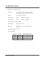
1
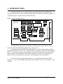
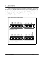
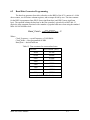
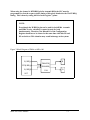
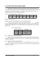
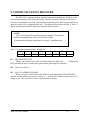
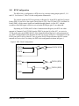
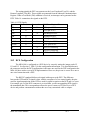
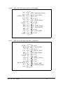
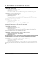
MPA-100 RS-232 SYNCHRONOUS ADAPTER CARD User's Manual INTERFACE CARDS FOR IBM PC/AT AND PS/2 QUATECH, INC. 5675 Hudson Industrial Parkway Hudson, Ohio 44236 TEL: (330) 665-9000 FAX: (330) 665-9010 http://www.quatech.com Warranty Information Quatech Inc. warrants the MPA-100 to be free of defects for one (1) year from the date of purchase. Quatech Inc. will repair or replace any adapter that fails to perform under normal operating conditions and in accordance with the procedures outlined in this document during the warranty period. Any damage that results from improper installation, operation, or general misuse voids all warranty rights. The authors have taken due care in the preparation of this document and any associated software program(s). In no event will Quatech Inc. be liable for damages of any kind, incidental or consequential, in regard to or arising out of the performance or form of the materials presented herein and in the program(s) accompanying this document. No representation is made regarding the suitability of this product for any particular purpose. Quatech Inc. reserves the right to edit or append to this document or the product(s) to which it refers at any time and without notice. Please complete the following information and retain for your records. Have this information available when requesting warranty service. Date of purchase: Model Number: MPA-100 Product Description: Single Channel RS-232 Synchronous Communication ISA Adapter Serial Number: MPA-100 User's Manual i The information contained in this document cannot be reproduced in any form without the written consent of Quatech, Inc. Likewise, any software programs that might accompany this document can be used only in accordance with any license agreement(s) between the purchaser and Quatech, Inc. Quatech, Inc. reserves the right to change this documentation or the product to which it refers at any time and without notice. The authors have taken due care in the preparation of this document and every attempt has been made to ensure its accuracy and completeness. In no event will Quatech, Inc. be liable for damages of any kind, incidental or consequential, in regard to or arising out of the performance or form of the materials presented in this document or any software programs that might accompany this document. Quatech, Inc. encourages feedback about this document. Please send any written comments to the Technical Support department at the address listed on the cover page of this document. Copyright ©2004 by Quatech Inc. 5675 Hudson Industrial Parkway Hudson, Ohio 44236 All rights reserved. Printed in the USA Trademarks: Quatech,, and Syncdrive are trademarks of Quatech Inc. Other product and company names are registered trademarks or trademarks of their respective holders. MPA-100 User's Manual ii Table of Contents 1. INTRODUCTION . . . . . . . . . . . . . . . . . . . . . . . . . . . . . . . . . . . . . . . . . . . . . . . . 1-1 2. HARDWARE INSTALLATION . . . . . . . . . . . . . . . . . . . . . . . . . . . . . . . . . . . 2-1 3. ADDRESSING . . . . . . . . . . . . . . . . . . . . . . . . . . . . . . . . . . . . . . . . . . . . . . . . . . . . 3-1 4. INTERRUPTS . . . . . . . . . . . . . . . . . . . . . . . . . . . . . . . . . . . . . . . . . . . . . . . . . . . . 4-1 4.1 Using Terminal Count to Generate Interrupts . . . . . . . . . . . . . . . . . . . . . . 4-2 5. JUMPER CONFIGURATIONS . . . . . . . . . . . . . . . . . . . . . . . . . . . . . . . . . . . 5-1 5.1 DTE/DCE Configuration - J2, J11, & J12 . . . . . . . . . . . . . . . . . . . . . . . . . 5-1 5.2 Interrupt Sharing Configuration - J4 . . . . . . . . . . . . . . . . . . . . . . . . . . . . . 5-1 5.3 Interrupt Level Selection - J5 & J6 . . . . . . . . . . . . . . . . . . . . . . . . . . . . . . . 5-2 5.4 Transmit DMA Selection - J8 . . . . . . . . . . . . . . . . . . . . . . . . . . . . . . . . . . . . 5-3 5.5 Receive DMA Selection - J9 . . . . . . . . . . . . . . . . . . . . . . . . . . . . . . . . . . . . . 5-3 5.6 SYNCA to RLEN Control - J7 . . . . . . . . . . . . . . . . . . . . . . . . . . . . . . . . . . . 6-4 6. SCC GENERAL INFORMATION . . . . . . . . . . . . . . . . . . . . . . . . . . . . . . . . . 6-1 6.1 Accessing the Registers . . . . . . . . . . . . . . . . . . . . . . . . . . . . . . . . . . . . . . . . . 6-2 6.2 Baud Rate Generator Programming . . . . . . . . . . . . . . . . . . . . . . . . . . . . . . 6-5 6.3 SCC Data Encoding Methods . . . . . . . . . . . . . . . . . . . . . . . . . . . . . . . . . . . . 7-6 7. DIRECT MEMORY ACCESS . . . . . . . . . . . . . . . . . . . . . . . . . . . . . . . . . . . . . 7-1 8. CONFIGURATION REGISTER . . . . . . . . . . . . . . . . . . . . . . . . . . . . . . . . . . . 8-1 9. COMMUNICATIONS REGISTER . . . . . . . . . . . . . . . . . . . . . . . . . . . . . . . . 9-1 10. DTE/DCE CONFIGURATION . . . . . . . . . . . . . . . . . . . . . . . . . . . . . . . . . . . 10-1 10.1 DTE Configuration . . . . . . . . . . . . . . . . . . . . . . . . . . . . . . . . . . . . . . . . . . . 10-2 10.2 DCE Configuration . . . . . . . . . . . . . . . . . . . . . . . . . . . . . . . . . . . . . . . . . . . 10-3 11. EXTERNAL CONNECTIONS . . . . . . . . . . . . . . . . . . . . . . . . . . . . . . . . . . . . 11-6 12. DEFINITION OF INTERFACE SIGNALS . . . . . . . . . . . . . . . . . . . . . . . . 12-1 13. SPECIFICATIONS . . . . . . . . . . . . . . . . . . . . . . . . . . . . . . . . . . . . . . . . . . . . . . . 13-1 MPA-100 User's Manual iii .. .. .. .. .. .. .. .. .. .. .. .. .. .. .. .. .. .. .. . . . . . . MPA-100 User's Manual iv 1. INTRODUCTION The Quatech MPA-100 is a single channel, synchronous RS-232 compatible serial communication port for systems utilizing the architecture of the IBM AT personal computer or compatible. Figure 1 depicts the layout of the MPA-100. Figure 1 MPA-100 Board Layout Quatech, Inc. MPA-100 U9 U29 U1 U6 U12 U2 U7 U13 J2 J4 J5 CN1 J7 U23 U18 U28 U19 U20 U14 SW2 U15 U8 U3 J11 J12 U11 U5 SW1 U22 U17 U10 U4 U16 X1 J8 J9 U21 J6 The MPA-100 occupies an 8 byte block of I/O address space which may be located anywhere within the available I/O address space in the system. Communication on the MPA-100 is controlled by a serial communications controller, hereafter referred to as the SCC (U17). The MPA-100 is compatible with several different types of SCC, all of which can support asynchronous formats, byte-oriented protocols such as IBM Bisync, and bit-oriented protocols such as HDLC and SDLC. The SCCs also offer internal functions such as on-chip baud rate generators, and digital phase-lock loops (DPLL). The MPA-100 also supports Direct Memory Access (DMA) and interrupts. DMA channels 1 - 3 can be used for high data transfer rates. Interrupt levels 2-7, 10-12, and 14-15 are available. MPA-100 User's Manual 1-1 MPA-100 User's Manual 1-2 2. HARDWARE INSTALLATION If the default address and interrupt settings are sufficient, the MPA-100 can be quickly installed and put to use. The factory default settings are listed below in Table 1. Table 1 Default Resource Settings Address Interrupt 300 hex IRQ 5 TxDMA DMA/DRQ 3 RxDMA DMA/DRQ 1 1. If the default settings are correct, skip to step 2, otherwise refer to chapters 3, 4, and 7 for detailed information on how to set the address, IRQ, and DMA levels. 2. Turn off the power of the computer system in which the MPA-100 is to be installed. 3. Remove the system cover according to the instructions provided by the computer manufacturer. 4. Install the MPA-100 in any vacant expansion slot. The board should be secured by installing the Option Retaining Bracket (ORB) screw. 5. Replace the system cover according to the instructions provided by the computer manufacturer. 6. Attach and secure the cable connectors to the desired equipment. MPA-100 User's Manual 2-1 MPA-100 User's Manual 2-2 3. ADDRESSING The MPA-100 occupies a continuous 8 byte block of I/O addresses. For example, if the base address is set to 300H, then the MPA-100 will occupy address locations 300H-307H. The base address of the MPA-100 may be set to any of the first 64 Kbytes (0 - FFFFH) of available I/O address space through the settings of dip switches SW1 and SW2. SW1 allows the user to select the higher address signals A15 - A8. SW2 allows the user to select the lower address signals A7 - A3. The sixth position of SW2 is not used and can be ignored. Figure 2 shows some examples of different base addresses. A6 A5 A4 A3 NOT USED 3 4 5 6 A4 A5 A3 NOT USED 2 3 4 5 6 A7 2 A6 5 6 7 8 SW2 4 A8 3 A9 2 A10 SW1 1 ON ON 1 A7 A8 A9 A10 A11 A12 A13 A14 A15 Figure 2 Address switch selection examples A11 A12 A13 A14 A15 Base Address = 300H ON 1 2 3 4 5 6 7 8 SW2 SW1 ON 1 Base Address = 3F8H MPA-100 User's Manual 3-1 The first four bytes, Base+0 through Base+3, of address space on the MPA-100 contain the internal registers of the SCC. The next two locations Base+4 and Base+5 contain the Communications Register and the Configuration Register. The last two address port locations are reserved for future use. The entire address range of the MPA-100 is shown in Table 2. Table 2 MPA-100 Address Assignments Address Register Description Base + 0 SCC Data Port, Channel A Base + 1 SCC Control Port, Channel A Base + 2 SCC Data Port, Channel B Base + 3 SCC Control Port, Channel B Base + 4 Communications Register Base + 5 Configuration Register Base + 6 Reserved Base + 7 Reserved Information on the internal registers of the SCC can be found in Section 6. The two onboard registers give the user additional options pertaining to DMA, interrupts and the RS-232-D standard for communication. Information on the Configuration Register and the Communications Register can be found in Section 8, and Section 9. MPA-100 User's Manual 3-2 4. INTERRUPTS The MPA-100 supports eleven interrupt levels: IRQ2 -7, IRQ10 - 12, and IRQ14 - 15, and selects which interrupt level is in use through jumper packs J5 and J6. The MPA-100 has three interrupt sources: interrupt on terminal count, interrupt on test mode, and interrupt from the SCC. The interrupt source is selected by bits D4 and D5 of the Configuration Register, see Section 8 for details. Interrupts from the SCC can occur on a number of conditions, depending on the configuration of the SCC’s internal register. The sources include interrupt on next character received, interrupt on all characters received, interrupt on special condition, interrupt on transmit buffer empty, and interrupt on External/Status (see the SCC Technical Manual for more details). Jumper block J4 can be selected to provide for interrupt sharing on the MPA-100. When using interrupts with the MPA-100, it is required that the application program have an interrupt service routine (ISR). There are several things that an ISR must do to allow proper system operation: 1. Do a software interrupt acknowledge to the SCC. This is accomplished by reading the interrupt vector register, read register 2, in channel B of the SCC. The value supplied by this read can also be used to vector to the appropriate part of the ISR. 2. Service the interrupt ( read the receiver buffer, write to the transmit buffer, etc.). 3. Write a Reset Highest Interrupt Under Service (IUS) command to the SCC. This is done by writing a 0x38 to write register 0. 4. Check for any additional interrupts pending in the SCC and service them. 5. For applications running under DOS, a nonspecific End of Interrupt must be submitted to the interrupt controller. For Interrupts 2-7 this is done by writing a 0x20 to port 0x20. For Interrupts 10-12,14 and 15 this is done by writing a 0x20 to 0x60, then a 0x20 to 0x20 (Due to the interrupt controllers being cascaded). Note that this should only be done if it is a requirement of the operating system being used. For further information on these subjects or any others involving the SCC contact the manufacturer of the SCC being used for a complete technical manual. MPA-100 User's Manual 4-1 4.1 Using Terminal Count to Generate Interrupts The MPA-100 allows the option of generating an interrupt whenever the Terminal Count (TC) signal is asserted. Terminal Count is an indicator generated by the system’s DMA controller, which signals that the number of transfers programed into the DMA controller’s transfer register have occurred. This board feature only works when the interrupt sharing feature is selected on jumper J4. MPA-100 User's Manual 4-2 5. JUMPER CONFIGURATIONS The MPA-100 utilizes various jumper blocks which allow the user to customize their hardware configuration. The following sections explain the function and setting of each of the jumper blocks on the MPA-100. 5.1 DTE/DCE Configuration - J2, J11, & J12 The jumper packs J2, J11, and J12 control the DTE/DCE configuration of the MPA-100. J2 determines the board setting (DTE or DCE) while the jumper packs J11 and J12 control the routing of the signals to the DB-25 connector. All three jumper packs must be set exclusively to either DTE or DCE for correct operation of the MPA-100. Table 3 DTE/DCE Jumper Selections DTE (Default) J2 1-2 DCE no connection J11 1-9, 2-10, 3-11, 4-12, 5-13, 6-14, 7-15, 8-16 1-2, 3-4, 5-6, 7-8, 9-10, 11-12, 13-14, 15-16 J12 1-5, 2-6, 3-7, 4-8 1-2, 3-4, 5-6, 7-8 J11 and J12 may be configured for DTE by setting all jumpers vertical on the board and for DCE by setting all jumpers horizontal on the board. 5.2 Interrupt Sharing Configuration - J4 J4 is a three pin jumper which determines the configuration for the interrupts. By selecting pins 1 & 2, the user has the ability to share interrupts with other Quatech adapter cards. The MPA-100 will drive the interrupt onto the bus only when an interrupt occurs. Otherwise, the output is high impedance. If pins 2 & 3 of J4 are selected, then interrupts abide by the IBM specification and cannot be shared. Table 4 summarizes the jumper block selections for J4. Table 4 Jumper Block J4 Selections Interrupt Function Interrupt Sharing (Default) No Interrupt sharing MPA-100 User's Manual Pins 1-2 2-3 5-1 5.3 Interrupt Level Selection - J5 & J6 Jumper blocks J5 and J6 select the interrupt level that the MPA-100 utilizes. Interrupt levels IRQ2 - IRQ7 reside on J5, while interrupt levels IRQ10 - IRQ12 and IRQ14 - IRQ15 reside on J6. Table 5 and Table 6 summarize the jumper block selections for J5 and J6. The IRQ levels are also marked on the MPA-100 silkscreen for easy identification. Table 5 Jumper block J5 selections. Interrupt Level Pins IRQ2(9) 1-7 IRQ3 2-8 IRQ4 3-9 IRQ5 (Default) 4-10 IRQ6 5-11 IRQ7 6-12 Table 6 Jumper block J6 selections. Interrupt Level Pins MPA-100 User's Manual IRQ10 1-6 IRQ11 2-7 IRQ12 3-8 IRQ14 4-9 IRQ15 5-10 5-2 5.4 Transmit DMA Selection - J8 J8 Selects the DMA channel to be used for Transmit DMA. Three channels (1 - 3) are available on the MPA-100 for DMA. When selecting a DMA channel, both the DMA acknowledge (DACK) and the DMA request (DRQ) for the appropriate channel need to be selected. Table 7 summarizes the jumper block selections for J8. Table 7 Jumper block J8 selections. DMA Channel Pins Channel 1 1-7 2-8 Channel 2 3-9 4-10 Channel 3 (Default) 5-11 6-12 5.5 Receive DMA Selection - J9 J9 selects the DMA channel to be used for Receive DMA. Three channels (1 - 3) are available on the MPA-100 for DMA. When selecting a DMA channel, both the DMA acknowledge (DACK) and the DMA request (DRQ) for the appropriate channel need to be selected. Table 8 summarizes the jumper block selections for J9. Table 8 Jumper block J9 selections. DMA Channel Pins Channel 1 (Default) 1-7 2-8 Channel 2 3-9 4-10 Channel 3 5-11 6-12 MPA-100 User's Manual 5-3 NOTE: Since it is illegal to perform DMA on transmit and receive on the same DMA channel, jumper blocks J7 and J8 should never have the same pins connected. This could result in damage to the system. 5.6 SYNCA to RLEN Control - J7 J7 controls the signal path from the RLEN bit in the Communications Register to the SYNCA input to the SCC. If J7 is installed and the SCC is in external SYNC mode, setting the RLEN bit high will assert the SYNCA pin. Note: the RLEN output is still affected when used to control the SYNCA pin. Table 9 Jumper J7 Selections Function Jumper J1 MPA-100 User's Manual SYNCA 1-2 RLEN (Default) no connections 5-4 6. SCC GENERAL INFORMATION The Serial Communications Controller (SCC) is a dual channel, multi-protocol data communications peripheral. The MPA-100 provides a single channel for communications, however, to provide full DMA capabilities with complete modem control line support, both channels of the SCC can be utilized. The SCC can be software configured to satisfy a wide variety of serial communications applications. Some of its protocol capabilities include: 1) Asynchronous Communications 5, 6, 7, or 8 bits per character 1, 1-1/2, or 2 stop bits Odd, even, or no parity Times 1, 16, 32, or 64 x clock modes Break generation and detection Parity, overrun and framing error detection 2) Byte-oriented Synchronous Communications Internal/external character synchronization 1 or 2 sync characters in separate registers Automatic Cyclic Redundancy Check (CRC) generation/detection 3) SDLC/HDLC (Bit Synchronous) Communications Abort sequence generation and checking Automatic zero insertion and deletion Automatic flag insertion between messages Address field recognition I-field residue handling CRC generation and detection SDLC loop mode with EOP recognition/loop entry and exit 4) NRZ, NRZI, or FM encoding/decoding MPA-100 User's Manual 6-1 6.1 Accessing the Registers The mode of communication desired is established and monitored through the bit values of the internal read and write registers. The register set of the SCC includes 16 write registers and 9 read registers. These registers only occupy four address locations, which start at the MPA-100's physical base address that is configured via the on board switches. This and all other addresses are referenced from this base address in the form Base + Offset. An example of this is Base + 1 for the SCC Control Port, Channel A. There are two register locations per SCC channel, a data port and a control port . Accessing the internal SCC registers is a two step process that requires loading a register pointer to perform the addressing to the correct data register. The first step is to write to the control port the operation and address for the appropriate channel. The second step is to either read data from or write data to the control port. The only exception to this rule is when accessing the transmit and receive data buffers. These registers can be accessed with the two step process described or with a single read or write to the data port. The following examples illustrate how to access the internal registers of the SCC. Also, Table 10 describes the read registers and Table 11 describes the write registers for each channel. The MPA-100 has been designed to assure that all back to back access timing requirements of the SCC are met without the need for any software timing control. The standard of adding jmp $+2 between IO port accesses is not required when accessing the MPA-100. Example 1: Enabling the transmitter on channel A. mov add mov out mov out dx,base dx,ContA al,05H dx,al al,08H dx,al MPA-100 User's Manual ; load base address ; add control reg A offset (1) ; write the register number ; write data to the register 6-2 Example 2: Monitoring the status of the transmit and receive buffers in RR0 of Channel A. Register 0 is addressed by default if no register number is written to WR0 first. mov add in Example 3: dx,base dx,ContA ax,dx Write data into the transmit buffer of channel A. mov out Example 4: ; load base address ; add control reg A offset (1) ; read the status dx,base dx,al ; load base address ; write data in ax to buffer Read data from the receive buffer of channel A. mov in dx,base al,dx ; load base address ; write data in ax to buffer Table 10 SCC read register description. RR0 Transmit, Receive buffer statuses and external status RR1 Special Receive Condition status, residue codes, error conditions RR2 Modified Channel B interrupt vector and Unmodified Channel A interrupt vector RR3 Interrupt Pending bits RR6 LSB of frame byte count register RR7 MSB of frame byte count and FIFO status register RR8 Receive buffer RR10 Miscellaneous status parameters RR12 Lower byte of baud rate time constant RR13 Upper byte of baud rate time constant RR15 External/Status interrupt information The SCC can perform three basic forms of I/O operations: polling, interrupts, and block transfer. Polling transfers data, without interrupts, by reading the status of RR0 and then reading or writing data to the SCC buffers via CPU port accesses. Interrupts on the SCC can be sourced from the receiver, the transmitter, or External/Status conditions. At the event of an interrupt, Status can be determined, then data can be written to or read from the SCC via CPU port accesses. For block transfer mode, DMA transfers accomplish data transfers from the SCC to memory or from memory to the SCC, interrupting the CPU only when the Block is finished. Further information on these subjects are found in Sections 4 and 7. The SCC incorporates additional circuitry supporting serial communications. This circuitry includes clocking options, baud rate generator (BRG), data encoding, and internal loopback. The SCC may be programmed to select one of several sources to provide the transmit MPA-100 User's Manual 6-3 and receive clocks. These clocks can be programmed in WR11 to come from the RTXC pin, the TRXC pin, the output of the BRG, or the transmit output of the DPLL. Programming of the clocks should be done before enabling the receiver, transmitter, BRG, or DPLL. Table 11 SCC write register description. WR0 Command Register, Register Pointer, CRC initialization, resets for various modes WR1 Interrupt control, Wait/DMA request control WR2 Interrupt vector WR3 Receiver initialization and control WR4 Transmit/Receive miscellaneous parameters and codes, clock rate, stop bits, parity WR5 Transmitter initialization and control WR6 Sync character (1st byte) or SDLC address field WR7 Sync character (2nd byte) or SDLC Flag WR7' Special HDLC Enhancement Register WR8 Transmit buffer WR9 Master interrupt control and reset WR10 Miscellaneous transmitter/receiver control bits, NRZI, NRZ, FM coding, CRC reset WR11 Clock mode and source control WR12 Lower byte of baud rate time constant WR13 Lower byte of baud rate time constant WR14 Miscellaneous control bits: baud rate generator, DPLL control, auto echo WR15 External/Status interrupt control For more information regarding the SCC registers please refer to the manufacturer's technical manual for the specific part being used. MPA-100 User's Manual 6-4 6.2 Baud Rate Generator Programming The baud rate generator (hereafter referred to as the BRG) of the SCC consists of a 16-bit down counter, two 8-bit time constant registers, and an output divide-by-two. The time constant for the BRG is programmed into WR12 (least significant byte) and WR13 (most significant byte). The equation relating the baud rate to the time constant is given below while Table 12 shows the time constants associated with a number of popular baud rates when using the standard MPA-100 9.8304 MHz clock. Baud_Const = Clock_Frequency 2&Baud_Rate&Clock_Mode -2 Where: Clock_Frequency = crystal frequency of 9.8304MHz Clock_Mode = value programmed in WR4 Baud_Rate = desired baud rate Table 12 Time constants for common baud rates Baud Rate Baud Constant (Hex) 38400 007EH 19200 00FEH 9600 01FEH 4800 03FEH 2400 07FEH 1200 0FFEH 600 1FFEH 300 3FFEH (for 9.8304 MHz Clock) MPA-100 User's Manual 6-5 6.3 SCC Data Encoding Methods The SCC provides four different data encoding methods, selected by bits D6 and D5 in WR10. These four include NRZ, NRZI, FM1 and FM0. The SCC also features a digital phase-locked loop (DPLL) that can be programmed to operate in NRZI or FM modes. Also, the SCC contains two features for diagnostic purposes, controlled by bits in WR14. They are local loopback and auto echo. For further information on these subjects or any others involving the SCC contact the manufacturer of the SCC being used for a complete technical manual. MPA-100 User's Manual 6-6 7. DIRECT MEMORY ACCESS Direct Memory Access (DMA) is a way of transferring data on the ISA bus directly to and from memory, resulting in high data transfer rates with very low CPU overhead. The ISA bus DMA channel(s) to be used are selected through jumper packs J6 and J7. The sources for these requests originate from the SCC and can be programmed for a variety of DMA modes. These modes include DMA request on transmit, DMA request on receive, and DMA request on both transmit and receive. For DMA request on transmit, the DMA controller should be programmed first for an 8 bit read transfer on the desired channel, but not yet enabled. Then the SCC should be programmed for DMA request on transmit on the desired DMA source. The sources for DMA request on transmit are either the W/REQA pin (pin 10) of channel A or the DTR/REQA pin (pin 16) of channel A. The source is then determined by bit D0 of the Configuration Register. After programming the SCC for DMA, DMA on the MPA-100 should be enabled by setting bit D2 of the Configuration Register. Next, the DMA on the SCC should be enabled, and finally, the DMA channel should be unmasked. The DMA controller will write the data in memory to the SCC. When the transmit buffer of the SCC becomes empty, a DMA request will be generated and the data will be transferred. For DMA request on receive, the DMA controller should be programmed first for an 8 bit write transfer on the desired channel, but not yet enabled. Next, the SCC should be programmed for DMA request on receive on the desired DMA source. The two sources for DMA request on receive are either the W/REQA pin (pin 10) of channel A or the W/REQB pin (pin 30) of channel B. The source is then determined by bit D1 on the Configuration Register. After programming the SCC for DMA, one should enable the DMA on the MPA-100 by setting bit D3 of the Configuration Register. Then, the DMA on the SCC should be enabled, and finally the DMA controller should be enabled. When a character enters the receive buffer of the SCC, a DMA request is generated. The DMA controller then writes the data from the SCC into memory. Programming for DMA request on both transmit and receive is simply a combination of the two. There are three possible configurations that can be used, depending on the sources selected. The first configuration available uses the W/REQA pin of channel A for DMA request on receive, and the DTR/REQA pin of channel A for DMA request on transmit. This is done by setting bit D0 and clearing bit D1 of the Configuration Register. The second configuration uses the DTR/REQA pin for DMA request on transmit, and the W/REQB pin for DMA request on receive. This is done by setting both D0 and D1 of the Configuration Register. The third configuration uses the W/REQA pin of channel A for DMA request on transmit, and the W/REQB pin of channel B for DMA request on receive. This is done by clearing bit D0 and setting bit D1 of the Configuration Register. Figure 3 shows a block diagram of the DMA circuitry on the MPA-100. MPA-100 User's Manual 7-1 When using the channel A DTR/REQ pin for transmit DMA the SCC must be programmed so that the request release timing of this pin is identical to the WAIT/REQ timing. This is done by setting bit D4 of write register 7 prime. NOTE: Even though the W/REQA pin can be used for both DMA transmit and DMA receive, obviously it cannot be used for both simultaneously. Therefore, bits D0 and D1 of the Configuration Register should never be cleared at the same time while bits D2 and D3 are both set. This situation may result in damage to the system. Figure 3 Block Diagram of DMA on MPA-100 J8 W/REQA DTR/REQA W/REQB DMATRQ DMARRQ PAL J9 SCC MPA-100 User's Manual 7-2 8. CONFIGURATION REGISTER The MPA-100 is equipped with an onboard register used for configuring information such as DMA enables, DMA sources, interrupt enables, and interrupt sources. Below is a detailed description of the Configuration Register. The address of this register is Base+5. Table 13 details the bit definitions of the Configuration Register. Table 13 Configuration Register - Read/Write D7 D6 D5 D4 0 0 INTS1 D3 D2 D1 D0 INTS0 DMREN DMTEN RXSRC TXSRC D7-D6 - Reserved, always 0. D5-D4 - INTS1, INTS0, INTERRUPT SOURCE AND ENABLE BITS: These two bits determine the source of the interrupt. The three options are interrupt on terminal count (INTTC), interrupt from the SCC (INTSCC), and interrupt on Test Mode (INTTM). When the source is set, that interrupt becomes enabled. Below is the mapping for these bits. Table 14 Interrupt Sources INTS1 INTS0 0 0 0 1 1 0 1 1 Interrupt Interrupts Disabled INTTC INTSCC INTTM D3 - DMREN, RECEIVE DMA ENABLE: When set (logic 1), the signal from the SCC’s receive DMA source is passed on to the selected ISA bus DRQ. When cleared (logic 0), the SCC cannot drive the receive request signal onto the ISA bus DRQ. D2 -DMTEN, TRANSMIT DMA ENABLE: When set (logic 1), the signal from the SCC’s transmit DMA source is passed on to the selected ISA bus DRQ. When cleared (logic 0), the SCC cannot drive the transmit request signal onto the ISA bus DRQ. MPA-100 User's Manual 8-1 D1 -RXSRC, RECEIVE DMA SOURCE: When set (logic 1), this bit allows the source for Receive DMA to come from the W/REQB pin of channel B on the SCC. When cleared (logic 0), the source for Receive DMA comes from the W/REQA pin of channel A on the SCC. D0 -TXSRC, TRANSMIT DMA SOURCE: When set (logic 1), this bit allows the source for Transmit DMA to come from the DTR/REQA pin of channel A on the SCC. When cleared (logic 0), the source for Transmit DMA comes from the W/REQA pin of channel A of the SCC. NOTE: Even though the W/REQA pin can be used for both DMA transmit and DMA receive, obviously it cannot be used for both simultaneously. Therefore, bits D0 and D1 of the Configuration Register should never be cleared at the same time while bits D2 and D3 are both set. This situation may result in damage to the system. MPA-100 User's Manual 8-2 9. COMMUNICATIONS REGISTER The MPA-100 is equipped with an onboard Communications Register which gives the user options pertaining to the clocks and testing. The user can specify the source and type of clock to be transmitted or received. Test mode bits pertain only to the DTE versions and can be ignored if using a DCE configured MPA-100. The address of this register is Base+4. Table 15 and the descriptions that follow detail the Communications Register. NOTE: The Local Loopback Test and the Remote Loopback Test cannot be performed simultaneously. Thus, bits D5 and D4 of the Communications Register should not be set (logic 1) simultaneously. Table 15 Communications Register - Read/Write D7 D6 D5 D4 TM ST 0 LLEN D3 D2 RLEN RCKEN TCKEN D1 D0 0 0 D7 -TEST MODE STATUS: This bit can read the status of the Test Mode signal on a MPA-100 DTE, allowing the user to monitor this signal without generating any interrupts. configured as D6 - Reserved, always 0. D5 -LOCAL LOOPBACK ENABLE: When set (logic 1), this bit allows the DTE to test the functionality of the DTE/DCE interface and the transmit and receive sections of the local DCE. When cleared (logic 0), no testing occurs. This can also be used as a general purpose output. MPA-100 User's Manual 9-1 D4 -REMOTE LOOPBACK ENABLE: When set (logic 1), this bit allows the DTE to test the transmission path up to and through the remote DCE to the DTE interface and the similar return transmission path. When cleared (logic 0), no testing occurs. If jumper J7 is in place the Remote Loopback is also used to control the Sync input of the Channel A data receiver. This is useful in situations where it is desired to receive unformatted serial data. D3 -RECEIVE CLOCK ENABLE (DCE only): When set (logic 1), this bit allows the DCE to transmit its Receive Clock (RCLK). When cleared (logic 0), the DCE receives RCLK. Since a DTE can only receive RCLK, writing to this bit has no effect on a DTE. D2 -TRANSMIT CLOCK ENABLE (DTE only): When set (logic 1), this bit allows the DTE to transmit its Transmit Clock (TCLK). When cleared (logic 0), the DTE receives TCLK. Since a DCE can only transmit its TCLK, writing to this bit has no effect on a DCE. D1 RESERVED: This bit should always be programmed to 0. D0 RESERVED: This bit should always be programmed to 0. MPA-100 User's Manual 9-2 10. DTE/DCE CONFIGURATION As indicated earlier in this manual, the MPA-100 can be configured as either a Data Terminal Equipment (DTE) or a Data Communications Equipment (DCE) device. The differences between these configurations include signal definitions, connector pin out, and clocking options. In order to simplify matters, an in depth description of each configuration is provided in the next two sections. NOTE: Because the connector used for the DCE configuration is the same one as is used for the DTE configuration the MPA-100 does not have a true DCE implementation. The DCE configuration is provided to allow the head-to-head connection of two MPA-100 boards (one configured DTE and the other DCE). MPA-100 User's Manual 10-1 10.1 DTE Configuration The MPA-100 is configured as a DTE device by correctly setting jumper packs J2, J11 and J12. See Section 5, Table 3 for this configuration information. The control signals the DTE can generate are Request To Send (RTS) and Data Terminal Ready (DTR). It can receive the signals Carrier Detect (CD), Clear To Send (CTS), and Data Set Ready (DSR). All the control signals are handled through channel A of the SCC, with the exception of the DSR signal, which is received on the DCDB pin (pin 21) on channel B. Depending on TCKEN (bit D2 of the Communications Register), the DTE can either transmit its Transmit Clock (TCLK) from the TRXCA pin (pin 14) of the SCC, or receive its TCLK on the same pin. RCKEN (bit D3 of the Communications Register) is always deasserted on a DTE configured MPA-100; therefore the DTE can receive its Receive Clock (RCLK) on the RTXC pins (pin 12 & 28) of the SCC but, as per the EIA-232D specification, the DTE cannot transmit its receive clock. For clarity, the DTE clock configuration is shown in Figure 4. Figure 4 DTE Clock Configuration RTXCA (RCLK) RXCLK (DCE) RTXCB RCKEN TRXCA (TCLK) TXCLK (DTE) TXCLK (DCE) TCKEN MPA-100 User's Manual 10-2 The testing signals the DTE can generate are the Local Loopback Test (LL) and the Remote Loopback Test (RL). These signals are generated from the onboard Communications Register. When a Test Mode (TM) condition is received, an interrupt can be generated on the DTE. Table 16 summarizes the signals on the DTE. Table 16 DTE Signals Signal Received Generated RTS CTS X X DTR SCC Pin or Register Bit RTSA pin of SCC CTSA pin of SCC X DTR/REQA of SCC DSR X DCDB pin of SCC CD X DCDA pin of SCC TxCLK X RxCLK X X TRXCA pin of SCC RTXC pins of SCC LL X Bit D5 of Comm Reg RL X Bit D4 of Comm Reg TM X INTM or Bit D7 of Comm Reg 10.2 DCE Configuration The MPA-100 is configured as a DCE device by correctly setting the jumper packs J2, J11 and J12. See Section 5, Table 3 for this configuration information. It is noted that because the connector used for the DCE configuration is the same one used for the DTE configuration the MPA-100 does not have a true DCE implementation. However, the pin out is correct for a one to one wired connection with a DTE. The RS232C standard defines each signal with respect to the DTE. The difference between the DTE and DCE signals is that, with the exception of a few control signals, the pins used for signal transmission on the DTE are used for signal reception on the DCE and vice versa. For example, pin 2 of the DCE connector is received data, yet the corresponding DTE signal is the transmitted data. This correspondence allows the user to connect a DTE device to a DCE device and perform communication without the use of any customized cable or adapter. MPA-100 User's Manual 10-3 Control signals the DCE can generate are the Clear to Send (CTS), Carrier Detect (CD), and Data Set Ready (DSR). It can receive the signals Data Terminal Ready (DTR) and Ready to Send (RTS). All the control signals are handled through channel A of the SCC, with the exception of the CD signal, which is generated on the DTR/REQB pin (pin 24) of the SCC. Depending on RCKEN (bit D3 of the Communications Register), the DCE can either transmit its Receive Clock (RCLK) from the TRXCB pin (pin 26) of the SCC, or receive its Receive Clock on the RTXC pins (pins 12 and 28) of the SCC. TCKEN (bit D2 of the Communications Register) is always asserted on a DTE configured MPA-100; therefore the DCE can transmit its Transmit Clock (TCLK) from the TRXCA pin (pin 14) but, as per the EIA-232D specification, the DCE cannot receive its Transmit Clock. For clarity, the DCE clock configuration is shown in Figure 5. Figure 5 DCE Clock Configuration RTXCA (RCLK) RTXCB TXCLK (DTE) TRXCB TXCLK (DCE) RCKEN TRXCA (TCLK) RXCLK (DCE) The test mode signals for the DCE configuration are the same those for the DTE configuration. These signals are Local Loopback Test (LL) and Remote Loopback Test (RL) for outputs and Test Mode (TM) for input. MPA-100 User's Manual 10-4 Table 17 DCE Signals Signal Received RTS X CTS DTR Generated SCC Pin or Register Bit CTSA pin of SCC X X RTSA pin of SCC DCDA of SCC DSR X DTR/REQA pin of SCC CD X DTR/REQB pin of SCC TxCLK X TRXCA pin of SCC X RTXC/TRXCB pin of SCC LL X Bit D5 of Comm. Reg RL X Bit D4 of Comm Reg RxCLK TM MPA-100 User's Manual X X INTM or Bit D7 of Comm Reg 10-5 MPA-100 User's Manual 10-6 11. EXTERNAL CONNECTIONS The MPA-100 is designed to meet the RS-232 standard through a D-25 connector. The MPA-100 uses a D-25 short body male connector (labeled CN1) for both the DTE and DCE configurations. Jumper blocks J2, J11, and J12 configure the connector pin out. Table 18 and Table 19 display the pin out definitions for both configurations while Figure 6 and Figure 7 illustrate the pin-outs for each of the configurations. The definitions of the interchange circuits according to the RS-232-D standard can be found in Section 12. Table 18 DTE Connector Pin Definitions PIN SIGNAL RECEIVED GENERATED SOURCE 1 CGND 2 TXD X TXDA on SCC 3 RXD X RXDA on SCC 4 RTS X RTSA on SCC 5 CTS X CTSA on SCC 6 DSR X DCDB on SCC 7 DGND 8 CD X DCDA on SCC 9 N/C 10 N/C 11 RXCLK (DTE) N/A N/A N/A 12 N/C 13 N/C 14 N/C 15 TXCLK (DCE) X TRXCB on SCC 16 N/C 17 RXCLK (DCE) X TRXCA on SCC 18 LL X D5 of COMM REG 19 N/C 20 DTR X DTR/REQA on SCC 21 RL X D4 of COMM REG 22 N/C 23 N/C 24 TXCLK (DTE) X TRXCA on SCC 25 TEST MODE X D7 of COMM REG MPA-100 User's Manual 11-1 Table 19 DCE Connector Pin Definitions PIN SIGNAL RECEIVED GENERATED SOURCE 1 CGND 2 TXD X RXDA on SCC 3 RXD X TXDA on SCC 4 RTS X CTSA on SCC 5 CTS X RTSA on SCC 6 DSR X DTR/REQA on SCC 7 DGND 8 CD X DTR/REQB on SCC 9 N/C 10 N/C 11 RXCLK (DTE) N/A N/A N/A 12 N/C 13 N/C 14 N/C 15 TXCLK (DCE) X TRXCA on SCC 16 N/C 17 RXCLK (DCE) X RTXC pins on SCC 18 LL X D5 of COMM REG 19 N/C 20 DTR X DCDB on SCC 21 RL X D4 of COMM REG 22 N/C 23 N/C 24 TXCLK (DTE) X RTXC pins on SCC 25 TEST MODE X D7 of COMM REG MPA-100 User's Manual 11-2 Figure 6 MPA-100 DTE Output Connector Configuration N/C N/C RxCLK (DTE) N/C N/C CD DGND DSR CTS RTS RxD TxD CGND 13 12 11 10 9 8 7 6 5 4 3 2 1 25 24 23 22 21 20 19 18 17 16 15 14 Test Mode (Output) TxCLK (DTE) N/C N/C RLBK (Output) DTR N/C LLBK (Output) RxCLK (DCE) N/C TxCLK (DCE) N/C Figure 7 MPA-100 DCE Output Connector Configuration CGND RxD TxD CTS 1 2 3 4 RTS 5 DTR 6 DGND 7 CD 8 N/C 9 N/C 10 RxCLK (DTE) 11 N/C 12 N/C 13 MPA-100 User's Manual 14 15 16 17 18 19 20 21 22 23 24 25 N/C TxCLK (DCE) N/C RxCLK (DCE) LLBK (Output) N/C DSR RLBK (Output) N/C N/C TxCLK (DTE) TestMode (Input) 11-3 MPA-100 User's Manual 11-4 12. DEFINITION OF INTERFACE SIGNALS CIRCUIT AB - Signal Ground CONNECTOR NOTATION: DGND DIRECTION: Not applicable This conductor directly connects the DTE circuit ground to the DCE circuit ground. CIRCUIT CC - DCE Ready (Data Set Ready) CONNECTOR NOTATION: DSR DIRECTION: From DCE This signal indicates the status of the local DCE by reporting to the DTE device that a communication channel has been established. CIRCUIT BA - Transmitted Data CONNECTOR NOTATION: TXD DIRECTION: To DCE This signal transfers the data generated by the DTE through the communication channel to one or more remote DCE data stations. CIRCUIT BB - Received Data CONNECTOR NOTATION: RXD DIRECTION: From DCE This signal transfers the data generated by the DCE, in response to data channel line signals received from a remote DTE data station, to the DTE. CIRCUIT DA - Transmit Signal Element Timing (TxCLK- DTE Source) CONNECTOR NOTATION: TXCLK (DTE) DIRECTION: To DCE This signal, generated by the DTE, provides the DCE with element timing information pertaining to the data transmitted by the DTE. The DCE can use this information for its received data. CIRCUIT DB -Transmit Signal Element Timing (TxClk - DCE Source) CONNECTOR NOTATION:TXCLK (DCE) DIRECTION: From DCE This signal, generated by the DCE, provides the DTE with element timing information pertaining to the data transmitted to the DCE. The DCE can use this information for its received data. MPA-100 User's Manual 12-1 CIRCUIT DD -Receiver Signal Element Timing(RxClk - DCE Source) CONNECTOR NOTATION: RXCLK (DCE) DIRECTION: From DCE This signal, generated by the DCE, provides the DTE with element timing information pertaining to the data transmitted by the DCE. The DTE can use this information for its received data. CIRCUIT CA - Request To Send CONNECTOR NOTATION: RTS DIRECTION: To DCE This signal controls the data channel transmit function of the local DCE and, on a half-duplex channel, the direction of the data transmission of the local DCE. CIRCUIT CB - Clear To Send CONNECTOR NOTATION: CTS DIRECTION: From DCE This signal indicates to the DTE whether the DCE is conditioned to transmit data on the communication channel. CIRCUIT CF - Received Line Signal Detector (CARRIER DETECT) CONNECTOR NOTATION: CD DIRECTION: From DCE This signal indicates to the DTE whether the DCE is conditioned to receive data from the communication channel, but does not indicate the relative quality of the data signals being received. CIRCUIT CD - DTE Ready (Data Terminal Ready) CONNECTOR NOTATION: DTR DIRECTION: To DCE This signal controls the switching of the DCE to the communication channel. The DTE will generate this signal to prepare the DCE to be connected to or removed from the communication channel. CIRCUIT LL - Local Loopback CONNECTOR NOTATION: LLBK DIRECTION: To DCE This signal provides a means whereby a DTE may check the functioning of the DTE/DCE interface and the transmit and receive sections of the local DCE. MPA-100 User's Manual 12-2 CIRCUIT RL - Remote Loopback CONNECTOR NOTATION: RLBK DIRECTION: To DCE This signal provides a means whereby a DTE or a facility test center may check the transmission path up to and through the remote DCE to the DTE interface and the similar return transmission path. CIRCUIT TM - Test Mode CONNECTOR NOTATION: TEST MODE DIRECTION: From DCE This signal indicates to the DTE that the DCE is in a test condition. The DCE generates this signal when it has received a local loopback or remote loopback signal from the DTE. MPA-100 User's Manual 12-3 MPA-100 User's Manual 12-4 13. SPECIFICATIONS Bus interface: IBM AT 16-bit bus Controller: Serial Communications Controller, 10 MHz (determined by user, typically an AMD 85C30). Interface: DTE: male D-25 connector Transmit drivers: RS-232: MC1488 or compatible Receive buffers: RS-232: MC1489 or compatible I/O Address range: 0000H - FFFFH Interrupt levels: IRQ 2-7, 10-12, 14-15 DMA levels: DMA Channel 1, 2, and 3 on transmit and receive. Physical Dimensions: 4.2” x 7.65” Power requirements: ITyp (mA) IMax (mA) 1248 1402 5 25 25 36 36 12 -12 MPA-100 User's Manual Supply Voltage (Volts) 13-1 MPA-100 User's Manual Version 4.12 March 2004 Part No. 940-0037-412 MPA-100 User's Manual 13-2