1
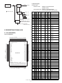
q SERVICE MANUAL
CODE : 00ZXEA20SUSME
ELECTRONIC
CASH REGISTER
MODEL
XE-A20S
(U version)
CONTENTS
CHAPTER 1. SPECIFICATIONS . . . . . . . . . . . . . . . . . . . . . . . . . . . . 1
CHAPTER 2. OPTIONS . . . . . . . . . . . . . . . . . . . . . . . . . . . . . . . . . . . 5
CHAPTER 3. MASTER RESET AND PROGRAM RESET. . . . . . . . . 5
CHAPTER 4. HARDWARE DESCRIPTION . . . . . . . . . . . . . . . . . . . . 6
CHAPTER 5. TEST FUNCTION . . . . . . . . . . . . . . . . . . . . . . . . . . . . 12
CHAPTER 8. CIRCUIT DIAGRAM AND PWB LAYOUT . . . . . . . . . 15
Parts marked with "!" are important for maintaining the safety of the set. Be sure to replace these parts with specified
ones for maintaining the safety and performance of the set.
SHARP CORPORATION
This document has been published to be used
for after sales service only.
The contents are subject to change without notice.
LEAD-FREE SOLDER
The PWB’s of this model employs lead-free solder. The “LF” marks indicated on the PWB’s and the Service Manual mean “Lead-Free” solder.
The alphabet following the LF mark shows the kind of lead-free solder.
Example:
<Solder composition code of lead-free solder>
Lead-Free
5mm
Solder composition
Solder composition
code (Refer to the
table at the right.)
a
Solder composition code
Sn-Ag-Cu
a
Sn-Ag-Bi
Sn-Ag-Bi-Cu
b
Sn-Zn-Bi
z
Sn-In-Ag-Bi
i
Sn-Cu-Ni
n
Sn-Ag-Sb
s
Bi-Sn-Ag-P
Bi-Sn-Ag
p
(1) NOTE FOR THE USE OF LEAD-FREE SOLDER THREAD
When repairing a lead-free solder PWB, use lead-free solder thread. Never use conventional lead solder thread, which may cause a
breakdown or an accident.
Since the melting point of lead-free solder thread is about 40°C higher than that of conventional lead solder thread, the use of the exclusive-use soldering iron is recommendable.
(2) NOTE FOR SOLDERING WORK
Since the melting point of lead-free solder is about 220°C, which is about 40°C higher than that of conventional lead solder, and its soldering capacity is inferior to conventional one, it is apt to keep the soldering iron in contact with the PWB for longer time. This may cause land
separation or may exceed the heat-resistive temperature of components. Use enough care to separate the soldering iron from the PWB
when completion of soldering is confirmed.
Since lead-free solder includes a greater quantity of tin, the iron tip may corrode easily. Turn ON/OFF the soldering iron power frequently.
If different-kind solder remains on the soldering iron tip, it is melted together with lead-free solder. To avoid this, clean the soldering iron tip
after completion of soldering work.
If the soldering iron tip is discolored black during soldering work, clean and file the tip with steel wool or a fine filer.
CAUTIONS
THERE IS A RISK OF EXPLOSION IF THE BATTERY
IS REPLACED BY AN INCORRECT TYPE.
PROPERLY DISPOSE OF USED BATTERIES ACCORDING
TO THE INSTRUCTIONS.
XE-A20S LEAD-FREE SOLDER
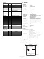
CHAPTER 1. SPECIFICATIONS
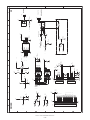
1. APPEARANCE
Key names
Rear view
Front view
KEY TOP
Customer display
(Pop-up type)
DESCRIPTION
2
RA
Received-on account key
RCPT/PO
Receipt print/Paid-out key
Operator display
Printer cover
Paper feed key
Receipt paper
Keyboard
Power cord
Mode switch
VOID
Void key
ESC
Escape key
CONV
Conversion key
%1, %2
Percent 1and 2 key
RFND
USB port
Refund key
-
Drawer
Discount key
@/FOR
Drawer lock
Multiplication key
•
Decimal point key
CL
Printer
Clear key
0-9,00
Take-up spool
Numeric Keys
PLU/SUB
Paper roll cradle
PLU/Subdepartment key
DEPT#
Print roller arm
Paper positioning guides
Print roller
release rever
Inner cover
Department code entry key
DEPT SHIFT
Department shift key
CLK#
Clerk code entry key
Dept1-32
Department keys
TAX
Tax 1 shift key
Tax 2 SHIFT
Tax 2 shift key
AUTO
2. RATING
XE-A20S
Weight
16.3lb (7.4kg)
Dimensions
13.0 (W) x 16.9 (D) x 11.0 (H) inches
(330 (W) x 428 (D) x 280 (H) mm)
AC 120V (m10%), 60Hz
Power consumption
Stand-by 7.7W, Operating 30W (max.)
Working temperature
32°F to 104°F (0°C~40°C)
Check key
CH
Charge key
#/TM/SBTL
Non-add code/Time display/Subtotal key
CA/AT/NS
Total/Amount tender/Non Sale key
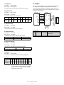
1) LAYOUT
1) KEYBOARD LAYOUT
• Rotary type
Normal keyboard
Key position
Std/Max 53keys
Key pitch
19 (W) x 19 (H) mm
Key layout
Fixed type
REG
OPX/Z
OFF
2) KEY LIST
VOID
Keyboard layout
RA %1
7
8
9
RCPT
/PO
4
5
6
Ð
%2
NUMBER
VOID RFND
DC
SHIFT
ESC
BS
SPACE
1
2
0
3
00
PLU
/SUB
4
DEPT
#
F
K
20
24
28
B
8
19
3
C
D
7
E
12
H
6
I
11
J
P
32
16
M
10
N
15
O
R
30
14
25
9
Q
31
26
21
5
L
CLK#
27
22
17
1
G
23
18
2
DEPT
SHIFT
A
S
29
13
T
MGR
X1/Z1
Operator key (OP)
X2/Z2
OP
PGM
CL
Manager key (MA)
MA
OP
MA
Type
¥
Merchandise subtotal key
4. MODE SWITCH
3. KEYBOARD
@/FOR
Automatic sequence key
CHK
MDSE SBTL
Power source
CONV
Tax key
Tax 1 SHIFT
TAX AUTO
U
X
TAX1
SHIFT
TAX2
SHIFT
V
Y
The mode switch can be operated by inserting one of the two supplied
mode keys - manager (MA) and operator (OP) keys. These keys can be
inserted or removed only in the “REG” or “OFF” position.
CHK CH
W
Z
MDSE #/TM
SBTL SBTL
CA/AT/NS
Note: The small characters on the bottom or lower right in each key
indicates functions or characters which can be used for character
entries for text programming.
XE-A20S
SPECIFICATIONS
–1–
The mode switch has these settings:
OFF:
PLU/SUB
DEPT REPEAT
OP X/Z: To take individual clerk X or Z reports, and to take flash
reports.
It can be used to toggle receipt state “ON” and “OFF” by
pressing he [RCPT/PO] key.
REG:
For entering sales.
PGM:
To program various items.
VOID:
Enters into the void mode. This mode allows correction after
finalizing a transaction.
MGR:
For manager’s entries. The manager can use this mode for an
override entry.
RCPT
OFF
The number of repeats is displayed, starting at “2” and incremental with each repeat. When you have registered ten
times, the display will show “0.” (2 3 3 ..... 9 3 0 3 1 3 2 ... )
Receipt function status:
The indicator “_” appears in the RCPT OFF position when
the receipt function is in the OFF status.
Time:
Appears in the far-right six positions (hour-minute - ”A” or
hour-minute - ”P”) in the OP X/Z, REG, or MGR mode. “A” is
displayed in the morning (AM), and “P” in the afternoon
(PM). In the REG or MGR mode, press the [#/TM/SBTL] key
to display the time.
5. DISPLAY
1) OPERATOR DISPLAY
LED
1 line
Machine state symbols
Number of positions: 10 digits
Color of display:
Yellow / Green
Character form:
7 segment
Character size:
Numeric 14 (H) x 8 (W) mm
Layout:
:
Appears during programming.
:
Appears when an error is detected.
:
Appears when the subtotal is displayed or when the amount
tendered is smaller than the sales amount.
:
Appears when the [CONV] key is pressed to calculate a subtotal in foreign currency.
:
Appears when a transaction is finalized by pressing the [CA/AT/
NS], [CHK] or [CH] key.
:
Appears when the change due amount is displayed.
PLU/SUB
DEPT
REPEAT
RCPT
OFF
: May appear in the far-left three positions at the timing of key
entry when the electronic journal (EJ) memory is full. (Depending on programming.)
DC SHIFT NUMBER
:
Appears when the voltage of the installed batteries is under the
required level. You must replace with new ones within two days
to avoid loss of memory.
:
Appears when the batteries are not installed, or the installed
batteries are dead. You must replace with new ones immediately.
:
May appear right below the eighth and ninth places at the timing
of finalization of a transaction when the electronic journal (EJ)
memory is nearly full.
Also appears right below the tenth place when power save
mode is effective.
:
Appears when the print roller arm is not locked.
2) CUSTOMER DISPLAY
Display device:
LED
Number of line:
1 line
DC SHIFT NUMBER
Number of repeats for repetitive registrations:
X2/Z2: To take the X/Z report for periodic (weekly or monthly)
consolidation.
Number of line:
Clerk code
Amount: Appears in the far-right eight (max.) positions. When the
amount is negative, the minus symbol “-” appears before the
amount.
X1/Z1: To take the X/Z report for various daily totals.
Display device:
Customer display
(Pop-up type)
Operator display
This mode locks all register operations. (AC power turns off.)
No change occurs to register data.
Number of positions: 7 digits
Color of display:
Yellow / Green
Style:
Pop up type
Character form:
7 segment
Character size:
14mm (H) x 8mm (W)
Layout:
: Appears when the paper is not installed or paper is out.
XE-A20S
SPECIFICATIONS
–2–
6. PRINTER
Segment
Display
position
Description
Amount
1-8
Minus sign
2-10
-: Floating
Error
8-10
Exx:xx = error code
PGM Mode
10
1) Printer
• Part number
: M-T53II
• No. of station
: 1 (Receipt or journal)
• Validation
: No.
F: Light up when a registration is
f inaliz ed by de pres sing CA S H,
CHECK, CHARGE key
• Printing system
: Line thermal
• No. of dot
: 288 dots
: Horizontal 0.167mm
Vertical 0.167mm
P
CASH, CHECK,
CHARGE
10
SUB TOTAL/
short tender
10
o
• Dot pitch
Change
10
C: Light up whenever the change
due amount appears in the display.
• Font
: 10 dots (W) x 24 dots (H)
• Printing capacity
: max. 24 characters/Line
• Character size
: 1.67mm (W) x 4.00mm (H) at 10 x 24 dots
• Print pitch
: Column distance 2.0mm
Row distance 5.21mm
Currency
Conversion
10
c: Light up whenever the foreign
amount appears in the display.
Department
9-10
No zero-suppressed
PLU
7-10
No zero-suppressed
Repeat
8
Endless count, starting from 2.
Receipt OFF
9
_
DC
_: Double size character entry status
SHIFT
_: Shift character entry status
NUMBER
_: Number character entry status
• Print speed
: Approximate 60mm/s (Approximate 12 l/s)
• Paper feed speed
: Approximate 60mm/s (Approximate 12 l/s)
• (Manual feed)
: Approximate 60mm/s (Approximate 12 l/s)
• Reliability
: Mechanism LIFE 6 million lines used to
high quality thermal paper
Clerk No.
2, 3
-xx-: clerk number
EJ FULL
8-10
E-E: Light up when EJ memory is
FULL at the timing of key entry
(by PGM selection).
• Paper end sensor
: Set up
• Cutter
: Manual Cutter
• Near end sensor
: No
Low Battery
10
L:
No Battery
10
L:
2) Paper
• Paper roll dimension: 2.25 m 0.02 inch
57.5 m 0.5mm in width
Decimal Point
Display
position
Decimal point
7-1
TAB
4-1
EJ near full
8, 9
Max. 3.15 inch
Max. 80mm in diameter
Description
• Paper quality:
High-quality thermal paper
paper thickness:
(by PGM selection)
0.06 to 0.08mm
Nihon seisi thermal paper
TF50KS-E2C
KANZAN thermal paper:
KF50
KSP thermal paper:
P350
3) Logo stamp
• No
4) Printing area
Number of thermal head heater elements 288 dots
(4.75)
48 (288 dots)
(4.75)
print area
(max.24 characters)
0.167
57.5±0.5
(Paper dimension)
XE-A20S
SPECIFICATIONS
–3–
(units : mm)
7. DRAWER
8. BATTERY
[OUTLINE]
1) MEMORY BACK UP BATTERY
• Standard equipment: Yes (1)
For memory back up, (3) dry AA batteries are needed.
• Max. number of additional drawers: 0
1. Memory holding time:
• The drawer consists of:
Approx. 1 year after NEW dry batteries are installed.
1) Drawer box (outer case) and drawer
2. Battery replacement method:
2) Money case
When the low battery symbol “L” lights up, replace the batteries (3
AA) by the following method;
3) Coin case
1) Power on the ECR.
4) Lock (attached to the drawer)
2) Mode switch turn to “REG” mode.
[SPECIFICATION]
3) Remove the OLD dry batteries (3 pieces).
4) Insert the NEW dry batteries (3 pieces).
1) DRAWER BOX AND DRAWER
5) Confirm the low battery symbol “L” is off.
• Model name of the drawer box : SK-415
• Size
: 330 (W) x 418 (D) x 98 (H) mm
13 (W) x 16.5 (D) x 3.9 (H) inch
2) LOW BATTERY
• Material
: Metal
• Bell
:-
Low battery indication will appear on the left side of display when the
battery voltage is low.
• Release lever
: Standard equipment:
locate on the bottom
• Drawer open sensor
:-
• Separation from the main unit
:-
CASE 1: When machine is sitting idle or after finalization of a transaction.
The machine will always indicate the low battery condition.
CASE 2: During any numeric or item key entry.
Battery condition will not appear.
Except when the power is restored after a power failure, the low
battery condition will appear on the display only when the battery
is low and the indicator will disapear after any key entry.
2) MONEY CASE
Separation from the drawer
Disallowed
Separation of the bill compartments from the
coin compartments
Allowed
[Display sample]
“
-
Bill separator
Number of compartments
0.00”: Battery is OK.
“L 0.00”: Low battery (You have to change the batteries.)
4B/5C
“L 0.00”: No battery (You have to change the batteries immediately.)
After finalization
Layout:
“F 12.34”: Battery is OK.
“L 12.34”: Low battery. (“L” indicate instead of “F”.)
“L 12.34”: No battery. (“L” indicate instead of “F”.)
Note: “NO BATTERY”: When “NO BATTERY” is displayed, the master
reset is executed upon "POWER ON" after
"POWER OFF" or power failure.
4B/5C
3) LOCK (LOCK KEY : LKGIM7331BHZZ)
Location of the lock: Front
Method of locking and unlocking:
To lock, insert the drawer lock key into the lock
and turn it 90 degrees counter clockwise.
To unlock, insert the drawer lock key and turn it 90
degrees clockwise.
ck
unlo
Lo
SK1-1
SK1-1
Key No:
ck
XE-A20S
SPECIFICATIONS
–4–
CHAPTER 2. OPTIONS
1. OPTIONS (NONE)
2. SERVICE TOOL
NO
1
NAME
PRICE
RANK
PARTS CODE
USB cable
DESCRIPTION
For connection between ECR and PC
3. SUPPLIES
NO
1
PARTS CODE
PRICE
RANK
TPAPR6656RC05
BA
NAME
Thermal roll paper
DESCRIPTION
5 ROLLS/PACK
CHAPTER 3. MASTER RESET AND PROGRAM RESET
1. MASTER RESETTING
2. PROGRAM RESETTING
(INITIALIZATION)
Master resetting clears the entire memory and resumes default values.
Master resetting can be accomplished by using the following procedure:
This resetting resumes the initial program without clearing memory.
Procedure:
1) Plug in the AC cord to the wall outlet.
This resetting can be operated at below sequence in PGM mode.
2) Set the mode switch to REG position.
Procedure:
1) Unplug the AC cord from the wall outlet.
3) Remove the 3 AA batteries.
2) Wait over 1 muinite for discharging.
4) Unplug the AC cord from the wall outlet.
3) Set the mode switch to the PGM position.
5) Wait over 1 minute for discharging.
4) While holding down the FEED key,
plugin the AC cord to the wall outlet.
6) Plug in the AC cord to the wall outlet.
7) Install the 3 AA batteries.
Note: In case a power failure occurs when the machine has no batteries installed, the master reset operation is automatically performed after the power has been restored.
Note: The master reset can also be accomplished in the following case.
In case a power failure occurs when the machine has no batteries
installed, the master reset operation is automatically performed after
the power has been restored.
When power failure occurs with no batteries installed in the the
machine, all memory is lost and the machine does not work properly
after power is restored, thus requiring the master reset operation.)
XE-A20S
OPTIONS
–5–
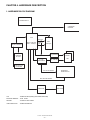
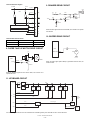
CHAPTER 4. HARDWARE DESCRIPTION
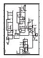
1. HARDWARE BLOCK DIAGRAM
POWER SUPPLY
STANDARD
DRAWER.
CPU
Data bus
DRIVER , SENSOR
ROM : 256K Byte
RAM : 20K Byte
RAM
Address
bus
128K Byte
POPUP
Seg. DRIVER
PRINTER
M-T53II
FRONT
LED
4 to 16
DECORDER
Dig. DRIVER
PAPER TAKE
UP MOTOR
KEY SCAN SIGNAL
KEYBOARD
MODE SWITCH
KEY RETURN SIGNAL
M66291GP
CPU
: RENESAS 30624 (MASK) (ROM 256KB RAM 20KB)
EXTERNAL MEMORY
: RAM 128 KB
PRINTER
: EPSON M-T53II 1SHEET
USB CONTROLLER
: RENESAS M66291FP
XE-A20S
HARDWARE DESCRIPTION
–6–
USB TYPE B
2) Pin description
PQ1CG2032
TRANSFORMER
V0 24V
M16C/62 PORT
Drawer
MEMORY SPACE
: MEMORY PROCESSOR MODE
(NORMAL MODE)
PROCESSOR MODE : MEMORY PROCESSOR MODE
It is used by (SEPARATE BUS 8bit Width)
/POFF detect point
PQ1CG2032
VLED 5.7V
PORT
PIN I/O
Pin
No.
name
VCC 5V
P00
88 I/O
D0
D0
OUT L
VDD 5V
P01
87 I/O
D1
D1
OUT L
P02
86 I/O
D2
D2
OUT L
P03
85 I/O
D3
D3
OUT L
P04
84 I/O
D4
D4
OUT L
P05
83 I/O
D5
D5
OUT L
P06
82 I/O
D6
D6
OUT L
P07
81 I/O
D7
D7
P10
80
O
P10
KST0
L
IN
KEY DISPLAY
(4 to 16)
P11
79
O
P11
KST1
L
IN
KEY DISPLAY
(4 to 16)
P12
78
O
P12
KST2
L
IN
KEY DISPLAY
(4 to 16)
P13
77
O
P13
KST3
L
IN
KEY DISPLAY
(4 to 16)
P14
76
O
P14
IN1
L
OUT L PAPER FEED
MOTOR
P15
75
O
P15
IN2
L
OUT L PAPER FEED
MOTOR
P16
74
O
P16
ENA1
L
OUT L PAPER FEED
MOTOR
P17
73
O
P17
ENA2
L
OUT L PAPER FEED
MOTOR
P20
72
O
A0
A0
OUT L
P21
71
O
A1
A1
OUT L
P22
70
O
A2
A2
OUT L
P23
69
O
A3
A3
OUT L
P24
68
O
A4
A4
OUT L
P25
67
O
A5
A5
OUT L
P26
66
O
A6
A6
OUT L
P27
65
O
A7
A7
OUT L
P30
63
O
A8
A8
OUT L
P31
61
O
A9
A9
OUT L
P32
60
O
A10
A10
OUT L
P33
59
O
A11
A11
OUT L
P34
58
O
A12
A12
OUT L
P35
57
O
A13
A13
OUT L
P36
56
O
A14
A14
OUT L
P37
55
O
A15
A15
OUT L
P40
54
O
A16
A16
OUT L
P41
53
O
A17
A17
OUT L
P42
52
O
A18
A18
OUT L
P43
51
O
A19
A19
P44
50
O
/CS0
(NU)
P45
49
O
/CS1
/CS1
Battery
ON/OFF Control (MODE SW)
LM2574
+ Tr.
VH, VP (8V)
PRINTER HEAD, MOTOR
PAPER TAKEUP MOTOR
ON/OFF Control (MODE SW,
/POFF, CPU P105)
2. DESCRIPTION OF MAIN LSI’S
2-1. CPU (M30624MGA)
Signal
name
Initial OFF
value MODE
OUT L
SIN4
AVCC
VREF
AN0
AVSS
AN1
AN2
AN3
AN4
AN5
AN6
AN7
D0
D1
D2
D3
D4
D5
D6
D7
D8
D9
D10
D11
D12
100
99
98
97
96
95
94
93
92
91
90
89
88
87
86
85
84
83
82
81
80
79
78
77
76
P97
VDD
VDD
TH
GND
P101
Vref
P103
P104
P105
LATCH
DTS
D0
D1
D2
D3
D4
D5
D6
D7
P10
P11
P12
P13
PH1
1) Pin configuration
SOUT4
CLK4
TB4IN
TB3IN
SOUT3
SIN3
CLK3
BYTE
CNVss
XCIN
XCOUT
/RESET
XOUT
Vss
XIN
Vcc
NMI
INT2
INT1
INT0
TA4IN/U
TA4OUT/U
TB3IN
TBEOUT
TA2INW
M30624MGA
D13
D14
D15
A0
A1
A2
A3
A4
A5
A6
A7
VSS
A8
VCC
A9
A10
A11
A12
A13
A14
A15
A16
A17
A18
A19
75
74
73
72
71
70
69
68
67
66
65
64
63
62
61
60
50
58
57
56
55
54
53
52
51
PH2
PH3
PH4
A0
A1
A2
A3
A4
A5
A6
A7
GND
A8
VDD
A9
A10
A11
A12
A13
A14
A15
A16
A17
NC
NC
26
27
28
29
30
31
32
33
34
35
36
37
38
39
40
41
42
43
44
45
46
47
48
49
50
TA2OUTW
TA1IN/V
TA1OUT/V
TB5IN
TB5OUT
TXD1
RXD1
CLK1
CLKS1
TXD0
RXD0
CLK0
/RTS0
/RDY
ALE
/HOLD
/HLDA
CBCLK
/RD
/BHE
/WR
/CS3
/CS2
/CS1
/CS0
1
2
3
4
5
6
7
8
9
10
11
12
13
14
15
16
17
18
19
20
21
22
23
24
25
P74
P73
CLK
P71
DAT
P67
P66
/FRES
P64
FSD
FRD
FSCK
DR1
/RDY
/HOLD
VCC
NC
NC
/RD
NC
/WR
/CS3
/RAS1
BUSY
/ROS1
P96
P95
P94
P93
P92
P91
P90
VDD
GND
XCIN
XCOUT
/RESET
XOUT
GND
XIN
VDD
VDD
CTCRL
/FRDY
P-OFF
MOTOR
BUZ1
P77
P76
P75
XE-A20S
OUT L
L
OUT L
OUT L USB
CONTROLLER
P46
48
O
/CS2
/CS2
OUT L SRAM
P47
47
O
/CS3
/CS3
OUT L SEGMENT LATCH
P50
46
O
/WR
/WR
OUT L
P51
45
O
/BHE
(NU)
OUT L
P52
44
O
/RD
/RD
OUT L
P53
43
O
BCLK
BCLK
OUT L
P54
42
O /HLDA
(NU)
OUT L
HARDWARE DESCRIPTION
–7–
Function
PORT
PIN
Pin
I/O
No.
name
Signal
name
P55
41
I
/HOLD
/EPM
IN
P56
40
O
ALE
(NU)
OUT L
P57
39
I
/RDY
/RDY
IN
P60
38
O
P60
DR1
L
OUT L DRAWER 1
DRIVE SIGNAL
P61
37
O
P61
(NU)
L
OUT L
P62
36
O
P62
(NU)
L
OUT L
Initial OFF
value MODE
<Power supply/CONTROL pins>
Function
PORT
P63
35
O
P63
/USBRST
L
OUT L USB CONTROLLER
RESET
P64
34
O
P64
/BUSY
L
OUT L BOOT BUSY
P65
33
I
P65
SCLK
IN
P66
32
I
P66
RXD
IN
P67
31
O
P67
TXD
L
OUT L BOOT TXD
P70
30
O
TXD2
DAT
H
OUT L PRINTER DATA OUT
P71
23
O
P71
(NU)
L
OUT L
P72
28
O
CLK2
CLK
L
OUT L PRINTER CLOCK
P73
27
O
P73
DR2
L
OUT L DRAWER
2 DRIVE SIGNAL
P74
26
O
P74
(NU)
L
OUT L
P75
25
O
P75
(NU)
L
OUT L
P76
24
O
P76
(NU)
L
OUT L
P77
23
O
P77
/EPM CTRL
H
OUT L
Connected to VDD
Vss
Connected to GND
AVss
96
AVss
Connected to GND
Vref
98
Vref
Connected to VDD
AVcc
99
AVcc
Connected to VDD
1) CPU
XIN
XOUT
USB DMA REQUEST
/INTUSB
IN
(NU)
IN
P86
11
O XCOUT
P87
10
I
P90
7
P91
P92
13
CPU
XCOUT
USB INTERRUPT
R62
330
11
X2
32.768KHz
XCOUT
32.768kHz
XCIN
XCIN
32.768kHz
I
P90
P90
IN
KEY IN
6
I
P91
P91
IN
KEY IN
5
I
P92
P92
IN
KEY IN
P93
4
I
P93
P93
IN
KEY IN
P94
3
I
P94
P94
IN
KEY IN
P95
2
I
P95
P95
IN
KEY IN
P96
1
I
P96
P96
IN
KEY IN
P97 100
I
P97
P97
IN
KEY IN
P100 97
I
AN0
P100
IN
HEAD TEMPERATURE MONITOR
P101 95
I
AN1
P101
IN
HEAD VOLTAGE
MONITOR
P102 94
O
P102
/STB2
P103 93
I
AN3
VBAT
P104 92
O
P104
P105 91
O
P106 90
P107 89
XCIN
10
C41
18P
H
OUT L PRINTER/STB2
(NU)
L
OUT L
P105
VPON
L
OUT L PRINTER HEAD
POWER
O
P106
/LAT
H
OUT L PRINTER DATA
LATCH
O
P107
/STB1
H
OUT L PRINTER /STB1
IN
15
12MHz
IN
/NMI
I
3. CLOCK GENERATOR
POWER INTERRUPT
/INT2
Connected to GND
64
IN
I
Vss
Vss
OUT L BUZZER
I
OPEN
14
BOOT RXD
OUT L PAPER TAKE UP
MOTOR
17
Xout
Vss
Connected to VDD
L
18
/RESET
O
Vcc
L
P85
I
13
62
MOTOR
P84
12
Xout
Vcc
BUZZER
/INT1 /DREQUSB
/RESET
BOOT SCLK
P80
I
Connected to VDD
NORMAL: L
Launch BOOT: H
Connected to Spectram diffusion IC
P81
19
BYTE
CNVss
Xin
O
P83
I
I
Vcc
O
POFF
8
9
16
22
/INT0
BYTE
CNVss
15
21
I
Function
Xin
P81
20
Signal
name
I/O
Vcc
P80
P82
PIN
No.
C42
27P
Two oscillators are connected to the CPU.
The basic clock X2 is supplied from a 12MHz oscillator.
If the CPU was not operating properly, the signal does not appear on
this line in most cases.
The sub-clock X1 generates 32.768KHz which is primarily used to
update the internal RTC (real time clock).
During the standby mode, it keeps oscillating to update the clock and
monitoring the power recovery.
BATTERY VOLTAGE
4. RESET CIRCUIT
VDD
MODE SWITCH
SRV' position
VDD
CPU
R
IC
S-80928ANMP
R
12
R
C
/RESET
C
(1) When the mode switch is placed in the “SRV” position, the reset
signal is sent to the CPU to reset the hardware.
(2) When VDD t 2.8V, a reset signal is sent from the reset IC.
(S-80928ANMP)
XE-A20S
HARDWARE DESCRIPTION
–8–
5. P-OFF CIRCUIT
7. PRINTER CONTROL CIRCUIT
I/O
VC C
LED V
1) Paper feed motor circuit
R92
2.7K
R93
9.1KG
R95
2.7K
VP
R19
C14
R17
0
1uF/50V
8
3
8
5
1
7
2
R103
3.9K
/POF
F
6
IC12A
BA10393
VCC
CPU
56K
IC12B
BA10393
4
4
P14
C75
0.1uF
P15
P16
10uF/50V
A
/A
B
/B
IC7
P17
ZD3
MTZJ5.1B
MOTOR
LB1838M
P-OFF
The P-OFF signal detects two signals by two comparators and sent to
the CPU.
Stepping motor control
V0 (24V) signal: If the power voltage V0 (24V) falls bellow the specified
level, the P-OFF signal is driver to LOW by the comparator IC12A.
The 2-phase, bi-polar stepping motor is driven at a constant voltage by
LB1838M (made by SANYO).
VLED signal:
1 step: 0.087mm
If the LED/Logic power voltage VLED falls below the
specified level, the P-OFF signal is driven to LOW by
the comparator IC12B.
1 dot: 2 steps
CPU port
6. MEMORY CIRCUIT
No.
CPU port
Signal used
1) Address map
76
P14
IN1
00000h
00400h
CPU internal RAM
20kbytes
05400h
75
P15
IN2
74
P16
ENA1
73
P17
ENA2
Drive step
Driver IC input
(CPU output)
06000h
Segment latch address
/CS3 area
06000h - 07FFFh
External S-RAM : 128kbytes
(128kbytes area)
/CS2 area
08000h - 27FFFh
/CS1 area
28000h - 3FFFFh
08000h
A
B
/A
/B
ENA2 (OUT1) (OUT3) (OUT2) (OUT4)
IN1
IN2
ENA1
1
L
L
H
H
H
H
L
L
2
H
L
H
H
L
H
H
L
3
H
H
H
H
L
L
H
H
4
L
H
H
H
H
L
L
H
STEP
28000h
Motor drive signal
40000h
2) Print circuit
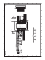
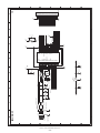
Thermal head configuration
Figure on next page shows the circuit of the thermal head consists of
heating elements and head drivers which drives and controls the heating elements.
C0000h
CPU internal ROM
256kbytes
The serial print data input through the DATA IN (DAT) is transferred to
the shift register synchronizing with the CLOCK (CLK) and stored in the
latch register by the LATCH (LAT) signal.
FFFFFh
2) RAM control
The head conduction signals (print commands 1 ~ 6) turn the gate on to
conduct the heating element corresponding to the print data.
Power supply circuit
or
Dry battery
CS2
A0-A16
A0-A16
A0-A16 VCC
VDD
0.1M
D0-7
VDD
D0-7
10K
I/O0-7
/CS2
/CS2
/CS1
150pF
CPU
10K
VCC
/RD
/RD
11
S-RAM
128K byte
IC
/OE
10K
VCC
/WR
/WR
/WE
XE-A20S
HARDWARE DESCRIPTION
–9–
9. DRAWER DRIVE CIRCUIT
Thermal head block diagram
5,6,18,19
VP
9,10,14,15
VO
GND
F6
FB1
VDR
C66673
C59
10uF/50V
C58
0.1uF
1.8K
D1A1
1N4002
CN3
3
2
1
5045-0
FB2
Q4
B
E
1 DR1
13
R77
+
STB1
C
11
C
T500mA/ 250V
C
Dot #1
A
Dot #288
C66673
2SD2212
D6
1SS133
A
STB2
7
Latch register
LAT
16
Shift register
CLK
17
When the DR1 signal from the CPU is HIGH, Q4 is turned on to operate
the solenoid.
DAT
12
VCC
Connector
10. BUZZER DRIVE CIRCUIT
Thermal head strobe terminals
STB No.
Dot No.
Number of dots
1
1 ~ 144
144
2
145 ~ 288
144
1.5k
8. PAPER TAKE UP MOTOR DRIVE CIRCUIT
CPU
R58
TA4OUT/U
VH
CN2
TA4IN/U
(21pin)
BZ
M
C51
CPU
MOTOR
BZ
22pin
MOTOR
R76
When the pulse signal (about 4KHz) is generated from the CPU, the
buzzer sounds.
Q1
1K
2SD2212
When the MOTOR signal from the CPU is HIGH, Q1 is turned on to
operate the motor.
11. KEYBOARD CIRCUIT
P10-13
P10-13
HC138
/S0-9
/S0-7
/S0-9
P10-13
HC138
/S0-7
/S1
/S3
/S4
Paper
feed key
Head up
sensor
Paper end
sensor
/S8-9
Key
Matrix
Mode
Switch
/S0 - 9
/S9
RS232
/CI
signal
P92-97
P92-97
P90
CPU
P91
P91
D0-7
/CS3
D0-7
G1',G2',
G3'G4',G5',
G6',G7
a,b,c,d,e,f,g,dp
74HC374
/CS3
Front
display
A',B',C',D',E',F',G',DP'
Four P10-13 signals from the CPU are converted into 16 strobe signals by two 74HC138 for use in various functions.
XE-A20S
HARDWARE DESCRIPTION
– 10 –
Pop-up
display
12. USB I/F
1) Keyboard
Scan signal:
10 /S0-9 signals
The XE-A20S is equipped with 1 USB port (slave) as a standard provision. By use of the USB general-purpose ASSP device M66291,
it sends and receives USB data. The M66291 is mapped to the /CS1
space (28000H~3FFFFFH). The CPU and the M66291 are connected
as shown in the figure below.
Return signal: 6 P92-97 signals
The keys are read by the key matrix following the above signals.
2) Mode switch
Scan signal:
M16C/62
8 /S0-7 signals
A0
A1~A6
The positions are read by the above signals.
Mode
switch
position
/S0
/S1
SRV
/S2
PGM (OFF)
/S3
TIME
/S4
/S5
REG
/S6
D0~D7
/S7
MGR X1/Z1 X2/Z2
7
8
3.3V
CoreVcc
D15/AD0
AD1~AD6
Vbus
TrON
1.5kΩ
D0~D7
CS1
RD
WRL
WRH
INT2
CS
RD
LWR
HWR/BYTE
INT1
Dreq0
3) Paper feed key
Scan signal:
IOVcc
Vcc
Return signal: 1 P90 signal
Scan
signal
M66291
5V
D+
1
3
Vbus
D+
27Ω
2
D27Ω
4
INT0
DGND
1.0{F
Xin
Xout
USB Connector
1 /S1 signal
Return signal: 1 P91 signal
24MHz
The paper feed key is read by the above signals.
<CPU PORT>
4) Head up sensor
Scan signal:
1 /S3 signal
Return signal: 1 P91 signal
No.
CPU PORT
SIGNAL
19
P83 (INT1)
/DREQUSE
18
P84 (INT2)
/INTUSB
The Head up sensor state is read by the above signals.
Head up sensor
Head up detected
Head up not detected
Low
High
P91
5) Paper end sensor
Scan signal:
1 /S4 signal
Return signal: 1 P91 signal
The paper end sensor state is read by the above signals.
Receipt near end sensor
End detected
End not detected
P91
Low
High
6) Display
Scan signal:
10 /S0-9 signals
The above 10 scan signals are used as the following digit signals.
Digit signal:
Scan signal
/S0
/S1
/S2 /S3 /S4 /S5 /S6 /S7 /S8
/S9
Digit signal: G1’
Front
G2’ G3’ G4’ G5’ G6’ G7’ G8’ G9’ G10
’
Digit signal: G1’
Pop-up
G2’ G3’ G4’ G5’ G6’ G7’
Segment signal : Segment signals: a, b, c, d, e, f, g, and DP are output
by the IC:74HC374, using the data bus signal:D0-7
from the CPU as an input signal and the chip select
signal:/CS3 as a latch signal.
XE-A20S
HARDWARE DESCRIPTION
– 11 –
Application
USB DMA CHANNEL 0 DMA
Request signal
USB Interrupt 0 Request signal
CHAPTER 5. TEST FUNCTION
1. TEST ITEMS
2) KEY CODE
1 Key operation
The test items are as follows:
NO.
Code
1
100
Display buzzer test
2
101
Key code
3
102
Printer test
4
104
Keyboard test
101
Description
5
105
mode switch test
6
106
Printer sensor test
7
107
Clock display test
8
110
Drawer 1 open & sensor test
9
120
External RAM test
10
121
CPU internal RAM test
11
140
CPU internal ROM test
12
160
AD conversion port test
13
520
USB TEST
14
550
Sleep mode test
RCPT/PO
2 Test procedure
Display
KEY CODE
3 Check that:
KEY code: Every time a key is pressed, the code of that key is displayed as a decimal number.
When a key is pressed twice or pressed in an incorrect manner, --will be displayed.
4 End of testing
You can exit the test mode by turning the mode switch to a position
other than the SRV mode. The printer prints as follows:
101
* Starting DIAG.
3) PRINTER TEST
Mode switch
1 Key operation
: PGM
Key operation : Above code + "CH" key
102
2 Test procedure
2. DESCRIPTION OF EACH DIAGNOSTIC
PROGRAM
Display
1) DISPLAY BUZZER TEST
1 2 3 4 5 6 7 8 9 0
ZZZZZZ
ZZZZZZ
ZZZZZZ
1 Key operation
100
RCPT/PO
----------------ZZZZZ
----------------ZZZZZ
----------------ZZZZZ
RCPT/PO
3 lines of 24 Z's are printed.
2 Test procedure
Display at operator side
Display at front side
1.2.3.4.5.6.7.8.9.0.
4.5.6.7.8.9.0.
The decimal point will shift in steps of 1 digit from the lower digit to
the upper (every 200 m sec).
3 Check that:
The print is free from contamination, blur, and uneven density.
After that, all segments turn on (about 1 sec)
Display at operator side
Display at front side
4 End of testing
8.8.8.8.8.8.8.8.8.8.
8.8.8.8.8.8.8.
The test will end automatically.
This mode is repeated.
At the same time, the buzzer sounds continuously.
4) KEYBOARD TEST
1 Key operation
3 Check that:
104
RCPT/PO
A) Each position is correctly displayed.
2 Test procedure
B) The brightness of each number is uniform.
The keyboard is checked using the check sum data of the key code.
C) The buzzer sound is normal.
4 End of testing
Display
You can exit the test mode by pressing any key. The following is
printed.
1 0 4
KEY CODE
3 Check:
100
A) The content of completion print
XE-A20S
TEST FUNCTION
– 12 –
4 End of testing
3 Check that:
When the test ends normally
When an error occurs
104
E- ~ - 104
“-” blinks and the clock counts up.
4 End of testing
Note: Calculation of key check sum data
The hard code (hexadecimal number) at the position (excluding
feed key) where there is input data, the hard code is added.
However, the end key (CA/AT/NS) is not added.
This data to which hard codes have been added is converted into
a decimal number value, which will become the check sum data
that will be entered when the Diag is started.
When any key is pressed, the date and time are printed and the test
mode will terminated.
Display
1 0 7
year month day
1 Key operation
1 Key operation
110
RCPT/PO
RCPT/PO
2 Test procedure
2 Test procedure
Display
hour min sec
8) DRAWER 1 OPEN AND SENSOR TEST
5) MODE SWITCH TEST
105
XXXXXX - XXXXXX
1 0 5
Display
X
1 1 0
X
X: O = DRAWER OPEN
C = DRAWER CLOSED
MODE: _PGM_VOID_OFF_OP X/Z_REG_MGR_X1/Z1_X2/Z2____PGM
x :
1
2
9
3
4
5
6
7
1
3 Check that:
The above x must be read in the correct order.
(If the contact is open, 9 will be displayed.)
A) The drawer opens normally.
B) The sensor correctly indicates the status of the drawer 1.
3 Check:
*On the XE-A202, “C” (CLOSED) is always displayed.
The display during testing and the content of the completion print.
4 End of testing
4 End of testing
When the test ends normally:
When an error occurs:
You can exit the test mode by pressing any key. The printer prints
the following.
105
E- ~ - 105
110
6) PRINTER SENSOR TEST
9) EXTERNAL RAM TEST
1 Key operation
106
1 Key operation
RCPT/PO
120
2 Test procedure
2 Test procedure
Check the status of paper end sensor and head up sensor.
7-segment display:
1 0 6
The standard 128 Kbyte RAM is checked.
The contents of the memory are lost after this test.
RAM(08000H ~ 27FFFH area) is tested in the following procedure:
X Y
3 Check the following:
X:1 - Paper present
O - Out of paper
a) Data in the test area is stored.
Y:1 - Head DOWN
O - Head UP
b) Write “00H”
4 End of testing
c) Read and compare “00H” and then write”55H”
d) Read and compare “55H” and then write”AAH”
You can exit the test mode by pressing any key and the printer prints
the following:
e) Read and compare “AAH”
106
f) Restore stored data.
If an error occurs at a step, the error is printed.
If an error does not occur, the following addresses are checked.
7) CLOCK TEST
1 Key operation
107
RCPT/PO
Addresses to be checked:
10000H , 10001H , 10002H , 10004H , 10008H
10010H , 10020H , 10040H , 10080H ,
10100H , 10200H , 10400H , 10800H ,
11000H , 12000H , 14000H , 18000H ,
20000H
RCPT/PO
2 Test procedure
Displayed digit:
8 7 6 5 4 3 2 1
7-segment display:
Display
hour
min
sec
1 2 0
3 Check:
Blinks at an interval of 0.5 sec.
A) The completion print.
XE-A20S
TEST FUNCTION
– 13 –
4 End of testing
12) AD conversion port
The program ends after printing.
1 Key operation
When the test ends normally.
When the test ends abnormally. Ex- ~ -
120
120
*****
x = 1: Data error
x = 2: Address error
160
RCPT/PO
2 Test procedure
The test program displays the voltage of each AD port.
1. Head temperature
When an error occurs, the printer outputs the error message and
then the address where the error has occurred in the area ****.
2. Head voltage
3. Battery voltage
10) CPU internal RAM test
RCPT/PO
160
2 Test procedure
The test program checks internal RAM of the CPU.
The contents of the memory are lost after this test.
RAM (00400H - 053FFH area) is tested in the following procedure.
13) Communication test
1 Key operation
520
a) Data in the test area is stored.
b) Write “00H”
CH
Note: USB service tool that should be used.
c) Read and compare “00H” and then write “55H”
2 Test procedure
The device address assigned by USB REVISION/VENDOR/
PRODUCT ID and the host is printed.
d) Read and compare “55H” and then read “AAH”
e) Read and compare “AAH”
f) Stored data is restored.
3 Check:
X X X = Device address
If an error occurs at a step, the error is printed.
If an error does not occur, the following addresses are checked.
Addresses to be checked:
Display
01000H , 01001H , 01002H , 01004H , 01008H
01010H , 01020H , 01040H , 01080H ,
01100H , 01200H , 01400H , 01800H ,
02000H , 04000H
Display
520
Ver. XXXX
USB Rev.
1 2 1
3 Check:
VENDOR ID
04DD
PRODUCT ID
90B5
DEVICE ADDRESS
XXX
The completion print.
The test program ends after printing.
When the test ends normally.
When the test ends abnormally. Ex- ~ -
121
121
14) Sleep mode test
*****
x = 1: Data error
x = 2: Address error
1 Key operation
550
If an error occurs, the printer outputs the error message and then
the address where the error has occurred in the area ****.
11) CPU internal ROM test
1 Key operation
3 Check that:
A) The display goes off (excluding Decimal point)
RCPT/PO
B) The system turns active when any key is pressed.
The test program checks that the checksum of the CPU internal
flash ROM (C0000H - FFFFFH) is correct.
The lower two digits of the checksum should be 10H.(pending)
4 End of testing
The test program will automatically be terminated and the printer
prints the following.
1 4 0
550
3 Check:
The completion print.
4 End of testing
The test will automatically be terminated and the printer prints as follows:
When the test ends normally.
ROM
When the test ends abnormally. E- ~ ROM
RCPT/PO
2 Test procedure
The test program checks the system in SLEEP MODE (The display
goes off and the Decimal point comes on) and then waits for any
status change (KEY input).
2 Test procedure
Display
1 Connect to host : 1~127
Unconnection : 0
4 End of testing
After completion of printing, the test is terminated automatically.
4 End of testing.
140
XXX
XXX
XXXX
3 End of testing
You can exit the test mode by pressing any key.
The printer prints the follwing.
1 Key operation
121
1 6 0 1
1 6 0 2
1 6 0 3
140
******** (CPU CODE)
******** (Version)
140
******** (CPU CODE)
******** (Version)
XE-A20S
TEST FUNCTION
– 14 –
A
ENA1
ENA2
IN1
IN2
KST3
KST2
KST1
KST0
2
X1
8
1
3
CST12.0MTW
2
2
2
2
2
2
2
2
CPU
D7
D6
D5
D4
D3
D2
D1
D0
2
330pF
C27
10K
R32
10K
R28
C28
10K
R33
R64
3.3K
/RESET
1
2
3
4
C10
FS781
XIN
XOUT
S1
LF
C31
10K
R36
VDD
S0
FSOUT
VSS
7
8
7
6
5
VDD
C38
3.3K
R56
C30
10K
100pF
820
R57
C29
10K
R35
C12
10K
R3
C13
10K
R4
C14
VBAT
/STB2
3
2
NC
33
R65
0.1uF
C44
C18
10K
R9
C37
100K
R54
VCC
C49
91pF
10uF/10V,OS
C19
10K
R10
100
100
100
100
100
100
100
100
VDD
VDD
1000pF
C45
+
P100
P97
2
2
P101
R42
R44
R45
R46
R47
R48
R49
R50
2
C39
2200pF
4
5
C17
10K
R8
33pF*8(C14-C21)
C16
10K
R7
C34
4.7UF/16V
+
CD
S-80928ANMP
SII
IC4
1
OUT
2
VDD
3
VSS
VCC
/STB1
/LAT
VPON
10K
10K
2
2
3
R38
R37
VCC
C15
10K
R6
VCC
10K
R5
100pF*4(C10-C13)
C11
10K
10K
R34
IC5
100pF*8(C24-C31)
C26
10K
R31
10K
R27
C25
10K
C48
C24
10K
R29
R30
10K
10K
VCC
R26
R25
A7
A6
A5
A4
A3
A2
A1
A0
R2
R1
2
2
2
2
2
2
2
C21
10K
R12
6
81
82
83
84
85
86
87
88
89
90
91
92
93
94
95
96
97
98
99
100
CNVss
D7
D6
D5
D4
D3
D2
D1
D0
AN7
AN6
AN5
AN4
AN3
AN2
AN1
AVSS
AN0
VREF
AVCC
SIN4
P96
P95
P94
P93
P92
P91
P90
IC2
M30624
C20
10K
R11
18pF
C41
R60
47K
R69
10K
VCC
32.768KHz
27pF
C42
R62
330
X2
R68
3.3k
5
UDZ4.3B
D3
2
3
CST12.0MTW
X3
R61
0
3
1. CIRCUIT DIAGRAM
1
B
5
2
C
6
C
A
-
+
8
D
7
10K
R13
VCC
10K
C2
10K
C1
IC6A
BA10393
1
/DREQUSB
/INTUSB
VO
CS0
CS1
CS2
CS3
WR
BHE
RD
CBCLK
HLDA
HOLD
ALE
CLKOUT
RTS0
CLK0
RXD0
TXD0
CLKS1
CLK1
RXD1
TXD1
R15
R14
C4
10K
R17
2,3
R53
47K
50
49
48
47
46
45
44
43
42
41
40
39
38
37
36
35
34
33
32
31
C5
10K
R18
/RESET
MOTOR
/POFF
33pF*9(C1-C9)
C3
10K
R16
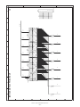
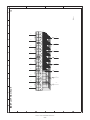
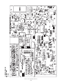
CHAPTER 6. CIRCUIT DIAGRAM AND PWB LAYOUT
8
80
79
78
77
76
75
74
73
72
71
70
69
68
67
66
65
64
63
62
61
60
59
58
57
56
55
54
53
52
51
D8
D9
D10
D11
D12
D13
D14
D15
A0
A1
A2
A3
A4
A5
A6
A7
VSS
A8
VCC
A9
A10
A11
A12
A13
A14
A15
A16
A17
A18
A19
SOUT4
CLK4
TB4IN
TB3IN
SOUT3
SIN3
CLK3
BYTE
CNVSS
XCIN
XCOUT
RESET
XOUT
VSS
XIN
VCC
NMI
INT2
INT1
INT0
TA4IN/U
TA4OUT/U
TB3IN
TBEOUT
TA2INW
TA2OUTW
TA1IN/V
TA1OUT/V
TB5IN
TB5OUT
1
2
3
4
5
6
7
8
9
10
11
12
13
14
15
16
17
18
19
20
21
22
23
24
25
26
27
28
29
30
– 15 –
4
CIRCUIT DIAGRAM AND PWB LAYOUT
4
2
3
33pF
10K
R39
C6
10K
R19
4
D2
1SS133
C
C9
A
+
R41
47K
10K
R22
VCC
C43
1.5K
R58
C8
10K
R21
10uF/16V,AL
C35
10K
R40
C7
10K
R20
R70
10K
0.1uF
R55
10K
1000pF
C50
2
2
B
/RES
3
R67
10K
VCC
R66
10K
5
4
3
2
1
D0
D1
D2
D3
D4
D5
D6
D7
A0
A1
A2
A3
A4
A5
A6
/DREQUSB
/INTUSB
/CS1
/WR
/RD
CON5
CLK
+
A[0..16]
D[0..7]
J1
33pF
C23
R43
10k
DAT
BZ1
CNVss
RXD
TXD
VCC
/CS3
VCC
A[0..16]
D[0..7]
3
PIEZO BZ
VCC
R51
47K
1SS133
D1
2
R24
10K
TP1
VCC
VCC
VDD
C46
DR1
/RD
/WR
/CS1
/CS2
10K
R23
A8
A9
A10
A11
A12
A13
A14
A15
A16
C
A
XE-A20S
VCC
C32
0.1uF
JST 25FMN-BTK-A
25
24
23
22
21
20
19
18
17
16
15
14
13
12
11
10
9
8
7
6
5
4
3
2
1
CN1
A16
A14
A12
A7
A6
A5
A4
A3
A2
A1
A0
D0
D1
D2
D0
D1
D2
D3
D4
D5
D6
D7
1
2
3
4
5
6
7
8
9
10
11
12
13
14
15
16
IC1
Q0
Q1
Q2
Q3
Q4
Q5
Q6
Q7
NC
A16
A14
A12
A7
A6
A5
A4
A3
A2
A1
A0
I/O0
I/O1
I/O2
VSS
IC3
C33
VCC
A15
CS2
WE
A13
A8
A9
A11
OE
A10
CS1
T/O7
I/O6
I/O5
I/O4
I/O3
2
32
31
30
29
28
27
26
25
24
23
22
21
20
19
18
17
VDD
VCC
VCC:20pin
GND:10pin
2
5
6
9
12
15
16
19
10uF/50V
+
VDD
74HC374
OC
CLK
D0
D1
D2
D3
D4
D5
D6
D7
LP621024DM-70MM
1
11
3
4
7
8
13
14
17
18
2
D7
D6
D5
D4
D3
A10
A13
A8
A9
A11
A15
C22
0.1uF
a
b
c
d
e
f
g
dp
a
b
c
d
e
f
g
dp
VDD
1
33pF
C40
10K
R59
33pF
VCC
33pF
C47
10K
R63
R52
10K
C36
1/3
VCC
2
2
2
2
2
2
2
2
1
/CS2
/RD
/WR
A
B
C
D
CIRCUIT DIAGRAM AND PWB LAYOUT
A
B
C
D
1
1
1
D4
34
33
32
31
30
29
28
27
26
25
24
23
22
21
20
19
18
17
16
15
14
13
12
11
10
9
8
7
6
5
4
3
2
1
8
A
D
G
R72
10KG
/S3
/S4
/S5
/S6
/S0
/S1
/S2
/S7
/S8
/RESET
P90
P91
P92
P93
P94
P95
P96
P97
/S9
/VON
a
b
c
d
e
f
g
dp
B
C52
1
1
1
1
1
1
1
1
/S3
/S4
/S5
/S6
/S0
/S1
/S2
/S7
/S8
/RESET
P90
P91
P92
P93
P94
P95
P96
P97
/S9
/VON
a
b
c
d
e
f
g
dp
HUPS
1
7
3
1
1
1
1
1
1
1
1
1
C61
0.1uF
PE
VLED
C57
0.1uF
0.1uF
KRC111S
Q3
2SK2731
S
10KG
R74
VCC
A
Q2
1SS133
D5
P91
1SS133
CN4
C
C
34FE-BT-VK-N
/S3
P91
P91
/S4
P101
VP
7
1
1
1
1
TH
/S7
KST0
KST1
KST2
KST3
1
2
3
4
5
6
7
8
9
10
11
12
CN5A
2K
R82
ONLY HOLE
1
2
3
4
5
6
7
8
9
10
11
12
CN5B
VP
6
VCC
C53
330pF
R73
30KG
ONLY HOLE
VCC
6
/STB1
/STB2
/LA
+
1
1
6
5
-
+
C62
47uF
50V
HUPS
1
1
16
15
14
13
12
11
10
9
C65
0.1uF
TH
CLK
PE
1
VCC
Y0
Y1
Y2
Y3
Y4
Y5
Y6
74HC138
A
B
C
G2A
G2B
G1
Y7
GND
IC9
16
15
14
13
12
11
10
9
R75
5.1KF
R71
56KG
VCC
Y0
Y1
Y2
Y3
Y4
Y5
Y6
74HC138
A
B
C
G2A
G2B
G1
Y7
GND
IC8
/BS
/AS
1
R81
10K
AS
BS
1
2
3
4
5
6
7
8
1
2
3
4
5
6
7
8
R83
4.7K
P10
VCC
8
4
DRIVER
C
E
7
5
VCC
/S8
/S9
/S0
/S1
/S2
/S3
/S4
/S5
/S6
C56
VO
C64
0.1uF
VCC
DAT
0.1uF
C60
0.1uF
R78
10K
IC6B
BA10393
5
1
1
1
1
1
VCC
TCOFF
+
VCC
IN1
IN2
3
1
1
C55
10uF/16V
ENA1
ENA2
1,3
DR1
7
14
6
9
2
13
1
4
P91
/S6
P91
/S6
A
KRC111S
1SS133
D7
10uF/50V
C
F6
VCONT
OUT1
OUT2
OUT3
OUT4
VS1
VS2
8
3
5
12
10
4
11
B
Q5
+
3
3
VP
1
R80
4.7K
R79
22K
B
C58
0.1uF
2SD2212
Q4
C66673
JUMPER WIRE(FB1)
FB1
C54
10uF/50V
AS
/AS
BS
/BS
jumper
1.8K
R77
VDR
1SS133
D6
T500mA/250V
C59
VO
LB1838M
GND
GND
IN1
IN2
ENA1
ENA2
VCC
IC7
NOT INSTALL
VCC
4
+
0.1uF
C63
MOTOR
1K
R76
0.1uF
C51
FB2
2
C66673
JUMPER WIRE
FB3
C66673
JUMPER WIRE(FB2)
1N4002
B
NOT INSTALL
D1A1
2
5045-03A
3
2
1
CN3
1
2
CN2
2/3
MOTOR
1
1
DRAWER1
STRAIGHT CON
B2B-EH-A
2SD2212
Q1
VP
C
E
8
C
A
E
– 16 –
C
C
E
C
A
XE-A20S
A
B
C
D
A
B
C
8
ZD3
MTZJ5.1B
1uF/50V
C72
NOT
INSTALL
R92
2.7K
+
R103
3.9K
R93
9.1KG
VO
POWER
R100
0
1
+
-
3
2
7
P-OFF
IC12A
BA10393
1
56K
R97
VCC
R95
2.7K
2
6
5
MYLOR
0.033uF
3.15A
/VON
IC12B
BA10393
VLED
B2P-VH
2
1
CN6
-
+
3 -
C79
0.1uF
6
B
C75
0.1uF
R109
33
7
C66
D8
4
1
F3
Q8
KRA106S
C76
1SS133
NOT
INSTALL
MTZJ5.1B
C
C
5
IC10
CB
R90
24K
5
UDZ4.3B
D19
+
A
1
IC13
HEAT SINK
+
1
IC11
HEAT SINK
1SS133
D10
C71
A
R89
R86
22K
220uF/50V
D18
ZD4
A
10K
R106
10K
R104
220uF/50V
1SS133
/VOFF
1.0A
1SS133
D12
C
A
A
+
50V
/POFF
2.2K
R91
C67
3300uF
D11
C
/POFF
1
+ 1
TCOFF
1 VPON
2
CP301
2
F1
5
2
5
B
PQ1CG2032FZ
5
PQ1CG2032FZ
Q7
KRC106S
6,8pin:N.C
L:ON
H:OFF
2
0
7
Q9
KRC106S
4
D9
R98
910F
C69
R107
560
R105
10K
1000uF
16V
+
FMB-G24H
2.7KF
R94
L1
63uH
IPEAK>12A :100%
0.02uF(M)
C78
RB060L40
D17
220uH
L3
/VOFF
RB060L40
D16
/VOFF
R108
10K
L2
180uH
R88
18K
R84
10(FUSE)
with FUSE
4
L:OFF
H,OPEN:ON
Q6
KTD998
E
LM2574
C
Q1:HEAT SINK
B
6
C
A
D
C
A
8
4
8
4
1
4
2
3
C
E
4
7
E
C
C
A
3
4
3
C77
VO
VO:23.8V
3
1000uF/35V
+
C73
10uF/10V,OS
+
R87
3.3KF
R85
17.8KF
NOT
INSTALL
3
C
A
1
1N4002
1N4002
D14
A
D13
A
PTZ6.2A
ZD2
+
VLED
C68
4700uF
16V
C
C
2
2
C
A
8
C
A
C
E
– 17 –
C
CIRCUIT DIAGRAM AND PWB LAYOUT
A
ZD1
330uF
16V
+
C70
0.1uF(M)
C74
R99
220
D15
RB721Q
VCC +5V
VLED +5.8V
PTZ9.1B
VP
C
A
XE-A20S
1
2
CN7
VBAT 1
3/3
1
B2B-XH-A-E(BLUE)
100
R102
3.3M
R101
22K
R96
VDD
VCC
1
A
B
C
D
CIRCUIT DIAGRAM AND PWB LAYOUT
– 18 –
A
B
C
8
BLM21PG221SN1D
USB B Type
5
6
7
8
L4
CN1
1
2
3
4
DLP31SN121SL2
L2
BLM21PG221SN1D
7
BLM21PG221SN1D
L3
L1
4
1
D
3
2
■ SUB I/F
22pF
C5
D1
D2
VCC
6
X1
4
1
R3
R4
R1
R2
0
1.5K
6
CSTCW24M
IC2
BA033F
24MHz
1uF
C4
C8
0.47uF
UDZS 6.2B
UDZS 6.2B
A1
A2
A3
A4
A5
A6
22pF
C6
C
A
6
C
A
7
3
8
2
8
XE-A20S
5
+
27
27
5
33uF/10V
C7
R5
1M
0.1uF
C1
3.3V
Vcore
0.1uF
C9
Vcore
1
2
3
4
5
6
7
8
9
10
11
12
13
14
15
16
17
18
19
20
21
22
23
24
IC1
4
M66291FP
Dack0#
CoreVcc
Dreq0#
GND
RST#
DCS#
D+
LWR#
Vbus
RD#
TrON
INT0#
TEST
HWR#/BYTE#
Dack1#
D15/A0
Dreq1#
D14/P6
TC1#
D13/P5
INT1#/SOF#
D12/P4
IOVcc
GND
Xout
IOVcc
Xin
D11/P3
GND
CoreVcc
D10/P2
D9/P1
A1
D8/P0
A2
D7
A3
D6
A4
A5
D5
A6
D4
D0
D3
D1
D2
4
48
47
46
45
44
43
42
41
40
39
38
37
36
35
34
33
32
31
30
29
28
27
26
25
VCC
C2
3
A0
10k
/DREQUSB
/RST
/CS1
/WR
/RD
/INTUSB
+
VCC
R6
10uF/16V
3
VCC
0.1uF
C3
D7
D6
D5
D4
D3
D2
D1
D0
2
2
D0
D1
D2
D3
D4
D5
D6
D7
A0
A1
A2
A3
A4
A5
A6
/DREQUSB
/INTUSB
/CS1
/WR
/RD
/RST
VCC
1/1
1
JST 25FMN-BTK-A
1
2
3
4
5
6
7
8
9
10
11
12
13
14
15
16
17
18
19
20
21
22
23
24
25
CN2
1
A
B
C
D
XE-A20S
CIRCUIT DIAGRAM AND PWB LAYOUT
– 19 –
A
B
C
D
7
8
7
ONLY HOLE
1
2
3
4
5
6
7
8
9
10
11
12
CN4D
ONLY HOLE
1
2
3
4
5
6
7
8
9
10
11
12
CN4C
■ PRINTER I/F PWB CIRCUIT
8
6
6
5
5
C201
0.1uF
4
VP
4
VCC
C200
0.1uF
3
3
1
2
3
4
5
6
7
8
9
10
11
12
13
14
15
16
17
18
19
20
21
22
23
24
25
26
27
27FMN-BTK-A
A
/B
B
/A
N.C
VP
VP
/LAT
/TH
GND
GND
/STB1
VCC
/STB2
GND
GND
CLK
DAT
VP
VP
N.C
N.C
VCC
LED
PE
HUPS
N.C
CN31
2
2
1
1
1/1
A
B
C
D
CIRCUIT DIAGRAM AND PWB LAYOUT
– 20 –
A
B
C
8
BLM21PG221SN1D
USB B Type
5
6
7
8
L4
CN1
1
2
3
4
DLP31SN121SL2
L2
BLM21PG221SN1D
7
BLM21PG221SN1D
L3
L1
4
1
D
3
2
■ USB I/F
22pF
C5
D1
D2
VCC
6
X1
4
R4
R3
0
1.5K
R1
R2
6
CSTCW24M
IC2
BA033F
24MHz
1uF
C4
C8
0.47uF
UDZS 6.2B
UDZS 6.2B
A1
A2
A3
A4
A5
A6
C6
22pF
C
A
6
C
A
7
3
8
1
2
8
XE-A20S
5
+
27
27
5
33uF/10V
C7
R5
1M
0.1uF
C1
3.3V
Vcore
Vcore
0.1uF
C9
1
2
3
4
5
6
7
8
9
10
11
12
13
14
15
16
17
18
19
20
21
22
23
24
IC1
4
M66291FP
Dack0#
CoreVcc
Dreq0#
GND
RST#
DCS#
D+
LWR#
Vbus
RD#
TrON
INT0#
TEST
HWR#/BYTE#
Dack1#
D15/A0
Dreq1#
D14/P6
TC1#
D13/P5
INT1#/SOF#
D12/P4
IOVcc
GND
Xout
IOVcc
Xin
D11/P3
GND
CoreVcc
D10/P2
D9/P1
A1
D8/P0
A2
D7
A3
D6
A4
A5
D5
A6
D4
D0
D3
D1
D2
4
48
47
46
45
44
43
42
41
40
39
38
37
36
35
34
33
32
31
30
29
28
27
26
25
VCC
C2
3
A0
10k
/DREQUSB
/RST
/CS1
/WR
/RD
/INTUSB
+
VCC
R6
10uF/16V
3
VCC
0.1uF
C3
D7
D6
D5
D4
D3
D2
D1
D0
2
2
D0
D1
D2
D3
D4
D5
D6
D7
A0
A1
A2
A3
A4
A5
A6
/DREQUSB
/INTUSB
/CS1
/WR
/RD
/RST
VCC
1/1
1
JST 25FMN-BTK-A
1
2
3
4
5
6
7
8
9
10
11
12
13
14
15
16
17
18
19
20
21
22
23
24
25
CN2
1
A
B
C
D
XE-A20S
CIRCUIT DIAGRAM AND PWB LAYOUT
– 21 –
A
B
C
D
7
8
27
27
DP'
R7
R8
G'
7
0
3 8
27
R6
F'
5 1 9 1 2 4 6 7
LED9
S568GWA
G7'
■ REAR DISPLAY PWB CIRCUIT
8
1
4
G6'
LED8
D568GWA
1
3
G5'
5
1
4
G4'
LED7
D568GWA
4
1
3
G3'
1
4
G2'
LED6
D568GWA
3
1
3
G1'
6
27
R5
E'
27
R4
D'
5
27
R3
C'
4
27
R2
B'
27
R1
3
A'
4 1 1 1 2 3 1 1 9 7 1 5 6 8 1 1 4 1 1 1 2 3 1 1 9 7 1 5 6 8 1 1 4 1 1 1 2 3 1 1 9 7 1 5 6 8 1 1
7 8
5 6
2
0 1
7 8
5 6
2
0 1
7 8
5 6
2
0 1
6
G1'..G7'
2
2
G1'
G2'
G3'
G4'
G5'
G6'
G7'
A'
B'
C'
D'
E'
F'
G'
DP'
1/1
1
52807-1510
1
2
3
4
5
6
7
8
9
10
11
12
13
14
15
CN31
1
A
B
C
D
XE-A20S
CIRCUIT DIAGRAM AND PWB LAYOUT
– 22 –
A
B
C
D
7
8
7
1
4
LED5
D568GWA
1
3
G
9
'
6
1
4
G
8
'
LED4
D568GWA
1
3
G
7
'
5
1
4
G
6
'
LED3
D568GWA
1
3
G
5
'
4
1
4
G
4
'
LED2
D568GWA
1
3
G
3
'
1
4
G
2
'
LED1
D568GWA
3
1
3
G
1
'
6
30
30
D
P
'
R234
R233
G
'
30
R235
F
'
5
30
R236
E
'
30
R237
D
'
4
30
R238
C
'
30
R239
B
'
3
30
R240
A
'
4 1 1 1 2 3 1 1 9 7 1 5 6 8 1 1 4 1 1 1 2 3 1 1 9 7 1 5 6 8 1 1 4 1 1 1 2 3 1 1 9 7 1 5 6 8 1 1 4 1 1 1 2 3 1 1 9 7 1 5 6 8 1 1 4 1 1 1 2 3 1 1 9 7 1 5 6 8 1 1
7 8
5 6
2
0 1
7 8
5 6
2
0 1
7 8
5 6
2
0 1
7 8
5 6
2
0 1
7 8
5 6
2
0 1
'
G
1
0
■ DISPLAY PWB CIRCUIT
8
2
2
|LINK
|POPUP.SCH
1
1
1/1
A
B
C
D
XE-A20S
CIRCUIT DIAGRAM AND PWB LAYOUT
– 23 –
A
B
C
D
7
2.7K
/S9
/S8
/S7
/S6
/S5
/S4
/S3
/S2
/S1
/S0
/S1
8
1.25mm FPC CN
12
11
10
9
8
7
6
5
4
3
2
1
CN21
KID65083
INPUT
2
P
9
2
3
P
9
3
23
22
21
31
30
29
28
27
26
12
CN22
1.25mm FPC CN
1
P
9
1
35
34
33
32
42
41
40
39
25
24
3K
7.2K
4
9
8
7
6
5
4
3
2
1
P
9
4
7
5
P
9
5
11
10
20
19
18
17
16
15
14
13
6
P
9
6
47
46
45
44
43
53
52
38
37
36
GND
7
P
9
7
59
58
57
56
55
54
51
50
49
48
OUTPUT
COMMON
8
9
■ KEY MATRIX PWB CIRCUIT
8
1
0
/
S
7
10
6
1
1
/
S
6
9
1
2
MODE SW
2SD2170
B
6
/
S
5
8
1
3
/
S
4
7
1
4
/
S
3
3.5K
6
1
5
M
O
R
5
300
1
6
/
S
2
4
/
S
1
5
1
7
E
C
5
3
1
8
/
S
0
2
1
9
/
R
E
S
E
T
1
2
0
G
N
D
2
1
4.7K
/
V
O
N
2
2
G
N
D
4
48
49
37
25
24
36
13
1
47K
12
PF
KRA101M, KRA106S
INPUT
4
COMMON
OUTPUT
3
50
38
26
14
2
3
51
39
27
15
3
52
40
28
16
4
53
41
29
17
5
2
2
54
42
30
18
6
55
43
31
19
7
56
44
32
20
8
57
45
33
21
9
1
58
46
34
22
10
1
59
47
35
23
11
1/1
A
B
C
D
XE-A20S
CIRCUIT DIAGRAM AND PWB LAYOUT
– 24 –
A
B
C
D
7
8
52044-3445
FROM MAIN
D24
D25
D26
D27
D28
D29
D30
/S3
/S4
/S5
/S6
/S7
/S8
/S9
34
33
32
31
30
29
28
27
26
25
24
23
22
21
20
19
18
17
16
15
14
13
12
11
10
9
8
7
6
5
4
3
2
1
G1'
G2'
G3'
G4'
G5'
G6'
G7'
A'
B'
C'
D'
E'
F'
G'
DP'
/S3
/S4
/S5
/S6
G1'
G2'
G3'
G4'
G5'
G6'
G7'
A'
B'
C'
D'
E'
F'
G'
DP'
/S0
/S1
/S2
/S7
/S8
/RESET
P90
P91
P92
P93
P94
P95
P96
P97
/S9
/VON
a
b
c
d
e
f
g
dp
D23
/S2
CN23
D22
VCC
D21
/S1
D31
/S0
/S1
52045-1245
1
2
3
4
5
6
7
8
9
10
11
15
14
13
12
11
10
9
8
7
6
5
4
3
2
1
CN24
52806-1510
/S3
/S4
/S5
/S6
/S0
/S1
/S2
/S7
/S8
/RESET
P90
P91
P92
P93
P94
P95
P96
P97
/S9
/VON
A
B
C
D
E
F
G
dp
7
POP UP
C104
100uF/16V
PLACE NEAR CONNECTER
1SS133
1SS133
1SS133
1SS133
1SS133
1SS133
1SS133
1SS133
1SS133
1SS133
1SS133
12
CN21
C105
0.1uF
VLED
VLED
P[91..97]
■ KEY INTERFACE PWB CIRCUIT
8
6
P[91..97]
6
VCC
P
9
1
2
P
9
2
KID65083AP
10PIN : NC
9 PIN :GND
/S[0..9]
1
CN22
52044-2245
P
9
3
4
P
9
4
5
P
9
5
5
/S[0..9]
or DTA143ESA
1
'
d
p
1
8
P
9
6
7
P
9
7
12K
R209
2
g
1
7
IC23B
G
'
120
G
1
0
R219
'
/
S
7
P90
1
0
Q20
KTA1664
9
120
Q32
R201
R202
R203
R204
R205
R206
R207
8
R218
12K
R208
IC23A
D
P
6
2.54mm Pitch
KRA101M X 10
47K * 7EA
3
KEY&MODE SW
5
/
S
6
Q33
1
1
3
G
9
'
F
'
f
1
6
/
S
4
4
Q34
100pF
C106
47K
IC23C
120
R220
1
3
R228
Q21
KTA1664
12K
R210
P90
/
S
5
VCC
1
2
4
1
4
12K
R211
M
D
R
4
e
1
5
E
'
IC23D
120
R221
Q22
KTA1664
G
8
'
/
S
3
1
5
/
S
2
Q35
1
6
12K
R212
/
S
1
1
8
/
S
0
G
7
'
5
1
9
Q36
IC23E
D
'
1
4
d
120
R222
Q23
KTA1663
1
7
3
120
R223
6
Q24
KTA1663
G
6
'
2
1
c
1
3
2
2
Q37
G
5
'
120
R224
Q25
KTA1663
R214
12K
7
/VON
/RESET
/VON
IC23F
C
'
/RESET
R213
12K
2
0
3
b
1
2
B
'
IC23G
Q31
G
4
'
120
R225
Q26
KTA1663
12K
R215
8
a
1
1
A
'
Q30
2
IC23H
G
3
'
120
R226
Q27
KTA1663
R216
12K
2
Q29
G
2
'
120
R227
Q28
KTA1663
R217
12K
G
1
'
|LINK
|POPUP.SCH
Q38
Q39
KTA1663
VLED
1
VLED
1
1/1
A
B
C
D
MIAN PWB
2. PWB LAYOUT
A. Side
XE-A20S
CIRCUIT DIAGRAM AND PWB LAYOUT
– 25 –
B. Side
XE-A20S
CIRCUIT DIAGRAM AND PWB LAYOUT
– 26 –
Q USB I/F PWB
A. Side
B. Side
XE-A20S
CIRCUIT DIAGRAM AND PWB LAYOUT
– 27 –
q
COPYRIGHT 2005 BY SHARP CORPORATION
All rights reserved.
Printed in Japan.
No part of this publication may be reproduced,
stored in a retrieval system, or transmitted.
In any form or by any means,
electronic, mechanical, photocopying, recording, or otherwise,
without prior written permission of the publisher.
SHARP CORPORATION
Digital Document Systems Group
Products Quality Assurance Department
Yamatokoriyama, Nara 639-1186, Japan
2005 January Printed in Japan t