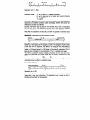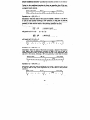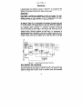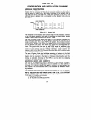
1
alMml digihl equipmentcorpomtion Digital Copyright 1969 by Equipment Corporation PDP is a registered of Digital Equipment, trademark Corporation The material in this handbook is for information purposes only and is subject to change without notice. TABLE OF CONTENTS CHAPIER PDP-11 1 lNTRODUCTlOR . . . . . . . . . . . . . . . . . . . . . . . . . . . . . . .:.. . . . . . . . . . . . . . . . . . . . . . . . . . . . . . .. . . . . . . . 1 . . . . . . . . . . . .. . . . . . . . . . . . . . . . . . . . . . . . . . . . . . . . . . . . . . . . . . . .. . . . , . . . . . . . . .. . . . . . . . . . . . . . . . 1 SYSTEMS UNIBUS KAl 1 PROCESSOR . . . . . . . . . . . . . . . . . . . . . . . . . . . . . . . . . . . . . . . . . . . . . . . . . . . . . . . .?. Priority Interrupts ,...............,..... . . . . . . . . . . . . . . . . .. . . . . . . .. . . . . . . . . . . . . . . . Reentrant Code . . . . . . . . . . . . . . . . . . . . . . . . . . . . . . . .. . . . . . . . . . . . . . . . . . . . . . . . . . . . . . . . . . . . General Registers . . . .. . . . . .. . . . . . . . . .:... . . . . . . . . . .. . . . . . . . . . . . . . . . . . . . Instruction Set . . . . . . . . . .._........................................................ Addressing . ..~...............................................~........,...,......... Operation ...... ........... ........ ............ ...... ......... L Asynchronous PACKAGJNG . . . . . . . . . . . . . . ... . .. . . . . . . . . . . . . . . . . . . ..I . . . . . . . . . . . . . . SOmARE .: ........................................................ ........................ CHAPTER 2 SYSTEM INTRODUCTION SYSTEM DEFINITION .................................................................. SYSTEM COMPONENTS ............................................................... UNIBUS ................................................... . .................................. Single Bus ................................................................. . .......... Bidirectional Lines ............ .......................................... ..* .... Relation Master-Slave ........................... .............................. ................................................ Interlocked .Communication Dynamic Master-Slave Relation ........................................... KAll CENTRAL PROCESSOR ...................................................... General Registers ................................................................ Central Processor Status Register ........................................ CORE MEMORY ............................................................................. PERIPHERAL DEVICES ................................................................ SYSTEM INTERACTION ................................................................ TRANSFER OF BUS MASTER ...................................................... PRIORITY STRUCTURE ............ .................................................... NPR Requests ....................................... .I ........................... Interrupt Requests .............................................................. CHAPTER . 3 ADDRESSING 4 INSTRUCTlOil 2 z 2 2 3 5 5 5 5 5 5 l : 6 6 6 6 7 5 7 : MODES INTRODUCTION . ..................... ............................. .; ..................... ADDRESS FIELDS ........................................................ . ............... General Register Addressing ....................... .:. ...................... *Indexed Addressing ........................ . ..................................... Autoincrement Mode Addressing ........................................ Autodecrement Addressing .................... . ............................. STACK PROCESSING .................................................................. USE OF THE PC AS A GENERAL REGISTER .......................... _... Immediate Addressing ......................................................... Absolute Addressing .:. ......................................................... Relative Addressing .............................................................. Deferred Relative Addressing .......................................... ..:. USE OF THE SP AS A GENERAL REGISTER ................................ DOUBLE OPERAND ADDRESSING .............................................. &iAPTER 1 1 11 11 11 12 12 12 13 13 13 13 14 14 14 14 Sk TIMING ................................................................ INSTRUCTION NOTATION .................................................................................... Ill 17 17 . . DOUBLE OPERAND-INSTRUCTIONS .......................... i.. ............... 17 Arithmetic Operations .................. 1........................................ Boolean Instructions ............................................................. BRANCHES .......................................................................... .:. ..... Unconditional Branch .......................................................... I Simple Conditional Branches .............................................. Signed Conditional Branches .............................................. Unsigned Conditional Branches .......................................... JUMP .................................................................................... SUBROUTINES ............................................................................. ............................................................................ Examples ............................................ SINGLE OPERAND INSTRUCTIONS Multiple Precision Operations .............................................. Rotates ................................................................................ .................................................................................. Shifts Examples ............................................................................ BYTE OPERATIONS ...................................................................... Double Operand Byte Instructions ...................................... Example .......... . ................................................................... Single Operand Instructions ................................................ CONDITION CODE OPERATORS ................................................ MISCELLANEOUS CONTROL INSTRUCTIONS .............................. , PROCESSOR TRAPS .................................................................... Trap Instructions ............................ . ................................... Stack Overflow Trap ............................................................ Bus Error Traps .................................................................. Trace Traps .......................................................................... CHAPTER 5 I ADDRESS ALLOCATION ADDRESS MAP ............................................................................ Interrupt and Trap Vector .................................................... Processor Stack and General Storage .................................. Peripheral Registers ............................................................ CORE MEMORY ............................................................................ Read-Write Core Memory .................................. , ................. Read-Only Core Memory ...................................................... Wordlet Memory .................................................................. 18 20 21 CHAPTER 6 PROGRAMMING OF PERIPHERALS DEViCE REGISTERS ...................................................... ..... . ......... CONTROL & STATUS REGISTERS ............................................... Device Function Bits ....................................... :.. ................ . ...... Memory Extension ....................................................... Done Enable and Interrupt Enable ...................................... ..i .... Condition Bits ............................................................. Unit Bits .............................................................................. Error Bits .............. I ..:. ......................................................... DATA BUFFER REGISTERS .................................................. .: ...... PROGRAMMING EXAMPLES--NON INTERRUPT ........................ INTERRUPT STRUCTURE ............................................................ PROGRAMMING EXAMPLE .......................................................... . CHAPTER 7 PERIPHERAL BULLETINS TELETYPE (MODEL LT33-DC/DD) .............................................. Size ...................................................................................... Power Requirement ............................................................ IV ;: 23 9: 27 28 zi 33 34 36 36 36 37 38 i! 41 41 ii 43 45 46 z 46 46 g ;; $ ii g 48 48 50 51 ;; 53 - . \ TELETYPE CONTROL (MODEL KLll) ......................................... Teletype Control .......................................................... r ....... Keyboard/Reader Operation ................................................ Registers (TKS, TKB) .................................................. Teleprinter/Punch ................................................................ Registers (TPS, TPB) .................................................... Programming Example ........................................................ Peripheral Address Assignments .......................................... Mounting ...................................... ....................................... HIGH-SPEED PERFORATED TAPE READER (MODEL PCll) ...... Tape Reader ........................................................................ Registers (PRS, PRB) ................................................... Programming Example ................................................ Peripheral Address Assignments ................................ Tape Punch .......................................................................... Registers (PPS, PPB) .................. ., ................................ Programming Example ................................................ Peripheral Address Assignments .................................. Mounting ............................................................................... Environmental ....................................................................... Line Frequency Clock (Model KWll-L) ............ I,.................... Register ..................................................................... .:. .... . .... Peripheral Address Assignments .......................................... Mounting ............................................................................... Vector Address .................................................................... Priority Level ........................................................................ DESCRIPTION OF THE UNIBUS ( GENERAL CONCEPTS OF THE UNIBUS ...................................... Single Bus ............................................................................ Bidirectional Bus ................................................................ Master-Slave Relation .......................................................... . Interlocked Communication .................................................. Dynamic Master-Slave Relation ............................................. UNIBUS SIGNALS ........................................................................ NON-INTERRUPT SIGNALS .......................................................... Data Lines .................................. ..r.~. ................................... Address Lines ...................................................................... Control Lines .:. ..................................................................... Master Sync &‘Slave Sync .................................................. Parity Available & Parity Bit ................................................ Initialization ........................................................................ Spare 1 & Spare 2 .............................................................. INTERRUPT SIGNALS ....................................... *. ....................... Bus Request Lines ........................................................... 9.. I Bus Grant Lines ................. r.. .............................................. Non-Processor Request ........................................................ Non-Processor Grant ............................................................ Selection Acknowledge ........................................................ Interrupt (and) Bus Busy .................................................... UNIBUS DATA TRANSFER OPERATIONS .................................... DATO and DATOB ................................................................ DATI and DATIP .................................................................. Examples of Data Transfers ......... . .................. ........ . ........... Signal Description of Data Transfers ......... . ........................ 53 53 53 54 54 .55 55 55 55 55 55 56 56 56 56 57 E 57 58 5588 58 58 58 58 CHAPTER 8 V 59 59 59 59 60 60 60 :?I E :: 61 ,61 61 z: 61 61 6": 61 :z 62 63 UNIBUS CONTROL ............. ’......................................................... Priority Arbitration ................................................................. .............................................. Selection of Next m m Interrupt Sequence ................................... . .......................... Example of Interrupt, etc. .................................................. Example of NPR Operation .................................................. CHAPTER 9 WI’TERF~MC REGISTERS .................................................................................. BUS DRIVERS AND RECEIVERS .................................................. ADDRESS SELECTOR .................................................................. ............................. INTERRUPT CONTRbL ................................... DEVICE CONTROL LOGIC ............................................................ 69 69 76 CHAPTER 10 CONFlGUMTICM AND MSTALLATIOW PlANNlm; MODULAR CONSTRUCTION ........................................................ MOUNTING BOXES AND CABINETS ............................................ PDP-11 Tabletop Box for 11/20, Etc. .................................. PDP-11 Basic Mounting Box ................................................ PDP-11 Tabletop Extension Mounting Box .......................... PDP-1 l-Freestanding Base Cabinet ............................. . ...... Freestanding Programmer’s Table ......................................... SYSTEM UNITS AND CABLES .................................................... Peripheral Mounting Unit .................................................... Blank System Unit ........................................................... .: ... Unibus Module .................................................................... Unibus Cable ...... :. ................................................................ CABLE REQUIREMENTS .............................................................. PDP-11/20 POWER REQUIREMENTS .......................................... TELETYPE REQUIREMENTS ........................................................ . ENVIRONMENTAL INSTALLATION REQUIREMENTS PROCEDURE ............................................ ..................... ................................ CHAPTER 11 PAPER TAPE SOFlWARE SYSTEM PTS FEATURES ............................................................................ PAL-11A Assembler . .............................................................. ED11 Editor .......................................................................... ODT On-Line Debugging ...................................................... IOX Input/Output, etc. ........................................................ Math Package ....................................................................... Loaders ................................................................................ Core Dump Routines ..................................................... CHAPTER 12 THE OPERATOR’S CONSOLE CQNSOLE ELEMENTS .................................................................. Indicator Lights ..................................................................... Register Displays .................................................................. Switch Register .................................................................... Control Switches .......................................................... CONTROL SWITCH OPERATION .................................................. \ .. APPENDIX A-PDP-11 INSTRUCTION REPERTOIRE . ...... i’. ..... .................. APPENDIX B-ADDRESSING SUMMARY .................... ..- ............. ADDRESSING MODES ......................................... . ...................... General Register Addressing ................................................ PC Register Addressing ............. \. ........... . ........................... -- VI :; x; a7 89 91 95 E 95 INSTRUCTION FORMATS APPENDIX C-ADDRESS APPENDIX D-UNIBUS ._.___...........___........................................ MAP . . . . . . . . . . . . . . . . . . . . . . . .. . . . . . . . . . . . . . . . . . . . . . . . . OPERATIONS .......... ........ ............ ........ .. 95 97 99 DATA-TRANSFERS .__............._._..................................................... 99 DATI and DATIP . . . . . . . . . . . . . . . . . . . . . . . .. . . . . . . . . . . . . . . . . . . . . . . . . . . . . . . . . . . . . . . . . . DATO and DATOB . . . .._.......................................................... / lzo” F’TR-PRIORITY TRANSFER . . . . . . . . . . . . . . . . . . . .. . . . . . . . . . . . ..__...................... 101 INTR-INTerRupt . . . . . . . . . . . . . . . . . . . . . . . . . . . . . . . . . . . . . . . . . . . . . . . . . . . .. . . . . . . . . . . . . . . . . . . . 102 GENERAL NOTES ON THE BUS OPERATIONS _.__._,...._...__.,.,,...... 102 l VII The PDP-11”is available in two versions-PDP-ll/lO and PDP11/20. The basic PDP-ll/lO contains 1,024 words of read only memory in conjunction with 128 words of read/write memory and the basic PDP-ll/PO includes 4,096,words of read/write memory. VIII CHAPTER 1 INTRODUCTION This publication is a handbook for Digital Equipment Corporation’s PDP-11. It provides a comprehensive overview of the system structure, the instruction repertoire, input/output programming, peripherals, general interfacing, software, and console operation. PDP-11 is Digital’s answer to the demand for a modular system for real-time data acquisition, analysis and control. PDP-11 systems can handle a wide variety of real-time control applications-each system being individually tailored from a comprehensive array of modular building blocks. Digital is unique among manufacturers of small-scale computers-in its ability to provide not only fast and efficient processing units, but also a large family of its own compatible I/O devices including A/D and D/A converters, magnetic tape, disk storage, paper tape, and displays, as well as a wide range of general-purpose modules. This capability offers the user a hew, more efficient approach to real-time systems. The following paragraphs introduce the new PDP-11 by way of highlighting several of the important design features that set it apart from other machines in its class. Subsequent chapters of this manual place these features in their proper context and provide detailed descriptions of each. PDP-11 SYSTEMS The PDP-11 is available in two versions designated as PDP-ll/ 10 11/20. The PDP-ll/ 10 contains a KAll processor, 1,024 words read-only memory, and 128 16-bit words of read-write memory. PDP-ll/PO contains a KAll processor and 4,096 words of 16.bit core memory, a programmer’s console, and an ASR-33 Teletype. sions can be similarly expanded with either read-write or read-only and peripheral devices. UNIBUS and PDPof 16-bit The basic read-write Both vermemory _ Unibus is the name given to the single bus structure of the PDP-11. The processor, memory and all peripheral devices share the same high-speed bus. The Unibus enables the processor to view peripheral devices-as active memory locations which perform special functions. Peripherals can thus be addressed as memory. In other words, memory reference insfructions can operate directly on’control, status, or data registers in peripheral devices. Data transfers from input to output devices can bypass the processor completely. KAll PROCESSOR The KAll processor incorporates a unique not previously available in ldbit computers. combination of powerful features Priority Interrupts-A four-level automatic priority interrupt system permits the processor to respond automatically to conditions outside the system, or in the processor itself. Any number of separate devices can be attached to each level. Each perkpheral device in a PDP-11 system has a hardware pointer to its own unique pair of memory locations which, in turn, point to the device’s service routine. This unique identification eliminates the need for polling of devices 1 to identify an interrupt, since the appropriate begins executing the interrupt servicing service routine. The device’s interrupt priority and service This allows dynamic adjustment of system conditions. hardware selects and routine priority are independent. behavior in response to real-time The interrupt system allows the processor continually to compare its own priority levels with the levels of any interrupting devices and to acknowledge the device with the highest level above the processor’s priority level. Servicing an interrupt for a device can be interrupted for servicing a higher priority device. Service to the lower priority device can be resumed aUtOmaticallY upon completion of the higher level servicing. Such a process, called nested interrupt servicing, can be carried out to any level. Rentrant Code-Both the interrupt handling hardware and the subroutine call hardware are designed to facilitate writing reentrant code for the PDP-11. This type of code allows use of a single copy of a given subroutine or program to be shared by more than one process or task. This reduces,the amount of core needed for multi-task applications such as the concurrent servicing of many peripheral devices. General Register-The PDP-11 is equipped with eight general registers. All are program-accessible and can be used as accumulators, as pointers to memory locations, or as full-word index registers. Six registers are used for general-purpose access while the seventh and eighth registers are used as a stack pointer and program counter respectively. Instruction Set-An important feature of the PDP-11 instruction set is the availability of double operand instructions. These instructions allow memoryto-memory processing and eliminate the need to use registers for Storage of intermediate results. By using double operand instructions, every memory location can be treated as an accumulator. This significantly reduces the length of programs by eliminating load and store operations associated with single operand machines. Addressing-Much of the power of the PDP-11 is derived from its wide range of addressing capabilities. PDP-11 addressing modes include list sequential addressing, full address indexing, full 16qbit word addressing, 8-bit byte addressing, stack addressing, and direct addressing to 32K words. Variable length instruction formatting allows a minimum number of bits to be used for each addressing mode. This results in efficient use of program storage space. Asynchronous Operation-The PDP-11’s memory and processor are asynchronous. As a result, I/O devices transferring directly memory may steal memory cycles during instruction operation. PACKAGING operations to or from ’ The PDP-11 has adopted a modular approach to allow custom configuring Of systems, easy expansion, and easy servicing. Systems are composed of basic building blocks, called System Units, which are completely independent subsystems connected only by pluggable Unibus and power connections. There is no fixed wiring between them. An example of this type of subsystem is a 4,096-word memory module. System Units can be mounted in many combinations within the PDP-11 hardware, since there are no fixed positions for memory or l/O device controllers. Additional units can be mounted easily and connected to the system 2 . in the field. In case maintenance is required, replaced with spares and operation resumed -E defective System Units can be within a few minutes. ’ A corn-e package of user-oriented software includes: Absolute assembler providing object and source listings Stritig-oriented editor Debugging routines capable of operating in a priority mint Input/output handlers for standard peripherals Relocatable integer and floating point math library 3 interrupt environ- All PDP-11 processors, memories and peripherals are electrically and mechanically modular subsystems .supported in System Units. which are simply plugged together to form a computer tailored to user needs. ‘4 I CHAPTER i SYSTEM SYSTEM INTRODUCTION DEFINITION Digital Equipment Corporation’s PDP-11 is a 16.bit, general-purpose, parallellogic computer using two’s complement arithmetic. The PDP-11 is a variable word length processor which .directly addresses 32,768 16.bit words or 65,536 8-bit bytes. All communication between system components is done on a single- high-speed bus called a Unibus. Standard features of the system include eight general-purpose registers which can be used as accumulators. index registers, or address pointers, and a multi’level automatic priority interrupt system. SYSTEM COMPONENTS UNIBW-There are five concepts that are very important both the hardware and software implications of the Unibus. for understanding Single Bus--The Unibus is a single, common path that connects the central processor memory, and all peripherals. Addresses, data, and control information are sent along the 56 lines of the bus. The form of communication is the same for every device on the Unibus. The processor uses the same set of signals to communicate with memory as with peripheral devices. Peripheral devices also use this set of signals when communicating with the processor, memory, or other peripheral devices. Peripheral device registers may be manipulated as flexibly as core memory by the central processor. All the instructions that can be applied to data in core memory can be applied equally well to data in peripheral device regis-, .ters. This is an especially powerful feature, considering the special capability of PDP-11 instructions to process data in any memory location as though it were an accumulator. Bidirectiona) Lines--Unibus lines are bidirectional, so that the same signals which are received as input can be driven as output. This means that a peripheral device register can be either read or set by the central processor or other peripheral devices; thus, the same register can be used. for both input and output functions. Master-Slave Relation-Communication between two devices on the bus is in the form of a master-slave relationship. At any point in time, there is one device that has control of the bus. This controlling device is termed the “bus master.” The master device controls the bus when communicating with another device on the bus, termed the “slave.” A typical example of this relationship is the processor, as master, fetching an instruction from memory (which is always a slave). Another example is the disk, as master, transferring data to memory, as slave. interlocked Communication--Communication on tliq Unibus is interlocked so that for each control signal issued by the master device, there must be-a response from the slave in order to complete the transfer. Therefore, communication is independent of the physical bus length and the response time of the master and slave devices. The maximum transfer rate on the Unibus is one 16-bit word every 750 nanoseconds, or 1.3 million 16-bit words- per second. ’ Dvnamlc Master-tive #?e!&eMastar-slave ,processor, for example, could then communicate relationships are dynamic. The may p&s bus control to a disk. The disk, as master, with a slave memory bank. Since the Unibus is used by the processor and all I/O devices, there is a priority structure to determine which device gets control of the bus. There fore, every device on the Unibus which is capable of becoming bus master has a ‘Priority assigned to it. When two devices which are kapable of becorning a bus master request use of the bus simultaneously, the device with the higher priority will receive control first. Details of what conditions must be satisfied before a device will get control of the bus are given in the section on System Interaction. ,+(A11 CENTRAL PROCESSOR-There are four major features which are of particular interest to the programmer: l), the General Registers: 2), the Processor Status Word; (3), the Addressing Modes; and 4), the Instruction Set. The addressing modes and the instruction set of the PDP-11 processor will be discussed in detail in Chapters 3 and 4. KAll processor contains eight 16.bit general regis‘Ganeral Registers-The Ms. These eight general registers (referred to as RO, Rl, . . . . . R7) may be used as accumulators, as index registers, or as stack pointers. One of these registers, R7, is reserved as. a program counter (PC). Generally, the PC holds the address of the next instruction, but it may point to data or to an address of data. The register R6 has the special function of processor stack pointer. Central Processor Status Register-The Central Processor Status Register (PS) contains information on the current priority of the processor, the result of previous operations, and an indicator for detecting the execution of an instruction to be trapped during program debugging. The priority of the central processor can be set under program control to any one of eight. levels. This information is held in bits 5, 6, and 7 of the PS. Four bits of the PS are assigned to monitoring different results of previous instructions. These bits are set as follows: Z-if the result was zero . N-if the result was negative C-if the operation resulted in a carry from the most significant bit V-if the operation resulted in an arithmetic overflow The T bit is used in program debugging and can be set or cleared under program control. If this bit is set, when an instruction is fetched from memory a processor trap will’ be caused by the completion of the instruction’s execution. Central Processor Status Register (PS) CORE MEI;(ORy-The PDP-11 allows both 16.bit word and 8-bit byte addressing. The address space may be filled by core memory and peripheral device registers. The top 4,096 words generally are reserved for peripheral device registers. The remainder of address space can be used for read-write core memory or read-only core memory. Read-write core memory is currently available in 4,096 1Qbit word segments. This memory has a cycle time of 1.2. microseconds and an access time of 500 nanoseconds. It is a standard part of a PDP-ll/PO system. 6 Read-only core memory (ROM) is available in 1,024 16 bit-word segments. The access time of the ROM is 500 nanoseconds. Memory is also available in 128 16-bit word segments with a 2.0 microsecond cycle time. Both 1,024 words of read-only memory and 128 words of read-write memory mount in a single System Unit and are a standard part of the PDP-ll/lO system. PERIPHERAL DEVICES-The ASR-33 Teletype with low-speed paper tape reader and punch is provided in the basic PDP-11/20 system. Options for the .PDP-11 include a paper tape reader capable of reading 300 characters per second, a paper tape punch with an output capacity of 50 characters per second, and additional Teletype units. Provision is made for the addition of numerous peripheral devices. These include standard DEC peripherals as well as other devices which will be unique to the PDP-11. SYSTEM INTERACTION At any point in time only one device can be in control of the bus, or be bus master. The master communicates with another device on the bus which is called the slave. Usually, the established master will communicate with the slave in the form of data transfers. Full 16-bit words or 8-bit bytes of information can be transferred on the bus between the master and the slave. The information can be instructions, addresses, or data. This type of ‘operation occurs when the processor, as master, is fetching instructions, operands, and data from memory, and restoring the results into memory after execution of instructions. Pure data transfers occur between a disk control and memory. TRANSFER OF BUS MASTER-When a device (other than the central processor) is capable of becoming bus master and requests use of the bus, it is 1) to make a non-processor transfer of generally for one of two purposes: data directly to or from memory, or 2) to interrupt program execution and force the processor to branch to a specific address where an interrupt service routine is located. PRIORITY STRUCTURE-When a device capable of becoming. bus master requests use of the bus, the handling of that request depends on the location of that device in the priority structure. These factors must be considered to determine the priority of the request; 1. The processor’s priority can be set under program control to one of eight levels using bits 7, 6, and 5 in the processor status register. These three bits set a priority level that inhibits granting of bus requests on lower levels. 2. Bus requests from external devices can be made on one of five request lines. A non-processor request (NPR) has the highest priority, and its request is honored by the processor between bus cycles of an instruction execution. Bus request 7 (BR7) is the next highest --priority, and BR4 is the lowest. The four lower level priority requests are honored by the processor between instructions. When the processor’s priority is set to a level, for example 6, all bus requests on BR6 and below are ignored. 3. When more than one device is connected to the same bus request (BR) line, a device nearer the central processor has a higher priority than a device farther away. Any number of devices can be connected to a given BR or NPR line. Once’s device other than the processor has control of the bus, it is for one of two types of requests: 1) NPR Request, 2) ‘Interrupt Request. 7 NPR Requeata-NPR data transfers can be made between any two peripheral devices without the supervision of the processor. Normally, NPR transfers are between a mass storage device, such as a disk, and core memory. The structure of the bus also permits device-to-device trat’ISfer% allowing. customer-designed peripheral controllers to access other devices such as disks directly. An NPR device has very fast access to the bus and can transfer at high data rates once it has control. The processor state is not affected by the transfer: therefore the processor can relinquish control while an instruction is in Progress. This can occur at the end of any bus cycle except in between a read-modify-write-sequence. (See Chapter 8 for details). In the PDP-11, an NPR device can gain bus control in 3.5 microseconds or less. An NPR device in COritrOl of the bus may transfer ldbit words from memory at memory speed or every 1.2 microseconds in the PDP-ll/EO or every 1.0 microseconds in the PDP-ll/lO. IIIterrUpt Requests-Devices that request interrupts on the bus request lines (BR7, BR6, BR5, BR4) can take advantage of the power and flexibility of the processor. The entire instruction set is available for manipulating data and status registers. When a device servicing program must be run, the task currently under way in the central processor is interrupted and the device service routine is initiated. Once the device request has been satisfied, the processor returns to the interrupted task. In the PDP-11, the return address for the interrupted routine and the processor status word are held in a “stack.” A stack is a dvnamic seauential list of data with special provision for access from one end. A stack-is also called a “push down” or “LIFO” (Last-In First-Out) list. Storaee and retrieval from stacks is called “pushing” and “popping” respecti&ly. These operations are illustrated in Figure 2-1. In the PDP-11, a stack is automatically maintained by the hardware for interrupt processing. Thus, higher level requests can interrupt the processing of lower level interrupt service, and automatically return control to the lower level interrupt service routines when the higher level servicing is completed. Here is an example of this procedure. requests use of the bus at one of the.BR operations undertaken to “service” A peripheral levels (BR7, requires service BR6, BR5, BR4). and The the device are as follows: ,E0 I l.AN EMPTY STACK 3.PlJStlING ANOTHER ~tiW&CNTO THE E2 E3 El El I3 El E0 El 5 POP 4. ANOTHER PUSH Fig 2-1 E4 E0 Illustration EO 6. PUSH of Push and Pop Operations 8 E3 Priorities permitting, the processor relinquishes the bus to that device. When the device has control of the bus, it sends the processor an interrupt command with the address of the words in memory containing the address and status of the appropriate device service routine. The processor then “pushes”first, the current central processor status (PS) and then, the current program counter (PC) onto the processor stack. The new. PC and PS (the “interrupt vector”) are taken from the location specified by the.device and the next location. and the device Figure 2-2 Nested 9 device Servicing 5. 6. 7, 8. service routine is begun. Note that those operations all occur automatically and that no device-polling is required to determine which service routine to execute. 7.2 microseconds is the time interval between the central Processor’s receiving the interrupt command and the fetching of the first inStruCtion. This assumes there were no NPR transfers during this time. The device service routine can resume the interrupted process by executing the RTI (Return from interrupt) instrudion which ‘ipops” the processor stack back into the PC and PS. This requires 4.5 microseconds if there are no intervening NPR’s. A device service routine can be interrupted in turn by a sufficiently high priority bus request any time after completion of its first instruction. lf such an interrupt occurs, the PC and PS of the device service routine are aUtOITX3tiCally pushed into the stack and the new device routine initiated as above. This “nesting” of priority interrupts can go on to any level, limited only by the core available for the stack. More commonly, this process will nest only four levels deep since there are four levels of BR signals. An example of nested device servicing is shown in Figure 2-2. A rough core map is given for each step of the process. The SP points to the top word of the stack as shown. 10 . CHAPTER 3 ADDRESSING jdODES‘ Most data in a program is structured in some way-in a table, in a stack, in a table of addresses, op perhap$ in a small set of frequently-used variables‘ local to a limited region of a program. The PDP-11 handles these common data structures -with addressing modes specifically designed for each kind of access. In addition, addressing for unstructured data is general enotfgh to permit direct random ac%ess to all of core. Memory is not brokeri up into pages and fields (often awkward and wasteful of core storage). *’ Addressing in the PDP-11 is dohe through the general registers. PrOWems requiring several stacks can use the general registers for stack pointers. Those requiring many local variables can use general registers as accumulators. The general registers can be used interchangeably as index ,registen or as sequential list pointers to access tabularrdata. Address arithmetic may be done directly in the general registers. , ADDRESS FIELDS PDP-11 instruction words contain a 6-bit address field divided fields selecting the general register and the mode generating address. The register subfield specifies used in the address calculation. is to be used in determining in the following paragraphs. into two subthe effective which of the eight general registers is to be The mode subfield indicates how this register the operand. These modes will be described GENERAL REGISTER ADDRESSING-The general registers will be used .as simple accumulators for operating on frequently-accessed variables. In this mode, the operand is held directly in the general register. The general registers are in iast memory, (280-nanosecond cycle time) resulting in a speed improvement for operations on these variables. PAL-11, the PDP-11 assembler, interprets instructions of the form OPR R as general register operations. R has been defineb as a register name and OPR is used to represent a general instruction mnemonic. ihe address field for general register operations is Operands that are pointed to -by addresses (indirect or deferred) noted to PAL-11 by the @ symbol. Thus, instructions of the form specify deferred register OPR @R addressing and have the following address are de*. field. , 11 Deferred register OPR (R). addressing INDEXED AD~RE&G-T~IZ jr&en to per&t random tions of the form specify indexed and the contents may also access in PAL-11 by the form general fegisters may be used as index reg of items in tables or stacks of data. InStrUC- mode addressing. of the specified The index word containing be selected OPR X(R) The effective general- register X follows address R. the instructi& is the sum of X word. Index mode addressing can be deferred to permit access of data elements through tables or stacks of their addresses. The address field for index deferred mode is It is specified by instructions of the form OPR @X(R) _ AUTOINCREMENT ADDRESSlNCiAutoincrement addressing provides for automatic stepping of a pointer through sequential elements of a table of operands. In this mode, the address of the operand is taken from the general register and then the contents of the register are stepped (incremented by one or two) to address/the next word or byte depending upon whether the instruction operates on byte or word data. Instructions of the * form specify autoincrement dressing is This mode addressing. may also be deferred. specify deferred address field. autoincrement 01% (RI+ The address field for autoincrement Instructions of the form OPR @(Wk addressing and assemble AUTODECREMENT ADDRESSlN*Autode&ement cified general register to the next lower byte 12 with ad- the followihg addressing steps the spe(decrement by one) or word (decrement by two) address ister as the operand address. specify autodecrement dressing is and-uses the new contents Instructions of the form -0PR -(RI addressing. The address field of the general for autodecrement This mode also may be deferred and specified by instructions OPR @ -(R). When deferred the address field is STACK reg- ad- ’ of the form PROCESSING The combination of autoincrement stepped forward after the operand addressing in which the general operand address is determined is overhead stack operations. addressing in which the general register is address is determined and autodecrement register is stepped backward before the the basic requirement for convenient low The PDP-11 has extensive stack processing capabilities. The stack pointer (SP), R6, maintains a stack for the nested handling of interrupts. All of the general registers can maintain stacks under program control. Elements in the middle of stacks may be accessed through indexed addressing. This provides for convenient access of dynamically assigned temporary storage, especially useful in nested procedures. USE OF THE PC AS A GENERAL REGISTER There are special implications in the use of the addressing modes already described when applied to the PC (R7). The use of the PC with the addressing modes described above generates immediate, absolute, relative, and deferred relative addressing. IMMEDIATE ADDRESSING-Immediate addressing provides time and space improvement for access of constant operands by including the constant in the instruction. The instruction word referencing an immediate operand specifies autoincrement addressing through the program counter. The address field would be . The program counter points to the word after the instruction word. The contents of this word are therefore used as the operand and the program counter is stepped to the next word. PAL-11 recognizes address expressions of the form “#n” as immediate operands and codes them with the address field shown above followed by a word of data (n). A full word is assembled so that instruction words ABSOLUTE for immediate operands even in byte instructions are always fetched from even locations. ADDRESSING-The contents 13 of the location following the instruc . tion word may be taken as the address of an operand by specifying in immediate mode addressing. That is, instructions of the form refer to the operand at, address this form into an address field followed by a word containing A. PAL-11 assembles address deferral cxprwssions of the o erand address. P MUTmE ADDRESSIF&-Relative addressing specifies the operand address relative to the instruction location. This is accomplished by using the pc as an index regkter. The PC is considered as a base address. The of&&, the distance betwe’en the. location of the operand and the PC, is held in the index word of the instruction. PAL-11 assembles instructions of the form OPR A (where A has not been assigned as a name instruction word with the address field followed of a general register) as an by an index word of the form k-f OFTM*IIIID.2 DEFERRED RELATIVE ADDRESSING-Deferral of relative addressing permits access to data through memory locations holding operand addresses. The “@I” character specifies deferred addressing: i.e., OPR @A. The address field for deferred relative addressing is USE OF THE SP AS A GENERAL REGISTER The processor stack pointer will in most cases be the general register used in PDP-11 stack operations. Note that the content of SP, (SP), refers to the top element of the stack, that -(SP) will push data onto the stack, that (SP)+ will pop data off the stack, and that X(SP) will permit random access of items on the stack. Since the SP is used by the processor for interrupt handling, it has a special attribute: autoincrements and autodecrements are always done in steps of two. Byte operations using the SP in this way will simply leave odd addresses unmodified. DOUBLE OPFRAND ADDRESSING Operations which imply two operands such as add, subtract .and compare are presented in the PDP11 by instructions which specify two addresses. The instruction word for 6uch operations is of the form Instruction Word-Double Operand 14 Instructions * and is followed by index words and immediate operands for the source and destination address fields as appropriate. Source address calculations are performed before destination address calculations. Since each operand may be anywhere in core storage or in the general registers, each memory location is thus effectively provided with the arithmetic capabilities of an accumulator. Further, since peripheral device registers and memory location are addressed in the same way, the contents of peripheral data buffers can be stored or loaded directly to and from memory without use of any general register. This means that interrupt routines can be executed without saving and restoring any of the general registers. 19 CHAPTER 4 INSTRUCTION SET This chapter Presents the order code for the PDP-11. Each PDP-11 instruction is described in terms of five parameters: operation, effect on condition Special codes, base timing, assembler mnemonics, and octal representation. comments are included where appropriate. NOTATION The following (XXX) src dst A V tf i notations will be used in this section: : The contents of XXX : The Source Address : The Destination Address : Boolean “AND” Function : Boolean “OR” Function : Boolean “Exclusive OR” Function : Boolean ‘NOT” Function (Complement) : “becomes” : “is popped from the stack” : “is pushed onto the stack” INSTRUCTION TIMING The PDP-11 is an asynchronous processor in which, in many cases, memory and processor operations are overlapped. The execution time for an instruction is the sum of a basic instruction time and the time to determine and fetch the source and/or destination operands. The following table shows the addressing times required for the various modes of addressing source and destination operands. The instruction time for each operation is given (throughout this chapter) for the 11/20 configuration. All times stated are subject to +20% variation. ADDRESSING FORM (src or dst) R (RI or @R TIMING src bs)t 0 1.5 1.5 dst Wt 0 1.4* 1.4’ 1.4* 2.6* 2.6* L”c’Rf @(W + G?-(R) BASE(R) @BASE(R) l dst time none of t referencing ,’ ::7” 2:; 3.9 or @(R) .4 ws. less than listed time if instruction CoMPare. CoMPare Byte Bit Test, Bit Test Byte TeST, or TeST Byte which ever modify the destination word. bytes at odd addresses adds 0.6~s to 2.6* 3.8’ is was sn and a dst times. DOUBLE OPERAND INSTRUCTIONS-Double Operand Instructions are represented in assembly language as: OPR src, dst where src and dst are the addresses of the source and destination operands respectively. The execution time for these operations is comprised of the source time, the destination time; and the instruction time. The source and destination times depend on addressing modes and are described in the pre. ceding table. 17 Arithmetic Operations- Operation: (src) + (dst) Condition Codes: Z: set if (src) = 0; cleared N: set if (src) < 0; cleared C: not affected V: cleared otherwise otherwise Description: Moves the source operand to the destination vious contents of the destination are lost. The contents not affected. The MOV instruction is a generalization of ‘load,” “pop,’ and interregister transfer operations. General registers may be loaded instructions of the form: location. The preof the source are “store,” with the contents “setup,” of memory ‘push,” addresses with MOV src, R Registers structions: may be loaded iwhich Operands may be pushed and may be popped Interregister with a counter, MOV #n. loads the number and values R n into register with MOV in- R) onto a stack by: MOV src, -(R) off a stack by: MOV (R)+, transfers pointer dst are simply: MOV RA, RB (RA and RB are general registers) Memory-to-memory general form: transfers may be done with the MOV instruction in the MOV src, dst 0 , (5 Operation: Condition 2.3~ ADD WC. dsi ADD 6 I I 12 I WC I 11 1 I 6 5 dst , I I 0 (src) + (dst) + (dst) Codes: Z: set if result = 0; cleared otherwise N: set if result < 0; cleared otherwise C: set if there was a carry from the most significant bit of the result; cleared otherwise V: set if there was arithmetic overflow as a result of the operation, that is, if both dperands were of the same sign and the result was of the opposite sign; cleared otherwise 18 Description: Adds the source operand to the destination operand and stores the re< at the destination address. The original contents-of the destination are lost. Ttr, ktmcI of the sowe are not a#ectod. Two’s cwpt addition is perfoti. The ADD instruction inckdes as special cases the “add-to-register,” memory,” and ‘Md-reister-to-rwister” functions: Add-to&gister ADD WC, R , ADD R, +t A&l-to*mory Add Register-to-Register ADD RA. RB Arithmetic instruction may also ADD . src, Use of this directly in memory by the general form ADD dst form Two special interpreters, be done “add-t@ saves considerable loadindand storing cases of the ADD instruction are particularly and other stack arithmeti processes: of accumulators. useful in coppilers, ADD (R +, (RI (where R is th II stack pointer) which replaces the top two elements ‘pf the stack with their sum; and ADD src. (R), which increases the top eletient of the stack by the contents of the source address. The “Add Immediate” ized .ADD iristruction: operation is y&t another ADD Immediate that: operations are useful #n, special in dealing with All these special cases of the ADD instruction double operand instruetions that follow. suBtract 1 , 6 (dst) Codes: 4 Description: leaves the destination I 12 15 Operation: Condition SUB t I constant operinds. Note register) through n addresses register” instruction. apply equally well to the other 2.3 YI WC, drt WC general- dst * ADD #n. R register R (which may be an index the need for a special “add-to-index steps the eliminating case of this drt I I 11 t II 6 t 5 I I t I 0 (src) 2: N: C: + (dst) [in detail, (dst) + - (src) + 1 + (dst)] set if result = 0; cleared otherwise set if result < 0; cleared otherwise cleared if there was a carry from the most significant bit of the result: set othen@se V: set if there was arithmetic overflow as a result of the operation, that is, if-the operands were of opposite signs and the sign of source was the Same as the sign of the result; cleared otherwise. Subtract; the source operand from the destination operand and result at the destination address. The original contents of the are lost. The contents of the source are not affected. 19 WC 2 01 I I 12 (5 .Operation: Condition I compares The only Boolean Instructions-These double operand arithmetic bit level. 1 1 I I I t 0 5 BIS 5 the source and destination operands. action is to set the condition codes instructions group. They Bll set , 1 6 Description: Arithmetically Affects neither operand. appropriately. have the same permit operations format- as the on data at the 2.31~~ src.dst It~IJ*I~~I’~l 12 15 Operation: I 11 dst (dst) [in detail, (src) + - (dst) + 11 Z: set if result = 0; cleared otherwise N: set if ‘result < 0; cleared ptherwise C: cleared if there was a carry from the most significant bit of the result; set otherwise V: set if there was arithmetic overflow; that is, operands were of opposite signs and the sign of the destination was the same as the sign of the result; cleared otherwise. (src) Codes: 0 2.3ur’ CMP rrc.dst COMParo 6 11 0 5 (src) V (dst) + (dst) Condition Codes: ,Z: N: C: V: set if resu’lt = 0; cleared otherwise set if high-order bit of result set; cleared not affected cleared otherwise Description: Performs “Inclusive OR” transfer between the source and destination operands and leaves the result at the destination address; that is, corresponding bits set in the source are set in the destination. The original contents of the destination are lost. The source is not affected. Bit BIC Clear 0 1 4 15 Operation: Conditions I L 12 - (src) Codes: src, I src 2 9us dst t I t 6 11 dst t I I 5 I 0 A (dst) + (dst) Z: N: C: V: set if result = 0; cleared otherwise set if high-order bit of result set; cleared not affected cleared . otherwise Description: The BIC instructi,on clears each bit in the destination that carresponds to a set bit in the source. The original contents of the destination are lost. The contents of the sources are unaffected. *There is no read/modify/write cycle in the CMP, BIT. and TST operations. 0.4 ws in all destination address modes except register mode. 20 ’ This.iaves . Bll Test * BIT 0, WC I . 15 I 12 Operation: .2.9*** rrc,dst 3 I I I I I 11 dd I 6 , 1 I 5 0 (src) A (dst) Condition Z: N: C: V: Codes: set if result = 0; cleared otherwise set if high-order bit of result set; cleared not affected cleared otherwise Description: Performs logical “and” comparison of the source and destination operands and modifies condition codes accordingly. Neither the source nor destination operands are affected. The BIT instruction may be used to test whether any of the corresponding bits that are set in the destination are also set in the source or whether all corresponding bits set in the destination are clear in the source. Note.that the operations of BIS, BIC, and BIT are parallel in that the same mask may be used to set, clear and test the state of particular BRANCHES-Branches have the instruction Opwotion I II operation exx IOC code I I I I Instruction Time offs*1 II 1 - ts bits in a word. format I,1 6 1 II’1 I 7 0 The offset is treated as a signed two’s complement displacement to be multiplied by 2 and applied to the program counter. The program counter points to the next word in sequence. The effect is to cause the next instruction to be taken from an address, “lot”, located up to 127. words back (-254 bytes) or 128 wordsahead (+ 256 bytes) of the branch instruction. PAL-11 gives an error indication in the instruction if “lot” is outside this range. The PDP-11 assembler handles address arithmetic for the user and computes and assembles the proper offsets field for branch instructions in the form Bxx lot where lot instructions is the address to which the branch have no effect on condition codes. Unconditional BRbnch 01 BR Wncondilionol) lOI I struction 2.6~s IOC I Ol I I4 6 I I I I I 0 7 lot + (PC) Description: range The branch Branch- 15 Operation: is to be made. Provides with a way of transferring a one word instruction. program The execution time (2.6~s) for the operation. 21 control time within is equal a limited to the in- . gbnpk corldttbnrit Bran&es-Conditioned branches combine tion a conditional sMp, unconditional branch sequence. in one instruc- . Timing for the conditional dition is not met, followed a program branch occurs). branches is shown as execution time if the con-. by the execution time if the condition is met (end Branch on Eauol(z.ro) 0 , ,O BEQIOC I I I I 4 I 15 ~.SILS,~,~.~ILS I 6 Operation: I offrrt I I, I, 1 7 0 lot + (PC) if Z = 1 Description: Tests the state of the Z-bit and causes a. branch if Z is set. It is used to test equality following a CMP operation, to test that no bits set in the destination were also set in the source fdllowing a BIT operation, and generally, to test that the result of the previouq operation was zero. Thus the sequence CMP BEQ A,B C ; compare A and B ; branch if they are equal will branch to C if A = B and the sequence (A - ADD BEQ A.B C B A 0) ; addAtoB ; branch if the result = 0 will branch to C if A + B = 0. Branch 0 on Not 1 EqualGk~) BNE I1 0 1 I 1.5113.2.6 IOC 0 I 15 I B Operation: I offset I I III ILS I 0 7 lot + (PC) if Z = 0 Description: Tests the state of the Z-bit and causes a branch if the Z-bit is clear. BNE is the complementary -operation to BEQ. It is. used to test inequality following a CMP, to test that some bits set in the destination were also set in the source, following a BIT end, generally, to test that the result of the previous operation was not zero. Branch 1 on Minus I I 0 I 0 BMI IQC III 4 15 Operation: 1.5u.s, I B Ill 2.6~ II offsri I I 7 0 lot --, (PC) if N = 1 Description: Tests the state of the’N-bit and causes a branch if N is set. It is used to test the sign (most significant bit) of the result of the previous operation. Branch 1 15 6PL on PLUS I I, 0 -. 0 I IOC t.5 AU, II 0 B I 7 I1 0ffS.t I I1 2.61~ 1 0 Operation: lot + (PC) if N = 0. Description: Tests the state of the N-bit and causes BPL is the complementary operation to BMI. Branch on Carry 1 , Set BCS 0, , 31 lot if N is,clear. 1.5~s I4 I t5 Operation: a branch 8 I I I I ,Z.~ALS I I 7 0 lot + (PC) if C = 1 Description: Tests the state of the C-bit and causes is used to test for a carry in the result of a previous Bmnch 1 on Carry , 0 Clear BCC I I 3 I 0 I I 8 lot + (PC) if C’= I I IOffset III on overflow I I 0 7 0 Description: Tests the state of the C-bit and causes BCC is the complementary operation to BCS. Branch if C is set. It t.5 U.S. 2.61~5 IOC 15 Operation: a branch operation. a branch 1.5us,2.6us BVS IOC set if C is clear. offset 1 , 15 Operation: 0 I I 2 I I 4 I 8 I I I t I 1 I 0 7 lot + (PC) if V = 1 Description: Tests the state of the V-bit (overflow) the V-bit is set. BVS is used to detect arithmetic operation. eranch 1 on I Overflow 0 clear I WC 121 15 and causes a branch. if overflow in the previous 1.5us.2.61~~ IOC PI I 8 I oftset I I I I 1 I 0 7 * Operation: lot + (PC) if V = 0 Description: Tests the state of the V-bit and causes clear. BVC is the complementary operation to BVS. a branch if the V-bit is Signed Condiiional Branches--Particular combinations of the condition code bits are tested with the signed conditioned branches. These instructions are used to test the results of instructions in which the operands were considered as signed (two’s complement) values. Note that the sense of signed comparisons differs from that of unsigned comparisons in that in signed 16-bit, two’s complement arithmetic the sequence of values is as follows: 23 largest .. ......... .... . . . . . . . . . . . . 077777 077776 . . . positive 000001 000000 177777 177776 negative lQo00l smallest whereas in unsigned 100000 16-bit arithmetic highest the sequence is considered to be . . . . . ~. . . . . . . . . . . . . . . . . . . . . . . . . 177777 . 000002 00000 1 _. .._. . . . _.. ._ ,. .___, 000000 lowest Branch on Less 01 BLT ThadZero) 0 I 2 I I 15 l.Sir. lot II 4 I 8 I offset I I I 2.6~ I I 7 0 lot + (PC) if N V V = 1 Operation: Description: Causes a branch if the “Exclusive OR” of the N- and V-bits are’ 1. Thus BLT will always branch following an operation that added two neg ative numbers, even if overflow occurred. In particular, BLT will always cause a branch if it follows a CMP instruction operating on a negative source and a positive destination (even if overfloti occurred). Further, BLT will never cause a branch when it follows a CMP instruction operating on a positive source and negative destination. BLT will not cause a branch if the result .of the previous operation was zero (without overflow). Branch 0 on Greater 1 0 than I I 2, 1.5 rrs.2.6~~ lot offset IO I 8 15 Operation: BGE or Equal (Zero) 7 I I I I I 0 lot + (PC) if N V V = 0 Description: Causes a branch if N and V are either both clear or both set. BGE is .the complementary operation to BLT. Thus BGE will always cause a branch when it follows an operation that caused addition to two positive numbers. BGE will also cause a branch on a zero result. 24 Branch on Less than or 01 to, Equal(Z*ro) BLE 1.5~~. lot I ‘31 14 offset t I I 2.6~ I I 0 07 i5 Operation: lot + (PC) if Z v (N V V) = 1 Description: Operation of BLE is similar to that of BLT but in addition cause a branch if the result of the previous operation was zero. Branch on Greater 0, 15 Than I 0 Operation: (Zero) I BGT 3 I II 1.51u,2.6u~ lot 11 0 8 will offset 1 ’ 1 ” 7 0 lot -+ (PC) if Z v (N tt V) = 0 Description: Operation of BGT is’ similar cause a branch on a zero result. Unsigned Conditional Branches-The vide a means of testing the result operands are considered as unsigned Branch 1 on Hlgher , , 0 I, 1 I that BGT will not Unsigned Conditional of comparison operations values. Branches proin which the l.Sur,2.6ur BHI offset ‘0 I ‘t 5 Gperation: to BGE, except 11.1 8 I I I I I 0 7 lot + (PC) if both C and Z = 0 Description: Causes a branch if the previous operation caused neither a carry nor a zero result. This will happen in comparison (CMP) operations as long as the source has a higher unsigned value than the destination. Branchon Lower of same I,0 f BLOS , 1 I I' 8 (5 Operation: 1.5~. lot I offset I I I 2.61~s 1 1 0 7 lot + (PC) if C v Z = 1 Description: Causes a branch if the previous operation caused either a carry or a zero result. BLOS is the complementary operation to BHI. The branch will occur in comparison operations as long as the source is equal to, or has a lower unsigned value than, the destination. Comparison of unsigned values with the CMP instruction can be tested for “higher or same” and “higher” by a simple test of the C-bit. For convenience, the mnemonics BHIS (Branch on Higher. or Same) and BLOS (Branch on Lower Or Same) have been defined such that BHIS = BCC and BLO = BCS. Bmnch t on Higher 1 0 Q Same I, BHIS 3 15 Operation: Description: Ii IQC 0 - 1.5~. I -8 I I, 7 25 I I 2.6~ , I 0 lot + (PC) if C = 0 BHIS is the same instruction offset as BCC ’ Branch BLO on LOwn t.5 YS, 2.6~s IOC Offset t 1 95 Operation: Description: 0, 1 , 3 , 1 4 e I I I I I 1.1 7 0 lot + (PC) if C = 1 BLO is the same instruction as BCS q The following example illustrates the use of some of the instructions and addressing modes described thus far. Two new instructions are used: INC (INCrement) and ASL (Arithmetic Shift Left) which respectively, add 1 (INC) and multiply an operand by 2 (ASL). Their operation is fully described later in this chapter. This example demonstrates the generation of a table (histogram) that shows the frequency of occurrence of each value in another table (within a range of values l-100). Histogram generation (including initialization) requires 22 words. Values outside the range l-1OB are ignored. HIST: ;set up to clear output table ;lOO entries in output table ;clear next entry ;check if done ;if not, continue clearing ;set up input pointer ;length of table ;max input value ;get next input value ;ignore if less than or equal zero ;check against max value ;ignore if greater ;2 bytes per table entry ;increment proper element ;input done? ;if not, continue scanning ;histogram complete MOV #OTABLE, RO MOV #-loo., Rl ‘yg p+ CLOOP: HLOOP: NOCOUNT: BNE CLOOP MOV #ITABLE, RO MOV # -lOOO., Rl MOV #lOO., R2 MOV (RO)+, R4 BLE NOCOUNT CMP R4, R2 BGT NOCOUNT ASL R4 INC OTABLE (R4) INC- Rl BNE HLOOP HALT The JUMP Instruction-JMP (JUMP) provides more flexible program branching then is provided with the branch instructions. Control may be transferred to any location in memory (no range limitation) and can be accomplished with the full flexibility of the PDP-11 addressing modes. JMP JUMP 01 ‘0 I I 0 I 1.2US dst I I 15 Operation: Conditioned 1 I I 6 I I dst 5 I t 1 0 dst + (PC) Codes: not affected Description: Register mode is illegal in JMP instructions “illegal instruction” condition. (Program control cannot register.) Register deferred mode is legal and will cause be transferred to the address held in the specified register. tions are word data and must therefore be fetched from 26 and will cause an be transferred to a program control to Note that instrucan even-numbered address. A “boundary error” condition will result tempts to fetch an instruction from an odd address. Deferred address when the processor at- index mode JMP instructions permit transfer of control to the contained in a selectable element of a. table of dispatch vectors. SUBROUTINES-The subroutine call in the PDP-II provides for automatic nesting of subroutines, regntrancy, and multiple entry points. Subroutines may call other subroutines (or indeed themselves) to any level of nesting without making special provision for storage of return addresses at each level of subroutine call. The subroutine calling mechanism modifies no fixed location in memory and thus also provides for reentrancy. This allows one copy of a subroutine to be shared among several interrupting processes. 01 0 I I 4 15 Operation: Condition I dst + (tmp) Oes) & (W -+ (rea) _ (tmp) + Up -Q I, 9 6 dsi I I, 6 I 3 (tmp.is an internal (push reg contents (PC holds location now put in reg) I,, 0 processor register) onto processor stack) following JSR; this address Codes: not affected Description: Execution time for JSR is the sum of instruction and destination times. In execution of the JSR, the old’contents of the specified-register, (the “linkage pointer”), are automatically pushed onto the ‘processor stack and new linkage information placed in the register. Thus subroutines nested within subroutines to any depth may all be called with the same linkage re&ter. There is no need either to plan the maximum depth at which any particular subroutine will be called or to include instructions in each routine to save and restore the linkage pointer. Further, since all linkages are saved in a reentrant manner-on the processor stack-execution of a subroutine may be interrupted, the same subroutine reentered and executed by an interrupt service routine. Execution of the initial subroutine can then be resumed when other requests are satisfied. This process (called nesting) can proceed to any level. A subroutine called with a JSR reg, dst instruction can access the arugments following the call with either autoincrement addressing, (reg) +, (if arguments are accessed sequentially) or by indexed addressing, X(reg), (if accessed in random order). These addressing modes may also be deferred, @(reg)+ and @X(reg) if the parameters are operand addresses rather than the operands themselves. JSR PC, dst is a special case of the PDP-11 subroutine call suitable subroutine calls that transmit parameters through the general registers. register except the program counter is modified by this call. - for No Another special case of the JSR instruction is JSR PC, (SP)+ which exchanges the top element of the processor stack and the contents of the program counter. Use of this instruction allows two routines to swap program control and resume operation when recalled where they left off. Such -routines are called “co-routines.” Return from a subroutine is done by the RTS instruction: RTS reg loads the &tents of the reg into the PC and pops the top element of the processor stack into the specified register. 27 ReTurn from 3.5&S Sutwoutine I 15 Operation: Condition 3 2 0 (reg) + (PC) T (ret3 Codes: not affected Description: Loads content of reg into PC and pops the top element Processor stack into the specified register. Execution time for RTS to the basic instruction time. is of the. equal Return from a subroutine is typically made through the same register that was used in its call. Thus, a subroutine called with a JSR PC, dst exists with a RTS PC and a subroutine called with a JSR R5, dst, picks up parameters with addressing modes (R5)+, X(R5);or @X(R5) and finally exists with a RTS R5. Programming Examples of the Use of Subroutines- 1. Passing arguments in subroutine calls-The subroutine TOLER checks each element in an array of unsigned integers to determine whether any elements are outside specified limits. If all are within tolerance, the value 0 is returned in the register RO. If TOLER find an element out of tolerance, it returns the address of the bad element + 2 in RO. The calling sequence for TOLER is: JSR R5, TOLER . WORD ARRAY ‘I / . WORD -LENGTH . WORD HILIM . WORD LOLIM ;Tolerance Check-Array TOLER: , MOV MOV MOV MOV TLOOP: MOV CMP BHI CMP BLO INC ; TEXIT: Elements (R5)+, (R5)+, (R5)+, (R5)+, (RO)+; R4, R2 TEXIT R4, R3 TEXIT Rl BNE TLOOP CLR RO RTS R5 28 Within RO Rl R2 R3 R4 . ;address of array ts be :checked (*WORD expresision-defines a word equal ;to the value of the expres;sion) ;minus # of items in array ;upper limit of tolerance ;lower limit of tolerance ;subroutine returns here Limits? ;get array address ;get minus the length :get high tolerance limit ;get low tolerance limit ;get next element of array ;check it against high limit ;leave routine if higher ;check it against low limit ;leave routine if lower ;increment count, check ;whether at end of array ;contihue if not at end yet ;exit with RO = 0 if all ok ;return, RO holds poirter :or 0 The instruction INC Rl increases CLR RO zeroes the register RO the contents of Rl by 1 and the instruction 2. Saving and restoring registers on the stack-This RO-R5 onto the stack. It is called by: JSR R5, SAVE MOV R4, -(SP) MOV R3, -(SP) SAVE: \ MOV R2, -(SP) MOV Rl, -(SP) MOV RO, -(SP) JMP R5 is equivalent to comparing the operand TST opr = CMP opr, #0 The only effect is to set the appropriate condition codes. REST: The operation it is used, the call to REST. by SAVE, this example illustrates TST MOV MOV MOV MOV MOV RTS a subroutine (SP) + (SP)+, (SP)+, (SP)+, (SP)+, (SP)+, R5 RO Rl R2 R3 R4 pushes ;R5 was pushed by the JSR ;R5 will be at the bottom ;of the stack ;R4, R3, R2, Rl, and RO ;in order ;will be above it ;RO is at the top of the ;stack ;R5 holds ‘the return ad;dress The TST operation The following stack. subroutine to restore with 0, i.e., RO-R5 from the ;this increments the SP by 2 ;the registers are restored :in reverse order to that in which ;they were put on the stack ;R5 is loaded into the PC and the old R5 restored TST (SP)+ removes the top element on the stack. At the time top element holds the contents of R5 that were saved by the Since R5 is to be loaded with the value saved on the stack information is not needed. 3. Stacks, recursion, and nesting -The following subroutine converts an unsigned binary integer to a string of typed ASCII characters. In the routine, the remainders of successive divisions by 10 are saved and then typed in reverse order. The operation of the subroutine is to call a part of itself (beginning with DECREM) repeatedly until a zero quotient is calculated by an integer divide subroutine, IDIVR. At each iteration, the dividend is divided by 10, the resulting quotient replaces the dividend, and the remainder is pushed onto the processor stack. The processor stack thus holds interleaved data (remainders) and control information (return addresses from calls to DECPNT and DECREM) when the quotient finally comes up as 0 and the branch is made to DECTIY. The portion of the routine beginning at DEClTY then pops a remainder from the stack, converts it to an ASCII character, types it and then returns control to DECTTY (with RTS PC) until the stack is reduced finally to its state immediately after the call to DECPNT. 29 At this program. point execution of RTS PC returns control to the main A character is typed in DECTY by loading the teleprinter buffer (TPB) and waiting for the teleprinter READY flag, the most significant bit of the low-order byte of the teleprinter status word (TPS), to be set. The symbols CR and sentations for carriage LF are assumed equal to the return and line feed respectively. This’subroutine types the unsigned the use of stacks. , DECPNT: DECREM: integer MOV #lo., R2 JSR PC, IDIVR in RO. It illustrates ASCII recursion repreand ;set up divisor of 10 ;subroutine divides (RO) by ;W’) MOV Rl, -(SP) TST RO BEQ DECTTY l-rYOUT: JSR MOV ADD MOV l-rYLUp: TST TPS DECTTY: BPL PC, DECREM (SP)+, RO #60, RO RO, TPB ’ ll-YLlJP CMP. #CR, RO BEQ TI-YLF RTS PC T-IYLF: MOV ‘#LF, TPB BR TTYLUP ;quotient is in RO, remain;der is in Rl ;after pushing remainder ;onto stack test quotient ;if the quotient is 0, we‘re ;done getting remainders ;if not try again ;get next remainder ;make an ASCII character ;type the ASCII character in ;RO ;wait for the teleprinter to ;be done ;TPS is negative when the ;TP is done ;was the character of a car;riage return ;if not: return, if so; get a ;line feed ;returns either to DEClTY ;or main program ;type a line feed ;and wait for it to be corn;pleted 4. Multiple entry points-In the example that follows, the subroutines described above are used to type out all the entries in a table of unsigned integers. that are not within specified tolerance. The subroutine TOLER is entered at TOLER for initialization and at TLOOP to pick up each bad entry of the array after the first one. ’ The subroutine DECPNT is entered at DECPNT the unsigned binary number held in RO and at ASCII character held in RO. TTYOUT prints the feed sequence when it sees the carriage return This routine The program types starts all out-of-tolerance at TYPOUT. 30 elements to print the value of TlYOUT to print the carriage return, line character. of an integer array. TYPFIN: ;suspend processor opera;tion, wait for key continue ;get address of bad item: ;initialization entry ;address of array ;-length of array ;high limit ;low limit ;Z-bit is set if no more out ;of limits ;an element is out of limits, ;save registers ;RO holds address + 2, get ;operand into RO Tprint out number ;type CR, LF mote use of second entry ;point ;restore registers ;continue searching array, ;alternate entry ;another bad element? Operand Instructions are repre- HALT JSR R5, TOLER TYPOUT: - . WORD ARRAY . WORD -LENGTH . WORD HILIM . WORD LOLIM BEQ TYPFIN TYPCHK: JSR R5, SAVE MOV -(RO), RO JSR PC, DECPNT MOV #CR, RO JSR PC, TTYOUT JSR JSR R5, REST R5, TLOOP BR TYPCHK SINGLE OPERAND sented as: INSTRUCTIONS-Single OPeRotion OPR operation I I’ I I I dst Instruction code I t Time dst ,I I I 15 I 6 1 I I I I 5’ I 0 The execution time for single operand instructions is the sum of the instruction time and destination a$dress time for the operation. General OperationsCLMR 0 CLR 1 0 51 I dd I 2.3~ 101 dd I I 15 Operation: 6 I I 1 0 5 0 + (dst) Condition Codes: Description: Z: N: C: V: set cleared cleared cleared Zeroes the specified INCrement 0 1 = I 0 destination. 2.3~ Hcdst _ I 5 II I Condition Description: I I 6 15 Operation: 2. drt l t -I 11 5 (dst) + 1 + (dst) Codes: Z: N: C: V: set set not set if the result is 0; cleared otherwise if t&e result is < 0; cleared otherwise affected if (dst) held 077777; cleared otherwise Adds 1 to the contents of the destination. 31 0 basic DECrment 01 DEC drt 10, I 15‘ 2.3~ I 13, I 6 15 Operation: (dst) - Condition 2: set N:-set V: not C: set Subtracts 1 from the contents NEG 1 I 0 I 5 of the destination. 2.3~ t I I 4 I I Condition I 6 - I ‘0 dst 15 Operation: I if the result is 0; cleared otherwise if the result is < 0;cleared otherwise affected if (dst) was 100000; cleared otherwise NEGate 0 I 1 + (dst) Codes Description: I 5 I drt I I I 5 0 (dst) + (dst) Codes: as in SUB dst, #0 z: set if the result is 0; cleared otherwise N: set if the result is < 0; cleared otherwise c: cleared if the result is 0; set otherwise v: set if the result is 100000; cleared otherwise Description: Replaces the contents of the destination address by their two’s complement. (However, 100000. is replaced by itself-in two’s complement notation the most negative number has no positive counterpart.) To-ST 0 TST 1 0 I t 5 dst 1. I 2.3~s 7 , 15 I 6 Operation: 0 - Condition I dst I’1 I I * I 0 5 (dst) Codes: as in CMP #0, dst Z: set if the result is 0; cleared otherwise N: set if the result is < 0; cleared otherwise C: cleared V: cleared Description: Sets the condition the destination address. COMplement codes COM Z and N according to the contents 2.31~ dst of * dst 01 IO, I 15, I t I’, 15 6 Operation: - Condition Codes: I I 5 I I 0 (dst) + (dst) Z: set if result is 0; cleared otherwise N: set if most significant bit. of result wise C: set V: cleared set; cleared other- Description: Replaces:. the co.nten)s. of tl$’ destination address by their logical complement (each: bit .equal- to. 0 is .set.and each bit e&al to1 is cleared). l See the note for the CMP instruction. 32 Multiple Precision Operations-It is sometimes on operands considered as multiple words.‘The vision for such operations with the instructions (SuBtract Carry). ADC dst ADd carry 01 IO, 1 5 I I I 5 I convenient to d6 arithmetic proADC (ADd Carry) and SBC PDP-11 makes special 2.3YS dst 1 1 6 15 Operation: (dst) + (F) + (dst) Condition Cobes: Z: set if result N: set if result c: set if (dst) wise V: set if (dst) wise. I I I 0 5 = 0; cleared otherwise < 0; cleared otherwise was 177777 and (C) was 1; cleared other- was 077777 other- and (C) was 1; cleared Description: Adds the contents of the C-bit into the destination. This permits the carry from the addition of the two low-order words to be carried into the high-order result. Double quence: precision addition ADD AO, BO ADC Bl, ADD Al,Bl suatract Carry 0 1 0 ,.. may ; ; ; be done with the SEC 5 dst Condition Codes: se- 2.3~ I I 6 dst I I 6 (dst) - instruction add low-order parts add carry into high-order add high-order parts t5 Operation: following I I I I J 5 0 (C) -, (dst) Z: set if the result 0;‘cleared N: set if the result otherwise < 0; cleared otherwise C: cleared if the result is 0 and C = 1; set otherwise V: set if the result is Description: Subtracts the contents 100000; cleared otherwise of the C-bit permits the carry from the subtraction of two tracted from the high-order part of the result. Double precision subtraction from the-destination. low-order wdtds This to be sub- is done by:- SUB AO, BO SBC Bl SUB Al, Bl Double precision negation NEG BO SBC Bl NEG Bl l Rotates-Testing are aided with ROL (ROtate appended is accomplisheg low-order ;makes ;negate “NEG Bl” high-order of sequential rotate Left) bits of’s operations. cause to the destination bith: ;negate The the C-bit operand part; sets C unless BO = 0 = “COMB part Bl” word and detailed instructions register in circular bit shifting. BO = 0 bit manipulation ROR (RDtate of the status 33 unless Right) and to be effectively ROtaA ROR Right 2.3~ dst dst 01 15 Condition lOI I I 6 I .I 0 , I 6 Codes: I I I 1 5 0 Z: set if all bits of result = 0; cleared otherwise. N: set if the high-order bit of the result is set; cleared otherwise C: loaded with the low-order bit of the destination V: loaded with the Exclusive OR of the N-bit and C-bit (as set by the completion of the rotate operation). Description: Rotates all bits of the destination right one place. Bit 0 is loaded into the C-bit of the status word and the previous contents of the’C-bit are loaded into bit 15 of the destination. ’ ROtato 0 ROL Left 1 0 I 2.3~ dst 16, I 1I I Condition I 6 15 Codes: 1 I dst I 1 I 1 0 5 Z: set if all bits of the result word = 0; cleared otherwise N: set if the highlorder bit of the result word is set; cleared otherwise C: loaded with the high-order bit of the destination V: loaded with the Exclusive OR of the N-bit and C-bit (as set by the completion of the rotate operation) Description: Rotates all bits of the destination left one place. Bit 15 is loaded into the C-bit of the status word and the previous contents of the C-bit are loaded into bit 0 of the destination. SWAO Bytes 01 10, SWAB I 10, .I 2.3~ dst dst Condition I 131 6 15 Codes: I I 5 I 0 Z: set if low-order byte of result = 0; cleared otherwise N: set if high-order bit of low-order byte (bit 7) of result is set: cleared otherwise C: cleared V: cleared Description: Exchanges high-order byte and low-order word (dst must be a word address). Shifts-Scaling data by factors of 2 is accomplished ASR-Arithmetic Shift Right ASL-Arithmetic Shift Left The sign bit (bit 15) of the operand low-order bit is filled with 0 in shifts are lost. byte of the destination by the shift instructions: is replicated in shifts to the right. The to the left. Bits shifted out of the C-bit / 34 - Arithmetic Shift ASR Right 2.3 us dst dst 01 , 0, 1 , 6, 1 , 2 15 Condition . , I 6 t e I 0 Z: set if the result = 0; cleared N: set if the high-order bit of otherwise C: loaded from the low-order V: loaded from the Exclusive .(as set by the completion,of Codes: I 5 otherwise the result is set; cleared bit of the destination OR of the N-bit and C-bit the shift operation) Shifts all bits of the destination right one ‘place. Bit 15 is rePlicated. The C-bit is loaded from bit 0 of the destination. ASR performs signed division of fhe destination by 2. Description: Arithmetic 01 Shift , 0 , 1 , 6 , 1 , dst 3, 1 6 (5 Condition 2.31~ ASL dst Left Codes: I I I I 0 5 Z: set if the result = 0; cleared otherwise N: set if the high-order bit of the result is set; cleared otherwise C: loaded with the high-order bit of the destination V: loaded with the Exclusive OR of the N-bit and C-bit (as set by the completion of the shift operation) Description: Shifts all bits of the destination left one place. Bit 0 is loaded with a 0. The C-bit of the status word is loaded from the most significant bit of the destination. ASL performs a signed multiplication of the destination by 2. Multiple precision shifting is done with a sequence of shifts and rotates. Double Precision Right Shift: ASR Al; low-order bit of Al to C-bit ROR AO; C-bit to high-order bit of.AO Double Precision Left Shift: ASL AO;. high-order bit of A0 to C-bit ROL Al; C-bit to low-order bit of Al Normalization of operands (scaling of the operand until the operand taken as a 15-bit fraction with sign is in the range l/e < operand < l/e) proceeds as follows: NORM: ASL BEQ NFtNy.3 i ’ : 1 “‘ 1 ? NDONE: BVC ROR BR ROR ,ASR . . . A NFIN NORM A NDONE ‘A ” A, ; shift O’s into low-order bit ; if the result is 0, the operation ; complete ’ ; if the sign did not change, continue ;restore the sign ; normalization complete : &store the sign: 000000 or 100000 f atiiYmplicate R?OOOOOO or 140000 is \ Double precision norma’lization ASL ROL DNORM: BVC ROR BR \ TST BNE ROR ASR :. . DNDONE: similarly: ; double A0 Al DZERO DNORM Al DNDONE A0 DN0RM Al Al BEQ DZERO: proceeds , precision left shift ; high order result O?. if so, check.10~ ; if the sign did not change, continue ; restore the sign ; normalization complete ; low order zero, too? ; if not, continue normalization ; restore the sign; 000000 or 100000 ; and replicate it; 000000 or 140000 The following example illustrates the use of shifts and rotates in a 16-bit unsigned integer multiply subroutine. Access of operands through address parameters following the subroutine is also shown. The multiplication takes 115170 &s in in-line code. The entire subroutine as shown below takes approximately 200 ps and requires 16 words. The calling sequence is JSR I R5, MULT. . WORD MCAND . WORD MPLIER . WORD PROD CLR RO MOV @ (R5) +, Rl MOV @ (R5) +, R2 MOV #-169 R3 ASL RO ROL Rl BCC NOADD ADD R2, RO ADC Rl INC R3 BNE MLOOP MOV (R5) +, R2 MOV RO, (R2) + MOV Rl, (R2) RTS R5 MULT: M LOOP: NOADD: ; address ; address ;.address of multiplicand of multiplier of product , ; get multiplier into Rl ; get multiplicahd into R2 ; set counter ; double prec shift ; shift and add multiply ; most significant bit governs add ; if set add in multiplicand ; keep 32-bit product ; done? ; if not continue ; get address to store prod. ; put low-order away, move to high ; put high-order away ; return to calling program Bni OPERATIONS--The PDP-11 processor includes a full complement of instructions that manipulate byte operands. Addressing is byte-oriented so that instructions for byte manipulation are straightforward. In addition, byte instructions with autoincrement or autodecrement direct addressing cause the specified register to be stepped by one to point to the next byte of data. Byte operations in register mode access the low-order byte of the specified register. These provisions enable the PDP-11 to perform as either a word or byte processor. Timing of byte instructions is the same as for word instructions except an additional 0.6 ps is required for access of bytes at odd addresses. Double Operand Move 1 . 15 Byte InstructionsMOVB !sytr , WC, dst 2.3~ WC t I t2 I I I dst I 11 I I’, 6 -36 I 5 I I I I 0 that Operation: (src) + (dst) Condition Codes: Set on the byte result as in MOV Description: Same as MOV instruction. The MOVB instruction in register mode (unique among byte operations) extends the most significant bit of the byte register (sign extension). Otherwise MOVB operates on bytes exactly as MOV operates on words. Coware Byte ‘I I CMPS 12 t5 Operation: (src) - Condition -I 12 src,dst src I 1 2.3us* dst I 1 H 1 6 I , I 0 ; in detail (src) + - (dst) I 5 (dst) + 1 Codes: Set on the byte result as in CMP Description: Same as CMP instruction. 811Set Byte BISB 2.3~ src,dst dst SW t1 ,s,- I I5 12 Operation: I I I I I 11 6 I I I 0 5 (src) V (dst) + (dst) Condition Codes: Set on the byte result as in BIS Description: Same as ,BIS. , Bll CIm3rByte BICB 2.31~ crc .dat SK 114, , t5 12 Operation: - Condition I (src) dst I I I I H 6 I I I 5 0 (dst) i, (dst) Codes: set on the byte result as in BIC Description: Bit Same as BIC. Tart Byte 41 , BIT6 3, I I m,drt UCI 2.31~~ 1 I drt I t5 12 Operation: (src) Condition 11 6 I I 5 I 0 (dst) Codes: Set on the byte result as in BIT Description: Same as BIT. The following subroutine scans a packed character string of variable length lines, removes blanks and unpacks the string to left-justified length lines. INSTRING is the address of the INput STRING, OUTSTRING is the address of,the OUTput String. EOLCHAR. SPCHAR.‘and EORCHAR are the End Of Line CHARacter, Space CHARacter, and End of Record CHARacter respectively. * See the note for the CMP instruction. 37 \ LNLINE is the Length EDIT: of uNpacked LINES. The routine MOV # INSTRING, RO MOV #OUTSTRING, Rl MOV #EOLCHAR, R2 MOV #SPCHAR, R3 MOV #LNLINE, R4 MOVB (RO) + ,R5 CMP R5, R2 BEQ FILINE CMP R5, R3 BEQ NXTCHR DEC R4 MOVB R5, (Rl) + BR NXTCHR CLRB (Rl) + DEC R4 BNE FILINE CMPB (RO), #EORCHAR BNE NULINE NOLINE: NXTCHR: FILINE: CHKEND: Single Operand CLeaR requires 24 words. ; set up input byte pointer ; set up output byte pointer ; put high use constant in reg. ; to save time in loop ; R4 holds # char left in line ; get next byte ; end of line? ; if yes, fill line ; blank? ; if yes, skip character ; decrement # of characters left in line ; move byte to output string ; continue ; put a blank byte in output ; decrement # char left ; continue if not end ; end of record? ; if not EOR, start next line Byte Instructions- Byte CLRB dst _ 2.3~ dst ‘I lOI I 15, I I rot t5 Operation: 6 I I I I 0 5 0 + (dst) Condition Codes: Set on the byte result Description: as in CLR Same as CLR INCrement Byte ‘I INCB I 101 I 15, 2.3~ dst I 121 15 Operation: 6 I dst I # I 5 0 (dst) + 1 + (dst) Condition Codes: Set on the byte result as in INC Description: byte. Same as INC. The carry from OECrcmcnt 1 1 1 5 I I Condition Description: 3 dst I I 6 15 bperation: (dst) - any other 2.3~ OECBdst Byte oi a byte does not affect 5 1 + (dst) Codes: Set on the byte result as in DEC Same as DEC. 38 1 I I 0 ~. NEGote Byte NEGB 23ns -dst dst ‘I 101 I Ii, I 141 I I5 6 I I t 5 -. 0 l Operation: -(dst) Condition + (dst) in detail, - ; (dst) f. 1 + (dst) Codes: Set on the byte result as NEG Description: Same as NEG. T&T TSTB Byte 2.3~(1* dst dst ‘I 15 I I 17, 6 Operation: 0 - Condition 5, lOI I 0 (dst) Codes: Set on the byte result as TST Description: Same as TST. cohtp*m(Hlt Byte ‘I 101 I COMB 151% dst I 2.3~ I I’, 15 6 Operation: - Condition I dst I I I 5 0 (dst) + (dst) Codes: Set on the byte result as COM Description: Same as COM. AOd Carry ‘I Byte ADCB lOI I dst 2.3~ I 15, I 5 dst , I 15 ‘\ I I 5 6 Operation: I I I 5 0 (dst) + (C) + (dst) Condition Codes: Set on the byte result as ADC Description: Same as ADC. SuBtract I Carry , Byte iBC0 0 I 15, dst I 2.3~~ I 15 I I 6 Operation: (dst) - Condition 6 I , dst I , , 5 0 (C) + (dst) Codes: Set on the byte result as SBC Description: Same as SBC. ROtate R’ght Byte RORB 2.3u+ dst I ‘I 10, 15 Operation: the ,“I I 6 Codes: Set on the byte result as ROR Description: See I - as in ROR.on byte operands Condition l 16, I dst note Same as ROR for the CMP instruction. 39 5 I I 1 n 0 , . mtate Left Byte ROLB drt ’ 2.3~1 Q ~ I I t 1 I I .I 1 1 1 ’ ’ 1 dst 1 15 , 0 6 3 6 Operation: as in ROL on byte operands Condition Codes: set on the byte results Description: 0 as ROL Shift 1 1 Riaht Bvte 0 I ASRB 16’1 2.3~7 dst I I 2 I I 6 15 Operation: 0 5 as in ASR on byte operands ConditionCodes: Description: set on the byte result as ASR Same as ASR Arithmetic Shift ‘I Left Byte 101 I ASLB I ‘61 dst I 2.3u** dst 131 t5 Condition 5 Same as ROL Arithmetic Operation: , I 6 I I I I 0 5 as in ASL on byte operands Codes: set on the byte results Description: as ASL Same as ASL code operators set and clear conof these bits may be cleared or set CONDITION CODE OPERATORS--Condition dition code bits. Selectable combinations together in one instruction. Condition Code Qpemtors 5 15 4 3 2 1 0 Condition code bits corresponding to bits in the condition code operator (bits 3-O; N, Z, V, C) are modified according to the sense of bit 4, the set/ clear bit of the operator. The following mnemonics are permanent symbols in the assembler: Mnemonic CLC CLV K Operation Clear Clear Clear Clear C V Z N Op Code Mnemonic Qperetion Op Code 000241 SEC Set C 000261 000242 oo(2244 000250 SEV SEZ Set V Set Z SEN Set N 000262 000264 000270 Timing for all condition code operators is the basic instruction time (1.5~s) for the operators. (The codes 000240 and 000260 are the shortest “no+operation” instructions.) T Shift and rotate operations r,equire an additional addresses. 40 0.6 we to etceee bytes at odd . Combinations of the above set or clear operations may be ORed together to form new instruction mnemonics. For example: CLCV = CLC ! CLV. The new or” in PAL-11.) instruction clears C and V bits. (‘I!” signifies “inclusive MISCELLANEOUS RESet CONTROL ExTernol 01 IO, iNSTRUCTIONS 20 ms RESET bus I 101 I 101 I lOI I I 5 , 0 15 Condition Codes: not affected Description: Sends an INIT pulse along the Unibus devices on the bus are reset to their state at power-up. by the processor. AlI \ WAit for IntempT WAIT 1.8 IL* 15 0 Condition Codes: not affected Description: Provides a way for the processor to relinquish use of the bus while it waits for an external interrupt. Having been given a WAIT command, the processor will not compete for bus use by fetching instructions or operands from memory. This permits higher transfer rates between a device and memory, since no processor-induced latencies will be encountered by bus requests from the device. In WAIT, as in all instructions, the PC points to the next instruction following the WAIT operation. Thus when an interrupt causes the PC and PS to be pushed onto the processor stack, the address of the next instruction following the WAIT is saved. The exit from the interrupt routine (i.e. execution of an RTI instruction) will cause resumption of the interrupted process at the instruction following the WAIT. 01 l.SlLS HALT HALT 101 I IO, I ,Ol I 101 I 45 101 0 Condition Codes: not affected Description: Causes the processor operation to cease. The console is given control of the bus. The console data lights display the contents of RO; the console address lights display the address of the halt instruction. Transfers on the Unibus are terminated immediately. The PC points to the next instruction to be executed. Pressing the continue key on the console causes processor operation to resume. No INIT signal is given. Processor Traps -Processor Traps are internally generated interrupts. Error conditions, completion of an instrustion in trace mode (i.e. T-bit of status word set), and certain instructions cause traps. As in interrupts, the current PC and PS are saved on the processor stack and a new PC and PS are loaded from the appropriate trap (interrupt) vector. See Appendix C for a summary of Trap Vector Addresses. ,Trapf Instructions-Trap monitors, debugging Instructions provide packages, and user-defined 41 for calls to interpreters. emulators, i/O EMulotw EMT Traps ‘I 101 ,4, 0, 15 9 Operation: (PS) J, WI J (30) + (3?) + Condition 9.9 us xycx , 1 , XXI , 1 , , 7 0 SP SP PC PS Codes: loaded from trap vector. . Description: Performs a trap sequence with a trap vector address of 30. All operation codes from 104000 to 104377 are EMT calls. The low-order byte, bits O-7 of the EMT instructions, may be used to transmit information to the emulating routine (e.g., function to be performed). The trap vector for EMT is at address 30. The new PC is taken from the Word at address 30; the new central processor status (PS) is taken from the word at address 32. TRAP TRAP .‘I 10, xxx 4 9.9JLs 4 xxx I 15 Operation: I I I I 7 0 as in E&IT except the trap vector Condition ’ 9 is located at 34. Codes: loaded from trap vector. Description: Performs a trap sequence with a trap vector address of 34. Operation codes from 104400 to 104777 are TRAP instructions. TRAPS and EMTs are identical in operation, except that the trap vector for TRAP is at address 34. l/O Trap 01 9.9LS IOT IO, I 101 I 101 I 101 I 141 15 Operation: information 0 as EMT except the trap vector is transmitted in the low byte. Condition is located at address Used to call the I/O executive No defined “I_-,04 mnemonic routine IOX. 000003 I 101 I 9.9us 101 I IO, 15 Condition no , Codes: loaded from trap vector. Description: Operation: 20 and I I 3 I 0 Same as IOT Codes: except that trap vector is located at address 14. loaded from trap vector. Description: Used to call debugging employing code 000003 in programs aids. The user is cautioned against run under these debugging aids. 42 R.Turn / from 01 Interrupt ,o, 4.Bus RTI I IO, I 101 I 101 I a21 0 IS Operation: SP T (PC), SP t Condition Codes: loaded from (PS). processor stack. Description: Used to exit from an interrupt or TRAP service and PS are restored (popped) from the processor stack. routine. The PC to execute instruction codes Instruction traps are also caused by attempts reserved for future processor expansion (reserved instructions) ‘Or instructions with illegal addressing modes (illegal instructions). Order codes not corresponding to any of the instructions described above are considered to be reserved instructions. Illegal instructions are JMP and JSR with register mode destinations. Reserved and illegal instruction traps occur as described under EMT, but trap through vectors at addresses 10 and 04 respectively. Stack Overflow Trap-Stack.Overflow Trap is a processor trap through the vector at address 4. It is caused by referencing addresses below 400, through the processor stack pointer R6 (SP) in autodecrement or autodecrement deferred addressing. The instruction causing the overflow is completed before the trap is made. Bus Error Traps-Bus 1. Boundary , Error Traps are: Errors-attempts to reference word operands at odd ad- dresses. 2. Time-Out Errors-attempts to reference addresses on the bus that made no response within 10 ps. In general, these are caused by attempts to reference nonexistent memory, and attempts to referf?nce nonexistent peripheral devices. Bus error traps Trace traps after cause cause processor traps through the trap vector address 4. Trap-Trace Trap enables bit 4 of the PS word and causes processor at the end of instruction executions. The instruction that is executed the instruction that set the T-bit will proceed to completion and then a processor trap through the trap vector at address 14. The following are special cases and are detailed in subsequent paragraphs. 1. The traced instruction 2. 3. 4. 5. 6. The The The The The the 7. The 8. The cleared the T-bit. traced instruction set the T-bit. traced instruction caused an instruction trap. traced instruction caused a bus error trap. traced instruction caused a stack overflow trap. process was interrupted between the time the T-bit was set and fetching of the instruction that was to be traced. I traced instruction was a WAIT. traced instruction was a HALT. An instruction that cleared the T-bit-Upon fetching the traced instruction an internal flag, the trace flag, was set. The trap will still occur at the end of execution of this instruction. The stacked status word, however, will have a clear T-bit. 43 - An instruction that again has no effect. set the T-bit-Since An instruction that caused an sprung and the entire routine for routine exists with an RTI or in word, the T-bit is set again, the is executed and, unless it ,is one trap occurs. An instruction that the T-bit was already set, Settiflg it Instruction Trap--The instruction trap is the service trap is executed. If the service any other way restores the stacked status instruction following the traced instruction of the special cases noted above, a trace caused a Bus Error-This is treated as in an Instruction is that the error service is not as likely to exit with an RTI, so that the trace trap may not occur. Trap. The only difference An instruction that caused a stack overflow-The instruction COmpleteS execution as usual-the Stack Overflow does not cause a trap. The Trace Trap Vector is loaded into the PC and PS, and the old PC and, PS are pushed onto the stack. Stack Overflow occurs again, and this time the trap is made., An interrupt between setting of the T-bit and fetch of the traced instruction The entire interrupt service routine is executed and then the T-bit is set again by the exiting RTI. The traced instruction is executed (if there have been no other interrupts) and, unless it is a special case noted above, causes a trace trap. Note’that no interrupts are acknowledged between the time of fetching any trapped instruction (including one that is trapped by reason of the T-bit being set) and completing execution of the first instruction of the trap service. A WAIT-The trap occurred is saved on the stack. immediately. The address of the next instruction . A HALT-The processor halts. When the continue. key on the console is pressed, the instruction following,the HALT is fetched and executed. Unless it is one of the exceptions noted above, the trap occurs immediately following execution. Trap priorities-In ously the following 1. 2. 3. 4. case multiple processor trap conditions occur simultaneorder of priorities is observed (from high to low): Bus Errors instruction Traps Trace Trap Stack Overflow Trap The details on the trace trap process have been described in the trace trap operational description which includes cases in which an instruction being traced causes a bus error, instruction trap, or a stack overflow trap, If a bus error is caused by the.trap process handling instruction traps, trace traps, stack overflow traps, or a previous bus error, the processor is halted. If a stack overflow is caused by the trap process in handling bus errors, instruction traps, or trace traps, the process is completed and then the stack overflow trap is sprung. 44 CHAPTER ADDRESS 5 ALLOCATION The PDP-11 provides for a very flexible addressing structure. Both 16-bit words and 8-bit bytes can be directly addressed. Addresses are 1Bbits long allowing for direct addressing of 32,768 words or 65,536 bytes. ADDRESS MAP As a result of the organization functions. A map of possible of the PDP-11, bus addresses serve several PDP-11 bus address allocation is shown CONTENT BUS ADDRESS 0 Program Processor 4608 Processor. Trap Vectors and Device Interrupt Vectors Counter Status Word Stack Pointer Overflow Stacks, Program Limit and Data Storage 160bOOs Typical Registers for Programmed Transfer Device . Status Register and Data Buffer Register . Device Address Register Word Count Register Memory Address Register Control and Status Registers 1777778 Simplified Figure 5-1 Address Allocation 45 Map Typical Registers for a Block Transfer * Device in Figure 5-1. Three areas of addresses of particular interest to the Programmers are: 1) Interrupt and Trap VeMors; 2) Processor Stack and General Storage; and 3) Peripheral Device Registers. INTERRUPT AND TRAP VECTORS-Addresses location 4001 are generally reserved for interrupt between lOCatiOn and trap vectors. zero and PROCESSOR STACK AND GENERAL STORAGE-Addresses between 4001 and the limit of implemented core are available for the processor stack or other programs and data. The highest address in ttiis region is 157777*. PERIPHERAL DEVICE REGISTERS-Addresses above 160000, generally are reserved for peripheral device status, control, and data registers. The general registers and the processor status can be addressed from the program console using addresses in this area. A more detailed address allocation map can be found in Appendix D. CORE MEMORY The three types of core memory 1) Read-Write Core Memory: 2) Memory. These memories can be they do not overlap. They do not MMll-E READ specifications: WRITE CORE that can be used in a PDP-11 system are: Read-Only Core Memory; and 3) Wordlet located anywhere in address space provided have to be in continuous address locations.’ MEMORY-The , MMll-E has the following Capacity: 4,096 l&bit words or 8,192 8-bit bytes Cycle Time: 1.2 microseconds Access Time: 500 nanoseconds Configuration: Planer 3-wire, 3-D using 22 mil cores Packaging: One standard PDP-11 System Unit interface: Designed to work with PDP-11 bus, l-FL-compatible MRll-A READ-ONLY CORE MEMORY (ROM)-The ROM has the specifications: Capacity: 1,024 l&bit words or 2,048 8-bit bytes Access Time: 500 nanoseconds Configuration: P-piece core with wire braid, 256 wires, 64 cores Packaging: 3/4 of one standard PDP-11 System Unit Interface: Designed to work with PDP-11 bus, TTL-compatible following MWllA WORDLET MEMORY-The wordlet memory is used with ROM systems and provides read-write memory capacity for temporary data and instruction storage. Capacity: 128 16.bit words or 256 8-bit bytes Cycle Time: 2.0 microseconds Access Time: 1.0 miorosecond Configuration: 5-Wire, 3D Packaging: l/4 standard PDP-11 single System UnitInterface: The wordlet memory will work with the ROM and interfaces through the ROM System Unit to the PDP-11 bus. 46 ’ CHAPiER 6 PROGRAMMING OF PERIPHERALS Programming of peripherals is extremely simple in the PDP-11-a special class of instructions to deal with input/output operations is unnecessary. The Unibus permits a unified addressing structure in which control, status, and data registers for peripheral devices are directly addressed as memory locations. Therefore all operations on these registers, such as transferring information into or out of them or manpulating data within them, are performed by normal memory reference instruction. The ability to use all memory reference instructions on peripheral device. registers greatly increases the flexibility of input/output programming. lnformation in a device register can be compared directly with a value and a branch made on the result. CMP #lOl, PRB BEQ SERVICE In this case the program looks for 101, from the paper tape reader data buffer, and branches if it finds it. There is no need to transfer the information into an intermediate register for comparison. When the character is of interest, a memory reference instruction can transfer the character into a user buffer in core or in another peripheral device. This instruction transfers a user-defined location. All arithmetic This instruction operations MOV PRB, LOC a character from the paper tape can be performed on a peripheral ADD #lo, -DSX will add lo8 to a display’s x-deflection reader buffer device into register. register. All peripheral device registers can be treated as accumulators. need to funnel all data transfers, arithmetic operations, and through a single or small number of accumulator registers. There is no comparisons DEVICE REGISTERS All peripheral devices are specified by a set of registers which are addressed ‘as core memory and manipulated as flexibly as an accumulator. There are two types of registers associated with each device: 1) Control and Status.Registers (CSR); and 2) Data Registers. CONTROL AND STATUS REGISTERS (CSR)-Each peripheral has one or more control and status registers which contain all the information necessary to communicate with that device. The general form of a control and status register is shown below. , This general as a format General Control and Status Register form does not necessarily apply to any device, but is presented which could be used as a guideline for designing peripheral 47 devices. Many devices will require less than sixteen status bits. Other devices will require more than sixteen bits and therefore will require additional status and control registers. Device Function Bits-These three bits specify operations that a device iS to perform. An example of one operation for a paper tape read&r is read one character. For a disk one operation would be read a block of words from memory and store them on the disk. Memory Extension Bits-These two bits are resewed They will allow devices to ‘use a full 18 bits to specify for future expansion. addresses on the bus. Done Enable and Error Enable Bits-These two bits are independently Programmable. If bit 6 is set, an interrupt will occur as a reSUlt of a function done condition. If bit 5 is set, an interrupt will occur as the result of an error condition. This occurs when one or more of the error bits is sat to a one. To initiate an interrupt routine to read from the paper tape reader, the instruction MOV #lOl, PRS could be used. This sets bit 0 and bit 6 of the paper tape reader control and status register. Setting bit 0 starts the read operation and setting bit 6 enables an interrupt to occur when the read operation’is complete. Condition Bits--The CSR contains a DONE bit, a READY bit, or a DONEBUSY pair of bits, depending on the device. These bits are set and cleared by the hardware, but may be queried by the program to determine the availability of the device. For example, the teleprinter status register (TPS) has a READY bit (7) that is cleared on request for output and then set when output is complete. The keyboard status register (TKS) has a DONE-BUSY between no input (DONE = BUSY pair (Bits 7 and 11) that distinguishes = 0), input under way (DONE = 0, BUSY = 1). and input complete (DONE = 1, BUSY = 0). . The DONE bit could be used to control an input loop for reading from- the paper tape reader as follows: LOOP: TSTB BPL PRS LOOP ; ; test low byte of paper tape status register branch back if DONE bit (bit 7) is not set Unit Bits-Some peripheral systems have more than one device per control. For example, a disk system can have multiple surfaces per control and an analog-to-digital converter can have multiple channels. The unit bits select the proper surface or channel. Error Bits--Generally there. is an individual bit associated with a specific error. When more bits are required for errors, they can be obtained by expanding the error section in the word or by using another status word. Example of Control and Status Register -The control and status register (PRS) is as follows: high-speed paper tape reader These bits may be read or set by instructions which use the appropriate effective address. Bit 0 of the PRS is the function bit for reading one char- 48 acter. Incrementing read. The instruction performs that more word. the function. PRS will set bit 0 and cause one character PRS INC MOV #l, PRS does the same thing but takes to be one DATA BUFFER REGISTERS-Each device has at least one buffer register for temporarily storing data to be transfer into or out of the computer. The number and type of data registers is a function of the device. The paper tape reader and punch use single 8-bit data buffer registers. A disk would use I&bit data registers and some devices may use two ldbit registers for data buffers. PROGRAMMING EtiMPLES PROGRAM CONTROLLED . DATA TRANSFER WITH THE INTERRUPT DISABLED -Single character I/O devices (teletype, paper tape reader/punch) have an addressable register buffer through which data is transferred. For input, the data buffer register is the source operand of the instruction used to get the data; for output, it% the destination operand. For example assuming the paper tape reader interrupt is not enabled, character input could proceed as follows: save R on the stack pointer to input buffer into register R start up reader START: LOOP: test DONE and ERROR bits branch back if none on yet branch to error routine if minus move byte from device buffer register to user’s buffer and increment pointer CMP #LIMIT R, check for end of buffer BGE START get next character. MOV (SP)+, R restore R Character output to the paper tape punch might be executed as follows: MOV RO, L(SP) ; save RO MOV Rl, -(SP) ; save Rl ; *number of characters into RO MOV NCHAR, RO ; user buffer address into Rl MOV BUFFER, Rl ; test device ready and error bits LOOP: BIT PPS, #100200 ; fall through if on BEQ LOOP ; branch on error BMI ERROR ; output character, increment pointer MOVB (Rl)+, PPB ; decrement character counter (and DEC RO ; set condition codes) BGT LOOP ; repeat if greater than zero ; restore RO MOV (SP)+, RO ; restore Rl MOV (SP)+, Rl MOV MOV INC BIT BEQ BMI MOVB R, -(SP) #8UFFER, R PRS PRS, # 100200 LOOP ERROR PRB, (R)+ ; ; ; ; ; ; ; ; ; ; ; ; BLOCK TRANSFER WITH THE INTERRUPT DISABLED-High-speed block transfer devices use the Unibus to make data transfers between the device and core memory. These devices are provided with addressible registers that control the flow of data. 49 A tvoical _. 1. 2. 3. 4. set might be: Control-and status register Memory address register Word count register Device address register Loading the device address register would in general initiate the transfer, which then proceeds without processor intervention. The device issues nonprocessor requests for the Unibus that, when granted, allow direct data transfer between the device and memory. These requests are interleaved with processor. requests for the bus. If very fast transfer is required, the processor may execute a WAIT instruction after starting the block transfer. The DONE or appropriate -error bits are set in the CSR with Completion of the transfer or when an error occurs. These may be enabled to cause an interrupt or may be tested to determine when the device needs assistance. A block transfer ’ could be executed MOV #401, MOV #BUFADR, DKMA MOV MOV #BUFCNT, #BLKNO, DKWC DKDA as follows: DKS, ; ; ; ; ; ; ; ; read block of data (function 1) from unit 1 buffer address to memory address register word count to word count register block number to device address register, which starts the transfer ; ; ; ; test done bit and error bits branch back if none on \ test for any error bits branch if any on . : when data is needed. LOOP: ; data INTERRUPT BIT #DKMSK, DKS BEQ LOOP BIT #DKEMSK, DKS BNE ERROR is now in buffer at BUFADR STRUCTURE If the appropriate interrupt enable bit is on, in,the control and status register of a device, transition from 0 to 1 of the DONE or READY bit causes an interrupt request to be issued to the processor. Also if DONE or READY’ is a 1 when the interrupt enable is turned on, an interrupt request is made. If the device makes the request at a priority greater than that at which the processor is running and no other conflicts exist, the request is granted and the interrupt sequence takes place: a. the current program counter and processor status are pushed onto the processor stack; .b. the new PC and PS are loaded from a pair of locations (the interrupt vector) in low core unique to the interrupting device. Since each device has a unique interrupt vector which dispatches control to the appropriate interrupt handling routine immediately, no device polling is required.. Furthermore, since the PS contains the processor priority, the priority at which an interrupt request is serviced can be set under program control and is independent of the priority of the interrupt request. The 50 _ ReTurn fmm Interrupt instruction is used to reverse the action of the interrupt sequence. The top two words on the stack are popped into the PC and PS, returning control to the interrupted sequence. PROGRAMMING A EXAMPLE paper tape reader interrupt service could appear as follows: First the user must initialize the service routine by specifying an address pointer and a word count ; set up address pointer INIF MOV #BUFADR, #0 ; in third word of MOV instruction. POINTR = . - 2 ; set up character count in MOV #CNTR, #0 ; third word of MOV instruction. CRCNT=.-2 MOV #lOl, PRS ; read a character with interrupt _ ; enabled. When the interrupt request the current PC and PS on new PC and PS beginning the first instruction of the PRS PRSER: TST BMI ERROR MOVB DONE: INC DEC BEQ . INC RTI occurs and is acknowledged, the processor stores the stack. Next it picks up the interrupt vector or at location 70~. The next instruction executed is device service routine at PRSER. test for error I branch to error routine if bit 15 of PRS is set. PRB, @POINTR ; move character (byte) from reader to buffer \ POINTR increment pointer CRCNT decrement character count DONE branch when input done PRS start reader for next character ; return from interrupt 51 The DIGITAL M225 module contains 8 high speed general-purpose registers. The M225 general registers provide program flexibility when used as accumulators, index registers, and pointers to data words. 52 CHAPTER TELETYPE (MODEL 7 LT33-DC/DD) The standard Teletype Model 33 ASR (Automatic Send-Receive) can be used to type in or print out information at a rate of up to ten characters per second, or to read in or punch out perforated paper tape at a ten characters per second rate. Signals transferred between the 33 ASR and the control logic are standard serial, 11-unit code Teletype signals. The signals consist of “marks” and “spaces” which correspond to idle and bias current in the Teletype serial line, and to O’s and l’s in the control and computer. The start mark and subsequent eight bits are each one unit of time duration and are followed by the stop mark which is two units. The 8-bit-code used by the Model 33 ASR Teletype unit is the America1 Standard Code for Information Interchange (ASCII) modified. To convert the ASCII code to Teletype code, add 200 octal (ASCII + 200s = Teletype). The Model 33 ASR can generate all assigned codes except 340 through 374 and 376. The Model 33 ASR can detect all characters, but does not interpret all codes that it can generate as commands. The standard number of characters printed per line is 72. The sequence for proceeding to the next line is a carriage return followed by a line feed. Punched tape format is as follows: Tape Channel 87 654 Binary Code (Punch = 1) 10 110 Octal Code (S = Sprocket) 2 6 SIZE- Floor space approximately Cable length 8 feet MODEL LT33-DC LT33-DD TELETYPE 221/” S 321 100 4 wide, 181/2” deep POWER REQUIREMENTS 115 v 510% 230 V -t-iO% CONTROL (MODEL 60 kO.45 Hz 50 kO.75 Hz KLll) TELETYPE CONTROL-Serial information read or written by a Teletype unit is assembled or disassembled by the control for parallel transfer on the Unibus. The control also provides the flags which cause a priority interrupt and indicate the availability of the teletype. KEYBOARD/READER-The Teletype control contains an 8-bit buffer (TKB) which assembles and holds the code ‘for the last character struck on the keyboard or read from the tape. Teletype characters from the keyboard/ reader are received serially by the 8-bit -shift register TKB. The code of -a Teletype character is loaded into the TKB so that “spaces” correspond to binary O’s and holes, “marks,” correspond to binary 1’s. Upon program command, the contents of the TKB may be transferred in parallel to a memory location or a general register. A character is read from the low-speed reader by setting the Teletype reader enable bit, (RDR ENB), to a 1. This sets the busy bit (BUSY) to a 1. When a Teletype character starts to enter, the control de-energizes a relay in the 53 Teletype unit to release the tape feed latch. When releasea the latch mechanism stops tape motion only when a complete character has been sensed, and before sensing of the next character is statthd. When the character is available in buffer (TKB), the busy bit (BUSY) i$ cleared and the done flag (DONE) is set. If the interrupt is enabled, a request is made for the bus at level 4 (BR4). The interrupt vector is at location 60,. The DONE bit is cleared by any instruction which reads the contents of the buffer (TKB) into the processor. If the DONE flag is cleared before the interrupt is granted, no interrupt will occur. The keyboard must be read within 18 milliseconds of DONE to ensure no loss of information. Registers1 Teletype Keyboard Status IS (TKS) 1t 7 0* l-BUSY I Bit 0 RDR ENB 6 INT ENB 7 DONE 11 BUSY ’ 6 0 L- ROR ENB ’ $&TENB Requests that one character be read from the reader; set from the bus: (Note: Setting RDR ENB causes tape to advance by one character which is shifted into TK8 if DONE is cleared.) Receipt of START bit on the serial input line sets BUSY, clears RDR ENB and clears TKB. O-No interrupt; l-Attach the keyboard and reader to the priority interrupt system at bus request level 4. Character available; cleared by reading the buffer (TKB). Character is being read; set by RDR EN8 going to a 1. Cleared by DONE going to a 1. I The following notation will be used throyghout this chapter for describing 0 -A power clear sets this bit to 0. 1 -A power clear sets this bit to 1. l -This bit can only be read from the bus. $-This bit can only be set from the bus. If it is read, it will as zero. Teletype Keyboard Buffer . . always appear (TKB). &BIT I I 15 registers. B 7 * CHARACTER 0 TELEPRINTER/PUNCH-On program command, a character is sent in parellel from a memory location (or a general register) to the TPB shift register for transmission to the teleprinter/punch unit. The control generates the start “space,” then shifts the eight bits serially into the Teletype u&,-and then generates the stop “marks.” This transfer of information from the TPB into the teleprinter/punch unit is accomplished at the normal Teletype rate and requires 100 milliseconds for completion. The READY flag in the teleprinter/punch indicates that the TP8 is ready to receive a new character. A maintenance mode is.provided which connects the TPB eutput to the TKB input so that the parallel serial and serial parallel shifting may be verified. 54 Registers Teleprinter Status Word (TPS) 7 6 2 * L I- I 1 0 0 IN-f L EN6 READY Bit 2 MAINT 6 INT ENB 7 READY Teleprinter Maintenance function which connects TPB serial output to TKB serial input. the Teleprinter to O-No interrupt; 1 -attaches the priority interrupt system at BR4. Set by punch/printer DONE; cleared by loading the teleprinterbuffer (TPB). Buffer (TPB) I 15 8 PRDGRAMMING EXAMPLE-To the printer: ECHO: INC TKS c TSTB TKS BPL .-2 TSTB TPS BPL .-2 MOVB TKB, TPB a-BIT PERIPHERAL TKS TKB TPS TPB CHARACTER OATA l 7 0 read i character from tape and echo it on ; ; ; ; ; ; set RDR ENB test for DONE set test again if not set test for printer READY set test again if not set put input character into’output buffer to be printed ; return for another character BR ECHO ADDRESS ASSIGNMENTS 177560 177562 177564 177566 VECTOR ADDRESS PRIORITY key board 1 MAINTENANCE CONTROL LEVEL Keyboard/ Reader Teleprinter/ Punch set to BR&Teletype printer MOUNTING-Requires one small peripheral of a DDll or one of two such spaces in KAll) HIGH-SPEED PERFORATED CONTROL (TYPE PCll) 60 64 is lower controller TAPE READER than the mounting Teletype s,pace (l/4 PUNCH ‘AND TAPE READER-This device senses 8-hole perforated paper or Mylar tape photo-electrically at 300 characters per second. The reader control requests reader movement, transfers data from the reader into the reader buffer (PRB), and signals the computer when incoming data is present. It does this 55 by setting a DONE bit. If the interrupt is enabled and the interrupt is granted, the processor traps to location 70, and may immediately begin executing the service routine for the paper tape reader. Reghters Paper Tape Reader Status Word (PRS) 15 11 7 0 0 l- 6 0 0 0 it * L ERROR Bll * 0 L BUSY LINT L EN6 DONE ROR RDR ENB ~ 0 RDR ENB Requests bus only 6 INT ENB O-No interrupt; 1-attached to priority interrupt system at BR4. (Note: Interrupt occurs when INT ENB is a 1 and either the error flag, ERROR, or the done flag, DONE, becomes a 1.) 7 DONE Set by character available; cleared paper, tape reader buffer (PRB). 11 BUSY Set by RDR ENB going going to a 1. 15 ERROR Error Flag - Set or cleared or off line switch. read of next character; if ERROR = 0. Clears can be set from PRB, sets BUSY. by reading to a 1; cleared the by DONE J by out-of-tape sensor Paper Tape Reader Buffer (PRB) 8 15 PROGRAMMING READ: TEST: ERROR: E-BIT I I EXAMPLE/Gape it CHARACTER 0 7 reading subroutine (not using INCB PRS ; enable reader BIT $100 200 PRS ; test for error or done ; branch back if not done BEQ TEST ; branch if error = 1 BML ERROR MOVB PRB. RO ;~ get character from buffer ; return to caller RTS R (message type out routine) ; wait for operator intervention HALT ; try again when continue switch JMP READ interrupt): is hit. TAPE PUNCH-This option of a Royal McBee paper tape punch that perforates B-hole tape at a rate of 50 characters per second. Information to be punched on a line of tape is loaded in an B-bit punch buffer (PPB) from a memory location or one of the general registers. The punch flag, READY, becomes a 1 at the completion of punching action, signaling new information may be transferred into the punch buffer and punching initiated. 56 * Registers Paper Tape Punch Status Word (PPS) Bit 6 INT ENB O-No Interrupt; l-Attached fo priority iflterrUFt system. (Note: An interrupt occurs when 1NT EN8 is a 1 and either the ERROR flag or the READY flag i becomes a ‘1.) 7 READY 15 ERROR Set by punch done; cleared tape punch buffer (PPB). Error Flag-Set by out-of-tape off switch. Paper Tape Punch Buffer II 1 (5 s the buffer sensor: the paper or unit power (PPB) I Loading by loading initiates &BIT CHARACTER DATA l I 0 7 punching. PROCRAMMING EXAMPLE PUNCH: BIT # 100200, PPS ; test for ready or error BEQ PUNCH BMI ERROR MOV RO. PPB RTS R ; ERROR: (message type out) HALT; wait for operator to fix punch JMP PUNCH; try again when Continue is hit. PERIPHERAL PRS PRB PPS PPB ADDRESS ASSIGNMENTS 177550 177552 177554 177556 VECTOR ADDRESSEGReader 70 Punch 74 PRIORITY LEVEL-Set to BR4. Punch is lower than reader. MOUNTING-Electromechanical assembly-EIA Standard 19” rack, lOI/,” vertical mounting space, by 171/2” deep. PCll-M Controller--One small peripheral controller mounting space (l/4 of DDll or one of two such places in KAll). -\ 57 ENVIRONMENTAL 55”-100°F 20% -95% MODEL PC11 PCllA PRll RH (without ~- condensation) POWER REQUIREMENTS 115+10% 60 Hz 115+-10% 50 Hz 115-c10°h 50-60 Hz DESCRIPTION Reader, Punch & Control Reader, Punch &Control Reader 81 Control LINE FREQUENCY KWll-L) CLOCK (TYPE The KWll=L real timeclock provides a method of measuring time intervals at line frequency. This clock consists of a frequency source and control logic. When enabled the clock causes an interrupt every 16.6 or 20 milliseconds, depending upon Iflie frequency. Register Line Time Clock Status Register (LKS) 7 - 6 (I 0 t Bit 6 INTR ENB 7 CLOCK 0 I LINTR CLOCK ENB When set, an interrupt will occur every time CLOCK goes true. Cleared by program or reset or start sequence. Set to 1 every 16.6 milliseconds Hz). Cleared by reading LKS, switch. (60 Hz) or 20 milliseconds (50 RESET or pressing ttie START PERIPHERAL ADDRESS ASSIGNMENTS 177546 LKS VECTOR ADDRESS 100 PRIORITY LEVEL BR6 MOUNTING-This option plugs into the KAll processor. . 58 CHAPTER DESCRIPTION -~ 8 OF THE UNIBUS Communication between all system units in a PDP-11 configuration is done by a single common bus: the Unibus. All communication-both instructions and logical operations-is defined by a set of 56 signals. This set of 56 sig nals is used for program controlled data transfers, direct memory data transfers, priority bus control, and program interrupt. This chapter presents the concepts of the Unibus and how they affect proand interfacing hardware. The use of the 56 bus signals to transfers and to control bus use is also described. gram software effect.data GENERAL CONCEPTS OF THE UNIBUS There are five major aspects of the Unibus hardware considerations in the PDP-11. that affect both software and SINGLE BU!j-The set of 56 signals that comprise the Unibus is the one and only bus connecting all peripheral devices, memories, and the central processor. Thus, to every device there exists a single set of signals by which it can be interrogated by the processor or other devices, or be used by the device itself to transfer data to and from memory. The processor uses this same set of signals to communicate with all memories and devices. The important point here is that the form- of the communication used by processor and peripheral devices is identical. Consequently; the same set of program instructions used to reference memory is used to reference peripheral devices. (A look at the PDP-11 instruction set will reveal that there are no explicit l/O instructions.) Peripheral devices in a PDP-11 system are designed to respond to the Unibus in the same manner as memory. Device status registers, device control registers, and device data registers are each assigned unique “memory” addresses. For example, the instruction MOVB RO, PUNCH would load the punch buffer register with an 8-bit character contained in RO. Other instructions would monitor the punch status and the program could determine when the punching operation was complete. BIDIRECTIONAL BUS-Unibus bus signals are bidirectional-the signal ceived as an-input can be driven as an output, as shown in Figure 8-1. r--- ----- re- Aurn7 t RECEIVE. DRtVE BUS BUS SIGNAL StGNAL I I l- Figure 8-l DEVtCE ----------- Bidirectional Nature LDGtC J of the Bus MASTER-SLAVE RELATION-At any one point in time, there is one device, called the master, that has control of the bus. The master device controls 59 the bus to communicate with other devices, call,ed slaves, on the bus. An example of this relationship is the processor (master) fetching an instruction from memory (which is always a slave). INTERLOCKED COMMUNICATION-For erich control signal issued by the master device, there is a response from the slave; thus bus communication is independent of the physical bus length and the response time of the master and slave devices. Also, master-slave relationships can exist in nearly any combination between fast-responding and slow-responding devices. DYNAMIC MASTER-SLAVE RELATION-Master-slave relationships are dynamic. The processor, for example, can pa&s bus control to a disk. The disk, as master, could then communicate with a slave memory bank. * UNIBUS % SIGNALS The 56 Unibus signals can group and the non-interrupt divided into two classes-the All bus signals except the connected to every device The grant signals, because (to be explained later), are in nature. be divided into two major groups-the interrupt group. The interrupt group can then be subrequest and control class and the grant class. grant class are bidirectional in nature and are (though they may not be used by every device). of their special nature in priority bus control bussed through each device and are unidiiectional NON-INTERRUPT SIGNALS Data Lines (0 < 15:OO >)-(Note that the notation A <a:b> specifies b - a + 1 signal lines which are named Aa through Ab.) The 16 data lines are used to transfer information between master and slave. This is the bit format: I HIGH BYTE I (5 8 Address Lines (A < 17:00 >)-The device’to select the slave (a unique with which it will be communicating. LOW 7 BYTE 1 0 18 address lines are used by the master core memory or device register address) This is the bit format of the 18 signals: A < 15:Ol > are used to specify a unique 16-bit word group. In byte operations, A00 is used to specify the byte being referenced. If a word is referenced at X (X must be even, since words can be addressed on even boundaries only), the low byte can be referenced at X and the high byte at X + 1. A < 15:00 > are supplied by the software as memory reference addresses. Al7 and Al6 are used as extended memory bits for relocation and as protection schemes in future systems. In the PDP-11/20 and the PDP-ll/lO, Al7 and Al6 are asserted or forced to 1 whenever an attempt is made to reference a memory location where A15’= Al4 = Al3 = 1. Thus the hardware converts the 18bit software address to a full Is-bit-bus address. An address map is shown in Figure 8-2. 60 oooo#O-017777 trt El . scFrwAF& AOORESS HAROWARE oooooo-own7 4K MEMORY ADDRESS BANK 02CWO-037777 02ooOO-037777 2nd 4K MEMORY 0Aw I I I I t40000-t57777 t40000-157777 7th MEMORY 4K BANK _ 760000-777777 t6oooo-t77777 PERIPHERAL BANK El Figure 8-2 Address . Map The peripheral bank is composed of the processor’s fast register, console switch register, and all device registers. Control device Lines (C < 1:0 > )-These two bus signals to indicate to the slave one of four possible Master Synchronization is a control and control Slave (INIT)-This and the processor PA, PB. SPl. PDP-ll/PO. are coded by the master data transfer operations. Synchronization (MSYN, SSYN)-MYSN signal is a power clear signal asserted by the conwhich is used to reset peripheral devices. SP2-These lines are not implemented INTERRUPT SIGNALS Bus Request Lines (BR i: 7:4 > )-These peripheral status signal used by the master to indicate to the slave that address information is present. SSYN is the slave’s response- to MSYN lnititiliiation sole and memory, devices to request control four of the bus. on the bus signals PDP-ll/lO are used or by Bus Grant Lines (BG < 7:4 >-)-These signals are the processor’s response to a BR. They will be asserted only at the end of instruction execution. Non-Processor Request (NPR)-This is a bus request from -a peripheral device to the processor. Non-Processor Grant (NPG)-This occurs at the end of bus cycles isthe processor’s response to an NPR. It within the instruction execution. Selection Acknowledge (SACK)-SACK is asserted by a bus-requesting device that has received a bus grant. Bus control will pass to this device when the current master of the bus completes its operations. INTERRUPT interruption (INTR)-This signal in the processor. Bus Busy (BBSY)-This UNIBUS Direction signal DATA TRANSFER of data transfers is asserted denotes by the master to start bus in use by a master program device. OPERATIONS on the Unibus 61 is defined in relation to the master device. A data transfer from processor to memory (always out,” and a transfer from memory to processor is “data in.” TYPES OF DATA TRANSFERS-The master and slave is determined a slave) is “data type of data transfer being made between _ by the C lines coded as follows: DATO AND DATOB-The DATO and DATOB operations are used to transfer data out of the master to the slave. DATO is used to transfera word to the address specified by A < .17:01 >. The slave ignores A00 and the data ap pears onD < 15:00>. DATOB is used to transfer a byte of data to the address specified by A < 17:OO >. A00 = 0 indicates, the low byte, and data appears on D < 07:OO >; A00 = 1 indicates the high byte, and data appears on D < 15:08 >. DATI AND DATIP-The DATI and DATIP operations transfer data from a slave whose address is specified on A < 17:Ol > into the master. Both transfers are made in words on D < 15:00 >. In destructive read-out devices, DATI commands a read-write operation, while a DATIP commands a read operation only and sets a pause flag. When the device receives the subsequent DATO or DATOB and its pause flag is set, the usual read cycle is skipped and an immediate write cycle is initiated. Thus, DATlPs are immediately followed by a DATO or DATOB to effect a read-modify-write data exchange. In nondestructive read-out devices, DATI and DATIP are treated identically. This diagram illustrates the data flow in the four data transfers: DATI OR DATIP DATA= D<l5:00> I 15 8.1 SLAM 7 0 ~~EGISTER I HIGH BYTE , I A LOW BYTE A DAToBI\AOO DATA=D<t5:08 > DATOBhm DATA=D <OX00 > DATA=CKl5:00> Figure 8-3 Data Flow Note that all transfers into the master are word operations; it is up to the master to accept the appropriate byte. On a DATOB, the master must place the byte on the appropriate data lines; the slave must accept the proper byte. DATA TRANSFER EXAMPLES-The bus operations used by the processor for a typical instruction sequence illustrates how the data transfer operations are used. The “program” starts at location 1000: 1000: INCB @RO ADD #3, @RO where RO contains 500 and location 500 contains 62 10023. The result of this I instruction sequence coding appears as: will leave 10027 in location 500. 1000: 105210 1002: 062710 ;INCB @RO ;ADD (PC)+, 000003 ;3 1004: In binary 200: This instruction The processor CMPB is assembled 200: 202: 204: compares is 177560 Dais Transferred 105210 _ 010923 000024 062710 000003 010024 010027 on D < 15:OB >; the contents of the Teletype with the ASCII value for the @#177560, #301 in three words as follows: 123727 177560 000301 will execute Processor Cycle 1. Fetch 2. Source 3. Source 4. Destination 5. Execute as a consequence 3, it is inconsequential what data appears only the modified low byte. A second example of bus ‘operation keyboard data buffer whose address letter “A.” this @RO . The following table lists the bus operations that result of these two instructions: Bus Address Bus Operation Processor Cycle (PC),= 001000 DATI 1. Fetch (RO) = 000500 DATIP 2. Destination (RO) = 000500 DATOB 3. Execute (lqz) = 001002 4. Fetch DATI 5. Source DATI (PC)= 001004 DATIP (RO) = 000500 6. Destination (RO) = 000500 7. Execute DATO Note that instep the slave accepts form, ;CMPB @@7)+, WV+ ;Address buffer ;301 this instruction Bus Operation DATI DATI DATI DATI none - condition Note that in step 3, the soware the bus address 777560. of data with these cycles: Bus Address (PC) = 200 Data Transferred 123727 ’ (PC)=202 777560 177560 (PC) = 204 codes set internally. specified address 177560 ASCII 000301 was converted to SIGNAL DESCRIPTION OF DATA TRANSFERS-Figure 8.4(a) shows the sig nal flow between master and slave during a DATO operation. (The sequence is similar for DATOB except that only a byte of information is transferred.) The master sets Control for DATO, sets Address for the unique slave address, and sets Data for the information to be transferred. The master then asserts MSYN. This signal is received by the slave that recognizes its address: it responds by accepting the data arid asserting SSYN. SSYN is received by the master which then negates Control, Address, Data, and MSYN. The slave sees MSYN negated and negates SSYN. The master device continues its operation when it sees SSYN negated. 63 \ MASTER OPERATION: A.C,D MSYN ‘4 rg------ A’C’D SLAVE DAl-0 SSYN 3 SSYN I Figure 8-4(a) The flow of signals for DATI is shown in Figure 8.4(b). (DATIP is similar except that the internal operation of the slave device is modified.) The master sets Control for DATI, sets Address for the slave to be se’lected, and asserts MSYN. The selected slave responds by setting Data for the information requested and asserts SSYN. The master sees SSYN, accepts the data, and then negates Control, Address, and MSYN. The slave sees MSYN negated and negates SSYN. The master continues when it sees SSYN negated. A more detailed signal sequence for the DATI, DATIP, operations can be found in Appendix D. MASTER OPERATION: DATO, and DATOB bus SLAVE / DATI W MSYN i , SSYNaD v $% _ ssVN6 i ’ Figure 8-4(b) UNIBUS CONTROL OPERATIONS The following section will deal with how a device becomes master of the bus .and how control of the bus is transferred from one device to another. TWO additional bus operations will be presented-the PTR (Priority Transfer) and INTR (Interrupt). In normal operation, the processor is bus master, fetching instructions and operands from memory. Other devices on the bus have the capability of becoming bus master, and use the bus for one of two purposes: l), to gain direct memory access or 2). to interrupt program execution and force the processor to branch to a specific address: PRIORITY ARBITRATION-Transfer is determined by a priority scheme First, the processor’s priority of bus control from one device to another in which three factors must be considered. is determined 64 by bits 7, 6, and 5 in the pro- cessor granting status register. These three bits of bus requests-on lower levels. set a priority level that inhibits Second, bus requests from external devices can be made on oni of five request lines. NPR has the highest priority, and its request is honored by the processor between bus cycles of an instruction execution. BR7 is the next highest; BR4 is the lowest. These four lower level requests are honored by the processor between instructions, except when the instruction currently being executed causes an internal trap (either an error or trap instruction). In this case, BR requests will not be honored until completion of the first instruction after the trap sequence. Thus if two requests are made to the processor for bus control, the higher of the two requests will be honored first. ~ Third, in response to a bus request, the processor may honor the request by asserting a bus grant (BG) corresponding to the line on which the bus request was made. This signal is passed serially through each device in the system. If a device had made a request, it would. block the grant signal and prevent it from reaching the following devices. Thus, in this “pass-thepulse” chain, the device that is closest to the processor has the highest priority on that request level. This table lists device priorities: Highest: Devices on NPR Processor when priority Devices on BR7 Processor when priority Devices on BR6 Processor when priority Devices on BR5 Processor when priority Devices on BR4 Processor when priority Internal options Processor when priority Internal options Processor when priority Internal options Lowest: Processor when priority When the processor’s priority level N and below are ignored. = 111 = 110 = 101 = 100 = 011 = 010 = 001 I = 000 is set at N, all requests for bus control at SELECTION OF NEXT BUS MASTER-The signal sequence by which a device becomes selected as next bus master is the PTR (Priority Transfer) bus operation. Note that this operation does not actually transfer bus control: it only selects a device as next bus master. It takes one additional condition to complete the transfer: the current bus master must complete its bus operations. The signal that indicates this is BBSY. Thus, when a device makes an NP,R or BR request to the processor for bus control, it waits until it first becomes selected as next bus master by the PTR operation and second, it no longer senses BBSY, The negation of the BBSY signal indicates that the current master has completed its bus operation. The selected device now becomes bus master and asserts BBSY itself. INTERRUPT SEQUENCE---Once the device has bus control and is asserting BBSY itself, it‘is sole user of the bus until it releases its control. This release of control can be made either actively or passively. Passive release is realized 65 , by negating BBSY. Bus control will then pass to either a device that was selected in the meantime by another PTR sequence or back to the processor, which will continue where it was interrupted. Active release of bus control is realized through the INTR bussequence. The INTR (interrupt) operation is used by the bus master to transfer to the processor a memory address (called the interrupt vector). Two consecutive words, the starting address of an interrupt service routine and a new status word, are stored at the interrupt vector address. After the INTR sequence is Complete, the Processor automatically becomes bus master and begins a trap sequence in which it stores the current value of the PC and PS on the stack and fetches a new PC and PS from the location pointed to by the interrupt vector. Thus, the next instruction executed is the Start of, the interrupt service routine. It is illegal to issue an INTR command after gaining control of the bus by requesting on an NPR line. NPR requests are granted during instruction execution and external bus masters must restrict their bus use* to nonprocessor activities. Interrupt Servicing INTR sequence. Sequence Example-The following When a peripheral requires service and requests BR signal, the operations undertaken to “service” l to (in 1. 2. 3. 4. 5. 6. 7. is an example of the , _ control of the bus with a the device are as follows: Gain Control of the Bus-When the processor has no higher priority tasks complete, it relinquishes the bus to that device. Higher priority items are order of priority): Acknowledging an NPR request Handling a processor error (illegal instructions, requirements for nonexistent memory, etc.) Completing the current instruction Acknowledging a trace trap Continuing a higher priority process Acknowledging a higher level BR signal Acknowledging same level BR signals for devices closer to the processor l Do INTR Sequence-when the device has cpntrol of the bus, it initiates an INTR sequence, transferring to the processor the interrupt vector address which specifies two words in memory containing the address and status of the appropriate device service routine. 0 Push Old Interrupt Vector Onto Stack-The processor then “pushes”first, the current central processor status (PS) and then the current program counter (PC) onto the processor stack. l Fetch New Interrupt Vector-The new PC and PS (the “interrupt vector”) are taken from the address specified by the device, and the device service routine is begun. Note that those operations all occur automatically and that no device polling is required to determine which service routine to execute. Example of NPR Operation-Disk operation gives an example of a device ‘which uses the bus for direct memory access. Under program.control, the processor would initialize registers in the disk control that specify word count (WC, number of words in block of data to be transferred), memory address (MA, the address at which the block of /data is found or is loaded), and Track Address (TA, the point on the disk where the block of data starts). Also, the 66 .* program would set certain function bits in the disk’s command register that specify a read or write function. For this example, disk was set to read. * and status assume the Once the disk’s control registers are initialized, the disk control logic’starts a search for the requested data. (fhe processor in the meantime has continued in its program execution.) When the disk has found the data, it assembles the first l&bit word from the disk surface into its data register. The disk now requests bus control via the NPR request line. The processor, when it has completed its current bus cycle of the current instruction and no higher NPR requests exist, grants control of the bus to the disk. The disk, as bus master, effects a DATO bus operation, transferring the contents to its data buffer to the core address held in its MA. The MA is now incremented and the WC is decremented. When the DATO operation is COftydete, the disk passively releases control of the bus. When the second word has been assembled, the disk again requests bus control, does a data transfer, and then releases bus control. This cycle is repeated until the WC reaches zero. At this point, the disk has completed the transfer that was requested. To notify the program that the transfer for bus control at the BR level, gains are satisfied, and does an immediate program to branch to a specific service example). Details is finished, the disk initiates a request control when higher priority requests INTR to the processor and causes the program (as described in the previous \ of the INTR and PTR bus operations 67 can be found in Appendix D. , ,I ; . . The plug-in console board with modular construction is supplied in the basic 11/20 configuration. In addition to aiding programming, console contributes to ease of maintenance on the PDP-11. 68 * CHAPTER 9 Interfacing A typical device bus interface as shown in Figure 9-l is composed of five major components: 1). Registers; 2), Bus Drivers and Receivers; 3). Address Selector; 4). interrupt Control; and 5), Device Control Logic. REGISTERS Each device is assigned bus addresses at which the program can interrogate and/or load the device status, control, and data registers. The standardized mapping for these registers and the bit assignments of the corn- . mandlstatus register (CSR) were given in Chapters 5 and 6. As shown in Figure 9-1, all information flow between the device logic and the Unibus is done through the registers. In general, registers are designed to be both loadable and readable from the bus. This allows the program to use such instructions as ADD RO, REG, or INC REG. However, registers can be “one-sided,” either “read-only” or “write-only.” Examples of read-only bits are the DONE and BUSY flags in the device’s CSR. These bits are derived from the internal state of the device log& and are not under direct program control. Write-only registers are used when it is unnecessary to read back information. Attempting to read such a register would result in an all-zero transfer. The instructions effective with this type of register are then limited to those which load the register such as MOV RO, REG, or CLR REG (as opposed to ADD REG, RO, or INC REG). Figure 9.1 BUS DRIVERS AND Typical Peripheral Device Interface RECEIVERS To maintain the transmission-line characteristics of the Unibus, special circuits are required to pass signals to and from the bus. The majority of bus signals (all except the five grant lines) are received, driven and terminated as shown in Figure 9-2. 69 ’ . I I I I I I I I L- M930 --- -J i WI-DRIVER Rl , R2=190fi R3. R4 = 390A 5% 1/4W 5% iI4W Figure 9.2 Typical Unibus Line Information is received from the bus using gates which have a high input impedance and proper logic thresholds. High input levels must be greater than 2.5 V with an input current less than 160 pa. Low level input must be less than 1.4 V with an input current greater than 0 pa. information transmitted on the bus must be driven with open collector drivers capable of sinking 50 ma with a collector voltage of less than .8 V. Output leakage current must be less than 25 ~a. In PDP-11 systems, the bus signals are dividers provided on the M930 module. the processor; another is located at the sits at logical “0” (inactive, or negated line is at logical “1” (active, or asserted) Drivers and receivers M783, M784 and M785 meeting modules terminated at both ends by resistor Physically, an M930 is located in last unit on the bus. A bus signal state) at a voltage of 3.4 V. A bus when it is pulled to ground. these specifications as shown in Figures 70 are available on 9-3, 9-4 and 9-5. the Ml05 ADDREsS SELECTOR Tho ‘Ml05 Address Selector as shown in Figure 9-6 is used to provide gating signals for up to four device registers. The selector decodes the 18-bit bus address on A < 17:00 > as follows: Figure Figure 9.3 9.4 M783 M784 Unibus Unibus Drivers Receivers ix . Figure 9.5 M785 Unibus Drivers and Receivers A00 is used for byte control. A01 and A02 are decoded to provide one of four addresses. A < 1203 > are determined by jumpers on the card. When the jumper is in, the selector will look for a 0 on that address lineA < 17:13 > must all be l’s-(this defines the external bank). Other bus inputs to the selector are C < 1:0 > and MSYN. The single bus output is SSYN. The user signals are SELECT 0. 2, 4, and 6 (corresponding to the decoding of A02 and AOl, one of which is asserted when A < 17:13 > are alll’s and A < 12:03 > compare with the state of the jumpers. Other user signals are OUT HIGH (gate data into high byte), OUT LOW (gate data into low byte), and IN (gate data onto the bus). The equations for these last three signals are as follows: . OUT HIGH = OUT LOW = = IN DATO + DATO + DATI + DATOB;AOO DATOB*m DATIP where “+” means a logical or and “*” means a logical and. Use of the M105, drivers, receivers and a flip-flop register ure 9-7. 72 is shown in- Fig EXT. CAP I -J f , 1 1 SELECT 2 H t A62L EH J 4 H SELECT 6 Ii I A61 L AmL GIL CaL SELECT I OUTHl6HH OUT LW IN tl a Figure 9.6 Ml05 Address Ii Selector 4 M782 INTERRUPT CONTROL The M782 Interrupt Control module contains the necessary logic circuits to allow a peripheral device to gain bus control and perform a program interrupt. The three circuits on this card are block diagrammed in Figure 9-8. Note that only signals relevant to the user’s interface are shown; bus signals SSYN, BBSY and SACK have been omitted for clarity. The Master Control circuit is used to gain bus control. When INT and INT ENB are asserted, a bus request is made on the request line to which BR is jumpered. When the processor issues the corresponding grant and other bus conditions are met, the MASTER signal is asserted, indicating that this device now has bus control. Note that this circuit also can be used to gain bus control on an NPR line for a device which requests the bus for direct memory access. 73 . -i I L--- Figure 9.7 -- ------2 Typical Peripheral 74 Device Regker . In addition to two Master Control circuits, a third logic network provides the necessary signals and gating to perform the INTR bus operation. When either of the START INTR signals is asserted, the INTR bus signal is asserted along with a vector address qn D < 07:02 >. Bits 07:03 are determined by jumpers on the card. A jumper “in” forces a 0 in that bit. Bit 2 is controlled by Vector Bit 2. When the processor responds to the INTR signal by asserting SSYN, the INTR DONE signal is asserted. This line is used to clear the condition which asserted INTR START. Figure 9.8 M782 Interrupt Control Figure 9-9 shows a possible interconnection of the M782 to provide independent interrupts for two possible conditions in a device: ERROR and DONE. The ERROR and DONE signals shown in Figure 9-9 are signals from bits 15 and 7 in a device’s CSR. Likewise ERROR INT ENB and DONE INT ENB are derived from the CSR. Both interrupts in this example are tied to the BR4 level: the corresponding grant line BG4 enters the ERROR Master Control and is passed on to the DONE Master Control. Thus, ERROR ha% a slightly higher priority interrupt level than DONE. Both MASTER signals are tied to the INTR control. Thus, whenever either ERROR or DONE gains bus control, an INTR operation is initiated. Note that Vector Bit 2 is a 1 or 0 as a function of which master control _ is interrupting. Also, INTR DONE is tied to MASTER CLEAR to clear the master condition. , DEVICE CONTROL LOGIC The type of control logic for a peripheral depends on .the nature of )h” device. Digital offers a wide line of general-purpose logic IllO~Ul~S for IITF plementing control logic. These modules are described in detail In another Digital publication: The Logic Handbook. Figure 9.9 Typical‘lnterconnection of M782 Interrupt Control . 76 . CHAPTER 10 CONFlGURATtON AND INSTALLAflON MODULAR PLANNING CONSTRUCTlbN Physically, the PDP.11 is composed of a number of System Units. Each System Unit is composed of three 8-slot connector blocks mounted end-toend as shown in Figure 10-l. The Unibus connects to the System Unit at the lower left and at the upper left. Power also connects to the unit in the leftmost black. A System Unit is connected to other System Units only via the Unibus. UNIBUS CONNECTION p:*~~ Figure 10.1 System Unit The remainder of the System Unit contams logic for the processor, memory or an I/O device interface. This logic is composed of single height, double height, or quad height modules which are 8.5 ” deep. The use of System Units allows the PDP-11 to be optimally packaged for each individual application. Up to six System Units can be mounted into a single mounting box. For a basic PDP-ll/PO system, the processor/console would fill 21/2 System Unit spaces and 4096 words of core memory would fill one System Unit space. This leaves 21/, spaces for user-designated op tions. This would allow the user to add 8,192 words of additional core memory, a Teletype control, and a High-Speed Paper Tape Control, or 4,096 words of core memory and six Teletype interfaces, Larger systems will require a BAll-EC or BAll-ES Extension Mounting Box which contains space for six additional System Units. The use of System Units also facilitates expansion of systems in the field and service. To add an additional option to a PDP-11 system, the proper System Unit is mounted in the Basic or Extension Mounting 80x and the Unibus is extended. Servicing of the PDP-11 can be done by swapping modules or by swapping System Units. MOUNTING BOXES AND CABINETS The PDP-11 is available as either a tabletop or rack-mounted configuration. The rack-mounted configuration may be installed in a DEC cabinet or mounted in a customer cabinet. The PDP-11 mounts in an EIA standard 19inch cabinet. The rack-mounted PDP-11 has tilt-slides as standard mounting hardware. 1 The following mounting units and cabinets are‘available for PDP-II systems. BOX AND POWER SUPPLY FOR 11/20, ll/lO SYSTEMSfBAll-CC AND H720)-This cover and box may be specified with a basic i1/20 and ll/lO system and includes: '1. H720 Power Supply PDP-11 TABLETOP 2. 15’ of power cord with ground wire 77 + + For 115 V standard, 3prong; U-ground, 15-ampere connectors For 230 V pigtail leads on one end 3. Cooling Fans 4. Filter 5. Programmers Console Approximate Size-11" layout of this unit. high, with 11/20 or Turn-Key Console 26” wide, 24” Figure deep. with ll/lO 10-2 shows the I * Figure 10.2 Approximate . Power-12OV Weight-100 Table Top PDP-11 Dimensions Ibs. (including +- 10%,47-63 Hz and H720-A) 230V -c 10%,47-63 Hz (BAll-CC and H720.B) CP, console and 4K core) 6 amps. single phase 3 amps. single phase (BAll-CC PDP-11BkC MOUNTINGBOXAND PGWERSUPPLY(BAll-CSAND H720) -This system 1. 2. 3. + + 4. 5. 6. basic mounting box may be specified with a basic 11/20 or a and includes: Tilt and Lock Chasis Slides H720 Power Supply 15’ of power cord with ground wire For 115 V standard, 3-prong, Uground, 15-ampere connector For 230 V pigtail lead% on one end I Cooling Fans Filter Programmers Console ‘with 11/20 or Turn-Key Console with Approximate Size-lbl/2” high, 19" wide, 23” deep. Figures lo-5 show the layout of this unit and give slide dimensipns. 16-3, . 78 ll/lO lI/IO IO-4 and . Approximate Power-12OV Weight-90 Itis. (including zflO%,47-63 Hz @All-C5 and H720-A) 230V +10%,47-63 Hz (BAll-C5 and H720-B) ~ Figure 10.3 Figure 10.5 CP, cdnsole 6 amps. X 3 amps. Rack Mountable and AK core) single phase single phase PDP-11 Dimensions Side View of Mounting Hardware PDP-11TABLETOP UcFENSfdh MOUNTING BOX (BAll-EC)-The tabletop Extension Box is supplied, when ordered, for mounting of up to 6 additional System Units which can not be contained in the Basic Mounting Box. This unit is supplied with: 1. 15' of power cord with ground wire + For 115 V standard, 3-prong, U-ground, 15-ampere connector + For 230 V pigtail leads on one end 2. Cooling Fans 3. Filter 4. Front Panel 5. Unibus Cable from Basic Mounting Box, 8’6” long Approximate Size-11" Power-120 V -C lo%, 47-63 Hz 6 amps. (when H720-A is added) V + 10%,47-63 Hz 3 amps. (when H720-B is added) 230 high, 20” wide, 24” deep r single phase single phase ‘) PDP-Ll EXTENSIONMOUNTING BOX(BAll-ES)-The Extension Box is sup plied, when ordered, for mounting of up to 6 additional System Units which can not be contained in the Basic Mounting Box. This unit contains: 1. Tilt and Lock chassis slides 2. 15’ of power cord with ground wire + For 115 V standard, 3-prong, U-ground, 15-ampere connector + For 230 V pigtail leads on one end 3. Cooling Fans 4.. Filter 5. Front Panel 6. Bus Cable from Basic Box, 8’ 6” long Approximate Power-120 size--101/z” high, 19” wide, 23” ,deep V + lo%, 47-63 Hz 6 amps. (when H720-A is added). 230V +10%,47-63 Hz 3 amps. (when H720-B is added) single phase single phase PDP-11FREESTANDING BASE CABINET (H969CA)This optional cabinet can be used to mount the BAll-CS Basic Mounting Box and a BAll-ES Extension Mounting Box supplied with Tilt and Lock chassis slides . . in addition to other PDP-11 equipment. cabinet Panel capacity is six lOI/” high mounting spaces, each of which with black plastic panels if equipment is not mounted-(5 panels, supplied). items supplied with the cabinet include: 1. H950-A Frame 2. H952-E Coasters 3. H-952-F Levelers 4. H-952-C Fan Assembly (in top of cabinet) 5. H-950-S Filter 6. PDP-11 Logo 7. H-950-B Rear Door 8. lOl/," Plastic Bezels, maximum of 5 supplied 9. Two H952-A End Panels 80 is covered maximum, 10. H955)-D Mounting 11.. H952-B Stabilizer 12. #7406782 13. #7005909 left side) Panel Doors Feet Kick Plate Power Distribution Approximate Size-22” Approximate height-150 e Voltage-115 Panel (ac ?rrd dc, mounted wide, 39” deep (including Ibs. (without stabilizer feet), on upper 711/” high computer) V 60 Hz (for fans) 230 Y 50 Hz (for fans) PDP-11 POWER SUPPLY SUBSYSTEM H728-This Power supply is used in the Basic and Extension Mounting boxes and supplies power to all devices in. basic PDP-11 systems, mounted in one of these boxes. It is included ‘but must be ordered separately with a BAllES or BAllEC Extension Mounting Box. Approximate Size-161/,” Approximate Weight-25 wide, 8” high, 6” deep Ibs. Voltages-(specify input voltage) IN 108V +-lo%, 47-63 120V *lo%. 47-63 47-63 216V *lo%, 228V +-lo%, 47-63 240V *lo%, 47-63 OUT +5v -15v Hz Hz Hz Hz Hz amps amps amps amps amps. (H720A) (H720A) l gEE; (H7208) . 12 amps 10 amps ,*50/o ‘5% +8RMS -22v 6 6 3 3 3 (unregulated) (unregulated) 1.5 amps, 1.0 amps FREESTANDING PROGRAMMER’S TABLE (H952-HA)-This freestanding table fits directly below the programmer’s console in the Freestanding Base Cabinet and extends into the cabinet approximately 1”. The surface plate is supported by its own adjustable height legs. Approximate Size-20” extension from cabinet, 19” wide, 27” above floor SYSTEM UNITS AND CABLES The following items are available for mounting eral device logic into a PDP-11 system. standard and special periph- DDll is a prewired System PERIPHERAL MOUNTING UNIT (DDll-A)-The Unit which allows standard small peripheral interfaces to be mounted in a PDP-11 system. It accepts standard small peripheral interfaces (up to 4) such as the KLll Teletype Control or the controller portion (PCll-M) of the High Speed Reader/Punch. For mounting, it requires one-sixth (l/6) of a BAll Mounting Box. BLANK SYSTEM. UNIT (BBll)-The BBll consists of three 288-pin connector blocks connected end-to-end. This unit Is unwired except for Unibus and power connections and allows customer-built interfaces to be integrated easily into a PDP-11 system. For mounting it requires one-sixth (l/6) of a BAll Mounting Box. 81 UNIBUS MODULE (M920)-The M920 is a double module which connects the Unibus from one System Unit to the next within a Mounting Box. The A single M920 printed circuit cards are separated ‘by 1” for this-purpose. will carry all 56 Unibus signals .and 14 grounds. UNIBUS CABLE (BCllA)-The BCllA is a 120~conductor flexprint cable used to connect System Units in .different mounting boxes or a peripheral device which is removed from the mounting boxes. The 120 signals consist of the 56 Unibus grou,nds alternate to minimize cross talk. lines plus 64 grounds., . Signals and + 2’ 5’ 8’6” 10’ 15‘ BCl lA-2. BCllA-5 BCllA-BA BCllA-10 BCl l A-15 BCl lA-25 25’ CABLE REQUIREMENTS When an Extension Mounting Box is used, an external cable, the @CIlA, is the only signal.conn@ion between mounting boxes. This external bus cable may also be. used to connect other peripherals to the PDP11. The maximum combined, internal and external, bus cable.length is 50’. - / ’ PDP-11/20 POWER REQUlkEMENTS Input Voltage and Current-105-125 peres, (single phase) Line Frequency47-63 Vat, 6 amperes, 210-260 Vat 3 am- Hz Pdwer Dissipation400 watts d A standard 15-foot, 3-prong,- U-ground, 15-ampere, line cord is provided on the rear of the PDP-11 for connection to the power source on 120 Vat models. On 230 Vat models, a 15-foot, S-conductor cable with pigtails is provided. TELETYPE REQUIREMENTS The standard Teletype requires a floor space approximately wide by 181/s inches deep. The Teletype cable length restricts within 8 feet of the si#e of the computer. Input Voltage-115 -CO.75 Hz Line Current Drainl2.0 Power Dissipation-150 Vat *lo%, 60 Hz kO.45 Hz, 230 Vat 221/2 inches its location to *lo%, 50 Hz amperes watts The Teletype plugs into the rear of the PDP-11 Basic Mounting Box and is turned ON and OFF by the~eower s,witch on the front panel of the PDP-11. ’ ENVIRONMENTAL REQUIREMENTS The PDP-11 is designed to operate from +lO to +5O”C humidity of from 20 to 95% (without condensation). 82 and with a relative . . INSTALLATION .PROCEDlJRE The PDP-11 is crated for shipment to the customer site to prevent Installation is provided by DEC personnel at the customers site. Computer customers may send persorinel to instruction courses operation, programming, and maintenance conducted regularly Massachusetts, Palo Alto, California, and Reading, England. 83 damage. on camput& in Maynard, The PDP-11 has adopted a moddlar packaging custom configuring of systems, easy expansion .. 84 approach to allow and easy servicing. CHAPTER 11 PAPER TAPE SiFTWARE PAPER TAPE SOFTWARE SYSTEM (PTS) SYSTEM‘ ’ PTS is a compatible group of software packages designed to aid development of PDP-11 application programs. A brief description of each item with its major features is offered below with detailed programming information available in corresponding software user’s manuals. PTS FEATURES l l 0 0 0 0 4K Absolute Assembler Symbolic Program Editor for editing of paper tape which is string oriented On-Line Debugging Aid allowing rapid and accurate modification of assembled programs I/O Driver Routine.allowing subroutine level communication with peripheral devices. and double buffered input/output operation concurrent with running programs Floating Point Math Package’using both reentrant and relocatable code General Utilities in.cluding loaders and dump routines PALIlA ASSEMBLER-This two- or three-pass assembler runs on a PDP-11 with 4K words bf core memory and an ASR-33. It will also accommodate a high-speed reader/punch. Optional outputs include the absolute object code, an assembly listing containing each sdurce statement, and an indication of any errors detected in the statement. A symkol table may be alphabetically listed. ED11 EDITOR-The PDP-11 Editor (EDll) allows the user to portions of source program on the teleprinter and to make additions. This is accomplished by typing simple commands Editor to-read, print, punch out on paper tape, search, delete the text of the program. type identified corrections or that cause the and/or add to Use of the ED11 presupposes no special knowledge or technical skill beyond that of the operation of explicitly defined one-character commands. The commands are grouped according to function: input, positioning of the current-character location pointer, output, search (which is done by character string), insert, delete, and exchange of text portions. ED11 uses 2,000 words of-core and requires an ASR-33 unit which includes a printer, keyboard, paper tape reader and paper tape punch. Alternatively, a KSR-33 may be used in conjunction with the high-speed paper tape’reader and punch. ODT-11ON-LINE DEBUGGING TECHNIQUE-ODT-11 is a core resident program which allows the user to debug his binary programs at the console by running them in specific segments and checking for expected results at various points. If modification of the program is needed, the user can alter the contents of the appropriate location by “opening’! it and typing in new data. Two versions of ODT are available, one being a subset of the other. The larger system uses 750 words of core and utilizes an ASR-33, or a KSR-33 and a high-speed paper tape punch and reader. The smaller version uses the same peripherals and 500 words of core. Up to eight breakpoints can be set using the larger .version of ODT, while one breakpoint is allowed in the smaller version. 85 Debugging operations alternate between commands to ODT and the running of the program to be debugged. Breakpoints are set in the user’s program by ODT commands, and a command to run starts execution of the program. When a breakpoint is encountered, the program run is suspended, and the progress of its execution can be monitored and altered. This is accomplished by using commands to open memory locations of interest, as well as special registers. An Operator may examine and change the operating priority of both ODT and the user’s program, the mask and address range for searches, results of logical and arithmetic operations, the SP and PC, and the general registers. Other commands will search for values of specified bits of a word, or for references to.an address within an address range, calculate 16-bit and 8-bit offsets to an address and restart the running of the user’s program at any address. IOX input/Output Utility ‘Peripheral Driver-lox is a set of service routines allowing sing&or double buffered I/O processing on an ASR-33 and/or a highspeed paper tape reader and punch. This routme atlows the user to make simple assembly language calls specifying devices and data forms to accomplish interrupt-controlled data transfer concurrent with execution of the running program. Multiple devices can be run simultaneously. IOX frees the user from the details of dealing directly with the device and allows development of programs which may be run under the direction of a monitor with minimum modification. IOX also provides some degree of real-time control to be executed at priority leaIs at the completion data transfer. MATH PACKAGE-A simplify programming. number These of commonly routines by allowing pser programs of some device action or used subroutines are reentrant and are available relocatable to to pro- vide maximum flexibility. Arguments are treated as floating point numbers with a signed 31.bit fraction and a signed 15-bit exponent. Subroutines supplied include: ADD MULtiply SUBtract DlVide SIN cos ATAN FIX-FLOAT FLOAT-FIX NORmalize (Integer MULtiply and DlVide are also supplied) LOADiER%Two l A Bootstrap l ABSolute jumps loaders are used: loader loads the ABSolute loader and jumps to it. loader loads PAL-1lA output, checks to a user program or halts when done. CORE DUMP ROUTINES-Routines ranges of core locations on paper printer in octal. are provided tape in absolute 86 for checksum which format errors and ,’ dump specified or on the tele- ’ CHAPTER 12 1. ’ THE OPERATOR’S CONSOiE , ‘The PDP-11 Operator’s Console has been configured to achieve convenient control of the system. Through switches and keys on the console, programs or information can be manually inserted or modified. Also.indioator lamps on the console face display the status of the machine, the contents of t’he Bus Address Register and the data at the output of the data paths. _ The consoie is shown in Figure 12-1. kllilaliltlalll ll lcidial Figure CONSOLE 12-1 ELEMENTS The console has the following indicators and switches: 1. A bank.of 8 indicators, indicating the following conditions or oper‘ations: Fetch, Execute, Bus, .Run, Source, Destination and Address (2 bits). 2. An l&bit Address Register Display 3. .A 18bit Data Register Display 4. An l&bit Switch Register 5. Control Switches: a. b. c. ,d. e. f. g. LOAD ADDR (Load Address) EXAM (Examine) CONT (Continue) .ENABLE/ HALT SIINST-S/CYCLE (Single Instruction/Single START DEP (Deposit) Cycle) INDICATOR LIGHTS-The indicators signify specific machine functions, operations, or states. Each is defined below. 1. Fetch-indicates that thdcentral processor is in the state of fetching an instruction. 2. Execute-indicates that the central processor is in the state of executing an instruction. 87 3. Bus-indicates that a peripheral is controlling the bus. It is lit when BBSY (Bus Busy) is asserted, unless the processor (which includes the Console) is asserting BBSY. 4. Run-indicates that the processor is running. It monitors the cdntrol flip-flop for the internal clock. 5. Source&ndicates that the central processor is. obtaining source data except from an internal register. 6. Destination-indicates that the central processor is obtaining des tination data (except from an internal register). 7. Address-identifies the source or destination address cycle of the ’ central processor, using two lights that are decoded zero, one, two, or three. When references are made via the Unibus to the.addresses, the lights tell the machine’s source or destination cycle. For an internal register reference, there is a “zeroth” addressing operation. REGISTER DISPLAYS-The Operator’s Console has an l&bit Address Register Display and a 16-bit Data Register Display. The Address Register Display is tied directly to the output of an l&bit flip-flop register called the Bus Address Register. This register displays the address of data examined or deposited. *The l&bit data register is divided on the face of the console by a line into two 8-bit bytes. This register is tied to t,he output of the processor data paths and will reflect the output of the processor adder. . SWITCH REGISTER-The PDP-ll/lO’and PDP-ll/PO can reference 216 bytes addresses. However, the Unibus ,has expansion capability for 218 byte addresses. In order that the console can access the entire l&bit address scheme, the switch register is 18 bits wide. These bits are assigned as 0 through 17. The highest two are used only as addresses. A switch in the “up” position is considered to have a “1” value and in the “down” position to .have a “0” value. The condition of the 18 switches can be loaded into the bus address register or any memory location by using the appropriate control switches which are described below. CONTROL SWITCHES-The switches listed in item 5 of the “Console Elements” have these specific control functions:, 1. LOAD ADDR-transfers the contents of the l&bit switch register into the bus address register. 2. EXAM-displays the contents of the location specified by the bus address register. the contents of the low 16 bits of the switch register 3. DEP-deposits into the address then displayed in the address register. (This switch is actuated by raising it.) or prevents running of programs. For a pro4. ENABLE/HALT-allows gram to run, theswitch must be in the ENABLE position (up). Placing the switch in the HALT position (down) will halt the system. 5. START-starts executing a program when the ENABLE/HALT switch is in the ENABLE position. When the START switch is depressed, it asserts a system initialization signal; the system actually starts when the switch is released. The processor will start executing at the address which was last loaded by the LOAD ADDR key. 6. CONT-allows ‘the machine to continue without initialization from whateyer state it was in when halted. whether a single instruction or a 7. S/ INST-S/CYCLE-determines single bus cycle is performed when the CONT switch is depressed while the machine is in the halt mode. 88 . . When the system is running a program, the LOAD ADDR, EXAM, and DEPOSIT functions are disabled to prevent disrupting the,program. When the machine is to be halted, the ENABLE/HALT switch is thrown to the halt position. The machine will halt either at the end of the current instruction, or at the end of the current bus cycle, depending upon the position of the S/ INST-S/CYCLE switch. -OPERATING THE CONTROL SWlTCHES When the PDP-11 has been halted, it is possible to examine and update bus locations. To examine a specific location, the operator sets the switches of the switch register to correspond to the location’s address. The operator then presses LOAD ADDR, which will transfer the contents of the switch register into the bus address register. The location of the address to be examined is then displayed in the address register display. The operator then depresses EXAM. The data in that location will appear in the data register display. If the operator then depresses EXAM again, the, bus address register will be incremented by 2 to the next word address and the new location will be examined. In the PDP-11, the bus address register will always be pointing to the data currently displayed in the data register,.The incrementation occurs when the EXAM switch is depressed, and then the location is examined. The examine function has been designed so that if LOAD ADDR and then * EXAM are depressed, the address register will not be incremented. In this case, the location reflected in the address register display is examined directly. However, on the second (and successive) depressings of EXAM, the bus address register is incremented. This will continue for successive depressings as long as another control switch is not depressed. If.the operator finds an incorrect entry in the data data there by putting it in the switch register and address register will not increment when this.data when the operator presses the EXAM key, he can deposited. However, when he presses EXAM again, register, he can enter new raising the DEP key. The is deposited. Therefore. examine the data he just the system will increment. If the operator attempts to examine data from, or deposit data into, a nonexistent memory location, the “time out” feature will cause an error flag. The data register will then reflect location 4, the trap location, for references to nonexistent locations. To verify this condition, the operator should try to deposit some number other than four in that location; if four is still indicated, this would indicate that either nothing is assigned to that location, or that whatever is assigned to that location is not working properly. When doing consecutive examines or consecutive deposits, the address will increment by 2, to successive word locations. However, if the programmer is examining the fast registers (the “scratch pad” memory), the system only increments by 1. The reason for this is that once the switch register is set properly, the programmer can then use the four least significant bitsof the switch register in examining fast memory registers from the front panel. To start a PDP-11 program, the programmer loads the starting address of the program in the switch register, depresses LOAD ADDR, and after ensuring that the ENABLE/HALT switch is in the ENABLE position, depresses ST;:. The program will ,start to run as soon as the START switch is reThe Run indicator lamp is driven off the flip-flop that controls the clock. Normally, when the system is running, not only will this light be on, .but the 89 other lights; (Fetch, Execute, Source, Destination; the.Address lights, and the Address and Data registers) will be flickering. If the run light is on, and none ofthe other indicators are flickering, the system could. be executing a “wait” instruction which waits for an interrupt. While in the halt mode;if the operator wishes to do a siqgle instruction, he places the S/INST-S/CYCLE switch in the S/lNST position and depresses CONT. When CONT is depressed, the console momentarily passes control to the processor, allowing the machine to execute one instruction before regain.ing control. Each time the CONT switch is depressed, the machine will execute one instruction. Similarly, if the operator wishes to have the machine perform a single bus cycle, he places the S/INST-S/CYCLE switch in the S/CYCLE position and presses CONT. The machine will then perform one complete bus cycle and halt. The operator cannot do an,examine or deposit function at the end of a single bus cycle unless the cycle ends coincidental with the end of an instruction. This prevents altering machine flow. Only when the machine is at the end of an instruction and in the halt mode’can the examine or deposit functions operate. To start the ENABLE/HALT switch. machine switch running in the its program again, the operator ENABLE position, and depresses ‘. places the the CONT . 90 . APPENDIX A-PDFIi INSTRUCTION instruction Operation Mnemonic DOUBLE OPERAND GROUP: OPR scr;dst MOV(B) MOVe (Byte) (src) + (dst) CoMPare (Byte) Cm) - (dst) Blt Test (Byte) (src) A (dst) Blt Clear (Byte) - (src) A (dst) + (dst) Blt Set (Byte) (src) v (dst) + (dst) ADD ’ suBtra(@ + (dst) -, (dst) CMP(B) / BIT(B) BIG(B) BIS(B) ADD SUB ’ CONDITIONAL BR * BNE BEQ BGE BLT BGT BLE BPL BMI BHI BLOS BVC BVS , BCC (or BHIS) BCS (or BLO) (dst)‘- BRANCHES: REPERTOIRE OP Code Codes ZNCV .lSSDD / d-0 2.3 -2SSDD / r’ fI r/ 2.3; .3SSDD 4 i-0 2.9* 4SSDD ,,’ i-0 2.9 .5SSDD / d-0 2.3 06SSDD r/ r’ / ,/ 2.3 16SSDD / / / / 2.3 Timing . ’ (src) + (dst) Bxx lot BRanch (unconditionally) lad+ (PC) -. Bratch if Not Equal (Zero) lot + (PC) if Z = 0 Branch if Equal (Zero). loc+(PC)ifZ=l Branch‘if Greater or Equal (Zero) loc+(PC)ifNVV=O) Branch if Less Than (Zero) loc+(PC)ifNYV=l Branch if Greater Than (Zero) loc+(PC)ifZv(NVt~O) Branch if Less Than or Equal (Zero) loc+(PC)ifZv(NVV)=l Branch if PLUS loc+(PC)ifN=O b Branch if Minus loc+(PC)ifN=l Branch if Higher lot-* (PC) ifCvZ=O Branch if Lower-o? Same loc+(PC)ifCvZ=l Branch if overflow Clear - loc+(PC)ifV=O Branch if overflow Set lot+ (PC) if V= 1 Branch if Carry Clear lot+ (PC) ifC=O Branch if Carry Set lot + (PC) if C = 1 91 0004xx 2.6- 0010xx 2.6- 0014xX 2.6- 002oxx 2.6 - 0024Xx 2.6- 003oxx 2.6 - 0034xX 2.6 - ioooxx i.6- 1004xX - 2.6 - 1010xx - 2.6 -, 1014xX - 2.6 - 102OXX - 2.6 - 1024Xx \- 2.6 - 103oxx - 2.6 - 1034xX - 2.6 - ’ SUBROUTINE 1JSR CALL: JSR reg,dst Jump to SubRoutine (dstb (tmp), 0%) J (PC> + (w3), Ww) + (PC) SUBROUTINE RETURN: RTS reg RTS ReTurn from Subroutine (w) + PC. t (w3) 004RDD - 4.2 00020R - 3.5 .050DD 1000 2.3 400 2.3 SINGLE OPERAND GROUP: OPR dst CLR(B) < CLeaR (Byte) 0 + (dst) COMplement (Byte) - (dst) + (dst) INCrement (Byte) (dst) ,+ 1 + (dst) DECrement (Byte) (dst) 1 (dst) NEGate (Bvte) 1 + (dst) ADd Carry (Byte) (dst) + (Q --, (dst) SuBtract Carry (Byte) (dst) - (C) + (dst) TeST (Byte) 0 - (dst) Rotate Right (Byte). rotate right 1 place with C ROtate Left (Byte) rotate left 1 place with C Arithmetic Shift Right (Byte) shift right with sign extension Arithmetic Shift Left (Byte) shift left with lo-order zero JUMP GM) + (PC) SWAP Bytes bytes of a word are exchanged COM(B) INC(B) DEC(B) i 4 +‘(dstj + NEG(B) ADW) SBC(B) TST(B) ROR(B) ROL(B) A5R( B) ASL( B) JMP SWAB . -051DD 4 -052DD .053DD .05,4DD .055DD .056DD .057DD .060DD .061DD .062DD r’ r’/ d 2.3” .063DD 4’4 r/ 4 2.3” OOOlDD 0003DD - 1.2 ,.‘t/OO 2.3 _ 1.5 CONDITION CODE OPERATORS: OPR Condition Code Operators set or clear combinations of condition code bits. Selected bits are set if S = 1 and cleared otherwise. Condition code bits corresponding to bits set as marked in the word below are set or cleared. CONDITION CODE 0 OPERATORS; 0 1 I - 0 1 I 2 I I 15 4SNZVC I i 54324 Thus SEC ‘= 000261 sets the C bit and has no effect code bits (CLC = 000241 clears the C Bit) OPERATE GROUP: OPRHALT HALT 000000 processor stops; (RO) and the HALT address 00000 1 WAIT WAIT processor releases l&s, waits for interrupt 92 0 on the other in lights condition l.8 1.8 I RTI IOT RESET EMT TRAP - ReTurn from Interrupt 000002 4 d / / t Pa f (W Input/Output Trap 000004 d/v’/ (PSI 4 s (PC) 4, (20) + (PC), (22) + (PS) RESET 000005 an INIT oulse;s issued bv the CP EMulator Trap’ 104400--1104377 (PS) 4, (PC) 4, (30) + (PC), (32) + (PS)’ TRAP 104400-104777 4 PSI 4, (PC) 4 r (34) + (PC), (36) + (PSI 4.8 8.9 20 ms. NOTATION: 1. for order codes word/byte bit, set for byte (+lOOOOO) field, . SS-source DD-destination field XX-offset (8 bit) 2. for operations A and, V or, not, contents of, (’ XOR “is pushed onto the processor stack” & “the contents of the top of the processor stack popped and becomes” + “becomes” 3. for timing * 0.4 ‘p.s less if not register mode 0.9 ps less if conditions for branch not met 0 1.2 r.~smore if addressing odd byte / (0.6 r~s additional in addressing odd bytes otherwise) 4. for condition codes f ~;a;~;$=W -r 1 set 93 is / 94 APPENDIX R-ADDRESSING SUhMlARY ADDRESSING. ‘MODES. S,C or’ GENERAL REGISTER ADDRESSING Description Mode 0 ’ register 1 registerdeferred 2 auto increment auto increment deferred auto decrement auto decrementdeferred indexed indexed deferred 5 6 7 dst SymboJii Timing src 00’ $ R or (R) CR) + @ (RI + - CR) @ - 09 X CR) @ X (RI or @ CR) 1.5 1.5 2.7 1.5 2.7 2.7 3.9 (ws) dst 00 1.4 1.4 2.6 1.4 2.6 2.6 3.8 PC REGISTER ADDRESSING Timing f .6 7 Symbolic Description Mode E immediate absolute relative relative deferred F?YA 1.4 2.6 2.6 3.8 2.7 2.7 3.9 @A INSTRUCTION FORMATS DOUBLE OPERAND I PI CODE 15 CONDITIONAL GROUP: OPR 4 11’15 12 BRANCHES: src,dsl Y I I I I I dsi, 11 6 Sax lot (loc=bffset-2)+ 5 I I 0 +2) w) dst SUBROUTlNE CALL: JSR r*g.dsl SUBROUTINE RETURN; RTS rr9 0 , 15 0 I, 0 I I t 2 I I I 0 II 1 r*g II 3 2 0 . SINGLE OPERAND GROUP: OP OPR drt COOE I 6 15 CONDITION 0 CODE I I s, 0 OPERATORS: 0 1 I 15 0“ I 1 2 I I 4SNZVC 5432t . . 0 APPENDIX C-ADDRESS 0 4 USER DEVfCE INTERRUPT VECTOR BUS ERROR, ILLEGAL INSTRUCTION, STACK VECTOR RESERVED INSTRUCTIONS TRAP VECTOR CODE 000003 AND TRACE TRAP VECTOR IOT INSTUCTION TRAP VECTOR POWER FAIL INTERRUPT VECTOR .EMT INSTRUCTION TRAP VECTOR TRAP INSTUCTION TRAP VECTOR 10 14 i: 30 34 40 44 50, 54 z 70 74 . . . . . . 400 . . . . OIKRFLOW TRAP SYSTEM SOFTWARE COMMUNQTION 1 TELEPRINTER INTERRUPT YECTOR TELETYPE KEYBOARD AND LOW SPEED READER INTERRUPT VECTOR HIGH SPEED PAPER TAPE PUNCH INTERRUPT VECTOR HIGH SPEED PAPER TAPE READER INTERRUPT VECTOR (additional interrupt vectors) PROCESSOR STACK PROGRAM AND DATA RESIDENT SYSTEM SOFTWARE * . . (ABSOLUTE (end of implemented 160000 LOADER, storage) BOOTSTRAP, . . SMALL READ-ONLY STORAGE . . OTHER PERIPHERAL DEVICE 177550 MAP I/O EXECUTIVE) UNITS REGISTERS HIGH SPEED READER AND PUNCH REGISTERS 97 DEVICE STATUS AND BUFFER 177560 TELElYP;- KEYBOARD REGISTER -’ AND PUNCH DEVCE STATUS AND EUFFER . . . * 177576 17-7600 . 177677 177700 . . 1777;6 RESERVEP GENERAL CENTRAL FOR EXPANSION REGISTERS RO - OF PROCESSOR R7 PROCESSOR STATUS REGISTER (PS) . REGISTERS . APPENDIX l+UNlBUS OPERATIONS There are ‘six bus operations: four to effect data transfers, on9 to transfer bus control, and one to effect a program interrupt. This appendix describes the signal interaction on the Unibus to perform these six operations. DATA TRANSFERS The four data transfers use the C lines coded as follows: Cl 0 1 co 0 1 0 1' 1 0 DATI-DATa In DATIP-DATa In, Pause DATO-DATa Out DATOB-DATa Out, Byte DATI AND DATIP-These two bus operations transfer data from a Slave whose address is specified by A < 17:Ol > into the master. Both transfers are made in words on D, < 15:OC >. In destructive read-out devices, DATI commands a read-restore operation, while DATIP commands a readpause operation and the setting of a pause flag. DATlPs are to be followed by a DATO or DATOB to effect a read-modify.write data exchange. In non _ destructive read-out devices, DATI and DATIP are treated identically. The sequence of operations is as follows: 1. Master puts address on A, 0 or 1 on C, and waits 150 nanoseconds. (75 nanoseconds for deskewing address + 75 nanoseconds for ad. dress decoding). 2. Master asserts MSYN. 3. Slave decodes address, sees 0 er 1 on C, and MSYN and ldegins read cycle (flip-flop register would simply gate flop outputs to bus). 4. Slave completes read cycle, outputs data to D lines, and asserts SSYN. If the slave is a destructive read-out device, it now restores data on a OATI: it sets a pause flag on a DATIP. Figure D-l shows the signals for a DATI operation. a SIGNALS Al MASTER ADtRESS-CONTROL AT ! JT MSYN L AT . IR SSYN SIGNALS I jR DATA SLAVE IR ADDRESS-CONTROL 1 DATA p I T IR MSYN I I SSYN MEMORY I CYCLE T= SIGNAL AS TFIANSMITTEO R*SIGNAL AS RECEIVED , Figure D-l DATI Operation 99 + l 5. Master sees SSYN and waits 75 nanoseconds, minimum (data deskewing + internal gating deskewing). data, drops MSYN, and waits 75 nanoseconds (des6. Master.strobes kew address). 7. Masfer drops A and C and waits for SSYN to fall. 8. Slave sees MSYN fall and drops SSYN and D lines. 9. Master sees SSYN fall, signaling-end of bus operation. NOTES: 1. Step 1 of the DATI P. ‘2. Step 2 of the DATIP. next data transfer may begin at step 7 of the current DATI or next data transfer may begin at step 9 of the current DATI or MT0 AND DATOB-These two bus operations transfer data out of the master to the slave. DATO is used to transfer a word to the address specified by A < 17:Ol >. The slave ignores A00 and the data appear. on D < 15:00 >. DATOB is used to transfer a byte to the add<ess specified by A < 17:00 >. A00 = 0 indicates the low byte and data appears on D < 07:OO >; A00 f 1 indicates high byte and data appears on D < 15:08 >. The sequence of op eration is as follows: 1. Master puts address on A, data on D, 2 or 3 on C, and waits 150 nanoseconds (75 nanoseconds for deskewing address + 75 nanoseconds for address decoding). . 2. Master asserts MSYN. 3. Slave decodes address, sees 2 or 3 on C and MSYN and strobes in word or byte. When slave has taken data, it asserts SSYN. If the slave is a destructive read-out device and its pause flag is set (by DATIP), slave begins write cycle; if .not, slave must first do a read cycle to clear the memory cell and then a write. sees SSYN and drops MSYN and waits 75 nanosecondi (des4. Master kew address). e Master drops A, D, and C, and waits for SSYN to fall. 2: Slave sees MSYN fall and drops SSYN. 7. Master sees SSYN fall, signaling end of bus operation. Figure D-2 shows the signals for a DATO operation. DATO SIGNALS AT MAST& . DATA I I IT IT MSYN IR SSYN SIGNALS I AT SLAVE ADDRESS-CONTROL I IR 1 BATA IR IR MSYN SSYN MEMORY * ‘T -1 CYCLE Figure D-2 DATO Operation 100 I \ NOTES: 1. Step 1 of the next-data transfer-may begin at step 5 of the current DATO or DATOB. 2. Step .2 of the next data transfer may begin at step 7 of the current DATO or DATOB. \ PTR-PRIORITY TRANSFER This bus operation is used to pass control of the bus from another. The steps which fbllow are performed simultaneously transfers: one master to with the data 0. Current master device always has BBSY asserted. device asserts its assigned BR line. 1. Requesting determines which BR is highest, and 2. Processor sees BR asserted, asserts the corresponding BG line if the processor’s Current Prior@ level’allow that level of bus request. 3. Each device that receives the BG passes it on to the next device . unless it itself is requesting. 4. The BG is propagated a!ong the priority chain until it reaches the first .requesting device. This device becomes selected as next bus master and does not allow the BG to pass to succeeding devices. 5. The selected device asserts SACK and drops its BR, .and waits for BBSY,,BG, and SSYN to drop. . 6. The processor sees SACK and drops BG. The device which is current master completes its data transfers, . 7. drops BBSY, and ceases to be bus master. . 8. The selected device sees BG, BBSY, and SSYN drop, becomes bus master, asserts BBSY, drops SACK, and begins data transfers. 9. New master relinquishes bus control, either to the processor or to a requesting device, by dropping BBSY at the end of its last bus op eration. This is termed a passive release of bus control. NOTES: 1. NPR bus requests ore handled as above. 2. Processor defers action on BR <7:4> until last bus cycle of an instruction execution or interrupt sequence, NPR is acted upon immediately. . 3. Processor becomes bus master and asserts BBSY whenever it sees BBSY = 0 end no other’ device has been selected or is being selected as next bus master. 4. Processor will not execute step 2 if SACK is asserted. See note 2 under INTR. Figure D-3 shows the signals for a PTR operation. I PTR SIGNALS AT DEVICE JT BR SIGNALS . I BG II3 SACK IT I AT PROCESSOR JR BR I . ‘0G IR SACK T= SIGNAL R * SIGNAL AS TRANSMITTED AS RECEIVED Figure D-3 PTR Operation 101 INTR-lNTerRupt This bus operation is initiated by a master immediately after receiving bus control to effect a program interrupt in the processor. It proceeds as follows: 0. Device has become bus master via PTR and BBSY is as&ted. Master puts interrupt vector address on D and asserts INTR. :: Processor sees INTR and waits 75 nanoseconds (deskewdata). Processor strobes data and asserts SSYN. :: Master sees SSYN, drops INTR, -D, and BBSY. The master has now relinquised bus control directly to the processor. The INTR sequence is termed an active release of bus control. - 5. Processor sees INTR drop and drops SSYN and. enters interrupt sequence to update PC and PS. 1. Step 1 must be made simultaneously with step 8 of FTR; that-is, SACK cannot be dropped until INTR i,s asserted. 2.’ When the processor’sees SACK drop. it waits 75 nanoseconds (deskew). If, at that time, INTR = 1. the processor issues no SG’s until the interrupt sequence is complete. Figure D-4 shows the signals for the INTR operation. ~ SIGNALS Al MASTER BBSY T JR DATA IT INTR IT 1 rR SMN -%NALS AT FIWCESSOR BBSY -i MTA UT I -R jR INTR 1 IT SBYN T. SIGNAL AS TRANSMITTED R * SIGNAL AS RECEIVED Figure D-4 GENERAL 1 INTR Operation NOTES ON THE BUS OPEliATlONS 1. A master device doing a read-modify-write operation must keep bus control BBSY asserted for both bus transactions (both the DATIP . and the DATO or DATOB). This is the one case where an NPR request will not be honored between bus transactions. 2. A device becomes master by the PTR operation. If ‘the request for bus control was made on the NPR line, bus control must be released passively (by dropping BBSY). Bus control is then passed either back to the processor to execute the next bus cycle of the instruction or to another device requesting on the NPR tine. If a device becomes master via a,BR request line, control may be passed actively back to the processor by using the INTR operation or passively (by drop pitig BBSY); If control is given up actively, only NPR~requests will‘be honored during the interrupt sequence of.updating the PC and PS. If control is given up passively, control may pass either to +he processor to fetch the next instruction or to an NPR requesting device. io3 ’ I c The PDP-11provides Direct Device Addressing. All memory-and devices on the Unibus are directly addressable and may be op erated upon by all computer instructions. Direct device to device transfers are possible. , . 104 ,