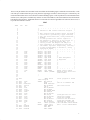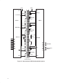
1
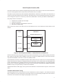
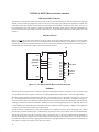
Microcontroller Based Data Acquisition Using the TLC2543 12-Bit Serial-Out ADC SLAA012 July 1995 Printed on Recycled Paper 0 IMPORTANT NOTICE Texas Instruments (TI) reserves the right to make changes to its products or to discontinue any semiconductor product or service without notice, and advises its customers to obtain the latest version of relevant information to verify, before placing orders, that the information being relied on is current. TI warrants performance of its semiconductor products and related software to the specifications applicable at the time of sale in accordance with TI’s standard warranty. Testing and other quality control techniques are utilized to the extent TI deems necessary to support this warranty. Specific testing of all parameters of each device is not necessarily performed, except those mandated by government requirements. Certain applications using semiconductor products may involve potential risks of death, personal injury, or severe property or environmental damage (“Critical Applications”). TI SEMICONDUCTOR PRODUCTS ARE NOT DESIGNED, INTENDED, AUTHORIZED, OR WARRANTED TO BE SUITABLE FOR USE IN LIFE-SUPPORT APPLICATIONS, DEVICES OR SYSTEMS OR OTHER CRITICAL APPLICATIONS. Inclusion of TI products in such applications is understood to be fully at the risk of the customer. Use of TI products in such applications requires the written approval of an appropriate TI officer. Questions concerning potential risk applications should be directed to TI through a local SC sales office. In order to minimize risks associated with the customer’s applications, adequate design and operating safeguards should be provided by the customer to minimize inherent or procedural hazards. TI assumes no liability for applications assistance, customer product design, software performance, or infringement of patents or services described herein. Nor does TI warrant or represent that any license, either express or implied, is granted under any patent right, copyright, mask work right, or other intellectual property right of TI covering or relating to any combination, machine, or process in which such semiconductor products or services might be or are used. Copyright 1995, Texas Instruments Incorporated Contents Title Page Introduction . . . . . . . . . . . . . . . . . . . . . . . . . . . . . . . . . . . . . . . . . . . . . . . . . . . . . . . . . . . . . . . . . . . . . . . . . . . . . . . Scope of this Application Report . . . . . . . . . . . . . . . . . . . . . . . . . . . . . . . . . . . . . . . . . . . . . . . . . . . . . . . . . . The TLC2543 . . . . . . . . . . . . . . . . . . . . . . . . . . . . . . . . . . . . . . . . . . . . . . . . . . . . . . . . . . . . . . . . . . . . . . . . . . Interface Timing . . . . . . . . . . . . . . . . . . . . . . . . . . . . . . . . . . . . . . . . . . . . . . . . . . . . . . . . . . . . . . . . . . . Minimum Number of Data Transfers per Channel . . . . . . . . . . . . . . . . . . . . . . . . . . . . . . . . . . . . . . Serial Peripheral Interface (SPI) . . . . . . . . . . . . . . . . . . . . . . . . . . . . . . . . . . . . . . . . . . . . . . . . . . . . . . . . . . TLC2543 to SPI Interface Timing . . . . . . . . . . . . . . . . . . . . . . . . . . . . . . . . . . . . . . . . . . . . . . . . . . . . Software Flowcharts . . . . . . . . . . . . . . . . . . . . . . . . . . . . . . . . . . . . . . . . . . . . . . . . . . . . . . . . . . . . . . . 1 1 1 1 2 3 3 4 TLC2543 TO TMS370 Microcontroller Interface . . . . . . . . . . . . . . . . . . . . . . . . . . . . . . . . . . . . . . . . . . . . . . . Microcontroller Features . . . . . . . . . . . . . . . . . . . . . . . . . . . . . . . . . . . . . . . . . . . . . . . . . . . . . . . . . . . . . . . . . Interface Circuit . . . . . . . . . . . . . . . . . . . . . . . . . . . . . . . . . . . . . . . . . . . . . . . . . . . . . . . . . . . . . . . . . . . . . . . . Software . . . . . . . . . . . . . . . . . . . . . . . . . . . . . . . . . . . . . . . . . . . . . . . . . . . . . . . . . . . . . . . . . . . . . . . . . . . . . . 6 6 6 6 List 1 . . . . . . . . . . . . . . . . . . . . . . . . . . . . . . . . . . . . . . . . . . . . . . . . . . . . . . . . . . . . . . . . . . . . . . . . . . . . . . . . . . . . . . 7 Opto-Isolated 12-Bit Data Acquisition System . . . . . . . . . . . . . . . . . . . . . . . . . . . . . . . . . . . . . . . . . . . . . . 9 TLC2543 to H8/325 Microcontroller Interface . . . . . . . . . . . . . . . . . . . . . . . . . . . . . . . . . . . . . . . . . . . . . . . . Microcontroller Features . . . . . . . . . . . . . . . . . . . . . . . . . . . . . . . . . . . . . . . . . . . . . . . . . . . . . . . . . . . . . . . . Interface Circuit . . . . . . . . . . . . . . . . . . . . . . . . . . . . . . . . . . . . . . . . . . . . . . . . . . . . . . . . . . . . . . . . . . . . . . . Software . . . . . . . . . . . . . . . . . . . . . . . . . . . . . . . . . . . . . . . . . . . . . . . . . . . . . . . . . . . . . . . . . . . . . . . . . . . . . 11 11 11 11 List 2 . . . . . . . . . . . . . . . . . . . . . . . . . . . . . . . . . . . . . . . . . . . . . . . . . . . . . . . . . . . . . . . . . . . . . . . . . . . . . . . . . . . . . 12 TLC2543 to MC68HC11 Microcontroller Interface . . . . . . . . . . . . . . . . . . . . . . . . . . . . . . . . . . . . . . . . . . . . Microcontroller Features . . . . . . . . . . . . . . . . . . . . . . . . . . . . . . . . . . . . . . . . . . . . . . . . . . . . . . . . . . . . . . . . Interface Circuit . . . . . . . . . . . . . . . . . . . . . . . . . . . . . . . . . . . . . . . . . . . . . . . . . . . . . . . . . . . . . . . . . . . . . . . Software . . . . . . . . . . . . . . . . . . . . . . . . . . . . . . . . . . . . . . . . . . . . . . . . . . . . . . . . . . . . . . . . . . . . . . . . . . . . . 15 15 15 15 List 3 . . . . . . . . . . . . . . . . . . . . . . . . . . . . . . . . . . . . . . . . . . . . . . . . . . . . . . . . . . . . . . . . . . . . . . . . . . . . . . . . . . . . . 16 TLC2543 to 80C51 Microcontroller Interface . . . . . . . . . . . . . . . . . . . . . . . . . . . . . . . . . . . . . . . . . . . . . . . . . Microcontroller Features . . . . . . . . . . . . . . . . . . . . . . . . . . . . . . . . . . . . . . . . . . . . . . . . . . . . . . . . . . . . . . . . Interface Circuit . . . . . . . . . . . . . . . . . . . . . . . . . . . . . . . . . . . . . . . . . . . . . . . . . . . . . . . . . . . . . . . . . . . . . . . Software . . . . . . . . . . . . . . . . . . . . . . . . . . . . . . . . . . . . . . . . . . . . . . . . . . . . . . . . . . . . . . . . . . . . . . . . . . . . . 18 18 18 18 List 4 . . . . . . . . . . . . . . . . . . . . . . . . . . . . . . . . . . . . . . . . . . . . . . . . . . . . . . . . . . . . . . . . . . . . . . . . . . . . . . . . . . . . . 19 Analog Considerations . . . . . . . . . . . . . . . . . . . . . . . . . . . . . . . . . . . . . . . . . . . . . . . . . . . . . . . . . . . . . . . . . . . . Power Supply Decoupling . . . . . . . . . . . . . . . . . . . . . . . . . . . . . . . . . . . . . . . . . . . . . . . . . . . . . . . . . . . . . . Grounding . . . . . . . . . . . . . . . . . . . . . . . . . . . . . . . . . . . . . . . . . . . . . . . . . . . . . . . . . . . . . . . . . . . . . . . . . . . . Board Layout . . . . . . . . . . . . . . . . . . . . . . . . . . . . . . . . . . . . . . . . . . . . . . . . . . . . . . . . . . . . . . . . . . . . . . . . . 21 21 21 21 Appendix A . . . . . . . . . . . . . . . . . . . . . . . . . . . . . . . . . . . . . . . . . . . . . . . . . . . . . . . . . . . . . . . . . . . . . . . . . . . . . . . 22 iii List of Illustrations Figure Title Page 1. TLC2543 Block Diagram . . . . . . . . . . . . . . . . . . . . . . . . . . . . . . . . . . . . . . . . . . . . . . . . . . . . . . . . . . . . . 1 2. Timing for 16-Clock Transfer Using CS With MSB First . . . . . . . . . . . . . . . . . . . . . . . . . . . . . . . . . . 2 3. Timing for 16-Clock Transfer Not Using CS With MSB First . . . . . . . . . . . . . . . . . . . . . . . . . . . . . . . 2 4. Serial Peripheral Interface – Internal Structure and Data Flow . . . . . . . . . . . . . . . . . . . . . . . . . . . . 3 5. TLC2543 to SPI Interface Timing . . . . . . . . . . . . . . . . . . . . . . . . . . . . . . . . . . . . . . . . . . . . . . . . . . . . . . 4 6. Flowchart for Main Program of TLC2543 to TMS37010 . . . . . . . . . . . . . . . . . . . . . . . . . . . . . . . . . . 4 7. Flowcharts of Subroutine DATAIN and STORE for TLC2543 to TMS370C010 Interface Software . . . . . . . . . . . . . . . . . . . . . . . . . . . . . . . . . . . . . . . . . . . . . . . . . . . . . . . . . . . . . . . . . . . 5 8. Flowcharts of Subroutine ADC for TLC2543 to TMS370C010 Interface Software . . . . . . . . . . . . 5 9. TLC2543 to TMS370C010 Interface Circuit . . . . . . . . . . . . . . . . . . . . . . . . . . . . . . . . . . . . . . . . . . . . . 6 10. Opto-Isolated 12-Bit Data Acquisition System . . . . . . . . . . . . . . . . . . . . . . . . . . . . . . . . . . . . . . . . . . 10 11. TLC2543 to H8/300 Microcontroller Interface Circuit . . . . . . . . . . . . . . . . . . . . . . . . . . . . . . . . . . . . . 11 12. TLC2543 to MC68HC811E2 Microcontroller Interface . . . . . . . . . . . . . . . . . . . . . . . . . . . . . . . . . . . . 15 13. TLC2543 to 80C51 Microcontroller Interface . . . . . . . . . . . . . . . . . . . . . . . . . . . . . . . . . . . . . . . . . . . . 18 14. TLC2543 to Microcontroller Interface: Grounding and Decoupling Scheme . . . . . . . . . . . . . . . . . 21 iv Introduction Scope of this Application Report This application report describes how to construct 12-bit data acquisition systems using the TLC2543 serial-out analog-to-digital converter (ADC) in conjunction with a range of four popular microcontrollers. The four microcontrollers used are the TMS370, H8/300, 68HC11 and 80C51. The TLC2543 The TLC2543 is a 12-bit ADC which uses the switched capacitor successive approximation technique to perform the conversion process and provides a maximum sampling rate of 66k samples per second (KSPS) while using only 1 mA (typical) of supply current. The block diagram of the TLC2543 is shown in Figure 1. Any one of eleven analog input channels can be selected by programming the four most significant bits (MSBs) of the eight bit channel/mode control byte applied serially to the DATA INPUT terminal of the device. In addition three internal test voltages [ Vref–, Vref+ and (Vref+ – Vref – )/2] can be applied to the converter for calibration or other purposes by applying the appropriate code to the same four MSBs. The four least significant bits (LSBs) of the channel/mode control byte are used to select the output data length (8, 12 or 16 bits), the output data order (MSB first or LSB first) and whether unipolar (binary) or bipolar (2’s complement around (Vref+ – Vref – )/2) format is required. Analog Inputs Input Address Register AIN0 AIN1 AIN2 AIN3 AIN4 AIN5 AIN6 AIN7 AIN8 AIN9 AIN10 14-Channel Analog Input MUX Data Input Control Logic Sample and Hold 12-Bit ADC Output Data Register I/O Clock Parallel To Serial Converter Serial Data Out EOC 3 Self-Test Reference • • • 12-Bit Resolution ADC 66-KSPS Sampling Rate 11 Analog Input Channels • • • Low Supply Current – 1 mA (Typ) Power-Down Mode – 4 µA (Typ) SPI Compatible Serial Interface Figure 1. TLC2543 Block Diagram Interface Timing Four transfer methods are available for obtaining the full 12 bits of resolution from the TLC2543. Either 12 or 16 clock cycles can be used for each conversion and data transfer. A chip select (CS) pulse can be inserted at the start of each conversion or only once at the beginning of each sequence of conversions with CS remaining low until the sequence is completed. 1 Figure 2 shows the timing for the method which uses 16 clock cycles for each conversion and data transfer cycle and which inserts CS between each of these transfer cycles. Figure 3 shows the timing for the method which uses 16 clock cycles for each conversion and data transfer cycle but inserts CS only once at the start of each sequence of conversions. This application report describes various microcontroller interfaces, each of which uses 16 clock cycles for each conversion data transfer. CS is applied at the start of each conversion and data transfer. This method allows for the general case where one or more conversions may be required. It also simplifies the required software. CS tsu > 1.425 µs I/O CLOCK 1 DATA OUT 2 A15 A14 3 A13 4 A12 5 A11 6 A10 7 A9 8 A8 15 A1 16 1 A0 B15 Previous Conversion Data DATA INPUT ÏÏÏÏÏÏÏÏÏÏÏÏÏÏÏ ÏÏÏÏÏÏÏÏÏÏÏÏÏÏÏ B7 B6 B5 MSB B4 B3 B2 B1 ÏÏ ÏÏ C7 B0 LSB EOC tconv < 10 µs 16-Clock Transfer Using CS (MSB First) Figure 2. Timing for 16-Clock Transfer Using CS With MSB First CS tsu > 1.425 µs I/O CLOCK DATA OUT 1 A15 2 A14 3 A13 4 A12 5 A11 6 A10 7 A9 8 A8 ÏÏÏÏÏÏÏÏÏÏÏÏÏÏÏÏ ÏÏÏÏÏÏÏÏÏÏÏÏÏÏÏÏ Previous Conversion Data DATA INPUT B7 MSB B6 B5 B4 B3 B2 B1 15 A1 16 1 A0 B15 td (EOC-DATA) < 10 µs B0 LSB ÏÏ ÏÏ C7 EOC 16-Clock Transfer Not Using CS (MSB First) tconv < 10 µs Figure 3. Timing for 16-Clock Transfer Not Using CS With MSB First Minimum Number of Data Transfers per Channel It should be noted that in any single data transfer cycle between the TLC2543 and the chosen microcontroller the data output from the ADC is the result of the previous conversion. The software listings included in this application report have been written for the general case where the conversion results may be required for any individual channel or sequence of channels. In this case the program included for each microcontroller interface must be run at least twice per channel so that valid data corresponding to the required analogue input channel and ADC mode is delivered. Software can be written to implement the consecutive channel scanning mode of operation of the TLC2543. In this case the result from the first analog-to-digital conversion should be ignored or overwritten. 2 Serial Peripheral Interface (SPI) The fastest and most efficient method of implementing a data transfer between the TLC2543 and a microcontroller is to use the serial peripheral interface (SPI) of the microcontroller, if this is available. The TMS370 (Texas Instruments), H8/300 (Hitachi) and MC68HC11 (Motorola) all offer SPIs (or the equivalent ) in a subset of each of these families of microcontrollers. The H8/300 offers a serial communications interface (SCI) which can be configured to operate in a similar way to that of the standard SPI’s offered by the TMS370 and MC68HC11. The principle features of the SPI are: • • • • Simultaneous serial data input and output Synchronous operation Provision of frequency programmable serial clock Data transfer complete flag Figure 4 shows the structure of the SPI. In this case the TMS370C010 is used to illustrate the main elements of the interface. TLC2543 TMS370C010 SPI Master (Master/Slave = 1) DATA OUT SOMI Serial Input Buffer (SPIBUF) DATA INPUT SOMO Shift Register (SPIDAT) MSB I/O CLOCK LSB SPICLK Figure 4. Serial Peripheral Interface – Internal Structure and Data Flow The microcontroller can be configured by software to perform as the SPI master or slave. When operating as the master, data is input to the SPI shift register (SPIDAT) via the slave out master in (SOMI) terminal. At the same time data is output from the SPIDAT via the slave in master out (SIMO) terminal. The SPI functions as follows. The SPIDAT should be loaded with the first byte of data to be sent. This automatically initiates the transmission of this byte. During this transmission time data is received at the other end of the SPIDAT shift register. The SPI INT FLAG is regularly checked. As soon as the last bit of the input data byte is received the SPI INT FLAG is set to 1. This then signals that the received byte can be read from the serial input buffer (SPIBUF) and that the SPIDAT is ready to accept the next byte of data to be transmitted. Additional SPI features which apply to the specific microcontrollers are described in their respective sections which follow. TLC2543 to SPI Interface Timing The timing digram for the 16 clock transfer TLC2543 to SPI interface is shown in Figure 5. The channel select/mode data is read into the TLC2543 on the positive going edges of the I/O clock and analog-to-digital conversion results are read into the microcontroller on the negative going edges of the I/O clock. 3 CS I/O CLOCK DATA IN DATA OUT B7 A15 B6 B5 B4 B3 B2 A14 A13 A12 A11 A10 B1 A9 B0 A8 B7 A7 B6 A6 B5 A5 B4 B3 B2 B1 B0 A4 A3 A2 A1 A0 ( = 0) ( = 0) ( = 0) ( = 0) tconv EOC Figure 5. TLC2543 to SPI Interface Timing Software Flowcharts Figures 6, 7, and 8 show the flow charts for the main program and subroutines used in the TLC2543 to TMS370C010 interface software shown in this application report. The same program structure also applies to the other three interfaces included in this report. 1 START 2 CALL SUBROUTINE DATAIN Reads channel/mode data for TLC2543 into microcontroller via parallel I/O port. (reformats channel/mode data if serial data is sent LSB first). Puts channel/mode data into accessible register. Derives destination address for STORE from channel data. 3 CALL SUBROUTINE ADC Provides CS high to low transition prior to conversion. Provides serial I/O CLOCK to TLC2543. Sends channel/mode data to TLC2543. Receives MSbyte then LSbyte of previous A/D conversion. 4 CALL SUBROUTINE STORE Stores MSbyte in even address of selected RAM space. Stores LSbyte in odd address of selected RAM space (all addresses mapped to corresponding channel number). 5 JUMP TO START Jump to start for next conversion Figure 6. Flowchart for Main Program of TLC2543 to TMS370C010 4 Read Channel/Mode Data Into Chosen Register Store MSBYTE In Even Address Of RAM (Channel # Dependant) Map Channel Numbers To Registers Or RAM Store LSBYTE In Odd Address Of RAM (Channel # Dependant) Put Destination Address Into Chosen Register STORE Return DATAIN Figure 7. Flowcharts of Subroutine DATAIN and STORE for TLC2543 to TMS370C010 Interface Software Send CS Of TLC2543 High IS MSB/LSB First Bit = 0 Delay > 1 µs Send CS Of TLC2543 Low IS MSB/LSB First Bit = 0 NO YES Send Channel/Mode Data To TLC2543 NO Receive LS Byte Of Previous Conversion Result and Store In LS BYTE Send Channel/Mode Data To TLC2543 NO Receive MS Byte Of Previous Conversion Result and Store In MS BYTE IS MSB/LSB First Bit = 0 YES Return Figure 8. Flowcharts of Subroutine ADC for TLC2543 to TMS370C010 Interface Software 5 TLC2543 TO TMS370 Microcontroller Interface Microcontroller Features Within the family of TMS370 microcontrollers there are several versions which contain a serial peripheral interface (SPI) facility. One of these versions should be chosen to implement the interface method described below. One such version is the TMS370C010 which is used to illustrate the method. Interface Circuit Figure 9 shows the circuit interconnections for the TLC2543 to TMS370C010 microcontroller interface. Note that no extra logic is required to implement this interface. 5V Analog Inputs VCC I/O CLOCK DATA INPUT DATA OUT CS AIN0 AIN1 AIN2 AIN3 TLC2543 AIN4 AIN5 AIN6 AIN7 AIN8 AIN9 AIN10 GN D 5V VCC SPICLK SPISIMO SPISOMI D7 TMS370 5V 8 × SPST Switch A0 A1 A2 A3 A4 A5 A6 A7 8 × 10 kΩ VSS Figure 9. TLC2543 to TMS370C010 Interface Circuit Depending upon the layout of the particular printed circuit board used it may be necessary to insert a small value capacitor of between 50 and 100 pF between the I/O CLOCK input of the TLC2543 and ground. This has the effect of ensuring that data applied to the DATA INPUT terminal of the TLC2543 is valid before the positive going transition of the I/O CLOCK. The positive reference, REF+, to the TLC2543 is provided directly from the VCC+ supply. The four digital interface terminals, I/O CLOCK, DATA INPUT, DATA OUT, and CS, of the TLC2543 connect directly to the SPICLK, SPISIMO, SPISOMI and D7 terminals respectively of the TMS370C010. The operation mode and channel number of the TLC2543 is determined by the serial data which is sent to its DATA INPUT terminal. Software List 1 contains the software listing for the program which controls the interface illustrated in Figure 5. The software consists of the main program and three subroutines called DATA IN, ADC and STORE. DATAIN reads in the channel select and mode control data into a holding register and maps the channel select number to a corresponding pair of registers between R64 and R91. The mapping vector is held in register R10. ADC provides the chip select pulse, controls the SPI operation, and puts the MSByte and LSByte of each conversion result into registers R20 and R21 respectively. STORE puts the MSByte into the even number register and the LSByte into the odd number register mapped by the contents of register R10. 6 The user can put channel select and ADC mode control data into the holding register within the microcontroller, via the 8-bit wide port A bidirectional I/O port, using a bank of eight toggle switches as shown in Figure 9. Alternatively, the mode and channel data can be sent to the microcontroller holding register via the asynchronous serial communications interface (SCI). This option is available only on those versions of the TMS370, such as the TMS370C020, which include both SPI and SCI interfaces. Additional software to control the SCI must be appended to the software shown in List 1 to provide this method of control. List 1 LINE 1 2 3 4 5 6 7 8 9 10 11 12 13 14 15 16 17 18 19 20 21 22 23 24 25 26 27 28 29 30 31 32 33 34 35 36 37 38 39 40 41 42 43 44 45 46 47 48 49 50 51 52 53 54 55 56 57 58 59 60 LOC OBJ 0030 0031 0037 0039 003d 003e 003f 0021 0022 0023 002c 002d 002e 002f 7ffe 2e 4000 4000 5260 4002 fd 4003 * 88400000 4007 8b7ffe 400a b5 400b 2121 400d 2123 400f f7802f 4012 2280 4014 2130 4016 2207 4018 2130 401a 2203 401c 213d 401e 2222 4020 213e 31 0b 4022 ’8e402d 4025 ’8e403e 4028 ’8e409d SOURCE ;* * * * * * * * * * * * * * * * ;* * ;* TLC2543 to TMS 370Cx10 Interface Program * ;* * ;* This program reads channel select and mode * ;* control data (provided by toggle switches) * ;* into the microcontroller, using subroutine * ;* DATAIN. * ;* It then provides the control signals to * ;* the TLC2543 to perform a 12 bit analog to * ;* conversion, using subroutine ADC. It * ;* finally stores the MSByte and LSByte of * ;* each conversion in consecutive even and * ;* odd number registers respectively starting * ;* at R64 corresponding to channel 0, using * ;* subroutine STORE. * ;* * * * * * * * * * * * * * * * SPICCR .EQU P030 ;* * * * * * * * SPICTL .EQU P031 ;* * SPIBUF .EQU P037 ;* * SPIDAT .EQU P039 ;* * SPIPC1 .EQU P03D ;* * SPIPC2 .EQU P03E ;* Name Peripheral * SPIPRI .EQU P03F ;* Registers * APORT2 .EQU P021 ;* * ADATA .EQU P022 ;* * ADIR .EQU P023 ;* * DPORT1 .EQU P02C ;* * DPORT2 .EQU P02D ;* * DDATA .EQU P02E ;* * DDIR .EQU P02F ;* * * * * * * * RESET .EQU 7FFEH ;Reset vector named CSBIT .DBIT 7,DDATA ;TLC2543 Chip Select bit ;named CSBIT ; ; .TEXT 4000H ;Main Program START MOV #60H,B LDSP MOVW #4000H,A MOV A,RESET CLR A MOV A,APORT2 MOV A,ADIR MOV #080H,DDIR MOV #80H,A MOV A,SPICCR MOV #07,A MOV A,SPICCR MOV #03,A MOV A,SPIPC1 MOV #22H,A MOV A,SPIPC2 SPIF .DBIT 6,SPICTL MSLSB .DBIT 1,R11 CALL DATAIN CALL ADC CALL STORE ;Start program at 4000H ; ;Set SP to address 60H ;Set reset vector ;Configure SPI for 8–bit ;character length. ;Configure SPICLK ;function and direction. ;Configure SPISOMI and ;SPISIMO pin functions. ;SPI INT FLAG named SPINTF ;Bit 1 of R11 named MSLSB 7 List 1 (Continued) LINE 61 62 63 64 65 66 67 68 69 70 71 72 73 74 75 76 77 78 79 80 81 82 83 84 85 86 87 88 89 90 91 92 93 94 95 96 97 98 99 100 101 102 103 104 105 106 107 108 109 110 111 112 113 114 115 116 117 118 119 120 121 122 123 124 125 126 127 128 8 LOC 402b OBJ ’00d3 402d 402f 9122 d10b 4031 4033 4034 4035 4036 4037 4039 403b 53f0 cc cc cc cc 5c02 5840 d10a 403d f9 403e 4040 4043 4044 4046 4047 4049 404b 404d 4051 4053 2203 a4802e b2 ’06fd c5 512e 2207 2131 ’76020b19 120b 2139 4055 4059 ’a74031fc a21437 405c 71390b 405f 4063 ’a74031fc a21537 4066 ’77020b32 406a 406c 406e 4072 120b 2139 ’a74031fc a21537 4075 4077 4079 407d 120b 2139 ’a74031fc a21437 4080 4082 4084 4086 4088 4089 408b 408e 4090 4092 4094 4096 4097 4099 2208 d516 dd14 df16 b2 ’06f9 421614 2208 d517 dd15 df17 b2 ’06f9 421715 SOURCE JMP START ; ;Subroutine :– DATAIN ; DATAIN MOV ADATA,B MOV B,R11 AND #0F0H,B RR B RR B RR B RR B MPY #002,B ADD #40H,B MOV B,R10 ;Read ADC mode/channel ;Put ADC mode/channel ;in R11 ;Retain channel number ;* * * * * * * * * ;* Map channel numbers * ;* to registers R64–R91 * ;* R10 contains storage * ;* address * ;* Even numbers – MS Byte* ;* Odd numbers – LS Byte * ;* * * * * * * * * RTS ; ;Subroutine :– ADC ; ADC MOV #003H,A SBIT1 CSBIT ;Set ADC Chip Select high. LOOP1 DEC A ;Chip Select stays high JNE LOOP1 ;while A is not 0. CLR B MOV B,DDATA ;CS goes low MOV #7,A MOV A,SPICTL ;Enable SPI transmission JBIT1 MSLSB,LS1ST MOV R11,A MOV A,SPIDAT ; MOV R11,SPIDAT ;Send mode/channel data ;to TLC2543 FLAG1 JBIT0 SPIF,FLAG1;If SPIF=0, repeat check. MOV SPIBUF,R20 ;Put received MS Byte ;in R20 MOV R11,SPIDAT ;Send mode/channel data ;to TLC2543 FLAG2 JBIT0 SPIF,FLAG2;If SPIF=0, repeat check. MOV SPIBUF,R21 ;Put received LS Byte ; in R21 JBIT0 MSLSB,RETURN ;If MSLSB=0, go ;to RETURN LS1ST MOV R11,A MOV A,SPIDAT FLAG3 JBIT0 SPIF,FLAG3;If SPIF=0, repeat check. MOV SPIBUF,R21 ;Put received LS Byte ;in R21 MOV R11,A MOV A,SPIDAT FLAG4 JBIT0 SPIF,FLAG4;If SPIF=0, repeat check. MOV SPIBUF,R20 ;Put received MS Byte ;in R20 MOV #08,A ;* * * * * * * * CLR R22 ;* * LOOP2 RRC R20 ;* Reformat MS Byte * RLC R22 ;* * DEC A ;* Put result in R20 * JNZ LOOP2 ;* * MOV R22, R20 ;* * * * * * * * MOV #08,A ;* * * * * * * * CLR R23 ;* * LOOP3 RRC R21 ;* Reformats LS Byte * RLC R23 ;* * DEC A ;* Put result in R21 * JNZ LOOP3 ;* * MOV R23,R21 ;* * * * * * * * List 1 (Continued) LINE 129 130 131 132 133 134 135 136 137 138 139 LOC OBJ 409c f9 409d 409f 40a1 40a3 40a5 40a7 1214 9b0a d30a 1215 9b0a f9 SOURCE RETURN RTS ; ;Subroutine :– STORE ; STORE MOV R20,A MOV A,@R10 INC R10 MOV R21,A MOV A,@R10 RTS .END ;Put MS Byte into even ;address contained in R10 ;(R10)+1 ;Put LS Byte into odd ;address contained in R10 Opto-Isolated 12-Bit Data Acquisition System The serial nature of the data flow between the TLC2543 analog-to-digital converter and the accompanying microcontroller makes this ADC an ideal choice for isolated 12-bit data acquisition. Figure 10 shows an opto-isolated system which uses four optocouplers to provide a 3-kV isolation barrier. Note that the optocoupler which routes conversion result data from the TLC2543 to the microcontroller is a single device and does not share the same piece of silicon with any of the other optocouplers used. This ensures that the full 3 kV of isolation is maintained between the ADC and microcontroller. The choice of VP0610 P-channel enhancement MOSFETs avoids the use of an extra inverter stage for each optocoupler driver. In addition, the relatively low input capacitance of the VP0610 (typically 15 pF) allows data rates up to 100 kHz to be achieved without the need for external buffers to be added at the outputs of the TLC2543 and TMS370. 9 VCC1 VCC2 VCC VCC VP0610 470 R SPICLK I/O CLOCK 1/2 GCPL2631 470 R TLC2543 TMS370 VP0610 470 R DATA INPUT 1/2 GCPL2631 470 R VP0610 470 R DATA OUT AIN0 AIN1 AIN2 AIN3 AIN4 AIN5 AIN6 AIN7 AIN8 AIN9 AIN10 SPISOMI D7 470 R VP0610 CS A0 A1 A2 A3 ADC Mode A4 A5 A6 A7 ADC Channel Number HCPL2601 470 R VSS VSS 3 kV Isolation Barrier Figure 10. Opto-Isolated 12-Bit Data Acquisition System 10 TLC2543 to H8/325 Microcontroller Interface Microcontroller Features The individual members of the H8 family of microcontrollers can be differentiated by various criteria, for example the inclusion or otherwise of an on-board 8-bit resolution analog-to-digital converter (ADC). Those members which include an ADC generally cost between 10 and 20 percent more than their counterparts which do not. System requirements such as ADC resolution, remote location of ADC, flexibility, and total cost all influence the final choice of microcontroller architecture. The H8/325, used for this application report, does not include an on-board ADC but provides 1K of RAM, 32K of ROM, and two serial I/O ports. It is therefore well suited to interfacing with the TLC2543 serial output ADC. Interface Circuit Figure 11 illustrates a typical 12-bit data acquisition system which uses the H8/325 microcontroller to coordinate the operation of the TLC2543 ADC via one of its serial (SCI) ports. The circuit uses the H8’s 8-bit parallel I/O port 4 to route ADC channel and mode information into the microcontroller. This information could be provided by a host system data bus or, as in Figure 6, by a bank of eight manually operated toggle switches situated on the same printed circuit board as the microcontroller. 5V TLC2543 VCC Analog Inputs H8/325 I/O CLOCK AIN0 AIN1 DATA INPUT AIN2 DATA OUT AIN3 CS AIN4 AIN5 AIN6 AIN7 AIN8 AIN9 AIN10 SCK0/P5.2 VCC MD0 MD1 TxD0/P5.0 RxD0/P5.1 P6.0 XTAL 20 MHz (max) EXTAL P4.0 P4.1 P4.2 P4.3 P4.4 P4.5 P4.6 P4.7 VSS GND ADC Mode Channel Number NOTE: Single Chip Mode (MD0 = MD1 = 1) Figure 11. TLC2543 to H8/300 Microcontroller Interface Circuit Software List 2 shows the program which was written to coordinate the interface. It uses three subroutines to implement the overall interface to the TLC2543. The first of these is called DATAIN which reads ADC channel and mode information into the microcontroller. It also maps converter channel numbers to corresponding addresses in RAM where conversion results can be stored. In this case the addresses from 0040H to 0067H were chosen to store the results. The most significant byte of each result is placed in an even address and the least significant byte of each result is placed in the corresponding adjacent odd address. The conversion result of each channel is stored in left justified format and therefore occupies the upper 12 bits of the 16-bit words which occupy even addresses from 0040H up to 0066H. The second subroutine to be used is ADC. This begins by producing a chip-select high pulse. The trailing negative edge of this pulse is rapidly followed by the transmission of channel and mode information to the converter. 11 List 2 LINE 1 2 3 4 5 6 7 8 9 10 11 12 13 14 15 16 17 18 19 20 21 22 23 24 25 26 27 28 29 30 31 32 33 34 35 36 37 38 39 40 41 42 43 44 45 46 47 48 49 50 51 52 53 54 55 56 57 58 59 60 61 62 63 64 65 66 67 12 LOC OBJ SOURCE ;* * * * * * * * * * * * * * * * * * * * * ;* * ;* TLC2543 to H8 Microcontroller Interface Program. * ;* * ;* This program contains subroutines DATAIN, ADC, * ;* FORMAT and STORE. * ;* DATAIN reads channel number and mode data into the * ;* microcontroller via Port4. ”ADC” controls A to D * ;* conversion. ”FORMAT” changes conversion results from * ;* LSB first format to MSB first format. ”Store” places * ;* results in memory addresses 40 to 5B (MS Bytes in even * ;* addresses, LS Bytes in odd addresses) according to * ;* channel number. * ;* * * * * * * * * * * * * * * * * * * * * ; ; * Define special function register names * ; RDR EQU H’FFDD ;Receive Data Register – RDR TDR EQU H’FFDB ;Transmit Data Register – TDR SMR EQU H’FFD8 ;Serial Mode Register – SMR SCR EQU H’FFDA ;Serial Control Register – SCR SSR EQU H’FFDC ;Serial Status Register – SSR BRR EQU H’FFD9 ;Bit Rate Register – BRR P5DDR EQU H’FFB8 ;Port5 Data Direction Register P5DR EQU H’FFBA ;Port5 Data Register – P5DR P4DDR EQU H’FFB5 ;Port4 Data Direction Register P4DR EQU H’FFB7 ;Port4 Data register – P4DR P6DDR EQU H’FFB9 ;Port6 Data Direction register P6DR EQU H’FFBB ;Port6 Data Register FFDD FFDB FFD8 FFDA FFDC FFD9 FFB8 FFBA FFB5 FFB7 FFB9 FFBB 1000 1000 79001000 1004 1008 100A 100C 100E 1010 1012 1014 1016 101A 101E 1022 1026 102A 7907FD00 F984 39D8 F931 39DA F901 39D9 F901 6A89FFB9 5E001082 5E00102C 5E0010B4 5E0010AC 40DC 102C 102E 1032 1034 1036 103A 103E 1040 1042 1046 1048 104A 104E FA05 7FBB7000 1A0A 46FC 7FBB7200 6A0CFFB7 731C 461E 7EDC7370 47FA 34DB 7FDC7270 7EDC7360 ORG H’1000 ;Sets start of program ; ; * Main Program * ; MOV.W #H’1000, R0 ; MOV.W R0, @H’0000 ;Sets reset vector to START MOV.W #H’FD00, SP ;Sets contents of Stack Pointer START MOV.B #H’84, R1L ;* * * * * * * * * * * * * * * MOV.B R1L, @SMR:8 ;* Sets up serial port * MOV.B #H’31,R1L ;* registers for simultaneous* MOV.B R1L, @SCR:8 ;* transmit and receive * MOV.B #H’01,R1L ;* * MOV.B R1L, @BRR:8 ;* * * * * * * * * * * * * * * MOV.B #H’01, R1L ;Sets R1(Low Byte) to 01H MOV.B R1L, @P6DDR ;Set Bit0 of Port6 as Output JSR @DATAIN:16 ;Read in ADC channel/mode data JSR @ADC:16 ;Do A/D conversion JSR @FORMAT:16 ;Reformat A/D conversion result JSR @STORE:16 ;Store A/D conversion result BRA START ;Repeat above routine. ; ; * Subroutine ADC which controls the conversion process * ; ADC MOV.B #H’05, R2L ;Put 05 in R2L BSET #0, @P6DR:8 ;TLC2543 chip select goes high CSHIGH DEC R2L ;(R2L) – 1 BNE CSHIGH ;If not zero, CS stays high BCLR #0, @P6DR:8 ;TLC2543 chip select goes low MOV.B @P4DR, R4L ;Puts channel/mode data in R4L BTST #1, R4L ;Is LSBF of channel/mode data BNE LSBYTE ;If not, do LSBYTE first MSBYTE BTST #7, @SSR:8 ;Is TDR empty ? BEQ MSBYTE ;If not empty, repeat check. MOV.B R4H, @TDR:8 ;Put channel/mode data in TDR BCLR #7, @SSR:8 ;Reset TDRE bit of SSR to 0 TESTB61 BTST #6, @SSR:8 ;Is receive shift reg. empty ? List 2 (Continued) LINE 68 69 70 71 72 73 74 75 76 77 78 79 80 81 82 83 84 85 86 87 88 89 90 91 92 93 94 95 96 97 98 99 100 101 102 103 104 105 106 107 108 109 110 111 112 113 114 115 116 117 118 119 120 121 122 123 124 125 126 127 128 129 130 131 132 133 134 135 LOC OBJ SOURCE 1052 47FA 1054 23DD BEQ TESTB61 MOV.B @RDR:8, R3H 1056 7FDC7260 105A 68D3 BCLR #6, @SSR:8 MOV.B R3H, @R5 105C 105E 1060 1064 1066 1068 106C 1070 1072 1074 731C 4620 7EDC7370 47FA 34DB 7FDC7270 7EDC7360 47FA 0A0D 2BDD BTST #1, R4L BNE RETURN LSBYTE BTST #7, @SSR:8 BEQ LSBYTE MOV.B R4H, @TDR:8 BCLR #7, @SSR:8 TESTB62 BTST #6, @SSR:8 BEQ TESTB62 INC R5L MOV.B @RDR:8, R3L 1076 7FDC7260 107A 68DB BCLR #6, @SSR:8 MOV.B R3L, @R5 107C 731C 107E 46C2 1080 5470 BTST #1, R4L BNE MSBYTE RTS 1082 1086 108A 108E 1090 1092 1094 1096 1098 109C 109E 79040000 79050000 6A0CFFB7 0CCD 110D 110D 110D 110D 79060002 50E5 8D40 10A0 10A2 10A4 10A6 10A8 10AA F008 110C 1204 1A00 46F8 5470 10AC 68D3 10AE 0A0D 10B0 68DB 10B2 5470 10B4 10B6 10B8 10BA 10BC 10BE 10C0 10C2 F008 1103 1207 1A00 46F8 0C73 F008 110B ;If not empty, repeat check ;Put MS Byte of conversion ;result in R3H ;Reset RDRF bit of SSR to 0 ;Put MS Byte in even address ;mapped by channel number. ;Is LSBF of channel/mode data 0 ;If not, return from subroutine ;Is TDR empty ? ;If not empty, repeat check ;Put channel/mode data in TDR ;Reset TDRE bit of SSR to 0 ;Is receive shift reg. empty ? ;If not empty, repeat check ;(R5L) + 1 ;Put LS Byte of conversion ;result in R3L ;Reset RDRF bit of SSR to 0 ;Put LS Byte in odd address ;mapped by channel number. ;Is LSBF of channel/mode data 0 ;If not, go to MSBYTE ;Return from subroutine RETURN ; ; * Subroutine ”DATAIN” which reads in ADC channel/mode data * ; DATAIN MOV.W #H’0000, R4 MOV.W #H’0000, R5 MOV.B @P4DR, R4L ;Puts channel/mode data in R4L MOV.B R4L, R5L ;Puts (R4L) in R5L SHLR R5L ;* * * * * * * * * * SHLR R5L ;* Retain only channel * SHLR R5L ;* number in R5L * SHLR R5L ;* * * * * * * * * * MOV.W #0002, R6 ;* * * * * * * * * * MULXU R6L, R5 ;* Maps channel numbers to * ADD.B #H’40, R5L ;* even addresses 40H to 5AH* ;* Put address in R5L * ;* * * * * * * * * * MOV.B #H’08, R0H ;Put 08 in R0H NEXTBIT SHLR R4L ;* * * * * * * * * * * ROTXL R4H ;* Reformats channel/mode data* DEC R0H ;* from MSB first to LSB first* BNE NEXTBIT ;* * * * * * * * * * * RTS ; ; * Subroutine ”STORE” stores A/D conversion results in RAM * ; STORE MOV.B R3H, @R5 ;Store MS Byte in even address ;corresponding to channel ;number INC R5L ;(R5) + 1 MOV.B R3L, @R5 ;Store LS Byte in odd address ;corresponding to channel ;number RTS ;Return from subroutine ; ; * Subroutine ”FORMAT” changes received data format * ; * ( LSB first ) into MSB first format * ; FORMAT MOV.B #H’08, R0H ;Put 08 in R0H LOOP1 SHLR R3H ;* * * * * * * * * ROTXL R7H ;* * DEC R0H ;* Reformats MSBYTE * BNE LOOP1 ;* * MOV.B R7H, R3H ;* * * * * * * * * MOV.B #H’08, R0H ;Put 08 in R0H LOOP2 SHLR R3L ;* * * * * * * * * 13 List 2 (Continued) LINE 136 137 138 139 140 141 14 10C4 10C6 10C8 10CA 10CC 10CE LOC 120F 1A00 46F8 0CFB 5470 OBJ SOURCE ROTXL R7L DEC R0H BNE LOOP2 MOV.B R7L, R3L RTS END ;* ;* Reformats LSBYTE ;* ;* * * * * * * * ;Return from subroutine * * * * TLC2543 to MC68HC11 Microcontroller Interface Microcontroller Features All members of the MC68HC11 family of microcontrollers contain an SPI. As is the case for the TMS370, the user is able to set the idle level of the serial clock of the 68HC11. This eliminates the need for an external inverter to be used to invert the microcontroller’s serial clock output prior to its arrival at the TLC2543’s serial clock input. The 68HC11D0, 68HC11D3 and 68HC711D3 versions do not contain an on-board ADC. One of these three devices may prove to be the most cost effective choice when used with the TLC2543. All other versions contain either an 8- or 10-bit resolution ADC. Interface Circuit Figure 12 shows the circuit diagram of the interface between the 68HC11 and the TLC2543. The microcontroller device type used to illustrate this interface is the 48-pin dual-in-line version of the MC68HC811E2. The master in slave out (MISO), master out slave in (MOSI) and serial clock (SCK) terminals of the SPI are available as the alternative, user selectable, functions of port D pins PD2, PD3, and PD4 respectively. When the SPI is configured to operate as a master, the SS/PD5 terminal can be used as an output to drive the chip select (CS) terminal of the TLC2543. This leaves all other bidirectional I/O ports of the microcontroller uncommitted and available for other uses. Note that no extra glue logic is required to implement the interface. 5V TLC2543 MC68HC811E2 VCC VCC 22 pF I/O CLOCK SCK0/PD4 DATA INPUT MISO/PD2 DATA OUT MOSI/PD3 22 pF SS/PD5 CS PC0 PC1 PC2 PC3 5V GND 10 M MODB VSS PC4 PC5 PC6 PC7 VSS ADC Mode Channel Number NOTES: A. Configured for single chip mode of operation B. Maximum SPI data rate = crystal frequency/8 Figure 12. TLC2543 to MC68HC811E2 Microcontroller Interface Software The listing of the program which was written to coordinate and control the interface between the TLC2543 and the 68HC811E2 is shown in List 3. The software consists of the main program and two subroutines named TLC2543 and STORE. TLC2543 begins by providing the ADC’s chip select pulse. It then reads in channel/mode data via the port C parallel I/O port and subsequently sends this data to the TLC2543 via the MOSI terminal of the SPI. At the same time, the first byte of the result from the previous analog-to-digital conversion is received at the MISO terminal of the SPI. 15 List 3 LINE 1 2 3 4 5 6 7 8 9 10 11 12 13 14 15 16 17 18 19 20 21 22 23 24 25 26 27 28 29 30 31 32 33 34 35 36 37 38 39 40 41 42 43 44 45 46 47 48 49 50 51 52 53 54 55 56 57 58 59 60 61 62 63 64 65 66 67 68 16 A A A A A A A A A A A A A A A A A A A A A A A A A A A A A A A A A A A A A A A A A A A A A A A A A A A A A A A A A A A A A A A A A A A A LOC OBJ SOURCE * * * * * * * * * * * * * * * * * * * * * * TLC2543 12–bit Serial Out ADC to MC68HC11 Microcontroller * Interface Program * * This program contains subroutines ”TLC2543” and ”STORE”. * ”TLC2543” reads in ADC mode control and channel select * data via Port C. It then sends this data to the TLC2543 * and at the same time receives the result of the previous * conversion. * ”STORE” puts the results into addresses $30 to $4B with * MSBytes in even addresses and LSBytes in odd addresses. * Channel 0 result in addresses $30 and $31 * Channel 1 result in addresses $32 and $33 etc. * * * * * * * * * * * * * * * * * * * * * * EQU EQU EQU EQU EQU EQU EQU EQU EQU EQU EQU EQU * * * * * * 1000 0000 0003 0007 0008 0009 0028 0029 002A 00F0 00F1 00F2 BASEADD PORTA PORTC DDRC PORTD DDRD SPCR SPSR SPDR MSBYTE LSBYTE TEMP F800 ORG $F800 * LDS #$0070 Set Stack Pointer START LDAA #$3E STAA DDRD,X LDAA #$50 STAA SPCR,X LDAA #$00 STAA DDRC,X BSET PORTD,X#$20 JSR TLC2543 JSR STORE BRA START * * $1000 $00 $03 $07 $08 $09 $28 $29 $2A $F0 $F1 $F2 * * * * * * * Register block start Port A Data Register Port C Data Register Port C Data Dir Reg Port D Data Register Port D Data Dir Reg SPI Control Register SPI Status Register SPI Data Register MSBYTE address LSBYTE address TEMP address 0000 F800 F802 F804 F806 F808 F80A F80C F80F F812 F815 863E A709 8650 A728 8600 A707 1C0820 BDF817 BDF84A 20E9 F817 CE1000 F81A 8602 F81C 1C0820 F81F F820 F822 F825 4A 26FA 1D0820 1E030210 F829 A603 F82B A72A F82D 1F2980FC F831 A62A F833 97F0 F835 1E030210 F839 A603 F83B A72A F83D F841 F843 F845 1F2980FC A62A 97F1 1E0302E0 LDX #BASEADD LDAA #02 CSHIGH BSET PORTD,X#$20 * Set Port A bit 6 (TLC2543 CS) high DECA BNE CSHIGH BCLR PORTD,X#$20 BRSET PORTC,X#$02 LSB * if LSBF set. MSB LDAA PORTC,X STAA SPDR,X * and receive MSByte LOOP1 BRCLR SPSR,X#$80 LOOP1 * repeat check LDAA SPDR,X STAA MSBYTE BRSET PORTC,X#$02 RETURN * If MSB/LSB–first bit = 1, return LSB LDAA PORTC,X STAA SPDR,X * and receive LSByte LOOP2 BRCLR SPSR,X#$80 LOOP2 LDAA SPDR,X STAA LSBYTE BRSET PORTC,X#$02 MSB Start @ $F800 Load 3EH in AA Store 3EH in DDRD Load 50H into AA Set SPI as master Load 00 into AA Set PORTC – all I/Ps ;ADC CS high Do A/D conversion Store results Repeat above TLC2543 ADC CS low Do LSB first Load Chan/mode data Send the data to ADC If SPIF=0, Store MSByte Load chan/mode data Send the data to ADC If SPIF=0, repeat check Store LSByte List 3 (Continued) LINE 69 70 71 72 73 74 75 76 77 78 79 80 81 82 83 84 85 86 87 88 89 90 91 92 93 94 95 95 96 97 A A A A A A A A A A A A A A A A A A A A A A A A A A A A A A LOC OBJ F849 39 F84A F84C F84F F851 F853 F855 F856 F857 F858 F859 F85A F85C F85D F85F F861 F863 F864 F866 F866 F868 A603 CE0030 97F2 86F0 94F2 46 46 46 46 16 8602 3D DDF2 96F0 A7F2 08 96F1 A7F2 A7F2 39 SOURCE * If MSB/LSB–first bit = 1 go to MSB RETURN RTS * * S’routine stores MSByte in even address * LSByte in odd address * Channel 0 result in $30 and $31 * Channel 1 result in $32 and $33 etc. * (Reserve addresses $30–$4B for results * of all channels) STORE LDAA PORTC,X LDX #$30 STAA TEMP LDAA #$F0 ANDA TEMP RORA RORA RORA RORA TAB LDAA #$02 MUL STD TEMP LDAA MSBYTE STAA TEMP,X INX LDAA LSBYTE STAA TEMP,X STAA TEMP,X RTS END 17 TLC2543 to 80C51 Microcontroller Interface Microcontroller Features The 80C51 microcontroller family does not provide an SPI or equivalent facility. In order to implement the interface with the TLC2543 analog-to-digital converter, it is necessry to use software to synthesize the operation of an SPI. This results in a slower data transfer rate which is governed by the microcontroller’s instruction cycle times. These are, in turn, influenced by the clock frequency of the microcontroller. The highest clock frequency possible should therefore be selected for the microcontroller to minimize instruction cycle times and thus optimize the data transfer rate of the interface. Interface Circuit Figure 13 shows the circuit for the interface of the TLC2543 to the 80C51 microcontroller. The I/O CLOCK, DATA INPUT and CS inputs to the TLC2543 are provided via the bidirectional parallel port 1 terminals P1.0, P1.1, and P1.3 respectively. Conversion result data from the TLC2543 is received by the 80C51 through the P1.2 terminal of port 1. The channel select/mode data is input to the microcontroller via port 3. 5V TLC2543 80C51 VCC VCC I/O CLOCK P1.0 DATA INPUT P1.1 DATA OUT P1.2 CS P1.3 GND P3.0 P3.1 P3.2 P3.3 ADC Mode P3.4 P3.5 P3.6 P3.7 Channel Number VSS Figure 13. TLC2543 to 80C51 Microcontroller Interface Software The listing for the program used to control the interface circuit mentioned above is shown in List 4. As for the other microcontroller interface programs, it consists of a main program and two subroutines – TLC2543 and STORE. The main program initializes the directions of the port 1 I/O terminals. P1.2 is configured as an input. P1.0, P1.1, and P1.3 are all programmed to perform as outputs. The chip select terminal of the TLC2543 is set high by setting P1.3. TLC2543 is then called. This subroutine contains the instructions which synthesize the SPI function and controls the exchange of data between the microcontroller and the TLC2543. The least significant bit first (LSBF) flag which is bit 1 of the channel select/mode data byte is checked to determine which byte (most significant – MSByte, least significant – LSByte) of the conversion result is to be expected first. The SPI function is synthesized by using the accumulator in conjunction with the rotate left through carry (RLC) instruction to act as the SPI shift register. The following sequence provides a slow motion version of the SPI function. The first bit of the first byte of the conversion result is read into the carry (C) bit. The contents of the accumulator are rotated left through carry and the first bit of the channel select/mode data is then output from P1.1. The first pulse of the serial clock is then provided by toggling the P1.0 bit of port 1 first high and then low. This sequence is repeated seven more times to complete the transfer of the first byte of data. 18 The second byte of data is tranferred between the TLC2543 and the 80C51 by repeating the entire sequence of eight sets of data transfer and clock pulse. The MSByte is placed in register 2 (R2) and the LSByte is placed in register 3 (R3). The subroutine STORE is used to map the MSByte and LSByte conversion results into even and odd number RAM addresses corresponding to the particular channel number which has been selected. List 4 LINE 0100 0100 0103 0106 0108 010A 010C 010E 0110 758150 759004 C290 D293 74FF 3112 313F 80EE 0112 0114 0115 0117 ACB0 EC C293 20E112 011A 011C 011E 011F 0121 0123 0125 0127 0128 0129 012C 012E 0130 0131 0133 0135 0137 0139 013A 013B 7D08 A292 33 9291 D290 C290 DDF5 FA EC 20E112 7D08 A292 33 9291 D290 C290 DDF5 FB EC 20E1DC 013E 22 013F 0140 0142 0143 EC 54F0 C4 75F002 LOC OBJ SOURCE 1 2 3 4 5 6 7 8 9 10 11 12 13 14 15 16 17 18 19 20 21 22 23 24 25 26 27 28 29 30 31 32 33 34 35 36 37 38 39 40 41 42 43 44 45 46 47 48 49 50 51 52 53 54 55 56 57 ;* * * * * * * * * * * * * * * * ;* * ;* TLC2543 12–bit Serial Out ADC to 80C51 * ;* * ;* Microcontroller Interface Program * ;* * ;* * * * * * * * * * * * * * * * ;This program reads mode/channel select data into the ;80C51 via Port 4 and transmits this data to the ;TLC2543 at the same time as reading the result from ;the previous conversion and storing the result in an ;adjacent pair of memory locations from 30H to 4CH. ;MSByte – Even Address LSByte – Odd Address ;MSByte Channel 0 in 30H, MSByte Channel 1 in 32H etc. ; ORG 100H START: MOV SP,#50H ;Initialise Stack Pointer MOV P1,#04H ;Initialize port 1 I/O Pins CLR P1.0 ;Set I/O clock low SETB P1.3 ;Set chip select high MOV A,#00FFH ACALL TLC2543 ACALL STORE JMP START TLC2543:MOV R4,P3 MOV A,R4 CLR P1.3 JB ACC.1,LSB ;Read mode/channel data into R4 ;and A ;Set chip select low ;If bit 1 of A is 1, ;do LSByte first MSB: MOV R5,#08 ;Load MS bit counter LOOP1: MOV C,P1.2 ;Read data bit into carry RLC A ;Rotate into accumulator MOV P1.1,C ;Output mode/channel bit SETB P1.0 ;Set I/O clock high CLR P1.0 ;Set I/O clock low DJNZ R5,LOOP1 ;Get/send another bit MOV R2,A ;Put MSByte in R2 MOV A,R4 ;Put mode/channel data in A JB ACC.1,RETURN ; LSB: MOV R5,#08 ;Load LS bit counter LOOP2: MOV C,P1.2 ;Read data bit into carry RLC A ;Rotate into accumulator MOV P1.1,C ;Output mode/channel bit SETB P1.0 ;Set I/O clock high CLR P1.0 ;Set I/O clock low DJNZ R5,LOOP2 ;Get/send another bit MOV R3,A ;Put LSByte in R3 MOV A,R4 ;Put mode/channel data in A JB ACC.1,MSB ;If bit 1 of R4 is 1, ;do MSbyte next RETURN: RET STORE: MOV A,R4 ANL A,#0F0H SWAP A MOV B,#02 ;Put mode/channel data in A ;Retain only channel number ;Swap high and low nibble of A 19 List 4 (Continued) LINE 0146 0147 0149 014A 014B A4 2430 F9 EA F7 014C 09 014D EB 014E F7 014F 22 20 LOC OBJ SOURCE 58 59 60 61 62 63 64 65 66 67 68 69 70 71 72 73 MUL ADD MOV MOV MOV AB A,#030H R1,A A,R2 @R1,A INC R1 MOV A,R3 MOV @R1,A RET END ;Add 30H to accumulator ;Put MSByte in corresponding ;even number address :– ;Channel 0 in address 30H, ;Channel 1 in address 32H etc. ;Put LSByte in corresponding ;odd number address :– ;Channel 0 in address 31H, ;Channel 1 in address 33H etc. Analog Considerations Power Supply Decoupling Care should be taken with the design of the printed circuit board when using 12-bit devices such as the TLC2543. The power supply terminal of each analog integrated circuit should be separately decoupled to the analog ground using a 0.1 µF ceramic capacitor. The inclusion of a 10 µF tantalum capacitor in parallel with the ceramic capacitor at each device supply terminal is also recommended, particularly in noisy environments. Grounding Separate ground return paths for analog and digital components back to the power supply should be used to prevent any noise currents induced by digital components from passing through the analog ground return path. These noise currents can induce noise voltages to occur in the analog ground return and thus corrupt the analog signal. Remember that, for a 5-V full scale signal, only 600 microvolts represents approximately half an LSB for a 12-bit ADC. The important point to remember is that all ground return paths have a finite impedance. This impedance should be kept to a minimum by the use of wide printed circuit board tracks or ground planes where possible. A separate star connected ground topology is recommended for the analog components. This involves connecting each analog component’s ground terminal to a central star point, which can then be connected via a wide printed circuit track to the power supply ground connection. Board Layout Digital devices and power switching elements should be kept as far away physically from analog components, such as the TLC2543, as possible. Particular attention should be paid to the use of switching power supplies. The high frequency switching currents which flow in the ground return paths of these space saving power blocks can introduce several LSBs of noise into 12-bit analog circuits. Linear regulated power supplies should be used or, if essential, switching regulators should be as far as possible from the analog circuitry with their outputs decouple. Judicious use of ground planes can help to reduce analog ground impedances. Figure 14 illlustrates a typical bypassing scheme for the TLC2543-to-TMS370 microcontroller interface. Direction Of Current Flow 10 µF Tantalum 10 µF Tantalum 0.1 µF Creamic + _ VCC VSS 10 µF Tantalum Connection to Output of Power Supply – 10 µF 0.1 µF Tantalum Creamic 0.1 µF Creamic VCC VCC TLC2543 TMS370C010 AIN0 I/O CLOCK AIN1 AIN2 DATA INPUT AIN3 DATA OUT AIN4 AIN5 CS 0.1 µF AIN6 Creamic AIN7 AIN8 AIN9 AIN10 GND Connection To Output Of Power Supply + External Data/Address Bus (If Used) SPICLK SPISIMO SPISOMI D7 GND Direction Of Current Flow Ground Return To Power Supply Figure 14. TLC2543 to Microcontroller Interface: Grounding and Decoupling Scheme 21 Appendix A References H8/325 Hardware User’s Manual H8/300 Series Programming Manual Embedded Microcontrollers and Processors Vol 1 M68HC11 Reference Manual (1991) TMS370 Family Data Manual (1993) TLC2543 Data Sheet (Dec. ’93) Hitachi Hitachi Intel Corporation Motorola Inc. Texas Instruments Incorporated Texas Instruments Incorporated Acknowledgement I wish to express my thanks to Mike Williams (Microcontroller Field Applications Engineer – Northern European Industrial Segment) for his useful comments on the TMS370 interface. 22