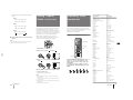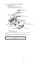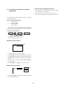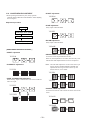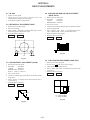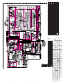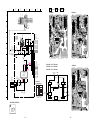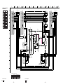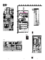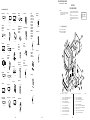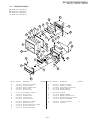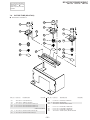
1
SERVICE MANUAL
MODEL
––––––––
KP-41T65C
KP-53S65C
KP-61S65C
COMMANDER DEST. CHASSIS NO.
––––––––––––––– –––––– ––––––––––––––
RM-Y136A
Chile SCC-N88A-A
RM-Y136A
Chile SCC-N88B-A
RM-Y136A
Chile SCC-N88C-A
RM-Y136A
KP-53S65C
MICROFILM
∗ Please file according to model size. .......
41 53 61
MODEL
––––––––
RA-2A CHASSIS
COMMANDER DEST. CHASSIS NO.
––––––––––––––– –––––– ––––––––––––––
KP-41T65C
KP-61S65C
PROJECTION TV
SPECIFICATIONS
Projection system
3 picture tubes, 3 lenses,
horizontal in-line system
Picture tube
7 inch high-brightness
monochrome tubes (6.3 raster
size), with optical coupling and
liquid cooling system
Projection lenses
High performance, largediameter hybrid lens F1.1
Screen size (measured diagonally)
Television system
Channel coverage
Antenna
Inputs/output
KP-41T65C
41 inches
KP-53S65C
KP-61S65C
53 inches
61 inches
Speaker
Speaker output
Power requirement
Power consumption
Full range speaker 100 mm (3.9
inches) diameter
15 W x 2
220 V, 50 Hz
165 W
Standby mode: 3 W
Dimensions (W/H/D)
American TV standards
VHF: 2 – 13 / UHF: 14 – 69 /
CATV: 1 – 125
75 ohm external antenna
terminal for VHF/UHF
VIDEO IN 1
VIDEO IN 2 (VIDEO 2 INPUT)
S VIDEO (4-pin mini DIN):
Y: 1 Vp-p, 75-ohms
unbalanced, sync negative
C: 0.286 Vp-p (Burst signal)
75 ohms
VIDEO (phono jack): 1 Vp-p,
75-ohms unbalanced, sync
negative
AUDIO (phono jacks): 500
mVrms (100% modulation)
Impedance : 47 kilohms
Mass
KP-41T65C
951 x 1,022 x 602 mm
(37 1/2 x 40 1/4 x 23 3/4 inches)
55 kg
(121 lbs 4 oz)
KP-53S65C
1,218 x 1,413 x 614 mm
(48 x 55 5/8 x 24 1/4 inches)
1,338 x 1,506 x 642 mm
(52 3/4 x 59 3/8 x 25 3/8 inches)
69 kg
(152 lbs 1 oz)
KP-61S65C
Supplied accessories
Optional accessories
122 kg
(268 lbs 15 oz)
Remote control RM-Y136A (1)
Size AA (R6) battery (2)
U/V mixer EAC-66
Connecting cables RK-74A, VMC810S/820S, YC-15V/30V, VMC-720M
Stand SU-41T2 (For KP-41T65C)
High-contrast protective screen
SCN-53X2 (For KP-53S65C)
SCN-61X2 (For KP-61S65C)
Design and specifications are subject to change without notice.
VIDEO IN 3
VIDEO (phono jacks): 1 Vp-p,
75-ohms unbalanced, sync
negative
AUDIO (phono jacks): 500
mVrms (100% modulation)
Impedance: 47 kilohms
MONITOR OUT
VIDEO (phono jack): 1 Vp-p,
75-ohms unbalanced, sync
negative
AUDIO (phono jacks): 500 mVrms
(100% modulation),
Impedance: 10 kilohms
AUDIO OUT (phono jacks): 900
mVrms (100% modulation)
Impedance: 5 kilohms
–2–
TABLE OF CONTENTS
Section
Title
Page
Section
Title
Page
1. GENERAL
Step 1 : Installing the projection TV ....................................... 4
Step 2 : Hook up ...................................................................... 5
Step 3 : Setting up the remote control ..................................... 8
Step 4 : Setting up the projection TV automatically
(AUTO SET UP) ..................................................................... 9
Changing the menu larguage ................................................. 11
Watching the TV ................................................................... 11
Watching tow programs at one time-PIP ............................... 12
Freezing the picture (FREEZE) ............................................ 13
Adjusting the picture (VIDEO) ............................................. 13
Adjusting the color temperature (TRINITONE) ................... 14
Selecting the video mode (VIDEO) ...................................... 14
Adjusting the sound (AUDIO) .............................................. 14
Using audio effect (SURROUND) ........................................ 15
Selecting stereo or bilingual programs (MTS) ...................... 15
Setting the speaker switch (SPEAKER) ............................... 15
Setting audio out (AUDIO OUT) .......................................... 16
Setting daylight saving time (DAYLIGHT SAVING) .......... 16
Setting the clock (CURRENT TIME SET) ........................... 16
Setting the timer to turn the projection TV on and off
(ON/OFF TIMER) ................................................................ 17
Customizing the channel names (CHANNEL CAPTION) ... 17
Blocking out a channel (CHANNEL BLOCK) .................... 18
Setting your favorite channels (FAVORITE CHANNEL) .... 18
Setting video labels (VIDEO LABEL) ................................. 18
Setting Caption Vision (CAPTION VISION) ....................... 19
Operating video equipment ................................................... 19
Operating a cable box or DBS receiver ................................. 20
Troubleshooting .................................................................... 21
Index to parts and controls .................................................... 21
2-7. High-Voltage Cable Installation and Removal ........... 27
2-8-1. Picture Tube Removal (KP-41T65C) ......................... 27
2-8-2. Picture Tube Removal (KP-53S65C/61S65C) ............. 27
2-9-1. Service stay Assy How to use and Carry Back Service
stay Assy ..................................................................... 28
2-9-2. Picture Tube Bracket Assy Removal (KP-41T65C) ... 28
2-9-3. Picture Tube Bracket Assy Removal (KP-53S65C/61S65C) . 29
2-9-4. Setting of Service stay Assy (KP-53S65C) ................ 30
2-9-5. Install a Chassis Assy ................................................. 30
3. SET-UP ADJUSTMENTS .................................................. 31
4. SAFETY RELATEDP ADJUSTMENTS .................... 44
5. CIRCUIT ADJUSTMENTS ................................................ 46
6. DIAGRAMS
6-1. Block Diagram (1) .......................................................... 49
Block Diagram (2) .......................................................... 52
Block Diagram (3) .......................................................... 54
6-2. Frame Schematic Diagram ............................................. 55
6-3. Circuit Boards Location ................................................. 58
6-4. Printed Wiring Boards and Schematic Diagrams ........... 58
• A Board ........................................................................ 59
• G Board ........................................................................ 66
• PT Board ...................................................................... 73
• CR, CG, CB Boards ..................................................... 79
• Z Board ........................................................................ 83
• HA Board ..................................................................... 85
• F Board ........................................................................ 87
6-5. Semiconductors .............................................................. 88
2. DISASSEMBLY
2-1. Rear Board Removal .................................................. 23
2-2. Chassis Assy Removal ................................................ 23
2-3. Service Position .......................................................... 23
2-4-1. HA Board Removal (KP-41T65C) ............................. 24
2-4-2. HA Board Removal (KP-53S65C/61S65C) ............... 24
2-5-1. Beznet Assy Removal (KP-41T65C) .......................... 25
2-5-2. Beznet Assy Removal (KP-53S65C) .......................... 25
2-5-3. Screen Frame Assy Removal (KP-61S65C) ............... 25
2-6-1. Mirror Cover Assy Removal (KP-41T65C) ............... 26
2-6-2. Mirror Cover Assy Removal (KP-53S65C/61S65C) ...... 26
2-6-3. Reflection Mirror Removal (KP-61S65C) ................. 26
(CAUTION)
SHORT CIRCUIT THE ANODE OF THE PICTURE TUBE AND
THE ANODE CAP TO THE METAL CHASSIS, CRT SHIELD, OR
CARBON PAINTED ON THE CRT, AFTER REMOVING THE ANODE.
WARNING!!
AN ISOLATION TRANSFORMER SHOULD BE USED DURING
ANY SERVICE TO AVOID POSSIBLE SHOCK HAZARD, BECAUSE OF LIVE CHASSIS.
THE CHASSIS OF THIS RECElVER IS DIRECTLY CONNECTED TO THE AC POWER LINE.
7. EXPLODED VIEWS
7-1. Cover (KP-41T65C) ....................................................... 90
7-2. Cover (KP-53S65C) ....................................................... 91
7-3. Cover (KP-61S65C) ....................................................... 92
7-4. Chassis (KP-41T65C) .................................................... 93
7-5. Chassis (KP-53S65C/61S65C) ........................................ 94
7-6. Picture Tube (KP-41T65C) ............................................ 95
7-7. Picture Tube (KP-53S65C/61S65C) ............................... 96
8. ELECTRICAL PARTS LIST ............................................. 97
SAFETY-RELATED COMPONENT WARNING!!
COMPONENTS IDENTIFIED BY SHADING AND MARK ! ON
THE SCHEMATIC DIAGRAMS, EXPLODED VIEWS AND IN THE
PARTS LIST ARE CRITICAL TO SAFE OPERATION. REPLACE
THESECOMPONENTS WITH SONY PARTS WHOSE PART NUMBERS APPEAR AS SHOWN IN THIS MANUAL OR IN SUPPLEMENTS PUBLISHED BY SONY. CIRCUIT ADJUSTMENTS THAT
ARE CRITICAL TO SAFEOPERATION ARE IDENTIFIED IN THIS
MANUAL. FOLLOW THESE PROCEDURES WHENEVER CRITICAL COMPONENTS ARE REPLACED OR IMPROPER OPERATION IS SUSPECTED.
–3–
SECTION 1
The operating instructions mentioned here partial abstracts from the
Operating Instructions Manual. The page numbers of the Operating
Instruction Manual remain as in the manual.
GENERAL
Getting Started
Welcome!
Precautions
Step 1: Installing
the projection TV
Carrying your projection TV
p KP-41T65C/53S65C only
Be sure to grasp the areas indicated when carrying the
projection TV, and to use more than two people.
(Rear of projection TV)
Thank you for purchasing the Sony Color Rear Video
Projection TV. Here are some of the features you will
enjoy with your projection TV:
–4–
• On-screen menus that let you set the picture quality,
sound, and other settings.
• Two tuner Picture-in-Picture (PIP) that allows you
to watch another TV channel, video or cable image
as a window picture.
• Surround system that simulates the sound quality of
a concert hall or movie theater.
• SAVA SPEAKER option of the AUDIO menu that
lets you take advantage of the Sony SAVA series
speaker system’s surround sound and super woofer
mode when you connect it to the projection TV.
About this manual
The instructions in this manual are for models KP41T65, KP-46C65, KP-48S65, KP-53S65, and KP-61S65.
Before you start reading this manual, please check your
model number, located at the rear of the projection TV.
Model KP-53S65 is used for illustration purposes in this
manual. Any differences in operation are clearly
indicated in the text, for example “KP-61T65 only.”
The differences in specifications are indicated in the
text.
Instructions in this manual are based on use of the
remote control. You can also use the controls on the
projection TV if they have the same name as those on
the remote control.
4 -EN
This projection TV operates on extremely high voltage.
To prevent fire or electric shock, please follow the
precautions below.
For the best picture quality, install the projection TV
within the areas shown below.
Safety
• Operate the projection TV only on 120 V AC.
• One blade of the plug is wider than the other for safety
purposes and will fit into the power outlet only one
way. If you are unable to insert the plug fully into the
outlet, contact your dealer.
• Should any liquid or solid object fall into the cabinet,
unplug the projection TV and have it checked by
qualified personnel before operating it further.
• Unplug the projection TV from the wall outlet if you
are not going to use it for several days or more. To
disconnect the cord, pull it out by the plug. Never
pull the cord itself.
Optimum viewing area (Horizontal)
min
.2
.1m
(ap
61 prox
(ap
"
.8
53 pro
ft.)
" x. 7
ft.)
min
.1
.5m
(a
41 ppro
"
x.
min
.2
.4m
5f
t.)
60°
p KP-61S65C only
60°
For details concerning safety precautions, see the supplied
leaflet “IMPORTANT SAFEGUARDS.”
Note on cleaning
Clean the cabinet of the projection TV with a dry soft
cloth. To remove dust from the screen, wipe it gently
with a soft cloth using vertical strokes only. Stubborn
stains may be removed with a cloth slightly dampened
with solution of mild soap and warm water. Never use
strong solvents such as thinner or benzine for cleaning.
If the picture becomes dark after using the projection TV
for a long period of time, it may be necessary to clean the
inside of the projection TV. Consult qualified service
personnel.
Installing
• To prevent internal heat build-up, do not block the
ventilation openings.
• Do not install the projection TV in a hot or humid
place, or in a place subject to excessive dust or
mechanical vibration.
• Avoid operating the projection TV at temperatures
below 5°C (41°F).
• If the projection TV is transported directly from a cold
to a warm location, or if the room temperature has
changed suddenly, the picture may be blurred or show
poor color. This is because moisture has condensed on
the mirror or lenses inside. If this happens, let the
moisture evaporate before using the projection TV.
• To obtain the best picture, do not expose the screen to
direct illumination or direct sunlight. It is
recommended to use spot lighting directed down from
the ceiling or to cover the windows that face the screen
with opaque drapery. It is desirable to install the
projection TV in a room where the floor and walls are
not of reflecting material. If necessary, cover them
with dark carpeting or wall paper.
EN
Carry your projection TV by the casters.
Preparing for your projection TV
Before you use your projection TV, adjust convergence.
For the procedure, see Step 4: Setting up the projection
TV automatically (AUTO SET UP) on page 14.
Optimum viewing area (Vertical)
min
. 2.4
m (a
p
61" prox. 8
ft.)
min
. 2.1
m (a
p
53" prox. 7
ft.)
min
in.. 11
.5
.5m
m (5
41"" (5
ftf.)t.)
20°
20°
Getting Started
5 -EN
Step 2: Hookup
Connecting an antenna/cable TV
system without a VCR
To cable or antenna
(Rear of projection TV)
VHF/UHF
Cable
Connecting an antenna/cable TV system with a VCR
For details on connection, see your VCR instruction
manual.
Before making the connection, disconnect the AC power
cords of the equipment to be connected.
To a conventional VCR
Although you can use either an indoor or outdoor
antenna with your projection TV, we recommend that
you connect an outdoor antenna or a cable TV system
to get better picture quality.
To cable box
If your cable company requires you to connect a cable
box, make the connection as follows:
(Rear of projection TV)
VHF/UHF
After making these connections, you will be able to do
the following:
• View the playback of video tapes
• Record one TV program while viewing another
program
• Watch two TV programs at once using PIP
Notes
• To connect a monaural VCR, connect the audio output of the VCR
to AUDIO-L (MONO) of VIDEO 1/2/3 IN on the projection TV.
Without a cable box
(Rear of projection TV)
Cable
AUX
IN
OUT
IN
Connecting an antenna
VIDEO 1 VIDEO 3
Connect your antenna cable to the VHF/UHF antenna
terminal. If you cannot connect your antenna cable
directly to the terminal, follow one of the instructions
below depending on your cable type.
A
• VHF only
or
• VHF/UHF
or
• Cable
75-ohm coaxial cable
• VHF only
or
• UHF only
or
• VHF/UHF
300-ohm twin lead cable
B
VIDEO
VHF/UHF
(Rear of projection TV)
AUX
Cable box
VHF/UHF
L
CONTROL S
OUT
Antenna cable
(MONO)
AUDIO
VCR
TO
CONVERTER
CATV cable
–5–
(Rear of projection TV)
VHF/UHF
AUDIO VIDEO
VIDEO (yellow)
AUDIO-L (white)
AUDIO-R (red)
LINE
OUT
Video and audio
outputs
With a cable box
(Rear of projection TV)
AUX
and
IN
VIDEO 1 VIDEO 3
Note
TO
CONVERTER
OUT
• You cannot watch the signal through an AUX connector as a
window picture.
S VIDEO
MONITOR AUDIO
(VAR/FIX)
VIDEO
EAC-66 U/V mixer
(not supplied)
VHF/UHF
To cable and antenna
CATV cable
300-ohm twin lead cable
(Rear of projection TV)
AUX
TO
CONVERTER
Notes
• Most VHF/UHF combination antennas have a signal splitter.
Remove the splitter before attaching the appropriate connector.
• If you use the U/V mixer, snow and noise may appear in the
picture when viewing cable TV channels over 37.
Antenna cable
VHF/UHF
CONTROL S
OUT
VHF/UHF
Antenna cable
L
(MONO)
AUDIO
R
VCR
AUDIO VIDEO
VIDEO (yellow)
AUDIO-L (white)
AUDIO-R (red)
LINE
OUT
VMC-810S/820S
(not supplied)
OUT
IN
Video
and
audio
outputs
Note
• Do not connect anything to the TO CONVERTER connector in
this case.
VHF/UHF
input
VHF/UHF
output
Cable box
Getting Started
Antenna cable
IN
VMC-810S/820S
(not supplied)
* The cable box will be supplied by the cable company.
(Rear of projection TV)
VHF/UHF
6 -EN
EN
OUT
VHF/UHF
input
VHF/UHF
Pay cable TV systems use scrambled or encoded signals
requiring a cable box* in addition to the normal cable
connection.
Antenna connector
VHF/UHF
output
R
75-ohm coaxial
cable (not supplied)
• VHF
• UHF
To cable box and cable
(Rear of projection TV)
VHF/UHF
75-ohm coaxial cable
C
TO
CONVERTER
OUT
MONITOR AUDIO
(VAR/FIX)
S VIDEO
Cable box
OUT
IN
Antenna
cable
Splitter (not supplied)
Getting Started
7 -EN
To an S video equipped VCR
Connecting a DBS receiver
If your VCR has an S VIDEO output connector, make
the following connections.
Whenever you connect the cable to the S VIDEO input
connector, the projection TV automatically receives S
video signals.
For details on connection, see the instruction manual of
the DBS (Digital Broadcasting Satellites) receiver.
To a projection TV
(Rear of projection TV)
Without a cable box
AUX
(Rear of projection TV)
IN
VIDEO 1 VIDEO 3
AUX
OUT
VIDEO 1 VIDEO 3
TO
CONVERTER
OUT
VIDEO
VHF/UHF
MONITOR AUDIO
(VAR/FIX)
S VIDEO
TO
CONVERTER
CONTROL S
OUT
VIDEO
VHF/UHF
VHF/UHF
Cable or cable box
MONITOR AUDIO
(VAR/FIX)
S VIDEO
IN
VHF/UHF
DBS receiver
L
(MONO)
Antenna
AUDIO
R
Antenna cable
VHF/UHF
IN
L
CONTROL S
OUT
(MONO)
AUDIO
VHF/UHF
output
R
VCR
AUDIO VIDEO S VIDEO
IN
Audio
outputs
S video
output
LINE IN
OUT
VIDEO (yellow)
AUDIO-L (white)
AUDIO-R (red)
OUT
LINE
OUT
S VIDEO
AUDIO-L (white)
AUDIO-R (red)
AUDIO VIDEO S VIDEO
LINE OUT
Audio
outputs
Antenna cable
VHF/UHF
input
Satellite
antenna
input
Video
output
EN
VMC-810S/820S (not supplied)
RK-74A
(not supplied)
Note
–6–
YC-15V/30V
(not supplied)
With a cable box
• You can use the S VIDEO connector or the composite video
connector for the video connection.
Cable or cable box
(Rear of projection TV)
DBS receiver
To a projection TV and VCR
IN
VIDEO 1 VIDEO 3
OUT
S VIDEO
TO
CONVERTER
AUDIO VIDEO S VIDEO
LINE IN
OUT
LINE OUT
MONITOR AUDIO
(VAR/FIX)
VIDEO
VHF/UHF
CONTROL S
OUT
Antenna
VHF/UHF
AUX
IN
VHF/UHF
Audio
outputs
Antenna cable
Satellite
antenna
input
Video
output
L
(MONO)
(Rear of projection TV)
AUDIO
R
VCR
AUX
AUDIO VIDEO S VIDEO
LINE
OUT
S VIDEO
AUDIO-L (white)
AUDIO-R (red)
OUT
IN
VIDEO 1 VIDEO 3
IN
OUT
Audio
outputs
VHF/UHF
input
S video
output
S VIDEO
TO
CONVERTER
Audio
inputs
MONITOR AUDIO
(VAR/FIX)
VHF/
UHF IN
VIDEO
RK-74A
(not supplied)
VHF/UHF
CONTROL S
OUT
IN
Note
• Video signals are composed of Y (luminance) and C (chroma)
signals. The S connection sends the two signals separately
preventing degradation, and gives better picture quality
compared to conventional connections.
8 -EN
Getting Started
Splitter
(not supplied)
LINE IN
OUT
LINE OUT
VHF/
UHF OUT
Antenna
cable
OUT
AUDIO VIDEO S VIDEO
(MONO)
AUDIO
R
YC-15V/30V
(not supplied)
Cable box
VCR
VHF/UHF
IN
L
Video
input
VIDEO (yellow)
AUDIO-L (white)
AUDIO-R (red)
Audio
outputs
Video
output
F-type cable
(not supplied)
VMC-810S/820S (not supplied)
Getting Started
9 -EN
Connecting two VCRs for tape editing using MONITOR OUT
Connecting a camcorder
Use this connection to view a camcorder picture.
You can record input images displayed on the screen.
This type of connection should be used only when you
connect from the line input of one VCR, and from the
line output of a second VCR.
(Front of projection TV)
S VIDEO
VIDEO
L(MONO)-AUDIO-R
VIDEO 2 INPUT
(Rear of projection TV)
VIDEO
(yellow)
AUDIO-R (red)
AUX
IN
AUDIO-L (white)
Video and
audio outputs
VIDEO 1 VIDEO 3
OUT
VMC-810S/820S
(not supplied)
S VIDEO
VIDEO
VCR (for playback)
AUDIO VIDEO
LINE
OUT
• To connect a monaural camcorder, connect the audio output of
the camcorder to AUDIO-L (MONO) of VIDEO 2 INPUT on
the projection TV.
When connecting audio equipment, see page 28 for
more information.
–7–
IN
TO
CONVERTER
IN
Video and audio
inputs
AUDIO-R (red)
AUDIO-L (white)
VIDEO (yellow)
VMC-810S/820S
(not supplied)
• When connecting a single VCR to the projection TV, do not
connect the MONITOR OUT to the VCR’s line input, while at
the same time connecting from the projection TV’s VIDEO IN
connectors to the VCR’s line output, as shown below.
VIDEO IN
VHF/UHF
AUDIO OUT-L
(white)
L
RK-74A (not supplied)
MONITOR
OUT
VCR
(MONO)
AUDIO
IN
R
Line
input
Note
• You can adjust the bass, treble, and balance, or select surround
(page 26) or an MTS (Multichannel TV Sound) mode (page 27)
with the supplied remote control.
LINE
OUT
Set the amplifier’s
function to line input.
AUDIO OUT-R
(red)
Getting Started
OUT
(Rear of projection TV)
MONITOR AUDIO
(VAR/FIX)
VIDEO
10 -EN
R
IN
• Do not change the input signal while editing through
MONITOR OUT, or the output signal will also change.
• You can use the S video jack to connect a VCR for playback
and the composite video connector to connect a VCR for
recording.
AUX
OUT
AUDIO VIDEO
LINE
IN
Notes
(Rear of projection TV)
CONTROL S
OUT
L
(MONO)
AUDIO
EN
Connecting an audio system
S VIDEO
CONTROL S
OUT
VMC-810S/820S
(not supplied)
VIDEO 1 VIDEO 3
VCR (for recording)
VHF/UHF
OUT
Video and audio
outputs
Note
TO
CONVERTER
MONITOR AUDIO
(VAR/FIX)
DO NOT CONNECT IN THIS WAY.
Stereo amplifier
Getting Started
11 -EN
Connecting a Sony SAVA series speaker system
If you have a Sony SAVA series speaker system, connect
your speakers to the AUDIO (VAR/FIX) OUT jacks on
the rear of the projection TV with the audio cable
supplied with the speakers. You can take advantage of
the speakers’ Dolby Pro Logic* surround system and
super woofer mode, and control them with the supplied
remote control. When connecting a Sony SAVA series
speaker system, see page 27 for more information.
* Manufactured under license from Dolby Laboratories
Licensing Corporation. Additionally licensed under Canadian
patent number 1,037,877. “Dolby,” the double-D symbol a
and “Pro Logic” are trademarks of Dolby Laboratories
Licensing Corporation.
Step 3: Setting up
the remote
control
Inserting batteries
(Rear of projection TV)
Insert two size AA (R6) batteries (supplied) by
matching the + and – on the battery to the diagram
inside the battery compartment.
AUX
IN
VIDEO 1 VIDEO 3
OUT
S VIDEO
TO
CONVERTER
AUDIO (VAR/FIX)
OUT L (white)
MONITOR AUDIO
(VAR/FIX)
VIDEO
Names of buttons on the remote control are indicated
in different colors to represent the available functions.
Button color
Transparent ....... TV/VCR/DBS/Cable box function
(light up)
buttons. Press the appropriate
function button first to change the
remote control’s function.
Green .................. Buttons relevant to power operations.
Label color
White .................. TV/VCR/DBS/Cable box operation
buttons.
Yellow ................. PIP operation buttons.
Blue ..................... DBS operation buttons.
SAVA series speaker system
VHF/UHF
CONTROL S
OUT
Getting to know buttons on the
remote control
L
(MONO)
AUDIO (VAR/FIX)
OUT R (red)
AUDIO
R
Green
EN
Blue
Transparent
Audio cord supplied
with the speakers
CONTROL S OUT
Notes
1 IN L
–8–
RK-G34, etc. (not supplied)
1 IN R
CONTROL S IN
Front left
12 -EN
Getting Started
• Under normal conditions, batteries will last up to six months.
If the remote control does not operate properly or the
indicators of the buttons on the remote control do not light up,
the batteries may be worn out. When replacing batteries,
replace both of them with new ones.
• Do not mix old batteries with new ones or mix different types
of batteries together.
• If the electrolyte inside the battery should leak, wipe the
contaminated area of the battery compartment with a cloth and
replace the old batteries with new ones. To prevent the
electrolyte from leaking, remove the batteries when you don‘t
plan to use the remote control for a long period of time.
• Do not handle the remote control roughly. Do not drop it, step
on it, or let it get wet.
• Do not place the remote control in direct sunlight, near a
heater, or where the humidity is high.
Yellow
1
2
3
4
5
6
7
8
9
0
Blue
Blue
Getting Started
13 -EN
3
Step 4: Setting up
the projection TV
automatically
Press CHANNEL +/– or VOLUME + to select
the on-screen menu language.
If you prefer Spanish or French to English, you can
change the on-screen menu language.
(2) Press TV/VIDEO to select RED or BLUE.
TV/VIDEO
[CH+ ]
[VOL – ]
[VOL + ]
[CH– ]
RED / BLUE : [TV/VIDEO]
E x i t : [SET UP]
– VOLUME +
– CHANNEL +
Erasing or adding channels
CONVERGENCE : RED
or
(AUTO SET UP)
(3) Using CHANNEL +/– or VOLUME +/–, move
the line until it converges with the center green
line.
You can set up your projection TV easily by using the
AUTO SET UP feature. It presets all the receivable
channels, adjusts the convergence and changes the onscreen menu language. To set up the projection TV
manually, see “Adjusting convergence” (page 16),
“Setting cable TV on or off” (page 17), “Presetting
channels” (page 18) and “Changing the menu
language” (page 18).
If the projection TV is set to a video input, you cannot
perform AUTO SET UP. Press TV/VIDEO so that a
channel number appears.
All of the menus will be set to the factory preset
condition in the selected language.
4
– VOLUME +
– CHANNEL +
– CHANNEL +
B
G+R
B
G+R
CONT I NUE TO
AUTO PROGRAM?
TV (FUNCTION)
CONVERGENCE : RED
[CH+ ]
[VOL – ]
Press VOLUME – to start AUTO SET UP.
[VOL + ]
[CH– ]
RED / BLUE : [TV/VIDEO]
E x i t : [SET UP]
1
2
3
4
5
6
7
8
9
>
To move horizontal line up/down, press CHANNEL
+/–.
To move vertical line right/left, press VOLUME +/–.
5
.
MENU
CH +/–
Press CHANNEL + to preset channels.
(4) Repeat steps (2) and (3) to adjust the other lines
until all three lines converge and are seen as a
white cross.
AUTO PROGRAM
TIMER/
STEREO STAND BY
0 – 9 buttons
ENTER
0
YES : [CH+ ]
NO : [CH– ]
– CHANNEL +
POWER
– VOLUME +
– VOLUME +
(Front of projection TV)
SETUP TV/VIDEO
After AUTO SET UP, you can erase unnecessary
channels or add the channels you want. Preset channels
during the day rather than late at night, when some
channels may not be broadcasting.
EN
CONVERGENCE : BLUE
[CH+ ]
[VOL – ]
White cross
–9–
“AUTO PROGRAM” appears on the screen and the
TV starts scanning and presetting channels
automatically. When all the receivable channels are
stored, “AUTO PROGRAM” disappears and the
following menu appears. If the projection TV
receives cable TV channels, CABLE is set to ON
automatically.
Before you start using AUTO SET UP, be sure to
connect the antenna or cable to the projection
TV (see page 6).
1
Press POWER to turn the projection TV on.
POWER
CONT I NUE TO
CONVERGENCE?
YES
NO :
: [CH+ ]
[CH– ]
[VOL + ]
[CH– ]
RED / BLUE : [TV/VIDEO]
E x i t : [SET UP]
1
Press TV (FUNCTION).
FUNCTION
Note
TV
• Using the AUX connector, press TV (black button) first and
make sure that “AUX” is displayed beside the channel number
on the screen. Then follow the steps 2 to 6 above to perform
AUTO SET UP.
To preview the main functions (DEMO)
Press TV/VIDEO on the projection TV in step 4. The
functions and menus are displayed one by one.
2
Press MENU.
The main menu appears.
MENU
To exit DEMO
Press any button.
2
CC
To exit AUTO PROGRAM
Press SETUP on the front of the projection
Press any button.
TV.
AUTO SET UP screen appears.
6
SETUP
ENGLISH :
ESPAÑOL :
FRANÇAIS :
AUTO SET UP :
DEMO :
[CH + ]
[CH – ]
[VOL +]
[VOL –]
[TV/VIDEO]
[SET UP] to exit.
R
G
B
B
G
R
14 -EN
Getting Started
Exit
Use
3
Adjust convergence.
(1) Press CHANNEL +.
The CONVERGENCE adjustment screen
appears.
– CHANNEL +
Press
VIDEO
MODE : STANDARD
PICTURE
HUE
COLOR
BRIGHTNESS
SHARPNESS
TRINITONE : HIGH
MENU
, and press
.
The SET UP menu appears.
CONVERGENCE : RED
[CH+ ]
[VOL – ]
Press V or v to select
MENU
[VOL + ]
SET UP
CHANNEL ERASE/ADD
CHANNEL CAPTION
CHANNEL BLOCK
FAVORITE CHANNEL
CABLE : ON
AUTO PROGRAM
VIDEO LABEL
LANGUAGE : ENGLISH
CC
CONVERGENCE
MENU
Exit MENU
Use
[CH– ]
RED / BLUE : [TV/VIDEO]
E x i t : [SET UP]
R=Red
G=Green
B=Blue
Getting Started
15 -EN
4
Press V or v to select CHANNEL ERASE/ADD,
and press
.
The CHANNEL ERASE/ADD menu appears.
6
7
CHANNEL ERASE/ADD
To erase and/or add other channels, repeat
step 5.
Press V, B, v, or b to move the cursor (z) to
the symbol showing the line you want to
adjust, and press
.
Press MENU to return to the original screen.
33
ERASE
ADD
MENU
4
CONVERGENCE
+ RED
+ BLUE
MENU
MENU
Use[0 – 9]or [CH+/–]
to select the channel.
Use
5
Us e
Exit
Notes
• If you erase or add a VHF or UHF channel, the cable TV
channel with the same number is also erased or added, and
vice versa.
• Erasing and adding channels is also available for the AUX
input.
To erase an unwanted channel
(1) Make sure the cursor (z) is beside ERASE.
(2) Press CH +/– or the 0 – 9 buttons to select the
channel you want to erase, and press ENTER.
+RED : Red vertical and horizontal line (left/right/up/
down adjustment)
+BLUE : Blue vertical and horizontal line (left/right/up/
down adjustment)
5
Selected channel number
CH
1
2
3
4
5
6
7
8
9
CHANNEL ERASE/ADD
33
ERASE
ADD
MENU
Use[0 – 9]or [CH+/–]
to select the channel.
ENTER
Press V, B, v, or b to move the line until it
converges with the center green line, and
press
.
Adjusting convergence
(CONVERGENCE)
R
G
B
0
Use
Exit
MENU
(3) Press
.
The “–” indication appears beside the channel
number, showing that the channel is erased
from the preset memory.
– 10 –
To add a channel that you want
(1) Press V or v to move the cursor (z) to ADD.
(2) Press the 0 – 9 buttons to select the channel you
want to add, and press ENTER.
Selected channel number
The projection tube image appears on the screen in
three layers (red, green and blue). If they do not
converge, the color is poor and the picture blurs. To
correct this, adjust convergence.
You do not have to do this procedure if you perform
AUTO SET UP (page 14). Do this procedure only
when you want to adjust it manually.
1
Press MENU.
2
Press V or v to select
3
Press V or v to select CONVERGENCE, and
press
.
The CONVERGENCE adjustment screen appears.
, and press
R
1
2
4
5
7
8
3
6
9
E x i t MENU
If you have connected the projection TV to a cable TV
system, set CABLE to ON (the factory setting). If not,
set CABLE to OFF.
You do not have to do this procedure if you perform
AUTO SET UP (page 14). Do this procedure only when
you want to set it manually.
MENU
Erase and/or add channels:
or
RETURN
Setting cable TV on or off
CHANNEL ERASE/ADD
ERASE
ADD
MENU
33
G
B
.
B
G+R
To move
Press
Up
Down
Right
Left
V
v
b
B
1
Press MENU.
2
Press V or v to select
3
Set CABLE to ON or OFF:
(1) Press V or v to move the cursor (z) to CABLE,
and press
.
(2) Press V or v to select ON or OFF, and press
.
, and press
.
CONVERGENCE
SET UP
CHANNEL ERASE/ADD
CHANNEL CAPTION
CHANNEL BLOCK
FAVORITE CHANNEL
CABLE : OFF
AUTO PROGRAM
VIDEO LABEL
LANGUAGE : ENGLISH
CC
CONVERGENCE
MENU
Exit MENU
Use
+ RED
+ BLUE
MENU
Us e
RETURN
E x i t MENU
6
Repeat steps 4 and 5 to adjust the other
lines until all three lines converge and are
seen as a white cross.
7
Press MENU to return to the original screen.
4
Press MENU to return to the original screen.
Note
• If CABLE appears in gray, the projection TV is set to a video
input and you cannot select CABLE. Press TV (black button) so
that a channel number appears.
CONVERGENCE
+ RED
+ BLUE
MENU
ENTER
0
Use
Exit
(3) Press
.
The “+” indication appears beside the channel
number, showing that the channel is added to
the preset memory.
16 -EN
Getting Started
MENU
B
G
R
Us e
RETURN
E x i t MENU
R=Red
G=Green
B=Blue
Getting Started
17 -EN
EN
Operations
Presetting channels
You can preset TV channels easily by using the AUTO
PROGRAM feature.
You do not have to do this procedure if you perform
AUTO SET UP (page 14). Do this procedure only when
you want to set it manually.
Changing the
menu language
Watching the TV
3
Select the channel you want:
To select a channel directly
Press the 0 – 9 buttons, and press ENTER.
For example, to select channel 10, press 1, 0 and
ENTER.
1
2
4
5
7
8
3
6
9
ENTER
0
1
Press MENU.
2
Press V or v to select
3
Press V or v to select AUTO PROGRAM, and
press
.
To scan through channels
, and press
.
AUTO PROGRAM
“AUTO PROGRAM” appears on the screen and the
projection TV starts scanning and presetting
channels automatically. When all the receivable
channels are stored, “AUTO PROGRAM”
disappears and the lowest numbered channel is
displayed.
4
Press CH +/– until the channel you want appears.
If you prefer Spanish or French to English, you can
change the menu language.
You do not have to do this procedure if you select the
language during AUTO SET UP (page 14). Do this
procedure only when you want to set it manually.
1
Press MENU.
2
Press V or v to select
3
Press V or v to select LANGUAGE, and press
.
, and press
MUTING
TV (POWER)
TV/VIDEO
ANT
DISPLAY
SLEEP
.
1
2
3
4
5
6
7
8
9
JUMP
0
0 – 9 buttons
4
– 11 –
Press any button.
Press V or v to select your favorite
language, “ENGLISH”, “ESPAÑOL,” or
“FRANÇAIS” and press
.
Notes
VOL +/–
5
1
Press TV (POWER) to turn on the projection
TV.
The TIMER/STANDBY indicator flashes until the
picture appears.
POWER
Switching quickly between two
channels
You can use the JUMP button to switch or “jump” back
and forth between two channels.
Press JUMP.
JUMP
TV
Press MENU to return to the original screen.
If “VIDEO” appears on the screen, press ANT so
that a channel number appears.
Note
• Certain parts of the Spanish or French menus remain in
English.
EN
CH +/–
VOLUME
PREFERENCIAS
BORRAR/AÑADIR CANAL
NOMBRE DEL CANAL
BLOQUEAR CANAL
CANAL FAVORITO
CABLE : SI
AUTO PROGRAMACION
ETIQUETA DE VIDEO
LENGUAJE : ESPAÑOL
CC
CONVERGENCIA
MENU
Usar
Salir MENU
• If the AUTO PROGRAM menu appears in gray, the projection
TV is set to a video input and you cannot select AUTO
PROGRAM. Press ANT button so that a channel number
appears.
• Presetting channels is also available for the AUX input.
Press VOL +/– to adjust the volume.
VOL
SET UP
CHANNEL ERASE/ADD
CHANNEL CAPTION
CHANNEL BLOCK
F AVORITE CHANNEL
CABLE : ON
AUTO PROGRAM
VIDEO LABEL
L ANGUAGE : ENGLISH
CC
CONVERGENCE
MENU
Exit MENU
Use
4
The channel can also be selected without pressing
ENTER.
ENTER
Press MENU to return to the original screen.
To exit AUTO PROGRAM
CH
TV (FUNCTION)
2
Pressing JUMP again switches the channel back to the
one you selected last.
Note
Press TV (FUNCTION).
• You cannot jump to channels you scanned through using the
CH +/– buttons.
FUNCTION
TV
Muting the sound
Press MUTING.
“MUTING” appears on the screen.
MUTING
Once you press TV (FUNCTION), the projection TV
function is set unless another function button is
pressed.
18 -EN
Getting Started
To restore the sound, press MUTING again, or press
VOL +.
-EN
Operations
19
Watching a video input picture
Press DISPLAY repeatedly until the desired
display appears.
Each time you press DISPLAY, the display changes as
follows:
Press TV/VIDEO repeatedly until the desired
video input appears.
Each time you press TV/VIDEO, the display changes
as follows:
Status display* n XDS ON** n cc 1 ON***
TV n VIDEO 1 n VIDEO 2 n VIDEO 3
DISPLAY OFF N
TV/VIDEO
Press TV/VIDEO (yellow labelled button) to
select the input mode.
Each time you press TV/VIDEO (yellow labelled
button), “TV”, “VIDEO 1”, “VIDEO 2”, and “VIDEO 3”
appear in sequence.
The Picture-in-Picture (PIP) feature allows you to
watch both the main picture and a window picture
simultaneously.
*
– 12 –
To cancel the display, press DISPLAY repeatedly until
“DISPLAY OFF” appears. “DISPLAY OFF” goes off
after three seconds.
Changing the window picture input
mode
TV/VIDEO
DISPLAY
Channel number, the current time, channel caption
(if set), and MTS mode (if SAP is selected) are
displayed. SAP indication disappears after three
seconds.
** Some programs are broadcast with XDS (Extended
Data Service) which shows a network name,
program name, program type, program length, call
letters, and time of the show. When you select XDS
with the DISPLAY button, this information will be
displayed on the screen if the broadcaster offers this
service.
*** Some programs are broadcast with Caption Vision.
When you select Caption Vision with the DISPLAY
button, Caption Vision will be displayed on the
screen if the broadcaster offers this service. (See
page 34 for selecting Caption Vision.)
Watching two
programs at one
time — PIP
N
N
Displaying on-screen information
A window picture will appear in the same input mode
as the last time you used PIP.
To return to the TV picture, press ANT so that a
channel number appears.
Changing the VHF/UHF input to the
AUX input
Press ANT.
“AUX” appears beside the channel number.
SWAP
PIP
TV/VIDEO (yellow
labelled button)
CH +/– (yellow
labelled button)
POSITION
AUDIO
Use the yellow labelled buttons for PIP operations.
Displaying a window picture
ANT
Press PIP.
Input-source mode or TV
channel for the main picture
Pressing ANT again switches back to the VHF/UHF
input.
PIP
Note
• If you connect your VCR without a cable box, your PIP input
source is a VCR. If you connect your VCR with a cable box,
your PIP input source is a VCR or cable box.
Listening to the sound of the window
picture
Press AUDIO.
The
display appears next to the PIP channel number
for a few seconds, indicating that the window picture
sound is being received.
Main picture
AUDIO
Window picture
(1/9 size)
Input-source mode or TV
channel for the window picture
The sound of the window
picture is received.
Setting the Sleep Timer
The projection TV stays on for the length of time you
specify and then shuts off automatically.
Input-source mode or TV
channel for the main picture
PIP
Main picture
Window picture
(1/16 size)
Input-source mode or TV
channel for the window picture
N
Press SLEEP repeatedly until the time (minutes)
you want appears.
Each time you press SLEEP, the time changes as
follows:
30 n 60 n 90 n SLEEP OFF
Press PIP again to display a smaller window
picture.
SLEEP
To remove the window picture, press PIP again.
To cancel the Sleep Timer, press SLEEP repeatedly
until “SLEEP OFF” appears, or turn off the projection
TV.
20 -EN
Operations
Note
To restore the main picture sound, press AUDIO again.
The
display moves to the main picture channel
number.
Changing TV channels in the window
picture
Press CH +/– (yellow labelled button).
TV/VTR
+
CH
–
• The window picture may be affected by the condition of the
main picture.
Operations
21 -EN
EN
Changing the position of the window
picture
Press POSITION.
Each time you press POSITION, the window picture
will move counterclockwise on the screen.
Freezing the picture
(FREEZE)
4
Adjusting the
picture (VIDEO)
VIDEO STANDARD
BRIGHTNESS
POSITION
Swapping the main and window
pictures
(2) Press
.
The new setting appears in the VIDEO menu.
The FREEZE feature is useful when you want to write
down an information such as a recipe from a cooking
program, a displayed address, or a phone number.
The frozen picture changes as follows depending on
whether the PIP function is used or not.
When watching TV programs, you can adjust the
picture to suit your taste.
You can adjust the picture of video input(s) as well.
CC
0
RESET
2
Press FREEZE.
v
MENU
Press MENU.
Press V or v to select
– 13 –
Note
, and press
.
Reciipe
flour - - - - 2
s u g a r - - - 1/2
s a l t - - - - - 1/2
butter - - - 1
Press FREEZE.
Exit
Use
3
MENU
6
Press MENU to return to the original screen.
Use
(2) Press
Exit
Press B or v to
EN
Press b or V to
Increase picture
contrast and give
vivid color.
HUE
Make picture tones
become purplish.
COLOR
Decrease color intensity. Increase color intensity.
Make picture tones
become greenish.
BRIGHTNESS Darken the picture.
Brighten the picture.
SHARPNESS Soften the picture.
Sharpen the picture.
To restore the factory settings
Press RESET after displaying and selecting the VIDEO
menu.
All of the settings are restored to the factory settings.
VIDEO
MODE : STANDARD
PICTURE
HUE
COLOR
BRIGHTNESS
SHARPNESS
TRINITONE : HIGH
MENU
CC
When the PIP function is being used
To adjust other items, repeat steps 3 and 4.
PICTURE Decrease picture
contrast and give soft
color.
Select the item you want to adjust.
For example:
(1) To adjust the brightness, press V or v to move
the cursor (z) to BRIGHTNESS.
The frozen picture
appears in the
window picture.
To remove the frozen window picture, press FREEZE
again.
5
Item
VIDEO
MODE : STANDARD
PICTURE
HUE
COLOR
BRIGHTNESS
SHARPNESS
TRINITONE : HIGH
MENU
CC
When the PIP function is not being used
R e c ip e
flour - - - - 2
s u g a r - - - 1/2
s a l t - - - - - 1/2
butter - - - 1
MENU
Description of adjustable items
FREEZE
• The channels being received through the AUX connector
cannot be displayed as a window picture.
Exit
For details on each item, see “Description of
adjustable items” below.
FREEZE
1
SWAP
VIDEO
MODE : STANDARD
PICTURE
HUE
COLOR
BRIGHTNESS
SHARPNESS
TRINITONE : HIGH
MENU
Use
V
Press SWAP.
Each time you press SWAP, the images and sound
from the main and window pictures switch places with
another.
Adjust the selected item:
(1) Press V, B, v, or b to adjust the item.
MENU
.
VIDEO STANDARD
Main picture
BRIGHTNESS
Press FREEZE.
Window picture
The images in the
window picture
freeze.
To cancel the frozen window picture, press FREEZE
again.
22 -EN Operations
Operations
23 -EN
Adjusting the color
temperature (TRINITONE)
Selecting the video
mode (VIDEO)
4
Adjusting the
sound (AUDIO)
Adjust the selected item:
(1) Press V, B, v, or b to adjust the item.
AUDIO
BASS
The TRINITONE feature controls the color
temperature, permitting white balance preference
adjustment without affecting skin tones.
7
8
The video mode feature allows you to choose three
different modes of picture settings. Choose the one that
best suits the type of program that you want to watch.
9
0
V
v
MENU
1
Press MENU.
2
Press V or v to select
3
and press
Press MENU.
2
Press V or v to select
3
Press V or v to select MODE, and press
4
Press V or v to select STANDARD, MOVIE, or
SPORTS mode, and press
.
– 14 –
4
CC
RESET
Exit
MENU
VIDEO
MODE : MOVIE
PICTURE
HUE
COLOR
BRIGHTNESS
SHARPNESS
TRINITONE : HIGH
MENU
Exit
5
1
2
Press MENU.
Press V or v to select
Exit
Choose
To
STANDARD
Receive a standard picture.
MOVIE
Receive a finely detailed picture.
SPORTS
Receive a vivid, bright picture.
Choose
To
a cool (bluish) white.
MEDIUM
a neutral white.
a warm (reddish) white.
NTSC STD
24 -EN
Operations
, and press
.
5
To adjust other items, repeat steps 3 and 4.
6
Press MENU to return to the original screen.
EN
Description of adjustable items
AUDIO
TREBLE
BASS
BALANCE
EFFECT : OFF
MTS :
STEREO
SPEAKER : ON
AUDIO OUT : VARIABLE
SURROUND MODE
CC
SUPER WOOFER MODE
MENU
Exit MENU
Use
MENU
3
Select the item you want to adjust.
For example:
(1) To adjust bass, press V or v to move the cursor
(z) to BASS.
AUDIO
TREBLE
BASS
BALANCE
EFFECT : OFF
MTS :
STEREO
SPEAKER : ON
AUDIO OUT : VARIABLE
SURROUND MODE
CC
SUPER WOOFER MODE
MENU
Exit MENU
Use
Press MENU to return to the original screen.
Note
• The settings for these modes can be adjusted in the VIDEO
menu.
Item
Press v or B to
Press V or b to
TREBLE
Decrease the treble
response.
Increase the treble
response.
BASS
Decrease the bass
response.
Increase the bass
response.
BALANCE
Emphasize the left
speaker’s volume.
Emphasize the right
speaker’s volume.
To restore the factory settings
Press RESET after displaying and selecting the AUDIO
menu.
All of the settings are restored to the factory settings.
Note
• When SPEAKER (page 27) is OFF and AUDIO OUT (page 28)
is in the FIXED condition, the volume, TREBLE, BASS, and
BALANCE cannot be adjusted.
MENU
(2) Press
HIGH
For details on each item, see “Description of
adjustable items” below.
v
MENU
.
VIDEO
MODE : MOVIE
PICTURE
HUE
COLOR
BRIGHTNESS
SHARPNESS
TRINITONE : HIGH
MENU
Use
Press V or v to select NTSC STD, MEDIUM, or
HIGH and press
.
Use
.
.
CC
CC
AUDIO
TREBLE
BASS
BALANCE
EFFECT : OFF
MTS :
STEREO
SPEAKER : ON
AUDIO OUT : VARIABLE
SURROUND MODE
CC
SUPER WOOFER MODE
MENU
Exit MENU
Use
V
, and press
Press V or v to select TRINITONE and press
.
Use
You can adjust the quality of the TV sound to suit your
taste. You can adjust the sound of the video input(s) as
well.
7
8
9
0
1
VIDEO
MODE : MOVIE
PICTURE
HUE
COLOR
BRIGHTNESS
SHARPNESS
TRINITONE : HIGH
MENU
(2) Press
.
The new setting appears in the AUDIO menu.
.
AUDIO
BASS
Operations
25 -EN
Using audio effect
Using the menu to set audio effect
Selecting stereo or
bilingual programs
0
(SURROUND)
V
(MTS)
v
MENU
The audio effect (SURROUND) feature simulates
sound reproduction with the atmosphere of a movie
theater or a concert hall. Audio effect is only effective
for stereo programs.
Press MENU.
2
Press V or v to select
3
Press V or v to select EFFECT, and press
1
2
3
4
5
6
7
8
9
4
EFFECT :
5
Press .
Each time you press the
changes as follows:
button, the display
SURROUND n SURROUND OFF
9
MTS
V
v
MENU
OFF
Press MENU to return to the original screen.
9
EN
V
v
MENU
STEREOnSAPnMONO
Choose
To
STEREO
Listen to stereo sound.
The STEREO indicator on the projection
TV lights up when a stereo broadcast is
received.
SAP
Listen to bilingual programs.
There is no sound when the SAP signal is
not broadcasting.
MONO
1
Press MENU.
2
Press V or v to select
3
Press V or v to select SPEAKER, and press
.
Listen to monaural sound.
Reduce noise during stereo broadcasts.
Press MENU.
Press V or v to select , and press
.
Press V or v to select MTS, and press
.
Press V or v to select STEREO, SAP, or MONO.
Press MENU to return to the original screen.
, and press
.
AUDIO
TREBLE
BASS
BALANCE
EFFECT : SURROUND
MTS :
STEREO
SPEAKER : ON/OFF/SAVA SP
AUDIO OUT : VARIABLE
SURROUND MODE
CC
SUPER WOOFER MODE
MENU
Exit MENU
Use
4
To set MTS using the menu
1
2
3
4
5
Operations
8
0
• Stereo and SAP sounds are subject to program sources.
26 -EN
If you connect the Sony SAVA series speaker system to
the AUDIO (VAR/FIX) OUT connectors, you can take
advantage of the speakers’ surround sound and super
woofer mode. After making the connections (page 12),
set SPEAKER to SAVA SPEAKER, then adjust
SURROUND MODE or SUPER WOOFER MODE.
7
Note
TV/DBS
You may switch off the projection TV speakers when,
for example, you want to listen to the sound through a
stereo system.
Press MTS repeatedly to select STEREO, SAP, or
MONO.
n
– 15 –
2
8
0
MTS :
STEREO
SPEAKER : ON
AUDIO OUT : VARIABLE
SURROUND MODE
CC
SUPER WOOFER MODE
MENU
Exit MENU
Use
0
Press TV (FUNCTION).
7
Press V or v to select the audio effect mode,
and press
.
AUDIO
TREBLE
BASS
BALANCE
button
1
.
The Multichannel TV Sound (MTS) feature allows you
to enjoy stereo sound or Second Audio Programs (SAP)
of your choice. The initial setting is stereo sound
(STEREO).
AUDIO
TREBLE
BASS
BALANCE
EFFECT : SURROUND
MTS :
STEREO
SPEAKER : ON
AUDIO OUT : VARIABLE
SURROUND MODE
CC
SUPER WOOFER MODE
MENU
Exit MENU
Use
(audio effect) button
TV (FUNCTION)
.
n
Using the
1
, and press
Setting the speaker
switch (SPEAKER)
Press V or v to select ON, OFF, or SAVA SP,
and press
.
AUDIO
TREBLE
BASS
BALANCE
EFFECT : SURROUND
MTS :
STEREO
SPEAKER : SAVA SP
AUDIO OUT : VARIABLE
SURROUND MODE
CC
SUPER WOOFER MODE
MENU
Exit MENU
Use
5
Press MENU to return to the original screen.
Operations
27 -EN
Choose
To
ON
Listen to the sound from the
projection TV.
Turn off the projection TV speaker
sound and listen to the projection
TV’s sound solely through the audio
system speakers.
Turn off the projection TV speaker
sound and listen to the projection
TV’s sound through the Sony SAVA
series speaker system. You can adjust
volume, muting, surround modes,
and super woofer mode with the
remote control supplied with the
projection TV.
OFF
SAVA SP
Setting audio out
(AUDIO OUT)
You can change AUDIO OUT to VARIABLE or FIXED
when SPEAKER is set to OFF.
AUDIO OUT is variable when SPEAKER is set to ON.
8
V
To select surround sound or super
woofer mode of the SAVA speaker
system
– 16 –
AUDIO
TREBLE
BASS
BALANCE
EFFECT : SURROUND
MTS :
STEREO
SPEAKER : SAVA SP
AUDIO OUT : VARIABLE
SURROUND MODE
CC
SUPER WOOFER MODE
MENU
Exit MENU
Use
v
MENU
Press MENU.
2
Press V or v to select
3
Press V or v to select AUDIO OUT, and press
.
, and press
7
.
8
9
0
AUDIO
TREBLE
BASS
BALANCE
EFFECT : SURROUND
MTS :
STEREO
SPEAKER : OFF
AUDIO OUT : FIXED
SURROUND MODE
CC
SUPER WOOFER MODE
MENU
Exit MENU
Use
4
If your area uses daylight saving time, change
DAYLIGHT SAVING setting depending on the season,
before setting the current time.
Daylight saving end
• After the last Sunday in October, set DAYLIGHT
SAVING to NO. Current time setting automatically
moves one hour back.
1
Press V or v to select VARIABLE or FIXED,
and press
.
Note
VARIABLE: Sound output varied according to the
projection TV settings. You can adjust
the volume, bass, treble, and balance.
FIXED: Sound output is always fixed to a certain
level. The volume, bass, treble, and balance
are also fixed to the factory settings.
8
9
0
V
v
MENU
1
2
3
Press MENU.
Press V or v to select
, and press
.
EN
Press V or v to select CURRENT TIME SET,
and press
.
CURRENT TIME SET
– – – – –:– – AM
MENU
1
Press MENU.
2
Press V or v to select t, and press
3
Press V or v to select DAYLIGHT SAVING,
and press
.
Use
.
4
CC
Use
4
– – – – –:– – AM
Exit MENU
Use
5
FRI 12:00 AM
MENU
Set the time.
Use
Set for daylight saving start.
NO
Set for daylight saving end.
5
MENU
CURRENT TIME SET
FRI 12:04 AM
MENU
Use
Press MENU to return to the original screen.
Exit
(2) Set the hour and minutes in the same way as in
step (1). When you press
after setting the
minutes, the clock starts.
– – – – –:– – AM
Exit MENU
To
YES
MENU
Set the current day of the week and time.
(1) Press V or v to set the day of the week, and press
.
CURRENT TIME SET
Press MENU to return to the original screen.
¥ If AUDIO OUT appears in gray, set SPEAKER to OFF.
Exit
Make sure the cursor (z) is to the left of
“--:-- AM,” and press
.
Set the day.
TIMER
DAYLIGHT SAVING:NO
CURRENT TIME SET
ON/OFF TIMER
MENU
Note
MENU
SUN 12 : 00 AM
MENU
Press V or v to select YES or NO, and press
.
CC
Exit
CURRENT TIME SET
TIMER
DAYLIGHT SAVING:YES
CURRENT TIME SET
ON/OFF TIMER
MENU
Choose
Operations
7
v
MENU
Use
5
Setting the clock enables you to turn the projection TV
on and off with the timer. Make sure to set daylight
saving time first.
V
AUDIO
TREBLE
BASS
BALANCE
EFFECT : SURROUND
MTS :
STEREO
SPEAKER : OFF
AUDIO OUT : VARIABLE
SURROUND MODE
CC
SUPER WOOFER MODE
MENU
Exit MENU
Use
• This feature is only for Sony SAVA speaker system with an
operation capability for KP-41T65C, KP-53S65C, and KP-61S65C.
28 -EN
(CURRENT TIME SET)
Daylight saving start
• After the first Sunday in April, set DAYLIGHT
SAVING to YES. Current time setting (right
column) automatically moves one hour ahead.
9
0
Press V or v to select SURROUND MODE or
SUPER WOOFER MODE, and press
.
For details on each option, refer to the operating
instructions of the speaker system.
Setting the clock
SAVING)
7
After setting SPEAKER to SAVA SP, follow the
procedure below.
Setting daylight
saving time (DAYLIGHT
6
Exit
MENU
Press MENU to return to the original screen.
Operations
29 -EN
(2) Press V or v to set the time (hour then minutes)
that you want to turn on the projection TV, and
press
.
Setting the timer to
turn the projection
TV on and off
ON/OFF TIMER
EVERY SUN – SAT
12:02 AM – h CH– – – –
MENU
9
(2) Press
ON/OFF TIMER
EVERY SUN – SAT
12:02 AM 1h CH – – – –
v
MENU
MENU
Select the channel.
1
Press MENU.
2
Press V or v to select t, and press
(4) Press V or v to select the channel, and press
.
4
5
6
7
8
9
RESET
.
1
2
CHANNEL CAPTION
0 – 9 buttons
125
ESP–
MENU
ENTER
Use
v
MENU
Press V or v to select
, and press
––––
– –:– – AM – h CH – – – –
.
– 17 –
The TIMER indicator on the projection TV lights up.
SUN 12:00 AM
4
Exit
Press
and enter the ON/OFF TIMER
setting.
(1) Press V or v to set the day(s), and press
MENU
.
Each time you press V or v, the days cycle as
follows:
EVERY SUN–SATnEVERY MON–FRIn
SUNDAYn...nSATURDAYnEVERY
SUNDAYn...nEVERY SATURDAY
5
To set the other program, press
repeat step 4.
6
Press MENU to return to the original screen.
, and
3
MENU
Use
6
Repeat steps 4 and 5 to caption other
channels.
7
Press MENU to return to the original screen.
After you customize the channel, the channel caption
appears green.
To erase a caption
In step 5, press RESET.
–––
––––
MENU
4
To cancel the timer
In step 3 or 4, press RESET.
Press V or v to select CHANNEL CAPTION,
and press
.
CHANNEL CAPTION
One minute before the projection TV turns off, the
message “TV will turn off soon.” is displayed on the
screen.
Exit
(3) Repeat steps (1) and (2) to select the remaining
letters, and press
.
Press MENU.
SET UP
CHANNEL ERASE/ADD
CHANNEL CAPTION
CHANNEL BLOCK
FAVORITE CHANNEL
CABLE : ON
AUTO PROGRAM
VIDEO LABEL
LANGUAGE : ENGLISH
CC
CONVERGENCE
MENU
Exit MENU
Use
SUN 12:00 AM
Exit MENU
ON/OFF TIMER
Use
.
Select the letter.
MENU
MENU
3
V
EVERY SUN – SAT
12:02 AM 1h CH 1
Use
2
0
ON/OFF TIMER
Press V or v to select ON/OFF TIMER, and
press
.
1
SUN 12:00 AM
Exit MENU
Use
n
n
8
You can add a caption for up to 12 channels. This
feature allows you to easily identify which channel you
are watching. You can make your own caption.
Each time you press V, the time duration
increases by one hour up to a maximum of six
hours.
V
3
0...9˜A...Z˜&,/,_(blank space)
(3) Press V or v to set the time duration, and press
.
0
RESET
Each time you press V or v, the letter changes as
follows:
SUN 12:00 AM
Exit MENU
Use
You can set the projection TV to turn on and off at the
times you specify. Make sure the clock is set correctly.
If it is not, set the clock first (page 29).
7
Enter the letters (up to four) to caption the
channel:
(1) Press V or v to select the first letter.
(CHANNEL CAPTION)
Set the duration.
(ON/OFF TIMER)
5
Customizing the
channel names
Exit
MENU
Press
and press V or v to select the
channel that you want to caption, and
press
.
Notes
• If the CHANNEL CAPTION menu appears in gray, the
projection TV is set to a video input, and you cannot select
CHANNEL CAPTION. Press TV (black button) so that a
channel number appears.
• If more than 90 seconds elapse after you press a button, the
menu disappears automatically.
• The channel caption feature is not available for the AUX input.
Note
• If you unplug the projection TV or a power interruption occurs,
the ON/OFF TIMER setting will be erased. Reset the current
time, then set the timer.
ON/OFF TIMER
EVERY SUN – SAT
12:00 AM – h CH – – – –
CHANNEL CAPTION
125
––––
MENU
MENU
Set the time.
Use
SUN 12:00 AM
Exit MENU
Select the letter.
Use
30 -EN
Operations
Exit
MENU
Operations
31 -EN
EN
Blocking out a
channel (CHANNEL BLOCK)
5
Setting your
favorite channels
Press V or v to select a favorite channel
number, and press
.
MODE: MANUAL
1. – – –
2. – – –
3. – – –
4. – – –
5. – – –
MENU
Select the channel.
Exit
Use
(FAVORITE CHANNEL)
6
The channel block feature allows you to prevent
children from watching unsuitable programs. You can
block out two channels.
0
V
RESET
1
2
3
The favorite channel feature allows your projection TV
to memorize your favorite channels easily.
If you set to AUTO, the last five channels you selected
with the 0 – 9 buttons are automatically set as your
favorite channels. If you want to input your own
selection of channels, set to MANUAL.
Press MENU.
.
Press V or v to select CHANNEL BLOCK, and
press
.
1. CH – – –
2. CH – – –
MENU
– 18 –
Select a program.
4
MODE: MANUAL
1.
5
2. – – –
3. – – –
4. – – –
5. – – –
MENU
Select a position.
Use
Exit
0
MENU
V
Press MENU to return to the original screen.
v
MENU
• If the FAVORITE CHANNEL menu appears in gray, the
projection TV is set to a video input and you cannot select
FAVORITE CHANNEL.
1
Press MENU.
v
MENU
• If more than 90 seconds elapse after you press another button,
the menu disappears automatically.
2
Press V or v to select
Exit
MENU
Press V or v to select program 1 or 2, and
press
.
1
2
3
• The favorite channel feature is not available for the AUX input.
3
Press V or v to select VIDEO LABEL, and
press
.
Press MENU.
Press V or v to select
, and press
Selecting your favorite channel
7
Use
4
8
VIDEO 1: VIDEO 1
VIDEO 2: VIDEO 2
VIDEO 3: VIDEO 3
MENU
9
V
Use
4
v
MENU
Exit
MENU
1
Press
and press V or v to select AUTO or
MANUAL, and press
.
MODE: MANUAL
1. – – –
2. – – –
3. – – –
4. – – –
5. – – –
MENU
Select a position.
Use
Exit
Press MENU to return to the original screen.
When you select the blocked
2
channel, the message “BLOCKED”
appears on the screen.
Use
If you select AUTO, skip steps 5 and 6.
The last five channels you selected with the 0 – 9
buttons are automatically set as your favorite
channels.
2
MENU
VIDEO 1: VIDEO 1
VIDEO 2: VIDEO 2
VIDEO 3: VIDEO 3
MENU
125 ESPN
14 ABC
48 CBS
16 HBO
5 CBC
Exit
MENU
Exit
Press V or v to select the input mode you
want to label, and press
.
VIDEO LABEL
Press
.
The FAVORITE CHANNEL menu appears.
FAVORITE CHANNEL
6
EN
.
0
MODE: AUTO
1.—
2.—
3.—
4.—
5.—
MENU
Press V or v to select the channel which you
want to block out, and press
.
, and press
VIDEO LABEL
.
Press V or v to select FAVORITE CHANNEL,
and press
.
FAVORITE CHANNEL
5
The video label feature allows you to label each input
mode so that you can easily identify the connected
equipment. For example, you can label VIDEO 1 as
VHS.
7
8
9
V
CHANNEL BLOCK
Use
Press V or v to select the channel that you
want to set as your favorite channel, and
press
.
Notes
9
0
, and press
MENU
Setting your favorite channels
8
Press V or v to select
(VIDEO LABEL)
FAVORITE CHANNEL
7
v
MENU
Setting video labels
FAVORITE CHANNEL
Press V or v to select the favorite channel
you want to watch, and press
.
The selected channel appears on the screen.
5
Exit
MENU
Press V or v to select the label, and press
.
VIDEO LABEL
VIDEO 1: VHS
VIDEO 2: VIDEO 2
VIDEO 3: VIDEO 3
MENU
Use
Exit
MENU
BLOCKED
To cancel a CHANNEL BLOCK setting
In step 4 or 5, press RESET.
Note
• Once you use CHANNEL BLOCK, Caption Vision and XDS of
the blocked channel and the selected channel output from
MONITOR OUT are also blocked out.
32 -EN
Operations
If you select MANUAL, the favorite channel
numbers become white, indicating that favorite
channels can be entered.
To cancel the FAVORITE CHANNEL menu
Press V or v to select “Exit,” and press
.
Operations
33 -EN
Each time you press V or v, the label changes as
follows:
VIDEO 1
VCR manufacturer code numbers
Operating video
equipment
˜
˜
VIDEO 1 ˜ VHS ˜ 8 mm ˜ BETA
Setting Caption
Vision (CAPTION VISION)
DBS ˜ DVD ˜ S VIDEO ˜ LD
VIDEO 2
˜
˜
VIDEO 2 ˜ VHS ˜ 8 mm ˜ BETA
DBS ˜ DVD ˜ S VIDEO ˜ LD
VIDEO 3
VIDEO 3 ˜ VHS ˜ 8 mm ˜ BETA
N
N
N
6
DBS ˜ DVD ˜ LDN
Repeat steps 4 and 5 to label other input
modes.
Some programs are broadcast with Caption Vision. To
display Caption Vision, select either CC1, CC2, CC3,
CC4, TEXT1, TEXT2, TEXT3, or TEXT4 from the menu.
CC1, CC2, CC3, or CC4 shows you on-screen version of
the dialogue or sound effects of a program. (The mode
should be set to CC1 for most programs.) TEXT1,
TEXT2, TEXT3, or TEXT4 shows you on-screen
information presented using either half or the whole
screen. It is not usually related to the program.
7
Note
8
You can use the supplied remote control to operate
Sony or non-Sony video equipment that has an infrared
remote sensor. For this operation, set the
manufacturer’s code number.
Setting the manufacturer’s code
9
0
VTR (FUNCTION)
• If more than 90 seconds elapse before you press another
button, the menu disappears automatically.
Code number
Sony
Aiwa
Audio Dynamic
Bell & Howell (M. Wards)
Brocsonic
Canon
Citizen
Craig
Curtis Mathis
Daewoo
DBX
Dimensia
Emerson
Fisher
Funai
General Electric
Goldstar
Hitachi
Instant Replay
JC Penny
301, 302, 303
338
314, 337
330, 343
319
309, 308
332
315, 302, 332
304, 338, 309
341, 312, 309
314, 336, 337
304
319, 320, 316, 317, 318
330, 334, 335, 333
338
329, 304, 309
332
306, 304, 305
309, 308
309, 305, 304, 330, 314,
336, 337
314, 336, 337
314, 336, 332, 337
332, 305, 333, 334, 330,
335
308, 309
314, 336, 337
332
309, 335
305, 304
323, 324, 325, 326
325, 338, 321
314, 336, 337
309, 308
308, 309, 306, 307
305, 304
308, 309
308, 309
308
308, 309
304, 305, 308, 309, 311,
312, 313
309, 330, 328, 335, 324,
338
314
315
322, 313, 321
330, 335
312, 313, 321, 335, 323,
324, 325, 326
327, 328
315
338, 327
308, 309, 338
338
332
314, 336, 337
314, 336, 338, 337
309, 308
312, 311
327, 328, 335, 331, 332
330, 314, 336, 337
331
JVC
Kenwood
LXI (Sears)
V
v
MENU
1
2
– 19 –
Manufacturer
2
3
4
5
6
7
8
9
Press V or v to select
0 – 9 buttons
ENTER
0
Press MENU.
CC ,
and press
CC
Use
3
1
.
CAPTION VISION
CC 1
CC 2
CC 3
CC 4
TEXT 1
TEXT 2
TEXT 3
TEXT 4
MENU
CODE SET
Exit
MENU
Press V or v to select the caption type, and
press
.
CC
Use
CAPTION VISION
CC 1
CC 2
CC 3
CC 4
TEXT 1
TEXT 2
TEXT 3
TEXT 4
MENU
Exit
Press the CODE SET, VTR (FUNCTION), and 0 – 9
buttons to enter the manufacturer’s code
number (see the chart on page 35-36), then
press ENTER.
For example, to operate a Sony 8 mm VCR,
press CODE SET, VTR (FUNCTION), 3, 0, 2, and
ENTER.
MENU
Magnavox
Marantz
Marta
Memorex
Minolta
Mitsubishi/MGA
Multitech
NEC
Olympic
Panasonic
Pentax
Philco
Philips
Pioneer
Quasar
RCA/PROSCAN
Realistic
Sansui
Singer
Samsung
Sanyo
Scott
FUNCTION
4
Press MENU to return to the original screen.
To display Caption Vision
Press DISPLAY. (See page 20 for details.)
Notes
• Poor reception of TV programs can cause errors in Caption
Vision and XDS.
Captions may appear with a white box or other errors instead
of a certain word.
• XDS, Caption Vision, and the status display cannot be used at
the same time.
• For details on XDS, see page 20.
34 -EN
Operations
CODE SET
VTR
ENTER
3
0
2
Sharp
Shintom
Signature 2000 (M. Wards)
Sylvania
Symphonic
Tashiro
Tatung
Teac
Technics
Toshiba
Wards
Yamaha
Zenith
Operations
35 -EN
EN
MDP manufacturer code numbers
Manufacturer
Code number
Sony
Kenwood
Magnavox
Maranz
Mitsubishi
Panasonic
Philips
Pioneer
RCA
Sanyo
Sharp
Yamaha
701
707
703
702
702
704
703
702
702
706
705
703
Operating video equipment
VTR (POWER)
Video operating
buttons
1
2
3
4
5
6
7
8
9
DBS/CABLE
the cable box/DBS control buttons to
check if the code number works.
For example, to operate a cable box or DBS receiver,
you can use the DBS/CABLE (POWER), JUMP, CH
+/–, 0 – 9 and ENTER buttons.
0 – 9 buttons
ENTER
You can program the supplied remote control to
operate a cable box or DBS receiver. Follow the
procedures below to set the manufacturer’s code
number in the remote control.
Note
• If the cable box or DBS receiver does not have a certain
function, the corresponding button on this remote control will
not operate.
DBS/CABLE (POWER)
CH +/–
DBS/CABLE
(FUNCTION)
Use the video operating buttons on the remote
control to operate the video equipment.
Press VTR (FUNCTION) before operating the
video equipment.
– 20 –
Operating a VCR
To turn on or off
To select a channel
directly
To change channels
To record
To search the picture
forward or backward
To change input mode
Operating an MDP
To turn on or off
To play
To stop
To pause
To search the picture
forward or backward
To search the chapter
forward and backward
1
2
3
4
5
6
7
8
9
JUMP
TV/DBS*
Buttons on the remote control
Press VTR (POWER).
Press the 0 – 9 buttons.
0 – 9 buttons
ENTER
GUIDE*
0
V/v/B/b/
To operate the projection TV
Press TV (FUNCTION). Then use the projection TV
control buttons to control the projection TV.
For more details on operating the cable box or
DBS receiver
Refer to the operating instructions that come with the
equipment.
DISPLAY*
If the remote control doesn’t work
*
• First, try repeating the setup procedures using the other codes
listed for your equipment.
MENU*
Press CH +/–.
Press ( while pressing r. First release
(, then release r.
Press (.
Press p.
Press ).
Press 0.
Press P.
To resume normal playback, press again.
Press ) or 0 during playback.
To resume normal playback, release the
button.
Press TV/VTR.
Buttons on the remote control
Press VTR (POWER).
Press (.
Press p.
Press P.
To resume normal playback, press again.
Keep pressing ) or 0 during
playback.
To resume normal playback, release the
button.
Press CH +/–.
Manufacturer code numbers (cable box)
CH +/–
CODE SET
* The TV/DBS, GUIDE, DISPLAY, V/v/B/b/
buttons can be used only with a DBS receiver.
1
• If the video equipment does not have a certain function, the
corresponding button on this remote control will not operate.
, and MENU
Turn off the equipment you want to set up,
and press DBS/CABLE (FUNCTION).
FUNCTION
DBS/CABLE
2
CODE SET
FUNCTION
DBS/CABLE
ENTER
8
Manufacturer
Code number
Hamlin/Regal
Jerrold/G. I.
222, 223, 224, 225, 226
201, 202, 203, 204, 205, 206, 207, 208,
218
227, 228, 229
219, 220, 221
214, 215
209, 210, 211
216, 217
212, 213
Oak
Panasonic
Pioneer
Scientific Atlanta
Tocom
Zenith
Manufacturer code numbers (DBS receiver)
Press the CODE SET, DBS/CABLE (FUNCTION),
and 0 – 9 buttons to enter the
manufacturer’s code number (see the chart
on the right column), then press ENTER. For
example, to program your remote control
to operate a Sony DBS receiver, press CODE
SET, DBS/CABLE (FUNCTION), 8, 0, 1, and
ENTER.
Note
Operations
Press DBS/CABLE (POWER) to turn on the
cable box or DBS receiver.
4 Use
0
To play
To stop
To fast forward
To rewind the tape
To pause
36 -EN
3
VTR (FUNCTION)
Notes
• If more than one code number is listed, try entering them one
by one, until you come to the correct code for your equipment.
• In some rare cases, you may not be able to operate your nonSony video equipment with the supplied remote control. This
is because your equipment may use a code that is not included
with this remote control. In this case, please use the
equipment’s own remote control unit.
• The code numbers for Sony equipment are assigned at the
factory as follows:
VHS VCR
301 (preset code for the supplied
remote control)
8 mm VCR
302
Beta, ED Beta VCRs
303
• Whenever you remove the batteries — to replace them, for
example — if too much time is taken, the code number may
revert to the factory setting and must be reset.
Operating a cable
box or DBS receiver
0
1
Manufacturer
Code number
Sony
801 (preset code for the supplied
remote control)
802
RCA
Notes
• If more than one code number is listed, try entering them one
by one until you come to the correct code for your equipment.
• If you enter a new code number, the code number you
previously entered at that setting is erased.
• In some rare cases, your equipment may use a code that is not
provided with this remote control and you may not be able to
operate your equipment with the supplied remote control. In
this case, use the equipment’s own remote control unit.
• Whenever you remove the batteries — to replace them, for
example — if too much time is taken, the code numbers may
revert to the factory setting and must be reset.
Operations
37 -EN
EN
Additional Information
Troubleshooting
Only snow and noise appear on the screen
/ Check the CABLE setting in the SET UP menu.
(page 17)
/ Check the antenna/cable connections. (page 6)
/ Make sure the channel is broadcasting
programs.
/ Press ANT to change the input mode. (page 20)
Index to parts and
controls
Dotted lines or stripes
/ Adjust the antenna.
/ Move the projection TV away from noise
sources such as cars, neon signs, and hairdryers.
If the problem persists after trying the methods below,
contact your nearest Sony dealer.
No picture (screen not lit), no sound
/ Make sure the power cord is connected
securely.
/ Operate with the buttons on the projection TV.
/ Insert the batteries in the remote control with
the correct polarity.
/ Replace the batteries with new ones if they are
weak.
/ Check to see if the TV/VIDEO setting is correct:
when watching TV, set to TV, and when
watching video tapes, set to VIDEO1, 2, or 3.
/ Try another channel. It could be station trouble.
/ Perform AUTO SET UP again using the SETUP
button to return to the factory preset condition.
(page 14)
– 21 –
Poor or no picture (screen lit), good sound
/ Adjust PICTURE in the VIDEO menu. (page 23)
/ Adjust BRIGHTNESS in the VIDEO menu.
(page 23)
/ Adjust convergence. (page 16)
/ Check antenna/cable connections. (page 6)
/ Perform AUTO SET UP again using the SETUP
button to return to the factory preset condition.
(page 14)
/ Remove objects from the front of the projection
TV.
Good picture, no sound
/ Press MUTING so that “MUTING” disappears
from the screen. (page 19)
/ Check the MTS setting in the AUDIO menu.
(page 27)
/ Make sure SPEAKER is set to ON in the AUDIO
menu. (page 27)
/ Perform AUTO SET UP again using the SETUP
button to return to the factory preset condition.
(page 14)
No color
/ Adjust the COLOR in the VIDEO menu. (page
23)
/ Confirm that black and white program is not
being broadcast.
/ Perform AUTO SET UP again using the SETUP
button to return to the factory preset condition.
(page 14)
Double images or ghosts
/ Use a highly directional outdoor antenna or a
cable (when the problem is caused by
reflections from nearby mountains or tall
buildings).
Cannot operate menu
/ If the item you want to choose appears in gray,
you cannot select it. Press TV/VIDEO
correctly.
/ Check the CABLE setting in the SET UP menu.
(page 17)
This section briefly describes the buttons and controls
on the projection TV and on the Remote control. For
more information, refer to the pages next to each
description.
Projection TV — Front
Cannot receive upper channels (UHF) when using an
antenna
/ Make sure CABLE is OFF in the SET UP menu.
(page 17)
/ Use AUTO PROGRAM to add receivable
channels that are not presently in projection TV
memory. (pages 14, 18)
Cannot receive any channels when using
cable TV
/ Make sure CABLE is ON in the SET UP menu.
(page 17)
/ Use AUTO PROGRAM to add receivable
channels that are not presently in projection TV
memory. (pages 14, 18)
Remote control does not operate
/ Batteries could be weak. Replace the batteries.
(page 13)
/ Make sure the projection TV’s power cord is
connected securely to the wall outlet.
/ Press TV (FUNCTION) when operating your
projection TV.
/ Are fluorescent lights too close to the projection
TV? Move them at least 3-4 feet away from the
projection TV.
SETUP
VIDEO
9
Additional Information
– CHANNEL +
6
5
POWER
TIMER/
STEREO STAND BY
8 7
4 3 2 1
1 TIMER/STANDBY indicator (pages 19, 30)
6 VOLUME +/– buttons (page 14)
2 STEREO indicator (page 27)
7 TV/VIDEO button (page 14, 15)
3 Remote sensor
8 SETUP button (page 14)
4 POWER switch (page 14)
9 S VIDEO/VIDEO 2 INPUT (VIDEO/AUDIO
L(MONO)/R) jacks (page 10)
5 CHANNEL +/– buttons (page 14)
38 -EN
– VOLUME +
L(MONO)-AUDIO-R
VIDEO 2 INPUT
Cannot gain enough volume when using a cable box
/ Increase the volume at the cable box. Then press
TV (FUNCTION) and adjust the projection TV’s
volume.
The projection TV needs to be cleaned
/ Clean the projection TV with a soft dry cloth.
Never use strong solvents such as thinner or
benzine, which might damage the finish of the
cabinet.
TV/VIDEO
S VIDEO
40 -EN
Additional Information
Remote control
1
!¢
2
!∞
3
!§
!¶
4
!•
5
!ª
6
7
8
@º
@¡
1
2
3
4
5
6
@£
7
8
9
@¢
9
@™
0
@∞
!º
@§
@¶
!¡
EN
@•
!™
!£
– 22 –
1 VTR (POWER) switch (page 36)
!¶ TV (FUNCTION) button (pages 15, 19)
2 MUTING button (page 19)
!• SWAP button (page 22)
3 VTR (FUNCTION) button (page 35)
!ª PIP button (page 21)
4 FREEZE button (page 22)
@º TV/VIDEO button (yellow labelled button) (page
21)
5 TV/VTR CH +/– buttons (Yellow labelled button)
(page 21)
@¡ AUDIO button (page 21)
6 POSITION button (page 22)
@™ TV/VIDEO button (page 20)
7 DISPLAY button (page 20)
@£ ANT button (page 20)
8 SLEEP button (page 20)
@¢ 0 – 9 buttons (page 16)
9 JUMP button (page 19)
@∞ ENTER button (page 16)
!º TV/DBS
@§ MTS/GUIDE button (page 27, 37)
button (page 26, 37)
!¡ RESET button (page 23)
@¶ Menu operation buttons (page 15)
!™ VOL (volume) +/– buttons (page 19)
MENU button
!£ CODE SET button (page 35)
V/B/v/b/ buttons
!¢ DBS/CABLE (POWER) switch (page 37)
!∞ TV (POWER) switch (page 19)
button
@• CH (channel) +/– buttons (pages 16, 19)
!§ DBS/CABLE (FUNCTION) button (page 37)
Additional Information
41 -EN
SECTION 2
DISASSEMBLY
2-1. REAR BOARD REMOVAL
2 Rear board
1 Eight screws (KP-41T65C)
Eleven screws (KP-53S65C)
Twelve screws (KP-61S65C)
(Tapping screw 4X20)
2-2. CHASSIS ASSY REMOVAL
1 Three screws
(Head tapping screw 4X20)
2 Chassis assy
F board
2-3. SERVICE POSITION
Remove the CN302 (A board)
Chassis assy
– 23 –
2-4-1. HA BOARD REMOVAL (KP-41T65C)
2 Control panel cap (L)
1 Six screws
(Tapping screw 4X20)
4 Nine screws
(+BVTP 3X12)
2 Control panel cap (R)
5 HA board
3 Control panel
assy
2-4-2. HA BOARD REMOVAL (KP-53S65C/61S65C)
3 Nine screws
(+BVTP 3X12)
4 HA board
1 Two screws
(Tapping screw 4X20)
2 Front cover
– 24 –
2-5-1. BEZNET ASSY REMOVAL (KP-41T65C)
1 Nine screws
(Tapping screw 4X20)
2 Beznet assy
2 Two screws
(Tapping screw 4x20)
2-5-2. BEZNET ASSY REMOVAL (KP-53S65C)
1 Twelve screws
(Tapping screw 4X20)
3 Beznet assy
2 Three screws
(Tapping screw 4X20)
2-5-3. SCREEN FRAME ASSY REMOVAL (KP-61S65C)
Four claws
3 Three hook
2 Three hook
4 Screen frame assy
(Remove the four claws)
1 Three screws
(Tapping screw 4X20)
– 25 –
2-6-1. MIRROR COVER ASSY REMOVAL (KP-41T65C)
2 Mirror cover
1 Fifteen screws
(Tapping screw 4X20)
2-6-2. MIRROR COVER ASSY REMOVAL (KP-53S65C)
2 Mirror cover assy
1 Twenty screws
(Tapping screw 4X20)
2-6-3. REFLECTION MIRROR REMOVAL (KP-61S65C)
4 Mirror board
5 Reflection mirror
3 Eleven screws
(Tapping screw 4X20
2 Top rear cover
– 26 –
1 Five screws
(Tapping screw 4X20)
2-7. HIGH-VOLTAGE CABLE INSTALLATION AND REMOVAL
(1) Remover
(2) Installation
1 Rubber cap
1 HV cable
2 HV cable
turn 90˚
Hook
Gutter
2-8-1. PICTURE TUBE REMOVAL (KP-41T65C)
CAUTION: Removing the arrow-marked screws
is strictly prohibited.
If removed, it may cause liquid spill.
Lens
1 Four screws
(Head tapping screws 4X20)
Picture tube
2 Lens
6 Four screws
(+BVTP 4X12)
7 Picture tube (R)
8 Tension spring
5 Deflection yoke
4 Neck assy
3 CR board
2-8-2. PICTURE TUBE REMOVAL (KP-53S65C/61S65C)
CAUTION:Removing the arrow-marked
screws is strictly inhibited.
If removed, it may cause liquid
spill.
1 Four screws
(Head tapping screws 4X20)
Lens
2 Lens
Picture tube
6 Four screws
(+BVTP 4X12)
7 Picture tube (R)
8 Tension spring
5 Deflection yoke
4 Neck assy
3 CR board
– 27 –
2-9-1. SERVICE STAY ASSY HOW TO USE AND CARRY BACK
SERVICE STAY ASSY.
SERVICE STAY ASSY
Side board (R)
4-057-613-01
X-3702-036-1
Side board (L)
4-057-612-01
Screw (+BVTP 4X12)
7-685-661-14
Chassis stay
4-058-638-01
2-9-2. PICTURE TUBE BRACKET ASSY REMOVAL (KP-41T65C)
3 Eight screws
(Head tapping screw 4X20)
4 Picture tube
bracket assy
1 Three screws
(Head tapping screw 4X20)
Cabinet assy
2 Chassis assy
1) Remove 1 three screws (head tapping screw 4X20) and pull out 2 chassis assy from cabinet
assy.
2) Remove 3 eight screws (head tapping screw 4X20) and release 4 picture tube bracket assy
from cabinet assy.
– 28 –
2-9-3. PICTURE TUBE BRACKET ASSY REMOVAL
(KP-53S65C/61S65C)
• Disassemble HA board and speaker cord.
• Disassemble all the harness from purse lock.
3 Two screws
(Tapping screw 4X20)
4 Shield board
6 Picture tube
bracket assy
5 Eight screws
(Head tapping screw 4X20)
7 Two screws
(+BVTP 4X12)
8 X-RAY shield (L)
1 Three screws
(Head tapping screw 4X20)
Cabinet assy
0 X-RAY shield (R)
9 Two screws
(+BVTP 4X12)
2 Chassis assy
• except KP-61S65C
1) Remove 1 three screws (head tapping screw 4X20) and pull out 2 chassis assy from cabinet
assy.
2) Remove 3 two screws (tapping screw 4X20) and remove 4 shield board.
3) Remove 5 eight screws (head tapping screw 4X20) and release 6 picture tube bracket assy
from cabinet assy.
4) Remove 7 two screws (+BVTP 4X12) and remove 8 X-RAY shield (L).
5) Remove 9 two screws (+BVTP 4X12) and remove 0 X-RAY shield (R).
• except KP-61S65C
– 29 –
2-9-4. SETTING OF SERVICE STAY ASSY.
(KP-41T65C/53S65C)
2 Six screws
(+BVTP 4X12)
Picture tube bracket assy
Notch
Hook
4 Six screws
(+BVTP 4X12)
Hook
Notch
1 Side board (L)
3 Side board (R)
1) Lift up picture tube bracket assy and fit the hook of 1 side board (L) to the notch on the assy.
Then fix then with 2 six screws (+BVTP 4X12).
2) Lift up picture tube bracket assy and fit the hook of 3 side board (R) to the notch on the assy.
Then fix then with 4 six screws (+BVTP 4X12).
2-9-5. INSTALL A CHASSIS ASSY
2 HA board
F board
1 Chassis assy
Chassis stays
1)
2)
3)
4)
5)
Put 1 chassis assy on chassis stays.
Put 2 HA board on 1 chassis assy.
Put HV bracket on 1 chassis assy. (KP-41T65C only)
Temporarily install the F Board on the CRT bracket.
You can carry the chassis assy in this condition.
– 30 –
SECTION 3
SET-UP ADJUSTMENTS
3-1. SCREEN VOLTAGE ADJUSTMENT
(ROUGH ALIGNMENT)
1. Receive the Monoscope signal.
2. Set 50% BRIGHTNESS and minimum PICTURE.
3. Turn the red VR on the FOCUS block all the way to the left
and then gradually turn it to the right until the point where
you can see the retrace line.
4. Next gradually turn it to the left to the position where the
retrace line disappears.
R
G
3-3. SCREEN (G2) ADJUSTMENT
1. Select VIDEO mode without signals.
2. Connect an oscilloscope to the TP701(KR), TP731(KG) and
TP761(KB) of CR board, CG board and CB board.
3. Adjust R, G and B screen voltage to 170 – 173V with screen
VR on the focusblock.
170170
– 173V
}VDC
B
SCREEN
R
G
pedestal
pedestal
GND
B
Fig. 3-3
FOCUS
FOCUS block
Fig. 3-1
3-2. FOCUS LENS ADJUSTMENT
1. Loose the lens screw.
2. Set in service mode.
3. Use VP on the service mode menu to shown only the green
color.
4. Press the Commander Menu button and select FEATURES
and CONVERGENCE to display the test signal (crosshatch)
on the screen.
5. Rotate the green lens and align with the optimal focus point
from the test signal.
6. Use RG-RH from the service mode menu to set to green and
red.
7. Output the test signal and rotate the red lens to obtain the
optimum focus at the point where the red and green spots
overlap.
8. Use RG-BH from the service mode menu to set to red and
blue.
9. Output the test signal and rotate the blue lens to obtain the
optimum focus at the point where the blue and red spots overlap.
10. Tighten the lens screw.
3-4. FOCUS VR ADJUSTMENT
1. Set in service mode.
2. Use VP on the service mode menu to shown only the green
color.
3. Press the Commander Menu button (convergence) and output the test signal (crosshach).
4. Rotate the green VR on the FOCUS block and align to obtain the optimal focus point.
5. Use RG-RH from the service mode menu to set to green and
red.
6. Output the test signal and rotate the red VR to obtain the
optimum focus at the point where the red and green spots
overlap.
7. Use RG-BH from the service mode menu to set to red and
blue.
8. Output the test signal and rotate the blue VR aligning to obtain the optimum focus at the point where the blue and green
spots overlap.
Scanning
Scanningline
linevisible.
visible.
AA Minimize
Minimize both
B. B.
bothAAand
and
Lens
Fig. 3-4
Test signal
Fig. 3-2
– 31 –
B
B
Fig. 3-5
3-5. DEFLECTION YOKE TILT ADJUSTMENT
3-7. 4-POLE MAGNET ADJUSTMENT
1. Set to receive the Monoscope signal.
2. Set in service mode.
3. Use VP on the service mode menu to show only the green
color.
4. Loosen the deflection yoke set screw and align the tilt of the
Deflection Yoke so that the bars at the center of the monoscope
pattern are horizontal.
5. After aligning the deflection yoke, fasten it securely to the
funnel-shaped portion (neck) of the CRT.
6. The tilt of the deflection yoke for red is aligned with RG-RH
on the service mode menu, and the tilt on the deflection yoke
for biue is aligned with RG-BH on the service menu, is aligned
the same as was done for green.
1.
2.
3.
4.
Set in service mode.
Set to receive the Dot signal.
Remove CN302 connector for A board
Place the caps on the red and blue lens so that only the green
color is shown.
5. Turn the green VR on the focus block to the left and set to
underfocus to enlarge the spot.
6. Now align the 4-Pole Magnet so that the enlarged spot becomes a perfect circle.
7. Perform the same alignment for red and blue.
Use the center dot
x
4-pole magnet
2-pole magnet
/
y
Deflection yoke
x : y = 1:1
Fig. 3-8
3-8. DEFOCUS ADJUSTMENT (Blue)
Neck Assy
1. Receive the crosshatch signal
2. Adjust the FOCUS knob so that the crosshatch pattern vertical line width is as in the figure on the right.
3. Blue only defocus Adjustment.
Anode cap
Fig. 3-6
[Focus adjustment point]
3-6. 2-POLE MAGNET ADJUSTMENT
1. Set in service mode.
2. Set to receive the Dot signal.
3. Place the caps on the red and blue lens so that only the green
color is shown.
4. Turn the green VR on the focus block to the right and set to
overfocus to enlarge the spot.
5. Now align the 2-Pole Magnet so that the enlarged spot is in
the center of the Just Focus spot.
6. Align the green focus VR and set for just (precise) focus.
7. Perform the same alignment for red and blue.
Use the center dot
Fig. 3-7
– 32 –
41” : 9–11mm
53” : 13–16mm
61” : 13–16mm
Fig. 3-9
3-9. ELECTRICAL ADJUSTMENT BY REMOTE
COMMANDER
2. MEMORY WRITE CONFIRMATION METHOD
1. After adjustment, remove the plug from AC outlet, and then
replace the plug in AC outlet again.
2. Turn the power switch ON and set to Service Mode.
3. Call the adjusted items again and confirm they were adjusted.
By using Remote Commander (RM-Y136A),all circuit adjustments can be made.
NOTE : Test Equipment Required.
1.
2.
3.
4.
Pattern Generator
Frequency counter
Digital multimeter
Audio oscillator
1. METHOD OF SETTING THE SERVICE ADJUSTMENT MODE
SERVICE MODE PROCEDURE
1. Standby mode. (Power off)
2. DISPLAY n 5 n VOL (+) n TV POWER
(
+
5
)
on the Remote Commander.
(Press each button within a second.)
SERVICE MODE ADJUSTMENT
Category Adjustment item
DATA
SERVICE VP VPOS 31
0000
0
3.
4.
5.
6.
The CRT displays the item being adjusted.
Press 1 or 4 on the Remote Commander to select the item.
Press 3 or 6 on the Remote Commander to change the data.
Press 2 or 5 on the Remote Commander to select the category.
7. If you want to recover the latest values press 7 then [ENTER] to
read the memory.
8. Press [MUTING] then [ENTER] to write into memory.
SERVICE MODE ADJUSTMENT
SERVICE VP VPOS 31
0000
0
MUTING WRITE
↓
ENTER
8. Press 8 then [ENTER] on the Remote Commander to initialize.
9. Turn set off and on to exit.
– 33 –
4. SERVICE MODE LIST
3. ADJUST BUTTONS AND INDICATOR
VP
Category
MUTING
MUTING
POWER
VTR
DBS/CABLE
VTR
FUNCTION
DBS/CABLE
TV
FREEZE
SWAP
PIP
POSITION
AUDIO
TV/VIDEO
TV POWER ON
TV
TV/VTR
VP
+
CH
–
SLEEP
DISPLAY TV/VIDEO
TV
Category up
Data up
DISPLAY
Adjustment item up
1
2
3
4
5
6
7
8
JUMP
Data down
9
ENTER
0
GUIDE
Adjustment item down
TV/DBS
– 34 –
RM-Y136A
Category down
Adjustment
item
Standard
data
VPOS
VSIZ
Data
range
Note
0-63
0-63
V SHIFT
V SIZE
VCOM
VLIN
VSCO
0
7
7
0-3
0-15
0-15
HV-COMP-V
V LIN
S CORRECTION
HPOS
HSIZ
PAMP
7
0-15
0-63
0-63
H SHIFT
H SIZE
PIN AMP
UPIN
LPIN
PPHA
7
7
7
0-15
0-15
0-15
UPPER CORNER PIN
LOWER CORNER PIN
H TRAPEZOID
AFC
VBOW
VANG
2
7
7
0-3
0-15
0-15
AFC LOOP GAIN
V BOW
V ANGLE
REF
GDRV
BDRV
3
0-3
0-63
0-63
AKB REFERENCE
GREEN DRIVE
BLUE DRIVE
GCUT
BCUT
SCON
0-15
0-15
0-15
GREEN CUT OFF
BLUE CUT OFF
SUB CONTRAST
SHUE
SCOL
SBRT
0-15
0-15
0-63
SUB HUE
SUB COLOR
SUB BRIGHTNESS
SSHP
GMMA
CDM2
7
0
0
0-15
0-3
0,1
SUB SHARPNESS
GAMMA LEVEL
COUNT DOWN MODE 2
DPIX
Y-DC
ABLM
1
1
1
0,1
0,1
0,1
DYNAMIC PICTURE
DC TRANSMISSION RATIO
ABL MODE
AXIS
NOTC
CROM
0
0
7
0,1
0,1
0-15
R-Y, G-Y AXIS
C TRAP
C TRAP F0
TOT
PREL
SHPF
0
3
2
0,1
0-3
0-3
C TOT FILTER
PRE/OVER LEVEL
SHARPNESS F0
0,1
0,1
0,1
RED ON/OFF
GREEN ON/OFF
BLUE ON/OFF
RON
GON
BON
DCOL
CDMD
LBLK
0
13
0,1
0,1
0-15
DYNAMIC COLOR
V COUNT DOWN
H BLK WIDTH LEFT SIDE
RBLK
13
0-15
H BLK WIDTH RIGHT SIDE
AP
Category
Adjustment
item
AP
SVOL
SBAL
SBAS
STRE
Standard
data
41T
V
0
0
7
9
6
7
7
7
Data
range
Note
0-15
SUB VOLUME
0-15
0-15
0-15
SUB BLANCE
SUB BASS
SUB TREBLE
RG
– 35 –
Category
Adjustment
item
Standard
data
Data
range
RG
GH CENT
–127- +127
GREEN H SENT
GH SKEW
GH BOW
GH 4BOW
–127-+127
–127-+127
–127-+127
GREEN H SKEW
GREEN H BOW
GREEN H 4TH BOW
GH SIZE
GH LIN
GH MSIZ
–127-+127
–127-+127
–127-+127
GREEN H SIZE
GREEN H LINEARITY
GREEN H MID SIZE
GH MLIN
GH KEY
GH SSKW
–127-+127
–127-+127
–127-+127
GREEN H MID LINEARITY
GREEN H KEY
GREEN H SUB SKEW
GH MPIN
GH PIN
GH SBOW
–127-+127
–127-+127
–127-+127
GREEN H MID PIN
GREEN H PIN
GREEN H SUB BOW
GH MBOW
GH 4PIN
GH 4SBO
–127-+127
–127-+127
–127-+127
GREEN H MID BOW
GREEN H 4TH PIN
GREEN H 4TH SUB BOW
GV CENT
GV SKEW
GV BOW
–127-+127
–127-+127
–127-+127
GREEN V CENT
GREEN V SKEW
GREEN V BOW
GV SIZE
GV LIN
GV MSIZ
–127-+127
–127-+127
–127-+127
GREEN V SIZE
GREEN V LINEARITY
GREEN V MID SIZE
GV MKEY
GV KEY
GV SSKW
–127-+127
–127-+127
–127-+127
GREEN V MID KEY
GREEN V KEY
GREEN V SUB SKEW
GV MPIN
GV PIN
GV SBOW
–127-+127
–127-+127
–127-+127
GREEN V MID PIN
GREEN V PIN
GREEN V SUB BOW
GV WAVE
GV 4PIN
RH CENT
–127-+127
–127-+127
–95-+96
GREEN V WAVE
GREEN V 4TH PIN
RED H CENT
RH SKEW
RH BOW
–127-+127
–127-+127
RED H SKEW
RED H BOW
Note
Category
RG
Adjustment
item
Standard
data
Data
range
Note
RH 4BOW
RH SIZE
–127-+127
–127-+127
RED H 4TH BOW
RED H SIZE
RH LIN
RH MSIZ
RH MLIN
–127-+127
–127-+127
–127-+127
RED H LINEARITY
RED H MID SIZE
RED H MID LINEARITY
RH KEY
RH SSKW
RH MPIN
–127-+127
–127-+127
–127-+127
RED H KEY
RED H SUB SKEW
RED H MID PIN
RH PIN
RH SBOW
RH MBOW
–127-+127
–127-+127
–127-+127
RED H PIN
RED H SUB BOW
RED H MID BOW
RH 4PIN
RH 4SBO
RV CENT
–127-+127
–127-+127
–95-+96
RED H 4TH PIN
RED H 4TH SUB BOW
RED V CEVT
RV SKEW
RV BOW
RV SIZE
–127-+127
–127-+127
–127-+127
RED V SKEW
RED V BOW
RED V SIZE
RV LIN
RV MSIZ
RV MKEY
–127-+127
–127-+127
–127-+127
RED V LINEARITY
RED V MID SIZE
RED V MID KEY
RV KEY
RV SSKW
RV MPIN
–127-+127
–127-+127
–127-+127
RED V KEY
RED V SUB SKEW
RED V MID PIN
RV PIN
RV SBOW
RV WAVE
–127-+127
–127-+127
–127-+127
RED V PIN
RED V SUB BOW
RED V WAVE
RV 4PIN
RV WING
BH CENT
–127-+127
–31-+32
–95-+96
RED V 4TH PIN
RED V WING
BLUE H CENT
BH SKEW
BH BOW
BH 4BOW
–127-+127
–127-+127
–127-+127
BLUE H SKEW
BLUE H BOW
BLUE H 4TH BOW
BH SIZE
BH LIN
BH MSIZ
–127-+127
–127-+127
–127-+127
BLUE H SIZE
BLUE H LINEARITY
BLUE H MID SIZE
BH MLIN
BH KEY
BH SSKW
–127-+127
–127-+127
–127-+127
BLUE H MID LINEARITY
BLUE H KEY
BLUE H SUB SKEW
BH MPIN
BH PIN
BH SBOW
–127-+127
–127-+127
–127-+127
BLUE H MID PIN
BLUE H PIN
BLUE H SUB BOW
BH MBOW
–127-+127
BLUE H MID BOW
OP
Category
RG
Adjustment
item
Standard
data
Data
range
Note
BH 4PIN
BH 4SBO
BV CENT
–127-+127
–127-+127
–95-+96
BLUE H 4TH PIN
BLUE H 4TH SUB BOW
BLUE V CENT
BV SKEW
BV BOW
BV SIZE
–127-+127
–127-+127
–127-+127
BLUE V SKEW
BLUE V BOW
BLUE V SIZE
BV LIN
BV MSIZ
BV MKEY
–127-+127
–127-+127
–127-+127
BLUE V LINEARITY
BLUE V MID SIZE
BLUE V MID KEY
BV KEY
BV SSKW
BV MPIN
–127-+127
–127-+127
–127-+127
BLUE V KEY
BLUE V SUB SKEW
BLUE V MID PIN
BV PIN
BV SBOW
BV WAVE
–127-+127
–127-+127
–127-+127
BLUE V PIN
BLUE V SUB BOW
BLUE V WAVE
BV 4PIN
BV WING
–127-+127
–31-+32
BLUE V 4TH PIN
BLUE V WING
Category
OP
Adjustment
item
Standard
data
Data
range
Note
DISP
0-63
OSD POSITION
PDPS
PDPO
0-255
0-7
FAV/IDX CH POSITION
CH POSITION (OFF SET)
ID
Category
Adjustment
item
Standard
data
Data
range
Note
ID
ID0
ID1
ID2
25
55
31
0-255
0-255
0-255
MODEL ID#0
MODEL ID#1
MODEL ID#2
ID3
ID4
ID5
1
155
177
0-255
0-255
0-255
MODEL ID#3
MODEL ID#4
MODEL ID#5
ID6
ID7
198
66
0-255
0-255
MODEL ID#6
MODEL ID#7
Category
Adjustment
item
Standard
data
Data
range
PP
BGHP
BGVP
MAHP
-
0-15
0-15
0-15
PIP H POSITION
PIP V POSITION
P&P MAIN H AQUISITION
MAVP
SAHP
SAVP
-
0-255
0-15
0-255
P&P MAIN V AQUISITION
P&P SUB H AQUISITION
P&P SUB V AQUISITION
DECS
DECM
DIS
-
0-31
0-31
0-127
S DECODER REGISTERS
M DECODER REGISTERS
DISPLAY SETTING
BSIZ
6BIT
VPED
-
0-15
0-3
0-15
BORDER SIZE
6bit (SMART6/SKIP6)
V OFFSET
UPED
-
0-15
U OFFSET
Adjustment
item
Standard
data
Data
range
PP
– 36 –
CC
Category
Adjustment
item
Standard
data
Data
range
CC
CRIH
9
0-15
CRI COUNT HIGH
CRIL
CFLD
CCDI
2
5
3
0-15
0-15
0-7
CRI COUNT LOW
FIXED FIELD COUNT
NO CCD INT COMPARE
CRIP
CRIT
CSB1
4
2
3
0-7
0-3
0-3
CRI & PARITY ERROR
CRI TIME CONSTANT
SYNC SLICE BIAS 1
CSB2
CCBD
CCFD
4
4
7
0-7
0-15
0-15
SYNC SLICE BIAS 2
C SYNC BACKPORCH DET
C SYNC FRONTPORCH DET
CREP
CSEP
CRBD
142
186
8
0-255
0-255
0-15
CRI SIGNAL END POSITION
START BIT END POSITION
CRI BACKPORCH DET
CRFD
CSSD
CSED
9
3
9
0-15
0-15
0-15
CRI FRONTPORCH DET
STROBE WINDOW ST DLY
STROBE WINDOW ED DLY
CSBS
CDSD
CCDS
12
8
9
0-31
0-31
0-31
START BIT THRESHOLD
DATA START DELAY
CAPTION DT THRESHOLD
CHMK
CHSY
42
136
0-63
0-255
H SYNC MASK WIDTH
H SYNC VCO COUNT
Note
Note
PS
Category
PS
PIPH
PIPV
PMVD
PIVD
PCON
26
22
Note
0-127
0-63
PIP H POSITION
PIP V POSITION
0-31
0-31
0-15
PIP V PULSE DELAY(M)
PIP V PULSE DELAY(I)
PIP CONTRAST(I)
Adjustment
item
Standard
data
Data
range
FRMY
IPER
IPEB
7
0
0
0-15
0-15
0-15
PIP FRAME Y LEVEL
PIP PEDESTAL R-Y(I)
PIP PEDESTAL B-Y(I)
IHUE
ICOL
PHDL
1
0-15
0-15
0-15
PIP SUB HUE
PIP SUB COLOR
PIP H PULSE DELAY
PYSD
PYDL
PCPS
1
0
0
0-15
0-7
0,1
PIP SELECT DELAY
PIP Y DELAY
PIP CLP
PCPF
PSEL
PPLL
0
0
0
0,1
0,1
0-3
PIP CLP CYCLES
PIP SELDOWN
PIP PLL
CHRI
CHRO
0
0
0,1
0,1
PIP INPUT POLARITY
PIP OUTPUT POLARITY
Adjustment
item
Standard
data
Data
range
MSCN
MSHU
MSCL
-
0-15
0-15
0-15
P&P MAIN SUB CONTRAST
P&P MAIN SUB HUE
P&P MAIN SUB COLOR
MUPD
MVPD
MDLY
-
0-15
0-15
0-3
P&P MAIN U OFFSET
P&P MAIN V OFFSET
P&P MAIN Y DELAY
MBGR
MBGF
-
0-3
0-3
P&P MAIN SCP CONTROL(1)
P&P MAIN SCP CONTROL(2)
Category
Adjustment
item
Standard
data
Data
range
IC
SSCN
SSHU
6
-
0-15
0-15
P&P SUB SUB CONTRAST
P&P SUB SUB HUE
SSCL
SUPD
SVPD
-
0-15
0-15
0-15
P&P SUB SUB COLOR
P&P SUB U OFFSET
P&P SUB V OFFSET
SDLY
SBGR
SBGF
0
3
3
0-3
0-3
0-3
P&P SUB Y DELAY
P&P SUB SCP CONTROL(1)
P&P SUB SCP CONTROL(2)
PAFC
PTOT
PYDR
2
0
10
0-3
0,1
0-31
PIP AFC LOOP GAIN
PIP CHROMA TOT FILTER
PIP Y DRIVE
PYDC
3
0-7
PIP DC TRAN
Category
PS
Note
MC
Category
MC
Note
– 37 –
IC
Note
Category
Adjustment
item
Standard
data
Data
range
Note
IC
PSHP
PDPI
1
0
0,1
0,1
PIP SHARPNESS F0
PIP DYNAMIC PICTURE
PSYS
PXTL
PLOP
0
0
0
0-3
0-3
0-3
PIP COLOR SYSTEM
PIP X’ TAL
PIP COLOR LOOP
• H-SHIFT adjustment
3-10. CONVERGENCE ADJUSTMENT
• When replacing the deflection yoke, always perform
“DEFLECTION YOKE TILT ADJUSTMENT” before adjusting
the convergence.
VP HPOS
Adjustment procedure
• H-SIZE adjustment
Finely adjust with SUB MSIZ.
VSP MAIN
VP HSIZ
R GH (SUB), R GV (SUB)
R RH (SUB), R RV (SUB)
• PIN-AMP adjustment
Finely adjust with SUB MPIN.
R BH (SUB), R BV (SUB)
VP PAMP
[ GREEN REGISTRATION ADJUSTMENT ]
• V-SHIFT adjustment
• UPPER/LOWER-CORNER PIN adjustment
Correct the screens top and bottom bow line.
However, if this adjustment is overdone, distortion may occur
with the PIN-AMP adjustment that can not be re-adjusted.
VP VPOS
Note : The PIN-AMP adjusts the overall screen from top to
bottom, but the UPPER/LOWER-CORNER PIN
adjustments have large movement in the top and
bottom sections, so be careful.
• V-LINEARITY adjustment
VP VLIN
VP UPIN
• V-SIZE, V-CORRECTION adjustment
While tracking, adjust so that the lattice intervals for VSIZ and
VSCO are equal.
VP LPIN
VP VSIZ
• V-ANGLE, V-BOW adjustment
Correct the tilt and bow of the vertical line at the center of the
screen.
VP VSCO
VP VANG
VP VBOW
– 38 –
[GREEN SUB ADJUSTMENT]
SCREEN CENTER SECTION GREEN VERTICAL LINE
ADJUSTMENT
1. Finely adjust with GH CENT, GH BOW, GH SKEW.
Adjust by watching out for the GH CENT screen center section.
2. RGH 4TH BOW adjustment
Correct the corner distortion that could not be adjusted away
with the GH 4BOW adjustment.
SCREEN CENTER SECTION GREEN HORIZONTAL LINE
ADJUSTMENT
1. Finely adjust the center position of the vertical line at the
center of the screen with GV CENT.
2. Correct the tilt and bow of the horizontal line at the center of
the screen with GV SKEW and GV BOW.
Watch the horizontal
center line.
Watch out only for the
GH CENT center point.
Watch
Watchout
outonly
onlyfor
forthe
theGV
GV CENT
center
CENT
center
point.point.
GV CENT
Watch the vertical center line.
GH CENT
GV SKEW
GH BOW
GV BOW
GH SKEW
GREEN SIZE AND LINEARITY ADJUSTMENT
GH 4BOW
1. Balance the sizes at both sides of the center section of the
screen with RGH MLIN.
2. Balance the sizes on both end sections of the screen with
RGH LIN.
3. While tracking, adjust with RGH MLIN and RGH LIN so
that the sizes of the horizontal line at the center of the screen
are symmetrical left and right.
MLIN
LIN
– 39 –
GREEN HORIZONTAL SIZE ADJUSTMENT
GREEN VERTICAL SIZE ADJUSTMENT
1. Adjust with RGH MSIZE so that the sizes of both ends and
of both sides of the center section of the screen are equal.
2. Adjust with GH SIZE so that the horizontal sizes of both
ends and of both sides of the center section of the screen are
equal.
3. While tracking, adjust with GH MSIZ and GH SIZE so that
the lattice intervals for the horizontal line section of the center section of the screen are equal and so that the horizontal
size is the prescribed value.
4. If M LIN is changed when the GH MSIZ and GH SIZE adjustment is complete, adjust again while tracking.
1. Adjust with GV MSIZE so that the sizes for the top and bottom sections of the screen and for both sides of the center
section of the screen are equal.
2. Set the vertical size to the prescribed value with GV SIZE.
3. Adjust GV MSIZ and GV SIZE watching the vertical line at
the center section of the screen.
4. While tracking, adjust with GV MSIZ and GV SIZE so that
the lattice intervals for the vertical line section of the center
section of the screen are equal and so that the vertical size is
the regulation value.
5. If GV LIN is out of place when the GV MSIZ and GV SIZE
adjustment is complete, adjust again while tracking.
• With just the H SIZE adjustment in MAIN, if there is no need
•
to adjust RGH SIZE in SUB this can save power.
If there is no need to adjust GV SIZE in SUB with just the V
SIZE adjustment in MAIN, this can save power.
MSIZ
MSIZ
SIZE
SIZE
GH MLIN
GV LIN
GH MSIZ
GH LIN
GV SIZE
GV MSIZ
GH SIZE
GREEN HORIZONTAL TRAPEZOIDAL DISTORTION
ADJUSTMENT
GREEN VERTICAL LINEARITY ADJUSTMENT
1. Adjust GV LIN so that the vertical lines at the top and bottom of the screen are symmetrical.
1. Adjust with GH SSKW so that the tilt of the vertical lines at
both ends of the screen is symmetrical left and right.
2. Adjust with GH KEY so that there is no tilt in the vertical
lines at both ends of the screen.
3. If there is a tilt on either the left or right after the GH KEY
adjustment, adjust while tracking.
SS KW
KEY
– 40 –
GREEN HORIZONTAL QUATERNARY ADJUSTMENT
1. Correct the quaternary distortion with GH 4PIN.
2. While balancing, correct the quaternary distortion of both
end sections of the screen with GH 4SBOW.
3. While tracking, adjust with GH 4PIN and RGH 4SBOW.
4 PIN
GREEN HORIZONTAL SYMMETRICAL PIN DISTORTION
ADJUSTMENT
1. Adjust the pin distortion at both sides of the center section of
the screen with GH MPIN.
2. Adjust the pin distortion at both end sections of the screen
with GH PIN.
3. While tracking, adjust with GH MPIN and GH PIN so that
the PIN of vertical lines on the entire screen have no bowing.
4. If there is asymmetrical pin distortion after the GH MPIN
and GH PIN adjustments, adjust with GH MBOW and GH
SBOW while tracking.
4SBOW
4SBO
• With just the PIN AMP adjustment in MAIN, if there is no
need to adjust GV PIN in SUB, this can save power.
GREEN HORIZONTAL ASYMMETRICAL PIN
DISTORTION ADJUSTMENT
M PIN
1. Adjust with GH MBOW so that the pin asymmetry at both
sides of the center section of screen is symmetrical.
2. Adjust with GH SBOW so that the bow at both end sections
of the screen is symmetrical left and right.
3. While tracking, adjust with GH MBOW and GH SBOW so
that the bow of vertical lines on the entire screen is symmetrical left and right.
PIN
GH MBOW
GH PIN
GH SBOW
GH MPIN
GREEN VERTICAL WAVE (TERTIARY DISTORTION)
ADJUSTMENT
M BOW
S BOW
1. Take the screen top and bottom horizontal lines with GV
WAVE and find the secondary and quaternary waveform.
2. There is KEY distortion after the GV WAVE adjustment, so
adjust withRGV WAVE and RGV KEY while tracking.
GV WAVE
GH MBOW
GV KEY
GH MPIN
– 41 –
GREEN VERTICAL QUATERNARY DISTORTION
ADJUSTMENT
GREEN VERTICAL ASYMMETRICAL PIN DISTORTION
(SECONDARY DISTORTION) ADJUSTMENT
1. Correct the quaternary distortion of the horizontal lines at
the top and bottom sections of the screen with GV 4PIN.
1. Correct the asymmetrical pin distortion at the top and bottom sections of the screen with RGV SBOW.
1) Since there is no 4SBOW for vertical correction, there will
be a slight imbalance, but adjust to eliminate the distortion
from the horizontal line at either the top or the bottom of the
screen.
2) In many cases, the horizontal lines at the top and bottom sections of the screen are not straight lines after the adjustment.
As long as the secondary distortion is mild enough that it can
be corrected with the PIN adjustment, this is OK.
GV SBOW
GREEN VERTICAL ASYMMETRICAL PIN DISTORTION
ADJUSTMENT
1. Adjust the pin distortion for both side sections and the center
of the screen with GV MPIN.
2. Adjust with GV PIN so that the horizontal lines at the top
and bottom sections of the screen are straight lines.
3. Adjust with GV MPIN and GV PIN so that there is no curve
in the horizontal lines on the entire screen.
4. After the adjustments in Items 1-3, adjust the tracking with
GV SBOW, GV MPIN, and GV PIN.
GV 4PIN
GREEN VERTICAL TRAPEZOIDAL DISTORTION
ADJUSTMENT
1. Adjust with GV SSKW so that the tilt of the horizontal lines
at the top and bottom sections of the screen is symmetrical
about the center position horizontal line.
2. Adjust with GV MKEY so that there is no tilt for the line
sections at both sides of the horizontal lines at the center section of the stream.
3. Adjust with GV KEY so that there is no tilt for the horizontal
lines at the top and bottom sections of the screen.
4. While tracking, adjust with GV MKEY and GV KEY so that
there is no tilt for the horizontal lines on the entire screen.
5. If the tilt is unbalanced after the GV MKEY and GV KEY
adjustment, adjust again with GV SSKW.
MPIN
PIN
GV SSKW
GV SBOW
GV MPIN
MKEY
KEY
GV SSKW
GV KEY
GV MKEY
– 42 –
GV PIN
GREEN AND RED REGISTRATION ADJUSTMENT
(RRH, RRV)
1. Receive a cross-hatch signal.
2. Adjust so that the red lines lay on the green lines.
Adjust with the same procedure as the GREEN SUB adjustment.
Notes: 1. The main correction is not carried out during
red registration adjustment.
2. Beware. The green adjustment items can be
changed by mistake.
3. Unlike for green, adjust within the range -127
~ +128.
GREEN AND BLUE REGISTRATION ADJUSTMENT
(RBH, RBV)
1. Receive a cross-hatch signal.
2. Adjust so that the blue and green lines are on top of each
other.
Notes :1. The main correction is not carried out during
RED registration adjustment.
2. Beware. The GREEN and RED adjustment
items can be changed by mistake.
3-11. AGC ADJUSTMENT
1. Receive an off-air signal.
2. Adjust the AGC VR ( TU 1001 ) so that there is no snow
noise and cross-modulation.
3-12. WHITE BALANCE ADJUSTMENT
1. Receive the monoscope pattern signal and adjust the picture
quality with the menu.
2. Adjust service mode SBRT so that the signal 10 IRE section
barely glows.
3. Receive the all-white pattern signal.
4. Adjust the white balance with service mode GCUT and
BCUT.
5. Adjust service mode SBRT so that the signal 100 IRE section barely glows.
6. Adjust the white balance with service mode GAMP and
BAMP.
7. Repeatedly adjust the white balance for the minimum and
maximum picture settings.
– 43 –
SECTION 4
SAFETY RELATED ADJUSTMENTS
[ G BOARD]
4-1. HV REGULATION CIRCUIT CHECK AND
ADJUSTMENT
4-2. HV HOLD DOWN CIRCUIT OPERATION
CHECK AND ADJUSTMENT
When replacing the following components marked with
on
the schematic diagram always check HV regulation, and if necessary re-adjust.
When replacing the following components marked with
on
the schematic diagram always check hold-down voltage and if
necessary re-adjust.
: R514, R561
: C507, C513
D501, D504, D507
IC301, IC501, IC651
R502, R514, R516, R517, R539, R560, R561
T502, T503, T504 (FBT)
D.Y
: C514
: C514, C515, C516
IC651
T502,T503, T504 (FBT)
D.Y
OPERATION CHECK
1. Connect a HV static voltmeter to the unconnected plug of
the high-voltage block. (Fig.4-1)
2. Power on the set.
3. Receive the dot signal. (PICTURE and BRIGHTNESS to
minimum)
4. Check that the HV static voltmeter is reading 31.00±1.0kVdc.
HV Regulation adjustment
1. Connect a HV static voltmeter to the unconnected plug of
the hight-voltage block.
2. Power on the set.
3. Receive the dot signal. (PICTURE and BRIGHTNESS to
minimum)
4. If anode voltage is 32kV or higher, replace C514 of 390PF/
2kV with that of 680PF/2kV, and check if the voltage is within
the standard range.
5. If anode voltage is 30kV or lower, replace C514 of 390PF/
2kV with that of 100PF/2kV, and check if the voltage is within
the standard range. (Fig.4-2)
Remove the cap off from
the unused terminal and
connect a static voltmeter
there.
OPERATION CHECK
1. Remove CN651 connecter.
2. Short-circuit across TP-PROT (R692) and ground.
3. Connect a HV static voltmeter to the unconnected plug of
the high-voltage block.
4. Connect a 220k variable resistor, across pin 3 and pin 5 of
IC651 set to maximum value.
5. Power on the set.
6. Receive the dot signal. (PICTURE and BRIGHTNESS to
minimum)
7. Gradually lower the value of the variable resistor and check
that the hold-down circuit operates at a static voltmeter reading of 33.5±1.0kVdc when the raster disappears.
HV HOLD-DOWN ADJUSTMENT
1. Repart steps 1 ~ 7 as above.
2. If hold down voltage is 34.5kV or higher, remove R514,
mount a resistor (390kΩ, 1/4W : RN) onto R561 instead,
and check again if the hold-down voltage is within the standard range.
3. If hold down voltage is 32.5kV or lower, mount a resistor
(220kΩ, 1/4W : RN) onto R561 and check again if the holddown voltage is within the standard range. (Fig.4-2)
NOTE : Please finish the adjustment as soon as possible
Fig. 4-1
G BOARD
4-3. +B MAX VOLTAGE CONFIRMATION
The following adjustments should always be performed when
replacing IC651.
1. Supply 230VAC to with variable autotransformer.
2. Input a dot signal.
3. Set the PICTURE control and the BRIGHTNESS controls to
minimum.
4. Confirm the voltage of G BOARD TP135V is less than
137.0Vdc.
5. If step 4 is not satisfied, replace IC651 and repeat above steps.
(Fig.4-2)
– COMPONENT SIDE –
R561
C514
CN505
R514
TP135V
5
R512
1
IC651
Fig. 4-2
– 44 –
SECTION 4
SAFETY RELATED ADJUSTMENTS
4-4. +B OVP CONFIRMATION
1. Remove CN651 connector.
2. Connect a voltmeter to TP135V, and TP (PROT) and ground.
3. Connect a 220kΩ variable resistor, across pin 3 and pin 5
of IC651 set to maximum value.
4. Supply 220VAC to variable autotransformer.
5. Set PICTURE and the BRIGHTNESS controls to minimum.
6. Gradually turn the 220kΩ variable resistor, and check if OVP
works properly when the voltage of TP135V is between
139.0 ~ 151.5V. (Fig.4-2)
– 45 –
SECTION 5
CIRCUIT ADJUSTMENTS
5-1. RF AGC
1. Input a color-bar signal.
2. Adjust AGC VR of TU1101 so that snow noise, and
crossmodulation disapper from the picture.
3. Verify picture quality on each channel.
5-2. BER DISPLAY ADJUSTMENT (DISP)
1. Receive the cross-hatch signal.
2. Set to Service mode.
3. Select “ DISP ”, and adjust so that the blank spaces on the
both sides of picture bar become equal.
4. Write the data into memory.
MUTING n ENTER
5-4. SUB-HUE AND SUB-COLOR ADJUSTMENT
(SHUE, SCOL)
1. Receive the color-bar signal.
2. PICTURE
: maximum
COLOR
: minimum
BRIGHTNESS : minimum
3. Set to service mode.
4. Connect an oscilloscope between 7 pin of CN004 (A Board)
connecter and ground.
5. Select “ SHUE ” and “ SCOL ”, and adjust them to have
VB1 = VB4 and VB2 = VB3 in the waveform levels.
6. Raise SCOL data 1 steps higher.
7. Write the data into memory.
MUTING n ENTER
VB1
VB2
VB3
VB4
Fig. 5-3
A
A=B
B
Fig. 5-1
5-5. P IN P POSITION ADJUSTMENT (PIPH, PIPV)
5-3. SUB CONTRAST ADJUSTMENT (SCON)
1. Receive the color-bar signal.
2. PICTURE
: maximum
COLOR
: minimum
BRIGHTNESS : minimum
RON---1 GON---0 BON---0
3. Set to service mode.
4. Connect an oscilloscope between 6 pin of CN004 (A board)
and ground.
5. Select “ SCON ”, and adjust so that the wave from level is
1.65±0.05Vp-p.
6. Write the data into memory.
MUTING n ENTER
1.
2.
3.
4.
Receive the monoscope signal.
Set to P IN P ( ) mode, and to Service mode.
Check the SUB PICTURE position.
Select “ PIPH ” and “ PIPV ” and adjust H/V position to the
center level.
5. Write the data into memory.
MUTING n ENTER
V
White
1.65 ± 0.05Vp-p
H
H : 7.00 ± 0.25sq
V : 5.25 ± 0.25sq
Black
Fig. 5-4
Fig. 5-2
– 46 –
SECTION 5
CIRCUIT ADJUSTMENTS
5-6. P IN P SUB CONTRAST ADJUSTMENT
(PCON)
1. Receive the color-bar signal.
2. PICTURE
: maximum
COLOR
: minimum
BRIGHTNESS : minimum
3. Set to service mode.
4. Connect an oscilloscope between 9 pin of CN303 (A Board)
and ground.
5. Select “ PCON ” and adjust so that waveform level is
1.55 ± 0.1Vp-p.
6. Write the data into memory.
MUTING n ENTER
White
White
1.55 ± 0.1
1.55 ± 0.1
Black
Black
PIP SCREEN
MAIN SCREEN
Fig. 5-5
5-7. P IN P SUB HUE, SUB COLOR ADJUSTMENT
(IHUE, ICOL)
1. Receive the color-bar signal.
2. PICTURE
: maximum
COLOR
: center
BRIGHTNESS : center
3. Set to service mode.
4. Connect an oscilloscope between 5 pin of CN303 (A Board)
and ground.
5. Select “ IHUE ” and “ ICOL ” , adjust them to have VB1 = VB4
and VB2 = VB3 in the waveform levels.
6. Raise “ ICOL ” data 1 steps higher.
7. Write the data into memory.
MUTING n ENTER
VB1
VB2
VB3
VB4
Fig. 5-6
– 47 –
MEMO
– 48 –
SECTION 6
DIAGRAMS
6-1. BLOCK DIAGRAM (1)
TO PT BOARD
CN5101
CN304(1/2)
6
CN305(1/2)
5
IC201
AV SW
CN304(2/2)
A
C
VIDEO
SUB V
TU1101
BFFER
Q220
DET OUT2
41
L OUT
R OUT
MUTE
ST LED
ENABLE
AF OUT
F MONO
MODE
RF AGC
AGC MUTE
Q1101
DET OUT
H SEP
Q05
DATA
CLOCK
MAIN V
42
40
MAIN L
MAIN R
3
5
6
1
2
3
V1 Y
V1 C
SW1
V1 V
V1 L
V1 R
13
14
16
V3 V
V3 L
V3 R
27
26
25
SUB V
SUB L
SUB R
J209
VIDEO1
INPUT
3
34
Y IN
C IN
Y OUT1
D
2
VIDEO
Y
C
6
4
MONITOR
OUT
L
TO PT BOARD
CN5051
R
CN305(2/2)
PR Y
P BY
PY
P YS
MAIN VP
MAIN HP
SCL
SDA
11
12
10
9
15
16
14
17
9
10
20
19
36
7
8
BUFFER
Q303-305
37
39
V
ML
MR
L
R
23
22
24
33
32
9
11
12
7
8
10
2
V
IC301
YCU
2
4
ERY IN
EBY IN
EY IN
YUV SW
APCP IN
SCL
SDA
31
29
C OUT1
OUT
OUT
OUT
OUT
OUT
V2 Y
V2 C
SW2
V2 V
V2 L
V2 R
TO PT BOARD
CN5101
TO PT BOARD
CN5051
V BUFFER
Q201,209
CM301
GRASS COMB
4
1
S-VIDEO
V OUT1
Y OUT
C OUT
B
4
SYNC BUFFER
Q308
Q206
MUTE
Y IN
5
C IN
44
43
HS IN
VS IN
14
15
16
17
18
YM
YS
R IN
G IN
B IN
CN303
9
R
22
BUFFER
Q302
7
G
B OUT
24
BUFFER
Q301
5
B
L2F IN
37
COG AMP
Q311,312,313
IK IN
25
VM
45
20
BUFFER
Q306
G OUT
R OUT
E
HD OUT
E/W DRIVE
ABL IN
35
36
26
AFC FIL
38
V DRIVE +
V DRIVE -
30
29
1
CN302
1
3
5
VM BUFFER
Q307
TO CR BOARD
CN703
IK
135V
9V
VM
F
TO Z BOARD
CN1431
CN301
1
5
7
HD
PIN
ABL
AFC AMP
Q314
G
TO G BOARD
CN506
Q209
MUTE
HP
3
V
IC1501
V OUT
V
10
11
L
9
7
L
5
IC001
TUNING PROCESSOR
R
R
5
4
MUTE
Q218
CN1501
3
V RET
6
1
H
3
J208
7
I 2HSYNC
I VIN
28
32
2
4
22
23
24
1
8
O MUTE
I STEREO
O LAT
I AFT
MONO
SAP
O AGCMT
I SYNC
O MUTE
32
O OSBLK
O DISPYM
OR
OG
OB
42
43
38
39
40
OI
41
10
11
O DAT
O CLK
BUFFER
Q013
IC1502
V ZOOMING AMP
TO Z BOARD
CN1403
V
VIDEO3
INPUT
1
L
R
TU1102
BUFFER
Q226
DET OUT
I HP
DEM OUT
DATA
CLOCK
ENABLE
AF OUT
MUTE
TO ANT SW
ANT SW2
ANT SW1
3
21
31
O 2LAT
I AFT
O 2MUTE
17
O OSC
18
I OSC
X002
12MHz
CN001
1
3
58
57
O ANTAUX
O 2ANTU
IC002
REGI UCOM
IC004
RESET
Q017 Q016 Q015
SW
SW
SW
BUFFER
Q004
13
4
36
RESET
34
XTAL
X001
4MGW
BUFFER
Q008
35
I VP
RELAY
O SPKMT
14
62
64
EXTAL
BV
RV
59
60
SCK/PB1
31
SDA/PD2
PC3/MUTE
PCO/CEB
30
21
24
VP
44
CN003
3
2
BUFFER
Q001
VP IN
Q007
SIRCS MIX
Q213,2105,2106
SIRCS
OUT
6
5
IC007
EEP ROM
56
54
IO BCLKN
IO BDATA
BV WAVE
RV WAVE
5
P CLK
7
6
8
R DAT
R MUTE
R LEA
10
VP
I
TO G BOARD
CN804
V SEP
Q1501
KEY
POWER
TIMLD
STLED
RMCON
20
50
59
60
6
O SIRCS
5
I
O
O
I
CN1601
2
IC401
TONE CONTROL
IR MUTE
Q207,214
31
IN L
2
IN R
OUT L
23
RESET
15
TO G BOARD
CN652
5
10
15
13
SCL
SDA
SCL
SDA
OUT R
10
L
E
E
R
1
2
4
3
4
2
4 IC003
RESET
SCL
SDA
K
RELAY
IC403
AUDIO OUT
8
J203
V DEF
L
SPEAKER
R
1
IC402
AUDIO BUFFER
MUTE
Q403
J1301
VIDEO2
INPUT
3
CN1302
1
4
1
S-VIDEO
STBY12V
FR Y OUT
ON/OFF MUTE
Q405,406
MUTE DRIVE
Q410
V
V
FRONT SW 3
FR C OUT 4
FR V OUT 6
FR L OUT 8
FR R OUT 10
1
L
5
7
R
AUDIO OUT
(VARI/FIX)
MUTE
Q411
CN1101
1
2
3
4
6
8
10
MUTE
Q402
J205
3
Q409
MUTE
Q408
MUTE
Q217
MUTE
Q216
MUTE
A
Y/C/J,AV SW,V OUT
AUDIO OUT,TUNER
L
S1307
L
B-SS605.<EW.>-B/D-1
CN1301
6
POWER
CN002
6
R
R
5
KEY
5
3
SIRCS
3
7
ST LED
7
S1301-1307
IC1301
1
REMOTE SENSOR
HA
VIDEO INPUT/
SIRCS/
FUNCTION KE)
D1304
8 TIMER LED 8
STBY5V
D1305
– 49 –
– 50 –
– 51 –
BLOCK DIAGRAM (3)
BLOCK DIAGRAM (2)
IC5101
D COMB FILTER
Z
CR(R OUT)
CN1434
(DY/VM)
DY
DY
G-H(+)
NC
NC
G-H(-)
(G)
1
2
3
4
A
DY
CN1461
(R)
VM DRIVE
Q1431,1432
VM CONT
Q1433-1436
V.DEF 1
V.MID 2
V.RET 3
3
IC701
VIDEO AMP
R
8
V901
PICTURE TUBE
5
(B)
CN1464
HB.RET
VB.RET
VB.IN
HB.IN
E
4
3
2
1
CN1462
HB.IN
VB.IN
VB.RET
HB.RET
1
2
3
4
CN1431
135V
NC
9V
E
VM
1
2
3
4
5
CN1402
VM OUT
VM RET
1
2
CN1463
VM OUT
VM RET
1
2
IN
IN
RET
RET
CN1433
HG
VG
VG
HG
1
2
3
4
CN1403
V DEF
NC
V RET
1
2
3
CN1401
V DEF
V MID
V RET
1
2
3
CN1406
HR IN
VR IN
VR.RET
HR RET
1
2
3
4
IN
IN
RET
RET
HR
VR
VR
HR
TO G BOARD
CN504
1
2
3
4
J
CN1404
CN703
TO A BOARD
CN303
1
2
H
TO A BOARD
CN1501
1
2
3
4
5
6
7
8
9
V IN
CN5101(1/2)
BUFFER
Q5101
6
CN5101(2/2)
BUFFER
Q5108,5105
TO A BOARD
CN304
27
AD IN
AY0
31
BUFFER
Q5102,5106,5109,FL5101
2
Y OUT
AC0
41
BUFFER
Q5103,5103,5110,FL5112
4
C OUT
B
BUFFER
Q5111,5112
CN706
IK
E
9V
E
B
E
G
E
R
R/S
NC
H(+)
H(-)
NC
NC
200V
NC
NC
Q701
H(+)
H(-)
200V
1
2
3
4
5
6
7
8
9
25
RB
IC5102
4FSC GENERATOR
1
0CLK
1
17
4FSC OUT
CN702
TO A BOARD
CN302
I
TO A BOARD
CN003
GND
RV WAVE
BV WAVE
GND
CLK
MUTE
DATA
CEB
GND
VP
CN804
1
2
3
4
5
6
7
8
9
10
1
V.SAW
V.PARA
V.SIN
V.BLK V.4TH
15
16
19
20
4
5
6
7
BV OUT
BH OUT
V.SAW
V.PARA
V.SIN
V.4TH
PEAK LIMIT
Q702
IC810
CONV OUT
IC804
B CONV GEN
IC1801
V.WAVE GEN
F
41
40
IK2
IK1
E
9V
E
B
G
9V
1
2
3
4
5
6
7
2
BUFFER
Q5104
1
9
7
H.SAW
H.PARA
H.SIN
H.4TH
4
5
6
7
1
2
3
4
MPIN 1
M PIN2
CEB
DATA
MUTE
CLKB
H.SAW
H.PARA
H.SIN
H.4TH
23
22
31
32
33
34
HB
VB
VB
HB
OUT
OUT
RET
RET
G2
G
TO A BOARD
CN301
V.SAW
V.PARA
V.SIN
V.4TH
CLKB
MUTE
DATA
CEB
10
11
12
13
GV OUT
GH OUT
41
40
15
18
HG
VG
VG
HG
OUT
OUT
RET
RET
TO A BOARD
CN305
CG(G OUT)
1
SUB V
5
3
CN801
1
2
3
4
14
H.SAW
H.PARA
H.SIN
H.4TH
13
HR
VR
VR
HR
OUT
OUT
RET
RET
34
BUFFER
Q5002
11
IC5052
PIP PROCESSOR
38
CVBS/Y IN
VSYNC
HSYNC
V OUT
U OUT
Y OUT
20
19
18
31
32
33
34
1
16
6
8
7
V.SAW
V.PARA
V.SIN
V.4TH
CLKB
MUTE
DATA
CEB
10
11
12
13
1
2
3
4
H.SAW
H.PARA
H.SIN
H.4TH
RV OUT
RH OUT
MPIM1
CEB
DATA
MUTE
CLKB
41
40
23
31
32
33
34
A2 INP
IC803
SHADING COMP
IC811
SHADING AMP
+B
5
6
3
1
11
10
9
6
7
H OUT
Q502
V902
PICTURE TUBE
G
8
SCP
16
VTIM
14
32
30
V IN
U IN
BUFFER
Q5003-5005
28
BUFFER
Q5057,5053,5036
20
S HSYNC
V OUT
7
U OUT
9
IC501(1/2)
REG COMP
7
3
+B
-B
10
9
1
2
3
4
5
6
7
8
9
CN502
1
2
3
4
B-H(+)
NC
NC
B-H(-)
CN503
1
2
3
4
G-H(+)
NC
NC
G-H(-)
CN504
1
2
3
4
R-H(+)
NC
NC
R-H(-)
2
1
2
3
4
5
6
7
11
13
8
PIN AMP
Q505
14
BUFFER
Q807
6
1
4
17
D513
CN736
CN737
R/S
NC
H(+)
H(-)
NC
NC
200V
NC
E
R/S
NC
H(+)
H(-)
NC
NC
200V
NC
NC
H+
H200V
1
2
3
4
5
6
7
8
9
1
9
10
DF OUT
Q506,507
8
1
3
RECT
D656
12V
11V
11V
5V
5V
PT
IK1
E
E
B
9V
G2
1
2
3
4
2
B-SS605.<EW.>-B/D-3
G2
CN501
1
2
3
4
5
6
7
8
9
10
B/S
R/S
NC
H(+)
H(-)
NC
NC
200V
NC
GND
CN805
4
3
2
1
GND
NC
DF
G2
3
IC761
VIDEO AMP
B
8
V903
PICTURE TUBE
5
CN765
G2
FV
FOCUS
BLOCK
1
2
3
4
5
6
7
8
9
R/S
NC
H(+)
H(-)
NC
NC
200V
NC
NC
CN507
2
GND
HV.REG
STDBY 12V
STDBY 12V
4
3
2
1
R
G
B
HV
BLOCK
4
3
2
1
IK1
E
E
B
H(+)
H(-)
G1
O
IC652
-5V REG
I
1
-5V
1
G2
G2
D653
CN766
I
1
2
3
4
5
6
7
8
9
10
-5V
B/S
R/S
NC
H(+)
H(-)
NC
NC
200V
NC
E
CN763
IC653
5V REG
135V
135V
STBY12V
K
TO A BOARD
AUDIO(+)
CN1601
AUDIO(-)
135V
STBY12V
RELAY
AUDIO(+)
AUDIO(+)
AUDIO(-)
AUDIO(-)
RECT
D655
10
4
2
T604
CN651
7
8
5
6
RECT
D602
RECT
D657
IC601
SW
D651
O
IC654
5V REG
RY601
I
T603
1
IC651
DM-48
Q601,602
STBY12V REG
4
Q654,656
RECT
D601,603
D691,692
CN6002
CN601
1
AC
CN6001
1
AC
4
AC
2
AC
L6002
L6001
AC
+B OVP
Q661,662
F6001
RELAY DRIVE
Q652
OCP
Q658,660
PROTECT
Q657
PROTECT
Q659
LATCH
Q653,655
BACK UP
Q651
G
H/V-WAVE,HV,
POWER SUPPLY
RGB CONV CORR
F
(AC LINE)
B-SS605.<EW..>-B/D-2
– 52 –
SCL
SDA
CN733
IK2
IK1
E
9V
E
B
G
D654
O
5V
-5V
20
19
BUFFER
Q5054
(D COMB FILTER,PIP PROCESSOR)
D658
5
22
21
SCL
SDA
TO DY(R)
-15V
CN652
7
MAIN VP
MAIN HP
X OUT
CN762
G2 MUTE
Q503,504
6
T605
15V
9
10
4
X5051
20.48MHz
FV
1
7
17
18
S VSYNC M VSYNC
M HSYNC
X IN
J
IC805
DF AMP
14
PB Y
PY
19
3
CN734
1
T502
13
BUFFER
Q5052
PYS
12
CB(B OUT)
11
9
PR Y
16
17
8
SEL
G2
IC501(2/2)
REG COMP
5
15
14
Y OUT
HV
FV
12V
-12V
BUFFER
Q5055
Y IN
1
BUFFER
Q802,805
BUFFER
Q5051
5
18
CEB
DATA
MUTE
CLKB
IC731
VIDEO AMP
2
15
T501
2
C IN
Y IN
X5102
500KHz
X5101
14.32MHz
CN5051(2/2)
BUFFER
Q5001
39
IC809
CONV OUT
T504
FBT
H DRIVE
Q501
8
2
IC5001
SUB DECODER
C
CN802
1
2
3
4
11
15
16
19
20
37
5
FV
CN732
HD
GND
HP
GND
PIN
PROT1
ABL
-15V
GND
+15V
V IN
G2
13
IC808
R CONV GEN
CN506
1
2
3
4
5
6
7
8
9
10
1
CN5051(1/2)
IC1802
H.WAVE GEN
H.BLK
30
14
16
1
26
VO 1
G2
CN803
1
2
3
4
6
IC806
G CONV GEN
15
16
19
20
V2 IN
CN704
11
1
2
3
4
TO A BOARD
CN304
– 53 –
– 54 –
D
TO A BOARD
CN305
6-2. FRAME SCHEMATIC DIAGRAM
-
L
1
2
3
4
5
6
7
8
9
H
+
A
CN701
:FASTON
IK
E
9V
E
B
E
G
E
R
(CRT-GND)
CN703
9P
RED
:S-MICRO
ANT SW
PT
CN1304
3P
WHT-L
:S-MICRO
E
E
E
1
2
3
TO A:CN303
CN734
1P
:MINI
TO DY(B)
TO G:CN801
CN733
4P
WHT
:S-MICRO
CN737
9P
WHT
:S-MICRO
R/S
NC
H(+)
H(-)
NC
NC
200V
NC
NC
1
2
3
4
5
6
7
8
9
HB.IN
VB.IN
VB.RET
HB.RET
1
2
3
4
5
1
2
3
4
5
6
7
8
9
VM.IN
VM.RET
1
2
3
4
5
6
7
8
9
B/S
R/S
NC
H(+)
H(-)
NC
NC
200V
NC
NC
1
2
3
4
5
6
7
8
9
10
1
2
3
4
5
6
7
8
1
2
3
4
5
6
7
8
ST.BY 5V
E
SIRCS
E
KEY
POWER
ST LED
TIMER LED
E
Y IN
E
C IN
E
VIDEO
NC
7V
MAIN C
E
MAIN Y
E
SUB V
SUB COL
SUB HUE
9V
MAIN V.P
MAIN H.P
E
BGP
E
PY
PRY
PBY
PYS
NC
SDA
SCL
L
E
R
E
IN
IN
1
2
5
6
7
8
9
10
11
IN
FOR CHECK
CN303
9P
RED
:S-MICRO
IK
E
9V
E
B
E
G
E
R
NC
NC
SIRCS
NC
NC
R
B
E
B INT
B DAT
B CLK
1
2
3
4
5
6
7
8
9
10
11
Z
NC
9 K
12 11 10 G1
G1 G2
CB
DY(B)
CN763
1P
:MINI
CN766
10P
WHT
:S-MICRO
CN501
10P
WHT
:S-MICRO
1
2
3
4
5
6
7
8
9
10
B/S
R/S
NC
H(+)
H(-)
NC
NC
200V
NC
NC
1
2
DF
G2
CN805
2P
:MINI
1
2
R561
R561
CN505
2P
:LARGE
CN301
10P
:B TO B-P
CN1602
10P
:B TO B-P
CN1601
10P
:B TO B-P
PT
TO G:CN804
TO G:CN506
TO G:CN651
TO G:CN652
CN804
10P
:B TO B-S
CN506
10P
:B TO B-S
CN651
10P
:B TO B-S
CN652
10P
:B TO B-S
CG
CB
A
G
F(KP-41T65C/53S65C)
F(KP-61S65C)
6-4. PRINTED WIRING BOARDS AND
SCHEMATIC DIAGRAMS
Note:
• Capacitors without voltage indication are all 50V.
• All resistors are in ohms.
kΩ=1000Ω, MΩ=1000kΩ
• Indication of resistance, which dose not have one for rating electrical power, is
as follows.
Pitch : 5mm
Rating electrical power : 1/ 4 W
G
1
R561
E
+B IN
+B OUT
AC(W)
AC(L)
G2(R)
G2(G)
G2(B)
DET
1
2
3
4
STBY 12V
STBY 12V
HV.REG
E
CN6002
4P
:VH
CN601
4P
CN653
3P
:MINI
G2(B)
1
2
3
4
1
2
3
4
F
AC(L)
G2
MV
FOCUS
PACK
MV
CN503
4P
:VH
CN502
4P
:VH
TO DY(R)
TO Z:CN1434
TO DY(B)
TO Z:CN1404
CN803
4P
BLK
:S-MICRO
TO Z:CN1433
TO Z:CN1462
1
2
AC(W)
AC(L)
•
: nonflammable resistor.
•
: fusible resistor.
•
• The components identified by
in this basic schematic diagram have been
carefully factory-selected for each set in order to satisfy regulations regarding
X-ray radiation.
Should replacement be required, replace only with the value originally used.
, make the necessary adjustments
• When replacing components identified by
indicated. If results do not meet the specified value, change the component
and repeat the adjustment until the specified value is achieved.
identified by
(Refer to R514,R561 and C514 adjustment on Page 44 – 45.)
HB.OUT
VB.OUT
VB.RET
HB.RET
• When replacing the part in below table, be sure to perform the related adjustment.
Part replaced (
)
C514, C515, C516, IC651, T502, T503,
T504, DY
C507, C513, D501, D504, D507, IC301,
IC501, IC651, R502, R514, R516, R517,
R539, R560, R561, T502, T503, T504, DY
HV(B)
HV(G)
HV(R)
Adjustment (
)
HV Reagurator
(C514)
HV HOLD-DOWN
(R514, R561)
• As to the voltage volue shown by the semiconductors on the Shematic Diagram,
see the another list
• Readings are taken with a color-bar signal input.
• Readings are taken with a 10MΩ digital multimeter.
• Voltages are dc with respect to ground unless otherwise noted.
• Voltage variations may be noted due to normal production tolerances.
• All voltages are in V.
* : Measurement impossibillity.
• Circled numbers are waveform references.
E(HV)
HV BLOCK
•
: B+ bus.
•
: B– bus.
•
: signal path.(RF)
The symbol
indicate fast operating fuse.
Replace only with fuse of same rating as maked.
Terminal name of semiconductors in silk screen
printed circuit ( * )
1
Printed symbol
2
Circuit
Terminal name
Collector
Transistor
Base
3
: earth-chassis.
display is on the component slde.
The components identified by shading and mark
are critical for safety. Replace only with part number
specified.
Device
•
: internal component.
: panel designation and adjustment for repair.
•
• All variable and adjustable resistors have characteristic curve B, unless otherwise
noted.
1
2
3
4
HG.OUT
VG.OUT
VG.RET
HG.RET
1
2
3
4
HR.OUT
VR.OUT
VR.RET
HR.RET
1
2
3
4
B-H(+)
NC
NC
B-H(-)
1
2
3
4
G-H(+)
NC
NC
G-H(-)
1
2
3
4
FBT
FV(B)
1
2
3
4
FV(G)
R-H(+)
NC
NC
R-H(-)
HV
DF
FV(R)
CN504
4P
:VH
CN802
4P
WHT
:S-MICRO
CN6001
2P
:VH
AC(W)
CN507
4P
WHT
:S-MICRO
CN801
4P
RED
:S-MICRO
METAL FILM
SOLID
NONFLAMMABLE CARBON
NONFLAMMABLE FUSIBLE
NONFLAMMABLE WIREWOUND
NONFLAMMABLE METAL OXIDE
NONFLAMMABLE CEMENT
ADJUSTMENT RESISTOR
MICRO INDUCTOR
TANTALUM
STYROL
POLYPROPYLENE
MYLAR
METALIZED POLYESTER
METALIZED POLYPROPYLENE
BIPOLAR
HIGH TEMPERATURE
HIGH RIPPLE
Note: The symbol
:
1
2
3
CR
TO CR:CN703
CN003
10P
:B TO B-P
Reference information
RESISTOR : RN
: RC
: FPRD
: FUSE
: RW
: RS
: RB
:
COIL
: LF-8L
CAPACITOR : TA
: PS
: PP
: PT
: MPS
: MPP
: ALB
: ALT
: ALR
HA
8
VM
DY(V)
V.RET
H.RET
V.DEF
V.MID
V.RET
1
G1
4 5 G1
H
6
7 H
G2
HV
SUB DY
DY(H)
CRT(B)
H.IN
V.IN
H+
H(MID)
H-
G4
R/S
NC
H(+)
H(-)
NC
NC
200V
NC
NC
CN004
11P
:B TO B-S
TO Z:CN1431
1
2
3
4
CN764
IK1
E
E
B
(CRT-GND)
CN765
9P
WHT
:S-MICRO
6-3. CIRCUIT BOARDS LOCATION
A
CN302
5P
WHT
:S-MICRO
135V
NC
9V
E
VM
TO G:CN803
CN762
4P
WHT
:S-MICRO
SW 3
IN 4
IN
CN1501
3P
RED
:S-MICRO
V DEF
NC
V RET
TO Z:CN1403
1
2
3
4
CN761
:FASTON
1
2
3
4
ST.BY 5V
E
SIRCS
E
KEY
POWER
ST LED
TIMER LED
1
2
3
4
5
6
7
8
1
2
3
G2(G)
CN1462
4P
BLK
:S-MICRO
MAIN C
E
MAIN Y
E
SUB V
SUB COL
SUB HUE
9V
MAIN V.P
MAIN H.P
E
BGP
E
PY
PRY
PBY
PYS
NC
SDA
SCL
FR Y OUT
E
FRONT SW
FR C OUT
E
FR V OUT
E
FR L OUT
E
FR R OUT
E
CN403
:FASTON
TO CHASSIS
1
2
3
4
HR.IN
VR.IN
VR.RET
HR.RET
TO DY(B)
HB.IN
VB.IN
VB.RET
HB.RET
TO DY(B)
1
2
3
4
CN1404
4P
RED
:S-MICRO
V.DFF
V.MID
V.RET
CN1464
4P
WHT
:S-MICRO
1
2
3
CN1461
3P
WHT
:S-MICRO
VM.OUT
VM.RET
CN1463
2P
WHT
:S-MICRO
CG
1
2
3
4
5
6
7
8
9
-5V
RELAY
E
STBY 12V
5V
E
11V
E
NC
135V
1
2
3
4
1
T0 G:CN503
G-H(+)
NC
NC
G-H(-)
8
9 K
12 11 10 G1
NC
G1 G2
CN736
9P
WHT
:S-MICRO
R/S
NC
H(+)
H(-)
NC
NC
200V
NC
NC
R
CN402
3P
WHT
:S-MICRO
E
E
E
1 1
2 2
3 3
4 4
5 5
6 6
7 7
8 8
9 9
10 10
CN1434
4P
:VH
CN401
4P
WHT
:S-MICRO
-5V
RELAY
E
STBY 12V
5V
E
11V
E
NC
135V
HV
CN305
20P
:B TO B-P
ANT
ANT
ANT
NC
AUDIO(-)
AUDIO(-)
AUDIO(+)
AUDIO(+)
E
NC
T0 G:CN802
1
2
3
4
CN304
8P
:B TO B-P
1 1
2 2
3 3
4 4
5 5
6 6
7 7
8 8
9 9
10 10
Z
HG.IN
VG.IN
VG.RET
HG.RET
CN002
8P
WHT
:S-MICRO
ANT
ANT
ANT
NC
AUDIO(-)
AUDIO(-)
AUDIO(+)
AUDIO(+)
E
NC
1
CN1433
4P
YEL
:S-MICRO
1
2
1
2
3
1 1
2 2
3 3
4 4
5 5
6 6
7 7
8 8
9 9
10 10
11 11
12 12
13 13
14 14
15 15
16 16
17 17
18 18
19 19
20 20
IK2
IK1
E
9V
E
B
G
1
2
3
4
5
6
7
G1
4 5 G1
H
6
7 H
G4
TO A:CN305
E
Y OUT
E
C OUT
E
VIDEO
NC
7V
G2
CN732
7P
WHT
:S-MICRO
(CRT-GND)
CN735
TO A:CN304
1
2
3
4
5
6
7
8
CN731
:FASTON
1
2
3
4
5
CN5051
20P
:B TO B-S
1 1
HD
HD
2 2
E
E
3 3
HP
HP
4 4
E
E
5 5
PIN
PIN
HV PROT 6 6 HV PROT
7 7
ABL
ABL
8 8
-15V
-15V
9 9
E
E
10 10
+15V
+15V
135V
NC
9V
E
VM
CN5101
8P
:B TO B-S
1 1
E
E
RV WAVE 2 2 RV WAVE
BV WAVE 3 3 BV WAVE
4 4
E
E
5 5
R-CLK
R-CLK
6
6
R-MUTE
R-MUTE
7 7
R-DAT
R-DAT
8 8
R-CEA
R-CEA
9 9
E
E
10 10
VP
VP
TO A:CN302
CRT(G)
1
G2(R)
1
2
3
4
5
6
7
CN1431
5P
WHT
:S-MICRO
-
FR Y
E
FRONT
FR C
E
FR V
E
FR L
E
FR R
E
TO DY(R)
+
CN1101
11P
WHT
:S-MICRO
CN001
4P
BLK
:S-MICRO
IK2
IK1
E
9V
E
B
G
TO DY(R)
1
2
3
IK1
E
E
B
TO DY(R)
TO A:CN1501
V.DEF
NC
V.RET
1
2
3
4
V.DEF
V.MID
V.RET
CN1401
3P
WHT
:S-MICRO
CN1403
3P
RED
:S-MICRO
G2
1
2
3
4
HR.IN
VR.IN
VR.RET
HR.RET
CN1406
4P
WHT
:S-MICRO
CN702
7P
WHT
:S-MICRO
1
2
3
1
2
VM.OUT
VM.RET
CN704
1P
:MINI
CN706
9P
WHT
:S-MICRO
1
2
3
4
5
6
7
8
9
CN1301
8P
WHT-L
:S-MICRO
1
2
3
4
5
6
7
8
9
10
11
9 K
12 11 10 G1
NC
G1 G2
DY(R)
HV
CN1402
2P
WHT
:S-MICRO
CR
8
R/S
NC
H(+)
H(-)
NC
NC
200V
NC
NC
CN1302
11P
WHT-L
:S-MICRO
ANT SW 2 1
2
E
ANT SW 1 3
4
9V
VM.IN
VM.RET
1
VM
DY(V)
V.RET
H.RET
V.DEF
V.MID
V.RET
SUB DY
DY(H)
CRT(R)
H.IN
V.IN
H+
H(MID)
H-
G4
4P
BLK-L
:S-MICRO
ANT SW2
E
ANT SW1
9V
G1
4 5 G1
H
6
7 H
1
2
3
4
(AS-2F)
CN705
Transistor
Base
Diode
Emitter
Collector
Emitter
Cathode
Anode
Cathode
4
Diode
Anode
(NC)
Cathode
5
Diode
Anode
(NC)
Common
6
7
8
9
0
!¡
Diode
Anode
Diode
Cathode
Common
Anode
Cathode
Common
Diode
Anode
Anode
Common
Diode
Anode
Anode
Common
Diode
Cathode
Cathode
Common
Diode
!™
Diode
!£
Transistor
(FET)
Cathode
Anode
Anode
Cathode
Drain
Cathode
Cathode
Anode
Anode
Source
Gate
D
!¢
Transistor
(FET)
!∞
Transistor
(FET)
–
Drain
Source
Gate
Source
Drain
Gate
– 56 –
– 57 –
G
S
S
D
D
G
G
S
S
Discrete semiconductot
(Chip semiconductors that are not actually used are included.)
– 55 –
D
G
– 58 –
Ver.1.5
18
Q017
Q201
2.0Vp-p (H)
2.4Vp-p (H)
2.4Vp-p (H)
Q206
19
20
21
Q207
2.4Vp-p (H)
2.0Vp-p (H)
2.0Vp-p (H)
Q209
Q305
Q306
Q307
Q308
Q311
Q1101
Q1501
Q2105
Q2106
23
25
26
1.3Vp-p (V)
R016
100 :CHIP
R015
100 :CHIP
R
R236
470
:CHIP
R231
470k
:CHIP
R078
100k
:CHIP
C034
0.047
25V
B:CHIP
Q005
2SB709A
H-SEP
R084
10k
:CHIP
R258
47k
:CHIP
R235
470
:CHIP
R230
470k
:CHIP
M
SIRCS
OUTPUT
Q214
2SB709A
BUFF.
D203
MTZJ-5.6B
PROT.
R268
220k
:CHIP
R265
100k
:CHIP
R266
2.2k
:CHIP
Q213
2SB709A
SIRCS MIX.
D239
1SS133
IR MUTE
C201
1
C403
0.0033
:PT
S-OUT
R408
100
:CHIP
C427
100
16V
C407
1
R407
100
:CHIP
STBY5V
Q2105
2SD601A
SIRCS AMP2
R2109
470
:CHIP
EYIN
CERA
ERYIN
22 AFCFIL
EBYIN
L2FIN
SGND
AFCPIN/HOFF
23
YM
HDOUT
24
YS
JVCC
RIN
SAWOSC
GIN
VAGCSH
BIN
E/WDRIVE
VDRIVE+
RSH
ROUT
25
VDRIVE-/VPROT
GSH
VTIM
GOUT
BSH
17
ABLFIL
ABLIN/VCCOMP
BOUT
18
IKIN
R345
330k
:CHIP
C344
100p
CH:CHIP
R351
3.3k
:CHIP
0.1
25V
B:CHIP
C342
0.1 :PT
C332
0.01 B:CHIP
C323
0.1 :PP
C322
0.1 :PT
C335
R339
220 :CHIP 470
16V
R338
220 :CHIP
R337
220 :CHIP
A84
A49
-5V
R349
1k
:CHIP
CN003
10P
:B TO B-P
A48
A46
A45
TO G BOARD CN804
A57
26
10
9
8
7
6
5
4
3
2
1
C326
10
R340
100
:CHIP
R343 R377
10k 10k
:CHIP :CHIP
C325
0.47
R376
2.2M
:CHIP
R378
2.2k
:CHIP
B2
B3
B1
B4
R380
47k
:CHIP
C334
0.001
CH:CHIP
C331
0.47
135V
NC
9V
E
VM
R352
2.7k
:CHIP
L302
100µH
:FLR50
R348
3.3M
:CHIP
C324
0.0033
B:CHIP
R381
100k
:CHIP
B6
B5
Q314
2SD601A R379
10k
AFC AMP :CHIP
VP
E
R-CEA
R-DAT
R-MUTE
R-CLK
E
BV WAVE
RV WAVE
E
YCJ9V
C1519
100
16V
C1518
100
16V
R1520
47k
:CHIP
C1517
10
A53
R360
4.7k
:CHIP
C1523
470p
B:CHIP
14
13
12
11
10
9
8
A84
1
Y
C
Q406
2SB709A
OFF MUTE
R442
100
:CHIP
R441
10k
:CHIP
A GND
IN-R
BAS R
BAS R
IN-L
BAS L
BAS L
TRE R
OUT R
VCC
SC
SDA
NC
SCL
D GND
2
3
4
5
6
R412
100
:CHIP
TRE L
OUT L
VC1
VC2
TC
BC
VRFF
A0
R418
100
:CHIP
1
R415
470
:CHIP
R401
0.47
:FPRD
R413
100
:CHIP
C440
10
C410
0.022
:PT
C409
0.0033 :PT
R429
1k
:CHIP
R414
1k
R422 :CHIP
2.2k
R404
:CHIP
1k
C419 :CHIP
22
25V
R403
10k
:CHIP
R428
Q410
1k
C441
:CHIP
2SD601A
10
2
Q408
2SD601A
MUTE
Q409
2SD601A
MUTE
4
C428
220
C429
47
5
C431
220
6
7
8
9
C1522
0.1
25V
B:CHIP
R1524
100k :CHIP
A45
A48
C1521
0.0022
B:CHIP
C430
10
1
R1502
10k
:RN-CP
C1501
0.001
B:CHIP
C436
4700
25V
D410
MTZJ-36B
PROT.
C432 C433
0.47 0.1
:MPS :PT
R439
4.7
:FPRD
R430
1.2k :CHIP
R1528
47k :CHIP
Q402
DTC144EKA
MUTE
3
C435
0.1
:PT
R440
4.7
:FPRD
TH1501
68
IC1501
STV9379
V OUT
4
5
6
15V
7
C1524
0.01
100V
:PT
27
R1506
220
2W
:RS
CN1501
3P
RED
:S-MICRO
R1510
10k
:RN-CP
R1509
10k
:RN-CP
D1502
C1511
GP08D C1514
0.01 1000
PUMP UP F:CHIP
25V
C1508
0.22
100V R1508
:PT
1.5
:FPRD C1510 C1513
0.01
1000 F:CHIP
25V
C1525
0.1
100V
:PT
R1501
1.5
1W
:RS
TO ZR BOARD CN1403
1
2
3
NL1501
80V
TO CHASSIS
CN403
:FASTON
15V
C1503
1
:MPS
C1507
47p
CH:CHIP
Q1501
2SD601A
V-SEP
R1529
100
:CHIP
D1501
MTZJ-5.6B
SYNC SLICE
30V
CN401
4P
WHT
:S-MICRO
TO SPEAKER
A57
1
2
3
4
C1509 R1511
100p
2.2k
CH:CHIP :CHIP
9V
C414
0.1 25V F:CHIP
C413
22 25V
C412
100 16V
JW402
JW(5MM)
JW401
JW(5MM)
JW404
JW(5MM)
R2111
47k
:CHIP
JW403
JW(5MM)
C1607
0.01
F:CHIP
A
R2110
10k
:CHIP
CN305
20P :B TO B-P
TO PT BOARD CN5051
CN004
11P
:B TO B-S
FOR CHECK
– 61 –
V DEF
NC
V RET
L1502
47µH
L1503
47µH
L1501
HWC
R1507
22k
:CHIP
Q411
DTA144EKA MUTE
HD
E
HP
E
PIN
HV PROT
ABL
-15V
E
+15V
A46
C1506
220
R424
100k
:CHIP
C424
2.2
2
R1504
10k
:RN-CP
R434 R435
12k
12k
:CHIP :CHIP
C408
0.0033 :PT
1
2
3
4
5
6
7
8
9
10
A84
R1522
47k :CHIP
R1523
10k :CHIP
-15V
11
C437
4700
25V
R437
1.2k :FPRD
R436
27
:CHIP
10
R438
1.2k :FPRD
Q403
DTA144EKA MUTE
R416
470 :CHIP
R425
470 :CHIP
C418
47
25V
C416
10
C415
10
3
C426
10
SW
R423
100
:CHIP
C411
0.1
:PT
A49
7
R1526
30k :RN-CP
R1527
100k :CHIP
TO G BOARD CN506
IC403
TDA7262
AUDIO OUT
C425
470
16V
D405
1SS133
CHARGE
SVR
Q405
2SB709A
ON MUTE
R432
22k
:CHIP
CN301
10P
:B TO B-P
IC1502
CA0007AM
V ZOOMING AMP
Y/C/J,AV SW,AUDIO OUT,V OUT,
VIDEO INPUT,AUDIO INPUT
B-SS605.<EW.>-A..
CN1602
10P
:B TO B-P
TO G BOARD CN651
board /
– 60 –
C339
0.47
R344
5.6k C338
:CHIP 2.2
C345
100p
:CHIP
R331 19
100
:CHIP
A14
D305
MTZJ-10B
PROT.
1
2
3
4
5
6
R330
100
:CHIP
JGND
25 26 27 28 29 30 31 32 33 34 35 36 37 38 39 40 41 42 43 44 45 46 47 48
8
6
7
7
R
C313
0.1 :PT
R323
100
:CHIP
Q301
2SB709A
B BUFF.
IREF
R402
0.47
:FPRD
D303
1SS133T-77
PINP SW.
R2112
4.7k
:CHIP
B
YUVSW
C337
1
R333
15k :RK-CP C333
0.01
B:CHIP
R332
X304
270
:CHIP 500KHz
C1520
10
R406
10k
:CHIP
C405
0.022
:PT
R297
68k :CHIP
Q2106
2SD601A
SIRCS AMP1
Q302
2SB709A G
G BUFF.
R302
1k :CHIP
SDA
R1525
30k
:RN-CP
Y/C
C404
0.0033
:PT
A27
R308
47
:CHIP
B11
D004
1SS133
SLICE2
R087
10k
:CHIP
C406
0.1
:PT
D240
1SS133
IR MUTE2
R309
47
:CHIP
VS FIL
TO ZG BOARD CN1431
1
2
3
4
C351 5
R353
Q308
2SB709A 2.7k
SYNC.BUFF. :CHIP
C329
0.0047
B:CHIP
R334
560 :CHIP
R342
100 :CHIP
R050
10k
:CHIP
R088
4.7k
:CHIP
C401
10
Q207
DTC144EKA
SAVA CONT
R261
4.7k
:CHIP
Q306
2SB709A
R BUFF.
STBY12V
5V
C417
10
A44
P
1
9V
IC402
NJM4558M-T2
AUDIO BUFF.
A27
STBY 5V
R310
47 :CHIP
R304
1k :CHIP
R327
1k :CHIP
R328
1k :CHIP
SCL
VSIN
R366
47
:CHIP
R347
1k
:CHIP
R335
220 :CHIP
9V
IC401
BH3856FS
TONE CONT.
J203
C318
0.01 B:CHIP
C317
0.01 B:CHIP
C316
0.01 B:CHIP
C315
0.1 :PT
R325
100 :CHIP
C314
0.1 :PT
R324
100 :CHIP
B
R350
1k :CHIP
C402
10
STBY5V
HSIN
16
CN302
5P
WHT
:S-MICRO
Q307
2SD601A
VM BUFF.
R346
1.5k
:CHIP
-5V
D241
1SS133
MUTE OR
R444
0
A51
A52
A29
A30
A31
D406
1SS133
MUTE OR.
L
R320
220 :CHIP
R319
220 :CHIP
G
BLK
9V
R443
0
A50
YM
D411
MTZJ-9.1B
REG.
D225
MTZJ-10B
PROT.
C308
0.1 25V B:CHIP
R303
1k :CHIP
470 :CHIP
Q216
DTC143TKA
MUTE
CIN
SVCC
A57
D401
1SS133
DISCHARGE
VM
21
C320
0.1 25V B:CHIP
C319
0.1 25V B:CHIP
A28
D226
MTZJ-10B
PROT. R2208
C219
10
R315
220 :CHIP
R314
220 :CHIP
R305
220 :CHIP
R
C
YIN
15
C309
100 16V
D005
JW(5)
C038
1
R077
1M
:CHIP
BCLK
BDAT
BGP
20
C
C124 C108
47
0.01
F:CHIP 25V
IC007
ST24C04FM6TR
EEPROM
Q008 R021
2SD601A 47k
HP-INV. :CHIP
D003
1SS133
SLICE1
R047
2.2k
:CHIP
C033
220p
CH:CHIP
VDD
N.C.
BLHOLD
N.C.
FLY
GEN
Y/C
A0
A1
A2
GND
APCFIL
8
R099 L006
C111
330 10µH 12p CH:CHIP
:CHIP :FLR50
C110
15p
CH:CHIP
R113
220 :CHIP
R112
220 :CHIP
R111
220 :CHIP
R2209
470 :CHIP
Q217
DTC143TKA
MUTE
A27
C092
220p CH:CHIP C109
C107
1000 L007
0.01 F:CHIP
6.3V 100µH
:FLR50
J205
L
A18
XTAL
A46
C422
47
25V
C220
10
R132
4.7k
:CHIPA19
5V
9V
L
R133
4.7k
A27
:CHIP A16
C321
4.7
Y
R056
C047
1M
0.0012
B:CHIP :CHIP
R090
4.7k
:CHIP
A13
C021
47p
CH:CHIP
J
R
IK
E
9V
E
B
E
G
E
R
A24
R053
1k
C035
:CHIP 47
25V
C302
0.47
C303
0.01 F:CHIP
A19
A53
A39
A40
A41
R154
100
:CHIP
2
1
2
3
4
5
6
7
8
R054
220
:CHIP
C312
0.47
C
R131
4.7k
:CHIP
R115
220 :CHIP
R322
15k
:CHIP
A16
A26
A22
A23
IC301
CXA2025AS
YCJ
24 23 22 21 20 19 18 17 16 15 14 13 12 11 10 9
STBY5V
R046
1k :CHIP
A11
A12
A27
C046
0.01 F:CHIP
C045
0.0047
B:CHIP
Y
A37
R125
220 :CHIP
R124
220 :CHIP
R123
220 :CHIP
R122
220 :CHIP
R121
220 :CHIP
R120
220 :CHIP
R119
220 :CHIP
R118
220 :CHIP
R117
220 :CHIP
R326
1.5k
:RK-CP
C310
470p :CHIP
9V
A24 A25
STBY12V
C330
0.00033
CH:CHIP
R370
27k
:CHIP
VCC
X001
CST4.00MGW
A57
R255
10k
:CHIP
B11
R026
220
:CHIP
Q007
DTC144EKA
VP INV.
C1606
0.01
F:CHIP
9V
R369
10k
:CHIP
14
R171
270
:CHIP
R155
100 :CHIP
R375
470k
:CHIP
C1502
10p :CH
C024
0.1
25V
B:CHIP
C1602
1000
16V
A45
R019
100k
:CHIP
R045
10k :CHIP
C048
0.47
25V
F:CHIP
C032
0.1
L003
25V
100µH 220R076
B:CHIP
:CHIP
:FLR50
R127
220 :CHIP
X301
3.58MHz
B10
B9
5
A14
A38
R023
4.7k
:CHIP
A12
Q013
2SD601A
BUFF.
IC004
PST9143N
RESET
4
L1601
47µH
I
C311
0.0033
CH:CHIP
VCC
1
R017
4.7k
:CHIP
Q001
2SD601A
BUFF.
A9
A10
A7
A8
O-OSC
I-OSC
TV-BLK
KEY
I-2AFT
I-AFT
MONO
SAP
GND
LFC1
LFC2
I-VIN
13
5V
CAP
O-2MUTE
O-MUTE
C305
15p
CH:CHIP
A52
5
5
12
R163
220
:CHIP
A20
3
4
C054
C037
0.022 F:CHIP
27p
CH:CHIP
X002
R086
C036 12MHz
220 :CHIP
15p
R048 CH:CHIP
4.7k
:CHIP
R061
1k :CHIP
R060
220 :CHIP
R059
220 :CHIP
R058
1k :CHIP
R085
R057
1k :CHIP 100k :CHIP
R128
220 :CHIP
4
XLC
C004
100
16V
O-SPKMT
H LOCK
RELAY
SPK SW
O-STLED
O-TIMLED
O-ANTAUX
O-2ANTAU
IO-BCLKN
IO-SCLKN
IO-BDAT
IO-SDAT
O-CHBLK
O-ALLYM
I-POWERN
GND
GND
5V
5V
O-DOSC
I-DOSC
O-DISPYM
O-OSDBLK
O-I
O-B
O-G
O-R
2CHBLK
M-BUS1
M-BUS2
SRS
SIMULATE
R367
27k
:CHIP
R355
47k
:CHIP
PS401
2
VM-9V
CM-9V
C001
0.01
F:CHIP
B11
R007
22k
:CHIP
1
R063
10k :CHIP
3
10
135V
9
NC
8
E
7
11V
6
E
5
5V
4 STBY 12V
3
E
2
RELAY
1
-5V
IC1601
PQ09RF21
9V REG.
Q313
2SD601A
COG AMP
BGP
D403
MTZJ-36B
PROT.
C003
10
50V
R374
1k
:CHIP
C1611
0.01
F:CHIP
R368
2.2k
:CHIP
C434
2200
R003
0
:CHIP
Q218
2SD601A
MUTE BUFF.
C1610
100
16V
11V
R371 R372 R373
15k
4.7k
18k
:CHIP :CHIP :CHIP
R354
10k
:CHIP
G
Q209
DTC143TKA
MUTE
C002
10
50V
A27
E
VIDEO
9V
C
E
Y
9V
B3
9V
AUDIO OUTPUT
(VAR/FIX)
1
2
3
4
5
6
7
8
9
1
2
3
4
5
6
7
8
A11
B7
1
2
3
4
5
R004
220
:CHIP
I
CN1601
10P
:B TO B-P
TO G BOARD CN652
C1605
0.01
F:CHIP
Q311
Q312
2SD601A 2SD601A
COG BUFF COG UNIT
R433
27 :CHIP
Q206
DTC143TKA
MUTE
K
ST BY 5V
E
SIRCS
E
KEY
POWER
ST LED
TIMER LED
ANT SW 2
E
ANT SW 1
9V
1
2
3
4
MUTE
DET OUT
DE-EM OUT
AF OUT
AF IN
VOL CONT
R241
470
:CHIP
O
A
R005
220
:CHIP
D236
MTZJ-10B
PROT.
R213
470k
:CHIP
C1609
0.01
F:CHIP
C1601
470
16V
A27
C216
10
B2
9
R068
220 :CHIP
R067
220 :CHIP
R066
1k :CHIP
C057
R065
1k :CHIP 220p CH:CHIP
R064
1k :CHIP
A36
R041
A38100 :CHIP
IC003
PST9143N
RESET
R
G
R172
270
:CHIP
Q015
2SD601A
SW
A20
D237
MTZJ-10B
PROT.
C213
10
C1603
1000
6.3V
A51
Q016
2SD601A
SW
R158
470k
:CHIP
AU-9V
R214
470k
:CHIP
B5
O-AGCMT
I-STEREO
O-2LAT
O-LAT
O-SIRCS
I-RMCN
I-2HSYNC
I-HSYNC
O-TV
O-DAT
O-CLKN
I-BINTN
10
I-HP
I-VP 11
I-RESET
GND
8
R2201
470
:CHIP
2
A50
R164
220
:CHIP
R156
470k
:CHIP
33 34 35 36 37 38 39 40 41 42 43 44 45 46 47 48 49 50 51 52 53 54 55 56 57 58 59 60 61 62 63 64
L
R075
1k :CHIP
R074
1k :CHIP
R073
220 :CHIP
R072
220 :CHIP
R081
220 :CHIP
R080
10k :CHIP
R071
220 :CHIP
R070
220 :CHIP
A2
A3
A4
S-OUT
R032 R038
10
10k 47k
16V
:CHIP :CHIP
:BP
C026
10 16V :BP
A16
A5
R044
R037
10k
R042
220 :CHIP
A6 47k :CHIP
:CHIP
R036
220 :CHIP
A19
2
R147
2.2k
:CHIP
TUNING UPROCESSOR
A44
B6
A35
C028
3
C1608
0.01
F:CHIP
1
135V
R173
270
:CHIP
Q017
2SD601A
SW
R160
470k
:CHIP
A28
IC001
CXP85856A-009S
32 31 30 29 28 27 26 25 24 23 22 21 20 19 18 17 16 15 14 13 12 11 10 9
L
R260
10k
:CHIP
Schematic diagram
R006
220
:CHIP
B1
R245
470
:CHIP
R299
470
:CHIP
N
60Vp-p (V)
A9
A6
A5
A3
D238
MTZJ-10B
PROT.
R264
47k
:CHIP
6.0Vp-p (H)
– 59 –
B7
A16
27
1.3Vp-p (V)
9V
30V
5V
C1115
0.01 F:CHIP CLOCK
L1105
10µH :FLR50
DATA
ENABLE
C1108
10
RF AGC
IF OUT
9V
L1106
47µH :FLR50
AFT OUT
NC
NC
A19
24
4.8Vp-p (H)
AUDIO L
R225
2.2k
:CHIP
56
:CHIP
16V
R215
470k
:CHIP
C226
10
D210
UDZ17-10B
PROT.
D211
UDZ17-10B
PROT.
D212
UDZ17-10B
PROT.
D213
UDZ17-10B
PROT.
C027
470
16V
R033 R040 R039
4.7k 4.7k 47k
:CHIP :CHIP :CHIP
R148
2.2k
:CHIP
C121 R157
47
10p
CH:CHIP :CHIP
R027
4.7k
:CHIP
L002
C025
0.01 100µH
F:CHIP :FLR50 B11 A1
GND
R206
75
:CHIP
C223
10
50V
D208
UDZ17-10B
PROT.
D209
UDZ17-10B
PROT.
Y/C
RESET
Q201
2SD601A
C203 VIDEO BUFFER2
R227
470
R2106
100
:CHIP
0.13Vp-p (500kHz)
C1107
47 25V
AUDIO R
R275
220
:CHIP
R295
10k
:CHIP
AII voltages are in V.
22
A12
R276
220
:CHIP
C228
47
25V
VDD
PA7
NC
PA6
VSS
PA5
MP
PA4
RV WAVE
PA3
BV WAVE
PA2
SCOL
PA1
SHUE
PA0
PF4/PWM4/SCL0
PB8
PF5/PWM5/SCL1
PB6
PF6/PWM6/SDA0
PB5
PF7/PWM7/SDA1
PB4
BLK
PB3
R
PB2
G
PB1
B
PB0
VSYNC
PC7
HSYNC
PC6
EXLC
PC5
XLC
PC4
PC3/MUTE
VP
PC2
7
PC1
PC0/CEB
EC/PD7
RMC/PD6
AC/PD5
HSI/PB4
SI/PD3
8
SDA/PD2
SCK/PB1
VSS
R031
4.7k
:CHIP
XLC
Q219
2SD601A
VIDEO BUFFER1
R224
47
:CHIP
D206
C231
UDZ17-10B
100
16V
PROT.
D207
UDZ17-10B
PROT.
R028
4.7k
:CHIP
IC002
CXP85112B-613S
REGI UP
C1604
220
16V
STBY12V
3
D232
MTZJ-36B
PROT.
Q304
R277
100 :CHIP
A37
R008
10k
:CHIP
7
Q016
D214
MTZJ-10B
PROTECTOR
C209
10
STBY5V
1
2
3
4
5
6
7
8
9
10
17
2.0Vp-p (H)
Q411
D9
D9
R216
470k
:CHIP
R165
220
:CHIP
ANT
ANT
ANT
NC
AUDIO(-)
AUDIO(-)
AUDIO(+)
AUDIO(+)
E
NC
16
0.14Vp-p (3.56MHz)
Q410
R279
100 :CHIP
R278
100 :CHIP
C
A19 A29
6
2.0Vp-p (H)
Q303
Q409
D7
D8
R030
10k
:CHIP
Y
C224
47 25V
C227
0.1
25V
B:CHIP
R
Y
5
Q015
D215
MTZJ-10B
PROTECTOR
C210
10
LOUT
ROUT
Y IN
5 GND
C IN
6 MUTE
SUBV
SUBR
SUBL
MROUT
VOUT
MLOUT
G
B
R149
2.2k
:CHIP
R161
C120
47
10p
CH:CHIP :CHIP
R159
C119
47
10p
CH:CHIP :CHIP
R012
220 :CHIP A36
R013
220 :CHIP A26
R014
220 :CHIP A25
15
R217
470k
:CHIP
R
R
4
D001
R034 1SS133
10k
:CHIP SLICE2
C005
L
BIAS
N.C.
VOUT1
A35
1
14
D8
3
C229
10
R296
100 :CHIP
C218
0.01 F:CHIP
C019
1
R024
1M
:CHIP
C018
220p
CH:CHIP
6
L
R263
82k :CHIP
D216
MTZJ-10B
PROTECTOR
C208
0.1
25V
B:CHIP
R218
75
:CHIP
VCC
YOUT1
R020
2.2k
:CHIP
7
V
2
B
R384
0.47
:FPRD
A16
2
13
Q302
D7
MAINL
MAINV
MAINR
COUT1
A31
R018
4.7k
:CHIP
Q003
DTA144EKA
LED BUFF.
R035
4.7k
:CHIP
3
Q013
DET OUT2
DET OUT
ST LED
SAP LED
MODE
F MONO
SMD
MUTE
S OUT
R OUT
L OUT
V
V1-V
V1-L
V1-Y
V1-R
V1-C
SW1
V2-V
V2-L
V2-Y
V2-R
V2-C
SW2
V3-V
V3-L
N.C.
V3-R
N.C.
N.C.
SCLK
SDATA
ADR
C230
10
B7
R043
4.7k
:CHIP
4
3.4Vp-p (12MHz)
D217
MTZJ-10B
PROTECTOR
C211
10
D1
D2
D3
D4
D5
D6
1
Q004
2SB709A
H.SEP.
R010
220 :CHIP B9
R011
220 :CHIP B10
5.0Vp-p (V)
D218
MTZJ-10B
PROTECTOR
R291
100 :CHIP
R290
100 :CHIP
R289
100 :CHIP
R288
100 :CHIP
R287
100 :CHIP
R286
100 :CHIP
AUDIO L
D002
1SS133 B8
SLICE1
B8
5.0Vp-p (H)
Q301
Q408
A14
IC201
MM1313AD
AV SW.
IC1602
MC7805CT
STBY 5V REG.
Q305
2SD601A
BUFF.
R357
1k
:CHIP
C304
10
R363
15k
:CHIP
R362
1k
:CHIP
9V
A30
R025
100k
:CHIP
R009
220 :CHIP
Q009
Q226
Q406
C017
0.047
25V
B:CHIP
1
2
3
4
5
6
7
8
9
10
11
Q008
Q220
R356
100
:CHIP
G
Q006
DTA144EKA
ANT SW.
R091
2.2k
:CHIP
NC
NC
SIRCS
NC
NC
R
B
E
B INT
B DAT
B CLK
12
Q007
9V
Q304
2SD601A
PEEKING2
R307
1k
:CHIP
B11
AUDIO R
J208
R
R358 R359
1k
1k
:CHIP :CHIP
R229
1k :CHIP
D4
V
VIDEO
D219
MTZJ-10B
PROTECTOR
C212
10
R219
470k
:CHIP
J206
L201
47µH
:FLR50
17 18 19 20 21 22 23 24 25 26 27 28 29 30 31 32
11
4.0Vp-p (H)
Q405
R365
22k
:CHIP
Q009
DTA144EKA
ANT SW.
R092
2.2k
:CHIP
9V
1
10
5.4Vp-p (4MHz)
Q403
R306
C349
100
56p
CH:CHIP :CHIP
O
A22
2
5.0Vp-p (V)
Q219
R220
470k
:CHIP
7
C221
0.1
25V
B:CHIP
R2204
680
:CHIP
D2
R
6
3
Q006
Q402
VIDEO
D6
L
5
4
9
Q314
5.7
5.1
8.8
5.3
4.8
7.7
1.5
0.9
4.5
3.6
GND
0
13.2
26.3
26.2
11.8
11.9
-1.3
11.9
11.8
-1.3
3.6
GND
0
3.6
GND
0
3.6
3.6
4.9
13.2
26.3
26.2
0
GND
4.1
-0.4
0.1
14.4
0.6
GND
0
0
0
5.0
R364
1.1k
:RK-CP
R361
470
:CHIP
Y
C348
100
16V
R294
560
:CHIP
D221
MTZJ-10B
PROTECTOR
C206
0.1
25V
B:CHIP
R221
75
:CHIP
4
C1122
47
25V
D1
L
3
GND
5
2
5
8
Q218
Q313
B
E
C
B
E
C
B
E
C
B
E
C
B
E
C
B
E
C
B
E
C
B
E
C
B
E
C
B
E
C
B
E
C
B
E
C
B
E
C
B
E
C
B
E
C
TU5V
1
6
7
Q217
Q312
R301
470
:CHIP
9V
7
Q005
Q216
4.9
5.0
0.3
5.0
5.0
4.9
0
GND
0
0
GND
0
0
0
8.9
5.1
4.5
8.2
4.8
4.1
9.0
5.1
4.4
8.4
0.9
1.5
GND
0.9
1.5
GND
4.4
3.8
8.8
2.9
3.5
6.6
6.6
5.9
8.2
0.9
1.6
GND
5.0
4.3
8.8
4.5
5.1
GND
4.2
5.1
8.8
C207
0.1
25V
B:CHIP
R2205
470
:CHIP
RESET
2
R
H
L303
10µH
:FLR50
Q002
DTA144EKA
LED BUFF.
5V
22
21
TO CR BOARD CN703
A14
A23
D3
1
CM301
CFB-4
GRASS COMB.
C232
0.1
25V
B:CHIP
Q226
2SD601A
BUFF. R2202
8
2.2Vp-p (H)
Q214
B
E
C
B
E
C
B
E
C
B
E
C
B
E
C
B
E
C
B
E
C
B
E
C
B
E
C
B
E
C
B
E
C
B
E
C
B
E
C
B
E
C
B
E
C
B
E
C
B
E
C
O
Q220
2SD601A
BUFF.
20
TU5V
16 15 14 13 12 11 10 9
2.2Vp-p (H)
Q213
R222
75
:CHIP
3
4
D1101
MTZJ-33B
VCO-REG.
19
CN303
9P
RED
:S-MICRO
TO HA BOARD CN1301
Q303
2SD601A
PEEKING1
L005
0
:CHIP
18
A19
A16
Q003
Q004
2.2Vp-p (H)
VOL.
C1119
100
17
CN002
8P
WHT
:S-MICRO
C006
0.01
F:CHIP
R204
0.47
:FPRD
10
D011
MTZJ-5.6B PROT.
6
Q002
0
GND
4.8
0
2.0
GND
3.8
3.8
GND
5.4
4.9
1.0
4.9
4.9
0.7
8.8
8.9
0
0.1
GND
4.8
0.1
GND
4.3
0
5.3
4.8
4.3
3.7
5.0
-0.2
GND
0
-0.2
GND
0
-0.2
GND
0
1.5
0.8
4.5
0
GND
0
0
GND
5.3
0
GND
0
I
G
REF.
16
5V
R2203
100
:CHIP
470
:CHIP
D222
MTZJ-10B
PROTECTOR
V
MONITOR
OUTPUT
L004
0
:CHIP
A19
A16
2.2Vp-p (H)
B
E
C
B
E
C
B
E
C
B
E
C
B
E
C
B
E
C
B
E
C
B
E
C
B
E
C
B
E
C
B
E
C
B
E
C
B
E
C
B
E
C
B
E
C
B
E
C
B
E
C
C204
0.1
25V
B:CHIP
V
F
TO ANT SW
D007
MTZJ-5.6B
PROT.
8
1
R223
75
:CHIP
D220
MTZJ-10B
PROTECTOR
VIDEO 3
INPUT
C1111
1
R1106 C1110
27k 0.0022
:CHIP B:CHIP
33 34 35 36 37 38 39 40 41 42 43 44 45 46 47 48 49 50 51 52 53 54 55 56 57 58 59 60 61 62 63 64
2.2Vp-p (H)
5
VOL.
5V
1
3
6
E
CN001
4P
BLK
:S-MICRO
15
14
9V
9V
R1108
22k
2W
:RS
IC1101
MC7805CT
5V REG
2
S
4
VIDEO 1
INPUT
13
D010
MTZJ-5.6B
PROT.
A39
A40
A41
A53
4
REF.
9V
D5
R
Q001
1.4Vp-p (H)
VOL.
C1113
10
J209
S VIDEO
12
R1107
4.7k
:CHIP
BGP
REF.
R1101
4.7k
:CHIP
G
A BOARD TRANSISTOR VOLTAGE LIST
3
C1117
0.01 F:CHIP
9V
R1105
39k
:CHIP
C1116
0.01
F:CHIP
C1109
100
16V
B4
2
C1112
0.01
F:CHIP
1
2
3
V
1
C1106
100
16V L1104
47µH
:FLR50
R1104
1k
:CHIP
Q1101
DTC144EKA
AGC MUTE
•All voltage are in V.
•Pin number which are not described are not used.
• A BOARD WAVEFORMS
C1114
0.01
F:CHIP
D202
MTZJ-10B
PROT.
E
E
E
2
11
9V
TO HA BOARD CN1304
C
L1103
47µH
:FLR50
C1105
1
C1104
0.0022
B:CHIP
R1103
39k
:CHIP
10
9
R427
1.2k :CHIP
CN402
3P
:S-MICRO
VIDEO
A57
A84
IC1602
B
R1102
27k
:CHIP
32 31 30 29 28 27 26 25 24 23 22 21 20 19 18 17 16 15 14 13 12 11 10 9
IC1601
C1120
100
16V
L1101
47µH
:FLR50
C1118
0.01
F:CHIP
C1103
100
16V
8
TU1102
BTF-LA402
SUB TUNER
A14
IC1502
C1101
0.01
F:CHIP
D
7
TU1101
FSS BTF-WA404
MAIN TUNER
A
3
IC1501
6
4
IC1101
5
5
IC403
4.9
4.4
4.4
4.4
4.4
4.4
4.4
5.1
4.4
4.4
4.4
GND
4.4
4.4
4.4
9.0
1.4
3.0
15.3
3.1
1.4
0
0.2
28.2
0.1
GND
9.0
GND
5.3
1.2
14.4
-14.0
-15.4
0.8
14.5
1.2
-0.3
0
0
GND
0
0
-0.3
4.9
-5.1
10.9
GND
9.0
11.9
GND
5.0
4
A8
A7
IC402
@¢
@∞
@§
@¶
@•
#º
#¡
#™
1
2
3
4
5
6
7
8
1
2
3
4
5
6
8
9
0
!¡
I
G
O
1
2
3
4
5
6
7
4
5
6
8
9
0
!¡
!£
!¢
I
G
O
1
2
3
3
2
A2
IC401
VOL.
A13
5.0
5.0
5.0
6.7
0.9
6.5
0.8
6.7
0.8
4.1
1.5
5.4
0.6
2.9
3.0
3.8
4.2
4.6
8.7
3.4
3.4
4.1
4.1
2.3
GND
2.6
2.7
3.9
3.0
5.7
0.3
GND
GND
GND
4.4
4.4
4.4
4.4
4.4
4.4
4.4
4.4
9.0
3.8
4.8
4.8
GND
3.9
3.9
1.8
1.8
0
0
4.4
Pin
NO.
1
2
3
4
5
6
7
8
9
10
11
12
13
14
15
16
17
18
19
20
IC401
!§
!¶
!•
!ª
@º
@¡
@™
@£
@¢
@∞
@§
@¶
@•
@ª
#º
#¡
#™
#£
#¢
#∞
#§
#¶
#•
#ª
$º
$¡
$™
$£
$¢
$∞
$§
$¶
$•
1
2
3
4
6
7
8
9
0
!¡
!™
!£
!∞
!§
!¶
!•
!ª
@º
@¡
@™
@£
REF.
6
IC301
VOL.
MAIN C
E
MAIN Y
E
SUB V
SUB COL
SUB HUE
9V
MAIN V.P
MAIN H.P
E
BGP
E
PY
PRY
PBY
PYS
NC
SDA
SCL
IC201
4.9
4.2
4.8
4.7
5.0
4.2
5.0
4.2
4.8
4.7
4.8
4.2
GND
4.2
GND
GND
4.8
4.8
GND
4.3
6.9
4.2
4.2
4.2
6.2
4.8
GND
5.7
4.3
4.2
5.1
GND
4.3
4.4
8.9
3.5
4.2
5.2
4.2
2.1
5.6
3.9
4.4
3.5
8.8
4.8
4.8
0
6.4
6.1
6.1
GND
0
0
Pin
NO.
A37
IC007
IC301
3
4
5
6
7
8
9
0
!¡
!™
!£
!¢
!∞
!§
!¶
!•
!ª
@º
@¡
@™
@£
@¢
@∞
@§
@¶
@ª
#º
#¡
#™
#£
#¢
#∞
#§
#¶
#•
#ª
$º
$¡
$™
1
2
3
4
5
6
7
8
9
0
!¡
!™
!£
!¢
!∞
REF.
22 23 24 25 26 27 28 29 30 31 32 33 34 35 36 37 38 39 40 41 42
IC004
IC201
VOL.
7
IC003
4.7
8.8
0
3.7
0
0
4.1
0
4.4
4.9
4.7
0
0
GND
2.4
2.1
4.9
GND
GND
GND
GND
GND
4.8
GND
GND
GND
4.8
4.8
2.2
2.8
2.2
2.2
GND
GND
4.9
4.9
GND
GND
4.9
5.0
GND
GND
4.9
4.9
GND
GND
GND
GND
4.8
4.8
GND
5.0
4.9
4.2
Pin
NO.
8
IC002
%§
%¶
%•
%ª
^º
^¡
^™
^£
^¢
@¡
@¢
#º
#¡
#™
#¢
#∞
#§
#ª
$º
$¡
$™
$£
$¢
$§
$¶
$•
%¢
%§
%¶
%•
%ª
^º
^¡
^™
^£
^¢
2
3
4
5
2
3
4
5
1
2
3
4
5
6
7
8
1
2
REF.
21 20 19 18 17 16 15 14 13 12 11 10 9
IC001
IC001
VOL.
A1 A10
0
0
0
0
0
4.8
0
0
0
0
4.9
4.3
0
4.9
GND
2.4
2.1
0
4.9
2.3
2.4
0
0
GND
1.8
1.9
2.2
5.0
1.9
0
0
0
0
0
0
0
0
0
0
0
0
0
2.7
2.7
4.9
4.9
GND
GND
4.7
0
0
4.7
4.7
4.7
Pin
NO.
A6
A5
A4
1
2
3
4
5
6
7
8
0
!¡
!™
!£
!¢
!∞
!§
!¶
!•
!ª
@º
@¡
@™
@£
@¢
@∞
@§
@¶
@•
@ª
#º
#¡
#™
#£
#¢
#∞
#§
#¶
#•
#ª
$º
$¡
$™
$£
$¢
$∞
$§
$¶
$•
$ª
%º
%¡
%™
%£
%¢
%∞
REF.
VCC 30V
VCC 5V
CLOCK
DATA
ENABLE
RF AGC
OUT
IF OUT
VCC 9V
AFT OUT
NC
GND
VOL.
FB1102
BLM601 :CHIP
Pin
NO.
VCC 9V
C1102
0.01 F:CHIP
REF.
VIDEO
1
A BOARD IC VOLTAGE LIST
– 62 –
L
E
R
E
A
[
TUNER, AV SW, Y/C/J,AUDIO OUT, V OUT
AV INPUT
]
A BOARD : IC007 ST24C04FM6TR
Vcc 8
– A Board –
Vss 4
1
1
1
1
1
DATA REGOSTER
D OUT
IIC BUS
DECODER
IREF
ABLIN/VOOMP
IKIN
32FM VCO
ABLFIL
PHASE
DETECTOR
NC
HSYNC
SEP.
VTIN
VSYNC
SEP.
VDRIVE+
37
EWDRIVE
38
VAGCSH
39
SAWOSC
40
JVCC
44
JGND
42 43
HDRIVE
AFCPIN
7 46 41
L2FIL
8
CERA
A BOARD : IC301 CXA2025AS
VDRIVE-/VPROT
D OUT
ACX
36
35
34
33
32
31
30 29 28
48
27 26
25
H PHASE
DETECTOR
H DRIVE
V SAW
DSC/AGC
H PHASE
SHIFTER
WIDE
MODE
V PARA
GEN.
V SAW
GEN.
D/A
1 / 32
DIVIDER
V COUNT DOWN
V
ZOOMING
TIMING PULSE GEN
ABL
CBLK
AXIS
D-PIC
AUTO
FILTER
ALIGNMENT
DC-CDL
GAMMA
CLAMP
BRIGHT
AKB / CUTOFF / IK
1
BLANKING
BUFFER
14 13 15 16 17 18
19 20 21 22 23 24
47
NC
9 10 11 12
6
RGB
CLAMP
GHUT
BSM
BUUT
2
YUV
CLAMP
AMP
CHROMA
VCD
RSH
HUE
ROUT
GSH
3
CHROMA
APC
YS SW
REF-P SW
GIN
BIN
ACC
DETECTOR
YUV SW YM SW
YM
SGND
YS
RIN
5
ACC
AMP
CHROMA
DEMOD
KILLER
DETECTOR
XTAL
45
COLOR
SVCC
4
TOT
APCFIL
DIFFERY
VM AMP
PICTURE
DRIVE
C-TRAP
SUBCONT
Y/C MIX
ETIN
ERYIN
EBVIN
SHARPNESS
YUVSW
Y-DELAY
CLAMP
DC-TRAN
BC
VREF
SLAVE ADDRESS
SELECT SW
24
23
2.1kΩ
22
21
20
19
18
17
30kΩ
25
TC
7
30kΩ
6
5.1kΩ
VC2
5
30kΩ
4
VC1
3
30kΩ
2
OUT2
1
TVO2
A BOARD : IC401 BH3856FS
(BASS)(TLEBLE)
TONE
VOLUME
30kΩ
47kΩ
30kΩ
47kΩ
Vcc
H
8
CK
PIN
I
V REF
G-1
H-7
H-7
F-6
F-6
Y DEN
VOLUME
Q001
Q002
Q003
Q004
Q005
*
G-8
H-5
F-8
H-6
H-8
D-6
H-11
D-4
D-5
D-2
C-10
G-3
I-4
F-2
F-3
64
3
R/W
IC
IC001
IC002
IC003
IC004
IC007
IC201
IC301
IC401
IC402
IC403
IC1101
IC1501
IC1502
IC1601
IC1602
1
5
CONTROL
VOLUME
TRANSISTOR
WDRD
ADDRESS
COUNTER
A0 1
TIN2
G
A1 2
INC
TVN2
F
LOAD
E2PROM
64x64
64
XDEC
A2 3
BVO2
E
CONTROL
LOGIC
SLAVE ADDRESS
REGISTER
COMP
SCL 6
MATRIX SUROUND
D
START
STOP
LOGIC
VOLUME
C
1
1
1
1
1
1
1
1
1
1
1
1
1
1
1
1
1
1
1
1
1
1
1
1
1
1
1
1
1
1
1
1
1
1
1
1
1
1
1
1
1
1
1
AFCFIL
B
–
–
–
–
–
–
–
–
3
3
3
3
3
3
3
3
3
–
–
–
–
–
–
–
–
–
–
–
–
–
–
–
–
–
–
–
–
–
–
–
–
–
–
–
3
3
3
3
3
3
–
–
A-11
H-5
I-7
A-11
G-9
H-8
H-9
H-9
B-8
B-8
F-5
A-8
F-5
F-5
A-8
A-9
C-6
C-8
E-6
D-7
H-11
H-12
G-11
G-11
G-11
G-12
I-10
I-10
H-12
H-12
H-11
I-11
C-1
C-1
F-2
F-2
C-1
D-1
F-4
D-12
G-3
F-4
F-5
BLHOLD
A
F-6
F-6
G-6
G-7
I-8
I-8
H-5
D-6
D-7
D-7
D-6
D-6
D-7
D-7
D-7
D-7
D-7
B-7
B-7
B-6
B-6
B-6
A-6
B-6
B-6
B-6
B-9
B-9
B-1
B-8
B-8
B-8
F-5
F-5
C-7
I-11
F-2
C-2
F-2
F-3
C-7
C-2
F-2
C-11
C-6
C-6
C-6
C-6
C-7
C-7
G-3
G-3
Q006
Q007
Q008
Q009
Q013
Q015
Q016
Q017
Q201
Q206
Q207
Q209
Q213
Q214
Q216
Q217
Q218
Q219
Q220
Q226
Q301
Q302
Q303
Q304
Q305
Q306
Q307
Q308
Q311
Q312
Q313
Q314
Q402
Q403
Q405
Q406
Q408
Q409
Q410
Q1101
Q1501
Q2105
Q2106
BIN2
D001
D002
D003
D004
D007
D010
D011
D202
D203
D206
D207
D208
D209
D210
D211
D212
D213
D214
D215
D216
D217
D218
D219
D220
D221
D222
D225
D226
D232
D236
D237
D238
D239
D240
D241
D305
D401
D403
D405
D406
D408
D410
D411
D1101
D1102
D1103
D1104
D1105
D1106
D1107
D1501
D1502
*
HSIN
DIODE
H.V GENERATION
TIMING
CONTROL
START CYCLE
SDA 5
C IN
A BOARD
N.C
12
VSIX
11
VM
10
BVN2
9
IREF
8
VSFIL
7
BGP
6
IN2
5
SCL
4
Y IN
(BASS)(TLEBLE)
TONE
– 63 –
– 64 –
Vcc
5
6
7
8
9
10
A-GND
IN1
BVN1
BIN1
N.C
BVO1
TVN1
TIN1
TVO1
OUT1
11
12
13
14
15
16
D-GND
4
SCL
3
N.C
2
SDA
1
200kΩ
SC
2.1kΩ
5.1kΩ
Vcc
3
SDA
2
FILTER
1
TEST 7
– 65 –
G
G BOARD : IC801, 802 PA0053B
[POWER SUPPLY, HV, RGB CONV, H/V WAVE GNE]
– G Board –
SAWDETC
18
RETDETC GND
16
15
RETC
17
REFR
14
BTMDETC
13
PARAC
12
PEKDETC
11
V6O
10
G BOARD
DIODE
STANDARD
VOLTAGE
CONTROL
SYMMETRICAL
CONTROL
PEAK
CONT
MULTI
PLEXER
BLK
BOT
CLAMP
PEAK
CONT
BLK
BLK BLKB
LEVEL
SHIFT
BLK
1
BLK IN
2
3
SAWC
Vcc
5
4
VSAWO VPARAO
MULTI
PLEXER
MULTI
PLEXER
MULTI
PLEXER
6
7
V4O
V5O
V3O
8
G BOARD : IC651 DM-58
3
1
4
R1
IC1
R2
5
9
VEE
D501
D502
D503
D504
D507
D508
D509
D510
D511
D513
D514
D515
D517
D519
D520
D521
D524
D527
D528
D601
D602
D603
D604
D605
D651
D652
D653
D654
D655
D656
D657
D658
D660
D661
D662
D664
D669
D670
D691
D692
D801
D802
D803
D804
D809
D810
D820
D828
D829
D835
D840
D842
D845
D846
D847
F-10
F-9
H-7
F-10
G-10
G-6
G-5
G-4
F-8
H-3
F-1
I-1
H-7
H-10
I-2
H-4
H-11
F-9
F-9
E-1
B-3
E-1
D-3
D-3
D-4
D-4
C-8
C-7
D-5
C-6
B-6
B-6
C-4
E-6
A-6
A-7
D-4
A-7
E-2
E-2
G-14
G-14
G-14
G-14
B-12
B-9
F-14
H-14
I-13
D-11
I-13
I-13
I-13
I-13
H-11
*
–
–
–
–
–
–
–
–
–
–
–
–
–
–
–
–
–
–
–
–
–
–
–
–
–
–
–
–
–
–
–
–
–
–
–
–
–
–
–
–
–
–
–
–
–
–
–
–
–
–
–
–
–
–
–
D848
D849
D850
D852
D853
D854
D855
D857
D860
G-12
G-11
H-14
H-12
H-11
H-12
H-12
H-11
I-12
TRANSISTOR
Q501
Q502
Q503
Q504
Q505
Q506
Q507
Q601
Q602
Q651
Q652
Q653
Q654
Q655
Q656
Q657
Q658
Q659
Q660
Q661
Q662
Q802
Q803
Q804
Q805
Q809
Q810
G-5
F-5
H-10
I-11
F-9
H-10
H-9
D-3
D-3
D-4
A-7
A-7
A-6
A-7
A-6
D-5
E-5
A-7
D-5
E-4
D-5
H-13
G-13
G-13
I-14
B-12
B-9
IC501
IC601
IC651
IC652
IC653
IC654
IC801
IC802
IC803
IC804
IC805
IC806
IC808
IC809
IC810
IC811
F-10
A-4
B-6
C-8
C-7
E-4
F-14
F-12
H-14
D-9
H-12
D-11
D-13
B-13
B-10
I-11
–
–
–
–
–
–
–
–
–
1
2
3
4
5
6
7
8
9
10
11
12
A
*
–
–
–
–
–
–
–
–
–
–
–
–
–
–
–
–
–
–
–
–
–
–
–
–
–
–
–
B
C
D
E
IC
F
G
H
NOTE :
The circuit indicated as left contains hight voltage of over
600 Vp-p. Care must be paid to prevent an electric shock in
inspection or repairing.
– 66 –
I
– 67 –
– 68 –
13
14
G BOARD IC VOLTAGE LIST
REF.
1
3
2
4
5
A
6
7
8
10
9
11
12
15
14
13
16
17
18
19
20
22
21
RV
RH
IC810
STK392-150
SUB DY DRIVE
1
R999
27k
SUB.
GND
H2
H2
GV
GH
H2
R809
4.7k
BV
BH
+5V
C880
2.2
R979
4.7k
2
R804 10k
-5V
6
Ch.1
-Vcc
8
7
PCSEL
MUTE
MPIN2
R911
27k :RN
R947
100k
C863
0.047
:PT
R933
22k
:RN
VCC
MPIN2
R851
100
R852
100
V2
9
+Vcc
10
R998
27k
FB654
1.1UH
C676
1
D658
D10SC4M-F
11V RECT
11
L652
2.2µH
~
-
+
L656
6.8µH
O
G
O
C652
33
160V
IC654
MC7805
5V REG
+B
-5V
FB653
0.45UH
2
R656
0.47
1/2W
:FPRD
D651
D1NL20
I
IC652
MC7905CT
-5V REG
R608
0.1 C612
1/2W 2200p
:RF 500V
K
JW238
Q660
2SC3311A
OCP
R686
1k
:RN
C660
100
6.3V
:BP
R680
1k
5
D652
1SS133
4
3
1
1
2
5
R614
220k
R611
2.2 1W :RS
D691
11ES2
STB-RECT
R655
220k
5
6
R612
220k
C615
0.47
:MPS
C618
0.22
:MPS
R692
4.7k
RY601
3
T603
RT
1
R657
10k
R696
1k
7
8
C659
Q651
1000p
2SA1309A
B
BACK UP
C661
1000p
B
T604
PRT
D603
11ESZ-TA2B
C666
1
Q602
2SD2012
12V REG
R658
1k
D669
1SS133
Q652
2SC3311A
RY DRIVE
C662
47
25V
D664
Q656
2SC3311A R682 MTZJ-24A
1k PROTECT
LIMIT
M
4
220V
JW223
9
HG
+Vcc
10
11
Ch.2
-Vcc
12
VR
R524
22k
R693
10k
R690
1k
C675
100
25V
Q659
2SA1309A
PROTECT
R664
4.7k
13
14
15
OUT
OUT
RET
RET
C671
47
25V
R617
2.2k
C604
470
D604
MTZJ-10B
D605
MTZJ-13A
IC802
IC803
IC804
VOL.
4
5
6
7
9
!¡
!™
!£
!¢
!∞
!§
!¶
!•
1
2
3
4
5
6
8
9
0
!¡
!£
!¢
1
2
3
4
5
6
7
8
9
!¢
!∞
!§
!¶
!•
!ª
@º
@¡
@™
@£
@¢
@∞
@§
@¶
@•
@ª
#º
#¡
0
-0.9
0
-1.0
-5.1
0
-0.9
0.3
1.2
GND
-1.9
1.2
-1.1
-0.4
-0.4
-0.3
-0.3
1.6
0.3
GND
0
0
0
4.9
-5.1
0
-0.9
0
-1.0
0
-0.4
-5.1
4.9
-5.1
-2.2
0
-0.8
0
-0.9
0
-0.5
4.9
0
-0.1
0
-0.4
0
0
0
0
0.5
4.7
Q504
2SC4632LS
G2 MUTE
C515 C554
0.033 0.001
630V 630V
:PP
:PP
R528
68
3W
:RS
C548
220p
500V
B
R531
680
R532
68 1/2W :FPRD
3
C
R903
1k
:RN
C530
330
160V
R533
91k
1/2W
:RN
R905
2.2
1/2W
:RN
30
CN805
2P
:MINI
G BOARD TRANSISTOR
VOLTAGE LIST
G2
DF
G2
DF
REF.
FV
R572
470k
R518
30k
33
14
13
12
C541
0.033 :PT
R534
270k
:RN
1
2
3
10
9
8
C512
0.001
:PP
4
5
6
7
R516
8.2k
:RN
34
R502
47k
1W
:RS
35
TP 12V
-12V
D501
1SS133
C507
22
R697
1k
R514
130k
:RN
TO CG BOARD
FV(G)
Q502
TO CR BOARD
D521
RGP10GPKG23
-12-RECT
R545
D514
0.47
GP08D
:FPRD
R540
0.68
TP -12V
C551
470 16V
D515
GP08D
Q503
MV
TO
FOCUS PACK
(FV)
3
C545
100
25V
FV(R)
-12V
R-BIAS
10
1
2
3
4
G-H(+)
NC
NC
G-H(-)
Q504
TO Z BOARD
CN1434
Q505
CN502
4P :VH
R546
0.47
:FPRD
9
11
1
2
3
4
B-BIAS
R569
1.8
3W
B-H(+)
NC
NC
B-H(-)
Q506
TO DY(B)
C535
0.068
200V
:PT
R541
100
1/2W
R537
4.7k
1/2W
:FPRD
1
2
3
4
5
6
7
8
9
10
Q505
IRF614-LF
PIN AMP
POWER SUPPLY,
RGB CONV CORR,
H/V WAVE,HV
CN501
10P WHT :S-MICRO
NL501
+200V
NL505
NL504
Q507
B/S
R/S
NC
H(+)
H(-)
NC
NC
200V
NC
E
Q601
Q602
TO CB BOARD
B-SS605.<EW.>-G.. CN766
Q651
TP 22V
Q652
R517
15k
:RN
R579
470k
R-H(+)
NC
NC
R-H(-)
CN503
4P :VH
S
+12V
FV(B)
(FOCUS PACK)
5
R567
0.47
:FPRD
R544
*
FB501
1.1UH
TO CB BOARD
TO DY(R)
+12V
D520
RGP10GPKG23
+12-RECT
C550
R543
1 1W :RS 470 16V
+B
G
11
CN504
4P
:VH
1
2
3
4
6
R565
100
1/2W
C540
0.022
:PT
TO
HV BROCK
(HV)
7
R575
JW(5)
R574
10k
Q501
HV
+200V
R566
0.47
:FPRD
C544
100
25V
R539
0.47
:FPRD
R513
3.9k
1
8
7
D507
EL1Z
C513
22
Q653
R523
47k
Q653
2SC3311A
LATCH
D504
MTZJ-7.5B
R662
4.7k
C665
220
25V
D528
MTZJ-T-77-15
C556
0.1
:PT
R560 C506
120 100
:RN 16V
• G BOARD * MARK LIST
R580
22k
R581
8.2k
C555
1
R583
8.2k
0.1
4.9
4.8
0
0
0
0
0
0
0.2
GND
7.2
7.2
7.0
12.1
0
0
0
-0.8
0
0
-12.3
0
0
0.8
0
-0.9
0
-1.0
0
-0.4
GND
4.9
-5.1
4.8
4.9
0.1
4.7
-2.1
0
-0.8
0
-0.9
0
-0.5
4.9
-0.4
0
0
0
0
0
IC808
Pin
NO.
VOL.
@•
@ª
#º
#¡
#™
#£
#¢
#∞
#§
#¶
#•
#ª
$º
$¡
$™
1
2
3
4
5
6
7
8
9
0
!¡
!™
!£
!¢
!∞
!§
!¶
!•
!ª
@º
@¡
@™
@£
@¢
@∞
@§
@¶
@•
@ª
#º
#¡
#™
#£
#¢
#∞
#§
#¶
0
0
0.4
4.7
0.1
4.9
4.8
0
0
0
0
0
0
0.1
GND
0
-0.9
0
-1.0
0
-0.4
4.9
4.9
-5.1
4.8
4.9
0.1
4.7
-2.1
0
-0.8
0
-0.9
0
-0.5
4.9
0.1
0
0
-0.5
0
0
0
0.2
0.2
4.7
0
4.9
4.8
0
0
0
R542
R544
T504
CN505
2P
:LARGE
D502
1SS133
IC809
IC810
IC811
Pin
NO.
VOL.
#•
#ª
$º
$¡
$™
1
2
3
4
5
6
7
8
9
0
!¡
!™
!£
!¢
!∞
!§
!¶
!•
1
2
3
4
5
6
7
8
9
0
!¡
!™
!£
!¢
!∞
!§
!¶
!•
1
2
3
4
5
6
7
8
0
0
-0.2
0.4
GND
GND
GND
-14.3
-15.3
14.5
-0.1
-0.1
-15.3
-0.2
14.5
0.5
-15.3
0.3
0.3
-0.2
-0.2
-15.3
-0.4
GND
GND
-14.5
-15.3
14.5
0.2
0.2
-15.3
0.3
14.5
0.1
-15.3
0
0
0.1
0.1
-15.3
0.2
-1.2
-0.3
-0.3
-12.3
GND
0
0.6
12.1
• G BOARD WAVEFORMS
VOL.
KP-41T65C
68 1W : RS
68 1W : RS
NX-4007//X4T4
KP-53S65C
150 1W : RS
150 1W : RS
NX-4007//X4A4
Q654
KP-61S65C
68 1W : RS
68 1W : RS
NX-4007//X4A4
Q655
B
E
C
B
E
C
B
E
C
B
E
C
G
D
S
B
E
C
B
E
C
B
E
C
B
E
C
B
E
C
B
E
C
B
E
C
B
E
C
B
E
C
-0.4
GND
47.0
0
GND
140.0
11.9
11.4
0
0
GND
0.5
9.9
21.9
GND
1.7
1.1
11.3
12.1
11.5
780.0
11.8
12.1
15.7
12.6
11.9
15.7
11.2
11.9
11.9
0.7
GND
0
0
GND
1.7
13.6
14.0
GND
1.7
1.7
0
REF.
VOL.
Q656
Q657
Q658
Q659
Q660
Q661
Q662
Q802
Q803
Q804
Q805
Q809
Q810
B
E
C
B
E
C
B
E
C
B
E
C
B
E
C
B
E
C
B
E
C
B
E
C
B
E
C
B
E
C
B
E
C
B
E
C
B
E
C
0
GND
13.6
4.9
4.9
0
0.6
0.4
4.9
17.6
17.6
0
0.6
GND
0.6
3.1
2.4
5.2
2.7
2.4
4.9
4.0
4.9
2.3
2.3
0
0
0
GND
0.5
2.3
1.7
12.1
-15.3
-15.3
-14.3
-15.3
-15.3
-14.5
2
1
4.8Vp-p (H)
3
25.0Vp-p (H)
5
6
2.4Vp-p (H)
9
7
10
13
17
21
16
19
22
2.8Vp-p (V)
0.2Vp-p (H)
2.7Vp-p (V)
0.7Vp-p (H)
12
15
18
2.5Vp-p (V)
4.8Vp-p (H)
2.6Vp-p (V)
0.6Vp-p (H)
8
11
14
2.2Vp-p (H)
2.5Vp-p (V)
2.4Vp-p (V)
0.7Vp-p (H)
4
2.4Vp-p (H)
5.0Vp-p (V)
2.4Vp-p (V)
AII voltages are in V.
R561
REF.
TO G BOARD T504
2
NL502
R542
*
8
IC806
#™
#£
#¢
#∞
#§
#¶
#•
#ª
$º
$¡
$™
1
2
3
4
5
6
7
8
9
0
!¡
!™
!£
!¢
1
2
3
4
5
6
7
8
9
0
!¡
!™
!£
!¢
!∞
!§
!¶
!•
!ª
@º
@¡
@™
@£
@¢
@∞
@§
@¶
REF.
R906
2.2
1/2W
:RN
4
D513
RGP10GPKG23
200V-RECT
NL503
10
IC805
VOL.
RH
+B
L506
C528
2.2 250V 2.2mH
D511
RGP10G
C546
22
160V
R525
100 :FPRD
IC501
µPC339C
PROTECT
R577
2.7k
C526
470p
500V
B
IC804
Pin
NO.
R954
3.3k :RN
R536
0.47 1/2W :FPRD
1
C524
0.0047
100V
:PP
1
R586
1
1/2W
:FPRD
R535 C533
220k 47
100V
9
L503
10mH
:LM
C532
470
T504
NX-4007
FBT
C529
0.75
200V
:PP
2
REF.
•All voltage are in V.
•Pin number which are not
described are not used.
r : The figures in the parenthese are the
voltage difference from primary side
ground.
1
2
Q601
2SA1309
12V REG
R616
2.2k
4
3
5
R530
47k
C523
1.5
200V
:PP
C531
470
T503
HLT
R584
220k
T502
PMT
T501
31 HDT
R561
R561
JW222
D692
11ES2
D601 STB-RECT
11ES2-TA2B
3
C511
0.0022
:PT
7
6
4
5
6
R582
JW(5)
C520
680p
2kV
B
R568
1M
R689
4.7k
R667
1k
Q655
2SA1309A
LATCH
1
R522
8.2k
R571
2.7k
R669
10k
R660
470
R651
10k
STBY12V
8
R615
4.7k
3
C881
100p
R996
220
HR
VR
VR
HR
3.4
0.7
12.1
3.3
1.8
7.9
8.1
1.4
2.2
5.5
1.8
GND
1.4
9.9
GND
-1.9
136.0
274.0
136.0
134.0
134.0
2.4
13.8
GND
-11.5
GND
-5.1
10.6
GND
4.9
18.0
GND
5.0
0.2
1.2
4.9
0
-0.8
0
-1.1
-5.1
0.4
-0.9
0.3
1.2
GND
-1.5
1.2
-1.6
0.5
1.1
4.9
Pin
NO.
TO Z BOARD
CN1404
RV
R955
3.3k :RN
-15V
R573
12k
C505
0.001
:PT
R507
2.7k
4
R618
4.7
1/4W
:FPRD
R506
10k
R501
2.2k
Q654
2SA1309A
SOFT START R695
100
C607
820
200V
:AL
6.8k
:RN
D670
MTZJ-T-77-15
PROTECT
D662
1SS133
C519
0.0047
100V
:PP
R589
220k
C510
680p
500V
B
L502
47µH
:FLR50
D660
1SS133
IC651
DM-58
R588
22k
C521
680p
2kV
B
R570
68 3W :RS
R509
47k
4
220V
L
D524
1SS133
C518
0.1
:PT
R505
470k
Q662
2SC3311A
R687 +B OVP
3
C603
470p
500V
:HR
C606
2200pF
250V
R538
22k
R977
220
1
2
3
4
2
1
4
R688
330k
:RN
Q661
2SC3311A
+B OVP
R665
100
2
4MX0841AB-F
SW
3
C668
100
16V
1
IC601
C608
820
200V
:AL
D661
11ES2
R681
1k
R675
680
:RN
Q658
2SC3311A
OCP
R676
1
2W
:RS
C616
0.47
:MPS
C617
0.22
:MPS
C605
2200pF
250V
R679
2.2k
C667
47
35V
R613
2.2
1W
:RS
R684
1k
C508
820p
500V
B
C504
680p
B
C514
390p
2kV
B
C516
0.0145
2kV
R521
JW(7.5)
R508
5.6k
1/2W
:FPRD
R503
3.3k
R683
1k
R672
2.2k
R673
470
R610
220k
C882
100p
CN801
4P
RED
:S-MICRO
1
2
3
4
5
6
IC501 7
8
9
0
!¡
!™
!£
!¢
1
2
3
rIC601
4
5
6
1
3
IC651
4
5
I
IC652 G
O
I
IC653 G
O
I
IC654 G
O
1
2
3
4
5
6
7
IC801 9
!¡
!™
!£
!¢
!∞
!§
!¶
!•
1
2
3
REF.
16
D860
MTZJ-30
5
Q657
2SA1309A
PROTECT
O
G
C651
100
35V
R609
220k
D602
LN4SB60-F
AC RECT
R661
1k
:FPRD
32
Q502
2SD2348LBSONY1
H.OUT
C509
0.047
200V
:PT
Q501
2SC2688
H DRIVE
CN653
3P
:MINI
7
1
JW237
C664
47
25V
C663
47
25V
G
I
C502
0.47
R511
2.2k
3W
:RS
R510
2.2k
3W
:RS
D527
MTZJ-5.1B
AC(L)
I
R504
1.5k
R512
1.8k
3W
:RS
TP -5V
+5V
D653
D1NS4
5V RECT
R668
0.47
:FPRD
TP -15V
IC653
MC7805CT
5V REG
C654
180
16V
C653
180
16V
FB651
0.45UH
TO F BOARD
CN6002
R909
1k
1/4W
:RN
28
1/2W
R519
22k
R904
2.2 1/2W :RN
R920
2.2 1/2W :RN
+B
TP 11V
D654
R653
0.47 D2S4MTA1
:FPRD 5V RECT
8
1
2
3
4
L802
47µH
R957
2.2 1/2W :RN
29
TP 135V
PS602
5A
C655
2200
25V
~
C621
0.027
630V
:PP
R547
100
-15V
TP 15V
PS601
5A
L651
2.2µH
+11V
D655
RBA-402LLF-A
135V RECT
C673
330p
500V
L653
2.2µH
C657
2200
25V
C656
2200
25V
-15V
FB652
0.45UH
R548
470
+15V
R958
2.2 1/2W :RN
DET
FB657
0.45UH
12
C536
0.033
:PT
R910
1k
:RN
C815
1000
25V
27
Q503
2SA1309A R564
OFF MUTE 470k
C527
47
25V
R549
22k
L801
47µH
C542
220
25V
R563
10k
R552
100
C537
100
R550
100
D855
MTZJ-30
PROTECT
D509
ERC06-15S
D510
ERC06-15S
10
R991
10k
R551
47k
-12V
GH
VOL.
ABL
+B IN
+B OUT
6
Q506
2SC3311A
DF AMP
R873
100
D847
MTZJ-30
PROTECT
+12V
1
2
3
9
D519
1SS133
+B
+15V
5
26
D857
MTZJ-30
PROTECT
L509
47µH
HP
R677
100
D656
D10SBS4F
15V RECT
FB656
0.45UH
T605
PIT
CN601
4P
135V
TP 30V
C658
2200
FB655
0.45UH
R990
10k
R889
56k
R908
220
R959
3.3k
:RN
+B
-5V
14
J
L654
2.2µH
R874
10k
R945
10k
OUT
OUT
RET
RET
Q809
2SC3311A
MUTE
C883
100p
Ch.1
-Vcc
8
TP 5V
13
AC(W)
-12V
D657
D4SBS4-F
30V RECT
E
I
C864
100
16V
25
R556
33k
:RC
R553
120k
+12V
C869
0.022
:PT
C856
0.01
HD
+5V
10
NC
9
E
AUDIO(+) 8
AUDIO(+) 7
AUDIO(-) 6
AUDIO(-) 5
4
NC
3
ANT
2
ANT
1
ANT
C897
1000 25V
HG
VG
VG
HG
TO Z BOARD
CN1433
R961
4.7k
Ch.3
-Vcc
17
-5V
CN651
10P
:B TO B-S
TO A BOARD
CN1602
D853
MTZJ-30
D854
MTZJ-30
R554 C538
100 100
:FPRD
R921
10k
8
HD
FB660
R585
39k
3W
:RS
Q507
2SC5022
DF AMP
C840
100
25V
9
H
10
9
8
7
6
5
4
3
2
1
R854 C866
10k 1
:MPS
7
TO A BOARD
CN1601
135V
NC
E
11V
E
5V
STDBY 12V
E
RELAY
-5V
D848
MTZJ-15
6
4
R956
10k
FB661
C825
100
25V
R886
8.2k
1
2
3
4
D809
1SS133
18
6
R935
10k
CN652
10P
:B TO B-S
R934
10k
CN802
4P
YEL
:S-MICRO
IC809
STK392-150 C885
SUB DY DRIVE 2.2
HR
-15V
R558 R559
39k 39k
3W
3W
:RS :RS
10
3
C870
0.01
R557
39k
3W
:RS
D852
MTZJ-15
7
R936
10k
+5V
D846
1SS133
-5V
C819
10
D842
1SS133
D840
1SS133
8
1
2
MPY
R836
100
C865
0.001
:PT
R953
22k
D845
1SS133
9 10 11 12 13 14
1
2
3
4
MPY
R937
33k
5
IC803
CA0007AD
SHADING AMP
8
R871
1k
C860
100
16V
D849
MTZJ-11
PROTECT
4
6
Y X X Y
R865
3.9k
V1
D850 MTZJ-5.6
2kV
E
R919
33k
11
+15V
IC811
NJM4558D
SHADING AMP
D517
D503
C539
RGP02-20EL RGP02-20EL 0.0047
R891
10k
12
R821
8.2k
R827
1k
R833
1k
R813
10k
11
+12V
3
Q802
2SA1309A
INVERTER
R812
10k
5
C821
0.1
:PT
Q805
2SC3311A
BUFFER
C857
100
16V
C818
100 16V
13
TP HV PLOT
D828 MTZJ-5.6
R806
10k
14
R853
220k
13V
R818
12k
D829
MTZJ-5.1B
LIMIT
-15V
2
G
10
9
8
7
6
5
4
3
2
1
GV
R962
2.2
1/2W
:RN
24
R591
1k 3W :RS
1
TO A BOARD
CN301
+15V
E
-15V
ABL
HV PROT
PIN
E
HP
E
HD
IC805
NJM2058D
DF AMP
R803
12k
7
F
R832
100k
R825
100k
STBY12V
D508
ERD29-08J
CN506
10P
:B TO B-S
BH
R963
2.2
1/2W
:RN
+15V
-15V
TO Z BOARD
CN1462
R938
1k
:RN
23
C848
100
16V
C861
0.047 :PT
C858
100
25V
Ch.3
-Vcc
17
32
31
30
29
28
27
26
14
15
16
17
MPIN1
R967
27k :RN
R850
100k
:RN
OUT
OUT
RET
RET
7
V3
MPOUT
V.4TH
R968
27k :RN
C862
0.047
:PT
H2
H3
V.SIN
R969
27k :RN
25
13
R943
100k
V4
VOUT3
H.PARA
R970
27k :RN
R986
18k
:RN
H1
V2
V3
R912
100k :RN
D835
MTZJ-5.6
PROTECT
VOUT2
18
C843
100
R892
10k :RN
C846
100
16V
VOUT1
H.SAW
R964 R907
3.3k 220
:RN
6
VCC
V.PARA
R971
27k :RN
V1
MPIN1
HOUT3
R972
27k :RN
H3
MPOUT
V.4TH
R941
100k
HOUT2
V.SAW
C887
100p
C886
100p
CEA
24
11
12
V.SIN
V2
R924
9.1k
:RN
INJ
19
R913
27k :RN
V1
HOUT1
20
R914
27k :RN
R960
18k
:RN
CEB
R966
220
SDA
23
32
31
30
29
28
VOUT3
27
H.PARA
26
VOUT2
R915
27k :RN
25
VOUT1
H.SAW
R916
27k :RN
R948
220
R980
220
R899
220
21
22
22
11
12
13
14
15
16
V.PARA
17
28
27
HOUT3
V1
V1
R875
100k
C851
0.047
:PT
V1
H2
H3
-5V
R826
51k
:RN
HOUT2
R942
2.2k
DATA
CEB
21
C853
0.047
:PT
C852
0.047
:PT
C844
100
16V
+5V
R896
100k
V4
IC804
PM0011AS
B-CONV-CORR
C809
0.047
:PT
R824
51k
:RN
R856
100
INJ
V.SAW
R918
27k :RN
R917
27k :RN
24
MPIN2
C834
100
HOUT1
18
32
31
30
VCC
V3
R857
100
CEB
23
R845
100k
MPIN1
DATA
22
C841
0.047
:PT
MPOVT
V.4TH
MUTE
CEB
19
C839
0.047
:PT
V.SIN
R858
27k :RN
R847
100k
:RN
DATA
DATA
20
R837
100k
V4
VOUT3
V2
MUTE
21
V3
C836
0.22 :MPS
H.PARA
R859
27k :RN
R902
56k
C837
4.7
R860
27k :RN
26
VOUT2
V1
25
VOUT1
H.SAW
29
11
12
13
14
15
16
V.PARA
R898
220
R861
27k :RN
R876
18k
R879
9.1k :RN
V.6TH
HOUT3
24
10 PEEKDET
VEE
HOUT2
R895
2.2k
R862
27k :RN
23
V.5TH
BTMDET
INJ
V.SAW
R863
27k :RN
22
V.4TH PARA.C
HOUT1
19
V.SIN
CEB
18
15
C842
0.047
:PT
14
RET-R
9
V4
V2
R831
560
CEB
20
R816
100
C831
1
R829
5.6k
13
V3
V.PARA
12
5
R814
100
C812
0.22
:MPS
GND
8
V2
C810
0.047
:PT
RETDET
R841
220
V1
C826
0.1 :MPS
7
R810
100
C805
220
16V
C838
100 25V
R838
2.2k
DATA
21
V.SAW
R805
100
V1
C806
220
16V
TO G BOARD T504
RET.C
16
3
VCC
4
D801
MTZJ-T-77-10
4
3
2
1
SWDET
18
2
SAW.C
17
1
V.BLK
6
D804
MTZJ-T-77-10
R835
100k
D820
MTZJ-3.6
R822
1k
MUTE
DATA
17
IC801
PA0053B
V.WAVE-GEN
D803
MTZJ-T-77-10
13
SCL
R981
220
14
R983
220
18
MUTE
HB
VB
VB
HB
R965
3.3k
:RN
1
CLKB
SUB.
GND
VEE
CLKB
R944
1k
:RN
2
C854
100
16V
1
2
3
4
R930
2.2 1/2W :RN
R929
2.2 1/2W :RN
11
R987
180
V2
MUTE
SCL
20
R975
2.2 1/2W :RN
R973
2.2 1/2W :RN
C802
100
25V
Ch.2
-Vcc
12
A2INP
HV
CN803
4P
BLK
:S-MICRO
R946
1k
:RN
Pre. Pre.
+Vcc -Vcc MUTE
5
4
3
R940
100k
BV
R855
220
R976
3.3k
:RN
15
ICADDR
R988
10k
:RN
R901 12k
R881
180
C888
100p
16
A2INM
19
R997
10k
:RN
R949 100
C847
100
16V
C889
1000 25V
C801
100
25V
VB
42
41
38
39
A1INP
V.PARA
C873
47p
36
V.SAW
37
4
5
A1INM
6
R950
100
R931
10k
:RN
H.4TH
C872
47p R985
10k
:RN
HB
3
R978
10k
:RN
R993
4.7k
35
MUTE
R989
4.7k
40
1
2
42
41
39
38
37
4
CLKB
CLKB
RH OUT
7
35
VEE
OUT
R984 9.1k :RN
C845
100
16V
H.SIN
D810
1SS133
Q810
2SC3311A
18
34
-5V
R834
100k
PCSEL
H4
R928
10k
:RN
R926
180
A2INP
HV
16 RV
17
C871
47p
R927
10k
:RN
ICADDR
R994 TH801
4.7K
33
Q804
2SC3311A
H.BLK SW
R801
47k
A2INM
-5V
GND
8
33
CEA
SDA
R897
100
R890
100k
A1INP
V.PARA
R982
470k
9
34
MUTE
R885
100k
V.SAW
C868
47p
36
CLKB
CLKB
R884
10k
:RN
A1INM
5
R882
10k :RN
H.4TH
6
C867
47p
R842 100
D802
MTZJ-T-77-10
R922
10k
:RN
35
VEE
H4
R883
10k
:RN
34
PCSEL
GH OUT
33
A2INP
H.PARA
H3
7
ICADDR
HV
OUT
8
39
38
A2INM
H2
+5V
14 GV
H.SIN
H.SAW
15
36
A1INP
V.PARA
37
4
5
V.SAW
6
R843
100
-5V
A1INM
7
15
C813
0.047
:PT
H.4TH
C823
47p
R868
10k
:RN
H1
9
BH 0UT
-5V
3
+5V
OUT
GND
R925
4.7k
40
1
2
H.PARA
H3
42
41
H.SIN
H2
40
1
2
3
12 BV
H.SAW
R923
4.7k
10
17
V1
+5V
10
9
8
7
6
5
4
3
2
1
H.PARA
H1
IC808
PM0011AS
R-CONV-CORR
R951
100
10
18
H4
C827
1
10
H6TH
R844
100
GND
13
11
PEEKDET
VEE
+5V
H.SAW
8
7
8
5
H.5TH
11
E
H.4TH
10
<HV.BLOCK>
C828
0.0022
:PT
H3
-5V
9
HV(G)
TO PICTURE TUBE G
E
HV.REG
STDBY 12V
STDBY 12V
H2
12
PARA.C
6
TO PICTURE TUBE G
1000M
1000M
HV(G)
C829
0.47
4
7
CN507
4P
WHT
:S-MICRO
TO PICTURE TUBE R
BTMDET
H1
R830
560
9
H.SIN
REF-R
IC806
PM0011AS
G-CONV-CORR
R887
100
R872
4.7k
R828
5.6k
14
H.PARA
8
HV(R)
3000P
D
GND
9
TO A BOARD
CN003
VP
E
R-CEA
R-DAT
R-MUTE
R-CLK
E
BV WAVE
RV WAVE
E
C832
1
R974
56k
:RN
R952
100
R888
100
R846
100
13
4
R817
100
5
R815
100
H3
H4
CN804
10P
:B TO B-S
H.SAW
3
H2
C803
220
16V
RETDET
VCC
R869
4.7k
R867
47k
:RN
C830
470p
:PT
2
R811
100
C
RET.C
16
3
R807
100
C807
0.047
:PT
SAWDET
1
H1
C811
0.0022
:PT
H.BLK
SAW.C
6
B
1
Q803
2SA1309A
H.BLK SW
C804 C808
220 0.047
16V :PT
R995
470
-5V
C833
1
R823
1k
10
C816
10
VG
IC802
PA0053B
H.WAVE-GEN
2
R820
10k
Pre. Pre.
+Vcc -Vcc MUTE
5
4
3
+5V
R808
10k
C820
470p
Pin
NO.
2.8Vp-p (V)
20
22.0Vp-p (V)
23
2.5Vp-p (V)
10.0Vp-p (V)
24
15.0Vp-p (V)
0.2Vp-p (H)
:µR
25
26
6.0Vp-p (H)
29
22.0Vp-p (V)
30
7.0Vp-p (H)
33
– 70 –
– 71 –
31
34
0.6Vp-p (H)
32
80.0Vp-p (H)
35
4.8Vp-p (H)
– 72 –
28
2.6Vp-p (V)
500.0Vp-p (V)
12.0Vp-p (H)
– 69 –
27
4.8Vp-p (H)
1100Vp-p (H)
PT BOARD : IC5052 SDA9288X-GEG
1
3
2
4
5
6
7
8
10
9
11
12
13
15
14
16
17
18
19
A
FB5108
0.45UH
BL02RN1
C5129
0.1
25V
F:CHIP
5V
R5102
0
:CHIP
Schematic diagram
?
G
Schematic diagram
PT
board
– 73 –
R5059
100
:CHIP
Q5054
2SD601A
BUFFER
R5073
1k
:CHIP
C5069
0.01
F:CHIP
R5074
2.2k
:CHIP
R5060
1k
:CHIP
9V
R5051
3.3k
:CHIP
Q5057
2SD601A
BUFFER
R5058
1k
:CHIP
R5052
1k
:CHIP
D5053
MA111
SLICE
C5052
0.22
16V
B:CHIP
C5055
1
16V
F:CHIP
C5051
0.1
25V
F:CHIP
R5062
1k
:CHIP
Q5053
2SB709A
INV
TST
APCN
XCOE
C1
C2
C3
C4
C5
C6
C7
C8
XYOE
Y1
Y2
DVDD
DVSS
Y3
Y4
Y5
Y6
Y7
Y8
CVSS
ACO
OCLK
DVSS
DVDD
CLKO
MCK
ADCK
CK4
TEST
FIN
CPO
PVSS
VCV
TEST
TEST
VCEN
TEST
PVDD
CLPI
CPON
ADVD
ADVS
ICP
CRV
GR
32
31
30
28
29
1
2
3
SDA
SEL
SELD S.HSYNC
VBB S.VSYNC
ADR M.HSYNC
VSS M.VSYNC
FB5103
0 :CHIP
FB5104
BLM601
5V
C5106
0.01 F:CHIP
R5085
220
:CHIP
CN5101
8P
:BTOB-S
5V
L5103
10µH
:FLR50
R5084
220
:CHIP
R5055
1k
:CHIP
C5131
0.01
B:CHIP
C5120
15p
CH:CHIP
1
2
Q5103
2SB709A
BUFFER
6
R5130
12k
:CHIP
R5063
100
:CHIP
R5081
470
:CHIP
C5130
47
25V
1
L5105
10µH
:FLR50
H
R5113
560
:CHIP
R5141
220
R5134 :CHIP
15k
:CHIP
2
R5128
12k
:CHIP
6
7V
R5129
560
:CHIP
L5101
10µH
:FLR50
R5132
560
:CHIP
C5077
100p
CH:CHIP
R5079
1k
:CHIP
I
Q5101
2SD601A
BUFFER
1
Q5105
2SB709A
BUFFER
C5076
100p
CH:CHIP
2
FL5103
R5110
470
:CHIP
4
R5144
5.6k
:CHIP
R5124
100
:CHIP
29
28
GND1
C5125
0.01
B:CHIP
C5124
0.01
B:CHIP
FB5109
BLM601
VCONT1
V2 IN
32FH
G CONT VCONT2
NC
C IN
KILL FIL
NT/PAL FH CLK
14.3M
GND2
17.73M
APC
4FSC OUT
ID CONT 1D OUT
X5102
500KHz
X5101
14.32MHz
R5152
100
:CHIP
C5154
47
25V
R5156
100
:CHIP
6
17
L
VO2
16
R5121
470
:CHIP
C5111
18p
CH:CHIP
1
C5122
0.047
B:CHIP
C5107
56p
CH:CHIP
VCC1
AFC
C5147
0.1
25V
F:CHIP
R5127
6.8k
:CHIP
Q5104
2SB709A
BUFFER
L5102
33µH
:FLR50
Y IN
R5122 C5126
1k 0.0047
:CHIP B:CHIP
C5123
1
K
VO1
2
R5106
270
:CHIP
5V
R5157
100
:CHIP
V1IN
3
J
R5149
560
:CHIP
IC5102
CXA1686M-T6
4FSC GEN.
C5127
47
25V
C5114 R5123
#
33p
CH:CHIP :CHIP
C5110
10
C5145
10
3
6
R5114
10k
:CHIP
C5146
0.01
B:CHIP
Q5108
2SD601A
BUFFER
C5132
15p
CH:CHIP
R5109
560
:CHIP
R5145
270
:CHIP
R5140
470
:CHIP
R5133
22k
:CHIP
4
R5117
1k
:CHIP
R5163
100
:CHIP
C5152
0.01
F:CHIP
Q5106
2SD601A
BUFFER
3
FL5101
Q5102
2SB709A
BUFFER
R5080
1k
:CHIP
AII voltages are in V.
Q5109
2SB709A
BUFFER
C5115
15p
CH:CHIP -2
R5089
2.2k
:CHIP
R5161 C5157
0.1
100
:CHIP 25V
B:CHIP
R5146
R5142 270
470 :CHIP
:CHIP
R5135
22k
:CHIP
1
2
3
4
5
6
7
8
4
Q5056
2SD601A
INV
R5057
1k
:CHIP
Q5107
2SD601A
BUFFER
3
FL5102
TO A BOARD CN304
C5150
0.01
F:CHIP
Q5110
2SB709A
BUFFER
R5116
560
:CHIP
C5109
10
R5082
100
:CHIP
R5143
220
:CHIP
R5136
22k
:CHIP
R5115
1k
:CHIP
R5112
1k
:CHIP
R5056
10k
:CHIP
R5107
100k
:CHIP
30
R5092
100
:CHIP
SCL
IREF
FB5102
0
:CHIP
27
R5091
100
:CHIP
SW1
VDDA2
Q5112
2SD601A
BUFFER
Q5111
2SB709A
BUFFER
26
R5090
100
:CHIP
R5076
6.8k :CHIP
SW2
U OUT
C5112
0.01
F:CHIP
FSC OUT
BGP MS
H S/S
25
Q5055
2SB709A
BUFFER
R5077
680
:CHIP
HVI
Y OUT
R5103
820
:CHIP
R5108
4.7k
:CHIP
C5149
47
25V
24
G
1
2
3
4
5
6
7
8
9
10
11
12
13
14
15
16
17
18
19
20
SYS
C5104
0.01 F:CHIP
C5116
0.01
F
23
F
MAIN.C
E
MAIN.Y
E
SUB.V
SUBCOL
SUB-HUE
9V
MAIN.V.P
MAIN.H.P
E
BGP
E
PY
PRY
PBY
PYS
NC
SDA
SCL
C5063
47
25V
C5053
47
25V
V OUT
C5103
0.01
B:CHIP
9 10 11 12 13 14 15 16 17 18 19 20 21 22 23 24
22
TO A BOARD CN305
Q5052
2SB709A
BUFFER
C5014
0.1
25V
F:CHIP
VSS
5V
R5078
470
:CHIP
FB5052
BLM601
YIN
VSSA2
C5119
0.01
F
8
21
C5010
220
16V
Q5051
2SB709A
BUFFER
C5013
0.01
B:CHIP
VDD
C5079
47
25V
7
BGP OUT
20
CN5051
20P
:BTOB-S
C5011
1
R5075
560
:CHIP
FB5053
BLM601
C5057 C5078
220p
0.01
B:CHIP F:CHIP
6
BGP IN
19
L5002
47µH
:FLR50
4
SECAMREF
APC
X443/358
X358
XNTSC
SVCC
R-Y OUT
B-Y OUT
B-Y IN
R-Y IN
R5072
6.8k
:CHIP
X5001
500KHz
C5070 C5054
470p
0.01
F:CHIP B:CHIP
C5067
0.01
F:CHIP
27
C5062
47
25V
26
R5061
4.7k
:CHIP
25
C5058
0.1
25V
F:CHIP
24
R5054
4.7k
:CHIP
5
R5053
4.7k
:CHIP
6
C5017
0.1
25V
F:CHIP
VDDA1
2
XQ
5
C5105
10p
CH:CHIP
4
7
FB5110
BLM601
C5118
0.01
B:CHIP
5V
PT
M
C5113
0.22
B:CHIP
R5118
8.2k
:CHIP
C5117
0.047
B:CHIP
PIP PROCESSOR,D COMB FILTER,
SUB DECODER,4FSC GENERATOR
VCC2
18
Q5112
E
R5012
10k
:CHIP
L5052
22µH
:FLR50
9 10
4
R5160
100
:CHIP
C5137
0.01 F:CHIP
C5140
0.1
25V
F:CHIP
5
0
0
4.9
R5010
8.2k
:CHIP
R5009
330
:CHIP
8
3
FB5105
BLM601
C5139
10
6
Q5111
C5002
100p
CH:CHIP
7
2
R5159
100
:CHIP
C5143
0.01 F:CHIP
7
*
*
*
6
1
C5101
47
25V
7V
R5147
1.8k
:RN-CP
R5137
220 :RN-CP
C5141
0.1 25V F:CHIP
8
Q5057
Q5110
5
UIN
R5150
3.3k
:RN-CP
9
Q5056
Q5109
4
XIN
AAVS
RB
C5144
0.01 F:CHIP
C5133
0.1 25V F:CHIP
FB5106
BLM601
C5136
0.01
F:CHIP
10
Q5055
0
0
4.9
0.5
1.1
GND
Q5108
3
VREFL VREFH
X5051
20.48MHz
3
R5148
1.8k
:RN-CP
11
Q5054
*
*
*
Q5107
2
VIN
YVSS
RT
AAVD
ADIN
C5153
47
25V
R5151
3.3k
:RN-CP
C5134
0.1 25V F:CHIP
R5139
3.3k :RN-CP
C5142
0.1 25V F:CHIP
R5138
3.3k :RN-CP
12
Q5053
Q5106
1
C5068
1
C5065
33p
CH:CHIP
C5064
33p
FB5051
BLM601 CH:CHIP
VSSA1
40
39
38
37
36
35
34
33
32
31
30
29
28
27
26
25
4
C5151
47
25V
FB5107
BLM601
13
Q5052
Q5105
R5001
1k
:CHIP
1
C5006
0.47
C5023
10
O
G
5
CVDD
CVG
CVRF
CIRF
VB
YIRF
YVRF
YVG
YVDD
AYO
IC5101
CXD2043Q
D COMB FILTER
I
C5135
0.01
F:CHIP
14
Q5051
Q5104
2SB709A
BUFFER
R5025
12k
:CHIP
23
Q5005
Q5103
C5005
R5004
220 :CHIP 0.0047 B:CHIP
R5008
330k
Q5002
:CHIP
5V
R5023
470
:CHIP
22
Q5004
Q5102
2.5
1.9
5.0
0.9
1.8
GND
0.9
1.6
GND
0.8
1.5
GND
1.9
2.6
GND
2.4
1.7
4.4
2.4
1.7
4.4
2.3
1.7
5.0
4.4
5.0
2.0
4.4
5.0
2.0
1.5
2.1
GND
2.1
1.5
4.9
R5019
330
:CHIP
C5021
0.1 25V F:CHIP
C5020
0.1 25V F:CHIP
C5019
0.1 25V F:CHIP
21
Q5003
Q5101
B
E
C
B
E
C
B
E
C
B
E
C
B
E
C
B
E
C
B
E
C
B
E
C
B
E
C
B
E
C
B
E
C
B
E
C
C5007
2.2
9EH
7
Q5002
6.5
5.8
8.8
5.8
6.5
GND
2.8
2.2
8.5
2.9
2.2
4.1
4.1
3.5
8.5
0.4
1.0
GND
0
0.5
GND
VOL.
R5005
100 :CHIP
C5066
0.01
F:CHIP
DVSS
DVDD
TEST
TEST
TEST
BPF
V18
V17
V16
V15
V14
V13
V12
V11
ADCO
INSL
IC5103
NJM78M05FA
5V-REG
D5101
UDZ-TE-17-5.6B
PROT
R5120
220
:RN-CP
C5121
0.01
B:CHIP
C5148
0.1
25V
F:CHIP
N
B-SS605.<EW.>-PT.
board /
– 74 –
– 75 –
21
5V
R5158
100
:CHIP
15
0.24Vp-p (14.32MHz)
Q5001
B
E
C
B
E
C
B
E
C
B
E
C
B
E
C
B
E
C
B
E
C
B
E
C
B
E
C
B
E
C
B
E
C
B
E
C
REF.
R5003
2.2k
:CHIP
R5002
3.3k
:CHIP
C5022
220p
CH:CHIP
20
7
@º
4.9
@¡
GND
@™
GND
@£
GND
@¢
GND
@∞
1.5
@§
GND
@¶
1.5
@•
4.9
@ª
2.6
#º
GND
#¡
0.9
#™
4.9
#£
2.9
#¢
1.8
#∞
1.8
#§
0.9
#¶
0
#•
0
#ª
0
$º
4.9
$¡
0.9
IC5101 $™
GND
$ª
GND
%º
4.9
%£
GND
^™
4.9
^£
5.0
^¢
0
^∞
GND
^§
4.9
^¶
GND
^•
GND
^ª
GND
&º
GND
&¡
GND
&™
GND
&£
GND
&¢
GND
&∞
GND
&§
GND
&¶
GND
&•
GND
&ª
GND
*º
GND
1
2.2
2
2.0
3
2.5
4
GND
5
1.1
6
GND
7
GND
8
0
9
4.8
0
4.9
!¡
3.1
!™
GND
!£
4.4
IC5102 !¢
2.6
!∞
2.5
!§
4.0
!¶
3.2
!•
4.9
!ª
3.9
@º
3.9
@£
4.9
@∞
GND
@§
2.1
@¶
0
@ª
4.9
#º
2.2
I
5.0
IC5103 G
GND
O
4.9
•All voltage are in V.
•Pin numbers which are not
described are not used.
VOL.
Q5001
2SD601A
BUFFER
R5021
470
:CHIP
C5108
0.01
F:CHIP
D.GND
19
0.1Vp-p (500kHz)
REF.
D
C5080
1
D6H
IC5052
SDA9288X-GEG
PIP PROCESSOR
18
1Vp-p (H)
VOL.
R5018
2.2k
:CHIP
17
1.8Vp-p (H)
6
2.3
4.1
9.0
0
GND
9.0
1.0
3.8
4.5
4.6
0.1
0.7
GND
2.8
2.9
2.9
GND
GND
9.0
2.4
4.5
GND
3.3
3.6
GND
4.8
4.8
4.1
3.3
0.7
GND
2.9
2.4
2.2
4.9
GND
0.4
0
0.5
4.9
1.9
0
-3.0
GND
GND
0.1
0.7
0.1
0.5
4.8
4.8
GND
GND
1.6
4.9
2.2
3.9
2.2
2.4
GND
4.9
2.3
2.3
2.3
GND
GND
GND
GND
GND
GND
GND
4.9
4.9
4.9
Pin
NO.
R5017
2.2k
:CHIP
R5027
1k
:CHIP
R5022
820
:CHIP
8
5
1.8Vp-p (H)
1
2
3
4
5
9
0
!¡
!™
!£
!¢
!§
!¶
!•
IC5001 !ª
@º
@¡
@™
@∞
@§
@ª
#¡
#£
#¢
#∞
#§
#¶
#•
#ª
$º
1
2
3
4
5
6
7
8
9
0
!¡
!™
!¢
!∞
IC5052 !§
!¶
!•
!ª
@º
@¡
@™
@∞
@¶
@•
@ª
#º
#¡
#™
1
2
3
4
5
6
8
IC5101 9
!¡
!™
!£
!¢
!∞
!¶
!•
!ª
REF.
Q5004
2SD601A
AMP
Q5003
2SD601A
BUFFER
9
4
4Vp-p (20.48MHz)
VOL.
IC5001
CXA2019Q-T4
SUB-DECODER
20
19
18
17
16
15
14
13
12
11
10
0.12Vp-p (500kHz)
3
Pin
NO.
R5007
100 :CHIP
R5006
100 :CHIP
V OUT
U OUT
Y OUT
SGND2
SCP
HTIM
VTIM
RV IN
RU IN
RY IN
C5073
0.47 25V F:CHIP
11
2
REF.
C5008
4.7
CERA
AFC
JVCC
IREF
JGND
RV OUT
RU OUT
RY OUT
ABL FIL IN
CP IN
1
PT BOARD TRANSISTOR
VOLTAGE LIST
31 SGND
32 CIN
33 APED
34 CVBS/Y IN
35 ADRS
36 SCL
37 SDA
38 VSYNC
39 HSYNC
40 VHOLD
R5016
470 :CHIP
R5015
470 :CHIP
R5014
100 :CHIP
65
66
67
68
69
70
71
72
73
74
75
76
77
78
79
80
FB5101
0
:CHIP
R5033
100
:CHIP
30 29 28 27 26 25 24 23 22 21
C5003
0.22
PT BOARD IC VOLTAGE LIST
Q5005
2SD601A
BUFFER
12
C
R5024 R5026
1k
22k
:CHIP :CHIP
13
R5011
15k
:CHIP
C5102
0.01
F:CHIP
9V
C5015
12p
CH:CHIP
X5002
3.58MHz
R5013
1.5k
:CHIP
C5012
0.47
C5009
470p
B:CHIP
C5024
100
16V
C5138
47
25V
64 63 62 61 60 59 58 57 56 55 54 53 52 51 50 49 48 47 46 45 44 43 42 41
C5071
0.1 25V F:CHIP
C5025
0.1
25V
F:CHIP
14
C5004
0.1
25V
F:CHIP
L5004
47µH
:FLR50
15
C5001
47
25V
C5018
220
16V
16
C5016
0.1
25V
F:CHIP
L5001
47µH
:FLR50
R5104
0
:CHIP
C5072
0.1 25V F:CHIP
L5003
47µH
:FLR50
9V
B
• PT BOARD WAVEFORMS
20
– 76 –
E
Y OUT
E
C OUT
E
V IN
NC
7V
PT
[
]
DIGITAL COMB FILTER, PIP PROCESSOR,
SUB DEC, 4FSC GNE
– PT Board –
1
2
3
4
5
6
7
8
9
10
PT BOARD
DIODE
D5053
D5101
A
C-8
E-9
TRANSISTOR
B
C
D
Q5001
Q5002
Q5003
Q5004
Q5005
Q5051
Q5052
Q5053
Q5054
Q5055
Q5056
Q5057
Q5101
Q5102
Q5103
Q5104
Q5105
Q5106
Q5107
Q5108
Q5109
Q5110
Q5111
Q5112
A-10
A-1
B-2
B-3
B-3
C-1
C-1
C-8
D-1
D-1
C-8
C-3
G-9
F-2
F-9
F-8
G-2
F-10
F-10
G-9
F-9
F-9
H-7
H-7
IC5001
IC5052
IC5101
IC5102
IC5103
A-2
C-2
E-4
E-3
E-2, E-9
*
3
3
*
1
2
2
2
2
2
2
1
2
2
1
2
1
2
1
1
2
1
1
1
1
1
1
1
IC
E
F
NOTE:
•
: Pattern from the side which enables seeing.
: Pattern of the rear side.
•
G
< Component Side >
– 77 –
< Conductor Side >
– 78 –
1
3
2
4
5
G1 G2
4 5
A
H
6
7
8
10
9
11
12
G1 G2
4 5
G4
1,2
V901 07MXC2 (R):KP-41T65C
PICTURE 07MXC3 (R):KP-53S65C
TUBE 07MXC4 (R):KP-61S65C
6
7
H
G4
1,2
6
7
G5
G3
G5
G3
K10
K10
V902
PICTURE
TUBE
07MXC2(G)
HV.BLOCK
HV.BLOCK
B
CRT BRACKET
CRT BRACKET
TO FOCUS PACK
TO FOCUS PACK
CR(R OUT)
C
CN705 FGND
R714
1k
1/2W
R719
100
1/2W
G1
GND 12
D
G2
4
11
NC 10
R704
560k
1/2W
G2
G1
5
6
9 8 7
K
NC
H(+)
D705
MTZJ-15
PROT
H(-)
R
1
C707
10p
500V
CH
C705
1000p
2kV
TO FOCUS PACK
CG (G OUT)
CN706
9P
WHT
:S-MICRO
NL701
1
CN704
1P
WHT
:MINI
1
2
3
4
5
6
7
8
9
CN735 FGND
R/S
NC
H(+)
H(-)
NC
NC
200V
NC
NC
R740
1k
1/2W
1
G1
GND 12
11
NC 10
CN734
1P
WHT
:MINI
G2
G2
R732
560k
1/2W
TO CB BOARD CN765
4
G1
5
6
9 8 7
NC K
H(+)
H(-)
G
1
C709
TP701 330p
2kV
B
SG702
R715
680k
1/2W
D706
MTZJ-15
PROT
R709
1.5k
1/2W
B
R712
100
1
2
3
4
5
6
7
NC
VOF
3
5
7
9
9V
R708
2k
:RN
R706
4.7k
:RN
R713
47k
PROT
R707
33k
D710
1SS133
R711
33k
D708
MTZJ-10
SLICE
H
D709
MTZJ-5.6
SLICE
R718
100
CR BOARD TRANSISTOR
VOLTAGE LIST
REF.
Q701
2SA1309
IK BUFF
R717
1k
B-SS605.<EW.>-CR.
VOL.
B
4.1
E
4.4
C
0
B
1.9
Q702
E
2.2
C
GND
AII voltages are in V.
Q701
B
G
G
R733
1k
:RN
R743
100
TO CR BOARD CN702
IK2
IK1
E
9V
E
B
G
1
2
3
4
5
6
7
TO CR BOARD CN706
C737
22
250V
2
CN732
7P
WHT
:S-MICRO
R710
68k
2W
:RS
R
1
2
3
4
4
TP733
B
C732
33p
1
3
D731
1SS133
GREEN-GUNMA
8
IC731
TDA6106Q
VIDEO-AMP
5
7
9
D732
1SS133
SHIFT
9V
1
1
2
3
4
5
6
7
8
9
R735
100k
CG BOARD
IC VOLTAGE LIST
R738
68k
2W
:RS
REF.
R742
180k
D733
MTZJ-10
SLICE
R734
JW(5)
B-SS605.<EW.>-CG.
• CR BOARD WAVEFORM
1
• CG BOARD WAVEFORM
1
140Vp-p (H)
160Vp-p (H)
Schematic diagram
CR CG
– 79 –
R/S
NC
H(+)
H(-)
NC
NC
200V
NC
NC
G
R736
2.4k
:RN
R741
3.9k
:RN
6
V-OUT
V-OUT
IK
1
IK1
E
E
B
VOF
8
CN736
9P
WHT
:S-MICRO
L731
470µH
:FLR50
TO CB BOARD CN762
3
2.6
4
GND
IC701 5
4.1
6
196.5
8
137.1
9
135.0
•All voltage are in V.
•Pin number which are not
described are not used.
1
200V
200V
6
VOL.
C735
0.01
500V
E
NC
4
Pin
NO.
TP732
CN733
4P
WHT
:S-MICRO
E
2
200V
R
C702
22p
D704
1SS133
RED-GUNMA
TP731
IK
R702
1.5k
:RN
REF.
C712
22
250V
R703
4.7k
:RN
C703
47
25V
R
TO CG BOARD CN732
IK2
IK1
E
9V
E
B
G
C704
10
IC701
TDA6106Q
VIDEO-AMP
G
CN702
7P
WHT
:S-MICRO
G
D701
1SS133
SLICE
CR BOARD
IC VOLTAGE LIST
L701
470µH
:FLR50
E
1
2
3
4
5
6
7
8
9
C708
0.01
500V
E
NC
F
1.3k
:RN
V-IN
IK
E
9V
E
B
E
G
E
R
R/S
NC
H(+)
H(-)
NC
NC
200V
NC
NC
SG732
R731
100
1/2W
:RC
NC
220
16V
R739
680k
1/2W
1
2
3
4
5
6
7
8
9
R737
1.5k
1/2W
Q702
2SA1309
PEAK-LIMIT C706 R705
D702
1SS133
SLICE
TO A BOARD CN303
C736
330p
2kV
B
SG731
V-IN
D703
1SS133
SLICE
CN703
9P
RED
:S-MICRO
CN731
:FASTON
200V
NC
E
C733
1000p
2kV
TO FOCUS PACK
NC
R701
100
1/2W
:RC
CN737
9P
WHT
:S-MICRO
NL731
TO CG BOARD CN736
SG701
CN701
:FASTON
14
13
board /
– 80 –
Pin
NO.
VOL.
3
2.5
4
GND
IC731 5
3.5
6
199.6
8
145.0
9
144.6
•All voltage are in V.
•Pin number which are not
described are not used.
1
3
2
4
5
CR
6
[R OUT]
CG
[G OUT]
CB
[B OUT]
– CR Board –
G1 G2
4 5
A
H
– CG Board –
G4
1,2
V903 07MAC2 (B):KP-41T65C
PICTURE 07MAC3 (B):KP-53S65C
TUBE 07MAC4 (B):KP-61S65C
6
7
G5
G3
K10
HV.BLOCK
B
CRT BRACKET
TO FOCUS PACK
CB
(B OUT)
C
CN764 FGND
TO G BOARD CN501
R769
1k
1/2W
1
G1
GND 12
D
G2
G1
5
6
9 8 7
K
G2
NC
R762
560k
1/2W
1
H(+)
H(-)
D762
MTZJ-15
PROT
B
C763
1000p
2kV
TO FOCUS PACK
SG761
CN761
:FASTON
R771
100
1/2W
4
11
10
NC
CN763
1P
WHT
:MINI
C766
330p
2kV
B
SG762
D764
MTZJ-15
PROT
TP761
R761
100
1/2W
:RC
1
2
3
4
5
6
7
8
9
10
B/S
R/S
NC
H(+)
H(-)
NC
NC
200V
NC
NC
R768
680k
1/2W
R766
1.5k
1/2W
E
C765
0.01
500V
E
L761
470µH
:FLR50
C767
22
250V
B
1
2
3
4
R770
100
H
200V
V-OUT
5
7
9
CN765
9P
WHT
:S-MICRO
200V
CR BOARD : IC701 TDA6106Q
TO CG BOARD CN737
1
1
2
3
4
5
6
7
8
9
R/S
NC
H(+)
H(-)
NC
NC
200V
NC
NC
– CB Board –
CG BOARD : IC701 TDA6106Q
CB BOARD : IC701 TDA6106Q
supply voltage
input HIGH
6
feedback
output
9
B
C762
33p
B
VOF
3
8
NC
1
6
IC761
TDA6106Q
VIDEO-AMP
R763
910 :RN
TO CG BOARD CN733
IK1
E
E
B
R764
5.6k
4
IK
CN762
4P
WHT
:S-MICRO
V-IN
D761
1SS133
BLUE-GUNMA
NC
NC
2
E
F
G
CN766
10P
WHT
:S-MICRO
NL761
R765
2.4k
:RN
7V
CB BOARD
IC VOLTAGE LIST
R767
68k
2W
:RS
REF.
D763
MTZJ-10
SLICE
B-SS605.<EW.>-CB.
Pin
NO.
MIRROR
MIRROR
FOLLOWERS
VOL.
3
2.5
4
GND
IC761 5
4.9
6
199.6
8
113.0
9
109.7
•All voltage are in V.
•Pin number which are not
described are not used.
C par
INV IN 3
NON-INV IN 1
DIFFERENTIAL
STAGE
CURRENT
SOURCE
MIRROR
4
GND
• CB BOARD WAVEFORM
cathode
7 transient
output
V bias
8
cathode
DC output
5
black current
measurement
output
MIRROR
2
supply voltage
input LOW
1
170Vp-p (H)
– 81 –
– 82 –
1
3
2
4
5
6
7
8
10
9
11
12
13
Z BOARD TRANSISTOR
VOLTAGE LIST
REF.
VOL.
B
0.9
E
0.5
C
67.2
B
134.4
Q1432 E
138.4
C
67.2
B
5.7
Q1433 E
5.8
C
GND
B
5.7
Q1434 E
5.8
C
9.0
B
2.7
Q1435 E
2.1
C
5.7
B
2.7
Q1436 E
2.1
C
9.0
AII voltages are in V.
A
DY(R)
H+
H(MID)
H-
Q1431
DY(H)
4P
:VH
T0 G BOARD CN504
1
R-H(+)
2
NC
3
NC
4
R-H(-)
CN1434
4P :VH
DY(G)
T0 G BOARD CN503
DY(H)
H+
H(MID)
HH.IN
V.IN
H.IN
V.IN
SUB DY
R1435
120 3W :RS
SUB DY
V.RET
H.RET
V.DEF
V.MID
V.RET
B
DY(V)
DY(V)
G-H(+)
NC
NC
G-H(-)
1
2
3
4
V.RET
H.RET
V.DEF
V(MID)
V.RET
CN1433
4P YEL :S-MICRO
R1436
120 3W :RS
T0 G BOARD CN802
HG.IN
VG.IN
VG.RET
HG.RET
1
2
3
4
R1432
560
R1431
560
C
SUB DY
DY(V)
V.RET
H.RET
V.DEF
V.MID
V.RET
V.DEF
NC
V.RET
VM.IN
VM.IN
VM.IN
VM.RET
VM.RET
R1443
0.47
:FPRD
R1455
1.8
:FPRD
DY1431
*
DY1461
CN1402
2P
WHT
:S-MICRO
VM.OUT
VM.RET
C1439
0.0047
500V
:E
R1440
560
:FPRD
R1454
39
1/2W
:FPRD
C1438
0.047
200V
:PT
Q1432
2SA1837
VM.DRIVE1
R1464
1k
C1437
0.001
:PT
VM ASSY
VM.OUT
VM.RET
C1433
0.001
200V
:PT
HR.IN
VR.IN
VR.RET
HR.RET
G
R1460
680
3W
:RS
1
2
3
4
R1456
680
3W
:RS
R1418
120
3W
:RS
R1415
120
3W
:RS
CN1404
4P RED :S-MICRO
D1431
MTZJ-39
DC.BIAS
R1442
180
1
2
CN1406
4P
WHT
:S-MICRO
CN1431
5P WHT :S-MICRO
TO A BOARD CN302
C1445
100
16V
R1457
1k
:FPRD
C1436
0.001
:PT
R1449
68
C1441
0.001
B
R1453
47
D1433
1SS133
BIAS
R1451
330
CN1464
4P
WHT
:S-MICRO
R1438
18k
R1458
1.8
:FPRD
R1459
39
:FPRD
R1437 C1434
560 0.047
200V
:PT
R1466
120
3W
:RS
R1465
120
3W
:RS
HB.IN
VB.IN
VB.RET
HB.RET
1
2
3
4
Q1431
2SC4793
VM.DRIVE2
CN1462
4P BLK :S-MICRO
TO G BOARD CN801
HR.IN
VR.IN
VR.RET
HR.RET
135V
NC
9V
E
VM
1
2
3
4
5
R1450
1k
R1441
1k
V.DFF
V.MID
V.RET
1
2
3
L1432
47µH
:FLR50
R1452
1k
R1445
68
C1440
100
16V
CN1463
2P WHT :S-MICRO
C1443
470
16V
Q1436
2SC3311A
BUFF
Q1435
2SC3311A
AMP
5mm
12mm
VM.RET
R1433
JW(5)
R1446
Q1433
2SA1309A JW(5)
BUFF
JW1432
(5MM)
JW1435
(10MM)
VM.IN
R1462
560
R1461
560
TO G BOARD CN803
1
2
3
4
HB.IN
VB.IN
VB.RET
HB.RET
1
2
3
4
H
Z(DY/VM)
B-SS605.<EW.>-Z..
I
• Z BOARD * MARK LIST
DY1431
JW1432
JW1435
KP-41T65C
1-451-454-11
5MM
10MM
Schematic diagram
KP-53S65C/61S65C
1-451-455-11
5MM
10MM
Schematic diagram
Z
board
– 83 –
VM
VM.RET
V.DEF
V.MID
V.RET
1
2
3
CN1461
3P
WHT
:S-MICRO
R1447
JW(5)
C1435
2.2
160V
E
R1401
560
L1431
47µH
:FLR50
Q1434
2SC3311A R1448
820
BUFF
R1439 D1432
18k MTZJ-39
DC.BIAS
1
2
R1402
560
9V
R1463
JW(5)
F
CN1401
3P
WHT
:S-MICRO
C1446
100
16V
VM
VM
D
CB
H.IN
V.IN
TO A BOARD CN1501
C1444
47
160V
?
DY(H)
H+
H(MID)
H-
CN1403
3P RED :S-MICRO
1
2
3
board /
– 84 –
4P
:VH
T0 G BOARD CN502
DY(B)
DY1461
1
2
3
4
B-H(+)
NC
NC
B-H(-)
Z
[VM, DY]
HA
1
[IN / OUT SELECT]
3
2
4
5
6
7
8
9
10
11
12
– Z Board –
AC 220V
60Hz
1
2
3
STBY5V
R1305
220
C1304
10
D1304
SLR-325VCT31
R1302
820
R1303
1k
R1307
1.8k
STEREO
TIMER
L6001
:LFT
CN6003
:FASTON
STÆ BY 5V
E
SIRCS
E
KEY
POWER
ST LED
TIMER LED
1
2
3
4
5
6
7
8
R1306
220
R1304
4.7k
D1309
MTZJ-5.6
PROT
IC1301
SBX1971-51
REMOTE SENSOR
R6001
8.2M
1W
:VH
C6001
0.47
250V
F6001
6.3A
250V
TO A BOARD CN002
3
R1310
10k
1
2
R1314
100
CN6001
2P
CN1301
8P
WHT-L
:S-MICRO
R1313
JW(5)
B
AC(W) 1
AC(L) 2
E
E
E
TO A BOARD CN402
CN1304
3P
WHT-L
:S-MICRO
A
GND
3
2
4
1
C6002
0.47
250V
D1305
SLR-325VCT31
C
S1301
VIDEO2
INPUT
J1301
4
S VIDEO
2
3
1
S1302
S1303
4 3
2 1
6
5
S1305
S1306
S1307
CH(-)
CH(+)
POWER
C1302
0.47
R1301
4.7k
D1301
MTZJ-10
PROT
R1315
75
C1305
0.1
V 2
AUDIO
L
L 2
AUDIO
R
R 2
R1312
75
R1316
JW(5)
C1306
10
R1317
JW(5)
C1307
10
1
R1308
470k
3
1
R1309
470k
C6004
470pF
250V
E
TO A BOARD CN1101
1
2
3
4
5
6
7
8
9
10
11
D1302
MTZJ-10
PROT
D1303
MTZJ-10
PROT
VIDEO
1
E
CN1302
11P
WHT-L
:S-MICRO
C1301
0.1
R1311
75
D
S1304
SET UP TV/VIDEO VOL(-) VOL(+)
HA
D1306
MTZJ-10
PROT
D1307
MTZJ-10
PROT
FR YÆ OUT
E
FRONT SW
FR CÆ OUT
E
FR VÆ OUT
E
FR LÆ OUT
E
FR RÆ OUT
E
F
(AC LINE)
3
2
4
1
C6007
0.0022
250V
B
CN6002
4P
:VH
C6005
0.0022
250V
B
L6002
:LFT
R6002
0.82
20W
:RN
C6006
0.0022
250V
B
B-SS605.<EW.>-F..
D1308
MTZJ-10
PROT
(VIDEO INPUT/SIRCS/FUNCTION KEY)
F
B-SS605.<EW.>-HA.
Pin
NO.
[AC LINE]
– F Board –
HA BOARD
IC VOLTAGE LIST
REF.
VOL.
1
5.0
IC1301 2
5.0
3
GND
•All voltage are in V.
– HA Board –
Schematic diagram
?
– 85 –
– 86 –
1
2
3
4
HA F
board
– 87 –
TO G BOARD
CN601
AC(W)
AC(L)
13
KP-41T65C/53S65C/61S65C
RM-Y136A
RM-Y136A
RM-Y136A
SECTION 7
EXPLODED VIEWS
6-5. SEMICONDUCTORS
NOTE:
BH3856FS-E2
1
DM-58
SDA9288X-B121
2SC5022-02
TOP VIEW
1
32pin
N
1
~
CA0007AM
CA0007AD
NJM2058D
UPC339C
1
TOP VIEW
TOP VIEW
MARKING SIDE VIEW
N
1
• pin
• Mt (one side, both side)
1
M5218AP
X24C04S8
8pin
32pin
B
C
E
5pin
MC7905CT
DTA144EKA-T146
DTC143TKA-T146
DTC144EKA
2SA1162-G
2SD601AQ
STK392-150
TOP VIEW
2SD2348 (LBSONY)
C
12
14pin
B
n
13
2
B
E
MARKING SIDE VIEW
C
D1NS4
HZS9.1NB2
MTZJ-T-77-13A
MTZJ-T-77-15
MTZJ-T-77-36B
MTZJ-30A
MTZJ-33B
MTZJ-7.5B
RD10ESB2
RD11ES-B2
RD24ES-B1
RD3.6ES-B1
RD39ES-B2
RD5.1ESB2
RD5.6ES-B1
RD5.6ESB2
11ES2
STV9379
1
1
TOP VIEW
ANODE
42pin
ANODE
CXA2019Q
NJM78M05FA
PQ09RF21
TA7805S
CATHODE
COVER (KP-41T65C)
r : +BVTP 4X12 7-685-661-14
p : +BVTP 3X12 7-685-648-79
® : +BVTP 4X12 7-685-661-79
SLR-325VCT31
21
B
D10SBS4F
D4SBS4-F
LN4SB60
RBA-402LLF-A
20
10
8
CATHODE
11
1SS133T-77
13
CATHODE
7
1
TOP VIEW
TDA6106Q
D1NL20
EL1Z
GP08D
RGP02-20EL-6394
+
+
LETTER SIDE
~–
~
~
–
1
48pin
D10SC4M
TOP VIEW
E C
B
1
21
21
2SC2688-LK
PST9143NL
5
6
ANODE
18pin
TDA7262
CXD2043Q
16
1
9pin
TOP VIEW
21
11
9
CATHODE
1
4
LETTER SIDE
12
1
3
3
2
3
2
D2S4MF
1
1
15
18
ANODE
~
MARKING SIDE VIEW
PA0053B
14
12
C E
2SA1175-HFE
2SC2785-HFE
CXA2025AS
20
1
7
40pin
7-1.
ANODE
ANODE
TOP VIEW
30pin
CATHODE
12
DTZ10B
MA111
RD5.6S-B
The componants identified by
shading and mark
are critical for safety.
Replace only with part number
specified.
• Items marked " * " are not stocked since they
are seldom required for routine service. Some
delay should be anticipated when ordering
these items.
CATHODE
IRF614
2SA1837
2SC4793
2SD2012
MM1313AD
PM0011AS
ERC06-15S
ERD29-08J
E
18pin
CXA1686M
• The construction parts of an assembled part are
indicated with a collation number in the remark
column.
• Items with no part number and no description
are not stocked because they are seldom
required for routine service.
TOP VIEW
5pin
E
C B
REF. NO. PART NO.
–––––––– –––––––––
19
21
DESCRIPTION
–––––––––––––
REMARK
–––––––––
REF. NO. PART NO.
–––––––– –––––––––
17
DESCRIPTION
–––––––––––––
REMARK
–––––––––
CATHODE
CXP85112B-613S
CXP85856A-009S
1
SBX1780-51(10)
2SC4632LS-CB7
ANODE
TOP VIEW
1
64pin
1
2
3
4
5
UPC4558G2
CONTROL PANEL ASSY (PTG) (41)
DOOR, CONTROL PANEL
GUIDE, LED/IR
BUTTON, MULTI
HA BOARD, COMPLETE
2
TOP VIEW
8pin
12
X-4034-531-1
4-057-605-01
4-057-604-01
4-057-603-01
* A-1372-474-A
6
7
8
9
10
3
B
C
E
SPEAKER (10CM)
BEZNET ASSY (41)
SCREEN (41), CONTRAST
PLATE (L), DIFFUSION
PLATE (F), DIFFUSION
* 4-059-011-01 HOLDER, SCREEN
* 4-037-351-01 HOLDER, MIRROR
4-047-861-01 MIRROR (41), REFLECTION
X-4032-607-1 COVER, MIRROR
16
17
18
19
20
* 4-059-014-01
4-057-601-01
4-057-600-01
4-057-611-01
7-600-003-52
21
11
– 88 –
1-505-748-11
X-4035-742-1
4-064-340-01
4-064-338-01
4-064-339-01
12
13
14
15
– 89 –
* 4-059-007-01 HOLDER, SCREEN
– 90 –
BOARD (41), REAR
CAP (RIGHT) (41), CONTROL PANEL
CAP (LEFT) (41), CONTROL PANEL
FOOT
BLACK ACETATE (2142) 46x50M
4-378-522-31 SCREW (4X20), TAPPING
KP-41T65C/53S65C/61S65C
RM-Y136A
The componants identified by
shading and mark
are critical for safety.
7-2.
COVER
(KP-53S65C)
Replace only with part number
specified.
r : +BVTP 4X12
p : +BVTP 3X12
4 : +BVTP 4X16
® : +BVTP 4X12
RM-Y136A
RM-Y136A
7-685-661-14
7-685-648-79
7-685-663-71
7-685-661-79
61
75
69
66
63
74
72
77
76
68 67
75
65
71
70
62
61
64
73
60
61
68
66
67
63
56
55
52
71
61
59
61
53
61
54
58
51
57
61
61
REF. NO. PART NO.
–––––––– –––––––––
51
52
53
54
55
X-4035-410-1
4-059-346-01
4-057-605-01
4-057-604-01
4-057-603-11
56
57
58
59
60
* A-1372-474-A
4-048-175-01
1-505-378-11
4-040-755-01
* 4-057-844-01
61
62
63
64
65
4-378-522-31
X-4035-743-1
7-632-661-51
4-063-555-01
4-059-221-11
DESCRIPTION
–––––––––––––
REMARK
–––––––––
REF. NO. PART NO.
–––––––– –––––––––
DESCRIPTION
–––––––––––––
GRILLE ASSY, SPEAKER
CUSHION, GRILLE
DOOR, CONTROL PANEL
GUIDE, LED/IR
BUTTON, MULTI
66
67
68
69
70
* 4-048-152-11 HOLDER (S), SCREEN
* 4-048-159-11 HOLDER (L), SCREEN
7-600-004-57 TAPE, SCREEN (12X50M) NTR
* 4-051-790-02 HOLDER, MIRSD (L)
* 4-051-789-02 HOLDER, MIRSD (R)
HA BOARD, COMPLETE
FOOT, PLASTIC
SPEAKER (10CM)
CASTER (DIA.30)
BOARD (53), REAR
71
72
73
74
75
* 4-049-098-01 CUSHION
* 4-037-351-01 HOLDER, MIRROR
4-048-181-01 MIRROR (53), REFLECTION
7-600-003-52 BLACK ACETATE (2142) 23X50M
4-033-775-41 PROTECTOR, MIRROR
SCREW (4X20), TAPPING
BEZNET ASSY (53V)
BLACK ACETATE (2142) 23X50M
PLATE (L), DIFFUSION
PLATE (F), DIFFUSION
76
77
* X-4032-620-1 COVER ASSY, MIRROR
4-048-150-01 CAP, HOLE
– 91 –
REMARK
–––––––––
77
KP-41T65C/53S65C/61S65C
RM-Y136A
7-3.
RM-Y136A
RM-Y136A
The componants identified by
shading and mark
are critical for safety.
Replace only with part number
specified.
COVER (KP-61S65C)
p : +BVTP 3X12 7-685-648-79
119
120
111
121
114
112
114
115
113
121
118
116
110
114
114
117
112
118
117
114
109
104
105
114
114
108
122
102
101
107
103
114
106
114
114
REF. NO. PART NO.
–––––––– –––––––––
DESCRIPTION
–––––––––––––
101
102
103
104
105
X-4035-408-1
4-060-556-01
4-057-604-01
4-057-603-01
* A-1372-474-A
GRILLE ASSY, SPEAKER
CUSHION GRILLE
GUIDE, LED/IR
BUTTON, MULTI
HA BOARD, COMPLETE
106
107
108
109
110
1-505-378-11
4-040-508-01
4-030-850-01
* 4-058-640-01
X-4035-418-1
SPEAKER (10CM)
CASTER
SOCKET, CASTER
BOARD, REAR
CABINET ASSY
111
112
REMARK
–––––––––
REF. NO. PART NO.
–––––––– –––––––––
113
114
115
108
4-058-643-01 MIRROR , REFLECTION
4-059-099-01 FORM, SPACER
– 92 –
DESCRIPTION
–––––––––––––
* 4-058-641-01 COVER, TOP REAR
4-378-522-31 SCREW (4X20), TAPPING
* 4-058-642-01 BOARD, MIRROR
116
117
118
119
120
X-4032-762-1
4-040-122-01
4-040-120-01
4-063-551-01
4-064-092-01
FRAME ASSY, SCREEN
HOLDER (S), SCREEN
HOLDER (L), SCREEN
PLATE (L), DIFFUSION
PLATE (F), DIFFUSION
121
122
7-600-004-57 TAPE, SCREEN (12X50M) NTR
4-057-605-01 DOOR, CONTROL PANEL
REMARK
–––––––––
KP-41T65C/53S65C/61S65C
RM-Y136A
The componants identified by
shading and mark
are critical for safety.
Replace only with part number
specified.
7-4.
RM-Y136A
RM-Y136A
CHASSIS (KP-41T65C)
r : +BVTP 4X12 7-685-661-14
p : +BVTP 3X12 7-685-648-79
166
165
167
161
163
164
160
162
157
156
154
158
169
153
168
159
157
152 155
171
170
151
REF. NO. PART NO.
–––––––– –––––––––
DESCRIPTION
–––––––––––––
REMARK
–––––––––
151
152
153
154
155
! 1-223-925-12 RESISTOR ASSY (HIGH-VOLTAGE)
* 4-057-596-01 BRACKET, HV
! 8-598-955-30 BLOCK ASSY, HIGH-VOLTAGE
4-373-137-01 CAP (Z), RUBBER
3-551-305-21 CUSHION, PANEL
156
157
158
159
160
* 4-057-594-01
4-052-894-01
* A-1316-392-A
! 1-769-796-11
* A-1298-448-A
161
BRACKET, MAIN
SCREW (4X20), HEAD TAPPING
G BOARD, COMPLETE
CORD, POWER (WITH NOISE FILTER)
A BOARD, COMPLETE
* A-1190-265-A PT BOARD, COMPLETE
REF. NO. PART NO.
–––––––– –––––––––
162
163
164
165
8-598-339-00
8-598-340-00
1-551-448-61
* 1-557-056-41
166
167
168
169
8-598-414-00
4-057-595-21
4-378-522-31
! 1-453-248-11
DESCRIPTION
–––––––––––––
REMARK
–––––––––
TUNER, FSS BTF-LA402
TUNER, FSS BTF-WA404
CABLE, P-P
CABLE, P-P
170
ANTENNA SWITCH AS-2F
TERMINAL BOARD
SCREW (4X20), TAPPING
TRANSFORMER ASSY, FLYBACK
(NX-4007//X4T4)
* A-1241-309-A F BOARD, COMPLETE
171
* 4-060-974-01 BRAKET, F
– 93 –
KP-41T65C/53S65C/61S65C
RM-Y136A
7-5.
RM-Y136A
RM-Y136A
The componants identified by
shading and mark
are critical for safety.
Replace only with part number
specified.
CHASSIS (KP-53S65C/61S65C)
p : +BVTP 3X12 7-685-648-79
214
213
209
203
211
212
208
210
202
204
205
206
215
216
207
207
217
204
204
216
217
KP-61S65C
201
REF. NO. PART NO.
–––––––– –––––––––
201
202
203
204
205
206
207
208
KP-53S65C
DESCRIPTION
–––––––––––––
REMARK
–––––––––
! 1-223-925-12 RESISTOR ASSY (HIGH-VOLTAGE)
* 4-057-594-01 BRACKET, MAIN
4-057-595-21 TERMINAL BOARD
4-052-894-01 SCREW (4X20), HEAD TAPPING
* A-1316-392-A G BOARD, COMPLETE (KP-61S65C)
* A-1316-393-A G BOARD, COMPLETE (KP-53S65C)
! 1-453-238-11 TRANSFORMER ASSY, FLYBACK
(NX/4007//X4A4)
! 1-769-796-11 CORD, POWER (WITH NOISE FILTER)
* A-1298-448-A A BOARD, COMPLETE
– 94 –
REF. NO. PART NO.
–––––––– –––––––––
DESCRIPTION
–––––––––––––
209
* A-1190-265-A PT BOARD, COMPLETE
210
211
212
213
214
8-598-339-00
8-598-340-00
* 1-557-056-41
1-551-448-61
8-598-414-00
215
216
217
3-551-305-21 CUSHION PANEL
* A-1241-309-A F BOARD, COMPLETE
* 4-060-974-01 BRAKET, F
TUNER, FSS BTF-LA402
TUNER, FSS BTF-WA404
CABLE, P-P
CABLE, P-P
ANTENNA SWITCH AS-2F
REMARK
–––––––––
KP-41T65C/53S65C/61S65C
RM-Y136A
The componants identified by
shading and mark
are critical for safety.
Replace only with part number
specified.
7-6.
RM-Y136A
RM-Y136A
PICTURE TUBE (KP-41T65C)
r : +BVTP 4X12 7-685-661-14
251
251
252
251
253
252
252
254
257
259
256
259
264
255
262
256
260
261
REF. NO. PART NO.
–––––––– –––––––––
258
263
DESCRIPTION
–––––––––––––
251
252
253
254
255
4-056-258-01
4-048-142-01
! 8-733-539-05
! 8-733-537-05
! 8-733-519-05
256
257
! 1-451-454-31 DEFLECTION YOKE (R) (B)
! 1-451-454-11 DEFLECTION YOKE (G)
REMARK
–––––––––
LENS (DELTA 78)
SPRING, TENSION
PICTURE TUBE 07MXC2 (R)
PICTURE TUBE 07MXC2 (G)
PICTURE TUBE 07MAC2 (B)
(GROUND SPRING)
REF. NO. PART NO.
–––––––– –––––––––
258
259
260
261
262
263
264
– 95 –
DESCRIPTION
–––––––––––––
* A-1390-867-A Z BOARD, COMPLETE
! 1-452-790-21 NECK ASSY
1-452-909-31 MAGNET ASSY, 4 POLE
* A-1331-777-A CR BOARD, COMPLETE
* A-1331-778-A CG BOARD, COMPLETE
* A-1331-779-A CB BOARD, COMPLETE
4-052-894-01 SCREW (4X20), HEAD TAPPING
REMARK
–––––––––
KP-41T65C/53S65C/61S65C
RM-Y136A
7-7.
RM-Y136A
RM-Y136A
The componants identified by
shading and mark
are critical for safety.
Replace only with part number
specified.
PICTURE TUBE (KP-53S65C/61S65C)
r : +BVTP 4X12 7-685-661-14
301
301
304
301
303
303
303
305
309
307
310
306
308
308
313 307
311
314
302
312
317
316
319
320
315
318
319
KP-61S65C
REF. NO. PART NO.
–––––––– –––––––––
301
302
303
304
305
306
307
308
4-040-131-21
4-056-258-01
4-052-894-01
4-048-142-01
! 8-733-553-05
DESCRIPTION
–––––––––––––
REMARK
–––––––––
LENS (LINNIT POINT 6) (KP-61S65C)
LENS (DELTA 78) (KP-53S65C)
SCREW (4X20), HEAD TAPPING
SPRING, TENSION
PICTURE TUBE 07MXC3 (R) (KP-53S65C)
! 8-733-555-05 PICTURE TUBE 07MXC4 (R) (KP-61S65C)
! 8-733-537-05 PICTURE TUBE 07MXC2 (G)
! 8-733-528-05 PICTURE TUBE 07MAC3 (B)
(GROUND SPRING) (KP-53S65C)
! 8-733-529-05 PICTURE TUBE 07MAC4 (B)
(GROUND SPRING) (KP-61S65C)
! 1-451-455-31 DEFLECTION YOKE (R) (B)
! 1-452-790-21 NECK ASSY
– 96 –
REF. NO. PART NO.
–––––––– –––––––––
DESCRIPTION
–––––––––––––
309
310
311
312
313
314
! 1-451-455-11 DEFLECTION YOKE (G)
* A-1390-843-A Z BOARD, COMPLETE
1-452-909-31 MAGNET ASSY, 4 POLE
* A-1331-777-A CR BOARD, COMPLETE
* A-1331-778-A CG BOARD, COMPLETE
* A-1331-779-A CB BOARD, COMPLETE
315
316
317
* 4-057-596-01 BRACKET, HV
! 8-598-955-30 BROCK ASSY, HIGH-VOLTAGE
4-373-137-01 CAP (Z), RUBBER
318
319
4-057-613-01 BOARD (R), SIDE (KP-61S65C)
4-058-638-01 STAY, CHASSIS (KP-61S65C)
320
4-057-612-01 BOARD (L), SIDE (KP-61S65C)
REMARK
–––––––––
KP-41T65C/53S65C/61S65C
The componants identified by
shading and mark
are critical for safety.
Replace only with part number
specified.
RM-Y136A
RM-Y136A
RM-Y136A
F PT
SECTION 8
ELECTRICAL PARTS LIST
NOTE:
REF. NO. PART NO.
–––––––– –––––––––
DESCRIPTION
REMARK
REF. NO. PART NO.
DESCRIPTION
REMARK
–––––––––––––
–––––––––
––––––––
–––––––––––––
–––––––––
• The components identified
by
in this
manual–––––––––
have
When indicating parts by reference number,
The componants identified by
shading and mark
are critical for safety.
Replace only with part number
specified.
been carefully factory-selected for each set in order to
satisfy regulations regarding X-ray radiation. Should
replacement be required, replace only with the value
originally used.
• Items marked " * " are not stocked since they are seldom
required for routine service. Some delay should be
anticipated when ordering these items.
• All variable and adjustable resistors have characteristic
curve B, unless otherwise noted.
please include the board name.
• CAPACITORS
PF : µµ F
• There are some cases the reference number on
one board overlaps on the other board. Therefore,
when ordering parts by the reference number,
please include the board name.
RESISTORS
• All resistors are in ohms
• F : nonflammable
REF. NO. PART NO.
–––––––– –––––––––
DESCRIPTION
–––––––––––––
REMARK
–––––––––
* A-1241-309-A F BOARD, COMPLETE
*********************
<CAPACITOR>
C6001
C6002
C6004
C6005
C6006
C6007
!
!
!
!
!
!
1-104-708-11
1-104-708-11
1-113-900-11
1-113-907-51
1-113-907-51
1-113-907-51
FILM
FILM
CERAMIC
CERAMIC
CERAMIC
CERAMIC
0.47MF
0.47MF
470PF
0.0022MF
0.0022MF
0.0022MF
20%
20%
10%
20%
20%
20%
250V
250V
250V
250V
250V
250V
<CONNECTOR>
CN6001*!1-580-843-11 PIN, CONNECTOR (POWER)
CN6002*!1-580-689-11 PIN, CONNECTOR (PC BOARD) 4P
CN6003 !1-695-915-11 TAB (CONTACT)
<FUSE>
F6001 ! 1-532-506-51 FUSE 6.3A/250V
1-533-223-11 CLIP, FUSE ; F6001
<COIL>
L6001 ! 1-424-248-11 TRANSFORMER, LINE FILTER
L6002 ! 1-424-248-11 TRANSFORMER, LINE FILTER
<RESISTOR>
R6001 ! 1-218-265-11 METAL
R6002 ! 1-202-981-11 CEMENTED
8.2M 5% 1W
0.82 5% 20W
************************************************************
* A-1190-265-A PT BOARD, COMPLETE
**********************
<CAPACITOR>
C5001
C5002
C5003
C5004
1-104-664-11
1-163-251-11
1-126-957-11
1-163-038-91
ELECT
CERAMIC CHIP
ELECT
CERAMIC CHIP
47µF
100PF
0.22µF
0.1µF
20%
5%
20%
25V
50V
50V
25V
REF. NO. PART NO.
–––––––– –––––––––
DESCRIPTION
–––––––––––––
REMARK
–––––––––
C5005
1-163-017-00 CERAMIC CHIP
C5006
C5007
C5008
C5009
C5010
1-126-959-11
1-126-961-11
1-126-963-11
1-163-005-11
1-126-934-11
ELECT
0.47µF
ELECT
2.2µF
ELECT
4.7µF
CERAMIC CHIP 470PF
ELECT
220µF
20%
20%
20%
10%
20%
50V
50V
50V
50V
16V
C5011
C5012
C5013
C5014
C5015
1-126-960-11
1-126-959-11
1-164-232-11
1-163-038-91
1-163-229-11
ELECT
ELECT
CERAMIC CHIP
CERAMIC CHIP
CERAMIC CHIP
1µF
0.47µF
0.01µF
0.1µF
12PF
20%
20%
10%
50V
50V
50V
25V
50V
C5016
C5017
C5018
C5019
C5020
1-163-038-91
1-163-038-91
1-126-934-11
1-163-038-91
1-163-038-91
CERAMIC CHIP
CERAMIC CHIP
ELECT
CERAMIC CHIP
CERAMIC CHIP
0.1µF
0.1µF
220µF
0.1µF
0.1µF
20%
25V
25V
16V
25V
25V
C5021
C5022
C5023
C5024
C5025
1-163-038-91
1-163-259-91
1-126-964-11
1-126-933-11
1-163-038-91
CERAMIC CHIP
CERAMIC CHIP
ELECT
ELECT
CERAMIC CHIP
0.1µF
220PF
10µF
100µF
0.1µF
5%
20%
20%
25V
50V
50V
16V
25V
C5051
C5052
C5053
C5054
C5055
1-163-038-91
1-164-489-11
1-104-664-11
1-163-005-11
1-164-346-11
CERAMIC CHIP
CERAMIC CHIP
ELECT
CERAMIC CHIP
CERAMIC CHIP
0.1µF
0.22µF
47µF
470PF
1µF
10%
20%
10%
25V
16V
25V
50V
16V
C5057
C5058
C5062
C5063
C5064
1-163-001-11
1-163-038-11
1-104-664-11
1-104-664-11
1-163-239-11
CERAMIC CHIP
CERAMIC CHIP
ELECT
ELECT
CERAMIC CHIP
220PF
0.1µF
47µF
47µF
33PF
C5065
C5066
C5067
C5068
C5069
1-163-239-11
1-163-031-11
1-163-031-11
1-126-960-11
1-163-031-11
CERAMIC CHIP
CERAMIC CHIP
CERAMIC CHIP
ELECT
CERAMIC CHIP
33PF
0.01µF
0.01µF
1µF
0.01µF
C5070
C5071
C5072
C5073
C5076
1-163-031-11
1-163-038-91
1-163-038-91
1-164-005-11
1-163-251-11
CERAMIC CHIP
CERAMIC CHIP
CERAMIC CHIP
CERAMIC CHIP
CERAMIC CHIP
0.01µF
0.1µF
0.1µF
0.47µF
100PF
C5077
C5078
1-163-251-11 CERAMIC CHIP
1-163-031-11 CERAMIC CHIP
100PF
0.01µF
– 97 –
0.0047µF 10%
5%
10%
20%
20%
5%
5%
20%
5%
5%
50V
50V
25V
25V
25V
50V
50V
50V
50V
50V
50V
50V
25V
25V
25V
50V
50V
50V
KP-41T65C/53S65C/61S65C
RM-Y136A
RM-Y136A
RM-Y136A
The componants identified by
shading and mark
are critical for safety.
Replace only with part number
specified.
PT
REF. NO. PART NO.
–––––––– –––––––––
DESCRIPTION
–––––––––––––
REMARK
–––––––––
C5079
C5080
C5101
1-104-664-11 ELECT
1-126-960-11 ELECT
1-104-664-11 ELECT
47µF
1µF
47µF
C5102
C5103
C5104
C5105
C5106
1-163-031-11
1-164-232-11
1-163-031-11
1-163-227-11
1-163-031-11
CERAMIC CHIP
CERAMIC CHIP
CERAMIC CHIP
CERAMIC CHIP
CERAMIC CHIP
0.01µF
0.01µF
0.01µF
10PF
0.01µF
C5107
C5108
C5109
C5110
C5111
1-163-245-11
1-163-031-11
1-126-964-11
1-126-964-11
1-163-099-00
CERAMIC CHIP
CERAMIC CHIP
ELECT
ELECT
CERAMIC CHIP
56PF
0.01µF
10µF
10µF
18PF
C5112
C5113
C5114
C5115
C5116
1-163-031-11
1-164-489-11
1-163-239-11
1-163-231-11
1-164-096-11
CERAMIC CHIP
CERAMIC CHIP
CERAMIC CHIP
CERAMIC CHIP
CERAMIC
0.01µF
0.22µF
33PF
15PF
0.01µF
C5117
C5118
C5119
C5120
C5121
1-163-809-11
1-164-232-11
1-164-096-11
1-163-231-11
1-164-232-11
CERAMIC CHIP
CERAMIC CHIP
CERAMIC
CERAMIC CHIP
CERAMIC CHIP
0.047µF
0.01µF
0.01µF
15PF
0.01µF
5%
10%
25V
50V
50V
50V
50V
C5122
C5123
C5124
C5125
C5126
1-163-809-11
1-126-960-11
1-164-232-11
1-164-232-11
1-163-017-00
CERAMIC CHIP
ELECT
CERAMIC CHIP
CERAMIC CHIP
CERAMIC CHIP
0.047µF
1µF
0.01µF
0.01µF
0.0047µF
10%
20%
10%
10%
10%
25V
50V
50V
50V
50V
C5127
C5129
C5130
C5131
C5132
1-104-664-11
1-163-038-91
1-104-664-11
1-164-232-11
1-163-231-11
ELECT
CERAMIC CHIP
ELECT
CERAMIC CHIP
CERAMIC CHIP
47µF
0.1µF
47µF
0.01µF
15PF
20%
25V
25V
25V
50V
50V
C5133
C5134
C5135
C5136
C5137
1-163-038-91
1-163-038-91
1-163-031-11
1-163-031-11
1-163-031-11
CERAMIC CHIP
CERAMIC CHIP
CERAMIC CHIP
CERAMIC CHIP
CERAMIC CHIP
0.1µF
0.1µF
0.01µF
0.01µF
0.01µF
C5138
C5139
C5140
C5141
C5142
1-104-664-11
1-126-964-11
1-163-038-91
1-163-038-91
1-163-038-91
ELECT
ELECT
CERAMIC CHIP
CERAMIC CHIP
CERAMIC CHIP
47µF
10µF
0.1µF
0.1µF
0.1µF
C5143
C5144
C5145
C5146
C5147
1-163-031-11
1-163-031-11
1-126-964-11
1-164-232-11
1-163-038-91
CERAMIC CHIP
CERAMIC CHIP
ELECT
CERAMIC CHIP
CERAMIC CHIP
0.01µF
0.01µF
10µF
0.01µF
0.1µF
C5148
C5149
C5150
C5151
C5152
1-163-038-91
1-104-664-11
1-163-031-11
1-104-664-11
1-163-031-11
CERAMIC CHIP
ELECT
CERAMIC CHIP
ELECT
CERAMIC CHIP
0.1µF
47µF
0.01µF
47µF
0.01µF
C5153
C5154
C5157
1-104-664-11 ELECT
1-104-664-11 ELECT
1-164-004-11 CERAMIC CHIP
47µF
47µF
0.1µF
20%
20%
20%
25V
50V
25V
50V
50V
50V
0.5PF 50V
50V
REF. NO. PART NO.
–––––––– –––––––––
DESCRIPTION
–––––––––––––
REMARK
–––––––––
<CONNECTOR>
CN5051
CN5101
1-573-301-21 CONNECTOR, BOARD TO BOARD 20P
1-770-156-21 CONNECTOR, BOARD TO BOARD 8P
10%
5%
20%
20%
5%
10%
5%
5%
10%
10%
20%
10%
5%
50V
50V
50V
50V
50V
50V
16V
50V
50V
50V
25V
25V
50V
50V
50V
20%
20%
20%
10%
20%
20%
20%
20%
10%
25V
50V
25V
25V
25V
50V
50V
50V
50V
25V
25V
25V
50V
25V
50V
25V
25V
25V
– 98 –
<DIODE>
D5053
D5101
8-719-404-49 DIODE MA111
8-719-158-15 DIODE RD5.6SB
<FERRITE BEAD>
FB5051
FB5052
FB5053
FB5101
FB5102
1-414-135-11
1-414-135-11
1-414-135-11
1-216-295-91
1-216-295-91
FERRITE
0µH
FERRITE
0µH
FERRITE
0µH
CONDUCTOR, CHIP
CONDUCTOR, CHIP
FB5103
FB5104
FB5105
FB5106
FB5107
1-216-295-91
1-414-135-11
1-414-135-11
1-414-135-11
1-414-135-11
CONDUCTOR, CHIP
FERRITE
0µH
FERRITE
0µH
FERRITE
0µH
FERRITE
0µH
FB5108
FB5109
FB5110
1-410-396-41 FERRITE
1-414-135-11 FERRITE
1-414-135-11 FERRITE
0.45µH
0µH
0µH
<FILTER>
FL5101
FL5102
FL5103
1-239-847-11 FILTER, LOW PASS
1-239-847-11 FILTER, LOW PASS
1-239-847-11 FILTER, LOW PASS
<IC>
IC5001
IC5052
IC5101
IC5102
IC5103
8-752-078-83
8-759-487-47
8-752-375-30
8-752-062-80
8-759-701-56
IC CXA2019Q
IC SDA9288X-B121
IC CXD2043Q
IC CXA1686M
IC NJM78M05FA
<COIL>
L5001
L5002
L5003
L5004
L5052
1-410-478-11
1-410-478-11
1-410-478-11
1-410-478-11
1-408-607-31
INDUCTOR
INDUCTOR
INDUCTOR
INDUCTOR
INDUCTOR
47µH
47µH
47µH
47µH
22µH
L5101
L5102
L5103
L5105
1-410-470-11
1-410-476-11
1-410-470-11
1-410-470-11
INDUCTOR
INDUCTOR
INDUCTOR
INDUCTOR
10µH
33µH
10µH
10µH
<TRANSISTOR>
Q5001
Q5002
Q5003
Q5004
Q5005
8-729-422-27
8-729-216-22
8-729-422-27
8-729-422-27
8-729-422-27
TRANSISTOR 2SD601A-Q
TRANSISTOR 2SA1162-G
TRANSISTOR 2SD601A-Q
TRANSISTOR 2SD601A-Q
TRANSISTOR 2SD601A-Q
KP-41T65C/53S65C/61S65C
The componants identified by
shading and mark
are critical for safety.
Replace only with part number
specified.
REF. NO. PART NO.
–––––––– –––––––––
RM-Y136A
RM-Y136A
RM-Y136A
PT
DESCRIPTION
–––––––––––––
REMARK
–––––––––
REF. NO. PART NO.
–––––––– –––––––––
DESCRIPTION
–––––––––––––
REMARK
–––––––––
Q5051
Q5052
Q5053
Q5054
Q5055
8-729-216-22
8-729-216-22
8-729-216-22
8-729-422-27
8-729-216-22
TRANSISTOR 2SA1162-G
TRANSISTOR 2SA1162-G
TRANSISTOR 2SA1162-G
TRANSISTOR 2SD601A-Q
TRANSISTOR 2SA1162-G
R5059
R5060
R5061
R5062
R5063
1-216-025-91
1-216-049-91
1-216-065-91
1-216-049-91
1-216-025-91
METAL GLAZE
METAL GLAZE
METAL GLAZE
METAL GLAZE
METAL GLAZE
100
1K
4.7K
1K
100
5%
5%
5%
5%
5%
1/10W
1/10W
1/10W
1/10W
1/10W
Q5056
Q5057
Q5101
Q5102
Q5103
8-729-422-27
8-729-422-27
8-729-422-27
8-729-216-22
8-729-216-22
TRANSISTOR 2SD601A-Q
TRANSISTOR 2SD601A-Q
TRANSISTOR 2SD601A-Q
TRANSISTOR 2SA1162-G
TRANSISTOR 2SA1162-G
R5072
R5073
R5074
R5075
R5076
1-216-069-00
1-216-049-91
1-216-057-00
1-216-043-91
1-216-069-00
METAL GLAZE
METAL GLAZE
METAL GLAZE
METAL GLAZE
METAL GLAZE
6.8K
1K
2.2K
560
6.8K
5%
5%
5%
5%
5%
1/10W
1/10W
1/10W
1/10W
1/10W
Q5104
Q5105
Q5106
Q5107
Q5108
8-729-216-22
8-729-216-22
8-729-422-27
8-729-422-27
8-729-422-27
TRANSISTOR 2SA1162-G
TRANSISTOR 2SA1162-G
TRANSISTOR 2SD601A-Q
TRANSISTOR 2SD601A-Q
TRANSISTOR 2SD601A-Q
R5077
R5078
R5079
R5080
R5081
1-216-045-00
1-216-041-00
1-216-049-91
1-216-049-91
1-216-041-00
METAL GLAZE
METAL GLAZE
METAL GLAZE
METAL GLAZE
METAL GLAZE
680
470
1K
1K
470
5%
5%
5%
5%
5%
1/10W
1/10W
1/10W
1/10W
1/10W
Q5109
Q5110
Q5111
Q5112
8-729-216-22
8-729-216-22
8-729-216-22
8-729-422-27
TRANSISTOR 2SA1162-G
TRANSISTOR 2SA1162-G
TRANSISTOR 2SA1162-G
TRANSISTOR 2SD601A-Q
R5082
R5084
R5085
R5089
R5090
1-216-025-91
1-216-033-00
1-216-033-00
1-216-057-00
1-216-025-91
METAL GLAZE
METAL GLAZE
METAL GLAZE
METAL GLAZE
METAL GLAZE
100
220
220
2.2K
100
5%
5%
5%
5%
5%
1/10W
1/10W
1/10W
1/10W
1/10W
<RESISTOR>
R5091
R5092
R5102
R5103
R5104
1-216-025-91
1-216-025-91
1-216-295-91
1-216-047-91
1-216-295-91
METAL GLAZE 100
METAL GLAZE 100
CONDUCTOR, CHIP
METAL GLAZE 820
CONDUCTOR, CHIP
5%
5%
1/10W
1/10W
5%
1/10W
R5106
R5107
R5108
R5109
R5110
1-216-035-00
1-216-097-91
1-216-065-91
1-208-776-11
1-208-774-11
METAL GLAZE
METAL GLAZE
METAL GLAZE
METAL CHIP
METAL CHIP
270
100K
4.7K
560
470
5%
1/10W
5%
1/10W
5%
1/10W
0.50% 1/10W
0.50% 1/10W
R5112
R5113
R5114
R5115
R5116
1-216-049-91
1-216-043-91
1-216-073-00
1-216-049-91
1-216-043-91
METAL GLAZE
METAL GLAZE
METAL GLAZE
METAL GLAZE
METAL GLAZE
1K
560
10K
1K
560
5%
5%
5%
5%
5%
R5117
R5118
R5120
R5121
R5122
1-216-049-91
1-216-071-00
1-208-766-11
1-216-041-00
1-216-049-91
METAL GLAZE
METAL GLAZE
METAL CHIP
METAL GLAZE
METAL GLAZE
1K
8.2K
220
470
1K
5%
1/10W
5%
1/10W
0.50% 1/10W
5%
1/10W
5%
1/10W
R5124
R5127
R5128
R5129
R5130
1-216-025-91
1-216-069-00
1-216-075-00
1-216-043-91
1-216-075-00
METAL GLAZE
METAL CHIP
METAL GLAZE
METAL GLAZE
METAL GLAZE
100
6.8K
12K
560
12K
5%
5%
5%
5%
5%
1/10W
1/10W
1/10W
1/10W
1/10W
R5132
R5133
R5134
R5135
R5136
1-216-043-91
1-216-081-00
1-216-077-00
1-216-081-00
1-216-081-00
METAL GLAZE
METAL GLAZE
METAL GLAZE
METAL GLAZE
METAL GLAZE
560
22K
15K
22K
22K
5%
5%
5%
5%
5%
1/10W
1/10W
1/10W
1/10W
1/10W
R5137
R5138
R5139
R5140
R5141
1-208-766-11
1-208-794-11
1-208-794-11
1-216-041-00
1-216-033-00
METAL CHIP
METAL CHIP
METAL CHIP
METAL GLAZE
METAL GLAZE
220
3.3K
3.3K
470
220
0.50% 1/10W
0.50% 1/10W
0.50% 1/10W
5%
1/10W
5%
1/10W
R5142
R5143
1-216-041-00 METAL GLAZE
1-216-033-00 METAL GLAZE
470
220
5%
5%
R5001
R5002
R5003
R5004
R5005
1-216-049-91
1-216-061-00
1-216-057-00
1-216-033-00
1-216-025-91
METAL GLAZE
METAL GLAZE
METAL GLAZE
METAL GLAZE
METAL GLAZE
1K
3.3K
2.2K
220
100
5%
5%
5%
5%
5%
1/10W
1/10W
1/10W
1/10W
1/10W
R5006
R5007
R5008
R5009
R5010
1-216-025-91
1-216-025-91
1-216-109-00
1-216-041-00
1-216-071-00
METAL GLAZE
METAL GLAZE
METAL GLAZE
METAL GLAZE
METAL GLAZE
100
100
330K
470
8.2K
5%
5%
5%
5%
5%
1/10W
1/10W
1/10W
1/10W
1/10W
R5011
R5012
R5013
R5014
R5015
1-216-077-00
1-216-073-00
1-216-053-00
1-216-025-91
1-216-041-00
METAL GLAZE
METAL GLAZE
METAL GLAZE
METAL GLAZE
METAL GLAZE
15K
10K
1.5K
100
470
5%
5%
5%
5%
5%
1/10W
1/10W
1/10W
1/10W
1/10W
R5016
R5017
R5018
R5019
R5021
1-216-041-00
1-216-057-00
1-216-057-00
1-216-037-00
1-216-041-00
METAL GLAZE
METAL GLAZE
METAL GLAZE
METAL GLAZE
METAL GLAZE
470
2.2K
2.2K
330
470
5%
5%
5%
5%
5%
1/10W
1/10W
1/10W
1/10W
1/10W
R5022
R5023
R5024
R5025
R5026
1-216-047-91
1-216-041-00
1-216-049-91
1-216-075-00
1-216-081-00
METAL GLAZE
METAL GLAZE
METAL GLAZE
METAL GLAZE
METAL GLAZE
820
470
1K
12K
22K
5%
5%
5%
5%
5%
1/10W
1/10W
1/10W
1/10W
1/10W
R5027
R5033
R5051
R5052
R5053
1-216-049-91
1-216-025-91
1-216-061-00
1-216-049-91
1-216-065-91
METAL GLAZE
METAL GLAZE
METAL GLAZE
METAL GLAZE
METAL GLAZE
1K
100
3.3K
1K
4.7K
5%
5%
5%
5%
5%
1/10W
1/10W
1/10W
1/10W
1/10W
R5054
R5055
R5056
R5057
R5058
1-216-065-91
1-216-049-91
1-216-073-00
1-216-049-91
1-216-049-91
METAL GLAZE
METAL GLAZE
METAL GLAZE
METAL GLAZE
METAL GLAZE
4.7K
1K
10K
1K
1K
5%
5%
5%
5%
5%
1/10W
1/10W
1/10W
1/10W
1/10W
– 99 –
1/10W
1/10W
1/10W
1/10W
1/10W
1/10W
1/10W
KP-41T65C/53S65C/61S65C
RM-Y136A
RM-Y136A
RM-Y136A
The componants identified by
shading and mark
are critical for safety.
Replace only with part number
specified.
PT A
REF. NO. PART NO.
–––––––– –––––––––
DESCRIPTION
–––––––––––––
REMARK
–––––––––
REF. NO. PART NO.
–––––––– –––––––––
DESCRIPTION
–––––––––––––
REMARK
–––––––––
R5144
R5145
R5146
1-216-067-00 METAL GLAZE
1-216-035-00 METAL GLAZE
1-216-035-00 METAL GLAZE
5.6K
270
270
5%
5%
5%
1/10W
1/10W
1/10W
C047
C048
C054
1-163-010-11 CERAMIC CHIP
1-164-005-11 CERAMIC CHIP
1-163-033-91 CERAMIC CHIP
0.0012µF 10%
0.47µF
0.022µF
50V
25V
50V
R5147
R5148
R5149
R5150
R5151
1-208-788-11
1-208-788-11
1-216-043-91
1-208-794-11
1-208-794-11
METAL CHIP
METAL CHIP
METAL GLAZE
METAL CHIP
METAL CHIP
1.8K
1.8K
560
3.3K
3.3K
0.50% 1/10W
0.50% 1/10W
5%
1/10W
0.50% 1/10W
0.50% 1/10W
C057
C092
C107
C108
C109
1-163-259-91
1-163-259-91
1-163-031-11
1-104-664-11
1-126-916-11
CERAMIC CHIP
CERAMIC CHIP
CERAMIC CHIP
ELECT
ELECT
220PF
220PF
0.01µF
47µF
1000µF
20%
20%
50V
50V
50V
25V
6.3V
R5152
R5156
R5157
R5158
R5159
1-216-025-91
1-216-025-91
1-216-025-91
1-216-025-91
1-216-025-91
METAL GLAZE
METAL GLAZE
METAL GLAZE
METAL GLAZE
METAL GLAZE
100
100
100
100
100
5%
5%
5%
5%
5%
1/10W
1/10W
1/10W
1/10W
1/10W
C110
C111
C119
C120
C121
1-163-231-11
1-163-229-11
1-163-227-11
1-163-227-11
1-163-227-11
CERAMIC CHIP
CERAMIC CHIP
CERAMIC CHIP
CERAMIC CHIP
CERAMIC CHIP
15PF
12PF
10PF
10PF
10PF
5%
5%
0.5PF
0.5PF
0.5PF
50V
50V
50V
50V
50V
R5160
R5161
R5163
1-216-025-91 METAL GLAZE
1-216-025-91 METAL GLAZE
1-216-025-91 METAL GLAZE
100
100
100
5%
5%
5%
1/10W
1/10W
1/10W
C124
C201
C203
C204
C206
1-163-031-11
1-126-960-11
1-126-935-11
1-164-004-11
1-164-004-11
CERAMIC CHIP
ELECT
ELECT
CERAMIC CHIP
CERAMIC CHIP
0.01µF
1µF
470µF
0.1µF
0.1µF
20%
20%
10%
10%
50V
50V
16V
25V
25V
C207
C208
C209
C210
C211
1-164-004-11
1-164-004-11
1-126-964-11
1-126-964-11
1-126-964-11
CERAMIC CHIP
CERAMIC CHIP
ELECT
ELECT
ELECT
0.1µF
0.1µF
10µF
10µF
10µF
10%
10%
20%
20%
20%
25V
25V
50V
50V
50V
C212
C213
C216
C218
C219
1-126-964-11
1-126-964-11
1-126-964-11
1-163-031-11
1-126-964-11
ELECT
ELECT
ELECT
CERAMIC CHIP
ELECT
10µF
10µF
10µF
0.01µF
10µF
20%
20%
20%
20%
50V
50V
50V
50V
50V
C220
C221
C224
C226
C227
1-126-964-11
1-164-004-11
1-104-664-11
1-126-964-11
1-164-004-11
ELECT
CERAMIC CHIP
ELECT
ELECT
CERAMIC CHIP
10µF
0.1µF
47µF
10µF
0.1µF
20%
10%
20%
20%
10%
50V
25V
25V
50V
25V
C229
C230
C231
C232
C302
1-126-964-11
1-126-964-11
1-126-933-11
1-164-004-11
1-126-959-11
ELECT
ELECT
ELECT
CERAMIC CHIP
ELECT
10µF
10µF
100µF
0.1µF
0.47µF
20%
20%
20%
10%
20%
50V
50V
16V
25V
50V
C303
C304
C305
C308
C309
1-163-031-11
1-126-964-11
1-163-231-11
1-164-004-11
1-126-933-11
CERAMIC CHIP
ELECT
CERAMIC CHIP
CERAMIC CHIP
ELECT
0.01µF
10µF
15PF
0.1µF
100µF
20%
5%
10%
20%
50V
50V
50V
25V
16V
C310
C311
C312
C313
C314
1-163-133-00
1-115-419-11
1-126-959-11
1-130-495-00
1-130-495-00
CERAMIC CHIP
CERAMIC CHIP
ELECT
FILM
FILM
470PF
3300PF
0.47µF
0.1µF
0.1µF
5%
5%
20%
5%
5%
50V
25V
50V
50V
50V
C315
C316
C317
C318
C319
1-130-495-00
1-164-232-11
1-164-232-11
1-164-232-11
1-164-004-11
FILM
CERAMIC CHIP
CERAMIC CHIP
CERAMIC CHIP
CERAMIC CHIP
0.1µF
0.01µF
0.01µF
0.01µF
0.1µF
5%
10%
10%
10%
10%
50V
50V
50V
50V
25V
C320
C321
C322
C323
1-164-004-11
1-126-963-11
1-130-495-00
1-137-581-11
CERAMIC CHIP
ELECT
MYLAR
FILM
0.1µF
4.7µF
0.1µF
0.1µF
10%
20%
5%
5%
25V
50V
50V
100V
5%
5%
<CRYSTAL>
X5001
X5002
X5051
X5101
X5102
1-577-611-11
1-567-505-11
1-760-095-21
1-567-878-11
1-577-611-11
OSCILALTOR, CERAMIC
OSCILLATOR, CRYSTAL
VIBRATOR, CRYSTAL
VIBRATOR, CRYSTAL
OSCILALTOR, CERAMIC
******************************************************
* A-1298-448-A A BOARD, COMPLETE
*********************
* 4-051-927-01 CASE, SHIELD
4-382-854-11 SCREW (M3X10), P, SW (+)
<CAPACITOR>
C001
C004
C005
C006
C017
1-163-031-11
1-126-933-11
1-126-964-11
1-163-031-11
1-163-809-11
CERAMIC CHIP
ELECT
ELECT
CERAMIC CHIP
CERAMIC CHIP
0.01µF
100µF
10µF
0.01µF
0.047µF
20%
20%
10%
50V
16V
50V
50V
25V
C018
C019
C021
C024
C025
1-163-259-91
1-126-960-11
1-163-243-11
1-164-004-11
1-163-031-11
CERAMIC CHIP
ELECT
CERAMIC CHIP
CERAMIC CHIP
CERAMIC CHIP
220PF
1µF
47PF
0.1µF
0.01µF
5%
20%
5%
10%
50V
50V
50V
25V
50V
C026
C027
C028
C032
C033
1-107-714-11
1-126-935-11
1-107-714-11
1-164-004-11
1-163-259-91
ELECT
ELECT
ELECT
CERAMIC CHIP
CERAMIC CHIP
10µF
470µF
10µF
0.1µF
220PF
20%
20%
20%
10%
5%
16V
16V
16V
25V
50V
C034
C035
C036
C037
C038
1-163-809-11
1-104-664-11
1-163-231-11
1-163-237-11
1-126-960-11
CERAMIC CHIP
ELECT
CERAMIC CHIP
CERAMIC CHIP
ELECT
0.047µF
47µF
15PF
27PF
1µF
10%
20%
5%
5%
20%
25V
25V
50V
50V
50V
C045
C046
1-163-017-00 CERAMIC CHIP
1-163-031-11 CERAMIC CHIP
0.0047µF 10%
0.01µF
50V
50V
– 100 –
KP-41T65C/53S65C/61S65C
The componants identified by
shading and mark
are critical for safety.
Replace only with part number
specified.
REF. NO. PART NO.
–––––––– –––––––––
RM-Y136A
RM-Y136A
RM-Y136A
A
DESCRIPTION
–––––––––––––
REMARK
–––––––––
REF. NO. PART NO.
–––––––– –––––––––
DESCRIPTION
–––––––––––––
C1103
C1104
C1105
C1106
C1107
1-126-933-11
1-164-161-11
1-126-960-11
1-126-933-11
1-104-664-11
ELECT
CERAMIC CHIP
ELECT
ELECT
ELECT
100µF
0.0022µF
1µF
100µF
47µF
20%
10%
20%
20%
20%
16V
50V
50V
16V
25V
C1108
C1109
C1110
C1111
C1112
1-126-964-11
1-126-933-11
1-164-161-11
1-126-960-11
1-163-031-11
ELECT
ELECT
CERAMIC CHIP
ELECT
CERAMIC CHIP
10µF
100µF
0.0022µF
1µF
0.01µF
20%
20%
10%
20%
50V
16V
50V
50V
50V
C1113
C1114
C1115
C1116
C1117
1-126-964-11
1-163-031-11
1-163-031-11
1-163-031-11
1-163-031-11
ELECT
CERAMIC CHIP
CERAMIC CHIP
CERAMIC CHIP
CERAMIC CHIP
10µF
0.01µF
0.01µF
0.01µF
0.01µF
20%
50V
50V
50V
50V
50V
C1118
C1119
C1120
C1122
C1501
1-163-031-11
1-126-968-11
1-126-933-11
1-104-664-11
1-163-009-11
CERAMIC CHIP
ELECT
ELECT
ELECT
CERAMIC CHIP
0.01µF
100µF
100µF
47µF
0.001µF
20%
20%
20%
10%
50V
50V
16V
25V
50V
C1502
C1503
C1506
C1507
C1508
1-107-504-11
1-136-177-00
1-126-969-11
1-163-243-11
1-137-401-11
CERAMIC
FILM
ELECT
CERAMIC CHIP
FILM
10PF
1µF
220µF
47PF
0.22µF
0.5PF
5%
20%
5%
10%
500V
50V
50V
50V
100V
C1509
C1510
C1511
C1513
C1514
1-163-251-11
1-126-942-61
1-126-942-61
1-163-031-11
1-163-031-11
CERAMIC CHIP
ELECT
ELECT
CERAMIC CHIP
CERAMIC CHIP
100PF
1000µF
1000µF
0.01µF
0.01µF
5%
20%
20%
50V
25V
25V
50V
50V
C1517
C1518
C1519
C1520
C1521
1-126-964-11
1-126-933-11
1-126-933-11
1-126-964-11
1-164-161-11
ELECT
ELECT
ELECT
ELECT
CERAMIC CHIP
10µF
100µF
100µF
10µF
0.0022µF
20%
20%
20%
20%
10%
50V
16V
16V
50V
50V
C1522
C1523
C1524
C1525
C1601
1-164-004-11
1-163-005-11
1-137-150-11
1-106-220-00
1-126-935-11
CERAMIC CHIP
CERAMIC CHIP
MYLAR
MYLAR
ELECT
0.1µF
470PF
0.01µF
0.1µF
470µF
10%
10%
10%
10%
20%
25V
50V
100V
100V
16V
C1602
C1603
C1604
C1605
C1606
1-126-767-11
1-126-916-11
1-126-934-11
1-163-031-11
1-163-031-11
ELECT
ELECT
ELECT
CERAMIC CHIP
CERAMIC CHIP
1000µF
1000µF
220µF
0.01µF
0.01µF
20%
20%
20%
16V
6.3V
16V
50V
50V
C1607
C1608
C1609
C1610
C1611
1-163-031-11
1-163-031-11
1-163-031-11
1-126-933-11
1-163-031-11
CERAMIC CHIP
CERAMIC CHIP
CERAMIC CHIP
ELECT
CERAMIC CHIP
0.01µF
0.01µF
0.01µF
100µF
0.01µF
C324
1-164-182-11 CERAMIC CHIP
0.0033µF 10%
50V
C325
C326
C329
C330
C331
1-126-959-11
1-126-964-11
1-163-017-00
1-163-263-11
1-126-959-11
ELECT
ELECT
CERAMIC CHIP
CERAMIC CHIP
ELECT
0.47µF
10µF
0.0047µF
330PF
0.47µF
50V
50V
50V
50V
50V
C332
C333
C334
C335
C337
1-164-232-11
1-164-232-11
1-163-275-11
1-126-935-11
1-126-960-11
CERAMIC CHIP 0.01µF
CERAMIC CHIP 0.01µF
CERAMIC CHIP 0.001µF
ELECT
470µF
ELECT
1µF
10% 50V
10% 50V
5% 50V
20% 16V
20% 50V
C338
C339
C342
C344
C345
1-126-961-11
1-126-959-11
1-130-495-00
1-163-251-11
1-163-251-11
ELECT
ELECT
FILM
CERAMIC CHIP
CERAMIC CHIP
20%
20%
5%
5%
5%
2.2µF
0.47µF
0.1µF
100PF
100PF
20%
20%
10%
5%
20%
50V
50V
50V
50V
50V
C349
C351
C401
C402
C403
1-163-245-11
1-164-004-11
1-126-964-11
1-126-964-11
1-137-367-11
CERAMIC CHIP
CERAMIC CHIP
ELECT
ELECT
FILM
56PF
0.1µF
10µF
10µF
0.0033µF
5% 50V
10% 25V
20% 50V
20% 50V
5% 50V
C404
C405
C406
C407
C408
1-137-367-11
1-137-372-11
1-130-495-00
1-126-960-11
1-137-367-11
FILM
FILM
FILM
ELECT
FILM
0.0033µF
0.022µF
0.1µF
1µF
0.0033µF
5%
5%
5%
20%
5%
C409
C410
C411
C412
C413
1-137-367-11
1-137-372-11
1-130-495-00
1-126-933-11
1-128-551-11
FILM
FILM
FILM
ELECT
ELECT
0.0033µF
0.022µF
0.1µF
100µF
22µF
5% 50V
5% 50V
5% 50V
20% 16V
20% 25V
C414
C415
C416
C417
C418
1-163-038-11
1-126-964-11
1-126-964-11
1-126-964-11
1-104-664-11
CERAMIC CHIP
ELECT
ELECT
ELECT
ELECT
0.1µF
10µF
10µF
10µF
47µF
25V
20% 50V
20% 50V
20% 50V
20% 25V
C419
C422
C424
C425
C426
1-128-551-11
1-104-664-11
1-126-961-11
1-126-935-11
1-126-964-11
ELECT
ELECT
ELECT
ELECT
ELECT
22µF
47µF
2.2µF
470µF
10µF
20%
20%
20%
20%
20%
25V
25V
50V
16V
50V
C427
C428
C429
C430
C431
1-126-933-11
1-126-969-11
1-126-967-11
1-126-964-11
1-126-969-11
ELECT
ELECT
ELECT
ELECT
ELECT
100µF
220µF
47µF
10µF
220µF
20%
20%
20%
20%
20%
16V
50V
50V
50V
50V
C432
C433
C434
C435
C436
1-136-173-00
1-130-495-00
1-128-550-11
1-130-495-00
1-128-548-11
FILM
FILM
ELECT
FILM
ELECT
0.47µF
0.1µF
2200µF
0.1µF
4700µF
5%
5%
20%
5%
20%
50V
50V
50V
50V
25V
C437
C440
C441
C1101
C1102
1-128-548-11
1-126-964-11
1-126-964-11
1-163-031-11
1-163-031-11
ELECT
ELECT
ELECT
CERAMIC CHIP
CERAMIC CHIP
4700µF
10µF
10µF
0.01µF
0.01µF
20% 25V
20% 50V
20% 50V
50V
50V
50V
50V
50V
50V
50V
REMARK
–––––––––
20%
50V
50V
50V
16V
50V
<CONNECTOR>
CN001
CN002
CN003
CN004
CN301
– 101 –
* 1-564-507-11 PLUG, CONNECTOR 4P
* 1-564-511-11 PLUG, CONNECTOR 8P
* 1-774-183-11 CONNECTOR, BOARD TOBOARD10P
1-573-979-21 CONNECTOR, BOARD TO BOARD 11P
* 1-774-183-11 CONNECTOR, BOARD TOBOARD10P
KP-41T65C/53S65C/61S65C
RM-Y136A
RM-Y136A
RM-Y136A
The componants identified by
shading and mark
are critical for safety.
Replace only with part number
specified.
A
REF. NO. PART NO.
–––––––– –––––––––
DESCRIPTION
–––––––––––––
REMARK
–––––––––
CN302 * 1-564-508-11 PLUG, CONNECTOR 5P
CN303 * 1-564-512-11 PLUG, CONNECTOR 9P
CN304
1-770-155-21 CONNECTOR, BOARD TO BOARD 8P
CN305
1-573-298-21 CONNECTOR, BOARD TO BOARD 20P
CN401 * 1-564-507-11 PLUG, CONNECTOR 4P
CN402 *
CN403
CN1101 *
CN1501 *
CN1601 *
1-564-506-11
1-695-915-11
1-564-514-11
1-564-506-11
1-774-183-11
PLUG, CONNECTOR 3P
TAB (CONTACT)
PLUG, CONNECTOR 11P
PLUG, CONNECTOR 3P
CONNECTOR, BOARD TOBOARD10P
REF. NO. PART NO.
–––––––– –––––––––
DESCRIPTION
–––––––––––––
REMARK
–––––––––
D1102
8-719-977-28 DIODE DTZ10B
D1103
D1104
D1105
D1106
D1107
8-719-977-28
8-719-977-28
8-719-977-28
8-719-977-28
8-719-977-28
D1501
D1502
8-719-109-89 DIODE RD5.6ESB2
8-719-908-03 DIODE GP08D
DIODE DTZ10B
DIODE DTZ10B
DIODE DTZ10B
DIODE DTZ10B
DIODE DTZ10B
<FERRITE BEAD>
CN1602 * 1-774-183-11 CONNECTOR, BOARD TOBOARD10P
FB1102
1-414-135-11 FERRITE
0µH
<DIODE>
D001
D002
D003
D004
D007
8-719-991-33
8-719-991-33
8-719-991-33
8-719-991-33
8-719-109-89
DIODE 1SS133T-77
DIODE 1SS133T-77
DIODE 1SS133T-77
DIODE 1SS133T-77
DIODE RD5.6ESB2
D010
D011
D202
D203
D206
8-719-109-89
8-719-109-89
8-719-110-17
8-719-109-89
8-719-977-28
DIODE RD5.6ESB2
DIODE RD5.6ESB2
DIODE RD10ESB2
DIODE RD5.6ESB2
DIODE DTZ10B
D207
D208
D209
D210
D211
8-719-977-28
8-719-977-28
8-719-977-28
8-719-977-28
8-719-977-28
DIODE DTZ10B
DIODE DTZ10B
DIODE DTZ10B
DIODE DTZ10B
DIODE DTZ10B
D212
D213
D214
D215
D216
8-719-977-28
8-719-977-28
8-719-110-17
8-719-110-17
8-719-110-17
DIODE DTZ10B
DIODE DTZ10B
DIODE RD10ESB2
DIODE RD10ESB2
DIODE RD10ESB2
D217
D218
D219
D220
D221
8-719-110-17
8-719-110-17
8-719-110-17
8-719-110-17
8-719-110-17
DIODE RD10ESB2
DIODE RD10ESB2
DIODE RD10ESB2
DIODE RD10ESB2
DIODE RD10ESB2
D222
D225
D226
D232
D236
8-719-110-17
8-719-110-17
8-719-110-17
8-719-983-38
8-719-110-17
DIODE RD10ESB2
DIODE RD10ESB2
DIODE RD10ESB2
DIODE MTZJ-T-77-36B
DIODE RD10ESB2
D237
D238
D239
D240
D241
8-719-110-17
8-719-110-17
8-719-991-33
8-719-991-33
8-719-991-33
DIODE RD10ESB2
DIODE RD10ESB2
DIODE 1SS133T-77
DIODE 1SS133T-77
DIODE 1SS133T-77
D305
D401
D403
D405
D406
8-719-110-17
8-719-991-33
8-719-983-38
8-719-991-33
8-719-991-33
DIODE RD10ESB2
DIODE 1SS133T-77
DIODE MTZJ-T-77-36B
DIODE 1SS133T-77
DIODE 1SS133T-77
D408
D410
D411
D1101
8-719-991-33
8-719-983-38
8-719-929-15
8-719-982-26
DIODE 1SS133T-77
DIODE MTZJ-T-77-36B
DIODE HZS9.1NB2
DIODE MTZJ-33B
<IC>
IC001
IC002
IC003
IC004
IC007
8-752-894-96
8-752-861-57
8-759-352-91
8-759-352-91
8-759-518-23
IC CXP85856A-009S
IC CXP85112B-613S
IC PST9143NL
IC PST9143NL
IC X24C04S8
IC201
IC301
IC401
IC402
IC403
8-759-534-81
8-752-076-76
8-759-369-39
8-759-100-96
8-759-089-13
IC MM1313AD/
IC CXA2025AS
IC BH3856FS-E2
IC UPC4558G2
IC TDA7262
IC1101
IC1501
IC1502
IC1601
IC1602
8-759-231-53
8-759-192-71
8-759-251-31
8-759-198-03
8-759-231-53
IC TA7805S
IC STV9379
IC CA0007AM
IC PQ09RF21
IC TA7805S
<JACK>
J203
J205
J206
J208
J209
1-507-667-00
1-774-750-11
1-774-749-11
1-774-749-11
1-774-751-11
JACK, MIC
JACK BLOCK, PIN
JACK BLOCK, PIN
JACK BLOCK, PIN
TERMINAL BLOCK, S
<CHIP CONDUCTOR>
– 102 –
JR003
JR201
JR202
JR1501
JR1502
1-216-295-91
1-216-295-91
1-216-295-91
1-216-295-91
1-216-295-91
CONDUCTOR, CHIP
CONDUCTOR, CHIP
CONDUCTOR, CHIP
CONDUCTOR, CHIP
CONDUCTOR, CHIP
JR1601
JR1602
JR1603
JR1604
JR1605
1-216-295-91
1-216-295-91
1-216-295-91
1-216-295-91
1-216-295-91
CONDUCTOR, CHIP
CONDUCTOR, CHIP
CONDUCTOR, CHIP
CONDUCTOR, CHIP
CONDUCTOR, CHIP
JR1607
JR1609
JR1610
JR1611
JR1612
1-216-295-91
1-216-295-91
1-216-295-91
1-216-295-91
1-216-295-91
CONDUCTOR, CHIP
CONDUCTOR, CHIP
CONDUCTOR, CHIP
CONDUCTOR, CHIP
CONDUCTOR, CHIP
JR1613
1-216-295-91 CONDUCTOR, CHIP
KP-41T65C/53S65C/61S65C
The componants identified by
shading and mark
are critical for safety.
Replace only with part number
specified.
REF. NO. PART NO.
–––––––– –––––––––
DESCRIPTION
–––––––––––––
JR1614
JR1615
JR1617
JR1619
1-216-295-91
1-216-295-91
1-216-295-91
1-216-295-91
JR1620
JR1621
JR1622
JR1623
JR1624
1-216-295-91
1-216-295-91
1-216-295-91
1-216-295-91
1-216-295-91
JR1625
JR1627
JR1629
RM-Y136A
RM-Y136A
A
REMARK
–––––––––
REF. NO. PART NO.
–––––––– –––––––––
DESCRIPTION
–––––––––––––
REMARK
–––––––––
CONDUCTOR, CHIP
CONDUCTOR, CHIP
CONDUCTOR, CHIP
CONDUCTOR, CHIP
Q209
Q213
Q214
Q216
8-729-027-56
8-729-216-22
8-729-216-22
8-729-027-56
TRANSISTOR DTC143TKA-T146
TRANSISTOR 2SA1162-G
TRANSISTOR 2SA1162-G
TRANSISTOR DTC143TKA-T146
CONDUCTOR, CHIP
CONDUCTOR, CHIP
CONDUCTOR, CHIP
CONDUCTOR, CHIP
CONDUCTOR, CHIP
Q217
Q218
Q219
Q220
Q226
8-729-027-56
8-729-422-27
8-729-422-27
8-729-422-27
8-729-422-27
TRANSISTOR DTC143TKA-T146
TRANSISTOR 2SD601A-Q
TRANSISTOR 2SD601A-Q
TRANSISTOR 2SD601A-Q
TRANSISTOR 2SD601A-Q
1-216-295-91 CONDUCTOR, CHIP
1-216-295-91 CONDUCTOR, CHIP
1-216-295-91 CONDUCTOR, CHIP
Q301
Q302
Q303
Q304
Q305
8-729-216-22
8-729-216-22
8-729-422-27
8-729-422-27
8-729-422-27
TRANSISTOR 2SA1162-G
TRANSISTOR 2SA1162-G
TRANSISTOR 2SD601A-Q
TRANSISTOR 2SD601A-Q
TRANSISTOR 2SD601A-Q
Q306
Q307
Q308
Q311
Q312
8-729-216-22
8-729-422-27
8-729-216-22
8-729-422-27
8-729-422-27
TRANSISTOR 2SA1162-G
TRANSISTOR 2SD601A-Q
TRANSISTOR 2SA1162-G
TRANSISTOR 2SD601A-Q
TRANSISTOR 2SD601A-Q
Q313
Q314
Q402
Q403
Q405
8-729-422-27
8-729-422-27
1-801-806-11
8-729-027-38
8-729-216-22
TRANSISTOR 2SD601A-Q
TRANSISTOR 2SD601A-Q
TRANSISTOR DTC144EKA-T146
TRANSISTOR DTA144EKA-T146
TRANSISTOR 2SA1162-G
Q406
Q408
Q409
Q410
Q411
8-729-216-22
8-729-422-27
8-729-422-27
8-729-422-27
8-729-027-38
TRANSISTOR 2SA1162-G
TRANSISTOR 2SD601A-Q
TRANSISTOR 2SD601A-Q
TRANSISTOR 2SD601A-Q
TRANSISTOR DTA144EKA-T146
Q1101
Q1501
Q2105
Q2106
1-801-806-11
8-729-422-27
8-729-422-27
8-729-422-27
TRANSISTOR DTC144EKA-T146
TRANSISTOR 2SD601A-Q
TRANSISTOR 2SD601A-Q
TRANSISTOR 2SD601A-Q
<COIL>
L002
L003
L004
L005
L006
1-410-482-31
1-410-482-31
1-216-295-91
1-216-295-91
1-410-470-11
INDUCTOR
100µH
INDUCTOR
100µH
CONDUCTOR, CHIP
CONDUCTOR, CHIP
INDUCTOR
10µH
L007
L201
L302
L303
L1101
1-410-482-31
1-410-478-11
1-410-482-31
1-410-470-11
1-410-478-11
INDUCTOR
INDUCTOR
INDUCTOR
INDUCTOR
INDUCTOR
100µH
47µH
100µH
10µH
47µH
L1103
L1104
L1105
L1106
L1501
1-410-478-11
1-410-478-11
1-410-470-11
1-410-478-11
1-406-663-21
INDUCTOR
INDUCTOR
INDUCTOR
INDUCTOR
INDUCTOR
47µH
47µH
10µH
47µH
0µH
L1502
L1503
L1601
1-412-533-21 INDUCTOR
1-412-533-21 INDUCTOR
1-406-975-21 INDUCTOR
47µH
47µH
0µH
<IC LINK>
PS401
RM-Y136A
1-532-984-11 LINK, IC 2A/90V
<TRANSISTOR>
Q001
Q002
Q003
Q004
Q005
8-729-422-27
8-729-027-38
8-729-027-38
8-729-216-22
8-729-216-22
TRANSISTOR 2SD601A-Q
TRANSISTOR DTA144EKA-T146
TRANSISTOR DTA144EKA-T146
TRANSISTOR 2SA1162-G
TRANSISTOR 2SA1162-G
Q006
Q007
Q008
Q009
Q013
8-729-027-38
1-801-806-11
8-729-422-27
8-729-027-38
8-729-422-27
TRANSISTOR DTA144EKA-T146
TRANSISTOR DTC144EKA-T146
TRANSISTOR 2SD601A-Q
TRANSISTOR DTA144EKA-T146
TRANSISTOR 2SD601A-Q
Q015
Q016
Q017
Q201
Q206
8-729-422-27
8-729-422-27
8-729-422-27
8-729-422-27
8-729-027-56
TRANSISTOR 2SD601A-Q
TRANSISTOR 2SD601A-Q
TRANSISTOR 2SD601A-Q
TRANSISTOR 2SD601A-Q
TRANSISTOR DTC143TKA-T146
Q207
1-801-806-11 TRANSISTOR DTC144EKA-T146
<RESISTOR>
R003
R004
R005
R006
R007
1-216-295-91
1-216-033-00
1-216-033-00
1-216-033-00
1-216-081-00
CONDUCTOR, CHIP
METAL GLAZE 220
METAL GLAZE 220
METAL GLAZE 220
METAL GLAZE 22K
5%
5%
5%
5%
1/10W
1/10W
1/10W
1/10W
R008
R009
R010
R011
R012
1-216-073-00
1-216-033-00
1-216-033-00
1-216-033-00
1-216-033-00
METAL GLAZE
METAL GLAZE
METAL GLAZE
METAL GLAZE
METAL GLAZE
10K
220
220
220
220
5%
5%
5%
5%
5%
1/10W
1/10W
1/10W
1/10W
1/10W
R013
R014
R015
R016
R017
1-216-033-00
1-216-033-00
1-216-025-91
1-216-025-91
1-216-065-91
METAL GLAZE
METAL GLAZE
METAL GLAZE
METAL GLAZE
METAL GLAZE
220
220
100
100
4.7K
5%
5%
5%
5%
5%
1/10W
1/10W
1/10W
1/10W
1/10W
R018
R019
R020
R021
R023
1-216-065-91
1-216-097-91
1-216-057-00
1-216-089-91
1-216-065-91
METAL GLAZE
METAL GLAZE
METAL GLAZE
METAL GLAZE
METAL GLAZE
4.7K
100K
2.2K
47K
4.7K
5%
5%
5%
5%
5%
1/10W
1/10W
1/10W
1/10W
1/10W
R024
R025
1-216-121-91 METAL GLAZE
1-216-097-91 METAL GLAZE
1M
100K
5%
5%
1/10W
1/10W
– 103 –
KP-41T65C/53S65C/61S65C
RM-Y136A
RM-Y136A
RM-Y136A
The componants identified by
shading and mark
are critical for safety.
Replace only with part number
specified.
A
REF. NO. PART NO.
–––––––– –––––––––
DESCRIPTION
–––––––––––––
REMARK
–––––––––
R026
R027
R030
1-216-033-00 METAL GLAZE
1-216-065-91 METAL GLAZE
1-216-073-00 METAL GLAZE
220
4.7K
10K
5%
5%
5%
1/10W
1/10W
1/10W
R033
R034
R035
R036
R037
1-216-065-91
1-216-073-00
1-216-065-91
1-216-033-00
1-216-033-00
METAL GLAZE
METAL GLAZE
METAL GLAZE
METAL GLAZE
METAL GLAZE
4.7K
10K
4.7K
220
220
5%
5%
5%
5%
5%
1/10W
1/10W
1/10W
1/10W
1/10W
R038
R039
R040
R041
R042
1-216-089-91
1-216-089-91
1-216-065-91
1-216-025-91
1-216-089-91
METAL GLAZE
METAL GLAZE
METAL GLAZE
METAL GLAZE
METAL GLAZE
47K
47K
4.7K
100
47K
5%
5%
5%
5%
5%
1/10W
1/10W
1/10W
1/10W
1/10W
R043
R045
R046
R047
R048
1-216-065-91
1-216-073-00
1-216-049-91
1-216-057-00
1-216-065-91
METAL GLAZE
METAL GLAZE
METAL GLAZE
METAL GLAZE
METAL GLAZE
4.7K
10K
1K
2.2K
4.7K
5%
5%
5%
5%
5%
1/10W
1/10W
1/10W
1/10W
1/10W
R050
R053
R054
R056
R057
1-216-073-00
1-216-049-91
1-216-033-00
1-216-121-91
1-216-049-91
METAL GLAZE
METAL GLAZE
METAL GLAZE
METAL GLAZE
METAL GLAZE
10K
1K
220
1M
1K
5%
5%
5%
5%
5%
1/10W
1/10W
1/10W
1/10W
1/10W
R058
R059
R060
R061
R063
1-216-049-91
1-216-033-00
1-216-033-00
1-216-049-91
1-216-073-00
METAL GLAZE
METAL GLAZE
METAL GLAZE
METAL GLAZE
METAL GLAZE
1K
220
220
1K
10K
5%
5%
5%
5%
5%
1/10W
1/10W
1/10W
1/10W
1/10W
R064
R065
R066
R067
R068
1-216-049-91
1-216-049-91
1-216-049-91
1-216-033-00
1-216-033-00
METAL GLAZE
METAL GLAZE
METAL GLAZE
METAL GLAZE
METAL GLAZE
1K
1K
1K
220
220
5%
5%
5%
5%
5%
1/10W
1/10W
1/10W
1/10W
1/10W
R070
R071
R072
R073
R074
1-216-033-00
1-216-033-00
1-216-033-00
1-216-033-00
1-216-049-91
METAL GLAZE
METAL GLAZE
METAL GLAZE
METAL GLAZE
METAL GLAZE
220
220
220
220
1K
5%
5%
5%
5%
5%
1/10W
1/10W
1/10W
1/10W
1/10W
R075
R076
R077
R078
R080
1-216-049-91
1-216-033-00
1-216-121-91
1-216-097-91
1-216-073-00
METAL GLAZE
METAL GLAZE
METAL GLAZE
METAL GLAZE
METAL GLAZE
1K
220
1M
100K
10K
5%
5%
5%
5%
5%
1/10W
1/10W
1/10W
1/10W
1/10W
R081
R084
R085
R086
R087
1-216-033-00
1-216-073-00
1-216-097-91
1-216-033-00
1-216-073-00
METAL GLAZE
METAL GLAZE
METAL GLAZE
METAL GLAZE
METAL GLAZE
220
10K
100K
220
10K
5%
5%
5%
5%
5%
1/10W
1/10W
1/10W
1/10W
1/10W
R088
R090
R091
R092
R099
1-216-065-91
1-216-065-91
1-216-057-00
1-216-057-00
1-216-037-00
METAL GLAZE
METAL GLAZE
METAL GLAZE
METAL GLAZE
METAL GLAZE
4.7K
4.7K
2.2K
2.2K
330
5%
5%
5%
5%
5%
1/10W
1/10W
1/10W
1/10W
1/10W
R111
R112
R113
R115
1-216-033-00
1-216-033-00
1-216-033-00
1-216-033-00
METAL GLAZE
METAL GLAZE
METAL GLAZE
METAL GLAZE
220
220
220
220
5%
5%
5%
5%
1/10W
1/10W
1/10W
1/10W
– 104 –
REF. NO. PART NO.
–––––––– –––––––––
DESCRIPTION
–––––––––––––
REMARK
–––––––––
R117
1-216-033-00 METAL GLAZE
220
5%
1/10W
R118
R119
R120
R121
R122
1-216-033-00
1-216-033-00
1-216-033-00
1-216-033-00
1-216-033-00
METAL GLAZE
METAL GLAZE
METAL GLAZE
METAL GLAZE
METAL GLAZE
220
220
220
220
220
5%
5%
5%
5%
5%
1/10W
1/10W
1/10W
1/10W
1/10W
R123
R124
R125
R127
R128
1-216-033-00
1-216-033-00
1-216-033-00
1-216-033-00
1-216-033-00
METAL GLAZE
METAL GLAZE
METAL GLAZE
METAL GLAZE
METAL GLAZE
220
220
220
220
220
5%
5%
5%
5%
5%
1/10W
1/10W
1/10W
1/10W
1/10W
R131
R132
R133
R147
R148
1-216-065-91
1-216-065-91
1-216-065-91
1-216-057-00
1-216-057-00
METAL GLAZE
METAL GLAZE
METAL GLAZE
METAL GLAZE
METAL GLAZE
4.7K
4.7K
4.7K
2.2K
2.2K
5%
5%
5%
5%
5%
1/10W
1/10W
1/10W
1/10W
1/10W
R149
R154
R155
R156
R157
1-216-057-00
1-216-025-91
1-216-025-91
1-216-113-00
1-216-017-91
METAL GLAZE
METAL GLAZE
METAL GLAZE
METAL GLAZE
METAL GLAZE
2.2K
100
100
470K
47
5%
5%
5%
5%
5%
1/10W
1/10W
1/10W
1/10W
1/10W
R158
R159
R160
R161
R163
1-216-113-00
1-216-017-91
1-216-113-00
1-216-017-91
1-216-033-00
METAL GLAZE
METAL GLAZE
METAL GLAZE
METAL GLAZE
METAL GLAZE
470K
47
470K
47
220
5%
5%
5%
5%
5%
1/10W
1/10W
1/10W
1/10W
1/10W
R164
R165
R171
R172
R173
1-216-033-00
1-216-033-00
1-216-035-00
1-216-035-00
1-216-035-00
METAL GLAZE
METAL GLAZE
METAL GLAZE
METAL GLAZE
METAL GLAZE
220
220
270
270
270
5%
5%
5%
5%
5%
1/10W
1/10W
1/10W
1/10W
1/10W
R204
R206
R213
R214
R215
1-249-377-11
1-216-022-00
1-216-113-00
1-216-113-00
1-216-113-00
CARBON
METAL GLAZE
METAL GLAZE
METAL GLAZE
METAL GLAZE
0.47
75
470K
470K
470K
5%
5%
5%
5%
5%
1/4W F
1/10W
1/10W
1/10W
1/10W
R216
R217
R218
R219
R220
1-216-113-00
1-216-113-00
1-216-022-00
1-216-113-00
1-216-113-00
METAL GLAZE
METAL GLAZE
METAL GLAZE
METAL GLAZE
METAL GLAZE
470K
470K
75
470K
470K
5%
5%
5%
5%
5%
1/10W
1/10W
1/10W
1/10W
1/10W
R221
R222
R223
R224
R225
1-216-022-00
1-216-022-00
1-216-022-00
1-216-017-91
1-216-057-00
METAL GLAZE
METAL GLAZE
METAL GLAZE
METAL GLAZE
METAL GLAZE
75
75
75
47
2.2K
5%
5%
5%
5%
5%
1/10W
1/10W
1/10W
1/10W
1/10W
R227
R229
R230
R231
R235
1-216-019-00
1-216-049-91
1-216-113-00
1-216-113-00
1-216-041-00
METAL GLAZE
METAL GLAZE
METAL GLAZE
METAL GLAZE
METAL GLAZE
56
1K
470K
470K
470
5%
5%
5%
5%
5%
1/10W
1/10W
1/10W
1/10W
1/10W
R236
R241
R245
R255
R258
1-216-041-00
1-216-041-00
1-216-041-00
1-216-073-00
1-216-089-91
METAL GLAZE
METAL GLAZE
METAL GLAZE
METAL GLAZE
METAL GLAZE
470
470
470
10K
47K
5%
5%
5%
5%
5%
1/10W
1/10W
1/10W
1/10W
1/10W
KP-41T65C/53S65C/61S65C
The componants identified by
shading and mark
are critical for safety.
Replace only with part number
specified.
RM-Y136A
RM-Y136A
RM-Y136A
A
REF. NO. PART NO.
–––––––– –––––––––
DESCRIPTION
–––––––––––––
REMARK
–––––––––
REF. NO. PART NO.
–––––––– –––––––––
R260
R261
R262
R263
R264
1-216-073-00
1-216-065-91
1-216-095-00
1-216-095-00
1-216-089-91
METAL GLAZE
METAL GLAZE
METAL GLAZE
METAL GLAZE
METAL GLAZE
10K
4.7K
82K
82K
47K
R265
R266
R268
R275
R276
1-216-097-91
1-216-057-00
1-216-105-91
1-216-033-00
1-216-033-00
METAL GLAZE
METAL GLAZE
METAL GLAZE
METAL GLAZE
METAL GLAZE
R277
R278
R279
R280
R281
1-216-025-91
1-216-025-91
1-216-025-91
1-216-041-00
1-216-041-00
R282
R283
R284
R285
R286
5%
5%
5%
5%
5%
1/10W
1/10W
1/10W
1/10W
1/10W
R337
R338
R339
1-216-033-00 METAL GLAZE
1-216-033-00 METAL GLAZE
1-216-033-00 METAL GLAZE
220
220
220
5%
5%
5%
1/10W
1/10W
1/10W
100K
2.2K
220K
220
220
5%
5%
5%
5%
5%
1/10W
1/10W
1/10W
1/10W
1/10W
R340
R342
R343
R344
R345
1-216-025-91
1-216-025-91
1-216-073-00
1-216-067-00
1-216-109-00
METAL GLAZE
METAL GLAZE
METAL GLAZE
METAL GLAZE
METAL GLAZE
100
100
10K
5.6K
330K
5%
5%
5%
5%
5%
1/10W
1/10W
1/10W
1/10W
1/10W
METAL GLAZE
METAL GLAZE
METAL GLAZE
METAL GLAZE
METAL GLAZE
100
100
100
470
470
5%
5%
5%
5%
5%
1/10W
1/10W
1/10W
1/10W
1/10W
R346
R347
R348
R349
R350
1-216-053-00
1-216-049-91
1-216-133-00
1-216-049-91
1-216-049-91
METAL GLAZE
METAL GLAZE
METAL GLAZE
METAL GLAZE
METAL GLAZE
1.5K
1K
3.3M
1K
1K
5%
5%
5%
5%
5%
1/10W
1/10W
1/10W
1/10W
1/10W
1-216-041-00
1-216-041-00
1-216-041-00
1-216-041-00
1-216-025-91
METAL GLAZE
METAL GLAZE
METAL GLAZE
METAL GLAZE
METAL GLAZE
470
470
470
470
100
5%
5%
5%
5%
5%
1/10W
1/10W
1/10W
1/10W
1/10W
R351
R352
R353
R354
R355
1-216-061-00
1-216-059-00
1-216-059-00
1-216-073-00
1-216-089-91
METAL GLAZE
METAL GLAZE
METAL GLAZE
METAL GLAZE
METAL GLAZE
3.3K
2.7K
2.7K
10K
47K
5%
5%
5%
5%
5%
1/10W
1/10W
1/10W
1/10W
1/10W
R287
R288
R289
R290
R291
1-216-025-91
1-216-025-91
1-216-025-91
1-216-025-91
1-216-025-91
METAL GLAZE
METAL GLAZE
METAL GLAZE
METAL GLAZE
METAL GLAZE
100
100
100
100
100
5%
5%
5%
5%
5%
1/10W
1/10W
1/10W
1/10W
1/10W
R356
R357
R361
R362
R363
1-216-025-91
1-216-049-91
1-216-041-00
1-216-049-91
1-216-077-00
METAL GLAZE
METAL GLAZE
METAL GLAZE
METAL GLAZE
METAL GLAZE
100
1K
470
1K
15K
5%
5%
5%
5%
5%
1/10W
1/10W
1/10W
1/10W
1/10W
R294
R295
R296
R297
R299
1-216-043-91
1-216-073-00
1-216-025-91
1-216-093-00
1-216-041-00
METAL GLAZE
METAL GLAZE
METAL GLAZE
METAL GLAZE
METAL GLAZE
560
10K
100
68K
470
5%
5%
5%
5%
5%
1/10W
1/10W
1/10W
1/10W
1/10W
R364
R365
R366
R367
R368
1-208-783-11
1-216-081-00
1-216-017-91
1-216-083-00
1-216-057-00
METAL GLAZE
METAL GLAZE
METAL GLAZE
METAL GLAZE
METAL GLAZE
1.1K
22K
47
27K
2.2K
0.50% 1/10W
5%
1/10W
5%
1/10W
5%
1/10W
5%
1/10W
R301
R302
R303
R304
R305
1-216-041-00
1-216-049-91
1-216-049-91
1-216-049-91
1-216-033-00
METAL GLAZE
METAL GLAZE
METAL GLAZE
METAL GLAZE
METAL GLAZE
470
1K
1K
1K
220
5%
5%
5%
5%
5%
1/10W
1/10W
1/10W
1/10W
1/10W
R369
R370
R371
R372
R373
1-216-073-00
1-216-083-00
1-216-077-00
1-216-065-91
1-216-079-00
METAL GLAZE
METAL GLAZE
METAL GLAZE
METAL GLAZE
METAL GLAZE
10K
27K
15K
4.7K
18K
5%
5%
5%
5%
5%
1/10W
1/10W
1/10W
1/10W
1/10W
R306
R307
R308
R309
R310
1-216-025-91
1-216-049-91
1-216-017-91
1-216-017-91
1-216-017-91
METAL GLAZE
METAL GLAZE
METAL GLAZE
METAL GLAZE
METAL GLAZE
100
1K
47
47
47
5%
5%
5%
5%
5%
1/10W
1/10W
1/10W
1/10W
1/10W
R374
R375
R376
R377
R378
1-216-049-91
1-216-113-00
1-216-129-00
1-216-073-00
1-216-057-00
METAL GLAZE
METAL GLAZE
METAL GLAZE
METAL GLAZE
METAL GLAZE
1K
470K
2.2M
10K
2.2K
5%
5%
5%
5%
5%
1/10W
1/10W
1/10W
1/10W
1/10W
R314
R315
R319
R320
R322
1-216-033-00
1-216-033-00
1-216-033-00
1-216-033-00
1-216-077-00
METAL GLAZE
METAL GLAZE
METAL GLAZE
METAL GLAZE
METAL GLAZE
220
220
220
220
15K
5%
5%
5%
5%
5%
1/10W
1/10W
1/10W
1/10W
1/10W
R379
R380
R381
R384
R401
1-216-073-00
1-216-089-91
1-216-097-91
1-249-377-11
1-249-377-11
METAL GLAZE
METAL GLAZE
METAL GLAZE
CARBON
CARBON
10K
47K
100K
0.47
0.47
5%
5%
5%
5%
5%
1/10W
1/10W
1/10W
1/4W F
1/4W F
R323
R324
R325
R326
R327
1-216-025-91
1-216-025-91
1-216-025-91
1-208-786-11
1-216-049-91
METAL GLAZE
METAL GLAZE
METAL GLAZE
METAL GLAZE
METAL GLAZE
100
100
100
1.5K
1K
5% 1/10W
5% 1/10W
5% 1/10W
0.50% 1/10W
5% 1/10W
R402
R403
R404
R406
R407
1-249-377-11
1-216-073-00
1-216-049-91
1-216-073-00
1-216-025-91
CARBON
METAL GLAZE
METAL GLAZE
METAL GLAZE
METAL GLAZE
0.47
10K
1K
10K
100
5%
5%
5%
5%
5%
1/4W F
1/10W
1/10W
1/10W
1/10W
R328
R330
R331
R332
R333
1-216-049-91
1-216-025-91
1-216-025-91
1-216-035-00
1-208-810-11
METAL GLAZE
METAL GLAZE
METAL GLAZE
METAL GLAZE
METAL GLAZE
1K
100
100
270
15K
5% 1/10W
5% 1/10W
5% 1/10W
5% 1/10W
0.50% 1/10W
R408
R412
R413
R414
R415
1-216-025-91
1-216-025-91
1-216-025-91
1-216-049-91
1-216-041-00
METAL GLAZE
METAL GLAZE
METAL GLAZE
METAL GLAZE
METAL GLAZE
100
100
100
1K
470
5%
5%
5%
5%
5%
1/10W
1/10W
1/10W
1/10W
1/10W
R334
R335
1-216-043-91 METAL GLAZE
1-216-033-00 METAL GLAZE
560
220
5%
5%
R416
R418
R422
R423
1-216-041-00
1-216-025-91
1-216-057-00
1-216-025-91
METAL GLAZE
METAL GLAZE
METAL GLAZE
METAL GLAZE
470
100
2.2K
100
5%
5%
5%
5%
1/10W
1/10W
1/10W
1/10W
1/10W
1/10W
– 105 –
DESCRIPTION
–––––––––––––
REMARK
–––––––––
KP-41T65C/53S65C/61S65C
RM-Y136A
RM-Y136A
RM-Y136A
• The components identified by
in this manual have
been carefully factory-selected for each set in order to
satisfy regulations regarding X-ray radiation. Should
replacement be required, replace only with the value
originally used.
A G
REF. NO. PART NO.
–––––––– –––––––––
DESCRIPTION
–––––––––––––
REMARK
–––––––––
R424
1-216-089-91 METAL GLAZE
47K
5%
1/10W
R425
R427
R428
R429
R430
1-216-041-00
1-216-051-00
1-216-049-91
1-216-049-91
1-216-051-00
METAL GLAZE
METAL GLAZE
METAL GLAZE
METAL GLAZE
METAL GLAZE
470
1.2K
1K
1K
1.2K
5%
5%
5%
5%
5%
1/10W
1/10W
1/10W
1/10W
1/10W
R432
R433
R434
R435
R436
1-216-081-00
1-216-011-00
1-216-075-00
1-216-075-00
1-216-011-00
METAL GLAZE
METAL GLAZE
METAL GLAZE
METAL GLAZE
METAL GLAZE
22K
27
12K
12K
27
5%
5%
5%
5%
5%
1/10W
1/10W
1/10W
1/10W
1/10W
R437
R438
R439
R440
R441
1-249-418-11
1-249-418-11
1-249-389-11
1-249-389-11
1-216-073-00
CARBON
CARBON
CARBON
CARBON
METAL GLAZE
1.2K
1.2K
4.7
4.7
10K
5%
5%
5%
5%
5%
1/4W F
1/4W F
1/4W F
1/4W F
1/10W
R442
R443
R444
R1101
R1102
1-216-025-91
1-216-295-91
1-216-295-91
1-216-065-91
1-216-083-00
METAL GLAZE 100
CONDUCTOR, CHIP
CONDUCTOR, CHIP
METAL GLAZE 4.7K
METAL GLAZE 27K
5%
1/10W
5%
5%
1/10W
1/10W
R1103
R1104
R1105
R1106
R1107
1-216-689-11
1-216-049-91
1-216-689-11
1-216-083-00
1-216-065-91
METAL GLAZE
METAL GLAZE
METAL GLAZE
METAL GLAZE
METAL GLAZE
39K
1K
39K
27K
4.7K
5%
5%
5%
5%
5%
1/10W
1/10W
1/10W
1/10W
1/10W
R1108
R1501
R1502
R1504
R1505
1-215-900-11
1-216-351-00
1-216-675-11
1-216-675-11
1-215-857-11
METAL OXIDE
METAL OXIDE
METAL CHIP
METAL CHIP
METAL OXIDE
22K
1.5
10K
10K
10
5%
2W F
5%
1W F
0.50% 1/10W
0.50% 1/10W
5%
1W F
R1506
R1507
R1508
R1509
R1510
1-215-888-00
1-216-081-00
1-249-383-11
1-216-675-11
1-216-675-11
METAL OXIDE
METAL GLAZE
CARBON
METAL CHIP
METAL CHIP
220
22K
1.5
10K
10K
5%
2W F
5%
1/10W
5%
1/4W F
0.50% 1/10W
0.50% 1/10W
R1511
R1520
R1522
R1523
R1524
1-216-057-00
1-216-089-91
1-216-089-91
1-216-073-00
1-216-097-91
METAL GLAZE
METAL GLAZE
METAL GLAZE
METAL GLAZE
METAL GLAZE
2.2K
47K
47K
10K
100K
5%
5%
5%
5%
5%
R1525
R1526
R1527
R1528
R1529
1-216-686-11
1-216-686-11
1-216-097-91
1-216-089-91
1-216-025-91
METAL CHIP
METAL CHIP
METAL GLAZE
METAL GLAZE
METAL GLAZE
30K
30K
100K
47K
100
0.50% 1/10W
0.50% 1/10W
5%
1/10W
5%
1/10W
5%
1/10W
R2106
R2109
R2110
R2111
R2112
1-216-025-91
1-216-041-00
1-216-073-00
1-216-089-91
1-216-065-91
METAL GLAZE
METAL GLAZE
METAL GLAZE
METAL GLAZE
METAL GLAZE
100
470
10K
47K
4.7K
5%
5%
5%
5%
5%
1/10W
1/10W
1/10W
1/10W
1/10W
R2201
R2202
R2203
R2204
R2205
1-216-041-00
1-216-041-00
1-216-025-91
1-216-045-00
1-216-041-00
METAL GLAZE
METAL GLAZE
METAL GLAZE
METAL GLAZE
METAL GLAZE
470
470
100
680
470
5%
5%
5%
5%
5%
1/10W
1/10W
1/10W
1/10W
1/10W
REF. NO. PART NO.
–––––––– –––––––––
R2208
R2209
The componants identified by
shading and mark
are critical for safety.
Replace only with part number
specified.
DESCRIPTION
–––––––––––––
1-216-041-00 METAL GLAZE
1-216-041-00 METAL GLAZE
REMARK
–––––––––
470
470
5%
5%
1/10W
1/10W
<THERMISTOR>
TH1501
1-800-193-00 THERMISTOR
<TUNER>
TU1101
TU1102
8-598-340-00 TUNER, FSS BTF-WA404
8-598-339-00 TUNER, FSS BTF-LA402
<CRYSTAL>
X001
X002
X301
X304
1-577-358-21
1-578-774-11
1-567-505-11
1-577-611-11
VIBRATOR, CERAMIC
VIBRATOR, CRYSTAL
OSCILLATOR, CRYSTAL
OSCILALTOR, CERAMIC
******************************************************
1/10W
1/10W
1/10W
1/10W
1/10W
– 106 –
* A-1316-392-A G BOARD, COMPLETE
(KP-41T65C/61S65C)
*********************
* A-1316-393-A G BOARD, COMPLETE (KP-53S65C)
*********************
* 4-039-590-01 SHIELD, TRANSFORMER
* 4-057-835-01 PLATE, TRANSFORMER SHIELD
4-382-854-11 SCREW (M3X10), P, SW (+)
<CAPACITOR>
C502
C504
C505
C506
C507
1-126-959-11
1-102-116-00
1-130-471-00
1-126-933-11
1-126-965-11
ELECT
CERAMIC
MYLAR
ELECT
ELECT
0.47µF
680PF
0.001µF
100µF
22µF
20%
10%
5%
20%
20%
50V
50V
50V
16V
50V
C508
C509
C510
C511
C512
1-102-212-00
1-106-383-00
1-102-002-00
1-130-475-00
1-136-479-11
CERAMIC
MYLAR
CERAMIC
MYLAR
FILM
820PF
0.047µF
680PF
0.0022µF
0.001µF
10%
10%
10%
5%
5%
500V
200V
500V
50V
50V
C513
1-126-965-11 ELECT
C514 !
CERAMIC
C515 ! 1-125-831-91 FILM
C516 ! 1-117-807-11 FILM
C518
1-130-495-00 MYLAR
22µF
20%
0.033µF 3%
14500PF 3%
0.1µF
5%
50V
2KV
630V
1.6KV
50V
C519
C520
C521
C523
C524
1-136-287-11
1-162-116-00
1-162-116-00
1-117-673-11
1-136-287-11
FILM
CERAMIC
CERAMIC
FILM
FILM
0.0047µF
680PF
680PF
1.5µF
0.0047µF
5%
10%
10%
5%
5%
100V
2KV
2KV
200V
100V
C526
C527
C528
C529
C530
1-102-228-00
1-104-664-11
1-107-649-11
1-109-961-11
1-110-626-11
CERAMIC
ELECT
ELECT
FILM
ELECT
470PF
47µF
2.2µF
0.75µF
330µF
10%
20%
20%
5%
20%
500V
25V
250V
200V
160V
KP-41T65C/53S65C/61S65C
The componants identified by
shading and mark
are critical for safety.
Replace only with part number
specified.
RM-Y136A
RM-Y136A
RM-Y136A
G
REF. NO. PART NO.
–––––––– –––––––––
DESCRIPTION
–––––––––––––
REMARK
–––––––––
REF. NO. PART NO.
–––––––– –––––––––
C531
C532
C533
C535
C536
1-126-971-11
1-126-971-11
1-128-562-11
1-106-387-00
1-137-374-11
ELECT
ELECT
ELECT
MYLAR
FILM
470µF
470µF
47µF
0.068µF
0.0047µF
20%
20%
20%
5%
5%
C537
C538
C539
C540
C541
1-104-665-11
1-104-665-11
1-162-114-00
1-130-487-00
1-130-489-00
ELECT
ELECT
CERAMIC
MYLAR
MYLAR
100µF
100µF
0.0047µF
0.022µF
0.033µF
20% 25V
20% 25V
2KV
5% 50V
5% 50V
C542
C544
C545
C546
C548
1-104-666-11
1-104-665-11
1-104-665-11
1-107-637-11
1-102-244-00
ELECT
ELECT
ELECT
ELECT
CERAMIC
220µF
100µF
100µF
22µF
220PF
20%
20%
20%
20%
10%
50V
50V
100V
200V
50V
C804
C805
C806
1-126-934-11 ELECT
1-126-934-11 ELECT
1-126-934-11 ELECT
220µF
220µF
220µF
20%
20%
20%
16V
16V
16V
C807
C808
C809
C810
C811
1-137-374-11
1-137-374-11
1-137-374-11
1-137-374-11
1-137-366-11
FILM
FILM
FILM
FILM
FILM
0.047µF
0.047µF
0.047µF
0.047µF
0.0022µF
5%
5%
5%
5%
5%
50V
50V
50V
50V
50V
C812
C813
C815
C816
C818
1-136-169-00
1-137-374-11
1-126-941-11
1-126-964-11
1-126-933-11
FILM
FILM
ELECT
ELECT
ELECT
0.22µF
0.047µF
470µF
10µF
100µF
5%
5%
20%
20%
20%
50V
50V
25V
50V
16V
C819
C820
C821
C823
C825
1-126-964-11
1-102-114-00
1-130-495-00
1-101-880-00
1-104-665-11
ELECT
CERAMIC
MYLAR
CERAMIC
ELECT
10µF
470PF
0.1µF
47PF
100µF
20%
10%
5%
5%
20%
50V
50V
50V
50V
25V
C550
C551
C554
C555
C556
1-126-935-11
1-126-935-11
1-129-702-00
1-126-960-11
1-130-495-00
ELECT
ELECT
FILM
ELECT
MYLAR
470µF
470µF
0.001µF
1µF
0.1µF
20% 16V
20% 16V
5% 630V
20% 50V
5% 50V
C826
C827
C828
C829
C830
1-136-165-00
1-126-960-11
1-137-366-11
1-126-959-11
1-136-356-11
FILM
ELECT
FILM
ELECT
FILM
0.1µF
1µF
0.0022µF
0.47µF
470PF
5%
20%
5%
20%
5%
50V
50V
50V
50V
50V
C603
C604
C605
C606
C607
1-102-228-00
1-126-971-11
1-113-907-51
1-113-907-51
1-125-692-11
CERAMIC
ELECT
CERAMIC
CERAMIC
ELECT(BLOCK)
470PF
470µF
0.0022µF
0.0022µF
820µF
10%
20%
20%
20%
20%
500V
50V
250V
250V
200V
C831
C832
C833
C834
C836
1-126-960-11
1-126-960-11
1-126-960-11
1-104-665-11
1-136-169-00
ELECT
ELECT
ELECT
ELECT
FILM
1µF
1µF
1µF
100µF
0.22µF
20%
20%
20%
20%
5%
50V
50V
50V
25V
50V
C608
C612
C615
C616
C617
1-125-692-11
1-164-646-11
1-136-173-00
1-136-173-00
1-136-169-00
ELECT(BLOCK)
CERAMIC
FILM
FILM
FILM
820µF
2200PF
0.47µF
0.47µF
0.22µF
20%
10%
5%
5%
5%
200V
500V
50V
50V
50V
C837
C838
C839
C840
C841
1-126-963-11
1-104-665-11
1-137-374-11
1-104-665-11
1-137-374-11
ELECT
ELECT
FILM
ELECT
FILM
4.7µF
100µF
0.047µF
100µF
0.047µF
20%
20%
5%
20%
5%
50V
25V
50V
25V
50V
C618
C621
C651
C652
C653
1-136-169-00
1-129-719-00
1-107-910-11
1-123-024-21
1-115-755-11
FILM
FILM
ELECT
ELECT
ELECT
0.22µF
0.027µF
100µF
33µF
180µF
5%
5%
20%
20%
50V
630V
35V
160V
16V
C842
C843
C844
C845
C846
1-137-374-11
1-104-665-11
1-126-933-11
1-126-933-11
1-126-933-11
FILM
ELECT
ELECT
ELECT
ELECT
0.047µF
100µF
100µF
100µF
100µF
5%
20%
20%
20%
20%
50V
25V
16V
16V
16V
C654
C655
C656
C657
C658
1-115-755-11
1-126-943-11
1-126-943-11
1-126-943-11
1-128-550-11
ELECT
ELECT
ELECT
ELECT
ELECT
180µF
2200µF
2200µF
2200µF
2200µF
20% 16V
20% 25V
20% 25V
20% 25V
20% 50V
C847
C848
C851
C852
C853
1-126-933-11
1-126-933-11
1-137-374-11
1-137-374-11
1-137-374-11
ELECT
ELECT
FILM
FILM
FILM
100µF
100µF
0.047µF
0.047µF
0.047µF
20%
20%
5%
5%
5%
16V
16V
50V
50V
50V
C659
C660
C661
C662
C663
1-102-074-00
1-126-235-11
1-102-074-00
1-104-664-11
1-104-664-11
CERAMIC
ELECT
CERAMIC
ELECT
ELECT
0.001µF
100µF
0.001µF
47µF
47µF
10%
20%
10%
20%
20%
50V
6.3V
50V
25V
25V
C854
C856
C857
C858
C860
1-126-933-11
1-164-096-11
1-126-933-11
1-126-941-11
1-126-933-11
ELECT
CERAMIC
ELECT
ELECT
ELECT
100µF
0.01µF
100µF
470µF
100µF
20%
20%
20%
20%
16V
50V
16V
25V
16V
C664
C665
C666
C667
C668
1-104-664-11
1-104-666-11
1-126-960-11
1-104-664-11
1-126-933-11
ELECT
ELECT
ELECT
ELECT
ELECT
47µF
220µF
1µF
47µF
100µF
20%
20%
20%
20%
20%
25V
25V
50V
25V
16V
C861
C862
C863
C864
C865
1-137-374-11
1-137-374-11
1-137-374-11
1-126-933-11
1-130-471-00
FILM
FILM
FILM
ELECT
MYLAR
0.047µF
0.047µF
0.047µF
100µF
0.001µF
5%
5%
5%
20%
5%
50V
50V
50V
16V
50V
C671
C673
C675
C676
C801
1-126-935-11
1-164-644-11
1-104-665-11
1-126-960-11
1-104-665-11
ELECT
CERAMIC
ELECT
ELECT
ELECT
470µF
330PF
100µF
1µF
100µF
20%
10%
20%
20%
20%
16V
500V
25V
50V
25V
C866
C867
C868
C869
1-136-177-00
1-101-880-00
1-101-880-00
1-130-489-00
FILM
CERAMIC
CERAMIC
MYLAR
1µF
47PF
47PF
0.033µF
5%
5%
5%
5%
50V
50V
50V
50V
C802
C803
1-104-665-11 ELECT
1-126-934-11 ELECT
100µF
220µF
20% 25V
20% 16V
25V
25V
25V
160V
500V
– 107 –
DESCRIPTION
–––––––––––––
REMARK
–––––––––
KP-41T65C/53S65C/61S65C
RM-Y136A
RM-Y136A
RM-Y136A
The componants identified by
shading and mark
are critical for safety.
Replace only with part number
specified.
G
REF. NO. PART NO.
–––––––– –––––––––
DESCRIPTION
–––––––––––––
REMARK
–––––––––
C870
1-164-096-11 CERAMIC
0.01µF
50V
C871
C872
C873
C880
C881
1-101-880-00
1-101-880-00
1-101-880-00
1-126-961-11
1-102-973-00
CERAMIC
CERAMIC
CERAMIC
ELECT
CERAMIC
47PF
47PF
47PF
2.2µF
100PF
5%
5%
5%
20%
5%
50V
50V
50V
50V
50V
C882
C883
C885
C886
C887
1-102-973-00
1-102-973-00
1-126-961-11
1-102-973-00
1-102-973-00
CERAMIC
CERAMIC
ELECT
CERAMIC
CERAMIC
100PF
100PF
2.2µF
100PF
100PF
5%
5%
20%
5%
5%
50V
50V
50V
50V
50V
C888
C889
C897
1-102-973-00 CERAMIC
1-126-941-11 ELECT
1-126-941-11 ELECT
100PF
470µF
470µF
5%
20%
20%
50V
25V
25V
<CONNECTOR>
CN501
CN502
CN503
CN504
CN505
*
*
*
*
1-564-513-11
1-580-689-11
1-580-689-11
1-580-689-11
1-506-371-00
CN506
CN507
CN601
CN602
CN651
* 1-774-182-11 CONNECTOR, BOARD TO BOARD10P
* 1-564-507-11 PLUG, CONNECTOR 4P
* 1-580-689-11 PIN, CONNECTOR (PC BOARD) 4P
1-695-915-11 TAB (CONTACT)
* 1-774-182-11 CONNECTOR, BOARD TO BOARD10P
CN652
CN653
CN801
CN802
CN803
*
*
*
*
*
1-774-182-11
1-573-963-11
1-564-507-11
1-564-507-11
1-564-507-11
PLUG, CONNECTOR 10P
PIN, CONNECTOR (PC BOARD) 4P
PIN, CONNECTOR (PC BOARD) 4P
PIN, CONNECTOR (PC BOARD) 4P
PIN, CONNECTOR 2P
CONNECTOR, BOARD TO BOARD10P
PIN, CONNECTOR (PC BOARD) 3P
PLUG, CONNECTOR 4P
PLUG, CONNECTOR 4P
PLUG, CONNECTOR 4P
CN804 * 1-774-182-11 CONNECTOR, BOARD TO BOARD10P
CN805 * 1-691-134-11 PIN, CONNECTOR (PC BOARD) 2P
<DIODE>
D501
D502
D503
D504
D507
8-719-991-33
8-719-991-33
8-719-018-82
8-719-921-63
8-719-302-43
DIODE 1SS133T-77
DIODE 1SS133T-77
DIODE RGP02-20EL-6394
DIODE MTZJ-7.5B
DIODE EL1Z
D508
D509
D510
D511
D513
8-719-900-26
8-719-945-80
8-719-945-80
8-719-302-43
8-719-302-43
DIODE ERD29-08J
DIODE ERC06-15S
DIODE ERC06-15S
DIODE EL1Z
DIODE EL1Z
D514
D515
D517
D519
D520
8-719-908-03
8-719-908-03
8-719-018-82
8-719-991-33
8-719-302-43
DIODE GP08D
DIODE GP08D
DIODE RGP02-20EL-6394
DIODE 1SS133T-77
DIODE EL1Z
D521
D524
D527
D528
D601
8-719-302-43
8-719-991-33
8-719-109-85
8-719-923-86
8-719-200-82
DIODE EL1Z
DIODE 1SS133T-77
DIODE RD5.1ESB2
DIODE MTZJ-T-77-15
DIODE 11ES2
REF. NO. PART NO.
–––––––– –––––––––
DESCRIPTION
–––––––––––––
REMARK
–––––––––
D602 ! 8-719-052-84 DIODE LN4SB60
D603
8-719-200-82 DIODE 11ES2
D604
8-719-110-22 DIODE RD11ESB2
D605
8-719-923-83 DIODE MTZJ-T-77-13A
D651
8-719-510-26 DIODE D1NL20-TA
D652
D653
D654
D655
D656
8-719-991-33
8-719-510-02
8-719-022-97
8-719-061-56
8-719-052-92
DIODE 1SS133T-77
DIODE D1NS4
DIODE D2S4MF
DIODE RBA-402LLF-A
DIODE D10SBS4F
D657
D658
D660
D661
D662
8-719-052-91
8-719-510-12
8-719-991-33
8-719-200-82
8-719-991-33
DIODE D4SBS4-F
DIODE D10SC4M
DIODE 1SS133T-77
DIODE 11ES2
DIODE 1SS133T-77
D664
D669
D670
D691
D692
8-719-110-61
8-719-991-33
8-719-923-86
8-719-200-82
8-719-200-82
DIODE RD24ESB1
DIODE 1SS133T-77
DIODE MTZJ-T-77-15
DIODE 11ES2
DIODE 11ES2
D801
D802
D803
D804
D809
8-719-110-17
8-719-110-17
8-719-110-17
8-719-110-17
8-719-991-33
DIODE RD10ESB2
DIODE RD10ESB2
DIODE RD10ESB2
DIODE RD10ESB2
DIODE 1SS133T-77
D810
D820
D828
D829
D835
8-719-991-33
8-719-109-68
8-719-109-89
8-719-109-85
8-719-109-89
DIODE 1SS133T-77
DIODE RD3.6ESB1
DIODE RD5.6ESB2
DIODE RD5.1ESB2
DIODE RD5.6ESB2
D840
D842
D845
D846
D847
8-719-991-33
8-719-991-33
8-719-991-33
8-719-991-33
8-719-982-19
DIODE 1SS133T-77
DIODE 1SS133T-77
DIODE 1SS133T-77
DIODE 1SS133T-77
DIODE MTZJ-30A
D848
D849
D850
D852
D853
8-719-923-86
8-719-110-22
8-719-109-89
8-719-923-86
8-719-982-19
DIODE MTZJ-T-77-15
DIODE RD11ESB2
DIODE RD5.6ESB2
DIODE MTZJ-T-77-15
DIODE MTZJ-30A
D854
D855
D857
D860
8-719-982-19
8-719-982-19
8-719-982-19
8-719-982-19
DIODE MTZJ-30A
DIODE MTZJ-30A
DIODE MTZJ-30A
DIODE MTZJ-30A
<FERRITE BEAD>
– 108 –
FB501
FB651
FB652
FB653
FB654
1-410-397-21
1-410-396-41
1-410-396-41
1-410-396-41
1-410-397-21
FERRITE
FERRITE
FERRITE
FERRITE
FERRITE
1.1µH
0.45µH
0.45µH
0.45µH
1.1µH
FB655
FB656
FB657
1-410-396-41 FERRITE
1-410-396-41 FERRITE
1-410-396-41 FERRITE
0.45µH
0.45µH
0.45µH
KP-41T65C/53S65C/61S65C
The componants identified by
shading and mark
are critical for safety.
Replace only with part number
specified.
REF. NO. PART NO.
–––––––– –––––––––
FB660
FB661
RM-Y136A
RM-Y136A
• The components identified by
in this manual have
been carefully factory-selected for each set in order to
satisfy regulations regarding X-ray radiation. Should
replacement be required, replace only with the value
originally used.
DESCRIPTION
–––––––––––––
1-412-761-11 FERRITE
1-412-761-11 FERRITE
REMARK
–––––––––
0µH
0µH
G
REF. NO. PART NO.
–––––––– –––––––––
DESCRIPTION
–––––––––––––
REMARK
–––––––––
Q507
Q601
Q602
Q651
8-729-032-61
8-729-119-76
8-729-209-15
8-729-119-76
TRANSISTOR 2SC5022-02
TRANSISTOR 2SA1175-HFE
TRANSISTOR 2SD2012
TRANSISTOR 2SA1175-HFE
Q652
Q653
Q654
Q655
Q656
8-729-119-78
8-729-119-78
8-729-119-76
8-729-119-76
8-729-119-78
TRANSISTOR 2SC2785-HFE
TRANSISTOR 2SC2785-HFE
TRANSISTOR 2SA1175-HFE
TRANSISTOR 2SA1175-HFE
TRANSISTOR 2SC2785-HFE
Q657
Q658
Q659
Q660
Q661
8-729-119-76
8-729-119-78
8-729-119-76
8-729-119-78
8-729-119-78
TRANSISTOR 2SA1175-HFE
TRANSISTOR 2SC2785-HFE
TRANSISTOR 2SA1175-HFE
TRANSISTOR 2SC2785-HFE
TRANSISTOR 2SC2785-HFE
Q662
Q802
Q803
Q804
Q805
8-729-119-78
8-729-119-76
8-729-119-76
8-729-119-78
8-729-119-78
TRANSISTOR 2SC2785-HFE
TRANSISTOR 2SA1175-HFE
TRANSISTOR 2SA1175-HFE
TRANSISTOR 2SC2785-HFE
TRANSISTOR 2SC2785-HFE
Q809
Q810
8-729-119-78 TRANSISTOR 2SC2785-HFE
8-729-119-78 TRANSISTOR 2SC2785-HFE
<IC>
IC501
8-759-133-90 IC UPC339C
IC601 ! 8-729-041-12 TRANSISTOR MX0841AB-F
IC651 ! 8-749-012-13 IC DM-58
IC652
8-759-012-67 IC MC7905CT
IC653
8-759-231-53 IC TA7805S
IC654
IC801
IC802
IC803
IC804
8-759-231-53
8-759-327-51
8-759-327-51
8-759-183-37
8-759-464-79
IC TA7805S
IC PA0053B
IC PA0053B
IC CA0007AD
IC PM0011AS
IC805
IC806
IC808
IC809
IC810
8-759-711-28
8-759-464-79
8-759-464-79
8-749-014-37
8-749-014-37
IC NJM2058D
IC PM0011AS
IC PM0011AS
IC STK392-150
IC STK392-150
IC811
8-759-634-51 IC M5218AP
<COIL>
<RESISTOR>
L502
L503
L506
L509
L651
1-410-478-11
1-459-111-00
1-412-552-11
1-412-533-21
1-414-158-11
INDUCTOR
INDUCTOR
INDUCTOR
INDUCTOR
INDUCTOR
47µH
0µH
2.2mmH
47µH
2.2µH
R501
R502
R503
R504
R505
1-249-421-11
1-215-879-11
1-247-843-11
1-249-419-11
1-247-895-91
CARBON
METAL OXIDE
CARBON
CARBON
CARBON
2.2K
47K
3.3K
1.5K
470K
5%
5%
5%
5%
5%
1/4W
1W F
1/4W
1/4W
1/4W
L652
L653
L654
L656
L801
1-414-158-11
1-414-158-11
1-414-158-11
1-412-523-11
1-406-975-21
INDUCTOR
INDUCTOR
INDUCTOR
INDUCTOR
INDUCTOR
2.2µH
2.2µH
2.2µH
6.8µH
0µH
R506
R507
R508
R509
R510
1-249-429-11
1-249-422-11
1-260-337-11
1-249-437-11
1-215-919-11
CARBON
CARBON
CARBON
CARBON
METAL OXIDE
10K
2.7K
5.6K
47K
2.2K
5%
5%
5%
5%
5%
1/4W
1/4W
1/2W
1/4W
3W F
L802
1-406-975-21 INDUCTOR
0µH
R511
1-215-919-11
R512
1-216-482-11
R513
1-249-424-11
R514 !
R516
1-215-443-00
METAL OXIDE
METAL OXIDE
CARBON
METAL
METAL
2.2K
1.8K
3.9K
5%
5%
5%
8.2K
1%
3W F
3W F
1/4W
1/4W
1/4W
R517
R518
R519
R522
R523
1-215-449-00
1-215-456-00
1-247-863-91
1-249-428-11
1-249-437-11
METAL
METAL
CARBON
CARBON
CARBON
15K
30K
22K
8.2K
47K
1%
1%
5%
5%
5%
1/4W
1/4W
1/4W
1/4W
1/4W
R524
R525
R528
R530
R531
1-247-863-91
1-249-405-11
1-215-910-00
1-249-437-11
1-215-868-00
CARBON
CARBON
METAL OXIDE
CARBON
METAL OXIDE
22K
100
68
47K
680
5%
5%
5%
5%
5%
1/4W
1/4W F
3W F
1/4W
1W F
R532
R533
R534
R535
R536
1-260-314-11
1-214-912-00
1-215-479-00
1-247-887-00
1-260-288-11
CARBON
METAL
METAL
CARBON
CARBON
68
91K
270K
220K
0.47
5%
1%
1%
5%
5%
1/2W
1/2W
1/4W
1/4W
1/2W
R537
R538
R539
1-260-336-11 CARBON
1-247-863-91 CARBON
1-249-377-11 CARBON
4.7K
22K
0.47
5%
5%
5%
1/2W
1/4W
1/4W F
<NEON LAMP>
NL501
NL502
NL503
NL504
NL505
1-519-108-99
1-519-108-99
1-519-108-99
1-519-108-99
1-519-108-99
LAMP, NEON
LAMP, NEON
LAMP, NEON
LAMP, NEON
LAMP, NEON
<IC LINK>
PS601 ! 1-533-597-31 LINK, IC
PS602 ! 1-533-597-31 LINK, IC
<TRANSISTOR>
Q501
Q502
Q503
Q504
Q505
8-729-119-80
8-729-024-05
8-729-119-76
8-729-823-81
8-729-931-45
TRANSISTOR 2SC2688-LK
TRANSISTOR 2SD2348(LBSONY-1)
TRANSISTOR 2SA1175-HFE
TRANSISTOR 2SC4632LS-CB7
TRANSISTOR IRF614
Q506
8-729-119-78 TRANSISTOR 2SC2785-HFE
– 109 –
RM-Y136A
KP-41T65C/53S65C/61S65C
RM-Y136A
RM-Y136A
RM-Y136A
in this manual have
• The components identified by
been carefully factory-selected for each set in order to
satisfy regulations regarding X-ray radiation. Should
replacement be required, replace only with the value
originally used.
G
REF. NO. PART NO.
–––––––– –––––––––
DESCRIPTION
–––––––––––––
REMARK
–––––––––
R540
R541
1-249-379-11 CARBON
1-260-087-11 CARBON
0.68
100
R542
1-215-862-11 METAL OXIDE
68
R542
1-215-864-00 METAL OXIDE
150
R543
1-216-349-00 METAL OXIDE
1
R544
1-215-862-11 METAL OXIDE
68
R544
1-215-864-00 METAL OXIDE
R545
1-249-377-11 CARBON
5%
1W F
(KP-41T65C/61S65C)
150
5%
1W F
(KP-53S65C)
0.47
5%
1/4W F
R546
R547
R548
R549
R550
1-249-377-11
1-247-807-31
1-249-413-11
1-247-863-91
1-247-807-31
CARBON
CARBON
CARBON
CARBON
CARBON
0.47
100
470
22K
100
5%
5%
5%
5%
5%
1/4W F
1/4W
1/4W
1/4W
1/4W
R551
R552
R553
R554
R556
1-249-437-11
1-247-807-31
1-247-881-00
1-249-405-11
1-260-123-11
CARBON
CARBON
CARBON
CARBON
CARBON
47K
100
120K
100
100K
5%
5%
5%
5%
5%
1/4W
1/4W
1/4W
1/4W F
1/2W
R557
R558
R559
R560
R561 !
1-216-490-11
1-216-490-11
1-216-490-11
1-215-399-00
METAL OXIDE
METAL OXIDE
METAL OXIDE
METAL
METAL
39K
39K
39K
120
5%
5%
5%
1%
3W F
3W F
3W F
1/4W
1/4W
R563
R564
R565
R566
R567
1-249-429-11
1-260-131-11
1-260-087-11
1-249-377-11
1-249-377-11
CARBON
CARBON
CARBON
CARBON
CARBON
10K
470K
100
0.47
0.47
5%
5%
5%
5%
5%
1/4W
1/2W
1/2W
1/4W F
1/4W F
R568
R569
R570
R571
R572
1-247-903-00
1-216-392-11
1-215-910-00
1-249-422-11
1-247-895-91
CARBON
METAL OXIDE
METAL OXIDE
CARBON
CARBON
1M
1.8
68
2.7K
470K
5%
5%
5%
5%
5%
1/4W
3W F
3W F
1/4W
1/4W
R573
R574
R577
R579
R580
1-249-430-11
1-249-429-11
1-249-422-11
1-247-895-91
1-247-863-91
CARBON
CARBON
CARBON
CARBON
CARBON
12K
10K
2.7K
470K
22K
5%
5%
5%
5%
5%
1/4W
1/4W
1/4W
1/4W
1/4W
R581
R583
R584
R585
R586
1-249-428-11
1-249-428-11
1-247-887-00
1-216-490-11
1-260-292-11
CARBON
CARBON
CARBON
METAL OXIDE
CARBON
8.2K
8.2K
220K
39K
1
5%
5%
5%
5%
5%
1/4W
1/4W
1/4W
3W F
1/2W
R588
1-247-863-91
R589
1-247-887-00
R591
1-215-917-11
R608 ! 1-202-933-61
R609
1-247-887-00
CARBON
CARBON
METAL OXIDE
FUSIBLE
CARBON
22K
220K
1K
0.1
220K
5%
5%
5%
10%
5%
1/4W
1/4W
3W F
1/2W F
1/4W
R610
R611
R612
R613
R614
CARBON
METAL OXIDE
CARBON
METAL OXIDE
CARBON
220K
2.2
220K
2.2
220K
5%
5%
5%
5%
5%
1/4W
1W F
1/4W
1W F
1/4W
1-247-887-00
1-216-353-00
1-247-887-00
1-216-353-00
1-247-887-00
5%
5%
1/4W F
1/2W
5%
1W F
(KP-41T65C/61S65C)
5%
1W F
(KP-53S65C)
5%
1W F
– 110 –
The componants identified by
shading and mark
are critical for safety.
Replace only with part number
specified.
REF. NO. PART NO.
–––––––– –––––––––
DESCRIPTION
–––––––––––––
REMARK
–––––––––
R615
R616
R617
R618
R651
1-249-425-11
1-249-421-11
1-249-421-11
1-249-389-11
1-249-429-11
CARBON
CARBON
CARBON
CARBON
CARBON
4.7K
2.2K
2.2K
4.7
10K
5%
5%
5%
5%
5%
1/4W
1/4W
1/4W
1/4W F
1/4W
R653
R655
R656
R657
R658
1-249-377-11
1-247-887-00
1-260-288-11
1-249-429-11
1-249-417-11
CARBON
CARBON
CARBON
CARBON
CARBON
0.47
220K
0.47
10K
1K
5%
5%
5%
5%
5%
1/4W F
1/4W
1/2W
1/4W
1/4W
R660
R661
R662
R664
R665
1-249-413-11
1-249-417-11
1-249-425-11
1-249-425-11
1-247-807-31
CARBON
CARBON
CARBON
CARBON
CARBON
470
1K
4.7K
4.7K
100
5%
5%
5%
5%
5%
1/4W
1/4W F
1/4W
1/4W
1/4W
R667
R668
R669
R672
R673
1-249-417-11
1-249-377-11
1-249-429-11
1-249-421-11
1-249-413-11
CARBON
CARBON
CARBON
CARBON
CARBON
1K
0.47
10K
2.2K
470
5%
5%
5%
5%
5%
1/4W
1/4W F
1/4W
1/4W
1/4W
R675
R676
R677
R679
R680
1-215-417-00
1-216-369-00
1-247-807-31
1-249-421-11
1-249-417-11
METAL
METAL OXIDE
CARBON
CARBON
CARBON
680
1
100
2.2K
1K
1%
5%
5%
5%
5%
1/4W
2W F
1/4W
1/4W
1/4W
R681
R682
R683
R684
R686
1-249-417-11
1-249-417-11
1-249-417-11
1-249-417-11
1-215-421-00
CARBON
CARBON
CARBON
CARBON
METAL
1K
1K
1K
1K
1K
5%
5%
5%
5%
1%
1/4W
1/4W
1/4W
1/4W
1/4W
R687
R688
R689
R690
R692
1-215-441-00
1-215-481-00
1-249-425-11
1-249-417-11
1-249-425-11
METAL
METAL
CARBON
CARBON
CARBON
6.8K
330K
4.7K
1K
4.7K
1%
1%
5%
5%
5%
1/4W
1/4W
1/4W
1/4W
1/4W
R693
R695
R696
R697
R801
1-249-429-11
1-247-807-31
1-249-417-11
1-249-417-11
1-249-437-11
CARBON
CARBON
CARBON
CARBON
CARBON
10K
100
1K
1K
47K
5%
5%
5%
5%
5%
1/4W
1/4W
1/4W
1/4W
1/4W
R803
R804
R805
R806
R807
1-249-430-11
1-249-429-11
1-247-807-31
1-249-429-11
1-247-807-31
CARBON
CARBON
CARBON
CARBON
CARBON
12K
10K
100
10K
100
5%
5%
5%
5%
5%
1/4W
1/4W
1/4W
1/4W
1/4W
R808
R809
R810
R811
R812
1-249-429-11
1-249-425-11
1-247-807-31
1-247-807-31
1-249-429-11
CARBON
CARBON
CARBON
CARBON
CARBON
10K
4.7K
100
100
10K
5%
5%
5%
5%
5%
1/4W
1/4W
1/4W
1/4W
1/4W
R813
R814
R815
R816
R817
1-249-429-11
1-247-807-31
1-247-807-31
1-247-807-31
1-247-807-31
CARBON
CARBON
CARBON
CARBON
CARBON
10K
100
100
100
100
5%
5%
5%
5%
5%
1/4W
1/4W
1/4W
1/4W
1/4W
R818
R820
1-249-430-11 CARBON
1-249-429-11 CARBON
12K
10K
5%
5%
1/4W
1/4W
KP-41T65C/53S65C/61S65C
The componants identified by
shading and mark
are critical for safety.
Replace only with part number
specified.
REF. NO. PART NO.
–––––––– –––––––––
RM-Y136A
RM-Y136A
RM-Y136A
G
DESCRIPTION
–––––––––––––
REMARK
–––––––––
REF. NO. PART NO.
–––––––– –––––––––
R888
1-247-807-31 CARBON
100
5%
1/4W
R889
R890
R891
R892
R895
1-249-438-11
1-249-441-11
1-249-429-11
1-215-445-00
1-249-421-11
CARBON
CARBON
CARBON
METAL
CARBON
56K
100K
10K
10K
2.2K
5%
5%
5%
1%
5%
1/4W
1/4W
1/4W
1/4W
1/4W
R896
R897
R898
R899
R901
1-249-441-11
1-247-807-31
1-247-815-91
1-247-815-91
1-249-430-11
CARBON
CARBON
CARBON
CARBON
CARBON
100K
100
220
220
12K
5%
5%
5%
5%
5%
1/4W
1/4W
1/4W
1/4W
1/4W
R902
R903
R904
R905
R906
1-249-438-11
1-215-421-00
1-214-800-11
1-214-800-11
1-214-800-11
CARBON
METAL
METAL
METAL
METAL
56K
1K
2.2
2.2
2.2
5%
1%
1%
1%
1%
1/4W
1/4W
1/2W
1/2W
1/2W
R907
R908
R909
R910
R911
1-247-815-91
1-247-815-91
1-215-421-00
1-215-421-00
1-215-455-00
CARBON
CARBON
METAL
METAL
METAL
220
220
1K
1K
27K
5%
5%
1%
1%
1%
1/4W
1/4W
1/4W
1/4W
1/4W
R912
R913
R914
R915
R916
1-215-469-00
1-215-455-00
1-215-455-00
1-215-455-00
1-215-455-00
METAL
METAL
METAL
METAL
METAL
100K
27K
27K
27K
27K
1%
1%
1%
1%
1%
1/4W
1/4W
1/4W
1/4W
1/4W
R917
R918
R919
R920
R921
1-215-455-00
1-215-455-00
1-249-435-11
1-214-800-11
1-249-431-11
METAL
METAL
CARBON
METAL
CARBON
27K
27K
33K
2.2
15K
1%
1%
5%
1%
5%
1/4W
1/4W
1/4W
1/2W
1/4W
R922
R923
R924
R925
R926
1-215-445-00
1-249-425-11
1-215-444-00
1-249-425-11
1-249-408-11
METAL
CARBON
METAL
CARBON
CARBON
10K
4.7K
9.1K
4.7K
180
1%
5%
1%
5%
5%
1/4W
1/4W
1/4W
1/4W
1/4W
R927
R928
R929
R930
R931
1-215-445-00
1-215-445-00
1-214-800-11
1-214-800-11
1-215-445-00
METAL
METAL
METAL
METAL
METAL
10K
10K
2.2
2.2
10K
1%
1%
1%
1%
1%
1/4W
1/4W
1/2W
1/2W
1/4W
R933
R934
R935
R936
R937
1-215-453-00
1-249-429-11
1-249-429-11
1-249-429-11
1-249-435-11
METAL
CARBON
CARBON
CARBON
CARBON
22K
10K
10K
10K
33K
1%
5%
5%
5%
5%
1/4W
1/4W
1/4W
1/4W
1/4W
R938
R940
R941
R942
R943
1-215-421-00
1-249-441-11
1-249-441-11
1-249-421-11
1-249-441-11
METAL
CARBON
CARBON
CARBON
CARBON
1K
100K
100K
2.2K
100K
1%
5%
5%
5%
5%
1/4W
1/4W
1/4W
1/4W
1/4W
R944
R945
R946
R947
R948
1-215-421-00
1-249-429-11
1-215-421-00
1-249-441-11
1-247-815-91
METAL
CARBON
METAL
CARBON
CARBON
1K
10K
1K
100K
220
1%
5%
1%
5%
5%
1/4W
1/4W
1/4W
1/4W
1/4W
R821
R822
R823
1-249-428-11 CARBON
1-249-417-11 CARBON
1-249-417-11 CARBON
8.2K
1K
1K
5%
5%
5%
1/4W
1/4W
1/4W
R824
R825
R826
R827
R828
1-215-462-00
1-249-441-11
1-215-462-00
1-249-417-11
1-249-426-11
METAL
CARBON
METAL
CARBON
CARBON
51K
100K
51K
1K
5.6K
1%
5%
1%
5%
5%
1/4W
1/4W
1/4W
1/4W
1/4W
R829
R830
R831
R832
R833
1-249-426-11
1-249-414-11
1-249-414-11
1-249-441-11
1-249-417-11
CARBON
CARBON
CARBON
CARBON
CARBON
5.6K
560
560
100K
1K
5%
5%
5%
5%
5%
1/4W
1/4W
1/4W
1/4W
1/4W
R834
R835
R836
R837
R838
1-249-441-11
1-249-441-11
1-247-807-31
1-249-441-11
1-249-421-11
CARBON
CARBON
CARBON
CARBON
CARBON
100K
100K
100
100K
2.2K
5%
5%
5%
5%
5%
1/4W
1/4W
1/4W
1/4W
1/4W
R841
R842
R843
R844
R845
1-247-815-91
1-247-807-31
1-247-807-31
1-247-807-31
1-249-441-11
CARBON
CARBON
CARBON
CARBON
CARBON
220
100
100
100
100K
5%
5%
5%
5%
5%
1/4W
1/4W
1/4W
1/4W
1/4W
R846
R847
R850
R851
R852
1-247-807-31
1-215-469-00
1-215-469-00
1-247-807-31
1-247-807-31
CARBON
METAL
METAL
CARBON
CARBON
100
100K
100K
100
100
5%
1%
1%
5%
5%
1/4W
1/4W
1/4W
1/4W
1/4W
R853
R854
R855
R856
R857
1-247-887-00
1-249-429-11
1-247-815-91
1-247-807-31
1-247-807-31
CARBON
CARBON
CARBON
CARBON
CARBON
220K
10K
220
100
100
5%
5%
5%
5%
5%
1/4W
1/4W
1/4W
1/4W
1/4W
R858
R859
R860
R861
R862
1-215-455-00
1-215-455-00
1-215-455-00
1-215-455-00
1-215-455-00
METAL
METAL
METAL
METAL
METAL
27K
27K
27K
27K
27K
1%
1%
1%
1%
1%
1/4W
1/4W
1/4W
1/4W
1/4W
R863
R865
R867
R868
R869
1-215-455-00
1-249-424-11
1-215-461-00
1-215-445-00
1-249-425-11
METAL
CARBON
METAL
METAL
CARBON
27K
3.9K
47K
10K
4.7K
1%
5%
1%
1%
5%
1/4W
1/4W
1/4W
1/4W
1/4W
R871
R872
R873
R874
R875
1-249-417-11
1-249-425-11
1-247-807-31
1-249-429-11
1-249-441-11
CARBON
CARBON
CARBON
CARBON
CARBON
1K
4.7K
100
10K
100K
5%
5%
5%
5%
5%
1/4W
1/4W
1/4W
1/4W
1/4W
R876
R879
R881
R882
R883
1-215-451-00
1-215-444-00
1-249-408-11
1-215-445-00
1-215-445-00
METAL
METAL
CARBON
METAL
METAL
18K
9.1K
180
10K
10K
1%
1%
5%
1%
1%
1/4W
1/4W
1/4W
1/4W
1/4W
R884
R885
R886
R887
1-215-445-00
1-249-441-11
1-249-428-11
1-247-807-31
METAL
CARBON
CARBON
CARBON
10K
100K
8.2K
100
1%
5%
5%
5%
1/4W
1/4W
1/4W
1/4W
– 111 –
DESCRIPTION
–––––––––––––
REMARK
–––––––––
KP-41T65C/53S65C/61S65C
RM-Y136A
RM-Y136A
RM-Y136A
The componants identified by
shading and mark
are critical for safety.
Replace only with part number
specified.
G CR
REF. NO. PART NO.
–––––––– –––––––––
DESCRIPTION
–––––––––––––
REMARK
–––––––––
REF. NO. PART NO.
–––––––– –––––––––
DESCRIPTION
–––––––––––––
REMARK
–––––––––
R949
R950
R951
R952
R953
1-247-807-31
1-247-807-31
1-247-807-31
1-247-807-31
1-247-863-91
CARBON
CARBON
CARBON
CARBON
CARBON
100
100
100
100
22K
5%
5%
5%
5%
5%
1/4W
1/4W
1/4W
1/4W
1/4W
R954
R955
R956
R957
R958
1-215-433-00
1-215-433-00
1-249-429-11
1-214-800-11
1-214-800-11
METAL
METAL
CARBON
METAL
METAL
3.3K
3.3K
10K
2.2
2.2
1%
1%
5%
1%
1%
1/4W
1/4W
1/4W
1/2W
1/2W
R959
R960
R961
R962
R963
1-215-433-00
1-215-451-00
1-249-425-11
1-214-800-11
1-214-800-11
METAL
METAL
CARBON
METAL
METAL
3.3K
18K
4.7K
2.2
2.2
1%
1%
5%
1%
1%
1/4W
1/4W
1/4W
1/2W
1/2W
R964
R965
R966
R967
R968
1-215-433-00
1-215-433-00
1-247-815-91
1-215-455-00
1-215-455-00
METAL
METAL
CARBON
METAL
METAL
3.3K
3.3K
220
27K
27K
1%
1%
5%
1%
1%
1/4W
1/4W
1/4W
1/4W
1/4W
R969
R970
R971
R972
R973
1-215-455-00
1-215-455-00
1-215-455-00
1-215-455-00
1-214-800-11
METAL
METAL
METAL
METAL
METAL
27K
27K
27K
27K
2.2
1%
1%
1%
1%
1%
1/4W
1/4W
1/4W
1/4W
1/2W
R974
R975
R976
R977
R978
1-215-463-00
1-214-800-11
1-215-433-00
1-247-815-91
1-215-445-00
METAL
METAL
METAL
CARBON
METAL
56K
2.2
3.3K
220
10K
1%
1%
1%
5%
1%
1/4W
1/2W
1/4W
1/4W
1/4W
C702
C703
C704
C705
C706
1-102-959-00
1-104-664-11
1-126-964-11
1-161-754-00
1-126-934-11
CERAMIC
ELECT
ELECT
CERAMIC
ELECT
22PF
47µF
10µF
0.001µF
220µF
5%
20%
20%
10%
20%
50V
25V
50V
2KV
16V
R979
R980
R981
R982
R983
1-249-425-11
1-247-815-91
1-247-815-91
1-247-895-91
1-247-815-91
CARBON
CARBON
CARBON
CARBON
CARBON
4.7K
220
220
470K
220
5%
5%
5%
5%
5%
1/4W
1/4W
1/4W
1/4W
1/4W
C707
C708
C709
C712
1-107-504-11
1-102-050-00
1-162-115-00
1-107-662-11
CERAMIC
CERAMIC
CERAMIC
ELECT
10PF
0.01µF
330PF
22µF
0.5PF
99%
10%
20%
500V
500V
2KV
250V
R984
R985
R986
R987
R988
1-215-444-00
1-215-445-00
1-215-451-00
1-249-408-11
1-215-445-00
METAL
METAL
METAL
CARBON
METAL
9.1K
10K
18K
180
10K
1%
1%
1%
5%
1%
1/4W
1/4W
1/4W
1/4W
1/4W
R989
R990
R991
R993
R994
1-249-425-11
1-249-429-11
1-249-429-11
1-249-425-11
1-249-425-11
CARBON
CARBON
CARBON
CARBON
CARBON
4.7K
10K
10K
4.7K
4.7K
5%
5%
5%
5%
5%
1/4W
1/4W
1/4W
1/4W
1/4W
R995
R996
R997
R998
R999
1-249-413-11
1-247-815-91
1-215-445-00
1-249-434-11
1-249-434-11
CARBON
CARBON
METAL
CARBON
CARBON
470
220
10K
27K
27K
5%
5%
1%
5%
5%
1/4W
1/4W
1/4W
1/4W
1/4W
<TRANSFORMER>
T501
T502
T503
T504
!
!
!
!
1-437-195-11
1-431-896-11
1-431-212-11
1-453-238-11
TRANSFORMER, HORIZONTAL DRIVE
TRANSFORMER, FERRITE (PMT)
TRANSFORMER, HORIZONTAL LINEAR
TRANSFORMER ASSY, FLYBACK
(NX-4007//X4A4))(KP-53S65C/61S65C)
T504 ! 1-453-248-11 TRANSFORMER ASSY, FLYBACK
(NX-4007//X4T4))(KP-41T65C)
T603 ! 1-448-374-11 TRANSFORMER, POWER
T604 ! 1-429-992-11 TRANSFORMER, CONVERTER (PRT)
T605 ! 1-429-986-11 TRANSFORMER, CONVERTER (PIT)
<THERMISTOR>
TH801
1-808-269-11 THERMISTOR
*************************************************************
* A-1331-777-A CR BOARD, COMPLETE
**********************
<CAPACITOR>
<CONNECTOR>
CN701
CN702 *
CN703 *
CN704 *
CN705 !
1-695-915-11
1-564-510-11
1-564-512-11
1-508-784-00
1-251-182-11
TAB (CONTACT)
PLUG, CONNECTOR 7P
PLUG, CONNECTOR 9P
PIN, CONNECTOR (5MM PITCH) 1P
SOCKET, CRT
CN706 * 1-564-512-11 PLUG, CONNECTOR 9P
<DIODE>
<RELAY>
RY601 ! 1-755-018-11 RELAY
– 112 –
D701
D702
D703
D704
D705
8-719-991-33
8-719-991-33
8-719-991-33
8-719-991-33
8-719-923-86
DIODE 1SS133T-77
DIODE 1SS133T-77
DIODE 1SS133T-77
DIODE 1SS133T-77
DIODE MTZJ-T-77-15
D706
D708
D709
D710
8-719-923-86
8-719-110-17
8-719-109-88
8-719-991-33
DIODE MTZJ-T-77-15
DIODE RD10ESB2
DIODE RD5.6ESB1
DIODE 1SS133T-77
KP-41T65C/53S65C/61S65C
The componants identified by
shading and mark
are critical for safety.
Replace only with part number
specified.
REF. NO. PART NO.
–––––––– –––––––––
RM-Y136A
DESCRIPTION
–––––––––––––
REMARK
–––––––––
8-759-434-39 IC TDA6106Q
<COIL>
L701
1-410-682-31 INDUCTOR
REF. NO. PART NO.
–––––––– –––––––––
DESCRIPTION
–––––––––––––
CN732 *
CN733 *
CN734 *
CN735 !
PLUG, CONNECTOR 7P
PLUG, CONNECTOR 4P
PIN, CONNECTOR (5MM PITCH) 1P
SOCKET, CRT
1-564-510-11
1-564-507-11
1-508-784-00
1-251-182-11
REMARK
–––––––––
CN736 * 1-564-512-11 PLUG, CONNECTOR 9P
CN737 * 1-564-512-11 PLUG, CONNECTOR 9P
470µH
<DIODE>
<TRANSISTOR>
Q701
Q702
D731
D732
D733
8-729-119-76 TRANSISTOR 2SA1175-HFE
8-729-119-76 TRANSISTOR 2SA1175-HFE
8-719-991-33 DIODE 1SS133T-77
8-719-991-33 DIODE 1SS133T-77
8-719-110-17 DIODE RD10ESB2
<IC>
<RESISTOR>
R701
R702
R703
R704
R705
1-219-743-11
1-215-425-00
1-215-437-00
1-260-132-11
1-215-424-00
CARBON
METAL
METAL
CARBON
METAL
100
1.5K
4.7K
560K
1.3K
5%
1%
1%
5%
1%
1/2W
1/4W
1/4W
1/2W
1/4W
R706
R707
R708
R709
R710
1-215-437-00
1-249-435-11
1-215-428-00
1-260-101-11
1-215-903-11
METAL
CARBON
METAL
CARBON
METAL OXIDE
4.7K
33K
2K
1.5K
68K
1%
5%
1%
5%
5%
1/4W
1/4W
1/4W
1/2W
2W F
R711
R712
R713
R714
R715
1-249-435-11
1-247-807-31
1-249-437-11
1-260-099-11
1-260-133-11
CARBON
CARBON
CARBON
CARBON
CARBON
33K
100
47K
1K
680K
5%
5%
5%
5%
5%
1/4W
1/4W
1/4W
1/2W
1/2W
R717
R718
R719
1-249-417-11 CARBON
1-247-807-31 CARBON
1-260-087-11 CARBON
1K
100
100
5%
5%
5%
1/4W
1/4W
1/2W
IC731
8-759-434-39 IC TDA6106Q
<COIL>
L731
1-410-682-31 INDUCTOR
470µH
<RESISTOR>
<SPARK GAP>
SG701
SG702
R731
R732
R733
R735
R736
1-219-743-11
1-260-132-11
1-215-421-00
1-249-441-11
1-215-430-00
CARBON
CARBON
METAL
CARBON
METAL
100
560K
1K
100K
2.4K
5%
5%
1%
5%
1%
1/2W
1/2W
1/4W
1/4W
1/4W
R737
R738
R739
R740
R741
1-260-101-11
1-215-903-11
1-260-133-11
1-260-099-11
1-215-435-00
CARBON
METAL OXIDE
CARBON
CARBON
METAL
1.5K
68K
680K
1K
3.9K
5%
5%
5%
5%
1%
1/2W
2W F
1/2W
1/2W
1/4W
R742
R743
1-247-885-00 CARBON
1-247-807-31 CARBON
180K
100
5%
5%
1/4W
1/4W
1-519-422-11 GAP, SPARK
1-519-422-11 GAP, SPARK
<SPARK GAP>
SG731
SG732
1-519-422-11 GAP, SPARK
1-519-422-11 GAP, SPARK
*************************************************************
* A-1331-778-A CG BOARD, COMPLETE
**********************
******************************************************
* A-1331-779-A CB BOARD, COMPLETE
**********************
<CAPACITOR>
C732
C733
C735
C736
C737
1-102-963-00
1-161-754-00
1-102-050-00
1-162-115-00
1-107-662-11
CERAMIC
CERAMIC
CERAMIC
CERAMIC
ELECT
<CONNECTOR>
CN731
RM-Y136A
CR CG CB
<IC>
IC701
RM-Y136A
33PF
0.001µF
0.01µF
330PF
22µF
5% 50V
10% 2KV
99% 500V
10% 2KV
20% 250V
<CAPACITOR>
C762
C763
C765
C766
C767
1-695-915-11 TAB (CONTACT)
– 113 –
1-102-963-00
1-161-754-00
1-102-050-00
1-162-115-00
1-107-662-11
CERAMIC
CERAMIC
CERAMIC
CERAMIC
ELECT
33PF
0.001µF
0.01µF
330PF
22µF
5%
10%
99%
10%
20%
50V
2KV
500V
2KV
250V
KP-41T65C/53S65C/61S65C
RM-Y136A
RM-Y136A
RM-Y136A
The componants identified by
shading and mark
are critical for safety.
Replace only with part number
specified.
CB HA
REF. NO. PART NO.
–––––––– –––––––––
DESCRIPTION
–––––––––––––
REMARK
–––––––––
<CONNECTOR>
REF. NO. PART NO.
–––––––– –––––––––
C1307
CN761
CN762 *
CN763 *
CN764 !
CN765 *
1-695-915-11
1-564-507-11
1-508-784-00
1-251-182-11
1-564-512-11
TAB (CONTACT)
PLUG, CONNECTOR 4P
PIN, CONNECTOR (5MM PITCH) 1P
SOCKET, CRT
PLUG, CONNECTOR 9P
CN766
1-564-513-11 PLUG, CONNECTOR 10P
DESCRIPTION
–––––––––––––
1-126-964-11 ELECT
REMARK
–––––––––
10µF
20%
50V
<CONNECTOR>
CN1301 1-564-523-11 PLUG, CONNECTOR 8P
CN1302 * 1-564-526-11 PLUG, CONNECTOR 11P
CN1304 * 1-564-518-11 PLUG, CONNECTOR 3P
<DIODE>
<DIODE>
D761
D762
D763
D764
8-719-991-33
8-719-923-86
8-719-110-17
8-719-923-86
DIODE 1SS133T-77
DIODE MTZJ-T-77-15
DIODE RD10ESB2
DIODE MTZJ-T-77-15
<IC>
IC761
8-759-434-39 IC TDA6106Q
D1301
D1302
D1303
D1304
D1305
8-719-110-17
8-719-110-17
8-719-110-17
8-719-053-43
8-719-053-43
DIODE RD10ESB2
DIODE RD10ESB2
DIODE RD10ESB2
DIODE SLR-325VCT31
DIODE SLR-325VCT31
D1306
D1307
D1308
D1309
8-719-110-17
8-719-110-17
8-719-110-17
8-719-109-89
DIODE RD10ESB2
DIODE RD10ESB2
DIODE RD10ESB2
DIODE RD5.6ESB2
<IC>
<COIL>
L761
1-410-682-31 INDUCTOR
IC1301
470µH
8-742-088-10 HYB IC SBX1780-51(10)
<JACK>
<RESISTOR>
R761
R762
R763
R764
R765
1-219-743-11
1-260-132-11
1-215-420-00
1-249-426-11
1-215-430-00
CARBON
CARBON
METAL
CARBON
METAL
100
560K
910
5.6K
2.4K
5%
5%
1%
5%
1%
1/2W
1/2W
1/4W
1/4W
1/4W
R766
R767
R768
R769
R770
1-260-101-11
1-215-903-11
1-260-133-11
1-260-099-11
1-247-807-31
CARBON
METAL OXIDE
CARBON
CARBON
CARBON
1.5K
68K
680K
1K
100
5%
5%
5%
5%
5%
1/2W
2W F
1/2W
1/2W
1/4W
R771
1-260-087-11 CARBON
100
5%
1/2W
<SPARK GAP>
SG761
SG762
1-519-422-11 GAP, SPARK
1-519-422-11 GAP, SPARK
J1301
1-770-361-11 TERMINAL BLOCK, S
<RESISTOR>
R1301
R1302
R1303
R1304
R1305
1-249-425-11
1-249-416-11
1-249-417-11
1-249-425-11
1-247-815-91
CARBON
CARBON
CARBON
CARBON
CARBON
4.7K
820
1K
4.7K
220
5%
5%
5%
5%
5%
1/4W
1/4W
1/4W
1/4W
1/4W
R1306
R1307
R1308
R1309
R1310
1-247-815-91
1-249-420-11
1-247-895-91
1-247-895-91
1-249-429-11
CARBON
CARBON
CARBON
CARBON
CARBON
220
1.8K
470K
470K
10K
5%
5%
5%
5%
5%
1/4W
1/4W
1/4W
1/4W
1/4W
R1311
R1312
R1314
R1315
1-247-804-11
1-247-804-11
1-247-807-31
1-247-804-11
CARBON
CARBON
CARBON
CARBON
75
75
100
75
5%
5%
5%
5%
1/4W
1/4W
1/4W
1/4W
*************************************************************
<SWITCH>
* A-1372-441-A HA BOARD, COMPLETE
**********************
<CAPACITOR>
C1301
C1302
C1304
C1305
C1306
1-130-495-00
1-126-959-11
1-126-964-11
1-130-495-00
1-126-964-11
FILM
ELECT
ELECT
FILM
ELECT
0.1µF
0.47µF
10µF
0.1µF
10µF
5%
20%
20%
5%
20%
50V
50V
50V
50V
50V
S1301
S1302
S1303
S1304
S1305
1-572-198-11
1-572-198-11
1-572-198-11
1-572-198-11
1-572-198-11
SWITCH, KEYBOARD
SWITCH, KEYBOARD
SWITCH, KEYBOARD
SWITCH, KEYBOARD
SWITCH, KEYBOARD
S1306
S1307
1-572-198-11 SWITCH, KEYBOARD
1-572-198-11 SWITCH, KEYBOARD
*************************************************************
– 114 –
KP-41T65C/53S65C/61S65C
The componants identified by
shading and mark
are critical for safety.
Replace only with part number
specified.
REF. NO. PART NO.
–––––––– –––––––––
RM-Y136A
RM-Y136A
RM-Y136A
Z
DESCRIPTION
–––––––––––––
REMARK
–––––––––
* A-1390-826-A Z BOARD, COMPLETE
*********************
4-382-854-11 SCREW (M3X10), P, SW (+)
REF. NO. PART NO.
–––––––– –––––––––
DESCRIPTION
–––––––––––––
REMARK
–––––––––
Q1434
Q1435
8-729-119-78 TRANSISTOR 2SC2785-HFE
8-729-119-78 TRANSISTOR 2SC2785-HFE
Q1436
8-729-119-78 TRANSISTOR 2SC2785-HFE
<CAPACITOR>
<RESISTOR>
C1433
C1434
C1435
C1436
C1437
1-106-343-00
1-106-383-00
1-107-667-11
1-137-364-11
1-137-364-11
MYLAR
MYLAR
ELECT
FILM
FILM
0.001µF
0.047µF
2.2µF
0.001µF
0.001µF
10%
10%
20%
5%
5%
200V
200V
160V
50V
50V
R1401
R1402
R1415
R1418
R1431
1-249-414-11
1-249-414-11
1-216-475-11
1-216-475-11
1-249-414-11
CARBON
CARBON
METAL OXIDE
METAL OXIDE
CARBON
560
560
120
120
560
5%
5%
5%
5%
5%
1/4W
1/4W
3W F
3W F
1/4W
C1438
C1439
C1440
C1441
C1443
1-106-383-00
1-161-830-00
1-126-933-11
1-102-074-00
1-126-935-11
MYLAR
CERAMIC
ELECT
CERAMIC
ELECT
0.047µF
0.0047µF
100µF
0.001µF
470µF
10%
200V
500V
20% 16V
10% 50V
20% 16V
R1432
R1435
R1436
R1437
R1438
1-249-414-11
1-216-475-11
1-216-475-11
1-249-414-11
1-249-432-11
CARBON
METAL OXIDE
METAL OXIDE
CARBON
CARBON
560
120
120
560
18K
5%
5%
5%
5%
5%
1/4W
3W F
3W F
1/4W
1/4W
C1444
C1445
C1446
1-107-639-11 ELECT
1-126-933-11 ELECT
1-126-933-11 ELECT
47µF
100µF
100µF
20% 160V
20% 16V
20% 16V
R1439
R1440
R1441
R1442
R1443
1-249-432-11
1-249-414-11
1-249-417-11
1-249-408-11
1-249-377-11
CARBON
CARBON
CARBON
CARBON
CARBON
18K
560
1K
180
0.47
5%
5%
5%
5%
5%
1/4W
1/4W F
1/4W
1/4W
1/4W F
R1445
R1448
R1449
R1450
R1451
1-249-403-11
1-249-416-11
1-249-403-11
1-249-417-11
1-249-411-11
CARBON
CARBON
CARBON
CARBON
CARBON
68
820
68
1K
330
5%
5%
5%
5%
5%
1/4W
1/4W
1/4W
1/4W
1/4W
R1452
R1453
R1454
R1455
R1456
1-249-417-11
1-249-401-11
1-260-311-11
1-249-384-11
1-215-916-00
CARBON
CARBON
CARBON
CARBON
METAL OXIDE
1K
47
39
1.8
680
5%
5%
5%
5%
5%
1/4W
1/4W
1/2W
1/4W F
3W F
R1457
R1458
R1459
R1460
R1461
1-249-417-11
1-249-384-11
1-249-400-11
1-215-916-00
1-249-414-11
CARBON
CARBON
CARBON
METAL OXIDE
CARBON
1K
1.8
39
680
560
5%
5%
5%
5%
5%
1/4W F
1/4W F
1/4W F
3W F
1/4W
R1462
R1464
R1465
R1466
1-249-414-11
1-249-417-11
1-216-475-11
1-216-475-11
CARBON
CARBON
METAL OXIDE
METAL OXIDE
560
1K
120
120
5%
5%
5%
5%
1/4W
1/4W
3W F
3W F
<CONNECTOR>
CN1401 *
CN1402
CN1403 *
CN1404 *
CN1406 *
1-564-506-11
1-564-505-11
1-564-506-11
1-564-507-11
1-564-507-11
PLUG, CONNECTOR 3P
PLUG, CONNECTOR 2P
PLUG, CONNECTOR 3P
PLUG, CONNECTOR 4P
PLUG, CONNECTOR 4P
CN1431 *
CN1433 *
CN1434 *
CN1461 *
CN1462 *
1-564-508-11
1-564-507-11
1-580-689-11
1-564-506-11
1-564-507-11
PLUG, CONNECTOR 5P
PLUG, CONNECTOR 4P
PIN, CONNECTOR (PC BOARD) 4P
PLUG, CONNECTOR 3P
PLUG, CONNECTOR 4P
CN1463 1-564-505-11 PLUG, CONNECTOR 2P
CN1464 * 1-564-507-11 PLUG, CONNECTOR 4P
<DIODE>
D1431
D1432
D1433
8-719-110-88 DIODE RD39ESB2
8-719-110-88 DIODE RD39ESB2
8-719-991-33 DIODE 1SS133T-77
<CONNECTOR>
*************************************************************
DY1431 1-451-454-11 DEFLECTION YOKE (KP-41T65C)
DY1431 1-451-455-11 DEFLECTION YOKE (KP-53S65C/61S65C)
MISCELLANEOUS
*****************
!
!
!
!
<COIL>
L1431
L1432
1-410-478-11 INDUCTOR
1-410-478-11 INDUCTOR
47µH
47µH
RESISTOR ASSY (HIGH-VOLTAGE)
DEFLECTION YOKE (G) (KP-41T65C)
DEFLECTION YOKE (R) (B) (KP-41T65C)
DEFLECTION YOKE (G)
(KP-53S65C/61S65C)
! 1-451-455-31 DEFLECTION YOKE (R) (B)
(KP-53S65C/61S65C)
! 1-452-790-21 NECK ASSY
1-452-909-11 MAGNET ASSY, 4 POLE
1-505-378-11 SPEAKER (10CM) (KP-53S65C/61S65C)
<TRANSISTOR>
Q1431
Q1432
Q1433
1-223-925-12
1-451-454-11
1-451-454-31
1-451-455-11
8-729-017-06 TRANSISTOR 2SC4793
8-729-017-05 TRANSISTOR 2SA1837
8-729-119-76 TRANSISTOR 2SA1175-HFE
– 115 –
KP-41T65C/53S65C/61S65C
RM-Y136A
RM-Y136A
REF. NO. PART NO.
–––––––– –––––––––
1-505-748-11
1-551-448-61
* 1-557-056-41
! 1-769-796-11
8-598-414-00
RM-Y136A
The componants identified by
shading and mark
are critical for safety.
Replace only with part number
specified.
DESCRIPTION
–––––––––––––
REMARK
–––––––––
REF. NO. PART NO.
–––––––– –––––––––
DESCRIPTION
–––––––––––––
REMARK
–––––––––
SPEAKER (10CM) (KP-41T65C)
CABLE, P-P
CABLE, P-P
CORD, POWER (WITH NOISE FILTER)
ANTENNA SWITCH AS-2F
! 8-733-519-05 PICTURE TUBE 07MAC2 (B)
(GROUND SPRING) (KP-41T65C)
! 8-733-528-05 PICTURE TUBE 07MAC3 (B)
(GROUND SPRING) (KP-53S65C)
! 8-733-529-05 PICTURE TUBE 07MAC4 (B)
(GROUND SPRING) (KP-61S65C)
!
!
!
!
8-733-537-05
8-733-539-05
8-733-553-05
8-733-555-05
PICTURE TUBE 07MXC2 (G)
PICTURE TUBE 07MXC2 (R) (KP-41T65C)
PICTURE TUBE 07MXC3 (R) (KP-53S65C)
PICTURE TUBE 07MXC4 (R) (KP-61S65C)
*************************************************************
ACCESSORIES AND PACKING MATERIALS
***************************************
*
*
*
*
3-862-541-11
4-041-423-01
4-041-426-01
4-041-428-01
4-042-463-01
MANUAL, INSTRUCTION
SHEET, PROTECTION (KP-41T65C)
BAG, PROTECTION (KP-53S65C)
BAG, POLYETHYLENE (KP-61S65C)
SHEET, PROTECTION (KP-53S65C/61S65C)
*
*
*
*
*
4-047-555-01
4-047-774-01
4-049-155-01
4-056-291-01
4-056-292-01
PLATE, TOP (KP-61S65C)
PLATE, TOP (KP-53S65C)
BAG, PROTECTION (KP-41T65C)
INDIVIDUAL CARTON (KP-53S65C)
CUSHION (UPPER) (ASSY) (KP-53S65C)
*
*
*
*
*
4-056-293-01
4-056-298-01
4-056-300-01
4-057-558-01
4-057-559-01
CUSHION (LOWER) (ASSY) (KP-53S65C)
BOARD, BOTTOM (KP-53S65C)
TRAY (KP-53S65C)
INDIVIDUAL CARTON (KP-41T65C)
TRAY (KP-41T65C)
*
*
*
*
*
4-057-560-01
4-057-561-01
4-057-642-01
4-057-643-01
4-057-648-01
CUSHION (UPPER) (ASSY) (KP-41T65C)
CUSHION (LOWER) (ASSY) (KP-41T65C)
CUSHION (UPPER) (ASSY) (KP-61S65C)
CUSHION (LOWER) (ASSY) (KP-61S65C)
INDIVIDUAL CARTON (KP-61S65C)
* 4-057-649-01 TRAY (KP-61S65C)
* 4-057-650-01 BOARD, BOTTOM (KP-61S65C)
REMOTE COMMANDER
***********************
1-473-749-31 REMOTE COMMANDER (RM-Y136A)
4-978-977-01 POCKET, COVER (FOR RM-Y136A)
Sony Ichinomiya Corporation
9-965-216-01
Quality Assurance Division
– 116 –
English
98DH74027-1
Printed in USA
©1998.4