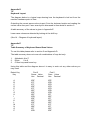
1
MTX VIDEO MEMORY MAPPING.
1.1
Terms used:
VRAM - Video ram.
VDP - Video Display Processor.
CPU - Central Processing Unit.
MBB - Most Significant Bit
LSB - Least Significant Bit
In using MSB and LSB, I have made the assumption that MSB is the left-most bit of
any byte, and LSB is the right-most bit. In my notation MSB = Bit 7. LSB - Bit 0.
MTX Vram memory architecture.
1.2
VRAM on the MTX is managed by the VDP chip, which contains its own autoincrementing address pointer.
The VRAM is independent from the Z30 processor ram as can be seen from diagram
1.0 above.
It can be seen that there is no apparent direct memory mapping to the video screen
which is held in VRAM, however the internal architecture of the VDP chip is such that
you can perform full memory mapping of various types through VDP ports 1 and 2.
Port 2 is used for address transfers.
Port 1 is used for data transfers
All addressing throughout VRAM is 14 bit. Address set ups require a two byte transfer
with two bits left over. To set up an addressing point the low byte of the address is
sent through port 2 first, then the high byte is sent of which bits 0 to 5 are part of the
address, the mode (described in section 1.3), being indicated by bits 6 and 7.
MODE.
1.3
The truth table below shows the bit set up required to direct the VD chip to either
select 'Write data to VRAM or 'Read data from VRAM'.
BIT
6
:
7
1
0
:
:
0
0
‘Write data to VRAM’
‘Read data from VRAM’
After the address set up has been made, data bytes can either be input or output
along port 1, and because the VRAM is managed by an auto-incrementing register,
sequential transfers of data bytes can be performed without having to re-set the
address pointer on the VDP chip.
If you wish to perform alternate input and output of data bytes to VRAM you must reset the addressing mode as appropriate.
Address set ups and data transfers require a certain minimum a of time between
sequential processes. This is 11 micro-seconds between sequential address set-ups,
and 8 micro-seconds between sequential data transfers.
If you are using BASIC there will never be any problem, but if you are using machine
code this is a point to be aware of.
Listed in the next two sections are routines which will perform the job of "PEEKING"
and "POKEING" to the video screen.
Section 1.4 describes the BASIC routines. Section 1.5 and 1.6 describe the assembler
code.
1.4
Both of these sections assume that you are using 'TEXT MODE' ie VS 5, which is the
normal default BASIC VRAM screen set-up.
For BASIC VRAM memory map see Appendix A..
100 REM THESE ROUTINES USE TWO VARIABLES
VADDRESS - USED TO SET UP VRAM ADDRESS
VDATA - USED TO RECEIVE OR SEND SCREEN DATA
110 LET VADDRESS=7*1024: LET VDATA=42
(Set up VRAM address pointer to 7K and data byte to numerical value for ‘*’)
120 GOSUB 1000
(POKE byte onto the screen)
130 LET ADDRESS=7*1024
(Set up VRAM address pointer to 7K)
140 GOSUB 2000 : PRINT VDATA
(PEEK byte on screen in location pointed by VADDRESS, set up in line 130, and print
result)
1000 REM POKE DATA BYTE HELD IN VDATA UNTO SCREEN POINTED TO BY
VADDRESS
1010 LET TEMP2=INT(VADDRESS/256): LET TEMP1=VADDRESS - (TEMP2*256)
1020 OUT (2),TEMP1
1030 LET TEMP2=TEMP2 OR 64 : LET TEMP2=TEMP2 AND 127
1040 OUT (2),TEMP2
1050 OUT (1),VDATA
1060 RETURN
2000 REM PEEK DATA BYTE ON SCREEN POINTED TO BY VADDRESS, AND
RETURN RESULT IN VDATA
2010 LET TEMP2 = INT(VADDRESS/256):LET TEMP1=VADDRESS-(TEMP2*256)
1020 OUT (2),TEMP1
1030 LET TEMP2=TEMP2 AND 63
1040 OUT (2),TEMP2
1050 LET VDATA=INP(1)
1060 RETURN
1.5
All of these routines use either registers DE or C. DE is always left unchanged as are
all other registers, except C which will change dependant on the values you are
reading into it when you call VDINPT.
Output a byte.
LD
CALL
DE,7168
VSETOT
LD
CALL
C,42
VDOUTP
;TOP OF TEXT SCREEN
;SET UP VRAM ADDRESS POINTER FOR DATA
;OUTPUT
;NUMERICAL VALUE OF '*'
;OUTPUT BYTE TO SCREEN
Input a byte.
LD
CALL
DE,7168
VSETRD
CALL
VDINPT
;TOP OF TEXT SCREEN
;SET UP VRAM ADDRESS POINTER FOR DATA
;INPUT
;READ BYTE FROM SCREEN - BYTE RETURNED
;N C
VDP I/O routines.
1.6
;VSETOT-SET UP VRAM ADDRESS POINTER FOR DATA OUTPUT DEPENDANT
ON ADDRESS HELD IN DE ON ENTRY
;
;VSET0T:
PUSH
AF
;SAVE ACC
LD
A, E
OUT
(2),A ;OUTPUT LOW BYTE ADDRESS
LD
A,D
OR 64
AND
OUT
POP
RET
127
(2),A
AF
;SET 'WRITE TO VRAM MODE'
;OUTPUT HIGH BYTE ADDRESS
;GET OLD ACC
;
;VSETRD - SET UP VRAM ADDRESS POINTER FOR DATA INPUT DEPENDENT
ON ADDRESS HELD IN DE ON ENTRY
;
VSETRD:
PUSH
AF
;SAVE ACC
LD
A, E
OUT
(2),A
;OUTPUT LOW BYTE ADDRESS
LD
A, D
AND
63
;SET 'READ FROM VRAM MODE'
OUT
(2),A
;OUTPUT HIGH BYTE ADDRESS
POP
AF
;GET OLD ACC
RET
;
;VD0UTP-OUTPUT DATA BYTE HELD IN C TO ADDRESS POINTED TO BY AUTOINCREMENTING REGISTER ON-BOARD THE VDP
;
VDOUTP:
PUSH
AF
;SAVE ACC
LD
A, C
OUT
(1),A
;OUTPUT DATA BYTE
POP
AF
;GET OLD ACC
RET
;
;VDINPUT-INPUT A DATA BYTE AND RETURN VALUE IN C FROM ADDRESS
POINTED TO BY THE AUTO INCREMENTING REGISTER ON BOARD
THE VDP
VDINPT:
PUSH
AF
;SAVE ACC
IN
A,(1)
;READ DATA BYTE
LD
C,A
;PLACE BYTE IN C'
POP
AF
;GET OLD ACC
RET
Using the MTX assembler.
1.7
The MTX assembler is a simple to use in line, assembler called from BASIC. Only the
machine executable OBJECT code is stored in memory, readable assembler
SOURCE code is generated by disassembling the object code and inserting the
relevant text and labels, stored in tables below the object code.
The actual location of the code can change as it is stored as a BASIC fine, within
BASIC. So as a program is extended and edited the location of the code changes.
Writing in Assembler.
As assembler code is stored in a BASIC line it is first necessary to tell the computer at
which BASIC line you wish the code to appear. This is done with the immediate
command ASSEM, eg :
ASSEM 10
where 10 is the BASIC line number at which the code will appear.
On pressing the return key the screen will clear and the prompt :
Assemble >
Will appear at the bottom of the screen. You are now in assemble mode !
The MTX will no longer respond to BASIC commands such as LIST or RUN but
instead expects one of the assembler commands:
L. - List
T - Top of program
E - Edit
Insert (by default)
Creating a Program.
To start writing your program press the RET key. The word "Insert" will appear at the
bottom of the screen.
A few lines higher up a 4 digit hex number representing the memory location to which
the next instruction will be assigned, the flashing cursory and the instruction RET
appears.
Press the EOL key on the cursor control keypad to get rid of the current instruction
and enter your own.
When you have typed and edited your assembler line press the RET key. The line you
have just typed in will disappear into memory and the next line will appear ready for
another assembler mnemonic.
When you have finished writing your program press CLS on the cursor control keypad
followed by RET. The Assemble prompt should re-appear.
At this point you may wish to list your program out on screen. Press T and RET to set
the program location pointer to the top of the program followed by L and RET to list
out the program.
If your program is more than can be displayed on one screen then after the first
screen has been presented a bell will ring and the listing will stop. To continue the
listing press any of the keys on the main key board. Should you want to stop the listing
then press the BRK key on the cursor control key pad.
When the listing is finished the assembler is again ready to accept another command,
ie. the Assemble prompt appears at the bottom of the screen.
In the following program the data stored in the five bytes starting at DATA are
transferred to the five bytes starting at COPY.
4007
LD HL,DATA
400A
LD DE,COPY
400D
LD BC,5
4010
LDIR
4012
RET
4013 DATA: DB 12,£34,"LOW''
4010 COPY:DS 5
4011
RET
Symbols..
DATA 4013
COPY
4018
Suppose we wanted to modify the program to transfer only the first two bytes. We
would change the line at 400D from LD BC,5 to LD BC,2.
To do this type E £400D and RET.
This will put us in edit mode and display the line to be edited.
Use the cursor along the line with the arrow keys until it is over the letter "5", then we
press the "2" key to change the number followed by RET to store the line away. The
line is now safe in memory and the next line will be presented for editing.
To quit edit mode type CLS followed by RET.
This will leave the assembler ready to accept the next directive.
There is another way of specifying lines in the assembler code without having to use
the address of the instruction.
Suppose we wanted to alter the 12 in line 4013 of the previous example. That line has
an associated label "DATA", so we can use this instead of the address.
Type E DATA and RET.
This has exactly the same effect as E £4013 and RET.
To leave the assembler press CLS and RET. This will bring you back to BASIC.
Now type LIST or L. in BASIC and you will see your assembler code program appear
as a BASIC line. If you already had or now add some lines of BASIC you will find the
code line takes its place just like any normal BASIC line would.
NB:- as your BASIC program is added to or edited the code line will move about in
memory. As most machine code is location dependent it will become necessary to reassemble your code.
To do this type:...
ASSEM 10
and then carriage return to get into the code line and summon the assembler followed
by CLS and RET to leave it again.
This will re-assemble the code for its current location. To get around this problem it is
wise to put your code lines as near the start of the BASIC program as possible. eg:
10
GOTO 100
100 CODE
4007
LD HL,DATA
400A
LD DE,DATA1
etc.
Symbols.
DATA 4013 COPY
4018
20 RETURN
100 REM START OF BASIC PROGRAM
Number Representation.
The MTX assembler will work with either decimal or Hexadecimal numbers. The
default is decimal, but by prefixing a hex number with a "£" , the number is treated as
being hexadecimal. Words are stored according to the Z80 convention, low byte first,
then high byte.
Executing Machine code.
There are two ways to execute machine code from BASIC.
The first and simplest is to place the code "in the way" of the BASIC program
execution flow. When the code line is encountered by BASIC, control will be passed to
the machine code in the code line, control is returned to BASIC by the RET statement.
Should you wish to execute the code more than once then it is best to incorporate the
code line in a BASIC subroutine which can then be called over and over. This also has
the advantage of allowing you to place the code line near the beginning of the BASIC
program and avoiding having to re-assemble the code every time the BASIC program
is edited.
The second method of executing machine code is by the use of the USR function.
Take the previous example and add the following BASIC lines to it..
5 GOTO 100
100 LET X=USR(16400)
110 STOP
If your machine is an MTX500 then line 100 should be:
100 LET X=USR(32784)
Now re-assemble the code line to take account of the fact it has been moved up the
memory by inserting line 5.
Type ASSEM 10 - Carriage return - CLS -Carriage return
The program can now be "RUN". The number in brackets in the USR function is the
address of the machine code, and needs to be re-calculated if the code is moved.
USR returns with the value of the BC register pair, which it.) this case, is assigned to
X. BC will be zero after execution of the routine.
Assembler Commands.
The assembler has only 4 different commands, L,E,T and an insert command which
works by default. The syntax for E, L and insert is :<command letter L,E> space <hexadecimal number> or <label>
Where command letter refers to L, E or in the case of insert no letter.
1) Any number used must be within the range of the code line.
2) Any label used must be contained within the current code line.
The space between the command letter and its operands is optional, but if the
command is used with a label then this may be misunderstood.
eg:- If you wish to edit the line DIOT then using E DIOT is ok but using EDIOT when
the label "EDIOT" exists will cause the assembler to insert lines before the label
EDIOT.
If no parameter is given with the command then the default is the current program line,
ie the line after the fast amended or inserted line. This can be quite useful when
switching between edit and insert modes.
The T command has no parameters and is used only to set the program line location
pointer to the start of the program.
Pseudo Ops.
Pseudo operations look like Z80 instruction mnemonics but are not. They are used to
define the contents of memory and reserve space.
There are only 3 pseudo operations in the MTX assembler, DB,DW,DS:
1) DB - Define byte.
This instruction is used to define the contents of a particular byte in memory. Its
arguments can be numeric, either decimal or hex, alphanumeric, or the low byte of a
label.
Eg:- <label>: DB <dec/hex No.> and/or "<string>" and/or <label>
NB:- Using a label will generate an out of range error, but ignoring this error leaves the
low byte of the label in memory.
2) DW - Define word.
DW allocates a value to word ie two bytes. The number is stored low byte first, making
it compatible with Z80 word instructions.
Eg:- <label>: DW <dec/hex.no.> and/or <label>
3) DS - Define space.
This reserves a specified amount of space in memory, which may be 0 to 254 bytes.
Eg.- <label>: DS <dec/hex.No.>
Examples of Pseudo ops.
DATA:
JMPTAB:
BUFFER:
DB 10,£20, "HIGH''
DB "SCORE''
DW START,START1,0,£FOE3
DW HIT,WIN
DS 50
DS £40
Inserting comments.
The MTX assembler accepts comments in the usual way, ie prefixed by a ";" and
delimited by the end of the line.
If you wish to insert comments after non-executable lines you must use NOP,s.
NOP
NOP
ROUTE:
;Routine to show comments
INC A
RET
Listing, Loading and Saving.
As the assembler code is stored as a BASIC line there is no problem in listing loading
and saving, these are all done as for BASIC.
MTX 500 and 512.
The main difference between the MTX 500 and 512 is the way in which RAM pages
are configured.
The 500 has 32k bytes of memory starting from 9000 hex and finishing at top of
memory at FFFF hex.
The 512 has 64k of memory starting at 4000 hex and finishing at FFFF hex, with an
additional page of 16k switched out between 3000 hex and C000 hex. This additional
memory is switched in and out automatically and provided the code line does not pass
over its boundary the user is unaware of the paging system which is maintained in
hardware by a ULA.
It is possible to trick an MTX 512 into acting like a 500. To do this go into PANEL and
change the contents of memory location FA7A hex (61422 decimal), to zero, then
leave PANEL and type NEW.
This will leave the machine ready to load or have typed a new program as though it
were a 500.
There are a number of differences between the MTX assembler and other
assemblers.
Among these are the fact that there is no requirement to specify the origin of the
object code or provide a long list of assembler directives. As a result the assembler is
both easy to use and relatively fast, about 2 or 3 seconds for an 8k program.
The set of Z80 instructions concerned with loading the stack pointer with HL, IX and IY
are not directly available from the assembler.
They can be accessed in the following way.,
Normally
Use instead
LD SP, HL
LD SP,IX
LD SP,IY
DB £ F9
DB £DD,£F9
DB £FD,£F9
The VDP Chip.
Introduction.
2. 1.
The VDP chip has four video display modes. Normally only Text mode and Graphics
mode 2 are available directly from BASIC, but you can access the other two modes,
Graphics mode 1 and Multicolour mode, by creating your own VDP set-ups (See
sections 2.2 to 2.5).
Text mode provides a screen which is 24 times 40 character rows in two colours.
Multicolour mode provides a 64 times 48 colour dot display in 15 colours plus
transparent and 32 sprites.
Graphics 1 mode provides a 256 times 192 pixel display in 15 colours plus transparent
and 32 sprites.
Graphics 2 mode is an enhancement of Graphics 1 mode providing more complex
colour and pattern displays and 32 sprites.
The video display consists of 35 planes, numbered from 34 down to 0. Working from
the 'back' of the screen to the 'front' these are listed below.
Plane number
34
External video plane
- (Not used at present)
33
Backdrop plane
- (This is where the border fives)
32
Pattern plane
- (This is where the screen you print appears)
31
Sprite plane 31
- (This sprite has the lowest priority and will be
hidden by any of the other 31 sprites which may
cross it)
30-1 Sprite planes 30 to 1
0
Sprite plane 0
- (This sprite has the highest; priority and will appear
to pass in front of any of the other 31 sprites it may
cross)
It is important to note that the sprite planes are not active in Text mode.
Write only registers.
2.2
The VDP has eight write-only registers and one read only status register. The writeonly registers control VDP operation and determine the way in which VRAM is
allocated. Section 2 is concerned with the operation of these write only registers and
does not cover the operation of the read-only register. For brief description of how this
works and what it does see Appendix B.
Each of the eight write-only registers can be loaded using two 8-bit data transfers from
the CPU. The first byte transferred is the data byte and the second is the control byte.
The data byte can be any value between 0 to £FF (Decimal 0 to 255). The format of
the control byte to write to each of the write-only registers (numbered 0 to 7), is shown
in the table below.
Register
Number
0
1
2
3
4
5
6
7
Bits
7, 6
Bits
5, 4, 3, 2, 1, 0
Hex
byte
Decimal
byte
1
1
1
1
1
1
1
1
0
0
0
0
0
0
0
0
£80
£81
£82
£83
£84
£85
£86
£87
128
129
130
131
132
133
134
135
0
0
0
0
0
0
0
0
0
0
0
0
0
0
0
0
0
0
0
0
0
0
0
0
0
0
0
0
1
1
1
1
00
0 1
1 0
1 1
0 0
0 1
1 0
1 1
It can be seen that bits 7 and 6 MUST be set to 1 and 0 respectively. These are the
active control bits in this byte and tell the VDP that the previously transmitted data
byte is to be directed into one of the write-only registers. Bits 5,4,3 MUST be set to
zeroes. The number of the destination register is indicated by bits 2,1,0.
Both data transfers and control bytes directed to the VDP write-only registers must be
output via port 2.
Example 1.
Assuming we are in text mode, the foreground and background colour is determined
by write-only register 7. To alter the foreground colour to black and the background
colour to white we could use either one of the two sections of code listed below.
The way in which VDP register 7 works is described in section 2.3 register 7.
In BASIC.
100 COLOUR 1,1 : COLOUR 2,15
Which will perform the same job as the assembler code listed below.
LD
DE,£071F
;Register D = Write only reg
;destination ie integer X
; 0 =< X =< 7
;Register E = Data byte
;Output data byte to write only register
CALL VOUTRG
;
;VOUTRO-OUTPUT A DATA BYTE TO A SPECIFIED REGISTER
;
REGISTER DESTINATION HELD IN D
;
DATA BYTE HELD IN E
;
DE MUST HOLD VALID CONTENTS ON ENTRY
;
NO REGISTERS AFFECTED ON EXIT
VOUTRG: PUSH
AF
;Save Acc and flags
LD
A,E
;Get data byte
OUT
(2),A
;Output data byte
LD
AA
;Get control byte
AND
7
;Set up correct control bits
OR
128
;Set bits 6,5,4,3 to zero
OUT
(2),A
;Output control byte
POP
AF
;Get old acc and Flags
RET
; Return to calling routine
How BASIC initialises the
2.3
When the MTX is switched on and the VDP write-only registers are set-up for the first
time, it is necessary to set and reset write-only register 0 to 'wake up' the VDP chip
and then to set up all of the other registers correctly.
BASIC sets up the VRAM tables as shown in Appendix A. The data bytes which are
used, and the routine to perform this set-up are listed in the example below.
The routine is called VRGINI (VDP Registers Initialisation Routine). It needs no
register setup on input, and affects none on output. It uses a table called VRGTAB
which has 18 elements, and the routine VOUTRG, which must be present.
;VRGINI-INITIALISE VDP WRITE-ONLY REGISTERS DEPENDENT CONTENTS OF
TABLE VRGTAB
;
NO REGISTER SET-UP REQUIRED ON ENTRY
;
NO REGISTERS AFFECTED ON EXIT
;
VRGINI:
PUSH
AF
;Save Ace and flags
PUSH
DE
;Save DE register pair
PUSH
HL
;Save HL register pair
LD
B, 18
;Set loop counter = 18
LD
HL,VRGTAB ;Set HL to point to start address of table
;VRGTAB
VRG1:
LD
E,(HL)
;Load data byte into E
INC
HL
;Move onto next byte in table VRGTAB
LD
D, (HL)
;Load control byte into D
INC
HL ;
Move onto next byte in table VRGTAB
CALL
VOUTRG
;Output data byte held in to register number
;held in D
DJNZ
VRG1
;Decrement loop counter and If loop counter
;<> 0 then goto VRG1 else drop through to
;VRG2
VRG2:
POP
HL
;Get old HL register pair
POP
DE
;Get old DE register pair
POP
AF
;Get old Acc and flags
RET
;Return to calling routine
;
VRGTAB:
DB
0,0,0,0,0,0,0,0,0
DB
0,0,0,0,0,0,0,0,0
;
The contents of the eight VDP write-only registers are shown in the table below.
Following this table is a description of each register and what each of the control bits
actually do.
Registers 0 and 1 contain flags to enable or disable various VDP features and modes.
Registers 2 through to 6 contain values which are the start addresses for the various
sub-blocks of VRAM (for example where the screen is located).
Register 7 is used to define backdrop and text colours.
Register
Number
MSB
7
0
0
1
4/16K
2
0
5
4
3
2
1
0
0
0
0
0
M3
EV
IE
M1
M2
0
SIZE
MAG
0
0
BLANK
0
3
NAME TABLE BASE ADDRESS
COLOUR TABLE BASE ADDRESS
4
0
5
0
6
0
7
LSB
0
6
0
0
0
0
PG BASE ADDRESS
SPRITE ATTRIBUTE TABLE BASE ADDRESS
0
0
TEXT COLOUR ONE
0
0
SPG BASE ADDRESS
TEXT COLOUR ZERO/BACKDROP
Register 0
This contains two VDP option control bits. All other bits are reserved for
future use and must be zeroes.
Bit1
Bit 0
M3 Mode Bit 3 (See register 1, bits 3 and 4)
EV External Video Enable/Disable 1 Enables External Video Input 0
Disables
Register 1
This contains seven VDP option control bits. Bit 2 is reserved for future
use and must be zero.
4/16k Ram Selection.
1 selects 4108/4116 RAM operation.
0 selects 4027 RAM operation.
This bit must be set to 1 on the MTX. It uses 4116 RAM chips for VRAM.
BLANK enable/ disable
1 enables the active display
0 causes the active display area to blank
When this bit is set to zero, the screen will show the border colour only
IE = Interrupt enable/disable
1 enables VDP interrupt
0 disables VDP interrupt
This subject is covered in depth in section 3
M1 = Mode bit 1
M2 = Mode bit 2
The three mode bits M1, M2 and M3 determine the graphic mode
that the VDP is currently in. The necessary bit set up required to activate
the different modes is shown in the table below.
Bit 7
Bit 6
Bit 5
Bit 4
Bit 3
M1
M2
M3
0
0
0
1
0
0
1
0
0
1
0
0
Bit 2
Bit 1
Reserved and must be zero.
SIZE selects Sprite Size
1 selects size 1 sprites (16 times 16 bits).
0 selects size 0 sprites (8 times 8 bits).
MAG is the magnification option for sprites.
1 selects MAG1 sprites (SIZE times 2).
0 selects MAG0 sprites (SIZE times 1).
Bit 0
Register 2
Graphic 1 mode
Graphic 2 mode
Multicolour mode
Text mode
The contents of this register define the start address of the name
table sub block, in other words, the start address of the VRAM display
screen.
It is a four bit value and therefore has a range of 0 to 15, which it must
not exceed. Bits 7,6,5 and 4 of this register must be zero.
The name table must be located on a 1k boundary, so if we were to load
this register with say 7, the VRAM display screen would start at 7K or
£1C00 Hex. If we loaded it with 15, the VRAM display screen would start
at 15K or £3C00 Hex. In text mode this table is 960 (24 times 40) bytes
long.
In all other modes this table is 768 (24 times 32) bytes long.
Register 3
The contents of this register define the start address of the colour table
sub block. This holds the colours of the patterns used in graphic modes
1 and 2. It is not used by text or multicolour mode. Text and multicolour
mode are covered in sections 2.5 and 2.7 respectively.
Graphic modes 1 and 2 access the colour table in different ways. This
means that the set up bits for this register are different dependant on
which graphic mode you wish to use.
In graphic one mode the colour table is located on a 64 byte boundary
and is 32 bytes long. If we wanted to locate it at 8k (£2000 Hex), we
need to divide 8k (3192 Decimal) by 64, and then load the result into
register 3. This will be 32.
For a fuller description of how graphic mode 1 works see section 2.6.
In graphic two mode, which is the usual BASIC graphic mode, the colour
table is located on an 8k boundary. As the VDP uses 16K of VRAM, this
means that the colour table can be located at either address 0K or 8k
only.
If you wish to locate the colour table at address 0K then bit 7 of register
3 must be set to 0. If you wish to locate the colour table at address 8k
then bit 7 of register 3 must be set to 1.
In both cases bits 6 to 0 must be set to 1's. This set-up is also shown in
the table below.
Locate colour table
at VRAM address
Load register 3
with data byte
OK - £0000 – 0 Decimal
127 Dec - £7F Hex
BK – £2000 – 8192 Dec
255 Dec - £FF Hex
The colour table is 6144 bytes long in graphic mode.
Graphic 2 mode colour table creation is described in much greater depth
in section 2.4.
Register 4
PG BASE ADDRESS is the start address of the pattern generator table.
This is where the patterns of the characters for the various modes are
held. It is a 3 bit value and therefore has a range of 0 to 7. It must not
exceed this value.
Bits 7,6,5,4 and 3 must be set to 0.
In all graphic modes except graphic mode 2, this table is located on a 2K
boundary. This gives 8 possible positions in which it can be located in
VRAM. The start address is determined by the contents of this register
times 2K.
If for example we wished to locate this table at address 8k (£2000 Hex)
in VRAM, we would load register 4 with 8k divided by 2K which is 4.
In graphic 2 mode this table is located on an 8k boundary as in the
graphic 2 mode for register 3.
Bits 1 and 0 must be 1. If bit 2 is 1 then the pattern generator table will
be located at address 8K . If this bit 2 is 0 then the table will be located
at 0K.
This set-up is also shown in the table below.
Locate pat gen table
at VRAM address
Load register 4
with data byte
OK - £0000 – 0 Decimal
3 Dec - £03 Hex
8K - £2000 – 8192 Dec
7 Dec – £07 Hex
The pat gen table is 6144 bytes long in graphic 2 mode.
Graphic 2 mode pattern generator creation is described in much greater
depth in section 2.4.
Register 5
SPRITE ATTRIBUTE TABLE BASE ADDRESS is the start address for a
128 byte block which contains position, colour and shape information, for
each of the 32 sprites which it is possible to enable.
The sprites are active in all modes except text mode.
This register value occupies 7 bits and therefore has a range of 0 to 127.
Bit 7 must be set to 0. The sprite attribute table is located on a 128 byte
boundary. If we wished to locate this table at say address 6K (£1000
Hex - 6144 Dec), we would have to divide our desired decimal start
address by 120 (or our desired hex address by £80), and then place the
result in register 5. In this case the correct resulting byte is shown in the
table below.
Desired address
Divide by
Result
Dec
6144
128
48
Hex
1800
£80
£30
For a fuller description of the sprite attribute table please see section 4.
Register 6
SPG BASE ADDRESS is the sprite pattern generator base address.
It holds a library of sprite shapes which can be 'called up' by one of the
control bytes in the sprite attribute table. This means that to change a
sprite shape to another existing pattern it is only necessary to change
one byte in VRAM.
This table is a maximum of 2043 bytes long, and is divided into 256
blocks of 8 bytes each.
The register value for this table occupies 3 bits and therefore has a
range of 0 to 7. It must not exceed this range. Bits 7,6,5,4 and 3 must all
be set to 0.
The table is located on a 2K boundary so if we wished to locate this table
at say address 14K, all we have to do is divide the desired start address
for this table by 2K to obtain the correct byte to load into register 6. In
this case 14K divided by 2K = 7.
For a fuller description of the sprite pattern generator table please see
section 4.
Register 7
This register is split into two nibbles ie two 4 bit values.
The upper 4 bits 7,6,5 and 4, contain the colour code of the ink colour for
characters in text mode.
The lower 4 bits 3,2,1 and 0, contain the colour code of the paper colour
for characters in text mode and the backdrop (border) colour in all
modes.
Graphics Mode 2
2.4
Graphics 2 mode is the normal BASIC graphics mode. The features which it provides
are summarised in the table below.
Screen
768 unique characters (24 rows by 32 columns). 256 (Horizontal) by 192
(Vertical) plottable pixels.
15 colours (See appendix C) plus transparent, in a 3 (Vertical) by 2
(Horizontal) colour matrix for each character.
15 border (Backdrop) colours plus transparent.
Sprites
32 sprites each one of which may have any one of 15 colours including
transparent and are plottable at. any of the 256 times 192 screen pixel
positions.
256 patterns for 8 pixel by 8 pixel sprites. Bits 1. and 0 in VDP write-only
register 1 are both 0.
64 patterns for 16 pixel by 16 pixel sprites. Bits
1 and 0 in VDP write only register 1 are 1 and 0 respectively.
The VDP is in graphics 2 mode when mode bits M1 = 0,M2 = 0 and M3 = 1 (see
section 2.2 register 1 bits 3 and 4).
When the DP is first initialised into graphics two mode, the VRAM is organised as
displayed in the table below.
VRAM sub block
Pattern generator table
Pattern colour table
Pattern name table (screen)
Sprite attribute table
Sprite generator table
Length in bytes
6144
6144
768
128
2048
If you had created your own graphic 2 mode set up then these tables could be located
at various addresses. If however, you had set them up at the same addresses as
BASIC does, then the VRAM memory map for these tables would look like that below.
Address to
decimal
0000
- start of pattern generator table
6143
- end of pattern generator table
6144
- free space (see below)
8191
- end free space. ^ (Illus 2 – VMM)
8192
- start of pattern colour table
14335
- end of pattern colour table
14336
- start of sprite generator table
15359
- end of sprite generator table
15360
- start of pattern name table
16127
- end of pattern name table
16128
- start of sprite attribute table
16255
- end of sprite attribute table
It can be seen that the sprite generator table as set up by BASIC is only 1K bytes long
whereas it is normally 2K bytes long. It means that you can only use half of the
number of possible sprite patterns that would normally be available because this table
overlaps with the display screen.
As it has to be located on a 2K byte boundary and as there is apparently 2K bytes free
at address 6144 Decimal, most readers will be wondering why the sprite generator
was not located there instead.
The reason for this is that this area is actually reserved for text mode which occupies
the ‘free space’ as shown below.
Address in
decimal
6144
- text pattern library
7167
- end text pattern library
7168
- start text name table (text display screen)
7191
- end text name table
Allocating 1K bytes for the sprite generator table as BASIC does is a compromise. The
VRAM set up as BASIC creates, it means that to switch from text mode to graphics 2
mode and vice versa it is only necessary to change two VDP write-only registers, a
process which takes a little over 20 micro-seconds (20 1/100 thousandths of a
second).
This is how you can switch from one mode to the other without affecting the integrity of
either screen in any way. The tables are held separately, and when the modes are
switched, are left intact because they have clearly defined separate boundaries within
VRAM.
In graphics 2 mode each byte of the pattern colour table provides a foreground and
background colour for the corresponding byte in the pattern generator table. Byte 0 of
the pattern colour table maps directly onto byte 0 of the pattern generator table. Byte 1
onto byte 1. Byte 2 onto byte 2 and so on. Assuming the pattern generator table is
located at 0K and the pattern colour table at 8K, to discover which pattern generator
byte is coloured in by which colour byte all we need to do is add an offset which is
equal to the distance between the two tables to find the desired VRAM address. In this
case the offset is 8192 Dec (£2000 Hex).
The mapping scheme below shows how the coloured patterns are actually mapped
onto the display screen.
^ (Illus 3 – Diagram of mapping scheme)
In order to access this mapping scheme, the pattern name table needs to be initialised
correctly. In order for the first pattern character block to map onto the first character
cell on the screen and the second pattern character block to map onto the second
character cell on the screen and so on, screen position 0 must contain 0, screen
position 1 must contain 1, up to screen position 255 which must contain 255.
This however only accounts for the top third of the screen, what of the other two
thirds?
Internally the VDP segments the pattern generator, pattern colour and pattern name
tables, into three equal blocks of 2048, 2048 and 256 bytes respectively. Character
labels in the upper third of the screen automatically correspond to the character
patterns in the upper third of the pattern generator table. Labels in the middle third of
the screen correspond to the character patterns in the middle third of the pattern
generator table, and labels in the lower third of the screen correspond to the character
patterns in the lower third of the pattern generator table.
The second and third blocks of the screen are mapped onto the related character
patterns in the pattern generator table on the basis of position, therefore, in order to
fill the second and third parts of the screen with the correct labels we load position 256
with 0 through to 511 with 255, and position 512 with 0 through to 255.
The correct start label values for the second and third block of the screen of 256 and
512 respectively are added by the VDP.
Assuming that we have located our pattern name table at 15K, then the assembler
code routine which will set up the screen correctly is shown below. The routine uses
the VRAM I/0 routines described in section 1.5 and 1.6
;
; INISCR
;
;
;
;
INISCR:
;
INISC1:
INITIALISE PATTERN NAME TABLE (DISPLAY SCREEN)
NO PARAMETERS REQUIRED ON ENTRY
NO REGISTERS AFFECTED ON EXIT
PUSH
PUSH
PUSH
PUSH
LD
AF
BC
DE
HL
HL,768
;Save Acc and flags
;Save BC register pair
;Save DE register pair
;Save HL register pair
;Set up loop counter to equal
;768 – This is the size of the
;display screen
;Set byte to be output to each
;sequential screen position to zero
;Load DE with start address of screen
;Set VDP write to VRAM pointer
;to point to start of screen
LD
C,0
LD
CALL
DE,15360
VSETOT
CALL
INC
DEC
VDOUTP
C
HL
;Output display byte to screen
;Increment display byte
;Decrement loop counter
LD
OR
JR
A,H
L
N,INISC1
;If loop counter < > 0 then
;goto INISC1 else drop through
;to INISC2
POP
POP
POP
POP
RET
HL
DE
BC
AF
;Get old HL register pair
:Get old DE register pair
;Get old BC register pair
;Get old Acc and flags
;Return to calling routine
;
;
INISC2:
Text Mode
2.5
Text mode is either decimal or hex, alphanumeric, or the low byte of a label.
eg: - <label>: DB <dec/hex No.> and/or “<string>” and/or <label>
NB: Using a label will generator an out of range error but ignoring this error leaves the
low byte of the label 8 (Vertical) pixel size.
The character patterns can be dynamically changed to give any number of character
patterns limited by the amount of storage space in Z80 RAM for the extra pattern
libraries.
The display colours can be any one of 15 including transparent for the backdrop
colour, and any one of 15 including transparent for the text colour.
The VDP is in text mode, when mode bits M1 = 1, M2 = 0 and M3 = 0 (see section 2.2
register 1 bits 3 and 4).
When the VDP is first initialised into text mode the VRAM is organised as shown in the
table below.
VRAM sub-block
Pattern generator table
Pattern name table
Length in bytes
2048
960
Text mode VRAM arrangement in BASIC has already been discussed in section 2.4,
because in BASIC it has been designed to be an integral part of the tabling for graphic
mode 2.
It can be seen however, that the text pattern generator table as BASIC sets it up is
only 1K long. This will only allow you to have a maximum of 128 different patterns in
this mode. As explained in section 2.4 concerning the reduction in size of the sprite
generator table, this is a compromise measure in order to have both graphics two
mode and text mode resident in VRAM at the same time.
Sprites are not available in this mode because it is concerned only with the use of text
type characters.
Text mode has many advantages in that it is very compact. A text mode set-up only
occupies 3K of VRAM. It is possible to build up several different text libraries in VRAM
and several screens, and switch to a complete new text set-up by changing only two
VDP write-only registers.
Alternatively it is possible to have one text library held in the text pattern generator
table, and to have up to 14 completely separate display screens, which can be
changed to a new screen by changing only one VDP write-only register (Register 2), in
a time interval of about 11 micro-seconds. This would be very useful for building up
animated displays.
The text pattern generator table is 2048 bytes long and is split into 256 text patterns,
each of which is 8 bytes long. Since each text position on the screen is six pixels
across, the least significant bits 9ie bits 1 and 0) of each text pattern byte are ignored.
Each block of eight bytes in the text pattern library define a text pattern in which the
1’s take on the text foreground colour, while the 0’s take on the background (or
backdrop) colour. These colours are chosen by loading VDP register 7 as described in
section 2.2 example 1.
Any one of any of the patterns held in the text pattern library can be displayed in any
position on the current text display screen, simply by loading the value of the desired
pattern number into the appropriate position in the text display screen area.
Assuming we had a standard ascii character set held in our pattern library and that the
text display screen was located at 7K, then we could use the simple routine below to
print out strings to this screen. The routine uses the VRAM I/O routines as described
in section 1.
The ascii values of the characters we wish to output will provide the correct pattern
number to be loaded into the text display screen area to extract the correct pattern
shape.
;
;STRING
;
;
;
;
;
;
;
;
;
;
MESSAGE:
;
START:
-PRINT A STRING ROUTINE
VDP SHOULD BE IN TEXT MODE ON ETYR
START ADDRESS OF STRING POINTED TO BY HL
SCREEN ADDRESS TO WHICH STRING MUST GO IN DE
STRING MUST BE DELIMITED BY A ‘$’
NO OTHER PARAMETERS REQUIRED
NO REGISTERS AFFECTED EXCEPT HL WHICH POINTS
TO ‘$’ CHARACTER ON EXIT
DB
‘This is an ascii string$’
LD
HL,MESSAGE
LD
DE,7144
CALL STRING
RET
;
STRING:
STRIN1:
STRIN2:
;Set HL to point to start address of
;text string
;Set DE to point to start address at
;which the text string is to be output
;Output string to screen
;Return to calling routine
PUSH AF
PUSH BC
CALL VSETOT
; Save Acc and flags
;Save Bc register pair
; Set VDP write to VRAM pointer to start
;address for text output
LD
CP
A,(HL)
‘$’
RET
Z
;Load text byte into Acc
;Test to see whether if character is
;a ‘$’
;If true then return to calling routine
;else drop through to line STRIN2
;Load text byte into output register
;Output text byte to VRAM
;Increment text pointer to point to next
;byte in text string
;Go back to STRIN1 and do it again
LD
C,A
CALL VDOUTP
INC HL
JR
STRIN1
Graphics 1 Mode
2.6
Graphics 1 mode is the other graphic mode available on the MTX and is not normally
allowed from BASIC. It can be enabled with ease in assembler, and does have
certain useful features. The features it provides are summarised in the table below.
Screen
768 character positions (24 rows by 32 columns) with up to 256
unique characters at any time in an 8 (Horizontal) by 8 (Vertical) pixel
size.
The graphics pattern display colours can be any two of 16 (including
transparent) sectioned into groups of 8 characters.
The backdrop or border colour can be any one of 16 (including
transparent).
The character patterns can be dynamically changed to give any number
of character patterns limited by the amount of storage space in Z80 RAM
for the extra pattern libraries.
Sprites are available up to a maximum of 32.
The VDP is in Graphics 1 mode, when mode bits M1 = 0, M2 = 0 and M3 = 0 (see
section 2.2 register 1 bits 3 and 4).
One of the major advantages of this mode is that it is very compact, requiring a
maximum 2848 VRAM bytes for a complete set-up. Yet it is possible with some care
to create graphics effects very similar to those available in graphics 2 mode.
Like text mode, it is also possible to build up several different pattern libraries in
VRAM and several screens, and switch to a complete new graphics 1 mode set-up by
changing only two VDP write-only registers.
And again like text mode it is possible to have one pattern library held in the pattern
generator table, and to have up to 14 completely separate display screens, which can
be changed to a new screen by changing only one VDP write-only reg A,E ;Get data
byte
OUT (2),A
;Output data byte
LD
A,D
:Get control byte
AND 7
;Set up correct control bits
OR
128
;Set bits 6,0w
VRAMsub-block
Pattern generator table
Pattern colour table
Pattern name table
Length in bytes
2048
32
768
The pattern generator table is 2048 bytes long and is split into 256 graphics patterns,
each of which is 8 bytes long.
Each block of eight bytes in the pattern generator library define a graphics pattern in
which the 1’s take on the foreground colour assigned to its, while the 0’s take on the
appropriate background (or backdrop) colour.
These colours are chosen by loading the correct byte of the pattern colour table with
the appropriate colour byte in a very similar way to that used to load VDP register 7 as
described in section 2.2 example 1.
The difference is that these colour control bytes are held in VRAM and do not need a
register type write to set them up, but would be manipulated using the VRAM I/0
routines described in section 1.
The mapping arrangement for pattern generator character shapes to the appropriate
colour bytes is shown in the table below.
Pattern
numbers
0 to 7
8 to 15
16 to 23
24 to 31
32 to 39
40 to 47
48 to 55
56 to 63
64 to 71
72 to 79
80 to 87
88 to 95
96 to 103
104 to 111
112 to 119
120 to 127
Pattern colour
bytes
Pattern
numbers
0
1
2
3
4
5
6
7
8
9
10
11
12
13
14
15
Pattern colour
bytes
128 to 135
136 to 143
144 to 151
152 to 159
160 to 167
168 to 175
176 to 183
184 to 191
192 to 199
200 to 207
208 to 215
216 to 223
224 to 231
232 to 239
240 to 247
248 to 255
16
17
18
19
20
21
22
23
24
25
26
27
28
29
30
31
It can be seen that for each block of eight patterns in the pattern generator library the
colour is determined by one byte of the pattern colour cable. This means that to obtain
a wide range of differently coloured graphic patterns in this mode may require some
thought.
Any one of any of the patterns held in the pattern generator library can be displayed in
any position on the current graphics display screen, simply by loading the value of the
desired pattern number into the appropriate position in the graphics display screen
area.
Assuming that we had set up the pattern colour table bytes as below:
Pattern colour table byte 0
=
£F1 (Hex), 241 (Decimal)
White on black
byte 1
=
£41 (Hex), 65 (Decimal)
Blue on black
The graphics display screen was located at VRAM address £C00 (Hex), 3096
(Decimal) or 3K.
The pattern generator library was located at VRAM address £0 (Hex), 0 (Decimal), or
0K.
Pattern generator table block
0
8
=
=
Blank pattern
Diamond shape
Then a routine which will blank the screen out and draw a border around the outside
of the screen is listed below. This routine makes full use of the VDP I/O routines listed
in section 1.
;
;GRAFIK-CLEAR SCREEN USING PATTERN NUMBER 0
;
DRAW BRODER USING PATTERN NUMBER 8
;
FOR USE WITH GRAPHICS 1 MODE SCREEN
;
;
ASSUMPTIONS DESCRIBED ABOVE
;
ALSO ASSUME THAT VDP WRITE-ONLY REIGSTERS
;
HAVE ALREADY BEEN SET-UP
;
;
NO PARAMETERS REQUIRED ON ENTRY
;
NO REGISTERS AFFECTED ON EXIT
;
GRAFIK:
PUSH
AF
;Save old Acc and flags
PUSH
BC
;Save BC register pair
PUSH
DE
;Save DE register pair
PUSH
HL
;Save HL Register pair
CALL
CLRSCR
;Clear the screen
CALL
BORDER
;Draw the border
POP
HL
;Get old HL register pair
POP
DE
;Get old DE register pair
POP
BC
;Get old BC register pair
POP
AF
;Get old Acc and flags
RET
;Return to calling routine
;
CLRSCR:
LD
DE,£C00
;Set the VDP write to VRAM
CALL
VSETOT
;Pointer to the start of the
;graphics display screen
LD
C,0
;Load the clear screen character
;into the output register
LD
CALL
HL,768
OUTBLK
;Loop counter – 768 (Decimal)
;This routine will output the byte
;held in C to VRAM from the start
;address held in DE HL number
;of times
;Return to calling routine
TOP
BOTTOM
SIDES
;Draw the top of screen border
;Draw the bottom of screen border
;Draw a border down both sides
;of the graphics display screen
;Return to the calling routine
LD
CALL
DE,£C00
VSETOT
LD
C,8
LD
CALL
HL,32
OUTBLK
;Set the VDP write to VRAM
;pointer to the start of the top line
;of the graphics display screen area
;Load the border character into
;the output register
;Loop counter = 32 (Decimal)
;This routine will output the byte
;held in C to VRAM from the start
RET
;
BORDER:
CALL
CALL
CALL
RET
;
TOP:
‘address held in DE HL number of
;times:
;Return to calling routine
RET
;
BOTTOM
LD
CALL
DE,£EA1
VSETOT
LD
C,8
LD
CALL
HL,32
OUTBLK
RET
;
SIDES:
SIDES1:
SIDES2:
;
OUTBLK:
LD
DE,£C20
LD
PUSH
CALL
B,22
BC
VSETOT
LD
CALL
C,8
VDOUTP
LD
ADD
EX
CALL
HL,31
HL,DE
DE,HL
VSETOT
CALL
VDOUTP
INC
DE
POP
DJNZ
BC
SIDES1
RET
CALL
VDOUTP
DEC
LD
HL
A,H
;Set the VDP write to VRAM
;pointer to the start of the bottom
;line of the graphics display screen
;Load the border character into
the output register
;Loop counter = 32 (Decimal)
;This routine will output the byte
;held in C to VRAM from the start
;address held in DE HL number of
;times
;Return to calling routine
;Load DE with the start address of
;the second line of the display screen
;Loop counter = 22 (Decimal)
;Save old BC register pair
;Set the VDP write to VRAM pointer
;to the start address contained within
;DE
;Load C with the border character
;Output border character to display
;screen (Left hand side)
;Increment DE by 31 ie move the
;VDP write to VRAM pointer
;to the right hand side of the screen
;Rest the VDP write to VRAM pointer
;to the start address contained within
;DE
;Output the border character still
;retained in C to the display screen
;(Right hand side)
;Increment the VDP write to VRAM
;reference pointer by one to move
;along character position and down
;one line back to the left hand side
;of the screen
;Get old BC register pair
;Decrement loop counter and if loop
;counter < > 0 then goto SIDES1
;else drop through to SIDES2.
; Return to calling routine
;Output data byte held in C to
;VRAM to address pointed to by the
;VDP write only pointer
;Decrement loop counter held in HL
;if loop counter < > 0 then goto
OUTBL1:
OR
JR
RET
L
NZ,OUTBLK
;OUTBLK else drop through to
;to OUTBL1
;Return to calling routine
Multicolour Mode
2.7
Multicolour mode is not normally allowed from BASIC, but like graphics 1 mode it can
be enabled with ease in assembler. Although I cannot see much use for it, it is
available on the machine and so I will attempt to describe it.
The features it provides are summarised in the table below:
Screen
An unrestricted 48 row by 64 column display consisting of blocks
of 4 (Horizontal) by 4 (Vertical) pixels in any one of 15 colours
plus transparent.
The character pattern colours can be dynamically changed to
provide colour animated displays.
The backdrop or border colour can be any one of 15 plus
transparent.
Sprites are available up to a maximum of 32.
The VDP is in multicolour mode, when mode bits M1 = 0, M2 = 1 and M3 = 0 (see
section 2.2 register 1 bits 3 and 4).
Multicolour mode occupies a total of 1728 VRAM bytes in a complete set-up divided
into two tables, but because the tables are not contiguous and begin on even 1K and
2K boundaries a total of 3K is needed. 768 bytes are used for the name table and
1536 bytes (24 rows by 32 columns by 8 bytes per pattern position), for the pattern
generator table.
Like the graphic modes, multicolour mode has a screen consisting of 768 character
positions. The character label value contained within any one of the positions on the
display screen does not point to a character shape because this is always a 2
(Horizontal) by 2 (Vertical) block of 4 (Horizontal) by 4 (Vertical) pixels all set to 1,s.
Instead it points to a colour reference held within what would normally be the pattern
generator table. As in other modes each cell within the pattern generator table
consists of eight bytes. Multicolour mode only uses two of these bytes within each
pattern generator cell for each label on screen.
These two bytes specify four colours, each colour being related to each of the 4 by 4
pixels blocks within a character position on screen. The four MSB,s of the first byte
define the colour of the upper left quarter of the multicolour pattern. The four LSB,s of
the first byte define the colour of the upper right quarter. The second byte similarly
defines the lower left and right hand corner of the multicolour pattern.
This is shown in the diagram below:
Byte
Number
Bits
7 6 5 4
Bits
3 2 1 0
8
PIXELS
1
2
COLOUR A
COLOUR C
COLOUR B
COLOUR D
8
PIXELS
****
*AB*
*CD*
****
^(Illus 4 – ABCD diagrammed from above)
The location of the two bytes within the eight byte segment of the pattern generator
table pointed to by the character label value held in any one of the display screen
character positions is dependent on the screen position in which the character label is
held. This is also elaborated to some extent by the diagram below.
For names in the top row of the display screen (ie values 0 to 31), the first two colour
bytes of the pattern generator cell are accessed. For the second row of the display
screen (ie values 32 to 63), the second two colour bytes of the pattern generator cell
are accessed. The next row of the screen uses the fifth and sixth bytes and the next
row uses the seventh and eighth . This series repeats for the remainder of the screen.
Pattern Generator
Cells
0 to 31
32 to 63
64 to 95
96 to 127
128 to 159
160 to 193
(X) to (X+31)
Screen
Rows
0
1
2
3
4
5
(X DIV 32)
Pattern Generator
Bytes
0 and 1
2 and 3
4 and 5
6 and 7
0 and 1
2 and 3
(X DIV 16
MOD 8
and (X DIV 16 + 1) MOD 8
NB: X = start location of each of the display screen rows relative to the top left hand
of the screen.
Points to look out for
2.8
One of the major points to look out for when manipulating the VDP chip through any of
the four different modes is a direct result of the action of BASIC.
BASIC services VRAM at all sorts of odd times using various interrupts. If you are
using the same modes as BASIC uses there will be no problems if you are using them
in the same way as BASIC does. If however, you are using and creating your own
VDP modes or are using the same modes with different VRAM table set-ups you will
have to choose between having BASIC around or not, else BASIC and your code will
conflict and you will end up with garbage.
In most cases if you are doing anything that BASIC would not normally do you will
have to use assembler. BASIC can easily be disabled by using a DI instruction at
the start of your code, and an RETI instruction at the end. If you have modified the
contents of the VDP registers drastically it would be far better to perform a JP £0000
as your last instruction as a warm boot back to BASIC.
No matter what processes you perform in Z80 ram, as long as you do not corrupt the
VDP registers, or perform a BASIC reboot, or perform a system reset the integrity of
VRAM will always be maintained.
You can switch from one VDP mode to another in mid processing operation by
performing a VDP write only register change. Some very interesting effects can be
obtained by having graphics 1 mode tables and text mode tables on compatible VRAM
start boundaries and then switching from one to the other.
All direct VDP operations are associated with ports 1 and 2 only.
VDP and CTC Interrupts – Introduction
3.1
At the end of each active display scan which is about every 1/50 of a second, the VDP
chip will stop all screen processing and perform other tasks. It is possible to set up
VDP interrupt servicing routines which will start at the end of each active display scan,
and finish before the next one has begun.
This routine is a period of time when data bytes written to the screen or blanked onscreen can be processed in a glitch free manner.
Bit 5 of register 2 must be set to a 1 to allow VDP interrupts to take place. This should
be done during VDP write only register set up at the start of your code.
In addition to this the use of standard IM 2 interrupts has been enhanced using the
CTC chip on board the MTX, to allow the user to set up vector tables on an 8 byte
boundary within a page instead of a page boundary alone leading to a much greater
flexibility and ease of use in vector table positioning.
This can be a complex subject for some computer users who are new to the subject,
but it is well worth while persisting with this section. The results of mastering
interrupts make the effort involved small in comparison.
The advantages of using VDP interrupts are:
1.
A drastic improvement in the quality of animated displays. Reducing or
removing glitches created when transferring bytes to or from the display
screen area.
2.
It gives a second optional clock and can be used for timing and compact
delay loops.
Programming the CTC
The Zilog CTC counter Timer Circuit handles all interrupts on the MTX including the
Video Display Processor (VDP) interrupt. The following is intended only as brief
outline concerning CTC operation. For more details refer to Zilog’s Z8430 CTC
Counter/Timer Circuit product specifications.
The CTC is capable of generating mode 2 interrupts from any of its 4 independently
programmable channels. It is capable of acting as either a timer or counter, working
on an external clock. The port numbers, CTC channel numbers and functions are as
follows:
Port
Number
Channel
Function
08
09
0A
0B
ch0
ch1
ch2
ch3
VDP interrupt line
4 MHz system clock /13
4 MHz system clock /13
cassette edge input
The first word to write out to the channel being programmed is the channel control
word this is made up as follows:
Bit
Value
Function
B7
1
0
Interrupt enabled
Disable interrupt
B6
1
0
counter mode
timer mode
B5
1
0
prescaler of 256
prescaler of 16
B4
1
0
trigger on rising edge
trigger on falling edge
B3
1
0
clk/trig pulse starts timer *
start on receiving time constant
B1
1
0
software reset
continued operation
B0
1
0
control word
vector word
*
Using Timer Mode Only
If bit 2 is set then the channel will consider the next byte it receives to be a time
constant. Setting bit 1 causes the channel to stop what it is doing and accept the next
set of parameters it will also require a new time constant.
The interrupt vector word is identified by a zero in bit 0. The 5 most significant bits
form the 5 most significant bits of the interrupt vector provided by the chip on
interrupts (mode 2). Bits 1 and 2 are set according to the channel generating the
interrupt and bit 0 is always zero.
B2
B1
0
0
1
1
0
1
0
1
Channel
0
1
2
3
The interrupt vector table must lie on an 8 byte boundary. This table normally sits at
FFF0 hex. A working example set up of an IM 2 vector table is detailed in section 3.2
Note that the ctc channels were reset twice, this is because one or all of the channels
may be expecting a timer constant and hence misunderstand the first reset program
word sent to the channel.
In the service routine the VDP status register is read (IN (2),A). This is to
acknowledge and reset the VDP interrupt as well as re-initialise the read write cycle of
the VDP.
How to Generate VDP Interrupts
3.2
Setting up a VDP interrupt servicing routine is essentially a three stage process which
is detailed in parts 1 to 3. Part 4 is a listing of the code which will perform the complete
task.
Before this section of code is executed it is vital to inform the VDP chip that it is going
to be expected to perform user defined interrupts. This is done by ensuring that when
the VDP write only registers are set up, bit 5 is register 1 is at 1. This is the VDP
interrupt enable bit.
Part 1
VDP interrupts are set up and accessed through the normal Z80 IM 2. This mode is
tied into the CTC chip and enables four channels to be made available to the user on
ports 8, 9, 10 and 11 referred to as CTC channels 0, 1, 2 and 3 respectively.
The first task that needs to be done is to shut off any existing interrupts on board the
ctc chip which you do not require. The code below will switch of all ctc interrupts on
channels 0, 1, 2 and 3.
KILLcTc:
LD
LD
B,2
A,3
KILLloop:
OUT
OUT
OUT
OUT
(CTC),A
(CTC+1),A
(CTC+2),A
(CTC+3),A
;Loop counter = 2
;Ready reset CTC channel byte in
;Acc ready for output to ports 8, 9, 10 & 11
;Ouput reset byte to channel 1 port 8
;Ouput reset byte to channel 2 port 9
;Ouput reset byte to channel 3 port 10
;Ouput reset byte to channel 4 port 11
DJNZ KILLloop
;Decrement loop counter and if loop
;counter < > 0 then goto KILLloop else
;drop through to next section of code.
It can be seen in the above code that the reset byte 3 is being written to the ctc chip
twice. This is because the CTC may expect the next byte input to it to be a time
constant therefore a re-write will eliminate these.
Part 2
After executing the code above, the next section of code (listed below), selects
interrupt mode 2, sets up the interrupt vector table by loading the high byte of the
vector table start address into the I register and the low byte of the vector table start
address into channel 0 of the ctc chip, then loading the interrupt servicing routine start
address into vector table bytes 0 and 1.
The most important point to note at this stage is that the two byte vector table start
address selected by the value in I (High byte), and the value output to CTC channel 0
(Low byte), MUST point to a fixed 0 byte boundary address.
The assumption being made is that the start address of the vector table is £8180
(Hex).
SETupCTC: DI
IM
LD
2
A,£81
LD
LD
I,A
A,£80
OUT (CTC),A
LD
HL,VDPout
LD
(IJtable),HL
;Disable all existing interrupts
;Select interrupt mode 2 (IM 2)
;Load the high byte of the vector
;table start address into the
;page select register
;Select low byte vector table
;start address on 8 byte boundary
;within the page pointed to by the
;contents of I.
;Select the start address of the actual
;servicing routine. In this case it is
;indicted by the label VDPout
;Load the interrupt servicing routine
;start address into vector table bytes
;0 and 1.
Part 3
The final stage is to re-enable the ctc chip interrupt on channel one, and clear the vdp
interrupt flag on board the vdp chip, by performing a read of the vdp read only register
(signified by variable VDPRGO which = 2).
Each time the read only register is read, the interrupt line is reset on board the vdp
chip.
NB:
1.
2.
The read only register on board the vdp chip must be read each time you
exit from your interrupt routine
The maximum duration of your interrupt routine MUST NOT be longer than
1/50 second (20,000 microseconds).
SETupINT:
LD
A,0C5H
OUT (CTC),A
LD
A,1
OUT (CTC),A
IN
A,(VDPRGO)
EI
RETI
;Send CTC bytes to CTC chip to
;’wake’ it up and prepare CTC
;chip prior to beginning execution of
;VDP interrupts
;Clear VDP interrupt flag held in VDP
;read only register on port 2
;Enable new interrupt system
;Return to calling routine and exit from
;interrupt set up routine.
Part 4
Complete source listing
;
;VARIABLES SECTION
;
CTC
EQU 8
VDPRGO
EQU 2
;
;TABLES SECTION
;
IJTABLE:
0,0,0,0,0,0,0,0
;
;VDP INTERRUPTS
;
KILLcTc:
LD
B,2
LD
A,3
KILLloop:
OUT (CTC),A
OUT (CTC+1),A
OUT (CTC+2),A
OUT (CTC+3),A
DJNZ KILLloop
;
SETupCTC: DI
IM
2
LD
A,$81
LD
I,A
LD
A,£80
OUT (CTC),A
LD
HLVDPout
LD
(IJtable),HL
;
SETupINT: LD
A,0C5H
OUT (CTC),A
LD
A,1
OUT (CTC),A
IN
A,(VDPRGO)
EI
;THIS TABLE MUST BE LOCATED
;ON AN 8 BYTE BOUNDARY
;In this case address £8180
;Shuts off all CTC channels
RETI
;
VDPout:
;
DI
;Disable all interrupts
(start of your routine)
(you MUST save all registers which will be affected by the servicing routine at this
point).
IN
BIT
JR
A,(VDPRGO)
7,A
NZ,VDPou1
;Has the VDP reached the end of
;the current active display
;scan – Indicated by bit 7 of the VDP
;read only register = 1
;If condition is true then goto VDPou1
;and begin VDP servicing routine else
(Retrieve all saved registers)
RET1
;
VDPou1:
;exit interrupt routine and return to
;calling routine
(VDP servicing begins)
“
(Insert whichever section 3.3)
(routines you are using at this point)
IN
A,(VDPRGO)
(end of your routine)
“
(Retrieve all saved registers)
RET1
Using VDP Interrupts
3.3
The most important point to note when using VDP interrupts is that whatever code you
write to go in them MUST NEVER take longer than 1/50th of a second (20,000
microseconds).
All of the following sections of code are designed to be placed in the VDP servicing
routine described in section 3.2 at the appropriate point.
As mentioned in section 3.1, the routine detailed in section 3.2 can be used to
generate reasonably accurate and useful clocks for time dependent processes or
delays within say games programs. Below is listed a section of code which will
generate a hundred hour clock and return the results in a 6 byte table called CLOCK.
The facilities it offers are:
1.
The contents of CLOCK can be examined at any time to return a hundred
hour value for
A) Hours
- Bytes 0 and 1
B) Minutes - Bytes 2 and 3
C) Seconds - Bytes 4 and 5
An important point to note is that the values of the digits returned by this
routine are ASCII values.
2.
Every 1/50th of a second the variable ONE50 is set to one and can be used
for delay loop timing.
3.
By using a variable called CLRCLK you have the following:
A) CLRCLK = 0 – No action taken
B) CLRCLK = 1 – Clear CLOCK. Time is ’00 00 00’
C) CLRCLK = 2 – CLOCK is set to time contained
within 6 byte table TIMSET.
;
;SEVCLK – INTERRUPT SERVICING ROUTINE SECTION
;
IM 2 – POINTER TABLE IJTABLE SET UP USING CODE
;
LISTED IN SECTION 3.3
;
;
ROUTINE MAINTAINS 6 DIGIT HUNDRED HOUR CLOCK
;
;
USES REFERENCE TABLE HELD IN CDATA (CLOCK DATA)
;
;
ALSO CONTROL VARIABLE CLRCLK
;
;
NO PARAMETERS REQUIRED ON ETRY
;
REGISTERS AFFECTED ON EXIT ARE AF, BC, DE AND HL
;
CLOCK:
HOURS:
DB
30H,30H
;(see description above)
MINS:
DB
30H,30H
;(see description above)
SECS:
DB
30H,30H
;(see description above)
WIDGET:
DB
30H
;1/50th of a second widget
;counter
ONE50:
DB
0
;see description above
CDATA:
DB
‘99’,’59’, ’59’
;set up clock counter reference
DB
‘0’ + 49
;data
TIMSET:
DB
‘1’, ‘1’, ‘3’, ‘4’
;6 byte table used to reset
DB
‘5’, ‘6’,
;table CLOCK to some specific
;time when CLRCLK = 2
CLRCLK:
;
SEVCLK:
SEVCL2:
SEVCL3:
;
SEVC3A:
SEVCL4:
DB
0
;see description above
LD
LD
LD
CP
JP
LD
LD
LD
LD
CP
JR
A,1
(ONE50),A
A,(CLRCLK)
0
NZ,SEVCL5
DE,CLOCK+6
HL,CDATA+6
B,7
A,(DE)
(HL)
C,SEVCL4
;set 1/50th second counter to 1
LD
INC
A, ‘0’-1
A
;Check value of CLRCLK.
;and drop through to SEVCL2
;else goto SEVCL5
;Increment clock by 1/50th
;of a second using one hundred
;hour reference values in table
;CDATA
;
SEVCL5:
;
SEVC5A:
;
SEVC5D:
SEVCL6:
;
SEVCL7:
LD
JP
DEC
DEC
DJNZ
JP
(DE),A
C,SEVCL7
DE
HL
SEVCL3
SEVCL7
CP
JP
2
NZ,SEVC5D
LD
HL,TIMSET
LD
LD
LDIR
LD
LD
JP
DE,CLOCK
BC,7
A,0
(CLRCLK),A
SEVCL7
;Reset option select control
;variable to zero
LD
LD
LD
LD
DJNZ
LD
LD
HL,CLOCK
A,30H
B,7
(HL),A
SEVCL6
A,0
(CLRCLK),A
;Clear clock option selected at
;this point here
;Fill table CLOCK with ASCII 0,s
;and then exit routine
;Goto routine exit at this point
;Has set a time option been
;selected at this point
;If condition true then drop
;through SEVC5A else goto
;SEVC5D
;Set clock to specific time held
;in table TIMSET and then
;goto SEVCL7 and exit routine
;Reset option select control
;variable to zero
(End of routine)
The following section of code illustrates the use of the above routine. It uses a table
called STATIM (Start time), which contains the start time for this section of code.
;
SAMPLE:
LD
LD
LD
LD
LDIR
LD
LD
RET
A,1
HL,STATIM
DE,TIMSET
BC,6
;Select clear clock option
;Transfer clock start time
;from table STATIM to table
;TIMSET
A,2
(CLRCLK),A
;Select clock reset option
;and update clock with new value
;contained within table TIMSET
;Return to calling routine
;
Another useful routine which can be used within the code described in 3.2 is a random
number routine.
Each time you require a random number (8 bit value), it is only necessary to look at
the location RND to extract a new value. This will be constantly updated under
interrupt by the interrupt routine RANDOM.
A point to note is that the random value contained within RND will only be autoupdated every 1/50th of a second. If this is too slow for some applications then it will
do no harm to call the routine random independently of the interrupt routine using a
standard Z80 ‘CALL RANDOM’ instruction.
The assumption made is that prior to setting under the VDP interrupt routine a routine
called SETRND is called. This is listed below. It sets up a random seed within an 8
byte table RNDMEM for use by the routine RANDOM.
;
SETRND-SET UP SEED WITHIN 8 BYTE TABLE RNDMEM FOR USE
;
BY ROUTINE RANDOM
;
NO REGISTER SET UP REQUIRED ON ENTRY
;
NONE AFFECTED ON EXIT
;
RNDMEM: DB
0,0,0,0,0,0,0,O
;
SETRND:
PUSH
AF
;Save Acc and flags
PUSH
BC
;Save BC register pair
PUSH
IY
;Save IY index register
LD
B,5
;Write five seed values into table
LD
IY,RNDMEM
;RNDMEM extracted from the Z80
SETRN1:
LD
A,R
;refresh register
LD
(IY+0),A
;Extra 3 bytes in table RNDMEM
INC
IY
;used by routine RANDOM
DJNZ
SETRN1
PDP
IY
;Retrieve old IY index register
PDP
BC
;Retrieve old BC register pair
PDP
AF
;Retrieve old Acc and flags
RET
;Return to calling routine
The code for the random number routine follows
;
‘RANDOM-RETURN 8 BIT RANDOM VALUE IN VARIABLE RND
;
USES TABLE RNDMEM
;
NO REGISTER SET UP REQUIRED ON ENTRY
;
NONE AFFECTED ON EXIT
;
RND:
DB
0
;See description above
;
RANDOM: PUSH
AF
;Save Acc and flags
PUSH
BC
;Save BC register pair
PUSH
IY
;Save IY register pair
LD
B,8
;Loop counter = 8
LD
IY,RNDMEM
;Set pointer to start of random
;seed table
RAN0:
LD
A,(RNDMEM+2)
;Extract seed value
SRL
A
;Shuffle seed table
SRL
A
SRL
A
XOR
(IY+4)
RR
A
RL
RL
RL
RL
RL
DJNZ
LD
(IY+0)
(IY+1)
(IY+2)
(IY+3)
(IY+4)
RAN0
A,(IY+0)
LD
(RND),A
PDP
IY
PDP
BC
PDP
AF
(End of routine)
;Decrement loop counter and if
;loop counter < > 0 goto RAN0
;else drop through to next
;statement and update value of RND
;Retrieve saved IY register pair
;Retrieve saved BC register pair
;Retrieve saved Acc and flags
As mentioned in section 3.1, VDP interrupt routines can be used to create glitch free
screen updates.
Listed below is a routine which will fill a text mode display screen with a selected byte
(It could be a blanking byte or any other), simply by selecting the appropriate byte and
loading it into a variable called FILTEX.
If FILTEX contains 255 no action is taken and therefore this is the only byte which
cannot be sent to the screen using this routine.
The assumptions made when using the routine listed below are :
1.
2.
3.
That the VDP is in text mode
The start address of the screen (pattern name table), is £1800 (Hex) or 6K
That we are using the VDP I/O routines described in section 1.1
;
;TEXMOD-FILL A TEXT MODE SCREEN (960 BYTES LONG) WITH A
;
SELECTED BYTE HELD IN VARIABLE FILTEXR
;
IF FILTER = 255 THEN NO ACTION TAKEN
;
;
NO REGISTER SET P REQUIRED ON ENTRY
;
AF, BC, DE REGISTERS AFFECTD ON EXIT
;
;
THE TWO BYTE VARIABLE SATMSC
;
(START ADDRESS TEXT MODE SCREEN) MUST BE SET TO START
OF TEXT PRIOR TO ENTRY TO THIS ROUTINE
;
SATMSC:
DW
£1800
;See description above
FILTEX:
DB
0
;See description above
;
TEXMOD: LD
A,(FILTEX)
;If variable FILTEX = 255
CP
255
;then no action taken – goto TEXMO4
JR
Z,TEXMO4
;and exit routine
;else drop through to TEXM01 and
;perform screen update
;
TEXMO1:
LD
DE,(SATMSC)
;Set write to VRAM pointer to start
CALL
VSETOT
;of text display screen
LD
C,A
;Load contents of variable FILTEX
TEXMO2:
TEXMO3:
TEXMO4:
LD
CALL
DEC
LD
OR
JR
DE,960
VDOUTP
DE
A,D
E
NZ,TEXMO2
LD
A,255
LD
(FILTEX),A
(End of routine)
;into the write to VRAM output
;register
;Loop counter = 960
;Output fill screen byte to screen
;Decrement loop counter and if
;loop counter <> 0 then goto TEXMO2
;else drop through to TEXMO3
;Reset fill screen byte to 255
Listed below is a section of code which demonstrates the use of the above routine.
It is assumed that the pattern generator library has been loaded with a series of ASCII
patterns for text mode use.
;
SAMPLE:
LD
LD
LD
LD
JR
A,’O’
(FILTEX),A
A, ‘X’
(FILTEX),A
SAMPLE
;Fill text screen with the symbol
;’O’
;Then fill text screen with the
;symbol ‘X’
;Then goto sample and do it again
;The update will occur so smoothly
;that these two characters will
;merge to form a ???? (diagram).
It is a simple matter and very convenient from a programming point of view to be able
to perform sprite collision detection routines under VDP interrupt.
The section of code listed below has been designed so that you have the option of
enabling the test or disabling the test through a variable called IONOFF (Impact
On/OFF) :
When IONOFF = 0 - No action taken
IONOFF = 1 - Impact test routine takes place
More important however, is the fact that it is now not necessary to keep repeatedly
calling the impact routine from within your main code but only to look at a single
variable TRUFAL:
When TRUFAL = 0 – No impact has taken place
TRUFAL = 1 – Then sprite impact has taken place
The sprite impact detection routine is that described in section 4.4. It is important to
note that if you are going to use this routine and because of the amount of time each
sprite impact test takes, you are constrained to a maximum number of ???? sprites
which you must not exceed.
It is assumed that a sprite attribute table delimeter has already been set up prior to
setting up the interrupt routine using the BLKSPR routine also described in section 4.
;
SPRIMP-SPRITE IMPACT DETECTION ROUTINE
;
USES ROUTINE FROM SECTION 4 (IMPACT)
;
AND VARIABLE IONOFF
;
;
NO REGISTER SET UP REQUIRED ON ENTRY
;
AF, BC, DE, HL REGISTERS AFFECTED ON EXIT
;
IONOFF;
DB
0
;See description above
;
SPRIMP:
LD
A,(IONOFF)
;If IONOFF = 0 then no action
CP
0
;taken – goto SPR99 and exit
JP
Z,SPRI99
;else drop through to SPRI1
;
SPRI1;
(Impact detection test routine from section 4)
;
SPRI99:
(End of routine)
Appending programs to other programs
3.4
Appending short programs to other short programs (ie both less than 8K), is very
easy. The procedure makes use of four 2 byte variables listed in table form below.
Variable
name
Address
of low byte
Address
of high byte
VAZERO
NBTOP
BASTOP
BASTBO
£FD65
£FAA4
£FAA7
£FAAC
£FD66
£FAA5
£FAA8
£FAAD
The assumptions made are:
1.
2.
There are no duplicate line numbers in either section of code
That the user has some knowledge of how to use PANEL.
The procedure to follow is listed below and MUST be adhered to EXACTLY
1.
2.
3.
4.
Load the first program into your MTX. This is the program to which you second
program will be appended to.
Enter panel.
Copy the contents of NETOP to VAZERO. Low byte to low byte and high
byte to high byte.
Note the original value of VAZERO and NBTOP as below.
VAZERO original value (£4000 for example)
NBTOP original value (£4327 for example)
5.
6.
7.
Exit panel and return to BASIC
Load in the second program
Enter panel
8.
9.
10.
11.
Now add the value obtained by subtracting the original value of VAZERO
(which you noted down), from the original value of NBTOP, BASTOP and
BASTBO.
Set VAZERO to its original value
Exit panel and return to BASIC
Save the appended code
At this point you will have an appended section of code saved on tape.
Screen Output using RST 10
3.5
The ROM calls for screen output are all in the form of restart 10 calls. Following each
of these calls is data which tells the ROM routine what to do. At first this is a little
confusing as data is stored in the path of the program, but is in fact remarkable easy
to use.
Writing ASCII characters to the Screen
The following RST 10 routine passes the ascii representations of registers B and C to
the screen.
START:
LD BC.”TM”
RST 10
DB 192
RET
A less trivial example would be the following:
START:
LOOP:
DATA:
LD, E,8
LD HL, DATA
LD A,(HL)
LD B,0
LD C,A
RST 10
DB 192; write BC token
DEC E
JR NZ, LOOP
RET
DB “MEMOTECH”
Try changing the line that loads B with zero to load B with the space character and
see what happens.
Sending Messages to the Screen
To avoid the complication of the above routine we can send a complete string in the
following way:
RST 10
DB £8D, “MEMOTECH LTD”
RET
The byte following the RST 10 is made up in the following way:
RST 10 Control byte – Bit Format
7
1
6
0
5
C
4
3
2
1
0
Where bit 5 indicates that the routine should continue to interpret data after this
instruction. n is the number of bytes in the string.
Virtual Screen and RST 10
The format for the virtual screen RST 10 instruction byte is:
RST 10 Control byte – Bit Format
7
0
6
1
5
c
4
*
3
cls
2
1
0
Where c is the continuation bit, n the virtual screen to be selected and cls gives the
option to clear the screen.
* = don’t care. (It can assume any value and has no operational effect when used in
this mode).
One Byte Screen Write
This RST 10 call allows the transfer of single bytes to the screen.
Its format is:
RST 10 Control byte – Bit Format
7
0
6
0
5
c
4
*
3
*
2
*
1
*
0
*
Where c is the continuation bit
* = don’t care. (it can assume any value and has no operational effect when used in
this mode).
The following is an example using RST 10 and CALL £79, keyboard input.
START:
CALL £79
JR Z,START
LD C,A
LD B,0
RST 10
DB 192
CP 13
JR NZ,START
RET
The routine reads the keyboard and echoes the typed characters on the screen.
Control Codes and RST 10
In the ASCII character set there are 32 invisible characters before the first printable
character (space). These invisible characters are called control characters. For
example pressing both the control key and the ‘G’ key at the same time generates the
bell code, character 7. These codes are extremely powerful in the MTX when used
with RST 10.
Try the following example:
START:
LOOP:
LOOP:
PAUSE:
PAUSE1:
LD B,160
RST 10
DB £86, “ * “
DJNZ LOOP
RST 10
DB £8B, 15,0, “*”, £10,£10,£38
DB £54,£10,£10,£10,£38
CALL PAUSE
RST 10
DB £8B, 15,0,”*”, 0,0,£10,£54
DB £38,£10,£7C,£44
CALL PAUSE
JP LOOP1
RET
LD B,50
HALT
DJNZ PAUSE1
RET
The program works by first printing up a series of “*” characters and then redefining
them to give an animation effect.
The following is a list of commands available through RST 10:
ASCII
Code
Function
1
2
3
7
10
12
13
13
14
15
16
17
18
19
20
plot x,y
line x1, y1, x2, y2
cursor x,y
bell
line feed,cursor down
cls and home
vertical tab
carriage return
ctlspr p,x
genpat p,n,d0,d1,d2,d3,d4,d5,d6,d7
colour p,b
adjspir p,n,v
sprite n,p,xp,yp,xs,ys,col
movspir p,n,d
view dir,dis
21
22
23
25
27,65
27,89
27,90
27,67
insert key
delete key
back tab
tab key
attr p,state
crvs n,t,x,y,w,h,s
vs n
gr$ x,y,b (result in work space)
Printer Output
All screen output can be redirected to either the RS232 or the centronics interface and
hence the printer. To do this from basic type:
POKE 64143,DEV – Where DEV is
0
1
2
for screen
for Centronics
for RS232
Option 2 sets the list device. To divert screen output to the list device:
POKE 64885,1
This done simply in assembler, eg:
START:
LD A,1
LD (£FD75),A
LD (£FA8F),A
;Select output to printer option
Points to look out for
3.6
In almost every case that you use interrupts of the nature described in section 3.3
BASIC will be knocked out of action. This is the reason why there is no BASIC in this
section because it cannot actually be used in conjunction with the listed code.
It is important to note that if you wish to exist from an interrupt servicing routine
entirely for some time, then you must perform a DI instruction to eliminate any pending
interrupts and then later an EI instruction to re-enable them.
If you wish to set up new interrupt servicing routines then you must perform a
complete set-up as described in section 3.2
Sprites – Introduction
4.1
The best way to lead into this section is to define exactly what sprites are on the MTX.
I am making the assumption that anybody who is reading this section will have seen
sprites in action at some time, perhaps on an arcade game of some sort, or the MTX
or some other computer.
Essentially a sprite on the MTX can be defined as below:
1.
It is a special animation pattern which can be moved one pixel at a time,
either vertically or horizontally dependent on or independently of the pattern
background.
2.
It can be coloured in any one of the 15 colours plus transparent available
of the MTX independently of the pattern background.
3.
It can display a pre-defined bit pattern shape held in VRAM by setting
only one byte and can re-display other predefined shapes in a cyclic sequence
to create true animated characters.
4.
It can be ‘bled in’ off the top, left, bottom and right, of the display screen
from ‘behind’ the border.
5.
It can assume any one of several sizes and magnifications (see section
2.2 register 1).
6.
Although the sprite X and Y coords, colours, shapes and a small amount of
other information are created in software, all other aspects of sprite
maintenance are performed under hardware.
7.
Any sprite can be defined to pass in front of or behind any other sprite, and
therefore, it is possible to create multilevel pattern overlaying.
The sections of VRAM which deal with the control and the definition of sprites are the
sprite attribute table, and the sprite generator table (see section 4.2). Further
additional control for size and magnification of sprites is determined by VDP write-only
register 1 and is discussed in depth in section 2.2 Register 1. Additional useful
information concerning sprites is contained in sections 4 and appendix B.
Sprite Attribute Table
4.2
The sprite attribute table is concerned with the control of sprites. As there are 32
sprite available on the MTX there are 32 control blocks within the sprites attribute
table, each control block consisting of four bytes. This means that the sprite attribute
table is 128 bytes (4 times 32 bytes), long.
The start address of the sprite attribute table is determined by the contents of VDP
write only register 5, which locates the sprite attribute table on a 128 byte boundary
(see section 2.2 register 5).
Each sprite on the MTX is assigned a priority by the hardware of the machine. This
means that out of any two sprites the higher priority sprite will appear to pass in front
of the lower, and the control block of which will occur nearer to the start of the sprite
attribute table.
Sprite 0 being assigned to sprite attribute bytes 0,1,2 and 3, has the highest priority.
Sprite 31 being assigned to sprite attribute bytes 124, 125, 126 and 127 has the
lowest priority.
The diagram below shows exactly how the four control bytes within each control block
of the sprite attribute table are arranged.
^ (Illus 5 – Sprite attribute table control block)
The first two bytes control the Y an X positions of the sprite onscreen.
The first byte indicates the vertical distance from the top of the screen in pixels, and is
defined such that a value of –1 (ie £FF Hex), places the sprite at the top of the screen
touching the backdrop area. A value of 0 will place the sprite one pixel below the top
of the screen. A value of 1 will place the sprite one pixel below that and so on.
The second byte indicates the horizontal distance in pixels, from the left hand side of
the screen, with a value of zero placing the sprite tight against the left hand border.
An important point is that all positioning of sprites on screen is determined from the
upper left corner of any sprite, therefore it we use a 16 by 16 sprite as an example
positioning the sprite at location 10,10 (Y/X):
^ (Illus 6 – 16 * 16 sprite pattern).
The third byte contains an 8 bit number (or name), which points to the sprite pattern
held in the pattern generator table. The fourth byte of the sprite attribute table is
concerned mainly with colour.
When the sprite pattern is defined in the pattern generator table, the 1,s of the pattern
assume the colour held in the lower 4 bits of this byte. The 0,s within the sprite pattern
are automatically set to transparent.
Byte four also performs one other function which is sometimes useful. Bit C is the
Early Clock Bit. when it is set to zero it does nothing, but when it is set to one will shift
the horizontal position of a sprite to the left by 32 pixels and allow a sprite to bleed in
off the left hand side of the backdrop rather than the normal default right.
All of the control byte within each control block of the sprite attribute table can be
altered dynamically during the running of your program code. This means that within
each control block you can:
1.
2.
3.
Animate any of the sprites by changing the third byte
Create colour scintillating sprites by changing the fourth byte
Create moving sprites by updating the Y/X coords in control bytes one and
two
As the information of sprite control is held in VRAM on pre-defined boundaries, you
can create sprite impact routines with ease because for any sprite you can always
refer to a fixed address independently of your program. It is also very easy to create
sprite to background mapping routines because there is a straight forward and simple
direct relationship between them.
The code and techniques which will perform the above mentioned two tasks are
described in depth in section 4.4.
Setting up the Sprite Attribute Table
The start address in VRAM of the sprite attribute table is determined by the contents
of VDP write only register 5, and is a fixed address. Given this fact and that there is a
proportional relationship between any sprite number and its position in the sprite
attribute table, it is easy to handle and manipulate sprites.
An important point to realise is that the contents of the sprite attribute table like any
other part of VRAM could assume any indeterminant value when the machine is
switched on and therefore must be cleared prior to use.
Clearing the sprite attribute table is not just a simple matter of setting each byte to
zero. If each byte is set to zero then all the sprites will have a location of 0,0 and will
all still be on screen when not active in the top left hand corner of the display.
It is far better to set the Y/X coords to 192,0 respectively which means that any non
active sprites will be hidden below the bottom border.
The hardware of the machine will service all sprites within the sprite attribute table,
including those which you may not be using. It is sometimes desirable to ‘lock off’ part
of the sprite attribute. This can be done by writing a 208 (Decimal) into the Y position
of the next sprite after the last sprite you wish to use.
If for example:
1.
2.
3.
4.
We were using 8 times 7 bit sprites
The first two shapes in the sprite generator table were a diamond and a square
in order
The sprite attribute table was located at £1C00 (Hex), 7K
We were using the VRAM I/O routines described in section 1
Then the routines to perform the following tasks are listed below.
1.
2.
3.
Clear the sprite attribute table
Lock off all but the first two sprites within the sprite attribute table
Display :
a) A yellow diamond sprite in the top left hand corner of the screen
b) A blue circle sprite in the top right hand corner of the screen
;
; SPRITE – NO REGISTER SET-UP REQUIRED ON ETRY
AF,BC,DE AND HL REGISTERS AFFECTED ON EDIT
;
;
USES TABLE VDTL (YELLOW DIAMOND TOP LEFT)
BCTR (BLUE CIRCLE TOP RIGHT)
;
;
VARIABLES SATSAD
;
;
SPRITE:
CALL
CLRSPR
;Clear sprite attribute table
LD
A,2
;Lock off all but the first
;two sprites within the sprite
CALL
BLKSPR
;attribute table
CALL
RET
DRWSPR
;Display two sprites on-screen
;Return to calling routine
;
;CLRSPR-CLEAR SPRITE ATTRIBUTE TABLE
;
;
NO REGISTER SET UP REQUIRED ON ETRY
;
;
VRAM START ADDRESS OF SPRITE ATTRIBUTE TABLE
;
ASSUMED TO BE HELD IN TWO BYTE LOCATION SATSAD
;
(SPRITE ATTRIBUTE TABLE START ADDRESS)
;
SATSAD:
;
CLRSPR:
CLRSP1:
DW
0
;SATSAD is a two byte location
;which MUST hold the start
;address of the sprite attribute table
LD
CALL
LD
LD
DE,(SATSAD)
VSETOT
B,32
C,192
CALL
VDOUTP
LD
CALL
CALL
CALL
C,0
VDOUTP
VDOUTP
VDOPUTP
DJNZ
CLRSP1
;Set write to VRAM pointer to
;start of sprite attribute table
;Set loop counter = 32
;Set first byte to be output
;(sprite Y coord) to 192
;and output byte to sprite
;attribute table
;Set output byte to zero
;and output it 3 times to
;the remaining three bytes
;within each control block of the
;sprite attribute table
;Decrement loop counter and
;if loop counter < > 0 then
;goto CLRSP1 else drop through
;to CLRSP2
;Return to calling routine
CLRSP2:
RET
;
;BLKSPR-LIMIT NUMBER OF ACTIVE SPRITES TO VALUE CONTAINED IN
A ON ENTRY
;
;
IF A = O THEN NO ACTIVE SPRITES
;
IF A = (N) THEN (N) ACTIVE SPRITES WHERE
;
1 < = N < = 31
;
IF A > 31 THEN REUTRN FROM ROUTINE AND NO ACTION
;
TAKEN
;
BLKSPR:
CP
32
;If A > 31 on entry to THIS
;routine then return to
RET
NC
;calling routine else drop
;through to BLKSP1
BLKSP1:
SLA
A
;Multiply contents of A
SLA
A
;by 4
LD
E,A
;Add the value of A * 4 to
LD
D,0
;the start address of the
LD
HL,(SATSAD)
;sprite attribute table
ADD
HL,DE
EX
CALL
DE,HL
VSETOT
LD
CALL
RET
C,208
VDOUTP
;Set the write to VRAM pointer
;to give the correct VRAM
;address of the control block
;for the sprite which is to
;hold the locking off byte
;Output the locking off byte
;to VRAM
;Return to the calling routine
;
;DRWSPR-DISPLAY TWO SPRITES ON-SCREEN
;
;
A YELLOW DIAMOND IN THE TOP LEFT HAND CORNER OF
;
THE SCREEN
;
A BLUE CIRCLE IN THE TOP RIGHT HAND CORNER OF THE
;
SCREEN
;
;
USES TABLE YDTL (YELLOW DIAMOND TOP LEFT)
;
BCTR (BLUE CIRCLE TOP RIGHT)
;
YDTL:
DB
1,1,0,11
;Sprite 0 control information
;Byte 1 – Set Y coord to 1
;Byte 2 – Set X coord to 1
;Byte 3 – Display pattern 0
;Byte 4 – Pattern colour is dark
;yellow
BCTR:
DB
1,247,1,5
;Sprite 1 control information
;Byte 1 – Set Y coord to 1
;Byte 2 – Set X coord to 247
;Byte 3 – Display pattern 1
;Byte 4 – Pattern colour is light
;blue
;
DRWSPR: LD
DE,(SATSAD)
;Set write to VRAM pointer to
CALL
VSETOT
;start of sprite attribute table
LD
B,8
;Loop counter = 8
LD
HL,YDTL
;Set pointer to start of sprite
;control data
DRWSP1: LD
C,(HL)
;Output the control byte
CALL
VDOUTP
;pointed to by HL to VRAM
INC
HL
;Increment pointer to look at next
;data byte
DJNZ
DRWSP1
;Increment loop counter and if
;loop counter < > 0 then goto
;DRWSP1 else drop through to
;DRWSP2
DRWSP2: RET
;Return to calling routine
^(Illus 7 – Screen display of above)
Sprite Generator Table
4.3
The sprite generator table holds a library of potential sprite patterns. It is a maximum
of 2048 bytes long and starts on a 2K boundary (see section 2.2 Register 6). It is split
into 256 blocks of 8 bytes each.
When 8 times 8 bit sprites are being used there are 256 different possible patterns
available for use at any one time. If however, 16 times 16 sprites are in use, each
sprite pattern will take four 8 times 8 bit blocks to make a complete shape, and
therefore only 64 patterns are available for use.
An important point to realise from this is that when you are using 8 times 8 bit sprites
you can access them sequentially by displaying pattern numbers
0,1,2,3,4........253,254,255 etc. But when accessing 16 bit by 16 bit sprites you need
to count in blocks of four so that the pattern numbers will be something like
0,4,8,12,16......244,248,252 etc.
The diagram below shows how 16 times 16 bit sprite patterns held in the sprite
generator table are mapped onto the screen.
Screen display.
^(Illus 8 – Quadrant diagram)
Start of Sprite generator table
Bytes 0,1,2,3,4,5,6,7
= Quadrant A
Bytes 8,9,10,11,12,13,14,15
= Quadrant B
Bytes 16,17,18,19,20,21,22,23
= Quadrant C
Bytes 24,25,26,27,28,29,30,31
= Quadrant D
The most important point is that patterns within this table are assigned a pattern
number on the basis of position. The actual manipulation of the sprite patterns has
been discussed in the previous section 4.2.
Animating Sprites (Assembler)
4.4
As has been discussed in section 4.1, animating sprites on the MTX is a matter of
changing one byte within the sprite attribute table to display a sequence of patterns
already resident in VRAM and held in the sprite pattern generator table.
The most difficult part of animating sprites is to get the timing right between displaying
each sequential pattern. The best solution, which unfortunately is the most complex, is
to perform this operation under interrupts. This has been separately described in
section 3.
An alternate solution which works quite well is to use a descending loop counter and
then display a new pattern in the animation sequence each time the counter reaches
zero. The pattern numbers to be displayed are held within a table marked by a
delimiter such as £FF (Hex), 255 (Decimal). This will allow the animation routine to
detect the end of the animation sequence and wrap around to the start of the table to
perform the sequence again without constraining it to a fixed number of display
patterns between the start of the sequence and the end.
Shown below is a very simple sequence for a growing square consisting of four
animation stages.
^(Illus 9 – Diagram of simple animation sequence).
The assembler code which will perform this animation is listed below.
The assumptions made are:
1.
That VDP write only register 1 has been set up to enable 8 times 8 bit
sprites with zero magnification (See section 2.2 register 1).
2.
That these patterns have already been loaded into the sprite generator table
into pattern positions 0,1,2 and 3.
3.
That the sprite display has already been taken care of by other routes (See the
previous section ‘Setting up the sprite attribute table’)
4.
That the sprite attribute table is located at VRAM address £1C00 (Hex).
5.
That we are using the first sprite control block in the sprite attribute table and
therefore displaying sprite 0.
6.
The routines will be making use of the VDP I/O routines described in section
1.1
This animation sequence can be altered to give an oscillating square with ease
without affecting the routine in any way merely by changing the contents of the table
ASTFS0 from 0,1,2,3,255 to 0,1,2,3,2,1,255
^(Illus 9a – Diagram of extended simple animation seq.)
;
;ANIMAT- ANIMATE SPRITE 0 – SEQUENCE IS GROWING SQUARE
;
USES SPRITE PATTERNS 0,1,2 AND 3
;
8 TIMES 8 BIT SPRITE
;
;
NO REGISTER SET UP REQUIRED ON ENTRY
;
;
NO REGISTERS AFFECTED ON EXIT
;
;
THE ROUTINE MAKES USE OF A DESCENDING LOOP COUNTER
;
CALLED ALCFS0
;
ANIMATION LOOP COUNTER FOR SPRITE 0
;
;
;
;
;
;
;
;
;
;
;
;
;
;
;
;
;
;
;
ALCREV:
ALCFS0:
ASTFS0:
SOTREV:
SOTP:
SPOLOC:
;
ANIMAT:
RESET VALUE FOR ALCFS0 HELD IN TWO BYTE LOCATION
ALCREV – ANIMATION LOOP COUNTER REFERENCE VALUE
ALSO USES TABLE ASTFS0
ANIMATION SEQUENCE TABLE FOR SPRITE 0
THE ROUTINE USES THE TWO BYTE POINTER SOTP TO
KEEP TRACK OF THE POSITION OF THE CURRENTLY
ACCESSED PATTERN NUMBER
THE RESET REFERENCE VALUE FOR THIS POINTER IS HELD
IN THE TWO BYTE LOCATION SOTREV
THE TWO BYTE VARIABLE SPOLOC IS THE VRAM ADDRESS
OF THE PATTERN BYTE FOR SPRITE 0
DW
DW
DB
DW
DW
DW
2000
2000
0,1,2,3,255
ASTFS0
ASTFS0
£1C02
CALL
JR
AS0
ANIMAT
;Call animate sprite routine
;Jump back to ANIMAT and
;perform next stage of animation
LD
DEC
LD
LD
OR
RET
HL,(ALCFS0)
HL
(ALCFS0),HL
A,H
L
NZ
;Decrement descending loop
;counter contained in ALCFS0
;and test to see if it is 0
;If ALCFS0 < > 0 then return
;to calling routine else
;drop through to AS0A
LD
LD
HL,(ALCREV)
(ALCFS0),HL
LD
HL,(S0TP)
LD
CP
JR
A, (HL)
255
NZ, (HL)
;Reset descending loop counter
;from reference value
;contained in location ALCREV
;Test to see if animation
;sequence is at end
;If condition is not true
;then goto AS0B else drop
;through to AS0A1
;
AS0A1:
LD
HL, (S0TREV)
ASOB:
LD
LD
INC
(S0TP), HL
A, (HL)
HL
LD
(S0TP), HL
LD
DE,(SP0LOC)
;
AS0:
;
AS0A:
;Reset animation sequence
;string pointer using ref
;value in S0TREV
;and get first stage in sequence
;Move animation sequence
;string pointer on one
;ready to display next pattern
;in sequence
;Set write to VRAM pointer to
CALL
LD
CALL
RET
VSETOT
C,A
VDOUTP
;address which contains sprite
;0 pattern number
;Write pattern number to VRAM
;updating previous pattern
;Return to calling routine
This routine may animate a sprite too quickly or perhaps too slowly, in which case the
speed of animation can be altered by changing the values contained in ALCREV and
ALCFS0. A larger value will give a slower speed and a smaller value will give a faster
speed. ALCREV and ALCFS0 must always be greater than one prior to calling the
routine.
Sprite Impact Detection Routine (Assembler)
The VDP chip contains a sprite coincidence flag. It is bit 6 in the read only register
(See Appendix B). Each time any two sprites coincide this bit is set, but it is not really
much use because:
1.
It does not tell you which two sprites have coincided.
2.
It may not necessarily detect on the sprite shape itself because it senses on
all of the pixels within the whole sprite block. Even those which are
transparent.
3.
It detects sprites which are not actually on the display screen if the X/Y
coord values will cause overlap.
What is needed is a routine that will solve all of these problems, and this is described
below.
The routine makes some assumptions:
1.
That any non displayed sprites have X/Y coords of 0,192 respectively
(see section 4.2 ‘Setting up the sprite attribute table’)
2.
That the routine is to check for impact relative to a particular sprite. In this
case sprite 0, the first sprite within the sprite attribute table.
3.
The routine will make use of the VDP I/O routines described in section 1.1.
An important point to note is that this routine can be used equally well with 8 times 8
bit sprites and 16 times 16 bit sprites. The value of OFFSET in the routine COMTSB is
a key variable.
^(Illus 10 – Diagram of OFFSET range – SIDR)
As can be seen from the diagram above OFFSET narrows down the pixel area under
which sprite impact is said to have occurred relative to the top left hand corner of the
sprite. By using larger values of OFFSET it is possible to provide proximity testing
prior to sprite impact because the routines below will then be looking at an area which
is larger than the actual area of the sprite pattern.
With an OFFSET value of 4 the routines below are designed to detect impact between
8 and 9 bit sprites within a central area of 4 pixels
;
; IMPACT-TEST FOR IMPACT BETWEEN SPRITE 0
;
AND ANY OTHER ON SCREEN SPRITES
;
;
THE VRAM START ADDRESS OF THE SPRITE
;
ATTRIBUTE TABLE IS HELD IN THE TWO BYTE LOCATION
;
SATSAD (SPRITE ATTRIBUTE TABLE START ADDRESS)
;
-;
;
NO REGISTER SET UP REQUIRED ON ENTRY
;
NO REGISTERS AFFECTED ON EXIT
;
;
IF IMPACT TRUE THEN VARIABLE TRUFAL = 1
;
ELSE TRUFAL = 0
;
;
IF TRUFAL = 1 THEN 7 BYTE TABLE IMPSPR CONTAINS
;
;
1) OFFENDING SPRITE NUMBER
- BYTE 1
;
2) OFFENDING SPRITE VRAM ADDRESS
- BYTE 2,3
;
3) OFFENDING SPRITE X COORD
- BYTE 4
;
4) OFFENDING SPRITE Y COORD
- BYTE 5
;
5) OFFENDING SPRITE PATTERN NUMBER
- BYTE 6
;
6) OFFENDING SPRITE COLOUR
- BYTE 7
;
SATSAD:
DW
£1000
;See description above
TRUFAL:
DB
0
;See description above
;
IMSPR:
DB
0
;See description above
DB
0,0
:See description above
DB
0
;See description above
DB
0
;See description above
DB
0
;See description above
DB
0
;See description above
;
IMPACT:
PUSH
AF
;Save old Acc and flags
PUSH
BC
;Save old BC register pair
PUSH
DE
;Save old DE register pair
PUSH
HL
;Save old HL register pair
PUSH
IX
;Save old IX register pair
;
LD
DE,(SATSAD)
;Set read from VRAM pointer
CALL
VSETRD
;to start of sprite attribute table
LD
A,0
;Set impact true/false byte
LD
(TRUFAL),A
;to false
CALL
VDINPT
;Read sprite 0 X/Y coords
LD
E,C
;from VRAM sprite attribute
CALL
VDINPT
;table into DE register pair
LD
D,C
;Register D = X coord
;Register E = Y coord
;
IMPAC0:
;
IMPAC1:
;
IMPAC2:
;
IMPAC3:
LD
CP
JR
LD
CP
RET
A,E
192
NZ,IMPAC0
A,D
0
Z
;Check to see that sprite o
;is actually on screen
;and if condition true goto
;IMPAC0
;else return to calling
;routine with variable
;TRUFAL = false
CALL
CALL
LD
VDINPT
VDINPT
B,31
;Move read from VRAM pointer
;onto next sprite
;Set loop counter = 31
PUSH
CALL
BC
VDINPT
LD
CP
A,C
208
JR
NZ,IMPAC2
POP
BC
JP
IMPAC4
;Save loop counter
;Read sprite Y coord from
;VRAM sprite attribute table
;and test to see whether the
;routine has detected a user
;defined end of sprite
;attribute table marker
;If condition is false then
;goto IMPAC2
;else retrieve old loop
;counter value and goto
;IMPAC4 to exit routine
LD
CALL
LD
L,A
VDINPT
H,C
CALL
COMTSB
LD
CP
JP
A,(TRUFAL)
0
NZ, IMPAC3
CALL
CALL
POP
VDINPT
VDINPT
BC
DJNZ
JP
IMPAC1
IMPAC4
POP
BC
LD
IX,IMPSPR
LD
(IX+3),H
;Read sprite X/Y coords from
;VRAM sprite attribute table
;into HL register pair
;Register H = X coord
;Register L = Y coord
;Call impact detection test
;routine
;and if the variable TRUFAL
;equals 0 on exit then sprite
;impact has not occurred
;therefore continue testing
;routine and move onto next
;sprite else goto IMPAC3
; and set up table IMPSPR
;Move read from VRAM pointer
;onto next sprite
;Retrieve old loop counter
;value and decrement it
;If loop counter < > 0 then
;goto IMPAC1 and repeat
;routine else goto IMPAC4
;and exit routine
;Retrieve old loop counter
;value
;Set index register pointer
;to point to start of table IMPSPR
:Byte 4 of table IMPSPR
;
IMPAC4:
LD
(IX+4),L
CALL
LD
CALL
LD
LD
SUB
LD
SLA
SLA
LD
LD
LD
ADD
VDINPT
(IX+5),C
VDINPT
(IX+6),C
A,32
B
(IX+0),A
A
A
E,A
D,0
HL,(SATSAD)
HL,DE
LD
(IX+1),L
LD
(IX+2),H
POP
POP
POP
POP
POP
RET
IX
HL
DE
BC
AF
;= offending sprite X coord
;Byte 5 of table IMPSPR
;= offending sprite Y coord
;Byte 6 of table IMPSPR
;= offending sprite pattern number
;Byte 7 of table IMPSPR
;= offending sprite pattern colour
;Byte 1 of table IMPSPR
;= offending sprite number
;Determine actual VRAM
;address of offending sprite
;using the reference value
;start address for the VRAM
;sprite attribute table held
;in the two byte location
;SATSAD and the loop counter
;value held in register B
;Bytes 2 and 3 of table
:IMPSPR hold two byte VRAM
;address of offending sprite
;Reset old IX register pair
;Reset old HL register pair
;Reset old DE register pair
;Reset old BC register pair
;Reset old Acc and flags
;Return to calling routine
;
; COMTSB-COMPARE TWO SPRITE BLOCKS
--;
;
;
COMPARES TWO SPRITE BLOCKS
;
ONE SET X,Y
IN HL RESPECTIVELY
;
THE OTHER, X,Y IN DE RESPECTIVELY
;
AND RETURNS TRUFAL = 1 IF TRUE
;
ELSE TRUFAL = 0
;
;
SPRITE X COORDS MUST NOT EQUAL 0 AND
;
SPRITE Y COORDS MUST NOT EQUAL 192
;
OFFSET:
DB
0
;Reserve 1 byte for variable
:OFFSET
;
COMTSB: LD
A,4
;Set variable OFFSET to 4
LD
(OFFSET),A
;
LD
A,0
;Set impact true/false
LD
(TRUFAL),A
;variable to false
;
COMTS1:
;
COMTS2:
;
COMTS3:
LD
CP
JR
LD
CP
RET
A,L
192
NZ,COMTS2
A,H
0
Z
;Check to see that sprite
;is on-screen
;If condition true then goto
;COMTS2 else return to
;routine with TRUFAL = false
LD
ADD
CP
JR
LD
ADD
CP
JR
LD
ADD
CP
JR
LD
ADD
CP
JR
LD
LD
RET
A,(OFFSET)
A,L
E
C,COMTS3
A,(OFFSET)
A,E
L
C,COMTS3
A,(OFFSET)
A,H
D
C,COMTS3
A,(OFFSET)
A,D
H
C,COMTS3
A,1
(TRUFAL),A
;Perform impact true/false
;test on each of the four
;sides of the two active
;sprites
;If at any point the test
;routine shows that the
;two sprites are not close
;enough for impact to take
;place then an exit is made
;to COMTS3 and TRUFAL is
;false
;Only if ALL impact test
;conditions are true will
;TRUFAL be set to true
;when the test routine
;is completed
NOP
RET
;Return to calling routine
;At this point here it is
;possible to include extra
;or specific user defined tests.
;Return to calling routine
Looking underneath sprites at the background
In many situations it may be desirable or even necessary to look underneath sprites at
objects or regions contained within the pattern background.
There is a direct and simple proportional relationship between the pattern background
and the position of sprites on screen.
Referring to scion 2.4 and assuming for the moment that this routine is being written
for a graphics 2 mode application, and that we are using 16 times 16 bit sprites, there
are actually two ways in which this problem can be tackled.
If we re using a high resolution plottable type graphics 2 mode set up (as BASIC
does), then the routine will not detect characters underneath sprites, but will detect
bits within pattern generator table bytes and will act on the pattern generator table.
This code is listed in Option 1.
If we are using the other option which is to set up three identical pattern libraries within
the pattern generator table and to have a dynamically changing screen (Pattern name
table), the routine will operate on the pattern name table and will return characters as
results. This section of code is listed in Option 2.
The relationship between both of these options and the sprites are shown in the
diagram below.
^(Illus 11 – Option 1 sprite to background mapping)
^(Illus 12 – Option 2 sprite to background mapping)
Each code option makes use of offset values to test underneath points within the
sprite relative to the top left hand corner of the sprite. Simply by changing the values
of these offsets it is possible to detect on new areas of the sprite. Also by adding or
deleting new calls within the DOT routine it is possible to detect on more or less points
within any sprite.
Both code sections listed in options 1 and 2 make use of the 1 byte variables SPRP1
to SPRP12, and the 2 byte variables CENLTL, CENLTR, CENLBL and CENLBR.
As shown in the diagram below SPRP1 to SPRP12 are actually points within a sprite
pattern area, and will contain the contents of the pattern name or generator table
bytes which map underneath them.
The variables CENLTL, CENLTR, CENLBL and CENLBR, will contain the pattern
name or generator table addresses of the bytes held in SPRP5, SPRP8 and SPRP9
respectively.
^(Illus 13 – Diagram of sprite points on sprite)
In the case of option 1, DOT will set SPRP1 to SPRP12 to 1,s or 0,s dependent on
whether a bit is set or no set underneath the sprite at the corresponding point on
screen.
In the case of option 2, DOT will set SPRP1 to SPRP12 to the character value
underneath the sprite at the corresponding point on screen.
Option 1
The code for option 1 is identical to the code for option 2 with two major differences.
1.
The routine DOTSUB is different and is listed below. It does not return
character values in SPRP1 to SPRP12 but returns bit set or not set indicated by
either 1 or 0. It does not operate on the pattern name table but uses the pattern
generator table, the start address of which is held in a two byte location
SAPATG.
2.
There is an additional table BITTAB used by DOTSUB.
;
; DOTSUB – DERIVES HIGH-RES SCREEN LOCATION OF A POINT WITHIN
;
A SPRITE PATTERN AND TEST BIT UNDERNEATH THAT POINT
;
RETURN RESULT OF TEST IN ACC
;
IF BIT SET THEN ACC = 1
;
IF BIT NOT SET THEN ACC = 0
;
;
X COORD IN H, Y COORD IN L ON ENTRY
;
;
PATTERN GENERATOR ADDRESS IN DE
;
BYTE IN A
;
ON EXIT
;
;
AF, BC, DE, HL REGISTER PAIRS AFFECTED ON EXIT
;
;
ROUTINE USES TWO BYTE VARIABLE SAPATG WHICH MUST
;
;
BE SET TO CONTAIN THE START ADDRESS OF THE PATTERN
;
GENERATOR TABLE PRIOR TO ENTRY TO THIS ROUTINE
;
;
BITTAB IS AN 8 BYTE TABLE USED TO PERFORM A BIT TEST
;
ON INDIVIDUAL BYTES EXTRACTED FROM THE PATTERN
;
GENERATOR TABLE
;
SAPATG:
DW
£0000
;(See description above)
BITTAB:
DW
128,64,32,16
;(See description above)
DB
8,4,2,1,0
;
DOTSUB:
PUSH
HL
;Save sprite X/Y coords
LD
A,L
;Derive relative Y offset from
LD
D,0
;start of pattern generator table
AND
248
;Result in DE when this section
LD
E,A
;finished
LD
B,5
;DE = INT (Y / 8) * 256 +
DOTSUB:
SLA
E
; (Y – (INT (Y / 8) * 8 ))
RL
D
DJNZ
DOTSU1
LD
A,L
AND
7
AND
A,E
LD
E,A
;Y coord offset in DE at this point
;
LD
A,H
;Derive relative X offset from
;start of pattern generator table
LD
H,0
;Result in HL when this section
AND
7
;finished
LD
L,A
;HL = INT ( X / 8) * 8
ADD
HL,DE
;Add Y offset to X offset
;Result in HL
LD
DE, (SAPATG)
;Actual start address of pattern
;generator table to DE
ADD
HL, DE
EX
DE, HL
POP
PUSH
HL
DE
LD
AND
LD
LD
LD
ADD
LD
POP
CALL
CALL
AND
CP
RET
LD
RET
A,H
248
L,A
H,0
DE,BITTAB
HL,DE
A,(HL)
DE
VSETRD
VDINPT
C
0
Z
A,1
;Add to relative address contained
;in HL to give true VRAM address
;of pattern generator byte to be
;examined – Result in DE
;Retrieve old sprite X/Y coords
;Save pattern generator byte
;address
;Perform bit test on extracted
;pattern generator byte
;using table BITTAB
;Read byte from pattern generator
;table
;If bit = 0 then exit routine
;Acc = 0
;If bit is < > then Acc = 1
;Return to calling routine
Option 2
;
;DOT
;
;
;
;
;
;
;
;
;
;
;
;
;
;
;
;
;
;
;
;
;
;
;
-SPRITE TO BACKGROUND MAPPING ROUTINE
LOOK AT 12 POINTS WITHIN 16 6IMES 16 BIT SPRITE PATTERN
AND RETURN THE CHARACTER VALUE UNDERNEATH THE
SPRITE EXTRACTED FROM THE PATTERN NAME TABLE
(DISPLAY SCREEN) AT EACH OF THESE POINTS IN SPRP1
TO SPRP12
RETURN THE PATTERN NAME TABLE (DISPLAY SCREEN)
ADDRESSES OF THE FOUR CENTRE POINTS OF THE SPRITE
PATTERN WITHIN THE LOCATIONS:
CENLTL
CENLTR
CENLBL
CENLBR
-
CENTRE LOCATION TOP LEFT QUADRANT
CENTRE LOCATION TOP RIGHT QUADRANT
CENTRE LOCATION BOTTOM LEFT QUADRANT
CENTRE LOCATION BOTTOM RIGHT QUADRANT
REGISTER PAIR DE MUST CONTAIN THE VRAM START ADDRESS
OF THE CONTROL BLOCK FOR THE SPRITE TO BE TESTED ON
ENTRY
THE SPRITE TO BE TESTED MUST BE ON-SCREEN WHEN DOT
IS CALLED
;
;
;
CENLTL:
CENLTR:
CENLBL:
CENLBR:
;
SPRP1:
SPRP2:
SPRP3:
SPRP4:
SPRP5:
SPRP6:
SPRP7:
SPRP8:
SPRP9:
SPRP10:
SPRP11:
SPRP12:
;
DOT:
;
DOT1:
;
DOT2:
;
DOT3:
NO OTHER REGISTER SET UP REQUIRED ON ENTRY
NO REGISTERS AFFECTED ON EXIT
DW
DW
DW
DW
0
0
0
0
;Screen address of byte in SPRP5
;Screen address of byte in SPRP6
;Screen address of byte in SPRP8
;Screen address of byte in SPRP9
DB
DB
DB
DB
DB
DB
DB
DB
DB
DB
DB
DB
0
0
0
0
0
0
0
0
0
0
0
0
;Top left hand corner
;Top middle
;Top right hand corner
;Left middle
;Top left quadrant centre
‘Top right quadrant centre
;Right middle
;Bottom left quadrant centre
;Bottom right quadrant centre
;Bottom left hand corner
;Bottom middle
;Bottom right hand corner
CALL
SETUHL
;Set up HL to contain sprite X/Y coords
;(See routine SETUHL)
PUSH
CALL
HL
DOTSUB
POP
LD
HL
(SPRP1),A
;Save HL register pair
;Map X/& coords in HL register pair
;onto pattern background
;Screen address of point in DE register
;pair and character value underneath
;point in Acc on exit
;Retrieve saved HL register pair
;Store character value under top left
;hand corner of sprite in SPRP1
LD
ADD
LD
PUSH
CALL
POP
LD
A,H
A,7
H,A
HL
DOTSUB
HL
(SPRP2),A
;Increment X coord in register
;H by 7 to move onto top middle point
;of sprite
;Save HL register pair
;(See description in section DOT1)
;Retrieve saved HL register pair
;Store character value under top middle
;point of sprite in SPRP2
LD
ADD
LD
PUSH
CALL
POP
LD
A,H
A,8
H,A
HL
DOTSUB
HL
(SPRP3),A
;Increment X coord in register
;H by 8 to move onto top right hand
;corner of sprite
;Save HL register pair
;(See description in section DOT1)
;Retrieve saved HL register pair
;Store character value under top right
;hand corner of sprite in SPRP3
;
DOT4:
;
DOT5:
;
DOT6:
;
DOT7:
;
DOT8:
LD
ADD
LD
PUSH
CALL
POP
LD
A,L
A,7
L,A
HL
DOTSUB
HL
(SPRP7),A
;Increment Y coord in register L
;by 7 to move onto right middle
;side of sprite
;Save HL register pair
;(See description in section DOT1)
;Retrieve saved HL register pair
;Store character value under right
;middle side of sprite in SPRP7
LD
SUB
LD
PUSH
CALL
POP
LD
A,H
7
H,A
HL
DOTSUB
HL
(SPRP6),A
;Decrement X coord in register H
;by 7 to move onto the top right hand
;quadrant centre of sprite
;Save HL register pair
;(See description in section DOT1)
;Retrieve saved HL register pair
;Store character value under top right
;hand quadrant centre of sprite in SPRP6
DEC
H
PUSH
CALL
POP
LD
HL
DOTSUB
HL
(SPRP5),A
;Decrement X coord in register H
;by 1 to move onto top left hand
;quadrant centre of spite
;Save HL register pair
;(See description in section DOT1)
;Retrieve saved HL register pair
;Store character value under top left
;hand quadrant centre of sprite in SPRP5
LD
SUB
LD
PUSH
CALL
POP
LD
A,H
7
H,A
Hl
DOTSUB
HL
(SPRP4),A
INC
LD
ADD
LD
PUSH
CALL
POP
LD
L
A,H
A,7
H,A
HL
DOTSUB
HL
(SPRP8),A
;Decrement X coord in register H
;by 7 to move onto left middle
;side of sprite
;Save HL register pair
;(See description in section DOT1)
;Retrieve saved HL register pair
;Store character value under left
;middle side of sprite in SPRP4
;Decrement Y coord in register L by 1
;and increment X coord in register H
;by 7 to move onto bottom left hand
;quadrant centre of sprite
;Save HL register pair
;(See description in section DOT1)
;Retrieve saved HL register pair
;Store character value under bottom
;left hand quadrant centre of sprite
;in SPRP8
LD
(CENLBL),DE;Store address of character value held
;in SPRP8 in two byte location CENLBL
;
DOT9:
INC
PUSH
CALL
POP
LD
LD
;
DOT10:
;
DOT11:
;
DOT12:
H
;Increment X coord held in register H
;by 1 to move onto bottom right hand
;quadrant centre of sprite
HL
;Save HL register pair
DOTSUB
;(See description in section DOT1)
HL
;Retrieve saved HL register pair
(SPRP9),A ;Store character value under bottom
;right hand quadrant centre of sprite
;in SPRP9
(CENLBR),A ;Store character value under bottom
;right hand quadrant centre of sprite
;in SPRP9
DEC
LD
ADD
LD
PUSH
CALL
POP
LD
H
A,L
A,7
L,A
HL
DOTSUB
HL
(SPRP11),A
;Decrement X coord held in register H
;by 1 and increment Y coord held in
;register L by 7 to move onto bottom
;middle of sprite
;Save HL register pair
;(See description in section DOT1)
;Retrieve saved Hl register pair
:Store character value under bottom
;middle of sprite in SPRP11
LD
SUB
LD
PUSH
CALL
POP
LD
A,H
7
H,A
HL
DOTSUB
HL
(SPRP10),A
;Decrement X coord held in register H
;by 7 to move onto bottom left hand
;corner of sprite
;Save HL register pair
;(See description in section DOT1)
;Retrieve saved HL register pair)
:Store character value under bottom
;left hand corner of sprite in SPRP10
LD
ADD
LD
PUSH
CALL
POP
LD
A,H
A,15
H,A
HL
DOTSUB
HL
(SPRP12),A
;Increment X coord held in register H
;by 15 to move onto bottom right hand
;corner of sprite
;Save HL register pair
;(See description in section DOT1)
;Retrieve saved HL register pair
;Store character value under bottom
;right hand corner of sprite in SPRP12
;Return to calling routine
RET
;
;DOTSUB-DERIVES SCREEN LOCATION OF A POINT WITHIN A SPRITE
PATTERN AND BYTE HELD WITHIN THE SCREEN ADDRESS
;
;
X COORD IN H, Y COORD IN L ON ENTRY
;
;
LOCATION ON SCREEN IN DE
;
BYTE IN A
;
ON EXIT
;
;
AF, BC, DE, HL REGISTER PAIRS AFFECTED ON EXIT
;
;
;
;
;
;
;
TOPSCR:
;
DOTSUB:
ROUTINE USES TO BYTE VARIABLE TOPSCR WHICH MUST
BE SET TO CONTAIN THE START ADDRESS OF THE TOP LEFT
HAND CORNER OF THE SCREEN PRIOR TO ENTRY TO THIS
ROUTINE
DW
£1800
;(See description above)
LD
LD
AND
DE,0
A,L
248
LD
SLA
RL
SLA
RL
LD
SRL
SRL
SRL
LD
LD
ADD
E,A
E
D
E
D
A,H
A
A
A
HL,0`
L,A
HL,DE
;Set DE to zero
;and mask off lowest three bits of Y
;coord held in register L
;this gives (Y coord DIV 8) * 8
;Multiply above value by 4
LD
ADD
;Screen Y position in DE
;Divide X coord by 8
;X position in Acc
;Set HL to zero
;Screen X position in HL
;Add screen X and Y positions
;together to give position relative
;to the top of the screen
DE,(TOPSCR);Calculate actual VRAM address by
;adding start address to top left hand
;corner of screen held in TOPSCR
HL,DE
;Result in HL register pair at this point
;
EX
CALL
CALL
LD
RET
DE,HL
VSETRD
VDINPT
A,C
;Transfer result to DE and set read
;from VRAM pointer to this address
;Read data byte held at this address
;in VRAM and place into Acc
;Return to calling routine
;
;
SETUHL-LOAD SPRITE VRAM X COORD INTO H
;
LOAD SPRITE VRAM Y COORD INTO L
;
FROM SPRITE VRAM CONTROL BLOCK START LOCATION
;
HELD IN DE ON ENTRY
;
SETUHL:
PUSH
BC
;Save old BC register pair
CALL
VSETRD
;Set read from VRAM pointer to start
;of sprite control block
CALL
VDINPT
;Read sprite Y coord from VRAM and
LD
L,C
;place into register L
INC
L
;Increment Y coord in L by 1
;(See section 4.2) – Adjusts sprite
;Y coord position to take into account
;VDP offset of –1 on Y coord
CALL
LD
POP
RET
VDINPT
H,C
BC
;Read sprite X coord from VRAM and
;place into register H
;Retrieve old BC Register pair
;Return to calling routine
Joystick and keyboard control – Introduction
5.1
On the MTX series computers, the joystick (left hand side), is mapped onto the cursor
keys and home key as shown below.
Cursor left
Cursor right
Cursor up
Cursor down
Home key
Joystick left
Joystick right
Joystick up
Joystick down
Fire key
What this effectively means is that if you wish to manipulate the joystick ports and
read joystick data, you can dispense with having to look at the joystick ports and
simply scan the keyboard for the corresponding cursor results.
This is a very simple process to perform but it does have what may be a disadvantage
in some applications in that it cannot detect multiple key presses at the same time.
However, this can be done by performing a strobe across selected lines of the
keyboard, and then reading the results directly from the read lines as described in
sections 5.2 and 5.3 by by-passing the operating systems. ‘GET A CHARACTER’
routine.
The sense lines and read lines for the keyboard on the MTX are tied into the same
port. This is port 5.
An output to this port is interpreted as a sense byte
An input from this port is interpreted as a read byte
An important point to realise is that the sense lines and read lines are active on bit
low. That is key presses across the keyboard matrix are indicated by 0,s rather than
1,s.
The difficult part of writing a routine to perform keyboard scanning is selecting the right
values to output along the sense lines of the keyboard, and knowing which lines to
look at when examining the value returned from the read lines.
In both code options described in section 5.2 and 5.3 the correct scan values have
already been worked out for the cursor keys. If however, you wish to create your won
keyboard scan routines to look at other keys, the correct values can be obtained by
reading appendix D (keyboard layout), and appendix E (keyboard scan values).
Joystick Manipulation (BASIC)
5.2
This section describes the basic code which will perform a keyboard strobe on cursor
left/right/up/down), and home.
100 LET SENSEBYTE=223 : OUT 5,SENSEBYTE
: LET READBYTE =INP(5)
110 IF READBYTE=127 THEN (firekey has been pressed)
120 LET SENSEBYTE=247 : OUT 5,SENSEBYTE
: LET READBYTE=INP(5)
130 IF READBYTE=127 THEN (cursor left has been pressed)
140 LET SENSEBYTE=129 : OUT 5,SENESBYTE
:LET READBYTE=INP(5)
150 IF READBYTE=127 THEN (cursor right has been pressed)
160 LET SENSEBYTE=251 : OUT 5,SENSEBYTE
: LET READBYTE=INP(5)
170 IF READBYTE=127 THEN (cursor up has been pressed)
180 LET SENSEBYTE=191 : OUT 5,SENSEBYTE
: LET READBYTE=INP(5)
190 IF READBYTE=127 THEN (cursor down has been pressed)
Joystick Manipulation (Assembler)
5.3
This section describes the machine code which performs the same task as the BASIC
described above.
The routine is called GETCHR and is relocatable. It requires no parameters on entry,
and will return the results of the keyboard strobe in a variable called KEYCHR
according to the table listed below.
No key pressed
Cursor left
Cursor right
Cursor up
Cursor down
Home key
KEYCHR = 0
Bit 0 set
Bit 1 set
Bit 2 set
Bit 3 set
Bit 4 set
This table assumes that bit 0 is the LSB, and bit 7 is the MSB.
;
GETCHR-USES VARIABLE ‘KEYCHR’
;
NO PARAMETERS ON ENTRY REQUIRED
;
AF AND HL REGISTERS AFFECTED ON EXIT
;
;
‘KEYCHR’ SET ACCORDING TO TABLE ABOVE
;
KEYCHR:
DB
0
;See description above
;
GETHCHR:
LD
LD
LD
A,0
HL(KEYCHR)
(HL),A
;Set KEYCHR to zero – no key
;pressed
LD
OUT
IN
CP
JR
SET
A,223
(5+OFFSET),A
A,(5+OFFSET)
127
NZ,GETLEF
4,(HL)
;Select strobe byte to scan
;fire key and output to port 5
;Examine read lines and if fire
;key is not depressed then goto
;GETLEF else
;Site fire key bit (condition true)
LD
OUT
IN
CP
JR
SET
A,247
(5+OFFSET),A
A,(5+OFFSET)
127
NZ,GETRGT
0,(HL)
;Select strobe byte to scan
;cursor left key and output to
;port 5 – examine read lines and
;if cursor left is not depressed
;then got GETRGT else
;Set cursor left bit (condition true)
LD
OUT
IN
CP
JR
SET
A,239
(5+OFFSET),A
A,(5+OFFSET)
127
NZ,GETUP
1,(HL)
;Select strobe byte to scan
;cursor right key and output to
;port 5 – examine read lines and
;if cursor right is not depressed
;then got GETUP else
;Set cursor right bit (condition true)
LD
OUT
IN
CP
JR
SET
A,251
(5+OFFSET),A
A,(5+OFFSET)
127
Z,GETUP
2,(HL)
;Select strobe byte to scan
;cursor up key and output to
;port 5 – examine read lines and
;if cursor up is not depressed
;then got GETDWN else
;Set cursor up bit (condition true
LD
OUT
IN
CP
RET
SET
A,191
(5+OFFSET),A
A,(5+OFFSET)
127
NZ,
3,(HL)
;Select strobe byte to scan
;cursor down key and output to
;port 5 – examine read lines and
;if cursor down is not depressed
; then return to calling routine
;else set cursor down bit
;(condition true)
;
;
GETLEF:
;
GETRGT:
;
GETUP:
;
GETDWN:
;
RET
;Return to calling routine
Get a character ROM routine.
5.4
In m/c code it is easy to get a character by using the call KBD option. The entry point
for DBD is located at £0079. It is designed to be transparent to the user and does not
affect any registers. The only bit affected is the zero flag.
The result is returned in A and will be a standard ASCII value or a specific non-ASCII
MTX keyboard value.
If the zero flag is set then no key has been pressed
If the zero flag is not set then a key has been pressed
To access KBD perform the command ‘CALL £0079’
An important point to note concerning KBD is that it makes use of the variable
LASTKEY to remove debouncing problems.
KBD is normally used as part of BASIC and will therefore perform BASIC error and
escape sequences. If you do not wish the break key to be serviced, then you must
disable it prior to calling this routine through the location INTFFF £FD5E (Hex), 64826
(Decimal).
This location can also be used to enable or disable auto-repeat, sound, sprite
movement and cursor flash.
Referring to the table below. If a bit is set then the feature it enables is ON. If a bit is
not set then the feature it enables is OFF.
INTFFF
Bit 0
Bit 1
Bit 2
Bit 3
Bit 4
Bit 5
Bit 6
Bit 7
Sound
Break key
Keyboard auto repeat
Sprite movement and cursor flash
User 1
User 2
User 3
(Unused at present)
Another important location is be aware of is KBDFLG at location £FA91 (Hex), 64145
(Decimal). This provides three more features listed below. If a bit is set then the
feature it enables is ON. If a bit is not set then the feature it enables is OFF.
KBDFLG
Bit 7
Bit 5
Bit 2
Alpha lock
Page/Scroll
Numeric keypad
Points to Look Out For
5.5
If you are running a section of code and for some reason BASIC is disabled the KBD
routine described in section 5.4 will not work. It may be necessary to run an edited
version of KBD in RAM which is completely independent of BASIC as an integral part
of you programme. This alternative version of KBD is listed in appendix F.
If you are considering writing an item of software for the MTX which is joystick based,
it is worthwhile noting that the vast majority of software uses the right joystick as
describe in this section (see guide to prospective software writers – section 10).
Data Output/Input To/From Tape – Introduction
6.1
In some applications it may be desirable or even necessary to save and load variables
or blocks of memory independently of your programme in files or discrete segments.
For most people who have an MTX at this time the cost of a disk system may be too
much to afford, and therefore the only logical alternative is to perform data file
manipulation on tape.
The MTX cassette system is relatively fast (2400 baud approx), and has proven to be
very reliable in extensive field trials, so this alternative may not be too bad.
Essentially all data I/O is channelled through a routine called INOUT which is located
at £0AAE (Hex). Most of the code written for this section will make use of this routine.
Tape I/O using ROM routines (Assembler)
6.2
The tape I/O ROM routine INOUT located at £0AAE (Hex) on its own, is designed to
save and load blocks of raw data extracted directly from memory and only from the
first BASIC page.
Variable retrieval and page control are taken care of by other routines and are
discussed in later sections.
A memory block save/load routine requires three parameters to be set up prior to
execution. These are listed below:
i.
ii.
iii.
Register pair HL must contain the start address at which data bytes are to be
transferred from/to
Register pair DE must contain the number of bytes which are to be transferred
to/from tape.
Variable TYPE located at £FD68 (Hex) must contain either :
a.
b.
0 – To indicated ‘Save Data’
1 – To indicate ‘Load Data’
A section of code which will save 100 (Decimal) bytes starting from location 10,000
(Decimal) is listed below.
There are several important points to note concerning INOUT:
i.
The routine INOUT services the break key during execution. If this option is not
required then the break key must be disabled through the location INTFFF (see
section 5.4)
ii.
It does not create any form of tape header label or display any user screen
prompts such as :
PRESS PLAY AND RECORD ON TAPE
AND HIT ANY KEY WHEN READY
and will begin saving or loading data the moment it is executed. This means that any
programmer who wishes to make use of this routine must write his or her own
prompts.
;
;DATAIO – SEE DESCRIPTION ABOVE FOR ROUTINE SUMMARY
;
;
PARAMETERS REQUIRED ON ENTRY
;
SEE DESCRIPTION ABOVE
;
;
AF, BC, DE, HL REGISTERS AFFECTED ON EXIT
;
DATAIO:
LD
HL,10000
;Start address at which data
;is to be saved from
LD
DE, 100
;Number of bytes to be saved
LD
A,0
;Set ‘save/load’ option byte
LD
(£FD68),A
;Type to save
CALL
£0AEE
;Save data bytes
RET
;Return to calling routine
An edited version of the tape routine INOUT is listed within appendix G. It is not
dependent on BASIC and can be used in applications where BASIC is not required to
be in use.
Adding Data Tape Save/Load Commands to BASIC
6.3
This routine has been designed so that it can be added to any BASIC program or
written as the core to a new BASIC program and will add two new commands listed
below.
i.
ii.
USER,L,<string$> - Load data string
USER,S,<string$> - Save data string
Once the code has been written into the BASIC program it must be executed before
the new form of USER is typed in via the editor otherwise the command USER will be
rejected.
it has been designed so that it will save and load strings only.
An important point to note is that all strings must have a length of some sort when
using this routine. If we were saving a string A$ which was equal to “” (Null), its
apparent length would be zero but internally this would be treated as 64K. In order to
give null strings a length they can be assigned with the value CHR$(0) or a spce.
??? (Insert rest of data tape save/load section here).
References and Acknowledgements
7.8
References
1.
2.
3.
4.
Texas TMS9929L Technical Handbook
Zilog Z80 Handbook
Zilog CTC Handbook
Memotech customer enquiries
Acknowledgements
Many thanks to:
1.
2.
3.
4.
David Fazackerley
David Netherwood
L R Whalley
Jeff Wakeford (Artwork)
And in particular all of Memotechs customers for the large amount of interest shown in
the MTX.
A guide for prospective software writers – Introduction
8.1
The following is intended to help software writers get their programs accepted, and
published quickly by Continental Software. In no way does compliance with the
following guarantee publication and should be considered only as a guide.
Documentation
8.2
All programs should be accompanied by full instructions, preferably typed. Games
should come with details of the keys to be used, the object of the game, features of
different levels of play, the score system and any other details which may be of
concern to us or our customers.
Business software should include details of the relevant standards to which it
conforms, eg type of accounting procedure, Country in which it is intended for use and
possible applications, eg small business, chemists etc.
Program Standards
8.3
All programs must be crash proof, ie be able to cope with all possible combinations of
input and user errors. Where the user does make an error the program should take
some suitable course of action. In a games program this might be to ignore the
erroneous input, in a business program this may mean displaying an error message
and an invitation to re-enter the input.
Business and educational programs should have some form of validation to ensure
that input is reasonable, eg range checks data type checks, format checks and any
other reasonable precaution against entering invalid data by mistake.
Programs should on the whole be simple to use, where this is not possible they should
include help pages. All programs should have instructions included in them.
Where joysticks or keys are to be used then we would prefer the use of the joystick
marked right/cursor control keys (the two are mapped onto each other). However, we
accept that it is sometimes more convenient to use the joystick marked left and its
associated keys.
In general programs should be small enough to run on the 32k MTX 500 machine.
Presentation
8.4
Presentation is of paramount importance. It is often all a prospective purchaser has to
go on, so please take some time and care over this very important aspect of
programming.
Both games and business software should make good use of sound and colour where
possible, though this should be done with care and taste. Where textual output is
concerned it should be correctly spelt, properly punctuated, and well laid out. Numeric
output should be tabulated where appropriate and column headings etc used. Where
the option to print out is available facilities should be offered to re-direct output down
the RS232 (see IOPR and IOPL system variables – Current BASIC manual).
Assembler Code Programs
8.5
Assembly code programs MUST contain all their labels, and all internal program
references must be by label. This is so we can relocate the program to run on both the
MTX 500 and 512. Please also note the following:
Labels must not be more than 6 characters in length
Program data lines should be kept to a reasonable length, ie less than 80 characters
per line where possible.
Pure assembler code programs should not rely on the machine being in any particular
state when it takes control, eg being in graphics mode etc. Our preference is for this
type of program.
The hash character should not be used anywhere in the program except to denote hex
numbers.
BASIC Programs
8.6
When writing business software and the like it is important to take great care over
input and the ease of inputting data, as a rule BASICS own input facilities are not good
enough
Blended BASIC and Assembler Code Programs
8.7
Where a combination of assembler and basic is used all the assembly code should be
contained in one line at the beginning of the program. If you do not wish to execute
this line at the start of the program make the first line of assembler a RET statement,
rather than skip around the line altogether. Calls to machine code routines should
then be made by means of the USR function.
NB it is important to mark the entry points used by the USR calls in the assembler
code eg
10 code
4007
4008 WAIT:
400B
400D
RET
CALL £79 ; ENTRY POINT TO WAIT FOR KEY
JR, Z,WAIT
RET
SYMBOLS:
WAIT
4007
100 LET WAIT=4*1024+8
110 LET X=USR (WAIT)
120 STOP
Program Media
8.8
Programs can be accepted as cassettes, 40 track 5 ¼” floppy disks, provided they will
run on an FDX (type 0-3 in config), 8” floppy disks config codes 10-13 or for CPM
software LIFEBOAT FORMAT A1 (Type 10) disks.
Cassettes should have a recording on both sides and should clearly indicate which
machine the program was written on.
Disks should likewise contain a backup copy of the program, together with any
appropriate source code and details of any compilers, interpreters or assemblers
used.
Technical/Commercial Enquiries
8.9
All technical enquiries should be directed to Technical Services at Memotech.
Completed programs and commercial enquiries should be sent to:
Mr T Spencer
Software Co-ordinator
Memotech
Unit 23 Station Lane
Whitney
Oxon
Appendix A
7.1
VDP BASIC Memory Mapping
This section gives the actual start addresses of the various tables created in VRAM by
BASIC to generate video displays and sprite patterns
Text Mode (VS 5)
Start Address
Pattern name table (screen)
Pattern generator table
- 7K
- 6K
Graphics 2 Mode (VS 4)
Start Address
Pattern name table (screen)
Pattern generator table
Pattern colour table
Sprite attribute table
Sprite generator table
- 15K
- 0 to 6143 (Decimal)
- 8K to 8K+6143
- 15K+768
- 14K
Appendix B
7.2
Sprite Coincidence Flag
This is held in the VDP READ ONLY REGISTER shown in diagram 1.1 below.
(Illus 15 – Sprite coincidence register)
This register can be read and its contents examined from BASIC or machine code.
In BASIC
3000 LET READRG=INP(2)
Will return contents of this location in variable READREG
In M/C CODE
Will return contents of this location in A
IN
A,(2)
The sprite coincidence flag, which detects impact of any two sprites will be 1 if impact
has occurred, and 0 if it has not. However, the use of it requires caution because it
will detect impact of zero sprites (that is the ones you are not using if the x/y
coordinates match). You need some method of ‘locking off’ extra sprites, and this can
be done by writing the decimal value 208 into the y coord position of the sprite number
after the last sprite you wish to use.
In diagram 1.1 the sprite coincidence flag is bit ‘C’. You can read this in either BASIC
or M/C code as shown below.
In BASIC
3010 LET READREG=READREG AND 32
3020 IF READREG=1 THEN (condition true)
ELSE (false)
In M/C Code
BIT (5), a
JP
NZ, (condition true)
(false)
BASIC itself copies the contents of the VDP read only register into location £FE54
(Decimal ????), during the interrupt (Copy of VDP Status Register).
Appendix C
7.3
Colour Assignments
Colour Code
Hex
Colour Code
Dec
0
1
2
3
4
5
6
7
8
9
A
B
C
D
E
F
0
1
2
3
4
5
6
7
8
9
10
11
12
13
14
15
Colour
Transparent
Black
Medium green
Light green
Dark blue
Light blue
Dark red
Cyan
Medium red
Light red
Dark yellow
Light yellow
Dark green
Magenta
Grey
White
Appendix D
7.4
Keyboard Layout
The diagram below is a logical map showing how the keyboard is laid out from the
machine hardware point of view.
Outputting the correct sense value via port 5 into the keyboard matrix and reading the
correct value from port 5 as a scan byte is discussed in more detail in section 5.
A table summary of the values is given in Appendix E.
Lower case values are detected by looking at the shift key.
(Illus 14 – Diagram of keyboard layout)
Appendix E
7.5
Table Summary of Keyboard Sense/Scan Values
To use this table please refer to section 5 and Appendix D.
The table summary does not cover all combinations of keys but only:
1.
2.
3.
Alphabetic A to Z
Digits
0 to 9
Cursor keys and home key
Using this table and the diagram above it is easy to work out any other values you
may need.
Detect Key
Key
A
B
C
D
E
F
G
H
I
J
K
L
M
N
O
P
Port 5
Sense Value
Hex Decimal
Port 5
Scan Value
Hex Decimal
£DF
£7F
£7F
£DF
£7F
£EF
£DF
£EF
£FB
£DF
£EF
£DF
£7F
£BF
£F7
£FB
£FE
£FB
£FD
£FD
£FD
£FB
£FB
£F7
£EF
£F7
£EF
£EF
£7F
£F7
£EF
£DF
Q
R
S
T
U
V
W
X
Y
Z
£F7
£FB
£EF
£F7
£F7
£BF
£FB
£BF
£FB
£7F
£FE
£FB
£FD
£FB
£F7
£FB
£FD
£FD
£F7
£FE
0
1
2
3
4
5
6
7
8
9
£FD
£FE
£FD
£FE
£FD
£FE
£FD
£FE
£FD
£FE
£DF
£FE
£FD
£FD
£FB
£FB
£F7
£F7
£EF
£FE
£FB
£BF
£EF
£F7
£DF
£7F (see section 5.2 – 5.3)
£7F
£7F
£7F
£7F
Cursor up
Cursor down
Cursor right
Cursor left
Home key
Appendix F
7.6
Alternative KBD Routine
Please refer to section 5.5
;
The bkd routine returns after finding the first valid character
;If control is pressed then upper and lower case is ignored
;If alpha lock is found then apha flag is set
:If shift is found then shifted characters are generated
;Numeric keypad is operated by alpha lock
;Numeric keypad produces code depending on NK flag
;
KBFLAG
*AL*TAB/LF*FN/NU*AUTO ON*AUTO SPEED*ICC*
;BIT
7
6
5
4
3 2 1
0
;
‘7alpha lock on/off
;6 tab or 1f key
;5 page mode or scroll
;4 auto repeat on
;3 speed of auto
;0 international codes on alpha lock
;
SENSE1
EQU 5
SENSE 2
EQU 6
DR
EQU 5
;
;
KBFLAG:
DB 40H
LASTKY:
DB 0
;
KBD:
PUSH BC
PUSH DE
PUSH HL
CALL SSS
;TEST ROUTINE
AND A
DB 0,0,0,0,0,0,0,0,0,0
EXIT:
POP HL
POP DE
POP BC
RET
DEB:
CALL DEB1
JR Z,0KI
LD (LASTKY),A
CP 128
RET C
OKI:
LD A,0
LD A, (LASTKY)
CP B
LD A,B
RET
SSS:
CALL KBDSTA
CALL DEB
RET
KBDSTA:
LD A,251
OUT (DR),A
IN A, (DR)
BIT 0,A
JR JZ,NORMAL
CNTRL:
CALL NORMAL
LD B,A
CP 128
JR Z,CN3
CP 136
JR NZ,CN2
CN3:
CALL DEB1
RET Z
LD C,01
CALL SWITCH
LD A,B
RET
CN2:
CN4:
CN1:
NOCONT:
SWITCH:
BITZ:
SWEND:
NORMAL:
AUTO: ;
;
NOTNP:
CP 129
JR Z,CN4
CP 137
JR NZ,CN1
CALL DEB1
RET Z
LD C,40H
CALL SWITCH
LD A,B
RET
LD A,B
BIT 6,A
JR Z,NOCONT
BIT 7,A
JR NZ,NOCONT
AND 1FH
RET
LD, A,O
RET
LED A, (KBFLAG)
LD D,A
AND C
JR Z,BITZ
CPL
AND D
JR SWEND
OR D
OR C
LD (KBFLAG),A
RET
CALL SHIF
JR Z,NSHIFT
CALL SCAN
LD D,A
LD BC,BASE
CALL KBDLUK
LD B,A
LD A,9KBFLAG0
LD C,A
BIT 7,A
LD A,B
JR Z,NCONT
CP 32
JR C,NSH1
CP 64
RET C
JR NZ,AU96
BIT O,C
RET Z
ADD A,32
RET
;GET FLAGS
;SAVE FLAGS IN D
;A=0 IF BIT NOT SET
;BIT IS SET TO UNSET IT
AUG96:
CP 95
JR NC,NSH1
BIT 0,C
RET Z
ADD A,32
RET
NSH1:
LD A,D
;PAD ON SHIFT
JR NSH2
NSHIFT:
CALL SCAN
NSH2:
LD BC,UPPER
CALL KBDLUK
NCONT:
LD B,A
CP 144
JR NZ,NORM1
LD A,(KBFLAG)
LAD C,A
LD A,9
BIT 6,C
RET Z
INC A
RET
NORM1:
CP 145
JR NZ,NORM2
CALL DEB1
RET \
LD C,128
CALL SWITCH
LD A,145
RET
NORM2:
CP 28
;28-SCROLL/PAGE
RET NZ
;NORMAL CHAR
LD 3,A
;save 28
CALL DEB1
RET Z
LD A,29
LD A,(KBFLAG)
BIT 5,A
JR Z,NORM3
INC E
NORM3:
LD C,32
CALL SWITCH
NORM4:
LD A,E
RET
;MATRIX SCAN
SCAN:
LD B,B
;B=8=DRIVE COUNTER
LD C,0
;SENSE COUNTER
LD,A,OFFH
AND A
SCAN2:
RL A
;A=FE,FD,FB,F7,EF,DF,BF,7F
PUSH AF
;SAVE DRIVE
OUT (DR),A
IN A,(SENSE1)
CP OFFH
JR Z,SCAN3
CHECK1:
PUSH AF
CH10:
LD A,2
CP B
JR NZ,CH11
POP AF
SET 6,A
JR CH13
CH11:
LD A,6
CP B
JR Z,CH12
POP AF
JR VALID
CH12:
POP AF
CH13:
SET 0,A
CH14:
CP OFFH
JR Z,SCAN3
;VALID KEY FOUND
VALID:
POP DE
LD C,0
CH15:
RRCA
JR NC,ENDSCAN
INC C
JR CH15
SCAN3
IN A, (SENSE 2)
AND 03
CP 3
JR Z,SCAN4
CHECK2:
AND A
ADD A,7
LD C,A
POP AF
JR ENDSCAN
SCAN4:
POP AF
DJNZ SCAN2
LD C,0
ENDSCAN: LD A,C
SLA A
SLA A
SLA A
ADD A,B
AND A
RET
SHIF:
LD A,191
OUT (DR), A
IN A,(DR)
BIT 6,A
RET Z
BIT 0,A
RET
;IF FF THEN NO SENSE, TRY OTHER DRIVE
;SAVE SENSE
;CHECK FOR SHIFT
;IF B=2 THEN RESET SHIFTS
;CHECK FOR CNTRL
;RESTORE SENSE
;RESET ALPHA SHIFT AND CONTROL
;TRY AGAIN AFTER ELIMINATING ODD KEYS
;IF STILL 0 THEN TRY OTHER DRIVE
;REMOVE DRIVE
;B=1 –8, C=0-7
;SECOND DRIVE
;C=8 OR 9
;RESTORE DRIVE
;MOVE TO NEXT DRIVE
;Z IMPLIES SHIFT
KBDLUK:
LD H,0
LD L,A
ADD HL,BC
LD A,(HL)
RET
;
BASE:
DB 00
DB 122,0,97,145,113,0,27,49
DB 99,120,100,115,101,119,50,51
DB 98,118,103, 102,116,114,52,53
DB 109,110, 106,104,117,131,54,55
DB 46, 44,108,107,111,105,56,57
DB 95,47,58,59,64,112,48,45
DB 14,0,13,93,144,91,94,92
DB 12,10,26,25,8,11,5,28
DB 134,135,132,133,131,130,129,128
DB 32,0,0,0,17,9,8,3
UPPER:
DB 0
DB 90,0,65,145,81 0,27,33
DB 67,88,68,83,69,87,34,35
DB 66,86,71,70,84,82,36,37
DB 77,78,74,72,85,89,38,39
DB 62,60,76,75,79,73,40,41
DB 95,63,42,43,96,80,48,61
DB 48,0,13,125,144,123,126,124
DB 13,46,50,51,49,53,56,55
DB 142,143,140,141,139,138,137,136
DB 32,0,0,0,54,52,8,57
Appendix G
7.7
Alternative INOUT Routine
Please refer to section 6.2
This appendix is a straight forward listing of an edited version of the source code used
to save/load data bytes.
it is intended for Z80 machine code programmers only.
The same process can be produced by using an absolute call and the parameter set
up explained in section 6.
;
CASSETTE ROUTINES
;
CASSET:
JP INOUT
;
;
;
;ENTRY POINT – (TYPE) = 0 for saving
= 1 for loading
;HL = start address, DE = no of bytes
CASPORT
EQU
3+OFFSET
SNDPTI
EQU
3+OFFSET
DRIVE
EQU
5+OFFSET
SNDPT0
EQU
6+OFFSET
SENSE2
EQU
6+OFFSET
PORT
EQU
8+OFFSET
CASonOF
EQU
1FH
DELAY
EQU
1500
;
;********** VARIABLES THAT YOU WILL NEED **********
;
CASBAUD:
DB 40H
MIDVAL:
DB 0B0H
TYPE:
DS 1
;
;IJHIGH/IJLOW POINTERS TO START OF CASSET ROUTINE
:(IE THE I/O POINT CASSET)
;USED BY CTC CHIP AND MUST BE ON AN 8 BYTE BOUNDARY
;
*******
;
IJHIGH
EQU
(HIGH BYTE)
IJLOW
EQU
(LOW BYTE)
;
;*********************************************************************************
;
;**********START OF CASSETTE INTERFACE***********
;
;
;Interrupt routine – toggles carry flag
;
TOGGLE:
CCF
EI
RETI
;
;
BLIP:
EX AF, AF’
XOR OFH
OUT (SNDPTO),A ;makes a noise
EX AF,AF’
IN A,(SNDPTI)
RET
;
;
;
INBIT::
CALL BLIP
EI
XOR A
;Carry flag cleared
INBIT1:
INBIT2:
JR NC,INBIT 1
DEC A
JP C,INBIT2
DI
CP (IX+0)
RET
;A bit faster
;IX = MIDVAL
;
;
;
OUTBIT::
CALL BLIP
LD A,0
JR C,HIGH
;
;
;
;Both LOW and HIGH entered with A = 0
;
LOW::
JR NC,LOW
OUT (CASPORT),A
L0W1:
JR C,LOW1
INC A
OUT (CASPORT),A
RET
;
;
;
HIGH::
JR C,HIGH
HIGH1:
JR NC,HIGH1
OUT (CASPORT),A
HIGH2:
JR C,HIGH2
HIGH3:
JR NC,HIGH3
INC A
OUT (CASPORT),A
RET
;
;
;
INBYTE::
LD B,B
INBY1:
CALL INBIT
RR C
DJNZ INBY1
RET
;
;
;
OUTBYTE::
LD B,B
OUTBY1:
RR C
CALL OUTBIT
DJNZ OUTBY1
RET
;
;Preserves carry flag
;Preserves carry flag
;
;
INOUT::
LD A,D
OR E
RET Z
CALL SETint
EX AF,AF’
LD A,128+16
;Return if size of block = 0
EX AF,AF
JR Z,OUTBLOCK
;
;
;
INBLOCK::
INBLK1:
STBIT:
INBLK2::
;
;
;
OUTBLOCK::
OTBLK1:
DEL1:
DEL2:
OTBLK2:
LD B,O
CALL INBIT
JR C,INBLOCK
DJNZ INBLK1
EI
XOR A
CCF
CALL INBIT2
JR NCSTBIT
CALL INBYTE
LD (HL),C
INC HL
DEC DE
LD A,D
OR E
JR NZ,INBLK2
JR RESint
;Jump if saving
;Look for 50 low bits
;Set carry
;Find long pulse
;C = byte from tape
;Store byte
LD BC, DELAY
XOR A
CALL LOW
DEC BE
LD A,B
OR C
JR NZ,OTBLK11 ;Carry flag reset A = 0
JR NC,DEL1
;Short high
OUT (CASPORT),A ;A = 0
JR C,DEL2
;One more interrupt
CCF
CALL HIGH2
LD C,(HL)
;C = byte to be output
CALL OUTBYTE
INC HL
DEC DE
LD A,D
OR E
JR NZ,OTBLK2
;
;
RESint:
CALL INJINIT
LD A,55H
OUT (CASonOFF),a
RET
;
;
;
;Routine to set CTC interrupts going
;Routine Z if saving, NZ if loading/verifying
;
SETint:
CALL IJINIT
PUSH HL
LD HL,TOGGLE
LD (IJTABLE+2),HL
LD (IJTABLE+6),HL
POP HL
LD IX,MIDVAL
LD A,0AAH
OUT (CASonOFF),A
LD C,PORT+3
LD B,0C5H
;Assume loading
LD A,(TYPE)
AND A
JR NZ,SETin1
;Jump if A = 1 ie loading
LD C,PORT+1
LD A, (CASBAUD)
SETin1:
OUT (C),B
OUT (C),A
EI
RETI
;Clear interrupts and return
;
;Init CTC and set all channels to
;disable interrupts and software reset
;
ijinit::
DI
IM
2
LD
A,IJHIGH
LD
I,A
LD
A,IJLOW
OUT (PORT),A
KILLINT::
LD
A,3
KILLO:
OUT (PORT),A
OUT (PORT+1),A
OUT (PORT+2),A
OUT (PORT+3),A
RETI
;
;**********END OF CASSETTE INTERFACE ************
;
DB
0,0
;DUMMY PAD OUT BYTES
;
INJTABLE::
DB
“IJTABLE”