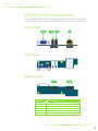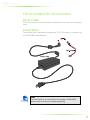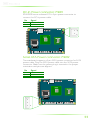
1
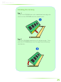
user manual
EPIA-P820
Pico-ITX Mainboard
Revision 1.07
107-06212012-1150
Copyright and Trademarks
Copyright © 2010-2012 VIA Technologies Incorporated. All rights reserved.
No part of this document may be reproduced, transmitted, transcribed, stored in a
retrieval system, or translated into any language, in any form or by any means, electronic,
mechanical, magnetic, optical, chemical, manual or otherwise without the prior written
permission of VIA Technologies, Incorporated.
All trademarks are the property of their respective holders.
PS/2 is a registered trademark of IBM Corporation.
Disclaimer
No license is granted, implied or otherwise, under any patent or patent rights of VIA
Technologies. VIA Technologies makes no warranties, implied or otherwise, in regard to
this document and to the products described in this document. The information provided
in this document is believed to be accurate and reliable as of the publication date of this
document. However, VIA Technologies assumes no responsibility for the use or misuse of
the information in this document and for any patent infringements that may arise from the
use of this document. The information and product specifications within this document are
subject to change at any time, without notice and without obligation to notify any person
of such change.
Battery Recycling and Disposal
Only use the appropriate battery specified for this product.
Do not re-use, recharge, or reheat an old battery.
Do not attempt to force open the battery.
Do not discard used batteries with regular trash.
Discard used batteries according to local regulations.
II
Regulatory Compliance
FCC-A Radio Frequency Interference Statement
This equipment has been tested and found to comply with the limits for a class A digital
device, pursuant to part 15 of the FCC rules. These limits are designed to provide
reasonable protection against harmful interference when the equipment is operated in a
commercial environment. This equipment generates, uses, and can radiate radio
frequency energy and, if not installed and used in accordance with the instruction manual,
may cause harmful interference to radio communications. Operation of this equipment in a
residential area is likely to cause harmful interference, in which case the user will be
required to correct the interference at his personal expense.
Notice 1
The changes or modifications not expressly approved by the party responsible for
compliance could void the user's authority to operate the equipment.
Notice 2
Shielded interface cables and A.C. power cord, if any, must be used in order to comply
with the emission limits.
Tested To Comply
With FCC Standards
FOR HOME OR OFFICE USE
KC Korean Certificate Statement
KCC-REM-VNT-EPIA-P820 (B)
VIA Technologies, Inc.
EPIA-P820
2009/12
Made in China
B 급 기기
( 가정용 방송통신기자재 )
이
로
든
기기는 가정용 (B 급 ) 전자파적합기기로서 주
가정에서 사용하는 것을 목적으로 하며 , 모
지역에서 사용할 수 있습니다 .
Class B Equipment
(For Home Use
Broadcasting & Communication
Equipment)
This electromagnetic wave equipment is suitable
for home use (Class B) and may be used mainly
at home and in other areas.
III
Safety Precautions
Do’s
o
Always read the safety instructions carefully.
o
Keep this User's Manual for future reference.
o
All cautions and warnings on the equipment should be
noted.
o
Keep this equipment away from humidity.
o
Lay this equipment on a reliable flat surface before setting
it up.
o
Make sure the voltage of the power source and adjust
properly 110/220V before connecting the equipment to the
power inlet.
o
Place the power cord in such a way that people cannot
step on it.
o
Always unplug the power cord before inserting any add-on
card or module.
o
If any of the following situations arises, get the equipment
checked by authorized service personnel:
o
The power cord or plug is damaged.
o
Liquid has penetrated into the equipment.
o
The equipment has been exposed to moisture.
o
The equipment has not worked well or you cannot
get it work according to User's Manual.
o
The equipment has dropped and damaged.
o
The equipment has obvious sign of breakage.
Don’ts
o
Do not leave this equipment in an environment
unconditioned or in a storage temperature above 70°C
(158°F). The equipment may be damaged.
o
Do not leave this equipment in direct sunlight.
o
Never pour any liquid into the opening. Liquid can cause
damage or electrical shock.
o
Do not place anything over the power cord.
o
Do not cover the ventilation holes. The openings on the
enclosure protect the equipment from overheating
IV
Box Contents
1
1
1
1
1
x
x
x
x
x
EPIA-P820 Pico-ITX mainboard
P820-A I/O module board
SATA cable
SATA power cable
DC-In cable
V
TABLE OF CONTENTS
1 Product Overview............................................................................................... 1
Key Components ................................................................................................. 2
VIA Nano 1.2 GHz NanoBGA2 Processor ........................................ 2
VIA VX855 Media System Processor..................................................... 2
Mainboard Specifications ................................................................................ 3
EPIA-P820 Layout ................................................................................................ 4
Top Side .............................................................................................................. 4
Bottom Side....................................................................................................... 5
P820-A I/O Module Layout ............................................................................ 6
Front View......................................................................................................... 6
Top View ............................................................................................................ 6
Bottom View..................................................................................................... 6
Development Kit Accessories ........................................................................ 7
DC-In Cable....................................................................................................... 7
Power Brick........................................................................................................ 7
2 Onboard Connectors, Slots and Pin Headers....................................... 9
Top Side Connectors .......................................................................................10
VIA Nano 1.2 GHz processor with Heatsink ........................................10
System Fan connector: FAN1 ................................................................10
DC-In Power connector: PWR1 ............................................................11
Serial ATA Power connector: PWR2...................................................11
Serial ATA connector: SATA1 .................................................................12
®
HDMI port connector: HDMI1............................................................12
IDE pin header: IDE1..................................................................................13
Ethernet LAN pin header: CN3.............................................................14
VGA and USB pin header: VGA_USB1 ............................................15
Front Audio pin header: CN1................................................................16
USB pin header: CN2 .................................................................................17
Front Panel and PS/2 KBMS pin header: CN4...............................18
LPC, SMBus and Digital I/O pin header: CN5................................19
UART port 2: J1 .............................................................................................20
Bottom Side Connector..................................................................................21
UART port 1: J2 .............................................................................................21
LVDS Panel connector: LVDS1..............................................................22
External Battery: BAT1................................................................................23
Memory Module Installation...................................................................24
VI
Pin Header and Connector Vendor Lists...............................................26
3 Onboard Jumpers ............................................................................................27
Clear CMOS jumper: JM1.........................................................................28
LCD Panel Power Selector: JM2............................................................29
LCD Backlight Power Selector: JM3 ....................................................29
4 P820-A I/O Module Installation ................................................................31
P820-A Installation Procedure.....................................................................32
5 BIOS Setup............................................................................................................35
Entering the BIOS Setup Menu ..................................................................36
Control Keys .........................................................................................................36
Getting Help ........................................................................................................37
Main Menu ...........................................................................................................38
AMIBIOS............................................................................................................38
Processor ..........................................................................................................38
System Memory.............................................................................................38
System Time ....................................................................................................38
System Date ....................................................................................................38
Advanced Settings ............................................................................................39
CPU Configuration ......................................................................................39
IDE Configuration ........................................................................................39
ACPI Configuration .....................................................................................39
APM Configuration .....................................................................................39
Spread Spectrum Configuration...........................................................39
USB Configuration.......................................................................................39
CPU Configuration ...........................................................................................40
CMPXCHG8B instruction support........................................................40
Nano CPU Thermal Monitor Adjust....................................................40
IDE Configuration .............................................................................................41
Parallel ATA IDE Controller......................................................................41
Hard Disk Write Protect ............................................................................41
IDE Detect Time Out (Sec).......................................................................41
ATA(PI) 80Pin Cable Detection .............................................................41
IDE Drives ..............................................................................................................42
Primary IDE Master ......................................................................................42
Primary IDE Slave (SATA Device)..........................................................42
Type.....................................................................................................................42
LBA/Large Mode..........................................................................................42
Block (Multi-Sector Transfer)....................................................................43
PIO Mode.........................................................................................................43
DMA Mode .....................................................................................................43
S.M.A.R.T............................................................................................................43
32Bit Data Transfer......................................................................................43
ACPI Settings........................................................................................................44
General ACPI Configuration...................................................................44
VII
Advanced ACPI Configuration..............................................................44
Chipset ACPI Configuration ....................................................................44
General ACPI Configuration ........................................................................45
Suspend Mode ..............................................................................................45
Repost Video on S3 Resume ..................................................................45
Advanced ACPI Configuration ...................................................................46
ACPI Version Features ...............................................................................46
ACPI APIC Support.......................................................................................46
AMI OEMB Table..........................................................................................46
Headless Mode..............................................................................................46
Chipset ACPI Configuration .........................................................................47
USB Device Wakeup Function..............................................................47
APM Configuration...........................................................................................48
Power Management / APM ...................................................................48
Power Button Mode...................................................................................48
Suspend Power Saving Type..................................................................48
Restore on AC / Power Loss ...................................................................48
Manual Throttle Ratio.................................................................................48
System Thermal .............................................................................................49
Standby Time Out........................................................................................49
Suspend Time Out.......................................................................................49
Hard Disk Time Out (Minute).................................................................49
Green PC Monitor Power State.............................................................49
Video Power Down Mode......................................................................49
Hard Disk Power Down Mode .............................................................49
Display Activity...............................................................................................49
Monitor IRQ3~15.........................................................................................49
Resume on Ring............................................................................................50
Resume on PME#.........................................................................................50
Resume On PS/2 KBC ................................................................................50
Wake-up Key ..................................................................................................50
Resume on PS/2 Mouse............................................................................50
Resume on RTC Alarm...............................................................................50
Spread Spectrum Configuration ................................................................51
Spread Spectrum Configuration...........................................................51
USB Configuration ............................................................................................52
USB 1.1 Ports Configuration ...................................................................52
USB 2.0 Ports Enable ..................................................................................52
USB Device Mode Enable........................................................................52
Legacy USB Support ...................................................................................52
USB 2.0 Controller Mode .........................................................................52
BIOS EHCI Hand-Off ...................................................................................52
Advanced PCI/PnP Settings..........................................................................53
Clear NVRAM .................................................................................................53
VIII
Plug & Play O/S .............................................................................................53
PCI Latency Timer.........................................................................................53
Allocate IRQ to PCI VGA...........................................................................53
Palette Snooping ..........................................................................................53
PCI IDE BusMaster........................................................................................54
Off Board PCI/ISA IDE Card ....................................................................54
IRQ3~15 ...........................................................................................................54
DMA Channel 0~7 .....................................................................................54
Reserved Memory Size...............................................................................54
Boot Settings........................................................................................................55
Boot Settings Configuration....................................................................55
Boot Device Priority.....................................................................................55
Boot Settings Configuration.........................................................................56
Quick Boot.......................................................................................................56
Display Logo...................................................................................................56
AddOn ROM Display Mode....................................................................56
Bootup Num-Lock .......................................................................................56
PS/2 Mouse Support...................................................................................56
Wait For ‘F1’ If Error....................................................................................56
Hit ‘DEL’ Message Display........................................................................56
Interrupt 19 Capture...................................................................................57
Boot Device Priority ..........................................................................................58
1st Boot Device .............................................................................................58
Security Settings..................................................................................................59
Change Supervisor Password ................................................................59
Change User Password ............................................................................59
Boot Sector Virus Protection...................................................................59
Advanced Chipset Settings...........................................................................60
North Bridge VIA VX855 Configuration...........................................60
South Bridge VIA VX855 Configuration...........................................60
North Bridge VIA VX855 Configuration................................................61
Software Reset E2 Issue.............................................................................61
Change DCLK using RDCKM .................................................................61
Dynamic CKE..................................................................................................61
NB Performance Register .........................................................................61
NB Energy Saving Register......................................................................61
OnChip VGA Configuration ........................................................................62
VGA Frame Buffer Size..............................................................................62
CPU Direct Access Frame Buffer ..........................................................62
Select Display Device..................................................................................62
Panel Type .......................................................................................................62
Dithering ..........................................................................................................62
Backlight Control ..........................................................................................62
South Bridge VIA VX855 Configuration................................................63
IX
Parallel Channel Enable ............................................................................63
ISA Master Support......................................................................................63
High Definition Audio................................................................................63
Enable Embedded COM..........................................................................63
PCI Debug Master Mode..........................................................................63
SMBus Multi-Master.....................................................................................63
PCI VCC33 Leakage Patch.......................................................................63
PCI Delay Transaction ................................................................................64
WATCH-DOG ................................................................................................64
Exit Options ..........................................................................................................65
Save Changes and Exit ..............................................................................65
Discard Changes and Exit........................................................................65
Discard Changes ..........................................................................................65
Load Optimal Defaults...............................................................................65
6 Driver Installation...............................................................................................67
Microsoft Driver Support................................................................................68
Linux Driver Support ........................................................................................68
X
XI
1
Product Overview
1
The VIA EPIA-P820 is an ultra-compact and highly integrated PicoITX mainboard and the smallest stand-alone form-factor available
today. Through a high level of integration, the Pico-ITX form factor
is 75% smaller than the existing Mini-ITX form factor. The
mainboard enables the creation of an exciting new generation of
small, ergonomic, innovative and affordable embedded systems.
The VIA EPIA-P820 Pico-ITX mainboard is rich in I/O integration
and comes with an integrated VIA Nano 1.2 GHz NanoBGA2
processor, boasting of ultra-low power consumption and cool
operation.
KEY COMPONENTS
VIA Nano 1.2 GHz NanoBGA2 Processor
The VIA Nano is a 64-bit superscalar processor in x86 platform
using a 65 nanometer process technology. It delivers an energyefficient, powerful performance, with cool and quiet operation all
within an ultra compact NanoBGA2 package measuring 21mm x
21mm. Perfectly fit for embedded system applications such as
industrial PCs, test machines, measuring equipment, digital
signage, medical PCs, monitoring systems, gaming machines, invehicle entertainment, and etc. The VIA Nano also boasts of
immersive multimedia performance, connectivity and computing
applications. When combined with the most recent VIA VX855
Media System Processor (MSP), which have been designed as
companion sets for the latest VIA processors, system developers
can utilize an impressive range of features for a wide range of
desktop and embedded applications.
VIA VX855 Media System Processor
The VIA VX855 MSP integrates a premium graphics engine, an
HD audio controller, a DDR2 memory controller, an 800MHz FSB
processor interface, and extensive I/O capabilities support in a
single chip design. Complementing the power-efficient VIA Nano
1.2 GHz NanoBGA2 processor, the VX855 is based on a highly
sophisticated power efficient architecture that enables such rich
integration into a compact package with a maximum power
envelope of just 2.3 W.
2
MAINBOARD SPECIFICATIONS
CPU
VIA Nano 1.2 GHz NanoBGA2 processor
• 800 MHz Front Side Bus
Chipset
VIA VX855 All-in-One System Processor
Graphics
Integrated VIA Chrome9TM HCM DX9 with MPEG-2
Accelerators
System Memory
One DDR2 800/667 SODIMM slot (up to 2 GB)
Onboard Storage
One SATA 3Gb/s connector
One UltraDMA 133/100/66/33 44-pin IDE connector
Audio
VIA VT1708S High Definition Audio Codec
LAN
One VIA VT6122 Gigabit Ethernet controller
Onboard I/O
Connectors
One Audio pin connector for Line-out, Line-in and Mic-in
One Single-channel LVDS connector (5V/3V)
One LPC pin connector
One SMBus pin connector
One DIO pin connector(4 GPI & 4 GPO)
Two UART port
One SYS fan connector
One PS2 mouse/keyboard pin header
One USB pin header for 4 additional USB 2.0 ports
One LAN pin header
One Front panel pin header
One Backlight control pin header
One SATA power connector
One +12V DC-in power pin connector
I/O Ports
One HDMI® port
One VGA port
One GigaLAN port
Two USB ports
System Monitoring
and Management
Wake-On-LAN and Keyboard Power-on
Watch Dog Timer
System power management, AC power failure
BIOS
AMI BIOS with 4Mbit SPI flash memory
Operating System
Windows XP / Windows CE / Windows XPe / Linux
Operating
Environment
Temperature: 0°C up to 60°C
Humidity: 0% ~ 95% (relative humidity; non-condensing)
Compliance
CE/FCC/BSMI/RoHS
Dimensions
135 mm(w) x 45 mm(H) x 131 mm (D)
Form Factor
Pico-ITX
10 cm x 7.2 cm
3
EPIA-P820 LAYOUT
Top Side
Symbol
CN1
CN2
CN3
CN4
CN5
JM1
JM2
JM3
Description
Front Audio pin header
USB and USB Device port
pin header
LAN Ethernet pin header
Front Panel and PS/2
KBMS pin header
LPC, SMBus and Digital
I/O pin header
Clear CMOS jumper
Panel Power Selector
Panel Backlight Power
Selector
Symbol
PWR1
PWR2
FAN1
VGA_USB1
IDE1
HDMI1
SATA1
J1
Description
DC-In power connector
SATA Power connector
System Fan connector
VGA and USB pin header
IDE pin header
®
HDMI port
SATA port
UART port 2
Note:
USB Device port is a reserved feature, contact sales for specific
support.
4
Bottom Side
Symbol
BAT1
LVDS1
Description
Symbol
Description
CMOS Battery connector
1-CH LVDS Panel connector
SODIMM1
J2
DDR2 SODIMM slot
UART port 1
5
P820-A I/O MODULE LAYOUT
The VIA EPIA-P820 Pico-ITX mainboard is bundled with an I/O
board (P820-A) to support connections to LAN, VGA and USB.
Front View
Top View
Bottom View
Symbol
VGA1
USB1
USB2
RJ1
CON1
CON2
Description
VGA port
USB 2.0 port 1
USB 2.0 port 2
RJ-45 LAN port
VGA & USB board-to-board connector
LAN board-to-board connector
6
DEVELOPMENT KIT ACCESSORIES
DC-In Cable
The DC-In power cable provides a means to connect to the power
brick.
Power Brick
The power brick provides a regulated 12V/5A output to power up
the EPIA-P820 mainboard.
Note:
The Power brick is not included in the package of EPIA-P820
and this item should be purchased separately.
7
8
2
Onboard
Connectors, Slots
and Pin Headers
This chapter provides you with information about hardware
installation procedures. It is recommended to use a grounded
wrist strap before handling computer components. Electrostatic
discharge (ESD) can damage some components.
9
TOP SIDE CONNECTORS
VIA Nano 1.2 GHz processor with Heatsink
The VIA EPIA-P820 Pico-ITX mainboard is packaged with a
standard VIA Nano 1.2 GHz NanoBGA2 processor.
System Fan connector: FAN1
FAN1 runs on +5V and maintains system cooling. When
connecting the cable to the connector, always be aware that the
red wire (positive wire) should be connected to the +5V pin. The
black wire is the ground wire and should always be connected to
GND.
Pin
Signal
1
2
+5V
GND
10
DC-In Power connector: PWR1
EPIA-P820 has an onboard DC-In 2-pin power connector to
connect the DC-In power cable.
Pin
Signal
1
2
DC In (+12V)
GND
Serial ATA Power connector: PWR2
The mainboard supports a 3-pin SATA power connector for SATA
power cable. Plug the SATA power cable into the SATA power
connector. Make sure the power plug is inserted in the proper
orientation and pins are aligned.
Pin
Signal
1
2
3
+5V
+12V
GND
11
Serial ATA connector: SATA1
The current SATA interface allows a data transfer rate of up to 300
MB/s — approximately 225% faster than Ultra DMA parallel ATA.
HDMI® port connector: HDMI1
The mainboard has a High Definition Multimedia Interface port for
®
connecting to high definition video and digital audio. The HDMI
port allows you to connect digital video devices which utilize a
®
high definition video signal. The HDMI port is HDCP 1.2
compatible.
Note:
CEC feature is not supported.
12
IDE pin header: IDE1
The mainboard has an Ultra DMA 133/100 controller. You can
connect up to two IDE devices in any combination.
Pin
Signal
Pin
Signal
1
3
5
7
9
11
13
15
17
19
21
23
25
27
29
31
33
35
37
39
41
43
-IDERST
PDD7
PDD6
PDD5
PDD4
PDD3
PDD0
PDD1
PDD2
GND
PDDREQ
PDDIOW
PDDIOR
PIORDY
PDDACK
-IRQ14
PDA1
PDA0
PDCS1
-HD_LED1
+5V
GND
2
4
6
8
10
12
14
16
18
20
22
24
26
28
30
32
34
36
38
40
42
44
GND
PDD8
PDD9
PDD10
PDD11
PDD12
PDD13
PDD14
PDD15
KEY
GND
GND
GND
GND
GND
NC
PDIAG
PDA2
PDCS3
GND
+5V
NC
13
Ethernet LAN pin header: CN3
The Ethernet LAN pin header is for connecting to the P820-A I/O
module.
Pin
Signal
Pin
Signal
1
3
5
7
9
11
13
A3V3GL(+3.3V)
TXNC
TXPC
TXNA
TXPA
GND
LED2
2
4
6
8
10
12
14
+3.3VSUS
TXND
TXPD
TXNB
TXPB
LED1
LINK ACT
14
VGA and USB pin header: VGA_USB1
The VGA and USB pin header is for connecting to the P820-A I/O
module.
Pin
Signal
Pin
Signal
1
3
5
7
9
11
13
15
17
VGA_RED
VGA_GREEN
VGA_BLUE
GND
+5VUSB_P
VGA_HS
+5VSUS
USBHP0USBHP0+
2
4
6
8
10
12
14
16
18
+5V
GND
DDC_DATA
DDC_CLK
VGA_VS
GND
GND
USBHP1-/USBDP_DUSBHP1+/USBDP_D+
15
Front Audio pin header: CN1
This pin header allows you to connect a front audio to the
mainboard.
Pin
Signal
Pin
Signal
1
3
5
7
LINE IN_R
LINE IN_L
LINE OUT_R
LINE OUT_L
2
4
6
8
AUD_GND
MIC IN_L
MIC IN_R
JACK SENSE
16
USB pin header: CN2
This 20-pin USB pin header allows you to connect up to four
USB2.0 ports.
Pin
Signal
Pin
Signal
1
3
5
7
9
11
13
15
17
19
GND
GND
USB VD2+
USB VD2+5VSUS
USB VD5USB VD5+
reserved
reserved
reserved
2
4
6
8
10
12
14
16
18
20
GND
GND
USB VD3+
USB VD3+5VSUS
USB VD4USB VD4+
reserved
reserved
reserved
17
Front Panel and PS/2 KBMS pin header: CN4
This single pin header allows you to connect the power switch,
reset switch, power LED, HDD LED, case speaker and two PS/2
ports.
Pin
Signal
Pin
Signal
1
3
5
7
9
11
13
15
17
+PWR_LED
+5VSUS (for LED use)
GND
SPEAK_BZ
GND
-PWR_LED
+5VSUS
KB_CLK
MS_CLK
2
4
6
8
10
12
14
16
18
+HD_LED
-HD_LED
PW_SW
GND
RST_SW
GND
GND
KB_DT
MS_DT
Note:
Pins 1 to 12 are for Front Panel and pin 13 to 18 use for PS/2
KBMS.
18
LPC, SMBus and Digital I/O pin header: CN5
This single pin header allows the connection of LPC, SMBus
devices and the Digital Input and Output.
Pin
Signal
Pin
Signal
1
3
5
7
9
11
13
15
17
19
21
23
25
GND
SIOOSC
LPCCLK
-LDRQ1
SERIRQ
-SIOSMI/-PME
SIOSMI
SMB_CLK
+5V
GPO5/CSTATE1
GPO6/-C4PSTOP
GPIO0/SMBDT2
GPIO1/SMBCK2
GND
2
4
6
8
10
12
14
16
18
20
22
24
26
LAD3
LAD2
LAD1
-LFRAME
LAD0
-PCIRST1
SMB_DAT
+3.3V
GPI8/-RING
GPI9/-THRM
GPI5/-EXTSMI
GPI4/-BATLOW
GND
(Pin 11) Default: -SIOSMI
19
UART port 2: J1
UART offers TTL level serial signal for the user to easily convert to
support RS232/RS422/RS485.
Pin
UART Signal
1
2
3
4
5
6
7
8
9
10
+5V
SIN_1
SOUT_1
DCD_1
RI_1
GND
DTR_1
CTS_1
RTS_1
DSR_1
(Pin 1) Default: 5V
20
BOTTOM SIDE CONNECTOR
UART port 1: J2
UART offers TTL level serial signal for the user to easily convert to
support RS232/RS422/RS485.
Pin
UART Signal
1
2
3
4
5
6
7
8
9
10
11
12
GND
-LPCRST
CTS_0
RTS_0
DSR_0
DTR_0
SIN_0
SOUT_0
DCD_0
RI_0
+3.3V
(Pin 12) Default: 3.3V
21
LVDS Panel connector: LVDS1
The single-channel LVDS connector allows you to connect the
panel’s LVDS cable directly to support LVDS panel.
Pin
Signal
Pin
Signal
1
3
5
7
9
11
13
15
17
19
21
23
LVDSD0LVDSD0+
GND
Panel_VDD
Panel_VDD
LCD1_DATA
LCD1_CLK
GND
Back Light_VDD
Back Light_VDD
BL_ENABLE
DIMMING
2
4
6
8
10
12
14
16
18
20
22
24
LVDSD1LVDSD1+
GND
LVDSD2LVDSD2+
GND
LVDSCLK+
LVDSCLKGND
LVDSD3LVDSD3+
GND
Note:
Contact local distributor and FAE for special Video BIOS for
24bit LCD panel support.
(Pin 23) DIMMING: LVDS Backlight Brightness Voltage Control, 0V ~ 3.3V
Level 0: 0%
Level 1: 25%
Level 2: 50%
Level 3: 75%
Level 4: 100%
22
External Battery: BAT1
The mainboard comes with external CMOS battery connector. This
2-pin connector used to connect the external cable battery for
CMOS.
Pin
Signal
1
2
+3.3VBAT
GND
23
Memory Module Installation
Memory Slot: SODIMM1
The VIA EPIA-P820 Pico-ITX mainboard has one 200-SODIMM slot
for DDR2 667/533 SDRAM memory modules and supports memory
sizes up to 2 GB.
Available DDR2 SDRAM Configuration
Refer to the table below for available DDR2 SDRAM configurations
on the mainboard.
Slot
Module Size
SODIMM
64 MB, 128 MB, 256 MB, 512 MB, 1 GB, 2 GB
Maximum supported system memory
Total
64 MB - 2 GB
2 GB
24
Installing the memory
Step 1
Locate the SODIMM slot in the mainboard and align the
notch on the SODIMM with the memory slot.
Step 2
Insert the SODIMM module at a 45 degree angle. Then
push the SODIMM down until it snaps into the locking
mechanism.
25
PIN HEADER AND CONNECTOR
VENDOR LISTS
Items
CN1
CN2
CN3
CN4
CN5
J1
J2
VGA_
USB1
LVDS1
PWR1
PWR2
FAN1
Function
Pin
Pitch
Vendor
P/N
Front Audio
USB
Ethernet LAN
Front Panel
and PS/2 KBMS
LPC, SMBus
and Digital I/O
UART
UART
8 Pin
20 Pin
14 Pin
2.0mm
2.0mm
2.0mm
Neltron
Neltron
Neltron
2208SM-08G-BK-CP
2208SM-20G-BK-CP
2208SM-14G-BK-CP
18 Pin
2.0mm
Neltron
2208SM-18G-BK-CP
26 Pin
2.0mm
Neltron
2208SM-26G-BK-CP
10 Pin
12 Pin
1.0mm
1.0mm
Neltron
Neltron
1600R-10-SM-TR
1600R-12-SM-TR
VGA and USB
18 pin
2.0mm
Neltron
2208SM-18G-BK-CP
LVDS Panel
DC-In Power
SATA Power
System Fan
24 Pin
2 Pin
3 Pin
3 Pin
1.0mm
2.5mm
2.5mm
1.25mm
ACES
Neltron
Neltron
Neltron
87216-2416-06
2317SJ-02-F4
2317SEH-03
1251S-02-SM1-TR
26
3
Onboard Jumpers
27
Clear CMOS jumper: JM1
The onboard CMOS RAM stores system configuration data and has
an onboard battery power supply. To reset the CMOS settings, set
the jumper on pins 2 and 3 while the system is off. Return the
jumper to pins 1 and 2 afterwards. Setting the jumper while the
system is on will damage the mainboard. The default setting is on
pins 1 and 2.
Setting
1
2
3
Normal Operation (default)
Clear CMOS setting
ON
OFF
ON
ON
OFF
ON
Caution:
Except when clearing the RTC RAM, never remove the cap from
the CLEAR_CMOS jumper default position. Removing the cap
will cause system boot failure. Avoid clearing the CMOS while
the system is on; it will damage the mainboard.
28
LCD Panel Power Selector: JM2
This jumper determines the input voltage for the LCD connector.
Setting
1
2
3
+5V
+3.3V (default)
ON
OFF
ON
ON
OFF
ON
LCD Backlight Power Selector: JM3
This jumper determines the input voltage for the LCD backlight
inverter.
Setting
1
2
3
+12V
+5V (default)
ON
OFF
ON
ON
OFF
ON
29
30
4
P820-A I/O
Module Installation
31
P820-A INSTALLATION PROCEDURE
Step 1
Align and mount the P820-A board.
Step 2
Align the CON1 (VGA & USB board-to-board connector) and
CON2 (LAN board-to-board connector) of P820-A I/O module
board with the CN3 and VGA_USB1 pin headers to the top side
of EPIA-P820 mainboard respectively.
32
Step 3
Then gently press down until the pins on the EPIA-P820
mainboard have been fully inserted into the CON1 and CON2
connectors of the P820-A I/O module board.
Step 4
Secure the EPIA-P820-A I/O module with two screws.
33
34
5
BIOS Setup
This chapter gives a detailed explanation of the BIOS setup
functions.
35
ENTERING THE BIOS SETUP MENU
Power on the computer and press <Delete
Delete>
Delete during the beginning
of the boot sequence to enter the BIOS setup menu. If you missed
the BIOS setup entry point, restart the system and try again.
CONTROL KEYS
Keys
Description
Up
Down
Left
Right
Enter
Esc
Move to the previous item
Move to the next item
Move to the previous tab
Move to the next tab
Select the item
Jumps to the Exit menu or returns to the main menu
from a submenu
Increase the numeric value
Decrease the numeric value
General help, only for Status Page Setup Menu and
Option Page Setup Menu
Discard Changes
Load Optimized defaults
Save all the changes and exit
+ (number pad)
- (number pad)
F1
F7
F9
F10
36
GETTING HELP
The BIOS setup program provides a “General
General Help”
Help screen. You
can display this screen from any menu/sub-menu by pressing
<F1
F1>.
F1 The help screen displays the keys for using and navigating
the BIOS setup. Press <E
Esc>
sc to exit the help screen.
37
MAIN MENU
AMIBIOS
BIOS version number and related information.
Processor
CPU information.
System Memory
Memory size.
System Time
Use the key “+” or “-” to configure system time. The time format is
[Hour : Minute : Second].
System Date
Use the key “+” or “-” to configure system Date. The date format is
[Day, Month, Date, Year].
38
ADVANCED SETTINGS
CPU Configuration
IDE Configuration
ACPI Configuration
APM Configuration
Spread Spectrum Configuration
USB Configuration
39
CPU CONFIGURATION
CMPXCHG8B instruction support
Settings: [Enabled, Disabled]
Nano CPU Thermal Monitor Adjust
Settings: [Disabled, Thermal Monitor 1, Thermal Monitor 2,
Thermal Monitor 3]
40
IDE CONFIGURATION
Parallel ATA IDE Controller
Settings: [Disabled, Primary]
Hard Disk Write Protect
Settings: [Disabled, Enabled]
IDE Detect Time Out (Sec)
Settings: [0, 5, 10, 15, 20, 25, 30, 35]
ATA(PI) 80Pin Cable Detection
Settings: [Host & Device, Host, Device]
41
IDE DRIVES
Primary IDE Master
Primary IDE Slave (SATA Device)
Type
Settings: [Not Installed, Auto, CD/DVD, ARMD]
LBA/Large Mode
Settings: [Disabled, Auto]
42
Block (Multi-Sector Transfer)
Settings: [Disabled, Auto]
PIO Mode
Settings: [Auto, 0, 1, 2, 3, 4]
DMA Mode
Settings: [Auto]
S.M.A.R.T.
Self Monitoring Analysis and Reporting Technology, a monitoring
system for hard disks.
Settings: [Auto, Disabled, Enabled]
32Bit Data Transfer
Settings: [Enabled, Disabled]
43
ACPI SETTINGS
General ACPI Configuration
This menu contains ACPI (Advanced Configuration and Power
Management Interface) options.
Advanced ACPI Configuration
Chipset ACPI Configuration
44
GENERAL ACPI CONFIGURATION
Suspend Mode
Select the ACPI state used for system suspend.
Settings
Description
S1(POS)
S1/Power On Suspend (POS) is a low power state. In this
state, no system context (CPU or chipset) is lost and
hardware maintains all system contexts
S3/Suspend To RAM (STR) is a power-down state. In this
state, power is supplied only to essential components
such as main memory and wakeup-capable devices. The
system context is saved to main memory, and context is
restored from the memory when a "wakeup" event
occurs.
Depends on the OS to select the state.
S3(STR)
Auto
Repost Video on S3 Resume
To determine whether to invoke VGA BIOS post on S3/STR
resume or not.
Settings: [No, Yes]
45
ADVANCED ACPI CONFIGURATION
ACPI Version Features
To enable RSDP pointers to 64-bit Fixed System Description Tables.
Settings: [ACPI v1.0, ACPI v2.0, ACPI v3.0]
ACPI APIC Support
To include ACPI APIC table pointer to RSDT pointer list.
Settings: [Enabled, Disabled]
AMI OEMB Table
To include OEMB table pointer to R(X)SDT pointer lists.
Settings: [Disabled, Enabled]
Headless Mode
To enable or disable headless operation mode through ACPI.
Settings: [Disabled, Enabled]
46
CHIPSET ACPI CONFIGURATION
USB Device Wakeup Function
Settings: [Disabled, Enabled]
47
APM CONFIGURATION
Power Management / APM
Settings: [Disabled, Enabled]
Power Button Mode
Settings: [On/Off, Standby, Suspend]
Suspend Power Saving Type
Settings: [C3, S1]
Restore on AC / Power Loss
The field defines how the system will respond after an AC power
loss during system operation.
Settings
Description
Power Off
Keeps the system in an off state until the power button is
pressed.
Restarts the system when the power is back
Save in last state
Power On
Last State
Manual Throttle Ratio
Settings: [0%-6.25%, 6.25%-12.5%, 18.75%-25%, 31.25%-37.5%,
37.5%-43.75%, 43.75%-50%, 50%-56.25%, 56.25%-62.5%, 62.5%68.75%, 68.75%-75%, 75%-87.5%, 75%-81.25%, 81.25%-87.5%,
87.5%-93.75%, 93.75%-100%]
48
System Thermal
Settings: [Disabled, Enabled]
Standby Time Out
Settings: [Disabled, 1/2/4/8/10/20/30/40/50/60 minutes]
Suspend Time Out
Settings: [Disabled, 1/2/4/8/10/20/30/40/50/60 minutes]
Hard Disk Time Out (Minute)
Settings: [Disabled, 1/2/3/4/5/6/7/8/9/10/11/12/13/14/15
minutes]
Green PC Monitor Power State
Settings: [Standby, Suspend, Off]
Video Power Down Mode
Settings: [Disabled, Standby, Suspend]
Hard Disk Power Down Mode
Settings: [Disabled, Standby, Suspend]
Display Activity
Settings: [Ignore, Monitor]
Monitor IRQ3~15
Enables or disables the monitoring of the specified IRQ line.
Settings: [Ignore, Monitor]
Note:
IRQ (Interrupt Request) lines are system resources allocated to
I/O devices. When an I/O device needs to gain attention of the
operating system, it signals this by causing an IRQ to occur.
After receiving the signal, when the operating system is ready,
the system will interrupt itself and perform the service required
by the IO device.
49
Resume on Ring
Settings: [Disabled, Enabled]
Resume on PME#
Settings: [Disabled, Enabled]
Resume On PS/2 KBC
Settings: [Disabled, S3, S3/S4/S5]
Wake-up Key
Settings: [Any Key, Specific Key]
Resume on PS/2 Mouse
Enable any mouse activity to restore the system from the power
saving mode to an active state.
Settings: [Disabled, S3, S3/S4/S5]
Resume on RTC Alarm
Set a scheduled time and/or date to automatically power on the
system.
Settings: [Disabled, Enabled]
50
SPREAD SPECTRUM CONFIGURATION
Spread Spectrum Configuration
Settings: [Disabled, 0.1%, 0.2%, 0.3%, 0.4%, 0.5%, 0.6%, 0.7%, 0.8%,
0.9%]
51
USB CONFIGURATION
USB 1.1 Ports Configuration
To enable USB 1.1 host controllers.
Settings: [Disabled, USB 2 ports, USB 4 ports, USB 6 ports]
USB 2.0 Ports Enable
To enable USB 2.0 host controllers.
Settings: [Disabled, Enabled]
USB Device Mode Enable
Settings: [Enabled, Disabled]
Legacy USB Support
To enable support for legacy USB.
Settings: [Disabled, Enabled, Auto]
USB 2.0 Controller Mode
To configure the USB 2.0 controller in HiSpeed (480Mbps) or
FullSpeed (12Mbps).
Settings: [FullSpeed, HiSpeed]
BIOS EHCI Hand-Off
Settings: [Disabled, Enabled]
52
ADVANCED PCI/PNP SETTINGS
Note:
This section covers some very technical items and it is strongly
recommended to leave the default settings as it is unless you
are an experienced user.
Clear NVRAM
To clear NVRAM during system boot.
Settings: [No, Yes]
Plug & Play O/S
Settings: [No, Yes]
PCI Latency Timer
Value in units of PCI clocks for PCI device latency timer register.
Settings: [32, 64, 96, 128, 160, 192, 224, 248]
Allocate IRQ to PCI VGA
Settings: [Yes, No]
Palette Snooping
Settings: [Disabled, Enabled]
53
PCI IDE BusMaster
Settings: [Disabled, Enabled]
Off Board PCI/ISA IDE Card
Settings: [Auto, PCI Slot1, PCI Slot2, PCI Slot3, PCI Slot4, PCI Slot5,
PCI Slot6]
IRQ3~15
Settings: [Available, Reserved]
DMA Channel 0~7
Settings: [Available, Reserved]
Reserved Memory Size
To decide the size of memory block to reserve for legacy ISA
devices.
Settings: [Disabled, 16k, 32k, 64k]
54
BOOT SETTINGS
Boot Settings Configuration
Configuration settings during system boot.
Boot Device Priority
Specifies the boot device priority sequence.
55
BOOT SETTINGS CONFIGURATION
Quick Boot
Settings: [Disabled, Enabled]
Display Logo
Settings: [Disabled, Enabled]
AddOn ROM Display Mode
Settings: [Force BIOS, Keep Current]
Bootup Num-Lock
To select power-on state for Num-Lock.
Settings: [Off, On]
PS/2 Mouse Support
Settings: [Disabled, Enabled, Auto]
Wait For ‘F1’ If Error
Settings: [Disabled, Enabled]
Hit ‘DEL’ Message Display
Settings: [Disabled, Enabled]
56
Interrupt 19 Capture
Settings: [Disabled, Enabled]
57
BOOT DEVICE PRIORITY
1st Boot Device
To specifies the boot sequence from the available devices. The
available boot devices are detected dynamically according to real
situation and variable options will be provided.
Settings: [Network: VIA Networking Bootagent, Disabled]
58
SECURITY SETTINGS
Change Supervisor Password
This option is for setting a password for entering BIOS Setup.
When a password has been set, a password prompt will be
displayed whenever BIOS Setup is run. This prevents an
unauthorized person from changing any part of your system
configuration.
When a supervisor password is used, the BIOS Setup program can
be accessed and the BIOS settings can be changed.
Change User Password
When a user password is used, the BIOS Setup program can be
accessed but the BIOS settings cannot be changed.
Boot Sector Virus Protection
Settings: [Disabled, Enabled]
59
ADVANCED CHIPSET SETTINGS
Caution:
The Advanced Chipset Features menu is used for optimizing the
chipset functions. Do not change these settings unless you are
familiar with the chipset.
North Bridge VIA VX855 Configuration
South Bridge VIA VX855 Configuration
60
NORTH BRIDGE VIA VX855
CONFIGURATION
Software Reset E2 Issue
Settings: [Patch, Escape Patch]
Change DCLK using RDCKM
Settings: [Program, Escape Program]
Dynamic CKE
Settings: [Disabled, Enabled]
NB Performance Register
Settings: [Disabled, Enabled]
NB Energy Saving Register
Settings: [Disabled, Enabled]
61
ONCHIP VGA CONFIGURATION
VGA Frame Buffer Size
Settings: [64MB, 128MB, 256MB]
CPU Direct Access Frame Buffer
Settings: [Disabled, Enabled]
Select Display Device
Settings: [CRT, LCD, HDMI, CRT+LCD, CRT+HDMI]
Panel Type
Settings: [02]
Dithering
Settings: [Disabled, Enabled]
Backlight Control
Settings: [0%, 25%, 50%, 75%, 100%]
62
SOUTH BRIDGE VIA VX855
CONFIGURATION
Parallel Channel Enable
Settings: [Enabled, Disabled]
ISA Master Support
Settings: [Support, Not Support]
High Definition Audio
Settings: [Disabled, Auto]
Enable Embedded COM
Settings: [Disabled, Enabled]
PCI Debug Master Mode
Settings: [Disabled, Enabled]
SMBus Multi-Master
Settings: [Disabled, Enabled]
PCI VCC33 Leakage Patch
Settings: [Disabled, Enabled]
63
PCI Delay Transaction
Settings: [Disabled, Enabled]
WATCH-DOG
Settings: [Disabled, Enabled]
64
EXIT OPTIONS
Save Changes and Exit
Exit system setup after saving the changes, or press “F10”.
Discard Changes and Exit
Exit system setup without saving any changes, or press “Esc”.
Discard Changes
Discard changes which have been done so far to any of the setup
questions, or press “F7”.
Load Optimal Defaults
Load optimal default values for all the setup items, or press “F9”.
The default optimized values are set by the mainboard
manufacturer to provide a stable system with optimized
performance.
65
66
6
Driver Installation
.
67
MICROSOFT DRIVER SUPPORT
The VIA EPIA-P820 mainboard is compatible with Microsoft
operating systems. The latest Windows drivers can be
downloaded from the VEPD website at www.viaembedded.com.
For embedded operating systems, the related drivers can be
found in the VIA Embedded website at www.viaembedded.com.
LINUX DRIVER SUPPORT
The VIA EPIA- P820 mainboard is highly compatible with many
Linux distributions.
Support and drivers are provided through various methods
including:
1. Drivers provided by VIA
2. Using a driver built into a distribution package
3. Visiting www.viaembedded.com for the latest updated
drivers
4. Installing a third party driver (such as the ALSA driver from
the Advanced Linux Sound Architecture project for
integrated audio)
For OEM clients and system integrators developing a product for
long term production, other code and resources may also be
made available. Contact VEPD to submit a request.
68