1
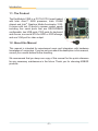
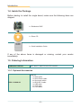
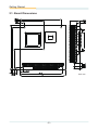
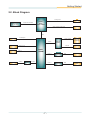
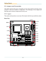
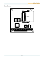
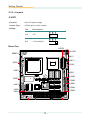
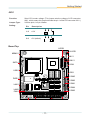
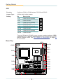
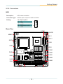
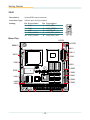
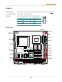
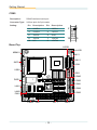
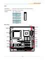
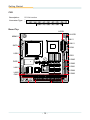
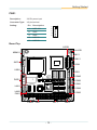
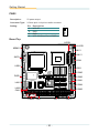
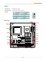
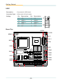
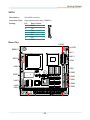
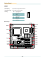
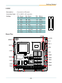
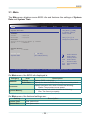
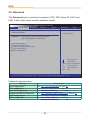
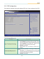
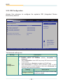
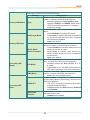
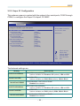
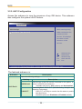
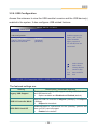
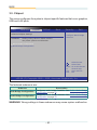
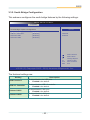
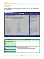
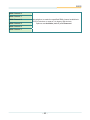
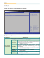
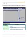
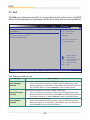
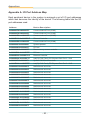
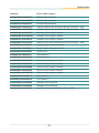
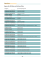
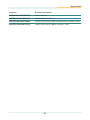
85
EmModule-749E
PC/104 CPU Module
User’s Manual
Version 1.0
85
2013.11
1
This page is intentionally left blank.
-2-
Revision History
Version
Release Time
Description
1.0
November 2013
Initial release
-i-
Contents
Table of Contents
Revision History..................................................................................i
Table of Contents...............................................................................ii
Preface................................................................................................v
Copyright Notice...................................................................................... v
Declaration of Conformity........................................................................ v
CE..................................................................................................... v
FCC Class A.................................................................................... vi
RoHS............................................................................................... vi
SVHC / REACH............................................................................... vi
Replacing Lithium Battery.......................................................................vii
Technical Support...................................................................................vii
Warranty................................................................................................viii
Chapter 1 - Introduction.....................................................................1
1.1. The Product...................................................................................... 2
1.2. About this Manual............................................................................. 2
1.3. Specifications.................................................................................... 3
1.4. Inside the Package........................................................................... 4
1.5. Ordering Information......................................................................... 4
1.5.1. Optional Accessories.............................................................. 4
Chapter 2 - Getting Started................................................................5
2.1. Board Dimensions............................................................................. 6
2.2. Block Diagram................................................................................... 7
2.3. Jumpers and Connectors.................................................................. 8
2.3.1. Layout..................................................................................... 8
2.3.2. Jumpers................................................................................ 10
2.3.3. Connectors........................................................................... 13
2.4. Driver Installation Notes.................................................................. 26
Chapter 3 - BIOS...............................................................................27
3.1. Main................................................................................................ 29
3.2. Advanced........................................................................................ 30
3.2.1. CPU Configuration................................................................ 31
3.2.2. IDE Configuration................................................................. 32
3.2.3. Super IO Configuration......................................................... 35
3.2.4. Hardware Health Configuration............................................ 37
3.2.5. AHCI Configuration............................................................... 38
3.2.6. USB Configuration................................................................ 39
3.3. Chipset............................................................................................ 40
3.3.1. North Bridge Configuration................................................... 41
3.3.2. South Bridge Configuration................................................... 43
- ii -
Contents
3.4. PCIPnP........................................................................................... 44
3.5. Boot................................................................................................. 46
3.6. Security........................................................................................... 47
3.7. Exit.................................................................................................. 48
Appendices.......................................................................................49
Appendix A. I/O Port Address Map........................................................ 50
Appendix B. Memory Address Map........................................................ 52
Appendix C. Interrupt Request Lines (IRQ)........................................... 54
Appendix D. DMA Map........................................................................... 58
Appendix E: Watchdog Timer (WDT) Setting......................................... 59
- iii -
This page is intentionally left blank.
- iv -
Preface
Preface
Copyright Notice
All Rights Reserved.
The information in this document is subject to change without prior notice in
order to improve the reliability, design and function. It does not represent a
commitment on the part of the manufacturer.
Under no circumstances will the manufacturer be liable for any direct, indirect,
special, incidental, or consequential damages arising from the use or inability
to use the product or documentation, even if advised of the possibility of such
damages.
This document contains proprietary information protected by copyright. All rights
are reserved. No part of this manual may be reproduced by any mechanical,
electronic, or other means in any form without prior written permission of the
manufacturer.
Declaration of Conformity
CE
The CE symbol on your product indicates that it is in compliance with the
directives of the Union European (EU). A Certificate of Compliance is available
by contacting Technical Support.
This product has passed the CE test for environmental specifications when
shielded cables are used for external wiring. We recommend the use of shielded
cables. This kind of cable is available from ARBOR. Please contact your local
supplier for ordering information.
This product has passed the CE test for environmental specifications. Test
conditions for passing included the equipment being operated within an
industrial enclosure. In order to protect the product from being damaged by ESD
(Electrostatic Discharge) and EMI leakage, we strongly recommend the use of
CE-compliant industrial enclosure products.
Warning
This is a class A product. In a domestic environment this product may cause
radio interference in which case the user may be required to take adequate
measures.
-v-
Preface
FCC Class A
This device complies with Part 15 of the FCC Rules. Operation is subject to the
following two conditions:
(1)This device may not cause harmful interference, and
(2)This device must accept any interference received, including interference that
may cause undesired operation.
NOTE:
This equipment has been tested and found to comply with the limits for a
Class A digital device, pursuant to Part 15 of the FCC Rules. These limits are
designed to provide reasonable protection against harmful interference when the
equipment is operated in a commercial environment. This equipment generates,
uses, and can radiate radio frequency energy and, if not installed and used in
accordance with the instruction manual, may cause harmful interference to radio
communications. Operation of this equipment in a residential area is likely to
cause harmful interference in which case the user will be required to correct the
interference at his own expense.
RoHS
ARBOR Technology Corp. certifies that all components in its products are
in compliance and conform to the European Union’s Restriction of Use of
Hazardous Substances in Electrical and Electronic Equipment (RoHS) Directive
2002/95/EC.
The above mentioned directive was published on 2/13/2003. The main purpose
of the directive is to prohibit the use of lead, mercury, cadmium, hexavalent
chromium, polybrominated biphenyls (PBB), and polybrominated diphenyl
ethers (PBDE) in electrical and electronic products. Member states of the EU
are to enforce by 7/1/2006.
ARBOR Technology Corp. hereby states that the listed products do not contain
unintentional additions of lead, mercury, hex chrome, PBB or PBDB that exceed
a maximum concentration value of 0.1% by weight or for cadmium exceed
0.01% by weight, per homogenous material. Homogenous material is defined as
a substance or mixture of substances with uniform composition (such as solders,
resins, plating, etc.). Lead-free solder is used for all terminations (Sn(96-96.5%),
Ag(3.0-3.5%) and Cu(0.5%)).
SVHC / REACH
To minimize the environmental impact and take more responsibility to the earth
we live, Arbor hereby confirms all products comply with the restriction of SVHC
- vi -
Preface
(Substances of Very High Concern) in (EC) 1907/2006 (REACH --Registration,
Evaluation, Authorization, and Restriction of Chemicals) regulated by the
European Union.
All substances listed in SVHC < 0.1 % by weight (1000 ppm)
Warning
Single Board Computers and their components contain very delicate
Integrated Circuits (IC). To protect the Single Board Computer and its
components against damage from static electricity, you should always follow the
following precautions when handling it :
1. Disconnect your Single Board Computer from the power source when you
want to work on the inside.
2. Hold the board by the edges and try not to touch the IC chips, leads or
circuitry.
3. Use a grounded wrist strap when handling computer components.
4. Place components on a grounded antistatic pad or on the bag that comes
with the Single Board Computer, whenever components are separated from
the system.
Replacing Lithium Battery
Incorrect replacement of the lithium battery may lead to a risk of explosion.
The lithium battery must be replaced with an identical battery or a battery type
recommended by the manufacturer.
Do not throw lithium batteries into the trash-can. It must be disposed of in
accordance with local regulations concerning special waste.
Technical Support
If you have any technical difficulties, please do not hesitate to call or e-mail our
customer service.
http://www.arbor.com.tw
E-mail:[email protected]
- vii -
Preface
Warranty
This product is warranted to be in good working order for a period of two years
from the date of purchase. Should this product fail to be in good working order
at any time during this period, we will, at our option, replace or repair it at no
additional charge except as set forth in the following terms. This warranty does
not apply to products damaged by misuse, modifications, accident or disaster.
Vendor assumes no liability for any damages, lost profits, lost savings or any other
incidental or consequential damage resulting from the use, misuse of, or inability to
use this product. Vendor will not be liable for any claim made by any other related party.
Vendors disclaim all other warranties, either expressed or implied, including but
not limited to implied warranties of merchantability and fitness for a
particular purpose, with respect to the hardware, the accompanying product’s
manual(s) and written materials, and any accompanying hardware. This limited
warranty gives you specific legal rights.
Return authorization must be obtained from the vendor before returned
merchandise will be accepted. Authorization can be obtained by calling or faxing
the vendor and requesting a Return Merchandise Authorization (RMA) number.
Returned goods should always be accompanied by a clear problem description.
- viii -
1
Chapter 1
Introduction
Chapter 1 - Introduction
-1-
Introduction
1.1. The Product
The EmModule-749E is a PC/104 CPU board loaded
with Intel® Atom™ N455 processor, Intel® ICH8M
chipset and Intel® Graphics Media Accelerator 3150.
It comes with rich IO ports to answer market needs
including four serial ports that are RS232/RS485
configurable, two USB ports, PS/2 ports for keyboard
and mouse, one serial ATA for HDD or SSD storage,
and one VGA port for video output.
1.2. About this Manual
This manual is intended for experienced users and integrators with hardware
knowledge of computers. If you are not sure about the description in this manual,
consult your vendor before further handling.
We recommend that you keep one copy of this manual for the quick reference
for any necessary maintenance in the future. Thank you for choosing ARBOR
products.
-2-
Introduction
1.3. Specifications
System
CPU
Soldered onboard Intel® Atom™ N455 1.66GHz processor
Memory
Soldered onboard 1GB DDR3 SDRAM
Chipset
Intel® ICH8M
BIOS
AMI PnP Flash BIOS
Watchdog Timer
1 ~ 255 levels reset
I/O
I/O Chipset
Fintek F81866
Serial Port
4 x RS-232/485 selectable ports (RS-485 with auto flow control)
USB Port
2 x USB 2.0 ports
KB/MS
6-pin wafer connector for keyboard and mouse
Expansion Bus
PC/104 interface
Storage
Ethernet Chipset
1 x Serial ATA port with 300MB/s HDD transfer rate
1 x CompactFlash Type II socket
2 x Intel® 82583V PCIe GbE controllers
Display
Graphics Chipset
Graphics Interface
Integrated Intel® Graphics Media Accelerator 3150
Analog RGB supports resolution up to 2048 x 1536
LCD: Single channel 18-bit LVDS
Mechanical & Environmental
Power Requirement
Power Consumption
+5V (Additional +12V might be required for LCD panel)
2.4A@+5V (Typical)
3.28A@+12V (SATA power required for HDD)
Operating Temp.
-40 ~ 85ºC (-40 ~ 185ºF)
Operating Humidity
10%~95% @ 85ºC (non-condensing)
Dimension (L x W)
95.89 x 90.17 mm (3.775” x 3.549”)
-3-
Introduction
1.4. Inside the Package
Before starting to install the single board, make sure the following items are
shipped:
1 x EmModule-749E
1 x Driver CD
1 x Quick Installation Guide
If any of the above items is damaged or missing, contact your vendor
immediately.
1.5. Ordering Information
EmModule-749E-N4
Intel® Atom™ N455 PC/104 CPU module
1.5.1. Optional Accessories
CBK-11-290K-00
Cable kit
1 x SATA cable
1 x SATA Power cable
4 x Serial port cables
1 x KB & MS Y-cable
1 x USB cable
1 x VGA cable
2 x LAN cables
-4-
2
Chapter 2
Getting
Started
Chapter 2 - Getting Started
-5-
Getting Started
2.1. Board Dimensions
Unit: mm
-6-
Getting Started
2.2. Block Diagram
Analog R.G.B.
Single Channel DDR3
Soldered on board
DDR3 1GB SDRAM
VGA
Intel®
Atom
N455 1.6GHz
Single Channel 18-bit LVDS
LVDS
DMIx4
USB
2 x USB ports
COM1~ COM4
LPC I/F
1 x SATA
CF II socket
PC-104 socket
Super IO
F81866D
Serial ATA I/F
KB, MS
KB/ MS
Intel®
ICH8M
IDE I/F
ISA Bus
COM1~COM4
Full RS232/485
ITE8888
PCI Bus
-7-
PCIe x1
Intel 82583V
GbE controller
GbE
LAN1
PCIe x1
Intel 82583V
GbE controller
GbE
LAN2
Getting Started
2.3. Jumpers and Connectors
The board comes with some connectors to join some devices and also some
jumpers to alter the hardware configuration. The following in this chapter will
explicate each of these components one-by-one.
2.3.1. Layout
This section will provide an overview of this board, both the top and bottom sides.
Board Top
LVDS1
JLVCD1
KBMS1
INV1
JINV1
SATA1
VGA1
USB1
JRS1
COM5
PWR1
COM2
COM1
LAN1
COM4
LAN2
FAN1
COM3
PWR2 CN2
FPT1
-8-
BAT1
Getting Started
Board Bottom
CFD1
-9-
Getting Started
2.3.2. Jumpers
JLVCD1
Function:
Sets LCD panel voltage
Jumper Type:
2.00mm pitch, 1x3-pin header
Setting:
Pin
Description
1-2
+5V
2-3
+3.3V (default)
3 2
1
3 2
1
Board Top
LVDS1
JLVCD1
KBMS1
INV1
JINV1
SATA1
VGA1
USB1
JRS1
COM5
PWR1
COM2
COM1
LAN1
COM4
LAN2
FAN1
COM3
PWR2 CN2
FPT1
- 10 -
BAT1
Getting Started
JINV1
Function:
Sets LCD inverter voltage. (This jumper sets the voltage of LCD connector
INV1, which means this jumper decides the pin 1 of the LCD connector INV1.)
Jumper Type:
2.00mm pitch, 1x3-pin header
Setting:
Pin
Description
1-2
+12V
2-3
+5V (default)
3 2
1
3 2
1
Board Top
LVDS1
JLVCD1
KBMS1
INV1
JINV1
SATA1
VGA1
USB1
JRS1
COM5
PWR1
COM2
COM1
LAN1
COM4
LAN2
FAN1
COM3
PWR2 CN2
FPT1
- 11 -
BAT1
Getting Started
JRS1
Function:
Configures COM1 to COM4 between RS-232 and RS-485.
Jumper Type:
2.00mm pitch, 2x8-pin header
Setting:
Pin
Board Top
Description
1 2
1-2
COM1 RS-232 (default)
3-4
COM1 RS-485*
5-6
COM2 RS-232 (default)
7-8
COM2 RS-485*
9-10
COM3 RS-232 (default)
11-12
COM3 RS-485*
13-14
COM4 RS-232 (default)
15-16
COM4 RS-485*
15 16
*To set a COM port to RS-485, be sure to make consistent settings in BIOS
| Advanced menu | Super IO Configuration except herewith this jumper to
prevent possible conflict. See 3.2.3. Super IO Configuration on page 35
for more details.
LVDS1
JLVCD1
KBMS1
INV1
JINV1
SATA1
VGA1
USB1
JRS1
COM5
PWR1
COM2
COM1
LAN1
COM4
LAN2
FAN1
COM3
PWR2 CN2
FPT1
- 12 -
BAT1
Getting Started
2.3.3. Connectors
INV1
Description:
LCD inverter connector
Connector Type:
2.00mm pitch 1x5-pin box wafer connector
Setting:
Pin
1
2
3
4
5
Description
Vin
GND
on/off
Brightness control
GND
1
5
Board Top
LVDS1
JLVCD1
KBMS1
INV1
JINV1
SATA1
VGA1
USB1
JRS1
COM5
PWR1
COM2
COM1
LAN1
COM4
LAN2
FAN1
COM3
PWR2 CN2
FPT1
- 13 -
BAT1
Getting Started
VGA1
Description:
Analog RGB output connector
Connector Type:
2.00mm pitch 2x5-pin headers
Setting:
Pin
2
4
6
8
10
Description
GND
GND
GND
VGA_HSYNC
VGA_VSYNC
Pin
1
3
5
7
9
Description
CRT_RED
CRT_GREEN
CRT_BLUE
VGA_DDC_DATA
VGA_DDC_CLK
Board Top
2
1
10
9
LVDS1
JLVCD1
KBMS1
INV1
JINV1
SATA1
VGA1
USB1
JRS1
COM5
PWR1
COM2
COM1
LAN1
COM4
LAN2
FAN1
COM3
PWR2 CN2
FPT1
- 14 -
BAT1
Getting Started
COM1~4
Description:
Serial ports 1 to 4 (RS-232 and RS-485 configurable. See jumper JRS1.)
Connector Type:
2.00mm pitch 2x5-pin header
Setting:
Pin
Description
Pin
Description
2
RX
1
DCD#
4
DTR#
3
TX#
6
DSR#
5
GND
8
CTS#
7
RTS#
10
N/C
9
RI#
Board Top
2
1
10
9
LVDS1
JLVCD1
KBMS1
INV1
JINV1
SATA1
VGA1
USB1
JRS1
COM5
PWR1
COM2
COM1
LAN1
COM4
LAN2
FAN1
COM3
PWR2 CN2
FPT1
- 15 -
BAT1
Getting Started
COM5
Description:
RS485-interfaced serial port
Connector Type:
2.00mm pitch 2x5-pin header
Setting:
Pin
Description
Pin
Description
2
+DATA1
1
-DATA1
4
+DATA2
3
-DATA2
6
-DATA3
5
GND
8
-DATA4
7
+DATA3
10
N/C
9
+DATA4
Board Top
2
1
10
9
LVDS1
JLVCD1
KBMS1
INV1
JINV1
SATA1
VGA1
USB1
JRS1
COM5
PWR1
COM2
COM1
LAN1
COM4
LAN2
FAN1
COM3
PWR2 CN2
FPT1
- 16 -
BAT1
Getting Started
FPT1
Description:
Connector for reset, power LED, HDD LED and speaker
Connector Type:
2.00mm pitch 1x8-pin header
Setting:
Pin
Description
1
RESET
2
GND
3
PWR LED+
4
GND
5
HDD LED+
6
HDD LED-
7
SPKOUT+
8
SPKOUT-
1
2
3
4
5
6
7
8
Board Top
LVDS1
JLVCD1
KBMS1
INV1
JINV1
SATA1
VGA1
USB1
JRS1
COM5
PWR1
COM2
COM1
LAN1
COM4
LAN2
FAN1
COM3
PWR2 CN2
FPT1
- 17 -
BAT1
Getting Started
CN2
Description:
Connector Type:
PC/104 interface
B1
B32
A32
A1
C0
C19
D0
D19
Board Top
LVDS1
JLVCD1
KBMS1
INV1
JINV1
SATA1
VGA1
USB1
JRS1
COM5
PWR1
COM2
COM1
LAN1
COM4
LAN2
FAN1
COM3
PWR2 CN2
FPT1
- 18 -
BAT1
Getting Started
PWR1
Description:
12V/5V power input
Connector Type:
1x5-pin terminal
Setting:
Pin
Description
1
VCC 12V
2
GND
3
GND
4
VCC 5V
5
VCC 5V
1
2
3
4
5
Board Top
LVDS1
JLVCD1
KBMS1
INV1
JINV1
SATA1
VGA1
USB1
JRS1
COM5
PWR1
COM2
COM1
LAN1
COM4
LAN2
FAN1
COM3
PWR2 CN2
FPT1
- 19 -
BAT1
Getting Started
PWR2
Description:
5V power output
Connector Type:
2.54mm pitch 1x4-pin box wafer connector
Setting:
Pin
1
2
3
4
Description
VCC 5V
GND
GND
VCC 12V(From Pin1 of PWR1)
Board Top
1
4
LVDS1
JLVCD1
KBMS1
INV1
JINV1
SATA1
VGA1
USB1
JRS1
COM5
PWR1
COM2
COM1
LAN1
COM4
LAN2
FAN1
COM3
PWR2 CN2
FPT1
- 20 -
BAT1
Getting Started
LAN1~2
Description:
Ethernet connectors
Connector Type:
2.00mm pitch 2x5-pin headers
Setting:
Pin
Description Pin Description
2
TX_MDI0-
1
TX_MDI0+
4
MDI2+
3
RX_MDI1+
6
RX_MDI1-
5
MDI2-
8
MDI3-
7
MDI3+
10
N/C
9
N/C
Board Top
2
1
10
9
LVDS1
JLVCD1
KBMS1
INV1
JINV1
SATA1
VGA1
USB1
JRS1
COM5
PWR1
COM2
COM1
LAN1
COM4
LAN2
FAN1
COM3
PWR2 CN2
FPT1
- 21 -
BAT1
Getting Started
USB1
Description:
Connectors for USB 0 and 1.
Connector Type:
2.00mm pitch 2x5-pin header
Setting:
Pin
Description
Pin
Description
2
+5V-
1
+5V
4
USBP1-
3
USBP0-
6
USBP1+
5
USBP0+
8
GND
7
GND
10
N/C
9
GND
Board Top
2
1
10
9
LVDS1
JLVCD1
KBMS1
INV1
JINV1
SATA1
VGA1
USB1
JRS1
COM5
PWR1
COM2
COM1
LAN1
COM4
LAN2
FAN1
COM3
PWR2 CN2
FPT1
- 22 -
BAT1
Getting Started
SATA1
Description:
Serial ATA connector
Connector Type:
High speed transfer rates (300MB/s).
Setting:
Pin
1
2
3
4
5
6
7
Description
GND
TX+
TXGND
RXRX+
GND
1
7
Board Top
LVDS1
JLVCD1
KBMS1
INV1
JINV1
SATA1
VGA1
USB1
JRS1
COM5
PWR1
COM2
COM1
LAN1
COM4
LAN2
FAN1
COM3
PWR2 CN2
FPT1
- 23 -
BAT1
Getting Started
KBMS1
Description:
Connector for keyboard and mouse.
Connector Type:
2.0mm pitch 1x6-pin header
Setting:
Pin
Description
1
KB_DATA
2
GND
3
MS_DATA
4
KB_CLK
5
PS2_VCC
6
MS_CLK
1
2
3
4
5
6
Board Top
LVDS1
JLVCD1
KBMS1
INV1
JINV1
SATA1
VGA1
USB1
JRS1
COM5
PWR1
COM2
COM1
LAN1
COM4
LAN2
FAN1
COM3
PWR2 CN2
FPT1
- 24 -
BAT1
Getting Started
LVDS1
Description:
Connector for LCD panel.
Connector Type:
DF-13-30DP-1.25V connector
Setting:
Pin
2
4
6
8
10
12
14
16
18
20
Desc.
VDD
N/C
N/C
GND
N/C
N/C
GND
N/C
N/C
GND
Pin
22
24
26
28
30
1
3
5
7
9
Desc.
N/C
N/C
GND
N/C
N/C
VDD
TX1CLK+
TX1CLKGND
TX1D0+
Pin
11
13
15
17
19
21
23
25
27
29
Board Top
Desc,
TX1D0GND
TX1D1+
TX1D1GND
TX1D2+
TX1D2GND
N/C
N/C
2
1
30
29
LVDS1
JLVCD1
KBMS1
INV1
JINV1
SATA1
VGA1
USB1
JRS1
COM5
PWR1
COM2
COM1
LAN1
COM4
LAN2
FAN1
COM3
PWR2 CN2
FPT1
- 25 -
BAT1
Getting Started
2.4. Driver Installation Notes
The CPU board supports Windows XP and Windows 7. Find the necessary
drivers on the CD that comes with your purchase. For different OS, the driver/
utility installation may vary slightly, but generally they are similar. DO follow the
sequence below to install all drivers to prevent errors:
Chipset → Graphics → LAN → AHCI
Find the drivers on CD by the following paths:
Windows XP
Device
Driver Path
Chipset
\Em104-i290K\CHIPSET\Winxp\PVM infinst_autol_9.1.1.1020
VGA
LAN
AHCI
\Em104-i290K\GRAPHICS\32\Graphics_WinXP_32_V6.14.10.5182
\Em104-i290K\GRAPHICS\64
\Em104-i290K\ETHERNET\32
\Em104-i290K\ETHERNET\64
\Em104-i290K\AHCI
Windows 7
Device
Driver Path
Chipset
\Em104-i290K\CHIPSET\Win7\INF 9.1
VGA
LAN
\Em104-i290K\GRAPHICS\32
\Em104-i290K\GRAPHICS\64
\Em104-i290K\ETHERNET\32
\Em104-i290K\ETHERNET\64
- 26 -
3
Chapter 3
BIOS
Chapter 3 - BIOS
- 27 -
BIOS
The BIOS Setup utility is featured by AMI BIOS to configure the system settings
stored in the system’s BIOS ROM. AMI BIOS is activated once the computer
powers on.
After entering the utility, use the left/right arrow keys to navigate between the top
menus and use the down arrow key to access one.
Menu
Main
Advanced
Chipset
PCIPnP
Boot
Security
Exit
Description
See 3.1. Main on page 29.
See 3.2. Advanced on page 30.
See 3.3. Chipset on page 40.
See 3.4. PCIPnP on page 44.
See 3.5. Boot on page 46.
See 3.6. Security on page 47.
See 3.7. Exit on page 48.
NOTE: For system stability and performance, this BIOS utility is constantly improved. The screenshots demonstrated and descriptions hereinafter are for reference only and may not exactly meet what is presented onscreen.
- 28 -
BIOS
3.1. Main
The Main menu displays some BIOS info and features the settings of System
Date and System Time.
Main
Advanced
Chipset
BIOS SETUP UTILITY
PCIPnP
Boot
System Overview
AMIBIOS
Version
Build Date
Security
Exit
Use [Enter], [TAB]
or [SHIFT-TAB] to
select a field.
: 08.00.16
: 07/17/13
Use [+] or [-] to
configure system time.
Processor
Intel(R) Atom(TM) CPU N455 @ 1.66GHz
Speed
: 1666MHz
System Memory
Size
: 1024MB
System Time
System Date
[16:27:35]
[Thu 08/01/2013]
+Tab
F1
F10
ESC
Select Screen
Select Item
Change Field
Select Field
General Help
Save and Exit
Exit
v02.68 (C) Copyright 1985 - 2009, American Megatrends, Inc.
On Main menu, the BIOS info displayed is:
Category
AMIBIOS
Item
Version
Build Date
Processor
System Memory
Description
Displays BIOS version info
Displays the date the BIOS Setup utility was made/updated.
Displays processor info, which includes the following:
` ` Speed: The processor’s max speed.
Displays memory info, which includes the following:
` ` Size: The memory’s capacity.
On Main menu, the featured settings are:
Setting
System Time
System Date
Description
Sets system time.
Sets system date.
- 29 -
BIOS
3.2. Advanced
The Advanced menu controls the system’s CPU, IDE, Super IO, AHCI and
USB. It also helps users monitor hardware health.
Main
Advanced
BIOS SETUP UTILITY
Chipset
PCIPnP
Boot
Advanced Settings
WARNING:
Security
Exit
Configure CPU.
Setting wrong values in below sections
may cause system to malfucntion.
CPU Configuration
IDE Configuration
SuperIO Configuration
Hardware Health Configuration
AHCI Configuration
USB Configuration
Select Screen
Select Item
Enter Go to Sub Screen
General Help
F1
F10 Save and Exit
ESC Exit
v02.68 (C) Copyright 1985 - 2009, American Megatrends, Inc.
Featured submenus are:
Setting
CPU Configuration
IDE Configuration
SuperIO Configuration
Hardware Health Configuration
AHCI Configuration
USB Configuration
Description
See 3.2.1. CPU Configuration on page 31.
See 3.2.2. IDE Configuration on page 32.
See 3.2.3. Super IO Configuration on page 35.
See 3.2.4. Hardware Health Configuration on page 37.
See 3.2.5. AHCI Configuration on page 38.
See 3.2.6. USB Configuration on page 39.
- 30 -
BIOS
3.2.1. CPU Configuration
This submenu enables viewing the detailed CPU info. It also configures the CPU.
BIOS SETUP UTILITY
Advanced
Configure advanced CPU settings
Enabled for Windows XP
and Linux4 (OS optimized for Hyper Threading
Technology) and disabled for other OS
Manufacture: Intel
Intel(R) Atom(TM) CPU N455 @ 1.66GHz
Frequency
: 1.66GHz
FSB Speed : 666MHz
Cache L1
: 24 KB
Cache L2
: 512 KB
Ratio Actual Value: 10
Hyper Threading Technology
Intel (R) SpeedStep(tm) tech
(OS not optimized for
Hyper-Threading Technology)
[Enabled]
[Enabled]
+F1
F10
ESC
Select Screen
Select Item
Change Option
General Help
Save and Exit
Exit
v02.68 (C) Copyright 1985 - 2009, American Megatrends, Inc.
The featured settings are:
Setting
Description
Hyper Threading Technology
Enables/disables the processor’s Hyper-threading feature.
` ` Select Enabled for Windows XP and Linux4. (These
are the OS optimized for Hyper-threading Technology)
` ` Select Disabled for the other OS (, which are not
optimized for Hyper-threading Technology).
` ` Enabled is the default.
` ` When disabled, only one thread per enabled core is
enabled.
Intel(R) SpeedStep(tm) tech
Enables/disables SpeedStep™ technology for better power
saving.
` ` SpeedStep™ is a technology built into some Intel®
processors that allows the processor’s clock speed to
be dynamically changed by software.
` ` Enabled is the default.
- 31 -
BIOS
3.2.2. IDE Configuration
Access this submenu to configure the system’s IDE (Integrated Device
Electronics) devices.
Main
Advanced
BIOS SETUP UTILITY
Chipset
PCIPnP
Boot
Security
Exit
Options
IDE Configuration
[Disabled]
ATA/IDE Configuration
Primary IDE Master
Primary IDE Slave
Secondary IDE Master
Secondary IDE Slave
:
:
:
:
Hard Disk Write Protect
IDE Detect Time Out (Sec)
[Not
[Not
[Not
[Not
Detected]
Detected]
Detected]
Detected]
Disabled
Compatible
Enhanced
[Disabled]
[35]
+F1
F10
ESC
Select Screen
Select Item
Change Option
General Help
Save and Exit
Exit
v02.68 (C) Copyright 1985 - 2009, American Megatrends, Inc.
The featured settings are:
Setting
ATA/IDE
Configuration
Description
Configures the system’s ATA/IDE port.
` ` Available options are Disabled (default), Compatible and
Enhanced.
` ` Select Compatible to have SATA as primary IDE channel and PATA
as secondary.
` ` Leave the setting to Disabled to disable the ATA/IDE port.
` ` Select Enhanced to configure SATA channels to IDE or AHCI
(Advanced Host Controller Interface). When set to Enhanced, the
following setting becomes available:
Setting
Description
Configure SATA as
Configures the SATA feature between IDE
(default) and AHCI.
- 32 -
BIOS
Each channel features the following settings:
Setting
Primary IDE Master
Type
LBA/Large Mode
Primary IDE Slave
Block (MultiSector Transfer)
Secondary IDE
Master
PIO Mode
DMA Mode
Secondary IDE
Slave
S.M.A.R.T.
32Bit Data
Transfer
Description
Sets the type of the IDE device connected to the
system, or leaves it on BIOS auto-detection.
` ` Available options are: Not Installed, Auto
(default), CD/DVD, and ARMD, which means
“ATAPI removable media device”, a type of
computing storage.
Enables/disables LBA (logical block address)
mode.
` ` Select Disabled to disable LBA mode.
` ` Select Auto to enable LBA mode if supported
by the device and the device isn’t formatted
with LBA mode disabled.
` ` Auto is the default.
Sets whether the data transfer from/to the device
occurs one sector or multiple sector at a time.
` ` Select Disabled to transfer data from/to the
device one sector at a time.
` ` Select Auto to transfer data from/to the
device multiple sectors at a time if supported
by the device.
` ` Auto is the default.
Sets PIO (Programmed I/O) mode for the IDE
drive, or leaves it on BIOS auto-configuration
` ` Available options are Auto (default), 0, 1, 2,
3, and 4.
` ` Select Auto to let the BIOS auto-detect the
IDE drive’s maximum PIO mode supported.
Configure the DMA (Direct Memory Address)
feature, or leaves it on BIOS auto-detection
` ` Auto is the only available option.
Enables/disables S.M.A.R.T. (Self-Monitoring
Analysis and Reporting Technology), or leaves it on
BIOS auto-detection.
` ` S.M.A.R.T. is a utility to monitor the disk status
to predict hard disk failure
` ` Available options are Auto (default), Disabled
and Enabled.
Enables/diables 32-bit to maximize the IDE hard
disk data transfer rate.
` ` Disabled is the default.
- 33 -
BIOS
Hard Disk Drive
Write Protect
Enables/disables device write protection when the device is accessed
through BIOS.
` ` Disabled is the default.
IDE Detect Time
Out (Sec)
Sets the time-out (sec) for detecting ATA/ATAPI devices.
` ` Options available are: 0, 5, 10, 15, 20, 25, 30 and 35 (default).
- 34 -
BIOS
3.2.3. Super IO Configuration
This submenu opens in context with the system’s four serial ports, COM1 through
COM4, to configure the Super IO chipset, F81865F.
BIOS SETUP UTILITY
Advanced
Configure F81865F Super IO Chipset
Serial Port1 Address
Serial Port1 IRQ
Serial Port1 RS485
Serial Port2 Address
Serial Port2 IRQ
Serial Port2 RS485
Serial Port3 Address
Serial Port3 IRQ
Serial Port3 RS485
Serial Port4 Address
Serial Port4 IRQ
Serial Port4 RS485
Allows BIOS To Select
[3F8]
[IRQ4]
[Disabled]
[2F8]
[IRQ3]
[Disabled]
[3E8]
[IRQ11]
[Disabled]
[2E8]
[IRQ10]
[Disabled]
Serial Port1 Base
Addresses.
+F1
F10
ESC
Select Screen
Select Item
Change Option
General Help
Save and Exit
Exit
v02.68 (C) Copyright 1985 - 2009, American Megatrends, Inc.
The featured settings are:
Setting
Serial Port1 Address
Serial Port1 IRQ
Serial Port1 RS485
Serial Port2 Address
Serial Port2 IRQ
Serial Port2 RS485
Description
Sets COM1 base addresses.
` ` Options available are: Disabled, 3F8 (default), 3E8 and 2E8.
Sets COM1 IRQ.
` ` Options available are: IRQ3, IRQ4 (default), IRQ10, IRQ11.
Enables/disables COM1 to/from RS485.
` ` Disabled is the default.
Sets COM2 base addresses.
` ` Options available are: Disabled, 2F8 (default), 3E8 and 2E8.
Sets COM2 IRQ.
` ` Options available are: IRQ3 (default), IRQ4, IRQ10, IRQ11.
Enables/disables COM2 to/from RS485.
` ` Disabled is the default.
- 35 -
BIOS
Serial Port3 Address
Serial Port3 IRQ
Serial Port3 RS485
Serial Port4 Address
Serial Port4 IRQ
Serial Port4 RS485
Sets COM3 base addresses.
` ` Options available are: Disabled, 3F8, 2F8, 3E8 (default) and
2E8.
Sets COM3 IRQ.
` ` Options available are: IRQ3, IRQ4, IRQ10 and IRQ11 (default).
Enables/disables COM3 to/from RS485.
` ` Disabled is the default.
Sets COM4 base addresses.
` ` Options available are: Disabled, 3F8, 2F8, 3E8 and 2E8
(default).
Sets COM4 IRQ.
` ` Options available are: IRQ3, IRQ4, IRQ10 (default) and IRQ11.
Enables/disables COM4 to/from RS485.
` ` Disabled is the default.
- 36 -
BIOS
3.2.4. Hardware Health Configuration
This submenu enables viewing the system’s hardware health status. It also
features one setting to enable/disable hardware health monitoring function.
BIOS SETUP UTILITY
Advanced
Hardware Health Configuration
H/W Health Function
[Enabled]
Enables Hardware
670C/1520F
Health Monitoring
CPU Temperature
System Temperature
:
: 530C/1270F
Vcore
+5VS
+V1.05S
+V1.05V
+V3.3V
:1.160
:4.834
:1.064
:1.517
:3.344
Device.
V
V
V
V
V
+F1
F10
ESC
Select Screen
Select Item
Change Option
General Help
Save and Exit
Exit
v02.68 (C) Copyright 1985 - 2009, American Megatrends, Inc.
The featured setting is:
Setting
H/W Health Function
Description
Enables/disables the hardware health monitoring device.
` ` Enabled is the default.
- 37 -
BIOS
3.2.5. AHCI Configuration
Access this submenu to view the presence of any IDE device. This submenu
also configures the system’s AHCI feature.
BIOS SETUP UTILITY
Advanced
AHCI Settings
While entering setup,
BIOS auto detects the
AHCI Port0 [Not Detected]
presence of IDE
devices. This displays
the status of auto
detection of IDE
devices.
Select Screen
Select Item
F1
F10
ESC
General Help
Save and Exit
Exit
v02.68 (C) Copyright 1985 - 2009, American Megatrends, Inc.
The featured submenu is:
Submenu
Description
Opens the following settings:
Setting
Description
SATA Port0
Sets the type of the IDE device connected to the system, or
leaves it on BIOS auto-detection.
` ` Available options are: Auto (default) and Not Installed.
S.M.A.R.T.
Enables/disables S.M.A.R.T. (Self-Monitoring Analysis and
Reporting Technology).
` ` S.M.A.R.T. is a utility to monitor the disk status to predict
hard disk failure
` ` Available options are Disabled and Enabled (default).
AHCI Port0
- 38 -
BIOS
3.2.6. USB Configuration
Access this submenu to view the USB module’s version and the USB device(s)
enabled in the system. It also configures USB-related features.
BIOS SETUP UTILITY
Advanced
USB Configuration
Legacy USB Support
USB 2.0 Controller Mode
BIOS EHCI Hand-Off
Enables support for
legacy USB. AUTO
option disables
legacy support if
no USB devices are
connected.
[Enabled]
[HiSpeed]
[Enabled]
+F1
F10
ESC
Select Screen
Select Item
Change Option
General Help
Save and Exit
Exit
v02.68 (C) Copyright 1985 - 2009, American Megatrends, Inc.
The featured settings are:
Setting
Description / Available Options
Legacy USB Support
Enables/disables legacy USB support including USB flash drives
and USB hard drives.
` ` Options available are Disabled and Enabled (default).
USB 2.0 Controller Mode
Sets the USB 2.0 controller to HiSpeed (480Mbps) or FullSpeed
(12Mbps).
` ` HiSpeed is the default.
BIOS EHCI Hand-Off
Enables/disables a workaround for the operating systems that
have no EHCI hand-off support.
` ` Enabled is the default.
- 39 -
BIOS
3.3. Chipset
This menu configures the system’s chipset-specific features that cover graphics,
USB and LAN ports.
Advanced
Main
BIOS SETUP UTILITY
Chipset
PCIPnP
Boot
Advanced Chipset Settings
WARNING:
Security
Exit
Configure North Bridge
Setting wrong values in below sections
may cause system to malfucntion.
Features.
North Bridge Configuration
South Bridge Configuration
Select Screen
Select Item
Enter Go to Sub Screen
General Help
F1
Save and Exit
F10
ESC Exit
v02.68 (C) Copyright 1985 - 2009, American Megatrends, Inc.
The featured submenus are:
Submenu
North Bridge Configuration
South Bridge Configuration
Description
Configures north bridge features. See 3.3.1. North Bridge
Configuration on page 41.
Configures south bridge features. See 3.3.2. South Bridge
Configuration on page 43.
WARNING: Wrong settings in these submenus may cause system malfunction.
- 40 -
BIOS
3.3.1. North Bridge Configuration
This submenu configures the north bridge features by the following settings:
BIOS SETUP UTILITY
Chipset
North Bridge Chipset Configuration
Initate Graphic Adapter
Internal Graphics Mode Select
DVMT Mode Select
DVMT/FIXED Memory
[IGD]
[Enabled, 8MB]
[DVMT Mode]
[256MB]
Boot Display Device
Flat Panel Type
[CRT + LVDS]
[1024x768]
Select which graphics
controller to use as
the primary boot
device.
+F1
F10
ESC
Select Screen
Select Item
Change Option
General Help
Save and Exit
Exit
v02.68 (C) Copyright 1985 - 2009, American Megatrends, Inc.
The featured settings are:
Setting
Description
Initiate Graphic Adapter
Sets which graphics controller to use as the primary boot device.
` ` Options available are: IGD (default) and PCI/IGD.
Internal Graphics Mode
Select
Sets the amount of system memory used by the internal graphics
device.
` ` It is enabled by default and set to 8MB.
DVMT Mode Select
Sets how to allocate system memory to the CPU and graphics
processor.
` ` Available options are:
Fixed Mode: A fixed portion of graphics memory is reserved
as graphics memory.
DVMT Mode: The default. Graphics memory is dynamically
allocated according to system and graphics needs.
- 41 -
BIOS
DVMT/FIXED Memory
Boot Display Device
Sets the maximum amount of system memory that can be
allocated as graphics memory.
` ` Available options are: 128MB, 256MB and Maximum DVMT.
Sets the display device during booting.
` ` Options available are: CRT, LVDS and CRT+LVDS.
- 42 -
BIOS
3.3.2. South Bridge Configuration
This submenu configures the south bridge features by the following settings:
BIOS SETUP UTILITY
Chipset
Options
South Bridge Chipset Configuration
USB Functions
USB 2.0 Controller
Onboard LAN1
Onboard LAN2
[Enabled]
[Enabled]
[Enabled]
[Enabled]
Disabled
Enabled
+F1
F10
ESC
Select Screen
Select Item
Change Option
General Help
Save and Exit
Exit
v02.68 (C) Copyright 1985 - 2009, American Megatrends, Inc.
The featured settings are:
Setting
Description
USB Functions
Enables/disables the USB ports.
` ` Enabled is the default.
USB 2.0 Controller
Enables/disables USB 2.0 controller.
` ` Enabled is the default.
Onboard LAN1
Enables/disables LAN1 port.
` ` Enabled is the default.
Onboard LAN2
Enables/disables LAN2 port.
` ` Enabled is the default.
- 43 -
BIOS
3.4. PCIPnP
Access PCIPnP menu to configure the system’s PCI bus and Plug and Play
(PnP) features.
Advanced
Main
BIOS SETUP UTILITY
Chipset
PCIPnP
Boot
Security
Advanced PCI/PnP Settings
WARNING:
[Yes]
IRQ3
IRQ4
IRQ5
IRQ7
IRQ10
IRQ11
[Available]
[Available]
[Available]
[Available]
[Available]
[Available]
DMA
DMA
DMA
DMA
DMA
DMA
Channel
Channel
Channel
Channel
Channel
Channel
Available: Specified
DMA is available to be
used by PCI/PnP
devices.
Reserved: Specified
DMA is reserved for
use by Legacy ISA
devices.
Setting wrong values in below sections
may cause system to malfucntion.
Allocate IRQ to PCI VGA
0
1
3
5
6
7
Exit
[Available]
[Available]
[Available]
[Available]
[Available]
[Available]
+F1
F10
ESC
Select Screen
Select Item
Change Option
General Help
Save and Exit
Exit
v02.68 (C) Copyright 1985 - 2009, American Megatrends, Inc.
The featured settings are:
Setting
Allocate IRQ to PCI VGA
Description
Sets whether to assign IRQ to PCI VGA card if the card requests it.
` ` Options available are Yes (default) and No.
IRQ3
IRQ4
IRQ5
IRQ7
Sets whether to make the IRQ available to PCI/PnP devices or
reserve it for legacy ISA devices.
` ` Options are Available (default) and Reserved.
IRQ10
IRQ11
- 44 -
BIOS
DMA Channel 0
DMA Channel 1
DMA Channel 3
DMA Channel 5
Sets whether to make the specified DMA channel available to
PCI/PnP devices or reserve it to legacy ISA devices.
` ` Options are Available (default) and Reserved.
DMA Channel 6
DMA Channel 7
- 45 -
BIOS
3.5. Boot
Access this menu to change system boot settings.
Main
Advanced
BIOS SETUP UTILITY
Chipset
PCIPnP
Boot
Boot Settings
Security
Exit
Configure Settings
during System Boot.
Boot Settings Configuration
Select Screen
Select Item
Enter Go to Sub Screen
General Help
F1
Save and Exit
F10
ESC Exit
v02.68 (C) Copyright 1985 - 2009, American Megatrends, Inc.
The featured submenu is:
Submenu
Description
Accesses the following settings:
Setting
Boot Settings
Configuration
Description
Quick Boot
Allows the BIOS to skip certain test during booting, which will
decreases the time to boot up the system.
` ` Enabled is the default.
Quite Boot
Sets whether to display the POST (power on self tests)
messages or the system manufacturer’s full screen logo
during booting.
` ` Select Disabled to display the normal POST messages,
which is the default setting.
Bootup
Num-Lock
Turns on/off keyboard Num-Lock during boot.
` ` On is the default.
LAN Boot
Function
Enables/disables booting up the computer over the Ethernet.
` ` Disabled is the default.
- 46 -
BIOS
3.6. Security
Access this menu to view the current security settings used in the system. This
menu also enables users to set up or change the security setting.
Main
Advanced
BIOS SETUP UTILITY
Chipset
PCIPnP
Boot
Security Settings
Supervisor Password
Security
Exit
Install or Change the
password.
: Not Installed
Change Supervisor Password
Select Screen
Select Item
Enter Change
General Help
F1
Save and Exit
F10
ESC Exit
v02.68 (C) Copyright 1985 - 2009, American Megatrends, Inc.
The featured settings are:
Setting
Change Supervisor
Password
Password Check
Description
Sets up or changes Supervisor password.
` ` Supervisor is a super user of the system who is able to administrate
the system.
Configures the password check.
` ` Select Setup to enable password check at each attempt to access
the BIOS Setup utility.
` ` Select Always to enable password check at each system boot as
well as at each attempt to access the BIOS Setup utility.
- 47 -
BIOS
3.7. Exit
The Exit menu features a handful of commands to launch actions from the BIOS
Setup utility regarding saving changes, quitting the utility and recovering defaults.
Main
Advanced
BIOS SETUP UTILITY
Chipset
PCIPnP
Boot
Exit Options
Security
Exit
Exit system setup
after saving the
changes.
Save Changes and Exit
Discard Changes and Exit
Load Optimal Defaults
F10 key can be used
for this operation.
Select Screen
Select Item
Enter Go to Sub Screen
General Help
F1
Save and Exit
F10
ESC Exit
v02.68 (C) Copyright 1985 - 2009, American Megatrends, Inc.
The featured settings are:
Setting
Description
Save Changes
and Exit
Saves the changes and quits the BIOS Setup utility.
` ` This is a command to launch an action from the BIOS Setup utility.
` ` When prompted for confirmation, select OK to save the changes and
quit the BIOS Setup, or select Cancel to return to BIOS Setup.
Discard Changes
and Exit
Discards the changes and quits the BIOS Setup utility.
` ` This is a command to launch an action from the BIOS Setup utility.
` ` When prompted for confirmation, select OK to quit BIOS Setup without
saving the change(s), or select Cancel to return to the BIOS setup.
Load Optimal
Defaults
Loads the defaults to all settings.
` ` This is a command to launch an action from the BIOS Setup utility.
` ` When prompted for confirmation, select OK to load the defaults, or
select Cancel to return to the BIOS setup.
- 48 -
Appendices
Appendices
- 49 -
Appendices
Appendix A. I/O Port Address Map
Each peripheral device in the system is assigned a set of I/O port addresses
which also becomes the identity of the device. The following table lists the I/O
port addresses used.
Address
Device Description
0x000003F8-0x000003FF
Communications Port (COM1)
0x000002F8-0x000002FF
Communications Port (COM2)
0x000003E8-0x000003EF
Communications Port (COM3)
0x0000DC00-0x0000DC1F
Ethernet Controller
0x000002E8-0x000002EF
Communications Port (COM4)
0x00000061-0x00000061
System speaker
0x00000000-0x00000CF7
PCI bus
0x00000000-0x00000CF7
Direct memory access controller
0x00000D00-0x0000FFFF
PCI bus
0x0000EC00-0x0000EC1F
Ethernet Controller
0x0000D000-0x0000DFFF
Intel(R) ICH8 Family PCI Express Root Port 2 - 2841
0x00000070-0x00000071
System CMOS/real time clock
0x0000E000-0x0000EFFF
Intel(R) ICH8 Family PCI Express Root Port 3 - 2843
0x00000010-0x0000001F
Motherboard resources
0x00000022-0x0000003F
Motherboard resources
0x00000044-0x0000005F
Motherboard resources
0x00000062-0x00000063
Motherboard resources
0x00000065-0x0000006F
Motherboard resources
0x00000072-0x0000007F
Motherboard resources
0x00000080-0x00000080
Motherboard resources
0x00000084-0x00000086
Motherboard resources
0x00000088-0x00000088
Motherboard resources
0x0000008C-0x0000008E
Motherboard resources
0x00000090-0x0000009F
Motherboard resources
0x000000A2-0x000000BF
Motherboard resources
0x000000E0-0x000000EF
Motherboard resources
0x000004D0-0x000004D1
Motherboard resources
0x00000800-0x0000087F
Motherboard resources
- 50 -
Appendices
Address
Device Description
0x00000500-0x0000053F
Motherboard resources
0x00000A00-0x00000AE7
Motherboard resources
0x000000F0-0x000000FF
Numeric data processor
0x0000FFA0-0x0000FFAF
Intel(R) ICH8M 3 port Serial ATA Storage Controller - 2828
0x0000FF90-0x0000FF9F
Intel(R) ICH8M 3 port Serial ATA Storage Controller - 2828
0x0000C800-0x0000C807
Standard VGA Graphics Adapter
0x000003B0-0x000003BB
Standard VGA Graphics Adapter
0x000003C0-0x000003DF
Standard VGA Graphics Adapter
0x0000C880-0x0000C89F
Intel(R) ICH8 Family USB Universal Host Controller - 2830
0x00000020-0x00000021
Programmable interrupt controller
0x000000A0-0x000000A1
Programmable interrupt controller
0x00000040-0x00000043
System timer
0x000001F0-0x000001F7
ATA Channel 0
0x000003F6-0x000003F6
ATA Channel 0
0x00000081-0x00000083
Direct memory access controller
0x00000087-0x00000087
Direct memory access controller
0x00000089-0x0000008B
Direct memory access controller
0x0000008F-0x0000008F
Direct memory access controller
0x000000C0-0x000000DF
Direct memory access controller
0x00000170-0x00000177
ATA Channel 1
0x00000376-0x00000376
ATA Channel 1
0x00000060-0x00000060
Standard PS/2 Keyboard
0x00000064-0x00000064
Standard PS/2 Keyboard
0x00000400-0x0000041F
Intel(R) ICH8 Family SMBus Controller - 283E
- 51 -
Appendices
Appendix B. Memory Address Map
Address
Device Description
0xFE8A0000-0xFE8BFFFF
Ethernet Controller
0xFE900000-0xFE9FFFFF
Ethernet Controller
0xFE89C000-0xFE89FFFF
Ethernet Controller
0xA0000-0xBFFFF
PCI bus
0xA0000-0xBFFFF
Standard VGA Graphics Adapter
0xD0000-0xDFFFF
PCI bus
0x3F700000-0xDFFFFFFF
PCI bus
0xF0000000-0xFED8FFFF
PCI bus
0xFEAA0000-0xFEABFFFF
Ethernet Controller
0xFEB00000-0xFEBFFFFF
Ethernet Controller
0xFEA9C000-0xFEA9FFFF
Ethernet Controller
0xFE800000-0xFE9FFFFF
Intel(R) ICH8 Family PCI Express Root Port 2 - 2841
0x0000-0x9FFFF
System board
0xC0000-0xCFFFF
System board
0xE0000-0xFFFFF
System board
0x100000-0x3F6FFFFF
System board
0xFED90000-0xFFFFFFFF
System board
0xFED90000-0xFFFFFFFF
System board
0xFED14000-0xFED19FFF
System board
0xFEA00000-0xFEBFFFFF
Intel(R) ICH8 Family PCI Express Root Port 3 - 2843
0xFEC00000-0xFEC00FFF
Motherboard resources
0xFEE00000-0xFEE00FFF
Motherboard resources
0xFED1C000-0xFED1FFFF
Motherboard resources
0xFED20000-0xFED3FFFF
Motherboard resources
0xFED40000-0xFED8FFFF
Motherboard resources
0xE0000000-0xEFFFFFFF
Motherboard resources
0xFFC00000-0xFFEFFFFF
Motherboard resources
0xFE700000-0xFE77FFFF
Standard VGA Graphics Adapter
0xD0000000-0xDFFFFFFF
Standard VGA Graphics Adapter
0xFE600000-0xFE6FFFFF
Standard VGA Graphics Adapter
0xFFB00000-0xFFBFFFFF
Intel(R) 82802 Firmware Hub Device
0xFFF00000-0xFFFFFFFF
Intel(R) 82802 Firmware Hub Device
- 52 -
Appendices
Address
Device Description
0xFE580000-0xFE5FFFFF
Video Controller
0xFED00000-0xFED003FF
High precision event timer
0xFE7FF800-0xFE7FFBFF
Intel(R) ICH8 Family USB2 Enhanced Host Controller - 2836
0xFE7FFC00-0xFE7FFCFF
Intel(R) ICH8 Family SMBus Controller - 283E
- 53 -
Appendices
Appendix C. Interrupt Request Lines (IRQ)
Peripheral devices use interrupt request lines to notify CPU for the service
required. The following table shows the IRQ used by the devices on board.
Level
Function
IRQ 4
Communications Port (COM1)
IRQ 3
Communications Port (COM2)
IRQ 11
Communications Port (COM3)
IRQ 5
Ethernet Controller
IRQ 5
Ethernet Controller
IRQ 5
Intel(R) ICH8 Family SMBus Controller - 283E
IRQ 4294967292
Intel(R) ICH8 Family PCI Express Root Port 1 - 283F
IRQ 10
Communications Port (COM4)
IRQ 4294967294
Intel(R) ICH8 Family PCI Express Root Port 2 - 2841
IRQ 8
System CMOS/real time clock
IRQ 4294967293
Intel(R) ICH8 Family PCI Express Root Port 3 - 2843
IRQ 13
Numeric data processor
IRQ 81
Microsoft ACPI-Compliant System
IRQ 82
Microsoft ACPI-Compliant System
IRQ 83
Microsoft ACPI-Compliant System
IRQ 84
Microsoft ACPI-Compliant System
IRQ 85
Microsoft ACPI-Compliant System
IRQ 86
Microsoft ACPI-Compliant System
IRQ 87
Microsoft ACPI-Compliant System
IRQ 88
Microsoft ACPI-Compliant System
IRQ 89
Microsoft ACPI-Compliant System
IRQ 90
Microsoft ACPI-Compliant System
IRQ 91
Microsoft ACPI-Compliant System
IRQ 92
Microsoft ACPI-Compliant System
IRQ 93
Microsoft ACPI-Compliant System
IRQ 94
Microsoft ACPI-Compliant System
IRQ 95
Microsoft ACPI-Compliant System
IRQ 96
Microsoft ACPI-Compliant System
IRQ 97
Microsoft ACPI-Compliant System
- 54 -
Appendices
Level
Function
IRQ 98
Microsoft ACPI-Compliant System
IRQ 99
Microsoft ACPI-Compliant System
IRQ 100
Microsoft ACPI-Compliant System
IRQ 101
Microsoft ACPI-Compliant System
IRQ 102
Microsoft ACPI-Compliant System
IRQ 103
Microsoft ACPI-Compliant System
IRQ 104
Microsoft ACPI-Compliant System
IRQ 105
Microsoft ACPI-Compliant System
IRQ 106
Microsoft ACPI-Compliant System
IRQ 107
Microsoft ACPI-Compliant System
IRQ 108
Microsoft ACPI-Compliant System
IRQ 109
Microsoft ACPI-Compliant System
IRQ 110
Microsoft ACPI-Compliant System
IRQ 111
Microsoft ACPI-Compliant System
IRQ 112
Microsoft ACPI-Compliant System
IRQ 113
Microsoft ACPI-Compliant System
IRQ 114
Microsoft ACPI-Compliant System
IRQ 115
Microsoft ACPI-Compliant System
IRQ 116
Microsoft ACPI-Compliant System
IRQ 117
Microsoft ACPI-Compliant System
IRQ 118
Microsoft ACPI-Compliant System
IRQ 119
Microsoft ACPI-Compliant System
IRQ 120
Microsoft ACPI-Compliant System
IRQ 121
Microsoft ACPI-Compliant System
IRQ 122
Microsoft ACPI-Compliant System
IRQ 123
Microsoft ACPI-Compliant System
IRQ 124
Microsoft ACPI-Compliant System
IRQ 125
Microsoft ACPI-Compliant System
IRQ 126
Microsoft ACPI-Compliant System
IRQ 127
Microsoft ACPI-Compliant System
IRQ 128
Microsoft ACPI-Compliant System
IRQ 129
Microsoft ACPI-Compliant System
IRQ 130
Microsoft ACPI-Compliant System
IRQ 131
Microsoft ACPI-Compliant System
- 55 -
Appendices
Level
Function
IRQ 132
Microsoft ACPI-Compliant System
IRQ 133
Microsoft ACPI-Compliant System
IRQ 134
Microsoft ACPI-Compliant System
IRQ 135
Microsoft ACPI-Compliant System
IRQ 136
Microsoft ACPI-Compliant System
IRQ 137
Microsoft ACPI-Compliant System
IRQ 138
Microsoft ACPI-Compliant System
IRQ 139
Microsoft ACPI-Compliant System
IRQ 140
Microsoft ACPI-Compliant System
IRQ 141
Microsoft ACPI-Compliant System
IRQ 142
Microsoft ACPI-Compliant System
IRQ 143
Microsoft ACPI-Compliant System
IRQ 144
Microsoft ACPI-Compliant System
IRQ 145
Microsoft ACPI-Compliant System
IRQ 146
Microsoft ACPI-Compliant System
IRQ 147
Microsoft ACPI-Compliant System
IRQ 148
Microsoft ACPI-Compliant System
IRQ 149
Microsoft ACPI-Compliant System
IRQ 150
Microsoft ACPI-Compliant System
IRQ 151
Microsoft ACPI-Compliant System
IRQ 152
Microsoft ACPI-Compliant System
IRQ 153
Microsoft ACPI-Compliant System
IRQ 154
Microsoft ACPI-Compliant System
IRQ 155
Microsoft ACPI-Compliant System
IRQ 156
Microsoft ACPI-Compliant System
IRQ 157
Microsoft ACPI-Compliant System
IRQ 158
Microsoft ACPI-Compliant System
IRQ 159
Microsoft ACPI-Compliant System
IRQ 160
Microsoft ACPI-Compliant System
IRQ 161
Microsoft ACPI-Compliant System
IRQ 162
Microsoft ACPI-Compliant System
IRQ 163
Microsoft ACPI-Compliant System
IRQ 164
Microsoft ACPI-Compliant System
- 56 -
Appendices
Level
Function
IRQ 165
Microsoft ACPI-Compliant System
IRQ 166
Microsoft ACPI-Compliant System
IRQ 167
Microsoft ACPI-Compliant System
IRQ 168
Microsoft ACPI-Compliant System
IRQ 169
Microsoft ACPI-Compliant System
IRQ 170
Microsoft ACPI-Compliant System
IRQ 171
Microsoft ACPI-Compliant System
IRQ 172
Microsoft ACPI-Compliant System
IRQ 173
Microsoft ACPI-Compliant System
IRQ 174
Microsoft ACPI-Compliant System
IRQ 175
Microsoft ACPI-Compliant System
IRQ 176
Microsoft ACPI-Compliant System
IRQ 177
Microsoft ACPI-Compliant System
IRQ 178
Microsoft ACPI-Compliant System
IRQ 179
Microsoft ACPI-Compliant System
IRQ 180
Microsoft ACPI-Compliant System
IRQ 181
Microsoft ACPI-Compliant System
IRQ 182
Microsoft ACPI-Compliant System
IRQ 183
Microsoft ACPI-Compliant System
IRQ 184
Microsoft ACPI-Compliant System
IRQ 185
Microsoft ACPI-Compliant System
IRQ 186
Microsoft ACPI-Compliant System
IRQ 187
Microsoft ACPI-Compliant System
IRQ 188
Microsoft ACPI-Compliant System
IRQ 189
Microsoft ACPI-Compliant System
IRQ 190
Microsoft ACPI-Compliant System
IRQ 23
Intel(R) ICH8 Family USB Universal Host Controller - 2830
IRQ 23
Intel(R) ICH8 Family USB2 Enhanced Host Controller - 2836
IRQ 0
System timer
IRQ 14
ATA Channel 0
IRQ 15
ATA Channel 1
IRQ 1
Standard PS/2 Keyboard
- 57 -
Appendices
Level
Function
IRQ0
Interval timer
IRQ1
Keyboard
IRQ2
Interrupt from controller 2 (cascade)
IRQ3
COM2
IRQ4
COM1
IRQ5
Reserved
IRQ6
Reserved
IRQ7
Reserved
IRQ8
RTC
IRQ9
Reserved
IRQ10
Reserved
IRQ11
Reserved
IRQ12
PS/2 mouse
IRQ13
Math coprocessor
IRQ14
Primary IDE
IRQ15
Secondary IDE
Appendix D. DMA Map
DMA Channel
Device Description
4
Direct memory access controller
- 58 -
Appendices
Appendix E: Watchdog Timer (WDT) Setting
WDT is widely used for industrial application to monitor CPU activities. The
application software depends on its requirement to trigger WDT with adequate
timer setting. Before WDT timeout, the functional normal system will reload
the WDT. The WDT never time-out for a normal system. The WDT will not be
reloaded by an abnormal system, then WDT will time-out and auto-reset the
system to avoid abnormal operation.
This computer supports 255 levels watchdog timer by software programming I/O
ports.
Below is an assembly program example to disable and load WDT.
Sample Codes:
/*-----Include Header Area -----*/
#include “math.h”
#include “stdio.h”
#include “dos.h”
#define SIO_INDEX
#define SIO_DATA
0x2E
0x2F
/* or index = 0x4E */
/* or data = 0x4F */
/*-----routing, sub-routing -----*/
void main()
{
outportb(SIO_INDEX, 0x87);
outportb(SIO_INDEX, 0x87);
/* SIO - Enable */
outportb(SIO_INDEX, 0x07);
outportb(SIO_DATA, 0x07);
/* LDN - WDT */
outportb(SIO_INDEX, 0x30);
outportb(SIO_DATA, 0x01);
/* WDT - Enable */
outportb(SIO_INDEX, 0xF6);
outportb(SIO_DATA, 0x05);
/* WDT - Timeout Value : 5sec */
outportb(SIO_INDEX, 0xFA);
outportb(SIO_DATA, 0x01);
/* WDOUT - Enable */
outportb(SIO_INDEX, 0xF5);
outportb(SIO_DATA, 0x31);
/* WDT - Configuration */
outportb(SIO_INDEX, 0xAA);
/* SIO - Disable */
}
- 59 -