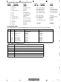
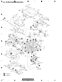
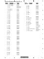
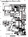
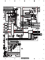
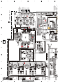
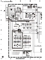
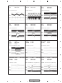
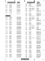
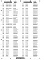
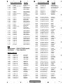
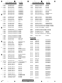
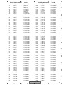
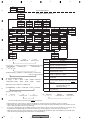
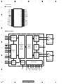
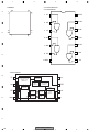
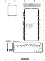
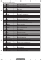
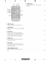
1
ORDER NO.
CRT3650
DEH-P880PRS/XN/UC
MULTI-CD CONTROL HIGH POWER CD/MP3/WMA/AAC PLAYER WITH FM/AM TUNER
DEH-P880PRS
/XN/UC
DEH-P80RS/XN/ES
DEH-P88RS/XN/EW5
MULTI-CD CONTROL DSP HIGH POWER CD/MP3/WMA/AAC PLAYER WITH RDS TUNER
This service manual should be used together with the following manual(s):
Model No.
CX-3164
Order No.
CRT3583
Mech.Module
S10.5COMP1
Remarks
CD Mech. Module : Circuit Descriptions, Mech. Descriptions, Disassembly
For details, refer to "Important Check Points for Good Servicing".
PIONEER CORPORATION
4-1, Meguro 1-chome, Meguro-ku, Tokyo 153-8654, Japan
PIONEER ELECTRONICS (USA) INC. P.O. Box 1760, Long Beach, CA 90801-1760, U.S.A.
PIONEER EUROPE NV Haven 1087, Keetberglaan 1, 9120 Melsele, Belgium
PIONEER ELECTRONICS ASIACENTRE PTE. LTD. 253 Alexandra Road, #04-01, Singapore 159936
PIONEER CORPORATION 2006
Z-ZZW. MAR. 2006 Printed in Japan
1
2
3
4
SAFETY INFORMATION
CAUTION
A
This service manual is intended for qualified service technicians; it is not meant for the casual do-it-yourselfer.
Qualified technicians have the necessary test equipment and tools, and have been trained to properly and safely
repair complex products such as those covered by this manual.
Improperly performed repairs can adversely affect the safety and reliability of the product and may void the warranty.
If you are not qualified to perform the repair of this product properly and safely, you should not risk trying to do so
and refer the repair to a qualified service technician.
W
WARNING
This product contains lead in solder and certain electrical parts contain chemicals which are known to the state of
California to cause cancer
Health & Safety Code Section 25249.6 - Proposition 65
B
- Safety Precautions for those who Service this Unit.
results.
Caution:
1. During repair or tests, minimum distance of 13cm from the focus lens must be kept.
2. During repair or tests, do not view laser beam for 10 seconds or longer.
C
CAUTION:
USE OF CONTROLS OR ADJUSTMENTS OR PERFORMANCE OF PROCEDURES OTHER THAN THOSE
SPECIFIED HEREIN MAY RESULT IN HAZARDOUS RADIATION EXPOSURE.
D
CLASS 1
LASER PRODUCT
E
F
2
DEH-P880PRS/XN/UC
1
2
3
4
5
6
7
8
WARNING!
The AEL (accessible emission level )of the laser power output is less than CLASS 1
but the laser component is capable of emitting radiation exceeding the limit for
CLASS 1.
A specially instructed person should do servicing operation of the apparatus.
A
Laser diode characteristics
Wave length : 785~814nm
Maximum output : 1190µW(Emitting period : unlimited)
B
Additional Laser Caution
Transistors Q101 in PCB drive the laser diodes.
When Q101 is shorted between their terminals, the laser diodes will radiate beam.
If the top cover is removed with no disc loaded while such short-circuit is continued,
the naked eyes may be exposed to the laser beam.
- Service Precautions
1. You should conform to the regulations governing the product (safety, radio and noise, and other
regulations), and should keep the safety during servicing by following the safety instructions
described in this manual.
2. This product memorizes every audio setting value during operating product such as VOL position and
EQ setting. As the setting value is recorded in the built-in EEPROM, it does not return to the initial setting
value even if you press RESET key.
If you return it to the initial setting value, execute the Audio Reset in the initial setting menu.
However, if you execute it, the user setting is deleted.
If you change the audio setting when repairing the product, the product is returned to the user with that
setting, so take care of it.
C
Method of Audio Reset
After pressing MULTI-CONTROL key for two seconds, select Audio Reset by right and left rotation.
After shifting to the reset confirmation screen by right-pressing MULTI-CONTROL key and execute the
reset by center-pressing.
D
- CD Section Precaution
1. Before disassembling the unit, be sure to turn off the power. Unplugging and plugging the connectors
during power-on mode may damage the ICs inside the unit.
2. To protect the pickup unit from electrostatic discharge during servicing, take an appropriate treatment
(shorting-solder) by referring to "the DISASSEMBLY".
3. After replacing the pickup unit, be sure to check the grating.
E
F
DEH-P880PRS/XN/UC
5
6
7
8
3
1
2
3
4
[Important Check Points for Good Servicing]
In this manual, procedures that must be performed during repairs are marked with the below symbol.
Please be sure to confirm and follow these procedures.
A
1. Product safety
Please conform to product regulations (such as safety and radiation regulations), and maintain a safe servicing environment by
following the safety instructions described in this manual.
1 Use specified parts for repair.
Use genuine parts. Be sure to use important parts for safety.
2 Do not perform modifications without proper instructions.
Please follow the specified safety methods when modification(addition/change of parts) is required due to interferences such as
radio/TV interference and foreign noise.
3 Make sure the soldering of repaired locations is properly performed.
B
When you solder while repairing, please be sure that there are no cold solder and other debris.
Soldering should be finished with the proper quantity. (Refer to the example)
4 Make sure the screws are tightly fastened.
Please be sure that all screws are fastened, and that there are no loose screws.
5 Make sure each connectors are correctly inserted.
Please be sure that all connectors are inserted, and that there are no imperfect insertion.
6 Make sure the wiring cables are set to their original state.
Please replace the wiring and cables to the original state after repairs.
In addition, be sure that there are no pinched wires, etc.
C
7 Make sure screws and soldering scraps do not remain inside the product.
Please check that neither solder debris nor screws remain inside the product.
8 There should be no semi-broken wires, scratches, melting, etc. on the coating of the power cord.
Damaged power cords may lead to fire accidents, so please be sure that there are no damages.
If you find a damaged power cord, please exchange it with a suitable one.
9 There should be no spark traces or similar marks on the power plug.
When spark traces or similar marks are found on the power supply plug, please check the connection and advise on secure
connections and suitable usage. Please exchange the power cord if necessary.
0 Safe environment should be secured during servicing.
D
When you perform repairs, please pay attention to static electricity, furniture, household articles, etc. in order to prevent injuries.
Please pay attention to your surroundings and repair safely.
2. Adjustments
To keep the original performance of the products, optimum adjustments and confirmation of characteristics within specification.
Adjustments should be performed in accordance with the procedures/instructions described in this manual.
3. Lubricants, Glues, and Replacement parts
Use grease and adhesives that are equal to the specified substance.
Make sure the proper amount is applied.
E
4. Cleaning
For parts that require cleaning, such as optical pickups, tape deck heads, lenses and mirrors used in projection monitors, proper
cleaning should be performed to restore their performances.
5. Shipping mode and Shipping screws
To protect products from damages or failures during transit, the shipping mode should be set or the shipping screws should be
installed before shipment. Please be sure to follow this method especially if it is specified in this manual.
F
4
DEH-P880PRS/XN/UC
1
2
3
4
5
6
7
8
CONTENTS
SAFETY INFORMATION......................................................................................................................................2
1. SPECIFICATIONS .............................................................................................................................................6
2. EXPLODED VIEWS AND PARTS LIST...........................................................................................................12
2.1 PACKING(UC, ES MODEL) ......................................................................................................................12
2.2 PACKING(EW5 MODEL) ..........................................................................................................................14
2.3 EXTERIOR(1)(UC, ES MODEL)...............................................................................................................16
2.4 EXTERIOR(1)(EW5 MODEL) ...................................................................................................................18
2.5 EXTERIOR(2) ...........................................................................................................................................20
2.6 CD MECHANISM MODULE .....................................................................................................................22
3. BLOCK DIAGRAM AND SCHEMATIC DIAGRAM ..........................................................................................24
3.1 BLOCK DIAGRAM....................................................................................................................................24
3.2 OVERALL CONNECTION DIAGRAM(UC, ES MODEL)(GUIDE PAGE) ..................................................28
3.3 OVERALL CONNECTION DIAGRAM(EW5 MODEL)(GUIDE PAGE) ......................................................34
3.4 KEYBOARD UNIT ....................................................................................................................................40
3.5 CD MECHANISM MODULE(GUIDE PAGE) .............................................................................................42
4. PCB CONNECTION DIAGRAM ......................................................................................................................52
4.1 TUNER AMP UNIT ...................................................................................................................................52
4.2 KEYBOARD UNIT ....................................................................................................................................56
4.3 CD CORE UNIT(S10.5COMP1) ...............................................................................................................58
4.4 SWITCH UNIT ..........................................................................................................................................60
5. ELECTRICAL PARTS LIST .............................................................................................................................61
6. ADJUSTMENT ................................................................................................................................................76
6.1 OEL ADJUSTMENT .................................................................................................................................76
6.2 CD ADJUSTMENT ...................................................................................................................................77
6.3 CHECKING THE GRATING AFTER CHANGING THE PICKUP UNIT.....................................................79
6.4 ERROR MODE .........................................................................................................................................81
6.5 E.VOL IC OSCILLATING FREQUENCY ADJUSTMENT..........................................................................82
6.6 SYSTEM MICROCOMPUTER TEST PROGRAM ....................................................................................82
7. GENERAL INFORMATION .............................................................................................................................83
7.1 DIAGNOSIS..............................................................................................................................................83
7.1.1 DISASSEMBLY......................................................................................................................................83
7.1.2 CONNECTOR FUNCTION DESCRIPTION ..........................................................................................87
7.2 IC ..............................................................................................................................................................88
7.3 OPERATIONAL FLOW CHART ..............................................................................................................103
8. OPERATIONS ...............................................................................................................................................104
A
B
C
D
E
F
DEH-P880PRS/XN/UC
5
6
7
8
5
1
2
3
4
3
4
1. SPECIFICATIONS
A
B
C
D
E
F
6
DEH-P880PRS/XN/UC
1
2
5
6
7
8
A
B
C
D
E
F
DEH-P880PRS/XN/UC
5
6
7
8
7
1
2
1
2
3
4
3
4
A
B
C
D
E
F
8
DEH-P880PRS/XN/UC
5
6
7
8
A
B
C
D
E
F
DEH-P880PRS/XN/UC
5
6
7
8
9
1
2
1
2
3
4
3
4
A
B
C
D
E
F
10
DEH-P880PRS/XN/UC
5
6
7
8
A
B
C
D
E
F
DEH-P880PRS/XN/UC
5
6
7
8
11
1
2
3
4
2. EXPLODED VIEWS AND PARTS LIST
NOTES : • Parts marked by " * " are generally unavailable because they are not in our Master Spare Parts List.
• The > mark found on some component parts indicates the importance of the safety factor of the part.
Therefore, when replacing, be sure to use parts of identical designation.
• Screw adjacent to mark on the product are used for disassembly.
• For the applying amount of lubricants or glue, follow the instructions in this manual.
(In the case of no amount instructions,apply as you think it appropriate.)
A
"
2.1 PACKING(UC, ES MODEL)
6
8
B
7
3
4
5
19
9
20
2
C
1
15
16
18
11
D
12
E
F
12
DEH-P880PRS/XN/UC
1
2
3
4
5
6
7
8
(1) PACKING(UC, ES MODEL) SECTION PARTS LIST
Mark No.
Mark No.
Part No.
1
2
3
4
5
Cord Assy
Cord Assy
Screw Assy
Screw
Polyethylene Bag
CDE7701
CDE8275
See Contrast table(2)
CBA1650
CEG-127
6
7
8
9
10
Screw
Screw
Screw
Polyethylene Bag
Polyethylene Bag
CRZ50P090FTC
See Contrast table(2)
TRZ50P080FTC
CEG-158
See Contrast table(2)
11
12
13
14
Carton
Contain Box
Protector
Protector
See Contrast table(2)
See Contrast table(2)
XHP7007
XHP7008
*
*
Description
15
*
*
Description
Part No.
Microphone Assy
CPM1054
16-1
16-2
16-3
16-4
16-5
Polyethylene Bag
Owner's Manual
Owner's Manual
Owner's Manual
Installation Manual
CEG1116
See Contrast table(2)
See Contrast table(2)
See Contrast table(2)
See Contrast table(2)
16-6
16-7
16-8
17
18
Caution Card
Warranty Card
Caution Card
Case Assy
Remote Control Unit
CRP1310
See Contrast table(2)
XRP7002
CXB3520
CXC5717
Handle
Bush
CNC5395
CNV3930
19
20
A
B
(2) CONTRAST TABLE
DEH-P880PRS/XN/UC and DEH-P80RS/XN/ES are constructed the same except for the following:
Mark
No.
Description
3
7
10
11
12
16-2
16-3
16-4
16-5
16-7
*
DEH-P880PRS/XN/UC
DEH-P80RS/XN/ES
Screw Assy
Screw
Polyethylene Bag
Carton
Contain Box
CEA5322
JPZ20P060FTB
CEG1368
CHG5735
CHL5735
CEA3849
Not used
CEG1227
CHG5736
CHL5736
Owner's Manual
Owner's Manual
Owner's Manual
Installation Manual
Warranty Card
CRD4080
Not used
Not used
CRD4081
CRY1070
CRD4082
CRD4083
CRB2177
CRD4084
Not used
C
Owner's Manual,Installation Manual
Part No.
Language
CRD4080
English, French
CRD4081
English, French
CRD4082
English, Spanish
CRD4083
Portuguese(B), Traditional Chinese
CRB2177
Arabic
CRD4084
English, Spanish, Portuguese(B), Traditional Chinese, Arabic
D
E
F
DEH-P880PRS/XN/UC
5
6
7
8
13
1
2
3
4
2.2 PACKING(EW5 MODEL)
A
6
19
8
7
3
4
5
22
9
23
2
B
20
21
1
18
11
12
C
14
15
17
15
16
10
D
13
14
E
F
14
DEH-P880PRS/XN/UC
1
2
3
4
5
6
7
8
(1)PACKING(EW5 MODEL) SECTION PARTS LIST
Mark No.
*
*
Description
Mark No.
Part No.
1
2
3
4
5
Cord Assy
Cord Assy
Screw Assy
Screw
Polyethylene Bag
CDE6562
CDE8274
CEA5322
CBA1650
CEG-127
6
7
8
9
10
Screw
Screw
Screw
Polyethylene Bag
Polyethylene Bag
CRZ50P090FTC
JPZ20P060FTB
TRZ50P080FTC
CEG-158
CEG-162
11
12
13
14
15
Sub Carton
Carton
Contain Box
Protector
Protector
CHG5195
CHG5882
CHL5882
CHP2797
CHP2798
16
Protector
CHP2812
*
*
*
*
Description
Part No.
17
18
19-1
19-2
Protector
Microphone Assy
Polyethylene Bag
Owner's Manual
CHP3184
CPM1054
E36-634
CRB2176
19-3
19-4
19-5
19-6
19-7
Owner's Manual
Owner's Manual
Owner's Manual
Installation Manual
Caution Card
CRD4076
CRD4077
CRD4078
CRD4079
CRP1335
19-8
19-9
20
21
22
Passport
Warranty Card
Case Assy
Remote Control Unit
Handle
CRY1013
CRY1157
CXB3520
CXC5717
CNC5395
Bush
CNV3930
23
A
B
Owner's Manual,Installation Manual
Part No.
Language
C
CRD4076
English, Spanish
CRD4077
German, French
CRD4078
Italian, Dutch
CRB2176
Russian
CRD4079
English, Spanish, German, French, Italian, Dutch, Russian
D
E
F
DEH-P880PRS/XN/UC
5
6
7
8
15
1
2
3
4
3
4
2.3 EXTERIOR(1)(UC, ES MODEL)
A
B
C
D
E
F
16
DEH-P880PRS/XN/UC
1
2
5
6
7
8
EXTERIOR(1)(UC, ES MODEL) SECTION PARTS LIST
Mark No.
>
Description
Mark No.
Part No.
1
2
3
4
5
Screw
Screw(M2.6 x 4)
Screw(M2 x 2.5)
Cord Assy
Fuse(10 A)
BSZ26P060FTC
CBA1828
CBA1924
CDE7701
CEK1136
6
7
8
9
10
•••••
Cap
Resistor
Cord Assy
Cable
CNS1472
RS1/2PMF102J
CDE7817
CDE8067
11
12
13
14
15
Cord Assy
Cap
Case Assy
Holder
Earth Plate
CDE8275
CNV6727
CXC6908
CNC8659
CND2171
16
17
18
19
20
Insulator
Cushion
Insulator
Panel
Tuner Amp Unit(UC)
CNM8790
CNM9126
CNM9936
CNS8516
CWN1478
21
22
23
24
Tuner Amp Unit(ES)
Screw
Screw
Screw
Screw
CWN1479
ASZ26P060FTC
BMZ26P040FTC
BMZ26P120FTC
BMZ26P180FTC
25
26
27
28
29
Screw(M2.6 x 14)
Antenna Cable
Clamper
Plug(CN901)
Connector(CN351)
CBA1632
CDH1336
CEF1040
CKM1278
CKM1389
30
31
32
33
34
Plug(CN871)
Connector(CN471)
Connector(CN581)(UC)
Connector(CN801)
Connector(CN472)
CKS-786
CKS3834
CKS4124
CKS4811
CKS4822
35
36
37
38
Connector(CN101)
•••••
Holder(CN402)
Holder(UC)
Holder(ES)
CKS5271
39
40
41
42
43
Holder
Heat Sink
FM/AM Tuner Unit(Y401)
Holder
Fan Motor
CND3133
CNR1837
CWE1802
CND2144
CXM1288
44
45
46
47
Connector(CN591)
Remote Control Unit
Cover
Panel Unit
VKN1928
CXC5717
CZN5357
CXC5737
CNC5399
CND3158
CND3159
*
*
*
*
*
*
*
*
Description
Part No.
48
Drive Unit
CXC6620
49
50
51
52
53
Screw
Screw(M2 x 2)
Cord
Gear
Gear
BMZ26P040FTC
CBA1871
CDE7392
CNV7752
CNV7753
54
55
56
57
58
Gear
Gear
Switch Unit
Switch(S1)
Spring Switch(S2)
CNV7754
CNV7755
CWS1389
CSN1051
CSN1052
59
60
61
62
63
Arm Unit
Chassis Unit
Arm Unit
Arm Unit
Screw
CXC2199
CXC5680
CXC6623
CXC6624
JFZ20P020FTC
64
65
66
67
68
Spring
Holder
Insulator
Holder Unit
Motor Unit(M10)
XBL7003
XNC7017
XNM7119
XXA7399
XXA7400
69
70
71
72
73
Holder Unit
Arm Unit
Gear Unit
Washer
CD Mechanism Module(S10.5)
XXA7401
XXA7403
XXA7424
YE15FTC
CXK5753
74
75
76
77
78
Screw
Holder
Screw(M2 x 2)
Screw
Spring
ISS26P055FTC
CND3606
CBA1871
CBA1935
CBH2530
79
80
81
82
83
Connector
Arm
Guide
Guide
Screw(M2 x 3.5)
CKS5273
CNV6962
CNV6967
CNV8048
XBA7002
84
85
86
87
88
Holder
Flexible PCB
Case Unit
Transistor(Q462,701,711)
IC(IC331)
XNC7019
XNP7026
XXA7426
2SD2396
PAL007B
6
B
C
D
E
F
DEH-P880PRS/XN/UC
5
A
7
8
17
1
2
3
4
3
4
2.4 EXTERIOR(1)(EW5 MODEL)
A
B
C
D
E
F
18
DEH-P880PRS/XN/UC
1
2
5
6
7
8
EXTERIOR(1)(EW5 MODEL) SECTION PARTS LIST
Mark No.
>
Description
Mark No.
Part No.
1
2
3
4
5
Screw
Screw(M2.6 x 4)
Screw(M2 x 2.5)
Cord Assy
Fuse(10 A)
BSZ26P060FTC
CBA1828
CBA1924
CDE6562
CEK1136
6
7
8
9
10
Cap
Cap
Resistor
Cord Assy
Cable
CKX-003
CNS1472
RS1/2PMF102J
CDE7817
CDE8067
11
12
13
14
15
Cord Assy
Cap
Case Assy
Holder
Earth Plate
CDE8274
CNV6727
CXC6908
CNC8659
CND2171
16
17
18
19
20
Insulator
Cushion
Insulator
Panel
Tuner Amp Unit
CNM8790
CNM9126
CNM9936
CNS8516
CWN1477
21
22
23
24
25
Screw
Screw
Screw
Screw
Screw(M2.6 x 14)
ASZ26P060FTC
BMZ26P040FTC
BMZ26P120FTC
BMZ26P180FTC
CBA1632
26
27
28
29
30
Antenna Cable
Clamper
Plug(CN901)
Connector(CN351)
Plug(CN871)
CDH1336
CEF1040
CKM1278
CKM1389
CKS-786
31
32
33
34
35
Connector(CN471)
Connector(CN581)
Connector(CN801)
Connector(CN472)
Connector(CN101)
CKS3834
CKS4124
CKS4811
CKS4822
CKS5271
36
37
38
39
40
Connector(CN541)
Holder(CN402)
Holder
Holder
Heat Sink
CKS5523
CNC5399
CND3129
CND3133
CNR1837
41
42
43
44
45
FM/AM Tuner Unit(Y401)
Holder
Fan Motor
Connector(CN591)
Remote Control Unit
CWE1801
CND2144
CXM1288
VKN1928
CXC5717
46
47
48
49
Cover
Panel Unit
Drive Unit
Screw
CZN5357
CXC5737
CXC6620
BMZ26P040FTC
Description
Part No.
50
Screw(M2 x 2)
CBA1871
51
52
53
54
55
Cord
Gear
Gear
Gear
Gear
CDE7392
CNV7752
CNV7753
CNV7754
CNV7755
*
56
57
58
59
60
Switch Unit
Switch(S1)
Spring Switch(S2)
Arm Unit
Chassis Unit
CWS1389
CSN1051
CSN1052
CXC2199
CXC5680
*
61
62
63
64
65
Arm Unit
Arm Unit
Screw
Spring
Holder
CXC6623
CXC6624
JFZ20P020FTC
XBL7003
XNC7017
*
*
*
*
*
66
67
68
69
70
Insulator
Holder Unit
Motor Unit(M10)
Holder Unit
Arm Unit
XNM7119
XXA7399
XXA7400
XXA7401
XXA7403
*
71
72
73
74
75
Gear Unit
Washer
CD Mechanism Module(S10.5)
Screw
Holder
XXA7424
YE15FTC
CXK5753
ISS26P055FTC
CND3606
76
77
78
79
80
Screw(M2 x 2)
Screw
Spring
Connector
Arm
CBA1871
CBA1935
CBH2530
CKS5273
CNV6962
81
82
83
84
85
Guide
Guide
Screw(M2 x 3.5)
Holder
Flexible PCB
CNV6967
CNV8048
XBA7002
XNC7019
XNP7026
86
87
88
Case Unit
Transistor(Q462,701,711)
IC(IC331)
XXA7426
2SD2396
PAL007B
6
B
C
D
E
F
DEH-P880PRS/XN/UC
5
A
7
8
19
1
2
3
4
3
4
2.5 EXTERIOR(2)
A
B
C
D
E
F
20
DEH-P880PRS/XN/UC
1
2
5
6
7
8
(1) EXTERIOR(2) SECTION PARTS LIST
Mark No.
Description
Mark No.
Part No.
1
2
3
4
5
Detach Grille Assy
Screw
Button(EJECT)
Button(RESET)
Earth Plate
See Contrast table(2)
BPZ20P080FTB
CAC9616
CAC9617
CND3149
6
7
8
9
10
Earth Plate
Lighting Conductor
Lighting Conductor
Connector(CN1801)
Connector(CN1861)
CND3150
CNV8923
CNV8924
CKS5272
CKS5545
11
12
13
14
15
Connector(CN1802)
Holder
Holder
Sheet
Double Sided Seal
See Contrast table(2)
CND3151
CND3152
CNM8658
CNM8673
16
Cushion
CNM9946
*
Description
Part No.
17
18
19
20
Holder
OEL Unit
Knob Unit(SOURCE,VOLUME)
Knob Unit(MULTI-CONTROL)
CNV8925
MXS8232
CXC5740
CXC5741
21
22
23
24
25
Button Unit(EQ/CLK)
Button Unit(BAND/DISP)
Cover Unit
Sub Grille Assy
IC(IC1902)
See Contrast table(2)
CXC5748
CXC5749
See Contrast table(2)
GP1UX51RK
26
27
28
29
30
Double Sided Seal
Double Sided Seal
Panel
Panel
Grille Unit
CNM9942
CNM9943
See Contrast table(2)
See Contrast table(2)
CXC5732
31
Badge
See Contrast table(2)
A
B
(2) CONTRAST TABLE
DEH-P880PRS/XN/UC, DEH-P88RS/XN/EW5 and DEH-P80RS/XN/ES are constructed the same except for the
following:
Mark
*
No.
Description
DEH-P880PRS/XN/UC
DEH-P88RS/XN/EW5
C
DEH-P80RS/XN/ES
1
11
21
24
28
Detach Grille Assy
Connector(CN1802)
Button Unit(EQ/CLK)
Sub Grille Assy
Panel
CXC5764
CKS5575
CXC5745
CXC5823
CNR1843
CXC5763
CKS3120(Mini Jack)
CXC5744(EQ/TA)
CXC5822
CNR1842
CXC5765
CKS5575
CXC5746
CXC5824
CNR1844
29
31
Panel
Badge
CNR1847
CAH1956
CNR1846
CAH1925
CNR1846
CAH1925
D
E
F
DEH-P880PRS/XN/UC
5
6
7
8
21
1
2
3
4
3
4
2.6 CD MECHANISM MODULE
A
B
C
D
E
F
22
DEH-P880PRS/XN/UC
1
2
5
6
7
8
CD MECHANISM MODULE SECTION PARTS LIST
Mark No.
Description
Mark No.
Part No.
1
2
3
4
5
CD Core Unit(S10.5COMP1)
Connector(CN101)
Connector(CN901)
Screw
Screw
CWX3381
CKS4182
CKS4187
BMZ20P025FTC
BSZ20P040FTC
6
7
8
9
10
Screw(M2 x 3)
Screw(M2 x 4)
Washer
•••••
Spring
CBA1511
CBA1835
CBF1038
11
12
13
14
15
Spring
Spring
Spring
Spring
Spring
CBH2612
CBH2614
CBH2616
CBH2617
CBH2620
16
17
18
19
20
Spring
Spring
Spring
Spring
Spring
CBH2855
CBH2937
CBH2735
CBH2854
CBH2642
21
22
23
24
25
Spring
Spring
Spring
Spring
Spring
CBH2856
CBH2857
CBH2860
CBH2861
CBL1686
26
27
28
29
30
Arm
Frame
Bracket
Arm
Lever
CND1909
CND2582
CND2583
CND2584
CND2585
31
32
33
34
35
Arm
Bracket
Arm
Lever
Holder
CND2586
CND2587
CND2588
CND2589
CNV7201
36
37
38
39
40
Gear
Gear
Gear
Gear
Gear
CNV7207
CNV7208
CNV7209
CNV7210
CNV7211
41
42
43
44
45
Gear
Rack
Arm
Roller
Gear
CNV7212
CNV7214
CNV7216
CNV7218
CNV7219
46
47
48
49
Guide
Gear
Guide
Arm
CNV7361
CNV7595
CNV7799
CNV7805
CBH2609
Description
Part No.
50
Rack
CNV8342
51
52
53
54
55
Roller
Holder
Arm
Guide
Arm
CNV8343
CNV8344
CNV8345
CNV8347
CNV8348
56
57
58
59
60
Arm
Arm
Clamper
Arm
Guide
CNV8349
CNV8350
CNV8365
CNV8386
CNV8396
61
62
63
64
65
Arm
Collar
Motor Unit(M2)
Arm Unit
Chassis Unit
CNV8413
CNV8938
CXC4026
CXC4027
CXC4028
66
67
68
69
70
Gear Unit
Frame Unit
Motor Unit(M1)
Screw Unit
Screw
CXC4029
CXC4031
CXC6742
CXC6359
JFZ20P020FTC
71
72
73
74
75
Screw
Washer
Pickup Unit(P10.5)(Service)
Screw
Connector(CN902)
JGZ17P022FTC
YE20FTC
CXX1942
IMS26P030FTC
CKS4979
6
B
C
D
E
F
DEH-P880PRS/XN/UC
5
A
7
8
23
1
2
3
4
3. BLOCK DIAGRAM AND SCHEMATIC DIAGRAM
3.1 BLOCK DIAGRAM
A
A
TUNER AMP UNIT
ASL
MICROPHONE
IC562(2/2)
NJM4558V
IC562(1/2)
NJM4558V
MIC521
DI
LDET
CE1
DO
CK
SL
CE2
VDD
3
OUT
MIC
3
1
7
5
2
A
21
RDSHSLK
20
RDSLOCK
RDSCK
DO
18 19
RDSDATA
14
11
LDET
CK
DI
8
CE1
10 9
SL
5
ROMVDD
WC
13
CE2
7 6
FM/AM TUNER UNIT
VR521
HIGH SPEED CLOCK
IC491
TC7SU04FU
DSP
IC492
TC7S04FU
2
4
2
4
IC121
AK7732VT
CK
43 XTI
CK_RE
X491
16.9344MHz
B
CN401
1
ANTENNA
1
IC3
EEPROM
IC4
5V 3.3V
AMANT
S_RE
INIT_RE
CDDT
22
BCKI
25
LRCKI
26
SDIN5A/JX0
BITCLK_I
LRCLK_I
RQ/C
COMP 16
2,3
VCO
SCLK
LPF
RCH
1
2
3
Q431
FMANT
LCH
ATT
TANK
RF
SI/C
37 SDOUT1 SDIN3
36 SDOUT2
SW
35
F
23
CN402
R
BUFFER
24
SDOUT3
TANK
IC1
MIX/IF/PLL
IC2
DET/NC/MPC/MPX/DIV/RDS
DIVER
LRCKO
39
BCKO
38
LRCLK_O
BITCLK_O
22
5
RF
LPF
IC431
NJM4558V
OSCGND
DGND
VCC
2
12
15
4
CF
X-tal
OSC
REG
7
D/A CONVERTER
VDD
RFGND
IFT
17
C
LRCKO
1
BCKO
2
F
3
MCK
5
TUN3V REGULATOR
IC401
NJM2885DL1-33
TUN3V
3
IC161
PCM1793DB
LRCK
BCK
18
VoutLVoutL+ 17
DATA
SCK
D/A CONVERTER
SYSB
1
CN541
A
3
2
REAR
AUX
2
LRCK
IC171
PCM1793DB
BCK
R
3
MCK
5
LRCKO
1
BCKO
2
IC181
PCM1793DB
BCK
5
MCK
2
1
LRCK
3
SW
142
Q101
REFO
8
AC,BD
F,E
LOAD/ CARRIAGE
MOTOR
3
FOP
2
TOP
1
TOM
LD+
SPINDLE
MOTOR
143
133
3
FOM
4
14
14
LRCK
50
LRCK
49
LRCKIN
46
DOUT
REFOUT
45
RF-AMP,CD DECODER,
DIN
48
MP3 , WMA, DECODER,
SCKO
DIGITAL SERVO / DATA PROCESSOR SCKIN 47
IC201
UPD63763CGJ
DATA
16
5
14
7
5
BUS+
6
LRCKI
TD,FD
SD,MD
CD
12
FOM
DRIVER
11
FOP
14
TOP
13
TOM
63
IC301
BA5835FP
M
LOCK
16
SOP CLCONT 21
15
SOM
22
18
LOEJ
LCOP
17
9
CONT
LCOM
M
41
40
47
32
E
31
30
42
S904
12EJ
1 TX
28
2 RX
27
19
8
CDDT
8
IPPW
S905
8EJ
CLCONT
BCLK
15
EEPROM
Q701
VDD
SWVDD
11
10
KEYD(E
1
CSB
2
SO
SI 5
6
SCK
VDD
VDD
IC631
BR25L320F-W
43
14
RESET
44
LRCKOK
/RESET
10
LRCKOK
8
70
ROMCSB
68
ROMSO
69
ROMSI
67
ROMSCK
KEY
JSNSO
JSNSO
JCKS
RESET
11
LRCKOK
13
53 CDRST
51
LRCKOK
FLPC
FLPO
VD
X1 12
X2 13
DSCSNS
HOME
VDCONT
CD3VON
VD
X701
4.00MHz
1
20
2
19
Q462
VD
BDATA,BSCK
MECHA VD
BUP
36
Q461
STD
(DSPMODE)
AUXL
49
VDCONT
46
MCKRQ
VD
AUTOEQ
Q522
VDCOUNT
9
17
12
4 MCKRQ
ROMDATA
1
OUT1
VDD
VM1
2
4
M
2
9
5
FLM02
14
3
AUTO FLAP
4
4
5
OUT2 RIN
OUT1 FIN
83
AUXON
DIM_
(PUC/
AEQON
SWV
DALMON
VM
Q521
FLPCLS
FLPOPN
FOPNSW
FCLSSW
VCC
58 91 34 33
E
6
JSNSON1
BUP
Q871
Q524
BUP
Q872
JSNSON2
FLPPW
Q842
JCKSNS
VDD
B SWITCH UNIT
84
AUXGND
11
FLOR
2
FLCL
3
1
DIM_
AUXL/MIC
IC871
BA6288FS
FLM01
DSPMOD
ILM
1
13
3
5
8
6
10
12
11
AUTO FLAP
MOTOR DRIVE
CN871
EEPROM
61
IC521
TC4066BF
3
IC522
BA3121F
Q523
IC704
BR93L56RFVM-W
A:DEH-P88RS/XN/EW5
B:DEH-P880PRS/XN/UC
C:DEH-P80RS/XN/ES
IN1
RO
MCKRQ
NW
(NETWORK)
S651
MIC/AUX
SELECT
VDD
+3.3V REGULATOR
FOPN
FCLS
FLP
RO
BRST,BRXEN,BSRQ
BRST,BRXEN,BSRQ
BDATA,BSCK
12EJ
8EJ
1
3
MU
ASENBO
LOEJ
S901
HOME
IC203
NJM2886DL3-33
IPPW
BUP
AMP
/CD3VON
ROMCS,ROMCK,
4
RX
RX2
FLP
BCKI
6
9
IC701
CONT PE5561A
CD CONTROLLER
S903
DSCSNS
V3R3D
TX
Q101
CD3VON
46
F
IC101
HA12241FP
LOCK/RFOK
56
FOP
2
1 TOP
TOM
4
XTAL
LD
PD
BUS-
CN471
DSENS
5
CN901
KYDT
15
5
HOLOGRAM
UNIT
FOCUS ACT.
MONITOR
TRACKING ACT.
DIODE
IC601(2/2)
PEG176A:A
PEG178A:B,C
IP-BUS DRIVER
34
OELPW
15
VREF 8
FOM
BUSL-
SYSTEM
CONTROLLE
OELPW
MD
BUSL+
BUSL-
1
XSO,XSI,WAIT,XINT
LD-
BUSL+
CN902
V3R3D
CN101
LASER
DIODE
17
VoutL+
SCK
8
XRST,XASTB,ADO,XCK,
D
D CD CORE UNIT(S10.5COMP1)
18
VoutL-
DATA
TUN L
7 BUSL+
11 BUSL5
1
IP-BUS
17
VoutL+
SCK
CN101
PICKUP UNIT
(P10.5)(SERVICE)
18
VoutL-
DATA
D/A CONVERTER
IC493
TC7SH08FUS1
4
1
BCKO
1
IC541
BA3121F
CN472
MCKCD
1
LRCKO
DPDT
ATT
B,C
OEL+B REGULAT
24
DEH-P880PRS/XN/UC
1
2
3
4
5
6
7
8
A
RCA OUT
CN351
ASL
3
IC561(1/2)
NJM4558V
3
1
5
7
Q401
LDET
2
A
VR521
Q402
RDSLOCK
RDSHSLK
DSP
IC121
AK7732VT
31
43 XTI
CKM[2]
28
CK_RESET
29
S_RESET
27
INIT_RESET
LRCLK_I
Q403
1
6
4
3
8
9
40
SDOUT3
38
BITCLK_O
63
7
D/A CONVERTER
6
5
CKO
BCK
3
IC201
NJM2114M
7
5
18
VoutLVoutL+ 17
DATA
5
K
CKO
K
CKO
LRCK
5
DATA
17
1 TX
28
2 RX
27
19
8
W
21 EVOLCS
20
FCKSEL
13
XIN
11
D
Vo5a
11
Si4L
BUSL+
1
BUSL-
2
RX
RX2
PEE
BSENS
73
BSENS
ASENS
72
ASENS
BATIND 88
BATIND
74
ISENS
XOUT
ISENS
AUXL
6
AUTOEQ
9
Vo3a
Si1L+
Vo1b
Si1L-
Vo3b
TELIN
BUP
Q911
ACC
RST1
IC661
S-80835CNMC-B8U
BRE
2
33
SWL
29
FL
ASENBO
AMPPW
KEYD(EW)
70
ROMCSB
68
ROMSO
69
ROMSI
67
ROMSCK
KEYAD
FLPCLS
FLPOPN
31
RL
36
FL
FL
RL
38
RL
12
14
IC331
PAL007B
FLIN
36
MCKRQ
RL-
RLIN
RL+
MUTE
22
C
4
B.REM
2
GND
3
FL2
5
FL1
23
RL2
10
21
RL1
FL-
12
FL+
9
RL-
11
RL+
CN581
KEYD
KEYAD
Q382
WIRED
REOTE
A,B
D
BUP
77
FAN DRIVE
Q591
Q831
AMPMUTE
Q592
CN591
2
1
FAN
26
AMPPW
18
32
92
JSNSON1
JSNSON2
JCKSNS
80
79
81
FLPCLS
FLPOPN
FOPNSW
FCLSSW
FLPPW
B,C
CN801
JACKSNS
AUXL
ILM+B CONTROL
B,C
Q821
Q822
AUXGND
ILB
B
3
12
4
E
13
DSPMOD
ILMPW
DIM_WH
XL/MIC
56
ROT0 8
Q823
ROT1 9
54
AUXON
DIM_BL 55
(PUC/JP)
AEQON
C
SWVDD
DSENS
KYDT
OELPW
Q861
G5V
VDD
DPDT
83
TEL
STBY
4
VDD
BZ601
BUP
84
8
Q381
BUZZER
NW
NETWORK)
61
FLFL+
Si3L
BUP
FOPNSW
82
FCLSSW
78
FLPPW
76
ROT0
75
ROT1
BSRQ
ILL
6,20
VCC1/2,VCC3/4
52
JSNSON1
JSNSON2 85
87
JCKSNS
53 CDRST
51
LRCKOK
3
BUP
POWER AMP
FLAP ILM
MUTE
ACC
VDD
Q331
9
TEL
PRE-OUTMUTE
22
5
Q921
ILL SENSE
DALMON
E
BUP
ILL
RESET
1
1
ACC SENSE
TELIN
66
Si2L
IPPW
FLPILM
SWVDD
57
10
Q862
DPDT
6
KYDT
NSON1
7
DSENS
BUP
Q841
OELB
9.2V
Q842
OELPW
CKSNS
CN1801
SWVDD
58 91 34 33
NSON2
CN901
Q931
BUP
XGND
BUP
TEL IN
IC601(2/2)
PEG176A:A
PEG178A:B,C
TX
DALMON
RESET
Vo1a
ER
25
Vi15(SWL)
SWL
SYSTEM
CONTROLLER
Q752
Q661
TUN L
Q702
TUN8V
REGULATOR
Q751
10
IC203
NJM2114M
VoutL+
SCK
16
44
SCK
43
SDA
45
CS
46
FCKSEL
Vi3(RL)
25
Q701
1
BACKUP SENSE
LPF
7
B
VDD
DALMON
IC281
PM9009A
5
Q712
VDD REGULATOR
SYSTEM
CONTROLLER
Q711
SYSB
IC941
TPD1018F
DSPRDY
RL
18
VoutL-
1,3
B.REM
6
IC251
NJM4558MD
X601
15.000MHz
22
7
5
IC181
PCM1793DB
BCK
3
Vi1(FL)
DSPPW
RAMCLR
DSPIN
6
AUDIO8V
REGULATOR
IC721
NJM2872F05
24
IC601(1/2)
PEG176A:A
PEG178A:B,C
LPF
IC171
LRCK
PCM1793DB
2
BCK
18
VoutL3
DATA
17
VoutL+
5
SCK
2
19
5
1
IC731
NJM2885DL1-33
SYSPW
DSPOUT
A5V
IC202
NJM2114M
1
1
4
REAR L
5
Q352
DAC5V
REGULATOR
23
DSPCK
So1L
FL
D/A CONVERTER
CKO
5
SCK
D/A CONVERTER
RCKO
6,7
SYSPW
DSPPW
BUFFER
3
3
D3V
DSPRQ
47
3
1,2
FRONT L
FU351
A3V
ELECTRONIC VOLUME/
SOURCE SELECTOR
LPF
IC161
PCM1793DB
Q355
AUDIO3V
REGULATOR
5V
IC671
TC74VHCT08AFTS1
4
6
1
INPUT ADC
IC261
NJM4558MD
LRCK
3V
3V
64
AINL+
AINL-
2
5
10
SO
LRCLK_O
46
IC672
TC74VHC08FTS1
9
RDY
KO
1
A5V
3
39
RCKO
A8V
14
SCLK/SCL
11
SI/CAD0
37 SDOUT1 SDIN3/JX2 20
36 SDOUT2
5V
1
2
RL
Q354
CKM[2]
12
35
FL
Q351
CK_RST
43
DSPS_RST
41
INT_RST
89
RDSLK
39
RDS57K
16
RCK
90
RDT
11
CKO
FL
TUNPCE1
2
TUNPCE2
98
TUNPDI
99
TUNPDO
100
TUNPCK
95
SL
8
RQ/CAD1
LDET
10
1
CE1
CE2
DI
DO
CK
SL
RDSDATA
A
BITCLK_I
26
Q356
SW L
9
Q353
42
SDIN5A/JX0
25
17
SWL
ASLIN
44
RDSCK
22
93
ASLIN
1
7
5
SWL
IC561(2/2)
NJM4558V
RESET
IC562(2/2)
NJM4558V
IC562(1/2)
NJM4558V
2
F
15
8
1
CD
IC841
CS
7
SI NJM2360M
DC-DC CONVERTER
D
RST
5
OEL+B REGULATOR
DEH-P880PRS/XN/UC
5
6
7
8
25
1
C
2
3
4
KEYBOARD UNIT
A
CN1801
CN1802
JCKSENS
2
AUXL/MIC
11
3 AGND
12
AUXSENS
AUXL
AUXGND
AUX/AEQ
CONNECTOR
Q1832
LED DRIVE
ILM+B
Q1831
KEY MATRIX
VOL/ SOURCE
S1832-S1836
7
8
ROT0
KS0
ROT1
KD2
KD0-2,KS0-1
S1831
ILLUMINATION
(WHITE)
ILLUMINATION
(BLUE)
KEY/OEL CONTROLLER
87
BLUE
90
OFFMODE
SWVDD
CN801
B
IC1903
PEG179A
Q1833
A
WHITE
3V REGULATOR
9
4,5
SWVDD
IC1904
S-818A33AUC-BGN
IC1902
GP1UX51RK
14
VCC1
97
AVCC
96
Vref
4
REM
27
DPDT
28
KYDT
1
5
6
1
14
OEL+B
OEL+B
S1801
(RESET)
4
RST
XIN
XOUT
12
48
CE
23
3
47
VCC
A17
33
2
46
BYTE/VPP A18
43
45
A19
14
42
OE
DATA
IC1905
PD8160A
ADDRESS
CSO
BANK0
BANK1
BANK2
RD
13
11
X1901
16MHz
CN1861
LS
CKD
CLK0
ROM
DSENS
B
VCC2
REMOTE CONTROL
SENSOR
3
OPT IN
89
60
1
OELD
DSEL
26
12
24
35
33
11
10
22
9
SWDVDD
OEL+B
OEL+B
Q1861
VDD
AVCC1
AVCC2
Q1862
CVCC
IREF
8
5
6
14
OEL UNIT
2
VR1861
MULTI-CONTROL
S1811
29
30
C
DGND
ROT1
7
ROT2
PGND1
1
PGND2
13
PGND3
15
88
JOYST
A:DEH-P88RS/XN/EW5
B:DEH-P880PRS/XN/UC
C:DEH-P80RS/XN/ES
D
E
F
26
DEH-P880PRS/XN/UC
1
2
3
4
5
6
7
8
A
B
C
D
E
F
DEH-P880PRS/XN/UC
5
6
7
8
27
1
2
3
4
3.2 OVERALL CONNECTION DIAGRAM(UC, ES MODEL)(GUIDE PAGE)
Note: When ordering service parts, be sure to refer to " EXPLODED VIEWS AND PARTS LIST" or
"ELECTRICAL PARTS LIST".
A-a
A-b
Large size
SCH diagram
A-a
A
CN871
3
S1 CLOSE
CSN1051
2
A-a
A-b
A-a
B SWITCH UNIT
Guide page
A-b
1
S2 OPEN
CSN1052
A
Detailed page
B
C
D
CN901
CD:0dBs
A : DEH-P880PRS/XN/UC
B : DEH-P80RS/XN/ES
D
CN902
D
CWE1802
FM(30%):-30.00dBs
AM(30%):-30.00dBs
E
IP-BUS:+2.20dBs
8 9 10 11
5 6
7
1 2 3 4
B
F
M
A B
28
C
M10
FLAP MOTOR
XXA7400
DEH-P880PRS/XN/UC
1
2
3
4
CN1801
5
6
7
8
A
A-b
A
TUNER AMP UNIT
FM:-5.78dBs
AM:-5.78dBs
IP-BUS:+10.32dBs
CD:+10.08dBs
FM:+0.22dBs
AM:+0.22dBs
IP-BUS:+16.32dBs
CD:+16.08dBs
SUB
WOOFER
R CH
SUB
WOOFER
L CH
B
REAR
R CH
REAR
L CH
FRONT
R CH
FRONT
L CH
>
C
FM:+20.22dBs
AM:+20.22dBs
IP-BUS:+36.32dBs
CD:+36.08dBs
CEK1136
10A >
BACKUP
GND
1K(1/2W)
ILL
B.REM
ACC
1K(1/2W)
D
TEL MUTE
RLFLRL+
FL+
RRFRRR+
FR+
B
A
E
A
A
A:
B:
NOTE :
Symbol indicates a resistor.
No differentiation is made between chip resistors and
discrete resistors.
Symbol indicates a capacitor.
No differentiation is made between chip capacitors and
discrete capacitors.
A:
B:
Decimal points for resistor
and capacitor fixed values
are expressed as :
2.2 ← 2R2
0.022 ← R022
The > mark found on some component parts indicates
the importance of the safety factor of the part.
Therefore, when replacing, be sure to use parts of
identical designation.
F
: The power supply is shown with the marked box.
C
CN1801
A
DEH-P880PRS/XN/UC
5
6
7
8
29
1
E
1
D
CN902
C
A : DEH-P880PRS/XN/UC
B : DEH-P80RS/XN/ES
A-b
CD:0dBs
B SWITCH UNIT
3
2
CN871
S1 CLOSE
CSN1051
30
S2 OPEN
CSN1052
A
A-a A-b
1
2
1
2
3
2
F
3
4
A
3
B
D
D
CN901
A-a B
DEH-P880PRS/XN/UC
4
5
6
7
7
1 2 3 4
IP-BUS:+2.20dBs
D
CN902
DEH-P880PRS/XN/UC
8
A-a A-b
M10
FLAP MOTOR
XXA7400
C
CN1801
7
M
B
880 S/ /UC
A
B : DEH-P80RS/XN/ES
6
5 6
8 9 10 11
FM(30%):-30.00dBs
AM(30%):-30.00dBs
CWE1802
5
8
A
A-b
B
C
D
E
F
A-a
31
A-a A-b
FM:-5.78dBs
AM:-5.78dBs
IP-BUS:+10.32dBs
CD:+10.08dBs
B
A
A-b
32
1
>
A
1
2
3
C
D
E
F
2
3
DEH-P880PRS/XN/UC
3
4
BACKUP
2
CEK1136
10A >
FM:+20.22dBs
AM:+20.22dBs
IP-BUS:+36.32dBs
CD:+36.08dBs
FRONT
L CH
FRONT
R CH
REAR
L CH
REAR
R CH
SUB
WOOFER
R CH
SUB
WOOFER
L CH
FM:+0.22dBs
AM:+0.22dBs
IP-BUS:+16.32dBs
CD:+16.08dBs
TUNER AMP UNIT
1
4
A:
B:
A
5
6
A:
B:
B
A
Decimal points for resistor
and capacitor fixed values
are expressed as :
2.2 ← 2R2
0.022 ← R022
7
7
: The power supply is shown with the marked box.
The > mark found on some component parts indicates
the importance of the safety factor of the part.
Therefore, when replacing, be sure to use parts of
identical designation.
FR+
RR+
FR-
RR-
FL+
RL+
FL-
RL-
TEL MUTE
ACC
B.REM
ILL
GND
BACKUP
6
DEH-P880PRS/XN/UC
8
A-a A-b
NOTE :
Symbol indicates a resistor.
No differentiation is made between chip resistors and
discrete resistors.
Symbol indicates a capacitor.
No differentiation is made between chip capacitors and
discrete capacitors.
A
1K(1/2W)
1K(1/2W)
CEK1136
10A >
FM:+20.22dBs
AM:+20.22dBs
IP-BUS:+36.32dBs
CD:+36.08dBs
5
8
A
B
C
D
E
F
A-b
33
1
2
3
4
3.3 OVERALL CONNECTION DIAGRAM(EW5 MODEL)(GUIDE PAGE)
A
A-a
A
CN871
1
S2 OPEN
CSN1052
3
S1 CLOSE
CSN1051
2
B SWITCH UNIT
B
C
D
CN901
CD:0dBs
D
CN902
D
CWE1801
FM(30%):-26.00dBs
AM(30%):-26.00dBs
E
IP-BUS:+2.20dBs
8 9 10 11
5 6
7
1 2 3 4
B
F
M
A B
34
C
M10
FLAP MOTOR
XXA7400
DEH-P880PRS/XN/UC
1
2
3
4
CN1801
5
6
7
8
A
A-b
A
TUNER AMP UNIT
FM:-2.18dBs
AM:-2.18dBs
IP-BUS:+10.32dBs
CD:+10.08dBs
FM:+3.82dBs
AM:+3.82dBs
IP-BUS:+16.32dBs
CD:+16.08dBs
SUB
WOOFER
R CH
SUB
WOOFER
L CH
B
REAR
R CH
REAR
L CH
FRONT
R CH
FRONT
L CH
>
C
FM:+23.82dBs
AM:+23.82dBs
IP-BUS:+36.32dBs
CD:+36.08dBs
CEK1136
10A
>
1K(1/2W)
1K(1/2W)
D
BACK
UP
ILM
B.
REM
GND ACC
RR
FR
FL
RL
-
RR
+
FR
+
FL
+
RL
+
E
F
A
DEH-P880PRS/XN/UC
5
6
7
8
35
1
2
3
4
A
A-b
1
2
3
B
A-a A-b
C
CD:0dBs
1
3
2
S1 CLOSE
CSN1051
A
S2 OPEN
CSN1052
CN871
E
B SWITCH UNIT
D
CN902
D
D
F
CN901
A-a B
36
DEH-P880PRS/XN/UC
1
2
3
4
5
6
7
7
1 2 3 4
IP-BUS:+2.20dBs
D
CN902
DEH-P880PRS/XN/UC
8
A-a A-b
M10
FLAP MOTOR
XXA7400
C
CN1801
7
M
B
6
5 6
8 9 10 11
FM(30%):-26.00dBs
AM(30%):-26.00dBs
CWE1801
5
8
A
A-b
B
C
D
E
F
A-a
37
A-a A-b
FM:-2.18dBs
AM:-2.18dBs
IP-BUS:+10.32dBs
CD:+10.08dBs
B
A
A-b
38
1
>
A
1
2
3
C
D
E
F
2
3
DEH-P880PRS/XN/UC
3
4
>
2
CEK1136
10A
FM:+23.82dBs
AM:+23.82dBs
IP-BUS:+36.32dBs
CD:+36.08dBs
FRONT
L CH
FRONT
R CH
REAR
L CH
REAR
R CH
SUB
WOOFER
R CH
SUB
WOOFER
L CH
FM:+3.82dBs
AM:+3.82dBs
IP-BUS:+16.32dBs
CD:+16.08dBs
TUNER AMP UNIT
1
4
5
6
A-a A-b
B.
REM
GND ACC
ILM
BACK
UP
1K(1/2W)
1K(1/2W)
>
CEK1136
10A
RR
FR
FL
RL
-
RR
+
FR
+
FL
+
RL
+
FM:+23.82dBs
AM:+23.82dBs
IP-BUS:+36.32dBs
CD:+36.08dBs
5
6
7
7
8
A
B
C
D
E
F
A-b
DEH-P880PRS/XN/UC
8
39
1
2
3
4
3.4 KEYBOARD UNIT
A
A
CN801
MULTI-CONTROL
B
A,C
C
VOLUME
B,C
EJECT
EQ
*
BAND
DISP
*
A
A,C : CLK
B : TA
D
E
A : DEH-P880PRS/XN/UC
B : DEH-P88RS/XN/EW5
C : DEH-P80RS/XN/ES
F
C
40
DEH-P880PRS/XN/UC
1
2
3
4
5
6
7
8
C
A
KEYBOARD UNIT
B
C
D
E
10K(B)
F
C
DEH-P880PRS/XN/UC
5
6
7
8
41
1
2
3
4
3.5 CD MECHANISM MODULE(GUIDE PAGE)
A
B
S
C
T
F
S
C
T
F
D-a
PICKUP UNIT(P10.5)(SERVICE)
$
F
F
F
T
T
T
F
@
T
F
F
T
C
!
T
SWITCHES:
CD CORE UNIT(S10.5COMP1)
S901:HOME SWITCH..........ON-OFF
S903:DSCSNS SWITCH......ON-OFF
S904:12EJ SWITCH.............ON-OFF
S905:8EJ SWITCH...............ON-OFF
The underlined indicates the switch position.
CD DRIVER
M1 CXC6742
SPINDLE MOTOR
NC
NC
NC
S
NC
S
NC
NC
C
NC
#
NC
C
NC
NC
M2 CXC4026
LOADING/CARRIAGE MOTOR
T
S
NC
NC
6
8
NC
C
F
NC
7
9
E
4
NC
NC
F
F
T
3
T
S
S
C
C
2
1
F
D
42
DEH-P880PRS/XN/UC
1
2
3
4
NC
NC
NC
NC
NC
D
5
6
7
8
A
D-b
B
SIGNAL LINE
F
T
C
S
FOCUS SERVO LINE
TRACKING SERVO LINE
CARRIAGE SERVO LINE
SPINDLE SERVO LINE
D
CD CORE UNIT(S10.5COMP1)
0
+ 3.3 V REGULATOR
C
A
CN472
NC
NC
NC
NC
NC
NC
NC
NC
NC
NC
NC
NC
D
NC
NC
NC
NC
CD3VON(MCKRQ)
NC
SRAMLEVEL2
NC
ADENA
NC
NC
NC
NC
NC
NC
NC
NC
SRAMLEVEL1
PE5561A
SRAMLEVEL0
5
CD CONTROLLER
E
(S904)
(S905)
NC
NC
NC
)
¤
⁄
*
&
(
A
CN471
F
D
DEH-P880PRS/XN/UC
5
6
7
8
43
F
2
3
T
!
@
3
E
D-a
DEH-P880PRS/XN/UC
4
The underlined indicates the switch position.
T
F
F
T
T
T
F
F
2
T
F
F
$
T
T
C
S
S
1
C
44
F
F
D-b
SWITCHES:
CD CORE UNIT(S10.5COMP1)
S901:HOME SWITCH..........ON-OFF
S903:DSCSNS SWITCH......ON-OFF
S904:12EJ SWITCH.............ON-OFF
S905:8EJ SWITCH...............ON-OFF
PICKUP UNIT(P10.5)(SERVICE)
D-a
A-a D-b
1
4
A
1
B
C
D
5
6
M2 CXC4026
LOADING/CARRIAGE MOTOR
M1 CXC6742
SPINDLE MOTOR
C
C
S
S
F
T
T
F
F
T
D-a
A-a D-b
9
8
CD DRIVER
4
S
7
C
6
#
NC
NC
NC
NC
NC
NC
NC
NC
NC
NC
NC
NC
NC
NC
NC
NC
6
1
2
3
The underlined indicates the switch position.
SWITCHES:
CD CORE UNIT(S10.5COMP1)
S901:HOME SWITCH..........ON-OFF
S903:DSCSNS SWITCH......ON-OFF
S904:12EJ SWITCH.............ON-OFF
S905:8EJ SWITCH...............ON-OFF
S
S
C
C
5
7
7
8
A
2
3
D-b
B
C
D
E
F
D-a
DEH-P880PRS/XN/UC
8
45
NC
NC
NC
NC
0
C
D-b
46
1
2
S
C
T
F
D CD CORE UNIT(S10.5COMP1)
SPINDLE SERVO LINE
CARRIAGE SERVO LINE
TRACKING SERVO LINE
FOCUS SERVO LINE
SIGNAL LINE
B
+ 3.3 V REGULATOR
D-a D-b
A
A
CN472
1
2
3
3
4
D
E
F
1
DEH-P880PRS/XN/UC
4
5
6
NC
NC
NC
NC
NC
NC
NC
NC
NC
NC
NC
NC
NC
NC
NC
NC
NC
NC
NC
NC
NC
NC
CD CONTROLLER
PE5561A
NC
(S905)
(S904)
SRAMLEVEL0
SRAMLEVEL1
ADENA
SRAMLEVEL2
CD3VON(MCKRQ)
D-a D-b
⁄
*
&
(
5
¤
)
A
A
CN471
CN472
5
6
7
2
7
8
A
B
C
D
E
NC
F
3
D-b
DEH-P880PRS/XN/UC
8
47
NC
NC
NC
NC
NC
1
2
- Waveforms
A
1 DSCSNS 5 V/div
2 8SNS
5 V/div
3 12SNS
5 V/div
B
500 ms/div 1 DSCSNS 5 V/div
4 CLCONT 5 V/div
5 VD
10 V/div
500 ms/div 1 DSCSNS 5 V/div
2 8SNS
5 V/div
3 12SNS
5 V/div
8 cm CD Loading operation
Ref.:
GND
Ref.:
GND
Ref.:
GND
Mode:
Normal
Mode:
Normal
Mode:
Normal
1 V/div
1 s/div
500 mV/div
500 mV/div
6 SIN
7 CIN
8 TIN
6 SIN
7 CIN
8 TIN
1 V/div
1 s/div
500 mV/div
500 mV/div
500 ms/div
1 V/div
1 s/div
500 mV/div
500 mV/div
12 cm CD-DA setup operation after loading
12 cm CD-ROM(1 session) setup operation
after loading
12 cm CD-ROM(3 sessions) setup operation
after loading
Ref.:
REFO
Ref.:
REFO
Ref.:
REFO
Mode:
Normal
Mode:
Normal
Mode:
Normal
200 mV/div 500 ms/div ! TE
2 V/div
@ FE
2 V/div
500 mV/div 200 ms/div @ FE
500 mV/div
9 FIN
! TE
8 TIN
12 cm CD-DA Source On setup operation
Source On setup operation
Ref.:
REFO
Ref.:
REFO
Ref.:
REFO
Mode:
Normal
Mode:
Normal
Mode:
Normal
@ FE
9 FIN
! TE
8 TIN
E
Note : 1. The encircled numbers denote measuring points in the circuit diagram.
2. Reference voltage REFO1(1.65 V)
12 cm CD Loading operation
9 FIN
0 RFOK
6 SIN
D
4
12 cm CD Loading operation
6 SIN
7 CIN
8 TIN
C
3
500 mV/div 20 ms/div
500 mV/div
500 mV/div
500 mV/div
# MDX
6 SIN
500 mV/div 20 ms/div
500 mV/div
500 mV/div
500 mV/div
CD-DA Play operation
2 V/div
50 ms/div # MDX
200 mV/div
6 SIN
2 V/div
5 µs/div
500 mV/div
CD-ROM play operation(Regular track Jump)
Spindle waveform during play operation
Spindle waveform during play operation
(Wider)
Ref.:
REFO
Ref.:
REFO
Ref.:
REFO
Mode:
Normal
Mode:
Normal
Mode:
Normal
F
48
DEH-P880PRS/XN/UC
1
2
3
4
5
9 FIN
@ FE
6
500 mV/div 200 ms/div ! TE
500 mV/div
$ RFAGC
7
8
$ RFAGC
! TE
8 TIN
500 mV/div 2 ms/div
500 mV/div
500 µs/div
1 V/div
500 mV/div
500 mV/div
Focus Search waveform
Track Open waveform
1 Track Jump waveform
Ref.:
REFO
Ref.:
REFO
Ref.:
REFO
Mode:
TEST
Mode:
TEST
Mode:
TEST
A
B
1 V/div
500 µs/div $ RFAGC
500 mV/div
! TE
500 mV/div
8 TIN
$ RFAGC
! TE
8 TIN
$ RFAGC
! TE
8 TIN
1 V/div
1 ms/div
500 mV/div
500 mV/div
1 V/div
2 ms/div
500 mV/div
500 mV/div
4 Tracks Jump waveform
10 Tracks Jump waveform
32 Tracks Jump waveform
Ref.:
REFO
Ref.:
REFO
Ref.:
REFO
Mode:
TEST
Mode:
TEST
Mode:
TEST
C
$ RFAGC
! TE
7 CIN
6 SIN
200 ms/div 1 DSCSNS 5 V/div
1 V/div
1 V/div
2 8SNS
5 V/div
500 mV/div
3 12SNS
5 V/div
2 V/div
Search operation(Outter to Inner)
500 ms/div 1 DSCSNS 5 V/div
5 CLCONT 5 V/div
4 LOEJ
5 V/div
12 cm CD Eject operation
500 ms/div
12 cm CD Eject operation
D
Ref.:
REFO
Ref.:
GND
Ref.:
GND
Mode:
Normal
Mode:
Normal
Mode:
Normal
500 ms/div 6 SIN
7 CIN
8 TIN
1 V/div
500 ms/div 6 SIN
500 mV/div
7 CIN
500 mV/div
8 TIN
1 DSCSNS 5 V/div
2 8SNS
5 V/div
3 12SNS
5 V/div
1 V/div
500 ms/div
500 mV/div
500 mV/div
E
8 cm CD Eject operation
CD-DA → CD-ROM mode change(Band key)
CD-ROM → CD-DA mode change(Band key)
Ref.:
GND
Ref.:
REFO
Ref.:
REFO
Mode:
Normal
Mode:
Normal
Mode:
Normal
F
DEH-P880PRS/XN/UC
5
6
7
8
49
1
$ RFAGC
8 TIN
! TE
9 FIN
A
2
1 V/div
1 V/div
1 V/div
1 V/div
3
500 µs/div ( CD3VON 5 V/div
2 V/div
& LRCK
) LRCKOK 2 V/div
4
200 ms/div ⁄ DOUT
& LRCK
* BCK
2 V/div
2 V/div
2 V/div
Black dot(800 µm) during play
12 cm CD Eject operation
CD-DA play operation
Ref.:
REFO
Ref.:
REFO
Ref.:
GND
Mode:
Normal
Mode:
Normal
Mode:
Normal
20 µs/div
B
( CD3VON 5 V/div
& LRCK
2 V/div
) LRCKOK 2 V/div
200 ms/div 7 CIN
! TE
¤ EMPH
500 mV/div 100 ms/div
500 mV/div
5 V/div
12 cm CD-DA Source On setup operation
Tracks Jump(EMPH : OFF → ON)
Ref.:
REFO
Ref.:
GND
Mode:
Normal
Mode:
Normal
C
D
E
F
50
DEH-P880PRS/XN/UC
1
2
3
4
5
6
7
8
A
B
C
D
E
F
DEH-P880PRS/XN/UC
5
6
7
8
51
1
2
3
4
4. PCB CONNECTION DIAGRAM
4.1 TUNER AMP UNIT
NOTE FOR PCB DIAGRAMS
A
150
1.The parts mounted on this PCB
include all necessary parts for
several destination.
For further information for
respective destinations, be sure
to check with the schematic diagram.
2.Viewpoint of PCB diagrams
Connector
CORD ASSY
140
WIRED REMOTE
CONTROL(UC,EW5)
Capacitor
AUX IN(EW5)
130
SIDE A
4
2
B
Chip Part
P.C.Board
A
2
2
5
11
3
SIDE B
1
10
1
1
7
5
16
IP-BUS
1
15
8
3
120
110
TUNER AMP UNIT
100
C
90
80
70
D
MODE
60
50
40
E
30
20
F
D
CN902
Y
D
CN901
0
A
52
10
X
10
20
30
40
50
60
DEH-P880PRS/XN/UC
1
2
3
4
70
5
6
7
8
5
A
SIDE A
FM/AM ANTENNA
D ASSY
1
2
RCA OUT
FM/AM TUNER UNIT
0
B
C
D
B
E
MOTOR UNIT(M10)
10
1
5
18
15
C
CN1801
F
70
80
90
100
110
120
130
140
150
160
170
A
FRONT
DEH-P880PRS/XN/UC
5
6
7
8
53
1
2
3
4
A
A
TUNER AMP UNIT
B
C
CPF
PCL1
D
TEST1
E
1
F
A
54
170
160
150
140
130
120
110
100
DEH-P880PRS/XN/UC
1
2
3
4
90FRON
5
6
7
8
A
SIDE B
150
140
1
1
1
130
1
B
120
110
100
C
90
80
70
D
60
50
40
E
30
20
10
F
Y
90FRONT 80
70
60
50
40
30
20
10
X
A
0
DEH-P880PRS/XN/UC
5
6
7
8
55
56
C
1
2
X
0
20
30
40
50
60
70
80
OEL UNIT
90
C
100
110
120
130
B
3
10
CLOCK(UC,ES)
TA(EW5)
140
RESET
150
MULTI-CONTROL
160
DISP
2
Y
AEQ/AUX
E
10
VOLUME
BAND
EJECT
KEYBOARD UNIT
20
F
EQ
C
30
A
40
1
3
4
4.2 KEYBOARD UNIT
SIDE A
D
DEH-P880PRS/XN/UC
4
5
KEYBOARD UNIT
7
8
A
SIDE B
160
C
6
150
140
130
A
B
CN801
120
110
100
OELG
C
90
IREF
80
70
D
60
50
40
E
30
20
10
X
F
40
30
20
10
Y
0
C
DEH-P880PRS/XN/UC
5
6
7
8
57
1
2
3
4
4.3 CD CORE UNIT(S10.5COMP1)
D
SIDE A
CD CORE UNIT(S10.5COMP1)
A
PICKUP UNIT(P10.5)(SERVICE)
A
CN472
A
CN471
B
REFO1
20
E
F
C
HOME
CN901
D
M2
LOADING
/CARRIAGE
MOTOR
M1
SPINDLE
MOTOR
E
IC203
IC301
F
D
58
DEH-P880PRS/XN/UC
1
2
3
4
5
D
6
7
8
SIDE B
CD CORE UNIT(S10.5COMP1)
A
8EJ
12EJ
B
DSCSNS
C
D
E
F
D
DEH-P880PRS/XN/UC
5
6
7
8
59
1
2
3
4
4.4 SWITCH UNIT
A
B
SWITCH UNIT
A
CN871
B
1
2
3
CLOSE
OPEN
C
D
E
F
B
60
DEH-P880PRS/XN/UC
1
2
3
4
5
6
7
8
5. ELECTRICAL PARTS LIST
NOTE:
• Parts whose parts numbers are omitted are subject to being not supplied.
• The part numbers shown below indicate chip components.
Chip Resistor
RS1/_S___J,RS1/__S___J
Chip Capacitor (except for CQS.....)
CKS....., CCS....., CSZS.....
• The > mark found on some component parts indicates the importance of the safety factor of the part.
Therefore, when replacing, be sure to use parts of identical designation.
• Meaning of the figures and others in the parentheses in the parts list.
Example) IC 301 is on the point (face A, 91 of x-axis, and 111 of y-axis) of the corresponding
PC board.
IC 301 (A, 91, 111) IC NJM2068V
Circuit Symbol and No.
Unit Number :
Unit Number :
Unit Name :
Unit Number :
Unit Name :
Unit Number :
Unit Name :
Unit Number :
Unit Name :
Unit Number :
Unit Name :
Circuit Symbol and No.
Part No.
CWN1478(UC model)
CWN1479(ES model)
Tuner Amp Unit
CWN1477(EW5 model)
Tuner Amp Unit
CWS1389
Switch Unit
Keyboard Unit
CWX3381
CD Core Unit(S10.5COMP1)
A
Unit Number : CWN1478(UC model)
Unit Number : CWN1479(ES model)
Unit Name : Tuner Amp Unit
MISCELLANEOUS
IC 101
IC 121
IC 161
IC 171
IC 181
(B,43,109) IC
(A,67,27) IC
(A,46,52) IC
(A,63,52) IC
(A,80,52) IC
HA12241FP
AK7732VT
PCM1793DB
PCM1793DB
PCM1793DB
IC 201
IC 202
IC 203
IC 251
IC 261
(A,53,78) IC
(A,67,78) IC
(A,81,78) IC
(B,47,72) IC
(B,107,73) IC
NJM2114M
NJM2114M
NJM2114M
NJM4558MD
NJM4558MD
IC 281
IC 331
IC 401
IC 431
IC 491
(A,112,92) IC
(A,98,134) IC
(B,147,73) IC
(A,155,90) IC
(A,86,28) IC
PM9009A
PAL007B
NJM2885DL1-33
NJM4558V
TC7SU04FU
(A,80,28) IC
(A,84,31) IC
(A,119,33) IC
(A,129,33) IC
(A,129,65) IC
TC7S04FU
TC7SH08FUS1
TC4066BF
BA3121F
PEG178A
IC 631
IC 661
IC 671
IC 672
IC 721
(A,132,45) IC
(A,115,42) IC
(A,96,15) IC
(A,83,15) IC
(A,37,76) IC
BR25L320F-W
S-80835CNMC-B8U
TC74VHCT08AFTS1
TC74VHC08FTS1
NJM2872F05
IC 731
IC 841
IC 871
IC 941
Q 101
(A,49,25) IC
(A,30,37) IC
(A,143,33) IC
(A,79,114) IC
(A,19,115) Transistor
NJM2885DL1-33
NJM2360M
BA6288FS
TPD1018F
UMF23N
Q
Q
Q
Q
Q
331
351
352
353
354
(A,107,125)
(A,147,121)
(A,138,121)
(A,130,121)
(A,145,112)
DTC124EU
IMH23
IMH23
IMH23
IMH23
Q
Q
Q
Q
Q
355
356
381
382
431
(A,139,112) Transistor
(A,133,112) Transistor
(B,25,104) Transistor
(A,123,122) Transistor
(B,160,92) Transistor
IMH23
IMH23
2SC3052-12
UMD3N
2SA1576
Q
Q
Q
Q
Q
432
461
462
521
522
(B,160,88) Transistor
(B,18,65) Transistor
(A,14,69) Transistor
(A,122,23) Transistor
(B,111,28) Transistor
2SA1576
UMD3N
2SD2396
DTC114EU
2SC3052-12
Q
Q
Q
Q
Q
523
524
591
592
661
(B,129,31)
(A,147,65)
(A,60,106)
(A,59,102)
(B,119,43)
UMD2N
UMD2N
2SD1767
UMD3N
2SC3052-12
Q
Q
Q
Q
Q
701
702
711
712
751
(A,14,99)
(B,19,99)
(A,14,82)
(B,23,80)
(A,39,98)
Q 752
Transistor
Transistor
Transistor
Transistor
Transistor
Transistor
Transistor
Transistor
Transistor
Transistor
(A,32,100) Transistor
6
7
C
D
E
2SD2396
UMD3N
2SD2396
UMD3N
2SD1760F5
F
UMD3N
DEH-P880PRS/XN/UC
5
B
Part No.
IC 492
IC 493
IC 521
IC 522
IC 601
Transistor
Transistor
Transistor
Transistor
Transistor
A
8
61
1
2
Circuit Symbol and No.
A
3
Part No.
4
Circuit Symbol and No.
921
931
941
942
(A,86,117)
(B,57,125)
(A,68,113)
(A,72,113)
Diode
Diode
Diode
Diode
Part No.
Q
Q
Q
Q
821
822
823
831
(A,28,18) Transistor
(A,30,14) Transistor
(A,38,23) Transistor
(A,72,7) Transistor
2SD1767
UMD3N
UMH1N
DTC114EU
D
D
D
D
Q
Q
Q
Q
Q
841
842
861
862
871
(A,19,55) Transistor
(A,19,47) Transistor
(A,66,9) Transistor
(A,65,14) Transistor
(A,143,15) Transistor
2SD1760F5
UMD3N
2SB710A
DTC114EU
2SD1760F5
D 971
D 972
ZNR401
L 101
L 121
(B,143,85) Diode Network DA204U
(B,143,94) Diode
HZU7L(C2)
(A,156,141) Surge Protector RCCA-201Q31UA-PI
(B,37,111) Inductor
LCTC3R3K2125
(B,57,24) Inductor
CTF1379
Q
Q
Q
Q
D
872
911
921
931
281
(B,146,14) Transistor
(A,89,109) Transistor
(A,81,120) Transistor
(B,66,125) Transistor
(A,111,106) Diode
UMD3N
UMX1N
DTC114EU
2SA1235A-12
RB520S-30
L
L
L
L
L
122
161
162
171
172
(B,61,16)
(A,54,44)
(A,53,50)
(A,72,44)
(A,70,50)
D
D
D
D
D
282
283
284
381
382
(A,107,102) Diode
(A,112,102) Diode
(B,112,98) Diode
(A,103,125) Diode
(A,12,90) Diode
1SS400
RB521S-30
RB521S-30
DAN202U
HZS9L(A2)
L
L
L
L
L
181
182
281
401
402
(A,88,44) Inductor
(A,87,50) Inductor
(A,89,88) Inductor
(B,162,144) Chip Coil
(A,150,113) Inductor
CTF1379
CTF1379
LCTAW2R2J2520
LCTAW4R7J2520
LAU1R0K
D
D
D
D
D
383
401
402
403
431
(A,120,117) Diode
(A,144,93) Diode
(A,144,89) Diode
(A,144,86) Diode
(B,150,88) Diode
1SS133
1SR154-400
1SR154-400
1SR154-400
UDZS5R6(B)
L
L
L
L
L
403
404
471
492
493
(A,146,99) Inductor
(A,149,99) Inductor
(A,99,51) Ferri-Inductor
(B,76,24) Inductor
(B,91,27) Inductor
LAU1R0K
LAU2R2K
LAU100K
CTF1379
CTF1389
D
D
D
D
D
461
521
522
525
526
(A,18,62) Diode
(B,119,9) Diode
(B,117,9) Diode
(B,124,29) Diode
(A,111,32) Diode
HZS7L(C3)
RSB6R8S
RSB6R8S
HZU3R9(B1)
DAN202U
L
L
L
L
L
494
521
522
523
524
(A,89,32) Inductor
(B,130,33) Inductor
(B,128,39) Inductor
(A,116,24) Inductor
(A,109,23) Inductor
CTF1389
LCTC1R0K1608
LCTAW2R2J2520
CTF1334
CTF1334
D
D
D
D
D
581
582
591
631
661
(A,8,114) Diode(UC)
(A,8,119) Diode(UC)
(A,65,105) Diode
(A,136,84) Diode
(A,119,42) Diode
DAN202U
DAP202U
HZS11L(B2)
MA111
MA111
L
L
L
L
L
601
671
672
731
732
(A,137,92) Ferri-Inductor
(B,96,17) Inductor
(B,83,17) Inductor
(B,46,28) Chip Coil
(B,50,28) Chip Coil
LAU100K
LCTC4R7K1608
LCTC4R7K1608
LCTAW1R0J2520
LCTAW1R0J2520
D
D
D
D
D
701
711
712
751
752
(A,22,90)
(A,18,76)
(B,22,87)
(A,33,88)
(A,42,90)
HZS9L(B2)
HZS9L(B3)
DAN202U
HZS6L(B3)
RB551V-30
L
L
L
X
X
841
842
931
491
601
(A,21,39) Inductor
CTF1660
(A,18,25) Inductor
LCTAW2R2J3225
(B,59,130) Inductor
LCTAW2R2J2520
(A,82,22) Crystal Resonator 16.934 MHz CSS1620
(A,129,79) Crystal Resonator 15.000 MHz CSS1653
D
D
D
D
D
801
802
803
804
805
(A,129,24)
(A,134,20)
(A,134,15)
(A,134,23)
(A,134,17)
D
D
D
D
D
806
807
821
822
823
D
D
D
D
D
D
D
D
D
D
Inductor
Inductor
Inductor
Inductor
Inductor
MPG06G-6415G50
DAN202U
MPG06G-6415G50
MPG06G-6415G50
CTF1379
CTF1379
CTF1379
CTF1379
CTF1379
B
C
D
E
F
DA204U
DA204U
DA204U
DA204U
DA204U
S 651
VR281
>FU351
Y 401
BZ601
(A,129,22) Diode Network
(A,129,19) Diode Network
(A,34,18) Diode
(A,37,18) Diode(UC)
(A,40,18) Diode
DA204U
DA204U
HZS11L(A2)
HZS6L(C3)
HZS7L(B3)
RESISTORS
831
831
841
842
871
(A,88,6) LED(UC)
(A,88,6) LED(ES)
(A,25,49) Diode
(B,29,37) Diode
(A,152,15) Diode
SML412BC5T(NP)
NECWB205-5780
HZS9L(C2)
RB411D
HZS7L(B2)
872
873
901
902
911
(A,145,23)
(A,141,23)
(A,53,128)
(A,49,126)
(A,90,117)
1SS133
1SS133
MPG06G-6415G50
MPG06G-6415G50
HZS7L(C3)
D 912
62
Diode
Diode
Diode
Diode
Diode
Diode Network
Diode Network
Diode Network
Diode Network
Diode Network
Diode
Diode
Diode
Diode
Diode
(A,93,117) Diode
(A,10,65) Switch(MODE) CSH1051
(A,103,98) Semi-fixed 15 kΩ(B) CCP1397
(A,150,128) Fuse 3 A
CEK1286
(A,165,146) FM/AM Tuner Unit CWE1802
(A,56,9) Buzzer
CPV1062
R
R
R
R
R
101
102
103
104
105
(B,28,133)
(B,26,133)
(B,30,133)
(B,24,133)
(A,17,130)
RS1/16S150J
RS1/16S470J
RS1/16S101J
RS1/16S101J
RS1/16S181J
R
R
R
R
R
106
107
108
109
110
(A,17,122)
(A,17,123)
(A,17,129)
(A,17,125)
(A,29,120)
RS1/16S181J
RS1/16S223J
RS1/16S223J
RS1/16S102J
RS1/16S222J
R
R
R
R
111
112
113
114
(A,17,127)
(B,35,111)
(A,21,113)
(A,21,115)
RS1/16S102J
RS1/16S102J
RS1/16S332J
RS1/16S562J
HZS7L(A1)
DEH-P880PRS/XN/UC
1
2
3
4
5
Circuit Symbol and No.
6
7
Part No.
Circuit Symbol and No.
8
Part No.
R 115
(B,46,114)
RS1/16S472J
R 236
(A,84,73)
RN1/16SE6800D
R
R
R
R
R
116
121
122
123
124
(B,48,114)
(A,75,20)
(A,77,20)
(A,78,20)
(A,69,17)
RS1/16S472J
RS1/16S101J
RS1/16S101J
RS1/16S101J
RS1/16S681J
R
R
R
R
R
251
252
253
254
261
(A,45,84)
(A,45,81)
(A,43,84)
(A,43,81)
(B,113,74)
RS1/16S332J
RS1/16S563J
RS1/16S682J
RS1/16S473J
RS1/16S223J
R
R
R
R
R
125
126
127
128
161
(A,68,17)
(A,61,33)
(A,61,35)
(A,59,26)
(A,48,44)
RS1/16S681J
RS1/16S104J
RS1/16S104J
RS1/16S153J
RAB4C101J
R
R
R
R
R
262
263
264
267
268
(B,100,75)
(B,115,71)
(B,100,71)
(B,113,67)
(B,100,67)
RS1/16S223J
RS1/16S153J
RS1/16S153J
RS1/16S101J
RS1/16S101J
R
R
R
R
R
162
163
164
165
171
(A,45,44)
(A,51,44)
(A,42,44)
(A,52,44)
(A,65,44)
RS1/16S473J
RS1/16S101J
RAB4C101J
RS1/16S473J
RAB4C101J
R
R
R
R
R
281
282
283
284
285
(A,123,87)
(A,123,88)
(A,127,102)
(A,126,102)
(A,124,102)
RS1/16S390J
RS1/16S390J
RS1/16S390J
RS1/16S390J
RS1/16S390J
R
R
R
R
R
172
173
174
175
181
(A,62,44)
(A,68,44)
(A,59,44)
(A,70,44)
(A,82,44)
RS1/16S473J
RS1/16S101J
RAB4C101J
RS1/16S473J
RAB4C101J
R
R
R
R
R
286
287
288
289
290
(A,123,102)
(A,123,93)
(A,123,94)
(A,123,96)
(A,123,98)
RS1/16S390J
RS1/16S0R0J
RS1/16S0R0J
RS1/16S0R0J
RS1/16S0R0J
R
R
R
R
R
182
183
184
185
201
(A,79,44)
(A,85,44)
(A,76,44)
(A,86,44)
(A,51,69)
RS1/16S473J
RS1/16S101J
RAB4C101J
RS1/16S473J
RN1/16SE1502D
R
R
R
R
R
291
292
331
332
333
(A,105,99)
(A,118,102)
(A,94,125)
(A,113,125)
(A,110,125)
RS1/16S103J
RAB4C101J
RS1/16S103J
RS1/16S331J
RS1/16S103J
R
R
R
R
R
202
203
204
205
206
(A,57,69)
(A,49,69)
(A,56,69)
(A,52,71)
(A,59,71)
RN1/16SE1502D
RN1/16SE1502D
RN1/16SE1502D
RN1/16SE1502D
RN1/16SE1502D
R
R
R
R
R
334
351
352
353
354
(A,111,125)
(B,148,118)
(B,145,118)
(A,148,123)
(A,145,118)
RS1/16S103J
RS1/16S390J
RS1/16S390J
RS1/16S223J
RS1/16S223J
R
R
R
R
R
207
208
209
210
211
(A,48,69)
(A,54,69)
(A,51,73)
(A,57,73)
(A,49,73)
RN1/16SE1502D
RN1/16SE1502D
RN1/16SE6800D
RN1/16SE6800D
RN1/16SE6800D
R
R
R
R
R
359
360
361
362
367
(B,140,118)
(B,137,118)
(A,140,123)
(A,137,118)
(B,135,118)
RS1/16S390J
RS1/16S390J
RS1/16S223J
RS1/16S223J
RS1/16S390J
R
R
R
R
R
212
213
214
215
216
(A,56,73)
(A,65,69)
(A,71,69)
(A,63,69)
(A,70,69)
RN1/16SE6800D
RN1/16SE1502D
RN1/16SE1502D
RN1/16SE1502D
RN1/16SE1502D
R
R
R
R
R
368
369
370
381
382
(B,132,118)
(A,131,123)
(A,128,118)
(A,119,122)
(B,29,104)
RS1/16S390J
RS1/16S223J
RS1/16S223J
RS1/16S473J
RS1/16S103J
R
R
R
R
R
217
218
219
220
221
(A,66,71)
(A,73,71)
(A,62,69)
(A,68,69)
(A,65,73)
RN1/16SE1502D
RN1/16SE1502D
RN1/16SE1502D
RN1/16SE1502D
RN1/16SE6800D
R
R
R
R
R
383
384
401
402
403
(B,31,104)
(A,120,122)
(A,151,85)
(B,168,136)
(B,168,134)
RS1/16S473J
RS1/16S221J
RS1/16S471J
RS1/16S681J
RS1/16S681J
R
R
R
R
R
222
223
224
225
226
(A,71,73)
(A,63,73)
(A,70,73)
(A,79,69)
(A,85,69)
RN1/16SE6800D
RN1/16SE6800D
RN1/16SE6800D
RN1/16SE1502D
RN1/16SE1502D
R
R
R
R
R
404
405
406
407
408
(B,168,131)
(B,168,128)
(B,168,126)
(B,168,124)
(B,162,109)
RS1/16S681J
RS1/16S681J
RS1/16S681J
RS1/16S681J
RS1/16S681J
R
R
R
R
R
227
228
229
230
231
(A,77,69)
(A,84,69)
(A,80,71)
(A,87,71)
(A,76,69)
RN1/16SE1502D
RN1/16SE1502D
RN1/16SE1502D
RN1/16SE1502D
RN1/16SE1502D
R
R
R
R
R
431
432
433
434
437
(B,160,94)
(B,160,85)
(B,157,94)
(B,157,86)
(A,159,94)
RS1/16S222J
RS1/16S222J
RS1/16S561J
RS1/16S561J
RS1/16S103J
R
R
R
R
232
233
234
235
(A,82,69)
(A,79,73)
(A,85,73)
(A,77,73)
RN1/16SE1502D
RN1/16SE6800D
RN1/16SE6800D
RN1/16SE6800D
R
R
R
R
438
439
440
441
(A,159,85)
(A,159,91)
(A,159,88)
(A,152,91)
RS1/16S103J
RS1/16S103J
RS1/16S103J
RS1/16S103J
DEH-P880PRS/XN/UC
5
6
7
8
A
B
C
D
E
F
63
1
Circuit Symbol and No.
A
B
C
D
E
F
2
3
Part No.
4
Circuit Symbol and No.
Part No.
R 442
(A,152,88)
RS1/16S103J
R 631
(B,132,45)
RS1/16S104J
R
R
R
R
R
443
444
445
461
471
(A,151,93)
(A,151,86)
(B,147,86)
(B,17,69)
(B,110,49)
RS1/16S103J
RS1/16S103J
RS1/16S681J
RS1/4SA561J
RS1/16S682J
R
R
R
R
R
633
634
635
636
642
(A,131,52)
(B,132,49)
(A,129,39)
(A,131,39)
(B,125,47)
RAB4C681J
RS1/16S104J
RS1/16S104J
RS1/16S104J
RS1/16S104J
R
R
R
R
R
472
473
474
475
476
(B,108,49)
(B,106,49)
(B,104,49)
(B,104,46)
(B,104,44)
RS1/16S682J
RS1/16S682J
RS1/16S682J
RS1/16S221J
RS1/16S221J
R
R
R
R
R
651
653
661
663
664
(B,12,68)
(B,12,62)
(A,117,43)
(B,119,38)
(A,119,49)
RS1/16S0R0J
RS1/16S473J
RS1/16S183J
RS1/16S473J
RS1/16S102J
R
R
R
R
R
477
478
479
480
481
(B,106,42)
(B,106,40)
(B,106,38)
(B,106,36)
(B,106,34)
RS1/16S221J
RS1/16S221J
RS1/16S221J
RS1/16S681J
RS1/16S473J
R
R
R
R
R
665
671
672
673
674
(B,119,40)
(A,91,17)
(A,90,14)
(A,100,23)
(A,84,37)
RS1/16S222J
RS1/16S681J
RS1/16S681J
RAB4C681J
RAB4C272J
R
R
R
R
R
482
483
491
492
493
(B,106,32)
(B,117,47)
(A,84,26)
(A,81,26)
(A,79,31)
RS1/16S473J
RS1/16S102J
RN1/16SE1003D
RS1/16S152J
RS1/16S101J
R
R
R
R
R
675
676
677
701
702
(B,85,37)
(A,90,13)
(A,100,20)
(B,17,103)
(B,19,103)
RAB4C472J
RS1/16S473J
RS1/16S473J
RS1/16S471J
RS1/16S561J
R
R
R
R
R
494
495
497
521
523
(A,84,33)
(A,94,32)
(B,77,29)
(A,118,22)
(B,122,28)
RS1/16S103J
RS1/16S472J
RS1/16S0R0J
RS1/16S103J
RS1/16S104J
R
R
R
R
R
705
712
713
751
752
(B,17,93)
(B,19,82)
(B,17,85)
(A,32,103)
(A,32,105)
RS1/16S473J
RS1/16S471J
RS1/16S471J
RS1/16S333J
RS1/16S681J
R
R
R
R
R
524
525
526
527
528
(B,121,30)
(B,115,31)
(B,115,28)
(B,112,31)
(B,114,25)
RS1/16S222J
RS1/16S683J
RS1/16S153J
RS1/16S682J
RS1/16S152J
R
R
R
R
R
753
801
802
803
804
(A,31,103)
(B,125,25)
(B,127,17)
(A,130,14)
(B,125,23)
RS1/16S821J
RS1/16S222J
RS1/16S222J
RS1/16S222J
RS1/16S222J
R
R
R
R
R
529
530
531
533
534
(B,127,33)
(A,145,64)
(A,143,65)
(A,114,24)
(A,106,26)
RS1/16S561J
RS1/16S682J
RS1/16S683J
RS1/16S102J
RS1/16S102J
R
R
R
R
R
805
806
807
808
809
(A,129,15)
(B,125,21)
(A,128,17)
(B,137,51)
(B,135,23)
RS1/16S222J
RS1/16S222J
RS1/16S222J
RS1/16S104J
RS1/16S104J
R
R
R
R
R
535
536
581
582
583
(A,111,24)
(A,109,26)
(A,6,115)
(A,10,115)
(A,10,118) (UC)
RS1/16S223J
RS1/16S223J
RS1/16S103J
RS1/16S104J
RS1/16S102J
R
R
R
R
R
821
822
823
831
831
(A,26,13)
(A,26,15)
(A,42,15)
(A,66,6) (UC)
(A,66,6) (ES)
RS1/16S221J
RS1/16S271J
RS1/16S473J
RS1/16S221J
RS1/16S181J
R
R
R
R
R
584
591
592
601
602
(A,6,118) (UC)
(A,73,108)
(A,56,104)
(B,134,78)
(B,126,73)
RS1/16S102J
RS1/16S1R0J
RS1/16S391J
RS1/16S0R0J
RS1/16S473J
R
R
R
R
R
841
842
843
844
845
(A,14,52)
(A,30,44)
(A,29,42)
(A,37,37)
(A,35,37)
RS1/4SA471J
RS1/16S1R0J
RS1/16S391J
RD1/4PU332J
RD1/4PU332J
R
R
R
R
R
603
604
605
606
607
(A,114,74)
(B,126,57) (ES)
(B,126,59) (UC)
(B,65,129)
(B,136,58)
RS1/16S473J
RS1/16S104J
RS1/16S104J
RS1/16S473J
RS1/16S104J
R
R
R
R
R
846
861
862
863
871
(A,34,42)
(A,64,12)
(A,67,12)
(A,73,11)
(B,140,14)
RS1/16S121J
RS1/16S103J
RS1/16S222J
RS1/16S473J
RS1/16S471J
R
R
R
R
R
608
609
610
611
612
(B,136,60)
(B,136,56)
(B,137,62)
(B,137,69)
(B,137,67)
RS1/16S104J
RS1/16S104J
RS1/16S473J
RS1/16S681J
RS1/16S681J
R
R
R
R
R
872
873
874
875
876
(B,142,14)
(A,144,39)
(A,144,38)
(B,146,31)
(B,146,33)
RS1/16S471J
RS1/16S102J
RS1/16S102J
RS1/16S102J
RS1/16S102J
R
R
R
R
613
614
615
616
(B,137,65)
(B,127,27)
(A,64,17)
(B,132,93)
RS1/16S681J
RS1/16S473J
RS1/16S102J
RS1/16S473J
R
R
R
R
877
878
911
912
(B,147,36)
(B,145,36)
(A,86,111)
(A,89,111)
RS1/16S104J
RS1/16S104J
RS1/16S473J
RS1/16S104J
64
DEH-P880PRS/XN/UC
1
2
3
4
5
Circuit Symbol and No.
6
7
Part No.
R 913
(B,67,140)
RS1/16S472J
R
R
R
R
R
914
915
921
931
932
(A,92,109)
(A,92,111)
(A,83,122)
(B,57,128)
(B,60,125)
RS1/16S473J
RS1/16S103J
RS1/16S103J
RS1/16S153J
RS1/16S472J
R
R
R
R
R
933
934
941
971
972
(B,62,125)
(B,65,127)
(A,75,110)
(B,146,91)
(B,143,90)
RS1/16S472J
RS1/16S102J
RS1/16S103J
RS1/16S102J
RS1/16S153J
R 973
(B,143,92)
RS1/16S102J
Circuit Symbol and No.
CAPACITORS
C
C
C
C
C
101
105
121
122
123
(B,20,133)
(B,46,104)
(B,73,25)
(B,71,20)
(B,66,32)
CKSRYB104K16
CKSRYB104K16
CKSRYB104K16
CKSRYB104K16
CKSRYB104K16
C
C
C
C
C
124
125
126
127
128
(B,67,20)
(B,64,32)
(A,57,22)
(B,59,27)
(B,59,30)
CKSRYB104K16
CKSRYB104K16
CKSYB106K6R3
CKSYB106K6R3
CKSYB106K6R3
C
C
C
C
C
129
130
131
132
134
(A,59,23)
(A,57,27)
(A,57,25)
(A,57,30)
(B,54,25)
CKSRYB104K16
CKSRYB104K16
CKSRYB682K50
CKSRYB104K16
CKSRYB103K50
C
C
C
C
C
135
136
137
138
139
(B,62,19)
(B,64,18)
(B,54,23)
(B,60,18)
(B,74,20)
CKSQYB225K10
CKSRYB103K50
CKSRYB473K25
CKSRYB473K25
CCSRCH470J50
C
C
C
C
C
140
141
142
143
144
(B,76,20)
(B,78,20)
(B,71,35)
(B,61,42)
(B,46,42)
CCSRCH470J50
CCSRCH470J50
CCSRCH470J50
CCSRCH470J50
CCSRCH470J50
C
C
C
C
C
145
146
147
161
162
(B,63,42)
(B,62,37)
(B,63,53)
(A,56,44)
(A,54,46)
CCSRCH470J50
CCSRCH470J50
CKSRYB102K50
CCSRCH102J50
CKSYB106K6R3
C
C
C
C
C
163
164
165
166
167
(A,53,48)
(A,56,50)
(A,54,52)
(A,53,54)
(A,53,56)
CCSRCH102J50
CCSRCH102J50
CKSYB106K6R3
CCSRCH102J50
CKSRYB105K6R3
C
C
C
C
C
171
172
173
174
175
(A,73,44)
(A,71,46)
(A,70,48)
(A,73,50)
(A,71,52)
CCSRCH102J50
CKSYB106K6R3
CCSRCH102J50
CCSRCH102J50
CKSYB106K6R3
C
C
C
C
C
176
177
181
182
183
(A,70,54)
(A,70,56)
(A,90,44)
(A,88,46)
(A,87,48)
CCSRCH102J50
CKSRYB105K6R3
CCSRCH102J50
CKSYB106K6R3
CCSRCH102J50
8
Part No.
C
C
C
C
C
184
185
186
187
201
(A,90,50)
(A,88,52)
(A,87,54)
(A,87,56)
(A,47,60) 10 µF/16 V
CCSRCH102J50
CKSYB106K6R3
CCSRCH102J50
CKSRYB105K6R3
CCH1532
C
C
C
C
C
202
203
204
205
206
(A,54,60) 10 µF/16 V
(A,47,65) 10 µF/16 V
(A,54,65) 10 µF/16 V
(A,52,73)
(A,59,73)
CCH1532
CCH1532
CCH1532
CCSRCH221J50
CCSRCH221J50
C
C
C
C
C
207
208
209
210
211
(A,48,73)
(A,54,73)
(A,50,71)
(A,56,71)
(A,62,60) 10 µF/16 V
CCSRCH221J50
CCSRCH221J50
CCSRCH821J50
CCSRCH821J50
CCH1532
C
C
C
C
C
212
213
214
215
216
(A,69,60) 10 µF/16 V
(A,62,65) 10 µF/16 V
(A,69,65) 10 µF/16 V
(A,66,73)
(A,73,73)
CCH1532
CCH1532
CCH1532
CCSRCH221J50
CCSRCH221J50
C
C
C
C
C
217
218
219
220
221
(A,62,73)
(A,68,73)
(A,64,71)
(A,70,71)
(A,77,60) 10 µF/16 V
CCSRCH221J50
CCSRCH221J50
CCSRCH821J50
CCSRCH821J50
CCH1532
C
C
C
C
C
222
223
224
225
226
(A,84,60) 10 µF/16 V
(A,77,65) 10 µF/16 V
(A,84,65) 10 µF/16 V
(A,80,73)
(A,87,73)
CCH1532
CCH1532
CCH1532
CCSRCH221J50
CCSRCH221J50
C
C
C
C
C
227
228
229
230
231
(A,76,73)
(A,82,73)
(A,78,71)
(A,84,71)
(B,52,78)
CCSRCH221J50
CCSRCH221J50
CCSRCH821J50
CCSRCH821J50
CKSRYB104K16
C
C
C
C
C
232
233
251
252
253
(B,66,78)
(B,80,78)
(A,44,77) 10 µF/16 V
(A,41,82)
(B,47,68)
CKSRYB104K16
CKSRYB104K16
CCH1532
CKSYB106K6R3
CKSRYB104K16
C
C
C
C
C
261
262
263
264
265
(B,113,71)
(B,98,71)
(B,107,63)
(B,101,63)
(A,109,62)
CCSRCH220J50
CCSRCH220J50
CKSRYB332K50
CKSRYB332K50
CEAL2R2M50
C
C
C
C
C
266
267
268
269
281
(A,103,62)
(B,110,67)
(B,103,67)
(B,107,69)
(A,94,84)
CEAL2R2M50
CKSQYB225K10
CKSQYB225K10
CKSRYB104K25
CEJQ2R2M50
C
C
C
C
C
282
283
284
285
286
(A,99,84)
(A,92,78)
(A,97,78)
(A,103,92)
(A,103,90)
CEJQ2R2M50
CEJQ2R2M50
CEJQ2R2M50
CKSQYB225K10
CKSQYB225K10
C
C
C
C
C
287
288
289
290
291
(B,110,37)
(B,111,90)
(B,111,88)
(A,110,78)
(A,104,78)
CKSQYB225K10
CKSRYB104K50
CKSRYB104K50
CEAL100M16
CEAL100M16
DEH-P880PRS/XN/UC
5
6
7
8
A
B
C
D
E
F
65
1
2
Circuit Symbol and No.
A
B
C
D
E
F
C
C
C
C
C
292
293
294
295
296
(A,50,83)
(A,57,83)
(A,64,84)
(A,70,84)
(A,78,84)
C
C
C
C
C
297
298
299
300
301
C
C
C
C
C
Part No.
4
Circuit Symbol and No.
Part No.
CCH1563
CCH1563
CCH1563
CCH1563
CCH1563
C
C
C
C
C
473
491
492
494
495
(A,98,57)
(B,80,32)
(B,78,32)
(B,80,24)
(B,78,24)
CEJQ101M10
CKSQYB225K10
CKSRYB103K50
CKSQYB225K10
CKSRYB103K50
(A,84,84) 10 µF/16 V
(A,95,99) 56 µF/10 V
(A,112,104)
(A,95,91) 56 µF/10 V
(A,109,102)
CCH1563
CCH1701
CKSQYB474K16
CCH1701
CKSQYB475K10
C
C
C
C
C
496
497
498
499
502
(A,84,25)
(A,80,25)
(A,81,32)
(A,81,31)
(B,88,26)
CCSRCH100D50
CCSRCH100D50
CCSRCH220J50
CCSRCH470J50
CKSRYB103K50
302
303
331
332
333
(A,112,101)
(B,107,95)
(A,109,117)
(A,97,117)
(A,115,117)
CKSQYB105K16
CKSRYB104K16
CFTNA274J50
CFTNA274J50
CFTNA274J50
C
C
C
C
C
503
504
505
506
521
(B,88,28)
(B,88,30)
(A,88,34)
(A,89,34)
(B,121,10)
CKSRYB103K50
CKSQYB225K10
CCSRCH151J50
CCSRCH390J50
CKSRYB221K50
C
C
C
C
C
334
335
336
337
338
(A,103,117)
(A,71,127) 3 300 µF/16 V
(A,129,128) 10 µF/16 V
(A,100,125)
(A,98,125)
CFTNA274J50
CCH1547
CCH1532
CKSQYB225K10
CKSQYB225K10
C
C
C
C
C
522
523
524
525
526
(B,115,10)
(A,113,27)
(A,107,29)
(B,121,32)
(B,124,37)
CKSRYB221K50
CKSQYB105K10
CKSQYB105K10
CKSRYB104K16
CKSRYB104K16
C
C
C
C
C
339
340
351
352
355
(B,105,135)
(A,123,127)
(A,138,100) 10 µF/16 V
(A,132,100) 10 µF/16 V
(A,138,106) 10 µF/16 V
CKSRYB104K16
CEHAR330M10
CCH1532
CCH1532
CCH1532
C
C
C
C
C
527
528
529
530
531
(B,124,35)
(A,135,31)
(B,120,28)
(B,118,28)
(A,135,37)
CKSRYB105K10
CEAL100M16
CCSRCH681J50
CKSQYB225K10
CEJQ101M6R3
C
C
C
C
C
356
359
360
381
401
(A,132,106) 10 µF/16 V
(A,125,109) 10 µF/16 V
(A,118,109) 10 µF/16 V
(A,125,115)
(B,168,138)
CCH1532
CCH1532
CCH1532
CEJQ220M16
CKSRYB103K50
C
C
C
C
C
532
533
534
535
536
(B,133,31)
(B,127,10)
(B,127,15)
(A,112,24)
(A,108,26)
CKSRYB103K50
CKSRYB104K16
CKSRYB471K50
CKSRYB682K50
CKSRYB682K50
C
C
C
C
C
402
403
404
405
406
(A,156,113)
(B,154,110)
(B,152,109)
(B,157,82)
(A,157,80)
CEAL101M10
CKSRYB104K16
CKSQYB475K10
CKSRYB103K50
CEJQ101M10
C
C
C
C
C
591
592
593
602
603
(A,69,104)
(A,70,108)
(A,62,102)
(B,138,94)
(A,136,88)
CEJQ100M16
CKSRYB103K50
CKSRYB103K50
CKSRYB103K50
CEJQ4R7M35
C
C
C
C
C
407
408
409
410
412
(A,150,80)
(B,150,78)
(B,143,68)
(B,151,83)
(B,162,105)
CEJQ220M25
CKSRYB103K50
CKSRYB103K50
CKSYB475K16
CKSYB475K16
C
C
C
C
C
604
605
606
631
632
(B,126,82)
(B,131,82)
(B,137,64)
(B,132,48)
(A,139,79)
CCSRCH180J50
CCSRCH180J50
CCSRCH470J50
CKSRYB104K16
CEJQ101M16
C
C
C
C
C
413
414
415
416
417
(B,162,101)
(B,162,111)
(A,150,106)
(A,157,106)
(B,143,103)
CKSRYB103K50
CKSRYB103K50
CEJQ470M10
CEJQ470M10
CKSRYB102K50
C
C
C
C
C
661
662
671
672
701
(A,118,45)
(B,119,36)
(B,96,15)
(B,83,16)
(A,21,95)
CKSRYB105K10
CKSRYB104K16
CKSRYB104K16
CKSRYB104K16
CEJQ101M16
C
C
C
C
C
431
432
433
434
435
(B,163,91)
(B,163,88)
(A,158,94)
(A,158,85)
(A,158,91)
CKSRYB332K50
CKSRYB332K50
CKSRYB474K10
CKSRYB474K10
CCSRCH470J50
C
C
C
C
C
702
703
704
711
712
(B,21,93)
(A,22,105)
(B,12,96)
(A,23,83)
(B,20,75)
CKSRYB103K50
CEJQ221M10
CKSRYB102K50
CEJQ221M10
CKSRYB472K50
C
C
C
C
C
436
437
438
439
440
(A,158,88)
(A,151,91)
(A,151,88)
(A,149,91)
(A,149,88)
CCSRCH470J50
CCSRCH470J50
CCSRCH470J50
CKSRYB474K10
CKSRYB474K10
C
C
C
C
C
713
714
721
722
723
(A,24,76)
(B,12,82)
(A,38,68) 47 µF/16 V
(A,35,73)
(A,37,79)
CEJQ2R2M50
CKSRYB102K50
CCH1533
CKSRYB104K16
CKSRYB104K16
C
C
C
C
C
441
442
461
462
463
(B,153,86)
(B,151,92)
(B,18,60)
(B,20,69)
(A,22,69)
CKSRYB105K10
CKSRYB105K10
CKSRYB473K50
CKSRYB102K50
CEJQ101M10
C
C
C
C
C
724
731
732
733
734
(A,36,81)
(A,53,18)
(B,55,17)
(A,42,27)
(A,46,30)
CKSYB475K10
CEAL220M6R3
CKSRYB104K16
CKSRYB104K16
CKSYB475K10
66
10 µF/16 V
10 µF/16 V
10 µF/16 V
10 µF/16 V
10 µF/16 V
3
DEH-P880PRS/XN/UC
1
2
3
4
5
6
Circuit Symbol and No.
Part No.
C
C
C
C
C
735
736
738
739
751
(B,45,34)
(A,45,36) 100 µF/10 V
(B,53,34)
(A,53,36)
(A,58,92)
CCSRCH101J50
CCH1511
CCSRCH101J50
CEAL101M6R3
CEAL470M6R3
C
C
C
C
C
752
753
754
801
821
(A,48,89)
(A,32,98)
(A,48,99) 0.1 F/5.5 V
(B,106,12)
(B,31,16)
CKSRYB103K50
CKSRYB472K50
CCL1050
CKSRYB104K16
CKSRYB473K25
C
C
C
C
C
841
842
843
844
845
(A,22,47)
(A,27,57)
(A,30,49)
(A,31,42)
(B,30,34)
CKSRYB103K50
CEJQ470M25
CEAL101M10
CKSRYB104K16
CCSRCH331J50
C
C
C
C
C
846
847
848
849
850
(B,33,37)
(A,25,29)
(A,18,30) 4.7 µF
(A,35,29)
(B,25,61)
CKSRYB103K50
CEJQ470M25
CCG1111
CEJQ470M25
CKSRYB474K10
C
C
C
C
C
862
871
872
873
874
(A,70,11)
(B,150,14)
(B,150,25)
(A,150,22)
(B,148,28)
CKSRYB105K10
CKSRYB224K10
CKSRYB104K16
CEAL220M16
CKSRYB102K50
C
C
C
C
C
875
876
911
921
941
(A,141,28)
(A,141,38)
(B,65,140)
(A,79,122)
(A,83,115)
CCSRCH101J50
CCSRCH101J50
CKSRYB104K16
CKSRYB105K10
CKSRYB473K25
C 942
C 971
(A,75,115)
(B,143,88)
CKSRYB104K16
CKSRYB104K16
A
Unit Number : CWN1477(EW5 model)
Unit Name
7
: Tuner Amp Unit
MISCELLANEOUS
Circuit Symbol and No.
8
Part No.
IC 601
IC 631
IC 661
IC 671
IC 672
(A,129,65) IC
(A,132,45) IC
(A,115,42) IC
(A,96,15) IC
(A,83,15) IC
PEG176A
BR25L320F-W
S-80835CNMC-B8U
TC74VHCT08AFTS1
TC74VHC08FTS1
IC 721
IC 731
IC 841
IC 871
IC 941
(A,37,76) IC
(A,49,25) IC
(A,30,37) IC
(A,143,33) IC
(A,79,114) IC
NJM2872F05
NJM2885DL1-33
NJM2360M
BA6288FS
TPD1018F
Q
Q
Q
Q
Q
101
331
351
352
353
(A,19,115) Transistor
(A,107,125) Transistor
(A,147,121) Transistor
(A,138,121) Transistor
(A,130,121) Transistor
UMF23N
DTC124EU
IMH23
IMH23
IMH23
Q
Q
Q
Q
Q
354
355
356
381
382
(A,145,112) Transistor
(A,139,112) Transistor
(A,133,112) Transistor
(B,25,104) Transistor
(A,123,122) Transistor
IMH23
IMH23
IMH23
2SC3052-12
UMD3N
Q
Q
Q
Q
Q
401
402
403
431
432
(A,153,101) Transistor
(A,158,97) Transistor
(A,158,100) Transistor
(B,160,92) Transistor
(B,160,88) Transistor
DTC143EU
UMH1N
UMH1N
2SA1576
2SA1576
Q
Q
Q
Q
Q
461
462
522
523
591
(B,18,65) Transistor
(A,14,69) Transistor
(B,111,28) Transistor
(B,129,31) Transistor
(A,60,106) Transistor
UMD3N
2SD2396
2SC3052-12
UMD2N
2SD1767
Q
Q
Q
Q
Q
592
661
701
702
711
(A,59,102) Transistor
(B,119,43) Transistor
(A,14,99) Transistor
(B,19,99) Transistor
(A,14,82) Transistor
UMD3N
2SC3052-12
2SD2396
UMD3N
2SD2396
Q
Q
Q
Q
Q
712
751
752
821
822
(B,23,80) Transistor
(A,39,98) Transistor
(A,32,100) Transistor
(A,28,18) Transistor
(A,30,14) Transistor
UMD3N
2SD1760F5
UMD3N
2SD1767
UMD3N
(B,43,109) IC
(A,67,27) IC
(A,46,52) IC
(A,63,52) IC
(A,80,52) IC
HA12241FP
AK7732VT
PCM1793DB
PCM1793DB
PCM1793DB
Q
Q
Q
Q
Q
823
831
841
842
861
(A,38,23) Transistor
(A,72,7) Transistor
(A,19,55) Transistor
(A,19,47) Transistor
(A,66,9) Transistor
UMH1N
DTC114EU
2SD1760F5
UMD3N
2SB710A
IC 201
IC 202
IC 203
IC 251
IC 261
(A,53,78) IC
(A,67,78) IC
(A,81,78) IC
(B,47,72) IC
(B,107,73) IC
NJM2114M
NJM2114M
NJM2114M
NJM4558MD
NJM4558MD
Q
Q
Q
Q
Q
862
871
872
911
921
(A,65,14) Transistor
(A,143,15) Transistor
(B,146,14) Transistor
(A,89,109) Transistor
(A,81,120) Transistor
DTC114EU
2SD1760F5
UMD3N
UMX1N
DTC114EU
IC 281
IC 331
IC 401
IC 431
IC 491
(A,112,92) IC
(A,98,134) IC
(B,147,73) IC
(A,155,90) IC
(A,86,28) IC
PM9009A
PAL007B
NJM2885DL1-33
NJM4558V
TC7SU04FU
Q
D
D
D
D
931
281
282
283
284
(B,66,125) Transistor
(A,111,106) Diode
(A,107,102) Diode
(A,112,102) Diode
(B,112,98) Diode
2SA1235A-12
RB520S-30
1SS400
RB521S-30
RB521S-30
IC 492
IC 493
IC 541
IC 561
IC 562
(A,80,28) IC
(A,84,31) IC
(A,27,116) IC
(A,140,44) IC
(A,140,53) IC
TC7S04FU
TC7SH08FUS1
BA3121F
NJM4558V
NJM4558V
D
D
D
D
D
381
382
383
401
402
(A,103,125) Diode
(A,12,90) Diode
(A,120,117) Diode
(A,144,93) Diode
(A,144,89) Diode
DAN202U
HZS9L(A2)
1SS133
1SR154-400
1SR154-400
DEH-P880PRS/XN/UC
6
B
C
IC 101
IC 121
IC 161
IC 171
IC 181
5
A
7
8
D
E
F
67
1
2
Circuit Symbol and No.
A
B
3
Part No.
4
Circuit Symbol and No.
Part No.
D
D
D
D
D
403
431
461
521
525
(A,144,86) Diode
(B,150,88) Diode
(A,18,62) Diode
(B,119,9) Diode
(B,124,29) Diode
1SR154-400
UDZS5R6(B)
HZS7L(C3)
RSB6R8S
HZU3R9(B1)
L
L
L
L
L
404
471
492
493
494
(A,149,99) Inductor
(A,99,51) Ferri-Inductor
(B,76,24) Inductor
(B,91,27) Inductor
(A,89,32) Inductor
LAU2R2K
LAU100K
CTF1379
CTF1389
CTF1389
D
D
D
D
D
541
542
543
544
561
(B,37,132)
(B,39,125)
(B,35,132)
(B,43,129)
(B,147,40)
UDZS6R8(B)
UDZS6R8(B)
UDZS6R8(B)
UDZS6R8(B)
UDZS3R9(B)
L
L
L
L
L
521
541
542
543
601
(B,130,33)
(B,35,128)
(B,39,120)
(A,41,119)
(A,137,92)
LCTC1R0K1608
CTF1334
CTF1334
LCTAW2R2J2520
LAU100K
D
D
D
D
D
562
581
582
591
631
(A,146,68) Diode
(A,8,114) Diode
(A,8,119) Diode
(A,65,105) Diode
(A,136,84) Diode
RB706F-40
DAN202U
DAP202U
HZS11L(B2)
MA111
L
L
L
L
L
671
672
731
732
841
(B,96,17)
(B,83,17)
(B,46,28)
(B,50,28)
(A,21,39)
D
D
D
D
D
661
701
711
712
751
(A,119,42) Diode
(A,22,90) Diode
(A,18,76) Diode
(B,22,87) Diode
(A,33,88) Diode
MA111
HZS9L(B2)
HZS9L(B3)
DAN202U
HZS6L(B3)
L
L
X
X
S
842
931
491
601
651
(A,18,25) Inductor
LCTAW2R2J3225
(B,59,130) Inductor
LCTAW2R2J2520
(A,82,22) Crystal Resonator 16.934 MHz CSS1620
(A,129,79) Crystal Resonator 15.000 MHz CSS1653
(A,10,65) Switch(MODE) CSH1051
D
D
D
D
D
752
801
802
803
804
(A,42,90) Diode
(A,129,24) Diode Network
(A,134,20) Diode Network
(A,134,15) Diode Network
(A,134,23) Diode Network
RB551V-30
DA204U
DA204U
DA204U
DA204U
VR281
VR521
>FU351
MIC521
Y 401
D
D
D
D
D
805
806
807
821
823
(A,134,17) Diode Network
(A,129,22) Diode Network
(A,129,19) Diode Network
(A,34,18) Diode
(A,40,18) Diode
DA204U
DA204U
DA204U
HZS11L(A2)
HZS7L(B3)
BZ601
D
D
D
D
D
831
841
842
871
872
(A,88,6) LED
(A,25,49) Diode
(B,29,37) Diode
(A,152,15) Diode
(A,145,23) Diode
NECWB205-5780
HZS9L(C2)
RB411D
HZS7L(B2)
1SS133
D
D
D
D
D
873
901
902
911
912
(A,141,23)
(A,53,128)
(A,49,126)
(A,90,117)
(A,93,117)
Diode
Diode
Diode
Diode
Diode
1SS133
MPG06G-6415G50
MPG06G-6415G50
HZS7L(C3)
HZS7L(A1)
D
D
D
D
D
921
931
941
942
971
(A,86,117)
(B,57,125)
(A,68,113)
(A,72,113)
(B,143,85)
Diode
Diode
Diode
Diode
Diode Network
MPG06G-6415G50
DAN202U
MPG06G-6415G50
MPG06G-6415G50
DA204U
Diode
Diode
Diode
Diode
Diode
Inductor
Inductor
Inductor
Inductor
Ferri-Inductor
Inductor
Inductor
Chip Coil
Chip Coil
Inductor
LCTC4R7K1608
LCTC4R7K1608
LCTAW1R0J2520
LCTAW1R0J2520
CTF1660
(A,103,98) Semi-fixed 15 kΩ(B) CCP1397
(A,145,54) Semi-fixed 10 kΩ(B) CCP1448
(A,150,128) Fuse 3 A
CEK1286
(A,148,45) Microphone
CPM1068
(A,165,146) FM/AM Tuner Unit CWE1801
C
D
E
F
(B,143,94) Diode
HZU7L(C2)
(A,156,141) Surge Protector RCCA-201Q31UA-PI
(B,37,111) Inductor
LCTC3R3K2125
(B,57,24) Inductor
CTF1379
(B,61,16) Inductor
CTF1379
L
L
L
L
L
161
162
171
172
181
(A,54,44)
(A,53,50)
(A,72,44)
(A,70,50)
(A,88,44)
L
L
L
L
L
182
281
401
402
403
(A,87,50) Inductor
(A,89,88) Inductor
(B,162,144) Chip Coil
(A,150,113) Inductor
(A,146,99) Inductor
68
CPV1062
RESISTORS
D 972
ZNR401
L 101
L 121
L 122
Inductor
Inductor
Inductor
Inductor
Inductor
(A,56,9) Buzzer
CTF1379
CTF1379
CTF1379
CTF1379
CTF1379
CTF1379
LCTAW2R2J2520
LCTAW4R7J2520
LAU1R0K
LAU1R0K
R
R
R
R
R
101
102
103
104
105
(B,28,133)
(B,26,133)
(B,30,133)
(B,24,133)
(A,17,130)
RS1/16S150J
RS1/16S470J
RS1/16S101J
RS1/16S101J
RS1/16S181J
R
R
R
R
R
106
107
108
109
110
(A,17,122)
(A,17,123)
(A,17,129)
(A,17,125)
(A,29,120)
RS1/16S181J
RS1/16S223J
RS1/16S223J
RS1/16S102J
RS1/16S222J
R
R
R
R
R
111
112
113
114
115
(A,17,127)
(B,35,111)
(A,21,113)
(A,21,115)
(B,46,114)
RS1/16S102J
RS1/16S102J
RS1/16S332J
RS1/16S562J
RS1/16S472J
R
R
R
R
R
116
121
122
123
124
(B,48,114)
(A,75,20)
(A,77,20)
(A,78,20)
(A,69,17)
RS1/16S472J
RS1/16S101J
RS1/16S101J
RS1/16S101J
RS1/16S681J
R
R
R
R
R
125
126
127
128
161
(A,68,17)
(A,61,33)
(A,61,35)
(A,59,26)
(A,48,44)
RS1/16S681J
RS1/16S104J
RS1/16S104J
RS1/16S153J
RAB4C101J
R
R
R
R
R
162
163
164
165
171
(A,45,44)
(A,51,44)
(A,42,44)
(A,52,44)
(A,65,44)
RS1/16S473J
RS1/16S101J
RAB4C101J
RS1/16S473J
RAB4C101J
R 172
(A,62,44)
RS1/16S473J
DEH-P880PRS/XN/UC
1
2
3
4
5
Circuit Symbol and No.
6
7
Part No.
Circuit Symbol and No.
8
Part No.
R
R
R
R
173
174
175
181
(A,68,44)
(A,59,44)
(A,70,44)
(A,82,44)
RS1/16S101J
RAB4C101J
RS1/16S473J
RAB4C101J
R
R
R
R
287
288
289
290
(A,123,93)
(A,123,94)
(A,123,96)
(A,123,98)
RS1/16S0R0J
RS1/16S0R0J
RS1/16S0R0J
RS1/16S0R0J
R
R
R
R
R
182
183
184
185
201
(A,79,44)
(A,85,44)
(A,76,44)
(A,86,44)
(A,51,69)
RS1/16S473J
RS1/16S101J
RAB4C101J
RS1/16S473J
RN1/16SE1502D
R
R
R
R
R
291
292
331
332
333
(A,105,99)
(A,118,102)
(A,94,125)
(A,113,125)
(A,110,125)
RS1/16S103J
RAB4C101J
RS1/16S103J
RS1/16S331J
RS1/16S103J
R
R
R
R
R
202
203
204
205
206
(A,57,69)
(A,49,69)
(A,56,69)
(A,52,71)
(A,59,71)
RN1/16SE1502D
RN1/16SE1502D
RN1/16SE1502D
RN1/16SE1502D
RN1/16SE1502D
R
R
R
R
R
334
351
352
353
354
(A,111,125)
(B,148,118)
(B,145,118)
(A,148,123)
(A,145,118)
RS1/16S103J
RS1/16S390J
RS1/16S390J
RS1/16S223J
RS1/16S223J
R
R
R
R
R
207
208
209
210
211
(A,48,69)
(A,54,69)
(A,51,73)
(A,57,73)
(A,49,73)
RN1/16SE1502D
RN1/16SE1502D
RN1/16SE6800D
RN1/16SE6800D
RN1/16SE6800D
R
R
R
R
R
359
360
361
362
367
(B,140,118)
(B,137,118)
(A,140,123)
(A,137,118)
(B,135,118)
RS1/16S390J
RS1/16S390J
RS1/16S223J
RS1/16S223J
RS1/16S390J
R
R
R
R
R
212
213
214
215
216
(A,56,73)
(A,65,69)
(A,71,69)
(A,63,69)
(A,70,69)
RN1/16SE6800D
RN1/16SE1502D
RN1/16SE1502D
RN1/16SE1502D
RN1/16SE1502D
R
R
R
R
R
368
369
370
381
382
(B,132,118)
(A,131,123)
(A,128,118)
(A,119,122)
(B,29,104)
RS1/16S390J
RS1/16S223J
RS1/16S223J
RS1/16S473J
RS1/16S103J
R
R
R
R
R
217
218
219
220
221
(A,66,71)
(A,73,71)
(A,62,69)
(A,68,69)
(A,65,73)
RN1/16SE1502D
RN1/16SE1502D
RN1/16SE1502D
RN1/16SE1502D
RN1/16SE6800D
R
R
R
R
R
383
384
401
402
403
(B,31,104)
(A,120,122)
(A,151,85)
(B,168,136)
(B,168,134)
RS1/16S473J
RS1/16S221J
RS1/16S471J
RS1/16S681J
RS1/16S681J
R
R
R
R
R
222
223
224
225
226
(A,71,73)
(A,63,73)
(A,70,73)
(A,79,69)
(A,85,69)
RN1/16SE6800D
RN1/16SE6800D
RN1/16SE6800D
RN1/16SE1502D
RN1/16SE1502D
R
R
R
R
R
404
405
406
407
408
(B,168,131)
(B,168,128)
(B,168,126)
(B,168,124)
(B,162,109)
RS1/16S681J
RS1/16S681J
RS1/16S681J
RS1/16S681J
RS1/16S681J
R
R
R
R
R
227
228
229
230
231
(A,77,69)
(A,84,69)
(A,80,71)
(A,87,71)
(A,76,69)
RN1/16SE1502D
RN1/16SE1502D
RN1/16SE1502D
RN1/16SE1502D
RN1/16SE1502D
R
R
R
R
R
409
410
431
432
433
(A,153,99)
(A,153,97)
(B,160,94)
(B,160,85)
(B,157,94)
RS1/16S103J
RAB4C223J
RS1/16S182J
RS1/16S182J
RS1/16S821J
R
R
R
R
R
232
233
234
235
236
(A,82,69)
(A,79,73)
(A,85,73)
(A,77,73)
(A,84,73)
RN1/16SE1502D
RN1/16SE6800D
RN1/16SE6800D
RN1/16SE6800D
RN1/16SE6800D
R
R
R
R
R
434
437
438
439
440
(B,157,86)
(A,159,94)
(A,159,85)
(A,159,91)
(A,159,88)
RS1/16S821J
RS1/16S103J
RS1/16S103J
RS1/16S103J
RS1/16S103J
R
R
R
R
R
251
252
253
254
261
(A,45,84)
(A,45,81)
(A,43,84)
(A,43,81)
(B,113,74)
RS1/16S332J
RS1/16S563J
RS1/16S682J
RS1/16S473J
RS1/16S223J
R
R
R
R
R
441
442
443
444
445
(A,152,91)
(A,152,88)
(A,151,93)
(A,151,86)
(B,147,86)
RS1/16S103J
RS1/16S103J
RS1/16S103J
RS1/16S103J
RS1/16S681J
R
R
R
R
R
262
263
264
267
268
(B,100,75)
(B,115,71)
(B,100,71)
(B,113,67)
(B,100,67)
RS1/16S223J
RS1/16S153J
RS1/16S153J
RS1/16S101J
RS1/16S101J
R
R
R
R
R
461
471
472
473
474
(B,17,69)
(B,110,49)
(B,108,49)
(B,106,49)
(B,104,49)
RS1/4SA561J
RS1/16S682J
RS1/16S682J
RS1/16S682J
RS1/16S682J
R
R
R
R
R
281
282
283
284
285
(A,123,87)
(A,123,88)
(A,127,102)
(A,126,102)
(A,124,102)
RS1/16S390J
RS1/16S390J
RS1/16S390J
RS1/16S390J
RS1/16S390J
R
R
R
R
R
475
476
477
478
479
(B,104,46)
(B,104,44)
(B,106,42)
(B,106,40)
(B,106,38)
RS1/16S221J
RS1/16S221J
RS1/16S221J
RS1/16S221J
RS1/16S221J
R 286
(A,123,102)
RS1/16S390J
R 480
(B,106,36)
RS1/16S681J
A
B
DEH-P880PRS/XN/UC
5
6
7
8
C
D
E
F
69
1
Circuit Symbol and No.
A
2
3
Part No.
4
Circuit Symbol and No.
Part No.
R
R
R
R
481
482
483
491
(B,106,34)
(B,106,32)
(B,117,47)
(A,84,26)
RS1/16S473J
RS1/16S473J
RS1/16S102J
RN1/16SE1003D
R
R
R
R
633
634
635
636
(A,131,52)
(B,132,49)
(A,129,39)
(A,131,39)
RAB4C681J
RS1/16S104J
RS1/16S104J
RS1/16S104J
R
R
R
R
R
492
493
494
495
497
(A,81,26)
(A,79,31)
(A,84,33)
(A,94,32)
(B,77,29)
RS1/16S152J
RS1/16S101J
RS1/16S103J
RS1/16S472J
RS1/16S0R0J
R
R
R
R
R
642
651
653
661
663
(B,125,47)
(B,12,68)
(B,12,62)
(A,117,43)
(B,119,38)
RS1/16S104J
RS1/16S0R0J
RS1/16S473J
RS1/16S183J
RS1/16S473J
R
R
R
R
R
522
523
524
525
526
(A,118,24)
(B,122,28)
(B,121,30)
(B,115,31)
(B,115,28)
RS1/16S0R0J
RS1/16S104J
RS1/16S222J
RS1/16S683J
RS1/16S153J
R
R
R
R
R
664
665
671
672
673
(A,119,49)
(B,119,40)
(A,91,17)
(A,90,14)
(A,100,23)
RS1/16S102J
RS1/16S222J
RS1/16S681J
RS1/16S681J
RAB4C681J
R
R
R
R
R
527
528
529
531
532
(B,112,31)
(B,114,25)
(B,127,33)
(A,143,65)
(B,127,13)
RS1/16S682J
RS1/16S152J
RS1/16S561J
RS1/16S683J
RS1/16S0R0J
R
R
R
R
R
674
675
676
677
701
(A,84,37)
(B,85,37)
(A,90,13)
(A,100,20)
(B,17,103)
RAB4C272J
RAB4C472J
RS1/16S473J
RS1/16S473J
RS1/16S471J
R
R
R
R
R
541
542
543
544
545
(B,35,127)
(B,42,119)
(B,37,124)
(B,42,115)
(B,34,124)
RS1/16S101J
RS1/16S101J
RS1/16S223J
RS1/16S223J
RS1/16S102J
R
R
R
R
R
702
705
712
713
751
(B,19,103)
(B,17,93)
(B,19,82)
(B,17,85)
(A,32,103)
RS1/16S561J
RS1/16S473J
RS1/16S471J
RS1/16S471J
RS1/16S333J
R
R
R
R
R
546
561
562
563
564
(B,42,114)
(B,144,51)
(B,144,56)
(B,144,48)
(B,140,59)
RS1/16S102J
RS1/16S103J
RS1/16S153J
RS1/16S153J
RS1/16S103J
R
R
R
R
R
752
753
801
802
803
(A,32,105)
(A,31,103)
(B,125,25)
(B,127,17)
(A,130,14)
RS1/16S681J
RS1/16S821J
RS1/16S222J
RS1/16S222J
RS1/16S222J
R
R
R
R
R
565
566
567
568
569
(B,140,48)
(B,144,49)
(B,140,56)
(B,144,54)
(B,140,45)
RS1/16S223J
RS1/16S102J
RS1/16S563J
RS1/16S101J
RS1/16S152J
R
R
R
R
R
804
805
806
807
808
(B,125,23)
(A,129,15)
(B,125,21)
(A,128,17)
(B,137,51)
RS1/16S222J
RS1/16S222J
RS1/16S222J
RS1/16S222J
RS1/16S104J
R
R
R
R
R
570
571
572
573
574
(B,138,45)
(B,143,46)
(B,143,44)
(A,144,68)
(A,149,68)
RS1/16S152J
RS1/16S104J
RS1/16S222J
RS1/16S104J
RS1/16S104J
R
R
R
R
R
809
821
822
823
831
(B,135,23)
(A,26,13)
(A,26,15)
(A,42,15)
(A,66,6)
RS1/16S104J
RS1/16S221J
RS1/16S271J
RS1/16S473J
RS1/16S181J
R
R
R
R
R
581
582
583
584
591
(A,6,115)
(A,10,115)
(A,10,118)
(A,6,118)
(A,73,108)
RS1/16S103J
RS1/16S104J
RS1/16S102J
RS1/16S102J
RS1/16S1R0J
R
R
R
R
R
841
842
843
844
845
(A,14,52)
(A,30,44)
(A,29,42)
(A,37,37)
(A,35,37)
RS1/4SA471J
RS1/16S1R0J
RS1/16S391J
RD1/4PU332J
RD1/4PU332J
R
R
R
R
R
592
601
602
603
606
(A,56,104)
(B,134,78)
(B,126,73)
(A,114,74)
(B,65,129)
RS1/16S391J
RS1/16S0R0J
RS1/16S473J
RS1/16S473J
RS1/16S473J
R
R
R
R
R
846
861
862
863
871
(A,34,42)
(A,64,12)
(A,67,12)
(A,73,11)
(B,140,14)
RS1/16S121J
RS1/16S103J
RS1/16S222J
RS1/16S473J
RS1/16S471J
R
R
R
R
R
607
608
609
610
611
(B,136,58)
(B,136,60)
(B,136,56)
(B,137,62)
(B,137,69)
RS1/16S104J
RS1/16S104J
RS1/16S104J
RS1/16S473J
RS1/16S681J
R
R
R
R
R
872
873
874
875
876
(B,142,14)
(A,144,39)
(A,144,38)
(B,146,31)
(B,146,33)
RS1/16S471J
RS1/16S102J
RS1/16S102J
RS1/16S102J
RS1/16S102J
R
R
R
R
R
612
613
614
615
616
(B,137,67)
(B,137,65)
(B,127,27)
(A,64,17)
(B,132,93)
RS1/16S681J
RS1/16S681J
RS1/16S473J
RS1/16S102J
RS1/16S473J
R
R
R
R
R
877
878
911
912
913
(B,147,36)
(B,145,36)
(A,86,111)
(A,89,111)
(B,67,140)
RS1/16S104J
RS1/16S104J
RS1/16S473J
RS1/16S104J
RS1/16S472J
R 631
(B,132,45)
RS1/16S104J
R 914
(A,92,109)
RS1/16S473J
B
C
D
E
F
70
DEH-P880PRS/XN/UC
1
2
3
4
5
Circuit Symbol and No.
R
R
R
R
R
R
R
R
R
915
921
931
932
(A,92,111)
(A,83,122)
(B,57,128)
(B,60,125)
6
7
Part No.
Circuit Symbol and No.
RS1/16S103J
RS1/16S103J
RS1/16S153J
RS1/16S472J
933
934
941
971
972
(B,62,125)
(B,65,127)
(A,75,110)
(B,146,91)
(B,143,90)
RS1/16S472J
RS1/16S102J
RS1/16S103J
RS1/16S102J
RS1/16S153J
R 973
(B,143,92)
RS1/16S102J
8
Part No.
C 186
C 187
C 201
(A,87,54)
(A,87,56)
(A,47,60) 10 µF/16 V
CCSRCH102J50
CKSRYB105K6R3
CCH1532
C
C
C
C
C
202
203
204
205
206
(A,54,60) 10 µF/16 V
(A,47,65) 10 µF/16 V
(A,54,65) 10 µF/16 V
(A,52,73)
(A,59,73)
CCH1532
CCH1532
CCH1532
CCSRCH221J50
CCSRCH221J50
C
C
C
C
C
207
208
209
210
211
(A,48,73)
(A,54,73)
(A,50,71)
(A,56,71)
(A,62,60) 10 µF/16 V
CCSRCH221J50
CCSRCH221J50
CCSRCH821J50
CCSRCH821J50
CCH1532
C
C
C
C
C
212
213
214
215
216
(A,69,60) 10 µF/16 V
(A,62,65) 10 µF/16 V
(A,69,65) 10 µF/16 V
(A,66,73)
(A,73,73)
CCH1532
CCH1532
CCH1532
CCSRCH221J50
CCSRCH221J50
C
C
C
C
C
217
218
219
220
221
(A,62,73)
(A,68,73)
(A,64,71)
(A,70,71)
(A,77,60) 10 µF/16 V
CCSRCH221J50
CCSRCH221J50
CCSRCH821J50
CCSRCH821J50
CCH1532
C
C
C
C
C
222
223
224
225
226
(A,84,60) 10 µF/16 V
(A,77,65) 10 µF/16 V
(A,84,65) 10 µF/16 V
(A,80,73)
(A,87,73)
CCH1532
CCH1532
CCH1532
CCSRCH221J50
CCSRCH221J50
C
C
C
C
C
227
228
229
230
231
(A,76,73)
(A,82,73)
(A,78,71)
(A,84,71)
(B,52,78)
CCSRCH221J50
CCSRCH221J50
CCSRCH821J50
CCSRCH821J50
CKSRYB104K16
C
C
C
C
C
232
233
251
252
253
(B,66,78)
(B,80,78)
(A,44,77) 10 µF/16 V
(A,41,82)
(B,47,68)
CKSRYB104K16
CKSRYB104K16
CCH1532
CKSYB106K6R3
CKSRYB104K16
C
C
C
C
C
261
262
263
264
265
(B,113,71)
(B,98,71)
(B,107,63)
(B,101,63)
(A,109,62)
CCSRCH220J50
CCSRCH220J50
CKSRYB332K50
CKSRYB332K50
CEAL2R2M50
C
C
C
C
C
266
267
268
269
281
(A,103,62)
(B,110,67)
(B,103,67)
(B,107,69)
(A,94,84)
CEAL2R2M50
CKSQYB225K10
CKSQYB225K10
CKSRYB104K25
CEJQ2R2M50
C
C
C
C
C
282
283
284
285
286
(A,99,84)
(A,92,78)
(A,97,78)
(A,103,92)
(A,103,90)
CEJQ2R2M50
CEJQ2R2M50
CEJQ2R2M50
CKSQYB225K10
CKSQYB225K10
C
C
C
C
C
287
288
289
290
291
(B,110,37)
(B,111,90)
(B,111,88)
(A,110,78)
(A,104,78)
CKSQYB225K10
CKSRYB104K50
CKSRYB104K50
CEAL100M16
CEAL100M16
(A,50,83) 10 µF/16 V
(A,57,83) 10 µF/16 V
CCH1563
CCH1563
A
CAPACITORS
C
C
C
C
C
101
105
121
122
123
(B,20,133)
(B,46,104)
(B,73,25)
(B,71,20)
(B,66,32)
CKSRYB104K16
CKSRYB104K16
CKSRYB104K16
CKSRYB104K16
CKSRYB104K16
C
C
C
C
C
124
125
126
127
128
(B,67,20)
(B,64,32)
(A,57,22)
(B,59,27)
(B,59,30)
CKSRYB104K16
CKSRYB104K16
CKSYB106K6R3
CKSYB106K6R3
CKSYB106K6R3
C
C
C
C
C
129
130
131
132
134
(A,59,23)
(A,57,27)
(A,57,25)
(A,57,30)
(B,54,25)
CKSRYB104K16
CKSRYB104K16
CKSRYB682K50
CKSRYB104K16
CKSRYB103K50
C
C
C
C
C
135
136
137
138
139
(B,62,19)
(B,64,18)
(B,54,23)
(B,60,18)
(B,74,20)
CKSQYB225K10
CKSRYB103K50
CKSRYB473K25
CKSRYB473K25
CCSRCH470J50
C
C
C
C
C
140
141
142
143
144
(B,76,20)
(B,78,20)
(B,71,35)
(B,61,42)
(B,46,42)
CCSRCH470J50
CCSRCH470J50
CCSRCH470J50
CCSRCH470J50
CCSRCH470J50
C
C
C
C
C
145
146
147
161
162
(B,63,42)
(B,62,37)
(B,63,53)
(A,56,44)
(A,54,46)
CCSRCH470J50
CCSRCH470J50
CKSRYB102K50
CCSRCH102J50
CKSYB106K6R3
C
C
C
C
C
163
164
165
166
167
(A,53,48)
(A,56,50)
(A,54,52)
(A,53,54)
(A,53,56)
CCSRCH102J50
CCSRCH102J50
CKSYB106K6R3
CCSRCH102J50
CKSRYB105K6R3
C
C
C
C
C
171
172
173
174
175
(A,73,44)
(A,71,46)
(A,70,48)
(A,73,50)
(A,71,52)
CCSRCH102J50
CKSYB106K6R3
CCSRCH102J50
CCSRCH102J50
CKSYB106K6R3
C
C
C
C
C
176
177
181
182
183
(A,70,54)
(A,70,56)
(A,90,44)
(A,88,46)
(A,87,48)
CCSRCH102J50
CKSRYB105K6R3
CCSRCH102J50
CKSYB106K6R3
CCSRCH102J50
C 184
C 185
(A,90,50)
(A,88,52)
CCSRCH102J50
CKSYB106K6R3
C 292
C 293
DEH-P880PRS/XN/UC
5
6
7
8
B
C
D
E
F
71
1
Circuit Symbol and No.
2
3
Part No.
4
Circuit Symbol and No.
Part No.
C 294
C 295
C 296
(A,64,84) 10 µF/16 V
(A,70,84) 10 µF/16 V
(A,78,84) 10 µF/16 V
CCH1563
CCH1563
CCH1563
C 492
C 494
C 495
(B,78,32)
(B,80,24)
(B,78,24)
CKSRYB103K50
CKSQYB225K10
CKSRYB103K50
C
C
C
C
C
297
298
299
300
301
(A,84,84) 10 µF/16 V
(A,95,99) 56 µF/10 V
(A,112,104)
(A,95,91) 56 µF/10 V
(A,109,102)
CCH1563
CCH1701
CKSQYB474K16
CCH1701
CKSQYB475K10
C
C
C
C
C
496
497
498
499
502
(A,84,25)
(A,80,25)
(A,81,32)
(A,81,31)
(B,88,26)
CCSRCH100D50
CCSRCH100D50
CCSRCH220J50
CCSRCH470J50
CKSRYB103K50
C
C
C
C
C
302
303
331
332
333
(A,112,101)
(B,107,95)
(A,109,117)
(A,97,117)
(A,115,117)
CKSQYB105K16
CKSRYB104K16
CFTNA274J50
CFTNA274J50
CFTNA274J50
C
C
C
C
C
503
504
505
506
521
(B,88,28)
(B,88,30)
(A,88,34)
(A,89,34)
(B,121,10)
CKSRYB103K50
CKSQYB225K10
CCSRCH151J50
CCSRCH390J50
CKSRYB221K50
C
C
C
C
C
334
335
336
337
338
(A,103,117)
(A,71,127) 3 300 µF/16 V
(A,129,128) 10 µF/16 V
(A,100,125)
(A,98,125)
CFTNA274J50
CCH1547
CCH1532
CKSQYB225K10
CKSQYB225K10
C
C
C
C
C
529
530
531
532
541
(B,120,28)
(B,118,28)
(A,135,37)
(B,133,31)
(B,39,134)
CCSRCH681J50
CKSQYB225K10
CEJQ101M6R3
CKSRYB103K50
CKSRYB221K50
C
C
C
C
C
339
340
351
352
355
(B,105,135)
(A,123,127)
(A,138,100) 10 µF/16 V
(A,132,100) 10 µF/16 V
(A,138,106) 10 µF/16 V
CKSRYB104K16
CEHAR330M10
CCH1532
CCH1532
CCH1532
C
C
C
C
C
542
543
544
545
546
(B,44,124)
(B,35,124)
(B,42,117)
(B,31,118)
(B,38,115)
CKSRYB221K50
CKSRYB471K50
CKSRYB471K50
CKSQYB225K10
CKSQYB225K10
C
C
C
C
C
356
359
360
381
401
(A,132,106) 10 µF/16 V
(A,125,109) 10 µF/16 V
(A,118,109) 10 µF/16 V
(A,125,115)
(B,168,138)
CCH1532
CCH1532
CCH1532
CEJQ220M16
CKSRYB103K50
C
C
C
C
C
547
548
549
550
551
(B,43,134)
(B,47,117)
(A,34,118)
(B,25,118)
(B,25,116)
CKSRYB104K16
CKSRYB471K50
CEAL220M16
CKSRYB105K10
CKSRYB104K16
C
C
C
C
C
402
403
404
405
406
(A,156,113)
(B,154,110)
(B,152,109)
(B,157,82)
(A,157,80)
CEAL101M10
CKSRYB104K16
CKSQYB475K10
CKSRYB103K50
CEJQ101M10
C
C
C
C
C
561
562
563
564
565
(B,140,50)
(A,145,59)
(A,151,55)
(A,137,52)
(B,143,40)
CKSRYB105K10
CEALNP4R7M16
CEALNP4R7M16
CKSRYB105K10
CKSRYB474K10
C
C
C
C
C
407
408
409
410
412
(A,150,80)
(B,150,78)
(B,143,68)
(B,151,83)
(B,162,105)
CEJQ220M25
CKSRYB103K50
CKSRYB103K50
CKSYB475K16
CKSYB475K16
C
C
C
C
C
566
567
568
569
570
(B,141,40)
(B,140,54)
(B,139,40)
(A,151,60)
(A,137,44)
CKSRYB104K16
CCSRCH101J50
CKSRYB105K10
CEAL100M16
CKSRYB105K10
C
C
C
C
C
413
414
415
416
417
(B,162,101)
(B,162,111)
(A,150,106)
(A,157,106)
(B,143,103)
CKSRYB103K50
CKSRYB103K50
CEJQ470M10
CEJQ470M10
CKSRYB102K50
C
C
C
C
C
571
572
591
592
593
(B,145,40)
(B,146,45)
(A,69,104)
(A,70,108)
(A,62,102)
CKSRYB105K6R3
CKSRYB105K6R3
CEJQ100M16
CKSRYB103K50
CKSRYB103K50
C
C
C
C
C
431
432
433
434
435
(B,163,91)
(B,163,88)
(A,158,94)
(A,158,85)
(A,158,91)
CKSRYB222K50
CKSRYB222K50
CKSRYB474K10
CKSRYB474K10
CCSRCH470J50
C
C
C
C
C
602
603
604
605
606
(B,138,94)
(A,136,88)
(B,126,82)
(B,131,82)
(B,137,64)
CKSRYB103K50
CEJQ4R7M35
CCSRCH180J50
CCSRCH180J50
CCSRCH470J50
C
C
C
C
C
436
437
438
439
440
(A,158,88)
(A,151,91)
(A,151,88)
(A,149,91)
(A,149,88)
CCSRCH470J50
CCSRCH470J50
CCSRCH470J50
CKSRYB474K10
CKSRYB474K10
C
C
C
C
C
631
632
661
662
671
(B,132,48)
(A,139,79)
(A,118,45)
(B,119,36)
(B,96,15)
CKSRYB104K16
CEJQ101M16
CKSRYB105K10
CKSRYB104K16
CKSRYB104K16
C
C
C
C
C
441
442
461
462
463
(B,153,86)
(B,151,92)
(B,18,60)
(B,20,69)
(A,22,69)
CKSRYB105K10
CKSRYB105K10
CKSRYB473K50
CKSRYB102K50
CEJQ101M10
C
C
C
C
C
672
701
702
703
704
(B,83,16)
(A,21,95)
(B,21,93)
(A,22,105)
(B,12,96)
CKSRYB104K16
CEJQ101M16
CKSRYB103K50
CEJQ221M10
CKSRYB102K50
(A,98,57)
(B,80,32)
CEJQ101M10
CKSQYB225K10
C 711
C 712
(A,23,83)
(B,20,75)
CEJQ221M10
CKSRYB472K50
A
B
C
D
E
F
C 473
C 491
72
DEH-P880PRS/XN/UC
1
2
3
4
5
6
Circuit Symbol and No.
7
Part No.
C 713
C 714
C 721
(A,24,76)
(B,12,82)
(A,38,68) 47 µF/16 V
CEJQ2R2M50
CKSRYB102K50
CCH1533
C
C
C
C
C
722
723
724
731
732
(A,35,73)
(A,37,79)
(A,36,81)
(A,53,18)
(B,55,17)
CKSRYB104K16
CKSRYB104K16
CKSYB475K10
CEAL220M6R3
CKSRYB104K16
C
C
C
C
C
733
734
735
736
738
(A,42,27)
(A,46,30)
(B,45,34)
(A,45,36) 100 µF/10 V
(B,53,34)
CKSRYB104K16
CKSYB475K10
CCSRCH101J50
CCH1511
CCSRCH101J50
C
C
C
C
C
739
751
752
753
754
(A,53,36)
(A,58,92)
(A,48,89)
(A,32,98)
(A,48,99) 0.1 F/5.5 V
CEAL101M6R3
CEAL470M6R3
CKSRYB103K50
CKSRYB472K50
CCL1050
C
C
C
C
C
821
841
842
843
844
(B,31,16)
(A,22,47)
(A,27,57)
(A,30,49)
(A,31,42)
CKSRYB473K25
CKSRYB103K50
CEJQ470M25
CEAL101M10
CKSRYB104K16
C
C
C
C
C
845
846
847
848
849
(B,30,34)
(B,33,37)
(A,25,29)
(A,18,30) 4.7 µF
(A,35,29)
CCSRCH331J50
CKSRYB103K50
CEJQ470M25
CCG1111
CEJQ470M25
C
C
C
C
C
850
862
871
872
873
(B,25,61)
(A,70,11)
(B,150,14)
(B,150,25)
(A,150,22)
CKSRYB474K10
CKSRYB105K10
CKSRYB224K10
CKSRYB104K16
CEAL220M16
C
C
C
C
C
874
875
876
911
921
(B,148,28)
(A,141,28)
(A,141,38)
(B,65,140)
(A,79,122)
CKSRYB102K50
CCSRCH101J50
CCSRCH101J50
CKSRYB104K16
CKSRYB105K10
C 941
C 942
C 971
(A,83,115)
(A,75,115)
(B,143,88)
CKSRYB473K25
CKSRYB104K16
CKSRYB104K16
Circuit Symbol and No.
Unit Name
S 1
S 2
(A,28,33) Transistor(UC)
(A,131,33) Transistor
(A,71,23) Transistor
(A,92,21) Transistor
(B,127,12) Diode
UMD22N
DTC114EU
2SC4617
2SD1664
DAN202U
D
D
D
D
D
1802
1803
1804
1831
1832
(B,133,13) Diode
(B,30,12) Diode
(B,30,8) Diode
(A,33,21) LED(UC)
(A,21,34) LED(UC)
DAP202U
RSB6R8S
RSB6R8S
SML412BC5T(NP)
SML412BC5T(NP)
D
D
D
D
D
1833
1834
1835
1836
1837
(A,136,33) LED
(A,18,9) LED(UC)
(A,6,21) LED(UC)
(A,162,21) LED(UC)
(A,135,21) LED(UC)
SML-310LT(MN)
SML412BC5T(NP)
SML412BC5T(NP)
SML412BC5T(NP)
SML412BC5T(NP)
D
D
D
D
D
1838
1839
1842
1843
1844
(A,150,33) LED(UC)
(A,147,9) LED(UC)
(A,159,38) LED(UC)
(A,18,34) LED
(A,21,9) LED
SML412BC5T(NP)
SML412BC5T(NP)
SML412BC5T(NP)
NECWB205-5780
NECWB205-5780
D
D
D
D
D
1845
1846
1847
1848
1849
(A,8,21) LED
(A,32,21) LED
(A,150,9) LED
(A,147,33) LED
(A,136,21) LED
NECWB205-5780
NECWB205-5780
NECWB205-5780
NECWB205-5780
NECWB205-5780
D
D
D
L
L
1850
1851
1901
1802
1803
(A,160,21) LED
(A,157,38) LED
(B,41,26) Diode
(B,38,10) Inductor(UC, ES)
(B,43,9) Inductor
NECWB205-5780
NECWB205-5780
1SS355
CTF1379
CTF1379
Unit Name
: Keyboard Unit
MISCELLANEOUS
(A,38,38) IC
(B,59,24) IC
(A,50,19) IC
(A,107,20) IC
(A,22,37) Transistor(UC)
B
C
L 1804
L 1861
L 1902
TH1861
X 1901
(B,45,8) Inductor
CTF1379
(A,101,29) Inductor
CTF1617
(A,57,25) Inductor
CTF1617
(A,71,29) Thermistor
CCX1037
(B,47,23) Ceramic Resonator 16.000 MHz CSS1616
S
S
S
S
S
(A,136,10) Push Switch
CSG1155
(A,148,21) Switch(MULTI-CONTROL) CSX1065
(A,20,21) Encoder(VOLUME) CSD1104
(A,162,37) Push Switch
CSG1155
(A,6,33) Push Switch
CSG1155
1801
1811
1831
1832
1833
GP1UX51RK
PEG179A
S-818A33AUC-BGN
PD8160A
UMD22N
6
D
(A,162,33) Push Switch
CSG1155
(A,6,10) Push Switch
CSG1155
(A,162,10) Push Switch
CSG1155
(B,95,21) Semi-fixed 10 kΩ(B) CCP1229
OEL Unit
MXS8232
E
R
R
R
R
R
1802
1803
1804
1805
1812
(A,128,27)
(A,130,27)
(A,135,14)
(A,126,18)
(B,158,27)
RS1/16S222J
RS1/16S222J
RS1/16S104J
RS1/16S103J
RS1/16S473J
R
R
R
R
R
1813
1814
1815
1816
1817
(B,138,10)
(B,136,10)
(B,158,25)
(B,134,8)
(B,123,12)
RS1/16S473J
RS1/16S822J
RS1/16S102J
RS1/16S332J
RS1/16S102J
R 1818
R 1819
(B,123,10)
(A,126,11)
RS1/16S473J
RS1/16S103J
DEH-P880PRS/XN/UC
5
A
RESISTORS
CSN1051
CSN1052
C
Unit Number :
IC 1902
IC 1903
IC 1904
IC 1905
Q 1831
1832
1833
1861
1862
1801
: Switch Unit
Switch(CLOSE)
Spring Switch(OPEN)
Part No.
Q
Q
Q
Q
D
S 1834
S 1835
S 1836
VR1861
B
Unit Number : CWS1389
8
7
8
F
73
1
Circuit Symbol and No.
2
3
Part No.
Circuit Symbol and No.
R 1820
R 1831
R 1832
(B,133,8)
(B,30,32) (UC)
(A,7,26) (UC)
RS1/16S222J
RS1/16S241J
RS1/16S241J
R
R
R
R
R
1833
1834
1835
1837
1838
(A,131,29)
(A,132,21) (UC)
(B,151,8) (UC)
(B,158,13) (UC)
(B,158,12) (UC)
RS1/16S181J
RS1/16S101J
RS1/16S561J
RS1/16S392J
RS1/16S272J
R
R
R
R
R
1839
1840
1841
1842
1843
(A,23,7)
(B,32,16)
(B,153,27)
(A,162,17)
(B,158,39)
RS1/16S271J
RS1/16S271J
RS1/16S271J
RS1/16S271J
RS1/16S332J
R
R
R
R
R
1844
1845
1846
1861
1862
(B,158,37)
(A,30,32) (EW5, ES)
(A,132,23) (UC)
(A,77,21)
(A,71,25)
RS1/16S562J
RS1/16S0R0J
RS1/16S820J
RS1/16S3902D
RS1/16S1802D
R
R
R
R
R
1863
1864
1865
1866
1902
(A,71,27)
(A,91,16)
(A,66,33)
(A,87,20)
(B,34,28)
RS1/16S6802D
RS1/16S392J
RAB4C101J
RS1/16S152J
RS1/16S101J
R
R
R
R
R
1903
1904
1905
1907
1908
(B,36,29)
(B,125,10)
(B,39,32)
(B,48,26)
(B,47,28)
RS1/16S103J
RS1/16S103J
RS1/16S2R2J
RS1/16S473J
RS1/16S102J
R
R
R
R
R
1909
1910
1911
1912
1913
(B,47,30)
(B,41,21)
(B,48,17)
(A,51,22)
(A,49,25)
RS1/16S102J
RS1/16S154J
RS1/16S104J
RS1/16S222J
RAB4C102J
R
R
R
R
R
1914
1915
1916
1917
1918
(B,43,34)
(A,70,12)
(A,58,32)
(A,64,25)
(A,67,17)
RS1/16S473J
RS1/16S221J
RAB4C473J
RAB4C101J
RAB4C101J
R
R
R
R
R
1919
1920
1921
1922
1923
(B,71,17)
(B,76,31)
(A,66,28)
(B,65,8)
(B,72,21)
RAB4C101J
RS1/16S101J
RS1/16S101J
RAB4C101J
RAB4C101J
R
R
R
R
1924
1925
1926
1927
(B,77,24)
(B,72,27)
(B,81,32)
(B,68,34)
RAB4C101J
RAB4C101J
RAB4C101J
RAB4C101J
A
B
C
D
E
4
Part No.
C
C
C
C
C
1837
1838
1841
1842
1843
(A,150,35) (UC)
(A,148,7) (UC)
(A,156,34) (UC)
(A,15,33)
(A,24,9)
CKSRYF104Z50
CKSRYF104Z50
CKSRYF104Z50
CKSRYF104Z50
CKSRYF104Z50
C
C
C
C
C
1844
1845
1846
1847
1848
(A,7,18)
(A,32,18)
(A,151,7)
(A,143,33)
(A,136,24)
CKSRYF104Z50
CKSRYF104Z50
CKSRYF104Z50
CKSRYF104Z50
CKSRYF104Z50
C
C
C
C
C
1849
1850
1864
1865
1866
(A,161,17)
(A,154,34)
(A,79,20)
(A,84,17)
(A,92,27)
CKSRYF104Z50
CKSRYF104Z50
CKSRYB104K25
CKSRYB104K25
CKSRYB104K25
C
C
C
C
C
1867
1902
1903
1905
1907
(A,87,19)
(B,35,32)
(B,43,23)
(B,44,21)
(A,50,15)
CKSRYB104K25
CSZSR100M16
CKSRYB103K50
CKSRYF104Z50
CSZSR4R7M16
C
C
C
C
C
1908
1909
1910
1911
1912
(A,54,14)
(A,54,31)
(A,49,31)
(A,59,25)
(A,109,29)
CSZSR4R7M10
CKSRYB103K50
CSZSR4R7M10
CKSRYB103K50
CKSRYB103K50
(B,43,32)
(A,60,28)
CCSRCH470J50
CCSRCH470J50
C 1913
C 1914
D
Unit Number : CWX3381
Unit Name
: CD Core Unit(S10.5COMP1)
MISCELLANEOUS
IC 201
IC 203
IC 301
IC 701
IC 704
(B,39,70)
(A,12,16)
(A,28,18)
(A,32,48)
(A,41,64)
IC
IC
IC
IC
IC
Q
Q
X
S
S
(B,60,89)
(B,24,41)
(A,24,37)
(A,57,57)
(B,23,78)
Transistor
2SA1577
Transistor
UN2111
Ceramic Resonator 4.000 MHz CSS1652
Switch(HOME) CSN1067
Switch(DSCSNS) CSN1067
101
701
701
901
903
S 904
S 905
(B,42,87) Switch(12EJ)
(B,28,88) Switch(8EJ)
UPD63763CGJ
NJM2886DL3-33
BA5835FP
PE5561A
BR93L56RFVM-W
CSN1068
CSN1068
RESISTORS
CAPACITORS
F
C
C
C
C
C
1801
1804
1805
1806
1831
(A,115,31)
(B,130,19)
(A,116,34)
(B,30,10)
(A,33,18) (UC)
CKSRYB104K25
CCSRCH102J50
CKSRYB104K25
CKSRYB104K25
CKSRYF104Z50
C
C
C
C
C
1832
1833
1834
1835
1836
(A,19,35) (UC)
(A,13,9) (UC)
(A,6,15) (UC)
(A,162,25) (UC)
(A,133,18) (UC)
CKSRYF104Z50
CKSRYF104Z50
CKSRYF104Z50
CKSRYF104Z50
CKSRYF104Z50
74
R
R
R
R
R
101
102
103
104
201
(B,61,92)
(B,63,92)
(B,63,89)
(A,52,73)
(B,44,57)
RS1/10SR2R4J
RS1/10SR2R4J
RS1/10SR2R7J
RS1/16SS102J
RS1/16SS102J
R
R
R
R
R
202
203
210
214
216
(A,38,62)
(A,37,62)
(A,33,62)
(A,46,79)
(A,46,81)
RS1/16SS473J
RS1/16SS473J
RS1/16SS0R0J
RS1/16SS472J
RS1/16SS472J
R 221
R 222
(A,44,81)
(A,45,81)
RS1/16SS103J
RS1/16SS103J
DEH-P880PRS/XN/UC
1
2
3
4
5
Circuit Symbol and No.
6
7
Part No.
R 225
R 226
R 227
(B,52,78)
(B,52,77)
(A,44,75)
RS1/16SS103J
RS1/16SS393J
RS1/16SS562J
R
R
R
R
R
228
229
232
237
238
(A,46,72)
(A,44,72)
(A,46,75)
(B,22,64)
(B,22,65)
RS1/16SS122J
RS1/16SS472J
RS1/16SS122J
RS1/16SS221J
RS1/16SS221J
R
R
R
R
R
239
241
243
245
248
(B,22,66)
(B,26,63)
(B,26,62)
(B,26,69)
(B,55,74)
RS1/16SS221J
RS1/16SS333J
RS1/16SS333J
RS1/16SS333J
RS1/16SS105J
R
R
R
R
R
307
308
309
310
701
(A,19,20)
(A,17,20)
(A,18,18)
(A,17,16)
(B,26,44)
RS1/16SS183J
RS1/16SS183J
RS1/16SS183J
RS1/16SS183J
RS1/16SS221J
R
R
R
R
R
707
709
710
712
713
(B,32,45)
(A,36,35)
(B,41,46)
(A,45,57)
(B,40,57)
RS1/16SS473J
RS1/16SS222J
RS1/16SS102J
RS1/16SS222J
RS1/16SS222J
R
R
R
R
R
716
724
726
727
729
(B,29,37)
(B,31,36)
(B,23,47)
(B,31,42)
(B,20,48)
RS1/16SS472J
RS1/16S473J
RS1/16SS103J
RS1/16SS473J
RS1/16SS223J
R
R
R
R
R
730
734
740
746
750
(B,20,46)
(A,40,61)
(A,38,59)
(A,13,38)
(A,40,66)
RS1/16SS473J
RS1/16SS472J
RS1/16SS222J
RS1/16SS104J
RS1/16SS473J
R
R
R
R
R
751
902
905
906
909
(B,40,46)
(A,20,36)
(A,21,36)
(B,20,36)
(B,16,65)
RS1/16SS102J
RS1/16SS221J
RS1/16SS221J
RS1/16SS221J
RS1/16SS0R0J
Circuit Symbol and No.
8
Part No.
C
C
C
C
C
228
232
237
239
246
(A,46,62)
(A,12,31)
(A,31,67)
(A,46,74)
(A,42,80)
CKSSYB103K16
CKSRYB105K10
CKSSYB104K10
CCSSCH220J50
CKSSYB104K10
C
C
C
C
C
249
250
251
303
304
(B,25,57)
(A,42,81)
(A,41,83)
(A,18,20)
(A,17,17)
CKSSYB221K50
CKSRYB102K50
CKSRYB102K50
CKSSYB472K25
CKSSYB103K16
C
C
C
C
C
307
308
701
703
706
(A,34,15)
(A,17,30)
(B,25,47)
(B,28,42)
(B,34,43)
CKSSYB104K10
CKSRYB105K10
CKSSYB104K10
CKSSYB103K16
CKSSYB104K10
C
C
C
C
C
707
714
719
722
903
(A,36,57)
(A,24,41)
(A,45,64)
(B,29,45)
(B,14,54)
CKSSYB104K10
CKSSYB104K10
CKSSYB104K10
CKSQYB475K6R3
CKSSYB471K50
A
B
Miscellaneous Parts List
M 1
M 2
M 10
Pickup Unit(P10.5)(Service) CXX1942
Motor Unit(SPINDLE)
CXC6742
Motor Unit(LOADING/CARRIAGE) CXC4026
Motor Unit(FLAP)
XXA7400
C
D
CAPACITORS
C
C
C
C
C
103
108
201
202
205
(B,57,83)
(A,47,66)
(B,46,56)
(B,47,58)
(A,34,63)
CEVW101M16
CKSSYB104K10
CKSSYB102K50
CKSSYB104K10
CKSSYB104K10
C
C
C
C
C
208
209
210
216
217
(B,34,54)
(B,31,57)
(A,31,66)
(B,53,77)
(B,52,79)
CKSSYB104K10
CKSSYB104K10
CKSRYB105K10
CKSSYB332K50
CKSSYB104K10
C
C
C
C
C
218
219
220
221
222
(B,52,76)
(B,52,74)
(A,46,77)
(B,51,74)
(A,46,73)
CKSSYB473K10
CKSSYB104K10
CKSSYB182K50
CKSSYB104K10
CCSSCH560J50
C
C
C
C
C
223
224
225
226
227
(A,44,74)
(B,52,68)
(A,47,67)
(A,49,67)
(A,48,65)
CCSSCH4R0C50
CKSSYB104K10
CKSSYB103K16
CCSSCH680J50
CCSSCH470J50
E
F
DEH-P880PRS/XN/UC
5
6
7
8
75
1
2
3
4
6. ADJUSTMENT
6.1 OEL ADJUSTMENT
A
Adjustment point
KEYBOARD UNIT (SIDE B)
CN1801
B
OELG
C
Digital Multi-Meter
VR1861
IREF
IC1903
D
E
<When the OEL Unit has been replaced>
1. Use VR1861 to adjust the resistance between IREF and OELG to 3.4 kΩ.
F
76
DEH-P880PRS/XN/UC
1
2
3
4
5
6
7
8
6.2 CD ADJUSTMENT
1) Cautions on adjustments
• In this product the single voltage (3.3V) is used for the
regulator. The reference voltage is the REFO1 (1.65V)
instead of the GND.
If you should mistakenly short the REFO1 with the GND
during adjustment, accurate voltage will not be obtained,
and the servo’s misoperation will apply excessive shock
to the pickup. To avoid such problems:
a. Do not mix up the REFO1 with the GND when
connecting the (-) probe of measuring instruments.
Especially on an oscilloscope, avoid connecting the (-)
probe for CH1 to the GND.
b. In many cases, measuring instruments have the same
potential as that for the (-) probe. Be sure to set the
measuring instruments to the floating state.
c. If you have mistakenly connected the REFO1 to the GND,
turn off the regulator or the power immediately.
• Before mounting and removing filters or leads for
adjustment, be sure to turn off the regulator.
• For stable circuit operation, keep the mechanism
operating for about one minute or more after the
regulator is turned on.
2) Test mode
This mode is used to adjust the CD mechanism module.
• To enter the test mode.
While pressing the EJECT and DISP keys at the same
time, reset.
• To exit from the test mode.
Turn off the ACC and back up.
A
Notes:
a. During ejection, do not press any other keys than the
EJECT key until the loaded disc is ejected.
b. If you have pressed the (→) key or (←) key during focus
search, turn off the power immediately to protect the
actuator from damage caused by the lens stuck.
c. For the TR jump modes except 100TR, the track jump
operation will continue even if the key is released.
d. For the CRG move and 100TR jump modes, the tracking
loop will be closed at the same time when the key is
released.
e. When the power is turned off and on, the jump mode
is reset to the single TR (91), the RF amp gain is set to 0dB,
and the auto-adjustment values are reset to the default
settings.
B
C
• In the test mode, any software protections will not
work. Avoid applying any mechanical or electrical
shock to the mechanism during adjustment.
• The RFI and RFO signals with a wide frequency range
are easy to oscillate. When observing the signals,
insert a resistor of 1k ohms in series.
• The load and eject operation is not guarantied with the
mechanism upside down. If the mechanism is blocked
due to mistaken eject operation, reset the product or
turn off and on the ACC to restore it.
D
E
F
DEH-P880PRS/XN/UC
5
6
7
8
77
1
2
3
4
- Flow Chart
[Key]
Contents
A
[EJECT] + [DISP]
+ Reset
Test Mode In
Display
Key of the head unit.
Key of the remote contol unit.
[CD] or [SOURCE]
Source On
TRK
MIN
SEC
[3]
[BAND]
Power On
(T.Offset is adjusted)
TRK MIN SEC
00
[BAND]
TRK
MIN
SEC
[BAND]
MIN
SEC
[BAND]
Power Off
TRK
MIN
91
91
[1]
T.Close & AGC
Applicable servomechanism
Power Off
SEC
99
99
99
TRK
MIN
SEC
[2]
[4]
RF AMP *1
Gain switching
TRK MIN SEC
SPINDLE *9
Speed switching
TRK MIN SEC
GG
[6]
Focus Close
S curve check
TRK MIN SEC
91
TRK
00
[3]
Power Off
B
00
Power On
(T.Offset is not adjusted)
TRK MIN SEC
GG
GG
SP
[1]
Focus Mode switching
*2
TRK
MIN
SEC
0X
0X
0X
[6]
[3]
[<]
CRG -
*8
00 00 00
or 99 99 99
*8
00 00 00
or 99 99 99
8X 8X 8X
or 9X 9X 9X
8X 8X 8X
or 9X 9X 9X
[>]
[<]
[3]
[6]
F,T AGC / F.Bias
RF AGC
TRK MIN SEC
CRG/TR jump
value switching
TRK MIN SEC
TRK
?tr ?min ?sec
?tr ?min ?sec
?tr ?min ?sec
??
??
*5
CRG/TR Jump -
*4
*4
SEC
TRK
??
??
OL
OL
OL
T.Balance adjustment /
T.BAL coefficient display
TRK MIN SEC
??
??
??
[2]
CRG/TR Jump +
MIN
Gop Mode *10
Gop Mode switching
TRK MIN SEC
[2]
CRG -
[1]
??
??
??
[<]
?tr ?min ?sec
[5]
Self-adjusting
switching *3
MIN SEC
TRK
CRG +
?tr ?min ?sec
F,T,RF AGC*7
F.Bias display switching
TRK MIN SEC
??
[2]
CRG +
[>]
RF AGC /
RF AGC coefficient display
TRK MIN SEC
??
SP
[>]
Tracking Servo
Close
00 00 00
or 99 99 99
T.Close
Applicable servomechanism
TRK MIN SEC
SP
MIN
Tracking Open
SEC
?tr ?min ?sec
C
8X 8X 8X
or 9X 9X 9X
*6
[BAND]
[2]
Power Off
TRK
MIN
*1)
Tracking Open
→
TYP
TRK
MIN
8X 8X 8X
or 9X 9X 9X
SEC
SEC
TRK
+ 6 dB
→
06MIN06SEC06
+ 12 dB
12MIN12SEC12
TRK
*2) Focus Close → S Curve check setting → F EQ measurement setting
TRK
TRK
TRK
00MIN00SEC00
01MIN01SEC01
02MIN02SEC02
(TRK99MIN99SEC99)
D
[Key]
[BAND]
[>]
[<]
[1]
*3) F.Offset Display → RF.Offset → T.Offset Display → Switch to the
order of the original display
[2]
[3]
*4) 1TR/4TR/10TR/32TR/100TR
*5) Single → 4TR → 10TR → 32TR → 100TR → CRG Move
9x(8x):91(81) 92(82)
93(83)
94(84)
95(85)
96(86)
[4]
*6) Only at the time of CRG move, 100TR jump
[5]
*7) TRK/MIN/SEC → F.AGC → T.AGC Gain → F.Bias → RF AGC
E
[6]
Operation
Test Mode
Power On/Off
CRG + / TR Jump +
(Direction of the external surface)
CRG - / TR Jump (Direction of the internal surface)
T. CLS & AGC & Applicable servomechanism /
AGC,AGC display setting
RF Gain switching / Offset adjustment display /
T.Balance adjustment / T. Open
F. Close,S Curve / Rough Servo and RF AGC /
F,T,RF AGC
SPDL 1X/2X switching
As for the double speed(2x), audio output cannot be
supported.
Error Rate measurement
ON : ERR 30Counts Start
BER display data[%]
F. Mode switching / Tracking Close / CRG•TR
Jump Switching
*8) CRG motor voltage = 2 [V]
*9)
TYP (1X)
TRK
MIN
SEC
→
TRK
2X
→
22MIN22SEC22
1X
11MIN11SEC11
TRK
*10)
OFF(TYP)
TRK
MIN
SEC
→
FORCUS
→
70MIN70SEC70
TRK
TRACKING
71MIN71SEC71
TRK
• As for the double speed (2x), audio output cannot be supported
*) • After the [Eject] key is pressed keys other than the [Eject] key should not be pressed, until disc ejection is complete.
• When the key [2] or [3] is pressed during the Focus Search, the power supply should be immediately turned off (otherwise the lens
sticks to Wall, causing the actuator to be damaged).
• In the case of TR jump other than to 100TR, the function shall continue to be processed even if the TR jump key is released. As for
the CRG Move and 100TR Jump, the mechanism shall be set to the Tracking Close mode when the key is released.
• When the power is turned on/off the jump mode is reset to the Single TR (91) while the gain of the RFAMP is reset to 0 dB. At the
same time all the self-adjusting values shall return to the default setting.
F
78
DEH-P880PRS/XN/UC
1
2
3
4
5
6
7
8
6.3 CHECKING THE GRATING AFTER CHANGING THE PICKUP UNIT
A
• Note :
The grating angle of the PU unit cannot be adjusted after the PU unit is changed. The PU unit in the CD mechanism
module is adjusted on the production line to match the CD mechanism module and is thus the best adjusted PU
unit for the CD mechanism module. Changing the PU unit is thus best considered as a last resort. However, if the
PU unit must be changed, the grating should be checked using the procedure below.
• Purpose :
To check that the grating is within an acceptable range when the PU unit is changed.
• Symptoms of Mal-adjustment :
If the grating is off by a large amount symptoms such as being unable to close tracking, being unable to perform
track search operations, or taking a long time for track searching.
• Method :
• Measuring Equipment
• Measuring Points
• Disc
• Mode
B
• Oscilloscope, Two L.P.F.
• E, F, REFO1
• TCD-782
• TEST MODE
CD CORE UNIT(S10.5COMP1)
C
E
L.P.F.
REFO1
E
F
Xch
100kΩ
F
Oscilloscope
390pF
VREF
Ych
100kΩ
390pF
VREF
L.P.F.
D
• Checking Procedure
1. In test mode, load the disc and switch the 3V regulator on.
2. Using the → and ← buttons, move the PU unit to the innermost track.
3. Press key 3 to close focus, the display should read "91". Press key 2 to implement the tracking balance
adjustment the display should now read "81". Press key 3. The display will change, returning to "81" on the
fourth press.
4. As shown in the diagram above, monitor the LPF outputs using the oscilloscope and check that the phase
difference is within 75° . Refer to the photographs supplied to determine the phase angle.
5. If the phase difference is determined to be greater than 75° try changing the PU unit to see if there is any
improvement. If, after trying this a number of times, the grating angle does not become less than 75° then the
mechanism should be judged to be at fault.
• Note
Because of eccentricity in the disc and a slight misalignment of the clamping center the grating waveform may be
seen to "wobble" ( the phase difference changes as the disc rotates). The angle specified above indicates the
average angle.
• Hint
Reloading the disc changes the clamp position and may decrease the "wobble".
E
F
DEH-P880PRS/XN/UC
5
6
7
8
79
1
2
3
4
Ech → Xch 20mV/div, AC
Fch → Ych 20mV/div, AC
Grating waveform
A
0°
30°
45°
60°
75°
90°
B
C
D
E
F
80
DEH-P880PRS/XN/UC
1
2
3
4
5
6
7
8
6.4 ERROR MODE
- Error Messages
If a CD is not operative or stopped during operation due to an error, the error mode is turned on and cause(s) of
the error is indicated with a corresponding number. This arrangement is intended at reducing nonsense calls from
the users and also for facilitating trouble analysis and repair work in servicing.
A
(1) Basic Indication Method
1) When SERRORM is selected for the CSMOD (CD mode area for the system), error codes are written to DMIN
(minutes display area) and DSEC (seconds display area). The same data is written to DMIN and DSEC. DTNO
remains in blank as before.
2) Head unit display examples
Depending on display capability of LCD used, display will vary as shown below. xx contains the error number.
8-digit display
ERROR–xx
6-digit display
ERR–xx
B
4-digit display
E–xx
(2) Error Code List
Displayed error code Description of the code and potential cause(s)
Code Class
Electricity Carriage Home NG
CRG can't be moved to inner diameter.
10
CRG can't be moved from inner diameter.
SERVO LSI Com→ Failure on home switch or CRG move mechanism.
munication Error
C
11
Electricity
Focus Servo NG
Communication error between microcomputer and SERVO LSI.
Focusing not available.
→ Stains on rear side of disc or excessive vibrations on REWRITABLE.
12
Electricity
Spindle Lock NG
Subcode NG
Spindle not locked. Sub-code is strange (not readable).
→ Failure on spindle, stains or damages on disc, or excessive vibrations.
A disc not containing CD-R data is found.
17
Electricity
Setup NG
Turned over disc are found, though rarely.
CD signal error.
AGC protection doesn't work. Focus can be easily lost.
→ Damages or stains on disc, or excessive vibrations on REWRITABLE.
30
Electricity
Search Time Out
Failed to reach target address.
→ CRG tracking error or damages on disc.
44
Electricity
ALL Skip
50
Mechanism CD On Mech Error
Skip setting for all track.
(CD-R/RW)
Mechanical error during CD ON.
→ Defective loading motor, mechanical lock and mechanical sensor.
A0
System
Power Supply NG
D
Power (VD) is ground faulted.
→ Failure on SW transistor or power supply (failure on connector).
Remarks: Mechanical errors are not displayed (because a CD is turned off in these errors).
Unreadable TOC does not constitute an error. An intended operation continues in this case.
Upper digits of an error code are subdivided as shown below:
E
1x: Setup relevant errors, 3x: Search relevant errors, Ax: Other errors.
F
DEH-P880PRS/XN/UC
5
6
7
8
81
1
2
3
4
6.5 E.VOL IC OSCILLATING FREQUENCY ADJUSTMENT
A
Specification
Measuring point
Adjustment point
Remarks
400 kHz ± 10 kHz
IC281 (Pin 49)
TP•CPF
VR281
(for source other than AM)
Beat may be generated for AM
Note)
The frequency is always 400 kHz for the sources other than AM, however, it may become 514 kHz by received frequency
for AM, adjust it with the source other than AM.
B
6.6 SYSTEM MICROCOMPUTER TEST PROGRAM
C
- PCL output
In the normal operation mode (with the detachable panel installed, the ACC switched ON, the standby mode
cancelled), shift the TEST1 (Pin 86) terminal to H.
The clock signal is output from the PCL1 terminal (Pin 37).
The frequency of the clock signal is 468.750 kHz that is one 32nd of the fundamental frequency.
The clock signal should be 468.750 kHz ± 13 Hz.
If the clock signal is out of the range, the X'tal (X601) should be replaced with new one.
D
E
F
82
DEH-P880PRS/XN/UC
1
2
3
4
5
6
7
8
7. GENERAL INFORMATION
7.1 DIAGNOSIS
7.1.1 DISASSEMBLY
A
- Removing the Case (not shown)
1. Remove the two screws and then remove the Case.
CD Mechanism Module
- Removing the CD Mechanism Module (Fig.1)
1
Remove the four screws.
B
Disconnect the connector and then remove the
CD Mechanism Module.
1
1
C
1
1
Fig.1
- Removing the Grille Assy (Fig.2)
1
D
Remove the four screws.
1
Disconnect the connector and then remove the
Grille Assy.
1
1
1
E
Grille Assy
Fig.2
F
DEH-P880PRS/XN/UC
5
6
7
8
83
1
2
3
4
- Removing the Tuner Amp Unit (Fig.3)
1
A
1
Remove the two screws.
2
Straighten the tabs at three locations
indicated.
3
Remove the screw and then remove
the Tuner Amp Unit.
3
1
2
B
2
2
Tuner Amp Unit
Fig.3
C
D
E
F
84
DEH-P880PRS/XN/UC
1
2
3
4
5
6
7
8
- How to hold the Mechanism Unit
1. Hold the Upper and Lower Frames.
2. Do not hold the front portion of the Upper
Frame, because it is not very solid.
A
B
Do not squeeze this area.
- Removing the Upper and Lower Frames
1. With a disc inserted and clamped in the
mechanism, remove the two Springs (A),
the six Springs (B), and the four Screws.
2. Turn the Upper Frame using the part "a" as
a pivot, and remove the Upper Frame.
3. While lifting the Carriage Mechanism,
remove it from the three Dampers.
Caution: When assembling, be sure to apply
some alcohol to the Dampers and assemble
the mechanism in a clamped state.
a
B
Upper Frame
B
C
B
B
B
B
A
Damper
D
Damper
A
Carriage Mechanism
Lower Frame
E
F
DEH-P880PRS/XN/UC
5
6
7
8
85
1
2
3
4
- How to remove the CD Core Unit
Shorting Solder
1. Apply Shorting Solder to the flexible cable of
the Pickup, and disconnect it from the
connector.
2. Unsolder the four leads, and loosen the
Screw.
3. Remove the CD Core Unit.
Caution: When assembling the CD Core Unit,
assemble it with the SW in a clamped state
so as not to damage it.
A
Screw
B
CD Core Unit
Solder
- How to remove the Pickup Unit
1. Make the system in the carriage mechanism mode, and have it clamped.
2. Remove the CD Core Unit and remove the leads from the Inner Holder.
3. Remove the Poly Washer, Change Arm, and Pickup Lock Arm.
4. While releasing from the hook of the Inner Holder, lift the end of the Feed Screw.
Caution: When assembling, move the Planet Gear to the load/eject position before setting the Feed Screw in the Inner
Holder.
Assemble the sub unit side of the Pickup, taking the plate (Chassis) in-between. When treating the leads of the Load
Carriage Motor Assy, do not make them loose over the Feed Screw.
C
Poly Washer
Change Arm
Pickup Lock Arm
Inner Holder
Feed Screw
D
Planet Gear
Pickup Rack
Chassis
E
Pickup
F
86
DEH-P880PRS/XN/UC
1
2
3
4
5
6
7
8
7.1.2 CONNECTOR FUNCTION DESCRIPTION
FM/AM ANTENNA
AUX IN (EW5)
A
B
RCA OUT
1
3
5
7
POWER SUPPLY
8 9 10 11
9 11
2
2
4
1. FL+
2. GND
3. FR+
4. GND
5. RL+
6. GND
7. RR+
8. GND
6
IP-BUS
8 10 12
9. SWL+
10. GND
11. SWR+
12. GND
1
5 6
4 6 8 10 12 14 16
3 5 7 9 11 13 15
1. B. UP
2. GND
3. ILM
4. B. REM
5. ACC
6. NC
7. NC
8. MUTE
9. RL10. FL11. RL+
12. FL+
13. RR14. FR15. RR+
16. FR+
7
1 2 3 4
1. BUS+
2. GND
3. GND
4. NC
5. BUS6. GND
7. BUS L+ INPUT
8. ASENB
9. BUS R+ INPUT
10. BUS R- INPUT
11. BUS L- INPUT
WIRED REMOTE
CONTROL
(UC, EW5)
C
D
E
F
DEH-P880PRS/XN/UC
5
6
7
8
87
1
2
3
4
3
4
7.2 IC
PEG176A
PAL007B
PEG179A
PD8160A
GP1UX51RK
UPD63763CGJ
PE5561A
BR93L56RFVM-W
NJM2886DL3-33
HA12241FP
TC7SH08FUS1
AK7732VT
PCM1793DB
PM9009A
TC74VHCT08AFTS1
TC74VHC08FTS1
BR25L320F-W
PEG178A
A
B
HA12241FP
stb
8
VCC
7
-BUS
5
+BUS
6
BIAS
DRIVER
OUTPUT
(current)
+
-
C
+
RECEIVER
OUTPUT
-
1
S1
COM
2
R out
3
S2
4
GND
D
* TC7SH08FUS1
1 IN B
5 VCC
2 IN A
E
3 GND
4 OUT Y
IC's marked by * are MOS type.
Be careful in handling them because they are very
liable to be damaged by electrostatic induction.
F
88
DEH-P880PRS/XN/UC
1
2
S_RESET
INIT_RESET
TESTI2
TESTI1
EESEL
SDIN1
SDIN2/JX0
SDIN3/JX2
SDIN4/JX1
SDIN5A/JX0
C
CK_RESET
I2CSEL
JX2_E
JX1_E
JX0_E
SWAD_N
SDATA_AD
ADC
AINL+
SDIN5
SDIN4
SDIN3
SDIN2
SDIN1
JX0
JX1
JX2
DSP
CONTROLLER
SDOUT5
SDOUT4
SDOUT3
SDOUT2T
SDOUT1T
TEST
GPO1
GPO0
RQ/CAD1
SCLK
SI/CAD0
SO
RDY
SDA
WDT
CRC
EESEL
EEPIF
CRC_E
EESO
EEST
EECS
EECK
EESI
OUT1E_N
OUT2E_N
OUT3E_N
OUT4E_N
SWG0
OUT5E_N
SWG1
SWIRPT
REF
VREFL
PLL & DRIVER
SWQ1
SWQ2
SWQ3
SWQ4
SWQ5
E
CLKO2E_N
VREFH
CLKO1E_N
AVDD
AVSS
BVSS
DVDD
DVSS
SDOUT5
SDOUT4
SDOUT3
SDOUT2
SDOUT1
RQ/CAD1
SCLK/SCL
SI/CAD0
SO
RDY
SDA
STO
EESI
EECK
EECS
EESO
XTI
XTO
CLKO2
CLKO1
7
8
89
DEH-P880PRS/XN/UC
D
AINRLRCLK_I
6
5
AINR+
SMODE
BITCLK_I
AINLBITCLK_O
VCOM
LFLT
CKM[3:0]
LRCLK_O
8
7
6
5
* AK7732VT
- Pin Layout
A
B
- Block Diagram
F
1
2
3
4
* PCM1793DB
- Pin Layout
A
LRCK
BCK
DATA
MUTE
SCK
RST
VDD
DGND
AGNDF
VCCR
AGNDR
VOUTR
VOUTR+
VCOM
B
1
2
3
4
5
6
7
8
9
10
11
12
13
14
28
27
26
25
24
23
22
21
20
19
18
17
16
15
FMT2
FMT1
FMT0
DEMP1
DEMP0
ZEROL
ZEROR
VCCF
VCCL
AGNDL
VOUTL
VOUTL+
AGNDC
VCCC
- Block Diagram
C
LRCK
MUTE
RST
FMT2
Function
Control
I/F
Bias
and
Vref
Current
Segment
DAC
and
I/V Buffer
DEMP1
DEMP0
VOUTR
VCCL
AGNDL
VCCF
AGNDC
AGNDF
VDD
Power Supply
DGND
Zero
Detect
System
Clock
Manager
SCK
ZEROR
VOUTR+
D/S and Filter
ZEROL
E
VOUTL+
VCOM
VCCR
FMT0
Advanced
Segment
DAC
Modulator
VCCC
FMT1
VOUTL
D/S and Filter
x8
Oversampling
Digital
Filter
and
Function
Control
AGNDR
DATA
D
Current
Segment
DAC
and
I/V Buffer
Audio
Data Input
I/F
BCK
F
90
DEH-P880PRS/XN/UC
1
2
3
4
5
6
7
8
- Pin Functions(PM9009A)
Pin No.
1
2
3
4
5
6
7
8
9
10
11
12
13
14
15
16
17
18
19
20
21
22
23
24
25
26
27
28
29
30
31
32
33
34
35
36
37
38
39
40
41
42
43
44
45
46
47
48
49
50
51
52
53
54
55
56
Pin Name
Si1L+
Si1LSi1R+
Si1RS.GND.1
Si2L
Si2R
S.GND.2
Si3L
Si3R
Si4L
Si4R
S.GND.3
So2L
So2R
So1L
So1R
S.GND.4
Vi1
Vi2
S.GND.5
Vi3
Vi4
S.GND.6
Vi5
Vi6
S.GND.7
Vi7
Vo1a
Vo2a
Vo3a
Vo4a
Vo5a
Vo6a
Vo7a
Vo1b
Vo2b
Vo3b
Vo4b
Vo5b
Vo6b
D.GND
SDA
SCK
CS
FCKSEL
Vee
NC1
NC2
P.GND
NC3
Vcc
ADJ
S.GND.MU
EXi+
EXi-
I/O
I
I
I
I
I
I
I
I
I
I
O
O
O
O
I
I
I
I
I
I
I
O
O
O
O
O
O
O
O
O
O
O
O
O
I
I
I
I
I
I
Function and Operation
Stereo source signal input 1 Lch (Balance : Hot)
Stereo source signal input 1 Lch (Balance : Cold)
Stereo source signal input 1 Rch (Balance : Cold)
Stereo source signal input 1 Rch (Balance : Hot)
Signal GND
Stereo source signal input 2 Lch
Stereo source signal input 2 Rch
Signal GND
Stereo source signal input 3 Lch
Stereo source signal input 3 Rch
Stereo source signal input 4 Lch
Stereo source signal input 4 Rch
Signal GND
Source selector signal output 2 Lch
Source selector signal output 2 Rch
Source selector signal output 1 Lch
Source selector signal output 1 Rch
Signal GND
Volume signal input 1ch
Volume signal input 2ch
Signal GND
Volume signal input 3ch
Volume signal input 4ch
Signal GND
Volume signal input 5ch
Volume signal input 6ch
Signal GND
Volume signal input 7ch
Volume signal output 1ch (for RCA-out)
Volume signal output 2ch (for RCA-out)
Volume signal output 3ch (for RCA-out)
Volume signal output 4ch (for RCA-out)
Volume signal output 5ch (for RCA-out)
Volume signal output 6ch (for RCA-out)
Volume signal output 7ch (for RCA-out)
Volume signal output 1ch (for Power-IC)
Volume signal output 2ch (for Power-IC)
Volume signal output 3ch (for Power-IC)
Volume signal output 4ch (for Power-IC)
Volume signal output 5ch (for Power-IC)
Volume signal output 6ch (for Power-IC)
Digital GND
Microcomputer interface serial data signal input
Microcomputer interface serial clock signal input
Microcomputer interface chip select signal input
Select input of VCO oscillation frequency
Power supply
Not used
Not used
Power GND
Not used
Power supply
Adjustment of VCO oscillation frequency
Signal GND
Monaural source signal input (Balance : Hot)
Monaural source signal input (Balance : Cold)
A
B
C
D
E
F
DEH-P880PRS/XN/UC
5
6
7
8
91
1
2
3
* PM9009A
56
A
* TC74VHCT08AFTS1
* TC74VHC08FTS1
43
1
4
42
14 VCC
1 1A
13 4B
2 1B
14
12 4A
3 1Y
29
B
15
28
4 2A
11 4Y
5 2B
10 3B
6 2Y
9 3A
7 GND
8 3Y
C
* BR25L320F-W
D
cs 1
WRITE
INHIBITION
SO 2
8 VCC
VOLTAGE
DETECTION
INSTRUCTION DECODE
CONTROL CLOCK
GENERATION
HIGH VOLTAGE
GENERATOR
INSTRUCTION
REGISTER
wp 3
GND 4
E
7 hold
STATUS
REGISTER
ADDRESS
REGISTER
DATA
REGISTER
12bit
8bit
ADDRESS
DECODER
READ/WRITE
AMP
6 SCK
12bit
32 768bit
EEPROM
8bit
5 SI
F
92
DEH-P880PRS/XN/UC
1
2
3
4
5
6
7
8
- Pin Functions(PEG178A : UC and ES model, PEG176A : EW5 model)
Pin No.
1
2
3
4
5
6
7
8
9
10
11
12
13
14
15
16
17
18
19
20
21
22
23
24
25
26
27
28
29
30
31
32
33
34
35
36
37
38
39
40
41
42
43
44
45
46
47
48
49
50
51
52
53
54
55
56
57
58
59
60
61
62
Pin Name
TUNPCE1
TUNPCE2
DSPOUT
DSPIN
DSPCK
BYTE
CNVSS
IPPW
ASENBO
reset
XOUT
VSS
XIN
VCC
nmi
rck
ldet
AMPPW
RX2
FCKSEL
EVOLCS
PEE
SYSPW
DSPPW
DALMON
MUTE
RX
TX
BSO
BSI
BSCK
KEYD
DPDT
KYDT
MCKCONT
MCKRQ
PCL
NC
rds%&k
DSP_RAMCLR
INIT_RESET
CK_RST
DSPS_RST
CKM[2]
AMTPW
DSPRQ
DSPRDY
bsrq
BRST
BRXEN
LRCKOK
JSNSON1
CDRESET
DIM_WH
DIM_BL
ILMPW
SWVDD
OELPW
MODEL
VCC
DSPMOD
VSS
I/O
O
O
O
I
O
I
I
O
O
I
O
I
I
I
O
I
O
O
O
O
O
O
O
I
O
O
I
O
I
O
I
I
O
I
O
O
O
O
O
O
I
I
O
I/O
I
O
O
O
O
O
O
O
I
I
Function and Operation
TUNER : Chip enable output (PLL)
TUNER : Chip enable output (EEPROM)
DSP, E.VOL : Data output
DSP : Data input
DSP, E.VOL : Clock output
External data bus width change input
Processor mode change input
IP-BUS : Driver power supply control output
IP-BUS : Slave ACC sense output
Reset input
Crystal oscillating element connection output
GND
Crystal oscillating element connection input
Power supply
Not used
RDS : Clock input (EW)
RDS : PLL Lock detect input (EW)
Power amplifier power supply control output
IP-BUS : Data input 2
Switch output of VCO oscillation frequency
E.VOL : Chip select output
BEEP sound output
System power control output
DSP : Power control output
For consumption low-current output
Mute output
IP-BUS : Data input
IP-BUS : Data output
PBUS : Serial data output
PBUS : Serial data input
PBUS : Clock output
Wired remote control key input (UC, EW)
GRILLE : Data output
GRILLE : Data input
Not used
Master clock request input
Output for clock adjustment
Not used
RDS : 57 kHz count pulse input (EW)
DSP : RAM clear output
DSP : System reset output
DSP : Clock reset output
DSP : System reset output
DSP : Clock mode select output
Not used
DSP : Interface request output
DSP : Data write ready input
PBUS : Communication request output
PBUS : Reset output
PBUS : Communication input/output
DSP : Clock stability information input
"H" output at Jack sense mode (UC, ES)
CD : Microcomputer reset output
Key illumination dimmer output (White)
Key illumination dimmer output (Blue) (UC, ES)
Illumination output
GRILLE : Chip enable output
OEL : Power supply output
Model select input (UC, ES)
Power supply
DSP : STD/NW setting input
GND
A
B
C
D
E
F
DEH-P880PRS/XN/UC
5
6
7
8
93
1
2
Pin No.
63
64
65
66
67
68
69
70
71
72
73
74
75
76
77
78
79
80
81
82
83
84
85
86
87
88
89
90
91
92
93
94
95
96
97
98
99
100
A
B
C
D
Pin Name
ROMCS
ROMCK
ROMDATA
TELIN
ROMSCK
ROMSO
ROMSI
ROMCSB
NC
asens
bsens
isens
ROT1
ROT0
FLPILM
FLPPW
FLPOPN
FLPCLS
FOPNSW
FCLSSW
AEQON
AUXON
JSNSON2
TESTIN
JCKSNS
BTIND
rdslk
RDT
DSENS
KEYAD
ASLIN
AVSS
SL
VREF
AVCC
TUNPDI
TUNPDO
TUNPCK
I/O
3
4
Function and Operation
OPEN
OPEN
Pull up
TEL mute input
1day backup : Clock output
1day backup : Data output
1day backup : Data input
1day backup : Chip select output
Not used
ACC sense input
Backup sense input
Illumination sense input
Rotary encoder pulse input 1
Rotary encoder pulse input 0
Inside of flap illumination output
Flap motor driver power ON/OFF output
Flap motor open output
Flap motor close output
Flap open sense input
Flap close sense input
AEQ ON output (UC, ES)
AUX ON output (UC, ES)
"H" output at Jack sense mode (UC, ES)
Test program input
Jack sense input
Battery indicator input
RDS : Lock signal input (EW)
RDS : Data input (EW)
Detach sense input
Wired remote control key input (UC, EW)
ASL input (EW)
Analog GND
Signal level input
Reference voltage
Analog power supply
TUNER : PLL communication data input
TUNER : Data output(PLL)
TUNER : Clock output(PLL)
I
O
O
I
O
I
I
I
I
I
O
O
O
O
I
I
O
O
O
I
I
I
I
I
I
I
I
I
I
O
O
* PEG178A, PEG176A
25
1
26
100
E
76
50
51
75
F
94
DEH-P880PRS/XN/UC
1
2
3
4
5
6
7
8
PAL007B
A
sw_vcc
Protector;
Over voltage
1
TAB
Reference
amp_vcc
2
OUT2-
3
5
VCC
6
OUT1-
7
8
OUT1+
9
SVR
10
IN1
11
IN2
12
S-GND
13
IN4
14
IN3
15
AC-GND
16
C
amp_vcc
Protector;
Short circuit
20
OUT4+
21
+-
19
VCC
Offset
Detection
-+
18
OUT3-
Offset
Detection
22
23
P-GND4
24
SWITCH
25
E
-+
OUT4-
D
+-
P-GND3
MUTE
Offset
Detection
17
OUT3+
B
-+
P-GND1
Protector;
Thermal
+-
4
OUT2+
Offset
Detection
-+
STBY
Stand-by
Circuit
+-
P-GND2
sw_vcc
stby
Protector;
Over current limit
Mute circuit
F
DEH-P880PRS/XN/UC
5
6
7
8
95
1
- Pin Functions (PEG179A)
Pin No
in Name
I/O
1
NC
2
I/O
ROMDT
3
O
ROMCS
REM
I
4
ROMCK
O
5
6
BYTE
I
7
CNVSS
I
8, 9
NC
10
reset
I
11
XOUT
12
VSS1
13
XIN
14
VCC1
15
nmi
I
16
NC
17-20
ks!-$
O
21
NC
22
DSEL
O
23
NC
24
CKD
O
25
NC
26
LS
O
27
DPDT
I
28
KYDT
O
29,30
ROT1,2
I
31,32
NC
33
OELD
O
34
NC
35
CLK0
I
36
NC
37
rdy
I
38
NC
39
hold
l
ld
I
40,41
NC
42
rd
O
43,44
NC
BANK2-0
O
45-47
48
cs)
O
49
NC
50-59
A18-9
O
60
VCC2
61
A8
O
62
VSS2
63-70
A7-0
O
71-86
D15-0
I/O
O
87
OFFMODE
I
88
JOYST
89
O
WHITE
90
BLUE
O
91-93
kd#-!
I
94
AVSS
95
kd#-!
I
96
VREF
97
AVCC
98-100
NC
A
B
C
D
E
2
Format
C
C
C
C
C
C
C
N
C
C
C
C
C
C
C
C
C
C
C
3
4
Function and Operation
p
Not used
ROM collection data input/output
p
p
ROM collection chip
p select output
p
Remote control reception input
ROM collection clock output
GND connection
GND connection
Not used
Pull up
Crystal oscillating element connection pin
GND connection
Crystal oscillating element connection pin
VCC connection
NMI input
Not used
Key strobe output
Not used
Display data select output
Not used
OEL data transfer and driver clock output
Not used
OEL line synchronous signal
g
output
Display data communication input
Key data communication output
Rotary encoder pulse input
Not used
Display data output
Not used
UART0
R clock input
Not used
RDY signal input
Not used
HOLD signal input
Not used
Read strobe output
Not used
Bank address output
p
External ROM chip select output
Not used
Address bus output
VCC connection
Address bus output
p
GND connection
Address bus output
p
Data bus input/output
p
p
LED output for light
g at the time of mode of display OFF
Rotary
y encoder AD input
p
White illumination ON output
Blue illumination ON output
Key
y data input
p
GND connection
Key
y data input
p
GND connection
VCC connection
Not used
F
96
DEH-P880PRS/XN/UC
1
2
3
4
5
6
7
Format
C
N
26
50
* PEG179A
25
51
8
Meaning
CMOS
Nch open drain
A
* PD8160A
75
76
100
1
NC
1
44
NC
A18
2
43
A19
A17
3
42
A8
A7
4
41
A9
A6
5
40
A10
A5
6
39
A11
A4
7
38
A12
A3
8
37
A13
A2
9
36
A14
A1
10
35
A15
A0
11
34
A16
ce
12
33
byte
VSS
13
32
VSS
oe
14
31
D15/A-1
D0
15
30
D7
D8
16
29
D14
D1
17
28
D6
D9
18
27
D13
D2
19
26
D5
D10
20
25
D12
D3
21
24
D4
D11
22
23
VCC
D15/A-1
A0-A19
D0-D14
ce
oe
byte
VCC
VSS
NC
:Data output/Address input
:Address input
:Data output
:Chip enable
:Output enable
:Mode switch
:Power supply
:GND
:Not used
B
C
D
GP1UX51RK
- Pin Layout
- Block Diagram
E
Amp
1
2
Limiter
B.P.F
Demodulator Integrator Comparator
3
VOUT GND
VCC
GND
VCC VOUT
F
DEH-P880PRS/XN/UC
5
6
7
8
97
1
2
3
4
- Pin Functions (UPD63763CGJ)
Pin No.
1
2
3
4-8
9-16
17
18
19
20
21
22
23,24
25
26
27
28
29
30
31
32
33
34
35
36
37
38
39-41
42
43
44
45
46
47
48
49
50
51
52
53
54
55
56
57
58
59
60
61
62
63
64
65
66
67
68
69
A
B
C
D
E
Pin Name
D.VDD
D1.GND
reset
AB12-8
AD7-0
cs
ASTB
read
write
wait
INTQ
IFMODE0,1
D1.VDD
DA.VDD
ROUT
DA.GND
REGC
DA.GND
LOUT
DA.VDD
X.VDD
XTAL
xtal
X.GND
VDDREG15
PWMSW0
TEST3-1
PWMSW1
TESTEN
D1.GND
DIN
DOUT
SCKIN
SCKO
LRCKIN
LRCK
xtalen
D1.VDD
RFCK/HOLD
WFCK/MIRR
PLCK/RFOK
LOCK/RFOK
C1D1/C8M/(RA13)
C1D2/C16M/(RA12)
C2D1/RMUTE
C2D2/LMUTE
C2D3/SHOCK
D1.GND
C33M
(rcs)
RA11
(CKE)
ras
cas)(LDQM)
cas!(UDQM)
Function and Operation
Power supply for digital circuits
Ground for 1.6 V digital circuits
Input of reset
Address bus 12-8 from the microcomputer
Address/data bus 7-0 to the microcomputer
Chip selection
Address strobe
Control signals(read)
Control signals(write)
Control signals(wait)
Interruption signals to the external microcomputer
Switching the microcomputer I/F 0, 1
Power supply for 1.6 V digital circuits
Power supply for DAC
Output of audio for the right channel
Ground for DAC
Connected to the capacitor for band gap
Ground for DAC
Output of audio for the left channel
Power supply for DAC
Power supply for the crystal oscillator
Connected to the crystal oscillator(16.9344 MHz)
Connected to the crystal oscillator(16.9344 MHz)
Ground for the crystal oscillator
Control of 1.6 V regulator
Setup 0 for PWM output(SD, MD)
Connected to Ground
Setup 1 for PWM output(FD, TD)
Connected to Ground
Ground for 1.6 V digital circuits
Input of audio data
Output of audio data
Clock input for audio data
Clock output for audio data
Input of LRCK for audio data
Output LRCK for audio data
Permission to oscillate 16.9344 MHz
Power supply for 1.6 V digital circuits
Output of RFCK/HOLD signal
Output of WFCK/MIRR signal
Output of PLCK/Output of RFOK
Output of LRCK/Output of RFOK
Information on error correction/C8M : 8 MHz
Information on error correction/C16M : 16 MHz
Information on error correction/Mute for Rch
Information on error correction/Mute for Lch
Information on error correction/Detection of vibration
Ground for 1.6 V digital circuits
Output of 33.8688 MHz(CLK for SDRAM)
DRAM cs
Output of DRAM address 11
Output of DRAM CKE
Output of DRAM ras
Output of DRAM lower cas(LDQM)
Output of DRAM upper cas(UDQM)
I/O
I
I
I/O
I
I
I
I
O
O
I
O
O
I
O
I
I
I
I
I
O
I
O
I
O
I
O
O
O
O
O
O
O
O
O
O
O
O
O
O
O
O
F
98
DEH-P880PRS/XN/UC
1
2
3
4
5
Pin No.
70
71
72
73-88
89-99
100
101
102
103
104
105
106
107
108
109
110
111
112
113
114
115
116
117
118
119
120,121
122
123
124
125
126
127
128
129
130
131
132
133
134
135
136
137
138
139
140
141
142
143
144
6
Pin Name
we
oe(cas)
D.GND
RDB0-15
RA0-10
D.VDD
FD+
FDTD+
TDSD+
SDMD+
MDREFOUTSV
AD.VDD
EFM
ASY
ATEST
RFI
AD.GND
AGCO
C3T
AGCI
RFO
EQ2,1
RF2RFA.GND
A
C
B
D
F
E
VREFIN
A.VDD
REFOUT
REFC
FEFEO
ADIN
TETEO
TE2
TEC
LD
PD
D.GND
I/O
O
O
I/O
O
O
O
O
O
O
O
O
O
O
O
I
O
I
O
O
I
O
I
I
I
I
I
I
I
I
I
I
O
I
I
O
I
I
O
O
I
O
I
7
8
Function and Operation
Output of DRAM we
Output of DRAM oe(cas)
Ground for digital circuits
Input/output of DRAM data0-15
Output of DRAM address0-10
Power supply for digital circuits
Output of focus drive PWM +
Output of focus drive PWM Output of tracking drive PWM +
Output of tracking drive PWM Output of thread drive PWM +
Output of thread drive PWM Output of spindle drive PWM +
Output of spindle drive PWM REFOUT for servo
Power supply for ADC
Output of EFM signals
Input of asymmetry
Analog tests
Input of RF
Ground for the analog system
Output of RF
Connection to the capacitor for detecting 3T
Input of AGC
Output of RF(AGC)
Equalizer 2, 1
Reversal input of RF2
Reversal input of RF
Ground for the analog system
Input of A
Input of C
Input of B
Input of D
Input of F
Input of E
Input of reference voltage
Power supply for the analog system
Output of reference voltage
Connected to the capacitor for output of REFOUT
Reversal input of FE
Output of FE
Input of FE, TE A/D converter
Reversal input of TE
Output of TE
TE2
TEC
Output of LD
Input of PD
Ground for digital circuits
A
B
C
D
E
144
109
* UPD63763CGJ
1
108
36
73
72
37
F
DEH-P880PRS/XN/UC
5
6
7
8
99
1
2
3
4
- Pin Functions (PE5561A)
Pin No.
1
2
3
4
5
6
7
8
9
10
11
12
13
14
15
16
17
18
19
20
21
22
23
24
25
26
27
28
29
30
31
32
33
34
35,36
37
38
39
40
41
42
43
44
45
46
47
48
49
50
51
52
53
54
55
56
A
B
C
D
E
Pin Name
AVREF
AVSS
testin
CLAMP
EVDD
FMODE
FLRQ
IC/FLMD0
VDD
REGC
VSS
X1
X2
reset
XT1
XT2
PULLDOWN
ejsw
xint
NC
brst
BSI
BSO
bsck
FTxD
FRxD
BRXEN
bsrq
dspok
DSCSNS
8EJ(S905)
12EJ(S904)
EVSS
EVDD
SRAMLEVEL0,1
EMPH
emph
CDMUTE
LOEJ
CLCONT
HOME
adena
LRCKOK
SRAMLEVEL2
CD3VON(MCKRQ)
CONT
xrst
VDCONT
xsi
xso
xck
xwait
XASTB
AD0
INT
I/O
Format
I
I
I
I
I
C
I
I
I
O
I/O
O
I
I/O
I/O
C
/C
C
/C
/C
I
I
I
C
C
C
O
O
C
O
I
O
O
O
O
O
O
O
I
O
O
I
O
O
C
C
C
C
C
C
C
C
C
C
C
C
Function and Operation
A power supply / Positive power supply(5V)
A power supply GND
Chip check test program starting input
Not used
E power supply / Positive power supply
For flash rewriting / L : flash rewriting mode
For flash rewriting / Reset voltage control
IC : VSS direct connection/FLMOD0 : Pull-down
Positive power supply(5V)
Connected to the capacity stabilizing output of the regulator
GND
Oscillator connection for mainclock
Oscillator connection for mainclock
System reset input
Connected to the oscillator for subclock(connected to VSS via the resistor)
Connected to the oscillator for subclock(Open)
Connected to EVDD or EVSS via the resistor
Not used
CD LSI interruption signal input
Not used
Bus reset input
Bus serial data input
Bus serial data output
Bus serial clock input/output
For flash rewriting(transmitted signal)
For flash rewriting(received signal)
Bus RX enable input/output
Bus serial clock input/output
Not used
Disc state sense input
input of detection of 8 cm disc ejection
input of detection of 12 cm disc ejection
E power supply GND
E power supply / Positive power supply
SRAM level meter output
Emphasis information output
Not used
Not used
Not used
Driver input switching output
Home SW sense input
A/D reference voltage supply control output
(DOUT mute output)
SRAM level meter output
CD + 3.3 V power supply control output(Digital output : MCKRQ)
Servo driver power supply control output
CD LSI reset control output
VD power supply control output
CD LSI serial data input
CD LSI serial data output
CD LSI serial clock output
CD LSI wait control signal input
CD LSI address strobe output
Address/data Bus 0
Not used
F
100
DEH-P880PRS/XN/UC
1
2
3
4
5
Pin No.
57
58
59
60,61
62
63
64-68
69
70
71-75
76
77-90
91-93
94
95
96,97
98
99
100
6
Pin Name
ROMDATA
ROMCK
ROMCS
NC
CLKOUT
LOCK
NC
BVSS
BVDD
NC
FLMD1
NC
A/D
csens
TYPE_A/D
NC
TEMP
VDSENS
DSCSNS
I/O
I/O
O
O
7
Function and Operation
E2PROM data input/output
E2PROM clock output
E2PROM chip selection output
Not used
Not used
Spindle lock input
Not used
B power supply GND
B power supply / Positive power supply
Not used
Address/Data Bus 5
Not used
Not used
Not used
Not used
Not used
Not used
VD power supply short sense input
Not used
Format
C
I
I/O
8
/C
I
Format
C
B
meaning
C MOS
76
100
* PE5561A
A
1
75
* BR93L56RFVM-W
C
25
1
SK
2
DI
3
50
26
51
CS
VCC
GND
CS
SK
DI
DO
NC
DO
NJM2886DL3-33
4
: Power Supply
: Ground (0 V)
: Chip Select Control Input
: Serial Data Clock Input
: Start Bit, Op. code, Address,
Serial Data Input
: Serial Data Output,
Ready/Busy Status Output
: No Connection
(Vcc or GND or OPEN)
8
VCC
7
NC
6
NC
D
5
GND
Thermal
Protection
E
-+
Bandgap
Reference
1
2
3
4
5
CONTROL
VIN
GND
VO
NC
F
DEH-P880PRS/XN/UC
5
6
7
8
101
1
2
3
4
- FM/AM Tuner Unit
IC4
5V
AM ANT
←
1
RDS_HSLK
RDS_DATA
DO
18 19 20 21
RDS_LOCK
14
RDS_CK
11
LDET
DI
SL
10 9 8
CK
5
CE1
13
ROM_VDD
WC
6
CE2
7
A
IC3
EEPROM
3.3 V
COMP 16
VCO
3
B
LPF
Rch
Lch
ATT
TANK
RF
ATT
RF
2
3
4
5
6
7
D
E
RFGND
FMANT
VCC
SL
CE2
WC
O
I
I
DGND
15
4
RF ground
g
FM antenna input
power supply
signal
g
level
chip enable-2
write control
8
9
10
11
12
13
CE1
CK
DI
LDET
OSCGND
ROM_VDD
I
I
I
O
chip enable-1
clock
data in
lock detector
osc ground
g
power supply
14
15
16
17
18
19
20
DO
DGND
COMP
VDD_3.3
RDS_CK
RDS_DATA
RDS_LOCK
O
data out
digital
g
ground
g
composite output
power supply
RDS clock
RDS data
RDS lock
21 RDS_HSLK
O
O
O
O
O
22 ANT1
23 L ch
24 R ch
O
O
ANT1
RDS high speed
lock
diversity antenna
control
L channel output
R channel output
CF
X-tal
REG
OSC
17
AM antenna input high impedance AMANT pin is connected with
an all antenna by way of 33 µH. (LAU type inductor) A series circuit
including an inductor and a resistor is connected with RF ground for
the countermeasure against
g
the hum of power transmission line.
Ground of antenna block
Input of FM antenna 75 Ω Surge
g absorber is necessary.
± 0.3 V
Output of FM/AM signals
g
level
Chip enable for EEPROM ”Low” active
Y
“Low”.
Chip enable for AF•RF ”
” active
Clock data input
Data input
“
” active
Ground of oscillator block
Power supply for EEPROM pin 13 is connected with a power supply of
micro computer.
Data output
Ground of digital
g
block
FM composite signal
g
output.
The power supply for digital
g
block. 3.3 V ± 0.2 V
Output of RDS clock(2.5 V)
Output unit “High”
external transistor. “Low” active)
Output unit “High”
“
” active)
“High” : MAIN, ”Low”=SUB
FM stereo “L-ch” signal output or AM audio output
FM stereo “R-ch” signal output or AM audio output
F
102
DEH-P880PRS/XN/UC
1
22
VDD_3.3
OSCGND
12
VCC
RFGND
2
I/O Explain
I AM antenna input
I
IC2
DET/NC/MPC/MPX/DIV/RDS
LPF
IFT
No. Symbol
1 AMANT
23
TANK
IC1
MIX/IF/PLL
C
24
FM ANT
2
3
4
5
6
7
8
7.3 OPERATIONAL FLOW CHART
Power ON
A
VDD, VCC = 5 V
Pin 14, 60
bsens
Pin 73
bsens = L
B
asens
Pin 72
asens = L
DSENS
Pin 91
1.5 V < DSENS < 4.5 V
C
ASENBO←H
Pin 9
Starts
communication
with Grille
microcomputer.
300 ms
SWVDD←H
Pin 57
300 ms
D
In case of the above signal, the communication
with Grille microcomputer may fail.
If the time interval is not 300 msec, the oscillator
may be defective.
Source keys
operative
Source ON
E
SYSPW←H
Pin 23
Completes power-on operation.
(After that, proceed to each source operation)
F
DEH-P880PRS/XN/UC
5
6
7
8
103
1
2
3
4
3
4
8. OPERATIONS
A
B
C
D
E
F
104
DEH-P880PRS/XN/UC
1
2
5
6
7
8
A
B
C
D
E
F
DEH-P880PRS/XN/UC
5
6
7
8
105
1
2
1
2
3
4
3
4
A
B
C
D
E
F
106
DEH-P880PRS/XN/UC
5
6
7
8
A
B
C
D
E
F
DEH-P880PRS/XN/UC
5
6
7
8
107
E
F
108
1
2
3
Black (ground)
To vehicle (metal) body.
Orange/white
To lighting switch terminal.
Fuse resistor
Fuse resistor
Rear speaker
or
High range speaker
Front speaker
or
Mid range speaker
Left
≠
+
Green/black
Green
≠
+
Rear speaker
or
High range speaker
Front speaker
or
Mid range speaker
Right
With a 2 speaker system, do not
connect anything to the speaker leads
that are not connected to speakers.
Violet/black
Violet
≠
Gray/black
≠
White/black
+
Gray
+
White
A
Red
To electric terminal controlled by
ignition switch (12 V DC) ON/OFF.
Fuse holder
(10 A)
Speaker leads
Blue/white
To system control terminal of the power amp or
Auto-antenna relay control terminal (max. 300
mA 12 V DC).
Multi-CD player
(sold separately)
2
Yellow
To terminal always supplied with
power regardless of ignition switch
position.
IP-BUS cable
IP-BUS input
(Blue)
Jack for the Wired Remote Control Adaptors
Please see the Instruction Manual for the
Wired Remote Control Adaptors (sold separately).
C
RCA cable connector
This product
B
Yellow/black
If you use an equipment with Mute
function, wire this lead to the Audio
Mute lead on that equipment.
If not, keep the Audio Mute lead free of
any connections
Antenna jack
15 cm
(5-7/8 in.)
Power cable connection diagram
1
3
4
- CONNECTION DIAGRAM (UC)
D
DEH-P880PRS/XN/UC
4
5
Power cable
This product
Antenna jack
6
7
Gray/black
Violet
Violet/black
Green/black
Gray
Subwoofer
Rear speaker
Front speaker
Left
≠
+
≠
+
≠
+
Right
Subwoofer
Rear speaker
Front speaker
7
≠
+
≠
+
≠
+
System remote control
Power amp
(sold separately)
Power amp
(sold separately)
Power amp
(sold separately)
Connecting cords with RCA pin
plugs (sold separately)
6
White/black
Green
White
Speaker leads
Not used.
Front output
(MID/FRONT OUTPUT)
Rear output
(HIGH/REAR OUTPUT)
Subwoofer output
(LOW/SUBWOOFER
OUTPUT)
Blue/white
To system control terminal of the power amp or
Auto-antenna relay control terminal (max. 300
mA 12 V DC).
DSP switch
Switch the DSP switch as
illustration below.
15 cm (5-7/8 in.)
15 cm (5-7/8 in.)
23 cm (9 in.)
Connection diagram for standard mode without internal amp
5
8
A
B
C
D
E
F
DEH-P880PRS/XN/UC
8
109
E
F
110
1
4*
5*
2
3
ISO connector
Note:
In some vehicles, the ISO connector may be
divided into two. In this case, be sure to connect
to both connectors.
Yellow/black
If you use an equipment with Mute function, wire
this lead to the Audio Mute lead on that equipment.
If not, keep the Audio Mute lead free of any
connections.
Black (ground)
To vehicle (metal) body.
Fuse resistor
Fuse resistor
Red (4*)
To electric terminal controlled by
ignition switch (12 V DC)
ON/OFF.
Speaker leads
White
White/black
Gray
Gray/black
Green
Green/black
Violet
Violet/black
: Front left + or Middle range left +
: Front left ≠ or Middle range left ≠
: Front right + or Middle range right +
: Front right ≠ or Middle range right ≠
: Rear left + or High range left +
: Rear left ≠ or High range left ≠
: Rear right + or High range right +
: Rear right ≠ or High range right ≠
The pin position of the ISO connector will differ
depends on the type of vehicle. Connect 6* and 7*
when Pin 5 is an antenna control type. In another type
of vehicle, never connect 6* and 7*.
Blue/white (6*)
2
Orange/white
To lighting switch terminal.
Fuse holder
(10 A)
Yellow (2*)
To terminal always supplied
with power regardless of
ignition switch position.
Multi-CD player
(sold separately)
Blue/white (7*)
To Auto-antenna relay control terminal
(max. 300 mA 12 V DC).
Blue/white
To system control terminal of the power
amp (max. 300 mA 12 V DC).
IP-BUS cable
IP-BUS input (Blue)
Jack for the Wired Remote Control Adaptors
Please see the Instruction Manual for the
Wired Remote Control Adaptors (sold separately).
AUX input jack
- CONNECTION DIAGRAM (EW5)
Red (5*)
Accessory
(or back-up)
Yellow (3*)
Back-up
(or accessory)
Connect leads of the same
color to each other.
This product
C
Cap (1*)
When not using this terminal, do
not remove the cap.
2*
RCA cable connector
B
3*
15 cm
A
1*
Antenna jack
D
Note:
Depending on the kind of vehicle, the function
of 3* and 5* may be different. In this case, be
sure to connect 2* to 5* and 4* to 3*.
Power cable connection diagram
1
3
4
DEH-P880PRS/XN/UC
4
5
Power cable
Antenna jack
This product
6
Blue/white (6*)
System remote control
7
Subwoofer
Rear speaker
Front speaker
Left
≠
+
≠
+
≠
+
Subwoofer
Rear speaker
Front speaker
Right
Power amp
(sold separately)
Power amp
(sold separately)
Power amp
(sold separately)
7
≠
+
≠
+
≠
+
The pin position of the ISO connector will differ
depends on the type of vehicle. Connect 6* and 7*
when Pin 5 is an antenna control type. In another type
of vehicle, never connect 6* and 7*.
Front output
(MID/FRONT OUTPUT)
Rear output
(HIGH/REAR OUTPUT)
Subwoofer output
(LOW/SUBWOOFER
OUTPUT)
Connecting cords with RCA pin
plugs (sold separately)
6
ISO connector
Note:
In some vehicles, the ISO connector
may be divided into two. In this case,
be sure to connect to both connectors.
Speaker leads
Not used.
Blue/white (7*)
To Auto-antenna relay control
terminal (max. 300 mA 12 V DC).
Blue/white
To system control terminal of the power
amp (max. 300 mA 12 V DC).
DSP switch
Switch the DSP switch as
illustration below.
15 cm
15 cm
30 cm
Connection diagram for standard mode without internal amp
5
8
A
B
C
DEH-P880PRS/XN/UC
8
D
E
F
111
E
F
112
1
2
3
Black (ground)
To vehicle (metal) body.
Orange/white
To lighting switch terminal.
Fuse resistor
Fuse resistor
Left
Rear speaker
or
High range speaker
≠
+
Green/black
Green
≠
+
Right
Rear speaker
or
High range speaker
Front speaker
or
Middle range speaker
With a 2 speaker system, do not connect
anything to the speaker leads that are not
connected to speakers.
Violet/black
Violet
Gray/black
≠
White/black
+
≠
Gray
+
White
- CONNECTION DIAGRAM (ES)
Front speaker
or
Middle range speaker
2
Red
To electric terminal controlled by
ignition switch (12 V DC) ON/OFF.
Fuse holder
(10 A)
Speaker leads
Blue/white
To system control terminal of the power amp or
Auto-antenna relay control terminal (max. 300
mA 12 V DC).
Multi-CD player
(sold separately)
A
Yellow
To terminal always supplied with
power regardless of ignition switch
position.
C
IP-BUS cable
B
Yellow/black
If you use an equipment with Mute
function, wire this lead to the Audio
Mute lead on that equipment.
If not, keep the Audio Mute lead free of
any connections
RCA cable connector
This product
IP-BUS input (Blue)
D
Antenna jack
15 cm
Power cable connection diagram
1
3
4
DEH-P880PRS/XN/UC
4
5
Power cable
This product
Antenna jack
6
7
Green/black
Violet/black
Gray/black
Violet
Gray
Speaker leads
Not used.
Subwoofer
Rear speaker
Front speaker
Left
≠
+
≠
+
≠
+
Right
Subwoofer
Rear speaker
Front speaker
7
≠
+
≠
+
≠
+
System remote control
Power amp
(sold separately)
Power amp
(sold separately)
Power amp
(sold separately)
Connecting cords with RCA pin
plugs (sold separately)
6
White/black
Green
White
15 cm
15 cm
Blue/white
To system control terminal of the power amp or
Auto-antenna relay control terminal (max. 300
mA 12 V DC).
DSP switch
Switch the DSP switch as
illustration below.
Front output
(MID/FRONT OUTPUT)
Rear output
(HIGH/REAR OUTPUT)
23 cm
Subwoofer output
(LOW/SUBWOOFER OUTPUT)
Connection diagram for standard mode without internal amp
5
8
A
B
C
D
E
F
DEH-P880PRS/XN/UC
8
113
1
2
3
4
- Jigs List
Name
Test Disc
L.P.F.
A
Jig No.
TCD-782
Remarks
Checking
g the g
grating
g
Checking
g the g
grating
g ((Two pieces))
Grease No.
GEM1024
GEM1045
Remarks
Drive Unit, CD Mechanism Module
CD Mechanism Module
- Grease List
Name
Grease
Grease
B
Before shipping out the product, be sure to clean the
following portions by using the prescribed cleaning
tools:
C
Portions to be cleaned
CD pickup lenses
Cleaning
g tools
Cleaning liquid : GEM1004
Cleaning
g paper
p p : GED-008
Portions to be cleaned
Fans
Cleaning
g tools
Cleaning paper : GED-008
D
E
F
114
DEH-P880PRS/XN/UC
1
2
3
4