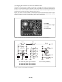
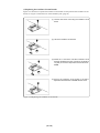
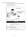
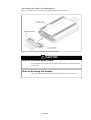
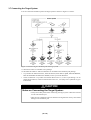
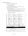
1
To our customers,
Old Company Name in Catalogs and Other Documents
On April 1st, 2010, NEC Electronics Corporation merged with Renesas Technology
Corporation, and Renesas Electronics Corporation took over all the business of both
companies. Therefore, although the old company name remains in this document, it is a valid
Renesas Electronics document. We appreciate your understanding.
Renesas Electronics website: http://www.renesas.com
April 1st, 2010
Renesas Electronics Corporation
Issued by: Renesas Electronics Corporation (http://www.renesas.com)
Send any inquiries to http://www.renesas.com/inquiry.
Notice
1.
2.
3.
4.
5.
6.
7.
All information included in this document is current as of the date this document is issued. Such information, however, is
subject to change without any prior notice. Before purchasing or using any Renesas Electronics products listed herein, please
confirm the latest product information with a Renesas Electronics sales office. Also, please pay regular and careful attention to
additional and different information to be disclosed by Renesas Electronics such as that disclosed through our website.
Renesas Electronics does not assume any liability for infringement of patents, copyrights, or other intellectual property rights
of third parties by or arising from the use of Renesas Electronics products or technical information described in this document.
No license, express, implied or otherwise, is granted hereby under any patents, copyrights or other intellectual property rights
of Renesas Electronics or others.
You should not alter, modify, copy, or otherwise misappropriate any Renesas Electronics product, whether in whole or in part.
Descriptions of circuits, software and other related information in this document are provided only to illustrate the operation of
semiconductor products and application examples. You are fully responsible for the incorporation of these circuits, software,
and information in the design of your equipment. Renesas Electronics assumes no responsibility for any losses incurred by
you or third parties arising from the use of these circuits, software, or information.
When exporting the products or technology described in this document, you should comply with the applicable export control
laws and regulations and follow the procedures required by such laws and regulations. You should not use Renesas
Electronics products or the technology described in this document for any purpose relating to military applications or use by
the military, including but not limited to the development of weapons of mass destruction. Renesas Electronics products and
technology may not be used for or incorporated into any products or systems whose manufacture, use, or sale is prohibited
under any applicable domestic or foreign laws or regulations.
Renesas Electronics has used reasonable care in preparing the information included in this document, but Renesas Electronics
does not warrant that such information is error free. Renesas Electronics assumes no liability whatsoever for any damages
incurred by you resulting from errors in or omissions from the information included herein.
Renesas Electronics products are classified according to the following three quality grades: “Standard”, “High Quality”, and
“Specific”. The recommended applications for each Renesas Electronics product depends on the product’s quality grade, as
indicated below. You must check the quality grade of each Renesas Electronics product before using it in a particular
application. You may not use any Renesas Electronics product for any application categorized as “Specific” without the prior
written consent of Renesas Electronics. Further, you may not use any Renesas Electronics product for any application for
which it is not intended without the prior written consent of Renesas Electronics. Renesas Electronics shall not be in any way
liable for any damages or losses incurred by you or third parties arising from the use of any Renesas Electronics product for an
application categorized as “Specific” or for which the product is not intended where you have failed to obtain the prior written
consent of Renesas Electronics. The quality grade of each Renesas Electronics product is “Standard” unless otherwise
expressly specified in a Renesas Electronics data sheets or data books, etc.
“Standard”:
8.
9.
10.
11.
12.
Computers; office equipment; communications equipment; test and measurement equipment; audio and visual
equipment; home electronic appliances; machine tools; personal electronic equipment; and industrial robots.
“High Quality”: Transportation equipment (automobiles, trains, ships, etc.); traffic control systems; anti-disaster systems; anticrime systems; safety equipment; and medical equipment not specifically designed for life support.
“Specific”:
Aircraft; aerospace equipment; submersible repeaters; nuclear reactor control systems; medical equipment or
systems for life support (e.g. artificial life support devices or systems), surgical implantations, or healthcare
intervention (e.g. excision, etc.), and any other applications or purposes that pose a direct threat to human life.
You should use the Renesas Electronics products described in this document within the range specified by Renesas Electronics,
especially with respect to the maximum rating, operating supply voltage range, movement power voltage range, heat radiation
characteristics, installation and other product characteristics. Renesas Electronics shall have no liability for malfunctions or
damages arising out of the use of Renesas Electronics products beyond such specified ranges.
Although Renesas Electronics endeavors to improve the quality and reliability of its products, semiconductor products have
specific characteristics such as the occurrence of failure at a certain rate and malfunctions under certain use conditions. Further,
Renesas Electronics products are not subject to radiation resistance design. Please be sure to implement safety measures to
guard them against the possibility of physical injury, and injury or damage caused by fire in the event of the failure of a
Renesas Electronics product, such as safety design for hardware and software including but not limited to redundancy, fire
control and malfunction prevention, appropriate treatment for aging degradation or any other appropriate measures. Because
the evaluation of microcomputer software alone is very difficult, please evaluate the safety of the final products or system
manufactured by you.
Please contact a Renesas Electronics sales office for details as to environmental matters such as the environmental
compatibility of each Renesas Electronics product. Please use Renesas Electronics products in compliance with all applicable
laws and regulations that regulate the inclusion or use of controlled substances, including without limitation, the EU RoHS
Directive. Renesas Electronics assumes no liability for damages or losses occurring as a result of your noncompliance with
applicable laws and regulations.
This document may not be reproduced or duplicated, in any form, in whole or in part, without prior written consent of Renesas
Electronics.
Please contact a Renesas Electronics sales office if you have any questions regarding the information contained in this
document or Renesas Electronics products, or if you have any other inquiries.
(Note 1) “Renesas Electronics” as used in this document means Renesas Electronics Corporation and also includes its majorityowned subsidiaries.
(Note 2) “Renesas Electronics product(s)” means any product developed or manufactured by or for Renesas Electronics.
User’s Manual
M37641T2-RPD-E
User’s Manual
Emulation Pod for 7641 and 7643 Group MCUs
Rev.1.00 2003.09
* IC61-080-081 is a product of Yamaichi Electronics Co., Ltd.
Keep safety first in your circuit designs!
• Renesas Technology Corporation and Renesas Solutions Corporation put the maximum effort into making semiconductor products better
and more reliable, but there is always the possibility that trouble may occur with them. Trouble with semiconductors may lead to personal
injury, fire or property damage. Remember to give due consideration to safety when making your circuit designs, with appropriate
measures such as (i) placement of substitutive, auxiliary circuits, (ii) use of nonflammable material or (iii) prevention against any
malfunction or mishap.
Notes regarding these materials
• These materials are intended as a reference to assist our customers in the selection of the Renesas Technology product best suited to
the customer's application; they do not convey any license under any intellectual property rights, or any other rights, belonging to Renesas
Technology Corporation, Renesas Solutions Corporation or a third party.
• Renesas Technology Corporation and Renesas Solutions Corporation assume no responsibility for any damage, or infringement of any
third-party's rights, originating in the use of any product data, diagrams, charts, programs, algorithms, or circuit application examples
contained in these materials.
• All information contained in these materials, including product data, diagrams, charts, programs and algorithms represents information
on products at the time of publication of these materials, and are subject to change by Renesas Technology Corporation and Renesas
Solutions Corporation without notice due to product improvements or other reasons. It is therefore recommended that customers contact
Renesas Technology Corporation, Renesas Solutions Corporation or an authorized Renesas Technology product distributor for the latest
product information before purchasing a product listed herein. The information described here may contain technical inaccuracies or
typographical errors. Renesas Technology Corporation and Renesas Solutions Corporation assume no responsibility for any damage,
liability, or other loss rising from these inaccuracies or errors. Please also pay attention to information published by Renesas Technology
Corporation and Renesas Solutions Corporation by various means, including the Renesas home page (http://www.renesas.com).
• When using any or all of the information contained in these materials, including product data, diagrams, charts, programs, and algorithms,
please be sure to evaluate all information as a total system before making a final decision on the applicability of the information and
products. Renesas Technology Corporation and Renesas Solutions Corporation assume no responsibility for any damage, liability or
other loss resulting from the information contained herein.
• Renesas Technology semiconductors are not designed or manufactured for use in a device or system that is used under circumstances
in which human life is potentially at stake. Please contact Renesas Technology Corporation, Renesas Solutions Corporation or an
authorized Renesas Technology product distributor when considering the use of a product contained herein for any specific purposes,
such as apparatus or systems for transportation, vehicular, medical, aerospace, nuclear, or undersea repeater use.
• The prior written approval of Renesas Technology Corporation and Renesas Solutions Corporation is necessary to reprint or reproduce
in whole or in part these materials.
• If these products or technologies are subject to the Japanese export control restrictions, they must be exported under a license from the
Japanese government and cannot be imported into a country other than the approved destination. Any diversion or reexport contrary to
the export control laws and regulations of Japan and/or the country of destination is prohibited.
• Please contact Renesas Technology Corporation or Renesas Solutions Corporation for further details on these materials or the products
contained therein.
Precautions to be taken when using this product
• This product is a development supporting unit for use in your program development and evaluation stages. In mass-producing your
program you have finished developing, be sure to make a judgment on your own risk that it can be put to practical use by performing
integration test, evaluation, or some experiment else.
• In no event shall Renesas Solutions Corporation be liable for any consequence arising from the use of this product.
• Renesas Solutions Corporation strives to renovate or provide a workaround for product malfunction at some charge or without charge.
However, this does not necessarily mean that Renesas Solutions Corporation guarantees the renovation or the provision under any
circumstances.
• This product has been developed by assuming its use for program development and evaluation in laboratories. Therefore, it does not fall
under the application of Electrical Appliance and Material Safety Law and protection against electromagnetic interference when used in
Japan.
• Do not attempt to modify this equipment. If modified, your authority to operate this equipment might be voided by FCC.
Note: This equipment has been tested and found to comply with the limits for a Class A digital device, pursuant to part 15 of the FCC Rules.
These limits are designed to provide reasonable protection against harmful interference when the equipment is operated in a commercial
environment. This equipment generates, uses, and can radiate radio frequency energy and, if not installed and used in accordance with
the user's manual, may cause harmful interference to radio communications. Operation of this equipment in a residential area is likely
to cause harmful interference in which case the user will be required to correct the interference at his own expense.
Warning: This is a Class A product. In a domestic environment this product may cause radio interference in which case the user may be
required to take adequate measures.
For inquiries about the contents of this document or product, fill in the text file the installer of the emulator debugger generates in the
following directory and email to your local distributor.
\SUPPORT\Product-name\SUPPORT.TXT
Renesas Tools Homepage http://www.renesas.com/en/tools
( 2 / 68 )
Preface
The M37641T2-RPD-E is an emulation pod for the 7641 and 7643 Groups of Renesas 16-bit
microcomputers. It's used with a PC4701 emulator.
This user's manual mainly describes specifications of the M37641T2-RPD-E emulation pod and how
to setup it. For details on the following products, which are used with the M37641T2-RPD-E, refer
to each product's user's manual.
• Emulator: PC4701 User's Manual
• Emulator debugger: M3T-PD38 User's Manual
All the components of this product are shown in "2.2 Package Components" (page 19) of this user's
manual. If there is any question or doubt about this product, contact your local distributor.
To use the product properly
Precautions for Safety:
• In both this User's Manual and on the product itself, several icons are used to insure
proper handling of this product and also to prevent injuries to you or other persons,
or damage to your properties.
• The icons' graphic images and meanings are given in "Chapter 1. Precautions for
Safety". Be sure to read this chapter before using the product.
When using outside Japan
• When using in Europe, the United States, or Canada, be sure to use both the emulator
and the emulation pod which meet local standards. EMI standards are not met when
the M37641T2-RPD-E is used with the PC4700H or PC4700L emulator.
( 3 / 68 )
Contents
Chapter 1. Precautions for Safety ........................................................................................... 7
1.1 Safety Symbols and Meanings .............................................................................. 8
Chapter 2. Preparation .......................................................................................................... 17
2.1 Terminology ........................................................................................................ 18
2.2 Package Components .......................................................................................... 19
2.3 Other Tool Products Required for Development ................................................ 19
2.4 Name of Each Part .............................................................................................. 20
(1) System Configuration............................................................................... 20
(2) Inside of the Emulation Pod ..................................................................... 21
2.5 Using the Emulator for the First Time ................................................................ 22
Chapter 3. Setting Up ........................................................................................................... 23
3.1 Removing the Upper Cover ................................................................................ 24
3.2 Replacing the Evaluation MCU .......................................................................... 25
3.3 Switch Settings .................................................................................................... 26
3.4 Connecting USB-related Signals......................................................................... 28
(1) Pins D+ and D- ......................................................................................... 28
(2) Pin Ext. Cap ............................................................................................. 29
(3) Pins LPF, AVss and AVcc ....................................................................... 30
3.5 Selecting Clock Supply ....................................................................................... 30
(1) Using the Oscillator Circuit on the Target System .................................. 31
(2) Changing the Oscillator Circuit in the Emulation Pod ............................. 32
(3) Replacing the Oscillator Circuit Boards .................................................. 33
3.6 Connecting the PC4701 and Emulation Pod ....................................................... 34
(1) Connecting the Cable to the PC4701 ....................................................... 34
(2) Connecting the Cable to the Emulation Pod ............................................ 35
3.7 Connecting the Target System ............................................................................ 36
Chapter 4. Usage .................................................................................................................. 37
4.1 Turning On the Power ......................................................................................... 38
(1) Checking the Connections of the Emulator System ................................. 38
(2) Turning On the Power .............................................................................. 38
(3) LED Display When the PC4701 Starts Up Normally .............................. 39
4.2 Downloading Firmware ...................................................................................... 40
(1) When It is Necessary to Download Firmware ......................................... 40
(2) Downloading Firmware in Maintenance Mode ....................................... 40
4.3 Starting Up Emulator Debugger (Init Dialog Box Settings) ............................... 41
(1) Settings in the CLOCK Tab ..................................................................... 41
(2) Settings in the MCU Tab .......................................................................... 42
( 4 / 68 )
4.4 Self-check ............................................................................................................ 42
(1) Self-check Procedure ............................................................................... 42
(2) If an Error is Detected in the Self-check .................................................. 42
Chapter 5. Specifications ...................................................................................................... 45
5.1 Specifications ...................................................................................................... 46
5.2 Connection Diagrams .......................................................................................... 47
5.3 Operation Timing ................................................................................................ 49
(1) Operation Timing When Using the Evaluation MCU (M37641M8-XXXFS) .... 49
(2) Operation Timing When Using the Evaluation MCU (M37643M8-XXXFS) .... 51
5.4 External Dimensions ........................................................................................... 55
(1) External Dimensions of the Emulation Pod ............................................. 55
(2) External Dimensions of the Converter Board (M3T-FLX-80LCC) ........ 56
Chapter 6. Troubleshooting .................................................................................................. 57
6.1 Flowchart to Remedy Troubles ........................................................................... 58
(1) When the LED Display of the PC4701 is Abnormal ............................... 59
(2) When the Init Dialog Box is Not Displayed ............................................ 59
(3) When the Program Window is Not Displayed (Target System Not Connected) .... 60
(4) When the Program Window is Not Displayed (Target System Connected) ........ 61
6.2 When the M37641T2-RPD-E Does Not Work Properly .................................... 62
Chapter 7. Maintenance and Guarantee ................................................................................ 63
7.1 Maintenance ........................................................................................................ 64
7.2 Guarantee ............................................................................................................ 64
7.3 Repair Provisions ................................................................................................ 64
7.4 How to Request for Repair .................................................................................. 65
( 5 / 68 )
MEMO
( 6 / 68 )
Chapter 1. Precautions for Safety
This chapter describes precautions for using this product safely and properly. For precautions for the emulator main unit
and the emulator debugger, refer to each user's manual included with your product.
1.1 Safety Symbols and Meanings ..................................................................................................... 8
WARNING
Warning for Installation ............................................................................................... 9
Warnings for Use Environment ................................................................................... 9
CAUTION
Caution to Be Taken for Modifying This Product ....................................................... 9
Cautions to Be Taken for Handling This Product ........................................................ 9
IMPORTANT
Note on Malfunctions in the PC4701 System ............................................................ 10
Note on PC4700 Systems........................................................................................... 10
Notes on Downloading Firmware .............................................................................. 10
Note on Map Settings (MAP Command)................................................................... 10
Notes on the Target System ....................................................................................... 11
Note on SYNCOUT Output ....................................................................................... 11
Note on Reset Input from the Target System............................................................. 11
Note on RDY Input .................................................................................................... 11
Note on HOLD Input ................................................................................................. 11
Note on Differences between the Actual MCU and Emulator .................................. 12
Notes on the Watchdog Function ............................................................................... 13
Note on DMA Transfer .............................................................................................. 13
Note on the Key-on Wake Up Function .................................................................... 13
Note on Reading MCU Internal Resources ............................................................... 14
Note on a Watch Point ............................................................................................... 14
Note on Event Breaks ................................................................................................ 14
Note on Software Breaks ........................................................................................... 14
Note on Stack Area .................................................................................................... 15
Note on Quitting the Emulator Debugger .................................................................. 15
Notes for Connecting the Target System ................................................................... 15
( 7 / 68 )
Chapter 1. Precautions for Safety
In both the user's manual and on the product itself, several icons are used to insure proper handling
of this product and also to prevent injuries to you or other persons, or damage to your properties.
This chapter describes the precautions which should be taken in order to use this product safely and
properly. Be sure to read this chapter before using this product.
1.1 Safety Symbols and Meanings
WARNING
If the requirements shown in the "WARNING"
sentences are ignored, the equipment may
cause serious personal injury or death.
CAUTION
If the requirements shown in the "CAUTION"
sentences are ignored, the equipment may
malfunction.
IMPORTANT
It means important information on using this
product.
In addition to the three above, the following are also used as appropriate.
means WARNING or CAUTION.
Example:
CAUTION AGAINST AN ELECTRIC SHOCK
means PROHIBITION.
Example:
DISASSEMBLY PROHIBITED
means A FORCIBLE ACTION.
Example:
UNPLUG THE POWER CABLE FROM THE RECEPTACLE.
The following pages describe the symbols "WARNING", "CAUTION", and "IMPORTANT".
( 8 / 68 )
WARNING
Warning for Installation:
• Do not set this product in water or areas of high humidity. Make sure that the main unit does not
get wet. Spilling water or some other liquid into the main unit can cause an unrepairable damage.
Warnings for Use Environment:
• The emulation pod is air-cooled with the ventilation slot. Therefore, do not block the ventilation
slot. When heated to high temperatures, the emulation pod may not work properly.
• This equipment is to be used in an environment with a maximum ambient temperature of 35°C. Care
should be taken that this temperature is not exceeded.
CAUTION
Caution to Be Taken for Modifying This Product:
• Do not disassemble or modify this product. Disassembling or modifying this product can cause
damage. Disassembling and modifying the product will void your warranty.
Cautions to Be Taken for Handling This Product:
• Use caution when handling the main unit. Be careful not to apply a mechanical shock.
• Do not touch the connector pins of the emulator main unit and the target MCU connector pins. Static
electricity may damage the internal circuits.
• Do not pull the emulation pod main unit by flexible cable FLX120-RPD for connecting to the
emulator main unit or flexible cable FLX100 for connecting the target system. The cable may cause
a break.
• Flexible cable FLX120-RPD for connecting to the emulator main unit and flexible cable FLX100
for connecting the target system are different from earlier models. The slits make them more
flexible. However, excessive flexing or force may break conductors.
• Do not use inch-size screws for this equipment. The screws used in this equipment are all ISO
(meter-size) type screws. When replacing screws, use same type screws as equipped before.
( 9 / 68 )
IMPORTANT
Note on Malfunctions in the PC4701 System:
• If the emulator malfunctions because of interference like external noise, do the following to remedy
the trouble.
(1) Press the RESET button on the emulator front panel.
(2) If normal operation is not restored after step (1), shut OFF power to the emulator once and then
reactivate it.
Note for PC4700 System:
• PC4700H products whose serial number ends with a number or D, DE, G cannot be used with the
M37641T2-RPD-E.
Example: 5KE100, 5KE100D, 5KE11DE, 5KE100G
Do NOT use it with the M37641T2-RPD-E. The PC4700 needs upgrading.
Example: 5LE123B
You can use it with the M37641T2-RPD-E.
Notes on Downloading Firmware:
• Before using this product for the first time, it is necessary to download the dedicated firmware
(control software for the emulation pod built into the PC4701). Please note that, to do this, it is
necessary to start up the PC4701 in maintenance mode. For firmware download procedures, see
"4.2 Downloading Firmware" (page 40). Once firmware has been downloaded, the product can be
used by simply turning on the power.
• Do not shut off the power while downloading firmware. If this happens, the product will not start
up properly. If power is shut off unexpectedly, redownload firmware.
• Except when a target status error occurs, if self-check is not completed successfully, there may be
trouble with the product. In such case, contact your local distributor. However, perform the selfcheck in the below setup.
(1) Target system:
Not connected
(2) Emulation pod internal switches: At their factory settings
Note on Map Settings (MAP Command):
• Always set the SFR area and the internal RAM area to EXT.
When you debug an MCU with flash memory, however, set addresses 0470H through 0FFFH to
INT. (The internal RAM size of the on-board evaluation MCU is 1 KB.) Because the internal RAM
size of the evaluation MCU is smaller than the RAM size of MCUs with flash memory, allocate
emulation memory.
You can set the mapping by issuing the MAP command in the script window of the emulator
debugger.
Example (when using an MCU with flash memory in the memory expansion mode):
MAP
MAP
MAP
MAP
0000,046F,EXT
0470,0FFF,INT
1000,7FFF,EXT
8000,FFFF,INT
(SFR area and internal RAM area)
(Internal RAM area extended by emulation memory)
(External area)
(Internal ROM area)
( 10 / 68 )
IMPORTANT
Notes on the Target System:
• As pin Vcc of emulator is connected to the target system to observe the voltage of the target system,
the target system is not powered by the emulator. Therefore design your system so that the target
system is powered separately.
• The voltage of the target system should be within the range of the MCU specification and +3.0 to
+3.6 V or +4.5 to 5.25 V.
• Do not change the voltage of the target system after turning on the power.
• Before powering on your emulator system, check that the host machine, the emulator main unit,
the converter board and target system are all connected correctly. Next, turn on the power to each
equipment following the procedure below.
(1) Turn ON/OFF the target system and the PC4701 emulator as simultaneously as possible.
(2) When the PC4701 and emulator debugger start up, check the target status LEDs on the
emulator main unit's front panel to see if this product is ready to operate.
(For the target status LEDs on the front panel when starting up the PC4701, refer to "4.1 (3)
LED Display When the PC4701 Starts Up Normally" on page 39)
Note on SYNCOUT Output:
• When using the emulator, SYNCOUT signals are not output.
Note on Reset Input from the Target System:
• If a reset is input from the target system, when a user program is being executed (when the RUN
status LED on the PC4701's front panel is lit), the user program is stopped.
Note on RDY Input:
• Be sure to input "L" to pin RDY* of the target system during the user program execution. Inputting
"L" to pin RDY* while the user program is stopped may cause a malfunction of the emulator.
Note on HOLD Input:
• Be sure to input "L" to pin HOLD* of the target system during the user program execution. Inputting
"L" to pin HOLD while the user program is stopped may cause a malfunction of the emulator.
( 11 / 68 )
IMPORTANT
Note on Differences between the Actual MCU and Emulator:
• Emulator operation differs from mask MCU operation as listed below.
(1) Reset condition
(2) Power voltage
When using the emulator, it is not possible to use with the range of 4.15 to 4.5 V.
(3) Initial values of internal resources data at power-on
(3) Internal memory (ROM and RAM) capacities, etc.
(4) Ports P0, P1, P2, P3 and P40
Some I/O ports (P0, P1, P2, P3 and P40) of the M37641T2-RPD-E are connected to the target
system via the port emulation circuit in the M37641T2-RPD-E. Therefore, the external bus
timing and the electrical characteristics are slightly different from those of the actual MCU.
For the differences of the I/O timing etc. between the emulator and the actual MCU, refer to
"5.2 Connection Diagrams" (page 47) and "5.3 Operation Timing" (page 49).
Table 1.1 lists the differences of the I/O level between the emulator and the MCU.
Table 1.1 Port I/O level
Input level
Port
Output level
Emulator
Actual MCU
Emulator
Actual MCU
P0
CMOS
CMOS
CMOS
CMOS
P1
CMOS
CMOS
CMOS
CMOS
P2 (for TTL input level*1)
CMOS
TTL
CMOS
CMOS
P2 (for CMOS input level* )
CMOS
CMOS
CMOS
CMOS
P3
CMOS
CMOS
CMOS
CMOS
P4
CMOS
CMOS
CMOS
CMOS
1
*1 Setting by the port control register (0010H) port 2 input level select bit (bit6).
(6) Pins XIN and XOUT
Make note that in the oscillator circuit where a resonator is connected between pins XIN and
XOUT, oscillation does not occur because a flexible cable, buffer IC and other devices are
used between the evaluation MCU and the target system. See "Figure 3.10 Circuit in which
oscillation does not occur (same for XCIN-XCOUT)" (page 31).
(7) Pins XCIN and XCOUT
Make note that in the oscillator circuit where a resonator is connected between pins XCIN and
XCOUT, oscillation does not occur because a flexible cable, buffer IC and other devices are
used between the evaluation MCU and the target system. See "Figure 3.10 Circuit in which
oscillation does not occur (same for XCIN-XCOUT)" (page 31).
(8) Pin SYNCOUT
Make note that pin SYNCOUT does not output data.
(9) Pins D+, D-, Ext. Cap, LPF, AVcc and AVss
Refer to "3.4 Connecting USB-related Signals" (page 28).
(10) Other pins
As a flexible cable is used between the evaluation MCU and the target system, some
characteristics are slightly different from those of the actual MCU.
Therefore, be sure to evaluate your system with an evaluation MCU. Before starting
mask production, evaluate your system and make final confirmation with an ES
(Engineering Sample) version MCU.
( 12 / 68 )
IMPORTANT
Notes on the Watchdog Function:
• The MCU's watchdog timer can be used only while a program is being executed. To use it
otherwise, disable the watchdog timer.
• If the reset circuit of the target system has a watchdog timer, disable it when using the emulator.
Note on DMA Transfer:
• When using the DMA transfer function, pay attention to the following.
(1) Breaks are not executed during the DMA transfer. Break are executed after the DMA transfer
is finished.
(2) The DMA transfer is not executed while a break is executed.
(3) The DMA transfer cannot be executed on the emulation memory. It is possible to transfer only
from the area set to "EXT" to the area set to "EXT" by MAP settings.
(4) In the result of the real-time trace, RD and WR signals during the DMA transfer cycle
displayed as fixed "H". (RD and WR signals output from the MCU change correctly.)
Note on the Key-on Wake Up Function:
• The key-on wakeup interrupt is accepted only during STP command or WIT command execution.
The interrupt is not accepted in any other situations.
( 13 / 68 )
IMPORTANT
Note on Reading MCU Internal Resources:
• When the M37641T2-RPD-E is configured with the emulator debugger, the following results occur
when reading MCU internal resources (SFR and internal RAM area). In both cases, data is not
displayed correctly, but internal data is not affected at all.
(1) Real-time tracing
Data values in the MCU internal resource read cycle are not displayed correctly.
(2) Real-time RAM monitoring
Data values in the MCU internal resource read cycle are not displayed correctly.
Note on a Watch Point:
• When the M37641T2-RPD-E is configured with the emulator debugger, note the following if
specifying a watch point for MCU internal resources (SFR and internal RAM area).
Change the address specified as a watch point so as not to overlap the area set for the real-time RAM
monitor (you can check using the RRAM command of the M3T-PD38). When the address specified
as a watch point overlaps the area set for the real-time RAM monitor and the MCU internal
resources are read out, data will not be displayed correctly. The initial setting of the real-time RAM
monitor is 0000H to 03FFH.
Example:
Watch point ................................ 0000H
Real-time RAM monitor ............ 0010H to 040FH
Note on Event Breaks:
• With the emulator debugger you can not use data read out from the MCU internal resources (RAM
and SFR area) as a condition for event breaks.
Note on Software Breaks:
• Software breaks generate BRK interruptions by forcibly inserting a BRK instruction at "00h"
instead of a instruction code. Therefore, when you reference the result of a trace in bus mode, "00h"
is displayed as the instruction fetch address where a software break is set.
( 14 / 68 )
IMPORTANT
Note on Stack Area:
• With this product, a maximum 3 bytes of the user stack is consumed as work area.
Note on Quitting the Emulator Debugger:
• To restart the emulator debugger, always shut power to the emulator module off once and then on
again.
Notes on Connecting the Target System:
• When connecting the FLX100 flexible board and the converter board, be careful not to forcibly
press the connector top of the converter board. The flexible board and the converter board are
guaranteed for only 20 insertion/removal iterations.
• Especially be careful not to insert the converter board in a wrong direction.
( 15 / 68 )
MEMO
( 16 / 68 )
Chapter 2. Preparation
This chapter describes the package components, the system configuration and the preparation for using this product for the
first time.
2.1 Terminology ............................................................................................................................... 18
2.2 Package Components.................................................................................................................. 19
2.3 Other Tool Products Required for Development........................................................................ 19
2.4 Name of Each Part ...................................................................................................................... 20
(1) System Configuration ........................................................................................................... 20
(2) Inside of the Emulation Pod.................................................................................................. 21
2.5 Using the Emulator for the First Time ....................................................................................... 22
( 17 / 68 )
Chapter 2. Preparation
2.1 Terminology
Some specific words used in this user's manual are defined as follows:
Emulator system
This means an emulator system built around the PC4701 emulator. The PC4701 emulator system is
configured with an emulator main unit, emulation pod, host machine and emulator debugger.
Emulator main unit (Hereafter PC4701)
This means a generic name for emulators for 8 and 16-bit MCUs. For details on specific models of
PC4701, visit the Renesas Tools Homepage at:
http://www.renesas.com/en/tools
Emulation pod
This means the M37641T2-RPD-E (this product). This emulation pod is for 740 Family 7600 Series
7641 and 7643 Group MCUs.
Host machine
This means a personal computer used to control the emulator and emulation pod.
Emulator debugger
This means a software tool M3T-PD38 to control the emulator from the host machine through an
interface.
Firmware
Program that analyzes contents of communication with the emulator debugger and controls the
emulator hardware. This program is installed in the EEPROM. This program is downloadable from
the emulator debugger to upgrade firmware or to support other MCUs.
Evaluation MCU
This means the microcomputer mounted on the emulation pod which is operated in the specific mode
for development tools.
Target MCU
This means the microcomputer you are going to debug.
Target system
This means a user's application system using the microcomputer to be debugged.
*
In this user's manual, this symbol is used to show active LOW. (e.g. RESET*: Reset signal)
( 18 / 68 )
2.2 Package Components
The M37641T2-RPD-E package consists of the following items. When unpacking, check to see if
your M37641T2-RPD-E package contains all the items listed below.
Package components
Item
Quantity
Emulation pod main unit M37641T2-RPD-E
1
Flexible cable FLX120-RPD for connecting PC4701
1
Converter board M3T-FLX-80LCC for 80-pin LCC package
1
IC socket IC61-080-081 (80-pin 0.8-mm-pitch) made by Yamaichi Electronics Co., Ltd.
1
Oscillator circuit board OSC-2 (bare-board)
1
Evaluation MCU M37643M8-XXXFS
1
Hardware tool user registration FAX sheet (English)
1
Hardware tool user registration FAX sheet (Japanese)
1
M37641T2-RPD-E user's manual (this manual)
1
M37641T2-RPD-E user's manual (Japanese)
1
Please keep the M37641T2-RPD-E's packing box and cushion material in your place for reuse at a
later time when sending your product for repair or other purposes. Always use these packing box and
cushion material when transporting the M37641T2-RPD-E.
If any of these items are missing or found faulty, please contact your local distributor. Also, if there
is any question or doubt about the packaged product, contact your local distributor.
2.3 Other Tool Products Required for Development
To bring forward programs development on the 7641 and 7643 Group MCUs, the products listed
below are necessary in addition to those contained package above. Get them separately.
Other tool products
Emulator main unit
PC4701
Emulator debugger
M3T-PD38
Converter board
(Choose according to the foot
pattern of your target system.
For details, see "3.7 Connecting
the Target System" on page
36.)
For 80-pin 0.8-mm-pitch QFP (80P6N-A):
- M3T-DUMMY80
- M3T-FLX-80NRA
- M3T-FLX-80LCC (included) and IC61-080-081 (included)
For 80-pin 0.5-mm-pitch QFP (80P6Q-A):
- M3T-FLX-80NSD
- M3T-FLX-80LCC (included) and M3T-80LCC-QSD
* To purchase these products, contact your nearest distributer.
* The IC61-080-081 is a product of Yamaichi Electronics Co., Ltd. For purchasing it or for
technical information, contact Yamaichi Electronics Co., Ltd. (http://www.yamaichi.co.jp/e/
index.shtml)
( 19 / 68 )
2.4 Name of Each Part
(1) System Configuration
Figure 2.1 System configuration
(1) to (4) in Figure 2.1 are included with this product package.
(1) Emulation pod M37641T2-RPD-E
This emulation pod contains an evaluation MCU, emulation memory and circuit to feature the
debugging functions.
(2) Flexible cable FLX120-RPD
This 120-pin flexible cable connects the PC4701 emulator and the emulation pod.
(3) Flexible cable FLX100
This 100-pin flexible cable connects the emulation pod and the target system.
(4) Converter board
This is a converter board for connecting to the target system.
For details, refer to "3.7 Connecting the Target System" (page 36).
( 20 / 68 )
(2) Inside of the Emulation Pod
Figure 2.2 Internal view of the emulation pod
(1) Base board
Base board for the 740 Family MCUs which controls the interface with the PC4701 and the
evaluation MCU.
(2) Memory board
Board on which the 128 KB emulation memory is mounted.
(3) Oscillator circuit board
Board on which the oscillator circuit in the emulation pod is mounted. Its operating frequency can
be changed by replacing this board with other available oscillator circuit boards.
(4) MCU-dependent board
Board grouping parts (number of pins or added functions) which vary according to MCU model.
(5) Evaluation MCU
Microcomputer (dedicated to the emulator) operated in the specific mode for the emulator. It is
necessary to replace the evaluation MCU according to the MCU you use.
( 21 / 68 )
2.5 Using the Emulator for the First Time
If you have purchased this emulation pod newly, it is necessary to download firmware. The download
procedure is given in Figure 2.3.
Before attempting to download firmware, check the emulator debugger is installed and the emulator
is connected to the host machine. For more information, see each user's manual of the emulator
debugger and the PC4701.
Connect the PC4701 and this product.
See "3.6 Connecting the PC4701
and Emulation Pod" (page 34).
Within 2 seconds of turning the power ON, press the
RESET button of the PC4701 and check maintenance
mode is accessed.
See "4.2 Downloading Firmware"
(page 40).
Download firmware using the emulator debugger.
Shut power OFF.
Figure 2.3 Firmware download procedure when emulator is used for the first time
To make sure the emulation pod works properly, run the self-check. For self-check procedures, see
"4.4 Self-check" (page 42).
( 22 / 68 )
Chapter 3. Setting Up
This chapter describes switch settings required for using this product and how to connect this product to the PC4701 and
the target system.
3.1 Removing the Upper Cover ........................................................................................................ 24
3.2 Replacing the Evaluation MCU.................................................................................................. 25
3.3 Switch Settings ........................................................................................................................... 26
3.4 Connecting USB-related Signals ................................................................................................ 28
(1) Pins D+ and D- ..................................................................................................................... 28
(2) Pin Ext. Cap .......................................................................................................................... 29
(3) Pins LPF, AVss and AVcc .................................................................................................... 30
3.5 Selecting Clock Supply ............................................................................................................... 30
(1) Using the Oscillator Circuit on the Target System ............................................................... 31
(2) Changing the Oscillator Circuit in the Emulation Pod ......................................................... 32
(3) Replacing the Oscillator Circuit Boards ............................................................................... 33
3.6 Connecting the PC4701 and Emulation Pod ............................................................................... 34
(1) Connecting the Cable to the PC4701 .................................................................................... 34
(2) Connecting the Cable to the Emulation Pod ......................................................................... 35
3.7 Connecting the Target System ..................................................................................................... 36
( 23 / 68 )
Chapter 3. Setting Up
To use this emulation pod with your application system, it is necessary to set as follows. Set the
following after removing the upper cover.
• Pins XIN and XOUT
• Pins XCIN and XCOUT
• USB-related pins (Pins Ext. Cap, D+ and D-)
• Input frequency
• Evaluation MCU
3.1 Removing the Upper Cover
The procedure of removing the upper cover is shown below.
(1) Remove the four screws of both sides of this product and lift off the upper cover (see Figure 3.1).
(2) Set the jumper switches etc.
(3) Replace the upper cover and secure the four screws.
Figure 3.1 Removing the upper cover
CAUTION
When Removing the Upper Cover:
• Always shut OFF power when removing the upper cover and setting the switches.
( 24 / 68 )
3.2 Replacing the Evaluation MCU
It is necessary to replace the evaluation MCU according to the MCU you use.
[MCU Group]
[Evaluation MCU]
7641 Group:
7643 Group:
M37641M8-XXXFS
M37643M8-XXXFS
To debug the 7643 Group, it is necessary to replace the evaluation MCU to the included M37643M8XXXFS.
When replacing the evaluation MCU, align the No. 1 pin as shown in the Figure 3.2. Especially be
careful not to insert the MCU in a wrong direction. Otherwise, it may cause a fatal damage to the
MCU.
The M37641M8-XXXFS is mounted on this product when shipped from the factory.
(1) Check the position of the MCU socket.
(2) Remove the evaluation MCU from the MCU
socket.
Insert tweezers into the notches at the four
corners of the socket. Then lift the MCU with
the tweezers slowly to remove it.
(3) Attach the evaluation MCU to the MCU
socket.
Align the No. 1 pin of the evaluation MCU
(see left) to mount another MCU into the
socket. Be sure to press down the MCU
until you hear it click.
Figure 3.2 Replacing the evaluation MCU
( 25 / 68 )
3.3 Switch Settings
Figure 3.3 shows the positions of the switches and Table 3.1 shows each switch setting.
Figure 3.3 Positions of the switches and their factory-settings
* Switches SW3 to SW6 have not been mounted. These switches cannot be used.
* For the circuit configuration of the switches, refer to "5.2 Connection Diagrams" (page 47).
( 26 / 68 )
Table 3.1 Switch settings of the M37641T2-RPD-E
Switch setting
P50
SW1
XCIN
(Factory-setting)
NC
Description
P50 side
[Using as a port]
When using pin P50/XCIN as a
port, set to this side.
[Using as a sub-clock]
When using P50/XCIN as a subclock and selecting the XCIN
oscillator circuit on the target board,
set to this side.
XCIN side
[Using as a sub-clock]
When using pin P50/XCIN as a
sub-clock and selecting the XCIN
oscillator circuit OSC-2 in the
emulation pod, set to XCIN side.
P51/XCOUT side
NC side
Connects pin XCOUT/P51 to the Does not connects pin XCOUT/P51
target system.
to the target system. Pin XCOUT/
P51 is open.
SW2
P51/XCOUT
(Factory-setting)
INT
SW7
EXT
(Factory-setting)
INT
EXT side
[Using the USB connector on the
target board]
When connecting pins USB D+ and
USB D- via the flexible cable, set to
this side. With this setting, pins USB
D+ and USB D- are not connected
to the USB connector in the
emulation pod.
INT side
[Using the USB connector in the
emulation pod]
When connecting pins USB D+ and
USB D- to the USB connector in the
emulation pod, set to this side. With
this setting, pins USB D+ and USB
D- are not connected to the flexible
cable.
INT side
EXT side
Does not output pin Ext. Cap to the To connect pin Ext. Cap to the
target system. Pin Ext. Cap is open. target system, set to this side.
SW8
EXT
(Factory-setting)
NC
NC side
EXT side
Does not output the clock (pin Outputs the clock (pin XOUT) to the
XOUT) to the target system. Pin target system.
XOUT is open.
SW9
EXT
(Factory-setting)
( 27 / 68 )
3.4 Connecting USB-related Signals
This section explains emulation pod specifications for each USB-related pin.
(1) Pins D+ and DIn the factory-setting, electrical characteristics differ from those of the actual MCU because of
the flexible cable between the emulation MCU and target system. If there are problems with
electrical characteristics because of the flexible cable, the USB connector on the emulation pod
can be used.
• Connecting to the target system via the flexible cable (factory-setting)
Set SW7 of the emulation pod to EXT side. The connection to the target system is shown in Figure
3.4 below.
Connected to the target
system via the flexible cable
Figure 3.4 Connecting pins D+ and D- (SW7 = EXT)
• Using the USB connector
Set SW7 of the emulation pod to INT side. Then, connect the USB cable to the USB connector in
the emulation pod. The connection to the target system is shown in Figure 3.5 below.
Connected to the target system
via the USB connector
Connected to the target
system via the flexible cable
(cannot be connected when
SW8 is set to INT side)
Figure 3.5 Connecting pins D+ and D- (SW7 = INT)
IMPORTANT
Notes on the USB Connector:
• Pin 1 of the USB connector connects only to the test pin (USB_VCC) located near
the USB connector.
• When the USB connector is used, pins D+ and Ext. Cap are connected in the
emulation pod through a 1.5K resistance.
( 28 / 68 )
(2) Pin Ext. Cap
In the factory-setting, the emulation pod processes the pin and does not connect it to the target system.
• When the emulation pod processes the pin (factory-setting)
Set SW8 of the emulation pod to INT side. The connection in the emulation pod is shown in Figure
3.6 below.
Figure 3.6 Connecting pin Ext. Cap (SW8 = INT)
• When Connecting to the target system
Set SW8 of the emulation pod to EXT side. The connection to the target system is shown in Figures
3.7 and 3.8 below.
Connected to the target
system via the flexible cable
Figure 3.7 Connecting pin Ext. Cap (SW7 = EXT, SW8 = EXT)
Connected to the target
system via the flexible cable
Figure 3.8 Connecting pin Ext. Cap (SW7 = INT, SW8 = EXT)
( 29 / 68 )
(3) Pins LPF, AVss and AVcc
These pins are processed in the emulation pod, and not connected to the target system. The connection
in the emulation pod is shown in Figure 3.9 below.
Figure 3.9 Connecting pins LPF, AVss and AVcc
IMPORTANT
Note on Connecting USB-related Pins:
• Pins LPF, AVss and AVcc are not connected to the target system.
3.5 Selecting Clock Supply
There are two ways to supply a clock to the MCU, using the oscillator circuit in the emulation pod
or using the oscillator circuit on the target system. Table 3.2 shows the factory-settings of each clock
supply.
Table 3.2 Clock supply to the MCU
Clock
Description
XIN-XOUT
Oscillator circuit
in the emulation pod
(OSC-3: 24 MHz)
XCIN-XCOUT
Display of emulator debugger Factory-setting
Internal
Yes
Target system
External
-
Oscillator circuit
in the emulation pod
(OSC-2: 32.768 kHz)
*1
Target system
*1
-
Yes
*1 Emulator debugger settings are inactive. The clock supply source can be selected with the
emulation pod switches.
IMPORTANT
Note on Changing Clock Supply:
• The clock supply can be set by the Init dialog box when starting up the emulator
debugger or inputting CLK command on the script window.
Example 1. When selecting the oscillator circuit in the emulation pod
CLK INT
Example 2. When selecting the oscillator circuit on the target system
CLK EXT
( 30 / 68 )
(1) Using the Oscillator Circuit on the Target System
When you turn on the power supply, the internal clock of the emulation pod is selected to supply the
clock to the MCU. To use the external clock on the target system, change the clock by the CLK
command of the emulator debugger. (For details, refer to the user's manual of the emulator debugger.)
IMPORTANT
Notes on the External Clock:
• Make note that in the oscillator circuit shown in Figure 3.11 where a resonator is
connected between pins XIN and XOUT, oscillation does not occur because a
flexible cable, buffer IC and other devices are used between the evaluation MCU and
the target system.
• Make note that in the oscillator circuit shown in Figure 3.11 where a resonator is
connected between pins XCIN and XCOUT, oscillation does not occur because a
flexible cable, buffer IC and other devices are used between the evaluation MCU and
the target system.
• To operate the emulation pod with an external clock, construct the oscillator circuit
as shown in Figure 3.10 in the target system and input the oscillator output at 50%
duty (within the operating range of the evaluation MCU) into pins XIN and XCIN.
And pins XOUT and XCOUT should be open.
Figure 3.10 External oscillator circuit
Figure 3.11 Circuit in which oscillation does not occur (same for XCIN-XCOUT)
( 31 / 68 )
(2) Changing the Oscillator Circuit in the Emulation Pod
Oscillator circuit boards for 24 MHz (for XIN) and 32.768 kHz (for XCIN) are mounted in this
product. To use the emulation pod at a frequency other than 24 MHz or 32.768 kHz, build the desired
oscillator circuit on the included oscillator circuit board OSC-2 (bare board) and replace the board
installed in the emulation pod when shipped from the factory.
Figure 3.12 shows a view of oscillator circuit board OSC-2 (bare board) and where connector pins
are located. Figure 3.13 shows the circuitry of oscillator circuit board OSC-2 (bare board). Use the
number of oscillator circuits recommended by the oscillator manufacturer.
J1-4: GND
J1-3: Oscillator output
J1-2: GND
J1-1: Vcc (5 V)
Figure 3.12 External view of oscillator board OSC-2 and connector pin assignments
IC1
11
IC1
10
CLK
8
9
J1-3
R1
*
*
X1 ,X 2
C2
*
X3
Vcc
1
2
3
4
5
6
7
13
12
GND
R2
C1
IC1
* X1: 5.08-mm-pitch 2-pin oscillator
* X2: 2.54-mm-pitch 2-pin oscillator
* X3: 2.54-mm-pitch 3-pin oscillator
Figure 3.13 Circuit of oscillator board OSC-2
( 32 / 68 )
C3
J1-1
14
IC1
J1-2
J1-4
GND
IC1: Inverter (Unbuffer)
(3) Replacing the Oscillator Circuit Boards
Figure 3.14 shows how to replace the oscillator circuit boards. For the position of the oscillator circuit
board, see "Figure 2.2 Internal view of the emulation pod" (page 21).
(1) Unscrew the screw connecting the oscillator circuit
board.
(2) Lift off the oscillator circuit board.
(3) Attach the J1 connector of another oscillator circuit
board for replacement to the connectors J5 (XCIN) or
J6 (XIN) of the MCU-dependent board M37641TRPDM.
(4) Secure the oscillator circuit board to the MCUdependent board M37641T-RPDM with the screw.
Figure 3.14 Replacing the oscillator circuit boards
( 33 / 68 )
3.6 Connecting the PC4701 and Emulation Pod
To connect the emulation pod to the PC4701, use 120-pin flexible cable FLX120-RPD included with
this product package. Connect the PC4701 side connector of the FLX120-RPD to the cable connector
of the PC4701, then secure with the two screws.
(1) Connecting the Cable to the PC4701
Figure 3.15 shows how to connect the PC4701 and FLX120-RPD.
Figure 3.15 Connecting the PC4701 and FLX120-RPD
CAUTION
Notes on Connecting the Cable:
• To connect the FLX120-RPD, be sure to hold the both sides of the PC4701 side
connector horizontally with the "UPSIDE" facing up.
• Always shut OFF power before connecting the FLX120-RPD. Otherwise internal
circuits can be destroyed.
Note on Securing the Screws:
• After connecting the FLX120-RPD to the PC4701, be sure to secure the screws
mounted in both sides of the connector.
( 34 / 68 )
(2) Connecting the Cable to the Emulation Pod
Figure 3.16 shows how to connect the FLX120-RPD and the emulation pod.
Figure 3.16 Connecting the emulation pod and FLX120-RPD
CAUTION
Note on Connecting the Cable:
• Always shut OFF power before connecting the cable. Otherwise internal circuits can
be destroyed.
Note on Securing the Screws:
• After connecting the emulation pod to the cable, be sure to secure the screws.
( 35 / 68 )
3.7 Connecting the Target System
You can connect the emulation pod to the target system as shown in Figure 3.17 below.
Figure 3.14 Connecting the emulation pod and target system
*1 These three items are available in one package.
*2 The M3T-FLX-80LCC and IC61-080-081 are included in this emulation pod package.
* To purchase the M3T-FLX100-T, M3T-FLX100-R, M3T-80LCC-QSD, M3T-DUMMY80,
M3T-FLX-80NRA and M3T-FLX-80NSD, contact your local distributor.
* The IC61-080-081 is a product of Yamaichi Electronics Co., Ltd. For purchasing it or for
technical information, contact Yamaichi Electronics Co., Ltd. (http://www.yamaichi.co.jp/e/
index.shtml)
CAUTION
Notes on Connecting the Target System:
• Always shut OFF power before connecting the target system. Otherwise internal
circuits can be destroyed.
• Take care not to attach the converter board in a wrong direction. It may cause a fatal
damage to the emulation pod.
( 36 / 68 )
Chapter 4. Usage
This chapter describes from turning on the power of this product to starting up the emulator debugger.
4.1 Turning On the Power ................................................................................................................ 38
(1) Checking the Connections of the Emulator System ............................................................. 38
(2) Turning On the Power........................................................................................................... 38
(3) LED Display When the PC4701 Starts Up Normally........................................................... 39
4.2 Downloading Firmware .............................................................................................................. 40
(1) When It is Necessary to Download Firmware ...................................................................... 40
(2) Downloading Firmware in Maintenance Mode .................................................................... 40
4.3 Starting Up Emulator Debugger (Init Dialog Box Settings) ...................................................... 41
(1) Settings in the CLOCK Tab .................................................................................................. 41
(2) Settings in the MCU Tab ...................................................................................................... 42
4.4 Self-check ................................................................................................................................... 42
(1) Self-check Procedure ............................................................................................................ 42
(2) If an Error is Detected in the Self-check............................................................................... 42
( 37 / 68 )
Chapter 4. Usage
4.1 Turning On the Power
(1) Checking the Connections of the Emulator System
Before turning the power ON, check the connection of the PC4701, emulation pod, converter board
and target system.
(2) Turning On the Power
Power ON/OFF the target system and PC4701 as simultaneously as possible.
CAUTION
Notes on Power Supply:
• The emulator's pin VCC is connected to the target system in order to monitor target
system voltage. For this reason, the emulator cannot supply power to the target
system. Therefore, provide the target system with a separate power supply from that
of the emulator.
• Keep target system power supply voltage within the MCU's specified range and
between +3.0 and 3.6 V or between +4.5 and 5.25 V.
• Do not change the voltage of power supply once the system is activated.
( 38 / 68 )
(3) LED Display When the PC4701 Starts Up Normally
After the emulator starts up, check the status of the LEDs on the front panel to see whether emulation
pod operation is enabled or not. Figure 4.1 shows the front panel LED lighting status when the
emulator is turned ON.
When using M3T-PD38 V.3.00 Release 1 or greater
When turning ON the power
When starting up M3T-PD38
When the target system is
connected, this LED lights.
When it is not lighting, check
the power voltage of the target
system. When the target system
is not connected, this LED does
not light.
When using M3T-PD38 V.2.00 Release 1 or previous version
When starting up M3T-PD38
When turning ON the power
When the target system is
connected, this LED lights.
When it is not lighting, check
the power voltage of the target
system. When the target system
is not connected, this LED does
not light.
Figure 4.1 LED display when the power turned on
( 39 / 68 )
4.2 Downloading Firmware
(1) When It is Necessary to Download Firmware
It is necessary to download firmware when:
(1) you use this product for the first time.
(2) firmware has been upgraded.
(3) the emulator debugger has been upgraded.
(4) you use this product with the PC4701 which was used with another emulation pod before.
(2) Downloading Firmware in Maintenance Mode
Download firmware in maintenance mode as explained here following. Do NOT connect the target
system when downloading firmware.
(1) Within 2 seconds of activating power to the PC4701, press the RESET button on the emulator
front panel. This will switch the emulator to maintenance mode.
(2) Start up the emulator debugger. When the Init dialog box setup is completed, the dialog which
urges to download firmware will appear. Download firmware following the messages.
Required time for downloading firmware depends on kind of interfaces.
• Serial interface:
About 7 minutes
• Parallel interface: About 30 seconds
Figure 4.2 Downloading firmware in maintenance mode
CAUTION
Note on Downloading Firmware:
• Do not shut OFF power while firmware is being downloaded. Otherwise, the
emulator will not start up properly. If power is shut OFF by mistake, redownload
firmware in maintenance mode.
( 40 / 68 )
4.3 Starting Up Emulator Debugger (Init Dialog Box Settings)
The Init dialog box shown in Figure 4.3 will appear after starting up the emulator debugger. Here
explains the settings in the MCU tab and Clock tab in the Init dialog box. The dialog box shown below
is an example of the emulator debugger M3T-PD38 V.5.10 Release 2. For more details, refer to the
M3T-PD38 User's Manual.
Figure 4.3 INIT dialog box
(1) Settings in the CLOCK Tab
MCU file:
To debug 7641/7643 Group MCUs,
choose the "M37640.mcu" file.
Communications interfaces:
Choose an interface you use. In this
example the serial interface is chosen.
Clock frequency:
Specify an operation clock of the target
MCU considering the frequency
division ratio of the clock.
Example:
When the supplied clock is 24 MHz
and the MCU operates divide-by-two:
Set "12" MHz.
( 41 / 68 )
(2) Settings in the MCU Tab
Make the settings of the clock supply.
Main
Choose an clock supply for pin XIN.
INTERNAL: S u p p l i e d f r o m t h e
oscillator circuit board
of the emulation pod
EXTERNAL: S u p p l i e d f r o m a n
oscillator circuit of the
target system
4.4 Self-check
(1) Self-check Procedure
To use the self-check function of the PC4701, do so as explained here below. While the self-check
is in progress, LEDs will change as shown in Figure 4.4.
(1) Set the switches in the emulation pod same as the factory settings (see "Table 3.1 Switch
settings of the M37641T2-RPD-E" on page 27).
(2) When the target system is connected, disconnect it.
(3) Within 2 seconds of activating power to the emulator, press the RESET button on the emulator
front panel to switch the emulator to maintenance mode.
(4) Check the "SAFE" LED starts flashing and then press the RESET button again.
(5) The self-check will start. If the normal result is displayed in about 2 minutes, the self-check
terminated normally.
(2) If an Error is Detected in the Self-check
If the self-check does not result normally (ERROR 1 or ERROR 2 in Figure 4.4), do the following.
• Check the connection of the emulation pod and PC4701.
• Redownload firmware.
• Check if the switches in this product is set same as the factory-settings (see "3.3 Switch Settings"
on page 26).
CAUTION
Note on the Self-check:
• If the self-check does not result normally (excluding errors of the target status), the
emulation pod may be damaged. Contact your local distributor.
( 42 / 68 )
Figure 4.4 Self-check procedure
( 43 / 68 )
MEMO
( 44 / 68 )
Chapter 5. Specifications
This chapter describes specifications of this product.
5.1 Specifications ............................................................................................................................. 46
5.2 Connection Diagrams ................................................................................................................. 47
5.3 Operation Timing ....................................................................................................................... 49
(1) Operation Timing When Using the Evaluation MCU (M37641M8-XXXFS) ..................... 49
(2) Operation Timing When Using the Evaluation MCU (M37643M8-XXXFS) ..................... 51
5.4 External Dimensions .................................................................................................................. 55
(1) External Dimensions of the Emulation Pod .......................................................................... 55
(2) External Dimensions of the Converter Board (M3T-FLX-80LCC) ..................................... 56
( 45 / 68 )
Chapter 5. Specifications
5.1 Specifications
Table 5.1 lists the specifications of the M37641T2-RPD-E.
Table 5.1 Specifications of the M37641T2-RPD-E
Emulator
PC4701
Applicable MCU
7641 Group M37641M8, M37641F8
7643 Group M37643M8, M37643F8
Evaluation MCU
7641 Group M37641M8-XXXFS (premounted)
7643 Group M37643M8-XXXFS (included)
Usable modes
• Single-chip mode
• Memory expansion mode
• Microprocessor mode
Emulation memory
Changeable 128 KB
Maximum operating frequency
VCC = 3.0 to 3.6 V:
Ø = 6 MHz (XIN = 24 MHz, divide-by-4), no-wait
VCC = 4.5 to 5.25 V:
Ø = 12 MHz (XIN = 24 MHz, divide-by-2), no-wait
Clock oscillator
XIN-XOUT
Internal oscillator circuit board
(OSC-3: 24 MHz)
Switchable to external oscillator input
XCIN-XCOUT
Internal oscillator circuit board
(OSC-2: 32.768 kHz)
Switchable to external oscillator input
Operating frequency
3.0 to 3.6 V, 4.5 to 5.25 V
Operating temperature
5 to 35°C (no dew)
Storage temperature
-10 to 60°C (no dew)
Power supply to emulation pod
Supplied from PC4701
Connection to target system
(1) 80P6N-A (0.8-mm-pitch 80-pin QFP)
(2) 80P6Q-A (0.5-mm-pitch 80-pin QFP)
For how to connect the target system, see "3.7 Connecting the
Target System" (page 36).
Overseas standards
• U.S. EMI standards (FCC part 15 Class A)
• CE marking (EN55022, EN55024)
( 46 / 68 )
5.2 Connection Diagrams
Figures 5.1 and 5.2 show the connection diagrams of the M37641T2-RPD-E. These connection
diagrams mainly show the interface section, and the circuits which are not connected to the target
system such as the emulator's control system are omitted.
*: Signal processed in emulator
• Switches SW2, SW4, SW5 and
SW6 are not mounted.
• Test pin TP1 is mounted to Pin 1 of
the USB connector (J7).
• C15 and C16 are mounted on the
products whose last letter of the
serial number is "A" or a number.
Figure 5.1 Connection diagram 1/2
( 47 / 68 )
Figure 5.2 Connection diagram 2/2
( 48 / 68 )
5.3 Operation Timing
With this emulator system, ports P0 to P3 and P40 are connected via the emulation circuit. Therefore,
I/O timing will differ from that of the actual MCU. Use the following as a reference when using the
emulation pod.
(1) Operation Timing When Using the Evaluation MCU (M37641M8-XXXFS)
Table 5.2 Timing requirements and switching characteristics (Vcc = 5.0V, Ø = 12 MHz)
Standard value
Symbol
Item
Actual MCU
Min.
td (ø-AH)
AB15 - AB8 delay time
tv (ø-AH)
AB15 - AB8 valid time
td (ø-AL)
AB7 - AB0 delay time
Max.
Min.
31
5
Unit
Emulator
Max.
32
ns
33
ns
0
33
tv (ø-AL)
AB7 - AB0 valid time
td (ø-WR)
WR* delay time
tv (ø-WR)
WR* valid time
td (ø-RD)
RD* delay time
tv (ø-RD)
RD* valid time
td (ø-DMA)
DMAOUT delay time
tv (ø-DMA)
DMAOUT valid time
5
0
tsu (RDY-ø)
RDY setup time
21
45
ns
th (ø-RDY)
RDY hold time
0
0
ns
tsu (HOLD-ø)
HOLD* setup time
21
34
ns
th (ø-HOLD)
HOLD* hold time
0
0
td (ø-HLDAL)
HLDA* "L" delay time
td (ø-HLDAH)
HLDA* "H" delay time
tsu (DB-ø)
Data bus setup time
7
th (ø-DB)
Data bus hold time
0
td (ø-DB)
Data bus delay time
tv (ø-DB)
Data bus valid time
td (ø-EDMA)
EDMA* delay time
5
ns
0
6
3
ns
15
ns
15
ns
25
ns
3
6
3
ns
3
25
25
ns
ns
ns
25
25
25
38
13
ns
23
ns
16
ns
8
9
ns
ns
0
22
ns
ns
tv (ø-EDMA)
EDMA* valid time
4
0
ns
td (AH-WR)
Before WR* AB15 - AB8 valid time
0.5*tc(ø)-28
0.5*tc(ø)-33
ns
td (AL-WR)
Before WR* AB7 - AB0 valid time
0.5*tc(ø)-30
0.5*tc(ø)-35
ns
tv (WR-AH)
After WR* AB15 - AB8 valid time
0
-5
ns
tv (WR-AL)
After WR* AB7 - AB0 valid time
0
-5
ns
td (AH-RD)
Before RD* AB15 - AB8 valid time
0.5*tc(ø)-28
0.5*tc(ø)-33
ns
td (AL-RD)
Before RD* AB7 - AB0 valid time
0.5*tc(ø)-30
0.5*tc(ø)-35
ns
tv (RD-AH)
After RD* AB15 - AB8 valid time
0
-5
ns
tv (RD-AL)
After RD* AB7 - AB0 valid time
0
-5
ns
tsu (RDY-WR) Before WR* RDY setup time
27
47
ns
th (WR-RDY)
0
0
ns
27
47
ns
After WR* RDY hold time
tsu (RDY-RD) Before RD* RDY setup time
th (RD-RDY)
After RD* RDY hold time
0
0
ns
tsu (DB-RD)
Before RD* data bus setup time
13
40
ns
th (RD-DB)
After RD* data bus hold time
0
0
ns
td (WR-DB)
Before WR* data bus delay time
tv (WR-DB)
After WR* data bus valid time
10
3
ns
tv (WR-EDMA) After WR* EDMA* delay time
2
2
ns
tv (RD-EDMA) After RD* EDMA* delay time
2
2
ns
( 49 / 68 )
20
25
ns
Table 5.3 Timing requirements and switching characteristics (Vcc = 3.0 V, Ø = 6 MHz)
Standard value
Symbol
Item
Actual MCU
Min.
td (ø-AH)
AB15 - AB8 delay time
tv (ø-AH)
AB15 - AB8 valid time
td (ø-AL)
AB7 - AB0 delay time
Max.
Min.
45
7
Unit
Emulator
Max.
51
ns
52
ns
3
47
7
ns
tv (ø-AL)
AB7 - AB0 valid time
td (ø-WR)
WR* delay time
3
tv (ø-WR)
WR* valid time
td (ø-RD)
RD* delay time
tv (ø-RD)
RD* valid time
td (ø-DMA)
DMAOUT delay time
tv (ø-DMA)
DMAOUT valid time
9
5
tsu (RDY-ø)
RDY setup time
35
68
ns
th (ø-RDY)
RDY hold time
0
0
ns
tsu (HOLD-ø)
HOLD* setup time
21
34
ns
th (ø-HOLD)
HOLD* hold time
0
0
td (ø-HLDAL)
HLDA* "L" delay time
td (ø-HLDAH)
HLDA* "H" delay time
tsu (DB-ø)
Data bus setup time
9
49
ns
th (ø-DB)
Data bus hold time
0
0
ns
td (ø-DB)
Data bus delay time
tv (ø-DB)
Data bus valid time
td (ø-EDMA)
EDMA* delay time
8
4
ns
15
ns
15
ns
32
ns
4
8
3
ns
3
26
30
ns
ns
30
30
30
30
15
ns
ns
36
ns
29
ns
8
12
ns
ns
tv (ø-EDMA)
EDMA* valid time
8
7
ns
td (AH-WR)
Before WR* AB15 - AB8 valid time
0.5*tc(ø)-33
0.5*tc(ø)-34
ns
td (AL-WR)
Before WR* AB7 - AB0 valid time
0.5*tc(ø)-35
0.5*tc(ø)-35
ns
tv (WR-AH)
After WR* AB15 - AB8 valid time
0
-5
ns
tv (WR-AL)
After WR* AB7 - AB0 valid time
0
-5
ns
td (AH-RD)
Before RD* AB15 - AB8 valid time
0.5*tc(ø)-33
0.5*tc(ø)-41
ns
td (AL-RD)
Before RD* AB7 - AB0 valid time
0.5*tc(ø)-35
0.5*tc(ø)-43
ns
tv (RD-AH)
After RD* AB15 - AB8 valid time
0
-5
ns
tv (RD-AL)
After RD* AB7 - AB0 valid time
0
-5
ns
tsu (RDY-WR) Before WR* RDY setup time
45
83
ns
th (WR-RDY)
0
0
ns
45
76
ns
After WR* RDY hold time
tsu (RDY-RD) Before RD* RDY setup time
th (RD-RDY)
After RD* RDY hold time
0
0
ns
tsu (DB-RD)
Before RD* data bus setup time
18
56
ns
th (RD-DB)
After RD* data bus hold time
0
0
ns
td (WR-DB)
Before WR* data bus delay time
tv (WR-DB)
After WR* data bus valid time
12
3
ns
tv (WR-EDMA) After WR* EDMA* delay time
3
3
ns
tv (RD-EDMA) After RD* EDMA* delay time
3
3
ns
( 50 / 68 )
28
29
ns
(2) Operation Timing When Using the Evaluation MCU (M37643M8-XXXFS)
Table 5.4 Timing requirements and switching characteristics (Vcc = 5.0V, Ø = 12 MHz)
Standard value
Symbol
Item
Actual MCU
Min.
td (ø-AH)
AB15 - AB8 delay time
tv (ø-AH)
AB15 - AB8 valid time
Max.
Min.
31
0
Unit
Emulator
Max.
32
-5
33
ns
ns
td (ø-AL)
AB7 - AB0 delay time
tv (ø-AL)
AB7 - AB0 valid time
td (ø-WR)
WR* delay time
tv (ø-WR)
WR* valid time
td (ø-RD)
RD* delay time
tv (ø-RD)
RD* valid time
td (ø-DMA)
DMAOUT delay time
tv (ø-DMA)
DMAOUT valid time
0
0
ns
tsu (RDY-ø)
RDY setup time
21
45
ns
0
33
-5
6
0
15
-3
6
0
ns
ns
15
-3
25
ns
ns
ns
ns
25
ns
th (ø-RDY)
RDY hold time
0
0
ns
tsu (HOLD-ø)
HOLD* setup time
21
34
ns
th (ø-HOLD)
HOLD* hold time
0
td (ø-HLDAL)
HLDA* "L" delay time
td (ø-HLDAH)
HLDA* "H" delay time
tsu (DB-ø)
Data bus setup time
7
th (ø-DB)
Data bus hold time
0
td (ø-DB)
Data bus delay time
tv (ø-DB)
Data bus valid time
td (ø-EDMA)
EDMA* delay time
tv (ø-EDMA)
EDMA* valid time
td (AH-WR)
0
25
ns
25
25
25
38
13
ns
23
8
12
ns
ns
0
22
ns
ns
ns
19
ns
4
0
ns
Before WR* AB15 - AB8 valid time
0.5*tc(ø)-28
0.5*tc(ø)-33
ns
td (AL-WR)
Before WR* AB7 - AB0 valid time
0.5*tc(ø)-30
0.5*tc(ø)-35
ns
tv (WR-AH)
After WR* AB15 - AB8 valid time
0
-5
ns
tv (WR-AL)
After WR* AB7 - AB0 valid time
0
-5
ns
td (AH-RD)
Before RD* AB15 - AB8 valid time
0.5*tc(ø)-28
0.5*tc(ø)-33
ns
td (AL-RD)
Before RD* AB7 - AB0 valid time
0.5*tc(ø)-30
0.5*tc(ø)-35
ns
tv (RD-AH)
After RD* AB15 - AB8 valid time
0
-5
ns
tv (RD-AL)
After RD* AB7 - AB0 valid time
0
-5
ns
tsu (RDY-WR) Before WR* RDY setup time
27
47
ns
th (WR-RDY)
0
0
ns
27
47
ns
After WR* RDY hold time
tsu (RDY-RD) Before RD* RDY setup time
th (RD-RDY)
After RD* RDY hold time
0
0
ns
tsu (DB-RD)
Before RD* data bus setup time
13
40
ns
th (RD-DB)
After RD* data bus hold time
0
td (WR-DB)
Before WR* data bus delay time
tv (WR-DB)
After WR* data bus valid time
0
20
10
ns
25
3
ns
ns
tv (WR-EDMA) After WR* EDMA* delay time
0
0
ns
tv (RD-EDMA) After RD* EDMA* delay time
0
0
ns
( 51 / 68 )
Table 5.5 Timing requirements and switching characteristics (Vcc = 3.0 V, Ø = 6 MHz)
Standard value
Symbol
Item
Actual MCU
Min.
Max.
Unit
Emulator
Min.
45
Max.
td (ø-AH)
AB15 - AB8 delay time
tv (ø-AH)
AB15 - AB8 valid time
td (ø-AL)
AB7 - AB0 delay time
tv (ø-AL)
AB7 - AB0 valid time
td (ø-WR)
WR* delay time
tv (ø-WR)
WR* valid time
td (ø-RD)
RD* delay time
tv (ø-RD)
RD* valid time
td (ø-DMA)
DMAOUT delay time
tv (ø-DMA)
DMAOUT valid time
0
-4
tsu (RDY-ø)
RDY setup time
35
68
ns
th (ø-RDY)
RDY hold time
0
0
ns
tsu (HOLD-ø)
HOLD* setup time
21
34
ns
th (ø-HOLD)
HOLD* hold time
0
0
td (ø-HLDAL)
HLDA* "L" delay time
td (ø-HLDAH)
HLDA* "H" delay time
tsu (DB-ø)
Data bus setup time
9
49
ns
th (ø-DB)
Data bus hold time
0
0
ns
td (ø-DB)
Data bus delay time
tv (ø-DB)
Data bus valid time
td (ø-EDMA)
EDMA* delay time
0
51
-4
47
0
ns
52
-4
8
0
0
15
ns
15
ns
32
ns
ns
0
26
30
ns
ns
30
30
15
ns
30
30
ns
ns
36
ns
32
ns
8
15
ns
ns
0
8
ns
ns
tv (ø-EDMA)
EDMA* valid time
0
0
ns
td (AH-WR)
Before WR* AB15 - AB8 valid time
0.5*tc(ø)-33
0.5*tc(ø)-34
ns
td (AL-WR)
Before WR* AB7 - AB0 valid time
0.5*tc(ø)-35
0.5*tc(ø)-35
ns
tv (WR-AH)
After WR* AB15 - AB8 valid time
0
-5
ns
tv (WR-AL)
After WR* AB7 - AB0 valid time
0
-5
ns
td (AH-RD)
Before RD* AB15 - AB8 valid time
0.5*tc(ø)-33
0.5*tc(ø)-41
ns
td (AL-RD)
Before RD* AB7 - AB0 valid time
0.5*tc(ø)-35
0.5*tc(ø)-43
ns
tv (RD-AH)
After RD* AB15 - AB8 valid time
0
-5
ns
tv (RD-AL)
After RD* AB7 - AB0 valid time
0
-5
ns
tsu (RDY-WR) Before WR* RDY setup time
45
83
ns
th (WR-RDY)
0
0
ns
45
76
ns
After WR* RDY hold time
tsu (RDY-RD) Before RD* RDY setup time
th (RD-RDY)
After RD* RDY hold time
0
0
ns
tsu (DB-RD)
Before RD* data bus setup time
18
56
ns
th (RD-DB)
After RD* data bus hold time
0
0
ns
td (WR-DB)
Before WR* data bus delay time
tv (WR-DB)
After WR* data bus valid time
12
3
ns
tv (WR-EDMA) After WR* EDMA* delay time
0
0
ns
tv (RD-EDMA) After RD* EDMA* delay time
0
0
ns
( 52 / 68 )
28
29
ns
Figure 5.3 Bus timing 1/2
( 53 / 68 )
Figure 5.4 Bus timing 2/2
( 54 / 68 )
5.4 External Dimensions
(1) External Dimensions of the Emulation Pod
Unit: mm
Figure 5.5 External dimensions of the emulation pod
( 55 / 68 )
(2) External Dimensions of the Converter Board (M3T-FLX-80LCC)
Figure 5.6 shows the external dimensions of the converter board M3T-FLX-80LCC for 80-pin LCC
(80P0).
Unit: mm
Figure 5.6 External dimensions of the converter board M3T-FLX-80LCC
( 56 / 68 )
Chapter 6. Troubleshooting
This chapter describes how to troubleshoot when this product does not work properly.
6.1 Flowchart to Remedy Troubles .................................................................................................. 58
(1) When the LED Display of the PC4701 is Abnormal ............................................................ 59
(2) When the Init Dialog Box is Not Displayed ......................................................................... 59
(3) When the Program Window is Not Displayed (Target System Not Connected).................. 60
(4) When the Program Window is Not Displayed (Target System Connected)......................... 61
6.2 When the M37641T2-RPD-E Does Not Work Properly ............................................................ 62
( 57 / 68 )
Chapter 6. Troubleshooting
6.1 Flowchart to Remedy Troubles
Figure 6.1 shows the Flowchart to Remedy Troubles from when power to the emulator is activated
until emulator debugger M3T-PD38 starts up.
Troubleshooting until the emulator system starts up
Starting up the emulator
(Turn ON the power of emulator and target
system simultaneously)
Check the front panel
LED of the PC4701
Not normal/Error displayed
See, "6.1 (1) When the LED Display of the PC4701 is Abnormal"
(page 59).
Normal
Starting up M3T-PD38 (part 1)
Double-click on the M3T-PD38 icon to start up
M3T-PD38
Init dialog box of the M3TPD38 displayed
Not normal/Error displayed
See, "6.1 (2) When the Init Dialog Box is Not Displayed" (page
59).
Normal
Starting up M3T-PD38 (part 2)
Close the Init dialog box (click OK button)
Program Window of the M3TPD38 displayed
Not normal/Error displayed
See "6.1 (3) When the Program Window is Not Displayed
(Target System Not Connected) " (page 60) and "6.1 (4) When
the Program Window is Not Displayed (Target System
Connected)" (page 61).
Normal
Emulator system has started up normally
Figure 6.1 Troubleshooting when starting up the emulator system
( 58 / 68 )
(1) When the LED Display of the PC4701 is Abnormal
Table 6.1 LED's abnormal display and checkpoints
Error
LEDs do not light up.
Connection to
the target system
-
All LEDs remain lit.
-
The CLOCK LED of
"STATUS OF TARGET"
does not light up.
-
The POWER LED of
"STATUS OF TARGET"
does not light up.
Connected
The RESET LED of
"STATUS OF TARGET"
is not normal.
Others
Checkpoint
Recheck the power cable is connected to the PC4701.
See the user's manual of the PC4701.
Recheck the connection between the PC4701 and this
product.
See "3.6 Connecting the PC4701 and Emulation Pod"
(page 34).
Check the oscillator circuit in the emulation pod has been
installed correctly.
Check power is properly supplied to the target system.
Connected
Check the rest pin of the target system does not remain
'L' level. The display of the RESET LED differs depending
on version of the M3T-PD38.
See "4.1 (3) LED Display When the PC4701 Starts Up
Normally" (page 39).
-
The firmware version may be different. Download
firmware in maintenance mode.
See "4.2 (2) Downloading Firmware in Maintenance
Mode" (page 40).
(2) When the Init Dialog Box is Not Displayed
• Check the operation environment of the host machine where the M3T-PD38 is operating.
• The M3T-PD38 may not have been installed properly. Therefore, Reinstall it again.
( 59 / 68 )
(3) When the Program Window is Not Displayed (Target System Not Connected)
Table 6.2 Checkpoints of errors when starting up the emulator debugger (target system not connected)
Error
Checkpoint
Not connected to the target system.
Cannot be connect to target system.
Communication error occurred.
Data was not sent to the target.
Communication error occurred.
Data was not received from target.
Target system is not properly built.
Communication between the emulator system and host
machine is not normal.
Check the connection between the emulator and host
machine.
Check the interface switch on the rear of the emulation
pod.
Check the interface setting of the Init dialog box.
The emulator system is not operating properly.
(1) Download the proper firmware.
See "4.2 Downloading Firmware" (page 40).
(2) Recheck the connection between the PC4701 and
this product.
See "3.6 Connecting the PC4701 and Emulation
Pod" (page 34).
M3T-PD38 version is not same as firmware Firmware is not compliant with this emulation pod.
Download the proper firmware.
version in target.
See "4.2 Downloading Firmware" (page 40).
MCU reset was not correctly controlled when the emulator
system was started up.
Target MCU cannot be reset.
Reset target system.
(1) The Clock tab setting in the Init dialog box may be set
to 'External'. When the target system is not connected,
set it to 'Internal'.
(2) 'M37640.MCU' may not be set in the MCU tab of the
Init dialog box. Check the setting.
( 60 / 68 )
(4) When the Program Window is Not Displayed (Target System Connected)
Table 6.3 Checkpoints of errors when starting up the emulator debugger (target system connected)
Error
Checkpoint
Not connected to the target system.
Cannot be connect to target system.
Communication error occurred.
Data was not sent to the target.
Communication error occurred.
Data was not received from target.
Target system is not properly built.
Communication between the emulator system and host
machine is not normal.
Check the connection between the emulator and host
machine.
Check the interface switch on the rear of the emulation
pod.
Check the interface setting of the Init dialog box.
The emulator system is not operating properly.
(1) Download the proper firmware.
See "4.2 Downloading Firmware" (page 40).
(2) Recheck the connection between the PC4701 and
this product.
See "3.6 Connecting the PC4701 and Emulation
Pod" (page 34).
M3T-PD38 version is not same as firmware Firmware is not compliant with this emulation pod.
Download the proper firmware.
version in target.
See "4.2 Downloading Firmware" (page 40).
MCU reset was not correctly controlled in the emulator.
Target MCU cannot be reset.
Reset target system.
(1) When the Clock tab setting in the Init dialog box is set
to External, check the oscillator is operating properly.
(2) 'M37640.MCU' may not be set in the MCU tab of the
Init dialog box. Check the setting.
(3) Check the reset pin of the target system is pulled up.
See "5.2 Connection Diagrams" (page 47).
( 61 / 68 )
6.2 When the M37641T2-RPD-E Does Not Work Properly
If your M37641-RPD-E does not operate normally, check the following. Go to (1) when your
M37641-RPD-E is connected to the target system, and go to (2) when it is not connected.
(1) YES, connected.
Check whether PC4701 and M37641-RPD-E are connected properly via the 120-pin flexible
cable. For more details, refer to "3.6 Connecting the PC4701 and Emulation Pod" (page 34).
Check whether the switches of the emulation pod are properly set. For more details, refer to "3.3
Switch Settings" (page 26).
Check whether the MCU file is properly set.
Check whether the mapping information is properly set. The initial settings of map areas are
as shown below.
• 00000h - 03FFFh: EXT
• 04000h - 0FFFFh: INT
• 10000h - 1FFFFh: INT
Check whether the proper oscillator circuit board is installed according to the current operating
voltage. For more details, refer to "5.1 Specifications" (page 46).
Check whether power (within the MCU's specified range and +3.0 to 3.6 V or +4.5 to 5.25 V)
and GND are supplied to the target system.
If an oscillator circuit on the target system is used, check whether it is oscillating properly.
Check whether pin RESET* is held High.
Check whether pin HOLD* is held High.
Check whether pin RDY* is held High.
(2) NO, not connected.
Check whether PC4701 and M37641-RPD-E are connected properly via the 120-pin flexible
cable. For more details, refer to "3.6 Connecting the PC4701 and Emulation Pod" (page 34).
Check whether the switches of the emulation pod are properly set. For more details, refer to "3.3
Switch Settings" (page 26).
Check whether the MCU file is properly set.
Check whether the mapping information is properly set. The initial settings of map areas are
as shown below.
• 00000h - 03FFFh: EXT
• 04000h - 0FFFFh: INT
• 10000h - 1FFFFh: INT
Check whether the proper oscillator circuit board is installed according to the current operating
voltage. For more details, refer to "5.1 Specifications" (page 46).
( 62 / 68 )
Chapter 7. Maintenance and Guarantee
This chapter describes how to maintenance, repair provisions and how to request for repair.
7.1 Maintenance ............................................................................................................................... 64
7.2 Guarantee .................................................................................................................................... 64
7.3 Repair Provisions........................................................................................................................ 64
7.4 How to Request for Repair ......................................................................................................... 65
( 63 / 68 )
Chapter 7. Maintenance and Guarantee
7.1 Maintenance
If dust or dirt collects on any equipment of your emulation system, wipe it off with a dry soft cloth.
Do not use thinner or other solvents because these chemicals can cause the equipment's surface
coating to separate.
7.2 Guarantee
If your product becomes faulty within one year after its purchase while being used under good
conditions by observing "Precautions for Safety" described in Chapter 1 of this user's manual, we will
repair or replace your faulty product free of charge. Note, however, that if your product's fault is raised
by any one of the following causes, we will repair it or replace it with new one with extra-charge:
• Misuse, abuse, or use under extraordinary conditions
• Unauthorized repair, remodeling, maintenance, and so on
• Inadequate user's system or misuse of it
• Fires, earthquakes, and other unexpected disasters
In the above cases, contact your local distributor. If your product is being leased, consult the leasing
company or the owner.
7.3 Repair Provisions
(1) Repair with extra-charge
The products elapsed more than one year after purchase can be repaired with extra-charge.
(2) Replacement with extra-charge
If your product's fault falls in any of the following categories, the fault will be corrected by
replacing the entire product instead of repair, or you will be advised to purchase new one,
depending on the severity of the fault.
• Faulty or broken mechanical portions
• Flaw, separation, or rust in coated or plated portions
• Flaw or cracks in plastic portions
• Faults or breakage caused by improper use or unauthorized repair or modification
• Heavily damaged electric circuits due to overvoltage, overcurrent or shorting of power supply
• Cracks in the printed circuit board or burnt-down patterns
• Wide range of faults that makes replacement less expensive than repair
• Unlocatable or unidentified faults
(3) Expiration of the repair period
When a period of one year elapses after the model was dropped from production, repairing
products of the model may become impossible.
(4) Transportation fees at sending your product for repair
Please send your product to us for repair at your expense.
( 64 / 68 )
7.4 How to Request for Repair
If your product is found faulty, follow the procedure below to send your product for repair.
Customer
Fill in the Repair Request Sheet included with this product, then send it
along with this product for repair to your local distributor. Make sure
that information in the Repair Request Sheet is written in as much detail
as possible to facilitate repair.
Distributor
After checking the contents of fault, the distributor should please send
the faulty product along with the Repair Request Sheet to Renesas
Solutions Corp.
Renesas Solutions
When the faulty product is repaired, it will be returned to the customer
at the earliest convenience.
CAUTION
Note on Transporting the Product:
• When sending your product for repair, use the packing box and cushion
material supplied with this product when delivered to you and specify
handling caution for it to be handled as precision equipment. If packing of
your product is not complete, it may be damaged during transportation. When
you pack your product in a bag, make sure to use conductive polyvinyl
supplied with this product (usually a blue bag). When you use other bags,
they may cause a trouble on your product because of static electricity.
( 65 / 68 )
MEMO
( 66 / 68 )
M37641T2-RPD-E User's Manual
Rev.1.00
September 1, 2003
REJ10J0261-0100Z
COPYRIGHT ©2003 RENESAS TECHNOLOGY CORPORATION
AND RENESAS SOLUTIONS CORPORATION ALL RIGHTS RESERVED
M37641T2-RPD-E
User’s Manual
1753, Shimonumabe, Nakahara-ku, Kawasaki-shi, Kanagawa 211-8668 Japan
REJ10J0261-0100Z