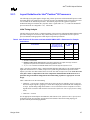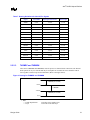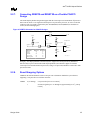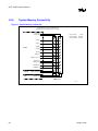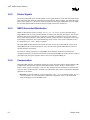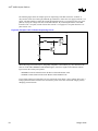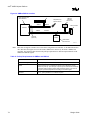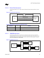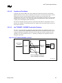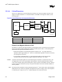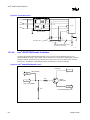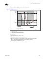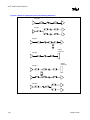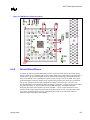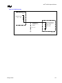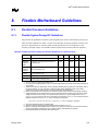
1
R Intel® 810E2 Chipset Platform Design Guide August 2002 Document Number: 298248-002 ® Intel 810E2 Chipset Platform R INFORMATION IN THIS DOCUMENT IS PROVIDED IN CONNECTION WITH INTEL PRODUCTS. NO LICENSE, EXPRESS OR IMPLIED, BY ESTOPPEL OR OTHERWISE, TO ANY INTELLECTUAL PROPERTY RIGHTS IS GRANTED BY THIS DOCUMENT. EXCEPT AS PROVIDED IN INTEL’S TERMS AND CONDITIONS OF SALE FOR SUCH PRODUCTS, INTEL ASSUMES NO LIABILITY WHATSOEVER, AND INTEL DISCLAIMS ANY EXPRESS OR IMPLIED WARRANTY, RELATING TO SALE AND/OR USE OF INTEL PRODUCTS INCLUDING LIABILITY OR WARRANTIES RELATING TO FITNESS FOR A PARTICULAR PURPOSE, MERCHANTABILITY, OR INFRINGEMENT OF ANY PATENT, COPYRIGHT OR OTHER INTELLECTUAL PROPERTY RIGHT. Intel products are not intended for use in medical, life saving, or life sustaining applications. Intel may make changes to specifications and product descriptions at any time, without notice. Designers must not rely on the absence or characteristics of any features or instructions marked "reserved" or "undefined." Intel reserves these for future definition and shall have no responsibility whatsoever for conflicts or incompatibilities arising from future changes to them. The Intel® 810E2 chipset may contain design defects or errors known as errata which may cause the product to deviate from published specifications. Current characterized errata are available on request. Contact your local Intel sales office or your distributor to obtain the latest specifications and before placing your product order. 2 2 I C is a 2-wire communications bus/protocol developed by Philips. SMBus is a subset of the I C bus/protocol and was developed by Intel. Implementations of the I2C bus/protocol may require licenses from various entities, including Philips Electronics N.V. and North American Philips Corporation. Alert on LAN is a result of the Intel-IBM Advanced Manageability Alliance and a trademark of IBM. Intel and the Intel logo are trademarks or registered trademarks of Intel Corporation or its subsidiaries in the United States and other countries. *Other names and brands may be claimed as the property of others. Copyright © Intel Corporation 2000-2002 2 Design Guide ® Intel 810E2 Chipset Platform R Contents 1. Introduction ................................................................................................................................ 13 1.1. 1.2. 1.3. 2. PGA370 Processor Design Guidelines ...................................................................................... 25 2.1. 2.2. 3. Electrical Differences for Flexible PGA370 Designs ..................................................... 25 PGA370 Socket Definition Details ................................................................................. 25 ® ® 2.2.1. Layout Guidelines for Intel Pentium III Processors.................................. 27 2.2.2. Determine General Topology and Layout ................................................... 28 2.2.2.1. Motherboard Layout Rules for AGTL+ Signals............................... 30 2.2.2.2. Motherboard Layout Rules for Non-AGTL+ (CMOS) Signals......... 30 2.2.2.3. THRMDP and THRMDN................................................................. 31 2.2.2.4. Additional Considerations ............................................................... 32 2.2.3. Undershoot/Overshoot Requirements......................................................... 32 2.2.4. BSEL[1:0] Implementation for PGA370 Designs......................................... 32 2.2.5. CLKREF Circuit Implementation ................................................................. 34 2.2.6. Undershoot/Overshoot Requirements......................................................... 34 2.2.7. Connecting RESET# and RESET2# on a Flexible PGA370 Design ........... 35 2.2.8. Reset Strapping Options ............................................................................. 35 2.2.8.1. Power-Up/Reset Strap Options ...................................................... 36 2.2.9. Voltage Regulation Differences................................................................... 36 2.2.10. Decoupling Guidelines for Flexible PGA370 Designs ................................. 36 2.2.10.1. VCCcore Decoupling Design.......................................................... 37 2.2.10.2. VTT Decoupling Design................................................................... 37 2.2.10.3. VREF Decoupling Design ................................................................ 37 2.2.11. Thermal/EMI Differences ............................................................................ 38 2.2.12. Debug Port Changes................................................................................... 38 2.2.13. PGA370 Socket Connector Strapping Option ............................................. 39 Layout and Routing Guidelines .................................................................................................. 41 3.1. 3.2. 3.1 3.3. 3.4. Design Guide About This Design Guide .............................................................................................. 13 1.1.1. References .................................................................................................. 17 System Overview........................................................................................................... 18 1.2.1. Graphics and Memory Controller Hub (GMCH) .......................................... 19 1.2.2. Intel 82801BA I/O Controller Hub 2 (ICH2) ............................................... 19 1.2.3. System Configurations ................................................................................ 20 Platform Initiatives ......................................................................................................... 21 1.3.1. Hub Interface............................................................................................... 21 1.3.2. Integrated LAN Controller............................................................................ 21 1.3.3. Ultra ATA/100 Support ................................................................................ 21 1.3.4. Expanded USB Support .............................................................................. 21 1.3.5. SMBus ........................................................................................................ 21 1.3.6. Interrupt Controller ...................................................................................... 21 1.3.7. Firmware Hub (FWH) Flash BIOS .............................................................. 22 1.3.8. AC’97 6-Channel Support ........................................................................... 22 1.3.9. Low Pin Count (LPC) Interface.................................................................... 24 General Recommendations........................................................................................... 41 Nominal Board Stackup................................................................................................. 41 Component Quadrant Layouts ...................................................................................... 42 ® Intel 810E2 Chipset Component Placement................................................................ 45 System Memory Layout Guidelines ............................................................................... 46 3.4.1. System Memory Solution Space ................................................................. 46 3 ® Intel 810E2 Chipset Platform R 3.5. 3.6. 3.7. 3.8. 3.9. 3.10. 3.11. 3.12. 3.13. 3.14. 3.15. 3.16. 3.17. 3.18. 3.19. 3.20. 3.21. 4 System Memory Routing Example ..............................................................47 3.1.1 3.4.2. System Memory Connectivity ......................................................................48 Display Cache Interface.................................................................................................49 3.5.1. Display Cache Solution Space.....................................................................49 Hub Interface .................................................................................................................51 3.6.1. Data Signals.................................................................................................51 3.6.2. Strobe Signals..............................................................................................52 3.6.3. HREF Generation/Distribution .....................................................................52 3.6.4. Compensation..............................................................................................52 ® Intel ICH2 .....................................................................................................................54 3.7.1. Decoupling ...................................................................................................54 1.8V/3.3V Power Sequencing ........................................................................................55 Power Plane Splits .........................................................................................................57 Thermal Design Power ..................................................................................................57 IDE Interface ..................................................................................................................57 3.11.1. Cabling ........................................................................................................58 Cable Detection for Ultra ATA/66 and Ultra ATA/100 ....................................................58 3.12.1. Combination Host-Side/Device-Side Cable Detection.................................58 3.12.2. Device-Side Cable Detection .......................................................................60 3.12.3. Primary IDE Connector Requirements ........................................................61 3.12.4. Secondary IDE Connector Requirements....................................................62 AC’97 .............................................................................................................................63 3.13.1. AC’97 Audio Codec Detect Circuit and Configuration Options ....................64 3.13.1.1. Valid Codec Configurations.............................................................68 3.13.2. SPKR Pin Considerations ............................................................................68 CNR ...............................................................................................................................69 USB................................................................................................................................69 ® 3.15.1. Disabling the Native USB Interface of Intel ICH2.......................................70 ISA .................................................................................................................................71 IOAPIC Design Recommendation .................................................................................71 SMBus/SMLink Interface ...............................................................................................71 PCI .................................................................................................................................73 RTC................................................................................................................................73 3.20.1. RTC Crystal .................................................................................................74 3.20.2. External Capacitors .....................................................................................75 3.20.3. RTC Layout Considerations.........................................................................75 3.20.4. RTC External Battery Connection................................................................75 3.20.5. RTC External RTCRST Circuit ....................................................................76 3.20.6. RTC Routing Guidelines ..............................................................................77 3.20.7. VBIAS DC Voltage and Noise Measurements.............................................77 3.20.8. Power-well Isolation Control ........................................................................77 LAN Layout Guidelines ..................................................................................................79 ® 3.21.1. Intel ICH2 – LAN Interconnect Guidelines .................................................80 3.21.1.1. Bus Topologies ...............................................................................80 3.21.1.2. Point-to-Point Interconnect..............................................................81 3.21.1.3. LOM/CNR Interconnect...................................................................81 3.21.1.4. Signal Routing and Layout ..............................................................82 3.21.1.5. Crosstalk Consideration ..................................................................83 3.21.1.6. Impedances.....................................................................................83 3.21.1.7. Line Termination .............................................................................83 3.21.2. General LAN Routing Guidelines and Considerations.................................83 3.21.2.1. General Trace Routing Considerations...........................................83 Design Guide ® Intel 810E2 Chipset Platform R 3.22. 3.23. 3.24. 3.25. 3.26. 4. Advanced System Bus Design................................................................................................. 113 4.1. Design Guide 3.21.2.2. Power and Ground Connections .................................................... 85 3.21.2.3. A 4-Layer Board Design ................................................................. 86 3.21.2.4. Common Physical Layout Issues ................................................... 87 ® 3.21.3. Intel 82562EH Home/PNA* Guidelines ..................................................... 88 3.21.3.1. Power and Ground Connections .................................................... 88 ® 3.21.3.2. Guidelines for Intel 82562EH Component Placement .................. 89 3.21.3.3. Crystals and Oscillators .................................................................. 89 3.21.3.4. Phoneline HPNA Termination......................................................... 89 3.21.3.5. Critical Dimensions......................................................................... 91 ® 3.21.4. Intel 82562ET / 82562EM Guidelines ........................................................ 92 ® 3.21.4.1. Guidelines for Intel 82562ET / 82562EM Component Placement 92 3.21.4.2. Crystals and Oscillators .................................................................. 93 ® 3.21.4.3. Intel 82562ET / 82562EM Termination Resistors ......................... 93 3.21.4.4. Critical Dimensions......................................................................... 94 3.21.4.5. Reducing Circuit Inductance........................................................... 95 ® 3.21.4.6. Intel 82562ET/EM Disable Guidelines .......................................... 96 ® 3.21.5. Intel 82562ET / 82562EH Dual Footprint Guidelines................................. 97 LPC/FWH ...................................................................................................................... 99 3.22.1. In-Circuit FWH Programming...................................................................... 99 3.22.2. FWH Vpp Design Guidelines ...................................................................... 99 FWH Decoupling ......................................................................................................... 100 Processor PLL Filter Recommendation ...................................................................... 100 3.24.1. Processor PLL Filter Recommendation .................................................... 100 3.24.2. Topology.................................................................................................... 100 3.24.3. Filter Specification ..................................................................................... 100 ® 3.24.4. Recommendation for Intel Platforms ....................................................... 102 3.24.5. Custom Solutions ...................................................................................... 104 RAMDAC/Display Interface ......................................................................................... 105 3.25.1. Reference Resistor (Rset) Calculation...................................................... 106 3.25.2. RAMDAC Board Design Guidelines .......................................................... 106 DPLL Filter Design Guidelines .................................................................................... 108 3.26.1. Filter Specification ..................................................................................... 109 3.26.2. Recommended Routing/Component Placement....................................... 110 3.26.3. Example LC Filter Components ................................................................ 110 AGTL+ Design Guidelines........................................................................................... 113 4.1.1. Initial Timing Analysis ................................................................................ 114 4.1.2. Determine General Topology, Layout, and Routing Desired..................... 117 4.1.3. Pre-Layout Simulation ............................................................................... 117 4.1.3.1. Methodology ................................................................................. 117 4.1.3.2. Sensitivity Analysis ....................................................................... 117 4.1.3.3. Monte Carlo Analysis.................................................................... 118 4.1.3.4. Simulation Criteria ........................................................................ 118 4.1.4. Place and Route Board ............................................................................. 119 4.1.4.1. Estimate Component to Component Spacing for AGTL+ Signals 119 4.1.4.2. Layout and Route Board............................................................... 119 4.1.5. Post-Layout Simulation ............................................................................. 120 4.1.5.1. Intersymbol Interference............................................................... 121 4.1.5.2. Crosstalk Analysis ........................................................................ 121 4.1.5.3. Monte Carlo Analysis.................................................................... 121 4.1.6. Validation................................................................................................... 121 4.1.6.1. Measurements.............................................................................. 121 4.1.6.2. Flight Time Simulation .................................................................. 122 5 ® Intel 810E2 Chipset Platform R 4.2. 4.3. 4.4. 5. Clocking....................................................................................................................................133 5.1. 5.2. 5.3. 5.4. 5.5. 5.6. 6. 6.2. 6.3. 6.4. 6.5. Thermal Design Power ................................................................................................144 6.1.1. Power Sequencing.....................................................................................144 Pull-up and Pull-down Resistor Values ........................................................................149 ATX Power Supply PWRGOOD Requirements...........................................................150 Power Management Signals ........................................................................................150 6.4.1. Power Button Implementation....................................................................151 6.4.2. 1.8V / 3.3V Power Sequencing ..................................................................152 6.4.3. 3.3V / V5REF Sequencing .........................................................................153 6.4.4. GMCH Decoupling Guidelines ...................................................................154 6.4.5. Ground Flood Planes .................................................................................155 Power_Supply PS_ON Considerations........................................................................156 Design Checklist.......................................................................................................................157 7.1. 7.2. 6 Clock Generation .........................................................................................................133 Clock Architecture........................................................................................................135 Clock Routing Guidelines.............................................................................................136 Capacitor Sites.............................................................................................................139 Clock Power Decoupling Guidelines............................................................................140 Clock Skew Requirements...........................................................................................142 5.6.1. IntraGroup Skew Limits .............................................................................142 Power Delivery..........................................................................................................................143 6.1. 7. Flight Time Hardware Validation ...................................................123 4.1.6.3. Theory..........................................................................................................................123 4.2.1. AGTL+ ......................................................................................................123 4.2.2. Timing Requirements.................................................................................123 4.2.3. Crosstalk Theory........................................................................................124 4.2.3.1. Potential Termination Crosstalk Problems....................................125 More Details and Insight ..............................................................................................125 4.3.1. Textbook Timing Equations .......................................................................125 4.3.2. Effective Impedance and Tolerance/Variation ...........................................127 4.3.3. Power/Reference Planes, PCB Stackup, and High Frequency Decoupling .................................................................................................127 4.3.3.1. Power Distribution .........................................................................127 4.3.3.2. High Frequency Decoupling ..........................................................129 4.3.4. Clock Routing ............................................................................................130 Definitions of Flight Time Measurements/ Corrections and Signal Quality..................130 4.4.1. VREF Guardband.........................................................................................131 4.4.2. Ringback Levels ........................................................................................131 4.4.3. Overdrive Region .......................................................................................131 4.4.4. Flight Time Definition and Measurement ...................................................132 4.4.5. Conclusion .................................................................................................132 Design Review Checklist .............................................................................................157 7.1.1. Design Checklist Summary........................................................................157 ® Intel ICH2 Checklist....................................................................................................163 7.2.1. PCI Interface..............................................................................................163 7.2.2. Hub Interface .............................................................................................163 7.2.3. LAN Interface.............................................................................................163 7.2.4. EEPROM Interface ....................................................................................165 7.2.5. FWH/LPC Interface ...................................................................................165 Design Guide ® Intel 810E2 Chipset Platform R Interrupt Interface ...................................................................................... 165 7.2.6. 7.2.7. GPIO Checklist.......................................................................................... 166 7.2.8. USB ...................................................................................................... 167 7.2.9. Power Management .................................................................................. 168 7.2.10. Processor Signals ..................................................................................... 168 7.2.11. System Management ................................................................................ 169 7.2.12. ISA Bridge Checklist.................................................................................. 169 7.2.13. RTC ...................................................................................................... 169 7.2.14. AC’97 ...................................................................................................... 170 7.2.15. Miscellaneous Signals............................................................................... 170 7.2.16. Power ...................................................................................................... 172 7.2.17. IDE Checklist............................................................................................. 173 LPC Checklist.............................................................................................................. 175 System Checklist......................................................................................................... 176 FWH Checklist ............................................................................................................ 176 Clock Synthesizer Checklist ........................................................................................ 177 ITP Probe Checklist..................................................................................................... 178 Power Delivery Checklist............................................................................................. 178 7.3. 7.4. 7.5. 7.6. 7.7. 7.8. 8. Flexible Motherboard Guidelines ............................................................................................. 179 8.1. Flexible Processor Guidelines ..................................................................................... 179 8.1.1. Flexible System Design DC Guidelines..................................................... 179 8.1.2. System Bus AC Guidelines ....................................................................... 181 8.1.3. Thermal Guidelines ................................................................................... 184 9. Third-Party Vendor Information................................................................................................ 185 Appendix A: Intel 810E2 Chipset Platform Reference Schematics ............................................................ 189 Design Guide ® 7 ® Intel 810E2 Chipset Platform R Figures ® Figure 1. Intel 810E2 Chipset System ....................................................................................20 Figure 2. Topology for 370-Pin Socket Designs with Single-Ended Termination (SET) ..........29 Figure 3. Routing for THRMDP and THRMDN.........................................................................31 Figure 4. BSEL[1:0] Circuit Implementation for PGA370 Designs ...........................................33 Figure 5. Examples for CLKREF Divider Circuit.......................................................................34 Figure 6. RESET# Schematic for PGA370 Designs.................................................................35 Figure 7. Capacitor Placement on the Motherboard.................................................................37 Figure 8. TAP Connector Comparison .....................................................................................38 Figure 9. Component Keep-Out Zones ....................................................................................39 Figure 10. Nominal Board Stackup...........................................................................................42 Figure 11. GMCH Quadrant Layout (top View).........................................................................42 ® Figure 12. Intel ICH2 Quadrant Layout (Top View).................................................................43 Figure 13. Firmware Hub (FWH) Packages .............................................................................44 Figure 14. uATX Placement Example for PGA370 Processors ...............................................45 Figure 15. System Memory Topologies ....................................................................................46 Figure 16. System Memory Routing Example ..........................................................................47 Figure 17. System Memory Connectivity ..................................................................................48 Figure 18. Display Cache (Topology 1) ....................................................................................49 Figure 19. Display Cache (Topology 2) ....................................................................................49 Figure 20. Display Cache (Topology 3) ....................................................................................50 Figure 21. Display Cache (Topology 4) ....................................................................................50 Figure 22. Hub Interface Signal Routing Example ...................................................................51 Figure 23. Single Hub Interface Reference Divider Circuit.......................................................53 Figure 24. Locally Generated Hub Interface Reference Dividers .............................................53 ® Figure 25. Intel ICH2 Decoupling Capacitor Layout................................................................55 Figure 26. Example 1.8V/3.3V Power Sequencing Circuit .......................................................56 Figure 27. Power Plane Split Example .....................................................................................57 Figure 28. Combination Host-Side / Device-Side IDE Cable Detection ...................................59 Figure 29. Device-Side IDE Cable Detection............................................................................60 Figure 30. Connection Requirements for Primary IDE Connector ...........................................61 Figure 31. Connection Requirements for Secondary IDE Connector.......................................62 ® Figure 32. Intel ICH2 AC’97– Codec Connection ...................................................................63 Figure 33. CDC_DN_ENAB# Support Circuitry for a Single Codec on Motherboard...............65 Figure 34. CDC_DN_ENAB# Support Circuitry for Multi-Channel Audio Upgrade...................66 Figure 35. CDC_DN_ENAB# Support Circuitry for Two-Codecs on Motherboard / One-Codec on CNR ..........................................................................................................66 Figure 36. CDC_DN_ENAB# Support Circuitry for Two-Codecs on Motherboard / Two-Codecs on CNR ........................................................................................................67 Figure 37. CNR Interface..........................................................................................................69 Figure 38. USB Data Signals....................................................................................................70 Figure 39. SMBus/SMLink Interface.........................................................................................72 Figure 40. PCI Bus Layout Example.........................................................................................73 ® Figure 41. External Circuitry for the Intel ICH2 RTC...............................................................74 Figure 42. Diode Circuit to Connect RTC External Battery ......................................................76 ® Figure 43. RTCRST External Circuit for Intel ICH2 RTC........................................................76 Figure 44. RTC Power-well Isolation Control............................................................................78 ® Figure 45. Intel ICH2 / LAN Connect Section .........................................................................79 Figure 46. Single-Solution Interconnect....................................................................................81 Figure 47. LOM/CNR Interconnect ...........................................................................................81 Figure 48. LAN_CLK Routing Example ....................................................................................82 Figure 49. Trace Routing..........................................................................................................84 Figure 50. Ground Plane Separation ........................................................................................85 8 Design Guide ® Intel 810E2 Chipset Platform R ® Figure 51. Intel 82562EH Termination ................................................................................... 90 Figure 52. Critical Dimensions for Component Placement ...................................................... 91 ® Figure 53. Intel 82562ET/82562EM Termination ................................................................... 93 Figure 54. Critical Dimensions for Component Placement ...................................................... 94 Figure 55. Termination Plane................................................................................................... 96 ® Figure 56. Intel 82562ET/EM Disable Circuit ......................................................................... 96 Figure 57. Dual-Footprint LAN Connect Interface.................................................................... 97 Figure 58. Dual-Footprint Analog Interface .............................................................................. 98 Figure 59. FWH VPP Isolation Circuitry................................................................................... 99 Figure 60. Filter Topology ...................................................................................................... 100 Figure 61. Filter Specification................................................................................................. 101 Figure 62. Using Discrete R ................................................................................................... 103 Figure 63. No Discrete R........................................................................................................ 103 Figure 64. Core Reference Model.......................................................................................... 104 Figure 65. Schematic of RAMDAC Video Interface ............................................................... 105 Figure 66. RAMDAC Component and Routing Guidelines .................................................... 107 Figure 67. Recommended RAMDAC Reference Resistor Placement and Connections....... 108 Figure 68. Recommended LC Filter Connection.................................................................... 109 Figure 69. Frequency Response (see Table 30) ................................................................... 111 Figure 70. Test Load vs. Actual System Load ....................................................................... 122 Figure 71. Aggressor and Victim Networks............................................................................ 124 Figure 72. Transmission Line Geometry: (A) Microstrip (B) Stripline..................................... 124 Figure 73. One Signal Layer and One Reference Plane........................................................ 127 Figure 74. Layer Switch with One Reference Plane .............................................................. 128 Figure 75. Layer Switch with Multiple Reference Planes (same type) ................................... 128 Figure 76. Layer Switch with Multiple Reference Planes ....................................................... 128 Figure 77. One Layer with Multiple Reference Planes ........................................................... 129 Figure 78. Overdrive Region and VREF Guardband................................................................ 131 Figure 79. Rising Edge Flight Time Measurement................................................................. 132 ® Figure 80. Intel 810E2 Chipset Clock Architecture............................................................... 135 Figure 81. Different Topologies for the Clock Routing Guidelines ......................................... 138 Figure 82. Example of Capacitor Placement Near Clock Input Receiver .............................. 139 Figure 83. Example of Clock Power Plane Splits and Decoupling......................................... 141 Figure 84. Power Delivery Map .............................................................................................. 144 Figure 85. G3-S0 Transistion................................................................................................. 145 Figure 86. S0-S3-S0 Transition.............................................................................................. 146 Figure 87. S0-S5-S0 Transition.............................................................................................. 147 Figure 88. Pull-up Resistor Example ..................................................................................... 149 Figure 89. Example 1.8V/3.3V Power Sequencing Circuit..................................................... 152 Figure 90. Example 3.3V/V5REF Sequencing Circuitry......................................................... 153 Figure 91. GMCH Power Plane Decoupling........................................................................... 155 Figure 92. USB Data Line Schematic .................................................................................... 167 Figure 93. SPKR Circuitry ...................................................................................................... 171 Figure 94. V5REF Circuitry .................................................................................................... 172 Figure 95. Host/Device Side Detection Circuitry .................................................................... 174 Figure 96. Device Side Only Cable Detection ........................................................................ 174 Figure 97. BCLK Waveform ................................................................................................... 182 Figure 98. Processor System Bus Valid Delay Timings......................................................... 183 Figure 99. Processor System Bus Setup and Hold Timings .................................................. 183 Figure 100. Power-On Reset and Configuration Timings ...................................................... 183 Design Guide 9 ® Intel 810E2 Chipset Platform R Tables Table 1. Platform Pin Definition Comparison for Single Processor Designs ............................26 ® ® ® Table 2. Intel Pentium III Processor and Intel 82810E GMCH AGTL+ Parameters for Example Calculations........................................................................................................27 1 Table 3. Example TFLT_MIN Calculations for 133 MHz Bus .......................................................28 1 Table 4. Example TFLT_MIN Calculations (Frequency Independent) .......................................28 1 Table 5. Segment Descriptions and Lengths for Figure 2 ......................................................29 Table 6. Trace Width:Space Guidelines...................................................................................29 Table 7. Routing Guidelines for Non-AGTL+ Signals ...............................................................31 ® Table 8. Intel CK810E Reset Strapping Matrix .......................................................................33 Table 9. Examples for CLKREF Divider Circuit ........................................................................34 Table 10. Power Up Options ....................................................................................................36 Table 11. Host Frequency Strappings ......................................................................................36 Table 12. System Memory Routing ..........................................................................................46 Table 13. Display Cache Routing (Topology 1) ........................................................................49 Table 14. Display Cache Routing (Topology 2) ........................................................................49 Table 15. Display Cache Routing (Topology 3) ........................................................................50 Table 16. Display Cache Routing (Topology 4) ........................................................................50 Table 17. Decoupling Capacitor Recommendation..................................................................54 Table 18. AC'97 SDIN Pull-down Resistors..............................................................................64 Table 19. Signal Descriptions ...................................................................................................67 Table 20. Codec Configurations ...............................................................................................68 Table 21. Pull-up Requirements for SMBus and SMLink .........................................................72 Table 22. LAN Design Guide Section Reference .....................................................................80 Table 23. Single-Solution Interconnect Length Requirements .................................................81 Table 24. LOM/CNR Length Requirements..............................................................................82 Table 25. Inductor...................................................................................................................102 Table 26. Capacitor ................................................................................................................102 Table 27. Resistor ..................................................................................................................102 Table 28. DPLL LC Filter Component Example .....................................................................110 Table 29. Additional DPLL LC Filter Component Example.....................................................111 Table 30. Resistance Values for Frequency Response Curves .............................................112 Table 31. AGTL+ Parameters for Example Calculations 1,2....................................................115 Table 32. Example T Calculations for 133 MHz Bus1 .............................................................116 Table 33. Example TFLT_MIN Calculations (Frequency Independent) ....................................116 Table 34. Trace Width Space Guidelines...............................................................................120 Table 35. REFCLK Reset Strap for CK810 vs. CK810E ........................................................133 ® Table 36. Intel 810E2 Chipset Clocks...................................................................................133 Table 37. Group Skew and Jitter Limits at the Pins of the Clock Chip ...................................136 Table 38. Signal Group and Resistor .....................................................................................136 Table 39. Layout Dimensions .................................................................................................137 Table 40. Clock Skew Requirements .....................................................................................142 Table 41. Power Sequencing Timing Definitions....................................................................148 Table 42. AGTL+ Connectivity Checklist for 370-Pin Socket Processors ..............................158 Table 43. CMOS Connectivity Checklist for 370-Pin Socket Processors...............................159 Table 44. TAP Checklist for a 370-Pin Socket Processor ......................................................159 Table 45. Miscellaneous Checklist for 370-Pin Socket Processors .......................................160 Table 46. GMCH Checklist .....................................................................................................161 Table 47. System Memory Checklist ......................................................................................162 Table 48. Display Cache Checklist.........................................................................................162 Table 49. Flexible Processor Voltage and Current Guidelines for 1.5V Processors ..............179 Table 50. Flexible Processor Voltage and Current Guidelines for 2.0 V Processors .............180 10 Design Guide ® Intel 810E2 Chipset Platform R Table 51. Flexible Motherboard Processor System Bus AC Guidelines (Clock) at the Processor Pins ........................................................................................................................ 181 Table 52. Processor System Bus AC Guidelines (AGTL+ Signal Group) at the Processor Pins......................................................................................................................... 182 ® ® Table 53. Intel Celeron Processor PPGA Flexible Thermal Design Power ........................ 184 Table 54. Super I/O................................................................................................................ 185 Table 55. Clock Generation ................................................................................................... 185 Table 56. Memory Vendors.................................................................................................... 185 Table 57. Voltage Regulator Vendors .................................................................................... 185 Table 58. Flat Panel ............................................................................................................... 186 Table 59. AC’97 ..................................................................................................................... 186 Table 60. TMDS Transmitters................................................................................................ 186 Table 61. TV Encoders .......................................................................................................... 187 Table 62. Combo TMDS Transmitters/TV Encoders ............................................................. 187 Table 63. LVDS Transmitter .................................................................................................. 187 Design Guide 11 ® Intel 810E2 Chipset Platform R Revision History Rev. Description Date -001 • Initial Release January 2001 -002 • Replaced Figure 84. Power Delivery Map August 2002 • Revised Section 7.2.6, ICH2 Checklist, Interrupt interface, APIC • Revised Section 7.2.16, Power, ICH2 Checklist: Recommendations for 5V_REF_SUS • Revised Section 6.4.3, 3.3V/5VREF Sequencing • Added Section 3.20.8, Power-well Isolation Control • Revised Figure 49. Trace Routing in General Trace Routing Considerations, Section 3.21.2.1 • Added SUSCLK to ICH2 Checklist Section 7.2.13, RTC • Added Section 6.5, Power_Supply PS_ON Considerations • Revised ICH2 Checklist Section 7.2.9, Power Management • Revised Section 3.15, USB • Added RTCRST# to ICH2 Checklist Section 7.2.13, RTC • Added 82562ET/EM Disable Guidelines, Section 3.21.4.6 • Revised Section 3.22.2., FWH Vpp Design Guidelines • Revised Section 3.21.5, 82562ET / 82562EH Dual Footprint Guidelines • Revised Section 3.1, General Recommendations • Revised ICH2 Checklist Section 7.2.13, RTC, RTCX1-RTCX2 • Revised RTC Crystal, Section 3.20.1 • Revised ICH2 Checklist, Section 7.2.9, Power Management, PWRBTN# • Revised ICH2 Checklist, PCI Interface, Section 7.2.1, PME# • Revised VCCcore Decoupling Design, Section 2.2.10.1 • Revised Figure 23 and Figure 24 in Compensation, Section 3.6.4 • Revised 82562ET / 82562EH Dual Footprint Guidelines, Section 3.21.5 • Revised 82562ET / 82562EM Termination Resistors, Section 3.21.4.3 • Revised General Trace Routing Considerations, Section 3.21.2.1 • Revised Table 23, in Point-To-Point Interconnect, Section 3.21.1.2 • Revised LAN Layout Guidelines, Section 3.21 12 Design Guide ® Intel 810E2 Chipset Platform R 1. Introduction This design guide provides motherboard design guidelines for Intel® 810E2 chipset systems. These design guidelines have been developed to ensure maximum flexibility for board designers while reducing the risk of board related issues. In addition to design guidelines, this document discusses 810E2 chipset system design issues (e.g., thermal requirements). The debug recommendations should be consulted when debugging an 810E2 chipset system. However, the debug recommendations should be understood before completing board design to ensure that the debug port, in addition to other debug features, will be implemented correctly. 1.1. About This Design Guide This design guide is intended for hardware designers who are experienced with PC architectures and board design. The design guide assumes that the designer has a working knowledge of the vocabulary and practices of PC hardware design. • Chapter 1, “Introduction”—This chapter introduces the designer to the organization and purpose of this design guide, and provides a list of references of related documents. This chapter also provides an overview of the 810E2 chipset. • Chapter 2, “PGA370 Processor Design Guidelines”—This chapter provides design guidelines for the PGA370 processor including processor-specific layout guidelines. • Chapter 3, “Layout and Routing Guidelines”—This chapter provides a detailed set of motherboard layout and routing guidelines, except for processor-specific layout guidelines. The motherboard functional units are covered (e.g., chipset component placement, system bus routing, system memory layout, display cache interface, hub interface, IDE, AC’97, USB, interrupts, SMBUS, PCD, LPC/ FWH Flash BIOS, and RTC). For the PGA370 processor specific layout guidelines, refer to Chapter 2. • Chapter 4, “Advanced System Bus Design”—The goal of this chapter is to provide the system designer with the information needed for the implementation of 133 MHz and 100 MHz single processor AGTL+ bus PCB layout. • Chapter 5, “Clocking”— This chapter provides motherboard clocking guidelines (e.g., clock architecture, routing, capacitor sites, clock power decoupling, and clock skew). • Chapter 6, “Power delivery” — This chapter includes guidelines regarding power delivery, decoupling, thermal, and power sequencing. • Chapter 7, “Design Checklist”— This chapter provides a design review checklist. ATA/66 and ATA/100 detection, calculation of pull-up/pull-down resistors, minimizing RTC ESD, and power management signals are also discussed. • Chapter 8, “Flixible Motherboard Guidelines”— This chapter includes guidelines regarding power deliver, decoupling, thermal, and power sequencing. • Chapter 9, “Third Party Vendor Information”— This chapter includes information regarding various third-party vendors who provide products to support the 810E2 chipset. • Appendix A, “Intel® 810E2 Chipset Platform Reference Schematics”— This appendix includes schematics for the 810E2 Reference Board Design Guide 13 ® Intel 810E2 Chipset Platform R Term 14 Definition Suspend-To-RAM (STR) In the STR state, the system state is stored in main memory and all unnecessary system logic is turned off. Only main memory and logic required to wake the system remain powered. Full-power operation During full-power operation, all components on the motherboard remain powered. Note that full-power operation includes both the full-on operating state (S0) and the processor Stop Grant state (S1). Suspend operation During suspend operation, power is removed from some components on the motherboard. The customer reference board supports three suspend states: processor Stop Grant (S1), Suspend-to-RAM (S3) and Soft-off (S5). Power rails An ATX power supply has 6 power rails: +5V, -5V, +12V, -12V, +3.3V, +5VSB. In addition to these power rails, several other power rails can be created with voltage regulators. Core power rail A power rail that is only on during full-power operation. These power rails are on when the PSON signal is asserted to the ATX power supply. The core power rails that are distributed directly from the ATX power supply are: ±5V, ±12V and +3.3V. Standby power rail A power rail that in on during suspend operation (these rails are also on during fullpower operation). These rails are on at all times (when the power supply is plugged into AC power). The only standby power rail that is distributed directly from the ATX power supply is 5VSB (5V Standby). There can be other standby rails that are created with voltage regulators. Derived power rail A derived power rail is any power rail that is generated from another power rail using an on-board voltage regulator. For example, 3.3VSB is usually derived (on the motherboard) from 5VSB using a voltage regulator. Dual power rail A dual power rail is derived from different rails at different times (depending on the power state of the system). Usually, a dual power rail is derived from a standby supply during suspend operation and derived from a core supply during full-power operation. Aggressor A network that transmits a coupled signal to another network is called the aggressor network. AGTL+ The processor system bus uses a bus technology called AGTL+, or Assisted Gunning Transceiver Logic. AGTL+ buffers are open-drain and require pull-up resistors for providing the high logic level and termination. The processor AGTL+ output buffers differ from GTL+ buffers with the addition of an active pMOS pull-up transistor to “assist” the pull-up resistors during the first clock of a low-to-high voltage transition. Additionally, the processor Single Edge Connector (S.E.C.) cartridge contains 56 Ω pull-up resistors to provide termination at each bus load. Bus Agent A component or group of components that, when combined, represent a single load on the AGTL+ bus. Corner Describes how a component performs when all parameters that could impact performance are adjusted to have the same impact on performance. Examples of these parameters include variations in manufacturing process, operating temperature, and operating voltage. The results in performance of an electronic component that may change as a result of corners include (but are not limited to): clock to output time, output driver edge rate, output drive current, and input drive current. Discussion of the “slow” corner would mean having a component operating at its slowest, weakest drive strength performance. Similar discussion of the “fast” corner would mean having a component operating at its fastest, strongest drive strength performance. Operation or simulation of a component at its slow corner and fast corner is expected to bound the extremes between slowest, weakest performance and fastest, strongest performance. Design Guide ® Intel 810E2 Chipset Platform R Term Crosstalk Definition The reception on a victim network of a signal imposed by aggressor network(s) through inductive and capacitive coupling between the networks. • Backward Crosstalk - coupling that creates a signal in a victim network that travels in the opposite direction as the aggressor’s signal. • Forward Crosstalk - coupling that creates a signal in a victim network that travels in the same direction as the aggressor’s signal. • Even Mode Crosstalk - coupling from multiple aggressors when all the aggressors switch in the same direction that the victim is switching. • Odd Mode Crosstalk - coupling from multiple aggressors when all the aggressors switch in the opposite direction that the victim is switching. Edge Finger The cartridge electrical contact that interfaces to the SC242 connector. Flight Time Flight Time is a term in the timing equation that includes the signal propagation delay, any effects the system has on the TCO of the driver, plus any adjustments to the signal at the receiver needed to guarantee the setup time of the receiver. More precisely, flight time is defined to be: The time difference between a signal at the input pin of a receiving agent crossing VREF (adjusted to meet the receiver manufacturer’s conditions required for AC timing specifications; i.e., ringback, etc.), and the output pin of the driving agent crossing VREF if the driver was driving the Test Load used to specify the driver’s AC timings. See Section 4.1 for details regarding flight time simulation and validation. The VREF Guardband takes into account sources of noise that may affect the way an AGTL+ signal becomes valid at the receiver. See the definition of the VREF Guardband. • Maximum and Minimum Flight Time - Flight time variations can be caused by many different parameters. The more obvious causes include variation of the board dielectric constant, changes in load condition, crosstalk, VTT noise, VREF noise, variation in termination resistance and differences in I/O buffer performance as a function of temperature, voltage and manufacturing process. Some less obvious causes include effects of Simultaneous Switching Output (SSO) and packaging effects. The Maximum Flight Time is the largest flight time a network will experience under all variations of conditions. Maximum flight time is measured at the appropriate VREF Guardband boundary. The Minimum Flight Time is the smallest flight time a network will experience under all variations of conditions. Minimum flight time is measured at the appropriate VREF Guardband boundary. For more information on flight time and the VREF Guardband, see the Intel® Pentium® II Processor Developer’s Manual. Design Guide GTL+ GTL+ is the bus technology used by the Pentium Pro processor. This is an incident wave switching, open-drain bus with pull-up resistors that provide both the high logic level and termination. It is an enhancement to the GTL (Gunning Transceiver Logic) technology. See the Intel® Pentium® II Processor Developer’s Manual for more details of GTL+. Network The trace of a Printed Circuit Board (PCB) that completes an electrical connection between two or more components. Network Length The distance between extreme bus agents on the network and does not include the distance connecting the end bus agents to the termination resistors. Overdrive Region Is the voltage range, at a receiver, located above and below VREF for signal integrity analysis. See the Intel® Pentium® II Processor Developer’s Manual for more details. Overshoot Maximum voltage allowed for a signal at the processor core pad. See each processor’s datasheet for overshoot specification. 15 ® Intel 810E2 Chipset Platform R Term 16 Definition Pad A feature of a semiconductor die contained within an internal logic package on the S.E.C cartridge substrate used to connect the die to the package bond wires. A pad is only observable in simulation. Pin A feature of a logic package contained within the S.E.C. cartridge used to connect the package to an internal substrate trace. Ringback Ringback is the voltage that a signal rings back to after achieving its maximum absolute value. Ringback may be due to reflections, driver oscillations, etc. See the respective processor’s datasheet for ringback specification. Settling Limit Defines the maximum amount of ringing at the receiving pin that a signal must reach before its next transition. See the respective processor’s datasheet for settling limit specification. Setup Window Is the time between the beginning of Setup to Clock (TSU_MIN) and the arrival of a valid clock edge. This window may be different for each type of bus agent in the system. Simultaneous Switching Output (SSO) Effects Refers to the difference in electrical timing parameters and degradation in signal quality caused by multiple signal outputs simultaneously switching voltage levels (e.g., high-tolow) in the opposite direction from a single signal (e.g., low-to-high) or in the same direction (e.g., high-to-low). These are respectively called odd-mode switching and even-mode switching. This simultaneous switching of multiple outputs creates higher current swings that may cause additional propagation delay (or “pushout”), or a decrease in propagation delay (or “pull-in”). These SSO effects may impact the setup and/or hold times and are not always taken into account by simulations. System timing budgets should include margin for SSO effects. Stub The branch from the trunk terminating at the pad of an agent. Test Load Intel uses a 50 Ω test load for specifying its components. Trunk The main connection, excluding interconnect branches, terminating at agent pads. Undershoot Maximum voltage allowed for a signal to extend below VSS at the processor core pad. See the respective processor’s datasheet for undershoot specifications. Victim A network that receives a coupled crosstalk signal from another network is called the victim network. VREF Guardband A guardband (DVREF) defined above and below VREF to provide a more realistic model accounting for noise such as crosstalk, VTT noise, and VREF noise. Design Guide ® Intel 810E2 Chipset Platform R 1.1.1. References • Intel® 810E Chipset: 82810E Graphics and Memory Controller Hub (GMCH) Datasheet (Document Number: 290676) • Intel® 82801BA I/O Controller Hub (ICH2) Datasheet (Document Number: 290687) • Intel® 82802AB/AC Firmware Hub (FWH) Datasheet (Document Number: 290658) • Intel® Celeron® Processor Datasheet (Document Number: 243658) • Intel® Celeron® Processor Specification Update (Document Number: 243748) • Intel® 810E Chipset Clock Synthesizer/Driver Specification • PPGA 370 Power Delivery Guidelines • Intel® Pentium® II Processor AGTL+ Guidelines (Document Number: 243330) • Intel® Pentium® II Processor Power Distribution Guidelines (Document Number: 243332) • Intel® Pentium® II Processor Developer's Manual (Document Number: 243341) • Intel® Pentium® II Processor at 350 MHz, 400 MHz and 450 MHz Datasheet (Document Number: 243657) • Intel® Pentium® II Processor Specification Update (Document Number: 243337) • Intel® Pentium® III Processor Datasheet (Document Number: 244452) • Intel® Pentium® III Processor Specification Update (Document Number: 244453) • AP-907: Intel® Pentium® III Power Distribution Guidelines (Document Number: 245085) • PCI Local Bus Specification, Revision 2.2 • Universal Serial Bus Specification, Revision 1.0 Design Guide 17 ® Intel 810E2 Chipset Platform R 1.2. System Overview The 810E2 chipset enhances the performance of the first generation Integrated Graphics chipset designed for the Intel® Celeron® processor and Intel® Pentium® III processor. The graphics accelerator architecture consists of dedicated multi-media engines executing in parallel to deliver high performance 3D, 2D, and motion compensation video capabilities. An integrated centralized memory arbiter allocates memory bandwidth to multiple system agents to optimize system memory utilization. A new chipset component interconnect, the hub interface, is designed into the 810E2 chipset to provide an efficient communication channel between the memory controller hub and the I/O hub controller. The 810E2 chipset architecture also enables a new security and manageability infrastructure through a Firmware Hub Flash BIOS component. An ACPI compliant 810E2 chipset platform can support the Full-on (S0), Stop Grant (S1), Suspend to RAM (S3), Suspend to Disk (S4), and Soft-off (S5) power management states. Through the use of an appropriate LAN device, the 810E2 chipset also supports wake-on-LAN* for remote administration and troubleshooting. The 810E2 chipset architecture removes the requirement for the ISA expansion bus that was traditionally integrated into the I/O subsystem of PCIsets/AGPsets. This removes many of the conflicts experienced when installing hardware and drivers into legacy ISA systems. The elimination of ISA provides true plug-and-play for the 810E chipset platform. Traditionally, the ISA interface was used for audio and modem devices. The addition of AC’97 allows the OEM to use software configurable AC’97 audio and modem coder/decoders (codecs) instead of the traditional ISA devices. The 810E2 chipset contains two core components: • Intel® 82810E Graphics and Memory Controller Hub (GMCH) • Intel® 82801BA I/O Controller Hub 2 (ICH2) The GMCH integrates a 66/100/133 MHz, P6 family system bus controller, integrated 2D/3D graphics accelerator, 100 MHz SDRAM controller and a high-speed hub interface for communication with the I/O Controller Hub (ICH2). The ICH2 integrates an Ultra ATA/100 controller, 2 USB host controllers with a total of 4 ports, LPC interface controller, FWH Flash BIOS interface controller, PCI interface controller, AC’97 digital controller and a hub interface for communication with the GMCH. 18 Design Guide ® Intel 810E2 Chipset Platform R 1.2.1. Graphics and Memory Controller Hub (GMCH) The GMCH provides the interconnect between the SDRAM and the rest of the system logic: • • • • • • • • 1.2.2. 421 Mini BGA Integrated Graphics controller 230 MHz RAMDAC Support for the Celeron processor and Pentium III processor with a 66 MHz , 100 MHz, or 133 MHz system bus. 100 MHz SDRAM interface supporting 64 MB/256 MB/512 MB with 16Mb/64Mb/128Mb SDRAM technology Optional 4 MB Display Cache Downstream hub interface for access to the ICH2 TV-Out/Flat Panel Display support Intel 82801BA I/O Controller Hub 2 (ICH2) The I/O Controller Hub 2 provides the I/O subsystem with access to the rest of the system: • • • • • • • • • • • • • Design Guide Upstream hub interface for access to the GMCH PCI 2.2 interface with 6 PCI Req/Grant Pairs Bus Master IDE controller; supports Ultra ATA/100 I/O APIC USB controller SMBus controller FWH interface LPC interface AC’97 2.1 interface Integrated System Management Controller Alert-on-LAN Interrupt controller Packaging / Power 360 EBGA 1.8 V core and 3.3 V standby 19 ® Intel 810E2 Chipset Platform R 1.2.3. System Configurations ® Figure 1. Intel 810E2 Chipset System Processor System Bus (66/100/133 M Hz) Digital Video Out Intel® 810E2 Chipset Encoder Intel ® 82810E-DC100 (GMCH) TV Display - Mem ory Controller - Graphcs Controller - 3D Engine - 2D Engine - Video Engine 64 Bit / 100 MHz O nly System M em ory Display Cache (4 MB SDRAM, 133 MHz) Hub Interface 4 IDE Drives UltraATA/100/66/33 PCI Slots 4 USB Ports; 2 HC AC'97 Codec(s) (optional) Keyboard, Mouse, FD, PP, SP, IR Super I/ O PCI Bus AC'97 2.1 I/O Controller Hub (82801BA ICH2) ISA Bridge (optional) ISA Slots LPC I/F PCI Agent LAN Connect GPIO FW H Flash BIOS sysblk2 20 Design Guide ® Intel 810E2 Chipset Platform R 1.3. Platform Initiatives 1.3.1. Hub Interface As I/O speeds increase, the demand placed on the PCI bus by the I/O bridge has become significant. With the addition of AC’97 and Ultra ATA/100, coupled with the existing USB, I/O requirements could impact PCI bus performance. The 810E2 chipset’s hub interface architecture ensures that the I/O subsystem (both PCI and the integrated I/O features such as IDE, AC’97, USB, etc.), receives adequate bandwidth. By placing the I/O bridge on the hub interface (instead of PCI), the hub architecture ensures that both the I/O functions integrated into the ICH2 and the PCI peripherals obtain the bandwidth necessary for peak performance. 1.3.2. Integrated LAN Controller The 810E2 chipset platform incorporates an ICH2 integrated LAN Controller. Its bus master capabilities enable the component to process high-level commands and perform multiple operations; this lowers processor utilization by off-loading communication tasks from the processor. The ICH2 functions with several options of LAN connect components to target the desired market segment. The 82562EH provides a HomePNA 1-Mbit/sec connection. The 82562ET provides a basic Ethernet 10/100 connection. The 82562EM provides an Ethernet 10/100 connection with the added flexibility of Alert on LAN. 1.3.3. Ultra ATA/100 Support The 810E2 chipset platform incorporates the ICH2 IDE controller with two sets of interface signals (primary and secondary) that can be independently enabled, tri-stated or driven low. The platform supports Ultra ATA/100 for transfers up to 100 MB/sec, in addition to Ultra ATA/66 and Ultra ATA/33 modes. 1.3.4. Expanded USB Support The 810E2 chipset platform contains two USB Host Controllers. Each Host Controller includes a root hub with two separate USB ports each, for a total of 4 USB ports. The addition of a second USB Host Controller expands the functionality of the platform. 1.3.5. SMBus The ICH2 integrates a SMBus controller. The SMBus provides an interface for managing peripherals such as serial presence detection (SPD) and thermal sensors. The slave interface allows an external microcontroller to access system resources. 1.3.6. Interrupt Controller The interrupt capabilities of the 810E2 chipset platform expand support for up to 8 PCI interrupt pins and PCI 2.2 message-based interrupts. In addition, the ICH2 supports system bus interrupt delivery. Design Guide 21 ® Intel 810E2 Chipset Platform R 1.3.7. Firmware Hub (FWH) Flash BIOS The 810E2 chipset platform supports firmware hub BIOS memory sizes up to 8 MB for increased system flexibility. 1.3.8. AC’97 6-Channel Support The Audio Codec ’97 (AC’97) Specification defines a digital interface that can be used to attach an audio codec (AC), a modem codec (MC), an audio/modem codec (AMC), or both an AC and a MC. The AC’97 Specification defines the interface between the system logic and the audio or modem codec known as the AC-link. The 810E2 chipset’s AC’97 (with the appropriate codecs) not only replaces ISA audio and modem functionality, but also improves overall platform integration by incorporating the AC-link. Using 810E2 chipset’s integrated AC-link reduces cost and eases migration from ISA. By using an audio codec, the AC-link allows for cost-effective, high-quality, integrated audio on the 810E2 chipset platform. In addition, an AC’97 soft modem can be implemented with the use of a modem codec. Several system options exist when implementing AC’97. The 810E2 chipset’s integrated digital link allows several external codecs to be connected to the ICH2. The system designer can provide audio with an audio codec, a modem with a modem codec, or an integrated audio/modem codec. The digital link is expanded to support two audio codecs or a combination of an audio and modem codec. Modem implementation for different countries must be taken into consideration, as telephone systems may vary. By implementing a split design, the audio codec can be on board and the modem codec can be placed on a riser. Intel is developing a Communications and Networking Riser connector. The digital link in the ICH2 is AC’97 Rev. 2.1 compliant, supporting two codecs with independent PCI functions for audio and modem. Microphone input and left and right audio channels are supported for a high-quality, two-speaker audio solution. Wake-on-ring-from-suspend also is supported with the appropriate modem codec. The 810E2 chipset platform expands audio capability with support for up to six channels of PCM audio output (i.e., full AC3 decode). Six-channel audio consists of Front Left, Front Right, Back Left, Back Right, Center and Woofer, for a complete surround sound effect. ICH2 has expanded support for two audio codecs on the AC-link. Figure 3. AC'97 with Audio and Modem Codec Connections 22 Design Guide ® Intel 810E2 Chipset Platform R a) AC'97 with Audio Codecs (4-Channel Secondary) ICH2 360 EBGA AC’97 Digital Link AC’97 Audio Codec Audio Port AC’97 Audio Codec Audio Port b) AC'97 with Modem and Audio Codecs Modem Port ICH2 360 EBGA AC’97 Digital Link AC’97 Modem CODEC AC’97 Audio/ CODEC Audio Port c) AC'97 with Audio/Modem Codec Modem Port ICH2 360 EBGA AC’97 Digital Link AC’97 Audio/ Modem Codec Audio Port AC97_connections Design Guide 23 ® Intel 810E2 Chipset Platform R 1.3.9. Low Pin Count (LPC) Interface In the 810E2 chipset platform, the Super I/O (SIO) component has migrated to the Low-Pin-Count (LPC) interface. Migration to the LPC interface allows for lower-cost Super I/O designs. The LPC Super I/O component requires the same feature set as traditional Super I/O components. It should include a keyboard and mouse controller, floppy disk controller, and serial and parallel ports. In addition to the Super I/O features, an integrated game port is recommended because the AC’97 interface does not provide support for a game port. In systems with ISA audio, the game port typically existed on the audio card. The fifteen-pin game port connector provides for two joysticks and a two-wire MPU-401 MIDI interface. Consult your preferred Super I/O vendor for a comprehensive list of the devices offered and the features supported. In addition, depending on system requirements, specific system I/O requirements may be integrated into the LPC Super I/O. For example, a USB hub may be integrated to connect to the ICH2 USB output and extend it to multiple USB connectors. Other SIO integration targets include a device bay controller or an ISA-IRQ-to-serial-IRQ converter to support a PCI-to-ISA bridge. Contact your Super I/O vendor to ensure the availability of desired LPC Super I/O features. 24 Design Guide ® Intel 810E2 Chipset Platform R 2. PGA370 Processor Design Guidelines This chapter provides PGA370 processor design guidelines including the PGA370 socket, Layout Guidelines, BSEL implementation, CLKREF, Undershoot/Overshoot requirements, Reset, Decoupling guidelines, Thermal/EMI differences, and Debug Port changes. The layout guidelines are processorspecific and should be used in conjunction with Chapter 3. For this chapter, the following terminology applies: • Legacy PGA370 refers to today’s 810 chipset utilizing the PGA370 socket for the microprocessor. In general, these designs support 66/100 MHz host bus operation, VRM 8.2 DC-DC Converter Guidelines, and Celeron processors. • Flexible PGA370 refers to new generation 810/810E/810E2 chipsets utilizing the PGA370 socket and designed for microprocessor flexibility. In general, these designs support 66/100/133 MHz host bus operation, VRM 8.4 DC-DC Converter Guidelines and Celeron processor and Pentium III processor PGA single processor based designs. 2.1. Electrical Differences for Flexible PGA370 Designs There are several electrical changes between the legacy and flexible PGA370 design. They include: • Changes to the PGA370 socket pin definitions. Pentium III processors utilize a superset of the Celeron processor pin definition. • Addition of VTT (AGTL+ termination voltage) delivery to the PGA370 socket. • BSEL[1:0] implementation differences. BSEL1 has been added to select either a 100 MHz or 133 MHz host bus frequency setting from the CK810E clock synthesizer. • Additional PLL reference voltage, 1.25V, on new CLKREF pin. • More stringent undershoot/overshoot requirements for CMOS and AGTL+ signals. • Addition of on-die Rtt (AGTL+ termination resistors) for the Pentium III processor. The requirement remains for on-motherboard Rtt implementation if supporting the Celeronprocessor (PPGA). If only supporting Pentium III processors, the reset signals (RESET#) still requires termination to VTT on the motherboard. 2.2. PGA370 Socket Definition Details The following tables compare legacy pin names and functions to new flexible pin names and functions. Designers need to pay close attention to the notes section for this table for compatibility concerns regarding these pin changes. Design Guide 25 ® Intel 810E2 Chipset Platform R Table 1. Platform Pin Definition Comparison for Single Processor Designs Pin # Legacy PGA370 Pin Name Flexible PGA370 Pin Name Function Type Notes A29 Reserved DEP7# Data bus ECC data AGTL+, I/O 2 A31 Reserved DEP3# Data bus ECC data AGTL+, I/O 2 A33 Reserved DEP2# Data bus ECC data AGTL+, I/O 2 AC1 Reserved A33# Additional AGTL+ address AGTL+, I/O 2 AC37 Reserved RSP# Response parity AGTL+, I 2 2 AF4 Reserved A35# Additional AGTL+ address AGTL+, I/O AH20 Reserved VTT AGTL+ termination voltage Power AH4 Reserved RESET# AJ31 GND BSEL1 AK16 Reserved VTT AK24 Reserved AERR# Address parity error AGTL+, I/O 2 AL11 Reserved AP0# Address parity AGTL+, I/O 2 AL13 Reserved VTT AGTL+ termination voltage AL21 Reserved VTT AGTL+ termination voltage AM2 GND Reserved AN11 Reserved VTT AN13 Reserved AP1# Address parity AN15 Reserved VTT AGTL+ termination voltage AN23 Reserved RP# Request parity AGTL+, I/O Processor reset (Intel® Pentium® III processor) System bus frequency select AGTL+ termination voltage Reserved AGTL+ termination voltage AGTL+, I 3 CMOS, I/O 1 Power Power Power Reserved 1 Power AGTL+, I/O 2 Power B36 Reserved BINIT# Bus initialization AGTL+, I/O 2 C29 Reserved DEP5# Data bus ECC data AGTL+, I/O 2 C31 Reserved DEP1# Data bus ECC data AGTL+, I/O 2 C33 Reserved DEP0# Data bus ECC data AGTL+, I/O 2 E29 Reserved DEP6# Data bus ECC data AGTL+, I/O 2 E31 Reserved DEP4# Data bus ECC data AGTL+, I/O 2 G35 Reserved VTT V4 Reserved BERR# W3 Reserved A34# X4 RESET# RESET2# X6 Reserved A32# Y33 GND CLKREF AGTL+ termination voltage Bus error Additional AGTL+ address Processor reset (Value processors) Additional AGTL+ address 1.25V PLL reference Power AGTL+, I/O 2 AGTL+, I/O 2 AGTL+, I 3 AGTL+, I/O 2 Power 1 NOTES: 1. These signals were previously defined as ground (Vss) connections in legacy designs utilizing the PGA370 socket to provide termination for unused inputs. For new Flexible PGA370 designs, use the new signal definitions. These new signal definitions are backwards compatible with the Celeron processor (PPGA). 2. While these signals are not used with 810E/810E2 chipset designs, they are available for chipsets that do support these functions. Only the Pentium III processor offers these capabilities in the PGA370 platform. 3. The AGTL+ reset signal, RESET#, is delivered to pin X4 on Legacy PGA370 designs. On Flexible PGA370 designs it is delivered to X4 and AH4 pins. See Figure 2 for more details. 26 Design Guide ® Intel 810E2 Chipset Platform R 2.2.1. Layout Guidelines for Intel® Pentium® III Processors The following layout guide supports designs using Celeron processors and the Pentium III processor with the 810E2 chipset. The solution covers system bus speeds of 66/100 MHz for the Celeron processor and 100/133 MHz for the Pentium III processors. The solution proposed in this segment requires the motherboard design to terminate the system bus AGTL+ signals with a 56 Ω ± 5% Rtt. The Pentium III processor must also be configured to 110 Ω internal Rtt. Initial Timing Analysis The table below lists the AGTL+ component timings of the processors and 82810E GMCH defined at the pins. These timings are for reference only; obtain each processor’s specifications from its respective processor datasheet and appropriate 810E2 chipset component specification. ® ® ® Table 2. Intel Pentium III Processor and Intel 82810E GMCH AGTL+ Parameters for Example Calculations Intel® Pentium® III processor core at 133 MHz System Bus Intel® 82810E GMCH Notes Clock to Output maximum (TCO_MAX) 2.70 3.70 2 Clock to Output minimum (TCO_MIN) 0.20 0.95 2 Setup time (TSU_MIN) 1.20 2.72 2,3 Hold time (THOLD) 0.80 0.10 IC Parameters NOTES: 1. All times in nanoseconds. 2. Numbers in table are for reference only. These timing parameters are subject to change. Check the appropriate component documentation for valid timing parameter values. 3. TSU_MIN = 2.72 ns assumes the 82810E GMCH sees a minimum edge rate equal to 0.3 V/ns. Table 3 provides an example AGTL+ initial maximum flight time and Table 4 is an example minimum flight time calculation for a 133 MHz, uni-processor system using the Pentium III processor/ 810E2 chipset system bus. Note that assumed values for clock skew and clock jitter were used. Clock skew and clock jitter values are dependent on the clock components and distribution method chosen for a particular design and must be budgeted into the initial timing equations as appropriate for each design. Table 3 and Table 4 are derived assuming: • CLKSKEW = 0.20 ns (Note: Assumes clock driver pin-to-pin skew is reduced to 50 ps by tying two host clock outputs together (“ganging”) at clock driver output pins, and the PCB clock routing skew is 150 ps. System timing budget must assume 0.175 ns of clock driver skew if outputs are not tied together and a clock driver that meets the CK810E Clock Synthesizer/ Driver Specification is being used.) • CLKJITTER = 0.250 ns See the appropriate 810E2 chipset documentation, and CK810E Clock Synthesizer/Driver Specification for details on clock skew and jitter specifications. Exact details of host clock routing topology are provided with the platform design guideline. Design Guide 27 ® Intel 810E2 Chipset Platform R Table 3. Example TFLT_MIN Calculations for 133 MHz Bus Driver Receiver 1 Clk Period2 TCO_MAX TSU_MIN ClkSKEW ClkJITTER MADJ Recommended TFLT_MIN3 Processor GMCH 7.50 2.70 2.72 0.20 0.25 0.40 3.73 GMCH Processor 7.50 5.35 1.20 0.20 0.25 0.40 2.60 NOTES: 1. All times in nanoseconds. 2. BCLK period = 7.50 ns @ 133.33 MHz. 3. The flight times in this column include margin to account for the following phenomena that Intel has observed when multiple bits are switching simultaneously. These multi-bit effects can adversely affect flight time and signal quality and are sometimes not accounted for in simulation. Accordingly, maximum flight times depend on the baseboard design and additional adjustment factors or margins are recommended. • SSO push-out or pull-in. • Rising or falling edge rate degradation at the receiver caused by inductance in the current return path, requiring extrapolation that causes additional delay. • Crosstalk on the PCB and internal to the package can cause variation in the signals. There are additional effects that may not necessarily be covered by the multi-bit adjustment factor and should be budgeted as appropriate to the baseboard design. Examples include: • The effective board propagation constant (SEFF), which is a function of: Dielectric constant (εr) of the PCB material. The type of trace connecting the components (stripline or microstrip). The length of the trace and the load of the components on the trace. Note that the board propagation constant multiplied by the trace length is a component of the flight time but not necessarily equal to the flight time. Table 4. Example TFLT_MIN Calculations (Frequency Independent) Driver Processor ® Intel 82810E GMCH Receiver 1 THOLD ClkSKEW TCO_MIN Recommended TFLT_MIN 82810E GMCH 0.10 0.15 0.35 0.40 Processor 1.0 0.15 0.35 0.23 NOTES: 1. All times in nanoseconds. 2.2.2. Determine General Topology and Layout In the SET (Set Ended Termination) topology for the 370-pin socket (PGA370), the termination should be placed close to the processor on the motherboard. There is no termination present at the chipset end of the network. Due to the lack of termination, SET will exhibit much more ringback than the dualterminated topology. Extra care is required in SET simulations to make sure that the ringback specifications are met under the worst case signal quality conditions. 810E2 chipset designs require all AGTL+ signals to be terminated with a 56 Ω termination on the motherboard. To ensure processor signal integrity requirements it is highly recommended that all system bus signal segments to be referenced to the ground plane for the entire route (See Chapter 4 for details). 28 Design Guide ® Intel 810E2 Chipset Platform R Figure 2. Topology for 370-Pin Socket Designs with Single-Ended Termination (SET) Vtt 56 Ω 82810E GMCH L(1): L3 L1 L2 PGA370 Socket Z0=60 Ω ±15%. 370pin_set.vsd Table 5. Segment Descriptions and Lengths for Figure 2 1 Segment Description Min length (inches) Max length (inches) L1 + L2 Intel® 82810E GMCH to Rtt Stub 1.90 4.50 L2 PGA370 Pin to Rtt stub 0.0 0.20 L3 Rtt Stub length 0.50 2.50 NOTES: 1. All AGTL+ bus signals should be referenced to the ground plane for the entire route. See Chapter 4. • AGTL+ signals should be routed with trace lengths within the range specified for L1+L2 from the processor pin to the chipset. • Use an intragroup AGTL+ spacing to line width to dielectric thickness ratio of at least 2:1:1 for microstrip geomety. If εr = 4.5, this should limit coupling to 3.4%. For example, intragroup AGTL+ routing could use 10 mil spacing, 5 mil traces, and a 5 mil prepreg between the signal layer and the plane it references (assuming a 4-layer motherboard design). • The trace width is recommended to be 5 mils and not greater than 6 mils. The following table contains the trace width: space ratios assumed for this topology. The crosstalk cases considered in this guideline involve three types: Intragroup AGTL+, Intergroup AGTL+, and AGTL+ to non-AGTL+. Intragroup AGTL+ crosstalk involves interference between AGTL+ signals within the same group. Intergroup AGTL+ crosstalk involves interference from AGTL+ signals in a particular group to AGTL+ signals in a different group. An example of AGTL+ to non-AGTL+ crosstalk is when CMOS and AGTL+ signals interfere with each other. Table 6. Trace Width:Space Guidelines Crosstalk Type Design Guide Trace Width:Space Ratios Intragroup AGTL+ signals (same group AGTL+) 5:10 or 6:12 Intergroup AGTL+ signals (different group AGTL+) 5:15 or 6:18 AGTL+ to non-AGTL+ Processor Signals 5:20 or 6:24 29 ® Intel 810E2 Chipset Platform R 2.2.2.1. Motherboard Layout Rules for AGTL+ Signals Minimizing Crosstalk The following general rules will minimize the impact of crosstalk in the high-speed AGTL+ bus design: • Maximize the space between traces. Maintain a minimum of 10 mils (assuming a 5 mil trace) between trace edges wherever possible. It may be necessary to use tighter spacing when routing between component pins. When traces have to be close and parallel to each other, minimize the distance that they are close together, and maximize the distance between the sections when the spacing restrictions relaxes. • Avoid parallelism between signals on adjacent layers if there is no AC reference plane between them. As a rule of thumb, route adjacent layers orthogonally. • Since AGTL+ is a low signal swing technology, it is important to isolate AGTL+ signals from other signals by at least 25 mils. This will avoid coupling from signals that have larger voltage swings (e.g., 5V PCI). • Select a board stack-up that minimizes the coupling between adjacent signals. Minimize the nominal characteristic impedance within the AGTL+ specification. This can be done by minimizing the height of the trace from its reference plane, which minimizes the crosstalk. • Route AGTL+ address, data and control signals in separate groups to minimize crosstalk between groups. Comply with the requirements pointed out in the Intergroup AGTL+ signals in the “Trace Width:Space Guidelines” table. • Minimize the dielectric used in the system. This makes the traces closer to their reference plane and thus, reduces the crosstalk magnitude. • Minimize the dielectric process variation used in the PCB fabrication. • Minimize the cross sectional area of the traces. This can be done by narrower traces and/or by using thinner copper, but the tradeoff for this smaller cross-sectional area is a higher trace resistivity that can reduce the falling edge noise margin because of the I*R loss along the trace. 2.2.2.2. Motherboard Layout Rules for Non-AGTL+ (CMOS) Signals Non-AGTL+ (CMOS) Signals Route these signals on any layer or any combination of layers. 30 Design Guide ® Intel 810E2 Chipset Platform R Table 7. Routing Guidelines for Non-AGTL+ Signals 2.2.2.3. Signal Trace Width Spacing to Other Traces Trace Length A20M# 5 mils 10 mils 1” to 6” FERR# 5 mils 10 mils 1” to 6” FLUSH# 5 mils 10 mils 1” to 6” IERR# 5 mils 10 mils 1” to 6” IGNNE# 5 mils 10 mils 1” to 6” INIT# 5 mils 10 mils 1” to 6” LINT[0] (INTR) 5 mils 10 mils 1” to 6” LINT[1] (NMI) 5 mils 10 mils 1” to 6” PICD[1:0] 5 mils 10 mils 1” to 8” PREQ# 5 mils 10 mils 1” to 6” PWRGOOD 5 mils 10 mils 1” to 6” SLP# 5 mils 10 mils 1” to 6” SMI# 5 mils 10 mils 1” to 6” STPCLK 5 mils 10 mils 1” to 6” THERMTRIP# 5 mils 10 mils 1” to 6” THRMDP and THRMDN These traces (THRMDP and THRMDN) route the processor’s thermal diode connections. The thermal diode operates at very low currents and may be susceptible to crosstalk. The traces should be routed close together to reduce loop area and inductance (Refer to the figure below). Figure 3. Routing for THRMDP and THRMDN Signal Y 1 -- Maximize (min - 20 mils) THRMDP 2 -- Minimize THERMDN 1 -- Maximize (min - 20 mils) Signal Z • Rule Length Equalization Layer Design Guide route these traces parallel ±0.5” route both on the same layer 31 ® Intel 810E2 Chipset Platform R 2.2.2.4. Additional Considerations • Distribute VTT with a wide trace. A 0.050” minimum trace is recommended to minimize DC losses. Route the VTT trace to all components on the host bus. Be sure to include decoupling capacitors. • The VTT voltage should be 1.5V ± 3% for static conditions and 1.5 V ± 9% for worst case transient condition. • Place resistor divider pairs for VREF generation at the 82810E GMCH component. VREF is also delivered to the processor. 2.2.3. Undershoot/Overshoot Requirements Undershoot and overshoot specificaitons become more critical as the process technology for microprocessors shrinks due to thinner gate oxide. Violating these undershoot and overshoot limits will degrade the life expectancy of the processor. 2.2.4. BSEL[1:0] Implementation for PGA370 Designs The Pentium III processor utilizes the BSEL1 pin to select either a 100 MHz or 133 MHz system bus frequency setting from the CK810E clock synthesizer. While the BSEL0 signal is still connected to the PGA370 socket, the Pentium III processor does not utilize it. Only the Celeron processor (CPUID=0665) utilizes the BSEL0 signal. The Pentium III processors are 3.3 V tolerant for these signals, as are the CK810E and GMCH. However, the Celeron processor requires 2.5V logic levels on the BSEL signals. A new clock synthesizer, the CK810E, has been designed to support selections of 66 MHz, 100 MHz, and 133 MHz. The REF input pin has been redefined to be a frequency selection strap (BSEL1) during power-on and then becomes a 14 MHz reference clock output. This maintains pin compatibility with the CK810 clock synthesizer. The following figure details the new BSEL[1:0] circuit design for Flexible PGA370 designs. Note that BSEL[1:0] are now pulled up using 1 kΩ Ω resistors. The following figure shows the 82810E GMCH and processor straps for selecting the system bus frequency. 32 Design Guide ® Intel 810E2 Chipset Platform R Figure 4. BSEL[1:0] Circuit Implementation for PGA370 Designs 3.3V 3.3V 1 ΚΩ 3.3V Processor 1 ΚΩ BSEL0 8.2 K Ω BSEL1 14 MHz REFCLK 10 K Ω Note 1 REF CK810E SEL1 SEL0 10 K Ω 10 K Ω LMD29 LMD13 82810E GMCH Notes: 1. If CK810E is installed (66/100 MHz only), this resistor should not be stuffed. SBus_FreqSel_pga370.vsd ® Table 8. Intel CK810E Reset Strapping Matrix Design Guide Intel® CK810E Function REF SEL1 SEL0 X 0 0 Tristate X 0 1 Test 0 1 0 Active processor = 66 MHz 0 1 1 Active processor = 100 MHz 1 1 1 Active processor = 133 MHz 1 1 0 Reserved 33 ® Intel 810E2 Chipset Platform R 2.2.5. CLKREF Circuit Implementation The CLKREF input requires a 1.25V source. It can be generated from a voltage divider on the Vcc2.5 or Vcc3.3 sources utilizing 1% tolerance resistors. A 4.7 µF decoupling capacitor should be included on this input. See the following figure and table for example CLKREF circuits. Do not use VTT as the source for this reference! Figure 5. Examples for CLKREF Divider Circuit PGA370 Vcc2.5 PGA370 Vcc3.3 CLKREF Y33 CLKREF Y33 150Ω R1 4.7uF 150Ω R2 4.7uF Table 9. Examples for CLKREF Divider Circuit 2.2.6. R1 (Ω Ω) R2 (Ω Ω) CLKREF Voltage (V) 182 110 1.243 301 182 1.243 374 221 1.226 499 301 1.242 Undershoot/Overshoot Requirements The Pentium III processor has more restrictive overshoot and undershoot requirements for system bus signals than previous processors. These requirements stipulate that a signal at the output of the driver buffer and at the input of the receiver buffer must not exceed a maximum absolute overshoot voltage limit (2.1V) and a minimum absolute undershoot voltage limit (- 0.35V). Exceeding these limits will cause damage to the Pentium III processor. There is also a time dependent, non-linear overshoot and undershoot requirement that is dependent on the amplitude and duration of the overshoot/undershoot. See the Pentium III processor datasheet for more details on overshoot/undershoot specifications. 34 Design Guide ® Intel 810E2 Chipset Platform R 2.2.7. Connecting RESET# and RESET2# on a Flexible PGA370 Design The 810E2 chipset platform designs that support both the Celeron processor and Pentium III processor must route the AGTL+ reset signal from the chipset to two pins on the processor, as well as to the ITP connector. This reset signal is connected to pins AH4 (RESET#) and X4 (RESET#) at the PGA370 socket (See the following figure). Figure 6. RESET# Schematic for PGA370 Designs lenITP ITP VTT VTT 91 Ω 240 Ω 91 Ω Daisy chain cs_rtt_stub cpu_rtt_stub Chipset cpu_rtt_stub Pin X4 lenCS lenCPU Processor 22 Ω Param eter lenCS lenIT P lenCPU cs_rtt_stub CPU+rtt_stub M inimum 0.5 1 0.5 0.5 0.5 M axim um 1.5 3 1.5 1.5 1.5 Pin AH4 10 pF reset_routing_370 On legacy 810 chipset platforms (ones that only have support for Celeron processors), RESET# is delivered only to pin X4. On flexible 810E chipset platforms (ones that have support for both the Celeron processor and the Pentium II processors) using a 370-pin socket, RESET# is delivered to both pins X4 and AH4. 2.2.8. Reset Strapping Options LMD26 on the 82810E GMCH is used as a strap at reset to determine whether the system board is supporting a 370-pin socket or an SC242 connector: LMD26: Design Guide 0 (or floating) = 370-pin socket [leave as no connect] 1 = SC242 slot [pull-up to 3.3V through an (approximately) 8.2 kΩ pull-up resistor] 35 ® Intel 810E2 Chipset Platform R 2.2.8.1. Power-Up/Reset Strap Options Table 10 lists power-up options that are loaded into the 82810E GMCH during cold reset. Table 10. Power Up Options Signal Description LMD[31] XOR Chain Test Select: LMD[31] is set to 0 for normal operation. It must be set to 1 to enter XOR tree mode during reset. This signal must remain 1 during the entire XOR tree test. LMD[30] ALL Z select: If LMD[30] is set to 1, it tri-states all signals during reset. For normal operation, LMD[30] should be set to 0 LMD[29] Host Frequency Select: If LMD[13] is 0 and LMD[29] is set to 0 during reset, the host bus frequency is 66 MHz. If LMD[13] is 0 and LMD[29] is set to 1, the host bus frequency is 100 MHz. LMD[28] In-Order Queue Depth Status: The value on LMD[28] sampled at the rising edge of CPURST# reflects if the IOQD is set to 1 or 4. If LMD[28] is set to 0, IOQD is 4. If LMD[28] is set to 1, IOQD is 1. LMD[13] Host Frequency Select: If LMD[13] is a 0, LMD[29] determines host bus frequency. If LMD[13] is a 1, the host bus frequency is 133 MHz. Table 11. Host Frequency Strappings 2.2.9. LMD[13] LMD[29] Host Bus Frequency 0 0 66 MHz 0 1 100 MHz 1 X 133 MHz Voltage Regulation Differences The Pentium III (FC-PGA w/256K L2 cache) processor requires the VRM or on-board voltage regulator to be compliant with Intel VRM 8.4 DC-DC Converter Design Guidelines revision 1.5 or greater. Important points to note regarding VRM 8.4 as follow: • Celeron processor (PPGA) operates at VCCCORE of 2.0V, Pentium III (FP-PGA w/128-K L2 cache) operates at 1.5V, and Pentium III 256K operates at 1.6V. • Requirement for VRM 8.4 to support the Pentium III processor at speeds greater than 650 MHz has changed from previous processors. Transient and static tolerances are tighter than VRM 8.2. • Maximum current is increased to 18.4A for flexible motherboard designs. • Additional motherboard decoupling is required to meet VRM 8.4. 2.2.10. Decoupling Guidelines for Flexible PGA370 Designs These are preliminary decoupling guidelines for Flexible PGA370 designs and are estimated to meet VRM 8.4 V1.5 flexible motherboard guidelines (Vcc=1.6V, Icc = 0.8 - ~18.4A). 36 Design Guide ® Intel 810E2 Chipset Platform R 2.2.10.1. VCCcore Decoupling Design • Ten or more 4.7 µF capacitors in 1206 packages. All capacitors should be placed within the PGA370 socket cavity and mounted on the primary side of the motherboard. The capacitors are arranged to minimize the overall inductance between VCCCORE/Vss power pins, as shown in the following figure. • 8 ea (min) 1 µF 0612 package placed in the Intel® PGA370 socket cavity. Figure 7. Capacitor Placement on the Motherboard 2.2.10.2. VTT Decoupling Design For Itt = 3.0 A (max). • Nineteen - 0.1 µF capacitors in 0603 packages placed within 200 mils of AGTL+ termination R-packs, one capacitor for every two R-packs. These capacitors are shown on the outer exterior of Figure 7. These are located on the motherboard. 2.2.10.3. VREF Decoupling Design Four - 0.1 µF capacitors in 0603 package placed near VREF pins (within 500 mils). Design Guide 37 ® Intel 810E2 Chipset Platform R 2.2.11. Thermal/EMI Differences Heatsink requirements will be different for FC-PGA processors from previous processors using PPGA packaging. The current flexible motherboard guidelines for Pentium III (FC-PGA w/256-K L2 cache) processors calls for 28.4 W. • Increased power density for Pentium III processor (approximately 27 W/cm2). • Different thermal design verification for FC-PGA compared to PPGA packaged processors. Pentium III processors are specified using Tjunction versus Tcase (used with Celeron processors). • New heatsink for FC-PGA package which is not backwards compatible with PPGA processors. • New heatsink clips for FC-PGA processor heatsinks. 2.2.12. Debug Port Changes Due to the lower voltage technology employed with the Pentium III processor, changes are required to support the debug port. Previously, the test access port (TAP) signals used 2.5V logic. This is the case with the Celeron processor in the PPGA package. Pentium III utilizes 1.5V logic levels on the TAP. As a result, a new ITP connector is to be used on flexible PGA370 designs. The new 1.5V connector is the mirror image of the older 2.5V connector. Either connector will fit into the same printed circuit board layout. Just the pin numbers would change, as can be seen in the drawing below. Figure 8. TAP Connector Comparison 2.5V connector, AMP 104068-3 Vertical Plug, Top View RESET# 2 4 6 8 10 12 14 16 18 20 22 24 26 28 30 1 3 5 7 9 11 13 15 17 19 21 23 25 27 29 1.5V connector, AMP 104078-4 Vertical Receptacle, Top View RESET# Caution: 38 1 3 5 7 9 11 13 15 17 19 21 23 25 27 29 2 4 6 8 10 12 14 16 18 20 22 24 26 28 30 The Pentium III processor requires an in-target probe (ITP) with a 1.5V tolerant buffer. Previous ITPs are designed to work with higher voltages and may damage the processor if they are connected to an Pentium III processor. Design Guide ® Intel 810E2 Chipset Platform R 2.2.13. PGA370 Socket Connector Strapping Option Clarifications of the keep-out zone changes are as follows: • An increase in the height of the heatsink volumetric area from 2.10” to 2.52” including a 0.420” area above the heatsink to allow adequate area for fan inlet air. • Growth in the x direction of the top of the heatsink keep-out zone from 2.55” to 3.504“ to enable a thumb tab for a heatsink-attach clip • Growth in the x direction of the bottom of the heatsink keep-out zone from 2.55” to 2.70” to enable a fan/shroud heatsink attach mechanism. OEMs can anticipate that the Intel reference design thermal solution will be larger than Intel Celeron processor thermal solutions. Enlarging this thermal solution may cause interference fit issues, please ensure that if you plan on using the Intel Reference solution, the motherboard and system can accommodate these adjusted dimensions. Figure 9. Component Keep-Out Zones Note: Design Guide Performance results of Intel reference design thermal solutions are dependent upon multiple system parameters and should therefore be evaluated individually by perspective users. *Actual required transition points (processor speed) for OEMs should be determined through system-level thermal evaluation. 39 ® Intel 810E2 Chipset Platform R This page is intentionally left blank. 40 Design Guide ® Intel 810E2 Chipset Platform R 3. Layout and Routing Guidelines This chapter describes motherboard layout and routing guidelines for 810E2 chipset systems, except for the processor layout guidelines. For the PGA370 processor specific layout guidelines, refer to Chapter 2. This chapter does not discuss the functional aspects of any bus or the layout guidelines for an add-in device. Note: 3.1. If the guidelines listed in this document are not followed, it is very important that thorough signal integrity and timing simulations are completed for each design. Even when the guidelines are followed, critical signals are recommended to be simulated to ensure proper signal integrity and flight time. Any deviation from these guidelines should be simulated. General Recommendations The trace impedance typically noted (i.e., 60 Ω ±15%) is the “nominal” trace impedance for a 5 mil wide trace (i.e., the impedance of the trace when not subjected to the fields created by changing current in neighboring traces). When calculating flight times, it is important to consider the minimum and maximum impedance of a trace based on the switching of neighboring traces. Using wider spaces between the traces can minimize this trace-to-trace coupling. In addition, these wider spaces reduce settling time. Coupling between two traces is a function of the coupled length, the distance separating the traces, the signal edge rate, and the degree of mutual capacitance and inductance. To minimize the effects of traceto-trace coupling, the routing guidelines documented in this chapter should be followed. Additionally, these routing guidelines are created using a PCB stack-up similar to that illustrated in the following figure. If this stack-up is not used, extremely thorough simulations of every interface must be completed. Using a thicker dielectric (prepreg) will make routing very difficult or impossible. 3.2. Nominal Board Stackup The 810E2 chipset platform requires a board stackup yielding a target impedance of 60 Ω ±15% with a 5 mil nominal trace width. The following figure presents an example stackup to achieve this. It is a 4-layer fabrication construction using 53% resin, FR4 material. Design Guide 41 ® Intel 810E2 Chipset Platform R Figure 10. Nominal Board Stackup Component Side Layer 1 (1/2 oz. cu) 4.5 mil Prepreg Power Plane Layer 2 (1 oz. cu) ~48 mil Core 62 mils Total Thickness Ground Layer 3 (1 oz. cu) 4.5 mil Prepreg Solder SIde Layer 4 (1/2 oz. cu) stackup.vsd 3.1 Component Quadrant Layouts Figure 11. GMCH Quadrant Layout (top View) Pin A1 System Memory Hub Interface System Memory GMCH Top View Digital Video Out System Bus System Bus 42 Display Cache CRT Display Design Guide ® Intel 810E2 Chipset Platform R ® Figure 12. Intel ICH2 Quadrant Layout (Top View) Hub interface Processor IDE LAN ICH2 360 EBGA SM bus AC'97 PCI LPC USB quad_ICH2 The diagram in the previous figure illustrates the relative signal quadrant locations on the ICH2 ballout. It does not represent the actual ballout. Refer to the Intel® 82801BA I/O Controller Hub 2 (ICH2) Datasheet for the actual ballout. Design Guide 43 ® Intel 810E2 Chipset Platform R Figure 13. Firmware Hub (FWH) Packages 4 1 2 3 4 5 6 7 8 9 10 11 12 13 14 15 16 17 18 19 20 FWH Interface (40-Lead TSOP) 40 39 38 37 36 35 34 33 32 31 30 29 28 27 26 25 24 23 22 21 3 2 1 32 31 30 5 29 6 28 7 FWH Interface 27 8 (32-Lead PLCC, 0.450" x 0.550") 26 9 25 Top View 10 24 11 23 12 22 13 21 14 15 16 17 18 19 20 pck_fwh.vsd 44 Design Guide ® Intel 810E2 Chipset Platform R 3.3. Intel® 810E2 Chipset Component Placement The assumptions for component placement are: • uATX form factor • 4-Layer motherboard • Single-sided assembly Figure 14. uATX Placement Example for PGA370 Processors Design Guide 45 ® Intel 810E2 Chipset Platform R 3.4. System Memory Layout Guidelines 3.4.1. System Memory Solution Space Figure 15. System Memory Topologies GMCH DIMM0 Topology 1 10 ohm A B 10 ohm A Topology 2 DIMM1 C Topology 3 A D Topology 4 A D Topology 5 A E F G G Table 12. System Memory Routing Trace Lengths (inches) Trace (mils) Signal Space Opt.1 5 10 Opt.2 5 Opt.3 Max Min C Min Max Min E Max F 8 3 10 8 5 10 8 Opt.1 4 10 8 3 Opt.2 4 10 8 Opt.3 4 10 8 SMAA[7:4] 1 10 8 0.5 SMAB[7:4]# 2 10 8 0.5 SCKE[1:0] 3 10 SMD[63:0], SDQM[7:0] 3 SCAS#, SRAS#, SWE# SBS[1:0], SMAA[11:8, 3:0] Min G Min Max 5 1.5 2 2.2 5 1.5 1.8 1.6 5 1.15 1.5 5 1.5 2 2.2 5 1.5 1.8 1.6 5 1.15 1.5 8 1 2.5 0.4 1 5 7 1 3 0.4 1 3 5 7 1 3.5 0.4 1 3 5 7 1 2.5 0.4 1 0.5 Max D Max SCS[1:0]# Width B Min SCS[3:2]# Top. A Max 2 0.5 2 NOTES: 1. It is recommended to add 10 Ω series resistors to the MAA[7:4] and the MAB[7:4] lines, as close as possible to GMCH for signal integrity. 46 Design Guide ® Intel 810E2 Chipset Platform R 3.1.1 System Memory Routing Example Figure 16. System Memory Routing Example Design Guide 47 ® Intel 810E2 Chipset Platform R 3.4.2. System Memory Connectivity Figure 17. System Memory Connectivity System Mem ory Array: 2 DIMM Sockets (Double-Sided Unbuffered Pinout w/o ECC) SCS[3:2]# SCS[1:0]# Min (16 Mbit) 8 MB Max (64 Mbit) 256 MB Max (128 Mbit) 512 MB SCKE0 SCKE1 SRAS# GM CH SCAS# SW E# SBS[1:0] SMAA[11:8, 3:0] SMAA[7:4] SMAB[7:4]# SDQ M[7:0] SMD[63:0] CK810E ICH2 DIMM_CLK[3:0] DIMM_CLK[7:4] SMB_CLK SMB_DATA DIM M 0 and 1 Mem_conn 48 Design Guide ® Intel 810E2 Chipset Platform R 3.5. Display Cache Interface Figure 18. Display Cache (Topology 1) 1Mx16 A 3.5.1. Display Cache Solution Space Table 13. Display Cache Routing (Topology 1) Trace (mils) Signal LMD[31:0], LDQM[3:0] A (inches) Topology Width Spacing Min Max 1 5 7 1 5 NOTES: 1. Trace Length (inches) Figure 19. Display Cache (Topology 2) C 1Mx16 C 1Mx16 B Table 14. Display Cache Routing (Topology 2) Design Guide Trace (units=mils) B (inches) C (inches) Signal Topology Width Spacing Min Max Min Max LMA[11:0], LWE#, LCS#, LRAS#, LCAS# 2 5 7 1 3.75 0.75 1.25 49 ® Intel 810E2 Chipset Platform R Figure 20. Display Cache (Topology 3) 22 Ohms D F 1Mx16 F 1Mx16 E Table 15. Display Cache Routing (Topology 3) Trace (units=mils) Signal TCLK D (inches) E (inches) F (inches) Topology Width Spacing Length Min Max Min Max 3 5 7 0.5 1.5 2.5 0.75 1.25 Figure 21. Display Cache (Topology 4) G OCLK 33 Ohms H RCLK Table 16. Display Cache Routing (Topology 4) Trace (units=mils) Signal OCLK 50 G (inches) H (inches) Topology Width Spacing Length Min Max 4 5 6 0.5 3.25 3.75 Design Guide ® Intel 810E2 Chipset Platform R 3.6. Hub Interface The 810E2 chipset’s GMCH ball assignment and ICH2 ball assignment have been optimized to simplify hub interface routing. It is recommended that the hub interface signals be routed directly from the GMCH to the ICH2 on the top signal layer. Refer to the following figure. The hub interface is divided into two signal groups: data signals and strobe signals. • Data Signals: HL[10:0] • Strobe Signals: HL_STB HL_STB# Note: HL_STB/HL_STB# is a differential strobe pair. No pull-ups or pull-downs are required on the hub interface. HL[11] on the ICH2 should be brought out to a test point for NAND Tree testing. Each signal should be routed such that it meets the guidelines documented for its signal group. Figure 22. Hub Interface Signal Routing Example NAND tree test point HL_STB HL11 HL_STB# ICH2 GMCH HL[10:0] GCLK CLK66 Clocks hub_link_sig_routing 3.6.1. Data Signals Hub interface data signals should be routed with a trace width of 5 mils and a trace spacing of 20 mils. These signals can be routed with a trace width of 5 mils and a trace spacing of 15 mils for navigation around components or mounting holes. To break out of the GMCH and the ICH2, the hub interface data signals can be routed with a trace width of 5 mils and a trace spacing of 5 mils. The signals should be separated to a trace width of 5 mils and a trace spacing of 20 mils, within 0.3” of the GMCH/ICH2 components. The maximum trace length for the hub interface data signals is 7”. These signals should each be matched within ±0.1” of the HL_STB and HL_STB# signals. Design Guide 51 ® Intel 810E2 Chipset Platform R 3.6.2. Strobe Signals Due to their differential nature, the hub interface strobe signals should be 5 mils wide and routed 20 mils apart. This strobe pair should be a minimum of 20 mils from any adjacent signals. The maximum length for the strobe signals is 7”, and the two strobes should be the same length. Additionally, the trace length for each data signal should be matched to the trace length of the strobes, within ±0.1”. 3.6.3. HREF Generation/Distribution HREF, the hub interface reference voltage, is 0.5 * 1.8 V = 0.9 V ± 2%. It can be generated using a single HREF divider or locally generated dividers (as shown in the following two figures). The resistors should be equal in value and rated at 1% tolerance, to maintain 2% tolerance on 0.9 V. The values of these resistors must be chosen to ensure that the reference voltage tolerance is maintained over the entire input leakage specification. The recommended range for the resistor value is from a minimum of 100 Ω to a maximum of 1 kΩ (300 Ω shown in example). The single HREF divider should not be located more than 4” away from either GMCH or ICH2. If the single HREF divider is located more than 4" away, then the locally generated hub interface reference dividers should be used instead. The reference voltage generated by a single HREF divider should be bypassed to ground at each component with a 0.01-µF capacitor located close to the component HREF pin. If the reference voltage is generated locally, the bypass capacitor must be close to the component HREF pin. 3.6.4. Compensation Independent Hub interface compensation resistors are used by the 810E2 chipset’s GMCH and the ICH2 to adjust buffer characteristics to specific board characteristics. Refer to the Intel® 810E2 Chipset Family: 82810 Graphics and Memory Controller Hub (GMCH) Datasheet and the Intel® 82801BA I/O Controller Hub 2 (ICH2) Datasheet for details on compensation. The resistive Compensation (RCOMP) guidelines are as follows: • RCOMP: Tie the HLCOMP pin of each component to a 40-Ω, 1% or 2% pull-up resistor (to 1.8 V) via a 10-mil-wide, 0.5” trace (targeted at a nominal trace impedance of 40 Ω). The GMCH and ICH2 each requires its own RCOMP resistor. 52 Design Guide ® Intel 810E2 Chipset Platform R Figure 23. Single Hub Interface Reference Divider Circuit 1.8V 300 Ω GM CH ICH HUBREF HUBREF 0.01 uF 300 Ω 0.01 uF 0.1 uF HubRef1 Figure 24. Locally Generated Hub Interface Reference Dividers 1.8V GM CH 1.8V 300 Ω 300 Ω HUBREF ICH HUBREF 300 Ω 0.01 uF 0.01 uF 300 Ω HubRef1 Design Guide 53 ® Intel 810E2 Chipset Platform R 3.7. Intel® ICH2 3.7.1. Decoupling The ICH2 is capable of generating large current swings when switching between logic High and logic Low. This condition could cause the component voltage rails to drop below specified limits. To avoid this type of situation, ensure that the appropriate amount of bulk capacitance is added in parallel to the voltage input pins. It is recommended that the developer use the amount of decoupling capacitors specified in the following table to ensure that the component maintains stable supply voltages. The capacitors should be placed as close as possible to the package, without exceeding 400 mils (100–300 mils nominal). Note: Routing space around the ICH2 is tight. A few decoupling caps may be placed more than 300 mils away from the package. System designers should simulate the board to ensure that the correct amount decoupling is implemented. Refer to the following figure for a layout example. It is recommended that, for prototype board designs, the designer include pads for extra power plane decoupling caps. Table 17. Decoupling Capacitor Recommendation Power Plane/Pins 54 Decoupling Capacitors Capacitor Value 3.3-V core 6 0.1 µF 3.3-V standby 1 0.1 µF Processor interface (1.3 ~ 2.5 V) 1 0.1 µF 1.8-V core 2 0.1 µF 1.8-V standby 1 0.1 µF 5-V reference 1 0.1 µF 5-V reference standby 1 0.1 µF Design Guide ® Intel 810E2 Chipset Platform R ® Figure 25. Intel ICH2 Decoupling Capacitor Layout 3.3V Core 1.8V Core 1.8V Standby 3.3V Standby 1.8V Standby 5V Ref 3.8. 3.3V Core decouple_cap_layout 1.8V/3.3V Power Sequencing The ICH2 has two pairs of associated 1.8V and 3.3V supplies. These are Vcc1_8, Vcc3_3 and VccSus1_8, VccSus3_3. These pairs are assumed to power up and power down together. The difference between the two associated supplies must never be greater than 2.0V. The 1.8V supply may come up before the 3.3V supply without violating this rule (though this is generally not practical in a desktop environment, since the 1.8V supply is typically derived from the 3.3V supply by means of a linear regulator). One serious consequence of violation of this "2V Rule" is electrical overstress of oxide layers, resulting in component damage. The majority of the ICH2 I/O buffers are driven by the 3.3V supplies, but are controlled by logic that is powered by the 1.8V supplies. Thus, another consequence of faulty power sequencing arises if the 3.3V supply comes up first. In this case the I/O buffers will be in an undefined state until the 1.8V logic is powered up. Some signals that are defined as "Input-only" actually have output buffers that are normally disabled, and the ICH2 may unexpectedly drive these signals if the 3.3V supply is active while the 1.8V supply is not. Design Guide 55 ® Intel 810E2 Chipset Platform R The following figure shows an example power-on sequencing circuit that ensures the “2V Rule” is obeyed. This circuit uses a NPN (Q2) and PNP (Q1) transistor to ensure the 1.8V supply tracks the 3.3V supply. The NPN transistor controls the current through PNP from the 3.3V supply into the 1.8V power plane by varying the voltage at the base of the PNP transistor. By connecting the emitter of the NPN transistor to the 1.8V plane, current will not flow from the 3.3V supply into 1.8V plane when the 1.8V plane reaches 1.8V. Figure 26. Example 1.8V/3.3V Power Sequencing Circuit +1.8V +3.3V 220 220 Q2 NPN Q1 PNP 470 When analyzing systems that may be "marginally compliant" to the 2V Rule, pay close attention to the behavior of the ICH2's RSMRST# and PWROK signals, since these signals control internal isolation logic between the various power planes: • RSMRST# controls isolation between the RTC well and the Resume wells. • PWROK controls isolation between the Resume wells and Main wells If one of these signals goes high while one of its associated power planes is active and the other is not, a leakage path will exist between the active and inactive power wells. This could result in high, possibly damaging, internal currents. 56 Design Guide ® Intel 810E2 Chipset Platform R 3.9. Power Plane Splits Figure 27. Power Plane Split Example pwr_plane_splits 3.10. Thermal Design Power The thermal design power is the estimated maximum possible expected power generated in a component by a realistic application. It is based on extrapolations in both hardware and software technology over the life of the product. It does not represent the expected power generated by a power virus. The thermal design power for the ICH2 is 1.5 W ±15%. 3.11. IDE Interface This section contains guidelines for connecting and routing the ICH2 IDE interface. The ICH2 has two independent IDE channels. This section provides guidelines for IDE connector cabling and motherboard design, including component and resistor placement and signal termination for both IDE channels. The ICH2 has integrated the series resistors that typically have been required on the IDE data signals (PDD[15:0] and SDD[15:0]) running to the two ATA connectors. Intel does not anticipate requiring additional series termination, but OEMs should verify the motherboard signal integrity via simulation. Additional external 0-Ω resistors can be incorporated into the design to address possible noise issues on the motherboard. The additional resistor layout increases flexibility by providing future stuffing options. The IDE interface can be routed with 5-mil traces on 7-mil spaces and must be less than 8” long (from ICH2 to IDE connector). Additionally, the shortest IDE signal (on a given IDE channel) must be less than 0.5” shorter than the longest IDE signal (on that channel). Design Guide 57 ® Intel 810E2 Chipset Platform R 3.11.1. Cabling • Length of cable: Each IDE cable must be equal to or less than 18”. • Capacitance: Less than 30 pF • Placement: A maximum of 6” between drive connectors on the cable. If a single drive is placed on the cable, it should be placed at the end of the cable. If a second drive is placed on the same cable, it should be placed on the connector next closest to the end of the cable (6” away from the end of the cable). • Grounding: Provide a direct, low-impedance chassis path between the motherboard ground and hard disk drives. • ICH2 Placement: The ICH2 must be placed at most 8” from the ATA connector(s). • PC99 Requirement: Support Cable Select for master-slave configuration is a system design requirement of Microsoft* PC99. The CSEL signal of each ATA connector must be grounded at the host side. 3.12. Cable Detection for Ultra ATA/66 and Ultra ATA/100 The ICH2 IDE controller supports PIO, multiword (8237-style) DMA, and Ultra DMA modes 0 through 5. The ICH2 must determine the type of cable present, to configure itself for the fastest possible transfer mode that the hardware can support. An 80-conductor IDE cable is required for Ultra ATA/66 and Ultra ATA/100. This cable uses the same 40-pin connector as the old 40-pin IDE cable. The wires in the cable alternate: ground, signal, ground, signal. All ground wires are tied together on the cable (and they are tied to the ground on the motherboard through the ground pins in the 40-pin connector). This cable conforms to the Small Form Factor Specification SFF-8049, which is obtainable from the Small Form Factor Committee. To determine whether the ATA/66 or ATA/100 mode can be enabled, the ICH2 requires that the system software attempt to determine the type of cable used in the system. If the system software detects an 80-conductor cable, it may use any Ultra DMA mode up to the highest transfer mode supported by both the chipset and the IDE device. If a 40-conductor cable is detected, the system software must not enable modes faster than Ultra DMA Mode 2 (Ultra ATA/33). Intel recommends that cable detection be performed using a combination host-side/device-side detection mechanism. Note that host-side detection cannot be implemented on an NLX form factor system, since this configuration does not define interconnect pins for the PDIAG#/CBLID# from the riser (containing the ATA connectors) to the motherboard. These systems must rely on the device-side detection mechanism only. 3.12.1. Combination Host-Side/Device-Side Cable Detection Host-side detection (described in the ATA/ATAPI-4 Standard, Section 5.2.11) requires the use of two GPI pins (one for each IDE channel). The proper way to connect the PDIAG#/CBLID# signal of the IDE connector to the host is shown in the following figure. All IDE devices have a 10-kΩ pull-up resistor to 5 volts on this signal. Not all GPI and GPIO pins on the ICH2 are 5-volt tolerant. If non 5-volt tolerant inputs are used, a resistor divider is required to prevent 5 V on the ICH2 or FWH pins. The proper value of the divider resistor is 10 kΩ (as shown in the following figure). 58 Design Guide ® Intel 810E2 Chipset Platform R Figure 28. Combination Host-Side / Device-Side IDE Cable Detection IDE drive IDE drive 5V 5V To secondary IDE connector GPIO ICH2 GPIO 10 kΩ 10 kΩ PDIAG# PDIAG# 40-conductor cable PDIAG#/ CBLID# 10 kΩ Resistor required for non-5V-tolerant GPI. 5V To secondary IDE connector 80-conductor GPIO ICH2 GPIO IDE drive IDE drive 5V 10 kΩ 10 kΩ PDIAG# PDIAG# IDE cable PDIAG#/ CBLID# 10 kΩ Open IDE_combo_cable_det Resistor required for non-5V-tolerant GPI. This mechanism allows the BIOS, after diagnostics, to sample PDIAG#/CBLID#. If the signal is High, then there is a 40-conductor cable in the system and ATA modes 3, 4 and 5 must not be enabled. If PDIAG#/CBLID# is detected Low, then there may be an 80-conductor cable in the system or there may be a 40-conductor cable and a legacy slave device (Device 1) that does not release the PDIAG#/CBLID# signal as required by the ATA/ATAPI-4 standard. In this case, the BIOS should check the Identify Device information in a connected device that supports Ultra DMA modes higher than 2. If ID Word 93, bit 13, is set to 1, then an 80-conductor cable is present. If this bit is set to 0, then a legacy slave (Device 1) is preventing proper cable detection, so the BIOS should configure the system as though a 40-conductor cable were present and then notify the user of the problem. Design Guide 59 ® Intel 810E2 Chipset Platform R 3.12.2. Device-Side Cable Detection For platforms that must implement device-side detection only (e.g., NLX platforms), a 0.047-µF capacitor is required on the motherboard as shown in the figure below. This capacitor should not be populated when implementing the recommended combination host-side/device-side cable detection mechanism described previously. Figure 29. Device-Side IDE Cable Detection IDE drive IDE drive 5V 5V 10 kΩ 10 kΩ PDIAG# PDIAG# 40-conductor cable ICH2 PDIAG#/ CBLID# 0.047 µF IDE drive IDE drive 5V 80-conductor 5V 10 kΩ 10 kΩ PDIAG# PDIAG# IDE cable ICH2 PDIAG#/ CBLID# 0.047 µF Open IDE_dev_cable_det This mechanism creates a resistor-capacitor (RC) time constant. The ATA mode 3, 4 or 5 drive will drive PDIAG#/CBLID# Low and then release it (pulled up through a 10-kΩ resistor). The drive will sample the signal after releasing it. In an 80-conductor cable, PDIAG#/CBLID# is not connected through to the host, so the capacitor has no effect. In a 40-conductor cable, the signal is connected to the host, so the signal will rise more slowly as the capacitor charges. The drive can detect the difference in rise times and will report the cable type to the BIOS when it sends the IDENTIFY_DEVICE packet during system boot, as described in the ATA/66 specification. 60 Design Guide ® Intel 810E2 Chipset Platform R 3.12.3. Primary IDE Connector Requirements Figure 30. Connection Requirements for Primary IDE Connector PCIRST_BUF# 22–47 Ω Reset# PCIRST# * PDD[15:0] PDA[2:0] PDCS1# PDCS3# PDIOR# PDIOW# PDDREQ 3.3 V 4.7 kΩ 3.3 V 8.2–10 kΩ Primary IDE Connector PIORDY IRQ14 PDDACK# GPIOx PDIAG# / CBLID# 10 kΩ (needed only for non-5V-tolerant GPI) ICH2 * Due to ringing, PCIRST# must be buffered. CSEL N.C. Pins 32 & 34 IDE_primary_conn_require NOTES: 1. 22-Ω to 47-Ω series resistors are required on RESET#. The correct value should be determined for each unique motherboard design, based on signal quality. 2. An 8.2-kΩ to 10-kΩ pull-up resistor is required on IRQ14 and IRQ15 to VCC3. 3. A 4.7-kΩ pull-up resistor to VCC3 is required on PIORDY and SIORDY. 4. Series resistors can be placed on the control and data lines to improve signal quality. The resistors are placed as close as possible to the connector. Values are determined for each unique motherboard design. 5. The 10-kΩ resistor to ground on the PDIAG#/CBLID# signal is now required on the Primary Connector. This change is to prevent the GPI pin from floating if a device is not present on the IDE interface. Design Guide 61 ® Intel 810E2 Chipset Platform R 3.12.4. Secondary IDE Connector Requirements Figure 31. Connection Requirements for Secondary IDE Connector PCIRST_BUF# 22–47 Ω Reset# PCIRST# * SDD[15:0] SDA[2:0] SDCS1# SDCS3# SDIOR# SDIOW# SDDREQ 3.3 V 4.7 kΩ 3.3 V 8.2–10 kΩ Secondary IDE Connector SIORDY IRQ15 SDDACK# GPIOy PDIAG# / CBLID# 10 kΩ (needed only for non-5V-tolerant GPI) ICH2 * Due to ringing, PCIRST# must be buffered. CSEL N.C. Pins 32 & 34 IDE_secondary_conn_require NOTES: 1. 22-Ω to 47-Ω series resistors are required on RESET#. The correct value should be determined for each unique motherboard design, based on signal quality. 2. An 8.2-kΩ to 10-kΩ pull-up resistor is required on IRQ14 and IRQ15 to VCC3. 3. A 4.7-kΩ pull-up resistor to VCC3 is required on PIORDY and SIORDY 4. Series resistors can be placed on the control and data lines to improve signal quality. The resistors are placed as close as possible to the connector. Values are determined for each unique motherboard design. 5. The 10-kΩ resistor to ground on the PDIAG#/CBLID# signal is now required on the Secondary Connector. This change is to prevent the GPI pin from floating if a device is not present on the IDE interface. 62 Design Guide ® Intel 810E2 Chipset Platform R 3.13. AC’97 The ICH2 implements an AC’97 2.1-compliant digital controller. Any codec attached to the ICH2 AClink must be AC’97 2.1 compliant, as well. Contact your codec IHV for information on 2.1-compliant products. The AC’97 2.1 specification is available on the Intel website: http://developer.intel.com/pc-supp/platform/ac97/index.htm. The AC-link is a bi-directional, serial PCM digital stream. It handles multiple input and output data streams, as well as control register accesses, by employing a time-division-multiplexed (TDM) scheme. The AC-link architecture enables data transfer through individual frames transmitted serially. Each frame is divided into 12 outgoing and 12 incoming data streams, or slots. The architecture of the ICH2 AC-link allows a maximum of two codecs to be connected. The following figure shows a two-codec topology of the AC-link for the ICH2. ® Figure 32. Intel ICH2 AC’97– Codec Connection Digital AC '97 2.1 controller AC / MC / AMC RESET# SDOUT SYNC BIT_CLK AC '97 2.1 controller section of ICH2 Primary codec SDIN 0 SDIN 1 AC / MC Secondary codec ICH2_AC97_codec_conn Intel has developed an advanced common connector for both AC’97 as well as networking options. This is known as the Communications and Network Riser (CNR). Refer to Section 3.14. The AC’97 interface can be routed using 5 mil traces with 5 mil space between the traces. Maximum length between ICH2 to CODEC/CNR is 14” in a tee topology. This assumes that a CNR riser card implements its audio solution with a maximum trace length of 4” for the AC-link. Trace impedance should be Z0 = 60 Ω ± 15%. Design Guide 63 ® Intel 810E2 Chipset Platform R Clocking is provided from the primary codec on the link via BITCLK, and it is derived from a 24.576-MHz crystal or oscillator. Refer to the primary codec vendor for crystal or oscillator requirements. BITCLK is a 12.288-MHz clock driven by the primary codec to the digital controller (ICH2) and any other codec present. That clock is used as the timebase for latching and driving data. The ICH2 supports wake-on-ring from S1–S5 via the AC’97 link. The codec asserts SDATAIN to wake the system. To provide wake capability and/or caller ID, standby power must be provided to the modem codec. ICH2 has weak pull-downs/pull-ups that are enabled only when the AC-Link Shut-off bit in the ICH2 is set. This keeps the link from floating when the AC-link is off or when there are no codecs present. If the Shut-off bit is not set, it means that there is a codec on the link. Therefore, BITCLK and AC_SDOUT will be driven by the codec and ICH2, respectively. However, AC_SDIN0 and AC_SDIN1 may not be driven. If the link is enabled, it may be assumed that there is at least one codec. If there only is an on-board codec (i.e., no AMR), then the unused SDIN pin should have a weak (10-kΩ) pull-down to keep it from floating. If an AMR is used, any SDIN signal could be Not Connected (e.g., with no codec, both can be NC), then both SDIN pins must have a 10-kΩ pull-down. Table 18. AC'97 SDIN Pull-down Resistors System Solution Pull-up Requirements On-board codec only Pull down the SDIN pin that is not connected to the codec. AMR only Pull down both SDIN pins. BOTH AMR and on-board codec Pull down any SDIN pin that could be NC*. *If the on-board codec can be disabled, both SDIN pins must have pull-downs. If the on-board codec cannot be disabled, only the SDIN not connected to the on-board codec requires a pull-down. 3.13.1. AC’97 Audio Codec Detect Circuit and Configuration Options The following provides general circuits to implement a number of different codec configurations. Refer to Intel’s White Paper Recommendations for ICHx/AC’97 Audio (Motherboard and Communication and Network Riser) for Intel’s recommended codec configurations. To support more than two channels of audio output, the ICH2 allows for a configuration where two audio codecs work concurrently to provide surround capabilities. To maintain data-on-demand capabilities, the ICH2 AC’97 controller, when configured for 4 or 6 channels, will wait for all the appropriate slot request bits to be set before sending data in the SDATA_OUT slots. This allows for simple FIFO synchronization of the attached codecs. It is assumed that both codecs will be programmed to the same sample rate, and that the codecs have identical (or at least compatible) FIFO depth requirements. It is recommended that the codecs be provided by the same vendor, upon the certification of their interoperability in an audio channel configuration. The following four circuit figures (Figure 33 to Figure 36)show the adaptability of a system with the modification of RA and RB combined with some basic glue logic to support multiple codec configurations. This also provides a mechanism to make sure that only two codecs are enabled in a given configuration and allows the configuration of the link to be determined by BIOS so that the correct PnP IDs can be loaded. 64 Design Guide ® Intel 810E2 Chipset Platform R As shown in the following figure, when a single codec is located on the motherboard, the resistor RA and the circuitry (AND and NOT gates) shown inside the dashed box must be implemented on the motherboard. This circuitry is required to disable the motherboard codec when a CNR is installed containing two AC ’97 codecs (or a single AC ’97 codec that must be the primary codec on the AC-Link). By installing resistor RB (1 kΩ) on the CNR, the codec on the motherboard becomes disabled (held in reset) and the codec(s) on the CNR take control of the AC-Link. One possible example of using this architecture is a system integrator installing an audio plus modem CNR in a system already containing an audio codec on the motherboard. The audio codec on the motherboard would then be disabled, allowing all of the codecs on the CNR to be used. Figure 33. CDC_DN_ENAB# Support Circuitry for a Single Codec on Motherboard M otherboard CN R Board Codec A SD ATA_IN R ESET# Codec C R ESET# From AC '97 AC97_RESET# SD ATA_IN Controller Vcc Codec D R To General R ESET# B 1kohms CDC_DN_ENAB# SD ATA_IN Purpose Input R A 10kohm s To AC '97 Digital SDATA_IN0 SDATA_IN1 Controller C NR C onnector AC97_1 The architecture shown in Figure 34 has some unique features. These include the possibility of the CNR being used as an upgrade to the existing audio features of the motherboard (by simply changing the value of resistor RB on the CNR to 100 kΩ). An example of one such upgrade is increasing from two-channel to four or six-channel audio. Both Figure 34 and Figure 35 show a switch on the CNR board. This is necessary to connect the CNR board codec to the proper SDATA_INn line so there is not a conflict with the motherboard codec(s). Design Guide 65 ® Intel 810E2 Chipset Platform R Figure 34. CDC_DN_ENAB# Support Circuitry for Multi-Channel Audio Upgrade Motherboard Primary Audio Codec CNR Board SDATA_IN RESET# Audio Codec RESET# SDATA_IN From AC '97 Controller AC97_RESET# ID0# Vcc RB 100kohms To General Purpose Input To AC '97 Digital Controller CDC_DN_ENAB# RA 10kohms SDATA_IN0 SDATA_IN1 CNR Connector Figure 35 shows the circuitry required on the motherboard to support a two-codec down configuration. This circuitry disables the codec on a single codec CNR. Notice that in this configuration the resistor RB has been changed to 100 kΩ. Figure 35. CDC_DN_ENAB# Support Circuitry for Two-Codecs on Motherboard / One-Codec on CNR Primary Audio Codec SDATA_IN RESET# Secondary Codec Motherboard CNR Board SDATA_IN RESET# Audio Codec From AC '97 Controller RESET# SDATA_IN AC97_RESET# ID0# Vcc RB 100kohms To General Purpose Input To AC '97 Digital Controller CDC_DN_ENAB# RA 10kohms SDATA_IN0 SDATA_IN1 CNR Connector 66 Design Guide ® Intel 810E2 Chipset Platform R The following figure shows the case of two-codecs down and a dual-codec CNR. In this case, both codecs on the motherboard are disabled (while both on CNR are active) by RA being 10 kΩ and RB being 1 kΩ. Figure 36. CDC_DN_ENAB# Support Circuitry for Two-Codecs on Motherboard / Two-Codecs on CNR Codec A Motherboard Codec B CNR Board SDATA_IN RESET# SDATA_IN RESET# Codec C RESET# From AC '97 Controller AC97_RESET# SDATA_IN Vcc Codec D To General Purpose Input To AC '97 Digital Controller RB 1kohms CDC_DN_ENAB# RESET# SDATA_IN RA 10kohms SDATA_IN0 SDATA_IN1 CNR Connector Circuit Notes (Figure 33 to Figure 36) 1. While it is possible to disable down codecs, as shown in Figure 33 and Figure 36, it is recommended against for reasons cited in the ICHx/AC'97 White Paper, including avoidance of shipping redundant and/or non-functional audio jacks. 2. All CNR designs include resistor RB. The value of RB is either 1 kΩ or 100 kΩ, depending on the intended functionality of the CNR (whether or not it intends to be the primary/controlling codec). 3. Any CNR with two codecs must implement RB with value 1 kΩ. If there is one codec, use a 100 kΩ pull-up resistor. A CNR with zero codecs must not stuff RB. If implemented, RB must be connected to the same power well as the codec so that it is valid when the codec has power. 4. 5. A motherboard with one or more codecs down must implement RA with a value of 10 kΩ. The CDC_DN_ENAB# signal must be run to a GPI so that the BIOS can sense the state of the signal. CDC_DN_ENAB# is required to be connected to a GPI; a connection to a GPIO is strongly recommended for testing purposes. Table 19. Signal Descriptions Signal Design Guide Description CDC_DN_ENAB# When low, this signal indicates that the codec on the motherboard is enabled and primary on the AC97 Interface. When high, this signal indicates that the motherboard codec(s) must be removed from the AC ’97 Interface (held in reset), because the CNR codec(s) will be the primary device(s) on the AC ’97 Interface. AC97_RESET# Reset signal from the AC ’97 Digital Controller (ICH2). SDATA_INn AC ’97 serial data from an AC ’97-compliant codec to an AC ’97-compliant controller (i.e., the ICH2). 67 ® Intel 810E2 Chipset Platform R 3.13.1.1. Valid Codec Configurations Table 20. Codec Configurations Valid Codec Configurations Invalid Codec Configurations AC(Primary) MC(Primary) + X(any other type of codec) MC(Primary) AMC(Primary) + AMC(Secondary) AMC(Primary) AMC(Primary) + MC(Secondary) AC(Primary) + MC(Secondary) AC(Primary) + AC(Secondary) AC(Primary) + AMC(Secondary) 3.13.2. SPKR Pin Considerations The effective impedance of the speaker and codec circuitry on the SPKR signal line must be greater than 50 kΩ. Failure to due so will cause the TCO Timer Reboot function to be erroneously disabled. SPKR is used as both the output signal to the system speaker and as a functional strap. The strap function enables or disables the “TCO Timer Reboot function” based on the state of the SPKR pin on the rising edge of POWEROK. When enabled, the ICH2 sends an SMI# to the processor upon a TCO timer timeout. The status of this strap is readable via the NO_REBOOT bit (bit 1, D31: F0, Offset D4h). The SPKR signal has a weak integrated pull-up resistor (the resistor is only enabled during boot/reset). Therefore, it is default state when the pin is a “no connect” is a logical one or enabled. To disable the feature, a jumper can be populated to pull the signal line low (see figure). The value of the pull-down must be such that the voltage divider caused by the pull-down and integrated pull-up resistors will be read as logic low. When the jumper is not populated, a low can still be read on the signal line if the effective impedance due to the speaker and codec circuit is equal to or lower than the integrated pull-up resistor. It is therefore strongly recommended that the effective impedance be greater than 50 kΩ and the pull-down resistor be less than 7.3 kΩ. 68 Design Guide ® Intel 810E2 Chipset Platform R 3.14. CNR The Communication and Networking Riser (CNR) Specification defines a hardware-scalable Original Equipment Manufacturer (OEM) motherboard riser and interface. This interface supports multi-channel audio, a V.90 analog modem, phone-line based networking, and 10/100 Ethernet based networking. The CNR specification defines the interface that should be configured before system shipment. Standard I/O expansion slots, such as those supported by the PCI bus architecture, are intended to continue serving as the upgrade medium. The CNR mechanically shares a PCI slot. Unlike in the case of the AMR, the system designer will not sacrifice a PCI slot after deciding not to include a CNR in a particular build. The following figure indicates the interface for the CNR connector. Refer to the appropriate section of this document for the appropriate design and layout guidelines. The Platform LAN Connection (PLC) can either be a 82562EH or 82562ET component. Refer to the CNR specification for additional information. Figure 37. CNR Interface AC '97 I/F Core logic controller LAN I/F USB SMBus Power Communication and networking riser (up to 2 AC '97 codecs and 1 PLC device) Reserved CNR connector IO_subsys_CNR_IF 3.15. USB The general guidelines for the USB interface are as follows: • Unused USB ports should be terminated with 15-kΩ pull-down resistors on both P+/P- data lines. • 15-Ω series resistors should be placed as close as possible to the ICH2 (<1”). These series resistors are required for source termination of the reflected signal. • An optional cap (0 pF – 47pF) may be placed as close to the USB connector side of the series resistors on the USB data lines (P0+/-, P1+/-, P2+/-, P3+/-). This cap should be sized to minimize EMI radiation while still maintaining signal quality (rise/fall time, Vcrs, etc). • 15-kΩ ± 5% pull-down resistors should be placed on the USB side of the series resistors on the USB data lines (P0± … P3±), and they are Required for signal termination by the USB specification. The stub should be as short as possible. • The trace impedance for the P0±…P3± signals should be 45 Ω (to ground) for each USB signal P+ or P-. When the stack-up recommended in Figure 10 is used, the USB requires 9-mil traces. The impedance is 90 Ω between the differential signal pairs P+ and P-, to match the 90-Ω USB twistedpair cable impedance. Note that the twisted-pair’s characteristic impedance of 90 Ω is the series Design Guide 69 ® Intel 810E2 Chipset Platform R impedance of both wires, resulting in an individual wire presenting a 45-Ω impedance. The trace impedance can be controlled by carefully selecting the trace width, trace distance from power or ground planes, and physical proximity of nearby traces. • USB data lines must be routed as critical signals. The P+/P- signal pair must be routed together, parallel to each other on the same layer, and not parallel with other non-USB signal traces to minimize crosstalk. Doubling the space from the P+/P- signal pair to adjacent signal traces will help to prevent crosstalk. Do not worry about crosstalk between the two P+/P- signal traces. The P+/Psignal traces must also be the same length. This will minimize the effect of common mode current on EMI. Lastly, do not route over plane splits. The following figure illustrates the recommended USB schematic. Figure 38. USB Data Signals P+ M o th e rb o a rd T ra c e 15 ohm < 1" 45 ohm 15k D r iv e r P- O p t io n a l 4 7 p f M o th e rb o a rd T ra c e 15 ohm < 1" 45 ohm 15k IC H 2 USB Connector D r iv e r 90 ohm O p t io n a l 4 7 p f T r a n s m is s io n L in e U S B T w is t e d P a ir C a b le The recommended USB trace characteristics are: • Impedance ‘Z0’ = 45.4 Ω • Line Delay = 160.2 ps • Capacitance = 3.5 pF • Inductance = 7.3 nH • Res @ 20° C = 53.9 mΩ 3.15.1. Disabling the Native USB Interface of Intel® ICH2 The ICH2 native USB interface can be disabled. This can be done when an external PCI-based USB controller is being implemented in the platform. To disable the native USB Interface, ensure the differential pairs are pulled down thru 15 kΩ resistors, ensure the OC[3:0]# signals are deasserted by pulling them up weakly to VCC3SBY, and that both function 2 & 4 are disabled via the D31:F0;FUNC_DIS register. Ensure that the 48 MHz USB clock is connected to the ICH2 and is kept running. This clock must be maintained even though the internal USB functions are disabled. 70 Design Guide ® Intel 810E2 Chipset Platform R 3.16. ISA Implementations that require ISA support can benefit from the enhancements of the ICH2, while “ISAless” designs are not burdened with the complexity and cost of the ISA subsystem. For information regarding the implementation of an ISA design, contact external suppliers. 3.17. IOAPIC Design Recommendation UP systems not using the IOAPIC should comply with the following recommendations: • On the ICH2: Tie PICCLK directly to ground. Tie PICD0, PICD1 to ground through a 10-kΩ resistor. • On the processor: PICCLK must be connected from the clock generator to the PICCLK pin on the processor. Tie PICD0 to 2.5 V through 10-kΩ resistors. Tie PICD1 to 2.5 V through 10-kΩ resistors. 3.18. SMBus/SMLink Interface The SMBus interface on the ICH2 is the same as that on the ICH. It uses two signals, SMBCLK and SMBDATA, to send and receive data from components residing on the bus. These signals are used exclusively by the SMBus host controller. The SMBus host controller resides inside the ICH2. The ICH2 incorporates a new SMLink interface supporting AOL*, AOL2*, and slave functionality. It uses two signals, SMLINK[1:0]. SMLINK[0] corresponds to an SMBus clock signal and SMLINK[1] corresponds to an SMBus data signal. These signals are part of the SMB slave interface. For Alert on LAN (AOL) functionality, the ICH2 transmits heartbeat and event messages over the interface. When the 82562EM LAN connect component is used, the ICH2’s integrated LAN controller claims the SMLink heartbeat and event messages and sends them out over the network. An external, AOL2-enabled LAN controller will connect to the SMLink signals, to receive heartbeat and event messages as well to as access the ICH2 SMBus slave interface. The slave interface function allows an external microcontroller to perform various functions. For example, the slave write interface can reset or wake a system, generate SMI# or interrupts, and send a message. The slave read interface can read the system power state, read the watchdog timer status, and read system status bits. Both the SMBus host controller and the SMBus slave interface obey the SMBus protocol, so the two interfaces can be externally wire-ORed together to allow an external management ASIC to access targets on the SMBus as well as the ICH2 slave interface. This is performed by connecting SMLink[0] to SMBCLK and SMLink[1] to SMBDATA, as shown in the following figure. Since the SMBus and SMLINK are pulled up to VCCSUS3_3, system designers must ensure that they implement proper isolation for any devices that may be powered down while VCCSUS3_3 is still active (i.e., thermal sensors). Design Guide 71 ® Intel 810E2 Chipset Platform R Figure 39. SMBus/SMLink Interface SPD Data Host Controller and Slave Interface Network Interface Card on PCI Temperature on Thermal Sensor SMBus SMBCLK Microcontroller SMBDATA 82801BA SMLink SMLink0 SMLink1 Wire OR (Optional) 82850 Motherboard LAN Controller smbus-link Note: Intel does not support external access to the ICH2’s integrated LAN controller via the SMLink interface. Also, Intel does not support access to the ICH2’s SMBus slave interface by the ICH2’s SMBus host controller. The following table describes the pull-up requirements for different implementations of the SMBus and SMLink signals. Table 21. Pull-up Requirements for SMBus and SMLink SMBus / SMLink Use 72 Implementation Alert-on-LAN* signals 4.7-kΩ pull-up resistors to 3.3 VSB are required. GPIOs Pull-up resistors to 3.3 VSB and the signals must be allowed to change states on power-up. (For example, on power-up the ICH2 will drive heartbeat messages until the BIOS programs these signals as GPIOs.) The value of the pull-up resistors depends on the loading on the GPIO signal. Not Used 4.7-kΩ pull-up resistors to 3.3 VSB are required. Design Guide ® Intel 810E2 Chipset Platform R 3.19. PCI The ICH2 provides a PCI Bus interface compliant with the PCI Local Bus Specification, Revision 2.2. The implementation is optimized for high-performance data streaming when the ICH2 is acting as either the target or the initiator on the PCI bus. For more information on the PCI Bus interface, refer to the PCI Local Bus Specification, Revision 2.2. The ICH2 supports six PCI Bus masters (excluding the ICH2), by providing six REQ#/GNT# pairs. In addition, the ICH2 supports two PC/PCI REQ#/GNT# pairs, one of which is multiplexed with a PCI REQ#/GNT# pair. Figure 40. PCI Bus Layout Example ICH2 IO_subsys_PCI_layout 3.20. RTC The ICH2 contains a real-time clock (RTC) with 256 bytes of battery-backed SRAM. The internal RTC module provides two key functions: keeping the date and time, and storing system data in its RAM when the system is powered down. This section presents the recommended RTC circuit hook-up for ICH2. Design Guide 73 ® Intel 810E2 Chipset Platform R 3.20.1. RTC Crystal The ICH2 RTC module requires an external oscillating source of 32.768 kHz connected on the RTCX1 and RTCX2 pins. The following figure documents the external circuitry that comprises the oscillator of the ICH2 RTC. ® Figure 41. External Circuitry for the Intel ICH2 RTC 3.3V VCCSUS VCCRTC 2 1 kΩ 1 µF RTCX2 3 Vbatt 1 kΩ 32768 Hz Xtal R1 10 M Ω RTCX1 4 C1 0.047 uF C3 1 18 pF R2 10 M Ω VBIAS 5 C2 1 18 pF VSSRTC 6 rtc_cir.vsd NOTES: 1. The exact capacitor value must be based on the crystal maker’s recommendation (Typical values for C2 and C3 are 18 pF for a crystal with CLOAD=12.5 pF) 2. VCCRTC: Power for RTC well 3. RTCX2: Crystal input 2 – Connected to the 32.768-kHz crystal. 4. RTCX1: Crystal input 1 – Connected to the 32.768-kHz crystal. 5. VBIAS: RTC BIAS voltage – This pin is used to provide a reference voltage. This DC voltage sets a current that is mirrored throughout the oscillator and buffer circuitry. 6. Vss: Ground 74 Design Guide ® Intel 810E2 Chipset Platform R 3.20.2. External Capacitors To maintain RTC accuracy, the external capacitor C1 must be 0.047 µF, and the external capacitor values (C2 and C3) should be chosen to provide the manufacturer-specified load capacitance (Cload) for the crystal, when combined with the parasitic capacitance of the trace, socket (if used), and package. When the external capacitor values are combined with the capacitance of the trace, socket, and package, the closer the capacitor value can be matched to the actual load capacitance of the crystal used, the more accurate the RTC will be. The following equation can be used to choose the external capacitance values (C2 and C3): Cload = (C2 * C3) / (C2 + C3) + Cparasitic C3 can be chosen such that C3 > C2. Then C2 can be trimmed to obtain 32.768 kHz. 3.20.3. RTC Layout Considerations • Keep the RTC lead lengths as short as possible. Approximately 0.25” is sufficient. • Minimize the capacitance between Xin and Xout in the routing. • Put a ground plane under the XTAL components. • Do not route switching signals under the external components (unless on the other side of the board). • The oscillator VCC should be clean. Use a filter (e.g., an RC low-pass or a ferrite inductor). 3.20.4. RTC External Battery Connection The RTC requires an external battery connection to maintain its functionality and its RAM while the ICH2 is not powered by the system. Example batteries include the Duracell* 2032, 2025 or 2016 (or equivalent), that give many years of operation. Batteries are rated by storage capacity. The battery life can be calculated by dividing the capacity by the average current required. For example, if the battery storage capacity is 170 mAh (assumed usable) and the average current required is 3 µA, the battery life will be at least: 170,000 µAh / 3 µA = 56,666 h = 6.4 years The voltage of the battery can affect the RTC accuracy. In general, when the battery voltage decays, the RTC accuracy also decreases. High accuracy can be obtained when the RTC voltage is within the range 3.0 V to 3.3 V. The battery must be connected to the ICH2 via an isolation Schottky diode circuit. The Schottky diode circuit allows the ICH2 RTC well to be powered by the battery when system power is unavailable, but by system power when it is available. So, the diodes are set to be reverse-biased when system power is unavailable. The following figure shows an example of the used diode circuitry. Design Guide 75 ® Intel 810E2 Chipset Platform R Figure 42. Diode Circuit to Connect RTC External Battery VCC3_3SBY 1 kΩ VccRTC 1.0 µF + - RTC_ext_batt_diode_circ A standby power supply should be used in a desktop system, to provide continuous power to the RTC when available, which will significantly increase the RTC battery life and thereby the RTC accuracy. 3.20.5. RTC External RTCRST Circuit ® Figure 43. RTCRST External Circuit for Intel ICH2 RTC VCC3_3SBY Diode / battery circuit 1 kΩ Vcc RTC 1.0 µF 8.2 kΩ RTCRST# 2.2 µF RTCRST circuit RTC_RTCRESET_ext_circ 76 Design Guide ® Intel 810E2 Chipset Platform R The ICH2 RTC requires some additional external circuitry. The RTCRST# signal is used to reset the RTC well. The external capacitor and the external resistor between RTCRST# and the RTC battery (Vbat) were selected to create a RC time delay such that RTCRST# goes high some time after the battery voltage is valid. The RC time delay should be within the range of 10–20 ms. When RTCRST# is asserted, bit 2 (RTC_PWR_STS) in the GEN_PMCON_3 (General PM Configuration 3) register is set to 1 and remains set until cleared by software. As a result, when the system boots, the BIOS knows that the RTC battery has been removed. This RTCRST# circuit is combined with the diode circuit (see previous figure) that allows the RTC well to be powered by the battery when system power is unavailable. The previous figure shows an example of this circuitry when used in conjunction with the external diode circuit. 3.20.6. RTC Routing Guidelines • All RTC OSC signals (RTCX1, RTCX2, VBIAS) should all be routed with trace lengths less than 1”. The shorter, the better. • Minimize the capacitance between RTCX1 and RTCX2 in the routing. (Optimally, there would be a ground line between them.) • Put a ground plane under all external RTC circuitry. • Do not route any switching signals under the external components (unless on the other side of the ground plane). 3.20.7. VBIAS DC Voltage and Noise Measurements • All RTC OSC signals (RTCX1, RTCX2, VBIAS) should all be routed with trace lengths less than 1”. The shorter, the better. • Steady-state VBIAS is a DC voltage of about 0.38 V ± 0.06 V. • When the battery is inserted, VBIAS will be “kicked” to about 0.7–1.0 V, but it will return to its DC value within a few ms. • Noise on VBIAS must be kept to a minimum (200 mV or less). • VBIAS is very sensitive and cannot be directly probed, but it can be probed through a .01-µF capacitor. • Excessive noise on VBIAS can cause the ICH2 internal oscillator to misbehave or even stop completely. • To minimize VBIAS noise, it is necessary to implement the routing guidelines described previously as well as the required external RTC circuitry, as described in the Intel® 82801BA I/O Controller Hub 2 (ICH2) Datasheet. 3.20.8. Power-well Isolation Control The circuit shown in the figure below should be implemented to control well isolation between the3.3V resume and RTC power-wells. Failure to implement this circuit may result in excessive droop on the VCCRTC node during Sx- to-G3 power state transitions (removal of AC power). Design Guide 77 ® Intel 810E2 Chipset Platform R Figure 44. RTC Power-well Isolation Control empty MMBT3906 iP/N 101421-602 RSMRST# RSMRST# ICH2 from Glue Chip or other source 10k BAV99 iP/N 305901-001 BAV99 iP/N 305901-001 2.2k empty 78 Design Guide ® Intel 810E2 Chipset Platform R 3.21. LAN Layout Guidelines The ICH2 provides several options for integrated LAN capability. The platform supports several components depending on the target market. These guidelines use the 82562ET to refer to both the 82562ET and 82562EM. The 82562EM is specified in those cases where there is a difference. LAN Connect Component Intel® 82562EM Connection Features Advanced 10/100 Ethernet AOL* & Ethernet 10/100 connection Intel 82562ET 10/100 Ethernet Ethernet 10/100 connection Intel® 82562EH 1-Mb HomePNA* LAN 1-Mb HomePNA connection ® Intel developed a dual footprint for the 82562ET and 82562EH, to minimize the required number of board builds. A single layout with the specified dual footprint allows the OEM to install the appropriate LAN connect component to satisfy market demand. Design guidelines are provided for each required interface and connection. Refer to the following figure and table for the corresponding section of the design guide. Dual footprint guidelines are in Section 3.21.4.6. ® Figure 45. Intel ICH2 / LAN Connect Section B ICH2 82562EH/82562ET Dual Footprint A C Magnetics Module Connector Refer to 82562EH/82562ET Section D ich2-lan_conn Design Guide 79 ® Intel 810E2 Chipset Platform R Table 22. LAN Design Guide Section Reference Layout Section Intel® ICH2 – LAN interconnect General routing guidelines Intel® 82562EH A B,C,D Design Guide Section Section 3.21.1 Intel® ICH2 – LAN Interconnect Guidelines Section 3.21.2 General LAN Routing Guidelines and Considerations B Section 3.21.3 Intel® 82562EH Home/PNA* Guidelines Intel 82562ET /82562EM C Section 3.21.4 Intel® 82562ET / 82562EM Guidelines Dual layout footprint D Section Intel® 82562ET/EM Disable Guidelines 82562ET/EM Disable Guidelines ® 3.21.1. Figure Ref. Intel® ICH2 – LAN Interconnect Guidelines This section contains the guidelines for the design of motherboards and riser cards that comply with LAN connect. It should not be considered a specification, and the system designer must ensure through simulations or other techniques that the system meets the specified timings. Special care must be taken to match the LAN_CLK traces with those of the other signals, as follows. The following guidelines are for the ICH2-to-LAN component interface. The following signal lines are used on this interface: • LAN_CLK • LAN_RSTSYNC • LAN_RXD[2:0] • LAN_TXD[2:0] This interface supports both 82562EH and 82562ET/82562EM components. Both components share signal lines LAN_CLK, LAN_RSTSYNC, LAN_RXD[0], and LAN_TXD[0]. Signal lines LAN_RXD[2:1] and LAN_TXD[2:1] are not connected when 82562EH is installed. 3.21.1.1. Bus Topologies The LAN connect interface can be configured in several topologies: • Direct point-to-point connection between the ICH2 and the LAN component • Dual footprint • LOM/CNR implementation 80 Design Guide ® Intel 810E2 Chipset Platform R 3.21.1.2. Point-to-Point Interconnect The following guidelines are for a single-solution motherboard. Either 82562EH, 82562ET or CNR is installed. Figure 46. Single-Solution Interconnect L LAN_CLK LAN_RSTSYNC ICH2 Platform LAN Connect (PLC) LAN_RXD[2:0] LAN_TXD[2:0] lan_p2p Table 23. Single-Solution Interconnect Length Requirements Configuration L Intel® 82562EH 4.5” to 10” ® Intel 82562ET 3.5” to 10” CNR 3” to 9” 3.21.1.3. Comment Signal lines LAN_RXD[2:1] and LAN_TXD[2:1] are not connected. The trace length from the connector to LOM should be 0.5” to 3.0” LOM/CNR Interconnect The following guidelines allow for an all-inclusive motherboard solution. This layout combines the LOM, dual-footprint, and CNR solutions. The resistor pack ensures that either a CNR option or a LAN on Motherboard option can be implemented at one time, as shown in the following figure. This figure shows the recommended trace routing lengths. Figure 47. LOM/CNR Interconnect B PLC A ICH2 Res. Pack C D CNR PLC Card lom-cnr_conn Design Guide 81 ® Intel 810E2 Chipset Platform R Table 24. LOM/CNR Length Requirements Configuration Intel® 82562EH A B C 0.5” to 6.0” 4.0” to (10.0” – A) Intel 82562ET 0.5” to 7.0” 3.0” to (10.0” – A) Dual footprint 0.5” to 6.5” 3.5” to (10.0” – A) Intel® 82562ET/EH card* 0.5” to 6.5” ® 2.5” to (9” – A) D 0.5” to 3.0” NOTES: 1. The total trace length should not exceed 13”. Additional guidelines for this configuration are as follows: • Stubs due to the resistor pack should not be present on the interface. • The resistor pack value can be 0 Ω or 22 Ω. • LAN on Motherboard PLC can be a dual-footprint configuration. 3.21.1.4. Signal Routing and Layout LAN connect signals must be carefully routed on the motherboard to meet the timing and signal quality requirements of this interface specification. The following are some of the general guidelines that should be followed. It is recommended that the board designer simulate the board routing, to verify that the specifications are met for flight times and skews due to trace mismatch and crosstalk. On the motherboard, the length of each data trace is either equal in length to the LAN_CLK trace or up to 0.5” shorter than the LAN_CLK trace. (LAN_CLK should always be the longest motherboard trace in each group.) Figure 48. LAN_CLK Routing Example LAN_CLK LAN_RXD0 82 Design Guide ® Intel 810E2 Chipset Platform R 3.21.1.5. Crosstalk Consideration Noise due to crosstalk must be carefully minimized. Crosstalk is the main cause of timing skews and is the largest part of the tRMATCH skew parameter. 3.21.1.6. Impedances Motherboard impedances should be controlled to minimize the impact of any mismatch between the motherboard and the add-in card. An impedance of 60 Ω ± 15% is strongly recommended. Otherwise, signal integrity requirements may be violated. 3.21.1.7. Line Termination Line termination mechanisms are not specified for the LAN connect interface. Slew-rate-controlled output buffers achieve acceptable signal integrity by controlling signal reflection, over/undershoot, and ringback. A 33-Ω series resistor can be installed at the driver side of the interface, if the developer has concerns about over/undershoot. Note that the receiver must allow for any drive strength and board impedance characteristic within the specified ranges. 3.21.2. General LAN Routing Guidelines and Considerations 3.21.2.1. General Trace Routing Considerations Trace routing considerations are important to minimize the effects of crosstalk and propagation delays on sections of the board where high-speed signals exist. Signal traces should be kept as short as possible to decrease interference from other signals, including those propagated through power and ground planes. Observe the following suggestions to help optimize board performance: • The maximum mismatch between the clock trace length and the length of any data trace is 0.5”. • Maintain constant symmetry and spacing between the traces within a differential pair. • Keep the signal trace lengths of a differential pair equal to each other. • Keep the total length of each differential pair under 4”. (Many customer designs with differential traces longer than 5” have had one or more of the following issues: IEEE phy conformance failures, excessive EMI, and/or degraded receive BER.) • Do not route the transmit differential traces closer than 100 mils to the receive differential traces. • Do not route any other signal traces both parallel to the differential traces and closer than 100 mils to the differential traces (300 mils is recommended). • Keep to 7 mils the maximum separation between differential pairs. • For high-speed signals, the number of corners and vias should be kept to a minimum. If a 90° bend is required, it is recommended to use two 45° bends instead. Refer to the following figure. • Traces should be routed away from board edges by a distance greater than the trace height above the ground plane. This allows the field around the trace to couple more easily to the ground plane rather than to adjacent wires or boards. • Do not route traces and vias under crystals or oscillators. This will prevent coupling to or from the clock. And as a general rule, place traces from clocks and drives at a minimum distance from apertures, by a distance exceeding the largest aperture dimension. Design Guide 83 ® Intel 810E2 Chipset Platform R Figure 49. Trace Routing 45 degrees Trace 45 degrees Trace Geometry and Length The key factors in controlling trace EMI radiation are the trace length and the ratio of trace width to trace height above the ground plane. To minimize trace inductance, high-speed signals and signal layers close to a ground or power plane should be as short and wide as practical. Ideally, this ratio of trace width to height above the ground plane is between 1:1 and 3:1. To maintain trace impedance, the width of the trace should be modified when changing from one board layer to another, if the two layers are not equidistant from the power or ground plane. Differential trace impedances should be controlled to ~100 Ω. It is necessary to compensate for trace-to-trace edge coupling. This can lower the differential impedance by 10 Ω when the traces within a pair are closer than 0.030” (edge-to-edge). Traces between decoupling and I/O filter capacitors should be as short and wide as practical. Long-andthin traces are more inductive and would reduce the intended effect of the decoupling capacitors. For similar reasons, traces to I/O signals and signal terminations should be as short as possible. Vias to the decoupling capacitors should have diameters sufficiently large to decrease series inductance. Additionally, the PLC should not be closer than one inch to the connector/magnetics/edge of the board. Signal Isolation Comply with the following rules for signal isolation: • Separate and group signals by function on separate layers if possible. Maintain a gap of 100 mils between all differential pairs (Phoneline and Ethernet) and other nets, but group associated differential pairs together. Note: Over the length of the trace run, each differential pair should be at least 0.3” away from any parallel signal trace. • Physically group together all components associated with one clock trace, to reduce trace length and radiation. • Isolate I/O signals from high-speed signals to minimize crosstalk, which can increase EMI emission and susceptibility to EMI from other signals. • Avoid routing high-speed LAN or Phoneline traces near other high-frequency signals associated with a video controller, cache controller, processor or other similar device. 84 Design Guide ® Intel 810E2 Chipset Platform R 3.21.2.2. Power and Ground Connections Comply with the following rules and guidelines for power and ground connections: • All VCC pins should be connected to the same power supply. • All VSS pins should be connected to the same ground plane. • Use one decoupling capacitor per power pin for optimized performance. • Place decoupling as close as possible to power pins. General Power and Ground Plane Considerations To properly implement the common-mode choke functionality of the magnetics module, the chassis or output ground (secondary side of transformer) should be physically separated from the digital or input ground (primary side) by at least 100 mils. Figure 50. Ground Plane Separation 0.01" minimum separation Magnetics Module Separate Chassis Ground Plane Separate Chassis Ground Plane Ground plane GND_Plane_Separ Good grounding requires minimizing inductance levels in the interconnections. Keeping ground returns short, signal loop areas small, and power inputs bypassed to signal return will significantly reduce EMI radiation. Design Guide 85 ® Intel 810E2 Chipset Platform R Comply with the following rules to help reduce circuit inductance in both backplanes and motherboards: • Route traces over a continuous plane with no interruptions (i.e., do not route over a split plane). If there are vacant areas on a ground or power plane, avoid routing signals over the vacant area. This will increase inductance and EMI radiation levels. • To reduce coupling, separate noisy digital grounds from analog grounds. • Noisy digital grounds may affect sensitive DC subsystems. • All ground vias should be connected to every ground plane, and every power via should be connected to all power planes at equal potential. This helps reduce circuit inductance. • Physically locate grounds between a signal path and its return. This minimizes the loop area. • Avoid fast rise/fall times as much as possible. Signals with fast rise and fall times contain many high-frequency harmonics that can radiate EMI. • The ground plane beneath the filter/transformer module should be split. The RJ45 and/or RJ11 connector side of the transformer module should have chassis ground beneath it. Splitting the ground planes beneath the transformer minimizes noise coupling between the primary and secondary sides of the transformer and between adjacent coils in the transformer. There should not be a power plane under the magnetics module. • Create a spark gap between pins 2 through 5 of the Phoneline connector(s) and shield ground of 1.6mm (59.0 mil). This is a critical requirement needed to past FCC part 68 testing for Phoneline connection. Note: For worldwide certification a trench of 2.5 mm is required. In North America, the spacing requirement is 1.6 mm. However, home networking can be used in other parts of the world, including Europe, where some Nordic countries require the 2.5 mm spacing. 3.21.2.3. A 4-Layer Board Design Top-Layer Routing Sensitive analog signals are routed completely on the top layer without the use of vias. This allows tight control of signal integrity and removes any impedance inconsistencies due to layer changes. Ground Plane A layout split (100 mils) of the ground plane under the magnetics module between the primary and secondary side of the module is recommended. It is also recommended to minimize the digital noise injected into the 82562 common ground plane. Suggestions include optimizing decoupling on neighboring noisy digital components, isolating the 82562 digital ground using a ground cutout, etc. Power Plane Physically separate digital and analog power planes must be provided to prevent digital switching noise from being coupled into the analog power supply planes VDD_A. Analog power may be a metal fill “island,” separated from digital power, and better filtered than digital power. Bottom-Layer Routing Digital high-speed signals, which include all LAN interconnect interface signals, are routed on the bottom layer. 86 Design Guide ® Intel 810E2 Chipset Platform R 3.21.2.4. Common Physical Layout Issues Common physical layer design and layout mistakes in LAN on Motherboard designs are as follows: 1. Unequal length of the two traces within a differential pair. Inequalities create common-mode noise and distort transmit or receive waveforms. 2. Lack of symmetry between the two traces within a differential pair. (For each component and/or via that one trace encounters, the other trace must encounter the same component or a via at the same distance from the PLC.) Asymmetry can create common-mode noise, and distort the waveforms. 3. Excessive distance between the PLC and the magnetics or between the magnetics and the RJ-45/11 connector. Beyond a total distance of about 4 inches, it can become extremely difficult to design a specification-compliant LAN product. Long traces on FR4 (fiberglass epoxy substrate) will attenuate the analog signals. Also any impedance mismatch in the traces will be aggravated if they are longer (see #9 below). The magnetics should be as close to the connector as possible (≤1 inch). 4. Routing any other trace parallel to and close to one of the differential traces. Crosstalk on the receive channel will induce degraded long-cable BER. When crosstalk gets onto the transmit channel, it can cause excessive emissions (below the FCC standard) and can cause poor transmit BER on long cables. Other signals should be kept at least 0.3” from the differential traces. 5. Routing the transmit differential traces next to the receive differential traces. The transmit trace closest to one of the receive traces will put more crosstalk onto the closest receive trace; this can greatly degrade the receiver's BER over long cables. After exiting the PLC, the transmit traces should be kept 0.3” or more away from the nearest receive trace. In the vicinities where the traces enter or exit the magnetics, the RJ-45/11 and the PLC are the only possible exceptions. 6. Use of an inferior magnetics module. The magnetics modules used by Intel have been fully tested for IEEE PLC conformance, long-cable BER problems, and emissions and immunity. (Inferior magnetics modules often have less common-mode rejection and/or no auto-transformer in the transmit channel.) 7. Another common mistake is using an 82555 or 82558 physical layer schematic in a PLC design. The transmit terminations and decoupling are different, and there also are differences in the receive circuit. Use the appropriate reference schematic or application notes. 8. Not using (or incorrectly using) the termination circuits for the unused pins at the RJ-45/11 and for the wire-side center-taps of the magnetics modules. These unused RJ pins and wire-side center-taps must be correctly referenced to chassis ground via the proper value resistor and capacitor or termination plane. If these are not terminated properly, there can be emission (FCC) problems, IEEE conformance issues, and long-cable noise (BER) problems. The application notes contain schematics that illustrate the proper termination for these unused RJ pins and the magnetics centertaps. Incorrect differential trace impedances. It is important to have ~100 Ω impedance between the two traces within a differential pair. This becomes even more important as the differential traces become longer. It is very common to see customer designs that have differential trace impedances between 75 Ω and 85 Ω, even when the designers think they have designed for 100 Ω. (To calculate the differential impedance, many impedance calculators only multiply the single-ended impedance by two. This does not take into account edge-to-edge capacitive coupling between the two traces. When the two traces within a differential pair are kept close (see Note) to each other, the edge coupling can lower the effective differential impedance by 5 Ω to 20 Ω. A 10-Ω to 15-Ω drop in impedance is common.) Short traces will have fewer problems if the differential impedance is a little off. 10. Another common problem is to use a too-large capacitor between the transmit traces and/or too much capacitance from the magnetic's transmit center-tap (on the 82562ET side of the magnetics) 9. Design Guide 87 ® Intel 810E2 Chipset Platform R to ground. Using capacitors with capacitances exceeding a few pF in either of these locations can slow the 100-Mbps rise and fall times so much that they fail the IEEE rise time and fall time specifications. This will cause the return loss to fail at higher frequencies and will degrade the transmit BER performance. Caution should be exercised if a cap is put in either of these locations. If a cap is used, it should almost certainly be less than 22 pF. (Reasonably good success has been achieved by using 6-pF to 12-pF values in past designs.) Unless there is some overshoot in the 100-Mbps mode, these caps are not necessary. Note: 3.21.3. It is important to keep the two traces within a differential pair close to each other. Keeping them close helps to make them more immune to crosstalk and other sources of common-mode noise. This also means lower emissions (i.e., FCC compliance) from the transmit traces and better receive BER for the receive traces. Close should be considered to be less than 0.030 inches between the two traces within a differential pair (0.007 inch trace-to-trace spacing is recommended). Intel® 82562EH Home/PNA* Guidelines Related Documents Title Location Intel® 82562EH HomePNA 1-Mb/s Physical Layer Interface Datasheet (Order number: 278313) Intel’s website for developers is at: http://developer.intel.com Intel® 82562EH HomePNA 1-Mb/s Physical Layer Interface Brief Datasheet (Order number: 278314) Intel’s website for developers is at: http://developer.intel.com For correct LAN performance, designers must follow the general guidelines outlined in Section 3.21.2. Additional guidelines for implementing a 82562EH Home/PNA* LAN connect component are listed in the following sections. 3.21.3.1. Power and Ground Connections Obey the following rule for power and ground connections: • For best performance, place decoupling capacitors on the back side of the PCB, directly under the 82562EH, with equal distance from both pins of the capacitor to power/ground. The analog power supply pins for 82562EH (VCCA, VSSA) should be isolated from the digital VCC and VSS through the use of ferrite beads. In addition, adequate filtering and decoupling capacitors should be provided between VCC and VSS as well as the VCCA and VSSA power supplies. 88 Design Guide ® Intel 810E2 Chipset Platform R 3.21.3.2. ® Guidelines for Intel 82562EH Component Placement Component placement can affect the signal quality, emissions, and temperature of a board design. This section discusses guidelines for component placement. Careful component placement can: • Decrease potential problems directly related to electromagnetic interference (EMI), which could result in failure to meet FCC specifications. • Simplify the task of routing traces. To some extent, component orientation will affect the complexity of trace routing. The overall objective is to minimize turns and crossovers between traces. It is important to minimize the space needed for the HomePNA LAN interface, because all other interfaces will compete for physical space on a motherboard near the connector edge. As with most subsystems, the HomePNA LAN circuits must be as close as possible to the connector. Thus, it is imperative that all designs be optimized to fit in a very small space. 3.21.3.3. Crystals and Oscillators To minimize the effects of EMI, clock sources should not be placed near I/O ports or board edges. Radiation from these devices may be coupled onto the I/O ports or out of the system chassis. Crystals should also be kept away from the HomePNA magnetics module to prevent communication interference. If they exist, the crystal’s retaining straps should be grounded to prevent the possibility of radiation from the crystal case, and the crystal should lie flat against the PC board to provide better coupling of the electromagnetic fields to the board. For noise-free and stable operation, place the crystal and associated discrete components as close as possible to the 82562EH. Minimize the length and do not route any noisy signals in this area. 3.21.3.4. Phoneline HPNA Termination The transmit/receive differential signal pair is terminated with a pair of 51.1-Ω (1%) resistors. This parallel termination should be placed close to the 82562EH. The center, common point between the 51.1-Ω resistors is connected to a voltage-divider network. The termination is shown in the following figure. Design Guide 89 ® Intel 810E2 Chipset Platform R ® Figure 51. Intel 82562EH Termination A+3.3 V 806 Ω 0.022 µF 1 rx_tx_p T 2 3 51.1 Ω rx_tx_n 0 10 Tip 9 Ring 1 2 3 4 5 6 B6008 Tab 7 Tab 806 Ω 51.1 Ω Line 8 1500 pF 1500 pF 6.8 µH 6.8 µH 1 2 3 4 5 6 Tab 6.8 µH Tab 7 6.8 µH Phone / m odem 8 Shield ground IO_subsys_82562EH_term The filter and magnetics component T1 integrates the required filter network, high-voltage impulse protection, and transformer to support the HomePNA LAN interface. One RJ-11 jack (labeled “LINE” in the previous figure) allows the node to be connected to the Phoneline, and the second jack (labeled “PHONE” in the previous figure) allows other down-line devices to be connected at the same time. This second connector is not required by the HomePNA. However, typical PCI adapters and PC motherboard implementations are likely to include it for user convenience. A low-pass filter, setup in-line with the second RJ-11 jack, also is recommended by the HomePNA to minimize interference between the HomeRun connection and a POTs voice or modem connection on the second jack. This restricts of the type of devices connected to the second jack as the pass-band of this filter is set approximately at 1.1 MHz. Refer to the HomePNA website (www.homepna.org) for up-todate information and recommendations regarding the use of this low-pass filter to meet HomePNA certifications. 90 Design Guide ® Intel 810E2 Chipset Platform R 3.21.3.5. Critical Dimensions There are three dimensions to consider during layout. Distance ‘B’ from the line RJ11 connector to the magnetics module, distance ‘C’ from the phone RJ11 to the LPF (if implemented), and distance ‘A’ from 82562EH to the magnetics module (see the following figure). Figure 52. Critical Dimensions for Component Placement B A ICH2 82562ET Magnetics Module C Line RJ11 LPF Phone RJ11 EEPROM Critical_place Distance Priority Guideline B 1 < 1” A 2 < 1” C 3 < 1” Distance from Magnetics Module to Line RJ11 This distance ‘B’ should be given highest priority and should be less then 1”. Regarding trace symmetry, route differential pairs with consistent separation and with exactly the same lengths and physical dimensions. Asymmetrical and unequally long differential pairs contribute to common-mode noise. This can degrade receive circuit performance and contribute to emissions radiated from the transmit side. Design Guide 91 ® Intel 810E2 Chipset Platform R Distance from Intel® 82562EH to Magnetics Module Due to the high speed of signals present, distance ‘A’ between the 82562EH and the magnetic should also be less than 1”, but should be second priority relative to distance from connects to the magnetic module. Generally speaking, any section of trace intended for use with high-speed signals should be subject to proper termination practices. Proper signal termination can reduce reflections caused by impedance mismatches between the device and trace route. The reflections of a signal may have a high-frequency component that may contribute more EMI than the original signal itself. Distance from LPF to Phone RJ11 This distance ‘C’ should be less then 1”. Regarding trace symmetry, route differential pairs with consistent separation and with exactly the same lengths and physical dimensions. Asymmetrical and unequally long differential pairs contribute to common-mode noise. This can degrade the receive circuit performance and contribute to emissions radiated from the transmit side 3.21.4. Intel® 82562ET / 82562EM Guidelines Related Documents • 82562ET Platform LAN Connect (PLC) Datasheet • PCB Design for the 82562 ET/EM Platform LAN Connect For correct LAN performance, designers must follow the general guidelines outlined in Section 3.21.2. Additional guidelines for implementing a 82562ET or 82562EM LAN connect component are as follows. 3.21.4.1. Guidelines for Intel® 82562ET / 82562EM Component Placement Component placement can affect the signal quality, emissions, and temperature of a board design. This section provides guidelines for component placement. Careful component placement can: • Decrease potential problems directly related to electromagnetic interference (EMI), which could result in failure to meet FCC and IEEE test specifications. • Simplify the task of routing traces. To some extent, component orientation will affect the complexity of trace routing. The overall objective is to minimize turns and crossovers between traces. It is important to minimize the space needed for the Ethernet LAN interface, because all other interfaces will compete for physical space on a motherboard near the connector edge. As with most subsystems, the Ethernet LAN circuits must be as close as possible to the connector. Thus, it is imperative that all designs be optimized to fit in a very small space. 92 Design Guide ® Intel 810E2 Chipset Platform R 3.21.4.2. Crystals and Oscillators To minimize the effects of EMI, clock sources should not be placed near I/O ports or board edges. Radiation from these devices may be coupled onto the I/O ports or out of the system chassis. Crystals should also be kept away from the Ethernet magnetics module to prevent interference with communication. If they exist, the retaining straps of the crystal should be grounded to prevent possible radiation from the crystal case. Also, the crystal should lie flat against the PC board to provide better coupling of the electromagnetic fields to the board. For noise-free and stable operation, place the crystal and associated discrete components as close as possible to the 82562ET or 82562EM. Keep the trace length as short as possible and do not route any noisy signals in this area. 3.21.4.3. Intel® 82562ET / 82562EM Termination Resistors The 100-Ω (1%) resistor used to terminate the differential transmit pairs (TDP/TDN) and the 120-Ω (1%) receive differential pairs (RDP/RDN) should be placed as close as possible to the LAN connect component (82562ET or 82562EM). This is due to the fact that these resistors terminate the entire impedance seen at the termination source (i.e., 82562ET), including the wire impedance reflected through the transformer. ® Figure 53. Intel 82562ET/82562EM Termination LAN Connet Interface 82562ET Magnetics Module RJ45 Place termination resistors as close to 82562ET as possible. xxET-xxEM_Term Design Guide 93 ® Intel 810E2 Chipset Platform R 3.21.4.4. Critical Dimensions There are two dimensions to consider during layout. Distance ‘B’ from the line RJ45 connector to the magnetics module and distance ‘A’ from the 82562ET or 82562EM to the magnetics module (see the following figure). Figure 54. Critical Dimensions for Component Placement B A ICH2 82562EH Magnetics Module C Line RJ11 Phone RJ11 LPF EEPROM Critical_place_2 Distance Priority Guideline A 1 < 1” B 2 < 1” Distance from Magnetics Module to RJ45 The distance A in the previous figure should be given the highest priority in board layout. The separation between the magnetic module and the RJ45 connector should be kept less than 1”. The following trace characteristics are important and should be observed: • Differential impedance: The differential impedance should be 100 Ω. The single-ended trace impedance will be approximately 50 Ω. However, the differential impedance can also be affected by the spacing between the traces. • Trace Symmetry: Differential pairs (e.g., TDP and TDN) should be routed with consistent separation and with exactly the same lengths and physical dimensions (e.g., width). 94 Caution: Asymmetric and unequal length traces in the differential pairs contribute to common-mode noise. This can degrade the receive circuit’s performance and contribute to emissions radiated from the transmit circuit. If the 82562ET must be placed farther than a couple of inches from the RJ45 connector, distance B can be sacrificed. It should be a priority to keep the total distance between the 82562ET and RJ45 as short as possible. Note: The measured trace impedance for layout designs targeting 100 Ω often result in lower actual impedance. OEMs should verify actual trace impedance and adjust their layouts accordingly. If the actual impedance is consistently low, a target of 105–110 Ω should compensate for second-order effects. Design Guide ® Intel 810E2 Chipset Platform R ® Distance from Intel 82562ET to Magnetics Module Distance B should also be designed to be less than 1” between devices. The high-speed nature of the signals propagating through these traces requires that the distance between these components be closely observed. In general, any section of traces intended for use with high-speed signals should be subject to proper termination practices. Proper termination of signals can reduce reflections caused by impedance mismatches between device and traces. The reflections of a signal may have a high-frequency component that contributes more EMI than the original signal itself. For this reason, these traces should be designed to a 100-Ω differential value. These traces should also be symmetric and of equal length within each differential pair. 3.21.4.5. Reducing Circuit Inductance The following guidelines show how to reduce circuit inductance in both backplanes and motherboards. Traces should be routed over a continuous ground plane with no interruptions. If there are vacant areas on a ground or power plane, the signal conductors should not cross the vacant area. This increases inductance and associated radiated noise levels. Noisy logic grounds should be separated from analog signal grounds to reduce coupling. Noisy logic grounds can sometimes affect sensitive DC subsystems, such as analog-to-digital conversion, operational amplifiers, etc. All ground vias should be connected to every ground plane. Similarly, every power via should be connected to all power planes at equal potential. This helps reduce circuit inductance. Another recommendation is to physically locate grounds so as to minimize the loop area between a signal path and its return path. Rise and fall times should be as slow as possible. Because signals with fast rise and fall times contain many high-frequency harmonics, they can radiate significantly. The most sensitive signal returns closest to the chassis ground should be connected together. This will result in a smaller loop area and reduce the likelihood of crosstalk. The effect of different configurations on the amount of crosstalk can be studied using electronics modeling software. Terminating Unused Connections In Ethernet designs, it is common practice to terminate to ground both unused connections on the RJ45 connector and the magnetics module. Depending on the overall shielding and grounding design, this may be done to the chassis ground, signal ground or a termination plane. Care must be taken when using various grounding methods to ensure that emission requirements are met. The method most often implemented is called the “Bob Smith” termination. In this method, a floating termination plane is cut out of a power plane layer. This floating plane acts as a plate of a capacitor with an adjacent ground plane. The signals can be routed through 75-Ω resistors to the plane. Stray energy on unused pins is then carried to the plane. Termination Plane Capacitance The recommended minimum termination plane capacitance is 1500 pF. This helps reduce the amount of crosstalk on the differential pairs (TDP/TDN and RDP/RDN) from the unused pairs of the RJ45. Pads may be placed for an additional capacitance to chassis ground, which may be required if the termplane capacitance is not large enough to pass EFT (electrical fast transient) testing. If a discrete capacitor is used, it should be rated for at least 1000 Vac, to satisfy the EFT requirements. Design Guide 95 ® Intel 810E2 Chipset Platform R Figure 55. Termination Plane TDP N/C TDN RDP RJ-45 RDN Magnetics Module Termination Plane Additional capacitance that may need to be added for EFT testing term_plane 3.21.4.6. Intel® 82562ET/EM Disable Guidelines To disable the 82562ET/EM (82562ET/EM), the device must be isolated (disabled) prior to reset (RSM_PWROK) asserting. Using a GPIO, such as GPO28 to be LAN_Enable (enabled high), LAN will default to enabled on initial power-up and after an AC power loss. This circuit shown below will allow this behavior. The BIOS, by controlling the GPIO, can disable the LAN microcontroller. ® Figure 56. Intel 82562ET/EM Disable Circuit VCCSUS3_3 In RSM_PWROK Out 10 kΩ In Q4301L MMBT3906 GPIO_LAN_ ENABLE Out 10 kΩ 96 Intel® 82562ET/EM_Disable Design Guide ® Intel 810E2 Chipset Platform R There are four pins which are used to put the 82562ET/EM controller in different operating states: Test_En, Isol_Tck, Isol_Ti, and Isol_Tex. The table below describes the operational/disable features for this design. Test_En Isol_Tck Isol_Ti Isol_Tex State 0 0 0 0 Enabled 0 1 1 1 Disabled w/ Clock (low power) 1 1 1 1 Disabled w/out Clock (lowest power) The four control signals shown in the above table should be configured as follows: Test_En should be pulled-down through a 100 Ω resistor. The remaining 3 control signals should each be connected through 100 Ω series resistors to the common node “82562ET/EM_Disable” of the disable circuit. 3.21.5. Intel® 82562ET / 82562EH Dual Footprint Guidelines These guidelines characterize the proper layout for a dual-footprint solution. This configuration enables the developer to install either the 82562EH or the 82562ET/82562EM components, while using only one motherboard design. The following guidelines are for the 82562ET/82562EH dual-footprint option. The guidelines called out in Sections 3.21.1 through 3.21.4 apply to this configuration. The dual footprint for this particular solution uses a SSOP footprint for 82562ET and a TQFP footprint for 82562EH. The combined footprint for this configuration is shown in the following two figures. Figure 57. Dual-Footprint LAN Connect Interface L LAN_CLK LAN_RSTSYNC ICH2 LAN_RXD[2:0] 82562EH TQFP LAN_TXD[2:0] 8 2 5 6 2 E T S S O P Stub dual_ft_lan_conn Design Guide 97 ® Intel 810E2 Chipset Platform R Figure 58. Dual-Footprint Analog Interface 82562EH/82562ET Tip TDP TDN RDP Ring Magnetics Module RDN RJ11 82562EH Config. RJ45 82562ET Config. TXP TXN dual_ft_AN_conn The following are additional guidelines for this configuration: • L = 3.5” to 10.0” • Stub < 0.5” • Either 82562EH or 82562ET/82562EM can be installed, but not both. • 82562ET pins 28, 29, and 30 overlap with 82562EH pins 17, 18, and 19. • Overlapping pins are tied to ground. • No other signal pads should overlap or touch. • Signal lines LAN_CLK, LAN_RSTSYNC, LAN_RXD[0], LAN_TXD[0], RDP, RDN, RXP/Ring, and RXN/Tip are shared by the 82562EH and 82562ET configurations. • No stubs should be present when 82562ET is installed. • Packages used for the dual footprint are TQFP for 82562EH and SSOP for 82562ET. • A 22-Ω resistor can be placed at the driving side of the signal line to improve signal quality on the LAN connect interface. • Resistor should be placed as close as possible to the component. • Use components that can satisfy both the 82562ET and 82562EH configurations (i.e., magnetics module). • Install components for either the 82562ET or the 82562EH configuration. Only one configuration can be installed at a time. • Route shared signal lines such that stubs are not present or are kept to a minimum. • Stubs may occur on shared signal lines (i.e., RDP and RDN). These stubs are due to traces routed to an uninstalled component. • Use 0-Ω resistors to connect and disconnect circuitry not shared by both configurations. Place resistor pads along the signal line to reduce stub lengths. 98 Design Guide ® Intel 810E2 Chipset Platform R 3.22. LPC/FWH The following provides general guidelines for compatibility and design recommendations for supporting the FWH flash BIOS device. The majority of the changes will be incorporated in the BIOS. 3.22.1. In-Circuit FWH Programming All cycles destined for the FWH will appear on the PCI. The ICH2 hub interface-to-PCI Bridge puts all processor boot cycles out on the PCI (before sending them out on the FWH interface). If the ICH2 is set for subtractive decode, these boot cycles can be accepted by a positive decode agent on PCI. This enables booting from a PCI card that positively decodes these memory cycles. To boot from a PCI card, it is necessary to keep the ICH2 in the subtractive decode mode. If a PCI boot card is inserted and the ICH2 is programmed for positive decode, two devices will positively decode the same cycle. In systems with the 82380AB (ISA bridge), it is also necessary to keep the NOGO signal asserted when booting from a PCI ROM. Note that it is not possible to boot from a ROM behind the 82380AB. Once you have booted from the PCI card, you potentially could program the FWH in circuit and program the ICH2 CMOS. 3.22.2. FWH Vpp Design Guidelines The Vpp pin on the FWH is used for programming the flash cells. The FWH supports a Vpp of 3.3 V or 12 V. If Vpp is 12 V, the flash cells will program about 50% faster than at 3.3 V. However, the FWH only supports 12 Vpp for 80 hours. The 12 Vpp would be useful in a programmer environment that is typically an event that occurs very infrequently (much less than 80 hours). The VPP pin MUST be tied to 3.3 V on the motherboard. In some instances, it is desirable to program the FWH during assembly with the device soldered down on the board. In order to decrease programming time it becomes necessary to apply 12 V to the VPP pin. The following circuit will allow testers to put 12 V on the VPP pin while keeping this voltage separated from the 3.3 V plane to which the rest of the power pins are connected. This circuit also allows the board to operate with 3.3 V on this pin during normal operation. Figure 59. FWH VPP Isolation Circuitry 3.3V 12V 1K FET VPP Design Guide 99 ® Intel 810E2 Chipset Platform R 3.23. FWH Decoupling A 0.1 µF capacitor should be placed between the Vcc supply pins and the Vss ground pins to decouple high frequency noise, which may affect the programmability of the device. Additionally, a 4.7 µF capacitor should be placed between the Vcc supply pins and the Vss ground pin to decouple low frequency noise. The capacitors should be placed no further than 390 mils from the Vcc supply pins. 3.24. Processor PLL Filter Recommendation 3.24.1. Processor PLL Filter Recommendation All Celeron processors have internal PLL clock generators that are analog and require quiet power supplies to minimize jitter. 3.24.2. Topology The general desired topology is shown in the following figure. Not shown are parasitic routing and local decoupling capacitors. Excluded from the external circuitry are parasitics associated with each component. Figure 60. Filter Topology VCC CORE R L PLL1 370-Pin Socket PLL C PLL2 VSS = 0V v004 3.24.3. Filter Specification The function of the filter is to protect the PLL from external noise through low-pass attenuation. In general, the low-pass description forms an adequate description for the filter. The low-pass specification, with input at VCCCORE and output measured across the capacitor, is as follows: < 0.2 dB gain in pass band < 0.5 dB attenuation in pass band (see DC drop in next set of requirements) > 34 dB attenuation from 1 MHz to 66 MHz > 28 dB attenuation from 66 MHz to core frequency 100 Design Guide ® Intel 810E2 Chipset Platform R The filter specification is graphically shown in the following figure. Figure 61. Filter Specification 0.2dB 0dB x dB -28dB -34dB DC 1Hz fpeak 1 MHz passband x = 20.log[(Vcc-60mV)/Vcc] 66 MHz fcore high frequency band filter1.vsd NOTES: 1. Diagram not to scale. 2. No specification for frequencies beyond fcore. 3. fpeak, if it exists, should be less than 0.05 MHz. Other requirements: • Filter should support DC current > 30 mA. • Shielded type inductor to minimize magnetic pickup. • DC voltage drop from VCC to PLL1 should be < 60mV, which in practice implies series R < 2 Ω; also means pass band (from DC to 1Hz) attenuation < 0.5dB for VCC = 1.1V, and < 0.35dB for VCC = 1.5V. Design Guide 101 ® Intel 810E2 Chipset Platform R 3.24.4. Recommendation for Intel® Platforms The following tables are examples of components that meet Intel’s recommendations, when configured in the topology presented in Figure 60. Table 25. Inductor Part Number Value Tol SRF Rated I DCR TDK MLF2012A4R7KT 4.7 µH 10% 35 MHz 30 mA 0.56 Ω (1 W max) Murata LQG21N4R7K00T1 4.7 µH 10% 47 MHz 30 mA 0.7 Ω (±50%) Murata LQG21C4R7N00 4.7 µH 30% 35 MHz 30 mA 0.3 Ω max Table 26. Capacitor Part Number Value Tolerance ESL ESR Kemet T495D336M016AS 33 µF 20% 2.5 nH 0.225 Ω AVX TPSD336M020S0200 33 µF 20% 2.5 nH 0.2 Ω Table 27. Resistor Value Tolerance Power Note 1Ω 10% 1/16W Resistor may be implemented with trace resistance in which discrete R is not needed To satisfy damping requirements, total series resistance in the filter (from VCCCORE to the top plate of the capacitor) must be at least 0.35 Ω. This resistor can be in the form of a discrete component, or routing, or both. For example, if the picked inductor has a minimum DCR of 0.25 Ω, then a routing resistance of at least 0.10 Ω is required. Be careful not to exceed the maximum resistance rule (2 Ω). For example, if using discrete R1, the maximum DCR of the L should be less than 2.0 - 1.1 = 0.9 Ω, which precludes using some inductors. Other routing requirements: • C should be close to PLL1 and PLL2 pins, < 0.1 Ω per route. These routes do not count towards the minimum damping R requirement. • PLL2 route should be parallel and next to PLL1 route (minimize loop area). • L should be close to C; any routing resistance should be inserted between VCCCORE and L. • Any discrete R should be inserted between VCCCORE and L. 102 Design Guide ® Intel 810E2 Chipset Platform R Figure 62. Using Discrete R VCC CORE R L <0.1 ohm route PLL1 Discrete Resistor 370-Pin Socket C PLL2 <0.1 ohm route v005 Figure 63. No Discrete R VCC CORE L <0.1 ohm route PLL1 Trace Resistance 370-Pin Socket C PLL2 <0.1 ohm route v006 Design Guide 103 ® Intel 810E2 Chipset Platform R 3.24.5. Custom Solutions As long as filter performance as specified in the previous “Filter Specification” figure and other requirements outlined in Section 3.24.1. are satisfied, other solutions are acceptable. Custom solutions should be simulated against a standard reference core model, which is shown in the figure below. Figure 64. Core Reference Model PLL1 Processor 0.1 ohm 120pF PLL2 1K ohm 0.1 ohm NOTES: 1. 0.1 Ω resistors represent package routing1. 2. 120 pF capacitor represents internal decoupling capacitor. 3. 1 kΩ resistor represents small signal PLL resistance. 4. Be sure to include all component and routing parasitics. 5. Please sweep across component/parasitic tolerances. 6. To observe IR drop, use DC current of 30 mA and minimum VCCCORE level. 1 104 For other modules (interposer, DMM, etc), adjust routing resistor if desired, but use minimum numbers. Design Guide ® Intel 810E2 Chipset Platform R 3.25. RAMDAC/Display Interface The following figure shows the interface of the RAMDAC analog current outputs with the display. Each DAC output is doubly-terminated with a 75-Ω resistance; one 75-Ω resistance from the DAC output to the board ground and the other termination resistance exists within the display. The equivalent DC resistance at the output of each DAC output is 37.5 Ω. The output current of each DAC flows into this equivalent resistive load to produce a video voltage without the need for external buffering. There is also an LC pi-filter that is used to reduce high-frequency glitches and noise, and reduce EMI. To maximize the performance, the filter impedance, cable impedance, and load impedance should be the same. The LC pi-filter consists of two 3.3 pF capacitors and a Ferrite bead with a 75-Ω impedance at 100 MHz. The LC pi-filter is designed to filter glitches produced by the RAMDAC while maintaining adequate edge rates to support high-end display resolutions. Figure 65. Schematic of RAMDAC Video Interface Graphics Board Display PLL Power Connects to this Segmented Power Plane Analog Power Plane Lf 1.8V Diodes D1, D2: Schottky Diodes 1.8V Board Power Plane 1.8V Board Power Plane Cf LC Filter Capacitors, C1, C2: 3.3 pF LC Filter Ferrite Bead, FB: 7 Ω @ 100 MHz (Recommended part: muRata BLM11B750S) 1.8V Board Power Plane Graphics Chip D1 VCCDACA1/ VCCDACA2 VCCDA FB RED Rt C1 C2 D2 RAMDAC 1.8V Board Power Plane Pixel Clock (From DPLL) Termination Resistor, R 75Ω 1% (metal film) Red D1 FB GREEN Rt Coax Cable Zo=75Ω pi Filter C1 C2 Video Connector Display 75Ω Green Blue 75Ω D2 75Ω pi Filter 1.8V Board Power Plane D1 FB Blue Rt IWASTE IREF VSSDACA C1 C2 D2 pi Filter Rset 1% Reference Current Resistor (metal film) Ground Plane ramdac3.vsd NOTES: Design Guide Diodes D1, D2 are clamping diodes and may not be necessary to populate. 105 ® Intel 810E2 Chipset Platform R In addition to the termination resistance and LC pi-filter, there are protection diodes connected to the RAMDAC outputs to help prevent latch-up. The protection diodes must be connected to the same power supply rails as the RAMDAC. An LC filter is recommended to connect the segmented analog 1.8V power plane of the RAMDAC to the 1.8V board power plane. The LC filter is recommended to be designed for a cut-off frequency of 100 kHz. 3.25.1. Reference Resistor (Rset) Calculation The full-swing video output is designed to be 0.7V according to the VESA video standard. With an equivalent DC resistance of 37.5 Ω (two 75 Ω in parallel - one 75 Ω termination on the board and one 75 Ω termination within the display), the full-scale output current of a RAMDAC channel is 0.7/37.5 Ω = 18.67 mA. Since the RAMDAC is an 8-bit current-steering DAC, this full-scale current is equivalent 255I, where I is a unit of current. Therefore, the unit current or LSB current of the DAC signals equals 73.2 µA. The reference circuitry generates a voltage across this Rset resistor equal to a bandgap voltage divided-by-three (409 mV). The RAMDAC reference current generation circuitry is designed to generate a 32I reference current using the reference voltage and the Rset value. To generate a 32I reference current for the RAMDAC, the reference current setting resistor, Rset, is calculated from the following equation: Rset = VREF/32I = 0.409V/32*73.2µA = 174 Ω 3.25.2. RAMDAC Board Design Guidelines The RAMDAC layout is shown in the following three figures. An RLC network should be used between the board power plane and the board ground plane. The recommended RAMDAC routing for a four layer board is such that the red, green and blue video outputs be routed on the top (bottom) layer over (under) a solid ground plane to maximize noise rejection characteristics of the video outputs. It is essential to avoid toggling signals from being routed next to the video output signals to the VGA connector. A 20 mil spacing between any video route and any other routes is recommended. Matching of the video routes (red, green, and blue) from the RAMDAC to the VGA connector is also essential. The routing for these signals should be as similar as possible (i.e., same routing layer(s), same number of vias, same routing length, same bends and jogs). The following figure shows recommended RAMDAC component placement and routing. The termination resistance can be placed anywhere along the video route from the RAMDAC output to the VGA connector as long as the impedance of the traces are designed as indicated in the following figure. The pi- filters are recommended to be placed in close proximity to the VGA connector to maximize EMI filtering effectiveness. The LC filter components for the RAMDAC/PLL power plane, de-coupling capacitors, latch-up protection diodes, and the reference resistor are recommended to be placed in close proximity to the respective pins. 106 Design Guide ® Intel 810E2 Chipset Platform R Figure 66. RAMDAC Component and Routing Guidelines Place LC filter components & high frequency de-coupling capacitors as close to the power pins as possible. Analog Power Plane Lf 1.8V 1.8V Board Power Plane 1.8V Board Power Plane Cf LC Filter Place the pi-Filter in close proximity to the VGA connector. 1.8V Board Power Plane Graphics Chip 75 Ω Routes FB D1 VCCDACA1/ VCCDACA2 VCCDA 37.5 Ω Route RED Red Route C1 Rt D2 RAMDAC C2 pi Filter 1.8V Board Power Plane Pixel Clock (From DPLL) 75 Ω Routes FB D1 37.5 Ω Route GREEN VGA Green Route C1 Rt D2 C2 pi Filter 1.8V Board Power Plane 75 Ω Routes FB D1 37.5 Ω Route Blue Blue Route Rt D2 IWASTE Place the Reference Resistor in Close Proximity to the IREF Pin IREF VSSDACA Rset C1 C2 pi Filter Place Diodes Close to RGB Pins Avoid Routing Toggling Signals in this Shaded Area. - Match the RGB Routes - Make Spacing Between the RGB Toutes a Min. of 20 mils via Straight Down to the Ground Plane ramdac4.vsd NOTES: Design Guide Diodes D1, D2 are clamping diodes and may not be necessary to populate. 107 ® Intel 810E2 Chipset Platform R The following figure shows the recommended reference resistor placement and connections. Figure 67. Recommended RAMDAC Reference Resistor Placement and Connections Graphics Chip IREF ball/pin Short, wide route connecting the resistor to IREF pin Place the resistor in close proximity to the IREF pin Rset No toggling signals should no toggling signals should the Rset resistor RAMDAC Reference Current Setting Resistor 174 Ω, 1±%, 1/16W, SMT, Metal Film Large Via or multiple Vias straight down to ground plane Ramdac1.vsd 3.26. DPLL Filter Design Guidelines The 810E2 chipset contains sensitive phase-locked loop circuitry, the DPLL, that can cause excessive dot clock jitter. Excessive jitter on the dot clock may result in a “jittery” image. An LC filter network connected to the DPLL analog power supply is recommended to reduce dot clock jitter. The DPLL bandwidth varies with the resolution of the display and can be as low as 100 kHz. In addition, the DPLL jitter transfer function can exhibit jitter peaking effects in the range from 100 kHz to a few megahertz. A low-pass LC filter is recommended for the display PLL analog power supply designed to attenuate power supply noise with frequency content from 100 kHz and above so that jitter amplification is minimized. The following figure is a block diagram showing the recommended topology of the filter connection (parasitics not shown). The display PLL analog power rail (VCCDA) is connected to the board power plane through an LC filter. The RAMDAC analog power rails (VCCDACA1 and VCCDACA2) are connected directly to the 1.8V board power plane. 108 Design Guide ® Intel 810E2 Chipset Platform R Figure 68. Recommended LC Filter Connection Board Power Plane R L DPLL Analog Power C Board Ground Plane VCCDA RAMDAC Analog Power VCCDACA1 VCCDACA2 Display PLL and RAMDAC VSSDA VSSDACA Board Ground Plane lc_filter.vsd The resistance from the inductor to the board 1.8V power plane represents the total resistance from the board power plane to the filter capacitor. This resistance, which can be a physical resistor, routing/via resistance, parasitic resistance of the inductor or combinations of these, acts as a damping resistance for the filter and effects the response of the filter. The LC filter topology shown in the above figure is the preferred choice since the RAMDAC minimum voltage level requirement does not place constraints on the LC filter for the DPLL. The maximum current flowing into the DPLL analog power is approximately 30 mA, much less than that of the RAMDAC, and therefore, a filter inductor with a higher DC resistance can be tolerated. With the topology in the above figure, the filter inductor DC current rating must be at least 30 mA and the maximum IR drop from the board power plane to the VCCDA ball should be 100 mV or less (corresponds to a series resistance equal to or less than 3.3 Ω. This larger dc resistance tolerance improves the damping and the filter response. 3.26.1. Filter Specification The low-pass filter specification with the input being the board power plane and the output measured across the filter capacitor is defined as follows for the filter topology shown in the above figure. • pass band gain < 0.2 dB • DC IR drop from board power plane to the DPLL VCCDA ball < 100 mV (and a maximum DC resistance < 3.3 Ω) • filter should support a DC current > 30 mA • minimum attenuation from 100 kHz to 10 MHz = 10 dB (desired attenuation > 20 dB) • a magnetically shielded inductor is recommended The resistance from the board power plane to the filter capacitor node should be designed to meet the filter specifications outlined above. This resistance acts as a damping resistance for the filter and affects Design Guide 109 ® Intel 810E2 Chipset Platform R the filter characteristics. This resistance includes the routing resistance from the board power plane connection to the filter inductor, the filter inductor parasitic resistance, the routing from the filter inductor to the filter capacitor, and resistance of the associated vias. Part of this resistance can be a physical resistor. A physical resistor may not be needed depending on the resistance of the inductor and the routing/via resistance. The filter capacitance should be chosen with as low of an ESR (equivalent series resistance) and ESL (equivalent series inductance) as possible to achieve the best filter performance. The parasitics of the filter capacitor can alter the characteristics of the filter significantly and even cause the filter to be ineffective at the frequencies of interest. The LC filter must be simulated with all the parasitics of the inductor, capacitor, and associated routing parasitics along with tolerances. 3.26.2. Recommended Routing/Component Placement • The filter capacitance should be placed as close to the VCCDA ball as possible so that the routing resistance from the filter capacitor lead to the package VCCDA ball is < 0.1 Ω. • The VSSDA ball should via straight down to the board ground plane. • The filter inductor should be placed in close proximity to the filter capacitor and any routing resistance should be inserted between the board power plane connection and the filter inductor. • If a discrete resistor is used for the LC filter, the resistor should be placed between the board power plane connection and the filter inductor. 3.26.3. Example LC Filter Components The following two tables show example LC components and resistance for the LC filter topology shown in the “Recommended LC Filter Connection” figure. Table 28. DPLL LC Filter Component Example Component Manufacturer Part No. Capacitor KEMET T495D336MD16AS Description 33 µF ±20%, 16VDC, ESR=0.225 Ω @ 100 kHz, ESL=2.5 nH Inductor muRATA LQG11A68NJ00 68 nH ±5%, 300 mA, Max dc resistance = 0.8 Ω, size=0603 Resistance < 3.3 Ω The resistance of the filter is defined as the total resistance from the board power plane to the filter inductor. If a discrete resistor is used as part of this resistance, the tolerance and temperature coefficient should be accounted for so that the maximum DC resistance in this path from the board power plane connection to the DPLL VCCDA ball is less than 3.3 Ω to meet the IR drop requirement. 110 Design Guide ® Intel 810E2 Chipset Platform R Table 29. Additional DPLL LC Filter Component Example Component Manufacturer Part No. Description Capacitor KEMET T495D336MD16AS 33 µF ±20%, 16VDC, ESR=0.225 Ω @ 100 kHz, ESL=2.5 nH Inductor muRATA LQG21NR10K10 100 nH ±10%, 250 mA, Max dc resistance = 0.26 Ω, size=0805, magnetically shielded As an example, is a Bode plot showing the frequency response using the capacitor and inductor values shown in Table 30. The capacitor and inductor values were held constant while the resistance was swept for four different combinations of resistance (the resistance of the discrete/trace resistor and the resistance of the inductor), each resulting in a different series resistance. In addition, different values for the resistance of the inductor were assumed based on its max and typical DC resistance. This is summarized in Table 30. This yielded the four different frequency response curves shown in. Figure 69. Frequency Response (see Table 30) Magnitude Response (VCCA) 0 Curve 3 Curve 2 -10 Curve 0 Db Curve 1 -20 -30 -40 0.100E-05 0.01 0.100E-3 1 100 MHz filter2.vsd Design Guide 111 ® Intel 810E2 Chipset Platform R Table 30. Resistance Values for Frequency Response Curves Curve RTRACE + RDISCRETE RIND 0 2.2 Ω 0.8 Ω 1 2.2 Ω 0.4 Ω 2 0Ω 0.4 Ω 3 0Ω 0.8 Ω As series resistance (RTRACE + RDISCRETE + RIND) increases, the filter response (i.e., attenuation in PLL bandwidth) improves. There is a limit of 3.3 Ω total series resistance of the filter to limit DC voltage drop. 112 Design Guide ® Intel 810E2 Chipset Platform R 4. Advanced System Bus Design This chapter discusses more detail about the methodology used to develop the guidelines. Section 4.1 specific system guidelines. This is a step-by-step methodology that Intel has successfully used to design high performance desktop systems. Section 4.2 introduces the theories that are applicable to this layout guideline. Section 4.3 contains more details and insights. The items in Section 4.3 expand on some of the rationale for the recommendations in the step-by-step methodology. This section also includes equations that may be used for reference. 4.1. AGTL+ Design Guidelines The following step-by-step guideline was developed for systems based on two processor loads and one Intel 82810E GMCH load. Systems using custom chipsets will require timing analysis and analog simulations specific to those components. The guideline recommended in this section is based on experience developed at Intel while developing many different Intel® Pentium® Pro processor family and Pentium II processor- based systems. Begin with an initial timing analysis and topology definition. Perform pre-layout analog simulations for a detailed picture of a working “solution space” for the design. These pre-layout simulations help define routing rules prior to placement and routing. After routing, extract the interconnect database and perform post-layout simulations to refine the timing and signal integrity analysis. Validate the analog simulations when actual systems become available. The validation section describes a method for determining the flight time in the actual system. Guideline Methodology: • Initial Timing Analysis • Determine General Topology, Layout, and Routing • Pre-Layout Simulation Sensitivity sweep Monte Carlo Analysis • Place and Route Board Estimate Component to Component Spacing for AGTL+ Signals Layout and Route Board • Post-Layout Simulation Interconnect Extraction Inter-Symbol Interference (ISI), Crosstalk, and Monte Carlo Analysis • Validation Measurements Determining Flight Time Design Guide 113 ® Intel 810E2 Chipset Platform R 4.1.1. Initial Timing Analysis Perform an initial timing analysis of the system using the Setup Time and Hold Time equations shown below. These equations are the basis for timing analysis. To complete the initial timing analysis, values for clock skew and clock jitter are needed, along with the component specifications. These equations contain a multi-bit adjustment factor, MADJ, to account for multi-bit switching effects such as SSO push out or pull-in that are often hard to simulate. These equations do not take into consideration all signal integrity factors that affect timing. Additional timing margin should be budgeted to allow for these sources of noise. Setup Time TCO_MAX + TSU_MIN + CLKSKEW + CLKJITTER + TFLT_MAX + MADJ ≤ Clock Period Hold Time TCO_MIN + TFLT_MIN - MADJ ≥ THOLD + CLKSKEW Symbols used in Setup Time and Hold Time equations above: • TCO_MAX is the maximum clock to output specification . 1 • TSU_MIN is the minimum required time specified to setup before the clock . 1 • CLKJITTER is the maximum clock edge-to-edge variation. • CLKSKEW is the maximum variation between components receiving the same clock edge. • TFLT_MAX is the maximum flight time as defined in Chapter 1. • TFLT_MIN is the minimum flight time as defined in Chapter 1. • MADJ is the multi-bit adjustment factor to account for SSO pushout or pull-in. • TCO_MIN is the minimum clock to output specification . 1 • THOLD is the minimum specified input hold time. Note: The Clock to Output (TCO) and Setup to Clock (TSU) timings are both measured from the signals last crossing of VREF, with the requirement that the signal does not violate the ringback or edge rate limits. See the Intel® Pentium® II Processor Developer’s Manual for more details. Solving these equations for TFLT results in the following equations: Maximum Flight Time TFLT_MAX ≤ Clock Period - TCO_MAX - TSU_MIN - CLKSKEW - CLKJITTER - MADJ Minimum Flight Time TFLT_MIN ≥ THOLD + CLKSKEW - TCO_MIN + MADJ 114 Design Guide ® Intel 810E2 Chipset Platform R There are multiple cases to consider. Note that while the same trace connects two components, component A and component B, the minimum and maximum flight time requirements for component A driving component B as well as component B driving component A must be met. The cases to be considered are: • Processor driving processor • Processor driving chipset • Chipset driving processor A designer using components other than those listed above must evaluate additional combinations of driver and receiver. Table 31. AGTL+ Parameters for Example Calculations 1,2 Intel® Pentium® III processor core at 133 MHz Bus (ns) Intel® 82810E GMCH (ns) Notes Clock to Output maximum (TCO_MAX ) 2.7 3.6 4 Clock to Output minimum (TCO_MIN ) -0.1 0.5 4 Setup time (TSU_MIN ) 1.2 2.27 3,4 Hold time (THOLD ) 0.8 0.28 4 IC Parameters NOTES: 1. All times in nanoseconds. 2. Numbers in table are for reference only. These timing parameters are subject to change. Please check the appropriate component documentation for valid timing parameter values. 3. TSU_MIN = 1.9 ns assumes the 82810E GMCH sees a minimum edge rate equal to 0.3 V/ns. 4. The Pentium III substrate nominal impedance is set to 65 Ω ±15%. Future Pentium III processor substrate may be set at 60 Ω ±15% Table 31 lists the AGTL+ component timings of the processors and 82810E GMCH defined at the pins. These timings are for reference only. Table 32 gives an example AGTL+ initial maximum flight time and Table 33 is an example minimum flight time calculation for a 133 MHz, 2-way Pentium III processor/Intel 810E2 chipset system bus. Note that assumed values for clock skew and clock jitter were used. Clock skew and clock jitter values are dependent on the clock components and distribution method chosen for a particular design and must be budgeted into the initial timing equations as appropriate for each design. Intel highly recommends adding margin as shown in the “MADJ ” column to offset the degradation caused by SSO push-out and other multi-bit switching effects. The “Recommended TFLT_MAX ” column contains the recommended maximum flight time after incorporating the MADJ value. If edge rate, ringback, and monotonicity requirements are not met, flight time correction must first be performed as documented in the Intel® Pentium® II Processor Developer’s Manual with the additional requirements noted in Section 4.1. The commonly used “textbook” equations used to calculate the expected signal propagation rate of a board are included in that section. Simulation and control of baseboard design parameters can ensure that signal quality and maximum and minimum flight times are met. Baseboard propagation speed is highly dependent on transmission line geometry configuration (stripline vs. microstrip), dielectric constant, and loading. This layout guideline includes high-speed baseboard design practices that may improve the amount of timing and signal quality margin. The magnitude of MADJ is highly dependent on baseboard design implementation (stackup, decoupling, layout, routing, reference planes, etc.) and needs to be characterized and budgeted appropriately for each design. Design Guide 115 ® Intel 810E2 Chipset Platform R Table 32 and Table 33 are derived assuming: • CLKSKEW = 0.2 ns (Note: Assumes clock driver pin-to-pin skew is reduced to 50 ps by tying two host clock outputs together (“ganging”) at clock driver output pins, and the PCB clock routing skew is 150 ps. System timing budget must assume 0.175 ns of clock driver skew if outputs are not tied together and a clock driver that meets the CK98 clock driver specification is being used.) • CLKJITTER = 0.250 ns Some clock driver components may not support ganging the outputs together. Be sure to verify with your clock component vendor before ganging the outputs. See the appropriate Intel 810E chipset documentation and CK98 Clock Synthesizer/Driver Specification for details on clock skew and jitter specifications. Refer to the “Clocking” chapter for host clock routing details. Table 32. Example T Calculations for 133 MHz Bus1 Driver Receiver Clk Period2 TCO_MAX TSU_MIN ClkSKEW ClkJITTER MADJ Recommended TFLT_MAX3 Processor Processor 7.50 2.7 1.20 0.20 0.250 0.40 2.75 Processor 82810E GMCH 7.50 2.7 2.27 0.20 0.250 0.40 1.68 Intel® Processor 7.50 3.63 1.20 0.20 0.25 0.40 1.82 82810E GMCH NOTES: 1. All times in nanoseconds. 2. BCLK period = 7.50 ns @ 133.33 MHz. 3. The flight times in this column include margin to account for the following phenomena that Intel has observed when multiple bits are switching simultaneously. These multi-bit effects can adversely affect flight time and signal quality and are sometimes not accounted for in simulation. Accordingly, maximum flight times depend on the baseboard design and additional adjustment factors or margins are recommended. - SSO push-out or pull-in. - Rising or falling edge rate degradation at the receiver caused by inductance in the current return path, requiring extrapolation that causes additional delay. - Crosstalk on the PCB and internal to the package can cause variation in the signals. There are additional effects that may not necessarily be covered by the multi-bit adjustment factor and should be budgeted as appropriate to the baseboard design. Examples include: - The effective board propagation constant (SEFF ), which is a function of: • Dielectric constant (r ) of the PCB material. • The type of trace connecting the components (stripline or microstrip). • The length of the trace and the load of the components on the trace. Note that the board propagation constant multiplied by the trace length is a component of the flight time but not necessarily equal to the flight time. Table 33. Example TFLT_MIN Calculations (Frequency Independent) Driver Receiver THOLD ClkSKEW TCO_MIN Recommended TFLT_MIN Processor Processor 0.8 0.2 -0.1 1.2 Processor 82810E GMCH 0.28 0.2 -0.1 0.58 Processor 0.8 0.2 0.5 0.5 ® Intel 82810E GMCH NOTE: All times in nanoseconds. 116 Design Guide ® Intel 810E2 Chipset Platform R 4.1.2. Determine General Topology, Layout, and Routing Desired After calculating the timing budget, determine the approximate location of the processor and the chipset on the baseboard. 4.1.3. Pre-Layout Simulation 4.1.3.1. Methodology Analog simulations are recommended for high-speed system bus designs. Start simulations prior to layout. Pre-layout simulations provide a detailed picture of the working “solution space” that meets flight time and signal quality requirements. The layout recommendations in the previous sections are based on pre-layout simulations conducted at Intel. By basing board layout guidelines on the solution space, the iterations between layout and post-layout simulation can be reduced. Intel recommends running simulations at the device pads for signal quality and at the device pins for timing analysis. However, simulation results at the device pins may be used later to correlate simulation performance against actual system measurements. 4.1.3.2. Sensitivity Analysis Pre-layout analysis includes a sensitivity analysis using parametric sweeps. Parametric sweep analysis involves varying one or two system parameters while all others such as driver strength, package, Z0, and S0 are held constant. This way, the sensitivity of the proposed bus topology to varying parameters can be analyzed systematically. Sensitivity of the bus to minimum flight time, maximum flight time, and signal quality should be covered. Suggested sweep parameters include trace lengths, termination resistor values, and any other factors that may affect flight time, signal quality, and feasibility of layout. Minimum flight time and worst signal quality are typically analyzed using fast I/O buffers and interconnect. Maximum flight time is typically analyzed using slow I/O buffers and slow interconnects. Outputs from each sweep should be analyzed to determine which regions meet timing and signal quality specifications. To establish the working solution space, find the common space across all the sweeps that result in passing timing and signal quality. The solution space should allow enough design flexibility for a feasible, cost-effective layout. Design Guide 117 ® Intel 810E2 Chipset Platform R 4.1.3.3. Monte Carlo Analysis Perform a Monte Carlo analysis to refine the passing solution space region. A Monte Carlo analysis involves randomly varying parameters (independent of one another) over their tolerance range. This analysis intends to ensure that no regions of failing flight time and signal quality exists between the extreme corner cases run in pre-layout simulations. For the example topology, vary the following parameters during Monte Carlo simulations: • Lengths L1 through L3 • Termination resistance RTT on the processor cartridge #1 • Termination resistance RTT on the processor cartridge #2 • Z0 of traces on processor substrate cartridge #1 • Z0 of traces on processor substrate cartridge #2 • S0 of traces on processor substrate cartridge #1 • S0 of traces on processor substrate cartridge #1 • Z0 of traces on baseboard • S0 of traces on baseboard • Fast and slow corner processor I/O buffer models for processor cartridge #1 • Fast and slow corner processor I/O buffer models for processor cartridge #2 • Fast and slow package models for processor cartridge #1 • Fast and slow package models for processor cartridge #2 • Fast and slow corner Intel 82810E GMCH I/O buffer models • Fast and slow Intel 82810E GMCH package models 4.1.3.4. Simulation Criteria Accurate simulations require that the actual range of parameters be used in the simulations. Intel has consistently measured the cross-sectional resistivity of the PCB copper to be approximately 1 Ω *mil2/inch, not the 0.662 Ω *mil2/inch value for annealed copper that is published in reference material. Using the 1 Ω *mil2/inch value may increase the accuracy of lossy simulations. Positioning drivers with faster edges closer to the middle of the network typically results in more noise than positioning them towards the ends. However, Intel has shown that drivers located in all positions (given appropriate variations in the other network parameters) can generate the worst- case noise margin. Therefore, Intel recommends simulating the networks from all driver locations, and analyzing each receiver for each possible driver. Analysis has shown that both fast and slow corner conditions must be run for both rising and falling edge transitions. The fast corner is needed because the fast edge rate creates the most noise. The slow corner is needed because the buffer’s drive capability will be a minimum, causing the V to shift up, which may cause the noise from the slower edge to exceed the available budget. Slow corner models may produce minimum flight time violations on rising edges if the transition starts from a higher VOL. So, Intel highly recommends checking for minimum and maximum flight time violations with both the fast and slow corner models. OL 118 Design Guide ® Intel 810E2 Chipset Platform R The transmission line package models must be inserted between the output of the buffer and the net it is driving. Likewise, the package model must also be placed between a net and the input of a receiver model. Editing the simulator’s net description or topology file generally does this. Intel has found wide variation in noise margins when varying the stub impedance and the PCB’s Z0 and S0. Intel, therefore, recommends that PCB parameters be controlled as tightly as possible, with a sampling of the allowable Z0 and S0 simulated. The Pentium III processor nominal effective line impedance is 65 Ω ±15%. Future Pentium III processor effective line impedance (ZEFF ) may be 60 Ω ±15%. Intel recommends the baseboard nominal effective line impedance to be at 60 Ω ±15% for the recommended layout guidelines to be effective. Intel also recommends running uncoupled simulations using the Z 0 of the package stubs and performing fully coupled simulations if increased accuracy is needed or desired. Accounting for crosstalk within the device package by varying the stub impedance was investigated and was not found to be sufficiently accurate. This lead to the development of full package models for the component packages. 4.1.4. Place and Route Board 4.1.4.1. Estimate Component to Component Spacing for AGTL+ Signals Estimate the number of layers that will be required. Then determine the expected interconnect distances between each of the components on the AGTL+ bus. Using the estimated interconnect distances, verify that the placement can support the system timing requirements. The required bus frequency and the maximum flight time propagation delay on the PCB determine the maximum network length between the bus agents. The minimum network length is independent of the required bus frequency. Table 32 and Table 33 assume values for CLKSKEW and CLKJITTER (parameters that are controlled by the system designer). To reduce system clock skew to a minimum, clock buffers that allow their outputs to be tied together are recommended. Intel strongly recommends running analog simulations to ensure that each design has adequate noise and timing margin. 4.1.4.2. Layout and Route Board Route the board satisfying the estimated space and timing requirements. Also stay within the solution space set from the pre-layout sweeps. Estimate the printed circuit board parameters from the placement and other information including the following general guidelines: • Distribute VTT with a power plane or a partial power plane. If this cannot be accomplished, use as wide a trace as possible and route the VTT trace with the same topology as the AGTL+ traces. • Keep the overall length of the bus as short as possible (but do not forget minimum component- tocomponent distances to meet hold times). • Plan to minimize crosstalk with the following guidelines developed for the example topology given (signal spacing recommendations were based on fully coupled simulations; spacing may be decreased based upon the amount of coupled length). Use an intragroup AGTL+ spacing to line width to dielectric thickness ratio of at least 2:1:1 for microstrip geometry. If er = 4.5, this should limit coupling to 3.4%. For example, intragroup AGTL+ routing could use 10 mil spacing, 5 mil traces, and a 5 mil prepreg between the signal layer and the plane it references (assuming a 4-layer motherboard design). Minimize the dielectric process variation used in the PCB fabrication. Eliminate parallel traces between layers not separated by a power or ground plane. Design Guide 119 ® Intel 810E2 Chipset Platform R Table 34 contains the trace width:space ratios assumed for this topology. The crosstalk cases considered in this guideline involve three types: Intragroup AGTL+, Intergroup AGTL+, and AGTL+ to nonAGTL+. Intra-group AGTL+ crosstalk involves interference between AGTL+ signals within the same group (See Section 4.3). Intergroup AGTL+ crosstalk involves interference from AGTL+ signals in a particular group to AGTL+ signals in a different group. An example of AGTL+ to non-AGTL+ crosstalk is when CMOS and AGTL+ signals interfere with each other. Table 34. Trace Width Space Guidelines Crosstalk Type Trace Width:Space Ratio Intragroup AGTL+ (same group AGTL+) 5:10 or 6:12 Intergroup AGTL+ (different group AGTL+) 5:15 or 6:18 AGTL+ to non-AGTL+ 5:20 or 6:24 The spacing between the various bus agents causes variations in trunk impedance and stub locations. These variations cause reflections that can cause constructive or destructive interference at the receivers. A reduction of noise may be obtained by a minimum spacing between the agents. Unfortunately, tighter spacing results in reduced component placement options and lower hold margins. Therefore, adjusting the inter-agent spacing may be one way to change the network’s noise margin, but mechanical constraints often limit the usefulness of this technique. Always be sure to validate signal quality after making any changes in agent locations or changes to inter-agent spacing. There are six AGTL+ signals that can be driven by more than one agent simultaneously. These signals may require more attention during the layout and validation portions of the design. When a signal is asserted (driven low) by two or more agents on the same clock edge, the two falling edge wave fronts will meet at some point on the bus and can sum to form a negative voltage. The ring- back from this negative voltage can easily cross into the overdrive region. The signals are AERR#, BERR#, BINIT#, BNR#, HIT#, and HITM#. This section addresses AGTL+ layout for both 1 and 2-way 133 MHz/100 MHz processor/Intel 810E2 chipset systems. Power distribution and chassis requirements for cooling, connector location, memory location, etc., may constrain the system topology and component placement location; therefore, constraining the board routing. These issues are not directly addressed in this document. Chapter 1 contains a listing of several documents that address some of these issues. 4.1.5. Post-Layout Simulation Following layout, extract the interconnect information for the board from the CAD layout tools. Run simulations to verify that the layout meets timing and noise requirements. A small amount of “tuning” may be required; experience at Intel has shown that sensitivity analysis dramatically reduces the amount of tuning required. The post layout simulations should take into account the expected variation for all interconnect parameters. Intel specifies signal integrity at the device pads and therefore recommends running simulations at the device pads for signal quality. However, Intel specifies core timings at the device pins, so simulation results at the device pins should be used later to correlate simulation performance against actual system measurements. 120 Design Guide ® Intel 810E2 Chipset Platform R 4.1.5.1. Intersymbol Interference Intersymbol Interference (ISI) refers to the distortion or change in the waveform shape caused by the voltage and transient energy on the network when the driver begins its next transition. Intersymbol Interference (ISI) occurs when transitions in the current cycle interfere with transitions in subsequent cycles. ISI can occur when the line is driven high, low, and then high in consecutive cycles (the opposite case is also valid). When the driver drives high on the first cycle and low on the second cycle, the signal may not settle to the minimum VOL before the next rising edge is driven. This results in improved flight times in the third cycle. Intel performed ISI simulations for the topology given in this section by comparing flight times for the first and third cycle. ISI effects do not necessarily span only 3 cycles so it may be necessary to simulate beyond 3 cycles for certain designs. After simulating and quantifying ISI effects, adjust the timing budget accordingly to take these conditions into consideration. 4.1.5.2. Crosstalk Analysis AGTL+ crosstalk simulations can consider the processor core package, Intel 82810E2 GMCH package, and SC242 connectors as non-coupled. Treat the traces on the processor cartridge and baseboard as fully coupled for maximum crosstalk conditions. Simulate the traces as lossless for worst case crosstalk and lossy where more accuracy is needed. Evaluate both odd and even mode crosstalk conditions. AGTL+ Crosstalk simulation involves the following cases: • Intra-group AGTL+ crosstalk • Inter-group AGTL+ crosstalk • Non-AGTL+ to AGTL+ crosstalk 4.1.5.3. Monte Carlo Analysis Perform a Monte Carlo analysis on the extracted baseboard. Vary all parameters recommended for the pre-layout Monte Carlo analysis within the region that they are expected to vary. The range for some parameters will be reduced compared to the pre-layout simulations. For example, baseboard lengths L1 through L7 should no longer vary across the full min and max range on the final baseboard design. Instead, baseboard lengths should now have an actual route, with a length tolerance specified by the baseboard fabrication manufacturer. 4.1.6. Validation Build systems and validate the design and simulation assumptions. 4.1.6.1. Measurements Note that the AGTL+ specification for signal quality is at the pad of the component. The expected method of determining the signal quality is to run analog simulations for the pin and the pad. Then correlate the simulations at the pin against actual system measurements at the pin. Good correlation at the pin leads to confidence that the simulation at the pad is accurate. Controlling the temperature and voltage to correspond to the I/O buffer model extremes should enhance the correlation between simulations and the actual system. Design Guide 121 ® Intel 810E2 Chipset Platform R 4.1.6.2. Flight Time Simulation As defined in Chapter 1, flight time is the time difference between a signal crossing VREF at the input pin of the receiver, and the output pin of the driver crossing VREF were it driving a test load. The timings in the tables and topologies discussed in this guideline assume the actual system load is 50 Ω and is equal to the test load. While the DC loading of the AGTL+ bus in a DP mode is closer to 25 Ω, AC loading is approximately 29 Ω since the driver effectively “sees” a 56 Ω termination resistor in parallel with a 60 Ω transmission line on the cartridge. Figure 70. Test Load vs. Actual System Load VTT I/O Buffer Driver Pad Vcc D CLK RTEST Test Load Driver Pin SET Q CLR Q TREF TCO I/O Buffer Driver Pad Vcc CLK D Actual System Load VTT RTT Receiver Pin SET Q CLR Q TFLIGHTSYSTE test_actual_load.vsd The figure above shows the different configurations for TCO testing and flight time simulation. The flipflop represents the logic input and driver stage of a typical AGTL+ I/O buffer. TCO timings are specified at the driver pin output. TFLIGHT-SYSTEM is usually reported by a simulation tool as the time from the driver pad starting its transition to the time when the receiver’s input pin sees a valid data input. Since both timing numbers (TCO and TFLIGHT-SYSTEM) include propagation time from the pad to the pin, it is necessary to subtract this time (TREF) from the reported flight time to avoid double counting. TREF is defined as the time that it takes for the driver output pin to reach the measurement voltage, VREF, starting from the beginning of the driver transition at the pad. TREF must be generated using the same test load for TCO. Intel provides this timing value in the AGTL+ I/O buffer models. In this manner, the following valid delay equation is satisfied: Valid Delay Equation Valid Delay = TCO + TFLIGHT-SYS - TREF = TCO-MEASURED + TFLIGHT-MEASURED This valid delay equation is the total time from when the driver sees a valid clock pulse to the time when the receiver sees a valid data input. 122 Design Guide ® Intel 810E2 Chipset Platform R 4.1.6.3. Flight Time Hardware Validation When a measurement is made on the actual system, TCO and flight time do not need TREF correction since these are the actual numbers. These measurements include all of the effects pertaining to the driversystem interface and the same is true for the TCO. Therefore the addition of the measured TCO and the measured flight time must be equal to the valid delay calculated above. • Changes in flight time due to crosstalk, noise, and other effects. 4.2. Theory 4.2.1. AGTL+ AGTL+ is the electrical bus technology used for the processor bus. This is an incident wave switching, open-drain bus with external pull-up resistors that provide both the high logic level and termination at each load. The processor AGTL+ drivers contain a full-cycle active pull-up device to improve system timings. The AGTL+ specification defines: • Termination voltage (VTT). • Receiver reference voltage (VREF) as a function of termination voltage (VTT). • processor termination resistance (RTT). • Input low voltage (VIL). • Input high voltage (VIH). • NMOS on resistance (RONN). • PMOS on resistance (RONP). • Edge rate specifications. • Ringback specifications. • Overshoot/Undershoot specifications. • Settling Limit. 4.2.2. Timing Requirements The system timing for AGTL+ is dependent on many things. Each of the following elements combine to determine the maximum and minimum frequency the AGTL+ bus can support: • The range of timings for each of the agents in the system. Clock to output (TCO). (Note that the system load is likely to be different from the “specification” load therefore the TCO observed in the system might not be the same as the TCO from the specification.) The minimum required setup time to clock (TSU_MIN) for each receiving agent. • The range of flight time between each component. This includes: The velocity of propagation for the loaded printed circuit board [SEFF]. The board loading impact on the effective TCO in the system. • The amount of skew and jitter in the system clock generation and distribution. • Changes in flight time due to crosstalk, noise, and other effects. Design Guide 123 ® Intel 810E2 Chipset Platform R 4.2.3. Crosstalk Theory AGTL+ signals swing across a smaller voltage range and have a correspondingly smaller noise margin than technologies that have traditionally been used in personal computer designs. This requires that designers using AGTL+ be more aware of crosstalk than they may have been in past designs. Crosstalk is caused through capacitive and inductive coupling between networks. Crosstalk appears as both backward crosstalk and as forward crosstalk. Backward crosstalk creates an induced signal on a victim network that propagates in a direction opposite that of the aggressor’s signal. Forward crosstalk creates a signal that propagates in the same direction as the aggressor’s signal. On the AGTL+ bus, a driver on the aggressor network is not at the end of the network; therefore it sends signals in both directions on the aggressor’s network. The figure below shows a driver on the aggressor network and a receiver on the victim network that are not at the ends of the network. The signal propagating in each direction causes crosstalk on the victim network. Figure 71. Aggressor and Victim Networks Zo Zo Victim Zo Zo Signal Propagates in both directions on agressor line. Aggressor aggres_victim.vsd Figure 72. Transmission Line Geometry: (A) Microstrip (B) Stripline Signal Lines Signal Lines W Dielectric, εr Dielectric, εr Sp t AC Ground Plane A. Microstrip B. Stripline trans_line_geom.vsd 124 Design Guide ® Intel 810E2 Chipset Platform R Additional aggressors are possible in the z-direction, if adjacent signal layers are not routed in mutually perpendicular directions. Because crosstalk-coupling coefficients decrease rapidly with increasing separation, it is rarely necessary to consider aggressors that are at least five line widths separated from the victim. The maximum crosstalk occurs when all the aggressors are switching in the same direction at the same time. There is crosstalk internal to the IC packages, which can also affect the signal quality. Backward crosstalk is present in both stripline and microstrip geometry (see Figure 72). A way to remember which geometry is stripline and which is microstrip is that a stripline geometry requires stripping a layer away to see the signal lines. The backward-coupled amplitude is proportional to the backward crosstalk coefficient, the aggressor’s signal amplitude, and the coupled length of the network up to a maximum that is dependent on the rise/fall time of the aggressor’s signal. Backward crosstalk reaches a maximum (and remains constant) when the propagation time on the coupled network length exceeds one half of the rise time of the aggressor’s signal. Assuming the ideal ramp on the aggressor from 0% to 100% voltage swing, and the fall time on an unloaded coupled network, then: LengthforMaxBaxkwardCrosstalk = (½ x FallTime) / (BoardDelayPerUnitLength) An example calculation follows when the fast corner fall time is 3 V/ns and board delay is 175 ps/inch (2.1 ns/foot): Fall time = 1.5 V/3 V/ns = 0.5 ns Length for Max Backward Crosstalk = ½ * 0.5 ns * 1000 ps/ns /175 ps/in = 1.43 inches Agents on the AGTL+ bus drive signals in each direction on the network. This causes backward crosstalk from segments on two sides of a driver. The pulses from the backward crosstalk travel toward each other and meet and add at certain moments and positions on the bus. This can cause the voltage (noise) from crosstalk to double. 4.2.3.1. Potential Termination Crosstalk Problems The use of commonly used “pull-up” resistor networks for AGTL+ termination may not be suitable. These networks have a common power or ground pin at the extreme end of the package, shared by 13 to 19 resistors (for 14- and 20-pin components). These packages generally have too much inductance to maintain the voltage/current needed at each resistive load. Intel recommends using discrete resistors, resistor networks with separate power/ground pins for each resistor, or working with a resistor network vendor to obtain resistor networks that have acceptable characteristics. 4.3. More Details and Insight 4.3.1. Textbook Timing Equations The following “textbook” equations used to calculate the propagation rate of a PCB are the basis for spreadsheet calculations for timing margin based on the component parameters. Design Guide 125 ® Intel 810E2 Chipset Platform R Intrinsic Impedance L0 Z0 = C0 ( Ω) Stripline Intrinsic Propagation Speed S0_ STRIPLINE = 1017 . * εr (ns/ft) Microstrip Intrinsic Propagation Speed S0_ MICROSTRIP = 1017 . * 0.475 * ε r + 0.67 (ns/ft) Effective Propagation Speed S C D 1 S EFF = 0∗ + C 0 (ns/ft) Effective Impedance Z EFF = Z 0 C 1+ D C 0 (Ω) Distributed Trace Capacitance S C = 0 0 Z 0 (pF/ft) Distributed Trace Inductance L0 = 12∗ Z0 ∗ S0 (nH/ft) Symbols for the above equations are: • S0 is the speed of the signal on an unloaded PCB in ns/ft. This is referred to as the board propagation constant. • S0 MICROSTRIP and S0 STRIPLINE refer to the speed of the signal on an unloaded microstrip or stripline trace on the PCB in ns/ft. • Z0 is the intrinsic impedance of the line in Ω and is a function of the dielectric constant (εr), the line width, line height and line space from the plane(s). The equations for Z0 are not included in this document. See the MECL System Design Handbook by William R. Blood, Jr. for these equations. • C0 is the distributed trace capacitance of the network in pF/ft. • L0 is the distributed trace inductance of the network in nH/ft. • CD is the sum of the capacitance of all devices and stubs divided by the length of the network’s trunk, not including the portion connecting the end agents to the termination resistors in pF/ft. • SEFF and ZEFF are the effective propagation constant and impedance of the PCB when the board is “loaded” with the components. 126 Design Guide ® Intel 810E2 Chipset Platform R 4.3.2. Effective Impedance and Tolerance/Variation The impedance of the PCB needs to be controlled when the PCB is fabricated. The method of specifying control of the impedance needs to be determined to best suit each situation. Using stripline transmission lines (where the trace is between two reference planes) is likely to give better results than microstrip (where the trace is on an external layer using an adjacent plane for reference with solder mask and air on the other side of the trace). This is in part due to the difficulty of precise control of the dielectric constant of the solder mask, and the difficulty in limiting the plated thickness of microstrip conductors, which can substantially increase crosstalk. The effective line impedance (ZEFF) is recommended to be 60 Ω ±15%, where ZEFF is defined by “Effective Impedance” equation. 4.3.3. Power/Reference Planes, PCB Stackup, and High Frequency Decoupling 4.3.3.1. Power Distribution Designs using the Intel Pentium III processor require several different voltages. The following paragraphs describe some of the impact of two common methods used to distribute the required voltages. Refer to the Flexible Motherboard Power Distribution Guidelines for more information on power distribution. The most conservative method of distributing these voltages is for each of them to have a dedicated plane. If any of these planes are used as an “AC ground” reference for traces to control trace impedance on the board, then the plane needs to be AC-coupled to the system ground plane. This method may require more total layers in the PCB than other methods. A 1 ounce/ft2 thick copper is recommended for all power and reference planes. A second method of power distribution is to use partial planes in the immediate area needing the power, and to place these planes on a routing layer on an as-needed basis. These planes still need to be decoupled to ground to ensure stable voltages for the components being supplied. This method has the disadvantage of reducing area that can be used to route traces. These partial planes may also change the impedance of adjacent trace layers. (For instance, the impedance calculations may have been done for microstrip geometry, and adding a partial plane on the other side of the trace layer may turn the microstrip into a stripline.) It is strongly recommended that baseboard stackup be arranged such that AGTL+ signals are referenced to a ground (VSS) plane, and that the AGTL+ signals do not traverse multiple signal layers. Deviating from either guideline can create discontinuities in the signal’s return path that can lead to large SSO effects that degrade timing and noise margin. Designing an AGTL+ platform incorporating discontinuities will expose the platform to a risk that is very hard to predict in pre-layout simulation. The figure below shows the ideal case where a particular signal is routed entirely within the same signal layer, with a ground layer as the single reference plane. Figure 73. One Signal Layer and One Reference Plane Signal Layer A Ground Plane 1lay_1ref-plane.vsd Design Guide 127 ® Intel 810E2 Chipset Platform R When it is not possible to route the entire AGTL+ signal on a single VSS referenced layer, there are methods to reduce the effects of layer switches. The best alternative is to allow the signals to change layers while staying referenced to the same plane (see Figure 74). Figure 75 shows another method of minimizing layer switch discontinuities, but may be less effective than Figure 74. In this case, the signal still references the same type of reference plane (ground). In such a case, it is important to stitch (i.e., connect) the two ground planes together with vias in the vicinity of the signal transition via. Figure 74. Layer Switch with One Reference Plane Signal Layer A Ground Plane Signal Layer B lay_sw_1refplane.vsd Figure 75. Layer Switch with Multiple Reference Planes (same type) Signal Layer A Ground Plane Layer Layer Ground Plane Signal Layer B lay_sw_Mult_refplane.vsd When routing and stackup constraints require that an AGTL+ signal reference VCC or multiple planes, special care must be given to minimize the SSO impact on timing and noise margin. The best method of reducing adverse effects is to add high-frequency decoupling wherever the transitions occur, as shown in Figure 76 and Figure 77. Such decoupling should, again, be in the vicinity of the signal transition via and use capacitors with minimal effective series resistance (ESR) and effective series inductance (ESL). When placing the caps, it is recommended to space the VSS and VCC vias as close as possible and/or use dual vias since the via inductance may sometimes be higher than the actual capacitor inductance. Figure 76. Layer Switch with Multiple Reference Planes Signal Layer A Power Plane Layer Layer Ground Plane Signal Layer B lay_sw_Mult_refplane2.vsd 128 Design Guide ® Intel 810E2 Chipset Platform R Figure 77. One Layer with Multiple Reference Planes Signal Layer A Ground Power 1lay_Mult_refplane.vsd 4.3.3.2. High Frequency Decoupling This section contains several high frequency decoupling recommendations that will improve the return path for an AGTL+ signal. These design recommendations will likely reduce the amount of SSO effects. Just as layer switching and multiple reference planes can create discontinuities in an AGTL+ signal return path, discontinuities may also occur when a signal transitions between the baseboard and cartridge. Therefore, providing adequate high-frequency decoupling across VCCCORE and ground at the SC242 connector interface on the baseboard will minimize the discontinuity in the signal’s reference plane at this junction. Note that these additional high-frequency decoupling capacitors are in addition to the highfrequency decoupling already on the processor. Transmission line geometry also influences the return path of the reference plane. The following are decoupling recommendations that take this into consideration: • A signal that transitions from a stripline to another stripline should have close proximity decoupling between all four reference planes. • A signal that transitions from a stripline to a microstrip (or vice versa) should have close proximity decoupling between the three reference planes. • A signal that transitions from a stripline or microstrip through vias or pins to a component (Intel 82810E GMCH, etc.) should have close proximity decoupling across all involved reference planes to ground for the device. Design Guide 129 ® Intel 810E2 Chipset Platform R 4.3.4. Clock Routing Analog simulations are required to ensure clock net signal quality and skew is acceptable. The system clock skew must be kept to a minimum (The calculations and simulations for the example topology given in this document have a total clock skew of 200 ps and 150 ps of clock jitter). For a given design, the clock distribution system, including the clock components, must be evaluated to ensure these same values are valid assumptions. Each processor’s datasheet specifies the clock signal quality requirements. To help meet these specifications, follow these general guidelines: • Tie clock driver outputs if clock buffer supports this mode of operation. • Match the electrical length and type of traces on the PCB (microstrip and stripline may have different propagation velocities). • Maintain consistent impedance for the clock traces. Minimize the number of vias in each trace. Minimize the number of different trace layers used to route the clocks. Keep other traces away from clock traces. • Lump the loads at the end of the trace if multiple components are to be supported by a single clock output. • Have equal loads at the end of each network. The ideal way to route each clock trace is on the same single inner layer, next to a ground plane, isolated from other traces, with the same total trace length, to the same type of single load, with an equal length ground trace parallel to it, and driven by a zero skew clock driver. When deviations from ideal are required, going from a single layer to a pair of layers adjacent to power/ground planes would be a good compromise. The fewer number of layers the clocks are routed on, the smaller the impedance difference between each trace is likely to be. Maintaining an equal length and parallel ground trace for the total length of each clock ensures a low inductance ground return and produces the minimum current path loop area. (The parallel ground trace will have lower inductance than the ground plane because of the mutual inductance of the current in the clock trace.) 4.4. Definitions of Flight Time Measurements/ Corrections and Signal Quality Acceptable signal quality must be maintained over all operating conditions to ensure reliable operation. Signal Quality is defined by four parameters: Overshoot, Undershoot, Settling Limit, and Ringback. Timings are measured at the pins of the driver and receiver, while signal integrity is observed at the receiver chip pad. When signal integrity at the pad violates the following guidelines and adjustments need to be made to flight time, the adjusted flight time obtained at the chip pad can be assumed to have been observed at the package pin, usually with a small timing error penalty. 130 Design Guide ® Intel 810E2 Chipset Platform R 4.4.1. VREF Guardband To account for noise sources that may affect the way an AGTL+ signal becomes valid at a receiver, VREF is shifted by ∆VREF for measuring minimum and maximum flight times. The VREF Guardband region is bounded by VREF - ∆VREF and VREF + ∆VREF. ∆VREF has a value of 100 mV, which accounts for the following noise sources: • Motherboard coupling • VTT noise • VREF noise 4.4.2. Ringback Levels The example topology covered in this guideline assumes ringback tolerance allowed to within 200 mV of 2/3 VTT. Since VTT is specified with approximate total ±11% tolerance, this implies a 2/3 VTT (VREF) range from approximately 0.89 V to 1.11 V. This places the absolute ringback limits at: • 1.3 V (1.1 V + 200 mV) for rising edge ringback • 0.69 V (0.89 V – 200 mV) for falling edge ringback A violation of these ringback limits requires flight time correction as documented in the Intel® Pentium® II Processor Developer’s Manual. 4.4.3. Overdrive Region The overdrive region is the voltage range, at a receiver, from VREF to VREF + 200 mV for a low-to- high going signal and VREF to VREF - 200 mV for a high-to-low going signal. The overdrive regions encompass the VREF Guardband. So, when VREF is shifted by ∆VREF for timing measurements, the overdrive region does not shift by ∆VREF. The figure below depicts this relationship. Corrections for edge rate and ringback are documented in the Intel® Pentium® II Processor Developer’s Manual. However, there is an exception to the documented correction method. The Intel® Pentium® II Processor Developer’s Manual states that extrapolations should be made from the last crossing of the overdrive region back to VREF. Simulations performed on this topology should extrapolate back to the appropriate VREF Guardband boundary, and not VREF. So, for maximum rising edge correction, extrapolate back to VREF + ∆VREF. For maximum falling edge corrections, extrapolate back to VREF - ∆VREF. Figure 78. Overdrive Region and VREF Guardband VREF + 200 mV VREF + 100 mV ∆V REF V Guardband VREF ∆ V REF REF VREF - 100 mV VREF - 200 mV Overdrive Region (200 mV) Overdrive Region (200 mV) overdrive_vref_guard.vsd Design Guide 131 ® Intel 810E2 Chipset Platform R 4.4.4. Flight Time Definition and Measurement Timing measurements consist of minimum and maximum flight times to take into account that devices can turn on or off anywhere in a VREF Guardband region. This region is bounded by VREF - ∆VREF and VREF + ∆VREF. The minimum flight time for a rising edge is measured from the time the driver crosses VREF when terminated to a test load, to the time when the signal first crosses VREF - ∆VREF at the receiver (see the figure below). Maximum flight time is measured to the point where the signal first crosses VREF + ∆VREF, assuming that ringback, edge rate, and monotonicity criteria are met. Similarly, minimum flight time measurements for a falling edge are taken at the VREF + ∆VREF crossing and maximum flight time is taken at the VREF - ∆VREF crossing. Figure 79. Rising Edge Flight Time Measurement Receiver Pin Driver Pin into Test Load VREF + 200 mV VREF + 100 mV VREF VREF - 100 mV ∆VREF ∆VREF Overdrive Region VREF Guardband Tflight-max Tflight-min rising_edge_flight.vsd 4.4.5. Conclusion AGTL+ routing requires a significant amount of effort. Planning ahead and leaving the necessary time available for correctly designing a board layout will provide the designer with the best chance of avoiding the more difficult task of debugging inconsistent failures caused by poor signal integrity. Intel recommends planning a layout schedule that allows time for each of the tasks outlined in this document. 132 Design Guide ® Intel 810E2 Chipset Platform R 5. Clocking 5.1. Clock Generation There is only one clock generator component required in an 810E2 chipset system. The CK810E clock chip is pin compatible with the CK810 clock chip, which comes in a single 56-pin SSOP package. There is one pin function change in the CK810E relative to the CK810, the REFCLK Reset Strap: Table 35. REFCLK Reset Strap for CK810 vs. CK810E At reset APIC Clock Strap System Bus Freq Select (SEL1) After reset 14 MHz Clock 14 MHz Clock Reset default Internal Pull-up for 33 MHz APIC Clock Internal Pull-down for 66 MHz or 100 MHz Bus Freq Select (SEL0) Populate External 10 kΩ Resistor to Ground for 16 MHz External Drive to 1 to Select 133 MHz System Bus The CK810E is a mixed voltage component. Some of the output clocks are 3.3V and some of the output clocks are 2.5V. As a result, the CK810E device requires both 3.3V and 2.5V. These power supplies should be as clean as possible. Noise in the power delivery system for the clock driver can cause noise on the clock lines. The CK810E provides the following clock frequencies. ® Table 36. Intel 810E2 Chipset Clocks Number Clock Frequency 3 Processor Clocks 66/100/133 MHz 9 SDRAM Clocks 100 MHz 8 PCI Clocks 33 MHz 2 APIC Clocks 16.67/33 MHz 2 48 MHz Clocks 48 MHz 2 3V66 MHz Clocks 66 MHz 1 REF Clock 14.31818 MHz The DCLKREF signal from the external clock synthesizer to the GMCH is a 48 MHz signal. This signal has no length requirements, except those specified in the Design Guide. However, care in routing this signal relative to the DIMM slots is important. Future board designs should attempt to route the DCLKREF trace so that the trace is not parallel to the DIMM slots or does not pass underneath the DIMM slots. This prevents noise coupling of memory-related signals into the 48 MHz clock signal. Design Guide 133 ® Intel 810E2 Chipset Platform R Features (56 Pin SSOP Package) • 3 copies of processor clock 66/100/133 MHz (2.5V) (Processor, GMCH, ITP) • 9 copies of 100 MHz (all the time) SDRAM clock (3.3V) (SDRAM[0:7], DClk) • 8 copies of PCI clock (33 MHz ) (3.3V) • 2 copies of APIC clock @16.67 MHz or 33 MHz, synchronous to processor clock (2.5V) • 2 copy of 48 MHz clock (3.3V) [Non SSC] • 2 copies of 3V66 MHz clock (3.3V) • 1 copy of REF clock @14.31818 MHz (3.3V) also used as input strap to determine APIC frequency • 66/100/133 MHz processor operation (selectable at power up only) • Ref. 14.31818 MHz Xtal oscillator input • Power Down Pin • Spread spectrum support • I2C Support for turning off unused clocks 134 Design Guide ® Intel 810E2 Chipset Platform R 5.2. Clock Architecture ® Figure 80. Intel 810E2 Chipset Clock Architecture Processor ITP CPU_2_ITP APIC_0 2.5V CPU_1 CPU_0 52 55 50 49 Clock Synthesizer PW RDW N SEL1 SEL0 SDATA SCLK SDRAM0 SDRAM1 SDRAM2 SDRAM3 SDRAM4 SDRAM5 SDRAM6 SDRAM7 3.3V DCLK 3V66_0 USB_0 32 29 28 30 Data 31 46 M ain Mem ory 2 DIM MS Address 45 GM CH 43 Control 42 40 39 37 36 34 7 25 Dot Clock 14.3118 MHz 3V66_1 REF PCIO/ICH USB1 2.5V APIC1 PCI_1 3.3V PCI_2 PCI_3 PCI_4 PCI_5 PCI_6 PCI_7 8 1 11 ICH2 32.768 KHz 26 54 12 SIO 13 15 16 18 PCI Total of 6 devices ( µ ATX) (5 slots + 1 down) 19 20 clk_arch.vsd Design Guide 135 ® Intel 810E2 Chipset Platform R 5.3. Clock Routing Guidelines The following table shows the group skew and jitter limits. Table 37. Group Skew and Jitter Limits at the Pins of the Clock Chip Signal Group Pin-Pin Skew Cycle-Cycle Jitter Nominal Vdd Skew, Jitter Measure Point Processor 175 pS 250 pS 2.5V 1.25V SDRAM 250 pS 250 pS 3.3V 1.50V APIC 250 pS 500 pS 2.5V 1.25V 48 MHz 250 pS 500 pS 3.3V 1.50V 3V66 175 pS 500 pS 3.3V 1.50V PCI 500 pS 500 pS 3.3V 1.50V REF N/A 1000 pS 3.3V 1.50V The following table shows the signal group and resistor tolerance. Table 38. Signal Group and Resistor Signal Group Resistor Processor 33 Ω ± 5% SDRAM 22 Ω ± 5% DCLK 33 Ω ± 5% 3V66 22 Ω ± 5% PCI 33 Ω ± 5% TCLK 22 Ω ± 5% OCLK/RCLK 33 Ω ± 5% 48 MHz 33 Ω ± 5% APIC 33 Ω ± 5% REF 10 Ω ± 5% The following table shows the layout dimensions for the clock routing. Note: 136 All the clock signals must be routed on the same layer which reference to a ground plane. Design Guide ® Intel 810E2 Chipset Platform R Table 39. Layout Dimensions Group Receiver Resistor Cap Topology A B C D MCLK DIMM 22 Ω N/A Layout 1 0.5” X N/A N/A Processor Intel® Pentium® III FC-PGA Processor 100/133 MHz Segment C => Pentium III FCPGA Processor 33 Ω N/A Layout 5 0.1” 0.5” X+4.8" X+7.1” Processor Intel® Celeron® Processor 66/100 MHz Segment C => Celeron Processor Socket 33 Ω N/A Layout 5 0.1” 0.5” X+5.4" X+7.1” DCLK GMCH 33 Ω 22 pF Layout 3 0.5” X+3.2” 0.5” N/A 3V66 GMCH 22 Ω 18 pF Layout 3 0.5” X+1.4” 0.5” N/A 3V66 ICH2 22 Ω 18 pF Layout 3 0.5” X+1.4” 0.5” N/A PCI PCI device 33 Ω N/A Layout 1 0.5” X+3.0” to X+9.3” N/A N/A PCI PCI socket 33 Ω N/A Layout 4 0.5” X+0.0” to X+6.0” N/A N/A PCI ICH2 33 Ω N/A Layout 1 0.5” X+4.4” N/A N/A TCLK SDRAM 22 Ω N/A Layout 6 0.5” 1.5” to 2.5” 0.75” to 1.25” N/A OCLK/RCLK GMCH 33 Ω N/A Layout 1 0.5” 3.25” to 3.75” N/A N/A APIC PPGA 33 Ω N/A Layout 4 0.5” Y N/A N/A APIC ICH2 33 Ω N/A Layout 1 0.5” Y+2.4” N/A N/A Segment D => GMCH Segment D => GMCH NOTES: 1. W, X, Y and Z trace lengths are arbitrary. Below are some suggested values: X=5.0", Y=4.2". The following figure shows the different topologies used for the clock routing guidelines. Design Guide 137 ® Intel 810E2 Chipset Platform R Figure 81. Different Topologies for the Clock Routing Guidelines Layout 1 B A Layout 2 B C B D A Layout 3 B A C Socket/ Connector Layout 4 B A Socket/ Connector Layout 5 A B C B D A A Layout 6 A C B C 138 Design Guide ® Intel 810E2 Chipset Platform R 5.4. Capacitor Sites Intel recommends 0603 package capacitor sites placed as close as possible to the clock input receivers for AC tuning for the following signal groups: • GMCH • Processor • SDRAM/DCLK • 3V66 • 3V66 to the ICH2 Figure 82. Example of Capacitor Placement Near Clock Input Receiver Design Guide 139 ® Intel 810E2 Chipset Platform R 5.5. Clock Power Decoupling Guidelines Several general layout guidelines should be followed when laying out the power planes for the CK810E clock generator. • Isolate power planes to the each of the clock groups. • Place local decoupling as close to power pins as possible and connect with short, wide traces and copper. • Connect pins to appropriate power plane with power vias (larger than signal vias). • Bulk decoupling should be connected to plane with 2 or more power vias. • Minimize clock signal routing over plane splits. • Do not route any signals underneath the clock generator on the component side of the board. • An example signal via is a 14 mil finished hole with a 24–26 mil path. An example power via is an 18 mil finished hole with a 33–38 mil path. For large decoupling or power planes with large current transients it is recommended to use a larger power via. An example of clock power layout is presented in the following figure. 140 Design Guide ® Intel 810E2 Chipset Platform R Figure 83. Example of Clock Power Plane Splits and Decoupling Design Guide 141 ® Intel 810E2 Chipset Platform R 5.6. Clock Skew Requirements To ensure correct system functionality, certain clocks must maintain a skew relationship to other clocks as summarized in the following section. 5.6.1. IntraGroup Skew Limits Clocks within each group must maintain appropriate skew relationship to each other. These requirements are summarized in the following table. Table 40. Clock Skew Requirements Group Pair 142 Skew Limit Measurement Point of Receiver Processor BCLK to GMCH HTCLK 350 pS window Pin on top of PPGA PKG GMCH Ball GMCH SCLK to DIMM Clocks ±630 pS Referenced to GMCH SCLK GMCH Ball DRAM Component Pin on Module GMCH HubCLK to ICH2 HubCLK 575 pS window GMCH Ball ICH Ball Design Guide ® Intel 810E2 Chipset Platform R 6. Power Delivery The following figure shows the power delivery architecture for an example 810E2 chipset platform. This power delivery architecture supports the “Instantly Available PC Design Guidelines” via the suspend-toRAM (STR) state. During STR, only the necessary devices are powered. These devices include: main memory, the ICH2 resume well, PCI wake devices (via 3.3 Vaux), AC’97, and optionally USB. (USB can be powered only if sufficient standby power is available.) To ensure that enough power is available during STR, a thorough power budget should be completed. The power requirements should include each device’s power requirements, both in suspend and in full-power. The power requirements should be compared with the power budget supplied by the power supply. Due to the requirements of main memory and the PCI 3.3 Vaux (and possibly other devices in the system), it is necessary to create a dual power rail. The solutions in this Design Guide are only examples. Many power distribution methods achieve the similar results. When deviating from these examples, it is critical to consider the effect of a change. Design Guide 143 ® Intel 810E2 Chipset Platform R Figure 84. Power Delivery Map Fan Processor Intel® 810E2 Chipset Universal Socket 370 Platform Power Map Core: VCC_VID: 1.5V1 28.5 A S0, S1 VRM8.5 ATX P/S with 720 mA 5 VSB ± 5% 5V ± 5% 3.3 V ± 5% Serial ports Core: VCC_VID: 1.75V1 22.0 A S0, S1 Serial xceivers-12: 12 V ± 1.2 V 22 mA S0, S1 VTT: 1.25V1 2.7A S0, S1 12 V -12 V ± 5% ± 10% VTT regulator Serial xceivers-N12: -12 V ± 1.2 V 28 mA S0, S1 VTT: 1.5V1 2.7A S0, S1 Serial xceivers-5: 5 V ± 0.25 V 30 mA S0, S1 VCC3.3 V: 3.3V ±0.165V 15 mA S0, S1 3.3 VSB regulator 1 Refer to processor datasheet for voltage tolerance specifications CLK 3V Dual Switch CK815-3.3: 3.3 V ± 0.165 V 280 mA S0, S1 5V Dual Switch VDDQ regulator 3V_DUAL Display cache: 3.3 V ± 0.3 V 960 mA S0, S1 CK815-2.5: 2.5 V ± 0.125 V 100 mA S0, S1 2.5 V regulator 5V_DUAL -12 V Intel ® 810E2 chipset Super I/O LPC super I/O: 3.3V ±0.3V 50 mA S0, S1 PS/2 keyboard/mouse 5 V ± 0.5 V 1 A S0, S1 GMCH VDDQ 2.3 A S0, S1 1.8 V regulator GMCH core: 1.8 V ± 3% 1.40 A S0, S1 GMCH: 3.3 V ± 0.165 V 1.40 A S0, S1 1.5V regulator GMCH: 3.3 VSB ± 0.165 V 110 mA S3, S5 AC'97 AC'97 12V: 12 V ± 0.6 V 500 mA S0, S1 AC'97 -12 V: -12 V ± 1.2 V 100 mA S0, S1 AC'97 5 V: 5 V ± 0.25 V 1.00 A S0,S1 AC'97 5 VSB: 5 VSB ± 0.25 V 500 mA S0, S1, S3, S5 AC'97 3.3 V: 3.3 V ± 0.165 V 1.00 A S0,S1 AC'97 3.3 VSB: 3.3 VSB ± 0.165 V 1.0A S0, S1; 375 mA S3, S5 ICH2 hub I/O: 1.8 V ± 0.09 V 55 mA S0, S1 ICH2 core: 3.3 V ± 0.3 V 300 mA S0, S1 ICH2 CMOS: 1.5V ± 0.15 250mA S0, S1 ICH2 resume: 3.3 VSB ± 0.3 V 1.5 mA S0, S1; 300 µA S3, S5 ICH2 resume: 1.8 VSB +0.1V, -0.2V 5mA S0, 2mA S1 1.8mA S3, S5 ICH2 RTC: 3.3 VSB ± 0.3 V 5 µA S0, S1, S3, S5 FWH core: 3.3 V ± 0.3 V 67 mA S0, S1 1.8 VSB regulator 2 DIMM slots: 3.3 VSB ± 0.3 V 7.2 A S0, S1; 96 mA S3 PCI 82559 LAN down 3.3 VSB ± 0.3 V 195 mA S0,S1; 120 mA S3, S5 (3) PCI 3.3 Vaux: 3.3 VSB ± 0.3 V 1.125 A S0, S1; 60 mA S3, S5 USB cable power: 5 V ± 0.25 V 2 A S0, S1; 1 mA S3, S5 Notes: Shaded regulators / components are ON in S3 and S5. KB / mouse will not support STR. Total max. power dissipation for GMCH = 4 W. Total max. power dissipation for AC'97 = 15 W. pwr_del_map 6.1. Thermal Design Power Thermal Design power (TDP) is defined as the estimated maximum possible expected power generated in a component by a realistic application. It is based on extrapolations in both hardware and software technology over the life of the product. It does not represent the expected power generated by a power virus. The TDP for the GMCH component is 4.0 W. The TDP for the ICH2 is 1.5 W. 6.1.1. Power Sequencing This section shows the timings between various signals during different power state transitions. 144 Design Guide ® Intel 810E2 Chipset Platform R Figure 85. G3-S0 Transistion Vcc3.3sus t1 RSMRST# t2 t3 SLP_S3# t4 SLP_S5# t5 SUS_STAT# t6 Vcc3.3core t7 CPUSLP# t8 PWROK t9 Clocks Clocks invalid Clocks valid t10 t11 PCIRST# t12 Cycle 1 from GMCH Cycle 1 from ICH2 t13 Cycle 2 from GMCH Cycle 2 from ICH2 t14 STPCLK# t15 t16 Freq straps t17 CPURST# pwr_G3-S0_trans Design Guide 145 ® Intel 810E2 Chipset Platform R Figure 86. S0-S3-S0 Transition Vcc3.3sus RSMRST# t24 STPCLK# Stop grant cycle t18 t7 CPUSLP# Go_C3 from ICH Ack_C3 from GMCH DRAM DRAM in STR (CKE low) DRAM active DRAM active t19 SUS_STAT# t20 t11 PCIRST# t12 Cycle 1 from GMCH Cycle 1 from ICH2 t13 Cycle 2 from GMCH Cycle 2 from ICH2 t17 CPURST# t21 t23 SLP_S3# SLP_S5# t8 PWROK t22 Vcc3.3core t9 Clocks Clocks valid Clocks invalid Clocks valid t15 t16 Freq straps Wake event pwr_S0-S3-S0_trans 146 Design Guide ® Intel 810E2 Chipset Platform R Figure 87. S0-S5-S0 Transition Vcc3.3sus RSMRST# t24 STPCLK# Stop grant cycle t18 t7 CPUSLP# Go_C3 from ICH Ack_C3 from GMCH DRAM DRAM in STR (CKE low) DRAM active DRAM active t19 SUS_STAT# t20 t11 PCIRST# t12 Cycle 1 from GMCH Cycle 1 from ICH2 t13 Cycle 2 from GMCH Cycle 2 from ICH2 t17 CPURST# t21 t23 SLP_S3# t25 t26 SLP_S5# t8 PWROK t22 Vcc3.3core t9 Clocks Clocks valid Clocks invalid Clocks valid t15 t16 Freq straps Wake event pwr_S0-S5-S0_trans Design Guide 147 ® Intel 810E2 Chipset Platform R Table 41. Power Sequencing Timing Definitions Symbol 148 Parameter Min. Max. Units 1 25 ms 50 ns t1 VccSUS good to RSMRST# inactive t2 VccSUS good to SLP_S3#, SLP_S5#, and PCIRST# active t3 RSMRST# inactive to SLP_S3# inactive 1 4 RTC clocks t4 RSMRST# inactive to SLP_S5# inactive 1 4 RTC clocks t5 RSMRST# inactive to SUS_STAT# inactive 1 4 RTC clocks t6 SLP_S3#, SLP_S5#, SUS_STAT# inactive to Vcc3.3core good * * t7 Vcc3.3core good to CPUSLP# inactive t8 Vcc3.3core good to PWROK active * * t9 Vcc3.3core good to clocks valid * * t10 Clocks valid to PCIRST# inactive 500 t11 PWROK active to PCIRST# inactive t12 50 .9 ns µs 1.1 ms PCIRST# inactive to cycle 1 from GMCH 1 ms t13 Cycle 1 from ICH2 to cycle 2 from GMCH 60 ns t14 PCIRST# inactive to STPCLK de-assertion 1 4 PCI clocks t15 PCIRST# to frequency straps valid -4 4 PCI clocks t16 Cycle 2 from ICH2 to frequency straps invalid 180 ns t17 Cycle 2 from ICH2 to CPURST# inactive 110 ns t18 Stop Grant Cycle to CPUSLP# active 8 PCI clocks t19 CPUSLP# active to SUS_STAT# active 1 RTC clock t20 SUS_STAT# active to PCIRST# active 2 3 RTC clocks t21 PCIRST# active to SLP_S3# active 1 2 RTC clocks t22 PWROK inactive to Vcc3.3core not good 20 t23 Wake event to SLP_S3# inactive 2 3 RTC clocks t24 PCIRST# inactive to STPCLK# inactive 1 4 PCI clocks t25 SLP_S3# active to SLP_S5# active 1 2 RTC clocks t26 SLP_S5# inactive to SLP_S3# inactive 2 3 RTC clocks ns Design Guide ® Intel 810E2 Chipset Platform R 6.2. Pull-up and Pull-down Resistor Values The pull-up and pull-down values are system dependent. The appropriate value for a system can be determined from an AC/DC analysis of the pull-up voltage used, the current drive capability of the output driver, the input leakage currents of all devices on the signal net, the pull-up voltage tolerance, the pullup/pull-down resistor tolerance, the input high-voltage/low-voltage specifications, the input timing specifications (RC rise time), etc. Analysis should be performed to determine the minimum/maximum values usable on an individual signal. Engineering judgment should be used to determine the optimal value. This determination can include cost concerns, commonality considerations, manufacturing issues, specifications, and other considerations. A simplistic DC calculation for a pull-up value is: RMAX = (VccPU MIN - VIH MIN) / ILEAKAGE MAX RMIN = (VccPU MAX - VIL MAX) / IOL MAX Since ILEAKAGE MAX is normally very small, RMAX may not be meaningful. RMAX also is determined by the maximum allowable rise time. The following calculation allows for t, the maximum allowable rise time, and C, the total load capacitance in the circuit, including the input capacitance of the devices to be driven, the output capacitance of the driver, and the line capacitance. This calculation yields the largest pull-up resistor allowable to meet the rise time t. RMAX = -t / (C * In(1-(VIH MIN / VccPU MIN) ) ) Figure 88. Pull-up Resistor Example Vccpu min. Vccpu max. Rmax ILeakage max. Rmin VIH min. IOL max. VIL max. pwr_pullup_res Design Guide 149 ® Intel 810E2 Chipset Platform R 6.3. ATX Power Supply PWRGOOD Requirements The PWROK signal must be glitch free for proper power management operation. The ICH2 sets the PWROK_FLR bit (ICH2 GEN_PMCON_2, General PM Configuration 2 Register, PM-dev31: function 0, bit 0, at offset A2h). If this bit is set upon resume from S3 power-down, the system will reboot and control of the system will not be given to the program running when entering the S3 state. System designers should insure that PWROK signal designs are glitch free. 6.4. Power Management Signals • A power button is required by the ACPI specification. • PWRBTN# is connected to the front panel on/off power button. The ICH2 integrates 16-ms debouncing logic on this pin. • AC power loss circuitry has been integrated into the ICH2 to detect power failure. • It is recommended that the PS_POK signal from the power supply connector be routed through a Schmitt trigger to square-off and maintain its signal integrity. It should not be connected directly to logic on the board. • PS_POK logic from the power supply connector can be powered from the core voltage supply. • RSMRST# logic should be powered by a standby supply, while making sure that the input to the ICH2 is at the 3-Volt level. The RSMST# signal requires a minimum time delay of 1 ms from the rising edge of the standby power supply voltage. A Schmitt trigger circuit is recommended to drive the RSMRST# signal. To provide the required rise time, the 1-ms delay should be placed before the Schmitt trigger circuit. The reference design implements a 20-ms delay at the input of the Schmitt trigger to ensure that the Schmitt trigger inverters have sufficiently powered up before switching the input. Also ensure that voltage on RSMRST# does not exceed VCC(RTC). • It is recommended that 3.3-Volt logic be used to drive RSMRST# to alleviate rise time problems when using a resistor divider from VCC5. • The PWROK signal to the chipset is a 3-Volt signal. • The core well power valid to PWROK asserted at the chipset is a minimum of 1 ms. • PWROK to the chipset must be deasserted after RSMRST#. • PWRGOOD signal to processor is driven with an open-collector buffer pulled up to 2.5 V, using a 330-Ω resistor. • RI# can be connected to the serial port if this feature is used. To implement ring indicate as a wake event, the RS232 transceiver driving the RI# signal must be powered when the ICH2 suspend well is powered. This can be achieved with a serial port transceiver powered from the standby well that implements a shutdown feature. • SLP_S3# from the ICH2 must be inverted and then connected to PSON of the power supply connector to control the state of the core well during sleep states. • For an ATX power supply, when PSON is low, the core wells are turned on. When PSON is high, the core wells from the power supply are turned off. 150 Design Guide ® Intel 810E2 Chipset Platform R 6.4.1. Power Button Implementation The following items should be considered when implementing a power management model for a desktop system. The power states are as follows: S1 – Stop Grant – (processor context not lost) S3 – STR (Suspend to RAM) S4 – STD (Suspend to Disk) S5 – Soft-off • Wake: Pressing the power button wakes the computer from S1–S5. • Sleep: Pressing the power button signals software/firmware in the following manner: • If SCI is enabled, the power button will generate an SCI to the OS. The OS will implement the power button policy to allow orderly shutdowns. Do not override this with additional hardware. • If SCI is not enabled: Enable the power button to generate an SMI and go directly to soft-off or a supported sleep state. Poll the power button status bit during POST while SMIs are not loaded and go directly to softoff if it gets set. Always install an SMI handler for the power button that operates until ACPI is enabled. • Emergency Override: Pressing the power button for 4 seconds goes directly to S5. This is only to be used in EMERGENCIES when the system is not responding. This will cause the user data to be lost in most cases. • Do not promote pressing the power button for 4 seconds as the normal mechanism to power the machine off. This violates ACPI. • To be compliant with the latest PC9x specification, machines must appear to the user to be off when in the S1–S4 sleeping states. This includes: All lights, except a power state light, must be off. The system must be inaudible: silent or stopped fan, drives off. • Note: Contact Microsoft* for the latest information concerning PC9x and Microsoft* Logo programs. Design Guide 151 ® Intel 810E2 Chipset Platform R 6.4.2. 1.8V / 3.3V Power Sequencing The ICH2 has two pairs of associated 1.8V and 3.3V supplies. These are (Vcc1_8, Vcc3_3) and (VccSus1_8, VccSus3_3). These pairs are assumed to power up and power down together. The difference between the two associated supplies must never be greater than 2.0V. The 1.8V supply may come up before the 3.3V supply without violating this rule (though this is generally not practical in a desktop environment, since the 1.8V supply is typically derived from the 3.3V supply by means of a linear regulator). One serious consequence of violation of this "2V Rule" is electrical overstress of oxide layers, resulting in component damage. The majority of the ICH2 I/O buffers are driven by the 3.3V supplies, but are controlled by logic that is powered by the 1.8V supplies. Thus, another consequence of faulty power sequencing arises if the 3.3V supply comes up first. In this case the I/O buffers will be in an undefined state until the 1.8V logic is powered up. Some signals that are defined as "Input-only" actually have output buffers that are normally disabled; the ICH2 may unexpectedly drive these signals if the 3.3V supply is active while the 1.8V supply is not. The figure below shows an example power-on sequencing circuit that ensures the “2V Rule” is obeyed. This circuit uses a NPN (Q2) and PNP (Q1) transistor to ensure the 1.8V supply tracks the 3.3V supply. The NPN transistor controls the current through PNP from the 3.3V supply into the 1.8V power plane by varying the voltage at the base of the PNP transistor. By connecting the emitter of the NPN transistor to the 1.8V plane, current will not flow from the 3.3V supply into 1.8V plane when the 1.8V plane reaches 1.8V. Figure 89. Example 1.8V/3.3V Power Sequencing Circuit +1.8V +3.3V 220 220 Q2 NPN Q1 PNP 470 When analyzing systems that may be "marginally compliant" to the 2V Rule, please pay close attention to the behavior of the ICH2's RSMRST# and PWROK signals, since these signals control internal isolation logic between the various power planes: • RSMRST# controls isolation between the RTC well and the Resume wells. • PWROK controls isolation between the Resume wells and Main wells 152 Design Guide ® Intel 810E2 Chipset Platform R If one of these signals goes high while one of its associated power planes is active and the other is not, a leakage path will exist between the active and inactive power wells. This could result in high, possibly damaging, internal currents. 6.4.3. 3.3V / V5REF Sequencing V5REF is the reference voltage for 5V tolerance on inputs to the ICH2. V5REF must be powered up before Vcc3_3, or after Vcc3_3 within .7V. Also, V5REF must power down after Vcc3_3, or before Vcc3_3 within .7V. The rule must be followed in order to ensure the safety of the ICH2. If the rule is violated, internal diodes will attempt to draw power sufficient to damage the diodes from the Vcc3_3 rail. Figure 87 shows a sample implementation of how to satisfy the V5REF/3.3V sequencing rule. This rule also applies to the stand-by rails. However, in most platforms the VccSus3_3 rail is derived from the VccSus5 and therefore, the VccSus3_3 rail will always come up after the VccSus5 rail. As a result, V5REF_Sus will always be powered up before VccSus3_3. In platforms that do not derive the VccSus3_3 rail from the VccSus5 rail, this rule must be comprehended in the platform design. As an additional consideration, during suspend, the only signals that are 5V tolerant capable are USB OC:[3:0]#. If these signals are not needed during suspend, V5REF_SUS can be connected to either VccSus3_3 or 5V_Always/5V_AUX. If OC:[3:0]# is needed during suspend and 5V tolerance is required then V5REF_SUS should be connected to 5V_Always/5V_AUX, but if 5V tolerance is not needed in suspend, then V5REF_SUS can be connected to either VccSus3_3 or 5V_Always/5V_AUX rails. Figure 90. Example 3.3V/V5REF Sequencing Circuitry Vcc Supply (3.3V) 5V Supply 1 KΩ 1 uF To System VREF To System 5VREF_Seq_C ircuit Design Guide 153 ® Intel 810E2 Chipset Platform R 6.4.4. GMCH Decoupling Guidelines GMCH Vsus 3.3V (3.3V Standby) Power Plane Decoupling The use of top-side (component side) capacitors near the GMCH (as shown in the following “GMCH Power Plane Decoupling” figure) as the only means of decoupling the VSUS_3.3V power plane may be insufficient to meet the 3.3V droop specification or to attenuate noise. In some cases bottom-side (solder side) capacitors (connected at three to four of the VSUS_3.3V signal balls to the nearest VSS balls) may be required to comply with the droop specification and improve noise protection. This is important in platforms where 100 MHz or 133 MHz SDRAM interface is used. • 3.3V Droop Specification Worse case droop on 3.3V plane must not go below 2.5 V. Droop below the minimum Vcc of 3.135 V must not occur for a period greater than 2 ns. • Place four 0.01 µF decoupling capacitors as close as possible to the GMCH. Trace from cap pad to via < 500 mils (Ideal = 300 mils). Trace width at least 15 mils. • Use power vias (multiple if possible). Power via example: 18 mil drill, 33–38 mil width. • Place capacitors orientation such that flight time will be minimized. Vias between GMCH ball and cap pad (see following figure). Power Plane Layout • Make the power planes as square as possible with no sharp corners. • Avoid crossing traces over multiple power planes. 154 Design Guide ® Intel 810E2 Chipset Platform R Figure 91. GMCH Power Plane Decoupling 6.4.5. Ground Flood Planes To further decouple the 82810E GMCH and provide a solid current return path for the system memory interface signals, it is recommended that 4-layer boards (signal-power-ground-signal) be designed with a topside (device side) ground flood plane under the GMCH. This topside copper flood plane under the center of the GMCH creates a parallel plate capacitor between the power layer and GND. This topside ground flood plane reduces the inductive trace/via path to the ground layer by acting as a ground itself. The top-side ground flood plane adds board plane decoupling to the power layer (1.8V and 3.3V) directly underneath it. This added board plane decoupling is significant – typically 25 pF/sq.inch without the ground flood plane vs. 225 pF/sq.inch with the ground flood plane. The added board plane decoupling has a much wider frequency spectrum (100 MHz – 1 GHz+) with a sustained low series resistance in that range compared to power plane decoupling capacitors alone. Tying the pads of these power plane decoupling capacitors to the ground flood plane reduces trace inductance into these capacitors and provides improved decoupling. Design Guide 155 ® Intel 810E2 Chipset Platform R 6.5. Power_Supply PS_ON Considerations If a pulse on SLP_S3# or SLP_S5# is short enough (~ 10-100mS) such that PS_ON is driven active during the exponential decay of the power rails, a few power supplies may not be designed to handle this short pulse condition. In this case, the power supply will not respond to this event and never power back up. These power supplies would need to be unplugged and re-plugged to bring the system back up. Power supplies not designed to handle this condition must have their power rails decay to a certain voltage level before they can properly respond to PS_ON. This level varies with affected power supply. The ATX spec does not specify a minimum pulse width on PS_ON de-assertion, which means power supplies must be able to handle any pulse width. This issue can affect any power supply (beyond ATX) with similar PS_ON circuitry. Due to variance in the decay of the core power rails per platform, a single board or chipset silicon fix would be non-deterministic (may not solve the issue in all cases). The platform designer must ensure that the power supply used with the platform is not affected by this issue. . 156 Design Guide ® Intel 810E2 Chipset Platform R 7. 7.1. Design Checklist Design Review Checklist This checklist highlights design considerations that should be reviewed prior to manufacturing a motherboard that implements an 810E2 chipset. This is not a complete list and does not guarantee that a design will function properly. Beyond the items contained in the following text, refer to the most recent version of the Design Guide for more detailed instructions on designing a motherboard. 7.1.1. Design Checklist Summary The following tables provide design considerations for the various portions of a design. Each table describes one of those portions, and is titled accordingly. Contact your Intel Field Representative for questions or issues regarding interpretation of the information contained in these tables. Design Guide 157 ® Intel 810E2 Chipset Platform R Table 42. AGTL+ Connectivity Checklist for 370-Pin Socket Processors Processor Pin I/O Recommendations A[35:3]# 1 I/O Connect A[31:3]# to GMCH. Leave A[35:32]# as No Connect (not supported by chipset). ADS# 1 I/O Connect to GMCH. AERR# I/O Leave as No Connect (not supported by chipset). AP[1:0]# I/O Leave as No Connect (not supported by chipset). BERR# I/O Leave as No Connect (not supported by chipset). BINIT# I/O Leave as No Connect (not supported by chipset). BNR# 1 I/O Connect to GMCH. BP[3:2]# I/O Leave as No Connect. BPM[1:0] I/O Leave as No Connect. BPRI# 1 I Connect to GMCH. BREQ[0]# (BR0#) I/O 10 Ω pull-down resistor to ground. D[63:0]# 1 I/O Connect to GMCH. DBSY# 1 I/O Connect to GMCH. DEFER# 1 I Connect to GMCH. DEP[7:0]# I/O Leave as No Connect (not supported by chipset). DRDY# 1 I/O Connect to GMCH. HIT# 1 I/O Connect to GMCH. HITM# 1 I/O Connect to GMCH. LOCK# 1 I/O Connect to GMCH. REQ[4:0]# 1 I/O Connect to GMCH. RESET# I 56 Ω pull-up resistor to Vtt, connect to GMCH, 240 Ω series resistor to ITP. RESET2# 2 I Driven by same signal as RESET#. RP# I/O Leave as No Connect (not supported by chipset). RS[2:0]# I Connect to GMCH. RSP# I Leave as No Connect (not supported by chipset). TRDY# 1 I Connect to GMCH. NOTES: 1. For Celeron (PPGA package, CPUID=0665) processor electrical compatibility, the motherboard must include AGTL+ termination resistors. If the Celeron processor is not supported, AGTL+ termination is provided by the Pentium III processor (except RESET#). 2. If the Celeron processor is not supported by the motherboard, then RTTCTRL is pulled down with a 56 Ω resistor and RESET2# is grounded. 158 Design Guide ® Intel 810E2 Chipset Platform R Table 43. CMOS Connectivity Checklist for 370-Pin Socket Processors Processor Pin I/O Recommendations A20M# I Connect to ICH2. FERR# O 150 Ω pull-up resistor to VCCCMOS / Connect to ICH2. FLUSH# I 150 Ω pull-up resistor to VCCCMOS (not used by chipset). IERR# O 150 Ω pull-up resistor to VCCCMOS if tied to custom logic or leave as No Connect (not used by chipset). IGNNE# I Connect to ICH2. INIT# I Connect to ICH2 & FWH Flash BIOS. LINT0/INTR I Connect to ICH2. LINT1/NMI I Connect to ICH2. PICD[1:0] I/O 150 Ω pull-up resistor to VCCCMOS / Connect to ICH2. PREQ# O ~200–330 Ω pull-up resistor to VCCCMOS / Connect to ITP. PWRGOOD I 150–330 Ω pull-up to 2.5V, output from the PWRGOOD logic. SLP# I Connect to ICH2. SMI# I Connect to ICH2. STPCLK# I Connect to ICH2. THERMTRIP# O 150 Ω pull-up resistor to VCCCMOS and connect to power off logic, or leave as No Connect. Table 44. TAP Checklist for a 370-Pin Socket Processor Processor Pin I/O Recommendations TCK I 1 kΩ pull-up resistor to VCCCMOS / 47 Ω series resistor to ITP. TDI I ~200–330 Ω pull-up resistor to VCCCMOS / Connect to ITP. TDO O 150 Ω pull-up resistor to VCCCMOS / Connect to ITP. TMS I 1 kΩ pull-up resistor to VCCCMOS / 47 Ω series resistor to ITP. TRST# I ~680 Ω pull-down resistor to ground / Connect to ITP. PRDY# I 150 Ω pull-up resistor to Vtt / 240 Ω series resistor to ITP. NOTES: 1. The ITP connector is different than the one previously specified for other Intel IA-32 processors. It is the female counterpart to the previously specified connector and is specifically for use with processors utilizing 1.5V CMOS TAP I/O signals. 2. The Pentium® III processor requires an ITP with a 1.5V tolerant buffer board. Previous ITPs are designed to work higher voltages and may damage the processor if they are connected to an Pentium III processor. Design Guide 159 ® Intel 810E2 Chipset Platform R Table 45. Miscellaneous Checklist for 370-Pin Socket Processors Processor Pin I/O Recommendations BCLK I Connect to clock generator / 22–33 Ω series resistor (though OEM needs to simulate based on driver characteristics). To reduce pin-to-pin skew, tie host clock outputs together at the clock driver then route to the GMCH and processor. BSEL0 I/O Case 1, 66/100/133 MHz support: 1 kΩ pull-up resistor to 3.3V, connect to CK810E SEL0 input, connect to GMCH LMD29 pin via 10 kΩ series resistor. Case 2, 100/133 MHz support: 1 kΩ pull-up resistor to 3.3V, connect to PWRGOOD logic such that a logic low on BSEL0 negates PWRGOOD. BSEL1 I/O 1 kΩ pull-up resistor to 3.3V, connect to CK810E REF pin via 10 kΩ series resistor, connect to GMCH LMD13 pin via 10 kΩ series resistor. CLKREF I Connect to divider on VCC_2.5 or VCC_3.3 to create 1.25V reference with a 4.7 µF decoupling capacitor. Resistor divider must be created from 1% tolerance resistors. Do not use VTT as source voltage for this reference! CPUPRES# Tie to ground, leave as No Connect, or could be connected to PWRGOOD logic to gate system from powering on if no processor is present. If used, 1 kΩ–10 kΩ pull-up resistor to any voltage. EDGCTRL I 51 Ω ±5% pull-up resistor to VCCCORE. PICCLK I Connect to clock generator / 22–33 Ω series resistor (though OEM needs to simulate based on driver characteristics). PLL1, PLL2 I Low pass filter on VCCCORE provided on motherboard. Typically a 4.7 uH inductor in series with VCCCORE is connected to PLL1 then through a series 33 µF capacitor to PLL2. RTTCTRL5 (S35) 110 Ω ±1% pull-down resistor to ground. SLEWCTRL (E27) 110 Ω ±1% pull-down resistor to ground. THERMDN O No Connect if not used; otherwise connect to thermal sensor using vendor guidelines. THERMDP I No Connect if not used; otherwise connect to thermal sensor using vendor guidelines. VCC_1.5 I Connected to same voltage source as VTT. Must have some high and low frequency decoupling. VCC_2.5 I Connected to 2.5V voltage source. Should have some high and low frequency decoupling. VCCCMOS O Used as pull-up voltage source for CMOS signals between processor and chipset and for TAP signals between processor and ITP. Must have some decoupling (HF/ LF) present. VCCCORE I 10 ea (min) 4.7 µF in 1206 package all placed within the PGA370 socket cavity. 8 ea (min) 1 µF in 0612 package placed in the PGA370 socket cavity. VCOREDET (E21) O 220 Ω pull-up resistor to 3.3V, connect to GMCH LMD27 pin via 10 kΩ series resistor for the Celeron® processor and Pentium® II processor. For the Celeron processor and Pentium® III processor VCOREdet must float. 160 VID[3:0] O Connect to on-board VR or VRM. For on-board VR, 10 kΩ pull-up resistor to powersolution compatible voltage required (usually pulled up to input voltage of the VR). Some of these solutions have internal pull-ups. Optional override (jumpers, ASIC, etc.) could be used. May also connect to system monitoring device. VID[4] N/A Connect regulator controller pin to ground (not on processor). Design Guide ® Intel 810E2 Chipset Platform R Processor Pin VREF[7:0] I/O I Recommendations Connect to Vref voltage divider made up of 75 and 150 Ω 1% resistors connected to Vtt. Decoupling Guidelines: 4 ea. (min) 0.1 µF in 0603 package placed within 500 mils of VREF pins. VTT I Connect AH20, AK16, AL13, AL21, AN11, AN15, and G35 to 1.5V regulator. Provide high and low frequency decoupling. Decoupling Guidelines: 19 ea (min) 0.1 µF in 0603 package placed within 200 mils of AGTL+ termination resistor packs (r-paks). Use one capacitor for every two (r-paks). 4 ea (min) 0.47 µF in 0612 package Additional VTT I AA33, AA35, AN21, E23, S33, S37, U35, U37 GND N/A AJ3 NO CONNECTS N/A The following pins must be left as no-connects: AK30, AM2, F10, G37, L33, N33, N35, N37, Q33, Q35, Q37, R2, W35, X2, Y1 NOTES: 1. If the Celeron processor (CPUID = 0665) is not supported by the motherboard, then RTTCTRL is pulled down with a 56 Ω resistor and RESET2# is grounded. Table 46. GMCH Checklist Checklist Line Items Comments VCCDA VCCDA needs to be connected to an isolated power plane. HCLK, SCLK 22 pF cap to ground as close as possible to GMCH. GTLREFA, GTLREFB Refer to the latest design guide for the correct GTLREF generation circuit. Design Guide HUBREF Refer to the latest design guide for the correct HUBREF generation circuit. Also, place a 0.1 µF cap as close as possible to GMCH to ground. IWASTE Tie to ground. IREF Place a resistor as close as possible to GMCH and via straight to VSS plane. A 174 Ω 1% resistor is recommended. LTVCL, LTVDA 10 kΩ (approximate) pull-up resistor to 3.3V if digital video out is not implemented. LTCLK Series resistor 22 Ω ± 2%. OCLK/RCLK Series resistor 33 Ω ± 2%. 161 ® Intel 810E2 Chipset Platform R Checklist Line Items LMD[27:31] Reset strapping options: Comments Strapping options: For a “1”, use a 10 kΩ (approximate) pull-up resistor to 3.3V; a “0” is default (due to internal pull-down resistors). LMD13: 0= LMD29 determines host bus frequency 1= host bus frequency is 133 MHz LMD31: 0 = Normal operation 1 = XOR TREE for testing purposes LMD30: 0 = Normal operation 1 = Tri-state mode for testing purposes (will tri-state all signals) LMD29: 0 = System bus frequency = 66 MHz 1 = System bus frequency = 100 MHz LMD28: The value on LMD28 sampled at the rising edge of CPURST# reflects if the IOQD (In-Order Queue Depth) is set to 1 or 4. 0 = IOQD = 4 1 = IOQD = 1 LMD27: PGA370: Connect to VCOREDET on the processor (pin E21) through a 10 kΩ series resistor for the Celeron processor and Pentium II processor For the Celeron processor and Pentium III processor, LMD27 should not be pulled up. SC242: HCOMP No Connect Option 1—RCOMP Method: Tie the HCOMP pin to a 40 Ω 1% or 2% (or 39 Ω 1%) pull-up resistor to 1.8V via a 10 mil wide, very short (~0.5”) trace. Option 2—ZCOMP Method: The HCOMP pin must be tied to a 10 mil trace that is AT LEAST 18” long. This trace must be un-terminated and care should be taken when routing the signal to avoid crosstalk (1520 mil separation between this signal and any adjacent signals is recommended). This signal may not cross power plane splits. Table 47. System Memory Checklist Checklist Line Items Recommendations Pin 147 Connect to Ground (since Intel® 810E2 chipset does not support registered DIMMs). WP (Pin 81 on the DIMMs) Add a 4.7 kΩ pull-up resistor to 3.3V. This is a recommendation to write-protect the DIMM’s EEPROM. MAA[7:4], MAB[7:4] Add 10 Ω series resistors to the MAA[7:4], MAB[7:4] as close as possible to GMCH for signal integrity. Table 48. Display Cache Checklist Checklist Line Items CKE 162 Recommendations 4.7 kΩ pull-up resistor to VCC3. Design Guide ® Intel 810E2 Chipset Platform R 7.2. Intel® ICH2 Checklist 7.2.1. PCI Interface Checklist Items Recommendations All All inputs to the ICH2 must not be left floating. Many GPIO signals are fixed inputs that must be pulled up to different sources. See GPIO section for recommendations. PERR#, SERR# PLOCK#, STOP# DEVSEL#, TRDY# IRDY#, FRAME# REQ#[0:4], GPIO[0:1], THRM# These signals require a pull-up resistor. Recommend an 8.2 kΩ pull-up resistor to VCC3.3 or a 2.7 kΩ pull-up resistor to VCC5. See PCI 2.2 Component Specification for pull-up recommendations for VCC3.3 and VCC5. PCIRST# The PCIRST# signal should be buffered to form the IDERST# signal. 33 Ω series resistor to IDE connectors. 7.2.2. PCIGNT# No external pull-up resistors are required on PCI GNT signals. However, if external pull-up resistors are implemented they must be pulled up to VCC3.3. PME# This signal has an integrated pull-up of 24K. SERIRQ External weak (8.2 kΩ) pull-up resistor to VCC3.3 is recommended. GNT[A]# /GPIO[16], GNT[B]/ GNT[5]#/ GPIO[17] No extra pull-up needed. These signals have integrated pull-ups of 24 kΩ. GNT[A] has an added strap function of “top block swap”. The signal is sampled on the rising edge of PWROK. Default value is high or disabled due to pull-up. A Jumper to a pulldown resistor can be added to manually enable the function. Hub Interface Checklist Items 7.2.3. HL[11] No pull-up resistor required. Use a no-stuff or a test point to put the ICH2 into NAND chain mode testing HL_COMP Tie the COMP pin to a 40 Ω 1% or 2% (or 39 Ω - 1%) pull-up resistor (to VCC1.8) via a 10-mil wide, very short (~0.5 inch) trace. ZCOMP No longer supported. LAN Interface Checklist Items Design Guide Recommendations Recommendations Comments 1 Trace Spacing: 5 mils wide, 10 mil spacing 2 LAN Max Trace Length Intel® ICH2 to CNR: L = 3” to 9” (0.5” to 3” on card) To meet timing requirements. 3 Stubs due to R-pak CNR/LOM stuffing option should not be present. To minimize inductance. 4 Maximum Trace Lengths: ICH2 to Intel® 82562EH: L = 4.5 inches to 10 inches; 82562ET: L = 3.5 inches to 10 inches; 82562EM: L = 4.5 inches to 8.5 inches. To meet timing requirements. 163 ® Intel 810E2 Chipset Platform R Checklist Items Comments 5 Max mismatch between the length of a clock trace and the length of any data trace is 0.5 inches (clock must be longest trace) To meet timing and signal quality requirements. 6 Maintain constant symmetry and spacing between the traces within a differential pair out of the LAN phy. To meet timing and signal quality requirements. 7 Keep the total length of each differential pair under 4 inches. Issues found with traces longer than 4 inches : IEEE phy conformance failures, excessive EMI and or degraded receive BER. 8 Do not route the transmit differential traces closer than 100 mils to the receive differential traces. To minimize crosstalk. Distance between differential traces and any other signal line is 100 mils. (300 mils recommended) To minimize crosstalk. 10 Route 5 mils on 7 mils for differential pairs (out of LAN phy) To meet timing and signal quality requirements. 11 Differential trace impedance should be controlled to be ~100 Ω. To meet timing and signal quality requirements. 12 For high-speed signals, the number of corners and vias should be kept to a minimum. If a 90 degree bend is required, it is recommended to use two 45 degree bends. To meet timing and signal quality requirements. 13 Traces should be routed away from board edges by a distance greater than the trace height above the ground plane. This allows the field around the trace to couple more easily to the ground plane rather than to adjacent wires or boards. 14 Do not route traces and vias under crystals or oscillators. This will prevent coupling to or from the clock. 15 Trace width to height ratio above the ground plane should be between 1:1 and 3:1. To control trace EMI radiation. 16 Traces between decoupling and I/O filter capacitors should be as short and wide as practical. Long and thin lines are more inductive and would reduce the intended effect of decoupling capacitors. 17 Vias to decoupling capacitors should be sufficiently large in diameter. To decrease series inductance. 18 Avoid routing high-speed LAN* or Phoneline traces near other high-frequency signals associated with a video controller, cache controller, processor, or other similar devices. To minimize crosstalk. 19 Isolate I/O signals from high speed signals. To minimize crosstalk. 20 Place the 82562ET/EM part more than 1.5 inches away from any board edge. This minimizes the potential for EMI radiation problems. 21 Place at least one bulk capacitor (4.7 µF or greater) on each side of the 82562ET/EM. Research and development has shown that this is a robust design requirement. 22 Place decoupling caps (0.1 µF) as close to the 82562ET/EM as possible. 9 164 Recommendations Design Guide ® Intel 810E2 Chipset Platform R Checklist Items 23 Recommendations Comments Connect to LAN_CLK on Platform LAN Connect Device. LAN_CLK 24 LAN_RXD[2:0] 25 Connect to LAN_RXD on Platform LAN Connect Device. ICH2 contains integrated 9 kΩ pull-up resistors on interface. Connect to LAN_TXD on Platform LAN Connect Device. LAN_TXD[2:0] LAN_RSTSYNC NOTES: 1. LAN connect interface can be left NC if not used. Input buffers internally terminated. 2. In the event of EMI problems during emissions testing (FCC Classifications) you may need to place a decoupling capacitor (~470 pF) on each of the 4 LED pins. Reduces emissions attributed to LAN subsystem. 7.2.4. EEPROM Interface Checklist Items EE_DOUT Recommendations Prototype Boards should include a placeholder for a pull-down resistor on this signal line, but do not populate the resistor. Connect to EE_DIN of EEPROM or CNR Connector. Connected to EEPROM data input signal (input from EEPROM perspective and output from ICH2 perspective). EE_DIN No extra circuitry required. Connect to EE_DOUT of EEPROM or CNR Connector. ICH2 contains an integrated pull-up resistor for this signal. Connected to EEPROM data output signal (output from EEPROM perspective and input from ICH2 perspective). 7.2.5. FWH/LPC Interface Checklist Items FWH[3:0]/ LAD[3:0] Recommendations No extra pull-ups required. ICH2 Integrates 24 kΩ pull-up resistors on these signal lines. LDRQ[1:0] 7.2.6. Interrupt Interface Checklist Items PIRQ[D:A]# Recommendations These signals require a pull-up resistor. The recommendation is a 2.7 kΩ pull-up resistor to VCC5 or 8.2 kΩ to VCC3.3. In Non-APIC Mode the PIRQx# signals can be routed to interrupts 3, 4, 5, 6, 7, 9, 10, 11, 12, 14 or 15 as described in the Interrupt Steering section. Each PIRQx# line has a separate Route Control Register. In APIC mode, these signals are connected to the internal I/O APIC in the following fashion: PIRQ[A]# is connected to IRQ16, PIRQ[B]# to IRQ17, PIRQ[C]# to IRQ18, and PIRQ[D]# to IRQ19. This frees the ISA interrupts. Design Guide 165 ® Intel 810E2 Chipset Platform R Checklist Items PIRQ[G:F]#/ GPIO[4:3] Recommendations These signals require a pull-up resistor. Recommend a 2.7 kΩ pull-up resistor to VCC5 or 8.2 kΩ to VCC3.3. In Non-APIC Mode the PIRQx# signals can be routed to interrupts 3, 4, 5, 6, 7, 9, 10, 11, 12, 14 or 15 as described in the Interrupt Steering section. Each PIRQx# line has a separate Route Control Register. In APIC mode, these signals are connected to the internal I/O APIC in the following fashion: PIRQ[E]# is connected to IRQ20, PIRQ[F]# to IRQ21, PIRQ[G]# to IRQ22, and PIRQ[H]# to IRQ23. This frees the ISA interrupts. PIRQ[H]# PIRQ[E]# These signals require a pull-up resistor. Recommend a 2.7 kΩ pull-up resistor to VCC5 or 8.2 kΩ to VCC3.3. Since PIRQ[H]# and PIRQ[E]# are used internally for LAN and USB controllers, they cannot be used as GPIO(s) pin. APIC • Intel Pentium® 4 processor based systems: These processors do not have APIC pins so all platforms using this processor should both tie APICCLK to ground and tie APICD:[1:0] to ground via a 1k-10k pull-down resistor. • Non- Pentium 4 processor based systems: If the APIC is used: 150Ω pull-up resistors on APICD[1:0] Connect APICCLK to CK133 with a 20-33Ω series termination resistor. • If the APIC is not used on up systems: The APICCLK can either be tied to GND or connected to CK133, but not left floating. Pull APICD[1:0] to GND through 10kΩ pull-down resistors. 7.2.7. GPIO Checklist Checklist Items Recommendations All Ensure ALL unconnected signals are OUTPUTS ONLY! GPIO[7:0] These pins are in the Main Power Well. Pull-ups must use the VCC3.3 plane. Unused core well inputs must either be pulled up to VCC3.3 or pulled down. Inputs must not be allowed to float. These signals are 5V tolerant. GPIO[1:0] can be used as REQ[A:B]#. GPIO[1] can also used as PCI REQ[5]#. [13:11], GPIO[8] These pins are in the Resume Power Well. Pull-ups must use the VCCSUS3.3 plane. These are the only GPI signals in the resume well with associated status bits in the GPE1_STS register. Unused resume well inputs must be pulled up to VCCSUS3.3. These signals are not 5V tolerant. These are the only GPIs that can be used as ACPI compliant wake events. 166 GPIO[23:16] Fixed as output only. Can be left NC. In Main Power Well. GPIO22 is open drain. GPIO[24,25,27,28] These I/O pins can be NC. These pins are in the resume power well. Design Guide ® Intel 810E2 Chipset Platform R 7.2.8. USB Checklist Items USBP[3:0]P Recommendations See Figure 92 for circuitry needed on each differential Pair. USBP[3:0]N VCC USB (Cable power) It should be powered from the 5V core instead of the 5V standby, unless adequate standby power is available. Voltage drop considerations The resistive component of the fuses, ferrite beads and traces must be considered when choosing components, and power and GND trace widths. Minimize the resistance between the Vcc5 power supply and the USB ports to prevent voltage drop. Sufficient bypass capacitance should be located near the USB receptacles to minimize the voltage drop that occurs during the hot plugging a new device. For more information, see the USB specification. Fuse A fuse larger than 1A can be chosen to minimize the voltage drop. Figure 92. USB Data Line Schematic P+ 15 Ω < 1" Motherboard trace 45 Ω 15 kΩ Driver 15 Ω < 1" Optional 47 pf Motherboard trace 90 Ω 45 Ω P15 kΩ ICH2 USB connector Driver Transmission line Optional 47 pf USB twisted-pair cable usb_data_line_schem Design Guide 167 ® Intel 810E2 Chipset Platform R 7.2.9. Power Management Checklist Items Recommendations THRM# Connect to temperature Sensor. Pull-up if not used. SLP_S3# No pull-up/down resistors needed. Signals driven by ICH2. SLP_S5# PWROK This signal should be connected to power monitoring logic, and should go high no sooner than 10 ms after both Vcc3_3 and Vcc1_8 have reached their nominal voltages PWRBTN# This signal has an integrated pull-up of 24K. RI# RI# does not have an internal pull-up. Recommend an 8.2 kΩ pull-up resistor to Resume well. If this signal is enabled as a wake event, it is important to keep this signal powered during the power loss event. If this signal goes low (active), when power returns, the RI_STS bit will be set and the system will interpret that as a wake event. RSMRST# 7.2.10. Connect to power monitoring logic, and should go high no sooner than 10 ms after both VccSUS3_3 and VccSus1_8 have reached their nominal voltages. Requires weak pull-down. Also requires well isolation control as directed in section 3.20.8 Processor Signals Checklist Items Recommendations A20M#, CPUSLP#, IGNNE#, INIT#, INTR, NMI, SMI#, STPCLK# Internal circuitry has been added to the ICH2, external pull-up resistors are not needed. FERR# Requires Weak external pull-up resistor to VCCCMOS. RCIN# Pull-up signals to VCC3.3 through a 10 kΩ resistor. A20GATE CPUPWRGD 168 Connect to the processor’s CPUPWRGD input. Requires weak external pull-up resistor. Design Guide ® Intel 810E2 Chipset Platform R 7.2.11. System Management Checklist Items SMBDATA SMBCLK Recommendations Requires external pull-up resistors. See SMBus Architecture and Design Consideration section to determine the appropriate power well to use to tie the pull-up resistors. (Core well, suspend well, or a combination.) Value of pull-up resistors determined by line load. Typical value used is 8.2 kΩ. SMBALERT#/ GPIO[11] See GPIO section if SMBALERT# not implemented SMLINK[1:0] Requires external pull-up resistors. See SMBus Architecture and Design Consideration section to determine the appropriate power well to use to tie the pull-up resistors. (Core well, suspend well, or a combination.) Value of pull-up resistors determined by line load. Typical value used is 8.2 kΩ. INTRUDER# 7.2.12. ISA Bridge Checklist Checklist Items ICH2 GPO[21] / MISA NOGO input ICH2 AD22 / MISA IDSEL input 7.2.13. Pull signal to VCCRTC (VBAT), if not needed. Recommendations Connect ICH2 GPO[21] to MISA NOGO input. If GPO[21] is not available on the ICH2, any other GPO that defaults High in the system can be used. GPO[21] is the only ICH2 GPO that defaults high. Connect ICH2 AD22 to the MISA IDSEL input. RTC Checklist Items Recommendations VBIAS The VBIAS pin of the ICH2 is connected to a .047 µF cap. See Figure 86 RTCX1 Connect a 32.768 kHz Crystal Oscillator across these pins with a 10 MΩ resistor and use 18 pF decoupling caps (assuming crystal with CLOAD=12.5 pF) at each signal. RTCX2 The ICH2 implements a new internal oscillator circuit as compared with the PIIX4 to reduce power consumption. The external circuitry shown in Figure 86 will be required to maintain the accuracy of the RTC. The circuitry is required since the new RTC oscillator is sensitive to step voltage changes in VCCRTC and VBIAS. A negative step on power supply of more than 100 mV will temporarily shut off the oscillator for hundreds of milliseconds. RTCX1 may optionally be driven by an external oscillator instead of a crystal. These signals are 1.8V only, and must not be driven by a 3.3V source. Design Guide RTCRST# Ensure 10 ms-20 ms RC delay (8.2 K & 2.2 µF) See Figure 43. RTCRST External Circuit for Intel® ICH2 RTC SUSCLK To assist in RTC circuit debug, route SUSCLK to a test point if it is unused. 169 ® Intel 810E2 Chipset Platform R 7.2.14. AC’97 Checklist Items AC_BITCLK Recommendations No extra pull-down resistors required. When nothing is connected to the link, BIOS must set a shut off bit for the internal keeper resistors to be enabled. At that point, you do not need pull-ups/pull-downs on any of the link signals. AC_SYNC No extra pull-down resistors required. Some implementations add termination for signal integrity. Platform specific. AC_SDOUT Requires a jumper to 8.2 kΩ pull-up resistor. Should not be stuffed for default operation. This pin has a weak internal pull-down. To properly detect a safe_mode condition a strong pull-up will be required to over-ride this internal pull-down. AC_SDIN[1], AC_SDIN[0] Requires pads for weak 10 kΩ pull-downs. Stuff resistor for unused AC_SDIN signal or AC_SDIN signal going to the CNR connector. AC_SDIN[1:0] are inputs to an internal OR gate. If a pin is left floating, the output of the OR gate will be erroneous. If there is no codec on the system board, then both AC_SDIN[1:0] should be pull-down externally with resisters to ground. CDC_DN_ENAB# If the primary codec is down on the motherboard, this signal must be low to indicate the motherboard codec is active and controlling the AC ’97 interface. ZO AC97 = 60 Ω + 15% 5 mil trace width, 5 mil spacing between traces Max Trace Length ICH2/Codec/CNR = 14” 7.2.15. Miscellaneous Signals Checklist Items SPKR Recommendations No extra pull-up resistors. Has integrated pull-up of between 18 kΩ and 42 kΩ. The integrated pull-up is only enabled at boot/reset for strapping functions; at all other times, the pull-up is disabled. A low effective impedance may cause the TCO Timer Reboot function to be erroneously disabled. Effective Impedance due speaker and codec circuitry must be greater than 50 kΩ or a means to isolate the resistive load from the signal while PWROK is low be found. see following figure. 170 TP[0] Requires external pull-up resistor to VCCSUS3.3 FS[0] Rout to a testpoint. ICH2 contains an integrated pull-up for this signal. Testpoint used for manufacturing appears in XOR tree. Design Guide ® Intel 810E2 Chipset Platform R Figure 93. SPKR Circuitry ICH2 3.3V Integrated Pull-up 18 kΩ - 42 kΩ Stuff jumper to disable time-out feature. Effective Impedence due to speaker and codec circuit. Reff > 50 kΩ R < 7.3 kΩ Speaker_Circuit Design Guide 171 ® Intel 810E2 Chipset Platform R 7.2.16. Power Checklist Items Recommendations V_CPU_IO[1:0] The power pins should be connected to the proper power plane for the processor 's CMOS Compatibility Signals. Use one 0.1 µF decoupling cap. VccRTC No clear CMOS jumper on VccRTC. Use a jumper on RTCRST# or a GPI, or use a safemode strapping for Clear CMOS Vcc3.3 Requires six 0.1 µF decoupling capacitors VccSus3.3 Requires one 0.1 µF decoupling capacitor. Vcc1.8 Requires two 0.1 µF decoupling capacitors. VccSus1.8 Requires one 0.1 µF decoupling capacitor. V5_REF SUS Requires one 0.1 µF decoupling capacitor. V5REF_SUS only affects 5V-tolerance for USB OC:[3:0]# pins and can be connected to either VccSUS3_3 or 5V_Always/5V_AUX if 5V tolerance on these OC:[3:0]# is not needed. If 5V tolerance on OC:[3:0]# is needed then V5REF_SUS USB must be connected to 5V_Always/5V_AUX which remains powered during S5. 5V_REF 5VREF is the reference voltage for 5V tolerant inputs in the ICH2. Tie to pins VREF[2:1]. 5VREF must power up before or simultaneous to Vcc3_3. It must power down after or simultaneous to Vcc3_3. Refer to the figure below for an example circuit schematic that may be used to ensure the proper 5VREF sequencing. Figure 94. V5REF Circuitry Vcc Supply (3.3V) 5V Supply 1 KΩ 1.0 uF To System VREF To System vref_circuit 172 Design Guide ® Intel 810E2 Chipset Platform R 7.2.17. IDE Checklist Checklist Items PDD[15:0], SDD[15:0] Recommendations No extra series termination resistors or other pull-ups/pull-downs are required. These signals have integrated series resistors. NOTE: Simulation data indicates that the integrated series termination resistors can range from 31 Ω to 43 Ω. PDD7/SDD7 does not require a 10 kΩ pull-down resistor. Refer to ATA ATAPI-4 specification. PDIOW#, PDIOR#, PDDACK#, PDA[2:0], PDCS1#, PDCS3#, SDIOW#, SDIOR#, SDDACK#, SDA[2:0], SDCS1#, SDCS3# No extra series termination resistors. Pads for series resistors can be implemented should the system designer have signal integrity concerns. These signals have integrated series resistors. PDREQ No extra series termination resistors. No pull-down resistors needed. SDREQ These signals have integrated series resistors in the ICH2. These signals have integrated pulldown resistors in the ICH2. PIORDY No extra series termination resistors. These signals have integrated series resistors in the ICH2. Pull-up to VCC3.3 via a 4.7 kΩ resistor. SIORDY IRQ14, IRQ15 NOTE: Simulation data indicates that the integrated series termination resistors can range from 31 Ω to 43 Ω. Recommend 8.2 kΩ—10 kΩ pull-up resistors to VCC3.3. No extra series termination resistors. IDERST# The PCIRST# signal should be buffered to form the IDERST# signal. A 33 Ω series termination resistor is recommended on this signal. Cable Detect: Host Side/Device Side Detection: Connect IDE pin PDIAG/CBLID to an ICH2 GPIO pin. Connect a 10 kΩ resistor to GND on the signal line. The 10 kΩ resistor to GND prevents GPI from floating if no devices are present on either IDE interface. Allows use of 3.3V and 5V tolerant GPIOs. Device Side Detection: Connect a 0.047 µF capacitor from IDE pin PDIAG/CBLID to GND. No ICH2 connection. NOTE: All ATA66/ATA100 drives will have the capability to detect cables Note: The maximum trace length from the ICH2 to the ATA connector is 8 inches. Design Guide 173 ® Intel 810E2 Chipset Platform R Figure 95. Host/Device Side Detection Circuitry IDE drive IDE drive 5V 5V To secondary IDE connector GPIO ICH2 GPIO 10 kΩ 10 kΩ PDIAG# PDIAG# 40-conductor cable PDIAG#/ CBLID# 10 kΩ IDE drive IDE drive 80-conductor GPIO ICH2 GPIO 5V 5V To secondary IDE connector 10 kΩ 10 kΩ PDIAG# PDIAG# IDE cable PDIAG#/ CBLID# 10 kΩ Open IDE_combo_cable_det Figure 96. Device Side Only Cable Detection IDE drive IDE drive 5V 5V 10 kΩ 10 kΩ PDIAG# PDIAG# 40-conductor cable ICH2 PDIAG#/ CBLID# 0.047 µF IDE drive IDE drive 5V 80-conductor 5V 10 kΩ 10 kΩ PDIAG# PDIAG# IDE cable ICH2 PDIAG#/ CBLID# 0.047 µF Open IDE_dev_cable_det 174 Design Guide ® Intel 810E2 Chipset Platform R 7.3. LPC Checklist Checklist Items Recommendations RCIN# Pull up through 8.2-kΩ resistor to Vcc3_3. LPC_PME# Pull up through 8.2-kΩ resistor to Vcc3_3. Do not connect LPC PME# to PCI PME#. If the design requires the Super I/O to support wake from any suspend state, connect Super I/O LPC_PME# to a resume well GPI on the ICH2. LPC_SMI# Pull up through 8.2-kΩ resistor to Vcc3_3. This signal can be connected to any ICH2 GPI. The GPI_ROUTE register provides the ability to generate an SMI# from a GPI assertion. TACH1, TACH2 Pull up through 4.7-kΩ resistor to Vcc3_3. Jumper for decoupling option (decouple with 0.1-µF capacitor) J1BUTTON1, JPBUTTON2, J2BUTTON1, J2BUTTON2 Pull up through 1-kΩ resistor to Vcc5. Decouple through 47-pF capacitor to GND. LDRQ#1 Pull up through 4.7-kΩ resistor to Vcc3SBY. A20GATE Pull up through 8.2-kΩ resistor to Vcc3_3. MCLK, MDAT Pull up through 4.7-kΩ resistor to PS2V5. L_MCLK, L_MDAT Decoupled using 470-pF capacitor to ground. RI#1_C, CTS0_C, RXD#1_C, RXD0_C, RI0_C, DCD#1_C, DSR#1_C, DSR0_C, DTR#1_C, DTR0_C, DCD0_C, RTS#1_C, RTS0_C, CTS#1_C, TXD#1_C, TXD0_C Decoupled using 100-pF capacitor to GND. L_SMBD Pass through 150-Ω resistor to Intel® 82559. SLCT#, PE, BUSY, ACK#, ERROR# Pull up through 2.2-kΩ resistor to Vcc5_DB25_DR. LFRAME# No required pull-up resistor LDRQ#0 No required pull-up resistor STROBE#, ALF#, SLCTIN#, PAR_INIT# Signal passes through a 33-Ω resistor and is pulled up through a 2.2-kΩ resistor to Vcc5_DB25_CR. Decoupled using a 180-pF capacitor to GND. PWM1, PWM2 Pull up to 4.7 kΩ to Vcc3_3 and connected to jumper for decouple with 0.1-µF capacitor to GND. INDEX#, TRK#0, RDATA#, DSKCHG#, WRTPRT# Pull up through 1-kΩ resistor to Vcc5. PDR0, PDR1, PDR2, PDR3, PDR4, PDR5, PDR6, PDR7 Passes through 33-Ω resistor. SYSOPT Design Guide Decouple through 180-pF capacitor to GND. Pull up through 2.2 kΩ to Vcc5_DB5_CRD and couple through 180-pF capacitor to GND. Pull down with 4.7-kΩ resistor to GND or IO address of 02Eh. 175 ® Intel 810E2 Chipset Platform R 7.4. System Checklist Checklist Items Recommendations KEYLOCK# Pull up through 10-kΩ resistor to Vcc3_3. PBTN_IN Connects to PBSwitch and PBin. PWRLED Pull up through a 220-Ω resistor to Vcc5. R_IRTX Signal IRTX after it is pulled down through 4.7-kΩ resistor to GND and passes through 82-Ω resistor. IRRX Pull up to 100-kΩ resistor to Vcc3_3. When signal is input for SI/O decouple through 470-pF capacitor to GND IRTX Pull down through 4.7 kΩ to GND. Signal passes through 82-Ω resistor. When signal is input to SI/O decouple through 470-pF capacitor to GND FP_PD Decouple through a 470-pF capacitor to GND. Pull up 470 Ω to Vcc5. PWM1, PWM2 7.5. Pull up through a 4.7-kΩ resistor to Vcc3_3. FWH Checklist Checklist Items 176 Recommendations No floating inputs Unused FGPI pins must be tied to a valid logic level. WPROT, TBLK_LCK Pull up through a 4.7-kΩ resistor to Vcc3_3. R_VPP Pulled up to Vcc3_3 and decoupled with two 0.1-µF capacitors to GND. FGPI0_PD, FGPI1_PD, FGPI2_PD, FPGI3_PD, FPGI4_PD, IC_PD Pull down through a 8.2-kΩ resistor to GND. FWH_ID1, FWH_ID2, FWH_ID3 Pull down to GND. INIT# FWH INIT# must be connected to processor INIT#. RST# FWH RST# must be connected to PCIRST#. ID[3:0] For a system with only one FWH device, tie ID[3:0] to ground. Design Guide ® Intel 810E2 Chipset Platform R 7.6. Clock Synthesizer Checklist Checklist Items Recommendations REFCLK Connects to R-RefCLK, USB_CLK, SIO_CLK14, and ICHCLK14. ICH_3V66/3V66_0, DOTCLK Passes through 33-Ω resistor. When signal is input for ICH2, it is pulled down through a 18-pF capacitor to GND. DCLK/DCLK_WR Passes through 33-Ω resistor. When signal is input for GMCH, it is pulled down through a 22-pF capacitor to GND. CPUHCLK/CPU_0_1 Passes through 33-Ω resistor. When signal is input for 370PGA, decouple through a 18-pF capacitor to GND. R_REFCLK REFCLK passed through 10-kΩ resistor. When signal is input for 370PGA, pull up through 1-kΩ resistor to Vcc3_3 and pass through 10-kΩ resistor. USB_CLK, ICH_CLK14 REFCLK passed through 10-Ω resistor. XTAL_IN, XTAL_OUT Passes through 14.318-MHz oscillator. Pulled down through 18-pF capacitor to GND. Design Guide SEL1_PU Pulled up via MEMV3 circuitry through 8.2-kΩ resistor. FREQSEL Connected to clock frequency selection circuitry through 10-kΩ resistor. L_VCC2_5 Connects to VDD2_5[0…1] through ferrite bead to Vcc2_5. GMCHHCLK/CPU_1, ITPCLK/CPU_2, PCI_0/PCLK_OICH, PCI_1/PCLK_1, PCI_2/PCLK_2, PCI_3/PCLK_3, PCI_4/PCLK_4, PCI_5/PCLK_5, PCI_6/PCLK_6, APICCLK_CPU/APIC_0, APICCLK)ICH/APIC_1, USBCLK/USB_0, GMCH_3V66/3V66_1, AGPCLK_CONN Passes through 33-Ω resistor. MEMCLK0/DRAM_0, MEMCLK1/DRAM_1, MEMCLK2/DRAM_2, MEMCLK3/DRAM_3, MEMCLK4/DRAM_4, MEMCLK5/DRAM_5, MEMCLK6/DRAM_6, MEMCLK7/DRAM_7, SCLK Pass through 22-Ω resistor. 177 ® Intel 810E2 Chipset Platform R 7.7. ITP Probe Checklist Checklist Items 7.8. R_TCK, TCK R_TMS, TMS Connect to 370-Pin socket through 47-Ω resistor and pull up to VCMOS. ITPRDY#, R_ITPRDY# Connect to 370-Pin socket through 243-Ω resistor. TDI Pull up through 330-Ω resistor to VCMOS. TDO Pull up through 150-Ω resistor to VCMOS. PLL1 See Design Guide. PLL2 See Design Guide. Power Delivery Checklist Checklist Items 178 Recommendations Recommendations All voltage regulator components meet maximum current requirements. Consider all loads on a regulator, including other regulators. All regulator components meet thermal requirements. Ensure the voltage regulator components and dissipate the required amount of heat. VCC1_8 VCC1_8 power sources must supply 1.8 V and be between 1.71 V to 1.89 V. If devices are powered directly from a dual rail (i.e., not behind a power regulator), then the RDSon of the FETs used to create the dual rail must be analyzed to ensure there is not too much voltage drop across the FET. “Dual” voltage rails may not be at the expected voltage. Dropout voltage The minimum dropout for all voltage regulators must be considered. Take into account that the voltage on a dual rail may not be the expected voltage. Voltage tolerance requirements are met. See the individual component specifications for each voltage tolerance. Total power consumption in S3 must be less than the rated standby supply current. Adequate power must be supplied by power supply. Design Guide ® Intel 810E2 Chipset Platform R 8. Flexible Motherboard Guidelines 8.1. Flexible Processor Guidelines 8.1.1. Flexible System Design DC Guidelines The processor DC guidelines for flexible system designed in this section is defined at the processor pin. Table 49 lists the guidelines for future 1.5V processors and Table 50 lists the guidelines for future 2.0V processors. Specifications are valid only while meeting specifications for case temperature, clock frequency, and input voltages. Care should be taken to read all notes associated with each parameter. Table 49. Flexible Processor Voltage and Current Guidelines for 1.5V Processors Symbol Parameter Min Typ Max 1.5 Unit Notes V 1, 3 VccCORE VCC for processor core Baseboard Tolerance, Static processor core voltage static tolerance at processor pins 0.070 0.070 V 2, 3 Baseboard Tolerance, Transient processor core voltage transient tolerance level at processor pins 0.110 0.110 V 2, 3 ICCCORE ICC for processor core 12.6 A 1, 4, 5, 7 ISGnt ICC Stop-Grant for processor core 0.8 A 6 dICCCORE/dt Power supply current slew rate 240 A/µS 8, 9 NOTES: 1. VccCORE and IccCORE supply the processor core. 2. Use the Typical Voltage specification with the Tolerance specifications to provide correct voltage regulation to the processor. 3. These are the tolerance requirements, across a 20 MHz bandwidth at the processor pin at the bottom side of the system platform. VccCORE must return to within the static voltage specification within 100 us after a transient event; see the VRM 8.4 DC-DC Converter Specification for further details. 4. Max ICC measurements are measured at Vcc maximum voltage, under maximum signal loading conditions. 5. Voltage regulators may be designed with a minimum equivalent internal resistance to ensure that the output voltage, at maximum current output, is no greater than the nominal (i.e., typical) voltage level of VccCORE (VccCORE_TYP). In this case, the maximum current level for the regulator, IccCORE_REG, can be reduced from the specified maximum current IccCORE _MAX and is calculated by the equation: IccCORE_REG = IccCORE_MAX X VccCORE_TYP / (VccCORE_TYP + VccCORE Tolerance, Transient) 6. The current specified is also for AutoHALT state. 7. Maximum values are specified by design/characterization at maximum VccCORE. 8. Based on simulation and averaged over the duration of any change in current. Use to compute the maximum inductance tolerable and reaction time of the voltage regulator. This parameter is not tested. 9. dICC/dt specifications are specified at the processor pins. Design Guide 179 ® Intel 810E2 Chipset Platform R Table 50. Flexible Processor Voltage and Current Guidelines for 2.0 V Processors Symbol Parameter Min VccCORE VCC for processor core Baseboard Tolerance, Static processor core voltage static tolerance at processor pins 0.089 Baseboard Tolerance, Transient processor core voltage transient tolerance level at processor pins 0.144 ICCCORE Typ Max 2.00 1 Unit Notes V 1, 3 0.100 V 2, 3 0.144 V 2, 3 ICC for processor core 15.6 A 1, 4, 5, 7 ISGnt ICC Stop-Grant for processor core 0.8 A 6 dICCCORE/dt Power supply current slew rate 240 A/µS 8, 9 NOTES: 1. VccCORE and IccCORE supply the processor core. 2. Use the Typical Voltage specification with the Tolerance specifications to provide correct voltage regulation to the processor. 3. These are the tolerance requirements, across a 20 MHz bandwidth at the top of the PPGA package. VccCORE must return to within the static voltage specification within 100 us after a transient event; see the VRM 8.4 DCDC Converter Specification for further details. 4. Max ICC measurements are measured at Vcc maximum voltage, under maximum signal loading conditions. 5. Voltage regulators may be designed with a minimum equivalent internal resistance to ensure that the output voltage, at maximum current output, is no greater than the nominal (i.e., typical) voltage level of VccCORE (VccCORE_TYP). In this case, the maximum current level for the regulator, IccCORE_REG, can be reduced from the specified maximum current IccCORE _MAX and is calculated by the equation: IccCORE_REG = IccCORE_MAX X VccCORE_TYP / (VccCORE_TYP + VccCORE Tolerance, Transient) 6. The current specified is also for AutoHALT state. 7. Maximum values are specified by design/characterization at maximum VccCORE. 8. Based on simulation and averaged over the duration of any change in current. Use to compute the maximum inductance tolerable and reaction time of the voltage regulator. This parameter is not tested. 9. dICC/dt specifications are specified at the processor pins. 180 Design Guide ® Intel 810E2 Chipset Platform R 8.1.2. System Bus AC Guidelines Table 51 and Table 52 contain 66 MHz and 100 MHz system bus AC Guidelines defined at the processor pins. For 133 MHz see the Intel Pentium III processor PGA 370 Socket datasheet. Table 51 contains the BCLK guidelines and Table 52 contains the AGTL+ system bus guidelines. Processor System Bus AC Specifications for the AGTL+ Signal Group at the processor pins for 100 MHz are equivalent to 66 MHz. The 66 MHz specification is documented in the processor datasheet. Table 51. Flexible Motherboard Processor System Bus AC Guidelines (Clock) at the Processor 1,2,3 Pins T# Parameter Min System Bus Frequency T1: BCLK Period Max Unit 66.67 MHz 100.00 MHz T6: BCLK Fall Time All processor core frequencies Figure 97 10.0 ns Figure 97 ±300 ps Figure 97 ±250 ps Figure 97 ns Figure 97 @>2.0V 5 Figure 97 @>2.0V 6 Figure 97 @<0.5V 5 Figure 97 @<0.5V 6 4.94 4.94 ns 2.4 T5: BCLK Rise Time Notes ns 2.5 T4: BCLK Low Time Figure 15.0 T2: BCLK Period Stability T3: BCLK High Time Nom 4, 5, 9 4, 6, 9 5, 7, 8, 9 6, 7, 8, 9 0.34 1.5 ns Figure 97 (0.5V2.0V) 5, 11 0.38 1.36 ns Figure 97 (0.5V2.0V) 6, 11 0.34 1.5 ns Figure 97 (2.0V0.5V) 5, 11 0.38 1.36 ns Figure 97 (2.0V0.5V) 6, 11 NOTES: 1. Unless otherwise noted, all specifications in this table apply to all processor frequencies and cache sizes. 2. All AC timings for the AGTL+ signals are referenced to the BCLK rising edge at 1.25V at the processor core pin. All AGTL+ signal timings (address bus, data bus, etc.) are referenced at 1.00V at the processor core pins. 3. All AC timings for the CMOS signals are referenced to the BCLK rising edge at 1.25V at the processor core pin. All CMOS signal timings (compatibility signals, etc.) are referenced at 1.25V at the processor core pins. 4. The BCLK period allows a +0.5 ns tolerance for clock driver variation. 5. This specification applies to the processor when operating with a system bus frequency of 66 MHz. 6. This specification applies to the processor when operating with a system bus frequency of 100 MHz. 7. Due to the difficulty of accurately measuring clock jitter in a system, it is recommended that a clock driver be used that is designed to meet the period stability specification into a test load of 10 to 20 pF. This should be measured on the rising edges of adjacent BCLKs crossing 1.25V at the processor core pin. The jitter present must be accounted for as a component of BCLK timing skew between devices. 8. The clock driver’s closed loop jitter bandwidth must be set low to allow any PLL-based device to track the jitter created by the clock driver. The –20 dB attenuation point, as measured into a 10 to 20 pF load, should be less than 500 kHz. This specification may be ensured by design characterization and/or measured with a spectrum analyzer. 9. The average period over a 1 uS period of time must be greater than the minimum specified period. Design Guide 181 ® Intel 810E2 Chipset Platform R Figure 97. BCLK Waveform th tr 2.0V CLK 1.25V 0.5V tf tl tp Tr Tf Th Tl Tp = T5 (Rise Time) = T6 (Fall Time) = T3 (High Time) = T4 (Low Time) = T1 (BLCK Period) 761a Table 52. Processor System Bus AC Guidelines (AGTL+ Signal Group) at the Processor 1, 2, 3, 4 Pins T# Parameter Min Max Unit Figure Notes T7: AGTL+ Output Valid Delay 0.30 4.43 ns Figure 98 5 T8: AGTL+ Input Setup Time 1.75 ns Figure 99 5, 6, 7, 8 T9: AGTL+ Input Hold Time 0.85 ns Figure 99 9 T10: RESET# Pulse Width 1.00 ms Figure 100 7, 10 NOTES: 1. Unless otherwise noted, all specifications in this table apply to all processor frequencies. 2. These specifications are tested during manufacturing. 3. All AC timings for the AGTL+ signals are referenced to the BCLK rising edge at 1.25V at the processor pin. All AGTL+ signal timings (compatibility signals, etc.) are referenced at 1.00V at the processor pins. 4. This specification applies to the processor operating with a 66 MHz or 100 MHz system bus. 5. Valid delay timings for these signals are specified into 25 Ω to 1.5V and with VREF at 1.0V. 6. A minimum of 3 clocks must be guaranteed between two active-to-inactive transitions of TRDY#. 7. RESET# can be asserted (active) asynchronously, but must be deasserted synchronously. 8. Specification is for a minimum 0.40V swing. 9. Specification is for a maximum 1.0V swing. 10. After VccCORE and BCLK become stable. 182 Design Guide ® Intel 810E2 Chipset Platform R Figure 98. Processor System Bus Valid Delay Timings CLK Tx Signal Tx V Valid Valid Tpw Tx = T7, T11, T29 (Valid Delay) Tpw = T14, T15 (Pulse Wdith) V = 1.0V for GTL+ signal group; 1.25V for CMOS, APIC and JTAG signal groups 000762b Figure 99. Processor System Bus Setup and Hold Timings CLK Ts Signal Th V Valid Ts = T8, T12, T27 (Setup Time) Th = T9, T13, T28 (Hold Time) V = 1.0V for GTL+ signal group; 1.25V for CMOS, APIC and JTAG signal groups Figure 100. Power-On Reset and Configuration Timings BCLK VCC, core, VREF PWRGOOD Vil, max Ta Vih, min Tb RESET# Ta = T15 (PWRGOOD Inactive Pulse Width) Tb = T10 (RESET# Pulse Width) Design Guide 183 ® Intel 810E2 Chipset Platform R 8.1.3. Thermal Guidelines The following table provides the recommended thermal design power dissipation for use in designing a flexible system board. The processor’s heatslug is the attach location for all thermal solutions. The maximum and minimum case temperatures are specified in the following table. A thermal solution should be designed to ensure the temperature of the case never exceeds these specifications. ® ® Table 53. Intel Celeron Processor PPGA Flexible Thermal Design Power Processor Power (W) Minimum TCASE (°C) Maximum TCASE (°C) 30.02 0 70 1, 2 NOTES: 1. These values are specified at nominal VccCORE for the processor core. 2. These values are preliminary. 184 Design Guide ® Intel 810E2 Chipset Platform R 9. Third-Party Vendor Information This design guide has been compiled to give an overview of important design considerations while providing sources for additional information. This chapter includes information regarding various thirdparty vendors who provide products to support the 810E2 chipset. The list of vendors can be used as a starting point for the designer. Intel does not endorse any one vendor, nor guarantee the availability or functionality of outside components. Contact the manufacturer for specific information regarding performance, availability, pricing and compatibility. Table 54. Super I/O Vendors Contact Phone SMC Dave Jenoff (909) 244-4937 National Robert Reneau (408) 721-2981 ITE Don Gardenhire (512)388-7880 Winbond James Chen (02) 27190505 - Taipei office Table 55. Clock Generation Vendors Contact Phone Cypress John Wunner 206-821-9202 x325 ICS Raju Shah 408-925-9493 IC Works Jeff Keip 408-922-0202, x1185 IMI Elie Ayache 408-263-6300, x235 PERICOM Ken Buntaran 408-435-1000 Table 56. Memory Vendors http://developer.intel.com/design/motherbd/se/se_mem.htm Table 57. Voltage Regulator Vendors Vendors Design Guide Contact Phone Linear Tech Corp. Stuewart Washino 408-432-6326 Celestica Dariusz Basarab 416-448-5841 Corsair Microsystems John Beekley 888-222-4346 Delta Electronics Colin Weng 886-2-6988, x233(Taiwan) N. America: Delta Products Corp. Maurice Lee 510-770-0660, x111 185 ® Intel 810E2 Chipset Platform R Table 58. Flat Panel Vendors Contact Silicon Images Inc John Nelson Phone 408-873-3111 Table 59. AC’97 Vendors Contact Phone Analog Devices Dave Babicz 781-461-3237 AKM George Hill 408-436-8580 Cirrus Logic (Crystal) David Crowell 512-912-3587 Creative Technologies Ltd./ Ensoniq Corp. Steve Erickson 408-428-6600 x6945 Diamond Multimedia Systems Theresa Leonard 360-604-1478 ESS Technology Bill Windsor 510-492-1708 Euphonics, Inc. David Taylor 408-554-7201 IC Ensemble Inc. Steve Allen 408-969-0888 x106 Motorola Pat Casey 508-261-4649 PCTel, Inc. Steve Manuel 410-965-2172 Conexant (formerly Rockwell) Tom Eichenberg 949-221-4164 SigmaTel Spence Jackson 512-343-6636 Arron Lyman 512-343-6636 x11 Staccato Systems Bob Starr 650-853-7035 Tritech Microelectronics, Inc. Rod Maier 408-941-1360 Yamaha Jose Villafuerte (US) 408-467-2300 Kazunari Fukaya (Japan) (0539) 62-6081 Table 60. TMDS Transmitters Vendors 186 Component Contact Phone Silicon Images SII164 John Nelson (408) 873- 3111 Texas Instrument TFP420 Greg Davis ([email protected]) (214) 480-3662 Chrontel CH7301 Chi Tai Hong ([email protected]) (408) 544-2150 Design Guide ® Intel 810E2 Chipset Platform R Table 61. TV Encoders Vendors Component Contact Phone Chrontel CH7007 / CH7008 Chi Tai Hong ([email protected]) (408)544-2150 Chrontel CH7010 / CH7011 Chi Tai Hong ([email protected]) (408)544-2150 Conexant CN870 / CN871 Eileen Carlson ([email protected]) (858) 713-3203 Focus FS450 / FS451 Bill Schillhammer ([email protected]) (978) 661-0146 Philips SAA7102A Marcus Rosin ([email protected]) None Texas Instrument TFP6022/ TFP6024 Greg Davis ([email protected]) (214) 480-3662 Table 62. Combo TMDS Transmitters/TV Encoders Vendors Chrontel Component CH7009/ Contact Phone Chi Tai Hong ([email protected]) (408) 544-2150 Greg Davis ([email protected]) (214) 480-3662 CH7010 Texas Instrument TFP6422/ TFP6424 Table 63. LVDS Transmitter Vendors National Semiconductor Design Guide Component 387R Contact Jason Lu ([email protected]) Phone (408) 721-7540 187 ® Intel 810E2 Chipset Platform R This page is intentionally left blank. 188 Design Guide ® Intel 810E2 Chipset Platform R Appendix A: Intel® 810E2 Chipset Platform Reference Schematics This appendix provides a set of schematics for Intel’s 810E2 chipset platform. The feature list is shown below: ® Intel 810E2 Chipset Reference Schematics Feature Set • 810E2 Chipset Graphics and Memory Controller Hub (GMCH) I/O Controller Hub (ICH) FWH Flash BIOS • Support for the Celeron or Pentium III processor (66/100/133 MHz System Bus Frequency) • Debug Port • Synchronous SDRAM Memory Interface 100 MHz SDRAM Support 2 DIMM Sockets • 4 MB Display Cache (133 MHz) • PCI 2.2 interface 6 REQ#/GNT# pairs • Integrated LAN controller • Bus master IDE controller: supports Ultra ATA/100 • USB controller • I/O APIC • LPC Interface • AC‘97 2.1 Interface • FWH interface • Integrated System Management controller • Intel On-board VRM (VRM 8.4, Rev 1.5 Compliant) • 4-Layer Design Design Guide 189 A Clock Synthesizer INTEL® PENTIUM® III & INTEL® CELERON (TM) PROCESSOR (PGA370) / INTEL® 810E2 CHIPSET UNIPROCESSOR CUSTOMER REFERENCE SCHEMATICS REVISION 1.0 Title A Page Cover Sheet 1 Block Diagram 370-pin socket 2 AGTL Termination 5 Clock Synthesizer 82810e 6 7, 8, 9 Display Cache 10 System Memory 11, 12 ICH2 13, 14 FWH & UDAM 100 IDE1-2 15 Super I/O 16 17, 18 PCI Connectors 19 AC97 CODEC 20 Audio I/O 21 WOL, WOR & 2S1P 22 Kybrd / Mse / F. Disk / Gme Connectors Digital Video Out 23 Front Panel & CNR THESE SCHEMATICS ARE PROVIDED "AS IS" WITH NO WARRANTIES WHATSOEVER, INCLUDING ANY WARRANTY OF MERCHANTABILITY, FITNESS FOR ANY PARTICULAR PURPOSE, OR ANY WARRANTY OTHERWISE ARISING OUT OF PROPOSAL, SPECIFICATION OR SAMPLES. 3,4 USB Connectors Video Connectors ** Please note these schematics are subject to change. Information in this document is provided in connection with Intel products. No license, express or implied, by estoppel or otherwise, to any intellectual property rights is granted by this document. Except as provided in Intel's Terms and Conditions of Sale for such products, Intel assumes no liability whatsoever, and Intel disclaims any express or implied warranty, relating to sale and/or use of Intel products including liability or warranties relating to fitness for a particular purpose, merchantability, or infringement of any patent, copyright or other intellectual property right. Intel products are not intended for use in medical, life saving or life sustaining applications. Intel may make changes to specifications and product descriptions at any time, without notice. The Intel® Celeron(tm) processor and Intel® 810e2 chipset may contain design defects or errors known as errata which may cause the product to deviate from published specifications. Current characterized errata are available on request. 24 25 ATX Power & H/W Monitor 26 27 Voltage Regulators 28, 29 System Configuration 30 Pullup Resistors and Unused Gates 31, 32 Decoupling Capacitors 33 A Copyright (c) Intel Corporation 2000. * Third-party brands and names are the property of their respective owners. Title: Intel® 810e2 Chipset Customer Reference Board REV. Cover Sheet intel A IAMG Platform Apps Engineering R 1900 Prairie City Road Folsom, Ca. 95630 1.0 Last Revision Date: 10/24/00 Sheet: 1 of 34 A Block Diagram 370-PIN SOCKET PROCESSOR VRM Clock DATA CTRL ADDR Term GTL BUS DATA CTRL ADDR Display Cache Memory 2 DIMM Modules GMCHE Digital Video Out Device IDE Primary USB Port 1-4 AUDIO CODEC A LPC Bus CNR CONNECTOR USB PCI CONN 4 PCI ADDR/DATA PCI CONN 3 PCI CNTRL ICH2 A PCI CONN 2 PCI CONN 1 UltraDMA/100 IDE Secondary AC'97 Link SIO FirmWare Hub Game Port Keyboard Mouse Floppy Serial 1 Serial 2 Parallel Title: REV. Intel® 810e2 Chipset Customer Reference Board 1.0 Block Diagram intel A IAMG Platform Apps Engineering R 1900 Prairie City Road Folsom, Ca. 95630 Last Revision Date: 10/24/00 Sheet: 2 of 34 A VCCVID HA#[31:3] RS#0 RS#1 RS#2 AH26 AH22 AK28 RS#0 RS#1 RS#2 Socket 370_9 370 - Pin Socket Part 1 AK8 AH12 AH8 AN9 AL15 AH10 AL9 AH6 AK10 AN5 AL7 AK14 AL5 AN7 AE1 Z6 AG3 AC3 AJ1 AE3 AB6 AB4 AF6 Y3 AA1 AK6 Z4 AA3 AD4 X6 AC1 W3 AF4 HA#3 HA#4 HA#5 HA#6 HA#7 HA#8 HA#9 HA#10 HA#11 HA#12 HA#13 HA#14 HA#15 HA#16 HA#17 HA#18 HA#19 HA#20 HA#21 HA#22 HA#23 HA#24 HA#25 HA#26 HA#27 HA#28 HA#29 HA#30 HA#31 HA#32 HA#33 HA#34 HA#35 5,7 HD#[63:0] 5,7 HA#3 HA#4 HA#5 HA#6 HA#7 HA#8 HA#9 HA#10 HA#11 HA#12 HA#13 HA#14 HA#15 HA#16 HA#17 HA#18 HA#19 HA#20 HA#21 HA#22 HA#23 HA#24 HA#25 HA#26 HA#27 HA#28 HA#29 HA#30 HA#31 AL35 AM36 AL37 AJ37 AK36 HREQ#0 AK18 HREQ#1 AH16 HREQ#2 AH18 HREQ#3 AL19 HREQ#4 AL17 C33 C31 A33 A31 E31 C29 E29 VTT1_5 A29 VID0 VID1 VID2 VID3 GND/VID4 REQ#0 REQ#1 REQ#2 REQ#3 REQ#4 DEP0# DEP1# DEP2# DEP3# DEP4# DEP5# DEP6# DEP7# AF36 GND X36 GND T36 GND P36 GND K36 GND F36 GND A37 GND AC33 GND AJ3 GND AL1 GND AN3 GND Y37 GND RS#[2:0] HD#0 HD#1 HD#2 HD#3 HD#4 HD#5 HD#6 HD#7 HD#8 HD#9 HD#10 HD#11 HD#12 HD#13 HD#14 HD#15 HD#16 HD#17 HD#18 HD#19 HD#20 HD#21 HD#22 HD#23 HD#24 HD#25 HD#26 HD#27 HD#28 HD#29 HD#30 HD#31 HD#32 HD#33 HD#34 HD#35 HD#36 HD#37 HD#38 HD#39 HD#40 HD#41 HD#42 HD#43 HD#44 HD#45 HD#46 HD#47 HD#48 HD#49 HD#50 HD#51 HD#52 HD#53 HD#54 HD#55 HD#56 HD#57 HD#58 HD#59 HD#60 HD#61 HD#62 HD#63 AM34 GND AH2 GND AD2 GND Z2 GND V2 GND M2 GND D18 GND H2 GND D2 GND AL3 GND AK4 GND AG5 GND AC5 GND Y5 GND U5 GND Q5 GND L5 GND G5 GND D4 GND B4 GND AM6 GND AJ7 GND E7 GND B8 GND AM10 GND AJ11 GND E11 GND B12 GND AM14 GND AJ15 GND E15 GND B16 GND AM18 GND AJ19 GND E19 GND F20 GND B20 GND AM22 GND AJ23 GND D22 GND F24 GND B24 GND AM26 GND AJ27 GND D26 GND F28 GND B28 GND AM30 GND D30 GND AF32 GND AB32 GND X32 GND T32 GND P32 GND F32 GND B32 GND AH34 GND AD34 GND Z34 GND V34 GND R34 GND M34 GND H34 GND D34 GND A W1 T4 N1 M6 U1 S3 T6 J1 S1 P6 Q3 M4 Q1 L1 N3 U3 H4 R4 P4 H6 L3 G1 F8 G3 K6 E3 E1 F12 A5 A3 J3 C5 F6 C1 C7 B2 C9 A9 D8 D10 C15 D14 D12 A7 A11 C11 A21 A15 A17 C13 C25 A13 D16 A23 C21 C19 C27 A19 C23 C17 A25 A27 E25 F16 VCCVID VCCVID VCCVID VCCVID VCCVID VCCVID VCCVID VCCVID VCCVID VCCVID VCCVID VCCVID VCCVID VCCVID VCCVID VCCVID VCCVID VCCVID VCCVID VCCVID VCCVID VCCVID VCCVID VCCVID VCCVID VCCVID VCCVID VCCVID VCCVID VCCVID VCCVID VCCVID VCCVID VCCVID VCCVID VCCVID VCCVID VCCVID VCCVID VCCVID VCCVID VCCVID VCCVID VCCVID VCCVID VCCVID VCCVID VCCVID VCCVID VCCVID VCCVID VCCVID VCCVID VCCVID VCCVID VCCVID VCCVID VCCVID VCCVID VCCVID VCCVID VCCVID VCCVID VCCVID VCCVID VCCVID VCCVID VCCVID VCCVID VCCVID VCCVID VCCVID VCCVID VCCVID VCCVID U1A HD#0 HD#1 HD#2 HD#3 HD#4 HD#5 HD#6 HD#7 HD#8 HD#9 HD#10 HD#11 HD#12 HD#13 HD#14 HD#15 HD#16 HD#17 HD#18 HD#19 HD#20 HD#21 HD#22 HD#23 HD#24 HD#25 HD#26 HD#27 HD#28 HD#29 HD#30 HD#31 HD#32 HD#33 HD#34 HD#35 HD#36 HD#37 HD#38 HD#39 HD#40 HD#41 HD#42 HD#43 HD#44 HD#45 HD#46 HD#47 HD#48 HD#49 HD#50 HD#51 HD#52 HD#53 HD#54 HD#55 HD#56 HD#57 HD#58 HD#59 HD#60 HD#61 HD#62 HD#63 HA#[31:3] B26 C3 AK2 AF2 AB2 T2 P2 K2 F4 E5 AM4 AE5 AA5 W5 S5 N5 J5 F2 D6 B6 AM8 AJ9 E9 B10 AM12 AJ13 E13 B14 AM16 AJ5 AJ17 E17 B18 AM20 AJ21 D20 F22 AM24 AJ25 D24 F26 AM28 AJ29 D28 AK34 F30 B30 AM32 AH32 Z32 V32 R32 M32 H32 AF34 AB34 X34 T34 P34 K34 F34 B34 AH36 B22 V36 R36 H36 D36 D32 AD32 AH24 F14 K32 AA37 Y35 HD#[63:0] VID0 VID1 VID2 VID3 16,29 16,29 16,29 16,29 HREQ#[4:0] A 5,7 AH20 AK16 AL21 AN11 AN15 G35 AL13 U37 U35 S37 S33 E23 AN21 AA35 AA33 VTT1_5 VTT1_5 VTT1_5 VTT1_5 VTT1_5 VTT1_5 VTT1_5 VTT1_5 VTT1_5 VTT1_5 VTT1_5 VTT1_5 VTT1_5 VTT1_5 VTT1_5 Title: Intel® 810e2 Chipset Customer Reference Board REV. 370-PIN SOCKET PART 1 intel A R IAMG Platform Apps Engineering Last Revision Date: 1900 Prairie City Road Folsom, Ca. 95630 Sheet: 1.0 10/24/00 3 of 34 1 VCMOS Decouping VTT1_5 Place 0603 Paclage near VCMOS Processor Pin VCMOS 14 AH14 AN17 AN25 AN19 AK20 AN27 AL23 AL25 AL27 AN31 AE37 BNR# BPRI# HTRDY# DEFER# HLOCK# DRDY# HITM# HIT# DBSY# HADS# 5,7 5,7 5,7 5,7 5,7 5,7 5,7 5,7 5,7 7 AJ33 AJ31 AK30 BSEL#0 BSEL#1 31 31 AN29 AL31 AL29 AH28 BR0# VTIN2 THRMDN 5 16,28 16,28 AE33 AG35 AH30 AJ35 M36 L37 AG33 AC35 AG37 AE35 A20M# STPCLK# CPUSLP# SMI# INTR NMI INIT# FERR# IGNNE# 13 13 13 13 13 13 13,15 13,32 13 VCC2_5 1K 330 DBRESET# 6 R15 ITPCLK 5 R6 330 1k R7 R8 1k 150 1 3 5 7 9 11 13 15 17 19 21 23 25 27 29 47 R17 47 R18 243 680 0.1UF VTT1_5 AN35 AN37 AN33 AL33 AK32 J37 A35 G33 E37 C35 E35 ITPRDY# VTT1_5 VCCVID R19 R20 R21 240 56 51 AM2 F10 W35 Y1 R2 G37 L33 X2 CPU_PWGD CPURST# VCC2_5 AG1 C37 PR1 150,1% R22 PR2 MC1 BC2 4.7UF 0.1UF TDI TDO TRST# TCK TMS BNR# BPRI# TRDY# DEFER# LOCK# DRDY# HITM# HIT# DBSY# ADS# FLUSH# PREQ# PRDY# BP2# BP3# BPM0# BPM1# 370 - Pin Socket RSRVD6 RSRVD7 RSRVD8 RSRVD9 RSRVD10 RSRVD11 RSRVD13 RSRVD15 RSRVD16 RSRVD17 RSRVD18 RSRVD19 RSRVD20 RESVD21(BR1#) BSEL0# BSEL1# RSRVD12/JBSEL1# Part2 BR0# THRMDP THRMDN THERMTRIP# A20M# STPCLK# SLP# SMI# LINT0/INTR LINT1/NMI INIT# FERR# IGNNE# IERR# PLL1 PLL2 PICD0 PICD1 PICCLK BCLK CLKREF PWRGOOD RESET# RESET2# RSP# AP0# AP1# RP# BINIT# AERR# BERR# EDGCTRL/VRSEL CPUPRES# R11 R12 R13 R14 150 150 1K 1K GTLREFA SLEWCNTR RTTCNTR VCOREDET C1 A VCC3_3 L1 W33 U33 + J35 L35 J33 W37 Y33 AK26 AH4 X4 13,32 APICD0 13,32 APICD1 6 APICCLK_CPU 6 CPUHCLK 13 7 BC1 330 N33 N35 N37 Q33 Q35 Q37 A R10 U1B R16 V3SB V3SB R9 HEADER 15X2 2 4 6 8 10 12 14 16 18 20 22 24 26 28 30 0 150 R5 AB36 AD36 Z36 27 150 R4 V_CMOS V1_5 V2_5 J1 R3 E33 F18 K4 R6 V6 AD6 AK12 AK22 R2 VREF0 VREF1 VREF2 VREF3 VREF4 VREF5 VREF6 VREF7 R1 33UF,20% 4.7UH/SMD-0805 AC37 AL11 AN13 AN23 B36 AK24 V4 E27 S35 E21 Socket 370_9 Do Not stuff C Place Site w/in 0.5" of clock pin (W37) C2 PR3 PR4 110,%1 110,%1 22 150,1% VTT1_5 X18PF C3 BSEL#1 0 0 1 1 10PF GTLREF Generation Circuit Use 0603 Packages and distribute within 500 mils of VREF pins FSB 66M 100M rsvd 133M BSEL#0 0 1 0 1 PR5 75,1% GTLREFA R23 X0 GTLREF 7 PR6 150,1% BC3 BC4 BC5 BC6 0.1UF 0.1UF 0.1UF 0.1UF Title: Intel® 810e2 Chipset Customer Reference Board REV. 370-Pin Socket Part 2 intel 1 R 1.0 IAMG Platform Apps Engineering Last Revision Date: 1900 Prairie City Road Folsom, Ca. 95630 Sheet: 10/24/00 4 of 34 5 4 VTT1_5 VTT1_5 RN1 1 3 5 7 D C B 3 VTT1_5 RN2 2 4 6 8 1 3 5 7 HA#19 HA#21 HA#25 HA#10 1 3 5 7 56/8P4R RN6 2 4 6 8 HA#13 HA#16 HA#3 HA#9 1 3 5 7 56/8P4R RN10 2 4 6 8 RN4 HD#15 HD#1 HD#0 HD#6 1 3 5 7 HD#8 HD#5 HD#9 HD#4 1 3 5 7 56/8P4R RN7 2 4 6 8 HD#23 HD#21 HD#16 HD#24 1 3 5 7 56/8P4R RN11 2 4 6 8 HD#50 HD#53 HD#58 HD#46 56/8P4R RN14 2 4 6 8 HD#3 HD#12 HD#10 HD#17 1 3 5 7 56/8P4R RN15 2 4 6 8 HD#54 HD#55 HD#57 HD#63 2 4 6 8 2 4 6 8 HD#59 HD#48 HD#52 HD#40 1 3 5 7 HD#56 HD#61 HD#62 HD#60 1 3 5 7 1 3 5 7 1 3 5 7 56/8P4R RN5 2 4 6 8 1 3 5 7 56/8P4R RN9 2 4 6 8 1 3 5 7 56/8P4R RN13 2 4 6 8 HA#30 HA#24 HA#20 1 3 5 7 1 3 5 7 56/8P4R RN17 2 4 6 8 HA#28 HA#15 HA#12 HA#5 1 3 5 7 56/8P4R RN18 2 4 6 8 HD#7 HD#30 HD#20 HD#13 1 3 5 7 56/8P4R RN19 2 4 6 8 HD#42 HD#27 HD#44 HD#45 1 3 5 7 56/8P4R RN20 2 4 6 8 1 3 5 7 56/8P4R RN21 2 4 6 8 HD#11 HD#14 HD#2 HD#18 1 3 5 7 56/8P4R RN22 2 4 6 8 HD#47 HD#41 HD#49 HD#51 1 3 5 7 56/8P4R RN23 2 4 6 8 1 3 5 7 56/8P4R RN24 2 4 6 8 HD#33 HD#25 HD#26 HD#19 1 3 5 7 56/8P4R RN25 2 4 6 8 HD#43 HD#34 HD#28 HD#22 1 3 5 7 56/8P4R RN26 2 4 6 8 1 3 5 7 56/8P4R RN27 2 4 6 8 1 3 5 7 56/8P4R RN28 2 4 6 8 HD#39 HD#37 HD#36 HD#38 HA#14 HA#7 BNR# 4,7 HREQ#1 3,7 HA#6 HA#8 HA#11 HA#4 HA#18 HA#26 HA#29 HA#27 56/8P4R VTT1_5 MC2 4.7UF HD#29 HD#31 HD#35 HD#32 56/8P4R 1 VTT1_5 RN3 HA#23 HA#17 HA#22 HA#31 2 U1C 2 4 6 8 DEFER# HREQ#2 HLOCK# DRDY# 4,7 3,7 4,7 4,7 56/8P4R RN8 2 4 6 8 HITM# HTRDY# HIT# DBSY# 4,7 4,7 4,7 4,7 56/8P4R RN16 2 4 6 8 HREQ#4 BPRI# HREQ#0 HREQ#3 3,7 4,7 3,7 3,7 ITPRDY# 4 GD1 GD2 GD3 GD4 GD5 GD6 GD7 GD8 GD9 GD10 GD11 GD12 GD13 GD14 GD15 GD16 GD17 GD18 56/8P4R GND GND GND GND GND GND GND GND GND GND GND GND GND GND GND GND GND GND GND GND GND GND GND GND GND GND GND GND GND GND GND GND GND GND GND GND GD19 GD20 GD21 GD22 GD23 GD24 GD25 GD26 GD27 D GD28 GD29 GD30 GD31 GD32 GD33 GD34 GD35 GD36 Socket 370_9 R24 150 HEATSINK GROUNDING C R25 10 HD#[63:0] HA#[31:3] BR0# 4 HD#[63:0] 3,7 HA#[31:3] 3,7 AGTL Termination B 56/8P4R " One Cap for each 2 R-Pack " MC3 4.7UF BC7 BC8 BC9 BC10 BC11 BC12 BC13 BC14 BC15 BC16 BC17 BC18 BC19 BC20 BC21 0.1UF 0.1UF 0.1UF 0.1UF 0.1UF 0.1UF 0.1UF 0.1UF 0.1UF 0.1UF 0.1UF 0.1UF 0.1UF 0.1UF 0.1UF A A Title: Intel® 810e2 Chipset Customer Reference Board REV. AGTL TERMINATION intel 5 4 3 2 R 1.0 IAMG Platform Apps Engineering Last Revision Date: 1900 Prairie City Road Folsom, Ca. 95630 Sheet: 10/24/00 of 5 1 34 A Clock Synthesizer VCC3_3 L2A 1 USBV3 22UF VCC3_3 2 1 + C5A 2 C4A 0.1UF VCC3_3 L3A L4A 0.1UF C13A C14A C15A C16A C6A C17A .001UF 0.1UF .001UF .1UF .001UF .001UF C18A .1UF C8A C7A .001UF C9A 0.1UF C19A C10A .001UF 22UF 0.1UF 1 1 C12A 2 22UF + C11A 2 MEMV3 PCIV3 - Place all decoupling caps as close to VCC/GND pins as possible - PCI_0/ICH pin has to go to the ICH. (This clock cannot be turned off through SMBus) - CPU_ITP pin must go to the ITP. It is the only CPU CLK that can be shut off through the SMBUS interface. + Notes: 1 2 2 1 R26A C21A 14.318MHZ XTAL_OUT R31A 14 ICH_CLK14 38 33 27 21 9 44 VDD3_3[7] VDD3_3[6] VDD3_3[5] VDD3_3[4] VDD3_3[3] VDD3_3[2] APIC_0 XTAL_IN APIC 1 31 FMOD1 3 APIC_0 54 APIC_1 REF 4 CPU_0 XTAL_OUT CPU 1 REF0 CPU_1 CPU_2/ITP CPU_0_1 52 50 49 CPU_2 46 DRAM_0 45 DRAM_1 43 DRAM_2 42 DRAM_3 40 DRAM_4 39 DRAM_5 37 DRAM_6 10 ICH_3V66 R35A 8 GMCH_3V66 22 A VCC3_3 R40A 33 R44A PCLK_2 18 PCLK_3 16 18 PCLK_4 PCLK_5 15 PCLK_6 3V66_0 223V66_1 33 R48A 33 7 8 3V66_0 3V66_1 SDRAM_0 3V66 SDRAM_1 CK810e R38A 11 PCI_0 13 PCLK_0/ICH 17 PCLK_1 17 APICCLK_CPU 4 APICCLK_ICH 13 R28A 33 R29A CPUHCLK R30A 33 R32A 33 PCI_1 R42A 12 13 PCI_2 33 PCI_3 15 PCI_3 R46A PCI_4 33 R49A 16 PCI_5 18 PCI_6 19 33 20 PCI_0/ICH SDRAM_2 SDRAM_3 SDRAM_4 PCI_1 SDRAM_5 PCI_2 PCI_3 PCI Memory SDRAM_7 PCI_4 PCI_5 PCI_6 DCLK ITPCLK 26 USB_1 USB_0 USB_1 2 MEMCLK0 22 R37A MEMCLK1 MEMCLK2 22 R41A MEMCLK3 22 R45A R47A 22 4 MEMCLK[7:0] 11,12 A MEMCLK4 MEMCLK5 MEMCLK6 MEMCLK7 R50A DCLK_WR 8 22 R51A SCLK USB SDATA 22 BC22 X10PF SEL1 BC23 X10PF SEL0 VCC2_5 32 SLP_S3# 14,16,30 CK_SMBCLK 25 CK_SMBDATA 25 10 31 30 29 L6A 28 FREQSEL 9,31 1 1 25 USB_0 33 R34A 22 R43A 22 DCLK 34 PCI_7 PWRDWN# R52A R53A DRAM_7 36 22 R39A 22 14,16 SIO_CLK24 14,16 USBCLK 9 DOTCLK SDRAM_6 R36A 4 GMCHHCLK 7 33 SEL1_PU 14 R27A 33 R33A L5A 55 33 12PF REFCLK APIC_1 2 XTAL_IN VDD3_3[1] 2 2 Y1A XTAL 12PF VDD3_3[0] C20A 10 8.2K U2A VDD_A VDD2_5[1] Minimize Stub Length from 51 VSS3_3[7] VSS2_5[0] C24A C25A C26A .001UF 0.1UF 4.7UF 56 48 47 VSS3_3[5] VSS3_3[4] VSS3_3[6] 41 35 24 VSS3_3[2] VSS3_3[1] VSS3_3[3] 17 14 VSS2_5[1] L_VCC2_5 53 VSS_A VSS3_3[0] 23 6 .001UF 5 0.1UF 1 VDD2_5[0] C23A + 22 C22A 2 L_CKVDDA JP1A CLK14 trace to JP20A. JP1 APIC Clk Strap JP20A 16 MHz in 33 MHz out R54A 10K Title: Intel® 810e2 Chipset Customer Reference Board REV. 1.0 Clock Synthesizer intel A IAMG Platform Apps Engineering R 1900 Prairie City Road Folsom, Ca. 95630 Last Revision Date: 10/24/00 Sheet: 6 of 34 A 82810E, PART 1: HOST INTERFACE VCC1_8 W13 X0 R57A 150 1% C27A 0.1UF F8 F10 F14 F7 VCC_CORE[13] VCC_CORE[12] VCC_CORE[11] F17 V7 V8 V9 V10 V14 F16 VCC_CORE[9] VCC_CORE[8] VCC_CORE[7] VCC_CORE[6] VCC_CORE[5] VCC_CORE[4] V15 V16 GTLREFA VCC_CORE[10] M5 VCC_CORE[3] GMCHGTLREF GTLREF VCC_CORE[2] V17 R56A 4 VCC_CORE[1] VCC_CORE[0] P6 U18 VCC1_8[2] VCC1_8[0] U3A R55A 75 1% VCC1_8[1] B20 VTT1_5 HD1# HD2# HD3# HD4# GTLREFB HD5# C28A .001UF HD0# V6 6 GMCHHCLK 15,16,24,32 PCIRST# M2 AB4 4 CPURST# 4,5 HLOCK# P5 DEFER# R3 HADS# N3 4,5 BNR# T3 4,5 BPRI# T1 4,5 DBSY# M4 4,5 DRDY# N1 4,5 4,5 4,5 HIT# HITM# HTRDY# P1 4,5 4 R1 N4 HD6# HTCLK HD7# RESETB HD8# CPURST# HD9# HLOCK# HD10# DEFER# HD11# INTEL 82810E ADS# HD12# BNR# HD13# BPRI# HD14# PART1 DBSY# HD15# DRDY# HD16# HIT# HD17# HOST INTERFACE HITM# HD18# HTRDY# HD19# 3,5 HA#[31:3] A HA#3 U5 HA#4 HA#5 U1 HA#6 V1 V4 HA#7 T4 HA#8 U2 HA#9 HA#10 U3 W1 HA#11 U4 HA#12 W3 HA#13 W4 HA#14 HA#15 T5 W2 HA#16 HA#17 AC2 HA#18 AA2 HA#19 HA#20 Y3 V2 AB3 HA#21 HA#22 AA1 HA#23 AC3 AB2 HA#24 HA#25 AA3 HA#26 HA#27 AB5 AC4 HA#28 Y1 HA#29 HA#30 AC5 HA#31 AB1 Y2 Y4 HD20# HA3# HD21# HA4# HD22# HA5# HD23# HA6# HD24# HA7# HD25# HA8# HD26# HA9# HD27# HA10# HD28# HA11# HD29# HA12# HD30# HA13# HD31# HA14# HD32# HA15# HD33# HA16# HD34# HA17# HD35# HA18# HD36# HA19# HD37# HA20# HD38# HA21# HD39# HA22# HD40# HA23# HD41# HA24# HD42# HA25# HD43# HA26# HD44# HA27# HD45# HA28# HD46# HA29# HD47# HA30# HD48# HA31# HD49# 3,5 HREQ#[4:0] HREQ#0 R4 HREQ#1 HREQ#2 T2 P4 HREQ#3 HREQ#4 R2 R5 HD50# HREQ0# HD51# HREQ1# HD52# HREQ2# HD53# HREQ3# HD54# HREQ4# HD55# RS#0 RS#1 N5 RS#2 N2 P2 HD56# RS0# HD57# RS1# HD58# RS2# HD59# HD60# VSS[23] HD62# HD63# W5 W8 AA6 AB6 Y6 AA5 AA9 V5 AC7 AB7 AC8 AA7 Y8 W7 AC6 W9 AC9 Y7 AA10 AB8 AC10 AB13 AB10 AB9 AB11 Y10 AB16 AB12 Y11 Y9 AC12 W11 AC11 W12 AA11 AA13 Y13 Y12 AC14 AA15 AC15 Y14 AC13 AA14 AB14 Y17 Y15 AC17 AC16 AA18 AB15 W15 AB18 W17 AA17 W18 W16 AC19 Y16 AB19 Y18 AC18 AB17 HD#0 HD#1 HD#2 HD#3 HD#4 HD#5 HD#6 HD#7 HD#8 HD#9 HD#10 HD#11 HD#12 HD#13 HD#14 HD#15 HD#16 HD#17 HD#18 HD#19 HD#20 HD#21 HD#22 HD#23 HD#24 HD#25 HD#26 HD#27 HD#28 HD#29 HD#30 HD#31 HD#32 HD#33 HD#34 HD#35 HD#36 HD#37 HD#38 HD#39 HD#40 HD#41 HD#42 HD#43 HD#44 HD#45 HD#46 HD#47 HD#48 HD#49 HD#50 HD#51 HD#52 HD#53 HD#54 HD#55 HD#56 HD#57 HD#58 HD#59 HD#60 HD#61 HD#62 HD#63 HD#[63:0] 3,5 A N13 VSS[21] VSS[20] VSS[22] N14 M10 M11 VSS[18] VSS[17] VSS[19] M12 M13 M14 VSS[15] VSS[14] VSS[16] L10 L11 L12 VSS[12] VSS[11] VSS[10] VSS[9] VSS[8] VSS[13] L13 L14 K10 K11 K12 K13 VSS[6] VSS[5] VSS[4] VSS[3] VSS[2] VSS[1] VSS[7] K14 E22 C19 Y19 J22 N22 VSS[0] HD61# V18 RS#[2:0] Y22 3 Y5 Do not Stuff C365A C29A Title: Intel® 810e2 Chipset Customer Reference Board 18PF REV. 82810E, Part 1: Host Interface Place site w/in 0.5" of clock ball (V6) intel A IAMG Platform Apps Engineering R 1900 Prairie City Road Folsom, Ca. 95630 1.0 Last Revision Date: 10/24/00 Sheet: 7 of 34 A 82810E, PART 2: SYSTEM MEMORY AND HUB INTERFACE VCC1_8 VCC3_3 VCC3_3SBY RP1A D7 SM_MAA4 1 8 B8 SM_MAA5 SM_MAA6 2 7 A8 3 6 B7 SM_MAA7 4 5 A7 SM_MAA8 D6 10 SM_MAA9 C6 SM_MAA10 SM_MAA11 D5 A5 J18 F18 G21 R18 VCC3_3[15] VCC3_3[14] VCC3_3[13] L21 VCC3_3[11] VCC3_3[12] B2 K6 F6 VCC3_3[9] F9 F15 G3 L3 C15 C7 SMAA1 VCC3_3[10] VCC3_3[8] VCC3_3[7] VCC3_3[6] VCC3_3[5] A9 VCC3_3[4] E7 SM_MAA2 SM_MAA3 VCC3_3[3] SM_MAA1 SMAA0 VCC3_3[2] C9 VCC3_3[0] SM_MAA0 D4 U3B VCC3_3[1] R58A 40 1% 11,12 SM_MAA[11:0] C11 Place Resistor as Close as possible to GMCH SMD0 SMD1 SMD2 SMD3 SMAA2 SMD4 SMAA3 SMD5 SMAA4 SMD6 SMAA5 SMD7 SMAA6 SMD8 SMAA7 SMD9 INTEL 82810E SMAA8 SMAA9 SMD10 SMD11 SMAA10 SMD12 SMAA11 SMD13 RP2A 12 SM_MAB#[7:4] SM_MAB#4 1 SM_MAB#5 8 2 B6 7 A6 SM_MAB#6 3 6 B4 SM_MAB#7 4 5 A4 PART 2 SMAB4# SM_DQM0 C10 SM_DQM1 A10 SM_DQM2 B1 SM_DQM3 D1 SM_DQM4 B10 SM_DQM5 D9 SM_DQM6 C1 SM_DQM7 D2 SMD15 SMAB5# SMD16 SMAB6# SMD17 SYSTEM MEMORY SMAB7# 10 11,12 SM_DQM[7:0] SMD14 SMD18 SMD19 SDQM0 SMD20 AND SDQM1 SDQM2 SMD21 SMD22 SDQM3 SMD23 SDQM4 SMD24 HUB INTERFACE SDQM5 SDQM6 SMD25 SMD26 SDQM7 SMD27 11,12 SM_BS[1:0] SM_BS0 C5 SM_BS1 E5 SMD28 SBS0 SMD29 SBS1 SMD30 A 11,12 SM_CS#[3:0] SM_CS#0 C4 SM_CS#1 C3 SM_CS#2 B3 SM_CS#3 C2 SMD31 SCS0# SMD32 SCS1# SMD33 SCS2# SMD34 SCS3# SMD35 11,12 SM_RAS# D8 11,12 SM_CAS# 11,12 SM_WE# A11 B11 SMD36 SRAS# SMD37 SCAS# SMD38 SWE# SMD39 11,12 SM_CKE[1:0] SM_CKE0 SM_CKE1 R59A A2 SCLK DCLK_WR E6 SMD40 SCKE0 SMD41 SCKE1 SMD42 SCLK SMD43 0K D19 6 GMCH_3V66 13 HL[10:0] C21 HL1 B23 HL2 B22 HL3 A23 HL4 B19 HL5 B18 1 VCC1_8 A18 2 A22 HL9 C20 HL10 A19 HUBREF D20 13 HLSTB# A21 A20 D18 HL0 SMD46 HL1 SMD47 HL2 SMD48 HL3 SMD49 HL4 SMD50 HL5 SMD51 HUB I/F HL6 SMD52 HL7 SMD53 HL8 SMD54 HL9 SMD55 HL10 SMD56 HUBREF SMD57 HLSTB SMD58 HLSTB# SMD59 HCOMP SMD60 VSS[45] VSS[44] VSS[43] SMD62 SMD63 SM_MD0 C16 D15 SM_MD1 SM_MD2 D17 SM_MD3 C17 A17 SM_MD4 SM_MD5 B16 SM_MD6 SM_MD7 A15 SM_MD8 C14 SM_MD9 SM_MD10 A16 B14 D13 SM_MD11 SM_MD12 C13 SM_MD13 A13 SM_MD14 SM_MD15 A14 A12 F2 SM_MD16 SM_MD17 G4 SM_MD18 G1 D3 SM_MD19 SM_MD20 H2 SM_MD21 H1 SM_MD22 J4 SM_MD23 J1 SM_MD24 SM_MD25 E1 K2 K3 SM_MD26 SM_MD27 L1 SM_MD28 L2 SM_MD29 M3 SM_MD30 K4 D16 SM_MD31 SM_MD32 E15 SM_MD33 D14 SM_MD34 E14 SM_MD35 E13 E12 SM_MD36 SM_MD37 D12 SM_MD38 B15 SM_MD39 B12 SM_MD40 C12 D11 SM_MD41 SM_MD42 D10 SM_MD43 E10 SM_MD44 SM_MD45 K1 E9 C8 SM_MD46 SM_MD47 F3 SM_MD48 F1 G2 SM_MD49 SM_MD50 H3 SM_MD51 E4 SM_MD52 E3 SM_MD53 F4 SM_MD54 SM_MD55 E8 J3 G5 SM_MD56 SM_MD57 H5 SM_MD58 H4 SM_MD59 H6 SM_MD60 J5 SM_MD61 K5 SM_MD62 L5 SM_MD63 F5 SM_MD[63:0] 11,12 A J2 L4 M1 VSS[41] VSS[40] VSS[42] P3 R6 V3 VSS[38] VSS[37] VSS[39] W14 W10 W6 AA16 VSS[36] VSS[34] AA12 VSS[35] AA8 VSS[32] VSS[31] VSS[33] AA4 AC1 P10 VSS[29] VSS[28] VSS[27] VSS[26] VSS[25] VSS[30] P11 P12 0.01UF P13 as possible to GMCH C32A N12 Place C369A as close VSS[24] SMD61 P14 C31 0.1 uF HLSTB GHCOMP R61 300 1% 13 2 Place HUBREF Generation Circuit in the middle of GMCH and ICH. Must be within 4" of GMCH and ICH2. 1 1 HUBREF C18 HL7 HL8 R60 300 1% 13 HL6 SMD45 N10 22PF HL0 SMD44 HLCLK N11 C30A 2 6 A3 E17 C33A Title: Intel® 810e2 Chipset Customer Reference Board 18PF REV. 82810E, Part 2: System Memory and Hub intel A R IAMG Platform Apps Engineering Last Revision Date: 1900 Prairie City Road Folsom, Ca. 95630 Sheet: 8 1.0 10/24/00 of 34 A 82810E, PART 3: DISPLAY CACHE VCC1_8 VCC1_8 L7A AND VIDEO INTERFACE FREQSEL 6,31 DC_DQM0 P21 DC_DQM1 R23 DC_DQM2 C23 DC_DQM3 F20 LTVDATA0 LDQM0 LTVDATA1 LDQM1 LTVDATA2 LDQM2 LTVDATA3 LDQM3 LTVDATA4 R_REFCLK 31 5 10 DC_WE# J19 10 DC_MA[11:0] 4 DC_MD31 M20 DC_MD29 DC_MA10 DC_MA11 DC_MD0 DC_MD1 M22 DC_MD2 L23 DC_MD3 L22 10 DC_MD[31:0] Comment IN = XOR Tree IN = Tri-state Mode *OUT = Normal Reads System Bus Freq. IN = IOQ Depth of 1 *Out = IOQ Depth of 4 TBD 10 DC_CLK R64A M21 DC_MD4 K21 DC_MD5 DC_MD6 R19 DC_MD7 R20 DC_MD8 DC_MD9 R22 DC_MD10 DC_MD11 P23 DC_MD12 N23 DC_MD13 DC_MD14 N21 DC_MD15 DC_MD16 M23 DC_MD17 E20 DC_MD18 DC_MD19 E21 DC_MD20 DC_MD21 D22 DC_MD22 D21 DC_MD23 C22 DC_MD24 H21 K23 R21 P22 N20 F23 E23 D23 H22 H23 DC_MD27 G20 DC_MD28 G22 DC_MD29 G23 DC_MD30 F21 DC_MD31 F22 R_LTCLK K22 LMA3 LTVDATA11 BLANK# LMA4 TVCLKIN/SL_STALL LMA5 PART3 LMA6 CLKOUT0 CLKOUT1 LMA7 TVVSYNC LMA8 TVHSYNC DISPLAY CACHE LMA9 LMA10 LTVCL LMA11 LMD0 RCLK R65A J20 J23 OCLK FTD1 W23 FTD2 W22 FTD3 W21 V23 FTD4 FTD5 U23 FTD6 U22 FTD7 U21 33UF C36A 1 2 0.1UF FTD[11:0] 24 FTBLNK# SL_STALL FTCLK0 24 24 24 FTD8 T23 FTD9 T22 FTD10 T21 FTD11 V19 U20 V21 V22 FTCLK1 FTVSYNC 24 24 U19 FTHSYNC 24 T19 3VFTSCL 24,25 T20 3VFTSDA 24,25 V20 LMD2 LMD3 LMD4 VIDEO INTERFACE LMD5 A LMD6 LMD7 LMD8 LMD9 LMD10 LMD11 LMD12 LMD13 LMD14 LMD15 LMD16 LMD17 LMD18 DISPLAY CACHE LMD19 DDCDA DDCCL W19 3VDDCDA W20 LMD20 LMD21 DCLKREF LMD22 IWASTE LMD23 IREF AA21 25 3VDDCCL 25 DOTCLK 6 DOTCLK Y23 AA23 C37A IREFPD LMD24 Do not Stuff C374A LMD25 VSYNC GRAPHICS INTERFACE LMD26 HSYNC LMD27 RED LMD28 GREEN LMD29 BLUE AA20 CRT_VSYNC 25 CRT_HSYNC 25 AB20 AC21 AC23 LMD31 R62A 174 1% LTCLK 18PF Place site w / in 0.5" of clock ball (AA21). VID_RED 25 VID_GREEN 25 VID_BLUE 25 AC22 LMD30 Place as close as Possible to GMCH and via straight to VSS plane. LRCLK LOCLK AA22 VSSDA VSS[60] VSS[59] VSS[58] VSS[57] AA19 VSS[61] T18 P18 K18 G18 VSS[55] VSS[54] VSS[56] B21 B17 E16 VSS[52] VSS[51] VSS[53] B13 E11 B9 VSS[49] VSS[50] B5 A1 E2 VSS[48] 33 Place R242A within 0.5" of the GMCH Ball. FTD0 Y20 placed as close as possible to power pins with short, wide direct connections AND LMD1 22 0K OCLK_FB LTVDATA10 INTEL 82810E LMA2 LTVDA DC_MD25 DC_MD26 R63A LTVDATA9 LMA1 VSS[47] JP24A Detects type of Processor I/O Buffers LMA0 VSSHA RESVD N/A L19 LTVDATA7 LTVDATA8 T6 VCORE Detect F19 LTVDATA6 INTERFACE LWE# VSS[46] JP23A H20 LTVDATA5 LCAS# G6 IOQ Depth N/A H19 DC_MD30 *OUT = Normal System Bus Freq. J21 H18 DC_MD26 JP22A N19 G19 JP5A Tri-state P20 DC_MA8 DC_MA9 A JP21A P19 DC_MA7 DC_MD28 XOR M19 VIDEO DIGITAL OUT LRAS# VSSBA 3 1 2 GRS_PU30 GRS_PU31 DC_MA5 DC_MA6 JP2A JP4A Jumper DC_MA0 DC_MA1 DC_MA3 DC_MA4 DC_MD13 JP3A Function K20 DC_MA2 10K GRS_PU26 4 3 2 GRS_PU28 1 10K K19 J6 6 7 8 5 6 7 8 RP4A DC_RAS# DC_CAS# E18 RP3A 10 10 Y21 Use Surface Mount Caps AB22 VSSDACA VCC3_3 C35A 0.01UF AB21 AB23 VCCDACA1 VCCDACA2 AC20 E19 VCCDA LCS# VCCBA L20 DC_CS# 10 DC_DQM[3:0] VCCHA 10 GMCH RESET STRAPS U6 U3C 68NH-0.3A + C34A VCCDACA C38A Title: Intel® 810e2 Chipset Customer Reference Board 22PF Do Not Populate C375A REV. 82810E, Part 3 : Display Cache and Video intel A R IAMG Platform Apps Engineering Last Revision Date: 1900 Prairie City Road Folsom, Ca. 95630 Sheet: 1.0 10/24/00 9 of 34 A 4MB Display Cache 32 DC_MA10 DC_MA11 20 19 A10 A11 DQ10 DQ11 DQ12 35 DC_CLK DC_CKE 34 DQ13 CLK DQ14 CKE DQ15 9 DC_CS# 18 9 9 DC_RAS# DC_CAS# 17 9 DC_WE# 15 16 DC_MD6 12 DC_MD8 40 DC_MD9 DC_MD11 45 DC_MD12 UDQM CAS# LDQM DC_MA9 32 DC_MA10 20 DC_MA11 19 DC_CLK 35 DC_CKE 34 DC_CS# 18 DC_RAS# 17 DC_MD13 48 DC_MD14 49 DC_MD15 36 DC_DQM1 14 DC_DQM0 44 38 13 7 DQ3 A4 DQ4 A5 A6 A7 A8 A9 A10 A11 DQ5 DQ6 DQ7 DQ8 DQ9 DQ10 DQ11 CLK DQ13 CKE DQ14 DC_CAS# 16 DC_WE# 15 DC_MD16 3 DC_MD17 5 DC_MD18 6 DC_MD19 8 DC_MD20 9 DC_MD21 11 DC_MD22 12 DC_MD23 39 DC_MD24 40 DC_MD25 42 DC_MD26 43 DC_MD27 45 DC_MD28 46 DC_MD29 48 DC_MD30 49 DC_MD31 36 DC_DQM3 14 DC_DQM2 DC_MD[31:0] 9 DC_DQM[3:0] 9 A CS# RAS# UDQM CAS# LDQM WE# WE# NC_1 VSS_2 VSS_1 50 26 VSSQ_2 VSSQ_1 47 41 10 VSSQ_3 37 VSSQ_4 NC_2 4 37 DQ2 A3 DQ15 33 33 VDDQ_4 31 VDDQ_3 DC_MA8 VDDQ_2 30 VDDQ_1 29 DC_MA7 A2 DQ12 CS# RAS# DC_MA6 DC_MD10 43 46 28 DC_MD7 39 42 DC_MA5 25 1 DQ9 A 9 VDD_1 38 13 44 VDDQ_4 VDDQ_3 VDDQ_2 7 A9 DQ8 11 27 2 NC_1 NC_2 VSS_1 DC_MA9 A8 DQ7 DC_MD5 24 DC_MA4 VSS_2 31 A7 DQ6 9 DC_MA3 DQ1 50 DC_MA8 A6 DQ5 DC_MD4 DQ0 A1 26 30 A5 DC_MD3 8 A0 4 DC_MA7 R66A 4.7K DQ4 DC_MD2 6 23 SDRAM 50-PIN TSOP 29 A4 5 22 DC_MA2 VSSQ_1 DC_MA6 DQ3 21 DC_MA1 VSSQ_2 28 DQ2 A3 DC_MA0 VSSQ_3 DC_MA5 A2 DC_MD1 47 27 DQ1 DC_MD0 3 41 24 DC_MA4 A1 2 10 23 DC_MA3 DC_MA[11:0] DQ0 A0 VSSQ_4 DC_MA2 VDDQ_1 22 SDRAM 50-PIN TSOP 21 DC_MA1 VDD_2 VDD_1 1 VCC3_3 DC_MA0 25 U4A U5A 9 DC_MA[11:0] VCC3_3 VDD_2 VCC3_3 Title: Intel® 810e2 Chipset Customer Reference Board REV. Display Cache intel A R 1.0 IAMG Platform Apps Engineering Last Revision Date: 1900 Prairie City Road Folsom, Ca. 95630 Sheet: 10 10/24/00 of 34 A SM_CKE1 SM_CKE0 SM_CS#1 SM_CS#0 SM_DQM7 SAO_PU 164 146 145 135 134 109 108 80 62 61 51 50 48 44 31 25 24 81 167 166 165 147 83 82 63 128 115 111 27 129 45 114 30 131 NC17 NC16 NC15 NC14 NC13 NC12 NC11 NC10 NC9 NC8 NC7 NC6 NC5 NC4 NC3 NC2 NC1 WP SA2 SA1 SA0 REGE SMBCLK SMBDATA CKE1 CKE0 RAS# CAS# WE# S3# S2# S1# S0# DQMB7 DQMB6 DQMB5 VCC6 130 VCC7 SM_DQM6 DQMB4 DQMB3 DQMB2 DQMB1 DQMB0 BA1 BA0 A13 A12 A11 A10 A9 A8 A7 A6 A5 A4 A3 VCC8 113 112 47 46 29 28 39 122 132 126 123 38 121 37 120 36 119 35 A2 VCC9 SM_DQM5 SM_DQM4 SM_DQM3 SM_DQM2 SM_DQM1 SM_DQM0 SM_BS1 SM_BS0 SM_MAA11 SM_MAA10 SM_MAA9 SM_MAA8 SM_MAA7 SM_MAA6 SM_MAA5 SM_MAA4 118 J2A 34 6 SM_MAA3 18 SM_MAA2 26 A1 40 A0 41 117 90 SM_MAA1 102 33 110 SM_MAA0 124 CLK3 49 CLK2 59 CLK1 73 163 84 79 133 125 143 MEMCLK3 157 MEMCLK2 168 CLK0 VCC17 VSS18 VCC16 VSS17 VCC15 VSS16 VCC14 VSS15 VCC13 VSS14 VCC12 VSS13 VCC11 VSS12 VCC10 VSS11 DIMM SOCKET 168 PIN ECC7 ECC6 ECC5 ECC4 ECC3 ECC2 ECC1 ECC0 DQ63 DQ62 DQ61 DQ60 DQ59 DQ58 DQ57 DQ56 DQ55 DQ54 DQ53 DQ52 DQ51 DQ50 DQ49 DQ48 DQ47 DQ46 DQ45 DQ44 DQ43 DQ42 DQ41 DQ40 DQ39 DQ38 DQ37 DQ36 DQ35 DQ34 DQ33 DQ32 DQ31 DQ30 DQ29 DQ28 DQ27 DQ26 DQ25 DQ24 DQ23 DQ22 DQ21 DQ20 DQ19 DQ18 DQ17 DQ16 DQ15 DQ14 DQ13 DQ12 DQ11 DQ10 DQ9 DQ8 DQ7 DQ6 DQ5 DQ4 DQ3 DQ2 DQ1 DQ0 VCC3_3SBY MEMCLK1 42 A MEMCLK0 SM_MD62 SM_MD63 137 136 106 105 53 52 22 21 SM_MD61 SM_MD43 161 SM_MD42 99 SM_MD60 SM_MD41 98 160 SM_MD40 97 SM_MD59 SM_MD39 95 159 SM_MD38 94 SM_MD58 SM_MD37 93 158 SM_MD36 92 SM_MD57 SM_MD35 91 156 SM_MD34 89 SM_MD56 SM_MD33 88 155 SM_MD32 87 SM_MD55 SM_MD31 86 154 SM_MD30 77 SM_MD54 SM_MD29 76 153 SM_MD28 75 SM_MD53 SM_MD27 74 151 SM_MD26 72 SM_MD52 SM_MD25 71 150 SM_MD24 70 SM_MD51 SM_MD23 69 149 SM_MD22 67 SM_MD50 SM_MD21 66 144 SM_MD20 65 SM_MD49 SM_MD19 60 142 SM_MD18 58 141 SM_MD17 57 SM_MD48 SM_MD16 56 SM_MD47 SM_MD15 55 140 SM_MD14 20 139 SM_MD13 19 104 SM_MD12 17 SM_MD44 SM_MD11 16 SM_MD46 SM_MD10 15 SM_MD45 SM_MD9 14 103 SM_MD8 13 101 SM_MD7 11 100 SM_MD5 7 SM_MD6 SM_MD4 5 10 SM_MD3 4 9 SM_MD2 3 8 SM_MD0 SM_MD1 2 A SYSTEM MEMORY 8,12 SM_MD[63:0] VSS10 VSS9 VSS8 VSS7 VCC5 VSS6 VCC4 VSS5 VCC3 VSS4 VCC2 VSS3 VCC1 VSS2 VSS1 intel R 162 152 148 138 127 116 107 96 85 78 68 64 54 43 32 A 23 12 1 12 8,12 SM_MAA[11:0] 6,12 MEMCLK[7:0] 8,12 SM_BS[1:0] 8,12 SM_DQM[7:0] 8,12 SM_CS#[3:0] 8,12 SM_WE# 8,12 SM_CAS# 8,12 SM_RAS# 12,14,16,25,26,32 SMBDATA 8,12 SM_CKE[1:0] 12,14,16,25,26,32 SMBCLK Title: Intel® 810e2 Chipset Customer Reference Board System Memory : DIMM0 1900 Prairie City Road Folsom, Ca. 95630 IAMG Platform Apps Engineering 11 REV. Last Revision Date: 10/24/00 1.0 Sheet: of 34 38 123 SM_MAA11 39 28 29 46 47 112 113 130 131 SM_BS1 SM_DQM0 SM_DQM1 SM_DQM2 SM_DQM3 SM_DQM4 SM_DQM5 SM_DQM6 SM_DQM7 6,11 MEMCLK[7:0] A 129 SM_CS#3 63 SM_CKE1 SAO_PU intel R 164 146 145 135 134 109 108 80 62 61 51 50 48 44 31 25 24 81 167 166 165 147 83 82 128 SM_CKE0 115 111 27 45 SM_CS#2 114 NC17 NC16 NC15 NC14 NC13 NC12 NC11 NC10 NC9 NC8 NC7 NC6 NC5 NC4 NC3 NC2 NC1 WP SA2 SA1 SA0 REGE SMBCLK SMBDATA CKE1 CKE0 RAS# CAS# WE# S3# S2# S1# S0# VCC6 DQMB7 VCC7 DQMB6 VCC8 DQMB5 DQMB4 DQMB3 DQMB2 DQMB1 DQMB0 BA1 BA0 A13 A12 A11 A10 A9 A8 A7 A6 A5 A4 A3 A2 VCC9 30 122 SM_BS0 132 126 121 SM_MAA9 37 120 36 119 SM_MAA10 SM_MAA8 SM_MAB#7 SM_MAB#6 SM_MAB#5 35 118 VCC3_3SBY SM_MAA3 SM_MAB#4 J3A A1 6 34 18 SM_MAA2 A A0 26 117 40 33 41 SM_MAA1 90 SM_MAA0 102 CLK3 110 163 49 MEMCLK7 124 CLK0 59 CLK2 73 CLK1 84 79 133 125 143 MEMCLK6 157 MEMCLK5 168 42 DIMM SOCKET 168 PIN ECC7 ECC6 ECC5 ECC4 ECC3 ECC2 ECC1 ECC0 DQ63 DQ62 DQ61 DQ60 DQ59 DQ58 DQ57 DQ56 DQ55 DQ54 DQ53 DQ52 DQ51 DQ50 DQ49 DQ48 DQ47 DQ46 DQ45 DQ44 DQ43 DQ42 DQ41 DQ40 DQ39 DQ38 DQ37 DQ36 DQ35 DQ34 DQ33 DQ32 DQ31 DQ30 DQ29 DQ28 DQ27 DQ26 DQ25 DQ24 DQ23 DQ22 DQ21 DQ20 DQ19 DQ18 DQ17 DQ16 DQ15 DQ14 DQ13 DQ12 DQ11 DQ10 DQ9 DQ8 DQ7 DQ6 DQ5 DQ4 DQ3 DQ2 DQ1 DQ0 VCC3_3SBY MEMCLK4 137 136 106 105 53 52 22 21 161 160 159 158 156 155 154 153 151 150 149 144 142 141 140 139 104 103 101 100 99 98 97 95 94 93 92 91 89 88 87 86 77 76 75 74 72 71 70 69 67 66 65 60 58 57 56 55 20 19 17 16 15 14 13 11 10 9 8 7 5 4 3 2 SM_MD0 SM_MD1 SM_MD2 SM_MD3 SM_MD4 SM_MD5 SM_MD6 SM_MD7 SM_MD8 SM_MD9 SM_MD10 SM_MD11 SM_MD12 SM_MD13 SM_MD14 SM_MD15 SM_MD16 SM_MD17 SM_MD18 SM_MD19 SM_MD20 SM_MD21 SM_MD22 SM_MD23 SM_MD24 SM_MD25 SM_MD26 SM_MD27 SM_MD28 SM_MD29 SM_MD30 SM_MD31 SM_MD32 SM_MD33 SM_MD34 SM_MD35 SM_MD36 SM_MD37 SM_MD38 SM_MD39 SM_MD40 SM_MD41 SM_MD42 SM_MD43 SM_MD44 SM_MD45 SM_MD46 SM_MD47 SM_MD48 SM_MD49 SM_MD50 SM_MD51 SM_MD52 SM_MD53 SM_MD54 SM_MD55 SM_MD56 SM_MD57 SM_MD58 SM_MD59 SM_MD60 SM_MD61 SM_MD62 SM_MD63 A SYSTEM MEMORY 8,11 SM_MD[63:0] VCC17 VSS18 VCC16 VSS17 VCC15 VSS16 VCC14 VSS15 VCC13 VSS14 VCC12 VSS13 VCC11 VSS12 VCC10 VSS11 VSS10 VSS9 VSS8 VSS7 VCC5 VSS6 VCC4 VSS5 VCC3 VSS4 VCC2 VSS3 VCC1 VSS2 VSS1 162 152 148 138 127 116 107 96 85 78 68 64 54 43 32 23 12 1 A R67A SAO_PU 11 2.2K 8,11 SM_MAA[11:0] 8,11 SM_BS[1:0] 8 SM_MAB#[7:4] 8,11 SM_DQM[7:0] 8,11 SM_CS#[3:0] 8,11 SM_CAS# 8,11 SM_RAS# 8,11 SM_WE# 11,14,16,25,26,32 SMBDATA 11,14,16,25,26,32 SMBCLK 8,11 SM_CKE[1:0] Title: Intel® 810e2 Chipset Customer Reference Board System Memory : DIMM1 REV. IAMG Platform Apps Engineering Last Revision Date: 1900 Prairie City Road Folsom, Ca. 95630 Sheet: 12 10/24/00 1.0 of 34 A 17,18 17,18 17,18 17,18 A C39 10PF NPOP C_BE#0 C_BE#1 C_BE#2 C_BE#3 6 PCLK_0/ICH 17,18,32 FRAME# 17,18,32 DEVSEL# 17,18,32 IRDY# 17,18,32 TRDY# 17,18,32 STOP# 32 ICHRST# 17,18,32 PLOCK# 17,18 PAR 17,18,32 SERR# 17,18,32 PERR# 17,18,22 PCI_PME# 32 32 32 32 32 15 15 32 26 16,32 15 32 32 AA3 AB6 Y8 AA9 W11 V3 AB7 W8 V4 W1 AA15 AA7 W2 W7 Y7 Y15 PCI_REQ#A M3 L2 ICH_IRQ#E ICH_IRQ#F ICH_IRQ#G ICH_IRQ#H P66DET S66DET GPI8 EXTSMI# LPC_PME# N3 N2 N1 M4 Y11 AA11 Y14 W14 AB15 A15 D14 C14 L1 B14 A14 AB14 AA14 GPIO23 GPIO27 GPIO28 H5 J5 VCCSUS1_8 VCCSUS1_8 V14 V15 V16 V1_8SB V1_8SB VCCSUS1_8 VCCSUS1_8 VCCSUS1_8 V17 V18 VCCSUS3_3 VCCSUS3_3 F5 G5 VCCSUS3_3 VCCSUS3_3 U18 T18 VCCSUS3_3 VCCSUS3_3 D2 VCC1_8 D10 E5 K19 L19 P5 V9 E14 E15 E16 E17 E18 F18 G18 AD0 AD1 AD2 AD3 AD4 AD5 AD6 AD7 AD8 AD9 AD10 AD11 AD12 AD13 AD14 AD15 AD16 AD17 AD18 AD19 AD20 AD21 AD22 AD23 AD24 AD25 AD26 AD27 AD28 AD29 AD30 AD31 VCC1_8 VCC1_8 VCC1_8 VCC1_8 VCC1_8 VCC1_8 AA4 AB4 Y4 W5 W4 Y5 AB3 AA5 AB5 Y3 W6 W3 Y6 Y2 AA6 Y1 V2 AA8 V1 AB8 U4 W9 U3 Y9 U2 AB9 U1 W10 T4 Y10 T3 AA10 VCC3_3 VCC3_3 VCC3_3 VCC3_3 VCC3_3 VCC3_3 VCC3_3 VCC3_3 VCC3_3 VCC3_3 VCC3_3 AD0 AD1 AD2 AD3 AD4 AD5 AD6 AD7 AD8 AD9 AD10 AD11 AD12 AD13 AD14 AD15 AD16 AD17 AD18 AD19 AD20 AD21 AD22 AD23 AD24 AD25 AD26 AD27 AD28 AD29 AD30 AD31 VCC3_3 VCC3_3 VCC3_3 VCC3_3 VCC3_3 VCC3_3 VCC3_3 AD[0..31] VCC1_8 V3SB V3SB V3SB HL[10:0] A20M# CPUSLP# FERR# IGNNE# INIT# INTR NMI SMI# STPCLK# RCIN# A20GATE CPUPWRGOD HL0 HL1 HL2 HL3 HL4 HL5 HL6 HL7 HL8 HL9 HL10 HL11 HLSTB HLSTB# HLCOMP HUBREF ICH2 Part 1 PIRQ#A PIRQ#B PIRQ#C PIRQ#D C_BE#0 C_BE#1 C_BE#2 C_BE#3 IRQ14 IRQ15 APICCLK APICD1 APICD0 SERIRQ PCICLK FRAME# DEVSEL# IRDY# TRDY# STOP# PCIRST# PLOCK# PAR SERR# PERR# PME# REQ#0 REQ#1 REQ#2 REQ#3 REQ#4 REQ#B/GPI1/REQ#5 GNT#0 GNT#1 GNT#2 GNT#3 GNT#4 GNT#B/GPO17/GNT#5 REQ#A/GPIO0 GNT#A/GPIO16 PIRQ#E/GPIO02 PIRQ#F/GPIO03 PIRQ#G/GPIO04 PIRQ#H/GPIO05 GPIO06 GPIO07 GPIO08 GPIO12 GPIO13 GPIO18 GPIO19 GPIO20 GPIO21 GPIO22 GPIO23 GPIO27 GPIO28 LAN_RXD0 LAN_RXD1 LAN_RXD2 LAN_TXD0 LAN_TXD1 LAN_TXD2 LAN_RSTSYNC LAN_CLK A1 VSS0 A10 VSS1 A2 VSS2 A21 VSS3 A22 VSS4 AA1 VSS5 AA2 VSS6 AA21 VSS7 AA22 VSS8 AB1 VSS9 AB2 VSS10 AB21 VSS11 AB22 VSS12 B1 VSS13 B10 VSS14 B2 VSS15 B21 VSS16 B22 VSS17 B3 VSS18 B9 VSS19 C2 VSS20 C3 VSS21 C4 VSS22 C9 VSS23 D3 VSS24 D5 VSS25 D6 VSS26 D7 VSS27 D8 VSS28 D9 VSS29 E6 VSS30 E7 VSS31 E8 VSS32 E9 VSS33 J10 VSS34 J11 VSS35 J12 VSS36 J13 VSS37 J14 VSS38 J9 VSS39 K1 VSS40 K10 VSS41 K11 VSS42 K12 VSS43 K13 VSS44 K14 VSS45 K9 VSS46 L10 VSS47 L11 VSS48 L12 VSS49 L13 VSS50 L14 VSS51 L9 VSS52 M9 VSS53 M10 VSS54 M11 VSS55 M12 VSS56 M13 VSS57 M14 VSS58 N9 VSS59 N10 VSS60 N11 VSS61 N12 VSS62 N13 VSS63 N14 VSS64 P9 VSS65 P10 VSS66 P11 VSS67 P12 VSS68 P13 VSS69 P14 VSS70 17,18 I6620272 U6A ICH2_5 AD[0..31] VCC1_8 H18 J18 P18 R18 R5 T5 U5 V5 V6 V7 V8 VCC3_3 D11 A12 R22 A11 C12 C11 B11 B12 C10 B13 C13 A13 HL[10:0] 8 A20M# CPUSLP# FERR# IGNNE# INIT# INTR NMI SMI# STPCLK# KBRST# A20GATE CPU_PWGD 4 4 4,32 4 4,15 4 4 4 4 16,32 16,32 4 HL0 HL1 HL2 HL3 HL4 HL5 HL6 HL7 HL8 HL9 HL10 A4 B5 A5 B6 B7 A8 B8 A9 C8 C6 C7 C5 A6 A7 A3 B4 TPHL1 1 Test point Place R VCC1_8 within 0.5" of HLCOMP pin via a PR7 10 mil wide trace 40,1% HLSTB HLSTB# 8 8 P1 P2 P3 N4 ICH_IRQ#A ICH_IRQ#B ICH_IRQ#C ICH_IRQ#D 32 32 32 32 F21 C16 N20 N19 P22 N21 IRQ14 IRQ15 APICCLK_ICH APICD1 APICD0 SERIRQ 15 15 6 4,32 4,32 16,32 R2 R3 T1 AB10 P4 L3 PREQ#0 PREQ#1 PREQ#2 PREQ#3 PREQ#4 PREQ#5 17,32 17,32 18,32 18,32 32 32 M2 M1 R4 T2 R1 L4 PGNT#0 PGNT#1 PGNT#2 PGNT#3 17 17 18 18 LAN_RXD0 LAN_RXD1 LAN_RXD2 26 26 26 LAN_TXD0 LAN_TXD2 LAN_TXD1 26 26 26 LAN_RSTSYNC LAN_CLK 26 26 HUBREF G2 G1 H1 F3 F2 F1 RN29 1 3 5 7 22/8P4R 2 4 6 8 H2 G3 0.01UF Place as close as Possible to ICH2 and via straight to VSS plane Title: Intel® 810e2 Chipset Customer Reference Board A R A REV. ICH2 Part 1 intel 8 BC24 1.0 IAMG Platform Apps Engineering Last Revision Date: 1900 Prairie City Road Folsom, Ca. 95630 Sheet: 10/24/00 13 of 34 A B C V3SB 6 D E VCCRTC ICH_CLK14 ICH_CLK14 VCMOS 4 D1 SS12/SMD VCC5SBY R68 R69 1K VCC5 1K VCC3_3 R70 JP6 1 2 3 15K C42 R71 SS12/SMD R72 16 22,32 16,27 PWRBTN# ICH_RI# RSMRST# 1K W15 V21 AA13 W16 AB18 R20 Y16 W21 AA17 R21 Y17 AA18 AA16 AB16 AB17 T19 C43 6,16 6 O.O47uF BAT1 BATTERY USBCLK ICH_3V66 M19 P20 D4 VBIAS RTCX1 RTCX2 RTCRST# T21 U22 T22 T20 AC_RST# AC_SYNC AC_BITCLK AC_SDOUT AC_SDIN0 AC_SDIN1 ICH_SPKR V22 P19 R19 P21 Y22 W22 N22 CLK14 CLK48 CLK66 VBIAS RTCX1 RTCX2 RTCRST# ICH2 Part 2 R73 26,31 20,26 C44 20,26 20,26,31 X18PF 20,26,32 26,32 26,31 10M R74 10M Y2 32.768KHZ 19 19 19 19 19 19 19 19 USBP0P USBP0N USBP1P USBP1N USBP2P USBP2N USBP3P USBP3N 19 USBOC#0-1 19 USBOC#2-3 26 26 26 26 EE_CS EE_DIN EE_DOUT EE_SHCLK C45 C46 18PF 18PF RN30 15/8P4R 1 2 3 4 5 6 7 8 RN31 15/8P4R 1 2 3 4 5 6 7 8 15,16 15,16 15,16 15,16 15,16 LAD0 LAD1 LAD2 LAD3 LFRAME# 16 LDRQ#0 Y12 W12 AB13 AB12 AB11 Y13 W13 W17 Y18 AB19 AA19 W18 Y19 AB20 AA20 W19 Y20 Y21 W20 K4 K3 J4 J3 R76 R77 560K 560K AC_RST# AC_SYNC AC_BITCLK AC_SDOUT AC_SDIN0 AC_SDIN1 SPKR LAD0/FWH0 LAD1/FWH1 LAD2/FWH2 LAD3/FWH3 LFRAME#/FWH4 LDRQ#0 LDRQ#1 C41 M20 K2 1K 3 2 V19 D12 D13 GPIO25 GPIO24 THRM# SLP_S3# SLP_S5# PWROK RSM_PWROK PWRBTN# RI# RSMRST# SUS_STAT# SUSCLK SMBDATA SMBCLK SMBALTER#/GPI11 INTRUDER# V5REF2 V5REF1 OVT# SLP_S3# SLP_S5# PWROK V5REF_SUS GPIO25 16,32 6,16,30 30 16,27 16 SUSCLK 11,12,16,25,26,32 SMBDATA 11,12,16,25,26,32 SMBCLK 32 SMBALERT# 16,28 CASEOPEN# CLR_CM0S 1.0UF D3 32 VCCRTC U7B V_CPU_IO V_CPU_IO 1.0UF U21 C40 4 1.0UF PDCS#1 SDCS#1 PDCS#3 SDCS#3 PDA0 PDA1 PDA2 SDA0 SDA1 SDA2 PDREQ SDREQ PDDACK# SDDACK# PDIOR# SDIOR# PDIOW# SDIOW# PIORDY SIORDY PDD0 PDD1 PDD2 PDD3 PDD4 PDD5 PDD6 PDD7 PDD8 PDD9 PDD10 PDD11 PDD12 PDD13 PDD14 PDD15 SDD0 SDD1 SDD2 SDD3 SDD4 SDD5 SDD6 SDD7 SDD8 SDD9 SDD10 SDD11 SDD12 SDD13 SDD14 SDD15 USBP0P USBP0N USBP1P USBP1N USBP2P USBP2N USBP3P USBP3N OC#0 OC#1 OC#2 OC#3 EE_CS EE_DIN EE_DOUT EE_SHCLK SMLINK0 SMLINK1 VRMPWRGD TP0 FS0 BC25 BC26 0.1UF 0.1UF E21 C15 E19 D15 F20 F19 E22 A16 D16 B16 PDA[0..2] PDA0 PDA1 PDA2 SDA0 SDA1 SDA2 SDA[0..2] G22 B18 F22 B17 G19 D17 G21 C17 G20 A17 H19 H22 J19 J22 K21 L20 M21 M22 L22 L21 K22 K20 J21 J20 H21 H20 D18 B19 D19 A20 C20 C21 D22 E20 D21 C22 D20 B20 C19 A19 C18 A18 PDD0 PDD1 PDD2 PDD3 PDD4 PDD5 PDD6 PDD7 PDD8 PDD9 PDD10 PDD11 PDD12 PDD13 PDD14 PDD15 PDD[0..15] SDD0 SDD1 SDD2 SDD3 SDD4 SDD5 SDD6 SDD7 SDD8 SDD9 SDD10 SDD11 SDD12 SDD13 SDD14 SDD15 SDD[0..15] U19 V20 B15 U20 AA12 D2 PDCS#1 SDCS#1 PDCS#3 SDCS#3 PDA[0..2] 15 15 15 15 15 SDA[0..2] PDREQ SDREQ PDDACK# SDDACK# PDIOR# SDIOR# PDIOW# SDIOW# PIORDY SIORDY 15 15 15 15 15 15 15 15 15 15 15 PDD[0..15] 15 4 SS12/SMD 3 2 V3SB SDD[0..15] SMLINK0 SMLINK1 VRM_PWRGD 15 18,32 18,32 29 R75 1K TPFS0 1 1 Test point ICH2_5 1 Title: Intel® 810e2 Chipset Customer Reference Board REV. ICH2 Part 2 intel A B C D R 1.0 IAMG Platform Apps Engineering Last Revision Date: 1900 Prairie City Road Folsom, Ca. 95630 Sheet: 10/24/00 14 E of 34 8 7 6 5 4 3 VCC3_3 VCC3_3 14 PDD[0..15] 14 PDA[0..2] 32 BC27 R79 BC28 BC29 BC30 0.1UF 0.1UF 0.1UF IDERST# PDD[0..15] PDA[0..2] R78 PDD7 PDD6 PDD5 PDD4 PDD3 PDD2 PDD1 PDD0 IDERST# VCC3_3 0.1UF 0 R80 4.7K IDE1 33 U8 7,16,24,32 13 PCIRST# R81 8.2K GPIO23 14,16 14,16 14,16 LAD0 LAD1 LAD2 C 1 2 3 4 5 6 7 8 9 10 11 12 13 14 15 16 VPP RST# FGPI3 FGPI2 FGPI1 FGPI0 WP# TBL# ID3 ID2 ID1 ID0 FWH0 FWH1 FWH2 GND 1 IDE FWH D 2 VCC CLK FGPI4 IC GNDA VCCA GND VCC INIT# FWH4 RFU RFU RFU RFU RFU FWH3 32 31 30 29 28 27 26 25 24 23 22 21 20 19 18 17 R82 8.2K PCLK_6 6 INIT# LFRAME# 4,13 14,16 14 14 14 14 14 13 PDREQ PDIOW# PDIOR# PIORDY PDDACK# IRQ14 14 26 PDCS#1 IDEACTP# VCC3_3 R83 PDA1 PDA0 8.2K 1 3 5 7 9 11 13 15 17 19 21 23 25 27 29 31 33 35 37 39 2 4 6 8 10 12 14 16 18 20 22 24 26 28 30 32 34 36 38 40 PDD8 PDD9 PDD10 PDD11 PDD12 PDD13 PDD14 PDD15 D P66DET 13 PDCS#3 14 PIN_2X20 R84 PDA2 C47 LAD3 10K 47PF 14,16 C FWH32 14 SDD[0..15] 14 SDA[0..2] SDD[0..15] SDA[0..2] R85 SDD7 SDD6 SDD5 SDD4 SDD3 SDD2 SDD1 SDD0 IDERST# VCC3_3 R86 4.7K 14 14 14 14 14 13 B SDREQ SDIOW# SDIOR# SIORDY SDDACK# IRQ15 VCC3_3 14 26 R87 SDA1 SDA0 8.2K SDCS#1 IDEACTS# IDE2 33 1 3 5 7 9 11 13 15 17 19 21 23 25 27 29 31 33 35 37 39 2 4 6 8 10 12 14 16 18 20 22 24 26 28 30 32 34 36 38 40 SDD8 SDD9 SDD10 SDD11 SDD12 SDD13 SDD14 SDD15 B PIN_2X20 S66DET 13 SDCS#3 14 R88 SDA2 10K C48 47PF A A Title: Intel® 810e2 Chipset Customer Reference Board REV. FWH & ULTRA-ATA100 IDE connectors intel 8 7 6 5 4 3 R 1.0 IAMG Platform Apps Engineering Last Revision Date: 1900 Prairie City Road Folsom, Ca. 95630 Sheet: 2 15 10/24/00 34 of 1 8 7 6 11,12,14,25,26,32 SMBDATA D 4 3 2 -5VIN -12VIN +12VIN +3.3VIN VTT VCORE HM_VREF VTIN3 FB1 VCC5 1 IOAVCC 2 BC31 0.1UF THRMDN VCCRTC 0.1UF VTIN2 VTIN1 OVT# VID3 VID2 VID1 VID0 FANIO3 FANIO2 FANIO1 28 28 FANPWM2 FANPWM1 26 23 23 23 23 23 23 23 23 23 23 BEEP MIDI_IN MIDI_OUT J1BUTTON2 J2BUTTON2 JOY1Y JOY2Y JOY2X JOY1X J2BUTTON1 J1BUTTON1 VTIN2 VTIN1 OVT# VID4 VID3 VID2 VID1 VID0 FANIO3 FANIO2 FANIO1 VCC FANPWM2 FANPWM1 VSS BEEP MSI/GP20 MSO/IRQIN0 GPSA2/GP17 GPSB2/GP16 GPY1/GP15 GPY2/P16/GP14 GPX2/P15/GP13 GPX1/P14/GP12 GPSB1/P13/GP11 GPSA1/P12/GP10 W83627HF CASEOPEN# 14,28 SUSCLK 14 SLP_S3# 6,14,30 PS_ON 27 D PWROK 14,27 RSMRST# 14,27 PANSWIN 26 PWRBTN# 14 MDAT MCLK 23 23 SUSLED KDAT KCLK 26 23 23 KBRST# A20GATE KEYLOCK# RI#0 DCD#0 13,32 13,32 26 22 22 TXD0 RXD0 DTR#0 RTS#0 DSR#0 CTS#0 22 22 22 22 22 22 STB# AFD# ERR# PAR_INIT# SLIN# 22 22 22 22 22 U9 64 63 62 61 60 59 58 57 56 55 54 53 52 51 50 49 48 47 46 45 44 43 42 41 40 39 SUSLED/GP35 KDAT KCLK VSB KBRST GA20M KBLOCK# RIA# DCDA# VSS SOUTA SINA DTRA# RTSA# DSRA# CTSA# VCC STB# AFD# ERR# INIT# SLIN# PD0 PD1 PD2 PD3 C VCC5SBY VCC5 BC34 0.1UF DRVDEN0 DRVDEN1 INDEX# MOA# DSB# DSA# MOB# DIR# STEP# WD# WE# VCC TRAK0# WP# RDATA# HEAD# DSKCHG# CLKIN PME# VSS PCICLK LDRQ# SERIRQ LAD3 LAD2 LAD1 LAD0 VCC3V LFRAME# LRESET# SLCT PE BUSY ACK# PD7 PD6 PD5 PD4 3,29 3,29 3,29 3,29 28 28 28 103 104 105 106 107 108 109 110 111 112 113 114 115 116 117 118 119 120 121 122 123 124 125 126 127 128 VTIN3 VREF VCOREA VCOREB +3.3VIN AVCC +12VIN -12VIN -5VIN AGND SCL/GP21 SDA/GP22 PLED/GP23 WDTO/GP24 IRRX/GP25 IRTX/GP26 VSS RIB# DCDB# SOUTB SINB DTRB# RTSB# DSRB# CTSB# VCC CASEOPEN# SUSCLKIN VBAT SUSCIN/GP30 PWRCTL#/GP31 PWROK/GP32 RSMRST#/GP33 CIRRX/GP34 PSIN# PSOUT# MDAT MCLK 4,28 28 14,32 C BC33 0.1UF 102 101 100 99 98 97 96 95 94 93 92 91 90 89 88 87 86 85 84 83 82 81 80 79 78 77 76 75 74 73 72 71 70 69 68 67 66 65 VCC5 BC32 23 23 22 22 22 22 22 22 22 22 VCC5SBY BEAD 2 BEAD 4,28 R91 10K R92 0 FB2 1 1 IRRX IRTX RI#1 DCD#1 TXD1 RXD1 DTR#1 RTS#1 DSR#1 CTS#1 R89 300 R90 300 11,12,14,25,26,32 SMBCLK 28 28 28 28 28 28 28 28 5 B 1 3 5 7 9 11 13 15 17 19 21 23 25 27 29 31 33 FDC1 2 4 6 8 10 12 14 16 18 20 22 24 26 28 30 32 34 1 2 3 4 5 6 7 8 9 10 11 12 13 14 15 16 17 18 19 20 21 22 23 24 25 26 27 28 29 30 31 32 33 34 35 36 37 38 FDD Signals Trace 8 or 10 mil B W83627HF RWC# DS1# MOA# DSB# DSA# MOB# DIR# STEP# WD# WE# PDR0 PDR1 PDR2 PDR3 PDR4 PDR5 PDR6 PDR7 ACK# BUSY PE SLCT 22 22 22 22 22 22 22 22 22 22 22 22 PCIRST# 7,15,24,32 VCC5 VCC3_3 BC35 .1U HEAD# BC36 .1U HEADER_17X2 6,14 SIO_CLK24 13,32 LPC_PME# 6 PCLK_4 A 14 13,32 LDRQ#0 SERIRQ 14,15 14,15 14,15 14,15 14,15 LAD3 LAD2 LAD1 LAD0 LFRAME# A Title: Intel® 810e2 Chipset Customer Reference Board intel 8 REV. Super I/O & FDC 7 6 5 4 3 R 1.0 IAMG Platform Apps Engineering Last Revision Date: 1900 Prairie City Road Folsom, Ca. 95630 Sheet: 16 2 10/24/00 of 34 1 A B C D E V3SB V3SB VCC3_3 VCC3_3 VCC5 VCC3_3 VCC5 VCC3_3 VCC5 VCC12- VCC5 VCC12- VCC12 VCC12 4 4 PCI1 18,32 18,32 PIRQ#B PIRQ#D 6 PCLK_1 13,32 PREQ#0 AD31 AD29 3 AD27 AD25 C_BE#3 AD23 AD21 AD19 AD17 C_BE#2 13,18,32 IRDY# 13,18,32 DEVSEL# 13,18,32 13,18,32 PLOCK# PERR# 13,18,32 SERR# PERR# C_BE#1 AD14 2 AD12 AD10 AD8 AD7 AD5 AD3 AD1 18,32 ACK64# ACK64# B1 B2 B3 B4 B5 B6 B7 B8 B9 B10 B11 B12 B13 B14 B15 B16 B17 B18 B19 B20 B21 B22 B23 B24 B25 B26 B27 B28 B29 B30 B31 B32 B33 B34 B35 B36 B37 B38 B39 B40 B41 B42 B43 B44 B45 B46 B47 B48 B49 B52 B53 B54 B55 B56 B57 B58 B59 B60 B61 B62 -12V TCK GND TDO +5V +5V INTB# INTD# PRSNT#1 RESERVED PRSNT#2 GND GND RESERVED GND CLK GND REQ# +5V(I/O) AD31 AD29 GND AD27 AD25 +3.3V C/BE#3 AD23 GND AD21 AD19 +3.3V AD17 C/BE#2 GND IRDY# +3.3V DEVSEL# GND LOCK# PERR# +3.3V SERR# +3.3V C/BE#1 AD14 GND AD12 AD10 GND AD8 AD7 +3.3V AD5 AD3 GND AD1 +5V(I/O) ACK64# +5V +5V PCI2 TRST# +12V TMS TDI +5V INTA# INTC# +5V RESERVED +5V(I/O) RESERVED GND GND RESERVED RST# +5V(I/O) GNT GND PME# AD30 +3.3V AD28 AD26 GND AD24 IDSEL +3.3 AD22 AD20 GND AD18 AD16 +3.3V FRAME# GND TRDY# GND STOP# +3.3V SDONE SBO# GND PAR AD15 +3.3V AD13 AD11 GND AD9 C/BE#0 +3.3V AD6 AD4 GND AD2 AD0 +5V(I/O) REQ64# +5V +5V A1 A2 A3 A4 A5 A6 A7 A8 A9 A10 A11 A12 A13 A14 A15 A16 A17 A18 A19 A20 A21 A22 A23 A24 A25 A26 A27 A28 A29 A30 A31 A32 A33 A34 A35 A36 A37 A38 A39 A40 A41 A42 A43 A44 A45 A46 A47 A48 A49 A52 A53 A54 A55 A56 A57 A58 A59 A60 A61 A62 PIRQ#A PIRQ#C AD30 18,32 18,32 PCI_RST# 18,32 PGNT#0 13 PCI_PME# 13,18,22 AD28 AD26 PIRQ#C PIRQ#A 6 PCLK_2 13,32 PREQ#1 AD31 AD29 AD27 AD25 AD24 R_AD16 R93 100 AD16 AD22 AD20 C_BE#3 AD23 AD21 AD19 AD18 AD16 AD17 C_BE#2 FRAME# 13,18,32 TRDY# 13,18,32 STOP# 13,18,32 PAR 13,18 IRDY# DEVSEL# PLOCK# PERR# SERR# AD15 AD13 AD11 C_BE#1 AD14 AD12 AD10 AD9 C_BE#0 AD8 AD7 AD6 AD4 AD5 AD3 AD2 AD0 AD1 REQ64#1 32 ACK64# B1 B2 B3 B4 B5 B6 B7 B8 B9 B10 B11 B12 B13 B14 B15 B16 B17 B18 B19 B20 B21 B22 B23 B24 B25 B26 B27 B28 B29 B30 B31 B32 B33 B34 B35 B36 B37 B38 B39 B40 B41 B42 B43 B44 B45 B46 B47 B48 B49 B52 B53 B54 B55 B56 B57 B58 B59 B60 B61 B62 PCI_CON_32BIT 13,18 AD[0..31] 13,18 C_BE#[0..3] -12V TCK GND TDO +5V +5V INTB# INTD# PRSNT#1 RESERVED PRSNT#2 GND GND RESERVED GND CLK GND REQ# +5V(I/O) AD31 AD29 GND AD27 AD25 +3.3V C/BE#3 AD23 GND AD21 AD19 +3.3V AD17 C/BE#2 GND IRDY# +3.3V DEVSEL# GND LOCK# PERR# +3.3V SERR# +3.3V C/BE#1 AD14 GND AD12 AD10 GND AD8 AD7 +3.3V AD5 AD3 GND AD1 +5V(I/O) ACK64# +5V +5V TRST# +12V TMS TDI +5V INTA# INTC# +5V RESERVED +5V(I/O) RESERVED GND GND RESERVED RST# +5V(I/O) GNT GND PME# AD30 +3.3V AD28 AD26 GND AD24 IDSEL +3.3 AD22 AD20 GND AD18 AD16 +3.3V FRAME# GND TRDY# GND STOP# +3.3V SDONE SBO# GND PAR AD15 +3.3V AD13 AD11 GND AD9 C/BE#0 +3.3V AD6 AD4 GND AD2 AD0 +5V(I/O) REQ64# +5V +5V A1 A2 A3 A4 A5 A6 A7 A8 A9 A10 A11 A12 A13 A14 A15 A16 A17 A18 A19 A20 A21 A22 A23 A24 A25 A26 A27 A28 A29 A30 A31 A32 A33 A34 A35 A36 A37 A38 A39 A40 A41 A42 A43 A44 A45 A46 A47 A48 A49 PIRQ#B PIRQ#D PCI_RST# PGNT#1 13 PCI_PME# AD30 AD28 AD26 3 AD24 R_AD17 R94 100 AD17 AD22 AD20 AD18 AD16 FRAME# TRDY# STOP# PAR AD15 AD13 AD11 2 AD9 C_BE#0 A52 A53 A54 A55 A56 A57 A58 A59 A60 A61 A62 AD6 AD4 AD2 AD0 REQ64#2 32 PCI_CON_32BIT AD[0..31] 1 1 C_BE#[0..3] Title: Intel® 810e2 Chipset Customer Reference Board REV. PCI 1 & 2 intel A B C D R 1.0 IAMG Platform Apps Engineering Last Revision Date: 1900 Prairie City Road Folsom, Ca. 95630 Sheet: 10/24/00 17 E of 34 A B C D V3SB VCC3_3 VCC3_3 VCC5 V3SB VCC3_3 VCC3_3 VCC5 VCC12- E VCC5 VCC12 VCC5 VCC12- VCC12 4 4 PCI3 17,32 17,32 PIRQ#D PIRQ#B 6 PCLK_3 13,32 PREQ#2 AD31 AD29 3 AD27 AD25 C_BE#3 AD23 AD21 AD19 AD17 C_BE#2 13,17,32 IRDY# 13,17,32 DEVSEL# 13,17,32 13,17,32 PLOCK# PERR# 13,17,32 SERR# PERR# C_BE#1 AD14 2 AD12 AD10 AD8 AD7 AD5 AD3 AD1 17,32 ACK64# ACK64# B1 B2 B3 B4 B5 B6 B7 B8 B9 B10 B11 B12 B13 B14 B15 B16 B17 B18 B19 B20 B21 B22 B23 B24 B25 B26 B27 B28 B29 B30 B31 B32 B33 B34 B35 B36 B37 B38 B39 B40 B41 B42 B43 B44 B45 B46 B47 B48 B49 B52 B53 B54 B55 B56 B57 B58 B59 B60 B61 B62 -12V TCK GND TDO +5V +5V INTB# INTD# PRSNT#1 RESERVED PRSNT#2 GND GND RESERVED GND CLK GND REQ# +5V(I/O) AD31 AD29 GND AD27 AD25 +3.3V C/BE#3 AD23 GND AD21 AD19 +3.3V AD17 C/BE#2 GND IRDY# +3.3V DEVSEL# GND LOCK# PERR# +3.3V SERR# +3.3V C/BE#1 AD14 GND AD12 AD10 GND AD8 AD7 +3.3V AD5 AD3 GND AD1 +5V(I/O) ACK64# +5V +5V PCI4 A1 A2 A3 A4 A5 A6 A7 A8 A9 A10 A11 A12 A13 A14 A15 A16 A17 A18 A19 A20 A21 A22 A23 A24 A25 A26 A27 A28 A29 A30 A31 A32 A33 A34 A35 A36 A37 A38 A39 A40 A41 A42 A43 A44 A45 A46 A47 A48 A49 TRST# +12V TMS TDI +5V INTA# INTC# +5V RESERVED +5V(I/O) RESERVED GND GND RESERVED RST# +5V(I/O) GNT GND PME# AD30 +3.3V AD28 AD26 GND AD24 IDSEL +3.3 AD22 AD20 GND AD18 AD16 +3.3V FRAME# GND TRDY# GND STOP# +3.3V SDONE SBO# GND PAR AD15 +3.3V AD13 AD11 GND AD9 A52 A53 A54 A55 A56 A57 A58 A59 A60 A61 A62 C/BE#0 +3.3V AD6 AD4 GND AD2 AD0 +5V(I/O) REQ64# +5V +5V PIRQ#C PIRQ#A AD30 17,32 17,32 PIRQ#A PIRQ#C PCI_RST# 17,32 6 PGNT#2 13 PCI_PME# 13,32 13,17,22 PCLK_5 AD28 AD26 13,17 13,17 AD31 AD29 AD27 AD25 AD24 R_AD18 R95 100 AD18 AD22 AD20 C_BE#3 AD23 AD21 AD19 AD18 AD16 AD17 C_BE#2 FRAME# 13,17,32 TRDY# 13,17,32 STOP# 13,17,32 IRDY# DEVSEL# PLOCK# PERR# SERR# AD15 PAR 13,17 C_BE#1 AD14 AD13 AD11 AD12 AD10 AD9 AD8 AD7 C_BE#0 AD6 AD4 AD5 AD3 AD2 AD0 AD1 REQ64#3 ACK64# 32 PCI_CON_32BIT 1 PREQ#3 B1 B2 B3 B4 B5 B6 B7 B8 B9 B10 B11 B12 B13 B14 B15 B16 B17 B18 B19 B20 B21 B22 B23 B24 B25 B26 B27 B28 B29 B30 B31 B32 B33 B34 B35 B36 B37 B38 B39 B40 B41 B42 B43 B44 B45 B46 B47 B48 B49 B52 B53 B54 B55 B56 B57 B58 B59 B60 B61 B62 -12V TCK GND TDO +5V +5V INTB# INTD# PRSNT#1 RESERVED PRSNT#2 GND GND RESERVED GND CLK GND REQ# +5V(I/O) AD31 AD29 GND AD27 AD25 +3.3V C/BE#3 AD23 GND AD21 AD19 +3.3V AD17 C/BE#2 GND IRDY# +3.3V DEVSEL# GND LOCK# PERR# +3.3V SERR# +3.3V C/BE#1 AD14 GND AD12 AD10 GND AD8 AD7 +3.3V AD5 AD3 GND AD1 +5V(I/O) ACK64# +5V +5V TRST# +12V TMS TDI +5V INTA# INTC# +5V RESERVED +5V(I/O) RESERVED GND GND RESERVED RST# +5V(I/O) GNT GND PME# AD30 +3.3V AD28 AD26 GND AD24 IDSEL +3.3 AD22 AD20 GND AD18 AD16 +3.3V FRAME# GND TRDY# GND STOP# +3.3V SDONE SBO# GND PAR AD15 +3.3V AD13 AD11 GND AD9 C/BE#0 +3.3V AD6 AD4 GND AD2 AD0 +5V(I/O) REQ64# +5V +5V A1 A2 A3 A4 A5 A6 A7 A8 A9 A10 A11 A12 A13 A14 A15 A16 A17 A18 A19 A20 A21 A22 A23 A24 A25 A26 A27 A28 A29 A30 A31 A32 A33 A34 A35 A36 A37 A38 A39 A40 A41 A42 A43 A44 A45 A46 A47 A48 A49 A52 A53 A54 A55 A56 A57 A58 A59 A60 A61 A62 PIRQ#D PIRQ#B PCI_RST# PGNT#3 PGNT#3 13 PCI_PME# AD30 AD28 AD26 3 AD24 R_AD18 R96 100 AD18 AD22 AD20 AD18 AD16 FRAME# TRDY# STOP# SMLINK0 SMLINK1 14,32 14,32 PAR AD15 AD13 AD11 2 AD9 C_BE#0 AD6 AD4 AD2 AD0 REQ64#4 32 PCI_CON_32BIT AD[0..31] AD[0..31] 1 Title: Intel® 810e2 Chipset Customer Reference Board C_BE#[0..3] C_BE#[0..3] REV. PCI 3 & 4 intel A B C D R 1.0 IAMG Platform Apps Engineering Last Revision Date: 1900 Prairie City Road Folsom, Ca. 95630 Sheet: 10/24/00 18 E of 34 8 7 6 5 4 3 2 1 VCC5DUAL F1 14 FUSE_1.0A USBOC#0-1 USB1 1 FB3 + EC1 D 2 BEAD BC37 470PF 100UF 1 1 14 14 14 14 1 2 3 4 5 6 7 8 2 FB4 2 BEAD VCC0 DATA0DATA0+ GND0 VCC1 DATA1DATA1+ GND1 D USB_CON2 USBP0N USBP0P USBP1N USBP1P 1 1 2 FB6 BEAD BEAD BEAD 2 4 6 8 1 3 5 7 2 4 6 8 FB7 2 FB5 CP3 2 4 6 8 1 3 5 7 RN32 15K/8P4R 47PF/8P4C 1 3 5 7 V3SB C C R97 330K 26 CNR_OC# R98 X0 VCC5DUAL F2 14 FUSE_1.0A USBOC#2-3 1 FB8 2 BEAD USB2 1 + EC2 C49 100UF 470PF 1 1 1 B FB12 BEAD HEADER 4X2 BEAD B BEAD 2 4 6 8 CP4 47PF/8P4C 1 3 5 7 2 4 6 8 1 3 5 7 RN33 15K/8P4R JP4 Pin 1 near USB2 Pin 3 JP4 Pin 2 near USB2 Pin 5 JP7 26 26 2 4 6 8 2 4 6 8 USBP2N USBP2P USBP3N USBP3P 2 FB10 1 3 5 7 BEAD 1 3 5 7 14 14 14 14 2 FB11 2 FB9 2 CNRUSBN CNRUSBP 1 2 HEADER_2 JP5 Pin 1 near USB2 Pin 4 JP5 Pin 2 near USB2 Pin 6 A A Title: Intel® 810e2 Chipset Customer Reference Board REV. 1.0 USB 0-3 intel 8 7 6 5 4 3 R IAMG Platform Apps Engineering Last Revision Date: 1900 Prairie City Road Folsom, Ca. 95630 Sheet: 10/24/00 19 2 of 34 1 A VCC5 VCC5_AUDIO 1 VCC3_3 PFB1 2 BEAD 40 44 43 25 26 AVSS1 AVDD1 42 AVSS2 AVDD2 DVSS2 NC40 NC44 NC43 46 45 48 47 PRI_DWN_RST# AC_SDOUT AC_SDIN0 AC_SYNC AC_BITCLK 31 14,26,31 14,26,32 14,26 14,26 EAPD 21 C50 XTL_IN XTL_OUT A R100 CS4299 3 1K 2 VREF VREFOUT 10PF 28 29 AFILT1 A 11 5 8 10 6 CS1 CS0 CHAIN_CLK EAPD 27 X1UF CX3D MC5 RX3D 10K 34 R99 33 AC97SPKR LNLVL_OUT_R LNLVL_OUT_L U10 RESET# SDATA_OUT SDATA_IN SYNC BIT_CLK AC'97 CODEC FILT_R 26 21 21 DVDD2 DVDD1 DVSS1 AUX_L AUX_R FILT_L 21 21 PC_BEEP LINE_IN_R LINE_IN_L MIC1 MIC2 CD_R CD_L CD_REF VIDEO_R VIDEO_L AUX_L AUX_R PHONE MONO_OUT LINE_OUT_R LINE_OUT_L LNLVL_OUT_R LNLVL_OUT_L 31 CD_R CD_L CD_REF 12 24 23 21 22 20 18 19 17 16 14 15 13 37 36 35 41 39 AFILT2 21 21 21 1UF 32 LINE_IN_R LINE_IN_L MIC_IN 30 MC4 21 21 21 38 0.1UF 9 BC41 0.1UF 7 BC40 0.1UF 1 BC39 0.1UF 4 BC38 R101 X0 AUD_VREFOUT 21 MC6 R102 Y3 0.1UF 1K 24.576MHZ BC42 R103 1K C51 MC7 MC8 MC9 MC10 MC11 MC12 C53 C54 2700PF 2700PF 1UF C52 1UF 0.1UF 0.1UF 4.7UF 2.2UF 22PF 22PF 0.1UF "SINGLE POINT CONNECTION" Title: Intel® 810e2 Chipset Customer Reference Board REV. 1.0 AC97 CODEC intel A R IAMG Platform Apps Engineering Last Revision Date: 1900 Prairie City Road Folsom, Ca. 95630 Sheet: 10/24/00 20 of 34 8 7 6 5 4 3 2 1 Stereo HP/Spkr out R104 + C55 FB13 2 1 JK1 20 C56 R105 BEAD + 100UF 20 100UF 20 MC13 R106 1UF 20K FB14 2 1 D D BEAD PHONEJACK LNLVL_OUT_L C59 C57 C58 100PF 100PF 100PF R107 20K VCC5_AUDIO U11 20 MC14 R109 1UF 20K 1 2 3 4 LNLVL_OUT_R OUTA INA BYPASS GND R108 20K 8 7 6 5 VDD OUTB INB SHUTDN C60 100PF LM4880 MC15 1UF BC43 C C 0.1UF 20 EAPD Line_In Analog Input MC16 20 20 R110 1K LINE_IN_R FB15 2 1 JK2 1UF BEAD MC18 FB16 2 R112 1K LINE_IN_L CD Analog Input CD1 1 CD_INR 1 2 3 4 CD_ING CD_INL 2.54_WAFER_4 1UF C62 100PF 100PF PHONEJACK CD2 B MC17 1K 1UF MC19 R113 1K BEAD C61 R111 R114 1UF MC20 1K 1UF R115 220K 1 2 3 4 C63 R116 220K 100PF C64 R117 220K CD_R 20 CD_L 20 CD_REF 20 B C65 100PF 100PF 2mm_WAFER_4 Microphone Input R118 20 JK3 AUD_VREFOUT 2.2K MC22 20 R119 1 MIC_IN 1K 1UF FB17 2 MC21 AUX_INL AUX_L 20 AUX_R 20 MC23 1UF AUX_INR 2.54_WAFER_4 BEAD C67 C66 0.01UF AUX1 1 2 3 4 1UF PHONEJACK 100PF C68 C69 100PF 100PF A A "SINGLE POINT CONNECTION" Title: Intel® 810e2 Chipset Customer Reference Board REV. 1.0 Audio I/O intel 8 7 6 5 4 3 R IAMG Platform Apps Engineering Last Revision Date: 1900 Prairie City Road Folsom, Ca. 95630 Sheet: 10/24/00 21 2 of 34 1 A B C D VCC12- WAKE ON LAN VCC12 E VCC5 COM1 VCC5SBY COM1 D5 SS12/SMD PCI_PME# Q1 3 2 1 R120 100 HEADER_3*1(2MM) 2N3904 R121 4.7K 16 16 16 16 16 16 16 16 12 13 14 15 16 17 18 19 DCD#0 DTR#0 CTS#0 TXD0 RTS#0 RXD0 DSR#0 RI#0 -12V GND 12V 5V RY5 DA3 RY4 DA2 DA1 RY3 RY2 RY1 RA5 DY3 RA4 DY2 DY1 RA3 RA2 RA1 1 20 9 8 7 6 5 4 3 2 DCD0 DTR0 CTS0 TXDD0 RTS0 RXDD0 DSR0 RI0 2 4 6 8 13,17,18 WOL1 1 6 2 7 3 8 4 9 5 CN1 2 4 6 8 10 11 4 DCD0 DSR0 RXDD0 RTS0 TXDD0 BC44 CTS0 .1U DTR0 RI0 2 4 6 8 U12 SS12/SMD 2 4 6 8 D4 4 CONNECTOR_DB9 CN2 1 3 5 7 100PF/8P4C 1 3 5 7 1 3 5 7 100PF/8P4C 1 3 5 7 GD75232 WAKE ON MODEM ICH_RI# COM2 U13 R124 Q3 2N3904 RI1 10K R125 2.2K 12 13 14 15 16 17 18 19 DCD#1 DTR#1 CTS#1 TXD1 RTS#1 RXD1 DSR#1 RI#1 RY5 DA3 RY4 DA2 DA1 RY3 RY2 RY1 RA5 DY3 RA4 DY2 DY1 RA3 RA2 RA1 9 8 7 6 5 4 3 2 DCD1 DTR1 CTS1 TXDD1 RTS1 RXDD1 DSR1 RI1 1 3 5 7 9 RTS1 RI1 16 ERR# Parallel Port 100PF/8P4C 1 3 5 7 AFD# VCC5 D6 2 4 6 8 10 HEADER_5X2 GD75232 CN3 16 3 COM2 2 4 6 8 16 16 16 16 16 16 16 16 CTS1 DSR1 DTR1 BC45 RXDD1 .1U DCD1 TXDD1 1 20 2 4 6 8 R123 2.2K 12V 5V 1 3 5 7 10K 3 -12V GND CN4 100PF/8P4C 1 3 5 7 Q2 2N3904 2 4 6 8 RI0 10 11 2 4 6 8 R122 1 3 5 7 14,32 U14 SS12/SMD 16 2 1 PAR_INIT# 1 16 SLIN# 2 16 STB# 3 16 PDR0 4 16 PDR1 5 16 PDR2 6 16 PDR3 7 16 SLCT 8 16 PDR4 9 16 PE 10 16 PDR5 11 16 BUSY 12 16 PDR6 13 16 PDR7 14 P1 P8 P2 P7 SI1 SO1 SI2 SO2 SI3 SO3 SI4 SO4 SI5 GND P3 SO5 SI6 VCC P4 SO6 SI7 SO7 P5 SO8 SI8 SO9 SI9 P6 28 27 26 25 24 23 22 21 20 19 18 17 16 15 BC46 .1U 2 LPT1 1 14 2 15 3 16 4 17 5 18 6 19 7 20 8 21 9 22 10 23 11 24 12 25 13 1 Title: Intel® 810e2 Chipset Customer Reference Board PAC-S1284 16 intel A B C 1.0 WOL, WOR & 2S1P LPT ACK# REV. D R IAMG Platform Apps Engineering Last Revision Date: 1900 Prairie City Road Folsom, Ca. 95630 Sheet: 10/24/00 22 E of 34 A B C VCC5 VCC5 VCC5 VCC5 VCC5 VCC5 D E VCC5 R126 0 XFUSE_1.0A 2 F3 FB18 R128 4.7K 4.7K R129 4.7K 4 R130 4.7K R131 4.7K R132 4.7K BEAD C70 4 1 R127 470PF J4 R133 R134 47 1K/8P4R 7 5 3 1 C72 22PF 8 6 4 2 C71 1000PF RN35 8 6 4 2 47 C74 1000PF C75 22PF C78 22PF C79 1000PF C80 22PF C81 1000PF VCC5DUAL C77 470PF 470PF 470PF/8P4C R135 R136 CN5 CN6 7 5 3 1 470PF/8P4C XFUSE_1.0A BEAD XFUSE_1.0A 1 FB20 2 1 BEAD FB21 2 2 KCLK U15 1 2 3 4 5 6 BEAD RN36 8 6 4 2 4.7K/8P4R 7 5 3 1 MDAT 16 Game Port FB19 2 1 0 F5 16 3 0 KDAT 16 C73 470PF F4 16 C76 7 5 3 1 3 GAME_PORT 8 6 4 2 JOY2Y JOY1Y J2BUTTON2 J1BUTTON2 MIDI_IN 8 6 4 2 MIDI_OUT 16 16 16 16 16 7 5 3 1 16 7 5 3 1 J1BUTTON1 J2BUTTON1 JOY1X JOY2X 1 9 J1BUT1 2 J2BUT1 10 JOY_1X 3 JOY_2X 11 4 MIDI_OUTPUT 12 5 JOY_2Y 13 JOY_1Y 6 J2BUT2 14 J1BUT2 7 MIDI_INPUT 15 8 1K/8P4R 7 5 3 1 8 6 4 2 16 16 16 16 RN34 8 6 4 2 MCLK 1 FB22 2 1 BEAD FB23 2 1 BEAD FB24 2 2 13 14 15 16 17 7 8 9 10 11 12 BEAD KB/MOUSE IR1 VCC5 1 16 IRRX 16 IRTX CN7 1 2 3 4 5 8 6 4 2 8 6 4 2 7 5 3 1 470PF8P4C HEADER_1X5 7 5 3 1 C82 C83 2.2UF 2.2UF Keyboard Mouse 1 Title: Intel® 810e2 Chipset Customer Reference Board IR 1.0 Kybrd / Mse / F. Disk / Gme Connectors intel A REV. B C D R IAMG Platform Apps Engineering Last Revision Date: 1900 Prairie City Road Folsom, Ca. 95630 Sheet: 10/24/00 23 E of 34 A Digital Video Out VCC3_3 VCC3_3 L8A L9A FPP1V3 + C89A 1 2 10UF 100PF 100PF 100PF 1 C90A C88A C87A FPDV3 1 2 10UF C86A 100PF 100PF + VCC3_3 2 C84A 1 C85A 2 L10A FPAV3 C91A 100PF 100PF R137A 10UF 1 2 C92A C93A 1 + 2 VCC1_8 1K R138A 400 1% 40 41 42 43 44 45 46 47 FTD[11:0] FTD11 FTD10 50 FTD9 FTD8 52 FTD7 54 FTD6 FTD5 55 FTD4 FTD3 59 FTD2 61 FTD1 FTD0 62 51 53 58 60 63 EXTRS_PU 12 33 1 VCC0 VCC1 49 23 29 18 VCC2 PVCC0 PVCC1 AVCC0 D23 D22 TXC- D21 TXC+ D18 TX0- D17 TX0+ Flat Panel Transmitter D15 D14 D13 TX1TX1+ TX2- D9 TX2+ EXT_RS D7 DKEN D5 D4 TEST D3 BSEL/SCL D2 DSEL/SDA D1 ISEL/RST D0 MSEN CTL1/A1/DK1 DE CTL2/A2/DK2 HS 25 25 30 TX2- 25 31 TX2+ 25 19 CTL3/A3/DK3 35 PCIRST# 7,15,16,32 15 3VFTSCL 9,25 14 3VFTSDA 9,25 SL_STALL 9 3VHTPLG 25 34 TEST_PD 13 11 10 9 R140A A1_PD 8 7 A2_PD 6 A3_PD 1K R141A VS GND0 R143A R142A 4.7K 1K 16 GND1 GND2 1K 48 5 EDGE/CHG IDCLK+ 64 4 IDCLK- PGND FTVSYNC TX1TX1+ 28 D6 17 9 27 D8 AGND0 2 25 A D10 20 FTBLNK# FTHSYNC 25 TX0+ D11 AGND1 9 9 TX0- 25 D12 AGND2 57 24 DFP D16/PFEN 26 56 FTCLK1 25 25 D19 32 FTCLK0 TXCTXC+ 22 D20 PD 9 9 21 FPDV3 37 39 9 3 VREF 36 38 A AVCC1 U16A + 1 0.01UF 1K Place C106A near U8A pin 3 2 R139A 100pF C95A C94A FTVREF Do Not Stuff Title: Intel® 810e2 Chipset Customer Reference Board REV. Digital Video Out intel A IAMG Platform Apps Engineering R 1900 Prairie City Road Folsom, Ca. 95630 1.0 Last Revision Date: 10/24/00 Sheet: 24 of 34 A Video Connectors VCC5 VGA Connector VCC1_8 CR1A 2 20 Pin Flat Panel Connector F6A 2 1 3 13 4 14 5 15 TX0+ 24 6 16 TX0- 7 17 - 1N5821 Place R66A,R67A,& R69A Close to VGA Connector Protection Circuit + R146A 75 1% for 20V Tolerance R144A 1K 2 24 C97A 24 TX2- 3.3PF TX2+ 12 C96A 11 2 BLM11B750S 3.3PF 1 TX1- A TX1+ 24 L12A VCC1_8 J6A CR3A 2 L_RED C99A 8 L_BLUE 3 L_HSYNC 13 4 L_VSYNC 14 10 5VDDCDA 5 R152A 5VHSYNC 5 10 15 C102A 15 VCC5 0K C103A 5VFTSCL 0K Populate if DFP Device is also populated. A 9 MON2PU 5VFTSDA 0K R151A 2 12 3.3PF 1 L_GREEN 2 BLM11B750S FUSE_5 R150A 11 11 L13A 1 9 VID_GREEN R149A 75 1% CON_FTSDA CON_FTSCL C98A De-Bounce Circuit 1 7 3.3PF 30k C100A 20 1 MONOPU BAT54S 2 10 2.2K 10UF R148 1 19 + 18 9 3 C101A 5VHTPLG 8 0.01UF CON_HTPLG 1 6 6 1 24 R147A 2 TXC+ TXC- 2 C CR2A 24 24 24 1 VID_RED CRT5V_F 9 R145A 1K L11A BAT54S J5A 2.5A BLM11B750S is rated at 70Ohms at 100MHz 3 1 VCC5 VCC5 A 2 3.3PF 5V to 3.3V Translation / Isolation 3.3PF CR4A VCC5 1 CR5A 3 Do Not Stuff C114A and C115A QS4_3V BAT54S A 5VDDCCL R154A R153A 5VVSYNC 4.7K VCC5 4 9,24 3VFTSCL 6 CK_SMBDATA 17 6 CK_SMBCLK 21 14 18 22 1 13 1B3 1A4 1B4 1A5 1B5 2A1 2B1 2A2 2B2 2A3 2B3 2A4 2A5 BEA# 2B4 2B5 GND 5VDDCCL 6 5VHSYNC 9 5VVSYNC 10 5VHTPLG 15 5VFTSDA 1 19 QSSDA 20 QSSCL 1 VID_BLUE 23 R155A 75 1% R156A R157A 0K 0K Do Not Stuff C117A and C118A C110A C109A C107A L14A 9 5VFTSCL 16 3 BAT54S 10PF 11 1A3 5 10PF 24 3VHTPLG 9,24 3VFTSDA 1B2 10PF 8 1A2 5VDDCDA 2 SMBDATA SMBCLK 11,12,14,16,26,32 11,12,14,16,26,32 VCC1_8 BLM11B750S 2 C112A 9 CRT_VSYNC 7 24 CR7A 2 1 3.3PF 4 1B1 C111A 9 3VDDCCL 9 CRT_HSYNC 1A1 3.3PF 3 10PF 2 VCC 3VDDCDA 3.3PF QST3384 9 C108A CR6A 3.3PF 3 2 1 2.2K U17A 0K C105A 0.1UF RP5A C106A 5 C104A 6 7 8 C 3 12 BAT54S BEB# R158A 2.2K R159A 2.2K Title: Intel® 810e2 Chipset Customer Reference Board Do Not Populate REV. 1.0 Video Connectors intel A IAMG Platform Apps Engineering R 1900 Prairie City Road Folsom, Ca. 95630 Last Revision Date: 10/24/00 Sheet: 25 of 34 8 7 6 V3SB 5 VCC5SBY 4 VCC5 3 2 VCC3_3 VCC12-VCC5SBY 1 VCC12V3SB VCC5 CNRSLOT1 R161 10K R162 R163 220 10K R164 150 R160 2.2K R165 220 D 13 13 PN1 16 13 16 1 2 3 4 5 6 7 8 9 10 11 12 13 14 KEYLOCK# EXTSMI# PANSWIN R168 10K BC47 R169 0 0.1UF C115 15 15 LAN_TXD1 LAN_RSTSYNC 13 13 LAN_RXD2 LAN_RXD0 19 CNR_OC# KEYLOCK HDD LED SMI_SW 14 14 B20 B21 B22 B23 B24 B25 B26 B27 B28 B29 B30 EE_DIN EE_SHCLK HEADER_14 11,12,14,16,25,32 SMBCLK 31 PRI_DWN D7 1N4148 D8 1N4148 RESERVED RESERVED RESERVED GND RESERVED RESERVED GND LAN_TXD1 LAN_RSTSYNC GND LAN_RXD2 LAN_RXD0 GND RESERVED +5VDUAL USB_OC# GND -12V +3.3VD A1 A2 A3 A4 A5 A6 A7 A8 A9 A10 A11 A12 A13 A14 A15 A16 A17 A18 A19 RESERVED RESERVED GND RESERVED RESERVED GND LAN_TXD2 LAN_TXD0 GND LAN_CLK LAN_RXD1 RESERVED USB+ GND USB+12V GND +3.3VDUAL +5VD LAN_TXD2 LAN_TXD0 13 13 LAN_CLK LAN_RXD1 13 13 CNRUSBP 19 CNRUSBN 19 D R166 C113 R167 C114 15K 15K 47PF 47PF PWR_SW 0.1UF C B1 B2 B3 B4 B5 B6 B7 B8 B9 B10 B11 B12 B13 B14 B15 B16 B17 B18 B19 14,20 14,20,31 14,20 IDEACTP# AC_SYNC AC_SDOUT AC_BITCLK A20 A21 A22 A23 A24 A25 A26 A27 A28 A29 A30 GND GND EE_DOUT EE_DIN EE_SHCLK EE_CS GND SMB_A1 SMB_A0 SMB_A2 SMB_SCL SMB_SDA PRIMARY_DN# AC97_RESET# GND RESERVED AC97_SYNC AC97_SD_IN1 AC97_SD_OUT AC97_SD_IN0 AC97_BITCLK GND EE_DOUT 14 EE_CS 14 SMBDATA AC_RST# 11,12,14,16,25,32 14,31 AC_SDIN1 AC_SDIN0 14,32 14,20,32 C CNR IDEACTS# VCC5 VCC5SBY VCC5 VCC5 R170 10K VCC5 SMBCLK R171 10K R172 150 SMBDATA PN2 27 1 2 3 4 5 6 7 8 9 10 11 12 13 14 HWRST# B 16 SUSLED Q4 2N3904 R173 0 RESET SMB1 SMB2 1 2 3 4 5 SPEAKER 1 2 3 4 5 SMBCON B SMBCON GREEN LED D9 RESERVE VCC5SBY R174 330 LED HEADER_14 VCC5 VCC5 SP1 R175 R176 10K 16 BEEP 14,31 ICH_SPKR Q5 2N3904 R177 68 R178 68 33 BUZZER JP8 A 1 3 R179 2 4 2.2K Q6 2N3904 BC48 0.1UF A Title: Intel® 810e2 Chipset Customer Reference Board XHEADER 2X2 R180 20 0 1.0 Front Panel & CNR AC97SPKR JP2 TRADITIONAL PC SOUND 1-2 ON ON BOARD BUZZ OR DIRECT TO SPKR 3-4 ON MIXED IN ON_BOARD AC97 CODEC 8 REV. 7 6 intel 5 4 3 R IAMG Platform Apps Engineering Last Revision Date: 1900 Prairie City Road Folsom, Ca. 95630 Sheet: 10/24/00 26 2 of 34 1 A B C VCC3_3 D VCC5SBY E VCC5 V3SB ATXPR1 PS_ON VCC_54 VCC5 3.3V -12V GND PS_ON GND GND GND -5V +5V +5V 1 2 3 4 5 6 7 8 9 10 3.3V 3.3V GND +5V GND +5V GND PWROK AUX5V +12V BC49 .1U D10 1N4148 R181 15K VCC5SBY 14 16 11 12 13 14 15 16 17 18 19 20 U19A 14 1 VCC5SBY 7 VCC12 ATXPWROK 2 1 4.7K 2 4 R183 33K C116 74LVC14A 74LVC06A ATX_PWCON R182 U18A 7 VCC12- 2UF VCC5SBY VCC5SBY HWRST# 3 U18B 4 3 4 U20A 74LS132 74LVC14A V3SB V3SB 74LVC06A 1 V3SB VCC5SBY U19C 4 5 DBRESET# C117 1.0uF U18D 6 9 8 Y 3 5 6 PWROK 14,16 B 74LVC06A 7 BC50 .1U U18C A GND 2 R185 1K VCC3_3SB VCC 26 100 14 U19B R184 74LVC14A 3 3 74LVC06A SW1 R186A 2 22 Reset button C118 1 1 C119 10uF JP9 2 0.01uF Place JP near front panel hdr Resume Reset Circuitry. 22msec delay V3SB V3SB V3SB R187A 1 14 2 14 2 U21A 2 3 4 RSMRST# 14,16 7 74LVC14A 7 74LVC14A 22k U21B BC51 1.0uF R188ADo not stuff. For 1M debugonly 1 1 Title: Intel® 810e2 Chipset Customer Reference Board REV. 1.0 ATX Power intel A B C D R IAMG Platform Apps Engineering Last Revision Date: 1900 Prairie City Road Folsom, Ca. 95630 Sheet: 10/24/00 27 E of 34 A B C D E 4 4 JP10 VTIN3 16 HM_VREF 16 VTIN1 4,16 VTIN2 PR8 VCC12 VCC5 RT1 10K,1% X10K_1%-THRM/0603 R189 4.7K R190 CHASSIS FAN Q7 2N2907 +12CHFAN 1K D11 1N4148 Q8 2N7002 16 FANPWM1 R193 EC3 + 22UF 510 C120 1K FAN1 3 2 1 FANIO1 4,16 PR10 VCC12 Q9 2N2907 +12CPUFAN D12 R197 1N4148 16 FANPWM2 R200 510 EC4 + 22UF FANIO2 14,16 VTT1_5 10K R198 VCC3_3 10K R199 16 PR12 56K,1% HEADER_3 R201 R195 1K FAN2 3 2 1 VCC12 VCCRTC VCCVID CPU FAN 4.7K Q10 2N7002 EC5 D13 + 22UF S1 HEADER_2PIN 1N4148 FAN3 3 2 1 56K,1% 16 VCORE 16 VTT 16 +3.3VIN 16 VCC12- PR15 -12VIN 16 -5VIN 16 VCC_5- 120K,1% R202 1K 1 FANIO3 Title: Intel® 810e Chipset Customer Reference Board 16 REV. 1.0 H/W Monitor HEADER_3 intel A 10K PR13 2 +12VIN 232K,1% PR14 PWR FAN CASEOPEN# Voltage Sensing VCC5 10M If case is opened, this switch should be closed. PR11 10K,1% VCC5 R194 1K 10K_1%-THRM/0603 "power use" 28K,1% R196 RT2 THRMDN 2 VCC12 PR9 10K,1% 30K 3300PF 16 HEADER_3 1 "system use" R192 R191 3 HEADER_2 t 16 1 2 Temperature Sensing t 3 B C D R IAMG Platform Apps Engineering Last Revision Date: 1900 Prairie City Road Folsom, Ca. 95630 Sheet: 10/24/00 28 E of 34 A B C VCC12 D VCC3_3 E VCC5 4 4 14 R205 VRM_PWRGD R203 R204 10 1K L15 1UH 33 VCCPWM C121 + EC6 + 1500UF 1500UF 1500UF 1500UF EC7 + EC8 + C122 VDDQ 3 R207 9 4.7K R208 1 10 L16 EC9 + 2 7UH C123 8 VCC Q11 HUF76107D3S TO-252 U22 PGOOD C124 1000PF 28 1UF OCSET2 D14 1N5820 UGATE2 UGATE1 PHASE2 PHASE1 LGATE1 10 11 VSEN2 SELECT PGND VCC3_3 VSEN1 FB1 Q14 HUF75307D3S TO-252 18 19 VCC3_3 23 COMP1 15 EC21 + 14 100UF 25 VSEN4 HIP6020 R210 5.1K C125 1000PF EC11 + EC12 + EC13 + EC14 + EC15 + EC16 + EC17 + EC18 + 1500UF 1500UF 1500UF 1500UF 1500UF 1500UF 1500UF 1500UF 24 22 R212 21 C127 20 10PF 2.2K C126 0.22UF R213 VSEN3 DRIVE4 3 VCCVID 3UH 55N03 Q13 TO-263 R211 0 C128 GND 1500UF R215 1K L17 26 DRIVE3 R214 22 EC20 + 55N03 Q12 TO-263 R209 0 27 VID0 VID1 VID2 VID3 VID4 SS 0.01UF 20K 7 6 5 4 3 12 VID0 VID1 VID2 VID3 3,16 3,16 3,16 3,16 2 R216 C129 0.1UF 17 VTT1_5 2 VAUX FAULT/RT 1500UF 13 EC19 + 16 3.9K R206 OCSET1 EC10 + 1500UF 1500UF 1000PF 270K Q15 3055 TO-252 R217 VCC1_8 EC22 + 1500UF 33 R218 1K "SINGLE POINT CONNECTION 1 1 Title: Intel® 810e2 Chipset Customer Reference Board REV. Voltage Regulators Part 1 intel A B C D R 1.0 IAMG Platform Apps Engineering Last Revision Date: 1900 Prairie City Road Folsom, Ca. 95630 Sheet: 10/24/00 29 E of 34 A B C VCC5SBY VCC12 D VCC3_3 E VCC5 VCC2_5 4 0.1UF EC23 + EC24 + EC25 + 100UF 10UF 100UF 3 VIN LM1117ADJ 4 PR16 Q18 V3SB EC29 + C132 10UF 1UF DRV2 3V3DL FAULT/MSET 3 C131 EC28 + 100,1% VCC5SBY 1500UF EC30 + S3 S5 EN5VDL EN3VDL SS 11 100UF Q19 NDS356AP/SOT23 V3SB 5VDL DLA 12 V1_8SB Q20 VCC5DUAL 10 3 C133 VIN HIP6501 2 VOUT 3 LM1117ADJ + EC31 1UF 8 C134 VCC3SBY 1UF GND 6 7 5 2 13 VCC5SBY HUF76121D3S/TO252 16 R219 10K SLP_S3# SLP_S5# 100UF PR17 VSEN2 5VDLSB 6,14,16 14 15 3V3DLSB ADJ 4 9 100,1% 10UF + EC27 Q17 0.1UF 1 3 U23 12V 5VSB 1 14 + EC26 NZT651/SOT223 2 VOUT 1 C130 ADJ Q16 PR18 10UF + EC32 10UF 120,1% Q21 PR19 4 VCC3_3 3 2 VCC5 2 1 EC33 + EC34 + 100UF 100UF G2 D2 S2 D2 G1 D1 S1 D1 60,1% 5 6 7 8 FDS8936 / SI9936 2 1 1 Title: Intel® 810e2 Chipset Customer Reference Board REV. Voltage Regulators Part 2 intel A B C D R 1.0 IAMG Platform Apps Engineering Last Revision Date: 1900 Prairie City Road Folsom, Ca. 95630 Sheet: 10/24/00 30 of E 34 A B C D E VCC3_3 4 4 R224 8.2K R_REFCLK 9 FREQSEL FMOD1 ICH_SPKR 6,9 6 14,26 R222 1.8K R221 1.8K 4 4 SW2 1 2 3 4 5 6 7 8 BSEL#0 BSEL#1 3 26 PRI_DWN 14,26 AC_RST# DIPSW-8 16 15 14 13 12 11 10 9 JUMPER JP? R223 10K R225 8.2K 3 D15 AC_SDOUT 14,20,26 PRI_DWN_RST# 20 1N4148 SW1:7-8 ON BOARD AC97 CODEC ON 7 PRIMARY CODEC DISABLE ON 8 2 2 SW1:1-2 FSB / SYSTEM MEMORY ON1-2 CPU DEFAULT OFF 1-2 BY SW2:3-4 SW1:3-4 ON ON OFF ON OFF OFF FSB / SYSTEM MEMORY 66M/PC100 100M/PC100 133M/PC100 OR PC133 SW1:5 ON OFF AC_SDOUT USE CPU FREQ STRAP IN ICH REGISTER FORCE CPU FREQ STRAP TO SAFE MODE(1111) SW1:6 ON OFF STRAP(SPKR) NO REBOOT ON 2ND WATCHDOG TIMEOUT REBOOT ON 2ND WATCHDOG TIMEOUT 1 1 Title: Intel® 810e2 Chipset Customer Reference Board REV. System Configuration intel A B C D R 1.0 IAMG Platform Apps Engineering Last Revision Date: 1900 Prairie City Road Folsom, Ca. 95630 Sheet: 10/24/00 31 of E 34 B C ICH VCC5 4 R1 R2 R3 R4 R5 R6 R7 R8 C C 2.7K/10P8R RN39 2 4 6 8 13,18 13,17 13,17 PREQ#2 PREQ#1 PREQ#0 1 3 5 7 13,18 13 13 17,18 PREQ#3 PREQ#5 PREQ#4 ACK64# 1 3 5 7 2.7K/8P4R RN41 2 4 6 8 1 3 5 7 2.7K/8P4R RN43 2 4 6 8 17 17 18 18 REQ64#1 REQ64#2 REQ64#3 REQ64#4 1 3 5 7 4.7K/8P4R RN38 2 4 6 8 V3SB 1 3 5 7 1 3 5 7 4.7K/8P4R RN40 2 4 6 8 V3SB GPI8 GPIO25 GPIO27 GPIO28 PCI_REQ#A OVT# KBRST# A20GATE 1 3 5 7 8.2K/8P4R RN42 2 4 6 8 VCC3_3 13 14,16 13,16 13,16 8.2K/8P4R VCC3_3 13,16 SERIRQ 14 5 SMBALERT# 11,12,14,16,25,26 SMBCLK 11,12,14,16,25,26 SMBDATA 10 13,16 LPC_PME# 14,18 14,18 SMLINK0 SMLINK1 13 14 13 13 BC52 .1U Do not populate R231 10K 14,26 R232 AC_SDIN1 VCC3_3 VCC3_3 PCI_RST# 17,18 PCIRST# 7,15,16,24 74LVC07A VCC3_3 VCC3_3 VCC3_3 R229 1K U24C 6 10K ICHRST# 5 R230 1K 3 U24D 8 9 7 74LVC07A 7 74LVC07A R233 R227 1K U24B 4 3 V3SB ICH_RI# 15 4 13 14,22 IDERST# 74LVC07A 8.2K 14,20,26 AC_SDIN0 2.7K/8P4R 3 R226 1K U24A 2 1 VCC3_3 R228 VCC5 7 1 2 3 4 6 7 8 9 VCC3_3 14 PERR# SERR# PLOCK# STOP# DEVSEL# TRDY# IRDY# FRAME# E VCC3_3 14 13,17,18 13,17,18 13,17,18 13,17,18 13,17,18 13,17,18 13,17,18 13,17,18 D V3SB RN37 2 4 6 8 7 RP6 14 PCI 14 A 8.2K VCC3_3 PIRQ#A PIRQ#B PIRQ#C PIRQ#D 2 1 3 5 7 RN44 2 4 6 8 1 3 5 7 RN45 2 4 6 8 1 3 5 7 0/8P4R RN46 2 4 6 8 1 3 5 7 8.2k RN47 2 4 6 8 VCC5SBY VCC3_3 U19D 9 8 74LVC14A 14 17,18 17,18 17,18 17,18 U18E 11 10 11 U24E 10 U19E 11 74LVC07A 74LVC14A 10 2 X0/8P4R ICH_IRQ#A ICH_IRQ#B ICH_IRQ#C ICH_IRQ#D 13 13 13 13 ICH_IRQ#E ICH_IRQ#F ICH_IRQ#G ICH_IRQ#H 8.2k VCC5SBY VCC3_3 U18F 13 14 13 13 13 13 7 74LVC06A U24F 12 12 13 VCMOS 74LVC07A 7 74LVC06A CPU R234A 1 1 4,13 Title: Intel® 810e2 Chipset Customer Reference Board APICD0 150 REV. R235A 4,13 R236 4,13 150 intel FERR# 150 A 1.0 Pullup Resistors APICD1 B C D R IAMG Platform Apps Engineering Last Revision Date: 1900 Prairie City Road Folsom, Ca. 95630 Sheet: 10/24/00 32 E of 34 A UNUSED GATES VCC3_3SBY VCC3_3SBY O 14 SN74LVC06A 3 74LVC14A 14 2 U21D 7 O GND A GND 1 SN74LVC08A 6 2 7 A U26B 14 VCC 1 U26A 1 2 5 U27A U21C 14 VCC 14 U25A 7 VCC3_3SBY 14 VCC3_3 74LVC14A 4 6 7 9 8 5 14 VCC 4 14 4 SN74LVC06A 14 Y 74LS132 14 4 7 9 SN74LVC06A U28C 14 5 6 10 A Y 8 B 74LS132 7 7 U20C VCC 6 SN74LVC07A GND SN74LVC07A O A B 7 14 VCC 3 A 6 14 7 6 U20B A U28B 14 VCC 7 5 U25C U27C O GND A 4 SN74LVC07A 5 5 2 7 7 SN74LVC07A U28A 1 VCC O GND A GND GND O 3 GND U27B 7 A VCC5SBY U25B VCC3_3SBY VCC 3 A SN74LVC08A 7 14 7 SN74LVC07A SN74LVC07A Title: Intel® 810e2 Chipset Customer Reference Board REV. Unused Gates intel A IAMG Platform Apps Engineering R 1900 Prairie City Road Folsom, Ca. 95630 1.0 Last Revision Date: 10/24/00 Sheet: 33 of 34 A B C VCC12 VCC3_3 " ATX POWER " " ATX POWER " VCC5 " ATX POWER " BC61 BC62 EC38 BC63 BC64 EC39 BC65 0.1UF 0.1UF 22UF 0.1UF 0.1UF 0.1UF 22UF BC53 BC54 BC55 BC56 EC36 BC57 BC58 BC59 BC60 0.1UF 0.1UF 0.1UF 0.1UF 22UF 0.1UF 0.1UF 0.1UF 0.1UF BC66 22UF 22UF E VCC_5- " ATX POWER " EC35 EC37 D VCC12- " ATX POWER " 0.1UF 4 4 VCCVID MC24 4.7UF VDDQ MC25 MC26 4.7UF MC27 4.7UF 4.7UF MC28 MC29 4.7UF MC30 4.7UF 4.7UF MC31 4.7UF MC32 4.7UF VCC3SBY " DIMM0 : Near Power Pins " MC40 4.7UF 3 VCC1_8 MC52 4.7UF MC41 4.7UF MC42 4.7UF MC43 4.7UF MC34 4.7UF MC35 MC36 4.7UF MC37 4.7UF 4.7UF MC38 4.7UF BC67 BC68 BC69 BC70 BC71 BC72 BC73 BC74 0.1UF 0.1UF 0.1UF 0.1UF 0.1UF 0.1UF 0.1UF 0.1UF BC75 BC76 BC77 BC78 BC79 BC80 0.1UF 0.1UF 0.1UF 0.1UF 0.1UF 0.1UF MC44 MC45 4.7UF MC46 4.7UF 4.7UF VCC3SBY " DIMM2 : Near Power Pins " MC47 4.7UF BC81 BC82 BC83 BC84 BC85 BC86 0.1UF 0.1UF 0.1UF 0.1UF 0.1UF 0.1UF MC48 4.7UF MC49 4.7UF MC50 4.7UF BC87 BC88 BC89 BC90 BC91 BC92 0.1UF 0.1UF 0.1UF 0.1UF 0.1UF 0.1UF 3 MC53 4.7UF BC93 BC94 BC95 BC96 BC97 BC98 BC99 BC100 BC101 BC102 BC103 BC104 BC105 BC106 BC107 BC108 0.1UF 0.1UF 0.1UF 0.1UF 0.1UF 0.1UF 0.1UF 0.1UF 0.01UF 0.01UF 0.01UF 0.01UF 0.01UF 0.01UF 0.01UF 0.01UF VDDQ " GMCH : Near Display Cache Quadrant " " Within 70 mils of GMCH " BC110 BC111 BC112 BC113 BC114 BC115 BC116 BC117 BC118 BC119 BC120 BC121 BC122 BC123 0.01UF 0.01UF 0.01UF 0.01UF 0.01UF 0.01UF 0.01UF 0.01UF 0.01UF 0.01UF 0.01UF 0.01UF 0.01UF 0.01UF 0.01UF VCC3_3 V3SB " ICH2 : Near Power Pins " " ICH2 : 0.1U//0.01U at each conner " 2 MC55 2.2UF 2.2UF VCC3_3 " misc. " BC124 BC125 BC126 BC127 BC128 BC129 BC130 BC131 0.1UF 0.1UF 0.1UF 0.1UF 0.01UF 0.01UF 0.01UF 0.01UF MC56 2.2UF MC57 2.2UF VCC1_8 " ICH2 : Near Power Pins " BC134 BC135 BC136 BC137 BC138 BC139 BC140 BC141 BC142 BC143 0.1UF 0.1UF 0.1UF 0.1UF 0.1UF 0.1UF 0.1UF 0.1UF 0.1UF 0.1UF 0.1UF BC146 BC147 BC148 BC149 BC150 BC151 BC152 BC153 BC154 BC155 BC156 BC157 BC158 BC159 BC160 BC161 BC162 BC163 0.1UF 0.1UF 0.1UF 0.1UF 0.1UF 0.1UF 0.1UF 0.01UF 0.01UF 0.01UF 0.01UF 0.01UF 0.01UF 0.01UF 0.01UF 0.01UF 0.01UF 0.01UF 0.01UF H2 1 2 3 4 HOLE A 8 7 6 5 H3 1 2 3 4 HOLE A H4 1 2 3 4 8 7 6 5 HOLE A 8 7 6 5 H5 1 2 3 4 HOLE A 8 7 6 5 2 BC133 BC145 8 7 6 5 " ICH : Near Power Pins " 0.1UF 0.1UF HOLE A V1_8SB BC132 BC144 H1 1 2 3 4 MC51 4.7UF " GMCH : 0.1U//0.01U at each conner and each side-center " BC109 MC54 MC39 4.7UF VCC3SBY " DIMM1 : Near Power Pins " VCC3SBY " GMCH : Near System Mem Quadrant " 1 MC33 4.7UF " Display Cache : Near the Power Pins " H6 1 2 3 4 HOLE A 8 7 6 5 1 Title: Intel® 810e2 Chipset Customer Reference Board REV. Decoupling capacitors intel A B C D R 1.0 IAMG Platform Apps Engineering Last Revision Date: 1900 Prairie City Road Folsom, Ca. 95630 Sheet: 10/24/00 34 E of 34