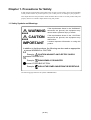
1
To our customers,
Old Company Name in Catalogs and Other Documents
On April 1st, 2010, NEC Electronics Corporation merged with Renesas Technology
Corporation, and Renesas Electronics Corporation took over all the business of both
companies. Therefore, although the old company name remains in this document, it is a valid
Renesas Electronics document. We appreciate your understanding.
Renesas Electronics website: http://www.renesas.com
April 1st, 2010
Renesas Electronics Corporation
Issued by: Renesas Electronics Corporation (http://www.renesas.com)
Send any inquiries to http://www.renesas.com/inquiry.
Notice
1.
2.
3.
4.
5.
6.
7.
All information included in this document is current as of the date this document is issued. Such information, however, is
subject to change without any prior notice. Before purchasing or using any Renesas Electronics products listed herein, please
confirm the latest product information with a Renesas Electronics sales office. Also, please pay regular and careful attention to
additional and different information to be disclosed by Renesas Electronics such as that disclosed through our website.
Renesas Electronics does not assume any liability for infringement of patents, copyrights, or other intellectual property rights
of third parties by or arising from the use of Renesas Electronics products or technical information described in this document.
No license, express, implied or otherwise, is granted hereby under any patents, copyrights or other intellectual property rights
of Renesas Electronics or others.
You should not alter, modify, copy, or otherwise misappropriate any Renesas Electronics product, whether in whole or in part.
Descriptions of circuits, software and other related information in this document are provided only to illustrate the operation of
semiconductor products and application examples. You are fully responsible for the incorporation of these circuits, software,
and information in the design of your equipment. Renesas Electronics assumes no responsibility for any losses incurred by
you or third parties arising from the use of these circuits, software, or information.
When exporting the products or technology described in this document, you should comply with the applicable export control
laws and regulations and follow the procedures required by such laws and regulations. You should not use Renesas
Electronics products or the technology described in this document for any purpose relating to military applications or use by
the military, including but not limited to the development of weapons of mass destruction. Renesas Electronics products and
technology may not be used for or incorporated into any products or systems whose manufacture, use, or sale is prohibited
under any applicable domestic or foreign laws or regulations.
Renesas Electronics has used reasonable care in preparing the information included in this document, but Renesas Electronics
does not warrant that such information is error free. Renesas Electronics assumes no liability whatsoever for any damages
incurred by you resulting from errors in or omissions from the information included herein.
Renesas Electronics products are classified according to the following three quality grades: “Standard”, “High Quality”, and
“Specific”. The recommended applications for each Renesas Electronics product depends on the product’s quality grade, as
indicated below. You must check the quality grade of each Renesas Electronics product before using it in a particular
application. You may not use any Renesas Electronics product for any application categorized as “Specific” without the prior
written consent of Renesas Electronics. Further, you may not use any Renesas Electronics product for any application for
which it is not intended without the prior written consent of Renesas Electronics. Renesas Electronics shall not be in any way
liable for any damages or losses incurred by you or third parties arising from the use of any Renesas Electronics product for an
application categorized as “Specific” or for which the product is not intended where you have failed to obtain the prior written
consent of Renesas Electronics. The quality grade of each Renesas Electronics product is “Standard” unless otherwise
expressly specified in a Renesas Electronics data sheets or data books, etc.
“Standard”:
8.
9.
10.
11.
12.
Computers; office equipment; communications equipment; test and measurement equipment; audio and visual
equipment; home electronic appliances; machine tools; personal electronic equipment; and industrial robots.
“High Quality”: Transportation equipment (automobiles, trains, ships, etc.); traffic control systems; anti-disaster systems; anticrime systems; safety equipment; and medical equipment not specifically designed for life support.
“Specific”:
Aircraft; aerospace equipment; submersible repeaters; nuclear reactor control systems; medical equipment or
systems for life support (e.g. artificial life support devices or systems), surgical implantations, or healthcare
intervention (e.g. excision, etc.), and any other applications or purposes that pose a direct threat to human life.
You should use the Renesas Electronics products described in this document within the range specified by Renesas Electronics,
especially with respect to the maximum rating, operating supply voltage range, movement power voltage range, heat radiation
characteristics, installation and other product characteristics. Renesas Electronics shall have no liability for malfunctions or
damages arising out of the use of Renesas Electronics products beyond such specified ranges.
Although Renesas Electronics endeavors to improve the quality and reliability of its products, semiconductor products have
specific characteristics such as the occurrence of failure at a certain rate and malfunctions under certain use conditions. Further,
Renesas Electronics products are not subject to radiation resistance design. Please be sure to implement safety measures to
guard them against the possibility of physical injury, and injury or damage caused by fire in the event of the failure of a
Renesas Electronics product, such as safety design for hardware and software including but not limited to redundancy, fire
control and malfunction prevention, appropriate treatment for aging degradation or any other appropriate measures. Because
the evaluation of microcomputer software alone is very difficult, please evaluate the safety of the final products or system
manufactured by you.
Please contact a Renesas Electronics sales office for details as to environmental matters such as the environmental
compatibility of each Renesas Electronics product. Please use Renesas Electronics products in compliance with all applicable
laws and regulations that regulate the inclusion or use of controlled substances, including without limitation, the EU RoHS
Directive. Renesas Electronics assumes no liability for damages or losses occurring as a result of your noncompliance with
applicable laws and regulations.
This document may not be reproduced or duplicated, in any form, in whole or in part, without prior written consent of Renesas
Electronics.
Please contact a Renesas Electronics sales office if you have any questions regarding the information contained in this
document or Renesas Electronics products, or if you have any other inquiries.
(Note 1) “Renesas Electronics” as used in this document means Renesas Electronics Corporation and also includes its majorityowned subsidiaries.
(Note 2) “Renesas Electronics product(s)” means any product developed or manufactured by or for Renesas Electronics.
User’s Manual
M302N2T-PRB
User’s Manual
Pod Probe for M302N1 and M302N2 Group
MCUs
Rev.1.00 2003.09
• TQPACK080SB, TQSOCKET080SBG, YQPACK056SB, NQPACK056SB and YQ-GUIDE are products of Tokyo Eletech Corporation.
Keep safety first in your circuit designs!
• Renesas Technology Corporation and Renesas Solutions Corporation put the maximum effort into making semiconductor products better
and more reliable, but there is always the possibility that trouble may occur with them. Trouble with semiconductors may lead to personal
injury, fire or property damage. Remember to give due consideration to safety when making your circuit designs, with appropriate
measures such as (i) placement of substitutive, auxiliary circuits, (ii) use of nonflammable material or (iii) prevention against any
malfunction or mishap.
Notes regarding these materials
• These materials are intended as a reference to assist our customers in the selection of the Renesas Technology product best suited to
the customer's application; they do not convey any license under any intellectual property rights, or any other rights, belonging to Renesas
Technology Corporation, Renesas Solutions Corporation or a third party.
• Renesas Technology Corporation and Renesas Solutions Corporation assume no responsibility for any damage, or infringement of any
third-party's rights, originating in the use of any product data, diagrams, charts, programs, algorithms, or circuit application examples
contained in these materials.
• All information contained in these materials, including product data, diagrams, charts, programs and algorithms represents information
on products at the time of publication of these materials, and are subject to change by Renesas Technology Corporation and Renesas
Solutions Corporation without notice due to product improvements or other reasons. It is therefore recommended that customers contact
Renesas Technology Corporation, Renesas Solutions Corporation or an authorized Renesas Technology product distributor for the latest
product information before purchasing a product listed herein. The information described here may contain technical inaccuracies or
typographical errors. Renesas Technology Corporation and Renesas Solutions Corporation assume no responsibility for any damage,
liability, or other loss rising from these inaccuracies or errors. Please also pay attention to information published by Renesas Technology
Corporation and Renesas Solutions Corporation by various means, including the Renesas home page (http://www.renesas.com).
• When using any or all of the information contained in these materials, including product data, diagrams, charts, programs, and algorithms,
please be sure to evaluate all information as a total system before making a final decision on the applicability of the information and
products. Renesas Technology Corporation and Renesas Solutions Corporation assume no responsibility for any damage, liability or
other loss resulting from the information contained herein.
• Renesas Technology semiconductors are not designed or manufactured for use in a device or system that is used under circumstances
in which human life is potentially at stake. Please contact Renesas Technology Corporation, Renesas Solutions Corporation or an
authorized Renesas Technology product distributor when considering the use of a product contained herein for any specific purposes,
such as apparatus or systems for transportation, vehicular, medical, aerospace, nuclear, or undersea repeater use.
• The prior written approval of Renesas Technology Corporation and Renesas Solutions Corporation is necessary to reprint or reproduce
in whole or in part these materials.
• If these products or technologies are subject to the Japanese export control restrictions, they must be exported under a license from the
Japanese government and cannot be imported into a country other than the approved destination. Any diversion or reexport contrary to
the export control laws and regulations of Japan and/or the country of destination is prohibited.
• Please contact Renesas Technology Corporation or Renesas Solutions Corporation for further details on these materials or the products
contained therein.
Precautions to be taken when using this product
• This product is a development supporting unit for use in your program development and evaluation stages. In mass-producing your
program you have finished developing, be sure to make a judgment on your own risk that it can be put to practical use by performing
integration test, evaluation, or some experiment else.
• In no event shall Renesas Solutions Corporation be liable for any consequence arising from the use of this product.
• Renesas Solutions Corporation strives to renovate or provide a workaround for product malfunction at some charge or without charge.
However, this does not necessarily mean that Renesas Solutions Corporation guarantees the renovation or the provision under any
circumstances.
• This product has been developed by assuming its use for program development and evaluation in laboratories. Therefore, it does not fall
under the application of Electrical Appliance and Material Safety Law and protection against electromagnetic interference when used in
Japan.
For inquiries about the contents of this document or product, fill in the text file the installer of the emulator debugger generates in the
following directory and email to your local distributor.
\SUPPORT\Product-name\SUPPORT.TXT
Renesas Tools Homepage http://www.renesas.com/en/tools
( 2 / 38 )
Preface
The M302N2T-PRB is a pod probe for the M302N1 and M302N2 Group of Renesas 16-bit MCUs.
The M302N2T-PRB is used by connecting to the PC4701 emulator main unit and the M30200T-RPD-E
emulation pod main unit.
This manual mainly explains specifications and how to set up the M302N2T-PRB. For detail
information about the emulator main unit, emulation pod main unit, and emulator debugger, refer to
each user's manual.
Emulator main unit:
Emulation pod main unit:
Emulator debugger:
PC4701 User's Manual
M30200T-RPD-E User's Manual
M3T-PD30 User's Manual
To check the components of this product, refer to "Table 2.1 Package Components" (page 14) in this
manual. If there is any question or doubt about this product, contact your local distributor.
To use the product properly
Precautions for Safety:
• Both in this User's Manual and on the product itself, several icons are used to insure
proper handling of this product and also to prevent injuries to you or other persons,
or damage to your properties.
• The icons' graphic images and meanings are given in "Chapter 1. Precautions for
Safety". Be sure to read this chapter before using the product.
( 3 / 38 )
Contents
Terminology ........................................................................................................................... 5
Chapter 1. Precautions for Safety ........................................................................................... 7
1.1 Safety Symbols and Meanings .............................................................................. 8
Chapter 2. Preparation .......................................................................................................... 13
2.1 Package Components .......................................................................................... 14
2.2 Other Tool Products Required for Development ................................................ 14
2.3 System Configuration .......................................................................................... 15
Chapter 3. Setting Up ........................................................................................................... 17
3.1 Switch Settings .................................................................................................... 18
3.2 A-D Conversion Bypass Capacitor ..................................................................... 19
3.3 Connecting the M30200T-RPD-E ....................................................................... 20
3.4 Connecting the Target System ............................................................................ 21
3.5 Procedure for Making MCU File for M3T-PD30 ............................................... 24
Chapter 4. Specifications ...................................................................................................... 25
4.1 Specifications ...................................................................................................... 26
4.2 External Dimensions ........................................................................................... 27
(1) External Dimensions of Pod Probe .......................................................... 27
(2) External Dimensions of Converter Board (FLX-80QSB) ........................ 27
(3) External Dimensions of Converter Board (M302N1T-56FPB) ............... 28
Chapter 5. Troubleshooting .................................................................................................. 29
5.1 When the Emulator Debugger Does Not Start Up Properly ............................... 30
(1) When the LED Display of PC4701 is Abnormal ..................................... 30
(2) Errors Occur When Starting Up the Emulator Debugger
(When the target system is connected) .................................... 31
(3) Errors Occur When Starting Up the Emulator Debugger
(When the target system is not connected) ............................. 32
5.2 Operation Differs from That of Actual MCUs .................................................... 32
Chapter 6. Maintenance and Warranty ................................................................................. 33
6.1 Maintenance ........................................................................................................ 34
6.2 Warranty .............................................................................................................. 34
6.3 Repair Provisions ................................................................................................ 34
6.4 How to Request for Repair .................................................................................. 35
( 4 / 38 )
Terminology
Some specific words used in this user's manual are defined as follows:
Emulation pod main unit
This means the emulation pod M30200T-RPD-E for the M16C/20 Series MCUs.
Emulator debugger
This means a software tool M3T-PD30 to control the emulator from the host machine through an
interface.
Emulator main unit (Hereafter PC4701)
This means the generic name for emulators for 8 and 16-bit MCUs. For details on specific models
of PC4701, visit Renesas Tools Homepage at http://www.renesas.com/en/tools
Emulator system
This means an emulator system built around the PC4701 emulator. The PC4701 emulator system is
configured with an emulator main unit, emulation pod, pod probe, host machine and emulator
debugger.
Evaluation MCU
This means the microcomputer mounted on the emulation pod which is operated in the specific mode
for tools.
Firmware
Program that analyzes contents of communication with the emulator debugger and controls the
emulator hardware. This program is installed in the EEPROM. This program is downloadable from
the emulator debugger to upgrade the firmware or to support other MCUs.
Hardware break
A hardware break is a function to break the program when the system detects a write/read of data to/
from memory or a rise/fall edge of the signal entered from the external trace cable. The former break
function is called address break; and the latter break function is called trigger break. While the
instruction at the address where the software break is set is not executed, a hardware break is
performed after the specified instruction is executed.
Host machine
This means a personal computer used to control the emulator and emulation pod.
Pod probe
This means pod probe M302N2T-PRB (this product) for the M302N1 and M302N2 Groups.
Software break
A software break is a function to break the program before the system executes an instruction at the
specified address. The instruction at the preset address will not be executed.
Target MCU
This means the MCU you are going to debug.
Target system
This means a user's application system using the MCU to be debugged.
*
In this user's manual, this symbol is used to show active LOW. (e.g. RESET*: Reset signal)
( 5 / 38 )
MEMO
( 6 / 38 )
Chapter 1. Precautions for Safety
This chapter describes precautions for using this product safely and properly. For precautions for the emulator main unit,
the emulation pod main unit and the emulator debugger, refer to each user's manual included with your product.
1.1 Safety Symbols and Meanings ..................................................................................................... 8
IMPORTANT
Note on Final Evaluation ............................................................................................. 9
Note on Differences from Actual MCUs ..................................................................... 9
Note on Clock Supply to the MCU ............................................................................ 10
Notes on Interruption ................................................................................................. 10
Note on the Work Area .............................................................................................. 11
Note on MAP References and Settings ...................................................................... 11
Note on Accessing SFR Area .................................................................................... 11
Note on Commands that Access the Single-step Interrupt Vector Area .................... 11
( 7 / 38 )
Chapter 1. Precautions for Safety
In both the user's manual and on the product itself, several icons are used to insure proper handling
of this product and also to prevent injuries to you or other persons, or damage to your properties.
This chapter describes the precautions which should be taken in order to use this product safely and
properly. Be sure to read this chapter before using this product.
1.1 Safety Symbols and Meanings
WARNING
If the requirements shown in the "WARNING"
sentences are ignored, the equipment may
cause serious personal injury or death.
CAUTION
If the requirements shown in the "CAUTION"
sentences are ignored, the equipment may
malfunction.
IMPORTANT
It means important information on using this
product.
In addition to the three above, the following are also used as appropriate.
means WARNING or CAUTION.
Example:
CAUTION AGAINST AN ELECTRIC SHOCK
means PROHIBITION.
Example:
DISASSEMBLY PROHIBITED
means A FORCIBLE ACTION.
Example:
UNPLUG THE POWER CABLE FROM THE RECEPTACLE.
The following pages describe the symbol "IMPORTANT".
( 8 / 38 )
IMPORTANT
Note on Final Evaluation:
• Be sure to evaluate your system and make final confirmation with an CS (Commercial Sample)
version MCU.
Note on Differences from Actual MCUs:
• Operations of the emulator system differ from those of mask MCUs as listed below.
(1) Initial values of internal resource data at power-on
(2) Internal memories (ROM and RAM) capacities, etc.
With this emulator system, "INT" (emulation memory ON) is the default for mapping areas
other than the SFR area (addresses 000h - 3FFh). For this reason, the emulation memory can
read and write in areas other than the SFR, internal RAM and internal ROM.
(3) Oscillator circuit
• Make note of the fact that in the oscillator circuit where a resonator is connected between
the XIN and XOUT pins, oscillation does not occur because a flexible cable, buffer IC and other
devices are used between the evaluation MCU and the target system. It is same for sub-clock
oscillator circuits (XCIN and XCOUT ).
• For note on when using the oscillator circuit on the target system, refer to "4.2 (2) Using
target system's oscillator" (page 21) of the M30200T-RPD-E User's Manual.
(4) XOUT pin
The XOUT pin is not assigned to the evaluation MCU used by this product. For this reason, the
XOUT pin of this product is open.
(5) DBC, single-step and BRK instruction interrupt vector table addresses
It is possible to download to DBC, single-step and BRK instruction interrupt vector table
addresses. However, because the emulator system uses these areas, data different from the
expected value is read out.
Table 1.1 Vector table addresses for the emulator
Factor of interruption
DBC*
Vector table addresses
1
Data for reading
FFFF4h - FFFF7h
Indefinite
Single-step*1
FFFECh - FFFEFh
Indefinite
BRK instruction*1
FFFE4h - FFFE7h
Indefinite
*1 Interruption for the debugger only
(6) A-D conversion
The characteristics of A-D converter differ from those of actual MCU because there are a
flexible cable, pitch converter and other devices between the evaluation MCU and the target
system. Make the final evaluation of the A-D converter with the actual MCU.
( 9 / 38 )
IMPORTANT
Note on Clock Supply to the MCU:
• Clock can be supplied to the evaluation MCU in one of the following two ways. This is determined
by emulator debugger clock selection.
(1) When Internal is selected:
The clock generated by the oscillation circuit in the emulation pod is supplied to the evaluation
MCU. The clock is continually supplied to the evaluation MCU regardless of "target system
clock status" and "user program execution status".
(2) When External is selected:
Clock supply to the evaluation MCU depends on oscillation status (oscillate/off) of the target
system.
Notes on Interruption:
• Even when the target program is not being executed (while the target program is stopped or during
runtime debugging), the emulation MCU keeps running so as to control the emulation pod.
Therefore, note that timers and other components do not stop running even though the target
program is not being executed.
• If a maskable interrupt request is generated when the target program is not being executed (while
the target program is stopped or during runtime debugging), the request is not accepted because the
emulator disables all interrupts. If an interrupt request is generated when the target program is not
being executed, but the target program enables that interrupt, it will be accepted immediately after
program execution starts.
( 10 / 38 )
IMPORTANT
Note on the Work Area:
• When using this product, set to "2C00h" as a start address of the work area at the time of starting
up the emulator debugger (set by "F/W and Work Area" tab*1 of Init dialog). In this case, the
emulator system uses the area below as a work area.
02C00h - 02C0Fh: Work area
*1 Supported by M3T-PD30 Ver.4.00 or later
Note on MAP References and Settings:
• When starting up the M30200T-RPD-E, initial MAP settings are as follows. Use generally the
M30200T-RPD-E in this setting.
00000h to 003FFh: "EXT"
00400h to FFFFFh: "INT" (emulation memory available)
Note on Accessing SFR Area:
• Access the below four registers by byte. They cannot be correctly accessed by word.
003FCh:
003FDh:
003FEh:
003FFh:
Pull-up control register 0 (PUR0)
Up control register 1 (PUR1)
Port P1 drive capacity control register (DDR)
Up control register 2 (PUR2)
Note on Commands that Access the Single-step Interrupt Vector Area:
• Do not perform the below debugging operations with the single step interrupt vector area (addresses
FFFECh - FFFEFh).
(1) Step execution of commands that access the single step interrupt vector area
(2) Program execution using commands that access the single step interrupt vector area when a
software breakpoint is set in those commands
( 11 / 38 )
MEMO
( 12 / 38 )
Chapter 2. Preparation
This chapter describes the package components, the system configuration and the preparation for using this product for the
first time.
2.1 Package Components.................................................................................................................. 14
2.2 Other Tool Products Required for Development........................................................................ 14
2.3 System Configuration ................................................................................................................. 15
( 13 / 38 )
Chapter 2. Preparation
2.1 Package Components
This product consists of the following items. When unpacking, check to see if your product package
contains all of these items.
Table 2.1 Package components
Item
Quantity
M302N2T-PRB pod probe for M302N1 and M302N2 Group MCUs
1
Screws (screws for fixing pod probe: pre-installed to the pod probe)
2
FLX-80QSB converter board for 80-pin 0.65-mm-pitch QFP (80P6S-A)
1
M302N2T-PRB User's Manual (this manual)
1
M302N2T-PRB User's Manual (Japanese)
1
M302N2T-PRB Repair Request Sheet (English/Japanese)
1
Please keep the M302N2T-PRB's packing box and cushion material in your place for reuse at a later
time when sending your product for repair or other purposes. Always use these packing box and
cushion material when transporting the M302N2T-PRB.
If any of these items are missing or found faulty, please contact your local distributor. Also, if there
is any question or doubt about the packaged product, contact your local distributor.
2.2 Other Tool Products Required for Development
To bring forward programs development on the M302N1 and M302N2 Group MCUs, the products
listed below are necessary in addition to the package components listed above. Get them separately.
Table 2.2 Other tool products
Emulator main unit
PC4701
Emulation pod main unit
M30200T-RPD-E
Emulator debugger
M3T-PD30 Ver.4.00 or later
Converter board
M302N1T-56FPB converter board for M302N1 Group MCUs
(Necessary for evaluating M302N1 Group MCUs)
To purchase these products, contact your nearest distributer.
( 14 / 38 )
2.3 System Configuration
Figure 2.1 System configuration
Products (1) and (2) shown in Figure 2.1 are included with this product. Get (3) and (4) separately.
(1) Pod probe (M302N2T-PRB)
This pod probe is equipped with the evaluation MCU (M302NX-OTHERS).
(2) FLX-80QSB (converter board for 80-pin 0.65-mm-pitch QFP)
This is a pitch converter board (included) used for evaluating the M302N2 Group MCUs.
(3) DIRECT80S (converter board for 80-pin 0.65-mm-pitch QFP)
This is a pitch converter board (separately available) used for evaluating the M302N2 Group
MCUs.
(4) M302N1T-56FPB (converter board for 56-pin 0.65-mm-pitch QFP)
This is a pitch converter board (separately available) used for evaluating the M302N1 Group
MCUs.
For details on the connection, refer to "3.4 Connecting the Target System" (page 21).
( 15 / 38 )
MEMO
( 16 / 38 )
Chapter 3. Setting Up
This chapter describes switch settings required for using this product and how to connect this product to the PC4701 and
the target system.
3.1 Switch Settings ........................................................................................................................... 18
3.2 A-D Conversion Bypass Capacitor ............................................................................................ 19
3.3 Connecting the M30200T-RPD-E .............................................................................................. 20
3.4 Connecting the Target System.................................................................................................... 21
3.5 Procedure for Making MCU File for M3T-PD30 ...................................................................... 24
( 17 / 38 )
Chapter 3. Setting Up
With this product, it is necessary to set the following according to your target system.
• Switching ports (P70 and P71) and sub-clock
• Mounting the A-D conversion bypass capacitor
3.1 Switch Settings
It is necessary to set the switches of the FLX64-PRB for debugging according to the target system.
Figure 3.1 shows the positions of the switches of the FLX64-PRB, and Table 3.1 shows the switch
settings.
Figure 3.1 Positions of the switches and their factory-settings
Table 3.1 Switch settings of the FLX64-PRB
Switch No.
Function
Switch setting
PORT
JP1
Switches
P71/XCIN
XCIN
When using the port function (P71)
(Factory-setting)
PORT
JP2
PORT
XCIN
When using the sub-clock
PORT
Switches
P70/NC
NC
When using the port function (P70)
(Factory-setting)
NC
When using the sub-clock
IMPORTANT
Note on Settings of JP1 and JP2:
• Change the switch setting of JP1 and JP2 at the same time as shown in Table 3.1.
( 18 / 38 )
3.2 A-D Conversion Bypass Capacitor
This product has foot patterns on the board for mounting a bypass capacitor for the A-D converter
circuit. Mount a suitable bypass capacitor as occasion demands.
Figure 3.2 shows the position of the bypass capacitor.
Figure 3.2 Foot patterns of A-D conversion bypass capacitor
IMPORTANT
Note on the Operation of A-D Converter:
• The characteristics of A-D converter differ from those of actual MCU because there
are a flexible cable and other devices between the evaluation MCU and the target
system. Make the final evaluation of the A-D converter with the actual MCU.
( 19 / 38 )
3.3 Connecting the M30200T-RPD-E
The emulation pod for M302N1 and M302N2 Group MCUs consists of the two products, the
M30200T-RPD-E emulation pod and the M302N2T-PRB pod probe. Figures 3.3 and 3.4 show how
to connect the M30200T-PRB and how to remove it, respectively.
(1) Connect the J1 and J2 connectors of the M302N2TPRB to the J3 and J4 connectors of the FLX64-PRB.
(2) Fix the FLX64-PRB by the two screws.
Figure 3.3 Connecting pod probe M302N2T-PRB
(1) Unscrew the two screws of the M302N2T-PRB.
(2) Remove the M302N2T-PRB from the FLX64-PRB. In
this time, lift off the M302N2T-PRB horizontally.
Otherwise, the connector may cause a break.
Figure 3.4 Removing pod probe M302N2T-PRB
CAUTION
When Connecting Pod Probe:
• Be sure to turn off the power before making connections. Otherwise, the internal
circuits may be damaged.
• The small connectors of the FLX64-PRB (J3 and J4) and M302N2T-PRB (J1 and
J2) are guaranteed for only 50 insertion/removal iterations.
( 20 / 38 )
3.4 Connecting the Target System
There are three ways available to connect this product to target systems as shown in Figure 3.5.
Figure 3.5 Connecting the target system
CAUTION
Notes on Connecting the Target System:
• Always shut OFF power before connecting the target system.
• The small connectors of the M302N2T-PRB (J3 and J4) are guaranteed for only 20
insertion/removal iterations.
( 21 / 38 )
The emulation pod for M302N2 Group needs the pitch converter board FLX-80QSB or DIRECT80S
and the emulation pod for M302N1 Group needs the pitch converter board M302N1T-56FPB.
Figures 3.6 and 3.7 show how to connect the pitch converter board FLX-80QSB for 80-pin QFP and
how to connect the pitch converter board M302N1T-56FPB for 56-pin QFP, respectively.
(1) Mount the included TQPACK080SB to the target
system.
(2) Connect the included TQSOCKET080SBG to the
TQPACK080SB.
(3) Connect the FLX-80QSB to the TQSOCKET080SBG.
(4) Connect the M302N2T-PRB to the FLX-80QSB.
Figure 3.6 Connecting the pitch converter board FLX-80QSB for 80-pin QFP
CAUTION
Note on Connecting the Target System:
• Take care not to attach the pitch converter board to the socket in an inverted position.
( 22 / 38 )
Figure 3.7 shows how to connect the pitch converter board M302N1T-56FPB for 56-pin 0.65-mmpitch QFP.
(1) Mount the NQPACK056SB to the target system.
(2) Fix the YQPACK056SB to the NQPACK056SB
using the included YQ-GUIDE's.
(3) Connect the M302N1T-56FPB along the YQGUIDE's.
(4) Connect the M302N2T-PRB.
Figure 3.7 Connecting the pitch converter board M302N1T-56FPB for 56-pin QFP
CAUTION
Note on Connecting the Target System:
• Take care not to attach the pitch converter board to the socket in an inverted position.
( 23 / 38 )
3.5 Procedures for Making MCU File for M3T-PD30
It is necessary to change the contents of the MCU file according to the MCU to be developed. Make
the MCU file M302N1.MCU for M302N1 Group and M302N2.MCU for M302N2 Group and store
it in the following directory (the directory varies depending on the version of the M3T-PD30).
• M3T-PD30 Ver.5.00 or later: Store the MCU file in the "Mcufiles" folder in the directory same
as emulator debugger M3T-PD30 is stored.
• M3T-PD30 Ver.4.10 or earlier: Store the MCU file in the folder same as emulator debugger
M3T-PD30.
The contents of the MCU file (the SFR area, internal RAM area, internal ROM area, the name of
firmware file) are shown below. Change the settings according to the MCU to be debugged. Use your
text editor for changing the MCU file. The parts listed in boldface with an underline are to be changed.
The contents of the MCU file are as follows:
(1) For M302N2FCTGP (M302N2.MCU)
0
3FF
400
17FF
E0000
FFFFF
M30620B
0
: SFR area
Start address
:
End address
: Internal RAM
Start address
:
End address
: Internal ROM
Start address
:
End address
: Name of firmware (Do not change.)
: Expansion No.
M3T-PD30 V.4.00 or later required (Do not change.)
(2) For M302N1M4T-xxxFP (M30217.MCU)
0
3FF
400
BFF
E8000
FFFFF
M30620B
0
: SFR area
Start address
:
End address
: Internal RAM
Start address
:
End address
: Internal ROM
Start address
:
End address
: Name of firmware (Do not change.)
: Expansion No.
M3T-PD30 V.4.00 or later required (Do not change.)
( 24 / 38 )
Chapter 4. Specifications
This chapter describes specifications of this product.
4.1 Specifications ............................................................................................................................. 26
4.2 External Dimensions .................................................................................................................. 27
(1) External Dimensions of Pod Probe ....................................................................................... 27
(2) External Dimensions of Converter Board (FLX-80QSB) .................................................... 27
(3) External Dimensions of Converter Board (M302N1T-56FPB) ............................................ 28
( 25 / 38 )
Chapter 4. Specifications
4.1 Specifications
Table 4.1 lists the specifications of the M302N2T-PRB.
Table 4.1 Specifications of M302N2T-PRB
Emulator
PC4701
Emulation pod main unit
M30200T-RPD-E
Applicable MCUs
M302N1 and M302N2 Group MCUs
Usable MCU mode
Single-chip mode
Emulation memory
1 MB
Max. operating frequency
XIN = 10.0 MHz (no-wait, 4.2 - 5.5 V)
Operating power voltage
4.2 - 5.5 V
Stack capacity for the emulator
Max. 8 bytes
Suspended cycles in run-time debug
16-byte dump:
16-byte fill:
Power supply to emulation pod
1. Supplied from the emulator main unit
2. The operating voltage of the emulation pod main unit is
determined by detecting the supply voltage of the target
system. When no target system is connected, or when the
supply voltage of the target system is more than 5.0 V, the
operating voltage is 5.0 V.
Operating temperature range
5 to 35°C (no dew)
Storage temperature range
-10 to 60°C (no dew)
Connection to the target system
See "3.4 Connecting the Target
System" (page 21).
M302N2 Group: for 80-pin 0.65-mm-pitch QFP (80P6S-A)
FLX-80QSB (included) or DIRECT80S (not included)
approx. 312 BCLK cycle
approx. 283 BCLK cycle
M302N1 Group: for 56-pin 0.65-mm-pitch QFP (56P6S-A)
M302N1T-56FPB (not included)
( 26 / 38 )
4.2 External Dimensions
(1) External Dimensions of Pod Probe
Figure 4.1 shows the external dimensions of the pod probe M302N2T-PRB.
Unit: mm
Figure 4.1 External dimensions of the pod probe M302N2T-PRB
(2) External Dimensions of Converter Board (FLX-80QSB)
Figure 4.2 shows the external dimensions and a sample foot pattern of the pitch converter board FLX80QSB for 80-pin 0.65-mm-pitch QFP.
Unit: mm
Figure 4.2 External dimensions of the FLX-80QSB
( 27 / 38 )
(3) External Dimensions of Converter Board (M302N1T-56FPB)
Figure 4.3 shows the external dimensions and a sample foot pattern of the pitch converter board
M302N1T-56FPB for 56-pin 0.65-mm-pitch QFP.
Unit: mm
Figure 4.3 External dimensions of the M302N1T-56FPB
( 28 / 38 )
Chapter 5. Troubleshooting
This chapter describes how to troubleshoot when this product does not work properly.
5.1 When the Emulator Debugger Does Not Start Up Properly....................................................... 30
(1) When the LED Display of PC4701 is Abnormal .................................................................. 30
(2) Errors Occur When Starting Up the Emulator Debugger
(When the target system is connected) .................................................................. 31
(3) Errors Occur When Starting Up the Emulator Debugger
(When the target system is not connected) ........................................................... 32
5.2 Operation Differs from That of Actual MCUs ........................................................................... 32
( 29 / 38 )
Chapter 5. Troubleshooting
When this product does not work properly, check the following.
5.1 When the Emulator Debugger Does Not Start Up Properly
(1) When the LED Display of PC4701 is Abnormal
Table 5.1 LED's abnormal display and its checkpoints
Error
LEDs do not light up.
Connection to
the target system
Checkpoint
-
Recheck the power cable is connected to the
PC4701.
See the PC4701 User's Manual.
(1) Recheck the connection between the
M30200T-RPD-E and this product.
All LEDs remain lit.
-
See "3.3 Connecting the M30200T-RPD-E"
(page 20).
(2) Recheck the connection between the PC4701
and the M30200T-RPD-E.
See the M30200T-RPD-E User's Manual.
The POWER LED of
"STATUS OF TARGET"
does not light up.
Connected
Check power is properly supplied to the target
system and that the target system is properly
grounded.
(1) Check that both the main and sub clocks of the
emulator debugger are not set to "EXT".
Disconnected
See the CLK command of the emulator
debugger.
(2) Check the oscillation circuit in the M30200TRPD-E is oscillating.
The CLOCK LED of
"STATUS OF TARGET"
does not light up.
See the M30200T-RPD-E User's Manual.
Connected
(1) Check the oscillation circuit in the target system
is oscillating properly.
(2) Check the switches of the FLX64-PRB are
correctly set.
See "3.1 Switch Settings" (page 18).
The RESET LED of
"STATUS OF TARGET"
does not go out.
Connected
( 30 / 38 )
Check if the reset pin of the target system is pulled
up.
(2) Errors Occur When Starting Up the Emulator Debugger
(When the target system is connected)
Table 5.2 Checkpoints of errors when starting up the emulator debugger (target is connected)
Error
Checkpoint
Communication ERROR
Data is not sent to the target
Check all emulator debugger settings, interface cable
connections and switches on the rear of the PC4701
match.
See the user's manuals of the PC4701 and emulator
debugger.
Target system is not constructed properly (1) Download the proper firmware.
See the user's manual of the emulator debugger.
(2) Recheck the connection between the M30200T-RPDE and this product.
See "3.3 Connecting the M30200T-RPD-E" (page 20).
(3) Recheck the connection between the PC4701 and
the M30200T-RPD-E.
See the M30200T-RPD-E User's Manual.
The version of M3T-PD30 and the firmware Download the proper firmware.
on the target system are not same
See the user's manual of the emulator debugger.
Target MCU is reset state
(1) Check the reset pin of the target system is pulled up.
(2) Check the reset pin of the target system has changed
from "L" to "H" level.
Target MCU cannot be reset
(1) If the reset circuit of the target system has a watchdog
timer, disable the timer.
(2) Check power is properly supplied to the target system
and that the target system is properly grounded.
Target MCU is in "HOLD" state
The MCU is either in the stop mode or wait mode. Either
reset the MCU or cancel the mode with an interrupt.
See MCU specifications.
Target clock is stopped
(1) Check the oscillation circuit in the target system is
oscillating properly.
(2) Check the switches of the FLX64-PRB are correctly
set.
See "3.1 Switch Settings" (page 18).
Target MCU is not receiving power
( 31 / 38 )
Check power is properly supplied to the target system
and that the target system is properly grounded.
(3) Errors Occur When Starting Up the Emulator Debugger
(When the target system is not connected)
Table 5.3 Checkpoints of errors when starting up emulator debugger (target is not connected)
Error
Checkpoint
Communication ERROR
Data is not sent to the target
Check all emulator debugger settings, interface cable
connections and switches on the rear of the PC4701
match.
See the user's manuals of the PC4701 and emulator
debugger.
Target system is not constructed properly (1) Download the proper firmware.
See the user's manual of the emulator debugger.
(2) Recheck the connection between the M30200T-RPDE and this product.
See "3.3 Connecting the M30200T-RPD-E" (page 20).
(3) Recheck the connection between the PC4701 and
the M30200T-RPD-E.
See the M30200T-RPD-E User's Manual.
The version of M3T-PD30 and the firmware Download the proper firmware.
See the user's manual of the emulator debugger.
on the target are not same
The MCU is either in the stop mode or wait mode. Either
reset the MCU or cancel the mode with an interrupt.
Target MCU is in "HOLD" state
See MCU specifications.
Check the switches of the FLX64-PRB are correctly set.
Target clock is stopped
See "3.1 Switch Settings" (page 18).
5.2 Operation Differs from That of Actual MCUs
Make note of the fact that the operation when using the emulation pod differs from that of actual
MCUs as follows.
(1) Initializing the internal resources of MCU at power-on
(2) Internal memories (ROM and RAM) capacities, etc.
With this emulator system, "INT" (emulation memory ON) is the default for mapping areas other
than the SFR area (addresses 000h - 3FFh). For this reason, the emulation memory can read and
write in areas other than the SFR, internal RAM and internal ROM.
(3) Oscillator circuit
• Make note of the fact that in the oscillator circuit where a resonator is connected between the
XIN and XOUT pins, oscillation does not occur because a flexible cable, buffer IC and other devices
are used between the evaluation MCU and the target system. It is same for sub-clock oscillator
circuits (XCIN and XCOUT ).
• For note on when using the oscillator circuit on the target system, refer to "4.2 (2) Using target
system's oscillator" (page 21).
(4) XOUT pin
The XOUT pin is not assigned to the evaluation MCU used by this product. For this reason, the XOUT
pin of this product is open.
(5) DBC, single-step and BRK instruction interrupt vector table addresses
It is possible to download to DBC, single-step and BRK instruction interrupt vector table
addresses. However, because the emulator system uses these areas, data different from the
expected value is read out.
(6) A-D conversion
The characteristics of A-D converter differ from those of actual MCU because there are a flexible
cable, pitch converter and other devices between the evaluation MCU and the target system. Make
the final evaluation of the A-D converter with the actual MCU.
( 32 / 38 )
Chapter 6. Maintenance and Warranty
This chapter describes how to maintenance, repair provisions and how to request for repair.
6.1 Maintenance ............................................................................................................................... 34
6.2 Warranty ..................................................................................................................................... 34
6.3 Repair Provisions........................................................................................................................ 34
6.4 How to Request for Repair ......................................................................................................... 35
( 33 / 38 )
Chapter 6. Maintenance and Guarantee
6.1 Maintenance
If dust or dirt collects on any equipment of your emulation system, wipe it off with a dry soft cloth.
Do not use thinner or other solvents because these chemicals can cause the equipment's surface
coating to separate.
6.2 Guarantee
If your product becomes faulty within twelve months after its purchase while being used under good
conditions by observing "Precautions for Safety" described in Chapter 1 of this user's manual, we will
repair or replace your faulty product free of charge. Note, however, that if your product's fault is raised
by any one of the following causes, we will repair it or replace it with new one with extra-charge:
• Misuse, abuse, or use under extraordinary conditions
• Unauthorized repair, remodeling, maintenance, and so on
• Inadequate user's system or misuse of it
• Fires, earthquakes, and other unexpected disasters
In the above cases, contact your local distributor. If your product is being leased, consult the leasing
company or the owner.
6.3 Repair Provisions
(1) Repair with extra-charge
The products elapsed more than twelve months after purchase can be repaired with extra-charge.
(2) Replacement with extra-charge
If your product's fault falls in any of the following categories, the fault will be corrected by
replacing the entire product instead of repair, or you will be advised to purchase new one,
depending on the severity of the fault.
• Faulty or broken mechanical portions
• Flaw, separation, or rust in coated or plated portions
• Flaw or cracks in plastic portions
• Faults or breakage caused by improper use or unauthorized repair or modification
• Heavily damaged electric circuits due to overvoltage, overcurrent or shorting of power supply
• Cracks in the printed circuit board or burnt-down patterns
• Wide range of faults that makes replacement less expensive than repair
• Unlocatable or unidentified faults
(3) Expiration of the repair period
When a period of twelve months elapses after the model was dropped from production, repairing
products of the model may become impossible.
(4) Transportation fees at sending your product for repair
Please send your product to us for repair at your expense.
( 34 / 38 )
6.4 How to Request for Repair
If your product is found faulty, follow the procedure below to send your product for repair.
Customer
Fill in the Repair Request Sheet included with this product, then send it
along with this product for repair to your local distributor. Make sure
that information in the Repair Request Sheet is written in as much detail
as possible to facilitate repair.
Distributor
After checking the contents of fault, the distributor should please send
the faulty product along with the Repair Request Sheet to Renesas
Solutions Corp.
Renesas Solutions
When the faulty product is repaired, it will be returned to the customer
at the earliest convenience.
CAUTION
Note on Transporting the Product:
• When sending your product for repair, use the packing box and cushion material supplied with this
product when delivered to you and specify handling caution for it to be handled as precision
equipment. If packing of your product is not complete, it may be damaged during transportation.
When you pack your product in a bag, make sure to use conductive polyvinyl supplied with this
product (usually a blue bag). When you use other bags, they may cause a trouble on your product
because of static electricity.
( 35 / 38 )
MEMO
( 36 / 38 )
M302N2T-PRB User's Manual
Rev.1.00
September 1, 2003
REJ10J0282-0100Z
COPYRIGHT ©2003 RENESAS TECHNOLOGY CORPORATION
AND RENESAS SOLUTIONS CORPORATION ALL RIGHTS RESERVED
M302N2T-PRB
User’s Manual
1753, Shimonumabe, Nakahara-ku, Kawasaki-shi, Kanagawa 211-8668 Japan
REJ10J0282-0100Z