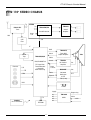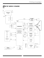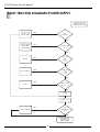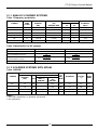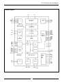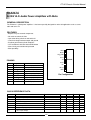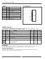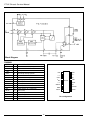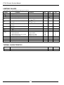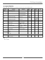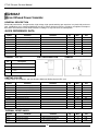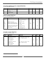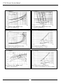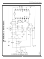
1
SERVICE MANUAL
PT92 CHASSIS
Modification reserved
PT-92 Chassis Service Manual
CONTENTS
PAGE
1.Technical Data
2. Recommendation for service repairs
3. Handling of MOS chip components
4. X-Ray radiation precaution
5. Service Menu
6. Specification of the connector (Euroscart)
7. Component descriptions
8. Block Diagrams
9. Fault tracing diagram-power supply
10. Power Supply circuit diagram
11. Troubleshooting guide for main PCB
12. Descriptions of the integrated circuits
-
TDA16846
TDA935X
TDA9875A
TDA9870A
TDA24C16
TDA8351
TDA8356
TDA2616
TDA2615
TDA7056
TDA7057AQ
TDA7050
TDA6107Q
TCDT1100
TDA9830
SAA7710T
BU2508AF
BU508DF
SPP03N60S5
SPP04N60S5
SMPS IC
UOC IC
TV SOUND IC (STEREO)
TV SOUND IC (G. STEREO)
EEPROM
VERTICAL IC (110O)
VERTICAL IC (90O)
STEREO AUDIO AMPLIFIER (110O)
STEREO AUDIO AMPLIFIER (90O)
MONO AUDIO AMPLIFIER (90O)
HP AMPLIFIER
HP AMPLIFIER
VIDEO OUTPUT AMPLIFIER
OPTOCOUPLER
TV SOUND AM DEMODULATOR
DOLBY PRO LOGIC SURROUND
HORIZONTAL TRANSISTOR (110O)
HORIZONTAL TRANSISTOR (90O)
SMPS MOSFET (90O)
SMPS MOSFET (110O)
13. Dolby and secam L mono board and circuits diagrams
14. Oscilloscope shapes
3
4
5
5
5
6
9
10
11
14
15
16
17
21
28
35
45
47
51
55
57
60
62
64
67
69
71
75
80
83
86
88
90
93
PT-92 Chassis Service Manual
TECHNICAL DATA
CRT PANEL
Visible Picture
Deflection Angle
Vertical Frequency
Horizontal Frequency
47” / 50 cm / 66 cm
90o / 110o
50Hz
15.625Hz
ELECTRONIC
Program Number
Teletext
Tuner
TV System
Music Power
100+AV
Flof text
Cable tuner - 8 MHz spacing for Hyper Band
European CCIR system
90o 2x8 Watt Rms 10% distortion
110o 2x4 Watt Rms 10% distortion
CONNECTIONS
Euro AV Socket
Include
MAIN STAGE
Mains Voltage
Mains Frequency
Power Consumption
In Stby Mode
165-260VAC
50Hz
110o 126 W; 90o 75 W
110o 8 W; 90o 5 W
4
PT-92 Chassis Service Manual
RECOMMENDATION FOR SERVICE REPAIRS
ve a shock hazard from the receiver.
Servicing should not be attempted by anyone who is
not thoroughly familiar with the precautions
necessary when working on high voltage equipment.
Perfectly discharge the high potential of the picture
tube before handling the tube. The picture tube is
highly evacuated and if broken.
Glass fragments will be violently expelled.
Always discharge the picture tube anode to the receiver chassis to keep of the shock hazard before removing the anode cap.
8- Keep wire away from the high voltage or high temperature components.
9- When replacing a wattage resistor in circuit board,
keep the resistor 10 mm away from circuit board.
1- Use only original spare parts. Only use components
with the same specifications for replacement.
2- Original fuse value only should be used.
3- Main leads and connecting leads should be checked
for external damage before connection.
Check the insulation.
4- Parts contributing to the safety of the product must
not be damaged or obviously unsuitable.
This is valid especially for insulators and insulating
parts.
5- Thermally loaded solder pads are to be sucked off
and re-soldered.
6- Ensure that the ventilation slots are not obstructed.
7- Potentials as high as 25 KV are present when this receiver is operating. Operation of the receiver
outside the cabinet or with back cover removed invol-
HANDLING OF MOS CHIP COMPONENTS
MOS circuit requires special attention with regard to
static charges. Static charges may occur with any highly insulating plastics and can be transferred to persons
wearing clothes and shoes made of synthetic materials. Protective circuits on the inputs and outputs of mos
circuits give protection to a limited extend only due to
time of reaction.
Please observe the following instructions to protect the
components against damage from static charges.
red in styropor materials or plastic magazines.
2- Persons have to rid themselves of electrostatic charges by touching MOS components.
3- Hold the component by the body touching the terminals.
4- Use only grounded instruments for testing and processing purposes.
5- Remove or connect MOS ICs when operating voltage is disconnected.
1- Keep mos components in conductive package until
they are used. Most components must never be sto-
X-RAY RADIATION PRECAUTION
1- Excessive high voltage can be produce potentially
hazardous X-RAY radiation. To avoid such hazard,
the high voltage must not be above the specified limit. The nominal value of the high voltage of this receiver is 25KV at zero beam current (minimum
brightness) under 220V AC power source. The high
voltage must not under any circumstance, exceed
30KV. It is recommended the reading of the high vol-
tage be recorded as a part of the service record. It is
important to use an accurate and reliable high voltage meter.
2- The primary source of X-RAY radiation in this TV receiver is the picture tube. For continued X-RAY radiation protection, the replacement tube must be
exactly the same type tube as specified in the part
list.
5
PT-92 Chassis Service Manual
SERVICE MENU
The service menu is entered by pressing the <SUB-PAGE> key on the RC and VOLUME-DOWN key on the TV simultaneously when the TV is in TV- mode. The service menu is left by pressing the <TV> key.
When entering the service mode the first menu item is IF (selection of normal IF). Next items can be selected using the keys
<PROGRAM-UP> and <PROGRAM-DOWN>. The value of each item can be changed using the keys <VOLUME-UP> and
<VOLUME-DOWN>. The item values are displayed as decimal values, except for the tuner-band-selection, BITS and option
items.
They are displayed as hexa-decimal values. All values are stored in non-volatile memory when the service menu is left. The
“INIT CTV832U” item initializes the NVM: It clears all names and tuning information of all programs and writes default values for the service alignments and preset values in NVM. While doing so, the OSD displays “BUSY”. When the initialization is
finished, the message “READY” is written on the screen.
Item
DefauIt
Explanation
IF
38.9
IF selection (58.8, 45.8, 38.9 or 38.00 MHz)
IFL1
33.9
IF for SECAM-L1 selection (33.4 or 33.9 MHz)
HP
31
Horizontal parallelogram
HB
31
Horizontal bow
EW
37
East-west Width for picture setting 16:9
PW
18
East-west Parabola for picture setting 16:9
UCP
13
East-west Upper Corner parabola for picture setting 16:9
LCP
13
East-west Lower Corner parabola for picture setting 16:9
TC
28
East-west Trapezium for picture setting 16:9
HP4:3
31
Horizontal parallelogram for picture setting 4:3
HB4:3
31
Horizontal bow for picture setting 4:3
EW4:3
45
East-west Width for picture setting 4:3
PW4:3
15
East-west Parabola for picture setting 4:3
UCP4:3
35
East-west Upper Corner parabola for picture setting 4:3
LCP4:3
25
East-west Lower Corner parabola for picture setting 4:3
TC4:3
31
East-west Trapezium for picture setting 4:3
HS
31
Horizontal Shift
VS
31
Vertical Slope
VA
31
Vertical Amplitude
SC
31
S-Correction
VSD
off
Vertical Scan Disable
VSH
31
Vertical Shift
VX
25
Vertical zoom (East-west only)
BLR
7
Black Level Red
BLG
7
Black Level Green
WPR
31
White point correction Red
WPG
31
White point correction Green
WPB
31
White point correction Blue
Ys
15
Y-delay adjustment for SECAM
Yn
8
Y-delay adjustment for NTSC
YP
0
Y-delay adjustment for PAL
6
PT-92 Chassis Service Manual
Yo
AGC
CL
Bits
Bits1
0
4
4
00
00
Y-delay adjustment for external sources
AGC take over
Cathode drive level
(ACL=0; FCO= 0; SVO= 0; HP2= 0; FSL= 0; OSO= 0)
(FFI= 0; TV= 0; AV-1= 0; AV-2= 0; AV-2S= 0;
AV-3= 0; AV-3S= 0; AV = 0)
OptByte1
(Default=E3)
PAL-BG
=
Selection PAL-BG
(1)
PAL-DK
=
Selection PAL-DK
(1)
PAL-I
=
Selection PAL-I
(0)
PAL-M
=
Selection PAL-M
(0)
PAL-N
=
Selection PAL-N
(0)
NTSC-M
=
Selection NTSC-M
(1)
NTSC-443
=
Selection NTSC-443
(1)
SECAM-BG
=
Selection SECAM-BG
(1)
*(1) Selected, (0) Not Selected
OptByte2
(Default=07)
SECAM-DK
=
Selection SECAM-DK
(1)
FRANCE
=
Selection FRANCE
(1)
WEB
=
Enable/Disable
(1/0)
PalBG Scr
=
When the PalBG Scr selected, TV searches only
PalBG. Otherwise it searches all. (0)
AV2
=
Selection AV2
(0)
*(1) Selected, (0) Not Selected
OptByte3
(Default=E8)
=
(0)
JR
=
(0)
HP
=
(0)
Vol Bar =
(1)
Sub Wof =
(0)
Presets =
(1)
Lock
=
(1)
Hotel
=
(0)
When the Hotel mode selected, It’s impossible to
nter menu settings.lt selects the Hotel mode. (1)
*(1) Selected, (0) Not Selected
OptByte4
(Default=B8)
16:9
=
Set 16:9 mode active
(1)
110
=
Selection 110/90 Tube
(1/0)
Hpol
=
Default
(0)
Vpol
=
DefauIt
(0)
Field
=
Default
(1)
FE-Out
=
Default
(1)
Sw-on
=
When the power on the TV, it Enables or Disables
Standby Mode.
(1/0)
Vg-Check
=
Default
(1)
*(1) Selected, (0) Not Selected
OptByte5
(Default=09)
Clock
=
Enable/Disable Clock Menu
(1)
AM/PM
=
(1)
AVL
=
Auto Volume Level
(1)
=
(0)
1-norma
=
Default
(0)
Flof-Txt
=
(0)
TR
=
(0)
DVD Start
=
(0)
*(1) Selected, (0) Not Selected
7
PT-92 Chassis Service Manual
OptByte6
UOC-J
ignrSUP
ignrNDF
Pal-BG/DK
Pal-L
Eco
WEB ST
WSS
TSL
TEL
TSM
TEM
TSH
TEH
TBL
TBN
TBH
45
118
118
400
400
863
03
06
85
(Default=00)
=
=
=
=
=
=
=
=
Default
Default
Default
(0)
(0)
(0)
(0)
(0)
(0)
(0)
(0)
Start frequency of the low-band in MHz
End frequency of the low-band
Start frequency of the mid-band
End frequency of the mid-band
Start frequency of the high-band
End frequency of the high-band
hex Value needed for switching to the low-band
hex Value needed for switching to the mid-band
hex Value needed for switching to the high-band
16:9 / 4:3 Adjustment
The CTV832U software uses two sets of parameters for the registers HP (horizontal parallelogram), HB (horizontal
bow), EW (EW width), PW (parabola/width), UCP (upper corner parabola), LCP (lower corner parabola)
and IC (EW trapezium). They occur in the service menu for 16:9 screen with the listed abbreviations.
For the 4:3 screen there is a second set of these registers. They occur in the service menu with the extension ‘4:3’
(i.e. HP4:3, HB4:3,...).
Each register set must be adjusted under the right conditions i.e. the 16:9 settings are adjusted with a 16:9 picture the 4:3 settings with a 4:3 picture.
The inenu items EW, PW, UCP, LCP, TC, HP4:3, HB4:3,... TC4:3 and VX will only be in the service menu if the
option 16:9 is set in 4 th option byte.
TUNER PARAMETER IN SERVICE AND DEFINITION
PHILIPS
OREGA
TEMIC
SAMSUNG
ALPS
TSL
Start frequency of the low-band in MHz
45
45
45
45
45
TEL
End frequency of the low-band
160
118
150
150
180
TSM
Start frequency of the mid-band
160
118
150
150
180
TEM
End frequency of the mid-band
440
400
440
425
465
TSH
Start frequency of the high-band
440
400
440
425
465
TEH
End frequency of the high-band
863
865
865
865
900
TBL
hex Value needed for switching to the low-band
A1
03
01
01
01
TBN
hex Value needed for switching to the mid-band
92
06
02
02
02
TBH
hex Value needed for switching to the high-band
34
85
04
08
0C
8
PT-92 Chassis Service Manual
SPECIFICATIONS OF THE CONNECTOR
(EURO SCART)
I- Audio output 1. right channel 0.5 VRMS/<l k 0
2- Audio input 1. right channel 0.5 VRMS (connected to No.6)
3- Audio output 2. left channel 0.5 VRMS (connected to No.1)
4- GND (audio)
5- GND
6- Audio input 2. left channel 0.5 VRMS/>10k 0
7- RGB input, blue (B)
8- Switch signal video (status)
9- GND
10- Reserved for clock signals (not connected)
11- RGB input, green (G)
12- Reserved for remote control (not connected)
13- GND
14- GND switch signal RGB
15- RGB input, red (R)
16- Switch signal RGB
17- GND (video)
18- GND19- Video output 1 Vpp/75 ohm
20- Video input 1 Vpp/75 ohm
21- Shield
1
3
2
5
4
7
6
9
11 13 15 17 19 21
8 10 12 14 16 18 20
9
PT-92 Chassis Service Manual
POWER CORD
SAW FILTER
IR SENSOR
VOLTAGE REGULATOR
COMPONENT DESCRIPTIONS
ON/OFF SWITCH
LINE FILTER
PTC
NPN TRANSISTOR
PNP TRANSISTOR
CERAMIC FILTER
COIL
LINEARITY COIL
FUSIBLE RESISTOR
IW METAL OXIDE RESISTOR
1/2W METAL OXIDE RESISTOR
1/4 OR 1/6W CARBON FILM RESISTOR
CERAMIC CAPACITOR /POLYESTER CAPACITOR
ELECTROLYTIC CAPACITOR
DIODE
ZENER DIODE
SWITCH JUMPER
NET (INPUT)
NET (OUTPUT)
TACT SWITCH
10 10
PT-92 Chassis Service Manual
PT92 110o STEREO CHASSIS
I2C
STEREO
I2C
UV1316 PLL
Tuner
TDA2616
L
Sound
Amplifier
R
TDA9870A/75A
Sound Processor
Scarts
L/R
AGC
SAV
Filter
Sub
IF
RGB
TDA6107Q
Iblack
Sound
Trap
Triple RGB
Output Amplifier
110o
TDA935X/6X/8X
Vdrive
PAL/SECAM/NTSC
Externals
L/R
TV Signal Proc.
Teletext Decoder
µ-Controller
RGB Processing
Guard
TDA8351
DC Vertical
Amplifier
Ver.
BU2525AF
Hor.
Horizontal
Deflection
& EHT
EHT
Beam
Current
Hdrive
CVBS
Flyback
E/W (110o)
RGB
12.000
Supply
Degaussing
TDA16846
2
IC
PCA8521
RC-5 Transmitter
SMPS
16K
EEPROM
11
Mains
≈ 220
PT-92 Chassis Service Manual
PT92 90o STEREO CHASSIS
12
PT-92 Chassis Service Manual
PT92 90o MONO CHASSIS
13
PT-92 Chassis Service Manual
FAULT TRACING DIAGRAM-POWER SUPPLY
Switched mode power
supply defective,+145V
is missing or level is wrong
DP 01 ÷ 04
CP 01 ÷ 04
CP 06, TP01
YES
Fuse
F1 defective
NO
RP 07, RP 05
open and
short circuit
NO
Voltage at drain
TP 01
YES
Voltage at
IP 01
PIN 11
< 1V
YES
RP 06
NO
YES
Start-up voltage
(6)
PIN 14
< 8V
RP 11, DP 07
NO
YES
TP 01
Start-up voltage
varies ca. 8V
NO
IP 01
Measure +145 V
NO
+145V
adjustable with
VAP 01
VAP 1, RP 03
YES
Control range of
switched-mode
power supply
14
POWER SUPPLY
PT-92 Chassis Service Manual
15
PT-92 Chassis Service Manual
TROUBLESHOOTING GUIDE FOR MAIN PCB
TROUBLE
CHECK POINTS
No color
CV37, CV38, XV01
Horizontal linearity
LD02, RD20, DD06
Horizontal size
+B voltage, CD18, CD20, CD27, CD08, TV06
Flue picture
RD17, RD06, RD62, R001, Focus adjust
Dark picture
Screen adjust, EHT voltage
Noise picture
TU01, AGC adjust, If adjust
Interference
TV01, TV04, TU01
No sound
IA50, IA51, IA01, DP17, DP12, RA51, X301, I302, IV01
Sound distortion
I302, IC01, L304, CA07, CA06, RA06, RA07, IA01, IA50, IA51
Memory
IC02, IV01, TC10
No video on the SCART
IV01, TE01, TE04
No audio on the SCART
I302, TV03
No picture
TD01, TD02, DD01, TD04, DD03, DD04, ID50, RD56, IV01
16
PT-92 Chassis Service Manual
TDA16846
Controller For Switch Mode Power Supplies
The TDA16846 is suited for TV-, VCR-sets and SAT receivers. It also can be good used in PC monitors.
The TDA 16847 is identical with TDA16846 but has an additional power measurement output (pin 8) which can be used
a Temporary High Power Circuit.
Pin Configuration (top view)
DTC
1
PCS
U
14
VCC
2
13
OUT
RZI
3
12
GND
SRC
4
11
PVC
OCI
5
10
FC1
FC2
6
9
REF
SYN
7
8
N.C./PMO
Pin Definitions and Functions
Pin
Symbol
Function
1
OTC
Off Time Circuit
2
PCS
Primary Current Simulation
3
RZI
Regulation and Zero Crossing Input
4
SRC
Soft-Start and Regulation Capacitor
5
OCI
Opto Coupler Input
6
FC2
Fault Comparator 2
7
SYN
Synchronization Input
8
N.C./PMO
Not Connected (TDA16846)
9
REF
Reference Voltage and Current
10
FC1
Fault Comparator 1
11
PVC
Primary Voltage Check
12
GND
Ground
13
OUT
Output
14
VCC
Supply Voltage
17
PT-92 Chassis Service Manual
TDA16846 Block Diagrams
PVC
11
Fold Back Point Correction
R4
D4
SYN
R6x1/3
Primary
Voltage
Check
KSY
R7
+
5V
30kΩ
R8
∞
PVA
R6
OTC
RZI
–
Limit
Off Time
Comparator
G1
5V
∞
1
3.5V
9
ED2
8
3
R2
+
-
S
6
+
FC2
–
ErrorFlipflop
D2
∞
∞
1
Eror
Amplifier
REF
N.C.
G4
RSTC/RSTF
5V
VCC
+
+
-
CS1
3.5V
+
1V
15kΩ
75kΩ
Control Voltage
1
∞
+
1.5V
R3
D5
∞
FC2
1.2V
Q
R
D3
Buffer for
Control Voltage
4
SRC
OCI
+
+
-
5
R1
PCS
&
On Time
Comparator
20kΩ
2
∞
5V
+
S
∞
Output
Driver
G3
G2
13
&
OUT
Q
R
I1
ED1
Zero Crossing
Signal
1.5V
D1
Startup
Diode
VCC
GND
<25mV
14
12
16V
Supply Voltage
Comparator
Overvoltage
Comparator
+
-
∞
+
-
15.8V
1) The input with the lower voltage becomes operative
18
FC1
1V
+
∞
10
∞
PT-92 Chassis Service Manual
ELECTRICAL CHARACTERISTICS
Absolute maximum ratings
All voltages listed are referenced to ground (0V, Vss) except where noted.
Parameter
Supply Voltage at Pin 14
Symbol
Vcc
Limit Values
Min.
-0.3
Typ.
17
Unit
V
Remarks
-
Voltage at Pin 1, 4, 5, 6, 7, 9, 10
-
-0.3
6
V
-
Voltage at Pin 2, 8, 11
-
-0.3
17
V
-
Voltage at Pin 3
RZI
Current into Pin 3
6
-10
Current into Pin 9
REF
Current into Pin 13
OUT
ESD Protection
-
-1
V3 < - 0.3V
-
mA
-
100
mA
V13 > - Vcc
mA
V13 < - 0V
kV
MIIL STD 883C
-100
-
V
mA
2
methot 3015.6,
100 PF, 1500Ω
-65
125
Operating Junction Temperature
Tstg
Tj
o
-
125
o
C
-
Thermal Resistance
RthJA
-
110
K/W
P-DIP-14-3
Soldering Temperature
-
-
260
o
-
Soldering Time -
-
10
s
-
Storage Temperature
C
-
Junction-Ambient
C
Note: Stresses above those listed here may cause permanent damage to the device. Exposure to absolute
maximum rating conditions for extended periods may affect device reliability.
19
PT-92 Chassis Service Manual
Short Description of the Pin Functions
Pin
Functions
1
A parallel RC-circuit between this pin and ground determines the ringing suppression time
and the standby-frequency.
2
A capacitor between this pin and ground and a resistor between this pin and the positive
terminal of the primary elcap quantifies the max. possible output power of the SMPS.
3
This is the input of the error amplifier and the zero crossing input. The output of a voltage
divider between the control winding and ground is connected to this input. If the pulses at
pin 3 exceed a 5 V threshold, the control voltage at pin 4 is lowered.
4
This is the pin for the control voltage. A capacitor has to be connected between this pin
and ground. The value of this capacitor determines the duration of the softstart and the
speed of the control.
5
If an opto coupler for the control is used, it's output has to be connected between this pin
and ground. The voltage divider at pin 3 has then to be changed, so that the pulses at pin
3 are below 5 V.
6
Fault comparator 2: If a voltage > 1.2 V is applied to this pin, the SMPS stops.
7
If fixed frequency mode is wanted, a parallel RC circuit has to be connected between this
pin and ground. The RC-value determines the frequency. If synchronized mode is wanted,
sync pulses have to be fed into this pin.
8
Not connected (TDA16846). / This is the power measurement output of the Temporary
High Power Circuit. A capacitor and a RC-circuit has to be connected between this pin
and ground.
9
Output for reference voltage (5 V). With a resistor between this pin and ground the fault
comparator 2 (pin 6) is enabled.
10
Fault comparator i: If a voltage > 1 V is applied to this pin, the SMPS stops.
11
This is the input of the primary voltage check. The voltage at the anode of the primary
elcap has to be fed to this pin via a voltage divider. If the voltage of this pin falls below
1 V, the SMPS is switched off. A second function of this pin is the primary voltage dependent fold back point correction (only active in free running mode).
12
Common ground.
13
Output signal. This pin has to be connected across a serial resistor with the gate of the
power transistor.
14
Connection for supply voltage and startup capacitor. After startup the supply voltage is
produced by the control winding of the transformer and rectified by an external diode.
20
PT-92 Chassis Service Manual
TDA935X/6X/8X
TV signal processor-Teletext decoder with embedded µ-Controller
GENERAL DESCRIPTION
The various versions of the TDA935X/6X/8X series
combine the functions of a n/ signal processor together with a µ-Controller and US Closed Caption decoder. Most versions have a Teletext decoder on board.
The Teletext decoder has an internal RAM memory
for 1 or 10 page text. The ICs are intended to be
used in economy television receivers with 90o and
110o picture tubes.
The ICs have supply voltages of 8 V and 3.3 V and
they are mounted in S-DIP envelope with 64 pins.
The features are given in the following feature list.
The differences between the various ICs are given in
the table on page 4.
FEATURES
TV-signal processor
• Multi-standard vision IF circuit with alignment-free PLL
demodulator
• Internal (switchable) time-constant for the IF-AGC circuit
• A choice can be made between versions with mono
intercarrier sound FM demodulator and versions with
QSS IF amplifier.
• The mono intercarrier sound versions have a selective
FM-PLL demodulator which can be switched to the
different FM sound frequencies (4.5/5.5/6.0/6.5 MHz).
The quality of this system is such that the external
band-pass filters can be omitted.
• Source selection between 'internal’ CVBS and external
CVBS or Y/C signals
• Integrated chrominance trap circuit
• Integrated luminance delay line with adjustable delay
time
• Asymmetrical ‘delay line type’ peaking in the luminance
channel
• Black stretching for non-standard luminance signals
• Integrated chroma band-pass filter with switchable
centre frequency
• Only one reference (12 MHz) crystal required for the
CL-Controller, Teletext- and the colour decoder
• PAL/NTSC or multi-standard colour decoder with
automatic search system
• Internal base-band delay line
• RGB control circuit with ‘Continuous Cathode
Calibration’, white point and black level off set
adjustment so that the colour temperature of the dark
and the light parts of the screen can be chosen
independently.
• Linear RGB or YUV input with fast blanking for external
RGB/YUV sources. The Text/OSD signals are internally supplied from the µ-Controller/Teletext decoder
• Contrast reduction possibility during mixed-mode of
OSD and Text signals
• Horizontal synchronization with two control loops and
alignment-free horizontal oscillator
• Vertical count-down circuit
• Vertical driver optimized for DC-coupled vertical output
stages
• Horizontal and vertical geometry processing
• Horizontal and vertical zoom function for 16 : 9
applications
• Horizontal parallelogram and bow correction for large
screen picture tubes
21
PT-92 Chassis Service Manual
µ-CONTROLLER
DISPLAY
• 80C51 µ-controller core standard instruction set and
timing
• 1 µs machine cycle
• 32 - 128Kx8-bit late programmed ROM
• 3 - 12Kx8-bit Auxiliary RAM (shared with Display and
Acquisition)
• Interrupt controller for individual enable/disable with
two level priority
• Two 16-bit Timer/Counter registers
• WatchDog timer
• Auxiliary RAM page pointer
• 16-bit Data pointer
• IDLE and Power Down (PD) mode
• 14 bits PWM for Voltage Synthesis Tuning
• 8-bit A/D converter
• 4 pins which can be programmed as general
I/O pin, ADC input or PWM (6-bit) output
•
•
•
•
•
•
•
•
•
•
•
•
•
•
•
•
DATA CAPTURE
•
• Text memory for 1 or 10 pages
• In the 10 page versions inventory of transmitted
Teletext pages stored in the Transmitted Page Table
(TPT) and Subtitle Page Table (SPT)
• Data Capture for US Closed Caption
• Data Capture for 525/625 line WST, VPS
(PDC system A) and Wise Screen Signalling (WSS)
bit decoding
• Automatic selection between 525 WST/625 WST
• Automatic selection between 625 WST/VPS on line
16 of VBI
• Real-time capture and decoding for WST Teletext in
Hardware, to enable optimized µ-processor throughput
• Automatic detection of FASTEXT transmission
• Real-time packet 26 engine in Hardware for processing accented, G2 and G3 characters
• Signal quality detector for video and WST/VPS data
types
• Comprehensive teletext language coverage
• Full Field and Vertical Blanking Interval (VBI) data
capture of WST data
•
•
22
Teletext and Enhanced OSD modes
Features of level 1.5 WST and US Close Caption
Serial and Parallel Display Attributes
Single/Double/Quadruple Width and Height for
characters
Scrolling of display region
Variable flash rate controlled by software
Enhanced display features including overlining,
underlining and italics
Soft colours using CLUT with 4096 colour palette
Globally selectable scan lines per row (9/10/13/16)
and character matrix [12x10, 12x13, 12x16 (VxH)]
Fringing (Shadow) selectable from N-S-E-W direction
Fringe colour selectable
Meshing of defined area
Contrast reduction of defined area
Cursor
Special Graphics Characters with two planes,
allowing four colours per character
32 software redefinable On-Screen display characters
4 WST Character sets (GO/G2) in single device (e.g.
Latin, Cyrillic, Greek, Arabic)
G1 Mosaic graphics, Limited G3 Line drawing
characters
WST Character sets and Closed Caption Character
set in single device.
PT-92 Chassis Service Manual
Block Diagram
23
PT-92 Chassis Service Manual
QUICK REFERENCE DATA
SYMBOL
PARAMETER
Min.
Typ.
Max.
Unit
Supply
VP
supply voltage
-
8.0/3.3
-
V
Ip
supply current
-
tbf
-
mA
Input voltages
ViSIF(rms)
video IF amplifier sensitivity (RMS value)
-
35
-
µV
ViVIF(rms)
QSS sound IF amplifier sensitivity (RMS value)
-
60
-
µV
ViAUDIO(rms)
external audio input (RMS value)
-
500
-
mV
ViCVBS(p-p)
external CVBS/Y input (peak-to-peak value)
-
1.0
-
V
-
0.3
-
V
ViCHORAMA(p-p) external chroma input voltage (burst amplitude)
(peak-to-peak value)
ViRGB(p-p)
RGB inputs (peak-to-peak value)
-
0.7
-
V
ViYIN(p-p)
luminance input signal (peak-to-peak value)
-
1.4
-
V
ViUVIN(p-p)
U/V input signal (peak-to-peak value)
-
1.33/1.05
-
V
Vo(IFVO(p-p)
demodulated CVBS output (peak-to-peak value)
-
2.5
-
V
Vo(QSSO)(rms)
sound IF intercarrier output in QSS versions (RMS value)
Output signals
-
100
-
mV
Vo(AMOUT)(rms) demodulated AM sound output in QSS versions (RMS value)
-
500
-
mV
Io(AGCOUT)
tuner AGC output current range
0
-
5
mV
VoRGB(p-p)
RGB output signal amplitudes (peak-to-peak value)
-
2.0
-
V
Io HOUT
horizontal output current
10
-
-
mA
Io VERT
vertical output current (peak-to-peak value)
1
-
-
mA
Io EWD
EW drive output current
1.2
-
-
mA
24
PT-92 Chassis Service Manual
PINNING
SYMBOL
PIN
DESCRIPTION
P1.3TT1
1
port 1.3 or Counter/Timer 1 input
P1.6/SCL
2
port 1.6 or I2C-bus clock line
P1.7/SDA
3
port 1.7 or I2C-bus data line
P2. O/TPWM
4
port 2.0 or Tuning PWM output
P3.0/ADC0
5
port 3.0 or ADC0 input
P3.1/ADCI
6
port 3.1 or ADC1 input
P3.2/ADC2
7
port 3.2 or ADC2 input
P3.3/ADC3
8
port 3.3 or ADC3 input
VSSC/P
9
digital ground for µ-Controller core and periphery
P0.5
10
port 0.5 (8 mA current sinking capability for direct drive of LEDs)
P0.6
11
port 0.6 (8 mA current sinking capability for direct drive of LEDs)
VSSA
12
analog ground of Teletext decoder and digital ground of TV- processor
SECPLL
13
SECAM PLL decoupling
VP2
14
DECDIG
15
decoupling digital supply of TV-processor
PH2LF
16
phase-2 filter
PH1LF
17
phase-1 filter
GND3
18
ground 3 for TV-processor
19
bandgap decoupling
20
Automatic Volume Levelling /East-West drive output
VDRB
21
vertical drive B output
VDRA
22
vertical drive A output
IFIN1
23
IF input 1
IFIN2
24
IF input 2
IREF
25
reference current input
VSC
26
vertical sawtooth capacitor
27
tuner AGC output
28
audio deemphasis or SIF input 1
DECSDEM/SIFIN2
29
decoupling sound demodulator or SIF input 2
GND2
30
ground 2 for TV-processor
31
narrow band PLL filter / AGC sound IF
AVL/REF0/AMOUT
32
Automatic Volume Levelling / subcarrier reference output/AM output (non controlled)
HOUT
33
horizontal output
FBISO
34
flyback input/sandcastle output
35
external audio input/QSS intercarrier out /AM audio output (non controlled)
EHTO
36
EHT/overvoltage protection input
PLLIF
37
IF-PLL loop filter
IFVO/SVO
38
IF video output / selected CVBS output
VP1
39
main supply voltage TV-processor (+8 V)
CVBSINT
40
internal CVBS input
DECBG
AVL/EWD
(1)
TUNERAGC
(1)
AUDEEM/SIFIN1
(1)
SNDPLL/SIFAGC
(1)
(1)
AUDEXT/
2nd supply voltage TV-processor (+8V)
(1)
QSSO/AMOUT
25
PT-92 Chassis Service Manual
PINNING
SYMBOL
PIN
DESCRIPTION
GND1
41
ground 1 for TV-processor
CVBS/Y
42
external CVBS/Y input
43
chrominance input (SVHS)
44
audio output / AM audio output (volume controlled)
INSSW2
45
2nd RGB /YUV insertion input
R2/VIN
46
2nd R input / V (R-Y) input
G2 YIN
47
2nd G input Y input
B2 UIN
48
2nd B input / U (B-Y) input
BCLIN
49
beam current limiter input/V-guard input
BLKIN
50
black current input
RO
51
Red output
GO
52
Green output
BO
53
Blue output
VDDA
54
analog supply of Teletext decoder and digital supply of TV-processor (3.3 V)
VPE
55
OTP Programming Voltage
VDDC
56
digital supply to core (3.3V)
OSCGND
57
oscillator ground supply
XTALIN
58
crystal oscillator input
XTALOUT
59
crystal oscillator output
RESET
60
reset
VDDP
61
digital supply to periphery (+3.3 V)
P1.0/INT1
62
port 1.0 or external interrupt 1 input
P1.1/T0
63
port 1.1 or Counter/Timer 0 input
P1.2/INT0
64
port 1.2 or external interrupt 0 input
CHROMA
AUDOUT / AMOUT
(1)
Note
1. The function of pin 20, 28, 29, 31, 32, 35 and 44 is dependent on the IC version (mono irtercarrier FM demodulator / QSS IF
amplifier and East-West output or not) and on some software control bits. The valid combinations are given in table 1.
Table 1 Pin functions for various versions
IC version
East-West Y/N
FM-PLL version
N
QSS version
Y
N
CMB1/CMB0 bits
-
00
01/10/11
00
AM bit
-
-
-
-
Pin 20
AVL
EWD
Y
01/10/11
0
1
SIFIN1
Pin 29
DECSDEM
SIFIN2
Pin 31
SNDPLL
SIFAGC
AVL
Pin 35
AUDEXT
Pin 44
AUDOUT
-
0
REFO
AMOUT
AUDEX
REFO
QSSO
AMOUT
AMOUT
AUDEXT
controlled AM out
26
1
EWD
AUDEEM
REFO
01/10/11
AVL
Pin 28
Pin 32
00
REFO
QSSO
AMOUT
PT-92 Chassis Service Manual
Pin configuration (SDIP 64)
P1.3TT1
1
P1.G/SCL
U
P1.2/ONTO
2
63
P1.1/TO
P1.7/SDA
3
62
P1.0/INT1
P2.0TPMW
4
61
VDDP
P3.0/ADC0
5
60
RESET
P3.1/ADC1
6
59
XTALOUT
P3.2/ADC2
7
58
XTALIN
P3.3/ADC3
8
57
OSCGND
VSSC/P
9
56
VDDC
P0.5
10
55
VPE
P0.6
11
54
VDDA
VSSA
12
53
BO
SECPLL
13
52
GO
VP2
14
51
RO
DECDIG
15
50
BLKIN
PH2LF
16
49
BCLIN
PH1LF
17
48
B2/UIN
GND3
18
47
G2/YIN
DECBG
19
46
R2/VIN
AVL/EWD
20
45
INSSW2
VDRB
21
44
AUDOUT/AMOUT
VDRA
22
43
CHROMA
IFIN1
23
42
CVBS/Y
IFIN2
24
41
GND1
IREF
25
40
CVBSINT
VSC
26
39
VP1
TUNERAGC
27
38
IFVO/SVO
AUDEEM/SIFIN1
28
37
PLLIF
DECSDEM/SIFIN(2)
29
36
GND2
30
35
EHTO
AUDEXT/QSSO/
AMOUT
SNDPLL/SIFAGC
31
34
FBISO
AVLIREFO/AMOUT
32
33
HOUT
TDA935X/6X/8X
64
27
PT-92 Chassis Service Manual
TDA9875A
Digital TV sound processor (DTVSP)
• Dual audio ADC from analog inputs to DSP
• Two dual audio Digital-to-Analog Converters (DACs)
for loudspeaker (Main) and headphone (Auxiliary)
outputs; also applicable for L, R, C and S in the
Dolby Pro Logic mode with feature extension.
FEATURES
1.1 Demodulator and decoder section
• Sound IF (SIF) input switch e.g. to select between
terrestrial TV SIF and SAT SIF sources
• SIF AGC with 24 dB control range
• SIF 8-bit Analog-to-Digital Converter (ADC)
• DQPSK demodulation for different standards,
simultaneously with 1-channel FM demodulation
• NICAM decoding (B/G, I and L standard)
• Two-carrier multistandard FM demodulation (B/G,
D/K and M standard)
• Decoding for three analog multi-channel systems
(A2, A2+ and A2*) and satellite sound
• Optional AM demodulation for system L,
simultaneously with NICAM
• Programmable identification (B/G, D/K and M
standard) and different identification times.
2 GENERAL DESCRIPTION
The TDA9875A is a single-chip Digital TV Sound
Processor (DTVSP) for analog and digital multi-channel
sound systems in TV sets and satellite receivers.
2.1 Supported standards
The muItistandard/multi-stereo capability of the
TDA9875A is mainly of interest in Europe, but also in
Hong Kong/Peoples Republic of China and South East
Asia. This includes B/G, D/K, 1, M and L standard. In
other application areas there exists only subsets of
those standard combinations otherwise only single
standards are transmitted.
1.2 DSP section
• Digital crossbar switch for all digital signal sources
and destinations
• Control of volume, balance, contour, bass, treble,
pseudo stereo, spatial, bass boost and soft-mute
• Plop-free volume control
• Automatic Volume Level (AVL) control
• Adaptive de-emphasis for satellite
• Programmable beeper
• Monitor selection for FM/AM DC values and signals,
with peak detection option
• I2S-bus interface for a feature extension (e.g. Dolby
surround) with matrix, level adjust and mute.
M standard is transmitted in Europe by the American
Forces Network (AFN) with European channel spacing
(7 MHz VHF, 8 MHz UHF) and monaural sound.
1.3 Analog audio section
• Analog crossbar switch with inputs for mono and
stereo (also applicable as SCART 3 input), SCART 1
input/output, SCART 2 input/output and line output
• User defined full-level/-3 dB scaling for SCART
outputs
• Output selection of mono, stereo, dual A/B, dual A or
dual B
• 20 kHz bandwidth for SCART-to-SCART copies
• Standby mode with functionality for SCART copies
• Dual audio digital-to-analog converter from DSP to
analog crossbar switch, bandwidth 15 kHz
An overview of the supported standards and sound
systems and their key parameters is given in Table 1.
The AM sound of L/L standard is normally demodulated
in the 1st sound IF. The resulting AF signal has to be
entered into the mono audio input of the TDA9875A. A
second possibility is to use the internal AM demodulator stage, however this gives limited performance.
Korea has a stereo sound system similar to Europe
and is supported by the TDA9875A. Differences
include deviation, modulation contents and
identification. It is based on M standard.
The analog multi-channel sound systems (A2, A2+ and
A2*) are sometimes also named 2CS (2 carrier
systems).
28
PT-92 Chassis Service Manual
2.1.1 ANALOG 2-CARRIER SYSTEMS
Table 1 Frequency modulation
SOUND
SYSTEM
CARRIER
FREQUENCY
(MHz)
FM DEVIATION
(kHz)
NOM./MAX./OVER
SC2
BANDWIDTH
DE-EMPHASIS
(kHz/µs)
M
mono
4.5
15/25/50
mono
-
15/75
M
A2+
4.5/4.724
15/25/50
1/2 (L + R)
1/2 (L - R)
15/75 (Korea)
B/G
A2
5.5/5.742
27/50/80
1/2 (L + R)
R
15/50
I
mono
6.5/6.742
27/50/80
mono
-
15/50
D/K
A2
6.5/6.742
27/50/80
1/2 (L + R)
R
15/50
D/K
A2*
6.5/6.258
27/50/80
1/2 (L + R)
R
15/50
STANDARD
MODULATION
SC1
Table 2 Identification for A2 systems
PARAMETER
A2/A2*
A2+ (KOREA)
Pilot frequency
54.6875 kHz = 3.5 x line frequency
55.0699 kHz = 3.5 x line frequency
Stereo identification frequency
117.5 Hz = line frequency
133
149.9 Hz = line frequency
105
Dual identification frequency
274.1Hz = line frequency
57
276.0 Hz = line frequency
57
AM modulation depth
50%
50%
2.1.2 2-CARRIER SYSTEMS WITH NICAM
Table 3 NICAM
SC1
SC2
(MHz)
NICAM
DE-EMPHASIS
ROLL-OFF
(%)
NICAM
CODING
27/50
5.85
J17
40
note 1
-
27/50
6.552
J17
100
note 1
FM
-
27/50
5.85
J17
40
note 2
AM
54/100
-
5.85
J17
40
note 1
MODULATION
STANDARD
FREQUENCY
(MHz)
TYPE
INDEX (%)
NOM./MAX.
B/G
5.5
FM
-
I
6.0
FM
D/K
6.5
L
6.5
DEVIATION
(kHz)
NOM./MAX.
Notes
1. See “EBU specification” or equivalent specification.
2. Not yet defined
29
PT-92 Chassis Service Manual
2.1.3 SATELLITE SYSTEMS
An important for satellite TV reception is the ‘Astra specification”. The TDA9875A is suited for the
reception of Astra and other satellite signals.
Table 4 FM satellite sound
CARRIER TYPE
CARRIER
FREQUENCY
(MHz)
MODULATION
INDEX
MAXIMUM
FM DEVIATION
(kHz)
main
6.50(1)
0.26
85
mono
15/50(1)
sub
7.02/7.20
0.15
50
m/st/d(2)
15/adaptive(3)
sub
7.38/7.56
0.15
50
m/st/d(2)
15/adaptive(3)
sub
7.74/7.92
0.15
50
m/st/d(2)
15/adaptive(3)
sub
8.10/8.28
0.15
50
m/st/d(2)
15/adaptive(3)
MODULATION
BANDWIDTH
DE-EMPHASIS
(kHz/µs)
Notes
1. For other satellite systems, frequencies of, for example, 5.80, 6.60 or 6.65 MHz can also be
received. A de-emphasis of 60 µs, or in accordance with J17, is available.
2. m/st/d = mono or stereo or dual language sound.
3. Adaptive de-emphasis = compatible to transmitter specification.
3 ORDERING INFORMATION
TYPE NUMBER
TDA9875A
PACKAGE
NAME
DESCRIPTION
VERSION
SDIP64
plastic shrink dual-in-line package; 64 leads (750 mil)
SOT274-1
30
PT-92 Chassis Service Manual
Block Diagram
SIF2
SIF1
12
10
P1
P2
ADDR1
ADDR2
SCL
SDA
9
20
7
INPUT SWITCH
AGC, ADC
3
13
2
IC
SUPPLY
SIF
4
6
11
8
5
IDENTIFICATION
FM (AM)
DEMODULATION
NICAM
DEMODULATION
2
1
XTALI
33
34
18
19
XTALO
CLOCK
21
A2 DECODER
&
SAT DECODER
NICAM
DECODER
ANALOG
CROSSBAR
SWITCH
SYSCLK
PEAK
DETECTION
47
48
51
52
63
LEVEL
ADJUST
LEVEL
ADJUST
36
37
31
32
29
62
SDI1
SDI2
SDO1
SDO2
SCK
WS
VDDD1
VDDD2
VSSD1
VSSD2
VSSD3
VSSD4
CRESET
NICAM
PCLK
SCIR1
SCIL1
SCIR2
SCIL2
EXTIR
EXTIL
MONOIN
SCOR1
SCOL1
SCOR2
SCOL2
LOR
LOL
27
26
25
24
41
DIGITAL
SELECT
I2S
22
ADC (2)
42
44
23
45
i.c.
i.c.
i.c.
i.c.
15
64
14
49
35
DIGITAL
SUPPLY
DAC (2)
54
55
17
PCAPR
PCAPL
16
59
TDA9875A
SUPPLY
SCART,
DAC,
ADC
AUDIO PROCESSING
38
39
40
46
53
TEST1
TEST2
VDEC1
VSSA1
Vref 1
Iref
28
30
TEST
DAC (2)
DAC (2)
43
56
50
61
60
MOL MOR
58
57
AUXOL
AUXOR
31
VDDA
VDEC2
Vref(p)
Vref(n)
Vref2
Vref3
VSSA2
VSSA3
VSSA4
PT-92 Chassis Service Manual
Pin configuration
U
VDDD2
2
63
LOR
ADDR1
3
62
LOL
SCL
4
61
MOL
SDA
5
60
MOR
VSSA1
6
59
VDDA
VDEC1
7
58
AUXOL
Iref
8
57
AUXOR
P1
9
56
VSSA3
SIF2
10
55
PCAPL
Vref1
11
54
PCAPR
SIF1
12
53
Vref3
ADDR2
13
52
SCOL2
VSSD1
14
51
SCOR2
VDDD1
15
50
VSSA4
CRESET
16
49
VSSD2
VSSD4
17
48
SCOL1
XTALI
18
47
SCOR1
XTALO
19
46
Vref2
P2
20
45
i.c.
SYSCLK
21
44
i.c.
SCK
22
43
VSSA2
WS
23
42
i.c.
SDO2
24
41
i.c.
SDO1
25
40
Vref(n)
SDI2
26
39
Vref(p)
SDI1
27
38
VDEC2
TEST1
28
37
SCIL2
MONOIN
29
36
SCIR2
TEST2
30
35
VSSD3
EXTIR
31
34
SCIL1
EXTIL
32
33
SCIR1
1
NICAM
TDA9875A
64
PCLK
32
PT-92 Chassis Service Manual
SYMBOL
PIN
I/O
DESCRIPTION
PCLK
1
O
NICAM clock output at 728 Khz
NICAM
2
O
serial NICAM data output at 728 kHz
ADDR1
3
I
first I2C-bus slave address modifier
SCL
4
I
I2C-bus clock
SDA
5
I/O
I2C-bus data
VSSA1
6
supply
VDEC1
7
-
positive power supply voltage 1 decoupling; analog front-end circuitry
Iref
8
-
resistor for reference current generator; analog front-end circuitry
P1
9
I/O
SIF2
10
-
sound IF input 2
Vref1
11
-
reference voltage; analog front-end circuitry
SIF1
12
I
sound IF input 1
ADDR2
13
I
second I2C-bus slave address modifier
VSSD1
14
supply
supply ground 1; digital circuitry
VDDD1
15
supply
digital supply voltage 1; digital circuitry
CRESET
16
-
capacitor for power-on reset
VSSD4
17
supply
supply ground 4; digital circuitry
XTALI
18
I
crystal oscillator input
XTALO
19
O
crystal oscillator output
P2
20
I/O
SYSCLK
21
O
SCK
22
I/O
I2C-bus clock
WS
23
I/O
I2C-bus word select
SDO2
24
O
I2C-bus data output 2
SDO1
25
O
I2C-bus data output 1
SDI2
26
I
I2C-bus data input 2
SDI1
27
I
I2C-bus data input 1
TEST1
28
I
first test pin; connected to VSSD1 for normal operation
MONOIN
29
I
audio mono input
TEST2
30
I
second test pin; connected to VSSD1 for normal operation
EXTIR
31
I
external audio input right channel
EXTIL
32
I
external audio input left channel
SCIR1
33
I
SCART 1 input right channel
SCIL1
34
I
SCART 1 input left channel
VSSD3
35
supply
supply ground 3; digital circuitry
SCIR2
36
I
SCART 2 input right channel
SCIL2
37
I
SCART 2 input left channel
VDEC2
38
-
positive power supply voltage 2 decoupling; audio analog to digital converter circuitry
supply ground 1; analog front-end circuitry
first general purpose I/O pin
second general purpose I/O pin
system clock output
33
PT-92 Chassis Service Manual
PIN
I/O
Vref(p)
39
-
positive reference voltage; audio analog to digital converter circuitry
PCLKVref(n)
40
-
reference voltage ground; audio analog-to-digital converter circuitry
i.c.
41
-
internally connected; note 1
i.c.
42
-
internally connected; note 2
VSSA2
43
i.c.
44
-
internally connected; note 2
i.c.
45
-
internally connected; note 1
Vref2
46
-
reference voltage; audio analog-to-digital converter circuitry
SCOR1
47
O
SCART 1 output right channel
SCOL1
48
O
SCART 1 output left channel
VSSD2
49
supply
supply ground 2; digital circuitry
VSSA4
50
supply
supply ground 4; audio operational amplifier circuitry
SCOR2
51
O
SCART 2 output right channel
SCOL2
52
O
SCART 2 output left channel
Vref3
53
-
reference voltage; audio digital to analog converter and operational amplifier circuitry
PCAPR
54
-
post filter capacitor pin right channel, audio digital-to-analog converter
PCAPL
55
-
post filter capacitor pin left channel, audio digital-to-analog converter
VSSA3
56
supply
AUXOR
57
O
headphone (auxiliary) output right channel
AUXOL
58
O
headphone (auxiliary) output left channel
VDDA
59
O
positive analog power supply voltage; analog circuitry
MOR
60
O
loudspeaker (Main) output right channel
MOL
61
supply
LOL
62
O
line output left channel
LOR
63
O
line output right channel
VDDD2
64
supply
SYMBOL
DESCRIPTION
supply supply ground; audio analog-to-digital converter circuitry
supply ground 3; audio analog-to-digital converter circuitry
loudspeaker (Main) output left channel
digital supply voltage 2; digital circuitry
Notes
1. Test pin, CMOS level input, pull-up resistor, can be connected to VSS.
2. Test pin, CMOS 3-state stage, can be connected to VSS.
34
PT-92 Chassis Service Manual
TDA9870A
Digital TV sound processor (DTVSP)
FEATURES
2 GENERAL DESCRIPTION
1.1 Demodulator and decoder section
• Sound IF (SIF) input switch e.g. to select between
terrestrial TV SIF and SAT SIF sources
• SIF AGC with 24 dB control range
• SIF 8-bit Analog-to-Digital Converter (ADC)
• Two-carrier multistandard FM demodulation (B/G, D/K
and M standard)
• Decoding for three analog multi-channel systems (A2,
A2+ and A2*) and satellite sound
• Programmable identification (B/G, D/K and M standard)
and different identification times.
The TDA9870A is a single-chip Digital TV Sound
Processor (DTVSP) for analog multi-channel sound
systems in TV sets and satellite receivers.
2.1 Supported standards
The multistandard/multi-stereo capability of the TDA9870A
is mainly of interest in Europe, but also in Hong
Kong/Peoples Republic of China and South East Asia.
This includes B/G, D/K, I, M and L standard. In other
application areas there exists only subsets of those
standard combinations otherwise only single standards
are transmitted.
M standard is transmitted in Europe by the American
Forces Network (AFN) with European channel spacing (7
MHz VHF, 8 MHz UHF) and monaural sound.
Korea has a stereo sound system similar to Europe and is
supported by the TDA9870A. Differences include
deviation, modulation contents and identification. It is
based on M standard.
An overview of the supported standards and sound
systems and their key parameters is given in.(Table 1).
The analog multi-channel sound systems (A2, A2+ and
AP) are sometimes also named 2CS (2 carrier systems).
1.2 DSP section
• Digital crossbar switch for all digital signal sources and
destinations
• Control of volume, balance, contour, bass, treble,
pseudo stereo, spatial, bass boost and soft-mute
• Plop-free volume control
• Automatic Volume Level (AVL) control
• Adaptive de-emphasis for satellite
• Programmable beeper
• Monitor selection for FM/AM DC values and signals,
with peak detection option
• I2S-bus interface for a feature extension (e.g. Dolby
surround) with matrix, level adjust and mute.
1.3 Analog audio section
• Analog crossbar switch with inputs for mono and stereo
(also applicable as SCART 3 input), SCART 1
input/output, SCART 2 input/output and line output
• User defined full-level/-3 dB scaling for SCART outputs
• Output selection of mono, stereo, dual A/B, dual A or
dual B
• 20 kHz bandwidth for SCART-to-SCART copies
• Standby mode with functionality for SCART copies
• Dual audio digital-to-analog converter from DSP to
analog crossbar switch, bandwidth 15 kHz
• Dual audio ADC from analog inputs to DSP
• Two dual audio Digital-to-Analog Converters (DACs) for
loudspeaker (Main) and headphone (Auxiliary) outputs;
also applicable for L, R, C and S in the Dolby Pro Logic
mode with feature extension.
35
PT-92 Chassis Service Manual
2.1.1 ANALOG 2-CARRIER SYSTEMS
Table 1 Frequency modulation
SOUND
SYSTEM
CARRIER
FREQUENCY
(MHz)
FM DEVIATION
(kHz)
NOM./MAX./OVER
SC2
BANDWIDTH
DE-EMPHASIS
(kHz/µs)
M
mono
4.5
15/25/50
mono
-
15/75
M
A2+
4.5/4.724
15/25/50
1/2 (L + R)
1/2 (L - R)
15/75 (Korea)
B/G
A2
5.5/5.742
27/50/80
1/2 (L + R)
R
15/50
I
mono
6.0
27/50/80
mono
-
15/50
D/K
A2
6.5/6.742
27/50/80
1/2 (L + R)
R
15/50
D/K
A2*
6.5/6.258
27/50/80
1/2 (L + R)
R
15/50
STANDARD
MODULATION
SC1
Table 2 Identification for A2 systems
PARAMETER
A2/A2*
A2+ (KOREA)
Pilot frequency
54.6875 kHz = 3.5 x line frequency
55.0699 kHz = 3.5 x line frequency
Stereo identification frequency
117.5 Hz = line frequency
133
149.9 Hz = line frequency
105
Dual identification frequency
274.1Hz = line frequency
57
276.0 Hz = line frequency
57
AM modulation depth
50%
50%
2.1.2 SATELLITE SYSTEMS
An important for satellite TV reception is the ‘Astra specification”. The TDA9875A is suited for the reception of Astra
and other satellite signals.
Table 3 FM satellite sound
CARRIER TYPE
CARRIER
FREQUENCY
(MHz)
MODULATION
INDEX
MAXIMUM
FM DEVIATION
(kHz)
main
6.50(1)
0.26
85
mono
15/50(1)
sub
7.02/7.20
0.15
50
m/st/d(2)
15/adaptive(3)
sub
7.38/7.56
0.15
50
m/st/d(2)
15/adaptive(3)
sub
7.74/7.92
0.15
50
m/st/d(2)
15/adaptive(3)
sub
8.10/8.28
0.15
50
m/st/d(2)
15/adaptive(3)
MODULATION
BANDWIDTH
DE-EMPHASIS
(kHz/µs)
Notes
1. For other satellite systems, frequencies of, for example, 5.80, 6.60 or 6.65 MHz can also be received. A de-emphasis of 60 µs, or in accordance with J17, is available.
2. m/st/d = mono or stereo or dual language sound.
3. Adaptive de-emphasis = compatible to transmitter specification.
3 ORDERING INFORMATION
TYPE NUMBER
TDA9875A
PACKAGE
NAME
DESCRIPTION
VERSION
SDIP64
plastic shrink dual-in-line package; 64 leads (750 mil)
SOT274-1
36
PT-92 Chassis Service Manual
Block Diagram
SIF2
SIF1
12
10
P1
P2
ADDR1
ADDR2
SCL
SDA
9
20
7
INPUT SWITCH
AGC, ADC
3
13
2
IC
4
6
11
8
5
33
34
18
A2 DECODER
&
SAT DECODER
19
XTALO
CLOCK
21
ANALOG
CROSSBAR
SWITCH
SYSCLK
36
37
31
32
29
47
48
51
52
63
LEVEL
ADJUST
PEAK
DETECTION
62
SDI1
SDI2
SDO1
SDO2
SCK
WS
VDDD1
VDDD2
VSSD1
VSSD2
VSSD3
VSSD4
CRESET
SCIR1
SCIL1
SCIR2
SCIL2
EXTIR
EXTIL
MONOIN
SCOR1
SCOL1
SCOR2
SCOL2
LOR
LOL
27
26
25
24
41
I2S
22
DIGITAL
SELECT
ADC (2)
42
44
23
45
i.c.
i.c.
i.c.
i.c.
15
64
14
49
35
DIGITAL
SUPPLY
DAC (2)
54
55
17
PCAPR
PCAPL
16
59
SUPPLY
SCART,
DAC,
ADC
AUDIO PROCESSING
TDA9870A
38
39
40
46
53
TEST1
TEST2
VDEC1
VSSA1
Vref 1
Iref
FM (AM)
DEMODULATION
IDENTIFICATION
XTALI
SUPPLY
SIF
28
30
TEST
DAC (2)
DAC (2)
43
56
50
61
58
60
57
AUXOL
AUXOR
MOL MOR
37
VDDA
VDEC2
Vref(p)
Vref(n)
Vref2
Vref3
VSSA2
VSSA3
VSSA4
PT-92 Chassis Service Manual
SYMBOL
PIN
I/O
DESCRIPTION
i.c.
1
-
internal connected; note 1
i.c.
2
-
internal connected; note 1
ADDR1
3
I
first I2C-bus slave address modifier
SCL
4
I
I2C-bus clock
SDA
5
I/O
I2C-bus data
VSSA1
6
supply
VDEC1
7
-
positive power supply voltage 1 decoupling; analog front-end circuitry
Iref
8
-
resistor for reference current generator; analog front-end circuitry
P1
9
I/O
SIF2
10
-
sound IF input 2
Vref1
11
-
reference voltage; analog front-end circuitry
SIF1
12
I
sound IF input 1
ADDR2
13
I
second I2C-bus slave address modifier
VSSD1
14
supply
supply ground 1; digital circuitry
VDDD1
15
supply
digital supply voltage 1; digital circuitry
CRESET
16
-
capacitor for power-on reset
VSSD4
17
supply
supply ground 4; digital circuitry
XTALI
18
I
crystal oscillator input
XTALO
19
O
crystal oscillator output
P2
20
I/O
SYSCLK
21
O
SCK
22
I/O
I2C-bus clock
WS
23
I/O
I2C-bus word select
SDO2
24
O
I2C-bus data output 2
SDO1
25
O
I2C-bus data output 1
SDI2
26
I
I2C-bus data input 2
SDI1
27
I
I2C-bus data input 1
TEST1
28
I
first test pin; connected to VSSD1 for normal operation
MONOIN
29
I
audio mono input
TEST2
30
I
second test pin; connected to VSSD1 for normal operation
EXTIR
31
I
external audio input right channel
EXTIL
32
I
external audio input left channel
SCIR1
33
I
SCART 1 input right channel
SCIL1
34
I
SCART 1 input left channel
VSSD3
35
supply
supply ground 3; digital circuitry
SCIR2
36
I
SCART 2 input right channel
SCIL2
37
I
SCART 2 input left channel
VDEC2
38
-
positive power supply voltage 2 decoupling; audio analog to digital converter circuitry
supply ground 1; analog front-end circuitry
first general purpose I/O pin
second general purpose I/O pin
system clock output
38
PT-92 Chassis Service Manual
PIN
I/O
Vref(p)
39
-
positive reference voltage; audio analog to digital converter circuitry
Vref(n)
40
-
reference voltage ground; audio analog-to-digital converter circuitry
i.c.
41
-
internally connected; note 2
i.c.
42
-
internally connected; note 3
VSSA2
43
supply
i.c.
44
-
internally connected; note 3
i.c.
45
-
internally connected; note 2
Vref2
46
-
reference voltage; audio analog-to-digital converter circuitry
SCOR1
47
O
SCART 1 output right channel
SCOL1
48
O
SCART 1 output left channel
VSSD2
49
supply
supply ground 2; digital circuitry
VSSA4
50
supply
supply ground 4; audio operational amplifier circuitry
SCOR2
51
O
SCART 2 output right channel
SCOL2
52
O
SCART 2 output left channel
Vref3
53
-
reference voltage; audio digital to analog converter and operational amplifier circuitry
PCAPR
54
-
post filter capacitor pin right channel, audio digital-to-analog converter
PCAPL
55
-
post filter capacitor pin left channel, audio digital-to-analog converter
VSSA3
56
supply
AUXOR
57
O
headphone (auxiliary) output right channel
AUXOL
58
O
headphone (auxiliary) output left channel
VDDA
59
supply
MOR
60
O
loudspeaker (Main) output right channel
MOL
61
O
loudspeaker (Main) output left channel
LOL
62
O
line output left channel
LOR
63
O
line output right channel
VDDD2
64
supply
SYMBOL
DESCRIPTION
supply ground; audio analog-to-digital converter circuitry
supply ground 3; audio analog-to-digital converter circuitry
positive analog power supply voltage; analog circuitry
digital supply voltage 2; digital circuitry
Notes
1. Test pin, CMOS 3-state stage, pull-up resistor, can be connected to VSS.
2. Test pin, CMOS level input, pull-up resistor, can be connected to VSS.
3. Test pin, CMOS 3-state stage, can be connected to VSS.
39
PT-92 Chassis Service Manual
Pin configuration
U
64
VDDD2
2
63
LOR
ADDR1
3
62
LOL
SCL
4
61
MOL
SDA
5
60
MOR
VSSA1
6
59
VDDA
VDEC1
7
58
AUXOL
Iref
8
57
AUXOR
P1
9
56
VSSA3
SIF2
10
55
PCAPL
Vref1
11
54
PCAPR
i.c.
1
i.c.
12
53
ADDR2
13
52
SCOL2
VSSD1
14
51
SCOR2
VDDD1
15
50
VSSA4
CRESET
16
49
VSSD2
VSSD4
17
48
SCOL1
XTALI
18
47
SCOR1
XTALO
19
46
Vref2
P2
20
45
i.c.
SYSCLK
21
44
i.c.
SCK
22
43
VSSA2
WS
23
42
i.c.
SDO2
24
41
i.c.
SDO1
25
40
Vref(n)
SDI2
26
39
Vref(p)
SDI1
27
38
VDEC2
TEST1
28
37
SCIL2
MONOIN
29
36
SCIR2
TEST2
30
35
VSSD3
EXTIR
31
34
SCIL1
EXTIL
32
33
SCIR1
TDA9870A
SIF1
Vref3
40
PT-92 Chassis Service Manual
FUNCTIONAL DESCRIPTION
Description of the demodulator and
decodersection
6.1.1 SIF INPUT
Two input pins are provided, SIF1 e.g. for terrestrial TV
and SIF2 e.g. for a satellite tuner. For higher SIF signal
levels the SIF input can be attenuated with an internal
switchable -10 dB resistor divider. As no specific filters
are
integrated, both inputs have the same specification giving
flexibility in application. The selected signal is passed
through an AGC circuit and then digitized by an 8-bit
ADC
operating at 24.576 MHz.
6.1.5 FM AND AM DEMODULATION
The identification of the FM sound mode is performed
by
AM synchronous demodulation of the pilot signal and
narrow-band detection of the identification frequencies.
The result is available via the I2C-bus interface. A
selection
can be made via the I2C-bus for B/G, D/K and M standard
and for three different modes that represent different
trade-offs between speed and reliability of identification.
6.1.6 CRYSTAL OSCILLATOR
The crystal oscillator (XO) is illustrated in Fig.8 (see
Chapter 12). The circuitry of the XO is fully integrated,
only
the external 24.576 MHz crystal is needed.
6.1.2 AGC
The gain of the AGC amplifier is controlled from the
ADC
output by means of a digital control loop employing
hysteresis The AGC has a fast attack behaviour to
prevent ADC overloads and a slow decay behaviour to
prevent AGC oscillations. For AM demodulation the
AGC
must be switched off. When switched off, the control
loop
is reset and fixed gain settings can be chosen
(see table 14; subaddress 0).
The AGC can be controlled via the I2C-bus. Details can
be
found in the I2C-bus register definitions (see Chapter
10).
6.1.7 TEST PINS
Both test pins are active HIGH, in normal operation of
the
device they are wired to VSSD1. Test functions are fo
manufacturing tests only and are not available to
customers. Without external circuitry these pads are
pulled
down to LOW level with internal resistors.
6.1.8 POWER-ON RESET FLIP-FLOP
The power-on reset flip-flop monitors the internal power
supply for the digital part of the device. If the supply
has
temporary been lower than the specified lower limit, the
power-on reset bit FOR, transmitter register subaddress O
(see Section 10.4.1), will be set to HIGH. The CLRPOR
bit,
slave register subaddress 1 (see Section 10.3.2),
resets
the power-on reset flip-flop to LOW.
6.1.3 MIXER
The digitized input signal is fed to the mixers, which
mix
one or both input sound carriers down to zero IF. A 24bit
control word for each carrier sets the required frequency.
Access to the mixer control word registers is via the
I2C-bus.
6.1.4 FM AND AM DEMODULATION
An FM or AM input signal is fed via a band-limiting filter
to
a demodulator that can be used for either FM or AM
demodulation. Apart from the standard (fixed)
de-emphasis characteristic, an adaptive de-emphasis is
available for encoded satellite programs. A stereo
decoder
recovers the left and right signal channels from the
demodulated sound carriers. Both the European and
Korean stereo systems are supported.
41
PT-92 Chassis Service Manual
Description of the DSP
42
PT-92 Chassis Service Manual
and right channel volume settings. Contour is adjustable
between 0 and +18 dB with 1 dB resolution. This function
is linked to the volume setting by means of microcontroller
software.
Bass is adjustable between +15 and -12 dB with 1 dB resolution and treble is adjustable between +12 dB with 1 dB
resolution.
For the purpose of a simple control software in the microcontroller, the decimal number that is sent as an I2C-bus
data byte for contour, bass or treble is identical to the new
contour, bass or treble setting in dBs (e.g. the I2C-bus
data byte +8 sets the new value to +8 dB).
Extra bass boost is provided up to 20 dB with 2 dB resolution. The implemented coefficient set serves merely as an
example on how to use this filter.
The beeper provides tones in a range from approximately
400 Hz to 30 kHz. The frequency can be selected via the
I2C-bus. The beeper output signal is added to the loudspeaker and headphone channel signals. The beeper
volume is adjustable with respect to full scale between 0
and -93 dB with 3 dB resolution. The beeper is not effected by mute.
Soft mute provides a mute ability in addition to volume
control with a well defined time (32 ms) after which the
soft mute is completed. A smooth fading is achieved by a
cosine masking.
6.2.1 LEVEL SCALING
All input channels to the digital crossbar switch (except for
the loudspeaker feedback path) are equipped with a level
adjust facility to change the signal level in a range of ±15
dB. It is recommended to scale all input channels to be 15
dB below full scale (-15 dB full scale) under nominal conditions.
6.2.2 FM (AM) PATH
A high-pass filter suppresses DC offsets from the FM
demodulator, due to carrier frequency offsets, and supplies the monitor/peak function with DC values and an
unfiltered signal, e.g. for the purpose of carrier detection.
The de-emphasis function offers fixed settings for the supported standards (50 µs, 60 µs and 75 µs). An adaptive
de-emphasis is available for Wegener-Panda 1 encoded
programs.
A matrix performs the dematrixing of the A2 stereo, dual
and mono signals.
6.2.3 MONITOR
This function provides data words from a number of locations of the signal processing paths to the I2C-bus interface (2 data bytes). Signal sources include the FM
demodulator outputs, most inputs to the digital crossbar
switch and the outputs of the ADC. Source selection and
data read-out is performed via the I2C-bus.
Optionally, the peak value can be measured instead of
simply taking samples. The internally stored peak value is
reset to zero when the data is read via the I2C-bus. The
monitor function may be used, for example, for signal level
measurements or carrier detection.
6.2.5 HEADPHONE (AUXILIARY) CHANNEL
The matrix provides the following functions; forced mono,
stereo, channel swap, channel 1 and channel 2 (or C and
S in Dolby Surround Pro Logic mode).
Volume is controlled individually for each channel in a
range from +24 to -83 dB with 1 dB resolution. There is
also a mute position.
6.2.4 LOUDSPEAKER (MAIN) CHANNEL
The matrix provides the following functions; forced mono,
stereo, channel swap, channel 1, channel 2 and spatial
effects.
There are fixed coefficient sets for spatial settings of 30%,
40% and 52%.
The Automatic Volume Level (AVL) function provides a
constant output level of -23 dB full scale for input levels
between 0 and -29 dB full scale. There are some fixed
decay time constants to choose from, i.e. 2, 4 and 8 s.
Pseudo stereo is based on a phase shift in one channel
via a 2nd-order all-pass filter. There are fixed coefficient
sets to provide 90 degrees phase shift at frequencies of
150, 200 and 300 Hz.
Volume is controlled individually for each channel ranging
from +24 to -83 dB with 1 dB resolution. There is also a
mute position. For the purpose of a simple control software in the microcontroller, the decimal number that is
sent as an I2C-bus data byte for volume control is identical
to the volume setting in dBs (e.g. the 12C-bus data byte
+10 sets the new volume value to +10 dB).
Balance can be realized by independent control of the left
43
PT-92 Chassis Service Manual
For the purpose of a simple control software in the microcontroller, the decimal number that is sent as an I2C-bus
data byte for volume control is identical to the volume setting in dB (e.g. the 12C-bus data byte +10 sets the new
volume value to +10 dB).
Balance can be realized by independent control of the left
and right channel volume settings.
Bass is adjustable between +15 and -12 dB with 1 dB resolution and treble is adjustable between +12 dB with 1 dB
resolution.
For the purpose of a simple control software in the microcontroller, the decimal number that is sent as an I2C-bus
data byte for bass or treble is identical to the new bass or
treble setting in dB (e.g. the 12C-bus data byte +8 sets
the new value to +8 dB).
The beeper provides tones in a range from approximately
400 Hz to 30 kHz. The frequency can be selected via the
I2C-bus. The beeper output signal is added to the loudspeaker and headphone channel signals. The beeper volume is adjustable with respect to full scale between 0 and
-93 dB with 3 dB resolution. The beeper is not effected by
mute.
Soft mute provides a mute ability in addition to volume
control with a well defined time (32 ms) after which the
soft mute is completed. A smooth fading is achieved by a
cosine masking.
6.2.8 CHANNEL TO THE ANALOG CROSSBAR PATH
Level adjust with control positions 0 dB, +3 dB, +6 dB and
+9 dB.
6.2.9 DIGITAL CROSSBAR SWITCH
(See Fig.6)
Input channels to the crossbar switch are from the audio
ADC, I2S1, I2S2, FM path and from the loudspeaker channel path after matrix and AVL.
Output channels comprise loudspeaker, headphone, I2S1,
I2S2 and the audio DACs for line output and SCART.
The I2S1 and I2S2 outputs also provide digital outputs from
the loudspeaker and headphone channels, but without the
beeper signals.
6.2.10 GENERAL
There are a number of functions that can provide signal
gain, e.g. volume, bass and treble control. Great care has
to be taken when using gain with large input signals in
order not to exceed the maximum possible signal swing,
which would cause severe signal distortion. The nominal
signal level of the various signal sources to the digital
crossbar switch should be 15 dB below digital full scale
(15 dB full scale). This means that a volume setting of,
say, +15 dB would just produce a full scale output signal
and not cause clipping, if the signal level is nominal.
Sending illegal data patterns via the I2C-bus will not cause
any changes of the current setting for the volume, bass,
treble, bass boost and level adjust functions.
6.2.6 FEATURE INTERFACE
The feature interface comprises two I2S-bus input/output
ports and a system clock output. Each I2S-bus port is
equipped with level adjust facilities that can change the
signal level in a range of ±15 dB with 1 dB resolution.
Outputs can be disabled to improve EMC performance.
The I2S-bus output matrix provides the following functions;
forced mono, stereo, channel swap, channel 1 and channel 2.
One example of how the feature interface can be used in
a TV set is to connect an external Dolby Surround Pro
Logic DSP, such as the SAA7710, to the I2S-bus ports.
Outputs must be enabled and a suitable master clock signal for the DSP can be taken from pin SYSCLK.
A stereo signal from any source will be output on one of
the I2S-bus serial data outputs and the four processed signal channels will be entered at both I2S-bus serial data
inputs. Left and right could then be output to the power
amplifiers via the Main channel, centre and surround via
the Auxiliary channel.
6.2.11 EXPERT MODE
The TDA9870A provides a special expert mode that gives
direct write access to the internal Coefficient RAM
(CRAM) of the DSP. It can be used to create user-defined
characteristics, such as a tone control with different corner
frequencies or special boost/cut characteristics to correct
the low-frequency loudspeaker and/or cabinet frequency
responses by means of the bass boost filter. However,
this mode must be used with great care.
More information on the functions of this device, such as
the number of coefficients per function, their default values, memory addresses, etc., can be made available
6.2.7 CHANNEL FROM THE AUDIO ADC
The signal level at the output of the ADC can be adjusted
in a range of ±15 dB with 1 dB resolution. The audio ADC
itself is scaled to a gain of -6 dB.
44
PT-92 Chassis Service Manual
ST24C16, ST25C16, ST24W16, ST25W16
Serial 16 K (2K x 8) Eeprom
• 1 million erase/write cycles, with 40 years data
retention
• Single supply voltage:
- 4.5V to 5.5V for ST24x16 versions
- 2.5V to 5.5V for ST25x16 versions
• Hardware write control versions:
ST24W16 and ST25W16
• Two wire serial interface, fully I2C Bus compatible
• Byte and Multibyte write (up to 8 bytes) for the
ST24C16
• Page write (up to 16 bytes)
• Byte, random and sequent›al read modes
• Self timed programming cycle
• Automatic address incrementing
• Enhanced ESD/Latch up performances
8
8
1
1
SO8 (M)
150 mil Width
PSDIP8 (B)
0.25mm Frame
Figure 1. Logic Diagram
DESCRIPTION
This specification covers a range of 16K bits I2C bus
EEPROM products, the ST24/25C16 and the
ST24/25W16. In the text, products are referred to as
ST24/25x16 where “X” is: “C” for Standard version and
“W” for hardware Write Control version.
The ST24/25x16 are 16K bit electrically erasable programmable memories (EEPROM), organized as 8
blocks of 256 x 8 bits. These are manufactured in SGSThomson’s Hi-Endurance Advanced CMOS technology
which guarantees an endurance of one million
erase/write cycles with a data retention of 40 years. The
ST25x16 operates with a power supply value as low as
2.5V. Both Plastic Dual-in-Line and Plastic Small Outline
packages are Available.
VCC
2
PBO-PB1
PRE
SCL
⇐
SDA
ST24x16
ST25x16
MODE/WC*
Table 1. Signal Names
PRE
Write Protect Enable
PB0, PB1
Protect Block Select
SDA
Serial Data Address Input/Output
SCL
Serial Clock
MODE
Multybyte/Page Write Mode
(C version)
WC
Write Control (W version)
Vcc
Supply Voltage
Vss
Ground
VSS
Note: WC signal is only available for ST24/25W16 products
45
PT-92 Chassis Service Manual
SO8 Pin Connections
DIP Pin Connections
ST24x16
ST25x16
ST24x16
ST25x16
U
2
7
MODE/WC
PB1
3
6
SCL
VSS
4
5
SDA
PRE
1
2
7
MODE/WC
PBO
PB1
3
6
SCL
VSS
4
5
SDA
PBO
Table 2. Absolute Maximum Ratings
Symbol
VCC
VCC
1
U
8
8
PRE
(1)
Parameter
Value
Unit
Ambient Operating Temperature
-40 to 125
o
TSTG
Storage Temperature
-65 to 150
o
TLEAD
Lead Temperature, Soldering
215
o
260
o
TA
(SO8)
40 sec
(PSDIP8)
10 sec
C
C
C
C
VIO
Input or Output Voltage
-0.6 to 6.5
V
VCC
Supply Voltage
-0.3 to 6.5
V
Electrostatic Discharge Voltage (Human Body Model) (2)
4000
V
Electrostatic Discharge Voltage (Machine Model) (3)
500
V
VESD
Notes: 1. Except for the rating “Operating Temperature Range”, stresses above those listed in the Table “Absolute Maximum Ratings” may cause
permanent damage to the device. These are stress ratings only and operation of the device at these or any other conditions above
those indicated in the Operating sections of this specification is not implied. Exposure to Absolute Maximum Rating conditions for
extended periods may affect device reliability. Refer also to the SGS-THOMSON SURE Program and other relevant quality documents.
2. 100pF through 1500Ω; MIL-STD-883C, 3015.7
3. 200pF through 0Ω; EIAJ IC-121 (condition C)
DESCRIPTION
The memories are compatible with the I2C standard two
wire serial interface which uses a bi-directional data bus
and serial clock. The memories carry a built-in 4 bit, unique
device identification code (1010) corresponding to the I2C
bus definition. The memories behave as slave devices in
the I2C protocol with all memory with all memory operations
synchronized by the serial clock. Read and write operations
are initiated by a START condition generated by the bus
46
master. The START condition is followed by a stream of 4
bits (identification code 1010), 3 block select bits, plus one
read/write bit and terminated by an acknowledge bit. When
writing data to the memory it responds to the 8 bits received
by asserting an acknowledge bit during the 9th bit time.
When data is read by the bus master, it acknowledges the
receipt of the data bytes in the same way. Data transfers
are terminated with a STOP condition .
PT-92 Chassis Service Manual
TDA8351
DC-coupled vertical deflection circuit
FEATURES
GENERAL DESCRIPTION
• Few external components
• Highly efficient fully DC-coupled vertical output bridge
circuit
• Vertical flyback switch
• Guard circuit
• Protection against:
- short - circuit of the output pins (7 and 4)
- short - circuit of the output pins to Vp
• Temperature (thermal) protection
• High EMC immunity because of common mode inputs
The TDA8351 is a power circuit for use in 90o and 100o
colour deflection systems for field frequencies of 50 to
120 Hz. The circuit provides a DC driven vertical deflection output circuit, operating as a highly efficient class
G system.
• A quard signal in zoom mode.
QUICK REFERENCE DATA
Symbol
Parameter
Conditions
Min.
Typ.
Max.
Unit
supply voltage
9
-
25
V
quiescent supply current
-
30
-
mA
output current
-
-
3
A
DC supply
VP
Iq
Vertical circuit
IO(p-p)
(peak-to-peak value)
Idiff(p-p)
differential input current
(peak-to-peak value)
-
600
-
µA
Vdiff(p-p)
differential input voltage
(peak-to-peak value)
-
1.5
1.8
V
peak output current
-
-
±1.5
A
flyback supply voltage
-
-
50
V
-
-
60
V
Flyback switch
IM
VFB
note 1
Thermal data (in accordance with IEC 747-1)
Tstg
storage temperature
-55
-
+150
o
Tamb
operating ambient temperature
-25
-
+75
o
150
o
Tvj
virtual junction temperature
-
-
C
C
C
Note:
1- A flyback supply voltage of >50 V up to 60 V is allowed in application. A 220 nF capacitor in series with a 22Ω resistor
(dependent on lo and the inductance of the coil) has to be connected between pin 7 and ground. The decoupling capacitor of VFB has to be
connected between pin 6 and pin 3. This supply voltage line must have a resistance of 33 Ω (see application circuit Fig.G).
47
PT-92 Chassis Service Manual
ORDERING INFORMATION
TYPE NUMBER
TDA8351
PACKAGE
NAME
DESCRIPTION
VERSION
SIL9P
plastic single-in-line power package; 9 leads
SOT131-2
Block Diagram
VP VO(guard)
3
VFB
6
8
+VP
+
-
CURRENT
SOURCE
TDA8351
+VP
+
-Is
1
+IT
Idrive(pos)
Idrive(neg)
VO(A)
+VO(A)
+
-
2
-IT
+VP
+V
9
+
-
VI(fb)
+Is
+
5
GND
48
4
-VO(B)
VO(B)
PT-92 Chassis Service Manual
PINNING
SYMBOL
FUNCTIONAL DESCRIPTION
PIN
DESCRIPTION
I drive(pos)
1
input power-stage (positive);
includes II(sb) signal bias
input power-stage (negative);
includes II(sb) signal bias
I drive(neg)
2
Vp
3
operating supply voltage
VO(B)
4
output voltage B
GND
5
ground
VFB
6
input flyback supply voltage
VO(A)
7
output voltage A
VO(guard)
8
guardoutput voltage
VI(fb)
9
input feedback voltage
The vertical driver circuit is a bridge configuration. The deflection coil is connected between the output amplifiers, which
are driven in phase opposition. An external resistor (RM)
connected in series with the deflection coil provides internal
feedback information. The differential input circuit is voltage
driven. The input circuit has been adapted to enable it to be
used with the TDA9150A, TDA9151B, TDA9160A, TDA9162,
TDA8366 and TDA8376 which deliver symmetrical current
signals. An external resistor (RCON) connected between the
differential input determines the output current through the
deflection coil. The relationship between the differential input
current and the output current is defined by: Idiff x RCON =
Icoil x RM. The output current is adjustable from 0.5 A (p-p)
to 3 A (p-p) by varying RM. The maximum input differential
voltage is 1.8 V. In the application it is recommended that
Vdiff = 1.5 V (typ), This is recommended because of the
spread of input current and the spread in the value of RCON
The flyback voltage is determined by an additional supply
voltage VFB. The principle of operating with two supply voltages (class G) makes it possible to fix the supply voltage Vp
optimum for the scan voltage and the second supply voltage
VFB optimum for the flyback voltage. Using this method,
very high efficiency is achieved.
Pin Configuration
The supply voltage VFB is almost totally available as flyback
voltage across the coil, this being possible due to the absence of a decoupling capacitor (not necessary, due to the bridge configuration). The output circuit is fully protected against
the following:
• thermal protection
• short-circuit protection of the output pins (pins 4 and 7)
U
• short-circuit of the output pins to Vp.
I drive(pos)
1
I drive(neg)
2
A guard circuit VO(guard) is provided. The guard circuit is
activated at the following conditions:
Vp
3
• during flyback
VO(B)
4
GND
5
• during short-circuit of the coil and during short-circuit of
the output pins (pins 4 and 7) to Vp or ground
VFB
6
VO(A)
7
VO(guard)
8
VI(fb)
9
TDA8351
• during open loop
• when the thermal protection is activated.
This signal can be used for blanking the picture tube
screen.
Metal block connected to substrate pin 5.
Metal on back
49
PT-92 Chassis Service Manual
LIMITING VALUES
In accordance with the Absolute Maximum Rating System (IEJ 134)
Symbol
Parameter
Conditions
Min.
Max.
Unit
-
40
V
-
25
V
-
50
V
note 1
-
60
V
note 2
-
3
A
-
52
V
-
62
V
-
±1.5
A
-55
+150
o
C
C
C
DC supply
VP
VFB
supply voltage
non-operating
flyback supply voltage
Vertical circuit
IO(p-p)
VO(A)
output current (peak-to-peak value)
output voltage (pin 7)
note 1
Flyback switch
IM
peak output current
Thermal data (in accordance with IEC 747-1)
Tstg
storage temperature
Tamb
operating ambient temperature
-25
+75
o
Tvj
virtual junction temperature
-
150
o
Rth vj-c
Rth vj-a
Tsc
resistance vj-case
resistance vj-ambient in free air
-
4
K/W
-
40
K/W
-
1
hr
short-circuiting time
note 3
Notes:
1. A flyback supply voltage of >50 V up to 60 V is allowed in application. A 220 nF capacitor in series with a 22Ω resistor (dependent on lo and the
inductance of the coil) has to be connected between pin 7 and ground. The decoupling capacitor of VFB has to be connected between pin 6 and
pin 3. This supply voltage line must have a resistance of 33 Ω (see application circuit Fig.6).
2. Io maximum determined by current protection.
3. Up to Vp = 18V.
50
PT-92 Chassis Service Manual
TDA8356
DC-coupled vertical deflection circuit
FEATURES
GENERAL DESCRIPTION
• Few external components
• Highly efficient fully DC-coupled vertical
output
bridge circuit
• Vertical flyback switch
• Guard circuit
• Protection against:
- short - circuit of the output pins (7 and 4)
- short - circuit of the output pins to Vp
• Temperature (thermal) protection
• High EMC immunity because of common mode inputs
• A quard signal in zoom mode.
The TDA8356 is a power circuit for use in 90o and 100o
colour deflection systems for field frequencies of 50 to
120 Hz. The circuit provides a DC driven vertical deflection output circuit, operating as a highly efficient class
G system.
QUICK REFERENCE DATA
Symbol
Parameter
Conditions
Min.
Typ.
Max.
Unit
DC supply
VP
Iq
supply voltage
9
-
25
V
quiescent supply current
-
30
-
mA
output current
-
-
2
A
Vertical circuit
IO(p-p)
(peak-to-peak value)
Idiff(p-p)
differential input current
(peak-to-peak value)
-
600
-
µA
Vdiff(p-p)
differential input voltage
(peak-to-peak value)
-
1.5
1.8
V
Flyback switch
IM
peak output current
-
-
±1.5
A
VFB
flyback supply voltage
-
-
50
V
-55
-
+150
o
Thermal data (in accordance with IEC 747-1)
Tstg
storage temperature
Tamb
operating ambient temperature
Tvj
virtual junction temperature
51
C
-25
-
+75
o
-
-
150
o
C
C
PT-92 Chassis Service Manual
ORDERING INFORMATION
PACKAGE
TYPE NUMBER
TDA8356
NAME
DESCRIPTION
VERSION
SIL9P
plastic single-in-line power package; 9 leads
SOT131-2
Block Diagram
52
PT-92 Chassis Service Manual
PINNING
SYMBOL
FUNCTIONAL DESCRIPTION
PIN
DESCRIPTION
I drive(pos)
1
input power-stage (positive);
includes II(sb) signal bias
I drive(neg)
2
input power-stage (negative);
includes II(sb) signal bias
Vp
3
operating supply voltage
VO(B)
4
output voltage B
GND
5
ground
VFB
6
input flyback supply voltage
VO(A)
7
output voltage A
VO(guard)
8
guard output voltage
VI(fb)
9
input feedback voltage
The vertical driver circuit is a bridge configuration. The
deflection coil is connected between the output amplifiers,
which are driven in phase opposition. An external resistor
(RM) connected in series with the deflection coil provides
internal feedback information. The differential input circuit is
voltage driven. The input circuit has been adapted to enable
it to be used with the TDA9150, TDA9151B, TDA9160A,
TDA9162, TDA8366 and TDA8376 which deliver
symmetrical current signals. An external resistor (RCON)
connected between the differential input determines the
output current through the deflection coil.
The relationship between the differential input current and
the output current is defined by: Idiff X RCON = Icoil X RM.
The output current is adjustable from
0.5 A (p-p) to 2 A (p-p) by varying RM. The maximum input
differential voltage is 1.8 V. In the application it is
recommended that Vdiff = 1.5 V (typ). This is recommended
because of the spread of input current and the spread in the
value of RCON.
The flyback voltage is determined by an additional supply
voltage VFB. The principle of operating with two supply
voltages (class G) makes it possible to fix the supply
voltage Vp optimum for the scan voltage and the second
supply voltage VFB optimum for the flyback voltage. Using
this method, very high efficiency is achieved. The supply
voltage VFB is almost totally available as flyback voltage
across the coil, this being possible due to the absence of a
decoupling capacitor (not necessary, due to the bridge
configuration). The output circuit is fully protected against
the following:
Pin Configuration
• thermal protection
U
• short-circuit protection of the output pins (pins 4 and 7)
I drive(pos)
1
I drive(neg)
2
• short-circuit of the output pins to Vp.
Vp
3
A guard circuit VO(guard) is provided. The guard circuit is
VO(B)
4
GND
5
VFB
6
VO(A)
7
• during open loop
VO(guard)
8
• when the thermal protection is activated.
VI(fb)
9
This signal can be used for blanking the picture tube
Screen.
activated at the following conditions:
• during flyback
TDA8356
• during short-circuit of the coil and during short-circuit of
the output pins (pins 4 and 7) to Vp or ground
Metal block connected to substrate pin 5.
Metal on back
53
PT-92 Chassis Service Manual
LIMITING VALUES
In accordance with the Absolute Maximum Rating System (IEJ 134)
Symbol
Parameter
Conditions
Min.
Max.
Unit
-
40
V
-
25
V
-
50
V
-
2
A
output voltage (pin 7)
-
52
V
peak output current
-
±1.5
A
-55
+150
o
C
C
C
DC supply
VP
VFB
supply voltage
non-operating
flyback supply voltage
Vertical circuit
IO(p-p)
VO(A)
output current (peak-to-peak value)
note 1
Flyback switch
IM
Thermal data (in accordance with IEC 747-1)
Tstg
storage temperature
Tamb
operating ambient temperature
-25
+75
o
Tvj
virtual junction temperature
-
150
o
Rth vj-c
Rth vj-a
Tsc
resistance vj-case
resistance vj-ambient in free air
-
4
K/W
-
40
K/W
-
1
hr
short-circuiting time
note 2
Notes
1. IO maximum determined by current protection.
2. Up to Vp = 18 V.
54
PT-92 Chassis Service Manual
TDA2616
2x12W Hi-Fi Audio Power Amplifiers with Mute
GENERAL DESCRIPTION
The TDA2616 is a dual power amplifiers. It has been especially designed for mains fed applications such as stereo
radio and stereo TV.
FEATURES
• Requires very few external components
• No switch-on/switch-off clicks
• Input mute during switch-on and switch-off
• Low offset voltage between output and ground
• Excellent gain balance of both amplifiers
• Hi-Fi accordance with IEC 268 and DIN 45500
• Short-circuit proof and thermal protected
• Mute possibility.
-INV1
1
MUTE
2
1/2VP/GND
3
OUT1
4
-VP
5
OUT2
6
+VP
7
INV1,2
8
-INV2
9
PINNING
Pin
Symbol
Function
1
2
3
4
5
6
7
8
9
-INV1
MUTE
1/2VP/GND
OUT1
-VP
OUT2
+VP
INV1,2
-INV2
non-inverting input 1
mute input
1/2 supply voltage or ground
output 1
supply voltage (negative)
output 2
supply voltage (positive)
inverting inputs 1,2
non-inverting input 2
U
TDA2616
Pin Configuration
QUICK REFERENCE DATA
SYMBOL
PARAMETER
CONDITIONS
Min.
Typ.
Max.
Unit
7.5
-
12
30
0.2
70
21
-
V
W
dB
dB
dB
±VP
PO
GV
I GV I
α
supply voltage range
output power
internal voltage gain
channel unbalance
channel separation
SVRR
supply voltage ripple rejection
-
60
-
dB
Vno
noise output voltage
-
70
-
µV
VP = ±16V; THD = 0.5%
55
PT-92 Chassis Service Manual
+VP
Block Diagram
7
VA
TDA2616
Vref1
20kΩ
680Ω
–INV1
MUTE
VB
CM
1
20kΩ
4
4kΩ
2
–VP
5kΩ
+VP
Vref3
+VP
10kΩ
1/2 VP / GND
3
OUT 1
+Vref2
Vref1
THERMAL
PROTECTION
voltage
comparator
VA VB
10kΩ
–Vref2
–VP
–VP
20kΩ
–INV2
INV1, 2
6
9
8
OUT 2
CM
680kΩ
VB
20kΩ
VA
5
Vref1
–VP
LIMITING VALUES
In accordance with the Absolute maximum System (IEC 134)
Symbol
Parameter
±VP
Min.
Max.
Unit
supply voltage
-
21
V
IOSM
Ptot
non-repetitive peak output current
–
4
A
total power dissipation
–
25
W
Tstg
storage temperature range
–55
+150
o
+150
o
–25
150
o
–
1
TXTAL
Conditions
crystal temperature
Tamb
ambient operating temperature range
Tsc
short circuit time
–
short-circuit to ground; note 1
C
C
C
h
Note to the limiting values
1. For asymmetrical power supplies (with the load short-circued), the maximum unloaded supply voltage is limited to VP = 28 V and with an internal
supply resistance of RS ≥ 4Ω, the maximum unloaded supply voltage is limited to 32 V (with the load short-circuited). For symmetrical power
supplies the circuit is short-circuit-proof up to VP=±21V.
56
PT-92 Chassis Service Manual
TDA2615
2x6 W Hi-Fi Audio Power Amplifiers with Mute
FEATURES
GENERAL DESCRIPTION
• Requires very few external components
• No switch-on/switch-off clicks
• Input mute during switch-on and switch-off
• Low offset voltage between output and ground
• Excellent gain balance of both amplifiers
• Hi-Fi accordance with “IEC 268” and “DIN 45500”
• Short-circuit proof and thermal protected
• Mute possibility.
The TDA2615 is a dual power amplifier in a 9-lead plastic single-in-line (SIL9MPF) medium power package. It
has been especially designed for mains fed applications
such as stereo radio and stereo TV.
QUICK REFERENCE DATA
Symbol
Parameter
Conditions
Min.
Typ.
Max.
Unit
7.5
-
21
V
-
6
-
W
±VP
supply voltage range
PO
output power
Gv
internal voltage gain
-
30
-
dB
Gv
channel unbalance
-
0.2
-
dB
α
channel separation
-
70
-
dB
SVRR
supply voltage ripple rejection
-
60
-
dB
Vno
noise output voltage
-
70
-
µV
VS = ±12V; THD = 0.5%
ORDERING INFORMATION
PACKAGE
TYPE NUMBER
NAME
TDA2615
SIL9PPF
DESCRIPTION
PINNING
SYMBOL
VERSION
plastic single-in-line medium power package with fin ; 9 leads
SOT110-1
Pin Configuration
PIN
DESCRIPTION
-INV1
1
non-inverting input 1
MUTE
2
mute input
-INV1
1
1/2 Vp/GND
3
1/2 supply voltage or ground
MUTE
2
OUT 1
4
output 1
1/2 Vp/GND
3
-Vp
5
supply voltage (negative)
OUT1
4
OUT 2
6
output 2
-Vp
5
+Vp
7
supply voltage (positive)
OUT2
6
INV1, 2
8
inverting input 1 and 2
+Vp
7
-INV2
9
non-inverting input 2
INV1,2
8
-INV2
9
57
U
TDA2615
PT-92 Chassis Service Manual
+VP
Block Diagram
7
VA
TDA2615
Vref1
20kΩ
680Ω
–INV1
MUTE
VB
CM
1
20kΩ
4
–VP
5kΩ
+VP
Vref3
+VP
10kΩ
3
+Vref2
Vref1
1/2 VP / GND
THERMAL
PROTECTION
voltage
comparator
VA VB
10kΩ
–Vref2
–VP
–VP
20kΩ
–INV2
INV1, 2
OUT 1
4kΩ
2
6
9
8
OUT 2
CM
680kΩ
VB
20kΩ
VA
5
Vref1
–VP
current of 300 µA is present at pin 2, the circuit is in the
mute condition.
FUNCTIONAL DESCRIPTION
The TDA2615 is a hi-fi stereo amplifier designed for mains fed applications, such as stereo radio and TV. The circuit is optimally designed for symmetrical power supplies,
but is also well-suited to asymmetrical power supply systems.
An output power of 2 x 6 W (THD = 0.5%) can be delivered into an 8 Ω load with asymmetrical power supply of
±12 V. The gain is internally fixed at 30 dB, thus offering a
low gain spread and a very good gain balance between
the two amplifiers (0.2 dB).
A special feature is the input mute circuit. This circuit disconnects the non-inverting inputs when the supply voltage
drops below ±6 V, while the amplifier still retains its DC
operating adjustment. The circuit features suppression of
unwanted signals at the inputs, during switch-on and
switch-off.
The device is provided with two thermal protection circuits. One circuit measures the average temperature of the
crystal and the other measures the momentary temperature of the power transistors. These control circuits attack at
temperatures in excess of +150 oC, so a crystal operating
temperature of max. +150 oC can be used without extra
distortion. With the derating value of 6 K/W, the heatsink
can be calculated as follows:
at RL = 8 Ω and Vs = ±12 V. The measured maximum
dissipation is 7.8 W.
With a maximum ambient temperature of +60 oC, the thermal resistance of the heatsink is:
150 - 60
Rth = ______ -6 = 5.5 K/W.
7.8
The internal metal block has the same potential as Pin 5.
The mute circuit can also be activated via pin 2. When a
58
PT-92 Chassis Service Manual
CHARACTERISTICS
Symbol
Parameter
Conditions
Min.
Typ.
Max.
Unit
Supply
±VP
supply voltage range
IORM
repetitive peak output current
-
12
21
V
2.2
-
-
A
7.5
12
21
V
18
40
70
mA
Operating position; note 1
±VP
supply voltage range
Iq(tot)
total quiescent current
RL = ∞
Po
output power
THD = 0.5%
5
6
-
W
THD = 10%
6.5
8
-
W
THD
total harmonic distortion
Po = 4W
-
0.15
0.2
%
B
power bandwidth
THD = 0.5%; note 2
-
20 to 20000
-
Hz
Gv
voltage gain
29
30
31
dB
Gv
gain unbalance
-
0.2
1
dB
Vno
noise output voltage
Zi
input impedance
SVRR
supply voltage ripple rejection
αcs
channel separation
Ibias
∆VGND
∆V4-6
DC output offset voltage
note 3
-
70
140
µV
14
20
26
kΩ
note 4
40
60
-
dB
Rs = 0
46
70
input bias current
-
0.3
-
µA
DC output offset voltage
-
30
200
mV
between two channels
-
4
150
mV
VI = 600 mV
-
0.3
-
dB
MUTE POSITION (AT I MUTE ≥ 300µA)
Vo
output voltage
Z2-7
mute input impedance
Iq(tot)
total quiescent current
RL = ∞
Vno
noise output voltage
SVRR
supply voltage ripple rejection
∆VGND
DC output offset voltage
-
∆Voff
offset voltage with respect to
operating position
-
I2
current if pin 2 is connected to pin 5
-
1.0
mV
-
9
-
kΩ
18
40
70
mA
note 3
-
70
140
µA
note 4
40
55
-
dB
40
200
mV
4
150
mV
-
6
mA
Mute position; note 5
±Vp
supply voltage range
2
-
5.8
V
Ip
total quiescent current
RL = ∞
9
30
40
mA
Vo
output voltage
VI = 600 mV
-
0.3
1.0
mV
Vno
noise output voltage
note 3
-
70
140
µV
SVRR
supply voltage ripple rejection
note 4
40
55
-
dB
∆VGND
DC output offset voltage
-
40
200
mV
59
PT-92 Chassis Service Manual
TDA7056
3 W mono BTL audio output amplifier
FEATURES
GENERAL DESCRIPTION
•
•
•
•
•
•
The TDA8351 is a mono output amplifier contained in a 9
pin medium power package.
The device is designed for battery-fed portable mono
recorders, radios and television.
No external components
No switch-on/off clicks
Good overall stability
Low power consumption
Short circuit proof
ESD protected on all pins.
QUICK REFERENCE DATA
Symbol
Parameter
VP
supply voltage
PO
output power in 16 Ω
Conditions
Vp = 11V
Gv
internal voltage gain
Ip
total quiescent current
Vp = 11V;
THD
total harmonic distortion
Po = 0.5W
Min.
Typ.
Max.
Unit
3
11
18
V
2.5
3
-
W
39
40.5
42
dB
-
5
7
mA
-
0.25
1
%
RL = ∞
ORDERING INFORMATION
PACKAGE
EXTENDED
TYPE NUMBER
PINS
PIN POSITION
MATERIAL
CODE
TDA7056
9
SIL
plastic
SOT110(1)
Note
1. SOT110-1; 1996 August 21.
PINNING
PIN
FUNCTIONAL DESCRIPTION
DESCRIPTION
1
n.c
2
Vp
3
input (+)
4
signal ground
5
n.c.
6
output (+)
7
power ground
8
output (–)
9
n.c.
The TDA7056 is a mono output amplifier, designed for battery-fed portable radios and mains-fed equipment such as
television. For space reasons there is a trend to decrease
the number of external components. For portable applications there is also a trend to decrease the number of battery cells, but still a reasonable output power is required.
The TDA7056 fulfills both of these requirements. It needs
no peripheral components, because it makes use of the
Bridge-Tied-Load (BTL) principle. Consequently it has, at
the same supply voltage, a higher output power compared
to a conventional Single Ended output stage. It delivers an
output power of 1 W into a loudspeaker load of 8 Ω with 6
V supply or 3 W into 16 Ω loudspeaker at 11 V without
need of an external heatsink. The gain is internally fixed at
40 dB. Special attention is given to switch-on/off click suppression, and it has a good overall stability. The load can
be short circuited at all input conditions.
60
PT-92 Chassis Service Manual
Description of the DSP
CHARACTERISTICS
At Tamb = 25 oC; f = 1kHz; Vp = 11V; RL = 16Ω (see Fig. 2)
Symbol
Parameter
Conditions
VP
operating supply voltage
IORM
repetitive peak output current
Ip
total quiescent current
note 1
Po
output power
THD = 10%
THD
total harmonic distortion
Po = 0.5W
Gv
voltage gain
Vno
noise output voltage
Vno
noise output voltage
Min.
Typ.
Max.
3
11
18
Unit
V
–
–
0.6
A
–
5
7
mA
2.5
3
–
W
RL = ∞
–
0.25
1
%
39
40.5
42
dB
note 2
–
180
300
µV
note3
–
60
–
µV
–
20 to 20.000
–
Hz
ripple rejection
note 4
36
50
–
dB
∆V
DC-output offset voltage
note 5
–
–
200
mV
Zi
input impedance
–
100
–
kΩ
Ii
input bias current
–
100
300
nA
frequency response
RR
Notes to the characteristics
1. With a load connected to the outputs the quiescent current will increase, the maximum value of this increase being equal to the DC output offset voltage divided by RL.
2. The noise output voltage (RMS value) is measured with Rs = 5 kΩ unweighted (20 Hz to 20 kHz).
3. The noise output voltage (RMS value) at f = 500 kHz is measured with Rs = 0 Ω and bandwidth = 5 kHz. With a practical load (RL = 16Ω, LL =
200 µH) the noise output current is only 50 nA.
4. The ripple rejection is measured with Rs = 0 Ω and f = 100 Hz to 10 kHz.
The ripple voltage (200 mV) is applied to the positive supply rail.
5. Rs=5kΩ.
61
PT-92 Chassis Service Manual
TDA7057AQ
2 x5 W stereo BTL Audio Output Amplifier with DC Volume Control
FEATURES
GENERAL DESCRIPTION
• DC volume control
• Few external components
• Mute mode
• Thermal protection
• Short-circuit proof
• No switch-on and switch-off clicks
• Good overall stability
• Low power consumption
• Low HF radiation
• ESD protected on all pins.
The TDA7057AQ is astereo BTL output amplifier with DC
volume control. The device is designed for use in TV and
monitors, but are also suitable for battery-fed portable
recorders and radios.
Missing Current Limiter (MCL)
A MCL protection circuit is built-in. The MCL circuit is
activated when the difference in current between the
output terminal of each amplifier exceeds 100 mA (typical
300 mA). This level of 100 mA allows for headphone
applications (single-ended).
QUICK REFERENCE DATA
SYMBOL
PARAMETER
VP
Pout
supply voltage
output power
Gv
voltage gain
GC
Iq(tot)
THD
gain control
total quiescent current
total harmonic current
CONDITIONS
Vp = 12 V; RL = 16 Ω
Vp = 12 V; RL = 8Ω
Vp = 12 V; RL = ∞
Pout=0.5w w
TYPE
TYP.
MAX.
UNIT
4.5
3.0
–
39.5
–
3.5
5.3
40.5
18
–
–
41.5
V
W
W
dB
68.0
–
–
73.5
22
0.3
–
25
1
dB
mA
%
PACKAGE
NUMBER
NAME
TDA7057AQ
DBS13P
SYMBOL
MIN.
PIN
DESCRIPTION
VERSION
Plastic DIL-bent-SIL power package; 13 leads (lead length 12 mm)
DESCRIPTION
VC1
1
DC volume contol 1
n.c.
VI (1)
VP
VI (2)
SGND
VC2
OUT2+
PGND2
OUT2OUT1PGND1
OUT1+
2
3
4
5
6
7
8
9
10
11
12
13
not connected
voltage input 1
positive supply voltage
voltage input 2
signal ground
DC volume contol 2
positeve output 2
power ground 2
negative output 2
negative output 1
powwer ground 1
positive output 1
vc1
1
n.c.
2
VI(1)
3
VP
4
VI(2)
5
SGND
6
VC2
7
OUT2
8
PGND2
9
OUT2–
10
OUT1-
11
PGND1
12
OUT1+
13
SOT141-6
U
TDA7057AQ
Pin Configuration
62
PT-92 Chassis Service Manual
VP
TDA7057AQ
input 1
DC volume
control 1
4
3
›+i
1
I
13
›–i
STABILIZER
Vref
input 2
DC volume
control 2
›–i
7
II
›+i
not
connected
6
signal
ground
11
negative
output 1
10
negative
output 2
8
positive
output 2
TEMPERATURE
PROTECTION
5
2
positive
output 1
12
power
ground 1
9
power
ground 2
Block diagram
FUNCTIONAL DESCRIPTION
citors can be used which results in cost reductions.
The TDA7057AQ is a stereo output amplifiers with two
DC volume control stages. The device is designed for TV
and monitors, but also suitable for battery-fed portable recorders and radios.
In conventional DC volume control circuits the control or
input stage is AC coupled to the output stage via external
capacitors to keep the offset voltage low.
In the TDA7057AQ the two DC volume control stages are
integrated into the input stages so that no coupling capacitors are required and a low offset voltage is still maintained. The minimum supply voltage also remains low.
The BTL principle offers the following advantages:
• Lower peak value of the supply current
• The frequency of the ripple on the supply voltage is twice the signal frequency.
Consequently, a reduced power supply with smaller capa
For portable applications there is a trend to decrease the
supply voltage, resulting in a reduction of output power at
conventional output stages. Using the BTL principle increases the output power.
The maximum gain of the amplifier is fixed at 40.5 dB.
The DC volume control stages have a logarithmic control
characteristic. Therefore, the total gain can be controlled
from +40.5 dB to -33 dB. If the DC volume control voltage
falls below 0.4 V, the device will switch to the mute mode.
The amplifier is short-circuit protected to ground, Vp and
across the load. A thermal protection circuit is also implemented. If the crystal temperature rises above 150 oC the
gain will be reduced, thereby reducing the output power.
Special attention is given to switch-on and switch-off
clicks, low HF radiation and a good overall stability.
63
PT-92 Chassis Service Manual
TDA7050
Low voltage mono/stereo power amplifier
GENERAL DESCRIPTION
The TDA7050 is a low voltage audio amplifier for small radios with headphones (such as watch, pen and pocket
radios) in mono (bridge-tied load) or stereo applications.
FEATURES
•
•
•
•
•
•
•
Limited to battery supply application only (typ. 3 and 4 V)
Operates with supply voltage down to 1.6 V
No external components required
Very low quiescent current
Fixed integrated gain of 26 dB, floating differential input
Flexibility in use - mono BTL as well as stereo
Small dimension of encapsulation (see package design example)
QUICK REFERENCE DATA
Supply voltage range
Total guiescent current (at Vp = 3V)
Vp
Itot
1.6 to 6.0V
typ.
3.2 mA
Po
∆V
TYP.
max
140 mW
70 mV
Vno(rms)
typ.
140µV
Po
Po
α
typ.
typ.
typ.
35 mW
75mW
40 dB
Vno(rms)
typ.
100µV
Bridge tied load application (BTL)
Output power at RL = 32Ω
Vp = 3V; dtot = 10%
D.C. output offset voltage between the outputs
noise output voltage (r.m.s. value)
at f = 1 kHz; Rs = 5Ω
Stereo applications
Output power at RL = 32Ω
dtot =10%; Vp = 3V
dtot =10%; Vp = 4.5V
Channel separation at Rs = 0Ω; f = 1 kHz
noise output voltage (r.m.s. value)
at f = 1 kHz; Rs = 5Ω
PACKAGE OUTLINE
8 -lead DIL; plastic (SOT97); SOT97-1; 1996 July 23.
64
PT-92 Chassis Service Manual
Fig. 2 Output power across the load impedance (RL) as a function of supply voltage (VP) in BTL application. Measurements were made at f = 1 kHz; dtot = 10%; Tamb = 25 oC
Fig. 3 Output power across the load impedance (RL) as a function of supply voltage (VP) in stereo application. Measurements were made at f = 1 kHz; dtot = 10%; Tamb = 25 oC
65
PT-92 Chassis Service Manual
CHARACTERISTICS
Vp = 3V; f = 1 kHz; RL = 32 Ω; Tamb = 25 oC; unless otherwise specified
PARAMETER
SYMBOL
MIN.
TYP.
MAX.
UNIT
Supply voltage
Vp
1.6
–
6.0
V
Total guiescent current
Itot
–
3.2.
4
mA
Po
–
140
–
mW
Po
–
150
–
mW
Gv
–
32
–
dB
Vno(rms)
Vno(rms)
–
140
–
µV
–
tbf
–
µV
D.C. output offset voltage (at Rs = 5Ω)
∆V
–
–
70
mV
input impedance (at Rs = ∞)
Zi
–
–
–
MΩ
input bias current
Ii
–
40
–
nA
Vp = 3.0V; dtot = 10%
Vp = 4.5V; dtot = 10%
Po
–
35
–
mW
Po
–
75
–
mW
Voltage gain
Gv
24.5
26
27.5
dB
Vno(rms)
Vno(rms)
–
100
–
µV
–
tbf
–
µV
Bridge tied load application (BTL); see Fig.4
Output power; note 1
Vp = 3.0V; dtot = 10%
Vp = 4.5V; dtot = 10% (RL = 64Ω)
Voltage gain
Noise output voltage (r.m.s. value)
Rs = 5Ω; f = 1 kHz;
Rs = 0Ω; f = 500 kHz; B = 5 kHz
Stereo applications; see Fig 5
Output power; note 1
Noise output voltage (r.m.s. value)
Rs = 5Ω; f = 1 kHz;
Rs = 0Ω; f = 500 kHz; B = 5 kHz
Channel separation
Rs = 0Ω; f = 1 kHz
α
30
40
–
dB
input impedance (at Rs = ∞)
Zi
2
–
–
MΩ
input bias current
Ii
–
20
–
nA
Note
1.Output power is measured directly at the output pins of the IC. It is shown as a function of the supply voltage in
Fig. 2 (BTL application) and Fig. 3 (stereo application).
66
PT-92 Chassis Service Manual
TDA6107Q
Triple video output amplifier
FEATURES
GENERAL DESCRIPTION
• Typical bandwidth of 5.5 MHz for an output signal of
60 V (peak-to-peak value)
• High slew rate of 900 V/µs
• No external components required
• Very simple application
• Single supply voltage of 200 V
• Internal reference voltage of 2.5 V
• Fixed gain of 50
• Black-Current Stabilization (BCS) circuit
• Thermal protection.
The TDA6107Q includes three video output amplifiers in
one plastic DIL-bent-SIL 9-pin medium power
(DBS9MPF) package (SOT111-1), using high-voltage
DMOS technology, and is intended to drive the three
cathodes of a colour CRT directly. To obtain maximum
performance, the amplifier should be used with
black -current control.
ORDERING INFORMATION
PACKAGE
TYPE
NUMBER
NAME
TDA6107Q
DBS9MPF
DESCRIPTION
plastic DIL-bent-SIL medium power package with fin; 9 leads
Block Diagram
67
VERSION
SOT111-1
PT-92 Chassis Service Manual
PINNING
Pin Configuration
SYMBOL
PIN
DESCRIPTION
Vi(1)
1
inverting input 1
Vi(2)
2
inverting input 2
Vi(3)
3
inverting input 3
GND
4
ground (fin)
Iom
5
black current measurement output
VDD
6
supply voltage
Voc(3)
7
cathode output 3
Voc(2)
8
cathode output 2
Voc(1)
9
cathode output 1
Vi(1)
1
Vi(2)
2
Vi(3)
3
GND
4
Iom
5
VDD
6
Voc(3)
7
Voc(2)
8
Voc(1)
9
U
TDA6107Q
LIMITING VALUES
In accordance with the Absolute Maximum Rating System (IEC 134); voltages measured with respect to pin 4
(ground); currents as specified in Fig. 1; unless otherwise specified.
No
Symbol
Parameter
Min.
Max.
Unit
supply voltage
0
250
V
input voltage at pins 1 to 3
0
12
V
101
VDD
102
Vi
103
Vo(m)
measurement output voltage
0
6
V
104
Vo(c)
cathode output voltage
0
VDD
V
107
Tstg
storage temperature
-55
+150
o
C
108
Tj
junction temperature
-20
+150
o
C
Ves
electrostatic handling
109
Human Body Model (HBM)
-
2000
V
110
Machine Model (MM)
-
300
V
HANDLING
Inputs and outputs are protected against electrostatic discharge in normal handling. However, to be totally safe, it is desirable to take normal precautions appropriate to handling MOS devices (see “Handling MOS Devices”).
QUALITY SPECIFICATION
Quality specification “SNW-FQ-611 part D” is applicable and can be found in the “Quality reference Handbook”.
The handbook can be ordered using the code 9397 750 00192.
68
PT-92 Chassis Service Manual
TCDT1100(G) Series
Optocoupler with Phototransistor Output
FEATURES
• Further approvals:
BS 415, BS 7002, SETI: IEC 950,
UL 1577: File No: E 76222
• Base not connected
• CTR offered in 4 groups
• Isolation materials according to UL94-VO
• Pollution degree 2 (DIN/VDE 0110 / resp. IEC 664)
• Climatic classification
55/100/21 (IEC 68 part 1)
• Special construction:
Therefore extra low coupling capacity of typical
0.2 pF, high Common Mode Rejection
• Low temperature coefficient of CTR
According to VDE 0884:
• Rated impulse voltage (transient overvoltage)
VIOTM = 6 kV peak
• Isolation test voltage (partial discharge test voltage)
Vpd = 1.6 kV
• Rated isolation voltage (RMS includes DC)
VlOWM = 600 VRMS (848 V peak)
• Rated recurring peak voltage (repetitive)
VIoRM = 600 VRMS
• Creepage current resistance according to
VDE 0303/1EC 112
Comparative Tracking Index: CTI = 275
• Thickness through insulation ≥ 0.75 mm
ORDER SCHEMATIC
PART NUMBERS
CTR-RANKING
TCDT1100/TCDT1100G
>40%
TCDT1101/TCDT1101G
40 to 80%
TCDT1102/TCDT1102G
63 to 125%
TCDT1103/TCDT1103G
100 to 2000%
Suffix:
G = Leadform 10.16 mm
Pin Connection
A (+)
n.c
C
E
6
5
4
1
2
3
C (–)
n.c.
69
PT-92 Chassis Service Manual
ABSOLUTE MAXIMUM RATINGS
Input (Emitter)
Parameters
Test Conditions
Symbol
Value
Unit
Reverse voltage
VR
5
V
Forward current
IF
60
mA
Forward surge current
tp ≤ 10µs
Power dissipation
Tamb ≤ 25 oC
Junction temperature
IFSM
3
A
Pv
100
mW
Tj
125
o
C
Output (Detector)
Parameters
Test Conditions
Symbol
Value
Unit
Collector emitter voltage
VCEO
Emitter collector voltage
VECO
7
V
IC
50
mA
Collector current
32
V
Collector peak current
tp/T = 0.5, tp ≤ 10ms
ICM
100
mA
Power dissipation
Tamb ≤ 25 oC
Pv
150
mW
Tj
125
Junction temperature
o
C
Coupler
Parameters
Test Conditions
Symbol
Isolation test voltage (RMS)
Total power dissipation
Tamb ≤ 25 oC
Ambient temperature range
Storage temperature range
Soldering temperature
2 mm from case t ≤ 10 s
Unit
VIO
3.75
kV
Ptot
250
mW
Tamb
-55 to +100
o
Tstg
-55 to +125
o
260
o
Tsd
70
Value
C
C
C
PT-92 Chassis Service Manual
TDA9830
TV sound AM-demodulator and audio source switch
FEATURES
• Adjustment free wideband synchronous AM demodulator
• Audio source-mute switch (low noise)
• Audio level according EN50049
• 5 to 8 V power supply or 12 V alternative
• Low power consumption.
GENERAL DESCRIPTION
The TDA9830, a monolithic integrated circuit, is designed for AM-sound demodulation used in L- and L’-standard.
The IC provides an audio source selector and also mute switch.
QUICK REFERENCE DATA
SYMBOL
PARAMETER
MIN.
TYP
MAX.
UNIT
V14
positive supply voltage
4.5
5.0
8.8
V
V11
supply voltage (alternative)
10.8
12.0
13.2
V
I14,11
supply current
24
30
36
mA
V1-16
IF sensitivity (RMS value) (for -3 dB AF-signal)
-
60
100
µV
Gv
V6
gain control
60
66
-
dB
AF output signal (m - 54%) (RMS value)
400
500
600
mV
Vs
47
53
-
dB
V7,9
S/N ratio ace. CCIR468-3 (IF-signal 10 mVRMS)
AF input signal (for THD < 1.5%) (RMS value)
-
-
1.2
V
V8
crosstalk and mute attenuation
80
90
-
dB
Tamb
operating ambient temperature
0
-
+70
°C
ORDERING INFORMATION
PACKAGE
EXTENDED TYPE NUMBER
PINS
PIN POSITION
MATERIAL
CODE
TDA9830
16
DIL
plastic
SOT38GG(1)
TDA9830T
16
SO
plastic
SOT109(2
Note
1. SOT38-1; 1996 November 20.
2. SOT109-1 1996 Novembe r20.
71
PT-92 Chassis Service Manual
Block Diagram
PINNING
SYMBOL
PIN
DESCRIPTION
IFIN
1
sound IF differential input signal
n.c.
2
not connected
CAGC
CREF
n.c.
3
AGC capacitor
4
REF voltage filtering capacitor
IFIN
1
5
not connected
n. c.
AMOUT
6
AM demodulator output
AMIN
7
input signal (from AM) to audio switch
AFOUT
8
output signal from audio switch
EXTIN
9
input signal (from external) to audio switch
SWITCH
10
switch input select control
Vp2
MUTE
11
supply voltage +12 V (alternative)
12
mute control
GND
13
ground (O V)
Vp1
n.c.
14
supply voltage +5 to +8 V
15
not connected
IFIN
16
sound IF differential input signal
U
16
IFIN
2
15
n. c.
CAGC
3
14
Vp1
CREF
4
13
GND
n. c.
5
12
MUTE
AMOUT
6
11
Vp2
AMIN
7
10
SWITCH
AFOUT
8
9
EXTIN
TDA9830
Pin configuration
72
PT-92 Chassis Service Manual
CHARACTERISTICS
Vp1 = 5.0 V at pin 14; Tamb = +25 OC; sound carrier fsc = 32.4 MHz modulated with f = 1 kHz and modulation depth
m = 54%. IF input signal (sound carrier): V1-16 10 mVRMS; unless otherwise specified.
Symbol
Parameter
Conditions
Min.
Typ.
Max.
Unit
V14-13
positive supply voltage Vp1
note 1
4.5
5.0
8.8
V
V11-13
positive supply voltage Vp2
note 1
10.8
12.0
13.2
V
I11/I14
current consumption
24
30
36
mA
1.75
2.2
2.65
kΩ
IF amplifier and gain control
R1-16
input resistance
C1-16
input capacitance
1.0
1.5
2.2
pF
V1-16
minimum IF input signal (RMS value)
note 2
–
60
100
µV
V1-16
maximum IF input signal (RMS value)
note 3
70
120
–
mV
Gv
I3
gain control
60
66
–
dB
5
7
µA
I3
fast AGC discharging current
–
–
5
maximum AGC charging/discharging current
V3 - V13
gain control voltage (Gmin - Gmax)
B
–3dB IF bandwidth
V1/16-13
3.5
mA
1.5
–
2.8
V
upper cut-off
frequency
50
70
–
MHz
lower cut-off
frequency
–
6
10
MHz
–
1.7
–
V
DC potential
AM-Demodulator
V6-13
AF output signal (RMS value)
B
-3 dB AF bandwidth
upper cut-off
frequency
lower cut-off
frequency; note 7
V6-13
THD
V6-13
S/N (weighted acc. CCIR 468-3)
V6-13
DC potential
R6
400
500
600
mV
100
–
–
kHz
–
–
20
Hz
–
0.8
2
%
47
53
–
dB
2.00
2.15
2.30
V
output resistance
(emitter follower with 0.5 mA bias current)
–
300
–
Ω
I6abs
allowable AC output current
–
–
0.3
mA
I6
allowable DC output current
–
–
0.5
mA
V7,9-13
AF-input-signal for THD < 1.5%
(RMS value)
–
–
1.2
V
V8-13
S/N ratio of audio switch
(in accordance with CCIR 468-3)
reference signal
at pin 7/9 is
0.5 VRMS
70
80
–
dB
B
-3 dB AF bandwidth
upper limit
100
–
–
kHz
V8-13
THD at 1 VRMS input signal at pin 7 or 9
–
0.1
1.0
%
V8-13
crosstalk and mute attenuation
20 Hz to 20 kHz
80
90
–
dB
V7,8,9-13
DC-potential
2.00
2.15
2.30
V
R7,9-13
input resistance
40
50
60
kΩ
G7,9-8
gain of audio switch
-0.5
0
+0.5
dB
V10-13
audio switching voltage to activate pin 7
0
–
0.8
V
V10-13
audio switching voltage to activate pin 9
1.5
–
Vp
V
Audio-switch
note 4
73
PT-92 Chassis Service Manual
Symbol
V12-13
Parameter
Conditions
input voltage for MUTE-ON
input voltage for MUTE-OFF
I10, 12
output current of switching-pins at
V 10,12-13= 0V
V8-13
DC-plop at AF output pin with switching
from internal to external audio signal or
to mute-state or vice-versa
R8
output resistance
note 4
note 5
Min.
Typ.
Max.
Unit
0
–
0.8
V
1.5
–
Vp
V
-110
-145
-185
µA
–
5
10
mV
70
100
150
Ω
26
30
–
dB
40
44
–
dB
Ripple rejection note 6
RR
AF signal output:
αRR = Vripple On Vp / Vripple On Vout
AF signal output with AF signal from
externalsource
Notes to the characteristics
1. In the power supply voltage range Vpl = 5.0 V UP to 8.0 V the performance will not change essentially. With
power supply from Vp2 = 12.0 V the performance will be comparable with the performance at Vpl = 5•0 V UP fo
8.0 V.
The unused power supply pin must be not connected.
2. Start of gain control (low IF input signal) at -3 dB AF signal reduction at pin 6.
3. End of gain control (high IF input signal) at +1 dB AF signal expansion at pin 6.
4. This state is also valid for pin left open-circuit.
5. If a DC-plop of about maximum 100 mV is acceptable when switching from internal to external audio-signal or
from internal to mute state or vice versa, the capacitor between pin 6 and 7 can be omitted and pin 6 can be connected to pin 7.
6. Measured with Vripple = 200 mV(p-p) at 70 Hz superimposed on supply voltage Vp.
7. Dependent on value of AGC capacitor.
74
PT-92 Chassis Service Manual
SAA7710T
Dolby Pro Logic Surround; Incredible Sound
• Incredible sound functions
• 5-band parametric equalizer on main channels left, centre, right (fs = 32 kHz)
• Tone control (bass/treble) on all four output channels (fs
= 44.1 kHz).
FEATURES
2
• Two stereo I C-bus digital input channels
• Three stereo I2C-bus digital output channels
• I2C-bus mode control
• Up to 45 ms on-chip delay-line (fs = 44.1 kHz)
• Optional clock divider for crystal oscillator
• Package: SO32L
• Operating supply voltage range: 4.5 to 5.5 V.
GENERAL DESCRIPTION
This data sheet describes the 104 ROM-code version of
the SAA7710T chip. The SAA7710T chip is a high quality
audio-performance digital add-on processor for digital sound systems. It provides all the necessary features for
complete Dolby Pro Logic surround sound on chip.
In addition to the Dolby Pro Logic surround function, this
device also incorporates a 5-band parametric equalizer, a
tone control section and a volume control. Instead of
Dolby Pro Logic surround, the Hall/matrix surround and
Incredible sound functions can be used together with the
equalizer or tone control.
Functions
• 4-channel active surround, 20 Hz to 20 kHz
(maximum 1/2fs)
• Adaptive matrix
• 7 kHz low-pass filters
• Adjustable delay for surround channel
• Modified Dolby B noise reduction
• Noise sequencer
• Variable output matrix
• Sub woofer
• Centre mode control: on/off, normal, phantom, wide
• Output volume control
• Automatic balance and master level control with DC-offset filter
• Hall/matrix surround sound functions
QUICK REFERENCE DATA
SYMBOL
PARAMETER
vDD
∆vDD
vi
IDD
Iss
Tamb
Tstg
DC supply voltage
voltage difference between two VDDx pins
Maximum input voltage
DC supply current
DC supply current
ambient operating temperature
storage temperature range
Min.
Max.
Unit
-0.5
-0.5
-40
-65
+6.5
550
VDD+0.5
50
50
+85
+150
V
mV
V
mA
mA
o
C
o
C
Remark Dolby* Dolby’ and ‘Pro Logic’ are trademarks of Dolby Laboratories Licensing Corporation. They are available
only to licensees of Dolby Laboratories Licensing Corporation, San Francisco, CA94111, USA, from whom licensing and
application information mus be obtained.
ORDERING INFORMATION
PACKAGE
TYPE
NUMBER
NAME
SAA7710T/N104
SO32
DESCRIPTION
plastic small outline package; 32 leads; body width 7.5 mm
75
VERSION
SOT287-1
I S-input2
2
I2S-input1
76
RTCB
TSCAN
DSP-RESET
I2S-WSIN2
I S-BCKIN2
2
I2S-DATAIN2
I2S-DATAIN1
I2S-WSIN1
I2S-BCKIN1
7
9
10
data 1
DSP-OUT2
DSP-OUT1
8
FLAG TEST
CONTROL
TEST
I2S
INPUT
SWITCH
CIRCUIT
DSP-IN2
DSP-IN1
3
13
17
26
27
25
24
23
22
SDA
15
SCL
16
I2C BUS
TRANSCEIVER
AUTO BALANCE
FUNCTION
A0
14
VARIABLE
OUTPUT
MATRIX
SAA7710T
XTAL
20
4
I2S OUT 3
I2S OUT 2
I2S OUT 1
SHTCB
OSCILLATOR
21
OSC
3 OR 5-BAND
DOLBY PRO LOGIC L
PARAMETRIC
OR
C
EQUALIZER
DOLBY 3 STEREO
OR
R
OR
TONE
HALL/MATRIX
SW CONTROL
OR
INCREDIBLE
SOUND
SURROUND
CHANNEL
DELAY LINE
S
31
11
6
18
19
32
12
5
30
29
28
1
2
MGE751
VSS3
VSS2
VSS1
VSS-XTAL
VDD-XTAL
VDD3
VDD2
VDD1
I2S-DATAOUT3
I2S-DATAOUT2
I2S-DATAOUT1
I S-WSOUT
I2S-BCKOUT
2
I2S outputs
PT-92 Chassis Service Manual
Block Diagram
PT-92 Chassis Service Manual
PINNING
Symbol
Pin
Function
I2S-WSOUT
1
I2S-bus slave word-select output
I2S-BCKOUT
2
I2S-bus slave bit-clock output
RTCB
3
asynchronous reset test control
block input (active LOW)
SHTCB
4
clock divider switch eneble
input (LOW = divide)
VDD1
5
positive power supply
VSS1
6
ground power supply
DSP-IN1
7
flag input 1
DSP-IN2
8
flag input 2
DSP-OUT1
9
flag output 1
DSP-OUT2
10
flag output 2
VSS2
11
ground power supply
VDD2
12
positive power supply
TSCAN
13
scan control input
AO
14
I2C-bus slave adress
selection input
SDA
15
I2C bus serial data input/output
SCL
16
I2S-bus serial clock input
DSP-RESET
17
chip reset input (active LOW)
VSS-XTAL
18
ground power supply crystal
oscillator
VDD-XTAL
19
positive power supply crystal
I2S-WSOUT
1
2
U
32
VDD3
I S-BCKOUT
2
31
VSS3
RTCB
3
30
I2S-DATAOUT3
SCHTCP
4
29
I2S-DATAOUT2
VDD1
5
28
I2S-DATAOUT1
VSS1
6
27
I2S-BCKIN2
DSP-IN1
7
26
I2S-WSIN2
DSP-IN2
8
25
I2S-DATAIN2
DSP-OUT1
9
24
I2S-DATAIN1
DSP-OUT2
10
23
I2S-WSIN1
VSS2
11
22
I2S-BCKIN1
VDD2
12
21
OSC
TSCAN
13
20
XTAL
A0
14
19
VDD-XTAL
SDA
15
18
VSS-XTAL
SCL
16
17
DSP-RESET
SAA7710T
oscillator
XTAL
20
crystal oscillator output
OSC
21
crystal oscillator input
I2S-BCKIN1
22
I2S-bus master bit-clock input 1
I2S-WSIN1
23
I2S-bus master word-select
input 1
2
I S-DATAIN1
24
I2S-bus master data input 1
I2S-DATAIN2
25
I2S-bus master data input 2
I2S-WSIN2
26
I2S-bus master word-select
input 2
I2S-BCKIN2
27
I2S-bus master bit-clock input 2
I2S-DATAOUT1
28
I2S-bus slave data output 1
I2S-DATAOUT2
29
I2S-bus slave data output 2
I2S-DATAOUT3
30
I2S-bus slave data output 3
VSS3
31
ground power supply
VDD3
32
positive power supply
Pin Configuration
77
PT-92 Chassis Service Manual
LIMITING VALUES
In accordance with the Absolute Maximum Rating System (IEC134)
Symbol
Parameter
VDD
DC supply voltage
∆VDD
voltage difference between two VDDx, pins
Vi(max)
maximum input voltage
IIK
DC input clamp diode current
Conditions
Vi < -0.5 V or
Min.
Typ.
Unit
-0.5
+6.5
V
–
550
mV
-0.5
VDD + 0.5
V
–
10
mA
Vi > VDD + 0.5 V
lOK
DC output clamp diode current output
type 4 mA
V0 < -0.5 V or
V0 > VDD + 0.5 V
–
20
mA
lo
DC output source or sink current output
type 4 mA
-0.5 V < V0 < VDD + 0.5 V
–
20
mA
IDD
DC output source or sink current output
type 4 mA
-0.5 V < V0 < VDD + 0.5 V
–
20
mA
IDD
DC VDD supply current per pin
–
50
mA
Iss
VESD
DC Vss supply current per pin
–
50
mA
–
–
–
V
V
V
ESD sensitivity for all pins
human body model
machine model all pins except pin OSC
machine model pin OSC
100 pF; 1500 Ω
200 pF; 2.5 µH; O Ω
200 pF; 2.5 µH; 0 Ω
3000
300
250
LTCH
latch-up protection
CIC spec/test method
100
–
mA
Ptot
total power dissipation
–
700
mW
Tamb
operating ambient temperature
-40
+85
o
Tstg
storage temperature
-65
+150
o
C
C
THERMAL CHARACTERISTICS
Symbol
Parameter
Value
Unit
Rth j-a
thermal resistance from junction to ambient in free air
57
K/W
78
PT-92 Chassis Service Manual
DC CHARACTERISTICS
VDD1 = VDD2 = VDD3 = VDD-XTAL = 4.5 to 5.5 V; Tamb = -40 to +85 OC; note 1; unless otherwise specified.
Symbol
Parameter
Conditions
VDDtot
IDD(tot)
total DC supply voltage
total DC supply current
DSP frequency=18 MHz;
Ptot
total power dissipation
DSP frequency=18 MHz;
Min.
Typ.
Max.
Unit
4.5
5
5.5
V
-
50
55
mA
–
250
300
mW
0.7VDDX
0.8VDDX
–
–
V
maximum activity DSP
maximum activity DSP
VIH
HIGH level input voltage
pin types 11, 12 and 13
all digital inputs and I/OS
pin type 14
–
–
V
VIL
LOW level input voltage
pin types 11, 12 and 13
–
–
V
all digital inputs and I/OS
pin type 14
–
–
0.3VDDX
0.2VDDX
V
hysteresis voltage
pin type 14
–
0.33VDDX
–
V
HIGH level output voltage
VDDX = 4.5 V; Io = -4 mA;
4.0
–
–
V
digital outputs
pin type 01 and 02
LOW level output voltage
VDDX=4.5 V; I0 = 4 mA;
–
–
0.5
V
digital outputs
pin types 13, 01 and 02
ILI
input leakage current
Vi = O or VDDX voltage;
pin type I1
–
–
1
µA
ILO
output leakage current
–
–
5
µA
3-state outputs
V0 = O or VDDX voltage;
pin type 13 and O2
Rpu(VDDX)(int)
internal pull-up resistor to
pin type 14
17
–
134
kΩ
Rpd(VSSD)(int)
VDDX
internal pull-down resistor
pin type I2
17
–
134
kΩ
4.5
5
5.5
V
Vhys
VOH
VOL
to VSSD
Crystal oscillator
VDDX
positive supply voltage
crystal oscillator
Note
1. VDDX = VDD-XTAL.
79
PT-92 Chassis Service Manual
BU2508AF
Silicon Diffused Power Transistor
GENERAL DESCRIPTION
Enhanced performance, new generation, high voltage, high-speed switching npn transistor in a plastic full-pack envelope, intended for use in horizontal deflection circuits of colour television receivers. Features exceptional envelope to
base drive and collector current load variations resulting in a very low worst case dissipation.
QUICK REFERENCE DATA
Symbol
Parameter
Conditions
VBE = 0V
Typ.
Max.
Unit
–
1500
V
VCESM
collector - emitter voltage peak value
VCEO
collector - emitter voltage (open base)
–
700
V
IC
collector current (DC)
–
8
A
ICM
collector current peak value
Ptot
total power dissipation
Ths ≤ 25 oC
VCEsat
collector - emitter saturation voltage
Ic = 4.5 A; IB = 1.1 A
ICsat
collector saturation current
tf
fall time
Icsat = 4.5 A; IB = 1.1 A
PINNING - SOT199
Pin
PIN CONFIGURATION
–
15
A
–
45
W
–
1.0
V
4.5
–
A
0.4
0.6
µs
SYMBOL
Description
1
base
2
collector
3
emitter
case
isolated
LIMITING VALUES
Limiting values in accordance with the Absolute Maximum Rating System (IEC 134)
Symbol
VCESM
VCEO
IC
ICM
IB
IBM
– IB (AV)
– IBM
Ptot
Tstg
Tj
Parameter
collector - emitter voltage peak value
collector - emitter voltage (open base)
collector current (DC)
collector current peak value
Base current (DC)
Base current peak value
Reverse Base current
Reverse Base current peak value
Total power dissipation
Storage temperature
Junction temperature
Conditions
VBE = 0V
Ths ≤ 25 oC
Ic=4.5A; IB=1.1 A
Icsat=4.5A; IB(end)=1.1 A
Ths ≤ 25 oC
Typ.
Max.
Unit
–
–
–
–
–
–
–
–
–
-65
–
1500
700
8
15
4
6
100
5
45
150
150
V
V
A
A
A
mA
mA
A
W
o
C
o
C
Typ.
Max.
Unit
–
–
35
3.7
2.8
–
THERMAL RESISTANCES
Symbol
Rth j-hs
Rth j-hs
Rth j-a
Parameter
Junction to heatsink
Junction to heatsink
Junction to ambient
Conditions
without heatsink compound
with heatsink compound
in free air
80
K/W
K/W
K/W
PT-92 Chassis Service Manual
ISOLATION LIMITING VALUE & CHARACTERISTICS
Ths = 25 oC; unless otherwise specified
SYMBOL
PARAMETER
CONDITIONS
Visol
Repetitive peak voltage from
all three terminals to external
heatsink
Capaticance from T2 to
external heatsink
R.H.≤ 65%; clean and dustfree
–
f= 1 MHz
–
Cisol
MIN.
TYP.
MAX.
UNIT
2500
V
22
–
pF
MIN.
TYP.
MAX.
UNIT
–
–
–
–
1.0
2.0
mA
mA
–
7.5
700
–
13.5
–
10
–
–
mA
V
V
–
–
–
4
–
–
13
5.5
1.0
1.1
–
7.0
V
V
TYP.
MAX.
UNIT
80
–
pF
STATIC CHARACTERISTICS
Ths = 25 oC; unless otherwise specified
SYMBOL
PARAMETER
CONDITIONS
Ices
Ices
Collector cut-off current 2
IEBO
BVEBO
VCEOsust
Emitter cut-off current
Emitter -basebreakdown voltage
Collector-emitter sustaining voltage
VCEsat
VBEsat
hFE
Collector-emitter saturation voltages
Base-emitter saturation voltages
DC current gain
VBE = 0 V; VCE = VCESMmax
VBE = 0 V; VCE = VCESMmax
Tj = 125 oC
VEB = 6.0 V; IC = OA
IB = 1mA
IB = 0A; Ic = 100 mA;
L = 25 mH
IC = 4.5 A; IB = 1.1 A;
IC = 4.5 A; IB = 1.7 A;
IC = 100 mA; VCE = 5 V
IC = 4.5 mA; VCE = 1 V
2
DYNAMIC CHARACTERISTICS
Ths = 25 oC; unless otherwise specified
SYMBOL
PARAMETER
CONDITIONS
Cc
Collector capacitance
Switching times (16 kHz line
deflection circuit)
IE = 0A; VCB = 10V; f= 1 MHz
ICsat = 4.5 A; IB(end) = 1.1 A; LB = 6 µH;
-VBB = 4V (-dB/dt = 0.6 A/µs)
ts
Turn-off storage time
5.0
6.0
µs
tf
Turn-off fall time
0.4
0.6
µs
Switching times (38 kHz line
deflection circuit)
ICsat = 4.0 A; IB(end) = 0.9 A; LB = 6 µH;
-VBB = 4V (-dB/dt = 0.6 A/µs)
ts
Turn-off storage time
4.7
5.7
µs
tf
Turn-off fall time
0.25
0.35
µs
2 Measured with half sine-wave voltage (curve tracer)
81
PT-92 Chassis Service Manual
Fig. 7 Typical base-emitter saturation voltage.
VBEsat = f (Ic); parameter IC/IB
Fig. 10 Typical collector-emitter saturation voltage.
VCEsat = f (IB); parameter IC
Fig. 8 Typical collector-emitter saturation voltage.
VCEsat = f (Ic); parameter IC/IB
Fig. 11 Typical turn-off losses. Ti = 85 oC
Eoff = f (IB); parameter IC; f = 16 kHz
Fig. 9 Typical base-emitter saturation voltage.
VBEsat = f (IB); parameter IC
Fig. 12 Typical collector storage and fall time.
ts = f (IB); tf = f (IB); parameter IC; Tj =85 oC; f = 16 kHz
82
PT-92 Chassis Service Manual
BU2508DF
Silicon Diffused Power Transistor
GENERAL DESCRIPTION
High voltage, high-speed switching non transistor in a fully isolated SOT199 envelope with integrated efficiency diode,
primarily for use in horizontal deflection circuits of colour television receivers.
QUICK REFERENCE DATA
Symbol
Parameter
Conditions
Max.
Unit
–
1500
V
–
700
V
VCESM
collector - emitter voltage peak value
VCEO
collector - emitter voltage (open base)
IC
collector current (DC)
–
8
A
ICM
collector current peak value
–
15
A
Ptot
total power dissipation
Ths ≤ 25 oC
–
45
W
VCEsat
collector - emitter saturation voltage
Ic = 4.5 A; IB = 1.1 A
–
1
V
ICsat
collector saturation current
f = 16kHz
4.5
–
A
Vf
diode forward voltage
IF = 4.5 A; f = 16 kHz
1.6
2.0
V
tf
fall time
Icsat = 4.5 A; IB(end) = 1.1 A
0.7
–
µs
PINNING - SOT199
Pin
VBE = 0V
Typ.
PIN CONFIGURATION
SYMBOL
Description
1
base
2
collector
3
emitter
case
isolated
LIMITING VALUES
Limiting values in accordance with the Absolute Maximum Rating System (IEC 134)
Symbol
VCESM
VCEO
IC
ICM
IB
IBM
Ptot
Tstg
Tj
Parameter
collector - emitter voltage peak value
collector - emitter voltage (open base)
collector current (DC)
collector current peak value
Base current (DC)
Base current peak value
Total power dissipation
Storage temperature
Junction temperature
Conditions
VBE = 0V
Ths ≤ 25 oC
Typ.
Max.
Unit
–
–
–
–
–
–
–
-65
–
1500
700
8
15
4
6
34
150
150
V
V
A
A
A
A
W
o
C
o
C
Typ.
Max.
Unit
–
–
35
3.7
2.8
–
THERMAL RESISTANCES
Symbol
Rth j-hs
Rth j-hs
Rth j-a
Parameter
Junction to heatsink
Junction to heatsink
Junction to ambient
Conditions
without heatsink compound
with heatsink compound
in free air
83
K/W
K/W
K/W
PT-92 Chassis Service Manual
ISOLATION LIMITING VALUE & CHARACTERISTICS
Ths = 25 oC; unless otherwise specified
SYMBOL
PARAMETER
CONDITIONS
Visol
Repetitive peak voltage from
all three terminals to external
heatsink
Capaticance from T2 to
external heatsink
R.H.≤ 65%; clean and dustfree
–
f= 1 MHz
–
Cisol
MIN.
TYP.
MAX.
UNIT
2500
V
22
–
pF
MIN.
TYP.
MAX.
UNIT
–
–
–
–
1.0
2.0
mA
mA
700
–
–
V
–
–
6
–
–
–
13
1.6
1.0
1.1
30
2.0
V
V
V
TYP.
MAX.
UNIT
7
125
–
–
MHz
pF
STATIC CHARACTERISTICS
Ths = 25 oC; unless otherwise specified
SYMBOL
PARAMETER
CONDITIONS
Ices
Ices
Collector cut-off current 2
VCEOsust
Collector-emitter sustaining voltage
VCEsat
VBEsat
hFE
VF
Collector-emitter saturation voltages
Base-emitter saturation voltages
DC current gain
Diode forward voltage
VBE = 0V; VCE = VCESMmax
VBE = 0V; VCE = VCESMmax
Tj = 125oC
IB = 0A; Ic = 100 mA;
L = 25 mH
IC = 4.5A; IB = 1.1A;
IC = 4.5A; IB = 2.0A;
IC = 100 mA; VCE = 5V
IF = 4.5A
1
DYNAMIC CHARACTERISTICS
Ths = 25 oC; unless otherwise specified
SYMBOL
PARAMETER
CONDITIONS
ft
Cc
Transition frequency at f = 5 MHz
Collector capacitance
Switching times (16 kHz line
deflection circuit)
IC = 0.1 A; VCE = 5V
VCB = 10V
ICsat = 4.5A; IC 1MHz; CFB = 4 nF
IB(end) = 1.4A; LB = 6 µH; VBB = -4 V;
-IBM = 2.25A
ts
Turn-off storage time
6.5
–
µs
tf
Turn-off fall time
0.7
–
µs
1 Measured with half sine-wave voltage (curve tracer)
84
PT-92 Chassis Service Manual
Fig. 7 Typical collector-emitter saturation voltage.
VCEsat = f (IB); parameter IC
Fig. 5 Typical collector-emitter saturation voltage.
VCEsat = f (Ic); parameter IC/IB
Fig. 6 Typical base-emitter saturation voltage.
VBEsat = f (Ic); parameter IC
Fig. 8 Normalised power dissipation
PD% = 100 PD/PD 25 C = f (Ths);
o
85
PT-92 Chassis Service Manual
SPP03N60S5 / SPB03N60S5
Cool MOS Power Transistor
•
•
•
•
•
•
•
New revolutionary high voltage technology
Ultra low gate charge
Periodic avalanche proved
Extreme dv/dt rated
Optimized capacitances
Improved noise immunity
Former development designation:
SPPx4N60S5/SPBx4N60S5
D,2
VPT05155
G, 1
S, 3
1
Type
VDS
ID
RDS(on)
SPP03N60S5
600V
3.2A
1.4Ω
SPB03N60S5
Package
2
Marking
3
VPT05164
Ordering Code
P-TO220-3-1
03N60S5
Q67040-S4184
P-TO263-3-2
03N60S5
Q67040-S4197
MAXIMUM RATINGS
at Tj = 25 oC; unless otherwise specified
Parameter
Symbol
Continuous drain current
Value
ID
A
TC = 25 oC
3.2
TC = 100 oC
2
Pulsed drain current, tp = 1ms (1)
Unit
ID puls
5.7
EAS
100
mJ
dv/dt
6
kV/µs
Gate source voltage
VGS
±20
V
Power dissipation
Ptot
38
o
Tj, Tstg
-55 ...+150
o
TC = 25 oC
Avalanche energy, single pulse
ID =3.2A, VDD = 50V, RGS = 25Ω
Periodic avalanche energy EAR only limited by Tjmax
Reverse diode dv/dt
IS = 3.2 A, VDS<VDSS, di/dt = 100 A/µs,
Tjmax = 150 oC
C
o
TC = 25 C
Operating and storage temperature
86
C
PT-92 Chassis Service Manual
ELECTRICAL CHARACTERISTICS
Parameter
Symbol
min.
Value
typ.
max.
Thermal resistance, junction - case
RthJC
–
–
3.3
Thermal resistance, junction - ambient
(Leaded and through-hole packages)
RthJA
–
–
62
SMD version, device on PCB
@ min. footprint
@ 6 cm2 cooling area (2)
RthJA
–
–
–
35
62
–
at Tj = 25 oC; unless otherwise specified
Unit
Thermal Characteristics
K/W
Static Characteristics
Drain-source breakdown voltage
VGS = 0V, ID = 0.25 mA
V(BR)DSS
600
–
–
Gate threshold voltage, VGS = VDS
ID = 135 µA, Tj = 25 oC
VGS(th)
3.5
4.5
5.5
–
–
0.5
–
1
70
V
Zero gate voltage drain current, VDS = VDSS
VGS = 0V, Tj = 25 oC
VGS = 0V, Tj = 150 oC
IDSS
Gate-source leakage current
VGS = 20V, VDS = 0V
IGSS
–
–
100
nA
RDS(on)
–
1.26
1.4
Ω
Drain Source on-state resistance
VGS = 10V, ID = 2A
1 current limited by T
jmax
2 Device on 50mm*50mm*1.5mm epoxy PCB FR4 with 6 cm2 (one layer, 70µm
thick) copper area for drain connection. PCB is vertical without blown air.
87
µA
PT-92 Chassis Service Manual
SPP04N60S5 / SPB04N60S5
Cool MOS Power Transistor
•
•
•
•
•
•
•
D,2
New revolutionary high voltage technology
Ultra low gate charge
Periodic avalanche proved
Extreme dv/dt rated
Optimized capacitances
Improved noise immunity
Former development designation:
SPPx6N60S5/SPBx6N60S5
VPT05155
G, 1
S, 3
1
Type
VDS
ID
RDS(on)
SPP04N60S5
600V
4.5A
0.95Ω
SPB04N60S5
Package
2
Marking
3
VPT05164
Ordering Code
P-TO220-3-1
04N60S5
Q67040-S4200
P-TO263-3-2
04N60S5
Q67040-S4201
MAXIMUM RATINGS
at Tj = 25 oC; unless otherwise specified
Parameter
Symbol
Continuous drain current
Value
ID
A
TC = 25 oC
4.5
TC = 100 oC
2.8
Pulsed drain current, tp = 1ms (1)
Unit
ID puls
7.7
EAS
130
mJ
dv/dt
6
kV/µs
Gate source voltage
VGS
±20
V
Power dissipation
Ptot
50
W
Tj, Tstg
-55 ...+150
o
TC = 25 C
Avalanche energy, single pulse
ID = 4.5A, VDD = 50V, RGS = 25Ω
Periodic avalanche energy EAR only limited by Tjmax
Reverse diode dv/dt
IS = 4.5 A, VDS<VDSS, di/dt = 100 A/µs,
Tjmax = 150 oC
o
TC = 25 C
Operating and storage temperature
88
o
C
PT-92 Chassis Service Manual
ELECTRICAL CHARACTERISTICS
Parameter
Symbol
min.
Value
typ.
max.
Thermal resistance, junction - case
RthJC
–
–
2.5
Thermal resistance, junction - ambient
(Leaded and through-hole packages)
RthJA
–
–
62
SMD version, device on PCB
@ min. footprint
2
@ 6 cm cooling area (2)
RthJA
–
–
–
35
62
–
at Tj = 25 oC; unless otherwise specified
Unit
Thermal Characteristics
K/W
Static Characteristics
Drain-source breakdown voltage
VGS = 0V, ID = 0.25 mA
V(BR)DSS
600
–
–
Gate threshold voltage, VGS = VDS
ID = 200 µA, Tj = 25 oC
VGS(th)
3.5
4.5
5.5
Zero gate voltage drain current, VDS = VDSS
VGS = 0V, Tj = 25 oC
VGS = 0V, Tj = 150 oC
IDSS
Gate-source leakage current
VGS = 20V, VDS = 0V
Drain Source on-state resistance
VGS = 10V, ID = 2.8A
µA
–
–
0.5
–
1
50
IGSS
–
–
100
nA
RDS(on)
–
0.85
0.95
Ω
1 current limited by T
jmax
2 Device on 50mm*50mm*1.5mm epoxy PCB FR4 with 6 cm2 (one layer, 70µm
thick) copper area for drain connection. PCB is vertical without blown air.
89
V
PT-92 Chassis Service Manual
PT-92 DOLBY BOARD
PT-92 SECAM L
90
91
99TA020
EX. AUD
IF 1
IF 2-S
RL24
10K
47K
RL01
10K
RL06
TL05
BC558B
47K
RL05
RL08
1K
CL03
1MF
50V
RL07
47K
BAT85
DL04
RL02
1K5
RL04
4K7
BAT85
47R
RL14
DL03
RL10
47K
RL03
47K
RL23
1K
RL15
820R
TL01
BCS47B
TL03
BCS47B
RL11
4K7
RL12
4K7
TL04
BCS47B
CL05
INF
50V
TL02
BCS47B
IF2-S
IF 1-S
8V
SW1
1N2F
50V
CL04
10R
RL25
IF1-S
NAME
ML 01
8V
CL01
10NF
50V
CL11
4M7F
25V
CL12
4M7F
25V
CL10
220NF
50V
RL09
10K
FL01
L9453
PT-92 SECAM L/L’ MONO MODUL
8
7
6
5
4
3
2
1
AFOUT
AMIN
AMOUT
NC
REF
AGC
NC
IFIN
TDA9830
IL01
EXTIN
SWITCH
UP2
MUTE
GND
UP1
NC
IFIN
9
10
11
12
13
14
15
16
RL13
100R
CL06 CL02
100MF 100MF
50V
25V
PT-92 Chassis Service Manual
PT-92 Chassis Service Manual
PT-92 DOLBY MODUL
L402
10uH
L401
10uH
SVD
L403
10uH
5VA
L404
10uH
C410
100n
VOL T
C411
100n
VOL T
C409
100u
10 V
C408
100n
VOL T
C407
100n
VOL T
C406
100n
VOL T
1
2
3
4
5
6
7
8
9
10
11
12
13
14
15
16
DATAOUT2
WSOUT
SHTCB
DATAOUT1
BCKOUT
VDD1
BCKIN2
RTCB
USS1
DSPIN1
DSPIN2
DSPOUT1
DSPOUT2
VSS2
VDD2
TSCAN
A0
SDA
SCL
SAA7710T
I401
36.86MHz
M304
92
32
99TA019
31
C401
10p
VOL T
UDD3
30
29
28
27
26
25
24
23
22
21
C405
100n
VOL T
R401
100K
C402
10p
VOL T
USS3
DATAOUT3
WSIN2
DATAIN2
DATAIN1
WSIN1
BCKIN1
20
19
18
17
X401
L405
4u7
C403
1n
VOL T
OSC
XTAL
VDDXTAL
USSXTAL
DSPRESET
C404
100n
VOL T
PT-92 Chassis Service Manual
OSCILLOSCOPE SHAPES
1) 5usn/div 100 volt/div
2) 20msn/50 volts/div
3) 10 usn/div 250 volt/div
4) 5 msn/div 0.5 volt/div
Drain of TP01
Collector of TD01
Collector of TD02
I V01 pin 22
5) 5msn/div 20 volts/div
6) 20usn/2 volts/div
7) 20usn/2 volts/div
8) 20usn/2 volts/div
I D50 pin 4
I V01 pin 34
I V01 pin 48
I V01 pin 47
9)10 usn/2 volts/div
10) 20 usn/0.5 volt/div
11) 20usn/1 volt/div
I V01 pin 46
I V01 pin 33
I V01 pin 40
93