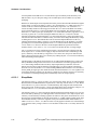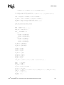
1
Intel® StrongARM® SA-1110
Microprocessor Development
Board
User’s Guide
ADVANCE INFORMATION
January 2000
Hardware Build Phase 4
Notice: This document contains information on products in the sampling and initial production phases of development. Revised information will be published when this product is available.
Order No: 278278-005
Information in this document is provided in connection with Intel products. No license, express or implied, by estoppel or otherwise, to any intellectual
property rights is granted by this document. Except as provided in Intel’s Terms and Conditions of Sale for such products, Intel assumes no liability
whatsoever, and Intel disclaims any express or implied warranty, relating to sale and/or use of Intel products including liability or warranties relating to
fitness for a particular purpose, merchantability, or infringement of any patent, copyright or other intellectual property right. Intel products are not
intended for use in medical, life saving, or life sustaining applications.
Intel may make changes to specifications and product descriptions at any time, without notice.
The SA-1110 Development Board may contain design defects or errors known as errata which may cause the product to deviate from published
specifications. Current characterized errata are available on request.
Contact your local Intel sales office or your distributor to obtain the latest specifications and before placing your product o rder.
Copies of documents which have an ordering number and are referenced in this document, or other Intel literature may be obtained by calling 1-800548-4725 or by visiting Intel’s website at http://www.intel.com.
Copyright © Intel Corporation, 2000
*Other brands and names are the property of their respective owners.-ARM and StrongARM are trademarks of ARM, Ltd.
Contents
1
Introduction ............................................................................................................. 1–1
1.1
1.2
2
Getting Started ........................................................................................................2–1
2.1
2.2
2.3
3
Physical Description.....................................................................................2–1
2.1.1 Unpacking the Intel® StrongARM® SA-1110 Development Board.2–5
2.1.2 Development JTAG.........................................................................2–5
2.1.3 Intel® StrongARM® SA-1110 Development Board Software .........2–5
Assembling the SA-1110 Development Platform.........................................2–5
2.2.1 Connecting Power from an AC Adapter ..........................................2–6
2.2.2 Connecting Power from the Li-Ion Battery ......................................2–7
Installing the StrataFlash™ Memory Components ......................................2–9
Theory of Operation................................................................................................3–1
3.1
4
Related Documentation ...............................................................................1–4
SA-1110 Development Platform Overview ..................................................1–4
System Partitioning ......................................................................................3–1
Hardware Considerations ......................................................................................4–1
4.1
4.2
4.3
4.4
4.5
4.6
4.7
Xbus Expansion Headers ............................................................................4–1
Storage ........................................................................................................4–1
4.2.1 Intel® StrongARM® SA-1110 Development Board Memory Map...4–1
4.2.2 Flash Memory .................................................................................4–2
4.2.3 Main SDRAM Interface ...................................................................4–3
4.2.4 Expansion Flash Memory ...............................................................4–3
4.2.5 Expansion SDRAM Interface ..........................................................4–3
4.2.6 Compact Flash................................................................................4–3
Intel® StrongARM® SA-1110 GPIO Usage .................................................4–4
4.3.1 GPIO 0 and GPIO 1 ........................................................................4–6
4.3.2 Intel® StrongARM® SA-1110 GPIO Pin Descriptions ....................4–7
Register Descriptions...................................................................................4–8
4.4.1 Intel® StrongARM® SA-1110 System Configuration
Register SCR ..................................................................................4–8
4.4.2 SA-1110 Development Board Control Register
BCR 0x1200,0000......................................................................... 4–10
4.4.3 SA-1110 Development Board Status Register 0x1200,0000........ 4–14
System Reset............................................................................................. 4–15
System Displays ........................................................................................ 4–15
4.6.1 LED Displays ................................................................................ 4–16
4.6.2 LCD Displays ................................................................................ 4–16
4.6.2.1 Sharp 3.9” Reflective Color ..............................................4–16
4.6.2.2 Memory Pixel Representations Versus
Physical Pixel Interface .................................................... 4–17
4.6.2.3 Mapping 18 Bit LCDs to 16 Bits of Pixel Data.................. 4–17
4.6.2.4 LCD Backlight Frontlight Support..................................... 4–17
Debugging..................................................................................................4–17
4.7.1 Keypad.......................................................................................... 4–17
4.7.2 Debug Switches ............................................................................ 4–18
4.7.3 Function Switches......................................................................... 4–18
Intel® StrongARM® SA-1110 Development Board User’s Guide
iii
4.8
4.9
4.10
4.11
4.12
4.13
4.14
4.15
4.16
5
Analog I/O............................................................................................................... 5–1
5.1
5.2
5.3
6
UCB1300 Analog IO .................................................................................... 5–1
5.1.1 Battery Voltage ............................................................................... 5–1
5.1.2 Battery Temperature ....................................................................... 5–2
5.1.3 Analog Spare .................................................................................. 5–2
Analog Outputs ............................................................................................ 5–3
Touch Screen .............................................................................................. 5–3
System Power Management ................................................................................. 6–1
6.1
6.2
iv
4.7.4 Logic Analyzer Support................................................................. 4–18
SMBus ....................................................................................................... 4–19
Serial Ports ................................................................................................ 4–19
Power System............................................................................................ 4–20
4.10.1 Power System Design Benefits..................................................... 4–20
4.10.2 Power System Design .................................................................. 4–20
4.10.2.11.5V Core Power ............................................................. 4–21
Power for the Intel® StrongARM SA-1110 Development
Board ......................................................................................................... 4–22
4.11.1 3.3 V Main System Power Design Considerations ....................... 4–22
4.11.2 MAX1705 Boost Converter and MIC5219 LDO Linear
Regulator ...................................................................................... 4–23
4.11.2.1Sleep Mode...................................................................... 4–24
4.11.2.2Virtual Backup Battery ..................................................... 4–25
4.11.2.3Linear Boost Bootstrap System ....................................... 4–25
4.11.2.4Radio Power .................................................................... 4–26
4.11.2.5LCD Power ...................................................................... 4–27
4.11.2.6System Power Limits ....................................................... 4–27
Audio Systems........................................................................................... 4–28
4.12.1 Stereo Codec ................................................................................ 4–29
4.12.2 L3 Bus........................................................................................... 4–29
4.12.3 Stereo Codec Interface................................................................. 4–30
4.12.4 Microphone and Speaker.............................................................. 4–31
4.12.5 SA-1110 Development Board Stereo Codec
Sampling Rates ............................................................................ 4–31
4.12.6 Phone Codec and Soft Modem..................................................... 4–31
4.12.7 Audio System Routing and Mixing Diagram ................................. 4–32
4.12.7.1UDA1341 Loopback Mode............................................... 4–32
4.12.7.2UDA1341 Digital Routing with Mixing
in the SA-1110 ................................................................. 4–32
Radio Interface .......................................................................................... 4–33
4.13.1 CDMA Radio Module .................................................................... 4–34
4.13.2 GSM Radio Module ...................................................................... 4–34
4.13.3 Bluetooth Radio Module ............................................................... 4–34
Quiet Alert Motor........................................................................................ 4–34
IrDA Infra-red Communications ................................................................. 4–34
USB Slave Port.......................................................................................... 4–35
Battery Power .............................................................................................. 6–1
Battery Management ................................................................................... 6–1
6.2.1 Low-Cost Battery Management ...................................................... 6–1
6.2.2 Smart Battery Management............................................................ 6–3
6.2.3 Battery Physical Interface ............................................................... 6–3
6.2.4 Battery Capacity ............................................................................. 6–3
Intel® StrongARM® SA-1110 Development Board User’s Guide
6.2.5
6.2.6
6.2.7
A
CPLD Code ............................................................................................................. A–1
A.1
A.2
B
Battery Safety ................................................................................. 6–3
Fuel Gauging ..................................................................................6–4
Special Handling and Storage Requirements for Batteries.............6–5
ASSCNTL_P2.PHD File Contents .............................................................. A–1
LCD_P2.PHD File Contents........................................................................ A–5
In-Circuit Programming........................................................................................ B/=1
B.1
B.2
In-Circuit Programming of Flash Devices .................................................. B/=1
In-Circuit Programming of CPLD Devices.................................................. B/=1
1-1
1-2
2-1
2-2
2-3
2-4
2-5
2-6
2-7
2-8
2-9
2-10
3-1
3-2
3-3
4-1
4-2
4-3
4-4
4-5
Preliminary Intel® StrongARM® SA-1110 Developer Platform....................1–2
Preliminary Cross-Sectional view of SA-1110 Development Platform.........1–3
Intel® StrongARM® SA-1110 Development Board, Side 1 .........................2–3
Intel® StrongARM® SA-1110 Development Board, Side 2 .........................2–4
Master Power Clip Location .........................................................................2–6
AC Power Input Jack Location.....................................................................2–7
Power Input Jack Location...........................................................................2–8
Li-Ion Battery Location .................................................................................2–8
Master Power Clip Location .........................................................................2–9
E11 Location on Side 1..............................................................................2–10
Opening the E11 Socket ............................................................................ 2–11
E12 Location on Side 2..............................................................................2–12
Intel® StrongARM® SA-1110 Development Platform Block Diagram .........3–2
Intel® StrongARM® SA-1110 Development Board Inputs and Outputs ......3–3
Data Flow in the SA-1110 Microprocessor ..................................................3–4
Li-ion Discharge Curves............................................................................. 4–21
Linear Boost Bootstrap Power System ...................................................... 4–26
Stereo Codec Glue Logic........................................................................... 4–30
UDA1341 Interface Timing......................................................................... 4–30
Audio Mixing Diagram................................................................................ 4–33
4-1
4-2
4-3
4-4
4-5
4-6
4-7
4-8
5-1
5-2
5-3
System Memory Map ..................................................................................4–2
GPIO Usage for Intel® StrongARM® Platforms ..........................................4–5
UCB 1300 CODEC ......................................................................................4–6
GPIO Pin Descriptions .................................................................................4–7
System Configuration Bit Descriptions....................................................... 4–10
Board Control Register ..............................................................................4–11
32-Bit Register Table ................................................................................. 4–15
LED Descriptions ....................................................................................... 4–16
ADC Input Pin Descriptions .........................................................................5–1
Battery Voltage Level Indications.................................................................5–2
Battery Temperature Indications..................................................................5–2
Figures
Tables
Intel® StrongARM® SA-1110 Development Board User’s Guide
v
Introduction
1
The Intel® StrongARM® SA-1110 Microprocessor (SA-1110) is a highly integrated
communications microcontroller that incorporates a 32-bit StrongARM® RISC processor core,
system support logic, multiple communication channels, an LCD controller, a memory and
PCMCIA controller, and general-purpose I/O ports. For more information about the SA-1110
device, see the Intel®StrongARM® SA-1110 Microprocessor Developer’s Manual, order number
278240.
The Intel® StrongARM® SA-1111 Microprocessor Companion Chip (SA-1111) is a companion
chip to the SA-1110, providing a variety of functions suitable for use in a high-performance
handheld computer system. The SA-1111 brings a new level of integration to small systems,
providing a variety of I/O functions that enable complete systems to be built with very little “glue”
logic. In addition to a complete USB Host Controller, the SA-1111 includes extensive support for
PCMCIA and Compact Flash (CF), two PS/2 ports, two industry-standard serial ports, and other
I/O capabilities. It can acquire the system memory bus and do DMA transfers to system memory
(EDO or SDRAM) with its high-performance memory controller. For more information about the
SA-1111 device, see the Intel®StrongARM® SA-1111 Companion Chip Developer’s Manual, order
number 278242.
The Intel® StrongARM® SA-1110 Development Platform (SA-1110 Development Platform) order
number SA111XDEVKIT is based upon these devices and is composed of a two board set1:
• Intel® StrongARM® SA-1110 Development Board (SA-1110 Development Board) order
number SA1110DEVBD.
• Intel® StrongARM® SA-1111 Companion Chip Development Module (SA-1111 Development
Module) order number SA1111DEVMOD.
Note:
This document and module are for the Phase 4 hardware build of this product. For the latest
information and updates, see the hardware release notes that are provided in hardcopy format, and
the software readme.txt files that are provided in the software kits, and related specification
updates on Intel’s website for developers.
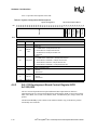
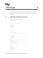
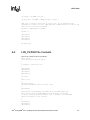
Figure 1-1 shows the preliminary front view of the SA-1110 Development Platform and Figure 1-2
shows a preliminary cross-sectional view.
1.
Though not included with the kit, the SA-1110 Development Platform also supports a graphics module.
Intel® StrongARM® SA-1110 Microprocessor Development Board User’s Guide
1-1
Introduction
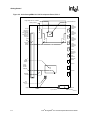
Figure 1-1. Preliminary Intel® StrongARM® SA-1110 Developer Platform
0.75"
Intel® StrongARM® *
SA-1110 hand held
reference design.
Add shield gnd
points every 0.5"
around entire board
LCD CPLD
LEDs
Reg16
Sharp 3.9" color reflective TFT LCD
Reg16
LCD GOO
Light Green:
3V side one components
Dark Green:
3V side two components
Blue: 1.65V Vcore
Red: 5V
Yellow: LCD components
Magenta:
System power components
cia
L
Hi
3V
A3-A0
AA
Batt.
Li-ion
UR
14500
Dxcv
L
0.157" non-plated tooling
and board stacking holes
spaced 0.2" from edges
unless marked otherwise.
5"
cas 25Addr0
lcd
Socket
sdclks31 Data0
12V
gpio
Axcv
20S
SA-1110
uBGA
L
L
AA
Batt.
BUF
CD side 2
5V
CFII
tp
LCD GOO and DAA GOO
are areas of discrete R
and C components
Intel StrongARM
SA-1110 Board
[top view]
IrDA
SW
D7-D0
SDRAM
54 tsop 256Mb
A4-A12
D8-D15
AA Batteries
shown for
scale only.
Final design
will be Li-ion
types
Stereo
3.5
3/4"
mic
10-pin Pots +
RS232
HD
set
Pwr
USB
3 1/2"
2Kb
SMC91C96
Ethernet
0.35"
2 Slot PCMCIA
US
AR
Intel® StrongARM®
SA-1111 Board
[top view]
1Kb
0.75"
stand off carriage allows
components under slot 1
56
TSOP
A22
Flash
A1
AC
97
SW PAK
TPS
2105
usb
1341
3/4"
Console 9-pin
Dsub
BUF
232
Port 2 9-pin
Dsub
max
232
D7 - D0
SDRAM
54tsop256Mb
A4 - A12 D8 - D15
Provide 3.3V
power shunt for
StrongARM® SA-1111
measurements.
5"
Axcv
PCMCIA Card
2.1 x 3.35
A3 - A0
Test CPLD
2064
pz3128
CPLD
100TQFP
AMP 536280-6 140 pin facing up
SA-1111
uBGA
socket
Dxcv
ISP 5x2
max
16
00
D15
10BT
D0
RJ45
1"
SJ
out
SJ
in
mic
PS2
3.5"
5"
USB
* StrongARM is a
registered trademark
of ARM Ltd.
A7310-01
1-2
Intel® StrongARM® SA-1110 Microprocessor Development Board User’s Guide
Introduction
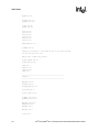
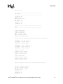
Figure 1-2 shows a preliminary sideview of the SA-1110 development board:
Figure 1-2. Preliminary Cross-Sectional view of SA-1110 Development Platform
Touch Screen
Front Light
Sharp Reflective 3" LCD
2.25"
Full development system
with Intel® StrongARM®*
SA-1111, GFX, LCD,
touch screen and
frontlight.
GFX
Speaker
mic
SA-1110
mic
XCVR
0.775"
SDRAM
32 Surface
mount leds
XCVR
SA-1111
5"
5 cm
Plexi Glass
1.5"
3.4 cm
J2
J3
Li-lon Battery
Plexi Glass
Note: Not actual size
* Intel StrongARM is a registered trademark of ARM Ltd.
A7371-01
The modular design of the SA-1110 Development Platform makes it a flexible, extendable and
reusable design that supports1 the following requirements:
•
•
•
•
•
Targeted for hand-held applications
Multiple OS development platform
Third-party vendor graphics accelerator development platform
Development platform for SA-1111 Companion Chip
SA-1110 Development Board may be used as a palm PC reference design and development
platform
• SA-1110 Development Board may be used as host board for PCI bridge ASIC/FPGA and a
Windows CE reference platform
• Battery powered design example
• Power management and battery management including SMBus and SBS development
platform
• RF communications development board with interfaces for CDMA and GSM and Bluetooth2
RF modules
1.
2.
The SA-1110 Development Platform has not been certified as being compliant with FCC, CE, UC, or PTT telephone standards or regulations.
For the phase 4 release of this document, formal Bluetooth interface specifications were not available. For more information, see section
Section 4.13.3.
Intel® StrongARM® SA-1110 Microprocessor Development Board User’s Guide
1-3
Introduction
1.1
Related Documentation
Other documentation that may be helpful while reading this document are described in the
following table:
Title
Location
Intel® StrongARM® SA-1110 Microprocessor Advanced
Developer’s Manual, order number: 278240
Intel® StrongARM® SA-1110 Microprocessor Specification
Update, order number: 278259
Intel® StrongARM® SA-1110 Development Board Parts List,
order number: 278280
Intel® StrongARM® SA-1110 Development Board Schematics,
order number: 278279
Intel® StrongARM® SA-1111 Microprocessor Companion Chip
Developer’s Manual, order number: 278242
Intel’s website for developers is at: http://developer.intel.com
Intel® StrongARM® SA-1111 Microprocessor Companion Chip
Specification Update, order number: 278260
Intel® StrongARM® SA-1111 Companion Chip Development
Board Schematics, order number: 289282
Intel® StrongARM® SA-1111 Companion Chip Development
Board Parts List, order number: 278283
Intel® StrongARM® SA-1111 Companion Chip Development
Board User’s Guide, order number: 278281
Intel® StrongARM® SA-1110 Development Board - Windows*
CE Software Kit User Guide, order number: 278322
The ARM Debug Monitor: Angel
ARM’s website is at:
http://www.arm.com
ARM Architecture Reference Manual
1.2
SA-1110 Development Platform Overview
The SA-1110 Development Board, the SA-1111 Development Module, and the graphics
accelerator boards are a flexible software and hardware development environment and example
design. When the SA-1110 Development Board is used as a development system, the SA-1111
Development Module is also required to provide Ethernet, serial port, LEDs and logic analyzer
support.
The SA-1110 Development Board has the following resources and features:
•
•
•
•
1-4
Up to 32MB socketed fast page mode Intel ® StrataFlash memory
Up to 64MB 100 MHz SDRAM
Un-buffered main memory interface allows highest possible SDRAM memory bandwidth
Small form factor 3.5” x 5” x 0.5” (same size as the Sony Nino*)
Intel® StrongARM® SA-1110 Microprocessor Development Board User’s Guide
Introduction
• Phillips Semiconductor UCB1300* codec supports microphone, speaker, POTS line soft
modem DAA connections and touch screen
• Phillips Semiconductor UDA1341* stereo codec supports high quality 16 bit stereo audio
record and playback
• Infra-red interface for IrDA data links up to 4Mb
• Battery powered, using high efficiency DC-DC converters and a single Lithium ion (Li-ion)
cell
• Smart battery technology development platform and reference design when used with smart
battery packs
• Integrated 3.9” reflective color TFT LCD and touch screen
• Optional 8” color passive LCD for use with GFX companion chip
• Two expansion headers for the SA-1111 Development Module, the graphics accelerator board,
or other boards
• Built in mini speaker and two microphones
• Built in quiet alert vibration motor
• One type II Compact Flash socket (available only when the SA-1111 Development Module
and graphics accelerator boards are not present)
• USB slave port for PC synchronization and battery trickle charge
• RF module interface connector for CDMA, GSM and Bluetooth modules up to 4 Watts
• Base station connector for JTAG programming, RS232, power input, and telephone
The SA-1111 Development Module has the following features1:
•
•
•
•
•
•
•
•
•
•
•
•
•
•
•
1.
Expansion Flash bank. Up to 32MB socketed fast page mode StrataFlash memory
Expansion SDRAM bank (up to 64MB 50MHz SDRAM)
Supports UDA1341 stereo codec for high quality 16 bit stereo audio record and playback
Supports AC97 stereo codec for high quality 16 bit stereo audio record and playback
Form factor is six inches by five inches by 1.38 inches
Built in microphone
One type II PCMCIA socket
One type II Compact Flash socket
USB host port
USB host plug and power control device
Two PS2 ports
Logic analyzer pods
32 LEDs to display program debug data
10BASE-T Ethernet controller
Debug serial ports (RS-232)
For more information about the SA-1111 Development Module, see the Intel® StrongARM® SA-1111 Companion Chip Development Module
User’s Guide.
Intel® StrongARM® SA-1110 Microprocessor Development Board User’s Guide
1-5
Introduction
The graphics accelerator board has the following features1:
• Third-party high performance graphics accelerator
• Two head display support; Analog XGA and LCD XGA
• Direct connection for Sharp LM8V31 dual scan STN VGA color panel with backlight and
touch screen
1.
1-6
For more information about the graphics accelerator board, see the third-party documentation.
Intel® StrongARM® SA-1110 Microprocessor Development Board User’s Guide
Getting Started
2
This SA-1110 Development Board is supplied as a mother board and functions as both a standalone handheld PC device as well as a development platform when used with the SA-1111
Development Module.
This chapter provides a physical description of the SA-1110 Development Board and describes
how to:
• Unpack the card and give it a visual inspection
• Verify SA-1110 Development Board kit contents
• Install the required hardware
2.1
Physical Description
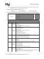
Figure 2-1 and shows the physical layout of the SA-1110 Development Board. The SA-1110
Development Board uses a 4-layer double-sided surface mount assembly technology.
The following components and systems are on side one of the SA-1110 Development Board:
• LCD cable connector—50-pin connector for Sharp 3.9” LCD display
• Touch screen header—Four-pin connector for touch screen connector
• Intel StrataFlash™—One of two 128 Mbit Intel StrataFlash for storage of the operating system
and applications
• Spare ADC input—An analog to digital converter that could be used as a photo-sensor input to
sense ambient light for background light control.
• Battery temperature sensor—Senses temperature of Li-ion battery
• Base station—14-pin connector for JTAG programming, RS232, power input jack, and
telephone
• Headset jack 2.5 mm—2.5 mm standard telephony headset connector
• Stereo jack 3.5 mm—standard stereo headphone 3.5 mm connector
• USB Type B connection—Universal Serial Bus, four-pin end point connector (slave) for host
communications
•
•
•
•
1.
Microphone connection—accepts Electret type microphone
Radio connector—30 pin connector that accepts CDMA, GSM, or Bluetooth1 radio modules
SDRAM—One of two 128 Mbit SDRAM storage devices
Intel® StrongARM® SA-1110 Microprocessor—Small size, low power, high performance, 32bit StrongARM processor.
For the phase 1 release of this document, formal Bluetooth interface specifications were not available. For more information, see section
Section 4.13.3.
Intel® StrongARM® SA-1110 Development Board User’s Guide
2-1
Getting Started
• 140-pin expansion header—Main connector for SA-1111 Development Module (daughter) or
third-party daughter cards
• Video out header—Five-pin connector that provides composite video
The following components and systems are on side two of the SA-1110 Development Board:
• Base station connector—14-pin connector for JTAG programming, RS232, power input jack,
and telephone
•
•
•
•
•
•
•
•
•
GPIO 0 switch—Manual override for GPIO 0
GPIO 1 switch—Manual override for GPIO 1
User software definable switches—Six switches for user software definable signals
Battery headers—Ten-pin connector for battery temperature and battery detection
Compact Flash II header—50-pin connector used for Ethernet and memory expansion
Backlight header—Five-pin connector for backlighting LCD display
Left channel input—Half of stereo input
Right channel input—Half of stereo input
Intel StrataFlash™—One of two 128 Mbit Intel StrataFlash of storage for the operating system
and applications
• SDRAM—One of two 128 Mbit SDRAM
• 140-pin expansion header—Main connector for SA-1111 Development Module (daughter) or
third-party daughter cards
2-2
Intel® StrongARM® SA-1110 Development Board User’s Guide
Getting Started
Figure 2-1. Intel® StrongARM® SA-1110 Development Board, Side 1
Master Power
Clip
Reset
Switch
J22
S9
Video Out
Header
J2
J18
(Momentary)
Intel®
StrongARM® *
SA-1110
E1
J9
LCD
Cable
Connector
Touch
Screen
Header
SDRAM
J8
E2
Large
Dimple
for Pin 1
Indicator
Radio
Connector
J21
E11
Intel®
StrataFlash™
Internal
Speaker
Jacks
J14
J11
J16
Battery
Temperature
Sensor
J17
J19
J7
Microphone
Jack
J10
J5
Microphone
Pads
J1
Spare
ADC
Input
140-pin
Expansion
Header for
Intel®
StrongARM®
SA-1111
Development
Module or
other
Daughter
Card
Base Station
Power Input Jack
Headset Jack
2.5 mm
Stereo Jack
3.5 mm
USB Type B
Connection
* StrongARM is a registered trademark of ARM Ltd.
A7223-01
Intel® StrongARM® SA-1110 Development Board User’s Guide
2-3
Getting Started
Figure 2-2. Intel® StrongARM® SA-1110 Development Board, Side 2
Large Dimple for Pin 1 Indicator
Intel® StrataFlash™
Battery Header
UserSoftware
Definable
Switch
140-pin
Expansion
Header for
StrongARM®
SA-1111
Development
Module or
Daughter
Card
S8
E35
S7
J6
Compact
Flash II
Header
UserSoftware
Definable
Switch
J4
UserSoftware
Definable
Switch
J6
J2
S6
UserSoftware
Definable
Switch
S5
UserSoftware
Definable
Switch
S4
UserSoftware
Definable
Switch
Intel®
StrataFlash™
S3
GPIO1
S2
E12
Large
Dimple
for Pin 1
Indicator
GPIO0
J13
S1
Backlight
Header
J15
J20
Left
Channel
Input
J10
Right Channel Input
Power
Input Jack
Base Station
Connector
A7222-02
2-4
Intel® StrongARM® SA-1110 Development Board User’s Guide
Getting Started
Unpacking the Intel® StrongARM® SA-1110 Development
Board
2.1.1
Warning:
This board contains electronic components that are susceptible to permanent damage from
electrostatic discharge (static electricity). To prevent electrostatic discharge, it is supplied in an
antistatic bag. When handling the board, risk of damage can be alleviated by following a few
simple precautions:
• Remove the board from the bag only when you are working on an antistatic, earthed surface
and wearing an earthed antistatic wrist strap.
• Keep the antistatic bag that the card was supplied in; if you remove the board from a system,
store it back in the bag.
• Do not touch the gold contacts.
2.1.2
Development JTAG
The SA-1110 Development Board uses the JTAG interface to program the PZ3128 and PZ3064
CPLDs. For information on the contents of the CPLD files, see Appendix A.
The same JTAG loop also includes the SA-1110 component. With the appropriate software
installed, the SA-1110 JTAG port hardware can be used to program the flash memories at a slow
rate. However, the SA-1110 JTAG port does not support JTAG In-Circuit Emulation (ICE).
Intel® StrongARM® SA-1110 Development Board Software
2.1.3
To purchase an ARM Software Development Kit (SDT), see your Intel sales representative.
The following source and executable files are available from the StrongARM section in the
developer’s area on the Intel website.
• Sample source code including I/O drivers such as the software video-processing engine drivers
and the SCB library available through Intel’s developer’s web site.
• Angel boot loader—Software component of ARM that loads an application from a remote host
computer or from the application flash.
• Set of microHAL libraries (to be used with Angel)—Set of drivers for communicating with the
SA-1100 multimedia development board.
• Diagnostics—Test program that analyze the functions of the SA-1110 Development Board.
Note:
2.2
All software is available from the StrongARM section in the developer’s area on the Intel website.
Assembling the SA-1110 Development Platform
The 140-pin connectors are very fragile on the SA-1110 Development Board and the SA-1111
Development Module. Care must be taken when assembling these modules. For information about
assembling, see the Intel® StrongARM® SA-1111 Microprocessor Development Module User’s
Guide.
Intel® StrongARM® SA-1110 Development Board User’s Guide
2-5
Getting Started
Caution:
2.2.1
If the 140-pin connector is damaged due to an improper assembly, the reader must contact their
Intel Sales representative for module replacement.
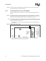
Connecting Power from an AC Adapter
Use the following procedure to provide power to the SA-1110 Development Board from an AC
adapter:
Caution:
The following procedure assumes that the jumper (shunt) for J22, the Master Power Clip for the
Li-ion battery, has been disconnected and that all power associated with the SA-1110 Development
Board is off. For more information about Li-ion battery considerations, see Chapter 6.
Note:
A very high value capacitor of 0.33 Farads (super cap) is connected in parallel with the power input
from J10. This capacitor provides enough power to support the system for several minutes in sleep
mode when power from J10 is removed.
1. Verify that the jumper (shunt) for J22 is not on the Master Power Clip (J22 should appear as
two bare pins).
Figure 2-3. Master Power Clip Location
Master Power
Clip
Reset
Switch
J22
S9
Video Out
Header
J2
J18
(Momentary)
LCD
Cable
Connector
140-pin
Expansion
Header for
Intel®
StrongARM®
SA-1111
Development
Module or
other
Daughter
Card
2. Select the appropriate AC adapter to DC converter device (wall brick) depending upon
whether you are in a 110-volt or 220-volt environment.
2-6
Intel® StrongARM® SA-1110 Development Board User’s Guide
Getting Started
3. Insert the power jack that is connected to the wall brick into J10 (see Figure 2-4 for the
location of J10).
J16
J7
J1
J11
J10
J5
J14
J17
Figure 2-4. AC Power Input Jack Location
Base Station
Power Input Jack
Headset Jack
2.5 mm
Stereo Jack
3.5 mm
USB Type B
Connection
A7615-01
Note:
The power jack may have to be rotated to its flat side to accommodate any other connectors in J10.
4. Plug in the wall-brick into an AC outlet.
5. See the Readme.txt file for success and failure indications of start-up diagnostic results and
how to proceed.
To disconnect power, remove the power jack from J10 and wait for the super cap to discharge
(typically less than 5 minutes).
Note:
2.2.2
If sleep mode was entered as a result of VDD_FAULT or BATT_FAULT signals, GPIO 0 and
GPIO 1 are the only wake up events that can bring the SA-1110 out of sleep mode.
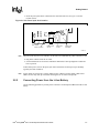
Connecting Power from the Li-Ion Battery
Use the following procedure to provide power to the SA-1110 Development Board from the Li-Ion
battery:
Intel® StrongARM® SA-1110 Development Board User’s Guide
2-7
Getting Started
Caution:
Note:
The following procedure assumes that the jumper (shunt) for J22, the Master Power Clip for the
Li-ion battery, has been disconnected and that all power associated with the SA-1110 Development
Board is off. For more information about Li-ion battery considerations, see Chapter 6.
A very high value capacitor of 0.33 Farads (super cap) is connected in parallel with the battery
through J22. This capacitor provides enough power to support the system for several minutes in
sleep mode while the battery is being changed.
1. Verify that the AC adapter power jack that is not connected to J10 (see Figure 2-4 for the
location of J10).
J16
J7
J1
J11
J10
J5
J14
J17
Figure 2-5. Power Input Jack Location
Base Station
Power Input Jack
Headset Jack
2.5 mm
Stereo Jack
3.5 mm
USB Type B
Connection
A7615-01
2. Verify that the Li-Ion battery is installed on the SA-1110 Development Board and that the
battery harness is connected to J4 (see Figure 2-6 for the location of the Li-Ion battery).
Figure 2-6. Li-Ion Battery Location
Plexi Glass
1.5"
J2
J3
Li-lon Battery
5 cm
Plexi Glass
Note: Not actual size
3.4 cm
A7371-0
2-8
Intel® StrongARM® SA-1110 Development Board User’s Guide
Getting Started
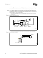
3. Insert the jumper (shunt) for J22 on the Master Power Clip (this jumper connects the two bare
pins enabling the Li-ion battery.).
Figure 2-7. Master Power Clip Location
Master Power
Clip
Reset
Switch
J22
S9
Video Out
Header
J2
J18
(Momentary)
LCD
Cable
Connector
140-pin
Expansion
Header for
Intel®
StrongARM®
SA-1111
Development
Module or
other
Daughter
Card
4. See the Readme.txt file for success and failure indications of start-up diagnostic results and
how to proceed.
To disconnect power, remove the jumper for J22 and wait for the super cap to discharge (typically
less than 5 minutes).
Note:
2.3
If sleep mode was entered as a result of VDD_FAULT or BATT_FAULT signals, GPIO 0 and
GPIO 1 are the only wake up events that can bring the SA-1110 out of sleep mode.
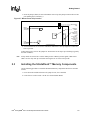
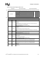
Installing the StrataFlash™ Memory Components
Use the following procedure to install the StrataFlash memory components into the E11 and E12
sockets:
1. Power down the module and remove the jumpe for J22, if it is installed.
2. Locate the E11 socket on side 1 of the SA-1110 Evaluation Board.
Intel® StrongARM® SA-1110 Development Board User’s Guide
2-9
Getting Started
Figure 2-8. E11 Location on Side 1
J22
J8
E2
Large
Dimple
for Pin 1
Indicator
Intel®
StrongARM® *
SA-1110
E1
J9
J2
J18
S9
J16
J7
J1
J11
J10
J5
J14
J17
J19
J21
E11
Intel®
StrataFlash™
* StrongARM is a registered trademark of ARM Ltd.
A7482-01
2-10
Intel® StrongARM® SA-1110 Development Board User’s Guide
Getting Started
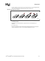
3. Slide the middle top section of the box away from the notch in E11. Open the right hand side
of the socket, then open the left hand side of the socket (see Figure 2-9).
Figure 2-9. Opening the E11 Socket
A7484-01
4. Using the Pen Vac tool, remove the low side (bits 0-15) StrataFlash memory component from
the shipping container.
5. Insert the low side StrataFlash memory component into the socket aligning the pin 1
indicators.
6. Close up the socket.
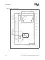
7. Repeat steps 2 through 5 for the socket on side 2 for the high side (bits 16-31) StrataFlash
memory component. See Figure 2-10 for locating and aligning E12 on side 2.
Intel® StrongARM® SA-1110 Development Board User’s Guide
2-11
Getting Started
.
Figure 2-10. E12 Location on Side 2
Large Dimple for Pin 1 Indicator
Intel® StrataFlash™
Battery Header
UserSoftware
Definable
Switch
140-pin
Expansion
Header for
StrongARM®
SA-1111
Development
Module or
Daughter
Card
S8
E35
S7
J6
Compact
Flash II
Header
UserSoftware
Definable
Switch
J4
UserSoftware
Definable
Switch
J6
J2
S6
UserSoftware
Definable
Switch
S5
UserSoftware
Definable
Switch
S4
UserSoftware
Definable
Switch
Intel®
StrataFlash™
S3
GPIO1
S2
E12
Large
Dimple
for Pin 1
Indicator
GPIO0
J13
S1
Backlight
Header
J15
J20
Left
Channel
Input
J10
Right Channel Input
Power
Input Jack
Base Station
Connector
A7483-01
2-12
Intel® StrongARM® SA-1110 Development Board User’s Guide
Theory of Operation
3
The SA-1110 Development Platform is designed for the hardware and software development of
hand-held, palm-top and tethered applications. The SA-1110 Development Platform provides all
the system components necessary for a Windows* CE or other OS hand-held PC system or a subnotebook system development platform including three independent video heads, high-quality
stereo sound and radio interface support.
3.1
System Partitioning
The SA-1110 Development Platform’s system partitioning is designed so that the SA-1110
Development Board functions as a standalone palm-size PC reference design. The SA-1110
Development Board’s mechanical design supports simple system packaging using sheet Lexan*,
screws and spacers to integrate the LCD, optional frontlight, touch screen and batteries.
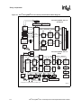
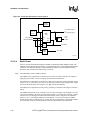
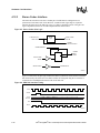
The block diagram shown in Figure 3-1 illustrates the modularity and flexibility of the design. Two
140-pin fully buffered daughter board expansion headers (J2) are supported; one on each side of
the SA-1110 Development Board. Either side of J2 can be used to support the SA-1111
Development Module or the graphics accelerator module.
The functionality of the dual interconnects is identical. The rationale for two interconnects is as
follows: When the cards are connected in an extended fashion (“Z” shaped), full electronic probing
is possible. When connected in a compact format (“U” shaped), tight packaging is facilitated.
Intel® StrongARM® SA-1110 Microprocessor Development Board User’s Guide
3-1
Theory of Operation
Figure 3-1. Intel® StrongARM® SA-1110 Development Platform Block Diagram
Intel® StrongARM®* SA-1110
CPU Board
LCD Header
LCD CPLD data
LCD analog support
formater for Sharp 3.9"
for Sharp 3.9"
UCB1300
POTS
Codec
USB stv
Power
Manager
8Mx16
Intel®
Page Mode
Strata Flash
Xceiver
Intel® StrongARM®* SA-1111
Board
9 Pin
RS232
Intel®
StrongARM®
SA-1111
Test
Pods Address 9:0
Buffer
Address 25:0
Expansion Header
16Mx16
SDRAM
Header
RS232
Max 3243
D31:0
Xceiver
Address
Decode Bus
Contrl. CPLD
Batt
e
Batt ry
ery
D15:0
8Mx16
Intel®
Page Mode
Strata Flash
PAL
UDA1341
I2S 16 Bit
Stereo Codec
16Mx16
SDRAM
CF Type II Slot
Intel®
StrongARM®
SA-1110
IrDA
Graphics Header
RS232
Expansion Header
Buffer
D15:0
16Mx16
SDRAM
D31:0
16Mx16
SDRAM
D15:0
D31:0
Xceiver
8Mx16 Intel®
Page Mode
Strata Flash
Socket
Test
Pods
Xceiver
8Mx16 Intel®
Page Mode
Strata Flash
Socket
Test
Pods
D15:0
SMC
91C96
Enet
10B
T
Address 5:2
D7:0
CPLD Debug
Registers
Lights
Switches
4x5 Key Pad
Header
32 SMT
LEDs
PCMCIA
Slot 1
Slot 2
UDA1341
I2S 16-Bit
Stereo Codec
AC97
Codec
SSP
PS/2a
PS/2b
USAR SPI
Key Coder
PWM-a
PWM-b
USB
Host
8 Switch
Pack
Matrix Keyboard Headers
3.5mm Jacks
* StrongARM is a registered trademark of ARM Limited.
A6881-01
3-2
Intel® StrongARM® SA-1110 Microprocessor Development Board User’s Guide
Theory of Operation
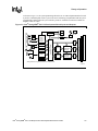
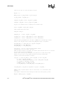
As shown in Figure 3-2, the system partitioning allows the SA-1110 Development Board to be used
by itself as a minimal palm-size PC system. All device interfacing is implemented with in-system
programmable CPLDs and most system interface points are available on connectors suitable for
daughter boards or cables.
Figure 3-2. Intel® StrongARM® SA-1110 Development Board Inputs and Outputs
Pwr
touch
Intel
StrataFlash
Memory
Graphics 140-pin Header
SDRAM
CF II Slot
Intel®
StrataFlash™
Memory
Xcvr
spk
Stereo
codec
SDRAM
Xcvr
IrDA
mic
Intel® StrongARM®
SA-1110
USB
USBend
TVenc
Intel® StrongARM®* SA-1111 140-pin Header
UCB1300
POTS
codec
Touch
Screen
RS232
mic
Chrg
Xcvr
Base Header
DAA
batt
LCD
CPLD
JTAG
* StrongARM is the registered trademark of ARM Limited.
A7264-01
Intel® StrongARM® SA-1110 Microprocessor Development Board User’s Guide
3-3
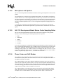
Theory of Operation
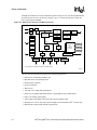
Although not intended as a ready to manufacture product design, the SA-1110 Development Board
provides the basis for low-cost derivative designs. Figure 3-3 shows how data flows within the
SA-1110 Development Module.
Figure 3-3. Data Flow in the SA-1110 Microprocessor
OSC
PLL
PC
OSC
Intel®
StrongARM®* ADDR
SA-1 Core
RTC
Power
Manager
ICache
8 KB
IMMU
32 TLBs
JTAG
& Test
DMMU
32 TLBs
Minicache
Instructions
Timers
ICache
16 KB
Data
Reset
Controller
Write
Buffer
Memory
&
PCMCIA
Controller
Read
Buffer
Interrupt
Controller
Address
Data [32]
Control
GPIOs
Bridge
USB Client
SDLC
LCD Controller
DMA
IrDA
UART
USB Client
* StrongARM is the registered trademark of ARM Limited.
A7263-01
The SA-1110 Development Board supports the following applications:
•
•
•
•
•
•
•
•
•
•
•
3-4
Palm-size PC with docking USB PC sync
MP3 HiFi stereo record and playback
Hand writing recognition
Speech recognition
Web browser
VoIP with voice dialing and speakerphone
Wireless voice dialing VoIP/POTS handset or speakerphone using CF RF modem
POTS voice dialing speakerphone
Video capture with CMOS camera and video capture daughter board
Broadcast TV receiver using video capture daughter board with Microtune® TV tuner chip
IBM 340 Mb compact flash microdrive applications
Intel® StrongARM® SA-1110 Microprocessor Development Board User’s Guide
Hardware Considerations
4
This chapter provides an in-depth description on the following topics:
•
•
•
•
•
•
•
•
4.1
Xbus expansion headers
Storage
GPIOs
Registers
Displays
Buses and Ports
Power
Audio
Xbus Expansion Headers
The general-purpose expansion bus headers provided on the SA-1110 Development Board are
referred to as the Xbus headers (not to be confused with ISA Xbus). All SA-1110 address, data and
memory interface signals are buffered before driving the Xbus headers.
The Xbus headers allow interfacing to the SA-1111 microprocessor companion chip and the SA1111 Development Module as well as a third-party graphics chip daughter board.
These general-purpose expansion headers allow the use of the SA-1110 Development Board as a
general-purpose hardware and software development platform for battery-powered and tethered
applications. For more information about Xbus headers, see the Intel® StrongARM® SA-1111
Development Module User’s Guide.
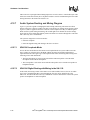
4.2
Storage
This section describes the memory map, the SDRAM interface, the expansion flash memory, the
interface for the expansion SDRAM, and compact flash issues.
4.2.1
Intel® StrongARM® SA-1110 Development Board Memory
Map
Table 5-1 shows the address ranges for the standard SA-1110 Development Board Xbus devices as
well as flash memory, SDRAM, and system control and system debug registers. The address range
field indicates the entire decoded range while the size:width field indicates the actual resource size
and width within the decoded range. All decoded resources are address wrapped within their
address range.
Intel® StrongARM® SA-1110 Microprocessor Development Board User’s Guide
4-1
Hardware Considerations
Table 4-1. System Memory Map
Address Range
Resource
Size
Use
SA-1110 Development Board
Size: Width
E800,0000-FFFF,FFFF
Reserved 384 Mbyte
Reserved
—
E000,0000-E7FF,FFFF
Zeros Bank 128 Mbyte
Cache flush
Read zeros, no bus cycle
D800,0000-DFFF,FFFF
SDRAM bank 3 128 Mbyte
Empty
—
D000,0000-D7FF,FFFF
SDRAM bank 2 128 Mbyte
Expansion SDRAM bank
on SA-1111 board Clk/4
16 Mbyte/32 Mbyte/64 Mbyte:
32 bits wide
C800,0000-CFFF,FFFF
SDRAM bank 1 128 Mbyte
Empty
—
C000,0000-C7FF,FFFF
SDRAM bank 0 128 Mbyte
Main SDRAM bank on SA1110 board Clk/2
16 Mbyte/32 Mbyte/64 Mbyte:
32 bits wide
Internal
—
Internal
—
Internal
—
Internal
—
B000,0000-BFFF,FFFF
A000,0000-AFFF,FFFF
9000,0000-9FFF,FFFF
LCD and DMA Control
256 Mbyte
Memory Control
256 Mbyte
SA-1110 System Control
Module Registera
256 Mbyte
8000,0000-8FFF,FFFF
Peripheral Control
256 Mbyte
5000,0000-7FFF,FFFF
Reserved 768 Mbyte
Reserved
—
4800,0000-4FFF,FFFF
CS5 128 Mbyte
GFX (uses rdy)
TBD bytes: 32 bits wide
4000,0000-47FF,FFFF
CS4 128 Mbyte
SA-1111 (uses Rdy)
8KB
3000,0000-3FFF,FFFF
PCMCIA/CF Slot B 512
Mbyte
Compact Flash
2x2KBytes: 16 bits wide
2000,0000-2FFF,FFFF
PCMCIA/CF Slot A 512
Mbyte
PCMCIA (SA-1111)
3x64 MBytes: 16 bits wide
1800,0000-1FFF,FFFF
CS3 128 Mbyte
Ethernet device (uses rdy)
1Kbytes: 8 bits wide
1000,0000-17FF,FFFF
CS2 128 Mbyte
SA-1110 Development
Board system registers
Various widths
0800,0000-0FFF,FFFF
CS1 128 Mbyte
Expansion flash on
SA-1111 board
16/32 MBytes: 32 bits wide
0000,0000-07FF,FFFF
CS0 128 Mbyte
Boot/Application flash
ROM on SA-1110 board
16/32 MBytes: 32 bits wide
a.
This register is located in the SA-1110 device.
4.2.2
Flash Memory
The SA-1110 Development Board flash bank is populated with 128 Mbit socketed fast page mode
3 V StrataFlash memory. These devices allows 32 Mbyte flash banks.
4-2
Intel® StrongARM® SA-1110 Microprocessor Development Board User’s Guide
Hardware Considerations
4.2.3
Main SDRAM Interface
The SA-1110 Development Board provides support for 64 Mbit, 128 Mbit or 256 Mbit SDRAMs.
The 54 pin TSOP footprint supports a wide variety of SDRAM vendors and densities. The system
partitioning is designed to minimize the loading and etch length on the SA-1110 pin bus. This
permits the system to run up to 103 MHz SDRAM using SA-1110 CoreClk/2 and 125 MHz
SDRAM components. Using two 256 Mb 16 Mx16 SDRAMs provides a main memory load of
64 MBytes. The SA-1110 Development Board is configured with 128 Mb SDRAMs for a
32 MByte memory load.
4.2.4
Expansion Flash Memory
The SA-1111 Development Module flash bank is populated with 128 Mbit socketed fast page mode
3V StrataFlash memory devices. These devices allow 32 Mbyte flash banks.
Switch component SW2, switch 8 on the SA-1111 Evaluation Module allows selection of either the
main flash bank on the SA-1110 Development Board or the expansion flash bank on the SA-1111
Development Module as the boot bank. For more information on the effects of SW2, see the Intel®
StrongARM® SA-1111 Companion Chip Development Board User’s Guide.
4.2.5
Expansion SDRAM Interface
The SA-1111 Development Module provides support for 64 Mbit, 128 Mbit or 256 Mbit SDRAMs.
The 54 pin TSOP footprint supports a wide variety of SDRAM types and sizes. The SA-1111
Development Module’s SDRAMs are buffered from the SA-1110 CPU and must run on a SA-1110
CoreClk/4 permitting a maximum SDRAM clock speed of 51.5 MHz for this SDRAM bank. Using
two 256 Mb 16Mx16 SDRAMs provides a expansion memory load of 64 Mbytes. The SA-1111
Development Module is initially configured with 128 Mb SDRAMs for a 32 Mbyte memory load.
4.2.6
Compact Flash
The SA-1110 Development Board supports a single type II CF socket. The SA-1110 Development
Board CF slot uses the same interface signals required by the SA-1111 Development Module and
graphics accelerator boards, therefore the CF socket on the SA-1110 Development Board only
functions when there are no daughter boards present.
Caution:
Do not plug a CF card plugged into the SA-1110 Development Board CF socket when the
SA-1111 Development or graphics boards are present or it will crash the system and may damage
the SA-1111 component, the graphics accelerator device or SA-1110 Development Board’s
transceiver component. The buffer and transceiver chips on the SA-1110 Development Board that
normally drive the CF socket are reconfigured to become the system buffers and transceivers that
are used to isolate the SA-1111 Development Module and graphics boards from the SA-1110
Development Board when the daughter boards are attached.
E11, which is shown on sheet 4 of 12 on the Intel® StrongARM® SA-1110 Development Board
Schematics, is a CPLD that controls the transceivers and some of the CF support signals. In
addition, GPIO bits 5:4 control the flash size, as shown in Table 4-5. The SA-1110 GPIO pins
GPIO 21, GPIO 22, GPIO 24 and GPIO 25 serve dual functions in the SA-1110 Development
Board CF design. When the SA-1111 Development Module is attached, GPIO 22 GPIO 21 are
configured to be the GPIO alternate function bus DMA control signals nMBREQ and nMBGNT
while GPIO 24 and GPIO 25 are the graphics and SA-1111 interrupt inputs. When the SA-1111
Intel® StrongARM® SA-1110 Microprocessor Development Board User’s Guide
4-3
Hardware Considerations
Development Module is not attached and the SA-1110 Development Board CF slot is active then
GPIO 21 and GPIO 22 are used as CF RDY interrupt signals and CF card detect interrupt while
GPIO 24 ad GPIO 24 are used as CF BVD2 and CF BVD1 inputs.
Note:
The SA-1110 Development Board CF slot is addressed in the same address space as the SA-1111
Development Module’s CF and PCMCIA slots, however the CF slot control signals and interrupt
signals are not the same. Refer to the Intel®StrongARM® SA-1111 Companion Chip Developer’s
Manual for the details. Two versions of the CF drivers are required for the SA-1110 Development
Platform, one for the SA-1111 Development Module and one for the SA-1110 Development Board.
Several key functions available in CF devices are:
•
•
•
•
•
4.3
Ethernet interface
High speed modem
Wireless one way and two way paging
IBM micro-drives up to 340 Mbyte
Bluetooth1 RF modules
Intel® StrongARM® SA-1110 GPIO Usage
The SA-1110 Development Board system maps the SA-1110 GPIO pins as shown in Table 5-4.
The table shows the GPIO mapping of SA-1110 Development Board and previous Intel®
StrongARM® development platforms for comparison and as an aid to OS and Angel porting.
1.
4-4
For the phase 4 release of this document, formal Bluetooth interface specifications were not available. For more information, see section
Section 4.13.3.
Intel® StrongARM® SA-1110 Microprocessor Development Board User’s Guide
Hardware Considerations
Note:
GPIO 0 and GPIO 1 are the only wake up events that can cause the SA-1110 to come out of sleep
mode if sleep mode was entered as a result of VDD_FAULT or BATT_FAULT signals.
Table 4-2. GPIO Usage for Intel® StrongARM® Platforms
GPIO
a.
b.
SA-1100 Development
Platforma
SA-1100 Multimedia and SA-1101
Development Boards b
SA-1110 Development Platform
27
32 KHz Out
3.68 MHz Out
3.68M_32K
26
RCLK_Out
GPIO or RCLK_Out
VBATT_LOW_IRQ/RCLK
25
KBC_ATN#
Keypad IRQ/Xbus_spare
SA111_IRQ_CF_BVD1
24
KBC_WUKO
SideKick IRQ
GFX_IRQ_CF_BVD2
23
KBC_WKUP#
UCB_IRQ
UCB1300_IRQ
22
IRQ_C#
nMBREQ
nMBREQ_CF_CardDetect
21
IRDA_SD
nMBGNT
nMBGNT_CF_IRQ
20
LED_RED#
I2C SDA
UART3_CLK/SPARE
19
SDLC_GPI
I2C SCL
STEREO_64FS_CLK
18
SDLC_HSKI
FIFO_IRQ
L3_I2C_SCL
17
SDLC_AAF
Xbus_spare
L3_MODE (LED)
16
SDLC_HSKO
Xbus_spare
PS_MODE_SYNC
15
UART_RXD
UART_RXD
L3_I2C_SDA
14
UART_TXD
UART_TXD
RADIO_IRQ
13
SSP_SFRM
Header SSP_SFRM/spare
SSP_UDA1341_SFRM
12
SSP_SCLK
Header SSP_SCLK/spare
SSP_UDA1341_SCLK
11
SSP_RXD
Header SSP_RXD/spare
SSP_UDA1341_RxD
10
SSP_TXD
Header SSP_TXD/spare
SSP_UDA1341_TxD
9
LCD_D15/LED_GRN1#
LCD_D15
LCD_D15_CNFG7
8
LCD_D14/LED_GRN2#
LCD_D14
LCD_D14_CNFG6
7
LCD_D13/P1_F1#
LCD_D13
LCD_D13_CNFG5
6
LCD_D12/P1_IREQ#
LCD_D12
LCD_D12_CNFG4
5
LCD_D11/P1_STSCHG#
LCD_D11
LCD_D11_CNFG3
4
LCD_D10/P0_F1#
LCD_D10
LCD_D10_CNFG2
3
LCD_D9/P0_IREQ#
LCD_D9
LCD_D9_CNFG1
2
LCD_D8/P0_STSCHG#
LCD_D8
LCD_D8_CNFG0
1
SW1
SW1/SW 7:0_IRQ/alt FIFO IRQ
ON_OFF_SW2_or_FIQ
0
SW0
SW0/DSP_IRQ/SW 7:0_IRQ
ON_OFF_SW1
Order number DE–1S110–OA
Order number DE–1S110–OC
Intel® StrongARM® SA-1110 Microprocessor Development Board User’s Guide
4-5
Hardware Considerations
Table 4-3. UCB 1300 CODEC
GPIO
a.
b.
SA-1100 Development
Platforma
SA-1100 Multimedia and SA-1101
Development Boardsb
SA-1110 Development Platform
9
ADC_SYNC
ACD_SYNC
8
DAA_OH
DAA_OH
ADC_SYNC
DAA_OH (LED)
7
DAA_RI#
DAA_RI#
DAA_RI-
6
RED_LED#
7 segment dot LED
CLID (caller ID)
5
GRN_LED#
NOT USED
FuncSW6
4
SEVEN_SEG_BLANK
NOT USED
FuncSW5
3
SEVEN_SEG_LED[3]
NOT USED
FuncSW4
2
SEVEN_SEG_LED[2]
NOT USED
FuncSW3
1
SEVEN_SEG_LED[1]
NOT USED
FuncSW2
0
SEVEN_SEG_LED[0]
NOT USED
FuncSW1
Order number DE–1S110–OA
Order number DE–1S110–OC
4.3.1
GPIO 0 and GPIO 1
When the SA-1111 Development Module and Angel debug monitor are attached, GPIO 0 and
GPIO 1 have special use at system boot time. The Angel boot software reads the SA-1110 GPIO 0
and GPIO 1 to determine which of four boot images to jump to. After system reset, GPIO 0 and
GPIO 1 are driven through the SA-1111 Development Module’s test CPLD from switch pack SW2,
switches 1 and 2. After boot time, the GP01_OFF bit in the NCR may be set to three-state the
CPLD GPIO 0 and GPIO 1 drivers and allow these GPIOs to be used as their normal functions.
When the SA-1110 Development Board is used without the SA-1111 Development Module, the
GPIO 0 and GPIO 1 signals are used for the soft power on/off switches and a spare fast interrupt
(FIQ) signal.
If the Angel boot software is run on the SA-1110 Development Board without the SA-1111
Development Module attached, then S1 and S2 on the SA-1110 Development Board, which drive
GPIO 0 and GPIO 1, can be used to select the Angel boot vector.
4-6
Intel® StrongARM® SA-1110 Microprocessor Development Board User’s Guide
Hardware Considerations
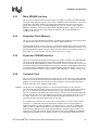
Intel® StrongARM® SA-1110 GPIO Pin Descriptions
4.3.2
Details of the SA-1110 GPIO pins are shown in Table 5-4. Pin Name indicates the actual name of
the pin on the SA-1110 device, while Signal Name indicates the signal name and function on the
SA-1110 Development Module.
Table 4-4. GPIO Pin Descriptions (Sheet 1 of 2)
Pin Name
Signal Name
Description
Main system software control on/off switch
GP[0]
On_Off_Sw1
GP[1]
On_Off_Sw2
and Spare
FIQ
Application dependent switch. Used to toggle main system power between run and sleep
modes.
Secondary system software control on/off switch
Application dependent switch. Used to toggle backlight power on and off. May function as
one touch record button that wakes up system to record audio.
Secondary function as a spare FIQ interrupt if required by GFX board.
LCD data for upper 8 bits of 16 bit color
GP[9:2]
LCD_D(15:8)
CNFG(7:0)
After system boot, these pins should be configured to drive the upper LCD data bits.
System configuration information
At system boot time, GPIO 9:2 may be read to determine system configuration. Refer to
CNFG table.
GP[13:10]
SSP_
UDA1341
SSP UDA1341 stereo codec port
Radio Interrupt request
GP[14]
Radio_IRQ
0 – No interrupt
1 – Interrupt
Only available when radio board is attached.
Shared L3 and SMB control ports
GP[15]
L3_SMB_
SDA
SMB data
L3 data is part of the L3 control bus to the UDA1341 stereo codec.
The System Management Bus (SMBus) is used to control smart battery chips
Power supply mode and sync control
GP[16]
PSMODE_
SYNC
0 – Low power operation for sleep mode
1 – High power, low noise operation for run mode
Sync – Program SDLC clock out to synchronize power switches. Used to reduce RFI and
video or audio noise
L3 mode signal with LED
GP[17]
L3_MODE
L3 MODE is part of the L3 control bus to the UDA1341 stereo codec.
LED
This GPIO has a LED that may be used by the boot code to indicate boot status by
flashing codes. After boot time this GPIO must function as the UDA1341 MODE signal.
Shared L3 and I2C control ports
GP[18]
L3_I2C_SCL
GP[19]
SSP_UDA
1341
Extrn_Clk
GP[20]
UART3 CLK/
SPARE
I2C clock
L3 clock is part of the L3 control bus to the UDA1341 stereo codec.
SCL is used as System Management Bus (SMBus) to control smart battery components
SSP UDA1341 stereo codec external clock input
Inputs 1.4976MHz 32Fs clock for 46.8KHz audio sample rate.
UART3 Clock input
GP[21]
User to provide high speed clock to UART3. UART3 is used as the radio communications
port. Bluetooth radio may require use of the external UART3 clock. Also a possible spare
GPIO if Bluetooth is not present.
MBGNT
MBGNT SA-1110 DMA bus grant signal when SA-1111 development is attached
CF_IRQ
CF_IRQ compact flash interrupt when no daughter boards are attached
Intel® StrongARM® SA-1110 Microprocessor Development Board User’s Guide
4-7
Hardware Considerations
Table 4-4. GPIO Pin Descriptions (Sheet 2 of 2)
Pin Name
Signal Name
Description
MBREQ SA-1110 DMA bus request signal when the SA-1111 Development Module is
attached
GP[22]
MBREQ
CF compact flash card detect interrupt when no daughter boards are attached
CF_
CardDetect
CF_CD1 and CF_CD2 are logically AND’ed on the SA-1110 Development Board
0 – CF card present
1 – CF card absent
GP[23]
GP[24]
UCB1300_
IRQ
UCB1300 Codec, UCB_GPIO and touch screen interrupts
GXF_IRQ
Graphics daughter board interrupt
CF_BVD2
CF_BVD2 signal when no daughter boards are attached
SA-1111_IRQ SA-1111 Development Module interrupt
GP[25]
CF_BVD1
CF_BVD1 signal when no daughter boards are attached
GP[26]
VBATT_LOW VBATT_LOW_IRQ Low battery interrupt
_IRQ
RClk, CPU coreclk/2 to clock logic analyzer pods when SA-1111 Development Module is
attached.
RClk
GP[27]
3.68M_32K
3.68 MHz SA-1111 and GFX PLL reference clock and GFX 32 KHz power up clock
GP[31:28]
Reserved
–
4.4
Register Descriptions
This section describes the following registers:
• System configuration register—to control SDRAM size, flash size, and type of module such as
SA-1111 development module.
• Board configuration register—to control the compact flash, codec, IRDA, stereo, audio, LCD,
RS232, LEDs, communication ports, charger, radio, and speaker.
• Board status register—to control communications and radio ports.
Intel® StrongARM® SA-1110 System Configuration Register
SCR
4.4.1
The SA-1110 Development Board supports several different SDRAM and flash memory types and
sizes as well as different LCD types and multiple daughter cards. To allow the system boot code to
correctly configure the SA-1110 memory interface and timing registers, the SA-1110 Development
Board uses GPIO 9:2 pins to input system configuration information at boot time.
Note:
In this document, the System Configuration Register (SCR) is referred to as a register, though no
register actually exists and therefore there is no corresponding address. The register bits are
composed of GPIO pins with some of them connected to pull-down resistors.
In the SA-1110 Development Platform, the GPIO 9:2 pins serve two functions: first as SCR bits
that can be read at boot time, and later as the upper 8 bits of the LCD data port.
After system reset and boot, all SA-1110 GPIO pins are reset to be inputs. During the boot
sequence the boot code performs the following sequence to determine the system configuration:
1. Configure GPIO 9:2 as outputs
4-8
Intel® StrongARM® SA-1110 Microprocessor Development Board User’s Guide
Hardware Considerations
2. Write 0xFF to GPIO 9:2
3. Configure GPIO 9:2 as inputs
4. Read GPIO 9:2 and save as system configuration byte.
High value resistors (100 K Ohms) are attached between GPIO 9:2 and ground on those bits that
must read as zeros in the configuration status register. High value resistors are required to minimize
wasted power in the resistors while the LCD is operating. These 100K ohm pull-down resistors
allow the GPIO pin to return to a valid zero level when the GPIO pins are configured as inputs.
To read the SCR bits, the boot code must first configure the GPIO 9:2 pins as outputs and then set
them to 0xFF very early in the boot process. This precharges the GPIO 9:2 pins to 3 volts. The boot
code must then configure the GPIO 9:2 pins as inputs and read the pins. The boot code must then
store the configuration information in a global area so that drivers and system services can
subsequently utilize the information.
The pins that have the 100K ohm pull-down resistors settle to a valid zero level in less then 2
microseconds. The pins that do not have pull-down resistors maintain valid high levels for more
then 10 microseconds. Due to these time constraints, the SCR boot code needs to sample the GPIO
9:2 pins only during valid times.
A section of boot code that allows the SCR bits to be read at a valid time is shown in Example 4-1:
Example 4-1. Boot Code to Read SCR Bits
ldr
mov
r0, =GPDR_PHYSICAL ;
;
r1, =0x0807A7FC
;
;
r1, [r0]
r0, =GPSR_PHYSICAL ;
;
;
r1, =GPIO_2_T0_9
;
r1, [r0]
r0, =GPDR_PHYSICAL ;
r1, =0x0807A400
r1, [r0]
r0, =GPLR_PHYSICAL ;
;
r2,#0x64
;
ldr
subs
r1, [r0]
r2,r2,#1
bne
%b10
and
ldr
r1, r1, #GPIO_2_T0_9; mask off non-configuration pins
r0, =CONFIG_PHYSICAL; equate with address of area to store
; SCR configuration info for later use
r1, [r0]
; store configuration in global area
r0, =GPDR_PHYSICAL
r1, =0x0807A7FC
; restore correct pin direction
r1, [r0]
ldr
str
ldr
ldr
str
ldr
ldr
str
ldr
equate with physical address of GPIO
pin direction register
SA1110DB Pin direction, for now get rid of
MBGRNT, STEREO, RXD
to find out SA-1110 HH board config must
write FF
to GPIO 2:9
writing 0 has no effect so can blast the 1s in
now configure pins 2 through 9 as input
equate with physical address of GPIO pin level
register
100 decimal
10
str
ldr
ldr
str
; now read pins to determine the configuration
; loop 100x through to make sure the pin bleed
; down takes
Intel® StrongARM® SA-1110 Microprocessor Development Board User’s Guide
4-9
Hardware Considerations
Table 4-5 provides bit descriptions of the SCR:
Table 4-5. System Configuration Bit Descriptions
2
6
2
5
2
4
2
3
2
2
2
1
Reset X
X
X
X
X
X
X
X
X
X
X
1
9
1
8
1
7
1
6
1
5
1
4
1
3
1
2
1
1
1
0
X
X
X
X
X
X
X
X
X
X
X
Reserved
2
0
Bits
Name
1:0
Reserved
9
8
X
X
7
6
5
X
X
X
4
3
X
X
2
1
X
0
Reserved
2
7
SDRAM_
Sizes
2
8
Flash_Size
2
9
Reserved
3
0
GFX
3
1
Bit
SA-1110 Development Board
SA-1111
System Configuration
X
X
Description
—
SDRAM size
11 – 128 Mbit devices. 32 Mbyte total bank size
SDRAM_
Size
3:2
10 – 64 Mbit devices. 16 Mbyte total bank size
01 – 256 Mbit devices. 64 Mbyte total bank size
00 – Reserved
Flash size
11 – 128 Mbit devices. StrataFalsh™ 32 Mbyte total bank size
5:4
Flash_Size
10 – 32 Mbit devices. StrataFalsh™ 8 Mbyte total bank size
01 – 16 Mbit devices. FlashFile™ 4 Mbyte total bank size
00 – 64 Mbit devices. StrataFalsh™ 16 Mbyte total bank size
7:6
Reserved
8
GFX
—
Graphics Accelerator board
0 – Present
1 – Not Present
SA-1111 Development Module
9
SA-1111
31:10
Reserved
0 – Present
1 – Not Present
4.4.2
—
SA-1110 Development Board Control Register BCR
0x1200,0000
The SA-1110 Development Board requires additional GPIO output functions which are
implemented in the SA-1110 Development Board Control Register (BCR) to control the compact
flash, codec, IRDA, stereo, audio, LCD, RS232, LEDs, communication ports, charger, radio, and
speaker.
The BCR is write only–system software must maintain a shadow copy of the BCR to perform
read-modify-write functions.
4-10
Intel® StrongARM® SA-1110 Microprocessor Development Board User’s Guide
Hardware Considerations
Note:
The BCR is not reset at power up time and is maintained during sleep mode. System software must
initialize this register very early in the cold power up code.
Table 4-6. Board Control Register (Sheet 1 of 4)
Bits
1
0
9
8
7
6
X
X
X
X
X
X
X
X
X
X
X
X
X
X
X
X
X
X
Name
5
4
X
X
3
2
1
0
CF_PWR NEP_RST
1
1
SOFT_RST
1
2
CF_RST GFX_RST
1
3
IRDA_FSEL
1
4
IRDA_MD[1:0]
1
5
Stereo_LB
X
1
6
Audio_On
X
1
7
CF_Bus_On
X
1
8
Light
X
1
9
LCD On
X
2
0
LCD12or16
X
2
1
D9_LED
Reset X
2
2
RS232En
X
Reserved
2
3
Vib_On
2
4
D8_LED
2
5
COM_DTR
2
6
COM_RTS
2
7
SMB_En
2
8
Rad_WU
2
9
Qmute
3
0
TV_IR_Dec_En
3
1
SA-1110 Evaluation Module
Rad_On
Bit
Board Control Register
Spk_Off
0x1200,0000
X
X
X
X
Description
Compact Flash Power
0
CF_PWR
0 – CF power off
1 – CF 3.3V power on
Must be programmed to 0 when system goes to sleep.
Compact Flash Reset
See Compact Flash spec V1.3
0 – No power up reset
1
CF_RST
GFX_RST
1 – Power up reset
Must be programmed to 1 when system goes to sleep.
Graphics Accelerator Reset
0 – Holds graphics accelerator in reset
1 – Allows graphics accelerator to run
Must be programmed to 1 when system goes to sleep
Codec Reset
2
SOFT_RST
0 – Holds UCB1300, ADI7171, and UDA1341 in reset
1 – Allows UCB1300, ADI7171 and UDA1341 to run
Must be programmed to 0 when system goes to sleep.
IRDA Frequency select
3
IRDA_FSEL
0 – SIR
1 – MIR/FIR
Controls IRDA chip data rate. Refer to IRDA chip vendor spec for details
IRDA Mode 1:0 Range/Power select
00 – Max range and power
5:4
IRDA_
MD[1:0]
01 – Shutdown. Power off
10 – 2/3 range and power
11 – 1/3 range and power
Must be programmed to 01 when system goes to sleep
Stereo Loopback
0 – Stereo loopback off
6
Stereo_LB
1 – Stereo loopback on
Stereo loopback is used by the system applications to route audio signals in the SA-1110
Development Board. Loopback is also used by diagnostic software.
Intel® StrongARM® SA-1110 Microprocessor Development Board User’s Guide
4-11
Hardware Considerations
Table 4-6. Board Control Register (Sheet 2 of 4)
Bits
1
0
9
8
7
6
X
X
X
X
X
X
X
X
X
X
X
X
X
X
X
X
X
X
Name
5
4
X
X
3
2
1
0
CF_PWR NEP_RST
1
1
SOFT_RST
1
2
CF_RST GFX_RST
1
3
IRDA_FSEL
1
4
IRDA_MD[1:0]
1
5
Stereo_LB
X
1
6
Audio_On
X
1
7
CF_Bus_On
X
1
8
Light
X
1
9
LCD On
X
2
0
LCD12or16
X
2
1
D9_LED
Reset X
2
2
RS232En
X
Reserved
2
3
Vib_On
2
4
D8_LED
2
5
COM_DTR
2
6
COM_RTS
2
7
SMB_En
2
8
Rad_WU
2
9
Qmute
3
0
TV_IR_Dec_En
3
1
SA-1110 Evaluation Module
Rad_On
Bit
Board Control Register
Spk_Off
0x1200,0000
X
X
X
X
Description
Compact Flash bus on
0 – CF BUS ON
7
CF_Bus_On
1 – CF BUS off (float)
Must be programmed to 0 when Xbus daughter boards are present
Must be programmed to 1 when system goes to sleep
Audio power on
0 – UDA1341, MIC and DAA power off
8
Audio_On
1 – UDA1341, MIC and DAA power on
Must be programmed to 0 when system goes to sleep.
Note that the UCB1300 has its own internal power down modes and is not controlled by
this signal.
Backlight
9
Light
0 – Backlight off
1 – Backlight on
Must be programmed to 0 when system goes to sleep
LCD 12bpp or 16bpp output select
10
LCD12or16
Configures the PZ3128 CPLD to map the SA-1110 LCD data pins as 12 bit RGB444 or 16
bit RGB565.
0 – 16RGB
1 – 12RGB
LCD power on
11
LCD On
0 – LCD and control logic power off
1 – LCD and control logic power on
Must be programmed to 0 when system goes to sleep
RS 232 transceiver enable
Controls power on RS232 level converters.
12
RS232En
0 – RS232 force power off
1 – RS232 enable auto power on
Must be programmed to 0 when system goes to sleep
Red LED
0 – LED on
13
D9_LED
1 – LED off
Application dependant. General application usage. May be used by developers as
general-purpose indicator or as a scope trigger.
Must be programmed to 1 when system goes to sleep.
4-12
Intel® StrongARM® SA-1110 Microprocessor Development Board User’s Guide
Hardware Considerations
Table 4-6. Board Control Register (Sheet 3 of 4)
Bits
1
0
9
8
7
6
X
X
X
X
X
X
X
X
X
X
X
X
X
X
X
X
X
X
Name
5
4
X
X
3
2
1
0
CF_PWR NEP_RST
1
1
SOFT_RST
1
2
CF_RST GFX_RST
1
3
IRDA_FSEL
1
4
IRDA_MD[1:0]
1
5
Stereo_LB
X
1
6
Audio_On
X
1
7
CF_Bus_On
X
1
8
Light
X
1
9
LCD On
X
2
0
LCD12or16
X
2
1
D9_LED
Reset X
2
2
RS232En
X
Reserved
2
3
Vib_On
2
4
D8_LED
2
5
COM_DTR
2
6
COM_RTS
2
7
SMB_En
2
8
Rad_WU
2
9
Qmute
3
0
TV_IR_Dec_En
3
1
SA-1110 Evaluation Module
Rad_On
Bit
Board Control Register
Spk_Off
0x1200,0000
X
X
X
X
Description
Green LED
0 – LED on
14
D8_LED
1 – LED off
Application dependant. General application usage. May be used by developers as a
general-purpose indicator or as a scope trigger.
Must be programmed to 1 when system goes to sleep.
Vibration motor (quiet alert)
0 – Motor off
15
Vib_On
1 – Motor on
Must be programmed to 0 when system goes to sleep.
This device uses significant power and should be used sparingly to conserve battery
usage.
16
COM_DTR
17
COM_RTS
COMport Data Terminal Ready
Must be programmed to 0 when system goes to sleep
COMport Request To Send
Must be programmed to 0 when system goes to sleep
Radio wake up interrupt
18
Rad_WU
0 – No interrupt
1 – Interrupts CPU in radio module
Must be programmed to 0 when system goes to sleep
System management bus enable
19
SMB_En
0 – Disable–Must be set to zero for phase 3 SA-1110 Development Boards
1 – Enable–Must be set to zero for phase 3 SA-1110 Development Boards
20
TV_IR_Dec_ TV IR Decode Enable
En
0 – Disable–Must be set to zero for phase 3 SA-1110 Development Boards
1 – Enable–Must be set to zero for phase 3 SA-1110 Development Boards
Quick Mute
21
Qmute
0 – Audio on
1 – Audio mute
Intel® StrongARM® SA-1110 Microprocessor Development Board User’s Guide
4-13
Hardware Considerations
Table 4-6. Board Control Register (Sheet 4 of 4)
Bits
1
0
9
8
7
6
X
X
X
X
X
X
X
X
X
X
X
X
X
X
X
X
X
X
Name
5
4
X
X
3
2
1
0
CF_PWR NEP_RST
1
1
SOFT_RST
1
2
CF_RST GFX_RST
1
3
IRDA_FSEL
1
4
IRDA_MD[1:0]
1
5
Stereo_LB
X
1
6
Audio_On
X
1
7
CF_Bus_On
X
1
8
Light
X
1
9
LCD On
X
2
0
LCD12or16
X
2
1
D9_LED
Reset X
2
2
RS232En
X
Reserved
2
3
Vib_On
2
4
D8_LED
2
5
COM_DTR
2
6
COM_RTS
2
7
SMB_En
2
8
Rad_WU
2
9
Qmute
3
0
TV_IR_Dec_En
3
1
SA-1110 Evaluation Module
Rad_On
Bit
Board Control Register
Spk_Off
0x1200,0000
X
X
X
X
Description
Radio Power On
0 – Radio power off
1 – Radio power on
22
Rad_On
Must be programmed to 0 when system goes to sleep.
This device uses significant power and should be used sparingly to conserve battery
usage. During transmission the radio may consume 10 times more power then the rest of
the system.
Speaker Off
0 – Speaker amplifier power on
23
Spk_Off
1 – Speaker amplifier power off
Must be programmed to 1 when system goes to sleep
This device may use significant power and should be used sparingly to conserve battery
usage.
31:24
4.4.3
Reserved
—
SA-1110 Development Board Status Register 0x1200,0000
The SA-1110 Development Board requires additional GPIO input functions which are
implemented in the SA-1110 Development Board Status Register (BSR) for communications and
radio functions. The BSR is read only.
4-14
Intel® StrongARM® SA-1110 Microprocessor Development Board User’s Guide
Hardware Considerations
Note:
The BSR is updated after each read to the BSR—to capture the present value of the BSR, two
consecutive read operations are required.
Table 4-7. 32-Bit Register Table
3
0
2
9
2
8
2
7
2
6
2
5
2
4
Rad_RI
Rad_DSR
Rad_CTS
COM_DSR
COM_CTS
COM_DCD
RS232_Valid
Reset X
X
X
X
X
X
X
X
Bit
a.
Bits
Name
23:0
Reserved
24
RS232_
Valid
32-Bit Register
SA-1110 Evaluation Board
2
3
2
2
2
1
2
0
1
9
1
8
1
7
1
6
1
5
1
4
1
3
1
2
X
X
X
X
X
X
X
X
X
X
X
X
1
1
1
0
9
8
7
6
5
4
3
2
1
0
X
X
X
X
X
X
X
X
X
X
X
X
Reserved
3
1
Rad_DCD
Physical Address
Description
—
MAX3244 RS232 transceiver detects a valid RS232 level
25
COM_DCD
COM port Carrier Detecta
26
COM_CTS
COM port Clear To Send
27
COM_DSR
COM port Data Set Ready
28
Rad_CTS
Radio port Clear To Send
29
Rad_DSR
Radio port Data Set Ready
30
Rad_DCD
Radio port Carrier Detect
31
Rad_RI
Radio port Ring Indicator
Not implemented in Phase 4, always reads 0.
4.5
System Reset
A MAX811 device is used to sense the 3.3 V rail and generate a reset signal called RESET_IN. A
manual reset switch also allows warm reset and system booting. The MAX811 component releases
the system reset signal when the 3.3 V rail is above 3.08 V.
Three subsystems in the SA-1110 Development Platform have a programmable soft reset control.
The SA-1110 Development Board provides the following reset controls:
• SA-1110 Compact Flash Reset (when Graphics and SA-1111 Development Modules are not
present)
• GFX_Reset
• UCB1300 and UDA1341 Codec_Reset (SA-1110 Development Board only)
The application must clear the reset on any subsystem that is to be used or initialized. The reset
controls are not affected by RESET_IN.
4.6
System Displays
This section describes the LED and LCD display topics on the SA-1110 Development Board.
Intel® StrongARM® SA-1110 Microprocessor Development Board User’s Guide
4-15
Hardware Considerations
4.6.1
LED Displays
There are six LEDs on the SA-1110 Development Board. These are primarily intended to provide
general status and power status and some low-level system debug and development support. Many
more system debug LEDs are on the SA-1111 Development Module.
Table 4-8. LED Descriptions
LED
Name
Description
GPIO 17 LED
D13
GPIO 17_LED
D9
D9_LED
D8
D8_LED
Used to signal boot diagnostic status. General purpose boot progress indicator.
Uses flashing codes to indicate boot progress. After boot time GPIO 17 is used as
the L3 MODE signal.
D9 LED
General purpose red LED controlled by BCR.
D8 LED
General purpose green LED controlled by BCR.
Automatic Gain Control LED
D11
AGC_LED
Used to indicate analog clipping in the microphone input circuit in the UDA1341
stereo codec. Intended as a development aid in AGC level control software and
speech recognition development.
Off Hook LED
D10
OH_LED
Indicates POTS modem off hook signal. Connected to UCB1300 GPIO_8. Also used
by system diagnostics to indicate successful UCB1300 communication.
Core Power LED
D4
CORE_PWR_LED
Indicates SA-1110 Vcore voltage is active. Used as an aid in power management
code development. Vcore is controlled by the SA_PWR_EN signal from the SA-1110
device.
4.6.2
LCD Displays
4.6.2.1
Sharp 3.9” Reflective Color
The SA-1110 Development Board provides direct support for a Sharp 3.9” 320x240 reflective TFT
color LCD (Sharp panel number LQ039Q2DS01). These panels utilize a new technology that does
not require backlighting and thus use much less battery power than the more common transmissive
LCD types. An optional frontlight may be switched on or off as required by the ambient lighting
conditions.
Note:
The design does not include a backlight power supply.
The 3.9” reflective panel requires rather elaborate analog and digital support circuitry on the
SA-1110 Development Board. Sharp does sell a custom ASIC part number LZ9GG31 that
implements the required digital circuitry, however the SA-1110 Development Board uses a PZ3126
CPLD to implement the LZ9GG31 functions.
A limitation with the SA-1110 is that it can not switch between eight bits per pixel (bpp) palettized
color RGB444 and 16 bpp hi-color RGB565 with out re-mapping the LCD data pins at the board
level. Normally this is not a problem because the bpp required by a particular application is known
before a design is complete. To provide a more flexible development design, the SA-1110
Development Board replaces the LZ9GG31 ASIC with a PZ3128 CPLD that implements the Sharp
LCD digital functions and in addition allows selecting between 8 bpp palettized color with
RGB444 12bpp, and hi-color RGB565 16bpp color systems. These two modes require different pin
4-16
Intel® StrongARM® SA-1110 Microprocessor Development Board User’s Guide
Hardware Considerations
mappings between the SA-1110 and the LCD that the CPLD can be programmed to accommodate.
In addition, no two LCDs are the same and the CPLD allows developers to adapt designs to support
other displays types or NTSC/PAL TV encoders. This LCD CPLD facilitates the adaptation of
many different LCD types to the SA-1110 Development Board.
The SA-1110 Development Board provides all required support circuitry for the 3.9” LCD and a
matching Hirose 50-pin connector for direct interfacing to this panel.
To use an LCD other than the Sharp 3.9”, a custom adapter flex print cable (FPC) must be
designed.
4.6.2.2
Memory Pixel Representations Versus Physical Pixel Interface
A frequent source of confusion with SA-1100 and SA-1110 LCD applications is the number of bits
per pixel. It is important to distinguish between the bits per pixel representation in SA-1110 system
memory and the bits per pixel of the physical interface between the SA-1110 and the LCD panel.
An operating system may use eight bit pixels in system memory while the SA-1110 LCD controller
color look up table (also known as a color palette) maps the eight bit memory pixels to twelve bit
physical pixels (RGB444) that appear on the LCD pixel data pins.
4.6.2.3
Mapping 18 Bit LCDs to 16 Bits of Pixel Data
Most TFT color LCDs have 18 bit interfaces which expect six bits of red, six bits of green and six
bits of blue, written as RGB 666. The SA-1110 Development Board provides 16 bits per pixel
maximum. To map the 16 bit SA-1110 LCD interface to an 18-bit color TFT LCD the LSBs of the
red and blue colors must be connected to ground. This results in five bits of blue, six bits of green
and five bits of red (RGB 565). The perceived color difference between RGB 666 and RGB 565 is
minimal.
4.6.2.4
LCD Backlight Frontlight Support
The SA-1110 Development Board provides a connector suitable for powering a backlight inverter
circuit. The raw battery voltage is available on the backlight connector to power a backlight
inverter. A program controlled GPIO pin allows switching the backlight/frontlight on and off. A
PWM DAC signal from the SA-1111 Development Module is also available on the connector to
control brightness if required by the display system.
Note:
4.7
The design does not include a backlight power supply.
Debugging
This section describes the SA-1110 Development Board’s keypad, debug and functional switches.
4.7.1
Keypad
A 5 x 4 matrix keypad suitable for use with telephone applications1 is supported in the SA-1111
Development Module. The primary use of the keypad is as a simple input device for system
debugging and diagnostic interaction. Applications may also use this resource.
1.
The SA-1110 Development Platform has not been certified as compliant with FCC, CE, UC, or PTT telephone standards or regulations.
Intel® StrongARM® SA-1110 Microprocessor Development Board User’s Guide
4-17
Hardware Considerations
4.7.2
Debug Switches
A switch pack containing eight switches is provided on the SA-1111 Development Module. The
switches may be read in the SWPK register. With the exception of Switch 8, which controls the
boot ROM bank select, the switch definitions are “soft” and may be defined by the debug
environment.
4.7.3
Function Switches
The SA-1110 Development Board has eight switches. These switches are mounted on the side of
the board and may be activated while booting the device.
• GPIO 0 switch–Manual override for GPIO 0
• GPIO 1 switch–Manual override for GPIO 1
• User software definable switches–Six switches for user software definable signals. Possible
applications are as follows.
— Power on/off
— Backlight on/off (soft switch)
— Scroll /Fast forward/Volume up/down
— Scroll /left/right/Fast reverse
— Record memo (audio microphone)
— Playback/stop
— Main Menu
With the exceptions of the GPIO 0 and GPIO 1 switches (S1 and S2 respectively), which also
functions as the system power on/off/wake-up switch, and the reset switch (S9), the definition of all
other switches (S3 through S8) as well as de-bouncing is done entirely in software.
Due to the limited number of switches, it is recommended that the switches share multiple
functions. An example would be a single switch for power on/off and backlight on/off with the
functions distinguished by the push duration or tap sequence.
The audio record/playback/fast forward/fast reverse/stop/volume functions should always be
assigned to switches and should not require using the touch screen. Audio record, playback and
shuttle function applications should permit single-handed operation.
4.7.4
Logic Analyzer Support
Logic analyzer support is needed on a very small percentage of all development boards. To reduce
the SA-1110 Development Board complexity, no logic analyzer test heads are provided on the
SA-1110 Development Board. However, the SA-1111 Development Module provides logic
analyzer access to all of the SA-1110 memory interface signals. For more information, see the
Intel® StrongARM® SA-1111 Development Module User’s Guide.
4-18
Intel® StrongARM® SA-1110 Microprocessor Development Board User’s Guide
Hardware Considerations
4.8
SMBus
The SMBus interface is a two-wire serial protocol requiring open-collector drivers that allow the
“wire or” of data on the SMBus. The SMBus SDA (data) and SCL (clock) have pull-up resistors to
VDD such that an un-driven SMBus pin will be high (one). The GPIO pins on the SA-1110
Development Module are three-state drivers that have programmable control of direction and data
as well as interrupt generation from either or both edges of a signal. To use the GPIO pins with the
SMBus requires the use of the GPIO direction control bits for two of the GPIO pins as SMBus data
bits.
The GPIO GPCR data register bits for both bits assigned to the SMBus are always cleared to zero.
To drive a low (zero) onto the SMBus SDA or SCL lines the direction bit is set to 1, which drives
the zero data on to the SMBus pin. To drive a one, the GPDR bit for the SMBus pin is set to zero,
which reconfigures the pin as an input and turns off the three-state driver allowing the pull-up on
the SMBus to pull the SMBus line high to a one. The value of the SMBus pins may be read at any
time through the GPLR. For more information about the GPCR, GPDR, and GPLR registers, see
the Intel®StrongARM® SA-1110 Microprocessor Advanced Developer’s Manual.
The SMBus protocol can be implemented in SA-1110 software with the assistance of interrupt
driven, system timed, programmed I/O. The system timer establishes the SMBus clock rate as well
as avoiding polled PIO of the SMBus GPIO pins. This strategy allows direct connection of two
GPIO pins to the two-wire SMBus with no external glue logic and a minimum of MIPS.
The SMBus is provided on the battery connector to support smart battery packs.
4.9
Serial Ports
The SA-1110 Development Board provides a RS232 interface connected to the SA-1110 serial
port 1. A custom 14-pin header made by FCI is used to allow an external connection to the RS232
port and the POTS signals. This header is similar to the serial adapter headers and the cables used
in cell phones. This communications port may be used for the debug serial port or as an application
communications port. This port provides RTS, CTS, DTR and DSR modem signals to support a
serial IO port PC synchronous application.
A Maxim MAX3244* RS232 transceiver is used to manage the level conversion and line interface.
This device has a power saving automatic shutdown that powers down the chip if no valid RS232
levels are detected. The component may also be forced off by RS232En, which is bit 12 in the
Board Control Register. When off, the CMOS receiver signals are three-stated allowing this serial
port to be shared with the SA-1111 Development Module.
The SA-1111 Development Module provides a standard 5x2 0.1” header for the SA-1110 serial
port 1. This port is used for system debugging and firmware development. When the SA-1111
Development Module is attached, the SA-1110 Development Board shuts down its MAX3244
RS232 transceiver to avoid conflict with the SA-1111 Development Module RS232 transceiver.
The SA-1110 Development Module’s RS232 transceiver may be forced off by RS232En. A second
port on the SA-1111 Development Module that is connected to the SA-1110 serial port 3, is
provided via a nine-pin RS232 port connector on the board. This port may be used for debug
messages from the development environment.
Intel® StrongARM® SA-1110 Microprocessor Development Board User’s Guide
4-19
Hardware Considerations
Note:
4.10
The nine-pin RS232 cable connected to the Base Station serial port (J10) on the SA-1110
Development Board cannot be connected at the same time as the UART1 connector on the
SA-1111 Development Module. Failure to do so will corrupt the data on the UART1.
Power System
The SA-1110 development system has a unique, highly efficient and cost effective battery power
system.
4.10.1
Power System Design Benefits
The SA-1110 Development Platform provides the following benefits:
•
•
•
•
Requires only a single cell Li-ion 3.6 V battery
Greater then 90% efficiency on 3.3 V, 1.5 Vcore, and radio power rails in operating mode
Greater then 90% efficiency on 3.3V rail in sleep mode
Supports high power, high efficiency radio power rail for radio modules requiring either two
cell Li-ion batteries providing 7.2 V power or a single cell Li-ion battery providing 3.6 V
power
• Control of pulse width modulation (PWM) or pulse frequency modulation (PFM) and power
switching synchronization modes of main switching regulators
• Very clean power rails for audio and LCD systems
• Allows charging from AC power adapter or USB power input using a Maxim MAX846*
Li-ion charge controller
•
•
•
•
•
4.10.2
Provides battery temperature monitoring
Provides battery voltage and charger voltage monitoring
Provides automatic battery lockout to prevent over-discharge and possible battery damage
Provides low battery interrupt to SA-1110 processor
Provides power switches for Compact Flash socket, audio subsystem and LCD display
subsystems
Power System Design
There are two main power rails in any SA-1110 design; are the 3.3 V main power and the
1.5 V core power. The 3.3 V rail must be on all the time to support sleep mode and preserve
SDRAM contents and system timer. In addition, a medium power 5 V rail is needed for the LCD as
well as a 7.6 V (two Li-ion cell equivalent) high power rail for the CDMA radio module.
As shown in Figure 4-1, the battery charge and discharge rates are quoted in relative terms related
to the rated capacity of the battery. As an example, a 1000 mA hour battery may be discharged at a
2 C rate where C is the rated battery current or 1000 mA in this example. A 0.2 C rate would be
200 mA for a 1000mAh battery. A Li-ion battery with a 100% charge starts at a terminal voltage of
4. 1 V and quickly discharges to about 3.6 V where it remains for most of the discharge cycle.
Toward the end of the discharge cycle the Li-ion terminal voltage falls rapidly from 3.6 V to 2.7 V
where the discharge must be stopped or battery damage (loss of capacity) may result. Two Li-ion
4-20
Intel® StrongARM® SA-1110 Microprocessor Development Board User’s Guide
Hardware Considerations
cells result in a 8.2 V to 5.4 V terminal voltage discharge curve, while a single cell Li-ion batteries
produce 4.1 V to 2.7 V through out its discharge cycle with a 3.6 V nominal voltage. The discharge
curves of Li-ion batteries are very flat when compared to lead acid or alkaline types. Li-ion
batteries do not exhibit the memory effects associated with NiCd batteries or the high self
discharge rates associated with NiMH batteries. In addition, Li-ion batteries have the highest
energy density (watt hours per CC) of any available, affordable battery technology.
Figure 4-1. Li-ion Discharge Curves
PWR IN
Chrg
Super
cap
3.6V
batt
5.5v Radio power @900ma
SMPS
SA PWR EN
track
LDO
Discharge Rate Characteristics
Voltage / V
off
1C discharge (4.1V cccv)
20˚C
4.0
LCD en
5V
LDO
LCD
5V
off 3.2V
Batt Lockout
4.5
or 3.5V during sleep
Main
3.3V
3.3V
LDO
0.2C
3.5
on
2C
3.0
1.55V
SMPS
1C
2.5
Vcore
1.55V
2.0
0
500
1000
1500
Capacity / mAh
A7267-01
Figure 5-1 shows the effect of higher discharge rates on a Li-ion cell. This voltage sag effect under
heavy loads is due to the internal resistance of the Li-ion cell which is less then 0.2 ohms typically.
Discharge loads that are less then 20% (0.2C) of the battery capacity result in the most power
efficient use of this battery type.
4.10.2.1
1.5V Core Power
The single Li-ion cell 1.5 V core power regulator solution is very simple and efficient. A
MAX1692 buck regulator is fed from the 4.1 V – 2.7 V single cell Li-ion battery. This regulator,
which is described in detail in Section 4.11.1, can achieve greater than 90% efficiency and is turned
off during sleep mode by the SA-1110 SA_PWR_EN signal. The MAX1692 buck regulator is a
high frequency type regulator. Powering the 1.5 V switching regulator from two Li-ion cells (8.2 V
to 5.4 V) results in less than 85% power conversion efficiency. Using a single Li-ion design instead
of two results in a greater than 90% conversion efficiency for the 1.5 V rail.
Intel® StrongARM® SA-1110 Microprocessor Development Board User’s Guide
4-21
Hardware Considerations
4.11
Power for the Intel® StrongARM SA-1110
Development Board
The following two sections provide a background on the design considerations for the 3.3 V supply
on the SA-1110 Development Board and the actual implementation used.
4.11.1
Note:
3.3 V Main System Power Design Considerations
This section provides a background on design considerations for the power supply on the SA-1110
Development Board, while Section 5.21.2 describes the actual implementation.
The terminal voltage for a single cell Li-ion battery varies between 4.1 V to 2.7 V throughout its
discharge cycle. This presents a problem for the 3.3 V power supply design, because the battery
terminal voltage starts out higher than the 3.3 V rail and ends up lower than the 3.3 V rail.
Switching regulators are generally considered the highest efficiency solution to most battery power
conversion designs. Switching regulator power conversion technology provides buck regulators
that reduce a high voltage to a lower voltage. Boost regulators can convert a low voltage to a higher
voltage. Combination buck/boost regulators can handle the 4.1V to 2.7V input variation of a single
Li-ion cell to produce the 3.3 V on the main power rail.
An alternative solution for 3.3 V generation could use a boost regulator to produce 5 V from the
2.7 V to 4.1 V battery (the LCD requires 5 V anyway) plus a secondary or post regulator to buck
the 5 V down to 3.3 V. This results in reduced conversion efficiency for the 3.3 V rail because the
efficiency of the two regulators are multiplied, 90% of 90% equals 81%.
However, switching regulators are typically less efficient at low-power levels than at high-power
levels. A switching regulator that is 90% efficient at full load may be less than 80% efficient under
very light loads, even when taking advantage of the pulse width modulation (PWM) or pulse
frequency modulation (PFM) selections that the regulators provide to optimize conversion
efficiency for heavy and light loads. This is important because the sleep mode, which is a very low
power mode, must be very efficient to allow the longest possible sleep times. Unfortunately, the 5
V to 3.3 V boost buck combination results in less than 65% (80% of 80%) combined efficiency in
sleep mode.
Buck and boost switching regulators as well as linear regulators are most efficient when the input
voltage is close to the output voltage. This is why the 1.5 V buck regulator is 91% efficient when
powered by a single cell 3.6 V Li-ion battery and only 85% efficient when powered from two cells
at 7.2 V. A key point here is that linear regulators, which are generally considered to be very
inefficient, can be more efficient than switching regulators if the input voltage is only slightly
higher than the output voltage. Low drop out (LDO) linear regulators improve this situation by
allowing the input voltage to be as little as 150 mv higher than the regulated output voltage at the
full rated load.
Given that Li-ion batteries discharge at less then a 0.2C rate (20% of the total mah rating) have a
terminal voltage at or above 3.6 V over 80% of their discharge cycle; the use of a simple LDO
linear regulator connected directly to the battery provides the 3.3 V rail a very power efficient, lowcost solution. An LDO linear regulator also does not require the bulky coils, capacitors and diodes
that switching regulators do, resulting in even lower cost and less circuit board “real estate”.
At the beginning of a charge with a terminal voltage of 4.1V, the LDO linear regulator for the 3.3 V
rail is over 80% efficient. When the battery is at its nominal voltage of 3.6 V, the LDO regulator is
over 91% efficient and approaches 96% efficiency as the battery discharges towards the 3.45 V
4-22
Intel® StrongARM® SA-1110 Microprocessor Development Board User’s Guide
Hardware Considerations
LDO cutout point. The efficiency goes up in sleep mode where the small load results in an even
lower drop out voltage of 20 mV, which allows the battery to discharge to 3.32 V before drop out
starts. With a 3.32 V battery voltage, the 3.3 V LDO linear regulator is over 99% efficient.
In addition, using a LDO linear regulator provides the 3.3V rail results with a very clear power
supply that requires fewer and smaller filter capacitors, saving cost and board space. An added
benefit is less noise in the audio, telephony and display systems.
Unfortunately, two major disadvantages to this scheme are:
• The last 20% of the battery capacity is not usable because the bottom 20% of the charge
terminal voltage goes below the 3.45 V cutout level necessary to maintain the 3.3 V output
from the LDO linear regulator.
• Battery voltage sag due to discharge rates in the 1C to 2C range, which may be typical when
the radio is transmitting, would cause the 3.3 V LDO linear regulator to drop out.
A three part solution to this dilemma also results in solving the two cell Li-ion radio power
requirements as well as allowing the elimination of the backup battery, improved power conversion
efficiency, reducing system cost, and reduced audio and video noise. This unique power system
design is referred to as a linear boost bootstrap with virtual backup battery. The three key elements
of this design are as follows:
• Use of an adjustable boost regulator with a built in adjustable LDO linear post regulator and
LDO track mode feature.
• Use of a separate 3.3 V LDO linear regulator connected directly to the single cell Li-ion
battery in parallel with the boost converter LDO linear post regulator.
• Reservation of the bottom 20% of battery charge when the battery terminal voltage is below
3.45V, to be used as a virtual backup battery. Reserving the last fraction of charge of a system
battery to preserve the memory contents is probably not new, however it is an optional cost
reducing feature that is a natural consequence of the linear boost bootstrap design.
4.11.2
Note:
MAX1705 Boost Converter and MIC5219 LDO Linear
Regulator
This section provides a description of how the actual power supply was implemented on the SA1110 Development Board, while Section 4.11.1 describes design considerations.
The MAX1705 has three key features that support the linear boost bootstrap SA-1110
Development Board power system design. First, the MAX1705 has a built-in adjustable LDO
linear regulator that is fed from the main boost regulator output. Second, the MAX1705 has a
special track mode that can be set to allow the main boost regulator to be regulated to 0.3 V above
the LDO output instead of the normal 5 V output. This causes the main boost output to track 0.3 V
above the LDO output to keep the LDO from dropping out. This permits efficient boost and post
linear regulation of the 3.3 V supply when the 5 V output is not needed, such as sleep mode. Third,
the MAX1705 supports a low battery sensing circuit that is used to sense the 2.7V bottom of charge
level and shutdown all battery loads in the SA-1110 Development Board system to protect the
Li-ion battery from over-discharge damage.
The SA-1110 Development Board design sets the MAX1705 main boost output to 5.5 V, which is
the maximum the boost output can be set to on the MAX1705. The LDO output is set to 3.2 V.
Given that the MAX1705 LDO power input is from the main boost output rail on the MAX1705,
the resulting conversion efficiency from the battery to the 3.2 V output is
0.9 X 3.2/5.5 X 100 = 52%, which is very poor. However, the MAX1705 3.2 V LDO output is
Intel® StrongARM® SA-1110 Microprocessor Development Board User’s Guide
4-23
Hardware Considerations
wired in parallel with a MIC5219 3.3V LDO which is powered directly from the battery. The
MIC5219 has a very low drop out voltage, has an enable input, and is available in very small
packaging.
With the two LDO outputs wired in parallel, the load is powered from the LDO that has the highest
output voltage. As long as the battery is above 3.45 V, the MIC5219 3.3 V LDO powers the 3.3 V
circuits on the SA-1110 Development Board. If the battery sags below 3.45 V, then the 3.3 V
circuits smoothly transition to drawing powered from the 3.2 V LDO in the MAX1705 which is
powered from the main 5.5 V output of the MAX1705 boost regulator. This bootstrap feature
allows the 3.2 V LDO to pick up or bootstrap the 3.3 V circuits when the battery sags below 3.45 V
necessary to power the 3.3 V LDO. Setting the MAX1705 LDO to 3.2 V allows a smooth
automatic load transfer from the MIC5219 3.3V LDO when the battery voltage sags under heavy
load from the radio transmitter or when the battery is near the end of charge and the battery voltage
is sinking below 3.45 V. This method allows the SA1110 Development Board to use the very
efficient and clean direct battery powered 3.3 V LDO through 80% of the discharge cycle while
providing reserve boosted linear regulation for the 3.3 V circuits when the battery drops below
3.45 V. All the 3.3 V devices in the SA-1110 Development Board are specified to function
normally down to 3.0 V, so the 3.3 V to 3.2 V switch over still has 200 mV of voltage margin.
The 3.2 V LDO reserve boost regulation power supply is no more then 52% efficient when the
boost output is at 5.5 V. However, this supply is only used when the radio is transmitting at full
power, which may cause the battery to sag below 3.45 V. In this case, the power drain from the
radio is almost 10 times the entire 3.2 V load anyway, making the poor 3.2 V conversion efficiency
while transmitting inconsequential.
The third feature of the MAX1705 used in the SA-1110 Development Board power system is the
battery threshold sensing circuit. This circuit is set to detect the Li-ion battery going below the
2.7 V end of charge threshold. The low battery output signal, BATT_LOCKOUT, forces the
MAX1705 to shut down and also shuts down the MIC5219 3.3V linear regulator, which shuts
down the SA-1110 and all other 3.3 V loads including SDRAM. When the SA-1110 is shut down,
the SA_PWR_EN signal goes low which also shuts down the MAX1692 1.5 V core regulator. The
end result is all battery loads are off, all memory contents are lost, but the expensive Li-ion battery
is saved from over discharge damage that can drastically reduce its storage capacity.
4.11.2.1
Sleep Mode
The efficiency of the 3.3 V power system is very critical in sleep mode. The SA-1110 Development
Board with its two SDRAM memories requires about 1 mA sleep current on the 3.3 V rail. With a
100% efficient 3.3 V power conversion, a 1000 mah battery fully charged results in about 1000
hours of sleep time, or about 6 weeks. A power system that boosts the Li-ion battery voltage to 5 V
and then bucks it to 3.3 V (less than 65% efficient) would last less then 4 weeks.
The efficiency of the 3.3 V rail in sleep mode with the linear boost bootstrap design is over 91% for
most of the battery discharge cycle and approaches 100% towards the 3.32 V drop out point. This
efficiency is better than any switching regulator can achieve in low-power mode. Below the 3.32 V
drop out point, with the MAX1705 in track mode and its 3.2 V LDO regulator picking up the load,
the combined efficiency of the boost regulator in low-power PFM and track mode and the 3.2 V
LDO is 0.8 X 3.2/3.5 X 100 = 73%. However this 73% only applies to the last 10% of the discharge
cycle where the battery voltage is below 3.32 V and before it falls to the 2.7 V battery lockout cutoff point.
4-24
Intel® StrongARM® SA-1110 Microprocessor Development Board User’s Guide
Hardware Considerations
4.11.2.2
Virtual Backup Battery
The linear boost bootstrap design relies on an LDO regulator in parallel with a boost converter and
a post LDO regulator to automatically load switch as the battery voltage falls from a high of 4.1 V
down to the 3.45 V main LDO drop out voltage. Below the 3.45 V main LDO drop out, the 3.3 V
circuits are powered by the 3.2 V LDO, which is powered from the boost regulator at the 5.5 V.
The linear boost bootstrap design is over 90% efficient for over 90% of the discharge cycle. The
design supplies full-system power all the way down to a 0.9 V battery voltage (well below the
2.7 V battery lockout point). However the full power 3.3 V efficiency is much less
(0.9 X 3.2/5.5 X 100= 52%) when the battery is below the 3.45 V point.
By reserving the bottom 10% of the charge as a virtual backup battery, the system can avoid the
reduced full-load conversion efficiency for the last 10% of the charge cycle and uses it instead to
eliminate the back up battery that is normally required. With the linear boost bootstrap circuits in
sleep mode, the last 10% of the charge is used at a 73% conversion efficiency. For example, if the
last 10% of the charge is at 100 mah and the 3.3 V sleep load is 1 ma, then the virtual battery lasts
73% of 100 mah or 73 hours, or about three days. If longer sleep times are required, the voltage
threshold where the virtual backup battery provides power can be raised.
The virtual battery design provides a direct read of the battery voltage through the UCB1300
Analog to Digital converters. The OS should notify the user to recharge or swap batteries as the
battery voltage approaches the 3.45 V virtual backup battery point. A low battery interrupt is also
provided as an alternative to scheduled battery voltage readings through the UCB1300. This low
battery interrupt is set at 3.5 V and is only active when the LCD is powered on. The low battery
interrupt results in the user receiving a two minute warning before an OS invoked sleep shutdown.
A hardware forced sleep mode is also provided with a MAX812 voltage sensing chip that drives
the SA-1110 VDD_FAULT signal when the battery drops below 3.08 V. The MAX812 may be
eliminated if the OS managed battery monitor and sleep mode entry is reliable and the OS never
hangs.
A very high value capacitor of 0.33 Farads (known as a supercap) connected in parallel with the
battery supports the system in sleep mode for several minutes if battery changes are required. A
low value resistor (1 ohm) in series with the supercap is essential to reduce inrush current when a
charged battery is attached to a discharged supercap.
The virtual backup battery circuit used in the SA-1111 Development Module is, of course, an
optional system design feature. Other designs may need real backup batteries as required by the
application.
4.11.2.3
Linear Boost Bootstrap System
Figure 5-2 shows the complete linear boost bootstrap system with virtual backup battery. Not
shown are the low-battery interrupt-sensing circuit and the end-of-charge forced-sleep-mode
circuit.
Intel® StrongARM® SA-1110 Microprocessor Development Board User’s Guide
4-25
Hardware Considerations
Figure 4-2. Linear Boost Bootstrap Power System
0.33 F
SuperCap
Li-ion
4.1 V to
2.7 V
SA_PWR_EN
BATT LOCKOUT
5.5 V Radio Power
or
3.5 V During Sleep
MAX
1705
track
off
LDO
3.3 V
MAX
1602
LDO
3.2 V
5.0 V
LCD
Power
LDO
5.0 V
3.3 V Main
1.5 V Core
A7297-01
4.11.2.4
Radio Power
The SA-1110 Development Board supports CDMA or GSM radio module daughter boards. The
CDMA board electro-mechanical interface is supported on the SA-1110 Development Board radio
connector. The GSM radio module is supported with the addition of a small adaptor board that
provides a smart card slot and connector type conversion.
Note:
The GSM adapter is not available in Phase 4.
The CDMA power requirements are matched to a two cell Li-ion battery that must be capable of
supplying up to 850 mA (worst case) during maximum power transmission.
The GSM power requirements are matched to a single cell Li-ion battery with a maximum current
of up to 2.5 A at a 12.5% duty cycle. The 0.33 F supercap used in the virtual backup battery design
also assists the main battery in meeting this very high current pulse demand.
The GSM power requirements are easily met by providing a connection to the single Li-ion main
battery.
The CDMA requirements are for a nominal 7.2 V two cell Li-ion supply. The discharge curves for
a two cell Li-ion battery run from 8.2 V fully charged, down to 5.4 V at the end of charge. A simple
solution was to use the high power MAX1705 boost output, which is designed to be adjustable
from 2.5 V to 5.5 V. Setting the MAX1705 boost output to 5.5 V allows powering the CDMA
module which requires a minimum of 5.4 V input. The current requirements of the CDMA module
are a maximum of 850 ma, which matches the maximum performance of the MAX1705.
4-26
Intel® StrongARM® SA-1110 Microprocessor Development Board User’s Guide
Hardware Considerations
4.11.2.5
LCD Power
The Sharp 3.9” LCD requires +5.0 V, +3.3 V +15 V, -14 V, and -11.7 V, all at low or very low
power levels. A MAX633 boost switching regulator is used to provide +15 V and to provide a
charge pump driver to allow the generation of a –14 V, and from that a 3.3 V Zener diode drops it to
–11.7 V. All LCD interfaces require proper sequencing of their power pins. To achieve the
sequencing, the SA-1110 Development Board powers all LCD circuits from a MIC5219 5.0 V
LDO linear regulator powered from the 5.5 V CDMA radio power rail. The battery power
conversion efficiency for this linear regulated 5 V rail powered from the boost 5.5 V output is
0.9 X 5/5.5 X 100 = 81%. The MIC5219 5.0V LDO LCD regulator regulates the 5.5 V down to
5.0 V, supports an output enable signal, and provides a very clean power rail to the LCD. The very
clean power rail to the LCD requires fewer bulk capacitors to smooth out, and results in a noise free
display. The LCD 5.0 V MIC5219 powers the MAX633 boost regulator as well as two more
MIC5219 regulators that are cascaded to provide correctly sequenced 4.0 V and 3.3 V for the LCD
and its control logic.
Most handheld devices turn on the LCD when the system is turned on. However, the SA-1110
Development Platform also supports high quality stereo audio that permits the unit to play MP3
entertainment audio like a personal stereo player. In this mode, the LCD is not needed for long
periods of time and battery charge can be substantially extended by allowing the LCD to be turned
off during audio only mode. Bit 11 in the Board Control Register, LCD On, controls the LCD
power enable.
4.11.2.6
System Power Limits
The following list defines the SA-1110 Development Board’s maximum available power:
• +3.3 V 300 mA main power–Always on to preserve DRAM contents in sleep mode
• +1.5 V to +2 V (depends on SA-1110 order number) 500 mA SA-1110 core power–Demand
switched1
•
•
•
•
•
•
+4.1 V to 2.7 V 1000 mA–Main Li-ion battery power to GSM radio
+5.5 V 850 mA. CDMA radio module power–Demand switched1
+5.0 V 180 mA LCD power – Demand switched1
+15 V 25 mA LCD power – Demand switched1
-15 V 10 mA LCD power – Demand switched1
-11.7 V 1 mA LCD power – Demand switched1
These numbers represent the maximum load limits on each rail. It is unlikely that all rails would be
fully loaded at the same time, and typical loading is much less than the maximums. The SA-1110
Development Board’s power system can sustain these maximum loads, however, the battery life
would be shortened substantially. Ideally the battery discharge current would never exceed 2C or
two times the rated battery capacity current (1000 mah to 1500 mah). The 2C limit would be
approached when using the radio module. Typical loads when not using the radio should be in the
0.1C to 0.2C range which is optimal for Li-ion batteries.
1.
Controlled by the SA-1110 PWR_EN signal.
Intel® StrongARM® SA-1110 Microprocessor Development Board User’s Guide
4-27
Hardware Considerations
4.12
Audio Systems
The SA-1110 Development Board audio subsystem has two primary components: the UCB1300
POTS and handset codec and the UDA1341 stereo codec. The UCB1300 is interfaced to the SA1110 Multimedia Communications Port (MCP) and supports POTS softmodem and medium
quality mono audio. The UDA1341 is interfaced to the SA-1110 Serial Peripheral Interface (SPI)
with the addition of a small amount of glue logic. The UDA1341 supports high quality stereo
capture and playback.
The SA-1110 Development Board’s audio subsystem includes the following resources:
•
•
•
•
•
•
•
•
•
•
•
•
•
•
UCB1300 audio codec for phone headset and microphone
UCB1300 phone codec for softmodem POTS connection
UDA1341 stereo codec
UDA1341 digital mixing of Line1 and Line2 inputs
UDA1341 microphone inputs with automatic gain control
UDA1341 Treble, Bass and Volume controls
Digital loopback of UDA1341 providing board level source mixing and diagnostics
Two built-in electret microphones
250 mW stereo audio amplifier to drive speaker(s) or headphones
One built-in mini speaker
3.5 mm stereo headphone jack
2.5 mm headset and microphone jack
Radio analog audio input
Radio analog audio output
The SA-1110 board audio system allows the software to control the following functions:
•
•
•
•
•
•
•
•
•
•
•
•
4-28
Selection of analog audio sources, including two microphones
UCB1300 audio output (analog)
Radio audio output (analog)
Selection of digital audio sources
UCB1300 system digital audio
UDA1341 system digital audio
UDA1341 controlled mixing of audio sources (using stereo loopback mode)
UCB1300 speaker with microphone 1
UCB1300 speaker with radio speaker
Radio speaker with microphone 2
Software digital mixing of audio sources
Any OS managed digital audio streams with any analog audio source (UCB speaker, radio
speaker, microphone 1, microphone 2)
Intel® StrongARM® SA-1110 Microprocessor Development Board User’s Guide
Hardware Considerations
• Software control of audio destinations
• Any OS managed digital audio streams or analog audio source to mini-speaker or UBC
microphone input or radio microphone input or headset or headphones
• Automatic gain control for microphone1 inputs
• Treble, bass and volume control
4.12.1
Stereo Codec
A Philips UDA1341 I2S 16 bit delta sigma stereo codec is provided on the SA-1110 Development
Board through the glue logic to the SA-1110 SSP port. The UDA1341 on the SA-1110
Development Board provides high quality stereo sound input and output for entertainment sound
and speech recognition application support without requiring the SA-1111 companion chip. The
SA-1110 Development Board provides a UDA1341 digital loopback that allows the UDA1341 to
be used as a systems audio routing and mixing resource without having to set up the SA-1110 SPI
port to access the UDA1341.
A 0.250 mW per channel audio amplifier drives the internal speaker or the 3.5 mm standard stereo
jack for high quality stereo output to a headset.
Volume, treble and bass settings are by program control of the UDA1341. Volume control up/down
switches may be allocated from the general purpose system switches as required by the application.
The UDA1341 is interfaced to the SA-1110 SSP port using a small amount of CPLD glue logic as
shown in Figure 5-3.
The UDA1341 also requires a three wire control interface known as L3. This control interface is
similar to I2C* in that it may be implemented using programmed I/O and GPIO pins. The L3 bus
and SMbus bus share the same GPIO pin.
4.12.2
L3 Bus
The UDA1341 L3 bus utilizes a simple serial protocol similar to the I2C—see the UDA1341
specifications for details. The L3 includes a clock pin, a data pin, and a mode pin. These three slow
speed signals are connected to the SA-1110 GPIO pins and are driven with software to implement
the L3 protocol.
Intel® StrongARM® SA-1110 Microprocessor Development Board User’s Guide
4-29
Hardware Considerations
4.12.3
Stereo Codec Interface
The UDA1341 interfaces to the SA-1110 SSP port. The SSP must be configured in a TI
synchronous serial format with 16 bit data slots. A small amount of glue logic is required to
interface the UDA1341 to the SSP port. Figure 5-3 shows a simplified version of the glue. The
logic is implemented in the SA-1110 Development Board control CPLD.
Figure 4-3. Stereo Codec Glue Logic
Divide
by 4
11.98 MHz from
MCP Clock
GPIO19 SSP
CLK IN
CODEC
256 FS SYSCLK
CODEC RESET L
D
Q
Q
GPIO13 SSP
SFRM
CODEC
Word
Select
C
GPIO12 SCLK
CODEC BCLK
A7266-01
Figure 5-4 shows how the glue logic modifies the SSP TI synchronous serial format to match the
I2S format used by the UDA1341. The UDA1341 must be configured using the L3 interface to
communicate in an MSB-Justified format with 16 bit data slots.
Figure 4-4. UDA1341 Interface Timing
SCLK
SFRM
Tx and
Rx Data
MSB
MSB-1
MSB-2
WS
BCLK
A6949-01
4-30
Intel® StrongARM® SA-1110 Microprocessor Development Board User’s Guide
Hardware Considerations
4.12.4
Microphone and Speaker
The SA-1110 Development Board includes two built in electret type microphones as well as a mini
speaker.
Two microphones are required to provide optimal sound capture. One microphone is used during
dictation when the SA-1110 Development Board is held like a tape recorder in front of the mouth.
The other microphone is used during voice cell-phone calls when the SA-1110 Development Board
is held like a phone. The audio mixing functions in the SA-1110 Development Board allow the
selection of which microphone to use for voice or using both microphones for high quality stereo
recording.
A 2.5 mm jack is provided for a headset/microphone and a 3.5 mm stereo jack is provided for
stereo headphones. An internal three pin header is provided to allow connections to stereo line in
signals.
4.12.5
SA-1110 Development Board Stereo Codec Sampling Rates
The SA-1110 Development Module UDA1341 does not include a sample rate clock generator.
Therefore, when web browsing, the following sample rates are expected:
•
•
•
•
•
8 KHz
11.025 KHz
16 KHz
22.05 KHz
44.1 KHz
To save the cost and power of a dedicated oscillator and clock generator for these frequencies, the
SA-1110 Development Board derives the 11.29 MHz 128 times clock from the CPU memory clock
using a clock “shimming” scheme implemented in the UDA1341 glue logic CPLD. This clock
shimming scheme produces a 11.29 MHz 128 times oversampling clock that is between 1.1% and
0.1% accurate depending on the CPU core clock chosen. A software sample rate converter (SRC)
function is required to up sample the 8, 11, 16, 22 KHz rates to 44 KHz.
4.12.6
Phone Codec and Soft Modem
The UCB1300 Codec from Philips and a DAA telephone line interface from Krypton support
softmodem and speaker phone. The UCB1300 has two codecs: one for the phone line and one for
microphone and speaker or handset.
The UCB1300 handset codec requires different sampling rates than the stereo codec and may be
required to run concurrently with the UDA1341. The SA-1110 Development Board audio mixing
system includes analog to digital to analog functions that allows the UBC1300 digital audio to be
converted to analog, passed to the UDA1341, and then converted back to digital at the 46.8 KHz
sample rate thus avoiding a software sample rate conversion.
The UCB1300 handset codec analog audio input is from UDA1341 analog audio right channel
output. The UDA1341 may be programmed to select between the main microphone or the back
microphone. The UCB1300 handset codec analog audio speaker output is connected to the
Intel® StrongARM® SA-1110 Microprocessor Development Board User’s Guide
4-31
Hardware Considerations
UDA1341 Line1 input right channel analog input mixer as well as to the 2.5 mm headset jack. This
allows the UCB1300 to directly drive the phone headset as well as an additional input to the audio
mixing functions in the UDA1341 and SA-1110.
4.12.7
Audio System Routing and Mixing Diagram
Figure 5-5 provides a guide to managing the audio routing and mixing. The UDA1341 allows
mixing of the Line 1 and Line 2 inputs. The mix is specified by two scaling factors (shown as M in
Figure 5-5) that are applied to the Line 1 and Line 2 stereo inputs before they are added together.
When used for system routing and mixing, the left and right stereo channels are used to manage
mono sources such as radio and telephony sound. All UDA1341 control is through the L3 interface
that is driven by SA-1110 GPIO bits.
The system is designed to work in two modes:
• UDA1341 loopback
• UDA1341 digital routing with mixing in the SA-1110 device
4.12.7.1
UDA1341 Loopback Mode
First is the basic mode that uses the UDA1341 in loopback mode as a system audio router and
mixer. Audio_On, which is bit 8 in the BCR, enables the UDA1341 digital loopback that is
implemented in the CPLD glue logic. This loopback mode allows the mixing and selecting of the
following sources and destinations:
• The main microphone is selected or mixed with the UCB1300 speaker to feed the radio
microphone and UCB1300 microphone.
• The UCB speaker is selected or mixed with the radio speaker out to feed the mini speaker or
headphone/headset.
4.12.7.2
UDA1341 Digital Routing with Mixing in the SA-1110
In this mode, the mixing circuits in the UDA1341 are still available, however, the SA-1110 SPI
port is active and all digital data is routed through the SA-1110 device and back out to the
UDA1341. This allows the OS to mix any combination of sources and route the result to the system
speaker or headphones or radio microphone.
4-32
Intel® StrongARM® SA-1110 Microprocessor Development Board User’s Guide
Hardware Considerations
A second UDA1341 and a standard AC97 codec are also implemented on the SA-1111
Development Module.
Figure 4-5. Audio Mixing Diagram
POTS OUT
0/6
dB
POTS IN
DAC
ADC
UCB1300
POTS codec
UGB MIC
0/6
dB
VOUT R
ADC
DAC
UCB SPKR
OUT
MCP
Intel® StrongARM®* SA-1110
SPI
Digital Loopback
VOUT L
VinL1
VinL2
Back
mic
VinR1
UCB
Spkr
0/6
dB
spk
Radio
Spkr
ADC
M
0/6
dB
ADC
M
0/6
dB
ADC
M
headset jack
Mini
Spkr
VinR2
0/6
dB
Mini
Spkr
ADC
+
AUD
DAC
AMP
+
AUD
DAC
AMP
M
Back mic
To Radio Mic
UCB Mic
VOUT R
* StrongARM is the registered trademark of ARM Limited.
A7265-01
4.13
Radio Interface
The SA1110 Development Board includes interface support for the two world wide digital radio
network standards, CDMA and GSM. In addition, interfaces to Bluetooth systems are possible with
this general purpose radio interface.
Intel® StrongARM® SA-1110 Microprocessor Development Board User’s Guide
4-33
Hardware Considerations
4.13.1
CDMA Radio Module
The SA-1110 Development Board provides primary support for a CDMA radio module. A 30-pin
header provides a serial port interface, analog audio input and output, radio control signals and
interrupts with a high-power 5.5 V rail. The SA-1110 serial port 3 is used to communicate with the
radio modules. CDMA AT modem commands are issued over this interface and data packets are
transmitted and received.
4.13.2
GSM Radio Module
Secondary support is provided for a GSM radio module, and requires an adapter header or board.
This adapter board must also provide a socket for a smart card component required by GSM.
Most radio control signals are shared with the CDMA interface. An SA-1110 Development Board
jumper option allows changing the power feed from the 3.6 V raw battery required by the GSM
module.
Note:
4.13.3
The GSM adapter module is not available for Phase 4.
Bluetooth Radio Module
At the time of this writing, formal Bluetooth interface specifications were not available. However,
specification details for the 30-pin radio header on the SA-1110 Development Board should
provide all the signal and power data necessary to interface a serial Bluetooth board. The
SA-1110 Development Board jumpers allow switching of the radio header serial port from serial
port 3 to serial port 1, which is capable of up to 1.5 Mb data rates.
4.14
Quiet Alert Motor
The SA-1110 Development Board includes a quiet alert motor activation circuit that, when
enabled, produces a vibration instead of sound. Most phones and pagers and many PDAs include
this type of alert. Vib_On, which is bit 15 in the BCR, controls an MIC2514 switch that drives the
micro motor with its eccentric wobble weight.
System boot code must initialize the BCR very early in the power up code to prevent this motor
from running after a cold start. The use of the motor should be limited to short bursts to conserve
battery charge.
4.15
IrDA Infra-red Communications
The SA-1110 Development Board includes a IrDA port and transceiver that is capable of up to
4 Mb/s communications. The Hewlett-Packard IrDA transceiver is controlled from IRDA_FSEL
(bit 3) and IRDA_MD[1:0] (bits 5:4) in the BCR for frequency, range, and power selections.
4-34
Intel® StrongARM® SA-1110 Microprocessor Development Board User’s Guide
Hardware Considerations
4.16
USB Slave Port
The SA-1110 Development Board includes a standard USB slave jack that allows the SA-1110
Development Board to communicate up to 12 Mbs as a USB slave. This port may be used for high
speed system synchronization between the SA-1110 Development Platform and a host PC.
The USB port may also supply up to 500 mA of current at 5 V for use by the SA-1110
Development Board. The SA-1110 Development Board allows the USB port power to trickle
charge the battery while powering the SA-1110 Development Platform.
Intel® StrongARM® SA-1110 Microprocessor Development Board User’s Guide
4-35
5
Analog I/O
The SA-1110 Development Board has several analog I/O systems in addition to the audio systems.
The non-audio analog IO functions include the following:
•
•
•
•
•
5.1
Battery temperature
Battery voltage
Charger voltage
Spare analog input
Touch screen
UCB1300 Analog IO
The UCB1300 supports four general-purpose analog inputs to the same ten-bit analog to digital
converter that support the touch screen. The inputs are high level inputs with 8 V DC required for a
full-scale reading. With the ten-bit ADC this means that the analog resolution is approximately
8 mV. Low level signals such as TEMP (main battery temperature) may have limited resolution. In
the SA-1110 Development Board, the four analog input channels are assigned as follows:
Table 5-1. ADC Input Pin Descriptions
ADC
Input
Name
Description/use
0
V_PWR_IN
Charger input voltage—This voltage must be monitored to determine the presence of
a battery charger voltage.
1
VBATT
Main battery terminal voltage—May be used by battery management software to
monitor battery voltage.
2
TEMP
Main battery temperature—Temperature sensor input used to monitor battery
temperature.
3
SPARE
Analog Spare Input—User definable inputs.
5.1.1
Battery Voltage
The SA-1110 Development Board battery voltage is monitored by one of the UCB1300 analog
inputs. The UCB1300 ADC device is accurate to about 10%.
Intel® StrongARM® SA-1110 Microprocessor Development Board User’s Guide
5-1
Analog I/O
The single cell Li-Ion battery has critical voltage thresholds as follows:
Table 5-2. Battery Voltage Level Indications
2 cell
Li-Ion
Voltage
UCB1300
ADC decimal
value
(estimated)
2.7V
270
Bottom Of Charge (BOC)—Must not fall below this voltage or battery
service life may diminish.
3.0V
300
Sleep Threshold Voltage (STV)—10% charge remaining. Force into sleep
mode or data may be lost.
4.1V
410
Top Of Charge (TOC)—Must not exceed this voltage (stop charging
immediately).
>4.2V
>420
Danger—Sound alarms, flash LEDs (personal safety and fire hazard, stop
charging immediately).
Indication
The UCB1300 is not sufficiently accurate to monitor Li-ion battery voltages. A one time per
system calibration step must be performed and the conversion factor saved in the system flash
memory for use by the OS and applications. The system software must provide 0.05 V of hysteresis
and rolling averages to eliminate noise and power fluctuations.
5.1.2
Battery Temperature
The SA-1110 Development Board battery temperature is monitored with an Analog Devices
TMP37 low-power, low-cost, thermometer device. This device is accurate to 2% and converts
temperature from °C to an analog voltage with a 20mV/C° conversion factor. The device output is
offset from absolute zero and will output the following voltages:
Table 5-3. Battery Temperature Indications
Temp
C°
TMP37
Output
UCB1300
ADC decimal
value (estimated)
25°
0.50 V
62
Room temperature.
40°
0.80 V
100
Battery High Temp—stop charging immediately.
Indication
Danger
>50°
>1.00 V
>125
Sound alarms, flash LEDs.
Personal safety and fire hazard.
Stop charging.
5.1.3
Analog Spare
Spare analog input for user definable inputs.
5-2
Intel® StrongARM® SA-1110 Microprocessor Development Board User’s Guide
Analog I/O
5.2
Analog Outputs
The SA-1111 Development Platform’s SA-1111 companion chip provides two Pulse Width
Modulated (PWM) general purpose outputs. These signals are available as test points on the SA1111 Development Module and are wired to the 140 pin connectors. The PWM signals are intended
for use in controlling the brightness and contrast of a display system and are not used in the SA1110 Development Board but may be used by the GFX graphics boards. A resistor and capacitor
are required to integrate the PWM digital signal to an analog signal. The PWM outputs are
intended as low frequency analog control signals and are limited to less then 1 KHz bandwidth.
The UCB1300 provides an analog audio output for direct drive of a small low power speaker. This
signal is input to the UDA1341 stereo codec which is part of the SA-1110 Development Board
audio mixing function. The UCB1300 also provides a DAC as part of the touch screen interface.
5.3
Touch Screen
The SA-1110 Development Board supports a standard resistive pressure sensitive touch screen.
The UCB1300 directly interfaces to the touch screen mounted over the Sharp 3.9” display. The
touch screen is analog in nature and uses the ten-bit ADC resource in the UCB1300. Refer to the
UCB1300 specification for more information about touch screens.
Intel® StrongARM® SA-1110 Microprocessor Development Board User’s Guide
5-3
System Power Management
6
The SA-1110 Development Board is a battery-powered design. It will also run from an AC adapter
that charges the built in batteries or it can draw power from the USB slave port connection.
System power management is a complicated resource management problem that requires
knowledge of all the system resources, as well as an understanding of battery technology and safety
issues.
The following section is intended as a short primer on the SA-1110 Development Board power
system resources and Li-ion battery management basics.
6.1
Battery Power
The main battery is a Lithium Ion (Li-ion) cell of 1000 mAH or greater capacity for a total energy
capacity of 3.6 Watt hours. A Li-ion cell has a fully charged terminal voltage of 4.1 V, a nominal
voltage of 3.6 V and a bottom of charge voltage of 2.5 V.
6.2
Battery Management
The SA-1110 Development Board supports two types of battery and power management: a simple
low-cost scheme and a more expensive smart-battery scheme.
6.2.1
Low-Cost Battery Management
Note:
This section provides background information on low-cost battery management issues. The SA1110 Development Board supports the hardware implementation of most battery management
functions, however, the software implementation is operating system specific and has not been
fully implemented yet.
The battery terminal voltage may be measured in real time by using the UCB1300 auxiliary analog
to digital converter input AD1. The operating system reads, records and produces histograms
relative to the battery terminal voltage and battery temperature on a fixed schedule of no less than
once per minute.
A battery voltage threshold detect with a hysteresis interrupt circuit is used to interrupt the SA1110 via GPIO 26. When the battery hits the hard wired low voltage threshold of 3.5 V, an interrupt
to the SA-1110 is generated. Depending upon the operating system, the system software should
measure the battery terminal voltage using the UBC1300 AD1 and warn the user of the low battery
condition. The hardware for the low-battery interrupt is only active while the LCD is powered up.
The low-battery interrupt scheme requires less software development then the periodic
measurement scheme and is usually a simpler and less sophisticated solution, depending upon the
operating system used. However it does require some system and hardware resources and it does
not provide gas gauging functions.
Intel® StrongARM® SA-1110 Microprocessor Development Board User’s Guide
6-1
System Power Management
A second battery threshold circuit, a MAX812 chip set to 3.08 V is used to force the SA-1110
system into sleep mode. This signal drives the VDD_FAULT input on the SA-1110. When this
interrupt occurs there is no time for user warnings or a user-friendly shutdown. The system is
forced into sleep mode.
The state of charge on Li-ion cells may be measured with reasonable accuracy simply by
measuring the battery terminal voltage and temperature while imposing a consistent load. When
measuring the terminal voltage the software must ensure that the same resources are powered up to
provide a consistent load that provides a more accurate state of charge indicator. For example the
terminal voltage should not be measured with the radio on at one point and the radio off at the next
point. Software gas gauging may use a table lookup of the battery terminal voltage and battery
temperature to indicate charge condition in 10% increments. The table should be calibrated for one
Li-ion cell. A one time per system software calibration step may be required to obtain accurate
results with the UCB1300 analog to digital converters. Battery temperature should also be
measured and included in the charge state calculation. Battery temperature has a significant effect
on usable charge. Cold batteries have substantially reduced capacity and the remaining charge
varies with ambient temperature.
The charge state measurement is a rolling average over several minutes that eliminates noise and
short term voltage dips due to varying loads. When the battery terminal voltage approaches the
10% charge remaining point the user should be warned by a software implementation of the
approaching bottom of charge condition.
The batteries must not be allowed to run down below the 10% point. The bottom 10% of the battery
charge is needed to maintain the SDRAM memory contents during sleep. The 10% reserve battery
scheme eliminates the need for a backup battery. A super cap is used to preserve the SDRAM
contents for over 2 minutes when the main batteries are changed.
A built in semi-smart Li-ion battery charger chip a MAX846 controls by the SA-1110 software.
The battery terminal voltage and temperature should be monitored during charging to determine
end of charge and overcharge conditions. The presence of live input power to the charger may be
sensed via the UCB1300 AD0. The charger circuit is controlled via the SA-1110 Development
Board Control Register (BCR).
The MAX846 is calibrated for single cell Li-ion charging and, if left to itself, will correctly manage
the charge cycle. However, the MAX846 does not monitor battery temperature.
Battery temperature is monitored during battery charge cycles with the temperature-sensor
component (Analog Devices, TMP37), which is connected to the UCB1300 analog input AD2. For
more information on the battery temperature, see Section 6.1.2.
Warning:
Battery over temperature is a serious and dangerous condition with Li-ion cells. Personal injury or
fire may result if the charge cycle is not terminated and if the batteries are not allowed to cool.
A software implementation should monitor and indicate the following conditions:
• Battery at high temperature, which is over 40 °C, should indicate the immediate termination of
the charge cycle.
• Battery over temperature, which is over 50 °C, should indicate the immediate termination of
the charge cycle and the sounding of an audio alarm and flashing LED indicators.
6-2
Intel® StrongARM® SA-1110 Microprocessor Development Board User’s Guide
System Power Management
6.2.2
Smart Battery Management
The SA-1110 Development Board’s battery pack connector includes connections for SMBus smart
battery system. Smart battery chips and smart battery packs are attached to the SA-1110
Development Board’s battery pack connector.
Smart battery system software has also been developed using this interface. For more information
on smart battery systems, refer to Intel’s web site for developers.
6.2.3
Battery Physical Interface
The SA-1110 Development Board’s battery interface will be via the J4 pin header that provides the
following connections:
•
•
•
•
•
•
•
Battery pack plus
Battery pack minus
Ground
SMBus SDA or thermistor signal
SMBus SCL or thermistor return
Key pin
SMBus Interrupt
The pack power header pins must be capable of up to 2 A of continuous current.
If the smart battery chips are not used, a thermistor must be attached to the Li-ion battery pack. The
thermistor shares the pins assigned to the SMBus signals. Zero ohm jumpers on the SA-1110
Development Board can configure the system for thermistor or SMBus usage.
6.2.4
Battery Capacity
Capacity is typically quoted at specific temperatures and discharge rates. High discharge rates and
low temperatures will result in drastically reduced battery capacity.
Charging and discharging rates are usually quoted as a factor times the rated capacity. As an
example, a fast battery charging rate may be quoted as 0.5C. If the capacity of a battery is
1000mAH then 0.5C would specify a 500 mA fast charge rate.
6.2.5
Battery Safety
Most high performance batteries exhibit very low internal resistance. Low internal resistance
permits very high discharge currents especially under short circuit conditions. Short circuit
conditions must be avoided as they could result in personal injury or fire.
Li-ion batteries present an added hazard due to the potentially explosive nature of lithium.
Overcharged and overheated Li-ion batteries can split and release lithium which reacts explosively
when exposed to water or moisture in the air.
Intel® StrongARM® SA-1110 Microprocessor Development Board User’s Guide
6-3
System Power Management
An added complication with sophisticated battery management systems and Li-ion batteries is the
possibility of battery fires or explosions caused by flawed hardware or software design or computer
viruses.
6.2.6
Fuel Gauging
Fuel gauging or gas gauging refers to the hardware and software techniques that attempt to
maintain an accurate accounting of the remaining battery capacity. In the past these attempts have
proved very inaccurate. Intel is a prime sponsor of the Smart Battery Systems (SBS) initiative that
includes micro-controllers that can sense and store battery information. A goal of better than 20%
accuracy is desired to provide useful information to the users.
Several key parameters affect accurate fuel gauging.
•
•
•
•
•
•
•
Battery chemistry
Battery capacity
Battery age and history
Battery temperature
Battery terminal voltage
Discharge current
Charge current
The SBS specifies a System Management Bus (SMBus) for communicating with the battery
management controllers. The SMBus is a subset of the I2C* bus protocol that can be supported
using SA-1110 GPIO pins.
Benchmarq Products supplied some of the first SBS v1.0 compatible battery management
components. Benchmarq Products supplies both devices as well as small boards intended for
integration inside battery packs. The SA-1110 Development Board may optionally use a 0.25” by
3.5” battery management board attached directly to the batteries. To accurately register battery
temperature the battery management ICs are in close proximity to the batteries. Battery
temperature is a critical parameter for accurate fuel gauging and battery safety. The use of a
separate battery management board allows the development and evaluation of alternate vendor
battery management boards. The interface to the batteries and battery management boards is
through a simple header that provides power ground and SMBus connections.
SBS battery management ICs provide non-volatile storage of many critical battery statistics such as
the following parameters:
•
•
•
•
•
•
•
6-4
Battery pack serial number
Battery temperature
Remaining charge
Instantaneous current
Total life time charge
Total lifetime discharge
Time
Intel® StrongARM® SA-1110 Microprocessor Development Board User’s Guide
System Power Management
• Max charge current
• Max temp
6.2.7
Special Handling and Storage Requirements for Batteries
The following URL contains battery safety information:
Note:
The link that follows is provided for your convenience. This link is not part of Intel’s Web site. Intel
does not control the content on other company’s Web sites or endorse other companies supplying
products or services.
http://www.batteryeng.com/safety.htm
Lithium battery storage areas should be clearly marked and provided with "Lith-X" or a Class D
fire extinguisher. Batteries could burst if subjected to excessive heating. In the event of fire, only
"Lith-X" or a Class D fire extinguisher should be used, as water will cause exposed lithium to
ignite. Signs should clearly state water is not to be used in case of fire.
Intel® StrongARM® SA-1110 Microprocessor Development Board User’s Guide
6-5
CPLD Code
A
This appendix lists the CPLD code used on the Intel® StrongARM® SA-1110 Development Board.
Note:
A.1
These code listing are for reference only. See Intel’s web site for developers to obtain the latest
source code.
ASSCNTL_P2.PHD File Contents
Here are the contents of the asscntl.phd file:
module Asscntlp2
title ’Xbus control chip for SA1110’
"
"
" Copyright © 1999 Intel Corp.
"
"Preliminary
"Preliminary
"Preliminary
"Preliminary
"
" 11/24/99
"
"Pass 2 etch
"
"Revision history
"11/24/99 preliminary release for pass 2 etch
"
"
"Preliminary
"Preliminary
"Preliminary
"Preliminary
"
"----------------------------------------------------"Controls
"----------------------------------------------------XPLA PROPERTY ’isp on’;
"----------------------------------------------------"Inputs
"----------------------------------------------------"SPARE 10
SDCLK2 pin 42;
RAS_SDCS_2n pin 38;
SD_CAS_DQM_0n pin 39;
SD_CASn pin 40;
Intel® StrongARM® SA-1110 Microprocessor Development Board User’s Guide
A-1
CPLD Code
RD_nWR pin 18;
SA_PCE1n pin 19;
SA_PCE2n pin 20;
VX_OEn pin 22;
SA_A25 pin 23;
CS0n
CS1n
CS2n
CS3n
CS4n
CS5n
pin
pin
pin
pin
pin
pin
25;
27;
28;
30;
31;
33;
SWAP_FLASH pin 37 ;
CF_ENAB pin 34;
"BCR_OK is cleared on a cold power up and is set after the BCR
"is written the first time.
BCR_OK node
ISTYPE ’reg_d keep’ ;
CF_IRQ_LVL2OE pin 13;
CF_BUS_ONn pin 35;
"TMS
"TDO
"TCK
"TDI
pin
pin
pin
pin
7 ;
32 ;
26 ;
1 ;
"----------------------------------------------------"Outputs
"----------------------------------------------------ADR_DIR pin 12;
XCV_DIR pin 44;
XCV_DATA_OEn pin 11;
VX_CF_OEn pin 6;
VX_A3_0_OEn pin 21;
FL_BNK1_CSn pin 43;
FL_BNK0_CSn pin 15;
NEP_REG_CSn pin 8;
BSR_RDn pin 14;
BCR_WRn pin 5;
BCR_OEn pin 3;
CF_ON node ;
A-2
Intel® StrongARM® SA-1110 Microprocessor Development Board User’s Guide
CPLD Code
SDCS_BNK2_DIR_1 node ;
SDCS_BNK2_DIR_2 node ;
SDCS_BNK2_DIR_3 node ;
NO_TEST node ; "Node for tri-state enable used in tester
MBGNT_CF_IRQ pin 2;
"----------------------------------------------------"Clock OE and reset equations
"----------------------------------------------------Equations
"BCR_OK is clocked true (1) at the end of the first write to the BCR
BCR_OK.CLK = !BCR_WRn ;
SDCS_BNK2_DIR_1.CLK = SDCLK2 ;
SDCS_BNK2_DIR_2.CLK = SDCLK2 ;
SDCS_BNK2_DIR_3.CLK = SDCLK2 ;
SDCS_BNK2_DIR_1.AR = RAS_SDCS_2n ;
SDCS_BNK2_DIR_2.AR = RAS_SDCS_2n ;
SDCS_BNK2_DIR_3.AR = RAS_SDCS_2n ;
MBGNT_CF_IRQ.OE = CF_ENAB & NO_TEST ;
CF_IRQ_LVL2OE.OE = !CF_ENAB & NO_TEST ;
ADR_DIR.OE = NO_TEST ;
XCV_DIR.OE = NO_TEST ;
"XCV_DATA_OEn.OE = NO_TEST ;
VX_CF_OEn.OE = NO_TEST ;
FL_BNK1_CSn.OE = NO_TEST ;
FL_BNK0_CSn.OE = NO_TEST ;
NEP_REG_CSn.OE = NO_TEST ;
BSR_RDn.OE = NO_TEST ;
BCR_WRn.OE = NO_TEST ;
"----------------------------------------------------"Logic equations
"----------------------------------------------------Equations
"BCR_OK will go false (0) when power is applied
Intel® StrongARM® SA-1110 Microprocessor Development Board User’s Guide
A-3
CPLD Code
"and will go true (1) after the BCR is written
BCR_OK := 1 ;
MBGNT_CF_IRQ = CF_IRQ_LVL2OE & CF_ON & BCR_OK ;
!CF_IRQ_LVL2OE = !FL_BNK1_CSn ;
!BSR_RDn = RD_nWR & !CS2n & (SA_A25 # CF_ENAB);
!BCR_WRn = !RD_nWR & !CS2n & (SA_A25 # CF_ENAB) ;
"CF_ON is an internal node to simplify the CF enable logic
CF_ON = CF_ENAB & !CF_BUS_ONn & BCR_OK ;
"Turn on BCR after first write
!BCR_OEn = BCR_OK ;
!NEP_REG_CSn
= !CS2n & !SA_A25 & !CF_ENAB ;
!FL_BNK1_CSn = (!CS1n & !SWAP_FLASH) # (!CS0n & SWAP_FLASH) ;
!FL_BNK0_CSn = (!CS0n & !SWAP_FLASH) # (!CS1n & SWAP_FLASH) ;
"The pipe delay programmed into the bank 2 SDRAM must be matched by an equal
"delay in the XCV_DIR. Add or remove SDCS_BNK2_DIR stages as required.
SDCS_BNK2_DIR_1 := (!RAS_SDCS_2n & !SD_CASn & RD_nWR) ;
SDCS_BNK2_DIR_2 := SDCS_BNK2_DIR_1 ;
SDCS_BNK2_DIR_3 := SDCS_BNK2_DIR_2 ;
"XCV_DIR low is B to A, CPU read from daughter boards
"XCV_DIR high is A to B, deault and write
"When the SA1111 board is attached, the default drives SA1110 data out to the Xbus
"so that SA1110 reads from SDRAM and
"Flash can be seen by logic analyzers. Only when data is read from an Xbus
"device or the CF slot on the SA1110 board are the data transceivers
"turned to drive data from Xbus to SA1110.
!XCV_DIR = (!CS5n & RD_nWR) # (!CS4n & RD_nWR) # (!CS3n & RD_nWR)
# (!CS2n & !SA_A25 & RD_nWR)
# (!CS1n & !SWAP_FLASH & RD_nWR) # (!CS0n & SWAP_FLASH & RD_nWR)
# (!SA_PCE1n # !SA_PCE2n) & RD_nWR
# (MBGNT_CF_IRQ & !CF_ENAB & VX_OEn)
# (SDCS_BNK2_DIR_1 # SDCS_BNK2_DIR_2 # SDCS_BNK2_DIR_3) ;
!XCV_DATA_OEn= ((!SA_PCE1n # !SA_PCE2n) & CF_ON) # (!CF_ENAB) ;
"MBGNT_CF_IRQ is pulled down so that at after reset it is un-asserted. This
prevents
"the address transceivers from driving the SA1110 bus after power up reset.
ADR_DIR = MBGNT_CF_IRQ & !CF_ENAB ;
A-4
Intel® StrongARM® SA-1110 Microprocessor Development Board User’s Guide
CPLD Code
!VX_CF_OEn = !CF_ENAB # (CF_ON)
;
!VX_A3_0_OEn = (!CF_ENAB & !MBGNT_CF_IRQ) # (CF_ON) ;
"Add logic to tristate outputs for in circuit test. Use an impossible input
"combination to enable tri-state. SWAP_FLASH and CF_ENAB should not be true at the
"same time in a non-tester enviorment
"NO_TEST = !(SWAP_FLASH & CF_ENAB) ;
NO_TEST = 1 ;
"Preliminary
"Preliminary
"Preliminary
"Preliminary
end Asscntlp2;
A.2
LCD_P2.PHD File Contents
Here are the contents of the lcd_p2.phd file:
module LCD_P2
title ’LCD control chip for SA1110’
"
"
" Copyright © 1999 Intel Corp.
"
"Preliminary
"Preliminary
"Preliminary
"Preliminary
"
"11/24/99
"
"Pass 2 etch
"
"Revision history
"11/24/99 preliminary release for pass 2 etch
"
"Preliminary
"
"Version with clock shimming for 147MHz CPU and 44.1KHz sample rate
"this version takes the 74MHz SDRAM clock from SDCLK_2 and divides
"it by 6.5 using the fractional divide logic to produce a 11.34276923MHz
"256Fs clock which is 0.47% accurate.
"
"
"Preliminary
"Preliminary
"Preliminary
Intel® StrongARM® SA-1110 Microprocessor Development Board User’s Guide
A-5
CPLD Code
"
"----------------------------------------------------"Controls
"----------------------------------------------------XPLA PROPERTY ’isp on’;
XPLA PROPERTY ’tri-state all’;
X = .X. ;"code for don’t care
"----------------------------------------------------"IR Signals
"----------------------------------------------------"TV_IR_EN
pin 13;
"BCR contol bit input
IRXD_2
pin 84;
"Input from IRDA RXCVR
SA_RXD_2
pin 24;
"Output to SA1110 RXD_2
"----------------------------------------------------"Codec Signals
"----------------------------------------------------SCLK pin 47;
SFRM pin 40;
STXD pin 46;
SRXD pin 35;
LOOPBACK pin 45;
CODEC_RESETn pin 44;
"ST_CNT4..ST_CNT0 pin ;
"FRACT_CNT3..FRACT_CNT0 pin ;
ST_CNT4..ST_CNT0 node ;
FRACT_CNT3..FRACT_CNT0 node ;
"FLAG pin 24;
FLAG node;
ST_SCALER = [ST_CNT4..ST_CNT0] ;
FRACT = [FRACT_CNT3..FRACT_CNT0] ;
FRACTlo = [FRACT_CNT2..FRACT_CNT0] ;
"input SDRAM CLK or could be RCLK GPIO27
IN_CLK pin 37;
FS256CLK pin 25; "output 11.29MHz
FS64CLK pin 23;"Output 2.82MHz
UDA_DATI pin 36;
UDA_DATO pin 89;
UDA_BCLK pin 33;"Output !SCLK FS32
A-6
Intel® StrongARM® SA-1110 Microprocessor Development Board User’s Guide
CPLD Code
UDA_WS pin 22;
"----------------------------------------------------"CF Signals
"----------------------------------------------------CF_CD2n pin 90;
CF_CD1n pin 41;
MBREQ_CF_DET pin 50;
NEP_PRESn pin 42;
GFX_PRESn pin 52;
CF_ENAB pin 48;
"----------------------------------------------------"LCD
"----------------------------------------------------H_CNT8..H_CNT0 node ;
V_CNT8..V_CNT0 node ;
E_CNT8..E_CNT0 node ;
HORZ = [H_CNT8..H_CNT0] ;
VERT = [V_CNT7..V_CNT0] ;
ENAB_CNT = [E_CNT8..E_CNT0] ;
SA_D15..SA_D0 pin 71,70,69,68,67,65,64,63,61,60,58,57,56,55,54,53;
SA_RED16bpp = [SA_D15..SA_D11] ;
SA_GRN16bpp = [SA_D10..SA_D5] ;
SA_BLU16bpp = [SA_D4..SA_D0] ;
SA_RED8bpp = [SA_D11..SA_D8,0] ;
SA_GRN8bpp = [SA_D7..SA_D4,0,0] ;
SA_BLU8bpp = [SA_D3..SA_D0,0] ;
T1_D15..T1_D0 node ;
T1_RED = [T1_D15..T1_D11] ;
T1_GRN = [T1_D10..T1_D5] ;
T1_BLU = [T1_D4..T1_D0] ;
T2_D15..T2_D0 node ;
T2_RED = [T2_D15..T2_D11] ;
T2_GRN = [T2_D10..T2_D5] ;
T2_BLU = [T2_D4..T2_D0] ;
LCD_D15..LCD_D0 pin 7,8,9,10,20,1,2,92,93,94,96,30,27,28,29,19;
LCD_RED = [LCD_D15..LCD_D11] ;
LCD_GRN = [LCD_D10..LCD_D5] ;
LCD_BLU = [LCD_D4..LCD_D0] ;
LCD_R0 pin 21;
LCD_B0 pin 17;
SA_PCLK pin 87;
SA_HCLK pin 72;
Intel® StrongARM® SA-1110 Microprocessor Development Board User’s Guide
A-7
CPLD Code
SA_VCLK pin 75;
SA_ENAB pin 76;
ENAB1 node ISTYPE ’reg_d’ ;
ENAB2 node ISTYPE ’reg_d’ ;
TV_CLK pin 49;
X1
node ISTYPE ’reg_d’
;
X2
node ISTYPE ’reg_d’
;
LCD_SPS pin 100;
LCD_CLS pin 99;
LCD_LP pin 98;
LCD_SPL pin 97;
LCD_LBR pin 6;
LCD_SPR pin 14;
LCD_UBL pin 85;
REV
pin 12;
LCD_PS pin 5;
LCD_CLK pin 16;
LCD_MODE pin 83;
CLK_GATE node ISTYPE ’reg_d’ ;
LCD16DATA pin 77;
LCD_PWR_ON pin 78;
MODE3..MODE0 node ISTYPE ’reg_d’ ;
MODE = [MODE3, MODE2, MODE1, MODE0];
mode0= ^h00;"Idle
mode1= ^h01;"
mode2= ^h02;"
mode3= ^h03;"
mode4= ^h04;"
mode5= ^h05;"
mode6= ^h06;"
mode7= ^h07;"
mode8= ^h08;"
mode9= ^h09;"
mode10= ^h0A;"
mode11= ^h0B;"
mode12= ^h0C;"
mode13= ^h0D;"
mode14= ^h0E;"
mode15= ^h0F;"
"----------------------------------------------------"Other signals
"----------------------------------------------------SYS_CLK pin 79; "GPIO_27 3.68MHz
UART3_CLK pin 32; "UART3 clock to SA1110
A-8
Intel® StrongARM® SA-1110 Microprocessor Development Board User’s Guide
CPLD Code
SA_PWR_EN pin 80;
SA_PWR_ENn pin 31;
AUDIO_PWR_ON pin 81;
"----------------------------------------------------"Clock OE and reset equations
"----------------------------------------------------Equations
ST_SCALER.CLK = IN_CLK ;
ST_SCALER.AR = !CODEC_RESETn ;
FRACT.CLK = IN_CLK ;
FRACT.AR = !CODEC_RESETn ;
FLAG.CLK = IN_CLK ;
FLAG.AR = !CODEC_RESETn ;
FS256CLK.CLK = IN_CLK ;
FS256CLK.AR = !CODEC_RESETn ;
FS64CLK.CLK = IN_CLK ;
FS64CLK.AR = !CODEC_RESETn ;
UDA_WS.CLK = !SFRM ;
UDA_WS.AP = !CODEC_RESETn ;
"Pass 2 control audio oe with AUDIO_PWR_ON
"UDA_WS.OE = AUDIO_PWR_ON ;
"UDA_DATI.OE = AUDIO_PWR_ON ;
"UDA_BCLK.OE = AUDIO_PWR_ON ;
"FS256CLK.OE = AUDIO_PWR_ON ;
CLK_GATE.CLK = !SA_PCLK ;
CLK_GATE.AR = !LCD_PWR_ON ;
HORZ.CLK = !SA_PCLK ;
VERT.CLK = !SA_PCLK ;
ENAB_CNT.CLK = !SA_PCLK ;
HORZ.AR = SA_HCLK ;
VERT.AR = SA_VCLK ;
ENAB_CNT.AR = !SA_ENAB ;
MODE.AR = !LCD_PWR_ON ;
T1_RED.CLK = !SA_PCLK ;
T1_GRN.CLK = !SA_PCLK ;
T1_BLU.CLK = !SA_PCLK ;
T2_RED.CLK = !SA_PCLK ;
T2_GRN.CLK = !SA_PCLK ;
T2_BLU.CLK = !SA_PCLK ;
LCD_RED.CLK = !SA_PCLK ;
LCD_GRN.CLK = !SA_PCLK ;
LCD_BLU.CLK = !SA_PCLK ;
LCD_R0.CLK = !SA_PCLK ;
LCD_B0.CLK = !SA_PCLK ;
LCD_RED.OE
LCD_GRN.OE
= LCD_PWR_ON ;
= LCD_PWR_ON ;
Intel® StrongARM® SA-1110 Microprocessor Development Board User’s Guide
A-9
CPLD Code
LCD_BLU.OE
= LCD_PWR_ON ;
LCD_SPS.OE
LCD_CLS.OE
LCD_LP.OE
LCD_UBL.OE
LCD_LBR.OE
LCD_SPR.OE
LCD_SPL.OE
REV.OE
LCD_PS.OE
LCD_CLK.OE
=
=
=
=
=
=
=
=
=
=
LCD_PWR_ON
LCD_PWR_ON
LCD_PWR_ON
LCD_PWR_ON
LCD_PWR_ON
0 ;
LCD_PWR_ON
LCD_PWR_ON
LCD_PWR_ON
LCD_PWR_ON
;
;
;
;
;
;
;
;
;
LCD_SPS.CLK = !SA_PCLK ;
LCD_CLS.CLK = !SA_PCLK ;
LCD_LP.CLK
= !SA_PCLK ;
"LCD_UBL.CLK = !SA_PCLK ;
"LCD_LBR.CLK = !SA_PCLK ;
"LCD_SPR.CLK = !SA_PCLK ;
LCD_SPL.CLK = !SA_PCLK ;
"LCD_PS.CLK
= !SA_PCLK ;
REV.CLK
= !SA_PCLK ;
ENAB1.CLK
= !SA_PCLK ;
ENAB2.CLK
= !SA_PCLK ;
MODE.CLK
= !SA_PCLK ;
REV.AR
= !LCD_PWR_ON ;
"Drive CF_DET when no daughter boards
"MBREQ_CF_DET.OE = NEP_PRESn & GFX_PRESn ;
"Temp pass 1. Pullup on NEP_PRESn only.
MBREQ_CF_DET.OE = NEP_PRESn & GFX_PRESn;
X1.CLK =
X2.CLK =
X1.AR
X2.AR
SA_PCLK ;
!SA_PCLK ;
= X1 # !CODEC_RESETn ;
= X2 # !CODEC_RESETn ;
"----------------------------------------------------"Logic equations
"----------------------------------------------------Equations
"Audio clocks and UDA131 glue
"---------------------------When (ST_SCALER == [0,0,0,0,0]) Then {FRACT := FRACT + ^b0001;}
else {FRACT := FRACT ;}
FLAG := !FRACT_CNT2 ; "1.41MHz
FS64CLK := FRACT_CNT1 ; "2.82MHz
FS256CLK := !ST_CNT2 ;
ST_SCALER := (ST_SCALER <= ^b0101)
& (ST_SCALER + 1 + ((FRACTlo !=0) & (FRACTlo !=1)
A-10
Intel® StrongARM® SA-1110 Microprocessor Development Board User’s Guide
CPLD Code
& (FRACTlo !=2) & (FRACTlo !=3)) & (ST_SCALER==^b0000));
"ST_SCALER := (ST_SCALER <= ^b01000)
"
& (ST_SCALER + 1 + ((FRACTlo !=0) & (FRACTlo !=3)) & (ST_SCALER==^b0010));
SRXD = (UDA_DATO & !LOOPBACK) # (STXD & LOOPBACK) ;
UDA_DATI = (STXD & !LOOPBACK) # (UDA_DATO & LOOPBACK) ;
UDA_BCLK = !SCLK ;"Output FS32CLK from SA1110
UDA_WS := !UDA_WS ; "Toggle word select on each frame
"LCD data paths and timing control
"--------------------------------HORZ := (HORZ + 1) ;
VERT := (VERT + (HORZ == ^h1)) ;
ENAB_CNT := (ENAB_CNT +1) ;
when
(LCD16DATA == 1)
then
{ T2_RED := SA_RED16bpp;
T2_GRN := SA_GRN16bpp;
T2_BLU := SA_BLU16bpp;}
else
{ T2_RED := SA_RED8bpp;
T2_GRN := SA_GRN8bpp;
T2_BLU := SA_BLU8bpp;}
"T2_RED := SA_RED16bpp ;
"T2_GRN := SA_GRN16bpp ;
"T2_BLU := SA_BLU16bpp ;
T1_RED := T2_RED ;
T1_GRN := T2_GRN ;
T1_BLU := T2_BLU ;
LCD_RED := T1_RED;
LCD_GRN := T1_GRN ;
LCD_BLU := T1_BLU ;
LCD_R0 := T1_D11 ;
LCD_B0 := T1_D0 ;
"CLK_GATE := ((HORZ >= (72+2)) & (HORZ <= (320+(72+2-1)))) ;
ENAB1
:= SA_ENAB ;
ENAB2
:= ENAB1 ;
CLK_GATE := ENAB1 ;
LCD_CLK = SA_PCLK & CLK_GATE ;
LCD_SPS
LCD_CLS
!LCD_PS
LCD_LP
LCD_UBL
LCD_LBR
:=
:=
=
:=
=
=
SA_VCLK ;
((HORZ >= 8) & (HORZ <= 100)) # ((ENAB_CNT >= 1) & ( ENAB_CNT <= 290)) ;
LCD_CLS ;
HORZ == 13 ;
1 ;
1 ;
Intel® StrongARM® SA-1110 Microprocessor Development Board User’s Guide
A-11
CPLD Code
LCD_SPR
LCD_SPL
= 1 ;
:= ENAB1 & !ENAB2 ;
"Note that the total number of lines must be an odd number
"so that the phase of REV alternates frame to frame.
REV
:= REV $ (HORZ == 1)
;
"
"End of LCD test code
"
"Other
"--------------------------------!MBREQ_CF_DET = (!CF_CD1n & !CF_CD2n) ;
CF_ENAB = NEP_PRESn & GFX_PRESn ;
SA_PWR_ENn = !SA_PWR_EN ;
"--------------------------------"IRdA receive is routed through CPLD to allow the TV_IR_EN signal to
"enable stripping the 38KHz carrier from a TV remote signal. As of 11/24/99 this
"function is not available. The CPLD is programmed to pass the IRXD_2 signal
"to the SA_RXD_2 pin on the SA1110.
SA_RXD_2
= IRXD_2 ;
"--------------------------------"TVclk generator is a clock doubler that uses two flip flop chains that are clocked
"on opposite phases of the input clock. The last flop in each chain clears the
first flop.
"The pulse widths are a function of clock to out and clear to out times of the flops
"and the number of flops in the chain. The ADV7171 clock spec requires a min of an
8ns
"wide clock pulse which this circuit provides. The pulse width can be increased by
adding
"inverters/bufferes between the Q and AR signals. Another method is to add a second
stage
"of flipflops that are clocked by the first set. However the pz3128 has very
limited
"async cock resources and this scheme does not work with this CPLD.
X1 := 1 ;
X2 := 1 ;
TV_CLK = X1 # X2 ;
UART3_CLK = SYS_CLK ;
"Add logic to tristate outputs for in circuit test. Use an impossible input
"combination to enable tri-state.
"
"Preliminary
A-12
Intel® StrongARM® SA-1110 Microprocessor Development Board User’s Guide
CPLD Code
"
"Equations
"
"State machine counts 5 Vertical pulses before enabling LCD
"
STATE_DIAGRAM[MODE3,MODE2,MODE1,MODE0]
state mode0:if (SA_VCLK & LCD_PWR_ON) then mode1
else mode0;
state mode1:if (!SA_VCLK) then mode2
else mode1;
state mode2:if (SA_VCLK) then mode3
else mode2;
state mode3:if (!SA_VCLK) then mode4
else mode3;
state mode4:if (SA_VCLK) then mode5
else mode4;
state mode5:if (!SA_VCLK) then mode6
else mode5;
state mode6:if (SA_VCLK) then mode7
else mode6;
state mode7:if (!SA_VCLK) then mode8
else mode7;
state mode8:if (SA_VCLK) then mode9
else mode8;
state mode9:if (!SA_VCLK) then mode10
else mode9;
state mode10:goto mode10 with LCD_MODE = 1 ;
end LCD_P2;
Intel® StrongARM® SA-1110 Microprocessor Development Board User’s Guide
A-13
In-Circuit Programming
B
This appendix lists the vendors that support in-circuit programming of Flash devices and CPLDs.
Since many new vendors provide in-circuit programming solutions each year, Intel recommends
that designers contact them for their latest products.
B.1
In-Circuit Programming of Flash Devices
The vendors that support in-circuit programming of Flash devices are:
JTAG Technologies BV
P.O. Box 1542
5602 BM Eindhoven
The Netherlands
Tel: +31 40 295 08 70
Fax: +31 40 246 84 71
E-mail: [email protected]
Corelis Inc.
12607 Hiddencreek Way
Cerritos, CA 90703-2146
Tel: 562-926-6727
Fax: 562-404-6196
E-mail: [email protected]
B.2
In-Circuit Programming of CPLD Devices
The vendors that support in-circuit programming of CPLD devices are:
Xilinx, Inc.
2100 Logic Drive
San Jose, CA 95124-3400
Tel: (408) 559-7778
TWX: 510-600-8750
Fax: 408-559-7114
Intel® StrongARM® SA-1110 Microprocessor Development Board User’s Guide
B-1
Support, Products, and Documentation
If you need general information or support, call 1-800-628-8686 or visit Intel’s website at:
http://www.intel.com
Copies of documents that have an ordering number and are referenced in this document, a product
catalog, or other Intel literature may be obtained by calling 1-800-548-4725 or by visiting Intel’s
website for developers at:
http://developer.intel.com