1
Application Note
Interfacing LCD Modules to
the Z8 MCU
AN003201-Z8X0500
ZILOG WORLDWIDE HEADQUARTERS ¥ 910 E. HAMILTON AVENUE ¥ CAMPBELL, CA 95008
TELEPHONE: 408.558.8500 ¥ FAX: 408.558.8300 ¥ WWW.ZILOG.COM
Application Note
Interfacing LCD Modules to the Z8 MCU
This publication is subject to replacement by a later edition. To determine whether a later edition
exists, or to request copies of publications, contact:
ZiLOG Worldwide Headquarters
910 E. Hamilton Avenue
Campbell, CA 95008
Telephone: 408.558.8500
Fax: 408.558.8300
www.ZiLOG.com
Windows is a registered trademark of Microsoft Corporation.
Information Integrity
The information contained within this document has been verified according to the general
principles of electrical and mechanical engineering. Any applicable source code illustrated in the
document was either written by an authorized ZiLOG employee or licensed consultant. Permission
to use these codes in any form, besides the intended application, must be approved through a
license agreement between both parties. ZiLOG will not be responsible for any code(s) used
beyond the intended application. Contact the local ZiLOG Sales Office to obtain necessary license
agreements.
Document Disclaimer
© 2000 by ZiLOG, Inc. All rights reserved. Information in this publication concerning the devices,
applications, or technology described is intended to suggest possible uses and may be
superseded. ZiLOG, INC. DOES NOT ASSUME LIABILITY FOR OR PROVIDE A
REPRESENTATION OF ACCURACY OF THE INFORMATION, DEVICES, OR TECHNOLOGY
DESCRIBED IN THIS DOCUMENT. ZiLOG ALSO DOES NOT ASSUME LIABILITY FOR
INTELLECTUAL PROPERTY INFRINGEMENT RELATED IN ANY MANNER TO USE OF
INFORMATION, DEVICES, OR TECHNOLOGY DESCRIBED HEREIN OR OTHERWISE. Except
with the express written approval ZiLOG, use of information, devices, or technology as critical
components of life support systems is not authorized. No licenses or other rights are conveyed,
implicitly or otherwise, by this document under any intellectual property rights.
AN003201-Z8X0500
Application Note
Interfacing LCD Modules to the Z8 MCU
iii
Table of Contents
General Overview . . . . . . . . . . . . . . . . . . . . . . . . . . . . . . . . . . . . . . . . . . . . . . . . 1
Discussion . . . . . . . . . . . . . . . . . . . . . . . . . . . . . . . . . . . . . . . . . . . . . . . . . . . . . . 1
LCD Module Basics . . . . . . . . . . . . . . . . . . . . . . . . . . . . . . . . . . . . . . . . . . . . 1
Z8 Microcontroller . . . . . . . . . . . . . . . . . . . . . . . . . . . . . . . . . . . . . . . . . . . . . 7
Connecting the LCD Module . . . . . . . . . . . . . . . . . . . . . . . . . . . . . . . . . . . . . 7
Serial Interface . . . . . . . . . . . . . . . . . . . . . . . . . . . . . . . . . . . . . . . . . . . . . . . 8
Firmware . . . . . . . . . . . . . . . . . . . . . . . . . . . . . . . . . . . . . . . . . . . . . . . . . . . . 8
Operational Results . . . . . . . . . . . . . . . . . . . . . . . . . . . . . . . . . . . . . . . . . . . 13
Summary . . . . . . . . . . . . . . . . . . . . . . . . . . . . . . . . . . . . . . . . . . . . . . . . . . . . . . 14
Technical Support . . . . . . . . . . . . . . . . . . . . . . . . . . . . . . . . . . . . . . . . . . . . . . . 14
Assembling the Application Code . . . . . . . . . . . . . . . . . . . . . . . . . . . . . . . . 14
Source Code . . . . . . . . . . . . . . . . . . . . . . . . . . . . . . . . . . . . . . . . . . . . . . . . 15
Test Procedure . . . . . . . . . . . . . . . . . . . . . . . . . . . . . . . . . . . . . . . . . . . . . . . . . 26
Equipment Used . . . . . . . . . . . . . . . . . . . . . . . . . . . . . . . . . . . . . . . . . . . . . 26
General Test Setup and Execution . . . . . . . . . . . . . . . . . . . . . . . . . . . . . . . 27
Test Results . . . . . . . . . . . . . . . . . . . . . . . . . . . . . . . . . . . . . . . . . . . . . . . . 27
References . . . . . . . . . . . . . . . . . . . . . . . . . . . . . . . . . . . . . . . . . . . . . . . . . . . . 28
Appendix . . . . . . . . . . . . . . . . . . . . . . . . . . . . . . . . . . . . . . . . . . . . . . . . . . . . . . 28
Acknowledgements
Project Lead Engineer
John D. Conder
Application and Support Engineer
John D. Conder
System and Code Development
John D. Conder
AN003201-Z8X0500
Application Note
Interfacing LCD Modules to the Z8 MCU
1
Interfacing LCD Modules to the Z8 MCU
There is an increasing demand to interface Liquid Crystal Display (LCD) modules
to low-end microcontrollers. Unfortunately, little information is offered to address
real-world applications and to help the design engineer understand how to make
LCD modules work.
General Overview
This Application Note provides a detailed example of creating a simple serial interface to an LCD module, using a Z8 microcontroller. The application allows text
messages typed on a computer keyboard to be directly displayed on the LCD
module when the circuit is connected to the computer serial port. The messages
are up to 16 characters long, and are terminated by the Enter key. If more than
16 characters are entered, complete lines of 16 characters are displayed until the
Enter key terminates the message. The serial interface has the following configuration:
¥
¥
¥
¥
4800 baud
8 data bits
1 start bit, 1 stop bit
No parity
This Application Note utilizes the Z86E08 microcontroller and the Hyundai Electronics Industries (HEI) HC16102 LCD module. However, the code is applicable to
any processor in the Z8 family. Also, because the HC16102 module is based on
the Hitachi HD44780 controller, the code is applicable to any other modules which
utilize this device to control the LCD.
Discussion
LCD Module Basics
Figure 1 contains a block diagram of the HC16102 module. The HC16102 module
contains a 1-line by 16-character display, a Hitachi HD44780 display controller,
and an LED backlight. The HD44780 divides the 16 characters into two lines of
eight characters each, even though all characters appear physically on the same
line. The controller has an on-board character generator in ROM capable of displaying 192 ASCII characters, along with eight user-programmable characters. All
characters are displayed in a 5x7 font. The module is also capable of configuring
AN003201-Z8X0500
Application Note
Interfacing LCD Modules to the Z8 MCU
2
the data bus for either an 8-bit or a 4-bit interface. This Application Note utilizes
the 8-bit option. Table 1 indicates the moduleÕs pin configuration.
Figure 1. LCD Module Block Diagram
DB7:0
8
COM8
COM8
E
R/W
RS
HD44780
LCD PANEL
Vo
Vdd
Vss
40SEG
A
Back Light
K
Table 1. HC16102 Pin Configuration
Pin
Symbol
Signal Description
1
VSS
GND
2
VDD
Power Supply
3
VO
LCD Driver Supply Voltage
4
RS
Register Select:
5
R/W
Read/Write:
6
E
Enable:
7 to 14
DB0 to DB7
Data Bus
15
A
Anode of LED Backlight
16
K
Cathode of LED Backlight
0 = Instruction, 1 = Data
0 = MPU to LCM, 1 = LCM to MPU
(active high)
AN003201-Z8X0500
Application Note
Interfacing LCD Modules to the Z8 MCU
3
The module is configured and controlled by the microcontroller via the instruction
set listed in the HC16102 Instruction Set in Table 2. (Table 2 uses a number of
abbreviations that are defined at the bottom of each page of the table.) Each
instruction has a maximum execution time. Upon issuing an instruction, the microcontroller waits for at least the maximum execution time before issuing another
instruction. Most execution times are at least 40 µsec.
The process of writing an instruction to the module is very straightforward. Essentially, the RS, R/W, and DB7:0 signals are set to the proper levels and then the E
signal is pulsed. On the falling edge of the E signal, the instruction is accepted
and processed by the HD44780. The minimum pulse width for the E signal is 230
ns with a minimum cycle time of 500 ns.
Table 2. HC16102 Instruction Set
Code
Instruction
Execution
Time
Description
RS R/W DB7 DB6 DB5 DB4 DB3 DB2 DB1 DB0
Clear
Display
0
0
0
0
0
0
0
0
0
1
Clears entire display
and sets DD RAM
address 0 in address
counter.
1.64ms
Return
Home
0
0
0
0
0
0
0
0
1
x
Sets DD RAM address 0 1.64ms
in address counter. Also
returns display from
being shifted to original
position. DD RAM
contents remain
unchanged.
Notes:
I/D:
S:
S/C:
R/L:
DL:
N:
F:
BF:
x:
ACG:
ADD:
AC:
DD RAM:
CG RAM:
1 = Increment, 0 = Decrement
1 = Accompanies display shift
1 = Display Shift, 0 = Cursor move
1 = Shift to the right, 0 = Shift to the left
1 = 8-bit interface, 0 = 4-bit interface
1 = 2 lines, 0 = 1 line
1 = 5x10 dot array, 0 = 5x7 dot array
1 = Busy, 0 = Instructions acceptable
DonÕt care
CG RAM address
DD RAM address (corresponds to cursor address)
Address counter used for both DD and CG RAM
Display data RAM
Character generator RAM
AN003201-Z8X0500
Application Note
Interfacing LCD Modules to the Z8 MCU
4
Table 2. HC16102 Instruction Set (Continued)
Code
Instruction
Execution
Time
Description
Entry Mode
Set
0
0
0
0
0
0
0
1
I/D
S
Sets cursor move
direction and specifies
shift of display. These
operations are
performed during data
write and read.
40µs
Display On/
Off
0
0
0
0
0
0
1
D
C
B
Sets On/Off of entire
display (D), cursor On/
Off (C), and blinking of
cursor position
character (B).
40µs
Cursor or
Display Shift
0
0
0
0
0
1
x
x
Moves cursor & shifts
display without
changing DD RAM
contents.
40µs
Function Set
0
0
0
0
1
DL
x
x
Sets interface data
length (DL), number of
display lines (N), and
character font (F).
40µs
Set CG RAM
Address
0
0
0
1
S/C R/L
N
F
ACG
Sets CG RAM address. 40µs
CG RAM data is sent
and received after this
setting.
Notes:
I/D:
S:
S/C:
R/L:
DL:
N:
F:
BF:
x:
ACG:
ADD:
AC:
DD RAM:
CG RAM:
1 = Increment, 0 = Decrement
1 = Accompanies display shift
1 = Display Shift, 0 = Cursor move
1 = Shift to the right, 0 = Shift to the left
1 = 8-bit interface, 0 = 4-bit interface
1 = 2 lines, 0 = 1 line
1 = 5x10 dot array, 0 = 5x7 dot array
1 = Busy, 0 = Instructions acceptable
DonÕt care
CG RAM address
DD RAM address (corresponds to cursor address)
Address counter used for both DD and CG RAM
Display data RAM
Character generator RAM
AN003201-Z8X0500
Application Note
Interfacing LCD Modules to the Z8 MCU
5
Table 2. HC16102 Instruction Set (Continued)
Code
Instruction
Execution
Time
Description
Set DD RAM
Address
0
0
1
ADD
Read Busy
Flag
0
1
BF
AC
Write Data to
CG or DD
RAM
1
0
Read Data
from CG or
DD RAM
1
1
Sets DD RAM address. 40µs
DD RAM data is sent
and received after this
setting.
Reads busy flag (BF)
indicating internal
operation is being
performed and reads
address counter
contents (AC).
0µs
DATA
Writes data into DD
RAM or CG RAM.
40µs
DATA
Reads data from DD
RAM or CG RAM.
40µs
Notes:
I/D:
S:
S/C:
R/L:
DL:
N:
F:
BF:
x:
ACG:
ADD:
AC:
DD RAM:
CG RAM:
1 = Increment, 0 = Decrement
1 = Accompanies display shift
1 = Display Shift, 0 = Cursor move
1 = Shift to the right, 0 = Shift to the left
1 = 8-bit interface, 0 = 4-bit interface
1 = 2 lines, 0 = 1 line
1 = 5x10 dot array, 0 = 5x7 dot array
1 = Busy, 0 = Instructions acceptable
DonÕt care
CG RAM address
DD RAM address (corresponds to cursor address)
Address counter used for both DD and CG RAM
Display data RAM
Character generator RAM
Message data must be initialized before it is written to the module. Initialization is
done either internally by the moduleÕs reset circuit or externally by instructions
from the microcontroller. For the moduleÕs internal reset circuit to successfully
complete initialization, the Vdd signal must transition smoothly to 4.5V within 0.1
milliseconds and 10.0 milliseconds. If this condition is not guaranteed, the module
must be initialized by the microcontroller. For this Application Note, the initialization is performed externally by the microcontroller. The flowchart in Figure 2 illus-
AN003201-Z8X0500
Application Note
Interfacing LCD Modules to the Z8 MCU
6
trates the initialization sequence. Note that the sequence is for 8-bit mode. A
slightly different sequence exists for 4-bit mode. However, the 4-bit mode
sequence is beyond the scope of this application and therefore not included in this
Application Note.
Figure 2. LCD Module Initialization Sequence
Power On
Wait 15ms or more after Vdd
reaches 4.5V
RS = 0
R/W = 0
DB7:0 = 0011xxxx
Wait 4.1ms or more
Issue "Function Set"
instruction 3 times to
insure proper setup
RS = 0
R/W = 0
DB7:0 = 0011xxxx
Wait 100us or more
RS = 0
R/W = 0
DB7:0 = 0011xxxx
RS = 0
R/W = 0
DB7:0 = 0011NFxx
RS = 0
R/W = 0
DB7:0 = 00001000
RS = 0
R/W = 0
DB7:0 = 00000001
Issue "real" config:
1) Function Set
2) Display Off
3) Display Clear
4) Entry Mode
RS = 0
R/W = 0
DB7:0 = 000001(I/D)S
Init Complete
AN003201-Z8X0500
Application Note
Interfacing LCD Modules to the Z8 MCU
7
Z8 Microcontroller
The microcontroller selected for this application is the Z86E08. It provides a minimal configuration for the application. As such, there are very few resources
remaining for interfacing to other circuitry. For applications that require additional
connections, other Z8 microcontrollers, such as the 28-pin Z86E3x series or the
40-pin Z86E4x series may be substituted with minimal impact to the firmware.
The Z86E08 is an 18-pin device with 14 available I/O pins. The I/O pins are
arranged into two 3-bit ports (Port 0 and Port 3) and one 8-bit port (Port 2). Port 0
(P02ÐP00) is a dedicated output port. Por t2 (P27 Ð P20) is a bidirectional port
with each pin independently configurable as input or output. Port 3 (P33 Ð P31) is
a dedicated input port.
The Z86E08 is capable of operating at a crystal frequency of up to 12 MHz. 8 MHz
was chosen for this application because it simplifies the system timing. Other frequencies may be selected. However, other frequencies require a reevaluation of
the serial interface timing as well as the timing of the firmware delay loops that are
used in the LCD Module interface.
Connecting the LCD Module
The Appendix contains the schematic for this application. As illustrated in the
schematic, the LCD Module data bus, DB7:0, is connected directly to Port2 of the
Z8 microcontroller. Port2 was chosen because it is the only bidirectional port
available on the Z86E08. It is also the only 8-bit wide port available. For other Z8
applications, other ports may be used The LCD Module control signals, E, R/W,
and RS, are connected to Port0 of the Z8 because they are strictly module inputs.
These signals could be connected to any Port0 pin. The required connection is
used because the E signal is toggled most frequently. Therefore, it is assigned to
the least significant Port0 pin, P00.
The module provides two pins for the LED backlight, pin 15 for the anode (A) and
pin 16 for the cathode (K). The anode is connected to VCC by a 10-Ohm resistor,
R2, and the cathode is connected to Gnd via a push-button switch, SW1. The
LED has a forward voltage of approximately 4.1 V and a forward current of 110
mA. The resistor is provided to limit the current to the 110mA requirement when
the button is pressed.
Contrast for the LCD is controlled by the voltage applied at pin 3, VO, of the LCD
Module. The contrast is adjusted by connecting the wiper leg of potentiometer R3
to VO and connecting the other legs to VCC and Gnd. A 10-k½ potentiometer is
used in this application, but any value from 10K to 20K is acceptable.
AN003201-Z8X0500
Application Note
Interfacing LCD Modules to the Z8 MCU
8
Serial Interface
The serial interface for this application functions only to receive data from a host
source. Therefore, the serial port connection is limited to the receive data pin
(DB9 connector pin 3) and the Gnd pin (DB9 connector pin 5). Traditionally, an
RS-232 buffer device is used to isolate the processor from the receive pin of the
connector. However, for this application, the buffer device is eliminated and a simple analog circuit replaces it. This circuit consists of two diodes, D1 and D2, and
resistor R1. Diode D1 limits the voltage on the processor pin to approximately
0.7V above VCC, while diode D2 limits the voltage to approximately 0.7V below
Gnd. This limitation protects the processor pin from the damaging voltages
present when connected to an RS-232 driver. Resistor R1 limits the current into or
out of the circuit to just a few milliamps, thereby protecting the diodes and processor pin from potential damage due to excessive current.
One of the key differences in this serial interface is that it requires the processor to
invert the sense of the serial data transitions. This inversion is traditionally performed by the RS-232 buffer, which has been eliminated. From the processorÕs
point of view, the start bit is logic level 1 instead of the traditional level 0, all the
data is inverted, and the stop bit is logic level 0.
Firmware
The majority of the functions for this application reside in the Z8 firmware. This
firmware consists of three major routines: a main processing loop, a serial input
routine, and a display write routine. Figure 3 contains a high-level flowchart for the
main processing loop.
AN003201-Z8X0500
Application Note
Interfacing LCD Modules to the Z8 MCU
9
Figure 3. Main Processing Loop Flowchart
Power On
Initialize Z8 ports and registers
Initialize LCD module
Write ">Ready" to the display
Reconfigure Timers and Interrupts
Reset the message buffer pointer
Overrun
flag set?
Yes
Add 17th character to message buffer
Clear the Overrun flag
No
No
Character
received?
No
Frame
error?
Yes
Yes
Is it 10hex
("CR")?
Abort current message
Write ">Frame Error!!!" to display
Yes
Fill missing characters with " "
Write the message to the display
Yes
Set the Overrun flag
No
Yes
Is it 13hex
("LF")?
No
Is it the 17th
character?
No
Add character to the message buffer
AN003201-Z8X0500
Application Note
Interfacing LCD Modules to the Z8 MCU
10
The basic operation of the main processing loop is as follows. On power-up, the
Z8 performs an initialization sequence and then enters into a main loop waiting for
an indication that a new character has been received via the serial routine. When
a new character is received, the character is examined to determine the next
action. If the character is 10h (ASCII carriage return), the message is considered
terminated. The message buffer is padded with as many spaces as required to
complete the 16-character message and the message is written to the LCD Module. The Z8 reenters the main loop waiting for new characters. The 13h character
(ASCII line feed) is ignored completely because it is part of the message termination. If any other character is received, it is written to the message buffer and the
buffer pointers are incremented. If the number of characters exceeds 16, without
receiving character 10h, the message buffer is automatically written to the LCD
Module and message buffering is restarted.
Figure 4 contains the high-level flowchart for the serial input routine. Because the
Z86E08 doesnÕt contain a UART, a firmware routine provides the receive portion
of the UART function. Essentially, the firmware routine detects the rising edge of
the start bit, samples it again in the middle to validate it, and then repetitively samples at bit-time intervals to obtain the data and stop bits.
AN003201-Z8X0500
Application Note
Interfacing LCD Modules to the Z8 MCU
11
Figure 4. Serial Input Routine Flowchart
IRQ3
Wait for 1/2 a bit time (104us)
Resample the P31 data pin
Still logic 1?
Yes
Mask off IRQ3 & enable IRQ4 (T0)
Clear the serial word buffer
Initialize bit counter
208
us
Halt
IRQ4
Data bit = 1, rotate into word buffer
Yes
P31 = "0"?
No
Data bit = 0, rotate into word buffer
Decrement bit counter
No
Bit count = 0?
Yes
Halt
208
us
No
IRQ4
Stop bit OK - set char available flag
Yes
P31 = "0"?
No
No stop bit - set frame error flag
Disable T0, re-enable IRQ3 only
Return
AN003201-Z8X0500
Application Note
Interfacing LCD Modules to the Z8 MCU
12
By connecting the receive data signal to P31 of the Z86E08, the rising edge of the
start bit is used to generate an interrupt, IRQ3, to the processor whenever a start
bit occurs. The bit-time delay is created by configuring the internal T0 timer for a
time delay of 208 µs. This operation results in an effective baud rate of 4808.
When the start bit is detected and validated, the IRQ3 interrupt is masked off and
the T0 interrupt, IRQ4, is enabled. The processor is halted between data bits, and
resumes processing when the IRQ4 interrupt occurs. If the start bit validation fails,
the IRQ3 interrupt is considered to be noise and is ignored. If the stop bit is not
present, a frame error is declared by setting the frame error flag. If the word is
completed successfully, a flag is set to denote that a new character is available.
Figure 5 contains the high level flowchart for the write display routine. This routine
expects a 16-character ASCII message to be in the message buffer. The routine
performs 16 consecutive writes to the LCD Module, beginning with the first word
in the buffer and writing the next sequential word on each pass. Because the
HD44780 LCD controller is configured as two 8-character lines, the 16 character
write is broken into two passes of eight characters each. Between the two passes,
the display controller must be instructed to switch from line 1 to line 2.
AN003201-Z8X0500
Application Note
Interfacing LCD Modules to the Z8 MCU
13
Figure 5. Display Write Routine Flowchart
Start
Reset LCM for line 1 input
Initialize character pointer
Force RS control line to "1"
Initialize loop counter to 8
Force RS control line to "1"
Initialize loop counter to 8
Place character on data bus
Toggle E control line to "1"
then back to "0"
Place character on data bus
Toggle E control line to "1"
then back to "0"
Wait for instruction to be processed
Increment the character pointer
Decrement the loop counter
Wait for instruction to be processed
Increment the character pointer
Decrement the loop counter
No
No
Loop
counter = 0?
Loop
counter = 0?
Yes
Yes
Force RS control line to "0"
Reset LCM for line 2 input
Initialize line 2 character pointer
Force RS control line to "0"
Return
Operational Results
This application is designed to connect to a regulated +5V power supply. The supply regulation must be within +/- 0.5V, which is the operational limit of the LCD
module. Connection to any other power source requires additional circuitry to provide this level of supply voltage and regulation.
When power is applied to the unit, it responds by displaying >Ready on the LCD
Module. This display is an indication that the unit is ready to receive messages.
AN003201-Z8X0500
Application Note
Interfacing LCD Modules to the Z8 MCU
14
The unit displays any message it receives. Note that the LCD module uses the
character space greater than 07Fh as Asian characters and other symbols. Messages containing these codes produce interesting results. Consult the data sheet
for the HC16102 or the HD44780 for a complete listing of the character map.
Operating the unit without connection to a serial port can sometimes display the
>Frame Error!!! message. This message displays because noise is coupled
into the unconnected data line. Depending on the amount of noise and its intensity, the display may appear to flash the message. An optional capacitor, C3, is
included (see Appendix schematic) to prevent the noise from creating false message starts. C3 has no other purpose and the capacitor can be eliminated from
designs that are not required to function while disconnected from the host.
Summary
This application provides an effective and reusable demonstration of applying the
basic LCD Module instructions to control an LCD display. A simple serial interface
is demonstrated for sending messages to the display. Because the LCD Module
utilizes a common Hitachi HD44780 controller, the firmware has wide applicability.
The application code readily fits into the 2-KB program space of the Z86E08,
using only 510 bytes. There is a large amount of space available for creating special effects or adding precoded messages. Also, if additional I/O pins are required,
the code readily transfers to higher pin-count microcontrollers in the Z8 family.
Technical Support
Assembling the Application Code
Any Z8 assembler may be used, but the ZiLOG Developer Studio (ZDS) is recommended. This integrated suite of software tools allows for program file handling,
editing, real-time emulation and debugging when used with the appropriate emulator. Future versions of ZDS incorporate a C-Compiler, simulator and trace buffer.
See ZiLOGÕs web-page at www.zilog.com for news and free downloads of ZDS.
Place the.ASM file and.INC file in their own sub-directory. Invoke ZDS and select
a new project from the file menu. Under Target Selection, select Family.
Under Master Select, select Z8. Under Project Target, select Z86E08.
Select the appropriate emulator type to be used. Browse to fill in the project name
by clicking on the ... key. Select the sub-directory containing the.ASM and.INC
files, name the project, (the extension is added for you), click Save and the first
ZDS screen reappears with the project name, path, and file extension filled in. If
everything is acceptable, click OK.
AN003201-Z8X0500
Application Note
Interfacing LCD Modules to the Z8 MCU
15
Click on the Project tab and select Add to Project. Then select Files.
Double click on the LCM_Interface.asm file. This file and the.INC file are now
displayed in the project window. Click on the Build tab and select Build. The
Output window displays the assembly results. The standard assembler and
linker settings produce listing and hex files, along with the ZDS files, in the same
sub-directory. Save the project and files by clicking on the File tab and selecting
these options. The ZDS Project File is included, and when the ZDS is installed,
allows you to skip the above steps for program assembly.
Program the OTP by selecting the OTP option with the hex code installed. Never
install the OTP until access to it is required, either for blank checking, verification,
or programming. Insert a blank Z86E08 into the OTP socket and click on the program OTP selection. Differences exist between earlier GUIs and the ZDS, so take
the time to read and understand the operation of the SW in use. Pad unused
memory locations with FFh before programming. If padding is not consistently
done, differences occur in the check sum.
Source Code
This application uses the following source files:
¥
¥
LCM_Interface.asm
RegDef.inc
Instead of displaying each file separately, they are shown exactly in the order and
location they are <.included> in the main source, LCM_Interface.asm. This is
similar to the way the output listing file (LCM_Interface.lst) is generated.
**************************************************************************
*
Module Name:
Z8 based Serial Interface to a LCD Module
*
Copyright:
ZiLOG Inc.
*
Date:
09/24/99
*
Created by:
John D. Conder
*
Modified by:
*
*
Description:
This module contains the code for using the
*
Z86E08 microcontroller to create a 4800 baud RS232
*
serial interface to a Hyundai HC16102 LCD module.
*
*
The module has a 16-character by 1-line display
*
format. The controller will display a 0 to 16
*
character message received via the serial port.
*
Messages are terminated by the "Enter" key (ASCII
*
code sequence 13hex, 10hex). The display is not
*
updated until either the "Enter" is received or
*
16 characters are received. The serial interface
*
is fixed at 8 data bits, no parity, 1 start bit
*
and 1 stop bit.
*
*
AN003201-Z8X0500
Application Note
Interfacing LCD Modules to the Z8 MCU
16
**************************************************************************
*////////////////////////////////////////////////////////////////////////*
*////////////////////////////////////////////////////////////////////////*
**************************************************************************
*
Include section
**************************************************************************
;
Include the register and constant definitions
include
"RegDef.inc"
;========================================================================
;=
TITLE:
RegDef.inc
=
;=
DATE:
September 24 1999
=
;=
PURPOSE:
Register and constant definitions for the=
;=
LCD Module interface app note
=
;=
=
;=
FILE TYPE:
.included header file
=
;=
=
;=
ASSEMBLER:
ZiLOG ZDS/ZMASM
=
;=
PROGRAMMER:
John Conder
=
;========================================================================
;
BIT DEFINITIONS
;
Port 0
; pins na----------na 13 12 11
; bits [7 6 5 4 3 2 1 0]
;
| | |_
;
| |____
;
|_______
Function
LCM Enable
LCM R/W
LCM Reg Sel
Polarity
hi-true
bipolar
bipolar
P0_E_Hi
PO_RW_Hi
P0_RS_Hi
.equ
.equ
.equ
00000001b
00000010b
00000100b
; LCM E control bit = 1
; LCM RW control bit = 1
; LCM RS control bit = 1
P0_Init
.equ
00000000b
; Reg 000 - Port0 Data Init
I/O
O
O
O
;
Port 1
; pins na-------------------na
(Port 1 nonexistant on Z86E08)
; bits [7 6 5 4 3 2 1 0]
;
P01M_Init
.equ 00000100b
; Reg 0F8 - Port0&1 Mode Init
;
xxxxxx00b
; P00-P03 Mode=Outputs
;
xxxxx1xxb
; 1=Reserved
;
00000xxxb
; 0=Reserved
AN003201-Z8X0500
Application Note
Interfacing LCD Modules to the Z8 MCU
17
;
Port 2
; pins
4 3 2 1 18 17 16 15
; bits [7 6 5 4 3 2 1 0]
;
| | | | | | | |_
;
| | | | | | |____
;
| | | | | |_______
;
| | | | |__________
;
| | | |_____________
;
| | |________________
;
| |___________________
;
|______________________
Function
DB0
DB1
DB2
DB3
DB4
DB5
DB6
DB7
P2_Init
P2_LCM8bits
P2_DOnNoC
P2_AIncNoS
P2_DspClr
P2_CurHome
P2_CGRam
P2_DDRam1
P2_DDRam2
.equ
.equ
.equ
.equ
.equ
.equ
.equ
.equ
00000000b
.equ 00111000b
00001100b
00000110b
00000001b
00000010b
01000000b
10000000b
11000000b
P2M_Init
P2M_Read
P2M_Write
.equ
.equ
.equ
11111111b
11111111b
00000000b
Polarity
bipolar
bipolar
bipolar
bipolar
bipolar
bipolar
bipolar
bipolar
I/O
I/O
I/O
I/O
I/O
I/O
I/O
I/O
I/O
; Reg 002 - Port2 Data Init
; LCM 8bit function set
; LCM display on, no cursor
; LCM addr incr, no shift
; LCM display clear
; LCM cursor home
; LCM set CG Ram
; LCM DD Ram line 1
; LCM DD Ram line 2
; Reg 0F6 - Port2 Mode Init
; Input data from LCM
; Output data to LCM
;
Port 3
; pins na-------na 10 9 8 na
; bits [7 6 5 4 3 2 1 0]
;
| | |____
;
| |_______ Serial
;
|__________
Function
Polarity
Unused
Input
Unused
P3_RxBit
.equ
00000100b
; Serial Input data bit
P3_Init
P3M_Init
;
;
;
.equ
.equ
00000000b
00000001b
xxxxxxx1b
xxxxxx0xb
000000xxb
;
;
;
;
;
Reg 003 - Port3 Data Init
Reg 0F7 - Port3 Mode
1=Port2 as Push-Pull
0=P33-P31 as Digital Mode
0=Reserved
;
Timer definitions
;
TMR_Init
.equ 00000000b
;
xxxxxxx0
;
xxxxxx0x
;
xxxxx0xx
;
xxxx0xxx
;
xx00xxxx
;
00xxxxxx
TMR_RxEnab .equ 00000011b
;
;
;
;
;
;
;
;
Reg 0F1 - Timer Mode
1=Load T0
1=Enable T0 Count
1=Load T1
1=Enable T1 Count
00=Tin Mode: external clock
00=Reserved
Enable Serial Receive
;
Timer0 (serial input)
;
T0_Init
.equ 208
; Reg 0F4 - 208uS (4808bps)
I/O
bipolar
I
AN003201-Z8X0500
Application Note
Interfacing LCD Modules to the Z8 MCU
18
PRE0_Init
;
;
;
.equ
00000101b
xxxxxxx1
xxxxxx0x
000001xx
;
;
;
;
Reg 0F5 - T0 Prescaler
1=Modulo n
0=Reserved
Modulo value (1us @ 8MHz)
;
Timer1 (unused)
T1_Init
.equ 208
PRE1_Init
.equ 00000111b
;
xxxxxxx1
;
xxxxxx1x
;
000001xx
;
;
;
;
;
Reg 0F2 - 208uS (4808bps)
Reg 0F3 - T1 Prescaler
1=Modulo-n
1=Internal Clock Source
Modulo value (1us @ 8MHz)
;
Interrupt definitions
;
IPR_Init
.equ 00100011b
;
xxx00xx1
;
xxxxxx1x
;
xxxxx0xx
;
xx1xxxxx
;
00xxxxxx
; Reg 0F9 - Interrupt Priority
; Group priority C>A>B
; Group C 1=IRQ4>IRQ1
; Group B 0=IRQ2>IRQ0
; Group A 1=IRQ3>IRQ5
; Reserved-Must be 0
IMR_Init
;
;
;
IMR_RxEnab
IMR_RxLoop
.equ
00000000b
xx000000
x0xxxxxx
0xxxxxxx
00001000b
00010000b
;
;
;
;
;
;
Reg 0FB - Interrupt Mask
0=IRQ5-IRQ0 disabled
0=Reserved-Must be 0
0=Global Interrupt disable
Enable IRQ3(P32) for serial detect
Enable IRQ4(T0) for serial loop
IRQ_Init
;
;
IRQ_T0bit
.equ
00000000b
xx000000
00xxxxxx
00010000b
;
;
;
;
Reg 0FA - Interrupt Request
0=Clear request bits 5-0
Reserved - Must be 0
TO interrupt bit
.equ
.equ
.equ
;
System Definitions
;
RegBot
.equ 004h
RegTop
.equ 07Fh
StackTop
.equ RegTop+1
; Bottom register
; Top register
; Top of Stack
AppRP
MsgBufRP
.equ
.equ
010h
020h
; System Register Pointer
; Message Buffer Pointer
Wt1MCnst
Wt1LCnst
Wt2Const
.equ
.equ
.equ
01Fh
0FFh
01Fh
; WaitLoop1 msbyte count constant
; WaitLoop1 lsbyte count constant
; WaitLoop2 count constant
;
System Flags
;
RxWrdAvail .equ 00000001b
RxFrameErr .equ 00000010b
RxOverrun
.equ 00000100b
; Serial input word available
; Serial input frame error
; Display line greater than 16
AN003201-Z8X0500
Application Note
Interfacing LCD Modules to the Z8 MCU
19
**************************************************************************
*
Global variables
**************************************************************************
DEFINE
REGDATA, SPACE=RFILE
;
;
;
RAM MAP
SEGMENT
REGDATA
Register Bank0
DS
16
; Bank0 Space
;
Register Bank1 - AppRP (010-01Fhex)
FlagReg
DS
1
; R0 - System Flag register
RxBitNum
DS
1
; R1 - Current bit
RxChrNum
DS
1
; R2 - Current character
RxWrdBuf
DS
1
; R3 - Serial Word Buffer
Unused
IRQ3Gnrl
General0
General1
General2
General3
DS
DS
DS
DS
DS
DS
7
1
1
1
1
1
; R4-R10
;
;
;
;
;
R11
R12
R13
R14
R15
-
Interrupt general reg
Main general reg0
Main general reg1
Main general reg2
Main general reg3
;
Register Bank2 - SerialRP (020-02F hex)
DS
16
; Message Buffer space
;
END RAM MAP
**************************************************************************
*
Global function declarations
**************************************************************************
; none
**************************************************************************
*
Interrupt Vectors
**************************************************************************
SEGMENT code
vector
vector
vector
vector
vector
vector
vector
reset
irq0
irq1
irq2
irq3
irq4
irq5
=
=
=
=
=
=
=
Main
IRQ0
IRQ1
IRQ2
IRQ3
TMR0
TMR1
**************************************************************************
*
Z8 based Serial Interface to a LCD Module
*
AN003201-Z8X0500
Application Note
Interfacing LCD Modules to the Z8 MCU
20
*
This is the main section of the program. It is essentially a
*
loop that cycles each time a complete message is received. The
*
message is considered complete when the "CR" + "LF" characters are
*
received. If the message exceeds 16 characters, the characters
*
are displayed in lines of 16 characters with each new line over*
writing the previous one. The receipt of individual characters is
*
denoted by activation of the character available flag.
*
**************************************************************************
Main:
di
; Init Ports
ld
P2M,#P2M_Init
ld
P2,#P2_Init
ld
P3M,#P3M_Init
ld
P3,#P3_Init
ld
P01M,#P01M_Init
ld
P0,#P0_Init
; Disable interrupts
;
;
;
;
;
;
Init
Init
Init
Init
Init
Init
Port2 Mode
Port2 Data
Port3 Mode
Port3 Data
Port0&1 Mode
Port0 Data
; Init Timer subsystem
ld
T0,#T0_Init
ld
PRE0,#PRE0_Init
ld
T1,#T1_Init
ld
PRE1,#PRE1_Init
ld
TMR,#TMR_Init
;
;
;
;
;
Init
Init
Init
Init
Init
T0
PRE0
T1
PRE1
TMR
; Init Interrupt subsystem
ld
IPR,#IPR_Init
ld
IMR,#IMR_Init
ld
IRQ,#IRQ_Init
ld
RP,#AppRP
;
;
;
;
Init Interrupt Priority
Init Interrupt Mask
Clear any IRQ prior to ei
Initialize the register pointer
; Clear Register Banks for debug clarity
ld
RegBot,#RegBot+1 ;
ClrRam:
;
clr
@RegBot
;
inc
RegBot
;
cp
RegBot,#RegTop+1 ;
jr
ule,ClrRam
;
ld
SPL,#StackTop
; Initialize the stack pointer
ld
P2M,#P2M_Write
; Port2 Mode = output
call LCM_Wait1
; Wait for LCM to stabilize
call LCM_Init
; Initialize the LCD Module
ld
R12,#>MsgInit
; Create a message pointer
ld
R13,#<MsgInit
;
call MsgBufLoad
; Load the message buffer
call DisplayMsg
; Write message to the LCD module
Msg_Loop:
; Reconfigure to recieve new input string and wait for characters
di
ld
TMR,#TMR_Init
; Disable Timers
ld
IMR,#IMR_RxEnab
; Enable IRQ3 start bit detect
ld
IRQ,#IRQ_Init
; Clear all pending interrupts
ld
R2,#MsgBufRP
; Initialize buffer location
AN003201-Z8X0500
Application Note
Interfacing LCD Modules to the Z8 MCU
21
tm
jr
ld
inc
and
ClrBuffer:
clr
ei
Chr_Wait:
tm
jr
tm
jr
R0,#RxOverrun
z,ClrBuffer
@R2,R3
R2
R0,#~RxOverrun
;
;
;
;
;
Check for overrun situation
If no overrun, clear the buffer
Save the overrun character
Move character pointer
Clear the Over-run flag
R3
; Clear the word buffer
R0,#RxWrdAvail
nz,Rcvd_Char
R0,#RxFrameErr
z,Chr_Wait
;
;
;
;
Valid character received?
If so, jump
Frame error received?
If not, jump & continue waiting
; Frame error detected - abort the input string - display error message
di
ld
TMR,#TMR_Init
; Disable Timers
ld
IMR,#IMR_Init
; Mask off all interrupts
ld
IRQ,#IRQ_Init
; Clear any pending interrupts
ld
R12,#>MsgFrErr
; Create a message pointer
ld
R13,#<MsgFrErr
;
call MsgBufLoad
; Load the message buffer
call DisplayMsg
; Write message to the LCD module
and
R0,#~RxFrameErr
; Clear the frame error flag
jr
Msg_Loop
; Return to main message loop
Rcvd_Char:
; Complete character's been recieved - check for end message or
; buffer overflow - otherwise, save char & continue looking for more.
cp
R3,#'\r'
; End of message: "CR"?
jr
eq,EndOfMsg
; If so, jump to display it
cp
R3,#'\n'
;
else, "LF" character?
jr
eq,IgnoreLF
; If so, jump to ignore it
cp
R2,#MsgBufRP+10h ;
else, check for overrun
jr
uge,MsgOvrRun
; If overrun, jump to display
ld
@R2,R3
;
else, save the character
inc
R2
; Move character pointer
and
R0,#~RxWrdAvail
; Clear the char available flag
jr
Chr_Wait
; Return to wait for more
IgnoreLF:
; End of input message - ignore the line feed character
and
R0,#~RxWrdAvail
; Clear char available flag
jr
Chr_Wait
; Return to wait for more
MsgOvrRun:
; More than 16 characters have been recieved - display partial message
or
R0,#RxOverrun
; Set the Over-run flag
EndOfMsg:
; End of input message - blank fill empty buffer space, if any, and
; write the message to the LCD module.
di
and
R0,#~RxWrdAvail
; Clear char available flag
AN003201-Z8X0500
Application Note
Interfacing LCD Modules to the Z8 MCU
22
ld
ld
ld
BlankFill:
cp
jr
ld
inc
jr
MsgBufFull:
call
jr
TMR,#TMR_Init
IMR,#IMR_Init
IRQ,#IRQ_Init
; Disable Timers
; Mask all interrupts
; Clear any pending interrupts
R2,#MsgBufRP+10h
uge,MsgBufFull
@R2,#' '
R2
BlankFill
;
;
;
;
;
DisplayMsg
Msg_Loop
; Write message to the LCD module
; Return to wait for more
Check for end of buffer
If at end, jump
else, save a ' ' character
Move character pointer
jump to continue filling
**************************************************************************
* Function Name:
LCM_Init
*
* Returns:
Nothing
* Entry values:
Register Pointer set to AppRP
* Description:
This routine prepares the LCD Module for message
*
display.
* Notes:
This routine has 2 entry points. The first one
*
(LCM_Init) perform intialization and reset, the
*
second one (LCM_Reset) performs reset only.
**************************************************************************
LCM_Init:
and
P0,#~P0_RS_Hi
; Force RS control line low
ld
P2,#P2_Init
; Zero the data bus
or
P0,#P0_E_Hi
; Force E control line hi
and
P0,#~P0_E_Hi
; Force E control line low
call LCM_Wait1
; Wait for approx 20ms
ld
P2,#P2_LCM8bits
; Function set instruction - 8bits
or
P0,#P0_E_Hi
; Force E control line hi
and
P0,#~P0_E_Hi
; Force E control line low
call LCM_Wait1
; Wait for approx 20ms
or
P0,#P0_E_Hi
; Force E control line hi
and
P0,#~P0_E_Hi
; Force E control line low
call LCM_Wait1
; Wait for approx 20ms
or
P0,#P0_E_Hi
; Force E control line hi
and
P0,#~P0_E_Hi
; Force E control line low
call LCM_Wait1
; Wait for approx 20ms
ld
P2,#P2_DOnNoC
; Turn on display - no cursor
or
P0,#P0_E_Hi
; Force E control line hi
and
P0,#~P0_E_Hi
; Force E control line low
call LCM_Wait1
; Wait for approx 20ms
ld
P2,#P2_AIncNoS
; Address increment, no shift
or
P0,#P0_E_Hi
; Force E control line hi
and
P0,#~P0_E_Hi
; Force E control line low
call LCM_Wait1
; Wait for approx 20ms
LCM_Reset:
ld
P2,#P2_DspClr
; Clear the display
or
P0,#P0_E_Hi
; Force E control line hi
and
P0,#~P0_E_Hi
; Force E control line low
call LCM_Wait1
; Wait for approx 20ms
ld
P2,#P2_CurHome
; Send the cursor home
or
P0,#P0_E_Hi
; Force E control line hi
and
P0,#~P0_E_Hi
; Force E control line low
AN003201-Z8X0500
Application Note
Interfacing LCD Modules to the Z8 MCU
23
call
ld
or
and
call
ld
or
and
call
ret
LCM_Wait1
P2,#P2_CGRam
P0,#P0_E_Hi
P0,#~P0_E_Hi
LCM_Wait2
P2,#P2_DDRam1
P0,#P0_E_Hi
P0,#~P0_E_Hi
LCM_Wait2
;
;
;
;
;
;
;
;
;
Wait for approx
Set the CG Ram
Force E control
Force E control
Wait for approx
Set the DD Ram
Force E control
Force E control
Wait for approx
20ms
line hi
line low
80us
line hi
line low
80us
**************************************************************************
* Function Name:
DisplayMsg
*
* Returns:
Nothing
* Entry values:
Register Pointer set to AppRP
* Description:
This routine writes the contents of the message
*
buffer into the LCD module for display.
* Notes:
**************************************************************************
DisplayMsg:
call LCM_Reset
; Reset LCM for line1
ld
R13,#MsgBufRP
; Initialize line1 char pointer
call LCM_Write
; Write line1 data to the LCM
and
P0,#~P0_RS_Hi
; Force RS control line to 0
ld
P2,#P2_DDRam2
; Load line2 starting address
or
P0,#P0_E_Hi
; Force E control line to 1
and
P0,#~P0_E_Hi
; Force E control line to 0
call LCM_Wait2
; Wait for approx 80us
ld
R13,#MsgBufRP+8
; Initialize line2 char pointer
call LCM_Write
; Write line2 data to the LCM
ret
**************************************************************************
* Function Name:
LCM_Write
*
* Returns:
Nothing
* Entry values: Register Pointer set to AppRP
*
R13 loaded with addr of 1st character of the line
* Description:
This routine loads the 8 characters of the display
*
line into the module.
* Notes:
**************************************************************************
LCM_Write:
or
P0,#P0_RS_Hi
; Force RS control line to 1
ld
R12,#008h
; Initialize loop counter
LCM_WrLoop:
ld
P2,@R13
; Place character on data bus
or
P0,#P0_E_Hi
; Force E control line to 1
and
P0,#~P0_E_Hi
; Force E control line to 0
call LCM_Wait2
; Wait for LCM processing
inc
R13
; Move the character pointer
djnz R12,LCM_WrLoop
; Check for end of loop
and
P0,#~P0_RS_Hi
; Force RS control line to 0
ret
AN003201-Z8X0500
Application Note
Interfacing LCD Modules to the Z8 MCU
24
**************************************************************************
* Function Name:
LCM_Wait1
*
* Returns:
Nothing
* Entry values: None
* Description:
This routine creates a delay of approximately 20ms
* Notes:
**************************************************************************
LCM_Wait1:
ld
R14,#Wt1MCnst
; Initialize upper byte of count
Wait1_Lp2:
ld
R15,#Wt1LCnst
; Initialize lower byte of count
Wait1_Lp1:
djnz R15,Wait1_Lp1
; Decrement ls byte count till 0
djnz R14,Wait1_Lp2
; Decrement ms byte count till 0
ret
**************************************************************************
* Function Name: LCM_Wait2
*
* Returns:
Nothing
* Entry values: None
* Description:
This routine creates a delay of approximately 80us
* Notes:
**************************************************************************
LCM_Wait2:
ld
R14,#Wt2Const
; Initialize count value
Wait2_Lp:
djnz R14,Wait2_Lp
; Decrement count till 0
ret
**************************************************************************
* Function Name: MsgBufLoad
*
* Returns:
Message buffer loaded with 16 character message
* Entry values: Register Pointer set to AppRP
*
R12 contains msbyte of message start addr
*
R13 contains lsbyte of message start addr
* Description:
This routine loads the message buffer with an
*
internally generated 16 byte message.
* Notes:
**************************************************************************
MsgBufLoad:
ld
R2,#MsgBufRP
; Initialize Comm Buffer Location
ld
R14,#010h
; Initialize loop counter
MsgBufLoop:
ldci @R2,@RR12
; Load Character into buffer
djnz R14,MsgBufLoop
; Test for end of message
dec
R2
ret
**************************************************************************
AN003201-Z8X0500
Application Note
Interfacing LCD Modules to the Z8 MCU
25
*
IRQ3 Interrupt Service
*
*
This routine performs the RS232 input function @4800 baud
*
Format: 8 bits data - LSB first,no parity, 1 start, 1 stop
*
Note: All bits inverted since there's no inverting input buffer
*
*
Procedure: Rising Start bit edge causes IRQ3 service.
*
After a half bittime input is sampled again to validate
*
the Start bit. Then IRQ5 is enabled and T0 is setup for bittime
*
delay in continous mode.
*
**************************************************************************
IRQ3:
; Setup half bit-time and wait to validate start bit
ld
R11,#024h
; Half bit-time =~ 104us
StrtBitWait:
djnz R11,StrtBitWait
; Wait for center of start bit
tm
P3,#P3_RxBit
; Take Sample on P32: RX=0?
Jr
nz,StrtValid
; If nonzero, Start bit is valid!
Iret
;
else, ignore it
StrtValid:
ld
ld
ei
TMR,#TMR_RxEnab
IMR,#IMR_RxLoop
; Load & enable T0
; Enable IRQ4 (T0) only
; Reenable interrupts
clr
ld
Rcv_Loop:
nop
halt
tm
jr
rcf
jr
Rcvd0:
scf
Rcvd1:
rrc
dec
jr
nop
halt
R3
R1,#008h
; Clear the word buffer
; Load the number of data bits
P3,#P3_RxBit
z,Rcvd0
;
;
;
;
;
;
R3
R1
nz,Rcv_Loop
; Carry into MSB, LSB into carry
; Decrement bit counter
; If not 0, jump to continue loop
;
else, wait for stop bit
;
tm
jr
or
jr
FrameOK:
Or
RxExit:
di
ld
ld
ld
iret
P3,#P3_RxBit
z,FrameOK
R0,#RxFrameErr
RxExit
; Test Stop Bit
; If stop bit=0 - OK, jump
;
else, set frame error flag
;
R0,#RxWrdAvail
; Set data available flag
IRQ,#IRQ_Init
TMR,#TMR_Init
IMR,#IMR_RxEnab
; Clear interrupts
; Disable timers
; Reenable IRQ3 only
Rcvd1
Clear pipeline
Wait to sample data
RX=0?
If zero, then jump
else, reset carry (data=0)
; Set carry (data=1)
AN003201-Z8X0500
Application Note
Interfacing LCD Modules to the Z8 MCU
26
**************************************************************************
*
Timer 0 Interrupt Service
*
*
This timer is used to create the bit time for the 4800 baud xfer.
*
There is no processing involved.
*
**************************************************************************
TMR0:
iret
**************************************************************************
*
Unused Interrupt Service
**************************************************************************
; Empty IRQ's defined earlier so that the processor will have a 16 bit
;
address in memory to jump to and return from in the case of a stray
;
or glich interrupt.
IRQ0:
IRQ1:
IRQ2:
TMR1:
iret
**************************************************************************
*
System messages
**************************************************************************
MsgBlank:
MsgInit:
MsgFrErr:
.ASCII
.ASCII
.ASCII
"
"
">Ready
"
">Frame Error!!! "
; Blank display message
; Initialization message
; Frame error message
**************************************************************************
; End of main program.
End
Test Procedure
Equipment Used
Testing the application requires the following items:
¥
¥
Target application board built according to the schematic in the Appendix
5V, 1A bench supply (for application power)
AN003201-Z8X0500
Application Note
Interfacing LCD Modules to the Z8 MCU
27
¥
¥
¥
¥
Windows 95/98/NT-based PC with ZDS 2.11 or higher installed
Z86CCP01ZEM (CCP Emulator)
Z86CCP00ZAC (Emulator Accessory Pack)
8V @ 0.8 A power supply (for emulator power)
A DOS or Windows terminal program, such as HyperTerminal, running on the
COM port of your choice, is also required to exercise the applicationsÕs RS-232
interface.
General Test Setup and Execution
Exercise the application by either burning an OTP (stand-alone) or running the
application from the emulator.
If using an emulator, at least two free serial ports are required on your PC. One is
for the emulator and the other for the applicationÕs RS-232 interface. Follow the
instructions for Assembling the Application Code as described in the previous section.
To send messages to the application, configure the terminal program as follows:
¥
¥
¥
¥
Direct connection to the com port where the application is connected
4800 baud, no parity, 8 data bits, 1 stop bit, and 1start bit
No flow control
Echo locally typed characters to the computer screen.
Test Results
When power is applied to the application, the application immediately responds
with the >Ready message. To read the display, it may be necessary to adjust the
LCD contrast by changing the setting of potentiometer R3. Also, press switch
SW1 to demonstrate the module backlight.
Using the terminal program, demonstrate the display of messages entered from
the keyboard. Note that the standard ASCII character set (7-bit) is supported.
Messages containing ASCII characters greater than 07Fh result in the display of
Asian or symbol characters. A message may contain from 0 to 16 characters and
is terminated by the Enter key. If more than 16 characters are entered as a message, they display in sets of 16 characters until the Enter terminates the message.
Note: If the HyperTerminal program is used as the terminal software, be aware that
some versions contain a bug. If any character is pressed repeatedly, the third
occurrence and then every other occurrence of the character is corrupted. The
AN003201-Z8X0500
Application Note
Interfacing LCD Modules to the Z8 MCU
28
corruption is manifested as having the most significant bit of the character set to 1
(for example, 031h is corrupted into 0B1h). This value includes the Enter key.
References
1.
Z8 Microcontroller UserÕs Manual, UM97Z8X0104, ZiLOG, Inc., 1997.
2.
The Z8 Application Note HandbookDB97Z8X01, ZiLOG Corporation, 1996.
3.
Serial Communications Using the Z8 CCP Software UART, AP96Z8X1300,
ZiLOG, Inc., 1997.
4.
Interfacing LCDs to the Z8,AP96Z8X1400, ZiLOG, Inc., 1997.
5.
The ZiLOG Macro Cross Assembler User Manual, UM003601, ZiLOG, Inc.,
1997.
6.
Liquid Crystal Display, HC16102 Datasheet, Hyundai Electronic Industries
Co, Ltd.
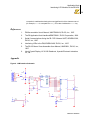
Appendix
Figure 6. LCM Interface Schematic
+5V
P1
D1
1N4148
5
9
4
8
3
7
2
6
1
U2
R1
D2
1N4148
Optional
C3
.01uF
7
6
P31/OE
P32/EPM
P33/VPP
XTAL1/CE
XTAL2
CONNECTOR DB9
P00/CLR
P01/CLK
P02/PGM
P20/D0
P21/D1
P22/D2
P23/D3
P24/D4
P25/D5
P26/D6
P27/D7
11
12
13
+5V
U1
15
16
17
18
1
2
3
4
7
8
9
10
11
12
13
14
DB0
DB1
DB2
DB3
DB4
DB5
DB6
DB7
Vdd
2
3
1K Ohm
8
9
10
Y1
Z86E08
C1
22 pF
6
5
4
C2
22 pF
Vo
3
E
R/W
RS
R3
10K Ohm
2
Contrast
Adjustment
1
8 MHz
+5V
R2
+5V
15
16
10 Ohm
J1
Power Plugs
Vss
Red
Black
1
2
HD16102
C4
.01uF
SW1
BackLight Switch
1
1
2
A
K
AN003201-Z8X0500