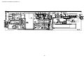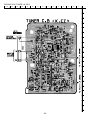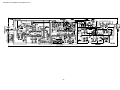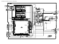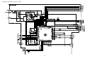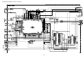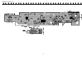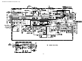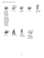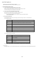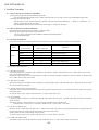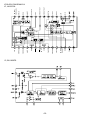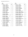
1
XR-DV700
XR-DV701
U(S), K(S)
EZ(S)
SERVICE MANUAL
MICRO COMPO STEREO/ DVD PLAYER
SYSTEM
XR-DV700 U(S)
XR-DV700 K(S)
XR-DV701 EZ(S)
DVD PLAYER
CX-SLDV700 U(S)
CX-SLDV700 K(S)
CX-SLDV701 EZ(S)
BASIC DVD MECHANISM : DV32BF2
SUB WOOFER
TS-SLW700 U(S)
TS-SLW700 K(S)
TS-SLW701 EZ(S)
SPEAKER
SX-SLDV700YJSN
S/M Code No. 09-018-358-0N1
DA
TA
If requiring information about the SUB WOOFER, see Service Manual of TS-SLW700,
S/M Code No.09-019-449-2R1.
TABLE OF CONTENTS
SPECIFICATIONS ................................................................................................................................................ 3
Caution when replacing lithium battery ................................................................................................................. 4
ACCESSORIES/PACKAGE LIST-1/1 .................................................................................................................. 4
PROTECTION OF EYES FROM LASER BEAM DURING SERVICING............................................................... 5
Precaution to replace Optical block ...................................................................................................................... 6
ELECTRICAL MAIN PARTS LIST .................................................................................................................... 7-14
BLOCK DIAGRAM-1/4 (EXCEPT DVD C.B) ...................................................................................................... 15
BLOCK DIAGRAM-2/4 (MAIN : MICON BLOCK) ................................................................................................ 16
BLOCK DIAGRAM-3/4 (DVD-2/2 : DVD BLOCK) .............................................................................................. 17
BLOCK DIAGRAM-4/4 (DVD-2/2 : FRONT END) .............................................................................................. 18
WIRING-1/10 (FRONT, KEY, MOT-SW) ............................................................................................................ 19
SCHEMATIC DIAGRAM-1/18 (FRONT, KEY, MOT-SW) ................................................................................... 20
WIRING-2/10 (TUNER <U>) .............................................................................................................................. 21
SCHEMATIC DIAGRAM-2/18 (TUNER <U>) ...................................................................................................... 22
WIRING-3/10 (TUNER <K, EZ>) ........................................................................................................................ 23
SCHEMATIC DIAGRAM-3/18 (TUNER <K, EZ>) ............................................................................................... 24
WIRING-4/10 (MAIN, FAN : COMPONENT) ....................................................................................................... 25
WIRING-5/10 (MAIN, FAN : CONDUCTOR) ....................................................................................................... 26
SCHEMATIC DIAGRAM-4/18 (MAIN-1/3 : MICON) ............................................................................................. 27
SCHEMATIC DIAGRAM-5/18 (MAIN-2/3 : AC3 FILTER) ..................................................................................... 28
SCHEMATIC DIAGRAM-6/18 (MAIN-3/3 : FUN, PRO LOGIC)............................................................................ 29
SCHEMATIC DIAGRAM-7/18 (FAN) ................................................................................................................... 30
WIRING-6/10 (DVD : COMPONENT) ................................................................................................................. 31
WIRING-7/10 (DVD : CONDUCTOR) ................................................................................................................ 32
SCHEMATIC DIAGRAM-8/18 (DVD : RF AMP) .................................................................................................. 33
SCHEMATIC DIAGRAM-9/18 (DVD : DSP) ........................................................................................................ 34
SCHEMATIC DIAGRAM-10/18 (DVD : AV DECODER) ..................................................................................... 35
SCHEMATIC DIAGRAM-11/18 (DVD : 5.1CH DECODER) ................................................................................ 36
SCHEMATIC DIAGRAM-12/18 (DVD : VIDEO ENCODER) ............................................................................... 37
SCHEMATIC DIAGRAM-13/18 (DVD : POWER, SPINDLE DRIVER) ............................................................... 38
SCHEMATIC DIAGRAM-14/18 (DVD : µ-COM) .................................................................................................. 39
SCHEMATIC DIAGRAM-15/18 (DVD : SYSCON) .............................................................................................. 40
WIRING-8/10 (SUPPLY, HP) .............................................................................................................................. 41
SCHEMATIC DIAGRAM-16/18 (SUPPLY, HP) ................................................................................................... 42
WIRING-9/10 (PT) .............................................................................................................................................. 43
SCHEMATIC DIAGRAM-17/18 (PT) ................................................................................................................... 44
WIRING-10/10 (JACK-SV, JACK-AU) ................................................................................................................. 45
SCHEMATIC DIAGRAM-18/18 (JACK-SV, JACK-AU) ........................................................................................ 46
TRANSISTOR ILLUSTRATION-1/1 .................................................................................................................... 47
FL (BCQ-0 ) GRID ASSIGNMENT/ANODE CONNECTION-1/1 ......................................................................... 48
WAVE FORM ................................................................................................................................................ 49-50
DVD TEST MODE ........................................................................................................................................ 51-53
IC BLOCK DIAGRAM .................................................................................................................................... 54-57
IC DESCRIPTION ......................................................................................................................................... 58-80
MECHANICAL EXPLODED VIEW ................................................................................................................. 81-86
MECHANICAL PARTS LIST .......................................................................................................................... 87-88
SPEAKER PARTS LIST ..................................................................................................................................... 89
-2-
SPECIFICATIONS
U MODEL
K, EZ MODEL
and specifications are subject to
• Design
change withoutnotice.
noise reduction manufactured under
• Dolby
license from Dolby Laboratories Licensing
•
-3-
Corporation.
and
“DOLBY” and the double-D symbol
“PRO LOGIC” are trademarks of Dolby
Laboratories Licensing Corporation.
Laboratories Licensing Corporation.
Manufactured under license from Digital Theater
Systems, Inc.
US Pat. No.5,451,942 and other worldwide patents
Issued and pending. “D T S” and “D T S Digital
Surround” are trade marks of Digital Theater
Systems, Inc. Systems, Inc. c 1996 Digital Theater
systems, Inc. All rights reserved.
Caution when replacing lithium battery
Danger of explosion if battery is incorrectly replaced.
Replace only with the same (CR2025) or equivalent type recommended
by the manufacturer.
Discard used batteries according to the manufacturer's instruction.
ACCESSORIES/PACKAGE LIST-1/1
REF. NO
PART NO.
KANRI
NO.
DESCRIPTION
1
1
1
1
2
8B-CQA-907-010
8B-CQA-906-010
8B-CQA-905-010
8B-CQA-903-010
8B-CQA-951-010
IB,EZ(4L)M<701 EZSM>
IB,EZ(5L)M<701 EZSM>
IB,K(E)M<700 KSM>
IB,U(ESF)M<700 USM>
RC UNIT,RC-BAT08
3
3
4
5
5
8B-CQA-961-010
87-A80-167-010
87-006-225-010
87-043-115-010
87-A90-118-010
CORD ASSY,DIN 13P-5M<700 USM>
CORD,PIN 1PY 150CM
AM LOOP ANT NC2<700 USM>
ANT,FEEDER FM<700 USM>
ANT,WIRE FM (Z)<EXCEPT 700 USM>
-4-
PROTECTION OF EYES FROM LASER BEAM DURING SERVICING
This set employs laser. Therefore, be sure to follow carefully the
instructions below when servicing.
CAUTION
Use of controls or adjustments or performance of procedures
other than those specified herein may result in hazardous
radiation exposure.
Danger of explosion if battery is incorrectly replaced.
Replace only with the same (CR2025) or equivalent type recommended
by the manufacturer.
Discard used batteries according to the manufacturer's instruction.
WARNING!
WHEN SERVICING, DO NOT APPROACH THE LASER EXIT
WITH THE EYE TOO CLOSELY. IN CASE IT IS NECESSARY TO
CONFIRM LASER BEAM EMISSION. BE SURE TO OBSERVE
FROM A DISTANCE OF MORE THAN 30cm FROM THE
SURFACE OF THE OBJECTIVE LENS ON THE OPTICAL
PICK-UP BLOCK.
ATTENTION
L'utilisation de commandes, réglages ou procédures autres que
ceux spécifiés peut entraîner une dangereuse exposition aux
radiations.
Caution: Invisible laser radiation when
open and interlocks defeated avoid exposure to beam.
Advarsel:Usynling laserståling ved åbning,
når sikkerhedsafbrydere er ude af funktion.
Undgå udsættelse for stråling.
ADVARSEL!
Usynlig laserståling ved åbning, når sikkerhedsafbrydereer ude
af funktion. Undgå udsættelse for stråling.
VAROITUS!
This Compact Disc player is classified as a CLASS 1 LASER
product.
The CLASS 1 LASER PRODUCT label is located on the rear
exterior.
Laiteen Käyttäminen muulla kuin tässä käyttöohjeessa mainitulla tavalla saattaa altistaa käyt-täjän turvallisuusluokan 1 ylittävälle näkymättömälle lasersäteilylle.
VARNING!
Om apparaten används på annat sätt än vad som specificeras i
denna bruksanvising, kan användaren utsättas för osynling
laserstrålning, som överskrider gränsen för laserklass 1.
CLASS 1
KLASSE 1
LUOKAN 1
KLASS 1
-5-
LASER PRODUCT
LASER PRODUKT
LASER LAITE
LASER APPARAT
Precaution to replace Optical block
(SF-HD3AV2)
SF-HD3AV2 (DV32BF2: M8-AZK-J93-070) MODEL
Body or clothes electrostatic potential could ruin
laser diode in the optical block. Be sure ground
body and workbench, and use care the clothes
do not touch the diode.
Solder short land for
DVD laser diode
1) After the connection, remove solder shown in
the right figure.
-6-
Solder short land for
CD laser diode
ELECTRICAL MAIN PARTS LIST-1/8
REF. NO
PART NO.
KANRI
NO.
DESCRIPTION
REF. NO
C-IC,HD74LV14AT
C-IC,HD74LV2G08A
C-IC,LC75824E
C-IC,LC87F72C8A
IC,SPS-440-1-E1
87-A20-712-040
87-A21-999-080
87-A20-925-040
87-A21-760-040
8B-ZA6-602-030
C-IC,BA6417F
C-IC,HD74LV1G04A
C-IC,BA05FP
C-IC,NJM4580V
C-IC,LC78661W
8A-ZA7-802-040
87-A21-309-040
8A-ZA7-800-010
8B-CQA-604-030
87-A21-986-040
C-IC,LC324265AT-25DV
C-IC,HD74LV74A
C-IC,LA9702W-MPB
C-IC,LC877256V-5Y36
C-IC,HD74LV4066AT
8A-ZA7-801-040
87-A22-107-010
87-A20-905-040
87-A22-034-010
87-A21-018-040
C-IC,LA6556L-TE-L
IC,SI-3123N
C-IC,BA033FP
IC,PQ1CF1
C-IC,M65849BFP631D
87-A21-882-030
87-A21-991-030
87-A21-763-040
8B-ZA6-606-030
87-A21-990-080
C-IC,M62466FP
C-IC,HD6412320VF25
C-IC,PST3430
C-IC,M29W800AB(BZA)2
C-IC,HD74LV1G08A
87-A21-941-030
8Z-AV2-630-010
87-A21-145-040
87-A21-617-010
87-A22-042-040
C-IC,UT62L1024LC-70LL
C-IC,L64021D
C-IC,BA4560F-E2
C-IC,HY57V161610DTC-8
C-IC,PLL1701
87-A21-993-040
87-A21-613-040
87-A21-928-010
87-A20-913-010
87-017-825-010
C-IC,PCM1742 KE
C-IC,SN74LV04APW
IC,LC72131D-N
IC,LA1837NL
IC,GP1F32T
87-A22-041-030
87-A20-440-040
87-A21-883-040
87-A21-884-040
87-001-607-080
C-IC,ADV7170K
C-IC,BU1920FS<701 EZSM>
C-IC,CS8415A
C-IC,CS4228A
C-IC,NJM4558M
87-A21-755-040
87-A21-987-040
87-A21-885-040
C-IC,SN74LV541APW
C-IC,BA025
C-IC,CS49326
TR,DTC114ES
C-TR,2SC3052F
TR,KTC3199GR<700 USM>
TR,2SA1980G
TR,CSC4115BC
87-A30-075-080
87-A30-427-040
87-A30-273-040
87-A30-257-080
87-A30-466-040
C-TR,2SA1235F
C-TR,DTC114EKA
C-TR,DTC124EKA
C-TR,2SD1306E
C-TR,DTA144TKA
87-A30-447-040
87-A30-072-080
87-A30-071-080
87-A30-086-040
87-A30-435-040
C-TR,DTA114EKA
C-TR,RT1P 144C
C-TR,RT1N 144C
C-TR,CSD1306E
C-TR,DTC144EK T146
87-A30-087-080
89-211-323-080
87-A30-484-080
89-333-265-040
89-110-372-080
C-FET,2SK2158
C-TR,2SB1132R
C-TR,KRA102S
C-TR,2SC3326A
C-TR,2SA1037K(R)
DESCRIPTION
C-FET,3LN01C-TB
C-TR,DTA123JKA
TR,2SC4115SRS
TR,HN1C03F (0.3W)
C-TR,DTA114TKA
87-A30-287-040
89-327-143-080
87-A30-455-040
89-503-602-080
87-A30-086-070
C-TR,DTC114TKA
TR,2SC2714 (0.1W)
C-TR,DTA144EKA
C-FET,2SK360E<EXCEPT 700 USM>
C-TR,CSD1306E<EXCEPT 700 USM>
87-A30-074-080
C-TR,RT1P 141C<EXCEPT 700 USM>
87-A40-524-040
87-020-465-080
87-A40-270-080
87-020-584-080
87-017-779-080
C-DIODE,1SR154-400
DIODE,1SS133 (110MA)
C-DIODE,MC2838
CHIP-ZENER,02CZ5.6Y
C-DIODE,1SS355
87-020-591-080
87-020-339-080
87-A40-269-080
87-017-654-060
87-017-520-080
C-ZENER,02CZ 11Y
CHIP DIODE,1SS226
C-DIODE,MC2836
DIODE,GBU6J
C-DIODE,SFPB52
87-070-274-080
87-A40-234-080
DIODE,1N4003 SEM
ZENER,MTZJ5.6A
C101
C102
C103
C104
C110
87-012-195-080
87-010-412-040
87-010-829-080
87-010-829-080
87-012-286-080
C-CAP,U 100P-50CH
CAP,E 10-25 5L
CAP, U 0.047-16
CAP, U 0.047-16
CAP, U 0.01-25
C111
C112
C113
C114
C132
87-012-274-080
87-010-560-040
87-012-286-080
87-012-286-080
87-010-831-080
CHIP CAP,U 1000P-50B
CAP,E 10-50 GAS
CAP, U 0.01-25
CAP, U 0.01-25
C-CAP,U,0.1-16F
C133
C134
CN101
CN102
LCD101
87-010-831-080
87-010-831-080
87-A61-371-010
87-099-203-010
8B-CQ0-606-010
C-CAP,U,0.1-16F
C-CAP,U,0.1-16F
CONN,22P V BLK FMN-BTRK
CONN,10P 6216 H
LCD,BCQ-0
LED101
LED102
LED103
LED104
LED105
87-A40-317-080
87-A92-218-010
87-A92-218-010
87-A92-078-010
87-A92-078-010
LED,SLR-342VCT31 RED
LED, SMLU12E16C-LF73
LED, SMLU12E16C-LF73
LED, SMLU1D10CXM-SLF38
LED, SMLU1D10CXM-SLF38
S101
S111
S112
S113
S114
87-A91-633-010
87-A90-095-080
87-A90-095-080
87-A90-095-080
87-A90-095-080
SW,RTRY
SW,TACT
SW,TACT
SW,TACT
SW,TACT
S115
S116
S117
87-A90-095-080
87-A90-095-080
87-A90-095-080
SW,TACT EVQ11G04M
SW,TACT EVQ11G04M
SW,TACT EVQ11G04M
C116
C117
C118
C130
C135
87-016-044-040
87-012-286-080
87-016-044-040
87-010-831-080
87-012-286-080
CAP,E 100-16 GAS
CAP, U 0.01-25
CAP,E 100-16 GAS
C-CAP,U,0.1-16F
CAP, U 0.01-25
C136
CN141
CN142
S110
S141
87-012-286-080
87-A60-077-010
87-A60-082-010
87-A92-254-010
87-A90-095-080
CAP, U 0.01-25
CONN,10P H 9604S-10F
CONN,05P H 9604S-05F
SW,PUSH 4-4-2 SPVF240100
SW,TACT EVQ11G04M
DIODE
FRONT C.B
TRANSISTOR
87-026-245-080
87-A30-076-080
87-A30-198-080
87-A30-494-080
87-A30-234-080
KANRI
NO.
87-A30-516-040
87-A30-448-040
87-A30-196-080
87-026-470-080
87-A30-282-040
IC
87-A21-998-040
87-A21-997-080
87-A21-968-030
8A-ZA7-804-010
87-A22-043-010
PART NO.
XRE012103PVB25FINA 1-2
EVQ11G04M
EVQ11G04M
EVQ11G04M
EVQ11G04M
KEY C.B
-7-
ELECTRICAL MAIN PARTS LIST-2/8
REF. NO
PART NO.
KANRI
NO.
DESCRIPTION
S142
S143
S144
S145
S146
87-A90-095-080
87-A90-095-080
87-A90-095-080
87-A90-095-080
87-A90-095-080
SW,TACT
SW,TACT
SW,TACT
SW,TACT
SW,TACT
S147
S148
S149
87-A90-095-080
87-A90-095-080
87-A90-095-080
SW,TACT EVQ11G04M
SW,TACT EVQ11G04M
SW,TACT EVQ11G04M
87-A60-082-010
87-A90-036-010
87-A90-117-010
87-A90-117-010
CONN,05P H 9604S-05F
MOT ASSY,RF-300CA-11
SW,PUSH 1-1-1 MPU103
SW,PUSH 1-1-1 MPU103
REF. NO
EVQ11G04M
EVQ11G04M
EVQ11G04M
EVQ11G04M
EVQ11G04M
C853
CN804
J803
J804
KANRI
NO.
DESCRIPTION
87-012-286-080
87-A61-100-010
87-009-610-010
87-009-610-010
CAP, U 0.01-25
CONN,7P V BLK FMN-BTRK
JACK PIN 2P H EARH
JACK PIN 2P H EARH
C401
C402
C403
C404
C405
87-A10-011-090
87-A12-317-080
87-A10-831-080
87-A12-317-080
87-010-831-080
CAP,E 2200-25 SMG
C-CAP,U 0.1-50 Z F
CAP,E 1000-25 M SMG
C-CAP,U 0.1-50 Z F
C-CAP,U,0.1-16F
C406
C407
C408
C408
C409
87-010-831-080
87-A12-074-080
87-A12-863-090
87-A12-878-000
87-A12-317-080
C-CAP,U,0.1-16F
CAP,E 470-25 SMG
CAP,E 10000-16 SMG 85 L35.5<700 USM>
CAP,E 15000-16<EXCEPT 700 USM>
C-CAP,U 0.1-50 Z F
C410
C411
C412
C413
C414
87-A12-317-080
87-010-831-080
87-010-831-080
87-012-286-080
87-010-831-080
C-CAP,U 0.1-50 Z F
C-CAP,U,0.1-16F
C-CAP,U,0.1-16F
CAP, U 0.01-25
C-CAP,U,0.1-16F
C415
C416
C418
C419
C420
87-012-286-080
87-010-831-080
87-A12-311-080
87-A12-893-080
87-012-286-080
CAP, U 0.01-25
C-CAP,U,0.1-16F
CAP,AS 100U-16 M FA
CAP, E 680-16 KZE
CAP, U 0.01-25
C421
C423
C424
C425
C426
87-A12-311-080
87-010-805-080
87-012-286-080
87-010-758-080
87-A11-057-080
CAP,AS 100U-16 M FA
CAP, S 1-16
CAP, U 0.01-25
C-CAP,U 0.068-25F
C-CAP,U 0.1-16 K B
C432
C433
C434
C435
C436
87-010-831-080
87-010-831-080
87-010-831-080
87-010-385-080
87-A12-893-080
C-CAP,U,0.1-16F
C-CAP,U,0.1-16F
C-CAP,U,0.1-16F
CAP, E 220-25
CAP, E 680-16 KZE
C437
CN401
CNA401
CNA403
!F2
87-A12-096-080
87-009-195-010
8B-CQA-640-010
8B-CQA-639-010
87-A91-939-080
CAP, E 220-50 SMG
CONN,5P B5BEH
CONN ASSY,9P V MAIN
CONN ASSY,9P V DVD
PROTECTOR,2A 20P 60V<EXCEPT 700 USM>
!F2
!F3
!F3
!F5
!F5
87-A90-091-080
87-A91-939-080
87-A90-091-080
87-A91-945-080
87-026-681-080
PROTECTOR, 2A 491<700 USM>
PROTECTOR,2A 20P 60V<EXCEPT 700 USM>
PROTECTOR, 2A 491<700 USM>
PROTECTOR,5A 20P 60V<EXCEPT 700 USM>
PROTECTOR,5A 60V 491<700 USM>
!F401
!F402
!F403
!F403
!JW414
87-A91-961-080
87-A91-961-080
87-A90-410-080
87-A91-931-080
87-A91-935-080
FUSE,1.25A 125V F 20N<700 USM>
FUSE,1.25A 125V F 20N<700 USM>
FUSE,0.5A 125V 251<700 USM>
PROTECTOR,500MA 20P 60V<EXCEPT 700 USM>
PROTECTOR, 1A 20P 60V<EXCEPT 700 USM>
L401
L402
L403
87-A50-517-080
87-A50-549-010
87-A50-549-010
COIL,10UHK FLR88
COIL,68UH RCH110
COIL,68UH RCH110
C701
C702
C703
CNA701
FB701
87-012-274-080
87-012-274-080
87-010-831-080
88-805-053-260
87-A91-364-080
CHIP CAP,U 1000P-50B
CHIP CAP,U 1000P-50B
C-CAP,U,0.1-16F
CONN ASSY,5P 320MM
C-F-BEAD, BK1608HS601
J701
R701
R702
87-A60-420-010
87-008-372-080
87-008-372-080
JACK,3.5 ST (MSC)
FILTER, EMI BL OIRNI
FILTER, EMI BL OIRNI
SUPPLY C.B
MOT-SW C.B
CN151
M151
S151
S152
PART NO.
JACK-SV C.B
C801
C802
C803
C804
C805
87-012-267-080
87-012-268-080
87-012-180-080
87-012-267-080
87-012-268-080
C-CAP,U
C-CAP,U
C-CAP,U
C-CAP,U
C-CAP,U
270P-50 B
330P-50 B
22P-50 CH
270P-50 B
330P-50 B
C806
C807
C808
C809
C810
87-012-180-080
87-012-267-080
87-012-268-080
87-012-180-080
87-010-555-040
C-CAP,U 22P-50 CH
C-CAP,U 270P-50 B
C-CAP,U 330P-50 B
C-CAP,U 22P-50 CH
CAP,E 100-10 GAS
C811
C812
C813
C814
C817
87-012-286-080
87-012-286-080
87-A12-319-080
87-012-188-080
87-012-286-080
CAP, U 0.01-25
CAP, U 0.01-25
C-CAP,U 0.1-25 K B
C-CAP,U 47P-50 CH
CAP, U 0.01-25
C818
C834
C846
C847
C854
87-010-552-040
87-010-831-080
87-016-350-040
87-016-350-040
87-A12-319-080
CAP,E 22-16 GAS
C-CAP,U,0.1-16F
CAP,E 470-4 MA GAS
CAP,E 470-4 MA GAS
C-CAP,U 0.1-25 K B<EXCEPT 700 USM>
C854
C860
C861
C862
CN801
87-012-286-080
87-012-286-080
87-012-286-080
87-012-286-080
87-A60-422-010
CAP, U 0.01-25<700 USM>
CAP, U 0.01-25
CAP, U 0.01-25
CAP, U 0.01-25<700 USM>
CONN,8P V TOC-B
CN802
CNA802
FB806
FB807
FB808
87-A61-366-010
8B-CQA-641-010
87-A91-364-080
87-A91-364-080
87-A91-364-080
CONN,10P V BLK FMN-BTRK
CONN ASSY,2P V SHIELD
C-F-BEAD, BK1608HS601
C-F-BEAD, BK1608HS601
C-F-BEAD, BK1608HS601
FB809
FB810
FB814
J801
J802
87-A91-364-080
87-A91-364-080
87-A91-364-080
87-A61-498-010
87-A61-284-010
C-F-BEAD, BK1608HS601
C-F-BEAD, BK1608HS601
C-F-BEAD, BK1608HS601
JACK,Y/C YKF51-5508
JACK,PIN 1P YEL YKC-21 TYPE C
J833
L302
L801
L802
L803
87-A61-202-010
87-005-481-080
87-005-423-080
87-005-423-080
87-005-423-080
JACK,DIN 8 P
COIL,47UH J FLR50
COIL,1.8UH K FLR50
COIL,1.8UH K FLR50
COIL,1.8UH K FLR50
T801
T802
T803
8A-MVS-608-010
8A-MVS-608-010
8A-MVS-608-010
COIL,SORTER-BALUN
COIL,SORTER-BALUN
COIL,SORTER-BALUN
HP C.B
JACK-AU C.B
C819
C820
C829
C830
C852
87-012-274-080
87-012-274-080
87-012-274-080
87-012-274-080
87-012-286-080
CHIP
CHIP
CHIP
CHIP
CAP,
CAP,U 1000P-50B
CAP,U 1000P-50B
CAP,U 1000P-50B
CAP,U 1000P-50B
U 0.01-25
-8-
ELECTRICAL MAIN PARTS LIST-3/8
REF. NO
PART NO.
KANRI
NO.
DESCRIPTION
REF. NO
MAIN C.B
C1
C2
C3
C4
C5
87-010-831-080
87-010-112-040
87-010-496-040
87-010-831-080
87-010-560-040
C-CAP,U,0.1-16F
CAP,E 100-16
CAP,E 3.3-50 GAS
C-CAP,U,0.1-16F
CAP,E 10-50 GAS
C6
C7
C8
C9
C10
87-010-560-040
87-010-555-040
87-010-555-040
87-010-555-040
87-A11-056-080
CAP,E 10-50 GAS
CAP,E 100-10 GAS
CAP,E 100-10 GAS
CAP,E 100-10 GAS
C-CAP,U 1-10 Z F
C11
C12
C13
C15
C26
87-A11-056-080
87-010-831-080
87-010-831-080
87-010-112-040
87-A11-049-080
C-CAP,U 1-10 Z F
C-CAP,U,0.1-16F
C-CAP,U,0.1-16F
CAP,E 100-16
C-CAP,U 1-6.3 K B
C27
C110
C111
C114
C115
87-A11-049-080
87-010-380-040
87-A10-260-080
87-012-193-080
87-012-193-080
C-CAP,U 1-6.3 K B
CAP,E 47-16 SME
C-CAP,U 0.1-16 K B
C-CAP,U 82P-50 CH
C-CAP,U 82P-50 CH
C116
C117
C118
C119
C120
87-012-193-080
87-012-193-080
87-012-196-080
87-A11-049-080
87-A11-049-080
C-CAP,U
C-CAP,U
C-CAP,U
C-CAP,U
C-CAP,U
82P-50 CH
82P-50 CH
120P-50 CH
1-6.3 K B
1-6.3 K B
C121
C122
C123
C124
C125
87-012-196-080
87-012-196-080
87-012-196-080
87-012-196-080
87-012-196-080
C-CAP,U
C-CAP,U
C-CAP,U
C-CAP,U
C-CAP,U
120P-50
120P-50
120P-50
120P-50
120P-50
CH
CH
CH
CH
CH
C126
C127
C128
C129
C130
87-012-196-080
87-012-196-080
87-012-196-080
87-012-196-080
87-012-196-080
C-CAP,U
C-CAP,U
C-CAP,U
C-CAP,U
C-CAP,U
120P-50
120P-50
120P-50
120P-50
120P-50
CH
CH
CH
CH
CH
C133
C134
C135
C136
C137
87-010-831-080
87-010-831-080
87-012-196-080
87-012-196-080
87-012-196-080
C-CAP,U,0.1-16F
C-CAP,U,0.1-16F
C-CAP,U 120P-50 CH
C-CAP,U 120P-50 CH
C-CAP,U 120P-50 CH
C139
C140
C141
C142
C143
87-A11-049-080
87-A11-049-080
87-012-196-080
87-012-196-080
87-012-196-080
C-CAP,U
C-CAP,U
C-CAP,U
C-CAP,U
C-CAP,U
1-6.3 K
1-6.3 K
120P-50
120P-50
120P-50
B
B
CH
CH
CH
C144
C145
C146
C147
C148
87-012-196-080
87-012-196-080
87-012-196-080
87-012-196-080
87-012-196-080
C-CAP,U
C-CAP,U
C-CAP,U
C-CAP,U
C-CAP,U
120P-50
120P-50
120P-50
120P-50
120P-50
CH
CH
CH
CH
CH
C149
C150
C153
C154
C156
87-012-196-080
87-012-196-080
87-010-831-080
87-010-831-080
87-010-831-080
C-CAP,U 120P-50 CH
C-CAP,U 120P-50 CH
C-CAP,U,0.1-16F
C-CAP,U,0.1-16F
C-CAP,U,0.1-16F
C157
C159
C160
C161
C162
87-010-831-080
87-A11-049-080
87-010-498-040
87-012-196-080
87-010-958-080
C-CAP,U,0.1-16F
C-CAP,U 1-6.3 K B
CAP,E 10-16 GAS
C-CAP,U 120P-50 CH
CHIP -CAP,S 0.01-25BJ
C163
C164
C165
C166
C167
87-012-196-080
87-016-118-080
87-012-196-080
87-016-118-080
87-012-196-080
C-CAP,U 120P-50 CH
C-CAP,U0.022-25BJ
C-CAP,U 120P-50 CH
C-CAP,U0.022-25BJ
C-CAP,U 120P-50 CH
-9-
PART NO.
KANRI
NO.
DESCRIPTION
C168
C169
C170
C173
C174
87-016-118-080
87-012-196-080
87-016-118-080
87-010-831-080
87-010-831-080
C-CAP,U0.022-25BJ
C-CAP,U 120P-50 CH
C-CAP,U0.022-25BJ
C-CAP,U,0.1-16F
C-CAP,U,0.1-16F
C181
C183
C185
C186
C187
87-010-405-040
87-016-114-080
87-A10-504-080
87-010-831-080
87-010-831-080
CAP,E 10-50
C-CAP,U0.01-25B
C-CAP,U 0.047-16 K B
C-CAP,U,0.1-16F
C-CAP,U,0.1-16F
C191
C192
C193
C194
C195
87-010-112-040
87-010-248-040
87-A11-049-080
87-A11-049-080
87-A11-049-080
CAP,E 100-16
CAP,E 220-10 SME
C-CAP,U 1-6.3 K B
C-CAP,U 1-6.3 K B
C-CAP,U 1-6.3 K B
C196
C210
C211
C221
C222
87-A11-049-080
87-A11-049-080
87-A11-049-080
87-A11-049-080
87-A11-049-080
C-CAP,U
C-CAP,U
C-CAP,U
C-CAP,U
C-CAP,U
C241
C242
C261
C262
C292
87-A11-049-080
87-A11-049-080
87-A11-049-080
87-010-405-040
87-012-195-080
C-CAP,U 1-6.3 K B
C-CAP,U 1-6.3 K B
C-CAP,U 1-6.3 K B
CAP,E 10-50
C-CAP,U 100P-50CH
C293
C294
C303
C304
C305
87-016-044-040
87-010-831-080
87-010-785-080
87-010-831-080
87-010-831-080
CAP,E 100-16 GAS
C-CAP,U,0.1-16F
C-CAP,U0.015-25BK
C-CAP,U,0.1-16F
C-CAP,U,0.1-16F
C306
C307
C308
C309
C310
87-012-195-080
87-012-178-080
87-012-198-080
87-012-274-080
87-010-831-080
C-CAP,U 100P-50CH
C-CAP,U 18P-50 CH
CAP 180P
CHIP CAP,U 1000P-50B
C-CAP,U,0.1-16F
C311
C312
C313
C316
C318
87-012-278-080
87-A10-781-080
87-010-831-080
87-010-831-080
87-010-831-080
C-CAP,U 2200P-50 B
C-CAP,U 0.15-10 K B
C-CAP,U,0.1-16F
C-CAP,U,0.1-16F
C-CAP,U,0.1-16F
C325
C552
C556
C557
C558
87-010-248-040
87-010-553-040
87-A11-058-080
87-A11-058-080
87-010-831-080
CAP,E 220-10 SME
CAP,E 47-16 GAS
C-CAP,U 0.22-10 K B
C-CAP,U 0.22-10 K B
C-CAP,U,0.1-16F
C559
C560
C561
C562
C563
87-A11-058-080
87-012-282-080
87-012-273-080
87-A10-248-080
87-A10-248-080
C-CAP,U 0.22-10 K B
CAP, U 4700P-50
C-CAP,U 820P-50 B
C-CAP,U0.1-16KBR
C-CAP,U0.1-16KBR
C564
C565
C566
C567
C569
87-012-282-080
87-012-273-080
87-A11-058-080
87-010-553-040
87-010-494-040
CAP, U 4700P-50
C-CAP,U 820P-50 B
C-CAP,U 0.22-10 K B
CAP,E 47-16 GAS
CAP,E 1-50 GAS
C571
C573
C601
C605
C606
87-010-492-040
87-010-493-040
87-A10-248-080
87-010-784-080
87-010-784-080
CAP,E 0.33-50 GAS
CAP,E 0.47-50 GAS
C-CAP,U0.1-16KBR
C-CAP, U 0.012-25 B<EXCEPT 700 USM>
C-CAP, U 0.012-25 B<EXCEPT 700 USM>
C611
C612
C613
C614
C615
87-A11-049-080
87-A11-049-080
87-A11-049-080
87-A11-049-080
87-A11-049-080
C-CAP,U
C-CAP,U
C-CAP,U
C-CAP,U
C-CAP,U
C616
C633
C634
C635
C636
87-010-497-040
87-012-281-080
87-A11-070-080
87-012-281-080
87-A11-070-080
CAP,E 4.7-35 GAS
C-CAP,U 3900P-50
C-CAP,U 0.033-16
C-CAP,U 3900P-50
C-CAP,U 0.033-16
1-6.3
1-6.3
1-6.3
1-6.3
1-6.3
1-6.3
1-6.3
1-6.3
1-6.3
1-6.3
K
K
K
K
K
K
K
K
K
K
B
B
B
B
B
B
B
B
B
B
B
K B
B
K B
ELECTRICAL MAIN PARTS LIST-4/8
REF. NO
PART NO.
KANRI
NO.
DESCRIPTION
REF. NO
PART NO.
KANRI
NO.
DESCRIPTION
C637
C638
C639
C640
C641
87-010-495-040
87-010-495-040
87-010-495-040
87-010-495-040
87-012-281-080
CAP,E 2.2-50 GAS
CAP,E 2.2-50 GAS
CAP,E 2.2-50 GAS
CAP,E 2.2-50 GAS
C-CAP,U 3900P-50 B
CN2
CN101
CN102
CN103
CN104
87-A60-626-010
87-A61-367-010
87-A60-620-010
87-A60-904-010
87-A61-400-010
CONN,9P V 2MM JMT
CONN,16P V BLK FMN-BTRK
CONN,3P V 2MM JMT
CONN,10P H BLK FMN-STRK
CONN,7P H BLK FMN-SSTRK
C643
C644
C645
C646
C647
87-010-958-080
87-010-958-080
87-010-958-080
87-010-958-080
86-ZA1-615-080
CHIP -CAP,S 0.01-25BJ
CHIP -CAP,S 0.01-25BJ
CHIP -CAP,S 0.01-25BJ
CHIP -CAP,S 0.01-25BJ
C-CAP,U 680P-25 J CH
CN301
CN302
CN303
CN304
CN305
87-A61-371-010
87-099-014-010
87-A60-899-010
87-A60-623-010
87-099-211-010
CONN,22P V BLK FMN-BTRK
CONN,12P 6216 V
CONN,6P V BLK FMN-BTRK
CONN,6P V 2MM JMT
CONN,4P 6216V<701 EZSM>
C648
C649
C650
C651
C652
86-ZA1-615-080
87-A10-248-080
87-016-118-080
87-016-118-080
87-A10-248-080
C-CAP,U 680P-25 J CH
C-CAP,U0.1-16KBR
C-CAP,U0.022-25BJ
C-CAP,U0.022-25BJ
C-CAP,U0.1-16KBR
CN701
L151
L701
L702
R379
87-A60-622-010
87-A50-333-010
87-005-811-080
87-005-811-080
87-022-239-080
CONN,5P V 2MM JMT
COIL,OSC 9.43MHZ
C-COIL,10UH J FLC32
C-COIL,10UH J FLC32
C-RES U 10K-1/16WF
C653
C654
C655
C656
C657
87-A10-248-080
87-A10-802-080
87-A10-802-080
87-A10-248-080
87-A11-058-080
C-CAP,U0.1-16KBR
C-CAP,S 0.047-16 J B CM
C-CAP,S 0.047-16 J B CM
C-CAP,U0.1-16KBR
C-CAP,U 0.22-10 K B
R380
R660
87-022-239-080
87-022-286-080
C-RES U 10K-1/16WF
C-RES U 100K-1/16WF
C658
C659
C660
C661
C662
87-A11-058-080
87-016-469-040
87-010-497-040
87-A11-058-080
87-A11-058-080
C-CAP,U 0.22-10 K B
CAP,E 6.8-50 5L SRE
CAP,E 4.7-35 GAS
C-CAP,U 0.22-10 K B
C-CAP,U 0.22-10 K B
C905
C909
C910
C911
C912
87-012-286-080
87-012-286-080
87-012-286-080
87-A11-049-080
87-010-401-040
CAP, U 0.01-25
CAP, U 0.01-25
CAP, U 0.01-25
C-CAP,U 1-6.3 K B
CAP,E 1-50 SME
C663
C664
C665
C666
C667
87-A10-799-080
87-A10-802-080
87-A10-229-080
87-A10-248-080
87-010-560-040
C-CAP,S 5600P-16 J B CM
C-CAP,S 0.047-16 J B CM
C-CAP,S 0.68-10 K W5
C-CAP,U0.1-16KBR
CAP,E 10-50 GAS
C916
C917
CN901
CN902
CNA901
87-010-831-080
87-012-195-080
87-A60-619-010
87-A60-619-010
88-805-061-230
C-CAP,U,0.1-16F
C-CAP,U 100P-50CH
CONN,2P V 2MM JMT
CONN,2P V 2MM JMT<EXCEPT 700 USM>
CONN ASSY,6P 120
C668
C669
C670
C675
C676
87-010-560-040
87-010-494-040
87-010-494-040
87-010-186-080
87-010-186-080
CAP,E 10-50 GAS
CAP,E 1-50 GAS
CAP,E 1-50 GAS
CAP,CHIP 4700P
CAP,CHIP 4700P
C685
C686
C687
C688
C689
87-012-167-080
87-010-196-080
87-010-196-080
87-010-555-040
87-010-555-040
C-CAP,U 5P-50 CH
CHIP CAPACITOR,0.1-25
CHIP CAPACITOR,0.1-25
CAP,E 100-10 GAS
CAP,E 100-10 GAS
!C1
C14
C16
C16
!CN1
87-A10-479-080
87-A10-831-080
87-010-496-080
87-010-405-080
87-099-674-010
CAP,CER 2200P-250 M E KH
CAP,E 1000-25 M SMG
CAP,E 3.3-50 5L<700 USM>
CAP, E 10-50<EXCEPT 700 USM>
CONN,2P VA V
C707
C708
C711
C712
C715
87-010-495-040
87-010-495-040
87-010-494-040
87-010-494-040
87-010-248-040
CAP,E
CAP,E
CAP,E
CAP,E
CAP,E
CNA1
!F1
FC1
FC2
!PR1
88-805-031-660
87-A91-224-010
87-033-213-080
87-033-213-080
87-A91-276-080
CONN ASSY,3P 160MM
FUSE,1.25A 125V T 51S<700 USM>
CLAMP, FUSE<700 USM>
CLAMP, FUSE<700 USM>
FUSE,125MA 125V F 251<700 USM>
C716
C717
C718
C750
C751
87-010-248-040
87-010-112-040
87-010-112-040
87-012-274-080
87-012-274-080
CAP,E 220-10 SME
CAP,E 100-16
CAP,E 100-16
CHIP CAP,U 1000P-50B
CHIP CAP,U 1000P-50B
!PT1
!PT1
!PT2
!PT2
!RY1
8A-NF8-662-010
8A-NF8-661-010
8B-CQA-652-010
8B-CQA-651-010
87-A90-977-010
PT,SUB ANF-8 (E)<EXCEPT 700 USM>
PT,SUB ANF-8 (U)<700 USM>
PT,BCQ-A EZ<EXCEPT 700 USM>
PT,BCQ-A U<700 USM>
RELAY,AC12V DG12D1-O(M)
C805
C806
C807
C808
C809
87-A11-049-080
87-A11-049-080
87-A11-049-080
87-A11-049-080
87-A11-049-080
C-CAP,U
C-CAP,U
C-CAP,U
C-CAP,U
C-CAP,U
!T1
!T2
!W1
!W1
!W1
87-A60-317-010
87-A60-317-010
87-A80-143-010
87-A80-092-010
87-A80-149-010
TERMINAL, 1P MSC
TERMINAL, 1P MSC
AC CORD ASSY,E BLK<700 KSM>
AC CORD ASSY,E BLK SUN FAI<701 EZSM>
AC CORD ASSY,U BLK<700 USM>
C810
C826
C827
C828
C829
87-010-498-040
87-A11-061-080
87-A11-061-080
87-A11-049-080
87-A11-049-080
CAP,E 10-16 GAS
C-CAP,S 2.2-10 K B
C-CAP,S 2.2-10 K B
C-CAP,U 1-6.3 K B
C-CAP,U 1-6.3 K B
C701
C702
C703
C704
C709
87-A12-071-080
87-A12-090-080
87-012-286-080
87-012-286-080
87-012-195-080
CAP,E 47-25 SMG
CAP,E 4.7-50 SMG
CAP, U 0.01-25
CAP, U 0.01-25
C-CAP,U 100P-50CH
C830
C831
C832
C833
C834
87-A11-049-080
87-010-560-040
87-010-831-080
87-010-831-080
87-010-498-040
C-CAP,U 1-6.3 K B
CAP,E 10-50 GAS
C-CAP,U,0.1-16F
C-CAP,U,0.1-16F
CAP,E 10-16 GAS
C711
C712
C713
C714
C715
87-A12-062-080
87-010-196-080
87-012-286-080
87-012-286-080
87-012-195-080
CAP,E 100-10 SMG
CHIP CAPACITOR,0.1-25
CAP, U 0.01-25
CAP, U 0.01-25
C-CAP,U 100P-50CH<EXCEPT 700 USM>
C835
C836
C837
C838
C839
87-A11-049-080
87-A11-049-080
87-A11-049-080
87-A11-049-080
87-A11-049-080
C-CAP,U
C-CAP,U
C-CAP,U
C-CAP,U
C-CAP,U
C717
C719
C720
C721
C722
87-012-286-080
87-012-286-080
87-012-195-080
87-012-176-080
87-012-176-080
CAP, U 0.01-25
CAP, U 0.01-25
C-CAP,U 100P-50CH<EXCEPT 700 USM>
CAP 15P
CAP 15P
FAN C.B
PT C.B
2.2-50 GAS
2.2-50 GAS
1-50 GAS
1-50 GAS
220-10 SME
1-6.3
1-6.3
1-6.3
1-6.3
1-6.3
1-6.3
1-6.3
1-6.3
1-6.3
1-6.3
K
K
K
K
K
K
K
K
K
K
B
B
B
B
B
TUNER C.B
B
B
B
B
B
-10-
ELECTRICAL MAIN PARTS LIST-5/8
REF. NO
PART NO.
KANRI
NO.
DESCRIPTION
REF. NO
PART NO.
KANRI
NO.
DESCRIPTION
C723
C725
C727
C728
C753
87-012-274-080
87-012-274-080
87-010-196-080
87-A12-063-080
87-012-195-080
CHIP CAP,U 1000P-50B
CHIP CAP,U 1000P-50B
CHIP CAPACITOR,0.1-25
CAP,E 220-10 SMG
C-CAP,U 100P-50CH<EXCEPT 700 USM>
C867
C868
C869
C940
C942
87-012-286-080
87-012-184-080
87-012-180-080
87-012-286-080
87-012-172-080
CAP, U 0.01-25<701 EZSM>
C-CAP,U 33P-50 CH<701 EZSM>
C-CAP,U 22P-50 CH<701 EZSM>
CAP, U 0.01-25<EXCEPT 700 USM>
CAPACITOR CHIP U 10P CH<EXCEPT 700 USM>
C755
C756
C757
C758
C761
87-012-286-080
87-012-286-080
87-012-188-080
87-012-167-080
87-010-196-080
CAP, U 0.01-25
CAP, U 0.01-25
C-CAP,U 47P-50 CH
C-CAP,U 5P-50 CH
CHIP CAPACITOR,0.1-25
C947
C949
C952
C958
C959
87-012-286-080
87-A10-039-080
87-012-286-080
87-012-286-080
87-010-196-080
CAP, U 0.01-25<EXCEPT 700 USM>
C-CAP,U 470P-50 J CH<EXCEPT 700 USM>
CAP, U 0.01-25<EXCEPT 700 USM>
CAP, U 0.01-25<EXCEPT 700 USM>
CHIP CAPACITOR,0.1-25
C762
C763
C764
C765
C766
87-012-286-080
87-010-829-080
87-012-337-080
87-012-286-080
87-012-286-080
CAP, U 0.01-25<EXCEPT 700 USM>
CAP, U 0.047-16
C-CAP,U 56P-50 CH<700 USM>
CAP, U 0.01-25
CAP, U 0.01-25
C960
C961
C962
CF801
CF801
87-010-196-080
87-012-170-080
87-A12-087-080
87-008-423-010
87-008-261-010
CHIP CAPACITOR,0.1-25
C-CAP,U 8P-50 CH<700 USM>
CAP,E 1-50 SMG<EXCEPT 700 USM>
CERAMIC FILTER, SFE10.7<EXCEPT 700 USM>
FILTER, SFE10.7MA5-A<700 USM>
C768
C769
C770
C771
C772
87-012-286-080
87-A12-071-080
87-010-829-080
87-A12-070-080
87-010-829-080
CAP, U 0.01-25<EXCEPT 700 USM>
CAP,E 47-25 SMG
CAP, U 0.047-16
CAP,E 33-25 SMG
CAP, U 0.047-16
CF802
CF802
CN601
CN602
FFE801
82-785-747-010
87-008-261-010
87-099-029-010
87-099-211-010
A8-6ZA-19H-030
CF MS2 GHY R<EXCEPT 700 USM>
FILTER, SFE10.7MA5-A<700 USM>
CONN,12P 6216H
CONN,4P 6216V<701 EZSM>
6ZA-1 FEMENM<EXCEPT 700 USM>
C773
87-015-785-080
C773
C774
C775
C776
87-010-196-080
87-A12-062-080
87-A12-090-080
87-012-286-080
CHIP CAPACITOR, 0.1FZ-25Z
<EXCEPT 700 USM>
CHIP CAPACITOR,0.1-25<700 USM>
CAP,E 100-10 SMG
CAP,E 4.7-50 SMG
CAP, U 0.01-25
FFE801
J801
J802
L771
L772
A8-8ZA-194-030
87-A60-657-010
87-033-241-010
87-A50-266-010
87-A90-733-010
8ZA-1 FEMUNM<700 USM>
TERMINAL,4P HSP-154V5-02<700 USM>
TERMINAL,ANT 2P AJ-2040<EXCEPT 700 USM>
COIL,FM DET-2N(TOK)
FLTR,PCFAZH-450 (TOK)
C777
C778
C779
C780
C781
87-A12-086-080
87-A12-087-080
87-A12-087-080
87-010-196-080
87-A12-091-080
CAP,E 0.47-50 SMG
CAP,E 1-50 SMG
CAP,E 1-50 SMG
CHIP CAPACITOR,0.1-25
CAP,E 10-50 SMG
L781
L791
L792
L832
L941
87-005-847-080
87-A50-027-010
87-A50-027-010
87-005-847-080
87-A50-020-010
COIL,2.2UH(CECS)
COIL,1 POLE MPX(TOK)<EXCEPT 700 USM>
COIL,1 POLE MPX(TOK)<EXCEPT 700 USM>
COIL,2.2UH(CECS)
COIL,ANT LW(COI)<EXCEPT 700 USM>
C782
C783
C784
C785
C786
87-A12-091-080
87-012-286-080
87-012-286-080
87-A11-061-080
87-A11-061-080
CAP,E 10-50 SMG
CAP, U 0.01-25
CAP, U 0.01-25
C-CAP,S 2.2-10 K B
C-CAP,S 2.2-10 K B
L942
L981
L981
TC942
87-A50-019-010
87-NF4-650-010
87-NF4-651-110
87-A91-774-080
X721
87-A70-306-010
COIL,OSC LW(COI)<EXCEPT 700 USM>
COIL,AM PACK 4N(TOK)<700 USM>
COIL,AM PACK2N(TOM)<EXCEPT 700 USM>
TRIMMER,PLY 30P 6.8X5.4 CDYL
<EXCEPT 700 USM>
VIB,XTAL 4.500MHZ CSA-309ST
C787
C788
C789
C790
C791
87-012-280-080
87-012-280-080
87-012-275-080
87-012-275-080
87-A12-091-080
CAP, U 3300P-50
CAP, U 3300P-50
C-CAP,U 1200P-50 B
C-CAP,U 1200P-50 B
CAP,E 10-50 SMG
X851
87-A70-091-010
VIB,XTAL 4.332MHZ CSA-309<701 EZSM>
C793
C793
C794
C795
C795
87-012-273-080
87-012-274-080
87-A12-092-080
87-010-596-080
87-010-829-080
C-CAP,U 820P-50 B<700 USM>
CHIP CAP,U 1000P-50B<EXCEPT 700 USM>
CAP,E 22-50 SMG
CAP, S 0.047-16<700 USM>
CAP, U 0.047-16<EXCEPT 700 USM>
C100
C101
C102
C103
C104
87-012-274-080
87-016-427-080
87-010-831-080
87-010-196-080
87-012-180-080
CHIP CAP,U 1000P-50B
C-CAP,E 47-6.3 5.5N
C-CAP,U,0.1-16F
CHIP CAPACITOR,0.1-25
C-CAP,U 22P-50 CH
C796
C797
C797
C798
C798
87-A12-089-080
87-012-277-080
87-012-275-080
87-012-277-080
87-012-275-080
CAP,E 3.3-50 SMG
C-CAP, U 1800P-50 B<700 USM>
C-CAP,U 1200P-50 B<EXCEPT 700 USM>
C-CAP, U 1800P-50 B<700 USM>
C-CAP,U 1200P-50 B<EXCEPT 700 USM>
C105
C106
C107
C110
C111
87-012-180-080
87-010-831-080
87-016-428-080
87-010-831-080
87-012-195-080
C-CAP,U 22P-50 CH
C-CAP,U,0.1-16F
C-CAP,E 47-16 5.5N
C-CAP,U,0.1-16F
C-CAP,U 100P-50CH
C798
C799
C812
C813
C814
87-012-276-080
87-010-829-080
87-012-286-080
87-010-197-080
87-012-286-080
CAP,
CAP,
CAP,
CAP,
CAP,
C112
C114
C115
C118
C119
87-010-831-080
87-016-430-080
87-010-831-080
87-012-172-080
87-012-172-080
C-CAP,U,0.1-16F
C-CAP,E 100-6.3 5.5N
C-CAP,U,0.1-16F
CAPACITOR CHIP U 10P CH
CAPACITOR CHIP U 10P CH
C818
C819
C820
C821
C822
87-010-197-080
87-010-197-080
87-A12-071-080
87-012-286-080
87-012-286-080
CAP, CHIP 0.01 DM<EXCEPT 700 USM>
CAP, CHIP 0.01 DM<700 USM>
CAP,E 47-25 SMG
CAP, U 0.01-25
CAP, U 0.01-25
C120
C121
C122
C123
C124
87-012-172-080
87-012-172-080
87-012-172-080
87-012-172-080
87-012-172-080
CAPACITOR
CAPACITOR
CAPACITOR
CAPACITOR
CAPACITOR
C823
C828
C829
C859
C861
87-012-286-080
87-010-196-080
87-010-196-080
87-012-286-080
87-012-199-080
CAP,
CHIP
CHIP
CAP,
CAP
C125
C126
C127
C128
C129
87-012-172-080
87-012-286-080
87-012-286-080
87-012-286-080
87-012-286-080
CAPACITOR CHIP U 10P CH
CAP, U 0.01-25
CAP, U 0.01-25
CAP, U 0.01-25
CAP, U 0.01-25
C862
C863
C864
C865
C866
87-012-199-080
87-012-270-080
87-A12-091-080
87-010-196-080
87-A12-091-080
CAP 220P<701 EZSM>
CAP, U 470P-50<701 EZSM>
CAP,E 10-50 SMG<701 EZSM>
CHIP CAPACITOR,0.1-25<701 EZSM>
CAP,E 10-50 SMG<701 EZSM>
C130
C201
C202
C203
C205
87-012-286-080
87-010-831-080
87-010-852-080
87-010-831-080
87-010-831-080
CAP, U 0.01-25
C-CAP,U,0.1-16F
C-CAP,E 100-4
C-CAP,U,0.1-16F
C-CAP,U,0.1-16F
DVD C.B
CHIP SS 1500 PBK<EXCEPT 700 USM>
U 0.047-16
U 0.01-25
CHIP 0.01 DM<700 USM>
U 0.01-25
U 0.01-25
CAPACITOR,0.1-25
CAPACITOR,0.1-25
U 0.01-25<701 EZSM>
220P<701 EZSM>
-11-
CHIP
CHIP
CHIP
CHIP
CHIP
U
U
U
U
U
10P
10P
10P
10P
10P
CH
CH
CH
CH
CH
ELECTRICAL MAIN PARTS LIST-6/8
REF. NO
PART NO.
KANRI
NO.
DESCRIPTION
C206
C208
C210
C211
C217
87-016-430-080
87-016-430-080
87-012-286-080
87-010-831-080
87-010-831-080
C-CAP,E 100-6.3 5.5N
C-CAP,E 100-6.3 5.5N
CAP, U 0.01-25
C-CAP,U,0.1-16F
C-CAP,U,0.1-16F
C218
C220
C221
C222
C224
87-010-831-080
87-012-274-080
87-012-274-080
87-010-831-080
87-012-277-080
C-CAP,U,0.1-16F
CHIP CAP,U 1000P-50B
CHIP CAP,U 1000P-50B
C-CAP,U,0.1-16F
C-CAP, U 1800P-50 B
C225
C226
C227
C228
C229
87-012-274-080
87-012-274-080
87-012-274-080
87-012-274-080
87-012-274-080
CHIP
CHIP
CHIP
CHIP
CHIP
C231
C232
C233
C234
C235
87-012-274-080
87-012-274-080
87-010-831-080
87-010-831-080
87-012-172-080
CHIP CAP,U 1000P-50B
CHIP CAP,U 1000P-50B
C-CAP,U,0.1-16F
C-CAP,U,0.1-16F
CAPACITOR CHIP U 10P CH
C236
C237
C238
C239
C240
87-012-172-080
87-010-831-080
87-010-829-080
87-010-829-080
87-010-831-080
CAPACITOR CHIP U 10P CH
C-CAP,U,0.1-16F
CAP, U 0.047-16
CAP, U 0.047-16
C-CAP,U,0.1-16F
C241
C242
C243
C244
C245
87-010-831-080
87-012-286-080
87-012-197-080
87-010-831-080
87-010-831-080
C-CAP,U,0.1-16F
CAP, U 0.01-25
C-CAP,U 150P-50 CH
C-CAP,U,0.1-16F
C-CAP,U,0.1-16F
C246
C247
C248
C249
C250
87-010-831-080
87-010-831-080
87-010-831-080
87-010-831-080
87-010-831-080
C-CAP,U,0.1-16F
C-CAP,U,0.1-16F
C-CAP,U,0.1-16F
C-CAP,U,0.1-16F
C-CAP,U,0.1-16F
C251
C252
C253
C254
C255
87-010-831-080
87-010-831-080
87-010-831-080
87-010-831-080
87-010-831-080
C-CAP,U,0.1-16F
C-CAP,U,0.1-16F
C-CAP,U,0.1-16F
C-CAP,U,0.1-16F
C-CAP,U,0.1-16F
C256
C259
C260
C261
C262
87-012-282-080
87-016-426-080
87-012-286-080
87-012-286-080
87-A11-056-080
CAP, U 4700P-50
C-CAP,E 47-4 5.5N
CAP, U 0.01-25
CAP, U 0.01-25
C-CAP,U 1-10 Z F
C263
C264
C265
C266
C267
87-A11-056-080
87-A11-976-080
87-A11-976-080
87-010-831-080
87-010-831-080
C-CAP,U 1-10 Z F
C-CAP,E 470-16 M 10.5L MV
C-CAP,E 470-16 M 10.5L MV
C-CAP,U,0.1-16F
C-CAP,U,0.1-16F
C268
C271
C300
C301
C302
87-010-831-080
87-A11-976-080
87-016-427-080
87-016-430-080
87-010-831-080
C-CAP,U,0.1-16F
C-CAP,E 470-16 M 10.5L MV
C-CAP,E 47-6.3 5.5N
C-CAP,E 100-6.3 5.5N
C-CAP,U,0.1-16F
C303
C304
C305
C307
C308
87-010-831-080
87-012-274-080
87-016-427-080
87-012-274-080
87-016-427-080
C-CAP,U,0.1-16F
CHIP CAP,U 1000P-50B
C-CAP,E 47-6.3 5.5N
CHIP CAP,U 1000P-50B
C-CAP,E 47-6.3 5.5N
C309
C311
C312
C313
C314
87-010-831-080
87-010-831-080
87-012-271-080
87-012-271-080
87-012-271-080
C-CAP,U,0.1-16F
C-CAP,U,0.1-16F
CAP, U 560P-50
CAP, U 560P-50
CAP, U 560P-50
C315
C316
C317
C318
C319
87-012-271-080
87-012-271-080
87-012-282-080
87-012-271-080
87-012-196-080
CAP, U 560P-50
CAP, U 560P-50
CAP, U 4700P-50
CAP, U 560P-50
C-CAP,U 120P-50 CH
CAP,U
CAP,U
CAP,U
CAP,U
CAP,U
REF. NO
1000P-50B
1000P-50B
1000P-50B
1000P-50B
1000P-50B
-12-
PART NO.
C320
C321
C322
C323
C324
KANRI
DESCRIPTION
NO.
87-016-430-080
C-CAP,E 100-6.3 5.5N
87-010-831-080
C-CAP,U,0.1-16F
87-012-286-080
CAP, U 0.01-25
87-010-831-080
C-CAP,U,0.1-16F
87-012-197-080
C-CAP,U 150P-50 CH
C329
C330
C336
C337
C338
87-016-427-080
87-012-195-080
87-012-197-080
87-012-188-080
87-012-174-080
C-CAP,E 47-6.3 5.5N
C-CAP,U 100P-50CH
C-CAP,U 150P-50 CH
C-CAP,U 47P-50 CH
CAP CHIP CERA SS 12P CHJ
C339
C340
C341
C342
C343
87-012-195-080
87-016-427-080
87-012-193-080
87-012-180-080
87-012-270-080
C-CAP,U 100P-50CH
C-CAP,E 47-6.3 5.5N
C-CAP,U 82P-50 CH
C-CAP,U 22P-50 CH
CAP, U 470P-50
C344
C345
C346
C347
C348
87-012-195-080
87-012-197-080
87-010-831-080
87-010-831-080
87-010-831-080
C-CAP,U 100P-50CH
C-CAP,U 150P-50 CH
C-CAP,U,0.1-16F
C-CAP,U,0.1-16F
C-CAP,U,0.1-16F
C349
C350
C351
C352
C353
87-010-843-080
87-010-831-080
87-010-831-080
87-016-427-080
87-A12-344-080
C-CAP,E 1-50 M 5.5L MV
C-CAP,U,0.1-16F
C-CAP,U,0.1-16F
C-CAP,E 47-6.3 5.5N
C-CAP,E 100-6.3 VC PX
C354
C355
C356
C357
C358
87-012-164-080
87-016-430-080
87-012-176-080
87-010-831-080
87-012-274-080
C-CAP,U 2P-50 CK
C-CAP,E 100-6.3 5.5N
CAP 15P
C-CAP,U,0.1-16F
CHIP CAP,U 1000P-50B
C359
C360
C361
C362
C363
87-012-274-080
87-010-831-080
87-010-831-080
87-010-831-080
87-010-831-080
CHIP CAP,U 1000P-50B
C-CAP,U,0.1-16F
C-CAP,U,0.1-16F
C-CAP,U,0.1-16F
C-CAP,U,0.1-16F
C364
C365
C367
C368
C369
87-010-831-080
87-010-831-080
87-010-831-080
87-010-831-080
87-010-831-080
C-CAP,U,0.1-16F
C-CAP,U,0.1-16F
C-CAP,U,0.1-16F
C-CAP,U,0.1-16F
C-CAP,U,0.1-16F
C370
C400
C401
C402
C403
87-010-196-080
87-010-831-080
87-016-426-080
87-A11-282-080
87-A11-282-080
CHIP CAPACITOR,0.1-25
C-CAP,U,0.1-16F
C-CAP,E 47-4 5.5N
C-CAP,S 1-16 K B
C-CAP,S 1-16 K B
C404
C405
C406
C407
C408
87-A11-976-080
87-A11-282-080
87-A11-282-080
87-012-199-080
87-012-199-080
C-CAP,E 470-16 M 10.5L MV
C-CAP,S 1-16 K B
C-CAP,S 1-16 K B
CAP 220P
CAP 220P
C409
C410
C412
C413
C414
87-012-199-080
87-012-199-080
87-016-430-080
87-010-831-080
87-010-805-080
CAP 220P
CAP 220P
C-CAP,E 100-6.3 5.5N
C-CAP,U,0.1-16F
CAP, S 1-16
C415
C416
C417
C418
C419
87-010-805-080
87-010-831-080
87-010-831-080
87-010-831-080
87-010-831-080
CAP, S 1-16
C-CAP,U,0.1-16F
C-CAP,U,0.1-16F
C-CAP,U,0.1-16F
C-CAP,U,0.1-16F
C420
C421
C422
C424
C425
87-010-831-080
87-010-848-080
87-010-831-080
87-016-427-080
87-010-831-080
C-CAP,U,0.1-16F
C-CAP,10-16V
C-CAP,U,0.1-16F
C-CAP,E 47-6.3 5.5N
C-CAP,U,0.1-16F
C426
C427
C428
C429
C430
87-010-831-080
87-010-805-080
87-016-430-080
87-010-831-080
87-016-430-080
C-CAP,U,0.1-16F
CAP, S 1-16
C-CAP,E 100-6.3 5.5N
C-CAP,U,0.1-16F
C-CAP,E 100-6.3 5.5N
ELECTRICAL MAIN PARTS LIST-7/8
REF. NO
PART NO.
KANRI
NO.
C432
C602
C603
C604
C609
87-010-805-080
87-012-286-080
87-012-286-080
87-012-286-080
87-012-286-080
CAP,
CAP,
CAP,
CAP,
CAP,
C611
C613
C614
C617
C619
87-012-286-080
87-012-286-080
87-012-174-080
87-012-174-080
87-012-286-080
C620
C623
C624
C625
C626
DESCRIPTION
S
U
U
U
U
REF. NO
1-16
0.01-25
0.01-25
0.01-25
0.01-25
PART NO.
KANRI
NO.
DESCRIPTION
C802
C824
C825
C826
C827
87-010-831-080
87-016-430-080
87-010-831-080
87-012-286-080
87-010-831-080
C-CAP,U,0.1-16F
C-CAP,E 100-6.3 5.5N
C-CAP,U,0.1-16F
CAP, U 0.01-25
C-CAP,U,0.1-16F
CAP, U 0.01-25
CAP, U 0.01-25
CAP CHIP CERA SS 12P CHJ
CAP CHIP CERA SS 12P CHJ
CAP, U 0.01-25
C828
C829
C830
C831
C832
87-010-831-080
87-010-831-080
87-010-831-080
87-010-831-080
87-010-831-080
C-CAP,U,0.1-16F
C-CAP,U,0.1-16F
C-CAP,U,0.1-16F
C-CAP,U,0.1-16F
C-CAP,U,0.1-16F
87-012-286-080
87-012-286-080
87-012-286-080
87-016-426-080
87-012-286-080
CAP, U 0.01-25
CAP, U 0.01-25
CAP, U 0.01-25
C-CAP,E 47-4 5.5N
CAP, U 0.01-25
C833
C834
C835
C900
C901
87-012-286-080
87-010-831-080
87-010-831-080
87-A11-969-080
87-010-831-080
CAP, U 0.01-25
C-CAP,U,0.1-16F
C-CAP,U,0.1-16F
C-CAP,U 0.082U-16 K B
C-CAP,U,0.1-16F
C627
C629
C630
C631
C632
87-012-286-080
87-A11-056-080
87-016-429-080
87-A11-056-080
87-016-429-080
CAP, U 0.01-25
C-CAP,U 1-10 Z F
C-CAP,E 100-4 5.5N
C-CAP,U 1-10 Z F
C-CAP,E 100-4 5.5N
C902
C903
C905
C908
C909
87-010-843-080
87-012-278-080
87-012-188-080
87-012-188-080
87-012-286-080
C-CAP,E 1-50 M 5.5L MV
C-CAP,U 2200P-50 B
C-CAP,U 47P-50 CH
C-CAP,U 47P-50 CH
CAP, U 0.01-25
C634
C701
C702
C703
C704
87-012-286-080
87-012-286-080
87-010-852-080
87-010-853-080
87-012-286-080
CAP, U 0.01-25
CAP, U 0.01-25
C-CAP,E 100-4
C-CAP,220-4V H5.5
CAP, U 0.01-25
C911
C913
C915
C916
C917
87-012-188-080
87-012-188-080
87-012-188-080
87-012-188-080
87-012-188-080
C-CAP,U
C-CAP,U
C-CAP,U
C-CAP,U
C-CAP,U
C705
C706
C707
C708
C709
87-012-286-080
87-012-286-080
87-012-278-080
87-012-286-080
87-012-286-080
CAP, U 0.01-25
CAP, U 0.01-25
C-CAP,U 2200P-50 B
CAP, U 0.01-25
CAP, U 0.01-25
C920
C921
C922
C923
C924
87-012-188-080
87-010-843-080
87-016-427-080
87-010-831-080
87-010-831-080
C-CAP,U 47P-50 CH
C-CAP,E 1-50 M 5.5L MV
C-CAP,E 47-6.3 5.5N
C-CAP,U,0.1-16F
C-CAP,U,0.1-16F
C710
C711
C712
C713
C714
87-010-851-080
87-012-286-080
87-012-286-080
87-010-197-080
87-010-197-080
C-CAP,47-4
CAP, U 0.01-25
CAP, U 0.01-25
CAP, CHIP 0.01 DM
CAP, CHIP 0.01 DM
C925
C926
C927
C928
C929
87-010-831-080
87-012-286-080
87-010-831-080
87-012-270-080
87-010-844-080
C-CAP,U,0.1-16F
CAP, U 0.01-25
C-CAP,U,0.1-16F
CAP, U 470P-50
C-CAP,E 2.2-50 M MV
C715
C716
C717
C718
C719
87-012-286-080
87-010-197-080
87-012-286-080
87-012-286-080
87-012-286-080
CAP,
CAP,
CAP,
CAP,
CAP,
U 0.01-25
CHIP 0.01 DM
U 0.01-25
U 0.01-25
U 0.01-25
C930
C932
C933
C940
C941
87-010-831-080
87-010-831-080
87-010-831-080
87-010-805-080
87-016-429-080
C-CAP,U,0.1-16F
C-CAP,U,0.1-16F
C-CAP,U,0.1-16F
CAP, S 1-16
C-CAP,E 100-4 5.5N
C720
C721
C722
C723
C724
87-012-286-080
87-012-286-080
87-012-286-080
87-012-286-080
87-012-286-080
CAP,
CAP,
CAP,
CAP,
CAP,
U
U
U
U
U
C942
C943
C944
C945
C946
87-010-805-080
87-010-831-080
87-010-805-080
87-010-831-080
87-010-805-080
CAP, S 1-16
C-CAP,U,0.1-16F
CAP, S 1-16
C-CAP,U,0.1-16F
CAP, S 1-16
C725
C727
C728
C729
C733
87-012-172-080
87-012-286-080
87-012-286-080
87-012-286-080
87-010-662-080
CAPACITOR CHIP U 10P CH
CAP, U 0.01-25
CAP, U 0.01-25
CAP, U 0.01-25
C-CAP,E 22-6.3
C947
C948
C949
C954
C955
87-010-805-080
87-010-851-080
87-010-831-080
87-010-831-080
87-016-427-080
CAP, S 1-16
C-CAP,47-4
C-CAP,U,0.1-16F
C-CAP,U,0.1-16F
C-CAP,E 47-6.3 5.5N
C734
C735
C736
C737
C738
87-012-172-080
87-012-286-080
87-010-848-080
87-010-662-080
87-012-286-080
CAPACITOR CHIP U 10P CH
CAP, U 0.01-25
C-CAP,10-16V
C-CAP,E 22-6.3
CAP, U 0.01-25
C956
C958
C960
C968
C969
87-010-805-080
87-010-851-080
87-010-831-080
87-010-851-080
87-010-851-080
CAP, S 1-16
C-CAP,47-4
C-CAP,U,0.1-16F
C-CAP,47-4
C-CAP,47-4
C739
C740
C741
C742
C744
87-010-662-080
87-010-831-080
87-010-831-080
87-010-662-080
87-010-831-080
C-CAP,E 22-6.3
C-CAP,U,0.1-16F
C-CAP,U,0.1-16F
C-CAP,E 22-6.3
C-CAP,U,0.1-16F
C970
C971
C972
C973
C974
87-012-274-080
87-012-274-080
87-012-274-080
87-012-274-080
87-012-274-080
CHIP
CHIP
CHIP
CHIP
CHIP
C745
C751
C752
C755
C761
87-010-831-080
87-010-848-080
87-010-848-080
87-010-662-080
87-010-848-080
C-CAP,U,0.1-16F
C-CAP,10-16V
C-CAP,10-16V
C-CAP,E 22-6.3
C-CAP,10-16V
C975
C976
C977
CN100
CN300
87-012-274-080
87-012-274-080
87-012-274-080
87-A61-476-080
87-A61-459-080
CHIP CAP,U
CHIP CAP,U
CHIP CAP,U
C-CONN,10P
C-CONN,33P
C767
C768
C769
C770
C801
87-012-286-080
87-012-274-080
87-012-274-080
87-012-274-080
87-A11-282-080
CAP, U 0.01-25
CHIP CAP,U 1000P-50B
CHIP CAP,U 1000P-50B
CHIP CAP,U 1000P-50B
C-CAP,S 1-16 K B
CN401
CN402
CN601
CN701
CN801
87-A61-337-080
87-A61-337-080
87-A60-852-080
87-A61-615-080
87-A61-638-080
C-CONN,9P
C-CONN,9P
C-CONN,6P
C-CONN,2P
C-CONN,8P
0.01-25
0.01-25
0.01-25
0.01-25
0.01-25
-13-
47P-50
47P-50
47P-50
47P-50
47P-50
CAP,U
CAP,U
CAP,U
CAP,U
CAP,U
CH
CH
CH
CH
CH
1000P-50B
1000P-50B
1000P-50B
1000P-50B
1000P-50B
1000P-50B
1000P-50B
1000P-50B
V WHT BM10B-SRSS-TB
H XF2H-3315-1
V
V
V
V
V
WHT PH-SM3-TB
WHT PH-SM3-TB
FMN-BMTTNTF
PH-SM3-TB
FMN-BMTTN-TF
ELECTRICAL MAIN PARTS LIST-8/8
REF. NO
PART NO.
KANRI
NO.
DESCRIPTION
REF. NO
PART NO.
KANRI
NO.
DESCRIPTION
CN901
CP111
CP112
CP113
CP114
87-A61-641-080
87-A91-065-080
87-A91-065-080
87-A91-065-080
87-A91-065-080
C-CONN,16P V FMN-BMTTN-TF
C-ARRAY,R 100X4 EXBV8V
C-ARRAY,R 100X4 EXBV8V
C-ARRAY,R 100X4 EXBV8V
C-ARRAY,R 100X4 EXBV8V
L600
L601
L602
L700
L701
87-A50-667-080
87-A50-667-080
87-A50-667-080
87-A50-667-080
87-A50-667-080
C-COIL,
C-COIL,
C-COIL,
C-COIL,
C-COIL,
CP200
CP201
CP203
FB201
FB401
87-A91-065-080
87-A91-065-080
87-A91-065-080
87-A91-861-080
87-A91-720-080
C-ARRAY,R
C-ARRAY,R
C-ARRAY,R
C-F-BEAD,
C-F-BEAD,
100X4 EXBV8V
100X4 EXBV8V
100X4 EXBV8V
BLM21P221SGPT
FBMJ3216HS800-T
L702
L705
R247
R250
R251
87-A50-668-080
87-005-815-080
87-A91-480-080
87-A91-480-080
87-A91-480-080
C-COIL, 2.2UH K FLC32
C-COIL, 22UH J FLC32
C-F-BEAD, BK1608 HS121
C-F-BEAD, BK1608 HS121
C-F-BEAD, BK1608 HS121
FB403
FB406
FB731
FB733
FB737
87-A91-720-080
87-A91-720-080
87-A91-480-080
87-A91-875-080
87-A91-480-080
C-F-BEAD,
C-F-BEAD,
C-F-BEAD,
C-F-BEAD,
C-F-BEAD,
FBMJ3216HS800-T
FBMJ3216HS800-T
BK1608 HS121
BK1608LL680
BK1608 HS121
R300
R301
R303
R304
R615
87-A91-480-080
87-A91-480-080
87-A91-480-080
87-A91-480-080
87-A91-480-080
C-F-BEAD,
C-F-BEAD,
C-F-BEAD,
C-F-BEAD,
C-F-BEAD,
BK1608
BK1608
BK1608
BK1608
BK1608
HS121
HS121
HS121
HS121
HS121
FB802
FB900
FB901
FB902
FB903
87-A50-667-080
87-A91-861-080
87-A91-861-080
87-A91-861-080
87-A91-861-080
C-COIL, 1.0UH K FLC32
C-F-BEAD, BLM21P221SGPT
C-F-BEAD, BLM21P221SGPT
C-F-BEAD, BLM21P221SGPT
C-F-BEAD, BLM21P221SGPT
R619
R624
R626
R685
R686
87-A91-480-080
87-A91-480-080
87-A91-480-080
87-A91-480-080
87-A91-480-080
C-F-BEAD,
C-F-BEAD,
C-F-BEAD,
C-F-BEAD,
C-F-BEAD,
BK1608
BK1608
BK1608
BK1608
BK1608
HS121
HS121
HS121
HS121
HS121
FB904
FB905
FB906
FB911
FB960
87-A91-861-080
87-A91-861-080
87-A91-861-080
87-A91-861-080
87-A91-480-080
C-F-BEAD,
C-F-BEAD,
C-F-BEAD,
C-F-BEAD,
C-F-BEAD,
R768
R835
W1
X100
X200
87-A91-878-080
87-A91-480-080
8A-ZGD-605-010
87-A70-284-080
87-A70-283-080
C-F-BEAD, BK1608HS241
C-F-BEAD, BK1608 HS121
FF-CABLE,33P 0.5 110MM
C-VIB,XTAL 10MHZ HC-49/U03C
C-VIB,XTAL 16.9344MHZ HC-49/U0
FB962
L100
L201
L203
L204
87-A91-480-080
87-A50-667-080
87-A50-395-080
87-A50-668-080
87-A50-667-080
C-F-BEAD, BK1608 HS121
C-COIL, 1.0UH K FLC32
C-COIL,100UHD73C-636CY
C-COIL, 2.2UH K FLC32
C-COIL, 1.0UH K FLC32
X600
X700
87-A70-194-080
87-A70-195-080
C-VIB,XTAL 20MHZ HC-49/U03C
C-VIB,XTAL 27MHZ HC-49/U03C
L300
L301
L302
L303
L400
87-A50-395-080
87-005-811-080
87-005-811-080
87-005-811-080
87-A50-667-080
C-COIL,100UHD73C-636CY
C-COIL,10UH J FLC32
C-COIL,10UH J FLC32
C-COIL,10UH J FLC32
C-COIL, 1.0UH K FLC32
BLM21P221SGPT
BLM21P221SGPT
BLM21P221SGPT
BLM21P221SGPT
BK1608 HS121
1.0UH
1.0UH
1.0UH
1.0UH
1.0UH
K
K
K
K
K
FLC32
FLC32
FLC32
FLC32
FLC32
• Regarding connectors, they are not stocked as they are not the initial order items.
The connectors are available after they are supplied from connector manufacturers upon the order is received.
CHIP RESISTOR PART CODE
Chip Resistor Part Coding
8 8
A
Figure
Resistor Code
Value of resistor
Chip resistor
L
W
t
:A
Resistor Code : A
1.0
0.5
0.35
104
1.6
0.8
0.45
108
2
1.25
0.45
118
3.2
1.6
0.55
128
Dimensions (mm)
Wattage
1/16W
Type
1005
Tolerance
5%
Symbol
CJ
1/16W
1/10W
1608
2125
5%
5%
CJ
CJ
1/8W
3216
5%
CJ
Form
L
t
W
-14-
BLOCK DIAGRAM-1/4 (EXCEPT DVD C.B)
-15-
BLOCK DIAGRAM-2/4 (MAIN : MICON BLOCK)
-16-
BLOCK DIAGRAM-3/4 (DVD-1/2 : DVD BLOCK)
-17-
BLOCK DIAGRAM-4/4 (DVD-2/2 : FRONT END)
-18-
WIRING-1/10 (FRONT, KEY, MOT-SW)
32
31
30
29
28
27
26
25
24
23
22
21
20
19
18
17
16
15
14
13
12
11
10
9
8
7
6
5
4
3
2
1
A
B
C
D
E
F
G
H
I
J
K
L
M
N
O
P
Q
R
S
T
U
-19-
SCHEMATIC DIAGRAM-1/18 (FRONT, KEY, MOT-SW)
-20-
WIRING-2/10 (TUNER <U>)
15
14
13
12
11
10
9
8
7
6
5
4
3
2
1
A
B
C
D
E
F
G
H
I
J
K
L
M
N
O
P
Q
R
S
T
U
-21-
SCHEMATIC DIAGRAM-2/18 (TUNER <U>)
-22-
WIRING-3/10 (TUNER <K, EZ>)
15
14
13
12
11
10
9
8
7
6
5
4
3
2
1
A
B
C
D
E
F
G
H
I
J
K
L
M
N
O
P
Q
R
S
T
U
-23-
SCHEMATIC DIAGRAM-3/18 (TUNER <K, EZ>)
-24-
WIRING-4/10 (MAIN, FAN : COMPONENT)
32
31
30
29
28
27
26
25
24
23
22
21
20
19
18
17
16
15
14
13
12
11
10
9
8
7
6
5
4
3
2
1
A
B
C
D
E
F
G
H
I
J
K
L
M
N
O
P
Q
R
S
T
U
-25-
WIRING-5/10 (MAIN, FAN : CONDUCTOR)
1
2
3
4
5
6
7
8
9
10
11
12
13
14
15
16
17
A
B
C
D
E
F
G
H
I
J
K
L
M
N
O
P
Q
R
S
6
1
T
U
-26-
18
19
20
21
22
23
24
25
26
27
28
29
30
31
32
SCHEMATIC DIAGRAM-4/18 (MAIN-1/3 : MICON)
-27-
SCHEMATIC DIAGRAM-5/18 (MAIN-2/3 : AC3 FILTER)
-28-
SCHEMATIC DIAGRAM-6/18 (MAIN-3/3 : FUN, PRO LOGIC)
-29-
SCHEMATIC DIAGRAM-7/18 (FAN)
-30-
WIRING-6/10 (DVD : COMPONENT)
32
31
30
29
28
27
26
25
24
23
22
21
20
19
18
17
16
15
14
13
12
11
10
9
8
7
6
5
4
3
2
1
A
B
C
D
E
F
G
H
I
J
K
L
M
N
O
P
Q
R
S
T
U
-31-
WIRING-7/10 (DVD : CONDUCTOR)
1
2
3
4
5
6
7
8
9
10
11
12
13
14
15
16
A
B
C
D
E
F
G
H
I
J
K
L
M
N
O
P
Q
R
S
T
U
-32-
17
18
19
20
21
22
23
24
25
26
27
28
29
30
31
32
SCHEMATIC DIAGRAM-8/18 (DVD : RF AMP)
-33-
SCHEMATIC DIAGRAM-9/18 (DVD : DSP)
-34-
SCHEMATIC DIAGRAM-10/18 (DVD : AV DECODER)
-35-
SCHEMATIC DIAGRAM-11/18 (DVD : 5.1CH DECODER)
-36-
SCHEMATIC DIAGRAM-12/18 (DVD : VIDEO ENCODER)
-37-
SCHEMATIC DIAGRAM-13/18 (DVD : POWER, SPINDLE DRIVER)
-38-
SCHEMATIC DIAGRAM-14/18 (DVD : µ-COM)
-39-
SCHEMATIC DIAGRAM-15/18 (DVD : SYSCON)
-40-
WIRING-8/10 (SUPPLY, HP)
32
31
30
29
28
27
26
25
24
23
22
21
20
19
18
17
16
15
14
13
12
11
10
9
8
7
6
5
4
3
2
1
A
B
C
D
E
F
G
H
I
J
K
L
M
N
O
P
Q
R
S
T
U
-41-
SCHEMATIC DIAGRAM-16/18 (SUPPLY, HP)
-42-
WIRING-9/10 (PT)
32
31
30
29
28
27
26
25
24
23
22
21
20
19
18
17
16
15
14
13
12
11
10
9
8
7
6
5
4
3
2
1
A
B
C
D
E
F
G
H
I
J
K
L
M
N
O
P
Q
R
S
T
U
-43-
SCHEMATIC DIAGRAM-17/18 (PT)
-44-
WIRING-10/10 (JACK-SV, JACK-AU)
32
31
30
29
28
27
26
25
24
23
22
21
20
19
18
17
16
15
14
13
12
11
10
9
8
7
6
5
4
3
2
1
A
B
C
D
E
F
G
H
I
J
K
L
M
N
O
P
Q
R
S
T
U
-45-
SCHEMATIC DIAGRAM-18/18 (JACK-SV, JACK-AU)
-46-
TRANSISTOR ILLUSTRATION-1/1
C
D
B
G
B C E
E
2SA1037K
2SA1235
2SC2714
2SC3052F
2SC3326A
2SD1306E
CSD1306E
DTA114EK
DTA114TKA
DTA144TKA
DTC114TKA
DTC144EK
KRA102S
RT1N144C
RT1P141C
RT1P144C
2SB1132
S
D
S
2SK2158
3LN01C
2SK360
C1
B2
E2
E1
B1
C2
HN1C03F
ECB
G
CSC4115BC
2SA1980G
OUT
IN
G OUT IN
DTC114ESA
ECB
2SC4115S
KTC3199GR
-47-
GND
DTA123JKA
DTA144EKA
DTC114EKA
DTC124EKA
FL (BCQ-0 ) GRID ASSIGNMENT/ANODE CONNECTION-1/1
GRID ASSIGNMENT
ANODE CONNECTION
-48-
WAVE FORM-1/2
1
TP319 (RFP), TP320 (RFN)
(DVD)
VOLT/DIV: 500mV
TIME/DIV: 50nS
1.3Vp-p
TP319 (RFP), TP320 (RFN)
(CD)
VOLT/DIV: 500mV
TIME/DIV: 500nS
1.25Vp-p
2
TP302 (FE)
VOLT/DIV: 50mV
TIME/DIV: 50nS
200mVp-p
3
TP303 (TE)
VOLT/DIV: 200mV
TIME/DIV: 200µS
1.2Vp-p
-49-
WAVE FORM-2/2
4
5
4
6
7
-50-
IC803 pin¤ (COMPOSITE)
PLAY: NTSC COLOR BAR
SOFT: A.BEX (PTD1-NOR)
VOLT/DIV: 500mV
TIME/DIV: 10µS
IC803 pin≥ (LUMI)
PLAY: NTSC COLOR BAR
SOFT: A.BEX (PTD1-NOR)
VOLT/DIV: 500mV
TIME/DIV: 10µS
IC803 pin¤ (COMPOSITE)
PLAY: NTSC COLOR BAR
SOFT: A.BEX (PTD1-NOR)
VOLT/DIV: 1V
TIME/DIV: 10µS
IC803 pin§ (CHROMA)
PLAY: NTSC COLOR BAR
SOFT: A.BEX (PTD1-NOR)
VOLT/DIV: 500mV
TIME/DIV: 10µS
IC704 Pin 7 (VOUTL)
IC704 Pin 8 (VOUTR)
PLAY: NTSC COLOR BAR
VOLT/DIV: 1V
TIME/DIV: 200µS
DVD TEST MODE-1/3
The three types of the DVD test mode are prepared.
Select the desired test mode in accordance with the requirement.
1. Status/Media Display Mode
1-1. How to Start up the Status/Media Display Mode
While pressing the DVD/CD button, connect the AC plug to the power outlet.
All of the FL displays turn on and then the test mode starts.
1-2. How to Quit the Status/Media Display Mode
Disconnect the AC plug from the power outlet to exit the test mode.
Alternately, quit the test mode by the following operation.
· Press any of the FUNCTION buttons. (Buttons other than the DVD/CD button)
· Press the POWER button.
1-3. Function Descriptions
After the DVD test mode starts up, the FL display shows the message “S**M**” as described below.
“S**” indicates the status.
Status display
Description
S41
STOP status of the pickup at inner circumference.
S42
STOP status of the pickup at inner circumference with the resume data.
S43
PLAY status
S44
PAUSE status
S45
SKIP status
S46
Status of reading TOC
S47
The signal indicating completion of writing into EEPROM
S48
State that the status is not fixed yet
S49
The signal indicating disc end
“M**” indicates the types of the media.
Media display
Description
M00
Detection of media type is in progress.
M21
No disc is inserted.
M22
CD-DA
M23
VCD (Ver 1.0 or Ver 1.1)
M24
VCD (Ver 2.0)
M25
DVD
If any numbers other than the above described numbers is displayed, they are all inappropriate data.
Normal display
The normal display is shown while the DVD/CD button is pressed during startup of the Status/Media display mode.
-51-
DVD TEST MODE-2/3
2. Front End Test Mode
2-1. How to Start up the Front End Test Mode
· Starting up this mode from the Status/Media display mode
Press the “ENTER” button and the “PLAY” button at the same time for 3 seconds or more in the Status/Media display mode.
· Starting up from the normal mode
From the remote control, input the following commands in the order starting from “RETURN” ™ “ANGLE” ™ “RETURN” ™ “C”
within 2 seconds while the disc is stopped.
After the FRONT END test mode has started up, the FL display is changed to “FE TEST”.
2-2. How to Quit the Front End Test Mode
Disconnect the AC plug from the power outlet to exit the test mode.
Alternately, quit the test mode by the following operation.
· Press any of the FUNCTION buttons. (Buttons other than the DVD/CD button)
· Press the POWER button.
2-3. Function Descriptions
Operations of both of the main unit operation buttons and the remote control unit operation buttons are described below.
Status
STOP
PLAY
Operation buttons
Operation buttons of the
of the main unit
remote control unit
Operations
FF
“1”
Sled advance in FWD
RWD
“2”
Sled advance in RWD
ECO
“3”
Spindle continuous kick (forward rotation)
ENTER
“4”
Laser ON/OFF
PLAY
“7”
PLAY (ALL SERVO ON)
STOP
“6”
STOP (ALL SERVO OFF)
Each operation is described below.
2-3-1. Sled advance in FWD
The optical pickup moves toward the outer circumference when the “FF” buttons of the main unit or the “1” button of the remote control
unit is pressed in the STOP status.
Because the optical pickup will not stop movement even when it reaches the outermost circumference, press the “STOP” of the main unit or
the “6” button of the remote control unit b.
2-3-2. Sled advance in RWD
The optical pickup moves toward the inner circumference when the “RWD” button of the main unit or the “2” button of the remote control
unit is pressed in the STOP status.
2-3-3. Spindle continuous kick (forward rotation)
The spindle rotates in the forward direction when the “ECO” button of the main unit or the “3” button of the remote control unit is pressed
in the STOP status.
To stop the rotation, press “STOP” of the main unit or “6” of the remote control unit.
2-3-4. Laser ON/OFF
Laser of the pickup is turned on or off when the “ENTER” button of the main unit or the “4” button of the remote control unit is pressed in
the STOP status.
The display changes as shown below by every pressing of the “ENTER” button of the main unit.
DVD laser ON ™ CD laser ON ™ Laser OFF ™ DVD laser ON ™ CD laser ON ™ Laser OFF ···
2-3-5. PLAY (ALL SERVO ON)
When the “PLAY” button of the main unit or the “7” button of the remote control unit is pressed in the STOP status, the disc detection and
the disc identification are performed. Then the machine enters the Test Play mode.
Neither picture nor audio is output during Test Play mode.
To quit the Test Play mode, press “STOP” of the main unit or “6” of the remote control unit.
2-3-6. STOP (ALL SERVO OFF)
The machine returns to the STOP status when “STOP” of the main unit or “6” of the remote control unit is pressed.
-52-
DVD TEST MODE-3/3
3. Test Display Mode
3-1. How to Start up the Test Display Mode
From the remote control, input the following commands in the order starting from “RETURN” ™ “ZOOM” ™ “RETURN” ™ “C” within 2
seconds in the normal mode while the disc is stopped.
After the Test Display mode has started up, the FL displays the message “H***_*_*” for 4 seconds.
3-2. How to Quit the Test Display Mode
Disconnect the AC plug from the power outlet to exit the Test Display mode.
Alternately, quit the Test Display mode by the following operation.
· Press any of the FUNCTION buttons. (Buttons other than the DVD/CD button)
· Press the POWER button.
3-3. Function Descriptions
In the Test Display mode, NTSC/PAL identification and region can be confirmed from the FL display message “H***_*_*” that appears for
4 seconds.
Display example
“H***_P_2”
This message indicates that the region is 2 and the TV system is PAL.
-53-
IC BLOCK DIAGRAM-1/4
IC, BA6417F
IC, PQ1CF1
IC, LC72131D
PD
X IN
X-OUT
A-IN
FM-IN
A-OUT
AM-IN
CE
DI
IF-IN
CL
DO
VDD
-54-
TUNE
IF-MUTE
MW/SW
FM/SW
MONO/BEAT
T-BASE
VSS
IC, BU1920FS
-55MONO
FM/AM
R IN
IF BO
R OUT
FM VSM
L IN
L OUT
AM SD BW
AM VSM/
SD ADJ
DET IN
FM DET OUT
AM DET OUT
FM DET
VCC
ST/
AM IFO
AGC
TUNE
AM RF
AM IF IN
S CURVE
REG
FM IF REF
GND
AM LO
AM LBO/
FM SD ADJ
AM IF OUT
FM IN
IC BLOCK DIAGRAM-2/4
IC, LA1837NL
IC BLOCK DIAGRAM-3/4
IC, PLL1701
IC, PCM1742 KE
IC, CS8415A
-56-
IC BLOCK DIAGRAM-4/4
IC, CS4228A
IC, SN74LV541APW
IC, LA6556L
THERMAL SHUT DOWN
FWD
1
36
S-GND
INPUT
2
CH2-4
MUTE
35
MUTE2
VCC2
3
CH1
MUTE
34
MUTE1
VLO–
4
33
VIN4
32
VIN4–
31
VIN4+
30
VREF-IN
29
VIN1 (VREF)-SW
28
VREF-OUT (CH1)
27
REG-OUT
26
REG-IN
25
VIN3+
24
VIN3–
23
VIN3
22
VIN2+
21
VIN2–
20
VIN2
19
VIN1+B
REV
OUTPUT
CONTROL
VO4+
6
+
–
5
+
–
VLO+
LEVEL
SHIFT
7
VO3+
8
VO3–
+
–
VO4–
VIN1/VREF
SWITCH
LEVEL
SHIFT
9
–
+
5VREG
+
–
VO2+ 10
LEVEL
SHIFT
VO2– 11
VO1+ 12
VO1– 13
+
–
LEVEL
SHIFT
+
–
VCC1 14
–
+
VIN1 15
+
–
VIN1–A 16
VIN1+A 17
VIN1–B 18
-57-
–
+
AMP-A
–
+
AMP-B
+
–
IC DESCRIPTION-1/10 (LC75824E)-1/1
Pin No.
Pin Name
I/O
Description
1
0-GRN LED
O
Segment outputs for displaying the display data transferred by serial data input.(Not connected)
2
0-RED LED
O
Segment outputs for displaying the display data transferred by serial data input.(Not connected)
3
0-BLU LED
O
Segment outputs for displaying the display data transferred by serial data input.(Not connected)
4-51
SEG48-SEG1
O
Segment outputs for displaying the display data transferred by serial data input.
52-55
COM1-COM4
O
Comnon driver outputs.
56
VDD
—
Power supply connection.
57
VDD1
I
Used for applying the LCD drive 2/3 bias voltage externally.
58
VDD2
I
Used for applying the LCD drive 1/3 bias voltage externally.
59
VSS
—
GND.
60
OSC
I/O
Oscillator connection.
61
INH
I
Display turning off inputpin. LNH=L(VSS)···Turned off. LNH=H(VDD)···Turned on.
62
CE
I
Serial data interface connections to the controller microprocessor. CE:Chip enable.
63
CL
I
Serial data interface connections to the controller microprocessor. CL:Sync clock.
64
DI
I
Serial data interface connections to the controller microprocessor. DI:Transfer data.
-58-
IC DESCRIPTION-2/10 (LC877256V-5V36)-1/2
Pin No.
Pin Name
I/O
Description
1
O-RIDOP
O
Output pin for Rid open.
2
O-PLLCE
O
Output pin for PLL Chip enable.
3
I/O-BUSY
I/O
BUSY signal input or output.
4
O-DATA
O
Control data output to the DSP etc.
5
O-MUTE
O
Muting control signal output to the LINE MUTE driver.
6
O-LCD DATA
O
Data output to the LCD driver.
7
O-LCD STB
O
Data latch signal output to the LCD driver.
8
O-LCD CLK
O
Clock signal output to the LCD driver.
9
O-POWER
O
Power on/off control signal output.
10
O-HMUTE
O
Headphone muting control signal output.
____________
11
RESET
I
Reset pin.
12
I-TU-SIG
I
Input pin for Tuner FM VSM.
13
NC
—
Not connected.
14
VSS1
—
Negative power supply pin.
15
CF1
I
Input pin for ceramic oscillator.
16
CF2
O
Output pin for ceramic oscillator.
VDD1
—
Positive power supply pin.
17
______________
18
I-HOLD
I
HOLD signal input.
I
Function key signal input from S141-149.
I
Function key signal input from S111-117.
____________
19
I-KEY1
____________
20
I-KEY2
___________
21
I-HSW
I
Headphone detect signal input from J701.
22
I-RID
I
Voltage detect signal input for VM.
23
O-NP1
O
NTSC/PAL selection control signal output.
O-NP2
O
NTSC/PAL selection control signal output.
24
__________________
25
I-SPHOLD
I
Pull down.
26
I-SIGNAL
I
SPEANA signal input from IC601.
27
I-RDSCLK
I
RDS clock input from the tuner.
28
I-TM BASE
I
TM BASE signal input from the tuner.
Data signal input from the remote control receiver.
___________
29
I-RMC
I
30
NC
—
31-33
RE1-3
I
Terminal for a selector.
34
CLOSE-2
I
Terminal for a selector.
35
NP-A
I
Terminal for a selector.
36
NP-B
I
Terminal for a selector.
37
AUX-MUTE
I
Terminal for a selector.
38
V-SW
I
Terminal for a selector.
39
RDS
I
Terminal for a selector.
LW
I
Terminal for a selector.
40
Not connected.
_____________
41
AM10K
I
Terminal for a selector.
42
FW-WIDE
I
Terminal for a selector.
I
Terminal for a selector.
___________
43
DEMO
-59-
IC DESCRIPTION-2/10 (LC877256V-5V36)-2/2
Pin No.
Pin Name
I/O
Description
_______
44
ECO
I
Terminal for a selector.
45-50
NC
I
Terminal for a selector.
51-53
NC
—
Not connected.
54
VDD2
—
Positive power supply pin.
55
VSS2
—
Negative power supply pin.
56-63
NC
—
Not connected.
64
DVD-ON
O
Power control signal output for the DVD unit.
65
FAN-ON
O
Fan driver control signal output.
66
I-HEAT
I
Pull up.
67-71
NC
—
Not connected.
72
O-LED GR
O
Green LED control signal output.
73-75
NC
—
Not connected.
76
O-LED BL
O
Blue LED control signal output.
77
O-LED RED
O
Red LED control signal output.
78
O-RID CLS
O
Close signal output to the motor driver.
79
O-RID OPN
O
Open signal output to the motor driver.
80-82
NC
—
Not connected.
83
I-RID CLS
I
Close switch detect signal input from S152.
84
I-RID OPN
I
Open switch detect signal input from S152.
85
I-JOG B
I
Jog dial signal input from the rotary encoder.
86
I-JOG A
I
Jog dial signal input from the rotary encoder.
87
O-DSPCE
O
Data latch signal output to the DSP.
______________
88
O-STBY
O
Control signal output for the STAND BY LED and the LCD driver.
89
VSS3
—
Negative power supply pin.
90
VDD3
—
Positive power supply pin.
O-C-SIFT
O
LC oscillator frequency control signal output.
I
STEREO detect signal input from the tuner.
91
__________________
92
I-STEREO
_________________
93
O-SP PON
O
Speaker relay control signal output.
94
O-DVD-CLK
O
Clock signal output to the DVD unit.
95
I-RDS-DATA
I
RDS data input from the tuner.
96
I-DVD-DATA
I
Data input from the DVD unit.
97
I-TU-IFC
I
Tuned signal detect input from the tuner.
98
I-SW
I
Push switch signal input from S110.
99
O-DVD-DATA
O
Data output to the DVD unit.
100
O-CLK
O
Clock output to the DSP etc.
-60-
IC DESCRIPTION-3/10 (M62466FP)-1/3
Pin No.
Pin Name
I/O
Description
1
TA-L
I
TA left signal input. (Pull down)
2
TA-R
I
TA right signal input. (Pull down)
3
TU-L
I
Tuner left signal input.
4
TU-R
I
Tuner right signal input.
5
AUX-L
I
AUX left signal input.
6
AUX-R
I
AUX right signal input.
7
MD-L
I
MD left signal input. (Pull down)
8
MD-R
I
MD right signal input. (Pull down)
9
CD-L
I
2-CH left signal input.
10
CD-R
I
2-CH right signal input.
11
INGND
—
Ground
12
VF1
—
Terminal for a capacitor. (Not connected)
13
VF2
—
Terminal for a capacitor. (Not connected)
14
KCONOUT
O
K-CON signal output. (Not connected)
15
KCONIN
I
K-CON signal input. (Not connected)
16
MIC-IN
I
MIC signal input. (Pull down)
17
SPEANA-OUT
O
Audio level signal output for the SPE ANA circuit.
18
RYHTHM-IN
I
RYHTHM signal input. (Not connected)
19
BBELCL
—
Terminal for a capacitor.
20
BBELCL
—
Terminal for a capacitor.
21
BBEHCL
—
Terminal for a capacitor.
22
BBEHCR
—
Terminal for a capacitor.
23
LINEOUTL
O
LINEOUT left signal output.
24
LINEOUTR
O
LINEOUT right signal output.
25
RECOUTL
I/O
REC OUT left signal output or MONI IN left signal input.
26
RECOUTR
I/O
REC OUT right signal output or MONI IN right signal input.
27
PROINL
I
Audio signal input to the DOLBY Pro Logic decoder.
28
PROINR
I
Audio signal input to the DOLBY Pro Logic decoder.
29
ABL
—
Terminal for a capacitor of the band pass filter.
30
ABR
—
Terminal for a capacitor of the band pass filter.
31
LBPF1
—
Terminal for a capacitor of the band pass filter.
32
LBPF2
—
Terminal for a capacitor of the band pass filter.
33
RBPF1
—
Terminal for a capacitor of the band pass filter.
34
RBPF2
—
Terminal for a capacitor of the band pass filter.
35
RLC6
—
Terminal for a capacitor of the full wave rectifier.
36
RLC8
—
Terminal for a capacitor of the full wave rectifier.
37
RLC3
—
Terminal for a capacitor of the full wave rectifier.
38
RLC7
—
Terminal for a capacitor of the full wave rectifier.
39
RLC4
—
Terminal for a capacitor of the LOG difference amplifier.
40
RLC1
—
Terminal for a capacitor of the LOG difference amplifier.
41
RLC2
—
Terminal for a capacitor of the LOG difference amplifier.
-61-
IC DESCRIPTION-3/10 (M62466FP)-2/3
Pin No.
Pin Name
I/O
Description
42
RLC5
—
Terminal for a capacitor of the LOG difference amplifier.
43
PSC4
—
Terminal for a capacitor.
44
PSC1
—
Terminal for a capacitor.
45
PSC5
—
Terminal for a capacitor.
46
PSC2
—
Terminal for a capacitor.
47
PSC6
—
Terminal for a capacitor.
48
PSC3
—
Terminal for a capacitor.
49
DELAYIN
O
Connection to the input of DSP for delay circuit.
50
DELAYOUT
I
Connection to the output of DSP for delay circuit.
51
DBC1
—
Terminal for a capacitor of the modified NR decoder.
52
DBC2
—
Terminal for a capacitor of the modified NR decoder.
53
DBC3
—
Terminal for a capacitor of the modified NR decoder.
54
CMC
—
Terminal for a capacitor of the center mode control.
55
IREF
—
Terminal for a resistor of the IREF circuit.
56
COUT
O
C signal output from the center mode control.
57
CIN
I
C signal input.
58
SOUT
O
S signal output from the modified NR decoder.
59
SIN
I
S signal input.
60
ROUT
O
R signal output from the center mode control.
61
RIN
I
R signal input.
62
LOUT
O
L signal output from the center mode control.
63
LIN
I
L signal input.
64
DGND
—
Ground.
65
S-MUTE
O
S_MUTE signal output for the muting circuit.
66
NC
—
Not connected.
67
NC
—
Not connected.
68
TU-ON
O
Tuner operation control signal output.
69
DVD-ON
O
Power control signal output for DVD circuit.
70
L/RGN
—
Ground.
71
NC
—
Not connected.
72
NC
—
Not connected.
73
VEE
—
Negative power supply.
74
MCUIN
I
75
VDD
—
Power supply.
76
SWOUT
O
SW signal output.
77
RSOUT
O
RS signal output.
78
LSOUT
O
LS signal output.
79
COUT
O
C signal output.
80
ROUT
O
R signal output.
81
LOUT
O
L signal output.
82
ALC
—
Pull down.
Data input from the microprocessor (controller).
-62-
IC DESCRIPTION-3/10 (M62466FP)-3/3
Pin No.
Pin Name
I/O
Description
83
MUTEGND
—
Ground.
84
TBASSR2
—
Terminal for the T-Bass soft SW.(Not connected)
85
TBASSR1
—
Terminal for the T-Bass soft SW.(Not connected)
86
TBASSL2
—
Terminal for the T-Bass soft SW.(Not connected)
87
TBASSL1
—
Terminal for the T-Bass soft SW.(Not connected)
88
GAINR
—
Terminal for a capacitor.
89
GAINL
—
Terminal for a capacitor.
90
TONER2
I
Input terminal for the tone control circuit.
91
TONER1
O
Output terminal for the tone control circuit.
92
TONEL2
I
Input terminal for the tone control circuit.
93
TONEL1
O
Output terminal for the tone control circuit.
94
VOLGND
—
Ground.
95
DSWIN
I
5.1CH-SW signal input.
96
DSRIN
I
5.1CH-RS signal input.
97
DSLIN
I
5.1CH-LS signal input.
98
DCIN
I
5.1CH-C signal input.
99
DRIN
I
5.1CH-R signal input.
100
DLIN
I
5.1CH-L signal input.
-63-
IC DESCRIPTION-4/10 (LC87F72C8A)-1/2
Pin No.
Pin Name
I/O
Description
1
SUBRXD
I
DATA input terminal for LOADER serial communication control.
2
SUBSCK
I
Clock input terminal for LOADER serial communication control.
3
LEDD1
O
Detection of LEDD1. (Not Connected)
4
LEDCSB
O
Detection of LEDCSB. (Not Connected)
5
LEDCLK
O
Detection of LEDCLK. (Not Connected)
6
RDY_HIF
O
LOADER READY signal output terminal.
7
PWM
O
Detection of PWM. (Not Connected)
8
RESET
I
Reset signal input terminal.
9
XT1/AN10
I
Input for 32.768kHz crystal oscillation. AD input port: AN10. (Connected to power supply)
10
XT2/AN11
I/O
Out put for crystal oscillation. AD input port: AN11. (Not Connected)
11
GND
—
GND.
12
CLOCK
I
In put for 10MHz crystal oscillation.
13
CLOCK
O
Out put for 10MHz crystal oscillation.
14
5V
—
Power supply 5V.
15
TESTKEY
O
TESTKEY output pin. (Not Connected)
16
BUSYB
I
DSP command dispose busy signal input pin.
17
FBUSYB
I
DSP command receiver busy signal input pin.
18
HEXKEY
O
Detection of HEXKEY. (Not Connected)
19
RID OPEN
I
Detection of RID OPEN.
20
OPEN_SW
I
Detection of OPEN SW. (Pull up)
21
CLOSE_SW
I
Detection of CLOSE SW pin. (Pull down)
22
LSW
I
LIMIT SW input pin.
23
HIRQB
I
Interrupt signal input pin.
24
INT_SUBSCK
I
Clock input terminal for LOADER serial communication control.
25
FGO
I
SENSER input.
26
WRQ
I
Subcode Q read ready monitor input.
27
S0/PA0
O
LCD display segment output. (Not Connected)
28
FEL_CSBI
O
Chip select signal output pin. (Not Connected)
29
FEL_CSBO
O
Chip select signal output pin. (Not Connected)
30
ZWR
O
Write signal output pin.
31
ZRD
O
Read signal output pin.
32
S5/PA5
O
FECONT control output pin.
33
WAITB
I
Wait signal input pin.
34
S7/PA7
I/O
Detection of S7/PA7. (Not Connected)
35-42
DB0-7
I/O
Data 0-7.
43-50
AB0-7
O
Address 0-7.
51
5V
—
Power supply 5V.
52
GND
—
GND.
53
S24/PD0
O
Detection of S24/PD0.
54
DEFINHB
O
DEFINHB control output.
55
TOPEN
I
RF general-purpose port output pin 0.
-64-
IC DESCRIPTION-4/10 (LC87F72C8A)-2/2
Pin No.
Pin Name
I/O
Description
56
CURRENT
I
RF general-purpose port output pin 2.
57
RW_DISC
O
RW DISC control output pin.
58
DUAL
O
DUAL control output pin.
59
DECRESB
O
Decoder reset output pin.
60
EVARESOB
O
System reset output pin.
61-65
AB8-12
O
Address 8-12.
66-68
S37-39/PE5-7
O
Detection of S37-39/PE5-7. (Not Connected)
69-72
CONT1-4
O
CONT1-4 output pin.
73
S44/PF4
O
Detection of S44/PF4. (Not Connected)
74, 75
OUT 1, 2
O
Detection of OUT 1, 2. (Not Connected)
76
HD_INT
O
Interropt signal for AV DECODER IC/TEST PIN. (Not Connected)
77-79
V3-1/PL6-4
O
Detection of V3-1/PL6-4. (Not Connected)
80-83
COM0-3/PL0-3
O
Detection of COM0-3/PL0-3. (Not Connected)
84
3TRY_FWD
O
TRY control output. (Not Connected)
85
TRY_REV
O
TRY control output. (Not Connected)
86
GND
—
GND.
87
5V
—
Power supply pin (+).
88
DMUTE
O
MUTE output pin.
89
F_DIO
O
F_DIO output pin.
90
F_CLK
O
F_CLK output pin.
91
F_DIOI
O
F_DIOI output pin.
92
DPD_TEB
O
DPD_TEB output.
93
RFSCT
O
RFSCT control output.
94
XQBH
O
XQBH out put. (Not Connected)
95
EQSCT
O
EQSCT output.
96
CD3T
O
CD3T control output.
97
PP_TEB
O
PP TEB output.
98, 99
LDON1, 2
O
LDON 1, 2 output.
100
SUBTXD
O
DATA output terminal for LOADER serial communication control.
-65-
IC DESCRIPTION-5/10 (LC78661W)-1/4
Pin No.
Pin Name
I/O
Description
1
RFPI
I
RF input port pin. (Pull down)
2
TEST0
I/O
Tracking margin signal I/O pin.
3
DVDD2
—
A/D D/A internai logic power supply. [Digital 5V]
4
DVSS
—
Digital GND.
5
AD5/BH
I
Servo A/D input pin. (AD5: Assistant input 5)
6
AD4/PH/TE
I
Servo A/D input pin. (AD4: Assistant input 4)
7
AD3
I
Servo A/D input pin. (AD3: Assistant input 3)
8
AD2
I
Servo A/D input pin. (AD2: Assistant input 2)
9
AD1/JV
I
Servo A/D input pin. (AD1: Assistant input 1)
10
AD0/RREC
I
Servo A/D input pin. (AD0: Assistant input 0)
11
RF_PH
I
Servo A/D input pin. (RF_PH: RF peak hold signal)
12
RF_BH
I
Servo A/D input pin. (RF_BH: RF bottom hold signal)
13
TE
I
Servo A/D input pin. (TE: Tracking error signal)
14
FE
I
Servo A/D input pin. (FE: Focus error signal)
15
TEST0
I
Test input pin 0. (L Fixed)
16
EFMINP
I
EFM/EFM+input pin.
17
TEST1
I
Test input pin 1. (L Fixed)
18
EFMINN
I
EFM-input pin.
19
SLCLPF0
—
SLC LPF pin.
20
SLCLPF1
—
SLC LPF pin.
21
SLC01
—
SLC control pin.
22
SLC02
—
SLC control pin.
23
AVDD1
—
A/D D/A SLC power supply. [Analog 5V]
24
ADSS
—
Analog GND.
25
VREF
O
Servo D/A standerd voltage. [2.5V]
26
SLCBIAS
O
Servo D/A output pin. (SLCBIAS: SLC standerd voltage signal)
27
TESBIAS
O
Servo D/A output pin. (TESBIAS: TES standerd voltage signal)
28
HFLBIAS
O
Servo D/A output pin. (HFLBIAS: HFL standerd voltage signal)
29
OFSET
O
Servo D/A output pin. (OFSET: Assistant signal)
30
BCA
O
Servo D/A output pin. (BCA: Assistant signal)
31
BOOT3T
O
Servo D/A output pin. (BOOT3T: Assistant signal)
32
RFVCA
O
Servo D/A output pin. (RFVCA: Assistant signal)
33
TBAL
O
Servo D/A output pin. (TBAL: Tracking balance control signal)
34
FBAL
O
Servo D/A output pin. (FBAL: Focus balance control signal)
35
SGC
O
Servo D/A output pin. (SGC: Assistant signal)
36
SLSO
O
Servo D/A output pin. (SLSO: Thread control signal)
37
SPDO
O
Servo D/A output pin. (SPDO: Spindle control signal)
38
TDO
O
Servo D/A output pin. (TDO: Tracking control signal)
39
FDO
O
Servo D/A output pin. (FDO: Focus control signal)
40
DVSS
—
Digital GND.
41
DVDD0
—
Internal logic power supply. [Digital 3.3V]
-66-
IC DESCRIPTION-5/10 (LC78661W)-2/4
Pin No.
Pin Name
I/O
Description
42
FG
I
FG counter input pin.
43
EVENT
I
EVENT counter input pin. (Pull down)
44
HFLIO
I/O
Mirror detest signal I/O pins. (Not Connected)
45-48
PP0-3
I/O
General-purpose port 0-3. (Pull down)
49
WRQ
O
Subcode Q read ready monitor pin.
50
HFBUSYB
O
DSP command dispose busy signal output pin.
51
HBUSYB
O
DSP command receiver busy signal output pin.
52
DVDD3
—
I/O power supply. [Digital 5V]
53
DVSS
—
Digital GND.
54
HWAITB
O
Wait signal output pin.
55
HIRQB
O
Interrupt signal output pin.
56
DVDRESB
I
Decoder reset input pin.
57
RESB
I
System reset input pin.
58
HRDB
I
Read signal input pin.
59
HWRB
I
Write signal input pin.
60
HCSB
I
Chip select signal input pin. (Not Connected)
61-68
HDAT0-7
I/O
69-81
HADR0-12
I
82
DVDD3
—
I/O power supply. [Digital 5V]
83
DVSS
—
Digital GND.
84
PW/FSEQ
O
Subcode [P, Q, R, S, T, U, V and W] data output pin. (Not Connected)
85
SBCK
I
Subcode data readout shift clock input pin. (Connected to GND)
86
SBSY
O
Subcode block synchronization signal output pin. (No connected)
87
SFSY
O
Subcode frame synchronization signal output pin. (Not Connected)
88
FSX
O
CD1 frame synchronization signal. (Not Connected)
89
EFLG
O
Error correction C1, C2 correction conditions monitor pins. (Not Connected)
90, 91
PP4, 5
I/O
General-purpose port4, 5. (Pull down)
92
X16MOUT
O
Internal 16MHz output pin. (No connected)
93
X16MIN
I
External 16MHz input pin.
94
TEST2
I
Test input pin2. (L Fixed)
95
DVDCKOUT
O
Internal DVD clock output pin.
96
DVDCKIN
I
External DVD clock input pin. (L Fixed)
97
TEST3
I
Test input pin3. (L Fixed)
98
DVDD0
—
Internal logic power supply. [Digital 3.3V]
99
DVSS
—
Digital GND.
100
VPDO
—
SYSTEM PLL filter connection pin.
101
VRPFR
—
SYSTEM PLL VCO oscillator range adjustment pin.
102
VCOC
—
SYSTEM PLL filter connection pin.
103
AVSS
—
Analog GND.
104
AVDD3
—
SYSTEM VCO power supply. [Analog 3.3V]
105
DVSS
—
Digital GND.
Data0-7.
Address0-12.
-67-
IC DESCRIPTION-5/10 (LC78661W)-3/4
Pin No.
Pin Name
I/O
Description
106
XIN
I
Oscillator circuit input pin. (16.9344MHz)
107
XOUT
O
Oscillator circuit outpit pin. (16.9344MHz)
108
DVDD6
—
Oscillator circuit power supply. [Digital 3.3V]
109, 110
PP6, 7
I/O
General-purpose port6, 7. (Pull down)
111
AVREQIO
I/O
AV data demand flag I/O pins.
112
AVACKOI
I/O
AV data read strobe output pin.
113
AVDACK
O
AV data read (Clock/Enable) output pins.
114
AVSCTB
O
AV output sector synchronization output pin.
115
AVERRB
O
AV data reliable flag output pin.
116
DVSS
—
Digital GND.
117
DVDD4
—
I/O power supply. [Digital 3.3V]
118-125
AVD0-7
O
AV data0-7.
126
C2F
O
C2 flag output pin.
127
ROMXA
O
CD data output pin.
128
ROMCK
O
CD data output shift lock output pin.
129
LRSY
O
CD data output L/R clock output pin.
130
EMPH
O
Deemphasis monitor pin.
131
DOUT
O
Audio EIAJ data output pin.
132
DVDD4
—
I/O power supply. [Digital 3.3V]
133
DVSS
—
Digital GND.
134
EFMOUT
O
EFM 2 value signal output pin. (Not Connected)
135
LEFM
O
Output pin for the signal picked out from EFM binary signal with PCK. (Not Connected)
136
PCK
O
EFM playback shift clock output pin. (Not Connected)
137
DVDD4
—
Inner logic power supply. [Digital 3.3V]
138
DVSS
—
Digital GND.
139
VCOCTL
—
VCO filter connection pin.
140
PPDO
—
Phase comparison filter connection pin.
141
FPDO
—
Frequency comparison filter connection pin.
142-144
LF1-3
—
Filter connection pin1-3.
145
PCN
—
Voltage monitor pin. (Phase comparison charge pomp PCH control voltage)
146
PISET
—
Current setting pin for the constant-current phase comparison charge pump.
147
FISET
—
Current setting pin for the constant-current frequency comparison charg pump.
148
CDFR
—
EFM playback VCO oscillator range setting pin. [For CD] (Pull down)
149
DVDFR
—
EFM playback VCO oscillator range setting pin. [For DVD] (Pull down)
150
AVDD2
—
EFM PLL JV power supply. [Analog 5V]
151
AVSS2
—
Analog GND.
152, 153
JVCPI, JVCPC
—
JV control pin.
154
JVAO
O
EFM playback PLL clock jitter output pin.
155
JVAIN
—
JV control pin. (Pull down)
156
JVRVO
—
JV control pin. (No connected)
157
AVDD4
—
SYSTEM PLL power supply. [Analog 3.3V]
-68-
IC DESCRIPTION-5/10 (LC78661W)-4/4
Pin No.
Pin Name
I/O
Description
158
AVSS
—
Analog GND.
159-166
MD15-8
I/O
DRAM data15-8.
167
DVDD5
—
I/O power supply. [Digital 5V]
168
DVSS
—
Digital GND.
169-176
MD7-0
I/O
DRAM data7-0.
177-184
MA0-7
O
DRAM address0-7.
185
DVDD5
—
I/O power supply. [Digital 5V]
186
DVSS
—
Digital GND.
187
MA8
O
DRAM address8.
188-191
MA9-12
O
DRAM address9-12. (No connected)
192
MRAS0B
O
RAS output pin0.
193
MRAS1B
O
RAS output pin1. (No connected)
194
MCASUB
O
CAS output pin. (Upper Byte)
195
MCASLB
O
CAS output pin. (Lower Byte)
196
MOEB
O
OE output pin.
197
MWEB
O
WE output pin.
198
DVSS
—
Digital GND.
199
DVDD0
—
Inner logic power supply. [Digital 3.3V]
200-204
RFP0-4
O
RF general-purpose port output pin0-4.
205
DBFECTO
O
Defect signal output pin.
206
DEFECTTI
I
Defect signal input pin.
207
DVSS
—
Digital GND.
208
DVDD1
—
I/O power supply. [Digital 5V]
-69-
IC DESCRIPTION-6/10(LA9702W)-1/2
Pin No.
Pin Name
I/O
Description
1
RFM
I
RF signal - input. (Pull up)
2
RFP
I
RF signal + input.
3
PD1
I
Pickup signal input.
4
PD2
I
Pickup signal input.
5
PD3
I
Pickup signal input.
6
PD4
I
Pickup signal input.
7
PD5
I
Pickup signal input.
8
PD6
I
Pickup signal input.
9
PD7
I
Pickup signal input.
10
PD8
I
Pickup signal input.
11
PD9
I
Pickup signal input.
12
VCC
—
Power supply. (Servo signal system)
13
LDD1
O
APC1 output.
14
LDS1
I
APC1 monitor voltage input.
15
LDD2
O
APC2 output.
16
LDS2
I
APC2 monitor voltage input.
17
GND
—
18
SGC
I
Servo gain control terminal. (RREC, FE, TE)
19
FBAL
I
Focus balance adjustment terminal.
20
TEBL
I
Tracking balance adjustment terminal.
21
VGA
I
RF gain adjustment terminal.
22
BST
I
Equalizer boost adjustment terminal.
23
FOST
I
Focus offset adjustment terminal.
24
TOST
I
Tracking offset adjustment terminal.
25
BCATH
I
BCA threshold adjustment terminal.
26
REFI
I
Reference voltage setting terminal.
27
2.5V OUT
O
Reference voltage output for servo signal.
28
RRBC
O
Reflection output.
29
FE
O
Focus error output.
30
TE
O
Tracking error output.
31
THC
—
External capacitor for setting TE hold time constant is connected to this terminal.
32
WO
O
Warble output terminal.
33
ISET
—
External resistor for setting BPF center frequency is connected to this terminal. (Pull down)
34
WOI
I
Push-pull signal input.
35
WOO
O
Push-pull signal output.
36
TEO
—
TE gain setting terminal for 3 beam.
37
TEN
—
TE gain setting terminal for 3 beam.
38
CP
—
External resistor and capacitor for setting charge pump gain, are connected to this terminal.
39
BHI
—
Ground. (Servo signal system)
External resistor for setting bottom hold detection constant, is connected to this terminal.
(Pull down)
40
RFON
O
RF - output.
-70-
IC DESCRIPTION-6/10 (LA9702W)-2/2
Pin No.
Pin Name
I/O
Description
41
RFOP
O
RF + output.
42
BH
O
RF bottom detection output.
43
PHI
—
External resistor for setting peak hold detection constant, is connected to this terminal.
(Pull down).
44
PH
O
RF peak detection output.
45
BCA
O
BCA output.
46
DEF
O
Defect output. (H: Defect detection)
47
DEFC
—
External resistor for defect detection is connected to this terminal.
48
TC
—
External resistor for setting defect detection constant is connected to this terminal.
49
GND
—
Ground. (DPD system)
50
LPC
—
External capacitor for RF DC servo is connected to this terminal.
51
CPOF
I
52
EQO2
—
53
TH
I
Tracking hold. (H: Hold)
54
EQL2
I
RF equalizer setting terminal.
55
VCC
—
Power supply. (DPD system)
56
EQO4
O
RF equalizer setting terminal.
57
XHTR
I
Tracking bottom detection band switch. (L: High band)
58
BQL4
I
RF equalizer setting terminal.
59
XQBH
I
Bottom detection constant switch. (L: High speed)
60
EQO3
O
RF equalizer setting terminal.
61
EQSCT
I
Equalizer switcher. (H: 77-pin selection, L: 52-pin selection)
62
EQI3
I
RF equalizer setting terminal.
63
DPD/TEB
I
DPD 3-beam tracking switcher. (H: DPD)
64
RFO2
O
RF output.
65
RFO1
O
RF output.
66
VCC
—
Power supply. (RF system)
67
EQI1
I
RF equalizer setting terminal.
68
TE/PP
I
3-beam push-pull tracking switcher. (L: 3-beam)
69
EQO1
O
RF equalizer setting terminal.
70
LDON2
I
APC2 laser ON terminal. (H: ON)
71
EQI2
I
RF equalizer setting terminal.
72
LDON1
I
APC1 laser ON terminal. (H: ON)
73
EQO2
O
RF equalizer setting terminal.
74
GND
—
Ground. (RF system)
75
EQL1
I
RF equalizer setting terminal.
76
RFSCT
I
RF input switcher. (H: RF different input, PP error)
77
EQO1
O
RF equalizer setting terminal.
78
CAO
O
Customer amplifier output.
79
PREF
—
Reference voltage output. (for pick)
80
OAN
I
Charge pump OFF terminal. (H: OFF)
RF equalizer setting terminal.
Customer amplifier input.
-71-
IC DESCRIPTION-7/10 (HD6412320VF25)-1/3
Pin No.
Pin Name
I/O
Description
________________
1
_CS1ROM
O
Not used.
________________
2
CS0ROM
O
Chip select output terminal for ROM.
3, 4
VSS
—
GND.
5
VCC
—
Power input terminal. EVER +3.3 V.
6-9
A0-3
O
Address bus output terminal.
10
VSS
—
GND.
11-18
A4-11
O
Address bus output terminal.
19
VSS
—
GND.
20-27
A12-19
O
Address bus output terminal.
28
VSS
—
GND.
29
A20
O
30
CODEC_ERR
—
Not used.
____________________
31
INT_VDEC
I
Interrupt signal for AV DECODER IC.
_______________
32
HD_INT
I
Interrupt signal from LOADER.
33, 34
P67, 66
I
P67, 66 Port. (Pull up)
35, 36
VSS
—
GND.
37
AK_SCK
O
AK_SCK output pin.
38
CS8415_INT
I
Interrupt signal from CS8415.
39
VCC
—
Power input terminal. EVER +3.3 V.
40-43
D0-3
I/O
Data bus input/output terminal.
44
VSS
—
GND.
45-52
D4-11
I/O
Data bus input/output terminal.
53
VSS
—
GND.
54-57
D12-15
I/O
Data bus input/output terminal.
58
VCC
—
Power input terminal. EVER +3.3 V.
59
TXD0
O
Data output terminal for FL DRIVER IC serial communication control.
60
TXD1
O
Data output terminal for LOADER serial communication control.
61
RXD0
I
Data input terminal for FL DRIVER IC serial communication control.
62
RXD1
I
Data input terminal for LOADER serial communication control.
63
SCK0
O
Clock output terminal for FL DRIVER IC serial communication control.
64
SCK1
O
Clock output terminal for LOADER serial communication control.
VSS
—
GND.
CS VDEC
O
Chip select output terminal for AV DECODER IC.
VSS
—
GND.
65
__________________
66
67, 68
________
69
CS5
O
Chip select output terminal for SRAM.
70
DREQ1
I
DMA transfer request.
71
CS49326 RESET
O
CS49326 RESET output pin.
CS_FR
O
FL DRIVER IC chip select output terminal.
72
________________
73
SYSRST
O
System reset signal output terminal.
74
REMOCON
I
Remote control signal input terminal. (Not connected)
75
USCL
O
I2C clock output terminal for EERROM, video encoder IC.
-72-
IC DESCRIPTION-7/10 (HD6412320VF25)-2/3
Pin No.
Pin Name
I/O
Description
2
76
USDA
O
I C data output terminal for EERROM, video encoder IC.
77
UML
O
Data enable signal output terminal for AUDIO DAC IC control.
78
UMC
O
Clock for AUDIO DAC IC control.
UMD
O
Data output terminal for AUDIO DAC IC control.
O
Watch dog timer overflow signal output terminal.
RESET
I
Micro processor reset input terminal.
NMI
I
79
__________________
80
WDTOVF
______________
81
82
___________
Fixed is to “H”.
83
STBY
I
84
VCC
—
85
XTAL
I
86
EXTAL
I
87
VSS
—
GND.
88
fO
O
Not used. (System clock output for external device)
89
VCC
—
Power input terminal. EVER +3.3 V.
—
Not used. (Address strobe)
O
Lead signal output terminal for bus control.
O
“H” write signal output terminal for bus control.
O
“L” write signal output terminal for bus control.
Power input terminal. EVER +3.3 V.
Crystal oscilator input terminal. 20 MHz.
______
90
AS
______
91
RD
__________
92
HWR
__________
93
LWR
_______
94
LAS
O
Lower column address strobe output terminal.
95
PFO
O
Not used. (Bus request acknowlege)
96
HRST
O
Reset signal output terminal for LOADER.
97
CS_SO
O
Serial control data output.
98
CS_SI
I
Serial control data input.
99, 100
VSS
—
GND.
101
CS_SCK
O
Serial clock terminal.
102
TEST MUTE
O
Test terminal. (Pull up)
103
AVCC
—
Power supply input terminal for A/D. EVER +3.3V.
104
VREF
I
F/ST/?
—
105
_____________
106
WRITE
Reference voltage input terminal for A/D. EVER +3.3V.
Not used.
_____________
I
WRITE input pin.
_____
_____
107
RY/BY
I
RY/BY input pin.
108
RDY_HIF
I
LOADER READY signal input terminal.
109
SW
I
NT/PAL sw input pin.
110
C2PO
I
C2 Flag inputpin.
111
EMPH
I
Deemphasis monitor input pin.
112
SV2
O
Voltage output for S2 terminal. S1 = 5V S2 = 2.5 V Normally = 0 V.
113
AVSS
—
114
VSS
—
115
CS4228 CS
O
CS4228 CS output pin.
116
RGB/YC
I
RGB/YC input pin.
117
CS49326 INT
I
CS49326 INT select input pin.
GND.
-73-
IC DESCRIPTION-7/10 (HD6412320VF25)-3/3
Pin No.
Pin Name
I/O
Description
118
CS49326 CS
O
CS49326 CS chip select output pin.
119
AMUTE
O
Audio signal (analog audio) output mute control terminal ON = H OFF = L.
120
CHECK
O
Detection of check.
121
A MUTE AC-3
O
Mute output pin.
122
CS8415 CS
O
CS8415 CS output pin.
123, 124
MD0, 1
I
Operation mode control Fixed to L.
125
MD2
I
Operation mode control Fixed to H.
_______
126
CAS
O
Column address strobe output pin.
127
TEST
O
Detection of TEST. (Pull down)
128
PG0
O
Detection of PG0.
-74-
IC DESCRIPTION-8/10 (L64021D)-1/3
Pin No.
Pin Name
I/O
Description
1
VSS
—
Ground.
2-5
SBD_7-4
I/O
SDRAM data bus 7-4.
6
VDD
—
Power. (3.3V)
7-10
SBD_3-0
I/O
SDRAM data bus 3-0.
11
VSS
—
Ground.
12-19
CH_DATA_0-7
I
20
VSS
—
21
TOS_N
I
Top of sector.
22, 23
NC
I
Not connected.
24
ERROR_N
I
Error.
25
VDD
—
26
AVALID_N
I
Audio data valid.
27
VVALID_N
I
Video data valid. (Not connected)
28
DCK
I
Data clock.
29
VREQ_N
O
Video transfer request. (Not connected)
30
AREQ_N
O
Audio transfer request.
31, 32
NC
—
Not connected.
33
VSS
—
Ground.
34-39
A_8-3
I
Address 8-3.
40
VDD
—
Power. (3.3V)
41
NC
—
Not connected.
42
VDD
—
Power. (3.3V)
43-45
A_2-0
I
Address 2-0.
46
VSS
—
Ground.
47-54
D_7-0
I/O
Host data bus 7-0.
55
VSS
—
Ground.
56
SYSCLK
I
System clock.
57
RESET_N
I
Reset.
58
DREQ_N
O
DMA transfer request.
59
INTR_N
O
Interrupt.
60
BUSMODE
I
Busmode. (Pull down)
61
VDD
—
Power. (3.3V)
62
RDY_N
O
Ready. (Not connected)
63
READ_N
I
Read indicator.
64
WRITE_N
I
Write indicator.
65
WAITIWTN_N
I/O
Wait. (Not connected)
66
VSS
—
Ground.
67
AS_N
—
Not connected.
68
CS_N
I
Chip select.
69
VS
O
Vertical synchronization.
70
HS
O
Horizontal synchronization.
Channel data bus 0-7.
Ground.
Power. (3.3V)
-75-
IC DESCRIPTION-8/10 (L64021D)-2/3
Pin No.
Pin Name
I/O
Description
71
VDD
—
Power. (3.3V)
72
OSD_ACTIVE
O
On screen display active. (Not connected)
73, 74
PD_0, 1
O
Pixel data output bus 0, 1.
75
VSS
—
Ground.
76-78
PD_2-4
O
Pixel data output bus 2-4.
79
VDD
—
Power. (3.3V)
80
NC
—
Not connected.
81
VSS
—
Ground.
82-84
PD_5-7
O
Pixel data output bus 5-7.
85
VSS
—
Ground.
86
BLANK
O
Blank. (composite) (Not connected)
87
CREF
O
Chroma reference for pixel data. (Not connected)
88-91
EXT_OSD_0-3
I
External OSD palette selection bus 0-3. (Not connected)
92
NC
O
Not connected.
93
VDD
—
Power. (3.3V)
94
ACLK_441
I
Audio input clock for 44.1kHz*N.
95
ACLK_48
I
Audio input clock for 48kHz*N.
96
ACLK_32
I
Audio input clock for 32kHz*N.
97
VSS
—
98
CD_BCLK
I
CD-Serial DAC bit clock.
99
CD_LRCLK
I
CD-Left right clock.
100
CD_ACLK
I
CD-External audio clock. (Not connected)
101
CD_ASDATA
I
CD-Audio serial data line.
102
SPDIF_IN
I
Sony/Philips data interface-input.
103
A_ACLK
O
Output audio clock. (Not connected)
104
VDD
—
Power. (3.3V)
105
BCLK
O
Serial DAC bit clock.
106
LRCLK
O
Serial DAC left right clock.
107
ASDATA
O
Audio serial data line.
108, 109
NC
O
Not connected.
110
VSS
—
Ground.
111
SPDIF_OUT
O
Sony/Philips data interface output.
112
AUDIO_SYNC
O
Audio sync strobe. (Not connected)
113, 114
TM1, TM0
I
Test mode 1, 0. (Pull down)
115
ZTEST
I
Test mode pin. (Pull up)
116
SCAN_TE
I
Scan test mode pin. (Not connected)
117
PREQ_N
O
PCM FIFO request. (Not connected)
118
VDD
—
Power. (3.3V)
119, 120
SBD_15, 14
I/O
SDRAM data bus 15, 14.
121
NC
—
Not connected.
122
SBD_13
I/O
SDRAM data bus 13.
Ground.
-76-
IC DESCRIPTION-8/10 (L64021D)-3/3
Pin No.
Pin Name
I/O
Description
123
VSS
—
Ground.
124-126
SBD_12-10
I/O
SDRAM data bus 12-10.
127
VDD
—
Power. (3.3V)
128, 129
SBD_9, 8
I/O
SDRAM data bus 9, 8.
130
SCLK
O
SDRAM 81MHz clock.
131
VSS
—
Ground.
132-134
SBA_9-7
O
SDRAM address bus 9-7.
135
VDD
—
Power. (3.3V)
136-138
SBA_6-4
O
SDRAM address bus 6-4.
139
VSS
—
Ground.
140-142
SBA_3-1
O
SDRAM address bus 3-1.
143
VDD
—
Power. (3.3V)
144
SBA_0
O
SDRAM address bus 0.
145, 146
SBA_10, 11
O
SDRAM address bus 10, 11.
147
VSS
—
Ground.
148
SCS1_N
O
Chip select for second DRAM.
149
SCS_N
O
Chip select for SDRAM.
150
SRAS_N
O
SDRAM row address strobe.
151
VDD
—
Power. (3.3V)
152
SCAS_N
O
SDRAM column address strobe.
153
SWE_N
O
SDRAM write enable.
154
SDQM
O
SDRAM control pin.
155
VSS
—
Ground.
156
PLLVDD
—
Power-phase locked loop for SDRAM.
157
NC
—
Not connected.
158
PLLVSS
—
Phase locked-loop ground pin.
159
VDD
—
Power. (3.3V)
160
NC
—
Not connected.
-77-
IC DESCRIPTION-9/10 (ADV7170K)-1/1
Pin No.
Pin Name
I/O
Description
1
AVDD
—
2-4
P5-7
I
Pixel Port. (Digital video signal in)
5-9
P8-12
I
Pixel Port. (Conneted to Ground.)
Power Supply. (3.3 V)
10
GND
—
Ground Pin.
11
AVDD
—
Power Supply. (3.3 V)
P13-15
I
Pixel Port. (Conneted to Ground.)
I
HSYNC Control Signal.
I
VSYNC Control Signal.
12-14
_____________
15
HSYNC
16
VSYNC
_____________
_____________
_____________
______________
17
BLANK
I
Video Blanking Control Signal. (Pull down)
18
ALSB
I
TTL Address Input. (Pull up)
19
GND
—
Ground Pin.
20
AVDD
—
Power Supply. (3.3 V)
21
GND
—
Ground Pin.
_____________
22
RESET
I
The input resets the on chip timing generator and sets the ADV7170/ADV7171 into default
mode.
23
SCLOCK
I
MPU Port Serial Interface Clock Input
24
SDATA
I/O
MPU Port Serial Data Input/Output
25
COMP
O
Compensation Pin. (Pull up)
26
CHROMA
O
RED/S-Video C/V Analog Output
27
LUMI
O
GREEN/S-Video Y/Y Analog Output
28
AVDD
—
Power Supply. (3.3 V)
29
GND
—
Ground Pin.
30
AVDD
—
Power Supply. (3.3 V)
31
B/COMP/U
O
BLUE/Composite/U Analog Output
32
COMPOSITE
O
PAL/NTSC Composite Video Output.
33
VREF
I/O
Voltage Reference Input for DACs or Voltage Reference Output. (Pull up)
34
RSET
I
A 150 Ω resistor connected from this pin to GND is used to control full-scale amplitudes of the
video signals.
35
SCRESET/RTC
I
This pin is subcarrier reset.
36
TTXREQ
O
Teletext Data Request Signal/Defaults to GND when Teletext not Selected. (Pull down)
37
TTX
I
Teletext Data/Defaults to VAA when Teletext not Selected. (Pull up)
38-42
P0-4
I
Pixel Port. (Digital video signal in)
43
GND
—
44
CLOCK
I
Ground Pin.
TTL Clock Input.Requires a stable 27 MHz reference Clock for standard operation.
-78-
IC DESCRIPTION-10/10 (CS49326)-1/2
Pin No.
Pin Name
I/O
Description
1
VD1
—
Digital positive supply.
2
DGND1
—
Digital ground.
3
AUDATAA3/XMT958
O
SPDIF transmitter output,digital audio output. (Not connected)
I
Host write storobe. (Pull down)
______
4
WR
_____
5
RD
I
Host parallel output enable. (Pull up)
6
SCDIN
I
SPI serial control data input.
7
SCCLK
I
Serial control port clock.
8-11
GPI07-04
I
These pins can act as general-purpose input pins that can be individually configured and
controlled by the DSP. (Pull up)
12
VD2
—
Digital positive supply.
13
DGND2
—
Digital ground.
14
T/M GPI03
I
These pins can act as general-purpose input pins that can be individually configured and
controlled by the DSP. (Pull up)
15
C GPI02
I
These pins can act as general-purpose input pins that can be individually configured and
controlled by the DSP. (Pull up)
16
B GPI01
I
These pins can act as general-purpose input pins that can be individually configured and
controlled by the DSP. (Pull up)
17
A GPI00
I
These pins can act as general-purpose input pins that can be individually configured and
controlled by the DSP. (Pull up)
_____
18
19
CS
I
Host parallel chip select,host serial SPI chip select.
SCDIO
O
Serial control port data input and output pin.
O
Automatic boot enable,control port interrupt request.
______________________________
20
ABOOT/INTREQ
_________________
21
EXTMEM
I
External memory chip select. (Pull up)
22
SDATAN1
I
PCM audio data input number one.
23
VD3
—
Digital positive supply.
24
DGND3
—
Digital ground.
25
SCLKLN1
I
PCM audio input bit clock.
26
LRCLKN1
I
PCM audio input sample rate clock.
27
SDATAN2
I
PCM audio data input number two.
28
SCLKN2
I
PCM audio input bit clock.
29
LRCLKN2
I
PCM audio input sample rate clock.
30
CLKIN
I
Master clock input.(Pull down)
31
CLKSEL
I
DSP clock slect.(Pull down)
32
FILT2
—
Phase-locked loop filter.
33
FILT1
—
Phase-locked loop filter. (Pull down)
34
VA
—
Analog positive supply.
AGND
—
Analog ground.
35
____________
36
RESET
I
Asynchronous active-low master reset input.
37
DD
—
This pin is reserved. (Pull up)
38
DC
—
This pin is reserved. (Pull up)
39
AUDATA2
O
Digital audio output 2.
-79-
IC DESCRIPTION-10/10 (CS49326)-2/2
Pin No.
Pin Name
I/O
Description
40
AUDATA1
O
Digital audio output 1.
41
AUDATA0
O
Digital audio output 0.
42
LRCLK
I
Audio output sample rate clock.
43
SCLK
I
Audio output bit clock.
44
MCLK
I
Audio master clock. (Pull down)
-80-
MECHANICAL EXPLODED VIEW-1/6
D x4
SH,RING TOP
P
3
2
A x3
SH,ADH TOP
1
C
B x5
C
B x2
C
700 USM
ONLY
44
PWB
62
63
4
B x2
F
B x10
-81-
B
67
PWB
SHLD
MAIN
MECHANICAL EXPLODED VIEW-2/6
7
B
9
11
8
10
44
PWB
54
44
B x3
53
13
B x9
12
-82-
MECHANICAL EXPLODED VIEW-3/6
22
PWB
53
21
PWB
M
20
18
19
H
17
H
23
G x2
15
16
14
-83-
MECHANICAL EXPLODED VIEW-4/6
27
28
5
27
K
x4
R
26
R
24
R
56
LUG
33
60
25
B x2
B x4
57
34
29
61
x3
B
56
-84-
67
MECHANICAL EXPLODED VIEW-5/6
700 USM
ONLY
68
PWB
B x2
6
64
B x2
Q x2
B
N
32
B x3
B
B
x2
PWB
PWB
58
HLDR,FAN
30
N
35
58
I x4
L
31
B x2
O x2
65
59
E
36
55
66
-85-
PWB
MECHANICAL EXPLODED VIEW-6/6
B x2
E x4
47
39
38
37
J
D x4
49
N x4
J
48
LCD
SH,DIFFUSION
51
B x4
44
42
41 40
SH,LCD
45
52
50
46
L
PWB
PWB
43
-86-
MECHANICAL PARTS LIST-1/1
700 USM ···············································1
700 KSM ···················································2
701 EZSM······················································3
! REF. NO PART NO.
PARTS-NAME
S QTY
COM 1
2 3
1 8B-CL2-009-010 CAP, TOP
O 1 1 1
2 8B-CQA-005-010 WINDOW,TOP(QA)
O 0 1 1
2 8B-CQA-020-010 WINDOW,TOP(QA) U
O 1 0 0
3 8B-CL2-045-010 RING,TOP
O 1 1 1
4 8B-CQA-025-010 PANEL,REAR USM
O 1 0 0
!
!
!
!
!
700 USM ···············································1
700 KSM ···················································2
701 EZSM······················································3
! REF. NO PART NO.
PARTS-NAME
S QTY
COM 1
2 3
42 8B-CL2-049-010 KEY,JOG
O 1 1 1
43 8B-CQA-001-010 CABI,FR(QA)
O 0 1 0
43 8B-CQA-017-010 CABI,FR(QA) U
O 1 0 0
43 8B-CQA-021-010 CABI,FR(QA) EZ
O 0 0 1
44 80-MQ1-209-010 CLOTH,20-7
X 4 4 4
4
4
5
6
7
8B-CQA-026-010
8B-CQA-027-010
8A-ZGD-607-010
8B-CL5-616-010
8A-CQ0-043-010
PANEL,REAR KSM
PANEL,REAR EZSM
CONN ASSY,9P PH
FAN,F410T-12LC-200MM
CUSH,TOP
O
O
O
O
X
0
0
1
0
2
1
0
1
1
2
0
1
1
1
2
45
46
47
47
47
8B-CL2-218-010
8B-CL2-219-010
8B-CQA-003-010
8B-CQA-019-010
8B-CQA-022-010
HLDR,LCD R
HLDR,LCD L
CABI,BOTTOM(QA)
CABI,BOTTOM(QA) U
CABI,BOTTOM(QA) EZ
O
O
X
O
X
1
1
0
1
0
1
1
1
0
0
1
1
0
0
1
8
8
8
9
10
8B-CQA-002-010
8B-CQA-018-010
8B-CQA-033-010
8B-CQA-012-110
8B-CL2-014-110
CABI,TOP(QA)
CABI,TOP(QA) U
CABI,TOP(QA) EZ
PLATE,OPE(QA)
ARM,OPEN L
O
O
O
O
O
0
1
0
1
1
1
0
0
1
1
0
0
1
1
1
48
49
50
51
52
8B-CL2-043-110
8B-CL2-205-110
8B-CL2-220-010
8B-CL2-029-010
8B-CQA-632-010
FOOT,ARCH
HLDR,FOOT
GUIDE,LCD
REFLECTOR,LCD
FF-CABLE,22P 1.0 140MM
O
O
O
O
O
2
2
1
1
1
2
2
1
1
1
2
2
1
1
1
11
12
13
14
15
8B-CL2-223-010
8B-CL2-047-010
8B-CL2-044-010
87-A90-036-010
84-ZG1-267-010
HLDR,ARM L
KEY,PLAY
KEY,FUN
MOT ASSY,RF-300CA-11
PULLEY,LOAD MO 8
O
O
O
O
O
1
1
1
1
1
1
1
1
1
1
1
1
1
1
1
53
54
55
56
57
88-905-121-110
88-910-201-110
87-A90-488-010
87-A92-208-010
8B-CQA-633-010
FF-CABLE, 5P 120MM
O
FF-CABLE, 10P 1.25 200MM
O
F-BEAD,12-21-15 E211
O
F-BEAD,20-23-12 HF70SH20X0.7X1O
FF-CABLE,6P 1.0 70MM
O
1
1
1
1
1
1
1
1
0
1
1
1
1
0
1
16
17
18
19
20
8B-CL2-211-110
8B-CL2-214-010
8B-CL2-225-010
8B-CL2-215-010
8B-CL2-226-010
CHAS,GEAR
GEAR,PULLY
BELT,SQ1.2-32.2
GEAR,MIDDLE
W-P,6.5-12.8-0.3 B W/O ADH
O
O
O
O
O
1
1
1
1
1
1
1
1
1
1
1
1
1
1
1
58
59
60
61
62
87-A90-193-010
8B-CQA-635-010
8B-CQA-637-010
A8-BZA-790-030
88-912-031-110
HLDR,CV100 (B)
FF-CABLE,7P 1.0 60MM
FF-CABLE,16P 1.0 150MM
BZA-7 5M
FF-CABLE,12P 1.25 30MM
O
O
O
X
O
2
1
1
1
1
2
1
1
1
1
2
1
1
1
1
21
22
23
24
25
8B-CL2-216-010
8B-CL2-013-110
8B-CL2-212-010
8A-ZGD-605-010
8B-CQA-202-010
GEAR,OUT
ARM,OPEN R
HLDR,GEAR
FF-CABLE,33P 0.5 110MM
PLATE,SHLD DVD
O
O
O
O
X
1
1
1
1
1
1
1
1
1
1
1
1
1
1
1
63
64
65
66
67
88-904-051-110
8B-CL2-207-010
8B-CQA-631-010
87-099-811-010
87-064-185-010
FF-CABLE,4P 1.25 50MM
HT-SINK,TR SUB
FAN,F410T-12L1C- 02-320MM
PLUG,ADPTR CONV(K)
HLDR,WIRE PVC 0.5
O
X
O
O
O
0
1
1
0
1
0
1
1
1
1
1
1
1
0
1
26
27
28
29
30
M8-AZK-J93-070
88-CH6-220-110
8B-CQA-023-010
8B-CQA-636-010
88-NF9-203-010
MECHA,DV32BF2 DVD
CUSHION,CD A
COVER, PICK DVD
FF-CABLE,8P 1.0 40MM
BUSHING,CORD-U
O
X
O
O
O
1
4
1
1
1
1
4
1
1
0
1
4
1
1
0
68
A
B
C
D
8B-CQA-200-010
87-067-761-010
87-067-703-010
8A-NF7-251-010
8Z-CL1-034-010
HLDR, PWB
TAPPING SCREW, BVT2+3-10
TAPPING SCREW, BVT2+3-10
W,3.2-8-0.45
S-SCREW,ZCL1
0 1 0 0
O 3 3 3
O 57 57 57
O 3 3 3
O 8 8 8
30
31
31
31
32
88-NF9-210-010
87-A80-092-010
87-A80-143-010
87-A80-149-010
8B-CL2-230-110
BUSHING,CORD-E
AC CORD ASSY,E BLK SUN FAI
AC CORD ASSY,E BLK
AC CORD ASSY,U BLK
COVER, WIRE(PT)
O
O
O
O
X
0
0
0
1
0
1
0
1
0
1
1
1
0
0
1
E
F
G
H
I
87-067-579-010
87-263-074-410
87-267-527-310
87-B10-294-010
87-067-585-010
TAPPING SCREW, BVT2+3-8
V+2.6-8 BLK
SCREW, V+1.7-3
BVT2+2.6-8
TAPPING SCREW, BVTT+4-6
O
O
O
O
O
5
2
2
4
4
5
2
2
4
4
5
2
2
4
4
33
34
35
36
36
87-064-080-010
8B-CQA-634-010
8B-CL2-201-110
8B-CQA-651-010
8B-CQA-652-010
WIRE, BINDER
FF-CABLE,10P 1.0 40MM
HLDR,PT
PT,BCQ-A U
PT,BCQ-A EZ
X
O
O
O
O
1
1
1
1
0
1
1
1
0
1
1
1
1
0
1
J
K
L
M
N
87-721-095-410
8Z-CK5-222-010
88-AR1-217-010
87-067-767-010
87-067-584-010
QT2+3-8GLD W/O SLOT
S-SCREW,CD+2.6-6 F9
S-SCREW,BFT2+3-8
BVTT+2.6-6
BVT2+3-6 W/O SLOT
O
O
O
O
O
2
4
1
1
9
2
4
1
1
9
2
4
1
1
9
37
38
39
40
41
8B-CQA-004-010
8B-CL2-026-010
8B-CL2-025-010
8B-CL2-048-010
8B-CL2-027-010
WINDOW,FR(QA)
REFLECTOR,VOL
KNOB,RTRY VOL
KEY,POWER
REFLECTOR,POWER
O
O
O
O
O
1
1
1
1
1
1
1
1
1
1
1
1
1
1
1
O
P
Q
R
87-751-097-410
87-351-529-310
87-751-096-410
8B-CQA-205-010
VT2+3-12 W/O SLOT
VT2+1.7-4.0 BLK
VT2+3-10 W/O SLOT
W,6-12.5-0.8 W/O ADH
O
O
O
O
2
1
2
3
2
1
2
3
2
1
2
3
-87-
COLOR NAME TABLE
Basic color symbol
Color
Basic color symbol
Color
Basic color symbol
Color
B
Black
C
Cream
D
Orange
G
Green
H
Gray
L
Blue
LT
Transparent Blue
N
Gold
P
Pink
R
Red
S
Silver
ST
Titan Silver
T
Brown
V
Violet
W
White
WT
Transparent White
Y
Yellow
YT
Transparent Yellow
LM
Metallic Blue
LL
Light Blue
GT
Transparent Green
LD
Dark Blue
DT
Transparent Orange
GM
Metallic Green
YM
Metallic Yellow
DM
Metallic Orange
PT
Transparent Pink
LA
Aqua Blue
GL
Light Green
HT
Transparent Gray
HM
Metallic Gray
NH
Champagne Gold
M
Wood Pattern
-88-
SPEAKER PARTS LIST-1/1
REF. NO
PART NO.
KANRI
NO.
DESCRIPTION
1
1
1
2
2
8B-CPP-604-010
8B-CPP-602-010
8B-CPP-606-010
8B-CPP-614-010
8B-CPP-612-010
SPKR, 80 C
SPKR, 80 F
SPKR, 80 R
CORD,SPKR C
CORD,SPKR F
2
3
4
5
8B-CPP-616-010
8B-NSX-014-010
8B-CPP-001-010
8B-NSX-004-010
CORD,SPKR R
FOOT,RUBBER
GRILLE,FRAME ASSY G
TERMINAL,
-89-
2–11, IKENOHATA 1–CHOME, TAITO-KU, TOKYO 110-8710, JAPAN TEL:03 (3827) 3111
0251431