1
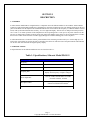
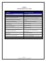
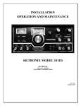
OPERATION AND MAINTENANCE
SILTRONIX
MODEL FD-1011
DIGITAL DIAL
A Division of Cubic Corporation
October 1976
Reprinted 2006
TABLE OF CONTENTS
SECTION I DESCRIPTION
1-1
General
1-4
Specifications
3
3
SECTION II INSTALLATION
2-1
Fixed Installation
4
2-3
Mobile Installation
4
2-6
VFO Connection
4
SECTION III OPERATION
3-1
On/Off Switch
3-3
Display
SECTION V MAINTENANCE
5-1
General
5-3
Calibration
5-5
Disassembly
5-6
Cover Removal
5-8
Circuit Board Removal
5-10
Display Removal
5-12
Troubleshooting
10
10
10
10
10
10
10
SECTION VI PARTS LISTS
6-1
General
17-18
5
5
SECTION IV THEORY OF OPERATION
4-1
General
6
4-3
Functional Description
6
4-7
Detailed Description
6
4-9
System Clock
6
4-12
Timing Signal Generation 7
4-14
Signal Sampling
7
4-14
Signal Sampling
7
4-16
Display
7
4-18
Reset
8
4-20
Power Supply
8
LIST OF ILLUSTRATIONS
Figure 4-1
Block Diagram
Figure 4-2
Timing System Waveforms
Figure 5-1
Component Locations
Figure 5-2
Schematic Diagram
LIST OF TABLES AND CHARTS
Table 1-1
Specifications
Chart I
Troubleshooting Guide
Chart II
Troubleshooting, Unit Inoperative Display Lighted with 25.500
Chart III
Troubleshooting, Timing System Inoperative
Table 6-1
Replaceable Parts List
3
11
12
13
17-18
9
9
15
16
SECTION I
DESCRIPTION
1-1 GENERAL
1-2 The Siltronix Model FD-1011 Digital Dial is a companion unit to the Siltronix Model 1011D 10 Meter Amateur Radio
Transceiver and Citizens Band (CB) Receiver. Plugging two connectors from the FD-1011 into mating connectors on the rear
panel of the Model 1011D completes the installation. The FD-1011 then indicates the frequency to which the Model 1011D is
tuned, with crystal controlled time base accuracy, on a five digit LED display. The FD-1011 is dual powered with provision
for 117VAC or 13.8VDC operation. If the companion 1011D is operating from 117VAC power, the power connector for the
FD-1011 is plugged into a mating receptacle on the rear panel of the Model 1011D. If the 1011D is operating from 13.8VDC,
the FD-1011 is also connected to the 13.8VDC supply through two insulated binding posts on its rear panel.
1-3 The Model FD-1011 is housed in a black, perforated metal case measuring 8 inches wide by 2-1/4 inches high by 6-1/4
inches deep. Four rubber feet elevate the unit 1/4 inch above the surface on which it rests. Front panel controls and indicators
are an ON - OFF switch and the five digit frequency display.
1-4 SPECIFICATIONS
1-5 Specifications for the Siltronix Model FD-1011 are listed in Table 1-1.
Table 1-1 Specifications, Siltronix Model FD-1011
FD-1011 Specifications
Frequency
26 to 30 MHz
Resolution
±1KHz.
Stability
Better than ± 0.005%
Sampling Rate
50 times per second. Provides fast up-date of
display when frequency of input is changed.
Power Input Max.
117VAC, 60 Hz, 20 Watts Max. 10-16VDC
(13.8VDC nominal), 14 Watts
DC Input Ground
Chassis may be (+) or (—) ground. Supply
connections insulated from chassis.
Size
8 in. wide by 2-1/4 in. high by 6-1/4 in. deep.
Page 3
Copyright 2006 Robert A. Larson, KC9ICH
SECTION II
INSTALLATION
2-1 FIXED INSTALLATION
2-2 To install the FD-1011 as a companion unit to a Model 1011D Transceiver operating from 117VAC, insert the AC
connector from the FD-1011 into the AC receptacle on the rear of the 1011D marked ―FD-1011 ACC‖ (117VAC SW). This
receptacle is energized whenever the Model 1011D is turned on, therefore, the FD-1011 power switch may be left on with
power being controlled by the Model 1011D. Plug the miniature phone plug that is on the end of the FD-1011 coaxial cable,
into the mating miniature phone jack on the rear of the Model 1011D marked ―FD-1011 ACC‖. Connect a ground strap
between the chassis of the 1011D and the FD-1011 using the ground post and wing nut for attachment. Place the FD-1011
alongside the transceiver NEVER ON TOP OF IT.
CAUTION
Placing the FD-1011 on top of the Model 1011D Transceiver will interfere with normal convection cooling of the 1011D and
can adversely affect component life in that unit. Electrical interference may also be encountered.
2-3 MOBILE INSTALLATION
2-4 Installation of the FD-1011 in mobile applications, or wherever 13.8VDC is used to power the Model 1011 Transceiver,
requires that the 13.8VDC source be connected to the two binding posts on the rear of the FD-1011. The positive (+) lead
must be connected to the red binding post and the negative (—) lead to the black binding post. The chassis may be connected
to either the positive or negative side of the line as both binding posts are insulated from the chassis. A ground strap should
be connected between the Model 1011D Transceiver and the FD-1011 Digital Dial using the ground post and wing nut on the
FD-1011.
2-5 In mobile installations, where the two units may be separated up to the length of the interconnecting coaxial cable
furnished with the FD-1011, the two units must be grounded to each other either by a single ground strap between them or
through the vehicle structure. Do not rely on mounting structure for such grounds but use heavy conductors attached to the
binding posts. Keep ground leads as short as possible.
CAUTION
Under no circumstances should the FD-1011 be connected to the Model 1011D Transceiver through either AC receptacle on
the rear of the 1011D when the transceiver is powered from the l3.8VDC source through the Model 14A power adapter.
Damage to the FD-1011 will result.
2-6 VFO CONNECTION
2-7 Connection to the VFO output of the Model 1011D Transceiver is made with the miniature phone plug on the end of the
coaxial cable from the FD-1011 which is plugged into the matching miniature phone jack on the rear of the 1011D
Transceiver marked ―FD-1011 ACC‖.
Page 4
Copyright 2006 Robert A. Larson, KC9ICH
SECTION III
OPERATION
3-1 ON/OFF SWITCH
3-2 When the FD-1011 and 1011D are operated from a 117VAC source, power will be applied to the FD-1011 only when the
front panel ON-OFF switch, which is combined with the VOLUME control on the 1011D, is turned ON. The front panel ONOFF switch on the FD-1011 may then he left in the ON position at all times. When operated from 13.8VDC, the front panel
ON-OFF switch must be actuated to turn the unit on and off.
3-3 DISPLAY
3-4 When the FD-1011 is turned on, and the 1011D is turned off, the FD-1011 display will indicate 25.500 MHz. This is a
normal indication. Remember, the FD1011 is a companion unit designed specifically for the 1011D Transceiver. When the
VFO frequency from the 1011D is injected into the FD-1011 via the interconnecting cable, the FD-1011 will read the
frequency to which the Model 1011D is tuned.
Page 5
Copyright 2006 Robert A. Larson, KC9ICH
SECTION IV
THEORY OF OPERATION
4-1 GENERAL
4-2 This section of the manual describes, in detail, the operation of the amplifiers and logic circuits of the Siltronix FD-1011
Digital Dial. The descriptions are in two parts. The first, supported by the block diagram of Figure 4-1, describes the circuit
functionally as a prelude to the more detailed descriptions of the second part which is supported by the logic/schematic
diagram of Figure 5-2 and a timing diagram, Figure 4-2. The descriptions herein assume knowledge on the part of the
technician of the operation of digital logic circuits such as NAND gates, inverters, counters, decoder/drivers and sevensegment display devices. The FD-1011 uses many integrated circuit packages that contain a multiplicity of identical circuits.
The circuits within these packages are not discussed in this text. Only the responses of certain outputs which are relative to
the discussion of the FD-1011 are detailed. Manufacturer‘s published data, and other publications readily available to
electronics technicians, provide the details of the internal circuits of these devices.
4-3 FUNCTIONAL DESCRIPTION
4-4 Refer now to Figure 4-1. When the FD-1011 is connected to a Siltronix Model 1011D transceiver, the output of the
transceiver VFO is coupled to the input amplifier of the FD-1011. The sampling gate is enabled for 10 milliseconds by the
timing system. The VFO frequency is then divided by a factor of 10 in each of the following decade counters. When the gate
is disabled at the end of the sampling period, each of the counters that comprise the division chain will contain a discrete
number in BCD code. These numbers as a group are directly related to the input frequency. The most significant figure will
be lost and the next most significant figure, plus a count of 5, will be contained in the last counter of the chain and the least
significant figure will be in the second counter. The count of 5 that is added is part of the conversion from the VFO frequency
to the operating frequency. The operating frequency is the desired display. The addition is further explained in the detailed
circuit description.
4-5 When the sampling period ends, the decoder / drivers are enabled for 9 milliseconds. They convert the BCD codes to a
code that will drive the seven segment numerical displays. At the end of the 9 millisecond period, the display is turned off;
the counters are reset or preset as appropriate. The sequence is then repeated. During the sampling period the display is blank,
however, the pulse rate is 50 Hz and it appears to the human eye that the display is on continually.
4-6 A crystal controlled oscillator operating at 2.048 MHz is the basic timing system. This frequency is first divided by a
factor of 4096 and then further divided by 5 and then 2 to generate the signals from which the system timing signals will be
generated. The timing system, through the combination of signals applied to gates and inverters, generates the sampling,
display and reset timing signals which control the sampling, display and reset sequence.
4-7 DETAILED DESCRIPTION
4-8 Unless otherwise noted, all circuit references in this text are to the schematic / logic diagram of Figure 5-2.
4-9 System Clock
4-10 The system clock frequency stability is maintained by a crystal controlled oscillator comprised of quartz crystal V1
inverters A14-D and A14-E and associated components. The oscillator operates at a frequency of 2.048 MHz and this
frequency is adjusted within small limits by variable capacitor C18. This permits precise adjustment of the clock frequency.
4-11 The 2.048 MHz signal from the oscillator is divided by a factor of 16 in each of the counters, A12, A13, and A14 for a
total division of 4096. The frequency at the output of A12 is 500 Hz. This is further divided by 5 to produce signals A11-11
and A11-12 shown in Figure 4-2.
Page 6
Copyright 2006 Robert A. Larson, KC9ICH
4-12 Timing Signal Generation
4-13 The identifications of the timing signals of Figure 4-2 are derived from the IC and terminals of their origins. For
example, the 500 Hz clock originates from A12, terminal 11. It is identified as A12-11. Timing signal A, which is the reset
pulse, is generated by firs combining the 500 Hz clock with A11-11 in NAND gate A6-A. Referring to Figure 4-2 it is seen
that the inputs to A6-A are both high only during the time of each 5th successive clock pulse. This produces a train of 1
millisecond negative pulses at 1/5th the clock rate. This pulse train is then inverted in Al-A and applied to the input of NAND
gate A6-D along with a 50 Hz square wave from Al-B which is waveform C inverted. The inputs to A6-D are both high only
during each second pulse of A1-A-2. This eliminates the intervening pulse and generates waveform A. Waveform B is
generated by combining waveform A and the inverted waveform C, (Al-B-4), in NAND gate A6-C. Waveform A goes low
for 1 millisecond prior to A1-B-4. This then generates a pulse that is high for 11 milliseconds and low for 9 milliseconds and
which is inverted for waveform B.
4-14 Signal Sampling
4-15 The VFO signal from the 1011D is applied to the base of Q1 which uses negative feedback and a tuned circuit in series
with the collector to provide an essentially flat response across the frequency range of the VFO. The output of the amplifier is
then applied to the sampling gate, A6-B. A6-B is enabled by timing signal C for 10 milliseconds out of the 20 millisecond
time base. The VFO frequency is, thus, gated to the counter chain for that period. The gated VFO signal is first prescaled by
10 in A15. A10 is a decade counter and its terminals 12, 9, 8 and 11, respectively, will produce a BCD code equal to the
number of pulses appearing at its clock input terminal 14. Since it is a decade counter, terminal 11, the ―8‖ output, will be
high during the eighth and ninth clock pulses. On the tenth pulse, it will go low clocking A9 which is another decade counter.
(The 7490 is clocked on the negative going edge of the input pulse). After ten input pulses, the BCD code at the output
terminals of A10 will be ―0‖ and at the output of A12 it will be ―1‖. A8 will be clocked by A9 when A9 accumulates 10
counts after 100 input pulses to A10. A7 will similarly be clocked by A8 after 1000 input pulses to A10. At the end of 10
milliseconds, when the sampling gate is disabled, the four counters will contain numbers in BCD code proportional to the
VFO frequency ÷5.5 KHz. A8 and A7 were each preset prior to the sampling period, to a count of 5. If the receiver is tuned
to 28.000 MHz the input frequency to the FD-1011 will be 22.500 MHz. Since the gate is opened for only 10 milliseconds,
the number of input pulses to A15 will be 225,000 which will he divided to 22,500 prior to the input of A10. This will be
divided in A10, A9, A8 and A7 as previously discussed. The most significant figure will overflow out of A7 and will be lost.
(Since it is always a ―2‖, this is of no importance as the most significant number in the display is permanently set at ―2‖).
Since A7 and A8 will both preset to 5, they will now have been clocked to 8 and 0 respectively by the next two significant
numbers: e.g., 25 + 55 equals 80. (Remember, the first 2 overflowed). A9 and A10 both contain BCD codes of ―0‖. The
numbers in the counters, reading from right to left are 8-0-0-0.
4-16 Display
4-17 Immediately on disabling of the sample gate, timing signal B unblanks decoder drivers A2, A3, A4 and A5 for 9
milliseconds. The decoder drivers convert the BCD code to a code that will display the BCD number on the seven-segment
displays Z1, Z2, Z3 and Z4, to which they are connected. A fifth seven - segment display, Z5, is connected so as to always
display a number 2 and the decimal point in Z4 is permanently connected. The display now reads 28.000 MHz. The 1011D
VFO oscillator operates low side, 5.5 MHz below the frequency to which the transceiver is tuned. If we add 5.5 MHz to the
VFO frequency of 22.500 MHz the sum is 28.000 MHz. This is the frequency to which the transceiver is tuned. The resistors
that interconnect the decoder drivers and the display limit the current through the display segments to approximately 15
milliamps per segment.
Page 7
Copyright 2006 Robert A. Larson, KC9ICH
4-18 Reset
4-19 At the end of the 9 millisecond display period, the display is blanked. Counters A9, A10 and A15 are reset by timing
signal A inverted and counters A7 and A8 are both preset to 5 by A completing the sample, display, reset sequence which is
then repeated.
4-20 Power Supply
4-21 The power supply operates from either 117VAC or 13.8VDC. Though no damage would occur if the unit was connected
to both sources simultaneously, no assurances could be given for which source was supplying power at any particular time.
117VAC is connected to T1 through S1 and F2. 9VAC, nominal, at the output of T1, is converted to 12.0 VDC by the bridge
rectifier. 12.6VDC powers the display which is filtered by C4 and regulated to 5VDC by the F74MO5UC regulator. C5, C6,
and C7 provide RF bypassing.
4-22 13.8VDC enters through CR1, S1, F1, and CR2, CR3, and CR4. The diodes drop the input by approximately 3.5 volts to
approximately 10.3 volts which is then applied to the displays and to the 5 V regulator.
Page 8
Copyright 2006 Robert A. Larson, KC9ICH
Figure 4-1 Block Diagram, Model FD-1011
Figure 4-2 Timing System Waveforms
Page 9
Copyright 2006 Robert A. Larson, KC9ICH
SECTION V
MAINTENANCE
5-1 GENERAL
5-2 The Siltronix FD-1011 Digital Dial requires no periodic or preventative maintenance. Maintenance procedures, therefore,
cover calibration, disassembly and troubleshooting.
5-3 CALIBRATION
5-4 Connect a counter to the 1011D VFO output or to a signal generator and set the frequency to 23.500 MHz ± 0.0001 MHz.
Next, connect the source of that frequency to the input of the FD-1011. Use an INSULATED screwdriver and adjust C12
through the rubber grommet until the FD-1011 display reads 29.000 MHz ± 0.000 MHz.
NOTE
The counter should have accuracy of ± 1 KHz at 23 MHz. The counter may be connected to a ‗T‘ in the line between signal
source and the 1011D.
5-5 DISASSEMBLY
5-6 Cover Removal
5-7 It is necessary to remove the cover of the FD1011 to gain access to the circuit components. Remove two screws on both
sides of the unit and lift the cover clear.
WARNING
The FD-1011, when connected to a source of 117VAC contains voltages that are dangerous to life. Remove the plug from the
power receptacle before removing the cover.
5-8 Circuit Board Removal
5-9 Remove the two #4 screws at the forward corners of the circuit board that pass through the small brackets and into the
threaded standoffs that are swaged into the chassis. Turn the unit over and remove the three sheet metal screws that hold the
rear panel to the chassis. Separate the rear panel and chassis. The circuit board is attached to the rear panel and its underside
will now be completely exposed allowing removal of any component. Reassembly will be accomplished with the reverse
procedure. When reassembling, check that the circuit board is fully forward with the plate on each switch resting snugly
against the front panel before tightening the screws.
CAUTION
Use care in removal of components so as not to damage the etched wiring on the board. Use a low temperature soldering iron
and vacuum solder removal tool. All leads from IC‘s should be cut and then removed one by one to avoid overheating of the
circuit board.
5-10 Display Removal
5-11 The digit displays are attached to the display board. Remove the main circuit board as directed in paragraph 5-8. This
will, then, permit unsoldering and removal of the display.
5-12 TROUBLESHOOTING
5-13 The troubleshooting aids included in this section consist of a Troubleshooting Guide (Chart I), and ―logic tree‖ types of
troubleshooting procedures (Charts II and III). They are cross-referenced so that they will lead the technician to the defective
component in most cases. It is not possible to anticipate all failure modes. Therefore, the technician will do well to review
Section IV, Theory of Operation, as preparation for troubleshooting the unit.
Page 10
Copyright 2006 Robert A. Larson, KC9ICH
CHART I
TROUBLESHOOTING GUIDE
Symptom
Probable Cause / Cure
Unit is totally inoperative.
Check fuses.
Unit operates on 117VAC but not on 13.8VDC.
Check fuse and diodes CR1 through CR4.
Operates on DC. Will not operate on AC.
Check for defective fuse, F2, defective transformer
Ti and bridge rectifier diodes CR5 through CR8.
All digits in display light but unit is inoperative.
See Chart II for troubleshooting procedure for this
symptom.
Unit operative but with small error.
Requires calibration. See paragraph 5-3.
Only least significant number in display changes
with changed input.
Defective counter A9.
Only least and next significant number in display
changes with changed input.
Defective counter A8.
First three digits change with input change, others do
not.
Defective counter A7.
One display (other than most significant figure) does
not change with change in input.
If second most significant figure, defective counter
A7 or decoder/driver. If other digit, defective
decoder/driver.
Most significant figure (permanent ―2‖) is only
lighted display.
5 Volt regulator defective.
Display reads 25. 500 even with input.
Defective input amplifier Q1, defective sampling
gate A6-B. Timing system defect. See Chart II for
timing system troubleshooting.
One segment in one digit of display does not light.
Defective display unit. Defective decoder, driver.
Page 11
Copyright 2006 Robert A. Larson, KC9ICH
CHART II
Unit Inoperative - Display Lighted with 25.500
Check for waveform B at A1-C-6.
See Figure 4-2
BAD
Go to Chart III
BAD
Defective C9 or coax cable. Analyze
and repair.
BAD
Look for open L1, shorted C10, or
defective Q1.
OK
Check for input at base of Q1.
OK
Check for input at collector of Q1.
OK
Check for 10 ms. Bursts of input
signal at A6-B-6.
BAD
Replace A6.
BAD
Replace A15.
OK
Check for 10 ms. Bursts of input
signal divided by 10 at A15-12.
OK
See chart I for symptoms and causes
or chart III for timing system
troubleshooting.
Page 12
Copyright 2006 Robert A. Larson, KC9ICH
CHART III
Timing System Inoperative
Check for 2.048 MHz oscillator output at
A1-D-8.
BAD
Troubleshoot and repair oscillator.
BAD
Replace A14.
OK
Check for 128 KHz output at A14-11.
OK
Check for 8 KHz output at A13-11.
BAD
Replace A13.
OK
Check for 500 Hz output at A12-11.
BAD
Replace A12.
BAD
Replace A11.
BAD
Replace A6.
BAD
Replace A1.
OK
Check for 50 Hz waveform C at A11-12.
OK
Check for proper waveform C at A6-A-3.
Inverse of A1-A-2, Figure 4-2.
OK
Check for proper waveform at A1-A-2.
OK
Continued
Page 13
Copyright 2006 Robert A. Larson, KC9ICH
CHART III
(Continued)
From Proceeding
Page.
Check A1-B-4 for inverted waveform C.
BAD
Replace A1.
BAD
Replace A6.
OK
Check waveform A at A6-D-11.
OK
Check for inverted waveform B at A6-C-8.
BAD
Replace A6.
OK
Check for waveform B at A1-C-6.
BAD
OK
Timing system operating normally.
Page 14
Copyright 2006 Robert A. Larson, KC9ICH
Replace A6.
Figure 5-1 Component Locations
R30-34
R2-29
Z1
A4
A9
Z2
Z3 A3 A8 Z4 A7 A2 Z5 C1-7 C13
R38
C12
C19
R39
A1
A6 C11 C8
A5
C7-4
A10
C7-3
R37
A15
A11
A14
C9
C5
C6
T1
R36
Q1
R35
C4
CR2
C7-2
C1-C2
C3 F2 A13 CR5-8
C7-5
F1
A12
L1
C10
Page 15
Copyright 2006 Robert A. Larson, KC9ICH
CR2
A16
Figure 5-2 Schematic Diagram
Page 16
Copyright 2006 Robert A. Larson, KC9ICH
SECTION VI
PARTS LISTS
6-1 GENERAL
6-2 The replaceable electrical parts of the FD-1011 listed in Table 6-1. When ordering items not listed in Table 6-1, please
furnish a complete description of the item.
Table 6-1 Replaceable Parts List
CAPACITORS
C1
C2
C3
C4
C5
C6
C7
C8
C9
C10
C11
C12
C13
C19
0.002 mfd., 500V, Disc
0.002 mfd., 500V, Disc
0.05 mfd., 500V, Disc
3300 mfd., 16V
0.1 mid., 50V
0.1 mfd., 12V, Disc
0.01 mfd., 100V, Disc
0.05 mfd., 500V, Disc
68 pfd., Disc
10 pfd., NPO, Disc
20 pfd., NPO, Disc
4 - 30 pfd., Trimmer
50 pfd., NPO, Disc
0.1 mfd., 12V, Disc
072-018
072-018
072-053
073-071
072-038
072-052
072-040
072-053
084-038
084-060
084-001
089-020
084-103
072-052
1A, 50V
1A, 50V
475-023
475-023
DIODES
CR1 — CR4
CR5 — CR8
INTEGRATED CIRCUITS
A1
A2 – A5
A6
A7
A8
A9
A10
All
A12 — A14
A15
A16
Hex Inverter, 7404
Decoder-Driver, 7447
Quad, Two-Input NAND Gate, 7400
Decade/Binary Counter/Latch, 74196
Decade/Binary Counter/Latch, 74196
Decade Counter/Divider, 7490
Decade Counter/Divider, 7490
Decade Counter/Divider, 7490
Counter / Divider 7493
Decade Counter/Divider 7490
Voltage Regulator, F78MO5UC
477-020
477-038
477-022
477-035
477-035
477-033
477-033
477-033
477-034
477-033
477-024
Page 17
Copyright 2006 Robert A. Larson, KC9ICH
Table 6-1 Replaceable Parts List
(Continued)
RESISTORS
R2 — R29
R30 — R34
R35
R36
R37 — R39
220 Ohms, 1/4 Watt, 5%
470 Ohms, 1/4 Watt, 5%
27K Ohms, 1/4 Watt, 5%
47 Ohms, 1/4 Watt, 5%
1.5K Ohms, 1/4 Watt, 5%
045-221
045-471
045-273
045-470
045-152
Fuse, 2A
Fuse, 0.5A, 250V
Inductor, 2.7 uh
Transistor, 2N5130
Switch, DPDT, Slide
Crystal, Quartz, 2.048 MHz
Seven-Segment Display
482-016
482-021
027-026
476-007
172 -020
486-053
475-044
MISCELLANEOUS
F1
F2
L1
Q1
S1
Y1
Z1 - Z5
Page 18
Copyright 2006 Robert A. Larson, KC9ICH
LIMITED WARRANTY POLICY
SILTRONIX warrants this equipment against defects in material or
workmanship, except for tubes and solid-state devices, under normal service
for a period of six (6) months from original purchase date. Tubes and solidstate devices are warranted for a period of ninety (90) days. This warranty is
valid only if the enclosed warranty registration card is properly completed
and mailed to the factory within ten (10) days of purchase date.
If warranty service is required, do not ship equipment to the factory without
prior authorization obtained from the SILTRONIX factory. This warranty is
limited to repairing or replacing the defective parts only and is not valid if the
equipment has been tampered with, misused or damaged.
Liability for damage during shipment lies with the carrier and not with
SILTRONIX. Any claims or adjustments for shipping damages must be filed
directly with the carrier.
THE LIABILITY OF THE COMPANY ON THIS EQUIPMENT IS LIMITED
TO THE EXPRESS TERMS OF THE WARRANTY PROVIDED ABOVE. NO
WARRANTY OF MERCHANTABILITY AND NO WARRANTY OF FITNESS
FOR A PARTICULAR USE IS IMPLIED IN THIS SALE.
A Division of Cubic Corporation
330 VIA EL CENTRO
OCEANSIDE, CALIF. 92054
Page 19
Copyright 2006 Robert A. Larson, KC9ICH