1
Hardware Instruction Manual
USB Evaluation Board
R0K866597D020BR
Hardware Instruction Manual
R19AN0005EJ0100
Rev.1.00
Jan 10, 2012
Introduction
This book is an instruction manual for the hardware used with evaluation board R0K866597D020BR, which operates
the USB Host function and peripheral function.
Target Device
RX62N RSK
Contents
1.
Preface .............................................................................................................................................. 2
2.
Important ........................................................................................................................................... 3
3.
Precautions for Safety....................................................................................................................... 5
4.
Function Overview............................................................................................................................. 8
5.
Outline ............................................................................................................................................... 9
6.
Evaluation Board Specifications........................................................................................................ 9
7.
Jumper and Switch Setting ............................................................................................................. 17
8.
Setup ............................................................................................................................................... 18
9.
Connectors Pin Assignment............................................................................................................ 23
10. Circuit Diagram................................................................................................................................ 25
11. Parts Layout Diagram ..................................................................................................................... 25
12. Parts List ......................................................................................................................................... 25
R19AN0005EJ0100 Rev.1.00
Jan 10, 2012
Page 1 of 26
R8A66597 USB Evaluation Board R0K866597D020BR
Hardware Instruction Manual
1. Preface
The R0K866597D020BR is the evaluation board of the USB Host function and built-in functions. This instruction
manual explains how to setup up and operate the related hardware and offers cautionary notes concerning usage.
All components of the R0K866597D020BR are listed under “Table 6.2 Assembly Components and Quantity.” If you
have any question about the R0K866597D020BR, contact your local distributor.
R19AN0005EJ0100 Rev.1.00
Jan 10, 2012
Page 2 of 26
R8A66597 USB Evaluation Board R0K866597D020BR
Hardware Instruction Manual
2. Important
Before using this product, be sure to read this user’s manual carefully.
Keep this user’s manual, and refer to it when you have questions about this product.
Product:
"Product" in this document collectively refers to the following products manufactured by Renesas Electronics
Corporation
(1) R8A66597FP USB Evaluation Board R0K866597D020BR
"Product" herein encompasses neither the customer's user system nor the host machine.
Purpose of use of the product:
This product is a device to support the development of systems that uses the R8A66597FP. It provides support for
system development in both software and hardware.
Be sure to use this product correctly according to said purpose of use. Please avoid using this product other than for
its intended purpose of use.
For those who use this product:
This product can only be used by those who have carefully read the user’s manual and know how to use it.
Use of this product requires basic knowledge of electric circuits, logical circuits, and MCUs.
When using this product:
(1) This product is a development-support unit for use in your program development and evaluation stages. When a
program you have finished developing is to be incorporated in a mass-produced product, the judgment as to
whether it can be put to practical use is entirely your own responsibility, and should be based on evaluation of the
device on which it is installed and other experiments.
(2) In no event shall Renesas Electronics Corporation be liable for any consequence arising from the use of this
product.
(3) Renesas Electronics Corporation strives to provide workarounds for and correct trouble with products
malfunctions, with some free and some incurring charges. However, this does not necessarily mean that Renesas
Electronics Corporation guarantees the provision of a workaround or correction under any circumstances.
(4) This product covered by this document has been developed on the assumption that it will be used for program
development and evaluation in laboratories. Therefore, it does not fall within the scope of applicability of the
Electrical Appliance and Material Safety Law and protection against electromagnetic interference when used in
Japan.
(5) Renesas Electronics Corporation cannot predict all possible situations and possible cases of misuse that carry a
potential for danger. Therefore, the warnings in this user's manual and the warning labels attached to this product
do not necessarily cover all such possible situations and cases. The customer is responsible for correctly and safely
using this product.
(6) The product covered by this document has not been through the process of checking conformance with UL or other
safety standards and IEC or other industry standards. This fact must be taken into account when the product is
taken from Japan to some other country.
(7) This product is a product used for development of a program, and an evaluation stage. It cannot include in a user's
product and cannot mass-produce.
(8) Even if it is the case where fault is in the device carried in this product, it does not exchange for the fault repair
article of a device.
(9) Operation of all USB peripheral devices cannot be guaranteed.
(10) The sample programs of this product are all references, and no one to guarantee the operation. Please use this
sample program as a technological reference when customer's software is developed.
R19AN0005EJ0100 Rev.1.00
Jan 10, 2012
Page 3 of 26
R8A66597 USB Evaluation Board R0K866597D020BR
Hardware Instruction Manual
Usage restrictions:
This product has been developed as a means of supporting system development by users. Therefore, do not use it as
an embedded device in other equipment. Also, do not use it to develop systems or equipment for use in the
following fields.
(1) Transportation and vehicular
(2) Medical (equipment that has an involvement in human life)
(3) Aerospace
(4) Nuclear power control
(5) Undersea repeaters
If you are considering the use of this product for one of the above purposes, please be sure to consult your local
distributor.
About product changes:
We are constantly making efforts to improve the design and performance of our product. Therefore, the
specification or design of the product, or this user's manual, may be changed without prior notice.
About rights:
(1) We assume no responsibility for any damage or infringement on patent rights or any other rights arising from the
use of any information, products or circuits presented in this user’s manual.
(2) The information or data in this user’s manual does not implicitly or otherwise grant a license to patent rights or any
other rights belonging to Renesas or to a third party.
(3) This user’s manual and this product are copyrighted, with all rights reserved by Renesas. This user’s manual may
not be copied, duplicated or reproduced, in whole or part, without prior written consent from Renesas.
About diagrams:
Some diagrams in this user’s manual may differ from the objects they represent.
Warranty:
Renesas will exchange this board free of charge only due to manufacturing defects.
R19AN0005EJ0100 Rev.1.00
Jan 10, 2012
Page 4 of 26
R8A66597 USB Evaluation Board R0K866597D020BR
Hardware Instruction Manual
3. Precautions for Safety
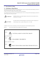
3.1. Definitions of Signal Words
This chapter describes the precautions which should be taken in order to use this product safely and properly. Be sure to
read and understand this chapter before using this product.
Contact us if you have any questions about the precautions described here.
This chapter describes the precautions which should be taken in order to use this product safely and properly. Be sure to
read this chapter before using this product.
WARNING indicates a potentially dangerous situation that will cause death or heavy
wound unless it is avoided.
WARNING
CAUTION indicates a potentially dangerous situation that will cause a slight injury or
CAUTION
a medium-degree injury or property damage unless it is avoided.
In addition to the two above, the following are also used as appropriate to indicate additional precautions.
[Notice]
Point out the attention for the malfunction by wrong setting.
means WARNING or CAUTION.
Example:
CAUTION AGAINST AN ELECTRIC SHOCK
means PROHIBITION.
Example:
DISASSEMBLY PROHIBITED
●means A FORCIBLE ACTION.
Example:
UNPLUG THE POWER CABLE FROM THE RECEPTACLE.
R19AN0005EJ0100 Rev.1.00
Jan 10, 2012
Page 5 of 26
R8A66597 USB Evaluation Board R0K866597D020BR
Hardware Instruction Manual
3.2. Warning
WARNING
Warnings for Power Supply:
If you connect the attached power cable with the stabilized power supply, be sure to connect it with the
appropriate polarity (the red cable is connected to the power line. The black cable is connected to the
ground).
Use this product within the appropriate voltage range. This product does NOT have a built in over voltage
protection.
Do not touch the plug of the power cable when your hands are wet. This may cause electric shock.
If you need to use an AC adaptor, please confirm the connector shape, voltage and polarity. In addition,
use an AC power cable which complies with the safety standard of the country.
Do NOT use the power supply function on the emulator, when both the emulator and another power supply
are connected to this product at the same time.
When installing this equipment, insure that a reliable ground connection is maintained.
If you smell a strange odor, hear an unusual sound, or see smoke coming from this product, then
disconnect power immediately Do not use this as it is because of the danger of electric shock and/or fire. In
this case, contact your local distributor.
Before setting up this product and connecting it to other devices, turn off power or remove a power cable
to prevent injury or product damage.
Warnings to Be Taken for Handling:
Do not break down this product. Breaking down the product will void your warranty.
Warning for Installation:
Do not set this product in water or areas of high humidity. Make sure that the product does not get wet.
Spilling water or some other liquid into the product may cause un-repairable damage.
Warning for Use temperature:
This equipment is to be used in an environment with a maximum ambient temperature of 35°C.
Care should be taken that this temperature is not exceeded.
R19AN0005EJ0100 Rev.1.00
Jan 10, 2012
Page 6 of 26
R8A66597 USB Evaluation Board R0K866597D020BR
Hardware Instruction Manual
3.3. Caution
CAUTION
Cautions to Be Taken for Handling This Product:
Use caution when handling the product. Be careful not to apply a mechanical shock.
Do not touch the connector pins of this product directly. Static electricity may damage the internal
circuits.
When attaching and removing the cable, hold the plug of the cable and do not pull on the cable. Do not
pull this product by the communications interface cable. Excessive flexing or force may break
conductors.
When you connect an external board to this product through test pins, be careful not to short signal lines
or between power line and ground. If this product is revised by the user, operation cannot be guaranteed.
Note on Transporting the Product:
When sending your product for repair, use the packing box and cushioning material supplied with the
product when it was delivered to you and specify caution in handling (handling as precision equipment). If
packing of your product is not complete, it may be damaged during transportation. When you pack your
product in a bag, make sure to use the conductive plastic bag supplied with the product. If you use a
different bag, it may lead to further trouble with your product due to static electricity.
Caution to Be Taken for Disposal:
Penalties may be applicable for incorrect disposal of this waste, in accordance with your national
legislation.
European Union regulatory notices:
The WEEE (Waste Electrical and Electronic Equipment) regulations put responsibilities on producers for
the collection and recycling or disposal of electrical and electronic waste. Return of WEEE under these
regulations is applicable in the European Union only. This equipment (including all accessories) is not
intended for household use. After use the equipment cannot be disposed of as household waste, and the
WEEE must be treated, recycled and disposed of in an environmentally sound manner.
Renesas Electronics Europe GmbH can take back end of life equipment, register for this service at
“http://www.renesas.eu/weee”.
R19AN0005EJ0100 Rev.1.00
Jan 10, 2012
Page 7 of 26
R8A66597 USB Evaluation Board R0K866597D020BR
Hardware Instruction Manual
4. Function Overview
4.1.
Overview
The R0K866597D020BR is an evaluation board for the Renesas Hi-Speed USB ASSP R8A66597FP. Two USB-A
receptacles are mounted on the board for evaluation of USB host operations using USB port0 and USB port1 of
R8A66597. CN1 can be used for evaluation of USB peripheral operations. Please refer to the data sheet “USB2.0 Dual
Function Controller R8A66597FP” for detailed specifications of the R8A66597.
The model name, package and package description of the chip that is mounted on the board is as follows:
Board
Chip Model Name
Package Description
R0K866597D020BR
R8A66597FP
Plastic 80-pin LQFP (0.4mm pitch 10×10mm body)
The board has the following features:
(1) Evaluate the system by connecting this board and a control board using the interface connector of this board.
(2) A solder pattern is prepared on the USB signal lines for chip common mode choke coils. For EMI suppression
evaluation.
(3) A solder pattern is prepared on the USB signal lines for ESD protection devices. For ESD protection evaluation.
(4) Supply 3.3V or 1.8V to the interface power VIF of R8A66597FP.
(5) Test R8A66597FP's functions (excluding split bus) by connecting with Renesas Starter Kits*1 board.
*1: Renesas Starter Kits are the latest development from Renesas in low-cost evaluation development toolkits.
(6) Supply 5V, 500mA to the VBUS.
4.2.
Related Data Sheets and Application Notes
The R8A66597FP comes with “USB Sample Firmware” for evaluation. For details, please contact Renesas Electronics,
your distributor, or check the information on the homepage below.
R8A66597 Datasheet (Doc. No. REJ03F0229-0101)
http://www.renesas.com/products/mpumcu/usb_device/assp_usb/m66596/Documentation.jsp
R19AN0005EJ0100 Rev.1.00
Jan 10, 2012
Page 8 of 26
R8A66597 USB Evaluation Board R0K866597D020BR
Hardware Instruction Manual
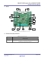
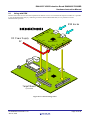
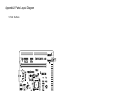
5. Outline
CN1
Port0
CN5
Port1
JA6
JA5
JP6
USB MODE
JP13
WR1 SEL
JA1
JA2
JP14
WR0 SEL
JP8
CS SEL
JP7
INT0
JP4
IOVcc
JA3
CN4
JP10
DC 5V SEL
Figure 5.1 R0K866597D020BR Board (Top View)
6. Evaluation Board Specifications
Table 6.1 Board Specifications
Specifications
Board Size
Supply power
Interface
98 mm × 88 mm
AVCC , VCC : 3.3 V , VIF : 3.3 V or 1.8 V
50 Pin Connector * 1 , 24 Pin Connector * 2 , 26 Pin Connector * 2
(Specification of all connectors : 2.54mm pitch, dual straight header, male type)
USB Receptacle (Type A, DIP, normal) * 2
R19AN0005EJ0100 Rev.1.00
Jan 10, 2012
Page 9 of 26
R8A66597 USB Evaluation Board R0K866597D020BR
Hardware Instruction Manual
Table 6.2 Assembly Components and Quantity
Component Name
Evaluation board ( R0K866597D020BR )
Power supply cable ( incl. 2P connector )
Table of Toxic and Hazardous Substance and Elements
Release Note ( English )
Release Note ( Japanese )
6.1.
QTY
1
1
1
1
1
Connector Description (View from R8A66597)
Connectors JA1, JA2, JA4 and JA6 provide all bus interface pins of the chip, such as processor bus interface
and DMA interface. Therefore, these pins provide the same pin characteristics of the R8A66597FP such as
electric characteristic, I/O direction, and functions except for the signal with *. Note: All pins on JA5 are
unconnected.
The following table shows the pin number and function correspondences.
Table 6.1.1 Connector Description (View from R8A66597)
Pin Description of
R8A66597FP
D15∼8
Connector
Pin Number of Connector
Function of R8A66597FP
JA3
Data bus (I/O)
Multiplex bus (I/O)
D7/AD7∼D1/AD1
JA3
D0
A6∼1
A7/ALE
WR0_N*
WR1_N*
RD_N*
CS_N*
RST_N***
DREQ0_N,
DACK0_N**
INT_N
JA3
JA3
JA3
JA3
JA3
JA3
JA3
JA2
JA6
JA6
JA2
36∼29 (D15∼8)
24∼18 (D7/AD7∼
D1/AD1)
17
7∼2
8
48
47
25
27 (In case of CS1)
1
1
2
7
DEND0_N
JA6
3
End of DMA transfer (I/O)
VDD(EX_VCC)
JA1
3
Power supply (3.3V) (I)
GND
GND
NC
NC
JA1
JA2
JA1
JA2
GND
NC
JA3
NC
NC
JA5
JA6
2,4
4
5∼22,24∼26
2,3,5,6,8,10∼22,24∼26
1,9∼16,26,28,37∼
46,49.50
1∼24
2∼24
Data bus (I/O)
Address bus (I)
Address bus or ALE (I/I)
Write strobe (I)
Write strobe (I)
Read strobe (I)
Chip select (I)
Reset (I)
DMA request (O)
DMA acknowledge (I)
Interrupt (O)
GND
Unused pin
Unused pin
Unused pin
Unused pin
Unused pin
*: Pulled up with 10kΩ
**: Pulled up 1MΩ
***: Connected to GND with 0.1µF
R19AN0005EJ0100 Rev.1.00
Jan 10, 2012
Page 10 of 26
R8A66597 USB Evaluation Board R0K866597D020BR
Hardware Instruction Manual
6.2.
Connector Description (View from RSK board)
There are five connecters (JA1, JA2, JA4, JA5, and JA6) to connect with RSK boards.
The following table shows the pin number and function correspondences of RSK boards.
Table 6.2.1 JA1 Expansion connector
Pin#
1
2
3
4
5
6
7
8
9
10
11
12
13
14
15
16
17
18
19
20
21
22
23
25
26
Functions
Signal
I/O
Pin# of
R8A66597
NC
5 V Power supply
5V
-
GND
3.3 V Power supply
GND
3V3
-
GND
Analog Power Supply
Analog GND
Analog reference voltage
A/D trigger
A/D converter
A/D converter
A/D converter
A/D converter
A/D converter
A/D converter
I/O Port
I/O Port
I/O Port
I/O Port
I/O Port
I/O Port
I/O Port
I/O Port
External interrupt request
M2_HSIN0
GND
AVCC
AVSS
VREF
ADTRG
ADC0
ADC1
ADC2
ADC3
DAC0
DAC1
IO_0
IO_1
IO_2
IO_3
IO_4
IO_5
IO_6
IO_7
IRQ3
M2_HSIN
0
IIC_SDA
I
I
I
I
I
O
O
I/O
I/O
I/O
I/O
I/O
I/O
I/O
I/O
I
I
I/O
NC
IIC_SCL
I/O
NC
I2C Bus Data
Send/receive
I2C Bus Clock
R19AN0005EJ0100 Rev.1.00
Jan 10, 2012
GND, AGND
VCC,VIF,
VCC
GND, AGND
NC
NC
NC
NC
NC
NC
NC
NC
NC
NC
NC
NC
NC
NC
NC
NC
NC
NC
NC (SOF_N)
Notes
Connect to the VBUS Supply
IC
Default = NC
Can be connected with Jumper
Pin
Page 11 of 26
R8A66597 USB Evaluation Board R0K866597D020BR
Hardware Instruction Manual
Table 6.2.2 JA2 Expansion connector
Pin#
1
2
3
4
5
6
7
8
9
10
11
12
13
14
15
16
17
18
19
20
21
22
23
24
25
26
Functions
Reset
External Clock Input
Non-Maskable Interrupt
GND
WDT Overflow
Serial port transmit
External interrupt request
M1_HSIN0
Serial port receive
External interrupt request
M1_HSIN1
Serial Port Clock
Motor control 1
Up/Down count
Serial port handshake
Motor control 1
three-phase PWM
output 1 positive
Motor control 1
three-phase PWM
output 1 negative
Motor control 1
three-phase PWM
output 2 positive
Motor control 1
three-phase PWM
output 2 negative
Motor control 1
three-phase PWM
output 3 positive
Motor control 1
three-phase PWM
output 3 negative
Timer output
Timer output
Timer input
Timer input
External interrupt request
Reset on Index
(Motor Control)
M1_HSIN2
Motor Control 1 POE
Motor Control 1
TRCCLK
Motor Control 1
TRDCLK
R19AN0005EJ0100 Rev.1.00
Jan 10, 2012
Name
I/O
RESET
EXTAL
NMI
GND
WDT_OV
F
SCIaTX
IRQ0
M1_HSIN
0
SCIaRX
IRQ1
M1_HSIN
1
SCIaCK
M1_UD
I
I
I
O
Pin# of
R8A66597
RST_N
NC
NC
GND
NC
O
I
I
NC
INT_N
I
I
I
NC
NC (SOF_N)
I/O
I
NC
NC
CTSRTS
M1_Up
I/O
O
NC
NC
M1_Un
O
NC
M1_Vp
O
NC
M1_Vn
O
NC
M1_Wp
O
NC
M1_Wn
O
NC
TMR0
TMR1
TRIGa
TRIGb
IRQ2
M1_EncZ
O
O
I
I
I
I
NC
NC
NC
NC
NC (INT_N)
M1_HSIN
2
M1_POE
M1_TRCC
LK
M1_TRDC
LK
I
I
I
NC
NC
I
NC
Notes
Default = NC
Can be connected with Jumper
Pin
Default = NC
Can be connected with Jumper
Pin
Page 12 of 26
R8A66597 USB Evaluation Board R0K866597D020BR
Hardware Instruction Manual
Table 6.2.3 JA3 Expansion connector
Pin#
1
2
3
4
5
6
7
8
9
10
11
12
13
14
15
16
17
18
19
20
21
22
23
24
25
26
27
Functions
Name
I/O
Address signal
Address signal
Address signal
Address signal
Address signal
Address signal
Address signal
Address signal
Address signal
Address signal
Address signal
Address signal
Address signal
Address signal
Address signal
Address signal
Data signal
Data signal
Data signal
Data signal
Data signal
Data signal
Data signal
Data signal
Data read
Data write
SDRAM Write Enable
Chip select
Chip select
A0
A1
A2
A3
A4
A5
A6
A7
A8
A9
A10
A11
A12
A13
A14
A15
D0
D1
D2
D3
D4
D5
D6
D7
RDn
WRn
WEn
CSa
CSb
O
O
O
O
O
O
O
O
O
O
O
O
O
O
O
O
I/O
I/O
I/O
I/O
I/O
I/O
I/O
I/O
O
O
O
O
O
Data signal
Data signal
Data signal
Data signal
Data signal
Data signal
Data signal
Data signal
Address signal
Address signal
Address signal
Address signal
SDRAM Bank 0
Address signal
SDRAM Bank 1
Address signal
SDRAM Bank 2
D8
D9
D10
D11
D12
D13
D14
D15
A16
A17
A18
A19
B0
A20
B1
A21
B2
I/O
I/O
I/O
I/O
I/O
I/O
I/O
I/O
O
O
O
O
O
O
O
O
O
Pin# of
R8A66597
NC
A1
A2
A3
A4
A5
A6
A7
NC
NC
NC
NC
NC
NC
NC
NC
D0
D1
D2
D3
D4
D5
D6
D7
RD_N
NC
CS_N
NC(CS_N)
28
29
30
31
32
33
34
35
36
37
38
39
40
41
42
R19AN0005EJ0100 Rev.1.00
Jan 10, 2012
Notes
Default = NC
Can be connected with Jumper
Pin
D8
D9
D10
D11
D12
D13
D14
D15
NC
NC
NC
NC
NC
NC
Page 13 of 26
R8A66597 USB Evaluation Board R0K866597D020BR
Hardware Instruction Manual
43
44
45
46
47
48
49
50
Address signal
SDRAM Bank 3
Clock output
Chip select
Wait
A22
B3
SDCLK
CSc
Wait
O
O
O
O
O
Address line enable
SDRAM SDCLK Enable
Higher-order byte
data write
SDRAM Data Mask
Enable
Lower-order byte data
write
SDRAM Data Mask
Enable
Column address select
Row address select
ALE
CKE
HWRn
O
O
O
DQM1
O
LWRn
O
DQM0
O
CAS
RAS
O
O
R19AN0005EJ0100 Rev.1.00
Jan 10, 2012
NC
NC
NC(CS_N)
Default = NC
Can be connected with Jumper
Pin
NC
WR1_N
WR0_N
NC
NC
Page 14 of 26
R8A66597 USB Evaluation Board R0K866597D020BR
Hardware Instruction Manual
Table 6.2.4 JA5 Expansion connector
Pin#
Functions
Name
1
2
3
4
5
6
7
8
A/D converter
A/D converter
A/D converter
A/D converter
CAN data transmit
CAN data receive
CAN data transmit
CAN data receive
External interrupt request
Reset on Index
M2_HSIN1
ADC4
ADC5
ADC6
ADC7
CAN1TX
CAN1RX
CAN2TX
CAN2RX
IRQ4
M2_EncZ
M2_HSIN
1
IRQ5
M2_HSIN
2
M2_UD
I
I
I
I
O
I
O
I
I
I
I
M2_Uin
M2_Vin
M2_Win
M2_Toggl
e
M2_POE
M2_TRCC
LK
M2_TRDC
LK
M2_Up
9
10
11
12
13
14
15
16
17
18
19
20
21
22
23
24
External interrupt request
M2_HSIN2
Motor control 2
Up/Down count
Motor Control 2 Uin
Motor Control 2 Vin
Motor Control 2 Win
Motor Control 2 Toggle
Motor Control 2 POE
Motor control 2
external input clock
Motor control 2
external input clock
Motor control 2
three-phase PWM
output 1 positive
Motor control 2
three-phase PWM
output 1 negative
Motor control 2
three-phase PWM
output 2 positive
Motor control 2
three-phase PWM
output 2 negative
Motor control 2
three-phase PWM
output 3 positive
Motor control 2
three-phase PWM
output 3 negative
R19AN0005EJ0100 Rev.1.00
Jan 10, 2012
I/O
Pin# of
R8A66597
NC
NC
NC
NC
NC
NC
NC
NC
NC
I
I
NC
I
NC
I
I
I
I
NC
NC
NC
NC
I
I
NC
NC
I
NC
O
NC
M2_Un
O
NC
M2_Vp
O
NC
M2_Vn
O
NC
M2_Wp
O
NC
M2_Wn
O
NC
Notes
Page 15 of 26
R8A66597 USB Evaluation Board R0K866597D020BR
Hardware Instruction Manual
Table 6.2.5 JA6 Expansion connector
Pin#
1
2
3
4
5
6
7
8
9
10
11
12
13
14
15
16
17
18
19
20
21
22
Functions
DMA transfer request
input
DMA transfer
discernment signal output
DMA transfer end signal
input
DMA Standby input
UART transmit
UART receive
Serial port receive
Serial port transmit
Serial port transmit
Serial port clock
Serial port clock
Serial port receive
Motor control 1 toggle
Motor control 1 Uin
Motor control 1 Vin
Motor control 1 Win
Reserved
Reserved
Reserved
Reserved
Reserved
Reserved
Unregulated supply
23
24
GND
R19AN0005EJ0100 Rev.1.00
Jan 10, 2012
DREQ
I
Pin# of
R8A66597
DREQ0_N
DACK
O
DACK0_N
TEND
I
DEND0_N
STBYn
RS232TX
RS232RX
SCIbRX
SCIbTX
SCIcTX
SCIbCK
SCIcCK
SCIcRX
M1_Toggl
e
M1_Uin
M1_Vin
M1_Win
Unregulate
d
VCC
GND
I
O
I
I
O
O
I/O
I/O
I
I
NC
NC
NC
NC
NC
NC
NC
NC
NC
NC
I
I
I
-
NC
NC
NC
NC
NC
NC
NC
NC
NC
NC
-
NC
Name
I/O
Notes
Page 16 of 26
R8A66597 USB Evaluation Board R0K866597D020BR
Hardware Instruction Manual
7. Jumper and Switch Setting
Table 7.1 Power supply / GND jumper setting
JP Name
Factory Settings
JP1
Shorted by
pattern
JP2
Shorted by
pattern
Shorted by wire
Shorted by
pattern
JP3
JP5
Function
Connecting between frame ground of CN5 and signal ground.
It is necessary to cut JP1’s pattern when dividing frame ground and
signal ground.
Jumper for measurement of 3.3V current.
It is necessary to cut JP2’s pattern when measuring 3.3 V current.
Connecting between AGND and DGND
Connecting between frame ground of CN1 and signal ground.
It is necessary to cut JP5’s pattern when dividing frame ground and
signal ground.
Table 7.2 VIF jumper setting
JP Name
Position
JP6
(VBUS)
EXIOVcc
3.3V
Factory
Settings
O
Function
Power is supplied to VIF through TP29
VCC and VIF of R8A66597 are supplied from same source.
Table 7.3 USB mode jumper setting
JP Name
Position
Factory
Settings
HOST
JP6
(VBUS)
OTG
PERI
O
Function
CN1-1 (VBUS of USB A receptacle) is connected to VBUS
output of U2-5
This position is for internal evaluation mode
CN1-1 (VBUS of USB A receptacle) is connected to VBUS pin
of R8A66597 and CN2-24.
Table 7.4 IRQ0 / IRQ2 jumper setting
JP Name
Position
JP7
(INT SEL0)
IRQ 0
IRQ 2
Factory
Settings
O
Function
Connect JA2-7 pin and INT_N pin on R8A66597
Connect JA2-23 pin and INT_N pin on R8A66597
Table 7.5 IRQ1 / IRQ3 jumper setting
JP Name
Position
JP11
(INT SEL1)
IRQ 1
IRQ 3
Factory
Settings
-
Function
Not used with this board
Not used with this board
Table 7.6 CS select jumper setting
JP Name
Position
JP8
(CS SEL)
CSa
CSb
CSc
R19AN0005EJ0100 Rev.1.00
Jan 10, 2012
Factory
Settings
O
Function
Connect JA3-27 pin and CS_N pin on R8A66597
Connect JA3-28 pin and CS_N pin on R8A66597
Connect JA3-45 pin and CS_N pin on R8A66597
Page 17 of 26
R8A66597 USB Evaluation Board R0K866597D020BR
Hardware Instruction Manual
Table 7.7 DC5V select jumper setting
JP Name
Position
JP10
(DC5VSEL)
EXT
RSK
Factory
Settings
O
Function
Connect CN4 and VBus supply device
Connect JA1-1 Pin and VBus supply device
Table 7.8 WR0 select jumper setting
JP Name
Position
JP14
(WR0 SEL)
WR
LWR
Factory
Settings
O
Function
Connect WR on RSK and WR0 on R8A66597
Connect LWR on RSK and WR0 on R8A66597
Table 7.9 DC5V select jumper setting
JP Name
Position
JP13
(WR1 SEL)
WR
HWR
Factory
Settings
O
CN2
Function
Connect WR on RSK and WR1 on R8A66597
Connect HWR on RSK and WR1 on R8A66597
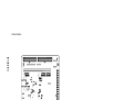
CN1
Port0
JA6
JP6
MODE
CN5
Port1
CN3
JA5
OTG
PERI
HOST
U1
R8A66597
JA2
JA1
WR1 SEL
HWR
R8A66597FP
JP
13
WR
WR0 SEL
LWR
JP
14
IO_Vcc
WR
EXIOVcc
JP4
3.3V
JP7
IRQ0
JP8
CS SEL
a
JP11(unmount)
IRQ1
b
IRQ2
RSK
JP10
c
IRQ3
DC 5V SEL
EXT
INT0
INT1
INT SEL
JA3
CN4
EXT 5V IN
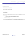
Figure 7.1 Default jumpers setting (Top view)
8.
Setup
The board combined with this board (R0K866597D020BR) is called a target board in the description below.
This section illustrates how to use this board with a target board to connect to a USB device.
R19AN0005EJ0100 Rev.1.00
Jan 10, 2012
Page 18 of 26
R8A66597 USB Evaluation Board R0K866597D020BR
Hardware Instruction Manual
8.1
Using with RSK
Renesas Starter Kits are the latest development from Renesas in low-cost evaluation development toolkits. It is possible
to test the R8A66597FP easily by combining it with this board and the RSK. But, it isn’t possible to test the
R8A66597FP’s split bus.
USB device
R0K866597D020BR
JA6
CN1
JA2
CN5
DC Power Supply
5V
JA3
R8A66597FP
CN4
JA5
JA1
JA6
JA2
JA5
JA1
Target Board
JA3
e.g.) RX62N RSK
Figure 8.1.1 Connected image chart
R19AN0005EJ0100 Rev.1.00
Jan 10, 2012
Page 19 of 26
R8A66597 USB Evaluation Board R0K866597D020BR
Hardware Instruction Manual
How to use the R0K866597D020BR with the RSK is shown as below.
(1) Setting of switch and jumper.
(a) Set JP4 to "3.3 V". ("3.3V" is factory setting)
(b) Set JP7 to "IRQ 0". ("IRQ 0" is factory setting)
(c) Set JP8 to "CSa". ("CSa" is factory setting)
(d) Set JP10 to "EXT". ("EXT" is factory setting)
(2) Connecting the R0K866597D020BR to the RSK.
Insert JA1’s #1-pin and #2-pin of the R0K866597D020BR board to JA1's #1-pin and #2-pin of the RSK to connect
the two boards together.
(3) VBUS output for host function
Apply 5V to CN4 of the R0K866597D020BR board using the power supply cable included. The red wire is 5V and
the black one is GND.
(a) When output VBUS to CN1:
(i) Set high level output to VBOUT0 pin of the R8A66597 by software.
(ii) Set JP6 to "HOST".
(b) When output VBUS to CN5:
(i) Set high level output to VBOUT1 pin of the R8A66597 by software.
It is possible to operate the R8A66597FP using the remote debugger RSK that is attached to the RSK. Please refer to
the RSK's Instruction Manual“.
R19AN0005EJ0100 Rev.1.00
Jan 10, 2012
Page 20 of 26
R8A66597 USB Evaluation Board R0K866597D020BR
Hardware Instruction Manual
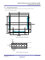
8.2
Using with other boards
This evaluation board supports separate bus mode only. (Does not support multiplex bus mode)
Below are notes for target board design.
98.00
91.44
24
24
23
23
JA6
JA5
1
25
2
26
1
25
JA1
Board center
35.56
JA2
2
1
2
2
JA3
50
1
1
15.24
88.00
2
26
49
15.24
60.96
15.24
Board center
Figure 8.2.1 Position of connectors chart
0.6 mm□
2.54 mm
2.54 mm
Figure 8.2.2 Detail view of connectors
R19AN0005EJ0100 Rev.1.00
Jan 10, 2012
Page 21 of 26
R8A66597 USB Evaluation Board R0K866597D020BR
Hardware Instruction Manual
(1) The receptacle of the target board should suit the size of this board (refer to Figure 3 and Figure 4). Make pin
arrangement the same as this board (refer to Table 1 and Table 2). Please refer to Appendix 1: the
R0K866597D020BR Part List and Appendix 2: the Circuit Diagram, when selecting connector and pin
arrangement. The HKP-50FD2 from Honda Tsushin Kogyo is applicable to the target board.
(2) The R8A66597FP generates a core power 1.5V from VCC 3.3V. An internal regulator makes 1.5V from 3.3V
through the #19-pin and #20-pin of CN3 and outputs 1.5V to VDD pin. On the R0K866597D020BR, 4.7uF and
0.1uF capacitors are mounted as smoothing capacitors for VDD.
(3) The interface power supply VIF is 1.8V or 3.3V.
(a) Short JP4 to “EXIOVcc” and supply 1.8V by the #25-pin and #26-pin of CN2 , when VIF is 1.8V.
(b) Short JP4 to “3.3V”, when VIF is 3.3V. In this case, power supply to VIF is the same as VCC.
(4) Use SD0-SD7 of CN2 when using split bus for DMA. SD0-SD7 can be used also as a general-purpose port.
(5) Processing for unused pin : Please refer to the R8A66597 datasheet, USB2.0 Dual Function Controller
R8A66597FP/DFP, for details.
VBUS circuit
Note:
When the peripheral device connected to the USB connector is in an unusual state due to a short circuit, or
an over current causes an over current in VBUS, the over current protection circuit of a USB power switch
IC turns on, and it turns the VBUS power supply off. But after turning off, current around 0.4A continues
flowing, and the USB power switch IC runs hot. Remove the unusual state promptly for the sake of safety.
To start/stop supply VBUS to the peripheral device, the MCU should operate the R8A66597 to turn on/off
the VBUS output of the USB power switch IC (U2). When the USB power switch IC detects over current, it
outputs a low pulse to the FLG output pin connected to the R8A66597FP, and it issues an interrupt to MCU
to notice the over current state. Monitor the FLG output pin status and turn off the VBUS output when the
over current state is detected by the R8A66597 control software.
Confirm that the USB device is in usual state before connecting.
(1) To supply 5V to VBUS of CN1:
(a) Apply 5V to CN4.
(b) Set JP6 to “HOST”.
(c) Output high signal from VBOUT0-pin by a R8A66597 control software.
(2) To supply 5V to VBUS of CN5
(a) Apply 5V to CN4.
(b) Output high signal from VBOUT1-pin by a R8A66597 control software.
Note:
8.3
When the R8A66597 control software turn off VBUS supply from the USB power switch IC, VBUS is not
shutdown immediately but slowly because of 150uF capacitor.
Using R0K866597D020BR as a peripheral
When the R0K866597D020BR is operated as a peripheral controller, please pay attention to following notes:
(1)
(2)
(3)
(4)
Set JP6 to "PERI"
Connect a USB host, such as a PC to CN1
To connect a USB host to CN1, an adapter is needed to convert the A-plug into the B-receptacle.
CN5 is not available as a peripheral.
R19AN0005EJ0100 Rev.1.00
Jan 10, 2012
Page 22 of 26
R8A66597 USB Evaluation Board R0K866597D020BR
Hardware Instruction Manual
9.
Connectors Pin Assignment
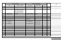
Table 9. R0K866597D020BR JA1 Pin Assignment
JA1
PIN
Function
1
5V
3
3V3
5
7
9
11
13
15
17
19
21
23
(SOF_N)*
* : Can be connected depending on JP setting.
PIN
2
4
6
8
10
12
14
16
18
20
22
24
Function
GND
GND
Table 10. R0K866597D020BR JA2 Pin Assignment
JA2
PIN
Function
1
RESET
3
5
7
INT_N
9
(SOF_N)*
11
13
15
17
19
21
23
(INT_N)*
25
* : Can be connected depending on JP setting.
R19AN0005EJ0100 Rev.1.00
Jan 10, 2012
PIN
2
4
6
8
10
12
14
16
18
20
22
24
26
Function
GND
Page 23 of 26
R8A66597 USB Evaluation Board R0K866597D020BR
Hardware Instruction Manual
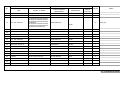
Table 11. R0K866597D020BR JA3 Pin Assignment
JA3
PIN
Function
1
3
A2
5
A4
7
A6
9
11
13
15
17
D0
19
D2
21
D4
23
D6
25
RD_N
27
CS_N
29
D8
31
D10
33
D12
35
D14
37
39
41
43
45
(CS_N)*
47
WR1_N
49
* : Can be connected depending on JP setting.
PIN
2
4
6
8
10
12
14
16
18
20
22
24
26
28
30
32
34
36
38
40
42
44
46
48
50
Function
A1
A3
A5
A7
D1
D3
D5
D7
(CS_N)*
D9
D11
D13
D15
WR0_N
Table 12. R0K866597D020BR JA6 Pin Assignment
JA6
PIN
1
3
5
7
9
11
13
15
17
19
21
23
Function
DREQ0_N
DEND0_N
PIN
2
4
6
8
10
12
14
16
18
20
22
24
Function
DACK0_N
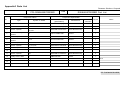
*: Because the signal wire of JA5 is not used in this board, the table is omitted.
R19AN0005EJ0100 Rev.1.00
Jan 10, 2012
Page 24 of 26
R8A66597 USB Evaluation Board R0K866597D020BR
Hardware Instruction Manual
10.
Circuit Diagram
See attached document. (Appendix 1)
11.
Parts Layout Diagram
See attached document. (Appendix 2)
12.
Parts List
See attached document. (Appendix 3)
R19AN0005EJ0100 Rev.1.00
Jan 10, 2012
Page 25 of 26
R8A66597 USB Evaluation Board R0K866597D020BR
Hardware Instruction Manual
Website and Support
Renesas Electronics Website
http://www.renesas.com/
USB Device Page
http://www.renesas.com/en/usb
Inquiries
http://www.renesas.com/inquiry
All trademarks and registered trademarks are the property of their respective owners.
R19AN0005EJ0100 Rev.1.00
Jan 10, 2012
Page 26 of 26
Revision Record
Rev.
1.00
Date
Jan 10.2012
Description
Page
Summary
—
First edition issued
A-1
General Precautions in the Handling of MPU/MCU Products
The following usage notes are applicable to all MPU/MCU products from Renesas. For detailed usage notes on the
products covered by this manual, refer to the relevant sections of the manual. If the descriptions under General
Precautions in the Handling of MPU/MCU Products and in the body of the manual differ from each other, the
description in the body of the manual takes precedence.
1. Handling of Unused Pins
Handle unused pins in accord with the directions given under Handling of Unused Pins in the manual.
⎯ The input pins of CMOS products are generally in the high-impedance state. In operation with an
unused pin in the open-circuit state, extra electromagnetic noise is induced in the vicinity of LSI, an
associated shoot-through current flows internally, and malfunctions occur due to the false
recognition of the pin state as an input signal become possible. Unused pins should be handled as
described under Handling of Unused Pins in the manual.
2. Processing at Power-on
The state of the product is undefined at the moment when power is supplied.
⎯ The states of internal circuits in the LSI are indeterminate and the states of register settings and
pins are undefined at the moment when power is supplied.
In a finished product where the reset signal is applied to the external reset pin, the states of pins
are not guaranteed from the moment when power is supplied until the reset process is completed.
In a similar way, the states of pins in a product that is reset by an on-chip power-on reset function
are not guaranteed from the moment when power is supplied until the power reaches the level at
which resetting has been specified.
3. Prohibition of Access to Reserved Addresses
Access to reserved addresses is prohibited.
⎯ The reserved addresses are provided for the possible future expansion of functions. Do not access
these addresses; the correct operation of LSI is not guaranteed if they are accessed.
4. Clock Signals
After applying a reset, only release the reset line after the operating clock signal has become stable.
When switching the clock signal during program execution, wait until the target clock signal has
stabilized.
⎯ When the clock signal is generated with an external resonator (or from an external oscillator)
during a reset, ensure that the reset line is only released after full stabilization of the clock signal.
Moreover, when switching to a clock signal produced with an external resonator (or by an external
oscillator) while program execution is in progress, wait until the target clock signal is stable.
5. Differences between Products
Before changing from one product to another, i.e. to one with a different type number, confirm that the
change will not lead to problems.
⎯ The characteristics of MPU/MCU in the same group but having different type numbers may differ
because of the differences in internal memory capacity and layout pattern. When changing to
products of different type numbers, implement a system-evaluation test for each of the products.
Notice
1.
Descriptions of circuits, software and other related information in this document are provided only to illustrate the operation of semiconductor products and application examples. You are fully responsible for
the incorporation of these circuits, software, and information in the design of your equipment. Renesas Electronics assumes no responsibility for any losses incurred by you or third parties arising from the
use of these circuits, software, or information.
2.
Renesas Electronics has used reasonable care in preparing the information included in this document, but Renesas Electronics does not warrant that such information is error free. Renesas Electronics
3.
Renesas Electronics does not assume any liability for infringement of patents, copyrights, or other intellectual property rights of third parties by or arising from the use of Renesas Electronics products or
assumes no liability whatsoever for any damages incurred by you resulting from errors in or omissions from the information included herein.
technical information described in this document. No license, express, implied or otherwise, is granted hereby under any patents, copyrights or other intellectual property rights of Renesas Electronics or
others.
4.
You should not alter, modify, copy, or otherwise misappropriate any Renesas Electronics product, whether in whole or in part. Renesas Electronics assumes no responsibility for any losses incurred by you or
5.
Renesas Electronics products are classified according to the following two quality grades: "Standard" and "High Quality". The recommended applications for each Renesas Electronics product depends on
third parties arising from such alteration, modification, copy or otherwise misappropriation of Renesas Electronics product.
the product's quality grade, as indicated below.
"Standard": Computers; office equipment; communications equipment; test and measurement equipment; audio and visual equipment; home electronic appliances; machine tools; personal electronic
equipment; and industrial robots etc.
"High Quality": Transportation equipment (automobiles, trains, ships, etc.); traffic control systems; anti-disaster systems; anti-crime systems; and safety equipment etc.
Renesas Electronics products are neither intended nor authorized for use in products or systems that may pose a direct threat to human life or bodily injury (artificial life support devices or systems, surgical
implantations etc.), or may cause serious property damages (nuclear reactor control systems, military equipment etc.). You must check the quality grade of each Renesas Electronics product before using it
in a particular application. You may not use any Renesas Electronics product for any application for which it is not intended. Renesas Electronics shall not be in any way liable for any damages or losses
incurred by you or third parties arising from the use of any Renesas Electronics product for which the product is not intended by Renesas Electronics.
6.
You should use the Renesas Electronics products described in this document within the range specified by Renesas Electronics, especially with respect to the maximum rating, operating supply voltage
range, movement power voltage range, heat radiation characteristics, installation and other product characteristics. Renesas Electronics shall have no liability for malfunctions or damages arising out of the
use of Renesas Electronics products beyond such specified ranges.
7.
Although Renesas Electronics endeavors to improve the quality and reliability of its products, semiconductor products have specific characteristics such as the occurrence of failure at a certain rate and
malfunctions under certain use conditions. Further, Renesas Electronics products are not subject to radiation resistance design. Please be sure to implement safety measures to guard them against the
possibility of physical injury, and injury or damage caused by fire in the event of the failure of a Renesas Electronics product, such as safety design for hardware and software including but not limited to
redundancy, fire control and malfunction prevention, appropriate treatment for aging degradation or any other appropriate measures. Because the evaluation of microcomputer software alone is very difficult,
please evaluate the safety of the final products or systems manufactured by you.
8.
Please contact a Renesas Electronics sales office for details as to environmental matters such as the environmental compatibility of each Renesas Electronics product. Please use Renesas Electronics
products in compliance with all applicable laws and regulations that regulate the inclusion or use of controlled substances, including without limitation, the EU RoHS Directive. Renesas Electronics assumes
no liability for damages or losses occurring as a result of your noncompliance with applicable laws and regulations.
9.
Renesas Electronics products and technology may not be used for or incorporated into any products or systems whose manufacture, use, or sale is prohibited under any applicable domestic or foreign laws or
regulations. You should not use Renesas Electronics products or technology described in this document for any purpose relating to military applications or use by the military, including but not limited to the
development of weapons of mass destruction. When exporting the Renesas Electronics products or technology described in this document, you should comply with the applicable export control laws and
regulations and follow the procedures required by such laws and regulations.
10. It is the responsibility of the buyer or distributor of Renesas Electronics products, who distributes, disposes of, or otherwise places the product with a third party, to notify such third party in advance of the
contents and conditions set forth in this document, Renesas Electronics assumes no responsibility for any losses incurred by you or third parties as a result of unauthorized use of Renesas Electronics
products.
11. This document may not be reproduced or duplicated in any form, in whole or in part, without prior written consent of Renesas Electronics.
12. Please contact a Renesas Electronics sales office if you have any questions regarding the information contained in this document or Renesas Electronics products, or if you have any other inquiries.
(Note 1)
"Renesas Electronics" as used in this document means Renesas Electronics Corporation and also includes its majority-owned subsidiaries.
(Note 2)
"Renesas Electronics product(s)" means any product developed or manufactured by or for Renesas Electronics.
http://www.renesas.com
SALES OFFICES
Refer to "http://www.renesas.com/" for the latest and detailed information.
Renesas Electronics America Inc.
2880 Scott Boulevard Santa Clara, CA 95050-2554, U.S.A.
Tel: +1-408-588-6000, Fax: +1-408-588-6130
Renesas Electronics Canada Limited
1101 Nicholson Road, Newmarket, Ontario L3Y 9C3, Canada
Tel: +1-905-898-5441, Fax: +1-905-898-3220
Renesas Electronics Europe Limited
Dukes Meadow, Millboard Road, Bourne End, Buckinghamshire, SL8 5FH, U.K
Tel: +44-1628-651-700, Fax: +44-1628-651-804
Renesas Electronics Europe GmbH
Arcadiastrasse 10, 40472 Düsseldorf, Germany
Tel: +49-211-65030, Fax: +49-211-6503-1327
Renesas Electronics (China) Co., Ltd.
7th Floor, Quantum Plaza, No.27 ZhiChunLu Haidian District, Beijing 100083, P.R.China
Tel: +86-10-8235-1155, Fax: +86-10-8235-7679
Renesas Electronics (Shanghai) Co., Ltd.
Unit 204, 205, AZIA Center, No.1233 Lujiazui Ring Rd., Pudong District, Shanghai 200120, China
Tel: +86-21-5877-1818, Fax: +86-21-6887-7858 / -7898
Renesas Electronics Hong Kong Limited
Unit 1601-1613, 16/F., Tower 2, Grand Century Place, 193 Prince Edward Road West, Mongkok, Kowloon, Hong Kong
Tel: +852-2886-9318, Fax: +852 2886-9022/9044
Renesas Electronics Taiwan Co., Ltd.
13F, No. 363, Fu Shing North Road, Taipei, Taiwan
Tel: +886-2-8175-9600, Fax: +886 2-8175-9670
Renesas Electronics Singapore Pte. Ltd.
80 Bendemeer Road, Unit #06-02 Hyflux Innovation Centre Singapore 339949
Tel: +65-6213-0200, Fax: +65-6213-0300
Renesas Electronics Malaysia Sdn.Bhd.
Unit 906, Block B, Menara Amcorp, Amcorp Trade Centre, No. 18, Jln Persiaran Barat, 46050 Petaling Jaya, Selangor Darul Ehsan, Malaysia
Tel: +60-3-7955-9390, Fax: +60-3-7955-9510
Renesas Electronics Korea Co., Ltd.
11F., Samik Lavied' or Bldg., 720-2 Yeoksam-Dong, Kangnam-Ku, Seoul 135-080, Korea
Tel: +82-2-558-3737, Fax: +82-2-558-5141
© 2012 Renesas Electronics Corporation. All rights reserved.
Colophon 2.2
A7/ALE
R32
R33
R34
0
0
0
SOF_N
DACK1_N
DREQ1_N
2
2
WR_N_C 3
+
+
1
8
7
MBRS130T3G
2
1
1
2
12
L1
1
BLM21PG600SN1
CN7
1
C21
ZD3
1.0u
TP5
1
1
C30
2
6
5
4
3
2
1
C22
1.0u
HZU6.8Z
0.1
2
1
2
ID0
VBOUT0
EXTLP0
OVCUR1
VBOUT1
100
2
K3 K2
1
K4 K1
4
3
60
59
58
57
56
55
54
53
52
51
50
49
48
47
46
45
44
43
42
41
5
A
1
GND0
JP5
Xout
1
TP12
2
VBUS_OUT1
2
2
24MHz
C27
C28
L4
2
ZD4
8pF
TP14
VBUS_1
1
1
1
C26
BLM21PG600SN1
3
1
X1
4
8pF
0.1
HZU6.8Z
CN5
VIF
1 R15 1M 2
VDD1
1
4
TP15
2
3
2
3
DLW21HN900SQ2
1
1
1
4
ZD2
K4 K1
2
2
0.1
5
SD4
SD5
SD6
SD7
TP34 TP35 TP36 TP37
HZM-RKZ
VIF
JP14
SD0_C
SD1_C
SD2_C
SD3_C
1
1
GND1
U1-60
VIF3
U1-70
VIF4
1
U1-43
VCC3
1
U1-35
VCC2
1
U1-25
AVCC
1
U1-20
VIF2
1
U1-22
VCC1
1
U1-1
VIF1
2
2
JP3
L6
BLM21PG600SN1
2
TP10
1
2
C23 C24 C25
1
AGND
SD0
SD1
SD2
SD3
TP30 TP31 TP32 TP33
0.1 10pF
1
SD7
SD6
SD5
SD4
SD3
SD2
SD1
SD0
1
10uF
2
2
EXIOVcc
JP1
TP13
3
1
3
GND
D+
DVbus
2
VIF
3.3V
DP1
DM1
USB_SOCKET-A
JP4
SD4_C
SD5_C
SD6_C
SD7_C
FRAME
4
3
2
1
L5
2
FLAG
TP26
5
K3 K2
VBUS_EN
TP25
FRAME1
3
EXIOVcc
TP29
C19 C20
0
0
0
0
0
0
0
0
GND
D+
DVbus
2
VIF3
CS_N
WR1_N
WR0_N
RD_N
A7
A6
A5
A4
VDD2
GN6
A3
A2
A1
MPBUS
GND5
RST_N
VCC3
GND4
VBUS
1
4.7uF
R53
R54
R55
R56
R57
R58
R59
R60
FRAME
4
3
2
1
R13 1M
EXIOVcc
SD7_C
SD6_C
SD5_C
SD4_C
SD3_C
SD2_C
SD1_C
SD0_C
5
FRAME0
XOUT
Xin
TP11
1
1 R16 1M 2
WR1_N_C
VBUS
XIN
1
VBUS
TP27
CN1
L3
A
D7
D6
D5
D4
D3
D2
D1
D0
Mini-AB
5.6k
4
0
0
0
0
0
0
0
0
ZD1
FRAME
GND
ID
D+
DVbus
R14 560
2
R45
R46
R47
R48
R49
R50
R51
R52
DGND
DLW21HN900SQ2
BLM21PG600SN1
1
1
TP9
ID_IN
DP0
DM0
2
TP8
DGND
2
2
D7_C
D6_C
D5_C
D4_C
D3_C
D2_C
D1_C
D0_C
DGND
6
5
4
3
2
1
USB_SOCKET-A
1
D15
D14
D13
D12
D11
D10
D9
D8
1 R12
2
0
0
0
0
0
0
0
0
1
R37
R38
R39
R40
R41
R42
R43
R44
1
2
3
HZM-RKZ
SD0
SD1
SD2
SD3
SD4
SD5
SD6
SD7
D15_C
D14_C
D13_C
D12_C
D11_C
D10_C
D9_C
D8_C
TP7
FRAME
GND
ID
D+
DVbus
CN6
2
3
1
1
TP6
D8
D9
D10
D11
D12
D13
D14
D15
1
4
DP1
DM1
1
0.1 10pF
DP0
DM0
40
39
38
37
36
35
34
33
32
31
30
29
28
27
26
25
24
23
22
21
1
10uF
DP0
DM0
GND3
DP1
DM1
VCC2
OVCUR0B
OVCUR0A
ID0
EXTLP0
VBOUT0
OVCUR1
VBOUT1
REFRIN
AGND
AVCC
XOUT
XIN
VCC1
GND2
1
TP2
R6
GND7
D0
D1
D2
D3
D4
D5
D6
D7
VIF4
GND8
D8
D9
D10
D11
D12
D13
D14
D15
GND9
VIF1
INT_N
SOF_N
DREQ0_N
DACK0_N
DEND0_N
DREQ1_N
DACK1_N
DEND1_N
VDD1
GND1
SD0
SD1
SD2
SD3
SD4
SD5
SD6
SD7
VIF2
WR1_N
0
61
62
63
64
65
66
67
68
69
70
71
72
73
74
75
76
77
78
79
80
D0
D1
D2
D3
D4
D5
D6
D7
INT_N
SOF_N
DREQ0_N
DACK0_N
DEND0_N
DREQ1_N
DACK1_N
DEND1_N
R61
1
AVCC
WR1_N_C
1
4
1
2
3
4
5
6
7
8
9
10
11
12
13
14
15
16
17
18
19
20
A8_C
A9_C
2
CN2
3
1.0u
L2
2
HKP-50FD2
10
C18
Micro-AB
U1
2
1
JP4P
1
1
DEND1_N
0
1
R36
2
LWR_N_C 1
VBUS_0
HOST
13
OFFVBUS
ID_OUT
ID_IN
STATUS1
STATUS2
SHDN
GND
HOST
JP6
OTG
C12 C13 C14
DEND1_N_C
2
HWR_N_C
LWR_N_C
1
0.1 10pF
1
CSc_N_C
0
0
R62
2
3
JP13
R63
R64
100K
VCC
AVCC
2
2
2
WR_N_C 3
TP3
1
1
4
3
5
6
11
1
HWR_N_C 1
PERI
0.1
VBUS
1
JP4P
CS SELECT
C6
14
C+
VBUS
R11
R65
VBUS
2
CS c
R68
100K
2
CS b
OTG
VL
0.1
100K
1
CS a
JP8
SEPA
PERI
150uF
1
CS_N_C
9
C8
0.1
1
VBUS
EXIOVCC
EXIOVCC
0
VIF
10uF
1
WR0_N_C
WR1_N_C
R17
Vcc
VBUS_OUT1
C4
150uF
2
2
C17
1
PIN CUT
PIN CUT
C5
U3
4
DEND0_N
0
1
3
0.1
1.0u
OVCUR0B
OVCUR0A
R35
DGND
JP11
INT SELECT
INT1
VIF
VCC
AVCC
0
DEND0_N_C
1
D0_C
D1_C
D2_C
D3_C
D4_C
D5_C
D6_C
D7_C
RD_N_C
WR_N_C
CSa_N_C
CSb_N_C
D8_C
D9_C
D10_C
D11_C
D12_C
D13_C
D14_C
D15_C
3
GND
C7
1
RST_N
TP23
VCC
R5
1
IRQ3
5
MIC2506
MULT
A3
A2
A1
TP20
EXTRESM
C9 C10 C11
2SOF/INT1_N_C
CTLB OUTB
C3
C-
CS_N
WR1_N
WR0_N
RD_N
A7/ALE
A6
A5
A4
CONF
CN2
2
3
VDD2
0
1
6
4
HD74LV1G04ACM
EXTRESM_N
1
1
2
1
TP19
1
IRQ1
7
MAX3355
SUSP
1
FFC-50BMEP1B
A0_C
A1_C
A2_C
A3_C
A4_C
A5_C
A6_C
A7_C
A8_C
A9_C
IN
FLGB GND
HD74LV1G04ACM
C15 C16
1K
100K
TP24
1
1
2
3
4
5
6
7
8
9
10
11
12
13
14
15
16
17
18
19
20
21
22
23
24
25
26
27
28
29
30
31
32
33
34
35
36
37
38
39
40
41
42
43
44
45
46
47
48
49
50
FLGA
3
100K
1
0
CN3
JP7
INT SELECT
INT0
2
100K
R1
100K
2
R31
IRQ3
1
2
3
4
5
6
7
8
9
10
11
12
13
14
15
16
17
18
19
20
21
22
23
24
25
26
27
28
29
30
31
32
33
34
35
36
37
38
39
40
41
42
43
44
45
46
47
48
49
50
VCC
2
ID/TC1
A7_C
A0_C
ID/TC1
SOF/INT1_N_C
DACK1_N_C
DREQ1_N_C
SUSP_N
CONF_N
INT_N_C
2
100K
R69
U7A
HKP-50FD2
3
8
4.7uF 0.1
2
R73
1
JA3
3
CTLA OUTA
R70
1
2
IRQ2
G
6
0.1
5
100K
2
1
R3
D1
R2
1
NC2
NC1
R71
100K
U2
10uF
U7B
TP4
C29
TP18 LED1
A1
A2
A3
A4
A5
A6
FFC-26BMEP1B
IRQ0
R7 R8 R9 R10
10k 10k 10k 10k
1
1
1
1
0
0
0
0
0
0
HAT1069C
D12
D23
D34
D45
1 S
0.1
2
2
2
2
2
R25
R26
R27
R28
R29
R30
Q1
LED-G
1
A1_C
A2_C
A3_C
A4_C
A5_C
A6_C
330
C2
+
R4
2
R72
JP12
C1
VIF
1
CS_N
RST_N
DREQ0_N
DACK0_N
INT_N
0
0
0
0
0
1
IRQ2
1
2
IRQ1
3.3V_RSK
R20
R21
R22
R23
R24
BS2P-SHF-1AA
2
IRQ0
FFC-26BMEP1B
5V_RSK
1
2
3
4
5
6
7
8
9
10
11
12
13
14
15
16
17
18
19
20
21
22
23
24
25
26
JA1
CS_N_C
RST_N_C
DREQ0_N_C
DACK0_N_C
INT_N_C
VCC3.3
1
RST_N_C
RD_N
3
JP10
2
JA1
1
2
3
4
5
6
7
8
9
10
11
12
13
14
15
16
17
18
19
20
21
22
23
24
25
26
WR0_N
0
2
FFC-24BMEP1B
0
R19
TP1
5V
2
1
EX_Vcc
EX_Vcc
R18
RD_N_C
1
DREQ1_N_C
DACK1_N_C
DEND1_N_C
WR0_N_C
2
1
1
1
DEND1 DACK1 DREQ1
TP28 TP22 TP21
1
2
3
4
5
6
7
8
9
10
11
12
13
14
15
16
17
18
19
20
21
22
23
24
25
26
27
28
29
30
31
32
33
34
35
36
37
38
39
40
41
42
43
44
45
46
47
48
49
50
1
1
2
3
4
5
6
7
8
9
10
11
12
13
14
15
16
17
18
19
20
21
22
23
24
3
1
2
5V
1
2
CN4
2
CN3
JA5
JA2
JP2
1
DREQ0_N_C
DACK0_N_C
DEND0_N_C
FFC-24BMEP1B
JA2
1
JA5
1
2
3
4
5
6
7
8
9
10
11
12
13
14
15
16
17
18
19
20
21
22
23
24
JA6
1
5V Input
EX_Vcc
1
JA6
3.3V
1
Appendix 1
Circuit Diagram
C31
0.01uF
C32
0.01uF
C33
0.01uF
C34
0.01uF
C35
0.01uF
C36
0.01uF
C37
0.01uF
C38
0.01uF
R0K866597D020BR
Circuit Diagram 1/1
D-R0K866597D020BR_C
Appendix2: Parts Layout Diagram
1.Front Surface
2.Rear Surface
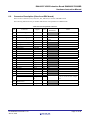
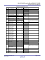
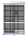
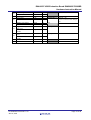
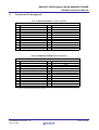
Appendix3 Parts List
Renesas Solutions Corporation
PPL-R0K866597D020BR
Component Name
No.
Type
Title
R0K866597D020BR Part List
Component Specification
Product Number
(specification)
Symbol on Board
Manufacture
Mount/
unmount
Qty/set
1
USB_SOCKET-A
CN1,CN5
UBA-4R-D14-4D(LF)(SN)
JST
2
2
HEADER
CN4
BS2P-SHF-1AA(LF)(SN)
JST
1
3
Ceramic Capacitor
C1,C3,C10,C13,C16,C17,C20,C22,
GRM188B11E104KA01D
C24,C28
Murata Manufacturing
10
4
Aluminum Electrolytic
Capacitor
C2
UWT1C100MCL1GB
Nichicom
1
5
Ceramic Capacitor
C9,C12,C23
GRM31CB11A106KA01
Murata Manufacturing
3
6
Aluminum Electrolytic
Capacitor
C4,C5
RHA1C151MCN1GS
Nichicom
2
7
Ceramic Capacitor
C21,C30
GRM21BB11C105KA01L
Murata Manufacturing
2
8
Ceramic Capacitor
C11,C14,C25
GRM1885C1H100JA01D
Murata Manufacturing
3
9
Ceramic Capacitor
C15,C19
GRM188B30J475KE18D
Murata Manufacturing
2
10
Ceramic Capacitor
C26,C27
GRM1885C1H8R0DZ01D
Murata Manufacturing
2
11
Ceramic Capacitor
C31,C32,C33,C34,C35,C36,C37,
C38
GRM188B11H103KA01D
Murata Manufacturing
8
12
Schottky barrier diode
D1
MBRS130LT3G
OnSemi
1
13
-
JP3
-
-
1
14
Jumper Pin 1P
JP6,JP8
WL-1
MAC8
2
15
Jumper Pin 3P
JP4,JP6,JP7,JP8,JP10,JP13,JP14
WL-1
MAC8
7
Notes
Short
PPL-R0K866597D020BR(1/4)
Component Name
No.
Type
Symbol on Board
Component Specification
Product Number
(specification)
Manufacture
Mount/
unmount
Qty/set
16
Thick Film Resistors
R3,R4,R11,R65,R68
MCR03EZPJ104
ROHM
5
17
Thick Film Resistors
R5,R6,R17
MCR03EZPJ000
ROHM
3
Thick Film Resistors
R18,R19,R20,R21,R22,R23,R24,
R25,R26,R27,R28,R29,R30,R31,
R32,R33,R34,R35,R36,R37,R38,
R39,R40,R41,
R42,R43,R44,R45,R46,R47,R48,
R49,R50,R51,R52,R53,R54,R55,
R56,R57,R58,R59,R60,R61
MCR01MZPJ000
18
44
Notes
1005 type
ROHM
19
Thick Film Resistors
R7,R8,R9,R10
MCR03EZPJ103
ROHM
4
20
Thick Film Resistors
R12
MCR03EZPFX5601
ROHM
1
21
Thick Film Resistors
R13,R15,R16
MCR03EZPJ105
ROHM
3
22
Thick Film Resistors
R14
MCR03EZPFX5600
ROHM
1
23
Thick Film Resistors
R62
MCR03EZPJ101
ROHM
1
24
USB ASSP
U1
R8A66597FP
Renesas Electronics
1
25
USB Power Switch IC
U2
MIC2506YM
MICREL
1
26
Crystal Oscillator
X1
DSX321G(24.0000MHz)
Daishinku
1
27
TP(SMD)
TP1
HK-5-G(RED)
MAC8
1
28
TP(SMD)
TP2
HK-5-G(YELLOW)
MAC8
1
29
TP(SMD)
TP3
HK-5-G(ORANGE)
MAC8
1
30
TP(SMD)
TP6,TP7,TP8,TP9,TP10
HK-5-G(BLACK)
MAC8
5
31
TP(SMD)
TP5,TP14
HK-5-G(BLUE)
MAC8
2
32
TP(SMD)
TP13
HK-5-G(GREEN)
MAC8
1
33
TP(SMD)
TP4,TP15
HK-5-G(WHITE)
MAC8
2
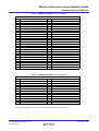
PPL-R0K866597D020BR(2/4)
Component Name
No.
Type
Symbol on Board
Component Specification
Product Number
(specification)
Manufacture
Mount/
unmount
Qty/set
34
PCB header connector(13x2)
JA1,JA2
FFC-26BSM1B
HONDA CONNECTORS
2
35
PCB header connector(25x2)
JA3
FFC-50BSM1B
HONDA CONNECTORS
1
36
PCB header connector(12x2)
JA5,JA6
FFC-24BSM1B
HONDA CONNECTORS
2
37
USB mini AB Socket
(CN6)
CAM-E48F-005-8620A
MITSUMI
unmount
0
38
USB micro AB Socket
(CN7)
ZX62-AB-5PA
HIROSE
unmount
0
39
Ceramic Capacitor
(C6),(C8),(C29),(C39)
GRM188B11E104KA01D
Murata Manufacturing
unmount
0
40
Ceramic Capacitor
(C7),(C18)
GRM21BB11C105KA01L
Murata Manufacturing
unmount
0
41
Jumper Pin 2P
(JP1),(JP2),(JP5),(JP9),(JP12)
WL-1
MAC8
unmount
0
42
Jumper Pin 3P
(JP11)
WL-1
MAC8
unmount
0
43
LED
(LED1)
SML-310MT
ROHM
unmount
0
44
Chip Ferrite Beads
(L1),(L3),(L4),(L6)
BLM21PG600SN1
Murata Manufacturing
unmount
0
45
Common Mode Choke Coils
(L2),(L5)
DLW21HN900SQ2
Murata Manufacturing
unmount
0
46
FET
(Q1)
HAT1069C
Renesas Electronics
unmount
0
47
Thick Film Resistors
(R1),(R2),(R69),(R71),(R73),
(R74)
MCR03EZPJ104
ROHM
unmount
0
48
Thick Film Resistors
(R63),(R64)
MCR03EZPJ000
ROHM
unmount
0
49
Thick Film Resistors
(R70)
MCR03EZPJ102
ROHM
unmount
0
50
Thick Film Resistors
(R72)
MCR03EZPJ331
ROHM
unmount
0
51
OTG Control IC
(U3)
MAX3355EEUD+
MAXIM
unmount
0
52
USB SWITCH DUAL
(U6)
TS3USB221DRCR
TI
unmount
0
53
Uni-logic IC
(U7)
HD74LV1G04ACM
Renesas Electronics
unmount
0
54
Zener Diode
(ZD1),(ZD2)
HZN6.2Z4MFA
Renesas Electronics
unmount
0
Notes
PPL-R0K866597D020BR(3/4)
Component Name
No.
Type
Symbol on Board
Component Specification
Product Number
(specification)
Manufacture
Mount/
unmount
Qty/set
55
Zener Diode
(ZD3),(ZD4)
HZU6.8Z
Renesas Electronics
unmount
0
56
TP
(TP11),(TP12)
ST-4-1
MAC8
unmount
0
57
TP
(TP18),(TP19),(TP20),(TP21),
(TP22),(TP23),(TP24),(TP25),
(TP26),(TP27),(TP28),(TP29),
(TP30),(TP31),(TP32),(TP33),
(TP34),(TP35),(TP36),(TP37)
WL-1
MAC8
unmount
0
58
PCB receptacle(12x2)
(CN2),(CN3)
HIF3H-50DA-2.54DSA(71)
HIROSE
unmount
0
59
PCB Board
-
R0K866597
SANYO KOGYO
-
1
Notes
Assembly parts
60
Jumper Socket
XJ8A-0241
OMRON
-
7
61
Housing for Power Cable
H2P-SHF-AA
JST
-
1
62
Contact for Power Cable
SHF-001T-0.8BS
JST
-
2
63
Power Cable(Red)
UL1007-AWG24-RED
SHINAGAWA
ELECTRIC WIRE
-
1
64
Power Cable(Black)
UL1007-AWG24-BLACK
SHINAGAWA
ELECTRIC WIRE
-
1
*
PPL-R0K866597D020BR(4/4)