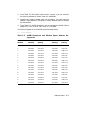
1
VAX 6000 Model 500
Mini-Reference
Order Number EK–650EA–HR–001
This manual supplies easy-to-access key information
on VAX 6000 Model 500 systems.
digital equipment corporation
maynard, massachusetts
First Printing, October 1990
The information in this document is subject to change without notice and should not be
construed as a commitment by Digital Equipment Corporation.
Digital Equipment Corporation assumes no responsibility for any errors that may appear in
this document.
The software, if any, described in this document is furnished under a license and may be used
or copied only in accordance with the terms of such license. No responsibility is assumed
for the use or reliability of software or equipment that is not supplied by Digital Equipment
Corporation or its affiliated companies.
Copyright ©1990 by Digital Equipment Corporation.
All Rights Reserved.
Printed in U.S.A.
dt
The following are trademarks of Digital Equipment Corporation:
DEMNA
DEC
DEC LANcontroller
DECnet
DECUS
PDP
ULTRIX
UNIBUS
VAX
VAXBI
VAXcluster
VAXELN
VMS
XMI
FCC NOTICE: The equipment described in this manual generates, uses, and may emit
radio frequency energy. The equipment has been type tested and found to comply with the
limits for a Class A computing device pursuant to Subpart J of Part 15 of FCC Rules, which
are designed to provide reasonable protection against such radio frequency interference when
operated in a commercial environment. Operation of this equipment in a residential area
may cause interference, in which case the user at his own expense may be required to take
measures to correct the interference.
Contents
Preface
xi
Chapter 1 Console Operation
Chapter 2 Self-Test
Chapter 3 Address Space
3.1
3.2
How to Find a Register in XMI Address Space . . . . . . . . . . .
How to Find a Register in VAXBI Address Space . . . . . . . . . .
3–5
3–6
Chapter 4 KA65A CPU Module Registers
4.1
4.2
4.3
4.4
4.5
KA65A Internal Processor Registers . .
KA65A Registers in XMI Private Space
KA65A XMI Registers . . . . . . . . . . . . .
Machine Checks . . . . . . . . . . . . . . . . . .
KA65A Parse Trees . . . . . . . . . . . . . . .
.
.
.
.
.
.
.
.
.
.
.
.
.
.
.
.
.
.
.
.
.
.
.
.
.
.
.
.
.
.
.
.
.
.
.
.
.
.
.
.
.
.
.
.
.
.
.
.
.
.
.
.
.
.
.
.
.
.
.
.
.
.
.
.
.
.
.
.
.
.
.
.
.
.
.
.
.
.
.
.
.
.
.
.
.
4–3
4–18
4–30
4–36
4–41
Chapter 5 MS65A Memory Registers
Chapter 6 DWMBB Adapter Registers
iii
Chapter 7 Vector Module Registers
7.1
7.2
7.3
7.4
7.5
Console Commands to Access Registers . . . . .
KA65A IPRs Related to the Vector Module . .
FV64A Internal Processor Registers . . . . . . .
FV64A Registers — Vector Indirect Registers
FV64A Parse Trees . . . . . . . . . . . . . . . . . . . .
.
.
.
.
.
.
.
.
.
.
.
.
.
.
.
.
.
.
.
.
.
.
.
.
.
.
.
.
.
.
.
.
.
.
.
.
.
.
.
.
.
.
.
.
.
.
.
.
.
.
.
.
.
.
.
. 7–1
. 7–7
. 7–8
. 7–11
. 7–28
Index
Examples
2–1
2–2
2–3
Sample Self-Test Results, Scalar Processors Only . . . . . . . . .
Sample Self-Test Results with VAXBI Adapter . . . . . . . . . . .
Sample Self-Test Results with Vector Processor . . . . . . . . . . .
2–1
2–4
2–5
Figures
1–1
1–2
3–1
3–2
3–3
4–1
4–2
4–3
4–4
4–5
4–6
4–7
4–8
4–9
4–10
4–11
4–12
4–13
4–14
iv
International and English Control Panels . . . . . . . . . . . .
BOOT Command Syntax . . . . . . . . . . . . . . . . . . . . . . . . .
VAX 6000 Model 500 Slot Numbers . . . . . . . . . . . . . . . . .
XMI Memory and I/O Address Space . . . . . . . . . . . . . . . .
XMI I/O Space Address Allocation . . . . . . . . . . . . . . . . . .
Interval Clock Control and Status Register (ICCS) . . . . .
Console Receiver Control and Status Register (RXCS) . . .
Console Receiver Data Buffer Register (RXDB) . . . . . . . .
Console Transmitter Control and Status Register (TXCS)
Console Transmitter Data Buffer Register (TXDB) . . . . .
Machine Check Error Summary Register (MCESR) . . . . .
Accelerator Control and Status Register (ACCS) . . . . . . .
Console Saved Program Counter Register (SAVPC) . . . . .
Console Saved Processor Status Longword (SAVPSL) . . .
Translation Buffer Tag Register (TBTAG) . . . . . . . . . . . .
I/O Reset Register (IORESET) . . . . . . . . . . . . . . . . . . . . .
Translation Buffer Data Register (TBDATA) . . . . . . . . . .
System Identification Register (SID) . . . . . . . . . . . . . . . .
Backup Cache Index Register (BCIDX) . . . . . . . . . . . . . .
.
.
.
.
.
.
.
.
.
.
.
.
.
.
.
.
.
.
.
.
.
.
.
.
.
.
.
.
.
.
.
.
.
.
.
.
.
.
.
.
.
.
.
.
.
.
.
.
.
.
.
.
.
.
.
.
.
1–2
1–8
3–1
3–2
3–3
4–8
4–8
4–8
4–9
4–9
4–9
4–10
4–10
4–10
4–11
4–11
4–11
4–12
4–12
4–15
4–16
4–17
4–18
4–19
4–20
4–21
4–22
4–23
4–24
4–25
4–26
4–27
4–28
4–29
4–30
4–31
4–32
4–33
4–34
4–35
4–36
4–37
4–38
4–39
4–40
4–41
4–42
4–43
4–44
4–45
4–46
4–47
4–48
4–49
4–50
Backup Cache Status Register (BCSTS) . . . . . . . . . . . . . . . .
Backup Cache Control Register (BCCTL) . . . . . . . . . . . . . . . .
Backup Cache Error Address Register (BCERA) . . . . . . . . . .
Backup Cache Tag Store Register (BCBTS) . . . . . . . . . . . . . .
Backup Cache Deallocate Tag Register (BCDET) . . . . . . . . . .
Backup Cache Error Tag Register (BCERT) . . . . . . . . . . . . . .
Vector Interface Error Status Register (VINTSR) . . . . . . . . .
Primary Cache Tag Array Register (PCTAG) . . . . . . . . . . . . .
Primary Cache Index Register (PCIDX) . . . . . . . . . . . . . . . . .
Primary Cache Error Address Register (PCERR) . . . . . . . . . .
Primary Cache Status Register (PCSTS) . . . . . . . . . . . . . . . .
Control Register 0 (CREG0) . . . . . . . . . . . . . . . . . . . . . . . . . .
Control Register 1 (CREG1) . . . . . . . . . . . . . . . . . . . . . . . . . .
Control Register Write Enable (CREGWE) . . . . . . . . . . . . . .
MSSC Base Address Register (SSCBAR) . . . . . . . . . . . . . . . .
MSSC Configuration Register (SSCCNR) . . . . . . . . . . . . . . . .
MSSC Bus Timeout Control Register (SSCBTR) . . . . . . . . . .
MSSC Output Port Register (OPORT) . . . . . . . . . . . . . . . . . .
MSSC Input Port Register (IPORT) . . . . . . . . . . . . . . . . . . . .
Control Register Base Address Register (CRBADR) . . . . . . . .
Control Register Address Decode Mask Register (CRADMR) .
EEPROM Base Address Register (EEBADR) . . . . . . . . . . . . .
EEPROM Address Decode Mask Register (EEADMR) . . . . . .
Timer Control Register 0 (TCR0) . . . . . . . . . . . . . . . . . . . . . .
Timer Interval Register 0 (TIR0) . . . . . . . . . . . . . . . . . . . . . .
Timer Next Interval Register (TNIR0) . . . . . . . . . . . . . . . . . .
Timer Interrupt Vector Register (TIVR0) . . . . . . . . . . . . . . . .
Timer Control Register 1 (TCR1) . . . . . . . . . . . . . . . . . . . . . .
Timer Interval Register (TIR1) . . . . . . . . . . . . . . . . . . . . . . .
Timer Next Interval Register 1 (TNIR1) . . . . . . . . . . . . . . . .
Timer Interrupt Vector Register 1 (TIVR1) . . . . . . . . . . . . . .
MSSC Interval Counter Register (SSCICR) . . . . . . . . . . . . . .
DAL Diagnostic Register (DCSR) . . . . . . . . . . . . . . . . . . . . . .
Failing DAL Register 0 (FDAL0) . . . . . . . . . . . . . . . . . . . . . .
Failing DAL Register 1 (FDAL1) . . . . . . . . . . . . . . . . . . . . . .
Failing DAL Register 2 (FDAL2) . . . . . . . . . . . . . . . . . . . . . .
4–13
4–13
4–14
4–14
4–14
4–15
4–15
4–16
4–16
4–16
4–17
4–19
4–20
4–20
4–20
4–21
4–21
4–22
4–22
4–22
4–23
4–23
4–23
4–24
4–24
4–24
4–25
4–25
4–25
4–26
4–26
4–26
4–27
4–27
4–27
4–28
v
4–51 Failing DAL Register 3 (FDAL3) . . . . . . . . . . . . . . . . . . . . . .
4–52 Interprocessor Implied Vector Interrupt Generation Register
(IPIVINTR) . . . . . . . . . . . . . . . . . . . . . . . . . . . . . . . . . . . . . .
4–53 Write Error Implied Vector Interrupt Generation Register
(WEIVINTR) . . . . . . . . . . . . . . . . . . . . . . . . . . . . . . . . . . . . .
4–54 Device Register (XDEV) . . . . . . . . . . . . . . . . . . . . . . . . . . . . .
4–55 Bus Error Register 0 (XBER0) . . . . . . . . . . . . . . . . . . . . . . . .
4–56 Failing Address Register (XFADR0) . . . . . . . . . . . . . . . . . . . .
4–57 XMI General Purpose Register (XGPR) . . . . . . . . . . . . . . . . .
4–58 Node Specific Control and Status Register (NSCSR0) . . . . . .
4–59 XMI Control Register 0 (XCR0) . . . . . . . . . . . . . . . . . . . . . . .
4–60 Failing Address Extension Register 0 (XFAER0) . . . . . . . . . .
4–61 Bus Error Extension Register 0 (XBEER0) . . . . . . . . . . . . . .
4–62 Writeback 0 Failing Address Register (WFADR0) . . . . . . . . .
4–63 Writeback 1 Failing Address Register (WFADR1) . . . . . . . . .
4–64 Machine Check Stack Frame . . . . . . . . . . . . . . . . . . . . . . . . .
4–65 KA65A Machine Check Parse Tree . . . . . . . . . . . . . . . . . . . . .
4–66 KA65A Hard Error Interrupt Parse Tree . . . . . . . . . . . . . . . .
4–67 KA65A Soft Error Interrupt Parse Tree . . . . . . . . . . . . . . . . .
5–1 Device Register (XDEV) . . . . . . . . . . . . . . . . . . . . . . . . . . . . .
5–2 Bus Error Register (XBER) . . . . . . . . . . . . . . . . . . . . . . . . . .
5–3 Starting and Ending Address Register (SEADR) . . . . . . . . . .
5–4 Memory Control Register 1 (MCTL1) . . . . . . . . . . . . . . . . . . .
5–5 Memory ECC Error Register (MECER) . . . . . . . . . . . . . . . . .
5–6 Memory ECC Error Address Register (MECEA) . . . . . . . . . .
5–7 Memory Control Register 2 (MCTL2) . . . . . . . . . . . . . . . . . . .
5–8 TCY Tester Register (TCY) . . . . . . . . . . . . . . . . . . . . . . . . . . .
5–9 Block State ECC Error Register (BECER) . . . . . . . . . . . . . . .
5–10 Block State ECC Address Register (BECEA) . . . . . . . . . . . . .
5–11 Starting Address Register (STADR) . . . . . . . . . . . . . . . . . . . .
5–12 Ending Address Register (ENADR) . . . . . . . . . . . . . . . . . . . .
5–13 Segment/Interleave Register (INTLV) . . . . . . . . . . . . . . . . . .
5–14 Memory Control Register 3 (MCTL3) . . . . . . . . . . . . . . . . . . .
5–15 Memory Control Register 4 (MCTL4) . . . . . . . . . . . . . . . . . . .
5–16 Block State Control Register (BSCTL) . . . . . . . . . . . . . . . . . .
5–17 Block State Address Register (BSADR) . . . . . . . . . . . . . . . . .
vi
4–28
4–28
4–29
4–30
4–31
4–32
4–32
4–32
4–33
4–33
4–34
4–35
4–35
4–36
4–41
4–46
4–49
5–2
5–2
5–3
5–3
5–4
5–4
5–5
5–5
5–6
5–6
5–7
5–7
5–7
5–8
5–8
5–9
5–9
5–18
5–19
6–1
6–2
6–3
6–4
6–5
6–6
6–7
6–8
6–9
6–10
6–11
6–12
6–13
6–14
6–15
6–16
6–17
6–18
6–19
6–20
6–21
6–22
7–1
7–2
7–3
7–4
7–5
7–6
7–7
7–8
7–9
7–10
7–11
EEPROM Control Register (EECTL) . . . . . . . . . . . . . . . . .
Timeout Control/Status Register (TMOER) . . . . . . . . . . . .
Device Register (XDEV) . . . . . . . . . . . . . . . . . . . . . . . . . . .
Bus Error Register (XBER) . . . . . . . . . . . . . . . . . . . . . . . .
Failing Address Register (XFADR) . . . . . . . . . . . . . . . . . . .
Responder Error Address Register (AREAR) . . . . . . . . . . .
DWMBB/A Error Summary Register (AESR) . . . . . . . . . . .
Interrupt Mask Register (AIMR) . . . . . . . . . . . . . . . . . . . .
Implied Vector Interrupt Destination/Diagnostic Register
(AIVINTR) . . . . . . . . . . . . . . . . . . . . . . . . . . . . . . . . . . . . .
Diag 1 Register (ADG1) . . . . . . . . . . . . . . . . . . . . . . . . . . .
Utility Register (AUTLR) . . . . . . . . . . . . . . . . . . . . . . . . . .
Control and Status Register (ACSR) . . . . . . . . . . . . . . . . .
Return Vector Register (ARVR) . . . . . . . . . . . . . . . . . . . . .
Failing Address Extension Register (XFAER) . . . . . . . . . .
BI Error Address Register (ABEAR) . . . . . . . . . . . . . . . . .
Control and Status Register (BCSR) . . . . . . . . . . . . . . . . .
DWMBB/B Error Summary Register (BESR) . . . . . . . . . . .
Interrupt Destination Register (BIDR) . . . . . . . . . . . . . . . .
Timeout Address Register (BTIM) . . . . . . . . . . . . . . . . . . .
Vector Offset Register (BVOR) . . . . . . . . . . . . . . . . . . . . . .
Vector Register (BVR) . . . . . . . . . . . . . . . . . . . . . . . . . . . .
Diagnostic Control Register 1 (BDCR1) . . . . . . . . . . . . . . .
Page Map Register (PMR) . . . . . . . . . . . . . . . . . . . . . . . . .
VAXBI Device Register (DTYPE) . . . . . . . . . . . . . . . . . . . .
Vector Length (VLR) and Vector Count (VCR) Registers . .
Vector Mask Register (VMR) . . . . . . . . . . . . . . . . . . . . . . .
Vector Interface Error Status Register (VINTSR) . . . . . . .
Accelerator Control and Status Register (ACCS) . . . . . . . .
Vector Processor Status Register (VPSR) . . . . . . . . . . . . . .
Vector Arithmetic Exception Register (VAER) . . . . . . . . . .
Vector Memory Activity Check Register (VMAC) . . . . . . . .
Vector Translation Buffer Invalidate All Register (VTBIA)
Vector Indirect Address Register (VIADR) . . . . . . . . . . . . .
Vector Indirect Data Low Register (VIDLO) . . . . . . . . . . . .
Vector Indirect Data High Register (VIDHI) . . . . . . . . . . .
.
.
.
.
.
.
.
.
. 5–10
. 5–10
. 6–3
. 6–4
. 6–5
. 6–5
. 6–6
. 6–7
.
.
.
.
.
.
.
.
.
.
.
.
.
.
.
.
.
.
.
.
.
.
.
.
.
.
.
.
.
.
.
.
.
.
.
.
.
.
.
.
.
.
.
.
.
.
.
.
.
.
.
.
.
.
6–7
6–8
6–8
6–9
6–9
6–10
6–10
6–11
6–11
6–12
6–12
6–12
6–13
6–13
6–13
6–14
7–2
7–2
7–7
7–7
7–8
7–8
7–9
7–9
7–9
7–10
7–10
vii
7–12
7–13
7–14
7–15
7–16
7–17
7–18
7–19
7–20
7–21
7–22
7–23
7–24
7–25
7–26
7–27
7–28
7–29
7–30
7–31
7–32
7–33
7–34
7–35
7–36
7–37
7–38
7–39
7–40
7–41
7–42
7–43
7–44
7–45
7–46
7–47
viii
Vector Register n (VREGn) . . . . . . . . . . . . . . . . . . . . . . . .
Arithmetic Exception Register (ALU_OP) . . . . . . . . . . . . .
Scalar Operand Low Register (ALU_SCOP_LO) . . . . . . . .
Scalar Operand High Register (ALU_SCOP_HI) . . . . . . . .
Vector Mask Low Register (ALU_MASK_LO) . . . . . . . . . .
Vector Mask High Register (ALU_MASK_HI) . . . . . . . . . .
Exception Summary Register (ALU_EXC) . . . . . . . . . . . . .
Diagnostic Control Register (ALU_DIAG_CTL) . . . . . . . . .
Current ALU Instruction Register (VCTL_CALU) . . . . . . .
Deferred ALU Instruction Register (VCTL_DALU) . . . . . .
Current ALU Operand Low Register (VCTL_COP_LOW) .
Current ALU Operand High Register (VCTL_COP_HI) . . .
Deferred ALU Operand Low Register (VCTL_DOP_LOW) .
Deferred ALU Operand High Register (VCTL_DOP_HI) . .
Load/Store Instruction Register (VCTL_LDST) . . . . . . . . .
Load/Store Stride Register (VCTL_STRIDE) . . . . . . . . . . .
Illegal Instruction (VCTL_ILL) . . . . . . . . . . . . . . . . . . . . .
Vector Controller Status (VCTL_CSR) . . . . . . . . . . . . . . . .
Module Revision (MOD_REV) . . . . . . . . . . . . . . . . . . . . . .
P0 Base Register (LSX_P0BR) . . . . . . . . . . . . . . . . . . . . . .
P0 Length Register (LSX_P0LR) . . . . . . . . . . . . . . . . . . . .
P1 Base Register (LSX_P1BR) . . . . . . . . . . . . . . . . . . . . . .
P1 Length Register (LSX_P1LR) . . . . . . . . . . . . . . . . . . . .
System Base Register (LSX_SBR) . . . . . . . . . . . . . . . . . . .
System Length Register (LSX_SLR) . . . . . . . . . . . . . . . . . .
Load/Store Exception Register (LSX_EXC) . . . . . . . . . . . .
Translation Buffer Control Register (LSX_TBCSR) . . . . . .
Memory Management Enable (LSX_MAPEN) . . . . . . . . . .
Translation Buffer Invalidate All Register (LSX_TBIA) . . .
Translation Buffer Invalidate Single Register (LSX_TBIS)
Vector Mask Low Register (LSX_MASKLO) . . . . . . . . . . . .
Vector Mask High Register (LSX_MASKHI) . . . . . . . . . . .
Load/Store Stride Register (LSX_STRIDE) . . . . . . . . . . . .
Load/Store Instruction Register (LSX_INST) . . . . . . . . . . .
Cache Control Register (LSX_CCSR) . . . . . . . . . . . . . . . . .
Translation Buffer Tag Register (LSX_TBTAG) . . . . . . . . .
.
.
.
.
.
.
.
.
.
.
.
.
.
.
.
.
.
.
.
.
.
.
.
.
.
.
.
.
.
.
.
.
.
.
.
.
.
.
.
.
.
.
.
.
.
.
.
.
.
.
.
.
.
.
.
.
.
.
.
.
.
.
.
.
.
.
.
.
.
.
.
.
7–11
7–11
7–12
7–12
7–12
7–13
7–13
7–14
7–14
7–15
7–15
7–15
7–16
7–16
7–17
7–17
7–18
7–19
7–20
7–20
7–20
7–21
7–21
7–21
7–22
7–22
7–22
7–23
7–23
7–23
7–24
7–24
7–24
7–25
7–26
7–26
7–48
7–49
7–50
7–51
7–52
Translation Buffer PTE Register (LSX_PTE)
FV64A Machine Check Parse Tree . . . . . . . . .
FV64A Hard Error Interrupt Parse Tree . . . .
FV64A Soft Error Interrupt Parse Tree . . . . .
FV64A Disable Fault Parse Tree . . . . . . . . . .
.
.
.
.
.
.
.
.
.
.
.
.
.
.
.
.
.
.
.
.
.
.
.
.
.
.
.
.
.
.
.
.
.
.
.
.
.
.
.
.
.
.
.
.
.
.
.
.
.
.
.
.
.
.
.
.
.
.
.
.
7–27
7–28
7–29
7–30
7–31
VAX 6000 Series Documentation . . . . . . . . . . . . . . . . . . . . .
Associated Documents . . . . . . . . . . . . . . . . . . . . . . . . . . . . .
Upper Key Switch . . . . . . . . . . . . . . . . . . . . . . . . . . . . . . . .
Lower Key Switch . . . . . . . . . . . . . . . . . . . . . . . . . . . . . . . .
Restart Button . . . . . . . . . . . . . . . . . . . . . . . . . . . . . . . . . . .
Control Panel Status Indicator Lights . . . . . . . . . . . . . . . . .
Console Commands and Qualifiers . . . . . . . . . . . . . . . . . . . .
Console Control Characters . . . . . . . . . . . . . . . . . . . . . . . . .
BOOT Command Qualifiers . . . . . . . . . . . . . . . . . . . . . . . . .
Sample BOOT Commands . . . . . . . . . . . . . . . . . . . . . . . . . .
R5 Bit Functions for VMS . . . . . . . . . . . . . . . . . . . . . . . . . .
R5 Bit Functions for ULTRIX . . . . . . . . . . . . . . . . . . . . . . .
Console Error Messages Indicating Halt . . . . . . . . . . . . . . .
Standard Console Error Messages . . . . . . . . . . . . . . . . . . .
System Configuration for Sample Self-Test . . . . . . . . . . . . .
Module LEDs After Self-Test . . . . . . . . . . . . . . . . . . . . . . . .
XMI Nodespace Addresses . . . . . . . . . . . . . . . . . . . . . . . . . .
VAXBI Nodespace and Window Space Address Assignments
VAXBI Registers . . . . . . . . . . . . . . . . . . . . . . . . . . . . . . . . .
Types of Registers, Bits, and Fields . . . . . . . . . . . . . . . . . . .
KA65A Internal Processor Registers . . . . . . . . . . . . . . . . . .
KA65A Registers in XMI Private Space . . . . . . . . . . . . . . . .
XMI Registers for the KA65A CPU Module . . . . . . . . . . . . .
Machine Check Parameters . . . . . . . . . . . . . . . . . . . . . . . . .
Machine Check Codes . . . . . . . . . . . . . . . . . . . . . . . . . . . . .
MS65A Memory Control and Status Registers . . . . . . . . . . .
DWMBB Registers . . . . . . . . . . . . . . . . . . . . . . . . . . . . . . . .
XMI Required Registers . . . . . . . . . . . . . . . . . . . . . . . . . . . .
Internal Processor Registers . . . . . . . . . . . . . . . . . . . . . . . .
.
.
.
.
.
.
.
.
.
.
.
.
.
.
.
.
.
.
.
.
.
.
.
.
.
.
.
.
.
xi
xii
1–3
1–3
1–3
1–4
1–4
1–7
1–8
1–9
1–10
1–10
1–11
1–13
2–3
2–6
3–4
3–7
3–8
4–2
4–3
4–18
4–30
4–37
4–39
5–1
6–2
6–3
7–3
Tables
1
2
1–1
1–2
1–3
1–4
1–5
1–6
1–7
1–8
1–9
1–10
1–11
1–12
2–1
2–2
3–1
3–2
3–3
4–1
4–2
4–3
4–4
4–5
4–6
5–1
6–1
6–2
7–1
ix
7–2
x
FV64A Registers—Vector Indirect Registers . . . . . . . . . . . . .
7–4
Preface
Intended Audience
This manual is intended for the system manager and programmer.
Document Structure
This manual has seven chapters:
•
Chapter 1—Console Operation
•
Chapter 2—Self-Test
•
Chapter 3—Address Space
•
Chapter 4—KA65A CPU Module Registers
•
Chapter 5—MS65A Memory Registers
•
Chapter 6—DWMBB Adapter Registers
•
Chapter 7—FV64A Vector Module Registers
VAX 6000 Series Documents
There are two sets of documentation: manuals that apply to all VAX 6000
series systems and manuals that are specific to one VAX 6000 model.
Table 1 lists the manuals in the VAX 6000 series documentation set.
Table 1: VAX 6000 Series Documentation
Title
Order Number
Operation
VAX 6000 Series Owner’s Manual
EK–600EA–OM
VAX 6000 Series Vector Processor Owner’s Manual
EK–60VAA–OM
VAX 6000 Vector Processor Programmer’s Guide
EK–60VAA–PG
xi
Table 1 (Cont.): VAX 6000 Series Documentation
Title
Order Number
Service and Installation
VAX 6000 Platform Technical User’s Guide
EK–600EA–TM
VAX 6000 Series Installation Guide
EK–600EA–IN
VAX 6000 Installationsanleitung
EK–600GA–IN
VAX 6000 Guide d’installation
EK–600FA–IN
VAX 6000 Guia de instalacion
EK–600SA–IN
VAX 6000 Platform Service Manual
EK–600EA–MG
Model 500
VAX 6000 Model 500 Mini-Reference
EK–650EA–HR
VAX 6000 Model 500 Service Manual
EK–650EA–MG
VAX 6000 Model 500 System Technical User’s Guide
EK–650EA–TM
VAX 6000: Installing Model 500 Processors
EK–KA65A–UP
Associated Documents
Table 2 lists other documents that you may find useful.
Table 2: Associated Documents
Title
Order Number
System Hardware Options
VAXBI Expander Cabinet Installation Guide
EK–VBIEA–IN
VAXBI Options Handbook
EB–32255–46
xii
Table 2 (Cont.): Associated Documents
Title
Order Number
System I/O Options
CIBCA User Guide
EK–CIBCA–UG
CIXCD Interface User Guide
EK–CIXCD–UG
DEC LANcontroller 200 Installation Guide
EK–DEBNI–IN
DEC LANcontroller 400 Installation Guide
EK–DEMNA–IN
InfoServer 100 Installation and Owners Guide
EK–DIS1K–IN
KDB50 Disk Controller User’s Guide
EK–KDB50–UG
KDM70 Controller User Guide
EK–KDM70–UG
RRD40 Disc Drive Owner’s Manual
EK–RRD40–OM
RA90/RA92 Disk Drive User Guide
EK–ORA90–UG
SA70 Enclosure User Guide
EK–SA70E–UG
Operating System Manuals
Guide to Maintaining a VMS System
AA–LA34A–TE
Guide to Setting Up a VMS System
AA–LA25A–TE
Introduction to VMS System Management
AA–LA24A–TE
ULTRIX–32 Guide to System Exercisers
AA–KS95B–TE
VMS Upgrade and Installation Supplement: VAX 6000 Series
AA–LB36C–TE
VMS Networking Manual
AA–LA48A–TE
VMS System Manager’s Manual
AA–LA00A–TE
VMS VAXcluster Manual
AA–LA27B–TE
xiii
Table 2 (Cont.): Associated Documents
Title
Order Number
Peripherals
HSC Installation Manual
EK–HSCMN–IN
H4000 DIGITAL Ethernet Transceiver Installation Manual
EK–H4000–IN
Installing and Using the VT320 Video Terminal
EK–VT320–UG
RV20 Optical Disk Owner’s Manual
EK–ORV20–OM
SC008 Star Coupler User’s Guide
EK–SC008–UG
TA78 Magnetic Tape Drive User’s Guide
EK–OTA78–UG
TA90 Magnetic Tape Subsystem Owner’s Manual
EK–OTA90–OM
TK70 Streaming Tape Drive Owner’s Manual
EK–OTK70–OM
TU81/TA81 and TU/81 PLUS Subsystem User’s Guide
EK–TUA81–UG
VAX Manuals
VAX Architecture Reference Manual
EY–3459E–DP
VAX Systems Hardware Handbook — VAXBI Systems
EB–31692–46
VAX Vector Processing Handbook
EC–H0739–46
xiv
xvi
Chapter 1
Console Operation
This chapter provides reference information for working at the console
terminal.
Terminal setup characteristics:
•
The maximum recommended baud rate is 1200.
If the console is not responding, you may need to press the Break key
to increment the baud rate.
•
Terminal characteristics should be set to the following: eight bits, no
parity, one stop bit.
Console Operation 1–1
Figure 1–1: International and English Control Panels
0
FRONT
EEPROM
2
1
0
Standby
Run
Enable
Battery
Secure
Fault
Update
Halt
KEY
Auto Start
Restart
msb-0037A-90
1–2 VAX 6000 Model 500 Mini-Reference
Table 1–1: Upper Key Switch
Position
Effect
Light Color
O (Off)
Removes all power, except to the battery backup unit
and optional storage.
No light
Standby
Supplies power to XMI backplane, blowers, and incabinet console load device.
Red
Enable
Supplies power to whole system; console terminal is enabled. Used for console mode or restart, and to start
self-test.
Yellow
Secure
(Normal Position)
Prevents entry to console mode; position used while machine is executing programs. Disables Restart button and causes the lower key switch to have the effect of Auto Start, regardless of its setting.
Green
Table 1–2: Lower Key Switch
Position
Effect
Light Color
Update
Enables writing to CPUs and adapters. Halts boot processor in console mode on power-up or when Restart
button is pressed. Used for updating parameters stored
in EEPROMs (upper key switch must be set to Enable). Prevents an auto restart.
Red
Halt
Prevents an auto restart if a failure or transient power outage occurs.
Yellow
Auto Start
(Normal Position)
Allows restart or reboot.
tion of the system.
Green
Used for normal opera-
Table 1–3: Restart Button
Upper Key Switch
Lower Key Switch
Restart Button Function
Enable
Update or Halt
Runs self-test, then halts.
Enable
Auto Start
Runs self-test, and attempts a restart.
If the restart fails, then it reboots the operating system. If the reboot fails, control returns to the console.
Standby
or Secure
Any position
Does not function.
Console Operation 1–3
Table 1–4: Control Panel Status Indicator Lights
Light
Color
State
Meaning
Run
Green
On
System is executing operating system instructions on at least one processor.
Off
System is in console mode, is set to Standby, or is
turned off.
On
Battery backup unit is charged to 98% of full capacity or battery backup unit is supplying power to the
load.
Flashing
1 x/sec
Battery backup unit is charging.
Flashing
10 x/sec
Battery backup requires service.
Off
System does not have a battery backup unit.
On
Self-test is in progress. If light does not turn off, system has a hardware fault.
See VAX 6000 Series Owner’s Manual for self-test information.
Off
Self-test has completed, or the system is turned off.
Battery
Fault
Green
Red
Table 1–5: Console Commands and Qualifiers
Command and
Qualifiers
Function
BOOT
/R3:n /R5:n
/XMI:n /BI:m
/NODE:n
/FILENAME:xyz
Initializes the system,
gins the boot program.
CLEAR EXCEPTION
Cleans up error state in XBER and RCSR registers.
CONTINUE
Begins processing at the address where processing was interrupted by a CTRL/P console command.
DEPOSIT
/B /G /I /L /M
/N /P /Q /V
/VE /W
Stores data in a specified address.
1–4 VAX 6000 Model 500 Mini-Reference
causing a self-test,
and be-
Table 1–5 (Cont.): Console Commands and Qualifiers
Command and
Qualifiers
Function
EXAMINE
/B /G /I /L /M
/N /P /Q /V
/VE /W
Displays the contents of a specified address.
FIND
/MEMORY
/RPB
Searches main memory for a page-aligned 256-Kbyte block
of good memory or for a restart parameter block.
HALT
Null command; no action is taken since the processor has already halted in order to enter console mode.
HELP
Prints explanation of console commands.
INITIALIZE [n]
/BI:n
Performs a system reset, including self-test.
REPEAT
Executes the command passed as its argument.
SET BOOT
Stores a boot command by a nickname.
SET CPU [n]
/ENABLED
/ALL
/NOENABLED
/NEXT_PRIMARY
/PRIMARY
/ALL
/NOPRIMARY
/VECTOR_ENABLED
/NOVECTOR_ENABLED
Specifies eligibility of processors to become the boot processor or disables a vector processor.
SET LANGUAGE
ENGLISH
INTERNATIONAL
Changes the output of the console error messages between
numeric code only (international mode) and code plus explanation (English mode).
SET MEMORY
/CONSOLE_LIMIT:n
/INTERLEAVE:(n+n...)
/INTERLEAVE:DEFAULT
/INTERLEAVE:NONE
Designates the method of interleaving the memory modules; supersedes the console program’s default interleaving.
Console Operation 1–5
Table 1–5 (Cont.): Console Commands and Qualifiers
Command and
Qualifiers
Function
SET TERMINAL
/BREAK
/NOBREAK
/HARDCOPY
/NOHARDCOPY
/SCOPE
/NOSCOPE
/SPEED:n
Sets console terminal characteristics.
SHOW ALL
Displays the current value of parameters set.
SHOW BOOT
Displays all boot commands and nicknames that have been
saved using SET BOOT.
SHOW CONFIGURATION
Displays the hardware device type and revision level for
each XMI and VAXBI node and indicates self-test status.
SHOW CPU
Identifies the primary processor and the status of other processors.
SHOW ETHERNET
Locates all Ethernet adapters on the system and displays their addresses.
SHOW FIELD
Displays saved boot commands, console terminal parameters, console language mode, memory configuration, type of power system, and system serial number.
SHOW LANGUAGE
Displays the mode currently set for console error messages, international or English.
SHOW MEMORY
Displays the memory lines from the system self-test, showing interleave and memory size.
SHOW TERMINAL
Displays the baud rate and terminal characteristics functioning on the console terminal.
START
Begins execution of an instruction at the address specified in the command string.
STOP
/BI:n
Halts the specified node.
TEST
/RBD
Passes control to the self-test diagnostics.
UPDATE
Copies contents of the EEPROM on the processor executing the command to the EEPROM of another processor.
1–6 VAX 6000 Model 500 Mini-Reference
Table 1–5 (Cont.): Console Commands and Qualifiers
Command and
Qualifiers
Z
Function
Logically connects the console terminal to another processor on the XMI bus or to a VAXBI node.
/BI:n
!
Introduces a comment.
Table 1–6: Console Control Characters
Character
Function
BREAK
Increments the console baud rate if enabled.
CTRL/C
Causes the console to abort processing of a command.
CTRL/O
Causes console to discard output to the console terminal until the next
is entered.
CTRL/P
In console mode, acts like CTRL/C . In program mode, causes the boot processor to halt and begin running the console program.
CTRL/Q
Resumes console output that was suspended with
CTRL/R
Redisplays the current line.
CTRL/S
Suspends console output on the console terminal until
CTRL/U
Discards all characters on the current line.
DELETE
Deletes the previously typed character.
ESC
Suppresses any special meaning associated with a given character.
RETURN
Carriage return; ends a command line.
CTRL/S
CTRL/O
.
CTRL/Q
is typed.
Console Operation 1–7
BOOT /XMI:m /R5:n /R3:r /NODE: sstt
/BI:u /FILENAME:x
Figure 1–2: BOOT Command Syntax
DDww
Invokes
BOOT
command
Selects
XMI node
Register 5 optional
parameters for VMB
Register 3 optional unit
number information
Selects HSC controller
on the VAXcluster
Selects optional VAXBI
boot device adapter
Specifies file used to
boot system from an
NI-based server
Selects boot device and
hexadecimal unit number
msb-0441B-90
Table 1–7: BOOT Command Qualifiers
Qualifier
Function
/X[MI]:number
Specifies the XMI node number of the node that connects the boot device.
/R5:number
Specifies the hexadecimal value to be loaded into register R5 immediately before the virtual memory boot (VMB) program receives control. Use as a bit mask to select VMB options and to set the system root directory.
/R3:number
Specifies the hexadecimal value to be loaded into register R3 immediately before the virtual memory boot (VMB) program receives control.
1–8 VAX 6000 Model 500 Mini-Reference
Table 1–7 (Cont.): BOOT Command Qualifiers
Qualifier
Function
This qualifier is used when multiple unit numbers must be specified: for example, when booting from VMS shadow sets. If /
R3 is specified, the unit number portion of the device name is ignored.
/N[ODE]:number
Specifies the remote node(s) that provide access to the boot device. The /XMI (and optionally /BI) qualifiers must have identified a controller that supports "nodes" such as a VAXcluster adapter. The /NODE qualifier would then specify the VAXcluster node number(s) of the HSC controlling the boot device.
/B[I]:number
Specifies a VAXBI node that connects the boot device.
The /
XMI qualifier must have selected a node containing a DWMBB/
A.
/FILE[NAME]:file
Specifies the filename used to boot from an Ethernet-based server.
The filename may be 1 to 16 characters in length.
Table 1–8: Sample BOOT Commands
Boot Procedure
BOOT Command
Boot from in-cabinet
console load device
BOOT CSA1
Boot VAX/DS from an
in-cabinet console load
device
BOOT /R5:10 CSA1
Boot from local RA disk
BOOT /XMI:m DUww
Boot from HSC disk
BOOT /XMI:m /R5:v/NODE:sstt DUww
Boot from an
Ethernet-based CD server
BOOT /XMI:m /FILENAME:ISL_LVAX EX0
Boot VAX/DS from an
Ethernet-based CD server
BOOT /XMI:m /FILENAME:ISL_LVAX R5:10 EX0
Boot over the Ethernet
with a VAXBI device
BOOT /XMI:m /BI:x ET0
Boot VAX/DS from disk
BOOT /XMI:m /R5:10 DUww
Conversational boot
BOOT /XMI:m /R5:1 DUww
Boot from VMS shadow set
BOOT /XMI:m /R3:w /NODE:sstt DUww
Console Operation 1–9
Table 1–9: R5 Bit Functions for VMS
Bit
Function
0
Conversational boot. The secondary bootstrap program, SYSBOOT, prompts you
for system parameters at the console terminal.
1
Debug. If this flag bit is set, the operating system maps the code for the
XDELTA debugger into the system page tables of the running operating system.
2
Initial breakpoint. If this flag bit is set, VMS executes a breakpoint (BPT) instruction early in the bootstrapping process.
3
Secondary boot from boot block.
The secondary boot is a single 512byte block whose logical block number is specified in General Purpose Register R4.
4
Boots the VAX Diagnostic Supervisor. The secondary loader is an image called DIAGBOOT.EXE.
5
Boot breakpoint. This stops the primary and secondary loaders with a breakpoint (BPT) instruction before testing memory.
6
Image header.
The transfer address of the secondary loader image comes from the image header for that file. If this flag is not set, control shifts to the first byte of the secondary loader.
8
File name. VMB prompts for the name of a secondary loader.
9
Halt before transfer. VMB executes a HALT instruction before transferring control to the secondary loader.
13
No effect, since console program tests memory.
15
Reserved for VAX Diagnostic Supervisor.
16
Do not discard CRD pages.
31:28
Specifies the top-level directory number for system disks.
Table 1–10: R5 Bit Functions for ULTRIX
Bit
Function
0
Forces ULTRIXBOOT to prompt the user for an image name (the default is VMUNIX).
1
Boots the ULTRIX kernel image in single-user mode.
3
Must be set, and R4 must be zero.
16
Must be set.
1–10 VAX 6000 Model 500 Mini-Reference
Table 1–11 lists the console error messages that appear when the processor
halts and the console gains control. Most messages are followed by:
•
PC = xxxxxxxx — program counter = address at which the processor
halted or the exception occurred
•
PSL = xxxxxxxx — processor status longword = contents of the register
•
–SP = xxxxxxxx — –SP is one of the following:
ESP executive stack pointer
ISP interrupt stack pointer
KSP kernel stack pointer
SSP supervisor stack pointer
USP user stack pointer
Table 1–12 lists standard console error messages for the Model 500.
Table 1–11: Console Error Messages Indicating Halt
Error Message
?0002 External halt (CTRL/P, break, or external halt).
Meaning
CTRL/P
or STOP command.
?0003 Power-up halt.
System has powered up, had a system reset, or an XMI node reset.
?0004 Interrupt stack not valid during exception processing.
Interrupt stack pointer contained an invalid address.
?0005 Machine check occurred during exception processing.
A machine check occurred while handling another error condition.
?0006 Halt instruction executed in kernel mode.
The CPU
tion.
?0007 SCB vector bits <1:0> = 11.
An interrupt or exception vector in the
System Control Block contained an invalid address.
?0008 SCB vector bits <1:0> = 10.
An interrupt or exception vector in the
System Control Block contained an invalid address.
?000A CHMx executed while on interrupt stack.
A change-mode instruction was issued
while executing on the interrupt stack.
executed
a
Halt
instruc-
Console Operation 1–11
Table 1–11 (Cont.): Console Error Messages Indicating Halt
Error Message
Meaning
?0010 ACV/TNV occurred during machine check
processing.
An access violation or translation-notvalid error occurred while handling another error condition.
?0011 ACV/TNV occurred during kernel-stacknot-valid processing.
An access violation or translation-notvalid error occurred while handling another error condition.
?0012 Machine check occurred during machine check processing.
A machine check occurred while processing a machine check.
?0013 Machine check occurred during kernelstack-not-valid processing.
A machine check occurred while handling another error condition.
?0019 PSL <26:24>= 101 during interrupt
or exception.
An exception or interrupt occurred while
on the interrupt stack but not in kernel mode.
?001A PSL <26:24>= 110 during interrupt
or exception.
An exception or interrupt occurred while
on the interrupt stack but not in kernel mode.
?001B PSL <26:24>= 111 during interrupt
or exception.
An exception or interrupt occurred while
on the interrupt stack but not in kernel mode.
?001D PSL <26:24> = 101 during REI.
An REI instruction attempted to restore a PSL with an invalid combination of access mode and interrupt stack bits.
?001E PSL <26:24> = 110 during REI.
An REI instruction attempted to restore a PSL with an invalid combination of access mode and interrupt stack bits.
?001F PSL <26:24> = 111 during REI.
An REI instruction attempted to restore a PSL with an invalid combination of access mode and interrupt stack bits.
1–12 VAX 6000 Model 500 Mini-Reference
Table 1–12:
Standard Console Error Messages
Error Message
Meaning
?0020 Illegal memory reference.
An attempt was made to reference a virtual address (/V) that is either unmapped or is protected against access under the current PSL.
?0021 Illegal command.
The command was not recognized, contained the wrong number of parameters, or contained unrecognized or inappropriate qualifiers.
?0022 Illegal address.
The specified address was recognized as
being invalid, for example, a general purpose register number greater than 15.
?0023 Value is too large.
A parameter or qualifier value contained too many digits.
?0024 Conflicting qualifiers.
A command specified recognized qualifiers that are illegal in combination.
?0025 Checksum did not match.
The checksum calculated for a block of X
command data did not match the checksum received.
?0026 Halted.
The processor is currently halted.
?0027 Item was not found.
The item requested in a FIND command could not be found.
?0028 Timeout while waiting for characters.
The X command failed to receive a full
block of data within the timeout period.
?0029 Machine check accessing memory.
Either the specified address is not implemented by any hardware in the system, or an attempt was made to write
a read-only address, for example, the address of the 33rd Mbyte of memory on a 32-Mbyte system.
?002A Unexpected machine check or
interrupt.
A valid operation within the console
caused a machine check or interrupt.
?002B Command is not implemented.
The command is not implemented by this
console.
?002C Unexpected exception.
An attempt was made to examine either a nonexistent IPR or an unimplemented register in RSSC address range
(20140000—20140800).
Console Operation 1–13
Table 1–12 (Cont.):
Standard Console Error Messages
Error Message
Meaning
?002D For Secondary Processor n.
This message is a preface to second message describing some error related to a secondary processor. This message indicates which secondary processor is involved.
?002E Specified node is not an I/O adapter.
The referenced node is incapable of performing I/O or did not pass its selftest.
?0030 Write to Z command target has timed out.
The target node of the Z command is not
responding.
?0031 Z connection terminated by ^P.
A CTRL/P was typed on the
board to terminate a Z command.
?0032 Your node is already part of a Z
connection.
You cannot issue a Z command while executing a Z command.
?0033 Z connection successfully started.
You have requested a Z connection to a
valid node.
?0034 Specified target already has a Z
connection.
The target node was the target of a previous Z connection that was improperly terminated. Reset the system to clear this
condition.
?0036 Command too long.
The command length exceeds 80 characters.
?0037 Explicit interleave list is bad.
Configuring all arrays uninterleaved.
The list of memory arrays for explicit interleave includes no nodes that
are actually memory arrays.
All arrays found in the system are configured.
?0039 Console patches are not usable.
The console patch area in EEPROM
is corrupted or contains a patch revision that is incompatible with the console ROM.
?003B Error encountered during I/O
operation.
An I/O adapter returned an error status
while the console boot primitive was performing I/O.
?003C Secondary processor not in console mode.
The primary processor console needed to
communicate with a secondary processor, but the secondary processor was not
in console mode. STOP the node or reset the system to clear this condition.
1–14 VAX 6000 Model 500 Mini-Reference
key-
Table 1–12 (Cont.):
Standard Console Error Messages
Error Message
Meaning
?003D Error initializing I/O device.
A console boot primitive needed to perform I/O, but could not initialize the I/O
adapter.
?003E Timeout while sending message to
secondary processor.
A secondary processor failed to respond to a message sent from the primary.
The primary sends such messages to perform console functions on secondary processors.
?003F Microcode power-up self-test failed
in REX520.
Model 400 CPU chip failed its microcoded self-test.
?0040 Key switch must be at "Update" to
update EEPROM.
A SET command was issued, but the
key switch was not set to allow updates to the EEPROM.
?0041 Specified node is not a bus adapter.
A command to access a VAXBI node specified an XMI node that was not a bus
adapter.
?0042 Invalid terminal speed.
The SET TERMINAL command specified an unsupported baud rate.
?0043 Unable to initialize node.
The INITIALIZE command failed to reset the specified node.
?0044 Processor is not enabled to BOOT or
START.
As a result of a SET CPU/NOENABLE
command, the processor is disabled from
leaving console mode.
?0045 Unable to stop node.
The STOP command failed to halt the
specified node.
?0046 Memory interleave set is
inconsistent: n n ...
The listed nodes do not form a valid memory interleave set.
One or more
of the nodes might not be a memory array or might be of a different size, or the set could contain an invalid number of members. Each listed array that is a valid memory will be configured uninterleaved.
?0047 Insufficient working memory for normal operation.
Less than 256 Kbytes per processor of
working memory were found. There is insufficient memory for the console to function normally or for the operating system to boot.
Console Operation 1–15
Table 1–12 (Cont.):
Standard Console Error Messages
Error Message
Meaning
?0048 Uncorrectable memory errors—long memory test must be performed.
A Model 400 memory array contains
an unrecoverable error.
The console must perform a slow test to locate all the failing locations.
?0049 Memory cannot be initialized.
The specified operation was attempted
and prevented.
?004A Memories not interleaved due to
uncorrectable errors:
The listed arrays would normally have
been interleaved (by default or explicit request). Because one or more of them contained unrecoverable errors, this interleave set will not be constructed.
?004B Internal logic error in console.
The console encountered
cally impossible condition.
?004C Invalid node for Z command.
The target of a Z command must be a CPU
or an I/O adapter and must not be the primary processor.
?004D Invalid node for new primary.
The SET CPU command failed when attempting to make the specified node the
primary processor.
?004E Specified node is not a processor.
The specified node is not a processor, as required by the command.
?004F System serial number has not been
initialized.
No CPU in the system contains a valid
system serial number.
?0050 System serial number not initialized on
primary processor.
The primary processor has an uninitialized system serial number. All other processors in the system contain a valid serial number.
?0051 Secondary processor returned bad
response message.
A secondary processor returned an unintelligible response to a request made
by the console on the primary processor.
?0052 ROM revision mismatch. Secondary
processor has revision x.xx.
The revision of console ROM of a secondary processor does not match that of
the primary.
?0053 EEPROM header is corrupted.
The EEPROM header has been corrupted.
The EEPROM must be restored from the TK tape drive.
1–16 VAX 6000 Model 500 Mini-Reference
a
theoreti-
Table 1–12 (Cont.):
Standard Console Error Messages
Error Message
Meaning
?0054 EEPROM revision mismatch.
Secondary processor has revision x.xx/y.yy.
A secondary processor has a different revision of EEPROM or has a different set of EEPROM patches installed.
?0055 Failed to locate EEPROM area.
The EEPROM did not contain a set of
data required by the console. The EEPROM may be corrupted.
?0056 Console parameters on secondary processor do not match primary.
The console parameters are not the same
for all processors .
?0057 EEPROM area checksum error.
A portion of the EEPROM is corrupted.
It may be necessary to reload the EEPROM from the TK tape drive.
?0058 Saved boot specifications on secondary
processor do not match primary.
The saved boot specifications are not the
same for all processors.
?0059 Invalid unit number.
A BOOT or SET BOOT command specified a unit number that is not a valid hexadecimal number between 0 and FF.
?005A System serial number mismatch.
Secondary processor has xxxxxxxx.
The indicated serial number of a secondary processor does not match that of
the primary.
?005B Unknown type of boot device.
The console program does not have a boot
primitive to support the specified type
of device or the device could not be accessed to determine its type.
?005C No HELP is available.
The HELP command is not supported
when the console language is set to International.
?005D No such boot spec found.
The specified boot specification was not
found in the EEPROM.
?005E Saved boot spec table full.
The maximum number of saved boot specifications has already been stored.
?005F EEPROM header version mismatch.
Processors have different versions of EEPROMs.
?0061 EEPROM header or area has bad
format.
All or part of the EEPROM contains inconsistent data and is probably corrupted. Reload the EEPROM from the TK
tape.
?0062 Illegal node number.
The specified node number is invalid.
Console Operation 1–17
Table 1–12 (Cont.):
Standard Console Error Messages
Error Message
?0063
vice.
Unable
to
Meaning
locate
console
tape
de-
The console could not locate the I/O
adapter that controls the TK tape.
?0064 Operation only applies to secondary
processors.
The command can only be directed at a
secondary processor.
?0065 Operation not allowed from secondary
processor.
A secondary processor cannot perform this
operation.
?0066 Validation of EEPROM tape image failed.
The image on tape is corrupted or
is not the result of a SAVE EEPROM command. The image cannot be restored.
?0067 Read of EEPROM image from tape failed.
The EEPROM image was not successfully read from tape.
?0068 Validation of local EEPROM failed.
For a PATCH EEPROM operation, the
EEPROM must first contain a valid image before it can be patched. For a RESTORE EEPROM operation, the image was written back to EEPROM
but could not be read back successfully.
?0069 EEPROM not changed.
The EEPROM contents were not changed.
?006A EEPROM changed successfully.
The EEPROM contents were successfully patched or restored.
?006B Error changing EEPROM.
An error occurred in writing to the EEPROM. The EEPROM contents may be corrupted.
?006C EEPROM saved to tape successfully.
The EEPROM contents were successfully written to the TK tape.
?006D EEPROM not saved to tape.
The EEPROM contents were not completely written to the TK tape.
?006E EEPROM Revision = x.xx/y.yy.
The EEPROM contents are at revision x.xx with revision y.yy patches.
?006F Major revision mismatch between tape
image and EEPROM.
The major revision of tape and EEPROM do not match. The requested operation cannot be performed.
?0070 Tape image Revision = x.xx/y.yy.
The EEPROM image on the TK tape is
at revision x.xx with revision y.yy patches.
1–18 VAX 6000 Model 500 Mini-Reference
Table 1–12 (Cont.):
Standard Console Error Messages
Error Message
Meaning
?0073 System serial number updated.
The EEPROM has been updated with the
correct system serial number.
?0074 System serial number not updated.
The EEPROM has not been changed.
?0075 /CONSOLE_LIMIT value too small for
proper operation. Value ignored.
No change has been made.
?0076 Error writing to tape. Tape may be
write-locked.
Tape has not been written. Check to see
if tape is write-locked.
?0077 CCA not accessible or corrupted.
Attempt to find the console communications area (CCA) failed.
The console then builds a local CCA, which does
not allow for interprocessor communication.
?0078 Vector module configuration error at node
n
The console detected a vector module configuration error. Problem can be that the
vector node number is not one greater
than the scalar CPU or that the module to the left of a vector processor is not a memory module.
?0079 Vector synchronization error.
The console could not synchronize with
the vector processor on a console entry. The Busy bit in the Vector Processor Status Register remained set after a timeout, or a vector processor error occurred.
?007A No vector module associated with CPU
at specified node.
No vector module is in the slot to the left
of the specified CPU, or the VIB cable either is not attached or is bad.
?007B An error occurred while accessing the vector module.
Attempt to access VCR, VLR, or VMR registers failed.
?007C I/O adapter configuration error at node
n
The I/O adapter at node n is configured improperly.
?007D Vector module is disabled—check KA64A
revision at XMI node n
The vector module is attached to a KA64A
module that is not at the revision level required.
?0104 Filename format error.
Period and semicolon characters are improperly used within the filename specified for a MOP boot.
?0105 Illegal character(s) in filename.
For filename specified in a MOP boot.
Console Operation 1–19
Table 1–12 (Cont.):
Standard Console Error Messages
Error Message
Meaning
?0106 Filename cannot contain nested blanks or
tabs.
For filename specified in a MOP boot.
?0107 Filename can be no longer than 16 characters.
For filename specified in a MOP boot.
?0111 Microcode power-up self-test failed in
DC595.
CPU chip failed its microcoded selftest.
?011E Uncorrectable memory errors discovered long memory test must be performed on node n
Memory array in node n contains an uncorrectable error. The console must perform a full test to locate all the failing locations.
?0120 Unsupported memory module found, will
not be configured.
One or more MS62A memory modules are installed but will not be used.
Only MS65A memory modules are compatible with Model 500.
?0121 Patch command no longer implemented—
use the Diagnostic utility EVUCA.
An invalid PATCH command was issued; use the EVUCA program to update the EEPROM.
?8003 Loading system software.1
The console is attempting to load the operating system in response to a BOOT command, power-up, or restart failure.
?8004 Failure.1
An operation did not complete successfully. Should be issued with another message to clarify failure.
?8005 Restarting system software.1
The console is attempting to restart the inmemory copy of the operating system following a power-up or serious error.
?8020 Initializing system.1
The console is resetting the system in response to a BOOT command.
?8027 Console halting after unexpected machine check or exception.1
The console executed a Halt instruction to reset the console state after processing an unexpected machine check.
?00A7 RCSR <WD> is set. Local CCA must be
built.
When the <WD> bit is set, writes to memory are disabled. The Model 400 processor must then build a CCA in local memory. Main memory cannot be written to or accessed with interlocked instructions.
1 No
numbered prefix appears with these messages in English language mode. These numbers are used for these messages in International mode.
1–20 VAX 6000 Model 500 Mini-Reference
Table 1–12 (Cont.):
Standard Console Error Messages
Error Message
?8029 Bootstrap failed due to previous
Meaning
error.1
The previous attempt to bootstrap the system failed.
?802A Restart failed due to previous error.1
The previous attempt to restart the system failed.
Node n: ?xxxx
Error message ?xxxx was generated on secondary processor n and was passed
to the primary processor to be displayed.
1 No
numbered prefix appears with these messages in English language mode. These numbers are used for these messages in International mode.
Boot and Status Error Messages
The following lists show the status and error messages for Ethernet MOP,
disk, tape, and CI boots. Status messages are shown in the order they would
appear after the boot command is issued. Listed after each status message
are the error messages that could appear during each boot subprocess.
Ethernet MOP Boot Status and Error Messages
1. [Start boot]
?0046 Specified node is not an I/O adapter
?0100 Specified adapter failed selftest
?010B Illegal adapter specified for NI boot
2. * Initializing adapter
?0119 Failure to initialize specified adapter
3. * Specified adapter initialized successfully
4. * "Request Program" MOP message sent—waiting for service from
remote node
?0115 Aborting boot process—adapter failed attempting to execute
port command
?0113 No traffic was detected on the net—aborting boot procedure
5. * Still waiting for assistance—reissuing "Request Program" message
Console Operation 1–21
6. * Remote service link established
7. * Reading boot image from remote node
?010F Failed to receive image from remote server
8. * Passing control to transfer address
Disk Boot Status and Error Boot Messages
1. [Start Boot]
?0046 Specified node is not an I/O adapter
?0100 Specified adapter failed selftest
?010A Illegal adapter specified for disk boot
2. * Initializing adapter
?0119 Failure to initialize specified adapter
3. * Specified adapter initialized successfully
4. * Connecting to boot disk
?0117 Specified unit offline
?0118 Specified unit offline—Unit unknown, online to another
controller or port disabled via A,B switches
?010E Specified unit offline — No media mounted or disabled via
RUN/STOP switch setting
?0116 Specified unit is inoperative
?0103 Drive error detected—aborting
?0102 Controller error detected—aborting
?0114 Serious exception reported—aborting
5. * Reading bootblock from disk
?0117 Specified unit offline
?0118 Specified unit offline—Unit unknown, online to another
controller or port disabled via A,B switches
?010E Specified unit offline—No media mounted or disabled via
RUN/STOP switch setting
?0116 Specified unit is inoperative
?0103 Drive error detected—aborting
?0102 Controller error detected—aborting
?0114 Serious exception reported—aborting
6. * Passing control to transfer address
1–22 VAX 6000 Model 500 Mini-Reference
Tape Status and Error Boot Messages
1. [Start boot]
?0046 Specified node is not an I/O adapter
?0100 Specified adapter failed selftest
?010C Illegal adapter specified for tape use
2. * Initializing adapter
?0119 Failure to initialize specified adapter
3. * Specified adapter initialized successfully
4. * Connecting to tape
?0117 Specified unit offline
?0118 Specified unit offline—Unit unknown, online to another
controller or port disabled via A,B switches
?010E Specified unit offline—No media mounted or disabled via
RUN/STOP switch setting
?0116 Specified unit is inoperative
?0103 Drive error detected—aborting
?0102 Controller error detected—aborting
?0114 Serious exception reported—aborting
?0101 BVP port error—aborting
5. * Reading bootblock from tape
?0117 Specified unit offline
?0118 Specified unit offline—Unit unknown, online to another
controller or port disabled via A,B switches
?010E Specified unit offline—No media mounted or disabled via
RUN/STOP switch setting
?0116 Specified unit is inoperative
?0103 Drive error detected—aborting
?0102 Controller error detected—aborting
?0114 Serious exception reported—aborting
?0101 BVP port error—aborting
6. * Rewinding tape
?0117 Specified unit offline
?0118 Specified unit offline—Unit unknown, online to another
controller or port disabled via A,B switches
?010E Specified unit offline—No media mounted or disabled via
RUN/STOP switch setting
?0116 Specified unit is inoperative
?0103 Drive error detected—aborting
?0102 Controller error detected—aborting
?0114 Serious exception reported—aborting
Console Operation 1–23
?0101 BVP port error—aborting
7. * Passing control to transfer address
CI Status and Error Boot Messages
1. [Start boot]
?0046 Specified node is not an I/O adapter
?0109 Illegal adapter specified for CI boot
2. * Initializing adapter
?0119 Failure to initialize specified adapter
3. * Specified adapter initialized successfully
4. * Connecting to storage controller
5. * Previous operation failed—retrying CI boot
6. * Port received a "no path" error—retrying the init sequence
?0110 Port received a "no path" error after 6 retries—aborting the
boot process
7. * Connecting to MSCP server layer
8. * Previous operation failed—retrying CI boot
9. * Connecting to boot disk
10. * Connecting to shadow unit
?0117 Specified unit offline
?0118 Specified unit offline—Unit unknown, online to another
controller or port disabled via A,B switches
?010E Specified unit offline—No media mounted or disabled via
RUN/STOP switch setting
?0116 Specified unit is inoperative
?0103 Drive error detected—aborting
?0102 Controller error detected—aborting
?0114 Serious exception reported—aborting
11. * Failure to connect to shadow unit—retrying on physical unit
12. * Reading bootblock from disk
?0117 Specified unit offline
?0118 Specified unit offline—Unit unknown, online to another
controller or port disabled via A,B switches
?010E Specified unit offline—No media mounted or disabled via
RUN/STOP switch setting
1–24 VAX 6000 Model 500 Mini-Reference
?0116 Specified unit is inoperative
?0103 Drive error detected—aborting
?0102 Controller error detected—aborting
?0114 Serious exception reported—aborting
13. * Passing control to transfer address
Console Operation 1–25
1–26 VAX 6000 Model 500 Mini-Reference
Chapter 2
Self-Test
Example 2–1 is a sample self-test display, which deliberately includes some
failures to illustrate the type of information reported. Each line is described
below. Table 2–1 describes the configuration and assumptions used for this
sample.
Example 2–1: Sample Self-Test Results, Scalar Processors Only
!
#123456789 0123456789 0123456789 0123456789 012345#
F
)
>>>
E
D
C
B
A
9
8
7
6
5
4
3
2
1
A
+
.
.
.
.
.
.
.
.
A
+
.
.
.
.
.
.
.
.
M
+
.
.
.
M
+
.
.
.
M
+
.
.
.
M
+
.
.
.
.
.
.
.
.
.
.
.
.
.
P
+
E
+
E
P
+
E
+
B
P
E
E
P
+
B
E
.
.
.
.
.
.
.
.
A4
64
A3
64
A2
64
A1
64
.
.
.
.
.
.
.
.
.
.
.
.
Console = V1.00
!
"
RBDs = V1.00
+>
EEPROM = 1.00/1.00
0
NODE #
TYP
STF
BPD
ETF
BPD
ILV
256 Mb
"
#$
%&
%
'(
+?
SN = SG01234567
The first line in Example 2–1 shows that the CPU in slot 1 passed
all testing. If the final # sign is missing, the last number shown is the
number of the failing test. This line of numbers is displayed only by the
processor in node 1 — and only when this processor undergoes power-up
or a system reset. This processor is not always the boot processor.
The NODE # line lists the node numbers on the XMI bus. The nodes
on this line are numbered in hexadecimal and reflect the position of the
XMI slots as you view the XMI from the front of the cabinet through
the clear card cage door.
Self-Test 2–1
#
$
%
The TYP line in the printout indicates the type of module at each node:
A = I/O adapter
P = scalar processor
V = vector processor
M = memory module
The STF line shows the results of self-test. This information is taken
from the self-test fail bit in the XBER register of each module. The
entries are:
+ (pass)
– (fail)
o (does not apply)
The BPD line indicates boot processor designation.
The results on the BPD line indicate:
B = Boot processor
E = Processors eligible to become boot processor
D = Processors ineligible to become boot processor
&
'
(
)
This BPD line is printed twice. After the first determination of the
boot processor, the processors go through an extended test. Since
it is possible for a processor to pass self-test (at line STF) and fail
the extended test (at ETF), the processors again determine the boot
processor following the extended test.
During the extended test (ETF) all processors run additional CPU tests
involving memory. Results printed at this ETF line indicate:
•
Two processors passed the extended test (+)
•
Two processors failed the extended test (–)
This ILV line contains a memory interleave value (ILV) for each
memory. If you have more than one interleave set, each set is indicated
by a different letter.
The line after the ILV line displays the size of each memory module
configured in the system and gives the total Mbytes of system memory.
In Example 2–1 the total is 256 Mbytes.
Console and RBD information indicates the version of read-only
memory that is installed on the processors in this system. Each
processor has a console ROM and an RBD ROM; each ROM has its
own version. In Example 2–1 all processors have version V1.00 ROM
resident. All processors should run with the same level of ROM. If your
processors have mixed levels of ROM, the ROM level of the primary
2–2 VAX 6000 Model 500 Mini-Reference
+>
+?
processor is displayed here, and you receive an error message that your
processors have different ROM levels.
The EEPROM information gives the boot processor’s version of
EEPROM and the patch level. In Example 2–1 the first number,
1.00, gives the version of the contents of the EEPROM, and the second
number, 1.00, is the console patch level. If you run processors whose
EEPROMs do not match, you will receive an error message.
SN gives the system serial number. The system serial number is also
on the cabinet.
Table 2–1: System Configuration for Sample Self-Test
Module
XMI Node
Number
Module Type
KA65A
1
Processor; boot processor after first level of self-test, fails extended test.
KA65A
2
Processor; fails first level of self-test and extended test.
KA65A
3
Processor; operating as boot processor.
KA65A
4
Processor; passes first level of self-test and extended test.
MS65A
7
Memory (64 Mbytes); interleaved with memories at other nodes.
MS65A
8
Memory (64 Mbytes); interleaved with memories at other nodes.
MS65A
9
Memory (64 Mbytes); interleaved with memories at other nodes.
MS65A
A
Memory (64 Mbytes); interleaved with memories at other nodes.
CIXCD
C
I/O adapter; passes self-test.
DEMNA
E
I/O adapter; passes self-test.
Self-Test 2–3
Example 2-2 shows a self-test display that contains an additional line when
an optional VAXBI adapter (DWMBB) is part of the system configuration.
The XBI line provides information on the node numbers and self-test status
for modules in the VAXBI card cages, which are connected to the XMI
through a DWMBB.
Example 2–2: Sample Self-Test Results with VAXBI Adapter
#123456789 0123456789 0123456789 0123456789 012345#
F
.
E
D
C
B
A
9
8
7
6
5
4
3
2
1
A
o
.
.
.
.
.
.
.
.
A
+
.
.
.
.
.
.
.
.
M
+
.
.
.
M
+
.
.
.
M
+
.
.
.
M
+
.
.
.
.
.
.
.
.
.
.
.
.
.
P
+
E
+
E
P
+
E
+
B
P
E
E
P
+
B
E
.
.
.
.
.
.
.
.
+
.
+
-
+
+
.
.
.
.
.
.
.
.
A4
64
A3
64
A2
64
A1
64
.
.
.
.
.
.
.
.
.
.
.
.
Console = V1.00
RBDs = V1.00
EEPROM = 1.00/1.00
0
NODE #
TYP
STF
BPD
ETF
BPD
.
!"
#
XBI E +
ILV
256 Mb
SN = SG01234567
>>>
The system configuration shown in Example 2–2 contains a DWMBB/A
module in XMI slot E.
!
"
#
The TYP line in this printout indicates that the adapters in this
configuration are in XMI slots C and E.
Because the DWMBB does not have a module-resident self-test, its
entry for the STF line will always be "o".
The test results for the DWMBB/A and the DWMBB/B modules are
indicated on the XBI line, at the far right. In this example, the DWMBB
modules have passed self-test (XBI E +). The results of the VAXBI I/O
adapter self-tests are shown in columns 1 through F, which stand for
the VAXBI node numbers; in this configuration, node numbers 1, 2, 3,
4, and 6 are used. The adapter at node 3 failed its self-test.
2–4 VAX 6000 Model 500 Mini-Reference
Example 2–3 shows a sample self-test display when a vector processor is
included in the system configuration.
Example 2–3: Sample Self-Test Results with Vector Processor
#123456789 0123456789 0123456789 0123456789 0123456789 #
F
E
D
C
B
A
9
8
7
6
5
4
3
2
A
+
.
.
.
.
.
.
.
.
A
+
.
.
.
.
.
.
.
.
M
+
.
.
.
M
+
.
.
.
.
.
.
.
.
.
.
.
.
.
M
+
.
.
.
V- -P
+
+
E
E
+
+
E
E
M
+
.
.
.
V- -P
+
+
E
B
+
+
E
B
.
.
.
.
.
.
.
.
A4
32
A3
32
.
.
.
.
A2
32
.
.
A1
32
.
.
Console = V1.00
RBDs = V1.00
.
.
EEPROM = 1.00/1.00
1
.
.
!
0
NODE #
TYP
STF
BPD
ETF
BPD
"
ILV
128 Mb
SN = SG01234567
#
>>>
!
"
At power-up, the system performs self-test and displays the results the
same as it does with scalar processors only.
The TYP line in Example 2–3 indicates that vector processors (V) are
in slots 2 and 5. The dashed lines indicate that they are attached to
the scalar processors to their right.
Self-Test 2–5
Table 2–2 lists each module’s LED status indicating self-test passed or selftest failed.
Table 2–2: Module LEDs After Self-Test
Module
Self-Test Passed
Self-Test Failed
Boot processor
Yellow ON
Top two red ON
Yellow OFF
Some red ON
Vector processor(s)
Yellow ON
Yellow OFF
Secondary processor(s)
Yellow ON
Top two and
bottom red ON
Yellow OFF
Some red ON
Error summary ON
Memory
Yellow ON
Green ON
Yellow ON
Green ON
VAXBI adapter
Yellow ON
Yellow OFF
1 Processor
1
2
modules have eight red LEDs. The group of seven is used to display the number of the test that failed. The eighth, the error summary, illuminates if any test failure results in any hardware error bits being set. Refer to the VAX 6000 Model 500 Service Manual for more information.
2 The yellow indicator on the memory module is used to indicate only that self-test has completed.
2–6 VAX 6000 Model 500 Mini-Reference
Self-Test 2–7
Chapter 3
Address Space
The design of the hardware for the system bus (the XMI) and for the
optional VAXBI bus affects addressing. The XMI card cage has its 14
slots permanently assigned to specific address locations. For the Model
500, no modules that require I/O cables can be installed in the middle
four slots (slots 6 through 9). The VAXBI bus consists of two VAXBI card
cages that are physically fastened together and logically connected as one
12-slot VAXBI bus. For more information on VAXBI node addressing, see
Section 3.2.
Figure 3–1: VAX 6000 Model 500 Slot Numbers
XMI CARD CAGE
VAXBI CARD CAGE
C
B A 9 8 7
6 5 4 3
2
1
E
D C B A 9
8
7 6 5 4 3
2
1
msb-0040A-90
Address Space 3–1
The XMI supports 2 gigabytes of physical memory space and 512 megabytes
of I/O space, as shown in Figure 3–2.
Figure 3–2: XMI Memory and I/O Address Space
Byte Address
0000 0000
Physical Memory Space
(2 Gigabytes)
7FFF FFFF
8000 0000
Unused Space
DFFF FFFF
E000 0000
I/O Space
(512 Megabytes)
FFFF FFFF
msb−p374−90
Register addresses for a particular device in a system are found by adding
an offset to the base address for that particular device. To distinguish
between addresses in XMI address space and addresses in VAXBI address
space, we use the following convention:
lowercase bb + offset indicates an address in VAXBI address space
uppercase BB + offset indicates an address in XMI address space
3–2 VAX 6000 Model 500 Mini-Reference
XMI I/O space is divided into private space, nodespace, and ten I/O adapter
address space regions.
Figure 3–3: XMI I/O Space Address Allocation
Byte Address
Size
E000 0000
XMI Private Space
24 Mbytes
E180 0000
XMI Nodespace
16 x 512 Kbytes
E200 0000
I/O Adapter 1 Address Space
32 Mbytes
I/O Adapter 2 Address Space
32 Mbytes
I/O Adapter 3 Address Space
32 Mbytes
I/O Adapter 4 Address Space
32 Mbytes
I/O Adapter 5 Address Space
32 Mbytes
E400 0000
E600 0000
E800 0000
EA00 0000
EC00 0000
Non−I/O Space
128 Mbytes
F400 0000
I/O Adapter A Space
32 Mbytes
I/O Adapter B Address Space
32 Mbytes
I/O Adapter C Address Space
32 Mbytes
I/O Adapter D Address Space
32 Mbytes
I/O Adapter E Address Space
32 Mbytes
F600 0000
F800 0000
FA00 0000
FC00 0000
FE00 0000
msb−p373A−90
Address Space 3–3
XMI Private Space
References to XMI private space are serviced by resources local to a node,
such as local device CSRs and boot ROM. The references are not broadcast
on the XMI. XMI private space is a 24-Mbyte address region located from
E000 0000 to E17F FFFF.
XMI Nodespace
The VAX 6000 platform XMI nodespace is a collection of 16 512-Kbyte
regions located from E180 0000 to E1FF FFFF. Nodes 0 and F are not
implemented. Each XMI node is allocated one of the 512-Kbyte regions
for its control and status registers. The starting address of the 512-Kbyte
region associated with a given node is computed as follows:
E180 0000 + (Node ID x 80000)
Table 3–1: XMI Nodespace Addresses
Slot Node Nodespace
I/O Window Space
1
1
E188 0000 – E18F FFFF
E200 0000 – 03FF FFFF
2
2
E190 0000 – E197 FFFF
E400 0000 – 05FF FFFF
3
3
E198 0000 – E19F FFFF
E600 0000 – 07FF FFFF
4
4
E1A0 0000 – E1A7 FFFF
E800 0000 – 09FF FFFF
5
5
E1A8 0000 – E1AF FFFF
EA00 0000 – EDFF FFFF
6
6
E1B0 0000 – E1B7 FFFF
N/A1
7
7
E1B8 0000 – E1BF FFFF
N/A1
8
8
E1C0 0000 – E1C7 FFFF
N/A1
9
9
E1C8 0000 – E1CF FFFF
N/A1
10
A
E1D0 0000 – E1D7 FFFF
F400 0000 – F5FF FFFF
11
B
E1D8 0000 – E1DF FFFF
F600 0000 – F7FF FFFF
12
C
E1E0 0000 – E1E7 FFFF
F800 0000 – F9FF FFFF
13
D
E1E8 0000 – E1EF FFFF
FA00 0000 – FBFF FFFF
14
E
E1F0 0000 – E1F7 FFFF
FC00 0000 – FDFF FFFF
1 Slots
in the center of the XMI card cage have no I/O connectors because of the daughter card’s presence.
3–4 VAX 6000 Model 500 Mini-Reference
3.1 How to Find a Register in XMI Address Space
Because XMI addresses correspond to slot and node numbers, you want to
determine the slot of the XMI card cage in which the module resides. The
slot number can be determined in two ways:
•
By looking at the XMI card cage (numbering of slots is shown in
Figure 3–1)
•
By entering at the console a SHOW CONFIGURATION command
A typical response is shown below.
>>> SHOW CONFIGURATION
1+
2+
6+
7+
8+
9+
B+
C+
E+
Type
KA65A
KA65A
MS65A
MS65A
MS65A
MS65A
DEMNA
KDM70
DWMBB/A
XBI
1+
4+
6+
E
DWMBB/B (2107) 0007
DMB32
(0109) 210B
TBK70
(410B) 0307
(8080)
(8080)
(4001)
(4001)
(4001)
(4001)
(0601)
(0C22)
(2002)
Rev
0006
0006
0084
0084
0084
0084
0003
0001
0002
Assume that you want to examine the Bus Error Register (XBER) of the
DEMNA module in slot 11, which is XMI node B. From Table 3–1, XMI
Nodespace Addresses, you can see that the nodespace base address for the
XMI module at node B is E1D8 0000. From Table 6–2, XMI Required
Registers, you can see that the XBER offset is BB + 04, so you add 04 to
the base address to get the address for that module’s XBER register. You
could examine the XBER register with the command:
>>>
E/L/P E1D80004
Address Space 3–5
3.2 How to Find a Register in VAXBI Address Space
The first part of a VAXBI adapter’s physical XMI address depends on which
XMI slot the DWMBB/A module occupies. The second part of the address
depends on the adapter’s VAXBI node number, which is shown in the SHOW
CONFIGURATION display.
NOTE: VAXBI slot and node numbers are not identical. The placement of
the VAXBI node ID plug on the backplane determines the node ID, so seeing
that a particular option is in a certain slot does not guarantee that the slot
and node number are identical. Use the VAXBI node identification from the
SHOW CONFIGURATION command.
The XMI slot number can be determined in two ways:
•
By looking at the XMI card cage (numbering of slots is shown in
Figure 3–1)
•
By entering at the console a SHOW CONFIGURATION command
A typical response is shown below.
>>> SHOW CONFIGURATION
1+
2+
6+
7+
8+
9+
B+
C+
E+
Type
KA65A
KA65A
MS65A
MS65A
MS65A
MS65A
DEMNA
KDM70
DWMBB/A
XBI
1+
4+
6+
E
DWMBB/B (2107) 0007
DMB32
(0109) 210B
TBK70
(410B) 0307
(8080)
(8080)
(4001)
(4001)
(4001)
(4001)
(0601)
(0C22)
(2002)
Rev
0006
0006
0084
0084
0084
0084
0003
0001
0002
Assume that you want to examine the Device Register (DTYPE) for the
DMB32, which is node 4 in the VAXBI channel shown above (XBI E).
To get the address for the DMB32 Device Register (DTYPE), do the
following:
1. From Table 3–1, XMI Nodespace Addresses, find XMI node E and take
the first two digits for that node’s window space (FC).
3–6 VAX 6000 Model 500 Mini-Reference
2. From Table 3–2 find VAXBI node 4 and in column 2 you can see that
the starting address for VAXBI node 4 is xx00 8000.
3. Combine this second number with the two digits. You now have the
adapter’s base address (FC00 8000) in VAXBI address space, indicated
by lowercase bb.
4. From Table 3–3, VAXBI Registers, you can see that the VAXBI Device
Register (DTYPE) is at bb + 00, which is FC00 8000.
The Device Register for the DMB32 would be examined by:
>>>
E/L/P FC008000
Table 3–2: VAXBI Nodespace and Window Space Address Assignments
Node
Nodespace Addresses
Window Space Addresses
Number
Starting
Ending
Starting
Ending
0
xx00 0000
xx00 1FFF
xx40 0000
xx43 FFFF
1
xx00 2000
xx00 3FFF
xx44 0000
xx47 FFFF
2
xx00 4000
xx00 5FFF
xx48 0000
xx4B FFFF
3
xx00 6000
xx00 7FFF
xx4C 0000
xx4F FFFF
4
xx00 8000
xx00 9FFF
xx50 0000
xx53 FFFF
5
xx00 A000
xx00 BFFF
xx54 0000
xx57 FFFF
6
xx00 C000
xx00 DFFF
xx58 0000
xx5B FFFF
7
xx00 E000
xx00 FFFF
xx5C 0000
xx5F FFFF
8
xx01 0000
xx01 1FFF
xx60 0000
xx63 FFFF
9
xx01 2000
xx01 3FFF
xx64 0000
xx67 FFFF
A
xx01 4000
xx01 5FFF
xx68 0000
xx6B FFFF
B
xx01 6000
xx01 7FFF
xx6C 0000
xx6F FFFF
C
xx01 8000
xx01 9FFF
xx70 0000
xx73 FFFF
D
xx01 A000
xx01 BFFF
xx74 0000
xx77 FFFF
E
xx01 C000
xx01 DFFF
xx78 0000
xx7B FFFF
F
xx01 E000
xx01 FFFF
xx7C 0000
xx7F FFFF
Address Space 3–7
Table 3–3: VAXBI Registers
Name
Mnemonic
Address1
Device Register
DTYPE
bb+00
VAXBI Control and Status Register
VAXBICSR
bb+04
Bus Error Register
BER
bb+08
Error Interrupt Control Register
EINTRSCR
bb+0C
Interrupt Destination Register
INTRDES
bb+10
IPINTR Mask Register
IPINTRMSK
bb+14
Force-Bit IPINTR/STOP Destination Register
FIPSDES
bb+18
IPINTR Source Register
IPINTRSRC
bb+1C
Starting Address Register
SADR
bb+20
Ending Address Register
EADR
bb+24
BCI Control and Status Register
BCICSR
bb+28
Write Status Register
WSTAT
bb+2C
Force-Bit IPINTR/STOP Command Register
FIPSCMD
bb+30
User Interface Interrupt Control Register
UINTRCSR
bb+40
General Purpose Register 0
GPR0
bb+F0
General Purpose Register 1
GPR1
bb+F4
General Purpose Register 2
GPR2
bb+F8
General Purpose Register 3
GPR3
bb+FC
Slave-Only Status Register
SOSR
bb+100
Receive Console Data Register
RXCD
bb+200
1 The
abbreviation "bb" refers to the base address of a VAXBI node (the address of the first location of the nodespace).
3–8 VAX 6000 Model 500 Mini-Reference
Address Space 3–9
Chapter 4
KA65A CPU Module Registers
The KA65A module registers consist of the following:
•
Internal processor registers (IPRs) (see Table 4–2)
•
Registers in XMI private space (see Table 4–3)
•
XMI registers (see Table 4–4)
Machine-check parameters are listed in Section 4.4 and parse trees in
Section 4.5.
KA65A CPU Module Registers 4–1
Table 4–1: Types of Registers, Bits, and Fields
Type
Description
MBZ
Must be zero. Bits and fields specified as MBZ must never be
filled by software with a nonzero value.
If the CPU encounters a nonzero value in a bit or field specified as MBZ, a Reserved Operand Exception occurs.
SBZ
Should be zero. Bits and fields specified as SBZ should be filled by software with a zero value.
If CPU encounters a nonzero value
in a bit or field specified as SBZ, UNPREDICTABLE results occur.
0
Initialized to logic level zero
1
Initialized to logic level one
X
Initialized to either logic level
RO
Read only
R/W
Read/write
R/Cleared on W
Read/cleared on write
R/W1C
Read/cleared by writing a one
WO
Write only
4–2 VAX 6000 Model 500 Mini-Reference
4.1 KA65A Internal Processor Registers
Table 4–2: KA65A Internal Processor Registers
Address
decimal (hex)
Register
Mnemonic
Type1
Class2
0 (0)
Kernel Stack Pointer
KSP
R/W
1
1 (1)
Executive Stack Pointer
ESP
R/W
1
2 (2)
Supervisor Stack Pointer
SSP
R/W
1
3 (3)
User Stack Pointer
USP
R/W
1
4 (4)
Interrupt Stack Pointer
ISP
R/W
1
5–7 (5–7)
Reserved
8 (8)
P0 Base
P0BR
R/W
1
9 (9)
P0 Length
P0LR
R/W
1
10 (A)
P1 Base
P1BR
R/W
1
11 (B)
P1 Length
P1LR
R/W
1
12 (C)
System Base
SBR
R/W
1
13 (D)
System Length
SLR
R/W
1
14–15 (E–F)
Reserved
16 (10)
Process Control Block Base
PCBB
R/W
1
17 (11)
System Control Block Base
SCBB
R/W
1
1 See
2 Key
3
3
Table 4–1.
to Classes:
1 = Implemented by the KA65A CPU module as specified in the VAX Architecture Reference Manual.
2 = Implemented uniquely by the KA65A CPU module.
3 = Not implemented. Read as zero; NOP on write. These registers should not be referenced during normal operation as no other instructions can be executed by the CPU until a timeout period that might be longer than device or CPU timeouts has expired.
4 = Access not allowed; accesses result in a reserved operand fault.
5 = Accessible, but not fully implemented; accesses yield UNPREDICTABLE results.
6 = Implemented by the FV64 vector module.
n Init = The register is initialized on a KA65A CPU module reset (power-up, system reset, and node reset).
KA65A CPU Module Registers 4–3
Table 4–2 (Cont.): KA65A Internal Processor Registers
Address
decimal (hex)
Register
Mnemonic
Type1
Class2
18 (12)
Interrupt Priority Level
IPL
R/W
1 Init
19 (13)
AST Level
ASTLVL
R/W
1 Init
20 (14)
Software Interrupt Request
SIRR
WO
1
21 (15)
Software Interrupt Summary
SISR
R/W
1 Init
22–23 (16–17)
Reserved
24 (18)
Interval Clock Control and
Status ICCS
25–26 (19–1A)
Reserved
3
R/W
2 Init
3
Clock3
TODR
R/W
1
Console Storage Receiver Status
CSRS
R/W
5 Init
29 (1D)
Console Storage Receiver Data
CSRD
RO
5 Init
30 (1E)
Console Storage Transmitter
Status
CSTS
R/W
5 Init
31 (1F)
Console Storage Transmitter
Data
CSTD
WO
5 Init
32 (20)
Console Receiver Control/Status RXCS
R/W
2 Init
33 (21)
Console Receiver Data Buffer
RO
2 Init
27 (1B)
Time-of-Year
28 (1C)
1 See
2 Key
RXDB
Table 4–1.
to Classes:
1 = Implemented by the KA65A CPU module as specified in the VAX Architecture Reference Manual.
2 = Implemented uniquely by the KA65A CPU module.
3 = Not implemented. Read as zero; NOP on write. These registers should not be referenced during normal operation as no other instructions can be executed by the CPU until a timeout period that might be longer than device or CPU timeouts has expired.
4 = Access not allowed; accesses result in a reserved operand fault.
5 = Accessible, but not fully implemented; accesses yield UNPREDICTABLE results.
6 = Implemented by the FV64 vector module.
n Init = The register is initialized on a KA65A CPU module reset (power-up, system reset, and node reset).
3 TODR
is maintained during power failure by the XMI TOY BBU PWR line on the XMI back-
plane.
4–4 VAX 6000 Model 500 Mini-Reference
Table 4–2 (Cont.): KA65A Internal Processor Registers
Address
decimal (hex)
Register
Mnemonic
Type1
Class2
34 (22)
Console Transmitter Control/
Status
TXCS
R/W
2 Init
35 (23)
Console Transmitter Data Buffer TXDB
WO
2 Init
36–37 (24–25)
Reserved
38 (26)
Machine Check Error Summary
39 (27)
Reserved
40 (28)
Accelerator Control and Status
41 (29)
Reserved
42 (2A)
Console Saved Program Counter SAVPC
RO
2
43 (2B)
Console Saved Processor Status Longword
RO
2
44–46 (2C–2E)
Reserved
47 (2F)
Translation Buffer Tag
48–54 (30–36)
Reserved
55 (37)
I/O Reset
IORESET
WO
2
56 (38)
Memory Management Enable
MAPEN
R/W
1 Init
57 (39)
Translation Buffer Invalidate
All
TBIA
WO
1
1 See
2 Key
3
MCESR
WO
2
3
ACCS
R/W
2 Init
3
SAVPSL
3
TBTAG
WO
2
3
Table 4–1.
to Classes:
1 = Implemented by the KA65A CPU module as specified in the VAX Architecture Reference Manual.
2 = Implemented uniquely by the KA65A CPU module.
3 = Not implemented. Read as zero; NOP on write. These registers should not be referenced during normal operation as no other instructions can be executed by the CPU until a timeout period that might be longer than device or CPU timeouts has expired.
4 = Access not allowed; accesses result in a reserved operand fault.
5 = Accessible, but not fully implemented; accesses yield UNPREDICTABLE results.
6 = Implemented by the FV64 vector module.
n Init = The register is initialized on a KA65A CPU module reset (power-up, system reset, and node reset).
KA65A CPU Module Registers 4–5
Table 4–2 (Cont.): KA65A Internal Processor Registers
Address
decimal (hex)
Register
Mnemonic
Type1
Class2
58 (3A)
Translation Buffer Invalidate
Single
TBIS
WO
1
59 (3B)
Translation Buffer Data
TBDATA
WO
2
60–61 (3C–3D)
Reserved
62 (3E)
System Identification
SID
RO
1
63 (3F)
Translation Buffer Check
TBCHK
WO
1
3
64–111 (40#–#6F) Reserved
3
112 (70)
Backup Cache Index
BCIDX
R/W
2
113 (71)
Backup Cache Status
BCSTS
R/W
2 Init
114 (72)
Backup Cache Control
BCCTL
R/W
2 Init
115 (73)
Backup Cache Error Address
BCERA
RO
2
116 (74)
Backup Cache Tag Store
BCBTS
R/W
2
117 (75)
Backup Cache Deallocate Tag
BCDET
WO
2
118 (76)
Backup Cache Error Tag
BCERT
RO
2
119–122 (77–7A)
Backup Cache Reserved
BC119–BC122
R/W
5
123 (7B)
Vector Interface Error Status
VINTSR
R/W
2
124 (7C)
Primary Cache Tag Array
PCTAG
R/W
2
125 (7D)
Primary Cache Index
PCIDX
R/W
2
1 See
2 Key
Table 4–1.
to Classes:
1 = Implemented by the KA65A CPU module as specified in the VAX Architecture Reference Manual.
2 = Implemented uniquely by the KA65A CPU module.
3 = Not implemented. Read as zero; NOP on write. These registers should not be referenced during normal operation as no other instructions can be executed by the CPU until a timeout period that might be longer than device or CPU timeouts has expired.
4 = Access not allowed; accesses result in a reserved operand fault.
5 = Accessible, but not fully implemented; accesses yield UNPREDICTABLE results.
6 = Implemented by the FV64 vector module.
n Init = The register is initialized on a KA65A CPU module reset (power-up, system reset, and node reset).
4–6 VAX 6000 Model 500 Mini-Reference
Table 4–2 (Cont.): KA65A Internal Processor Registers
Address
decimal (hex)
Register
Mnemonic
Type1
Class2
126 (7E)
Primary Cache Error Address
PCERR
R/W
2
127 (7F)
Primary Cache Status
PCSTS
R/W
2 Init
128–143 (80–8F)
Reserved
144 (90)
Vector Processor Status
VPSR
R/W
2
145 (91)
Vector Arithmetic Exception
VAER
RO
6
146 (92)
Vector Memory Activity Check
VMAC
RO
6
147 (93)
Vector Translation Buffer Invalidate All
VTBIA
WO
6
148–156 (94–9C)
Reserved
157 (9D)
Vector Indirect Register Address
VIADR
R/W
6
158 (9E)
Vector Indirect Data Low
VIDLO
R/W
6
159 (9F)
Vector Indirect Data High
VIDHI
R/W
6
160–255 (A0–FF)
Reserved
3
256 (100) and
up
Reserved
4
1 See
2 Key
3
5
Table 4–1.
to Classes:
1 = Implemented by the KA65A CPU module as specified in the VAX Architecture Reference Manual.
2 = Implemented uniquely by the KA65A CPU module.
3 = Not implemented. Read as zero; NOP on write. These registers should not be referenced during normal operation as no other instructions can be executed by the CPU until a timeout period that might be longer than device or CPU timeouts has expired.
4 = Access not allowed; accesses result in a reserved operand fault.
5 = Accessible, but not fully implemented; accesses yield UNPREDICTABLE results.
6 = Implemented by the FV64 vector module.
n Init = The register is initialized on a KA65A CPU module reset (power-up, system reset, and node reset).
KA65A CPU Module Registers 4–7
Figure 4–1: Interval Clock Control and Status Register (ICCS)
3
1
7 6 5
MUST BE ZERO
0
MUST BE ZERO
Receiver Interrupt Enable (RX IE)
msb−p376−90
Figure 4–2: Console Receiver Control and Status Register (RXCS)
3
1
8 7 6 5
MUST BE ZERO
0
MUST BE ZERO
Receiver Done (RX DONE)
Receiver Interrupt Enable (RX IE)
msb−p266−90
Figure 4–3: Console Receiver Data Buffer Register (RXDB)
3
1
1 1 1 1 1 1 1
6 5 4 3 2 1 0
MUST BE ZERO
0
8 7
0
MBZ
Error (ERR)
Overrun Error (OVR ERR)
Framing Error (FRM ERR)
Received Break (RCV BRK)
Received Data
msb−p267−90
4–8 VAX 6000 Model 500 Mini-Reference
Figure 4–4: Console Transmitter Control and Status Register (TXCS)
3
1
8 7 6 5
MUST BE ZERO
3 2 1 0
MBZ
0
Transmitter Ready (TX RDY)
Transmitter Interrupt Enable (TX IE)
Loopback
Transmit Break (XMIT BRK)
msb−p268−90
Figure 4–5: Console Transmitter Data Buffer Register (TXDB)
3
1
8 7
0
MUST BE ZERO
Transmit Data
msb−p269−90
Figure 4–6: Machine Check Error Summary Register (MCESR)
3
1
0
Machine Check Error Summary Register (MCESR)
msb−p270−90
KA65A CPU Module Registers 4–9
Figure 4–7: Accelerator Control and Status Register (ACCS)
3 3
1 0
3 2 1 0
MUST BE ZERO
Write Even Parity
Addressing Mode (ADRM)
F−Chip Present
Vector Present
msb−p271−90
Figure 4–8: Console Saved Program Counter Register (SAVPC)
3
1
0
Console Saved Program Counter (SAVPC)
msb−p272−90
Figure 4–9: Console Saved Processor Status Longword (SAVPSL)
3
1
1 1 1 1
6 5 4 3
8 7
0
Processor
Status
Longword<31:16>
(PSL<31:16>)
Memory Management Enable
(MAPEN<0>)
Invalid
Halt Code
Processor Status Longword<7:0> (PSL<7:0>)
msb−p273−90
4–10 VAX 6000 Model 500 Mini-Reference
Figure 4–10: Translation Buffer Tag Register (TBTAG)
3
1
9 8
Virtual Page Number (VPN)
0
MUST BE ZERO
msb−p274−90
Figure 4–11: I/O Reset Register (IORESET)
3
1
0
IORESET
msb−p275−90
Figure 4–12: Translation Buffer Data Register (TBDATA)
3 3
1 0
2 2 2
7 6 5
2 2
3 2
0
MBZ
Page Table Entry Page
Frame Number (PTE.PFN)
Page Table Entry Modify (PTE.M)
Page Table Entry Protection (PTE.PROT)
Page Table Entry Valid (PTE.V)
msb−p276−90
KA65A CPU Module Registers 4–11
Figure 4–13: System Identification Register (SID)
3
1
2 2
4 3
1 1
6 5
8 7
0
MUST BE ZERO
CPU Type
Microcode Options
Microcode Revision
msb−p277−90
Figure 4–14: Backup Cache Index Register (BCIDX)
3
1
1 1
9 8
1 1
1 0
MUST BE ZERO
7 6
0
MBZ
Backup Tag Store Row Index
(BTS ROW INDEX)
Backup Tag Store Column Index
(BTS COL INDEX)
msb−p281−90
Op
4–12 VAX 6000 Model 500 Mini-Reference
Figure 4–15: Backup Cache Status Register (BCSTS)
3 3 2 2 2 2 2
1 0 9 8 7 6 5
MBZ
2 2 2 1 1 1 1 1 1
2 1 0 9 8 7 6 5 4
9 8 7 6 5 4 3 2 1 0
MBZ
0
Error Summary
(ERR SUMMARY)
Backup Tag Store Tag
Parity Error (BTS TPERR)
Backup Tag Store Valid/
Dirty Parity Error (BTS VDPERR)
Invalidate Parity Error<1:0>
(I PERR<1:0>)
Fill Abort
Address/Command Parity Error
(AC PERR)
Second Error (SECOND ERR)
Backup Tag Store Hit (BTS HIT)
Backup Tag Store Compare (BTS COMPARE)
Predicted Parity Generator (PPG)
Backup Tag Store Parity<1:0> (BTS PARITY<1:0>)
Inval−bus Cycle (IBUS CYCLE)
Inval−bus Command (IBUS CMD)
Data Address Lines Command<3:0> (DAL CMD<3:0>)
DMG L
SYNC L
Address Bus/Command Field Parity (AC PARITY)
Ownership Read Pending (OREAD PENDING)
msb−p282r−90
Figure 4–16: Backup Cache Control Register (BCCTL)
3
1
4 3 2 1 0
MUST BE ZERO
Generate Bad Address/Command Parity
(GEN BAD ACP)
Backup Tag Store Error Transaction (BTS ERROR TRAN)
Enable Backup Tag Store (ENABLE BTS)
Force Backup Tag Store Hit (FORCE BHIT)
msb−p283−90
KA65A CPU Module Registers 4–13
Figure 4–17: Backup Cache Error Address Register (BCERA)
3
1
3 2
Error Address
0
MBZ
msb−p279−90
Figure 4–18: Backup Cache Tag Store Register (BCBTS)
3 3
1 0
0
1 1
9 8
Cache Entry Tag
1
0 9 8 7
4 3
0
MUST BE ZERO
Tag Parity
Valid/Dirty Parity
Dirty bits (D4:D1)
Valid bits (V4:V1)
msb−p278−90
Figure 4–19: Backup Cache Deallocate Tag Register (BCDET)
3
1
1 0
MUST BE ZERO
Backup Cache Deallocate Tag
msb−p280−90
4–14 VAX 6000 Model 500 Mini-Reference
Figure 4–20: Backup Cache Error Tag Register (BCERT)
3 3
1 0
1 1
9 8
0
1
0 9 8 7
4 3
0
MUST BE ZERO
Backup Cache
Entry Tag
Tag Parity
V/D Parity
Dirty<3:0>
Valid<3:0>
msb−p284−90
Figure 4–21: Vector Interface Error Status Register (VINTSR)
3
1
1 1 1
2 1 0 9 8 7 6 5 4 3 2 1 0
MUST BE ZERO
Force Bad Command Parity
Force Bad Data Parity
Disable Vector Interface
(DISABLE VECT INTF)
Vector Module Reset
Bus Timeout
C−Chip VIB Hard Error (CCHIP VIB HERR)
C−Chip VIB Soft Error (CCHIP VIB SERR)
VECTL VIB Hard Error (VECTL VIB HERR)
VECTL VIB Soft Error (VECTL VIB SERR)
Vector Hard Error (VHE)
Vector Soft Error (VSE)
Vector Absent
msb−p175−90
KA65A CPU Module Registers 4–15
Figure 4–22: Primary Cache Tag Array Register (PCTAG)
3 3
1 0
1 1
1 0
Tag
1 0
MUST BE ZERO
Parity
Valid
msb−p312−90
Figure 4–23: Primary Cache Index Register (PCIDX)
3
1
1 1
1 0
3 2
MUST BE ZERO
0
MBZ
Tag Array Index
msb−p311−90
Figure 4–24: Primary Cache Error Address Register (PCERR)
3
1
0
Primary Cache Error Address Register (PCERR)
msb−p286−90
4–16 VAX 6000 Model 500 Mini-Reference
Figure 4–25: Primary Cache Status Register (PCSTS)
3
1
1 1 1 1
3 2 1 0 9 8 7 6 5 4 3 2 1 0
MUST BE ZERO
0
Backup Cache Hit (B CACHE HIT)
DAL Bus Error (BUS ERROR)
Primary Data Parity Error
(P DATA PARITY ERROR)
DAL Bus Data Parity Error
(DAL DATA PARITY ERROR)
Tag Parity Error
Trap1
Trap2
Interrupt
Primary Cache Hit
(P CACHE HIT)
Flush Cache
Enable Primary Tag Store
(ENABLE PTS)
Force Hit
msb−p285−90
KA65A CPU Module Registers 4–17
4.2 KA65A Registers in XMI Private Space
Table 4–3: KA65A Registers in XMI Private Space
Register
Mnemonic
Address
Control Register 0
CREG0
none
Control Register 1
CREG1
none
Control Register Write Enable
CREGWE
E000 0000
Console ROM (halt protected)
E004 0000 – E009 FFFF
Console EEPROM (halt protected)
E00A 0000 – E00A 7FFF
Console ROM (not halt protected)
E00C 0000 – E011 FFFF
Console EEPROM (not halt protected)
E012 0000 – E012 7FFF
MSSC Base Address
SSCBAR
E014 0000
MSSC Configuration
SSCCNR
E014 0010
MSSC Bus Timeout Control
SSCBTR
E014 0020
MSSC Output Port
OPORT
E014 0030
MSSC Input Port
IPORT
E014 0040
Control Register Base Address
CRBADR
E014 0130
Control Register Address Decode Mask
CRADMR
E014 0134
EEPROM Base Address
EEBADR
E014 0140
EEPROM Address Decode Mask
EEADMR
E014 0144
Timer Control 0
TCR0
E014 0160
Timer Interval 0
TIR0
E014 0164
Timer Next Interval 0
TNIR0
E014 0168
Timer Interrupt Vector 0
TIVR0
E014 016C
Timer Control 1
TCR1
E014 0170
Timer Interval 1
TIR1
E014 0174
Timer Next Interval 1
TNIR1
E014 0178
Timer Interrupt Vector 1
TIVR1
E014 017C
MSSC Interval Counter
SSCICR
E014 01F8
MSSC Internal RAM
4–18 VAX 6000 Model 500 Mini-Reference
E014 0400 – E014 07FF
Table 4–3 (Cont.): KA65A Registers in XMI Private Space
Register
Mnemonic
Address
DAL Diagnostic Register
DCSR
E100 0000
Failing DAL Register 0
FDAL0
E100 0020
Failing DAL Register 1
FDAL1
E100 0028
Failing DAL Register 2
FDAL2
E100 0030
Failing DAL Register 3
FDAL3
E100 0038
MAXMI RAM
MAXMI RAM
E100 8000 – E100 9FFF
IP IVINTR Generation
IPIVINTR
E101 0000 – E101 FFFF
WE IVINTR Generation
WEIVINTR
E102 0000 – E102 FFFF
Figure 4–26: Control Register 0 (CREG0)
3
1
7 6 5 4 3 2 1 0
MUST BE ZERO
Forced Parity Select (FPSEL)
I/0 2 (IO 2)
I/O 1 (IO 1)
Self−Test Passed LED (STP LED)
Console Terminal Enable (TERM ENA)
Console Terminal Mode Select (TERM SEL)
msb−p313−90
KA65A CPU Module Registers 4–19
Figure 4–27: Control Register 1 (CREG1)
3
1
8 7 6 5 4 3 2 1 0
MUST BE ZERO
Self−Test
Self−Test
Self−Test
Self−Test
Self−Test
Self−Test
Self−Test
Self−Test
LED
LED
LED
LED
LED
LED
LED
LED
8
7
6
5
4
3
2
1
(ST
(ST
(ST
(ST
(ST
(ST
(ST
(ST
LED8)
LED7)
LED6)
LED5)
LED4)
LED3)
LED2)
LED1)
msb−p314−90
Figure 4–28: Control Register Write Enable (CREGWE)
3
1
0
Control Register Write Enable (CREGWE)
WO
msb−p008−89
Figure 4–29: MSSC Base Address Register (SSCBAR)
3 3 2 2
1 0 9 8
MBZ 1
1 1
1 0
MSSC Base Address (SSCBA)
0
MUST BE ZERO
msb−p322−90
4–20 VAX 6000 Model 500 Mini-Reference
Figure 4–30: MSSC Configuration Register (SSCCNR)
3 3
1 0
2 2 2 2 2 2 2
8 7 6 5 4 3 2
MBZ
0
2 1 1
0 9 8
1 1 1
6 5 4
0
1 1 1
2 1 0
8 7 6
MBZ
4 3 2
0
0
CREG Address
Enable (CREG ADS ENA)
EEPROM Enable
(EEPROM ADS ENA)
Console Terminal Baud Rate Select
(TERM BAUD SEL)
CTRL/P Enable (CTRL/P ENA)
ROM Halt Protect Address Space Size
(HALT PROT)
ROM Address Space Size Select (ROM SIZE)
ROM Speed
Interrupt Priority Level Select (IPL SEL)
Interrupt Vector Disable (IV Disable)
Battery Low (BLO)
msb−p323R−90
Figure 4–31: MSSC Bus Timeout Control Register (SSCBTR)
3 3 2
1 0 9
2 2
4 3
MBZ
0
Bus Timeout Interval
Read Write Timeout (RWT)
Bus Timeout (BTO)
msb−p324−90
KA65A CPU Module Registers 4–21
Figure 4–32: MSSC Output Port Register (OPORT)
3
1
1
0 9
2 1 0
MUST BE ZERO
Control Register Data (CREG DATA)
Control Register 1 Select (CREG1 SEL)
Control Register 0 Select (CREG0 SEL)
msb−p325−90
Figure 4–33: MSSC Input Port Register (IPORT)
3 3
1 0
9 8 7 6 5 4 3
0
MUST BE ZERO
Console Enable
Scan Test Disable
Self−Test Loop Disable (STL DISABLE)
XMI AC LO State (XACLO)
Front Panel EEPROM Enable
(FP EEPROM ENABLE)
Front Panel Boot Disable (FP BOOT DISABLE)
Node Identification (NODE ID)
msb−p326−90
Figure 4–34: Control Register Base Address Register (CRBADR)
3 3 2
1 0 9
MBZ
2 1 0
Control Register Base Address (CRBAD)
MBZ
msb−p327−90
4–22 VAX 6000 Model 500 Mini-Reference
Figure 4–35: Control Register Address Decode Mask Register (CRADMR)
3 3 2
1 0 9
MBZ
2 1 0
Control Register Address Decode Mask (CRADM)
MBZ
msb−p328−90
Figure 4–36: EEPROM Base Address Register (EEBADR)
3 3 2
1 0 9
MBZ
2 1 0
EEPROM Base Address (EEBAD)
MBZ
msb−p329−90
Figure 4–37: EEPROM Address Decode Mask Register (EEADMR)
3 3 2
1 0 9
MBZ
2 1 0
EEPROM Address Decode Mask Register (EEADMR)
MBZ
msb−p330−90
KA65A CPU Module Registers 4–23
Figure 4–38: Timer Control Register 0 (TCR0)
3 3
1 0
8 7 6 5 4
MUST BE ZERO
Error (ERR)
2
0
0
0
Interrupt (INT)
Interrupt Enable (IE)
Single (SGL)
Transfer (XFR)
Stop (STP)
Run (RUN)
msb−p331−90
Figure 4–39: Timer Interval Register 0 (TIR0)
3
1
0
Timer Interval Register
msb−p332−90
Figure 4–40: Timer Next Interval Register (TNIR0)
3
1
0
Timer Next Interval Register
msb−p333−90
4–24 VAX 6000 Model 500 Mini-Reference
Figure 4–41: Timer Interrupt Vector Register (TIVR0)
3
1
10 9
2 1 0
MUST BE ZERO
MBZ
SCB Vector Offset
msb−p334−90
Figure 4–42: Timer Control Register 1 (TCR1)
3 3
1 0
8 7 6 5 4
MUST BE ZERO
Error (ERR)
2
0
0
0
Interrupt (INT)
Interrupt Enable (IE)
Single (SGL)
Transfer (XFR)
Stop (STP)
Run (RUN)
msb−p331−90
Figure 4–43: Timer Interval Register (TIR1)
3
1
0
Timer Interval Register
msb−p332−90
KA65A CPU Module Registers 4–25
Figure 4–44: Timer Next Interval Register 1 (TNIR1)
3
1
0
Timer Next Interval Register
msb−p333−90
Figure 4–45: Timer Interrupt Vector Register 1 (TIVR1)
3
1
10 9
2 1 0
MUST BE ZERO
MBZ
SCB Vector Offset
msb−p334−90
Figure 4–46: MSSC Interval Counter Register (SSCICR)
3
1
1 1
3 2
MUST BE ZERO
0
Current Count
msb−p335−90
4–26 VAX 6000 Model 500 Mini-Reference
Figure 4–47: DAL Diagnostic Register (DCSR)
3
1
1 1 1 1 1 1 1
9 8 7 6 5 4 3
8 7 6 5 4 3
0
MUST BE ZERO
Diagnostic MDA XMI
XMIP<1:0> (FXMIP<1:0>)
Enable Force
MDA XMI Parity (EFXMIP)
Write Data
Parity Check Disable (WDPCD)
Diagnostic DP Value (FDP)
Diagnostic ECC<5:0> Value (FECC<5:0>)
Writeback ECC Check Disable (WBECCD)
Read Upper Longword (RUP)
Enable Force DP (EFDP)
Enable Force (EFECC)
MDA Revision (MDAREV)
msb−p336−90
Figure 4–48: Failing DAL Register 0 (FDAL0)
3
1
0
DAL<31:0>
msb−p337−90
Figure 4–49: Failing DAL Register 1 (FDAL1)
3
1
0
DAL<63:32>
msb−p338−90
KA65A CPU Module Registers 4–27
Figure 4–50: Failing DAL Register 2 (FDAL2)
3
1
0
ECC<31:0>
msb−p339−90
Figure 4–51: Failing DAL Register 3 (FDAL3)
3
1
2 2
4 3
MUST BE ZERO
1 1
6 5
0
DP<7:0>
ECC<47:32>
msb−p340−90
Figure 4–52: Interprocessor Implied Vector Interrupt Generation Register (IPIVINTR)
3
1
1 1
6 5
MUST BE ZERO
0
IPIVINTR Destination Mask
msb−p341−90
4–28 VAX 6000 Model 500 Mini-Reference
Figure 4–53: Write Error Implied Vector Interrupt Generation Register
(WEIVINTR)
3
1
1 1
6 5
MUST BE ZERO
0
WEIVINTR Destination Mask
msb−p342−90
KA65A CPU Module Registers 4–29
4.3 KA65A XMI Registers
Table 4–4: XMI Registers for the KA65A CPU Module
Register
Mnemonic
Address
XMI Device
XDEV
BB1 + 00
XMI Bus Error 0
XBER0
BB + 04
XMI Failing Address 0
XFADR0
BB + 08
XMI General Purpose
XGPR
BB + 0C
Node-Specific Control and Status
NSCSR
BB + 1C
XMI Control Register 0
XCR0
BB + 24
XMI Failing Address Extension 0
XFAER0
BB + 2C
XMI Bus Error Extension 0
XBEER0
BB + 34
Writeback 0 Failing Address Register
WFADR0
BB + 40
Writeback 1 Failing Address Register
WFADR1
BB + 44
1 BB
= base address of an XMI node, which is the address of the first location in nodespace.
Figure 4–54: Device Register (XDEV)
3
1
1 1
6 5
Device Revision
0
Device Type (8080)
msb−344−90
4–30 VAX 6000 Model 500 Mini-Reference
Figure 4–55: Bus Error Register 0 (XBER0)
3 3 2 2 2 2 2 2 2 2 2 2 1 1 1 1 1 1 1 1 1 1
1 0 9 8 7 6 5 4 3 2 1 0 9 8 7 6 5 4 3 2 1 0 9
1 0 0 1 0 0 0 0 0 0 0 0 0 0 0 0 0 0 0 0 1 1
4 3
FCID
0
MBZ
Reserved
Failing Commander ID
Self−Test Fail (STF)
Extended Test Fail (ETF)
Node−Specific Error Summary
(NSES)
Commander Errors
Transaction Timeout (TTO)
Reserved; must be zero
Command NO ACK (CNAK)
Read Error Response (RER)
Read Sequence Error (RSE)
No Read Response (NRR)
Corrected Read Data (CRD)
Write Data NO ACK (WDNAK)
Responder Errors
Read/IDENT Data NO ACK (RIDNAK)
Write Sequence Error (WSE)
Parity Error (PE)
Inconsistent Parity Error (IPE)
Miscellaneous
Write Error Interrupt (WEI)
Reserved; must be zero
Corrected Confirmation (CC)
XMI BAD (XBAD)
Node Halt (NHALT)
Node Reset (NRST)
Error Summary (ES)
msbp−343R−90
KA65A CPU Module Registers 4–31
Figure 4–56: Failing Address Register (XFADR0)
3
1
2 1
0 9
1 1
6 5
0
MUST BE ZERO
Interrupt Priority Level
(IPL)
Interrupt Source
msb−p346−90
Figure 4–57: XMI General Purpose Register (XGPR)
3
1
0
XMI General Purpose Register (XGPR)
msb−p201−89
Figure 4–58: Node Specific Control and Status Register (NSCSR0)
3
1
1 1
1 0
7 6 5 4 3
0
MUST BE ZERO
High Drive Output Disable (DHOD)
Boot Processor Disable (BPD)
Boot Processor (BP)
Warm Start (WS)
MCA Revision (MCAREV)
msb−p348−90
4–32 VAX 6000 Model 500 Mini-Reference
Figure 4–59: XMI Control Register 0 (XCR0)
3 3 2 2 2 2 2
1 0 9 8 7 6 5
2 2
2 1
1 1 1 1 1 1 1 1 1 1
9 8 7 6 5 4 3 2 1 0 9 8 7 6 5 4 3 2 1 0
MBZ
0
MBZ
REQUIRED
Lockout Mode (LOCMOD)
XMI BAD Drive (XBADD)
Trigger Control (TRIGC)
Corrected Read Interrupt Disable
(CRDID)
Corrected Confirmation Interrupt
Disable (CCID)
MSSC IPL<1:0> (MSCIPL)
XMI−RELATED
Lockout Debug Timeout Enable (LDTE)
LED Control (LEDC)
Vector Mode Enable (VME)
Timeout Select (TOS)
Enable Self Invalidates Only (ESIO)
XMI Force Parity<2:0> (XMIFP)
Gate Array Visibility Mux Sel (GMXSL)
DAL−RELATED
Force Inval−Bus Bad Parity (FIBP)
CWB Disable (CWBD)
Address/Command Parity Check Disable (ACPCD)
Force Address/Command Bad Parity (FACBP)
msb−p349R−90
Figure 4–60: Failing Address Extension Register 0 (XFAER0)
2 2 2 2
8 7 6 5
3
1
CMD
MBZ
1 1
6 5
Address Extension
0
Mask
msb−p200−89
KA65A CPU Module Registers 4–33
Figure 4–61: Bus Error Extension Register 0 (XBEER0)
3 3 2 2 2 2 2 2 2 2 2 2 1 1 1 1 1 1 1 1 1 1
1 0 9 8 7 6 5 4 3 2 1 0 9 8 7 6 5 4 3 2 1 0 9 8 7
0
3 2 1 0
MBZ
REQUIRED
Second Error Occurred
(SEO)
Only LOC Response
(OLR)
Unexpected Read
Response (URR)
XMI−RELATED
Unexpected Unlock Write (UUW)
MCA−Chip XMI Parity Error (MCAXPE)
MDA−Chip XMI Parity Error (MDAXPE)
Unlock Write Pending (UWP)
WRITEBACK−RELATED
WBack1
WBack1
WBack1
WBack1
WBack1
WBack1
WBack1
WBack1
WBack0 Failing DAL Qualifier (WFDQ0)
WBack0 Second Error Occurred (WSEO0)
WBack0 Command NO ACK (WCNAK0)
WBack0 Write Data NO ACK (WWDNAK0)
WBack0 Transaction Timeout (WTTO0)
WBack0 Tagged Bad Data (WTBDAT0)
WBack0 Sequence Error (WSQE0)
WBack0 Corrected Data Error (WCDE0)
Failing DAL Qualifier (WFDQ1)
Second Error Occurred (WSEO1)
Command NO ACK (WCNAK1)
Write Data NO ACK (WWDNAK1)
Transaction Timeout (WTTO1)
Tagged Bad Data (WTBDAT1)
Sequence Error (WSQE1)
Corrected Data Error (WCDE1)
DAL−RELATED
Address/Command Parity Error (ACPE)
Write Data Parity Error (WPDE)
Cache Fill Error (CFE)
msb−p350R−90
4–34 VAX 6000 Model 500 Mini-Reference
Figure 4–62: Writeback 0 Failing Address Register (WFADR0)
3 3 2 2 2
1 0 9 8 7
0
X D2 4 4 2 2
M 9 9 8 8 7
I
0
Failing Writeback Address
Failing Writeback Address Extension
msb−p351−90
Figure 4–63: Writeback 1 Failing Address Register (WFADR1)
3 3 2 2 2
1 0 9 8 7
0
X D2 4 4 2 2
M 9 9 8 8 7
I
0
Failing Writeback Address
Failing Writeback Address Extension
msb−p351−90
KA65A CPU Module Registers 4–35
4.4 Machine Checks
A machine check exception is reported through SCB vector 04 (hex) when an
error condition is detected. The frame pushed on the stack for a machine
check indicates the type of error and provides internal state information
that helps to identify the cause of the error. The machine check stack frame
is shown in Figure 4–64 and its parameters are described in Table 4–5.
Table 4–6 lists and describes the machine check codes.
Software must acknowledge machine checks by writing a zero to IPR38,
MCESR, as a second machine check causes an ERR_MCHK_MCHK console
halt.
Figure 4–64: Machine Check Stack Frame
3
1
1
Parameter Byte Count (18 hex)
R
0
:SP
Machine Check Code
VA
VIBA
ICCS..SISR
Internal State
31
24 23 21 20 18 17 16 15
DELTA−PC Unused
AT
DL
OPCODE
8 7
4 3
0
Unused
RN
SC
PC
PSL
msb−p216−89
4–36 VAX 6000 Model 500 Mini-Reference
Table 4–5: Machine Check Parameters
Parameter
Description
Parameter Byte Count
The size of the stack frame in bytes, not including PSL, PC, and the
byte count longword. It is always 18 (hex) bytes. Stack frame PC
and PSL values are always referenced using this count as an offset from the stack pointer.
R (VAX Restart bit)
A flag from the hardware and microcode to the operating system to be used in the software equation to determine if the current macroinstruction is restartable after error cleanup. Other terms in the equation are PSL<27> (First
Part Done, FPD), PCSTS<6> (Trap2), and XBEER0<11> (Unlock Write Pending, UWP). If R=1, no state has been changed
by the instruction that was executing when the error was detected.
If R=0, state had been changed by the instruction.
Machine check code
(bits<15:0>)
Table 4–6 lists and describes the machine check codes.
VA
The virtual
time of the
ror handler
ing to the
ror.
VIBA
The CPU prefetch virtual instruction buffer address at the time of
the fault.
ICCS..SISR
The interrupt state information where bit<22> is ICCS<6> and
bits<15:1> are SISR<15:1>.
Internal State
The internal state at the time of the fault.
nal state has the following layout:
address
fault.
checks
device
Delta-PC, bits<31:24>
being processed by the CPU at the
VA is not necessarily relevant; the erthe specific error address correspondor mechanism that signaled the er-
The inter-
Difference between the values of the
current incremented PC at the time
that the machine check was detected and the PC of the instruction opcode. The exact interpretation
of Delta-PC requires a detailed knowledge of the internal pipeline operation of the MP-chip and is not used
by software to make recovery decisions.
Unused, bits<23:21>
KA65A CPU Module Registers 4–37
Table 4–5 (Cont.): Machine Check Parameters
Parameter
Description
AT. bits<20:18>
DL, bits<17:16>
Opcode, bits<15:8>
The current setting of the E-box
(the MP-chip’s execution unit or main
data path) access-type latch, relating to the last (or upcoming) memory reference.
Value (binary)
Interpretation
000
Read
001
Write
010
Modify
011
Unassigned, MP-chip
error
100
Unassigned, MP-chip
error
101
Address
110
Variable bit
111
Branch
The current setting of the E-box
data length latch, relating to the
last (or forthcoming) memory reference.
Value (binary)
Interpretation
00
Byte
01
Word
10
Long, F_Floating
11
Quad, D_Floating,
G_Floating
The opcode (second opcode, if twobyte) of the instruction being processed at the time of the fault.
Unused, bits<7:4>
4–38 VAX 6000 Model 500 Mini-Reference
Table 4–5 (Cont.): Machine Check Parameters
Parameter
Description
RN, bits<3:0>
The value of the E-box RN
ter at the time of the fault,
may indicate the last GPR
enced by the E-box during
fier or instruction flows.
regiswhich
referspeci-
SC
Internal microcode-accessible register.
PC, PSL
The program counter and processor status longword at the time of
the fault.
Table 4–6: Machine Check Codes
Code
(hex) Mnemonic and Description
Restart Condition
01
MCHK_FP_PROTOCOL_ERROR
Protocol error during MF-chip operand/result
transfer
(R=1).(FPD=0).(UWP=0)
02
MCHK_FP_ILLEGAL_OPCODE
Illegal opcode detected by MF-chip
(R=1).(FPD=0).(UWP=0)
03
MCHK_FP_OPERAND_PARITY
Operand parity error detected by MF-chip
(R=1).(FPD=0).(UWP=0)
04
MCHK_FP_UNKNOWN_STATUS
Unknown status returned by MF-chip
(R=1).(FPD=0).(UWP=0)
05
MCHK_FP_RESULTS_PARITY
Returned MF-chip result parity error
(R=1).(FPD=0).(UWP=0)
08
MCHK_TBM_ACV_TNV
Translation buffer miss status generated in
ACV/TNV microflow
((R=1)+(FPD=1)).(UWP=0)
Where:
R is the VAX restart bit in the machine check stack frame
FDP is PSL<27>, First Part Done
UWP is RCSR<20>, Unlock Write Pending
TR2 is PCSTS<6>, Trap2
. is the logical AND operation
+ is the logical OR operation
KA65A CPU Module Registers 4–39
Table 4–6 (Cont.): Machine Check Codes
Code
(hex) Mnemonic and Description
Restart Condition
09
MCHK_TBM_ACV_TNV
Translation buffer hit status generated in
ACV/TNV microflow
((R=1)+(FPD=1)).(UWP=0)
0A
MCHK_INT_TD_VALUE
Undefined INT.ID value during interrupt
service
((R=1)+(FPD=1)).(UWP=0)
0B
MCHK_MOVC_STATUS
Undefined state bit combination in MOVCx
(FPD=1).(UWP=0)
0C
MCHK_UNKNOWN_IBOX_TRAP
Undefined trap code produced by the
I-box (the MP-chip’s instruction fetch and decode unit)
(R=1)+(FPD=0).(UWP=0)
0D
MCHK_UNKNOWN_CS_ADDR
Undefined control store address reached
((R=1)+(FPD=1)).(UWP=0)
10
MCHK_BUSERR_READ_PCACHE
MP-cache tag or data parity error during read
((R=1)+(FPD=1)).(UWP=0).(TR2=0)
11
MCHK_BUSERR_READ_DAL
DAL bus or data parity error during read
((R=1)+(FPD=1)).(UWP=0).(TR2=0)
12
MCHK_BUSERR_WRITE_DAL
DAL bus error on write or clear write buffer
None
13
MCHK_UNKNOWN_BUSERR_TRAP
Undefined bus error microtrap
None
14
MCHK_VECTOR_STATUS
Vector module error
None
15
MCHK_ERROR_ISTREAM
Error on I-stream read
((R=1)+(FPD=1)).(UWP=0).(TR2=0)
4–40 VAX 6000 Model 500 Mini-Reference
4.5 KA65A Parse Trees
Figure 4–65: KA65A Machine Check Parse Tree
(select one)
MCHK_FP_PROTOCOL_ERROR (01 hex)
MF−chip protocol error
MCHK_FP_ILLEGAL_OPCODE (02 hex)
MF−chip illegal opcode
MCHK_FP_OPERAND_PARITY (03 hex)
MF−chip operand parity error
MCHK_FP_UNKNOWN_STATUS (04 hex)
MF−chip unknown result status
MCHK_FP_RESULTS_PARITY (05 hex)
MF−chip result parity error
MCHK_TBM_ACV_TNV (08 hex)
TB miss status during
ACV/TNV processing
MCHK_TBH_ACV_TNV (09 hex)
TB hit status during ACV/TNV
processing
MCHK_INT_ID_VALUE (0A hex)
Undefined interrupt ID value
MCHK_MOVC_STATUS (0B hex)
MOVCx status encoding error
MCHK_UNKNOWN_IBOX_TRAP (0C hex)
Unknown I−box trap
MCHK_BUSERR_READ_PCACHE (10 hex) (select all)
PCSTS<TAG_PARITY_ERROR> (PCSTS<8>)
P−cache tag parity error on
D−stream read hit
PCSTS<P_DATA_PARITY_ERROR> (PCSTS<10>)
P−cache data parity error on
D−stream read hit
neither
Inconsistent status (one or
both bits must be set)
msb−p358−90
Figure 4–65 Cont’d on next page
KA65A CPU Module Registers 4–41
Figure 4–65 (Cont.): KA65A Machine Check Parse Tree
MCHK_BUSERR_READ_DAL (11 hex) (select one)
PCSTS<DAL_DATA_PARITY_ERROR> (PCSTS<9>) (select one)
PCSTS<B_CACHE_HIT> (PCSTS<12>)
Backup cache data parity error
on D−stream read
otherwise
MAXMI data parity error on
D−stream read
PCSTS<BUS_ERROR> (PCSTS<11>) (select one)
SSCBTR<RWT> (SSCBTR<30>) (select all)
BCSTS<AC PERR> (BCSTS<7>)
MC−Chip−detected Command/Address
parity error on D−stream read
XBEER<ACPE> (XBEER<29>)
MAXMI−detected Command/Address
parity error on D−stream read
otherwise
Nonexistent Memory (NXM)
(BCSTS<CMD> = read) AND (BCERA = PCERR)
(BCSTS<25:22> = 1 hex) AND (BCERA = IPR126)
BCSTS<TPERR> (BCSTS<1>)
Tag parity error on D−stream read
BCSTS<VDPERR> (BCSTS<2>)
Valid/Dirty bit parity error on
D−stream read
otherwise
Inconsistent status (no BCSTS
status bits set)
msb−p359−90
Figure 4–65 Cont’d on next page
4–42 VAX 6000 Model 500 Mini-Reference
Figure 4–65 (Cont.): KA65A Machine Check Parse Tree
Figure 4–65 Cont’d on next page
KA65A CPU Module Registers 4–43
Figure 4–65 (Cont.): KA65A Machine Check Parse Tree
Figure 4–65 Cont’d on next page
4–44 VAX 6000 Model 500 Mini-Reference
Figure 4–65 (Cont.): KA65A Machine Check Parse Tree
KA65A CPU Module Registers 4–45
Figure 4–66: KA65A Hard Error Interrupt Parse Tree
Figure 4–66 Cont’d on next page
4–46 VAX 6000 Model 500 Mini-Reference
Figure 4–66 (Cont.): KA65A Hard Error Interrupt Parse Tree
Figure 4–66 Cont’d on next page
KA65A CPU Module Registers 4–47
Figure 4–66 (Cont.): KA65A Hard Error Interrupt Parse Tree
4–48 VAX 6000 Model 500 Mini-Reference
Figure 4–67: KA65A Soft Error Interrupt Parse Tree
(select all)
PCSTS<INTERRUPT> (PCSTS<5>) (select all)
PCSTS<P_TAG_PARITY_ERROR> (PCSTS<8>)
P−cache tag parity error on
read, write, or invalidate
PCSTS<P_DATA_PARITY_ERROR> (PCSTS<10>)
P−cache data parity error on
I−stream read hit
PCSTS<DAL_DATA_PARITY_ERROR> (PCSTS<9>)
(select one)
PCSTS<B_CACHE_HIT> (PCSTS<12>)
Backup cache data parity
error on I−stream read or
nonrequested longword of
D−stream read
otherwise
MAXMI data parity error on
I−stream read or nonrequest−
ed longword of D−stream read
PCSTS<BUS_ERROR> (PCSTS<11>)
(select one)
SSCBTR<RWT> (SSCBTR<30>)
MSSC bus timeout on I−stream
read
XBER<FCMD> = read (XBER<3:0>)
(select one)
XBER<RSE> (XBER<17>)
XMI read sequence error on
first quadword of I−stream
read
XBER<RER> (XBER<16>)
XMI read error response on
first quadword of I−stream
read
XBER<TTO> (XBER<13>)
(select one)
XBER<CNAK> (XBER<15>)
NXM on first quadword of
I−stream read
XBER<NRR> (XBER<18>)
XMI no read response for
first quadword of I−stream
read
otherwise
No XMI grant to I−stream
msb−p366−90
Figure 4–67 Cont’d on next page
KA65A CPU Module Registers 4–49
Figure 4–67 (Cont.): KA65A Soft Error Interrupt Parse Tree
4–50 VAX 6000 Model 500 Mini-Reference
Chapter 5
MS65A Memory Registers
Table 5–1: MS65A Memory Control and Status Registers
Name
Mnemonic
Address
Device Register
XDEV
BB1 + 00
Bus Error Register
XBER
BB + 04
Starting and Ending Address Register
SEADR
BB + 10
Memory Control Register 1
MCTL1
BB + 14
Memory ECC Error Register
MECER
BB + 18
Memory ECC Error Address Register
MECEA
BB + 1C
Memory Control Register 2
MCTL2
BB + 30
TCY Tester Register
TCY
BB + 34
Block State ECC Error Register
BECER
BB + 38
Block State ECC Address Register
BECEA
BB + 3C
Starting Address Register
STADR
BB + 50
Ending Address Register
ENADR
BB + 54
Segment/Interleave Control Register
INTLV
BB + 58
Memory Control Register 3
MCTL3
BB + 5C
Memory Control Register 4
MCTL4
BB + 60
Block State Control Register
BSCTL
BB + 68
Block State Address Register
BSADR
BB + 6C
EEPROM Control Register
EECTL
BB + 70
Time-out Control/Status Register
TMOER
BB + 74
1 "BB"
refers to the base address of an XMI node (E800 0000 + (node ID x 8000)).
MS65A Memory Registers 5–1
Figure 5–1: Device Register (XDEV)
3
1
2 2
4 3
1 1
6 5
8 7
0
MUST BE ZERO
Device Revision (DREV)
Device Class (DCLS)
Device ID (DEVID)
msb−p245−90
Figure 5–2: Bus Error Register (XBER)
3 3 2 2 2 2
1 0 9 8 7 6
0 0
2 2 2 2 2
4 3 2 1 0
MBZ
1 1 1 1
3 2 1 0 9
MUST BE ZERO
0
0
MUST BE ZERO
Self−Test Completed
(STC)
Node−Specific
Error Summary
(NSES)
Read Data NO ACK (RDNAK)
Write Sequence Error (WSE)
Bus Parity Error (BPE)
Corrected Confirmation Received (CCR)
Node Reset (NRST)
Error Summary (ES)
msb−p244−90
5–2 VAX 6000 Model 500 Mini-Reference
Figure 5–3: Starting and Ending Address Register (SEADR)
3 3 2 2
1 0 9 8
MBZ
2 2
4 3
1 1
6 5
1 1
1 0
MUST BE ZERO
8 7 6 5 4
MBZ
2 1 0
MBZ
Top
512 MByte
Ending
Address
Ending Address
(TENADR)
(ENADR)
Starting Address (STRADR)
Interleave Address (INADn)
Interleave Address Mode (INTMn)
msb−p237−90
Figure 5–4: Memory Control Register 1 (MCTL1)
3 3 2 2
1 0 9 8
1 1 1 1 1 1 1 1 1
8 7 6 5 4 3 2 1 0 9 8 7 6 5 4 3 2 1 0
0
MBZ
C C C C C C C C
7 6 5 4 3 2 1 0
Data Check Bits
(DCKB)
Data RMWrite Error
(DRMWER)
Interlock Sequence
Error (INSEQ)
Enable 2−Mbyte Data
Protection Mode (EPM)
On−Board Memory
Valid (MEMVAL)
Inhibit CRD Status
Generation (ICRD)
RAM Type (RAMTYP)
Memory Size (MEMSIZ)
Data ECC Disable (DECCD)
Data ECC Diagnostic Mode (DECCM)
MCTL1, MCTL2 and MECER Error Summary (ERRSUM)
msb−p231−90
MS65A Memory Registers 5–3
Figure 5–5: Memory ECC Error Register (MECER)
3 3 2 2 2 2 2 2
1 0 9 8 7 6 5 4
0
2 2
2 1
1 1
6 5
1 1
2 1
MBZ
8 7
0
MBZ
Data
Commander
Syndrome
Code (COMCD)
(DTSYN)
Commander ID (COMID)
Column Parity Error (Data Address) (CPER)
Row Parity Error (Data Address) (RPER)
Byte Write Error (Data Address) (BWERR)
Data CRD Error (DCRDE)
Second Data Error Occurred (SDEO)
Data RER Error (DRER)
msb−p236−90
Figure 5–6: Memory ECC Error Address Register (MECEA)
3
1
3 2
DATA ERROR ADDRESS (DERA)
0
MBZ
msb−p235−90
5–4 VAX 6000 Model 500 Mini-Reference
Figure 5–7: Memory Control Register 2 (MCTL2)
3
1
1 1 1 1
8 7 6 5
MUST BE ZERO
6 5 4 3 2 1 0
MUST BE ZER0
Force Memory Refresh (FMRE)
Refresh Error (RERR)
Hold Mode (HLDM)
Refresh Rate (RRB)
Arbitration Suppression Mode (ARBSC)
msb−p232−90
Figure 5–8: TCY Tester Register (TCY)
3 3
1 0
4 3 2 1 0
MUST BE ZERO
Ignore Data ECC Check Bits (IDEC)
Ignore Block State ECC Check Bits (IBEC)
Block State ECC Test (BSET)
Data ECC Test (ECCT)
Refresh Request (TRR)
TCY Mode (Refresh Enabled) (TCYE)
TCY Mode (XMA Compatible, Refresh Disabled) (TCYD)
msb−p242−90
MS65A Memory Registers 5–5
Figure 5–9: Block State ECC Error Register (BECER)
3 3 2 2 2 2 2 2 2 2 2
1 0 9 8 7 6 5 4 3 2 1
0
1 1
6 5
1 1 1
2 1 0 9 8 7 6 5 4
MBZ
0
0
Block
Syndrome
(BSYN)
Block State
ID (BSID)
Block State
Code (BLSC)
Commander Code (COMCD)
Commander ID (COMID)
Tagged Bad Block Accessed (TBBA)
Column Parity Error (CPER)
Row Parity Error (RPER)
Byte Write Error (BWERR)
Block State Correctable Error (BSCE)
Second Block State Error Occurred (SBSEO)
Block State Uncorrectable Error (BSUE)
msb−p224−90
Figure 5–10: Block State ECC Address Register (BECEA)
3
1
3 2
BLOCK ERROR ADDRESS (BERA)
0
MBZ
msb−p223−90
5–6 VAX 6000 Model 500 Mini-Reference
Figure 5–11: Starting Address Register (STADR)
3
1
1 1
6 5
6 5
0
MUST BE ZERO
MBZ
Starting Address (STADD)
msb−p241−90
Figure 5–12: Ending Address Register (ENADR)
3
1
1 1 1
7 6 5
6 5
0
MUST BE ZERO
MBZ
Top of Segment Memory
Ending Address (TSMEA)
Ending Address
(ENADD)
msb−p228−90
Figure 5–13: Segment/Interleave Register (INTLV)
3
1
2 2
1 0
MUST BE ZERO
1 1
6 5
8 7 6 5 4
MUST BE ZERO
Segment Address (SEGADR)
1 0
MBZ
Interleave
Mode (INMD)
Interleave Address (INAD)
msb−p230−90
MS65A Memory Registers 5–7
Figure 5–14: Memory Control Register 3 (MCTL3)
3 3 2 2 2 2
1 0 9 8 7 6
1 1 1
6 5 4
0
0 0
Trigger
Configuration Mode (TRCM)
Trigger Enable (TREN)
Inconsistency Errors (INCE)
Attempted Invalid EEPROM Update (AIEU)
EEPROM Update Enable (EEUE)
MCTL3 Error Summary (ERRSM)
msb−p233−90
Figure 5–15: Memory Control Register 4 (MCTL4)
3 3 2 2
1 0 9 8
2 2
3 2
MBZ
1 1 1 1 1 1 1 1 1
8 7 6 5 4 3 2 1 0 9 8
5 4
0
MBZ
Block
ECC Check
Bits (BSEC)
Block State
ID (BSID)
Block State
Code (BSCD)
Ownership Sequence
Error (OSQE)
Block RMW Error (BRME)
Module Population (MODP)
RAM Type (RMTYP)
Memory Size (MEMSIZ)
Block State ECC Disable (BSED)
Block State Diagnostic Mode (BSDM)
MCTL4 and BECER Error Summary (ERSUM)
msb−p234−90
5–8 VAX 6000 Model 500 Mini-Reference
Figure 5–16: Block State Control Register (BSCTL)
3 3 2 2
1 0 9 8
1 1
1 0 9 8
5 4
0
MUST BE ZERO
Block
State ECC
Check Bits
(BSEC)
Block
Commander ID
(BSID)
Block State (BSTA)
Block State Access Mode (BSAM)
Block State Port Enable (BSPE)
msb−p226−90
Figure 5–17: Block State Address Register (BSADR)
3
1
5 4
BLOCK ADDRESS A (BLAA)
0
MBZ
msb−p225−90
MS65A Memory Registers 5–9
Figure 5–18: EEPROM Control Register (EECTL)
3 3 2
1 0 9
2 2
7 6
1 1
6 5
MBZ
8 7
0
MUST BE ZERO
EEPROM Data (EEDAT)
EEPROM Address (EEADD)
EEPROM Operation Command (EEOC)
Initiate EEPROM Operation (IEEO)
msb−p227−90
Figure 5–19: Timeout Control/Status Register (TMOER)
3 3 2 2
1 0 9 8
1 1 1
6 5 4
MUST BE ZERO
Deferred Write Time−
Out Occured (DWTO)
Deferred Read Time−
Out Occured (DRTO)
1 0
MUST BE ZERO
Time−Out Counter
Mode (TOCM)
Time−Out Counter
Disable (TOCD)
Second Time−Out Occured (STOC)
Time−Out Occured (TOOC)
msb−p243−90
5–10 VAX 6000 Model 500 Mini-Reference
Chapter 6
DWMBB Adapter Registers
The DWMBB adapter consists of two modules: an XMI module in the XMI
card cage and a VAXBI module in the VAXBI card cage. Table 6–1 lists
the DWMBB registers: some of which are XMI required registers, some
DWMBB/A registers, some DWMBB/B registers, and the VAXBI Device
Register for the DWMBB/B module.
Register addresses for a particular device in a system are found by adding
an offset to the base address for that device. To distinguish between
addresses in VAXBI address space and addresses in XMI address space,
we use the following convention:
lowercase bb + offset indicates an address in VAXBI address space
uppercase BB + offset indicates an address in XMI address space
DWMBB Adapter Registers 6–1
Table 6–1: DWMBB Registers
Name
Mnemonic1
Address2
Device Register
XDEV
BB + 00
Bus Error Register
XBER
BB + 04
Failing Address Register
XFADR
BB + 08
Responder Error Address Register
AREAR
BB + 0C
DWMBB/A Error Summary Register
AESR
BB + 10
Interrupt Mask Register
AIMR
BB + 14
Implied Vector Interrupt Destination/Diagnostic
Register
AIVINTR
BB + 18
Diag 1 Register
ADG1
BB + 1C
Utility Register
AUTLR
BB + 20
Control and Status Register
ACSR
BB + 24
Return Vector Register
ARVR
BB + 28
Failing Address Extension Register
XFAER
BB + 2C
BI Error Register
ABEAR
BB + 30
Control and Status Register
BCSR
BB + 40
DWMBB/B Error Summary Register
BESR
BB + 44
Interrupt Destination Register
BIDR
BB + 48
Timeout Address Register
BTIM
BB + 4C
Vector Offset Register
BVOR
BB + 50
Vector Register
BVR
BB + 54
1 The
first letter of the mnemonic indicates the following:
X=XMI register, resides on the DWMBB/A module
A=Resides on the DWMBB/A module
B=Resides on the DWMBB/B module; accessible from the XMI bus
2 The
abbreviation "BB" refers to the base address of an XMI node (the address of the first location of the nodespace). The abbreviation "bb" refers to the base address in VAXBI nodespace.
3 This
is a VAXBI register. For information on other VAXBI registers, see the VAXBI Options Handbook.
6–2 VAX 6000 Model 500 Mini-Reference
Table 6–1 (Cont.): DWMBB Registers
Name
Mnemonic1
Address2
Diagnostic Control Register 1
BDCR1
BB + 58
Reserved Register
–
BB + 5C
Page Map Register (first location)
PMR
BB + 200
.
.
.
.
.
.
Page Map Register (last location)
PMR
BB + 401FC
Device Register3
DTYPE
bb + 00
Name
Mnemonic
Address1
Device Register
XDEV
BB + 00
Bus Error Register
XBER
BB + 04
Failing Address Register
XFADR
BB + 08
Failing Address Extension Register
XFAER
BB + 2C
Table 6–2: XMI Required Registers
1 The
abbreviation "BB" refers to the base address of an XMI node (the address of the first location of the nodespace).
Figure 6–1: Device Register (XDEV)
3
1
1 1
6 5
Device Revision
0
Device Type
(2002)
msb−p100−89
DWMBB Adapter Registers 6–3
Figure 6–2: Bus Error Register (XBER)
3 3 2 2 2 2 2 2 2 2 2 2 1 1 1 1 1 1 1 1 1 1
1 0 9 8 7 6 5 4 3 2 1 0 9 8 7 6 5 4 3 2 1 0 9
0 0 0 0 0 0 0 0 0 0 0 0 0 0 0 0 0 0 0 0 0 1
4 3 2 1 0
FCID
0 0 MBZ
Reserved
Timeout Disabled
Reserved
Failing Commander ID
Self−Test Fail (STF)
Reserved
Node−Specific Error Summary (NSES)
Commander Errors
−−−−−−−−−−−−−−−−−−−−−−−−−−−−−
Transaction Timeout (TTO)
Reserved
Command NO ACK (CNAK)
Read Error Response (RER)
Read Sequence Error (RSE)
No Read Response (NRR)
Corrected Read Data (CRD)
Write Data NO ACK (WDNAK)
Responder Errors
−−−−−−−−−−−−−−−−−−−−−−−
Read/IDENT Data NO ACK (RIDNAK)
Write Sequence Error (WSE)
Parity Error (PE)
Inconsistent Parity Error (IPE)
Miscellaneous
−−−−−−−−−−−−−−−−−−−−−−−
Reserved
Reserved
Corrected Confirmation (CC)
Reserved
Reserved
Node Reset (NRST)
Error Summary (ES)
msb−p101r−89
6–4 VAX 6000 Model 500 Mini-Reference
Figure 6–3: Failing Address Register (XFADR)
3 3 2
1 0 9
0
Failing Address
Failing Length (FLN)
msb−p102−89
Figure 6–4: Responder Error Address Register (AREAR)
3 3 2
1 0 9
0
Responder
Failing Address
Responder Failing Length (RFLN)
msb−p104−89
DWMBB Adapter Registers 6–5
Figure 6–5: DWMBB/A Error Summary Register (AESR)
3 3
1 0
2 2
6 5
MBZ
2 1
0 9
RFID
1 1 1 1 1 1 1
6 5 4 3 2 1 0 9 8 7 6 5 4 3 2 1 0
RFCMD
0
DWMBB Cable OK
Responder Failing Commander ID
Responder Failing Command
DWMBB/A Multiple Errors (ME)
Correctable PMR ECC Error (CORR PMR ECC ERR)
Uncorrectable PMR ECC Error (UNCORR PMR ECC ERR)
Invalid PFN (IPFN)
Correctable DMA ECC Error (CORR DMA ECC ERR)
Uncorrectable DMA ECC Error (UNCORR DMA ECC ERR)
Invalid VAXBI Address (INV BI ADR)
Internal Error (IE)
I/O Write Failure
BCI AC LO
IBUS DMAA Data Parity Error (IBUS DMAA DATA PE)
IBUS DMAA C/A Parity Error (IBUS DMAA C/A PE)
IBUS DMAB Data Parity Error (IBUS DMAB DATA PE)
IBUS DMAB C/A Parity Error (IBUS DMAB C/A PE)
IBUS I/O Read Data Parity Error (IBUS I/O RD PE)
msb−p105r−89
6–6 VAX 6000 Model 500 Mini-Reference
Figure 6–6: Interrupt Mask Register (AIMR)
3 3
1 0
2 2 2
8 7 6
MBZ
MBZ
INTR CC
INTR
INTR
INTR
INTR
INTR
IPE
PE
WSE
RIDNAK
WDNAK
2 2 2 2 2 1 1 1 1 1 1 1 1 1 1
4 3 2 1 0 9 8 7 6 5 4 3 2 1 0 9 8 7 6 5 4 3 2 1 0
Enable IVINTR
Transactions
INTR CRD
INTR NRR
INTR RSE
INTR RER
INTR CNAK/NXM
RESERVED
INTR TTO
RESERVED
INTR IPFN
INTR CORR ECC ERR
INTR UNCORR ECC ERR
INTR INV BI ADR
INTR IE
INTR IO WRT FAIL
INTR BCI AC LO
INTR DMAA DATA PE
INTR DMAA CA PE
INTR DMAB DATA PE
INTR DMAB CA PE
INTR I/O RD PE
msb−p106r−89
Figure 6–7: Implied Vector Interrupt Destination/Diagnostic Register
(AIVINTR)
3
1
1 1
6 5
MUST BE ZERO
0
IVINTR Destination
msb−p081−89
DWMBB Adapter Registers 6–7
Figure 6–8: Diag 1 Register (ADG1)
3 3 2 2 2 2 2
1 0 9 8 7 6 5
1 1 1 1 1
4 3 2 1 0 9 8 7 6 5 4 3 2 1 0
Diagnostic ECC
Force Illegal Command
Force Data NO ACK
Error Summary Test
Transmit Lockout Status
Receive Lockout Status
Auto Retry Disable
Substitute ECC
Latch Check Bits
Force ECC Error
Force TLOCKOUT
Flip FADDR Bit<1>
Flip ADR Bit<29>
DWMBB Loopback Enable
Force Octaword Transfers
Force DMAA Buffer Busy
Force DMAB Buffer Busy
Force Bad IBUS Receive Parity
Force Bad IBUS Transmit Parity
Interrupt Sent Status
ECC Disable
msb−p107−89
Figure 6–9: Utility Register (AUTLR)
3
1
2 2
8 7
2 2
4 3
2 1 1 1 1
0 9 8 7 6
1 1
4 3
MBZ
0
VAXBI Window Space
34−bit Address Enable (34 ENA)
Mapping Register Mode Enable (MR MD)
Timeout Limit (TLIM)
Lockout Deassertion (LDEASRT)
Lockout Limit (LLIM)
msb−p108−89
6–8 VAX 6000 Model 500 Mini-Reference
Figure 6–10: Control and Status Register (ACSR)
3 3 2 2
1 0 9 8
0
1 1
7 6
ECC Syndrome
1
0 9 8 7 6 5 4 3 2 1 0
MUST BE ZERO
0
0
0
PMR Ready
Control Reset (CTL RESET)
Short Timeout Enable (SHORT TMO ENA)
Lockout Response Enable
(LOCKOUT RESPONSE ENA)
Lockout Assert Enable (LOCKOUT ASSERT END)
VAXBI Window Space Enable (BIWIN ENA)
Responder Request Enable (RES REQ ENA)
Multiple Interrupt Enable (ME ENA)
Return Vector Disable (RETURN VECTOR DIS)
msb−p109−89
Figure 6–11: Return Vector Register (ARVR)
3
1
1 1
6 5
MUST BE ZERO
2 1 0
DWMBB Vector
MBZ
msb−p110−89
DWMBB Adapter Registers 6–9
Figure 6–12: Failing Address Extension Register (XFAER)
3
1
2 2 2 2
8 7 6 5
FCMD
1 1
6 5
MBZ
0
Failing Mask
Failing Address Extension
Failing Command
msb−p103−89
Figure 6–13: BI Error Address Register (ABEAR)
3 3 2
1 0 9
0
Failing VAXBI Address
VAXBI Failing Address Length (BI FLN)
msb−p111−89
6–10 VAX 6000 Model 500 Mini-Reference
Figure 6–14: Control and Status Register (BCSR)
3 3
1 0
5 4 3 2 1 0
MUST BE ZERO
0
VAXBI BAD
VAXBI Interlock Read Failed Mask
VAXBI Power−Up LED
IBUS Parity Error Interrupt Mask
Enable DWMBB Interrupts (to XMI processor(s))
msb−p113−89
Figure 6–15: DWMBB/B Error Summary Register (BESR)
3
1
1 1
7 6
1 1 1
3 2 1
8 7 6 5 4 3 2 1 0
MUST BE ZERO
Interrupt Sent Status
DWMBB Interrupt−Pending Status
VAXBI Interrupt−Pending Status
Multiple CPU Errors
Command/Address Fetch Failed
Slave Sequencer Transaction Failed
Master Sequencer Transaction Failed
Illegal CPU Command
VAXBI Interlock Read Failed
IDENT Error
DWMBB/B−Detected IBUS Parity Error
msb−p114−89
DWMBB Adapter Registers 6–11
Figure 6–16: Interrupt Destination Register (BIDR)
3
1
1 1
6 5
Diagnostic Read/Write
0
Interrupt Destination
msb−p115−89
Figure 6–17: Timeout Address Register (BTIM)
3 3 2
1 0 9
0
VAXBI DMA Failing Address
Length
msb−p116−89
Figure 6–18: Vector Offset Register (BVOR)
3
1
1 1
6 5
MUST BE ZERO
9 8
0
MUST BE ZERO
DWMBB/B Vector Offset Register (VOR)
msb−p117−89
6–12 VAX 6000 Model 500 Mini-Reference
Figure 6–19: Vector Register (BVR)
3
1
1 1
6 5
MUST BE ZERO
2 1 0
DWMBB Vector
MBZ
msb−p118−89
Figure 6–20: Diagnostic Control Register 1 (BDCR1)
3
1
7 6 5 4 3 2 1 0
MUST BE ZERO
DWMBB
DWMBB
Force
Force
0
MBZ
Flip FADDR Bit<1>
Flip Bit<29>
BIIC Loopback Mode
BCI Bad Parity
msb−p119−89
Figure 6–21: Page Map Register (PMR)
3 3 2
1 0 9
2 2
6 5
0
PAGE FRAME NUMBER (PFN)
MSB for 40−Bit Address Translation (8KB pages)
MSB for 40−Bit Address Translation (4KB pages)
MSB for 40−Bit Address Translation (512B pages)
Diagnostic Bit (PMRE_30)
Valid PFN Number (V)
msb−p375E−90
DWMBB Adapter Registers 6–13
Figure 6–22: VAXBI Device Register (DTYPE)
3
1
1 1
6 5
Device Revision
0
Device Type (210F)
msb−p121−89
6–14 VAX 6000 Model 500 Mini-Reference
Chapter 7
Vector Module Registers
The vector module registers consist of the following:
•
Internal processor registers (IPRs) (see Table 7–1)
•
Vector indirect registers (see Table 7–2)
•
Vector Length, Vector Count, and Vector Mask control registers
This chapter explains how to access the registers and then shows the
registers. See your System Technical User’s Guide for complete descriptions
of the registers.
7.1 Console Commands to Access Registers
From the console, the EXAMINE and DEPOSIT commands are used to
read and write the IPRs and the vector indirect registers. The vector data
registers can also be accessed from the console. The qualifiers differ:
•
/I — to read and write the IPRs
•
/M — to read and write the vector indirect registers, except for the 16
vector data registers
•
/VE — to read and write the vector data registers
From the console, the Vector Length, Vector Count, and Vector Mask control
registers can be specified as VLR, VCR, and VMR after DEPOSIT and
EXAMINE commands with no qualifiers. VLR and VCR are 7-bit registers
(Figure 7–1), and VMR is a 64-bit register (Figure 7–2).
Vector Module Registers 7–1
Figure 7–1: Vector Length (VLR) and Vector Count (VCR) Registers
6
0
msb−p320−90
Figure 7–2: Vector Mask Register (VMR)
6
3
3
2
Vector Mask High
Vector Mask Low
3
1
0
msb−p321−90
7–2 VAX 6000 Model 500 Mini-Reference
Table 7–1: Internal Processor Registers
Register
Mnemonic
Address
decimal (hex)
Type
Class
Vector Copy—P0 Base
P0BR
8 (8)
WO
1
Vector Copy—P0 Length
P0LR
9 (9)
WO
1
Vector Copy—P1 Base
P1BR
10 (A)
WO
1
Vector Copy—P1 Length
P1LR
11 (B)
WO
1
Vector Copy—System Base
SBR
12 (C)
WO
1
Vector Copy—System Length
SLR
13 (D)
WO
1
Accelerator Control and Status
ACCS
40 (28)
R/W
2I
Vector Copy—Memory Management
Enable
MAPEN
56 (38)
WO
1
Vector Copy—Translation Buffer
Invalidate All
TBIA
57 (39)
WO
1
Vector Copy—Translation Buffer
Invalidate Single
TBIS
58 (3A)
WO
1
Vector Interface Error Status
VINTSR
123 (7B)
R/W
2
Vector Processor Status
VPSR
144 (90)
R/W
3
Vector Arithmetic Exception
VAER
145 (91)
RO
3
Vector Memory Activity Check
VMAC
146 (92)
RO
3
Vector Translation Buffer
Invalidate All
VTBIA
147 (93)
WO
3
Vector Indirect Register Address
VIADR
157 (9D)
R/W
3
Vector Indirect Data Low
VIDLO
158 (9E)
R/W
3
Vector Indirect Data High
VIDHI
159 (9F)
R/W
3
Key to Types:
RO–Read only, WO–Write only, R/W–Read/write
Key to Classes:
1–Implemented by KA65A CPU with a copy in the FV64A vector module.
2–Implemented by KA65A CPU module.
3–Implemented by FV64A vector module.
I–Initialized on KA65A reset (power-up, system reset, and node reset).
Vector Module Registers 7–3
Table 7–2: FV64A Registers—Vector Indirect Registers
Register
Mnemonic
Register Field
Address (hex)
Type
Vector Register 0
VREG0
000–03F
R/W
Vector Register 1
VREG1
040–07F
R/W
Vector Register 2
VREG2
080–0BF
R/W
Vector Register 3
VREG3
0C0–0FF
R/W
Vector Register 4
VREG4
100–13F
R/W
Vector Register 5
VREG5
140–17F
R/W
Vector Register 6
VREG6
180–1BF
R/W
Vector Register 7
VREG7
1C0–1FF
R/W
Vector Register 8
VREG8
200–23F
R/W
Vector Register 9
VREG9
240–27F
R/W
Vector Register 10
VREG10
280–2BF
R/W
Vector Register 11
VREG11
2C0–2FF
R/W
Vector Register 12
VREG12
300–33F
R/W
Vector Register 13
VREG13
340–37F
R/W
Vector Register 14
VREG14
380–3BF
R/W
Vector Register 15
VREG15
3C0–3FF
R/W
Arithmetic Instruction
ALU_OP
4403
R/BW
Scalar Operand Low
ALU_SCOP_LO
448
R/BW
Scalar Operand High
ALU_SCOP_HI
44C
R/BW
Vector Mask Low
ALU_MASK_LO
450
BR/BW
Vector Mask High
ALU_MASK_HI
451
BR/BW
Exception Summary
ALU_EXC
454
R/BW
Diagnostic Control
ALU_DIAG_CTL
45C
R/BW
Current ALU Instruction
VCTL_CALU
480
R/W
Deferred ALU Instruction
VCTL_DALU
481
R/W
3 Addresses from 400–45F in this column specify the address of Verse chip 0; addresses for Verse chips 1, 2, and 3 are found by adding 1, 2, and 3 to the address given. A read must specify each Verse chip by its own address; a write to the address given in the table (for Verse chip 0) is broadcast to all Verse chips.
7–4 VAX 6000 Model 500 Mini-Reference
Table 7–2 (Cont.): FV64A Registers—Vector Indirect Registers
Register
Mnemonic
Register Field
Address (hex)
Type
Current ALU Operand Low
VCTL_COP_LO
482
R/W
Current ALU Operand High
VCTL_COP_HI
483
R/W
Deferred ALU Operand Low
VCTL_DOP_LO
484
R/W
Deferred ALU Operand High
VCTL_DOP_HI
485
R/W
Load/Store Instruction
VCTL_LDST
486
R/W
Load/Store Stride
VCTL_STRIDE
487
R/W
Illegal Instruction
VCTL_ILL
488
R/W
Vector Controller Status
VCTL_CSR
489
R/W
Module Revision
MOD_REV
48A
R
Vector Copy—P0 Base
LSX_P0BR
500
WO
Vector Copy—P0 Length
LSX_P0LR
501
WO
Vector Copy—P1 Base
LSX_P1BR
502
WO
Vector Copy—P1 Length
LSX_P1LR
503
WO
Vector Copy—System Base
LSX_SBR
504
WO
Vector Copy—System Length
LSX_SLR
505
R/W
Load/Store Exception
LSX_EXC
508
RO
Translation Buffer Control
LSX_TBCSR
509
WO
Vector Copy—Memory Management Enable
LSX_MAPEN
50A
WO
Vector Copy—Translation Buffer LSX_TBIA
Invalidate All
50B
WO
Vector Copy—Translation Buffer LSX_TBIS
Invalidate Single
50C
WO
Vector Mask Low
LSX_MASKLO
510
WO
Vector Mask High
LSX_MASKHI
511
WO
Load/Store Stride
LSX_STRIDE
512
WO
Load/Store Instruction
LSX_INST
513
WO
Cache Control
LSX_CCSR
520
R/W
Vector Module Registers 7–5
Table 7–2 (Cont.): FV64A Registers—Vector Indirect Registers
Register
Mnemonic
Register Field
Address (hex)
Type
Translation Buffer Tag
LSX_TBTAG
530
R/W
Translation Buffer PTE
LSX_PTE
531
R/W
7–6 VAX 6000 Model 500 Mini-Reference
7.2 KA65A IPRs Related to the Vector Module
Figure 7–3: Vector Interface Error Status Register (VINTSR)
3
1
1 1 1
2 1 0 9 8 7 6 5 4 3 2 1 0
MUST BE ZERO
Force Bad Command Parity
Force Bad Data Parity
Disable Vector Interface
(DISABLE VECT INTF)
Vector Module Reset
Bus Timeout
C−Chip VIB Hard Error (CCHIP VIB HERR)
C−Chip VIB Soft Error (CCHIP VIB SERR)
VECTL VIB Hard Error (VECTL VIB HERR)
VECTL VIB Soft Error (VECTL VIB SERR)
Vector Hard Error (VHE)
Vector Soft Error (VSE)
Vector Absent
msb−p175−90
Figure 7–4: Accelerator Control and Status Register (ACCS)
3 3
1 0
2 1 0
MUST BE ZERO
Write Even Parity
F−Chip Present
Vector Present
Vector Module Registers 7–7
7.3 FV64A Internal Processor Registers
Figure 7–5: Vector Processor Status Register (VPSR)
3 3
1 0
2 2 2 2
6 5 4 3
MBZ
8 7 6
2 1 0
MUST BE ZERO
MBZ
Vector Arithmetic
Exception (AEX)
Reset (RST)
Vector Processor Enabled/Disabled (VEN)
Implementation−Specific Hardware Error (IMP)
Illegal Vector Opcode (IVO)
Vector Processor Busy (BSY)
msb−p122−90
Figure 7–6: Vector Arithmetic Exception Register (VAER)
3
1
1 1
6 5
6 5 4 3 2 1 0
MUST BE ZERO
0
Vector Destination Register Mask
Integer Overflow (IOV)
Floating Overflow (FOV)
Floating Reserved Operand (FRS)
Floating Divide by Zero (FDZ)
Floating Underflow (FUN)
msb−p123−90
7–8 VAX 6000 Model 500 Mini-Reference
Figure 7–7: Vector Memory Activity Check Register (VMAC)
3
1
0
Vector Memory Activity Check Register
msb−p124−90
Figure 7–8: Vector Translation Buffer Invalidate All Register (VTBIA)
.
3
1
0
Vector Translation Buffer Invalidate All Register
msb−p125−90
Figure 7–9: Vector Indirect Address Register (VIADR)
3
1
1 1
1 0
0
MUST BE ZERO
Register Field Address
msb−p126−90
Vector Module Registers 7–9
Figure 7–10: Vector Indirect Data Low Register (VIDLO)
3
1
0
Vector Indirect Data Low Register
msb−p127−90
Figure 7–11: Vector Indirect Data High Register (VIDHI)
3
1
0
Vector Indirect Data High Register
msb−p128−90
7–10 VAX 6000 Model 500 Mini-Reference
7.4 FV64A Registers — Vector Indirect Registers
Figure 7–12: Vector Register n (VREGn)
6
3
0
Element 0
:
:
:
.
.
.
:
:
:
Element 63
msb−p138−90
Figure 7–13: Arithmetic Exception Register (ALU_OP)
3
1
2 2 2 2
6 5 4 3
2 1 1 1
0 9 8 7
1 1
4 3
9 8 7 6 5 4 3
0
Opcode
Vector Length Bit<6> (VL<6>)
Vector Length Bit<5> (VL<5>)
Vector Register A (VRA)
Mask Operate Enable (M)
Vector Length Bit<4> (VL<4>)
Vector Register B (VRB)
Function
Vector Length Bit<3> (VL<3>)
Vector Length Bit<2> (VL<2>)
Vector Length Bit<1> (VL<1>)
Mask Sense (S)
Vector Length Bit<0> (VL<0>)
Vector Register C (VRC)
msb−p139−90
Vector Module Registers 7–11
Figure 7–14: Scalar Operand Low Register (ALU_SCOP_LO)
3
1
0
Scalar Operand Low Register
msb−p140−90
Figure 7–15: Scalar Operand High Register (ALU_SCOP_HI)
3
1
0
Scalar Operand High Register
msb−p141−90
Figure 7–16: Vector Mask Low Register (ALU_MASK_LO)
3
1
0
Vector Mask Low Register
msb−p142−90
7–12 VAX 6000 Model 500 Mini-Reference
Figure 7–17: Vector Mask High Register (ALU_MASK_HI)
3
1
0
Vector Mask High Register
msb−p143−90
Figure 7–18: Exception Summary Register (ALU_EXC)
3
1
6 5 4 3 2 1 0
Read as Ones
1
Integer Overflow (IOV)
Floating Overflow (FOV)
Floating Reserved Operand (FRS)
Floating Divide by Zero (FDZ)
Floating Underflow (FUN)
msb−p144−90
Vector Module Registers 7–13
Figure 7–19: Diagnostic Control Register (ALU_DIAG_CTL)
3
1
1 1
1 0 9 8 7 6 5 4 3 2 1 0
Read as Ones
1
Illegal Favor Opcode (IFO)
C−Bus Parity Error (CPE)
AB−Bus Parity Error (ABE)
Invert Internally Generated
C−Bus Parity (ICI)
Invert CD−Bus Parity High (ICH)
Invert CD−Bus Parity Low (ICL)
Invert B Operand Parity High (IBH)
Invert B Operand Parity Low (IBL)
Invert Scalar Operand Parity High (ISH)
Invert Scalar Operand Parity Low (ISL)
msb−p145−90
Figure 7–20: Current ALU Instruction Register (VCTL_CALU)
2 2 2
4 3 2
3
1
Opcode
1 1 1 1 1 1
6 5 4 3 2 1
0 Vector Length
8 7
4 3
0
0
Masked Operations Enable (MOE)
Match True/False (MTF)
Exception Enable (EXC) or
Modify Intent (MI)
Vector Register A (VRA)
Vector Register B (VRB)
Vector Register C (VRC)
msb−p146−90
7–14 VAX 6000 Model 500 Mini-Reference
Figure 7–21: Deferred ALU Instruction Register (VCTL_DALU)
3
1
2 2 2
4 3 2
Opcode
1 1 1 1 1 1
6 5 4 3 2 1
0 Vector Length
8 7
4 3
0
0
Masked Operations Enable (MOE)
Match True/False (MTF)
Exception Enable (EXC) or
Modify Intent (MI)
Vector Register A (VRA)
Vector Register B (VRB)
Vector Register C (VRC)
msb−p146−90
Figure 7–22: Current ALU Operand Low Register (VCTL_COP_LOW)
3
1
0
Scalar Operand Low
msb−p147−90
Figure 7–23: Current ALU Operand High Register (VCTL_COP_HI)
3
1
0
Scalar Operand High
msb−p148−90
Vector Module Registers 7–15
Figure 7–24: Deferred ALU Operand Low Register (VCTL_DOP_LOW)
3
1
0
Scalar Operand Low
msb−p147−90
Figure 7–25: Deferred ALU Operand High Register (VCTL_DOP_HI)
3
1
0
Scalar Operand High
msb−p148−90
7–16 VAX 6000 Model 500 Mini-Reference
Figure 7–26: Load/Store Instruction Register (VCTL_LDST)
6
3
3
2
Load Store Base Address
3
1
2 2 2
4 3 2
Opcode
1 1 1 1 1 1
6 5 4 3 2 1
8 7
4 3
0
Vector Length
Modify Intent
(MI)
Masked Operations Enable (MOE)
Match True/False (MTF)
Current Processor Mode (CUR MOD)
Vector Register A (VRA)
Vector Register B (VRB)
Vector Register C (VRC)
msb−p149−90
Figure 7–27: Load/Store Stride Register (VCTL_STRIDE)
3
1
0
Load/Store Stride
msb−p150−90
Vector Module Registers 7–17
Figure 7–28: Illegal Instruction (VCTL_ILL)
3
1
2 2 2
4 3 2
Opcode
1 1 1 1 1 1
6 5 4 3 2 1
0 Vector Length
8 7
4 3
0
0
Masked Operations Enable (MOE)
Match True/False (MTF)
Exception Enable (EXC) or
Modify Intent (MI)
Vector Register A (VRA)
Vector Register B (VRB)
Vector Register C (VRC)
msb−p146−90
7–18 VAX 6000 Model 500 Mini-Reference
Figure 7–29: Vector Controller Status (VCTL_CSR)
3 3 2 2 2 2 2 2 2 2 2 2 1 1 1 1 1
1 0 9 8 7 6 5 4 3 2 1 0 9 8 7 6 5
0
0 0
1 1
1 1 1
2 1 0 9 8 7 6 5 4 3 2 1 0
MBZ
1 0
Load/Store Chip
Soft Error (LSS)
Load/Store Chip
Hard Error (LSH)
Soft Internal Bus
Parity Error (CDS)
Hard Internal Bus
Parity Error (CDH)
VIB−Bus Soft
Error (VIS)
VIB−Bus Hard
Error (VIH)
Illegal Sequence
Error (ISE)
Machine Check Code (MCC)
Seft−Test Failed (STF)
Extended Test Failed (ETF)
Verse Hard Error (VHE)
Soft Error Enable (SEE)
Hard Error Enable (HEE)
Force Bad RFA Low Parity (FRL)
Force Bad RFA High Parity (FRH)
Force Bad CD−Bus Low Data Parity (FDL)
Force Bad CD−Bus High Data Parity (FDH)
Current Mode During Error (CUR MOD ERR)
Force Soft Error (FSE)
Force Bad VIB−Bus Data Parity (FVP)
Implementation−Specific Error (IMP)
msb−p151−90
Vector Module Registers 7–19
Figure 7–30: Module Revision (MOD_REV)
3
1
1 1
2 1
8 7 6
Must Be Zero
0
0
VECTL Chip Revision (VECTL REV)
Module Revision (MOD REV)
msb−p174−90
Figure 7–31: P0 Base Register (LSX_P0BR)
3 3 2
1 0 9
0
9 8
Vector Copy −− P0 Base Register
0
MUST BE ZERO
msb−p129−90
Figure 7–32: P0 Length Register (LSX_P0LR)
3
1
2 2
2 1
MUST BE ZERO
0
Vector Copy −− P0 Length Register
msb−p130−90
7–20 VAX 6000 Model 500 Mini-Reference
Figure 7–33: P1 Base Register (LSX_P1BR)
3 3 2
1 0 9
0
9 8
Vector Copy −− P1 Base Register
0
MUST BE ZERO
msb−p131−90
Figure 7–34: P1 Length Register (LSX_P1LR)
3
1
2 2
2 1
MUST BE ZERO
0
Vector Copy −− P1 Length Register
msb−p132−90
Figure 7–35: System Base Register (LSX_SBR)
3 3 2
1 0 9
0
9 8
Vector Copy −− System Base Address
0
MUST BE ZERO
msb−p133−90
Vector Module Registers 7–21
Figure 7–36: System Length Register (LSX_SLR)
3
1
2 2
2 1
MUST BE ZERO
0
Vector Copy −− System Length Register
msb−p134−90
Figure 7–37: Load/Store Exception Register (LSX_EXC)
3
1
9 8 7 6
0
VA<31:9> of Faulting Reference
Fault Type (FT)
Exception Code (ECODE)
msb−p302−90
Figure 7–38: Translation Buffer Control Register (LSX_TBCSR)
3 3
1 0
2 1 0
MUST BE ZERO
Modify Exception Enable (MEE)
Diagnostic Mode Enable (DME)
Memory Management Enable (MME)
msb−p303−90
7–22 VAX 6000 Model 500 Mini-Reference
Figure 7–39: Memory Management Enable (LSX_MAPEN)
3
1
0
Memory Management Enable Register (A Pseudo Register)
msb−p135−90
Figure 7–40: Translation Buffer Invalidate All Register (LSX_TBIA)
3
1
0
Translation Buffer Invalidate All
msb−p136−90
Figure 7–41:
Translation Buffer Invalidate Single Register (LSX_TBIS)
3
1
0
Translation Buffer Invalidate Single
msb−p137−90
Vector Module Registers 7–23
Figure 7–42: Vector Mask Low Register (LSX_MASKLO)
3
1
0
Vector Mask Low Register
msb−p304−90
Figure 7–43:
Vector Mask High Register (LSX_MASKHI)
3
1
0
Vector Mask High Register
msb−p305−90
Figure 7–44: Load/Store Stride Register (LSX_STRIDE)
3
1
0
Load/Store Stride Register
msb−p306−90
7–24 VAX 6000 Model 500 Mini-Reference
Figure 7–45: Load/Store Instruction Register (LSX_INST)
6
3
3
2
Base Address
3 3
1 0
1 1 1 1 1 1
5 4 3 2 1 0 9 8 7 6
0
MUST BE ZERO
Valid Bit (V)
Current CPU Mode (CUR MOD)
Mask Operate Enable (MOE)
Match True/False (MTF)
Offset Control (OFF)
Address Generation Mode (AGM)
Load or Store (LS)
Data Length (LQ)
Vector Length (VL)
msb−p307−90
Vector Module Registers 7–25
Figure 7–46: Cache Control Register (LSX_CCSR)
3 3 2 2 2 2 2 2 2 2 2 2 1 1 1 1 1 1
1 0 9 8 7 6 5 4 3 2 1 0 9 8 7 6 5 4
0
1 1 1
2 1 0 9 8
5 4
1 0
0
Memory Activity (ACT)
Load/Store Chip Revision
Node ID
(LSXREV)
Cache Parity Error (CPE)
XMI Interface Soft Error (XSE)
XMI Interface Hard Error (XHE)
Cache Error Enable (CEE)
Soft Error Enable (SEE)
Cache Enable (ENA)
Cache Hit (HIT)
Force Hit (FHT)
Flush Cache (FLU)
Force Bad Low RFA Parity (FRL)
Force Bad Low Data Parity (FDL)
Force Bad High Data Parity (FDH)
Primary Tag Valid Sense (PVS)
Primary Tag Parity Sense (PPS)
Disable XMI Transactions (DXT)
Duplicate Tag Valid Sense (DVS)
Invert Duplicate Tag Parity Sense (DPS)
Duplicate Tag Check (DTC)
msb−p308−90
Figure 7–47: Translation Buffer Tag Register (LSX_TBTAG)
3
1
1
0 9
Address Tag Data
0
MBZ
msb−p309−90
7–26 VAX 6000 Model 500 Mini-Reference
Figure 7–48:
6 6
3 2
Translation Buffer PTE Register (LSX_PTE)
5 5 5
9 8 7
5 5
3 2
3
2
Page Frame Number (PFN)
Software Bits (SOFT)
Modify Bit (M)
Protection Field (PROT)
Valid Bit (V)
3 3
1 0
2 2 2
7 6 5
2 2
1 0
0
Page Frame Number (PFN)
Software Bits (SOFT)
Modify Bit (M)
Protection Field (PROT)
Valid Bit (V)
msb−p310−90
Vector Module Registers 7–27
7.5 FV64A Parse Trees
Figure 7–49: FV64A Machine Check Parse Tree
MCHK_VECTOR_STATUS
CODE = VA<8:7> (SP + 8 on stack frame)
(select one)
CODE = 00 (Unrecoverable VIB error)
(select one)
VINTSR<VECTL VIB HERR>
<4>
VECTL detected VIB hard error
VINTSR<CCHIP VIB HERR>
<6>
C−chip detected VIB hard error
VINTSR<Bus Timeout>
<7>
Scalar DAL bus timeout error
VINTSR<Vector Module Reset>
<8>
Vector module is being reset
CODE = 10, VINTSR<VHE> <2> (Unrecoverable vector hard error)
<24>
VPSR<IMP>
(select all)
(Vector hardware error)
VCTL_CSR<CDH> <3>
CD bus hard error
VCTL_CSR<ISE>
<6>
Illegal sequence error
VCTL_CSR<VHE>
<11>
(select all)
ALU_DIAG_CTL<ABE>
(Verse chip hard error)
<8>
AB bus parity error
ALU_DIAG_CTL<CPE>
<9>
C bus parity error
ALU_DIAG_CTL<IFO>
<10>
Illegal opcode
VCTL_CSR<LSH>
<1>
(select all)
Load/Store Chip Hard Error
LSX_CCSR<XHE>
<11> = 0
LSX_CCSR<XHE>
<11> = 1
Hard CD bus error
XMI interface hard error
msb−p287R−90
7–28 VAX 6000 Model 500 Mini-Reference
Figure 7–50: FV64A Hard Error Interrupt Parse Tree
(select all)
(Unrecoverable VIB error)
(select one)
VINTSR<VECTL VIB HERR>
<4>
VECTL detected VIB hard error
<6>
VINTSR<CCHIP VIB HERR>
C−chip detected VIB hard error
VINTSR<Bus Timeout>
<7>
Scalar DAL bus timeout error
VINTSR<Vector Module Reset>
<8>
Vector module is being reset
VINTSR<VHE>
<2>
(Unrecoverable vector hard error)
VPSR<IMP> <24> (Vector hardware error)
(select one)
VCTL_CSR<CDH>
<3>
CD bus hard error
VCTL_CSR<ISE>
<6>
Illegal sequence error
VCTL_CSR<VHE> <11>
(select all)
ALU_DIAG_CTL<ABE>
Verse Hard Error
<8>
AB bus parity error
ALU_DIAG_CTL<CPE>
<9>
C bus parity error
ALU_DIAG_CTL<IFO>
<10>
Illegal opcode
VCTL_CSR<LSH>
(select all)
<1> Load/Store Chip Hard Error
LSX_CCSR<XHE> <11> = 0
Hard CD bus error
LSX_CCSR<XHE> <11> = 1
XMI interface hard error
msb−p288−90
Vector Module Registers 7–29
Figure (select
7–51: all)FV64A Soft Error Interrupt Parse Tree
(Recoverable VIB error)
(select one)
VINTSR<VECTL VIB SERR>
<3>
VECTL detected
VIB soft error
VINTSR<CCHIP VIB SERR>
<5>
C−chip detected
VIB soft error
VINTSR<Vector Soft Error>
(select one)
<1> (Recoverable vector error)
VCTL_CSR<CDS> <2>
CD bus soft error
VCTL_CSR<LSS> <0>
(select all)
Load/Store Chip Soft Error
LSX_CCSR<XSE> <10>
XMI interface soft error
LSX_CCSR<CPE> <9>
Data cache parity error
No error bits set
Hard error interrupt
msb−p289−90
7–30 VAX 6000 Model 500 Mini-Reference
Figure 7–52: FV64A Disable Fault Parse Tree
VPSR<VEN> <0> = 0, Vector disabled
(select one)
VPSR<IVO>
<25>
Illegal vector opcode
VPSR<AEX> <7> Vector arithmetic exception
(select all)
VAER<FUN>
<0>
Floating Underflow
VAER<FDZ>
<1>
Floating Divide by Zero
VAER<FRS>
<2>
Floating Reserved Operand
VAER<FOV>
<3>
Floating Overflow
VAER<IOV>
<5>
Integer Overflow
No error bits set
Hard error interrupt
msb−p290−90
Vector Module Registers 7–31
7–32 VAX 6000 Model 500 Mini-Reference
Index
A
ABEAR, 6–10
Accelerator Control and Status
Register, 4–10, 7–7
Access to registers, 7–1
ACCS, 4–10
ACCS register, 7–7
ACSR, 6–9
ADG1, 6–8
AESR, 6–6
AIMR, 6–7
AIVINTR, 6–7
ALU_DIAG_CTL register, 7–14
ALU_EXC register, 7–13
ALU_MASK_HI register, 7–13
ALU_MASK_LO register, 7–12
ALU_OP register, 7–11
ALU_SCOP_HI register, 7–12
ALU_SCOP_LO register, 7–12
AREAR, 6–5
Arithmetic Exception Register, 7–11
ARVR, 6–9
AUTLR, 6–8
B
Backup Cache Control Register,
4–13
Backup Cache Deallocate Tag
Register, 4–14
Backup Cache Error Address
Register, 4–14
Backup Cache Error Tag Register,
4–15
Backup Cache Index Register, 4–12
Backup Cache Status Register, 4–13
Backup Cache Tag Store Register,
4–14
BCBTS, 4–14
BCCTL, 4–13
BCDET, 4–14
BCERA, 4–14
BCERT, 4–15
BCIDX, 4–12
BCSR, 6–11
BCSTS, 4–13
BDCR1, 6–13
BECEA, 5–6
BECER, 5–6
BESR, 6–11
BIDR, 6–12
BI Error Address Register, 6–10
Block State Address Register, 5–9
Block State Control Register, 5–9
Block State ECC Address Register,
5–6
Block State ECC Error Register, 5–6
BOOT command, 1–8
sample, 1–9
Booting
status and error messages, 1–21
to 1–25
BSADR, 5–9
BSCTL, 5–9
BTIM, 6–12
Bus Error Extension Register 0,
4–34
Bus Error Register, 5–2, 6–4
Bus Error Register 0, 4–31
BVOR, 6–12
BVR, 6–13
Index–1
C
Cache Control Register, 7–26
Console
error messages, 1–11 to 1–21
Console commands
SHOW CONFIGURATION
and self-test results, 2–5
summary chart, 1–4
Console commands and qualifiers,
1–4 to 1–7
Console control characters, 1–7
Console Receive Data Buffer
Register, 4–8
Console Receiver Control and Status
Register, 4–8
Console Saved Processor Status
Longword, 4–10
Console Saved Program Counter
Register, 4–10
Console Transmitter Control and
Status Register, 4–9
Console Transmitter Data Buffer
Register, 4–9
Control and Status Register, 6–9,
6–11
Control panel, 1–2
Control panel status indicator lights,
1–4
Control Register 0, 4–19
Control Register 1, 4–20
Control Register Address Decode
Mask Register, 4–23
Control Register Base Address
Register, 4–22
Control Register Write Enable, 4–20
CRADMR, 4–23
CRBADR, 4–22
CREG0, 4–19
CREG1, 4–20
CREGWE, 4–20
Current ALU Instruction Register,
7–14
Current ALU Operand High
Register, 7–15
Index–2
Current ALU Operand Low Register,
7–15
D
DAL Diagnostic Register, 4–27
DCSR, 4–27
Deferred ALU Instruction Register,
7–15
Deferred ALU Operand High
Register, 7–16
Deferred ALU Operand Low
Register, 7–16
Device Register, 4–30, 5–2, 6–3
Diag 1 Register, 6–8
Diagnostic Control Register, 7–14
Diagnostic Control Register 1, 6–13
Disable fault parse tree
FV64A, 7–30 to 7–31
DTYPE, 6–14
DWMBB/A Error Summary Register,
6–6
DWMBB/B Error Summary Register,
6–11
DWMBB registers, 6–2
E
EEADMR, 4–23
EEBADR, 4–23
EECTL, 5–10
EEPROM Address Decode Mask
Register, 4–23
EEPROM Base Address Register,
4–23
EEPROM Control Register, 5–10
ENADR, 5–7
Ending Address Register, 5–7
Exceptions
machine check, 4–36
Exception Summary Register, 7–13
F
Failing Address Extension Register,
6–10
Failing Address Extension Register
0, 4–33
Failing Address Register, 4–32, 6–5
Failing DAL Register 0, 4–27
Failing DAL Register 1, 4–27
Failing DAL Register 2, 4–28
Failing DAL Register 3, 4–28
FDAL0, 4–27
FDAL1, 4–27
FDAL2, 4–28
FDAL3, 4–28
First Part Done (FPD) bit, 4–37
FPD (First Part Done) bit, 4–37
H
Hard error interrupt parse tree
FV64A, 7–29
KA65A, 4–46 to 4–48
I
I/O Reset Register, 4–11
I/O space, 3–2, 3–3
I-box, 4–40
ICCS, 4–8
Illegal Instruction Register, 7–18
Implied Vector Interrupt
Destination/Diagnostic
Register, 6–7
Internal processor registers, 7–3 to
7–10
Interprocessor Implied Vector
Interrupt Generation Register,
4–28
Interrupt Destination Register, 6–12
Interrupt Mask Register, 6–7
Interval Clock Control and Status
Register, 4–8
INTLV, 5–7
IORESET, 4–11
IPIVINTR, 4–28
IPORT, 4–22
K
KA65A vector registers, 7–7
Key switch
lower, 1–3
upper, 1–3
L
LEDs after self-test, 2–6
Load/Store Exception Register, 7–22
Load/Store Instruction Register,
7–17, 7–25
Load/Store Stride Register, 7–17,
7–24
LSX_CCSR register, 7–26
LSX_EXC register, 7–22
LSX_INST register, 7–25
LSX_MAPEN register, 7–23
LSX_MASKHI register, 7–24
LSX_MASKLO register, 7–24
LSX_P0BR register, 7–20
LSX_P0LR register, 7–20
LSX_P1BR register, 7–21
LSX_P1LR register, 7–21
LSX_PTE register, 7–27
LSX_SBR register, 7–21
LSX_SLR register, 7–22
LSX_STRIDE register, 7–24
LSX_TBCSR register, 7–22
LSX_TBIA register, 7–23
LSX_TBIS register, 7–23
LSX_TBTAG register, 7–26
M
Machine Check Error Summary
Register, 4–9
Machine check exceptions, 4–36
Machine check parse tree
FV64A, 7–28
KA65A, 4–41 to 4–45
MBZ (Must be zero), 4–2
MCESR, 4–9
MCTL1, 5–3
MCTL2, 5–5
Index–3
MCTL3, 5–8
MCTL4, 5–8
MECEA, 5–4
MECER, 5–4
Memory Control Register 1, 5–3
Memory Control Register 2, 5–5
Memory Control Register 3, 5–8
Memory Control Register 4, 5–8
Memory ECC Error Address
Register, 5–4
Memory ECC Error Register, 5–4
Memory Management Enable
Register, 7–23
Module Revision Register, 7–20
MOD_REV register, 7–20
/M qualifier, 7–1
MSSC Bus Timeout Control
Register, 4–21
MSSC Configuration Register, 4–21
MSSC Input Port Register, 4–22
MSSC Interval Counter Register,
4–26
MSSC Output Port Register, 4–22
N
Nodespace, 3–4
Node Specific Control and Status
Register, 4–32
NSCSR0, 4–32
O
PCIDX, 4–16
PCSTS, 4–17
PCTAG, 4–16
PMR, 6–13
Primary Cache Error Address
Register, 4–16
Primary Cache Index Register, 4–16
Primary Cache Status Register,
4–17
Primary Cache Tag Array Register,
4–16
R
R5 bit functions
ULTRIX, 1–10
VMS, 1–10
Registers
DWMBB, 6–2
finding in VAXBI address space,
3–6 to 3–7
finding in XMI address space, 3–5
internal processor, 7–3 to 7–10
VAXBI, 3–8
XMI required, 6–3
Responder Error Address Register,
6–5
Restart button, 1–3
Return Vector Register, 6–9
RSSC Base Address Register, 4–20
RXCS, 4–8
RXDB, 4–8
OPORT, 4–22
S
P
SAVPC, 4–10
SAVPSL, 4–10
Scalar Operand High Register, 7–12
Scalar Operand Low Register, 7–12
SEADR, 5–3
Segment/Interleave Register, 5–7
Self-test
explanation of sample
configuration, 2–3
line
XBI, 2–4 to 2–5
P0 Base Register, 7–20
P0 Length Register, 7–20
P1 Base Register, 7–21
P1 Length Register, 7–21
Page Map Register, 6–13
Parse trees
FV64A, 7–28 to 7–31
KA65A, 4–41 to 4–50
PCERR, 4–16
Index–4
Self-test (Cont.)
sample, 2–1 to 2–5
VAXBI module test results, 2–5
when invoked, 2–1
SID, 4–12
Soft error interrupt parse tree
FV64A, 7–30
KA65A, 4–49 to 4–50
SSCBAR, 4–20
SSCBTR, 4–21
SSCCNR, 4–21
SSICR, 4–26
STADR, 5–7
Starting Address Register, 5–7
Starting and Ending Address
Register, 5–3
System Base Register, 7–21
System Identification Register, 4–12
System Length Register, 7–22
T
TBDATA, 4–11
TBTAG, 4–11
TCR0, 4–24
TCR1, 4–25
TCY, 5–5
TCY Tester Register, 5–5
Timeout Address Register, 6–12
Time-Out Control/Status Register,
5–10
Timer Control Register, 4–24
Timer Control Register 1, 4–25
Timer Interrupt Vector Register,
4–25
Timer Interrupt Vector Register 1,
4–26
Timer Interval Register, 4–25
Timer Interval Register 0, 4–24
Timer Next Interval Register, 4–24,
4–26
TIR0, 4–24
TIR1, 4–25
TIVR0, 4–25
TIVR1, 4–26
TMOER, 5–10
TNIR0, 4–24
TNIR1, 4–26
Translation Buffer Control Register,
7–22
Translation Buffer Data Register,
4–11
Translation Buffer Invalidate All
Register, 7–23
Translation Buffer Invalidate Single
Register, 7–23
Translation Buffer PTE Register,
7–27
Translation Buffer Tag Register,
4–11, 7–26
Trap2 bit, 4–37
TXCS, 4–9
TXDB, 4–9
U
Unlock Write Pending (UWP) bit,
4–37
Utility Register, 6–8
UWP (Unlock Write Pending) bit,
4–37
V
VAER register, 7–8
VAXBI adapters
self-test, 2–5
VAXBI address space, 3–6 to 3–7
VAXBI Device Register, 6–14
VAXBI modules
self-test, 2–5
VAXBI nodespace and window space
address assignments, 3–7
VAXBI registers, 3–8
VCR, 7–1
VCTL_CALU register, 7–14
VCTL_COP_HI register, 7–15
VCTL_COP_LOW register, 7–15
VCTL_CSR register, 7–19
VCTL_DALU register, 7–15
VCTL_DOP_HI register, 7–16
Index–5
VCTL_DOP_LOW register, 7–16
VCTL_ILL register, 7–18
VCTL_LDST register, 7–17
VCTL_STRIDE register, 7–17
Vector Arithmetic Exception
Register, 7–8
Vector Controller Status Register,
7–19
Vector Count Register, 7–1
Vector Indirect Address Register,
7–9
Vector Indirect Data High Register,
7–10
Vector Indirect Data Low Register,
7–10
Vector indirect registers, 7–11 to
7–27
Vector Interface Error Status
Register, 4–15, 7–7
Vector Length Register, 7–1
Vector Mask High Register, 7–13,
7–24
Vector Mask Low Register, 7–12,
7–24
Vector Mask Register, 7–1
Vector Memory Activity Register,
7–9
Vector Offset Register, 6–12
Vector Processor Status Register,
7–8
Vector Register, 6–13
Vector Register n, 7–11
Vector Translation Buffer Invalidate
All Register, 7–9
/VE qualifier, 7–1
VIADR register, 7–9
VIDHI register, 7–10
VIDLO register, 7–10
VINTSR, 4–15
VINTSR register, 7–7
VLR, 7–1
VMAC register, 7–9
VMR, 7–1
VPSR register, 7–8
VREGn register, 7–11
Index–6
VTBIA register, 7–9
W
WEIVINTR, 4–29
WFADR0, 4–35
WFADR1, 4–35
Writeback 0 Failing Address
Register, 4–35
Writeback 1 Failing Address
Register, 4–35
Write Error Implied Vector Interrupt
Generation Register, 4–29
X
XBEER0, 4–34
XBER, 5–2, 6–4
XBER0, 4–31
XCR0, 4–33
XDEV, 4–30, 5–2, 6–3
XFADR, 6–5
XFADR0, 4–32
XFAER, 6–10
XFAER0, 4–33
XGPR, 4–32
XMI address space, 3–5
XMI Control Register 0, 4–33
XMI General Purpose Register, 4–32
XMI I/O space address allocation,
3–3
XMI memory and I/O address space,
3–2
XMI required registers, 6–3
XMI slot numbers, 3–1
XMI-to-VAXBI adapter
self-test results, 2–5