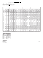
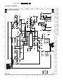
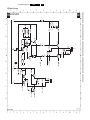
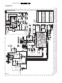
1
Colour Television
Chassis
L04E
AE
E_14480_142.eps
260504
Contents
Page
1. Technical Specifications, Connections, and Chassis
Overview
2
2. Safety Instructions, Warnings, and Notes
4
3. Directions for Use
7
4. Mechanical Instructions
8
5. Service Modes, Error Codes, and Fault Finding 10
6. Block Diagrams, Test Point Overviews, and
Waveforms
Wiring Diagram
21
Block Diagram Supply and Deflection
22
Block Diagram Video
23
Block Diagram Audio/Control
24
I2C and Supply Voltage Overview
25
7. Circuit Diagrams and PWB Layouts
Diagram
Mono Carrier: Power Supply
(A1) 26
Mono Carrier: Diversity Table for A1
27
Mono Carrier: Deflection
(A2) 28
Mono Carrier: Diversity Table for A2
29
Mono Carrier: Tuner IF
(A3) 30
Mono Carrier: Hercules
(A4) 31
Mono Carrier: Features & Connectivities (A5) 32
Mono Carrier: Class D - Audio Amplifier
(A6) 33
Mono Carrier: Audio Amplifier
(A7) 34
Mono Carrier: Rear I/O Scart
(A8) 35
Mono Carrier: Front Control
(A9) 36
Mono Carrier: DVD Power Supply
(A10)37
CRT Panel
(B1) 44
CRT Panel: Eco Scavem
(B2) 45
Side I/O + Headphone Panel (PV2)
(D) 47
Side I/O + Headphone Panel (FL13)
(D) 49
Top Control Panel (PV2)
(E) 51
Top Control Panel (FL13)
(E) 52
Power Supply PIP Panel
(F1) 53
Tuner IF and Demodulator PIP Panel
(F2) 54
Contents
8.
9.
10.
11.
Page
Linearity & Panorama Panel
(G) 57
Front Interface Panel (FL13)
(J) 58
Front Interface Panel (PV2)
(J) 59
Front Interface and Keyboard Panel
(J) 60
Alignments
63
Circuit Descriptions, Abbreviation List, and IC Data
Sheets
70
Abbreviation List
79
IC Data Sheets
81
Spare Parts List
83
Revision List
87
57
58
59
61
PWB
38-43
38-43
38-43
38-43
38-43
38-43
38-43
38-43
38-43
38-43
38-43
38-43
46-46
46-46
48-48
50-50
51-51
52-51
55-56
55-56
©
Copyright 2007 Philips Consumer Electronics B.V. Eindhoven, The Netherlands.
All rights reserved. No part of this publication may be reproduced, stored in a
retrieval system or transmitted, in any form or by any means, electronic,
mechanical, photocopying, or otherwise without the prior permission of Philips.
Published by WS 0673 BG CD Customer Service
Printed in the Netherlands
Subject to modification
EN 3122 785 16810
EN 2
1.
Technical Specifications, Connections, and Chassis Overview
L04E AE
1. Technical Specifications, Connections, and Chassis Overview
1.2
Index of this chapter:
1.1 Technical Specifications
1.2 Connections
1.3 Chassis Overview
Notes:
• Figures below can deviate slightly from the actual situation,
due to different set executions.
1.1
Technical Specifications
1.1.1
Vision
Display type
Screen size
Tuning system
Tuner bands
TV Colour systems
Video playback
Channel selections
Aerial input
1.1.2
Connections
Note: The following connector colour abbreviations are used
(acc. to DIN/IEC 757): Bk= Black, Bu= Blue, Gn= Green, Gy=
Grey, Rd= Red, Wh= White, Ye= Yellow.
1.2.1
Side Connections
Video In
L
Audio In
R
:
:
:
:
:
:
:
:
:
:
:
:
:
:
CRT
29” (72 cm), 4:3
PLL
VHF
UHF
Hyperband
S-Channel
PAL B/G, D/K, I
SECAM
SECAM B/G, D/K, L/L'
NTSC
100 presets
75 ohm, Coax
IEC-type
G_16810_001.eps
151206
Figure 1-1 Side I/O
Audio / Video In
Ye - Video (CVBS)
Wh - Audio - L
Rd - Audio - R
1 V_pp / 75 ohm
0.5 V_rms / 10 kohm
0.5 V_rms / 10 kohm
Jack: Audio Head phone- Out
Bk - Head phone
32 - 600 ohm / 10 mW
jq
jq
jq
rt
Sound
1.2.2
Sound systems
Maximum power
Features
:
:
:
:
NICAM Stereo
2 x 5 W_rms
Ultra bass
Incredible surround
Rear Connections
75 Ohm
AUDIO
OUT
EXTERNAL 2
L
1.1.3
Miscellaneous
Power supply:
- Mains voltage
- Mains frequency
SERVICE
CONNECTOR
R
EXTERNAL 1
G_16810_002.eps
181206
: 220 - 240 V_ac
: 50/60 Hz
Figure 1-2 Rear connections
Ambient conditions:
- Temperature range
- Maximum humidity
Power consumption
- Normal operation
- Standby
: +5 to +40 °C
: 90 % R.H.
: 74 W (29PT5408)
: 54 W (29PT5458)
: <1W
Dimensions (W x H x D cm)
: 771 x 699 x 594
(29PT5408)
: 775 x 586 x 670
(29PT5458)
Weight (kg)
: 42
Aerial In
- F-type
Coax, 75 ohm
Cinch: Audio - Out
Rd - Audio - R
Wh - Audio - L
0.5 VRMS / 10 kohm
0.5 VRMS / 10 kohm
D
kq
kq
Technical Specifications, Connections, and Chassis Overview
External 1: RGB/YUV - In and CVBS - In/Out
20
20
21
1
E_06532_001.eps
050404
Figure 1-3 SCART connector EXT2
1.3
- Audio - R
- Audio - R
- Audio - L
- Audio - gnd
- Blue - gnd
- Audio - L
- Blue/U - in
- CVBS - status
9
10
11
12
13
14
15
16
- Green - gnd
- n.c.
- Green/Y - in
- n.c.
- Red - gnd
- FBL - gnd
- Red/V - in
- Status/FBL
17
18
19
20
21
- Video
- Video
- CVBS - out
- CVBS - in
- Shielding
1.
EN 3
External 2: CVBS- In and SVHS - In
2
21
1
2
3
4
5
6
7
8
L04E AE
2
1
E_06532_001.eps
050404
Figure 1-4 SCART connector EXT1
0.5 V_rms / 1 kohm
0.5 V_rms / 10 kohm
0.5 V_rms / 1 kohm
Ground
Ground
0.5 V_rms / 10 kohm
0.7 V_pp / 75 ohm
0 - 2 V: INT
4.5 - 7 V: EXT 16:9
9.5 - 12 V: EXT 4:3
Ground
k
j
k
H
H
j
j
0.7 V_pp / 75 ohm
j
Ground
Ground
0.7 V_pp / 75 ohm
0 - 0.4 V: INT
1 - 3 V: EXT / 75 ohm
Ground
Ground
1 V_pp / 75 ohm
1 V_pp / 75 ohm
Ground
H
H
j
j
H
j
H
H
k
j
H
1
2
3
4
5
6
7
8
- Audio - R
- Audio - R
- Audio - L
- Audio - gnd
- Blue - gnd
- Audio - L
- n.c.
- CVBS - status
9
10
11
12
13
14
15
16
17
18
19
20
21
- Green - gnd
- n.c.
- n.c.
- n.c.
- Red - gnd
- FBL - gnd
- YC-C - in
- n.c.
- Video
- Video
- CVBS - out
- Y/CVBS - in
- Shielding
0.5 V_rms / 1 kohm
0.5 V_rms / 10 kohm
0.5 V_rms / 1 kohm
Ground
Ground
0.5 V_rms / 10 kohm
k
j
k
H
H
j
0 - 2 V: INT
4.5 - 7 V: EXT 16:9
9.5 - 12 V: EXT 4:3
Ground
j
H
Ground
Ground
0.7 V_pp / 75 ohm
H
H
j
Ground
Ground
1 V_pp / 75 ohm
1 V_pp / 75 ohm
Ground
H
H
k
j
H
Chassis Overview
B1
CRT
B2
ECO
SCAVEM
D
CRT PANEL
SIDE AV PANEL +
HEADPHONE
FRONT INTERFACE PANEL
(only 29PT5458)
MONO
CARRIER
J
POWER SUPPLY
A1
LINE & FRAME DEFLECTION
A2
TUNER IF
A3
HERCULES
A4
FEATURES & CONNECTIVITIES
A5
CLASS D AUDIO AMPLIFIER
A6
AUDIO AMPLIFIER
A7
REAR I/O SCART
A8
FRONT CONTROL
A9
G_16810_003.eps
181206
Figure 1-5 PWB location
EN 4
2.
L04E AE
Safety Instructions, Warnings, and Notes
2. Safety Instructions, Warnings, and Notes
Index of this chapter:
2.1 Safety Instructions
2.2 Maintenance Instructions
2.3 Warnings
2.4 Notes
2.1
Safety Instructions
1. Perform the “general repair instruction” noted above.
2. Clean the power supply and deflection circuitry on the
chassis.
3. Clean the picture tube panel and the neck of the picture
tube.
2.3
Safety regulations require the following during a repair:
• Connect the set to the Mains/AC Power via an isolation
transformer (> 800 VA).
• Replace safety components, indicated by the symbol h,
only by components identical to the original ones. Any
other component substitution (other than original type) may
increase risk of fire or electrical shock hazard.
• Wear safety goggles when you replace the CRT.
•
Safety regulations require that after a repair, the set must be
returned in its original condition. Pay in particular attention to
the following points:
• General repair instruction: as a strict precaution, we advise
you to re-solder the solder connections through which the
horizontal deflection current flows. In particular this is valid
for the:
1. Pins of the line output transformer (LOT).
2. Fly-back capacitor(s).
3. S-correction capacitor(s).
4. Line output transistor.
5. Pins of the connector with wires to the deflection coil.
6. Other components through which the deflection current
flows.
Note: This re-soldering is advised to prevent bad connections
due to metal fatigue in solder connections, and is therefore only
necessary for television sets more than two years old.
• Route the wire trees and EHT cable correctly and secure
them with the mounted cable clamps.
• Check the insulation of the Mains/AC Power lead for
external damage.
• Check the strain relief of the Mains/AC Power cord for
proper function, to prevent the cord from touching the CRT,
hot components, or heat sinks.
• Check the electrical DC resistance between the Mains/AC
Power plug and the secondary side (only for sets that have
a Mains/AC Power isolated power supply):
1. Unplug the Mains/AC Power cord and connect a wire
between the two pins of the Mains/AC Power plug.
2. Set the Mains/AC Power switch to the "on" position
(keep the Mains/AC Power cord unplugged!).
3. Measure the resistance value between the pins of the
Mains/AC Power plug and the metal shielding of the
tuner or the aerial connection on the set. The reading
should be between 4.5 Mohm and 12 Mohm.
4. Switch "off" the set, and remove the wire between the
two pins of the Mains/AC Power plug.
• Check the cabinet for defects, to prevent touching of any
inner parts by the customer.
2.2
Warnings
V
E_06532_007.eps
250304
Figure 2-1 Discharge picture tube
•
•
•
•
All ICs and many other semiconductors are susceptible to
electrostatic discharges (ESD w). Careless handling
during repair can reduce life drastically. Make sure that,
during repair, you are connected with the same potential as
the mass of the set by a wristband with resistance. Keep
components and tools also at this same potential. Available
ESD protection equipment:
– Complete kit ESD3 (small tablemat, wristband,
connection box, extension cable and earth cable) 4822
310 10671.
– Wristband tester 4822 344 13999.
Be careful during measurements in the high voltage
section.
Never replace modules or other components while the unit
is switched "on".
When you align the set, use plastic rather than metal tools.
This will prevent any short circuits and prevents circuits
from becoming unstable.
2.4
Notes
2.4.1
General
•
Maintenance Instructions
We recommend a maintenance inspection carried out by
qualified service personnel. The interval depends on the usage
conditions:
• When a customer uses the set under normal
circumstances, for example in a living room, the
recommended interval is three to five years.
• When a customer uses the set in an environment with
higher dust, grease, or moisture levels, for example in a
kitchen, the recommended interval is one year.
• The maintenance inspection includes the following actions:
In order to prevent damage to ICs and transistors, avoid all
high voltage flashovers. In order to prevent damage to the
picture tube, use the method shown in figure “Discharge
picture tube”, to discharge the picture tube. Use a high
voltage probe and a multi-meter (position VDC). Discharge
until the meter reading is 0 V (after approx. 30 s).
•
•
Measure the voltages and waveforms with regard to the
chassis (= tuner) ground (H), or hot ground (I), depending
on the tested area of circuitry. The voltages and waveforms
shown in the diagrams are indicative. Measure them in the
Service Default Mode (see chapter 5) with a colour bar
signal and stereo sound (L: 3 kHz, R: 1 kHz unless stated
otherwise) and picture carrier at 475.25 MHz for PAL, or
61.25 MHz for NTSC (channel 3).
Where necessary, measure the waveforms and voltages
with (D) and without (E) aerial signal. Measure the
voltages in the power supply section both in normal
operation (G) and in stand-by (F). These values are
indicated by means of the appropriate symbols.
The semiconductors indicated in the circuit diagram and in
the parts lists, are interchangeable per position with the
Safety Instructions, Warnings, and Notes
•
2.4.2
Schematic Notes
•
•
•
•
•
•
2.4.3
semiconductors in the unit, irrespective of the type
indication on these semiconductors.
Manufactured under license from Dolby Laboratories.
“Dolby”, “Pro Logic” and the “double-D symbol”, are
trademarks of Dolby Laboratories.
All resistor values are in ohms, and the value multiplier is
often used to indicate the decimal point location (e.g. 2K2
indicates 2.2 kohm).
Resistor values with no multiplier may be indicated with
either an "E" or an "R" (e.g. 220E or 220R indicates 220
ohm).
All capacitor values are given in micro-farads (μ= x10-6),
nano-farads (n= x10-9), or pico-farads (p= x10-12).
Capacitor values may also use the value multiplier as the
decimal point indication (e.g. 2p2 indicates 2.2 pF).
An "asterisk" (*) indicates component usage varies. Refer
to the diversity tables for the correct values.
The correct component values are listed in the Spare Parts
List. Therefore, always check this list when there is any
doubt.
Rework on BGA (Ball Grid Array) ICs
General
Although (LF)BGA assembly yields are very high, there may
still be a requirement for component rework. By rework, we
mean the process of removing the component from the PWB
and replacing it with a new component. If an (LF)BGA is
removed from a PWB, the solder balls of the component are
deformed drastically so the removed (LF)BGA has to be
discarded.
Device Removal
As is the case with any component that is being removed, it is
essential when removing an (LF)BGA, that the board, tracks,
solder lands, or surrounding components are not damaged. To
remove an (LF)BGA, the board must be uniformly heated to a
temperature close to the reflow soldering temperature. A
uniform temperature reduces the risk of warping the PWB.
To do this, we recommend that the board is heated until it is
certain that all the joints are molten. Then carefully pull the
component off the board with a vacuum nozzle. For the
appropriate temperature profiles, see the IC data sheet.
Area Preparation
When the component has been removed, the vacant IC area
must be cleaned before replacing the (LF)BGA.
Removing an IC often leaves varying amounts of solder on the
mounting lands. This excessive solder can be removed with
either a solder sucker or solder wick. The remaining flux can be
removed with a brush and cleaning agent.
After the board is properly cleaned and inspected, apply flux on
the solder lands and on the connection balls of the (LF)BGA.
Note: Do not apply solder paste, as this has been shown to
result in problems during re-soldering.
Device Replacement
The last step in the repair process is to solder the new
component on the board. Ideally, the (LF)BGA should be
aligned under a microscope or magnifying glass. If this is not
possible, try to align the (LF)BGA with any board markers.
So as not to damage neighbouring components, it may be
necessary to reduce some temperatures and times.
More Information
For more information on how to handle BGA devices, visit this
URL: www.atyourservice.ce.philips.com (needs subscription,
not available for all regions). After login, select “Magazine”,
then go to “Repair downloads”. Here you will find Information
on how to deal with BGA-ICs.
2.4.4
L04E AE
2.
EN 5
Lead-free Solder
Philips CE is producing lead-free sets (PBF) from 1.1.2005
onwards.
Identification: The bottom line of a type plate gives a 14-digit
serial number. Digits 5 and 6 refer to the production year, digits
7 and 8 refer to production week (in example below it is 1991
week 18).
MODEL
MADE IN BELGIUM
220-240V ~ 50/60Hz
128W
VHF+S+H+UHF
: 32PF9968/10
PROD.NO: AG 1A0617 000001
S
BJ3.0E LA
E_06532_024.eps
130606
Figure 2-2 Serial number example
Regardless of the special lead-free logo (which is not always
indicated), one must treat all sets from this date onwards
according to the rules as described below.
P
b
Figure 2-3 Lead-free logo
Due to lead-free technology some rules have to be respected
by the workshop during a repair:
• Use only lead-free soldering tin Philips SAC305 with order
code 0622 149 00106. If lead-free solder paste is required,
please contact the manufacturer of your soldering
equipment. In general, use of solder paste within
workshops should be avoided because paste is not easy to
store and to handle.
• Use only adequate solder tools applicable for lead-free
soldering tin. The solder tool must be able:
– To reach a solder-tip temperature of at least 400°C.
– To stabilise the adjusted temperature at the solder-tip.
– To exchange solder-tips for different applications.
• Adjust your solder tool so that a temperature of around
360°C - 380°C is reached and stabilised at the solder joint.
Heating time of the solder-joint should not exceed ~ 4 sec.
Avoid temperatures above 400°C, otherwise wear-out of
tips will increase drastically and flux-fluid will be destroyed.
To avoid wear-out of tips, switch “off” unused equipment or
reduce heat.
• Mix of lead-free soldering tin/parts with leaded soldering
tin/parts is possible but PHILIPS recommends strongly to
avoid mixed regimes. If this cannot be avoided, carefully
clean the solder-joint from old tin and re-solder with new
tin.
• Use only original spare-parts listed in the Service-Manuals.
Not listed standard material (commodities) has to be
purchased at external companies.
• Special information for lead-free BGA ICs: these ICs will be
delivered in so-called "dry-packaging" to protect the IC
against moisture. This packaging may only be opened
shortly before it is used (soldered). Otherwise the body of
the IC gets "wet" inside and during the heating time the
structure of the IC will be destroyed due to high (steam-)
pressure inside the body. If the packaging was opened
before usage, the IC has to be heated up for some hours
(around 90°C) for drying (think of ESD-protection!).
Do not re-use BGAs at all!
• For sets produced before 1.1.2005, containing leaded
soldering tin and components, all needed spare parts will
be available till the end of the service period. For the repair
of such sets nothing changes.
EN 6
2.
L04E AE
Safety Instructions, Warnings, and Notes
In case of doubt whether the board is lead-free or not (or with
mixed technologies), you can use the following method:
• Always use the highest temperature to solder, when using
SAC305 (see also instructions below).
• De-solder thoroughly (clean solder joints to avoid mix of
two alloys).
Caution: For BGA-ICs, you must use the correct temperatureprofile, which is coupled to the 12NC. For an overview of these
profiles, visit the website www.atyourservice.ce.philips.com
(needs subscription, but is not available for all regions)
You will find this and more technical information within the
"Magazine", chapter "Repair downloads".
For additional questions please contact your local repair help
desk.
2.4.5
Alternative BOM identification
In September 2003, Philips CE introduced a change in the way
the serial number (or production number, see Figure 2-2) is
composed. From this date on, the third digit in the serial
number (example: AG2B0335000001) indicates the number of
the alternative BOM (Bill of Materials used for producing the
specific model of TV set). It is possible that the same TV model
on the market is produced with e.g. two different types of
displays, coming from two different O.E.M.s.
By looking at the third digit of the serial number, the service
technician can see if there is more than one type of B.O.M.
used in the production of the TV set he is working with. He can
then consult the At Your Service Web site, where he can type
in the Commercial Type Version Number of the TV set (e.g.
28PW9515/12), after which a screen will appear that gives
information about the number of alternative B.O.M.s used.
If the third digit of the serial number contains the number 1
(example: AG1B033500001), then there is only one B.O.M.
version of the TV set on the market. If the third digit is a 2
(example: AG2B0335000001), then there are two different
B.O.M.s. Information about this is important for ordering the
correct spare parts!
For the third digit, the numbers 1...9 and the characters A...Z
can be used, so in total: 9 plus 26 = 35 different B.O.M.s can
be indicated by the third digit of the serial number.
2.4.6
Practical Service Precautions
•
•
It makes sense to avoid exposure to electrical shock.
While some sources are expected to have a possible
dangerous impact, others of quite high potential are of
limited current and are sometimes held in less regard.
Always respect voltages. While some may not be
dangerous in themselves, they can cause unexpected
reactions that are best avoided. Before reaching into a
powered TV set, it is best to test the high voltage insulation.
It is easy to do, and is a good service precaution.
Directions for Use
3. Directions for Use
You can download this information from the following websites:
http://www.philips.com/support
http://www.p4c.philips.com
L04E AE
3.
EN 7
EN 8
4.
L04E AE
Mechanical Instructions
4. Mechanical Instructions
Index of this chapter:
4.1 Set Disassembly
4.2 Service Position
4.3 Assies/Panels Removal
4.4 Set Re-assembly
Notes:
• Figures below can deviate slightly from the actual situation,
due to different set executions.
• Make sure that both the ComPair connector and the UART
connector are shielded off with a piece of insulating tape
after repair for ESD reasons. Place this tape over the holes
in the rear cover of the set.
1
4.1
Set Disassembly
Warning: Be sure to disconnect the AC power from the set
before opening it.
4.1.1
2
A
Rear Cover
1. Remove all fixation screws of the rear cover (do not forget
the screws that hold the rear connection panel).
2. Pull the rear cover backwards to remove it.
4.2
Service Position
Before placing the Mono Carrier in its service position, remove
the Front Interface assy/panel (see paragraph “Front Interface
Assy/Panel removal”), the Side AV assy/panel (see paragraph
“Side AV Assy/Panel removal”) and the PIP assy/panel (if
exists) (see paragraph “PIP Assy/Panel removal”).
3
4
B
E_14480_048.eps
110204
Figure 4-1 Service position Mono Carrier
1. Disconnect the degaussing coil [1].
2. Release the two fixation clamps (at the mid left and mid
right side of the bracket), and remove the bracket from the
bottom tray, by pulling it backwards [2].
3. Turn the chassis tray 90 degrees counter clockwise.
4. Move the panel bracket somewhat to the left and flip it 90
degrees [3], with the components towards the CRT.
5. Turn the panel bracket with the rear I/O toward the CRT.
6. Place the hook of the tray in the fixation hole of the cabinet
bottom [4] and secure it.
Mechanical Instructions
4.3
Assies/Panels Removal
4.3.1
Front Interface Assy/Panel Removal
1
1
2
3
3
E_14480_049.eps
110204
Figure 4-2 Front interface assy/panel removal
1. Remove the complete module from the bottom plate, by
pulling the two fixation clamps upward [1], while sliding the
module away from the CRT [2].
Note: these clamps are difficult to access.
2. Release the two fixation clamps [3] at the side of the
bracket, and lift the panel out of the bracket (it hinges at
one side).
4.3.2
Side AV Assy/Panel Removal
E_14480_050.eps
170204
Figure 4-3 Side AV assy/panel removal
1. Remove the two fixation screws, and remove the complete
Side AV assembly.
2. Release the two fixation clamps, and lift the panel out of the
bracket.
4.4
Set Re-assembly
To re-assemble the whole set, do all processes in reverse
order.
Note: before you mount the rear cover, perform the following
checks:
1. Check whether the AC power cord is mounted correctly in
its guiding brackets.
2. Check whether all cables are replaced in their original
position
L04E AE
4.
EN 9
EN 10
5.
Service Modes, Error Codes, and Fault Finding
L04E AE
5. Service Modes, Error Codes, and Fault Finding
Index of this chapter:
5.1 Test Points
5.2 Service Modes
5.3 Problems and Solving Tips Related to CSM
5.4 ComPair
5.5 Error Codes
5.6 The Blinking LED Procedure
5.7 Protections
5.8 Fault Finding and Repair Tips
5.1
Table 5-2 Software cluster overview
5.2.1
The chassis is equipped with test points printed on the circuit
board assemblies. These test points refer to the functional
blocks:
Table 5-1 Test point overview
Circuit
Diagram
F508, F535, F536, F537, F552, F561, F563, Power supply
F573, F664,I513, I518, I519, I524, I531, I533,
I546
A1
F401, F412, F413, F414, F418, F452, F453,
F455, F456, F458, F459, F460, F461, I408,
I416, I417, I420, I462, I468
Line + Frame
Deflection
A2
F003, F004, I001, I002
Tuner IF
A3
F201, F203, F205, F206
Hercules
A4
F240, F241, F242
Features &
Connectivity
A5
F952, F955, I951, I952
Audio Amplifier
A7
F692
Front Control
A9
F331, F332, F333, F338, F339, F341, F351,
F353, F354
CRT Panel
B1
F361, F362, F381, F382
ECO Scavem
B2
Perform measurements under the following conditions:
• Television set in Service Default Alignment Mode.
• Video input: Colour bar signal.
• Audio input: 3 kHz left channel, 1 kHz right channel.
5.2
SW Version
First Mask
Remarks
L6LKEF7_3.1
L04EF7 3.1
TDA12020H1/N1F90
Europe
Service Default Mode (SDM)
Purpose
• To create a predefined setting for measurements to be
made.
• To override software protections.
• To start the blinking LED procedure.
Test Points
Test point
SW Cluster
Service Modes
Service Default mode (SDM) & Service Alignment Mode (SAM)
offers several features for the service technician, while the
Customer Service Mode (CSM) is used for communication
between the call centre and the customer.
This chassis also offers the option of using ComPair, a
hardware interface between a computer and the TV chassis. It
offers the abilities of structured troubleshooting, error code
reading, and software version read-out for all these chassis.
Minimum requirements for ComPair: a Pentium processor, a
Windows OS, and a CD-ROM drive (see "ComPair" section).
Specifications
• Tuning frequency: 475.25 MHz.
• Colour system: PAL/SECAM.
• All picture settings at 50 % (brightness, colour contrast,
hue).
• Bass, treble and balance at 50 %; volume at 25 %.
• All service-unfriendly modes (if present) are disabled. The
service unfriendly modes are:
– Timer / Sleep timer.
– Child / parental lock.
– Blue mute.
– Hotel / hospital mode.
– Auto shut OFF (when no 'IDENT' video signal is
received for 15 minutes).
– Skipping of non-favourite presets / channels.
– Auto-storage of personal presets.
– Auto user menu time-out.
– Auto Volume Levelling (AVL).
How to Enter
To enter SDM, use one of the following methods:
• Press the following key sequence on the remote control
transmitter: '0 6 2 5 9 6' directly followed by the 'MENU'
button (do not allow the display to time out between entries
while keying the sequence).
• Short jumper wires 9252 and 9275 on the family board (see
Fig. 8-1) and apply mains. Then press the power button
(remove the short after start-up).
Caution: Entering SDM by shorting wires 9252 and 9275
will override the +8V-protection. Do this only for a short
period. When doing this, the service-technician must know
exactly what he is doing, as it could damage the television
set.
• Or via ComPair (with the ComPair ‘Tools’, it should be
possible to enter SDM via the ComPair interface).
After entering SDM, the following screen is visible, with SDM in
the upper right corner of the screen to indicate that the
television is in Service Default Alignment Mode.
Service Modes, Error Codes, and Fault Finding
00028 L04EF30.10
SDM
ERR 0 0 0 0 0
OP 000 057 140 032 120 128 000
L04E AE
5.
00028 L04EF30.10
ERR 0 0 0 0 0
EN 11
SAM
OP 000 057 140 032 120 128 000
E_14480_139.eps
250504
Figure 5-1 SDM menu
How to Navigate
Use one of the following methods:
• When you press the MENU button on the remote control,
the set will switch on the normal user menu in the SDM
mode.
• On the TV, press and hold the 'VOLUME down' and press
the 'CHANNEL down' for a few seconds, to switch from
SDM to SAM and reverse.
How to Exit
Switch the set to STANDBY by pressing the POWER button on
the remote control transmitter or the television set.
If you turn the television set OFF by removing the Mains (i.e.,
unplugging the television) without using the POWER button,
the television set will remain in SDM when mains is re-applied,
and the error buffer is not cleared.
5.2.2
Service Alignment Mode (SAM)
Purpose
• To change option settings.
• To display / clear the error code buffer.
• To perform alignments.
Specifications
• Run timer (maximum five digits displayed)
• Software version, Error & Option Bytes display
• Clear error buffer.
• Option settings
• AKB switching
• Software alignments (Tuner, 2 Tuner PIP, White Tone,
Geometry & Audio)
• NVM Editor
• ComPair Mode switching
How to Enter
To enter SAM, use one of the following methods:
• Press the following key sequence on the remote control
transmitter: '0 6 2 5 9 6' directly followed by the “On Screen
Display icon “i +” button (do not allow the display to time out
between entries while keying the sequence).
• Or via ComPair.
After entering SAM, the following screen is visible, with SAM in
the upper right corner of the screen to indicate that the
television is in Service Alignment Mode.
. Clear
. Options
. AKB
. Tuner
. 2 Tuner PIP*
. White Tone
. Geometry
. Audio
. NVM Editor
. ComPair
Clear ?
On
on
E_14480_140.eps
260504
* optional
Figure 5-2 SAM menu
Menu Explanation
1. LLLLL. This represents the run timer. The run timer counts
normal operation hours, but does not count standby hours
(maximum four digits displayed).
2. AAABCD-X.Y. This is the software identification of the
main microprocessor:
– A = the project name (L04).
– B = the region: E= Europe, A= Asia Pacific, U= NAFTA,
L= LATAM.
– C = the software diversity:
• Europe: T = 1 page TXT, F = Full TXT, V = Voice
control.
• LATAM and NAFTA: N = Stereo non-dBx, S =
Stereo dBx.
• Asian Pacific: F = Full TXT, N = non TXT, C =
NTSC.
• ALL regions: M = mono, D = DVD, Q = Mk2.
– D = the language cluster number.
– X = the main software version number (updated with a
major change that is incompatible with previous
versions).
– Y = the sub software version number (updated with a
minor change that is compatible with previous
versions).
3. SAM. Indication of the Service Alignment Mode.
4. Error Buffer. Shows all errors detected since the last time
the buffer was erased. Five errors possible.
5. Option Bytes. Used to set the option bytes. See 'Options'
in the Alignments section for a detailed description. Seven
codes are possible.
6. Clear. Erases the contents of the error buffer. Select the
CLEAR menu item and press the MENU RIGHT key. The
content of the error buffer is cleared.
7. Options. Used to set the option bits. See 'Options' in the
Alignments section for a detailed description.
8. AKB. Used to disable (OFF) or enable (ON) the 'black
current loop' (AKB = Auto Kine Bias).
9. Tuner. Used to align the tuner. See 'Tuner' in the
Alignments section for a detailed description.
10. 2 Tuner PIP. Used to align the tuner PIP (optional)
11. White Tone. Used to align the white tone. See 'White Tone'
in the Alignments section for a detailed description.
12. Geometry. Used to align the geometry settings of the
television. See 'Geometry' in the Alignments section for a
detailed description.
EN 12
5.
L04E AE
Service Modes, Error Codes, and Fault Finding
13. Audio. No audio alignment is necessary for this television
set.
14. NVM Editor. Used to change the NVM data in the
television set.
15. ComPair Mode. Used to switch ON the television to ISP
mode (for uploading software)
1 00028 L04EF30.10
CSM
2 CODES 0 0 0 0 0
3 OP 000 057 140 032 120 128 000
4 nnXXnnnn/nnX
5 P3C-1
6 NOT TUNED
7 PAL
8 STEREO
9 CO 50 CL 50 BR 50 HU 0
0 AVL Off BS 50
How to Navigate
• In SAM, select menu items with the MENU UP/DOWN keys
on the remote control transmitter. The selected item will be
highlighted. When not all menu items fit on the screen, use
the MENU UP/DOWN keys to display the next / previous
menu items.
• With the MENU LEFT/RIGHT keys, it is possible to:
– Activate the selected menu item.
– Change the value of the selected menu item.
– Activate the selected submenu.
• In SAM, when you press the MENU button twice, the set
will switch to the normal user menus (with the SAM mode
still active in the background). To return to the SAM menu
press the MENU or STATUS/EXIT button.
• When you press the MENU key in while in an SDAM
submenu, you will return to the previous menu.
E_14480_141.eps
250504
Figure 5-3 CSM menu
How to Store SAM Settings
To store settings changed in SAM leave the top level SAM
menu by using the POWER button on the remote control
transmitter or the television set.
Menu Explanation
1. Indication of the service mode (CSM = Customer Service
Mode).
2. Reserved item.
3. Software identification of the main microprocessor (see
'Service Default Alignment Mode' for an explanation)
4. Reserved item for P3C call centres (AKBS stands for
Advanced Knowledge Base System).
5. Indicates the type of TV system or whether or not the
television is receiving an 'IDENT' signal on the selected
source. If no 'IDENT' signal is detected, the display will
read 'NOT TUNED'
6. Displays the last five errors detected in the error code
buffer.
How to Exit
Switch the set to STANDBY by pressing the POWER button on
the remote control transmitter or the television set.
If you turn the television set OFF by removing the mains (i.e.,
unplugging the television) without using the POWER button,
the television set will remain in SAM when mains is re-applied,
and the error buffer is not cleared.
5.2.3
Customer Service Mode (CSM)
Purpose
The Customer Service Mode shows error codes and
information on the TV operation settings. The call centre can
instruct the customer to enter CSM by telephone and read out
the information displayed. This helps the call centre to
diagnose problems and failures in the TV set before making a
service call.
The CSM is a read-only mode; therefore, modifications are not
possible in this mode.
How to Enter
To enter CSM, press the following key sequence on the remote
control transmitter: '1 2 3 6 5 4' (do not allow the display to time
out between entries while keying the sequence).
Upon entering the Customer Service Mode, the following
screen will appear:
How to Exit
To exit CSM, use one of the following methods:
• Press the MENU, STATUS/EXIT, or POWER button on the
remote control transmitter.
• Press the POWER button on the television set.
5.3
Problems and Solving Tips Related to CSM
5.3.1
Picture Problems
Note: The problems described below are all related to the TV
settings. The procedures used to change the value (or status)
of the different settings are described.
Picture too Dark or too Bright
If:
• The picture improves when you press the AUTO PICTURE
button on the remote control transmitter, or
• The picture improves when you enter the Customer
Service Mode
Then:
1. Press the AUTO PICTURE button on the remote control
transmitter repeatedly (if necessary) to choose
PERSONAL picture mode.
2. Press the MENU button on the remote control transmitter.
This brings up the normal user menu.
3. In the normal user menu, use the MENU UP/DOWN keys
to highlight the PICTURE sub menu (if necessary).
4. Press the MENU LEFT/RIGHT keys to enter the PICTURE
sub menu.
Service Modes, Error Codes, and Fault Finding
5. Use the MENU UP/DOWN keys (if necessary) to select
BRIGHTNESS.
6. Press the MENU LEFT/RIGHT keys to increase or
decrease the BRIGHTNESS value.
7. Use the MENU UP/DOWN keys to select PICTURE.
8. Press the MENU LEFT/RIGHT keys to increase or
decrease the PICTURE value.
9. Press the MENU button on the remote control transmitter
twice to exit the user menu.
10. The new PERSONAL preference values are automatically
stored.
EN 13
Then:
1. Press the AUTO PICTURE button on the remote control
transmitter repeatedly (if necessary) to choose
PERSONAL picture mode.
2. Press the MENU button on the remote control transmitter.
This brings up the normal user menu.
3. In the normal user menu, use the MENU UP/DOWN keys
to highlight the PICTURE sub menu (if necessary).
4. Press the MENU LEFT/RIGHT keys to enter the PICTURE
sub menu.
5. Use the MENU UP/DOWN keys to select PICTURE.
6. Press the MENU LEFT key to decrease the PICTURE
value.
7. Press the MENU button on the remote control transmitter
twice to exit the user menu.
8. The new PERSONAL preference value is automatically
stored.
5.4
ComPair
Note:
Make sure that both the ComPair connector and the UART
connector are shielded off with a piece of insulating tape after
repair for ESD reasons. Place this tape over the holes in the
rear cover of the set.
5.4.1
Introduction
ComPair (Computer Aided Repair) is a service tool for Philips
Consumer Electronics products. ComPair is a further
development on the European DST (service remote control),
which allows faster and more accurate diagnostics. ComPair
has three big advantages:
• ComPair helps you to quickly get an understanding on how
to repair the chassis in a short time by guiding you
systematically through the repair procedures.
• ComPair allows very detailed diagnostics (on I2C level)
and is therefore capable of accurately indicating problem
areas. You do not have to know anything about I2C
commands yourself because ComPair takes care of this.
• ComPair speeds up the repair time since it can
automatically communicate with the chassis (when the
microprocessor is working) and all repair information is
directly available. When ComPair is installed together with
the SearchMan electronic manual of the defective chassis,
schematics and PWBs are only a mouse click away.
Snowy Picture
To enter CSM, press the following key sequence on the remote
control transmitter: '123654' (do not allow the display to time
out between entries while keying the sequence).
Check CSM line 5. If this line reads 'Not Tuned,' check the
following:
• Antenna not connected. Connect the antenna.
• No antenna signal or bad antenna signal. Connect a proper
antenna signal.
• The tuner is faulty (in this case line 6, the Error Buffer line,
will contain error number 10). Check the tuner and replace/
repair the tuner if necessary.
Black and White Picture
If:
• The picture improves after you have pressed the AUTO
PICTURE button on the remote control transmitter
5.4.2
Then:
1. Press the AUTO PICTURE button on the remote control
transmitter repeatedly (if necessary) to choose
PERSONAL picture mode.
2. Press the MENU button on the remote control transmitter.
This brings up the normal user menu.
3. In the normal user menu, use the MENU UP/DOWN keys
to highlight the PICTURE sub menu (if necessary).
4. Press the MENU LEFT/RIGHT keys to enter the PICTURE
sub menu.
5. Use the MENU UP/DOWN keys to select COLOR.
6. Press the MENU RIGHT key to increase the COLOR value.
7. Press the MENU button on the remote control transmitter
twice to exit the user menu.
8. The new PERSONAL preference value is automatically
stored.
5.
Menu Text not Sharp Enough
If:
• The picture improves after you have pressed the AUTO
PICTURE button on the remote control transmitter.
White Line around Picture Elements and Text
If:
The picture improves after you have pressed the AUTO
PICTURE button on the remote control transmitter
Then:
1. Press the AUTO PICTURE button on the remote control
transmitter repeatedly (if necessary) to choose
PERSONAL picture mode.
2. Press the MENU button on the remote control transmitter.
This brings up the normal user menu.
3. In the normal user menu, use the MENU UP/DOWN keys
to highlight the PICTURE sub menu (if necessary).
4. Press the MENU LEFT/RIGHT keys to enter the PICTURE
sub menu.
5. Use the MENU UP/DOWN keys to select SHARPNESS.
6. Press the MENU LEFT key to decrease the SHARPNESS
value.
7. Press the MENU button on the remote control transmitter
twice to exit the user menu.
8. The new PERSONAL preference value is automatically
stored.
L04E AE
Specifications
ComPair consists of a Windows based fault finding program
and an interface box between PC and the (defective) product.
The ComPair interface box is connected to the PC via a serial
or RS232 cable.
In this chassis, the ComPair interface box and the TV
communicate via a bi-directional service cable via the service
connector.
The ComPair fault finding program is able to determine the
problem of the defective television. ComPair can gather
diagnostic information in two ways:
• Automatic (by communication with the television):
ComPair can automatically read out the contents of the
entire error buffer. Diagnosis is done on I2C level. ComPair
can access the I2C bus of the television. ComPair can
send and receive I2C commands to the micro controller of
the television. In this way, it is possible for ComPair to
communicate (read and write) to devices on the I2C
busses of the TV-set.
EN 14
5.
Service Modes, Error Codes, and Fault Finding
L04E AE
•
Manually (by asking questions to you): Automatic
diagnosis is only possible if the micro controller of the
television is working correctly and only to a certain extend.
When this is not the case, ComPair will guide you through
the fault finding tree by asking you questions (e.g. Does the
screen give a picture? Click on the correct answer: YES /
NO) and showing you examples (e.g. Measure test-point I7
and click on the correct waveform you see on the
oscilloscope). You can answer by clicking on a link (e.g.
text or a waveform picture) that will bring you to the next
step in the fault finding process.
By a combination of automatic diagnostics and an interactive
question / answer procedure, ComPair will enable you to find
most problems in a fast and effective way.
Beside fault finding, ComPair provides some additional
features like:
• Up- or downloading of pre-sets.
• Managing of pre-set lists.
• Emulation of the Dealer Service Tool (DST).
• If both ComPair and SearchMan (Electronic Service
Manual) are installed, all the schematics and the PWBs of
the set are available by clicking on the appropriate
hyperlink. Example: Measure the DC-voltage on capacitor
C2568 (Schematic/Panel) at the Mono-carrier.
– Click on the 'Panel' hyperlink to automatically show the
PWB with a highlighted capacitor C2568.
– Click on the 'Schematic' hyperlink to automatically
show the position of the highlighted capacitor.
5.4.3
•
•
•
•
•
•
•
•
Note: If you encounter any problems, contact your local
support desk.
5.5
TO
UART SERVICE
CONNECTOR
Error Codes
The error code buffer contains all errors detected since the last
time the buffer was erased. The buffer is written from left to
right. When an error occurs that is not yet in the error code
buffer, it is displayed at the left side and all other errors shift one
position to the right.
5.5.1
How to Read the Error Buffer
You can read the error buffer in 3 ways:
• On screen via the SDAM (if you have a picture).
Examples:
– ERROR: 0 0 0 0 0 : No errors detected
– ERROR: 6 0 0 0 0 : Error code 6 is the last and only
detected error
– ERROR: 9 6 0 0 0 : Error code 6 was detected first and
error code 9 is the last detected (newest) error
• Via the blinking LED procedure (when you have no
picture). See 'The Blinking LED Procedure'.
• Via ComPair.
How to Connect ComPair
1. First, install the ComPair Browser software (see the Quick
Reference Card for installation instructions).
2. Connect the RS232 interface cable between a free serial
(COM) port of your PC and the PC connector (marked with
'PC') of the ComPair interface.
3. Connect the mains adapter to the supply connector
(marked with 'POWER 9V DC') of the ComPair interface.
4. Switch the ComPair interface “OFF”.
5. Switch the television set “OFF” with the mains switch.
6. Connect the ComPair interface cable between the
connector on the rear side of the ComPair interface
(marked with 'I2C') and the ComPair (or Service) connector
at the rear side of the TV (for its location see figure 8-1 in
chapter “Alignments”).
7. Plug the mains adapter in a mains outlet, and switch the
interface “ON”. The green and red LEDs light up together.
The red LED extinguishes after approx. 1 second while the
green LED remains lit.
8. Start the ComPair program and read the 'Introduction'
chapter.
ComPair interface (excluding transformer): 4822 727
21631.
Starter kit ComPair32 software (registration version): 3122
785 60040.
Starter kit SearchMan32 software: 3122 785 60050.
ComPair32 CD (update): 3122 785 60070 (year 2002,
3122 785 60110 (year 2003).
SearchMan32 CD (update): 3122 785 60080 (year 2002),
3122 785 60120 (year 2003).
ComPair interface cable: 3122 785 90004.
Transformer (non-UK): 4822 727 21632.
Transformer UK: 4822 727 21633.
5.5.2
How to Clear the Error Buffer
The error code buffer is cleared in the following cases:
• By using the CLEAR command in the SDAM menu:
– To enter SAM, press the following key sequence on the
remote control transmitter: '062596' directly followed
by the “OSD" icon button (do not allow the display to
time out between entries while keying the sequence).
– Make sure the menu item CLEAR is highlighted. Use
the MENU UP/DOWN buttons, if necessary.
– Press the MENU RIGHT button to clear the error
buffer. The text on the right side of the 'CLEAR' line will
change from 'CLEAR?' to 'CLEARED'
• If the contents of the error buffer have not changed for 50
hours, the error buffer resets automatically.
TO
I2C SERVICE
CONNECTOR
Note: If you exit SAM by disconnecting the Mains from the
television set, the error buffer is not reset.
5.5.3
PC
VCR
Power
9V DC
I2C
E_06532_021.eps
180804
Figure 5-4 ComPair connection
5.4.4
How to Order
ComPair order codes:
• Starter kit ComPair32/SearchMan32 software and
ComPair interface (excl. transformer): 3122 785 90450.
Error Codes
In case of non-intermittent faults, write down the errors present
in the error buffer and clear the error buffer before you begin
the repair. This ensures that old error codes are no longer
present.
If possible, check the entire contents of the error buffer. In
some situations, an error code is only the result of another error
and not the actual cause of the problem (for example, a fault in
the protection detection circuitry can also lead to a protection).
Service Modes, Error Codes, and Fault Finding
L04E AE
5.
EN 15
Table 5-3 Error codes overview
Error Device
Error description
0
Not applicable
No Error
Check item
Diagram
1
Not applicable
X-Ray / over-voltage protection (US only)
2411, 2412, 2413, 6404, 6411,
6412.
A2
2
3
Not applicable
High beam (BCI) protection
3404, 7405
A2
Not applicable
Vertical guard protection
3466, 7451, 7452, 7453, 7454
4
Tuner UA1316/A I2C error while communicating with 2nd tuner
A2
1000, 5010 (PIP Module)
F2
5
Not applicable
6
I2C bus
+5v protection
7604, 7605
A5
General I2C error
7200, 3207, 3214
7
A4
Not applicable
-
-
-
8
Not applicable
-
-
-
9
24C16
I2C error while communicating with the EEPROM
7601, 3604, 3605
A5
10
Tuner
= I2C error while communicating with the PLL tuner
1000, 5001
A3
11
TDA6107/A
Black current loop instability protection
7330, 3351, CRT
B1
12
SDA9488X
I2C error while communicating with the PIP processor
7242 (PIP Module)
F1
13
Not applicable
-
-
-
14
DVD Loader
I2C error while communicating with the DVD Interface module DVD Interface module
15
TDA9178T/N1
I2C error while communicating with LTI module
7610
H
16
TDA9887
I2C error while communicating with PIP_Demodulator
7201
F2
17
Not applicable
-
-
-
18
Not applicable
-
-
-
19
TDA1200
I2C error while communicating with SSD stereo sound decoder 7200
A4
20
TDA1200
I2C error while communicating with video cosmic in Hercules IC 7200
A4
Note: Errors 7, 8, 13, 17, 18 are not applicable.
5.6
5.8
Using this procedure, you can make the contents of the error
buffer visible via the front LED. This is especially useful when
there is no picture.
Example of error buffer: 12 9 6 0 0
After entering SDM, the following occurs:
• 1 long 'ON' blink of 5 seconds to start the sequence,
• 12 short blinks followed by a pause of 1.5 seconds,
• 9 short blinks followed by a pause of 1.5 seconds,
• 6 short blinks followed by a pause of 1.5 seconds,
• 1 long 'ON' blink of 1.5 seconds to finish the sequence,
• The sequence starts again at 12 short blinks.
5.7
Protections
If a fault situation is detected, an error code will be generated;
and, if necessary, the television set will go into protection
mode. Blinking of the red LED at a frequency of 3 Hz indicates
the protection mode. In some error cases, the microprocessor
does not put the set in protection mode. The error codes of the
error buffer and the blinking LED procedure can be read via the
Service Default Menu (SDM), or via ComPair.
To get a quick diagnosis the chassis has three service modes
implemented:
• The Customer Service Mode (CSM).
• The Service Default Mode (SDM).
• The Service Alignment Mode (SAM).
For a detailed description, see the "Customer Service Mode,
Service Default mode" and "Service Alignment Mode" sections.
Fault Finding and Repair Tips
Notes:
• It is assumed that the components are mounted correctly
with correct values and no bad solder joints.
• Before any fault finding actions, check if the correct options
are set.
The Blinking LED Procedure
When the SDM is entered, the LED will blink the contents of the
error-buffer:
• When all the error-codes are displayed, the sequence
finishes with an 'ON' LED blink of 1.5 seconds,
• The sequence starts again.
DVD Loader
5.8.1
NVM Editor
In some cases, it can be handy if one directly can change the
NVM contents. This can be done with the “NVM Editor” in SAM
mode. In the next table, the default NVM values are given.
EN 16
5.
Service Modes, Error Codes, and Fault Finding
L04E AE
Model
29PT5458
5.8.2
29PT5408
Table 5-4 NVM default values
Parameter
Addr.
(dec)
EW (EW width)
19
25
25
PW (EW parabola width)
20
0A
0A
HS (Horizontal shift)
21
1A
1A
Power Supply
Set Not Working
Check Power
Supply Mains
Switch
Value (hex)
HP (Horizontal parallelogram)
22
1F
1F
HB (Horizontal Bow)
23
1F
1F
UCP (EW upper corner parabola)
24
1E
1E
LCP (EW lower corner parabola)
25
28
28
TC (EW trapezium)
26
1A
1A
VS (Vertical slope)
27
25
25
VA (Vertical amplitude)
28
1E
1E
SC (S-Correction)
29
14
14
VSH (Vertical Shift)
30
1A
1A
VX (Vertical Zoom)
31
19
19
VSL (Vertical scroll)
32
20
20
VL (Vertical linearity)
33
20
20
AGC (AGC Takeover)
36
17
17
OIF (IF-PLL Offset)
37
20
20
AGC10 (AGC 10)
38
01
01
H60 (60 Hz Horizontal Shift)
39
09
09
PWL (Peaking Frequency, Soft Clipper, Peak White
Limit)
40
07
07
COR_ON_OFF (SECAM_PAL)
41
0F
0F
60 Hz Vertical amplitude
42
40
40
CL
43
07
07
RGB amplitude for full teletext mode
46
14
14
NVM_TABLE_VERSION
60
31
31
OPTION_TABLE_VERSION
61
13
13
NVM_RGB_BLOR
62
23
23
NVM_RGB_BLOG
63
24
24
TXT Brightness
64
0F
0F
V60 offset (60Hz Vertical Amplitude)
66
FE
FE
FOAB, CHSE
139
03
03
SPR, WS
140
00
00
VMA, SVM
141
32
32
SOC_SMD
142
03
03
CCC_Preset_Gain_Red
143
1F
1F
CCC_Preset_Gain_Green
144
1F
1F
CCC_Preset_Gain_Blue
145
1F
1F
NVM_FMWS
149
02
02
NVM_ASD_SC1_THR
150
10
10
NVM_CRYSTAL_ALIGN
208
31
31
Last Brightness (VID PP others)
264
TBF
TBF
Last Color (VID PP others)
265
TBF
TBF
Last Contrast (VID PP others)
266
TBF
TBF
Last Sharpness (VID PP others)
267
TBF
TBF
Last Hue (VID PP others)
268
TBF
TBF
Last Colour Temperature (VID PP others)
269
TBF
TBF
White-D Cool Red
294
FD
FD
White-D Cool Blue
296
8
8
White-D Normal Red
297
22
22
White-D Normal Green
298
20
20
White-D Normal Blue
299
1E
1E
White-D Warm Red
300
03
03
White-D Warm Blue
302
F9
F9
Last Volume
343
14
14
Last Balance
344
32
32
Last Treble (AUD PP others)
345
37
37
Last Bass (AUD PP others)
346
28
1E
Bridge Rectifier
circuit 6500
Check fusible
resistor 3510 &
circuit before it
Not Ok
Ok
Check DC
voltage at
2505/2507
Not Ok
Ok
Check
fusible
resistor 3532
Check
7512
Check IC7511 &
IC7531
Ok
Set able to
start-up
Check other
fusible resistor
and capacitor in
the circuit
No
Yes
End
E_14480_057.eps
190204
Figure 5-5 Fault finding tree “Set not working”
Set Does Not Start Up
Set Unable
to Start
Software
loaded?
No
Fuse Blown?
Yes
Yes
Change
Fuse
Load
Software
Check
voltage
across 2552
Is Vbatt
approximately
140V
No
Check Power
Supply circuit
Yes
Check
voltage 2562
&2563
No
16V
Yes
Check 3V
across 2535
Yes
Check 6V
across 2535
Yes
Set able to
Start
No
Check Line
Transistor 7405
Yes
End
E_14480_058.eps
170204
Figure 5-6 Fault finding tree “Set does not start up”
Service Modes, Error Codes, and Fault Finding
5.8.3
Deflection
L04E AE
5.
EN 17
Blank Screen
One Thin Vertical Line
Quick check:
• Set in protection mode.
• LED blinking with error “3”.
Blank Screen
Check Vg2
(fine tune)
Ok
Picture
appears?
One Thin Vertical Line
LED Blinking
Not Ok
Picture not appearing
Check Beam Current Limit
(voltage is 1.8V-2V when
brightness and contrast is
set to the maximum
Check all
connection and
peripheral at
Deflection Circuit in
place
Not Ok
Check deflection
circuit
Ok
Check heater voltage
(measure pin 9&10
at the CRT socket)
Check
Line Transistor
7405
Ok
Picture not appearing
Not Ok
Is VBE between
200mV to 30mV & VCB
approximately 500mV
Yes
Check video supply
(2457) is approximately
180V
Check Horizontal
Deflection
Circuitry
Ok
Picture
appears?
Ok
Replace transistor
End
E_14480_059.eps
170204
E_14480_061.eps
170204
Figure 5-7 Fault finding tree “One thin vertical line”
One Thin Horizontal Line
Quick check:
• Set in protection mode.
• LED blinking with error “2”.
Figure 5-9 Fault finding tree “Blank screen”
5.8.4
Source Selection
Set is not able to go into AV or any missing AV is
encountered
E.g. AV1 is available but not able to enter to AV1: Check if the
option setting is correct.
One Horizontal
Thin Line
LED Blinking
Set is able to go to AV, but no audio is heard.
1. Check that continuity of signal is there from the SCART/
Cinch input to the input of the Hercules.
2. If continuity is there and still no audio, check that option
settings are correct.
3. If logic setting is correct and still no audio, proceed to Audio
Decoder/Processor troubleshooting section.
Check all connection
and peripheral at
Deflection Circuit
in place
Set is able to go into AV but no video is available:
1. Check continuity from AV input to HERCULES depending
on the input.
2. If continuity is available and yet no video, proceed to Video
Processor troubleshooting section.
Check transistor
(7451, 7523, 7543) at
Vertical Deflection Circuitry
Replace transistor
Check Vertical
Deflection Circuit
E_14480_060.eps
170204
Figure 5-8 Fault finding tree “One thin horizontal line”
5.8.5
Tuner and IF
No Picture
1. Check that the Option settings are correct.
2. If correct, check that supply voltages are there.
3. If supply voltages are present, check whether picture is
present in AV.
4. If picture is present in AV, check with the scope the Tuner
IF output signal by manual storage to a known channel.
EN 18
5.
Service Modes, Error Codes, and Fault Finding
L04E AE
Picture o.k., No Sound
5. If IF output is present, Tuner is working fine. If no IF output,
I2C data lines may be open, check continuity of I2C lines.
If I2C lines are o.k., Tuner may be defect, replace Tuner.
6. If Tuner IF is present and yet still no picture in RF mode, go
to Video Processing troubleshooting section.
Picture Ok,
No Sound
No Picture, No Sound
No Picture,
No Sound,
Raster Ok
Check tuning
supply voltage,
pin 9 of tuner
Check AGC
Voltage, pin 1
of tuner
>30V & <35V
Check IF output of
tuner, pin 11
No
Yes
Check
VT Supply
Section
CVBS
present?
No
Refer to fig.
"Power Supply:
Set not working"
No
Replace SAW
filter
Yes
AGC voltage
changes with
different signal
strength
Check supply
voltage, pin 7 of
tuner
5V
Check SAW filter output
(pin 4&5)
EU/AP/CH (QSS)- 1001
NA/LA/AP INT - 1002
No
No
Check Power
Supply
Yes
Check AGC
circuit section
Output Ok?
Check Tuner
pin 4 & 5
I2C Bus
Yes
Ok
No
Check other
functional area
Check other
functional area
E_14480_063.eps
170204
Yes
Figure 5-11 Fault finding tree “Picture o.k., no sound”
Replace Tuner
E_14480_062.eps
170204
Unable To Perform Tuning
Figure 5-10 Fault finding tree “No picture, no sound”
Unable to
perform tuning
Enter SDM
check optionbyte 1
Enter SDM and change
to the appropriate byte
Incorrect
Correct
Check if tuner
Supply Voltage
pin 7
5V
No
Check Power
Supply
Yes
Check I2C
circuit
Replace
Tuner
No
Check Tuner
Supply Voltage
33V
Yes
Not Ok
Check I2C at pin
4 & 5 and tuner
Not Ok
Not Ok
Ok
I2C
Check other
functional area
Tuner
Not Ok
E_14480_064.eps
170204
Figure 5-12 Fault finding tree “Unable to perform tuning”
5.8.6
Controller
Below are some guidelines for troubleshooting of the Micro
Controller function. Normally Micro Controller should be
checked when there is a problem of start-up.
1. Check that both +3.3 V_dc and +1.8 V_dc are present.
2. Check that crystal oscillator is working.
Service Modes, Error Codes, and Fault Finding
3. Check that Power Good signal is at “high” logic, normal
operation.
4. Check that HERCULES is not in standby mode. Pin 15 of
HERCULES should be 0 V_dc.
5. Make sure H-drive pulse is there. This can be checked at
resistor R3239. If H-drive does not exist, remove resistor
R3239 to check if there is loading.
5.8.8
5.
EN 19
Audio Processing
No Sound
Picture Ok,
No Sound
Note: When the set shuts down after a few second after power
“ON”, the main cause is that Vg2 not aligned properly, try
adjusting Vg2 during the few seconds of power “ON”.
5.8.7
L04E AE
Tuner IF Ok
Video Processing
Not Ok
Check Tuner/IF
Ok
No Picture
When “no picture in RF”, first check if the microprocessor is
functioning o.k. in section “Controller”. If that is o.k., follow the
next steps.
When “no picture in AV”, first check if the video source
selection is functioning o.k. in section “Source Selection”. If that
is o.k., follow the next steps.
Check AUDOUTLSL &
AUDOUTLSR pin at
UOCIII
Not Ok
Check UOCIII IC
Ok
Check Audio
Amplifier
1. Check that normal operating conditions are met.
2. Check that there is video signal at pin 81. If no video,
demodulator part of the HERCULES is faulty, replace with
new HERCULES.
3. If video signal is available at pin 81, check pin 56, 57, and
58 for the RGB signal.
4. If signal is not available, try checking the BRIGHTNESS
and/or CONTRAST control, and make sure it is not at zero.
5. If still with the correct settings and no video is available,
proceed to the CRT/RGB amplifier diagram.
Not Ok
Check Audio
Power Supply
Check Power
Supply
Ok
Check Audio
Amplifier Circuit
and loud speaker
Not Ok
Replace Audio
Amplifier
Ok
Check NVM
E_14480_065.eps
201005
For sets with TDA9178, follow steps below:
1. Put Option Byte 2 bit 4 to “0”; if video signal is not available,
then check fault finding section “Controller”, Section
“Source Selection”, and steps above.
2. If video is available but not correct, put Option Byte 2 bit 4
to “1”, then check if LTI panel is present. If not, put LTI
panel in the main chassis (connector 1221).
3. If LTI panel is in main chassis, check cable between LTI
panel and main chassis (position is 1206). If it is
connected, then the LTI panel is faulty, replace it.
Figure 5-13 Fault finding tree “No sound”
No RF audio for QSS/Inter-Carrier stereo sets.
1. Check pin 99 and 100 for SIF signal (for QSS) or pin 104
and 105 for video with SIF (for Inter-Carrier)
2. If signal is not present, check for the QSS/FMI bit settings.
Check also the NVM data.
3. If signals are present and still no audio, check the audio
supply voltage +8V are present.
4. If still no audio signal at Hercules output, Hercules is faulty.
For sets with Scavem, and Scavem does not work, follow steps
below:
1. Check Scavem coil connector (position is 1361) if
connected; if not, connect it.
2. If connected, check NVM “bit storage” byte 1 bit 7; if it is not
“1”, set it to “1”.
3. If it is “1”, then check the data of the NVM addresses as in
the next table. If the data is not correct, then set these
addresses to diagram values.
4. If it still not works, track Scavem output from pin 64 of
HERCULES to CRT panel.
No AV audio.
1. Check troubleshooting methods in section “Source
Selection”.
2. Check the output of the Hercules to see if there is signal
available. If no, check the normal operating condition and
also the NVM data.
3. If still no audio signal at Hercules output, Hercules is faulty.
Note: If there is audio signal at Hercules output and no audio
at loudspeaker, proceed to Audio Amplifier troubleshooting
methods.
Table 5-5 NVM default values for Scavem
5.8.9
Description
Address
(dec)
Address
(hex)
Value (hex)
SPR, WS
140
8C
00
VMA, SVM
141
8D
32
NVM_SOC_SMD
142
8E
03
Audio Amplifier
No RF nor AV audio at the loudspeaker:
1. Check that the normal operation condition of the amplifier
is met.
2. If normal operation conditions are met, check the continuity
from Hercules output to input of the amplifier.
3. If continuity is there and still no audio, check speaker wire
connections. If still no audio, amplifier IC might be faulty.
EN 20
5.
L04E AE
Service Modes, Error Codes, and Fault Finding
Personal Notes:
E_06532_012.eps
131004
Block Diagrams, Test Point Overviews, and Waveforms
L04E AE
6.
21
6. Block Diagrams, Test Point Overviews, and Waveforms
Wiring Diagram
DEGAUSSING COIL
CRT
4:3
AQUADAG
FRAME
ROTATION
COIL
(component view)
CRT PANEL
RIGHT
SPEAKER
2P
2P
B
EHT
CRT
1361
3P
5P
1351
LEFT
SPEAKER
SCAVEM
COIL
1332
1352
7P
1331
B
CRT
SOCKET
CRT PANEL
1383
D
SIDE
A/V PANEL +
HEADPHONE
1381
3P
J
1510
FRONT INTERFACE
1693
6P
1252
MAINS
SWITCH
6P
7P
1693
1509
CVBS (YELLOW)
1504
RIGHT (RED)
1254
1505
2P
2P
1508
MAINS
CORD
5P
LEFT (WHITE)
1108
1505
1278
2P
4P
(OPTIONAL)
4P
1282
5P
1280
A
1582
MONO
CARRIER
1240
1682
3P
1683
1206
3P
7P
1221
1404
1204
7P
2P
5401
1212
12P
1664
1401
7P
5P
1207
1451
2P
LOT
9
9P
1
1219
1729
3
TUNER
HEADPHONE
2P
COMPAIR 1005
CONNECTOR 3P
1763
1013
1
G_16810_032.eps
170107
Block Diagrams, Test Point Overviews, and Waveforms
L04E AE
6.
22
Block Diagram Supply and Deflection
SUPPLY
J
FRONT INTERFACE
1110
1108
1
1505
1
2
2
DEFLECTION
1506
1
ENERGIZING
CIRCUIT
(optional)
A2
V_DG
7200-H
(SYNC)
112
113
A2 LINE + FRAME DEFLECTION
A2
6500
VERTICAL
GUARD
DETECTOR
VIDEO
IDENT
AC
T4E
HD
R.G.B.
BLANKING
TO RGB
PROC.
6401
7405
BU4508DX
5402
OR
7404
5520
MAIN
SUPPLY
7511
TEA1506T
DRIVER
2
2511
6
SENSE
Vcc
11
DEMAG
18
5551 6551
5552
D
13
5
5562 6563
HORIZONTAL
OSC.
PHI 2
DETECTOR
HORIZONTAL
OUTPUT
HDRIVE
62
-Vaudio
7207
14
3
7514
10
6571
5561 6562
INTF_Y GREEN_IN
56
A5
A5
+6VA
3517
+8V
MAIN
SYNC
SEPARATOR
7571
A5
4
1
E/W
+
GEOMETRY
3575
3518
3
108
EW_DRIVE
HOR.
DEFL.
COIL
3410
STANDBY
SUPPLY
Vcc
3485
6456
8
7561
6565
VIDEO/SUPPLY
1452
+9V
3457
2456
6566
POWER-DOWN
A4 2x
A2
6454
6455
97
X-RAY
PROTECTION
EHTo
FRAME
3455
6459
+9V
DRAIN
14
2564
5
SOURCE
10
2534
3565
6535
1
3538
8
6536
6
6532
5537
+3V
+6VA
+6VA
+6V
VERTICAL
SYNC
SEPARATOR
VERTICAL
DIVIDER
VERTICAL
SAWTHOOTH
VERTICAL
OUTPUT
+
GEOMETRY
106
SEE BLOCK DIAGRAM VIDEO
107
VDRA
VD
3474
7455
7456
6537
S
3534
A4
7453
Vaux
D
G
7536
TO 1351
FILAMENT
3
VIDEO/SUPPLY
1491
1
2
B1
CRT
1
Vbatt
7452
7535
3531
4
Vguard
3465
7454
3466
1401
5
EHTb
A5
7451
VDRB
2536
2
AUX
6676
2535
9
12
I531
11
3458
EHTinfo
6564
4
CONTROL
IC
REG
6453
7
3462
6
7532
6484
3484
9
6533
3530
-12V
3532
5531
7531
TEA1620
3
6452
6483
7411
6512
3519
1454
6
7406
6573
1532
1A
BCL
A4
5
A4
A4
2403
3440
7410
EHTb
EHTb
+
EHTinfo
+
EHTinfo
BCL
PROC.
6481 3481
7484
Stdby_Con
STANDBY
CIRCUIT
3451
3442
10
2
Vbatt
7573
2
1404
1
3576
+3V3
7515
TCET1103
3420
SEE BLOCK DIAGRAM VIDEO
REFERENCE
CIRCUIT
6511
+8V
3291 HD_PIP
SANDCASTLE
GENERATOR
3571
11
LINE
OUTPUT
CIRCUIT
+
E/W
3497
CORR.
E/W
SANDCASTLE
63
+Vaudio
S
FOCUS VG2
1543
3516
7
PHI 1
DETECTOR
Vbatt
FRAME_FB
HD
2
CONTROL
IC
CTRL
G
3532
9
8
4
7512
3514
17
A1
B1
+Vbatt
3513
14
DRAIN
9
TO
CRT
1
3498
9508
EHT
3
9507
7401 : 7403
3411 7480 : 7483 POWER-DOWN
5445
6486
-9V
2505
DC
1505
Vbatt
+6VA
LINE
116
7408
5500 :
5502
1500
A4 HERCULES
7541
Vguard
2
1503
EHTinfo
4
3507
t
1505
3
3232
1504
Degaussing
Coil
2240
A1 POWER SUPPLY
2
VER.
DEFL.
COIL
3463
3401
VT_SUPPLY
A4
-12V
3461
FRAME_FB
3471
For IDTV only
HOT GROUND
COLD GROUND
G_16810_035.eps
160107
Block Diagrams, Test Point Overviews, and Waveforms
L04E AE
6.
23
Block Diagram Video
VIDEO
54
INTF_Pr/RED_IN
INTF_Pb/BLUE_IN
INTF_Y/GREE_IN
55
57 58 59
DIGITAL SIGNAL PROC.
- 4:3 LINEAR/NON-LINEAR SCALING
- DOUBLE WINDOW PROC.
A2 VT_SUPPLY
7003
PHASE
DISC
8 9
VCO
YPrPb2/
YPrPb3
SELECTION
65
ADC
SC1_FBL
PLL
1002
1003
ERR FM-RADIO FM 10
10
TUNER
VIF_1
+
11
TV TUNER IF
TV
5
4
105
VIF_2
104
RF_AGC
98
VIDEO
IF
SC1_CVBS_IN 74
SOUND
TRAP
VIDEO
DEMOD
AGC
1
Yint
INPUT
SWITCH
CVBS1
A4 SDA
3000
A4 SCL
1004
7001
FILTER
SELECTION
SIF1
100
SIF2
99
SOUND
MIXER
AUDIO IF
QSS/AM
AM
SOUND
DET.
SC2_CHROMA_IN 70
SIDE_CHROMA_IN 77
FM/QSS
COMB
FILTER
&TRAP
SWITCH
Uint
CHROMA/CVBS
C
TO
AUDIO
PART
AM
Yint
PAL, NTSC
SECAM
DECODER
YUV
TO
DVD
DVD
TO
YUV
Yint
Y
Uint
Pr
Vint
Pb
Vint
52 INSSW3
See block
diagram
AUDIO
RGB
TO
DVD
CVBS/Y
PLL
TUNER IF
AGC
DVD
TO
DVD
SC2_Y/CVBS_IN 71
SIDE_Y/CVBS_IN 78
3001
A4 SEL-LLPIM
DAC
INTF_CVBS_OUT
VT
FM
RGB2/
RGB3
SELECTION
SELECTION
LOGIC
VIDEO
IDENT
YUV
RGB
DVD
DINT
1000 6 7
OUTPUT
SWITCH
YUV
5001
SC1_CVBS_OUT
86
SW_SC2_CVBS 81
SWITCH
DVD
9002
+5V
SSIF
6001
BZX79-C33
RGB
A4
53
7200-B (CVBS I/O + FILTERS + COLOUR DECODING)
7200-A (IF)
TUNER IF
51 50 49
INTF_Y_OUT
(RGB/YPrPb/YUV
7200-C INPUT SWITCHING)
INTF_U-OUT
A4 HERCULES
INTF_V-OUT
SC1_FBL
SEE BLOCK DIAGRAM AUDIO
SC1_GREEN_IN
TO
AUDIO
PART
SC1_BLUE_IN
SSIF
SC1_RED_IN
SC1_R/G/B
SCART 1
21
7701
19
SC1-RED-IN
15
SC1-GREEN-IN
11
SW_SC2_CVBS
A8 REAR I/O SCART (VIDEO PART)
SC1-CVBS-OUT
20
SC1-CVBS-IN
16
SC1-FBL
B1 CRT
B2 SCAVEM
FILAMENT
7
SC1-BLUE-IN
SC1-STATUS
8
A4
ROT
A5
1381
1
ROTATION
OUTPUT
2
ROTATION
COIL
(OPTIONAL)
7606
7607
SC1-R/G/B
SW_SC2_CVBS
SCART 2
21
SC2-CVBS-OUT
19
SC2-CHROMA-IN
15
FILAMENT VSVM
SC2-CVBS-OUT
SC2-Y/CVBS-IN
20
A4
16
11
7
SVM
A5
HERCULES
1361
1
SCAVEM
OUTPUT
2
SCAVEM
COIL
(OPTIONAL)
7200-E (RGB PROCESSING + CATHODE CALIBRATION)
7200-D (YUV PROCESSING)
SC2-STATUS/ITV_MSG
8
A4
FROM µP PART
+200VA
FBL
1204
R
7
6
6
5
5
SIDE_CHROMA_IN
WHITE/BLACK
STRETCH
GAMMA COR.
Y
Pr
Pb
VIDEO
IN
Y
RGB
ADDER
G
B
PEAKING
CLAMP
+
MUTE
BLUE
STRETCH
&
CONTRAST
OSD
INSERTION
BRIGHTNESS
+
PEAK WHITE
LIM.
CATHODE
CALIBRATION
OUTPUT
STAGE
43
44
3227
3228
1
1 B
GOUT
2
2 G
ROUT
3
3 R
4
4
IBLACK
SIDE_Y/CVBS_IN
1331
BOUT
7330
1332
7 B 3332
3
AQUADAG
11
1
9 G 3334
2
8 R
3336
6
B
8
G
45
SVM
TINT CONTROL
SKINTONE
SCAVEM
PROC.
SATURATION
MATRIX
G_Y
5
6
6
SVM
7
7
ROT
BC_INFO
5
VSVM FILAMENT
B_Y
5352
64
5 7 1
25kV
BEAM
CURRENT
LIM.
R_Y
5
CRT
R
10 9
+200V
46
7308
BCL
A2
EHT-b
3351
A4
EHT
N.C.
1207
7
3226
ROT
1252
42
VG2
FOCUS
DEFLECTION
B_OSD
A5 CONNECTION
SIDE AV
G_OSD
D
R_OSD
SC2-CHROMA-IN
A2 FROM DEFLECTION
+200VA
2351
1351
1 1351
2
3
4
to 1401
A2 DEFLECTION
5
G_16810_033.eps
160107
Block Diagrams, Test Point Overviews, and Waveforms
L04E AE
6.
24
Block Diagram Audio/Control
AUDIO
A3 TUNER IF
A4 HERCULES
7200-A (IF)
TDA12020H1
7003
A2 VT_SUPPLY
9002
1000
6, 7
2
PHASE
DISC
9
FM/QSS
SSIF
VCO
+
11
TV TUNER IF
TV
5
VIF_1
24
VIF_2
25
VIDEO
IF
N.C.
3001
RF
A4 SDA
3000
31
I001
PLL
TUNER IF
AGC
A4 SCL
1004
7001
FILTER
SELECTION
A4 SEL-LLPIM
AUDIO
SOURCE
SELECTION
ADC
DIGITAL
SOUND
PROCESSING
AUDIO
SELECT
DAC
SCART
CINCH
OUTPUT
93
SC1_L_OUT
92
SC1_R_OUT
3
2
1
SCART 2
1735-2
6
AM
To VIDEO PART
see block diagram
VIDEO
VIDEO
DEMOD
AGC
1
4
AMPLI
+
MUTE
FM
DEM.
96
PLL
1002
1003
ERR FM-RADIO FM 10
10
TUNER
SCART 1
1735-1
6
DIGITAL PART
VT
FM
REAR I/O SCART
7200-F (AUDIO)
SSIF
6001
BZX79-C33
5001
+5V
A8
SIF1
29
SIF2
30
AUDIO IF
QSS/AM
SOUND
MIXER
FM/QSS
AM
SOUND
DET.
AM
INTF_R_IN
75
INTF_L_IN
76
SC2_R_IN
72
SC2_L_IN
73
SIDE_R_IN
79
SIDE_L_IN
80
SC1_R_IN
94
SC1_L_IN
95
DIGITAL
STEREO
SOUND
DECODER
AUDIO
SELECT
HP
OUTPUT
67
SC2_L_OUT
66
SC2_R_OUT
3
2
1
7705
ERR
19
LS
OUTPUT
68
MAIN_OUTR
69
MAIN_OUTL
1734
5
4
2
1
L
R
7703
7702
MUTING
MONITOR
OUT
A8 REAR I/O SCART
SCART 1
1735-1
A7 AUDIO AMPLIFIER
SC1_L_IN
7990
TDA2616Q
SC1_R_IN
3
2
1
A4 Stby_Con
MUTE
MUTING
A4 POWER_DOWN
7
1281
SCART 2
1735-2
6
MAIN_OUTL
1
MAIN_OUTR
9
4
5
6
2
SC2_L_IN
RES
SC2_R_IN
3
2
1
2
D
A5
7993, 7994
V AUDIO+1
6
A5 CONNECTIVITIES
SIDE AV
1252
1250
L
R
-V AUDIO
1207
3
3
SIDE_L_IN
1
1
SIDE_R_IN
A4 VOL_MUTE
VOLUME
+
MUTE
D
5
7991
7992
1280
1254
1
5
2
2
SIDE AV
1232
1278
1
L 16 Ohm/10W
7991
2
R 16 Ohm/10W
CONTROL
A4 HERCULES (CONTROL)
A5 FEATURES
+3.3V
7601
7200-G (Control)
TDA12020H1
22
I/O PORTS
INTERFACE
J1 FRONT
(PARTLY)
A9
6692
TSOP1836
IR
6691
KEY_PROTN
FRONT CONTROL
1693
3
IR
4
4
LED
5
5
KEY_PROTN
1693
3
9
LED
30
LIGHT-SENSOR
14
LED
4x
Channel +/Volume +/-
KEY_PROTN
LIGHT_SENSOR
6
OR
A1
POWER_DOWN 31
3202
IIC BUS
TRANSCEIVER
20
21
PWM
OUTPUTS
SDA
3214
+3.3V
3279
3280 3266
2
3265
18
VOL_MUTE
15
Stdby_Con
CPU
LIGHT_SENSOR
6693
+
RES
1
IR
TELETEXT
(close caption)
OR
6691
17
ROT
16
SEL_LLPIM
23
I2SD/1
+
LED
ROM
RAM
KEYBOARD
4x
Channel +/Volume +/-
E
D
see
IIC
DIAGRAM
(FOR LTI
AND PIP)
A7
A1
A7
7205
6692
TSOP1836
+3.3V
see
IIC
DIAGRAM
SCL
+
6693
EEPROM 8
(NVM)
6
ERR
5
9
3604
3204
3207
1
LIGHT_SENSOR
6
+
+
LED
+3.3V
+3.3V
32
IR
7
WRITE_PROTECT
119
1205
24MHz
ERR
20
24
Reset__5V
25
SEL_SC2_INTF
B2
A3
A5
G
A5
A5
SERVICE JUMPER
9275
9252
SDM
118
G_16810_034.eps
160107
Block Diagrams, Test Point Overviews, and Waveforms
L04E AE
6.
25
I2C and Supply Voltage Overview
SUPPLY LINES DIAGRAM
A1 POWER SUPPLY
A2 LINE + FRAME DEFLECTION
3
4
2
1
1503
7541
+Vbatt
ENERGIZING
CIRCUIT
(optional)
V_DG
B3 CRT INTF
FILAMENT
EHT
8
18
13
5551 6551
1543 *
-Vaudio
+Vaudio
10
To 3463, 3475
on
-Vaudio
5
Vaudio+1
7
A2
3571 *
AUDIO
OUTPUT
4
1
STANDBY
CIRCUIT
2
3
1903
+Vaudio
7573
STDBY_CON
HOR.
DEFL.
COIL
2
2
A4
3
3
FILAMENT
3
3 FILAMENT
4
4
4
4
5
5
5
5
9910
3401
V_DG
+200V
3351
+200A
FILAMENT
12Vdc
3458
VIDEO SUPPLY
A5 FEATURES &
CONNECTIVITIES
FILAMENT
1221
+9V
1
3485
6456
8
1452
+9V
3459
+9V
1212
2456
+9V
3456
12
A2
6454
4611
+9V -12V
VT_SUPPLY
+9V
To 6403, 3480,
3420, b-7401,
c-7403
on
3423
9
6573
+200V
-12V
6452
6453
+9VA
6455
3639
1532
T315mA
3422
+6VA
5531
7561
6564
4
6565
10
A4 HERCULES
+3V
A1
1
8
6536
+3V
+6VA
5537
+6V
3210
+3.3V
A5
A4,A5,A9
6
7204
A3
Vbuffer
A1
+3V
+3V (N.C.)
A1
+6V
+6V
7200
Vbuffer
Vaux
S
A10
1
19
35
125
DECDIG
115
3
3206
A10 SUPPLY
5001
To TUNER
Pin 6.7
+5VS
1004
7603
L78L33ACZ
7535
G
7536
A4
+6VS
HERCULES
D
+8V
Vbuffer
A3 TUNER IF
4604
3211
6537
+8V
+1.8V_A
+3.3V
2536
2
6610
9605
A4,A5
+3V
6576
3610
A3,A5
3565
2535
To
VERTICAL
DEFLECTION
VT_SUPPLY
A4
6535
+9VA_1
6459
+6VA (To 3445)
POWER-DOWN
6566
2564
5
1
+3.3V
Vaux
1581
1
3020
2
+3.3V
7201-2
A1
Vbuffer
A4,A5,A8
A4
1582
1
B
A4
PWM1
16
7605
7203
+1.8V_B
COLD GROUND
A1
A1
Stdby_Con
15
POWER_DOWN
31
A2
+5V
6207
Vbutter
A1
+6V
A5
+8V
VT_SUPPLY
To TUNER
Pin 9
6001
-/C33
A3
A4
A8 REAR I/O SCART
7210
+5V
A3
+5V
3608
7201-1
+5V
+5V
3208
3296
A5
2
A5
3209
HOT GROUND
+200V
3
1454
5
To 6407
on A2
9911 *
6383
VSVM
2
BCL
7
Vaudio+1
VSVM
1351
1
2
3484
3576
1466
1
2
(RESERVED)
+3V3
7513
TCET1103
6
+Vbatt
AUDIO AMP
REFERENCE
CIRCUIT
1404
1
1401
1
1410
10
LINE
OUTPUT
CIRCUIT
+
EW_DRIVE
E/W
CORR.
A4
A6 CLASS D
3575
N.C.
FOCUS VG2
+6VA
7571
FILAMENT
7990
TDA2616Q
6571
2
12
VIDEO SUPPLY
A4
A7 AUDIO_AMPLIFIER
5561 6562
6483 6484
B1
Vbatt
5
3
1401
Vbatt 1
HDRIVE
5552
5562 6563
TO
CRT
1
7404
17
4
SUPPLY PRIMARY SIDE
7405
VSVM
B1 CRT
Vbatt
5445
3
5512
B2 SCAVEM
1383
V_DG
5402
9
1405
6401
+Vbatt
A2
D
VT_SUPPLY
A3
3606
Vbutter
7604
G
S
2204
+Vbutter
7209
RESET +5V
A4
D
3607
A9 FRONT CONTROL
3609
G
+6V
3217
To LED
S
7202
A1
+8V
+6V
3690
3693
To 3-6692
(IR_REC)
1693
+6V
1
J
FRONT
INTERFACE
1693
1
+6V
6694
-/C5V1
I2C BUS INTERCONNECTION DIAGRAM
A4 HERCULES
A5 FEATURES & CONNECTIONS
A3 TUNER IF
A5
+3.3V
+3.3V
ERR
6
3202
7200
20
SET
PROCESSOR
21
PART OF
VIDEOPROCESSER
(HERCULES)
3204
1206
6210
3207
SDA
E
1
3214
SCL
D
3
3605
6211
22
WRITE_PROTECT
+3.3V
+3.3V
5
2
ERR
19,20
1
6
3001
5
3000
4
+3.3V
3601
3279
3604
7
3280
3266
3265
7601
PCF85116
EEPROM
(NVM)
1000
TUNER
ERR
9
ERR
10
1005
1
2
E
D
3
For
COMPAIR
only
G_16810_036.eps
160107
Circuit Diagrams and PWB Layouts
L04E AE
7.
26
7. Circuit Diagrams and PWB Layouts
Mono Carrier: Power Supply
1
2
4
5
6
7
POWER SUPPLY
8
9
10
3
1503
LKS1AF
2553
4
180P
BZX384-C12
47K
6541
47u 25V
15
* 3571
5
14
2552
15n
3563
6564
220R
BAS316
2538
FOR MAINS 120V AC 170V (177V
220V AC 309V (317V )
..V.. Normal Operation
)
(..V..) Standy Mode
HOT GROUND
COLD GROUND
100p
2K2
2549
3537
4n7
2533
100K
3531
10n
POWER-UP
RESET
+
10X
-
1
4K7
1u0
Vaux_GND
5536
Vaux_GND
+3V
+6V
BAS316
RES
9537
RES
2548
1u0
Vaux_GND
4536
F
Vaux
10
6537
Vaux_GND
STPS10L60D
2543
2540
2n2
9536
RES
100n
+6VA
2535
2539
E
2566
2547
5537
SB180
470P
SS22220-03
10n
9512
BAS316
RES
1m0 6.3V
2536
2
1u0
4535
RES
6536
6576
3532
1532
4R7
8
Vaux_GND
9
5535
HOT
1n
COLD
3536
7535
SI2307DS
*
B
A4
3535
7536
PDTC143ZT
1K0
For IDTV Only
Vaux_GND
Vaux_GND
4
SGND
G
8
1545
Provision For
Lightning Protection
NC
1 2 7 9 10 13 15 16
4538
Vaux_GND
Vaux_GND
G_16810_011.eps
181206
3139 123 5676.6
1
POWER_DOWN
3V3
0V
+
GND
2544
12
SOURCE 0V
2.5V
+
470p
3539 3R3
6 REG
2V7
11 AUX
0V3
2546
68K
2545
For IDTV Only
F
U
3542
BLANK
3538
8K2
470p
3533
2531
3530
PROT
LOGIC
6540
3
SB160
1u0
2m2 16V
LOW FREQ
1R8 (Basic)
2R2 (IDTV)
OSC
1.8
"$"
2534 68P
THERMAL
SHTDWN
STOP
5 RC
1V
0V3
G
5532
+
4
33P
9532
PWM
220R
100R
33u
3534
5533
3V8
-8V3
6
Vaux_GND
7
6566
*3565
4537
2537
LOGIC
13V
7532
BC857B
T315MA
BZX384-B6V8
6533
6531
BZX384-C15
6534
*
BAV21WS
330p
6532
10u
2530
2532
*
2550
DRAIN 14
6535
5534
5531
5
VCC
BZX384-B3V9
100n
2512
1K2
3512
15K
3527
*
6538
3528
2528
*
For IDTV
Only
BAT54 COL
6512
F
7531 TEA1620 (Basic)
TEA1623 (IDTV) 3
4534 RES
* 6565
Vaux_GND
470P
*
3519
3K3
3576
3574
7561
PDTC143ZT
100n
6572
*
2564
10n
7513
TCET1103(G)
3518
VALLEY
3572
D
2m2 10V
1u0
1K5
220n
2518
2 8V2
BZX384-B6V2
5V 3
5513
9V3
6573
1
E
SUPPLY
A4
9589
3577 6V2
BZX79-C9V1
3511 4K7
15V6 4
2573
OVER
POWER
PROTECTION
*
100p
100n
1N5062
3520
11
2V2
1K0
6575
47K
2516
Stdby_Con
6V8
470P
0R1
3516
0V
3589
100R
7571
BC547B
7V6
8V2
82K
10
AUDIO_GND2
470R
7573
PDTC114ET
+6VA
2570
3515
2519
MAXIMUM
ON-TIME
PROTECTION
3522
A2
3575
11
AUDIO_GND1
3578
2K2
2571
C
K
2572
470p
2515
1n5
2514
2562
AUDIO_GND2
3579
12
*
A1
15K
3K3
5511
3521
BAS316
1n
13
8
6571
BAV70
*
10n
4
9
9
100u 160V
2541
2507
2505
2n2
2504
RES
16
9513
RES
3573
4R7
9511
RES
3510
100n
2508
2502 RES
Driver
OUTPUT
DRIVER
BURST
DETECTOR
1n0
CURRENT
SENSING
B
+Vaudio
2561
17
D 295V
S
0V
470p
2511
RGP10D
2517
6511
Ctrl
Sense
CIRCUIT
*
-16V
AUDIO_GND1
LOGIC
CONTROL
POWER-ON
RESET
INPUT
CONTROL
CIRCUIT
7
0V
330K
2513
3M3
3501
1n5
3506
3M3
2509
*
6
0V
Demag
3514
START-UP
OVER
TEMPERATURE
PROTECTIOM
3529
*
6562
HVS
CURRENT SOURCE
TO 1013 OF
(For
Lightning
Protection)
* 7512
2V3
G
VOLTAGE
CONTRLLED
OSCILLATOR
FREQUENCY
CONTROL
* 9514
for DVD
+16V
0V
2V3
14
297V
*
2565
2
2K2
7514
BC847B
VALLEY
1510
D
Drain
CURRENT SOURCE
Gnd
1542
For Heatsink
* 5512 18
*
22u 50V
3
START-UP
SUPPLY
MANAGEMENT
* 1543
140V
1n
For 70W Subwoofer
Vcc
6563
3
2
1
-Vaudio
*2542
3
1507
7511
TEA1506T/N1
2
15V5
*
5562
Vbatt
1535
27u
Vaux_GND
3
A
Vaux_GND
AUDIO_GND1
5552
1n
3513
DSP
AUDIO_GND2
*
2551
5561
9504
* 3503
*
*
3M3
3
9509
6551
5551
"$"
1
9505
RES
3517
1509
For
Lightning
Protection
3500
C
2
3502
* 9508
1508
4
DMF-2810
47K
6514
MAINS SWITCH
1
6500
4
3
-T
3
4
2
1
2
3
DMF-2405
9503
RES
V
*
1
1M5
3504
9500
for ITV only
4
2
2500
2
470n
3505
1505
* 9502
1
* 5500
9501
RES
5501 4
1
5503
Audio_Gnd
Vaux_GND
*
1500
T4E.250V
2
2
9510
2563
33n
2n2
470R
3509
2503
3508
1
*
2
*2506
+t
* 9507
*615065
16V4
7541
BC857B
9506
RES
B
16V4
3524
*
1502
PFC5000
3541
1
1
*
3507
+t
1501
PFC5000
4
*5502
RES
2501
1
8
5
2
2
1
Rp
1504
+t
Rs
3523
DEGAUSSING COIL
A
A1
V_DG
3
A1
3
2
3
4
5
6
7
8
9
10
1500 B2
1501 A2
1502 A2
1503 A7
1504 A1
1505 B1
1506 B1
1507 C4
1508 C1
1509 C1
1510 D1
1532 E6
1535 A10
1542 B7
1543 B9
1545 G6
2500 B2
2501 A2
2502 B4
2503 B5
2504 B5
2505 B6
2506 A5
2507 B6
2508 B4
2509 D1
2511 D1
2512 E2
2513 E4
2514 D5
2515 D6
2516 D5
2517 E1
2518 E5
2519 E5
2528 F1
2530 F2
2531 G3
2532 F1
2533 G2
2534 F5
2535 F8
2536 F8
2537 G8
2538 E8
2539 F8
2540 G8
2541 A7
2542 B7
2543 G6
2544 G2
2545 F6
2546 F5
2547 E9
2548 F9
2549 G3
2550 F6
2551 A8
2552 B8
2553 A10
2561 C8
2562 C8
2563 B8
2564 E9
2565 B8
2566 E10
2570 D7
2571 C8
2572 D9
2573 E7
3500 C1
3501 C1
3502 C3
3503 C4
3504 B3
3505 B2
3506 D1
3507 A3
3508 A5
3509 B3
3510 B4
3511 D6
3512 E1
3513 C5
3514 D4
3515 D5
3516 D5
3517 E4
3518 E4
3519 F1
3520 D5
3521 C6
3522 D5
3523 A3
3524 C5
3527 F1
3528 F1
3529 D1
3530 G2
3531 G2
3532 E6
3533 G3
3534 G2
3535 G9
3536 F9
3537 G2
3538 G5
3539 G5
3541 A7
3542 F6
3563 E8
3565 E9
3571 C8
3572 C10
3573 D8
3574 D8
3575 D9
3576 D9
3577 D8
3578 C8
3579 C8
3589 C10
4534 E7
4535 F7
4536 F9
4537 E8
4538 G5
5500 B4
5501 B3
5502 A5
5503 B5
5511 C6
5512 C7
5513 E5
5531 F7
5532 F5
5533 G2
5534 E7
5535 F7
5536 E9
5537 F9
5551 A8
5552 A9
5561 B8
5562 B8
6500 B6
6511 E1
6512 E1
6514 C5
6531 F2
6532 F2
6533 F2
6534 F2
6535 E8
6536 F8
6537 F8
6538 F1
6540 F5
6541 A7
6551 A8
6562 B8
6563 B8
6564 E8
6565 E9
6566 E9
6571 C9
6572 D8
6573 D7
6575 D5
6576 F8
7511 C1
7512 C5
7513 E6
7514 C5
7531 F3
7532 F1
7535 F9
7536 G10
7541 A6
7561 E10
7571 D8
7573 C9
9500 B2
9501 B3
9502 B4
9503 C3
9504 C4
9505 B5
9506 A5
9507 B1
9508 C1
9509 A10
9510 A9
9511 B5
9512 F6
9513 C8
9514 B9
9532 F5
9536 E9
9537 F9
9589 D10
Circuit Diagrams and PWB Layouts
L04E AE
7.
27
Mono Carrier: Diversity Table for A1
DIVERSITY TABLE FOR
REGION
NAFTA
MAIN RANGE
LATAM / AP
LR
SET
27RF
27FSQ
VBATT
AUDIO
OUTPUT
1508
2X5W
2X10W
---
130V
2X5W
2X10W
---
1510
---
---
2505
2506
2508
2509
2528
2542
2570
3505
3506
3507
3508
3514
3520
3527
3528
3529
3523
3565
3574
5500
5502
5512
6500
6538
6551
6565
7512
7532
9502
9504
9506
POWER SUPPLY
130V
32RF
200V 470U 200V 470U
----------------250V 1N5
250V 1N5
----1MA/423V 1MA/423V
------144V 3R
----100R
100R
0R18
0R18
--------------145V 1R5
15K
15K
150K
150K
--------SS40310-01 SS40310-01
GBU4JL
GBU6JL
----STTH8L06D BYV29X-500
UDZS9.1B UDZS9.1B
FQPF9N50 FQPF9N50
----JMP
JMP
JMP
JMP
JMP
JMP
FR
26WSRF
30WSRF
32FSQ
143V
2X5W
2X10W
---
21RF
130V
2X10W
WIRE SIN
180 SIN
18ST BK
--WIRE SIN
400 SIN
18ST BK
200V 470U 400V 330U
------275V 100N
--250V 1N5
470N
--250V 1N5
250V 1N
--250V 470P
1MA/423V 1MA/612V
--3M3
--144V 3R
----100R
47R
0R18
0R33
--47K
--1M
--2M2
--276V 4R5
15K
18K
33K
150K
--10MH 2A
----SS40312-01 SS42315-01
GBU6JL
GBU4JL
BAS316
--BYV29X-500 STTH8L06D
UDZS9.1B UDZS7.5B
FQPF9N50 FQPF7N80
--BC857B
--JMP
--JMP
JMP
JMP
25RF
29FSQ
29RF
29RF
28WSSF
28WSRF
32WSRF
130V
143V
143V
130V
130V
2X5W
2X5W
2X10W
2X5W
2X10W
2X10W
WIRE SIN
WIRE SIN
WIRE SIN
WIRE SIN
WIRE SIN
180 SIN
180 SIN
180 SIN
180 SIN
180 SIN
18ST BK
18ST BK
18ST BK
18ST BK
18ST BK
WIRE SIN
WIRE SIN
WIRE SIN
WIRE SIN
WIRE SIN
400 SIN
400 SIN
400 SIN
400 SIN
400 SIN
18ST BK
18ST BK
18ST BK
18ST BK
18ST BK
400V 330U
400V 330U
400V 330U
400V 330U
400V 330U
----------275V 100N
275V 100N
275V 100N
275V 100N
275V 100N
250V 1N5
250V 1N5
250V 1N5
250V 1N5
250V 1N5
470N
470N
470N
470N
470N
250V 1N
250V 1N
250V 1N
250V 1N
250V 1N
250V 470P
250V 470P
250V 470P
250V 470P
250V 470P
1MA/612V
1MA/612V
1MA/612V
1MA/612V
1MA/612V
3M3
3M3
3M3
3M3
3M3
--------------------47R
47R
47R
47R
47R
0R22
0R33
0R33
0R22
0R33
47K
47K
47K
47K
47K
1M
1M
1M
1M
1M
2M2
2M2
2M2
2M2
2M2
276V 4R5
276V 4R5
276V 4R5
276V 4R5
276V4R5
18K
18K
18K
18K
18K
150K
150K
150K
33K
33K
10MH 2A
10MH 2A
10MH 2A
10MH 2A
10MH 2A
----------SS49309-01
SS42316-01
SS49308-01
SS42315-01
SS42315-01
GBU6JL
GBU4JL
GBU6JL
GBU6JL
GBU6JL
BAS316
BAS316
BAS316
BAS316
BAS316
STTH8L06D
STTH8L06D
STTH8L06D
STTH8L06D
BYV29X-500
UDZS7.5B
UDZS7.5B
UDZS7.5B
UDZS7.5B
UDZS7.5B
STP10NK8OZFP STP10NK8OZFP STP10NK8OZFP STP10NK8OZFP STP10NK8OZFP
BC857B
BC857B
BC857B
BC857B
BC857B
--------------------JMP
JMP
JMP
JMP
JMP
21/25RF
130V
2X10W
WIRE SIN
180 SIN
18ST BK
WIRE SIN
400 SIN
18ST BK
450V 220U
--275V 100N
250V 1N5
470N
250V 1N
250V 470P
1MA/612V
3M3
----47R
0R33
47K
1M
2M2
276V 4R5
15K
150K
20MH 1A5
--SS42315-01
GBU4JL
BAS316
STTH8L06D
UDZS10B
FQPF7N80
BC857B
----JMP
CHINA
INDIA
HR
HR
29RF
34RF
130V
130V
2X10W
2X5W
2X10W
WIRE SIN
WIRE SIN
180 SIN
180 SIN
18ST BK
18ST BK
WIRE SIN
WIRE SIN
400 SIN
400 SIN
18ST BK
18ST BK
450V 220U 450V 220U
400V 33N
400V 33N
275V 100N 275V 100N
250V 1N5
250V 1N5
470N
470N
250V 1N
250V 1N
250V 470P 250V 470P
1MA/612V 1MA/612V
3M3
3M3
----470R
470R
47R
47R
0R33
0R33
47K
47K
1M
1M
2M2
2M2
276V 4R5
276V 4R5
15K
15K
150K
150K
20MH 1A5 20MH 1A5
65MH
65MH
SS42315-01 SS42315-01
GBU4JL BYV29X-500
BAS316
BAS316
STTH8L06D GBU4JL
UDZS10B UDZS10B
FQPF7N80 FQPF7N80
BC857B
BC857B
-------------
21/29RF
130V
2X5W
2X10+20W
WIRE SIN
180 SIN
18ST BK
WIRE SIN
400 SIN
18ST BK
450V 220U
----250V 1N5
470N
250V 1N
250V 470P
1MA/612V
3M3
----47R
0R33
47K
1M
2M2
276V 4R5
15K
150K
----SS42315-01
GBU4JL
BAS316
STTH8L06D
UDZS10B
FQPF7N80
BC857B
JMP
JMP
JMP
EUROPE
HR
21/29RF
29FSQ
130V
2X15W
WIRE SIN
180 SIN
18ST BK
WIRE SIN
400 SIN
18ST BK
450V 220U
----250V 1N5
470N
250V 1N
250V 470P
1MA/612V
3M3
----47R
0R33
47K
1M
2M2
276V 4R5
15K
150K
----SS42317-01
GBU4JL
BAS316
STTH8L06D
UDZS10B
FQPF7N80
BC857B
JMP
JMP
JMP
21RF
130V
2X5W
2X10W
WIRE SIN
180 SIN
18ST BK
WIRE SIN
400 SIN
18ST BK
400V 220U
--275V 100N
250V 1N5
470N
250V 1N
250V 470P
1MA/612V
3M3
----47R
0R33
47K
1M
2M2
276V 4R5
15K
150K
20MH 1A5
--SS42315-01
GBU4JL
BAS316
STTH8L06D
UDZS10B
FQPF7N80
BC857B
----JMP
24WR
25/28BLD
29RF
28WSSF
29RF
130V
130V
143V
2X5W
2X10W
WIRE SIN
180 SIN
18ST BK
WIRE SIN
400 SIN
18ST BK
400V 220U
--275V 100N
250V 1N5
470N
250V 1N
250V 470P
1MA/612V
3M3
----47R
0R33
47K
1M
2M2
276V 4R5
15K
150K
20MH 1A5
--SS42315-01
GBU4JL
BAS316
STTH8L06D
UDZS10B
FQPF7N80
BC857B
----JMP
WIRE SIN
180 SIN
18ST BK
WIRE SIN
400 SIN
18ST BK
400V 220U
400V 33N
275V 100N
250V 1N5
470N
250V 1N
250V 470P
1MA/612V
3M3
--470R
47R
0R33
47K
1M
2M2
276V 4R5
15K
150K
20MH 1A5
65MH
SS42315-01
GBU4JL
BAS316
STTH8L06D
UDZS10B
FQPF7N80
BC857B
-------
2X5W
2X10W
WIRE SIN
180 SIN
18ST BK
WIRE SIN
400 SIN
18ST BK
400V 220U
--275V 100N
250V 1N5
470N
250V 1N
250V 470P
1MA/612V
3M3
----47R
0R33
47K
1M
2M2
276V 4R5
15K
33K
20MH 1A5
--SS42316-01
GBU4JL
BAS316
STTH8L06D
UDZS10B
FQPF7N80
BC857B
----JMP
28WSRF
32WSRF
143V
143V
2X5W
2X5W
2X10W
2X10W
WIRE SIN
WIRE SIN
180 SIN
180 SIN
18ST BK
18ST BK
WIRE SIN
WIRE SIN
400 SIN
400 SIN
18ST BK
18ST BK
400V 220U 400V 220U
400V 33N
400V 33N
275V 100N
275V 100N
250V 1N5
250V 1N5
470N
470N
250V 1N
250V 1N
250V 470P 250V 470P
1MA/612V
1MA/612V
3M3
3M3
----470R
470R
47R
47R
0R33
0R33
47K
47K
1M
1M
2M2
2M2
276V 4R5
276V 4R5
15K
15K
33K
33K
20MH 1A5
20MH 1A5
65MH
38MH
SS42316-01 SS42316-01
GBU4JL
GBU4JL
BAS316
BAS316
STTH8L06D BYV29X-500
UDZS10B
UDZS10B
FQPF7N80 FQPF7N80
BC857B
BC857B
-------------
AUDIO
2X5W
2X10W
2X10+20W
2X15W
----OUTPUT
----1543
2A 250V
2A250V
2562
25V 1000uF 25V 2200uF 25V 2200uF 25V 2200uF
2563
25V 1000uF 25V 2200uF 25V 2200uF 25V 2200uF
3571
220R
220R
680R
220R
220R
220R
470R
3572
220R
SB360
SB360
6562
SB360
SB380
SB360
6563
SB360
SB360
SB380
----JMP
9514
JMP
REGION NAFTA
ROW
1506
--Main Switch
--9507
JMP
--9508
JMP
G_16810_012.eps
160107
Circuit Diagrams and PWB Layouts
L04E AE
7.
28
Mono Carrier: Deflection
3
4
5
6
7
10K
27u
+9V
3477
2491
RES
RES
47n
0V
4492
3492
56K
+9V
1u0 16V
RES
3493
*
9404
220u
5404
10K
RES
3483
BAV21WS
RGP10D
6454
BAS316
22u 100V
2470
15K
E
3437
1403
220R
4437
7454
BC847B
3466
6458
2K0
1
2
0V5
-1V1
3470
-11V8
22R
2469
7452
BF422
220n
-12V4
1
2
-1V6
7453
BD136
VERTICAL
DEFLECTION COIL
220R
2467
470p
1451
F
Frame_FB
3461
A2
2K2
FRAME DEFLECTION
G
6489
BZX384-C33
56n
2428
RES
2425
7484
BC847B
6488
BAS316
1K5
7411
BC857B
4K7
3498
1453
RES
EW DRIVE
2V8
1V3
0V2
A4
-0V8
3471
820K
3420
470R
3440
3V3
3V6
-12V
8K2
B2P-VH
-12V
VDRB
3475
Vguard
24V
7451
BD135
-0V6
D
+9V
2465
1452
MRT
1R
* 47n
*9451
3427
3495
G
100n
3481
RES
2480
3n3
2484
2452
1R
3467
1n
2462
2K2
3462
1n
2461
9407
2K2
4u7
2458
2418
9417
2457
RGP10D
-1V9
A4
7410
BC857B
3482
6451
2451
BZX384-C4V7
2453
2490
3R3
3418
100R
RGP10D
3468
7406
KTC2800
6455
2464
1K0
3463
470R
10n
3460
A4
3428 2R2
EW_DRIVE
3446
2482
F
2456 47n
330R
2463 50V 100u
6457
100K
3431
7455
BC857B
-12V4
1K0
100K
3425
0V6
3423 4R7
6456
0V8
7456
BC857B
3469
-12V4
0V8
2488
100p
6459
*
470p
1V4
VDRA
Vbatt
5451
3464
*
6484
1N4148
2
*
G_16810_013.eps
120107
3139 123 5676.6
1
2
C
BAV21WS
3465 330R
3 SC21329 1
2455
16V 470u
VideoSupply
200V
3459 4R7
5452
CI-15
1
*
2454
16V 470u
6481
3456 1R0
8
1R0
3497
820K
3499
5405
6480
BZX79-B5V1
Filament
35m
27V6
4R7
RGP15G
2
BAV21WS
RGP10D
3422 1R0
*
5406
BAV21WS
Vbatt
3458
3485
5403
1n0
3436
6408
2487
6407
RGP10D
*
12
4
B
A2
1R
MRT
7
6K8
3486
-12V4
*
18V1
17V1
-12V
470u 16V
BY228-1500
6410 RGP10D
6491
*
BAS316
6452
6453
9452
*
A4
7481
BC857B
EHTb
3484
2459
2492
*
11
*
5408
A4
3443
6K8
9
BYV29X-500
2413
6411
A
*
2416
6412
*
AK
6404
2411
*
BYV29X-500
2412
3
4V5
1n
2408
2
1
0V7
A4
DMV1500M
100n
100n
2421
2410
K
2414
*
9402
3416
10n
2489
0V
15K
5
3 PSD10-204B 6
HDRIVE
3442
6K8
1454
A4
1V7
6K8
2460
33n
2403
33n
0V
5402
1
7404
SI2306DS
4R7
1K0
1u0
9443
5
3417
100n
3404
47R
6406
2409
126V
BCL
2K2
6450
220p
68R
7405
BU4508DX
680K
RGP10D
68V
*
D
6
2415
6442
-2V2
3489
*
10
9401
6441
680K
3415
2420
of CRT PANEL
9442
2u2 100V
2419
3441
3414
RGP10D
1404
3430
6486
BAV21
6403
To
2486 100p
BZX384-C12
1V
VG2
1
To 1404 of
1K8
33R
HD
FOCUS
4
2417
6V
7408
BC847B
A4
OR
2402
+6VA
1470
3409
6443
3K3
3445
EHTinfo
3476
3478
1
BAS316
3419
-12V
TO 1382 of
TO PICTURE TUBE
COIL
3407
6490
4u7 50V
2493
1K0
3447
A2
7485
BC847B
8K2
*
BAS316
3402
Frame_FB
*
3
DEFLECTION
390R
A4
EHT
*
HORIZONTAL
EHTinfo
* 5450
2468
A2
5401
BC847B
LOT
L.LIN
5
680K
3454
680p
1K0
7403
EHTb
E
22K
*
2406
3412
4
+9V
3452
*
220R
1n 2KV
2405
1401
Filament
C
3451
3473
3
A
2483
6V2
56K
3474
BYD33V
3491
2V6
3K3
3494
680K
22R
15n
1V7
7483
BC857B
*6483
6401
A2
3R3
3411
220R
3434
3432
10u 50V
POWER_DOWN
15n
68K
2427
2481
33R
3472
VT_Supply
VideoSupply
47u
2404
CRT PANEL CRT INTERFACE PANEL
1
+9V 7401
BUH2M20AP
2
3401
3487
0V
3433
*9410
0V5
6482
7V9 BZX384-C6V8
1u0
From 1401 of
OR
B
7480
BC857B
3490
3488
2K2
From LOT 5450
(For A80ERF042X14
Tube Only)
5410
To 1351 of
10
+9V
1402
Vbatt
9
7482
PDTA114ET
LINE + FRAME DEFLECTION
A
8
3453
A2
2
3480
1
3
4
5
6
7
8
9
10
1401 B2
1402 A3
1403 E10
1404 C5
1451 F10
1452 D8
1453 G2
1454 C8
1470 B8
2402 C4
2403 C4
2404 A4
2405 B4
2406 A5
2408 D2
2409 C2
2410 D2
2411 D4
2412 D4
2413 D4
2414 D1
2415 C5
2416 D5
2417 C5
2418 C6
2419 D5
2420 D1
2421 D2
2425 G3
2427 A5
2428 G4
2451 B8
2452 D9
2453 B8
2454 C8
2455 C9
2456 D9
2457 C8
2458 C9
2459 D7
2460 D8
2461 E6
2462 E7
2463 E7
2464 F8
2465 E9
2467 F9
2468 E8
2469 F8
2470 E9
2480 C9
2481 A8
2482 F2
2483 A9
2484 C9
2486 C3
2487 E4
2488 E3
2489 C3
2490 D9
2491 A9
2492 D5
2493 B2
3401 A2
3402 B2
3404 C5
3407 B3
3409 B4
3411 A3
3412 B5
3414 C1
3415 C2
3416 C4
3417 C5
3418 F2
3419 C2
3420 G2
3422 D7
3423 D8
3425 E3
3427 G5
3428 F5
3430 C3
3431 F4
3432 A5
3433 A6
3434 A6
3436 E4
3437 E9
3440 G2
3441 C2
3442 C8
3443 C8
3445 C1
3446 F3
3447 B3
3451 A6
3452 A7
3453 B7
3454 B8
3456 D7
3458 C8
3459 D8
3460 F6
3461 F7
3462 E7
3463 F7
3464 E8
3465 E7
3466 E9
3467 E9
3468 F9
3469 F7
3470 F8
3471 G9
3472 G9
3473 A8
3474 E10
3475 D10
3476 B9
3477 A8
3478 B9
3480 A7
3481 C9
3482 B9
3483 B10
3484 C8
3485 D8
3486 B9
3487 A8
3488 A6
3489 C1
3490 A8
3491 A8
3492 A9
3493 B8
3494 B9
3495 G2
3497 E3
3498 G2
3499 F1
4437 E9
4492 A9
5401 B6
5402 C3
5403 E4
5404 D9
5405 E4
5406 E5
5408 E6
5410 A5
5450 B6
5451 D10
5452 D7
6401 A4
6403 C1
6404 D4
6406 C5
6407 E2
6408 E3
6410 D5
6411 D4
6412 D4
6441 C3
6442 C3
6443 C2
6450 B9
6451 B8
6452 C8
6453 C8
6454 D9
6455 D9
6456 D7
6457 E7
6458 E8
6459 D8
6480 B9
6481 C8
6482 A10
6483 C9
6484 C10
6486 C1
6488 G5
6489 G5
6490 B2
6491 D5
7401 A3
7403 B4
7404 D2
7405 C4
7406 F3
7408 C2
7410 G2
7411 G3
7451 E8
7452 F8
7453 F8
7454 E8
7455 F6
7456 E7
7480 A7
7481 B9
7482 A9
7483 A8
7484 G3
7485 B3
9401 D5
9402 D6
9404 D9
9407 E6
9410 A5
9417 C6
9442 B8
9443 B8
9451 D10
9452 D7
Circuit Diagrams and PWB Layouts
L04E AE
7.
29
Mono Carrier: Diversity Table for A2
DEFLECTION
Region
LATAM
NAFTA
AP
CHINA
INDIA
Tube
LPD
LPD
LPD
LPD
LPD
LPD
SMGK
LPD
LPD
LPD
LPD
LPD
SMGK
CPT
LPD
LPD
LPD
LPD
LPD
LPD
LPD
LPD
CPD
LPD
SMGK
Size
27 V
28 WR
29 RF
32 V
32 V RF
32 WR
25 RF
25 RF
27V
28WS
28WR
32WR
29RF
21RF
25RF
29RF
32WR
34RF
25RF
21RF
29RF
34RF
21RF
29RF
29FSQ
2411
2412
2413
2416
2418
2419
2425
2451
2457
2487
2490
3224
3295
3414
3431
3451
3452
3453
3467
3468
3471
3472
3473
3474
3481
3482
3483
3491
3494
3499
5401
5408
5450
5451
6404
6411
6412
7405
9407
9417
1.2nF
2.2nF
330pF
470pF
1.5nF
680pF
1.2nF
13nF
15nF
13nF
12nF
15nF
12nF
15nF
15nF
33nF
18nF
120nF
39nF
33nF
33nF
3n3
4n7
470nF
390nF
330nF
270nF
390nF
390nF
2u2
430nF
2u2
2u2
2u2
33nF
33nF
33nF
33nF
10nF
33nF
150nF
180nF
180nF
150nF
180nF
150nF
100nF
4u7
4u7
4u7
4u7
4u7
4u7
4u7
1n5
1n5
1n5
1n5
2n2
1n5
47n
47n
680K 5%
680K 5%
680K 5%
680K 5%
680K 5%
560K 5%
680K 5%
10K 5%
8K2 5%
8K2 5%
8K2 5%
8K2 5%
8K2 5%
8K2 5%
2R2 1W 5%
0R33 1W 5%
6R8 1W 5%
1R 1W 5%
1R 1W 5%
1R 1W 5%
3R3 1W 5%
82K 1%
82K 1%
82K 1%
82K 1%
82K 1%
10K 1%
82K 1%
82K 1%
75K 1%
82K 1%
68K 1%
68K 1%
68K 1%
68K 1%
15K 5%
15K 5%
6K8 5%
18K 5%
15K 5%
6K8 5%
18K 5%
22K 5%
22K 5%
22K 5%
33K 5%
33K 5%
33K 5%
33K 5%
120R 5%
220R 5%
220R 5%
120R 5%
120R 5%
150R 5%
120R 5%
150R 5%
150R 5%
220R 5%
220R 5%
150R 5%
150R 5%
150R 5%
2R7 1%
2R4 1%
1R8 1%
2R4 1%
2R2 1%
2R2 1%
2R4 1%
2R7 1%
3R3 1%
3R3 1%
2R4 1%
2R2 1%
2R 1%
680K 5%
820K 5%
820K 5%
390K 5%
820K 5%
820K 5%
680K 5%
15K 5%
12K 5%
15K 5%
15K 5%
15K 5%
15K 5%
15K 5%
5R6 5%
2R7 5%
4R7 5%
5R6 5%
10R 5%
5R6 5%
22K 1%
22K 1%
22K 1%
22K 1%
2K4 1%
22K 1%
56K 1%
56K 1%
56K 1%
56K 1%
5K6 1%
56K 1%
100K 5%
100K 5%
82K 5%
82K 5%
100K 5%
100K 5%
68K 5%
180K 5%
100K 5%
680K 5%
150K 5%
680K 5%
680K- 5%
680K- 5%
330K- 5%
680K- 5%
680K- 5%
680K- 5%
680K- 5%
33uH
42uH
33uH
42uH
50uH
33uH
25uH
CU15
SC2132 9-00B
CU15
SC2132 9-00B
CU15
CU15
JF0501-21835B JF0501-85021B JF0501-21836B JF0501-21140B JF0101-85020B JF0101-85021B JF0501-21835B
33uH 10%
JMP
JMP
27uH 10%
JMP
27uH 10%
33uH 10%
DVM1500M
DVM1500M
DVM1500M
DVM1500M
DVM1500M
BY229X-800
BY229X-800
BY359X-1500
BY359X-1500
BU4508DX
BU4508DX
BU4508DX
BU2725DX
BU2725DX
BU2725DX
BU4508DX
JMP
JMP
JMP
JMP
JMP
JMP
-
Region
680nF
15nF
33nF
360nF
2u2
33nF
100nF
4u7
1n5
680K 5%
8K2 5%
1R 1W 5%
82K 1%
68K 1%
18K 5%
33K 5%
120R 5%
150R 5%
2R4 1%
2R4 1%
820K 5%
15K 5%
100K 5%
680K- 5%
37uH
CU15
JF0501-2153B
27uH 10%
DVM1500M
BU4508DX
JMP
-
470pF
1.2nF
1.2nF
330pF
1.5nF
220pF
680nF
1.2nF
330pF
12nF
15nF
13nF
13nF
15nF
8n2
15nF
15nF
13nF
120nF
18nF
15nF
18nF
39nF
68nF
33nF
33nF
18nF
2n2
3n3
3n3
390nF
330nF
220nF
360nF
330nF
470nF
390nF
430nF
2u2
2u2
2u2
430nF
33nF
33nF
33nF
33nF
33nF
33nF
33nF
150nF
120nF
150nF
180nF
100nF
120nF
120nF
220nF
180nF
4u7
4u7
4u7
4u7
4u7
4u7
4u7
4u7
4u7
1n5
1n5
1n5
3n3
1nF
1n5
1nF
1n5
47n
680K 5%
680K 5%
560K 5%
680K 5%
680K 5%
1M 5%
680K 5%
680K 5%
680K 5%
8K2 5%
8K2 5%
10K 5%
8K2 5%
8K2 5%
2K7 5%
8K2 5%
10K 5%
8K2 5%
10R 1W 5%
6R8 1W 5%
1R 1W 5%
4R7 1W 5%
2R2 1W 5%
6R8 1W 5%
0R33 1W 5%
1R 1W 5%
1R 1W 5%
82K 1%
82K 1%
82K 1%
82K 1%
82K 1%
82K 1%
82K 1%
82K 1%
82K 1%
82K 1%
68K 1%
68K 1%
82K 1%
68K 1%
120K 1%
82K 1%
82K 1%
68K 1%
18K 5%
18K 5%
15K 5%
6K8 5%
18K 5%
27K 5%
15K 5%
6K8 5%
15K 5%
33K 5%
33K 5%
33K 5%
22K 5%
33K 5%
33K 5%
22K 5%
22K 5%
33K 5%
220R 5%
120R 5%
120R 5%
220R 5%
120R 5%
220R 5%
120R 5%
220R 5%
120R 5%
220R 5%
150R 5%
150R 5%
220R 5%
220R 5%
220R 5%
150R 5%
220R 5%
150R 5%
2R2 1%
2R4 1%
2R4 1%
1R8 1%
2R2 1%
2R7 1%
1R8 1%
1R8 1%
3R9 1%
2R4 1%
2R4 1%
3R3 1%
3R3 1%
3R3 1%
2R4 1%
3R3 1%
2R2 1%
390K 5%
820K 5%
680K 5%
820K 5%
390K 5%
1M 5%
680K 5%
820K 5%
1M 5%
15K 5%
15K 5%
15K 5%
15K 5%
15K 5%
15K 5%
12K 5%
15K 5%
15K 5%
4R7 5%
5R6 5%
5R6 5%
4R7 5%
22K 1%
22K 1%
22K 1%
22K 1%
56K 1%
56K 1%
56K 1%
56K 1%
82K 5%
100K 5%
82K 5%
82K 5%
100K 5%
82K 5%
100K 5%
82K 5%
82K- 5%
680K 1%
180K 5%
680K 5%
680K 5%
680K 5%
680K 5%
680K 5%
680K- 5%
680K- 5%
680K- 5%
680K- 5%
680K- 5%
82uH
37uH
33uH
42uH
50uH
16uH
42uH
42uH
25uH
CU15
CU15
SC2132 9-00B
SC2132 9-00B SC2132 9-00B SC2132 9-00B
CU15
JF0501-21835B JF0501-21133B JF0501-85021B JF0101-85021B JF0501-2136B JF0501-2135B JF0501-2135B JF0501-2136B JF0101-85021B
68uH 5%
27uH 10%
27uH 10%
0.58mm COL
27uH 10%
39uH 10%
JMP
JMP
27uH 10%
DVM1500M
DMV1500M
DVM1500M
DVM1500M
DVM1500M
BY229X-80
BY229X-80
BY229X-800
BY229X-800
BY359X-1500
BY359X-1500
BY359X-1500
BY359X-1500
BU4508DX
BU4508DX
BU4508DX
BU2725DX
BU4508DX
BU4508DX
BU2725DX
BU2725DX
BU4508DX
JMP
JMP
JMP
JMP
JMP
JMP
JMP
1nF
680nF
220pF
1.2nF
1nF
220pF
1.2nF
680pF
12nF
15nF
8n2
15nF
12nF
8n2
15nF
13nF
33nF
33nF
68nF
33nF
33nF
68nF
33nF
39nF
3n3
3n3
300nF
360nF
270nF
330nF
300nF
220nF
330nF
390nF
2u2
2u2
2u2
2u2
2u2
2u2
10nF
33nF
33nF
10nF
33nF
33nF
270nF
120nF
220nF
220nF
270nF
120nF
220nF
220nF
4u7
4u7
4u7
4u7
4u7
4u7
4u7
4u7
3n3
1n5
1nF
1nF
3n3
1nF
1nF
1nF
1M 5%
680K 5%
1M 5%
680K 5%
1M 5%
1M 5%
680K 5%
1M 5%
7K5 1%
8K2 5%
8K2 5%
10K 5%
7K5 1%
2K7 5%
10K 5%
8K2 5%
6R8 1W 5%
1R 1W 5%
4R7 1W 5%
1R 1W 5%
6R8 1W 5%
10R 1W 5%
1R 1W 5%
4R7 1W 5%
10K 1%
82K 1%
82K 1%
82K 1%
10K 1%
82K 1%
82K 1%
82K 1%
68K 1%
68K 1%
68K 1%
68K 1%
68K 1%
82K 1%
68K 1%
56K 1%
18K 5%
18K 5%
18K 5%
15K 5%
18K 5%
18K 5%
15K 5%
18K 5%
33K 5%
33K 5%
33K 5%
33K 5%
33K 5%
33K 5%
33K 5%
33K 5%
150R 5%
120R 5%
220R 5%
120R 5%
150R 5%
220R 5%
120R 5%
220R 5%
150R 5%
150R 5%
220R 5%
150R 5%
150R 5%
220R 5%
150R 5%
220R 5%
2R2 1%
2R4 1%
3R9 1%
2R4 1%
2R2 1%
2R4 1%
2R2 1%
2R2 1%
2R2 1%
2R4 1%
4R7 1%
2R4 1%
2R2 1%
3R9 1%
2R4 1%
2R2 1%
430K 5%
820K 5%
680K 5%
680K 5%
430K 5%
390K 5%
680K 5%
680K 5%
15K 5%
15K 5%
15K 5%
15K 5%
15K 5%
15K 5%
15K 5%
15K 5%
82K 5%
100K- 5%
56K 5%
82K 5%
82K 5%
82K 5%
82K 5%
56K 5%
56K 5%
56K 5%
680K 5%
680K 5%
680K 5%
56K 5%
56K 5%
56K 5%
42uH
82uH
33uH
42uH
82uH
33uH
33uH
CU15
CU15
CU15
CU15
CU15
CU15
37uH
JF0501-2601B JF0501-2135B
JF0501-2135B JF0501-2136B JF0501-2601B JF0501-2135B JF0501-2136B JF0501-2133B
22uH
27uH 10%
68uH 5%
27uH 10%
22uH
68uH 5%
27uH 10%
22uH 10%
DVM1500M
DVM1500M
DVM1500M
DVM1500M
DVM1500M
DVM1500M
DVM1500M
DVM1500M
BU4508DX
BU4508DX
BU4508DX
BU4508DX
BU4508DX
BU4508DX
BU4508DX
BU4508DX
JMP
JMP
JMP
JMP
JMP
JMP
-
EUROPE
Tube
LPD
LPD
Size
21RF
24 WR
2411
2412
2413
2416
2418
2419
2425
2451
2457
2487
2490
3224
3295
3414
3431
3451
3452
3453
3467
3468
3471
3472
3473
3474
3481
3482
3483
3491
3494
3499
5401
5408
5450
5451
6404
6411
6412
7405
9407
9417
470pF
8n2
33nF
470nF
2u2
33nF
220nF
4u7
1nF
47n
1M 5%
8K2 5%
4R7 1W
82K 1%
68K 1%
18K 5%
22K 5%
220R 5%
220R 5%
3R3 1%
3R3 1%
470K 5%
15K 5%
56K 5%
56K 5%
680K- 5%
82uH
CU15
1342.0033CY
22uH 10%
DVM1500M
BU4508DX
JMP
-
1n2
13nF
15nF
2n2
470nF
33nF
220nF
4u7
1nF
1M 5%
8K2 5%
4R7 1W
82K 1%
56K 1%
18K 5%
22K 5%
220R 5%
220R 5%
3R3 5%
3R3 1%
470K 5%
15K 5%
56K 5%
56K 5%
680K- 5%
37uH
SC21329-00B
1342.0048B
22uH 10%
BY229X-800
BY359X-1500
BU2725DX
JMP
LPD
LPD
LPD
LPD
LPD
LPD
25 I
28 I
29 RF
28 WR
28 WS
32 WR
470pF
9n1
18nF
390nF
470nF
33nF
220nF
4u7
1nF
1M 5%
8K2 5%
10R 1W 5%
82K 1%
120K 5%
18K 5%
33K 5%
220R 5%
220R 5%
1R5 1%
2R2 1%
680K 5%
15K 5%
56K 5%
56K 5%
680K- 5%
50uH
SC21329-00B
1342.0048B
27uH 10%
BY229X-800
BY359X-1500
BU2725DX
-
470pF
9n1
18nF
390nF
470nF
33nF
220nF
4u7
1nF
1M 5%
8K2 5%
10R 1W 5%
82K 1%
120K 5%
18K 5%
33K 5%
220R 5%
220R 5%
1R5 1%
2R2 1%
680K 5%
15K 5%
56K 5%
56K 5%
680K- 5%
50uH
SC21329-00B
1342.0048B
27uH 10%
BY229X-800
BY359X-1500
BU2725DX
-
1nF
13nF
33nF
360nF
2u2
33nF
220nF
4u7
1nF
1M 5%
8K2 5%
2R2 1W
82K 1%
68K 1%
18K 5%
33K 5%
220R 5%
220R 5%
2R2 1%
2R2 1%
680K 5%
15K 5%
56K 5%
56K 5%
680K- 5%
25uH
CU15
1362.0016AB
39uH 10%
DVM1500M
BU4508DX
JMP
-
680pF
11nF
15nF
4n7
430nF
33nF
220nF
4u7
1nF
1M 5%
8K2 5%
3R3 1W
82K 1%
68K 1%
18K 5%
22K 5%
220R 5%
220R 5%
1R5 1%
6R8 1%
470K 5%
15K 5%
56K 5%
56K 5%
680K- 5%
50uH
SC21329-00B
1362-0015AB
0.588 COL
BY229X-800
BY359X-1500
BU2725DX
JMP
680pF
11nF
15nF
2n2
470nF
33nF
220nF
4u7
1nF
1M 5%
8K2 5%
4R7 1W
82K 1%
68K 1%
18K 5%
22K 5%
220R 5%
220R 5%
3R3 1%
3R3 1%
470K 5%
15K 5%
56K 5%
56K 5%
680K- 5%
25uH
SC21329-00B
1342.0042CY
22uH 10%
BY229X-800
BY359X-1500
BU4508DX
JMP
680pF
11nF
15nF
4n7
430nF
33nF
220nF
4u7
1nF
1M 5%
8K2 5%
3R3 1W
68K 1%
18K 5%
220R 5%
220R 5%
1R5 1%
6R8 1%
470K 5%
15K 5%
56K 5%
56K 5%
680K 5%
680K 5%
25uH
SC21329-00B
1362-0015AB
33uH 10%
BY229X-800
BY359X-1500
BU2725DX
JMP
G_16810_014.eps
120107
Circuit Diagrams and PWB Layouts
L04E AE
7.
30
Mono Carrier: Tuner IF
1
3
4
5
6
7
8
9
1000
9002
1
2
7
2005
2004
5
ADC
8
RES
1K5
3003
100n
4006
RES
for ATSC
5V
*
*
*
*
*
*
4
VIF1
L06ATSC
UV1336BE/ATSN-4
--100u
------------------0U56
---
1
4002
*
2
4004
10p
10p
1003
SWI
O1
4
GND_28
GND_28
TO 1510 OF
IN
ING GND
GND_28
* *
2018
2017
GND_28
IFGND
3
O2
5
1013
for EMC
8
GND_28
(For Lightning Protection)
4013
E
GND_28
1001
IFGND
1
SIF2
4
*
2
4011
SIF1
A4
*
AP QSS
CH QSS
NA/LA/AP INT
L06ATSC
K9352M
--K9362M
--M1971M/F072TPL
M1971M
K7257M
----K6274M
--------50V 10N
50V 10N
----------10K
--10K
--2K2
2K2
--6K8
6K8
--------2K2
2K2
--JMP
JMP
JMP
----JMP
JMP
--JMP
----JMP
JMP
JMP
JMP
------------JMP
JMP
----------1SS356
--1SS356
----PDTC124ET PDTC124ET
5
1u8
5003
A4
3
GND_28
F
IFGND
G
G_16810_013.eps
120107
3139 123 5676.6
1
D
VIF2
5
A4
4012
NA/LA/AP NTSC
AP Splitter
AP LNA
CH LNA
EU Normal EU FM Radio EU Splitter
UV1316E/A I-4 UR1316/A I-3 TEDE9-703A TEDH9-305A
UV1356A/A I G-3 TEDE9-703A UV1356A/A I G-3
--50V 22P
50V 22P
50V 22P
50V 22P
50V 22P
50V 22P
100u
68u
100u
100u
68u
68u
68u
----------16V 100N
----------25V 1N
--------------25V 1N
------------25V 1N
--------330R
------820R
--------------------100K
------------560R
------------150K
----0U47
0U47
0U39
0U47
0U39
0U39
0U47
------------BFS20
A4
3
*
G
0V3
*
1002
2
10
EU-QSS
ITEM
1001
K9656M
1002
K3953M
1003
--2003
50V 10N
3002
10K
3006
10K
3007
2K2
3008
6K8
2K2
3009
4002
JMP
4003
----4004
--4006
JMP
4011
--4012
BAS316
6002
1SS356
6004
7001 PDTC124ET
C
2013
*
*
1V1
*
5004
3007
0V
IFGND
ITEM
1000
2002
2008
2009
2013
2014
2016
3010
3014
3016
3018
3019
5002
7003
SSIF
A4
3018
*
3008
6004
3009
*
2014
7003
0V
*
D
*
5V
4010
RES
3010
1
3006
*
2016
+5V
1
2
3
SEL_LLP|M
1012
3014
*
*
3016
* *
3004
2008
4003
5002
*
A4
2009
RES
2002
2001
1005
7001
PDTC124ET
A4
*
B
RF_AGC
100R
RES
For Compair only
C
*
3001
A4
3005
*
*
3002
4001
SDA
FOR DVD
ONLY
BAS316
6003
3000
A4
220R
6002
3019
SCL
4
+5
2003
B
SDA
4.9V
3
4000
SCL
4.3V
AS
47n
11
POWER SUPPLY
4005
RES
34V5
10
15
1011
VT_Supply
9
2007
MT
14
FOR EMC ONLY
4.3V
TO 0282
OF
NC
470u
TV TUNER
13
1
2
3
3020
BZX79-B8V2
1010
A
1004
5001
6
2006
12
6006
FOR ITV ONLY
BZX79-C33
A
F
A3
+5V +5VSVbuffer
*
E
10
TUNER IF
6001 10u 50V
A3
2
2
3
4
5
6
7
8
9
10
1000 A4
1001 E8
1002 D8
1003 D8
1004 A10
1005 C3
1010 A3
1011 B3
1012 C10
1013 E10
2001 C4
2002 C4
2003 B5
2004 B6
2005 B6
2006 A6
2007 A7
2008 B6
2009 C9
2013 C9
2014 C8
2016 C10
2017 D9
2018 D10
3000 B4
3001 B4
3002 B7
3003 A7
3004 B7
3005 B8
3006 D4
3007 D7
3008 D7
3009 C5
3010 C8
3014 C9
3016 C9
3018 C9
3019 C9
3020 A9
4000 B4
4001 B4
4002 E8
4003 B6
4004 E8
4005 A8
4006 B7
4010 C8
4011 F8
4012 F8
4013 E9
5001 A8
5002 B6
5003 E9
5004 D9
6001 B6
6002 B7
6003 B7
6004 C5
6006 A9
7001 D4
7003 C9
9002 A9
A9
A5
KEY_protn
A5
INTF_U_OUT
100R INTF_V_OUT
100R
BAS316 3234
6202
3233
A5
A5
SVM
*4211
3290
*4214
BZX384-C27
3245
220R
6205
220n
3287
3201
+3.3V
1K0
B
1n0
4K7 3279
GND121
4K7
VSSP2 128
0V0
0V0
C
A5
D
A5
E
-1V
100u 10V
for ITV only
6201
3
2V
7203
2V9
BC327-25
7201-2
IMX1
5
2V6
2
D
GND95 GND92
2V
1R0
7204
BC327-25 2V8
E
6
2V
2V
2V
4
3210
27K
3211
1R0
3208
GND_1
7201-1
IMX1
3209
5214
2217
2258
2V6
12V
+1.8V_A
5K6
+1.8V_B
3225
2V6
4u7 10V
2226
5K6
2227
100R
3296
INTF_Y_OUT
100n 100n
INTF_Y|GREEN_IN 100n 2243
100n
INTF_Pr|RED_IN 2247
220n
5213
2229
INTF_Pb|BLUE_IN
GND1
2246
1u0
150n 2278
2251
100n
2223
47u 25V
2218
kelvin_gnd_SDAC
GND89
7209
BSH103
GND_1
kelvin_gnd_SDAC
3206
2u2
*
4228
GND89
HC49U
24MHZ576
Emission reduction
GND_1
22n
3203 150K
2V
BAS316
*
5296
2242
+3.3V
+3V
2204
3v3_SDAC
kelvin_1v8a
7202
GND_1
+3.3V
BAS316
GND_28
5V
1K0
3285
15K
*
1u0
2277
3205
6207
101 0V0
A5
100R
3217
GND92
GND3
GND2
GND1
C
4225
+5V
1205
GND92
VIF1
VIF2
3230
100n
2290
100R
A5
100R 3264
100R 3266
kelvin_1v8a
117 0V0
5219
105
0V0 104
0V0 121
0V0 123
3V3 120
3V3 124
3V3 122
1V6 38
0V0 40
3V3 39
4V0 103
1V6 119
1V6 118
1V5 58
1V5 59
1V5 57
2V0 56
116
39K
0V5
2V0
0V3 100
0V3
99
SIF1
SIF2
VD c200
Vguard
A5
B_1
2K7
3241
GND1
7210
BSH103
F
GND_1
GND_1
SERVICE JUMPER
SDM
9252
A5
A5
A5
A3
A5
+3.3V
A3
6n8
GND1
15K
SC1_FBL
A
3263 100R
3265 100R
0V0
37
0V0
GNDA
48
0V0
GND3
89
0V0
GND2
111 0V0
GND1
GNDIF
3262
27K
2282
0V3
1V2
1V2
5V0
1V7
2V5
90
2V0
0V5
13 0V0
10 0V0
9 3V3
14
64
54
106
107
53
55
3V2
17 0V0
16 3V4
15 0V0
7 0V0
6 0V0
3283 4K7
GND1
ITEM NO
EU
3127
3293
4213
7200
7202
7208
10K
----TDA12020H1/N1F90
PDTC114ET
---
G
c209
c208
c207
c211
c206
c204
c203
c210
OR
To 1280 of
SIDE AV PANEL+HP PANEL(FL13)
A8
3295
BZX384-C6V8
6212
EHTinfo
10K
3251
+8V
c205
9203
c202
9202
c201
9205
100R
ROT
3246
22K
22K
2259
3259
100R
5n6
1K0
100n
6208 BAS316
100R
2235
GND1
100n
3232
33K
2240
3243
100R
3244
33K
TOP CONTROL PANEL
1
2
3
KEY_protn
100R
18
30
3
22
2
1
21
20
31
23
3231
10u 50V
2275
22n
2274
GND1
A8
3297
GND2
2285
100R
*9262
SC2_Y|CVBS_IN
SIDE_Y|CVBS_IN
*
+5V
100p
2287
GND2
100R
9215
SC1_CVBS_IN
A8
INTF_L_IN
INTF_R_IN
SC2_L_IN
SC2_R_IN
SIDE_L_IN
SIDE_R_IN
SC1_L_IN
SC1_R_IN
A5
A5
A8
A8
A5
A5
A8
A8
SIDE_CHROMA_IN
A5
requested by Rama Rao
Vaux_GND
INTF_FBL
A5
A2
A2
*
VDRB
4213
VDRA
3237
100R
3235
2222
1n0
10n
2252
2248
GND1
GND2
3n3
for ITV only SC2_STATUS|ITV_MSG
3212
100R
1234
for ITV only
100R
3298
1230
2257
10K
LIGHT_SENSOR
SC1_STATUS
3271220R
A5
A8
A8
A3
A1,A3
+3.3V
BAS316 6209
SEL_LLP|M
Stdby_Con
BZX384-C5V6
6210
GND121
SDA
VOL_MUTE
*4219
3219 100R
10R
3207
10R
6211
GND121
BZX384-C5V6
3204
3214
3284
4K7
3252
A6
POWER_DOWN
A3,A5
A3,A5
+3.3V
A9
A5
POWER_DOWN
LED
WRITE_PROTECT
SCL
3K3
3202
3K3
IR
4K7
3215
1u0
100p
2280
3216
3218 10R
24
25
26
27
32
3V3
3V9
0V0
3V3
3V3
3V3
2V1
2V2
0V0
62 1V3
81 1V4
63 0V8
2241
2u2
2244
2230
100n
2261
100p
2283
GND2
3275
2255
*
100R
9257
3270
A9
A5
A5
I2SCLK
I2SWS
100R
2279
100R
3269
9204
3260
5K6
GND_1 3223
100R
3236
100R
108 3V5
86 3V8
85 4V4
2V3
2V4
2V4
0V0
42
43
44
65
4K7
3261
4u7
5217
2221
33n
GND1
SW_SC2_CVBS
I2SD|1
Reset_+5V
SEL_SC2_INTF
+3.3V
EW_DRIVE
A5
A5
A5
A5
A8
A2
SC1_CVBS_OUT
ITV_V1OUT
100R
100R
9201
3289
4V5
3V8
3V6
3V3
3V3
3V6
3V6
0V0
83
76
75
73
72
80
79
95
94
49
100p
GND2
10n 2284
2262 100p
2286 100n
*
3278
100R
*9265
SC1_RED_IN
A8
A8
GND2
2254
1n0
A
To 1010 or 1682 of
1682
GND1
3242
220n
220n
2208
A5
A5
A2
4212
2207
G
A8
requested by Gozali
SC2_CHROMA_IN
A8
+3V
100R
9261
GND2
100n
2237
100n
2232
100R
*9266
3277
SC1_BLUE_IN
CRT INTERFACE
PANEL
+6V
C
Iblack
BCL
4209
IFGND
1V9
2V2
2V2
2V2
2V2
2V2
2V2
2V2
2V2
1V3
560p
2264
OR
requested by Leong From 1410(pin2) of
SC1_GREEN_IN
1683
GND3
2231
GND3
GND121
TO 1282 OF
3276
POWER_DOWN
100R
F
100u 16V
10u 10V
2203
Vguard
5295
GND2
100n
1K0
2u2
4u7 50V
BAS316
2K7
+1.8V_B
5201
GND3
3229
2281
Vguard
390R
3221
To 1729 Of
6203
2267
100p 2256
E
Rear I/O Scart
1684
220n
5220
kelvin_1v8a
3274
180R
GND2
2225
220n
3288
100n
3220
2273
100u 10V
2272
5216
A3
A3
A5
A2
VCC8V
GND1
VDDA_1.8
+3.3V
2211
2245 1n0
VSSA1
GND2
VDDA1
7205 1V
BC847B
A4
3281
10n
84
7V0
*
13V
1V7
VSSADC 34
2236
2K7 2V0
GND89
98
67
66
69
68
93
92
96
VDDADC_1.8
3247
100n
390R
2239 220n
2266
2u2
GND2
36
3294
11
+3.3V
2263
41
5206 3V3
+1.8V_A
3293 56K
7200
* TDA12001H1
10n
3254
120R
3v3_SDAC
VDDC4
VDDC3
VDDC2
VDDC1
A2
GND92
3292
VDDCOMB
125
VDDA3_3.3
35
VDDA2_3.3
3V3
2215
3V3
220n
2210
+3.3V
100R
+5V
10
3280 4K7
1M0
5205
1V4
9
VSSCOMB 61
0V0
GND68
127
VSSC4
0V0
4
VSSC3
0V0
VSSC2 28
0V0 GND121
VSSC1|P 8
1V4 78
2V3
109
2V8 115
2V3 91
2V0 11
1V7 97
0V0 52
2V0 102
2V3 112
4V0 113
2V0 88
2V3 110
1V5 87
220n
+3.3V
220n
5211
2V0 126
5
2V0
2V0 29
12
2V0
2V0 33
2K7
2205
13V
VDDP_3.3
2260 100n
100n
5203
5207
60
A5
GND68
5V0
1V5 71
+1.8V_A
(+8V)
GND68
SS14
6204
Vbuffer
2250
100u 25V
2249
D
GND1
220n
100u 10V
+5V
19
3V4 46
3V2 45
1V6 70
1V6
77
1V4 74
5210
+1.8V_B
2238
1V3 51
C
5209
2224
1V3 50
+5V
GND1
3V3
47
5V1
VP3
82
5V1
VP2
5V1 114
VP1
100n
VIDEO
SIGNAL
PROCESSOR
100u 10V
Φ
GND2
12K
220n
* 7208
AGCOUT
AUDOUTHPL
AUDOUTHPR
AUDOUTLSL
AUDOUTLSR
AUDOUTSL
AUDOUTSR
AVL
SWO
SSIF
REFO
REFIN
BO
GO
RO
CVBSO
PIP
DVBO
FMRO
DVBO
IFVO
FMRO
EWD
AVL
FBISO
CSY
HOUT
IFVO
SVO
CVBSI
I2SDI1
O
I2SDO1
I2SDO2
I2SCLK
I2SWS
INT0
P0<0:5>
INT1
T0
INT2
T1
RX
TX
SCL
SDA
P1<0:7>
TPWM
PWM0
PWM1
PWM2
PWM3
PWM4
P2<0:5>
ADC0
ADC1
ADC2
ADC3
P3<0:3>
QSSO
AMOUT
AUDEEM
SVM
UOUT
VDRA
VDRB
VOUT
YOUT
GND3
8
AGC2SIF
AUDIOIN2L
AUDIOIN2R
AUDIOIN3L
AUDIOIN3R
AUDIOIN4L
AUDIOIN4R
AUDIOIN5L
AUDIOIN5R
B
PBIN3
G
YIN3
R
PRIN3
BCLIN
BLKIN
C2
C3
C4
CVBS2
Y2
CVBS3
Y3
CVBS4
Y4
DECBG
DECDIG
DECSDEM
DECV1V8
EHTO
INSSW3
IREF
PH1LF
PH2LF
PLLIF
SECPLL
SIFAGC
DVBAGC
SIFIN1
DVBIN1
SIFIN2
DVBIN2
VGUARD
SWIO
VIFIN1
VIFIN2
VREF_NEG_HPL+HPR
VREF_NEG_LSL+HPL
VREF_POS_HPR
VREF_POS_LSL
VREF_POS_LSR+HPR
VREFAD
VREFAD_NEG
VREFAD_POS
VSC
XTALIN
XTALOUT
UIN
VIN
YIN
YSYNC
100n
2265
7
4K7 3282
1u5 3224
100u 25V
2233
+3.3V
GND121
+5V
0V0
0V0
0V0
0V0
5V5
2209
3253
5202
2234
6
+5V
2276
31
100R
5208
for ITV only 3268
100R
3228
100R
3227
5212
+5V
3267
3226
100n
2271
GND2
10n
*9260
Bout
Gout
Rout
INTF_CVBS_OUT
INTCO
680R
3222
100R
2253
+5V
A5
A5
A5
A5
A5
A5
A3
SSIF
A8
A8
3256 100R
3255
2289
1n0
3248
100R
3249
3257 100R
100R
3258
22K
3299
1
2
3
7.
5
1208
for ITV only
3286 22K
10K
9212
100R
3200
3238 2K2
SC1_R_OUT
RT-01T-1.0B
SC1_L_OUT
A3
MAIN_OUTR
RF_AGC
MAIN_OUTL
SC2_R_OUT
A8
A8
A8
MAIN_OUTL_A
9211
100R
3239
22K
1
1235
2270
GND2 100n
GND68
SC2_L_OUT
A2
MAIN_OUTR_A
A2
HDRIVE
1K0
3291
1
3272
820R
3250
B
1n0
3213
1K0
3240
1K0
4207
0v7
2288
10K
4215
2
0v6
3273
HD
+5V
7207
BC847B
3
A
HD_PIP
SANDCASTLE
A5
A5
A4 HERCULES
4
A8
3
100R
Mono Carrier: Hercules
1
2
L04E AE
100R
Circuit Diagrams and PWB Layouts
for EMC
3139 123 5676.6
1
Vaux_GND
2
3
G_16810_021.eps
140307
GND1 GND2 GND3 GND12 GND_28 GND68 GND89 GND92 GND95 GND121GND125
GND2
GND_1
4
5
6
7
8
9
10
11
1205 E8
1208 B2
1230 B7
1234 B7
1235 A3
1682 A10
1683 F1
1684 E1
2203 F2
2204 D9
2205 C2
2207 G1
2208 G1
2209 B3
2210 D2
2211 E2
2215 D2
2217 E9
2218 F7
2221 A5
2222 A8
2223 F7
2224 C2
2225 E2
2226 F9
2227 F9
2229 F7
2230 E4
2231 F2
2232 F2
2233 C2
2234 B2
2235 E5
2236 F6
2237 F3
2238 C2
2239 E6
2240 F5
2241 E5
2242 E8
2243 F8
2244 E5
2245 A8
2246 F7
2247 F7
2248 A8
2249 C2
2250 C2
2251 E7
2252 A8
2253 B3
2254 F5
2255 F3
2256 F4
2257 B7
2258 E8
2259 A8
2260 F4
2261 F4
2262 F3
2263 F6
2264 E2
2265 C2
2266 E6
2267 E3
2270 B4
2271 B4
2272 E1
2273 E1
2274 F5
2275 E5
2276 B2
2277 D10
2278 E7
2279 A6
2280 A6
2281 F1
2282 B9
2283 F4
2284 F3
2285 F5
2286 F3
2287 F4
2288 A2
2289 A3
2290 E7
3200 A2
3201 B9
3202 A6
3203 E9
3204 A6
3205 D9
3206 E9
3207 B6
3208 E10
3209 E10
3210 E11
3211 E11
3212 A7
3213 A2
3214 B6
3215 A6
3216 B6
3217 D9
3218 B6
3219 A7
3220 E1
3221 E1
3222 A4
3223 B5
3224 F6
3225 F8
3226 A4
3227 B4
3228 B4
3229 E2
3230 F6
3231 E5
3232 F5
3233 A10
3234 A9
3235 A8
3236 B5
3237 A8
3238 B2
3239 B2
3240 B1
3241 E6
3242 B8
3243 F5
3244 F5
3245 A9
3246 A8
3247 E6
3248 A3
3249 A3
3250 B1
3251 G5
3252 A7
3253 B5
3254 D1
3255 A3
3256 A4
3257 A3
3258 A2
3259 A8
3260 B5
3261 A5
3262 C9
3263 C9
3264 C9
3265 C9
3266 C9
3267 B5
3268 A4
3269 B5
3270 F3
3271 A7
3272 B1
3273 B1
3274 F4
3275 F4
3276 F2
3277 F2
3278 F2
3279 B10
3280 B10
3281 B10
3282 B10
3283 B10
3284 A7
3285 D9
3286 B2
3287 B8
3288 F2
3289 B4
3290 A9
3291 A1
3292 A7
3293 A7
3294 A9
3295 G5
3296 F9
3297 F5
3298 B7
3299 B2
4207 B1
4209 G1
4211 A9
4212 G1
4213 A8
4214 A9
4215 A1
4219 A6
4225 C11
4228 E7
5201 F1
5202 B3
5203 D2
5205 D2
5206 D2
5207 C2
5208 B2
5209 C2
5210 C2
5211 D1
5212 B2
5213 F7
5214 E9
5216 D2
5217 A5
5219 E9
5220 E2
5295 F1
5296 E9
6201 D10
6202 A9
6203 E1
6204 D1
6205 A9
6207 D9
6208 F6
6209 A7
6210 B7
6211 B6
6212 G5
7200 C5
7201-1 E10
7201-2 E10
7202 D10
7203 E10
7204 E11
7205 A9
7207 A1
7208 A8
7209 E9
7210 F10
9201 B4
9202 G2
9203 G4
9204 B5
9205 G2
9211 A2
9212 A2
9215 F4
9257 F3
9260 A5
9261 F3
9262 F4
9265 F2
9266 F2
c200 F6
c201 G4
c202 G4
c203 G5
c204 G5
c205 G5
c206 G5
c207 G6
c208 G6
c209 G6
c210 G5
c211 G6
Circuit Diagrams and PWB Layouts
Mono Carrier: Features & Connectivities
1
2
3
7.
4
32
5
6
7
8
9
10
FEATURES & CONNECTIVITIES
INTF_U_OUT
A4
INTF_Y_OUT
100R
GND_1
WRITE_PROTECT
3V3
A4
2601
22R
7
4
3
2
3604
6
SCL
100R
5
3605
A4
SDA
A4
4612
100R
BAS316
100u 10V
Rout
A4
Iblack
3633
68K
3636
INTF_CVBS_IN
A4
A4
A2 INTF_CVBS_IN
7602
PDTC124ET
100u 10V
A8
AK
K
4u7
100R
VD
A4
HD_PIP
A4
9607
4606
9612
A4 Stdby_Con
4u7
3V3
7607
BC847B
+9VA_1
For ITV
1242
Only
MUTING
1240
A7
2630
TO 1138
OF
(FOR CINCH)
/
+6V
3623 100K
22K
3631
1K0
33p
TO 1763 & 1764
OF
4601
4607
+3.3V
+3V
+5V
For ITV
Only 1243
(FOR SCART)
SIDE_CHROMA_IN
A4
I2SWS
3626
A4
I2SCLK
3625 10R
A4
I2SD|1
10R 3628
1221
1
2
3
9280
I2SD|1
SIDE_Y|CVBS_IN
A4
A4
+9V
A4
1241
for ITV only
1n0
F
1
2
3
4
5
6
GND_1
100K
D
1220
3622
7606
BC847B
Reset_+5V
5601
9603
1
2
3
4
5
6
7
SIDE_L_IN
+6VS
A4
A4
C
ROT
A4
A4
3V2
2622
GND_1
CRT INTERFACE PANEL
SVM
ITV_V1OUT
GND_1
GND_1 GND_1
From 1465 of
A4
SIDE_R_IN
7V
SC2_CVBS_OUT
3609
100n
2617
47K
3635
3614
470R
27K
2u2
3607
9235
RES
5602
22u 50V
2615
3634
100n
2624
SW_SC2_CVBS
GND_1 GND_1
2625
E
2631
+5V
2623
6602
BAV99
A
A4
A4 INTF_CVBS_OUT
5V
OR
1207
A4
7604
BC847B
0V5
CRT PANEL
1219
1
2
3
4
5
6
7
8
9
A4
5V4
5V
To 1331 of
4605
RES
4u7
SEL_SC2_INTF
6V
3642
2614
3637
27K
3608
3606
150K
D
9642
RES
+6V
7605
BC327-25
9633
A4INTF_L_IN
Vbuffer
GND_1 GND_1
VT_Supply
INTF_R_IN
Vbuffer
47R
100n
2621
2620
9605
1
2
3
4
5
6
7
A4
for EMC
A4
+8V
6610
1204
Gout
4609
4610
RES
3610
B
Bout
RES
C
2613
A4
For ITV
Only
1245
GND3
A4 INTF_FBL
A4 SANDCASTLE
100R
1
9273
100n
100R
4602
BAV21
A4 SEL_SC2_INTF
9604
RES
3603
8
6273
AV PANEL
+9VA_1
+9V
B
A
To 1252 of
+9VA
4K7
9639
RES
3639
7601
PCF85116
1n0
+9V
3601
4611
EEPROM
B
14
16
A1
A4
A
6613
33V
3619
+3.3V
D
6612
A4
GND_1
FOR ITV ONLY
47u 16V
A4
A4 C
A4 B_1
6611
3618 100R
1206
1
2
3
4
5
6
7
27p
INTF_Pr|RED_IN
E
A4
2626
100R 3617
A4
To 1219 of FOR ITV
INTF_Pb|BLUE_IN
A4
+3.3V
2611
COM
GND
2
To 1462 of
3
OUT
3616
75R
OUT
INTF_Y|GREEN_IN
3620 75R
1
IN
IN
4604
+6V
A4
75R 3621
7603
L78L33ACZ
+6VS
To 1212 of
1
2
3
4
5
6
7
8
9
10
11
12
13
15
To 1206 of
INTF_V_OUT
A4
LT1/CT1 INTERFACE PANEL
1212
A
LT1/CT1 INTERFACE PANEL
A5
E
1213
1
2
3
4
5
6
7
10R
I2S
RES
A5
L04E AE
LIGHT_SENSOR
A4
C
A4
Stdby_Con
A4
F
4630
1213
1
2
3
4
5
6
7
G
MTV
1206
ITV
A
B
C
D
E
ITV DATA OUT/SDA
I2SWS
ITV DATAIN
I2SCLK
I2SDI1
ITV CLOCK
GND
GND
Light sensor
ITV SCL
ITV POR 1
C
Stdby-con
Stdby-con
1212
ATSC
1
2
3
4
5
6
7
8
9
10
11
12
Y
GND
U
GND
V
-
iDTV
USB
PCMCIA
DVD
ATSC
Power On
Power On Power On
Power On
Power On
Bus Request Bus Request Bus Request Bus Request Reset #
Rx
Rx
Rx
Rx
Tx
Tx
Tx
Tx
G
G_16810_017.eps
120107
3139 123 5676.6
1
2
3
4
5
6
7
8
9
10
1204 B9
1206 A9
1207 D9
1212 A7
1213 E9
1219 C8
1220 D8
1221 F8
1240 F4
1241 F7
1242 E6
1243 E7
1245 B7
2601 C4
2611 B2
2613 B9
2614 D5
2615 E4
2617 D6
2620 C2
2621 C2
2622 E5
2623 E2
2624 E2
2625 E1
2626 C8
2630 F2
2631 D4
3601 B4
3603 B7
3604 B5
3605 C5
3606 D1
3607 E1
3608 D2
3609 E2
3610 C1
3614 E4
3616 A6
3617 B6
3618 B6
3619 B6
3620 B6
3621 B6
3622 E7
3623 E7
3625 E9
3626 E9
3628 E9
3631 E6
3633 C7
3634 E5
3635 D5
3636 C5
3637 D5
3639 B2
3642 C7
4601 E7
4602 B6
4604 B1
4605 D7
4606 D7
4607 E7
4609 D9
4610 C1
4611 B1
4612 C2
4630 F2
5601 F2
5602 E5
6273 B8
6602 E1
6610 C2
6611 C9
6612 C9
6613 C9
7601 B5
7602 D5
7603 A2
7604 D2
7605 D2
7606 E5
7607 E6
9235 E5
9273 B9
9280 F7
9603 F1
9604 B7
9605 C3
9607 D7
9612 E7
9633 C7
9639 B2
9642 C7
Circuit Diagrams and PWB Layouts
L04E AE
7.
33
Mono Carrier: Class D - Audio Amplifier
1
A6
2
3
4
5
6
7
8
9
CLASS D - AUDIO AMP
A6
3975
+9VB
6906
Vaudio+
Audio_Gnd 2928
47n
2950
1u0
-V
3935
1
2
3
P0102DA
BAS316
VT_Supply
Vaux_GND
100K
Vaudio+
10K
15n
3956
220n
2982
Audio_Gnd
Audio_Gnd
2971
4R7
4912
Vaudio+
47n
6904
5912
VaudioAudio_Gnd
680p
D
2970
Vaudio+
680p
5902
5908
3957
33u
33u
39K
2981
Audio_Gnd
BZX384-C27
Vaudio+
10K
3971
3945
VSS2
5
4
3
2
1
Vaudio+
680p
10K
VSS1
35V 470u
2946
150K
1902
2954
Vaudio-
-V
680p
11
2945
560p
3937
4R7
1u0
OUT2
-Vaudio
2936
39K
2953
10V5
3953
-15V6
47K
12
33u
2955
15n
3972
SW2
REL2
EN2
10
3948
-2V8
-2V8
BOOT2
33u
Vaudio-
POWERUP
8
7903
BC847B
17
16
14
-2V8
220n
2983
DIAG
3
C
Audio_Gnd
220n
2974
15
3955
STAB
220n
5907
220n
2957
-8V8
9
5901
Audio_Gnd
2973
-2V8
4911
5911
7
Audio_Gnd
220n
2980
2952
10V7
1u0
39K
47K
3946
BAS316
BOOT1
OUT1
-9V1
D
SW1
REL1
EN1
6
2984
2958
3947
Audio_Gnd
Audio_Gnd
VDD2
220n
2972
4K7
2K2
3974
-15V6
3943
470R
3961
-2V7
1
2
4
Vaux_GND
39K
100n
1V5
4K7
-9V1
22K
3962
1V6
Φ
CLASS-D
AMPLIFIER
22u
2942
3949
7904
BC857B
3K9
3959
VDD1
3952
5
7902
TDA8925J
2960
-V
4910
Audio_Gnd
13
Vaudio-
B
Vaudio-
9915
+Vaudio
6901
10K
22K
3964
Vaudio-
Audio_Gnd
VOL_MUTE
A4
6903
5910
RES
4913
47n
C
3965
47n
2K2
22u
2947
RES
9914
2978
2K7
6905
Audio_Gnd
-Vaudio
10p
120p
47K
1u0
3933
7901-1
LM393N
100K
470u 35V
2948
220n
B
4K7
2933
4
3934
2932
3960
5914
2
220p
3932
47n
2949
1 -9V1
10K
2934
100n
7906
BC327-25
25V 47u
3
3942
2930
MAIN_OUTL
A4
A
V_DG
2961
Audio_Gnd
8
9910
+Vaudio
2963
1n0
3930
Vaudio+
Vaudio+1
RES
VALUE MRT
BAV99
2K2
2951
Vaudio-
2977
9913
5913
Vaudio3958
150K
10K
3973
A
9911
1903
*
Vaudio+
560p
3931
*
50V 22u
2979
2931
Audio_Gnd
2929
E
1n0
3936
2935
MAIN_OUTR
A4
2939
100n
7
10K
For SUB Woofer
And
For ITV
F
1222
1
2
3
4
5
6
1u0
3939
120p
Audio_Gnd
2K7
-9V1
4
7901-2
LM393N
47K
4K7
2938
3940
2937
E
Audio_Gnd
6
220p
3938
Audio_Gnd
Audio_Gnd
8
5
3941
-V
100K
F
Vaudio+
Audio_Gnd
4914
4916
4915
4917
3139 123 5676.6
1
G_16810_018.eps
120107
Audio_Gnd
2
3
4
5
6
7
8
9
1222 F1
1902 C9
1903 A7
2928 A2
2929 E2
2930 A2
2931 A2
2932 B2
2933 B2
2934 B2
2935 E2
2936 D2
2937 E2
2938 F2
2939 E2
2942 C4
2945 D5
2946 D5
2947 B5
2948 B5
2949 B5
2950 A5
2951 A5
2952 C6
2953 D6
2954 D7
2955 C7
2957 C8
2958 C8
2960 C4
2961 A5
2963 B6
2970 D7
2971 D7
2972 E7
2973 E8
2974 E8
2977 A4
2978 B8
2979 B8
2980 C8
2981 E7
2982 C8
2983 E8
2984 C8
3930 A2
3931 A2
3932 B2
3933 B2
3934 B3
3935 B3
3936 E2
3937 E2
3938 E2
3939 F2
3940 F3
3941 F3
3942 B4
3943 C4
3945 E9
3946 D2
3947 C3
3948 D2
3949 C4
3952 C6
3953 D6
3955 C7
3956 C8
3957 D9
3958 A5
3959 C3
3960 B5
3961 C3
3962 C2
3964 B8
3965 A8
3971 D7
3972 E9
3973 A3
3974 C4
3975 A7
4910 B9
4911 C7
4912 D7
4913 B7
4914 F8
4915 F8
4916 F8
4917 F8
5901 C7
5902 D7
5907 C8
5908 D8
5910 B7
5911 C7
5912 D7
5913 A8
5914 B7
6901 D2
6903 A9
6904 E3
6905 B5
6906 A6
7901-1 B3
7901-2 E3
7902 C5
7903 D3
7904 C2
7906 A8
9910 A7
9911 A7
9913 A8
9914 B7
9915 B7
Circuit Diagrams and PWB Layouts
L04E AE
7.
34
Mono Carrier: Audio Amplifier
1
3
4
5
6
7
8
AUDIO AMPLIFIER
9
A7
100n
2986
100n
Vaudio+1
2987
A7
2
A
A
2985
2 MUTE
+16V
3 V|GND
RES
3991
2992
9
1K0
AmpOutR
INV12
5
4
3
2
1
8 ohm / 15W
8 ohm / 15W
B
22n
10R
2997
3993
Audio_Gnd
100n
-Vaudio
2988
VOL_MUTE
7992
BC847B
4u7
68K
2995
-16V 5
16V
2916
C
10R
6
VP-
47K
3995
2993
4K7
3992
7991
BC847B
3994
Vaudio+1
22n
1281
1280
5
4
3
2
1
Audio_Gnd
220n
8
3989
INV2OUT2
1n0
MAIN_OUTR
2994
47n
2991
A4
AmpOutL
4
INV1-
47n
OUT1
1
2996
B
VP+
220n
1n0
1K0
2990
2989
3988
A4
RES
3985
4K7
MAIN_OUTL
7990
TDA2616Q +16V 7
C
Audio_Gnd
3997
TO 1683 OF
100K
A4
680R
3996
0V7
7993
BC847B
6990
D
Stdby_Con
3998
10K
E
4992
BZX384-C5V1
4u7
6992
*
2918
D
3999
2917
BAS316
100u 6.3V
1282
7994
BC847B
E
MUTING
A5
G_16810_019.eps
160107
3139 123 5676.6
1
2
3
4
5
6
7
8
9
1280 B9
1281 B9
1282 D2
2916 C5
2917 D3
2918 D4
2985 A4
2986 A7
2987 A6
2988 C6
2989 A4
2990 B5
2991 B4
2992 B4
2993 B5
2994 B7
2995 B7
2996 B8
2997 C8
3985 A4
3988 B4
3989 B8
3991 B4
3992 B4
3993 B8
3994 C4
3995 B5
3996 C5
3997 D4
3998 E2
3999 D4
4992 D5
6990 D2
6992 D5
7990 A6
7991 C5
7992 C4
7993 D4
7994 E3
Circuit Diagrams and PWB Layouts
Mono Carrier: Rear I/O Scart
1
2
4
7.
35
5
6
7
REAR I/O SCART
8
9
10
11
A8
FOR ITV ONLY
7709
BC847B
7708
BC847B
1727
7707
BC847B
7706
BC847B
1
2
3
A8
3
L04E AE
1764
SCART 1
G
1131
4707
RES
1132
330p
Audio-R_in
Audio-L_out
6B
Audio-L_in
1135
1133
330p
8B
B
YC-C_in
C
11B
3737
22K
3739
SC2_STATUS|ITV_MSG
15B
1136
33K
16B
1140
6K8
3740
A4
6733
*
A4
A5
1767
*
SC2_Y|CVBS_IN
1728
3762
1
2
3
3746
SPDIF
47p
1K0
2763
3757
1142
22R
330R
FOR ITV ONLY
1768
RES
A4
75R
6732
A4
75R
330R
75R
1141
9746
SC1_RED_IN
TO 1240 OF
1
2
3
9716
RES
Video/YC-Y_in
D
FOR ITV ONLY
3716
CVBS_out
20B
21B
68R
9714
19B
3743
SC2_CVBS_OUT
330R
RES
3715
18B
330R
9742
FOR ITV ONLY
SC1_GREEN_IN
17B
3742
75R
1139
A4
SC2_CHROMA_IN
BZX384-C5V6
3741
SC1_STATUS
3713
1108
13B
14B
A4, A8
1766
1110
1138
47K
12B
1137
100n
330p
2742
1134
SC2_L_IN
A4
2741
A4
3745
33K
1106
20A
Function_Sw
9B
RES
3711
19A
820R
RES
3770
LEFT
A4
Cell 11NC
: 8239_125_0927
Function 11NC : 8239_125_0936
7703
BC847B
6
FOR ITV ONLY
FOR ITV ONLY
From 1462 of
G
1762
TO 1684 OF
1770
CRT
INTERFACE
PANEL
6
7
1
2
3
4
5
SC2_STATUS|ITV_MSG
SC1_FBL
A4
A4
G_16810_020.eps
120107
3139 123 5676.6
2
F
820R
RES
3771
1K2
2756
50V 10u
LPR6520-M920F
BLACK-WHITE-RED
1152
1
330p
1K2
2766
7705-2
IMT1A
2
MAIN_OUTL_A
1K0
A4
3754
3753
220K
2753
2754
3767
1K0
3720
RIGHT
1
Vbuffer
RES
75R
2
MONITOR OUTPUT
100n
2757
47K
1153
1K2
2755
330p
7702
BC847B
3
1151
SC1_CVBS_IN
3722
3721
50V 10u
3
33p
3752
2759
2
1734
Woofer
3751
2752
220K
2751
MAIN_OUTR_A
2768
A4
1K0
SC1_CVBS_OUT A4
1
9722
RES
4
4
7705-1
IMT1A
5
3768
16V 100n
3766
1112
CRT INTERFACE PANEL
3769
Vbuffer
1K2
7701
BC847B
3
3761
Vbuffer
100K
3756
3758
3719
E
1763
FOR ITV ONLY
47R
2760
68R
OR
From 1410(pin1) of
100K
A4
3764
SC1_FBL
330R
75R
3717
1111
3718
ITEM WITH MON. WITHOUT
OUT
MON.OUT
--2731
330pF
4u7
2752
----2753
330pF
2754
--4u7
3751
--150R
--220K
3752
3753
--150R
--220K
3754
--7731
BC847B
1
2B
3B
5B
4708
RES
330p
2732
220K
47K
3736
2738
150R
220K
50V 10u
9710
1769
6706
F
2735
4706
47K
220K
47K
75R
3709
FOR ITV ONLY
1113
E
2731
2732
2733
2734
2735
2736
2737
2738
2739
2740
2741
2742
2743
2744
2745
2747
3721
3731
3732
3733
3734
3735
3736
3738
3739
3740
3741
3742
3743
3744
3746
4705
SC1_L_IN
A4
3714
DUAL
SCART
IN
390pF
390pF
4u7
390pF
390pF
4u7
390pF
390pF
4u7
390pF
390pF
4u7
330pF
330pF
22pF
22pF
--150R
220K
150R
47K
150R
220K
47K
27K
6K8
75R
100R
68R
1K
JMP
---
3735
330R
D
SINGLE
SCART
IN-DVD
--------------------------------75R
----------------------------JMP
22K
2739
SC2_L_OUT
A4
SC1_BLUE_IN
21A
ITEM
A4
2u2
3710
18A
Video_in
100n
Audio-R_out
4B
1765
17A
Terr_CVBS_out
3733
FOR ITV ONLY
6K8
16A
A4
2736
1771
2712
3712
RGB-BL_in
150R
1B
10B
22K
1105
15A
50V 10u
3732
220K
330p
3702
3704
10u 50V
3707
1104
1109
150R
14A
RGB-R_in
A4
SC1_L_OUT
2709
3708
11A
12A
C
3731
3738
1107
10A
13A
A4
2733
SC2_R_IN
SC1_R_IN
3705
3706
1103
9A
RGB-G_in
A
1735-2
A4
SC2_R_OUT
7B
330p
8A
2u2
2708
Function_Sw
22K
330p
RGB-B_in
7A
2706
4702
RES
B
Audio-L_in
1102
5A
6A
SCART 2
SC1_R_OUT
10u 50V
3703
2705
4A
330p
3A
2702
150R
2711
Audio-L_out
2703
RES
2A
4701
Audio-R_in
1101
Audio-R_out
1A
3701
3734
1735-1
1729
A
TO 1240 OF
3
4
5
6
7
8
9
10
11
1101 A3
1102 B3
1103 B3
1104 C3
1105 C3
1106 D3
1107 B2
1108 D3
1109 C2
1110 E3
1111 E3
1112 F3
1113 F3
1131 A9
1132 B9
1133 B9
1134 C9
1135 B10
1136 C9
1137 C10
1138 C10
1139 D9
1140 C10
1141 D9
1142 E9
1151 F10
1152 F10
1153 E10
1727 A7
1728 D11
1729 E7
1734 E11
1735-1 A1
1735-2 A11
1762 G5
1763 E9
1764 A6
1765 C5
1766 D5
1767 D5
1768 E5
1769 C4
1770 G4
1771 B6
2702 A4
2703 A5
2705 B4
2706 B5
2708 B4
2709 B5
2711 C4
2712 C5
2732 A8
2733 A8
2735 B8
2736 B8
2738 B8
2739 B8
2741 C8
2742 C8
2751 F10
2752 F9
2753 F10
2754 F9
2755 F10
2756 F10
2757 E10
2759 F5
2760 E5
2763 E10
2766 F9
2768 F9
3701 A4
3702 A4
3703 A4
3704 B4
3705 B4
3706 B4
3707 B4
3708 C4
3709 C4
3710 C5
3711 D4
3712 D4
3713 D4
3714 D5
3715 E4
3716 D5
3717 E4
3718 E5
3719 F3
3720 F4
3721 F4
3722 F4
3731 A9
3732 A8
3733 A9
3734 B8
3735 B9
3736 B8
3737 B9
3738 C8
3739 C9
3740 C8
3741 D9
3742 C7
3743 D9
3745 E9
3746 E7
3751 F10
3752 F10
3753 F10
3754 F10
3756 E10
3757 E10
3758 E5
3761 E10
3762 D10
3764 E9
3766 F8
3767 F8
3768 F8
3769 E8
3770 F11
3771 F11
4701 A3
4702 B3
4706 B7
4707 A9
4708 B9
6706 F3
6732 E9
6733 D9
7701 E5
7702 F9
7703 G9
7705-1 F8
7705-2 F8
7706 A6
7707 A6
7708 A8
7709 A9
9710 C5
9714 D5
9716 E5
9722 F4
9742 D7
9746 D7
Circuit Diagrams and PWB Layouts
L04E AE
7.
36
Mono Carrier: Front Control
1
2
3
4
FRONT CONTROL
KEY_PROTN
1602
820R
3681
1K8
3687
390R
3685
3686
1603
volume-
USA
A
volume+
1604
channel+
1606
TS
1K2
3684
DVD Eject
9683
3683
RES
POWER
RES
3689
A
channel-
A4,A9
A9
150R
A9
1601
1600
B
B
STANDBY LED
6691
1
2
*
330R
IR
A4
6692
TSOP1836
3
1
IR_OUT
4691
2
IR
LED_OUT
D
VS
C
BZX384-C5V1
3694
*
100u
6694
3693
3692
C
3691
220R
4692
4K7
LED
A4
4695
RES
2691
RES
3690
3695
220R
+6V
1600 B4
1601 B4
1602 B3
1603 B3
1604 B3
1606 B2
1692 D4
1693 D4
2691 D4
2692 E2
3681 A4
3683 A2
3684 A2
3685 A3
3686 A3
3687 A4
3689 A2
3690 C4
3691 C3
3692 C2
3693 C4
3694 D3
3695 C2
3696 E2
3697 E3
3698 E3
4691 D2
4692 C2
4693 E3
4694 D1
4695 C3
6691 C2
6692 C3
6693 D2
6694 D4
7691 D3
9683 A2
Personal Notes:
OUT
GND
D
IR RECEIVER
for ITV only
BPW46
1692
*
4693
3698
3697
E
1693
1
2
3
4
5
6
7
7691
BC847B
10K
1
2
3
4
5
6
To
1693
of
100R
2692
47n
3696
4694
680K
6693
For Engg Purpose Only
E
LIGHT_SENSOR
A4
KEY_PROTN
A9
G_16810_021.eps
120107
3139 123 5676.6
1
For Front Cinch
ITEM Mono Set GL
2
Mono Set EU Stereo Set GL Stereo Set EU
0218
---
0227
YES
Yes
---
---
2184
2u2
4u7
2u2
4u7
2185
---
390p
---
390p
---
YES
YES
2186
---
390p
---
390p
3813
150R
150R
150R
150R
3814
47K
47K
47K
47K
3185
---
---
150R
150R
3186
---
---
47K
47K
3
4
HEADPHONE
ITEM Mono HP Stereo HP
--9982
JMP
Note that for Non-Headphone set, non of the components are in
FRONT CONTROL
ITEM AP EU LATAM NAFTA
----3692 --- 1K
FRONT CONTROL
ITEM PAINTER LEADER PAINTER PLUS
470R
3681
390R
3682
3K9
3K3
3683
390R
270R
3684
470R
560R
3685
560R
560R
3686
1K8
1K5
E_06532_012.eps
131004
Circuit Diagrams and PWB Layouts
L04E AE
7.
37
Mono Carrier: DVD Power Supply
1
A10
2
3
4
5
6
7
DVD POWER SUPPLY
A10
Vaux
1582
1583
3593
ITV only
A
4
3
2
1
A
ITV only
22K
220n
3581
2582
3
OSC
OUT
8K2
3582
100n
2584
2n2
2583
OUT
COM
2
4K7
3583
B
Vaux_GND
Vaux_GND
22n
Vaux_GND
3
Vaux_GND
2u2
2u2
2589
IN
CRT INTERFACE PANEL
C
2590
1
2585
4581
7582
L78L08ACZ
Vaux_GND
1m0 16V
6
2588
1
1n0
GND BOOT
2587
COMP
Vaux_GND
+9VB
From 1410(pin3) of
47u
Vaux_GND
C
1
2
3
4
5
6
2 SS_INH
Vaux_GND
7
+9VA
Vaux_GND
+5V
5581
4
SB340
B
2K7
6581
Vaux_GND
FB 8
VCC
100n
Vaux_GND
25V
100u
2581
3585
100R
5
1581
3584
DVD/IDTV
7581
L4978
9593
2586
Vaux
MainSupplyGnd MainSupplyGnd MainSupplyGnd
G_16810_022.eps
120107
3139 123 5676.6
1
2
3
4
5
6
7
1581 A7
1582 A7
1583 A1
2581 B2
2582 B2
2583 B2
2584 B3
2585 C3
2586 B4
2587 B4
2588 B5
2589 C1
2590 C2
3581 B2
3582 B3
3583 B5
3584 A6
3585 B1
3593 A2
4581 C2
5581 B5
6581 B4
7581 A3
7582 C2
9593 A2
Circuit Diagrams and PWB Layouts
L04E AE
7.
38
Layout Mono Carrier: (Top Side)
1000
1001
1002
1003
1004
1005
1010
1011
1012
1013
1204
1205
E7
E5
E5
E5
E7
E7
E7
E7
E6
E7
C5
D5
1206
1207
1208
1212
1213
1219
1220
1221
1222
1230
1234
1235
D4
E6
D6
C6
D5
C7
E4
C5
D3
D4
D5
E6
1240
1241
1242
1243
1245
1280
1281
1282
1401
1402
1404
1451
D4
D5
E4
C6
D6
E3
E3
D3
C6
A6
A5
C7
3139 123 5676.6
1452
1453
1454
1470
1500
1501
1502
1503
1504
1505
1506
1507
A7
B5
B7
A7
A2
A2
B2
C2
C2
A2
A2
C2
1508
1509
1510
1532
1535
1542
1543
1545
1581
1582
1583
1600
A2
C1
B1
B3
C4
C4
C4
C4
D3
C3
D3
C1
1601
1602
1603
1604
1606
1682
1683
1684
1692
1693
1727
1728
C1
D1
D1
C1
A1
D4
C4
D6
C1
C1
C7
D7
1729
1734
1735
1762
1763
1764
1765
1766
1767
1768
1769
1770
D7
D7
D7
D7
E7
C7
C7
D7
D7
E7
D7
D7
1771
1902
1903
2005
2006
2008
2203
2217
2218
2224
2230
2234
C7
D1
D3
E5
E7
E7
D5
E5
D6
E5
D6
D6
2240
2250
2251
2265
2273
2275
2404
2405
2406
2411
2412
2413
E5
D6
E5
E6
E6
E6
B6
A6
A6
B6
A6
B6
2415
2416
2417
2418
2419
2427
2451
2452
2454
2455
2457
2458
A5
B6
A5
A5
B5
B6
A7
B7
A7
A7
C7
C6
2459
2460
2463
2465
2467
2481
2484
2486
2492
2493
2500
2501
A7
A7
C7
C7
C7
A7
A7
B6
B6
A6
A2
C2
2502
2503
2504
2505
2506
2507
2508
2509
2511
2514
2528
2534
C2
A3
A4
A3
A3
A3
C2
C1
A5
A4
B3
B3
2535
2536
2537
2539
2540
2541
2542
2543
2545
2546
2551
2552
C3
C3
C3
C3
C3
C2
B4
B3
B3
B3
B4
C5
2561
2562
2563
2565
2570
2581
2588
2611
2621
2624
2631
2691
C4
B4
C4
C4
B4
C4
C3
E4
E5
E5
D7
B1
2703
2709
2733
2739
2752
2754
2945
2948
2949
2960
2961
2978
C7
C7
C7
C7
E7
E7
D2
D2
D2
D2
D1
C3
3020
3200
3201
3213
3215
3224
3230
3231
3234
3239
3241
3246
E6
E7
D5
E7
D5
E5
D4
D6
C6
C6
E5
D5
3249
3252
3258
3260
3270
3274
3275
3276
3277
3278
3291
3401
D6
D5
D6
D5
D7
D7
E7
C7
C7
D7
D6
C6
3402
3407
3411
3412
3414
3415
3417
3418
3425
3430
3431
3432
A7
A7
A6
A5
C5
B6
A5
C5
C5
B6
C5
B6
3433
3434
3440
3441
3442
3443
3447
3451
3454
3458
3460
3461
B6
B6
C5
B6
A7
A7
A7
B6
A7
B7
B7
C7
3466
3467
3468
3470
3471
3472
3482
3483
3484
3485
3497
3500
C7
C7
C7
C7
C7
C7
B7
B7
B7
B7
C5
B1
3501
3502
3503
3504
3505
3506
3507
3508
3509
3510
3511
3513
B1
A1
B1
B2
A1
B1
B2
A3
B2
B2
B5
A4
3514
3515
3516
3519
3520
3521
3523
3529
3531
3532
3534
3542
A4
A4
A4
B4
A4
A5
B2
B3
B3
B3
B3
B3
3563
3571
3574
3575
3577
3584
3585
3589
3593
3603
3606
3616
C3
B5
B5
B5
B5
C4
D4
C5
C4
C6
E4
C6
3617
3618
3633
3639
3642
3683
3701
3703
3705
3707
3709
3710
C6
C6
C6
E4
D6
B1
C7
C7
C7
C7
D7
D7
3713
3714
3715
3716
3717
3718
3721
3722
3731
3733
3735
3737
D7
D7
D7
D7
D7
D7
D7
D7
C7
C7
C7
C7
3739
3741
3742
3743
3745
3746
3751
3753
3757
3758
3943
3945
D7
D7
D7
D7
D7
D7
E7
E7
D7
D7
C2
D2
3961
3962
3975
5201
5208
5216
5217
5295
5401
5402
5403
5404
C3
D3
D3
D5
D6
D6
D7
C5
A6
B6
B5
B7
5405
5406
5408
5410
5450
5451
5452
5500
5501
5502
5503
5511
B5
B5
B5
B6
B7
B7
A7
B2
B2
A3
A3
A4
5512 B4
5512C B4
5512D B4
5531 B3
5532 B3
5536 C3
5537 C4
5551 B4
5552 B5
5561 B4
5562 B4
5581 D3
5602
5901
5902
5907
5908
5913
5914
6001
6006
6273
6401
6403
D7
D1
D2
D1
D2
D3
D3
E7
E7
D4
A6
C6
6404
6406
6410
6411
6412
6452
6453
6454
6455
6456
6459
6480
A6
A5
A6
A6
A6
C7
B6
B7
B7
A7
B7
B7
6481
6486
6491
6500
6511
6535
6536
6537
6540
6551
6562
6563
G_16810_023.eps
160107
B7
C6
A6
A3
A5
C3
C3
C3
B3
C4
B4
C4
6573
6575
6581
6691
6692
6693
6905
7203
7204
7401
7405
7406
7451
7452
7453
7512
7513
7531
7571
7581
7582
7601
7603
7605
7902
7906
7990
9002
9201
9202
9203
9204
9205
9206
9207
9208
9209
9210
9211
9212
9213
9214
9215
9216
9217
9218
9219
9220
9221
9222
9223
9224
9225
9226
9227
9228
9229
9230
9231
9232
9233
9234
9235
9236
9237
9238
9239
9240
9241
9242
9243
9244
9245
9246
9247
9248
9249
9250
9251
9252
9253
9254
9255
9257
9258
9259
9260
9261
9262
9263
9264
9265
9266
9267
9268
9269
9271
9272
9273
9274
9275
9276
9277
B5
A4
D3
A1
B1
B1
D1
E4
E4
A6
B6
C5
C7
C7
C7
A4
B5
B3
B5
D4
D4
D5
E4
E4
C2
C3
E3
E6
E6
E4
E6
E6
D4
D4
D4
D4
C5
E7
E7
E7
D7
D4
E7
D4
D6
E6
D6
D5
D5
E5
E6
D5
D4
D4
D5
D4
D5
D5
E6
E5
E6
E7
D7
C5
D6
D7
E6
E4
C6
D4
C4
E5
E4
E5
E4
E6
D4
E6
E5
C5
D4
C6
C6
D7
C7
D7
D7
D7
D7
E6
C6
C7
C7
D7
D7
C4
E5
D4
D4
D4
C5
D4
C6
9278
9279
9280
9290
9294
9296
9297
9298
9299
9401
9402
9404
9407
9410
9417
9442
9443
9451
9452
9460
9466
9467
9469
9470
9473
9474
9475
9476
9477
9478
9479
9480
9481
9482
9483
9484
9485
9486
9487
9488
9489
9490
9491
9492
9500
9501
9502
9503
9504
9505
9506
9507
9508
9509
9510
9511
9512
9513
9514
9532
9536
9537
9570
9573
9574
9575
9576
9577
9578
9579
9582
9583
9584
9585
9586
9587
9589
9590
9591
9592
9593
9603
9604
9605
9607
9612
9631
9633
9637
9639
9642
9643
9653
9660
9661
9662
9663
9664
9665
9666
9683
9688
9689
D4
D4
D5
E6
C6
C4
C4
C4
C5
B5
B5
B7
B6
B6
A5
A7
A7
B7
A7
B6
B5
B6
C5
C6
C5
C5
C5
C5
C5
C6
C6
C6
C6
C6
C7
C7
C7
B7
B7
A7
B7
A7
A6
C6
A2
B2
B2
B1
B2
B2
A3
A2
A2
C4
C4
B2
B3
B5
C4
B3
C3
C4
A3
C2
B4
C3
A4
B5
B3
C3
C3
C4
B4
A4
C4
B4
C5
C5
C3
C3
C4
C7
C6
E6
D6
E4
C5
C6
E7
E4
D6
D4
D4
C1
C1
B1
C1
C1
B1
C1
B1
E4
E4
9690
9694
9695
9696
9710
9714
9716
9720
9721
9722
9723
9724
9728
9729
9742
9746
9910
9911
9913
9914
9915
9920
9921
9924
9926
9927
9933
9935
9936
9937
9939
9940
9941
9942
9943
9944
9946
E4
E6
E4
D4
D7
D7
D7
D7
D7
D7
D7
D7
D7
D7
D7
D7
C3
D3
D3
D3
C3
D3
D3
D2
D3
D2
D3
D2
C3
C3
D3
C3
D3
D3
D3
D3
C1
Circuit Diagrams and PWB Layouts
L04E AE
7.
39
Layout Mono Carrier (Overview Bottom Side) (Old Mapping)
2001
2002
2003
2004
2007
2009
2013
2014
2016
2017
2018
2103
2104
2107
2108
E1
E1
E2
E2
E2
E2
E2
E2
E2
E4
E4
D2
E2
D1
D1
2122
2124
2126
2127
2131
2133
2136
2137
2157
2158
2159
2163
2204
2205
2207
D1
D2
D1
D1
C1
C1
C1
D1
E1
E1
E2
E1
E4
D4
E5
2208
2209
2210
2211
2215
2221
2222
2223
2225
2226
2227
2229
2231
2232
2233
E5
D4
D4
D3
D3
E4
E4
D3
D3
E4
E4
D3
D3
D3
D3
2235
2236
2237
2238
2239
2241
2242
2243
2244
2245
2246
2247
2248
2249
2252
E4
E4
D3
E4
E4
E4
D3
D3
E4
E4
D3
D3
E4
D3
D3
2253
2254
2255
2256
2257
2258
2259
2260
2261
2262
2263
2264
2266
2267
2270
E3
E3
E2
D3
E3
D3
D4
E3
E3
D3
E3
D3
E3
E3
E3
2271
2272
2274
2276
2277
2278
2279
2280
2281
2282
2283
2284
2285
2286
2287
E3
E3
E3
E3
D4
E4
D4
D4
D4
D4
E3
E3
E3
D3
D3
2288
2289
2290
2402
2403
2408
2409
2410
2414
2420
2421
2425
2428
2453
2456
D5
D5
D4
A1
A1
C3
B3
B3
C3
C3
B3
C3
B2
A1
B1
2461
2462
2464
2468
2469
2470
2480
2482
2483
2487
2488
2489
2490
2491
2512
B2
B2
C1
C1
B2
C1
A1
B4
A1
B3
C4
B3
B1
A1
A4
2513
2515
2516
2517
2518
2519
2530
2531
2532
2533
2538
2544
2547
2548
2549
A4
B4
A4
A4
A4
A4
B5
B5
B5
B6
C5
B5
C5
C5
B6
2550
2553
2564
2566
2571
2572
2573
2574
2575
2582
2583
2584
2585
2586
2587
Part 1
G_16850_024a.eps
B6
B5
C5
C5
B4
C4
B4
C6
A4
C5
D5
D5
D5
D5
D5
2589
2590
2601
2602
2613
2614
2615
2617
2620
2622
2623
2625
2626
2630
2692
D5
D5
D4
D4
D4
D2
D2
D2
E4
D2
E4
E5
C3
C2
B8
2916
2917
2918
2928
2929
2930
2931
2932
2933
2934
2935
2936
2937
2938
2939
D6
E5
D5
C6
D6
D6
C6
C6
C6
C6
D6
D6
D6
D6
D6
2942
2946
2947
2950
2951
2952
2953
2954
2955
2957
2958
2963
2970
2971
2972
C7
D7
C7
D7
C7
C7
C7
D7
D7
D8
D7
D7
D7
D7
D7
2973
2974
2977
2979
2980
2981
2982
2983
2984
2985
2986
2987
2988
2989
2990
D7
D7
C7
C6
D8
D7
D7
D7
D7
D6
E6
E6
E6
D6
E6
2991
2992
2993
2994
2995
2996
2997
2998
3000
3001
3002
3003
3004
3005
3006
E6
E6
E6
E6
E6
E6
E6
E6
E1
E1
E1
E2
E1
E2
E4
3007
3008
3009
3010
3014
3016
3018
3019
3104
3106
3111
3113
3115
3121
3124
E4
E2
E4
E2
E2
E2
E2
E2
D2
E2
D1
D1
D1
D1
D2
3126
3129
3130
3132
3134
3135
3136
3156
3161
3162
3164
3166
3168
3169
3202
D2
C1
C1
C1
C1
C1
C1
E1
D1
E1
D1
E1
D2
D2
D4
3203
3204
3205
3206
3207
3208
3209
3210
3211
3212
3214
3216
3217
3218
3219
E4
D4
E4
E4
D4
E5
E5
E5
E5
D4
D4
D3
E4
D4
D4
3220
3221
3222
3223
3225
3226
3227
3228
3229
3232
3233
3235
3236
3237
3238
D3
D3
E3
E5
D3
D3
D3
D3
D3
E4
C3
E4
E4
E4
D3
3240
3242
3243
3244
3245
3247
3248
3250
3251
3253
3254
3255
3256
3257
3259
D3
D3
E4
E3
C4
E3
D2
D2
E3
E3
E3
E3
E3
D2
D4
3261
3262
3263
3264
3265
3266
3267
3268
3269
3271
3272
3273
3279
3280
3281
D5
D4
D4
D4
D4
D4
E3
D2
D4
D3
D3
D3
D4
D4
D4
3282
3283
3284
3285
3286
3287
3288
3289
3290
3292
3293
3294
3295
3296
3297
D4
D4
D4
E5
E2
D4
D4
D3
C3
D3
D3
C3
E4
E4
E3
3298
3299
3404
3405
3409
3416
3420
3427
3428
3436
3437
3445
3446
3452
3453
D4
E2
A3
A2
A1
B3
C3
B2
B2
B4
C2
C4
C4
B2
A2
3462
3463
3464
3465
3469
3473
3474
3475
3476
3477
3478
3480
3481
3486
3487
B1
B1
C1
C1
C1
A1
C2
C2
A2
A1
B1
A2
B1
B1
A2
3488
3489
3490
3491
3492
3493
3494
3495
3498
3499
3512
3517
3518
3522
3524
A2
C3
A1
A1
A1
A1
A1
C3
C3
C3
A4
A4
A4
A4
A4
3527
3528
3530
3533
3535
3536
3537
3538
3539
3541
3565
3572
3573
3576
3578
B5
B5
B6
B6
C6
C6
B6
B6
B6
C6
C5
C4
B4
B4
B4
3579
3581
3582
3583
3601
3604
3605
3607
3608
3609
3610
3614
3619
3620
3621
B4
D5
D5
D5
D4
D4
D4
E5
E4
E5
E5
D2
C3
C3
C3
3622
3623
3625
3626
3628
3631
3634
3635
3636
3637
3681
3684
3685
3686
3687
E5
E5
D4
D4
D4
D2
D2
D2
D2
D2
C8
C8
D8
D8
C8
3689
3690
3691
3692
3693
3694
3695
3696
3697
3698
3930
3931
3932
3933
3934
C8
C7
A8
A8
B8
A8
B8
B8
B8
C8
C6
C6
C6
C6
C6
3935
3936
3937
3938
3939
3940
3941
3942
3946
3947
3948
3949
3952
3953
3955
C7
D6
D6
D6
D6
D6
D7
C7
D6
C7
C6
C7
C7
C7
D7
3956
3957
3958
3959
3960
3964
3965
3971
3972
3973
3974
3982
3983
3984
3985
D7
D6
D8
C6
D8
C6
C6
D7
D7
D7
C7
E6
E6
D6
D6
3986
3988
3989
3991
3992
3993
3994
3995
3996
3997
3998
3999
4000
4001
4002
Part 2
G_16850_024b.eps
Part 3
G_16850_024c.eps
Part 4
G_16850_024d.eps
3139 123 5676.6
G_16810_024.eps
120107
D6
E6
E6
E6
E6
E6
D6
E5
D5
D5
E5
E5
E1
E1
E4
4003
4004
4005
4006
4010
4011
4012
4013
4015
4101
4102
4103
4104
4105
4106
4107
4108
4109
4110
4111
4112
4113
4115
4116
4117
4118
4130
4136
4144
4207
4209
4211
4212
4213
4214
4215
4219
4220
4221
4222
4223
4224
4225
4226
4227
4228
4240
4241
4437
4470
4474
4477
4492
4493
4533
4534
4535
4536
4537
4538
4581
4601
4602
4604
4605
4606
4607
4609
4610
4611
4612
4620
4630
4631
4635
4637
4642
4644
4645
4646
4648
4649
4650
4651
4691
4692
4693
4694
4695
4696
4910
4911
4912
4913
4914
4915
4916
4917
4921
4984
4991
4992
5001
5002
5003
E2
E4
E2
E1
E2
E3
E3
E3
E1
D1
D1
D1
C1
D1
D1
D1
D1
D1
D1
D1
C2
C2
D2
C1
E1
D2
C1
C1
D2
D3
E3
D3
D4
D3
C3
D3
D4
E3
D4
E4
E3
E4
D3
E4
E3
D4
C5
C5
C2
A1
C3
A1
A1
C2
A4
C5
C5
C6
C5
C6
D5
E5
C3
E5
C2
C2
E5
E3
E5
D5
E4
C2
C2
D5
C2
D3
E2
E2
D3
D4
D2
E5
D5
D5
C8
B8
B8
C8
A8
C8
D6
D7
D7
C7
E5
E5
E5
E5
C7
D6
D6
D5
E2
E2
E4
5004
5202
5203
5205
5206
5207
5209
5210
5211
5212
5213
5214
5219
5220
5296
5513
5533
5534
5535
5601
5910
5911
5912
6002
6003
6004
6106
6107
6132
6201
6202
6203
6204
6205
6207
6208
6209
6210
6211
6212
6407
6408
6441
6442
6443
6450
6451
6457
6458
6482
6483
6484
6488
6489
6512
6514
6531
6532
6533
6534
6538
6541
6564
6565
6566
6571
6572
6576
6602
6610
6611
6612
6613
6694
6901
6903
6904
6906
6990
6991
6992
7001
7003
7103
7104
7200
7201
7202
7205
7207
7208
7209
7210
7402
7403
7404
7408
7410
7411
7454
7455
7456
7480
7481
7482
E4
D4
D4
D3
D3
D4
E4
D3
E3
E3
D3
E4
E4
D4
D4
B4
B5
C5
C5
C2
C7
D7
D7
E1
E1
E4
D1
C1
C1
E5
D3
D3
E3
C3
E4
C4
C5
D4
D4
C4
B4
B4
B3
B3
C4
A2
A2
C2
C1
C4
B3
B3
B2
B2
B4
A4
B6
B5
B5
B5
B5
C6
C5
C5
C5
C4
B4
C6
E5
E4
D3
D3
D3
C8
D6
C6
C7
D7
D5
D6
D5
E4
E2
E2
D2
D3
E4
E4
C4
D3
D3
E4
E4
A2
A2
C3
C3
C3
C3
C1
B1
B1
A2
B1
C4
7483
7484
7511
7514
7532
7535
7536
7541
7561
7573
7602
7604
7606
7607
7691
7901
7903
7904
7991
7992
7993
7994
A1
C4
A4
A4
B5
C6
C6
C7
C5
C4
D2
E5
D2
D2
B8
C6
C6
C6
D6
D6
E5
E5
Circuit Diagrams and PWB Layouts
L04E AE
7.
40
Layout Mono Carrier (Part 1 Bottom Side)
Part 1
G_16810_024a.eps
120107
Circuit Diagrams and PWB Layouts
L04E AE
7.
41
Layout Mono Carrier (Part 2 Bottom Side)
Part 2
G_16810_024b.eps
120107
Circuit Diagrams and PWB Layouts
L04E AE
7.
42
Layout Mono Carrier (Part 3 Bottom Side)
120107
Part 3
G_16810_024c.eps
120107
Circuit Diagrams and PWB Layouts
L04E AE
7.
43
Layout Mono Carrier (Part 4 Bottom Side)
120107
Part 4
G_16810_024d.eps
120107
Circuit Diagrams and PWB Layouts
L04E AE
7.
44
CRT Panel
1
B1
2
3
4
5
6
7
8
9
10
EUROPE
ITEM RGB+DISPL-21RF.28WS-EU &
RGB+DISPL-29RF-EU &
RGB+DISPL-24WR.25.28BLD-EU RGB+DISPL-24WR.28.32WR-EU
3328
------3329
----3330
----3337
--4328
JMP
JMP
4329
JMP
JMP
4330
JMP
JMP
--4337
--5351
IND FXD LAL04 A 22U PM10
--9351
JMP
---
CRT PANEL
A
A
AQUADAG
WIRE
1332
3356
B1
EHTb
10R
+200VA
0330
MECHPART
BAV21
100R
1K
OUT2 8
BC2
140V
3335
1K
2332
100R
THERMAL
140V
7V
E
2333
GND_CRT
*
4
10
11
11
12
H1
9
H2
10
CB
11
GND
12
CR
H1
H2
CB
GND
Red
D
*
*
BC_INFO
C
Green
8
CR
100R
4336
2336
6338
*
3
Features &
Connectivities
OR
From 1431 of
9
CRT
G2
6V
4
2
9
10
12
1
From 1204 of
8
CG
7
G2
BCI 5
PROTECTION
GND
1331
1K
3331
8
CG
5
4337
5
3337
E
*
6
1
7
NOT USED
Vref
2.5V
BC3
B
7
V
A3
Vref
OUT3 7
1n5
6
7
G1
6
10n
3358
4330
3330 100R
4328
3328 100R
3k75
3332
Vdd
6
Blue
5
G1
1n
3k77
R
5
2354
Vref
G
3336
Vdd
A2
2V5
G3
T0 CRT SOCKET
140V
3334
188k7
3 IN3
1
G3
V
3k77
3k75
1
2331
2 IN2
1254-A
1256-A
5
3333
188k7
2V5
D
BAV21
6332
BAV21
6333
6331
OUT1 9
BC1
Vref
100R
4329
10n
Vdd
A1
3k75
3329
2334
188k7
3k77
2V5
1255
1
4
6
Vdd
1 IN1
100n
2330
7330
C
B
CRT Sockets
10n
3357
B
T0 CRT SOCKET
7
CRT
5352
F
3n3
2353
680p
2352
1K5
3354
INTERFACE PANEL
F
9351
B2
SVM
5351
27u
ROT
*
B2
1352
VG2
+200V
B2
1351
EHT
FOCUS
10n
2335
VSVM
1
From 1466 of
From 1401 of
G
OR
3351
2
+200VA
3
Line + Frame
CRT
Deflection INTERFACE PANEL
100R
Filament
FROM LOT, MAIN CHASSIS
LINE + FRAME DEFLECTION
G
5330
4
5
EHTb
2351
10u
G_16810_025.eps
150107
3139 123 5889.5
1
2
3
4
5
6
7
8
9
10
0330 B1
1254-A B6
1255 B5
1256-A B6
1331 D1
1332 B7
1351 G1
1352 F8
2330 B2
2331 D5
2332 C5
2333 D4
2334 B3
2335 G2
2336 E3
2351 G3
2352 F6
2353 F6
2354 D6
3328 D1
3329 C2
3330 D2
3331 D3
3332 D4
3333 C3
3334 C4
3335 C3
3336 C4
3337 E3
3351 G2
3354 F5
3356 B6
3357 D6
3358 D6
4328 D1
4329 C1
4330 D2
4336 E3
4337 E3
5330 G4
5351 F3
5352 F4
6331 C4
6332 B4
6333 B4
6338 E2
7330 C2
9351 F3
Circuit Diagrams and PWB Layouts
L04E AE
7.
45
CRT Panel: Eco Scavem
1
3
4
5
6
7
8
9
10
11
ECO SCAVEM
B2
2368
*
3364
820R
3363
2K7
3361
AK
BAV99
A
To 1470 of
K
A
6362
6363
AK
BAV99
3397
4K7
A
1382
K
2390
A
100N
2363
4K7
22n 100V
3373
VSVM
22u 100V
B2
2
B
B
4361
7361
BC547B
3398
7363
2SA1358
6364
BAS316
2364
10R
22n
1361
3366
4362
3388
220R
3391
RES
9361
D
*
3372
3368
100n
2389
270R
RES
RES
3395
2391
3396
C
1K2
3383
1K0
E
3
2
1
100n
3381
7366
BC857B
100R
7332
BC857B
ROT
E
7381
BC337-40
7331
BC847B
2382
100n
3390
2381
RGP10D
2392
6383
100u 25V
Filament
7364
2SC3421
22n
10R
1383
CRT INTERFACE
PANEL
2365
3389
TO
SCAVEM COIL
5361
3362
*
From 1405 of
D
9362
56K
3371
*
7362
BC557B
3367
2367
1K0
100nF 100V
7365
BC547B
3394
3365
SVM
C
1
2
3
220R
9365
330p
A
1
56K
K
2
220R
150R
2388
3 AK
BAV99
820R
2387
RES
RES
6361
1381
F
82K
3384
1u0
2383
3386
100n
2386
F
7382
BC337-40
3374
1K0
3385
10K
*
G
G
G_16810_026.eps
150107
3139 123 5889.5
1
2
3
4
5
6
7
8
9
10
11
1361 C10
1381 F7
1382 A8
1383 D2
2363 A7
2364 C6
2365 C6
2367 C6
2368 A7
2381 E2
2382 F6
2383 F6
2386 F3
2387 B3
2388 C9
2389 D5
2390 A3
2391 D3
2392 E2
3361 B4
3362 D4
3363 A7
3364 A8
3365 C2
3366 C7
3367 C7
3368 D7
3371 C9
3372 D8
3373 A6
3374 G5
3381 F3
3383 E4
3384 F4
3385 G4
3386 F4
3388 C6
3389 C6
3390 E3
3391 D5
3394 C3
3395 D3
3396 D3
3397 B3
3398 B4
4361 B3
4362 C3
5361 C9
6361 B3
6362 B4
6363 B3
6364 C4
6383 D2
7331 E3
7332 F3
7361 B5
7362 C4
7363 B8
7364 C8
7365 C3
7366 E5
7381 E5
7382 F5
9361 D9
9362 C4
9365 C2
Circuit Diagrams and PWB Layouts
L04E AE
7.
46
Layout CRT Panel (Top Side)
0330
1254
1255
1256
A1
A2
A2
A2
1331
1332
1351
1352
A1
A1
A1
A1
1361
1381
1382
1383
A2
A2
A2
A2
2330
2351
2352
2353
A1
A1
A2
A2
2363
2364
2367
2368
A2
A2
A2
A2
2381
3331
3332
3333
A2
A1
A2
A1
3334
3335
3336
3351
A1
A1
A1
A1
3354
3356
3362
3364
A2
A1
A2
A2
3365
3366
3371
3373
A2
A2
A2
A1
3381
3390
5330
5351
A2
A2
A1
A1
5352
5361
6331
6332
A2
A2
A1
A1
6333
6383
7330
7361
A1
A2
A1
A2
7362
7363
7364
7365
A2
A2
A2
A2
7381
7382
9351
9361
A2
A2
A1
A2
9362
9365
9390
9391
A2
A2
A2
A2
G_16810_027.eps
180107
3139 123 5889.5
Layout CRT Panel (Bottom Side)
2331
2332
2333
2334
2335
2336
2354
2365
A2
A1
A2
A2
A2
A2
A2
A1
2382
2383
2386
2387
2388
2389
2390
2391
A1
A1
A1
A1
A1
A1
A1
A1
3139 123 5889.5
2392
3328
3329
3330
3337
3357
3358
3361
A1
A2
A2
A2
A2
A2
A2
A1
3363
3367
3368
3372
3374
3383
3384
3385
A1
A1
A1
A1
A1
A1
A1
A1
3386
3388
3389
3391
3394
3395
3396
3397
A1
A1
A1
A1
A1
A1
A1
A1
3398
4310
4328
4329
4330
4336
4337
4361
A1
A2
A2
A2
A2
A2
A2
A1
4362
6338
6361
6362
6363
6364
7331
7332
A1
A2
A1
A1
A1
A1
A1
A1
7366
F331
F332
F333
F334
F335
F336
F338
A1
A2
A2
A2
A2
A2
A2
A2
F339
F340
F341
F351
F352
F353
F354
F356
A1
A1
A1
A2
A2
A2
A2
A1
F360
F361
F362
F363
F381
F382
I330
I331
A2
A1
A1
A1
A1
A1
A2
A2
I332
I333
I334
I335
I336
I337
I351
I353
A2
A2
A2
A2
A1
A2
A2
A1
I355
I357
I360
I361
I362
I364
I366
I368
A1
A2
A2
A1
A1
A1
A1
A1
I369
I371
I372
I381
I383
I385
I386
I387
A1
A1
A1
A1
A1
A1
A1
A1
I388
I389
I390
I391
I392
A1
A1
A1
A1
A2
G_16810_028.eps
180107
Circuit Diagrams and PWB Layouts
L04E AE
7.
47
Side I/O + Headphone Panel (PV2)
1
3
4
7
8
9
75R
*
*
1250-C
RIGHT
470pF
2178
2176
3157
470pF
SG11
9175
1279
3
3
2
1
7
8
*
TO
ECO SUB
9
C
*
2172
RES
2173
SG04
9152
7
*
*
4181
RES
9
3152
3153
8
1250-A
2u2
*
Video_Gnd
*
2175
B
4
2
39K
1
1277-A
SG10
SG09
SG08
Video_Gnd Video_Gnd
4
3
2
1
5
*
3161
3
Video_Gnd
3156
5
4
3
2
1
1278
1232
6
1u
2
BZX79-C6V8
6161
SG02
Video_Gnd
1254
2181
7
6
5
4
3
2
1
100R
From Main Chassis 1207
Features & Connectivities
1252
for 2X10W from 1902
1
Video_Gnd
3160
VIDEO IN
HEADPHONE
for 2X5W from 1280
SG01
75R
3155
4180
9181
*
A
TO
SPEAKER
75R
3154
3159
100R
*
B
D
AUDIO_AMPLIFIER
Video_Gnd
1251
LAP5100-1411F
*
6
from Main Chassis
6
1
2
3
4
5
A
C
5
SIDE AV PANEL + HP PANEL
3158
D
2
6162
2183
PDZ33-B
PDZ33-B
6163
D
D
Head_Gnd
LEFT
4
1277-B
*
330p
2171
47K
3150
RES
2174
SG03
150R
6
*
*
3151
5
2180
4182
Sound_Gnd
2u2 50
6164
2184
PDZ33-B
9180
PDZ33-B
6165
*
1250-B
Sound_Gnd
Video_Gnd
E
E
G_16810_029.eps
150107
3139 123 5718.2
1
2
3
4
5
6
7
8
9
1232 B9
1250-A D1
1250-B E1
1250-C C1
1251 A2
1252 B5
1254 B6
1277-A C1
1277-B E1
1278 B9
1279 B9
2171 E3
2172 D3
2173 D3
2174 E3
2175 C4
2176 C7
2178 B7
2180 D4
2181 D7
2183 D6
2184 D6
3150 E3
3151 D3
3152 D3
3153 C3
3154 B2
3155 B2
3156 B7
3157 C7
3158 A3
3159 A3
3160 B3
3161 C7
4180 B2
4181 D5
4182 D5
6161 B3
6162 D5
6163 D6
6164 D5
6165 E6
9152 D2
9175 C4
9180 E4
9181 B2
SG01 A3
SG02 B2
SG03 E2
SG04 D2
SG08 B3
SG09 B3
SG10 B4
SG11 B4
Circuit Diagrams and PWB Layouts
L04E AE
7.
48
Layout Side I/O + Headphone Panel (PV2) (Top Side)
1232 A4
1250 A3
1251 A2
1252 A1
1254 A3
1277 A2
1278 A4
1279 A4
2171 A1
2172 A2
2173 A3
2174 A2
2175 A2
2180 A1
3150 A2
3151 A2
3152 A3
3153 A3
3154 A1
3155 A1
3156 A4
3157 A4
3158 A1
3159 A1
3160 A1
6161 A1
9152 A3
9175 A2
9180 A1
9181 A1
G_16810_030.eps
180107
3139 123 5718.2
Layout Side I/O + Headphone Panel (PV2) (Bottom Side)
2176 A1
2178 A1
3139 123 5718.2
2181 A2
2183 A2
2184 A3
3161 A2
4180 A3
4181 A1
4182 A2
6162 A1
6163 A2
6164 A2
6165 A3
G_16810_031.eps
180107
Circuit Diagrams and PWB Layouts
L04E AE
7.
49
Side I/O + Headphone Panel (FL13)
1
D
2
3
4
5
6
7
8
9
10
SIDE I/O PANEL + HP PANEL (FL13)
A
D
A
1251
YKF51-5304
1
3159
4
100R
75R
3158
SG01
3
HEADPHONE
2
1
3
1
*
*
1277-A
2175
1250-C
I155
SG11
470p
2178
820R
F154
TO
SPEAKER
B
4
2
1279
I162
3157
100n
3
I163
820R
7
3
2
1
I171
TO
ECO SUB
8
9
C
I169
3153
8
330p
47K
2172
3152
330p
2173
SG04
22K
9
1280
9152
To
Main Chassis 1682
1
2
3
7
RES
1250-A
5
9175
RES
RIGHT
*
F152
2u2
Video_Gnd
D
SG10
SG09
SG08
Video_Gnd Video_Gnd
4
3
2
1
I170
I168
39K
C
Video_Gnd
7
6
5
4
3
2
1
3156
1u
2
BZX79-C6V8
6161
SG02
VIDEO IN
F153
1278
1232
6
2176
1252
100R
from Main Chassis 1207
3160
5
4
3
2
1
from Main Chassis
I157
Video_Gnd
Features & Connectivities
75R
4180
3154
B
I166
1254
3161
Video_Gnd
2181
Video_Gnd
5
for 2X5W from 1280
7
for 2X10W from 1902
6
D
1281
4
*
1277-B
*
1250-B
2u2 50
330p
22K
47K
2180
2171
330p
6
2174
SG03
5
E
3151
3150
I152
LEFT
1
2
3
F150
From 1010 of
Top Control (FL13)
E
9180
RES
F151
E_14480_132.eps
131205
3139 123 5823.1
1
2
3
4
5
6
7
8
9
10
1232 B9
1250-A D1
1250-B E1
1250-C C1
1251 A1
1252 C5
1254 B6
1277-A C1
1277-B E1
1278 B10
1279 B10
1280 D10
1281 E10
2171 E4
2172 D4
2173 D3
2174 E3
2175 C4
2176 C8
2178 B8
2180 E4
2181 D8
3150 E3
3151 E3
3152 D3
3153 D3
3154 B2
3156 B8
3157 C8
3158 A3
3159 A4
3160 C4
3161 C8
4180 B2
6161 C3
9152 D2
9175 C4
9180 E4
F150 E4
F151 E4
F152 C4
F153 C4
F154 B7
I152 E3
I155 D3
I157 B3
I162 C7
I163 C8
I166 B7
I168 B8
I169 C8
I170 B10
I171 C10
SG01 A3
SG02 C3
SG03 E3
SG04 D3
SG08 C4
SG09 C4
SG10 C4
SG11 C4
Circuit Diagrams and PWB Layouts
L04E AE
7.
Layout Side I/O + Headphone Panel (FL13) (Top Side)
Layout Side I/O + Headphone Panel (FL13) (Bottom Side)
1232
1250
1251
1252
1254
1277
1278
1279
1280
1281
2171
2172
2173
2174
2175
2180
3150
3151
3152
3153
3154
3156
3157
3158
3159
3160
6161
9152
9175
9180
3139 123 5823.1
E_14480_133.eps
180504
50
B2
D2
E2
E1
B2
D2
A1
A2
A1
A2
D1
C1
C1
D2
C1
D1
D1
D1
C1
C1
E2
B2
C2
E1
E1
E1
E1
C1
D1
D1
3139 123 5823.1
E_14480_134.eps
180504
Circuit Diagrams and PWB Layouts
L04E AE
7.
51
Top Control Panel (PV2)
Layout Top Control Panel (PV2) (Bottom Side)
1010 A1 1012 B3 1014 B2 3011 A2 3013 A3 3015 A3 F011 A2 I011 A2
1011 B3 1013 B2 3010 A2 3012 A2 3014 B3 3016 B3 F012 A3 I013 A3
1
2
I017 B3
I018 A3
3010 A1
3011 A1
3012 A1
3013 B1
3014 B1
3015 B1
3016 C1
3
E TOP CONTROL (PV2)
1010
1
FROM 1682
OF
A
2
KEY_PROTN
F011
A
*
3015
3016
*
SKQNAB
volume-
B
I017
E_14480_031.eps
190204
3139 123 5714.1
1
I018
1012
*
SKQNAB
volume+
1011
SKQNAB
channel-
1014
150R
390R
1K8
JMP
820R
JMP
SKQNAB
200R
430R
2K2
200R
820R
120R
channel+
3011
3012
3013
3014
3015
3016
L04
1013
ITEM L03SS
B
*
3013
F012
I013
3014
I011
*
3012
*
3011
RES
3010
3
2
3
Layout Top Control Panel (PV2) (Top Side)
1010
1011
1012
1013
1014
A1
B1
C1
A1
A1
3139 123 5714.1
E_14480_032.eps
190204
3139 123 5714.1
E_14480_033.eps
100204
Circuit Diagrams and PWB Layouts
L04E AE
7.
52
Top Control Panel (FL13)
Layout Top Control Panel (FL13)
1
2
3
Bottom
Top
1010 A1
TOP CONTROL (FL-13)
1011 B3
1012 B3
FROM 1682
OF
1013 B2
1010
1014 B3
1
2
A
F012
I013
1015 B2
3010 A1
3011 A2
820R
3015
1K8
3013
3012
I011
I012
390R
150R
3011
820R
1K8
3018
OF
KEY_PROTN
3
3010
FROM 1281
F011
3017
OR
RES
A
3012 A3
3013 A3
I018
3015 A3
3017 A2
3018 A2
volume-
SKQNAB
1012
SKQNAB
volume+
1011
channel-
SKQNAB
1014
SKQNAB
channel+
menu
SKQNAB
1015
1013
F011 A2
B
I017
B
F012 A3
I011 A3
I012 A2
I013 A3
I017 B3
E_14480_135.eps
180504
3139 123 5825.1
3012 B4
1012 B1
3013 B8
1013 B8
3015 B10
1014 B7
3017 B6
1015 B5
3018 B6
3
3139 123 5825.1
3010 B6
3011 B3
1011 B3
2
1010 B9
1
I018 A3
3139 123 5825.1
E_14480_137.eps
180504
Circuit Diagrams and PWB Layouts
L04E AE
7.
53
Power Supply PIP Panel
5K6
2274
3274
10n
15K
I276
4
5
3280
F272
INTF_Pb|BLUE_OUT
3271
3
7272
RES
F273
INTF_Pr|RED_OUT
F
2249
8
MUX
23
HSP
VSSA
20
3
FAST
RGB/YUV
SWITCH
IN1 11
0V5
IN2 12
0V5
IN3 13
0V5
FSW 14
0V5
75R
3010
C
*
*
I263
+5VD
3255
*
3254
*
O1 18
1V
O2 17
0V6
O3 16
1V
SEL 15
1V
D
4
E
100p
5K6
I255
3250
27p
2257
75R
3248
AT-49
20M
F243
I277
BUOUT
2275
F244
RES
4271
6
4276
3246
2273
RES
4270
390R
INTF_Y|GREEN_OUT
2
390R
1
I273
+5VD
I253
75R
3251
F271
1212
VSS
2
I254
I252 3247
GYOUT
4275
7271
RES
1
2263
1241
2u2
4274
5K6
E
TRIPLE
DAC
PARANT
SYNC
PROC.
-0V3 VSP
2261
MEM
CTRL
1V
DATA
SLICER
INTF_FBL
F
LTI/CTI
2276
3276
9
10n
15K
+9V
5K6
F274
8 F275
3281
3273
7
390R
+5VD
From 1216 of
4278
I279
7273
RES
EH-B
+5VD
G
RVOUT
RES
5K6
2278
3278
390R
3275
I280
2277
4272
10n
I278
7274
RES
I281
SEL
G
RES
1K0
3277
4279
3279
4273
E_14480_107.eps
221205
3139 123 5821.1
1
2
3
B
*
*
3253
FRAME
GEN
CLK
SYNTH
NC
RES
INSERTION
3X7BIT
CONTR
1220
5
4
3
2
1
F279
FRAME
DISPLAY
CTRL
XQ
I2C
100p
I274
INSERT
SYNC
PROC.
I2C
*
F276
2262
PEAKING
RGB
MATRIX
512KB
3249 8K2
F241
7241
RES
MUX
10n
10n
2253
5u6
Y/C &
SYNC
SEP.
SCL
SDA
10 INT
+5V
2265
CVBS3
INP
SEL
CLAMP
GAIN
1V7
15K
I251
5244
CVBS2
27p
10n
RES
820p
A
3252
eDRAM
VREFL
CVBS1
*
19
COLOR
DEC.
1V7
3272
I250
3244
ADC
8-BIT
2258
2272
I249
100R
1
2
3
4
INTF_CVBS_IN
VD
HD_PIP
INTF_CVBS_OUT
*
DECIMATION
VREFM
10n
2271
FEATURES &
CONNECTIVITIES
100R
2242
I248
100n
2256
+5VD
10u 50V
5u6
F503
15K
+5V
3243
3245
TO 1219 OF
+5VD
F504
2264
1219
I271
*
2241
10n
RES
5271
*
H/V SCALER
VREFH
XIN
4
3
2
1
*
2255
4
3
2
1
SDA
D
F240
1214
3241
*
IRQ
SCL
*
LTI/CTI
1206
3285
F245
CVBS1_PIP
I257
I258
2u2
3283
To 1215 of
F2
3284
1u0 50V
2254
2279 I259
22
2007
VDDA
SKEWCOMP
21
3V3
27
2V1
25
1V2
28
1V9
26
1V7
24
2V1
6
3V2
5
3V2
9
3286
F242
7
VDD
I245
PIP+DVD-AP
CON BM V 4P M 2.50
CON BM V 5P M 2.5
CER2 0603 X7R 16V 100N
CER2 0603 X7R 10V 220N
CER2 0603 X7R 16V 100N
CER2 0603 X7R 10V 2U2
CER2 0603 X7R 16V 100N
RST SM 0603 75R PM5
--RST SM 0603 75R PM5
RST SM 0603 75R PM5
RST SM 0603 2K2 PM5
RST CRB 1/6W A 2K2 PM5
RST SM 0603 15K PM5
RST SM 0603 5K6 PM5
RST SM 0603 75R PM5
RST SM 0603 390R PM5
RST SM 0603 75R PM5
FXDIND SM 0805 5U6 PM10
+3.3V
10u
2250
2245
10n
2243
2251
*
7242
SDA9488X
1V5
7243
1u0 50V
2252
2280
*
*
C
LTI/CTI
5243
I256
3282
10u
470u 16V
F501
F508 +3.3V
2510
2509
4n7
470u 16V
I507
2503
TO 1214 of
I243
I244
5505
3K3
PIP-AP
---------------------------------------
10u
I242
1u0 50V
2244
*
5242
I241
75R
5506
F507
PIP-RD+DVD-EU
CON BM V 4P M 2.50
CON BM V 5P M 2.5
CER2 0603 X7R 16V 100N
CER2 0603 X7R 10V 220N
CER2 0603 X7R 16V 100N
CER2 0603 X7R 10V 2U2
CER2 0603 X7R 16V 100N
RST SM 0603 75R PM5
--RST SM 0603 75R PM5
RST SM 0603 75R PM5
RST SM 0603 2K2 PM5
RST CRB 1/6W A 2K2 PM5
RST SM 0603 15K PM5
RST SM 0603 5K6 PM5
RST SM 0603 75R PM5
RST SM 0603 390R PM5
RST SM 0603 75R PM5
FXDIND SM 0805 5U6 PM10
11
1u0 50V
+5V
10u
5241
+5V
3287
10u
5245
PSD10-204B
SB140
470u 16V
5
2508
1
5504
470u 16V
1n0
SB140
2512
470p
6501
F506
6504
PIP-EU
---------------------------------------
10n
1
I508 1n0
ITEM
1206
1220
2007
2242
2262
2263
2280
3010
3252
3253
3254
3255
3282
3283
3284
3285
3286
5245
7243
10
2259
1n0
2K
2502
3504
+3.3V
I509
5507
6
GND 4
5 CIN_NEG
1V3
3503
5503
3
2507
470u 16V
I503
2504
REFERENCE
REGULATOR
6
VCC
9V
I501
SWE 2
3V5
I504
TIMC 3
0V7
IPK
OSC
+3.3V
2511
I505
RES 1R0
3500
3502 1R2
3501 1R2
10u
3507 1R5
F502
R
7 IS
9V
9
1u0 50V
6502
BAV99
+9V
BZX79-B33
3
1n0
2505
1K0
S Q
2K2
SWC 1
9V
3505
I502
8 DCOL
9V
3506
3V
A
100u 50V
6503
3V
7502
BC337-25
0V4
I510
2506
7501
MC34063AD
+33V
33V
2
1m
5501
8
10n
F505
I506
5502
+3.3V
2501
7
POWER SUPPLY PIP
F1
B
6
2248
5
2247
4
10n
3
2246
2
10u 50V
1
4
5
6
7
8
9
10
11
1206 D4
1212 E1
1214 D4
1219 E4
1220 B11
1241 E8
2007 B10
2241 D6
2242 D7
2243 B7
2244 B7
2245 B8
2246 B8
2247 B9
2248 B9
2249 B10
2250 B10
2251 C7
2252 C7
2253 C7
2254 C7
2255 E7
2256 E7
2257 E8
2258 E8
2259 E10
2261 E6
2262 B10
2263 C10
2264 D5
2265 E5
2271 E2
2272 E2
2273 E5
2274 E4
2275 F5
2276 F3
2277 G5
2278 G4
2279 C6
2280 C6
2501 B1
2502 B1
2503 C2
2504 B3
2505 A4
2506 A5
2507 B5
2508 B5
2509 C5
2510 C5
2511 A5
2512 B4
3010 B11
3241 D6
3243 D6
3244 D7
3245 E6
3246 E7
3247 E7
3248 E7
3249 E9
3250 E9
3251 E6
3252 C10
3253 C10
3254 D11
3255 C11
3271 E3
3272 E3
3273 F4
3274 E4
3275 G3
3276 F3
3277 G4
3278 G3
3279 G5
3280 E3
3281 F4
3282 C6
3283 C6
3284 C6
3285 C6
3286 C7
3287 B6
3500 B1
3501 B1
3502 B1
3503 B1
3504 B2
3505 A3
3506 A4
3507 B1
4270 E3
4271 F4
4272 G3
4273 G4
4274 E6
4275 E4
4276 F5
4278 F5
4279 G5
5241 B7
5242 B7
5243 B10
5244 D6
5245 B6
5271 D2
5501 B1
5502 A4
5503 A4
5504 B5
5505 B5
5506 B3
5507 A4
6501 B3
6502 A5
6503 A5
6504 B5
7241 E7
7242 C8
7243 C6
7271 E3
7272 F4
7273 G3
7274 G4
7501 A2
7502 A4
F240 D6
F241 E6
F242 C5
F243 F6
F244 F6
F245 C5
F271 E2
F272 F2
F273 F2
F274 F2
F275 F1
F276 B11
F279 B11
F501 C1
F502 A1
F503 D6
F504 D6
F505 A5
F506 B5
F507 B5
F508 B5
I241 B7
I242 B8
I243 B9
I244 B7
I245 C7
I248 D7
I249 D7
I250 D7
I251 D7
I252 E7
I253 E7
I254 E9
I255 E9
I256 B6
I257 C7
I258 C6
I259 C6
I263 C10
I271 D2
I273 E4
I274 E5
I276 F4
I277 F5
I278 G4
I279 F3
I280 F5
I281 G5
I501 B1
I502 A1
I503 B1
I504 B3
I505 A3
I506 A4
I507 C4
I508 A5
I509 A5
I510 A3
Circuit Diagrams and PWB Layouts
L04E AE
7.
54
Tuner IF and Demodulator PIP Panel
1
3
4
5
6
7
8
9
10
TUNER IF & DEMODULATOR PIP
TUNER / IF
A
DEMODULATOR
5010
2220
100u
2011
+5V
5u6
F1
3K3
3003
B
100n
2010
+5VA
5220
I217
+5VS
+5V
5u6
220u
I004
+5VA
100n
A
F2
2221
F2
2
B
SCL
47R
3207
47R
3206
C
RES
7202
RES
+5VA
6002
F002
IF1
11
1K0
*
4
SWI
I006
2
*
IN
ING
O2
4001
4002
GND
3
6
**
+5VA
5
7
3201
*
F202
220R
I208
75R
3216
220R
3211
SDA
68R
3208
21
AFC
3V2
3V2
SCL
Vp
AGND
REF
CVBS1_PIP
68R
D
4208
I207
SIOMAD 12
7201
TDA9887
14 TAGC
5V2
AUD
8
E
FMIN 13
6
DEEM
5
2V1 FMPLL
7
AFD
3V DGND
3V
VAGC
16
470n
10K
F
3215
AGC
ADJ
TOP
9
I210
3V5
I213
3 OP1
0V4
2209
F201
2
G
10
3210
OP2 22
* 7001
PIP-EU
TUNER UV1316E/A I-4
FIL SAW 38MHZ9 OFWK3953
--RST SM 0603 10K PM5
----------RST SM 0603 JUMP OR05
--DIO SIG SM 1SS356 (RH)
-----
11
3
1 SEL_P-N
ITEM
1000
1003
2005
3004
3007
3008
3009
3203
4001
4002
4004
6001
6002
7001
20
17
CVBS
3V
24 SIF2
+5VS
NC
8
18
1 VIF1
2V
2 VIF2
2V
23 SIF1
VIF2
O1
15
2V5
1M0
3205
VIF1
10
1
3009
820n
F003
3006
0R
3005
E
8
5002
6
3
I007
2
NC
1002
OFWK6274K
2006
10n
VSPLL
7
19
3
10
* 1000
AS
*
I005
IF2|GND
VT
*
5
VPLL
*
I209
22n
GND
2
2201
15
I201
14
15K
VST
13
3202
AGC
12
3008
SDA
9
3007
SCL
1
3203
D
5
2005
* 1003
4
+5VS
I204
4
1V6
1
1004
100n
2208
I206
2207
RES
10n
22p
2205
2206
I203
470n
2204
2203
100u
2004
+5VS
+5VS
I205
1n5
1201
3204
6001
F001
5u6
I003
*
*
47n
2003
4004
3004
5001
I002
*
4MHZ02797
I202
TUNER_AGC
330R
2202
100R
3002
+33V
RES
2002
2001
C
RES
I001
3001
100R
SDA
4
2210
3212
10n
2211
5K6
390p
F
PIP-RD+DVD-EU
PIP-AP
PIP+DVD-AP
TUNER UV1316T/A I-4
TUNER UV1316T/A I X-3
TUNER UV1316T/A I-4
FIL SAW 38MHZ9 OFWK3953 FIL SAW 38MHZ9 OFWK7257 FIL SAW 38MHZ9 OFWK7257
--CER2 0603 X7R 50V 10N
CER2 0603 X7R 50V 10N
--RST SM 0603 10K PM5
--RST SM 0603 6K8 PM5
--RST SM 0603 6K8 PM5
RST SM 0603 2K2 PM5
--RST SM 0603 2K2 PM5
RST SM 0603 2K2 PM5
--RST SM 0603 2K2 PM5
RST CRB 1/6W A 4K7 PM5 RST CRB 1/6W A 4K7 PM5
--RST SM 0603 JUMP 0R05
RST SM 0603 JUMP 0R05
------RST SM 0603 JUMP 0R05
RST SM 0603 JUMP 0R05
RST SM 0603 JUMP 0R05
------DIO SIG SM 1SS356 (RH)
--DIO SIG SM 1SS356 (RH)
DIO SIG SM 1SS356 (RH)
TRA SIG SM PDTC124ET (C) TRA SIG SM PDTC124ET (C)
---
G
E_14480_108.eps
221205
3139 123 5821.1
1
2
3
4
5
6
7
8
9
10
1000 D3
1002 D5
1003 D5
1004 D3
1201 C7
2001 C1
2002 C2
2003 C2
2004 C3
2005 D4
2006 D4
2010 B4
2011 B4
2201 E7
2202 C7
2203 C7
2204 C7
2205 C8
2206 C8
2207 C8
2208 C9
2209 F7
2210 F8
2211 F8
2220 B7
2221 B7
3001 C2
3002 C2
3003 B3
3004 C3
3005 E2
3006 E2
3007 D4
3008 D4
3009 E4
3201 E7
3202 E6
3203 E6
3204 C7
3205 D7
3206 C8
3207 C8
3208 D9
3210 D9
3211 D9
3212 F9
3215 F7
3216 D10
4001 E5
4002 E5
4004 C3
4208 D9
5001 C2
5002 E3
5010 A4
5220 A7
6001 C3
6002 D4
7001 E5
7201 E8
7202 C9
F001 C3
F002 D4
F003 E4
F201 E6
F202 E7
I001 C2
I002 C2
I003 C2
I004 A4
I005 D5
I006 E4
I007 E2
I201 E6
I202 C7
I203 C7
I204 D7
I205 C8
I206 C8
I207 D9
I208 D8
I209 D9
I210 F7
I213 F7
I217 A7
Circuit Diagrams and PWB Layouts
L04E AE
7.
55
Layout PIP Panel (Top Side)
1000
1002
1003
1004
1201
D2
C2
C2
D1
A1
1206
1212
1214
1219
1220
A1
A5
B1
A3
B4
3139 123 5821.1
1241
2004
2011
2221
2243
C4
C1
D2
B2
D4
2245
2248
2250
2251
2253
B4
D4
C4
D3
D4
2271
2501
2506
2507
2508
B5
B6
C5
D6
D5
2509
2510
3001
3002
3003
C6
D5
C1
C1
C1
3006
3201
3203
3206
3207
D2
B1
B2
B1
B1
3208
3210
3215
3243
3244
B2
B3
C1
B3
B3
3247
3249
3250
3255
3505
C3
B4
B3
B4
B5
5001
5010
5220
5241
5242
D3
D2
B3
D4
B4
5243
5244
5271
5501
5502
D4
B3
D5
A6
C5
5503
5504
5505
6501
6503
C6
D6
C5
C6
D5
6504
7502
9280
9281
9282
C6
B5
D5
C3
B3
9283
9284
9285
9286
9287
B1
C4
B4
C3
C1
9288
9289
9290
9550
C1
B5
D3
B6
E_14480_055.eps
160204
Circuit Diagrams and PWB Layouts
L04E AE
7.
56
Layout PIP Panel (Bottom Side)
2001
2002
2003
2005
2006
2007
2010
D5
D5
D6
C5
C5
C3
D5
2201
2202
2203
2204
2205
2206
2207
B6
B5
B5
B6
B5
B6
B6
2208
2209
2210
2211
2220
2241
2242
3139 123 5821.1
B5
B5
B5
B5
B5
C4
C3
2244
2246
2247
2249
2252
2254
2255
C3
C3
C3
C2
C3
C3
B4
2256
2257
2258
2259
2261
2262
2263
C4
B3
B3
C2
B3
B2
C3
2264
2265
2272
2273
2274
2275
2276
A4
B3
B3
C2
B3
C2
B2
2277
2278
2279
2280
2502
2503
2504
C2
C2
B4
B4
B2
B2
B1
2505
2511
2512
3004
3005
3007
3008
C2
C1
C1
C6
D5
C5
C5
3009
3010
3202
3204
3205
3211
3212
C5
B3
B6
B5
B5
B5
B5
3216
3241
3245
3246
3248
3251
3252
B4
C4
B4
B4
C4
B4
B3
3253
3254
3271
3272
3273
3274
3275
B3
B3
B3
B3
B2
B3
B2
3276
3277
3278
3279
3280
3281
3282
B2
C2
B2
C2
B3
B3
B4
3283
3284
3285
3286
3287
3500
3501
B4
D3
D3
C3
B4
A1
B1
3502
3503
3504
3506
3507
4001
4002
B1
B2
B2
B2
B1
C5
C5
4004
4050
4208
4250
4251
4252
4270
C6
C6
A5
D3
B2
D4
B3
4271
4272
4273
4274
4275
4276
4278
B3
B2
C2
B4
C2
C2
C2
4279
5002
5245
5506
5507
6001
6002
C2
C4
B4
C1
C1
C6
C5
6502
7001
7201
7202
7241
7242
7243
C2
C5
B5
B5
B4
C3
C4
7271
7272
7273
7274
7501
B3
B3
B2
C2
B1
E_14480_056.eps
160204
Circuit Diagrams and PWB Layouts
L04E AE
7.
57
Linearity & Panorama Panel
1
Layout Linearity & Panorama Panel (Top Side)
2
3
4
LINEARITY & PANORAMA PANEL
INNER PIN CUSHION CORRECTION
A
2n2
B
2467
3468
100R
I410
2464
I416
2n2
I405
2466
47K
10u
6462
2K2
3464
2470
15K
2469
*
3467
2K7
2460
I409
4R7
3469
3470
*
*
RGP10D
6464
2K7
3463
BZX79-C4V7
2u2 100V
I413
I408
BZX79-C12
2468
I412
7460
BC547B
6460
I406
B
3466
100n
2465
I402
3465
I417
1
7462
IRF640
I404
470K
3461
I403
3462
I407
4
6K8
1461
TO HORIZONTAL
DEFLECTION COIL
100K
A
C
C
I415
*
DIVERSITY TABLE
2466
34 BMCC
29 RF PDCC
34 RF PDCC
470N
220N
120N
1464
10u
6463
22u
1463
*
1N4148
2471
5461
*
I2SD/1
3
2
+9V 1
I419
I418
7463
BC547B
1462
I420
3471
3K9
I421
1u
E
1u
2473
470n
2478
10n
2472
2476
470n
2477
D
From 1221 of
1
22u
2
* 9460
5460
2474
1
D
4
3
4
2475
TO 1404 OF
LINE DEFLECTION
E
1461 A1
1462 D4
1463 D3
1464 D1
2460 B3
2464 B4
2465 A3
2466 A4
2467 B4
2468 B1
2469 C1
2470 C1
2471 D3
2472 E3
2473 E3
2474 D2
2475 D2
2476 D1
2477 E1
2478 E1
2479 E1
3461 A2
3462 B2
3463 B2
3464 C2
3465 B3
3466 A3
3467 B4
3468 C4
3469 B1
3470 C1
3471 E4
5460 D1
5461 D1
6460 B3
6462 B4
6463 D3
6464 C1
7460 B3
7462 A4
7463 E3
9460 D1
I402 A3
I403 A2
I404 A4
I405 A4
I406 B3
I407 A1
I408 B3
I409 B2
I410 B4
I412 B1
I413 C1
I415 C1
I416 B4
I417 B1
I418 E3
I419 D3
I420 E4
I421 E3
1461
1462
1463
1464
2460
B2
D2
D1
C2
A1
2464
2465
2466
2467
2468
B2
B1
B2
A2
C2
2469
2470
2471
2472
2473
B2
B1
D2
D2
D2
2474
2475
2476
2477
2478
D2
C2
C2
C2
C2
2479
3461
3462
3463
3464
C2
B2
B1
B1
B1
3465
3466
3467
3468
3469
B1
B2
A2
A2
C2
3470
3471
5460
5461
6460
C1
D2
B2
C2
A1
6461
6462
6463
7460
7461
A2
D2
C1
A1
A2
7462 D2
9460 B2
2479
1u
Regions
EU
NA / LA /AP
Screen Size 28WS 28WR 32WR 24WR 28WS 28WR 32WR
----2469
560nF 680nF
680nF 560nF ------2470
470nF 470nF
470nF
------2474
330nF
330nF 470nF 330nF 330nF 330nF
------------2475
560nF
------JMP
JMP
JMP
JMP
9460
E_14480_043.eps
270504
3139 123 5859.1
1
2
3
4
3139 123 5859.1
E_14480_044.eps
100204
Circuit Diagrams and PWB Layouts
L04E AE
7.
58
Front Interface Panel (FL13)
1
Layout Front Interface Panel (FL13) (Top Side)
2
3
4
FRONT INTERFACE PANEL (FL13)
LATAM 100V - 250V
NAFTA 110V
EUROPE 220V - 240V
A
*
AC MAINS
INPUT
5
1108
I104
1
I101
3M3
*
I002
A
2
4
I105
1
3
I106
*
3M3
B
1110
6
1505
FROM 1505 OF
1
POWER SUPPLY
2
SDKVE30100
3100
110V/220V
3101
2
T4.0AE
9101
*
I003
9102
9120
B
*
6102
TSOP1836
3
1
4
*
*
I111
100n
*
6103
I120
7101
BC547B
D
2
C
I112
1108
1110
1505
1693
2101
2102
2103
3100
3101
3111
3112
3113
3114
3115
6101
6102
6103
7101
9101
9102
9111
9112
9120
9161
9162
LTL-10224WHCR
5
6
6101
1
FOR
ITV
ONLY
GND
220R
10u 50V
2103
*
I110
9111
I109
1K2
3
3111
2
I108
3112
OUT
BPW46
FROM 1693
OF
FRONT
CONTROL
*
I107
1
2101
1693
C
RES
3113
2
VS
1108 A1
1110 A3
1505 A4
1693 C1
2101 C4
2102 D2
2103 C4
3100 B2
3101 B2
3111 C3
3112 C4
3113 C3
3114 D2
3115 D2
6101 C3
6102 B4
6103 D2
7101 D2
9101 A3
9102 B3
9111 C3
9112 D2
9120 B3
I002 B3
I003 B3
I101 A2
I104 A2
I105 A4
I106 A4
I107 C2
I108 C1
I109 C2
I110 C2
I111 C3
I112 C4
I119 D2
I120 D2
D
1u
180K
2102
9112
3114
I119
3115
10K
E_14480_131.eps
180504
3139 123 5827.1
1
2
3
4
3139 123 5827.1
E_14480_130.eps
270504
B2
B1
C2
A2
A1
A2
A1
B2
B2
A1
A1
A1
A2
A2
A1
A1
A1
A1
B2
B2
A1
A1
A2
C1
A1
Circuit Diagrams and PWB Layouts
L04E AE
7.
59
Front Interface Panel (PV2)
1
Layout Front Interface Panel (PV2) (Top Side)
2
3
1211 D1
1231 C3
1505 A1
4
FRONT INTERFACE PANEL
A
A
LATAM 100V - 250V
NAFTA 110V
EUROPE 220V - 240V
9001
RES
1231
AC MAINS
T4.0AE
INPUT
5
1211
I012
1
2
110V/220V
2
4
I013
1
3
I014
I002
From 1505 OF
POWER SUPPLY
B
9002
RES
3M3
3501
1505
1
2
SDKVE30100
3M3
3500
B
I001
6
4001
I003
C
6692
TSOP1836
RES
3694
C
3
1
2
A9
4
5
6691
I008
1
I010
2
100n
FOR
ITV
ONLY
10u 50V
2698
I004
D
I007
2698 A3
3500 B2
3501 B3
3691 B3
3693 B3
3694 B3
6691 B4
6692 B4
6693 A4
9001 C1
9002 D2
9685 B3
9695 B3
9696 A3
3139 123 5722.1
E_14480_035.eps
100204
Layout Front Interface Panel (PV2) (Bottom Side)
LTL-10224WHCR
L01 USA ONLY
I015
I011
6693
6
GND
I009
2691
3
OUT
220R
I006
9695
2
3693
+6
3691
D
FROM 1693
OF
FRONT
CONTROL
I005
330R
1
7691
RES
LTR-301
1693
VS
1211 B1
1231 A3
1505 B4
1606 D3
1693 D1
2691 D4
2692 E2
2698 D4
3500 B2
3501 B2
3691 D3
3693 D3
3694 C4
3696 E2
3697 E2
4001 C3
4601 E2
6691 D3
6692 C4
6693 E2
7691 E2
9001 A3
9002 B3
9695 D3
I001 B2
I002 B3
I003 C3
I004 D1
I005 D1
I006 D1
I007 D3
I008 D1
I009 D4
I010 D1
I011 D3
I012 B2
I013 B4
I014 B4
I015 D1
I016 E2
1606 D4
1693 A3
2691 A4
1606
POWER
E
47n
4601
680K
2692
E
3696
I016
3697
10K
E_14480_034.eps
200204
3139 123 5722.1
1
2
3
4
3139 123 5722.1
E_14480_036.eps
100204
Circuit Diagrams and PWB Layouts
L04E AE
7.
60
Front Interface and Keyboard Panel
1
2
3
4
5
FRONT INTERFACE + KEYBOARD
9101
RES
A
A
1110
1108
AC MAINS
1
INPUT
1505
I105
I104
1
I101
2
3
2
110V/220V AC
I106
4
5
FROM 1505 OF
POWER SUPPLY
1
2
6
T4.0AE
3100
3M3
9102
RES
I102
B
B
3101
3M3
I103
6102
TSOP1836
C6
C
3
I109
VS
1
I112
I108
KEY_PROTN
100n
10u
D
F101
F102
I116
820R
3102
1K8
3108
390R
3107
I115
I114
I113
150R
3106
1K2
3105
47n
680K
2102
9112
3114
10K
9104
3115
0R
F103
RES
6LIGHT_SENSOR
2103
I111
4
5
2101
6101
I110
330R
3
3111
2
for ITV
only
220R
3110
D
3112
9111
FROM 1693
OF
FRONT
CONTROL
I107
3104
1
GND
RES
3113
1693
C
OUT
2
I118
1101
volume-
1102
volume+
USA
1103
channel-
TS
1104
channel+
E
1106
DVD Eject
POWER
BPW46
7101
RES
6103
I119
1100
I120
E_14620_146.eps
270504
3139 123 5756.1
1
2
3
4
5
E
1100 E5
1101 E5
1102 E5
1103 E4
1104 E4
1106 E3
1108 A2
1110 A3
1505 A4
1693 C1
2101 D3
2102 D3
2103 D4
3100 B2
3101 B2
3102 D5
3104 D3
3105 D4
3106 D4
3107 D5
3108 D5
3110 D3
3111 D3
3112 C3
3113 C3
3114 D2
3115 D2
6101 D2
6102 C4
6103 E3
7101 E2
9101 A3
9102 B3
9104 D4
9111 D3
9112 D2
F101 D3
F102 D5
F103 D2
I101 A3
I102 B3
I103 B3
I104 A2
I105 A4
I106 A4
I107 C2
I108 D2
I109 C3
I110 D2
I111 D3
I112 C4
I113 E3
I114 E4
I115 E4
I116 E5
I118 E5
I119 E3
I120 E5
Circuit Diagrams and PWB Layouts
L04E AE
7.
61
Layout Front Interface and Keyboard Panel (Top Side)
1100
1101
1102
1103
1104
1106
1108
1110
1505
1693
2101
2102
2103
3100
3101
3102
3104
3105
3106
3107
3108
3110
3111
3112
3113
3114
3115
6101
6102
6103
7101
9101
9102
9103
9104
9111
9112
3139 123 5756.1
E_14620_147.eps
270504
D5
D6
D6
D7
D4
D2
B1
B2
B3
B5
D4
C5
D3
C2
C3
C5
D3
C5
C5
C5
C5
C5
D3
D3
D3
D4
D5
D3
D3
D4
C4
B2
B2
C4
D3
D3
C4
Circuit Diagrams and PWB Layouts
L04E AE
7.
62
Personal Notes:
E_06532_013.eps
131004
Alignments
L04E AE
8.
EN 63
8. Alignments
Index of this chapter:
8.1 General Alignment Conditions
8.2 Hardware Alignments
8.3 Software Alignments and Settings
5.
6.
7.
8.
9.
Note:
• The Service Default Mode (SDM) and Service Alignment
Mode (SAM) are described in chapter 5 “Service Modes,
...”.
• Menu navigation is done with the CURSOR UP, DOWN,
LEFT, or RIGHT keys of the remote control transmitter.
8.1
10.
General Alignment Conditions
11.
Perform all electrical adjustments under the following
conditions:
• AC voltage and frequency: 120 V_ac / 60 Hz or 240 V_ac /
50 Hz (region dependent).
• Connect the set to the Mains voltage via an isolation
transformer with a low internal resistance.
• Allow the set to warm up for approximately 20 minutes.
• Measure the voltages and waveforms in relation to chassis
ground (with the exception of the voltages on the primary
side of the power supply). Never use the cooling fins /
plates as ground.
• Test probe: Ri > 10 Mohm; Ci < 2.5 pF.
• Use an isolated trimmer / screwdriver to perform the
alignments.
12.
13.
SATURATION/COLOR to “0”.
CONTRAST to “0”.
BRIGHTNESS to minimum (OSD just visible).
Return to the SAM via the MENU key.
Connect the RF output of a pattern generator to the
antenna input. Test pattern is a 'black' picture (blank
screen on CRT without any OSD info) with a signal
strength of 1 V_pp.
Set the channel of the oscilloscope to 50 V/div and the time
base to 0.2 ms (external triggering on the vertical pulse).
Ground the scope at the CRT panel and connect a 10:1
probe to one of the cathodes of the picture tube socket (see
diagram B).
Measure the cut off pulse during first full line after the frame
blanking (see figure “V_cutoff waveform”). You will see two
pulses, one being the “cut off” pulse and the other being the
“white drive” pulse. Choose the one with the lowest value;
this is the “cut off” pulse.
Select the cathode with the highest V_dc value for the
alignment. Adjust the V_cutoff of this gun with the
SCREEN potentiometer (see figure “Top view family
board”) on the LOT to 160 V_dc, except for the 25/28BLD
picture tube (Black Line Display, for EU only); this tube
must be aligned to 140 V_dc.
Restore BRIGHTNESS and CONTRAST to normal (= 31).
max.
8.2
Hardware Alignments
VCUTOFF [VDC]
0V Ref.
E_06532_011.eps
110204
Figure 8-2 V_cutoff waveform
C
1506
1504
8.2.2
1. Tune the set to a circle or crosshatch test pattern (use an
external video pattern generator).
2. Choose picture mode NATURAL (or MOVIES) with the
SMART PICTURE button on the remote control
transmitter.
3. Adjust the FOCUS potentiometer (see figure “Top view
family board”) until the vertical lines at 2/3 from east and
west, at the height of the centre line, are of minimum width
without visible haze.
7990
5512
7601
9275
SDM
A
9252
1221
1204
B
1000 (TUNER)
LOT
Focus
Screen
VG2
D
1005
ComPair
E_14480_030.eps
130204
Figure 8-1 Top view family board
8.2.1
Focusing
Vg2 Adjustment
1. Activate the SAM.
2. Go to the WHITE TONE sub menu.
3. Set the values of NORMAL RED, GREEN and BLUE to
“32”.
4. Go, via the MENU key, to the normal user menu and set
EN 64
8.3
8.
L04E AE
Alignments
Software Alignments and Settings
Note: The values are indicative.
00028 L04EF 30.10
SDM
ERR 0 0 0 0 0
OP 000 057 140 032 120 128 000
00028 L04EF 30.10
ERR 0 0 0 0 0
. OP1
. OP2
. OP3
. OP4
. OP5
. OP6
. OP7
0
57
140
32
120
128
0
SAM
OP 000 057 140 032 120 128 000
. Clear
. Options
. AKB
. Tuner
. 2 Tuner PIP
. White Tone
. Geometry
. Audio
. NVM Editor
. ComPair
SAM
Clear ?
On
SAM
. IFPLL
. AGC
. CL
32
30
10
. Delta Cool Red -3
. Delta Cool Green -1
. Delta Cool Blue 5
on
1 00028 L04EF 30.10
CSM
2 CODES 0 0 0 0 0
3 OP 000 057 140 032 120 128 000
4 nnXXnnnn/nnX
5 P3C-1
6 NOT TUNED
7 PAL
8 STEREO
9 CO 50 CL 50 BR 50 HU 0
0 AVL Off BS 50
SAM
SAM
. PIP AGC
0
SAM
. Normal Red
. Normal Green
. Normal Blue
32
35
41
SAM
. Cool
. Normal
. Warm
SAM
. Delta Warm Red
2
. Delta Warm Green -3
. Delta Warm Blue
-13
SAM
. Horizontal
. Vertical
SAM
.HP 37
.HB 31
.HSH 34
.EWW 45
.EWP 14
.EWT 27
.UCP 42
.LCP 53
SAM
. QSS Off
. FMI On
. NICAM Alignment 63
SAM
.SBL
.VS
.VSH
.VAM
.VSC
OFF
37
29
30
25
SAM
.ADR
.VAL
.Store
0x0000
0x0000
Store ?
0
0
E_14480_143.eps
260504
Figure 8-3 Service Mode overview
Alignments
Enter the Service Alignment Mode (see also chapter 5 “Service
Modes, ....”). The SAM menu will now appear on the screen.
Select one of the following alignments:
• Options
• Tuner
• White Tone
• Geometry
• Audio
8.3.1
Options
Options are used to control the presence/absence of certain
features and hardware.
How to Change an Option Byte
An Option Byte represents a number of different options.
Changing these bytes directly, makes it possible to set all
options very fast. All options are controlled via seven option
bytes. Select the option byte (OP1.. OP7) with the MENU UP/
DOWN keys, and enter the new value.
Leaving the OPTION submenu saves the changes in the
Option Byte settings. Some changes will only take effect after
the set has been switched “OFF” and “ON” with the AC power
switch (cold start).
How to Calculate the Value of an Option Byte
• Calculate an Option Byte value (OP1 .. OP7) in the
following way:
• Check the status of the single option bits (OB): are they
enabled (1) or disabled (0).
• When an option bit is enabled (1) it represents a certain
value (see column “Bit value” in table below). When an
option bit is disabled, its value is 0.
• The total value of an Option Byte (decimal) is formed by the
sum of its eight option bits. The factory values are printed
on a sticker on the CRT.
Table 8-1 Option Byte calculation
L04E AE
Model number
8.
EN 65
29PT5408/01
29PT5408/58
29PT5458/01
29PT5458/58
6
Green_UI
5
Channel Naming
0
0
4
LTI
0
3
Tilt
0
2
Fine Tuning
1
1
PIP Philips Tuner
0
0
Hue
0
Decimal
4
Hex
04
Bit
Byte_3
7
EW Function
1
6
2 Tuner PIP
0
5
PIP_SPLITTER/WAKEUP_CLOCK
1
4
SPLITTER/SMART_CLOCK
1
3
Virtual Dolby
0
2
Wide Screen
0
1
WSSB(EU)
0
0
Eco_Subwoofer
0
Decimal
176
Hex
B0
Bit
Byte_4
7
Compress_16_9
6
OPTIMIZED_START
0
5
Ultra Bass
1
4
Delta Volume
0
3
2
0
Volume Limiter
1
0
1
0
0
Stereo_Nicam_2CS
1
Decimal
161
Hex
A1
Bit
Byte_5
7
AV1
1
6
AV2
1
5
AV3
1
4
CVI
0
3
SVHS2
1
2
SVHS3
0
1
Hotel Mode
0
0
Simply Factory
0
Bit (value)
OP1
OP2
OP3
OP4
OP5
OP6
OP7
Decimal
232
0 (1)
OB10
OB20
OB30
OB40
OB50
OB60
OB70
Hex
E8
1 (2)
OB11
OB21
OB31
OB41
OB51
OB61
OB71
Bit
Byte_6
2 (4)
OB12
OB22
OB32
OB42
OB52
OB62
OB72
7
Personal Zapping
0
3 (8)
OB13
OB23
OB33
OB43
OB53
OB63
OB73
6
Smart_Surf
0
4 (16)
OB14
OB24
OB34
OB44
OB54
OB64
OB74
5
FM Trap
0
4
Combfilter
0
3
Active Control
0
2
Video Text
0
1
Light Sensor
0
0
Dual Text
0
5 (32)
OB15
OB25
OB35
OB45
OB55
OB65
OB75
6 (64)
OB16
OB26
OB36
OB46
OB56
OB66
OB76
7 (128)
OB17
OB27
OB37
OB47
OB57
OB67
OB77
Total:
Sum
Sum
Sum
Sum
Sum
Sum
Sum
Option Bit Assignment
Following are the option bit assignments for all software
clusters.
Table 8-2 Option code overview
Model number
Bit
29PT5408/01
29PT5408/58
29PT5458/01
29PT5458/58
Decimal
0
Hex
00
Bit
Byte_7
7
Time Win1
6
Malay
0
5
Thai
0
0
4
0
3
0
2
0
1
0
0
Byte_1
0
Decimal
0
Hex
00
7
Philips Tuner
1
6
FM Radio
0
Bit
Byte_8
5
LNA
0
7
-
0
4
ATS(EU)
1
6
-
0
3
ACI
1
5
-
0
2
UK PNP
0
4
-
0
1
Virgin Mode
0
3
-
0
0
China
0
2
-
0
Decimal
152
1
-
0
Hex
98
0
-
0
Decimal
0
Hex
00
Bit
Byte_2
7
SC
0
EN 66
•
•
•
•
•
•
•
8.
L04E AE
Alignments
Option Byte 1 (OP1)
– OB17: PHILIPS TUNER
– OB16: FM RADIO
– OB15: LNA
– OB14: ATS (EU)
– OB13: ACI
– OB12: UK PNP
– OB11: VIRGIN MODE
– OB10: CHINA
Option Byte 2 (OP2)
– OB27: SC
– OB26: GREEN UI
– OB25: CHANNEL NAMING
– OB24: LTI
– OB23: TILT
– OB22: FINE TUNING
– OB21: PIP PHILIPS TUNER
– OB20: HUE
Option Byte 3 (OP3)
– OB37: EW FUNCTION
– OB36: 2 TUNER PIP
– OB35: PIP SPLITTER/WAKEUP CLOCK
– OB34: SPLITTER/SMART CLOCK
– OB33: VIRTUAL DOLBY
– OB32: WIDE SCREEN
– OB31: WSSB (EU)
– OB30: ECO SUBWOOFER
Option Byte 4 (OP4)
– OB47: COMPRESS 16:9
– OB46: OPTIMIZED START
– OB45: ULTRA BASS
– OB44: DELTA VOLUME
– OB43: Reserved (value= 0)
– OB42: VOLUME LIMITER
– OB41: Reserved (value= 0)
– OB40: STEREO NICAM 2CS
Option Byte 5 (OP5)
– OB57: AV1
– OB56: AV2
– OB55: AV3
– OB54: CVI
– OB53: SVHS2
– OB52: SVHS3
– OB51: HOTEL MODE
– OB50: Reserved (value= 0)
Option Byte 6 (OP6)
– OB67: PERSONAL ZAPPING
– OB66: Reserved (value= 0)
– OB65: FM TRAP
– OB64: COMB FILTER
– OB63: ACTIVE CONTROL
– OB62: VIDEO TEXT
– OB61: LIGHT SENSOR
– OB60: DUAL TEXT
Option Byte 7 (OP7)
– OB77: TIME WIN1
– OB76: Reserved (value= 0)
– OB75: Reserved (value= 0)
– OB74: Reserved (value= 0)
– OB73: Reserved (value= 0)
– OB72: Reserved (value= 0)
– OB71: Reserved (value= 0)
– OB70: Reserved (value= 0)
–
•
•
•
•
•
0: Auto Picture Booster is not available or not
applicable.
– 1: Auto Picture Booster is available.
OB14: ATS
– 0: Automatic Tuning System (ATS) feature is disabled
or not applicable.
– 1: ATS feature is enabled. When ATS is enabled, it
sorts the program in an ascending order starting from
program “1”.
OB13: ACI
– 0: Automatic Channel Installation (ACI) feature is
disabled or not applicable.
– 1: ACI feature is enabled.
OB12: UK PNP
– 0: UK's default Plug and Play setting is not available or
not applicable.
– 1: UK's default Plug and Play setting is available.
– When UK PNP and VIRGIN MODE are set to “1” at the
initial setup and after exiting from menu, VIRGIN
MODE will be set automatically to “0” while UK PNP
remains “1”.
OB11: VIRGIN MODE
– 0: Virgin mode is disabled or not applicable.
– 1: Virgin mode is enabled. Plug and Play menu item will
be displayed to perform installation at the initial start-up
of the TV when VIRGIN MODE is set to “1”. After
installation is finished, this option bit will be
automatically set to “0”.
OB10: CHINA
– 0: Tuning is not for China set, or this option bit is not
applicable.
– 1: Tuning is for China set.
Option Byte 2 (OP2)
• OB27: SC
– 0: Soft clipping is disabled.
– 1: Soft clipping is enabled.
• OB26: GREEN UI
– 0: Green UI is disabled (for Philips brand).
– 1: Green UI is enabled (for Magnavox brand).
– Note: only for NAFTA region.
• OB25: CHANNEL NAMING
– 0: Name FM Channel is disabled or not applicable.
– 1: Name FM Channel is enabled.
– Note: Name FM channel can be enabled only when FM
RADIO= “1”.
• OB24: LTI
– 0: Luminance Transient Improvement (LTI) is disabled
or not applicable.
– 1: LTI is enabled.
• OB23: TILT
– 0: Rotate Picture is disabled or not applicable.
– 1: Rotate Picture is enabled.
• OB22: FINE TUNING
– 0: Fine Tuning for Channel Offset is disabled or not
applicable.
– 1: Fine Tuning for Channel Offset is enabled.
• OB21: PIP PHILIPS TUNER
– 0: ALPS / MASCO compatible tuner is in use for PIP
module.
– 1: Philips compatible tuner is in use for PIP module.
• OB20: HUE
– 0: Hue/Tint Level is disabled or not applicable.
– 1: Hue/Tint Level is enabled.
Option Bit Definition
Option Byte 1 (OP1)
• OB17: PHILIPS TUNER
– 0: ALPS / MASCO compatible tuner is in use.
– 1: Philips compatible tuner is in use.
• OB16: FM RADIO
– 0: FM radio feature is disabled or not applicable.
– 1: FM radio feature is enabled.
• OB15: LNA
Option Byte 3 (OP3)
• OB37: EW FUNCTION
– 0: EW function is disabled. In this case, only Expand
4:3 is allowed, Compress 16:9 is not applicable.
– 1: EW function is enabled. In this case, both Expand
4:3 and Compress 16:9 are applicable.
• OB36: 2 TUNER PIP
– 0: Software selection no PIP
– 1: Software selection with PIP
Alignments
•
•
•
•
•
•
– Note: Only for EU/AP region for sets with PIP.
OB35: PIP SPLITTER/WAKEUP CLOCK
– 0: Normal Tuner in PIP/No wake-up clock
– 1: Splitter in PIP OR Wake-up clock
– Note: Only for EU/AP region. For PIP sets and build in
with Splitter in PIP tuner.
OB34: SPLITTER/SMART CLOCK
– 0: Normal Tuner for main chassis/No smart clock
– 1: Splitter Tuner for main chassis OR Smart clock
– Note: Only for EU/AP region.
OB33: VIRTUAL DOLBY
– 0: Virtual Dolby is not applicable.
– 1: Virtual Dolby is applicable.
OB32: WIDE SCREEN
– 0: Software is used for 4:3 sets or not applicable.
– 1: Software is used for 16:9 sets.
OB31: WSSB (EU)
– 0: WSSB is disabled or not applicable.
– 1: WSSB is enabled.
– Note: This option bit can be set to “1” only when WIDE
SCREEN= “1”.
OB30: ECO SUBWOOFER
– 0: Feature is disabled or not applicable.
– 1: Feature is enabled.
•
8.
EN 67
OB50: Reserved
– Default setting is “0”.
Option Byte 6 (OP6)
• OB67: PERSONAL ZAPPING
– 0: Personal Zapping feature is disabled or not
applicable.
– 1: Personal Zapping feature is enabled.
• OB66: Reserved
– Default setting is “0”.
• OB65: FM TRAP
– 0: FM Trap is not present.
– 1: FM Trap is present.
– Note: Only for LATAM region.
• OB64: COMBFILTER
– 0: 3D-combfilter is not present.
– 1: 3D-combfilter is present.
• OB63: ACTIVE CONTROL
– 0: Active Control feature is disabled or not applicable.
– 1: Active Control feature is enabled.
• OB62: VIDEO TEXT
– 0: Video Text (DW with TXT) is disabled or not
applicable.
– 1: Video Text (DW with TXT) is enabled.
– Note: For EU only.
• OB61: LIGHT SENSOR
– 0: Light sensor feature is disabled or not applicable.
– 1: Light sensor feature is enabled.
• OB60: DUAL TEXT
– 0: Dual Text and Text Dual Screen are disabled or not
applicable.
– 1: Dual Text and Text Dual Screen are enabled.
Option Byte 4 (OP4)
• OB47: COMPRESS 16:9
– Default setting is “0”.
• OB46: OPTIMIZED START
– Default setting is “0”.
• OB45: ULTRA BASS
– 0: Ultra Bass is disabled or not applicable.
– 1: Ultra Bass is enabled.
– Default setting is “0”.
• OB44: DELTA VOLUME
– 0: Delta Volume Level is disabled or not applicable.
– 1: Delta Volume Level is enabled.
• OB43: Reserved
– Default setting is “0”.
• OB42: VOLUME LIMITER
– 0: Volume Limiter Level is disabled or not applicable.
– 1: Toggle Volume Limiter Level is enabled.
• OB41: Reserved
– Default setting is “0”.
• OB40: STEREO NICAM 2CS
– 0: For AV Stereo.
– 1: For NICAM Stereo 2CS.
Option Byte 5 (OP5)
• OB57: AV1
– 0: AV1 source is not present.
– 1: AV1 source is present.
• OB56: AV2
– 0: AV2 source is not present.
– 1: AV2 source is present.
– Note: For EU, when AV2=“1”, both EXT2 and SVHS2
should be included in the OSD loop.
• OB55: AV3
– 0: Side/Front AV3 source is not present.
– 1: Side/Front AV3 source is present.
• OB54: CVI
– 0: CVI source is not available.
– 1: CVI source is available.
• OB53: SVHS2
– 0: SVHS2 source is not available.
– 1: SVHS2 source is available.
– Note: This option bit is not applicable for EU.
• OB52: SVHS3
– 0: SVHS3 source is not available.
– 1: SVHS3 source is available.
– Note: This option bit is not applicable for EU.
• OB51: HOTEL MODE
– 0: Hotel mode is disabled or not applicable.
– 1: Hotel mode is enabled.
L04E AE
Option Byte 7 (OP7)
• OB77: TIME WIN1
– 00: The time window is set to 1.2 s.
– 01: The time window is set to 2 s.
– Note: The time-out for all digit entries depends on this
setting.
• OB76: Reserved
– Default setting is “0”.
• OB75: Reserved
– Default setting is “0”.
• OB74: Reserved
– Default setting is “0”.
• OB73: Reserved
– Default setting is “0”.
• OB72 Reserved
– Default setting is “0”.
• OB71 Reserved
– Default setting is “0”.
• OB70: Reserved
– Default setting is “0”.
8.3.2
Tuner
Note: Described alignments are only necessary when the NVM
(item 7601) is replaced.
IF PLL
This adjustment is auto-aligned. Therefore, no action is
required.
AGC (AGC Take-over Point)
1. Set the external pattern generator to a colour bar video
signal and connect the RF output to aerial input. Set
amplitude to 10 mV and set frequency to 475 MHz.
2. Connect a DC multimeter to pin 1 of the tuner (item 1000
on the main panel).
3. Activate the SAM.
4. Go to the TUNER sub menu.
5. Select AGC with the UP/DOWN cursor keys.
EN 68
8.
Alignments
L04E AE
6. Adjust the AGC-value with the LEFT/ RIGHT cursor keys
until the voltage at pin 1 of the tuner lies between 3.8 and
2.3 V (default value is “20”).
7. Switch the set to STANDBY, in order to store the
alignments.
CL (Cathode drive level)
Always set to “5”.
8.3.3
White Tone
Now the following alignments can be performed:
In the WHITE TONE sub menu, the values of the black cut off
level can be adjusted. Normally, no alignment is needed, and
you can use the given default values.
The colour temperature mode (NORMAL, COOL and WARM)
and the colour (R, G, and B) can be selected with the UP/
DOWN RIGHT/LEFT cursor keys. The value can be changed
with the LEFT/RIGHT cursor keys. First, select the values for
the NORMAL colour temperature. Then select the values for
the COOL and WARM mode. After alignment, switch the set to
STANDBY, in order to store the alignments.
Default settings:
• NORMAL:
– NORMAL R= “26”
– NORMAL G= “32”
– NORMAL B= “27”
• COOL:
– DELTA COOL R= “-3”
– DELTA COOL G= “0”
– DELTA COOL B= “5”
• WARM:
– DELTA WARM R= “2”
– DELTA WARM G= “0”
– DELTA WARM B= “-6”
8.3.4
1. Connect an external video pattern generator to the aerial
input of the TV-set and input a crosshatch test pattern. Set
the generator amplitude to at least 1 mV and set frequency
to 475 MHz.
2. Set 'Smart Picture' to NATURAL (or MOVIES).
3. Activate the SAM menu (see chapter 5 “Service Modes,
...”).
4. Go to the GEOMETRY sub menu.
5. Choose HORIZONTAL or VERTICAL alignment.
Geometry
The geometry alignments menu contains several items to align
the set, in order to obtain correct picture geometry.
1
VERT. SLOPE
2
VERT. SHIFT
3
VERT. AMPLITUDE
4
V.S-CORRECTION
5
HOR. SHIFT
6
HOR. AMPLITUDE
7
E/W PARABOLE
8
UPPER E/W CORNER
9
LOWER E/W CORNER
10
E/W TRAPEZIUM
11
HOR. PARALLELOGRAM
12
HOR. BOW
E_06532_010.eps
110204
Figure 8-4 Geometry alignments
Horizontal
• Horizontal Parallelogram (HP). Align straight vertical
lines in the top and the bottom; vertical rotation around the
centre.
• Horizontal Bow (HB). Align straight horizontal lines in the
top and the bottom; horizontal rotation around the centre.
• Horizontal Shift (HSH). Align the horizontal centre of the
picture to the horizontal centre of the CRT.
• East West Width (EWW). Align the picture width until the
complete test pattern is visible.
• East West Parabola (EWP). Align straight vertical lines at
the sides of the screen.
• Upper Corner Parabola (UCP). Align straight vertical lines
in the upper corners of the screen.
• Lower Corner Parabola (LCP). Align straight vertical lines
in the lower corners of the screen.
• East West Trapezium (EWT). Align straight vertical lines
in the middle of the screen.
• H60 (Delta HSH for 60Hz, if present). Align straight
horizontal lines if NTSC system is used (60 Hz) i.s.o. PAL
(50 Hz). Default value is “9”.
Vertical
• Service blanking (SBL). Switch the blanking of the lower
half of the screen “ON” or “OFF” (to be used in combination
with the vertical slope alignment).
• Vertical Shift (VSH). Align the vertical centring so that the
test pattern is located vertically in the middle. Repeat the
'vertical amplitude' alignment if necessary.
• Vertical slope (VS). Align the vertical centre of the picture
to the vertical centre of the CRT. This is the first of the
vertical alignments to perform. For an easy alignment, set
SBL to “on”.
• Vertical Amplitude (VAM). Align the vertical amplitude so
that the complete test pattern is visible.
• Vertical S-Correction (VSC). Align the vertical linearity,
meaning that vertical intervals of a grid pattern must be
equal over the entire screen height.
• Vertical Zoom (VX, if present). The vertical zoom is
added in for the purpose of development. It helps the
designer to set proper values for the movie expand or
movie (16x9) compress. Default value is “25”.
• V60 (Delta VAM for 60Hz, if present). Align straight
vertical lines if NTSC system (60 Hz) is used i.s.o. PAL (50
Hz). Default value is “-2”.
In the next table, you will find the GEOMETRY default values
for the different sets.
Alignments
Table 8-3 Default geometry values
Alignment
8.3.5
Default
values
(hex)
Default
values
(dec)
HP (Horizontal parallelogram)
1F
31
HB (Horizontal Bow)
1F
31
HS (Horizontal shift)
1A
26
EWW (EW width)
25
37
EWP (EW parabola width)
0A
10
EWT (EW trapezium)
1A
26
UCP (EW upper corner parabola)
1E
30
LCP (EW lower corner parabola)
28
40
VSH (Vertical Shift)
1A
26
VS (Vertical slope)
25
37
VAM (Vertical amplitude)
1E
30
VSC (Vertical S-Correction)
19
25
Audio
No alignments are needed for the audio sub menu. Use the
given default values.
QSS (Quasi Split Sound)
• For NICAM/2CS sound system (EU/AP, except for
APNTSC), set to “ON”.
• For AV-Stereo sound system (sets without NICAM), set to
“ON”.
• For all other sets (NAFTA/LATAM/AP-NTSC), set to “OFF”.
FMI (Freq. Modulation Intercarrier)
• For NICAM/2CS sound system (EU/AP, except for
APNTSC), set to “ON”.
• For AV-Stereo sound system (sets without NICAM), set to
“OFF”.
• For dBx/non-dBx sound systems, set to “ON”.
NICAM Alignment
• For sets with NICAM/2CS (EU/AP, except for AP-NTSC)
sound system, set to “79”.
• For all other sets (NAFTA/LATAM/AP-NTSC), set to “63” (=
don’t care).
L04E AE
8.
EN 69
EN 70
9.
L04E AE
Circuit Descriptions, Abbreviation List, and IC Data Sheets
9. Circuit Descriptions, Abbreviation List, and IC Data Sheets
Index of this chapter:
9.1 Introduction
9.2 Power Supply
9.3 Deflection
9.4 Control
9.5 Tuner and IF
9.6 Source Select
9.7 Video Processing
9.8 Audio Processing
9.9 Picture in Picture (PIP)
9.10 Abbreviation List
9.11 IC Data Sheets
The functions for video/audio processing, microprocessor (P),
and CC/Teletext (TXT) decoder are all combined in one IC
(TDA1200x, item 7200), the so-called third generation Ultimate
One Chip (UOC-III) or “Hercules”. This chip is mounted on the
“solder” side of the main panel, and has the following features:
• Control, small signal, mono/stereo, and extensive Audio/
Video switching in one IC.
• Upgrade with digital sound & video processing.
• Alignment free IF, including SECAM-L/L1 and AM.
• FM sound 4.5/5.5/6.0/6.5, no traps/bandpass filters.
• Full multi-standard colour decoder.
• One Xtal reference for all functions (microprocessor, RCP,
TXT/CC, RDS, colour decoder, and stereo sound
processor).
Notes:
• Only new (not recently published) circuits are described in
this chapter. For the other circuit descriptions, see the
L01.1/M8 Service Manual.
• The descriptions below are a copy from the L04U manual,
therefore sometimes a reference is made to region specific
terminology or chassis (like the M8). Only the PIP
description is new.
• Figures can deviate slightly from the actual situation, due
to different set executions.
• For a good understanding of the following circuit
descriptions, please use the diagrams in sections “Block
Diagrams, ...”, and/or “Electrical Diagrams”. Where
necessary, you will find a separate drawing for clarification.
9.1
The tuning system features 181 channels with on-screen
display. The main tuning system uses a tuner, a
microcomputer, and a memory IC mounted on the main panel.
The microcomputer communicates with the memory IC, the
customer keyboard, remote receiver, tuner, signal processor IC
and the audio output IC via the I2C bus. The memory IC retains
the settings for favourite stations, customer-preferred settings,
and service / factory data.
The on-screen graphics and closed caption decoding are done
within the microprocessor where they are added to the main
signal.
The chassis uses a Switching Mode Power Supply (SMPS) for
the main voltage source. The chassis has a 'hot' ground
reference on the primary side and a cold ground reference on
the secondary side of the power supply and the rest of the
chassis.
Introduction
The "L04" chassis was a global TV chassis for the model year
2004 and is used for TV sets with large screen sizes (from 21
to 36 inch), in Super Flat and Real Flat executions (both in 4:3
and 16:9 variants).
There are three types of CRT namely the 100 degrees, 110
degrees and Wide Screen CRT.
• The 100 deg. 4:3 CRT is raster-correction-free and does
not need East/West Correction (except when used in AP
regions), therefore the corrections needed are Horizontal
Shift, Vertical Slope, Vertical Amplitude, Vertical SCorrection, Vertical Shift, and Vertical Zoom for geometry
corrections.
• The 110 deg. 4:3 CRT comes with East/West Correction.
In addition to the parameter mentioned above, it also
needs the Horizontal Parallelogram, Horizontal Bow,
Horizontal Shift, East/West Width, East/West Parabola,
East/West Upper and Lower Corners, and East/West
Trapezium correction.
• The Wide Screen TV sets have all the correction of the
110 deg. 4:3 CRTs and also have additional picture format
like the 4:3 format, 16:9, 14:9, 16:9 zoom, subtitle zoom,
and the Super-Wide picture format.
In comparison to its predecessor (the L01.1/M8), this chassis
has the following (new) features:
• Audio: The sound processor is part of the UOC processor
(called “Hercules”).
• Video: Enhanced video features, video drivers, and Active
Control.
• Control: Comparable to L01.1/M8 (e.g. Dual clock, I/O
mapping, I/O switching).
• Power Supply: Adapted to supply the Hercules IC, and to
enable 0.5 W Standby power dissipation. Also provisions
are made for future extensions like DVD and iDTV.
The standard architecture consists of a Main panel (called
"family board"), a Picture Tube panel, a Side I/O panel, and a
Top Control panel. The Main panel consists primarily of
conventional components with some surface mounted devices
in the audio and video processing part.
9.2
Power Supply
9.2.1
Block Diagram
Vbatt (to deflection & DVD interface board)
-Vaudio
SWITCH
FILTER &
MH COIL
RECTIFIER
MAIN SMPS
+Vaudio
+6V (from AUX SMPS for Stdby feedback)
Degaussing Supply (V_DG)
Derived from =Vaudio
Stdby_Con (from HERCULES)
RELAY
Power_Down (to HERCULES)
DEGAUSS
+3V (to derive HERCULES supply 1.8V)
AUX SMPS
+6V (to derive HERCULES & TUNER)
supply +5V & +3.3V)
Vaux (for IDTV)
B (connected to HERCULES port B to
switch ON/OFF Vaux)
E_14480_072.eps
120504
Figure 9-1 Block diagram power supply
Stdby_con Signal
The Hercules generates this signal. This line is logic “low” (0 V)
under normal operation and in semi-Standby of the TV, and is
“high” (3.3 V) during Standby.
Power_down Signal
The AUX SMPS generates this signal. It is logic “high” (3.3 V)
under normal operation of the TV and goes “low” (0 V) when the
AC power (or Mains) input voltage supply goes below 70 V_ac.
B (Hercules Port)
This port is used to switch the AUX SMPS output V_aux “ON/
OFF”. This is required for DVD and iDTV (for future
extensions).
Circuit Descriptions, Abbreviation List, and IC Data Sheets
9.2.2
Timing Diagrams
To Standby
Normal
Description
Sense
This pin contains three different functions.: 1) Detection of soft
start, protection levels of 2) OCP, and 3) SWP.
14
Drain
This pin is connected to the drain of the switch or center tap of
the transformer. It contains three functions: 1) M-level (mainsdependent operation-enabling level), 2) Supply for start-up
current, and 3) Valley detection.
Perform hard-reset
Normal
EN 71
12
Power off
Out of Standby
Standby mode
9.
Pin Symbol
Power ON - To Standby - Out of Standby - Power OFF
Power ON
L04E AE
3, 3.3, 6V
POWER_DOWN
STDBY
As C2532 of IC7531 is charged, it will also start to charge the
V_cc capacitor (C2511) of IC7511. Via resistor R3519 and
C2511, the TEA1506 starts to switch as soon as the V_cc
voltage reaches the V_cc start level of is about 11 V. The V_cc
voltage is automatically taken over by the main transformer
L5512 (winding 2-3) when the V_cc is high enough (when this
voltage is even higher than the voltage on C2511, there is no
current flow from C2532 to C2511 due to diode D6512).
+1V8 EXT.
Stdby_con
Vbat, Vaudio
STB bit
VT_supply
+5V
10mS
PIP Supplies
B
Table 9-2 Pinning overview TEA1506
Closed
Open
Relay status
2s(ref)
200ms
1s(ref)
100ms(ref)
800ms 200ms
20ms(ref)
2s(ref)
10ms(ref 10ms(ref)
E_14480_073.eps
200204
Pin Symbol
Description
2
Vcc
This pin is connected to the supply voltage. When this voltage
is high (Vcc_start level, about 11 V), the IC will start switching.
When the voltage is lower than Vcc_uvlo (about 8.7 V), the IC
will stop switching.Note: This pin is not self supplied by internal
source like in TEA1507
3
Gnd
This pin is Ground of the IC.
6
Ctrl
This pin is connected to the feedback loop. The pin will control
the "ON" time between 1 V to 1.5 V.
7
Demag
This pin is connected to the Vcc winding of 5512. It contains
three functions: 1) During magnetization, the input voltage is
sensed to compensate OCP level for OPP, 2) During
demagnetization, the output voltage is sensed for OVP and 3)
a comparator is used to prevent continuous conduction when
the output is overloaded.
9
Sense
This pin contains three different functions: 1) detection of soft
start, protection levels of 2) OCP, and 3) SWP.
11
Driver
This pin will drive the (MOSFET) switch.
12
HVS
This is High Volt Spacer (n.a.)
14
Drain
Connected to the Drain of the external MOSFET switch, this is
the input for valley sensing and initial internal supply.
Figure 9-2 Timing diagram Standby
Power ON - To Semi Standby - Out of Semi Standby Power OFF
To Semi Standby
Power ON
Normal
Out of Semi Standby
Semi Standby
Power OFF
Normal
under
start_up
Perform
sequence
fordetails.
Hard-reset
3, 3.3, 6V
STDBY
+1V8 ext
Stdby_con
Vbat, Vaudio
STB bit
VT_supply
+5V
10mS
PIP Supplies
B
Closed
9.2.4
Open
Relay status
200ms
1s(ref)
800ms
2s(ref)
20ms (ref)
10ms(ref)
E_14480_074.eps
200204
In this mode, IC7511 (TEA1506) will be totally disabled. So
there is no voltage on the main transformer output. But IC7531
(TEA1523) will still work and will provide the necessary output
voltages (6V -> 5V, 3.3V, 3V -> 1.8V) to the Hercules (IC7200).
Figure 9-3 Timing diagram Semi Standby
9.2.3
Standby Mode
10ms(ref)
Start-up Sequence
Table 9-3 PSU voltage overview
When the set is connected to the AC power, the rectified line
voltage (via winding 4-5 of L5531 connected to pin 14 of
IC7531) will start the internal voltage source to charge the V_cc
capacitor (C2532). The IC starts to switch as soon as the V_cc
reaches the V_cc start level of 9.5 V. This supply is
automatically taken over by winding 1-2, as soon as the V_cc
is high enough, and the internal supply source will stop (for high
efficiency switching).
Table 9-1 Pinning overview TEA1523
Pin Symbol
Description
2
Gnd
This pin is Ground of the IC.
3
V_cc
This pin is connected to the supply voltage. An internal current
charges the V_cc capacitor (2532), and the start-up sequence
is initiated when this voltage reaches a level of 9.5 V. Note: The
output power is disabled when the voltage gets below 9 V
(UVLO). Operating range is between 0 to 40 V.
5
RC
Frequency setting
6
REG
This pin is connected to the feedback loop. The pin contains two
functions: 1) Between 1 to 1.425 V it controls the "on" time. 2)
Above the threshold of 3.5 V, it is possible to initiate "burst
mode" standby.
11
Demag
This pin is connected to the V_cc winding of 5531. It has three
functions: 1) During Magnetization, the input voltage is sensed
to compensate OCP level for OPP. 2) During demagnetization,
the output voltage is sensed for OVP and 3) A comparator is
used to prevent continuous conduction when output is
overloaded.
Voltage
Normal operation
Stdby mode
V_batt
130 - 143 V
0V
V_audio
+/- 15.5 V
0V
+6V
6V
6V
+3V
3V
3V
Stdby_con
0V
3.3 V
9.3
Deflection
9.3.1
Synchronization
Before the Hercules (IC7200) can generate horizontal drive
pulses, the +3.3V supply voltages must be present. After the
start up command of the microprocessor (via I2C), the
Hercules outputs the horizontal pulses. These horizontal
pulses begin “initially” with double line frequency and then
change “gradually” to line frequency in order to limit the current
in the line stage (slow-start).
The VDRA and VDRB signals are the balanced output currents
(sawtooth shaped) of the frame oscillator (pins 106 and 107 of
the Hercules). These output signals are balanced, so they are
less sensitive to disturbances.
EN 72
9.
L04E AE
Circuit Descriptions, Abbreviation List, and IC Data Sheets
There is a current source inside the UOC at pin 102. This
pumps energy in the capacitor connected to this pin producing
a pure saw tooth. The vertical drive signals and the E/W
correction signal are derived.
Pin 108 is the East-West drive (or AVL), and it is a single ended
current output. The correction for “horizontal width for changed
EHT” from this pin is available by setting the HCO bit to “1”.
The Phase-2 Compensation available at pin 113 gives frame
correction for high beam currents. The phase compensation
signal is used to correct the phase of the picture from the
horizontal drive signal.
Pin 63 is the SANDCASTLE output (contains all sync info) and
also HORIZONTAL FLYBACK (HFB) input.
Pin 97 is the EHT tracking/over-voltage protection pin. The
HCO bit can switch on the tracking on EW. If the voltage at pin
97 exceeds 3.9 V, the over-voltage protection will be activated
and the horizontal drive is switched “OFF” via a slow stop.
9.3.2
Horizontal Deflection
There are several executions (depending on the CRT):
• Sets without East-West correction. The principle of the
horizontal deflection is based on the quasi-diode
modulation circuit. This horizontal deflection circuit
supplies the deflection current and auxiliary voltages from
the LOT.
• Sets with East-West correction. The principle of the
horizontal deflection is based on a diode modulator with
east-west correction. This horizontal deflection circuit
supplies the deflection current and auxiliary voltages from
the LOT.
• Sets with dynamic East-West correction. The principle
of the horizontal deflection is based on a diode modulator
with dynamic east-west correction for picture tubes with
inner pincushion. This horizontal deflection circuit supplies
the deflection current and auxiliary voltages from the LOT.
Basic Principle
During a scan period, either the Line Transistor or diode(s)
conduct to ensure a constant voltage over the deflection coil
(that results in a linear current). During the flyback period, the
Line Transistor stops conducting, and the flyback capacitor(s)
together with the inductance of the deflection coil creates
oscillation.
First Part of Scan
Pin 62 of the UOC delivers the horizontal drive signal for the
Line Output stage. This signal is a square pulse of line
frequency. L5402 is the flyback drive transformer. This
transformer de-couples the line output stage from the UOC. It
has a direct polarization. The flyback drive circuit works with
the start-up supply taken from +6V of the Aux supply (and
subsequently taking from VlotAux+9V). When the H-drive is
high, TS7404 conducts, and transformer L5402 starts to store
energy. The base of the line transistor TS7405 is low and
therefore blocks. The current in the deflection coil returns from
diode D6404.
Second Part of Scan
When the H-drive is low, TS7404 does not conduct, and the
energy that is stored in the transformer will transfer to the
secondary, making the base of the Line Transistor high. Then
the Line Transistor starts to conduct. The current in the
deflection coil returns from the transistor in another direction.
Flyback
At the moment the H-drive becomes high, the base of the Line
Transistor becomes low. Both the Line Transistor and the
Flyback Diode will block. There is an oscillation between the
flyback capacitor C2412 and the deflection coil. Because of the
inductance of the LOT, the Line Transistor cannot stop
conducting immediately. After the Line Transistor is out of
conduction, the flyback pulse is created. The flyback capacitor
charges until the current in the deflection coil reduce to zero.
Then it discharges through the deflection coil and the deflection
current increases from the other direction. The flyback diode
conducts and is back to the first part of the scan.
Linearity Correction
Because the deflection coil has a certain resistance, a picture
without any linearity issues cannot be expected. L5401 is the
linearity coil to compensate for this resistance. It is a coil with a
pre-magnetized core. This correction is called linearity
correction.
Horizontal S-Correction
Because the electronic beam needs to travel a longer distance
to both sides of the screen than the centre, the middle of the
screen would become narrower than both sides. To prevent
this, a parabolic voltage is applied across the deflection coil
during scan. To create this parabolic voltage, a capacitor called
S-cap (C2417/C2418) is used as a voltage source during scan.
The sawtooth current of the deflection through this capacitor
creates the required parabolic voltage. This correction is called
S-Correction.
Mannheim-Circuit
When the EHT is heavily loaded with a bright line, the flyback
time can be increased a bit in this situation. As a result, the
scan delays a bit causing a DC-shift to the right in the next line,
which would create a small spike on the S-cap. This spike
oscillates with the inductance of the deflection coil and the
primary of LOT. The result is visible in vertical lines under
horizontal white line. This is called the Mannheim-effect.
To prevent this from happening, a circuit called Mannheimcircuit is added. This consists of C2415, R3404, R3417 and
D6406. During the scan, C2415 is charged via R3417. During
the flyback, the S-correction parabola across the S-Cap
C2417/C2418 is in its most negative, and D6406 conducts.
Thus, C2415 is switched in parallel to C2417/C2418 during
flyback. As C2415 is much larger than C2417/C2418, the
voltage across C2415 reduces the Mannheim-effect oscillation.
Class D East-West Driver
To reduce the power loss of the normal used linear East-West
amplifier, a class-D East-West circuit is used. To achieve this,
the East-West parabola waveform EW_DRIVE from the
Hercules (frame frequency) is sampled with a saw tooth (line
frequency) taken from the line aux output. Then a series of
width-modulated pulses is formed via two inverted phase
amplifiers, filtered by an inductor, which then directly drive the
diode modulated line circuit.
East-West Correction
To achieve a good geometry, dynamic S-correction is needed.
The design is such that the tube/yoke needs East-West
correction. Besides that, an inner pincushion is present after
East-West correction. The line deflection is modulated with a
parabolic voltage (frame frequency). In this way it is not so
much at top and bottom, and much more in the middle.
Upon entering the picture geometry menu in the SAM mode,
the following corrections will be displayed.
• EWW: East West Width.
• EWP: East West Parabola.
• UCP: Upper Corner Parabola.
• LCP: Lower Corner Parabola.
• EWT: East West Trapezium.
The East-West drive circuit realizes them all. The settings can
be changed by a remote control. All changed data will be stored
into the NVM after the geometry alignment.
Circuit Descriptions, Abbreviation List, and IC Data Sheets
Panorama
For Wide Screen sets, the S-correction of the picture has to
adapt between the different picture modes. In particular,
between 16:9 Wide Screen and 4:3 picture modes. This is
achieved with the (separate) Panorama circuit (see diagram
“G”). A signal (I2SDI1) from the UOC controls the state of
TS7463. When in the normal 16:9 Wide Screen mode, the
signal is “LOW” and therefore TS7463 is switched “OFF”.
When the 4:3 mode is selected, this signal from the UOC is
pulled “HIGH”, switching TS7463 “ON”. The relay 1463 on the
Panorama panel is subsequently turned “ON” and, in effect,
paralleling capacitor C2475/C2474 to the S-Cap C2469/
C2470. This changes the overall effective S-correction. The
relay is switched “ON” in 4:3 and Superwide picture modes.
9.3.3
9.3.5
When the picture content becomes brighter, it will introduce:
• Geometry distortion due to the impedance of the LOT
causing the EHT to drop.
• Picture blooming due to the picture characteristics
Because of the above mentioned, we will need a circuit for
Beam Current Limiter (BCL) and EHT compensation
(EHT_info). These two circuits derive the signal from the
picture tube current info through LOT pin 10.
BCL
• When the BCL pin voltage goes to 2.8 V, the Hercules will
start to limit CONTRAST gain.
• When it reaches 1.7 V, then the BRIGHTNESS gain limit
will start to react.
• When BCL pin voltage goes to 0.8 V, the RGB will be
blanked.
Components TS7483, R3490, R3491, R3492, and C2483 are
for fast beam current limiting (e.g. with a Black-to-White
pattern).
Components R3454, D6451, D6450, C2453, R3493, and
C2230 are for average beam current limiting. C2453 and
R3493 also control the timing where average beam current
limiting is more active or less active.
DAF
The Dynamic Astigmatic Focus (DAF) circuit is required by
34RF sets only. It provides vertical DAF and horizontal DAF.
Both of the parabola signals are derived through integration by
using chassis available signals:
• The vertical parabola is using RC integration (via R3403
and C2401) on the Frame sensing resistor saw tooth
(Frame_FB).
• The horizontal parabola is obtained by 2 RC integration
(R3409, R3410, C2402, C2403) on the +9 V LOT output.
Both of the parabolas are added on the output stage through
adder TS7402 and TS7403. The collector of TS7402 emitterdrives TS7401 and is amplified by pull up resistor R3411.
D6401 and C2405 provide the rectified supply voltage.
Beam Current
The beam current is adjusted with R3451 and R3452. The
components R3473, R3453 and C2451 determine the
EHT_info characteristic. The voltage across C2412 varies
when the beam current changes. This EHT_info is used to
compensate the picture geometry via pin 97 of the Hercules
when the picture changes rapidly, and compensate the phase
2 loop via pin 113 of the Hercules. Also from the EHT_info line,
a BCL signal is derived and sent to the Hercules for controlling
the picture’s contrast and brightness.
EN 73
Power Down
The power down connection is for EHT discharge during AC
Power “OFF” state. In the Hercules, if EHT_info > 3.9 V, it will
trigger the X-ray protection circuit via a 2fH soft stop sequence.
The Hercules bits OSO (Switch OFF in Vertical Over scan) and
FBC (Fixed Beam Current Switch OFF) will discharge the EHT
with 1mA cathode current at over-scan position.
During switch-off, the H_out frequency is doubled immediately
and the duty cycle is set to 25% fixed, during 43 ms. The RGB
outputs are driven “high” to get a controlled discharge of the
picture tube with 1 mA during 38 ms. This will decrease the
EHT to about half the nominal value (= safety requirement).
When bit OSO is set, the white spot/flash during switch-off will
be written in overscan and thus will not be visible on the screen.
Careful application must guarantee that the vertical deflection
stays operational until the end of the discharge period.
Notes:
• The V_T voltage (to tuner) is drawn from V_batt.
• The EHT voltage is generated by the Line Output
Transformer (LOT). The Focus and Vg2 voltages are
created with two potentiometers integrated in the
transformer.
9.3.4
9.
EHT_info
The “PHI2 correction” is to correct the storage time deviation of
the Line Output Transistor, which is causing geometry
distortion due to brightness change.
Line EHT_info is to correct the geometry distortion due to EHT
deviation.
Both of them feedback through the EHTO and PH2LF pin, and
correct the geometry through the East-West circuit.
Auxiliary Voltages
The horizontal deflection provides various auxiliary voltages
derived either directly or indirectly from the secondary pins of
the LOT:
• +9V: This supplies the Hercules’s flyback driver.
• +11V: This supplies the frame amplifier.
• -12V: This supplies the frame amplifier.
• 50V: This supplies the frame amplifier.
• Filament: This supplies the heater pins of the picture tube.
• VideoSupply (+ 200 V from primary side of LOT): This
supplies the RGB amplifier and Scavem circuit at the CRT
panel.
L04E AE
9.3.6
X-ray Protection
The X-ray protection circuit rectifies the filament voltage and
uses it to trigger TS7481 when the EHT is too high. TS7481 is
biased at “OFF” condition by D6480, R3482, and R3483 during
normal operation. When the EHT goes too high, the voltage
across R3482 will tend to increase as well, while the voltage
across D6481 is fixed. Up to certain level (triggering point),
TS7481 will be “on” and will force the EHT_info > 3.9 V. The
chassis will be shut down through a soft stop sequence.
9.3.7
Vertical Deflection
The Frame stage consists fully of discrete components. This
has the advantage for better flash behaviour than when an IC
was used.
The Frame differential drive signal from the Hercules comes
from a current source. Resistors R3460 and R3461 convert
them into a voltage, and feed them into the differential amplifier
TS7455 and TS7456. The output of TS7456 is input to the next
amplification stage of TS7452. Finally, TS7451 and TS7453
deliver the Vertical yoke current to the coil and feedback
through the sensing resistors R3471 and R3472.
D6458 and TS7454 are used to bias TS7451 and TS7453, to
get rid of zero crossovers, which can cause horizontal lines at
the screen centre.
The negative supply is from -12V and the positive scanning
supply is from +12V through D6459. The flyback supply is
derived from D6455, D6456 and C2456. This circuit is a voltage
doubler, which stores energy in C2456 during the Line flyback
EN 74
9.
L04E AE
Circuit Descriptions, Abbreviation List, and IC Data Sheets
period and delivers the energy to C2465 during the Line
scanning period. Throughout the Frame period, the charging
and discharging of C2456 works alternatively. However, at the
first half of the Frame scanning, TS7451 is “ON” and consumes
all the charge from C2456. When entering 2nd half Frame
period, TS7451 is “OFF”, so C2456 will gradually charge up to
the required flyback supply.
C2463, R3464 and D6457 are for boosting the base voltage of
TS7451 during the flyback period and the 1st half Frame period
as well. C2463 is charged by D6457 during the 2nd half
scanning. R3467 and R3468 are for oscillation damping.
After that, the signal is AC-coupled to TS7363 and TS7364
where the emitter resistors (R3364 and R3370) will determine
the final SCAVEM current. TS7363 and TS7364 are biased by
R3363, R3366, R3367 and R3368.
C2387, R3388, R3389, R3365, R3369, C2384, and C2385 are
used for suppressing unwanted oscillations.
The function of TS7376 is to limit the SCAVEM current from
going too high. It basically senses the voltage after R3373 and
clamps the SCAVEM signal through D6367 and C2376.
9.4
The Micro Controller is integrated with the Video Processor,
and is called the Hercules. For dynamic data storage, such as
SMART PICTURE and SMART SOUND settings, an external
NVM IC is being used.
Another feature includes an optional Teletext/Closed Caption
decoder with the possibility of different page storage depending
on the Hercules type number.
The V_guard protection is to protect the Frame stage if a fault
condition happens. The V_guard will sense the pulse with
voltage > 3.8 V and period < 900 us. Any signal out of this
range will be considered as fault, and the chassis will be shut
down.
9.3.8
Tilt and Rotation
The rotation control signal is a PWM output from the UOC. It is
filtered by R3252, R3246, R3259 and C2259. The DC voltage
after filtering at C2259 will be amplified by R3245 (Main Board)
and R3390 (CRT panel).
The output stage functions similarly as in L01.1/M8 with
rotation IC TDA8941P. TS7331/TS7382 and TS7332/TS7381
will function alternatively corresponding to the rotation setting.
9.3.9
Control
The Micro Controller ranges in ROM from 128 kB with no TXTdecoder to 128 kB with a 10 page Teletext or with Closed
Caption.
9.4.1
Block Diagram
The block diagram of the Micro Controller application is shown
below.
CRT panel
!$ "%%&
The RGB amplifier stage is exactly the same as in L01.1/M8.
However, the RGB amplifier IC has been changed to
TDA6107AJF or TDA6108AJF. The “A” indication is with gain
of “80” rather than “50” in L01.1/M8. The diode D6332 used in
the former chassis, to solve the bright screen during start up, is
not required because this IC has the error correction
implemented.
KEYBOARD/
PROTECTION
CIRCUIT
VOLUME/MUTE/TREBBLE /BASS/PANORAMA
In this chassis the SCAVEM signal is different from its
predecessor because the Hercules generates the differential
SCAVEM signal inside the IC.
The supply of the SCAVEM is taken from V_bat through a 1k5
/ 5 W resistor. Compared with the L01.1/M8, this has the
advantage of getting better performance for the pattern with
tremendous SCAVEM current (like V_sweep). In this former
chassis, because the supply was taken from the 200 V through
a 8k2 / 5 W resistor, the supply dropped significantly during a
large SCAVEM current. In this chassis, the drop due to the
pattern will be less because of the lower supply voltage
impedance.
In the Main Board, 1st stage amplification is taken care by 7208
with the pull up resistors (3361, 3387) located in the CRT panel.
TS7361 and TS7362 is the current buffer delivering the current
to the output stage. The diode D6361 is to lightly bias these
transistors, to get rid of the zero crossover of the stage.
WRITE
PROTECT
KEYBOARD/PROTECTION
INPUT
OUTPUT
LIGHT SENSOR
LED
IR
#
!"
Scavem
In certain versions, the Scavem feature is used to enhance the
sharpness of the picture. The RGB signals are first
differentiated and subsequently amplified before feeding to an
auxiliary coil known as the SVM coil. The current, flowing
through the SVM coil during the picture intensity transients,
modulates the deflection field and thus the scan velocity.
During the first half of the intensity increase, the scan velocity
is increased (thus decreasing the current density by spreading
it on a wider area). During the second half of the intensity
increase, the scan velocity is decreased (increasing the current
density by concentrating it on a smaller area). The increasing
current density transition is sharpened. A decreasing current
density transition is processed in a similar way and is also
sharpened.
STBY_CON
POWER GOOD
E_14480_070.eps
120504
Figure 9-4 Micro Controller block diagram
9.4.2
Basic Specification
The Micro Controller operates at the following supply voltages:
• +3.3 V_dc at pins 33, 125, and 19.
• +1.8 V_dc at pins 126, 36, and 33.
• I2C pull up supply: +3.3V_dc.
9.4.3
Pin Configuration and Functionality
The ports of the Micro Controller can be configured as follows:
• A normal input port.
• An input ADC port.
• An output Open Drain port.
• An output Push-Pull port.
• An output PWM port.
• Input/Output Port
The following table shows the ports used for the L04 control:
Circuit Descriptions, Abbreviation List, and IC Data Sheets
Table 9-4 Micro Controller ports overview
•
Pin
Name
Description
Configuration
32
INT0/ P0.5
IR
INT0
31
P1.0/ INT1
PWRDOWN
INT1
30
P1.1/ T0
LED
P1.1
27
P0.4/ I2SWS
(for future use)
-
26
P0.3/ I2SCLK
(for future use)
25
P0.2/ I2SDO2
SEL_SC2_INTERFACE/ P0.2
SDM
24
P0.1/ I2SDO1
(for future use)
P0.1
23
P0.0/ I2SDI/O
Panorama
P0.0
22
P1.3/ T1
Write Protect
P1.3
21
P1.6/ SCL
SCL
SCL
20
P1.7/ SDA
SDA
SDA
18
P2.0/ TPWM
VOL_MUTE
P2.0
17
P2.1/ PWM0
ROTATION
PWM0
16
P2.2/ PWM1
SEL_LL'/M
P2.2
15
P2.3/ PWM2
STANDBY_CON
P2.3
14
P3.0/ ADC0
Light Sensor
ADC0
13
P3.1/ ADC1
(for future use)
-
10
P3.2/ ADC2
(for future use)
-
9
P3.3/ ADC3
KEYBOARD
ADC3
7
P2.4/ PWM3
A (for future use)
P2.4
6
P2.5/ PWM4
B (for future use)
P2.5
3
P1.2/ INT2
C (for future use)
INT2
2
P1.4/ RX
E (for future use)
-
1
P1.5/ TX
D (for future use)
-
•
•
•
•
L04E AE
9.
EN 75
Rotation. This pin is configured as PWM for the Rotation
feature. The output of the PWM is proportional to the
feature control.
Light Sensor. This pin is configured as ADC input for the
Light Sensor.
Sel_SC2_Interface. This pin is use to switch between the
SC2_CVBS_OUT and the INTF_CVBS_OUT for the
SCART_2_CVBS_OUT/ MONITOR_OUT signal.
– 0: Hercules CVBS Output (default)
– 1: Interface CVBS Output
PWRDOWN. The AUX SMPS generates this signal. Logic
“high” (3.3 V) under normal operation of the TV and goes
“low” (0 V) when the Mains input voltage supply goes below
70 V_ac.
Keyboard. Following are the Keyboard functions and the
step values (8 bit) for it.
Table 9-6 Local keyboard values
The description of each functional pin is explained below:
• LED. This signal is used as an indication for the Standby,
Remote and Error Indicator. Region diversity:
– During protection mode, the LED blinks and the set is
in standby mode.
– During error conditions it blinks at a predefined rate.
– After receiving a valid RC-5 or local keyboard
command it flashes once.
– For sets with error message indication, the LED blinks
when message is active and the set is in standby
mode.
Function
Voltage (V_dc)
NAFTA Standby
0
Step values (8 bit)
0-6
Ch +
0.43
7 - 33
Exit Factory (Ch- and Vol-)
0.69
34 - 53
Ch -
0.93
54 - 73
Menu (Vol - and Vol +)
1.19
74 - 96
Vol -
1.49
97 - 121
DVD Eject
1.8
122 - 147
Vol +
2.12
148 - 169
•
•
•
•
SDM. This pin is configured as Open Drain during the cold
start only. If this pin is shorted to ground during cold start,
it will enter the SDM mode (for Service use).
ISP. This pin is configured as Open Drain during the cold
start only. If this pin is shorted to ground during cold start,
it will enter the ISP mode (for Service use).
PANEL. This pin is configured as Open Drain during the
cold start only. If this pin is shorted to ground during that,
then it will enter to the PANEL mode.
ResetEnabled. This is an output pin to switch the control
transistor (pos. TS7202) “high” or “low” for the reset of 1.8
V in case there is a corruption in the Hercules.
Table 9-5 LED signal diversity
LED Europe
AP/ LATAM
9.5
NAFTA
0
LED brighter Standby
LED lighted Standby LED lighted
Normal
1
LED dimmer Normal
LED "OFF" Normal
Standby
•
•
•
•
•
•
•
LED "OFF"
SCL. This is the clock wire of the two-wire single master bidirectional I2C bus.
SDA. This is the data wire of the two-wire single master bidirectional I2C bus.
STDBY_CON. The Hercules generates this signal. This
can enable the MAIN SMPS in normal operation and
disable it during Standby. It is of logic “low” (0 V) under
normal operation and “high” (3.3 V) during Standby.
IR. This input pin is connected to an RC5 remote control
receiver.
SEL-IF-LL’/ M-TRAP. For AP: All L04 AP sets are Multi
System QSS set. This is an output pin to switch the Video
SAW filter between M system and other systems.
– 0: NTSC M (default)
– 1: PAL B/G, DK, I, L
Write Protect. The global protection line is used to enable
and disable write protection to the NVM. When write to the
NVM is required, pin 7 of the NVM must be pulled to logic
‘0’ first (via Write_Protect of the micro-controller pin) before
a write is performed. Otherwise pin 7 of NVM must always
be at logic “1”
– 0: Disabled
– 1: Enabled (default)
Mute. This pin is use to MUTE the audio amplifier. It is
configured as push pull.
Tuner and IF
The tuner used in this chassis comes from two sources, from
Philips and from Alps. Both tuner sources have the same pin
configuration so they are 1 to 1 compatible except for the
software, which will be selected by means of Option Settings.
Some features:
• Multi-Standard alignment free PLL-IF, incl. SECAM L/L’.
• Integrated IF-AGC time constant.
• Integrated sound band-passes and traps (4.5 / 5.5 / 6.0 /
6.5 MHz).
• Group delay compensation (for NTSC and for PAL).
• QSS versions with digital Second-Sound-IF SSIF (AM
demodulator for free).
• FM mono operation possible: Inter-Carrier or QSS.
9.5.1
Diversity
The following Tuners can be present (depending on the region
and the set execution):
• Normal tuner without PIP.
• FM radio tuner without PIP.
• Normal tuner with PIP (main tuner with splitter).
• FM radio set with PIP (PIP tuner with splitter).
The SAW filter used, depends on the application concept
(whether it is a QSS concept or an Intercarrier):
• OFWM3953M for QSS Video.
• OFWK9656M for QSS Audio.
• OFWM1971M for Intercarrier.
EN 76
9.5.2
9.
Circuit Descriptions, Abbreviation List, and IC Data Sheets
L04E AE
Pin Assignments and Functionality
The Audio/Video Source Select is one of the more complex
functions due to its diversity and complex switching. The Audio/
Video Source Select comprises of the following components:
• The Hercules itself for Mono Audio and Video Source
Selection.
• The HEF switch for Stereo Audio as well as Video
Selection.
Pin assignment of the Tuner:
Table 9-7 Pinning Tuner
Pin Pin Description
DC Voltages
1
RF-AGC
4V for Maximum Gain < 4V for Strong Signal
Condition
2
FM Radio Input or N.C
-
3
NC (Address Pin)
-
4
SCL
0 to 3.3 V_dc
5
SDA
0 to 3.3 V_dc
6/7
Supply Voltage
5 V_dc +/- 0.25 V
8
N.C
-
9
Tuning Supply Voltage
30 to 35 V_dc
10
FM Radio IF Output/Ground -
11
TV IF Output
9.6.1
The option settings for the Source Selection can be found in
Option settings of the SAM mode. The Option settings for
Option 5 are as follows:
• Option Byte 5
– Bit 7: AV1
– Bit 6: AV2
– Bit 5: AV3
– Bit 4: CVI
– Bit 3: SVHS2
– Bit 2: SVHS3
– Bit 1: HOTEL MODE
– Bit 0:
-
Pin assignment of the several SAW filters (depends on region/
execution):
Table 9-8 Pinning SAW filters
For more detail on the option settings, please refer to the
chapter 8 “Alignments”.
Pin
QSS Video
(item 1002)
QSS Video (item QSS Audio (item Intercarrier
1003)
1001)
(item 1002)
1
Input
Input
Input
Input
2
Input Ground
Input Ground
Switching Input
Input Ground
3
Ground
Ground
Ground
Ground
4
Output
Output
Output
Output
5
Output
Output
Output
Output
6
-
n.c.
-
-
7
-
n.c.
-
-
8
-
Ground
-
-
9
-
Free
-
-
10
-
Switching input
-
-
The table below shows the switching behaviour of SAW filter.
Table 9-9 Switching behaviour SAW filter
Condition
System
High
Low
M
BG/DK/I/L
Note: The logic level is measured at the base of transistor
7001.
9.5.3
9.6
Options
Option Settings
9.6.2
Diversity
The basic diversity of the Audio/Video Source Select is
between the Mono and the Stereo sets and the number of
Cinch/SCART’s as specified in the product specification. The
table below shows the Audio/Video Source Select diversity for
all regions:
Table 9-10 AV Source Select diversity
Pin
Symbol
Remark
51
R/Pr IN3
AV1 (CVI)
50
G/Y IN3
49
B/Pb IN3
52
INSSW3
74
CVBS2/Y2
95
AUDIO IN5 L
94
AUDIO IN5 R
73
AUDIO IN3 L
72
AUDIO IN3 R
71
CVBS3/Y3
70
C2/C3
80
AUDIO IN4 L
79
AUDIO IN4 R
78
CVBS4/Y4
AV2 (SVHS)
Side (SHVS)
The option settings for the Tuner type can be found in Option
setting 1 of the SAM mode. The Option settings for Option 1 are
as follows:
• Option Byte 1
– Bit 7: OP_PHILIPS_TUNER
– Bit 6: OP_FM_RADIO
– Bit 5: OP_LNA
– Bit 4: OP_ATS
– Bit 3: OP_ACI
– Bit 2: OP_UK_PNP
– Bit 1: OP_VIRGIN_MODE
– Bit 0: OP_CHINA
77
C4
81
IFVO/SVO/CVBSI
67
AUD OUT HP L
86
DVBO/IFVO/FMRO
N.C.
For more details on the option settings, please refer to the
chapter 8 “Alignments”.
65
CVBSO/PIP
PIP application
56
Y SYNC
100 nF
55
Y OUT
100 nF
53
V OUT (SWO)
N.C.
93
AUD OUT S L
N.C.
92
AUD OUT S R
N.C.
Source Select
For this chassis, the audio/video source selection is controlled
via the Hercules.
66
AUD OUT HP R
69
AUD OUT LS L (AUD OUT/AM OUT)
68
AUD OUT LS R
59
V IN (R/Pr IN2/CX)
58
U IN (B/Pb IN2)
57
Y IN (G/Y IN2/CVBS-Yx)
54
U OUT (INSSW2)
76
AUDIO IN2 L
75
AUDIO IN2 R
Monitor Out
HP/ LS Out
Interface
Circuit Descriptions, Abbreviation List, and IC Data Sheets
9.7
Table 9-11 SCART Source Select diversity
9.6.3
Pin
Symbol
Remark
51
R/Pr IN3
SCART 1
50
G/Y IN3
49
B/Pb IN3
52
INSSW3
74
CVBS2/Y2
86
DVBO/IFVO/FMRO
95
AUDIO IN5 L
94
AUDIO IN5 R
93
AUD OUT S L
92
AUD OUT S R
71
CVBS3/Y3
70
C2/C3
81
IFVO/SVO/CVBSI
73
AUDIO IN3 L
72
AUDIO IN3 R
67
AUD OUT HP L
66
AUD OUT HP R
80
AUDIO IN4 L
79
AUDIO IN4 R
78
CVBS4/Y4
77
C4
69
AUD OUT LS L (AUD OUT/AM OUT)
68
AUD OUT LS R
59
V IN (R/Pr IN2/CX)
58
U IN (B/Pb IN2)
57
Y IN (G/Y IN2/CVBS-Yx)
Interface
U OUT(INSSW2)
75
AUDIO IN2 R
65
CVBSO/PIP
for PIP
56
YSYNC
100 nF
55
YOUT
100 nF
53
VOUT(SWO)
N.C.
For sets with the TDA9178, there are two extra features:
• Luminance Transient Improvement (LTI).
• Colour Transient Improvement (CTI).
9.7.2
Block Diagram
Following diagram is the block diagram of the video processing
part:
Audio Source Selection
For L04, the assigned I/O with respect to the Hercules is as
follows:
• SCART1 or AV1 Input assigned to Audio In 5.
• SCART2 or AV2 Input assigned to Audio In 3.
• Side AV Input assigned to Audio In 4.
• External Interface Input assigned to Audio In 2.
• SCART1 Output assigned to SCART Output.
• SCART2 Output (EU) or Monitor Output (LA/NA/AP)
assigned to Headphone Output.
• Constant Level Output assigned to Loudspeaker Output.
Features
The features included in the Hercules are as follows:
• Brightness Control.
• Contrast Control.
• Saturation Control.
• Sharpness Control.
• Peak White Limiter.
• Beam Current Limiter.
• Black Stretch (Contrast Plus).
LS/ HP/ MON OUT
The signals coming out of the DEMDEC (internal demodulator/
decoder block of the Hercules) are selectable and consist of
the following (depending on the transmission):
• DEC L/R (Can be NICAM, FM 2CS, or BTSC Stereo).
• Mono (Refers to fallback/forced Mono in Stereo
Transmission).
• SAP.
9.6.4
Some features:
• Full YUV-loop interface (alternative functions: DVD, RGB
or Y/C).
• Internal OSD insertion (not Saturation or Contrast
controlled).
• Double window implementation.
• Linear / non linear scaling for 16:9 sets.
• Tint (hue) on UV signals (including DVD).
• Peaking, Coring, Black \ Blue \ White-stretch.
• Transfer-Ratio and Scavem (also on TXT).
Side I/O
AUDIO IN2 L
NVM
20 21
42,43 44
CRT
49,50,51
RGB/CVI
INPUT
TUNER
VI DEO
SAW
24 25
53,54,55
HERCULES
57,58 59
LTI/CTI
SW
AUDIO
SAW
29,30
95,94,80,79,
78,77,76,75,
74,73,72,71,70
PIP/
DVD
86,81,
67,66
68,69
65
CVBS/AUDIO
REAR/SIDE
INPUT/OUTPUT
AUDIO
AM P
MONITOR
OUT
Video Source Selection
Video source selection is done inside the Hercules. Therefore
it provides a video switch with 3 external CVBS inputs and a
CVBS output. All CVBS inputs can be used as Y-input for Y/C
signals. However, only 2 Y/C sources can be selected because
the circuit has 2 chroma inputs.
All input signals are converted to YUV, and looped through an
external interface. This to enable picture improvement features
(like LTI/CTI) or PIP.
EN 77
The Video Processor is basically the Hercules and the
TDA9178 (CTI/LTI). Video processing is done in these two
chips such as the Brightness Control, Contrast Control and so
on.
9.7.1
76
9.
Video Processing
SCART 2
54
L04E AE
E_14480_071.eps
200204
Figure 9-5 Video processing block diagram
9.7.3
LTI/CTI
The TDA9178 is an I2C-bus controlled IC (INCREDIBLE chip)
with YUV interface. This IC can do mainly histogram
processing, colour transient improvement (CTI) and line
transient improvement (LTI).
• Luminance Vector Processing involves histogram function,
which provides scene dependent contrast improvement,
adaptive black and white point stretching.
• Colour Vector Processing involves skin tone correction,
green enhancement and blue stretch.
EN 78
•
•
•
9.
L04E AE
Circuit Descriptions, Abbreviation List, and IC Data Sheets
Spectral Processor involves step improvement processing,
contour processing, smart sharpness control, colour
dependant sharpness and Colour Transient Improvement.
Noise detector, feature mode detector and cue flash
functions.
Demonstration mode shows all the improvement features
in one picture.
In this chassis, the analog decoder is used in two cases:
• It is used for AM Sound demodulation in the Europe
SECAM LL’ transmission.
• It is used for all FM demodulation in AP AV-Stereo sets.
9.8.1
Table 9-12 Pinning overview TDA9178
9.7.4
Pin
Symbol
Description
1
SC
Sandcastle input pin
2
n.c.
Not connected pin
3
ADEXT1
External AD-conversion #1 input pin
4
ADEXT2
External AD-conversion #2 input pin
5
ADEXT3
External AD-conversion #3 input pin
6
Y in
Luminance input pin
7
ADR
Address selection input pin
8
U in
-(B-Y) signal input pin
9
V in
-(R-Y) signal input pin
10
TP
Testpin, connected to ground
11
SCL
I2C-bus: clock input pin
12
n.c.
Not connected pin
13
n.c.
Not connected pin
14
SDA
I2C-bus: data input pin
15
DECDIG
Decoupling digital supply
16
V out
-(R-Y) signal output pin
17
U out
-(B-Y) signal output pin
18
V ee
Ground pin
19
Y out
Luminance output pin
20
V cc
Supply-voltage pin
21
S out
Luminance output for SCAVEM
22
CF
Cue-flash output pin
23
n.c.
Not connected pin
24
n.c.
Not connected pin
9.8
The diversity for the Audio decoding can be broken up into two
main concepts:
• The Quasi Split Sound concept used in Europe and some
AP sets.
• The Inter Carrier concept, used in NAFTA and LATAM.
The UOC-III family makes no difference anymore between
QSS- and Intercarrier IF, nearly all types are softwareswitchable between the two SAW-filter constructions.
Simple data settings are required for the set to determine
whether it is using the Inter Carrier or the QSS concept. These
settings are done via the “QSS” and “FMI” bit found in SAM
mode. Due to the diversity involved, the data for the 2 bits are
being placed in the NVM location and it is required to write once
during start-up.
On top of that, it can be further broken down into various
systems depending on the region. The systems or region
chosen, will in turn affect the type of sound standard that is/are
allowed to be decoded.
• For the case of Europe, the standard consists of BG/DK/I/
LL’ for a Multi-System set. There are also versions of
Eastern Europe and Western Europe set and the standard
for decoding will be BG/DK and I/DK respectively. FM
Radio is a feature diversity for the Europe sets. The same
version can have either FM Radio or not, independent of
the system (e.g. sets with BG/DK/I/LL’ can have or not
have FM radio).
• For the case of NAFTA and LATAM, there is only one
transmission standard, which is the M standard. The
diversity then will be based on whether it has a dBx noise
reduction or a Non-dBx (no dBx noise reduction).
• For the case of AP, the standard consists of BG/DK/I/M for
a Multi-System set. The diversity here will then depends on
the region. AP China can have a Multi-System and I/DK
version. For India, it might only be BG standard.
Options
The option settings allow for process of the video as per set
specification. The option settings can be found in “Option 2”
and “Option 6” in the SAM mode. The option settings are as
follows:
• Option Byte 2
– Bit 7:
– Bit 6: OP_GREEN_UI
– Bit 5: OP_CHANNEL_NAMING,
– Bit 4: OP_LTI,
– Bit 3: OP_TILT,
– Bit 2: OP_FINE_TUNING
– Bit 1: OP_PIP_PHILIPS_TUNER,
– Bit 0: OP_HUE,
• Option Byte 6
– Bit 7: OP_PERSONAL_ZAPPING,
– Bit 6:
– Bit 5: OP_FMTRAP
– Bit 4: OP_COMBFILTER
– Bit 3: OP_ACTIVE_CONTROL
– Bit 2: OP_VIDEO_TEXT
– Bit 1: OP_LIGHT_SENSOR,
– Bit 0: OP_DUAL_TEXT
For more details on the option settings, please refer to the
chapter 8 “Alignments”.
9.8.2
Functionality
The features available in the Hercules are as follows:
• Treble and Bass Control.
• Surround Sound Effect that includes:
– Incredible Stereo.
– Incredible Mono.
– 3D Sound (not for AV Stereo).
– TruSurround (not for AV Stereo).
– Virtual Dolby Surround, VDS422 (not for AV Stereo).
– Virtual Dolby Surround, VDS423 (not for AV Stereo).
– Dolby Pro-Logic (not for AV Stereo).
• Bass Feature that includes:
– Dynamic Ultra-Bass.
– Dynamic Bass Enhancement.
– BBE (not for AV Stereo).
• Auto-Volume Leveller.
• 5 Band Equalizer.
• Loudness Control.
All the features stated are available for the Full Stereo versions
and limited features for the AV Stereo
Audio Processing
The audio decoding is done entirely via the Hercules. The IF
output from the Tuner is fed directly to either the Video-IF or the
Sound-IF input depending on the type of concept chosen.
There are mainly two types of decoder in the Hercules, an
analog decoder that decodes only Mono, regardless of any
standards, and a digital decoder (or DEMDEC) that can decode
both Mono as well as Stereo, again regardless of any
standards.
Diversity
9.8.3
Audio Amplifier
The audio amplifier part is very straightforward. It uses the
integrated power amplifier TDA2616Q, and delivers a
maximum output of 2 x 10 W_rms.
The maximum operating condition for this amplifier is 21 V
unloaded. Normal operating supply is from 7.5 V to 16 V.
Circuit Descriptions, Abbreviation List, and IC Data Sheets
Muting is done via the VOLUME_MUTE line connected to pin
2 of the amplifier-IC and coming from the UOC.
The following table shows pin functionality of the Audio
Amplifier:
9.9
Pin Name
Normal Operation
1
Input Left
Input AC signal
2
Mute
16 V_dc
3
Ground
0V
4
Output L Channel
AC waveform
5
Supply Voltage (negative)
-16 V_dc
6
Output R Channel
AC waveform
7
Supply Voltage (positive)
+ 16 V_dc
8
Inverting inputs L and R
0V
9
Input Right
Input AC signal
Picture in Picture (PIP)
The PIP application has two tuners, one with a splitter on the
main chassis and another with "phono" input on the PIP panel.
The same signal is injected to both tuners, so that it does not
need separate auto tuning for the PIP tuner.
The TDA9887TS (item 7201) is an alignment free multistandard vision and sound IF signal PLL demodulator for
positive and negative modulation, including sound AM and FM
processing.
The SDA9489 (item 7242) is a multi system colour decoder
with many features such as: half screen size PIP, selectable
YUV or YPbPr, 16:9 application, WSS detection, Closed
Caption, and OSD display for PIP window etc.
The PIP power supply is based on the step down converter
principle. The +9V input voltage is converted to +5V and +3.3V
via the regulator (item 7501).
9.
EN 79
9.10 Abbreviation List
2CS
ACI
Table 9-13 Pinning overview TDA2616
Pin
L04E AE
ADC
AFC
AFT
AGC
AM
AP
AR
ATS
AV
AVL
BCL
B/G
BTSC
CC
CCC
ComPair
CRT
CSM
CTI
CVBS
CVI
DAC
DBX
D/K
DFU
DNR
DSP
DST
DVD
EEPROM
EHT
EHT-INFO
EPG
EU
EW
EXT
FBL
FILAMENT
FM
H
HP
I
I2C
IF
2 Carrier (or Channel) Stereo
Automatic Channel Installation:
algorithm that installs TV sets directly
from cable network by means of a
predefined TXT page
Analogue to Digital Converter
Automatic Frequency Control: control
signal used to tune to the correct
frequency
Automatic Fine Tuning
Automatic Gain Control: algorithm that
controls the video input of the feature
box
Amplitude Modulation
Asia Pacific region
Aspect Ratio: 4 by 3 or 16 by 9
Automatic Tuning System
External Audio Video
Automatic Volume Leveller
Beam Current Limitation
Monochrome TV system. Sound
carrier distance is 5.5 MHz
Broadcast Television Standard
Committee. Multiplex FM stereo sound
system, originating from the USA and
used e.g. in LATAM and AP-NTSC
countries
Closed Caption
Continuous Cathode Calibration
Computer aided rePair
Cathode Ray Tube or picture tube
Customer Service Mode
Colour Transient Improvement:
manipulates steepness of chroma
transients
Composite Video Blanking and
Synchronization
Component Video Input
Digital to Analogue Converter
Dynamic Bass Expander or noise
reduction system in BTSC
Monochrome TV system. Sound
carrier distance is 6.5 MHz
Direction For Use: description for the
end user
Dynamic Noise Reduction
Digital Signal Processing
Dealer Service Tool: special remote
control designed for dealers to enter
e.g. service mode
Digital Versatile Disc
Electrically Erasable and
Programmable Read Only Memory
Extra High Tension
Extra High Tension information
Electronic Programming Guide
Europe
East West, related to horizontal
deflection of the set
External (source), entering the set via
SCART or Cinch
Fast Blanking: DC signal
accompanying RGB signals
Filament of CRT
Field Memory or Frequency
Modulation
Horizontal sync signal
Headphone
Monochrome TV system. Sound
carrier distance is 6.0 MHz
Integrated IC bus
Intermediate Frequency
EN 80
9.
IIC
ITV
LATAM
LED
L/L'
LS
M/N
MHEG
NC
NICAM
NTSC
NVM
OB
OC
OP
OSD
PAL
PCB
PLL
POR
PTP
RAM
RC
RGB
ROM
SDAM
SAP
SC
S/C
SCL
SDA
SECAM
SIF
SS
STBY
SVHS
SW
THD
TXT
uP
UOC
V
V_BAT
V-chip
VCR
WYSIWYR
XTAL
L04E AE
Circuit Descriptions, Abbreviation List, and IC Data Sheets
Integrated IC bus
Institutional TV
Latin American countries like Brazil,
Argentina, etc.
Light Emitting Diode
Monochrome TV system. Sound
carrier distance is 6.5 MHz. L' is Band
I, L is all bands except for Band I
Large Screen or Loudspeaker
Monochrome TV system. Sound
carrier distance is 4.5 MHz
Multimedia and Hypermedia
information coding Expert Group
Not Connected
Near Instantaneous Compounded
Audio Multiplexing. This is a digital
sound system, mainly used in Europe.
National Television Standard
Committee. Colour system mainly
used in North America and Japan.
Colour carrier NTSC M/N = 3.579545
MHz, NTSC 4.43 = 4.433619 MHz
(this is a VCR norm, it is not
transmitted off-air)
Non Volatile Memory: IC containing
TV related data e.g. alignments
Option Bit
Open Circuit
Option Byte
On Screen Display
Phase Alternating Line. Colour system
mainly used in West Europe (colour
carrier = 4.433619 MHz) and South
America (colour carrier PAL M =
3.575612 MHz and PAL N = 3.582056
MHz)
Printed Circuit board
Phase Locked Loop. Used for e.g.
FST tuning systems. The customer
can give directly the desired frequency
Power-On Reset
Picture Tube Panel (or CRT-panel)
Random Access Memory
Remote Control handset
Red, Green, and Blue video signals
Read Only Memory
Service Default / Alignment Mode
Second Audio Program
Sandcastle: pulse derived from sync
signals
Short Circuit
Serial Clock
Serial Data
SEquence Couleur Avec Memoire.
Colour system mainly used in France
and East Europe. Colour carriers =
4.406250 MHz and 4.250000 MHz
Sound Intermediate Frequency
Small Screen
Standby
Super Video Home System
Software
Total Harmonic Distortion
Teletext
Microprocessor
Ultimate One Chip
Vertical sync signal
Main supply voltage for the deflection
stage (mostly 141 V)
Violence Chip
Video Cassette Recorder
What You See Is What You Record:
record selection that follows main
picture and sound
Quartz crystal
YC
Luminance (Y) and Chrominance (C)
signal
Circuit Descriptions, Abbreviation List, and IC Data Sheets
L04E AE
9.
EN 81
9.11 IC Data Sheets
This section shows the internal block diagrams and pin layouts
of ICs that are drawn as "black boxes" in the electrical diagrams
(with the exception of "memory" and "logic" ICs).
9.11.1 Diagram F, TDA9887 (IC7201)
BLOCK DIAGRAM
CVAGC(pos)
TOP
TAGC
9
14
VAGC
1
6
CAGC(neg)
TUNER AGC
VIF2
2
VIF1
1
external reference signal
or 4 MHz crystal
VIF-PLL
filter
VPLL
REF
AFC
19
15
21
CBL
VIF-AGC
DIGITAL VCO CONTROL
RC VCO
AFC DETECTOR
17 CVBS
SOUND TRAPS
4.5 to 6.5 MHz
VIF-PLL
video output: 2 V (p-p)
[1.1 V (p-p) without trap]
TDA9887TS
SIF2
24
SIF1
23
SINGLE REFERENCE QSS MIXER
INTERCARRIER MIXER
AND AM DEMODULATOR
AUDIO PROCESSING
AND SWITCHES
8
AUD
5
DEEM
de-emphasis
network
MAD
6
SUPPLY
SIF AGC
OUTPUT
PORTS
audio output
I 2C-BUS TRANSCEIVER
AFD
CAF
NARROW-BAND
FM-PLL DEMODULATOR
CAGC
20
18
3
22
11
10
7
12
13
4
VP
AGND
OP1
OP2
SCL
SDA
DGND
SIOMAD
FMIN
FMPLL
sound intercarrier output
and MAD select
MHC143
FM-PLL
filter
PIN CONFIGURATION
VIF1 1
24 SIF2
VIF2 2
23 SIF1
OP1 3
22 OP2
FMPLL 4
21 AFC
DEEM 5
20 VP
19 VPLL
AFD 6
TDA9887TS
DGND 7
18 AGND
AUD 8
17 CVBS
TOP 9
16 VAGC
SDA 10
15 REF
SCL 11
14 TAGC
SIOMAD 12
13 FMIN
MHC144
Figure 9-6 Internal Block Diagram and Pin Configuration
E_14480_129.eps
120504
EN 82
9.
Circuit Descriptions, Abbreviation List, and IC Data Sheets
L04E AE
9.11.2 Diagram H, TDA9178 (IC7610)
BLOCK DIAGRAM
Sout
spectral processing
Luminance vector processing
Yin
Uin
Vin
Y
inputstage
luminance
processing
smart peaking
LTI
VDC
black stretch
histogram processing
gamma control
U,V
Yout
+
output
stage
Uout
Vout
CDS
colour vector processing
Vcc
CTI
colour
processing
supply
skin tone correction
green enhancement
blue stretch
ground
Sandcastle
delay
control
saturation
correction
DECDIG
CF
window
generation
noise
measuring
"cue flash"
calibrate
ADC
featuremode
detection
I 2C
ADext1 (low frequencies)
ADext2 (low frequencies)
ADext3 (low frequencies)
I2C-control
PIN CONFIGURATION
Sc
1
24
Nc
Nc
2
23
Nc
ADEXT1
3
22
CF
ADEXT2
4
21
Sout
ADEXT3
5
20
Vcc
Yin
6
19
Yout
TDA9178
ADR
7
18
Vee
Uin
8
17
Uout
Vin
9
16
Vout
TP
10
15
DECDIG
SCL
11
14
SDA
Nc
12
13
Nc
E_14480_075.eps
270204
Figure 9-7 Internal Block Diagram and Pin Configuration
Spare Parts List
L04E AE
10.
EN 83
10. Spare Parts List
Set Level per Model Number (CTN)
29PT5408/01
g
2001
2002
2003
2004
2005
2006
2007
2008
2203
2205
2206
b
2207
2208
5203h
2422 549 01315 Coil degaus 29"RF
2209
5213
2422 264 00525 Loudsp. 16Ω 10W FR
2210
5214
2422 264 00525 Loudsp. 16Ω 10W FR
2211
2212
29PT5458/01
2213
2214
0601
Proc. Main SW Download from website
2215
0602
Proc. NVM SW Download from website
2216
9301 984 90314 CRT A68ERF185X013/M 2217
1099h
1116
3139 268 04861 Side I/O Assy [D]
2218
1160
3139 188 50561 Keyboard Cntrl Assy [E] 2222
8157
3104 311 07341 Cable 6p/340/6p Wh
2223
8177
3104 311 03821 Cable 2p3/340/2p3 Bk
2224
8206
3139 110 39021 Cable 7P 180mm
2225
8207
3104 311 07301 Cable 7p/480/7p Wh
2225
8278
3104 311 03391 Cable 4P 1000mm
2226
8280
3104 301 08422 Wiring 5P480 Wh
2226
2229
2230
b
2231
2232
5203h
2422 549 01315 Coil degaus 29"RF
2233
5213
2422 264 00476 Loudsp. 16Ω 10W FR
2234
5214
2422 264 00476 Loudsp. 16Ω 10W FR
2235
2236
2237
Mono Carrier [A]
2238
2238
Various
2239
2240
1000
3139 147 20911 Tuner UV1316E/A I-4
2241
1001
2422 549 44341 SAW 38.9MHz K9656M
2242
1002
4822 242 81436 SAW 38.9MHz K3953M
2243
1005
4822 267 10748 Connector 3p
2244
1204
4822 265 41113 Connector 7p
2245
1205
2422 543 01421 Xtal 24.576MHz
2246
1207
2422 025 11244 Connector 7p m
2247
1280
4822 267 10734 Connector 5p
2248
1282
3139 121 09143 Wire Fhook/140/Fhook
2249
1401
4822 265 30735 Connector 5p
2250
1404
4822 267 10966 Connector 2p
2251
1451
2422 025 10646 Connector 2p m
2253
4822 071 51252 Fuse 1.25A
1452h
2254
4822 071 51252 Fuse 1.25A
1454h
2255
2422 086 10905 Fuse 4A
1500h
2256
1500h
2422 086 10914 Fuse 4A 250V
2257
1501
2422 090 01101 Soc Fuse 1P Female
2260
1502
2422 090 01101 Soc Fuse 1P Female
2261
1503
2422 132 07467 Relay 1p 12V 5A LKS1AF 2262
1504
4822 265 20723 Connector 2p
2263
1505
4822 265 20723 Connector 2p
2264
1506
2422 128 03111 Switch
2265
1508
3139 131 03601 Wire Sin 180 Sin Bk
2266
1510
3139 131 03611 Wire Sin 400 Sin Bk
2267
1600
4822 276 13775 Switch 1p 0.1A 12V
2270
1601
4822 276 13775 Switch 1p 0.1A 12V
2271
1602
4822 276 13775 Switch 1p 0.1A 12V
2272
1603
4822 276 13775 Switch 1p 0.1A 12V
2273
1682
2422 025 16382 Connector 3p m
2274
1684
3139 131 04162 Cable 3P 100mm
2275
1693
2422 025 12482 Connector 6p m
2276
1729
4822 267 10735 Connector 3p
2279
1734
2422 026 05466 Soc cinch 2p
2280
1735
4822 267 10771 Socket 2 x SCART
2282
1763
3139 131 03952 Cable 280+140 SIN Bk
2288
8198
3104 311 00171 Cable 2P 560
2289
8199
3104 311 08561 Cable 2P 560
2290
8204
3104 311 09011 Cable 7P/400/7P
2290
8270
3139 121 09143 Wire Fhook/140/Fhook
2404
8401
3139 121 09041 Cable 5p/560/5p
2406h
2408
2409
2410
0601
0602
1099h
1116
8207
8278
8280
Proc. Main SW
Proc. NVM SW
9301 984 90314
3139 268 05821
3104 311 07801
3104 311 03391
3104 301 08562
Download from website
Download from website
CRT A68ERF185X013/M
Side I/O Assy [D]
Cable 7P 400mm
Cable 4P 1000mm
Cable 5p/340/5p Wh
4822 122 33761
4822 122 33761
5322 126 11583
3198 024 44730
4822 124 40769
4822 124 80791
2238 586 59812
2038 035 21307
4822 124 41584
3198 017 42240
3198 017 42240
3198 017 42240
3198 017 42240
3198 017 42240
3198 017 42240
3198 017 42240
3198 017 42240
3198 017 42240
2238 586 59812
3198 017 42240
3198 017 42240
4822 124 40207
4822 124 40433
2238 586 15633
2238 586 59812
4822 124 40207
2020 552 00183
3198 017 42240
2020 552 00183
3198 017 42240
3198 017 42240
4822 124 40248
2238 586 59812
2238 586 59812
2238 586 59812
4822 124 40207
5322 126 11582
5322 126 11583
2238 586 59812
3198 017 42240
4822 126 14076
3198 017 42240
4822 124 41631
2238 916 15641
2238 586 59812
2238 586 59812
4822 126 14491
3198 016 31020
2238 586 59812
2238 586 59812
5322 122 31647
2238 586 59812
4822 124 40207
2022 318 00212
5322 126 11583
3198 017 34730
5322 126 11583
2238 586 59812
5322 126 11579
2238 586 59812
2238 586 59812
5322 126 11583
2238 586 59812
4822 126 14249
4822 124 40207
4822 126 14491
4822 126 14491
5322 126 11578
5322 126 11578
2238 586 59812
4822 124 40207
2238 586 59812
4822 124 40248
4822 126 14585
2020 552 94427
3198 017 41050
5322 126 11578
5322 126 11578
5322 126 11578
2020 552 00183
3198 017 41050
2038 035 13805
4822 126 13185
2020 552 94427
2238 586 59812
4822 126 14043
22pF 5% 50V
22pF 5% 50V
10nF 10% 50V 0603
47nF 50V 0603
4.7μF 20% 100V
470μF 20% 16V
100nF 20% 50V 0603
68μ 25V
100μF 20% 10V
220nF 16V Y5V 0603
220nF 16V Y5V 0603
220nF 16V Y5V 0603
220nF 16V Y5V 0603
220nF 16V Y5V 0603
220nF 16V Y5V 0603
220nF 16V Y5V 0603
220nF 16V Y5V 0603
220nF 16V Y5V 0603
100nF 20% 50V 0603
220nF 16V Y5V 0603
220nF 16V Y5V 0603
100μF 20% 25V
47μF 20% 25V
5.6nF 50V
100nF 20% 50V 0603
100μF 20% 25V
2.2μF 10% 6.3V 0603
220nF 16V Y5V 0603
2.2μF 10% 6.3V 0603
220nF 16V Y5V 0603
220nF 16V Y5V 0603
10μF 20% 63V
100nF 20% 50V 0603
100nF 20% 50V 0603
100nF 20% 50V 0603
100μF 20% 25V
6.8nF 10% 63V
10nF 10% 50V 0603
100nF 20% 50V 0603
220nF 16V Y5V 0603
220nF +80/-20% 25V
220nF 16V Y5V 0603
1.5μF 50V
22nF 10% 25V 0603
100nF 20% 50V 0603
100nF 20% 50V 0603
2.2μF 10V 0805
1nF 25V 0603
100nF 20% 50V 0603
100nF 20% 50V 0603
1nF 10% 63V
100nF 20% 50V 0603
100μF 20% 25V
150nF 50V
10nF 10% 50V 0603
47nF 16V 0603
10nF 10% 50V 0603
100nF 20% 50V 0603
3.3nF 10% 63V
100nF 20% 50V 0603
100nF 20% 50V 0603
10nF 10% 50V 0603
100nF 20% 50V 0603
560pF 10% 50V 0603
100μF 20% 25V
2.2μF 10V 0805
2.2μF 10V 0805
1nF 10% 50V 0603
1nF 10% 50V 0603
100nF 20% 50V 0603
100μF 20% 25V
100nF 20% 50V 0603
10μF 20% 63V
100nF 10% 0805 50V
100pF 5% 50V
1μF 10V 0603
1nF 10% 50V 0603
1nF 10% 50V 0603
1nF 10% 50V 0603
2.2μF 10% 6.3V 0603
1μF 10V 0603
47μF 20% 160V
680pF 10% 500V
100pF 5% 50V
100nF 20% 50V 0603
1μF +80-20% 16V 0805
2411h
2412
2413
2414
2415
2418
2418
2419
2420
2425
2427
2428
2451
2454
2456
2457
2459h
2460
2461
2462
2463
2464
2465
2465
2465
2467
2468
2469
2470
2486
2486
2487
2488
2489
2490
2500
2503h
2504h
2505
2508
2509
2511
2512
2513
2514h
2515
2516
2517
2519
2528
2530
2531
2532
2533
2534
2535
2536
2538
2539h
2541
2542
2543h
2549
2550
2551h
2552
2553
2561h
2562
2563
2564
2565h
2570
2570
2571
2572
2573
2601
2611
2617
2620
2621
2622
2623
2624
2625
2625
2630
2631
4822 126 14237
4822 121 70663
5322 121 44151
3198 017 41050
2022 031 00172
2222 479 90019
4822 121 43888
2222 468 90324
3198 017 41050
3198 017 33330
4822 121 51305
3198 017 33330
5322 121 42578
4822 124 80791
4822 117 11151
2022 031 00137
4822 122 31177
2022 031 00139
3198 016 31020
3198 016 31020
2020 021 91677
4822 126 13881
2020 022 00003
2022 031 00493
5322 124 40641
4822 121 70162
4822 126 13883
3198 017 42240
2222 601 55649
2252 508 08255
2252 562 14256
5322 126 10465
2020 557 00002
5322 126 11583
4822 117 11151
2022 330 00053
4822 126 12793
4822 126 12793
2022 020 01012
2022 330 00049
2022 554 04157
4822 124 81151
2238 586 59812
4822 126 13881
4822 126 13862
4822 126 13881
2238 586 59812
5322 126 11578
2238 606 11536
4822 121 51252
2020 557 00005
4822 126 13881
2020 552 96823
4822 126 13193
2020 558 90261
4822 124 40184
2020 012 93728
4822 126 13881
4822 122 31177
4822 124 40433
2252 811 95021
4822 126 10206
2020 552 94427
2020 557 00002
4822 126 13449
2022 031 00165
4822 126 14508
4822 122 31175
4822 124 80061
4822 124 80061
4822 126 14585
4822 122 31175
2020 554 90168
2022 554 04155
3198 017 31530
5322 126 11583
2020 552 96683
3198 016 31020
4822 124 40433
2238 586 59812
2238 586 59812
4822 124 40207
2020 552 96664
2238 586 59812
4822 124 40207
2020 552 00179
2022 552 05615
5322 126 11583
4822 124 41796
470pF 10% 2kV
13nF 5% 6V
33nF 10% 400V
1μF 10V 0603
2.2μF 160V
360nF 5% 250V
360nF 5% 250V
2.2μF 100V
1μF 10V 0603
33nF 20% 16V 0603
15nF 10% 50V
33nF 20% 16V 0603
100nF 5% 250V
470μF 20% 16V
1Ω 5%
4.7μF 20% 250V
470pF 10% 500V
470μF 20% 16V
1nF 25V 0603
1nF 25V 0603
100μF 20% 50V
470pF 5% 50V
10μF 20% 100V
10μF 20% 100V
10μF 20% 100V
10nF 5% 400V
220pF 5% 50V
220nF 16V Y5V 0603
100nF 10% 100V 1206
27pF 500V
27P 10% 2KV
3.9nF 10% 50V
33pF 200V
10nF 10% 50V 0603
1Ω 5%
470nF 20% 275V
2.2nF 10% 2kV
2.2nF 10% 2kV
220μF 20% 400V
100nF 20% 275V
1.5nF 250V 20%
22μF 50V
100nF 20% 50V 0603
470pF 5% 50V
1.5nF 10% 2kV
470pF 5% 50V
100nF 20% 50V 0603
1nF 10% 50V 0603
100pF 5% 100V
470nF 5% 63V
330pF 100V
470pF 5% 50V
10μF 16V
4.7nF 10% 63V
68pF 1kV
1000μF 20% 10V
2200μF 20% 10V
470pF 5% 50V
470pF 10% 500V
47μF 20% 25V
1nF 10% 250V
2.2nF 10% 500V
100pF 5% 50V
33pF 200V
1nF 10% 2kV
100μF 160V
180pF 5% 50V 0603
1nF 10% 500V
1000μF 20% 25V
1000μF 20% 25V
100nF 10% 0805 50V
1nF 10% 500V
330pF 10% 250V
470pF 20% 250V
15nF 20% 50V 0603
10nF 10% 50V 0603
220nF 10% 50V
1nF 25V 0603
47μF 20% 25V
100nF 20% 50V 0603
100nF 20% 50V 0603
100μF 20% 25V
33pF 50V 0603
100nF 20% 50V 0603
100μF 20% 25V
2μ2 10% 25V
2.2μF 10% 6.3V 0805
10nF 10% 50V 0603
22μF 20% 16V
EN 84
2691
2702
2703
2705
2706
2708
2709
2711
2712
2732
2733
2735
2736
2738
2739
2741
2742
2751
2752
2753
2754
2755
2756
2759
2760
2917
2985
2986
2987
2988
2989
2990
2991
2992
2993
2994
2995
2996
2997
10.
L04E AE
4822 124 40196
4822 126 14241
4822 124 40248
4822 126 14241
4822 126 14491
4822 126 14241
4822 124 40248
4822 126 14241
4822 126 14491
4822 126 14241
4822 124 40248
4822 126 14241
3198 017 41050
4822 126 14241
4822 124 40248
4822 126 14241
3198 017 41050
4822 126 14241
4822 124 40248
4822 126 14241
4822 124 40248
5322 126 11579
5322 126 11579
2020 552 96664
2238 586 59812
3198 032 27190
4822 126 14508
2238 586 59812
2238 586 59812
2238 586 59812
3198 017 41050
4822 126 14241
4822 126 14508
3198 017 41050
4822 126 14241
2238 916 15641
2238 916 15641
3198 024 44730
3198 024 44730
220μF 20% 16V
330pF 0603 50V
10μF 20% 63V
330pF 0603 50V
2.2μF 10V 0805
330pF 0603 50V
10μF 20% 63V
330pF 0603 50V
2.2μF 10V 0805
330pF 0603 50V
10μF 20% 63V
330pF 0603 50V
1μF 10V 0603
330pF 0603 50V
10μF 20% 63V
330pF 0603 50V
1μF 10V 0603
330pF 0603 50V
10μF 20% 63V
330pF 0603 50V
10μF 20% 63V
3.3nF 10% 63V
3.3nF 10% 63V
33pF 50V 0603
100nF 20% 50V 0603
100μF 6.3V
180pF 5% 50V 0603
100nF 20% 50V 0603
100nF 20% 50V 0603
100nF 20% 50V 0603
1μF 10V 0603
330pF 0603 50V
180pF 5% 50V 0603
1μF 10V 0603
330pF 0603 50V
22nF 10% 25V 0603
22nF 10% 25V 0603
47nF 50V 0603
47nF 50V 0603
4822 051 30103
4822 051 30223
4822 051 30101
4822 051 30103
4822 051 30222
4822 051 30682
4822 051 30222
4822 050 11002
4822 051 30332
4822 051 30332
4822 051 30562
4822 051 30101
4822 051 30273
3198 021 31080
3198 021 31080
4822 051 30273
4822 051 30101
4822 051 30101
4822 116 52283
4822 051 30109
4822 051 30103
4822 051 30101
4822 051 30103
4822 051 30272
4822 051 30103
4822 051 30331
4822 116 83874
4822 051 30471
4822 051 30101
4822 051 30101
4822 051 30101
4822 051 30152
4822 051 30332
4822 116 52175
4822 116 52175
4822 051 30562
4822 051 30101
4822 116 52175
4822 051 30102
4822 051 30101
4822 051 30102
4822 051 30472
4822 116 52207
4822 051 30223
2120 101 90485
4822 051 30101
4822 051 30391
4822 051 30101
4822 116 52175
4822 051 30222
4822 051 30123
10kΩ 5% 0.062W
22kΩ 5% 0.062W
100Ω 5% 0.062W
10kΩ 5% 0.062W
2.2kΩ 5% 0.062W
6.8Ω 5% 0.062W
2.2kΩ 5% 0.062W
1kΩ 1% 0.4W
3.3Ω 5% 0.062W
3.3Ω 5% 0.062W
5.6kΩ 5% 0.063W 0603
100Ω 5% 0.062W
27kΩ 5% 0.062W
1Ω 5% 0603
1Ω 5% 0603
27kΩ 5% 0.062W
100Ω 5% 0.062W
100Ω 5% 0.062W
4.7kΩ 5% 0.5W
10Ω 5% 0.062W
10kΩ 5% 0.062W
100Ω 5% 0.062W
10kΩ 5% 0.062W
2.7kΩ 5% 0.062W
10kΩ 5% 0.062W
330Ω 5% 0.062W
220kΩ 5% 0.5W
47Ω 5% 0.062W
100Ω 5% 0.062W
100Ω 5% 0.062W
100Ω 5% 0.062W
1.5Ω 5% 0.062W
3.3Ω 5% 0.062W
100Ω 5% 0.5W
100Ω 5% 0.5W
5.6kΩ 5% 0.063W 0603
100Ω 5% 0.062W
100Ω 5% 0.5W
1kΩ 5% 0.062W
100Ω 5% 0.062W
1kΩ 5% 0.062W
4.7Ω 5% 0.062W
1.2kΩ 5% 0.5W
22kΩ 5% 0.062W
39kΩ
100Ω 5% 0.062W
390Ω 5% 0.062W
100Ω 5% 0.062W
100Ω 5% 0.5W
2.2kΩ 5% 0.062W
12kΩ 5% 0.1W
f
3002
3003
3005
3006
3007
3008
3009
3201
3202
3204
3206
3207
3208
3209
3210
3211
3212
3214
3215
3216
3217
3218
3219
3220
3221
3222
3224
3225
3226
3227
3228
3229
3229
3230
3231
3232
3233
3234
3235
3236
3237
3238
3239
3240
3241
3244
3247
3248
3249
3250
3251
Spare Parts List
3253
3255
3256
3257
3258
3260
3261
3262
3263
3267
3269
3270
3272
3274
3275
3276
3277
3278
3282
3283
3284
3287
3289
3291
3295
3296
3297
3298
3401
3404
3412
3414
3415
3416
3417
3418
3420
3422
3423
3425
3427
3428
3430
3431
3432
3433
3434
3440
3441
3442
3443
3445
3446
3446
3451
3452
3453
3454
3456
3458
3460
3461
3462
3463
3464
3465
3466
3467
3468
3469
3470
3471
3472
3473
3474
3475
3475
3484
3485
3489
3490
3491
3495
3497
3498
3499
3500
3501
3502
3503
3504
3505
3506
3510
4822 051 30101
4822 051 30101
4822 051 30101
4822 051 30101
4822 116 52175
4822 116 52175
4822 051 30472
4822 051 30101
4822 051 30101
4822 051 30101
4822 051 30101
4822 116 52219
4822 117 12968
4822 116 52175
4822 116 52175
4822 116 52175
4822 116 52175
4822 116 52175
4822 051 30472
4822 051 30472
4822 051 30472
4822 051 30101
4822 051 30101
4822 050 11002
3198 021 38220
4822 051 30562
4822 051 30223
4822 051 30101
4822 050 24703
4822 117 11151
4822 050 11002
4822 053 11339
4822 116 52175
4822 051 30479
4822 053 11153
4822 116 52175
4822 117 10833
4822 117 11151
4822 122 32542
4822 050 21004
4822 117 11449
4822 051 20332
4822 053 20334
4822 050 21003
4822 053 11159
4822 050 21008
4822 050 21008
4822 116 52226
4822 053 20334
3198 036 90010
3198 036 90010
4822 051 20479
4822 051 30101
4822 051 30479
2312 915 16803
4822 051 30563
4822 051 30153
4822 116 83884
4822 117 11151
4822 052 11478
4822 116 52256
4822 116 52256
4822 051 30222
4822 051 30102
4822 051 20391
4822 051 20391
4822 052 11108
4822 116 83872
4822 116 83872
4822 051 30102
4822 116 52186
4822 050 22208
4822 050 22208
4822 051 30105
4822 051 30153
3198 021 38220
4822 051 30682
4822 052 10108
4822 052 10108
4822 051 20479
4822 117 12891
4822 051 30334
4822 051 20334
4822 052 11338
4822 051 30472
4822 051 20684
4822 053 21335
4822 053 21335
4822 116 83872
4822 252 11215
4822 053 21155
2122 550 00171
4822 053 21335
2122 612 00055
100Ω 5% 0.062W
100Ω 5% 0.062W
100Ω 5% 0.062W
100Ω 5% 0.062W
100Ω 5% 0.5W
100Ω 5% 0.5W
4.7Ω 5% 0.062W
100Ω 5% 0.062W
100Ω 5% 0.062W
100Ω 5% 0.062W
100Ω 5% 0.062W
330Ω 5% 0.5W
820Ω 5% 0.62W
100Ω 5% 0.5W
100Ω 5% 0.5W
100Ω 5% 0.5W
100Ω 5% 0.5W
100Ω 5% 0.5W
4.7Ω 5% 0.062W
4.7Ω 5% 0.062W
4.7Ω 5% 0.062W
100Ω 5% 0.062W
100Ω 5% 0.062W
1kΩ 1% 0.4W
8.2kΩ 5% 0.062W 0603
5.6kΩ 5% 0.063W 0603
22kΩ 5% 0.062W
100Ω 5% 0.062W
47kΩ 1% 0.6W
1Ω 5%
1kΩ 1% 0.4W
33Ω 5% 2W
100Ω 5% 0.5W
47Ω 5% 0.062W
15kΩ 5% 2W
100Ω 5% 0.5W
10kΩ 1% 0.1W
1Ω 5%
47nF 10% 63V
100kΩ 1% 0.6W
2.2kΩ 5% 0.1W 0805
2.3kΩ 5% 0.1W
330kΩ 5% 0.25W
10kΩ 1% 0.6W
15Ω 5% 2W
1Ω 1% 0,6W
1Ω 1% 0,6W
560Ω 5% 0.5W
330kΩ 5% 0.25W
Wire 0.58mm
Wire 0.58mm
47Ω 5% 0.1W
100Ω 5% 0.062W
47Ω 5% 0.062W
68kΩ 1% 0.5W
56kΩ 5% 0.062W
15kΩ 5% 0.062W
47kΩ 5% 0.5W
1Ω 5%
4.7Ω 5% 0.5W
2.2kΩ 5% 0.5W
2.2kΩ 5% 0.5W
2.2kΩ 5% 0.062W
1kΩ 5% 0.062W
390Ω 5% 0.1W
390Ω 5% 0.1W
1Ω 5% 0.5W
220Ω 5% 0.5W
220Ω 5% 0.5W
1kΩ 5% 0.062W
22Ω 5% 0.5W
2.2Ω 1% 0,6W
2.2Ω 1% 0,6W
1MΩ 5% 0.062W
15kΩ 5% 0.062W
8.2kΩ 5% 0.062W 0603
6.8Ω 5% 0.062W
1Ω 5% 0.33W
1Ω 5% 0.33W
47Ω 5% 0.1W
220kΩ 1%
330kΩ 5% 0.062W
330kΩ 5% 0.1W
3.3Ω 5% 0,5W
4.7Ω 5% 0.062W
680kΩ 5% 0.1W
3.3MΩ 5% 0.5W
3.3MΩ 5% 0.5W
220Ω 5% 0.5W
DSP301N-A21F
1.5MΩ 5% 0.5W
1mΩ 612V
3.3MΩ 5% 0.5W
4.7Ω 3W
3511
3512
3513
3514
3515
3516
3517
3518
3519
3520
3521
3522
3523
3524
3527
3528
3529
3530
3531
3532
3533
3534
3537
3538
3541
3563
3565
3571
3572
3573
3574
3575
3576
3577
3578
3579
3601
3604
3605
3606
3607
3608
3609
3614
3616
3617
3618
3634
3635
3637
3639
3681
3684
3685
3686
3687
3690
3691
3692
3693
3694
3701
3702
3703
3704
3705
3706
3707
3708
3709
3711
3712
3713
3715
3717
3718
3719
3720
3721
3731
3732
3733
3734
3735
3736
3737
3738
3739
3740
3741
3743
3745
3751
3752
4822 050 24708
4822 117 11817
4822 052 10222
4822 052 10479
4822 050 11002
4822 116 83303
2322 704 63004
4822 051 30332
4822 116 52244
4822 117 11342
4822 116 52269
4822 051 30563
2122 663 00018
4822 117 12925
4822 117 12925
4822 051 20105
4822 053 20225
4822 051 30221
4822 116 52234
4822 052 10478
3198 021 38220
4822 116 52175
4822 051 30222
4822 051 20188
4822 117 12925
4822 116 83872
4822 051 30153
4822 116 83872
4822 051 30221
4822 051 30153
4822 116 52245
4822 050 28203
5322 117 13026
4822 116 52243
4822 051 30471
4822 051 30222
4822 051 30472
4822 051 30101
4822 051 30101
4822 116 52291
4822 051 30103
4822 051 30273
4822 051 30331
4822 051 30101
4822 116 52175
4822 116 52175
4822 116 52175
4822 051 30102
4822 117 12925
4822 051 30479
4822 116 52186
5322 117 13057
5322 117 13036
4822 051 30151
4822 051 30391
5322 117 13046
4822 051 30221
4822 117 11817
4822 051 30272
4822 051 30221
4822 051 30472
4822 116 83868
4822 117 12891
4822 116 52303
4822 051 30123
4822 116 83868
4822 117 12891
4822 116 52303
4822 051 30123
4822 116 52201
4822 051 30333
4822 051 30682
4822 116 52201
4822 116 52201
4822 116 52201
4822 116 52219
4822 051 30689
4822 051 30102
4822 116 52201
4822 116 83868
4822 117 12891
4822 116 52303
4822 051 30123
4822 116 83868
4822 117 12891
4822 116 52303
4822 051 30123
4822 050 23303
4822 051 30682
4822 116 52201
4822 116 52199
4822 116 52201
4822 116 83868
4822 117 12891
4.7Ω 1% 0.6W
1.2kΩ 1% 0.0625W
2.2kΩ 5% 0.33W
47Ω 5% 0.33W
1kΩ 1% 0.4W
0.1Ω 2W
300KΩ
3.3Ω 5% 0.062W
15kΩ 5% 0.5W
0.33Ω 5% 2W
3.3kΩ 5% 0.5W
56kΩ 5% 0.062W
4.7Ω 20%
47kΩ 1% 0.063W 0603
47kΩ 1% 0.063W 0603
1MΩ 5% 0.1W
2.2MΩ 5% 0.25W
220Ω 5% 0.062W
100kΩ 5% 0.5W
4.7Ω 5% 0.33W
8.2kΩ 5% 0.062W 0603
100Ω 5% 0.5W
2.2kΩ 5% 0.062W
1.8Ω 5% 0.1W
47kΩ 1% 0.063W 0603
220Ω 5% 0.5W
15kΩ 5% 0.062W
220Ω 5% 0.5W
220Ω 5% 0.062W
15kΩ 5% 0.062W
150kΩ 5% 0.5W
82kΩ 1% 0.6W
4.7kΩ 1% 0.063W 0603
1.5kΩ 5% 0.5W
47Ω 5% 0.062W
2.2kΩ 5% 0.062W
4.7Ω 5% 0.062W
100Ω 5% 0.062W
100Ω 5% 0.062W
56kΩ 5% 0.5W
10kΩ 5% 0.062W
27kΩ 5% 0.062W
330Ω 5% 0.062W
100Ω 5% 0.062W
100Ω 5% 0.5W
100Ω 5% 0.5W
100Ω 5% 0.5W
1kΩ 5% 0.062W
47kΩ 1% 0.063W 0603
47Ω 5% 0.062W
22Ω 5% 0.5W
820Ω 1% 0.063W 0603
1.2kΩ 1% 0.063W 0603
150Ω 5% 0.062W
390Ω 5% 0.062W
1.8kΩ 1% 0.063W 0603
220Ω 5% 0.062W
1.2kΩ 1% 0.0625W
2.7kΩ 5% 0.062W
220Ω 5% 0.062W
4.7Ω 5% 0.062W
150Ω 5% 0.5W
220kΩ 1%
8.2kΩ 5% 0.5W
12kΩ 5% 0.1W
150Ω 5% 0.5W
220kΩ 1%
8.2kΩ 5% 0.5W
12kΩ 5% 0.1W
75Ω 5% 0.5W
33kΩ 5% 0.062W
6.8Ω 5% 0.062W
75Ω 5% 0.5W
75Ω 5% 0.5W
75Ω 5% 0.5W
330Ω 5% 0.5W
68Ω 5% 0.063W 0603
1kΩ 5% 0.062W
75Ω 5% 0.5W
150Ω 5% 0.5W
220kΩ 1%
8.2kΩ 5% 0.5W
12kΩ 5% 0.1W
150Ω 5% 0.5W
220kΩ 1%
8.2kΩ 5% 0.5W
12kΩ 5% 0.1W
33kΩ 1% 0.6W
6.8Ω 5% 0.062W
75Ω 5% 0.5W
68Ω 5% 0.5W
75Ω 5% 0.5W
150Ω 5% 0.5W
220kΩ 1%
Spare Parts List
3753
3754
3758
3767
3769
3975
3985
3988
3989
3991
3992
3993
3994
3995
3996
3997
3998
4000
4001
4002
4011
4013
4015
4207
4209
4212
4221
4222
4223
4226
4227
4240
4241
4437
4470
4471
4472
4473
4474
4492
4533
4534
4535
4537
4581
4602
4604
4610
4612
4620
4631
4635
4637
4642
4644
4645
4646
4648
4649
4691
4692
4694
4696
4730
4910
4914
4915
4916
4917
4921
4992
9202
9203
9205
9206
9207
9208
9209
9210
9211
9212
9213
9214
9216
9217
9218
9219
9220
9221
9222
9223
9224
9225
9226
4822 116 83868
4822 117 12891
4822 116 52195
4822 117 11817
4822 117 11817
4822 053 11101
4822 051 30563
4822 051 30103
4822 051 30109
4822 051 30563
4822 051 30103
4822 051 30109
4822 051 30683
4822 051 30472
4822 051 30682
4822 117 13632
4822 051 30103
4822 051 30008
4822 051 30008
4822 051 30008
4822 051 30008
4822 051 30008
4822 051 30008
4822 051 30008
4822 051 30008
4822 051 30008
4822 051 30008
4822 051 30008
4822 051 20008
4822 051 30008
4822 051 30008
4822 051 30008
4822 051 30008
4822 051 30008
4822 051 30008
4822 051 30008
4822 051 30008
4822 051 30008
4822 051 30008
4822 051 30008
4822 051 20008
4822 051 30008
4822 051 30008
4822 051 30008
4822 051 20008
4822 051 30008
4822 051 30008
4822 051 30008
4822 051 20008
4822 051 30008
4822 051 30008
4822 051 30008
4822 051 30008
4822 051 30008
4822 051 20008
4822 051 30008
4822 051 30008
4822 051 30008
4822 051 30008
4822 051 30008
4822 051 30008
4822 051 30008
4822 051 30008
4822 051 30008
4822 051 30008
4822 051 20008
4822 051 20008
4822 051 20008
4822 051 20008
4822 051 20008
4822 051 20008
3198 036 90010
3198 036 90010
3198 036 90010
3198 036 90010
3198 036 90010
3198 036 90010
3198 036 90010
3198 036 90010
3198 036 90010
3198 036 90010
3198 036 90010
3198 036 90010
3198 036 90010
3198 036 90010
3198 036 90010
3198 036 90010
3198 036 90010
3198 018 11280
3198 036 90010
3198 036 90010
3198 036 90010
3198 036 90010
3198 036 90010
150Ω 5% 0.5W
220kΩ 1%
47Ω 5% 0.5W
1.2kΩ 1% 0.0625W
1.2kΩ 1% 0.0625W
100Ω 5% 2W
56kΩ 5% 0.062W
10kΩ 5% 0.062W
10Ω 5% 0.062W
56kΩ 5% 0.062W
10kΩ 5% 0.062W
10Ω 5% 0.062W
68kΩ 5% 0.062W
4.7Ω 5% 0.062W
6.8Ω 5% 0.062W
100kΩ 1% 0603 0.62W
10kΩ 5% 0.062W
Jumper 0603
Jumper 0603
Jumper 0603
Jumper 0603
Jumper 0603
Jumper 0603
Jumper 0603
Jumper 0603
Jumper 0603
Jumper 0603
Jumper 0603
Jumper 0805
Jumper 0603
Jumper 0603
Jumper 0603
Jumper 0603
Jumper 0603
Jumper 0603
Jumper 0603
Jumper 0603
Jumper 0603
Jumper 0603
Jumper 0603
Jumper 0805
Jumper 0603
Jumper 0603
Jumper 0603
Jumper 0805
Jumper 0603
Jumper 0603
Jumper 0603
Jumper 0805
Jumper 0603
Jumper 0603
Jumper 0603
Jumper 0603
Jumper 0603
Jumper 0805
Jumper 0603
Jumper 0603
Jumper 0603
Jumper 0603
Jumper 0603
Jumper 0603
Jumper 0603
Jumper 0603
Jumper 0603
Jumper 0603
Jumper 0805
Jumper 0805
Jumper 0805
Jumper 0805
Jumper 0805
Jumper 0805
Wire 0.58mm
Wire 0.58mm
Wire 0.58mm
Wire 0.58mm
Wire 0.58mm
Wire 0.58mm
Wire 0.58mm
Wire 0.58mm
Wire 0.58mm
Wire 0.58mm
Wire 0.58mm
Wire 0.58mm
Wire 0.58mm
Wire 0.58mm
Wire 0.58mm
Wire 0.58mm
Wire 0.58mm
1.2μH 5%
Wire 0.58mm
Wire 0.58mm
Wire 0.58mm
Wire 0.58mm
Wire 0.58mm
9227
9228
9229
9230
9231
9232
9233
9234
9236
9237
9238
9239
9240
9241
9244
9245
9246
9247
9248
9249
9250
9251
9252
9253
9254
9255
9258
9259
9263
9264
9268
9269
9271
9272
9273
9274
9275
9276
9277
9278
9279
9280
9290
9294
9296
9297
9298
9299
9401
9404
9407
9452
9460
9466
9467
9469
9470
9473
9474
9475
9476
9477
9478
9479
9480
9481
9482
9483
9484
9485
9486
9487
9488
9489
9490
9491
9492
9505
9506
9509
9510
9536
9537
9570
9573
9574
9575
9576
9577
9582
9583
9584
9585
9586
3198 036 90010
3198 036 90010
3198 036 90010
3198 036 90010
3198 036 90010
3198 036 90010
3198 036 90010
3198 036 90010
3198 036 90010
3198 036 90010
3198 036 90010
3198 036 90010
3198 036 90010
3198 036 90010
3198 036 90010
3198 036 90010
3198 036 90010
3198 036 90010
3198 036 90010
3198 036 90010
3198 036 90010
3198 036 90010
3198 036 90010
3198 036 90010
3198 036 90010
3198 036 90010
3198 036 90010
3198 036 90010
3198 036 90010
3198 036 90010
3198 036 90010
3198 036 90010
3198 036 90010
3198 036 90010
3198 036 90010
3198 036 90010
3198 036 90010
3198 036 90010
3198 036 90010
3198 036 90010
3198 036 90010
3198 036 90010
3198 036 90010
3198 036 90010
3198 036 90010
3198 036 90010
3198 036 90010
3198 036 90010
3198 036 90010
3198 036 90010
3198 036 90010
3198 036 90010
3198 036 90010
3198 036 90010
3198 036 90010
3198 036 90010
3198 036 90010
3198 036 90010
3198 036 90010
3198 036 90010
3198 036 90010
3198 036 90010
3198 036 90010
3198 036 90010
3198 036 90010
3198 036 90010
3198 036 90010
3198 036 90010
3198 036 90010
3198 036 90010
3198 036 90010
3198 036 90010
3198 036 90010
3198 036 90010
3198 036 90010
3198 036 90010
3198 036 90010
3198 036 90010
3198 036 90010
3198 036 90010
3198 036 90010
3198 036 90010
3198 036 90010
3198 036 90010
3198 036 90010
3198 036 90010
3198 036 90010
3198 036 90010
3198 036 90010
3198 036 90010
3198 036 90010
3198 036 90010
3198 036 90010
3198 036 90010
Wire 0.58mm
Wire 0.58mm
Wire 0.58mm
Wire 0.58mm
Wire 0.58mm
Wire 0.58mm
Wire 0.58mm
Wire 0.58mm
Wire 0.58mm
Wire 0.58mm
Wire 0.58mm
Wire 0.58mm
Wire 0.58mm
Wire 0.58mm
Wire 0.58mm
Wire 0.58mm
Wire 0.58mm
Wire 0.58mm
Wire 0.58mm
Wire 0.58mm
Wire 0.58mm
Wire 0.58mm
Wire 0.58mm
Wire 0.58mm
Wire 0.58mm
Wire 0.58mm
Wire 0.58mm
Wire 0.58mm
Wire 0.58mm
Wire 0.58mm
Wire 0.58mm
Wire 0.58mm
Wire 0.58mm
Wire 0.58mm
Wire 0.58mm
Wire 0.58mm
Wire 0.58mm
Wire 0.58mm
Wire 0.58mm
Wire 0.58mm
Wire 0.58mm
Wire 0.58mm
Wire 0.58mm
Wire 0.58mm
Wire 0.58mm
Wire 0.58mm
Wire 0.58mm
Wire 0.58mm
Wire 0.58mm
Wire 0.58mm
Wire 0.58mm
Wire 0.58mm
Wire 0.58mm
Wire 0.58mm
Wire 0.58mm
Wire 0.58mm
Wire 0.58mm
Wire 0.58mm
Wire 0.58mm
Wire 0.58mm
Wire 0.58mm
Wire 0.58mm
Wire 0.58mm
Wire 0.58mm
Wire 0.58mm
Wire 0.58mm
Wire 0.58mm
Wire 0.58mm
Wire 0.58mm
Wire 0.58mm
Wire 0.58mm
Wire 0.58mm
Wire 0.58mm
Wire 0.58mm
Wire 0.58mm
Wire 0.58mm
Wire 0.58mm
Wire 0.58mm
Wire 0.58mm
Wire 0.58mm
Wire 0.58mm
Wire 0.58mm
Wire 0.58mm
Wire 0.58mm
Wire 0.58mm
Wire 0.58mm
Wire 0.58mm
Wire 0.58mm
Wire 0.58mm
Wire 0.58mm
Wire 0.58mm
Wire 0.58mm
Wire 0.58mm
Wire 0.58mm
L04E AE
9587
9589
9590
9603
9605
9695
10.
EN 85
3198 036 90010
3198 036 90010
3198 036 90010
3198 036 90010
3198 036 90010
3198 036 90010
Wire 0.58mm
Wire 0.58mm
Wire 0.58mm
Wire 0.58mm
Wire 0.58mm
Wire 0.58mm
2422 549 42896
3198 018 34770
4822 526 10704
2422 549 42896
2422 549 42896
2422 549 42896
2422 549 42896
2422 549 44393
2422 549 42896
2422 549 44393
4822 526 10704
2422 549 42896
2422 549 42896
2422 549 42896
2422 549 42896
2422 549 42896
2422 549 42896
2422 549 42896
4822 526 10704
4822 157 11835
2422 549 44393
4822 526 10704
2422 549 44393
2422 535 91028
2422 535 91033
2422 531 00101
2422 536 00846
4822 157 11711
4822 157 11737
2422 531 98047
5322 157 51687
4822 157 10476
4822 157 11523
4822 526 10704
2422 531 02634
2422 531 02631
4822 526 10704
4822 157 71401
4822 526 10704
4822 526 10704
4822 157 11835
Bead 120Ω 100MHz
0.47μH 10% 0805
Bead 50 Ω at 100MHz
Bead 120Ω 100MHz
Bead 120Ω 100MHz
Bead 120Ω 100MHz
Bead 120Ω 100MHz
Bead 2.7kΩ at 100MHz
Bead 120Ω 100MHz
Bead 2.7kΩ at 100MHz
Bead 50 Ω at 100MHz
Bead 120Ω 100MHz
Bead 120Ω 100MHz
Bead 120Ω 100MHz
Bead 120Ω 100MHz
Bead 120Ω 100MHz
Bead 120Ω 100MHz
Bead 120Ω 100MHz
Bead 50 Ω at 100MHz
4,7μH 5%
Bead 2.7kΩ at 100MHz
Bead 50 Ω at 100MHz
Bead 2.7kΩ at 100MHz
Linearity coil 25μH
38μH
JDT1103
SC15334-00 B
Choke coil
22μH 10%
1362.0016A
39μH
DMF-2820H
Line filter 5mH/2A
Bead 50 Ω at 100MHz
SS42315-01 B
SS22220-03 B
Bead 50 Ω at 100MHz
27μH
Bead 50 Ω at 100MHz
Bead 50 Ω at 100MHz
4,7μH 5%
4822 130 34142
4822 130 11397
4822 130 11525
4822 130 34382
4822 130 11397
9322 128 70685
9340 548 69115
4822 130 80622
3198 020 55680
3198 020 55680
5322 130 31938
9322 221 54687
9334 939 60673
9322 197 45703
9322 243 89685
9322 197 45703
9322 243 89685
5322 130 31559
9322 150 20685
9322 150 20685
4822 130 11551
4822 130 11397
4822 130 11148
5322 130 31938
9334 939 60673
9334 939 60673
9334 939 60673
4822 130 11572
4822 130 11397
4822 130 11397
9334 939 60673
4822 130 11416
9322 197 45703
9322 243 89685
9322 197 45703
9322 243 89685
4822 130 30842
4822 130 11397
9340 548 71115
BZX79-B33
BAS316
1SS356
BZX79-B8V2
BAS316
SMSS14
PDZ27B
BAT54
BZX384-C5V6
BZX384-C5V6
BYV27-200
DMV1500SDFD
RGP10G
BAV21WS
BAV21WS-V
BAV21WS
BAV21WS-V
BY448
BZX384-C68
BZX384-C68
UDZS10B
BAS316
UDZ4.7B
BYV27-200
RGP10G
RGP10G
RGP10G
STPS8H100F
BAS316
BAS316
RGP10G
PDZ6.8B
BAV21WS
BAV21WS-V
BAV21WS
BAV21WS-V
BAV21
BAS316
PDZ33B
b
5001
5002
5201
5202
5203
5205
5206
5206
5207
5207
5208
5209
5210
5211
5212
5213
5214
5215
5216
5217
5220
5295
5296
5401
5401
5402
5405
5408
5410
5450
5451
5500
5501
5511
5512
5531
5551
5552
5561
5562
5602
d
6001
6003
6004
6006
6203
6204
6205
6209
6210
6211
6403
6404
6406
6407
6407
6408
6408
6410
6441
6442
6443
6450
6451
6452
6453
6454
6455
6456
6457
6458
6459
6482
6483
6483
6484
6484
6486
6488
6489
EN 86
6500
6511
6512
6514
6531
6532
6532
6533
6534
6535
6535
6536
6536
6538
6541
6551
6562
6563
6564
6565
6566
6571
6572
6573
6575
6602
6611
6612
6613
6691
6692
6694
6733
6990
10.
3198 010 10640
4822 130 31607
4822 130 80622
4822 130 11397
4822 130 11522
9322 197 45703
9322 243 89685
9322 171 80685
9322 199 75685
9322 238 52673
9965 000 31718
9322 198 25673
9322 243 94673
4822 130 11397
9322 129 41685
9322 198 41687
9322 161 78682
9322 161 78682
4822 130 11397
4822 130 11551
4822 130 11397
5322 130 34331
9340 548 54115
4822 130 30862
4822 130 31878
5322 130 34337
9340 548 71115
9340 548 71115
9340 548 71115
9322 050 99682
9322 206 78667
9340 548 52115
3198 020 55680
4822 130 11397
L04E AE
Bridge cell GBU4K
RGP10D
BAT54
BAS316
UDZ15B
BAV21WS
BAV21WS-V
BZX384-B6V8
BZX384-B3V9
SR106
SB160
SB180
SR108
BAS316
BZM55-C12
STTH8L06D
SB360L-7024
SB360L-7024
BAS316
UDZS10B
BAS316
BAV70
PDZ6.2B
BZX79-B9V1
1N4003G
BAV99
PDZ33B
PDZ33B
PDZ33B
LTL-10224WHCR
TSOP34836UH1B
PDZ5.1B
BZX384-C5V6
BAS316
ce
7001
7200
7200
7201
7202
7203
7204
7404
7405
7406
7408
7410
7411
7451
7452
7453
7454
7455
7456
7482
7483
7484
7511
7512
7513
7514
7531
7532
7541
7561
7571
7573
7601
7603
7604
7605
7606
7701
7702
7703
7705
7706
7707
7708
7709
7990
7991
7992
7993
7994
4822 130 63732 MMUN2212
For SW see item 0601
9352 811 67557 TDA12020H1/N1F90
4822 130 62343 IMX1
4822 130 11155 PDTC114ET
4822 130 41246 BC327-25
4822 130 41246 BC327-25
9340 547 13215 BSH103
9340 497 50127 BU2725DX
9322 224 86676 2SC5174
5322 130 60159 BC846B
4822 130 60373 BC856B
4822 130 60373 BC856B
9322 195 14687 KTD600KY
9322 224 86676 2SC5174
9322 195 05687 KTB631KY
5322 130 60159 BC846B
4822 130 60373 BC856B
4822 130 60373 BC856B
3198 010 44010 PDTA114ET
4822 130 60373 BC856B
5322 130 60159 BC846B
9352 720 43118 TEA1506T/N1
9322 174 27687 FQPF7N80
8238 274 02070 TCET1103G
5322 130 60159 BC846B
9352 739 52112 TEA1620p/N1
4822 130 60373 BC856B
4822 130 60373 BC856B
9340 547 00215 PDTC143ZT
4822 130 40959 BC547B
4822 130 11155 PDTC114ET
For SW see item 0602
4822 209 16978 LF33CV
5322 130 60159 BC846B
4822 130 41246 BC327-25
5322 130 60159 BC846B
5322 130 60159 BC846B
5322 130 60159 BC846B
5322 130 60159 BC846B
9322 058 40685 SM IMT 1A
5322 130 60159 BC846B
5322 130 60159 BC846B
5322 130 60159 BC846B
5322 130 60159 BC846B
4822 209 32641 TDA2616Q
5322 130 60159 BC846B
5322 130 60159 BC846B
5322 130 60159 BC846B
5322 130 60159 BC846B
Spare Parts List
CRT Panel [B]
3160
9181
Various
d
1254
1331
1332
1351
2422 500 80086
4822 265 41113
3104 301 08281
4822 265 30735
Soc CRT 12P Female
Connector 7p
Connector 1p
Connector 5p
4822 121 40518
5322 126 11583
2020 558 90621
5322 126 11578
2020 558 90621
2020 557 90742
2038 031 92009
4822 126 14505
100nF 10% 250V
10nF 10% 50V 0603
10nF 630V
1nF 10% 50V 0603
10nF 630V
22nF 10% 250V
10μF 250V
4.7nF 10% 2KV
4822 051 30221
4822 051 30221
4822 051 30221
4822 116 52175
3198 013 01020
4822 116 52175
3198 013 01020
4822 116 52175
3198 013 01020
4822 052 10101
3198 013 01520
4822 050 21009
2122 552 00004
4822 051 20008
4822 051 30008
3198 036 90010
220Ω 5% 0.062W
220Ω 5% 0.062W
220Ω 5% 0.062W
100Ω 5% 0.5W
1kΩ 20% 0.5W
100Ω 5% 0.5W
1kΩ 20% 0.5W
100Ω 5% 0.5W
1kΩ 20% 0.5W
100Ω 5% 0.33W
1.5kΩ 20% 0.5W
10Ω 1% 0.6W
1mA 18V 0603
Jumper 0805
Jumper 0603
Wire 0.58mm
g
2330
2331
2332
2333
2334
2335
2351
2353h
b
5330
5351
5352
4822 526 10704 Bead 50 Ω at 100MHz
4822 157 50961 22μH
2422 535 94257 0.22 μF
d
6331
6332
6333
4822 130 30842 BAV21
4822 130 30842 BAV21
4822 130 30842 BAV21
ce
7330
9352 753 84112 TDA6108AJF/N2
Side I/O Panel [D]
Various
1232
1232
1250
1252
1254
1278
2422 026 05701
4822 267 51391
2422 026 05742
2422 025 11244
4822 267 10734
4822 267 10565
Socket Phone 1p f
Connector Phone
Socket Cinch 3p
Connector 7p m
Connector 5p
Connector 4p
4822 126 13512
4822 126 13512
4822 126 13512
4822 126 13512
4822 124 22652
2238 586 59812
4822 126 13881
4822 124 22652
330pF 10% 50V
330pF 10% 50V
330pF 10% 50V
330pF 10% 50V
2.2μF 20% 50V
100nF 20% 50V 0603
470pF 5% 50V
2.2μF 20% 50V
4822 116 83884
4822 116 52257
4822 116 83884
4822 116 52257
4822 116 52201
4822 116 52231
4822 116 52231
47kΩ 5% 0.5W
22kΩ 5% 0.5W
47kΩ 5% 0.5W
22kΩ 5% 0.5W
75Ω 5% 0.5W
820Ω 5% 0.5W
820Ω 5% 0.5W
g
2171
2172
2173
2174
2175
2176
2178
2180
f
3150
3151
3152
3153
3154
3156
3157
9340 548 71115
9340 548 71115
9340 548 71115
9340 548 71115
PDZ33B
PDZ33B
PDZ33B
PDZ33B
Keyboard Control Board [E]
f
3328
3329
3330
3331
3332
3333
3334
3335
3336
3351
3354
3356
3357
4336
4337
9390
6162
6163
6164
6165
4822 116 52175 100Ω 5% 0.5W
3198 036 90010 Wire 0.58mm
Various
1100
1101
1102
1103
1108
1110
1505
1693
4822 276 13775
4822 276 13775
4822 276 13775
4822 276 13775
2422 025 16268
2422 128 03111
2422 025 16268
2422 025 10738
Switch 1p 0.1A 12V
Switch 1p 0.1A 12V
Switch 1p 0.1A 12V
Switch 1p 0.1A 12V
Connector 2p m
Switch
Connector 2p m
Connector 6p m
g
2101
2103
4822 124 12379 220μF 25V
5322 121 42386 100nF 5% 63V
f
3100
3101
3102
3105
3106
3107
3108
3111
3112
3113
4822 053 21335
4822 053 21335
4822 116 52231
2312 915 11202
4822 050 21501
3198 039 39010
4822 050 21802
4822 116 52207
4822 116 83872
4822 116 52283
3.3MΩ 5% 0.5W
3.3MΩ 5% 0.5W
820Ω 5% 0.5W
1.2kΩ 1% 0.5W
150Ω 1% 0,6W
390Ω 1%
1K80 1% 0,6W
1.2kΩ 5% 0.5W
220Ω 5% 0.5W
4.7kΩ 5% 0.5W
d
6101
6102
9322 050 99682 LTL-10224WHCR
9322 206 78667 TSOP34836UH1B
Revision List
11. Revision List
11.1 Manual xxxx xxx xxxxx.0
•
First release. (L04E-AE = Hercules 10.4)
L04E AE
11.
EN 87