1
CY8C20xx6A/H
CapSense® Design Guide
Doc. No. 001-65973 Rev. *A
Cypress Semiconductor
198 Champion Court
San Jose, CA 95134-1709
Phone (USA): 880.858.1810
Phone (Intnl): 408.943.2600
http://www.cypress.com
Copyrights
© Cypress Semiconductor Corporation, 2010-2011. The information contained herein is subject to change without notice.
Cypress Semiconductor Corporation assumes no responsibility for the use of any circuitry other than circuitry embodied in a
Cypress product. Nor does it convey or imply any license under patent or other rights. Cypress products are not warranted
nor intended to be used for medical, life support, life saving, critical control or safety applications, unless pursuant to an
express written agreement with Cypress. Furthermore, Cypress does not authorize its products for use as critical
components in life-support systems where a malfunction or failure may reasonably be expected to result in significant injury
to the user. The inclusion of Cypress products in life-support systems application implies that the manufacturer assumes all
risk of such use and in doing so indemnifies Cypress against all charges.
Trademarks
PSoC Designer™, Programmable System-on-Chip™, and SmartSense™ are trademarks and PSoC® and CapSense® are
registered trademarks of Cypress Semiconductor Corp. All other trademarks or registered trademarks referenced herein are
property of the respective corporations.
Source Code
Any Source Code (software and/or firmware) is owned by Cypress Semiconductor Corporation (Cypress) and is protected
by and subject to worldwide patent protection (United States and foreign), United States copyright laws and international
treaty provisions. Cypress hereby grants to licensee a personal, non-exclusive, non-transferable license to copy, use,
modify, create derivative works of, and compile the Cypress Source Code and derivative works for the sole purpose of
creating custom software and or firmware in support of licensee product to be used only in conjunction with a Cypress
integrated circuit as specified in the applicable agreement. Any reproduction, modification, translation, compilation, or
representation of this Source Code except as specified above is prohibited without the express written permission of
Cypress.
Disclaimer
CYPRESS MAKES NO WARRANTY OF ANY KIND, EXPRESS OR IMPLIED, WITH REGARD TO THIS MATERIAL,
INCLUDING, BUT NOT LIMITED TO, THE IMPLIED WARRANTIES OF MERCHANTABILITY AND FITNESS FOR A
PARTICULAR PURPOSE. Cypress reserves the right to make changes without further notice to the materials described
herein. Cypress does not assume any liability arising out of the application or use of any product or circuit described herein.
Cypress does not authorize its products for use as critical components in life-support systems where a malfunction or failure
may reasonably be expected to result in significant injury to the user. The inclusion of Cypress’ product in a life-support
systems application implies that the manufacturer assumes all risk of such use and in doing so indemnifies Cypress against
all charges.
Use may be limited by and subject to the applicable Cypress software license agreement.
CY8C20xx6A/H CapSense Design Guide
Doc. No. 001-65973 Rev. *A
2
Contents
1.
Introduction.................................................................................................................................................................... 6
1.1
1.2
1.3
1.4
2.
CapSense Technology .................................................................................................................................................. 8
2.1
2.2
3.
How to Use This Document ................................................................................................................................... 6
CY8C20xx6A/H CapSense Family Features ......................................................................................................... 6
Document Revision History ................................................................................................................................... 7
Document Conventions ......................................................................................................................................... 7
CapSense Equivalent Model ................................................................................................................................. 8
CapSense Capacitive Sensing Methods ............................................................................................................... 8
2.2.1 Capacitance Conversion ........................................................................................................................... 9
2.2.2 CapSense with Sigma Delta Modulator (CSD) ....................................................................................... 10
2.2.3 CapSense Successive Approximation Electromagnetic Compatible (CSA_EMC) .................................. 11
2.2.4 SmartSense™ Auto-Tuning .................................................................................................................... 12
CapSense Design Tools .............................................................................................................................................. 14
3.1
3.2
3.3
3.4
Overview ............................................................................................................................................................. 14
3.1.1 PSoC Designer and User Modules ......................................................................................................... 14
3.1.2 Universal CapSense Controller Kit ......................................................................................................... 15
3.1.3 Universal CapSense Controller Module Board ....................................................................................... 15
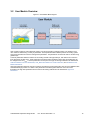
User Module Overview ........................................................................................................................................ 16
CapSense User Module Global Arrays ................................................................................................................ 17
3.3.1 Raw Count .............................................................................................................................................. 17
3.3.2 Baseline .................................................................................................................................................. 17
3.3.3 Difference Count ..................................................................................................................................... 18
3.3.4 Sensor State ........................................................................................................................................... 18
High-Level Parameters ........................................................................................................................................ 18
3.4.1 Finger Threshold..................................................................................................................................... 18
3.4.2 Hysteresis ............................................................................................................................................... 19
3.4.3 Debounce ............................................................................................................................................... 19
3.4.4 Noise Threshold...................................................................................................................................... 19
3.4.5 Baseline Update Threshold .................................................................................................................... 19
3.4.6 Negative Noise Threshold ...................................................................................................................... 20
3.4.7 Low Baseline Reset ................................................................................................................................ 20
3.4.8 Sensors Autoreset .................................................................................................................................. 20
3.4.9 High-Level Parameter Recommendations .............................................................................................. 20
CY8C20xx6A/H CapSense Design Guide
Doc. No. 001-65973 Rev. *A
3
3.5
3.6
3.7
4.
CapSense Performance Tuning with User Module ................................................................................................... 26
4.1
4.2
4.3
4.4
5.
CSD User Module Low-Level Parameters ........................................................................................................... 21
3.5.1 iDAC Value ............................................................................................................................................. 21
3.5.2 Resolution ............................................................................................................................................... 21
3.5.3 Scanning Speed ..................................................................................................................................... 22
3.5.4 Shield Electrode Out ............................................................................................................................... 22
3.5.5 Precharge Source ................................................................................................................................... 22
3.5.6 Prescaler ................................................................................................................................................ 22
3.5.7 PRS Resolution ...................................................................................................................................... 22
3.5.8 Autocalibration ........................................................................................................................................ 22
3.5.9 iDAC Range ............................................................................................................................................ 23
CSA_EMC User Module Low-Level Parameters ................................................................................................. 23
3.6.1 Settling Time ........................................................................................................................................... 24
3.6.2 Freq Num ................................................................................................................................................ 24
3.6.3 Spread Spectrum .................................................................................................................................... 24
3.6.4 Raw Data Median Filter .......................................................................................................................... 24
3.6.5 RawData IIR Filter .................................................................................................................................. 24
3.6.6 RawData IIR Filter Coefficient ................................................................................................................ 24
3.6.7 Clock....................................................................................................................................................... 24
SmartSense User Module Parameters ................................................................................................................ 25
3.7.1 Shield Electrode Out ............................................................................................................................... 25
3.7.2 Sensor Sensitivity ................................................................................................................................... 25
3.7.3 Multi-Chart for monitoring CapSense user module parameters .............................................................. 25
General Considerations ....................................................................................................................................... 26
4.1.1 Signal, Noise, and SNR .......................................................................................................................... 26
4.1.2 Charge/Discharge Rate .......................................................................................................................... 27
4.1.3 Importance of Baseline Update Threshold Verification ........................................................................... 28
Tuning the CSA_EMC User Module .................................................................................................................... 29
4.2.1 Clock and Settling Time .......................................................................................................................... 29
4.2.2 C MOD ....................................................................................................................................................... 31
Tuning the CSD User Module .............................................................................................................................. 31
4.3.1 High Level API Parameters .................................................................................................................... 35
4.3.2 Set High-Level Parameters ..................................................................................................................... 36
Using the SmartSense User Module ................................................................................................................... 36
4.4.1 Guidelines for SmartSense ..................................................................................................................... 36
4.4.2 Understanding the Difference ................................................................................................................. 36
4.4.3 SmartSense User Module Parameters ................................................................................................... 37
4.4.4 Scan Time of a CapSense Sensor.......................................................................................................... 37
4.4.5 SmartSense Response Time .................................................................................................................. 38
4.4.6 Firmware Design Guidelines ................................................................................................................... 39
Design Considerations ............................................................................................................................................... 41
5.1
5.2
Overlay Selection ................................................................................................................................................ 41
ESD Protection .................................................................................................................................................... 42
5.2.1 Prevent ................................................................................................................................................... 42
5.2.2 Redirect .................................................................................................................................................. 42
5.2.3 Clamp ..................................................................................................................................................... 42
CY8C20xx6A/H CapSense Design Guide
Doc. No. 001-65973 Rev. *A
4
5.3
5.4
5.5
5.6
5.7
6.
Design Considerations ............................................................................................................................................... 47
6.1
6.2
7.
Electromagnetic Compatibility (EMC) Considerations ......................................................................................... 42
5.3.1 Radiated Interference ............................................................................................................................. 42
5.3.2 Radiated Emissions ................................................................................................................................ 43
5.3.3 Conducted Immunity and Emissions....................................................................................................... 43
Software Filtering................................................................................................................................................. 43
Power Consumption ............................................................................................................................................ 44
5.5.1 System Design Recommendations ......................................................................................................... 44
5.5.2 Sleep-Scan Method ................................................................................................................................ 44
5.5.3 Response Time versus Power Consumption .......................................................................................... 44
5.5.4 Measuring Average Power Consumption ............................................................................................... 45
Pin Assignments .................................................................................................................................................. 45
PCB Layout Guidelines ....................................................................................................................................... 46
Additional Power Saving Techniques .................................................................................................................. 47
6.1.1 Set Drive Modes to Analog High Z.......................................................................................................... 47
6.1.2 Putting it All Together ............................................................................................................................. 48
6.1.3 Sleep Mode Complications ..................................................................................................................... 48
6.1.4 Pending Interrupts .................................................................................................................................. 48
6.1.5 Global Interrupt Enable ........................................................................................................................... 48
Post Wakeup Execution Sequence ..................................................................................................................... 48
6.2.1 PLL Mode Enabled ................................................................................................................................. 48
6.2.2 Execution of Global Interrupt Enable ...................................................................................................... 49
6.2.3 I2C Slave with Sleep Mode ..................................................................................................................... 49
6.2.4 Sleep Timer ............................................................................................................................................ 49
Resources .................................................................................................................................................................... 50
7.1
7.2
7.3
7.4
7.5
7.6
7.7
7.8
7.9
Website ............................................................................................................................................................... 50
Datasheet ............................................................................................................................................................ 50
Technical Reference Manual ............................................................................................................................... 50
Development Kits ................................................................................................................................................ 50
7.4.1 Universal CapSense Controller Kit ......................................................................................................... 50
7.4.2 Universal CapSense Module Boards ...................................................................................................... 50
7.4.3 In-Circuit Emulation (ICE) Kits ................................................................................................................ 51
PSoC Programmer .............................................................................................................................................. 51
Multi-Chart ........................................................................................................................................................... 51
PSoC Designer .................................................................................................................................................... 51
Code Examples ................................................................................................................................................... 52
Design Support .................................................................................................................................................... 52
CY8C20xx6A/H CapSense Design Guide
Doc. No. 001-65973 Rev. *A
5
1. Introduction
1.1 How to Use This Document
This document provides design guidance for the CapSense CY8C20XX6A/H family of devices. It is intended for
design engineers who are familiar with capacitive sensing technology and have chosen this specific family of devices
for their applications. For a thorough treatment of CapSense technology, including in-depth discussions of theory of
operation and complete product offering detail, refer to Getting Started with CapSense.
1.2 CY8C20xx6A/H CapSense Family Features
Cypress’s CY8C20xx6A/H is a low-power, high-performance, programmable touch sensing family of devices that
features:
CapSense Successive Approximation, Electromagnetic Compatible (CSA_EMC) and CapSense Sigma Delta
(CSD) sensing technology
SmartSense™ Auto-Tuning
Supports up to 33 capacitive buttons and 5 sliders
1.71- to 5.5-V operating voltage
Up to 33 GPIOs
Wide variety of packages: 16-pad QFN (3 × 3 × 0.6 mm) to 48-pad QFN (7 × 7 × 1.0 mm), 30-ball WLCSP
(2.2 × 2.3 × 0.4 mm), and 48-pin SSOP
I2C, full speed USB, and SPI communication interfaces
Up to 32 KB flash and 2 KB SRAM
CY8C20xx6H with Haptic (tactile) feedback
Additional peripherals:
24-MHz Internal Main Oscillator (IMO)
Three 16-bit timers
20 × 2 LCD interface
EEPROM emulation
8- to 10-bit incremental ADC
Internal voltage reference
Two comparators
CY8C20xx6A/H CapSense Design Guide
Doc. No. 001-65973 Rev. *A
6
1.3 Document Revision History
Revision
Issue Date
Origin of Change
Description of Change
**
12/14/2010
ANBA
New Design Guide
*A
3/4/2011
BVI
Multiple chapter enhancements for content and reader
clarity
1.4 Document Conventions
Convention
Usage
Courier New
Displays file locations, user entered text, and source code:
C:\ ...cd\icc\
Italics
Displays file names and reference documentation:
Read about the sourcefile.hex file in the PSoC Designer User Guide.
[Bracketed, Bold]
Displays keyboard commands in procedures:
[Enter] or [Ctrl] [C]
File > Open
Represents menu paths:
File > Open > New Project
Bold
Displays commands, menu paths, and icon names in procedures:
Click the File icon and then click Open.
Times New Roman
Displays an equation:
2+2=4
Text in gray boxes
Describes Cautions or unique functionality of the product.
CY8C20xx6A/H CapSense Design Guide
Doc. No. 001-65973 Rev. *A
7
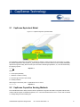
2. CapSense Technology
2.1 CapSense Equivalent Model
Figure 2-1. CapSense System Equivalent Model
The capacitance measured by the CapSense controller is named C X . When a finger is not on the sensor, C X equals
the parasitic capacitance of the system, C P. When a finger touches the sensor surface, it forms a simple parallel plate
capacitor through the overlay with the sensor pad. The result is called finger capacitance, C F , and can be defined by
the following equation.
𝐶𝐹 =
𝜀0 𝜀𝑟 𝐴
𝐷
Equation 1
Where:
ε 0 = Free space permittivity
ε r = Dielectric constant of overlay
A = Area of finger and sensor pad overlap
D = Overlay thickness
With a finger on the sensor pad, C X equals the sum of C P and C F :
𝐶𝑋 = 𝐶𝑃 + 𝐶𝐹
Equation 2
2.2 CapSense Capacitive Sensing Methods
The CY8C20xx6A/H device family measures sensor capacitance using either the CSD or CSA_EMC methods. Both
of these methods require one additional capacitor, C MOD . The recommended value for C MOD is 2.2 nF with a minimum
5-V voltage rating and X7R or NPO types.
CY8C20xx6A/H CapSense Design Guide
Doc. No. 001-65973 Rev. *A
8
Figure 2-2. C MOD Configuration
2.2.1 Capacitance Conversion
The CapSense algorithm converts the sensor capacitance into a digital count, called raw count. The raw count is
interpreted as either a TOUCH or NO TOUCH state for the sensor. The numerical value of the raw count is the digital
representation of the sensor capacitance. The sensitivity of a CapSense sensor is normally specified in units of
counts-per-pF.
Figure 2-3. Output of Sensing Algorithm
CY8C20xx6A/H CapSense Design Guide
Doc. No. 001-65973 Rev. *A
9
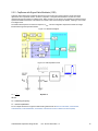
2.2.2 CapSense with Sigma Delta Modulator (CSD)
Cypress’s CSD method uses a switched-capacitor circuit on the front end of the system to convert the sensor
capacitance to an equivalent resistor, as shown in Equation 3. A Sigma-Delta modulator converts the current
measured through the resistor into a digital count. When a finger is on the sensor, the capacitance increases and the
equivalent resistance decreases. This causes an increase in the current through the resistor, resulting in an increase
in the digital count.
The CSD method requires one external component, C MOD . This is an Integration capacitor that holds the charge
transferred through the equivalent resistor.
Figure 2-4. CSD Block Diagram
Figure 2-5. CSD Equivalent Circuit
𝑅𝑒𝑞 = 𝑓
1
𝑠𝑤 ×𝐶𝑃
Equation 3
Where:
f SW = switching frequency
C P = sensor capacitance
For an in depth discussion of Cypress’s CSD sensing method refer to PSoC® CY8C20x66, CY8C20x66A,
CY8C20x46/96, CY8C20x46A/96A, CY8C20x36, CY8C20x36A Technical Reference Manual (TRM).
CY8C20xx6A/H CapSense Design Guide
Doc. No. 001-65973 Rev. *A
10
2.2.3 CapSense Successive Approximation Electromagnetic Compatible (CSA_EMC)
Cypress’s CSA_EMC method also uses a switched-capacitor circuit on the front end of the system to convert the
sensor capacitance to an equivalent resistor. An internal constant current source called the iDAC is calibrated with a
successive approximation procedure until a preset voltage develops across the equivalent resistor. This baseline
voltage is measured using a single-slope ADC. When a finger is on the sensor, the capacitance increases and the
equivalent resistance decreases. This causes the voltage across the resistor to decrease and the ADC output to
increase. This results in an increase in the digital count.
The CSA_EMC method requires one external component, C MOD . This is an Integration capacitor that is used by the
single-slope ADC.
Figure 2-6. Block Diagram of CSA_EMC
Figure 2-7. CSA_EMC Equivalent Circuit
The CSA_EMC CapSense algorithm has been enhanced to work well in the presence of RF interference. CSA_EMC
is used in applications where CapSense is exposed to conducted interference, AC noise, and other noise sources
that include inverters, transformers, and power supplies. CSA_EMC User Module Low-Level Parameters discusses
this topic in detail.
For an in-depth discussion of Cypress’s CSA_EMC sensing method, refer to PSoC® CY8C20x66, CY8C20x66A,
CY8C20x46/96, CY8C20x46A/96A, CY8C20x36, CY8C20x36A Technical Reference Manual (TRM)
CY8C20xx6A/H CapSense Design Guide
Doc. No. 001-65973 Rev. *A
11
2.2.4 SmartSense™ Auto-Tuning
Tuning the touch sensing user interface is a critical step in ensuring proper system operation and a pleasant user
experience. The typical design flow entails tuning the sensor interface in the initial design phase, during system
integration, and finally production fine-tuning before the production ramp. Tuning is an iterative process and can be
time consuming. SmartSense Auto-Tuning was developed to simplify the user interface development cycle. It is easy
to use and significantly reduces the design cycle time by eliminating the tuning process throughout the entire product
development cycle, from prototype to mass production. SmartSense tunes each CapSense sensor automatically at
power up and then monitors and maintains optimum sensor performance during run time. This technology adapts for
manufacturing variation in PCBs, overlays and noise generators such as LCD inverters, AC line noise, and switchmode power supplies, and automatically tunes them out.
2.2.4.1 Process Variation
The SmartSense User Module (UM) for the CY8C20xx6A/H is designed to work with sensor parasitic capacitance in
the range of 5 pF to 45 pF, (typical sensor C P values are in the range of 10 pF to 20 pF). The sensitivity parameter for
each sensor is set automatically, based on the characteristics of that particular sensor. This improves the yield in
mass production, because consistent response is maintained from every sensor regardless of C P variation between
sensors within the specified range of 5 to 45 pF. Parasitic capacitance of the individual sensors can vary due to PCB
layout, PCB manufacturing process variation, or with vendor-to-vendor PCB variation within a multisourced supply
chain. The sensitivity of a sensor depends on its parasitic capacitance; higher C P values will decrease the sensor
sensitivity and result in decreased finger touch signal amplitude. In some cases, the change in C P value will detune
the system, resulting in less than optimum sensor performance (either too sensitive or not sensitive enough) or worst
case, a nonoperational sensor. In either situation, you must retune the system, and in some cases requalify the UI
subsystem. SmartSense Auto-Tuning solves these issues.
SmartSense Auto-Tuning makes platform designs possible. Imagine the capacitive touch sensing multimedia keys in
a laptop computer; the spacing between the buttons depends on the size of the laptop and keyboard layout. In this
example, the wide-screen machine has larger spacing between the buttons than a standard-screen model. More
space between buttons means increased trace length between the sensor and the CapSense controller, which leads
to higher parasitic capacitance of the sensor. This means that the parasitic capacitance of the CapSense buttons can
be different in different models of the same platform design. Though the functionality of these buttons is the same for
all of the laptop models, the sensors must be tuned for each model. SmartSense enables the system designer to do
platform designs using the recommended best practices shown in section 3.7 PCB Layout in Getting Started with
CapSense, knowing the tuning will be done efficiently and automatically.
Figure 2-8. Design of Laptop Multimedia Keys for a 21-inch Model
Figure 2-9. Design of Laptop Multimedia Keys for a 15-inch model with Identical Functionality and Button Size
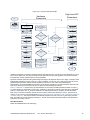
2.2.4.2 Reduced Design Cycle Time
Usually, the most time consuming task for a capacitive sensor interface design is firmware development and sensor
tuning. With a typical touch-sensing controller, the sensor must be retuned when the same design is ported to
different models or when there are changes in the mechanical dimensions of the PCB or the sensor PCB layout. A
design with SmartSense solves these challenges since it needs less firmware development effort, no tuning, and no
retuning. This makes a typical design cycle much faster. Figure 2-10 compares the design cycles of a typical touchsensing controller and a SmartSense-based design.
CY8C20xx6A/H CapSense Design Guide
Doc. No. 001-65973 Rev. *A
12
Figure 2-10. Typical Capacitive Interface Design Cycle Comparison
Typical capacitive user interface Design Cycle
Feasibility
Study
Mechanical Design
Schematics
Design
Re-tuning for any
changes
Production Fine
Tuning
PCB Layout
Design
System
Integration
Design
Validation
CY8C20xx6A/H CapSense Design Guide
Review
Firmware
Development
SmartSense based capacitive user interface Design Cycle
Feasibility
Study
Tuning process
Production
Doc. No. 001-65973 Rev. *A
Schematics
Design
PCB Layout
Design
Review
Mechanical Design
System
Integration
Design
Validation
Firmware
Development
Production
13
3. CapSense Design Tools
3.1 Overview
Cypress offers a full line of hardware and software tools for developing your CapSense capacitive touch sense
application. A basic development system for the CY8C20xx6A/H family includes the following components. See
Resources for ordering information.
3.1.1 PSoC Designer and User Modules
Cypress’s exclusive integrated design environment, PSoC Designer, allows you to configure analog and digital
blocks, develop firmware, and tune and debug your design. Applications are developed in a drag-and-drop design
environment using a library of user modules. User modules are configured either through the Device Editor GUI or by
writing into specific registers with firmware. PSoC Designer comes with a built-in C compiler and an embedded
programmer. A pro compiler is available for complex designs.
CSD, CSA_EMC, and SmartSense User Modules implement an array of capacitive touch sensors using switchedcapacitor circuitry, an analog multiplexer, a comparator, digital counting functions, and high-level software routines
(APIs). User modules for other analog and digital peripherals are available to implement additional functionality such
as I2C, SPI, TX8, Timers, and PWMs.
Figure 3-1. PSoC Designer Device Editor
CY8C20xx6A/H CapSense Design Guide
Doc. No. 001-65973 Rev. *A
14
3.1.1.1 Getting Started with CapSense User Modules
To create a new CY8C20xx6A/H project in PSoC Designer:
1.
Select and place the CSD/CSA_EMC/SmartSense User Module.
2.
Right click the user module to access the User Module Wizard.
3.
Set button sensor count, slider configuration, pin assignments, and associations.
4.
Set pins and global user module parameters.
5.
Generate the application and switch to Application Editor.
6.
Adapt sample code from the user module datasheet to implement buttons or sliders.
For a detailed step-by-step procedure for creating a PSoC Designer project and configuring the User Module Wizard,
refer to the datasheet of the specific user module.
3.1.2 Universal CapSense Controller Kit
The Universal CY3280-20xx6 CapSense Controller Kit features predefined control circuitry and plug-in hardware to
make prototyping and debugging easy. Programming and I2C-to-USB Bridge hardware are including for tuning and
data acquisition.
Figure 3-2. CY3280-20xx6 CapSense Controller Kit
3.1.3 Universal CapSense Controller Module Board
Cypress’s module boards feature a variety of sensors, LEDs, and interfaces to meet your application’s needs
CY3280-BSM Simple Button Module
CY3280-BMM Matrix Button Module
CY3280-SLM Linear Slider Module
CY3280-SRM Radial Slider Module
CY3280-BBM Universal CapSense Prototyping Module
CY8C20xx6A/H CapSense Design Guide
Doc. No. 001-65973 Rev. *A
15
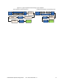
3.2 User Module Overview
Figure 3-3. User Module Block Diagram
User modules contain an entire CapSense system, from physical sensing to data processing. The behavior of the
user module is defined using a variety of parameters. These parameters affect different parts of the sensing system
and can be separated into low-level and high-level parameters. The parameters communicate with one another using
global arrays.
Low-level parameters define the behavior of the sensing method at the physical layer, and relate to the conversion
from capacitance to Raw Count. These parameters include things like the iDAC's output range and settling time for
the voltage across the C MOD . Low-level parameters are unique to each type of sensing method and are described in
CSD User Module Low-Level Parameters, CSA_EMC User Module Low-Level Parameters, and SmartSense User
Module Parameters.
High-level parameters define the way taw counts are processed to produce information such as sensor ON/OFF state
and estimated finger position on a slider. These parameters include things like debounce counts and noise
thresholds. The high-level parameters are the same for all sensing methods and are described in High-Level
Parameters.
CY8C20xx6A/H CapSense Design Guide
Doc. No. 001-65973 Rev. *A
16
3.3 CapSense User Module Global Arrays
Before studying CapSense User Module parameters, you need to know certain global arrays used by the CapSense
system to ensure proper detection and operation in spite of environmental changes. These arrays should not be
altered manually, but may be inspected for debugging purposes.
Figure 3-4. Global Parameters
3.3.1 Raw Count
The CapSense controller hardware measures the capacitance and provides the result in a digital form called Raw
Count. The value of Raw Count increases as sensor capacitance increases.
Raw count values are stored in an integer array named UMname_waSnsResult[] where UMname is CSD,
SmartSense, or CSA_EMC.
3.3.2 Baseline
The raw count values of a sensor vary gradually due to changes in the environment such as temperature and
humidity. These gradual variations are compensated for with the baseline values. The baseline keeps track of gradual
changes in raw count using a software algorithm. It is a low-pass filter that is less sensitive to sudden changes in the
raw count. The baseline values provide the reference level for computing the difference counts.
Baseline values are stored in an integer array named UMname_waSnsBaseline[] where UMname is CSD,
SmartSense, or CSA_EMC.
CY8C20xx6A/H CapSense Design Guide
Doc. No. 001-65973 Rev. *A
17
3.3.3 Difference Count
The difference count is the difference between the raw count and the baseline of the sensor. Usually, the difference
count is zero when the sensor is inactive. When the sensor is touched, it causes the raw count to increase, and
results in a positive difference count value.
Baseline values are stored in an integer array named UMname_waSnsDiff[] where UMname is CSD, SmartSense, or
CSA_EMC.
3.3.4 Sensor State
The state of each sensor is represented as 1 if the button is ON and 0 if the button is OFF.
The ON/OFF states for all of the sensors are stored in a byte array named UMname_baSnsOnMask[ ] where
UMname is CSD, SmartSense, or CSA_EMC. Each array element can hold the ON/OFF state of eight sensors.
UMname_baSnsOnMask[0] contains the masked bits for sensors 0 through 7. UMname_baSnsOnMask[1] contains
the masked bits for sensors 8 through 15. This byte array contains as many elements as are necessary to include all
of the sensors.
If any sensor is ON, the bIsAnySensorActive() function returns a 1. If all sensors are OFF, the bIsAnySensorActive()
function returns a 0.
3.4 High-Level Parameters
Figure 3-5. High Level Parameters
𝑖𝑓 𝐷𝑖𝑓𝑓𝑒𝑟𝑒𝑛𝑐𝑒 𝐶𝑜𝑢𝑛𝑡 ≥ 𝐹𝑖𝑛𝑔𝑒𝑟 𝑇ℎ𝑟𝑒𝑠ℎ𝑜𝑙𝑑 + 𝐻𝑦𝑠𝑡𝑒𝑟𝑒𝑠𝑖𝑠,
𝑖𝑓 𝐷𝑖𝑓𝑓𝑒𝑟𝑒𝑛𝑐𝑒 𝐶𝑜𝑢𝑛𝑡 ≤ 𝐹𝑖𝑛𝑔𝑒𝑟 𝑇ℎ𝑟𝑒𝑠ℎ𝑜𝑙𝑑 − 𝐻𝑦𝑠𝑡𝑒𝑟𝑒𝑠𝑖𝑠,
𝑆𝑒𝑛𝑠𝑜𝑟 𝑆𝑡𝑎𝑡𝑒 = 𝑂𝑁 𝑖𝑓 𝑆𝑎𝑚𝑝𝑙𝑒 𝐶𝑜𝑢𝑛𝑡 ≥ 𝐷𝑒𝑏𝑜𝑢𝑛𝑐𝑒
𝑆𝑒𝑛𝑠𝑜𝑟 𝑆𝑡𝑎𝑡𝑒 = 𝑂𝐹𝐹
Equation 4
Where:
Sample Count = the number of samples measured above Finger Threshold + Hysteresis
3.4.1 Finger Threshold
The finger threshold parameter defines the sensitivity of the sensor to finger touches. It is used in conjunction with the
Hysteresis parameter to determine the sensor state, as defined in Equation 4.
For individual sensors (not contained in a slider group) the Finger Threshold parameter is stored in a byte array
named. baBtnFThreshold[] that contains as many elements as are necessary to include all sensors.
CY8C20xx6A/H CapSense Design Guide
Doc. No. 001-65973 Rev. *A
18
The SetDefaultFingerThresholds() function is used to set the thresholds to the default value set in the Device Editor.
Possible values are 5 to 255.
3.4.2 Hysteresis
The Hysteresis parameter is used in conjunction with the finger threshold to determine sensor state, as defined in
Equation 4. Hysteresis adds immunity to noisy transitions. This is a debounce feature of a button. The touch state
stays off until the difference counts are a little higher than the finger threshold. The touch state stays on until the
difference counts are a little lower than the noise threshold. This prevents the touch/no touch state machine from
triggering if the difference counts are very noisy and are halfway between noise and finger thresholds.
Possible values are 0 to 255. The Hysteresis parameter setting must be lower than the Finger Threshold parameter
setting.
3.4.3 Debounce
This Debounce parameter adds a counter to the sensor transition from OFF to ON. For the sensor to transition from
OFF to ON, the difference count value must stay above the finger threshold plus hysteresis level for the number of
samples specified.
Possible values are 1 to 255. A setting of 1 provides no debouncing.
3.4.4 Noise Threshold
For individual sensors, the Noise Threshold parameter sets the upper raw count limit for updating the baseline value.
For slider sensors, it sets the lower raw count limit for counting results in the centroid calculation.
Possible values are 3 to 255. The noise threshold value should never be set to higher than Finger Threshold minus
Hysteresis value for proper operation of the user module.
Figure 3-6. Noise and Baseline Update Parameters
3.4.5 Baseline Update Threshold
When the raw count value is above the current baseline and the difference count is below the noise threshold, the
difference between the current baseline and the raw count is accumulated into a "bucket." When the bucket fills
completely, the baseline increments and the bucket is emptied. The Baseline Update Threshold parameter sets the
threshold that the bucket must reach for the baseline to increment.
Possible values are 0 to 255.
CY8C20xx6A/H CapSense Design Guide
Doc. No. 001-65973 Rev. *A
19
3.4.6 Negative Noise Threshold
The Negative Noise Threshold parameter acts as a negative difference count threshold. If the raw count is below the
baseline minus the negative noise threshold for the number of samples specified by the Low Baseline Reset
parameter, the baseline is set to the new raw count value.
Possible values are 0 to 255.
3.4.7 Low Baseline Reset
The Low Baseline Reset parameter works together with the Negative Noise Threshold parameter. It counts the
number of abnormally low samples required to reset the baseline. It is used to correct the finger-on-at-startup
condition.
Possible values are 0 to 255.
3.4.8 Sensors Autoreset
This parameter determines whether the baseline is updated at all times, or only when the difference counts are below
the noise threshold.
When Sensors Autoreset is enabled, the baseline is updated constantly. This limits the maximum time duration of the
sensor (typical values are 5 to 10 seconds), but prevents the sensors from permanently turning on when the raw
count accidentally rises without anything touching the sensor. This sudden rise can be caused by a large power
supply voltage fluctuation, a high-energy RF noise source, or a very quick temperature change.
When Sensors Autoreset is disabled, the baseline is updated only when the difference counts are below the noise
Threshold parameter.
Possible values are Enabled and Disabled.
3.4.9 High-Level Parameter Recommendations
The following recommendations are only a starting place for selecting the optimal parameter settings
Finger Threshold: Set to 75 percent of Raw Counts with sensor ON
Noise Threshold: Set to 40 percent of Raw Counts with sensor OFF
Negative Noise Threshold: Set equal to Noise Threshold
Baseline Update Threshold: Set two times Noise Threshold
Hysteresis: Set to 15 percent of Raw Counts with sensor ON
Low Baseline Reset: Set to 10
Sensors Autoreset: Based on design requirements
Debounce: Based on design requirements
CY8C20xx6A/H CapSense Design Guide
Doc. No. 001-65973 Rev. *A
20
3.5 CSD User Module Low-Level Parameters
The CSD User Module has several low-level parameters in addition to the high-level parameters. These parameters
are specific to the CSD sensing method and determine how raw count data is acquired from the sensor.
Figure 3-7. PSoC Designer - CSD Parameters WIndow
3.5.1 iDAC Value
The iDAC parameter sets the capacitance measurement range. A higher value corresponds to a wider range. Adjust
the iDAC value such that raw counts are at about 50 to 70 percent of full range. This parameter can be changed in
run time using the corresponding API function.
Possible values are 1 to 255.
3.5.2 Resolution
This parameter determines the scanning resolution in bits. The maximum raw count for scanning resolution of N bits
N–1
is 2 . Increasing the resolution improves sensitivity, but reduces scan time.
Possible values are 9 to 16 bits.
CY8C20xx6A/H CapSense Design Guide
Doc. No. 001-65973 Rev. *A
21
Table 3-1. Resolution and Scan Speed
Scan Speed (µs)
Resolution
Ultra Fast
Fast
Normal
Slow
9
57
78
125
205
10
78
125
205
380
11
125
205
380
720
12
205
380
720
1400
13
380
720
1400
2800
14
720
1400
2800
5600
15
1400
2800
5600
11000
16
2800
5600
11000
22000
3.5.3 Scanning Speed
This parameter sets sensor scanning speed. While faster scanning speed provides good response time, slower
scanning speeds provide the following advantages:
Improved SNR
Better immunity to power supply and temperature changes
Less demand for system interrupt latency; you can handle longer interrupts
Possible values are Ultra Fast, Fast, Normal, and Slow.
3.5.4 Shield Electrode Out
A shield electrode is used to reduce parasitic capacitance. This parameter selects where to route the output of the
shield electrode.
Possible values are P0[7] or P1[2].
3.5.5 Precharge Source
This parameter selects the clock source for precharge switches.
Possible values are PRS and Prescaler. Use the PRS source in most cases to get better EMI immunity and lower
emission.
3.5.6 Prescaler
This parameter sets the prescaler ratio and determines the precharge switch output frequency. This parameter also
affects the PRS output frequency.
Possible values are 1, 2, 4, 8, 16, 32, 64, 128, and 256.
3.5.7 PRS Resolution
This parameter changes the PRS sequence length.
Possible values are 8-bit and 12-bit. Corresponding sequence lengths are 511 and 2047 input clock periods. Use an
8-bit setting if 12-bit does not provide good SNR.
3.5.8 Autocalibration
When Autocalibration is enabled, the Raw Count value is normalized as a percentage of the max count (2N–1) where
N is the resolution. Autocalibration overrides the device editor settings.
When Autocalibration is disabled, the Raw Count value depends on iDAC Range, iDAC value, resolution, sensor
capacitance, IMO frequency, prescaler, precharge source, and V ref parameters set in the device editor.
CY8C20xx6A/H CapSense Design Guide
Doc. No. 001-65973 Rev. *A
22
Autocalibration consumes ROM and RAM resources and increases start time. Autocalibration does not automatically
select the iDAC Range value. If the Raw Count value after calibration is less than half of the resolution range, you
should increase the iDAC Range or reduce the precharge frequency. Autocalibration works to improve marginally
functional configurations.
3.5.9 iDAC Range
The iDAC Range parameter scales the iDAC current output. For example, selecting 2x will scale the iDAC output to
twice the range
Possible values are 1x, 2x, 4x, and 8x.
3.6 CSA_EMC User Module Low-Level Parameters
The CSA_EMC User Module has several low-level parameters in addition to the high-level parameters. These
parameters are specific to the CSA_EMC sensing method and determine how Raw Count data is acquired from the
sensor.
Figure 3-8. PSoC Designer - CSA_EMC Parameter Window
CY8C20xx6A/H CapSense Design Guide
Doc. No. 001-65973 Rev. *A
23
3.6.1 Settling Time
The Settling Time parameter controls the software delay that allows the voltage on the C MOD capacitor to stabilize.
Each loop has nine CPU cycles per iteration. Select a settling Time based on Equation 5.
𝑆𝑒𝑡𝑡𝑙𝑖𝑛𝑔 𝑇𝑖𝑚𝑒 ≥ 10 × 𝑅𝑠𝑒𝑟𝑖𝑒𝑠 × 𝐶𝑃
Equation 5
Where:
R series = 400-Ω + series resistor placed between port pin and sensor (typical value 560 Ω)
C P = sensor base capacitance
Possible values are 2 to 255.
3.6.2 Freq Num
This parameter improves EMC performance by implementing a patented EMC improvement technology.
Freq Num = 1 corresponds to the standard scanning algorithm and Freq Num = 3 turns on the advanced algorithm.
Enabling the advanced scanning algorithm increases the scanning time and RAM usage by a factor of three.
Possible values are 1 (standard scanning algorithm) and 3 (advanced algorithm).
3.6.3 Spread Spectrum
This parameter improves EMC performance by implementing a firmware-based spread-spectrum technique that
randomly changes the clock value during scanning. Spread spectrum is enabled when Freq Num is set to 1.
Possible values are 1 (enabled) and 3 (disabled).
3.6.4 Raw Data Median Filter
The median filter looks at the three most recent samples from a sensor and reports the median value. It is used to
remove short noise spikes. This filter generates a delay of one sample. This filter is generally not recommended
because of the delay and RAM usage. Enabling this filter consumes (Number of Sensors × 2 × Freq Num) bytes of
RAM and 100 bytes of Flash. It is disabled by default.
Possible values are Enabled and Disabled.
3.6.5 RawData IIR Filter
This infinite impulse response (IIR) filter reduces noise in the conversion result (raw count). Filtering on the raw
counts can be more effective than filtering the XY coordinate, but requires more RAM. Enabling this filter consumes
an additional 100 bytes of Flash. It is disabled by default. The default IIR coefficient is 0.5.
Possible values are Enabled and Disabled.
3.6.6 RawData IIR Filter Coefficient
This is the coefficient for the Raw Count IIR filter.
Possible values are 2 (½ previous sample + ½ current sample) and 4 (¾ previous sample + ¼ current sample).
3.6.7 Clock
The Clock parameter can be used to increase the amount of effective resistance of the sensor. If the sensor area is
large, the effective resistance may be too high for the autocalibration of the switched capacitor circuit. Large proximity
sensors may encounter decreased sensitivity. In this case, the settling voltage is too far below the comparator
threshold. Setting a larger divider of the internal main oscillator (IMO) increases the effective resistance,
compensating for the high capacitance.
Possible values are IMO, IMO/2, IMO/4, and IMO/8.
CY8C20xx6A/H CapSense Design Guide
Doc. No. 001-65973 Rev. *A
24
3.7 SmartSense User Module Parameters
Figure 3-9. PSoC Designer SmartSense Parameters
3.7.1 Shield Electrode Out
A shield electrode is used to reduce parasitic capacitance. This parameter selects where to route the output of the
shield electrode.
Possible values are P0[7] or P1[2].
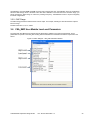
3.7.2 Sensor Sensitivity
This parameter is used to increase and decrease the sensitivity of a sensor.
Possible values are 0.1 pF, 0.2 pF, 0.3 pF, and 0.4 pF
3.7.3 Multi-Chart for monitoring CapSense user module parameters
Tuning the CapSense system requires you to monitor the CapSense User Module global arrays. Multi-chart helps to
monitor this parameter very easily. Refer to application note AN2397 for more details on the use of the multi-chart
tool.
CY8C20xx6A/H CapSense Design Guide
Doc. No. 001-65973 Rev. *A
25
4. CapSense Performance Tuning with
User Modules
Optimal user module parameter settings depend on board layout, button dimensions, overlay material, and
application requirements. These factors are discussed in Design Considerations. Tuning is the process of identifying
the optimal parameter settings for robust and reliable sensor operation.
4.1 General Considerations
4.1.1 Signal, Noise, and SNR
A well-tuned CapSense system reliably discriminates between ON and OFF sensor states. To achieve this level of
performance, the CapSense signal must be significantly larger than the CapSense noise. The measure that
compares signal to noise is the signal-to-noise Ratio (SNR). Before discussing the meaning of SNR for CapSense, it
is first necessary to define what signal and noise are in the context of touch sensing.
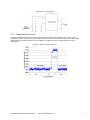
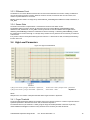
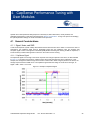
4.1.1.1 CapSense Signal
The CapSense signal is the change in the sensor response when a finger is placed on the sensor, as demonstrated
in Figure 4-1. The output of the sensor is a digital counter with a value that tracks the sensor capacitance. In this
example, the average level without a finger on the sensor is 5925 counts. When a finger is placed on the sensor, the
average output increases to 6060 counts. The CapSense signal tracks the change in counts due to the finger, so
Signal = 6060 – 5925 = 135 counts.
Figure 4-1. Example of CapSense Signal
CY8C20xx6A/H CapSense Design Guide
Doc. No. 001-65973 Rev. *A
26
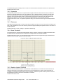
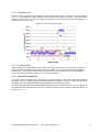
4.1.1.2 CapSense Noise
CapSense noise is the peak-to-peak variation in sensor response when a finger is not present, as demonstrated in
Figure 4-2. In this example, the output waveform without a finger is bounded by a minimum of 5912 counts and a
maximum of 5938 counts. The noise is the difference between the min and the max values of this waveform, so
Noise = 5938 – 5912 = 26 counts.
Figure 4-2. Example of CapSense Noise
4.1.1.3 CapSense SNR
CapSense SNR is the simple ratio of signal and noise. Continuing with the example, if the signal is 135 counts and
noise is 26 counts, then SNR is 135:26, which reduces to an SNR of 5.2:1. The minimum recommended SNR for
CapSense is 5:1, which means the signal is five times larger than the noise. Filters are commonly implemented in
firmware to reduce noise. Refer to Software Filtering for more information.
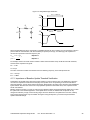
4.1.2 Charge/Discharge Rate
To achieve maximum sensitivity in the tuning process, the sensor capacitor must be fully charged and discharged
during each cycle. The charge/discharge path switches between two states at a rate set by a user module parameter
called Clock in the CSA_EMC User Module, and Precharge Clock in the CSD User Module.
The charge/discharge path includes series resistance that slows down the transfer of charge. The rate of change for
this charge transfer is characterized by an RC time constant involving the sensor capacitor and series resistance, as
shown in Figure 4-3.
CY8C20xx6A/H CapSense Design Guide
Doc. No. 001-65973 Rev. *A
27
Figure 4-3. Charge/Discharge Waveforms
Vs
Tsmin >= 10*Rx*Cx
Vdd
Vx
Rx
Vref
Vs
Vx
Cx
5*Rx*Cx
5*Rx*Cx
t
Vdd
Vref
t
Set the charge/discharge rate to a level that is compatible with this RC time constant. The rule of thumb is to allow a
period of 5RC for each transition, with two transitions per period (one charge, one discharge).The equations for
minimum time period and maximum frequency are:
𝑇𝑠𝑚𝑖𝑛 = 10 × 𝑅𝑋 𝐶𝑋
𝑓𝑠𝑚𝑎𝑥 =
1
10×𝑅𝑋 𝐶𝑋
Equation 6
Equation 7
For example, assume the series resistor includes a 560-Ω external resistor and up to 800 Ω of internal resistance,
and the sensor capacitance is typical:
R X = 1.4 kΩ
C X = 24 pF
The value of the time constant and maximum front-end switching frequency in this example would be:
Ts min = 0.34 µs
fs max = 3 MHz
4.1.3 Importance of Baseline Update Threshold Verification
Temperature and humidity both cause the average number of counts to drift over time. The baseline is a reference
count level for CapSense measurements that plays an important role in compensating for environmental effects.
High-level decisions, such as Finger Present and Finger Absent states, are based on the reference level established
by the baseline. Because each sensor has unique parasitic capacitance associated with it, each capacitive sensor
has its own baseline.
Baseline tracks the change in counts at a rate set by the Baseline Update Threshold parameter. Make sure to match
the update rate to the intended application. If the update rate is too fast, the baseline will compensate for any
changes introduced by a finger, and the moving finger will not be detected. If the update rate is too slow, relatively
slow environmental changes may be mistaken for fingers. During development, you should verify the Baseline
Update Threshold settings.
CY8C20xx6A/H CapSense Design Guide
Doc. No. 001-65973 Rev. *A
28
4.2 Tuning the CSA_EMC User Module
Manual selection of iDAC settings is not required for the CSA_EMC User Module; they are adjusted automatically.
However, monitoring the iDAC settings can be useful for debugging or statistical process control.
4.2.1 Clock and Settling Time
The first step in tuning CSA_EMC User Module is to determine the settings for the clock and settling time. Figure 4-4
outlines the steps required to set these parameters.
Figure 4-4. Determining CSA_EMC Clock and Settling Times
Begin
Initial Settings
CMOD = 1 nF
Clock = IMO/8
Reduce CP or Clock
Measure iDAC Gain,
iDACGAIN MEASURED
Read SAcode
No
SAcode ≤ 255 * (280/iDACGAIN MEASURED)
Yes
Decrease CPU
Frequency
Estimate CP
Estimate Settling Time,
tsettling,min
tsettling,min / (25 * tcpu_clk) ≤ 255
No
Yes
End
CY8C20xx6A/H CapSense Design Guide
Doc. No. 001-65973 Rev. *A
29
4.2.1.1 Measure iDAC Gain
After following the steps to create a new PSoC Designer Project, use the following code snippet to route iDAC to port
pin P1[0]:
//configure P1[0] to HI-Z
PRT1DM0 &= ~0x01;
PRT1DM1 |= 0x01;
//connect P1[0] to analog mux bus
MUX_CR1 |= 0x01;
// set iDAC to full scale
IDAC_D = 0xFF;
// turn iDAC on, 4x range
CS_CR2 = 0x90;
Place a current meter between pin P1[0] and ground, and measure current, I MEASURED . Calculate the iDAC gain using
Equation 8.
𝐼𝑀𝐸𝐴𝑆𝑈𝑅𝐸𝐷
𝐼𝐷𝐴𝐶𝐺𝐴𝐼𝑁 𝑀𝐸𝐴𝑆𝑈𝑅𝐸𝐷 =
1020
Equation 8
4.2.1.2 Read SA Code
iDAC code found in the successive approximation is termed as SA code. SA codes computed by CSA_EMC
algorithm for each sensor can be read from array CSA_EMCbaDACCodeBaseline.
4.2.1.3 Estimate C P
C P can be estimated by using an LCR meter or by applying the following equations.
𝑓𝑆𝑊 =
𝐶𝑃 =
𝐼𝑀𝑂
Equation 9
𝐶𝑆𝐴_𝐸𝑀𝐶 𝐶𝐿𝑂𝐶𝐾
4×𝑆𝐴𝐶𝑂𝐷𝐸 ×𝐼𝐷𝐴𝐶𝐺𝐴𝐼𝑁 𝑀𝐸𝐴𝑆𝑈𝑅𝐸𝐷
Where:
𝑉𝑟𝑒𝑓 ×𝑓𝑆𝑊
Equation 10
V ref = 1.2 V
4.2.1.4 Estimate Settling Time
The minimum Settling Time is estimated using Equation 11.
𝑡𝑠𝑒𝑡𝑡𝑙𝑖𝑛𝑔,𝑚𝑖𝑛 =
Where:
5×𝐶𝑀𝑂𝐷 ×𝑉𝑟𝑒𝑓
4×𝑆𝐴𝐶𝑂𝐷𝐸 ×𝐼𝐷𝐴𝐶𝐺𝐴𝐼𝑁 𝑀𝐸𝐴𝑆𝑈𝑅𝐸𝐷
Equation 11
V ref = 1.2 V
CY8C20xx6A/H CapSense Design Guide
Doc. No. 001-65973 Rev. *A
30
4.2.2 C MOD
After the Clock and Settling Time are set, select the C MOD value. Figure 4-5 outlines the steps for this part of the
tuning process. If you need to adjust the C MOD value, clock and settling time must be retuned, as described in
Figure 4-4.
Figure 4-5. Determining CSA_EMC C MOD Value
Begin
Initial Setting
CMOD = 1 nF
No
SNR > 5
Increase CMOD
No
Reduce Noise with Filter
Yes
End
Re-tune
Clock and
Settling Time
4.3 Tuning the CSD User Module
Figure 4-6 is a flowchart showing the tuning process for CSD UM parameters. CSD UM parameters can be separated
into two broad categories, hardware parameters and high-level API parameters. The parameters in these categories
affect the behavior of the capacitive sensing system in different ways and are therefore treated separately in this
section. There is, however, a complementary relationship between the sensitivity of each sensor as determined by
the hardware parameter settings and many of the high-level API parameter settings. Be mindful of this fact when any
hardware parameter is changed to ensure that the corresponding high-level API parameters are adjusted accordingly.
Tuning CSD User Module parameters should always begin with the hardware parameters.
CY8C20xx6A/H CapSense Design Guide
Doc. No. 001-65973 Rev. *A
31
Figure 4-6. Tuning the CSD User Module
Start
Set Shield
Electrode Out
according to needs
of design
High-Level API
Parameters
Hardware
Parameters
Measure Cp of sensors
using EP64134
If max Cp < 45pF set Idac
Range to 4X. Otherwise
set to 8X.
Enable Autocalibration
Set Precharge Source to
PRS
Set Prescaler according to
Table 4-1
Set Resolution according
to Figure 4-7 and
Table 4-2
Set Noise Threshold to
40% of signal
No
Yes
Is SNR from all sensors
> 5:1?
Yes
Does scan time meet
design requirements?
No
Set Hysteresis to 15%
of signal
No
Is SNR from all sensors
> 5:1?
Set BaselineUpdate
Threshold to double
the Noise Threshold
Set Sensors Autoreset
according to needs of
design
Increase Resolution and/or
experiment with Scanning
Speed until optimal SNR is
obtained
Set Scanning Speed to
Fast
Set PRS Resolution to 12
bits if scan time > 380 µs
according to Table 4-3.
Otherwise set to 8 bits.
Set Finger Threshold to
75% of signal
Revise PCB design
according to AN2292 and
AN2318
Set Debounce
according to needs of
design
Yes
Reduce Resolution or
used faster Scanning
Establish digital
communication interface and
obtain raw counts from each
sensor during finger
activation cycle, for example.
Figure 4-8
Speed
Set Negative Noise
Threshold to same
value as Noise
Threshold
Set Low Baseline
Reset to 10
Start
Hardware parameters configure the hardware that the CSD method uses to convert the physical capacitance of each
sensor into a digital code. This section describes these parameters and provides guidance on how each should be
tuned based on system characteristics and other parameters.
By default, hardware parameters are global settings that apply to all CapSense sensors in a design. In designs where
total parasitic capacitance of each sensor (C P ), sensor sensitivity, or both vary over a wide range, there may not be
global hardware parameter settings that are suitable for all sensors. In such cases, the SetIdacValue(i),
SetPrescaler(i), and SetScanMode(i) API functions can be used to configure the respective hardware parameters for
each sensor where (i) is the sensor index prior to calling the ScanSensor(i) API function.
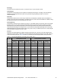
Table 4-1 and Table 4-3 provide tuning recommendations for several key hardware parameters based on sensor C P .
C P values depend on characteristics of the PSoC, PCB layout, and proximity of other components in the assembled
product. That being the case, C P must be measured in its original position with the system in its final assembled
state; that is, in the same enclosure and with the same overlay as the system will have in service. The best way to
measure C P is to use the code example titled Measuring Absolute Sensor Capacitance with a CY8C20xx6 CapSense
Controller (EP64134). This project measures the absolute capacitance of each sensor in a system using the PSoC
itself, thus taking into account all factors affecting C P . See the documentation associated with the code example for
instructions on its setup and use
ShieldElectrodeOut
Enable the ShieldEletrodeout for this design.
CY8C20xx6A/H CapSense Design Guide
Doc. No. 001-65973 Rev. *A
32
Idac Range
For projects where the maximum sensor C P is less than 45 pF, use 4X; otherwise, use 8X.
Autocalibration
Autocalibration should always be set to Enabled in CY8C20xx6A CSD designs. The ability of the autocalibration
algorithm to successfully set the iDAC relies on the prescaler being set properly and that C MOD be of the
recommended size.
iDAC Value
This parameter determines the current output of iDAC when autocalibration is disabled. When autocalibration is
enabled, as recommended, this parameter is overridden and has no effect. When autocalibration is disabled, raising
this parameter lowers the raw count baseline and vice versa.
Precharge Source
This parameter selects the sensor switching clock source. The available options are Prescaler, which uses the IMO
through a divider, or PRS, which passes the divided IMO clock through a pseudo random generator, providing a
spread-spectrum clock. PRS provides superior noise immunity and lower noise emissions and is therefore the
recommend default setting for Precharge Source. In some instances, the prescaler precharge source can provide
higher SNR (signal-to-noise ratio). However, when using copper circuitry, this SNR improvement is usually marginal
and rarely justifies foregoing the benefits of PRS.
Prescaler
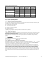
Prescaler is the divider applied to the IMO to develop the precharge clock. This is the most critical hardware UM
parameter for properly tuning a CSD design. Prescaler depends on the selected precharge source, IMO, and the C P
of the sensors being scanned. Table 4-1 provides recommended prescaler settings based on these parameters.
Table 4-1. Prescaler Setting Based on Precharge Source, IMO, and C P
C P (pF)
Precharge Source = PRS
Precharge Source = Prescaler
Prescaler
Prescaler
Prescaler
Prescaler
Prescaler
Prescaler
IMO = 24 MHz
IMO = 12 MHz
IMO = 6 MHz
IMO = 24 MHz
IMO = 12 MHz
IMO = 6 MHz
<6
1
Note 1
Note 1
2
1
1
7–11
2
1
Note 1
4
2
1
12–15
2
1
Note 1
4
2
1
16–19
4
2
1
8
4
2
20–22
4
2
1
8
4
2
23–26
4
2
1
8
4
2
27–30
4
2
1
8
4
2
31–34
4
2
1
8
4
2
35–37
8
4
2
16
8
4
38–41
8
4
2
16
8
4
42–45
8
4
2
16
8
4
46–49
8
4
2
16
8
4
50–52
8
4
2
16
8
4
53–56
8
4
2
16
8
4
57–60
8
4
2
16
8
4
Note 1 This combination of Precharge Source, Prescaler, and C P is not recommended.
CY8C20xx6A/H CapSense Design Guide
Doc. No. 001-65973 Rev. *A
33
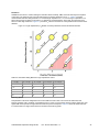
Resolution
Available choices are 9 to 16 bits. Raising the resolution raises sensitivity, SNR, and noise immunity at the expense
of scan time. The maximum raw count (full scale range) for scanning resolution n is 2n – 1. Table 4-2 provides
recommended resolution settings based on C P and the finger capacitance C F . C F is the change in capacitance of a
sensor when a finger is placed on the sensor. C F depends on overlay thickness, sensor size, and proximity of the
sensor to other large conductors. Figure 4-7 provides C F values as a function of overlay thickness and circular sensor
diameter.
Figure 4-7. Finger Capacitance (C F ) Based on Overlay Thickness and Circular Sensor Diameter
Table 4-2. Resolution Setting Based on Finger Capacitance and C P
C P (pF)
C F = 0.1 pF
C F = 0.2 pF
C F = 0. 4pF
C F = 0.8 pF
<6
12
11
10
9
7–12
13
12
11
10
13–24
14
13
12
11
25–48
15
14
13
12
>49
16
15
14
13
Scanning Speed
This parameter controls the integration time for each LSB of the scan result. The choices are Ultra Fast, Fast,
Normal, and Slow. Fast is generally a good starting point. In some, but not all cases, slower scanning speed can yield
higher SNR at the expense of longer scan time and more power consumption. Table 4-3 shows the actual scan time
in microseconds for a single sensor based on resolution and scanning speed.
CY8C20xx6A/H CapSense Design Guide
Doc. No. 001-65973 Rev. *A
34
Table 4-3. Scan Time for a Single Sensor in цs Based on Resolution and Scanning Speed
Scanning Speed
Resolution
(bits)
Ultra Fast
Fast
Normal
Slow
9
57
78
125
205
10
78
125
205
380
11
125
205
380
720
12
205
380
720
1400
13
380
720
1400
2800
14
720
1400
2800
5600
15
1400
2800
5600
11000
16
2800
5600
11000
22000
4.3.1 High-Level API Parameters
High-level API parameters determine the behavior of high-level firmware algorithms that discriminate between sensor
activations and noise, and compensate for signal drift caused by environmental conditions. In order to determine
proper values for these parameters, you must establish a digital communication interface with the system to monitor
raw counts, baseline, and difference counts during a finger activation event for each sensor. This data is stored in
arrays named CSD_waSnsBaseline[], CSD_waSnsResult[], and CSD_waSnsDiff[], respectively. The high-level API
parameter settings are based primarily on ambient noise and finger signal strength, as indicated by this data. Noise
and signal strength depend on EMI environment, PCB layout, overlay thickness, and other physical characteristics of
the system. Therefore, the data used as the basis for setting these parameters must be taken in its original position
with the system in its final assembled state and in the same EMI environment as will exist in use.
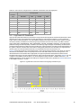
Figure 4-8 shows the typical raw counts obtained from a sensor during a finger activation cycle; that is, the sensor is
activated then deactivated. Labels are superimposed over the data that indicate how noise and signal are to be
calculated based on the raw data. Where appropriate, the high-level parameter descriptions that follow include
information about how to set each parameter based on these noise and signal values. According to AN2403, the ratio
of signal to noise (SNR) must be at least 5:1 for robust CapSense system operation. If SNR is less than 5:1, the
hardware parameters must be adjusted, the PCB layout changed according to the guidelines of AN2292 and AN2318
to raise SNR to at least 5:1, or both.
Figure 4-8. Typical Raw Counts from a Sensor During Finger Activation Cycle
Signal
Noise
CY8C20xx6A/H CapSense Design Guide
Doc. No. 001-65973 Rev. *A
35
4.3.2 Set High-Level Parameters
The following recommendations are a starting place for selecting the optimal parameter settings:
Finger Threshold: Set to 75 percent of Raw Counts with sensor ON
Noise Threshold: Set to 40 percent of Raw Counts with sensor OFF
Negative Noise Threshold: Set equal to (Noise Threshold/2)
Baseline Update Threshold: Set to two times Noise Threshold
Hysteresis: Set to 15 percent of Raw Counts with sensor ON
Low Baseline Reset: Set to 50
Sensors Autoreset: Based on design requirements
Debounce: Based on design requirements
4.4 Using the SmartSense User Module
SmartSense enables you to create a CapSense design that requires no tuning, as long as the sensor parasitic
capacitance is in the range from 5 pF to 45 pF with a minimum 0.1-pF finger touch. You can create a SmartSense
design by using the SmartSense User Module in PSoC Designer 5.1. This section also shows you how to migrate an
existing CSD CapSense design to SmartSense.
4.4.1 Guidelines for SmartSense
Follow these guidelines when using the SmartSense User Module in an application:
SmartSense requires capacitive user interface design to follow the layout and system design best practices
documented in the previous sections of this design guide.
All of the CSD User Module parameters (such as iDAC value, prescaler period, clock divider, scan speed,
resolution) are determined at run time by the SmartSense User Module. You should not use APIs that modify
these CSD parameters in firmware, unless you know exactly what effect it has in your design.
To migrate an existing design from CSD to SmartSense,
Ensure that all APIs that set or modify the CSD parameters are first removed from the program.
Ensure that the parasitic capacitance of all CapSense sensors in the design is between 5 pF and 45p F over
environmental and PCB production process variations.
Make sure recommended C MOD capacitor (X7R, 2.2-nF, voltage rating more than 5 V) is connected to the
C MOD port pin selected in the user module wizard.
4.4.2 Understanding the Difference
The differences between the SmartSense User Module and the standard CSD User Module are:
The SmartSense User Module supports APIs that a standard CSD User Module supports. Thus, no change is
required in placing, configuring, starting, or calling other APIs except the User Module instance name.
There is no need to set any User Module parameters for tuning, as all the parameters related to tuning are
automatically set at run time by the SmartSense User Module.
The C MOD capacitor value is restricted to 2.2 nF. Use of an X7R capacitor with a voltage rating higher than 5 V is
recommended in all CapSense applications.
The SmartSense algorithm maintains the signal SNR of each sensor between 5:1 and 11:1 to ensure robust
CapSense operation while maximizing performance.
The scanning time of the SmartSense User Module is restricted by the algorithm to be between 410 µs and
2.8 ms per sensor in 24-MHz operating mode, based on the parasitic capacitance of the sensor.
CY8C20xx6A/H CapSense Design Guide
Doc. No. 001-65973 Rev. *A
36
4.4.3 SmartSense User Module Parameters
Only four parameters must be set for this user module. These are:
Sensors Autoreset
Debounce
Modulator Capacitor Pin
Shield Electrode Out
4.4.3.1 Sensors Autoreset
This parameter determines whether the baseline is updated at all times or only when the signal difference is below
the noise threshold. When set to Enabled the baseline is updated constantly. This setting limits the maximum time
that a sensor may remain on (typically it is 5 to 10 seconds), but it prevents the sensors from permanently turning on
when the raw count suddenly rises without anything touching the sensor due to any failure condition of the system.
4.4.3.2 Debounce
The Debounce parameter adds a debounce counter to the sensor’s active transition. For the sensor to be declared as
active from inactive state, a finger touch signal should be present on the sensor for debounce number of consecutive
scans. This parameter affects all the sensors similarly.
4.4.3.3 Modulator Capacitor Pin
This parameter selects the pin to which the 2.2 nF/X7R/voltage rating more than 5 V C MOD capacitor is connected.
The available pins are P0[1] and P0[3].
Note An external 2.2-nF capacitor is mandatory for the SmartSense to work correctly.
4.4.4 Scan Time of a CapSense Sensor
To maintain the consistent finger response sensitivity over a wide range of parasitic capacitance, the SmartSense
User Module automatically determines the hardware parameters of the user module. As a result of this, sensor scan
time does not remain constant. For a design in mass production, it could vary based on the parasitic capacitance
variation of the PCB.
The total scan time of a sensor is decided by four factors. They are parasitic capacitance of sensor, IMO frequency,
CPU operating frequency, and sensitivity level of the SmartSense User Module.
Scan time of a sensor can be found using Equation 12 and the following tables.
Equation 12
𝑆𝑐𝑎𝑛 𝑡𝑖𝑚𝑒 = 𝑆𝑎𝑚𝑝𝑙𝑖𝑛𝑔 𝑡𝑖𝑚𝑒 (𝑆𝑇) + 𝑃𝑟𝑜𝑐𝑒𝑠𝑠𝑖𝑛𝑔 𝑡𝑖𝑚𝑒 (𝑃𝑇)
The following tables show the sampling time value with various IMO and sensitivity levels.
Table 4-4. Sampling Time for a Sensor with IMO = 24 MHz
Sensitivity = 0.2 pF
C P (pF)
ST (µs)
Sensitivity = 0.3 pF
C P (pF)
ST (µs)
Sensitivity = 0.4 pF
C P (pF)
ST (µs)
8 to 10
340
8 to 17
340
8 to 10
170
10 to 23
680
17 to 35
680
10 to 23
340
23 to 41
1360
35 to 41
1360
23 to 41
680
41 to 45
2730
41 to 45
2730
41 to 45
1360
CY8C20xx6A/H CapSense Design Guide
Doc. No. 001-65973 Rev. *A
37
Table 4-5. Sampling Time for a Sensor with IMO = 12 MHz
Sensitivity = 0.2 pF
C P (pF)
ST (µs)
Sensitivity = 0.3 pF
C P (pF)
Sensitivity = 0.4 pF
ST(µs)
C P (pF)
ST (µs)
8 to 10
680
8 to 17
680
8 to 10
340
10 to 23
1360
17 to 35
1360
10 to 23
680
23 to 41
2730
35 to 41
2730
23 to 41
1360
41 to 45
5460
41 to 45
5460
41 to 45
2730
Table 4-6. Sampling Time for a Sensor with IMO = 6 MHz
Sensitivity = 0.2 pF
C P (pF)
ST (µs)
Sensitivity = 0.3 pF
C P (pF)
Sensitivity = 0.4 pF
ST(µs)
C P (pF)
ST (µs)
8 to 11
680
8 to 10
680
8 to 11
680
11 to 23
1360
10 to 17
1360
11 to 23
1360
23 to 42
2730
17 to 35
2730
23 to 41
2730
42 to 45
5460
35 to 41
5460
41 to 45
5460
41 to 45
10920
Table 4-7 shows the value for processing time with various CPU frequencies.
Table 4-7. Processing Time for a Sensor
CPU CLK
Processing Time (PT) in µs
24
71
12
142
6
284
3
568
For example, if a CapSense system is designed with 24-MHz IMO frequency, 6-MHz CPU clock (IMO/4), and
SmartSense sensitivity level of 0.3 pF, the scan time of the sensor that has parasitic capacitance ~15 pF can be
determined from the previous tables using Equation 12.
Sampling time for the above-mentioned configuration (24 MHz of IMO, 0.3 pF of sensitivity) is chosen from Table 4-4;
it is 680 µs. Processing time for the above-mentioned configuration (CPU clock of 6 MHz) Is chosen from Table 4-7; it
is 284 µs.
Thus, the total scan time in this configuration is 680 + 284 = 964 µs. Scan time for more than one sensor is the sum
of the scan time of each sensor
4.4.5 SmartSense Response Time
Consider the following application with standard CSD along with typical CapSense scanning firmware.
Three CapSense sensors with parasitic capacitance of sensor between 5 pF and 10 pF
IMO of 12 MHz and CPU clock of 12 MHz
Sensor sensitivity level of 0.4 pF
Debounce = 3
According to the above tables, scanning of each sensor requires 482 µs and three sensors have a scan time of
1.45 ms. The following firmware example requires 1 ms for additional firmware execution; thus, the loop execution
time would be 2.45 ms.
while (1)
{
CY8C20xx6A/H CapSense Design Guide
Doc. No. 001-65973 Rev. *A
38
SmartSense_ScanAllSensors();
SmartSense _UpdateAllBaselines();
}
if(SmartSense _bIsAnySensorActive() )
{
//1mS firmware routines
}
This means that, upon the activation of a CapSense sensor, firmware produces the sensor ON status within 7.35 ms
(the sensor should be active for Debounce number of consecutive scans). This is often referred to as the response
time of CapSense system.
If the scan time varies with respect to the parasitic capacitance to maintain consistent , what is the impact on
response time if the parasitic capacitance of the sensor changes due the process variation? Response time may be
increased (slow response) in this case. This can have a negative impact on sensor performance. Guidelines to build
a robust firmware design are provided below.
4.4.6 Firmware Design Guidelines
The response time of the CapSense sensors may change due to the increased parasitic capacitance of the sensor. IT
is also important to watch the loop execution time (see the following example code), which may also increase. When
the parasitic capacitance of all sensors was less than 10 pF, the firmware routine was executed at a rate of 2.45 ms.
This rate will be modified if the sensor scan time is increased because of the increase in the parasitic capacitance of
the sensor based on the process variation.
The following is example code for toggling a port pin based on the main loop execution time.
while (1)
{
SmartSense_ScanAllSensors();
SmartSense_UpdateAllBaselines();
if(SmartSense_bIsAnySensorActive() )
{
//1 ms firmware routines
}
}
PRT0DR_Shadow ^= 0x01;
PRT0DR = PRT0DR_Shadow;
The period of the signal on Port_0[1] pin is 4.9 ms (the period is twice the loop time as the port pin is toggled). If the
parasitic capacitance of one sensor is increased to approximately 15 pF, the scan time will change to 1.78 ms; thus,
the period of signal on the Port_0[1] will be 5.6 ms.
If the parasitic capacitance of the sensor is close to the boundary of the SmartSense capacitance banks (for example,
9 pF, which is very close to the 10-pF boundary), SmartSense may choose a neighboring scan time in an application
due to process variation. Because of this, different production parts of the same design can have two different main
loop execution times and response times.
Based on the above discussions, firmware should not rely on the scan time of the sensor for implementing other
features (for example, software PWM, software delay, and so on). Programs implementing watch dog timer (WDT)
should consider this fact while setting the WDT expiration time
A simple firmware implementation example to get a consistent main loop execution time using Timer16 User Module
follows.
// Main program
BYTE bTimerTicks = 0;
#pragma interrupt_handler myTimer_ISR_Handler;
void myTimer_ISR_Handler( void );
void main()
{
M8C_EnableGInt;
CY8C20xx6A/H CapSense Design Guide
Doc. No. 001-65973 Rev. *A
39
SmartSense_Start();
SmartSense_ScanAllSensors();
SmartSense_SetDefaultFingerThresholds() ;
Timer16_EnableInt();
Timer16_SetPeriod (TIMEOUT_10MS) ;
Timer16_Start();
while( 1 )
{
/* Scan all 3 sensors and update
Baseline */
SmartSense_ScanAllSensors();
SmartSense_UpdateAllBaselines();
/* Wait till timer expires or
sleep here */
while (bTimerTicks != 1) ;
bTimerTicks = 0 ;
if(CSDAUTO_bIsAnySensorActive() )
{
//1 ms firmware routines
}
}
}
// Toggle Port_0[1]
PRT0DR_Shadow ^= 0x01 ;
PRT0DR = PRT0DR_Shadow ;
// Timer16 ISR program
void myTimer_ISR_Handler(void)
{
bTimerTicks++;
}
In the previous example, the program waits for the Timer to expire even if the sensor scanning is complete. The
period of the Timer should be chosen based on the worst case main loop execution time. This is the sum of the worst
case scan times of the individual CapSense sensors. If the parasitic capacitance of the sensor is close to the
boundary of the SmartSense capacitance bank, chose higher scan time (using Table 4-5 on page 38) for the
calculation.
The SmartSense User Module enables you to easily implement the capacitive touch sensing user interface into a
system. It removes the difficulties of the tuning process and also helps to increase the yield in production against
manufacturing process variations of the PCB, and other variations. Therefore, the preferred option is to migrate the
existing CSD-based CapSense designs to SmartSense and to use SmartSense for new designs.
The main loop execution time and scan time of SmartSense vary based on the process variations. Though it does not
affect the performance of CapSense in any way, the firmware developer should consider this when implementing
CapSense PLUS applications with SmartSense Auto-Tuning technology.
CY8C20xx6A/H CapSense Design Guide
Doc. No. 001-65973 Rev. *A
40
5. Design Considerations
When designing capacitive touch sense technology into your application, it is crucial to keep in mind that the
CapSense device exists within a larger framework. Careful attention to every level of detail from PCB layout to user
interface to end-use operating environment will lead to robust and reliable system performance. For more in-depth
information, refer Getting Started with CapSense.
5.1 Overlay Selection
In CapSense Equivalent Model, Equation 1 was presented for finger capacitance
𝜀0 𝜀𝑟 𝐴
𝐷
Where:
ε 0 = Free space permittivity
ε r = Dielectric constant of overlay
A = Area of finger and sensor pad overlap
D = Overlay thickness
𝐶𝐹 =
To increase the CapSense signal strength, choose an overlay material with a higher dielectric constant, decrease the
overlay thickness, and increase the button diameter.
Table 5-1. Overlay Material Dielectric Strength
Material
Breakdown Voltage (V/mm)
Min. Overlay Thickness at 12 kV (mm)
1200–2800
10
Air
Wood – dry
3900
3
Glass – common
7900
1.5
13,000
0.9
PMMA Plastic (Plexiglas )
13,000
0.9
ABS
16,000
0.8
Polycarbonate (Lexan )
16,000
0.8
Formica
18,000
0.7
FR-4
28,000
0.4
280,000
0.04
290,000
0.04
®)
Glass – Borosilicate (Pyrex )
®
®
®
PET Film – (Mylar )
®
Polymide film – (Kapton )
Conductive material cannot be used as an overlay because it interferes with the electric field pattern. For this reason,
do not use paints containing metal particles in the overlay.
An adhesive is typically used to bond the overlay to the CapSense PCB. A transparent acrylic adhesive film from
3M™ called 200MP is qualified for use in CapSense applications. This special adhesive is dispensed from paperbacked tape rolls (3M™ product numbers 467MP and 468MP).
CY8C20xx6A/H CapSense Design Guide
Doc. No. 001-65973 Rev. *A
41
5.2 ESD Protection
Robust ESD tolerance is a natural by-product of thoughtful system design. By considering how contact discharge will
occur in your end product, particularly in your user interface, it is possible to withstand an 18-kV discharge event
without incurring any damage to the CapSense controller.
CapSense controller pins can withstand a direct 2-kV event. In most cases, the overlay material provides sufficient
ESD protection for the controller pins. Table 5-1 lists the thickness of various overlay materials required to protect the
CapSense sensors from a 12-kV discharge, as specified in IEC 61000-4-2. If the overlay material does not provide
sufficient protection, ESD countermeasures should be applied in the following order: Prevent, Redirect, Clamp.
5.2.1 Prevent
Ensure all paths on the touch surface have a breakdown voltage greater than potential high-voltage contacts. Also,
design your system to maintain an appropriate distance between the CapSense controller and possible sources of
ESD. If it is not possible to maintain adequate distance, place a protective layer of a high breakdown voltage material
®
between the ESD source and CapSense controller. One layer of 5-mil-thick Kapton tape will withstand 18 kV.
5.2.2 Redirect
If your product is densely packed, it may not be possible to prevent the discharge event. In this case, you can protect
the CapSense controller by controlling where the discharge occurs. A standard practice is to place a guard ring on
the perimeter of the circuit board that is connected to chassis ground. As recommended in PCB Layout Guidelines,
providing a hatched ground plane around the button or slider sensor can redirect the ESD event away from the
sensor and CapSense controller.
5.2.3 Clamp
Because CapSense sensors are purposely placed in close proximity to the touch surface, it may not be practical to
redirect the discharge path. In this case, including series resistors or special purpose ESD protection devices may be
appropriate.
The recommended series resistance value is 560 Ω.
A more effective method is to provide special-purpose ESD protection devices on the vulnerable traces. ESD
protection devices for CapSense need to be low capacitance. Table 5-2 lists devices recommended for use with
CapSense controllers.
Table 5-2. Low-Capacitance ESD Protection Devices Recommended for CapSense
ESD Protection device
Manufacturer
Part Number
Input
Capacitance
Contact
Discharge
maximum limit
Leakage
Current
Air Discharge
maximum limit
Littlefuse
SP723
5 pF
2 nA
8 kV
15 kV
Vishay
VBUS05L1-DD1
0.3 pF
0.1 µA <
±15 kV
±16 kV
NXP
NUP1301
0.75 pF
30 nA
8 kV
15 kV
5.3 Electromagnetic Compatibility (EMC) Considerations
5.3.1 Radiated Interference
Radiated electrical energy can influence system measurements and potentially influence the operation of the
processor core. The interference enters the PSoC® chip at the PCB level, through CapSense sensor traces and any
other digital or analog inputs. Layout guidelines for minimizing the effects of RF interference include:
Ground Plane: Provides a ground plane on the PCB.
Series Resistor: Series resistors should be placed within 10 mm of the CapSense controller pins.
The recommended series resistance for CapSense input lines is 560 Ω.
The recommended series resistance for communication lines such as I C, and SPI is 330 Ω.
2
Trace Length: Minimizes trace length whenever possible.
CY8C20xx6A/H CapSense Design Guide
Doc. No. 001-65973 Rev. *A
42
Current Loop Area: Minimizes the return path for current. Hatched ground instead of solid fill should be
provided within 1 cm of the sensors and traces to reduce the impact of parasitic capacitance.
RF Source Location: Partition systems with noise sources such as LCD inverters and switched-mode power
supplies (SMPS) to keep them separated from CapSense inputs. Shielding the power supply is another common
technique for preventing interference.
5.3.2 Radiated Emissions
Selecting a low frequency for the switched capacitor clock will help to reduce radiated emissions from the CapSense
sensor. This clock is controlled in firmware using the Prescaler option. Increasing the Prescaler value decreases the
frequency of the switching clock
5.3.3 Conducted Immunity and Emissions
Noise entering a system through interconnections with other systems is referred to as conducted noise. These
interconnections include power and communication lines. Because CapSense controllers are low-power devices,
conducted emissions must be avoided. The following guidelines will help reduce conducted emission and immunity:
Use decoupling capacitors as recommended by the datasheet.
Add a bidirectional filter on the input to the system power supply. This is effective for both conducted emissions
and immunity. A pi-filter can prevent power supply noise from effecting sensitive parts, while also preventing the
switching noise of the part from coupling back onto the power planes.
If the CapSense controller PCB is connected to the power supply by a cable, minimize the cable length and
consider using a shielded cable.
Place a ferrite bead around power supply or communication lines to filter out high-frequency noise.
5.4 Software Filtering
Software filters are one of the techniques for dealing with high levels of system noise. Table 5-3 lists the types of
filters that have been found useful for CapSense.
Table 5-3. Table of CapSense Filters
Type
Description
Application
Average
Finite impulse response filter (no feedback)
with equally weighted coefficients
Periodic noise from power supplies
IIR
Infinite impulse response filter (feedback)
with a step response similar to an RC filter
High frequency white noise (1/f noise)
Median
Nonlinear filter that computes median input
value from a buffer of size N
Noise spikes from motors and switching power
supplies
Jitter
Nonlinear filter that limits current input
based on previous input
Noise from thick overlay (SNR < 5:1), especially useful
for slider centroid data
Event-Based
Nonlinear filter that causes a predefined
response to a pattern observed in the
sensor data
Commonly used during non-touch events to block CapSense
data transmission.
Rule-Based
Nonlinear filter that causes a predefined
response to a pattern observed in the
sensor data
Commonly used during normal operation of the touch
surface to respond to special scenarios such as
accidental multibutton selection
Table 5-4 details the RAM and Flash requirements for different software filters. The amount of flash required for each
filter type depends on the performance of the compiler. The requirements listed here are for both the ImageCraft
compiler and the ImageCraft Pro compiler
CY8C20xx6A/H CapSense Design Guide
Doc. No. 001-65973 Rev. *A
43
Table 5-4. RAM and Flash Requirements
Filter Type
Filter Order
RAM
(Bytes per
sensor)
Flash (Bytes)
ImageCraft
Compiler
Flash (Bytes)
ImageCraft Pro
Compiler
2–8
6
675
665
1
2
429
412
2
6
767
622
Average
IIR
Median
3
6
516
450
5
10
516
450
Jitter filter on Raw Counts
N/A
2
277
250
Jitter filter on slider centroid
N/A
2
131
109
5.5 Power Consumption
5.5.1 System Design Recommendations
For many designs, minimizing power consumption is an important goal. There are several ways to reduce the power
consumption of your CapSense capacitive touch-sensing system.
Set GPIO drive mode for low power.
Turn off the high-power blocks.
Optimize CPU speed for low power.
Operate at a lower V DD .
In addition to these suggestions, applying the sleep-scan method can be very effective.
5.5.2 Sleep-Scan Method
In typical applications, the CapSense controller does not need to always be in the active state. The device can be put
into the sleep state to stop the CPU and the major blocks of the device. Current consumed by the device in sleep
state is much lower than the active current.
The average current consumed by the device over a long time period can be calculated by using the following
equation.
𝐼𝐴𝑉𝐸 =
(𝐼𝐴𝑐𝑡 ×𝑡𝐴𝑐𝑡 )+(𝐼𝑆𝑙𝑝 ×𝑡𝑆𝑙𝑝 )
𝑇
Equation 13
The average power consumed by the device can be calculated as follows:
𝑃𝐴𝑉𝐸 = 𝑉𝐷𝐷 × 𝐼𝐴𝑉𝐸
Equation 14
5.5.3 Response Time versus Power Consumption
As illustrated in Equation 13, the average power consumption can be reduced by decreasing I AVE or V DD . I AVE may be
decreased by increasing sleep time. Increasing sleep time to a very high value will lead to poor CapSense button
response time. As a result, the sleep time must be based on system requirements.
In any application, if both power consumption and response time are important parameters to be considered, an
optimized method can be used that incorporates both continuous-scan and sleep-scan modes. In this method, the
device spends most of its time in sleep-scan mode where it scans the sensors and goes to sleep periodically, as
explained in the previous section, thereby consuming less power. When a user touches a sensor to operate the
system, the device jumps to continuous-scan mode where the sensors are scanned continuously without invoking
sleep, thereby giving very good response time. The device remains in continuous-scan mode for a specified timeout
period. If the user does not operate any sensor within this timeout period, the device jumps back to the sleep-scan
mode.
CY8C20xx6A/H CapSense Design Guide
Doc. No. 001-65973 Rev. *A
44
5.5.4 Measuring Average Power Consumption
The following instructions describe how to determine average power consumption when using the sleep-scan
method:
1.
Build a project that scans all of the sensors without going to sleep (continuous-scan mode). Include a pin-toggle
feature in the code before scanning the sensors. Toggling the state of the output pin serves as a time marker that
can be tracked with an oscilloscope.
2.
Download the project to the CapSense device and measure the current consumption. Assign the measured
current to I Act .
3.
Get the sleep current information from the datasheet and assign it to I Slp .
4.
Monitor the toggling output pin in the oscilloscope and measure the time period between two toggles. This gives
the active time. Assign this value to t Act .
5.
Apply sleep-scan to the project. The time period of the sleep-scan cycle, T, is set by selecting the sleep timer
frequency in the global resources window as shown in Figure 5-1.
6.
Subtract active time from the sleep-scan cycle time period to get the sleep time. t Slp = T - t Act .
7.
Calculate the average current using Equation 13.
8.
Calculate average power consumption using Equation 14.
Figure 5-1. Global Resources Window
5.6 Pin Assignments
An effective method to reduce interaction between CapSense sensor traces and communication and non-CapSense
traces is to isolate each by port assignment. Figure 5-2 shows a basic version of this isolation for a 32-pin QFN
package. Because each function is isolated, the CapSense controller is oriented such that there is no crossing of
communication, LED, and sensing traces.
Figure 5-2. Recommended: Port Isolation for Communication, CapSense and LEDs
CY8C20xx6A/H CapSense Design Guide
Doc. No. 001-65973 Rev. *A
45
The architecture of the CapSense controller imposes a restriction on current budget for even and odd port pin
numbers. An odd pin can be any port pin having an odd number as pin number. For a CapSense controller, if the
current budget of odd port pin is 100 mA, total current drawn though all odd port pins should not exceed 100 mA. In
addition to the total current budget limitation, there is also a maximum current limitation for each port pin that is
defined in the CapSense controller datasheet.
All CapSense controllers provide high-current sink and source capable port pins. When using high-current sink or
source from port pins, it is recommended to use the ports that are closest to device ground pin to minimize the noise.
5.7 PCB Layout Guidelines
Detailed PCB layout guidelines are available in Getting Started with CapSense.
CY8C20xx6A/H CapSense Design Guide
Doc. No. 001-65973 Rev. *A
46
6. Design Considerations
Power consumption is an important aspect of microcontroller designs. Among the several techniques to reduce the
average current used by PSoC, sleep mode is the most popular. PSoC uses sleep mode when it is not required to
perform any function, similar to a cell phone backlight dimming after an idle period. This is done to reduce the
average current consumed by the device, a necessity of all battery applications. The PSoC enters sleep mode by
writing a “1” to the SLEEP bit within the CPU_SCR0 register (Bit 3). This is accomplished by calling the M8C_Sleep
macro. While in sleep mode, the central CPU is stopped, the internal main oscillator (IMO) is disabled, the Bandgap
Voltage reference is powered down, and the Flash Memory Model is disabled. The only circuits left in operation are
supply voltage monitor and 32-kHz internal oscillator. Power saving techniques other than sleep mode are:
Disable PSoC analog block references
Disable CT and SC blocks
Disable PSoC analog output buffers
Set drive Modes to analog HI-Z
Sleep mode has negative effects for a design. If not used carefully, it can cause unpredictable operation. The PSoC
must be correctly awakened from sleep when necessary, and the user must be aware that the device is sleeping to
allow extra processing.
6.1 Additional Power Saving Techniques
All of the power saving techniques, with the exception of sleep mode, are application based and some of these
produce undesirable results. Each technique is discussed in detail below.
ABF_CR0 &= 0xc3; // Buffer Off
6.1.1 Set Drive Modes to Analog HI-Z
The state of the PSoC drive modes can affect power consumption. You can change the drive modes only on pins that
do not cause adverse affects to the system. The change must occur in a sequence that does not produce line
glitches. This sequence depends on the current drive mode of the pin and the state of port data register. With the
PSoC drive mode structure, the pin must temporarily be in either Resistive Pull Up or Resistive Pull Down drive mode
when switching between HI-Z or Strong drive modes. The temporary drive mode is the opposite of the previous value
on the pin. So, if the pin was driven high, then the temporary drive mode must be Resistive Pull Down. This ensures
that the drive mode of the pin is not resistive, which eliminates any possible glitch.
The drive modes are set manually in software, before going to sleep. There are three registers, PRTxDM0,
PRTxDM1, and PRTxDM2, which control the drive modes. One bit per register is assigned to a pin. So, to change the
drive mode of a single pin, three register writes are needed. However, this is convenient because an entire port is
changed by the same three register writes. The correct pit pattern for Analog HI-Z is 110b. Use the following code to
set port zero to Analog HI-Z, from Strong, by first going to Resistive Pull Down.
PRT0DM0 = 0x00; // low bits
PRT0DM1 = 0xff; // med bits
PRT0DM2 = 0xff; //high bits
CY8C20xx6A/H CapSense Design Guide
Doc. No. 001-65973 Rev. *A
47
6.1.2 Putting it All Together
The following code is a sample of a typical sleep preparation sequence for a 28-pin part. In this sequence, interrupts
are disabled, the analog circuitry is turned off, all drive modes are set to Analog HI-Z, and interrupts are re-enabled.
void PSoC_Sleep(void){
M8C_DisableGInt;
ARF_CR &= 0xf8; // analog blocks Off
ABF_CR0 &= 0xc3; // analog buffer off
PRT0DM0 = 0x00; // port 0 drives
PRT0DM1 = 0xff;
PRT0DM2 = 0xff;
PRT1DM0 = 0x00; // port 1 drives
PRT1DM1 = 0xff;
PRT1DM2 = 0xff;
PRT2DM0 = 0x00; // port 2 drives
PRT2DM1 = 0xff;
PRT2DM2 = 0xff;
M8C_EnableGInt;
M8C_Sleep;
}
6.1.3 Sleep Mode Complications
The PSoC can exit sleep either from a reset or through an interrupt. There are three types of resets within the PSoC:
External Reset, Watch Dog Reset, and Power On Reset. Any of these resets takes the PSoC out of sleep mode, and
once the reset deasserts, the PSoC begins executing code starting at Boot.asm. Available interrupts to wake the
PSoC are: Sleep Timer, Low Voltage Monitor, GPIO, Analog Column, and Asynchronous. Sleep mode complications
arise when using interrupts to wake the PSoC or attempting digital communication while asleep. These
considerations are discussed in detail in the following sections.
6.1.4 Pending Interrupts
If an interrupt is pending, enabled, and scheduled to take after a write to the SLEEP bit in the CPU_SCR0 register,
the system will not go to sleep. The instruction still executes, but the PSoC does not set the SLEEP bit. Instead, the
interrupt is serviced which effectively causes the PSoC to ignore the sleep instruction. To avoid this, interrupts should
be globally disabled while sleep preparation occurs and then re-enabled just before writing the SLEEP bit.
6.1.5 Global Interrupt Enable
The Global Interrupt Enable register (CPU_F) need not to be enabled to wake the PSoC from interrupts. The only
requirement to wake up from a Sleep by an interrupt is to use the correct interrupt mask within the INT_MSKx
registers, as in the example below. If global interrupts are disabled, the ISR that wakes the PSoC is not executed but
the PSoC still exits sleep mode.
In this case, you must manually clear the pending interrupt or enable global interrupts to allow the ISR to be serviced.
Interrupts are cleared within the INT_CLRx registers.
//Set Mask for GPIO Interrupts
M8C_EnableIntMask(INT_MSK0, INT_MSK0_GPIO)
// Clear Pending GPIO Interrupt
INT_CLR0 &= 0x20;
6.2 Post Wakeup Execution Sequence
If the PSoC is awakened through a reset, then execution starts at the beginning of the boot code. If the PSoC is
woken up by an interrupt service routine, the first instruction to execute is the one immediately following the sleep
instruction. This is because the instruction immediately following the sleep instruction is prefetched before the PSoC
is fully asleep. Therefore, if global interrupts are disabled, the instruction execution will continue where it left off
before sleep was initiated.
6.2.1 PLL Mode Enabled
If PLL mode is enabled, the CPU frequency must be reduced to the minimum of 3 MHz before going to sleep. This is
because the PLL always overshoots as it attempts to relock after the PSoC wakes up and is re-enabled. Additionally,
you should wait 10 ms after wakeup before normal CPU operation commences to ensure proper execution. This
CY8C20xx6A/H CapSense Design Guide
Doc. No. 001-65973 Rev. *A
48
implies that ,to use sleep mode and the PLL, the software must be able to execute at 3 MHz. A simple write to the
OSC_CR0 register can reduce CPU speed. However, this register just sets a divider of SYSCLK, which means that
the CPU speed will vary between part families with different SYSCLKs. Typically, SYSCLK is 24 MHz
OSC_CR0 &= 0xf8; // CPU = 3 IMO = 24
6.2.2 Execution of Global Interrupt Enable
It is undesirable to get an interrupt on the instruction boundary of writing the SLEEP bit. This could cause all firmware
preparations for going to sleep to be bypassed, if a sleep command is executed on a return from interrupt (reti)
instruction. To prevent this, interrupts are temporarily disabled before sleep preparations and then re-enabled before
going to sleep. Because of the timing of the Global Interrupt instruction, an interrupt cannot occur during the next
instruction, which in this case is setting the SLEEP bit.
6.2.3 I2C Slave with Sleep Mode
There are a few complications using an I2C Slave in sleep mode. Because the IMO and CPU are shut off during
2
sleep, there is no processing within the PSoC. The problem arises with the I C address. When an I2C START
condition is sent to a particular address, the PSoC cannot process the address and therefore responds with a NAK. A
typical workaround is to set up falling edge interrupts on either the clock or data lines of the I2C bus. The master can
then send a dummy START condition to wake up the PSoC. There is some lag time between waking up and being
able to process an I2C address, so the master may need to delay up to 200 µs before the next transmission or
continue to send until an ACK is received. This solution has a second problem in that the PSoC will wake up on any
2
I C falling edge traffic, which causes more total active time and higher sleep currents. Another solution is to use a
third GPIO pin to wake up the PSoC and then send the initial START condition after the appropriate delay time.
6.2.4 Sleep Timer
The PSoC offers a sleep timer and a sleep timer user module. These are used while PSoC is asleep and both
perform similar functions. The actual sleep timer runs off of the internal low-speed oscillator, which is never turned off.
At selectable intervals of 1 Hz, 8 Hz, 64 Hz, and 512 Hz, the timer generates an interrupt. It is often useful to
periodically wake the PSoC up to do some processing or check for activity. An example of this would be to
periodically wake up to scan a sensor. The sleep timer user module uses the sleep timer to generate some additional
functionality. This functionality includes a background tick counter to generate periodic interrupts, a delay function for
program loops, a settable down counter, and a loop governor to control loop time. A simple block diagram for this
functionality is shown below in Figure 6-1. .
Figure 6-1. Sleep Timer User Module Block Diagram
CY8C20xx6A/H CapSense Design Guide
Doc. No. 001-65973 Rev. *A
49
7. Resources
7.1 Website
Visit Cypress’s CapSense Controllers website to access all of the reference material discussed in this section.
Find a variety of technical resources for the CapSense CY8C20xx6A/H family of devices at the CY8C20xx6A/H web
page.
7.2 Datasheet
The datasheets for the CapSense CY8C20XX6A/H family of devices are available at www.cypress.com.
CY8C20x36A, CY8C20x46A, CY8C20x66A, CY8C20x96A
CY8C20336H, CY8C20446A
7.3 Technical Reference Manual
Cypress has created the following technical reference manual to provide quick and easy access to information on
CapSense controller functionality, including top-level architectural diagrams, register summaries and timing diagrams.
PSoC® CY8C20x66, CY8C20x66A, CY8C20x46/96, CY8C20x46A/96A, CY8C20x36, CY8C20x36A Technical
Reference Manual (TRM)
7.4 Development Kits
7.4.1 Universal CapSense Controller Kit
Universal CapSense Controller Kits feature predefined control circuitry and plug-in hardware to make prototyping and
2
debugging easy. Programming and I C-to-USB Bridge hardware are including for tuning and data acquisition
CY3280-20xx6 Universal CapSense Controller
7.4.2 Universal CapSense Module Boards
7.4.2.1 Simple Button Module Board
The CY3280-BSM Simple Button Module consists of ten CapSense buttons and ten LEDs. This module connects to
any CY3280 Universal CapSense Controller Board
7.4.2.2 Matrix Button Module Board
The CY3280-BMM Matrix Button Module consists of eight LEDs and eight CapSense sensors organized in a 4×4
matrix format to form 16 physical buttons. This module connects to any CY3280 Universal CapSense Controller
Board.
CY8C20xx6A/H CapSense Design Guide
Doc. No. 001-65973 Rev. *A
50
7.4.2.3 Linear Slider Module Board
The CY3280-SLM Linear Slider Module consists of five CapSense buttons, one linear slider (with ten sensors), and
five LEDs. This module connects to any CY3280 Universal CapSense Controller Board.
7.4.2.4 Radial Slider Module Board
The CY3280-SRM Radial Slider Module consists of four CapSense buttons, one radial slider (with ten sensors), and
four LEDs. This module connects to any CY3280 Universal CapSense Controller Board
7.4.2.5 Universal CapSense Prototyping Module
The CY3280-BBM Universal CapSense Prototyping Module provides access to every signal routed to the 44-pin
connector on the attached controller boards. The Prototyping Module board is used in conjunction with a Universal
CapSense Controller board to implement additional functionality that is not part of the other single-purpose Universal
CapSense Module boards
7.4.3 In-Circuit Emulation (ICE) Kits
The ICE pod provides the interconnection between the CY3215-DK In-Circuit Emulator and the target PSoC device in
a prototype system or PCB via package-specific pod feet, using a flex cable. The following Pods are available.
CY3250-20246QFN In-Circuit Emulation (ICE) Pod Kit for Debugging CY8C20236/46A CapSense PSoC Devices
CY3250-20346QFN In-Circuit Emulation (ICE) Pod Kit for Debugging CY8C20336/346A CapSense PSoC
Devices
CY3250-20666QFN In-Circuit Emulation (ICE) Pod Kit for Debugging CY8C20636/646/666A CapSense PSoC
Devices
CY3250-20566 In-Circuit Emulation (ICE) Pod Kit for Debugging CY8C20536/546/566A CapSense PSoC
Devices
7.5 PSoC Programmer
PSoC Programmer is a flexible, integrated programming application for programming PSoC devices. It can be used
with PSoC Designer and PSoC Creator to program any design onto a PSoC device.
PSoC Programmer provides the user a hardware layer with APIs to design specific applications utilizing the
programmers and bridge devices. The PSoC Programmer hardware layer is fully detailed in the COM guide
documentation as well as example code across the following languages: C#, C, Perl, and Python.
7.6 Multi-Chart
Multi-Chart is a simple PC tool for real-time CapSense data viewing and logging. The application allows you to view
data from up to 48 sensors, save and print charts, and save data for later analysis in a spreadsheet.
7.7 PSoC Designer
Cypress offers an exclusive Integrated Design Environment, PSoC Designer. With PSoC Designer you can configure
analog and digital blocks, develop firmware, and tune your design. Applications are developed in a drag-and-drop
design environment using a library of precharacterized analog and digital functions, including CapSense.
PSoC Designer comes with a built-in C compiler and an embedded programmer. A pro compiler is available for
complex designs.
CY8C20xx6A/H CapSense Design Guide
Doc. No. 001-65973 Rev. *A
51
7.8 Code Examples
Cypress offers a large collection of code examples to get your design up and running fast.
CapSense Buttons using SmartSense™ on CY8C20xx6A
CapSense Buttons and Slider using SmartSense™ on CY8C20xx6A
CapSense Matrix Buttons using SmartSense™ on CY8C20xx6A
Reduced Power Consumption with CapSense CSD on CY8C20xx6A
Reduced Power Consumption with CapSense CSA on CY8C20xx6A
CSD Software Filter Examples
CapSense® Sigma Delta (CSD) with LED Backlight Fading on CY8C20xx6A
CSA with LED Backlight Fading on CY8C20xx6A
CSD with TX8SW on CY8C20xx6A
7.9 Design Support
Cypress has a variety of design support channels to ensure the success of your CapSense solutions.
Knowledge Based Articles – Browse technical articles by product family or perform a search on various
CapSense topics.
CapSense Application Notes – Refer to a wide variety of application notes built on information presented in this
document.
White Papers – Learn about advanced capacitive-touch interface topics.
Cypress Developer Community – Connect with the Cypress technical community and exchange information.
CapSense Product Selector Guide – See the complete product offering of Cypress’s CapSense product line.
Video Library – Quickly get up to speed with tutorial videos
Quality & Reliability – Cypress is committed to complete customer satisfaction. At our Quality website you can
find reliability and product qualification reports.
Technical Support – World class technical support is available on-line.
CY8C20xx6A/H CapSense Design Guide
Doc. No. 001-65973 Rev. *A
52