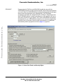
1
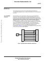
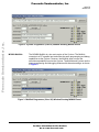
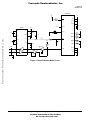
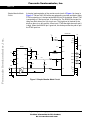
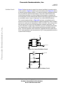
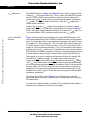
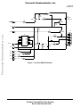
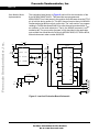
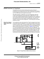
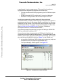
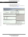
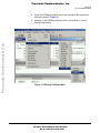
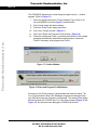
Freescale Semiconductor
Application Note
AN2317/D
Rev. 1, 10/2002
Freescale Semiconductor, Inc...
Low-Cost Programming and
Debugging Options for
M68HC08 MCUs
By: John Suchyta
Applications Engineering
8/16-Bit Products Division
Introduction
This application note describes several low-cost ways to get a target
M68HC908 microcontroller (MCU) into monitor mode for the purposes of
programming FLASH memory, reprogramming, and debugging. In most cases
an external connector is used to bring the necessary signals from a host
computer to the M68HC908 mounted on the target board. The size and type of
external connector can be tailored to the needs of the application.
Considerations for successful implementation of the monitor mode interface in
a production product are discussed. This application note applies to all
FLASH-based M68HC08 MCUs in general, and to the MC68HC908QY/QT
Family in two particular examples. Note that “FLASH-based M68HC08” and
“M68HC908” are synonymous in this document.
Commercial products, such as Motorola’s line of in-circuit simulator (ICS) kits
and the MON08-Cyclone and MON08-Multilink from P&E Microcomputer
Systems, are available to provide the external connector (typically called the
MON08 interface) and software to develop an application. These products are
recommended for many users, but low-cost alternatives are also available.
These alternatives can be used with several free or low-cost software
packages to develop and program an application.
Commercial products that gang program FLASH MCUs before they are
installed on a printed circuit board are not discussed here since the topic of this
document concerns in-circuit programming. However, commercial
programmers should be considered when the physical means to program in a
production environment are not available.
© Freescale Semiconductor, Inc., 2004. All rights reserved.
For More Information On This Product,
Go to: www.freescale.com
© Motorola, Inc., 2002
Freescale Semiconductor, Inc.
AN2317/D
What is Monitor Mode?
Freescale Semiconductor, Inc...
Monitor mode was developed as a feature of the M68HC08 MCU architecture
to provide basic in-circuit debugging, as well as programming of nonvolatile
memories. Monitor mode is not a substitute for full chip emulation, but it allows
a low-cost connection to a host computer, which sends commands serially to
the MCU. These commands perform read and write operations on the MCU’s
registers and memory. The system developer does not have to be concerned
about the monitor commands since these are embedded in the
programming/debugging tools. However, there are some practical limitations
that must be considered when designing a system that will be programmed or
debugged in-circuit using monitor mode.
Monitor mode uses a single I/O pin to communicate with a host PC. This pin is
controlled by the monitor mode firmware in the MCU. The pin is switched
between input and output as it emulates the serial protocol to the PC. This
limitation only applies during monitor mode. As soon as the chip is released
from monitor mode, the pin reverts to its I/O function.
Monitor mode must have a clock frequency that will allow the MCU to match the
serial baud rate of the PC. In most cases the debug connector can provide a
clock signal that can overdrive the crystal on the target board. The
MON08-Cyclone tool mentioned below does this, as well as offering an
“autobaud” function to adapt to the operating frequency of the target.
Several MCU pins must also be biased when configuring an MCU to enter
monitor mode. These pins and their functions are described in later sections.
The host software that communicates with the MCU in-circuit is usually part of
the development tool that the system developer obtains when starting a project.
The development tool vendors all use the M68HC08’s monitor mode as the
preferred debug interface.
Some protection features are disabled in monitor mode. Care must be taken to
understand the operation of the computer operating properly (COP) watchdog,
SWI instruction, and FLASH protection features while in monitor mode.
To use monitor mode for in-circuit programming and debugging, a developer
will need:
2
•
Host software for the personal computer or work station
•
A serial cable and pod (serial communications and biasing circuit) that
translates host commands to monitor mode signals
•
A suitable connection method on the target application to bias the MCU
into the proper mode
Low-Cost Programming and Debugging Options for M68HC08 MCUs
For More Information On This Product,
Go to: www.freescale.com
Freescale Semiconductor, Inc.
AN2317/D
Monitor Mode Signals
Freescale Semiconductor, Inc...
Monitor Mode Signals
The physical monitor mode interface uses up to nine connections to configure
the MCU and establish serial communications. As few as two or three
connections are used to program the MCU’s FLASH memory when the FLASH
is blank and the special “Forced Monitor Mode” is invoked. (Refer to the Monitor
ROM section of the appropriate M68HC908 data sheet.) For the purpose of this
application note, we will only consider the “normal” monitor mode interface,
which allows reprogramming. The monitor mode pin functions are discussed
here. All signal names are taken from data books or made up by the author to
identify functionality.
VTST/IRQ
Normal monitor mode is entered after a power on reset (POR) with a high
voltage, typically called VTST (pronounced V test), on the MCU’s IRQ pin. VTST
ranges from 7 V to 9 V, depending on operating VDD level. The VTST level
enables the mode selection logic and internal operating conditions for the
monitor mode.
COM/PTA0
Since all M68HC908 MCUs do not have a dedicated asynchronous serial
communications interface (SCI), a software-based serial protocol is coded into
each M68HC08 Family’s monitor ROM. This serial interface is designed to
communicate with a host computer’s RS232 serial port at 9600 baud or other
standard PC serial baud rate. The MCU’s serial input and output are
time-shared on a single I/O port pin, usually port A bit 0 (PTA0), to keep
pin-count to a minimum. (See data sheet for specific pin.) A later section will
cover the physical interface to connect this bidirectional pin to a PC.
Mode Select Signals
(MOD1, MOD0, DIV4,
SSEL)
Along with the high voltage on the IRQ pin, up to four port pins are used to
configure the monitor mode operating state. Two pins, sometimes referred to
as MOD0 and MOD1, are always used as mode select pins. Two more pins are
reserved for bus clock divider selection and an alternate security byte entry
enable. These four pins only need to be at their valid logic levels at the rising
edge of the reset pin for monitor mode entry. They revert to general-purpose
I/O pins as soon as the mode is selected so that maximum I/O functionality is
available in monitor mode.
Low-Cost Programming and Debugging Options for M68HC08 MCUs
For More Information On This Product,
Go to: www.freescale.com
3
Freescale Semiconductor, Inc.
Freescale Semiconductor, Inc...
AN2317/D
MOD1, MOD0
The mode select pins must be at their prescribed levels if the VTST voltage is
applied to the IRQ pin. These pins select monitor mode. They are also used by
Motorola production test facilities and emulator manufacturers to gain access
to special test and emulation features.
DIV4
DIV4 (for bus clock equal to input clock divided by 4), if implemented, is used
by the monitor firmware to determine the appropriate communications baud
rate. A high-frequency input clock is recommended for the MON08 interface,
which necessitates pulling the DIV4 signal high.
SSEL
SSEL (for serial select), if implemented, allows serial or parallel entry of
security code bytes. Serial entry is the normal entry method supported by
programming and debugging tools. Parallel entry is only useful during
production test, and is not a user option, since eight more pins are needed to
enter the security data. This signal does not allow memory data to be loaded
into the FLASH in a parallel mode.
OSC
Since the monitor serial communication is generated by the monitor mode
firmware rather than a dedicated serial communications interface, the internal
bus clock must be forced to a frequency that will yield baud rates that personal
computers can recognize. The OSC1 input can be over-driven by a canned
oscillator even if a crystal resonator circuit or RC network is connected to the
OSC1 and OSC2 pins. While most M68HC08 monitor mode implementations
recommend a 9.8304 MHz oscillator input to get a 9600 baud rate, some
M68HC08’s, particularly the M68HC(9)08A and M68HC(9)08JB Families,
specify other oscillator frequencies. Again, refer to the specific data sheet for
details.
Reset
The Reset input is required for proper debugging operation, but is not required
for programming and simple debugging. The Reset pin normally is pulled up
(via an internal pullup resistor) to VDD. In monitor mode on some devices, this
pin can be raised to the VTST level (after monitor mode is entered) to allow the
IRQ pin to be switched back to its interrupt input function for debugging
purposes. For example, the M68HC908KX Family requires a pullup on the I/O
pin that is shared with Reset.
Ground/VSS
The VSS pin must be connected to the host system’s ground to provide the
proper voltage reference for communications and mode biasing.
4
Low-Cost Programming and Debugging Options for M68HC08 MCUs
For More Information On This Product,
Go to: www.freescale.com
Freescale Semiconductor, Inc.
AN2317/D
MON08 Pods
MON08 Pods
The hardware that connects a PC and the target board ranges from
full-featured development tools to simple communications circuits that anyone
can build.
Freescale Semiconductor, Inc...
The ICS MON08
Connector
Motorola builds In-Circuit Simulators (ICS) for many popular M68HC08
derivatives. This tool provides a fairly sophisticated debug environment for
code developers and the capability to program individual MCU devices while
designing an application. The ICS contains a 16-pin ribbon cable that can mate
with a connector on the target board. This connector, typically called the
MON08 connector, is usually a 2-row by 8-pin (2 x 8) dual row header with
0.10 inch spacing. One end of the ribbon cable is attached to the ICS and the
other end is attached to the target application. The connector pinout is
described in the in-circuit simulator (ICS) kit for each particular M68HC08
MCU, and can also be found in most M68HC08 development tool
documentation. Figure 1 is an example of the MON08 connector pinout found
on the ICS tool for the MC68HC908GP32.
PC
RS-232
ICS
2 GND
VSS
4 RST
RST
6 IRQ
IRQ
8 PTA0
PTA0
10 PTA7
PTA7
12 PTC0
PTC0
14
PTC1
PTC1
16
PTC3
PTC3
TARGET
J6
Figure 1. MC68HC908GP32 MON08 Connections
Low-Cost Programming and Debugging Options for M68HC08 MCUs
For More Information On This Product,
Go to: www.freescale.com
5
Freescale Semiconductor, Inc.
AN2317/D
The MON08 connector pinout for one MCU may not match the pinout for
another due to the different biasing requirements among the M68HC08 MCU
families. M68HC08 versions with smaller pin counts will generally have one or
two fewer pins in the MON08 connection. Table 1 shows the MON08 pin
number and target signal name for several popular M68HC08 MCUs.
Freescale Semiconductor, Inc...
Table 1. Typical MON08-to-Target Mapping
MON08-Cyclone
Target Pin Name
MON08 Pin
Number
GP/GT
JL/JK
KX
MR
QY/QT
2
VSS
VSS
VSS
VSS
VSS
4
RST
RST
RST
RST
RST
6
IRQ
IRQ
IRQ
IRQ
IRQ
8
PTA0
NC
PTA0
PTA0
PTA0
10
PTA7
PTB0
PTA1
PTC2
PTA4
12
PTC0
PTB1
PTB0
PTC3
PTA1
14
PTC1
PTB2
PTB1
PTC4
NC
16
PTC3
PTB3
NC
NC
NC
The MON08-Cyclone tool from P&E Microcomputer Systems
(www.pemicro.com) was developed to provide a better way to standardize the
monitor mode connection across the M68HC08 MCU Families. The
MON08-Cyclone supports programming and debugging of almost every
M68HC908 MCU in current production. The Cyclone pod connects between
the serial port of a PC and the target board. It also can be used as a stand-alone
programmer to program multiple assemblies. This feature makes an ideal way
to set up a production test fixture to program newly assembled circuit boards
without PC intervention.
The MON08 connector supplied with the Cyclone tool is the same 16-pin ribbon
cable that is found in the ICS kits. Two additional pins were populated to
provide the oscillator signal (OSC) and a switchable power supply (VOut) as
shown in Figure 2. The Cyclone automatically configures the pinout for the
M68HC08 MCU version so that only one hardware tool is necessary to program
and debug any M68HC908. P&E Microcomputer Systems also posts software
revisions on their Web site for regular updates and whenever a new M68HC08
MCU is introduced.
6
Low-Cost Programming and Debugging Options for M68HC08 MCUs
For More Information On This Product,
Go to: www.freescale.com
Freescale Semiconductor, Inc.
Freescale Semiconductor, Inc...
AN2317/D
MON08 Pods
Figure 2. Cyclone Programmer (Class V) Window Showing MON08 Pinout
MON08-Multilink
The MON08-Multilink is a low-cost version of the Cyclone. The Multilink
connects to a PC’s parallel port and offers the same programming and debug
capabilities as the Cyclone. However, the Multilink does not offer the
stand-alone portability found on the Cyclone. The Multilink and Cyclone use the
same programming and debugging software with alternate settings, as shown
in Figure 3.
Figure 3. Multilink Programmer (Class VII) Window Showing MON08 Pinout
Low-Cost Programming and Debugging Options for M68HC08 MCUs
For More Information On This Product,
Go to: www.freescale.com
7
Freescale Semiconductor, Inc.
AN2317/D
Freescale Semiconductor, Inc...
Custom MON08
Interfaces
As mentioned above, monitor mode entry conditions can be introduced to a
circuit board in many ways. The method of mode entry and communications
can be as simple as including a “standard” MON08 interface (16-pin ribbon
cable to a 2 x 8 dual row header) to program or debug. Since dual row headers
can add unnecessary expense and area to a production board, other
connection methods should be explored in some applications.
Successful in-circuit programming schemes implemented by customers
include a bed-of-nails test environment, a board edge connector and socket
arrangement, and custom cabling that makes alternate use of cable
connections already present on the circuit board. These schemes can route the
necessary monitor mode signals to the board in a test or calibration
environment and not interfere with the end application. Mating the
MON08-Cyclone to any of these schemes makes a programming or
reprogramming session easy to operate, and does not require a PC.
Let’s explore some methods to communicate with a target in monitor mode
without the benefit of an ICS, MON08-Cyclone, MON08-Multilink, or other
production tool. These methods all can be made into target-powered MON08
interfaces (power for the communications circuit comes from the target board)
and become the “pod” for the monitor mode interface scheme.
Normal Monitor Mode
Circuit
The normal monitor mode circuit in most M68HC08 data books looks
something like that shown in Figure 4. The circuit to the left of the MCU in
Figure 4 shows the MAX232 serial level shifter and the 74HC125 buffers that
provide the bidirectional data switching for the serial communications on port
PTA0. This portion can be used a stand-alone pod for monitor mode
communication with many M68HC08 variants. Notice that we use the V+
supply from the MAX232 to provide the VTST voltage for the IRQ pin. The signal
generator in the middle of the figure is usually a canned oscillator which can
also be placed in the stand-alone pod.
The RST pin circuit is optional. The reset function can be accomplished by
simply toggling power to the target board since a power on reset (POR —
specified as VDD less than 0.1 V) is adequate for most programming and debug
sessions. The requirement to have a high level on RST is addressed by the
internal pullup resistor that’s present on most M68HC08 RST pins or an
external pullup for devices like the M68HC908A and M68HC908MR Families.
More information on the RST pin is given below.
The mode select signals on the right of the MCU are only necessary during the
rising edge of reset to enter monitor mode. The biasing of these signals is
described in more detail below.
Also note that a 9.8304 MHz clock source is used. This requires the DIV4 signal
to be pulled high to provide the 9600 baud rate.
8
Low-Cost Programming and Debugging Options for M68HC08 MCUs
For More Information On This Product,
Go to: www.freescale.com
Freescale Semiconductor, Inc.
AN2317/D
MON08 Pods
MC68HC908
VDD
VDD
10 k
RST
VDD
VDDA
VDDAD
MAX232
1
C1
+
Freescale Semiconductor, Inc...
4
C1–
C2+
OSC1
C5
GND 15
C3
5
MOD0
VTST
V+ 2
7
8
IRQ
VDD
V– 6
+
3
10 k
+
C4
MOD1
9.1 V
10 k
10 k
10 k
74HC125
5
6
10
9
1k
SSEL
DB9
2
10 k
DIV4
9.8304 MHz
+
5 C2–
0.1 µF
OSC2
VDD
VCC 16
+
3
C2
C1+
NC
VDD
74HC125
3
2
VSSAD
PTA0
4
VSSA
VSS
1
Figure 4. Normal Monitor Mode Circuit
Low-Cost Programming and Debugging Options for M68HC08 MCUs
For More Information On This Product,
Go to: www.freescale.com
9
Freescale Semiconductor, Inc.
AN2317/D
Simpler Monitor Mode
Circuit
A simpler implementation of the monitor mode circuit of Figure 4 is shown in
Figure 5. The two 74HC125 buffers are replaced by a resistor and diode. When
PTA0 is outputting a 1, the input at the MAX232 pin 10 is held high. When PTA0
is outputting a 0, the input at pin 10 is driven low. The RS232 level at pin 8 is
idling low which drives pin 9 to a logic one. This high level is blocked by the
diode so there is no bus conflict. As an input, PTA0 idles high whenever pin 9
is high. When the MAX232 pin 9 goes low, the diode provides the path to pull
the PTA0 input low.
MC68HC908
VDD
Freescale Semiconductor, Inc...
VDD
10 k
VDD
RST
VDDA
VDDAD
MAX232
1
C1
+
4
C1–
C2+
GND
OSC1
C5
C3
10 k
+
MOD0
VTST
V+ 2
IRQ
VDD
1k
V– 6
+
C4
MOD1
9.1 V
7
10
3
8
9
5
10 k
PTA0
1k
VSSAD
VSSA
VSS
1N4148
Figure 5. Simpler Monitor Mode Circuit
10
Low-Cost Programming and Debugging Options for M68HC08 MCUs
For More Information On This Product,
Go to: www.freescale.com
10 k
10 k
SSEL
DB9
2
10 k
DIV4
9.8304 MHz
15
+
5 C2–
0.1 µF
OSC2
VDD
VCC 16
+
3
C2
C1+
N.C.
VDD
Freescale Semiconductor, Inc.
AN2317/D
MON08 Pods
Freescale Semiconductor, Inc...
Oscillator Circuits
Figure 6 shows two ways to supply the external oscillator for normal monitor
mode operation. Figure 6a shows a canned oscillator while Figure 6b shows
a discrete inverter-based oscillator. The canned oscillator is perhaps the best
way to provide the external clock signal. It may cost a little more than the
inverter-based oscillator, but it has suitable drive strength to overdrive the
on-board crystal, and its small physical footprint (8-pin and 14-pin DIP versions
are available) makes it easy to implement in a custom MON08 interface.
The inverter-based oscillator in Figure 6b has been successfully used in
several circuits which required different oscillator frequencies. With a suitable
socket, the crystal can be changed from 4 MHz to 16 MHz. Care must be taken
with the layout of this circuit to avoid improper oscillation and noise. The
inverter should be a single-stage 74HCU04 to prevent unwanted phase shifts.
The unused inputs of the inverter package should be grounded to prevent
noise. The load capacitors were chosen for a parallel resonant crystal with a
20 pF load capacitance and assumes about 5 pF of stray capacitance due the
crystal socket and layout.
VDD
U1
1
2
3
4
5
6
7
NC
NC
NC
VSS
NC
NC
VSS
VCC
NC
NC
OUT
NC
NC
OUT
14
13
12
11
10
9
8
OSCOUT
9.8304 MHz OSC
Figure 6a. Canned Oscillator Circuit
U1A
2
1
OSCOUT
74HCU04
RF
5M
Y1
9.8304 MHz
CL1
22 pF
CL2
47 pF
Figure 6b. Inverter-Based Oscillator Circuit
Low-Cost Programming and Debugging Options for M68HC08 MCUs
For More Information On This Product,
Go to: www.freescale.com
11
Freescale Semiconductor, Inc.
AN2317/D
VTST Generation
The MAX232 shown in Figure 4 and Figure 5 can be used to supply the high
voltage (VTST) for monitor mode entry. The V+ output of the MAX232 supplies
about 9 V for the RS232 communications interface, which is adequate for
monitor mode entry. A zener diode and current limiting resistor complete the
VTST supply. The IRQ pin draws about 200 µA from the VTST supply when
monitor mode is selected.
Freescale Semiconductor, Inc...
Another way to get the VTST voltage is by switching a 9 V battery or power
supply to the IRQ pin. An example of a switching circuit is shown in Figure 7
below. The supply voltage should be limited to 9 V to meet the VTST spec. The
1 kΩ series resistor (R9) is a simple current limit for the VTST supply.
Low-Cost MON08
Interface
Figure 7 shows another implementation of a custom MON08 interface. This
circuit was modified from a low-cost RS232 interface found on several Internet
sites. The central part of the circuit, composed of transistors Q1 and Q2, diode
D1, capacitor C1, and resistors R1 – R5, is a simple level shifter between the
0 V and 5 V levels on the PTA0 pin and the –8 V to +8 V levels from the PC’s
serial port. This circuit actually transmits –5 V to +5 V levels due to the negative
pull down at C1 and VDD pullup at Q1. Q1 and Q2 can be any general-purpose
PNP and NPN transistors, respectively. Resistor R3 can be trimmed to provide
the best negative voltage swing for the transmitter signal at the DB9’s pin 2.
The top part of the circuit, composed of transistors Q3 and Q4, resistors R6 –
R9, and the 9 V battery or supply, is a simple way to switch the high VTST
voltage to the IRQ pin only when power is applied from the target’s VDD supply.
The VTST level cannot remain on the IRQ pin when the part is powered down,
but it must be present when the Reset pin is released. Switch S1 is inserted for
the case where the PTA0 pin is used for serial communication in the normal
application (if an asynchronous serial communications interface (SCI) is not
available on the MCU). Again, Q3 and Q4 can be any purpose PNP and NPN
transistors, respectively.
The bottom part of the circuit in Figure 7 is an optional way to route the
appropriate levels for monitor mode selection to a target system that requires
the external bias.
A socket for a canned oscillator is included. This configuration allows either a
standard 14-pin footprint or a smaller 8-pin footprint.
12
Low-Cost Programming and Debugging Options for M68HC08 MCUs
For More Information On This Product,
Go to: www.freescale.com
Freescale Semiconductor, Inc.
AN2317/D
MON08 Pods
S1
R8
10 k
Q4
2N3906
SW SPDT
9V
BATTERY
OR SUPPLY
R7
22 k
R9
Q3
2N3904
VTST (IRQ)
1k
r6
10 k
VDD
R1
10 k
R2
Q1
2N3906
Freescale Semiconductor, Inc...
PTA0
4.7 k
U1
1
2
3
4
5
6
7
GND (VSS)
NC
NC
NC
VSS
NC
NC
VSS
14
13
12
11
10
9
8
VCC
NC
NC
OUT
NC
NC
OUT
9.8304 MHz OSC
OSC1
R3
3.9 k
D1
1N4148
Q2
2N3904
r5
4.7 k
+
C1
1 µF
R4
4.7 k
P1
1
6
2
7
3
8
4
9
5
DB9
R12
SSEL
1k
R13
R10
1k
1k
R11
MOD1
MOD0
DIV4
1k
Figure 7. Low-Cost MON08 Interface
Low-Cost Programming and Debugging Options for M68HC08 MCUs
For More Information On This Product,
Go to: www.freescale.com
13
Freescale Semiconductor, Inc.
AN2317/D
Freescale Semiconductor, Inc...
User Monitor Mode
Implementation
C7
VDD
The evaluation board shown in Figure 8 was built for the introduction of the
8-pin MC68HC908QT4 MCU. This board has a preprogrammed
M68HC908QT4 on it that jumps to the monitor mode firmware when the PTA2
pin is held low during power-up. This MCU has so few pins that a full MON08
interface takes just about every pin on the chip. The “user monitor” is a program
residing in FLASH that allows the MCU to enter the monitor mode without VTST,
an oscillator, or the mode select pins. That is, the MON08 connector is not
needed at all! The user monitor program is fully described in the application
note entitled User Mode Monitor Access for MC68HC908QY/QT Series MCUs,
Motorola document order number AN2305/D.
VDD
0.1 µF
VDD
MC68HC908QT4
1
VSS
VDD
PTA5/AD3
PTA4
C3
R3
PTA0
VDD
3
MAX232
1
R2
10 kΩ
7
2
VR1
20 kΩ
8
PTA1/TCH1
R4
6
LED1
330 Ω
1 kΩ
+2
1 µF
C4
+
D1
1N4148
PTA3
+
5
C6
+
VDD
IN
C1–
T1Out
C2+
R1In
C2–
R1Out
C2
1 µF
14
13
6
V–
T1In
T2Out
T2In
1 µF
7
12
11
10
OUT
GND
9V
BATT
+
1 µF
C5
MC7805CT
16
15
GND
4
PTA2/IRQ
SW1
+
VCC
V+
1 µF
5
4
3
C1+
8
R2In
R2Out
9
C1
0.33 µF
1
6
Tx
Rx
2
3
7
DTR
8
4
GND
5
9
DB9
Figure 8. Low-Cost Evaluation Board Schematic
14
Low-Cost Programming and Debugging Options for M68HC08 MCUs
For More Information On This Product,
Go to: www.freescale.com
Freescale Semiconductor, Inc.
AN2317/D
MON08 Connections on a Target Board
MON08 Connections on a Target Board
With proper planning, an application can have the appropriate mode and
control pins preconfigured to reduce the number of pins required to enter
monitor mode. Engineering Bulletins EB366 through EB370 show examples of
user circuits that have the mode select pins pulled high or low, and therefore,
demonstrate that as few as five signals, including power and ground, are
needed to communicate with the application. The following figure from EB366
shows this concept.
Mode Select Signals
(MOD1, MOD0, DIV4,
SSEL)
Let’s consider the mode select signals first. These four signals can be biased
by the default state of the application’s I/O so that the MON08 connector does
not have to connect to them. They can be either inputs or outputs in the target
circuit. During monitor mode entry they just have to be at the appropriate logic
state to provide mode selection. For instance, in Figure 9, pins PTC0 and
PTC3 can be configured as inputs that are active low in the application. The
external pullup resistors would be a necessary expense to provide the proper
biasing since the internal pullup resistors are not enabled during reset. PTC0
and PTC3 configured as active low outputs would also be effective. As LED
drive ports, these pins can be pulled up to VDD through the LED and current
limiting resistor and provide the high logic level without additional components.
VDD
VTST
IRQ
VDD
RS-232
Freescale Semiconductor, Inc...
A target-powered monitor mode interface gets its power and ground
connections from the target printed circuit board. Depending on the usage of
the general-purpose I/O and control pins, as few as three other signals (COM,
VTST, and OSC) need to be brought onto the board.
PTA0
9600 BAUD
HC125
GND
PTC0 PTC3
PTC1 PTA7
OSC1
9.8304 MHz
OPTIONAL
Figure 9. Target-Powered Monitor Mode Interface.
Low-Cost Programming and Debugging Options for M68HC08 MCUs
For More Information On This Product,
Go to: www.freescale.com
15
Freescale Semiconductor, Inc.
AN2317/D
Here are some suggestions on how to configure I/O pins for monitor mode
entry:
High level needed:
•
Use as inputs, active low. Need weak pullup resistors (~10 kΩ).
•
Use as outputs, active low. External circuitry could be LEDs with pullup
resistors.
Freescale Semiconductor, Inc...
Low level needed:
•
Use as inputs, active high. Need weak pulldown resistors (~10 kΩ).
•
Use as outputs, active high. External circuitry could be an NPN transistor
or N-channel FET with a pulldown resistor.
As discussed here, the mode select signals do not have to be supplied from the
external MON08 interface if they can be “pre-biased” by the application.
VTST/IRQ
The IRQ pin is generally an input on most M68HC08s. As an input it can
withstand the higher-than-VDD voltage that VTST needs to be. In most
applications this pin is held high by the internal pullup resistor in normal mode.
If an active driver like a latch or NOR gate is used to drive this input low during
an actual application, then proper isolation should be used to prevent the
applied VTST voltage from damaging the external driver. A series resistor may
be all that is needed in most cases.
The VTST signal should be supplied from the external MON08 interface to
prevent accidental monitor mode entry while the application is in normal
operation.
COM/PTA0
The PTA0 signal is best when configured as an input pin to receive the
bidirectional COM serial signal. On most M68HC08 MCUs, this pin is a
keyboard interrupt input. It also is an analog-to-digital input and
general-purpose I/O on other devices. If configured as an input pin in normal
modes, there will be no conflict in monitor mode when the COM signal is
connected to this pin. If this pin is configured as an output, the circuitry
connected to the pin must be isolated from the bidirectional serial data to avoid
inadvertent triggering of the application’s output function.
The COM signal must be supplied from the external MON08 interface.
16
Low-Cost Programming and Debugging Options for M68HC08 MCUs
For More Information On This Product,
Go to: www.freescale.com
Freescale Semiconductor, Inc.
AN2317/D
MON08 Connections on a Target Board
OSC/OSC1
The OSC signal is always applied to the OSC1 pin on every M68HC08 for
monitor mode entry. This pin may have a crystal or RC attached to it in normal
operation. The external oscillator can easily overdrive the crystal or RC to
provide the 9.8 MHz monitor mode frequency. On device families like the
M68HC908GT, M68HC908KX, and M68HC908QYQT, this pin may be a
general-purpose I/O pin in addition to an optional oscillator input in normal
operation.
Unless the appropriate clock source is available in the application, the OSC
signal should be supplied from the external MON08 interface.
Freescale Semiconductor, Inc...
RST
The RST pin is an input and a low-driving output on most M68HC08s. As an
input it has an internal or external pullup resistor. As an output it drives the
pulled-up reset line low to signal an internal reset condition. Depending on the
level of debugging necessary in the target, this pin may not need to be brought
out to a MON08 interface. That is, if the reset input is not a critical part of the
application, the reset function can be accomplished by cycling power to the
board, thereby providing a power-on-reset (POR) which is sufficient for
programming and most debugging.
In the cases where the IRQ is an active part of the application, applying VTST
to the RST pin during monitor mode releases the IRQ pin to be operated as the
interrupt input, but only after successful monitor mode entry with VTST on IRQ.
This sequencing of IRQ and RST is generally provided by sophisticated (and
more expensive) debug tools.
On some low-pin count devices, such as the M68HC908KX and
M68HC908QY/QT Families, the RST pin is shared with general-purpose I/O. In
these cases, the RST pin must be pulled to VDD with a resistor to enter normal
monitor mode. VTST cannot be applied to the pin on these parts.
In general, the RST signal does not have to be supplied by the external MON08
interface.
Ground/VSS
Ground must be provided as the signal reference in the external MON08
interface.
Power/VDD
This connection can be used to power the MON08 interface if the pod does not
have its own power supply. The current requirements of the MON08 interface
must be considered in the application’s power supply design when deciding to
use a target-powered MON08 interface.
In summary, the VTST/IRQ, COM/PTA0, OSC/OSC1, and Ground/VSS pins
must be provided in the external MON08 interface. The Power/VDD pin can be
provided if the MON08 circuit needs to be powered from the target. The RST
pin and the four mode select signals may not need to be provided if the
application can bias them in normal operation.
Low-Cost Programming and Debugging Options for M68HC08 MCUs
For More Information On This Product,
Go to: www.freescale.com
17
Freescale Semiconductor, Inc.
AN2317/D
Freescale Semiconductor, Inc...
Low-Cost MON08 Software
Free or low-cost software options for programming and debugging M68HC908
MCUs are available from P&E Microcomputer Systems (www.pemicro.com),
Metrowerks (www.metrowerks.com), and ImageCraft
(www.imagecraft.com/software/). P&E’s ICS08 interface software packages
are available at no charge for individual use by registering at their web site.
Metrowerk’s CodeWarrior Development Studio for 68HC08, Special Edition, is
available at no charge from the Motorola MCU Web site
(www.motorola.com/semiconductors/mcu). You must register for the license
key for this software. ImageCraft’s low-cost ICC08 compiler works with the
NoICE debugger. P&E also bundles programming software in their
MON08-Cyclone and MON08-Multilink tools.
P&E Microcomputer
Systems
P&E’s ICS08 software packages contain the WinIDE integrated development
environment, which pulls together an assembler, in-circuit simulator, memory
programmer, and in-circuit debugger. The programmer and debugger work
with any MON08 hardware interface, as shown in the target hardware type
menu in Figure 10. Class III is used with the MON08 interfaces in Figure 4,
Figure 5, and Figure 7, above. Classes V and VII are used with the Cyclone
and Multilink pods, respectively.
The following examples illustrate how to program and debug an
M68HC908GT16 MCU with P&E’s PROG08SZ and ICD08SZ tools. The
MON08 pod in this example is a custom version of the circuit shown in
Figure 4.
Figure 10. Hardware Selection in P&E PROG08SZ
18
Low-Cost Programming and Debugging Options for M68HC08 MCUs
For More Information On This Product,
Go to: www.freescale.com
Freescale Semiconductor, Inc.
AN2317/D
Low-Cost MON08 Software
Programming the FLASH on an M68HC908 is relatively easy with the
PROG08SZ component. Simply open the WinIDE, then develop and assemble
your code. When your MON08 interface is attached between the PC and target
board, select the programmer icon (lightning bolt). The PROG08SZ
programmer launches and configures the PC’s COM port. Depending on the
type of MON08 interface, a power cycle dialog box may appear to ask you to
turn power off then on to your board. (The Cyclone and Multilink can perform
this operation for you.) PROG08 then prompts you to choose a programming
algorithm from a file window. Monitor mode communication is established
automatically and the programmer window (Figure 11) appears.
Freescale Semiconductor, Inc...
PROG08SZ
Figure 11. Select Port, Baud, and Security Bytes
Low-Cost Programming and Debugging Options for M68HC08 MCUs
For More Information On This Product,
Go to: www.freescale.com
19
Freescale Semiconductor, Inc.
AN2317/D
Here are the main steps in programming the FLASH with PROG08SZ in normal
monitor mode:
1. Launch P&E’s WinIDE from the ICS08 software.
2. Open desired file or develop new code.
3. Assemble the file.
4. Attach MON08 pod between PC and target.
5. Click on programmer icon.
6. From Target Hardware Type, select Class III (see Figure 10).
7. Select the PC port and the appropriate baud rate (see Figure 11).
Freescale Semiconductor, Inc...
8. From Target MCU Security Bytes, select appropriate security codes or
check the IGNORE security failure box.
9. Click Contact target with these settings…
10. Follow the instructions in the Power Cycle dialog window.
11. Select appropriate algorithm for the part (908_gt16_highspeed.08p in
Figure 12).
12. Double-click on Erase module (see Figure 12). (Flash cannot be
programmed unless first erased.)
13. Double-click on Specify S record and select file.
14. Double-click on Program module.
15. Double-click on Verify module. (Optional)
16. Double-click on Quit to exit the programmer.
At this point the FLASH memory on the MCU is programmed and ready for
in-circuit debugging.
20
Low-Cost Programming and Debugging Options for M68HC08 MCUs
For More Information On This Product,
Go to: www.freescale.com
Freescale Semiconductor, Inc.
Freescale Semiconductor, Inc...
AN2317/D
Low-Cost MON08 Software
Figure 12. P&E’s PROG08SZ Programmer Window
Low-Cost Programming and Debugging Options for M68HC08 MCUs
For More Information On This Product,
Go to: www.freescale.com
21
Freescale Semiconductor, Inc.
AN2317/D
Freescale Semiconductor, Inc...
ICD08SZ
Getting into the ICD08SZ debugger is even simpler. With a MON08 interface
between PC and target, select the In-Circuit Debugger icon from the WinIDE
menu bar. Follow the instructions in the Power Cycle dialog box if using the
Class III hardware type. The debugger establishes communications with the
target and interrogates the memory spaces on the MCU. Various windows
display register, variables, code, memory, and status information. See
Figure 13. Icons in the menu bar offer quick access to debugger functions.
Figure 13. P&E’s ICD08SZ Debugger Window
Metrowerks
22
An assembler, linker, and assembly source level debugger, Metrowerks’
CodeWarrior Development Studio for 68HC08, Special Edition, is a free tool
that can be upgraded to the functionality needed for the job. While the upgrades
are available at graduated prices, the Special Edition version offers unlimited
absolute assembly and provides debugging capabilities that make this free tool
Low-Cost Programming and Debugging Options for M68HC08 MCUs
For More Information On This Product,
Go to: www.freescale.com
Freescale Semiconductor, Inc.
AN2317/D
Low-Cost MON08 Software
Freescale Semiconductor, Inc...
a great bargain for serious programmers. This powerful tool combines a
high-performance Integrated Development Environment with:
• Full-chip simulation and FLASH programming from P&E Microcomputer
Systems
• A highly optimized ANSI C compiler and C source level debugger
• Automatic C code generation with Processor Expert from Unis
Launching a programming or debug session with the project-based
CodeWarrior IDE is as simple as double-clicking on the project name (format is
projectname.mcp) from your file storage. Starting a new project is a little more
challenging, but the tutorials, FAQs, and Quick Start Guides are easy to follow
and have you building a new project, using pre-built templates, in a short time.
(See www.Metrowerks.com/MW/Develop/ and select “CodeWarrior
Development Studio for HC08 for Microcontrollers”.)
The following example illustrates how to program and debug an M68HC908
MCU from within the CodeWarrior IDE.
Here are the main steps in programming the FLASH with CodeWarrior in
normal monitor mode and starting a debug session. This example was built with
PEDebug as the project stationery and QT4 absolute assembly. This example
also uses the low-cost MON08 circuit from Figure 7 as the MON08 pod.
1. a. Launch the CodeWarrior CW08 software and create a new project, or
b. Double-click on your project file (projectname.mcp)
The Project Manager window appears. See Figure 14.
Figure 14. CodeWarrior Project Window
Low-Cost Programming and Debugging Options for M68HC08 MCUs
For More Information On This Product,
Go to: www.freescale.com
23
Freescale Semiconductor, Inc.
AN2317/D
2. Click the + sign to expand the Sources folder.
3. Modify the source file if necessary.
Freescale Semiconductor, Inc...
4. Click the Debug icon (green arrow). The True-Time Simulator and
Real-Time Debugger launches. Figure 15.
Figure 15. True-Time Simulator & Real-Time Debugger Window
24
Low-Cost Programming and Debugging Options for M68HC08 MCUs
For More Information On This Product,
Go to: www.freescale.com
Freescale Semiconductor, Inc.
AN2317/D
Low-Cost MON08 Software
5. Select the PEDebug pulldown menu and navigate to the appropriate
device as shown in Figure 16.
Freescale Semiconductor, Inc...
6. Likewise, in the PEDebug pulldown menu, select Mode: In-Circuit
Debug/Programming.
Figure 16. PEDebug Pulldown Menu
Low-Cost Programming and Debugging Options for M68HC08 MCUs
For More Information On This Product,
Go to: www.freescale.com
25
Freescale Semiconductor, Inc.
AN2317/D
The PROG08SZ Attempting to contact target and pass security… window
appears. (Refer to Figure 11)
7. Select the appropriate class in Target Hardware Type (Class III for
low-cost MON08 circuit from Figure 7) and baud rate.
8. Click Contact target with these settings…
9. Follow the Power Cycle dialog instructions.
10. Click Yes in Confirm window. (Figure 17)
11. Click Yes in Erase and Program FLASH window. (Figure 18)
Freescale Semiconductor, Inc...
12. Follow the subsequent Power Cycle dialog instructions as the scripted
procedure automatically establishes communications, erases the
FLASH if necessary, and programs the FLASH.
Figure 17. Confirm Window
Figure 18. Erase and Program FLASH Window
At this point, the FLASH memory is programmed and ready for debug. The
True-Time Simulator & Real-Time Debugger integrates the debugger tools
from P&E Microcomputer Systems in this example. The windows look slightly
different between the ICD08SZ and True-Time tools (compare Figure 13 with
Figure 15), but the same basic debugger (ICD08SZ) drives both.
26
Low-Cost Programming and Debugging Options for M68HC08 MCUs
For More Information On This Product,
Go to: www.freescale.com
Freescale Semiconductor, Inc.
AN2317/D
Conclusion
Freescale Semiconductor, Inc...
Conclusion
Several aspects must be considered when implementing in-circuit FLASH
programming and debugging in M68HC908 applications. The hardware to
connect a personal computer to the target board (Cyclone, ICS, Multilink,
custom pod), the physical connections to the target board, and the software to
develop an application and program the MCU each have wide ranges of cost
and complexity associated with them. Low-cost MON08 interfaces were
examined, along with minimum pin connections to implement monitor mode.
Freely available software (with the price of registering) to develop an
application, program the memory, and debug the code was also discussed.
Low-Cost Programming and Debugging Options for M68HC08 MCUs
For More Information On This Product,
Go to: www.freescale.com
27
Freescale Semiconductor, Inc.
How to Reach Us:
Home Page:
www.freescale.com
E-mail:
[email protected]
Freescale Semiconductor, Inc...
USA/Europe or Locations Not Listed:
Freescale Semiconductor
Technical Information Center, CH370
1300 N. Alma School Road
Chandler, Arizona 85224
+1-800-521-6274 or +1-480-768-2130
[email protected]
Europe, Middle East, and Africa:
Freescale Halbleiter Deutschland GmbH
Technical Information Center
Schatzbogen 7
81829 Muenchen, Germany
+44 1296 380 456 (English)
+46 8 52200080 (English)
+49 89 92103 559 (German)
+33 1 69 35 48 48 (French)
[email protected]
Japan:
Freescale Semiconductor Japan Ltd.
Headquarters
ARCO Tower 15F
1-8-1, Shimo-Meguro, Meguro-ku,
Tokyo 153-0064
Japan
0120 191014 or +81 3 5437 9125
[email protected]
Asia/Pacific:
Freescale Semiconductor Hong Kong Ltd.
Technical Information Center
2 Dai King Street
Tai Po Industrial Estate
Tai Po, N.T., Hong Kong
+800 2666 8080
[email protected]
For Literature Requests Only:
Freescale Semiconductor Literature Distribution Center
P.O. Box 5405
Denver, Colorado 80217
1-800-441-2447 or 303-675-2140
Fax: 303-675-2150
[email protected]
Information in this document is provided solely to enable system and software
implementers to use Freescale Semiconductor products. There are no express or
implied copyright licenses granted hereunder to design or fabricate any integrated
circuits or integrated circuits based on the information in this document.
Freescale Semiconductor reserves the right to make changes without further notice to
any products herein. Freescale Semiconductor makes no warranty, representation or
guarantee regarding the suitability of its products for any particular purpose, nor does
Freescale Semiconductor assume any liability arising out of the application or use of
any product or circuit, and specifically disclaims any and all liability, including without
limitation consequential or incidental damages. “Typical” parameters which may be
provided in Freescale Semiconductor data sheets and/or specifications can and do
vary in different applications and actual performance may vary over time. All operating
parameters, including “Typicals” must be validated for each customer application by
customer’s technical experts. Freescale Semiconductor does not convey any license
under its patent rights nor the rights of others. Freescale Semiconductor products are
not designed, intended, or authorized for use as components in systems intended for
surgical implant into the body, or other applications intended to support or sustain life,
or for any other application in which the failure of the Freescale Semiconductor product
could create a situation where personal injury or death may occur. Should Buyer
purchase or use Freescale Semiconductor products for any such unintended or
unauthorized application, Buyer shall indemnify and hold Freescale Semiconductor
and its officers, employees, subsidiaries, affiliates, and distributors harmless against all
claims, costs, damages, and expenses, and reasonable attorney fees arising out of,
directly or indirectly, any claim of personal injury or death associated with such
unintended or unauthorized use, even if such claim alleges that Freescale
Semiconductor was negligent regarding the design or manufacture of the part.
AN2317/D
Rev. 1
10/2002
Information
For More
On This Product,
Go to: www.freescale.com