1
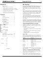
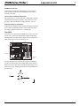
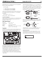
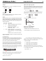
XP8000 Series Expansion Products
PLCBus
The PLCBus is a Z-World concept that allows you to extend
your control system by the addition of expansion boards.
Rather than buy controllers with many I/O lines, you can get
smaller controllers to which you add lines, according to your
needs. Z-World’s PLCBus concept also allows you to build your
own expansion boards, following a few guidelines.
TM
TM
A RELAY6, a UIO board and an ADC4 board, when properly
cabled to a PK2200, would look something like this:
PLCBus Cable
PLCBus Cable
PLCBus Cable
Z-World offers these expansion boards:
RELAY6
Series
Name
Description
XP8100
IO32
XP8200
UIO
XP8300
RELAY6
XP8400
RELAY8
XP8500
ADC4
*
A/D12
32 protected digital I/O lines, configurable as
inputs or outputs in groups of eight.
3.525 × 2.835 (89.5 × 72 mm)
Six high-current outputs and 16 universal inputs, which can be used as digital inputs (with
single or dual thresholds) or analog inputs.
3.525 × 2.835 (89.5 × 72 mm)
Six SPDT 10A relays.
3.525 × 2.835 (89.5 × 72 mm)
Eight DIP relays, each SPST, 500 mA, normally
open. 2.2× 2.835 (55.9 × 72 mm)
Four 12-bit ADC channels with signal conditioning, seven channels without.
3.525 × 2.835 (89.5 × 72 mm)
Eight configurable ADC channels. Selectable
gain, differential or single-ended.
3.525 × 2.835 (89.5 × 72 mm)
Two DAC channels.
3.525 × 2.835 (89.5 × 72 mm)
Single RS232 serial communication channel.
2.2 × 2.835 (55.9 × 72 mm)
Single-axis stepper motor controller with
quadrature decoder and high-speed counter.
4.0 × 2.835 (101.6 × 72 mm)
Four or eight DAC channels.
4.0 × 2.835 (101.6 × 72 mm)
XP8600
DAC2
XP8700
RS232
XP8800
SMC
XP8900
DAC8
The PLCBus, physically, is a set of one or more 26-wire ribbon
cables with which you connect a series of expansion boards to
a controller. When you have several boards connected, the
cables act as a “flexible backplane.” The limits to the number
of boards on a bus are power and addressability. You can address up to 64 relay boards and up to 64 A/D12 boards and up to
32 UIO boards, and so forth, on a single bus. TTL loading limits
the number of boards on a single bus.
You can also build networks of controllers, each having expansion boards.
All PLCBus expansion boards are 72 mm in width and fit in
DIN rail cards. Z-World expansion cards can also be installed,
with standoffs, on almost any flat surface that accepts screws.
Generally, mounting holes are 1/8″ (0.125″) in from the edge of
a board, with a diameter of 0.187.″
2900 Spafford Street
Davis CA 95616 USA
Tel: +916.757.3737
UIO
ADC4
DIN Rail
PK2200
Most Z-World controllers support the PLCBus, although some
require special connectors. (Some controllers have limited software support. Some do not have an actual PLCBus port.)
Z-World software usually hides most of the detail of operating a
PLCBus board. In practice, you need only make “plug and
play” physical connections, and make a few function calls in
your software.
The Concept
PLCBus devices connect with 26-wire ribbon cable (included
with the board) with the following pin assignments:
GND
attention /AT
strobe /STBX
A3X
A2X
A1X
D6X
D4X
D2X
D0X
–
–
(+5V) VCC
1
3
5
7
9
11
13
15
17
19
21
23
25
2
4
6
8
10
12
14
16
18
20
22
24
26
VCC (+5V)
+V (normally +24V)
GND
GND
GND
GND
D7X
D5X
D3X
D1X
–
–
GND
The PLCBus core signals consists of
/AT
/STBX
A1X, A2X, A3X
D0X–D7X
+V
VCC, GND
Attention line (open drain). May be pulled low by
any PLCBus device, causing an interrupt.
Negative going strobe.
Three mode lines, for selecting bus operation.
Bidirectional data lines.
PLCBus power. Either 24VDC (for 24V boards) or
12VDC (for 12V boards).
Normal regulated +5V and ground.
Fax: +916.753.5141
www.zworld.com
Revision: D
XP8000 Series (PLCBus )
TM
References
Contents
Summary ............................................... 1
The PLCBus Concept ............................. 1
Bus Topology ........................................ 2
Building Your Own ................................ 3
Relay Boards ......................................... 4
• RELAY6 (XP8300)
• RELAY8 (XP8400)
21 . . . . . Boards.8 . . . . )
Boards ........................................... 5
• A/D12
• ADC4 (XP8500)
DAC
• DAC2 (XP8600)
• DAC8
(XP8900)
(XP8700
RS232
2
Bus Topology
Please refer to
• Zilog: Z180 MPU User’s Manual
• Zilog: Z180 Serial Communication Controllers
• Zilog: Z80 Microprocessor Family User’s Manual
• Z-World: Dynamic C Data Sheet
• Z-World: PCL-AK Tech Note (101)
• Signetics: SCC2691 (UART) Data Sheet
ADC
Z-World 530-757-3737
A device on the PLCBus generally has one or more ports (control registers or data registers). For example, Z-World relay
boards each have one 4-bit control register. RS232 (XP8700)
boards each have one 8-bit control register and one 8-bit data
register.
Thus, a PLCBus device has one or more port addresses. All addresses on a single bus must be unique. Each device on the bus
recognizes its own set of addresses (by PAL encoding, jumper
wiring and other forms of logic). Each board responds only
when it is being addressed.
Any PLCBus device may have an address expansion register.
This is a register that can be used to extend the address space
of the device. No Z-World expansion card has an expansion register at present.
Addressing modes (discussed later) and address expansion registers allow you (theoretically) to build a PLCBus with millions
of devices or perhaps a few devices with millions of addresses.
Z-World expansion boards typically have one or two addresses.
Communicating with Devices on the Bus
To operate a PLCBus device, your program (running in your
controller) will read from it or write to it. The steps involved
are as follows:
0 Initially, reset the devices on the bus.
1 Select a board—or a board register—by placing its address
on the bus.
2 If the board has an address expansion register, you might
need to set its value.
3 Send data to the device or read data from the device.
UIO (XP8200) ....................................... 14
Stepper Motor Controller (XP8800) .... 16
IO32 (XP8100) ...................................... 20
A1X
BUSRD0
How it is done
There are 8 memory-mapped registers that correspond to the 8
bus cycles determined by the 3 bus lines A1X, A2X, and A3X.
Their specific addresses depend on the controller you are using.
Register
-
000
BUSADR0
01
BUSRD1
0
10
BUSRD2
0
11
BUSRESET
0
01
BUSADR1
1
10
BUSADR2
1
11
BUSWR
1
100
BUSADR1
2
Meaning
Read data, cycle 0
Read data, cycle 1
Read data, cycle 2
Reading this register resets the entire
PLCBus.
Bus address, cycle 0
Bus address, cycle 1
Bus address, cycle 2
Write data
To place an address on the bus, write 1, 2, or 3 bytes in succession to BUSADR0,
, BUSADR2 respectively. Whether
you write 1, , or 3 bytes depends on addressing modes described below. The addressing modes allow up to 24-bit addresses, with -bit addresses being most typical. The address
expansion register can extend this space.
You can read up to 24 bits using the BUSRD0, BUSRD1, and
BUSRD2 cycles. You can write up to eight bits using BUSWR.
XP8000 Series (PLCBus )
TM
Z-World 530-757-3737
Primitive functions are available in Z-World’s software libraries
to carry out these bus cycles. Higher level functions are also
available. They take care of the details for you.
Bus Addresses
To allow you to use an arbitrary combination of bus devices, in
anticipation of future products and third-party products,
Z-World has established a two-level addressing scheme. The
first level in the scheme specifies how addresses are encoded
when placed on the bus. The second level in the scheme specifies the actual addresses assigned to Z-World devices.
First level: placing addresses on the bus
You place an address on the bus by writing to BUSADR0,
BUSADR1 and BUSADR2 in succession. Doing so places address bits on the data lines (D0X–D7X) and modifies the mode
lines (A3X–A1X). A PLCBus devices must respond by comparing the address bits with its own address.
The lower four bits of the first address byte identify address
categories. There are 16 address categories, given in the table
below. The symbol “–” indicates an unused bit. An “x” indicates the address bit may be a 1 or a 0. Each PLCBus device
recognizes its own category and responds to that and no other.
The ‘x’ bits are further encoded by the second level of the addressing scheme, as you will see later.
Not all these categories are in use.
Z-World software also maintains “logical” address spaces that
map to physical address spaces. Generally, the logical space
simply numbers the boards sequentially.
First byte
1
2
3
4
5
7
7
8
9
10
11
12
13
14
15
16
–
–
–
–
–
–
–
–
–
–
–
–
x
x
x
x
–
–
–
–
–
–
–
–
–
–
–
–
x
x
x
x
–
–
–
–
–
–
–
–
x
x
x
–
x
x
x
x
–
–
–
–
x
x
x
x
x
x
x
–
x
x
x
x
0
0
0
0
0
0
0
0
1
1
1
1
1
1
1
1
Mode
0
0
0
0
1
1
1
1
0
0
0
0
1
1
1
1
0
0
1
1
0
0
1
1
0
0
1
1
0
0
1
1
0
1
0
1
0
1
0
1
0
1
0
1
0
1
0
1
Addresses
4 bits x 3
5 bits x 3
6 bits x 3
6 bits x 1
4 bits x 1
8 bits x 2
8 bits x 3
8 bits x 1
8 bits x 1
256
256
256
256
2,048
2,048
2,048
2,048
16,384
16,384
4
1
4,096
1 Meg
16
16
3
Abbreviated Addresses
Assume you have just placed a full PLCBus address on the bus
and wish to place another address on the bus. If the first two
bytes of the next address are the same as for the previous address, it is sufficient to write BUSADR2 only.
Expansion Register
Addressing the expansion register is a special case: the encoding scheme uses one byte which has a fixed value (0xB). When
you write to this address, all devices which have an expansion
register respond by latching the data from the next BUSWR.
The following sample code writes 3 to expansion registers:
ld
out0
ld
out0
...
a,0xB
(BUSADR0),a
a,3
(BUSWR),a
;0xB addresses ALL exp regs
;All expansion registers get 3
At present, no Z-World device has an expansion register. If you
design a PLCBus expansion card, the use of an expansion register is up to you.
Second Level: Physical Device Addresses
The second level of the addressing scheme specifies what addresses a PLCBus device can occupy. This applies primarily to
PLCBus devices manufactured by Z-World.
Each Z-World expansion card has a unique second-level address
based on PAL coding and jumper wiring. The second-level address scheme is described, for each product, in the section that
describes the product.
For PLCBus devices that have PAL encodings, you will have to
order boards with the specific PAL in the quantity you need, if
you want to have more than one such board on a PLCBus.
Full address encoding
0000 xxxx xxxx
0001 xxxx xxxx
0010 xxxx xxxx
0011 xxxx xxxx
x0100 xxxxx xxxxx
x0101 xxxxx xxxxx
x0110 xxxxx xxxxx
x0111 xxxxx xxxxx
xx1000 xxxxxx xxxxxx
xx1001 xxxxxx xxxxxx
xx1010
1011 (expansion reg.)
xxxx1100 xxxxxxxx
xxxx1101 xxxxxxxx xxxxxxxx
xxxx1110
xxxx1111
The mode notation indicates how many bus address cycles must take place
and how many bits are placed on the bus each cycle. For example, “5 bits x
3” means 3 bus cycles and 5 address bits each time.
Building Your Own
PLCBus expansion devices must be designed ac-
cording to the following rules:
1 The device must have two 26-pin headers that
match the PLCBus signals and operate according to those signals.
2 The device must not rely on critical timing,
such as a minimum delay between successive
register accesses.
3 The device must be capable of being selected
and deselected at any time without adverse effect.
4 The device must operate according to the first
level addressing rules given here. They do not
have to operate according to the second level
rules given next, but must not interfere with
devices that do.
XP8000 Series (PLCBus )
TM
Z-World 530-757-3737
Relay Boards
Z-World’s RELAY6 (XP8300) and RELAY8 (XP8400) expansion
boards provide a simple way to add relays to your control system. Up to 64 relay boards can be addressed on a single bus.
The RELAY6 board has six high-power relays installed as standard equipment. The board has six LEDs that correspond to the
six relays. An LED turns on while the corresponding relay’s
coil is activated.
The RELAY8 board has eight DIP relays installed as standard.
Other types are acceptable. A single LED on the board flashes
any time the board has been addressed.
Relay 6
The RELAY6 board has six 10A SPDT relays. Headers H1, H2,
and H4 connect the external world to the relays. Jumper J1
(along with PAL encoding) determines the board’s bus address.
Jumper J2 affects the relays’ actuation voltage.
LEDs 0 – 3
J1
LEDs 4 & 5
U5
PAL
U1
Relay 4
Driver
Headers H1, H2 and H4 connect your system’s devices to the relays. Pin 1 (common) and pin 3 (N.O.) connections for all six
relays are provided on H1 and H2. Header H4 provides the pin 4
(N.C.) connections for relays 4 and 5.
H1
3
H2
1
3
relay 0
1
relay 1
3
1
3
relay 2
H3
H4
1
relay 3
3
1
relay 4
3
1
4
4
V+
GND
relay 5 rel.4 rel. 5
Jumper J2 affects the actuation voltage for the board’s relays.
When J2:1-2 is connected, the actuation voltage is supplied by
the +V line on the PLCBus. When J2:2-3 is connected, the actuation voltage is supplied by the VCC line on the PLCBus.
To supply actuation voltage at header H3, leave J2 unconnected
and connect your power supply at V+ and GND.
Relay 8
The RELAY8 board has eight 500 mA DIP relays. Header H1 (34
pins) connects the external world to the relays. Jumper J1
(along with PAL encoding) determines the board’s bus address.
Jumper J2 affects the relays’ actuation voltage.
U2
Latch
4
Relay 5
LED
U4
U3
Relay 3
U1
P2
F2 F3
J2
F0 F1
H3
Fuses
3
Relay 7
U8
U10
U11
U13
H1
Configuration: SPDT
Coil Actuation Voltage: 24 VDC
The relay installed by Z-World as standard equipment has the
following specifications:
5
Pin 5 connects to the high-current (sinking) driver on the relay
board. Pin 2 is for the actuation voltage. Turning on the sink allows current to flow through the coil, switching on the relay.
Pin 3 is the normally open output. Pin 4 is the normally closed
output. Pin 1 is common to N.O. and N.C. outputs.
activation
voltage
U1
U6
2
1
4
P2
J2
Relay 5
H4
U12
Relay 4
H2
U9
Relay 2
H1
The relays installed by Z-World have the following specifications:
U7
U3
Relay 0
P1
High Current
Driver
Relay 6
Relay 2
Relay 3
Relay 1
Latch
Relay 1
Relay 0
P1
J1
U2
F4 F5
PAL
U4
your
external
voltage
your load
(N.O.)
2
3
High
Current
Driver
your
external
voltage
activation
voltage
2
3
1
1
4
5
4
5
your load
(N.C.)
Each relay is protected by a 10A fuse. To reduce or eliminate
transients, a metal oxide varistor (MOV) is connected between
pins 1 and 3 on each relay.
7 6
2 1
Configuration: SPST
Coil Actuation Voltage: 24 VDC
8 9
13 14
XP8000 Series (PLCBus )
TM
Z-World 530-757-3737
the +V line on the PLCBus. When J2:2-3 are connected, the actuation voltage is supplied by the VCC line on the PLCBus.
To supply actuation voltage at header H1, leave J2 unconnected
and connect your power supply at V+ and GND.
How to use Relay Boards
Whether you are using a RELAY6 board or a RELAY8 board,
the method for controlling it is the same:
1 Initially, send a reset command to all boards on the PLCBus.
Wait 350 ms.
2 Get the board’s attention by placing its address on the
PLCBus.
3 Operate the various relays on the board.
Addressing a Relay Board
Up to 64 relay boards (RELAY6 and RELAY8 boards in any
combination) can be addressed individually on a single
PLCBus. The address of a particular relay board is determined
(1) by the encoding of the PAL chip installed on the board and
(2) by jumper J1. Eight different PALs are available and J1 can
be set eight different ways, giving 64 unique addresses:
RELAY8 (XP8400)
Board Size
Operating Temp
Humidity
Power
Relays
5
2.835 × 2.22 × 0.58
–40°C to +70°C
5% to 95% non-condensing
24VDC, 80 mA
8 SPST (contacts rated 150VDC at 500 mA).
ADC Boards
Z-World’s A/D12 and ADC4 expansion boards add analog-todigital (ADC) channels to your control system. You can address
up to 64 A/D12 boards and up to 16 ADC4 boards on a single
PLCBus.
The A/D12
The A/D12 board has eight analog input channels. These can be
read as eight differential signals with selectable gain, or as 16
single-ended signals with unity gain. Gains of 2, 6, 22, 42, 102,
and 202X, as well as unity gain, can be selected.
J1
U8
U9
U10
U7
PAL
PAL
J3
C1
Latch
z = 1 when J1 pins 5-6 are not connected
y = 1 when J1 pins 3-4 are not connected
x = 1 when J1 pins 1-2 are not connected.
C2
C3
U1
U4
U13
Prec.
+2.5V
ADC
J5
Op Amps
The bits ppp are determined by the PAL number. Software gives
the relay boards logical addresses, 0 – 63, using this formula:
Op Amps
P1
MUX
RN2
U2
U3
U5
not
used
P2
U6
–5V
U11
logical address = ppp × 8 + zyx
RN3
J4
MUX
000z 000y pppx
Power
+5V
J2
EEPROM
U12
U14
where ppp and z, y, and x are defined above.
Controlling a relay
Once you have placed a relay board’s address on the bus, you
may switch its relays at will. Using BUSWR, place four bits of
data on the bus:
Relay D3 D2 D1
Relay D3 D2 D1
D0
0
1
2
3
4
5
6
7
0 = relay off
1 = relay on
0
0
0
0
0
0
1
1
0
1
0
1
1
1
1
1
0
0
1
1
0
1
0
1
Notes
Each relay on the RELAY6 board has an LED that illuminates
when the corresponding relay is activated. This does not provide verification that the contacts within the relay actually
switch, however.
Specifications
RELAY6 (XP8300)
Board Size
Operating Temp
Humidity
Power
Relays
H1
H2
Each A/D12 board is factory-calibrated. Compensation coefficients for all ADC channels are stored in the board’s EEPROM.
The EEPROM can be read or written by your application program. Normally, you would not do this. However, you might
wish to recalibrate your A/D12 board at some point.
The A/D12 board’s main power supply provides +5V up to 1
amp. U6 and U14 provide V–, a regulated –5V up to 50 mA. An
LT1019 provides a precision 2.5V reference up to 10 mA.
External Connection
Analog signals enter the A/D12 board via terminals on connectors H1 and H2. A third connector, H5, provides excitation voltages for strain gauges and other analog input sensors. Signals
at the board’s input terminals (ANx+ and ANx–, 0 ≤ x ≤ 7) are
routed to the board’s ADC chip, U4, by two multiplexers and
several differential amplifiers.
GND
V–
VREF
VCC
V+
DCIN
EX4
EX1
2.835 × 3.525 × 0.78
–40°C to +70°C
5% to 95% non-condensing
24VDC, 100 mA
6 SPDT (contacts rated 120VAC at 10A).
H5
AN0 AN1 AN2 AN3 AN4 AN5 AN6 AN7
GND
+ – + – + – + – + – + – + – + –
H1
H2
H5
XP8000 Series (PLCBus )
TM
Z-World 530-757-3737
Jumpers
The A/D12 board uses 4 jumpers, J1 through J4. Settings for J1,
coupled with the encoding of the PAL chip U7, determine the
board’s PLCBus address. These settings are explained later.
3 Read one of the A/D12 board’s input channels. Allow for
MUX settling time.
4 Calculate real-world values, such as temperature or displacement, from the data obtained.
5 Use the data (to control relays, switches, or other devices).
Connect for address bit “x” = 0
J1
Connect for address bit “y” = 0
Once an A/D channel has been set up, you can read it repeatedly, as fast as 165 µsec per read (on a 9 MHz controller).
Jumper J2 directs power for the board’s analog circuitry.
V+ connected to VCC
J2
V+ connected to +5V from U10
J2
1
1
Addressing the board
The address of a particular A/D12 board is determined (1) by the
encoding of PAL chip U7 installed on the board and (2) by
jumper J1. Sixteen different PALs are available and J1 can be
set four different ways, giving 64 unique addresses:
Jumper J3 is a write-protect switch for the EEPROM (U9).
J3
J3
1
1
Write-protect
Write-enable
Jumper J4 routes a reference voltage to the A/D conversion chip
U4. The factory setting connects pins 2-3, routing U1’s precision 2.5V reference output to the A/D chip. Connecting pins 1-2
routes the “ratiometric” voltage (RM) to the A/D chip. (When
R7 = 0 and R3 is not installed, RM ≈ V+.)
Route RM to A/D chip
J4
000p 10px ppRy
R = 0 for register S3A, 1 for register S3B
y = 1 when J1 pins 3-4 are not connected
x = 1 when J1 pins 1-2 are not connected
Route precision +2.5V to A/D chip
J4
1
The bits pppp are determined by the PAL number.
1
The Analog Circuitry
The A/D12 board’s eight inputs (ANx+ and ANx–) are routed to
the board’s ADC chip by two analog multiplexers and several
differential amplifiers. Gains of 2, 6, 22, 42, 102, and 202X, as
well as unity gain, can be selected by software.
AN[0-3]+
AN[0-3]–
MUX
+
–
U11
AN[4-7]+
AN[4-7]–
6
IN+
IN–
2X
–
G1
+5V
22X
G3
42X
G4
102X
G5
6X
G6
CH3
CH4
CH5
+2.5V
REF+
–V Reg
VREF
Ratiometric Reference
CH6
CH7
The ADC Chip
U4
The ADC chip, a 12-bit LTC1294, can convert a signal at one of
its input pins in either of two modes: unipolar or bipolar. The
chip’s allowable input range and output values are as follows:
Mode
–Input Range
Bipolar
Unipolar
–2.5V to +2.5V –2048 to +2047
–0 to +2.5V
–0 to 4095
logical address = pppp × 4 + xy
where pppp, and y and x are defined above.
–5V
G2
+V
+V Reg
CH2
U12
202X
The A/D12 expansion boards have logical addresses, 0–63, according to this formula:
EEPROM
ADC
+
MUX
CH0
CH1
For a given board, the R bit selects one of two hardware registers—S3A or S3B—coded on the PAL chip. S3A is a “MUX control register” that selects one of the board’s eight input channels. S3B is the “serial communication control register.”
–Output Range
You can reduce a voltage input to the required range with a resistor network. Otherwise, when an input voltage falls outside
the supported range, the chip responds with its maximum or
minimum value.
How to Use an A/D12 Board
Generally, this is what you do:
1 Initially, send a reset command to the PLCBus.
2 Place the address of the board on the PLCBus.
A/D Conversion Modes
When reading a differential input signal, connect the sensor to
both ANx+ and ANx–. When reading a single-ended signal, connect the voltage source to ANx+ and connect ANx– to GND.
When reading a unity-gain single-ended signal, no ground is
necessary. Simply connect the voltage source to the desired terminal (ANx+ or ANx–).
(When reading the A/D chip with Z-World software, specify the
desired gain and polarity by selecting a particular “A/D mode.”
There are 18 different A/D modes.)
Input Stability
Grounded input signals were used to calculate the standard deviations of “A/D channels.” Tests of 1000 samples per channel
were performed on typical boards in both unipolar and bipolar
modes. Under these conditions, the standard deviation for all
channels was under 1 part in 2047, and very near 0.1 part in
2047 for small gain values.
MUX Settling Time
When switching MUXs, you must allow the circuitry to settle
before attempting to read the A/D output. Capacitors C10–C14
(330 pF) attached to the feedback on gain amplifiers are the
greatest contributors of delay.
XP8000 Series (PLCBus )
TM
Z-World 530-757-3737
EEPROM Coefficients
Compensation coefficients, determined by precise measurement, are stored in the on-board EEPROM for each of the 18
software A/D modes.
Measurement of Ambient Temperature
The TEMP pin on U1 (LT1019) puts out a voltage that is directly
proportional to absolute temperature, with a slope of 2.1 mV
per degree. Room temperature (295°K) generates ~620 mV.
Excitation Voltage at Each Input
To provide an excitation voltage at each input channel on headers H1 and H2, install RN2 and RN3 on the board and connect
EX1 (on H1) and EX4 (on H2) to V+ on header H5.
The ADC4
Z-World’s ADC4 expansion board adds eleven 12-bit ADC channels to your system. Four channels have signal conditioning
that can match your input voltage range. The ADC4 board normally operates at 24V, but will operate at 12V.
H2
P2
J4, J5
H1
U9
PAL
C11
U1
U6
U3
J1, J2
U8
Regulator
J3
U5
U2
U7
Gain and
Bias
P1
RP4
RP3
The four channels (CH0–CH3) that have signal-conditioning
circuitry, as shown below. You can match the voltage range of
the device you are measuring to the fixed voltage range (2.5V)
of the ADC chip by changing socketed resistors (labelled GAIN
and BIAS here).
–
+
7
XP8000 Series (PLCBus )
TM
Z-World 530-757-3737
Setting Up Your Conditioned Inputs
As they comes from the factory, the conditioned inputs have a
0–10V input range. The socketed resistors are 2370 Ω (gain) and
39.2 kΩ (bias) respectively.
You can have any input range you want, simply by changing
the gain and bias resistors. The following tables present some
useful input ranges. The table values require 1% resistors and
have been adjusted from the theoretical values to account for
tolerance.
Input Range (V)
Gain
RGAIN (Ω)
RBIAS (Ω)
–10.0 to +10.0
–5.0 to +5.0
–2.5 to +2.5
–2.0 to +2.0
–1.0 to +1.0
–0.5 to +0.5
–0.25 to +0.25
–0.10 to +0.10
0 to +10.0
0 to +5.0
0 to +2.5
0 to +1.0
0.125
0.250
0.500
0.625
1.250
2.500
5.000
12.500
0.250
0.500
1.000
2.500
1180
2370
4750
5900
11.8K
23.7K
47.5K
118
2370
4750
9530
22.6K
8060
6650
4990
4530
2870
1690
931
392
39.2K
20.0K
10.0K
4020
Software is available to read and to calibrate the analog inputs.
Once calibrated, the calibration values reside in non-volatile
memory. All subsequent analog readings will use the calibration values and give the best possible value.
ADC4 Board IDs
You can address up to 16 ADC4 boards on a single bus, since
four different PALs are available and the address jumpers J4
and J5 can be set four different ways:
0000 1100 ppxy
The bits pp are determined by the PAL number.
Specifications
VREF+
Eight configurable 12-bit channels. (16 channels if single-ended, unity gain.)
ADC4 (XP8500)
Board Size
Operating Temp
Humidity
Power
Provides
2.835 × 2.12 × 0.75
–40°C to +70°C
5% to 95% non-condensing
24VDC, 32 mA
Eleven 12-bit ADC channels, 4 with signal
conditioning.
+5ANA
For optimal results, drive the unconditioned inputs with lowimpedance voltage sources. Operational amplifiers (such as the
LM660) are ideal for the purpose. High-impedence signal
sources are susceptible to noise.
Low-Pass Filter
The 0.01 µF capacitors in the op-amp circuitry function as lowpass filters. The filter characteristics depend on the resistors
you select. The 3 dB corner frequency is given by
DAC Boards
The DAC2
Z-World’s DAC2 (XP8600) expansion boards add digital-to-analog conversion (DAC) channels to your control system. Up to 64
DAC2 boards can be addressed on a single PLCBus.
(J4)
U10
1
C16
High-Side
Switch
(optional)
2π × RGAIN × 0.01 µF
If the input range is 10V, for example, the gain resistor is 2370Ω
and the 3dB corner frequency is 6715.4 Hz.
The LMC662C op-amp has an offset voltage drift of 1.3 µV per
°C, or 910 µV over the range 0–70°C.
Other contributers to overall drift are the 10K resistors R21–
R24. These have temperature coefficients of ±100 ppm per °C,
or 1W per °C. But, because they are small, surface-mounted resistors, all close to each other, their temperature deviations
match closely.
C15
C1
U11
C5 C2
U13
U7
C3
P2
DAC
C6
DAC
U2
P1
Drift
The AD680JT voltage reference has a typical drift of 10 ppm per
°C and a maximum drift of 30 ppm per °C. These values correspond to 25 (typ) and 75 (max) µV per °C and 1.75 (typ) and
5.25 (max) mV over the range 0–70°C.
Reg.
+15V+
U12
U9
REF+
f3dB =
J3
U8
PAL
10K
2.835 × 3.525
–40°C to +70°C
5% to 95% non-condensing
24VDC, 100 mA
Latch
ADC
A/D12
Board Size
Operating Temp
Humidity
Power
Provides
–24V
Default
U3
AIN [4 –10]
Using the Analog Inputs
x = 1 when J5 is open, else 0
y = 1 when J4 is open, else 0.
Using the Unconditioned Channels
The unconditioned channels are CH4–CH10.
CH [4 –10]
8
U8
Op-Amps
U4
U6
U3
J2
U5
J1
H1
The DAC2 board has two digital-to-analog output channels.
Each of these can be operated either as a voltage source or a
current source. The default range for voltage output is 0–10V.
The default range for current output is 0–22 mA. The D/A
chips—AD7543s—have a linearity of ±1 LSB and a gain stability of about 5 ppm per °C.
XP8000 Series (PLCBus )
TM
Z-World 530-757-3737
The DAC2 board’s main power supply (U9) provides +15V up to
1 amp. U8 and U2 provide V–, a regulated –5V up to 50 mA.
U13, an LT1021 (the factory setting) provides a precision 10V
reference (REF–). Optionally, you may install an LT1019 for
U13. This provides a precision 2.5V reference for REF–. A third
option is to leave U13 vacant and install a zener diode at Z1.
The actual reference voltage depends on the sizes of Z1 and R4.
External Connection
Analog signals (voltage or current output) leave the DAC2
board via terminals 1 and 3 on header H1. Other terminals provide access to board voltages.
GND GND V–
+V
VI2 VI1 VCC V+
When used with most Z-World controllers, the +V (normally
+24V) from the PLCBus is the power source, accessible on H1.
When using the DAC2 board with some controllers, +24V is not
available from the PLCBus. You must supply +24V on H1.
Jumpers
The DAC2 board uses 3 jumpers, J1 through J3. Settings for J3,
coupled with the encoding of the PAL chip U7, determine the
board’s PLCBus address. These settings are explained later.
Jumpers J1 and J2 determine the mode of output channels 1 and
2 (VI1 and VI2, on H1). Connecting pins 2-3 selects voltage output. Connecting pins 1-2 selects current output:
Voltage out
J1
Current out
1
Voltage out
J2
1
Current out
1
LED
The DAC2 board has an LED (D1) which illuminates whenever
the board’s address is placed on the PLCBus.
Reset
The DAC2 board has a reset device, U12, that monitors VCC.
Whenever VCC is interrupted, U12 pulls /RST low. Thus, you
can force the board to reset with software or a push-button.
The Circuitry
The DAC2 board’s digital-to-analog circuitry comprises two 12bit AD7543s, U3 and U4, and an LM324N quad op-amp chip, U1.
The outputs of the DACs are amplified, providing either current
output or voltage output. The outputs appear at jumpers J1 and
J2 as well as at header H1. Digital input values come, via the
PLCBus, from the program running on the controller.
(RP2)
V+
U3 or U4
DAC
AD7543
OUT
REF–
The AD7543 Chip
Each of the two AD7543s receives serial data in register A.
When register A is full, its contents are transferred to register
B. The data are then converted and analog level is output.
AD7543
REF–
LD
STB
12-Bit D/A Converter
OUT
Load Register (B)
12-Bit Shift Reg (A)
SDI
Each AD7543 has a linearity of ±1 LSB and a gain stability of
approximately 5 ppm per °C.
The output of each DAC is given by the following formula:
H1
1
9
+
U1
–
(RP1)
V+
100K
+
U1
–
V–
100K
(RP1)
V–
I1
OUT = – (input / 4096) × REF–
The DAC output voltage ranges from 0 to REF–. When U13 is
an LT1021 (the factory default) REF– is 10V.
Voltage Output
When voltage output is selected, the output is given by the following formula:
V = OUT × (1 + RP2 / RP1)
where OUT is the output of the DAC chip. Output values can be
changed by changing resistor packs RP1 and RP2. The maximum output voltage is limited by the op-amp to 14V.
Current Output
When current output is selected, the output is given by the following formula:
I = (OUT / RX) × (RP2 / RP1)
Output values can be changed by changing resistor packs RP1
and RP2. The maximum output current is limited by the op-amp
to 22 mA.
How to Use a DAC2 Board
Generally, this is what you do:
1 Initially, send a reset command to the PLCBus.
2 Place the address of the DAC2 board on the PLCBus.
3 Send data to one of the DAC2 board’s two DACs (register A).
When register A is filled, transfer the data to DAC2 register
B where it is converted and output. There is software that
does this.
4 Use the analog output (to control motors, attenuators or
other analog devices).
J1 or J2
2.2K
RX
Voltage
10
Current
2.2K
V1
(RP2)
330p
Capacitors C7 and C8 are normally not installed. For applications that operate at more than ~100 Hz, install C7 and C8.
Addressing the board
Up to 64 DAC2 boards may be addressed individually over a
single PLCBus. The address of a particular DAC2 board is determined (1) by the encoding of PAL chip U7 installed on the
board and (2) by jumper J3.
XP8000 Series (PLCBus )
TM
Z-World 530-757-3737
Eight different PALs are available and J3 can be set eight different ways, giving 64 unique addresses:
000z 001y pppx
z = 1 when J3 pins 5-6 are not connected
y = 1 when J3 pins 3-4 are not connected
x = 1 when J3 pins 1-2 are not connected
The board’s main power supply (U2, U6, U7, U17) provides +5V
(VCC), +5V reference for the DACs and +12V and –12V “rails”
for the op-amps. Q1 switches a +2V reference voltage to the opamps for power conservation. Jumpers H1, H2 and H3 allow you
to connect external ±12V rails to the op-amps if you wish. External power has a higher current rating.
U7
The bits ppp are determined by the PAL number. Software gives
DAC2 expansion boards logical addresses, 0–63, according to
the formula:
10
+24V
+12IN
12V Reg
+12VREF
+12V
U6
+12V to
op-amps
H1
U2
H3
R39, R33
[16.364K]
logical address = ppp × 8 + zyx
+2VREF
to op-amps
Q1
where ppp and z, y and x are defined above.
DAC2 Specifications
2.835 × 3.525 × 0.75
–40°C to +70°C
5% to 95% non-condensing
24VDC, 30 mA
Two 12-bit DAC channels, rated 0–10V voltage
output or 0–22 mA current ouput.
The DAC8
Z-World’s DAC8 (XP8900) expansion boards add digital-to-analog conversion (DAC) channels to your control system. Up to 8
DAC8 boards can be addressed on a single PLCBus.
AD5300
DACs, 8x
R2 R17
R1 R18
C28
+
+
+
+
+
U4
OpAmps
P1
H3
H2
R10 R25
R9 R26
C29
U17
C3
H4
C20
H1
U16
U1
CPLD
C16
C27 C21
R32 R14
R31 R13
U3
OpAmps
R19 R4
R20 R3
C24
R37
C7
C5
+
R7
R8
+
C1
C17
+
U9
+
C8
C35
R39 R33
U10 U11 U12
U13 U14 U15
C19
R34
Q1
C13 C14 C15
C2 C11 C12
C18
C26
C31
C30
R22
R24 R6 R16 R30
R21
R23 R5 R15 R29
U2
C34
R35
+
Reference
R36
C9
+
12V
Reg
+
C33
U7
C23
C22
R27 R12
R28 R11
C25
C36
RN1
P3
P2
C32
R38 C6
C4
U6
U5
5V
Reg
U8
+
(J3)
C10
J1
J2
The XP8900 has eight channels. The XP8910 has four channels.
Each channel be operated as a bipolar voltage source. The factory default range for voltage output is –10V to +10V. Each
channel can source or sink 2 mA on internal power or 7 mA
with external power. The D/A chips—AD5320s—are accurate to
±16 LSB and have a gain stability of about 5 ppm per °C.
In sufficient quantity, Z-World will build XP8900s with from 1
to 8 channels, with 8- or 10-bit DACs, or with customer-defined
voltage ranges.
R34 11K
/2V_EN
U17
Current Consumption
With no output, the DAC2 board draws 30 mA. With both output
channels operating at maximum current (22 mA) the DAC2
board draws a total of 75 mA.
Board Size
Operating Temp
Humidity
Power
Provides
+5VREF
to DACs
REF
+5V
5V Reg
C+
V+
C–
VOUT
H2
Charge
Pump
–12VREF
–12IN
–12V to
op-amps
Data are clocked into the DACs (low-power AD5300s). Output
of a DAC feeds into an op-amp which adjust the output to the
desired range.
+12VREF
+5VREF
U9–U16
DA_DATA
DA_CLK
DA_EN[0–7]
DIN DAC
SCLK
VOUT
/SYNC
+2VREF
100K
+
U3–U4
OUT[0–7]
–
–12VREF
410K
The default range is –10V to +10V. In sufficient quantity, you
can order your DAC boards with different output ranges.
External Connection
Analog signals leave the XP8900 on Wago headers J1 and J2.
Two terminals allow you to use external ±12V to power the
channel op-amps. Each channel has its own ground terminal.
XP8000 Series (PLCBus )
TM
Jumpers
The DAC8 board uses 3 jumpers, H1 through H3 to select the
±12V source:
Internal ±12V
External ±12V
H1
H1
1
1
H2
H2
1
H3
EEPROM
The DAC8 board’s EEPROM (U5) stores calibration constants
and is controlled by the CPLD (U1).
11
Bipolar and Unipolar Operation
The AD5320 was designed for unipolar operation, but with an
op-amp and the right resistors, bipolar output can be achieved.
The default output for the XP8900 is bipolar. The formula for
output on the XP8900 is
R2
R1+ R2
input
VOUT
1
H3
Z-World 530-757-3737
= VREF × 4096 × R – 2 ×
1
R1
The XP8900 has, by default, R1 = 100K (two 200K resistors in
parallel) and R2 = 410K (two 205K resistors in series). Thus,
input
410
100 + 410
×
– 2×
VOUT = 5 ×
4096
100
100
input
Bits Mode
00
01
10
DAC
EE
Select
giving a full range from –10.2V to +10.3V:
+10.3
0
–10.2
0
Digital Input
4095
How to Use a DAC8 Board
Generally, this is what you do:
1 Initially, send a reset command to the PLCBus.
2 Place the address of the DAC8 board on the PLCB
us.The
Description
Write to a selected DAC. Bit 0 of BUSWR is
for data; bit 1 clocks the data.
Read or write the EEPROM.
BUSWR: Bit 0 = data; bit 1 = clock.
BUSRD0: Bit 0 = data.
BUSWR: when data = 0111, turn on 2V ref.
BUSWR: when data = 0110, turn off 2V ref.
BUSWR: when data = 1xxx, turns on channel
xxx (0–7).
BUSRD0: reads 1010 when board is present.
= 20.5 × 4096 – 10.2
Voltage Output
CPLD
The DAC8 board’s CPLD (U1) encapsulates the board’s logic. It
monitors PLCBus addresses to determine if the board is being
addressed. When the board is being addressed, the CPLD examines the low 2 bits of the address. These 2 bits identify the current DAC8 operation:
The CPLD can enable or disable DAC output (by turning on and
off the 2V reference).
The AD5320 Chip
The AD5320 is a single 12-bit DAC operating from a single 2.7–
5.5V supply. It has an on-chip output amplifier that allows true
rail-to-rail output swing. Its reference is derived from the
power input. Its output is guaranteed monotonic.
The AD5320 sinks/sources 140 µA at 5V during normal operations and 200 nA in power-down mode. There are three powerdown modes; the differences between them are not relevant.
Each of the eight AD5300s receives serial data in a 16-bit shift
register. Two bits represent “power-down mode” (normal mode
is 0). The low 12 bits represent the output value:
15
13
11
PD
8 DAC8 boards may be addressed individually over a
single PLCBus. The address of a particular DAC8 board is determined by 3 jumpers at P3. The address bits are:
0010 000z yxMM
z = 1 when P3 pins 1-2 are not connected
y = 1 when P3 pins 3-4 are not connected
x = 1 when P3 pins 5-6 are not connected
The bits MM determine the DAC8 operation, as described previously. Software gives DAC8 expansion boards logical addresses,
0–7, according to the formula:
0
data bits
Power Down Mode
Following the 16-bit sequence, the CPLD strobes the DAC chip.
The output of each DAC is given by the following formula:
VOUT = VREF × ( input / 4096 )
where VREF is +5V from U2.
logical address = zyx
XP8000 Series (PLCBus )
TM
Z-World 530-757-3737
12
Typical Operations
The RS232 Board
In the examples given below, the shorthand notation
Z-World’s RS232 (XP8700) expansion boards provide a simple
way to add an RS232 channel to your control system. Each
board has a single Signetics SCC2691 UART. Up to 4 RS232
boards can be addressed on a single PLCBus.
BUSxxx value
stands for this assembly code
ld
a,value
out0 (BUSxxx),a
U6
PAL
Perform board check
BUSADR0
BUSADR1
BUSADR2
BUSRD0
0010
000z
yx10 ;select mode
value ;1010 if board exists
U4
U1
PAL
SCC2691 UART
Turn analog section on or off
BUSADR0
BUSADR1
BUSADR2
BUSWR
0010
000z
yx10
011a
0010
000z
yx10
1xxx
U2
C1
Drive a channel
Select the channel, then...
BUSADR0
BUSADR1
BUSADR2
0010
000z
yx00
;data mode
Repeat
BUSWR
BUSWR
BUSWR
for each
000d
001d
000d
of 16
;d is data
;bit 1 is clock
;not change clock same time as data
bits
Read or write the EEPROM
BUSADR0
BUSADR1
BUSADR2
0010
000z
yx01
;EE mode
BUSWR
0000
;Init EE clock and data bits
0000
C3
C4
RS232
Jack
C2
R2 D1 D2
The SCC2691 UART
The SCC2691 is a full-duplex asynchronous receiver/transmitter. It supports 18 baud rates from 50 to 38,400 baud. Data may
be framed with from 5 to 8 data bits, four parity modes, and 1,
1.5, or 2 stop bits. The UART provides error detection (framing
errors, parity errors, and overrun errors), break detection and
generation, and echo. There are two diagnostic modes. The
chip also has a multifunction 16-bit counter/timer.
8
;Re-init the EEPROM
Bus Buffer
READ
WRITE
A0–A2
RESET
Operation Control
3
Address Decode
Read/Write Control
ENABLE
Current Consumption
The DAC8 board draws approximately 30 mA at 24VDC.
The AD5320s are single-channel 12-bit DACs. They consume
very little power: 140 µA at 5V and can power down to 200 nA
(at 5V). The contribution of the DAC channels to current consumption is negligible.
The effect of power-down mode is also negligible.
DAC8 Specifications
Board Size
Operating Temp
Humidity
Power
Provides
2.835 × 3.525 × ~0.75
–40°C to +70°C
95% r. h., non-condensing
24VDC, 30 mA
Eight (or four) 12-bit DAC channels, output
rated –10V to +10V.
Each AD5320 has a linearity of ±16 LSB and a gain stability of
approximately 5 ppm per °C.
J1
H2
To operate the RS232 board’s UART, you read and write to two
registers on the RS232 board: the control register (CTRL) and
data register (DATA). In addition, the RS232 board can raise a
processor interrupt INT1.
D0–D7
Make transaction with EE. Serial reads and writes
BUSWR
Latch
H1
232 Driver
R1
;select mode
;xxx is channel (0–7)
P2
U5
RN1
;select mode
;a is 1 for on, 0 for off
Select a channel
BUSADR0
BUSADR1
BUSADR2
BUSWR
3.686
MHz
P1
Communication
Transmit Holding
Register
TxD
Receiver Holding
Registers (3)
RxD
MR1 & MR2
CR
SR
Interrupt Control
INTR
IMR
ISR
Timing
Baud Rate Generator
X1/CLK
Clock Selectors
I/O Pins
MPI
Change of State
Detector
MP
Function Select Logic
Counter/Timer
X2
CSR
ACR
CTUR
CTLR
The chip will generate interrupts under seven maskable conditions. It has a low-power mode and a “wake-up” mode. Receiver data are buffered (4-byte FIFO).
Control of the UART is accomplished by reading or writing its
internal registers. You may set up a counter or timer, initiate
RS232 communication, or control interrupts. Options include
setting baud rates, parity and other modes.
XP8000 Series (PLCBus )
TM
There are 14 internal registers, 7 of which you can read and 9 of
which you can write:
A2 A1 A0
Read
Write
0
0
0
0
1
1
1
1
MR1, MR2
SR
Reserved
RHR
Reserved
ISR
CTU
CTL
MR1, MR2
CSR
CR
THR
ACR
IMR
CTUR
CTLR
0
0
1
1
0
0
1
1
0
1
0
1
0
1
0
1
Z-World 530-757-3737
Reading and Writing to the UART
The PLCBus cycles have specific meaning when addressing an
RS232 board.
Write data to either CTRL or DATA register.
Read RS232 board status. Bit 0 (when 0) indicates the
presence of an RS232 board. Bit 1 (when set) indicates
that the UART needs servicing. This read is valid only
when the board’s CTRL register has been addressed.
Read the UART internal register selected by the board’s
CTRL register. This read is valid only when the board’s
DATA register has been addressed.
Resets all expansion cards on the PLCBus. However, an
RS232 board does not respond to this. The UART is reset with the RESET bit of the CTRL register.
BUSWR
BUSRD0
BUSRD1
BUSRESET
If the UART is being read, one set of registers is addressed. If it
is being written, the other set is addressed.
Refer to the Signetics SCC2691 product description.
How to Use the RS232 Board
Generally, this is what you do:
1 Initially, send a reset command to the PLCBus.
2 Place the address of one of the RS232 board’s registers on
the bus. Write a reset command to an RS232 board’s CTRL
register.
3 As needed, write to the internal registers of the board’s UART
to control the UART. Read the UART’s internal registers to
find out how things are going.
4 Read the RHR (receive holding register) or write to the THR
(transmit holding register) to communicate.
Connections
There are two RS232 connectors on the board, a 10-pin header,
H1, and a 6-wire “phone jack,” H2. You can use either one.
TXD
RXD
GND
1
3
5
7
9
2
4 /IN (CTS)
6 /OUT (RTS)
8
10
Header H1
/OUT (RTS)
GND
TXD
RXD
/IN (CTS)
Jack H2
6 5 4 3 2 1
Addressing the board
There are two registers on an RS232 board, the control register
and the data register. Each is addressable on the PLCBus. The
address of an RS232 board register is determined by jumper J1.
J1 can be set four different ways, giving up to 4 RS232 boards
per bus. Each register’s 15-bit address has this format:
00100 00000 xy00R
R = 0 for CTRL register, 1 for DATA register
y = 1 when J1 pins 3-4 are not connected
x = 1 when J1 pins 1-2 are not connected.
Software gives RS232 expansion boards logical addresses, 0–3,
according to the following formula:
logical address = xy
where x and y are described above. Observe that, for any RS232
board, the DATA address = CTRL address + 1.
13
Controlling the UART
To control the UART on the RS232 board, you send data to, or
read data from, one of its internal registers. This uses the
board’s control and data registers. This is the control register:
—
/CE
A0–A2
RESET
LT1180 ON
—
CE
A0
RESET
A1
LT1180
ON
A2
Enables the UART chip when low. The UART must be
enabled to read from it or write to it.
Select one of the UART’s internal registers. The register
selection depends also on whether you are reading or
writing and whether MR1 or MR2 has been selected.
Resets the UART.
When set, enables the LT1180 RS232 driver. When
clear, reduces power consumption.
The RS232 board can communicate with any RS232 device.
When a modem is used with the RS232 board, TX of the RS232
board must be connected to RX of the modem and vice versa.
Connecting a null modem between the RS232 board and the
modem takes care of this.
Interrupts from the RS232 Board
The RS232 expansion board has the capability of interrupting
your controller through the INT1 line whenever
1 a character has been received ( RXRDY)
2 the transmit buffer is empty (TXEMT)
When such an interrupt occurs, your program may check for errors (parity, framing, and overrun errors).
The /AT line of the PLCBus is connected to INT1 of the Z180.
There may be more than one interrupting device on the
PLCBus. An interrupt service function must check all devices
that could possibly have caused the interrupt, and service the
devices that need service.
You can also test whether an RS232 expansion card is interrupting by executing a BUSRD0 cycle. If you get a zero result, the
board generated no interrupt.
RS232 Board Specifications
Board Size
Operating Temp
Humidity
Power
Provides
2.835 × 3.525 × 0.75
–40°C to +70°C
95% r. h., non-condensing
24VDC, 80 mA
One full-duplex RS232 port. Up to 57, 600 bps.
XP8000 Series (PLCBus )
TM
Z-World 530-757-3737
Universal Input/Output Board
The signals on J1 are shown here:
Z-World’s Universal Input/Output board (XP8800) adds 16 universal inputs and six high-current outputs to your control system. The universal inputs can be used as
• digital inputs with single fixed threshold
• digital inputs with two adjustable thresholds
• analog inputs.
For the latter 2 cases, an external voltage source is required.
U4
PAL
U11
Comparator
RN2
P1
J6
Comparator
Selector
Regulator
RN3
Comparator
RN1
U3
U1
Selector
U5
U6
U7
Comparator
U2
C18
U8
C26
P2
J4 U9
J5
J3
J2
Latch
U10
Drivers
J1
H4
14
RN8
BD0 1
VCC 3
CV+ 5
V+ 7
+24V 9
VH 11
VIN 13
Pins
GND
EX+
EX
V+
10 +24V
12 K
14 VIN
2
4
6
8
Description
1-2
3-5
5-7
4-6
Least significant bit of board address (1 if not connected).
Comparator voltage CV+ connected to VCC.
Comparator voltage CV+ connected to V+ (default).
Reference voltage connected to external excitation voltage
(EX+).
6-8
Reference voltage connected to V+ (default).
9-11 Input voltage to regulator (VH) is +24V from PLCBus
(default).
11-13 Input voltage to regulator (VH) is VIN, from external
supply.
10-12 Common protective diode K connected to +24V from
PLCBus.
12-14 Common protective diode K connected to VIN from external supply (default).
C19
When jumper J6 is connected (it has only two pins) V+ is 7
volts. Otherwise, it is 14 volts.
H1
H2
H3
Up to 32 XP8800 (UIO for short) boards can be addressed on a
single PLCBus.
External Connection
The universal inputs (IN0–IN15) appear on headers H1 and H2.
High-current outputs (/L0–/L5) appear on header H3.
Inputs
1
0
3
2
5
4
7
6
9
8
Outputs
GND GND
11
10
13
12
15
14
DA EX+
5
4
2
3
0
1
+VI
SUB
Jumper H4 selects whether the inputs are digital or “universal.”
H4
1
H4
threshold voltage
from external
source
1
threshold voltage
generated on
board
Jumpers J2, J3, J4, and J5 comprise one large header for connecting the universal inputs. There are 16 columns on this
header, one for each of the 16 input channels. There are three
pins in each column. Connecting the upper two pins pulls a
channel’s input to ground. Connecting the bottom two pins in a
column pulls that channel’s input up to the excitation voltage:
Input Channels 0–15
J3
H1
H2
H3
Pins
Description
IN0–IN15
Universal inputs
Board ground
External voltage source (presumed to be a DAC).
External excitation voltage.
High voltage driver outputs.
External supply voltage for devices driven by /L0
through /L5.
External supply ground.
GND
DA
EX+
/L0–/L5
+VI
SUB
Jumpers
The UIO board uses 7 jumpers, J1 through J6 and H4. Pins 1 and
2 of jumper J1, coupled with the encoding of the PAL chip U2,
determine the board’s PLCBus address. This is explained later.
J4
J2
J5
input 10 to ground, across 4.7 kΩ
input 2 to excitation voltage, across 3.3 kΩ
The “Universal” Inputs
The UIO board’s 16 inputs (IN0–IN15) are fed to the positive
side of 16 comparators. The negative side of the comparators
are driven either by an external analog voltage source (DA) or a
fixed threshold VL.
J1
3 5 7
VCC
V+
CV+
R4
10K
H4
1 2 3
DA
VL
R5
10K
J1
0.1µ
VCC
4 6 8
EX+
V+
CV+
3.3K
INx
16
4.7K
THRESH
22K
CPx
0.01µ
10K
–
U2
16
+
LM339
comparator
UIx
XP8000 Series (PLCBus )
TM
Z-World 530-757-3737
Each input channel can be pulled high to an excitation voltage
(which can be external or V+) or pulled to ground, depending
on the setting of jumpers J2, J3, J4 and J5.
Universal Inputs As Digital Inputs
When the negative side is connected to VL, the inputs function
as digital inputs: the channel read “1” when the input voltage is
more positive than its threshold voltage and “0” otherwise. The
threshold voltage is given by this expression:
VTHRESHOLD = CV+ ×
R5
R4 + R5
Universal Inputs as Digital Inputs with Two Thresholds
The input channels can be used as digital channels with two (or
more) thresholds specified in software when the negative side
of the comparator is connected to an external analog voltage
source. Presumably, the external source is a DAC operated by
the system’s controller. (Z- World’s PK2100 has such a DAC output.) When an input voltage is higher than its upper threshold,
the channel becomes “1” and when it goes below its lower
threshold, the channel becomes “0.” The digital result does not
change (in software) when the input is between thresholds.
This feature offers stability for some kinds of inputs.
Universal Inputs as Analog Inputs
The input channels can be used as analog channels when the
negative side of the comparator is connected to an external
DAC. Because the comparator threshold can be varied, it is possible to take an analog reading by successive approximation.
The accuracy of such a reading depends, in part, on the accuracy of the DAC.
The High-Current Output(s)
Six high-current outputs drive external loads (/LO–/L5) such as
relays or small actuators.
D0–D3
U10
259
J1
12
14
/L0–/L5
6
20K
10
+V
+VI
2003
driver
K
Protection
SUB
15
Addressing the Board
Each UIO board can have one of 16 PALs. Jumper J1 (pins 1-2)
be set two ways. Thus, there can be 32 UIO boards on a single
PLCBus. Each board’s address has this format:
0000 010p pppx
pppp is determined by the PAL
x = 1 when J1 pins 1-2 are not connected.
UIO board addresses, therefore, range from 0x040 to 0x05F.
Software give the UIO logical addresses. Each UIO channel has
an address, according to the formula:
address = board << 4 + channel.
Operating the Board
The UIO board has 16 universal inputs and six high-current outputs. To access an input channel or an output channel, write to
the board’s latch using BUSWR:
D3 D2 D1 D0 Meaning
0
0
0
0
1
1
1
1
0
0
1
1
0
0
1
1
0
1
0
1
0
1
0
1
x
x
x
x
x
x
x
x
Set or clear /L0
for high-current outputs 0–5
Set or clear /L1
Set or clear /L2
Set or clear /L3
Set or clear /L4
Set or clear /L5
Unused
Set up a read. When D0=0, select even input channels. When D0=1, select odd input channels
Setting an output driver is straightforward.
Reading one of the input channels (in digital mode) is slightly
more complicated. There are two different read cycles.
BUSRD1 corresponds to input channels 0–7. BUSRD2 corresponds to channels 8–15. You must also set up for a read: writing 0xE to the latch selects even input channels. Writing 0xF
selects odd input channels. Thus, the BUSRD1 and BUSRD2
cycles read 4 channels at a time, one bit per channel, in D3–D0.
The various bus cycles have specific meaning when using a
UIO board:
6
SUB
The voltage supplied to the outputs can be +V from the PLCBus
or an external voltage (+VI) from the header H3. If you supply
an external voltage, connect SUB (also on H3) to external
ground. Diodes internal to the 2003 protect the driving transistors against spikes.
The driver chips dissipate up to 1.25W at 60°C. With six channels on at the same time, the maximum current is ~160 mA per
channel. The maximum current per channel is 500 mA.
How to use a Universal Input/Output Board
The general method for using a UIO board is this:
1 Initially, send a reset command to all boards on the PLCBus.
2 Get the board’s attention by placing its address on the
PLCBus.
3 Read the inputs on the board, or perform output.
BUSWR
BUSRD0
Write data.
Determine the presence of a UIO board. Bit 0, when 0,
indicates the presence of a board.
BUSRD1
Read input channels [0, 2, 4, 6] or [1, 3, 5, 7].
BUSRD2
Read input channels [8, 10, 12, 14] or [9, 11, 13, 15].
BUSRESET Resets all expansion cards on the PLCBus.
Higher level functions available in Dynamic C libraries take
care of the details of much of this.
Specifications
Board Size
Operating Temp
Humidity
Power
Provides
2.835 × 3.525 × 0.75
–40°C to +70°C
5% to 95% non-condensing
24VDC, 45 mA
16 “universal” channels. 6 high-current output
channels, sinking continuously 150 mA at 48V
at 50°C (all on) or 500 mA continuously at 48V
at 25°C (one channel at a time).
XP8000 Series (PLCBus )
TM
Z-World 530-757-3737
The Stepper Motor Controller
Z-World’s stepper motor controller (XP8800) is a special purpose expansion board. This document will use the abbreviation
SMC to refer to the stepper motor controller.
ture counter by ignoring the PCL-AK and the motor driver. It
can even be used as a timer by ignoring or disabling its outputs.
interrupt request
data
U5
H1
J1
D3 D4 D5 D6
U9
PLC
Bus
A
B
C
D
Phase
Output
(U2, U3, U4)
Watchdog
Reset
U8
data
RN
R1
D1
D2
H3
A B
from external
quadrature encoder
H2
R2
H5
R3
H4
Motor
Driver
H6
Screw Terminals
The SMC controls a single axis of motion. You can address up
to 16 SMCs on a single PLCBus. The virtue of the SMC is that
you can offload motor control operations, leaving your master
controller free to perform other tasks.
The motor driver (UCN5804) is capable of driving 1A per phase
and motor voltages up to 35V. The driver automatically generates the sequencing for 1-phase, 2-phase, and half-step operations. The SMC includes a 16-bit quadrature decoder/counter
(HCTL-2016) which can count at speeds up to 3 MHz.
System Description
The SMC board has three major components
1 PCL-AK pulse generator
2 UCN5804 motor driver
3 HCTL-2016 quadrature decoder / counter
Many of the SMC features are found in the programmable
PCL-AK pulse generator—the “brain” of the SMC.
• Continuous (i.e., manual), preset (i.e., counted), or originseeking modes of operation.
• Switching between high- and low-speed operation, with or
without acceleration and deceleration.
• “Bidirectional” pulse output modes.
• Sensing of origin, end-limit, and slow-down signals.
• Interrupt generation.
• 13-bit (8191) step rate resolution. 18-bit (256K) counter.
• User-definable output speed range, up to 3 MHz.
• Single-phase, dual-phase, and half-step modes.
• 16-bit quadrature decoder / counter.
• Watchdog safety feature.
The SMC board has a control register (U3) and control logic
(U2, U4). You can choose to use or disregard some of the SMC
components. For example, you can replace the motor driver
with one of your own. The SMC can be used solely as a quadra-
Expansion
Header
Quadrature
Decoder / Counter
8
RN4
X1
U6
control
byte
PAL
Control Reg.
PAL
PCL-AK
U4
RN3
(U7)
Motor
Driver
mode:
1-phase
2-phase
half-step
Control
8
RN1
U3
Pulse & Dir
2
2
Quadrature Decoder & Counter
U2
PCL-AK
Pulse Generator
8
Reset
PLCBus connectors
U1
16
ORG SD– EL–
SD+ EL+
from external sensors
SD: “slow down”
EL: “end limit”
ORG: origin
+ Positive direction
– Negative direction
PCL-AK
Pulse output from the PCL-AK is bidirectional. The /PULSE signal steps a motor. The PDIR signal specifies the direction of rotation (1 means + direction, 0 means – direction).
The PCL-AK can sense external signals (such as “slow down,”
“end limit,” and “origin”) and can accelerate and decelerate
betwen high and low speed settings and can generate interrupt
requests on several conditions, such as end-of-operation. It can
stop immediately or decelerate to a stop. The PCL-AK can generate thousands of different pulse rates.
It has three basic modes of operation:
continuous mode
preset mode
origin mode
The PCL-AK continues to generate pulses until
told to stop or an external signal occurs.
The PCL-AK generates pulses until its counter
(preset) reaches 0 or an external signal occurs.
The PCL-AK generates pulses until an “origin”
pulse occurs.
This diagram shows the programmer’s view of the PCL-AK.
PULSE
command &
data in
status and data
out
8
address
2
clock
PCL-AK
WR
Reg.
Bits
CTR
18
FL
13
FH
13
ADR
10
RD
16
MUL
10
RD
CS
FL
FH
CTR
RD
MUL
ADR
Control
Registers
PDIR
ORG
EL–
EL+
SD–
SD+
INT
Reset
Meaning
Down-counter, which gives the number of pulses to
generate. This register is readable.
Low speed register. The PCL-AK can operate at this
frequency or ramp to amd from this frequency.
High speed register. The PCL-AK can operate at this
frequency or ramp to and from this frequency.
Acceleration / deceleration rate register.
Ramp-down point register. The ramp-down point is the
number of pulses before end-of-count at which the
PCL-AK will start ramping down from high speed to
low speed. The register is readable.
Multiplier register. This register interacts with FL and
FH to give various pulse rates.
XP8000 Series (PLCBus )
TM
Z-World 530-757-3737
Communicating with the PCL-AK
You tell the PCL-AK what to do by (A) writing to its command
buffer and (B) writing values to its control registers. You find
out what it’s doing by reading the status register or a control
register. Only two registers are readable: the counter and rampdown point register.
You can issue a hard reset to the PCL-AK by pulsing the /RESET line. This resets internal registers. A soft reset (given as a
command) does not change internal registers.
17
A 5V, 1A motor would require
VD = VM + VCE + VF
VD = 5V + 1.1V + 0.7V
VD = 6.8V
Quadrature Decoder / Counter
The HCTL-2016 is a 16-bit quadrature decoder and counter. Its
two lines A and B accept two quadrature encoded signals, that
is two square waves 90° out of phase. The order in which these
signals make transitions determines the direction, up or down.
Status bits are available at PCL-AK addresses 0 and 3.
Forward Quadrature (Counting Up)
A
Motor Driver
The motor driver (UCN5804) receives two pulse signals from
the PCL-AK. One signal, /PULSE, steps the motor. The other,
PDIR, specifies the motor rotation (1 = forward, 0 = reverse).
The driver receives two mode signals from the control register:
Bit 7
0
0
1
1
Bit 6
0
1
0
1
Mode selected
Two-phase
Half-step
Single-phase (or wave)
undefined. (Do not use this.)
F
o
r
w
a
r
d
A
0
1
1
1
B
1
0
1
1
C
1
1
0
1
D
1
1
1
0
Two-Phase
A
0
0
1
1
B
1
0
0
1
C
1
1
0
0
D
0
1
1
0
Half-Step
A
0
0
1
1
B
1
0
0
0
C
1
1
1
0
D
1
1
1
1
1
1
1
0
1
1
1
1
0
0
1
1
1
0
0
0
R
e
v
e
r
s
e
VD
D6
Motor
Driver
C
B
There are four states of lines A and B. The counter counts up or
down depending on the state transitions.
The maximum reliable counting frequency is 3 MHz. You can
read the counter as two successive bytes.
Control Register
The control register is an 8-bit write-only latch that controls
operations of the SMC.
Each bit in the register has the following meaning (bit 0 is the
least significant bit):
Bit Name
RESCNT Reset quadrature decoder/counter. Low means reaset.
1
RESCTL Reset the PCL-AK. Low means reset.
2
LED
3
SEL0
4
6
D5
7
D3
Driver Power
To select a motor driver voltage, you must consider the various
losses in the driver circuit, including the collector/emitter voltage and the voltage of the blocking diode.
VD drive voltage
VM motor-specified voltage
VF diode forward voltage, typically 0.7V
VCE collector-emitter voltage
Meaning
0
5
D4
A
driver
A
Reverse Quadrature (Counting Down)
The top line of each sequence (in the above illustration) indicates the state of the driver at power-up. The 0s in the illustration indicate that the driver line is ON, that is, sinking current.
The phase lines are connected to the motor’s windings thus:
D
Time
B
The meaning of these modes lies in how the driver generates
the phase signals A, B, C, and D.
Single-Phase
B
Turn LED on or off. Low means ON.
Local address line.
SEL1
Local address line.
DRVOE Enable Motor Driver Output. Low means ON.
HSTEP Half-step mode for motor driver when this bit is 1 and
bit 7 is 0.
WAVE
Single-phase mode for motor driver when this bit is 1
and bit 6 is 0. Two phase mode when this bit is 0 and
bit 6 is 0.
The select lines SEL0 and SEL1 have very specific meaning.
They are connected to the two address lines of the PCL-AK.
SEL0 is also connected to the quadrature decoder/counter.
Coupled with PAL logic, these select lines allow you to read
and write to the PCL-AK and to read the 16-bit counter value.
External Connection
Signals reach the external world on headers H5 and H6. H5 is a
14-pin header. H6 (next page) is a 16-position terminal block.
XP8000 Series (PLCBus )
TM
H6
Motor Drive
Quadrature
Sense Input
Z-World 530-757-3737
Power
1
PHA
PHC
PHB
GND
PHD
BIN
AIN
/EL+
/ORG
/SD+
/EL–
/SD–
K
GND
+5V
+24V
• PHA, PHB, PHC, PHD
Open-collector motor control outputs, connecting to motor
phase lines. They can sink up to 1A.
• AIN, BIN
TTL-compatible quadrature-encoded inputs.
• /ORG
Active-low origin pulse. Readable in the PCL-AK (address 0)
status bits.
• /EL+, /EL–
Active-low end-limit, one for the + direction, another for the
– direction. Readable in the PCL-AK (address 0) status bits.
• /SD+, /SD–
Active-low “slow-down” inputs, one for the + direction, another for the – direction. Readable in the PCL-AK (address
3) status bits.
• K
Driver chip protection. Connect this to your motor’s voltage
source.
• +24V
Unregulated PLCBus power. Though nominally 24V, this can
be anywhere from 9–30VDC. You can use this as the motor
supply voltage of your power supply can handle the current
requirements.
• +5V
Regulated PLCBus power. A poor source for motor power,
but can be used to power external logic.
• GND
PLCBus ground, common to your entire system. Your
motor’s power supply ground should be connected here.
H5
H5 provides additional connection points for motor control sig-
nals, power and ground, power failure, and watchdog signals.
GND
WDO
PFO
PFI
+5V
GND
PULSE
PDIR
DRVOE
HSTEP
WAVE
+24V
• /PULSE
A low-going pulse in this line signals a one-step move to the
motor driver. (TTL)
• PDIR
Indicates in which direction the motoro is to move. A high
level means movement in the + direction. A low level means
movement in the – direction.
• /DRVOE
When low, enables motor driver outputs. (TTL)
18
• WAVE
Coupled with HSTEP, this determins the operation of the
motor driver: single-phase, two-phase, or half-step. (TTL)
• HSTEP
Coupled with WAVE, this determines the operation of the
motor driver: single-phase, two-phase, half-step. (TTL)
• /WDO
Active low, open-collector watchdog output line. When the
watchdog is enabled, this line will go low—upon a watchdog timeout—to getnerate a hard reset at the PCL-AK pulse
generator.
• PFI
Input to the power-fail comparator. When this line drops below ~1.25V, the /PFO line becomes active.
• /PFO
Open collector power-failure indicator. This line goes low
when PFI goes below ~1.25V. This line can be connected to
the NMI or interrupt line on the master controller.
• +24V
Unregulated PLCBus power.
• +5V
Regulated PLCBus power.
• GND
PLCBus ground.
Jumpers
The SMC uses one jumper, J1, and a header H4. When J1 is connected, the watchdog timer is enabled. When disconnected, the
watchdog timer is disabled. The four jumper positions on H4
determine the board’s PLCBus address.
How to Use an SMC Board
Generally, this is what you do:
1 Initially, send a reset command to the PLCBus.
2 Place the address of the SMC on the PLCBus. This will actually be the address of one of its components, the PCL-AK or
the quadrature decoder/counter.
3 Operate the SMC. You can, for example,
• Set the SMC control register.
• Issue a command to the PCL-AK pulse generator.
• Set PCL-AK parameters or read PCL-AK registers or
status.
• Reset the quadrature counter or read its value.
• Wait for interrupt requests.
4 Following an SMC operation, you typically issue a soft reset
to the PCL-AK. Refer to Z-World’s Tech Note 101 for details
about the PCL-AK.
There is a software library (STEP.LIB) that handles all the complex details of operating the SMC.
Addressing the board
Up to 16 SMCs may addressed on the PLCBus. Each SMC has
three addressable components: the PCL-AK pulse generator and
XP8000 Series (PLCBus )
TM
the quadrature decoder/counter, and the control register. The
address of a particular SMC is determined by jumpers on H4:
abcd1100 x0000Rxx
a = 0 if H4 pins 1 and 2 are connected, and 1 if not
b = 0 if H4 pins 3 and 4 are connected, and 1 if not
c = 0 if H4 pins 5 and 6 are connected, and 1 if not
d = 0 if H4 pins 7 and 8 are connected, and 1 if not
x = don’t care
R = 0 to read or write the PCL-AK pulse generator
R = 1 to read the quadrature counter
R = 1 to write the control register
The LED (D2) will light when the SMC board is addressed.
Software keeps information for all SMCs on the PLCBus in a
table, sorted by SMC address. Thus, SMC boards have logical
addresses which are simply indexes into the table.
Z-World 530-757-3737
PCL-AK Formulas
The ADR—a register with settings from 2 to 1023—governs
ramping-up (acceleration) and ramping-down (deceleration)
characteristics. When started in high-speed mode, the PCL-AK
starts with the speed set on FL register and accelerates to reach
the speed set in the FH register.
The Z-World reference clock frequency is 6 MHz. The clock period is 1/6 µs. The time it takes to accelerate or decelerate is
TRAMP = ( FH – FL ) × ADR / 6, in microseconds.
The relationship between acceleration and the ADR is this:
accel = CLOCK
ADR
Once reset this way, the PCL-AK will stay reset until your software hits the watchdog again. Connecting the jumper J1 enables the watchdog function. When it is unconnected, a watchdog reset will not occur.
PCL-AK Reset
Aside from the watchdog reset and power-up reset, there are
two other ways to reset the pulse generator.
To achieve a soft reset, write a reset command to the controller.
A soft reset immediately stops pulse generation and deactivates
the PCL-AK’s interrupt request line if it is active. The contents
of PCL-AK registers are not affected.
To achieve a hard reset, drive the PCL-AK reset line low.
Quadrature Counter Reset
The quadrature counter is reset to zero on power-up.
[ pulses / sec ]
FL × CLOCK
8192
MUL
[ pulses / sec ]
freq LOW =
The term MUL is the value of the multiplier register. It can be
from 2 to 1023.
Referring to the picture below, the number of pulses output
during TDEC is represented by the area of the shaded trapezoid:
ramp-down point
PLCBus Reset
A PLCBus reset command strobes both the PCL-AK and
quadrature decoder/counter reset lines, forcing hard resets for
both. The control register and motor driver are not effected by a
PLCBus reset.
Watchdog Reset
The watchdog timer is a safety feature that halts the PCL-AK
(and therefore, motion) in the event of a system crash. When
you turn on the watchdog, your software must periodically
“hit” the watchdog at least every 1.5 seconds. The quadrature
counter is not reset in the event of a watchdog timeout.
freq HIGH = FH × CLOCK
8192
MUL
Rate
Power-Up Reset
On power-up, both the PCL-AK and the quadrature decoder/
counter undergo a hard reset.
The control register powers-up to an unknown state, thus your
application program should initialize it before using anything
else on the board.
[ pulses / second2 ]
The relationship between the value of a speed register (FL or
FH) and actual output frequency is
Reset States
There are many ways to reset the SMC and its components.
19
FH
FL
Time
TDEC
PDEC =
or
PDEC =
(freq HIGH + freq LOW) × TDEC
2
(FH 2– FL2 ) × ADR
16384 × MUL
[ pulses ]
[ pulses ]
The speed registers (FH and FL) have values from 1 to 8191.
The reference clock (on the CLOCK pin) is divided by the variable frequency divider and multiplied by the frequency multiplier then output to /PULSE. The actual pulse frequency is
given here again:
freq =
FX × CLOCK
8192
MUL
= FX × factor
[ pulses / sec ]
[ pulses / sec ]
When factor = 1, output pulse frequency is the same as the contents of the speed register (either FL or FH). With Z-World’s
6 MHz reference clock, MUL = 732 (actually, 732.421875
rounded off) gives a factor close to 1, but not exactly.
Specifications
Board Size
Operating Temp
Humidity
Power
Provides
2.835 × 4.0 × 0.58
–40°C to +70°C
5% to 95% non-condensing
24VDC, 40 mA
One-axis stepper motor control rated at 35V
and 1.25A per phase in full step mode, and 1
amp per phase in half-step mode.
XP8000 Series (PLCBus )
TM
XP8100 (IO32)
An XP8100 Series expansion board adds up to 32 digital I/O
lines to your control system. The lines can be inputs or outputs,
depending on the configuration you order.
The XP8100 Series is available from the factory in three standard configurations:
• XP8100
16 inputs, 16 outputs.
• XP8110
32 inputs
• XP8120
32 outputs.
You can get the configurations below (and others) by special
order:
• 8 inputs and 24 outputs
• 8 outputs and 24 inputs
Shown below is the XP8100.
Z-World 530-757-3737
20
XP8000 Series (PLCBus )
TM
Z-World 530-757-3737
Outputs
The XP8100 high-current outputs normally have “sinking” drivers. The sinking drivers (2803s) are rated at a maximum output
of 48V at 500 mA per individual output (when only one output
is active). You can get sourcing drivers (2985s) by special order.
Each driver chip can, and should, be connected to a “K” line to
prevent inductive kickback current from damaging the drivers.
+5V
D1
D2
D3
D0
U10A
139
4
10K
S0
S1
Q[0–7]
S2
D
GND
259
HV[00–31]
2803
K
/G
Select lines 0–7,
8–15, 16–23, or
24–31
Addressable
Latches, 8x
High-current
Drivers
U1, U4, U8, U12
U5, U6, U13, U14
When all sinking outputs are on simultaneously, thermal limits
restrict the current to 75 mA per output. If the temperature exceeds 50°C, derate power dissipation by 55°C per Watt.
Jumpers J1 and J3 route the K and GND lines to the drivers, according to whether you have sinking or sourcing drivers.
Sinking
J1
0–7
8–15
Sourcing
J3
21
XP8000 Series (PLCBus )
TM
Z-World 530-757-3737
Jumpers
FWT-Opto
There are 4 locations for jumper blocks. Not all of the jumper
blocks may be installed on your particular model.
Total I/O Channels
Pitch
Maximum Wire
Quick Disconnect
Wire Orientation
Input Protection
AC Input Response
XP8100 Jumpers (16 Inputs, 16 Outputs)
J1
J2
J4
Bank A outputs 0–15, sinking vs. sourcing configuration
Bank B inputs 0–7, pull-up/down resistors
Bank B inputs 8–15, pull-up/down resistors and board address
XP8110 Jumpers (32 Inputs)
J2
J4
22
16, optically isolated (input channels only)
3.81 mm (0.15")
28–16 AWG
Yes
Top
5 kV RMS between input and output
–40V to +40V
//
Bank A inputs 0–7 and bank B inputs 0–7, pull-up/down resistors
Bank A inputs 8–15, bank B inputs 8–15, pull-up/down resistors,
and board address
0.115 dia, 2x
0.125
2.85
~0.32
TTL- and CMOS-Compatible Outputs
If you want TTL- or CMOS-compatible outputs, Z-World will
install the appropriate connections required. You have to request it. With TTL/CMOS outputs, input and output channels
may be configured independently in any combination.
0.25 typ
0.925
Bank A outputs 0–15, sinking vs. sourcing configuration
Bank B outputs 0–15, sinking vs. sourcing configuration
Board address
~0.81
J1
J3
J4
~0.425
XP8120 Jumpers (32 Outputs)
FWT-50
Specifications
H1
U1
H2
Inputs
Input voltage range
~0.32
0.925
2.85
0.125 typ
U2
0.25 typ
~1.1
0.115 dia, 2x
~0.7
–20V to +24V continuous. Protected againsts
spikes in ±48V range.
Logic threshold
2.5V
Resistors
User-settable, pull up or pull down, in groups
of four and eight
Input protection
low-pass filter, 22K current-limiting series resistor, input-protection diode
Low-pass filter
220 µs
Input-leakage current 5 mA
Outputs
FWT-38
U1
U6
H2
U5
U4
The UDN2985 is rated at 30V and 250 mA for an individual output at 25°C.
U2
FWT50
0.925
16
5 mm
24–12 AWG
4.20
~1.1
No
Side
~0.32
FWT38
Total I/O Channels
Pitch
Maximum Wire
Quick Disconnect
Wire Orientation
16
3.81 mm (0.15")
28–16 AWG
Yes
Top
0.115 dia, 2x
3.275
~0.7
Total I/O Channels
Pitch
Maximum Wire
Quick Disconnect
Wire Orientation
U3
1.15
H1
0.35, 2x
Default
Sinking drivers (2803)
Maximum current
500 mA single channel
Non-inductive voltage +5V to +48V
Inductive voltage
+5V to +30V
Switching response 1 µs
Leakage current
100 mA max
FWT-OPTO