1
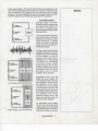
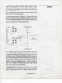
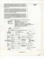
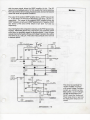
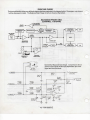
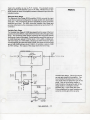
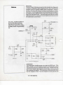
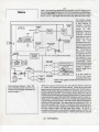
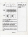
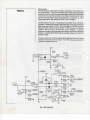
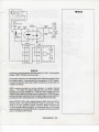
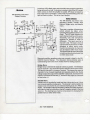
Notes
MACRO-TECH 5000VZ
OVERVIEW
At first glance the MA-5000VZ looks a great deal Hke any other MA
Series amplifier, except that ¡t is physically larger and puts out more
power. The internal structure of the MA-5000VZ is, however, quite
different from other models in the MA une. To the user, this one is like
the others, but with a f ew more f eatures. To the technician, this amplifier
representsaradicaldeparturefromthe"normal"Crowndesign. Previous
chapters covered the "normal," this chapter shall endeavorto take the
MA-5000VZ as a unique entrty.
The amplifier ¡s protected from all common hazards that plague highpower amplifiers, including shorted, open or mismatched loads,
overloaded power supplies, excessive temperature, chain-destruction
phenomena, input-overload damage, and high-frequency blowups.
The unit protects loudspeakers from DC in the input signal and from
turn-on and turn-off transients. It also detects and prevenís unwanted
DC on the outputs. Additional protection features include input current
sense, overvoltage (AC mains).
A mode of protection which may be switched on or off is called
Loudspeaker Offset Integration (LOI). The LOI circuit, when switched
on, prevenís excessive bass frequency cone excursions below the
audible frequency range. It operates essentially as a band-pass filter.
The low frequencies are rolled off at 18dB/oclave with a -3dB córner of
35 Hz (Butterworth response). Ullra-sonics are rolled off wilh a second
order Bessel response and -3dB córner of SOkHz.
A compression circuil in each channel may be switched off, on slow, or
on fast by swilches on Ihe rear panel. This compressor is aclivaled by
eilherinputoverloadord¡stort¡on(cl¡pping). Compression ratio is infinite
(operates as a peak limiter).
Thefour-quadrant lopology used in the grounded oulpul slages is called
Ihe grounded bridge and makes full use of Ihe power supplies. This
patentad lopology also makes peak-lo-peak voltages available lo the
load which are twice the vollage any output device ¡s ever exposed to.
The grounded bridge is covered in detail in the BASICS seclion of this
texl.
MA-5000VZ - 1
Notes
The two channels may be used together to double the voltage (bridgedmono)orthecurrent(parallel-mono)presentedto the load. Thisfeature
gives the User flexibility in maximizing the power available to the load.
Output power of the amplifier is rated as follows (assumes 120V 60Hz
AC mains):
StereoSohm: 1300W/CH
Stereo4ohm: 2000W/Ch
Stereo2ohm: 2500W/Ch
Bridge Mono 8 ohm: 4000W
Bridge Mono 4 ohm: 5000W
Parallel Mono 2 ohm: 4000W
Parallel Mono 1 ohm: 5000W
Macro-Tech amplifiers utilize a wide bandwidth multiloop design with
state of the art compensation techniques. This produces ideal behavior
and results ¡n ultra-low distortion valúes.
Aluminum extrusions have been widely used for heatsinks in power
amplifiers due to their low cost and reasonable performance. However,
measured on a watts per pound or watts per volume basis, the extrusión
technology doesn't perform nearly as well as the thermal diffuser
technology developed for Macro-Tech power amplifiers.
Our thermal diffusers are fabricated from custom cut fin stock that
provides an extremely high ratio of área to volume, or área to weight. All
power devices are mounted directly to massive heat spreaders that are
electrically hot. Making the heat spreaders electrically hot allows
MA-5000VZ:
CHANNEL1
SHOWN
4 (ooep)
MA-5000VZ Overall Block
Diagram
D
(ODEP)
2 - MA-5000VZ
improved thermal performance by eliminating the insulating interface
underneath the power devices. The chassis itself is used as part of the
thermal circuit, and this maximizes utilization of the available resources.
Air flow in this amplifier is front to rear, also a departure from other
Macro-Techs. Fan speed is a function of ODEPIevel. AlthoughODEP
was covered in detail in the BASICS section of this text, the specif ics of
the MA-5000VZ ODEP circuit are unique and will be covered here.
OUTPUT STAGE CIRCUITRY
The MA-5000VZ, like other Macro-Techs, uses the grounded bridge. It
does differ, however, in certain aspects. For example, quadrants use
four devices ¡n parallel ratherthan the normal máximum of three. Output
stages are also physically built in a modular way, for ease of field
replacement.
Electrically, there are also a few differences. Bias servo networks
consist of two transistor devices per Vbe multiplier (one set for high side,
one set for low side). Also, ODEP affects the low side as well as the high
side by stealing low side bias and drive. Taking that a step further, any
protective action which limits, mutes, or shuts down the amplifier will
accomplish the same thing by stealing drive.
Circuitry on the positive and negative output modules ¡nclude bias
circuitry, current limit circuitry (the MA-5000VZ has two speed current
limit), last voltage amplifiers (LVA's), pre-driyers, drivers, and output
devices. Temperature sensors are also mounted to the heatsinks vía
the output modules. These deliver ¡nformation to the main module
which computes actual calibrated temperature for ODEP and
temperature measurement.
H-15V
R571
2.7K
U50O V.
LM334 r
L
r£
Positive (NPN) Output Stage
Thermal Sensor Circuitry
3
R572
R584
2.7K
227
O.5OW
\
+TEMP1 :
The positive LVA's (Q501, Q502, and Q503)convert the negative output
of the voltage translator stage to a positive drive voltage for the NPN
High Side (HS) predriver. There are three LVAtransistorsin parallel due
to the very high voltages (therefor higher current and thermal
requirements) that are present when the power supply is in high voltage
mode. D522 prevenís the +LVA'sfromproducinga high negative output
to the HS NPN stage.
MA-5000VZ - 3
Notes
Notes
Q507, Q508, and Q509 are the -LVA's and are arranged ¡n mirror image
to the +LVA's, ¡ncluding D513.
On the positive side D514, D515, and C506 vía the +LVA's act to limit
slew rate. D514 and D515 also prevent dangerously excessive current
through the LVA's. D516, D517, and C507 are the negative HS mirror
image.
Q534 and Q540 provide two-speed current limiting ¡n the output stage.
Sense lines are arranged such that excessive current through any single
HS output device will result in current limit protection. Q535 and Q541
are the negative side mirror image.
Q503 on the positive output module works in tándem with Q505 on the
negative output module as a Vbe multiplier circuit. They produce and,
with great stabilily, control biasforthe High Side NPN and PNP devices.
Potentiometer R505 is used precisely set bias voltage. Bias voltage is
easily measured from pin 2 (hot) to pin 4 of ATE ports TP1 and TP2.
Refer to section 2 for appropriate test procedures.
Q504¡stheHSNPNpre-driverandQ511 istheHSNPNdriver. These
devices are biased class AB for ultra low distortion in the zero-crossing
región.
Q513, Q515, Q517, and Q536 are the HS NPN output devices. These
devices are biased class B, in soft cut-off, Together with driver and predriver, they function as a three-deep Darlington. The output devices
work ¡n parallel as a giant composite. The over-all bias topology is
referred to as AB+B, originally conceived and patented by Crown
engineers in 1966. This ¡s still the most efficient, stable, and distortion
free method used today.
Positive LVA, Portion of HS Bias,
& Positive Current Limit Section
VCC1
D51O
R595
3
82K
C536
O.O01
r-
R5O5
HIGH) 500
High Side +LVA's, Current Limit,
and the portion of the Bias Servo
Network on the Positive Output
Module.
SIDE ';
BIAS U
Emitter Sense
Output Audio
4 - MA-5000VZ
D506 is theflybackdiode forthe HS NPN output quadrant. In the event
that a back EMF (flyback) pulse exceeds power supply voltage, the
flyback diode will shunt this voltage to the supply in order to protect the
output devices.
Notes
PNP pre-drivers, drivers, output devices, and flyback diode D508 are a
mirror image of the NPN side.
Overall the High Side of bridge operates much like a conventional output
stage, but the Low Side (LS) is quite unique.
The LS senses output voltage and common (ground) buss potential.
The audio output is inverted by U503. Also in the U503 input circuitry
are static and dynamic balance controls. These controls provide a fine
balance of the grounded bridge. Output of the op-amp drives the LS predriver circuits through the LS bias network.
LS bias ¡s controlled in a fashion similar to that of the HS. Two
transistors, Q529 and Q530, along fix LS bias voltage as measured from
pin 15(hot)topin13ofapplicableATEportTP1 orTP2. Potentiometer
R556 adjusts bias in the LS.
Diodes D504 and D505 control polarity of applied LS drive signal. Via
the bias transistors signal ¡s delivered to the bases of the pre-drivers
Q527 (NPN) and Q528 (PNP). Pre-drivers, drivers, and output devices
in the LS opérate class AB+B, exactly like the HS. The major difference
¡s that rather than driving a load, the NPN and PNP stages control the
ground reference for the high voltage rails. As the HS NPN's conduct,
LS PNP's conduct, and vice versa (as explained in section 4.2.1).
When the ODEP circuit senses that limiting drive is necessary to prevent
a dangerous thermal condition, ¡t provides an output which limits drive
OUTPUT POSITIVE SECTION
+VCC1
+VCC BUSS BAR
Q513
Q515 Q517
H-VCC1
Q536
'
D5O6
+ LVA
C5O6
220pF
High Side Predrivers,
Drivers, Output Devices,
and Flyback Diodes.
Notice the various sense
lines. These are used
for various functions
such as VZ switching
sense and protection
features.
_L C510
' O.O1
MA-5000VZ - 5
I-15V
-I-VCC1
I-15V
o
R552
1OO
C524
2OOpF
R553
1OO
D518
To NPN LS
Predriver
15V
I
A
k
5
^ D5£ 4
5
r
_L
os:6
C534
!47pF
l
C52 6
10p =
J
—
D521
<
R554
1 .821<
R547
4.99K
C52S
xH
R56O
47K
U5O3 •
LM6364 g
N
d
' R555
> 1K
RS56
500
4
1f
D5 D4
y
H
JjH
—
C528
33OOpF
LOW S >>[ DE
BIAS
OUT1 B
I
COMM1
1
'
1
Low Side of Bridge: sensing amplifier output and ¡nverting the signal,
Low Side Bias (portion on positive output module), and differential
circuit which clamps Low Side signal ¡n the event of ODER or other
protective function.
I
¡T
L
> H534
D507 > 12
X 2W
Q538
tí
r
rj
BU
V| Q51
Q527
Q525
Q523
N
470uH
-
r^^V^VN
kr
.
*T
R544
51
R546
100
R550
13K
C522
0.033
C520
r-
+VCC1
+VCC1
+VCC1
0.022
R582 ¿
0. 33 >
5W
S
¿ R536
> 0.33
S 5W
•
i
S R538
> 0.33
S 5W
/ R54O
> 0.33
S 5W
i
-*S V"
R542
4. 3
0. 50W
r N r^^>1^Jl-t Ql ice; n A c(
LLL
6 - MA-5000VZ
ni||
Low Side of Bridge: including P
Driver, Output Devices, and Fl^
Diode on the NPN side.
to the output stages. For the HS, this limiting ¡s accomplished on the
main module and isexplained ¡nsect¡on4.4. Forthe LS, ODEP provides
(via wires labeled ±LL) a signal which limits bias feed to the LS output
devices. This is accomplished through current mirrors Q532 and Q531
(LS NPN quadrant), and Q542 and Q543 (LS PNP quadrant).
VZ POWER SUPPLY
The VZ supply in the MASOOOVZworks, inconcept, very
much like the MA-3600VZ. For
the sake of completeness,
some conceptual things will be
duplicated here.
POWER
TRANSISTOR
SPEAKER
LOAD
VZ means Variable Impedance
and is the ñame of Crown's
patented articulated power
supply technology. It enables
Crown to pack tremendous
power into just 5.25 inches of
vertical rack space.
POWER
TRANSISTOR
VZ POWER SUPPLY
POWER
TRANSISTOR
SPEAKER
LOAD
VZ
STAGE
VZ
STAGE
POWER
TRANSISTOR
Low Voltage, High Current Mode
VZ POWER SUPPLY
POWER
TRANSISTOR
VZ
STAGE
SPEAKER
LOAD
POWER
TRANSISTOR
VZ
STAGE
High Voltage, Low Current Mode
A power supply must be large
enough to handle the máximum
voltage and current necessary
for the amplifier to drive its
máximum rated power into a
specified load. In the process
of fulfilling this requirement
cónventional power supply
designs produce lots of heat,
are heavy, and take up precious
real estáte. And it's no secret
that heat is one of a power
amplifiers worst enemies.
According to Ohm's Law, the
bigger the power supply, the
more heai the power transistors
must dissipate. Also, the lower
the resistance of the power
transistors, the more voltage
you can deliverto the load. But
at the same time that you lower
the resistance of the transistors,
you increase the current
passing through them, and
again ¡ncrease the amount of
heat they must dissipate.
An articulated power supply,
like VZ, can circumvent much
of this problem by reducing the
voltage appliedto the transistors
when less voltage is required.
MA-5000VZ - 7
Notes
Notes
Reducing the voltage reduces the heat. Since the amplifier runs cooler,
you can safely pack more power into the chassis.
The VZ supply is divided ¡nto segments to better match the voltage and
current requirements of the power transistors. Remember that audio
signáis like music are complex waveforms.
For music the average level is always much less than the peak level.
This means a power supply does not need to produce full voltage all the
time.
The VZ supply is divided into two parís. When the voltage requirements
are not high, it opérales in a parallel mode to produce less vollage and
more current.
The power transistors slay cooler and are nol torced lo needlessly
dissipate heal. This is Ihe normal operaling mode of Ihe VZ power
supply.
When Ihe vollage requiremenls are high VZ swilches to a series mode
to produce higher vollage and less currenl. The amplified oulpul signal
never misses a beal and gels full vollage when it needs il—not when il
doesn't need ¡t.
Sensing circuilry walches Ihe vollage of Ihe signal lo delermine when
GROUNDEDBRIDGE
OUTPUT STAGE
VZ
Power Supply
Input
R = Switch Resistance
8 - MA-5000VZ
^
to switch VZ modes. The switching circuitry is designed to prevent
audible switching distortion to yield the highest dynamic transfer
function—you hear only the musió and not the amplifier. You get not
only the máximum power with the máximum safety, you also get the best
power matching to your load.
Actual current flow with power supply and grounded bridge operating
together is shown on the previous page.
The individual components are shown below. Upstream of the toroid
transformer, though not shown, is where shutdown protection and softstart circuitry taps in to control AC mains ¡nput to the power supply. The
VZ Control circuitry senses audio level and switches the articulating VZ
supplies to either parallel (high current) mode for lower level audio, or
series (high voltage) mode for high program peaks.
Toroid
Bridge 1
In both examples it can be seen that when the MOSFET switch is off,
the dual supplies are torced to opérate ¡n a parallel mode. Audio level
is sensed via a line tapping off the NFb loop. When audio level ¡s rising
and at about 80% of the parallel mode supply voltage, the MOSFETs
(the switch is actually a three-device composite switch) are turned on.
No current will flow through either of the control diodes (D810 and D811,
as shown for channel 1) because reverse polarity is applied through the
MOSFET switch. Since this happens to both rectifier sources at the
same time, and the negative side of Bridge 1 ¡s then shorted to the
positive side of Bridge 2, the supplies are forced to opérate in series
mode. Like two batteries, the supplies will provide double voltage in
series mode, double current ¡n parallel mode.
Although shipped from the factory ¡n normal VZ mode, the user may
switch modes to lock low voltage (high current), lock high voltage, or
opérate the supply in Bi-ODEP mode. Bi-ODEP is similar to normal VZ
MA-5000VZ - 9
Notes
Notes
mode, except that ¡n the event ODEP ¡s activated to protect the
amplifier, the VZ will automatically lock into low voltage (high current)
mode. While this mode of operation will cool the amplifier more quickly
in the event that the thermal reserve ¡s exhausted, it may cause voltage
clipping rather than ODEP limiting, this may be a worse condition for
speakers. Seldom will the amplifier be operated locked in high current
mode unless a very low impedance is being driven. By the same token,
it ¡s also unlikely that a user will opérate the amplifier locked in high
voltage mode for the thermal reasons mentioned.
To Bottom Rectifier
Positivo Sense
/N
VCC BUSS BAR
-VCC BUSS BAR
N/
To Top Rectifier
Negative Sense
From 555 for
Switch Control
-VCC BUSS BAR
VZ Switch Control Circuitry
10-MA-5000VZ
VZ SUPPLY CIRCUITRY
For simplicity, only channel 1 circuitry will be covered unless noted
otherwise. Circuitry.forthe VZ supply (and lowvoltage supply) is located
on the control module. The actual VZswitch circuit is located on the VZ
switch assembly. In this assembly are the two bridge rectif ¡ers, two f ilter
capacitors, MOSFET switches, and control diodes D810 and D811.
Three MOSFETs are used in parallel for sharing the high currents
supplied to the rails.
Notes
WARNING: From a sen/ice standpoint, 'rt is critical to note that VZ
switch control circuitry is NOT ground referenced. Any attempt to take
voltage measurements using a ground reference when voltage ¡s
applied will not only be unreliable, but may be extremely dangerous.
Serious damage to equipment or personnel may occur ¡f this is
attempted.
The output of a 555 timer (U703) on the control module determines
whether the MOSFETs are switched on (high) or off (low). This 555
device and the various sources that feed the 555 are the things that
make the articulation work wfíéh and how desired.
The master 555 trigger is controlled by the output of U702A. S700,
physically accessible from behind the front grille, determines the VZ
operating mode. In high voltage mode the output of U702A ¡s held low.
This in turn keeps the 555 output high and the MOSFETs are kept on.
In the high current mode U702A is held ¡n the opposite polarity keeping
the output of the 555 low and the MOSFETs off. In the AUTO position
of S700, the audio level sense circuitry controls the threshold and reset
inputs to the 555. The 555 will then switch states to high voltage when
the audio level is sufficient and will switch back down automatically when
Low Voltage Power Supply,
including DC Pulse network
for Soft-start and Fan Control
circuitry.
MA-5000VZ - 11
Notes
level has dropped sufficiently. Capacitors ¡n the U705 circuitry control
the speed of the down-shift. In the Bi-ODEP mode, the switch opérales
as it would ¡n AUTO mode unless ODER ümiting is ¡n progress. When
ODER limiting occurs optic coupler U704 shorts a negative potential (VCC) to the 555 reset control to turn the MOSFET switches off and keep
them off (low voltage/high current mode) until the ODER limiting
condition clears.
Upstream of the toroids are the soft-start and protection mechanisms
used to power down the amplifier. See Protection Systems.
The low voltage power supply utilizes a sepárate transformer. The front
panel power switch and a 1A fuse (F702) are the only components
upstream of this transformer. The output of the transformer produces
±24VDC unregulated. U715 and U716 produce regulated ±15VDC
respectively. A sepárate fullwaverectifier produces pulsedDC for Overvoltage sense and Soft-start control.
ODEPTHEORY: MA-5000VZ
To protect the output stages from adverse thermal conditions, a
specially developed "ODER" (Output Device Emulation Protection)
circuit is used. It produces a complex analog output signal proportional
to the always changing safe operating área (SOA) margin of the output
transistors. This output signal controls the Voltage Translatorstage and
Low Side output stage bias. This action removes only the drive that may
exceed the safe-operating-area of the output stage.
Thermal sensors give the ODER circuitry vital Information on the
operating temperature of the heat sinks on which the output devices are
mounted. This temperature signal combines with the complex ODER
signal to form the heart óf the patented ODER protection scheme. Refer
to block diagram on the next page for a discussion of the basic operation
of the ODER system.
The ODER circuitry actually comes in two parts, one positive and the
other negative. For the purposes of discussion, only channel 1 ODER
circuitry is covered here, and focus will primarily be on the positive half.
An LM-334Z thermal sensor provides a calibrated output from the output
modules. At 25°C its output ¡s 2.98V, with a 10mV increase per every
1°C rise in heatsink temperature.
This thermal sensor output, from the positive sensor, goes to three
destinations. First ¡s a buffer which drives the caübrated temperature
test point at pin 7 of TP1/TP2. Second ¡s an over-temperature limit trip.
This will cause both the positive and the negative ODER circuit to go into
and remain in hard ODER until the heatsinks cool. Third, it goes down
into a circuit which combines thermal and output power information for
proportionalfan control and, when needed, limiting. The thermal sensor
from the negative output module only performs this lastfunction.
A pair of sense unes from the Low Side emitter resistors provide current
information. Combined with VCC information actual instantaneous
power is calculated. A combining circuit determines the net thermal
12-MA-5000VZ
Notes
level has dropped sufficiently. Capacitors in the U705 circuitry control
the speed of the down-shift. In the Bi-ODEP mode, the switch opérales
as it would in AUTO mode unless ODEP limiting ¡s in progress. When
ODER ümiting occurs optic coupler U704 shorts a negative potential (VCC) to the 555 reset control to turn the MOSFET switches off and keep
them off (low voltage/high current mode) until the ODEP limiting
condition clears.
Upstream of the toroids are the soft-start and protection mechanisms
used to power down the amplifier. See Protection Systems.
The low voltage power supply utüizes a sepárate transformer. The front
panel power switch and a 1A fuse (F702) are the only components
upstream of this transformer. The output of the transformer produces
±24VDC unregulated. U715 and U716 produce regulated ±15VDC
respectively. A sepáratefullwave rectif¡er produces pulsed DC for Overvoltage sense and Soft-start control.
ODEPTHEORY: MA-5000VZ
To protect the output stages from adverse thermal conditions, a
specially developed "ODEP" (Output Device Emulation Protection)
circuit is used. It produces a complex analog output signal proportional
to the always changing safe operating área (SOÁ) margin of the output
transistors. This output signal controls the Voltage Translatorstage and
Low Side output stage bias. This action removes only the drive that may
exceed the safe-operating-area of the output stage.
Thermal sensors give the ODEP circuitry vital ¡nformation on the
operating temperature of the heat sinks on which the output devices are
mounted. This temperature signal combines with the complex ODEP
signal to form the heart of the patented ODEP protection scheme. Ref er
to block diagram on the next page for a discussion of the basic operation
of the ODEP system.
The ODEP circuitry actually comes ¡n two parts, one positive and the
other negative. For the purposes of discussion, only channel 1 ODEP
circuitry is covered here, and focus will primarily be on the positive half.
An LM-334Z thermal sensor provides a calibrated output from the output
modules. At 25°C its output is 2.98V, with a 10mV increase per every
1°C rise in heatsink temperature.
This thermal sensor output, from the positive sensor, goes to three
destinations. First is a buffer which drives the calibrated temperature
test point at pin 7 of TP1/TP2. Second ¡s an over-temperature limit trip.
This will cause both the positive and the negative ODEP circuit to go into
and remain in hard ODEP until the heatsinks cool. Third, it goes down
into a circuit which combines thermal and output power Information for
proportional fan control and, whenneeded, limiting. The thermal sensor
from the negative output module only performs this last function.
A pair of sense lines from the Low Side emitter resistors provide current
information. Combined with VCC information actual instantaneous
power ¡s calculated. A combining circuit determines the net thermal
12-MA-5000VZ
Notes
Also tapping in to the ODER output control of LS bias feed and Voltage
Translator feed are signáis from the fault, power (turn-on delay), and
power loss (brown-out) circuits. By using the output of ODER for ±LL
and ±LH control, these sources can mute the audio to the ouíput stage:
a. until power-up delay has timed out; b. immediately upon indication
of any failure mode; c. and immediately upon loss of AC mains (powerdown or actual loss of AC service).
±TEMP signáis are produced by U500 and U501 on the output modules.
U108, on the main module, is a buffer which drives the temperature
sense test point. U117A hasafixed window voltage of 6.2VviaZener
D129. If heatsink temperature level exceeds about 130°C U117A
output will cause both the positiva and negative ODER amplifiers to go
into hard ODER limiting. When the thermal condition clears this ümiting
condition will also clear.
+VCC enters via dual PNP transistor pack U116. Positive ODER bias
isadjustedbyR182. The voltage atthat point controls thestatic balance
of the U116 device. U116 combines the VCC and output current sense
information, the output of which represents output power level. The
common output is brought into RN101 where it provides the reference
for temperature and power. U112B is the active device and, together
Positive ODER
-15V
C130
0.1
14-MA-5000VZ
condition based on the power being delívered for the existing heat level.
The ODER amplifier accepts íhis input informaíion and, using an RC
modei of the heat transfer characteristics of the output devíces (as
mounted in the heatsinks), creates a complex output proportional to
thermal reserve.
Notes
Output from the positive ODER amplifier ranges from -12V (cold) to +9V
(hard ODER). This output drives the positive Low Síde bias feed control
circuit and the negative High Side Voltage Translator feed control
circuit. Also, this circuit provides test poini moniíoring information and
Bi-ODEP VZ mode control information.
Output from the negative ODER amplifier ranges from +12V (cold) to 9V (hard ODER). This output drives the negative LS bias feed control
circuit and the positive HS Voltage Translator feed control circuit. Also,
this circuit provides test point monitoring information, Bi-ODEP VZ
mode control information, and front panel ODER (thermal reserve) LED
control information.
Channel 1 ODER Circuitry shown (channel 2 is idéntica!)
ODER Inputs:
Temperatura
±VCC
Output Current
On Main Module
OffMain
Module
oo—
+Ten p 1
Calibrated Temperatura Output
Hot
-+9V
Buffer Amplifier
LM-334Z
nermal Sensor
2.98Vat25'C,
lOmV/'CRise)
CC
•s
ODER Outputs:
Calibrated Temperature, for monitoring
±ODEP Level, for monitoring
±ODEP Level, for Bi-ODEP control of VZ Supply
±ODEP Level, to limit drive at ±Voltage Transiators (±LH)
±ODEP Level, to limit Low Side Bias (±LL)
ODER Indication (front panel LEDs)
Thermal Limit Amplifier
-12V
*+ODEP Output
+VC
-LH1
+IC
+LL1
+ICC M1
FAULT1
PWR1
PWR LOSS
Q519 LS
Output
$Re
I
Dutput Buss I
I
-ICO M 1
?Re
+LH1
-1C1
/
Q524 LS
•> Output
-LL1
-VC
*J
CC
*--ODER Output
CC^ -Ten p 1
LM-334Z
hermal Sensor
MA-5000VZ-13
Notes
AIso tapping in to the ODER output control of LS bias feed and Volíage
Translator feed are signáis from the fault, power (turn-on delay), and
power loss (brown-ouí) circuits. By using íhe output of ODER for ±LL
and ±LH control, these sources can mute the audio to the output stage:
a. untíl power-up delay has timed out; b. immediately upon ¡ndication
of any failure mode; c. and immediately upon loss of AC mains (powerdown or actual loss of AC sen/ice).
±TEMP signáis are produced by U500 and U501 on the output modules.
U108, on the main module, is a buffer which drives the temperature
sense test point. U117A has a fixed window voltage of 6.2V via Zener
D129. If heatsink temperature leve! exceeds about 130°C U117A
output will cause both the positive and negative ODER amplifiers to go
into hard ODER iimiting. When thethermal condition clearsthis limiting
condition will also clear.
+VCC enters via dual PNP transistor pack U116. Positive ODER bias
isadjustedbyR182. The voltage atthat point controls the static balance
of the U116 device. U116 combines the VCC and output current sense
information, the output of which represents output power level. The
common output is brought into RN101 where it provides the reference
for temperature and power. U112B isthe active device and, together
Positive ODER
-15V
2
<
+ICOM1
14-MA-5000VZ
U116
UPA75HA
/ H180
> 100
wíth the power signal, drives the ODER amplifier U112A. The RC
network in the feedback path of U112A models the thermal junctions
from output devíce die to housing, housing to case, and caseto heatsink
under both static and dynamic conditions.
Notes
The output of the posrtive ODER amplifier drives +ODEP test point pin
11. Italso drives U114A and U114B which in turn drive -LH and +LL
respectively. The output of the negative ODER amplifier drives the
ODER indicatíon circuitry and -ODER test point pin 9. Negative ODER
also drives U114C and U114D which in turn drive +LH and -LL
respectively.
Also entering the U114 comparator networks are the PWR (power relay
engage), PWRLOSS (brown-ouí), and FAULT (any protection which
shuts down the amplifier) signáis via blocking diodes. If any of these
signáis drop low the f eed to LS bias and Voltage Translator drive will be
shut down via ±LL and ±LH. This action mutes all audio in the event of
a dramatic failure.
-ODER
Output:
+ 12V Cold
-9V Hot
This circuit is essentially the
"resulí" of ODER, its output.
±LH control Voltage Translator
current; ±LL control Low Stde
Bias current. ±LL7LH volíages
will also be activated by the
FAULT circuit, the "brown-out"
Power Loss circuit, or any time
the main power relays are not
closed.
MA-5000VZ-15
FRONT END THEORY
Thefront-end portion of the over-all block diagram has been exploded in the diagram below. Once again, only channel
1 will be discussed in detail. The Balanced Gain Stage circuitry is shown at the bottom.
MA-5000VZ FRONT END:
(CHANNEL 1 SHOWN)
Torac
/i KXDRIVER/
^ INTEGRATOR
¿^
—
DISPLAY ^
^Sx.
CACT
^
fy • .:,.-.• i
COMPRESSOF
DEVICE 1 -«— INTEGRATOR ^-O^O^QyT
BALANCED
INPUTS
FXQ
.
Q
^QtmOL*
VOLTAGE
TRANSLATOR
_.
~ *"
.„.
LVA
I
LEVEL
|\
CONTROL
^\
u
ODEP
¿
BALANCED
GAIN STAGE
ERROR AMP
3¡
1
26dB
.775VO
\
O >O—
LCH
1
-
VOLTAGE
TRANSLATOR
~"~
LVM
^^>
(
1.
SEIJQITIUITV
JSITIVITY
S WITCH
VARIABLE
STAGE
OIAUK
GAiN
4 t
'1
o ií(< <^T
i——^
^
U103
MA-5000VZ Balanced Gain Stage. Compression device
shown across ¡nputs shunts input dependent upon error
signal and front end level.
VTL5C2
|
R371
R370>
Circuitry
51K
47K y
<
C1O2
,
I
-=Lr
R1OO
4.99K
82PFH
10K
1
R102
4.99K
+ 15V
0
A
R1O4
oMR-iT>
o inO3
-a
H1
R105 >
5QPK
I
r*
_L_
R1O1
4.99K
—
J>
4
C101
x
~~^
~
^^*_
"v,^^
o
62pF< R107
< 1OK
< 1
¡I
Ó
16-MA-5000VZ
\o Level
/ Control
15O
25V NP
C151
8
2
C1O3
,
O.1
4.99K
i—\r\r\
4-30pF
' '
R106
II
I
S1,50
°- 1
•
Input to the amplifíer ¡s oníy vía P.l.P. module. The standard module
shipped with the MA-5000VZ is the P.I.P.-FXQ. Whether this or any
other module is used, the amplifier senses a balanced input from the
installed module.
Notes
Balanced Gain Stage
The Balanced Gain Stage (BGS) amplifier U100A converts the input
audio from a balanced configuration to single-ended with (electrically)
unity gain. The compression device is essentially a shunt across the
balanced input lines. The BGS drives the Variable Gain Stage and
provides information to the compressor control circuit and tothe P.l.P.
connector.
Variable Gain Stage
The Variable Gain Stage (U1 OOB) taps signal from the wiper of the front
panel level control (R120). Gain of the front-end ¡s set by the gain of this
stage. The sensitivity switch (S100, located on the rear panel) selects
the amount of gain ¡n this stage. Overall amplifier sensitivity may be set
for26dB fixed gain (about 5.1Vrms inpuí), 1.4V (+4dBu, unbalanced,
with 8ohmload), or0.775V (OdBu, unbalanced, with 8ohmload). Since
overall amplifier gain afterthis stage is 26dB, íhis stage will have a fixed
gain of OdB (26dB setting), about +12dB (1.4V setting), or about +16dB
(0.775V setting). The output of this stage drives the Error Amp.
FRONT PANEL
LEVEL
CONTROL
0.47
From BGS
,s>
^*^¡
/
\
R120
5K
11
•
II
To Error Amp
S\9
/\
R119
8.87K
1
1
1 R364
> 19. 1K
»
>
A
.' R121
,> 49. 9K
i1
1
3 I2
f1
0 0 Q- 0 g > ¿
>
6
c;i nn
O l \J\J
C107
1OO
35V
i
"
R122
49.9K
^
r-
<0
(N
Í4?
C1O8
12PF|(
i
1 R123
nr
i
e r^
^> 7
i
£- *^x^ U1OOB
•=^LX>
33078P
MA-5000VZ-17
Variable Gain Stage. This is the second
op-amp gain stage in the amplifier. Features include front panel level control a
rear panel switch to determine gain of this
stage. Gain of the all other stages is
fixed, therefore changing the gain of this
stage results in a change to overall
amplifier gain. In this case (üke other
Crown amplifiers) the input impedance is
varied to control gain of the op-amp.
Notes
Error Amp
The Error Amp (U 105) input comes from the Variable Gain Stage with
or wiíhout Loudspeaker Offset Integration (LOI), and is summed with
ampüfier output in a negative feedback (NFb) configuration. Output of
the Error Amp drives the Voltage Translators and provides error signal
information. An error signal (spike) is produced any time the shape of
the output waveform differs from the output of the Variable Gain Stage
and LOI by more than 0.05%. This error signal drives the error signal
(ES) input to the P.I.P. connector, the error signal sense test point, and
the compression control circuií.
Error Amp. Amplifier feedback ¡s
summed with input audio and
fixes gain from the input to this
stage to the output of the amplifier
at 26dB (a factor of approxímately
20).
From LOI
To Ch 2 for Parallel Mono
Compressor
The compression circuitry senses error signal and BGS level. If the
BGS overloads, or an error signal is present, the compression control
circuit (U101) produces a compression drive pulse. A switch on the rear
panel selects speed of the ¡ntegrator circuit to follow, and may shut off
the compressor all together. The compression drive pulse also drives
the IOC Integrator (U 102). The IOC integrator not only tells the IOC
18-MA-5000VZ
Inverting Stages
Overall the amplifier is non-inverting. Four stages within the amplifier,
however, do invert the audio signal for a net norHnversion. The
individual stages are: the BGS, which inverts the audio; the Variable
Gain Stage, which inverts it back, the input side of U106 and U107 which
drivetheVoltageTranslatorsre-invertsthe audio (the VoltageTranslators
are a common-base confíguration for high voltage gain); and finally the
LVA's invert the audio for the last time for a net non-inversion through
the amplifier.
PROTECTION SYSTEMS
The MA-5000VZ has several protection mechanisms to limit drive or
shutdown the amplifier completely in the event of a fault of almost any
kind. Mechanisms include: ODER (covered in depth previously),
current limit (alsocovered previously), over-voltage (on AC mains), DC/
LFI.commonmodeoutputcurrent.output thermal, transformerthermal,
FET thermal, loss of AC mains, compression (covered previously), LOl
(covered previously), and slew rate limit (covered previously). After any
non-latching fault clears which has shut down the amplifier, the ampüf ier
will automatically powerback upvía soft-start. Becausethe fans within
the MA-5000VZ cool the amplifier to, under normal conditions, prevent
thermal shutdowns and ODER limiting, the fan control circuit is also
covered in this section.
On the following pagés you will f ind block diagrams of both the Soft-start
circuitry and the overall protection scheme. Each augments the other.
Soft-Start
Soft-start circuitry controls the rate at which power is initially applied to
the primary of the toroid transformers for the high-voltage power
supplies. For ease of explanation, assume the amplifier ¡s operating
properly and is just being turned on from the front panel power switch.
Before the power switch push-button is depressed, the input to the low
voltage supply is open. The high voltage supply is isolated via input relay
K700 and triac Q701 (which is in parallel with K700).
Several things occur immediately at turn-on. First the low voltage
supply powers up and produces its main unregulated ±24VDC and
regulated ±15VDC. It also immediately produces pulsed DC via fullwave rectifier D709/D714.
As this occursall op-amps in the amplifier receive power, including frontend stages, relay power control U111C, and standby control U111B.
The output of U111C powers relay K700 via relay drive transistor Q700.
When the output of this op-amp goes high, Q700 turns on and the relay
closes. The output of U111C is held low until the amplifier delay times
out by comparing a high voltage on its inverting input to an RC network
voltage on its non-inverting input. R329 and R330 fix a window at about
+10.4VDC. Atturn-onC220(a10uFcap)isful!yd¡scharged. Inthatfirst
instant it keeps -15V on the non-inverting input of U111 C, keeping its
output low. As the capacitor charges it produces a ramped rise in
voltage as it charges through R327. After about 4 seconds the voltage
between R327 and R328 exceeds the window voltage and U111C
output goes high, in tum causing relay K700 to cióse.
MA-5000VZ - 21
Notes
Notes
Q POWER
VSWITCH
r>O
Note: Any protection sign$Uviíhin the amplifier which is t¡a^<á to shut it
down will discria.rg^t'his
.
capacitor (C1 20) immediately causing ihe'fe
(K700) ítfefien.%ipon ciearance of such shut-down protection signa*
the ch ¿( ¿e w;" ':-ogin again with the same ramp effect and same delay.
TOCH 2 SOFT-START DRIVER
—O +15V
—O -15V
—O +24V
O -24V
CH 1 FAN
CONTROL
The ramped voitage
onthecapacitorC120
is also sensed by
Standby amplifier
U111B. Its unity gain
output
is noninverting. Itdrivesthe
Soft-start op-amp
(U/01A) inverting
¡nput with its ramp to
control the rate at
which the field
developsinthetoroid.
On the non-inverting
inputto U701A isíhe
pulsed DC drive from
the
U701B/Q708
pulse circuit. Jumper
JP1 may be set to 50
or 60Hz, but must be
set properly to nave
the correct pulse width
for soft-start. Pulse
width is determined by;
C717andeitherR7;;/
(50Hz) or R7^-'in
parallel wjg?!'R806
(60hU}>
It is the output of
U701A ihat really
controlsthe Soft-start.
Refer to the graphic of Soft •start waveforms on the
next page.
Soft-start block diagram. Note: DC
pulse stretching circuit shown in Low
Voitage Power Supply schematic cutaway on page 11.
When the output of U701A goes low, the opto-triac device U700 turns
on. While on the input triac Q700 conducís. Positor R702 litnits peak
input current to the toroid to a máximum of 22A (with 120VAC mains).
U701A combines the sloped input from the C120 circuitry onthe main
module with the pulsed DC. As the portíon of time which the output of
U701Agoeslowincreases, the amountof time whereAC mains conduct
to the transformar (via Q700 and R702) increases until it remains on.
When the U111C PWR circuit times out, the relay closes bypassing the
current límiting soft-start circuit. Soft-start control signáis are shown in
at the top of the next page. The uppersignal isproducedby C120. At
time O the amplifier is off. At time 1: the power swiích is pressed (on).
At time 2: C120 has fully charged, the magnetic fields have built up in
the high voitage supply, and the main relay closes. At time 3: a
protective action occurs; note that the DC supply remains. At time 4: the
conditionclearsandtherestartbegins. Time5isakintot¡me2,andtime
22 - MA-5000VZ
Notes
Soft-start waveforms. Timel: power
switch on. Time 2: relay engaged.
Time 3: protective action occurs. Time
4: protective action clears, Soft-startup beginsagain. Time 5: relay
engages. Time 6: amplifier turned off
by power switch.
C120
CHARGE
VOLTAGE
O
1
,
i
¿11*11 III m A M A H A M A HA II AltH
PULSEO
DC FROM
LVPS
11 lili 1U Hl U
!
O
1
lill
ii'**i
1 1
I
SOFT-START
TRIAC
CONTROL
6 is ampfcfter shutdown vía power swiyit. The lower graph shows Q701
operatioñ (htgfcv = on) The longá?- &701 is on, the more the main
transformer fieltMs^fett^^üilá.
Any time a protection mechanism has acted and íhe condition then
clears, this entire process repeats.
Over-Voltage
One mode of amplifier protection is a shutdown ¡n the event of overvoltage on the AC mains. This is sensed by the pulsed DC signal
produced by the full-wave rectifier in the low voltage supply.
R780 picks off the pulsed DC and U707D will, if the voltage ¡s too high,
shift its output to a low. When this happens the over-volt/therm red LED
on the control module lights and signal OV1 goes low to the main
module.
A low (over-voltage condition) on OV1 causes U211C to shift to a low
output. This low, through D1, causes C120 todischarge immediately.
This in turn causes the main relay to drop out, soft-start to reset, and the
±LL and ±LH to clamp audio drive. Over-voitage is a non-latching fault
condition.
MA-5000VZ - 23
Notes
LSNPN CURREN!
HSNPNCURRENT
OUTPUT
MODULE
-±r
RED
OWTSW
1 OVER-VOLTAGE
Overall protection scheme block diagram.
DC/LFI
The amplif ier senses it own output for DC or very low f requency and wil!
interrupt the amplifier channel in the event of DC or low frequency.
The feedback loop is sensed for voltage and the current sense signal
provides current information. An RC network at the input to U109C/D
will prevent the LFI circuit from activating with normal audio frequency
material, and will ensure acíivation with high leve! subsonic currents or
voltages.
24 - MA-5000VZ
+ 15V
Notes
Over-Voltage and Thermal Switch
¡nformation combines to produce the
"OV" signal driving U211C. The
remote standby (RS) function (from the
P.I.P. module) also ties ¡nto the signal
pathlabelledTIMER/STBY. They are
shown together since, schematically,
they share a common control line to the
C120 Soft-start and PWR (relay)
control circuitry.
R324
D1
TIMER/STSY1
+ 15V
+ 15V
R771
3.3*0
CHANNEL 2
O VER-VOLT/
THERM
Over-Voltage and Thermal
Switch information combines
to produce the "OV" signal
driving U211C. The r
U707C
LM339
-vr
If U109C/D sense a DC (or LF) level, ¡t will output a low which will,
through D102, discharge C120 and initiate power supply shutdown. A
low will also cause the DC/LF red LED on the main module to light.
MA-5000VZ - 25
-15V
E10O
JA» RED
Notes
CH1
DC/LF
R338^
47 K
R159
3.3K
-15V
¡_ 14
DC/LF
Circuitry
R339
14.3K
-15V
> R327 > R329
S 100K S 82K
Q
U109C
LM339
19
1O
9
D102
11
14.
la
> 13
MUTE1 ^
i
yt
D
C120
10
19
> R328
S 1.3M
J
8
R330
> 470K
<1
'í
-Í5V
| labNSb
C183I
R355
unió
' 6'8K
LM339
(-) MWI-i^
C184
* 1
-f5V
C18S
i22 x01
To ODER
R189
8.15K
Common Mode Output Current FAULT
circuit. In the event of high current in
both the positive and negative halves of
the output stage simultaneously, this
circuit will shut down the amplifier. This
is the only latching protection function in
theMA-5000VZ
CH1 " E102
OUTPUT MODULE
26 - MA-5000VZ
Common Mode Output Current
Common mode current ¡n the output stage can only be due to an output
stage faílure, or full power output of RF energy. Common mode current
occurs when a high current level exists in both the positive and the
negative halves of the output stage.
U115 is a specíalty device. It serves as both an Opto-SCR, and as a
conventional SCR. It must have both an optic gate and conventional
gate firing at the same time in order to latch. The conventional gate is
fired by current sense of the output stage Low-side. The optic gate is
fired by the High-side current sense. If high currents exist ¡n both sides
simuitaneously, the SCR will latch on, and remain on until the unit is
turned off.
When the SCR latches, low voltage causes the red LED (labeled Output
Module) to light, and places a low on the FAULT signal line. A low on
the FAULT line is sensed, via D112, by C120. Once again, a low here
discharges C120 and shuts down the amplífier.
Output Thermal
Output over-temperature protection was covered in the ODER Circuitry
section of this text. The calibrated temperature sense f rom the positive
half of the output stage drives an over-temperature amp, U117A. If
heatsink temperature exceeds a limit of about 130°C, the amplifier will
go into hard ODEP. This does not shut down the amplifier, but does
clamp the audio.
Transformer Thermal
The main powertransformers have built-in thermal switches which open
in the event of transformer over-temperature. In the event that the
thermal switch opens in the channel 1 toroid, Q709 turns on causing
U707D to go low. When ¡t does, the over-voltage/thermal switch LED
on the control module is energized and the OV1 signal is tripped. This
results in amplifier shutdown by way of shared over-voltage circuitry.
FET Thermal
The MOSFET switches in the VZsupply have built-in thermal protection.
In the event of over-heat they functionally open, locking the VZ supply
¡n low voltage (high current) mode, regardless of the control signal.
Power Loss
The MA-5000VZ has the ability to sense a "brown-out" condition on the
AC service. This is accomplished by sensing the low-voltage power
supply at U111A. Local capacitors onthe ±15VDC supply to this chip
keep it powered for a short time after the low voltage supply drops out
on power-down/loss.
An RC network, consisting of C1 and R6, will cause the output of U111A
to shift low the instant low voltage is lost. This negative potential
discharges C120 causing immediateopening of the main relay and reset
of the Soft-start circuitry. It is essential thaí C120 be discharged
immediately ¡n the event that power is restored before C120 would
otherwise discharge. Thepower-losscircuit is common to both channels.
Its output also goes to ±LL and ±LH to immediately mute audio upon
power-down or power-loss, thus preventing turn-off audio noise.
MA-5000VZ - 27
Notes
Fan Control
The MA-5000VZ, unlike other members of the Macro-Tech family, has
two on board fans. They are mounted to the chassis dívider assembly
and pulí cool air from the front and discharge it across the output stage
heatsinkstotherearoftheamplifier. Aíso unlike the other Macro-Techs,
the fans are fully ODEP proportional (opérate in proportion to output
stage temperature and calibrated ODEP control voltage).
Notes
U713B combines channel 1 temperature and ODEP level, U713A for
channe!2. D706andD707formad¡odeORgaíe. The output of the OR
gate drives one input to U707B. The other ¡nput to U707B is from the
DC pulse width control círcuit (U701B). U707B opérales in a fashion
similar to that of U707A, the Soft-start control amplifier. A graphic
example of the fan control waveforms would look a good deal like those
¡n Fig. 4.7, except that the thermal drive would be unique f rom that of the
Soft-start ramp.
The fans will aíso be forced to opérate at full speed in the event a toroid
transformer thermal switch trips open. Note that very early units did not
¡nclude this additional circuit.
+ 15V
U701B
LM339
To Fan
Control
Triac
U713A"
TL°72CS731
R799
4.7K
-
-ftv
28 - MA-5000VZ
Notes
U707B
LM339
DISPLAY
Amplifierfront panel indication includes a total of 7 LED's. These include
Enable, ODER, SPI/IOC, and ILOAD/ILIMIT.
The Enable indicator is an amber light which indicates presence of the
low voltage supply. It is powered by the unregulated +24VDC supply.
It will be on any time the power switch is depressed (unless the low
voltage fuse blows).
ODER indicators provide an on-line indication of amplifier thermal
reserve. The LED's are amber (although they may have a reddish
appearance) and are normally on. They dim and/or extinguish in the
eventthattheamplifier'sthermal reserve ¡sexhausted. ODER indicators
will also extinguish whenever the main supply relays are open (such as
a protection action being activated, or during Soft-start time-out).
Green SPI/IOC LED's show signal presence (SPl) and any form of
distortion (IOC) They flash dimlywith the audioto show signal. Inthe
event of an IOC condition (output waveform differs from input by
>0.05%) the light will be on brightly. An occasional flash of !OC usually
indicates clipping. If the IOC light locks in it usually ¡ndicates a protective
action, including ODER limiting.
MA-5000VZ - 29
Notes
MA-5000VZ Front Panel
Display Circuitry
ILOAD/ILIMIT LED's flash green with the audio when program material is
being deüvered to a load. Its functíon ¡s similar to that of the SPI, except
that it comes on when the amplifier is loaded, SPI does not require a
load. This is the ILOAD f unction. In the event of current ümiting action the
light will flash to yellow. This ¡s the ILIMIT function.
MONO MODES
The MA-5000VZ has three main
operating modes, namely dual
(stereo), bridge mono, and parallel
mono.
There are a number of precautions
which should be taken when
operatingtheamplifierineithermono
mode. The VZ mode switches for
each channel must be set the same.
Sensitivity, LOI, and Compressor
switches for channel 2 make no
difference. The input must be to
channeM only. The input to channel
2 and conírols for channel 2 are NOT
defeated in either mono mode,
therefor no connection to channel 2
may be made in either mono mode.
The channel 2 level control should be
turned down (counterclockwise) f ully
¡n either mono mode.
Monaural amplifier operating modes are covered in detail in the MA5000VZ Owner's Manual. The discussion below primarily aides in
understanding how to the mono modes work for testing purposes.
Bridge Mono
Bridge mono is intended for loads of 4 ohms or greater. The feedback
loop for channel 1 also drives the input to channel 2 in this mono mode.
The input to channel 2 is, however, inverted. This causes the output of
channel 2 ío be of equal magnitude and opposite polarity (for double
voltage output) the output of the amplifier is balanced, and channel hot
output is connected to load hot (+), channel 2 hot output is connected
to load return (-).
Parallel Mono
Parallel mono is intended for loads less than 4 ohms (as Iow as 1 ohm)
¡n a monaural amplifier configuration. The channeM and 2 amplifier hot
outputs must be shorted by an external shorting buss (10 AWG or
larger). The amplifier output to the load(s) is taken f rom either channel's
hot output to load hot, and either channel's negative output to the load
return (-). The shorting buss must be removed prior to changing from
parallel mono to either other mode.
30 - MA-5000VZ