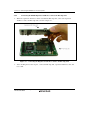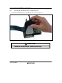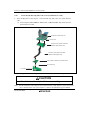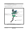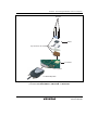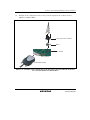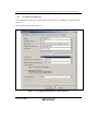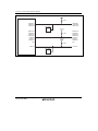
1
To our customers,
Old Company Name in Catalogs and Other Documents
On April 1st, 2010, NEC Electronics Corporation merged with Renesas Technology
Corporation, and Renesas Electronics Corporation took over all the business of both
companies. Therefore, although the old company name remains in this document, it is a valid
Renesas Electronics document. We appreciate your understanding.
Renesas Electronics website: http://www.renesas.com
April 1st, 2010
Renesas Electronics Corporation
Issued by: Renesas Electronics Corporation (http://www.renesas.com)
Send any inquiries to http://www.renesas.com/inquiry.
Notice
1.
2.
3.
4.
5.
6.
7.
All information included in this document is current as of the date this document is issued. Such information, however, is
subject to change without any prior notice. Before purchasing or using any Renesas Electronics products listed herein, please
confirm the latest product information with a Renesas Electronics sales office. Also, please pay regular and careful attention to
additional and different information to be disclosed by Renesas Electronics such as that disclosed through our website.
Renesas Electronics does not assume any liability for infringement of patents, copyrights, or other intellectual property rights
of third parties by or arising from the use of Renesas Electronics products or technical information described in this document.
No license, express, implied or otherwise, is granted hereby under any patents, copyrights or other intellectual property rights
of Renesas Electronics or others.
You should not alter, modify, copy, or otherwise misappropriate any Renesas Electronics product, whether in whole or in part.
Descriptions of circuits, software and other related information in this document are provided only to illustrate the operation of
semiconductor products and application examples. You are fully responsible for the incorporation of these circuits, software,
and information in the design of your equipment. Renesas Electronics assumes no responsibility for any losses incurred by
you or third parties arising from the use of these circuits, software, or information.
When exporting the products or technology described in this document, you should comply with the applicable export control
laws and regulations and follow the procedures required by such laws and regulations. You should not use Renesas
Electronics products or the technology described in this document for any purpose relating to military applications or use by
the military, including but not limited to the development of weapons of mass destruction. Renesas Electronics products and
technology may not be used for or incorporated into any products or systems whose manufacture, use, or sale is prohibited
under any applicable domestic or foreign laws or regulations.
Renesas Electronics has used reasonable care in preparing the information included in this document, but Renesas Electronics
does not warrant that such information is error free. Renesas Electronics assumes no liability whatsoever for any damages
incurred by you resulting from errors in or omissions from the information included herein.
Renesas Electronics products are classified according to the following three quality grades: “Standard”, “High Quality”, and
“Specific”. The recommended applications for each Renesas Electronics product depends on the product’s quality grade, as
indicated below. You must check the quality grade of each Renesas Electronics product before using it in a particular
application. You may not use any Renesas Electronics product for any application categorized as “Specific” without the prior
written consent of Renesas Electronics. Further, you may not use any Renesas Electronics product for any application for
which it is not intended without the prior written consent of Renesas Electronics. Renesas Electronics shall not be in any way
liable for any damages or losses incurred by you or third parties arising from the use of any Renesas Electronics product for an
application categorized as “Specific” or for which the product is not intended where you have failed to obtain the prior written
consent of Renesas Electronics. The quality grade of each Renesas Electronics product is “Standard” unless otherwise
expressly specified in a Renesas Electronics data sheets or data books, etc.
“Standard”:
8.
9.
10.
11.
12.
Computers; office equipment; communications equipment; test and measurement equipment; audio and visual
equipment; home electronic appliances; machine tools; personal electronic equipment; and industrial robots.
“High Quality”: Transportation equipment (automobiles, trains, ships, etc.); traffic control systems; anti-disaster systems; anticrime systems; safety equipment; and medical equipment not specifically designed for life support.
“Specific”:
Aircraft; aerospace equipment; submersible repeaters; nuclear reactor control systems; medical equipment or
systems for life support (e.g. artificial life support devices or systems), surgical implantations, or healthcare
intervention (e.g. excision, etc.), and any other applications or purposes that pose a direct threat to human life.
You should use the Renesas Electronics products described in this document within the range specified by Renesas Electronics,
especially with respect to the maximum rating, operating supply voltage range, movement power voltage range, heat radiation
characteristics, installation and other product characteristics. Renesas Electronics shall have no liability for malfunctions or
damages arising out of the use of Renesas Electronics products beyond such specified ranges.
Although Renesas Electronics endeavors to improve the quality and reliability of its products, semiconductor products have
specific characteristics such as the occurrence of failure at a certain rate and malfunctions under certain use conditions. Further,
Renesas Electronics products are not subject to radiation resistance design. Please be sure to implement safety measures to
guard them against the possibility of physical injury, and injury or damage caused by fire in the event of the failure of a
Renesas Electronics product, such as safety design for hardware and software including but not limited to redundancy, fire
control and malfunction prevention, appropriate treatment for aging degradation or any other appropriate measures. Because
the evaluation of microcomputer software alone is very difficult, please evaluate the safety of the final products or system
manufactured by you.
Please contact a Renesas Electronics sales office for details as to environmental matters such as the environmental
compatibility of each Renesas Electronics product. Please use Renesas Electronics products in compliance with all applicable
laws and regulations that regulate the inclusion or use of controlled substances, including without limitation, the EU RoHS
Directive. Renesas Electronics assumes no liability for damages or losses occurring as a result of your noncompliance with
applicable laws and regulations.
This document may not be reproduced or duplicated, in any form, in whole or in part, without prior written consent of Renesas
Electronics.
Please contact a Renesas Electronics sales office if you have any questions regarding the information contained in this
document or Renesas Electronics products, or if you have any other inquiries.
(Note 1) “Renesas Electronics” as used in this document means Renesas Electronics Corporation and also includes its majorityowned subsidiaries.
(Note 2) “Renesas Electronics product(s)” means any product developed or manufactured by or for Renesas Electronics.
User’s Manual
SH-2A, SH-2 E200F Emulator
Additional Document for User’s Manual
Supplementary Information on
Using the SH72546RFCC, SH72544R,
SH72543R, SH72531, and SH72531FCC
Renesas Microcomputer Development
Environment System
SuperH™ Family
SH7254R Group
SH7253 Group
R0E572546EMU00E
Rev.2.00 2009.02
Rev. 2.00 Feb. 18, 2009 Page ii of vi
REJ10J1938-0200
Notes regarding these materials
1. This document is provided for reference purposes only so that Renesas customers may select the appropriate
Renesas products for their use. Renesas neither makes warranties or representations with respect to the
accuracy or completeness of the information contained in this document nor grants any license to any
intellectual property rights or any other rights of Renesas or any third party with respect to the information in
this document.
2. Renesas shall have no liability for damages or infringement of any intellectual property or other rights arising
out of the use of any information in this document, including, but not limited to, product data, diagrams, charts,
programs, algorithms, and application circuit examples.
3. You should not use the products or the technology described in this document for the purpose of military
applications such as the development of weapons of mass destruction or for the purpose of any other military
use. When exporting the products or technology described herein, you should follow the applicable export
control laws and regulations, and procedures required by such laws and regulations.
4. All information included in this document such as product data, diagrams, charts, programs, algorithms, and
application circuit examples, is current as of the date this document is issued. Such information, however, is
subject to change without any prior notice. Before purchasing or using any Renesas products listed in this
document, please confirm the latest product information with a Renesas sales office. Also, please pay regular
and careful attention to additional and different information to be disclosed by Renesas such as that disclosed
through our website. (http://www.renesas.com )
5. Renesas has used reasonable care in compiling the information included in this document, but Renesas
assumes no liability whatsoever for any damages incurred as a result of errors or omissions in the information
included in this document.
6. When using or otherwise relying on the information in this document, you should evaluate the information in
light of the total system before deciding about the applicability of such information to the intended application.
Renesas makes no representations, warranties or guaranties regarding the suitability of its products for any
particular application and specifically disclaims any liability arising out of the application and use of the
information in this document or Renesas products.
7. With the exception of products specified by Renesas as suitable for automobile applications, Renesas
products are not designed, manufactured or tested for applications or otherwise in systems the failure or
malfunction of which may cause a direct threat to human life or create a risk of human injury or which require
especially high quality and reliability such as safety systems, or equipment or systems for transportation and
traffic, healthcare, combustion control, aerospace and aeronautics, nuclear power, or undersea communication
transmission. If you are considering the use of our products for such purposes, please contact a Renesas
sales office beforehand. Renesas shall have no liability for damages arising out of the uses set forth above.
8. Notwithstanding the preceding paragraph, you should not use Renesas products for the purposes listed below:
(1) artificial life support devices or systems
(2) surgical implantations
(3) healthcare intervention (e.g., excision, administration of medication, etc.)
(4) any other purposes that pose a direct threat to human life
Renesas shall have no liability for damages arising out of the uses set forth in the above and purchasers who
elect to use Renesas products in any of the foregoing applications shall indemnify and hold harmless Renesas
Technology Corp., its affiliated companies and their officers, directors, and employees against any and all
damages arising out of such applications.
9. You should use the products described herein within the range specified by Renesas, especially with respect
to the maximum rating, operating supply voltage range, movement power voltage range, heat radiation
characteristics, installation and other product characteristics. Renesas shall have no liability for malfunctions or
damages arising out of the use of Renesas products beyond such specified ranges.
10. Although Renesas endeavors to improve the quality and reliability of its products, IC products have specific
characteristics such as the occurrence of failure at a certain rate and malfunctions under certain use
conditions. Please be sure to implement safety measures to guard against the possibility of physical injury, and
injury or damage caused by fire in the event of the failure of a Renesas product, such as safety design for
hardware and software including but not limited to redundancy, fire control and malfunction prevention,
appropriate treatment for aging degradation or any other applicable measures. Among others, since the
evaluation of microcomputer software alone is very difficult, please evaluate the safety of the final products or
system manufactured by you.
11. In case Renesas products listed in this document are detached from the products to which the Renesas
products are attached or affixed, the risk of accident such as swallowing by infants and small children is very
high. You should implement safety measures so that Renesas products may not be easily detached from your
products. Renesas shall have no liability for damages arising out of such detachment.
12. This document may not be reproduced or duplicated, in any form, in whole or in part, without prior written
approval from Renesas.
13. Please contact a Renesas sales office if you have any questions regarding the information contained in this
document, Renesas semiconductor products, or if you have any other inquiries.
Rev. 2.00 Feb. 18, 2009 Page iii of vi
REJ10J1938-0200
Rev. 2.00 Feb. 18, 2009 Page iv of vi
REJ10J1938-0200
Contents
Section 1 System Configuration ........................................................................1
1.1
1.2
Components of the Emulator ............................................................................................ 1
System Configuration ....................................................................................................... 5
Section 2 Connecting the Emulator to the User System ....................................9
2.1
2.2
2.3
2.4
2.5
2.6
2.7
Connecting the Emulator to the User System ................................................................... 9
Connecting the Emulator to the User System by Using the EV-chip Unit........................ 9
2.2.1 Connecting the EV-chip Unit to the Emulator ..................................................... 9
2.2.2 Connecting the E200F Expansion AUD Trace Unit to the EV-chip Unit............ 12
2.2.3 Connecting the H-UDI/AUD Probe to the EV-chip Unit..................................... 14
2.2.4 Connecting the E200F Expansion AUD Trace Unit, Emulation Memory Unit,
and EV-chip Unit ................................................................................................. 15
2.2.5 Connecting the EV-chip Unit to the User System Interface Cable ...................... 16
2.2.6 Using the E200F Emulator as a Stand-Alone Unit .............................................. 18
Connecting the Emulator to the User System by Using the H-UDI Port Connector......... 19
Installing the H-UDI Port Connector on the User System ................................................ 20
Pin Assignments of the H-UDI Port Connector ................................................................ 21
Recommended Circuit between the H-UDI Port Connector and the MCU ...................... 25
2.6.1 Recommended Circuit (36-Pin Type) .................................................................. 25
Using the IC Socket to Mount an MCU on the User System............................................ 28
Section 3 Software Specifications when Using the SH72546RFCC, SH72544R,
SH72543R, SH72531, and SH72531FCC.........................................33
3.1
3.2
Differences between the MCU and the Emulator ............................................................. 33
Specific Functions for the Emulator when Using the SH72546RFCC, SH72544R,
SH72543R, SH72531, and SH72531FCC......................................................................... 39
3.2.1 Event Condition Functions .................................................................................. 39
3.2.2 Trace Functions.................................................................................................... 46
3.2.3 Notes on Using the JTAG (H-UDI) Clock (TCK) and AUD Clock (AUDCK)... 67
3.2.4 Notes on Setting the [Breakpoint] Dialog Box .................................................... 67
3.2.5 Notes on Setting the [Event Condition] Dialog Box and
the BREAKCONDITION_ SET Command ........................................................ 68
3.2.6 Performance Measurement Function ................................................................... 68
3.2.7 Emulation RAM Setting Function ....................................................................... 72
3.2.8 [Select Emulation] Dialog Box at Activation of the Emulator ............................ 75
3.2.9 [Configuration] Dialog Box................................................................................. 78
Rev. 2.00 Feb. 18, 2009 Page v of vi
REJ10J1938-0200
3.2.10 EVA AUD Monitoring Function ......................................................................... 83
Section 4 User System Interface Circuits ..........................................................85
4.1
4.2
User System Interface Circuits ......................................................................................... 85
Delay Time for the User System Interface........................................................................ 94
Rev. 2.00 Feb. 18, 2009 Page vi of vi
REJ10J1938-0200
Section 1 System Configuration
Section 1 System Configuration
1.1
Components of the Emulator
The E200F emulator supports the SH72546RFCC, SH72544R, SH72543R, SH72531, and
SH72531FCC. Table 1.1 lists the components of the emulator.
Table 1.1 Components of the Emulator
Classification Component
Hardware
Emulator main unit
AC adapter
Appearance
Quantity
1
Remarks
R0E0200F1EMU00:
Depth: 185.0 mm, Width: 130.0
mm,
Height: 45.0 mm, Mass: 321.0 g
Product numbers: 0001 to 0113
1
Input: 100 to 240 V
Output: 12 V 4.0 A
Depth: 120.0 mm, Width: 72.0 mm,
Height: 27.0 mm, Mass: 400.0 g
Product numbers: 0114 or later
AC cable
1
Input: 100 to 240 V
Output: 12 V 3.0 A
Depth: 99.0 mm, Width: 62.0 mm,
Height: 26.0 mm, Mass: 270.0 g
1
Length: 2000 mm
Rev. 2.00 Feb. 18, 2009 Page 1 of 94
REJ10J1938-0200
Section 1 System Configuration
Table 1.1 Components of the Emulator (cont)
Classification Component
Hardware
(cont)
USB cable
External probe
Appearance
Quantity
Remarks
1
Length: 1500 mm, Mass: 50.6 g
Product numbers: 0001 to 0113
1
Length: 500 mm,
Pins 1 to 4: probe input pins,
T: trigger output pin,
G: GND pin
Product numbers: 0114 or after
Software
E200F emulator setup
program,
SH-2A, SH-2 E200F
Emulator User’s Manual,
and
Supplementary
Information on Using the
SH72546RFCC,
SH72544R, SH72543R,
SH72531, and
SH72531FCC*
1
Length: 500 mm,
Pins 1 to 4: probe input pins,
T: trigger output pin,
G: GND pin
1
R0E0200F1EMU00S,
R0E0200F1EMU00J,
R0E0200F1EMU00E,
R0E572546EMU00J,
R0E572546EMU00E
(provided on a CD-R)
Note: Additional document for the MCUs supported by the emulator is included. Check the target
MCU and refer to its additional document.
Rev. 2.00 Feb. 18, 2009 Page 2 of 94
REJ10J1938-0200
Section 1 System Configuration
Table 1.2 Optional Components of the Emulator
Classification Component
Hardware
Trace cable
Appearance
Quantity
Remarks
1
R0E200F0ACC00
Length: 300mm, Mass: 65g
Profiling expansion unit
1
R0E200F0EPU00
Depth: 98.0 mm, Width: 115.0 mm,
Height: 15.2 mm, Mass: 52 g
Expansion AUD trace unit
1
R0E0200F1ATU00:
Depth: 90.0 mm, Width: 125.0 mm,
Height: 15.2 mm, Mass: 88 g
Emulation memory unit
1
R0E0200F1MSR00 (8 Mbytes),
R0E0200F1MSR01 (16 Mbytes):
Depth: 90.0 mm, Width: 125.0 mm,
Height: 15.2 mm,
Mass: 81 g (R0E0200F1MSR00), 85
g (R0E0200F1MSR01)
Note that it is not possible to
connect these emulation memory
units at the same time.
EV-chip unit
1
R0E572546VKK00:
Depth: 110.0 mm, Width: 125.0 mm,
Height: 15.2 mm, Mass: 116 g
Rev. 2.00 Feb. 18, 2009 Page 3 of 94
REJ10J1938-0200
Section 1 System Configuration
Table 1.2 Optional Components of the Emulator (cont)
Classification Component
User system interface
cable
(board unit and cable unit)
Appearance
Quantity
Remarks
1
R0E0200F1CKL10:
(board unit)
Depth: 60.0 mm, Width: 110.0 mm,
Height: 26.0 mm, Mass: 44 g
R0E0200F1CKL10:
(cable unit)
Depth: 35.0 mm, Width: 267.0 mm,
Height: 5.05 mm, Mass: 8 g
User-system interface
converter board
1
R0E572546CBF10:
Depth: 43.5 mm, Width: 30.0 mm,
Height: 10.2 mm, Mass: 12 g
1
R0E572531CFK10:
Depth: 43.0 mm, Width: 40.0 mm,
Height: 10.2 mm, Mass: 17 g
(PRBG0272FA-A
converter board)
User-system interface
converter board
(PLQP0176KB-A
converter board)
Rev. 2.00 Feb. 18, 2009 Page 4 of 94
REJ10J1938-0200
Section 1 System Configuration
1.2
System Configuration
Figures 1.1 shows examples of the emulator system configuration.
- When the EV-chip unit is used
Expansion AUD trace unit
Profiling expansion unit
High-performance
Embedded Workshop
Emulation
memory unit
Trace cable
EV-chip unit
USB 2.0/1.1
User system
interface cable
PC
E200F
IC socket
User system
- When the EV-chip unit is not used
Profiling expansion unit
Expansion AUD trace unit
High-performance
Embedded Workshop
Trace cable
USB 2.0/1.1
PC
E200F
Emulation
memory unit
User system
Figure 1.1 System Configuration Using the Emulator
Rev. 2.00 Feb. 18, 2009 Page 5 of 94
REJ10J1938-0200
Section 1 System Configuration
(1) System Configuration of the SH72546RFCC, SH72544R, and SH72543R
Table 1.3 shows the system configuration supported by the SH72546RFCC, SH72544R, and
SH72543R.
Table 1.3 System Configuration Supported by the SH72546RFCC/SH72544R/SH72543R
E200F
E200F
Profiling
Emulator
expansion unit
Trace cable
Expansion
Emulation
AUD
Memory Unit
Ev-chip Unit
User System
Interface Cable
Trace Unit
R0E0200F1EMU00
R0E0200F0EPU00
R0E0200F0ACC00
R0E0200F1ATU00
R0E0200F1MSR00
R0E5725460VKK00
R0E0200F1MSR01
R0E0200F1CKL10
R0E572546CBF10
*1
System
Supported
Not supported
Not supported
Not supported
Not supported
Not supported
Not supported
Supported
Not supported
Supported
Not supported
Not supported
Supported
Not supported
Supported
Not supported
Supported
Not supported
Not supported
Supported
Supported
Supported
Not supported
Supported
Supported
Not supported
Supported
Not supported
Supported
Not supported
Supported
Supported
Not supported
Supported
Supported
Supported
Not supported
Supported
Supported
Supported
Supported
Not supported
Supported
Not supported
Supported
Supported
Supported
Supported
Supported
Supported
Supported
Not supported
Not supported
Not supported
Not supported
Not supported
Supported
Supported
Supported
Not supported
Not supported
Supported
Not supported
configuration 1*2
System
configuration 2
System
configuration 3
System
configuration 4
System
configuration 5
System
configuration 6
System
configuration 7
System
configuration 8 *2
System
configuration 9
Rev. 2.00 Feb. 18, 2009 Page 6 of 94
REJ10J1938-0200
Section 1 System Configuration
Table 1.3 System Configuration Supported by the SH72546RFCC/SH72544R/SH72543R
E200F (Cont)
E200F
Profiling
Emulator
expansion unit
Trace cable
Expansion
Emulation
AUD
Memory Unit
Ev-chip Unit
User System
Interface Cable
Trace Unit
R0E0200F1EMU00
R0E0200F0EPU00
R0E0200F0ACC00
R0E0200F1ATU00
R0E0200F1MSR00
R0E5725460VKK00
R0E0200F1MSR01
R0E0200F1CKL10
R0E572546CBF10
*1
System
Supported
Supported
Supported
Not supported
Not supported
Supported
Supported
Supported
Supported
Supported
Supported
Not supported
Supported
Not Supported
Supported
Supported
Supported
Supported
Not supported
Supported
Supported
Supported
Supported
Supported
Supported
Supported
Supported
Not supported
Supported
Supported
Supported
Supported
Supported
Supported
Supported
configuration 10
System
configuration 11
System
configuration 12
System
configuration 13
System
configuration 14
Note 1: As the user system interface cable, be sure to use both the R0E0200F1CKL10 and
R0E572546CBF10 at the same time.
The user system interface cable is only used when the emulator is connected to the user
system; it is not required when the emulator system operates alone.
Note 2: To configure a system without using the EV-chip unit, the H-UDI port connector must be
installed on the user system. For design of the user system, refer to section 2.3, Connecting
the Emulator to the User System by Using the H-UDI Port Connector. Note that when a
system is configured in this way, the H-UDI pins or AUD pins of the device will be occupied.
Rev. 2.00 Feb. 18, 2009 Page 7 of 94
REJ10J1938-0200
Section 1 System Configuration
(2) System Configuration of the SH72531 and SH72531FCC
Table 1.4 shows the system configuration supported by the SH72531 and SH72531FCC.
Table 1.4 System Configuration Supported by the SH72531/SH72531FCC E200F
E200F
Profiling
Emulator
expansion unit
Trace cable
Expansion
Emulation
AUD
Memory Unit
Ev-chip Unit
User System
Interface Cable
Trace Unit
R0E0200F1EMU00
R0E0200F0EPU00
R0E0200F0ACC00
R0E0200F1ATU00
R0E0200F1MSR00
R0E5725460VKK00
R0E0200F1MSR01
R0E0200F1CKL10
R0E572531CFK10
*1
System
Supported
Not supported
Not supported
Not supported
Not supported
Not supported
Not supported
Supported
Not supported
Supported
Not supported
Not supported
Supported
Not supported
Supported
Not supported
Supported
Not supported
Not supported
Supported
Supported
Supported
Not supported
Supported
Supported
Not supported
Supported
Not supported
Supported
Not supported
Supported
Supported
Not supported
Supported
Supported
configuration 1*2
System
configuration 2
System
configuration 3
System
configuration 4
System
configuration 5
Note 1: For the user system interface cable, be sure to use both R0E0200F1CKL10 and
R0E572531CFK10 as a set.
The user system interface cable is only used when the emulator is connected to the user
system; it is not required when the emulator system operates alone.
Note 2: To configure a system without using the EV-chip unit, the H-UDI port connector must be
installed on the user system. For design of the user system, refer to section 2.3, Connecting
the Emulator to the User System by Using the H-UDI Port Connector. Note that when a
system is configured in this way, the H-UDI pins of the device will be occupied.
Rev. 2.00 Feb. 18, 2009 Page 8 of 94
REJ10J1938-0200
Section 2 Connecting the Emulator to the User System
Section 2 Connecting the Emulator to the User System
2.1
Connecting the Emulator to the User System
When the emulator is connected to the user system, use the optional EV-chip unit, user system
interface cable, and trace cable.
2.2
Connecting the Emulator to the User System by Using the EV-chip
Unit
The following describes how to connect the emulator to the EV-chip unit, expansion AUD trace
unit, emulation memory unit, trace cable, and user system interface cable.
2.2.1
Connecting the EV-chip Unit to the Emulator
• Open the cover of TRACE I/F on the side of the main unit case.
• Connect the trace cable to the EV-chip unit as shown in figure 2.1.
Rev. 2.00 Feb. 18, 2009 Page 9 of 94
REJ10J1938-0200
Section 2 Connecting the Emulator to the User System
Figure 2.1 Connecting the Trace Cable to E200F when Using the EV-chip Unit
Rev. 2.00 Feb. 18, 2009 Page 10 of 94
REJ10J1938-0200
Section 2 Connecting the Emulator to the User System
• Connect the EV-chip unit to the trace cable (CN1 side).
Figure 2.2 Connecting the Trace Cable to the EV-chip Unit
CAUTION
Check the location of pin 1 before connecting.
Rev. 2.00 Feb. 18, 2009 Page 11 of 94
REJ10J1938-0200
Section 2 Connecting the Emulator to the User System
2.2.2
Connecting the E200F Expansion AUD Trace Unit to the EV-chip Unit
• When the expansion AUD trace unit is used with the EV-chip unit, connect the expansion
AUD trace unit to the EV-chip unit as shown in figure 2.3.
Figure 2.3 Connecting the Expansion AUD Trace Unit to the EV-chip Unit
• After checking the location of pin 1, connect the EV-chip unit, expansion AUD trace unit, and
trace cable.
Rev. 2.00 Feb. 18, 2009 Page 12 of 94
REJ10J1938-0200
Section 2 Connecting the Emulator to the User System
Figure 2.4 Connecting the Expansion AUD Trace Unit, EV-chip Unit, and Trace Cable
CAUTION
Check the location of pin 1 before connecting.
Rev. 2.00 Feb. 18, 2009 Page 13 of 94
REJ10J1938-0200
Section 2 Connecting the Emulator to the User System
2.2.3
Connecting the H-UDI/AUD Probe to the EV-chip Unit
• Connect the H-UDI/AUD probe to the EV-chip unit as shown in figure 2.5.
Figure 2.5 Connecting the H-UDI/AUD Probe to the EV-chip Unit
CAUTION
Check the location of pin 1 before connecting.
Rev. 2.00 Feb. 18, 2009 Page 14 of 94
REJ10J1938-0200
Section 2 Connecting the Emulator to the User System
2.2.4
Connecting the E200F Expansion AUD Trace Unit, Emulation Memory Unit, and
EV-chip Unit
• When the expansion AUD trace unit is used with the emulation memory unit and EV-chip unit,
as shown in figure 2.6, connect them in the positions of (a), (b), and (c) for the expansion AUD
trace unit, emulation memory unit, and EV-chip unit, respectively.
• After checking the location of pin 1, connect the expansion AUD trace unit, emulation memory
unit, and EV-chip unit.
Figure 2.6 Connecting the Expansion AUD Trace Unit, Emulation Memory Unit, and EVchip Unit
CAUTION
Check the location of pin 1 and the position of each unit
before connecting.
Rev. 2.00 Feb. 18, 2009 Page 15 of 94
REJ10J1938-0200
Section 2 Connecting the Emulator to the User System
2.2.5
Connecting the EV-chip Unit to the User System Interface Cable
• After checking the location of pin 1, connect the EV-chip unit to the user system interface
cable.
(1) Connecting the SH72546RFCC, SH72544R, or SH72543R EV-chip Unit to the User
System Interface Cable.
Expansion AUD trace unit
EV-chip unit
Common user-system interface
adaptor cable (board unit)
x3
Common user-system interface
adaptor cable (cable unit)
User-system interface converter board
IC socket plug
IC socket
User system
Figure 2.7 Connecting User System Interface Cable and EV-Chip Unit
CAUTION
Check the location of pin 1 before connecting.
Note: For the method of connecting the user system interface cable and user system, refer to the
user’s manual for the user system interface cable for the individual supported MCU.
Rev. 2.00 Feb. 18, 2009 Page 16 of 94
REJ10J1938-0200
Section 2 Connecting the Emulator to the User System
(2) Connecting the SH72531 or SH72531FCC EV-chip Unit to the User System Interface
Cable.
Expansion AUD trace unit
EV-chip unit
Common user-system interface
adaptor cable (board unit)
x3
Common user-system interface
adaptor cable (cable unit)
User-system interface converter board
Cover for connecting the emulator
IC socket
User system
Figure 2.8 Connecting User System Interface Cable to EV-Chip Unit
CAUTION
Check the location of pin 1 before connecting.
Note: For the method of connecting the user system interface cable and user system, refer to the
user’s manual for the user system interface cable for the individual supported MCU.
Rev. 2.00 Feb. 18, 2009 Page 17 of 94
REJ10J1938-0200
Section 2 Connecting the Emulator to the User System
2.2.6
Using the E200F Emulator as a Stand-Alone Unit
If you are using the E200F emulator unit without connecting it to a user system, refer to table 1.3
and table 1.4 in section 1.2, System Configuration, and make connections as shown in figure 2.9
until the EV-chip unit becomes available.
Expansion AUD trace unit
EV-chip unit
When using the emulator as a
stand-alone unit
When connecting to the user system
Common user-system interface
adaptor cable (board unit)
x3
Common user-system interface
adaptor cable (cable unit)
User-system interface converter board
Figure 2.9 Connecting the E200F Emulator as a Stand-Alone Unit
Rev. 2.00 Feb. 18, 2009 Page 18 of 94
REJ10J1938-0200
Section 2 Connecting the Emulator to the User System
2.3
Connecting the Emulator to the User System by Using the H-UDI Port
Connector
To connect the E200F emulator (hereinafter referred to as the emulator) in a configuration without
an Ev-chip unit, the H-UDI port connector must be installed on the user system to connect the user
system interface cable. When designing the user system, refer to the recommended circuit
between the H-UDI port connector and the MCU.
It is impossible to connect the emulator to the 14-pin type connector that is recommended for the
E10A-USB emulator. The 36-pin type connector is the same as that of the E10A-USB emulator.
When designing the user system, read the E200F emulator user's manual and hardware manual for
the related device.
Table 2.1 shows the type number of the emulator, the corresponding connector type, and the use of
AUD function.
Table 2.1 Type Number, AUD Function, and Connector Type
Type Number
Connector
AUD Function
R0E200F1EMU00
14-pin connector
Not available
R0E200F1EMU00
36-pin connector
Available
The H-UDI port connector has the 36-pin and 14-pin types as described below. Use the 36-pin
connector when using the emulator.
1. 36-pin type (with AUD function)
The AUD trace function is supported. A large amount of trace information can be acquired in
realtime. The window trace function is also supported for acquiring memory access in the
specified range (memory access address or memory access data) by tracing.
2. 14-pin type (without AUD function)
The AUD trace function cannot be used because only the H-UDI function is supported. This
connector type is not available for the emulator. Use the E10A-USB emulator.
Rev. 2.00 Feb. 18, 2009 Page 19 of 94
REJ10J1938-0200
Section 2 Connecting the Emulator to the User System
2.4
Installing the H-UDI Port Connector on the User System
Table 2.2 shows the recommended H-UDI port connectors for the emulator.
Table 2.2 Recommended H-UDI Port Connectors
Connector
Type Number
Manufacturer
Specifications
36-pin connector
DX10M-36S
Hirose Electric Co., Ltd.
Screw type
DX10M-36SE,
DX10G1M-36SE
Lock-pin type
Note: When designing the 36-pin connector layout on the user board, do not connect any
components under the H-UDI connector.
Rev. 2.00 Feb. 18, 2009 Page 20 of 94
REJ10J1938-0200
Section 2 Connecting the Emulator to the User System
2.5
Pin Assignments of the H-UDI Port Connector
Figure 2.10 shows the pin assignments of the 36-pin H-UDI port connectors.
(1) Pin assignment of the SH72546RFCC, SH72544R, and SH72543R
Note: Note that the pin number assignments of the H-UDI port connector shown on the
following page differ from those of the connector manufacturer.
Rev. 2.00 Feb. 18, 2009 Page 21 of 94
REJ10J1938-0200
Section 2 Connecting the Emulator to the User System
Pin
No. Signal
1
AUDCK
2
GND
3
AUDATA0
Input/
Output*1
Pin
No.
Note
Output
19
Output
Signal
Input/
Output*1
TMS
Input
20
GND
21
_TRST
22
(GND)*4
23
TDI
24
GND
*2
4
GND
5
AUDATA1
6
GND
7
AUDATA2
8
GND
9
AUDATA3
10
GND
28
GND
11
_AUDSYNC*2 Output
29
UVCC
12
GND
30
GND
13
N.C.
31
_RES*2
14
GND
32
GND
15
N.C.
33
GND *3
16
GND
34
GND
17
TCK
35
N.C.
18
GND
36
GND
Output
Output
25
TDO
26
GND
27
Output
Input
Note
Input
Input
Output
_ASEBRKAK
/_ASEBRK *2
Input/
output
Output
Output
User reset
Output
Notes: 1. Input to or output from the user system.
2. The symbol (_) means that the signal is active-low.
3. The emulator monitors the GND signal of the user system and detects whether or not the user system is connected.
4. When the E200F probe head is connected to this pin and the _ASEMD pin is set to 0, do not connect to GND
but to the _ASEMD pin directly.
H-UDI port connector (top view)
Edge of the board
(connected to the connector)
φ 0.7+0.1
0
2
36
3
1
9.0
1.905
1.1
4.5
φ 2.8+0.1
0
4
(Pin 1 mark)
35
1.27
4.09
M2.6 x 0.45
H-UDI port connector (front view)
4.8
H-UDI port connector (top view)
3.9
37.61
43.51
: Pattern inhibited area
0.3
9.0
21.59
Unit: mm
Figure 2.10 Pin Assignments of the H-UDI Port Connector (36 Pins) for the
SH72546RFCC, SH72544R, and SH72543R
Rev. 2.00 Feb. 18, 2009 Page 22 of 94
REJ10J1938-0200
Section 2 Connecting the Emulator to the User System
(2) Pin assignment of the SH72531 and SH72531FCC
Note: Note that the pin number assignments of the H-UDI port connector shown on the
following page differ from those of the connector manufacturer.
Rev. 2.00 Feb. 18, 2009 Page 23 of 94
REJ10J1938-0200
Section 2 Connecting the Emulator to the User System
Pin
No. Signal
Input/
Output*1
Pin
No.
Note
Signal
Input/
Output*1
TMS
Input
1
N.C.
19
2
GND
20
GND
3
N.C.
21
_TRST
*2
4
GND
22
(GND)*4
5
N.C.
23
TDI
6
GND
24
GND
7
N.C.
25
TDO
8
GND
26
GND
9
N.C.
27
N.C.
10
GND
28
GND
11
N.C.
29
UVCC
GND
12
GND
30
13
N.C.
31
_RES*2
14
GND
32
GND
15
N.C.
33
GND *3
16
GND
34
GND
17
TCK
35
N.C.
18
GND
36
GND
Input
Note
Input
Input
Output
Input/output
Output
Output
User reset
Output
Notes: 1. Input to or output from the user system.
2. The symbol (_) means that the signal is active-low.
3. The emulator monitors the GND signal of the user system and detects whether or not the user system is connected.
4. When the E200F probe head is connected to this pin and the _ASEMD pin is set to 0, do not connect to GND
but to the _ASEMD pin directly.
H-UDI port connector (top view)
Edge of the board
(connected to the connector)
φ 0.7+0.1
0
36
3
1
9.0
1.905
1.1
4.5
2
φ 2.8+0.1
0
4
(Pin 1 mark)
35
1.27
4.09
M2.6 x 0.45
H-UDI port connector (front view)
4.8
H-UDI port connector (top view)
3.9
37.61
43.51
: Pattern inhibited area
0.3
9.0
21.59
Unit: mm
Figure 2.11 Pin Assignments of the H-UDI Port Connector (36 Pins) for the SH72531 and
SH72531FCC
Rev. 2.00 Feb. 18, 2009 Page 24 of 94
REJ10J1938-0200
Section 2 Connecting the Emulator to the User System
2.6
Recommended Circuit between the H-UDI Port Connector and the
MCU
2.6.1
Recommended Circuit (36-Pin Type)
Figure 2.12 shows the recommended circuit for connection between the H-UDI and AUD port
connectors (36 pins) and the MCU, and figure 2.13 shows a recommended circuit for connection
between the H-UDI port connectors (36 pins) and the MCU when the emulator is in use.
Notes: 1.
Do not connect anything to the N.C. pins of the H-UDI port connector.
2.
The _ASEMD pin must be 1 when the emulator is connected and 0 when the emulator
is not connected, respectively.
(1) When the emulator is used: _ASEMD = 1 (ASE mode)
(2) When the emulator is not used: _ASEMD = 0 (normal mode)
3.
When a network resistance is used for pull-up, it may be affected by a noise. Separate
TCK from other resistances.
4.
The pattern between the H-UDI port connector and the MCU must be as short as
possible. Do not connect the signal lines to other components on the board.
5.
The AUD signals (AUDCK, AUDATA3 to AUDATA0, and _AUDSYNC) operate in
high speed. Isometric connection is needed if possible. Do not separate connection nor
connect other signal lines adjacently.
6.
Since the H-UDI and the AUD of the MCU operate with the Vcc, supply only the Vcc
to the UVCC pin.
7.
The resistance values shown in figure 2.12 and figure 2.13 are for reference.
8.
For the pin processing in cases where the emulator is not used, refer to the hardware
manual of the related MCU.
Rev. 2.00 Feb. 18, 2009 Page 25 of 94
REJ10J1938-0200
Section 2 Connecting the Emulator to the User System
Vcc = 3.3-V power supply
All pulled-up at 4.7 kΩ or more
Vcc
Vcc
Vcc
H-UDI port connector
(36-pin type)
2
4
6
8
10
12
14
16
18
20
22
24
26
28
30
32
34
36
GND
AUDCK
GND
AUDATA0
GND
AUDATA1
AUDATA2
GND
GND
AUDATA3
GND
AUDSYNC
GND
AUDRST
GND
AUDMD
GND
TCK
GND
TMS
GND
TRST
GND
TDI
GND
TDO
GND
ASEBRKAK
GND
UVCC
GND
RES
GND
GND
GND
N.C.
MCU
1
AUDCK
3
AUDATA0
5
AUDATA1
7
AUDATA2
9
AUDATA3
11
AUDSYNC
13
AUDRST
15
AUDMD
17
TCK
19
TMS
21
TRST
23
TDI
25
TDO
27
ASEBRKAK
29
31
RES
33
35
1 kΩ
ASEMD
Reset signal
User system
Figure 2.12 Recommended Circuit for Connection between the H-UDI Port Connector and
MCU when the Emulator is in Use (H-UDI and AUD 36-Pin Type)
Rev. 2.00 Feb. 18, 2009 Page 26 of 94
REJ10J1938-0200
Section 2 Connecting the Emulator to the User System
Vcc = 3.3-V power supply
All pulled-up at 4.7 kΩ or more
Vcc
Vcc
Vcc
H-UDI port connector
(36-pin type)
2
4
6
8
10
12
14
16
18
20
22
24
26
28
30
32
34
36
GND
N.C.
GND
N.C.
GND
N.C.
GND
N.C.
GND
N.C.
GND
N.C.
GND
N.C.
GND
N.C.
GND
TCK
GND
TMS
GND
TRST
GND
TDI
GND
TDO
GND
N.C.
GND
UVCC
GND
RES
GND
GND
GND
N.C.
MCU
1
3
5
7
9
11
13
15
17
TCK
19
TMS
21
TRST
23
TDI
25
TDO
27
29
31
RES
33
35
1 kΩ
ASEMD
Reset signal
Figure 2.13 Recommended Circuit for Connection between the H-UDI Port Connector and
MCU when the Emulator is in Use (H-UDI 36-Pin Type)
Rev. 2.00 Feb. 18, 2009 Page 27 of 94
REJ10J1938-0200
Section 2 Connecting the Emulator to the User System
2.7
Using the IC Socket to Mount an MCU on the User System
Figure 2.14 shows the example of the configuration when the IC socket is used to mount an MCU
on the user system using and the E200F emulator is connected in on-chip debugging mode.
(1)
Example of the configuration of the on-chip connection when the IC socket is used for
SH72546RFCC, SH72544R, or SH72543R
Rev. 2.00 Feb. 18, 2009 Page 28 of 94
REJ10J1938-0200
Section 2 Connecting the Emulator to the User System
Screws
MCU
Top cover for IC socket
IC socket
User system
H-UDI/AUD probe
Figure 2.14 Example of the Configuration of the On-Chip Connection when the IC Socket
is Used for the SH72546RFCC, SH72544R, or SH72543R
Rev. 2.00 Feb. 18, 2009 Page 29 of 94
REJ10J1938-0200
Section 2 Connecting the Emulator to the User System
CAUTION
1. Check the location of pin 1 before connecting.
2. IC socket and IC top cover for mounting on the user
system, we recommend the following products.
IC socket: BSSOCKET272Z2021RE21N socket (manufactured
by Tokyo Eletech Corporation).
Top cover for IC socket : LSPACK272Z22021RE02 cover
(manufactured by Tokyo Eletech Corporation).
Rev. 2.00 Feb. 18, 2009 Page 30 of 94
REJ10J1938-0200
Section 2 Connecting the Emulator to the User System
(2)
Example of the configuration of the on-chip connection when the IC socket is used for
SH72531 or SH72531FCC
Screws
Top cover for IC socket
MCU
IC socket
User system
H-UDI/AUD probe
Figure 2.15 Example of the Configuration of the On-Chip Connection when the IC Socket
is Used for the SH72531 or SH72531FCC
Rev. 2.00 Feb. 18, 2009 Page 31 of 94
REJ10J1938-0200
Section 2 Connecting the Emulator to the User System
CAUTION
1. Check the location of pin 1 before connecting.
2. IC socket and IC top cover for mounting on the user
system, we recommend the following products.
IC socket: NQPACK176SD-ND socket (manufactured by Tokyo
Eletech Corporation).
Top cover for IC socket : HQPACK176SD cover (manufactured
by Tokyo Eletech Corporation).
Rev. 2.00 Feb. 18, 2009 Page 32 of 94
REJ10J1938-0200
Section 3 Software Specifications when Using the SH72546RFCC, SH72544R, SH72543R, SH72531, and SH72531FCC
Section 3 Software Specifications when Using the
SH72546RFCC, SH72544R, SH72543R, SH72531, and
SH72531FCC
3.1
Differences between the MCU and the Emulator
1. When the emulator system is initiated, it initializes the general registers and part of the control
registers as shown in table 3.1. The initial values of the MCU registers are undefined. When
the emulator is initiated from the workspace, a value to be entered is saved in a session.
Table 3.1 Register Initial Values at Emulator Link Up
Register
Emulator at Link Up
R0 to R14
H'00000000
R15 (SP)
Value of the SP in the power-on reset vector table
PC
Value of the PC in the power-on reset vector table
SR
H'000000F0
GBR
H'00000000
VBR
H'00000000
TBR
H'00000000
MACH
H'00000000
MACL
H'00000000
PR
H'00000000
FPSCR*
H'00040001
FPUL*
H'00000000
FPR0-15*
H'00000000
Note: If the MCU does not incorporate the floating-point unit (FPU), these registers are not
displayed.
Note: When a value of the interrupt mask bit in the SR register is changed in the [Registers]
window, it is actually reflected in that register immediately before execution of the user
program is started. It also applies when the value is changed by the REGISTER_SET
command.
2. The emulator uses the H-UDI; do not access the H-UDI.
Rev. 2.00 Feb. 18, 2009 Page 33 of 94
REJ10J1938-0200
Section 3 Software Specifications when Using the SH72546RFCC, SH72544R, SH72543R, SH72531, and SH72531FCC
3. Low-Power States (Sleep, Software Standby, and Module Standby)
⎯ When the emulator is used, the sleep state can be cleared with either the clearing function
or with the [STOP] button, and a break will occur.
⎯ Emulation is not possible in the hardware standby mode.
4. Reset Signals
The MCU reset signals are only valid during emulation started with clicking the GO or STEPtype button. If these signals are enabled on the user system in command input wait state, they
are not sent to the MCU.
Note: Do not break the user program when the /RES or /WAIT signal is being low. A
TIMEOUT error will occur. If the /BREQ or /WAIT signal is fixed to low during break, a
TIMEOUT error will occur at memory access.
5. Direct Memory Access Controller (DMAC)
The DMAC operates even when the emulator is used. When a data transfer request is
generated, the DMAC executes DMA transfer.
6. Memory Access during User Program Execution
During execution of the user program, memory is accessed by the following two methods, as
shown in table 3.2.
Table 3.2 Memory Access during User Program Execution
Method
Description
H-UDI read/write
The stopping time of the user program is short because memory is
accessed by the dedicated bus master.
Short break
This method is not available for this product (do not set short break).
The method for accessing memory during execution of the user program is specified by using
the [Configuration] dialog box.
Rev. 2.00 Feb. 18, 2009 Page 34 of 94
REJ10J1938-0200
Section 3 Software Specifications when Using the SH72546RFCC, SH72544R, SH72543R, SH72531, and SH72531FCC
Table 3.3 Stopping Time by Memory Access (Reference)
Method
Condition
Stopping Time
H-UDI read/write
Reading of one longword for the
internal RAM
Reading: Maximum three peripheral
clock cycles (Pφ)
Writing of one longword for the
internal RAM
Writing: Maximum two peripheral
clock cycles (Pφ)
CPU clock: 160 MHz
JTAG clock: 20 MHz
About 15 ms
Short break
Reading or writing of one byte, one
word, or one longword for the
external area
7. Memory Access to the External Flash Memory Area
The emulator can download the load module to the external flash memory area (for details,
refer to section 6.21, Download Function to the Flash Memory Area, in the SH-2A, SH-2
E200F Emulator User’s Manual). Other memory write operations are enabled for the RAM
area. Therefore, an operation such as memory write or a BREAKPOINT should be set only for
the RAM area.
8. ROM Cache
For ROM cache in the MCU, the emulator operates as shown in table 3.4.
Rev. 2.00 Feb. 18, 2009 Page 35 of 94
REJ10J1938-0200
Section 3 Software Specifications when Using the SH72546RFCC, SH72544R, SH72543R, SH72531, and SH72531FCC
Table 3.4
Operation for ROM Cache
Function
Operation
Write and erase of the flash memory
Writes or erases all contents of
ROM cache.
Download of the program to the flash memory
Set an overlap of ERAM to the flash memory
Change of the setting of an overlap of ERAM to the flash
memory
Download of a program to ERAM overlapped with the
flash memory
Rewrite of the memory contents of ERAM overlapped
with the flash memory
Set a software break to the flash memory and ERAM
overlapped with the flash memory
Memory read
Accesses the disabled cache area
to read the content of internal flash
memory.
9. Using the Watchdog Timer (WDT)
The WDT does not operate during a break.
10. Loading Sessions
Information in [JTAG clock] of the [Configuration] dialog box cannot be recovered by loading
sessions. Thus the TCK value will be 15 MHz.
11. [IO] Window
⎯ Display and modification
For each watchdog timer register, there are two registers to be separately used for write and
read operations.
Rev. 2.00 Feb. 18, 2009 Page 36 of 94
REJ10J1938-0200
Section 3 Software Specifications when Using the SH72546RFCC, SH72544R, SH72543R, SH72531, and SH72531FCC
Table 3.5 Watchdog Timer Register
Register Name
Usage
Register
WTCR(W)
Write
Watchdog timer control register
WTCNT(W)
Write
Watchdog timer counter
WTCR(R)
Read
Watchdog timer control register
WTCNT(R)
Read
Watchdog timer counter
WTSR(W)
Write
Watchdog timer status register
WTSR(R)
Read
Watchdog timer status register
WRCR(W)
Write
Watchdog reset control register
WRCR(R)
Read
Watchdog reset control register
⎯ The internal I/O registers can be accessed from the [IO] window. However, note the
following when accessing the SDMR register of the bus state controller. Before accessing
the SDMR register, specify addresses to be accessed in the I/O-register definition file
(SH72546RFCC.IO, SH72544R.IO, or SH72543R.I/O) and then activate the Highperformance Embedded Workshop. After the I/O-register definition file is created, the
MCU’s specifications may be changed. If each I/O register in the I/O-register definition
file differs from addresses described in the hardware manual, change the I/O-register
definition file according to the description in the hardware manual. The I/O-register
definition file can be customized in accordance to its format. Note that, however, the
emulator does not support the bit-field function.
⎯ Verification
In the [IO] window, the input values cannot be verified.
12. Illegal Instructions
Do not execute illegal instructions with STEP-type commands.
Rev. 2.00 Feb. 18, 2009 Page 37 of 94
REJ10J1938-0200
Section 3 Software Specifications when Using the SH72546RFCC, SH72544R, SH72543R, SH72531, and SH72531FCC
13. Reset Input
During execution of the user program, the emulator may not operate correctly if a contention
occurs between the following operations for the emulator and the reset input to the target
device:
⎯ Setting an Event Condition
⎯ Setting an internal trace
⎯ Displaying the content acquired by an internal trace
⎯ Reading or writing of a memory
Note that those operations should not contend with the reset input to the target device.
14. MCU Operating Mode
Boot mode is not supported in the SH72546RFCC, SH72544R, SH72543R, SH72531, or
SH72531FCC.
Rev. 2.00 Feb. 18, 2009 Page 38 of 94
REJ10J1938-0200
Section 3 Software Specifications when Using the SH72546RFCC, SH72544R, SH72543R, SH72531, and SH72531FCC
3.2
Specific Functions for the Emulator when Using the SH72546RFCC,
SH72544R, SH72543R, SH72531, and SH72531FCC
In on-chip debugging mode, a reset must be input when the emulator is activated.
3.2.1
Event Condition Functions
The emulator is used to set event conditions for the following three functions:
• Break of the user program
• Internal trace
• Start or end of performance measurement
Table 3.6 lists the types of Event Condition.
Table 3.6 Types of Event Condition
Event Condition Type
Description
Address bus condition (Address)
Sets a condition when the address bus (data access) value
or the program counter value (before or after execution of
instructions) is matched.
Data bus condition (Data)
Sets a condition when the data bus value is matched. Byte,
word, or longword can be specified as the access data size.
Bus state condition
(Bus State)
There are two bus state condition settings:
Bus state condition: Sets a condition when the data bus
value is matched.
Read/write condition: Sets a condition when the read/write
condition is matched.
Count
Sets a condition when the other specified conditions are
satisfied for the specified counts.
Reset point
A reset point is set when the count and the sequential
condition are specified.
Action
Selects the operation when a condition (such as a break, a
trace halt condition, a trace acquisition condition, or a trigger
output) is matched.
Use the [Combination action(Sequential or PtoP)] dialog box to specify the sequential condition,
the point-to-point operation of the internal trace, and the start or end of performance measurement.
Rev. 2.00 Feb. 18, 2009 Page 39 of 94
REJ10J1938-0200
Section 3 Software Specifications when Using the SH72546RFCC, SH72544R, SH72543R, SH72531, and SH72531FCC
Table 3.7 lists the combinations of conditions that can be set under Ch1 to Ch11 and the software
trace.
Table 3.7 Dialog Boxes for Setting Event Conditions
Function
Address Bus
Condition
(Address)
Dialog Box
Data Bus
Condition
(Data)
Bus State
Count
Condition (BusCondition
Status)
(Count)
Action
[Event
Condition 1]
Ch1
O
O
O
O
O
(B, T1, and P)
[Event
Condition 2]
Ch2
O
O
O
X
O
(B, T1, and P)
[Event
Condition 3]
Ch3
O
X
X
X
O
(B and T2)
[Event
Condition 4]
Ch4
O
X
X
X
O
(B and T3)
[Event
Condition 5]
Ch5
O
X
X
X
O
(B and T3)
[Event
Condition 6]
Ch6
O
X
X
X
O
(B and T2)
[Event
Condition 7]
Ch7
O
X
X
X
O
(B and T2)
[Event
Condition 8]
Ch8
O
X
X
X
O
(B and T2)
[Event
Condition 9]
Ch9
O
X
X
X
O
(B and T2)
[Event
Condition 10]
Ch10
O
X
X
X
O
(B and T2)
[Event
Condition 11]
Ch11
O
(reset point)
X
X
X
X
Notes: 1. O: Can be set in the dialog box.
X: Cannot be set in the dialog box.
2. For the Action item,
B: Setting a break is enabled.
T1: Setting the trace halt and acquisition conditions are enabled for the internal trace.
T2: Setting the trace halt is enabled for the internal trace.
T3: Setting the trace halt and point-to-point is enabled for the internal trace.
P: Setting a performance-measurement start or end condition is enabled.
Rev. 2.00 Feb. 18, 2009 Page 40 of 94
REJ10J1938-0200
Section 3 Software Specifications when Using the SH72546RFCC, SH72544R, SH72543R, SH72531, and SH72531FCC
3. The [Event Condition 11] dialog box is used to specify the count of [Event Condition 1]
and becomes a reset point when the sequential condition is specified.
Sequential Setting: Use the [Combination action(Sequential or PtoP)] dialog box to specify the
sequential condition and the start or end of performance measurement.
Table 3.8 Conditions to Be Set
Classification
Item
Description
[Ch1, 2, 3] list box
Sets the sequential condition and the start or end of performance
measurement using Event Conditions 1 to 3 and 11.
Don’t care
Sets no sequential condition or the start or end of
performance measurement.
Break: Ch3-2-1
Breaks when a condition is satisfied in the order of
Event Condition 3, 2, 1.
Break: Ch3-2-1,
Reset point
Breaks when a condition is satisfied in the order of
Event Condition 3, 2, 1.
Enables the reset point of Event Condition 11.
Break: Ch2-1
Breaks when a condition is satisfied in the order of
Event Condition 2, 1.
Break: Ch2-1,
Reset point
Breaks when a condition is satisfied in the order of
Event Condition 2, 1.
Enables the reset point.
I-Trace stop: Ch3-2-1
Halts acquisition of an internal trace when a
condition is satisfied in the order of Event Condition
3, 2, 1.
I-Trace stop: Ch3-2-1, Halts acquisition of an internal trace when a
Reset point
condition is satisfied in the order of Event Condition
3, 2, 1.
Enables the reset point.
I-Trace stop: Ch2-1
Halts acquisition of an internal trace when a
condition is satisfied in the order of Event Condition
2, 1.
I-Trace stop: Ch2-1,
Reset point
Halts acquisition of an internal trace when a
condition is satisfied in the order of Event Condition
2, 1.
Enables the reset point.
Rev. 2.00 Feb. 18, 2009 Page 41 of 94
REJ10J1938-0200
Section 3 Software Specifications when Using the SH72546RFCC, SH72544R, SH72543R, SH72531, and SH72531FCC
Table 3.8 Conditions to Be Set (cont)
Classification
Item
Description
[Ch1, 2, 3] list box
(cont)
Ch2 to Ch1 PA
Sets the performance measurement period during
the time from the satisfaction of the condition set in
Event Condition 2 (start condition) to the
satisfaction of the condition set in Event Condition
1 (end condition).
Ch1 to Ch2 PA
Sets the performance measurement period during
the time from the satisfaction of the condition set in
Event Condition 1 (start condition) to the
satisfaction of the condition set in Event Condition
2 (end condition).
[Ch4, 5] list box
Sets the point-to-point of the internal trace (the start or end condition of
trace acquisition) using Event Conditions 4 and 5.
Don’t care
Sets no start or end condition of trace acquisition.
I-Trace: Ch5 to Ch4
PtoP
Sets the acquisition period during the time from the
satisfaction of the condition set in Event Condition
5 (start condition) to the satisfaction of the
condition set in Event Condition 4 (end condition).
I-Trace: Ch5 to Ch4
PtoP, Power-on reset
Sets the acquisition period during the time from the
satisfaction of the condition set in Event Condition
5 (start condition) to the satisfaction of the
condition set in Event Condition 4 (end condition)
or the power-on reset.
Notes: 1. After the sequential condition and the count specification condition of Event Condition 1
have been set, break and trace acquisition will be halted if the sequential condition is
satisfied for the specified count.
2. If a reset point is satisfied, the satisfaction of the condition set in Event Condition will be
disabled. For example, if the condition is satisfied in the order of Event Condition 3, 2,
reset point, 1, the break or trace acquisition will not be halted. If the condition is
satisfied in the order of Event Condition 3, 2, reset point, 3, 2, 1, the break and trace
acquisition will be halted.
3. If the start condition is satisfied after the end condition of the performance
measurement has been satisfied, performance measurement will be restarted. For the
measurement result after a break, the measurement results during performance
measurement are added.
4. If the start condition is satisfied after the end condition has been satisfied by the pointto-point of the internal trace, trace acquisition will be restarted.
Rev. 2.00 Feb. 18, 2009 Page 42 of 94
REJ10J1938-0200
Section 3 Software Specifications when Using the SH72546RFCC, SH72544R, SH72543R, SH72531, and SH72531FCC
Usage Example of Sequential Break Extension Setting: A tutorial program provided for the
product is used as an example. For the tutorial program, refer to section 6, Tutorial, in the SH-2A,
SH-2 E200F Emulator User’s Manual.
The conditions of Event Condition are set as follows:
1. Ch1
Breaks address H’000010F2 when the condition [Prefetch address break after executing] is
satisfied.
2. Ch2
Breaks address H’00001088 when the condition [Prefetch address break after executing] is
satisfied.
3. Ch3
Breaks address H’0000106C when the condition [Prefetch address break after executing] is
satisfied.
Note: Do not set other channels.
4. Sets the contents of the [Ch1,2,3] list box to [Break: Ch 3-2-1] in the [Combination action
(Sequential or PtoP)] dialog box.
5. Enables the condition of Event Condition 1 from the popup menu by clicking the right mouse
button on the [Event Condition] sheet.
Then, set the program counter and stack pointer (PC = H’00000800, R15 = H’FFF9F000) in the
[Registers] window and click the [Go] button. If this does not execute normally, issue a reset and
execute the above procedures.
The program is executed up to the condition of Ch1 and halted. Here, the condition is satisfied in
the order of Ch3 -> 2 -> 1.
Rev. 2.00 Feb. 18, 2009 Page 43 of 94
REJ10J1938-0200
Section 3 Software Specifications when Using the SH72546RFCC, SH72544R, SH72543R, SH72531, and SH72531FCC
Figure 3.1 [Source] Window at Execution Halt (Sequential Break)
If the sequential condition, performance measurement start/end, or point-to-point for the internal
trace is set, conditions of Event Condition to be used will be disabled. Such conditions must be
enabled from the popup menu by clicking the right mouse button on the [Event Condition] sheet.
Notes: 1. If the Event condition is set for the slot in the delayed branch instruction by the
program counter (after execution of the instruction), the condition is satisfied before
executing the instruction in the branch destination (when a break has been set, it occurs
before executing the instruction in the branch destination).
2. Do not set the Event condition for the SLEEP instruction by the program counter (after
execution of the instruction).
3. When the Event condition is set for the 32-bit instruction by the program counter, set
that condition in the upper 16 bits of the instruction.
4. If the power-on reset and the Event condition are matched simultaneously, no condition
will be satisfied.
5. Do not set the Event condition for the DIVU or DIVS instruction by the program
counter (after execution of the instruction).
Rev. 2.00 Feb. 18, 2009 Page 44 of 94
REJ10J1938-0200
Section 3 Software Specifications when Using the SH72546RFCC, SH72544R, SH72543R, SH72531, and SH72531FCC
6. If a condition of which intervals are satisfied closely is set, no sequential condition will
be satisfied.
• Set the Event conditions, which are satisfied closely, by the program counter with
intervals of two or more instructions.
• After the Event condition has been matched by accessing data, set the event
condition by the program counter with intervals of 17 or more instructions.
7. If the settings of the Event condition or the sequential conditions are changed during
execution of the program, execution will be suspended. (The number of clock cycles to
be suspended during execution of the program is a maximum of about 18 peripheral
clock cycles (Pφ). If the peripheral clock (Pφ) is 66.6 MHz, the program will be
suspended for 0.27 μs.)
8. If the settings of Event conditions or the sequential conditions are changed during
execution of the program, the emulator temporarily disables all Event conditions to
change the settings. During this period, no Event conditions will be satisfied.
9. If the break condition before executing an instruction is set to the instruction followed
by DIVU and DIVS, the factor for halting a break will be incorrect under the following
condition:
If a break occurs during execution of the above DIVU and DIVS instructions, the break
condition before executing an instruction, which has been set to the next instruction,
may be displayed as the factor for halting a break.
10. If the break conditions before and after executing instructions are set to the same
address, the factor for halting a break will be incorrectly displayed. The factor for
halting a break due to the break condition after executing an instruction will be
displayed even if a break is halted by the break condition before executing an
instruction.
11. Do not set the break condition after executing instructions and BREAKPOINT
(software break) to the same address.
12. When the emulator is being connected, the user break controller (UBC) function is not
available.
Rev. 2.00 Feb. 18, 2009 Page 45 of 94
REJ10J1938-0200
Section 3 Software Specifications when Using the SH72546RFCC, SH72544R, SH72543R, SH72531, and SH72531FCC
3.2.2
Trace Functions
The emulator supports the trace functions listed in table 3.9.
Table 3.9 Trace Functions
Function
Internal Trace
AUD Trace
EVA AUD Trace
Branch trace
Supported
Supported
Supported
Memory access trace
Supported
Supported
Supported
Software trace
Not supported
Supported
Not supported
Execution-instruction trace
Not supported
Not supported
Supported
The internal and AUD traces are set in the [I-Trace/AUD-Trace acquisition] dialog box of the
[Trace] window.
The EVA AUD trace is set in the [EVAAUD trace acquisition] dialog box of the [EVA AUD]
window.
Rev. 2.00 Feb. 18, 2009 Page 46 of 94
REJ10J1938-0200
Section 3 Software Specifications when Using the SH72546RFCC, SH72544R, SH72543R, SH72531, and SH72531FCC
(1)
Internal Trace Function
To acquire the internal trace, open the [Internal trace] window by selecting [Internal trace] in the
[Trace Window Type] dialog box which is opened by selecting [View] -> [Code] -> [Trace] from
the menu. When [I-Trace] is selected for [Trace type] on the [Trace mode] page of the [ITrace/AUD-Trace acquisition] dialog box, the internal trace is available.
Figure 3.2 [I-Trace/AUD-Trace acquisition] Dialog Box (Internal Trace Function)
Rev. 2.00 Feb. 18, 2009 Page 47 of 94
REJ10J1938-0200
Section 3 Software Specifications when Using the SH72546RFCC, SH72544R, SH72543R, SH72531, and SH72531FCC
The following six items can be selected as the internal trace from [Type] of [I-Trace mode].
Table 3.10 Information on Acquiring the Internal Trace
Item
Acquisition Information
[M-Bus & Branch]
Acquires the data and branch information on the M-bus.
• Data access (read/write)
• PC-relative access
• Branch information
[I-Bus]
Acquires the data on the I-bus.
• Data access (read/write)
• Selection of the bus master on the I-bus (CPU/DMA/A-DMA)
• Instruction fetch
[F-Bus]
Acquires the instruction fetch information on the F-bus.
• Instruction fetch
[I-Bus, M-Bus & Branch]
Acquires the contents of [M-Bus & Branch] and [I-Bus].
[F-Bus, M-Bus & Branch]
Acquires the contents of [M-Bus & Branch] and [F-Bus].
[I-Bus, F-Bus]
Acquires the contents of [I-Bus] and [F-Bus].
After selecting [Type] of [I-Trace mode], select the contents to be acquired from [Acquisition].
Typical examples are described below (note that items disabled for [Acquisition] are not
acquired).
• Example of acquiring branch information only:
Select [M-Bus & Branch] from [Type] and enable [Branch] on [Acquisition].
• Example of acquiring the read or write access (M-bus) only by the user program:
Select [M-Bus & Branch] from [Type] and enable [Read] and [Write] on [Acquisition].
• Example of acquiring the read access only by DMAC (I-bus):
Select [I-Bus] from [Type] and enable [Read] and [DMA] on [Acquisition].
Rev. 2.00 Feb. 18, 2009 Page 48 of 94
REJ10J1938-0200
Section 3 Software Specifications when Using the SH72546RFCC, SH72544R, SH72543R, SH72531, and SH72531FCC
Using the Event Condition restricts the condition; the following three items are set as the internal
trace conditions.
Table 3.11 Trace Conditions of the Internal Trace
Item
Acquisition Information
Trace halt
Acquires the internal trace until the Event Condition is satisfied. (The
trace content is displayed in the [Trace] window after a trace has been
halted. No break occurs in the user program.)
Trace acquisition
Acquires only the data access where the Event Condition is satisfied.
Point-to-point
Traces the period from the satisfaction of Event Condition 5 to the
satisfaction of Event Condition 4.
To restrict trace acquisition to access only a specific address or specific function of a program, an
Event Condition can be used. Typical examples are described below.
• Example of halting a trace with a write access (M-bus) to H’FFF80000 by the user program as
a condition (trace halt):
Set the condition to be acquired on [I-Trace mode].
Set the following in the [Event Condition 1] or [Event Condition 2] dialog box:
Address condition: Set [Address] and H’FFF80000.
Bus state condition: Set [M-Bus] and [Write].
Action condition: Disable [Acquire Break] and set [Acquire Trace] for [Stop].
• Example of acquiring the write access (M-bus) only to H’FFF80000 by the user program (trace
acquisition condition):
Select [M-Bus & Branch] from [Type] and enable [Write] on [Acquisition].
Set the following in the [Event Condition 1] or [Event Condition 2] dialog box:
Address condition: Set [Address] and H’FFF80000.
Bus state condition: Set [M-Bus] and [Write].
Action condition: Disable [Acquire Break] and set [Acquire Trace] for [Condition].
For the trace acquisition condition, the condition to be acquired by the Event Condition should
be acquired by setting the [I-Trace mode].
• Example of acquiring a trace for the period while the program passes H’1000 through H’2000
(point-to-point):
Set the condition to be acquired on [I-Trace mode].
Set the address condition as H’1000 in the [Event Condition 4] dialog box.
Set the address condition as H’2000 in the [Event Condition 5] dialog box.
Rev. 2.00 Feb. 18, 2009 Page 49 of 94
REJ10J1938-0200
Section 3 Software Specifications when Using the SH72546RFCC, SH72544R, SH72543R, SH72531, and SH72531FCC
Set [I-Trace] as [Ch4 to Ch5 PtoP] in the [Combination action (Sequential or PtoP)] dialog
box.
When point-to-point and trace acquisition condition are set simultaneously, they are ANDed.
Notes on Internal Trace
(2)
• Timestamp
The timestamp is the clock counts of Pφ (48-bit counter). Table 3.12 shows the timing for
acquiring the timestamp.
Table 3.12 Timing for the Timestamp Acquisition
Item
Acquisition Information
Counter Value Stored in the Trace Memory
M-bus data access
Counter value when data access (read or write) has
been completed
Branch
Counter value when the next bus cycle has been
completed after a branch
I-bus
F-bus
Fetch
Counter value when a fetch has been completed
Data access
Counter value when data access has been completed
Fetch
Counter value when a fetch has been completed
• Point-to-point
The trace-start condition is satisfied when the specified instruction has been fetched.
Accordingly, if the trace-start condition has been set for the overrun-fetched instruction (an
instruction that is not executed although it has been fetched at a branch or transition to an
interrupt), tracing is started during overrun-fetching of the instruction. However, when
overrun-fetching is achieved (a branch is completed), tracing is automatically suspended.
If the start and end conditions are satisfied closely, trace information will not be acquired
correctly.
The execution cycle of the instruction fetched before the start condition is satisfied may be
traced.
When the I-bus is acquired, do not specify point-to-point.
• Halting a trace
Do not set the trace-end condition for the SLEEP instruction and the branch instruction that the
delay slot becomes the SLEEP instruction.
Rev. 2.00 Feb. 18, 2009 Page 50 of 94
REJ10J1938-0200
Section 3 Software Specifications when Using the SH72546RFCC, SH72544R, SH72543R, SH72531, and SH72531FCC
• Trace acquisition condition
Do not set the trace-end condition for the SLEEP instruction and the branch instruction
according to which the delay slot becomes the SLEEP instruction.
When [I-BUS, M-Bus & Branch] is selected and the trace acquisition condition is set for the
M-bus and I-bus with the Event Condition, set the M-bus condition and the I-bus condition for
[Event Condition 1] and [Event Condition 2], respectively.
If the settings of [I-Trace mode] are changed during execution of the program, execution will
be suspended. (The number of clock cycles to be suspended during execution of the program is
a maximum of about 24 peripheral clock cycles (Pφ). If the peripheral clock (Pφ) is 66.6 MHz,
the program will be suspended for 0.36 μs.)
• Displaying a trace
If a trace is displayed during execution of the program, execution will be suspended to acquire
the trace information. (The number of clock cycles to be suspended during execution of the
program is a maximum of about 5120 peripheral clock cycles (Pφ). If the peripheral clock (Pφ)
is 66.6 MHz, the program will be suspended for 76.87 μs.)
• Branch trace
If breaks occur immediately after executing non-delayed branch and TRAPA instructions and
generating a branch due to exception or interrupt, a trace for one branch will not be acquired
immediately before such breaks.
However, this does not affect on generation of breaks caused by a BREAKPOINT and a break
before executing instructions of Event Condition.
• Writing memory immediately before generating a break
If an instruction is executed to write memory immediately before generating a break, trace
acquisition may not be performed.
Rev. 2.00 Feb. 18, 2009 Page 51 of 94
REJ10J1938-0200
Section 3 Software Specifications when Using the SH72546RFCC, SH72544R, SH72543R, SH72531, and SH72531FCC
(3)
AUD Trace Functions
This function is operational when the AUD pins of the MCU are connected to the emulator. Table
3.13 shows the AUD trace acquisition mode that can be set in each trace function.
Table 3.13 AUD Trace Acquisition Mode
Type
Mode
Description
Continuous
trace occurs
Realtime trace
When the next branching occurs while the trace information
is being output, all the information may not be output. The
user program can be executed in realtime, but some trace
information will be lost.
Non realtime trace
When the next branching occurs while the trace information
is being output, the CPU stops operations until the
information is output. The user program is not executed in
realtime.
Trace continue
Once the buffer becomes full, the latest trace information is
stored by writing it over the oldest information.
Trace stop
Once the buffer becomes full, trace information is no longer
acquired. Execution of the user program continues.
Break
A break is generated when the trace buffer is full.
Enable free trace
When this box is checked, the emulator ignores the AUD
eventpoint setting and acquires all trace information.
Time stamp clock
The resolution of the timer for timestamps can be specified.
Select 20 ns, 100 ns, 400 ns, or 1.6 μs.
Trace buffer
full
AUD trace
function used
To set the AUD trace acquisition mode, click the [Trace] window with the right mouse button and
select [Setting] from the pop-up menu to display the [I-Trace/AUD-Trace acquisition] dialog box.
The AUD trace acquisition mode can be set in the [AUD mode1], [AUD mode2], or [AUD
mode3] group box in the [Trace mode] page of the [I-Trace/AUD-Trace acquisition] dialog box.
Rev. 2.00 Feb. 18, 2009 Page 52 of 94
REJ10J1938-0200
Section 3 Software Specifications when Using the SH72546RFCC, SH72544R, SH72543R, SH72531, and SH72531FCC
Figure 3.3 [Trace mode] Page
Rev. 2.00 Feb. 18, 2009 Page 53 of 94
REJ10J1938-0200
Section 3 Software Specifications when Using the SH72546RFCC, SH72544R, SH72543R, SH72531, and SH72531FCC
To acquire the AUD trace, open the [AUD trace] window by selecting [AUD trace] in the [Trace
Window Type] dialog box which is opened by selecting [View] -> [Code] -> [Trace] from the
menu. When [AUD function] is selected for [Trace type] on the [Trace mode] page of the [ITrace/AUD-Trace acquisition] dialog box, the AUD trace is available.
(a)
Branch Trace Function
The branch source and destination addresses and their source lines are displayed.
Branch trace can be acquired by selecting the [Branch trace] check box in the [AUD function]
group box of the [Trace mode] page.
The branch type can be selected in the [AUD Branch trace] page.
Rev. 2.00 Feb. 18, 2009 Page 54 of 94
REJ10J1938-0200
Section 3 Software Specifications when Using the SH72546RFCC, SH72544R, SH72543R, SH72531, and SH72531FCC
Figure 3.4 [AUD Branch trace] Page
Rev. 2.00 Feb. 18, 2009 Page 55 of 94
REJ10J1938-0200
Section 3 Software Specifications when Using the SH72546RFCC, SH72544R, SH72543R, SH72531, and SH72531FCC
(b)
Window Trace Function
Memory access in the specified range can be acquired by trace.
Two memory ranges can be specified for channels A and B. The read, write, or read/write cycle
can be selected as the bus cycle for trace acquisition.
[Setting Method]
(i) Select the [Channel A] and [Channel B] check boxes in the [AUD mode] group box of the
[Trace mode] page. Each channel will become valid.
(ii) Open the [Window trace] page and specify the bus cycle and memory range that are to be set
for each channel.
Rev. 2.00 Feb. 18, 2009 Page 56 of 94
REJ10J1938-0200
Section 3 Software Specifications when Using the SH72546RFCC, SH72544R, SH72543R, SH72531, and SH72531FCC
Figure 3.5 [Window trace] Page
Note: When [M-BUS] or [I-BUS] is selected, the following bus cycles will be traced.
• M-BUS: A bus cycle generated by the CPU is acquired. A bus cycle is also acquired
when the cache has been hit.
• I-BUS: A bus cycle generated by the CPU or DMA is acquired. A bus cycle is not
acquired when the cache has been hit.
Rev. 2.00 Feb. 18, 2009 Page 57 of 94
REJ10J1938-0200
Section 3 Software Specifications when Using the SH72546RFCC, SH72544R, SH72543R, SH72531, and SH72531FCC
(c)
Software Trace Function
Note: This function can be supported with SuperH C/C++ compiler (manufactured by Renesas
Technology Corp.; including OEM and bundle products) V7.0 or later.
When a specific instruction is executed, the PC value at execution and the contents of one general
register are acquired by trace. Describe the Trace(x) function (x is a variable name) to be
TM
compiled and linked beforehand. For details, refer to the SuperH RISC engine C/C++ Compiler,
Assembler, Optimizing Linkage Editor User’s Manual.
When the load module is downloaded on the emulator and is executed while a software trace
function is valid, the PC value that has executed the Trace(x) function, the general register value
for x, and the source lines are displayed.
To activate the software trace function, select the [Software trace] check box in the [AUD mode]
group box of the [Trace mode] page.
(4)
Notes on AUD Trace
1. When the trace display is performed during user program execution, the mnemonics, operands,
or source is not displayed.
2. The AUD trace function outputs the differences between newly output branch source addresses
and previously output branch source addresses. The window trace function outputs the
differences between newly output addresses and previously output addresses. If the previous
branch source address is the same for the upper 16 bits, the lower 16 bits are output. If it
matches the upper 24 bits, the lower 8 bits are output. If it matches the upper 28 bits, the lower
4 bits are output.
The emulator regenerates the 32-bit address from these differences and displays it in the
[Trace] window. If the emulator cannot display the 32-bit address, it displays the difference
from the previously displayed 32-bit address.
3. If the 32-bit address cannot be displayed, the source line is not displayed.
4. In the emulator, when multiple loops are performed to reduce the number of AUD trace
displays, only the IP counts up.
5. In the emulator, the maximum number of trace displays is 262144 lines (131072 branches).
However, the maximum number of trace displays differs according to the AUD trace
information to be output. Therefore, the above pointers cannot always be acquired.
6. If a completion-type exception occurs during exception branch acquisition, the next address to
the address in which an exception occurs is acquired.
7. The AUD trace is disabled while the profiling function is used.
Rev. 2.00 Feb. 18, 2009 Page 58 of 94
REJ10J1938-0200
Section 3 Software Specifications when Using the SH72546RFCC, SH72544R, SH72543R, SH72531, and SH72531FCC
8. If breaks occur immediately after executing non-delayed branch and TRAPA instructions and
generating a branch due to exception or interrupt, a trace for one branch will not be acquired
immediately before such breaks.
However, this does not affect on generation of breaks caused by a BREAKPOINT and a break
before executing instructions of Event Condition.
9. For the result by software trace, a value in the [Data] item is not correct (that value is correct
for window trace).
(5)
EVA AUD Trace Function
This function is operational when the EVA AUD unit is connected to the emulator. This function
provides a realtime tracing function. Here, operation of the CPU is not stalled by tracing.
• Branch source and branch destination addresses (general branches, subroutine branches, and
branches due to exceptions)
• Access to memory within specified ranges (M-bus and I-bus)
• Instruction-execution information
To acquire an EVA AUD trace, open the [EVA AUD] window by selecting [EVA AUD] in the
[Trace Window Type] dialog box which is opened by selecting [View] -> [Code] -> [Trace] from
the menu.
Figure 3.6 [Trace Window Type] Dialog Box
Rev. 2.00 Feb. 18, 2009 Page 59 of 94
REJ10J1938-0200
Section 3 Software Specifications when Using the SH72546RFCC, SH72544R, SH72543R, SH72531, and SH72531FCC
Clicking on the [EVA AUD] window with the right mouse button and selecting [Setting] from the
pop-up menu opens the [EVAAUD trace acquisition] dialog box.
Figure 3.7 [EVA AUD trace acquisition] Dialog Box
Table 3.14 shows the EVA AUD trace acquisition modes, which can be set for tracing functions.
Table 3.14 EVA AUD Trace Acquisition Mode
Type
Mode
Description
Trace buffer
full
Trace continue
Once the buffer becomes full, the latest trace information is
stored by writing it over the oldest information.
Trace stop
Once the buffer becomes full, trace information is no longer
acquired. Execution of the user program continues.
Break
A break is generated when the trace buffer is full.
Rev. 2.00 Feb. 18, 2009 Page 60 of 94
REJ10J1938-0200
Section 3 Software Specifications when Using the SH72546RFCC, SH72544R, SH72543R, SH72531, and SH72531FCC
The EVA AUD trace acquisition mode is set in the [Trace buffer full] group box.
[Trace buffer full]
[Trace continue]
Selects the continued tracing mode.
[Trace stop]
Selects the stop tracing mode.
[Break]
Selects the break mode.
The other two items to be selected are the amount of trace data to be acquired by the host
computer from the hardware of the EVA AUD unit and the range of lines to be displayed in the
[EVA AUD] window.
The fast display of the results of EVA AUD tracing is possible with an appropriate setting for that
amount of trace data and is constricted by the setting for lines to be displayed.
This function can be set in the [Display and analyze range] group box.
[Display and analyze range]
[Trace buffer size]
Selects the amount of trace data to be
acquired by the host computer from the
hardware of the EVA AUD unit. The amount
of trace data is set in the range from H’2 to
H’40000.
[Start point]
The results of tracing are displayed from the
specified line.*
After trace acquisition, the oldest line of trace
data in the display is that at the side of [Start
point]. When the setting for [Trace buffer size]
is changed and [EVA AUD trace acquisition]
is then closed and reopened, the old line of
trace data will change.
[End point]
The results of tracing are displayed from the
specified line.*
Note: The interval between [Start point] and [End point] must be less than 524288 lines; e.g.,
when D’0 is set for [End point], the upper limit on [Start point] will be D’524287.
If the EVA AUD trace function is used, select the [EVA AUD trace] check box in the [EVA AUD
trace acquisition] dialog box.
Rev. 2.00 Feb. 18, 2009 Page 61 of 94
REJ10J1938-0200
Section 3 Software Specifications when Using the SH72546RFCC, SH72544R, SH72543R, SH72531, and SH72531FCC
(a)
Window Trace Function
Trace information on access to a specified range of memory is acquired.
Four memory ranges can be specified, i.e. one each for channels A, B, C, and D. The following
conditions are selectable.
• Bus state condition: M-BUS or I-BUS
• Read/write condition: write, read, or read/write
• M-BUS state condition: the time of completion of M-bus data transfer (M-BUS data end) or
completion of M-bus command transfer and address transfer (M-BUS command end)
[Setting Method]
(i)
Select the [Window trace] check box.
(ii) Select the [Channel A], [Channel B], [Channel C], and [Channel D] check boxes in the
[Window trace] group box to enable tracing on all of the channels.
(iii) Specify the memory range for trace acquisition and bus-state and read/write conditions for
each channel.
(iv) If M-bus is to be selected for all channels, specify the M-bus state condition for the timing of
the acquisition of time-stamp information for the trace.
Rev. 2.00 Feb. 18, 2009 Page 62 of 94
REJ10J1938-0200
Section 3 Software Specifications when Using the SH72546RFCC, SH72544R, SH72543R, SH72531, and SH72531FCC
Figure 3.8 [EVAAUD trace acquisition] Dialog Box
Rev. 2.00 Feb. 18, 2009 Page 63 of 94
REJ10J1938-0200
Section 3 Software Specifications when Using the SH72546RFCC, SH72544R, SH72543R, SH72531, and SH72531FCC
(b)
Branch Trace Function
Branch source and destination addresses and the corresponding lines of source code are displayed.
Select the [Branch trace] check box to acquire a branch trace.
Branch types can be selected in the [Branch trace] group box.
Figure 3.9 [EVAAUD trace acquisition] Dialog Box
(c)
Instruction-Execution Information Trace Function
When all of the branch types (general branch, subroutine branch, and branches due to exceptions)
have been selected for the branch tracing function, the results of tracing instruction-execution
information are displayed.
Rev. 2.00 Feb. 18, 2009 Page 64 of 94
REJ10J1938-0200
Section 3 Software Specifications when Using the SH72546RFCC, SH72544R, SH72543R, SH72531, and SH72531FCC
(d)
Items Displayed in the [EVA AUD Trace] Window
Table 3.15 Items Displayed in the [EVA AUD Trace] Window
Column
Contents
PTR
Pointer offset within the trace buffer in ascending order, with the position where
tracing stopped as 0 (signed decimal)
Address
Address value
Type
Indicator of type of traced information
BRANCH: Branch instruction
BRANCH (LOST): Indicates that trace information was lost at or before this
branch instruction.
MEMORY: Memory access
MEMORY (LOST): Indicates that trace information was lost at or before this
access to memory.
MEMORY (OVF): Access to memory was within 128 clock cycles after the
output of trace information from the MCU. Some results of tracing that
correspond to an instruction-execution information trace for the previous 128
clock cycles are not present. In certain cases, there will be no corresponding
instruction-execution information trace.
MEMORY (LOST) (OVF): Indicates that trace information was lost at or before
this access to memory. Furthermore, access to memory was within 128 clock
cycles after the output of trace information from the MCU. Some results of
tracing that correspond to an instruction-execution information trace for the
previous 128 clock cycles are not present. In certain cases, there will be no
corresponding instruction-execution information trace.
INSTRUCTION: Instruction-execution information
BranchType
Indicator of type of branch
GENERAL: General branch
GENERAL (DLY): Delayed general branch
SUBROUTINE: Subroutine branch
SUBROUTINE (DLY): Delayed subroutine branch
EXCEPTION: Branch due to an exception
EXCEPTION (DLY): Delayed branch due to an exception
Master
Indicator of bus master that generated the trace event
CPU: CPU was the bus master
DMAC (A-DMAC): DMA or A-DMA was the bus master
Rev. 2.00 Feb. 18, 2009 Page 65 of 94
REJ10J1938-0200
Section 3 Software Specifications when Using the SH72546RFCC, SH72544R, SH72543R, SH72531, and SH72531FCC
Table 3.15 Items Displayed in the [EVA AUD Trace] Window (cont.)
Column
Contents
Bus
Displays the type of cycles accessed.
M-BUS: M-bus
I-BUS: I-bus
R/W
Displays whether data access is read from or written to.
READ: Read access
WRITE: Write access
Size
Displays the access size.
BYTE: Byte size
WORD: Word size
LONG: Longword size
Data
Displays the data value.
Instruction
Displays mnemonics of the execution instructions.
Time stamp
Displays the timestamp. The internal clock value is used.
When the value is D’2199023255550, an overflow occurs and the value
becomes D’0 (about three hours when Iφ is 200 MHz).
Source
Displays the C/C++ or assembly source of an address that has been acquired
by trace.
Label
Displays label information.
(6)
Notes on EVA AUD Trace
1. In the acquisition of trace information on both M-bus (CPU) and I-bus (DMAC or A-DMAC)
access to the same areas of the internal RAM (ERAM) and internal ROM, the actual orders of
memory access and of the output of trace information will be different. While data-trace
information is acquired at the time of completion of bus access, the actual timing of memory
access differs from the timing of the end of the bus cycle. Access to internal RAM via the Mbus is in synchronization with the internal clock (φ) and so is faster than access to internal
RAM via the I-bus. Accordingly, the order of memory access and order of the acquisition of
trace information will differ in some cases. For example, in access to the internal RAM etc. via
the I-bus, the access to internal RAM will be completed before the I-bus access; if the next
access is via the M-bus, information on the later M-bus access will be the first to be output as
trace information.
2. Instruction-execution information is not acquired between branches where the timestamp
overflows.
Rev. 2.00 Feb. 18, 2009 Page 66 of 94
REJ10J1938-0200
Section 3 Software Specifications when Using the SH72546RFCC, SH72544R, SH72543R, SH72531, and SH72531FCC
3. Clicking on the [Cancel] button, which is displayed on the progress bar during analysis, stops
trace analysis. At this time, nothing will be displayed in the [EVA AUD Trace] window.
3.2.3
Notes on Using the JTAG (H-UDI) Clock (TCK) and AUD Clock (AUDCK)
1. Set the JTAG clock (TCK) frequency to lower than the frequency of the SH72546R peripheral
module clock (CKP).
2. The initial value of the JTAG clock (TCK) is 15 MHz.
3. A value to be set for the JTAG clock (TCK) is initialized after executing [Reset CPU] or
[Reset Go]. Thus the TCK value will be 15 MHz.
4. Set the AUD clock (AUDCK) frequency to 50 MHz or lower. If the frequency is higher than
50 MHz, the emulator will not operate normally.
3.2.4
Notes on Setting the [Breakpoint] Dialog Box
1. When an odd address is set, the next lowest even address is used.
2. A BREAKPOINT is accomplished by replacing instructions of the specified address.
Accordingly, it can be set only to the internal RAM area.
A BREAKPOINT cannot be set to the following addresses:
⎯ An area other than CS and the internal RAM
⎯ An instruction in which Event Condition 2 is satisfied
⎯ A slot instruction of a delayed branch instruction
3. During step operation, the specified BREAKPOINT and Event Condition breaks are disabled.
4. When execution resumes from the address where a BREAKPOINT is specified and a break
occurs before the Event Condition execution, single-step operation is performed at the address
before execution resumes. Therefore, realtime operation cannot be performed.
5. When a BREAKPOINT is set to the slot instruction of a delayed branch instruction, the PC
value becomes an illegal value. Accordingly, do not set a BREAKPOINT to the slot
instruction of a delayed branch instruction.
6. If a BREAKPOINT cannot be correctly set to an address in the ROM or flash memory area, a
mark z will be displayed in the [BP] area of the address on the [Source] or [Disassembly]
window by refreshing the [Memory] window, etc. after Go execution. However, no break will
occur at this address. When the program halts with the break condition, the mark z
disappears.
Rev. 2.00 Feb. 18, 2009 Page 67 of 94
REJ10J1938-0200
Section 3 Software Specifications when Using the SH72546RFCC, SH72544R, SH72543R, SH72531, and SH72531FCC
3.2.5
Notes on Setting the [Event Condition] Dialog Box and the BREAKCONDITION_
SET Command
1. When [Go to cursor], [Step In], [Step Over], or [Step Out] is selected, the settings of Event
Condition 3 are disabled.
2. When an Event Condition is satisfied, emulation may stop after two or more instructions have
been executed.
3.2.6
Performance Measurement Function
The emulator supports the performance measurement function.
1. Setting the performance measurement conditions
To set the performance measurement conditions, use the [Performance Analysis] dialog box or
the PERFORMANCE_SET command. When any line in the [Performance Analysis] window
is clicked with the right mouse button, a popup menu is displayed and the [Performance
Analysis] dialog box can be displayed by selecting [Setting].
Note: For the command line syntax, refer to the online help.
(a) Specifying the measurement start/end conditions
The measurement start/end conditions are specified by using Event Condition 1,2. The
[Ch1,2,3] list box of the [Combination action] dialog box can be used.
Table 3.16 Measurement Period
Classification
Item
Description
Selection in
the [Ch1, 2, 3]
list box
Ch2 to Ch1
PA
The period from the satisfaction of the condition set in Event
Condition 2 (start condition) to the satisfaction of the condition set
in Event Condition 1 (end condition) is set as the performance
measurement period.
Ch1 to Ch2
PA
The period from the satisfaction of the condition set in Event
Condition 1 (start condition) to the satisfaction of the condition set
in Event Condition 2 (end condition) is set as the performance
measurement period.
Other than
above
The period from the start of execution of the user program to the
occurrence of a break is measured.
Rev. 2.00 Feb. 18, 2009 Page 68 of 94
REJ10J1938-0200
Section 3 Software Specifications when Using the SH72546RFCC, SH72544R, SH72543R, SH72531, and SH72531FCC
Figure 3.10 [Performance Analysis] Dialog Box
For measurement tolerance,
• The measured value includes tolerance.
• Tolerance will be generated before or after a break.
Note: When [Ch2 to Ch1 PA] or [Ch1 to Ch2 PA] is selected, to execute the user program,
specify conditions set in Event Condition 2 and Event Condition 1 and one or more items
for performance measurement.
(b) Measurement item
Items are measured with [Channel 1 to 4] in the [Performance Analysis] dialog box.
Maximum four conditions can be specified at the same time. Table 3.17 shows the
measurement items (Options in table 3.17 are parameters for <mode> of the
PERFORMANCE_SET command. They are displayed for CONDITION in the [Performance
Analysis] window).
Rev. 2.00 Feb. 18, 2009 Page 69 of 94
REJ10J1938-0200
Section 3 Software Specifications when Using the SH72546RFCC, SH72544R, SH72543R, SH72531, and SH72531FCC
Table 3.17 Measurement Item
Selected Name
Option
Disabled
None
Elapsed time
AC
Branch instruction counts
BT
Number of execution instructions
I
Number of execution 32bit-instructions
I32
Exception/interrupt counts
EA
Interrupt counts
INT
Data cache-miss counts
DC
Instruction cache-miss counts
IC
All area access counts
ARN
All area instruction access counts
ARIN
All area data access counts
ARND
Cacheable area access counts
CDN (data access)
Cacheable area instruction access counts
CIN
Non cacheable area data access counts
NCN
URAM area access counts
UN
URAM area instruction access counts
UIN
URAM area data access counts
UDN
Internal I/O area data access counts
IODN
Internal ROM area access counts
RN
Internal ROM area instruction access counts
RIN
Internal ROM area data access counts
RDN
All area access cycle
ARC
All area instruction access cycle
ARIC
All area data access cycle
ARDC
All area access stall
ARS
All area instruction access stall
ARIS
All area data access stall
ARDS
Notes: 1. In the non-realtime trace mode of the AUD trace, normal counting cannot be performed
because the generation state of the stall or the execution cycle is changed.
2. For SH72546RFCC, SH72544R, or SH72543R, do not set measurement items for the
cache-miss counts, cacheable area, or non-cacheable area.
Rev. 2.00 Feb. 18, 2009 Page 70 of 94
REJ10J1938-0200
Section 3 Software Specifications when Using the SH72546RFCC, SH72544R, SH72543R, SH72531, and SH72531FCC
3. Even when [Exception/interrupt counts (EA)] is selected as the measurement condition,
no trap-instruction exception caused by TRAPA instructions will be counted.
2. Displaying the measured result
The measured result is displayed in the [Performance Analysis] window or the
PERFORMANCE_ANALYSIS command in hexadecimal (32 bits).
Note: If a performance counter overflows as a result of measurement, “********” will be
displayed.
3. Initializing the measured result
To initialize the measured result, select [Initialize] from the popup menu in the [Performance
Analysis] window or specify INIT with the PERFORMANCE_ANALYSIS command.
Rev. 2.00 Feb. 18, 2009 Page 71 of 94
REJ10J1938-0200
Section 3 Software Specifications when Using the SH72546RFCC, SH72544R, SH72543R, SH72531, and SH72531FCC
3.2.7
Emulation RAM Setting Function
The emulation RAM can be set in the [ERAM Mapping] dialog box which is opened by selecting
[Setup] -> [Emulator] -> [ERAM] from the menu.
The emulator incorporates eight 64-kbyte blocks of emulation RAM. These can be set on any 64kbyte boundary within the address range from H’00000000 to H’001FFFFF.
The emulation RAM can be overlaid on an address range for the internal flash memory. By using
the emulation RAM, debugging by the user can proceed without the need to rewrite programs and
data in the internal flash memory.
When the emulation RAM is not used by the emulator, it can be used as internal RAM for
debugging.
Figure 3.11 [Memory Mapping] Dialog Box
Rev. 2.00 Feb. 18, 2009 Page 72 of 94
REJ10J1938-0200
Section 3 Software Specifications when Using the SH72546RFCC, SH72544R, SH72543R, SH72531, and SH72531FCC
The contents of the [Memory Mapping] dialog box are shown below.
[Mode]
[User]
The emulator does not use the emulation RAM.
[Emulator]
The emulator uses the emulation RAM.
[Edit…]
Open the dialog box for setting [Memory Mapping] to change the
address ranges and attributes of the emulation RAM.
[ERAM Setting]
[Reset]
Reset the selected emulation RAM as default.
[Reset All]
Reset all emulation RAMs as default.
[OK]
Reflect changes and close the [Memory Mapping] dialog box.
[Cancel]
Reflect no changes and close the [Memory Mapping] dialog box.
Figure 3.12 Dialog Box for Setting [Memory Mapping]
Rev. 2.00 Feb. 18, 2009 Page 73 of 94
REJ10J1938-0200
Section 3 Software Specifications when Using the SH72546RFCC, SH72544R, SH72543R, SH72531, and SH72531FCC
The contents of the dialog box for setting [Memory Mapping] are shown below.
[From:]
Enter the start address for the ranges.
[Setting:]
[ERAM to
FLASH]
Reflect the contents of the emulation RAM in the internal flash
memory when address allocation is cancelled.
[ERAM not
to FLASH]
Reflect no contents of the emulation RAM in the internal flash
memory when address allocation is cancelled.
[OK]
Reflect changes and close the dialog box for setting [Memory
Mapping].
[Cancel]
Reflect no changes and close the dialog box for setting [Memory
Mapping].
Notes: 1. Operation is not guaranteed in cases where registers of the ERAM module are
manipulated from the [IO] window or in some other way.
2. For command-line syntax, refer to the online help file.
3. If an area of emulation RAM is not being used by the emulator, the user must not
allocate that emulation RAM to a ROM area; instead use the emulation RAM in its
original address area.
Rev. 2.00 Feb. 18, 2009 Page 74 of 94
REJ10J1938-0200
Section 3 Software Specifications when Using the SH72546RFCC, SH72544R, SH72543R, SH72531, and SH72531FCC
3.2.8
[Select Emulation] Dialog Box at Activation of the Emulator
When the emulator is activated, the [Select Emulation] dialog box will appear. The following
explains this dialog box.
Figure 3.13 [Select Emulation] Dialog Box
Rev. 2.00 Feb. 18, 2009 Page 75 of 94
REJ10J1938-0200
Section 3 Software Specifications when Using the SH72546RFCC, SH72544R, SH72543R, SH72531, and SH72531FCC
The contents of the [Select Emulation] dialog box are shown below.
[Device]
Displays the selected device.
[Change
Emulation in start
up] check box
Displays the [Select Emulation] dialog box when the emulator is activated.
[Operating mode]
group box
Specifies MD2, MD1, MD0, and FEW and selects the operating mode.
[Select
mode]
The followings are the settings:
mode 0 (CS0 8bit mode): MD2 = 1, MD1 = 1, MD0 = 1, and FEW
=0
mode 1 (CS0 16bit mode): MD2 = 1, MD1 = 1, MD0 = 1, and FEW
=1
mode 2 (rom enable): MD2 = 0, MD1 = 0, MD0 = 1, and FEW = 0
mode 3 (single chip): MD2 = 0, MD1 = 0, MD0 = 0, and FEW = 0
[User
system
Mode]
[Clock] group
box
[Clock Mode]
group box
Reflects pins set on the user system to MD2, MD1, MD0, and
FEW.
Selects the input clock.
[Emulator
Internal
Clock]
Selects the input clock by moving the level bar.
[User
system
clock]
Specifies the clock set on the user system as the input clock.
Specifies MD_CLKP, MD_CLK1, and MD_CLK0 and selects the clock mode.
[Select
Clock
Mode]
The followings are the settings:
mode 0 (PLL x 4, P = EXTAL x 1): MD_CLKP = 0, MD_CLK1 = 0,
and MD_CLK0 = 0
mode 1 (PLL x 6, P = EXTAL x 1): MD_CLKP = 0, MD_CLK1 = 0,
and MD_CLK0 = 1
mode 2 (PLL x 10, P = EXTAL x 1): MD_CLKP = 0, MD_CLK1 =
1, and MD_CLK0 = 0
mode 3 (PLL x 8, P = EXTAL x 1): MD_CLKP = 0, MD_CLK1 = 1,
and MD_CLK0 = 1
mode 4 (PLL x 4, P = EXTAL x 2): MD_CLKP = 1, MD_CLK1 = 0,
and MD_CLK0 = 0
Rev. 2.00 Feb. 18, 2009 Page 76 of 94
REJ10J1938-0200
Section 3 Software Specifications when Using the SH72546RFCC, SH72544R, SH72543R, SH72531, and SH72531FCC
mode 5 (PLL x 6, P = EXTAL x 2): MD_CLKP = 1, MD_CLK1 = 0,
and MD_CLK0 = 1
mode 6 (PLL x 10, P = EXTAL x 2): MD_CLKP = 1, MD_CLK1 =
1, and MD_CLK0 = 0
mode 7 (PLL x 8, P = EXTAL x 2): MD_CLKP = 1, MD_CLK1 = 1,
and MD_CLK0 = 1
[User
system
Clock
Mode]
Settings of the corresponding pins on the user system are
reflected in MD_CLKP, MD_CLK1, and MD_CLK0.
Rev. 2.00 Feb. 18, 2009 Page 77 of 94
REJ10J1938-0200
Section 3 Software Specifications when Using the SH72546RFCC, SH72544R, SH72543R, SH72531, and SH72531FCC
3.2.9
[Configuration] Dialog Box
The [Configuration] dialog box is displayed by selecting [Setup] -> [Emulator] -> [System] from
the menu.
The following explains this dialog box.
Figure 3.14 [Configuration] Dialog Box ([General] Page)
Rev. 2.00 Feb. 18, 2009 Page 78 of 94
REJ10J1938-0200
Section 3 Software Specifications when Using the SH72546RFCC, SH72544R, SH72543R, SH72531, and SH72531FCC
The contents of the [General] page are shown below.
[Mode]
Displays the MCU name.
[Emulation
mode]
Selects the emulation mode when user program is executed.
[Step option]
[Read/Write on
the fly]
Normal:
Normal operation
No break:
Temporarily disables the software and hardware
breakpoints to execute the user program.
Sets the step interrupt option.
Disable interrupts
during single step
execution:
Disables interrupts (including interrupts generated during a
break) during step execution.
Enable interrupts
during single step
execution:
Enables interrupts (including interrupts generated during a
break) during step execution.
Enables or disables reading from or writing to memory during emulation.
Disable:
Disables reading from and writing to memory during
emulation.
H-UDI
Read/Write:
Uses the H-UDI to read from or write to memory during
emulation. Realtime emulation is slightly affected.
Short Break
Read/Write:
This item is not used in this product (do not set this item).
[AUD clock]
A clock used in acquiring AUD traces. It selects the CPU clock as 1/10, 1/8, or
1/4. If its frequency is set too low, complete data may not be acquired during
realtime tracing.
[JTAG clock]
A communication clock used except for acquiring AUD trace. If its frequency is
set too low, the speed of downloading will be lowered.
[Flash memory
synchronization]
Selects synchronization of the internal flash memory when the user program is
stopped.
Disable:
Synchronization is not performed except when the emulator
is activated and the internal flash memory area is modified.
PC to flash
memory:
The host computer is synchronized with the internal flash
memory.
Flash memory to
PC:
Synchronizes the internal flash memory with the host
computer.
PC to flash
memory, Flash
memory to PC:
Synchronizes between the host computer and the internal
flash memory.
Rev. 2.00 Feb. 18, 2009 Page 79 of 94
REJ10J1938-0200
Section 3 Software Specifications when Using the SH72546RFCC, SH72544R, SH72543R, SH72531, and SH72531FCC
[Eeprom memory
synchronization]
[FCU message]
Selects synchronization of the internal EEPROM when the user program is
stopped.
Disable:
Synchronization is not performed except when the emulator
is activated and the internal EEPROM area is modified.
Eeprom memory
to PC:
The internal EEPROM is synchronized with the host
computer.
Selects generation or non-generation of messages when the emulator
manipulates registers related to ROM or EEPROM.
Display FCU
registers and
message:
Selects whether or not messages are displayed to show the
contents of registers related to ROM or EEPROM when the
emulator manipulates those registers (by default, these
messages are not displayed). When [Yes] is selected, the
emulator manipulates the registers. When [No] is selected,
the emulator does not manipulate them. Thus, note that in
this case there will be no reading or writing of the internal
flash ROM or EEPROM.
You always select
YES.:
If [Display FCU registers and message] is not selected, no
messages will be displayed to show the contents of
registers related to ROM or EEPROM. This check box is
used to set whether or not the emulator is capable of
manipulating those registers despite no messages being
displayed.
Check box selected: The emulator manipulates registers
related to ROM or EEPROM.
Check box not selected: The emulator does not manipulate
registers related to ROM or EEPROM.
[Flash load
option]
Selects the operation of the internal flash memory when program is downloaded.
update:
The content of the internal flash memory is read and
merged with data that has been loaded. Then the internal
flash memory is erased and the merged data is written to
the internal flash memory.
erase:
The internal flash memory is erased and the loaded data is
written to the internal flash memory.
Rev. 2.00 Feb. 18, 2009 Page 80 of 94
REJ10J1938-0200
Section 3 Software Specifications when Using the SH72546RFCC, SH72544R, SH72543R, SH72531, and SH72531FCC
Figure 3.15 [Configuration] Dialog Box ([Eva Board] Page)
Rev. 2.00 Feb. 18, 2009 Page 81 of 94
REJ10J1938-0200
Section 3 Software Specifications when Using the SH72546RFCC, SH72544R, SH72543R, SH72531, and SH72531FCC
The contents of the [Eva Board] page are shown below.
[Change
Emulation in start
up] check box
Displays the [Select Emulation] dialog box when the emulator is activated by
connecting the EV-chip unit.
[User Signals]
check boxes
Enables or disables output of the reset and NMI signals from the user system.
[Multiplexed pins
setting…] list box
User Reset
enable:
Enables output of the reset signal from the user system.
User NMI enable:
Enables output of the NMI signal from the user system.
Selects usage or non-usage of the pin functions that have been set in the pin
function controller (PFC). This has the following function if all correspondences
between pins and signals are the same as those set up by the PFC:
•
Monitoring function
Set this up allowing pin usage as set up in the PFC by the user program.
[Multiplexed pins
setting…(CSn)]
button
“pin name” (used):
Select this item when “pin name” has been set in the PFC
by the user program and is to be used as such.
“pin name”
(unused):
Select this item when “pin name” has been set in the PFC
by the user program but is not to be used as such.
Opens the [Multiplexed pins setting…] dialog box, in which the states of usage for
multiplexed pins can be set (only CSn is available).
Rev. 2.00 Feb. 18, 2009 Page 82 of 94
REJ10J1938-0200
Section 3 Software Specifications when Using the SH72546RFCC, SH72544R, SH72543R, SH72531, and SH72531FCC
3.2.10
EVA AUD Monitoring Function
The [Monitor setting] group box in the [Function select] dialog box has two radio buttons.
Figure 3.16 [Function select] Dialog Box
• [H-UDI] radio button
When this radio button is selected, the contents of memory are displayed by the H-UDI in the
monitoring function.
• [EVAAUD] radio button
When this radio button is selected, the contents of memory are displayed by the window trace
function for EVA AUD tracing in the monitoring function. This is the EVA AUD monitoring
function.
The EVA AUD monitoring function is effective when the EVA AUD unit is connected to the
emulator and monitoring four areas of 256 bytes is enabled.
When the EVA AUD monitoring function is used to monitor changes in the contents of
memory that are generated in access by the CPU, the following settings must be made for
relevant channels of the [Window trace] group box and in the [M-BUS state] group box of the
[EVAAUD trace acquisition] dialog box for the EVA AUD trace function.
⎯ Set the address range that covers the addresses to be monitored to [Start address] and [End
address] in [Window trace].
⎯ Select “M-BUS” for [Bus state] in [Window trace].
⎯ Select “Write” for [Read/Write] in [Window trace].
⎯ Select [M-BUS data end] in [M-BUS state].
Rev. 2.00 Feb. 18, 2009 Page 83 of 94
REJ10J1938-0200
Section 3 Software Specifications when Using the SH72546RFCC, SH72544R, SH72543R, SH72531, and SH72531FCC
Notes: 1. With the above settings, if a value is changed other than through access by the CPU,
the changed value will not be shown.
2. If a “LOST” condition is generated in the EVA AUD trace function, the correct values
will not be shown.
3. An address range of 1024 bytes or more can be set for [Window trace] of the EVA
AUD trace function; however, four address areas of 256 bytes are actually available for
the EVA AUD monitoring function.
4. In the range of four address areas of 256 bytes that have been set with the EVA AUD
monitoring function, four or more address areas will be displayed in the monitoring
window shown by the monitoring function.
Rev. 2.00 Feb. 18, 2009 Page 84 of 94
REJ10J1938-0200
Section 4 User System Interface Circuits
Section 4 User System Interface Circuits
4.1
User System Interface Circuits
Figures 4.1 through 4.11 show user system interface circuits. Use them as a reference to determine
the value of the pull-up resistance.
(1) User system interface circuits for SH72546RFCC, SH72544R, or SH72543R
MCU
MD4
MD3
MD2
MD1
MD0
MD_CLK1
MD_CLK0
MD_CLKP
User system
Vcc
EP1S20F
47 kΩ
MD4
MD3
MD2
MD1
MD0
MD_CLK1
MD_CLK0
MD_CLKP
Figure 4.1 User System Interface Circuits for SH72546RFCC, SH72544R, or SH72543R (1)
MCU
User system
_WDTOVF
_WDTOVF
EP1S20F
Figure 4.2 User System Interface Circuits for SH72546RFCC, SH72544R, or SH72543R (2)
Rev. 2.00 Feb. 18, 2009 Page 85 of 94
REJ10J1938-0200
Section 4 User System Interface Circuits
User system
MCU
Vcc
EP1S20F
AHC14
AHC14
47 kΩ
NMI
NMI
Vcc
LVC08
EP1S20F
AHC14
AHC14
47 kΩ
_RES
_RES
ALVCH16244
Figure 4.3 User System Interface Circuits for SH72546RFCC, SH72544R, or SH72543R (3)
Rev. 2.00 Feb. 18, 2009 Page 86 of 94
REJ10J1938-0200
Section 4 User System Interface Circuits
MCU
User system
Vcc
PLLVcc
0.001 μF
120 pF
N.C.
PLLVcc
PLLVss
N.C.
XTAL
PLLVss
EP1S20F
XTAL
EXTAL
EXTAL
MAX709
47 Ω
PVcc1
MAX709
47 Ω
Vcc
Vcc
0.001 μF
PVcc2
MAX709
0.01 μF
47 Ω
Vss
Vcc
G6K 2G
AVREFHA
AVREFHA
1000 pF
0.01 μF
0.1 μF
0.1 μF
G6K 2G
AVREFLA
AVREFLA
1000 pF
0.01 μF
0.1 μF
0.1 μF
G6K 2G
AVREFHB
AVREFHB
1000 pF
0.01 μF
0.1 μF
0.1 μF
G6K 2G
AVREFLB
AVREFLB
1000 pF
0.01 μF
0.1 μF
0.1 μF
G6K 2G
AVcc
AVcc
1000 pF
0.01 pF
0.33 μF
1.0 μF
0.1 μF
Figure 4.4 User System Interface Circuits for SH72546RFCC, SH72544R, or SH72543R (4)
Rev. 2.00 Feb. 18, 2009 Page 87 of 94
REJ10J1938-0200
Section 4 User System Interface Circuits
PVcc1
MCU
User system
47 kΩ
PA0-PA21
PB0-PB14
PC0-PC15
PA0-PA21
PB0-PB14
PC0-PC15
EP1S20F
PVcc2
PD0-PD13
PE0-PE13
PF0-PF15
PG0-PG15
PH0-PH5
PJ0-PJ9
PK0-PK11
PL8
47 kΩ
PVcc2
PD0-PD13
PE0-PE13
PF0-PF15
PG0-PG15
PH0-PH5
PJ0-PJ9
PK0-PK11
PL8
47 kΩ
PL0-PL7
PL0-PL7
EP1S20F
Figure 4.5 User System Interface Circuits for SH72546RFCC, SH72544R, or SH72543R (5)
Rev. 2.00 Feb. 18, 2009 Page 88 of 94
REJ10J1938-0200
Section 4 User System Interface Circuits
User system
MCU
AN(27:0)
AN(48:40)
AVcc
AN(27:0)
AN(48:40)
DALC112S1
LVC244
ASEBCK
N.C.
ASEBCK
EP1S20F
ASEBRK
N.C.
ASEBRK
Figure 4.6 User System Interface Circuits for SH72546RFCC, SH72544R, or SH72543R (6)
Rev. 2.00 Feb. 18, 2009 Page 89 of 94
REJ10J1938-0200
Section 4 User System Interface Circuits
(2) User system interface circuits for SH72531 or SH72531FCC
MCU
User system
Vcc
MDD
MDC
MDB
MD_CLK0
MD_CLKP
EP1S20F
47 kΩ
MDD
MDC
MDB
MD_CLK0
MD_CLKP
Figure 4.7 User System Interface Circuits for SH72531 or SH72531FCC (1)
Rev. 2.00 Feb. 18, 2009 Page 90 of 94
REJ10J1938-0200
Section 4 User System Interface Circuits
MCU
User system
Vcc
EP1S20F
AHC14
AHC14
47 kΩ
NMI
NMI
Vcc
LVC08
EP1S20F
AHC14
AHC14
47 kΩ
_RES
_RES
ALVCH16244
Figure 4.8 User System Interface Circuits for SH72531 or SH72531FCC (2)
Rev. 2.00 Feb. 18, 2009 Page 91 of 94
REJ10J1938-0200
Section 4 User System Interface Circuits
User system
MCU
Vcc
PLLVcc
0.001 μF
120 pF
N.C.
PLLVcc
PLLVss
N.C.
XTAL
PLLVss
EP1S20F
XTAL
EXTAL
EXTAL
MAX709
47 Ω
PVcc
MAX709
Vcc
Vcc
0.001 μF
47 Ω
Vcc
0.01 μF
Vss
AN(22:0)
AN(48:40)
AVcc
AN(22:0)
AN(48:40)
DALC112S1
G6K 2G
AVREFH
AVREFH
1000 pF
0.01 μF
0.1 μF
0.1 μF
G6K 2G
AVREFL
AVREFL
1000 pF
0.01 μF
0.1 μF
0.1 μF
G6K 2G
AVcc
AVcc
1000 pF
0.01 pF
0.33 μF
1.0 μF
0.1 μF
Figure 4.9 User System Interface Circuits for SH72531 or SH72531FCC (3)
Rev. 2.00 Feb. 18, 2009 Page 92 of 94
REJ10J1938-0200
Section 4 User System Interface Circuits
MCU
User system
_WDTOVF
_WDTOVF
EP1S20F
Figure 4.10 User System Interface Circuits for SH72531 or SH72531FCC (4)
PVcc
MCU
User system
47 kΩ
PA0-PA21
PB0-PB14
PC0-PC15
PG0-PG3
PA0-PA21
PB0-PB14
PC0-PC15
PG0-PG3
EP1S20F
PVcc
47 kΩ
PF0-PF15
PG4-PG15
PJ0-PJ9
PF0-PF15
PG4-PG15
PJ0-PJ9
Figure 4.11 User System Interface Circuits for SH72531 or SH72531FCC (5)
Rev. 2.00 Feb. 18, 2009 Page 93 of 94
REJ10J1938-0200
Section 4 User System Interface Circuits
4.2
Delay Time for the User System Interface
Since the _RES and NMI signals are connected to the user system via the logic on the EV-chip
unit, a delay time shown in table 4.1 will be generated until the signal is input from the user
system to the MCU.
Table 4.1 Delay Time for Signals via the EV-chip Unit
No.
Signal Name
Delay Time (ns)
1
_RES
12
2
NMI
12
Rev. 2.00 Feb. 18, 2009 Page 94 of 94
REJ10J1938-0200
SH-2A, SH-2 E200F Emulator
Additional Document for User's Manual
Supplementary Information on Using the SH72546RFCC,
SH72544R, SH72543R, SH72531, and SH72531FCC
Publication Date: Rev.2.00, February 18, 2009
Published by:
Sales Strategic Planning Div.
Renesas Technology Corp.
Edited by:
Customer Support Department
Global Strategic Communication Div.
Renesas Solutions Corp.
© 2009. Renesas Technology Corp., All rights reserved. Printed in Japan.
Sales Strategic Planning Div.
Nippon Bldg., 2-6-2, Ohte-machi, Chiyoda-ku, Tokyo 100-0004, Japan
RENESAS SALES OFFICES
http://www.renesas.com
Refer to "http://www.renesas.com/en/network" for the latest and detailed information.
Renesas Technology America, Inc.
450 Holger Way, San Jose, CA 95134-1368, U.S.A
Tel: <1> (408) 382-7500, Fax: <1> (408) 382-7501
Renesas Technology Europe Limited
Dukes Meadow, Millboard Road, Bourne End, Buckinghamshire, SL8 5FH, U.K.
Tel: <44> (1628) 585-100, Fax: <44> (1628) 585-900
Renesas Technology (Shanghai) Co., Ltd.
Unit 204, 205, AZIACenter, No.1233 Lujiazui Ring Rd, Pudong District, Shanghai, China 200120
Tel: <86> (21) 5877-1818, Fax: <86> (21) 6887-7858/7898
Renesas Technology Hong Kong Ltd.
7th Floor, North Tower, World Finance Centre, Harbour City, Canton Road, Tsimshatsui, Kowloon, Hong Kong
Tel: <852> 2265-6688, Fax: <852> 2377-3473
Renesas Technology Taiwan Co., Ltd.
10th Floor, No.99, Fushing North Road, Taipei, Taiwan
Tel: <886> (2) 2715-2888, Fax: <886> (2) 3518-3399
Renesas Technology Singapore Pte. Ltd.
1 Harbour Front Avenue, #06-10, Keppel Bay Tower, Singapore 098632
Tel: <65> 6213-0200, Fax: <65> 6278-8001
Renesas Technology Korea Co., Ltd.
Kukje Center Bldg. 18th Fl., 191, 2-ka, Hangang-ro, Yongsan-ku, Seoul 140-702, Korea
Tel: <82> (2) 796-3115, Fax: <82> (2) 796-2145
Renesas Technology Malaysia Sdn. Bhd
Unit 906, Block B, Menara Amcorp, Amcorp Trade Centre, No.18, Jln Persiaran Barat, 46050 Petaling Jaya, Selangor Darul Ehsan, Malaysia
Tel: <603> 7955-9390, Fax: <603> 7955-9510
Colophon 6.2
SH-2A, SH-2 E200F Emulator
Additional Document for User’s Manual
Supplementary Information on Using the
SH72546RFCC, SH72544R, SH72543R,
SH72531, and SH72531FCC
1753, Shimonumabe, Nakahara-ku, Kawasaki-shi, Kanagawa 211-8668 Japan
REJ10J1938-0200