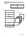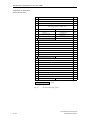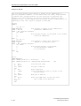
1
SIMATIC S5
S5-135U
CPU 928B
Introduction
1
User Program
2
Program Execution
3
Operating Modes and Program
Processing Levels
4
Interrupt and Error Diagnosis
5
Integrated Special Functions
6
Extended Data Block DX 0
7
Programming Guide
Order No. 6ES5 998-2PR21
Release 01
Memory Assignment and
Memory Organization
Memory Access Using
Absolute Addresses
Multiprocessor Mode and
Communication
9
10
PG Interfaces and Functions
11
Appendix
12
Further Reading
13
List of Abbreviations
Index
List of Tables and Figures
14
The CPU 922/CPU 928/CPU 928B/CPU 948 List of
Operations, Order No. 6ES5 997-3UA22 is included
with this manual.
C79000-H8576-C898-01
8
Copyright
Copyright © Siemens AG 1994 All Rights Reserved
The reproduction, transmission or use of this document or its contents is not permitted without express
written authority.
Offenders will be liable for damages. All rights, including rights created by patent grant or registration of a
utility model or design, are reserved.
Disclaimer of liability
We have checked the contents of this manual for agreement with the hardware and software described.
Since deviations cannot be precluded entirely, we cannot guarantee full agreement. However, the data in
this manual are reviewed regularly and any necessary corrections included in subsequent editions.
Suggestions for improvement are welcomed.
Technical data subject to change.
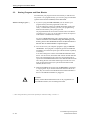
Safety-related guidelines
This manual contains notices which you should observe to ensure your own personal safety, as
well as to protect the product and connected equipment. These notices are highlighted in the
manual by a warning triangle and are marked as follows according to the level of danger:
!
!
Warning
indicates that death, severe personal injury or substantial property damage can
result if proper precautions are not taken.
Caution
indicates that minor personal injury or property damage can result if proper
precautions are not taken.
Only qualified personnel should be allowed to install and work on this equipment. Qualified persons
are defined as persons who are authorized to commission, to ground and to tag equipment,
systems and circuits in accordance with established safety practices and standards.
Siemens Aktiengesellschaft
6ES5 998-2PR21
EWK Elektronikwerk Karlsruhe
Printed in the Federal Republic of Germany
How to use this Manual
Scope
This programming guide describes the following versions of the
CPU 928B-3UB11 and CPU 928B-3UB12 and its system software:
The additional functions of the CPU 928B-3UB12 are indicated in the
manual. Some of them can be retrofitted to the CPU 928B-3UB11
(see Section 1.8 for details).
CPU 928B Programming Guide
C79000-D8576-C898-01
0-1
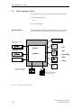
How to Use this Manual
Overview of the Chapters
Chapter 1
This informs you about the areas of application of the S5-135U
programmable controller with the CPU 928B and its device structure.
It explains the typical mode of operation of the CPU and illustrates
how a CPU program is structured.
The chapter also contains suggestions about how to tackle
programming and which characteristics of the CPU 928B are
important for programming.
If you have already worked with the CPU 928B-3UB11 and want to
know the differences between these CPU and the CPU 928B-3UB12
you will find this information in this chapter.
Chapter 2
This explains the components of a STEP 5 user program and how the
program can be structured.
Chapter 3
This is intended for readers who do not yet have much experience of
using the STEP 5 programming language. It therefore deals with the
basics of STEP 5 programming and explains the STEP 5 operations in
detail (with examples).
Experienced readers who may find that the information about specific
operations in the pocket guide is inadequate, can use Section 3.5 as a
reference section.
Chapter 4
This provides an overview of the modes and program execution levels
of the CPU 928B. It provides you with detailed information about
various start-up modes and the associated organization blocks in
which you can program your routines for differrent start-up situations.
The chapter also explains the differences between the program
execution levels "cyclic processing", "time-controlled processing" and
"interrupt-driven processing" and which blocks are available for your
user program.
Chapter 5
This informs you about errors to be avoided when planning and
writing your STEP 5 programs.
The chapter tells you about the help you can obtain from the system
program for diagnosing errors and which reactions can be expected
and informs you about the blocks in which you can program reactions
to certain errors.
The chapter also explains the CPU 948 self-test.
CPU 928B Programming Guide
0-2
C79000-D8576-C898-01
How to Use this Manual
Chapter 6
This covers the special functions integrated in the system program. It
tells you how to use the special functions and how to call and assign
parameters to the special function OBs. The chapter also explains how
to recognize and deal with errors in the processing of a special
function.
Chapter 7
This describes the use of data block DX 0 and its structure. The chapter
informs you of the significance of the various DX 0 parameters. Based on
examples, you will learn how to create data block DX 0 or how to assign
the parameters in a screen form.
Chapter 8
This is a reference section for experienced system users. It provides
information about the memory organization of the CPU 928B and
certain system data words which contain information that can be
called up by the user.
Chapter 9
This is also for experienced system users. The chapter explains how to
address data in certain memory areas using absolute addresses.
Chapter 10
This explains when the multiprocessor mode can be used and how
data can be exchanged between the CPUs and CPs. The chapter
provides information about programming for multiprocessor operation.
The remainder of the chapter provides detailed information and
application examples for exchanging larger amounts of data in the
multiprocessor mode (multiprocessor communication).
Chapter 11
This tells you how to connect your CPU to a PG and the functions
provided by the PG software to test your STEP 5 program.
Chapter 12
This contains the Appendix with technical specifications of the CPUs
which can be used on the S5-135U, some reference tables with
important information on error diagnostics and an ISTACK evaluation
example.
CPU 928B Programming Guide
C79000-D8576-C898-01
0-3
How to Use this Manual
Chapter 13
This lists documentation for further reading.
Chapter 14
This is intended to help you find themes quickly and contains a list of
abbreviations and a list of keywords as well as lists of all the
numbered tables and figures.
CPU 928B Programming Guide
0-4
C79000-D8576-C898-01
How to Use this Manual
Conventions used in the text
To provide you with an overview of the contents of the pages, the
manual uses the following conventions in addition to a 2nd and 3rd
order of titles:
Entries in the margin
Entries in the margin are keywords printed in italics on the left-hand
edge of a page. They provide information about the contents of one or
more paragraphs on the page.
Fourth order entries
Fourth order entries are not numbered but appear in the margin in bold
face and identify a longer section of text.
The following conventions are also used.
Notes
Note
Important information is indicated in this format.
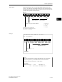
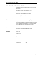
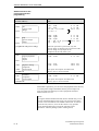
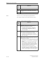
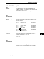
Instructions
Instructions (often a sequence of operations to be performed) are
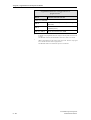
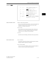
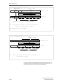
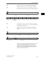
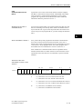
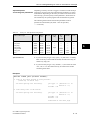
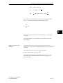
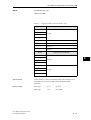
represented in tables, e.g.
Step
Action
Result
1
Switch the mode selector
from RUN to STOP.
The CPU is in the stop
mode. The STOP LED is lit
continuously.
2
An OVERALL RESET is
Hold the reset switch in the
OVERALL RESET position; requested. The STOP LED
at the same time, switch the flashes quickly.
mode selector from STOP to
RUN and back to STOP.
CPU 928B Programming Guide
C79000-D8576-C898-01
0-5
How to Use this Manual
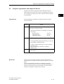
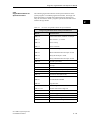
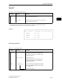
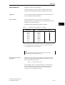
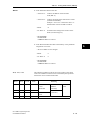
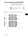
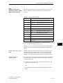
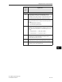
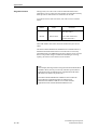
Reference tables
Table 3-2
Specific information you may require at any time is contained in
numbered tables as shown in the following example and can be found
in the list of tables (refer to Chapter 14).
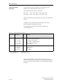
Binary logic operations
Operation
Operand
Function
A
AND logic operation with scan for signal state "1"
O
OR logic operation with scan for signal state "1"
I 0.0 to 127.7
......
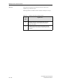
Examples
Example 1:
of an input in the PII
........
Examples, some of which cover several pages, are highlighted by a gray
frame. When the examples cover more than one page this is clearly
indicated.
Calling and assigning parameters to a function block in the
methods of representation STL and LAD/CSF in a program block
Method of representation STL
......
CPU 928B Programming Guide
0-6
C79000-D8576-C898-01
1
Introduction
1
Contents of Chapter 1
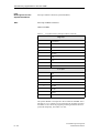
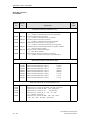
1.1
Area of Application for the S5-135U with the CPU 928B. . . . . . . . . . . . . . . . . . . . . . . . 1 - 4
1.2
Typical Mode of Operation of a CPU . . . . . . . . . . . . . . . . . . . . . . . . . . . . . . . . . . . . . . . . 1 - 6
1.3
The Programs in a CPU . . . . . . . . . . . . . . . . . . . . . . . . . . . . . . . . . . . . . . . . . . . . . . . . . . . 1 - 8
System program . . . . . . . . . . . . . . . . . . . . . . . . . . . . . . . . . . . . . . . . . . . . . . . . . . . . . . . . . 1 - 8
User program . . . . . . . . . . . . . . . . . . . . . . . . . . . . . . . . . . . . . . . . . . . . . . . . . . . . . . . . . . 1 - 10
1.4
Which Operands are available to the User Program? . . . . . . . . . . . . . . . . . . . . . . . . . . . 1 - 12
1.5
Accessing Operand Areas and Memory Areas . . . . . . . . . . . . . . . . . . . . . . . . . . . . . . . . 1 - 16
1.6
How to Tackle Programming? . . . . . . . . . . . . . . . . . . . . . . . . . . . . . . . . . . . . . . . . . . . . . 1 - 17
1.7
Programming Tools . . . . . . . . . . . . . . . . . . . . . . . . . . . . . . . . . . . . . . . . . . . . . . . . . . . . . 1 - 20
1.8
What is New with the CPU 928B? . . . . . . . . . . . . . . . . . . . . . . . . . . . . . . . . . . . . . . . . . 1 - 21
CPU 928B Programming Guide
C79000-D8576-C898-01
1-1
1
Introduction
1
Aims of the manual
This manual is intended to provide specialized information about
programming the CPU 928B for users who already have basic
knowledge of programming PLCs and want to use the CPU 928B in
the S5-135U programmable controller. If you do not yet have this
basic knowledge, we strongly advise you read the documentation
introducing the programming language STEP 5 (STEP 5 Manual,
refer to Chapter 13) or take part in a course at our training center.
SIEMENS provides comprehensive training for SIMATIC S5. For
more detailed information, contact your local SIEMENS office.
Contents of Chapter 1
Chapter 1 explains how to use the manual and deals with the areas of
application of the S5-135U programmable controller with the
CPU 928B and its structure.
The chapter explains the typical mode of operation of a CPU and the
structure of the CPU program.
You will also find a few suggestions about how to tackle
programming and will learn some of the features of the CPU 928B
(-3UB12) which are important for programming.
If you have already worked with the CPU 928B (-3UB11) and would
like to know the differences between these modules and the
CPU 928B (-3UB12), refer to Section 1.8.
CPU 928B Programming Guide
C79000-D8576-C898-01
1-3
Area of Application for the S5-135U with the CPU 928B
1.1
Area of Application for the S5-135U with the CPU 928B
SIMATIC S5 family
The S5-135U programmable controller belongs to the family of
SIMATIC S5 programmable controllers. With the CPU 928B, it is the
most powerful multiprocessor unit for process automation (open and
closed loop control, signalling, monitoring, logging).
Owing to its modularity and high performance, it can be used for
medium to extremely large control systems as well as for complex
automation tasks at the plant and process supervision level.
Suitability
The S5-135U with the CPU 928B is particularly suitable for the
following:
• Tasks requiring fast bit and word-oriented processing and fast
reaction times, i.e. with extremely fast open and closed loop controls.
Examples of this are fast processes in mechanical engineering
(bottling plant, packing machines or similar systems) and in the
automobile industry.
• Tasks requiring an extremely high storage capacity and fast access
times, e.g. in the automobile industry, process and plant
engineering.
• Tasks requiring fast communication with other CPUs installed in
the PLC and operating in the multiprocessor mode and with CP
modules (e.g. when connected to bus systems, host computers, for
visualization, operation and monitoring).
• Complex tasks which can be handled efficiently and clearly using
the high level languages C and SCL.
CPU 928B Programming Guide
1-4
C79000-D8576-C898-01
Area of Application for the S5-135U with the CPU 928B
1
This p age has been left intentionally blank.
CPU 928B Programming Guide
C79000-D8576-C898-01
1-5
Typical Mode of Operation of a CPU
1.2
Typical Mode of Operation of a CPU
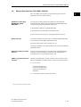
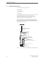
Mode of operation of a CPU
1.
The following modes of operation are possible in a CPU:
2.
Time-controlled processing
Cyclic processing
Cyclic processing
3.
Interrupt-driven processing
This is the main part of all activities in the CPU. As the name already
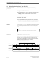
says, the same operations are repeated in an endless cycle.
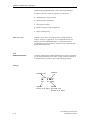
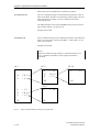
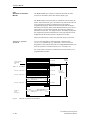
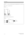
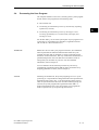
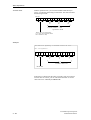
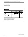
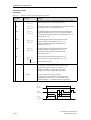
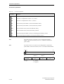
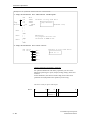
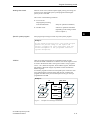
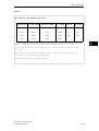
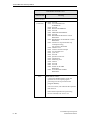
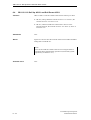
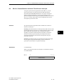
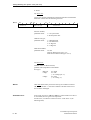
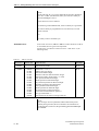
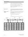
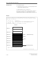
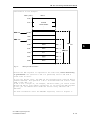
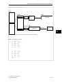
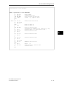
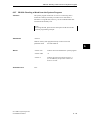
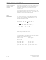
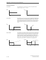
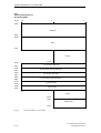
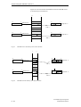
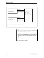
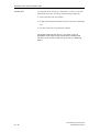
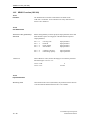
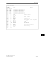
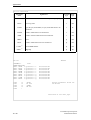
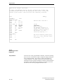
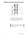
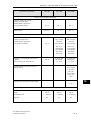
Cyclic processing can be divided into three main phases, as follows:
Phase
1
2
3
Sequence
All the input modules assigned to the
CPU are scanned by the system
program and the values read in are
stored in the process image of the
inputs (PII).
The values contained in the PII are
processed by the user program and the
values to be output are entered in the
process image of the outputs (PIQ).
The values contained in the process
image of the outputs are output by the
system program to the output modules
assigned to the CPU.
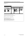
Process
C PU
Input I 1.3
Read in process image
of the inputs
Input I 1.4
Input I 1.5
Evaluate input signals,
set output signals
I 1.5
&
I 1.6
=1
I 1.4
I 1.3
&
Q 3.1
Output process image
of the outputs
Output Q 2.0
Output Q 3.1
Output Q 4.7
CPU 928B Programming Guide
1-6
C79000-D8576-C898-01
Typical Mode of Operation of a CPU
Time-controlled processing
In addition to the cyclic processing, time-controlled processing is
also available for processes requiring control signals at constant
intervals, e.g. non-time critical monitoring functions performed every
second.
Interrupt-driven processing
If the reaction to a particular process signal must be particularly fast, this
should be handled with interrupt-driven processing. With, for example,
a process interrupt, triggered via an interrupt generating module, you can
activate a special processing section within your program.
Processing according to
priority
The types of processing listed above are handled by the CPU
according to their priority.
Since a fast reaction is required to a time or interrupt event, the CPU
interrupts cyclic processing to handle a time or interrupt event. Cyclic
processing therefore has the lowest priority.
CPU 928B Programming Guide
C79000-D8576-C898-01
1-7
1
The Programs in a CPU
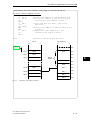
1.3
The Programs in a CPU
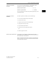
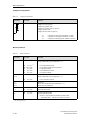
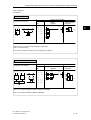
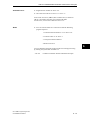
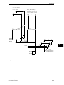
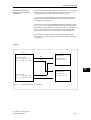
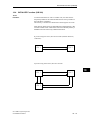
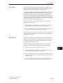
The program existing on every CPU is divided into the following:
• the system program
and
• the user progra m.
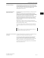
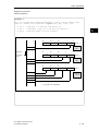
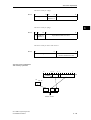
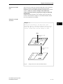
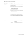
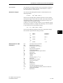
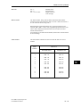
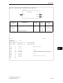
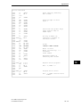
System program
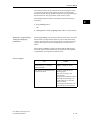
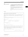
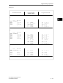
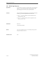
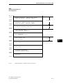
The system program organizes all the functions and sequences of the
CPU which do not involve a specific control task (refer to Fig. 1-2).
Execute start-up
Update process image
of the inputs
Output process image
of the outputs
Call
System
user
program
processing
(inter-
Manage memory
faces)
Handle communications
via 2nd serial interface
Handle errors
Execute communications
with the programmer
Fig. 1-1
Tasks of the system program
CPU 928B Programming Guide
1-8
C79000-D8576-C898-01
The Programs in a CPU
Tasks
The tasks include the following: 1)
• cold and warm restart,
1
• updating the process image of the inputs and outputting the
process image of the outputs,
• calling the cyclic, time-controlled and interrupt-driven programs,
• detection and handling of errors,
• memory management,
• communication with the programmer (PG).
User interfaces
As the user, you can influence the reaction of the CPU to particular
situations and errors via special interfaces to the system program.
Default system reaction
The following chapters, except for Chapter 7, describe the default
system reaction to process events or errors. Depending on the
defaults, the CPU changes to the stop mode if an operation code error
occurs and the error organization block is not loaded.
Modifying the defaults
You can modify the system response by assigning parameters for the
data block DX 0.
Chapter 7 describes the system response following modification .
1)
When operating with several CPUs (multiprocessing) further tasks are involved.
CPU 928B Programming Guide
C79000-D8576-C898-01
1-9
The Programs in a CPU
User program
Tasks
The user program contains all the functions required for processing a
specific control task. In general terms, these functions can be
assigned to the interface provided by the system program for the
various types of processing, as follows:
Type of processing
Task
Cold and warm restart
To provide the conditions under which
the other processing functions can start
from a defined status following a cold or
warm restart of the control system (e.g.
assigning specific values to signals).
Cyclic processing
Constantly repeated signal processing
(e.g. logic operations on binary signals,
reading in and analyzing analog values,
specifying binary signals for output,
outputting analog values).
Time-controlled
processing
Special, time-dependent processing with
the following time conditions:
- faster than the average cycle,
- at a time interval greater than the
average cycle time,
- at a specified point in time.
Interrupt-driven processing Special, fast reactions to certain process
signals.
Error reaction
Handling problems within the normal
sequence of the program.
CPU 928B Programming Guide
1 - 10
C79000-D8576-C898-01
The Programs in a CPU
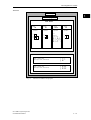
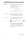
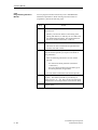
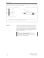
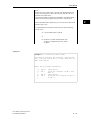
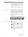
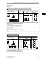
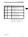
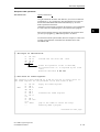
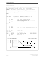
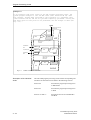
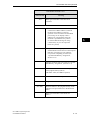
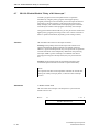
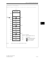
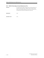
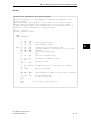
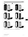
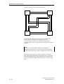
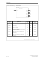
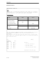
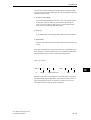
Structure
User memory
1
User program
Code blocks
Organization
blocks
Program
blocks
OB
PB
STEP 5
operations
STEP 5
operations
I 1.5
F 50.1
=1
I 1.4
FB/FX
F 1.7
SEGMENT 1
NAME :TRANS
F 50.2
F 50.3
STEP 5
operations
FB 8
=1
&
I 1.3
SB
STEP 5
operations
&
I 1.6
Sequence
blocks
Function
blocks
Q 5.3
Q 3.1
0005
0006
0007
0008
0009
000A
000B
I 2.6
S
I 1.3
R
Q
:L IB
3
:T FW 200
:C DB
5
:DO FW 200
:L DW
0
:T QW
6
:BE
Data blocks
DB
static or dynamic data
(bits, bytes, words, double words)
DX
static or dynamic data
(bits, bytes, words, double words)
Fig. 1-2
1:
2:
3:
4:
5:
6:
7:
KH
KF
KS
KY
KG
KM
= 0101;
= +120;
= xy;
= 4.5;
=
=
1:
2:
3:
4:
5:
6:
7:
KH
KH
KH
KH
KH
KH
=
=
=
=
=
=
FFFF;
FFFF;
FFFF;
FFFF;
FFFF;
FFFF;
Structure of a STEP 5 user program
CPU 928B Programming Guide
C79000-D8576-C898-01
1 - 11
The Programs in a CPU
Storing the user program
The CPU 928B has two areas for storing blocks:
• User memory: max. 64 Kbytes
The user memory is on a plug-in RAM or EPROM submodule and
contains logic and data blocks (if the user memory is an EPROM
submodule, the data blocks whose data are changed by the user
program must be loaded in the DB RAM).
Data block RAM (DB RAM): max. 46 Kbytes
The DB RAM is an additional memory area for storin g d ata
blocks.
Interfaces to the system
program
Org anization blocks are available as interfaces to the system
program for the special types of processing.
CPU 928B Programming Guide
1 - 12
C79000-D8576-C898-01
Which Operands are available to the User Program?
1.4
Which Operands are available to the User Program?
1
The CPU 928B provides the following operand areas for
programming:
• process image and I/Os
• flags (F flags and S flags)
• timers/counters
• data blocks
Process image of the inputs
and outputs PII/PIQ
Characteristics
The user program can access the following data types
in the process image extremely quickly:
- single bits,
- bytes,
- words,
- double words
Size
128 bytes
each for
inputs and
outputs
I/O area (P area)
Characteristics
The user program can access the I/O modules directly
via the S5 bus.
The following data types are possible:
- bytes,
- words.
Size
256 bytes
each for
inputs and
outputs
Extended I/O area (O area)
Characteristics
The user program can access the I/O modules directly
via the S5 bus.
The following data types are possible:
- bytes,
- words.
Size
256 bytes
each for
inputs and
outputs
CPU 928B Programming Guide
C79000-D8576-C898-01
1 - 13
Which Operands are available to the User Program?
F flags
Characteristics
Size
The flag area is a memory area which the user
program can access extremely quickly with certain
operations.
The flag area should be used ideally for working data
required often.
2048 bits
The following data types can be accessed:
- single bits,
- bytes,
- words,
- double words.
Single flag bytes can be used as interprocessor
com munication flags (IPC flags) to exchange data
between the CPUs in the multiprocessor mode (refer
to Chapter 10). IPC flags are updated by the system
program at the end of the cycle via a buffer in the
coordinator or CP/IP.
S flags (extended flag area)
Characteristics
Size
The CPU 928B also contains an additional flag area,
the S flag area. The user program can also access this
area extremely quickly as with the F flags.
8192 bits
S flags cannot however by used as actual operands
with function block calls nor as IPC flags for data
exchange between the CPUs. The bit test operations
of the CPU 948 can also not be used with the S flags.
These flags can only be used with the PG system
software "S5-DOS" from version 3.0 upwards or
"S5-DOS/MT" from version 1.0 upwards.
CPU 928B Programming Guide
1 - 14
C79000-D8576-C898-01
Which Operands are available to the User Program?
Timers (T)
Characteristics
The user program loads timer cells with a time value
between 10 ms and 9990 s and by means of a start
operation, decrements the timer from this value at the
preselected intervals until it reaches the value zero.
Size
1
256 timer
cells
Counters (C)
Characteristics
Size
The user program loads counter cells with a start value
(max. 999) and then increments or decrements them.
256
counters
Characteristics
Size
Data words in the current data
block
A data block contains constants and/or variables in the
byte, word or double word format. With STEP 5
operations, you can always access the "current" data
block (refer to Section 2.4.2).
The following data types can be accessed:
- single bits,
- bytes,
- words,
- double words.
1)
256
words
1)
In data blocks with a length greater than 256 words, you can only access data
words with the numbers > 255 with operations for absolute memory access
(refer to Chapter 9).
CPU 928B Programming Guide
C79000-D8576-C898-01
1 - 15
Accessing Operand Areas and Memory Areas
1.5
Accessing Operand Areas and Memory Areas
STEP 5 operations use two different mechanisms for accessing
operand areas and the entire memory:
Relative addressing
The majority of STEP 5 operations address a memory location
relative to the beginning of the operand area. If these operations are
used exclusively, code and data areas of the user program are
protected against unintentional overwriting. At the same time, the user
program is dependent on the CPU as long as the CPU has an
appropriate operand area.
Absolute addressing
Some STEP 5 operations work with absolute addresses. These
operations can be used to access the entire memory area. They can
only be used in function blocks and should only be used with great
care due to the danger of data corruption. These operations are
dependent on the CPU used. However, there is no difference between
the CPU 928 and CPU 928B regarding these operations.
Current data block
Data blocks are loaded into the user memory or the DB-RAM by the
system program. Their location depends on the memory space
available in each case. The lengths of the individual data blocks can
vary and are set when programming the data blocks.
The current data block is the data block whose starting address and
length are entered in special registers. This entry is made via a special
STEP 5 operation for calling or "opening" a data block (like the page
of book). Unless operations with absolute addressing are used, the
user program can only access the current data block. The following
data types are possible: single bits, bytes, words and double words.
CPU 928B Programming Guide
1 - 16
C79000-D8576-C898-01
How to Tackle Programming
1.6
How to Tackle Programming
If you are an experienced user, you have probably found the most
suitable method for creating programs for yourself and you can skip
this section.
Less experienced readers will find tips for designing, programming,
testing and starting up your STEP 5 program.
Implementation stages
The implementation of the STEP 5 control program can be divided
into three stages:
Stage
Activity
1
Determining the technological task
2
Designing the program
3
Creating, testing and starting the program
Recursive procedure
In practice, you will recognize that certain steps must be repeated
(recursive procedure), e.g. when you realize that more signals are
required to improve the handling of the task.
Stage 1
Determining the technological task:
Stage
Activity
1
Create a general block diagram outlining the control
tasks of your process.
2
Create a list of the input and output signals required
for the task.
3
Improve the block diagram by assigning the signals
and any particular time conditions and/or counter
statuses to the individual blocks.
CPU 928B Programming Guide
C79000-D8576-C898-01
1 - 17
1
How to Tackle Programming
Stage 2
Notes on the scope of
cyclic processing
Designing the program:
Stage
Activity
1
Based on the improved block diagram, decide on the
types of processing required of your program (cyclic
processing, time-controlled processing etc.) and select
the OBs required for this.
2
Divide the types of processing into technological
and/or functional units.
3
Check whether the units can be assigned to a program
or function block and select the blocks you require
(PB x, FB y etc.)
4
Find out which timers, counters and data or results
memory you require.
5
Specify the tasks for each of the proposed logic blocks
and the data for flags and data blocks which may be
required. Create flow diagrams for the logic blocks.
When deciding on the types of processing, keep the following
conditions in mind:
• The cycle must run through quickly enough. The process statuses
must not change more quickly than the CPU can react. Otherwise
the process can get out of control.
• The maximum reaction time should be taken as twice the cycle
time.
The cycle time is determined by the cyclic processing of the
system program and the type and scope of the user program. It is
often not constant, since the cyclic user program may be
interrupted when time and interrupt-driven program sections are
called.
CPU 928B Programming Guide
1 - 18
C79000-D8576-C898-01
How to Tackle Programming
Stage 3
Creating, testing and starting up the program:
1
Stage
Activity
1
Decide on the type of representation for the logic
blocks (LAD, CSF or STL, refer to Chapter 2).
Remember that function blocks can only be created in
the STL method of representation.
2
Program all logic and data blocks (please refer to your
STEP 5 manual).
3
Start up the blocks one after the other (you may have
to program a different OB for each individual step, to
call the logic blocks):
1a: load the block(s)
1b: test the block(s)
(For more detailed information please refer to your
STEP 5 manual and Chapter 11).
4
Note on test strategies
When you are certain that all the logic blocks run
correctly and all the data can be correctly calculated
and stored, you can start up your whole program.
When you actually start up your program for the first time in genuine
process operation, i.e. with real input and more importantly output
signals, is a decision that must be left up to yourself or to a team of
experts.
The more complex the process, the greater the risk and therefore the
greater the care required when starting up.
CPU 928B Programming Guide
C79000-D8576-C898-01
1 - 19
Programming Tools
1.7
Programming Tools
Suitable PGs
The following programmers are available for creating your user
program, PG 685, PG 710, PG 730, PG 750 and PG 770. You can
check on the performance and characteristics of these devices in the
catalog ST 59 (see Chapter 13).
Note
Enter the CPU ID for C PU 922 (0010H) in system data word
RS 29 (see Chapter 8) in order to be able to use a PG 615 or a CP
3xx. In this case, you cannot use S flags.
If you do not change the ID, this will lead to erroneous indicators,
e.g. in the case of ISTACK output, or to the loss of some
debugging aids.
In all programmers, the STA TUS test function operates without
restriction only at scan times of ≤ 2.5 s. This value is halved in the
case of parallel operation of 2 programmer interfaces (see
Chapter 11).
Suitable software
You can create user programs for SIMA TIC S5 programmable
controllers as follows:
• In the STEP 5 programming language,
Here you require the STEP 5 programming package along with the
system software STEP 5/ST or STEP 5/MT (description, refer to
/3/ in Chapter 13),
or
• In a higher programming language:
If you are familiar with programming in higher programming
languages, you can also formulate your STEP 5 program for the
CPU 928B as follows:
-
SCL (refer to /12/ in Further Reading, the SCL compiler is
contained in the PG software "S5-DOS/MT" from version 6
upwards.)
You can also create programs for sequence control systems in a
graphic representation using the GRAPH 5 programming package
(description, refer to /4/ in Chapter 13).
Depending on the task, you can also incorporate "off-the-peg"
standard function blocks in your user program. The performance and
characteristics of these blocks are described in the catalog ST 57 (see
Chapter 13).
CPU 928B Programming Guide
1 - 20
C79000-D8576-C898-01
What is New with the CPU 928B (-3UB12)?
1.8
What is New with the CPU 928B (-3UB12)?
The CPU 928B (-3UB12) offers you the following new functions
compared to the CPU 928B (-3UB11).
Additional restart type:
RETENTIVE COLD
RESTART 1)
As well as the existing restart types (MANUAL/AUTOMATIC
COLD RESTART; MANUAL/AUTOMATIC WARM RESTART)
you can use the following additional restart types:
• RETENTIVE MANUAL COLD RESTART
• RETENTIVE AUTOMATIC COLD RESTART
You can set these restart types by assigning parameters in DX 0.
Delay interrupt
As well as the familiar time interrupts, an additional delay interrupt
is processed by the new OB 6 organization block.
The delay interrupt has a time resolution of 1 ms.
You assign parameters to the desired delay time with the new OB 153
organization block.
Alternative loading of data
blocks 1)
You can use the programmer to load data blocks into DB RAM first,
instead of into the user memory. Selection of the loading mode is
controlled via bit 0 in system data word RS 144.
SINEC L1 via the 2nd serial
interface 1)
Connection to the SINEC L1 LAN (with the new L1 interface card)
has been expanded for communication via the second serial interface:
• Use as slave in
- Normal communication
- Internode communication
- Interrupt communication
- Broadcast;
• Use as master in point-to-point connections.
1)
can be retrofitted to CPU 928B (-3UB11)
CPU 928B Programming Guide
C79000-D8576-C898-01
1 - 21
1
2
User Program
2
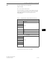
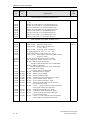
Contents of Chapter 2
2.1
STEP 5 Programming Language . . . . . . . . . . . . . . . . . . . . . . . . . . . . . . . . . . . . . . . . . . . . 2 - 4
2.1.1
2.1.2
2.1.3
2.1.4
2.1.5
The LAD, CSF, STL Methods of Representation . . . . . . . . . . . . . . . . . . . . . . . . . . . . . . . 2 - 4
Structured Programming. . . . . . . . . . . . . . . . . . . . . . . . . . . . . . . . . . . . . . . . . . . . . . . . . . . 2 - 5
STEP 5 Operations . . . . . . . . . . . . . . . . . . . . . . . . . . . . . . . . . . . . . . . . . . . . . . . . . . . . . . . 2 - 6
Number Representation . . . . . . . . . . . . . . . . . . . . . . . . . . . . . . . . . . . . . . . . . . . . . . . . . . . 2 - 8
STEP 5 Blocks and Storing them in Memory . . . . . . . . . . . . . . . . . . . . . . . . . . . . . . . . . 2 - 12
2.2
Program, Organization and Sequence Blocks . . . . . . . . . . . . . . . . . . . . . . . . . . . . . . . . . 2 - 16
2.2.1
2.2.2
Organization Blocks as User Interfaces. . . . . . . . . . . . . . . . . . . . . . . . . . . . . . . . . . . . . . 2 - 18
Organization Blocks for Special Functions . . . . . . . . . . . . . . . . . . . . . . . . . . . . . . . . . . . 2 - 22
2.3
Function Blocks . . . . . . . . . . . . . . . . . . . . . . . . . . . . . . . . . . . . . . . . . . . . . . . . . . . . . . . . 2 - 23
2.3.1
2.3.2
2.3.3
2.3.4
Structure of Function Blocks . . . . . . . . . . . . . . . . . . . . . . . . . . . . . . . . . . . . . . . . . . . . . .
Programming Function Blocks. . . . . . . . . . . . . . . . . . . . . . . . . . . . . . . . . . . . . . . . . . . . .
Calling Function Blocks and Assigning Parameters to them . . . . . . . . . . . . . . . . . . . . .
Special Function Blocks . . . . . . . . . . . . . . . . . . . . . . . . . . . . . . . . . . . . . . . . . . . . . . . . . .
2.4
Data Blocks. . . . . . . . . . . . . . . . . . . . . . . . . . . . . . . . . . . . . . . . . . . . . . . . . . . . . . . . . . . . 2 - 35
2.4.1
2.4.2
2.4.3
Creating Data Blocks . . . . . . . . . . . . . . . . . . . . . . . . . . . . . . . . . . . . . . . . . . . . . . . . . . . . 2 - 37
Opening Data Blocks . . . . . . . . . . . . . . . . . . . . . . . . . . . . . . . . . . . . . . . . . . . . . . . . . . . . 2 - 38
Special Data Blocks . . . . . . . . . . . . . . . . . . . . . . . . . . . . . . . . . . . . . . . . . . . . . . . . . . . . . 2 - 41
2 - 24
2 - 26
2 - 28
2 - 33
CPU 928B Programming Guide
C79000-B8576-C898-01
2-1
2
User Program
2
The following chapter explains the components that make up a
STEP 5 user program for the CPU 928B and how it can be structured.
CPU 928B Programming Guide
C79000-B8576-C898-01
2-3
STEP 5 Programming Language
2.1
STEP 5 Programming Language
With the STEP 5 programming language, you convert automation
tasks into programs that run on SIMATIC S5 programmable
controllers. You can program simple binary functions, complex digital
functions and arithmetic operations including floating point arithmetic
using STEP 5.
Types of operation
The operations of the STEP 5 programming language are divided
into the following groups:
B asic operations
• you can use these operations in all logic blocks
• methods of representation: ladder diagram (LAD), control system
flowchart (CSF), statement list (STL).
Supplementary operations and system operations:
• can only be used in function blocks
• only statement list (STL) method of representation
• system operations: only experienced STEP 5 programmers should
use system operations
2.1.1
The LAD, CSF, STL
Methods of Representation
When programming in STEP 5, you can choose between the three
methods of representation ladder diagram (LAD), control system
flowchart (CSF) and statement list (STL) for each individual logic block.
You can choose the method of representation that best suits your
particular application.
The machine code MC5 that the programmers (PGs) generate is the
same for all three methods of representation.
If you follow certain rules when programming in STEP 5 (see /3/ in
Chapter 13), the programmer can translate your user program from
one method of representation into any other.
Graphic representation or
list of statements
While the ladder diagram (LAD) and control system flowchart (CSF)
methods of representation represent your STEP 5 program
graphically, statement list (STL) represents STEP 5 operations
individually as mnemonic abbreviations.
CPU 928B Programming Guide
2-4
C79000-B8576-C898-01
STEP 5 Programming Language
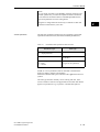
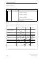
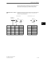
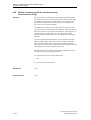
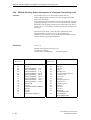
Ladder diagram
Statement list
Control system flowchart
Programming with
graphic symbols
like a circuit diagram
Programming with
mnemonic abbreviations
of function designations
Programming with
graphic symbols
complies with
DIN 19239
complies with
DIN 19239
complies with
IEC 117-15
DIN 40700
DIN 40719
DIN 19239
LAD
STL
CSF
A
AN
A
ON
O
=
Fig. 2-1
I
I
I
I
I
Q
2
&
>=1
Methods of representation in the STEP 5 programming language
Graphic representation of
sequential controls
2.1.2
Structured Programming
GRAPH 5 is a programming language for graphic representation of
sequential controls. It is at a higher level than the LAD, CSF, STL
methods of representation. A program written in GRAPH 5 as a
graphic representation is automatically converted to a STEP 5
program by the PG. (Refer to /4/ in Chapter 13)
Using STEP 5, you can structure your program by dividing it into
self-contained program sections (blocks). This division of your
program clarifies the essential program structures making it easy to
recognize the system parts that are related within the software.
CPU 928B Programming Guide
C79000-B8576-C898-01
2-5
STEP 5 Programming Language
Structured programmin g offers you the following advantages:
• simple and clear creation of programs, even large ones
• standardization of program parts
• simple program organization
• easy program changes
• simple, section by section program test
• simple system start-up
What is a block?
2.1.3
STEP 5 Operations
A block is a part of the user program that is distinguished by its
function, structure or application. You can differentiate between
blocks that contain statements (code) i.e. organization blocks,
program blocks, function blocks or sequence blocks, and blocks that
contain data (data blocks).
A STEP 5 operation is the smallest independent unit of the user program.
It is the work specification for the CPU. A STEP 5 operation consists of
an operation and an operand as shown in the following example:
Example
Operation code
:O
Parameter
F 54.1
Operand
Operation
(what is to be done?) (with what is the
operation to be done?)
CPU 928B Programming Guide
2-6
C79000-B8576-C898-01
STEP 5 Programming Language
Absolute and symbolic
operands
You can enter the operand absolutely or symbolically (using an
assignment list) as shown in the following example:
Absolute representation:
:A I 1.4
Symbolic representation:
:A -Motor1
For more information on absolute and symbolic programming, refer to
your STEP 5 manual.
Application of STEP 5
operations
The STEP 5 operation set enables you to do the following:
• set or reset and combine binary values logically
• load and transfer values
• compare values and process them arithmetically
• specify timer and counter values
• convert number representations
• call blocks and execute jumps within a block
and
• influence program execution
Result of logic operation RLO
The central bit for controlling the program is the result of logic
operation RLO. This is obtained as a result of binary logic operations
and is influenced by some operations.
Section 3.5 describes the whole STEP 5 operation set and explains how
the RLO is obtained. This section also includes programming examples
for individual STEP 5 operations.
CPU 928B Programming Guide
C79000-B8576-C898-01
2-7
2
STEP 5 Programming Language
2.1.4
Number Representation
To allow the CPU to logically combine, modify or compare numerical
values, these values must be located in the accumulators (working
registers of the CPU) as binary numbers.
Depending on the operations to be carried out, the following number
representations are permitted in STEP 5:
Binary numbers:
16-bit fixed point numbers
32-bit fixed point numbers
32-bit floating point numbers (with a 24-bit
mantissa)
Decimal numbers: BCD-coded numbers (sign and 3 digits)
Numerical input on the PG
When you use a programmer to input or display number values, you
set the data format on the programmer (e.g. KF or fixed point) in
which you intend to enter or display the values. The programmer
converts the internal representation into the form you have requested.
Permitted operations
You can carry out all arithmetic operations with the 16-bit fixed
point numbers and floating point numbers, including comparison,
addition, subtraction, multiplication and division.
Note
Do not use BCD-coded numbers for arithmetical operations, since
this leads to incorrect results.
Use 32-bit fixed point numbers to execute comparison operations.
These are also necessary as an intermediate level when converting
numbers in BCD code to floating point numbers. With the operations
+D and -D they can also be used for addition and subtraction.
The STEP 5 programming language also has conversion operations that
enable you to convert numbers directly to the most important of the other
numerical representations.
CPU 928B Programming Guide
2-8
C79000-B8576-C898-01
STEP 5 Programming Language
16-bit and 32-bit fixed
point numbers
Fixed point numbers are whole binary numbers with a sign.
Coding of fixed point numbers Fixed point numbers are 16 bit (= 1 word) or 32 bit (= 2 words) in
binary representation. Bit 15 or bit 31 contains the sign.
•
’0’ = positive number
•
’1’ = negative number
2
The two’s complement representation is used for negative numbers.
PG input
Permitted numerical range
Input of 16-bit fixed point number data format at the PG:
KF
Input of 32-bit fixed point number data format at the PG:
DH
-32768 to +32767 (16 bit)
-2147483648 to +2147483647 (32 bit)
Using fixed point numbers
Use fixed point numbers for simple calculations and for comparing
number values. Since fixed point numbers are always whole numbers,
remember that the result of dividing two fixed point numbers is also a
fixed point number without decimal places.
CPU 928B Programming Guide
C79000-B8576-C898-01
2-9
STEP 5 Programming Language
Floating point numbers
Floating point numbers are positive and negative fractions. They
always occupy a double word (32 bits). A floating point number is
represented as an exponential number. The mantissa is 16 or 24 bits
long and the exponent is 8 bits long.
In the CPU 928B, the default mantissa (assuming you have not
changed the setting) is 16-bits long (bits 8 to 23) for adding,
subtracting, multiplying and dividing. The least significant (on the
right) bits 0 to 7 always have the value "0".
If you require floating point calculations with a higher accuracy (and
can accept a slightly longer runtime), program the setting "floating
point arithmetic with 24-bit mantissa" in DX 0 (see Chapter 7).
The exponent indicates the order of magnitude of the floating point
number. The sign of the exponent tells you whether the value of the
floating point number is greater or less than 0.1.
Using floating point numbers
Use floating point numbers for solving extensive calculations,
especially for multiplication and division or when you are working
with very large or very small numbers!
Accuracy
The mantissa indicates the accuracy of the floating point number as
follows:
• Accuracy with a 24-bit mantissa:
2
-2 4
= 0.000000059604 (corresponds to 7 decimal places)
• Accuracy with a 16-bit mantissa:
2
-16
= 0,00001525 8 (corresponds to 4 decimal places)
If the sign of the mantissa is "0" the number is positive; if the sign is
"1" it is a negative number in its two’s complement representation.
The floating point value ’0’ is represented as the binary value
8 0000000H (32 bits, see below).
CPU 928B Programming Guide
2 - 10
C79000-B8576-C898-01
STEP 5 Programming Language
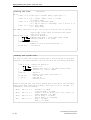
Coding floating point numbers Coding a floating point number:
31 30
V
24 23 22
6
2 ...
. ... 2
0
V
0
-1
2 .... . . .
Exponent
-23
. . ... 2
Mantissa
2
Specification of the data format for floating point numbers at the
PG: KG
Permissible numerical range
± 0.1469368 x 10
Input/output on PG
a)
-38
to ± 0.1701412 x 1039
in a logic block:
You want to load the number N = 12.34567 as a floating point
number.
Input:
:LKG1 234567+2
PG display after you enter the line:
:L
KG + 1234567 + 02
Mantissa with sign
Exponent (base 10)
with sign
Value of the number input: +0.1234567 x 10+2 = 12.34567
b)
in a data block:
You want to define the number N = - 0.005 as a floating point
constant.
Input:
6:
KG
= -5 -2
PG display after you enter the line:
6:
KG
=- 5000000 - 02
Mantissa with sign
Exponent (base 10)
with sign
Value of the number input:
- 0.5 x 10-2 = 0.005
CPU 928B Programming Guide
C79000-B8576-C898-01
2 - 11
STEP 5 Programming Language
Numbers in BCD code
Decimal numbers are represented as numbers in BCD code. With
their sign and three digits, they occupy 16 bits (1 word) in an
accumulator as shown in the following example:
15
V V V V
12 11
8 7
hundreds
4 3
tens
0
ones
The individual digits are positive 4-bit binary numbers between 0000 and
1001 (0 and 9 decimal).
The left bits are reserved for the sign as follows:
Sign for a positive number:
Sign for a negative number:
Permissible numerical range
0000
1111
-999 to +999
CPU 928B Programming Guide
2 - 12
C79000-B8576-C898-01
STEP 5 Programming Language
2.1.5
STEP 5 Blocks and Storing
them in Memory
Identifier
A block is identified as follows:
2
• the block type (OB, PB, SB, FB, FX, DB, DX)
and
• the block number (number between 0 and 255).
Block types
The STEP 5 programming language differentiates between the
following block types:
Organization blocks (OB)
Organization blocks are the interface between the system program and
the user program. They can be divided into two groups as follows:
With OB 1 to OB 39, you can control program execution, the restart
procedure of the CPU and the reaction in the event of an error. You
program these blocks yourself according to your automation task.
These OBs are called by the system program.
OBs 40 to 100 are blocks belonging to the operating system. You
must not call these blocks.
OBs 121 to 255 contain special functions of the system program. You
can call these blocks, if required, in your user program.
Program blocks (PB)
You require program blocks to structure your program. They contain
program parts divided according to technological and functional
criteria. Program blocks represent the heart of the user program.
Sequence blocks (SB)
Sequence blocks were originally special program blocks for step by
step processing of sequencers. In the meantime, however, sequencers
can be programmed with GRAPH 5. Sequence blocks have therefore
lost their original significance in STEP 5.
Sequence blocks now represent an extension of the program blocks
and are used as program blocks.
CPU 928B Programming Guide
C79000-B8576-C898-01
2 - 13
STEP 5 Programming Language
Function blocks (FB/FX)
You use function blocks to program frequently recurring and/or
complex functions (e.g. digital functions, sequence control systems,
closed loop controls and signalling functions).
A function block can be called several times by higher order blocks
and supplied with new operands (assigned parameters) at each call.
Using block type FX increases the maximum number of possible
function blocks from 256 to 512.
Data blocks (DB/DX)
Data blocks contain the (fixed or variable) data with which the user
program works. This type of block contains no STEP 5 statements and
has a distinctly different function from the other blocks. Using block
type DX doubles the number of possible data blocks.
Formal structure of the
blocks
All blocks consist of the following two parts:
• a block header
and
• a block body
Block header
The block header is always 5 words long and contains information for
block management in the PG and data for the system program.
Block body
Depending on the block type, the block body contains the following:
• STEP 5 operations (in OB, PB, SB, FB, FX),
• variable or constant data (in DB, DX)
and
• a formal operand list (in FB, FX).
CPU 928B Programming Guide
2 - 14
C79000-B8576-C898-01
STEP 5 Programming Language
Block preheader
The programmer also generates a block preheader (DV, DXV, FV,
FXV) for block types DB, DX, FB and FX. These block preheaders
contain information about the data format (for DB and DX) or the
jump labels (for FB and FX). Only the PG can evaluate this
information. Consequently the block preheaders are not transferred to
the CPU memory. You cannot influence the contents of the block
header directly.
Maximum length
A STEP 5 block can occupy a maximum of 4096 words in the
program memory of the CPU (1 word corresponds to 16 bits).
Available blocks
You can program the following block types:
OB
1 to 39
FB
0 to 255
FX
0 to 255
PB
0 to 255
SB
0 to 255
DB
3 to 255
DX
3 to 255
total 512
total 506
Data blocks DB 0, DB 1, DB2, DX 0, DX 1 and DX 2 contain
parameters. These are reserved for specific functions and you cannot use
them as normal data blocks.
CPU 928B Programming Guide
C79000-B8576-C898-01
2 - 15
2
STEP 5 Programming Language
Block storage
The programmer stores all programmed blocks in the program
memory in the order in which they are transferred (Fig. 2-2). The
programmer function "Transfer data blocks B" transfers first the code
blocks then the data blocks to the PLC. In RAM mode, the RAM card
is first to be filled with data blocks after transfer of the code blocks
and then the remaining data blocks are written into internal DB RAM.
The start addresses of all stored blocks are placed in data block DB 0.
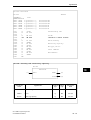
Address 0
PB1
FB1
Location of blocks
in the user memory
PB2
DB1
SB10
OB1
Fig. 2-2
Example of block storage in the user memory
Alternative loading (only in the By setting bit 0 in system data word RS 144, you can load data blocks
first into internal DB RAM first (i.e. as long as space is available)
case of Version -3UB12)
("Alternative loading" - see Chapter 8/RS 144). Data blocks are
transferred to the RAM card only when the DB RAM has been filled.
Correcting and deleting
blocks
When you correct blocks in "RAM mode", the old block is declared
invalid in the memory and a new block is entered.
Similarly, when blocks are deleted , they are not really deleted, instead
they are declared invalid. Deleted and corrected blocks therefore
continue to use up memory space.
Note
You can use the COMPRESS MEMORY online function to make
space for new blocks. This function optimizes the utilization of
the memory by deleting blocks marked as invalid and shifting
valid blocks together. Compression is handled separately
according to memory card and internal RAM (see Section 11.2.2).
CPU 928B Programming Guide
2 - 16
C79000-B8576-C898-01
Program, Organization and Sequence Blocks
2.2
Program, Organization and Sequence Blocks
Program blocks (PBs), organization blocks (OBs) and sequence
blocks (SBs) are the same with respect to programming and calling.
You can program all three types in the LAD, CSF and STL methods
of representation.
Programming
When programming organization, program and sequence blocks,
proceed as follows:
Step
Action
1
First indicate the type of block and then the number of the
block that you want to program.
The following numbers are available for the type of
block listed:
- program blocks
0 to 255
- sequence blocks
0 to 255
- organization blocks
1 to 39
2
Enter your program in the STEP 5 programming language.
When programming PBs, OBs and SBs, you can only
use the STEP 5 b asic operations!
A STEP 5 block should always be a self-contained
program section.
Logic operations must always be completed
within a block.
3
Block calls
Complete your program input with the block end
operation "BE".
With the exception of OB 1 to OB 39 you must call the blocks to
process them. Use the special STEP 5 block call operations to call the
blocks.
You can program block calls inside an organization, program,
function or sequence block. They can be compared with jumps to a
subroutine. Each jump causes a block change. The return address
within the calling block is buffered by the system.
CPU 928B Programming Guide
C79000-B8576-C898-01
2 - 17
2
Program, Organization and Sequence Blocks
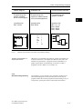
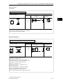
Block calls can be unconditional or conditional as follows:
Unconditional call
The "JU" statement belongs to the unconditional operations. It has no
effect on the RLO. The RLO is carried along with the jump to the new
block. Within the new block, it can be evaluated but no longer
combined logically.
The addressed block is processed reg ardless of the previous result of
logic operation (RLO - see Section 3.4).
Example: JU PB 100
Conditional call
The JC statement belongs to the conditional operations. The addressed
block is processed only if the previous R LO = 1. If the RLO = 0, the
jump is not executed.
Example: JC PB 100
Note
After the conditional jump operation is executed, the RLO is set
to " 1 " regardless of whether or not the jump to the block is
executed.
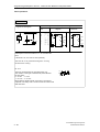
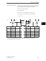
PB 1
JU
O
PB 5
PB 5
I 5.3
PB 10
A
I
1.0
JC
O
PB 10
F 1.5
BE
A
I
2.0
BE
PB 6
A
JC
A
BE
Fig. 2-3
I 1.5
PB 6
I 3.2
O
I
3.0
BE
Block calls that enable processing of a program block
CPU 928B Programming Guide
2 - 18
C79000-B8576-C898-01
Program, Organization and Sequence Blocks
Effect of the BE statement
After the "BE" statement (block end), the CPU continues the user
program in the block in which the block call was programmed.
Program execution continues at the STEP 5 statement following the
block call.
The "BE" statement is executed regardless of the RLO. After "BE",
the RLO can no longer be combined logically. However, the RLO or
arithmetic result occurring directly before execution of the BE
operation is transferred to the block where the call originated and can
be evaluated there. When program execution returns from the block
that has been called, the contents of ACCU 1, ACCU 2, ACCU 3 and
ACCU 4, the condition codes CC 0 and CC 1 and the RLO are not
changed. (Refer to Section 3.5 for more detailed information about the
ACCUs, CC0/CC1 and RLO).
2.2.1
Organization Blocks as
User Interfaces
Organization blocks form the interfaces between the system program
and the user program. Organization blocks OB 1 to OB 39 belong to
your user program just as program blocks. By programming these
OBs, you can influence the behavior of the CPU during start-up,
program execution and in the event of an error. The organization
blocks are effective as soon as they are loaded in the PLC memory.
This is also possible while the PLC is in the run mode.
Once the system program has called a specific organization block, the
user program it contains is executed.
Note
You can program blocks OB 1 to OB 39 as user interfaces and
they are called automatically by the system program as a reaction
to certain events.
For test purposes, you can also call these organization blocks
from the user program (JC/JU OB xxx). It is, however, not
possible to trigger a COLD RESTART, e.g. by calling OB 20.
The following table provides you with an overview of the user
interfaces (OBs).
CPU 928B Programming Guide
C79000-B8576-C898-01
2 - 19
2
Program, Organization and Sequence Blocks
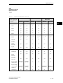
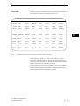
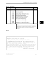
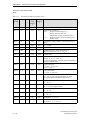
Table 2-1
Overview of the organization blocks for program execution
Org anization blocks for controllin g program execution
Block
Function and call criterion
OB 1
Organization of cyclic program execution;
first call after a start-up, then cyclic call
OB 2
Organization of interrupt-driven program
execution;
Call by interrupt signal of S5 bus (process
interrupt)
OB 3 to OB 5
OB 6
Not used with the CPU 928B
Delay interrupt (from Version -3UB12)
OB 7, OB 8
Not used with the CPU 928B
OB 9
Processing clock-controlled time interrupts
Time interrupts with fixed intervals:
OB 10
call every 10 ms
OB 11
call every 20 ms
OB 12
call every 50 ms
OB 13
call every 100 ms
OB 14
call every 200 ms
OB 15
call every 500 ms
OB 16
call every 1 s
OB 17
call every 2 s
OB 18
call every 5 s
CPU 928B Programming Guide
2 - 20
C79000-B8576-C898-01
Program, Organization and Sequence Blocks
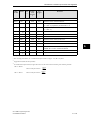
Table 2-2
Overview of the organization blocks for start-up
Organization blocks to control the start-up procedure
Block
Function and call criterion
OB 20
Call on request for COLD RESTART (manual
and automatic)
OB 21
Call on request for MANUAL WARM
RESTART/RETENTIVE COLD
RESTART
OB 22
Call on request for AUTOMATIC
WARM RESTART/RETENTIVE COLD
RESTART
Table 2-3
Overview of the organization blocks for error handling
Organization blocks for reactions to device or
1)
program errors
Block
Function and call criterion
OB 19
Runtime error (LZF):
called block not loaded
OB 23
Timeout (QVZ) in user program (during direct
access to I/O modules or other S5 bus
addresses)
OB 24
Timeout (QVZ) when updating the process
image and transferring interprocessor
communication flags
OB 25
Addressing error (ADF)
OB 26
Cycle time exceeded (ZYK)
OB 27
Op. code error (BCF): substitution error
OB 28
STOP by PG function/stop switch/
S5 bus 2)
OB 29
Op. code error (BCF):
code not permitted
OB 30
Op. code error (BCF):
parameter not permitted
OB 31
Other runtime errors (LZF)
OB 32
Runtime error (LZF): load and transfer error
with data blocks
OB 33
Collision of time interrupts (WECK-FE)
CPU 928B Programming Guide
C79000-B8576-C898-01
2 - 21
2
Program, Organization and Sequence Blocks
Organization blocks for reactions to device or
1)
program errors
Block
Function and call criterion
Table 2-3 continued:
OB 34
Error in closed loop controller processing
(REG-FE)
OB 35
Communication error on the second serial
interface (FE-3)
OB 36 to OB 39
do not exist for the CPU 928B
1)
If the OB is not programmed, the CPU changes to the stop mode in the event of
an error.
EXCEPTION: if OB 23, OB 24 and OB 35 do not exist, there is no reaction.
2)
OB28 is called before the CPU changes to the stop mode. The CPU stops regardless of whether and how OB 28 is programmed.
EXCEPTION: OB28 is not called if the power is switched off.
CPU 928B Programming Guide
2 - 22
C79000-B8576-C898-01
Program, Organization and Sequence Blocks
2.2.2
Organization Blocks for
Special Functions
The following organization blocks contain special functions of the
system program. You cannot program these blocks, but simply call
them (this applies to all OBs with numbers between 40 and 255!).
They do not contain a STEP 5 program. Special function OBs can be
called in all logic blocks.
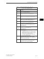
Table 2-4
Overview of organization blocks for special functions
Integral organization blocks with special functions
Block:
Block function:
OB 110
Access to the status (condition code) byte
OB 111
Clear ACCU 1, 2, 3 and 4
OB 112
ACCU roll up
OB 113
ACCU roll down
OB 120
"Block all interrupts" on/off
OB 121
"Block individual time interrupts" on/off
OB 122
"Delay all interrupts" on/off
OB 123
"Delay individual time interrupts" on/off
OB 150
Set/read system time
OB 151
Set/read time for clock-controlled time
interrupt
OB 152
Cycle statistics
OB 153
Set/read time for delay interrupt
OB 160-163
Counter loops
OB 170
Read block stack (BSTACK)
OB 180
Variable data block access
OB 181
Test data blocks DB/DX
OB 182
Copy data area
OB 190, 192
Transfer flags to data block
OB 191, 193
Transfer data fields to flag area
OB 200, 202-205
Multiprocessor communication
OB 216-218
Access to "pages" (CPs and some IPs)
OB 220
Sign extension
OB 221
Set cycle monitoring time
OB 222
Restart cycle monitoring time
CPU 928B Programming Guide
C79000-B8576-C898-01
2 - 23
2
Program, Organization and Sequence Blocks
Integral org anization blocks with special functions
Block:
Block function:
Table 2-4 continued:
OB 223
Compare restart type
OB 224
Transfer blocks of IPC flags
OB 226
Read word from the system program
OB 227
Read checksum of the system program
memory
OB 228
Read status information of a program
execution level
OB 230-237
Functions for standard function blocks
(handling blocks)
OB 240
Initialize shift register
OB 241
Process shift register
OB 242
Clear shift register
OB 250
Initialize PID controller algorithm
OB 251
Process PID controller algorithm
OB 254, 255
Transfer data block to the DB-RAM
These special functions are described in detail in Chapter 6.
CPU 928B Programming Guide
2 - 24
C79000-B8576-C898-01
Function Blocks
2.3
Function Blocks
Function blocks (FB/FX) are also parts of the user program just like
program blocks. FX function blocks have the same structure as FB
function blocks and are programmed in the same way.
You use function blocks to implement frequently recurring or very
complex functions. In the user program, each function block represents a
complex complete function. You can obtain function blocks as follows:
• as a software product from SIEMENS (standard function blocks
on diskette - see /11/ in Chapter 13); with these function blocks
you can generate user programs for fast and simple open loop
control, signalling, closed loop control and logging;
or
• you can program function blocks yourself.
Compared with organization, program and sequence blocks, function
blocks have the following four essential differences:
OB, PB, SB
1.
FB/FX
Range of operations
only basic operations
2.
- basic operations,
- supplementary operations
- system operations
Method of representation
programming and call
in STL, LAD, CSF
3.
programming only in AWL
Name
name environment not
possible
(only number)
4.
in addition to the number
a name with max. 8 chars. can
be assigned
Operands
none
formal operands (block
parameters).
When the block is called
formal operands are assigned
actual operands
CPU 928B Programming Guide
C79000-B8576-C898-01
2 - 25
2
Function Blocks
2.3.1
Structure of Function
Blocks
The block header (five words) of a function block has the same
structure as the headers of the other STEP 5 block types.
The block bod y on the other hand, has a different structure from the
bodies of the other block types. The block body contains the function
to be executed in the form of a statement list in the STEP 5
programming language. Between the block header and the STEP 5
statements, the function block needs additional memory space for its
name and for a list of formal operands. Since this list contains no
statements for the CPU, it is skipped with an unconditional jump that
the programmer generates automatically. This jump statement is not
displayed when the function block is displayed on the PG!
When a function block is called, only the block body is processed.
Absolute or symbolic
operands
You can enter operands in a function block in absolute form
(e.g. F 2.5) or symbolically (e.g. MOTOR1). You must store the
assignment of the symbolic operands in an assignment list before you
enter the operands in a function block (see /3/ in Chapter 13).
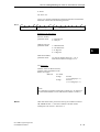
Fig. 2-4 shows the structure of a function block in the memory of a
programmable controller.
5 wo r d s
Skip for m a l
operand
list
JU
Block
header
1 wo r d
Na m e o f th e F B / F X
4 wo r d s
Formal operand 1
3 wo r d s
Formal operand 2
3 wo r d s
List o f
fo r m a l
operands
Block
body
Formal operand
3 wo r d s
n
1 s t ST EP 5 u s e r o p e r a t io n
ST EP 5
user
program
BE
Fig. 2-4
Structure of a function block (FB/FX)
CPU 928B Programming Guide
2 - 26
C79000-B8576-C898-01
Function Blocks
The memory contains all the information that the programmer needs
to represent the function block graphically when it is called and to
check the operands during parameter assignment and programming of
the function block. The programmer rejects incorrect input.
When handling function blocks, distinguish between the following
procedures:
• programming FB/FX
and
• callin g FB/FX and then assigning actual values to the parameters.
Distinction: "programming" –
"calling and assigning
parameters"
When programmin g, you specify the function of the block. You must
decide which input operands the function requires and which output
results it should transfer to the calling program. You define the input
operands and output results as formal operands. These function as
tokens.
When a block is called by a higher order block (OB, PB, SB, FB, FX),
the formal operands (block parameters) are replaced by actual operands;
i.e. parameters are assigned to the function block.
How to program
IF...
You want to program a function
block "directly", i.e. without
formal operands.
T HEN...
Program it as you would a
program or sequence block.
You want to use formal operands Proceed as explained on the
in a function block.
following pages.
Make sure you keep to the
required order:
First program the FB/FX with the
formal operands and keep it on
the PG (offline) or in the CPU
memory (online)
Then program the block(s) to be
called with the actual operands.
CPU 928B Programming Guide
C79000-B8576-C898-01
2 - 27
2
Function Blocks
2.3.2
Programming Function
Blocks
You can program a function block only in the "statement list"
method of representation. When entering a function block at a
programmer, perform the following steps:
Step
1
Action
Enter the block type (FB/FX) and the number of the
function block.
Number your function blocks in descending order
starting with FB 255, so that they do not collide with
the standard function blocks. The standard function
blocks are numbered from FB 1 to FB 199.
2
Enter the n ame of the function block.
The name can have a maximum of eight characters
and must start with a letter.
3
If the function block is to process formal operands:
Enter the formal operands you require in the block as
block parameters.
Enter the following information for each formal
operand:
-
the name of the block parameter (maximum
4 characters),
the type of block parameter and the data type of
the block parameter (if applicable)
You can define a maximum of 40 formal operands.
4
Enter your STEP 5 program in the form of a statement
list (STL). The formal operands are preceded by an
equality sign (e.g. A = X1). They can also be referenced
more than once at various positions in the function block.
5
Terminate your program input with the block end
operation "BE".
CPU 928B Programming Guide
2 - 28
C79000-B8576-C898-01
Function Blocks
Note
If you change the order or the number of formal operands in the
formal operand list, you must also update all STEP 5 statements
in the function block that reference a formal operand and also
the block parameter list in the calling block!
Program or change function blocks only on diskette or hard disk
and then transfer them to your CPU!
Formal operands
The following parameter and data types are permitted as the formal
operands of a function block (also known as block parameters):
Table 2-5
Permitted formal operands for function blocks
Parameter type
Data type
I = input parameter
Q = output parameter
BI/BY/W/D
D = data
KM/KH/KY/KS/KF/
KT/KC/KG
B = block operation
T = timer
C = counter
none
(no type can be specified)
I, D, B, T or C are parameters that are indicated to the left of the
function symbol in graphic representation.
Parameters labelled with Q are indicated on the right of the function
symbol.
The data type indicates whether you are working with bits, bytes,
words or double words for I and Q parameters and which data format
applies to D parameters (e.g. bit pattern or hexadecimal pattern).
CPU 928B Programming Guide
C79000-B8576-C898-01
2 - 29
2
Function Blocks
2.3.3
Calling Function Blocks and
Assigning Parameters to
them
You can call every function block as often as you want anywhere in
your STEP 5 program. You can call function blocks in a statement list
or in one of the graphic methods of representation (CSF or LAD).
To call a function block and assign parameters to it, perform the
following steps:
Step
Action
Reaction on PG
1
Make sure that the called function block exists either none
in the PG memory (offline) or in the CPU memory
(online).
2
Enter the call statement for the function block in the
block where the call is to originate.
You can program a function block call in an
organization, program or sequence block or
in another function block.
3
Assign the actual operand relevant to this call to
each of the formal operands, i.e. you assign
parameters to the function block.
After you enter the call statement
(e.g. JU FB200), the name of the
relevant function block and the formal
operand list appear automatically.
none
These actual operands can be different for
separate calls (e.g. inputs and outputs for the
first call of FB 200, flags for the second call).
Using the formal operand list, you assign the
required actual operands for each function
block call.
Unconditional/conditional call
Unconditional call
" JU FBn" for FB function blocks or
"DOU FXn" for FX extended function blocks:
the referenced function block is processed
regardless of the previous result of logic
operation (RLO).
Conditional call
"JC FBn" for FB function blocks or
"DOC FXn" for FX extended function blocks:
the referenced function block is only
processed when the result of logic operation
RLO = 1. If RLO = 0 the block call is not
executed. Regardless of whether the block call
is executed or not, the RLO is alsways set to "1".
After the unconditional or conditional call, the RLO can no longer be combined logically. However, it is
carried over to the called function block with the jump and can be evaluated there.
CPU 928B Programming Guide
2 - 30
C79000-B8576-C898-01
Function Blocks
Permitted actual operands
Table 2-6
Which operands can be assigned as actual operands is shown in the
following table.
2
Permitted actual operands for function blocks
Parameter
type
Data type
Actual operands permitted
I, Q
BI
for an operand
with bit address
I
Q
F
n.m
n.m
n.m
input
output
flag
BY
for an operand
with byte address
IB
QB
FY
DL
DR
PY
OY
n
n
n
n
n
n
n
input byte
output byte
flag byte
data byte left
data byte right
peripheral byte
byte from extended periphery
W
for an operand
with word address
IW
QW
FW
DW
PW
OW
n
n
n
n
n
n
input word
output word
flag word
data word
peripheral word
word from extended periphery
ID
QD
FD
DD
n
n
n
n
input double word
output double word
flag double word
data double word
D
D
for an operand
with double word address
KM
for a binary pattern (16 bits) Constants
KY
for two absolute numbers,
one byte each, each in the
range from 0 to 255
KH
for a hexadecimal pattern
with a maximum of four
digits
KS
for two alphanumeric
characters
KT
for timer value (BCDcoded) units .0 to .3 and
values 0 to 999
KC
for a counter value
0 to 999
CPU 928B Programming Guide
C79000-B8576-C898-01
2 - 31
Function Blocks
Parameter
type
Data type
Actual operands permitted
Table 2-6 continued:
D
KF
for a fixed point number
-32768 to +32767
KG
for a floating point
number1)
(Cont.)
B
Constants
Data type designation not possible DB
n
Data block; the operation
C DB n is executed
FB
n
Function block (permitted
only without parameters)
called unconditionally (JU . .n)
OB
n
Organization block called
unconditionally (JU . .n)
PB
n
Program blocks - called
unconditionally (JU . .n)
SB
n
Sequence blocks - called
unconditionally (JU . .n)
T
Data type designation not possible T 0 to 255 Timer
C
Data type designation not possible Z 0 to 255 Counter
1)
±0.1469368 x 10
-38
to ±0.1701412 x 1039
Note
S flags are not permitted as actual operands for function blocks.
After the jump to a function block, the actual operands from the block
then called are used in the function block program instead of the
formal operands.
This feature of programmable function blocks allow them to be used
for a wide variety of purposes in your user program.
CPU 928B Programming Guide
2 - 32
C79000-B8576-C898-01
Function Blocks
Examples
Example 1:
clarify
the following (complete) example is intended to further
the programming and calling of a function block and the
assignment of parameters to it. You yourself can easily
try out the example.
2
Programming the function block FB 202:
FB 202
SEGMENT 1
NAME EXAMPLE
DECL : INP1
DECL : INP2
DECL : OUT1
I/Q/D/B/T/C:
I/Q/D/B/T/C:
I/Q/D/B/T/C:
I
I
Q
BI/BY/W/D:
BI/BY/W/D:
BI/BY/W/D:
BI
BI
BI
Formal
operand
list
:A= INP1
:A= INP2
:== OUT1
STEP 5
:
: BE
ments
Formal
operands
state-
Parameter
type
Data
type
Function block FB 202 is called and has parameters assigned to
it in program block PB 25:
STL method of representation
CSF/LAD method of representation
PB 25
SEGMENT 1
NAME
INP1
INP2
OUT1
:
:
:
:
:
:
JU FB 202
EXAMPLE
I 13.5
F 17.7
Q 23.0
BE
Formal
operandes
I 13.5
F 17.7
FB 202
EXAMPLE
INP1
INP2
OUT1
Q 23.0
:BE
Actual
operands
The following operations are executed after the jump to FB 202
: A
: A
: =
I 13.5
F 17.7
Q 23.0
CPU 928B Programming Guide
C79000-B8576-C898-01
2 - 33
Function Blocks
Example 2: calling a function block and assigning parameters to it with
the STL and CSF/LAD methods of representation in a program block.
STL method of representation
PB 25
SEGMENT 1
:
: C DB 5
:
: JU
FB 201
NAME : REQUEST
DATA :
DW
1
RST :
I
3.5
SET :
F
2.5
MTIM :
T
2
TIME :
KT
010.1
TRAN :
DW
2
BEC :
Q
2.3
LOOP :
Q
6.0
: BE
Formal
operands
Actual
operands
CSF/LAD method of representation
PB 25
SEGMENT 1
FB 201
DW 1
I 3.5
F 2.5
T 2
KT 010.1
REQUEST
DATA
RST
SET
MTIM
TIME
TRAN
BEC
LOOP
DW 2
Q
2.3
Q
6.0
:BE
CPU 928B Programming Guide
2 - 34
C79000-B8576-C898-01
Function Blocks
2.3.4
Special Function Blocks
Apart from the function blocks that you program yourself, you can
order standard function blocks as a finished software product. These
contain standard functions for general use (e.g. signalling functions
and sequence control).
Standard function blocks are assigned numbers FB 1 to FB 199.
If you order standard function blocks, remember the special
instructions in the accompanying description (i.e. areas assigned and
conventions etc.).
The standard function blocks for the S5-135U are listed in catalog
ST 57.
Example
Floating point root extractor RAD:GP FB 6
The function block RAD:GP extracts the root of a floating point number
(8-bit exponent and 24-bit mantissa). It forms the square root. The
result is also a floating point number (8-bit exponent and 24-bit
mantissa). The least significant bit of the mantissa is not rounded up
or down.
If applicable, for the rest of the processing, the function block sets
the "radicand negative" identifier.
Numerical range:
Radicand
Root
- 0.1469368 Exp. -38 to +0.1701412 Exp. +39
+0.3833434 Exp.
-19 to +0.1304384 Exp. +20
Function: Y = √A
Y = SQRT; A = RADI
Calling the function block FB 6:
In the example, the root is extracted from a floating point number that is
located in DD5 of DB 17 with an 8-bit exponent and a 24-bit mantissa. The
result, another 32-bit floating point number, is written to DD 10. Prior
to this, the appropriate data block must be opened. The parameter VZ
(parameter type: Q, data type: BI) indicates the sign of the radicand: VZ
= 1 for a negative radicand.
Occupied flag words: FW 238 to FW 254.
Continued on the next page
CPU 928B Programming Guide
C79000-B8576-C898-01
2 - 35
2
Function Blocks
"Floating point root extractor" continued:
STL method of representation
Segment
1
: C DB 17
:
:***
: JU FB 6
Seg- NAME : RAD : GP
ment RADI : DD 5
2
VZ
: F 15.0
*) SQRT : DD 10
LAD method of representation
SEGMENT 2
DD 5
FB 6
RAD
RADI
VZ
SQRT
F 15.0
DD 10
:BE
DD= data double word
*) Must be located in separate segments, since the operation "C DB 17"
in segment 1 cannot be converted to LAD/CSF.
Using FB 0
If you have not programmed organization block OB 1, the system
program calls FB 0 (provided it is loaded) cyclically instead of OB 1.
Since you have the total operation set of the STEP 5 programming
language available in a function block, programming FB 0 instead of
FB 1 can be an advantage, particularly when you wish to execute a
short time-critical program.
Note
You should only use FB 0 for programming cyclic program
execution (it must not contain parameters).
If both OB 1 and FB 0 are loaded, the system program will only
call organization block OB 1 cyclically.
CPU 928B Programming Guide
2 - 36
C79000-B8576-C898-01
Data Blocks
2.4
Data Blocks
Data blocks (DB) or extended data blocks (DX) are used to store the
fixed or variable data with which the user program works. No STEP 5
operations are processed in data blocks.
2
The data of a data block includes the following:
• various bit patterns (e.g. for status of a controlled process)
• numbers (hexadecimal, binary, decimal) for timer values or
arithmetic results
• alphanumeric characters, e.g. for message texts.
Structure of a data block
A data block (DB/DX) consists of the following parts:
• block preheader (DV, DXV),
• block header
• block body.
Block preheader
The block preheader is created automatically on the hard or floppy
disk of the PG and not transferred to the CPU. It contains the data
formats of the data words entered in the block body. You have no
influence over the creation of the block preheader.
Note
When you transfer a data block from the PLC to diskette or hard
disk, the corresponding block preheader can be deleted. For this
reason, you must never modify a data block with different data
formats in the PLC and then transfer it back to diskette, otherwise
all the data words in the DB are automatically assigned the data
format you selected in the presets screen form.
CPU 928B Programming Guide
C79000-B8576-C898-01
2 - 37
Data Blocks
Block header
The block header occupies five words in the memory and contains
the following:
• the block identifier
• the programmer identifier
• the block type and the block number
• the library number
• the block length (including the length of the block header).
Block body
The block body contains the data words with which the user program
works. These data words are in ascending order in the block body,
starting with data word DW 0. Each data word occupies one word
(16 bits) in the memory.
Maximum length
A data block can occupy a total of maximum 32 767 words (including
header) in the CPU memory. When you use your programmer to enter
and transfer data blocks, remember the size of your CPU memory!
CPU 928B Programming Guide
2 - 38
C79000-B8576-C898-01
Data Blocks
2.4.1
Creating Data Blocks
To create a data block, perform the following steps:
Step
Action
1
Enter the block type (DB/DX) and data block number
between 3 and 255.
2
Enter individual data words in the data format you
require.
(Do not complete your input of the data words with a
BE statement!)
Note
Data blocks DB 0, DB 1, DX 0, DX 1 and DX 2 are reserved for
specific functions and you cannot use them freely for other
functions (see Section 2.4.3)!
Table 2-7
Data formats permitted in a data block
Type
D ata format
Exa mples
KM
Bit pattern
00100110 00111111
KH
Hexadecimal
263F
KY
2 Bytes
038,063
KF
Fixed point number
+09791
KG
Floating point number
+1356123+12
KS
Character
?!ABCD123-+.,%
KT
Timer value
055.2
KC
Counter value
234
CPU 928B Programming Guide
C79000-B8576-C898-01
2 - 39
2
Data Blocks
2.4.2
Opening Data Blocks
You can only open a data block (DB/DX) unconditionally . This is
possible within an organization, program, sequence or function block.
You can open a specific data block more than once in a program.
To open a data block, perform the following steps:
IF...
Validity of a data block
T HEN...
You want to open a D B data
block
"C D B.."
Type in the STEP 5 operation
You want to open a D X data
block
"CX DX.."
Type in the STEP 5 operation
After you open a data block, all statements that follow with the
operand area ’D’ refer to the opened data block.
The opened data block also remains valid when the program is
continued in a different block following a block call.
If a second data block is opened in this new block, the second data
block is only valid in the newly called block from the point at which it
is called. After program execution returns to the calling block, the old
data block is once again valid.
Access
You can access the data stored in the opened data block during
program execution using load or transfer operations (refer to
Chapter 3 for more detailed information).
With a binary operation , the addressed data word bit is used to form
the RLO. The content of the data word is not changed.
With a set/reset operation, the addressed data word bit is assigned the
value of the RLO. The content of the data word may be changed.
A load operation transfers the contents of the referenced data word
into ACCU 1. The contents of a data word are not changed.
A transfer operation transfers data from ACCU 1 to the referenced
data word. The old contents of the data word are overwritten.
CPU 928B Programming Guide
2 - 40
C79000-B8576-C898-01
Data Blocks
Note
Before accessing a data word, you must open the data block you
require in your program. This is the only way that the CPU can
find the correct data word.
The referenced data word must be contained in the opened block,
otherwise the system program detects a load or transfer error.
With load and transfer operations, you can only access data word
numbers up to 255!
An opened data block remains valid until one of the following
events occur:
a) a second data block is opened
or
b) the block, in which the data block was
opened, is completed with ’BE’, ’BEC’
or ’BEU’.
Examples
Example 1: transferring data words
You want to transfer the contents of data word
DW 1 from data block DB 10 to data word DW 1 of
data block DB 20.
Enter the following statements:
:C
:L
:
:C
:T
:
:
DB 10
DW 1
DB 20
DW 1
(open DB 10)
(load the contents of DW 1 into
ACCU 1)
(open DB 20)
(transfer the contents of ACCU 1
to DW 1)
CPU 928B Programming Guide
C79000-B8576-C898-01
2 - 41
2
Data Blocks
Example 2: range of validity of data blocks
(Fig. 2-5)
Data block DB 10 is opened in program block
PB 7 (C DB 10). During the subsequent program
execution, the data of this data block are
processed.
After the call (JU PB 20) program block PB 20
is processed. Data block DB 10, however,
remains valid. The data area only changes when
data block DB 11 (C DB 11) is opened.
Data block DB 11 now remains valid until the
end of program block PB 20 (BE).
After the jump back to program block PB 7,
data block DB 10 is once again valid.
PB
C
JU
7
PB
20
C
DB 11
DB 10
PB 20
BE
BE
Range of validity of DB 10
Range of validity of DB 11
Fig. 2-5
Range of validity of an opened data block
CPU 928B Programming Guide
2 - 42
C79000-B8576-C898-01
Data Blocks
2.4.3
Special Data Blocks
DB 0
On the CPU 948 data blocks DB 0, DB 1, DX 0, DX 1 and DX 2 are
reserved for special functions. They are managed by the system
program and you cannot use them freely for other functions.
• Data block DB 0 (see Section 8.3.2)
2
Data block DB 0 contains the address list with the start addresses
of all blocks that are located in the data block RAM of the CPU.
The system program generates this address list during
initialization (following each POWER UP or OVERALL RESET)
and it is updated automatically when you use a programmer to
change data blocks or generate a new data block.
DB 1
• Data block DB 1 (see Section 10.1.6)
Data block DB 1 contains the list of digital inputs/outputs (P
peripheral with relative byte addresses from 0 to 127) and the
interprocessor communication (IPC) flag inputs and outputs that are
assigned to the CPU. If applicable, the block may also contain a timer
field length.
DB 1 can have parameters assigned and be loaded as follows:
to reduce the cycle time in single processor operation, since
only the inputs, outputs or timers entered in DB1 are updated.
D B 1 must be assigned parameters and loaded as follows:
a) for multiprocessing
b) when IPC flags exist with CPs
DB 2
• Data block DB 2 (see Section 4.4.3)
You use data block DB 2 to assign parameters to the closed loop
controller structure R64. The closed loop control function can be
ordered as a software product and operates supported by the
system program.
CPU 928B Programming Guide
C79000-B8576-C898-01
2 - 43
Data Blocks
DX 0
• Data block DX 0 (see Chapter 7)
If you assign parameters to data block DX 0 and load it, you can
change the defaults of certain system program functions (e.g. the
start-up procedure) and adapt the performance of the system program
to your particular application.
DX 1
• Data block DX 1
Reserved.
DX 2
• Data block DX 2 is used to specify the communication via the
second serial interface. See the "CPU 928B Communication"
Manual for details of assigning parameters to this block (/14/ in
Chapter 13).
CPU 928B Programming Guide
2 - 44
C79000-B8576-C898-01
Program Execution
3
Contents of Chapter 3
3.1
Principle of Program Execution. . . . . . . . . . . . . . . . . . . . . . . . . . . . . . . . . . . . . . . . . . . . . 3 - 4
3.2
Program Organization. . . . . . . . . . . . . . . . . . . . . . . . . . . . . . . . . . . . . . . . . . . . . . . . . . . . . 3 - 5
3.3
Storing Program and Data Blocks . . . . . . . . . . . . . . . . . . . . . . . . . . . . . . . . . . . . . . . . . . 3 - 10
3.4
Processing the User Program . . . . . . . . . . . . . . . . . . . . . . . . . . . . . . . . . . . . . . . . . . . . . . 3 - 11
3.4.1
Definition of Terms used in Program Execution. . . . . . . . . . . . . . . . . . . . . . . . . . . . . . . 3 - 12
3.5
STEP 5 Operations with Examples . . . . . . . . . . . . . . . . . . . . . . . . . . . . . . . . . . . . . . . . . 3 - 15
3.5.1
Basic Operations. . . . . . . . . . . . . . . . . . . . . . . . . . . . . . . . . . . . . . . . . . . . . . . . . . . . . . . .
Binary logic operations . . . . . . . . . . . . . . . . . . . . . . . . . . . . . . . . . . . . . . . . . . . . . . . . . .
Set/reset operations. . . . . . . . . . . . . . . . . . . . . . . . . . . . . . . . . . . . . . . . . . . . . . . . . . . . . .
Load and transfer operations . . . . . . . . . . . . . . . . . . . . . . . . . . . . . . . . . . . . . . . . . . . . . .
Timer and counter operations. . . . . . . . . . . . . . . . . . . . . . . . . . . . . . . . . . . . . . . . . . . . . .
Arithmetic operations . . . . . . . . . . . . . . . . . . . . . . . . . . . . . . . . . . . . . . . . . . . . . . . . . . . .
Comparison operations . . . . . . . . . . . . . . . . . . . . . . . . . . . . . . . . . . . . . . . . . . . . . . . . . . .
Block operations . . . . . . . . . . . . . . . . . . . . . . . . . . . . . . . . . . . . . . . . . . . . . . . . . . . . . . . .
NOP/display/stop operations . . . . . . . . . . . . . . . . . . . . . . . . . . . . . . . . . . . . . . . . . . . . . .
Programming Examples in the STL, LAD and CSF Methods of Representation . . . . .
Supplementary Operations . . . . . . . . . . . . . . . . . . . . . . . . . . . . . . . . . . . . . . . . . . . . . . . .
Binary logic operations . . . . . . . . . . . . . . . . . . . . . . . . . . . . . . . . . . . . . . . . . . . . . . . . . .
Digital logic operations . . . . . . . . . . . . . . . . . . . . . . . . . . . . . . . . . . . . . . . . . . . . . . . . . .
Set/reset operations. . . . . . . . . . . . . . . . . . . . . . . . . . . . . . . . . . . . . . . . . . . . . . . . . . . . . .
Timer and counter operations. . . . . . . . . . . . . . . . . . . . . . . . . . . . . . . . . . . . . . . . . . . . . .
Load and transfer operations . . . . . . . . . . . . . . . . . . . . . . . . . . . . . . . . . . . . . . . . . . . . . .
Arithmetic operations . . . . . . . . . . . . . . . . . . . . . . . . . . . . . . . . . . . . . . . . . . . . . . . . . . . .
3.5.2
3.5.3
3 - 19
3 - 19
3 - 20
3 - 21
3 - 26
3 - 31
3 - 32
3 - 32
3 - 33
3 - 34
3 - 49
3 - 50
3 - 50
3 - 51
3 - 52
3 - 54
3 - 56
CPU 928B Programming Guide
C79000-B8576-C898-01
3-1
3
Contents
3.5.4
3.5.5
Executive Operations . . . . . . . . . . . . . . . . . . . . . . . . . . . . . . . . . . . . . . . . . . . . . . . . . . . .
Jump operations . . . . . . . . . . . . . . . . . . . . . . . . . . . . . . . . . . . . . . . . . . . . . . . . . . . . . . . .
Shift operations . . . . . . . . . . . . . . . . . . . . . . . . . . . . . . . . . . . . . . . . . . . . . . . . . . . . . . . . .
Conversion operations . . . . . . . . . . . . . . . . . . . . . . . . . . . . . . . . . . . . . . . . . . . . . . . . . . .
Decrement/increment . . . . . . . . . . . . . . . . . . . . . . . . . . . . . . . . . . . . . . . . . . . . . . . . . . . .
Processing operations . . . . . . . . . . . . . . . . . . . . . . . . . . . . . . . . . . . . . . . . . . . . . . . . . . . .
Disabling/enabling process interrupts . . . . . . . . . . . . . . . . . . . . . . . . . . . . . . . . . . . . . . .
Semaphore Operations . . . . . . . . . . . . . . . . . . . . . . . . . . . . . . . . . . . . . . . . . . . . . . . . . . .
3 - 58
3 - 58
3 - 60
3 - 62
3 - 65
3 - 65
3 - 71
3 - 75
CPU 928B Programming Guide
3-2
C79000-B8576-C898-01
Program Execution
3
This chapter is intended for readers who do not yet have any great
experience in using the programming language. The chapter therefore
deals with the basics of STEP 5 programming and explains in detail
(with examples) the STEP 5 operations for the CPU 928B.
Experienced readers who require more information about a specific
STEP 5 operation listed in the Pocket Guide can refer to the reference
section in 3.5.
CPU 928B Programming Guide
C79000-B8576-C898-01
3-3
3
Principle of Program Execution
3.1
Principle of Program Execution
You can process your STEP 5 user program in various ways.
Cyclic program execution is most common with programmable
controllers (PLCs). The system program runs through a program loop
(the cycle, refer to Section 3.4) and calls organization block OB 1
cyclically in each loop (refer to Fig. 3-1).
System program
Us e r p r o g r a m
from start-up
OB 1
Tr i g g e r c y c l e t i m e
Up d a t e in t e r processor comm.
f la g in p u t s
Up d a t e p r o c e s s
im a g e in p u t s
( PI I )
PB 20
Ca l l P B 2 0
Call OB1
BE
Up d a t e p r o c e s s
im a g e o u t p u t s
( PI Q )
Up d a t e in t e r processor comm.
f la g o u t p u t s
Fig. 3-1
BE
Principle of cyclic program execution
CPU 928B Programming Guide
3-4
C79000-B8576-C898-01
Program Organization
3.2
Program Organization
Program organization allows you to specify which conditions affect the
processing of your blocks and the order in which they are processed.
Organize your program by programming organization blocks with
conditional or unconditional calls for the blocks you require.
You can call additional program, function and sequence blocks in any
combination in the program of individual organization, program,
function and sequence blocks. You can call these one after another or
nested in one another.
For maximum efficiency, you should organize your program to
emphasise the most important program structures and in such a way
that you can clearly recognize parts of the controlled system which are
related in the software.
Figs. 3-2 and 3-3 are examples of a program structure.
CPU 928B Programming Guide
C79000-B8576-C898-01
3-5
3
Program Organization
OB 1
PB ’A’
Op e r a t in g mo d e
program
FB
Stop to the system
EMERGENCY
OFF
JU PB ’A’
FB
Go to in itia l
state
PB ‘B‘
Se q u e n c e
control
FB
Co n t r o l o f
sequence
cascade
SB
Se q u e n c e
step
JU PB ‘B‘
SB
Se q u e n c e
step
PB ‘C‘
I n d iv id u a l
c o n t r o l le v e l
FB
Gr o u p
in itia liza tio n
FX
DB
I n t e r f a c e fla g s
o f t h e in d iv id u a l
control
e le m e n t s
I n d iv id u a l
in itia liza tio n
JU PB ‘C‘
FX
I n d iv id u a l
in itia liza tio n
PB ‘D‘
Message output
JU PB ‘D‘
FB
Message output
v ia st a n d a r d
p e r ip h e r a ls
FB
Message output
v ia st a n d a r d
p e r ip h e r a ls
DX
Message
texts
BE
Fig. 3-2
Example of the organization of the user program according to the program structure
CPU 928B Programming Guide
3-6
C79000-B8576-C898-01
Program Organization
OB
1
PB ‘X‘
Controlled
system part ‘X‘
FB
Individual control
FB
JU PB ‘X‘
Closed loop control
3
FX
Signalling
PB ‘Y‘
Controlled
system part ‘Y‘
JU PB ‘Y‘
FB
Sequence control
FX
Signalling
FB ‘Z‘
Controlled
system part ‘Z‘
JU PB ‘Z‘
FB
Closed loop control
FB
Arithmetic
FB
Data logging output
BE
Fig. 3-3
Example of the organization of the user program according to the structure of the controlled system
CPU 928B Programming Guide
C79000-B8576-C898-01
3-7
Program Organization
Nesting blocks
OB 1
Fig. 3-4 shows the principle of nested block calls.
PB 5
1st STEP 5 Op.
C
DB 20
JU
=
PB 20
Q 60.6 *)
PB 20
1st STEP 5 Op.
C
JU PB 5
A F 200.5
*)
BE
*)
BE
DB 30
JU FB 30
NAME: KURV
A
I 55.0 *)
BE
Operation to which the program returns
Fig. 3-4
Nested logic block calls
Block addresses
A block start address specifies the location of a block in the user
memory (oder DB-RAM). For logic blocks, this is the address of the
memory location containing the first STEP 5 operation (with FB and
FX, the JU operation via the formal operand list); with data blocks, it
is the address of the first data word.
To enable the CPU to locate the called block in the memory, the start
addresses of all valid blocks are entered in the block address list in
data block DB 0. DB 0 is managed by the system program, you cannot
call it yourself.
The CPU stores a return address every time a new block is called. After
the new block has been processed, this return address enables the
program to find the block from which the call originated. The return
address is the address of the memory location containing the next STEP 5
statement after the block call. The CPU also stores the start address and
len gth of the d ata block valid at this location.
CPU 928B Programming Guide
3-8
C79000-B8576-C898-01
Program Organization
Nesting depth
You can only nest 62 blocks within one another. If more than 62
blocks are called, the CPU signals an error and goes to the stop mode.
Example of nesting depth
Program
processing
level
3
OB 25
OB 2
OB 13
OB 1
PB 1
PB 131
FB 21
FB 131
FB 1
Nesting depth
1
Fig. 3-5
2
3
4
5
6
7
8
9
Example of block nesting depth
You can determine the nesting depth of your program as follows:
- Add all the organization blocks you have programmed
(in the example: 4 OBs).
- Add the nesting depth of the individual organization blocks
(in the example: 2 + 2 + 1 + 0 = 5).
- Add the two amounts together to obtain the program nesting depth
(in the example: 4 + 5 = nesting depth 9). It may not exceed a value
of 62.
CPU 928B Programming Guide
C79000-B8576-C898-01
3-9
Storing Program and Data Blocks
3.3
Storing Program and Data Blocks
You must load your program into the user memory so that the CPU
can process it. As program memory you can use a plug-in submodule
(optional either RAM or EPROM) and the DB-RAM.
Different storage types 1)
• If you use a plug-in R A M submodule you can transfer your
program directly from the programmer to the CPU.
You can change the contents of a RAM submodule quickly and
easily. A central back-up battery prevents your program being
deleted in the memory if the power goes off.
All programmed blocks are stored in random order in the RAM
(see Section 2.1.5, Fig. 2-2). If you change a block, the sequence
of the blocks in the RAM also changes.
If you use a RAM submodule with a back-up battery , you can
remove it from the CPU without losing data. Havin g its own
b attery protects the submodule from loss of data and ensures
that the d ata is retained until it is required again.
• You can also store your complete program in plug-in EPR O M
sub modules. Your program is completely protected in EPROM
submodules even when the power goes off and no back-up battery
is necessary.
You cannot change the contents of an EPROM submodule from
the PC. For this reason, data blocks that contain variable data that
have to be changed during the course of your program must be
copied from the EPROM submodule to the data block RAM of the
CPU during the first cold restart following an overall reset. You
must program this function (see special function OB 254 and
OB 255, Section 6.4.6).
• Data blocks DB/DX are written into the DB-RAM by generating
or copying them. If you transfer data blocks from the PG to the
CPU, they are written to the DB-RAM if the RAM submodule is
full or if an EPROM submodule is plugged in.
C aution
Battery-backed RAM submodules must not be programmed via
the EPROM interface; this can damage the RAM.
1)
When storing data blocks, please note the possibility of "alternative loading" - Section 2.1.5.
CPU 928B Programming Guide
3 - 10
C79000-B8576-C898-01
Processing the User Program
3.4
Processing the User Program
The complete software on the CPU (consisting of the system program
and the STEP 5 user program) has the following tasks:
• CPU START-UP
• Controlling an automation process by continuously repeating
operations (CYCLE).
3
• Controlling an automation process by reacting to events
occurring sporadically or at certain times (interrupts) and
reacting to errors.
For all three tasks, you can select special parts of your program to run
on the CPU by programming user interfaces (organization blocks
OB 1 to OB 35 - refer to Section 2.2.1).
START-UP
Before the CPU can start cyclic program execution, an initialization
must be performed to establish a defined initial status for cyclic
program execution and, for example, to specify a time base for the
execution of certain functions. The way in which this initialization is
performed depends on the event that led to a START-UP and on
settings that you can make on your CPU. For more detailed
information, refer to Chapter 4.
You can influence the START-UP procedure of your CPU by
programming organization blocks OB 20, OB 21 and OB 22 or by
assigning parameters in DX 0 (refer to Chapter 7).
CYCLE
Following the START-UP, the system program goes over to cyclic
processing. It is responsible for background functions required for the
automation tasks (refer to Fig. 3-1 at the beginning of this section).
After the system functions have been executed at the beginning of a
CYCLE, the system program calls organization block OB 1 or
function block FB 0 as the cyclic user program. You program the
STEP 5 operations for cyclic processing in this block.
CPU 928B Programming Guide
C79000-B8576-C898-01
3 - 11
Processing the User Program
Reactions to interrupts
and errors
To allow you to specify the reactions to interrupts or errors, special
organization blocks (OB 2, OB6 and OB9 to OB 18 for interrupt
servicing, OB 19 and OB 23 to OB 35 for reactions to errors) are
available on the CPU 928B. You can store an appropriate STEP 5
program in these blocks.
When interrupts or errors are to be processed, the system program
activates the corresponding organization block during cyclic
processing. This means that the cyclic processing is interrupted to
service an interrupt or to react to an error. The nesting of the
organization blocks has a fixed priority (for further information, refer
to Chapters 4 and 5).
In addition to the organization blocks, you can also influence the
reaction of the CPU to interrupt servicing by assigning parameters in
data block DX 0.
Organization blocks OB 1 to OB 39 can be called by the system
program as soon as they are loaded in the program memory (also
during operation).
If the OBs are not loaded, there is either no reaction from the CPU or
(in the event of errors) it goes to the stop mode (refer also to
Section 5.4).
You can also load data block DX 0 into the program memory during
operation like the organization blocks. It is, however, only effective
after the next COLD RESTART. If DX 0 is not loaded, the standard
settings apply (refer to Chapter 7).
3.4.1
Definition of Terms used in
Program Execution
Cycle time
The cycle begins when the cycle monitoring time is triggered and
ends with the next trigger. The time that the CPU requires to execute
the program between two triggers is called the cycle time. The cycle
time consists of the runtime of the system program and the runtime of
the user program.
The cycle time therefore includes the following:
• the time required to process the cyclic program (system and user
program),
• the time required to process interrupts (e.g. time-controlled
interrupt),
• the time required to process interruptions (errors).
CPU 928B Programming Guide
3 - 12
C79000-B8576-C898-01
Processing the User Program
Cycle time monitoring
The CPU monitors the cycle time in case it exceeds a maximum value.
The standard setting for this maximum value is 150 ms. You can set the
cycle time monitoring yourself or restart it during user program execution
(refer to DX 0/Chapter 7 and special function OB OB 221 and
OB 222/Sections 6.22 and 6.23).
Process input and output
image (PII and PIQ)
The process image of the inputs and outputs is a memory area in the
internal RAM.
Before cyclic execution of the user program begins, the system
program reads the signal states of the input peripheral modules and
transfers them to the process input image. The user program evaluates
the signal states in the process input image and then sets the
appropriate signal states for the outputs in the process output image.
After the user program has been processed, the system program
transfers the signal states of the process output image to the output
peripheral modules.
Buffering the I/O signals in the process image of the inputs and
outputs avoids a change in a bit within a program cycle from causing
the corresponding output to "flutter".
The process image is therefore a memory area whose contents are
output to the peripherals and read in from the peripherals once per
cycle.
Note
The process image only exists for input and output bytes of the "P"
peripherals with byte addresses from 0 to 127!
Interprocessor communication IPC flags exchange data between individual CPUs (multiprocessing) or
between the CPU and some communication processors.
(IPC) flags
The system program reads the input IPC flags of the CPU before
cyclic execution of the user program begins. After the STEP 5
program is processed, the system program transfers the output IPC
flags to the coordinator or to the communications processors.
You define the input and output IPC flags when you create data block
DB 1 (refer to Section 10.1.5).
CPU 928B Programming Guide
C79000-B8576-C898-01
3 - 13
3
Processing the User Program
Interrupt events
Cyclic program execution can be interrupted by the following:
• process interrupt-driven program processing,
• time-controlled program processing,
• delay interrupt,
• time interrupt clock-controlled.
The cyclic program can be interrupted or even aborted completely by
the following:
• a device hardware fault or program error,
• operator intervention (using the PC stop function, or setting the
mode selector to "stop", multiprocessor stop MP-STP),
• a stop operation.
CPU 928B Programming Guide
3 - 14
C79000-B8576-C898-01
STEP 5 Operations with Examples
3.5
STEP 5 Operations with Examples
A STEP 5 operation consists of the operation and an operand. The
operation specifies wh at the CPU is to do (operation). The operand
specifies with what an operation is to be executed.
STEP 5 operations can be divided into the following groups:
• basic operations (can be used in all logic blocks),
3
• supplementary operations,
• executive operations (can only be used in FB/FX function blocks),
• semaphore operations (can only be used in FB/FX function
blocks).
Accumulators as working
registers
The CPU 928B has four accumulators, ACCU 1 to ACCU 4. Most
STEP 5 operations use two 32-bit registers (ACCU 1 and ACCU 2)
as the source of operands and the destination for results.
High word
ACCU 1
24 23
31
High byte
Low byte
High byte
1)
Low word
16 15
ACCU-1-HL
ACCU-1-HH
ACCU-1-H
Low byte
8 7
0
ACCU-1-LH
ACCU-1-LL
ACCU-1-L
The STEP 5 operation to be carried out affects the accumulators, e.g.:
• ACCU 1 is always the destination in load operations. A load
operation shifts the old contents of ACCU 1 to ACCU 2 (stack
lift). Accumulators 3 and 4 are not changed by any load operations.
1)
analogous for ACCU 2 to ACCU 4
CPU 928B Programming Guide
C79000-B8576-C898-01
3 - 15
STEP 5 Operations with Examples
• Arithmetic operations combine the contents of ACCU 1 with those
of ACCU 2, write the result to ACCU 1 and transfer the contents
of ACCU 3 to ACCU 2 and the contents of ACCU 4 to ACCU 3
(stack drop). In 16-bit fixed point arithmetic, only the low word or
ACCU 3 is transferred to the low word of ACCU 2 and the low
word of ACCU 4 to the low word of ACCU 3.
• When a constant is added (ADD BF/KF/DH) to the contents of
ACCU 1, the accumulators 2, 3 and 4 are not changed.
Condition codes
STEP 5 operations either set or evaluate condition codes. The condition
codes are written to a condition code byte. Two groups of condition
codes can be distinguished: condition codes of digital operations (word
condition codes - bits 4 to 7 in the condition code byte) and condition
codes from binary and executive operations (bit condition codes - bits 0
to 3 in the condition code byte). You can see how the various condition
codes are influenced or evaluated by STEP 5 operations be referring to
the operation list (see /1/ in Chapter 13).
You can display the condition code byte on a programmer using the
"STATUS" online function (refer to Section 11.2.3). The byte has the
following structure:
W ord condition codes
CC 1
Bit condition codes
Bit condition codes
CC 0
OV
OS
Bit 7
6
5
4
• ER A B
First bit scan
OR
3
STA
RLO
ERAB
2
1
0
A logic operation sequence containing binary operations always
begins with the first bit scan, following which a new RLO is
formed. The bit condition code ERAB = 1 is then set. While the
remaining logic operations in the sequence are being performed,
ERAB remains set to 1 and the RLO cannot be changed by these
logic operations.
The active sequence of logic operations is terminated by a binary
set/reset operation (e.g. S Q 5.0). The set/reset operation sets
ERAB to 0; the RLO can be evaluated (e.g. by RLO-dependent
operations) but can no longer be combined logically. The next
binary logic operation following a binary set/reset operation is
once again a first bit scan.
CPU 928B Programming Guide
3 - 16
C79000-B8576-C898-01
STEP 5 Operations with Examples
Example of ERAB
Other bit condition codes
:S
Q 7.7
:A
:
:
:O
:
:AN
:
:S
:
:JC
:
:
:
I 1.0
I 6.3
I 2.1
Q 2.4
FB 150
Last operation of the previous logic operation
sequence
ERAB is set to ’1’,
the new RLO is formed by
an AND operation
The RLO is influenced by
an OR operation
The RLO is influenced by
an AND NOT operation.
ERAB is set to ’0’,
the sequence is now complete
The function block is called
dependent on the RLO.
• R LO Result of logic operation
This is the result of bit logic operations. It is the truth statement for
comparison operations (refer to operations list, binary logic
operations or comparison operations).
• STA Status
For bit operations, this indicates the logical status of the bit just
scanned or set. The status is updated in binary logic operations except for A(, O(,), O and for set/reset operations.
• O R Or
Internal CPU bit for handling "AND before OR" logic operations.
Word condition codes
• OV Overflow
This indicates whether the permissible number range was exceeded
during the arithmetic operation just completed.
• OS Stored overflow
It can be used in several arithmetic operations to indicate whether an
overflow occurred at any point during the operations.
CPU 928B Programming Guide
C79000-B8576-C898-01
3 - 17
3
STEP 5 Operations with Examples
• CC 1 and CC 0
These are the result condition codes that you can interpret from the
following table:
Note
To evaluate the condition codes directly, comparison and jump
operations are available (refer to Sections 3.5.1 and 3.5.3).
Table 3-1
Result condition codes of STEP 5 operations
W ord
condition codes
CC 1
CC 0
0
0
0
1
Arithmetical
operations
Digital
logic
operations
Comparison
operations
Shift
operations
For
SED,
SEE
Jump
operations
executed
Result
=0
Result
=0
ACCU 2
=
ACCU 1
Shifted
bit
=0
Semaphore
is
set
JZ
Result
<0
–
ACCU 2
<
ACCU 1
–
–
1
0
Result
>0
Result
≠0
ACCU 2
>
ACCU 1
Shifted
bit
=1
Semaphore
is
set
or
enabled
1
1
Division
by 0
–
–
–
–
JM
JN
JP
JN
JN
Note
When a change of level takes place, e.g. servicing a timed interrupt,
all accumulators and the bit and word condition codes (RLO etc.) are
saved and loaded again when the interrupted level is resumed.
CPU 928B Programming Guide
3 - 18
C79000-B8576-C898-01
Basic Operations
3.5.1
Basic Operations
You can use the basic operations in all logic blocks and all methods of
representation (STL, LAD, CSF).
Binary logic
operations
Table 3-2
3
Binary logic operations
Operation
Operand
Function
A
AND logic operation after scanning for signal state "1"
O
OR logic operation after scanning for signal state "1"
I
Q
F
S
D
T
C
0.0 to 127.7
0.0 to 127.7
0.0 to 255.7
0.0 to 4095.7
0.0 to 255.15
0 to 255
0 to 255
of an input in the PII
of an output in the PIQ
of a flag bit
of an S flag bit
of a data word bit
of a timer
of a counter
AN
AND logic operation after scanning for signal state "0"
ON
OR logic operation after scanning for signal state "0"
I
Q
F
S
D
T
C
0.0 to 127.7
0.0 to 127.7
0.0 to 255.7
0.0 to 4095.7
0.0 to 255.15
0 to 255
0 to 255
of an input in the PII
of an output in the PIQ
of a flag bit
of an S flag bit
of a data word bit
of a timer
of a counter
O
–
Combine AND operations through logic OR
U(
O(
)
–
ANDing of expressions in parentheses
ORing of expressions in parentheses
Close parenthesis (to complete the bracketed expression)
Maximum of 8 levels are permitted, i.e. 7 opened brackets
RLO formation
The binary logic operations generate the result of logic operation
(RLO).
At the beginning of a logic sequence, the RLO only depends on the
signal state scanned (first scan) and not on the type of logic operation
(O = OR, A = AND).
CPU 928B Programming Guide
C79000-B8576-C898-01
3 - 19
Basic Operations
Within a sequence of logic operations, the RLO is formed from the type
of operation, previous RLO and the scanned signal state. A sequence of
logic operations is completed by an operation (e.g. set/reset operations)
which retains the RLO (ERAB = 0). Following this, the RLO can be
evaluated but cannot be further combined.
Example
Program
=
A
A
A
=
:
Q
I
I
I
Q
0.0
1.0
1.1
1.2
0.1
Status
0
1
1
0
0
R LO
0
1
1
0
0
ER A B
0
1
1
1
0
RLO retained
first bit scan
RLO retained, end of
the logic operations
sequence
Set/reset operations
Table 3-3
Operation
Set/reset operations
Operand
Function
Set if RLO = 1
Reset if RLO = 1
S
R
I
Q
F
S
D
0.0 to 127.7
0.0 to 127.7
0.0 to 255.7
0.0 to 1023.7
0.0 to 255.15
an input in the PII
an output in the PIQ
a flag
an S flag
a bit in the data word
The RLO is assigned to
=
I
Q
F
S
D
0.0 to 127.7
0.0 to 127.7
0.0 to 255.7
0.0 to 1023.7
0.0 to 255.15
an input in the PII
an output in the PIQ
a flag
an S flag
a bit in the data word
CPU 928B Programming Guide
3 - 20
C79000-B8576-C898-01
Basic Operations
Load and transfer
operations
Table 3-4
Operation
Load and transfer operations/part 1
Operand
Function
Load
Transfer
L
T
IB
IW
ID
0 to 127
0 to 126
0 to 124
an input byte from/to the PII
an input word from/to the PII
an input double word from/to the PII
QB
QW
QD
0 to 127
0 to 126
0 to 124
an output byte from/to the PIQ
an output word from/to the PIQ
an output double word from/to the PIQ
FB
FW
FD
0 to 255
0 to 254
0 to 252
a flag byte
a flag word
a flag double word
SY
SW
SD
0 to 1023
0 to 1022
0 to 1020
an S flag byte
an S flag word
an S flag double word
DR
0 to 255
the right byte of a data word from/to DB,DX
DL
0 to 255
the left byte of a data word from/to DB,DX
DW
DD
0 to 255
0 to 254
a data word from/to DB, DX
a data double word from/to DB, DX
PY
0 to 127
a peripheral byte of the digital inputs/outputs (P area)
PY
128 to 255
a peripheral byte of the analog or digital inputs/outputs
(P area)
PW
0 to 126
a peripheral word of the digital inputs/outputs (P area)
PW
128 to 254
a peripheral word of the analog or digital inputs/outputs
(P area)
OY
0 to 255
a byte of the extended I/O area (O area)
OW
0 to 254
a word of the extended I/O area (O area)
3
CPU 928B Programming Guide
C79000-B8576-C898-01
3 - 21
Basic Operations
Table 3-5
Load and transfer operations/part 2
Operation
Operand
Function
Load
L
KB
KS
0 to 255
2 ASCII
characters
a constant, 1 byte
a constant, 2 ASCII characters
KF
-32768 to
+32767
a constant as fixed point number
KG
KH
DH
KM
KY
1)
0 to FFFF
0 to
FFFF FFFF
16-bit pattern
0 to 255 for
each byte
a constant as floating point number
a constant as hexadecimal number
a double word constant as a hexadecimal number
a constant as bit pattern
a constant, 2 bytes
KT
KC
0.0 to 999.3
0 to 999
a constant timer value (in BCD)
a constant counter value
T
C
0 to 255
0 to 255
a timer, binary coded
a counter, binary coded
LC
Load
T
C
0 to 255
0 to 255
a timer
a counter
in BCD
1)
-38
±0,1469368 x 10
to ±0,1701412 x 1039
Load operations
Load operations write the addressed value into ACCU 1. The
former contents of ACCU 1 are saved in ACCU 2 (stack lift).
Transfer operations
Transfer operations write the contents of ACCU 1 to the addressed
memory location.
CPU 928B Programming Guide
3 - 22
C79000-B8576-C898-01
Basic Operations
Examples of load and
transfer operations
Example 1:
Fig. 3-6 illustrates loading/transferring a byte, word or double word
from/to a memory area organized in bytes (PII, PIQ, flags, I/O).
:L IB i
:L IW j
:L FD k
load byte i of the PII into ACCU-1-LL
load bytes j and j+1 of the PII into ACCU-1-L
load flag bytes k to k+3 in ACCU 1
7
0
31
23
0
1)
15
0
1)
3
7
0
1)
0
i
ACCU 1
L IB i
T IB i
i
Addresses
in
ascending
order
31
23
0
1)
15
0
1)
7
j
0
ACCU 1
j+1
L IW j
T IW j
j
j + 1
31
23
k
15
k+1
k
k + 1
k + 2
k + 3
0
k+3
ACCU 1
L FD k
T FD k
1)
Fig. 3-6
7
k+2
only with load operations
Load and transfer operations in a byte-oriented memory area
CPU 928B Programming Guide
C79000-B8576-C898-01
3 - 23
Basic Operations
Example 2:
Fig. 3-7 illustrates the loading/transfer of a byte, word or double word
from/into a memory area organized in words.
:L
:L
:L
:L
DR
DL
DW
DD
i
j
k
l
load
load
load
load
the right byte of data word i into ACCU-1-LL
the left byte of data word j into ACCU-1-LL
data word k into ACCU-1-L
data words l and l+1 into ACCU 1
15
0
31
23
0
1)
15
0
1)
7
0
1)
0
i
ACCU 1
L DR i
T DR i
right byte
Addresses
in
ascending
order
D a t a
w o r d
i
31
23
0
1)
15
0
1)
7
0
1)
0
j
ACCU 1
L DL j
T DL j
left byte
D a t a w o r d
j
31
15
0
1)
0
ACCU 1
k
L DW k
T DW k
k
31
0
15
l
l+1
ACCU 1
L DD l
T DD l
l
l + 1
1 ) only
Fig. 3-7
with load operations
Load and transfer operations in a word-oriented memory area
Note
Load operations do not affect the condition codes .
Transfer operations clear the OS bit.
When a byte or word is loaded the extra bits are cleared
in ACCU 1.
CPU 928B Programming Guide
3 - 24
C79000-B8576-C898-01
Basic Operations
Addressing I/Os
You can use load and transfer operations to address the I/O
peripherals as follows:
• directly using the following operations:
L../T.. ..PY, ..PW, ..OY, ..OW
or
• usin g the process image with the following operations:
3
L../T.. ..IB, ..IW, ..ID, .QB, ..QW, ..QD
and with logic and set/reset operations
Note
If you use the transfer operations T PY 0 to 127 and T PW 0 to
126, the process output image is updated at the same time.
Exception: command output is disabled by the STEP 5 operation
BAS (refer to Section 3.5.4).
Note the following points about I/O peripherals:
• A process input/output image exists for 128 input and 128 output
bytes of the P peripherals with byte addresses from 0 to 127.
• No process image exists for the entire area of the O peripherals
and the P peripherals with relative byte addresses from 128 to 256.
(For more information on address space allocation see
Section 8.2.2).
• I/O modules with addresses of the O peripherals can only be
plugged into expansion units (not in the central controller).
• In one expansion unit, you can use either only P peripherals or
only O peripherals.
Caution
If you use relative addresses of the O peripherals in an expansion
unit, you can no longer use these addresses for I/O modules in the
central controller (this would result in double addressing).
CPU 928B Programming Guide
C79000-B8576-C898-01
3 - 25
Basic Operations
Timer and counter
operations
To load a timer using a start operation or a counter using a set
operation, you must first load the value in ACCU 1.
The following load operations are preferable:
For timers: L KT, L IW, L QW, L FW, L DW, L SW.
For counters: L KC, L IW, L QW, L FW, L DW, L SW.
Starting a timer with the selected timer value requires an RLO signal
change.
A counter is set or started with the selected counter value when a
positive-going RLO signal edge is detected.
The following table indicates the signal edge change with
corresponding arrows.
Table 3-6
Timer and counter operations
Operation
Operand
SP
SE
SD
SS
SF
R
T
T
T
T
T
T
0
0
0
0
0
0
S
R
CU
CD
C
C
C
C
0 to 255
0 to 255
0 to 255
0 to 255
1)
to
to
to
to
to
to
255
255
255
255
255
255
positive-going edge ( ↑ ):
negative-going edge ( ↓ ):
RLO Function
1)
↑
↑
↑
↑
↓
1
Start a timer as a pulse
Start a timer as extended pulse
Start a timer as ON delay
Start a timer as stored ON delay
Start a timer as OFF delay
Reset a timer
↑
1
↑
↑
Set a counter (BCD number from 0 to 999)
Reset a counter
Count up
Count down
signal change from ’0’ to ’1’
signal change from ’1’ to ’0’
When executing the timer or counter operations SP T, SE T, SD T,
SS T, SF T and S C the value in ACCU 1 is transferred to the timer or
counter (as with the transfer operation) and the appropriate operation
is started.
CPU 928B Programming Guide
3 - 26
C79000-B8576-C898-01
Basic Operations
Timer value
With the operation L KT, you can load a timer value directly into
ACCU 1 or indirectly from a flag or data word. The value must have
the following structure (with L KT, you specify the time base after the
period in the operand as shown below):
Bit no.
15 14 13 12 11 10 9
8
6
7
5
2
3
4
10 1
10 2
1
0
10 0
3
Timer value 0 ... 999 in BCD
0:
1:
2:
3:
Time base specified in BCD:
These bits are irrelevant
(i.e. they are ignored when
the timer is started)
0.01 sec
0.1 sec
1 sec
10 sec
Example
You want to set a time of 127 sec.:
Bit assignment:
x
x
1 0
0
2
0
0
1
1
0
0
1
0
0
2
1
1
1
7
Timer value 127
Time base 1 sec
Irrelevant
Note
The start of each timer is liable to an inaccuracy of 1 time base!
When using timers, you should therefore select the smallest
possible time base (time base < timer value):
Example:
time value 4s not:
but:
1sx4
inaccuracy: 1 s
0.01 s x 400 inaccuracy: 0.01 s
CPU 928B Programming Guide
C79000-B8576-C898-01
3 - 27
Basic Operations
Counter value
With the operation L KC, you can load a counter value directly in
ACCU 1 or indirectly from a flag or a data word. The value must have
the following structure:
Bit no.
15 14 13 12 11 10 9
8
10 2
7
6
5
3
4
10 1
2
1
0
10 0
Counter value 0 ... 999
specified in BCD
These bits are irrelevant,
(i.e. they are ignored when
the counter is set)
Example
You want to specify a counter value of 127:
Bit assignment:
x
x
x x
0
0 0
1
1 0 0 1
0
0 1 1 1
2
7
Counter value 127
Irrelevant
In the timer or counter itself, the value is in binary code. If you want to
scan the timer or counter, you can load the actual timer or counter
value into ACCU 1 directly or in BC D code.
CPU 928B Programming Guide
3 - 28
C79000-B8576-C898-01
Basic Operations
Further examples of timer
and counter values
Loading timer values directly:
Ti m e r v a l u e
9
0
Ti m e r T 1 0
0
ACCU 1
3
’0’
"L
T 10":
9
Loads the binary timer value of timer T 10
directly into ACCU 1
The time base is not loaded.
Loading counter values directly:
Counter value
’0’
"L
C 10":
9
0
Counter C 10
9
0
ACCU 1
Loads the binary counter value of counter C 10
directly into ACCU 1
CPU 928B Programming Guide
C79000-B8576-C898-01
3 - 29
Basic Operations
Loading timer values in BCD code:
Time
base
Timer
13 12
value
9
0
Binary
’0’
13 12
T
10
BCD
11
8
7
10 2
Time
Timer
4
10 1
base
Timer
0
3
ACCU
1
10 0
value
"LC T 10":Loads the timer value and time base of
timer T 10 into ACCU 1 in BCD
The time base is also loaded.
Loading counter values in BCD code:
Counter value
9
0
Binary
’0’
BCD
8
11
10 2
7
4
3
10 1
Counter value in
"LC
Counter C 10
0
ACCU 1
10 0
BCD
C 10": Loads the counter value of counter C 10
into ACCU 1 in BCD
If you load values in BCD, status bits 14 and 15 of the timer or 12 to
15 of the counter are not loaded. They have the value 0 in ACCU 1.
The value in the ACCU can now be processed further.
CPU 928B Programming Guide
3 - 30
C79000-B8576-C898-01
Basic Operations
Arithmetic operations
Table 3-7
Operation
+
x
:
F
F
F
F
+
x
:
G
G
G
G
Arithmetic operations
Operand
Function
–
Add two fixed point numbers (16 bits)
Subtract one fixed point number from another (16 bits)
Multiply two fixed point numbers (16 bits)
Divide one fixed point number by another (16 bits):
quotient in ACCU-1-L, remainder in ACCU-1-H
3
Add two floating point numbers (32 bits)
Subtract one floating point number from another (32 bits)
Multiply two floating point numbers (32 bits)
Divide one floating point number by another (32 bits)
Arithmetic operations logically combine the contents of ACCU 1 and
ACCU 2 (e.g. ACCU 2 - ACCU 1). The result is then contained in
ACCU 1. An arithmetic operation changes the arithmetic registers as
follows (in fixed point operations only the low word):
ACCU 1
ACCU 2
ACCU 3
ACCU 4
before:
<ACCU 1>
<ACCU 2>
<ACCU 3>
<ACCU 4>
after:
<result>
<ACCU 3>
<ACCU 4>
<ACCU 4>
Note
Within the supplementary operations, there are operations for
subtraction and addition of double word fixed point numbers .
In addition, you can use the EN T operation from the set of
supplementary operations for loading ACCU 3 and ACCU 4 (see
Section 3.5.3).
CPU 928B Programming Guide
C79000-B8576-C898-01
3 - 31
Basic Operations
Comparison operations
Table 3-8
Operation
!=
><
>
>=
<
<=
Comparison operations
Operand
Function
–
F
D
G
Compare for equal to
Compare for not equal to
Compare for greater than
Compare for greater than or equal to
Compare for less than
Compare for less than or equal to
...F:
...D:
...G:
compare two fixed point numbers (16 bits)
compare two fixed point numbers (32 bits)
compare two floating point numbers (32 bits)
Block operations
Table 3-9
Operation
Block operations
Operand
Function
Jump unconditionally
Jump conditionally (only when RLO = 1)
JU
JC
OB 1 to 39 1)
OB 110 to 255
PB
0 to 255
FB
0 to 255
SB
0 to 255
DOU
DOC
to an organization block
to a system program special function
to a program block
to an FB function block
to a sequence block
Jump unconditionally
Jump conditionally (only when RLO = 1)
FX
0 to 255
–
BE
BEC
BEU
to an FX function block
Block end
Block end, conditional (only when RLO = 1)
Block end, unconditional
C
CX
DB
DX
3 to 255
3 to 255
Call a DB data block
Call a DX data block
G
GX
DB
DX
3 to 255
3 to 255
Generate data block DB
Generate data block DX
(ACCU 1 must contain the number of data words
– maximum 4091 – that the new block is to have )
1)
only for test purposes!
CPU 928B Programming Guide
3 - 32
C79000-B8576-C898-01
Basic Operations
G DB/GX DX
Generating a data block
The operation G DBx generates a DB data block with the number x
(3 ≤ x ≤ 255) in the user memory of the CPU. The content of the data
block is not assigned the value 0, i.e. the data words can have any
contents.
Before programming this statement, you must store the number of
data words that the new DB is to have in ACCU-1-L. The operation
"G DB" or "GX DX" creates the block header. A data block generated
in this way (without block header) can occupy a maximum of 4091
words. You can generate longer data blocks using OB 125.
If the data block already exists, the length of the DB is not permitted
or there is not enough space in the DB-RAM, the system program
calls OB 31. If this is not loaded, the CPU goes to the stop mode.
The GX DXx operation generates a DX data block in the DB-RAM
and is otherwise the same as G DBx.
NOP/display/stop operations
Table 3-10
Operation
NOP/display/stop operations
Operand
NOP0
NOP1
BLD
Function
–
0 to 255
STP
No operation
No operation
Display generation operation for the PG:
the CPU handles the operation like a no operation
–
CPU changes to soft STOP.
CPU 928B Programming Guide
C79000-B8576-C898-01
3 - 33
3
Programming Examples in the STL, LAD and CSF Methods of Representation
3.5.2
Programming Examples in
the STL, LAD and CSF
Methods of Representation
Logic operations
AND operation
STEP 5 representation
Logical/circuit diagram
I 1.1 1.3 1.7
Statement
list
Ladder
diagram
I 1.1
I 1.1
I 1.3
&
I 1.3
I 1.7
Control system
flowchart
Q 3.5
I 1.1
A
I 1.1
I 1.3
A
I 1.3
I 1.7
A
I 1.7
=
Q3.5
&
Q 3.5
I 1.7
Q 3.5
Q 3.5
Output Q 3.5 is "1" when all inputs are "1" simultaneously
Output Q 3.5 is "0" if any of the inputs has signal state "0"
The number of scans and the sequence of the logic
statements are optional
CPU 928B Programming Guide
3 - 34
C79000-B8576-C898-01
Programming Examples in the STL, LAD and CSF Methods of Representation
Logic operations
(continued)
OR operation
STEP 5 representation
Logical/circuit diagram
Statement
list
Ladder
diagram
I 1.2
I 1.2 1.7 1.5
I 1.2
I 1.7
I 1.5
O
I 1.2
O
I 1.7
O
I 1.5
=
Q3.2
Control system
flowchart
Q 3.2
I 1.2
I 1.7
3
1
Q 3.2
I 1.5
I 1.7
1
Q 3.2
I 1.5
Q 3.2
Output Q 3.2 is "1" when at least one of the inputs is "1"
Output Q 3.2 is "0" when all inputs have the signal state
state "0" simultaneously
The number of scans and sequence of programming is optional
AND-before-OR operation
STEP 5 representation
Logical/circuit diagram
I 1.5 I 1.6
Statement
list
I 1.5
I 1.4 I 1.3
I 1.5
&
Ladder
diagram
I 1.5
I 1.1
I 1.4
A
I 1.6
I 1.7
I 1.3
O
I 1.4
1
Q 3.1
A
&
I 1.6
I 1.6
Control system
flowchart
Q 3.1
I 1.4
A
I 1.3
=
Q3.1
1
I 1.3
I 1.1
A
&
I 1.7
&
Q 3.1
Q 3.1
Q 3.1 is "1" when at least one AND condition is satisfied
Q 3.1 is "0" when no AND condition is satisfied
CPU 928B Programming Guide
C79000-B8576-C898-01
3 - 35
Programming Examples in the STL, LAD and CSF Methods of Representation
Logic operations
(continued)
/1st example
OR-before-AND operation
STEP 5 representation
Logical/circuit diagram
Statement
list
I 6.0
I 6.2
I 6.3
I 6.0
Q 2.1
I 6.0
O
I 6.1
A
1
Control system
flowchart
I 6.0
A
I 6.0 I 6.1 I 6.2 I 6.3
Ladder
diagram
I 6.2
I 6.1
1
I 6.1
A(
&
I 6.1
&
O
I 6.3
I 6.2
I 6.3
O
1
1
I 6.2
I 6.3
Q 2.1
)
Q 2.1
=
Q2.1
Q 2.1
Output Q 2.1 is "1" when input I 6.0 or input I 6.1 and one
of the inputs I 6.2 or I 6.3 has signal state "1"
Output Q 2.1 is "0" when input I 6.0 has signal state "0"
and the AND condition is not satisfied
/2nd example
OR-before-AND operation
STEP 5 representation
Logical/circuit diagram
Statement
list
Ladder diagram
Control system
flowchart
A(
I 1.4 I 1.5
I 1.4
I 2.0 I 2.1
I 1.4
1
I 1.5
I 2..0
I 1.4
I 1.4
O
I 1.5
I 1.5
I 1.5
1
&
Q 3.0
I 2.1
Q3.0
I 2.0
I 2.1
A(
O
I 2.0
O
I 2.1
1
&
I 2.1
)
I 2..0
Q 3.0
O
1
Q 3.0
)
=
Q3.0
Output Q 3.0 is "1" when both OR conditions are satisifed
Output Q 3.0 is "0" when at least one OR condition is not satisfied
CPU 928B Programming Guide
3 - 36
C79000-B8576-C898-01
Programming Examples in the STL, LAD and CSF Methods of Representation
Logic operations
(continued)
Scan for signal state "0"
STEP 5 representation
Logical/circuit diagram
I 1.5
Statement
list
Ladder
diagram
I 1.5
I 1.6
A
I 1.5
I 1.6
Control system
flowchart
Q 3.0
I 1.5
I 1.5
I 1.6
&
=
3
&
I 1.6
AN I 1.6
Q 3.0
Q3.0
Q 3.0
Q 3.0
Output Q 3.0 is "1" only when input I 1.5 has signal state "1"
(normally open contact activated) and input I 1.6 has signal
state "0" (normally closed contact activated)
Set/reset operations
RS flip-flop for a latching signal output
STEP 5 representation
Logical/circuit diagram
I 1.4
Statement
list
I 2.7
I 1.4
R
I 2.7
S
1 1
A
I 2.7
S
Q 3.5
A
I 1.4
R
Q 3.5
Q 3.5
1 0
Ladder
diagram
I 2.7
Control system
flowchart
Q3.5
Q3.5
S
I 1.4
R
I 2.7
S
I 1.4
R
Q
Q
Q 3.5
Signal state "1" at input I 2.7 sets the flip-flop
(signal state "1" at output Q 3.5).
If the signal state at input I 2.7 changes to "0", the
state of output Q 3.5 is retained (i.e. the signal is latched).
Signal state "1" at input I 1.4 resets the flip-flop
(signal state "0" at output Q 3.5).
If the signal state at input I 1.4 changes to "0", the
state of Q 3.5 is retained.
When the set signal (input I 2.7) and the reset signal
(input I 1.4) are applied at the same time, the scan
operation programmed last (in this case AI 1.4)
remains in effect for the rest of the program (reset priority).
CPU 928B Programming Guide
C79000-B8576-C898-01
3 - 37
Programming Examples in the STL, LAD and CSF Methods of Representation
Set/reset operations
(continued)
RS flip-flop with flags
STEP 5 representation
Logical/circuit diagram
I 1.3
Statement
list
I 2.6
I 1.3
R
I 2.6
S
1 1
F 1.7
A
I 2.6
S
F 1.7
A
I 1.3
R
F 1.7
Ladder
diagram
I 2.6
Control system
flowchart
F 1.7
F 1.7
S
I 2.6
S
I 1.3
R
Q
I 1.3
1 0
R
Q
F1.7
Signal state "1" at input I 2.6 sets the flip-flop.
If the signal state at input I 2.6 changes to "0", the
signal state of the flag is retained, i.e. the signal is latched.
Signal state "1" at input I 1.3 resets the flip-flop.
If the signal state at input I 1.3 changes to "0", the
signal state of the flag is retained.
When the set signal (input I 2.6) and the reset signal
(input I 1.3) are applied at the same time, the scan
operation last programmed (in this case AI 1.3) remains
in effect for the rest of the program (reset priority).
CPU 928B Programming Guide
3 - 38
C79000-B8576-C898-01
Programming Examples in the STL, LAD and CSF Methods of Representation
Set/reset operations
(continued)
Simulation of a momentary contact relay (one shot)
STEP 5 representation
Logical/circuit diagram
I 1.7
Statement
list
I 1.7
F4.0
F2.0
F2.0
A
I 1.7
AN
F 4.0
=
F 2.0
A
F 2.0
S
F 4.0
AN
I 1.7
R
Ladder
diagram
Control system
flowchart
F 2.0
I 1.7 F 4.0
I 1.7
3
&
F 4.0
F 2.0
F 2.0
F 4.0
F 4.0
S
F 4.0
F 2.0
S
I 1.7
R
I 1.7
I 1.7
R
F 4.0
Q
Q
F 2.0
On each leading edge of the signal at input I 1.7,
the AND condition (AI 1.7 and AN F 4.0) is satisfied;
the RLO is "1". This sets flags F 4.0 (edge flag) and
F 2.0 (pulse flag).
In the next processing cycle, the AND condition
AI 1.7 and AN F 4.0 is not satisfied, since flag F 4.0
has already been set.
Flag F 2.0 is reset.
Flag F 2.0 therefore only remains "1" for one program
run.
Binary scaler (binary divider)
STEP 5 representation
Logical/circuit diagram
I 1.0
I 1.0
M1.0
M1.1
Q3.0
F 2.0
Q 3.0
0
I 1.0
Q 3.0
Statement
list
A
AN
=
A
S
AN
R
A
A
=
A
AN
AN
S
A
R
I 1.0
F 1.0
F 1.1
F 1.1
F 1.0
I 1.0
F 1.0
F 1.1
Q3.0
F 2.0
F 1.1
Q3.0
F 2.0
Q 3.0
F 2.0
Q 3.0
Ladder
diagram
I1.0
Control system
flowchart
F1.0
F1.1
I1.0
&
F1.1
F1.0
F1.1 F1.0
S
I1.0
R
Q
F1.1 Q3.0
F 2.0
F1.1
F1.0
S
I1.0
R Q
F1.1
&
F2.0
Q3.0
F1.1
Q3.0 F2.0
Q3.0
S
F2.0
R
Q
F1.1
Q3.0
F2.0
&
Q3.0
S
F2.0
R
Q
The binary scaler (output Q 3.2) changes its state
each time input I 1.0 changes its signal state from 0
to 1 (leading edge). Therefore, only half the input
frequency appears at the output of the memory cell.
CPU 928B Programming Guide
C79000-B8576-C898-01
3 - 39
Programming Examples in the STL, LAD and CSF Methods of Representation
Timer operations
Pulse timer
STEP 5 representation
Logical/circuit diagram
Statement
list
I 3.0
I 3.0
R
S
10s
1
T1
T1
Q4.0
Q4.0
A
L
SP
AN
R
L
T
LC
T
A
=
I
3.0
KT 10.2
T
1
I
3.0
T
1
T
1
QW 0
T
1
QW 2
T
1
Q
4.0
Ladder
diagram
Control system
flowchart
T1
I 3.0
T1
1
KT
10.2
TV
BI
QW0
DE
QW2
I 3.0
I 3.0
1
KT
10.2
TV
BI
QW0
DE
QW2
Q
Q4.0
=
Q4.0
R
Q
R
The timer is started during the first scan if the RLO is "1".
Subsequent scans with an RLO of "1" do not affect the
timer.
If the RLO is "0", the timer is reset (cleared).
The scan AT or OT produces the signal "1" as long
as the timer is running.
KT 10.2:
The timer is loaded with the specified value (10).
The number to the right of the decimal point indicates
the time base:
0 = 0.1sec 2 = 1sec
1 = 0.1 sec 3 = 10 sec
BI and DE are digital outputs of the timer. The time at
output BI is in binary code. The time at DE is in BCD code
with time base.
I 3.0
Q4.0
T
CPU 928B Programming Guide
3 - 40
C79000-B8576-C898-01
Programming Examples in the STL, LAD and CSF Methods of Representation
Timer operations (continued)
Extended pulse timer
STEP 5 representation
Logical/circuit diagram
Statement
list
I 3.1
A
L
SE
A
=
I 3.1
R
S
1
T2
I
IW
T
T
Q
3.1
15
2
2
4.1
Ladder
diagram
T2
I 3.1
1
IW15
TW
T2
V
BI
I 3.1
1
IW15
TW
V
BI
DE
T2
DE
Q4.1
T2
R
Q4.1
Control system
flowchart
Q
R
Q
Q4.1
=
Q4.1
The timer is started during the first scan if the RLO is
"1".
(IB 15)
An RLO of "0" does not affect the timer.
5 43
(IB 16)
07
10 2
The scan AT or OT produces a signal "1" as long as
the timer is running.
IW 15:
Set the timer with the value of the operand I, Q, F or
D in BCD code (in this example, input word 15).
Time
base
43
10 1
0
10 0
Timer value
I 3.1
Q4.1
T
T
CPU 928B Programming Guide
C79000-B8576-C898-01
3 - 41
3
Programming Examples in the STL, LAD and CSF Methods of Representation
Timer operations (continued)
ON-delay timer
STEP 5 representation
Logical/circuit diagram
Statement
list
I 3.5
A
L
SD
AN
R
A
=
I 3.5
R
S
9s
0
T3
T3
I
KT
T
I
T
T
Q
Ladder
diagram
3.5
9.2
3
3.5
3
3
4.2
T3
I 3.5
KT9.2
Control system
flowchart
T3
T
O
I 3.5
TW
BI
KT9.2 TV
DE
O
BI
DE
Q4.2
I 3.5
R
Q
R
Q4.2
Q4.2
T
Q
Q4.2
=
The timer is started during the first scan if the RLO
is "1". An RLO of "1" during subsequent scans does
not affect the timer.
When the RLO is "0", the timer is reset (cleared).
The scan AT or OT produces the signal "1" when the
timer has elapsed and the RLO is still applied to the
input.
KT 9.2:
The timer is loaded with the specified value (9). The
number to the right of the decimal point indicates
the time base:
0 = 0.1sec
1 = 0.1 sec
I 3.5
Q4.2
T
2 = 10 sec
3 = 10 sec
CPU 928B Programming Guide
3 - 42
C79000-B8576-C898-01
Programming Examples in the STL, LAD and CSF Methods of Representation
Timer operations (continued)
Stored ON-delay timer
STEP 5 representation
Logical/circuit diagram
I 3.2
R
Statement
list
I 3.3
E
S
20s 0
T4
I 3.3
T4
I 3.2
Q 4.3
A
I
L
KT 20.2
3.3
SS T
4
A
3.2
I
Ladder
diagram
Control system
flowchart
T4
T4
I 3.3
20.2
T
S
I 3.3
T
S
TV
BI
20.2
TV
BI
DE
I 3.2
T4
R
T
4
A
T
4
=
Q
4.3
3
DE
Q 4.3
R
I 3.2
Q
R
Q
Q 4.3
=
Q 4.3
The timer is started during the first scan if the RLO is "1".
An RLO of "0" does not affect the timer.
I 3.3
The scan AT or OT produces the signal "1" when the
Q 4.3
T
timer has elapsed. The signal state does not change
T
to "0" until the R T operation resets the timer.
OFF-delay timer
STEP 5 representation
Logical/circuit diagram
Statement
list
I 3.4
R
0
A
L
S
1
T5
I 3.4
T5
I
KT
3.4
Ladder
diagram
SF
T
5
A
T
5
T5
I 3.4
10.1
10.1
Control system
flowchart
T5
O
T
TV
BI
I 3.4
10.1
O
T
TV
BI
DE
DE
Q 4.4
Q 4.4
=
T5
Q
4.3
R
Q
R
Q
Q 4.4
=
Q 4.4
When the RLO at the start input changes from "1" to
"0", the timer is started. It runs for the length of time
programmed.
When the RLO is "1", the timer is reset (cleared).
I 3.4
Q 4.4
T
T
T
The scan AT or OT produces signal state "1" if
or the RLO at the input is "1".
the timer is running
CPU 928B Programming Guide
C79000-B8576-C898-01
3 - 43
Programming Examples in the STL, LAD and CSF Methods of Representation
Counter operations
Set counter
STEP 5 representation
Logical/circuit operation
Statement
list
A
CU
A
L
S
I 4.1 KC 150
R S CI
I
C
I
KC
C
Ladder
diagram
4.0
1
4.1
150
1
CU
CU
I 4.0
CD
CD
I 4.1
KC 150
binary
16 bits
C1
C1
I 4.0
+
CQ
Control system
flowchart
S
BI
CV
DE
R
I 4.1
KC 150
S
BI
CV
DE
R
Q
Q
When the result of logic operation changes at the start input
(I 4.1) from "0" to "1", the counter is loaded with the specified
value (150).
The flag necessary for edge evaluation of the set input
is incorporated in the counter word.
BI and DE are digital outputs of the counter cell. The
value at BI is in binary code and the value at DE is in
BCD.
Reset counter
STEP 5 representation
Logical/circuit diagram
A
CD
A
R
A
=
I 4.2
R S CI
=0
/
CQ
Statement
list
I
4.0
C
I
C
C
Q
2
4.2
2
2
2.4
binary
16 bits
Ladder
diagram
Control system
flowchart
C2
C2
I 4.0
CD
I 4.0
CU
I 4.2
CD
CU
S
BI
S
BI
CV
DE
CV
DE
R
Q
Q 2.4
I 4.2
R
Q
Q 2.4
=
Q 2.4
An RLO of "1" (I 4.2) resets the counter to zero.
An RLO of "0" does not affect the counter.
CPU 928B Programming Guide
3 - 44
C79000-B8576-C898-01
Programming Examples in the STL, LAD and CSF Methods of Representation
Counter operations
(continued)
Count up
STEP 5 representation
Logical/circuit diagram
Statement
list
A
I
4.1
Ladder
diagram
C1
I 4.1
CD
+
CQ
CU
1
R S CI
I 4.1
3
C1
I 4.1
CU
CU C
Control system
flowchart
binary
16 bits
CD
S
DU
S
BI
CV
DE
CV
DE
R
Q
R
Q
The value of the addressed counter is incremented
by "1" to a maximum value of 999. The function CU
is only executed on a positive edge (from "0" to "1")
of the logic operation programmed before CU. The
flags necessary for edge evaluation of the counter
inputs are incorporated in the counter word.
Owing to the two separate edge flags for CU and CD,
a counter with two different inputs can be used as an
up/down counter.
CPU 928B Programming Guide
C79000-B8576-C898-01
3 - 45
Programming Examples in the STL, LAD and CSF Methods of Representation
Counter operations
(continued)
Count down
STEP 5 representation
Logical/circuit diagram
Statement
list
A
I
4.0
Ladder
diagram
C1
I 4.0
C1
I 4.0
CD
CD C
CU
CQ
CD
1
R S CI
I 4.0
Control system
flowchart
binary
16 bits
CU
S
BI
S
BI
CV
DE
CV
DE
R
Q
R
Q
The value of the addressed counter is decremented
by 1 to a maximum counter value of 0. The function
is only executed on a positive edge (from "0" to "1")
of the logic operation programmed before the CD.
The flags necessary for edge evaluation of the
counter inputs are incorporated in the counter word.
Owing to the two separate edge flags for CU and CD,
a counter with two different inputs can be used as an
up/down counter.
CPU 928B Programming Guide
3 - 46
C79000-B8576-C898-01
Programming Examples in the STL, LAD and CSF Methods of Representation
Comparison operations
Compare for equal to
STEP 5 representation
Logical/circuit diagram
Statement
list
Ladder
diagram
Control system
flowchart
3
IB19
IB20
V1
V2
=
L
I B19
L
IB20
IB19
!=F
=
Q 3.0
IB20
V1
!=
F
V2
Q
IB19
C1
!=
F
IB20
C2
Q
Q 3.0
Q 3.0
=
Q 3.0
The first operand is compared with the second operand
by the comparison operation. The RLO of the comparison
is binary.
RLO = "1": comparison is satisfied if ACCU-1-L = ACCU-2-L
RLO = "0": comparison is not satisfied, when ACCU-1-L is
not equal to ACCU-2-L.
The condition codes CC1 and CC0 are set as described
in the list of operations.
ACCU-2-H and ACCU-1-H are not involved in the operation
for a 16-bit fixed point comparison.
In a 32-bit fixed point comparison (! = D) and floating point
comparison (! = G) the entire contents of ACCU 1 and
ACCU 2 (32 bits) are compared with each other.
During the comparison, the numerical representation of the
operands is taken into account, i.e. the contents of ACCU-1-L
and ACCU-2-L are interpreted here as a fixed point number.
CPU 928B Programming Guide
C79000-B8576-C898-01
3 - 47
Programming Examples in the STL, LAD and CSF Methods of Representation
Comparison operations
(continued)
Compare for not equal to
STEP 5 representation
Logical/circuit diagram
IB21
DW3
V1
V2
=/
Statement
list
L
I B21
L
DW3
Ladder
diagram
IB21
>< F
=
Q 3.1
DW3
V1
><
F
V2
Q
Control system
flowchart
IB21
V1
><
F
DW3
V2
Q
Q 3.1
Q 3.1
=/
Q 3.1
The first operand is compared with the second operand
by the comparison operation.
The RLO of the comparison is binary.
RLO = "1": comparison is satisfied if ACCU-1-L is not
equal to ACCU-2-L.
RLO = "0": comparison is not satisfied if ACCU-1-L
equals ACCU-2-L.
The condition codes CC1 and CC0 are set as described
at the beginning of Section 3.5.
ACCU-2-H and ACCU-1-H are not involved in the operation
for a 16-bit fixed point comparison.
ACCU-2-H and ACCU-1-H are involved in a 32-bit fixed
point comparison and floating point comparison.
This information also applies to comparison operations for
"greater than", "greater than or equal to", "less than" and
"less than or equal to" (see the operations list). During the
comparison, the numerical representation of the operands
is taken into account, i.e. the contents of ACCU-1-L and
ACCU-2-L are interpreted here as a fixed point number.
CPU 928B Programming Guide
3 - 48
C79000-B8576-C898-01
Supplementary Operations
3.5.3
Supplementary Operations
You can use the supplementary operations set on the programmer
only in function blocks (FB and FX). This means that the total
operations set for function blocks consists of the basic operations and
the supplementary operations.
The system operations also belong to the supplementary functions.
You can use the system operations, for example to overwrite the
memory at optional locations or to change the contents of the working
registers of the CPU.
If you intend to use system operations, you should be familiar with
Chapter 9 "Memory access".
Caution
Only experienced system programmers should use the system
operations and then only with caution.
You can only write operations in function blocks in STL. You cannot
program function blocks in graphic form (LAD and CSF methods of
representation).
This section describes the supplementary operations and covers possible
combinations of substitution operations with actual operands.
System operations
System operations are marked in the first column of the
tables with
S
CPU 928B Programming Guide
C79000-B8576-C898-01
3 - 49
3
Supplementary Operations
Binary logic operations
Table 3-11
Binary logic operations with formal operands
Operation
Operand
Function
A
=
AND operation, scan a formal operand for signal state ’1’
AN
=
AND operation, scan a formal operand for signal state ’0’
O
=
OR operation, scan a formal operand for signal state ’1’
ON
=
OR operation, scan a formal operand for signal state ’0’
Insert formal operand
Inputs, outputs, data and flags addressed in binary (parameter
types: I, Q; data type BI) and timers and counters (parameter
type: T, C) are permitted as actual operands.
Digital logic operations
Table 3-12
Operation
Digital logic operations
Operand
Function
AW
AND operation on the contents of ACCU-1-L and ACCU-2-L
OW
OR operation on the contents of ACCU-1-L and ACCU-2-L
XOW
Exklusive OR operation on the contents of ACCU-1-L and
ACCU-2-L
ACCUs 2, 3 and 4 are not affected, however, the condition codes
CC 1 and CC 0 are affected (see word condition codes).
CPU 928B Programming Guide
3 - 50
C79000-B8576-C898-01
Supplementary Operations
Set/reset operations
Table 3-13
Set/reset operations with formal operands
Operation
Operand
Function
S
=
Set a formal operand (binary)
RB
=
Reset a formal operand (binary)
3
Reset a formal operand (digital)
for timers and counters
RD=
=
=
Assign the value of the RLO to a
formal operand
Insert formal operand
Inputs, outputs and F flags addressed in binary
(parameter type: I, Q; data type BI) are permitted
as actual operands.
CPU 928B Programming Guide
C79000-B8576-C898-01
3 - 51
Supplementary Operations
Timer and counter
operations
Table 3-14
Timer and counter operations with formal operands
Operation
Operand
Function
SP
=
Start timer specified by the formal operand as a pulse with the
value stored in ACCU-1-L (parameter type T).
SD
=
Start timer specified by the formal operand as ON delay with the
value stored in ACCU-1-L (parameter type T).
SEC
=
Start timer specified by the formal operand as extended pulse
with the value stored in ACCU-1-L or set counter specified
as formal operand with the counter value stored in ACCU-1-L
(parameter type: T, C).
SSU
=
Start timer specified by the formal operand as stored
ON delay with the value stored in ACCU-1-L or
increment a counter specified as formal operand
(parameter type: T, C).
SFD =
Start timer specified by the formal operand as stored
OFF delay with the value stored in ACCU-1-L or
decrement a counter specified as formal operand
(parameter type: D, C).
FR
Enable formal operand (timer/counter) for cold
restart (see FR T or FR R); (parameter type: T, C).
FR
=
T 0 to 255
C 0 to 255
Insert formal operand
Enable timer for cold restart:
The operation is only executed on the leading edge
of the RLO (change from 0 to 1). The timer is
restarted if the RLO is 1 at the time of the start
operation. (See timing diagram below the table).
Enable a counter for setting or resetting:
The operation is executed only on the leading edge
of the RLO (change from 0 to 1). The counter is only
started if the RLO = 1 at the time of the start operation.
RLO
for SP T
RLO
for FR T
t
t
Scan
with A T
CPU 928B Programming Guide
3 - 52
C79000-B8576-C898-01
Supplementary Operations
Examples
Function block call
Program in the
function block
Program executed
a)
NAME
ANNA
BERT
JOHN
:JU
FB 203
:EXAMPLE1
:
I 10.3
:
T 17
:
Q 18.4
3
:A
:L
:SSU
:U
:=
=ANNA
KT 010.2
=BERT
=BERT
=JOHN
:A
:L
:SS
:U
:=
I 10.3
KT 010.2
T 17
T 17
Q 18.4
:A
:SSU
:A
:SFD
:A
:L
:SEC
:AN
:=
=MAXI
=DORA
=IRMA
=DORA
=EVA
KC 100
=DORA
=DORA
=EMMA
:A
:CU
:A
:CD
:A
:L
:S
:AN
:=
I 10.5
C 15
I 10.6
C 15
I 10.7
KC 100
C 15
C 15
F 58.3
:A
:L
:SEC
:A
:=
=BILL
=EGON
=JACK
=JACK
=YOGI
:A
:L
:SE
:A
:=
I 10.4
IW 20
T 18
T 18
F 100.7
b)
NAME
MAXI
IRMA
EVA
DORA
EMMA
:JU
FB 204
:EXAMPLE2
:
I 10.5
:
I 10.6
:
I 10.7
:
C 15
:
F 58.3
c)
NAME
BILL
JACK
EGON
YOGI
:JU
FB 205
:EXAMPLE3
:
I 10.4
:
T 18
:
IW 20
:
F 100.7
CPU 928B Programming Guide
C79000-B8576-C898-01
3 - 53
Supplementary Operations
Load and transfer
operations
Table 3-15
Load and transfer operations with formal operands
Operation
L
=
Operand
Function
Load a formal operand:
The value of the operand specified as a formal
operand is loaded into the ACCU (parameter
type: I, T, C, Q; data type: BY, W, D).
LCD =
Load a formal operand in BCD code:
The value of the timer or counter specified as a formal operand is
loaded into the ACCU in BCD code (parameter type: T, C).
LW
Load the bit pattern of a formal operand:
The bit pattern of a formal operand is loaded into the ACCU
(parameter type: D; data type: KF, KH, KM, KY, KS, KT, KC).
=
LWD =
Load the bit pattern of a formal operand:
The bit pattern of a formal operand is loaded into the ACCU
(parameter type: D; data type: KG).
T
Transfer to a formal operand:
The contents of the accumulator are transferred to
the operand specified as a formal operand (parameter
type: I, Q; data type: BY, W, D).
=
Insert formal operand
Actual operands permitted include those of the corresponding basic
operations except for S flags. For the "LW=" operation, permissible
data types include a binary pattern (KM) or a hexadecimal pattern
(KH), two absolute numbers of 1 byte each (KY), a character (KS), a
fixed point number (KF), a timer value (KT) and a counter value
(KC). For "LWD=" permissible data is a floating point number.
CPU 928B Programming Guide
3 - 54
C79000-B8576-C898-01
Supplementary Operations
Table 3-16
Operation
L
L
T
T
Load and transfer operations with special operands
Operand
Function
RI
0 to 255
Load a word from the interface data area
into ACCU 1 (RI area)
RJ
0 to 255
Load a word from the extended interface area
into ACCU 1 (RJ area)
RS
0 to 255
Load a word from the system data area
into ACCU 1 (RS area)
RT
0 to 255
Load a word from the extended system data
area into ACCU 1 (RT area)
RI
0 to 255
Transfer the contents of ACCU 1 to a
word in the interface data area (RI area)
RJ
0 to 255
Transfer the contents of ACCU 1 to a word
in the extended interface data area (RJ area)
RS
60 to 63
Transfer the contents of ACCU 1 to a
word in the system data area (RS area)
RT
0 to 255
Transfer the contents of ACCU 1 to a word
in the extended system data area (RT area)
3
In contrast to the RI, RJ and RT areas, you can only use words RS 60 to
RS 63 of the RS area. Refer to Section 8.3.4 "RS/RT Area".
You can use the RT area in its complete length (RT 0 to RT 255)
providing you do not use any standard function blocks.
CPU 928B Programming Guide
C79000-B8576-C898-01
3 - 55
Supplementary Operations
Arithmetic operations
Table 3-17
Operation
ENT
Arithmetic operation ENT
Operand
Function
–
This causes a stack lift into ACCUs 3 and 4:
<ACCU 4> := <ACCU 3>
<ACCU 3> := <ACCU 2>
<ACCU 2> := <ACCU 2>
<ACCU 1> := <ACCU 1>
ACCUs 1 and 2 are not changed. The old contents
of ACCU 4 are lost.
Example
The following fraction must be calculated: (30 + 3 * 4) / 6 = 7
ACCU 1
Contents of the ACCUs
before the sequence of
arithmetic operations
ACCU 2
ACCU 3
ACCU 4
a
b
c
d
30
a
c
d
L KF +3
3
30
c
d
ENT
3
30
30
c
L KF +4
4
3
30
c
x F
12
30
c
c
+ F
42
c
c
c
L KF +6
6
42
c
c
:
7
c
c
c
L KF +30
F
CPU 928B Programming Guide
3 - 56
C79000-B8576-C898-01
Supplementary Operations
Table 3-18
Supplementary arithmetic operations
Operation
Operand
Function
S ADD
BN
Add a byte constant (fixed point) to ACCU-1-L (includes
sign change)/the condition code in CC 0, CC 1, OV and
OS are not affected! – ACCU-1-H and ACCUs 2 to 4
remain unchanged.
S ADD
S ADD
1)
-128 to
+127
3
KF
-32 768 to
+32 767
Add a fixed point constant (word) to ACCU-1-L/ the
condition codes in CC 0, CC 1, OV and OS are not
affected! – ACCU-1-H and ACCUs 2 to 4 remain unchanged.
DH
0000 0000
to
FFFF FFFF
Add a double word fixed point constant to ACCU 1/the
condition codes in CC 0, CC 1, OV and OS are not affected! –
ACCUs 2 to 4 remain unchanged.
S +D
1)
Add two double word fixed point constants
(ACCU 2 + ACCU 1)/the result can be evaluated
in CC 0/CC 1. 2)
S -D
1)
Subtract two double word fixed point constants
(ACCU 2 - ACCU 1)/the result can be evaluated in CC 0/CC 1.
S TAK
2)
Swap the contents of ACCU 1 and ACCU 2
1)
Programming is dependent on the PG type and the release of the PG system software.
2)
For changes in ACCU 2 and ACCU 3: see Section 3.5.1 "Basic Operations/Arithmetic Operations".
CPU 928B Programming Guide
C79000-B8576-C898-01
3 - 57
Executive Operations
3.5.4
Executive Operations
The executive operations also include system operations.
C aution
System operations should only be used with care and then only by
experienced programmers familiar with the system.
System operations are indicated in the table by S
Jump operations
When you use the supplementary jump operations, you indicate the
jump destination for unconditional jumps symbolically. The symbolic
parameter of the jump operation is identical to the symbolic address of
the destination statement. When programming, remember that the
absolute jump distance should not exceed ± 127 words and a STEP 5
statement can consist of more than one word. You can only execute
these jumps within a block; jumps over segment boundaries are not
permitted ("segment" = structural element in PBs, SBs, FBs, FXs and
OBs; see STEP 5 manual).
Note
The jump statement and jump destination (symbolic address)
must be in the same segment. A symbolic address can only be
used once per segment.
Exception: this does not apply to the JUR jump for which you
specify an absolute jump distance as the parameter.
Table 3-19
Jump operations
Operation
JU
=
JC
=
JZ
=
Operand
addr
( addr =symbolic
address with
maximum
4 characters)
Function
Jump unconditionally:
The jump is executed regardless of conditions
Jump conditionally:
the conditional jump is executed only if the RLO is 1.
If the RLO is 0, the statement is not executed and the RLO
is set to 1.
Jump if result is ’0’ :
the jump is executed only if CC 1 is 0 and CC 0 is 0.
The RLO is not changed.
CPU 928B Programming Guide
3 - 58
C79000-B8576-C898-01
Executive Operations
Operation
Operand
Function
Table 3-19 continued:
JN =
addr
JP =
(addr = symbolic
address with
maximum
4 characters)
3
Jump on overflow:
the jump is executed when the OV condition code is 1. If
there is no overflow (OV is 0), the jump is not executed. The
RLO is not changed.
An overflow occurs when an arithmetic operation exceeds
the permissible range for a given numerical representation.
JO =
S JUR
Jump if result > ’0’ :
the jump is only executed if CC 1 = 1
and CC 0 = O. The RLO is not changed.
Jump if result < ’0’:
the jump is only executed if CC 1 = 0 and CC 0 = 1.
The RLO is not changed.
JM =
JOS
Jump if result is not 0 :
the jump is executed only if CC1
is not equal to CC0.
The RLO is not changed.
Jump when the OS (stored overflow) condition code is set:
the jump is executed when the condition code OS is 1. If
there is no overflow (OS is 0), the jump is not executed. The
RLO is not changed.
An overflow occurs when an arithmetic operation exceeds
the permissible range for a given numerical representation.
=
-32 768 to
+32 767
Relative jump within the user memory or within a function
block (e.g. to arrive in a different segment). The operation is
always executed regardless of conditions.
The operand is the number of words difference between the
address of the jump destination - the current destination. The
jump is executed either to a higher (positive operand) or
lower (negative operand) address than the current operation.
Caution
If you use JUR incorrectly, undefined statuses can occur in the
system. It should only be used by extremely experienced
programmers with detailed knowledge of the system.
CPU 928B Programming Guide
C79000-B8576-C898-01
3 - 59
Executive Operations
Shift operations
Table 3-20
Operation
Shift operations
Operand
Function (operation with ACCU 1)
SLW
0 to 15
Shift a word to the left (vacant positions
to the right are padded with zeros)
SRW
0 to 15
Shift a word to the right (vacant position
to the left are padded with zeros)
SLD
0 to 32
Shift a double word to the left (vacant positions
to the right are padded with zeros)
SSW
0 to 15
Shift a word with sign to the right (vacant positions
to the left are padded with the sign - bit 15)
SSD
0 to 32
Shift a double word with sign to the right (vacant
positions to the left are padded with the sign - bit 31)
RLD
0 to 32
Rotate to the left
RRD
0 to 32
Rotate to the right
Only ACCU 1 is involved in the execution of shift operations. The
parameter part of these operations specifies the number of positions by
which the accumulator contents should be shifted or rotated. For the
SLW, SRW and SSW operations, only the low word of ACCU 1 is
involved in the shift operations. For SLD, SSD, RLD and RRD
operations, the entire contents of ACCU 1 (32 bits) are involved.
Shift operations are executed regardless of conditions.
You can use jump operations to scan the value of the last bits shifted
out using CC 1/CC 0.
Shift: last
bit shifted
CC 1
CC 0
Jump operation
0
0
0
JZ=
1
1
0
JN=
JP=
CPU 928B Programming Guide
3 - 60
C79000-B8576-C898-01
Executive Operations
Examples
1. You want to shift the contents of data word DW 52 four bits to the
left and
write them to data word DW 53.
STEP 5 program:
Contents of the data words:
:L
DW 52
:SLW 4
:T
DW 53
KH = 14AF
3
KH = 4AF0
2. You want to read the input double word ID 0, and shift the contents of
ACCU 1 so that the bit positions of the input double word shown in bold
face are retained and the remaining bit positions are set to defined
values (0H or 0FH).
STEP 5 program:
:L
ID 0
:SLW
4
:SRW
4
:SLD
4
:SSW
4
:SSD
4
:RLD
4
:RRD
4
Contents of ACCU 1 (hexadecimal)
ACCU-1-H:
ACCU-1-L:
2348
2348
2348
3480
3480
0348
3480
0348
ABCD
BCD0
0BCD
BCD0
FBCD
0FBC
FBC0
0FBC
3. Application: Multiplication by the 3rd power, e.g. new value = old
value x 8
:L
FW 10
:SLW
3
:T
FW 10
Caution: do not exceed the
positive area limit!
4. Application: Division by the 2nd power, e.g. new value = old value : 4
:C
:L
DB 5
DW 0
CPU 928B Programming Guide
C79000-B8576-C898-01
3 - 61
Executive Operations
Conversion operations
Table 3-21
Operation
Conversion operations
Function
CFW
Form the 1’s complement of ACCU-1-L (16 bits)
CSW
Form the 2’s complement of ACCU-1-L (16 bits)
CSD
Form the 2’s complement of ACCU 1 (32 bits)
DEF
Convert a fixed point number (16 bits) from BCD to binary
DUF
Convert a fixed point number (16 bits) from binary to BCD
DED
Convert a double word (32 bits) from BCD to binary
DUD
Convert a double word (32 bits) from binary to BCD
FDG
Convert a fixed point number (32 bits) to a floating point number (32 bits)
GFD
Convert a floating point number to a fixed point number (32 bits)
DEF
The value in ACCU-1-L (bits 0 to 15) is interpreted as a BCD
number. After the conversion, ACCU-1-L contains a 16-bit fixed
point number.
DUF
The value in ACCU-1-L (bits 0 to 15) is interpreted as a 16-bit fixed
point number. After the conversion, ACCU-1-L contains a BCD number.
15 14
0
S 2 14 . . . .
15
SSSS
S (sign):
...........20
DUF ↓
DEF ↑
10 2
10 1
0
10 0
0 = positive
1 = negative
CPU 928B Programming Guide
3 - 62
C79000-B8576-C898-01
Executive Operations
DED
The value in ACCU 1 (bits 0 to 31) is interpreted as a BCD number.
After the conversion, ACCU 1 contains a 32-bit fixed point number.
DUD
The value in ACCU 1 (bits 0 to 31) is interpreted as a 32-bit fixed
point number. After the conversion, ACCU 1 contains a BCD number.
31 30
0
S 2 30 . . . .
.....20
DUD ↓
3
DED ↑
31
0
SSSS
S (sign):
10 6
10 5
10 4
10 3
10 2
10 1
10 0
0 = positive
1 = negative
FDG
The value in ACCU 1 (bits 0 to 31) is interpreted as a 32-bit fixed
point number. After the conversion, ACCU 1 contains a floating point
number (exponent and mantissa).
GFD
The value in ACCU 1 (bits 0 to 31) is interpreted as a floating point
number. After the conversion, ACCU 1 contains a 32-bit fixed point
number.
31 30
S 2
0
30
.....20
....
FDG ↓
31 30 ...
... 24 23
0
S 2 6 . . . . . . . . . . . . . . 2 0 S 2 -1 . . . . .
Exponent
GFD ↑
. . . . . 2 -23
Mantissa
The conversion is made by multiplying the (binary) mantissa by the value
of the (binary) exponent by shifting the mantissa value to more
significant bits past an imaginary decimal point by the value of the
exponent (base 2). After the multiplication, remnants of the original
mantissa remain to the right of the imaginary decimal point. These bit
places are cut off from the whole result.
CPU 928B Programming Guide
C79000-B8576-C898-01
3 - 63
Executive Operations
This conversion algorithm produces the following result classes:
• Floating point numbers ≥ 0 or ≤ -1 result in the next lower
number.
• Floating point numbers < 0 and > -1 result in the value ’0’.
Conversion examples
Floating point number
GFD
+5,7
-2,3
-0,6
+0,9
→
→
→
→
32-bit fixed point number
5
-3
0
0
Examples of CFW, CSW
1. You want the contents of data word DW 64
inverted bit for bit (reversed) and stored in
data word DW 78.
STEP 5 program:
Assignment of the data words:
:L DW 64
:CFW
:T DW 78
KM = 0011111001011011
KM = 1100000110100100
2. The contents of data word DW 207 are
interpreted
as a fixed point number and stored in data
word 51 with a reversed sign.
STEP 5 program:
Assignment of the data words:
:L DW 207
:CSW
:T DW 51
KF = +51
KF = -51
CPU 928B Programming Guide
3 - 64
C79000-B8576-C898-01
Executive Operations
Decrement/
increment
Table 3-22
Operation
Decrement/increment operation
Operand
Function
D
1 to 255
Decrement the low byte (bits 0 to 7) of ACCU-1-L
by the value of the operand 1)
I
1 to 255
Increment the low byte (bits 0 to 7) of ACCU-1-L
by the value of the operand 1)
3
1)
The contents of the low byte of ACCU-1-L are decremented or incremented by the number specified as the
operand without a carry. The operation is executed regardless of conditions.
Example
STEP 5 program:
:L DW 7
:I 16
:T DW 8
:D 33
:T DW 9
Assignment of the data words:
KH = 1010
KH = 1020
KH = 10FF
Processing operations
Table 3-23
Operation
DO
Processing operations
Operand
Function
DW
0 to 255
Process data word:
the following operation is combined with
the parameter specified in the address data
word and executed.
FW
0 to 254
Process flag word:
the following operation is combined with
the parameter specified in the addressed
F flag and executed.
DO =
Process formal operand (parameter type B):
Only C DB, JU PB, JU OB, JU FB, JU SB
can be substituted.
Insert formal operand
CPU 928B Programming Guide
C79000-B8576-C898-01
3 - 65
Executive Operations
Operation
Operand
Function
Table 3-23 continued:
1)
S BI
B
1)
RS
Indirect processing of a formal operand:
execute an operation whose operation code is
stored in a formal operand. The number of the
formal operand must be stored in ACCU 1.
60 to 63 1)
Execute an operation whose operation code
is stored in the system data area (RS = free
system data: RS 60 to 63). In 2-word operations
the 2nd word must be loaded in RS n + 1.
The value in the formal operand or system data is interpreted as the operation code of a STEP 5
operation and is then executed.
Note
Only the following operations can be combined with D O DW, or
DO FW , D I or D O RS:
-
A.. , AN.. , O.. , ON.. , S.. , R.. , =..
with areas I, Q, F, S,
-
FR T, R T, SF T, SD T, SP T, SS T, SE T,
-
FR C, R C, S C, CD C, CU C,
-
L.., T.. with areas P, O, I, Q, F, S, D, RI, RJ, RS, RT,
-
L T, L C,
-
LC T, LC C,
-
JU=, JC=, JZ=, JN=, JP=, JM=, JO=,
-
SLW, SRW,
-
D, I, SED, SEE,
-
C DB, JU.. , JC.., G DB, GX DX, CX DX, DOC FX, DOU FX.
The PG does not check the legality of the combinations!
CPU 928B Programming Guide
3 - 66
C79000-B8576-C898-01
Executive Operations
Examples of DO operations
DO DW/DO FW
Operand substitution
Using the statements "DO DW" and "DO FW" you can access data with
a substitution, e.g. in a program loop. The substituted access consists of
the statement DO DW/DO FW followed immediately by one of the
STEP 5 operations listed above.
"Substituted" means that the operand for the operation is not programmed
as a static value but is fixed during the course of the STEP 5 program.
Select the operand type from the range permitted for the operation when
you write your program, e.g. PB for the operation "JU PB nn":
You must first load the operand value (nn in the example) in a data word
or F flag word (parameter word) before the substituted access with
DO DW/DO FW.
1 . Principle of substitution:
:L
:T
:DO
:L
KF
FW
FW
IB
+120
14
14
0
load FW with the value "KF
+120"
before the operation "L IB" is executed,
the operand value ’0’ is replaced by the value
’120’;
Operation executed: L IB 120
2. Data word as index register:
The contents of data words DW 20 to DW 100 are set to signal state ’0’.
The index register for the parameter of the data words is DW 1.
M001
:L
:T
:L
:DO
:T
:L
:L
:+F
:T
:L
:<=F
:JC
...
KF
DW
KF
DW
DW
DW
KF
+20
1
+0
1
0
1
+1
supply the index register
reset
increment the index register
DW 1
KF +100
=M001
jump if the index is within the range
remaining STEP 5 program
Continued on next page
CPU 928B Programming Guide
C79000-B8576-C898-01
3 - 67
3
Executive Operations
Examples of operand substitution continued:
3. Jump distributor for subroutine techniques:
+
Jump
distance
M001
M002
M003
:DO
:JU
:JU
:JU
:JU
:JU
: .
: .
: .
: .
:BEU
: .
: .
:BEU
: .
: .
:BEU
FW 5
=M001 Contents of flag word FW 5:
=M002
=M003
jump distance
=M004
(maximum ± 127)
=M005
Advantage:
all program sections are
contained in one block.
4. Jump distributor for block calls:
:DO
:JU
FW 10
PB 0
Contents of flag word FW 10:
PB
PB
PB
PB
.
.
PB
0
1
2
3
Block no. x
x
Operand substitution with binary operations
For operand substitutions with binary operations you can use the
following operand types: inputs, outputs, F flags, S flags, timers and
counters.
In this substitution, the structure of the F flag word or data word
(parameter word) depends on the operation you are using.
Parameter word for inputs and outputs
Bit no.
15
11 10
no significance
8
7
6
0
Bit address
from 0 to 7
0
Byte address from 0 to 127
CPU 928B Programming Guide
3 - 68
C79000-B8576-C898-01
Executive Operations
Parameter word for F flags
Bit no.
15
11 10
no significance
8
7
Bit address
from 0 to 7
0
Byte address from 0 to 255
Parameter word for S flags
Bit no.
15 14
3
12 11
0 Bit address
from 0 to 7
0
Byte address from 0 to 1023
Parameter word for timers and counters
Bit no.
15
8
7
no significance
0
Number of timer or
counter cell from 0 to 255
Principle of the substitution
with a binary operation
15
11 10
8
4
DO
DW 27
A
I
7
0
0
30
DW 27
0.0
A I
30
. 4
statement executed
CPU 928B Programming Guide
C79000-B8576-C898-01
3 - 69
Executive Operations
Example of DI operation
In function block FB 1, STEP 5 operations are executed whose operation
codes were transferred
by a calling block as formal operands FW 10, FW 12 and FW 14.
Which of the operation codes is executed is written by the calling
block as a consecutive number in flag word FW 16.
The result of the executed operation is then entered in ACCU 1 and is
transferred to flag word FW 18.
FB 1
NAME :TEST
DECL :FW10
DECL :FW12
DECL :FW14
I/Q/D/B/T/C: D
I/Q/D/B/T/C: D
I/Q/D/B/T/C: D
:L
FW 16
:
:DI
:T
FW 16
:BE
KM/KH/KY/KS/KF/KT/KC/KG:
KM/KH/KY/KS/KF/KT/KC/KG:
KM/KH/KY/KS/KF/KT/KC/KG:
KH
KH
KH
cons. number of formal operand
with required operation code
transferred operation code is executed
result from ACCU 1
FB 2
AUFR
NAME
FW10
FW12
FW14
:
:L
KF +1
:T
FW 16
:JU =AUFR
:
:
:
:JU FB 1
:TEST
:
KH 4A5A
:
KH xxxx
:
KH yyyy
:T
FW 18
:BE
cons. no. of formal operand with operation code
call FB TEST
op. code "L IB 90",
other operation code,
other operation code,
ACCU 1 → FW 18
List of actual operands in FB 2
FW 10
FW 12
FW 14
4A5AH
xxxxH
yyyyH
formal operand 1
formal operand 2
formal operand 3
Principle of sequence in FB 1
FW 16
0001H
:L
ACCU 1
FW 16
0001H
(cons. no. of actual operand)
:L IB 90
:DI
Operation executed with "DI"
CPU 928B Programming Guide
3 - 70
C79000-B8576-C898-01
Semaphore Operations
Disabling/enabling
process interrupts
Table 3-24
Disabling/enabling process interrupts
Function
IA
Disable external process interrupt servicing
RA
Enable external process interrupt servicing
3
You can use operations "disable/enable process interrupts", for example
to suppress external process interrupts when you are using time-driven
processing. External process interrupt-driven processing is then no longer
possible in the program section between the IA and RA operations.
See also the special function OB 120 "disable interrupts", Section 6.5.
3.5.5
Semaphore Operations
If two or more CPUs in one programmable controller (see Chapter 10)
require access to the same global memory area (peripherals, CPs, IPs),
there is a danger that one CPU will overwrite the data of another CPU
or that one CPU could read invalid intermediate data statuses of
another CPU and misinterpret them. You must therefore coordinate
CPU accesses to the common memory areas.
You can coordinate the individual CPUs using the SED and SEE
operations.
You can, for example, program the following coordination between two
CPUs: a CPU involved in multiprocessing can only access the common
memory area after it has successfully set a declared semaphore (SES). A
semaphore xx can only be set by a single CPU. If a CPU fails to set (i.e.
disable) the semaphore, it cannot access the memory area. In the same
way, a CPU can no longer access the memory once it has released the
semaphore again (SEE).
CPU 928B Programming Guide
C79000-B8576-C898-01
3 - 71
Semaphore Operations
SED/SEE disable/enable
semaphore
Table 3-25
(non-system operations)
Disable/enable semaphore
Operation
Operand
Function
SED
0 to 31
Disable (set) a semaphore
SEE
0 to 31
Enable (release) a semaphore
evaluation of the result of the operation via
CC 0/CC 1
Note
The SED xx and SEE xx operations must be programmed in all
CPUs that require synchronized access to a common global
memory area.
Standard FBs, handling blocks and blocks for multiprocessor
communication manage the coordination internally. If you use
these blocks, you do not need to program the operations SEE xx
and SED xx.
Effect of SED/SEE
The CPU that executes the operation SED xx (disable semaphore)
accesses a specific byte in the coordinator (provided that no other
CPU has access to that byte already). Once a CPU has reserved
access, the other CPUs can no longer access the memory area
protected by the semaphore (numbers 0 to 31). The area is therefore
disabled for all other CPUs.
Make sure that the coordination functions correctly, all CPUs
requiring access to the same area of global memory must use the same
semaphore.
The SEE xx (enable semaphore) operation resets the byte on the
coordinator. The protected memory area is then once again accessible
to the other CPUs. A semaphore can only be enabled by the CPU that
disabled it.
CPU 928B Programming Guide
3 - 72
C79000-B8576-C898-01
Semaphore Operations
Use of SED/SEE
Fig. 3-8 illustrates the basic sequence of coordinated access using a
semaphore.
START
Di s a b l e s e m a p h o r e
SED
Operation
successful?
No
3
Ye s
Access to sem a phore protected
global memory
Enable semaphore:
SEE
End
Fig. 3-8
Coordination of access to the global memory
Before disabling or enabling a particular semaphore, the SED and SEE
operations scan the status of the semaphore. The condition codes CC 0
and CC 1 are affected as follows:
CC 1
CC 0
Evalu ation
0
0
JZ
1
0
JN, JP
Significance
Semaphore was disabled by
another CPU and cannot be
disabled/enabled.
Semaphore was disabled/
enabled.
CPU 928B Programming Guide
C79000-B8576-C898-01
3 - 73
Semaphore Operations
Note
The scanning of a particular semaphore (= read procedure) and
the disabling or enabling of the semaphore (=write procedure) are
one unit. No other CPU can access the semaphore during these
procedures!
When using semaphores, remember the following points:
• A semaphore is a global variable, i.e. the semaphore with number
16 exists only once in the entire system, even if your controller is
using three CPUs.
• All CPUs that require coordinated access to a common memory area
must use the SED and SEE operations.
• All participating CPUs must execute the same start-up type.
During a COLD RESTART, all the semaphores are cleared.
During a manual or automatic warm restart, the semaphores are
retained.
• Start-up in multiprocessor operation must be synchronized. For
this reason, no test operation is allowed.
CPU 928B Programming Guide
3 - 74
C79000-B8576-C898-01
Semaphore Operations
Application example for
semaphores
Tasks:
Four CPUs are plugged into an S5-135U. They output status messages to a
status signalling device via a common memory area of the O peripherals
(OW 6). A CPU must output each status message for 10 seconds. Only after
a 10 second output can a new message be output from the same CPU or a
different CPU overwrite the first message. The use of peripheral word OW
6 (extended I/O area, no process image) is controlled by a semaphore.
Only the CPU that was able to reserve this area for itself by disabling
the assigned semaphore can write this message to OW 6. The semaphore
remains disabled for 10 seconds at a time (TIMER T 10). The CPU
re-enables the semaphore only after this timer has elapsed. After the
semaphore has been re-enabled, the other CPUs can access the reserved
area. The new message can then be written to OW 6.
If one CPU attempts to disable a semaphore and the semaphore is already
disabled by a second CPU, the first CPU waits until the next cycle. It
then re-attempts to set the semaphore and output its message.
Implementation:
The following program can run in all four CPUs, each with a different
message. The blocks shown below are loaded.
FB 100:
DISABLE SEMAPHORE
FB 0:
MAIN PROGRAM
FB 110:
OUTPUT REPORT
FB 10:
REPORT
FB 101:
ENABLE SEMAPHORE
5 flags are used as follows:
F 10.0 = 1: a message was requested or is being processed
F 10.1 = 1: the semaphore was disabled successfully
F 10.2 = 1: the timer was started
F 10.3 = 1: the message was transmitted
F 10.4 = 1: the semaphore was re-enabled
Continued on next page
CPU 928B Programming Guide
C79000-B8576-C898-01
3 - 75
3
Semaphore Operations
Semaphore application example continued:
FB 0
NAME :MAIN
:A
F 10.0
:JC =M001
:
:AN I 0.0
:BEC
:
:L
KH 2222
:T
FW 12
:AN F 10.0
:S
F 10.0
:
M001 :JU FB10
NAME :REPORT
:
:BE
If no message is active,
generate message and
set "MESSAGE" flag.
Call "REPORT" FB
FB 10
NAME :REPORT
:AN F 10.1
:JC FB 100
NAME :SEMADIS
:
:A
F 10.1
:AN F 10.2
:S
F 10.2
:L
KT010.2
:SE T 10
:
:A
F 10.2
:AN F 10.3
:JC FB 110
NAME :MSGOUT
:
:A
F 10.2
:AN F 10.4
:AN T 10
:JC FB 101
NAME :SEMAENAB
:
:AN F 10.4
:BEC
:
:L
KH0000
:T
FY10
:BE
If no semaphore is disabled,
call "disable semaphore" FB.
If the semaphore is disabled
and the timer has not started,
start the timer.
If the timer has started
and no message is being transmitted,
call "output message" FB.
If the timer has started
and the semaphore is not enabled
and the timer has elapsed,
call "enable semaphore" FB.
If the semaphore is enabled,
reset all flags.
Continued on next page
CPU 928B Programming Guide
3 - 76
C79000-B8576-C898-01
Semaphore Operations
Semaphore application example continued:
FB 100
NAME :SEMADIS
:SED
:JZ
:AN
:S
M001 :BE
10
=M001
F 10.1
F 10.1
Disable semaphore no. 10
If the semaphore is disabled successfully,
set "SEMAPHORE-DISABLED" flag.
3
FB 110
NAME:MSGOUT
:L
:T
:AN
:S
:
:BE
FW12
OW 6
F 10.3
F 10.3
Transmit a message
to the peripherals
Set "TRANSFER MESSAGE"
flag
FB 101
NAME :SEMAENAB
:SEE
:JZ
:AN
:S
:
M001 :BE
10
=M001
F 10.4
F 10.4
Enable semaphore no. 10
Set "SEMAPHORE ENABLED"
flag
CPU 928B Programming Guide
C79000-B8576-C898-01
3 - 77
Operating Modes and Program
Processing Levels
4
4
Contents of Chapter 4
4.1
Introduction and Overview. . . . . . . . . . . . . . . . . . . . . . . . . . . . . . . . . . . . . . . . . . . . . . . . . 4 - 4
4.2
Program Processing Levels . . . . . . . . . . . . . . . . . . . . . . . . . . . . . . . . . . . . . . . . . . . . . . . . 4 - 7
4.3
STOP Mode . . . . . . . . . . . . . . . . . . . . . . . . . . . . . . . . . . . . . . . . . . . . . . . . . . . . . . . . . . . 4 - 13
4.3.1
4.3.2
4.3.3
Characteristics and Indication of the Operating Mode . . . . . . . . . . . . . . . . . . . . . . . . . . 4 - 13
Requesting an OVERALL RESET . . . . . . . . . . . . . . . . . . . . . . . . . . . . . . . . . . . . . . . . . 4 - 15
Performing an OVERALL RESET . . . . . . . . . . . . . . . . . . . . . . . . . . . . . . . . . . . . . . . . . 4 - 16
4.4
RESTART Mode. . . . . . . . . . . . . . . . . . . . . . . . . . . . . . . . . . . . . . . . . . . . . . . . . . . . . . . . 4 - 17
4.4.1
4.4.2
4.4.3
4.4.4
4.4.5
MANUAL and AUTOMATIC COLD RESTART . . . . . . . . . . . . . . . . . . . . . . . . . . . . .
MANUAL and AUTOMATIC WARM RESTART . . . . . . . . . . . . . . . . . . . . . . . . . . . .
Comparison of the Different Restart Types. . . . . . . . . . . . . . . . . . . . . . . . . . . . . . . . . . .
User Interfaces for Restart . . . . . . . . . . . . . . . . . . . . . . . . . . . . . . . . . . . . . . . . . . . . . . . .
Interruptions in the RESTART Mode . . . . . . . . . . . . . . . . . . . . . . . . . . . . . . . . . . . . . . .
4.5
RUN Mode . . . . . . . . . . . . . . . . . . . . . . . . . . . . . . . . . . . . . . . . . . . . . . . . . . . . . . . . . . . . 4 - 27
4.5.1
4.5.2
Cyclic Program Execution . . . . . . . . . . . . . . . . . . . . . . . . . . . . . . . . . . . . . . . . . . . . . . . .
Time-Driven Program Execution . . . . . . . . . . . . . . . . . . . . . . . . . . . . . . . . . . . . . . . . . . .
Delay interrupt (from Version -3UB12)
Clock-driven time interrupts
TIME INTERRUPTS . . . . . . . . . . . . . . . . . . . . . . . . . . . . . . . . . . . . . . . . . . . . . . . . . . .
Collision of time interrupts (WECK-FE)
CLOSED LOOP CONTROLLER INTERRUPT: Processing
Closed Loop Controllers . . . . . . . . . . . . . . . . . . . . . . . . . . . . . . . . . . . . . . . . . . . . . . . . .
PROCESS INTERRUPT: Interrupt-Driven Program Execution . . . . . . . . . . . . . . . . . .
Nested Interrupt-Driven and Time-Driven Program Execution . . . . . . . . . . . . . . . . . . .
4.5.3
4.5.4
4.5.5
4 - 18
4 - 19
4 - 21
4 - 22
4 - 25
4 - 28
4 - 31
4 - 31
4 - 33
4 - 35
4 - 36
4 - 38
4 - 39
4 - 42
CPU 928B Programming Guide
C79000-B8576-C898-01
4-1
Operating Modes and Program
Processing Levels
4
4
This chapter provides an overview of the operating statuses and
program execution levels of the CPU 928B. It informs you in detail
about various types of start-up and the organization blocks associated
with them, in which you can program your own sequences for various
situations when restarting.
You will also learn the characteristics of the program execution modes
"cyclic processing", "time-controlled processing" and
"interrupt-driven processing" and will see which blocks are available
for your user program.
CPU 928B Programming Guide
C79000-B8576-C898-01
4-3
Introduction and Overview
4.1
Introduction and Overview
The CPU 928B has three operating modes:
• STOP mode
• RESTART mode
• RUN mode
In the RESTART and RUN modes, certain events can occur to which
the system program has to react. In many cases, a specific
organization block (a block from OB 1 to OB 35) is called as a
reaction to an event and serves as the user interface.
The modes are displayed by LEDs on the front panel of the CPU.
Some of the modes must be activated using the operating elements on
the front panel of the CPU. The position of the LEDs and operating
elements can be seen in Fig. 4-1.
S5-155U CPU948
Receptacle for
memory card
RUN
Mode selector
STOP
RUN
STOP
SYS FAULT
LED (green)
LED (red)
LED (red)
RÜCKSETZEN
RESET
Reset switch
URLÖSCHEN
OVERALL
RESET
SIEMENS 6ES5 948-3UA11
QVZ
ADF
ZYK
BASP
SI1
SI2
INIT
SI1
SI2
Error display LEDs (red)
Error display LED (red)
Interface error LEDs (red)
Interface SI1
PG interface, 15-pin
Second serial interface SI2
Receptacle for interface submodule
Order number and version
Lever
Securing bolt
Fig. 4-1
Front panel of the CPU 928B with display and operating elements
CPU 928B Programming Guide
4-4
C79000-B8576-C898-01
Introduction and Overview
LED display of modes
Table 4-1
LED
RUN
Various LEDs on the front panel of the CPU signal the current CPU
mode. The following table shows you the relationship between the
STOP and RUN LED displays and the mode they indicate.
Other LEDs (BASP, ADF, QVZ, ZYK) provide more information.
Meaning of the LEDs "RUN" and "STOP"
LED
STOP
Mode
ON
OFF
The CPU is in the RUN mode.
OFF
ON
The CPU is in the STOP mode.
After a STOP request at the switch or from the PG, the STOP LED is lit
continuously, because the STOP condition was requested by the user or, in
multiprocessor operation, by another CPU and was not prompted by the CPU
itself.
OFF
OFF
The CPU is in the RESTART mode
or
the CPU is in the RESTART/RUN mode, the program test is active and the
program has reached a breakpoint (wait state)
or
the CPU is in the RESTART/RUN mode, the program test is active and a
breakpoint was eliminated again before it was reached (wait state)
OFF
flashing
slowly
The CPU is in the STOP mode.
The CPU itself prompted the STOP condition (possibly also of the other CPUs).
Typical causes:
ADF, QVZ, LZF, BCF, CL controller error, interrupt collision, cycle time error,
BSTACK overflow, ISTACK overflow, stop command, end of processing check.
If you switch the mode selector to STOP, the flashing stops and the LED is lit
continuously.
OFF
flashing
quickly
The CPU is in the STOP mode.
An overall reset has been requested. This request can be prompted by the CPU
itself or by an operator input.
ON
ON
4
Serious system error
Remedy:
- Overall Reset of CPU;
if error persists,
- Switch off voltage at PLC, remove and re-insert the CPU and
perform Overall Reset;
if error persists,
- Replace CPU or have it repaired.
CPU 928B Programming Guide
C79000-B8576-C898-01
4-5
Introduction and Overview
Signalling and error LEDs
BASP LED
This indicates whether the S5 bus signal BASP (disable command
output) is active:
In the single processor mode, the CPU clears BASP when it changes
to the RUN mode and sets BASP when it changes to the STOP mode.
BASP is activated in the RESTART and in the STOP mode and in the
first cycle following a warm restart.
In the multiprocessor mode, the conditions for BASP are identical
with those in the single processor mode, provided the switch on the
coordinator is set to RUN. (See your System Manual (/2/ in Chapter
13) for more information on the "Test mode" special case.)
Note
If BASP is active, all digital outputs are disabled.
If an AUTOMATIC or MANUAL WARM RESTART has been
executed before the transition to the RUN mode, the BASP LED
goes out only after the remaining cycle has been processed.
"QVZ" LED
Timeout of an I/O module.
"ADF" LED
Addressing error; the user program has accessed an address in the
process image for which there is no module inserted in the I/Os.
"ZYK" LED
Cycle error; cycle monitoring time has been exceeded.
The errors ADF and QVZ can only occur in RESTART and in RUN,
the cycle error ZYK can only occur in RUN.
At the end of the program processing levels ADF, QVZ or ZYK, the
error LED is cleared by the system program, if the CPU has not gone
to the STOP mode.
CPU 928B Programming Guide
4-6
C79000-B8576-C898-01
Program Processing Levels
4.2
Program Processing Levels
Fig. 4-2 gives an overview of the operating states and the processing
levels in the CPU 928B (-3UB12). The explanations of the
abbreviations are on the following page.
LED RUN: off
LED STOP: on
LED BASP: on
LED RUN: off
LED STOP: off
LED BASP: on
S T O P
mode
In multiproc.
operation:
Wait to start
cycle together
RUN
mode
RESTART mode
STP
PEU
BAU
DOPP
STUEU
STUEB
CYCLE
MANUAL COLD
RESTART/
BCF
RETENTIVE
C. RESTART/ LZF
WARM REST.
ADF
QVZ
AUTOMAT.
C. RESTART/ SSF
RETENTIVE
C. RESTART/
WARM REST.
NAU
NAU
LED RUN: on
LED STOP: off
LED BASP: off
TIMED JOB
TIME INT.
CONTR. INT.
DELAY
INTERRUPT
PROCESS
INTERRUPT
4
WECK-FE
REG-FE
ZYK
BCF
LZF
ADF
QVZ
SSF
STP
PEU
BAU
DOPP
STUEU
STUEB
ABORT (OB 28)
(mode selector,
PG-STP or MP-STP)
POWER UP
NAU
POWER
DOWN
Fig. 4-2
Operating states and program processing levels
CPU 928B Programming Guide
C79000-B8576-C898-01
4-7
Program Processing Levels
Program processing levels in RESTART:
MANUAL COLD RESTART
MANUAL WARM RESTART
RETENTIVE MANUAL COLD RESTART
RETENTIVE AUTOMATIC COLD RESTART
AUTOMATIC COLD RESTART
AUTOMATIC WARM RESTART
BCF
LZF
ADF
QVZ
SSF
(operating code error)
(runtime error)
(addressing error)
(timeout)
(interface error)
Restart
levels
error
levels
Program processing levels in the RUN mode:
CYCLE
(cyclic program execution)
TIMED JOB
(time-driven program execution)
TIME INT
5 sec
(time-driven program execution)
TIME INT
2 sec
(time-driven program execution)
TIME INT
1 sec
(time-driven program execution)
TIME INT
500 ms
(time-driven program execution)
TIME INT
200 ms
(time-driven program execution)
TIME INT
100 ms
(time-driven program execution)
TIME INT
50 ms
(time-driven program execution)
TIME INT
20 ms
(time-driven program execution)
TIME INT
10 ms
(time-driven program execution)
CONTROLLER INT
(collision of time interrupts)
DELAY INTERRUPT
(time-driven program execution) 1)
PROCESS INT
(process interrupt-driven prog. execution)
Basic
levels
WECK-FE
REG-FE
ZYK
BCF
LZF
ADF
(collision of time interrupts)
(CL controller error)
(cycle time error)
(operating code error)
(runtime error)
(addressing error)
Features of a program
processing level
A program processing level is characterized by specific features which
are explained on the following pages.
Error
levels
1) from Version -3UB12
CPU 928B Programming Guide
4-8
C79000-B8576-C898-01
Program Processing Levels
Nesting other levels
When an event occurs, which requires higher priority processing, the
current level is interrupted by the system program and the higher
priority level is activated.
This occurs in the following situations:
• at error levels
and program processing
levels at RESTART:
• all other levels:
always at operation boundaries,
at block or operation boundaries
(depending on the setting in DX 0
refer to Chapter 7)
4
Specific system program
Each program processing level has its special system program.
Example:
At the CYCLE processing level, the system program
updates the process image of the inputs and
outputs, triggers the cycle monitoring time and
invokes management of the programmer interface
(system checkpoint).
ISTACK
After the system program calls an organization block, the CPU
executes the STEP 5 statements it contains. The current register record
is saved in the ISTACK and a new register record is set up (register:
ACCU 1 to 4, block stack pointer, block address register, data block
start address, data block length, step address counter and the base
address register).
If "normal" program execution is interrupted by the occurrence of an
event, following the execution of the OB, the CPU continues the
program execution at the point of interruption as long as no stop is
programmed in the OB.
Example:
WARM RESTART
STP
ADF
ISTACK
ADF
ADF
Depth 1
BCF
ISTACK
BCF
BCF
Depth 2
CYCLE
ISTACK
CYCLE
CYCLE
Depth 3
ISTACK = Image of the
interrupted levels
Fig. 4-3:
Principle of level change and ISTACK
CPU 928B Programming Guide
C79000-B8576-C898-01
4-9
Program Processing Levels
Priority
Program processing levels have a fixed priority. Depending on this
priority, they can interrupt each other or can be nested within each
other.
The warm restart and error levels differ from the basic levels in that
they can always be nested at operation boundaries whenever the
appropriate event occurs. They can be nested both in the basic levels
and within each other. In the event of errors, the last to occur always
has the highest priority.
A basic level on the other hand can be nested in a lower priority
level only at block boundaries unless this default is changed by
writing the appropriate program in DX 0 (see Chapter 7).
Priority of the "basic levels":
CYCLE
TIMED JOB
TIME INT 5 s
TIME INT 2 s
.
.
CONTROLLER INT
PROCESS INT
ascending priority
Example:
A process interrupt occurs during the
processing of a time interrupt. Since the
process interrupt has a higher priority, the
processing of the time interrupt level is
interrupted at the next block boundary and the
PROCESS INTERRUPT program processing level is
activated. If, for example, an addressing
error is detected while the process interrupt
is being serviced, the process interrupt is
stopped immediately at the next operation
boundary to activate the ADF level.
CPU 928B Programming Guide
4 - 10
C79000-B8576-C898-01
Program Processing Levels
Response to double
error
Once an error level has been activated (ADF, BCF, LZF, QVZ, REG,
ZYK) it cannot be activated again until it has been processed
completely, not even if a different program processing level is nested
within it. In this case, the PLC changes to the STOP mode
owing to the double call of a program processing level (DOPP in
the ISTACK).
Collisions of time interrupts are an exception, refer to the relevant
section). In the ISTACK, at depth "01", the DOPP identifier and the
error level called twice are marked.
Examples of double
call errors
Example 1:
4
During the processing of the ADF level (user
interface OB 25) a further processing error occurs.
Since the ADF level is still active, it cannot be
called a second time; the CPU changes to STOP.
STOP
Addressing error in PB 30
causes STOP
PB 25
OB 25
PB 30
PB 26
ADF
Addressing error in FB 5:
Call OB 25/
ADF level
FB 5
OB 1
CYCLE
Fig. 4-4
Change of level as a result of a double call error
CPU 928B Programming Guide
C79000-B8576-C898-01
4 - 11
Program Processing Levels
Example 2:
If an operation code error occurs in the LZF program processing level, the
system program attempts to call the BCF level (user interface OB 29). This
has, however, already been activated by the occurrence of a parameter error
(user interface OB 30) and has not yet been completely processed. Calling the
BCF level again at this point is not permitted; the CPU changes to STOP (see
Fig. 4-5).
STOP
Op code error in FB 22
causes STOP
FB 21
OB 31
FB 22
LZF
Runtime error processing OB 30:
OB 31 call /
LZF level
if substitution
error
OB 27
if op code error
OB 29
if parameter
error
OB 30
PB 5
FB 7
BCF
Parameter error in FB 3:
OB 30 call /
BCF level
FB 2
FB 3
OB 1
CYCLE
Fig. 4-5
Double call of error level BCD
Description of the individual
levels
The individual program processing levels and the corresponding user
interfaces are described in more detail in the following sections:
Section 4.4
describes the program processing levels
in RESTART.
Section 4.5
describes the program processing levels
in RUN
Sections 5.6 and 5.7
describe the error levels in RESTART
and RUN.
CPU 928B Programming Guide
4 - 12
C79000-B8576-C898-01
STOP Mode
4.3
STOP Mode
4.3.1
Characteristics and
Indication of the Operating
Mode
The STOP mode is distinguished by the following features:
User program
The user program is not processed.
Retention of data
If program execution has already been active, the values of counters,
timers, flags and process images are retained at the transition to the
stop mode.
BASP signal
The BASP signal (disable command output) is active. This disables all
digital outputs.
Exception: In multiprocessor mode the BASP signal is not active
during the test mode of the coordinator - please see your System
Manual (/2/ in Chapter 13) for more information.
ISTACK
If program execution was already active, there is an information field
for each interrupted program processing level in the interrupt stack
(ISTACK) that indicates the cause of the interrupt when the CPU is in
the STOP mode (see Section 5.4).
LEDs on the front panel
of the CPU
RUN LED:
STOP LED:
BASP LED:
off
on (steady or flashing)
on (except in test mode)
The STOP LED indicates the possible causes of the current stop state.
The following paragraphs describe a continuously lit or flashing
STOP LED.
CPU 928B Programming Guide
C79000-B8576-C898-01
4 - 13
4
STOP Mode
STOP LED lit continuously
The STOP mode was triggered by the following:
• in the single processor mode
-
the mode selector was switched from RUN to STOP
the PLC STOP programmer function was activated
a device fault occurred (BAU, PEU)
an OVERALL RESET was performed
• in the multiprocessor mode
- by switching the mode selector on the coordinator to STOP,
- by another CPU going into STOP as the result of a fault (a CPU
not causing a fault is lit continuously).
STOP LED flashes slowly
(approximately once every
two seconds)
When the STOP LED flashes slowly, this normally indicates an error.
In the multiprocessor mode, slow flashing indicates the CPU which
caused the stop mode (owing to an error).
The STOP LED flashes slowly in the following situations:
- a stop operation was programmed in the user program
- an operator error has occurred (e.g. DB 1 error, selection of an
illegal start-up type, etc.)
- programming or device errors (calling a block that is not loaded,
addressing error, timeout, operation code error etc.); the following
LEDs also light up to define the possible cause of error more
exactly:
ADF LED
QVZ LED
ZYK LED
- the END PROGRAM TEST programmer function was activated in
this CPU.
The STOP LED flashes
quickly (approximately twice
per second)
When the STOP LED flashes quickly, this is a warning that an
OVERALL RESET is being requested.
CPU 928B Programming Guide
4 - 14
C79000-B8576-C898-01
STOP Mode
4.3.2
Requesting an OVERALL
RESET
Request by the system
program
Each time you turn on the power and perform an overall reset, the
CPU runs through an initialization routine. If errors are detected
during this initialization, the CPU changes to the STOP mode and the
STOP LED flashes quickly.
Possible errors:
Contents of the RAMs are not correct.
Remedy: overall reset on the CPU
Contents of the user EPROM are not
correct
Remedy: insert programmed EPROM
and overall reset on the CPU
You must deal with the cause of the problem and then perform an
overall reset on the CPU again. OVERALL RESET is also requested
if a CPU or system error occurs. You can recognize this error by the
fact that the request appears again following an OVERALL RESET.
In this case, call your SIEMENS representative.
Operator request
You request OVERALL RESET as follows:
1. Switch the mode selector from RUN to STOP.
Result: the CPU is in the STOP mode. The STOP LED is lit
continuously.
2. Hold the momentary-contact mode selector in the OVERALL
RESET position; at the same time, switch the mode selector from
STOP to RUN and back to STOP.
Result: you request an OVERALL RESET. The STOP LED
flashes quickly.
Note
If you do not want the OVERALL RESET that you requested to
be executed, carry out a COLD RESTART or MANUAL WARM
RESTART.
CPU 928B Programming Guide
C79000-B8576-C898-01
4 - 15
4
STOP Mode
4.3.3
Performing an OVERALL
RESET
Regardless of whether you yourself or the system program requested
an overall reset, you perform the OVERALL RESET as follows:
• Hold the mode selector in the OVERALL RESET position; at the
same time, switch the mode selector from STOP to RUN and once
again to STOP.
Result: the OVERALL RESET is performed, the STOP LED is lit
continuously.
• OR: use the PG function OVERALL RESET
(If you perform an OVERALL RESET at the PG, the manual
overall reset request using the switches and selector can be
omitted. The position of the reset switch and mode selector are
then irrelevant.)
Result: the OVERALL RESET is performed. The STOP LED is
lit continuously.
Note
Once you have performed an OVERALL RESET, the only
permitted restart mode is a COLD RESTART.
CPU 928B Programming Guide
4 - 16
C79000-B8576-C898-01
RESTART Mode
4.4
RESTART Mode
The RESTART mode is distinguished by the following features:
Transition from STOP
to RUN
The RESTART is the transition from the STOP mode to the RUN
mode.
Restart types
The CPU 928B has the following restart modes:
- COLD RESTART (manual or automatic)
- WARM RESTART (manual or automatic)
- RETENTIVE COLD RESTART (manual or automatic only with Version -3UB12)
4
Following a COLD RESTART, the cyclic user program is processed
from the beginning. Following a WARM RESTART, the cyclic user
program is processed from the point at which it was interrupted.
Organization blocks
The following organization blocks are called:
for MANUAL or AUTOMATIC COLD RESTART:
OB 20
for MANUAL WARM RESTART or RETENTIVE
COLD RESTART:
OB 21
for AUTOMATIC WARM RESTART or RETENTIVE
COLD RESTART:
OB 22
The length of the STEP 5 start-up program in the OBs is not restricted.
The organization blocks are not time-monitored. Other blocks can be
called in the start-up OBs.
Data handling
In each start-up type, the values of counters, timers, flags and process
images are handled differently.
BASP signal
The BASP signal (disable command output) is active. This disables all
digital outputs.
Exception: in the test mode, BASP is not activated! (Please see your
System Manual for information on the test mode.)
LEDs on the front panel of the RUN LED: off
CPU
STOP LED: off
BASP LED: on (except in test mode)
Restart characteristics in
multiprocessor mode
For information on the start-up procedure in the multiprocessor mode,
refer to Section 10.1.7.
CPU 928B Programming Guide
C79000-B8576-C898-01
4 - 17
RESTART Mode
4.4.1
MANUAL and AUTOMATIC
COLD RESTART
When is a COLD RESTART
permitted?
A COLD RESTART is always permitted provided the system is not
requesting an OVERALL RESET.
MANUAL COLD RESTART
You carry out a MANUAL COLD RESTART as follows:
• Hold the mode selector in the RESET position; at the same time,
switch the mode selector from STOP to RUN.
• Or use the PC START programmer function (COLD RESTART).
AUTOMATIC COLD
RESTART
AUTOMATIC COLD RESTART is triggered in the following case:
After power failure/POWER OFF in RESTART or RUN followed by
power restore/POWER ON, the CPU runs an initialization routing and
then attempts to automatically execute a COLD RESTART as long as
DX 0 is correctly parameterized (see Chapter 7).
Prerequisite:
•
The switches on all CPUs and on the
coordinator must remain at RUN.
•
There must have been no faults in the
initialization run.
•
The CPU was not in the STOP mode
when the power was switched off.
In the case of power failure in an expansion unit (PEU signal), the
CPU goes to STOP. It remains in STOP until the PEU signal is
switched inactive and then attempts to execute an AUTOMATIC
COLD RESTART or an AUTOMATIC WARM RESTART.
CPU 928B Programming Guide
4 - 18
C79000-B8576-C898-01
RESTART Mode
4.4.2
MANUAL and AUTOMATIC
WARM RESTART
When is a WARM RESTART
not permitted?
A MANUAL WARM RESTART is not permitted in the following
situations:
• when the system is requesting OVERALL RESET
or
• after the following events:
4
- double call of a program processing level (ISTACK: DOPP),
- OVERALL RESET (control bits: URGELOE),
- start-up aborted (control bits: ANL-ABB),
- STOP after the END PROGRAM TEST programmer function,
- when compressing the memory in the STOP mode,
- stack overflow,
- when the user program has been modified in the STOP mode.
MANUAL WARM RESTART
You carry out a MANUAL WARM RESTART as follows:
• The mode selector is in the mid-position.
• Switch the mode selector from STOP to RUN.
• Or use the PLC START programmer function (WARM
RESTART).
CPU 928B Programming Guide
C79000-B8576-C898-01
4 - 19
RESTART Mode
AUTOMATIC WARM
RESTART
If there is a power failure/POWER OFF during RESTART or RUN,
when the power returns again/POWER ON, the CPU performs an
initialization routine and then attempts to perform a WARM
RESTART automatically, as long as DX 0 is correctly parameterized
(see Chapter 7).
Conditions:
•
The selectors on all the CPUs and on the
coordinator remain set to RUN.
•
No errors are detected during the initialization.
•
The CPU was not in STOP before the power
failure/POWER OFF.
If there is a power failure in an expansion unit (PEU signal), the CPU
changes to STOP. It remains in this state until the PEU signal is
cleared and then attempts to perform an AUTOMATIC WARM
RESTART or AUTOMATIC COLD RESTART.
RETENTIVE COLD
RESTART (from Version
-3UB12)
If the parameter "Retentive cold restart" is stored in DX 0, the system
program executes RETENTIVE COLD RESTART instead of WARM
RESTART. See the following section to find out how this differs to a
"normal" COLD RESTART.
CPU 928B Programming Guide
4 - 20
C79000-B8576-C898-01
RESTART Mode
4.4.3
Comparison of the
Different Restart
Types
Table 4-2
Comparison of the different restart types
COLD RESTART
WARM RESTART
RETENTIVE COLD
RESTART
manual
manual
System program
performs
manual
automatic
automatic
automatic
4
Evaluation of:
- DB 1
yes
yes
no
no
no
no
- DB 2
yes
yes
no
no
no
no
- DX 0
yes
yes
no
no
no
no
- DX2
yes
yes
no
no
no
no
- DB 0
no 1)
no 1)
no 1)
no 1)
no 1)
no 1)
- 9th track
yes
yes
no
no
no
no
- Disable/
enable
interrupts
yes
yes
no
no
yes
yes
- Cycle
statistics
yes
yes
no
no
no
no
- Timed job
yes
yes
no
no
no
no
- Delay
interrupt
yes
yes
yes
yes
yes
yes
yes
yes
no
no
yes
yes
- Process image
of the inputs
yes (completely)
yes (completely)
no
no
no
no
- Process image
of the outputs/
digital I/O
yes (completely)
yes (completely)
no
no
yes (acc. to
9th track)
yes (acc. to
9th track)
yes
yes
no
no
no
no
Initialization of:
Deletion of:
- ISTACK/
BSTACK
- Analog I/O
CPU 928B Programming Guide
C79000-B8576-C898-01
4 - 21
RESTART Mode
COLD RESTART
WARM RESTART
RETENTIVE COLD
RESTART
System program
performs
manual
automatic
manual
automatic
manual
automatic
- IPC flags
yes
yes
no
no
no
no
- Semaphores
yes
yes
no
no
no
no
- F flags and
S flags
yes
yes
no
no
no
no
- Timers and
counters
yes
yes
no
no
no
no
Processing of
remaining cycle
in the case of
active BASP
signal
no
no
yes
yes
no
no
Restart type
determined by
OB 223
COLD
RESTART
COLD
RESTART
MANUAL
WARM
RESTART
AUTO.
WARM
RESTART
MANUAL
WARM
RESTART
AUTO.
WARM
RESTART
Indication of the
restart type at
the programmer
in the ISTACK
control bits
NEUSTA
NEUSTA
+ AWA
MWA
AWA
ANL-6 +
MWA
ANL-6 +
AWA
OB 20
OB 20
OB 21
OB 21
OB 22
OB 22
Table 4-2 continued:
Deletion of
(cont.):
User interface
1)
DB 0 is always initialized after POWER ON or OVERALL RESET
Definition of the "9th track"
The "9th track" is a list of input and output bytes in the process image
that acknowledged at the last COLD RESTART.
If you program and load DB 1, then following a successful COLD
RESTART, the 9th track contains only the input and output bytes
listed in DB 1.
You cannot access the 9th track with STEP 5 operations.
4.4.4
User Interfaces for Restart
The organization blocks OB 20, OB 21 and OB 22 are used as user
interfaces for the different restart types. You can store your STEP 5
program for each restart type in these blocks.
CPU 928B Programming Guide
4 - 22
C79000-B8576-C898-01
RESTART Mode
You can do the following in the RESTART OBs:
• set flags,
• start timers (the start is delayed by the system program until the
user program enters the RUN mode),
• prepare the data traffic of the CPU with the I/O modules,
• execute synchronization of the CPs.
OB 20
COLD RESTART:
When the CPU executes a MANUAL or AUTOMATIC COLD
RESTART, the system program calls OB 20 once. In OB 20, you can
store a STEP 5 program that executes preparatory steps for restarting
cyclic program execution:
After OB 20 is processed, the cyclic program execution begins by
calling OB 1 or FB 0.
If OB 20 is not loaded, the CPU begins cyclic program execution
immediately after the end of a COLD RESTART (following the
system activities).
OB 21
MANUAL WARM RESTART or RETENTIVE MANUAL
COLD RESTART:
When the CPU carries out a MANUAL WARM RESTART or
RETENTIVE MANUAL COLD RESTART, the system program calls
OB 21 once. In OB 21, you can store a STEP 5 program that carries
out specific activities once before cyclic program execution is
resumed.
MANUAL WARM
RESTART
After OB 21 is processed, for MANUAL WARM RESTART the
cyclic program execution continues with the next statement after the
point at which it was interrupted. The following conditions apply:
• The disable command output signal (BASP) remains active while
the rest of the cycle is processed. It is only cleared at the beginning
of the next (complete) cycle.
• The process output image is reset at the end of the remaining cycle.
If OB 21 is not loaded, then at the end of a MANUAL WARM
RESTART and after performing system activities the CPU begins
program execution again at the point at which the program was
interrupted.
CPU 928B Programming Guide
C79000-B8576-C898-01
4 - 23
4
RESTART Mode
Note
The CPU registers a power down (NAU or PEU) even when this
occurs in the STOP mode. If you then trigger a MANUAL
WARM RESTART, the CPU calls OB 22 before OB 21. If,
instead, you trigger a MANUAL COLD RESTART, the previous
events are ignored by the CPU and OB22 is not called.
RETENTIVE MANUAL
COLD RESTART
If the parameter "RETENTIVE COLD RESTART" is entered in the
data block DX 0, after processing OB 21, the system program then
goes through a COLD RESTART (the CPU resumes program
execution with the first STEP 5 statement in OB 1 or
FB 0). The signal states of the flags, IPC flags, semaphore and the
block address list (DB 0) are retained.
OB 22
AUTOMATIC WARM RESTART or RETENTIVE AUTOMATIC
COLD RESTART:
When the CPU executes an AUTOMATIC WARM RESTART or a
RETENTIVE AUTOMATIC COLD RESTART, the system program
calls OB 22 once. Here you can store a STEP 5 program which
executes specific actions once before restoration of program execution
previously interrupted in RUN.
AUTOMATIC WARM
RESTART
When the power is restored, the CPU carries out the system functions
mentioned above and attempts to continue the program from the point
at which it was interrupted.
If it is loaded, OB 22 is called first. After OB 22 is processed, cyclic
program execution resumes with the next statement after the point at
which it was interrupted.
After a power failure and subsequent restoration of power, the
following conditions apply:
• The BASP signal (disable command output) remains active while
the remaining cycle is processed. It is cleared at the beginning of
the next complete cycle.
• The process output image is reset at the end of the remaining cycle.
RETENTIVE AUTOMATIC
COLD RESTART
If the parameter "RETENTIVE COLD RESTART" is entered in the
data block DX 0, after processing OB 22, the system program then
goes through a COLD RESTART (the CPU resumes program
execution with the first STEP 5 statement in OB 1 or FB 0). The
signal states of the flags, IPC flags, semaphore and the block address
list (DB 0) are retained.
CPU 928B Programming Guide
4 - 24
C79000-B8576-C898-01
RESTART Mode
4.4.5
Interruptions in the
RESTART Mode
A start-up program can be interrupted by the following:
• NAU (power failure) or PEU (power failure in expansion unit),
• activating the stop switch, the stop operation, MP-STP or PG-STP,
• program and device errors (see Section 5.6).
If you want to continue an interrupted RESTART with one of the
possible restart types, please remember the following points:
Power failure at RESTART
After power returns following a power failure you must distinguish
between the situations listed in the following table:
Selected mode: AUTOMATIC WARM RESTART
The CPU is performing a COLD RESTART (OB 20):
following the return of power after power failure, the organization block OB 22 (AUTOMATIC
WARM RESTART) is activated at the point of interruption in OB 20.
The CPU is performing a MANUAL WARM RESTART (OB 21):
following the return of power after a power failure, organization block OB 22 (AUTOMATIC WARM
RESTART) is activated at the point of interruption in OB 21.
The CPU is already performing an AUTOMATIC WARM RESTART (OB 22):
following the return of power after a power failure, no second OB 22 is activated. The interrupted
OB 22 is not continued after the return of power but is aborted and then called again and processed
from the beginning.
AUTOMATIC COLD RESTART
The CPU is performing a MANUAL or AUTOMATIC COLD RESTART or a MANUAL WARM
RESTART:
following the return of power after power failure, the interrupted OB 20 or OB 21 is not continued, but
abandoned and the newly called OB 20 is processed.
The same rules apply to an AUTOMATIC WARM RESTART
following a PEU signal.
CPU 928B Programming Guide
C79000-B8576-C898-01
4 - 25
4
RESTART Mode
MANUAL WARM RESTART
after aborting a RESTART
If the CPU goes to the STOP mode during any RESTART (stop
switch of ADF) and you then trigger a MANUAL WARM
RESTART, the interrupted RESTART is continued from the point at
which it was interrupted. OB 21 is not activated.
MANUAL COLD RESTART
after aborting a RESTART
If the CPU goes to the STOP mode during any RESTART and you
then trigger a MANUAL COLD RESTART, the interrupted
RESTART is aborted and a COLD RESTART is performed (if it
exists, OB 20 is called).
Aborting RETENTIVE
COLD RESTART
RETENTIVE COLD RESTART is aborted by:
•
Power failure in the central controller (NAU) or in the expansion
unit (PEU),
• Stop switch, stop command, MP-STP or PG-STP
or
• Program errors and hardware faults (see Section 5.6).
An aborted RETENTIVE COLD RESTART is not continued at warm
restart. Instead, a new RETENTIVE COLD RESTART is started.
Previous events and statuses are not taken into account in the selection
of restart type. The following applies especially:
• If a MANUAL or AUTOMATIC RETENTIVE COLD RESTART
is aborted by POWER OFF or power failure in the expansion unit,
a RETENTIVE AUTOMATIC COLD RESTART always takes
place at POWER ON if all other restart conditions are met.
• If a MANUAL or AUTOMATIC RETENTIVE COLD RESTART
is initiated by one of the other abort types, a new RETENTIVE
MANUAL COLD RESTART takes place.
CPU 928B Programming Guide
4 - 26
C79000-B8576-C898-01
RUN Mode
4.5
RUN Mode
When the CPU has executed a RESTART (and only then) it changes
to the R U N mode. This mode is characterized by the following
features:
Execution of the user program The user program in OB 1 or in FB 0 is executed cyclically and
additional interrupt-driven program sections can be nested in it.
Timers, counters, process
image
All the timers and counters started in the program are running, the
process image is updated cyclically.
BASP signal
The BASP signal (disable command output) is inactive. All the digital
outputs are therefore enabled.
IPC flags
The interprocessor communication (IPC) flags are updated cyclically
(provided this is programmed in DB1).
LEDs on the front panel of the
CPU
RUN LED: on
STOP LED: off
BASP LED: off
Note
If an AUTOMATIC or MANUAL warm restart was executed
before the CPU went into the RUN mode, the BASP LED
remains lit until the rest of the cycle has been processed and the
process image has been updated.
The R U N mode is only possible after the RESTART mode.
Program processing levels
In the RUN mode there are 13 basic program processing levels, as
follows:
• CYCLE:
the user program is executed cyclically
• TI MED JOB:
the user program is executed at fixed
times you have programmed or once at a
fixed time (clock-controlled time
interrupt)
CPU 928B Programming Guide
C79000-B8576-C898-01
4 - 27
4
RUN Mode
• 9 TI ME INTERRUPTS:
the user program is processed at
fixed intervals specified by the
system.
• CONTROLLER
time-driven processing of a preset
number of closed loop controllers.
INTERRUPT :
• D ELAY
INTERRUPT
• PROCESS
INTERRUPT:
The user program is processed
once after a preset delay
time has elapsed.
process interrupt-driven user
program execution.
The processing levels differ from each other in the following aspects:
• they are triggered by different events
• the user interface for each program processing level is a different
organization block or function block.
You can program all basic processing levels at the same time in a
CPU 928B. The levels are called by the system program according to
the default priority (see Section 4.2).
4.5.1
Cyclic Program Execution
Triggering
Most functions of a programmable controller involve cyclic progra m
execution (CYCLE program processing level). This cycle is known
as a "free cycle", i.e. after reaching the end of the program, the next
cycle is executed immediately (see Fig. 4-6).
If the CPU completes the restart program without errors, it begins
cyclic program execution.
CPU 928B Programming Guide
4 - 28
C79000-B8576-C898-01
RUN Mode
Principle
The system program activities are as follows:
from restart
triggers the cycle time monitoring
updates the IPC flag inputs
updates the process input image
(PII)
calls the cyclic user program (OB 1
or FB 0)
4
User program
including nesting of
the other
basic processing levels
outputs the process output image
(PIQ)
updates IPC flag outputs
system activities, e.g.
loading or clearing blocks,
compressing blocks. . .
Fig. 4-6
User interface: OB 1 or FB 0
Cyclic program execution
The system program calls organization block OB 1 or function block
FB 0 as the user interface regularly during cyclic program execution.
The system program processes the STEP 5 user program in OB 1 or
FB 0 from the beginning through the various block calls you have
programmed. Following the system activities, the CPU starts again
with the first STEP 5 statement in OB 1 (or in FB 0).
In OB 1, you program the calls for program, function and sequence
blocks that are to be processed in your cyclic program.
CPU 928B Programming Guide
C79000-B8576-C898-01
4 - 29
RUN Mode
If you have a short time-critical user program in which you do not
require structured programming, then program FB 0. Since you use
the total STEP 5 operation set in this block, you do not require block
calls and can reduce the runtime of your program.
Note
If both OB 1 and FB 0 are programmed, only OB 1 is called by
the system program. If you use FB 0 as the user interface, it must
not contain parameters.
Interrupt points
Cyclic program execution can be interrupted at block boundaries by
the following:
• process interrupt-driven program execution,
• closed loop controller processing,
• time-driven program execution.
Note
You can program DX 0 to enable these interruptions to occur at
operation boundaries (see Chapter 7).
Cyclic program execution can be interrupted at operation boundaries
or aborted completely as follows:
• if a device or program error occurs,
• by operator intervention (PG function, stop switch, MP-STP),
• by the STOP operation.
ACCUs as data storage
The arithmetic registers ACCU 1, 2, 3 and 4 of the CPU 928B can be
used as data storage outside the cycle (from the end of one program
cycle to the beginning of the next).
CPU 928B Programming Guide
4 - 30
C79000-B8576-C898-01
RUN Mode
4.5.2
Time-Driven Program
Execution
Time-driven processing occurs when a time signal from a clock or
internal clock pulse prompts the CPU to interrupt the current program
and execute a specific program. After executing this program, the
CPU returns to the point at which the previous program was
interrupted and continues execution. This way, particular program
sections can be inserted automatically into the cyclic program at a
specified time.
You can trigger time-driven program execution in different ways, as
follows:
• One-off triggering after a freely selectable delay time in the
millisecond range, a " delay interrupt" (DELAY INTERRUPT
program processing level). The OB 6 organization block is called
via this interrupt.
• Triggering using a freely selected time base or once only at an
absolute time, a "clock-driven time interrupt" (program processing
level TIMED JOB). This interrupt calls organization block OB 9.
• Triggering in 9 different time bases with a range from 10 ms to 5
seconds by "time interrupts" (program processing levels TIME
INTERRUPTS). An organization block (OB 10 to OB 18) is
assigned to each time interrupt. These have a fixed cycle, i.e. the
time between two program starts is fixed.
Delay interrupt (from
Version -3UB12)
Small time intervals with a resolution of 1 ms can also be specified
with the delay interrupt of the CPU 928B. When the set time has
elapsed, the system program calls OB 6 once.
Resolution
A delay interrupt is generated by calling the special function
organization block OB 153 (see Section 6.12). As soon as the delay
time parameterized with OB 153 has elapsed, the system program
interrupts the current program execution and calls OB 6. After this,
program execution is resumed at the interrupt point.
User interface OB 6
In the case of a delay interrupt, OB 6 is called as the user interface. In
OB 6 you store a STEP 5 program to be executed in this case. If OB 6
has not been loaded, program execution will not be interrupted.
CPU 928B Programming Guide
C79000-B8576-C898-01
4 - 31
4
RUN Mode
Interruptions
With the default setting, the TIMED INTERRUPTS level has the
highest priority of the basic levels (can be modified by changing the
parameter assignment in DX 0).
In timed-controlled program execution, the servicing of the delayed
interrupt has highest priority.
Owing to the distribution of priorities, the processing of the delayed
interrupt cannot be interrupted by any other user program.
Special features
• A delayed interrupt is only processed in the RUN mode. Delayed
interrupts owing in the STOP mode, during power down or
START-UP are discarded.
• A generated delayed alarm (= OB 153 call was processed) is not
retained in the transition to the STOP mode and during POWER
OFF.
• If you generate a new delayed interrupt, i.e. call OB 153 with
new parameters, a previously set delayed interrupt is cancelled.
A delayed interrupt currently being processed is continued.
This means that only one delayed interrupt is valid at any one
time.
• If a delayed interrupt occurs without the previous one being
completely processed, the new interrupt is discarded. Delayed
interrupts are not checked for collisions!
• Note the special functions OB 122 and OB 142 with which you
can disable or delay the servicing of delayed interrupts.
CPU 928B Programming Guide
4 - 32
C79000-B8576-C898-01
RUN Mode
Clock-driven time interrupts The CPU 928B has a battery-backed clock (central back-up via the
power supply of the central controller), which you can set and read
out using a STEP 5 program. Using this clock, you can execute a
program section time-driven.
While the delay interrupt is used for high-speed jobs, the clock-driven
time interrupt is especially suitable for processing one-off jobs or jobs
occurring cyclically at large time intervals such as hourly, daily or
every Monday. When the set time is reached, the system program
calls OB 9.
Triggering
A clock-driven time interrupt (timed job) is generated by calling the
special function organization block OB 151 (see Section 6.10). Once
the time transferred to OB 151 (time of day, date) has been reached,
the timed job is processed. This can be programmed to occur once
(absolute time) or be repeated (time base). Once a job becomes due
for processing, the system program interrupts the current program and
calls OB 9 (program processing level TIMED JOB). Following this,
the program is resumed at the point at which it was interrupted.
Example:
You want to trigger a time interrupt at the
55th second every minute.
Setting using OB 151:
SECONDS:
JOB TYPE:
55
1 (every minute)
5’55
6’55
7’55
min
Call OB 9
Call OB 9
Call OB 9
Generate
clock-driven
time interrupt
(call OB 151)
CPU 928B Programming Guide
C79000-B8576-C898-01
4 - 33
4
RUN Mode
User interface: OB 9
OB 9 is called as the user interface for a clock-driven time interrupt.
You store a STEP 5 program in OB 9 that is to be processed whenever
it is called. If you do not load OB 9, program execution is not
interrupted.
Interruptions
The execution of a clock-controlled time interrupt can be interrupted
at block boundaries, or operation boundaries (if selected in DX 0) by
the following:
• processing of a process interrupt
• processing of a delay interrupt
• processing of a closed loop controller interrupt.
The processing can be interrupted at operation boundaries or aborted
completely by the following:
• the occurrence of a hardware fault or program error,
• operator intervention (PG function, stop switch, MP-STP),
• the stop operation.
Special features
• A clock-driven time interrupt is only processed in the RUN mode.
Clock-driven time interrupts that occur in the STOP mode, when
the power has failed or during RESTART are discarded providing
the trigger time did not occur during STOP (see above).
• A clock-driven time interrupt generated following OVERALL
RESET and COLD RESTART (= OB 151 call) is retained during
a WARM RESTART and following POWER OFF/POWER ON,
providing the trigger time did not occur during STOP (see above).
• If you generate a new clock-controlled time interrupt, i.e. you call
OB 151 with new timer values, an already existing clock-driven
time interrupt is cancelled. A currently active clock-driven
interrupt is continued. Only one clock-driven time interrupt is ever
valid at one time.
• If a clock-driven time interrupt occurs when a previous
clock-driven time interrupt has not been processed or not been
completely processed, the new time interrupt is discarded.
Clock-driven time interrupts are not checked for collisions.
• You can use the special functions OB 120 and OB 122, to disable
or delay the processing of clock-driven time interrupts.
CPU 928B Programming Guide
4 - 34
C79000-B8576-C898-01
RUN Mode
TIME INTERRUPTS
Program execution in fixed time bases
In the CPU 928B, you can execute up to 9 different time-driven
programs, each program being called at a different time interval.
Triggering
A time interrupt is triggered automatically at a fixed time interval if
the corresponding OB is programmed.
User interfaces
When a particular time interrupt occurs, the corresponding
organization block is activated as the user interface at the next block
boundary (or operation boundary).
4
Assignment of the time interrupt time to the OBs:
Table 4-3
Assignment "Time interrupt time - called OB"
Time b ase
10 ms
20 ms
50 ms
100 ms
200 ms
500 ms
1 sec
2 sec
5 sec
Organization block called
OB 10
OB 11
OB 12
OB 13
OB 14
OB 15
OB 16
OB 17
OB 18
Falling priority
For example, program the program section to be inserted into the
cyclic program every 100 ms in OB 13.
Note
OBs with shorter time bases have a higher priority and can
interrupt OBs with longer time bases.
Time since last interrupt
processed
Whenever a time interrupt OB is called (OB 10 to OB 18) ACCU 1
contains the number of time units that have occurred since the last
time interrupt OB call, as follows:
ACCU 1 := number of time units - 1
If, for example, ACCU 1 contains the number "5" when OB 11 is
called, this means that 120 ms (6 time units) have elapsed since
OB 11 was last called. As long as there is no collision of time
interrupts, a "0" is transferred in ACCU 1.
CPU 928B Programming Guide
C79000-B8576-C898-01
4 - 35
RUN Mode
Interrupt points
Time-driven program execution can be interrupted either at block
boundaries (default) or at operation boundaries (programmed in
DX 0) by the following:
• processing of a process interrupt
• processing of a delay interrupt
• processing of a closed loop controller interrupt
• renewed processing of a time interrupt
Processing can be interrupted at operation boundaries or aborted
completely by the following:
• the occurrence of a hardware fault or program error
• operator intervention (PG function, stop switch, MP-STP)
• the stop operation STP.
Note
Time-driven program execution cannot be interrupted by the
same time interrupt (collision of time interrupts).
Collision of time interrupts
(WECK-FE)
If a time interrupt OB has not yet been completely processed and is
called a second time, a collision occurs. A time interrupt collision also
occurs if an OB is called a second time and the first call has not been
processed. This is possible when the time interrupts can only interrupt
the cyclic program at block limits, particularly if your STEP 5
program contains blocks with long runtimes.
If a collision of time interrupts occurs, the error program processing
level WECK-FE is activated and the system program calls OB 33 as
the user interface. In OB 33, you can program a specific reaction to
this problem.
If OB 33 is not loaded, the CPU goes into Stop if an error occurs.
Then WECK-FE is indicated on the programmer in the control bits
"Output ISTACK" screen. The level ID of the relevant time interrupt
(LEVEL) is indicated in the ISTACK.
CPU 928B Programming Guide
4 - 36
C79000-B8576-C898-01
RUN Mode
When the system program calls OB 33, it transfers additional
information to ACCU 1 and ACCU 2 which provides more detail
about the first error to occur.
Table 4-4
Collision of time interrupt identifiers
Error identifier
ACCU-1L
Explanation
ACCU-2L
1001H
001H
Collision of time interrupts with OB 10 ( 10 ms)
1001H
0014H
Collision of time interrupts with OB 11 ( 20 ms)
1001H
0010H
Collision of time interrupts with OB 12 ( 50 ms)
1001H
0010H
Collision of time interrupts with OB 13 (100 ms)
1001H
000EH
Collision of time interrupts with OB 14 (200 ms)
1001H
000CH
Collision of time interrupts with OB 15 (500 ms)
1001H
000AH
Collision of time interrupts with OB 16 ( 1 sec)
1001H
0008H
Collision of time interrupts with OB 17 ( 2 sec)
1001H
0006H
Collision of time interrupts with OB 18 ( 5 sec)
4
The identifier in ACCU-2-L is the level identifier (see Section 5.3) of
the time interrupt which caused the error.
Continuing program
execution
If you require the program to continue if a collision of time interrupts
occurs, either program the block end statement "BE" in OB 33 or
change the default in DX 0 so that the program is continued if a
collision occurs and OB 33 is not programmed.
After OB 33 is processed, the program is continued from the point at
which it was interrupted.
CPU 928B Programming Guide
C79000-B8576-C898-01
4 - 37
RUN Mode
Note
With respect to time-driven program execution, remember the
special functions OB 120, OB 121, OB 122 and OB 12 3 with
which you can disable or delay the processing of time interrupts
for a particular program section. (This is possible either for all
programmed time interrupts or for individual time interrupts.)
The "faster" a time-driven program processing level is, the greater
the danger of time interrupt collisions. If you have time interrupts
with short time bases (e.g. the 10 ms and the 20 ms time
interrupts) it is normally necessary to select interruption at
operation boundaries. This means that the closed loop controller
interrupt and the process interrupt must also be set to interrupt at
operation boundaries (see Chapter 7, Assigning Parameters to
DX 0).
4.5.3
CLOSED LOOP
CONTROLLER INTERRUPT:
Processing Closed Loop
Controllers
Triggering
In the CPU 928B, apart from cyclic, time and process interrupt
program execution, it is also possible to process closed loop
controllers. You select intervals (= sampling time) at which the cyclic
or time-driven program execution is interrupted and the controller is
processed. Following this, the CPU returns to the point at which the
cyclic or time-driven program was interrupted and continues
execution.
A closed loop controller interrupt is triggered when the sampling time
you have selected elapses.
System program activities
• It manages the user interface for closed loop controller processing.
• It updates the controller process image.
User interface: standard
function block "closed loop
controller structure R64"
When processing a controller, the R64 standard function block is
called as the user interface. In conjunction with the controller
parameter assignment block DB 2, this allows up to 64 controllers to
be processed.
You assign a specific data block for each controller. In data block DB
2, known as the "controller list" you specify which controllers are to
be processed by the system program at which point in time. DB 2 is
reserved for this task.
(When assigning parameters, starting up and testing the R64 standard
FB, you are supported by a special program package: "COMREG",
see Catalog ST 59.)
CPU 928B Programming Guide
4 - 38
C79000-B8576-C898-01
RUN Mode
Interrupt points
Closed loop control processing can be interrupted either at block
boundaries (default) or at operation boundaries (programmed in
DX 0), by the following:
• processing of a process interrupt,
• processing of a delay interrupt.
Processing can be interrupted at operation boundaries or aborted
completely by the following:
• the occurrence of a hardware fault or program error,
• operator intervention (PG function, stop switch, MP-STP),
4
• the stop operation STP.
4.5.4
PROCESS INTERRUPT:
Interrupt-Driven Program
Execution
Interrupt-driven program execution involves the S5 bus signal of an
interrupt-capable digital input module (e.g. 6ES5 432-4UAxx) or a
suitable IP module that causes the CPU to interrupt program
execution and to process a specific program section. On completion of
this program, the CPU returns to the point at which execution was
interrupted and continues from there.
The evaluation of a process interrupt can be triggered either by a
signal level or signal edge. You can write a program to either disable,
delay or enable the interrupt. OB 2 can interrupt the current program
either at operation or block boundaries (when you program DX 0).
Triggering
The active state of an interrupt line on the S5 bus triggers the process
interrupt. Depending on the slot in the rack, each CPU is assigned one
of the interrupt lines (for more detailed information, refer to Chapter 4
in the System Manual).
User interface OB 2
When a process interrupt occurs, OB 2 is called as the user interface.
In OB 2, you program a specific program to be processed if a process
interrupt occurs.
If OB 2 is not programmed, the cyclic program is not interrupted. No
interrupt-driven program execution takes place.
CPU 928B Programming Guide
C79000-B8576-C898-01
4 - 39
RUN Mode
Interrupt points
Process interrupt-driven program execution can only be interrupted by
the following:
• a program or device error (at operation boundaries)
• operator intervention (PG function, stop switch, MP-STP),
• the stop operation.
Note
Interrupt-driven program execution cannot be interrupted by
time-driven program execution or by a further process
interrupt.
Multiple interrupts
If further process interrupts occur during the interrupt-driven program
execution, these are ignored until OB 2 has been completely
processed (including all the blocks called in OB 2).
The CPU then returns to the point of interruption and executes the
program until the next block boundary. Only then is a new process
interrupt accepted and OB 2 called again. This means that a
permanently active interrupt cannot totally block cyclic program
execution. (This is not the case if you selected process interrupts at
operation boundaries in DX 0.)
Note
Multiple interrupts are not detected.
OB 2 can also be called when the signal state of the interrupt line
is passive again when the block boundary is reached.
Edge-triggered process interrupts occurring during the execution
of OB 2 and remaining active for a shorter time than OB 2 are not
detected (if level triggered).
The signal state of the interrupt signal between its becoming
active and the completion of OB 2 (BE operation) is irrelevant.
Process interrupt signal
In the default (DX 0), the process interrupt signal for the CPU 928B is
level-triggered. i.e. the active state of the interrupt line sets a request
which causes OB 2 to be processed at the next block or operation
boundary (depending on the setting of DX 0).
CPU 928B Programming Guide
4 - 40
C79000-B8576-C898-01
RUN Mode
A process interrupt is also recognized and processed when the
interrupt signal is no longer active when the block boundary is
reached.
inactive
Interrupt
line
active
Process interrupt
OB 2
OB 2
OB 2
OB 2
(at block boundaries)
Cycle
4
= block boundaries
Fig. 4-7
Process interrupt, level triggered
When it is called, OB 2 is processed completely. If the interrupt signal
is still active or active once again at the end of OB 2, a block is
processed in the cyclic program and OB 2 is then called again. If the
level is no longer active, OB 2 is only called again at the next change
of signal state (from inactive to active).
Active interrupt signal states before processing the block end
operation (BE) of OB 2 are irrelevant.
Process interrupt signal:
edge-triggered
You can select this setting by assigning parameters to DX 0. After
OB 2 has been processed, a new process interrupt can only be
triggered by a signal state change (from inactive to active). After
processing the block end command (BE) of OB 2 an "inactive-active
signal change" of the interrupt signal must follow to generate a
process interrupt.
A process interrupt is also recognized and processed when the
interrupt is no longer active at the block boundary.
inactive
Interrupt
line
active
Process interrupts
OB 2
OB 2
OB 2
(at block boundaries)
Cycle
= block boundaries
Fig. 4-8
Process interrupt, edge-triggered
CPU 928B Programming Guide
C79000-B8576-C898-01
4 - 41
RUN Mode
Disabling interrupt-driven
processing
The system program inserts an interrupt-driven program into the
cyclic program at a block boundary or at a STEP 5 operation
boundary.
An interruption of this type can have a negative effect if a cyclic
program section has to be processed within a specific time (e.g. to
achieve a specific response time) or if a sequence of operations should
not be interrupted (e.g. when reading or writing related values).
If a section of the user program should not be interrupted by
interrupt-driven processing, you can use the following program
procedures:
• Program this section so that it does not contain a block change and
retain the default in DX 0 (process interrupts at block limits).
Program sections that do not contain block changes cannot be
interrupted.
• Program the disable process interrupts (IA) operation. Enable
interrupt processing with the enable interrupts (RA) operation. No
process interrupt driven program execution can take place between
these two operations.
IA and RA are only allowed in function blocks (supplementary
operation set).
• You can use the special functions OB 120 and OB 122 to disable
or delay the processing of process interrupts for a particular
program section.
4.5.5
Nested Interrupt-Driven and
Time-Driven Program
Execution
Priorities for interrupt and
If a process interrupt occurs during time controlled program
time-driven program execution execution, the program is interrupted at the next interrupt point (block
or operation boundary) and the process interrupt is processed.
Following this, the time-controlled program is completed.
If a time interrupt occurs during interrupt-driven program execution,
the interrupt-driven program execution is completed first before the
time-driven program execution is started.
CPU 928B Programming Guide
4 - 42
C79000-B8576-C898-01
RUN Mode
If a process interrupt and a time interrupt occur simultaneously the
process interrupt is processed first at the next interrupt point. After
this is completed, the pending time interrupt is then processed.
Fig. 4-9 is a schematic representation of how program execution is
interrupted at block boundaries by time-controlled and
program-controlled interrupt processing.
OB 1
PB
cyclic
Interrupt point at which
interrupt or time-driven
program execution can
normally be inserted
into cyclic, interrupt or
time-driven program
execution. Time-driven
program execution can
only be interrupted by
a process interrupt and
not vice-versa.
OB 9/OB 13
time-driven
OB 2
interrupt-driven
Fig. 4-9
Interrupt-driven program execution at block boundaries
CPU 928B Programming Guide
C79000-B8576-C898-01
4 - 43
4
RUN Mode
Response time
The response time to a time interrupt request corresponds to the
processing time of a block or a STEP 5 operation (depending on the
selected preset). If, however, process interrupts are still in the queue
when cyclic program execution is interrupted, the time-driven
program is only processed after all pending process interrupts have
been completely processed.
The maximum response time between the occurrence and processing
of a time interrupt is then increased by the processing time of the
process interrupts. If you want to exclude as far as possible the chance
of a collision for a particular time interrupt OB xy, remember the
following rules:
A + B + C< D where
A = the sum of the processing times of
all higher priority program
processing levels (process,
controller, time interrupt OBs)
B =
processing time of the time
interrupt OB xy
C =
runtime of the longest block of all
lower priority processing levels
D =
time base of the time interrupt
OB xy
Note
If you run your program not only cyclically but also time and
interrupt-driven, you run the risk of overwriting flags.
This can occur if you use flags as intermediate flags both in the
cyclic and in the inserted time-driven or interrupt-driven
programs and the cyclic program is interrupted by a time or
interrupt-driven program.
For this reason, save the signal states of the flags in a data block
at the beginning of time or interrupt-driven program execution
and rewrite them into the (doubly assigned) flags at the end of the
interrupt.
Four special organization blocks are available for this purpose:
OB 190 and OB 192 "transfer flags to data block" and OB 191
and 193 "transfer data fields to flag area" (refer to the relevant
section).
To avoid double assignment of flags, you can also use the S-flags
for most applications. Special "saving procedures" for flags are
then no longer necessary (there are enough S flags available).
CPU 928B Programming Guide
4 - 44
C79000-B8576-C898-01
Interrupt and Error Handling
5
Contents of Chapter 5
5
5.1
Frequent Errors in the User Program. . . . . . . . . . . . . . . . . . . . . . . . . . . . . . . . . . . . . . . . . 5 - 4
5.2
Error Information . . . . . . . . . . . . . . . . . . . . . . . . . . . . . . . . . . . . . . . . . . . . . . . . . . . . . . . . 5 - 5
5.3
Control Bits and Interrupt Stack . . . . . . . . . . . . . . . . . . . . . . . . . . . . . . . . . . . . . . . . . . . 5 - 10
5.3.1
5.3.2
5.3.3
Control bits . . . . . . . . . . . . . . . . . . . . . . . . . . . . . . . . . . . . . . . . . . . . . . . . . . . . . . . . . . . .
ISTACK Content. . . . . . . . . . . . . . . . . . . . . . . . . . . . . . . . . . . . . . . . . . . . . . . . . . . . . . . .
Explanation of the ISTACK screen . . . . . . . . . . . . . . . . . . . . . . . . . . . . . . . . . . . . . . .
Example of Error Diagnosis using the ISTACK . . . . . . . . . . . . . . . . . . . . . . . . . . . . . . .
5.4
Error Handling using Organization Blocks . . . . . . . . . . . . . . . . . . . . . . . . . . . . . . . . . . . 5 - 29
5.5
Errors during RESTART . . . . . . . . . . . . . . . . . . . . . . . . . . . . . . . . . . . . . . . . . . . . . . . . . 5 - 32
5.5.1
5.5.2
5.5.3
5.5.4
DB0-FE (DB 0 Errors) . . . . . . . . . . . . . . . . . . . . . . . . . . . . . . . . . . . . . . . . . . . . . . . . . . .
DB1-FE (DB 1 Errors) . . . . . . . . . . . . . . . . . . . . . . . . . . . . . . . . . . . . . . . . . . . . . . . . . . .
DB2-FE (DB 2 Errors) . . . . . . . . . . . . . . . . . . . . . . . . . . . . . . . . . . . . . . . . . . . . . . . . . . .
DX0-FE (DX 0 or DX 2 Errors) . . . . . . . . . . . . . . . . . . . . . . . . . . . . . . . . . . . . . . . . . . .
5.6
Errors in RUN and in RESTART. . . . . . . . . . . . . . . . . . . . . . . . . . . . . . . . . . . . . . . . . . . 5 - 38
5.6.1
BCF (Operation Code Errors) . . . . . . . . . . . . . . . . . . . . . . . . . . . . . . . . . . . . . . . . . . . . .
Substitution error (OB 27) . . . . . . . . . . . . . . . . . . . . . . . . . . . . . . . . . . . . . . . . . . . . . .
Operation code error (OB 29). . . . . . . . . . . . . . . . . . . . . . . . . . . . . . . . . . . . . . . . . . . .
Parameter error (OB 30) . . . . . . . . . . . . . . . . . . . . . . . . . . . . . . . . . . . . . . . . . . . . . . . .
LZF (Runtime Errors) . . . . . . . . . . . . . . . . . . . . . . . . . . . . . . . . . . . . . . . . . . . . . . . . . . .
LZF - calling a block that is not loaded (OB 19) . . . . . . . . . . . . . . . . . . . . . . . . . . . .
Load/transfer error (OB 32) . . . . . . . . . . . . . . . . . . . . . . . . . . . . . . . . . . . . . . . . . . . . .
Other runtime errors(OB 31) . . . . . . . . . . . . . . . . . . . . . . . . . . . . . . . . . . . . . . . . . . . .
ADF (Addressing Error). . . . . . . . . . . . . . . . . . . . . . . . . . . . . . . . . . . . . . . . . . . . . . . . . .
5.6.2
5.6.3
5 - 11
5 - 18
5 - 19
5 - 25
5 - 33
5 - 34
5 - 35
5 - 36
5 - 40
5 - 40
5 - 41
5 - 42
5 - 43
5 - 43
5 - 44
5 - 45
5 - 53
CPU 928B Programming Guide
C79000-B8576-C898-01
5-1
Contents
5.6.4
5.6.5
5.6.6
5.6.7
5.6.8
5.6.9
QVZ (Timeout Error) . . . . . . . . . . . . . . . . . . . . . . . . . . . . . . . . . . . . . . . . . . . . . . . . . . . .
QVZ during direct access via the S5 bus. . . . . . . . . . . . . . . . . . . . . . . . . . . . . . . . . . .
QVZ during PII update and transfer of the IPC flags . . . . . . . . . . . . . . . . . . . . . . . . .
ZYK (Cycle Time Exceeded Error). . . . . . . . . . . . . . . . . . . . . . . . . . . . . . . . . . . . . . . . .
WECK-FE (Collision of Time Interrupts) . . . . . . . . . . . . . . . . . . . . . . . . . . . . . . . . . . . .
REG-FE (Controller Error) . . . . . . . . . . . . . . . . . . . . . . . . . . . . . . . . . . . . . . . . . . . . . . .
ABBR (Abort). . . . . . . . . . . . . . . . . . . . . . . . . . . . . . . . . . . . . . . . . . . . . . . . . . . . . . . . . .
Communication Errors (FE-3) . . . . . . . . . . . . . . . . . . . . . . . . . . . . . . . . . . . . . . . . . . . . .
5 - 53
5 - 53
5 - 54
5 - 56
5 - 57
5 - 58
5 - 60
5 - 61
CPU 928B Programming Guide
5-2
C79000-B8576-C898-01
Interrupt and Error Handling
5
This chapter explains how to avoid errors when planning and
programming your STEP 5 programs.
You will see what help you can get from the system program for
diagnosing and reacting to errors and which blocks you can use to
program reactions to errors.
5
CPU 928B Programming Guide
C79000-B8576-C898-01
5-3
Frequent Errors in the User Program
5.5
Frequent Errors in the User Program
The system program can detect faulty operation of the CPU, errors in
the system program processing or the effect of user errors in the
program.
This section contains a list of errors most likely to occur when you
first run your user program.
You can avoid these errors easily by remembering the following
points when you write your STEP 5 program:
• When specifying byte addresses for I/Os, make sure that the
corresponding modules are plugged into the central controller or
the expansion unit.
• Make sure that you have provided correct parameters for all
operands.
• Make sure that outputs, flags, timers and counters are not
processed at different points in the program with operations that
counteract each other.
• Make sure that all data blocks called in the program exist and are
long enough.
• Check that all blocks called are actually in the memory.
• Be careful when changing existing function blocks. Check that the
FBs/FXs are assigned the correct operands and that the actual
operands are specified.
• Make sure that timers are scanned only once per cycle (e.g. A T1).
• Make sure that scratchpad flags (intermediate flags) are saved by
interrupt and time-driven programs and are loaded again on
completion of the inserted program when they are required by
other blocks (e.g. standard FBs).
CPU 928B Programming Guide
5-4
C79000-B8576-C898-01
Error Information
5.6
Error Information
If an error occurs during system start-up or during cyclic execution of
your program, there are various sources of information to help you
find the problem, as follows:
• LEDs on the front panel of the CPU
• ISTACK interrupt stack and control bits
• system data RS 3, RS 4 and RS 80
• error identifiers in ACCU 1 and ACCU 2
• BSTACK block stack
5
The following sections describe how to evaluate the information
provided by these sources and how to use the error information to
analyze a problem.
LEDs on the Front Panel of
the CPU
If the CPU goes over to the STOP mode when you do not want it to,
check the LEDs on the front panel. They can indicate the cause of the
problem.
LED display
STOP LED lit continuously
STOP LED flashes slowly
STOP LED flashes quickly
Meanin g
The various states of
the STOP LED indicate
specific causes of
interruptions and errors
(see section 4.1).
ADF LED lit continuously
Addressing error
QVZ LED lit continuously
Timeout error
ZYK LED lit continuously
Cycle time exceeded error
CPU 928B Programming Guide
C79000-B8576-C898-01
5-5
Error Information
OUTPUT ISTACK
programmer online function
You can get information about the status of the control bits and the
contents of the interrupt stack (= ISTACK) using the ISTACK
programmer online function.
When the CPU goes over to the STOP mode, the system program
enters the following information in the ISTA C K. This information is
required for a warm restart:
• register contents
• accumulator contents
• STEP 5 address counter SAC
and
• condition codes
These entries can be very helpful for error diagnosis.
Before the actual ISTACK is output on the programmer, the status of
the control bits is displayed. The control bits mark the current
operating status and certain characteristics of the CPU and the user
program and provide additional information on the cause of an error.
You can use the "Output ISTACK" function in the STOP, RESTART
and RUN modes; however, in RESTART and RUN you only get
information via the control bits and not via the contents of the
ISTACK.
The meaning of the control bits and the structure of the interrupt stack
are described in more detail in Section 5.3.
System data RS 3 and RS 4
If your CPU returns to the stop mode owing to an error during the
R ESTART, the cause of the error is defined in greater detail in the
system data words RS 3 and RS 4 (see Section 5.5). These involve
errors detected by the system program when it sets up the address list
in DB 0 or evaluates DB 1, DB 2, DX 0 or DX 2.
CPU 928B Programming Guide
5-6
C79000-B8576-C898-01
Error Information
The two data words are stored at the following absolute memory
addresses:
system data word RS 3:
KH = EA03
system data word RS 4:
KH = EA04
The error identifier in system data word RS 3 tells you what type of
error has occurred.
System data word RS 4 tells you where the error has occurred.
The error identifiers are in the KH data format.
Analyzing system data words
RS 3 and RS 4 on the
programmer
Using the online function INFO ADDRESS (KH = EA03 or EA04)
you can read out the contents of the two system data words directly
and discover the cause of the error.
5
System data RS 80
If the system program detects a serious system error, it sets the control
bit INF in the interrupt stack (see Section 5.3) and enters an additional
error identifier in the data format KH in system data word RS 80.
The system data word RS 80 has the absolute memory address
KH = EA 50. You can read it out in the same way as the system data
RS 3 and RS 4.
Error identifiers in ACCU 1
and ACCU 2
If errors occur in the STEP 5 program execution in R ESTART or in
the CYCLE for which there is a particular organization block as user
interface, the system program automatically enters additional error
information in the accumulators ACCU 1 and ACCU 2 when the
organization block is called. These entries also define the cause of the
error more exactly (see Section 5.6).
The error identifier in ACCU 1 tells you what type of error has
occurred.
The error identifier in ACCU 2 (if entered) tells you where the error
occurred.
The error identifiers are in the KH data format.
CPU 928B Programming Guide
C79000-B8576-C898-01
5-7
Error Information
Analysis of ACCU 1 and
ACCU 2 on the programmer
Using the online function OUTPUT ISTACK, you can read the
contents of the two accumulators directly out of the ISTACK to find
out the exact cause of the error.
Analysis of ACCU 1 and
ACCU 2 with STEP 5
Since the error identifiers are written to ACCU 1 and ACCU 2
automatically when an error organization block is called, you can take
these identifiers into account when you program your error OB.
This allows you to program specific reactions to various errors in your
organization block depending on the error identifier transferrred to it.
OUTPUT BSTACK online
function
The PG online function OUTPUT BSTACK gives you information in
STOP about the contents of the block stack (BSTACK - see
Section 3.2 "Nesting blocks").
Starting from OB 1 or FB 0, the BSTACK contains a list of all blocks
called in sequence and not completely processed when the CPU went
into the STOP mode. Since the BSTACK is filled from the bottom,
the block on the uppermost level of the BSTACK display contains the
block that was last processed and in which the error occurred.
BSTACK information
The top line contains the following information:
Information
BLOCK NO
BLOCK ADDR
Meaning
Type and number of the block that called the
faulty block
Absolute start address of the calling block in
the program memory
RETURN ADDR Absolute address of the first STEP 5 operation
of this block in the user memory.
REL ADDR
DB NO
DB ADDR
Relative address (= difference "RETURN
ADDR - BLOCK ADDR") of the next
operation to be processed in the calling block.
(You can display relative addresses on a
programmer in the mode "disable input"/key
switch and with S5-DOS from Stage IV
upwards using the function key "addresses").
Number of the last data block opened in the
calling block
Absolute start address in the program memory
of the last data block opened in the calling
block (address of data word DW 0)
CPU 928B Programming Guide
5-8
C79000-B8576-C898-01
Error Information
Example:
Evaluating the BSTACK function:
B LOCK NO
BLOC K ADDR
R ETURN ADDR
REL ADDR
DB NO
DB ADDR
OB 23
0063
0064
0001
13
0078
FB 5
006A
0072
0008
13
078
FB 6
008A
0091
0007
100
098
OB 1
009D
009E
0001
In the example above, the stoppage occurred in OB 23 when processing the
STEP 5 statement at the absolute memory address "0064 - 1 = 0063".
OB 23 (QVZ error OB) was called in FB 5 at the relative address "0008 1 = 0007".
The data block DB 100 was opened in FB 6. When the CPU went into the
stop mode, data block DB 13 was valid.
Data block DB 13 was opened in FB 5.
CPU 928B Programming Guide
C79000-B8576-C898-01
5-9
5
Control Bits and Interrupt Stack
5.7
Control Bits and Interrupt Stack
Using the PLC INFO and OUTPUT ISTACK online programmer
functions, you can analyze the operating status, the characteristics of
the CPU and the user program and any possible causes of errors and
interruptions.
Note
You can display the control bits in any mode. You can display
the ISTA C K only in the STO P mode.
• The control bits indicate the current and previous operating status
and the cause of the problem.
If several errors occurred, the control bits indicate all of them.
• The ISTA C K indicates the location of the interruption (addresses)
with the current condition codes, the accumulator contents and the
cause of the problem.
If several errors occurred, a multiple level interrupt stack is
constructed as follows:
depth 01 = last cause of problem,
depth 02 = next to last cause of problem etc.
If an ISTACK overflow occurs (more than 13 entries) the CPU
goes into the STOP mode immediately. If this happens, you must
perform a POWER OFF/POWER ON and a cold restart.
The meanings of the individual abbreviations in the control bits and in
the ISTACK are described below.
Note
The text on the screen of your programmer depends on the PG
software used. It may differ from the screen represented here.
Nevertheless, the description of the individual positions on the
screen in these programming instructions is valid.
CPU 928B Programming Guide
5 - 10
C79000-B8576-C898-01
Control Bits and Interrupt Stack
5.7.1
Control Bits
When you display the ISTACK on the PG the statuses of the control
bits are shown on the first screen page (see Fig. 5-1).
C O N T R O L B I T S
>>STP<<
STP-6
FE-STP
BARBEND
PG-STP
STP-SCH
STP-BEF
MP-STP
>>ANL<<
ANL-6
M W A
A W A
ANL-2
>>RUN<<
X
RUN-6
NEUSTA
X
EINPROZ
X
BARB
OB1GEL
FB0GEL
X
NEUZU
X
OBPROZA
MWA-ZUL
X
OBWECKA
8KWRAM
X
STP-VER
EPROM
KM-AUS
KM-EIN
ANL-ABB
UA-PG
UA-SYS
DIG-EIN
X
UA-PRFE
DIG-AUS
X
UA-SCH
32KWRAM 16KWRAM
URGELOE URL-IA
DX0-FE
FE-22
MOF-FE
RAM-FE
DB0-FE
DB1-FE
DB2-FE
KOR-FE
N A U
P E U
B A U
STUE-FE
Z Y K
Q V Z
A D F
WECK-FE
B C F
FE-6
FE-5
FE-4
FE-3
L Z F
REG-FE
DOPP-FE
Fig. 5-1
5
Example of the first screen form page "OUTPUT ISTACK": control bits
The control bits (>>STP<<, >>ANL<< and >>RUN<<) and the
control bits in the first lines of the first screen page mark the current
or previous status of the CPU and provide information about certain
features of the CPU and your STEP 5 program.
You can display the control bits in all modes. You can, for example,
make sure that organization block OB 2 is loaded and that interrupt
control program execution is possible at any time.
CPU 928B Programming Guide
C79000-B8576-C898-01
5 - 11
Control Bits and Interrupt Stack
The following tables explain the meaning of the individual bits.
Table 5-1
Meaning of the control bits in the >>STP<< line
>>STP<< line (CONTROL BITS)
Control bit Meanin g
»STP«
CPU is in the STOP mode
STP-6
Not used
FE-STP
Error stop: stop mode caused by NAU (power failure),
PEU (peripherals not ready), BAU (battery not ready),
STUEB (BSTACK overflow), STUEU (ISTACK
overflow), DOPP (double call error) or CPU fault
BARBEND Program test end: stop mode after PROGRAM TEST
END online function (COLD RESTART required)
Is not set if the END PROGRAM TEST function was
executed with the CPU in the STOP mode.
PG-STP
PG-STOP: stop mode due to command from PG
STP-SCH STOP switch: stop mode due to mode selector in
position STOP
STP-BEF Stop operation:
-stop mode caused by STEP 5 operation "STP"
-stop mode after stop command from system
program, if error
-organization block is not programmed
MP-STP
Multiprocessor STOP:
-reset switch on the coordinator in STOP position or
-different CPU in the STOP mode in multiprocessing
CPU 928B Programming Guide
5 - 12
C79000-B8576-C898-01
Control Bits and Interrupt Stack
Table 5-2
Meaning of the control bits in the >>ANL<< line
>>ANL<< line (C ON TROL BITS)
Control bit Meanin g
»ANL«
CPU is in the RESTART mode
ANL-6
+
MWA
RETENTIVE MANUAL COLD RESTART
ANL-6
+
AWA
RETENTIVE AUTOMATIC COLD RESTART
NEUSTA MANUAL COLD RESTART requested (STOP) or
was last RESTART type (RESTART/RUN)
MWA
MANUAL WARM RESTART requested (STOP) or
was last RESTART type (RESTART/RUN)
AW A
AUTOMATIC WARM RESTART after power failure
is requested (STOP) or was last RESTART type
(RESTART/RUN)
MWA
+
AWA
AUTOMATIC COLD RESTART was requested
(STOP) or was last RESTART type
(RESTART/RUN)
ANL-2
Double function:
- is set after PROGRAM TEST END (in contrast to
BARBEND in the first line, it is also set when
PROGRAM TEST END is called in the STOP
mode; prevents WARM RESTART)
- is set after "compressing in the STOP mode";
prevents WARM RESTART
NEUZU
COLD RESTART permitted (STOP) or COLD
RESTART was permitted when the last RESTART
took place (RESTART/RUN)
MWA-ZUL MANUAL WARM RESTART permitted (STOP) or
COLD RESTART was permitted when the last
RESTART took place (RESTART/RUN)
CPU 928B Programming Guide
C79000-B8576-C898-01
5 - 13
5
Control Bits and Interrupt Stack
Table 5-3
Meaning of the control bits in the >>RUN<< line
>>RUN<< line (CONTROL BITS)
Control bit Meanin g
»RUN«
CPU is in the RUN mode (cyclic processing is active)
RUN-6
Not used
EINPROZ Single processor mode
BARB
PROGRAM TEST online function is active
OB1GEL
Organization block OB 1 is loaded in the user memory.
Cyclic program execution is determined by OB 1
FB0GEL
Function block FB 0 is loaded in the user memory.
Cyclic program execution is determined by FB 0 if no
OB 1 is loaded. If FB 0 and OB 1 are both loaded, OB
1 determines the cyclic program execution
OBPROZA Process interrupt organization block OB 2 is loaded,
i.e. process interrupt-driven program execution is
possible
OBWECK Time interrupt organization block loaded, i.e.
time-driven program execution is possible
Table 5-4
Meaning of the control bits in lines 4 and 5
Lines 4 and 5 (CONTROL BITS)
Control bit Meaning
32KWRAM User memory submodule is a RAM with 32 x 210
words
16KWRAM User memory submodule is a RAM with 16 x 210
words
8KWRAM User memory submodule is a RAM with 8 x 210
words
EPROM
User memory submodule is an EPROM
KM-AUS Address list for IPC flag outputs from DB 1 exists
KM-EIN
Address list for IPC flag inputs from DB 1 exists
DIG-EIN Address list for digital inputs exists
CPU 928B Programming Guide
5 - 14
C79000-B8576-C898-01
Control Bits and Interrupt Stack
Lines 4 and 5 (CONTROL BITS)
Control bit Meaning
DIG-AUS Address list for digital outputs exists
Table 5-4 continued:
URGELOE Overall reset performed on CPU (COLD RESTART
required)
URL-IA
Overall reset being performed on CPU
STP-VER CPU caused CP stop
ANL-ABB RESTART aborted (COLD RESTART required)
UA-PG
PG has requested OVERALL RESET
UA-SYS
System program has requested OVERALL RESET (no
RESTART possible); OVERALL RESET must be
performed
UA-PRFE OVERALL RESET requested owing to CPU error
UA-SCH OVERALL RESET requested at hardware switch:
perform an OVERALL RESET or select a restart
type if you do not want to perform the requested
OVERALL RESET
The control bits in the following table indicate errors that can occur in
the RESTART (e.g. during an initial COLD RESTART) and RUN
(e.g. during time-driven program execution) modes.
If several errors occur, all causes of interruptions that have occurred
up to now (and have not yet been processed) are displayed in the last
three lines of the control bits. See also system data word RS 2, this
contains the ICMK (interrupt condition code group word, 16 bits), in
which all errors not yet processed are also entered (Section 8.3.5).
CPU 928B Programming Guide
C79000-B8576-C898-01
5 - 15
5
Control Bits and Interrupt Stack
Table 5-5
Meaning of the control bits in lines 6 to 8
Lines 6 to 8 (CONTROL BITS)
Control bit Meaning
DX0-FE
FE-22
Parameter assignment error in DX 0 or DX 2
Not used
MOD-FE Error in contents of user submodule (OVERALL
RESET required)
RAM-FE Error in contents of system program RAM
or of DB RAM (OVERALL RESET required)
DB0-FE
Structure of block address lists in DB 0 incorrect
DB1-FE
Structure of the address lists in DB 1 for process
image updating is incorrect:
- DB 1 not programmed and coordinator
plugged in or multiprocessor operation
required
- structure or contents of DB 1 incorrect
DB2-FE
Error evaluating the parameter assignment data block
DB 2 of controller structure R64
KOR-FE
Error in data exchange with the coordinator
NAU
Power failure in the central controller
PEU
Peripherals not ready = power failure in expansion
unit
BAU
Battery not ready = back-up battery failure in central
controller
STUE-FE Interrupt or block stack overflow (nesting depth too
great; COLD RESTART required)
ZYK
Cycle monitoring time exceeded
QVZ
Timeout during data exchange with I/Os
ADF
Addressing error with inputs or outputs:
error caused by accessing the process
image, in which I/O modules were addressed
that were not plugged in, defect or not
specified in DB 1 at the last COLD RESTART
CPU 928B Programming Guide
5 - 16
C79000-B8576-C898-01
Control Bits and Interrupt Stack
Lines 6 to 8 (CONTROL BITS)
Control bit Meaning
WECK-FE Collision of time interrupts:
an attempt was made to call a particular time
interrupt OB a second time while or before first
call was processed
Table 5-5 continued:
BCF
Operation code error:
- substitution error: processed STEP 5 operation
cannot be substituted
- operation code error: processed STEP 5 operation
is incorrect
- parameter error: parameter of the processed
STEP 5 operation is incorrect
FE-6
Not used
FE-5
Indicates a serious system error, additional
information in RS 80
FE-4
Power down error:
processing of a previous power failure (NAU)
by the system program did not run correctly;
WARM RESTART is therefore not possible
FE-3
Interface error (SSF)
LZF
Runtime error:
- called block not loaded
- load/transfer error with data blocks
- other runtime errors
REG-FE
Error processing the controller structure R64
in the CYCLE
DOPP-FE Double call error:
a still active error program processing level
(ADF, BCF, LZF, QVZ, REG, ZYK) is
activated a second time (COLD RESTART
required)
CPU 928B Programming Guide
C79000-B8576-C898-01
5 - 17
5
Control Bits and Interrupt Stack
5.7.2
ISTACK Content
If the CPU is in the stop state, you can display the content of the
ISTACK on the screen after the control bit display by pressing the
enter key. When the CPU goes into the STOP mode, the system
program enters all the information it needs in this ISTACK for a
warm restart.
You can use the entries in this ISTACK to see what kind of error
occurred and where it occurred in the program.
If the stop state was caused by a sin gle error, only one level of the
ISTACK information is displayed. With several errors, the
corresponding number of ISTACK levels are output (DEPTH 01,
DEPTH 02, etc.). At all levels, only one error is marked as the
CAUSE OF INTERRUPT.
If several errors have occurred DEPTH 01 marks the error detected
immediately before the change to the stop state.
Fig 5-2 is an example of a PG display of the ISTACK content.
INTERRUPT STACK
DEPTH
02
OP-REG:
BLK-STP:
C70A
0002
LEVEL:
0004
ACCU1:
0000 C464
SAC:
FB-NO.:
REL-SAC:
ICMK:
00F3
226
0006
0200
DB-ADD:
DB-NO.:
DBL-REG.:
ICRW:
0000 00FF
KLAMMERN: KE1 111
KE2 100
KE3 111
CONDITION CODE:
CC1
CC0
OVFL
OVFLS
STATUS
X
NAU
X
VKE
X
PEU
BAU
STP
BCF
STUEU
WECK
ADF
X
STUEB
Fig. 5-2
0000
BA-ADD:
OB-NO.:
0000
0000
ACCU2:
CAUSE OF INTERR.:
ACCU3:
0000
0000 0000
ACCU4:
0000 0000
ODER
ERAB
MPSTP
ZYK
QVZ
S-6
LZF
REG-FE
DOPP
Example of a screen page "OUTPUT ISTACK"
CPU 928B Programming Guide
5 - 18
C79000-B8576-C898-01
Control Bits and Interrupt Stack
Explanation of the ISTACK
screen
DEPTH
Information level of the ISTACK when more than one error has
occurred:
DEPTH 01 = last cause of stop to occur
DEPTH 02 = next to last cause of stop to occur
......
DEPTH13 = ...... (maximum depth)
Information about the error
The following table contains information about the ISTACK IDs with
which the statement in the user program can be found which caused
the CPU to change to the STOP mode.
Table 5-6
Meaning of the ISTACK IDs concerning the point of error
Information about the error
ISTACK ID
Meaning
OP-REG
Operation register:
Contains machine code (first word) of the
instruction processed last in an interrupted
program processing level (see list of
operations, list of machine codes).
BLK-STP
Block stack pointer:
contains the number of elements entered
in the block stack at the time when
the interruption of this processing level
occurred
LEVEL Z
Specifies the level of program processing that was
interrupted
Z : 0002:
0004:
0006:
0008:
000A:
000C:
000E:
0010:
0012:
0014:
0016:
0018:
COLD RESTART
CYCLE
TIME INTERRUPT / 5 sec
TIME INTERRUPT / 2 sec
TIME INTERRUPT / 1 sec
TIME INTERRUPT / 500 ms
TIME INTERRUPT / 200 ms
TIME INTERRUPT / 100 ms
TIME INTERRUPT / 50 ms
TIME INTERRUPT / 20 ms
TIME INTERRUPT / 10 ms
TIMED JOB
(OB 18)
(OB 17)
(OB 16)
(OB 15)
(OB 14)
(OB 13)
(OB 12)
(OB 11)
(OB 10)
CPU 928B Programming Guide
C79000-B8576-C898-01
5 - 19
5
Control Bits and Interrupt Stack
Information about the error
ISTACK ID
Meaning
Table 5-6 continued:
LEVEL Z
(continued)
SAC
Z: 001A: not used
001C: CL CONTROLLER
INTERRUPT
001E: not used
0020: DELAY INTERRUPT
0022: not used
0024: PROCESS INTERRUPT
0026: not used
0028: RETENTIVE MANUAL COLD
RESTART
002A: RETENTIVE AUTOMATIC COLD
RESTART
002C: transition to stop mode after stop
in multiprocessing,
stop switch or PG STOP
002E: interface error
0030: collision of time interrupts
0032: CL controller error
0034: cycle error
0036: not used
0038: operation code error
003A: runtime error
003C: addressing error
003E: timeout
0040: not used
0042: not used
0044: MANUAL WARM
RESTART
0046: AUTOMATIC WARM
RESTART
STEP address counter:
- contains the absolute address of the last
operation of an interrupted program
processing level to be processed in the
program memory
-
if an error occurs, SAC indicates the operation
that caused it.
-
before the first operation of a processing
level is executed, SAC is set to "0"
CPU 928B Programming Guide
5 - 20
C79000-B8576-C898-01
Control Bits and Interrupt Stack
Information about the error
ISTACK ID
...NO.
Meaning
Block type and number of the last block
processed
Table 5-6 continued:
REL-SAC
Relative STEP address counter:
contains the relative address (related to
the block start address) of the last
operation to be executed in the last block
processed (you can display relative
addresses on a programmer using the
PG mode "input disable"/key-switch
or with S5-DOS from stage IV using
a function key or you can output the
block on a printer)
5
ICMK
Interrupt condition code group word:
ICMK indicates all the causes of interruptions
that have occurred up to now and have
not yet been completely processed (see
"System Data Memory Assignment",
Section 8.3.5)
ICRW
Interrupt condition code reset word (see "System
Data Memory Assignment", (Section 8.3.5)
DB-ADD
Absolute start address of the data block opened last
in the program memory (DW 0)
(DB-ADD = 0000, if no DB was opened)
DB-NO.
Number of the data block opened last
DBL-REG
Length of the data block opened last
BA-ADD
Absolute address in the program memory of the
operation to be processed next in the block last
called
...No.
Block type and number of the block last
called
CPU 928B Programming Guide
C79000-B8576-C898-01
5 - 21
Control Bits and Interrupt Stack
Information about the error
ISTACK ID
ACCU 1...4
Meaning
Contents of the calculation registers at the time of
interruption:
in the event of certain errors, the system program
writes error identifiers into
ACCUs 1 and 2 when the interruption occurs.
These identifiers define the cause of the
interruption more exactly
Table 5-6 continued:
BRACKETS
Number of bracketed levels:
"KEx abc"
x = 1 to 7 levels
a = OR (OR see condition code bits)
b = RLO (result of logic operation, see
condition code bits)
c = 1: A(
c = 0: O(
Condition code
see Section 3.5
Cause of interrupt
The following abbreviations (ISTACK IDs) represent the most
important causes of interruptions.
Table
5-7 causes
ISTACK
IDs cause of interrupt
The only
of interruptions
that are marked are those that have
occurred in the currently displayed program processing level (see
LEVEL).
The causes of interruptions represent the contents of the interrupt
condition code group word (ICMK, 16 bits, see Section 8.3.5). Some
of the entries here are identical to those in the control bits.
Cause of interrupt
ISTA C K
ID
Meaning (called error OB)
NAU
Power supply failure in central controller
PEU
Peripherals not ready = power failure in expansion unit
CPU 928B Programming Guide
5 - 22
C79000-B8576-C898-01
Control Bits and Interrupt Stack
Cause of interrupt
ISTA C K
ID
BAU
MPSTP
Meaning (called error OB)
Battery not ready = back-up battery failure (central
controller)
Multiprocessor STOP:
- reset switch on the coordinator in STOP position or
- STOP at a different CPU in multiprocessor
operation
Table 5-7 continued:
5
ZYK
Cycle monitoring time exceeded
QVZ
Timeout during data exchange with I/O peripherals
ADF
Addressing error for inputs and outputs with process
I/O image
STP
-
stop mode caused by setting the stop switch to
STOP
stop mode caused by command from PG
stop mode after processing the STEP 5 operation
"STP"
stop mode after stop command from system program,
if error organization block is not programmed
BCF
Operation code error: error detected during the
operation decoding
- substitution error: processed STEP 5 operation
cannot be substituted
- operation code error: processed STEP 5 operation
is incorrect
parameter error: parameter of the processed
STEP 5 operation is not permitted
S-6
Interface error
LZF
Runtime error: error detected during the execution
of an operation:
- called block not loaded
- load/transfer error with data blocks
- other runtime errors
CPU 928B Programming Guide
C79000-B8576-C898-01
5 - 23
Control Bits and Interrupt Stack
Cause of interrupt
ISTA C K
ID
Meaning (called error OB)
REG-FE
Error processing the controller structure R64 in the
CYCLE
STUEB
Block stack overflow:
nesting depth too great; required
measure: COLD RESTART)
STUEU
Interrupt stack overflow:
nesting depth too great; required
measure: COLD RESTART)
Table 5-7 continued:
WECK
Collision of time interrupts:
before or during the processing of a time
interrupt OB, an attempt was made to
call the same OB a second time
DOPP
Double call error
a still active error program processing level
(ADF, BCF, LZF, QVZ, REG, ZYK) is
activated a second time (COLD RESTART
required)
CPU 928B Programming Guide
5 - 24
C79000-B8576-C898-01
Control Bits and Interrupt Stack
5.7.3
Example of Error Diagnosis
using the ISTACK
Example 1:
Fig. 5-3 illustrates the structure of the ISTACK in conjunction with the
interruptions that have occurred.
- Die Programmbearbeitungsebene ZYKLUS (OB 1) wird unterbrochen durch
das Auftreten eines Interrupts.
- Following this, the program processing level TIME INTERRUPT is
activated and OB 13 is processed.
- The TIME INTERRUPT level is exited owing to the occurrence of a process
interrupt, the PROCESS INTERRUPT level is activated and OB 2 is
processed.
- An incorrect addressing operation activates level ADF where OB 25 is
processed. In the error handling program, the user has programmed a
stop operation (STP); the CPU aborts program execution.
STP
Depth 01
ADF
OB25
Level: 003C
STP
x
Depth 02
Level: 0024
PROCESS
INTERRUPT
OB2
ADF
x
Depth 03
Level: 0010
TIME
INTERRUPT
OB13
Depth 04
Level: 0004
OB1
CYCLE
Program processing levels
Fig. 5-3
ISTACK
Example 1 of evaluating the ISTACK
Before the CPU finally goes into the stop mode, a total of four
different program processing levels have been interrupted. If you
display the ISTACK, you obtain a four level ISTACK, first the ISTACK
with depth 01, in which the identifier of the program processing level
last interrupted (=ADF) is marked. You can now "page down" through the
ISTACK until you reach the ISTACK with depth 04, that represents the
CYCLE program processing level, that was interrupted first.
CPU 928B Programming Guide
C79000-B8576-C898-01
5 - 25
5
Control Bits and Interrupt Stack
Example 2:
In this example the CPU detects an addressing error when executing the
"A I x.y" operation in OB 1. This leads to the processing of OB 25. As a
result of an STP operation in PB 5, the CPU goes into the STOP mode (see
Fig. 5-4).
PB 5
OB 25
0100
1000
0105
JU PB 5
0106
1007
STP
ADF
OB 1
0010
ADF
A Ix.y
C DB 16
001A
CYCLE
Fig. 5-4
Example 2 of evaluating the ISTACK
Continued on next page
CPU 928B Programming Guide
5 - 26
C79000-B8576-C898-01
Control Bits and Interrupt Stack
Continuation 1 of Example 2:
Two interrupted program execution levels lead to the creation of a
two-level ISTACK (see Figs 5-5 and 5-6):
INTERRUPT STACK
DEPTH
01
OP-REG:
BLK-STP:
STP
0003
LEVEL:
003C
SAC:
PB-NO.:
REL-SAC:
ICMK:
1007
5
0007
0300
DB-ADD:
DB-NO.:
DBL-REG.:
ICRW:
16
BA-ADD:
OB-NO.:
0106
25
0000
ACCU1:
5
CONDITION CODE:...
CAUSE OF INTERR.:
STP
X
Fig. 5-5
Example 2 of evaluating the ISTACK: 1st ISTACK level
Continued on the next page
CPU 928B Programming Guide
C79000-B8576-C898-01
5 - 27
Control Bits and Interrupt Stack
Continuation 2 of Example 2:
INTERRUPT STACK
DEPTH
02
OP-REG:
BLK-STP:
A Ix.y
0001
LEVEL:
0004
SAC:
OB-NO.:
REL-SAC:
ICMK:
001A
1
000A
0200
DB-ADD:
DB-NO.:
DBL-REG.:
ICRW:
BA-ADD:
0000
16
0000
ACCU1:
CONDITION CODE:...
CAUSE OF INTERR.:
ADF
X
Fig. 5-6
Example 2 of evaluating the ISTACK: 2nd ISTACK level
CPU 928B Programming Guide
5 - 28
C79000-B8576-C898-01
Error Handling using Organization Blocks
5.4
Error Handling using Organization Blocks
When the system program detects an error, it calls the appropriate
organization block to handle it. You can determine how the CPU
reacts by programming the relevant organization block.
Depending on how you program the organization block, you can
achieve the following reactions:
• normal program processing is continued
• the CPU goes to the STOP mode
and/or
• a special error handling program is run through.
5
Organization blocks exist for the following causes of errors:
Table 5-8
The organization blocks called in case of errors
Cause of error
Organization
block called
Reaction of CPU
if OB is not
1)
programmed
Call of a block that is not loaded (LZF)
OB 19
STOP
Timeout in the user program during access to I/O
modules (QVZ)
OB 23
none
Timeout during update of the process image and during transfer of
IPC flags (QVZ)
OB 24
none
Addressing error (ADF)
OB 25
STOP
Cycle time exceeded (ZYK)
OB 26
STOP
Substitution error (SUF)
OB 27
STOP
Mode selector set to STOP, PG function PC STOP,
STOP from S5 bus (multiprocessor operation)
OB 28
STOP
Operation code error (BCF)
OB 29
STOP
Parameter error (BCF)
OB 30
STOP
Other runtime errors (LZF)
OB 31
STOP
Load/transfer error with data blocks (TRAF)
OB 32
STOP
Collision of time interrupts (WECK-FE)
OB 33
STOP
CPU 928B Programming Guide
C79000-B8576-C898-01
5 - 29
Error Handling using Organization Blocks
Cause of error
Organization
block called
Reaction of CPU
if OB is not
1)
programmed
Error processing the controller structure R64 (REG-FE)
OB 34
STOP
Communication error on the 2nd serial interface (FE-3)
OB 35
none
Table 5-8 continued:
1)
with DX 0 defaults
Response of organization
block not loaded
If the organization block is not loaded the response depends on the
particular error:
No interruption of cyclic
program execution
If a timeout occurs and OB 23, OB 24 or OB 35 is not loaded, cyclic
program execution is not interrupted. The CPU does not react.
If you want the CPU to go into the STOP mode when a timeout
occurs, the organization block must contain a stop statement and be
completed with the block end statement BE or DX 0 must have
suitable parameters assigned.
Program for STOP:
:
:
:STP
:BE
STOP mode
When any other error occurs, the CPU goes into the STOP mode
immediately if you did not program the appropriate organization
blocks.
If, in exceptional circumstances, (e.g. during system installation) you
do not want one of these errors to interrupt cyclic program execution,
a block end statement in the appropriate organization block is
sufficient or assign suitable parameters to DX 0.
Program for uninterrupted operation:
:
:
:BE
Note
Organization block OB 28 is an exception: here, the CPU always
goes to the STOP mode regardless of whether you have loaded
OB 28 or not.
CPU 928B Programming Guide
5 - 30
C79000-B8576-C898-01
Error Handling using Organization Blocks
If you do not want to program the corresponding organization block,
you can prevent the transition to the STOP mode by assigning
appropriate parameters to data block DX 0.
Interruptions during
processing of error
organization blocks
After the system program calls the appropriate organization block, the
user program in that block is processed.
If another error occurs while the first organization block is being
processed, the program is interrupted at the next operation boundary
and the appropriate second organization block is called, just as in
cyclic program execution.
The organization blocks are processed in the order in which they are
called. The nesting depth for error organization blocks depends on the
following:
• The type of error
5
No organization blocks belonging to the same program processing
level can be nested within each other. (See Chapter 6 for the
assignment of error OBs to the program processing level).
When processing OB 27 (program processing level BCF) it is, for
example, possible to nest OB 32 (program processing level LZF),
however, OB 29 or OB 30 (also BCF) cannot be nested in OB 27.
If two blocks from the same program processing level are called,
the CPU changes immediately to the STOP mode.
• The number of program processin g levels currently active at
any one time
For each activated program processing level, the system program
requires extra memory space to set up the ISTACK when an
interrupt occurs. If there is not enough memory left, an ISTACK
overflow results.
If there is an ISTACK overflow, the CPU changes immediately to
the STOP mode.
• The number of blocks called at any one time
If there is a BSTACK overflow, the CPU changes immediately to
the STOP mode.
CPU 928B Programming Guide
C79000-B8576-C898-01
5 - 31
Errors during RESTART
5.5
Errors during RESTART
During initialization and during a restart, causes of interruptions and
errors can lead to the restart program being aborted and put the CPU
into the STOP mode. Interruptions occurring during the restart
program (organization blocks OB 20, 21 and 22) are handled just as in
the CYCLE.
Exception: if a STOP occurs during the restart, no organization block
OB 28 is called.
Causes of interrupt and
causes of error
There is no way of responding via a user interface (error OB) to the
causes of interrupt and causes of error listed in the table below.
Table 5-9
Causes of error and causes of interrupt in RESTART
Control bit
or ID in
ISTA C K
Explanation
STP
Stop command from system program (at FE-STP)
or in the user program
BAU
Failure of the back-up battery on the central
controller
NAU
Failure of the power supply in the central
controller
PEU
Failure of the power supply in an expansion
unit
STUEU
Stack overflow in interrupt stack (ISTACK)
STEUB
Stack overflow in the block stack (BSTACK)
DOPP-FE
Double call of an error program processing
level
RAM-FE
Error during initialization: the contents of the
operation system RAM or the DB RAM are
incorrect
MOD-FE
Error during initialization: the contents of the user
submodule (RAM or EPROM submodule) are not
correct
DB0-FE 1)
Error setting up the block address list
(DB 0)
DB1-FE 1)
Error evaluating DB 1 to set up the address list for
updating the process image
CPU 928B Programming Guide
5 - 32
C79000-B8576-C898-01
Errors during RESTART
Control bit
or ID in
ISTA C K
Table 5-9 continued:
1)
1)
5.5.1
DB0-FE (DB 0 Errors)
Explanation
DB2-FE
Error evaluating DB 2 of the controller structure
R64
DX0-FE 1)
Error evaluating data block DX 0
or
Error evaluating data block DX 2
for further explanations: see the following pages
5
Errors when setting up the block address list (data block DB 0).
DB 0 is set up by the system program following POWER ON. If a
DB 0 error occurs, you will find error identifiers in the system data
words RS 3 and RS 4 that define the error in greater detail.
Table 5-10
IDs for DB 0 errors
Error identifier
RS 3
RS 4
Explanation
8001H yyyyH
Wrong block length
yyyy = address of the block with the wrong
length
8002H yyyyH
Calculated end address of the block in the
memory is wrong
yyyy = block address
8003H yyyyH
Invalid block identifier
yyyy = address of the block with the incorrect
identifier
8004H yyyyH
Organization block number too high
(permitted: OB 1 to OB 39)
yyyy = address of the block with the incorrect
number
8005H yyyyH
Data block number 0 (permitted: DB 1 to
DB 255)
yyyy = address of the block with the incorrect
number
CPU 928B Programming Guide
C79000-B8576-C898-01
5 - 33
Errors during RESTART
5.5.2
DB1-FE (DB 1 Errors)
Error evaluating DB 1 to set up the address list for updating the
process image.
• DB 1 does not exist in multiprocessor operation,
or
• incorrect DB 1 address list during COLD RESTART.
Note
In multiprocessor operation, the system checks whether DB 1
exists in all types of restart. DB 1 parameters are, however, only
evaluated during a COLD RESTART.
Table 5-11
IDs for DB 1 errors
Error identifier
RS 3
RS 4
Explanation
0410H
yyyyH
Illegal identifier:
- header identifier missing or incorrect
(correct KC MASK01)
- identifier illegal (permitted KH DE00,
DA00, CE00, CA00, BB00)
- end identifier missing or incorrect (correct
KH EEEE)
yyyy = illegal identifier
0411H
yyyyH
"Digital inputs", number of addresses illegal
(permitted 0...128)
yyyy = illegal number of addresses
0412H
yyyyH
"Digital outputs", number of addresses illegal
(permitted 0...128)
yyyy = illegal number of addresses
0413H
yyyyH
"IPC flag inputs", number of addresses illegal
(permitted 0...256)
yyyy = illegal number of addresses
0414H
yyyyH
"IPC flag outputs", number of addresses
illegal (permitted 0...256)
yyyy = illegal number of addresses
0415H
yyyyH
Illegal number of timers
(permitted: 256)
yyyy = illegal number of timers
0419H
yyyyH
Timeout with digital inputs
yyyy = address of the unacknowledged
input byte
CPU 928B Programming Guide
5 - 34
C79000-B8576-C898-01
Errors during RESTART
Error identifier
RS 3
RS 4
Explanation
Table 5-11 continued:
5.5.3
DB2-FE (DB 2 Errors)
041AH
yyyyH
Timeout with digital outputs
yyyy = address of the unacknowledged
output flag byte
041BH
yyyyH
Timeout with IPC flag input
yyyy = address of the unacknowledged
IPC flag byte
041CH
yyyyH
Timeout with IPC flag output
yyyy = address of the unacknowledged
IPC flag byte
5
Errors in the evaluation of the parameter assignment data block DB 2
for controller structure R64 (controller initialization).
If a DB 2 error occurs, system data words RS 3 and RS 4 contain error
identifiers that define the error in greater detail.
Table 5-12
IDs for DB 2 errors
Error identifier
RS 3 RS 4
Explanation
0421H
DByyH
Data block not loaded
yy = number of the data block that is not
loaded
0422H
FByyH
Function block not loaded
yy = number of the function block that is not
loaded
0423H
FByyH
Function block not recognized
yy = number of the unrecognized function
block
0424H
FByyH
Function block loaded with wrong PG
software
yy =number of the function block
0425H
DByyH
Wrong controller data block length
yy = number of the data block
0426H
—
There is not enough memory space in the
DB-RAM to shift the controller DBs from the
user EPROM to the DB-RAM
CPU 928B Programming Guide
C79000-B8576-C898-01
5 - 35
Errors during RESTART
5.5.4
DX0-FE (DX 0 or DX 2
Errors)
Note
DX 0 and DX 2 errors have a common control bit (DX0-FE) in
the control bit screen form.
Errors evaluating data block
DX 0
In the event of a DX 0 error you will find error identifiers in the
system data words RS 3 and RS 4 that define the error in more detail.
Table 5-13
Errors evaluating data block
DX 2
IDs for DX 0 errors
Error identifier
RS 3
RS 4
Explanation
0431H
yyyyH
Illegal identifier:
- header identifier missing or incorrect
(correct KC MASKX0)
- field identifier illegal
- end identifier missing or incorrect (correct
KH EEEE)
yyyy = illegal identifier
0432H
yyyyH
Illegal parameter
yyyy = illegal parameter
0434H
yyyyH
Illegal number of timers (permitted: 0...256)
yyyy = incorrect number of timers
0435H
yyyyH
Illegal cycle time monitoring (permitted: 1 ms
to 13000 ms)
yyyy = incorrect time value
Parameter assignment for the second serial interface.
Data block DX 2 is set up by the system program after a COLD
RESTART. In the event of a DX 2 error, you will find error identifiers
in the system data words RS 3 and RS 4 that define the error in more
detail.
Table 5-14
IDs for DX 2 errors
Error identifier
RS 3
RS 4
0451H
0452H
—
yyyyH
Explanation
DX 2 length (without block header) < 4 words
is not permitted
DX 2 length (without block header) is too
short for link type
yyyy = length DX 2
CPU 928B Programming Guide
5 - 36
C79000-B8576-C898-01
Errors during RESTART
Error identifier
RS 3
RS 4
Explanation
Table 5-14 continued:
0453H
yyyyH
Link type illegal
yyyy = link type
0454H
xx00H
Data identifier for stat. parameter set illegal
(not equal to 44H, 58H)
xx = data identifier
0455H
xxyyH
Block for static parameter set illegal
xx = identifier / yy = DB number
0456H
xxyyH
Static parameter set does not exist
xx = identifier / yy = DB number
0457H
yyyyH
Static parameter set too short
yyyy = number of the non-existent DW
0458H
xx00H
Data identifier for dynamic parameter invalid
(44H, 58H, 00H)
xxH = data identifier
0459H
yyyyH
Block for dynamic parameter set illegal
xx = identifier / yy = DB number
045AH
xx00H
Data identifier for send/job mailbox invalid
(not equal to 44H, 58H, 00H)
xx = data identifier
045BH
xxyyH
Block for send/job mailbox illegal
xx = identifier / yy = DB number
045CH
xx00H
Data identifier for receive mailbox invalid
(not equal to 44H, 58H, 00H)
xx = data identifier
045DH
xxyyH
Block for receive mailbox illegal
xx = identifier / yy = DB number
045EH
xx00H
Data identifier for coordination bytes invalid
(not equal to 44H, 58H, 4DH)
xx = identifier
045FH
xxyyH
Block for coordination bytes illegal
xx = identifier / yy = DB number
0460H
xxyyH
Block for coordination bytes does not exist
xx = identifier / yy = DB number
0461H
yyyyH
DW for coordination bytes does not exist
yyyyH = number of the non-existent DW
CPU 928B Programming Guide
C79000-B8576-C898-01
5 - 37
5
Errors in RUN and in RESTART
5.6
Errors in RUN and in RESTART
In the RUN mode, cyclic, time-driven or interrupt-driven program
execution or controller processing can be interrupted at operation
boundaries by the occurrence of certain errors or faults, e.g. power
failure in the central controller or block stack overflow.
Interruptions during initialization and in the RESTART mode cause
the restart program to be aborted and the CPU goes into the STOP
mode or calls the organization block intended for this error.
Interruptions occurring during the start-up program are handled in the
same way as in the CYCLE.
A distinction is made between problems that cause the CPU to go
directly to the STOP mode (e.g. STUEU) and problems that cause the
system program to call certain organization blocks that you can
program instead of the CPU going directly to the STOP mode (e.g.
ADF).
There is no way of responding via a user interface (error OB) to the
causes of interrupt and causes of error listed in the table below.
Errors which lead direct to
STOP
If these errors occur, an ISTACK is created in which the interrupt is
displayed.
Causes of error and causes of interrupt in RESTART and RUN,
which lead direct to STOP
Control bit or
Explanation
ID in ISTA C K
Table 5-15
STP
STOP caused by the system program
(machine error), when an error OB is not
loaded, or there is a stop operation in the user
program
BAU
Failure of the back-up battery in the central
controller
NAU
Failure of the power supply to the central
controller
PEU
Failure of the power supply to one or more
expansion units
STUEU
Stack overflow in the interrupt stack
(ISTACK), nesting depth too great
STUEB
Stack overflow in the block stack (BSTACK),
nesting depth too great
DOPP-FE
Double call of an error program processing
level
CPU 928B Programming Guide
5 - 38
C79000-B8576-C898-01
Errors in RUN and in RESTART
Errors- which cause an error
OB to be called
Table 5-16
Causes of error and causes of interrupt in RESTART and
RUN, which lead direct to STOP
Control bit
or ID in
ISTA C K
BCF
LZF
ADF
QVZ
ZYK
WECK-FE
REG-FE
ABBR
S-6
Explanation
OB no.
Operation code error:
- substitution error
- operation code error
- parameter error
OB 27
OB 29
OB 30
Runtime error:
- call for a block that is not loaded
- transfer error with DBs
- other runtime errors
OB 19
OB 32
OB 31
Addressing error:
- when accessing the process image
OB 25
Timeout:
- in the user program when accessing
I/O modules
- when updating the process image
OB 23
OB 24
Cycle error
- the cycle monitoring time was
exceeded
OB 26
Collision of two time interrupts:
- error processing a time interrupt
OB 33
Controller error:
- error processing a controller
interrupt
OB 34
Abort:
- (see Section 5.6.8)
OB 28
Communication error:
- during data exchange via the second
serial interface
OB 35
The following sections describe each of these causes of errors in more
detail.
CPU 928B Programming Guide
C79000-B8576-C898-01
5 - 39
5
Errors in RUN and in RESTART
5.6.1
BCF (Operation Code
Errors)
An operation code error occurs when the CPU either cannot interpret
or cannot execute a STEP 5 operation in the user program. All
permissible operation codes are listed in the list of operations.
The operation that caused the operation code error is not executed. If
the relevant BCF organization block is loaded, this is called,
processed and the user program is then continued starting with the
next operation. If the BCF-OB is not loaded, the CPU goes into the
STOP mode.
The following operation code errors can occur. In each case, the error
OB named is called:
Substitution error
(OB 27)
If an operation with a formal operand is to be executed in a function
block, the CPU replaces this formal operand with the actual operand
contained in the function block call.
The CPU recognizes an illegal substitution. The system program
interrupts the processing of the user program and calls organization
block OB 27, if it is loaded.
ACCU 1 contains additional information that defines the error in more
detail.
Table 5-17
BCF substitution error
Error identifier
ACCU-1-LACCU-2-L
Explanation
1801H
—
Substitution error with the DO RS
operation
1802H
—
Substitution error with the DO DW, DO
FW operations
1803H
—
Substitution error with the DO=, DI
operations
1804H
—
Substitution error with the L=, T=
operations
1805H
—
Substitution error with the A=, AN=, O=,
ON=, ==, S= and RB= operations
1806H
—
Substitution error with the RD=, LD=,
FR=, SFD=, SD=, SSU; and SEC=
operations
CPU 928B Programming Guide
5 - 40
C79000-B8576-C898-01
Errors in RUN and in RESTART
Operation code error
(OB 29)
An operation code error is detected by the CPU during the execution
of a STEP 5 program when an operation is programmed that does not
belong to the STEP 5 set of operations for the CPU 928B (e.g. RU and
SU operations can be programmed at the programmer but cannot be
interpreted by the CPUs 928B, 928, 922 (R processor) and 921
(S processor) in the S5 135U).
If the CPU detects an illegal operation code, the execution of the user
program is interrupted and organization block OB 29 is called, if it is
loaded
When OB 29 is called, ACCU 1 contains additional information that
defines the error in greater detail.
Table 5-18
BCF operation code error
Error identifier
ACCU-1-LACCU-2-L
5
Explanation
1811H
—
Operation with illegal OP code
1812H
—
Illegal OP code for an operation in which
the high byte of the first operation word
contains the value 68H
1813H
—
Illegal OP code for an operation in which
the high byte of the first operation word
contains the value 78H
1814H
—
Illegal OP code for an operation in which
the high byte of the first operation word
contains the value 70H
1815H
—
Illegal OP code for an operation in which
the high byte of the first operation word
contains the value 60H
Caution
An operation code error should not be acknowledged: the CPU
does not recognize whether the incorrect operation is a single
word or multiword operation. Once the CPU has processed
OB 29, it attempts to continue the program at the next operation
word. If this is the second word of a multiword operation, it either
detects a further operation code error or executes this word as a
valid operation, which can cause a variety of program errors.
CPU 928B Programming Guide
C79000-B8576-C898-01
5 - 41
Errors in RUN and in RESTART
Parameter error
(OB 30)
An illegal parameter occurs when an operation is programmed with a
parameter that is not permitted for the particular CPU (e.g. calling a
reserved data block), or when a non-existent special function is called.
If the CPU detects an illegal parameter, the system program interrupts
the execution of the user program and calls organization block OB 30,
if it is loaded.
When OB 30 is called, ACCU 1 contains additional information that
defines the error in greater detail.
Table 5-19
BCF parameter error
Error identifier
ACCU-1-LACCU-2-L
Explanation
(illegal p arameter in...)
1821H
—
C DB 0, 1, 2
182BH
—
JU(C) OB 0
182CH
—
JU(C) OB > 39: special function does
not exist
182DH
—
CX DX 0, CX DX 1, CX DX 2
182EH
—
L FW/T FW/L PW/T PW/L OW/T
OW/L DD/T DD/DO FW 255
182FH
—
L IW/T IW/L QW/T QW 127
1830H
—
L FD/T FD 253, 254, 255
1831H
—
L ID/T ID/L QD/T QD 125,
126, 127
1832H
—
RLD/RRD/SSD/SLD 33-255
1833H
—
SLW/SRW/LIR/TIR 16-255
1834H
—
SED/SEE 32-255
1835H
—
A=/AN=/O=/ON=/S=/RB=/==/
RD=/FR=/SP=/SD=/SEC=/SSU=/
SFD=/L=/LD=/LW=/T= 0, 127-255
1836H
—
DO=/LWD= 0, 126-255
1837H
—
A S/O S/S S/=S/AN S/ON S/R S
byte number > 1023
1838H
—
A S/OS/S S/=S/AN S/ON S/RS
bit number > 7
1839H
—
L SY/T SY parameter>1023
183AH
—
L SW/T SW parameter > 1022
CPU 928B Programming Guide
5 - 42
C79000-B8576-C898-01
Errors in RUN and in RESTART
Error identifier
ACCU-1-LACCU-2-L
Explanation
(illegal parameter in...)
Table 5-19 continued:
5.6.2
LZF (Runtime Errors)
183BH
—
L SD/T SD parameter >1020
183CH
—
G DB/GX DX parameter 0, 1 or 2 (DB
or DX 0, 1, 2 cannot be generated)
A runtime error occurs when the CPU detects an error during the
execution of a STEP 5 operation.The operation that causes the
runtime error is not executed. (Exception: opening a non-existent
data block DB/D X). If there is an LZF organization block, this is
called. The interrupted user program is then continued from the next
operation after the operation that caused the error. If no LZF-OB is
loaded, the CPU goes to the STOP mode.
The following runtime errors are possible. In each case, the named
error OB is called:
LZF - calling a block that
is not loaded (OB 19)
If a block is called or opened in the user program and this block does
not exist, the system program automatically detects an error. This
applies to all block types and is true for conditional and unconditional
calls.
If the system program detects the call or opening of a block that is not
loaded, it calls organization block OB 19 , if it is loaded. In OB 19,
you can specify how the CPU should proceed.
If you have programmed OB 19, it is called and processed following
which the interrupted STEP 5 program is continued at the next
operation unless OB 19 contains a stop operation. If, on the other
hand, you have not programmed OB 19, the CPU goes into the STOP
mode when a block that is not loaded is called or opened.
CPU 928B Programming Guide
C79000-B8576-C898-01
5 - 43
5
Errors in RUN and in RESTART
When OB 19 is called, ACCU 1 contains additional information that
defines the error in greater detail.
Table 5-20
LZF - calling a block that is not loaded
Error identifier
ACCU-1-L ACCU-2-L
Explanation
1A01H
—
Data block not loaded for C DB
1A02H
—
Data block not loaded for CX DX
1A03H
—
Block not loaded for JU(C) FB, OB 1 to
39, PB, SB
1A04H
—
Block not loaded for DOU(C) FX
1A05H
—
Data block not loaded for OB 254 or
255
1A06H
—
Data block not loaded for OB 182
1A07H
—
Data block not loaded for
OB150/OB151/OB 153
Note
If you attempt to open a data block that is not loaded, the DBA
register (see Chapter 9) is affected. In this case a loaded data
block must be opened again before accessing DB/DX data.
Load/transfer error
(OB 32)
When you transfer data to data blocks (DB, DX), the CPU compares
the length of the DB that has been opened with the operand in the
transfer operation. If the specified parameter exceeds the actual data
block length, the CPU does not execute the transfer statement to
prevent data in the memory from being overwritten by mistake.
The system program also detects a load/transfer error if a single bit of
a non-existent data word is to be set/reset or scanned.
The system program also detects a load/transfer error if you attempt to
access a data word before you call a data block (using C DBn or
CX DXn).
CPU 928B Programming Guide
5 - 44
C79000-B8576-C898-01
Errors in RUN and in RESTART
When the system program detects a load/transfer error, it calls
organization block OB 32 , if it is loaded. The operation that caused
the transfer error is not executed.
When OB 32 is called, ACCU 1 contains additional information that
defines the error in greater detail.
Table 5-21
LZF-load/transfer error (TRAF)
Error identifier
ACCU-1-L ACCU-2-L
Other runtime errors
(OB 31)
Explanation
1A11H
—
A/AN D, O/ON D, S/R D, =D access to
a non-defined data word
1A12H
—
Transfer error: T DR to a non-defined
data word
1A13H
—
Transfer error: T DL to a non-defined
data word
1A14H
—
Transfer error: T DW to a non-defined
data word
1A15H
—
Transfer error: T DD to a non-defined
data word
1A16H
—
Load error: L DR to a non-defined data
word
1A17H
—
Load error: L DL to a non-defined data
word
1A18H
—
Load error: L DW to a non-defined data
word
1A19H
—
Load error: L DD to a non-defined data
word
These include all runtime errors that cannot be grouped with the
previous types of runtime error (transfer errors or calling a block that
is not loaded).
If the system program detects one of these runtime errors, it calls
organization block OB 31 . The operation (or special function) that
caused the error is not processed any further. If OB 31 is not loaded,
the CPU goes into the STOP mode.
If you want program execution to continue when one of the errors
listed below occurs, simply write the block end statement BE in
OB 31.
CPU 928B Programming Guide
C79000-B8576-C898-01
5 - 45
5
Errors in RUN and in RESTART
When OB 31 is called, ACCU 1 and ACCU 2 contain additional
information that defines the error in greater detail.
Error identifiers of different
operations, OB 254/255 and
OB 250
Table 5-22
LZF-other runtime errors/part 1
Error identifier
ACCU-1-L ACCU-2-L
Explanation
1A21H
—
G DB, GX DX: data block already
exists
1A22H
—
G DB, GX DX: illegal number of data
words (< 1 or > 4091)
1A23H
—
G DB, GX DX: not enough space in
the RAM
1A25H
—
DI:
1A29H
—
Bracket stack under or overflow
following A(, O(, )
1A2AH
—
C DB, CX DX, block length in data
block header too short
(length < 5 words)
1A2BH
—
Function block with incorrect PG
software loaded
1A2CH
—
ACR: illegal page number in
ACCU-1-L (> 255)
1A31H
—
OB 254 or OB 255 (shift) or
OB 250:
destination data block already
exists in DB-RAM
1A32H
—
OB 254 or OB 255 (duplicate):
destination data block already
exists in DB-RAM
1A33H
—
OB 254 or OB 255 or OB 250:
not enough space in the
DB-RAM
illegal parameter in ACCU 1
(< 1 or > 125)
CPU 928B Programming Guide
5 - 46
C79000-B8576-C898-01
Errors in RUN and in RESTART
OB 182 error identifiers
Table 5-23
LZF-other runtime errors/part 2 (OB 182 identifier)
Error identifier
ACCU-1-L ACCU-2-L
Explanation
1A34H
0001H
description of the data field
1A34H
0100H
address area type is illegal
1A34H
0101H
data block number is illegal
1A34H
0102H
"number of the first parameter word"
illegal
1A34H
0200H
"source data block type" illegal
1A34H
0201H
"source data block number" illegal
1A34H
0202H
number of first data word in the source
to be transmitted illegal
1A34H
0203H
length of source data block in the block
header, value < 5 words entered
1A34H
0210H
"destination data block type" illegal
1A34H
0211H
"destination data block" number illegal
1A34H
0212H
number of the first data word in the
destination to be transmitted illegal
1A34H
0213H
length of the destination data block in
the block header, value < 5 words
entered
1A34H
0220H
number of data words to be transmitted
illegal (= 0 or > 4091)
1A34H
0221H
source data block too short
1A34H
0222H
destination data block too short
1A34H
0223H
destination data block in EPROM
CPU 928B Programming Guide
C79000-B8576-C898-01
5 - 47
5
Errors in RUN and in RESTART
Error identifiers of the
different special function OBs
The table below contains identifiers of OB 110, OB 121, OB 122,
OB 221, OB 240, OB 241, OB 242 and OB 250.
Table 5-24
LZF-other runtime errors/part 3
Error identifier
ACCU-1-L ACCU-2-L
Explanation
1A35H
—
OB 250: number of the transfer block
illegal
1A36H
—
OB 250: DB x and DB x + 1 or DX x
and DX x +1 have different
lengths
1A3AH
—
OB 221: illegal value for the new cycle
time (cycle time < 1 ms
or > 13000 ms)
1A3BH
—
OB 223: different CPU start-up types in
multiprocessor operation
1A41H
—
OB 240, OB 241 or OB 242:
illegal shift register or data
block number
(number < 192 or > 255)
1A42H
—
OB 241: shift register not initialized
1A43H
—
OB 240: not enough space in the
DB-RAM
1A44H
—
OB 240: data word DW 0 of the data
block does not contain ’0’
1A45H
—
OB 240: illegal shift register length in
DW 1 (not between 2 and 256)
1A46H
—
OB 240: illegal pointer position or
number of pointers > 5
1A47H
—
OB 120: illegal value in ACCU 1 or
ACCU-2-L
1A48H
—
OB 122: illegal value in ACCU 1
1A49H
—
OB 110: illegal value in ACCU 1 or
ACCU-2-L
1A4AH
—
OB 121: illegal value in ACCU 1or
ACCU-2-L
1A4BH
—
OB 123: illegal value in ACCU 1
CPU 928B Programming Guide
5 - 48
C79000-B8576-C898-01
Errors in RUN and in RESTART
OB 150 error identifiers
Table 5-25
LZF-other runtime errors/part 4 (OB 150 identifiers)
Error identifier
ACCU-1-L ACCU-2-L
Explanation
1A4CH
0001H
illegal function number (=0 or >2)
1A4CH
0100H
address area type illegal
1A4CH
0101H
data block number illegal
1A4CH
0102H
"number of the first data field word"
illegal
1A4CH
0103H
data block length entered in header
< 5 words
1A4CH
0201H
year specification in data field illegal
1A4CH
0202H
month specification in data field illegal
1A4CH
0203H
day of month specification in data field
illegal
1A4CH
0204H
weekday spec. in data field illegal
1A4CH
0205H
hour specification in data field
illegal
1A4CH
0206H
minute specification in data field
illegal
1A4CH
0207H
second specification in data field
illegal
1A4CH
0208H
1/100 seconds in data field not equal
to 0
1A4CH
0209H
data field word 3 / bits 0 to 3 not equal
to 0
1A4CH
020AH
hour format does not match setting in
OB 151
CPU 928B Programming Guide
C79000-B8576-C898-01
5 - 49
5
Errors in RUN and in RESTART
Error identifiers of OB 151,
OB 152 and OB 153
Table 5-26
LZF-other runtime errors/part 5 (identifiers of
OB 151, OB 152 and OB 153)
Error identifier
ACCU-1-L ACCU-2-L
Explanation
OB 151 identifiers
1A4DH
0001H
function number illegal
(= 0 or > 2)
1A4DH
0100H
address area type illegal
1A4DH
0101H
data block number illegal
1A4DH
0102H
number of the first data field word
illegal
1A4DH
0103H
data block length entered in header
< 5 words
1A4DH
0201H
year specification in data field illegal
1A4DH
0202H
month specification in data field illegal
1A4DH
0203H
day of month spec. in data field illegal
1A4DH
0204H
weekday specification in data field
illegal
1A4DH
0205H
hour specification in data field illegal
1A4DH
0206H
minute specification in data field
illegal
1A4DH
0207H
second specification in data field
illegal
1A4DH
0208H
1/100 seconds in data field not equal
to 0
1A4DH
0209H
job type in data field illegal (> 7)
1A4DH
020AH
OB 152 identifiers
1A4EH
0001H
function no. illegal (not 0 to 3, or 8 or
15)
OB 153 identifiers
1A4FH
0001H
function no. illegal
(=0 or <1)
1A4FH
0002H
illegal delay time
CPU 928B Programming Guide
5 - 50
C79000-B8576-C898-01
Errors in RUN and in RESTART
Error identifiers of different
system operations
Table 5-27
LZF-other runtime errors/part 6 (identifiers of
different system operations)
Error identifier
ACCU-1-L ACCU-2-L
Explanation
1A50H
—
LRW, TRW:
the calculated memory address
<BR + constant> not in range
"0 - EDFFH" 1)
1A51H
—
LRD, TRD:
the calculated memory address
<BR + constant> not in range
"0 - EDFEH" 1)
5
1A52H
—
TSG, LY GB, LW GW, TY GB,
TW GW:
the calculated linear address
<BR + constant>not in range
"0 - EFFFH"
1A53H
—
LY GW, LW GD, TY GW, TW GD:
the calculated linear address
<BR + constant> not in range
"0 - EFFEH"
1A54H
—
LY GD, TY GD:
the calculated linear address
<BR + constant> not in range
"0 - EFFCH"
1A55H
—
TSC, LY CB, LW CW, TY CB,
TW CW:
the calculated page address
<BR + constant> not in range
"F400H - FBFFH"
1A56H
—
LY CW, LW CD, TY CW, TW CD:
the calculated page address
<BR + constant> not in range
"400H - FBFEH"
1A57H
—
LY CD, TY CD:
the calculated page address
<BR + constant> not in range
"F400H - FBFCH"
CPU 928B Programming Guide
C79000-B8576-C898-01
5 - 51
Errors in RUN and in RESTART
Error identifier
ACCU-1-L ACCU-2-L
Explanation
Table 5-27 continued:
1A58H
—
TNW, TNB:
the source field is not completely in one
of the following ranges:
0000 .. 7FFF
user memory 1)
8000 .. DD7F
data block RAM
DD80 .. E3FF
DB 0
E400 .. E7FF
S flags
E800 .. EDFF
system data (RI,
RJ, RS, RT, C, T)
EE00 .. EFFF
flags, process image
F000 .. FFFF
peripherals
1A59H
—
TNW, TNB:
the destination field is not completely in
one of the following ranges:
0000 .. 7FFF
user memory 1)
8000 .. DD7F
data block RAM
DD80 .. E3FF
DB 0
E400 .. E7FF
S flags
E800 .. EDFF
system data (RI,
RJ, RS, RT, C, T)
EE00 .. EFFF
flags, process image
F000 .. FFFF
peripherals
1)
see Chap. 9
CPU 928B Programming Guide
5 - 52
C79000-B8576-C898-01
Errors in RUN and in RESTART
5.6.3
ADF (Addressing Error)
OB 25
Error identifiers
An addressing error occurs when a STEP 5 operation references a
process image input or output to which no I/O module was assigned at
the time of the last COLD RESTART (e.g. the module is not plugged
in, it is defective or it is not defined in DB 1 of the CPU).
The system program interrupts the execution of the user program and
calls organization block OB 25. After executing the program in
OB 25, the CPU continues with the next operation of the interrupted
program. The STEP 5 statement that caused ADF was executed but
with an undefined input or output value.
If OB 25 is not programmed, the CPU goes into the STOP mode when
the error occurs, unless you have specified in data block DX 0 that the
program should continue.
The address error monitoring can also be completely suppressed if
you program DX 0 appropriately.
The system program transfers the following as error identifiers:
ACCU-1-L = 1E40H
ACCU-2-L = ADF address
5.6.4
QVZ (Timeout Error)
A timeout error occurs when an input or output module is addressed
and does not respond with the ready signal (RDY) within a specific
time. The cause of the timeout may be a defect on the I/O module or
the module may have been unplugged from the PC during operation.
The following timeout errors interrupt the user program, and call the
appropriate organization blocks:
QVZ during direct access
via the S5 bus
Timeout in the user program during direct access via the S5 bus to
CP, IP, coordinator or to a peripheral module (e.g. with load and
transfer operations L/T P... or O...):
OB 23
The system program calls organization block OB 23, if it is loaded.
CPU 928B Programming Guide
C79000-B8576-C898-01
5 - 53
5
Errors in RUN and in RESTART
Error identifiers
ACCUs 1 and 2 contain additional information that defines the error
in greater detail.
ACCU1-L = 1E23H
ACCU2-L = QVZ address
QVZ address
The QVZ address indicates the first peripheral byte to generate a
QVZ. Normally, this is the byte with the lowest address in peripheral
operations.
An exception to this are QVZ addresses supplied with the commands
TNB/TNW in the event of a timeout. Since these operations are
decremented, in this case the QVZ address indicates the byte with the
highest address that triggered the QVZ during the transfer of data.
Timeout error during the update of the process image for
inputs/outputs and transfer of IPC flags:
QVZ during PII update
and transfer of the
IPC flags
OB 24
The system program calls organization block OB 24. ACCUs 1 and 2
contain additional information that defines the error in greater detail:
Table 5-28
QVZ flags when calling OB 24
Error identifier
ACCU-1-L ACCU-2-L
Explanation
1E25H
yyyyH
Timeout outputting the process image
of the digital outputs
yyyy = address of the non-acknowledged output byte
1E26H
yyyyH
Timeout updating the process image of
the digital inputs
yyyy = address of the non-acknowledged input byte
1E27H
yyyyH
Timeout updating the IPC flag outputs
yyyy = address of the non-acknowledged IPC flag byte
1E28H
yyyyH
Timeout updating the IPC flag inputs
yyyy = address of the non-acknowledged IPC flag byte
CPU 928B Programming Guide
5 - 54
C79000-B8576-C898-01
Errors in RUN and in RESTART
Note
If the organization blocks called are not programmed , the user
program is continued .
If a timeout occurs, the CPU reads in the substitute value "00H"
and continues to work with this value if the QVZ is
acknowledged.
A timeout, however, increases the runtime of the STEP 5
operation that caused it.
STOP in the case of QVZ
If you want a timeout to cause the CPU to stop, you must program the
stop operation STP in OB 23 or 24.
You can also program DX 0 to cause a system stop in the event of a
timeout without programming OB 23/24.
CPU 928B Programming Guide
C79000-B8576-C898-01
5 - 55
5
Errors in RUN and in RESTART
5.6.5
ZYK (Cycle Time Exceeded
Error)
The cycle time includes the entire duration of cyclic program
execution. The cycle monitoring time can be exceeded owing to a
number of reasons: e.g. incorrect programming, a program loop in a
function block, failure of the clock pulse generator or by system
activities such as process image updating in conjunction with long
programs.
OB 26
When the cycle time exceeded error occurs, the system program
interrupts the user program and calls organization block OB 26, if it is
loaded. This retriggers the cycle time monitoring. If the monitoring
time elapses again, before OB 26 has been completely processed, the
CPU goes into the STOP mode owing to a double call error
(DOPP-FE).
Cycle monitoring time
The cycle monitoring time is variable (1 to 13000 ms) and can be
retriggered (see above). Regardless of the cycle time, 100 ms after the
cycle time has elapsed, BASP is activated if OB 26 has not yet been
completed.
You can select the cycle monitoring time by means of an entry in DX
0 or by calling the special function organization block OB 221.
In the cyclic program, the cycle time monitoring can be retriggered by
calling the special function OB 222.
STOP in the case of
unloaded OB 26
If you do not program OB 26, the CPU changes to the STOP mode. If
you do not want this to happen, you must change the default in DX 0.
No error identifiers
If a cycle time exceeded error occurs, no error identifiers are
transferred to ACCU 1 or ACCU 2.
CPU 928B Programming Guide
5 - 56
C79000-B8576-C898-01
Errors in RUN and in RESTART
5.6.6
WECK-FE (Collision of Time If a particular time interrupt OB is requested before its last request has
been completely processed, the system program recognizes a collision
Interrupts)
of time interrupts and calls organization block OB 33 , if it is loaded,
or the CPU goes to the STOP mode. See Section 4.5.2.
ACCUs 1 and 2 contain additional information that defines the error
in greater detail.
Table 5-29
WECK-FE identifiers
Error identifier
ACCU-1-L ACCU-2-L
1001H
0016H
Explanation
Collision of time interrupts in OB 10
(10 ms)
0014H
Collision of time interrupts in OB 11
(20 ms)
0012H
Collision of time interrupts in OB 12
(50 ms)
0010H
Collision of time interrupts in OB 13
(100 ms)
000EH
Collision of time interrupts in OB 14
(200 ms)
000CH
Collision of time interrupts in OB 15
(500 ms)
000AH
Collision of time interrupts in OB 16
(1 sec)
0008H
Collision of time interrupts in OB 17
(2 sec)
0006H
Collision of time interrupts in OB 18
(5 sec)
Note
The identifier in ACCU 2 is the level identifier of the time
interrupt that caused the error.
If you do not program OB 33, the CPU goes into the stop mode.
You can, however, program DX 0 so that the program is
continued when a collision of time interrupts occurs although you
have not programmed OB 33.
A second call for the already active error program processing
level "collision of time interrupts" does not lead to a double call
error (DOPP).
CPU 928B Programming Guide
C79000-B8576-C898-01
5 - 57
5
Errors in RUN and in RESTART
5.6.7
REG-FE (Controller Error)
An error occurring during the processing of the standard function
block for controller structure R64 is detected as a controller error.
Note
While, for example, a collision of time interrupts is always
recognized by the system program, when a particular time
interrupt OB is not started and completed within a particular time
interval (e.g. OB 13 within 100 ms), incorrect processing of the
closed loop control program is only detected when the program
processing level CL CONTROL is called . The error is then
indicated in the ISTACK.
OB 34
If a controller error occurs, the program processing level CL
CONTROL is exited and the CONTROLLER ERROR (LEVEL:
001CH) level is called with organization block OB 34.
The subsequent reaction of the CPU depends on how you have
programmed OB 34:
• If you have not programmed OB 34, the CPU goes into the STOP
mode. You can see the cause of the error by displaying the
ISTACK.
• If you have programmed OB 34, the STEP 5 program it contains
(e.g. evaluation of ACCU 1 and 2 and then appropriate error
handling) is executed. Following this, the controller processing is
continued from the point at which it was interrupted.
Response to controller errors
If you want to ignore all controller errors, simply write the block end
statement BE in OB 34.
If you want the controller processing to continue when a controller
error occurs and you do not program OB 34, change the default in
DX 0.
CPU 928B Programming Guide
5 - 58
C79000-B8576-C898-01
Errors in RUN and in RESTART
When OB 34 is called, ACCUs 1 and 2 contain additional information
that defines the error in greater detail.
Table 5-30
REG-FE identifiers
Error identifier
ACCU-1-LACCU-2-L
Entry in the control bit
screen form
Explanation
0801H
DByyH
Sampling time error
yy = number of controller data block
involved
0802H
DByyH
Controller data block not loaded
yy = number of the data block that
is not loaded
0803H
FByyH
Controller function block not loaded
yy = the number of the function block
that is not loaded
0804H
FByyH
Controller function block not recognized
yy = number of the non-recognized
function block
0805H
FByyH
Controller function block loaded with
incorrect PC software
yy = function block number
0806H
DByyH
Wrong controller data block length
yy = data block number
0880H
00yyH
Timeout (QVZ) during the controller
processing
yy = number of the I/O byte that caused
the timeout.
In all seven situations, the error identifier R EG-FE is marked in the
control bits on the programmer screen. If you operate a PG without
the S5-DOS operating system, the last position in the lower line of the
control bits screen is not labelled, but is also marked. In the ISTACK
screen, the level CL CONTROL, R EG is marked as the cause of the
interruption.
CPU 928B Programming Guide
C79000-B8576-C898-01
5 - 59
5
Errors in RUN and in RESTART
Sampling time errors
After the selected sampling time has elapsed, the cyclic program is
stopped at the next block boundary and the controller processing is
inserted. It is possible that the processing of longer blocks takes too
long and that the controller processing becomes "out of step": this
causes a sampling time error.
You can handle a sampling time error just as the other controller
errors (as described on the previous page) or you can suppress the
error by means of a mask. In this case, program execution is not
interrupted when a sampling time error occurs.
Refer also to the description "compact closed loop control in the R
processor of the S5 135U" in the R64 Controller Structure.
You can sometimes prevent a sampling time error by changing the
default in DX 0 "processing of controller and process interrupts at
block boundaries" to "processing of controller and process interrupts
at operation boundaries".
5.6.8
ABBR (Abort)
If, during the RUN mode, the stop mode is requested by one of the
following:
• switching the mode selector on the CPU from RUN to STOP,
• PG online function, PLC STOP,
• reset switch on coordinator set to STOP (in multiprocessor
operation),
the system program calls OB 28, it is loaded. After OB 28 has been
processed, the CPU goes into the STOP mode.
Note
The transition to the stop mode takes place regardless of whether
you program OB 28 or not.
No error identifiers
No error identifiers are transferred to ACCU 1 or ACCU 2.
CPU 928B Programming Guide
5 - 60
C79000-B8576-C898-01
Errors in RUN and in RESTART
5.6.9
Communication Errors
(FE-3)
If problems occur on the second serial interface with the computer
link RK 517, data transfer with procedure 3964/3964R, data transfer
with "open driver" or data transfer with SINEC L1, the system
program calls organization block OB 35 and transfers additional
information about the problems to ACCU 1.
Response in the case of
unloaded OB 35
If you do not program OB 35, the system program does not react and
the CPU does not go into the stop mode. This is the default reaction.
If you want the CPU to go into the stop mode when an interface error
occurs and you do not program OB 35, you must change the default in
DX 0.
5
Error information in ACCU 1
Every 100 ms the system program checks whether communication
errors have occurred on the second serial interface. If an error is
detected, the system program transfers the error information to ACCU
1 and ACCU 2. If you program OB 35, the system program calls it
and transfers the error information in ACCU 1 and ACCU 2.
Error numbers for a maximum of three causes of problems can be
transferred when OB 35 is called. If there are more than three causes
of problems at the same time, this is indicated by a special overflow
identifier.
Structure of the error
information in ACCU 1 and
ACCU 2
31
ACCU 1
0
24 23
0
0
0
F
U
B
0
18 15
Error number
1
8 7
Error number
2
0
Error number
3
F
= ’0’, when there is no error entered in the error area
= ’1’, when there is an error entered in the error area.
U
= ’0’, when there is no error overflow (maximum three entries)
= ‘1‘, when there is an error overflow (more than three entries)
B
= ’0’, when there is no BREAK on the interface
= ’1’, when there is a BREAK on the interface
CPU 928B Programming Guide
C79000-B8576-C898-01
5 - 61
Errors in RUN and in RESTART
BREAK
If there is a BREAK on an interface, OB 35 is only called at the
beginning and end of the BREAK status.
Error numbers 1 to 3
Here, a maximum of three error numbers belonging to problems
detected on the interface are entered in the order in which they are
detected by the system.
Meaning of the error numbers
For the meaning of the error numbers and further information on
handling interface errors, refer to the "CPU 928B Communication"
Manual (/14/ in Chapter 13).
CPU 928B Programming Guide
5 - 62
C79000-B8576-C898-01
Integrated Special Functions
6
Contents of Chapter 6
6.1
Introduction. . . . . . . . . . . . . . . . . . . . . . . . . . . . . . . . . . . . . . . . . . . . . . . . . . . . . . . . . . . . . . 6-6
6.2
OB 110: Accessing the Condition Code Byte . . . . . . . . . . . . . . . . . . . . . . . . . . . . . . . . . 6-11
6.3
OB 111: Clear ACCUs 1, 2, 3 and 4 . . . . . . . . . . . . . . . . . . . . . . . . . . . . . . . . . . . . . . . . . 6-13
6.4
OB 112/113: Roll Up ACCU and Roll Down ACCU . . . . . . . . . . . . . . . . . . . . . . . . . . . 6-14
6.5
OB 120: Enabling/Disabling of Interrupts . . . . . . . . . . . . . . . . . . . . . . . . . . . . . . . . . . . . 6-16
6.6
OB 121: Enable/Disable Individual Time-Driven Interrupts . . . . . . . . . . . . . . . . . . . . . . 6-19
6.7
OB 122: Enable/Disable "Delay of All Interrupts" . . . . . . . . . . . . . . . . . . . . . . . . . . . . . 6-22
6.8
OB 123: Enable/Disable "Delay of Individual Time-Driven Interrupts" . . . . . . . . . . . . . 6-25
6.9
Setting/Reading the System Time (OB 150) . . . . . . . . . . . . . . . . . . . . . . . . . . . . . . . . . . . 6-28
6.10
OB 151: Setting/Reading the Time for Clock-Driven Interrupts . . . . . . . . . . . . . . . . . . 6-33
6.11
OB 152: Cycle Statistics . . . . . . . . . . . . . . . . . . . . . . . . . . . . . . . . . . . . . . . . . . . . . . . . . . 6-40
6.12
OB 153: Set/Read Time for Delayed Interrupt . . . . . . . . . . . . . . . . . . . . . . . . . . . . . . . . . 6-48
6.13
OB 160 to 163: Loop Counters . . . . . . . . . . . . . . . . . . . . . . . . . . . . . . . . . . . . . . . . . . . . . 6-51
6.14
OB 170: Read Block Stack (BSTACK) . . . . . . . . . . . . . . . . . . . . . . . . . . . . . . . . . . . . . . 6-53
6.15
OB 180: Accessing Variable Data Blocks . . . . . . . . . . . . . . . . . . . . . . . . . . . . . . . . . . . . 6-58
6.16
OB 181: Testing Data Blocks (DB/DX) . . . . . . . . . . . . . . . . . . . . . . . . . . . . . . . . . . . . . . 6-62
CPU 928B Programming Guide
C79000-B8576-C898-01
6-1
6
Contents
6.17
OB 182: Copying a Data Area . . . . . . . . . . . . . . . . . . . . . . . . . . . . . . . . . . . . . . . . . . . . . 6-65
6.18
OB 190/OB 192: Transferring Flags to a Data Block . . . . . . . . . . . . . . . . . . . . . . . . . . . 6-68
6.19
OB 191/OB 193: Transferring Data Fields to a Flag Area . . . . . . . . . . . . . . . . . . . . . . . 6-71
6.20
OB 200 to OB 205: Multiprocessor Communication . . . . . . . . . . . . . . . . . . . . . . . . . . . . 6-77
6.21
OB 216 to OB 218: Page Access. . . . . . . . . . . . . . . . . . . . . . . . . . . . . . . . . . . . . . . . . . . . 6-78
6.21.1
6.21.2
6.21.3
6.21.4
What are pages? . . . . . . . . . . . . . . . . . . . . . . . . . . . . . . . . . . . . . . . . . . . . . . . . . . . . . . .
How to access pages . . . . . . . . . . . . . . . . . . . . . . . . . . . . . . . . . . . . . . . . . . . . . . . . . . . .
Address areas for peripherals on the S5 bus . . . . . . . . . . . . . . . . . . . . . . . . . . . . . . . . .
Notes on assigning parameters . . . . . . . . . . . . . . . . . . . . . . . . . . . . . . . . . . . . . . . . . . . .
OB 216: Writing to a Page . . . . . . . . . . . . . . . . . . . . . . . . . . . . . . . . . . . . . . . . . . . . . . . .
OB 217: Reading from a Page . . . . . . . . . . . . . . . . . . . . . . . . . . . . . . . . . . . . . . . . . . . . .
OB 218: Reserving a Page . . . . . . . . . . . . . . . . . . . . . . . . . . . . . . . . . . . . . . . . . . . . . . . .
Program Example . . . . . . . . . . . . . . . . . . . . . . . . . . . . . . . . . . . . . . . . . . . . . . . . . . . . . . . .
6.22
OB 220: Sign Extension . . . . . . . . . . . . . . . . . . . . . . . . . . . . . . . . . . . . . . . . . . . . . . . . . . 6-90
6.23
OB 221: Setting the Cycle Monitoring Time . . . . . . . . . . . . . . . . . . . . . . . . . . . . . . . . . . 6-91
6.24
OB 222: Restarting the Cycle Monitoring Time . . . . . . . . . . . . . . . . . . . . . . . . . . . . . . . 6-92
6.25
OB 223: Comparing Restart Types . . . . . . . . . . . . . . . . . . . . . . . . . . . . . . . . . . . . . . . . . . 6-93
6.26
OB 224: Transferring Blocks of Interprocessor Communication Flags . . . . . . . . . . . . . 6-94
6.27
OB 226: Reading a Word from the System Program . . . . . . . . . . . . . . . . . . . . . . . . . . . 6-95
6.28
OB 227: Reading the Checksum of the System Program . . . . . . . . . . . . . . . . . . . . . . . . 6-96
6.29
OB 228: Reading Status Information of a Program Processing Level . . . . . . . . . . . . . . 6-98
6.30
OB 230 to 237: Functions for Standard Function Blocks . . . . . . . . . . . . . . . . . . . . . . . 6-100
6.31
OB 240 to 242: Special Functions for Shift Registers . . . . . . . . . . . . . . . . . . . . . . . . . . 6-101
6.31.1
6.31.2
6.31.3
6.31.4
Shift Registers. . . . . . . . . . . . . . . . . . . . . . . . . . . . . . . . . . . . . . . . . . . . . . . . . . . . . . . . . .
OB 240: Initializing Shift Registers . . . . . . . . . . . . . . . . . . . . . . . . . . . . . . . . . . . . . . . .
OB 241: Processing Shift Registers . . . . . . . . . . . . . . . . . . . . . . . . . . . . . . . . . . . . . . . .
OB 242: Deleting a Shift Register . . . . . . . . . . . . . . . . . . . . . . . . . . . . . . . . . . . . . . . . .
6-78
6-79
6-80
6-81
6-82
6-84
6-86
6-88
6-101
6-105
6-108
6-109
CPU 928B Programming Guide
6-2
C79000-B8576-C898-01
Contents
6.32
OB 250/251: Closed-loop Control/ PID Algorithm . . . . . . . . . . . . . . . . . . . . . . . . . . . . 6-110
6.32.1
6.32.2
6.32.3
6.32.4
Functional Description of the PID Controller . . . . . . . . . . . . . . . . . . . . . . . . . . . . . . . . .
PID Algorithm . . . . . . . . . . . . . . . . . . . . . . . . . . . . . . . . . . . . . . . . . . . . . . . . . . . . . . . . .
OB 250: Initializing the PID Algorithm . . . . . . . . . . . . . . . . . . . . . . . . . . . . . . . . . . . . .
OB 251: Processing the PID Algorithm . . . . . . . . . . . . . . . . . . . . . . . . . . . . . . . . . . . . .
Format of controller inputs and outputs . . . . . . . . . . . . . . . . . . . . . . . . . . . . . . . . . . . .
General notes. . . . . . . . . . . . . . . . . . . . . . . . . . . . . . . . . . . . . . . . . . . . . . . . . . . . . . . . .
Controller parameters . . . . . . . . . . . . . . . . . . . . . . . . . . . . . . . . . . . . . . . . . . . . . . . . . .
Parameter changes. . . . . . . . . . . . . . . . . . . . . . . . . . . . . . . . . . . . . . . . . . . . . . . . . . . . .
Abbreviations for PID controllers . . . . . . . . . . . . . . . . . . . . . . . . . . . . . . . . . . . . . . . .
Normalized fixed point numbers . . . . . . . . . . . . . . . . . . . . . . . . . . . . . . . . . . . . . . . . .
6.33
OB 254, OB 255: Transferring a Data Block to the DB RAM . . . . . . . . . . . . . . . . . . . 6-125
6-110
6-112
6-118
6-119
6-120
6-121
6-122
6-123
6-123
6-124
6
CPU 928B Programming Guide
C79000-B8576-C898-01
6-3
Integrated Special Functions
6
This Chapter tells you which integral special functions the system
program contains, where you can use these functions and how you
must call and assign parameters to the special function OBs.
In addition, you will learn how to detect errors in processing a special
function and how do deal with these in the program.
6
CPU 928B Programming Guide
C79000-B8576-C898-01
6-5
Introduction
6.1
Introduction
The CPU 928B operating system provides you with a number of
special functions, that you can call with a conditional (JC OBx) or
unconditional (JU OBx) block call. Organization blocks OB 40 to
OB 255 are reserved for these special functions.
These functions are known as integrated special functions, since they
are a fixed part of the system program. You can call these special
functions, you cannot, however, read or modify them.
The table below gives you an overview of the special functions
available.
Table 6-1
Overview of the special functions available with the CPU 928B
Block
Function
see section /
p age
OB 110
OB 111
OB 112
OB 113
Access to the condition code byte
Clear ACCU 1, 2, 3 and 4
Roll up ACCU
Roll down ACCU
6.2/ 6 - 11
6.3/ 6 - 13
6.6/ 6 - 14
"
OB 120
OB 121
OB 122
OB 123
"Disable all interrupts" on/off
"Disable single time interrupts" on/off
"Delay all interrupts" on/off
"Delay single time interrupts" on/off
6.5/ 6 - 16
6.6/ 6 - 19
6.7/ 6 - 22
6.8/ 6 - 25
OB 150
OB 151
Set/read the system time
Set/read time for clock-driven time interrupt
6.9/ 6 - 28
6.10/ 6 - 33
OB 152
Read out cycle time
6.11/ 6 - 40
OB 153
Set/read time for delay interrupt
(from Version -3UB12)
6.12/ 6 - 48
OB 160 to 163
Loop counter
6.13/ 6 - 51
OB 170
Read block stack (BSTACK)
6.14/ 6 - 53
OB 180
OB 181
OB 182
Variable data block access
Test data block (DB/DX)
Copy data area
6.15/ 6 - 58
6.16 / 6 - 62
6.17/ 6 - 65
OB 190, 192
OB 191, 193
Transfer flags to data blocks
Transfer data fields to flag area
6.18/ 6 - 68
6.19/ 6 - 71
OB 2001), 2021)
Functions for multiprocessor communication
OB 203, 2041), 205
6.20/ 6 - 77
OB 216 to 218
6.21/ 6 - 78
Accessing pages
CPU 928B Programming Guide
6-6
C79000-B8576-C898-01
Introduction
Block
Function
see section /
p age
OB 220
Sign extension
6.22/6 - 90
OB 221 2)
OB 222
OB 223
OB 224 2)
OB 226
OB 227
OB 228
Set the cycle monitoring time
Restart the cycle monitoring time
Compare restart types in multiprocessor operation
Transfer a block of IPC flags in multiprocessor operation
Read a word from the system program
Read the checksum of the system program
Read status information of a program processing level
6.23/6 - 91
6.24/6 - 92
6.25/6 - 93
6.26/6 - 94
6.27/6 - 95
6.28/6 - 96
6.29/6 - 98
OB 230 to 2371)
Functions for standard function blocks
6.30/6 - 100
OB 240
OB 241
OB 242
Initialize shift register
Process shift register
Clear shift register
6.31.2/6 - 105
6.31.3/6 - 108
6.31.4/6 - 109
OB 2501)
OB 2511)
Initialize PID controller
Process PID controller
6.32.3/6 - 118
6.32.4/6 - 119
Copy/duplicate a DB or DX data block
6.33/6 - 125
Table 6-1 continued:
OB 254, 255
1)
1)
Special functions with pseudo operation boundaries (executed in several steps)
2)
Instead of these special function organization blocks, assign parameters in data block DX 0 (see Chapter 7).
6
CPU 928B Programming Guide
C79000-B8576-C898-01
6-7
Introduction
Interfaces
The following operations and parameters are available as interfaces
when programming the use of special functions:
Block call
• Conditional/unconditional block call JC ... / JU ...
Parameters
• Parameters for selecting presets using ACCU 1 and possibly
ACCU 2 and/or memory registers.
In this description, the term parameters refers to all data that the
CPU needs to carry out the special functions correctly. Before you
call these special functions in your STEP 5 program, you must
load this data into the accumulators or into the memory registers
as indicated.
ACCU abbreviations
The abbreviations used in reference to the parameter assignment of
special function OBs are as follows:
ACCU 1:
ACCU 1,
32 bits
ACCU-1-L:
ACCU 1, low word,
16 bits
ACCU-1-LL:
ACCU 1, low word, low byte,
8 bits
ACCU-1-LH :
ACCU 1, low word, high byte,
8 bits
High word
High byte
31
Low word
Low byte
24 23
High byte
16 15
Low byte
8 7
0
CPU 928B Programming Guide
6-8
C79000-B8576-C898-01
Introduction
Errors during special
function processing
If an error occurs during the processing of the special functions, the
system program reacts in a specific manner.
In terms of the system program reaction to errors, the special
functions can be divided into two groups.
Error OB, ACCU identifiers
Group 1 includes all the special functions for which an error
organization block (error OB) is called in the event of an error. You
can program the CPUs reaction in these error OBs. These error OBs
are OB 19, OB 30 and OB 31. In ACCU 1 and for some special
functions also in ACCU 2 (see Section 5.6.1 and 5.6.2), identifiers are
transferred to the error OB that define the error in greater detail.
If the CPU encounters for example an incorrect parameter when
processing one of these special functions, it detects a runtime error
and calls OB 31. On the other hand, if for example the called special
function does not exist, the CPU detects an operation code error and
attempts to call OB 30. With some of these special functions, if there
is a reference to a data block in the call parameters and the data block
is not loaded, then the CPU attempts to call OB 19.
If the error OBs 30 or 31 are not loaded or contain an STP operation,
the CPU goes into the stop mode. LZF or BCF is marked in the
control bits in the ISTACK. The accumulators of the error processing
levels contain error identifiers that describe the error in greater detail.
If OB 19, OB 30 or OB 31 is loaded (and does not contain an STP
operation), the user program is continued at the next operation after
the OB has been processed. In this case, the accumulators remain
unchanged.
CPU 928B Programming Guide
C79000-B8576-C898-01
6-9
6
Introduction
RLO, CC 0/CC 1
In connection with some of the special functions, errors specific to the
special function affect the condition codes CC 0/CC 1.
If an error occurs during the processing of these special functions, the
RLO is normally set (RLO = 1). When using these special functions,
you can use a JC operation (conditional jump) in your STEP 5
program to evaluate the RLO and to react to an error.
The processing of some special functions also affects the condition
codes CC 0 and CC 1. In your STEP 5 program, you can scan these
condition codes with comparison operations and once again react to
an error.
The following descriptions of the individual special function OBs
indicate which of these reactions apply to the particular special
function OB.
Note
Calling a special function OB with the operation JC OB > 39 or
JU OB > 39 is not a "genuine" block change, but is handled like a
STEP 5 operation without a block operand. No interrupts are
inserted (when "interrupts at block boundaries" is set).
Special functions with
pseudo operation
boundaries
Some of the special functions are carried out in several steps and
contain what are known as pseudo operation boundaries.
This means that the special function is executed in several steps. If an
error (e.g. ZYK) or an interrupt (e.g. time or process interrupt at
operation boundaries) occurs during the execution of a step, the
appropriate organization block is inserted at the end of this step at the
pseudo operation boundary.
The special functions containing pseudo operation boundaries are
marked in the overview of the integrated special functions.
CPU 928B Programming Guide
6 - 10
C79000-B8576-C898-01
OB 110: Accessing the Condition Code Byte
6.2
OB 110: Accessing the Condition Code Byte
Function
Using the special function organization block OB 110, you can write
the contents of ACCU 1 to the condition code register, or mask it with
"1" or "0".
Assignment of ACCU 1 for
access to the condition code
register
31
*)
7
6
5
4
3
2
C1
C0
OV
OS
OR
STA
W ord displays
1
0
RLO ERAB
Bit displays
*) Bits 8 to 31 are reserved for extensions and must be "0" when the condition code register is written to. They must also be ignored
when reading out the condition code register.
Parameters
1. ACCU-2-L:
Function number
possible values:
2. ACCU 1
1, 2 or 3
:
New condition code byte or mask
Function
no. in
ACCU-2-L
Contents of ACCU-1-L
Function
before
after
1
New
condition
code byte
New
condition
code byte
The contents of ACCU 1 are loaded in the condition
code register.
2
Mask
New
condition
code byte
All the bits indicated as "1" in the mask in ACCU 1 are set
to "1" in the condition code register. The new
condition code byte is loaded in ACCU 1.
New
condition
code byte
All the bits indicated as "1" in the mask in ACCU 1 are set
to "0" in the condition code register. The new
condition code byte is loaded in ACCU 1.
1)
3
Mask
1)
1)
Restriction:
OB 110 itself affects the condition code bits. It sets: OR = 0, STA = 1 and ERAB = 0, regardless of the
value specified for these bits in ACCU 1 before the OB was called.
CPU 928B Programming Guide
C79000-B8576-C898-01
6 - 11
6
OB 110: Accessing the Condition Code Byte
Result
After execution of OB 110, the condition code byte will have been
changed in accordance with the function and the contents of ACCU-1.
Possible errors
• Function number in ACCU-2-L not equal to 1, 2 or 3.
• One of the bits no. 8 to no. 31 is set in ACCU 1.
If an error occurs, OB 31 (other runtime errors) is called. If OB 31 is
not loaded, the CPU goes to the STOP mode. In both cases, the error
identifier 1A49H is entered in ACCU-1-L.
Example
With OB 110, you can test the operations that evaluate or affect the
condition code register. Its application is, however, not restricted to
the operation test. The following example shows you a further
possible application.
Call distributor
One of four subroutines is to be called depending on the contents of
flag byte FY 0. The four subroutines are assigned to bits F 0.0 to
F 0.3. Only one of these bits can be set at any one time.
M000
M001
M002
M003
:L FY0
:SLW
4
:L KB1
:TAK
:JU OB110
:JS =M000
:JO =M001
:JM =M002
:JP =M003
:
:
:
:BEU
:
:
:
:BEU
:
:
:
:
:
:BEU
:
:
:BEU
;shift F 0.0 to F 0.3 four bits to the left
;load the function number
;jump
;jump
;jump
;jump
if
if
if
if
OS
OV
CC
CC
=
=
0
1
1
1
= 1
= 1
;if no bit is set
;if F 0.0 = 1
;if F 0.1 = 1
;if F 0.2 = 1
;if F 0.3 = 1
CPU 928B Programming Guide
6 - 12
C79000-B8576-C898-01
OB 111: Clear ACCUs 1, 2, 3 and 4
6.3
OB 111: Clear ACCUs 1, 2, 3 and 4
Function
Calling special function organization block OB 111 is a simple way of
clearing ACCUs 1 to 4. OB 111 overwrites all four registers with "0".
Parameters
none
Result
Accus 1 to 4 (32 bits each) are deleted.
Possible errors
none
6
CPU 928B Programming Guide
C79000-B8576-C898-01
6 - 13
OB 112/113: Roll Up ACCU and Roll Down ACCU
6.4
OB 112/113: Roll Up ACCU and Roll Down ACCU
Function
OBs 112 and 113 roll the contents of the ACCUs either up or down.
• OB 112 (roll up) shifts the contents of ACCU 1 to ACCU 2, the
contents of ACCU 2 to ACCU 3 etc.
• OB 113 (roll down) shifts the contents of the ACCUs in the
opposite direction; the contents of ACCU 1 to ACCU 4, ACCU 4
to ACCU 3 etc.
Parameters
none
Result
Figures 6-1 and 6-2 show the contents of the ACCUs before and after
calling OB 112 and OB 113.
Note
You can also shift the contents of the ACCUs using the STEP 5
operations ENT (supplementary operation set) and TAK (system
operation) (see Section 3.4.3.).
Possible errors
none
CPU 928B Programming Guide
6 - 14
C79000-B8576-C898-01
OB 112/113: Roll Up ACCU and Roll Down ACCU
roll ACCU contents
31
0
31
0
ACCU 4
<ACCU 4>
<ACCU 3>
ACCU 3
<ACCU 3>
<ACCU 2>
OB 112
ACCU 2
<ACCU 2>
<ACCU 1>
ACCU 1
<ACCU 1>
<ACCU 4>
before
Fig. 6-1
after
6
Effects of the "roll up" function
roll ACCU contents
31
0
31
0
ACCU 4
<ACCU 4>
<ACCU 1>
ACCU 3
<ACCU 3>
<ACCU 4>
OB 113
ACCU 2
<ACCU 2>
<ACCU 3>
ACCU 1
<ACCU 1>
<ACCU 2>
before
Fig. 6-2
after
Effects of the "roll down" function
CPU 928B Programming Guide
C79000-B8576-C898-01
6 - 15
OB 120: Enabling/Disabling of Interrupts
6.5
OB 120: Enabling/Disabling of Interrupts
A STEP 5 program can be interrupted at block or operation
boundaries by programs with a higher priority. These higher priority
program processing levels include the process and all time interrupts
(cyclic time interrupts, clock-driven time interrupt and delay
interrupt). The runtime of the interrupted program is therefore
extended by the runtime of the programs inserted by the interrupts.
Using special function organization blocks OB 120, you can prevent
the insertion of higher priority program processing levels at one or
more consecutive block or operation boundaries (depending on the
setting in DX 0).
Function
The special function organization OB 120 affects the reaction to
interrupts:
Disabling interrupts means that no more interrupts are recognized and
the interrupts that have already been detected (e.g. they are waiting for
a block boundary) are cleared. If OB 2 (process interrupts) or an OB
for time-driven interrupt processing have already started, they are
processed to the end.
En abling interrupts means that all interrupts are once again
recognized immediately, and are inserted and processed at the next
block or operation boundary.
Parameters
1. Double control word
OB 120 records the interrupts to be disabled or delayed in a
system-internal double control word .
Bit no. 31
3 2 1 0
Double control word
CPU 928B Programming Guide
6 - 16
C79000-B8576-C898-01
OB 120: Enabling/Disabling of Interrupts
The bits of the double control word are assigned as follows:
Control
word bit no.
Function
0 = ’1’
all time-driven interrupts in fixed interval delayed
1 = ’1’
the clock-driven time interrupt is disabled
2 = ’1’
all process interrupts are disabled
3 = ’1’
the delay interrupt is disabled
4 to 31
reserved; these bits must be "0"!
2. Accus
2a) ACCU-2-L
Function No.
Permissible values
6
1,2 or 3 with:
1:
The contents of ACCU 1 are loaded
in the control word.
2:
All the bits in the mask in ACCU 1
marked with a ’1’ are set to ’1’ in the
control word. The new control word is
loaded in ACCU 1.
3:
All the bits in the mask in ACCU 1
marked with ’1’ are set to ’0’ in the
control word. The new control word is
loaded in ACCU 1.
2b) ACCU1
New control word or mask, depending on the desired function
CPU 928B Programming Guide
C79000-B8576-C898-01
6 - 17
OB 120: Enabling/Disabling of Interrupts
Result
Possible errors
Calling OB 120 has the following results:
Function no.
in
ACCU-2-L
Contents of ACCU 1
before
after
1
Control word
Control word
2
Mask
New
control word
3
Mask
New
control word
• Illegal function number in ACCU-2-L
• One of the reserved bits in ACCU 1 (no. 3 to 31) is set to "1".
In the event of an error, OB 31 (other runtime errors) is called. If
OB 31 is not loaded, the CPU goes to the STOP mode.
In both cases, an error ID is entered in ACCU-1-L.
Notes
• You can scan the status of a control word with the following
program sequence:
1. Load the function number 2 or 3 in ACCU-2-L
2. Load the value ’0’ in ACCU 1
3. Call special function OB 120
4. Read out ACCU 1
• You can determine the status of interrupt processing by reading
out system data word RS 131.
- RS 131
Condition codeword "disable all interrupts"
• Instead of OB 120, you can use the operations IA and RA to
disable and enable process
interrupts as follows:
IA corresponds to
:L
:L
:JU
KB 2
KM 00000000 00000100
OB 120
RA corresponds to
:L
:L
:JU
KB 3
KM 00000000 00000100
OB 120
CPU 928B Programming Guide
6 - 18
C79000-B8576-C898-01
OB 121: Enable/Disable Individual Time-Driven Interrupts
6.6
OB 121: Enable/Disable Individual Time-Driven Interrupts
Using the special function organization block OB 121, you can
prevent the insertion of certain time-driven OBs (time-driven
interrupts with a fixed time interv al ) at one or more consecutive
block or operation boundaries. You can, for example, prevent a
particular program section being interrupted by an OB 18 (5 s) and an
OB 17 (2 s). On the other hand, all other programmed time-driven
interrupts are processed as usual.
Function
The special function organization OB 121 affects the reaction to
time-driven interrupts:
Disabling individual time-driven interrupts means that no more of the
specified time-driven interrupts are recognized and the interrupts that
have already been detected (e.g. they are waiting for a block
boundary) are cleared. If OB 2 (process interrupts) or an OB for
time-driven interrupt processing (for processing a time-driven
interrupt at a fixed time interval) have already started, they are
processed to the end.
En abling individual time-driven interrupts means that all interrupts
are once again recognized immediately, and are inserted and
processed at the next block or operation boundary.
Parameters
1. Control word
OBs 121 records the time-driven interrupts to be disabled or delayed
in a control word:
Bit no.:
15
3 2 1 0
Control word
CPU 928B Programming Guide
C79000-B8576-C898-01
6 - 19
6
OB 121: Enable/Disable Individual Time-Driven Interrupts
The bits of the control word are assigned as follows:
Bit no.
0 to 2
Interrupt
Reserved; these bits must be "0"!
3 = ’1’
4 = ‘1‘
5 = ’1’
6 = ’1’
7 = ’1’
8 = ’1’
9 = ’1’
10 = ’1’
11 = ’1’
Time-driven interrupt with fixed time
intervals:
10 ms (OB 10)
20 ms (OB 11)
50 ms (OB 12)
100 ms (OB 13)
200 ms (OB 14)
500 ms (OB 15)
1 sec (OB 16)
2 sec (OB 17)
5 sec (OB 18)
12 to 15
Reserved; these bits must be "0"!
2. Accus
2a) ACCU-2-L
Function No.
Permissible values: 1, 2 or 3 with:
1:
The contents of ACCU 1 are loaded
in the control word.
2:
All the bits in the mask in ACCU 1
marked with a ’1’ are set to ’1’ in
the control word. The new control word
is loaded in ACCU 1.
3:
All the bits in the mask in ACCU 1
marked with ’1’ are set to ’0’ in the
control word. The new control word
is loaded in ACCU 1.
2b) ACCU 1
New control word or mask, depending on the desired function
CPU 928B Programming Guide
6 - 20
C79000-B8576-C898-01
OB 121: Enable/Disable Individual Time-Driven Interrupts
Possible errors:
• Illegal function number in ACCU-2-L
• One of the reserved bits in ACCU 1 is set to "1".
In the event of an error, OB 31 (other runtime errors) is called. If
OB 31 is not loaded, the CPU goes to the STOP mode.
In both cases, an error ID is entered in ACCU-1-L.
Notes
• You can scan the status of a control word with the following
program sequence:
1. Load the function number 2 or 3 in ACCU-2-L
2. Load the value "0" in ACCU 1
3. Call special function OB 121
4. Read out ACCU 1
6
You can determine the status of the time-driven interrupt processing
by reading out system data word RS 135.
- RS 135
Condition codeword "disable individual interrupts"
CPU 928B Programming Guide
C79000-B8576-C898-01
6 - 21
OB 122: Enable/Disable "Delay of All Interrupts"
6.7
OB 122: Enable/Disable "Delay of All Interrupts"
A STEP 5 program can be interrupted at block or operations
boundaries by a higher-priority program. Such higher-priority
program processing levels include the process interrupts and all time
interrupts (cyclic time interrupts, clock-driven time interrupt and
delay interrupt). The runtime of the interrupted program is therefore
extended by the runtime of the programs inserted by the interrupts.
Using special function block OB 122, you can prevent the insertion of
higher priority program processing levels at one or more consecutive
block or operation boundaries (depending on the setting in DX 0).
Function
OB 122 affects the reaction to interrupts as follows:
En abling interrupt delay means all interrupts will continue to be
registered and already pending interrupts will remain registered.
However, registered interrupts will not yet be processed. All operation
or block boundaries will be temporarily disabled for the processing
interrupts. If OB 2 (process interrupts) or an OB for time-driven
interrupt processing have already started, they are processed to the
end.
Disabling interrupt delay means all registered interrupts will be
inserted and processed at the next block or operation boundary.
Note
If a specific time-driven interrupt OB is called for the second time
during the "Delay interrupt" phase, a collision of time interrupts
occurs.
Parameters
1. Double control word
OB 122 records the interrupts to be delayed in a system-internal
double control word.
Bit no.:
31
3 2 1 0
Double control word
CPU 928B Programming Guide
6 - 22
C79000-B8576-C898-01
OB 122: Enable/Disable "Delay of All Interrupts"
The bits of the double control word are assigned as follows:
Control
word bit no.
Function
0 = ’1’
all time-driven interrupts in fixed interval are
delayed
1 = ’1’
the clock-driven time interrupt is delayed
2 = ’1’
all process interrupts are delayed
3 = ’1’
the delay interrupt is delayed
4 to 31
reserved; these bits must be "0"!
6
2. Accus
2a) ACCU-2-L
Function No.
Permissible values: 1, 2 or 3 with:
1:
The contents of ACCU 1 are loaded in
the control word.
2:
All the bits in the mask in ACCU 1
marked with " 1" are set to "1". The new
control word is loaded in ACCU 1.
3:
All the bits in the mask in ACCU 1
marked with " 0" are set to "1" in the
control word. The new control word is
loaded in ACCU 1.
2b) ACCU 1
New control word or mask depending on the desired function.
CPU 928B Programming Guide
C79000-B8576-C898-01
6 - 23
OB 122: Enable/Disable "Delay of All Interrupts"
Result
Possible errors
Calling OB 122 has the following results:
Function no.
in
ACCU-2-L
Contents of ACCU 1
before
after
1
Control word
Control word
2
Mask
New
control word
3
Mask
New
control word
• Illegal function number in ACCU-2-L
• One of the reserved bits in ACCU 1 (no. 4 to 31) is set to "1".
In the event of error, OB 31 (other runtime errors) is called. If OB 31
is not loaded, the CPU goes to the STOP mode.
In both cases, the error ID 1A48 H is entered in ACCU-1-L.
Notes
• You can scan the status of the control work with the following
program sequence:
1. Load the function number 2 or 3 in ACCU-2-L
2. Load the value "0" in ACCU 1
3. Call special function OB 122
4. Read out ACCU 1
• You can determine the status of interrupt processing by reading
out system data word RS 132.
-
RS 132
Condition code word "delay all interrupts"
CPU 928B Programming Guide
6 - 24
C79000-B8576-C898-01
OB 123: Enable/Disable "Delay of Individual Time-Driven Interrupts"
6.8
OB 123: Enable/Disable "Delay of Individual Time-Driven Interrupts"
Using special function organization block OB 123, you can prevent
the insertion of certain time-driven OBs (time-driven interrupts with a
fixed time interval) at one or more consecutive block or operation
boundaries.
Function
OB 123 affects the reaction to time-driven interrupts as follows:
Disabling delay of individual time-driven interrupts means all
interrupts will continue to be registered and already pending interrupts
will remain registered. However, registered interrupts will not yet be
processed. All operation or block boundaries will be temporarily
disabled for the processing interrupts. If a time interrupt OB (for
processing a time interrupt with a fixed time base) has already been
started, it is processed to the end.
Disabling delay of individual time-driven interrupts means that with
immediate effect, all cyclic time-driven interrupts will again be
registered, inserted at the next block or operation boundary
(depending on the setting in DX 0) and processed.
Note
If a specific time-driven interrupt OB is called for the second time
during the "Delay interrupt" phase, a collision of time interrupts
occurs.
Parameters
1. Control word
OB 123 records the interrupts to be disabled in a system-internal
control word.
Bit no.:
15
3 2 1 0
Control word
CPU 928B Programming Guide
C79000-B8576-C898-01
6 - 25
6
OB 123: Enable/Disable "Delay of Individual Time-Driven Interrupts"
The bits of the control word are assigned as follows:
Bit no.
0 to 2
Interrupt
Reserved; these bits must be "0"!
3 = ’1’
4 = ‘1‘
5 = ’1’
6 = ’1’
7 = ’1’
8 = ’1’
9 = ’1’
10 = ’1’
11 = ’1’
Time-driven interrupt with fixed time
intervals:
10 ms (OB 10)
20 ms (OB 11)
50 ms (OB 12)
100 ms (OB 13)
200 ms (OB 14)
500 ms (OB 15)
1 sec (OB 16)
2 sec (OB 17)
5 sec (OB 18)
12 to 15
Reserved; these bits must be "0"!
2. Accus
2a) ACCU-2-L
Function No.
Permissible values: 1, 2 or 3 with:
1:
The contents of ACCU 1 are loaded in
the control word
2:
All the bits in the mask in ACCU 1
marked with " 1" are set to "1". The new
control word is loaded in ACCU 1.
3:
All the bits in the mask in ACCU 1
marked with " 0" are set to "1" in the
control word. The new control word is
loaded in ACCU 1.
2b) ACCU 1
New control word or mask depending on the desired function.
CPU 928B Programming Guide
6 - 26
C79000-B8576-C898-01
OB 123: Enable/Disable "Delay of Individual Time-Driven Interrupts"
Possible errors
• Illegal function number in ACCU-2-L
• One of the reserved bits in ACCU 1 (no. 4 to 31) is set to ’1’
In the event of error, OB 31 (other runtime errors) is called. If OB 31
is not loaded, the CPU goes to the STOP mode.
In both cases, the error ID 1A4B H is entered in ACCU-1-L.
Notes
• You can scan the status of the control word with the following
program sequence:
1. Load the function number 2 or 3 in ACCU-2-L
2. Load the value ’0’ in ACCU 1
3. Call special function OB 123
4. Read out ACCU 1
• You can determine the status of interrupt processing by reading
out system data word RS 137.
- RS 137
Condition code word "delay individual
time-driven interrupts"
CPU 928B Programming Guide
C79000-B8576-C898-01
6 - 27
6
Setting/Reading the System Time (OB 150)
6.9
Setting/Reading the System Time (OB 150)
Characteristics of the
system time
• The resolution is 10 ms for reading and 1 sec for setting.
• Leap years are taken into account.
• You can select between a 24 hour clock and a 12 hour clock, "am"
(midnight to twelve o’clock), and "pm" (twelve o’clock to
midnight),
• The weekday can be specified
• Input and output in BCD.
• The integral hardware clock for the system time is backed up by
the battery in the PLC rack. If you have set the system time, it also
remains correct following a power down and WARM RESTART.
Function
Using OB 150, you can set or read the date and time of the CPU 928B
in your user program. The date and time are known as the "system
time".
Note
Before you can read out the system time, it must first be set.
Parameters
1. Data Field for the Time Parameters
When you set the system time, OB 150 takes the system time from a
data field, when you read the system time, OB 150 transfers the
current data to the data field. You can set up this data field in a data
block or in one of the two fla g areas (F or S flags).
The data field consists of four words.
1a) Format of the data field for setting the hardware clock
Bit no.
15
1st word
2nd word
12
11
8
7
Seconds
Format
Day of month
4th word
Year
3
0
0
Hours
3rd word
4
Minutes
Weekday
0
Month
CPU 928B Programming Guide
6 - 28
C79000-B8576-C898-01
Setting/Reading the System Time (OB 150)
1b) Format of the data field when readin g the hardware clock
Bit no.
15
11
8
Seconds
1st word
2nd word
12
Format
7
4
3
0
1/100th second
Hours
3rd word
Day of month
4th word
Year
Minutes
Weekday
0
Month
The time parameters have the following meaning, permitted range of
values and representation:
1)
Data field in the flag area
Parameter
Permitted range of values
Representation
Seconds
1/100
seconds
Minutes
Hours
Weekday
Day of
month1)
Month
Year
00 to 59
00 to 99
00 to 59
00 to 23 or 01 to 12 depending
on selected format
0 to 6 where Mo = 0,..., Su = 6
01 to 31 1)
01 to 12
00 to 99
BCD format
Format
The format for the hour field is
as follows:
Bit 15 = 1: 24 hour format
(bit 14 = 0)
Bit 15 = 0: 12 hour format
(select "am" or
"pm" in bit 14)
Bit 14 = 0: "am"
Bit 14 = 1: "pm"
--
6
The value you input is checked to ensure that the date is logically correct
taking into account leap years after OB 150 is called.
If you set up the data field in a flag area, you must take into account
the following assignment of data field words to flag bytes. "x" is the
parameter "number of the first data field word" (see following page)
that you must enter in ACCU-1-L when OB 150 is called.
Bit no.
1st data field word
2nd data field word
3rd data field word
4th data field word
15
8 7
flag byte x
flag byte x+1
flag byte x+2
flag byte x+3
0
flag byte x+4
flag byte x+5
flag byte x+6
flag byte x+7
CPU 928B Programming Guide
C79000-B8576-C898-01
6 - 29
Setting/Reading the System Time (OB 150)
2. Accus
2a) ACCU-2-L
ACCU-2-L contains information on the desired function and the data
field used. It must have the following structure:
Bit no.
15
Function no.
12 11
Address area type
Function number,
permitted values:
Address area type,
permitted values:
8
7
0
Data block no.
1 = set system time
2 = Read system time
1 = DB data block
2 = DX data block
3 = F flag area
4 = S flag area
Data block number,
permitted values:
3 to 255
(only for address area type 1 or 2;
irrelevant for address area types 3 or 4)
2b) ACCU-1-L
Number of the 1st data field word,
possible value (dependent on the address
area type):
DB, DX:
0 to 2044
F flags :
0 to 248
(= no. of flag byte ’x’)
S flags :
0 to 1016
(= no. of flag ’x’)
Result
After OB 150 has been processed correctly, the condition code bits
OR, ERAB and OS = 0. All other condition code bits and ACCUs 1
and 2 remain unchanged.
Possible errors:
In the event of an error, OB 19 or OB 31 is called. If OB 19 or OB 31
is not loaded, the CPU goes to the stop mode.
In both cases, error IDs are entered in ACCU 1 and ACCU 2 (see
following table).
CPU 928B Programming Guide
6 - 30
C79000-B8576-C898-01
Setting/Reading the System Time (OB 150)
Table 6-2
OB 150 error IDs
ACCU-1-L
ACCU-2-L
1A07H
-
1A4CH
0001H
0100H
0101H
0102H
0103H
0201H
0202H
0203H
0204H
0205H
0206H
0207H
0208H
0209H
020AH
Cause of error
OB called
Data block not loaded
OB 19
Function no. = 0 or > 2
Address area type illegal
Data block number illegal
"Number of the first data field word" illegal
Data block length in block header < 5 words
Year specified in data field illegal
Month specified in data field illegal
Day of month specified in data field illegal
Weekday specified in data field illegal
Hour specified in data field illegal
Minute specified in data field illegal
Second specified in data field illegal
1/100 second in data field not equal to 0
Data field word 3 / bit no. 0 to 3 ≠ 0
Hour format not the same as setting in OB 151
OB 31
6
Note
If you select incorrect parameters when setting the system time,
and if the time has been set correctly at least once, the error IDs
are transferred, however, the previously set system time is
retained.
Example
"Setting the time"
You want to set the system time as follows:
"Thurs, 24.11.1991, 11:30, 0 seconds, 24 hour format"
It is assumed that the time parameters
DB 10 from data word DW 0 onwards. The
accurate to the second by triggering a
e.g. I 1.0 - button in the vicinity of
will be stored in data block
system time should be set
process interrupt (trigger bit,
the PLC).
First, program data block DB 10 with the following values and load it in
the PLC. You must include the STEP 5 operations for calling OB 150 in
OB 1 in such a way that the operations for calling OB 151 are only
executed in the case of a rising edge of the trigger bit:
Continued on the next page
CPU 928B Programming Guide
C79000-B8576-C898-01
6 - 31
Setting/Reading the System Time (OB 150)
(continued)
"Setting the time":
DB 10
0: KH= 0 0 0 0 left byte = seconds (BCD), right byte = 0
1: KH= 9 1 3 0 91
30
2: KH= 2 4 3 0 24
30
3: KH= 9 1 1 0 93
10
= format (=80H) + hour (= 11 BCD)
minutes (BCD)
= day of the month (BCD)
= day of week (3 = Thursday) + bit 0 to bit 3 = 0
= year (BCD)
= month (BCD)
The STEP 5 operations in OB 1 for calling for OB 150 are as follows:
:
STELL:L KH1 1 0 A
:
:
:
:L KF +0
:
:JU OB 150
:
Signal edge of the input for setting the system
time has occurred
Values for ACCU-2-L:
Address area type = 1 for "data field in DB"
Function number = 1 for "set"
ACCU-1-L:
Number of the 1st data field word = 0
Call OB 150
"Reading the system time":
You want to write the current system time to data block DB 10 from data
word DW 4. You must therefore call OB 150 with the following parameters:
:
:L KH 2 1 0 A
:
:
:
:
:L KF +4
:
:JU OB 150
:C DB 10
:
Values for ACCU-2-L:
DB no. = 10
Address area type = 1 for "data field in DB"
Function no. = 2 for "read"
ACCU-1-L
Number of 1st data field word = 4
Call OB 150
Open DB 10
Evaluate DB 10
After calling OB 150, the actual system time is stored in the following
form in the data block DB 10 ("Thurs, 24.10.93, 11:30, 20 seconds, 13
hundredths, 24 hour format"):
DW 4:
KH= 2 0 1 3
DW 5:
KH= 9 1 3 0
DW 6:
KH= 2 4 3 0
DW 7:
KH= 9 1 1 0
Seconds = 20 (BCD)
1/100 seconds = 13 (BCD)
Format = 24 hour (bits 14/15 = 01), hours = 11
(BCD), Minutes = 30 (BCD)
Day of month = 24 (BCD)
Day of week = 3 = Thursday
Year = 93 (BCD)
Month = 10 (BCD)
CPU 928B Programming Guide
6 - 32
C79000-B8576-C898-01
OB 151: Setting/Reading the Time for Clock-Driven Interrupts
6.10 OB 151: Setting/Reading the Time for Clock-Driven Interrupts
Function
By calling OB 151 you can perform the following:
• program the CPU 928B, to activate the clock-driven time
interrupt ("Time job" - OB 9, see Section 4.5.2) at a
preset time :
- every minute
- every hour
- every day
- every week
- every month
- every year
- once
• read out the current status of a timed job
• cancel a previously generated timed job
6
You can call OB 151 in the modes RESTART and RUN. Once
generated, a clock-controlled time interrupt is retained following a
WARM RESTART (automatic or manual). A COLD RESTART
clears an existing timed job.
If you generate a new timed job, a currently programmed timed job is
automatically cancelled. This means that only one clock-controlled
time interrupt can be active.
Parameters
1. Data Field for Job Parameters
When you generate or cancel a timed job, OB 151 takes the required
job parameters from a data field.
When you read out the current status of a timed job, OB 151 transfers
the current job parameters to a data field.
You can set up this data field in a data block or in one of the two flag
areas (F or S flags).
The data field consists of four words and has the following format for
both generating and reading out a timed job:
Bit no.
15
1st word
2nd word
12
11
8
7
Seconds
Format
Day of month
4th word
Year
3
0
0
Hours
3rd word
4
Minutes
Weekday
Job type
Month
CPU 928B Programming Guide
C79000-B8576-C898-01
6 - 33
OB 151: Setting/Reading the Time for Clock-Driven Interrupts
The parameters have the following meanings, permissible value
ranges and representations:
Parameter
Permissible range of values
Job type
0 to 7 where:
0 = cancel job or no
job active
1 = every minute
2 = every hour
3 = every day
4 = every week
5 = every month
6 = every year
7 = once
BCD format
Seconds
1/100 second
Minutes
Hours
00 to 59
00 to 99
00 to 59
00 to 23 or 01 to 12 depending
on the selected format
0 to 6 where Mo = 0,..., Su = 6
01 to 31 1)
BCD format
Weekday
Day of
month1)
Month
Year
Format
Data field in the flag area
2)
Representation
01 to 12
00 to 99
--
The format of the hour field is
as follows:
Bit 15 = 1: 24 hour format
(bit 14 = 0)
Bit 15 = 0: 12 hour format
(select "am" or
"pm" in bit 14)
Bit 14 = 0: "am"
Bit 14 = 1: "pm"
1)
After calling OB 150, the value specified is checked to ensure it is logically
correct taking into account leap years.
2)
For the significance of "am" and "pm", see OB 150 in the previous section:
"Format" must agree with the format set for the system time in OB 150.
When you set up the data field in a flag area, you must take into
account the following assignment of the data field words to the flag
bytes. "x" is the parameter "number of the first data field word" that
you must enter in ACCU-1-L when OB 151 is called.
Bit no.
1st data field word
2nd data field word
3rd data field word
4th data field word
15
8 7
flag byte x
flag byte x+1
flag byte x+2
flag byte x+3
0
flag byte x+4
flag byte x+5
flag byte x+6
flag byte x+7
CPU 928B Programming Guide
6 - 34
C79000-B8576-C898-01
OB 151: Setting/Reading the Time for Clock-Driven Interrupts
2. Accus
2a) ACCU-2-L
ACCU-2-L contains information on the desired function and the data
field used. It must have the following structure:
Bit no.
15
Function no.
12 11
8
7
Address area type
0
Data block no.
Parameters in ACCU-2-L
Function number,
permitted values:
Address area type,
permitted values:
1 = generate job
2 = read job
1 = DB data block
2 = DX data block
3 = F flag area
4 = S flag area
6
Data block number,
permitted values:
3 to 255 (for address area type = 1 or 2;
irrelevant for address area type 3 or 4
2b) ACCU-1-L
Number of the 1st data field word,
possible values (dependent on the
address area type):
DB, DX:
0 to 2044
F flags:
S flags:
0 to 248
(= no. of flag byte ’x’)
0 to 1016
(= no. of flag byte ’x’)
Note
It is pointless to generate a timed job cyclically (e.g. by means of
an unconditional OB 151 call with function number 1 in OB 1).
Result
After OB 150 has been processed correctly, the condition code bits
OR, ERAB and OS = 0. All other condition code bits remain
unchanged, as do ACCU 1 and ACCU 2.
CPU 928B Programming Guide
C79000-B8576-C898-01
6 - 35
OB 151: Setting/Reading the Time for Clock-Driven Interrupts
Note
If the job type "0" is set in the data field and all other parameters
are "F" or "FF" (hexadecimal) when you read out a timed job,
then no timed job is active.
This status can occur as follows:
a) following a COLD RESTART, when no timed job is generated,
b) when a timed job programmed to be executed only once has
been executed
or
c) when you have cancelled a job.
Possible errors:
Table 6-3
In the event of an error, OB 19 or OB 31 is called. If OB 19 or OB 31
is not loaded, the CPU goes to the stop mode.
In both cases, error IDs are entered in ACCU 1 and ACCU 2 (see
following table).
OB 151 error IDs
ACCU-1-L
ACCU-2-L
1A07H
-
1A4DH
0001H
0100H
0101H
0102H
0103H
0201H
0202H
0203H
0204H
0205H
0206H
0207H
0208H
0209H
020AH
C ause of error
OB called
Data block not loaded
OB 19
Function no. = 0 or > 2
Address area type illegal
Data block number illegal
"Number of the first data field word" illegal
Data block length in block header < 5 words
Year specified in data field illegal
Month specified in data field illegal
Day of month specified in data field illegal
Weekday specified in data field illegal
Hour specified in data field illegal
Minute specified in data field illegal
Second specified in data field illegal
1/100 second in data field not equal to 0
Job type in data field > 7
Hour format not the same as setting in OB 150
OB 31
Note
If you assign incorrect parameters and a valid timed job has
already been generated, the error identifiers are transferred as
indicated above, however, the previously generated timed job
is retained.
CPU 928B Programming Guide
6 - 36
C79000-B8576-C898-01
OB 151: Setting/Reading the Time for Clock-Driven Interrupts
Important points
Depending on when you want to trigger a clock-driven time interrupt
concerning time parameters (timed job) you must select the individual time parameters in certain
combinations. Depending on the time you select for the clock-driven
time interrupt, you must specify certain parameters, while others are
not evaluated by the system program and can therefore be ignored.
The following table indicates which time parameters must be
specified for which timed job (XXX = must be specified,
--- = irrelevant).
Table 6-4
"Time job - Time parameter" assignments
Time of interrupt
every
every
every
every
every
every
once
minute
hour
day
week
month
year
Special features
Seconds
Minutes
Hours
W eekd ay
Day
of
month
Month
Year
XXX
XXX
XXX
XXX
XXX
XXX
XXX
--XXX
XXX
XXX
XXX
XXX
XXX
----XXX
XXX
XXX
XXX
XXX
------XXX
-------
--------XXX
XXX
XXX
----------XXX
XXX
------------XXX
• If you select the job type "every year" (= 6) and select " February
29th" as the day of the month and month, then OB 9 will only be
called every leap year.
• If you select the job type "every month" (= 5) and select the value
"29", "30" or "31" then OB 9 will only be called in the months
containing these dates.
Examples
Various timed jobs (24 hour format):
1. "Job at the 29th second of every minute"
(12:44:29, 12:45:29 etc):
You must specify the following:
job type = 1 (Function no. in
ACCU-2-L = 1)
seconds = 29
2. "Job every hour at xx:14:15":
You must specify the following:
job type = 2 (Function no. in
ACCU-2-L = 1)
seconds = 15
minutes = 14
Continued on the next page
CPU 928B Programming Guide
C79000-B8576-C898-01
6 - 37
6
OB 151: Setting/Reading the Time for Clock-Driven Interrupts
Various timed jobs (24 hour format): (continued)
3. "Job daily at 5:32:47"
You must specify the following:
job type =
seconds =
minutes =
hours =
3 (Function no. in
ACCU-2-L = 1)
47
32
05
4. "Job every week at 10:50:00":
You must specify the following:
job type =
seconds =
minutes =
hours =
weekday=
4 (Function no. in
ACCU-2-L = 1)
00
50
10
01
5. "Job every month, on the 14th at 7:30:15":
You must specify the following:
job type =
seconds =
minutes =
hours =
day of month=
5 (Function no. in
ACCU-2-L = 1)
15
30
07
14
6. "Job every year, on May 1st at 00:01:45":
You must specify the following:
job type =
seconds =
minutes =
hours =
day of month=
month =
6 (Function no. in
ACCU-2-L = 1)
45
01
00
01
05
7. "Job on December 31st 1999 at 23:55:00":
You must specify the following:
job type =
seconds =
minutes =
hours =
day of month=
month =
year =
7 (Function no. in
ACCU-2-L = 1)
00
55
23
31
12
99
Continued on the nex page
CPU 928B Programming Guide
6 - 38
C79000-B8576-C898-01
OB 151: Setting/Reading the Time for Clock-Driven Interrupts
Various timed jobs (24 hour format): (continued)
8. "Cancel job":
You must specify the following:
job type = 0 (Function no. in
ACCU-2-L = 1)
9. "Read out timed job":
You must specify the following:
function no. in ACCU-2-L = 2
If no job is active, you receive the following result in the data field:
Data
Data
Data
Data
field
field
field
field
word
word
word
word
0:
1:
2:
3:
FFFF
FFFF
FFF0
FFFF
H
H
H
H
6
CPU 928B Programming Guide
C79000-B8576-C898-01
6 - 39
OB 152: Cycle Statistics
6.11 OB 152: Cycle Statistics
A series of statistical data relating to the duration of the cycle can be
recorded in the CPU 928B (cycle statistics). Using OB 152, you can
initialize the cycle statistics, read out the statistical data and enable
and disable the recording of statistical data.
Overview
The statistical data include the following:
• the duration of the previous cycle,
• the time elapsed in the currently active cycle since the last cycle
boundary,
• the minimum and maximum cycle time since the last initialization
of the cycle statistics,
• the number of cycles since the last initialization of the cycle
statistics,
• the average cycle time: a maximum of the last 256 cycles recorded
in the statistics are used to calculate the average value.
Note
Only "normal" cycles are recorded in the cycle statistics. If the
recording of the duration of the current cycle would falsify the
cycle statistics, e.g. by retriggering or restarting the cycle
monitoring time, these data are not included in the statistics. This
means that "mavericks" do not affect the statistics.
This does, however, have the effect that if the cycle monitoring
time is repeatedly restarted, then only a few or even no data will
be recorded for the statistics (please see in this context the Notes
at the end of Section 6.11 "Falsifying the statistical data").
Enabling/disabling the
statistics function
Following a COLD RESTART (automatic or manual), the statistics
function is always disabled and the statistical data are deleted (the
cycle statistics are initialized). A WARM RESTART (automatic or
manual) does not affect the statistics function or the statistical data.
You can activate the statistics function in the RESTART or RUN
modes using OB 152.
CPU 928B Programming Guide
6 - 40
C79000-B8576-C898-01
OB 152: Cycle Statistics
If the statistics function is enabled with OB 152, the statistical data are
updated at each cycle boundary and you can read them out by calling
OB 152.
If you no longer require the statistics function, you can disable the
function in the RESTART or RUN modes, once again using OB 152.
This reduces the cycle time load caused by the updating of the cycle
data at each cycle boundary.
You can also initialize the cycle statistics using OB 152 in the
RESTART or RUN modes. It may, for example, be useful to initialize
the cycle statistics after evaluating the statistical data (possibly also
dependent on the value of the cycle counter).
Statistical data
The statistical data are read out directly as individual values using
OB 152 or calculated when OB 152 is called. They are transferred by
OB 152 to ACCU-1-L or ACCU-2-L.
You can determine the following statistical values by calling OB 152:
Table 6-5
Cycle statistics variables - OB 152
Statistical
value
Format
Unit
Range of
values
LASTCYC Duration of the last completed cycle.
Fixed
point
number
Milliseconds
0 to 13000
CURCYC
Time already elapsed in the current cycle.
Fixed
point
number
Milliseconds
0 to 13000
MINCYC
Duration of the shortest cycle since the last
initialization of the cycle statistics.
Fixed
point
number
Milliseconds
0 to 13000
MAXCYC Duration of the longest cycle since the last
initialization of the cycle statistics.
Fixed
point
number
Milliseconds
0 to 13000
AVERAGE Average of the cycle times of the last
(maximum 256) cycles 1)
Fixed
point
number
Milliseconds
0 to 13000
CYCLE Number of cycles recorded in the statistics
COUNTER since the last initialization of the cycle statistics.
Hexadecimal
number
Number
of cycles
0 to
0FFFFH
1)
Significance
see "calculation of the average value"
CPU 928B Programming Guide
C79000-B8576-C898-01
6 - 41
6
OB 152: Cycle Statistics
Calculation of the average
value
The average value is calculated by OB 152 using the following
algorithm:
Each time the statistical data are updated, the value of LASTCYC is
entered into an internal system buffer each time the statistical data are
updated. This buffer can take a maximum of 256 values. If the buffer
is full, the oldest LASTCYC value is lost and the newest value is
entered. During the updating of the data, the sum of the LASTCYC
values in the buffer is formed so that it always contains the most
recent LASTCYC values (maximum 256).
When OB 152 is called, the average value is formed by dividing the
total by the number of LASTCYC values stored in the buffer. In
practical terms, this means that the average value is almost always
formed from the LASTCYC values of the last 256 cycles .
Functions
When OB 152 is called, you can activate the following individual
functions by means of a function number:
Table 6-6
OB 153 functions
Function no.
Function
0
Disable cycle statistics
1
Read CURCYC / LASTCYC
2
Read MINCYC / MAXCYC
3
Read AVERAGE VALUE / CYCLE COUNTER
8
Initialize cycle statistics
15
Enable cycle statistics
CPU 928B Programming Guide
6 - 42
C79000-B8576-C898-01
OB 152: Cycle Statistics
Parameters
ACCU-1-L
ACCU-1-L contains the function no.; it must have the following
structure:
Bit no.
15
4
3
0
Function no.,
permitted values:
0
Function no.
see table 6-6
Bit nos. 4 to 15 must always be 0!
Result
Table 6-7
After OB 152 is called, the condition codes OS, OR and ERAB = ’0’,
the RLO is also 0 except in the cases listed below. In addition to this,
the statistical values requested by some functions are transferred to
ACCU-1-L and ACCU-2-L with some functions (see table below).
Results of the OB 152 functions
Function
Results of the functions
ACCU-1L
Disable cycle statistics
ACCU-2L
Unchanged
Significance
of "RLO = 1"
--
Read CURCYC / LASTCYC
CURCYC LAST-CYC CURCYC is incorrect,
the data of the current
cycle are not used in the
statistics 1)
Read MINCYC / MAXCYC
MINCYC MAXCYC
Read AVERAGE VALUE / CYCLE
COUNTER
AVERAGE
--
CYCLE CYCLE COUNTER
COUNTER overflow
2)
VALUE
Initialize cycle statistics
Unchanged
--
Enable cycle statistics
Unchanged
--
1)
Due to starting/restarting the cycle monitoring time, cycle error or WARM RESTART
2)
If RLO = 1 is set when you read out the cycle counter, then when the condition code is transferred, a system
internal flag for cycle overflow is cleared. This flag is then only set again when the cycle counter overflows again.
CPU 928B Programming Guide
C79000-B8576-C898-01
6 - 43
6
OB 152: Cycle Statistics
Possible errors
An error occurs if an incorrect function no. is transferred to
ACCU-1-L (only the numbers 0 to 3, 8 and 15 are permissible).
In the event of an error, OB 31 (other runtime errors) is called. If
OB 31 is not loaded, the CPU goes to the stop mode.
In both cases, the error ID 1A4EH is entered in ACCU-1-L and
0 001H is entered in ACCU-2-L.
Special Features
This section explains several special features of OB 152 during a
COLD RESTART, following a RESTART or when certain events
occur and you should take note of these points if you want to use
OB 152.
Reaction to a COLD
RESTART
The statistical data are initialized during a COLD RESTART. Calling
OB 152 in the first cycle following COLD RESTART reestablishes
the initialization data.
The following table shows how the statistical data are
• initialized following a COLD RESTART
and
• modified during the first three cycles by the system program.
Initialization of
stat. data by
system program
OB 20
1st cycle
OB 152:
"stat. on."
OB 152:
"read stat."
Update
stat. data
by system
program
Update
stat. data
by system
2nd cycle
3rd cycle
COLD
RESTART
CURCYC
---
---
CURCYC (1.)
LASTCYC
0
0
0
MINCYC
13 000
13 000
13 000
Cycle time (1.)
MAXCYC
0
0
0
AVERAGE
0
0
CYCLE C.
0
0
1)
1)
OB 152:
"read stat."
OB 152:
"read stat."
---
CURCYC (3.)
Cycle time
(2.)
Cycle time
(2.)
Cycle time
(1.)
min. c.t.
min. c.t.
Cycle time (1.)
Cycle time
(1.)
max. c.t.
max. c.t.
0
Cycle time (1.)
Cycle time
(1.)
aver. c.t.
aver. c.t.
0
1
1
2
2
---
CURCYC (2.)
Cycle time (1.) Cycle time (1.)
The value for CURCYC is always read out via OB 152, the cycle monitoring timer. For this reason, it is already
available during the first cycle.
CPU 928B Programming Guide
6 - 44
C79000-B8576-C898-01
OB 152: Cycle Statistics
When the statistical data are initialized, not only the defaults listed in
the table, but also the internal system buffer for the average are
deleted and an internal flag for cycle counter overflow is reset.
Calling OB 152 in a start-up
OB
Depending on the type of restart, the OB 152 call to read the statistical
data provides the following values in ACCU-1-L and ACCU-2-L
(columns on a gray background).
COLD RESTART
Initialization of
stat. data by
system program
WARM RESTART in cycle n
OB 20
OB 152:
"stat on"
OB 21/22
OB 152:
"read stat."
OB 152:
"read stat."
CURCYC
---
---
0
LASTCYC
0
0
0
MINCYC
13 000
13 000
13 000
MINCYC
MAXCYC
0
0
0
MAXCYC
AVERAGE
0
0
0
AVERAGE
CYCLE C
0
0
0
CYCLE C.
6
CURCYC 0
Cycle time (n-1)
LASTCYC
incl. cyc. (n-1)
incl. cyc. (n-1)
incl. cyc. (n-1)
n-1
CPU 928B Programming Guide
C79000-B8576-C898-01
6 - 45
OB 152: Cycle Statistics
Initializing the statistical data
by calling OB 152
Cycle
The following table shows how the statistical data are changed when
they are initialized by calling OB 152 in the CYCLE. The columns
with a gray background contain the values transferred when the
statistical data are read.
(n)
(n+1)
(n+1)
T
Update
Update
OB 152:
"read stat."
OB 152:
"read stat."
OB 152:
"init. stat."
OB 152:
"read stat."
OB 152:
"read stat."
CURCYC
CURCYC(n-1)
---
CURCYC (n)
---
T
---
CURCYC (n+1)
LASTCYC
Cycle time (n-2)
Cycle time (n-1)
Cycle time (n-1)
0
0
no
0
MINCYC
incl. cyc. (n-2)
incl. cyc. (n-1)
incl. cyc. (n-1)
13 000
13 000
no
13 000
MAXCYC
incl. cyc. (n-2)
incl. cyc. (n-1)
incl. cyc. (n-1)
0
0
no
0
AVERAGE
incl. cyc. (n-2)
incl. cyc. (n-1)
incl. cyc. (n-1)
0
0
no
0
CYCLE C.
n-2
n-1
n-1
0
0
no
0
When the statistical data are initialized, not only the defaults listed in
the table, but also the system internal buffer for forming the average
value is deleted and an internal flag for cycle counter overflow is reset.
After the statistical data are initialized by calling OB 152, the data are
only updated by the system program at the end of the first cycle after
the initialization.
Calling OB 152 when the
cycle statistics are disabled
If you disable the cycle statistics by calling OB 152, the statistical
data of the last update are retained. If you then use OB 152 to read
the statistical data, it supplies the data from the last update before the
statistics were disabled.
If you read the statistical data following a COLD RESTART, without
enabling the cycle statistics with an OB 152 call, OB 152 supplies the
initialization data.
CPU 928B Programming Guide
6 - 46
C79000-B8576-C898-01
OB 152: Cycle Statistics
Falsifying the statistical data
Certain events can cause problems when recording the cycle length of
the current cycle and can lead to incorrect values. In these situations,
the statistical data for the cycle affected are not updated.
These events include the following:
• WARM RESTART
• Starting the cycle monitoring time by calling OB 221
• Restarting the cycle monitoring time by calling OB 222
• Cycle errors
Cycle
(n)
(n-1)
(n+1)
Update
Interruption by:
WARM
RESTART
OB 221/222
cycle error
OB 152:
"read stat."
CURCYC
CURCYC
---
LASTCYC
Cycle time
(n-2)
Cycle time
(n-1)
MINCYC
incl. cyc. (n-2)
incl. cyc. (n-1)
MAXCYC
incl. cyc. (n-2)
AVERAGE
CYCLE C
Update
OB 152:
"read stat."
OB 152:
"read stat."
1)
---
CURCYC
(n+1)
no
Cycle time
(n-1)
incl. cyc. (n-1)
no
incl. cyc. (n-1)
incl. cyc. (n-1)
incl. cyc. (n-1)
no
incl. cyc. (n-1)
incl. cyc. (n-2)
incl. cyc. (n-1)
incl. cyc. (n-1)
no
incl. cyc. (n-1)
n-2
n-1
n-1
no
n-1
Cycle time
(n-1)
1) The value of CURCYC corresponds to the time T that has elapsed since the occurrence of the "problem" in the
current cycle. This is not the length of the whole cycle. To indicate this situation, the RLO is set to "1" in addition
to the values transferred to ACCU-1-L and ACCU-2-L.
CPU 928B Programming Guide
C79000-B8576-C898-01
6 - 47
6
OB 153: Set/Read Time for Delayed Interrupt
6.12 OB 153: Set/Read Time for Delayed Interrupt
Using OB 153, you can transfer so-called "delay jobs" to the system
program. After a specified delay time "a delayed interrupt" is then
processed (refer to OB 6, Section 4.5.2).
Function
By calling OB 153, you can do the following:
• define and start a delay time,
• stop an activated delay time (cancel delay job),
• read how long the delay time still has to run.
A delay job can be activated in the START UP and RUN modes.
Life of a delay job
The delayed interrupt triggered by a delay job is only activated by the
system program in the R U N mode (OB 6 call).
Jobs which become due in a mode other than RUN are discarded by
the system program without any message.
A currently active (but not yet due) job is also discarded if the CPU
changes to the STOP mode or if the power is switched off.
Parameters
Accus
a) ACCU-2-L
Delay time in milliseconds (max. 65535)
Permitted values:0001H to FFFFH
ACCU-2-L only needs to be supplied with the function number ’1 ’
("define delay time") when OB 153 is called. The contents of
ACCU-2-L are not evaluated in the remaining OB 153 functions.
b) ACCU-1-L
Function no.
Permitted values:
1 = define and start delay time
2 = stop delay time (= cancel job)
3 = read remaining delay time
CPU 928B Programming Guide
6 - 48
C79000-B8576-C898-01
OB 153: Set/Read Time for Delayed Interrupt
Note
If a previously defined delay time is not yet elapsed when a
further delay time is defined, the previously defined time is lost
and the new delay time started.
Result
After correct processing of OB 153, the condition code bits OR,
ERAB and OS = 0.
When OB 153 is called with the function no. ’2’ or ’3’, ACCU-1-L
contains the remaining time to run in milliseconds.
If no delay job is active when OB 153 is called with function no. ’2’
or ’3’, ACCU-1-L contains the value ’0’.
Possible errors
The errors listed in the following table can occur.
OB 31 (other runtime errors) is called. If OB 31 is not loaded, the
CPU goes to the STOP mode.
In both cases, error IDs are entered in ACCU-1-L and ACCU-2-L (see
the table below).
Table 6-8
OB 153 error IDs
ACCU-1-L
1A4FH
ACCU-2-L
0001H
0002H
Bedeutung
Function no. = 0 or >3
Illegal delay time
Examples
Define and start delay time:
When an AUTOMATIC WARM RESTART is performed, after 5 seconds a certain
STEP 5 operation sequence must be run through once. To do this, the
delay time is defined and started in start-up organization block OB 22.
The STEP 5 operations in OB 22 for calling OB 153:
:
:
:L KF +5000
:L KF +1
:
:JU OB 153
:
Value for ACCU-2-L: 5000 ms
Value for ACCU-1-L: function no. = 1 for
"define and start delay time"
Call OB 153
CPU 928B Programming Guide
C79000-B8576-C898-01
6 - 49
6
OB 153: Set/Read Time for Delayed Interrupt
Stop delay time (cancel job)
STEP 5 operations for calling OB 153:
:
:
:L KF +2
:
:JU OB 153
:
Value for ACCU-1-L: function no. = 2 for
"stop delay time"
Call OB 153
Read out remaining time of a delay job:
STEP 5 operations for calling OB 153:
:
:
:L KF +3
:
:JU OB 153
:
:
Value for ACCU-1-L: function no. = 3 for
"read out remaining time"
Call OB 153
ACCU-1-L contains the time the delay job still
has to run.
CPU 928B Programming Guide
6 - 50
C79000-B8576-C898-01
OB 160 to 163: Loop Counters
6.13 OB 160 to 163: Loop Counters
By using these special function operation blocks, you can implement
program loops with a particularly fast runtime.
Function
A system data word is assigned to each of the four special function
OBs as follows:
• RS 60:
OB 160
• RS 61:
OB 161
• RS 62:
OB 162
• RS 63:
OB 163
6
Programming the
program loop
You transfer the value for the required number of loop repetitions to
one of these system data words. When you then call the appropriate
special function OB, the loop counter in the system data word is
decremented by 1. The loop is repeated until the loop counter reaches
the value zero.
Note
If the loop counter is already zero before the special function OB
is called, it is decremented by 1; the loop is then run through
65,536 times.
Parameters
System data word RS 60 - 63
Loop counters
possible values:
0 - 65 535 decimal (0 to FFFFH)
CPU 928B Programming Guide
C79000-B8576-C898-01
6 - 51
OB 160 to 163: Loop Counters
Result
Loop counter in
system data word >0:
RLO is set (RLO = 1)
Loop counter in
system data word = 0:
RLO is cleared (RLO = 0)
The other bit and word condition codes are always cleared.
The accumulators are not changed and not evaluated. This means that
they are still available at the beginning of the next loop and do not
need to be set again.
Possible errors
none
Example
Programming a loop counter:
The required number of loop repetitions is contained in flag word x.
Initialize
the loop:
"Loop
program":
Manage loop:
Further
program
:
:L
:L
:!=F
:JC
:T
:
:
:
KB0
FWx
=M002
RS 62
Loop counter
Transfer loop counter
to system data word
.
M001 :
: .
: .
: .
:
:JU
OB162
Loop counter
:JC
:
:
=M001
If RLO = 1 the
loop is run
through again
M002 :
:
:
:
.
.
.
.
For a further example, refer to Section 9.3 "TNW and TNB:
Transferring Memory Fields".
CPU 928B Programming Guide
6 - 52
C79000-B8576-C898-01
OB 170: Read Block Stack (BSTACK)
6.14 OB 170: Read Block Stack (BSTACK)
Starting with OB 1 or FB 0, the block stack contains all the blocks
that have been called in sequence and that have not yet been
completely processed.
Function
Using the special function organization block OB 170, you can read
the entries currently in the BSTACK into a data block. In this way,
you can find out how many entries are currently in the BSTACK and
how much space is still available for further entries.
For each entry, you obtain the return address (step address counter =
SAC), the absolute start address of the data block valid in this block
(DBA) and its length (number of data words = DBL).
Note
Before you call OB 170, you must first open a data block (DB or
DX) with sufficient length. Four data words are required for
each BSTACK entry.
Parameters
Accus
a) ACCU-2-L
Number of the data word (DW n) from which the entries are to be
stored in the open DB (offset)
b) ACCU-1-L
Required number of BSTACK elements;
Possible values:
1 - 62
Example:
if ACCU-1-L contains the value "1", you obtain the last
BSTACKentry, if it contains "2", you obtain the last
and one before last etc.
CPU 928B Programming Guide
C79000-B8576-C898-01
6 - 53
6
OB 170: Read Block Stack (BSTACK)
Result
After OB 170 has been called successfully
• the offset in the data block is still contained in ACCU-2-L
• the actual number of BSTACK elements represented is in
ACCU-1-L 1)
• The RLO is cleared.
• The condition codes CC 0 and CC 1 can be analyzed.
• All other bit and word condition codes are cleared.
1)
Possible values:
0 - 62, where the represented number is less than or equal to
the required number
0 = "no BSTACK entry exists" or "error"
(Multiply the contents of ACCU-1-L by four to obtain the
number of data words written to the DB).
RLO, CC 0 and CC 1
settings
Storing the BSTACK
elements in open data blocks
R LO
CC 1
CC 0
Scan with
0
0
1
JM
Meanin g
Existing number of
BSTACK elements
< required number
0
0
0
JZ
Existing number of
BSTACK elements
= required number
0
1
0
JP
Existing number of
BSTACK elements
> required number
1
1
1
JC
Error
The contents of the BSTACK are stored in the data block as follows
when OB 170 is called (see also Fig. 6-3):
A = BSTACK element number (62 to 1)
(As soon as the last BSTACK element is output you can determine the
remaining space: A = 17
reserve = A - 1 = 16)
B = Depth if the BSTACK element (1 to 62)
CPU 928B Programming Guide
6 - 54
C79000-B8576-C898-01
OB 170: Read Block Stack (BSTACK)
Block header
DW0
Offset
DWn
A
B
DWn+1
SAC
DWn+2
DBA
DWn+3
Length
DWn+4
DWn+5
A
last entry in the
BSTACK (B = 1)
6
B
SAC
DWn+6
DBA
DWN+7
Length
second last entry
in the BSTACK (B = 2)
older BSTACK entries
Fig. 6-3
Storing BSTACK entries in a data block
CPU 928B Programming Guide
C79000-B8576-C898-01
6 - 55
OB 170: Read Block Stack (BSTACK)
Possible errors
• No data block opened
• Opened data block does not exist or is not long enough to take the
required number of BSTACK entries
• Illegal parameters in ACCU 1 and ACCU 2
If an error occurs, the RLO and the condition codes CC 0 and CC 1
are set (RLO, CC 0 and CC 1 = 1). The remaining bit and word
condition codes are cleared. The contents of ACCU-1-L are set to "0".
Example
You want to read the last three BSTACK entries into data block DX 10.
You want the entries to be stored in DX 10 from data word DW 16 onwards
(see Figs. 6.4 and 6.5).
:CX DX
10
;open DX 10
:L
KY
0,16
;BSTACK entries to be stored from DW 16 onwards
:L
KY
0,3
;you require the last three BSTACK entries
170
:JU OB
Six blocks are entered in the BSTACK as follows:
BSTACK
Element 1
Element 56
Element 57
Depth 1
Element 58
Depth 2
Element 59
Depth 3
(last BSTACK entry)
Element 60
Element 61
Element 62
Fig. 6-4
(first BSTACK entry)
Contents of the BSTACK in this example
Continued on the next page
CPU 928B Programming Guide
6 - 56
C79000-B8576-C898-01
OB 170: Read Block Stack (BSTACK)
Continuation of the example:
After the special function OB is called, DX 10 contains the following:
DX 10
Block header
DW 0
Offset
DW 16
57
1
DW 17
SAC
DW 18
DBA
DW 19
Length
DW 20
58
DW 21
SAC
DW 22
DBA
DW 23
Length
DW 24
59
Depth 1
6
2
Depth 2
3
Depth 3
ACCU-2-L= 16 (Offset)
DW 25
SAC
ACCU-1-L= 3 (No. of elements in DX 10)
Fig. 6-5
DW 26
DBA
DW 27
Length
RLO
= 0 (No errors)
CC 0
= 0
CC 1
= 1
(No. of BSTACK elements
greater then requested
number of elements)
Contents of DX 10 in this example after OB 170 is called
CPU 928B Programming Guide
C79000-B8576-C898-01
6 - 57
OB 180: Accessing Variable Data Blocks
6.15 OB 180: Accessing Variable Data Blocks
DBA/DBL register
When a data block is opened with the operations C DB and CX DX,
the DBA register (data block start address) is loaded with the address
of data word DW 0, stored in DB 0.
Access to data blocks with operations such as L DR 60 or
DO DW 240 etc. are always relative to the data block start address.
In addition to the DBA register, the DBL register (data block length)
is always loaded when a data block is called. This register contains the
length (in words) of the opened DB or DX data block without the
block header.
Note
A maximum of up to 4091 data words can be entered in the DBL
register.
STEP 5 access to data words is only possible up to a maximum
data word number of 255.
Example
The DBA register the address of the memory word
in which DW 0 to DB 17 is stored: DBA = 151BH
The number of data words is stored in the DBL
register: DBL = 8 (DW 0 to DW 7)
Since access to the data words by means of the
STEP 5 operations L DW, U D, DO DW etc. is
always relative to DBA, 3 is added to 151BH in
order to access, e.g. DW 3.
Data word DW 3 is stored under the address
151EH.
The DBL register is used to check whether a
transfer or load operation is pending. T DW 7
is permissible but T DW 8 or L DW 8 are not.
Applications of OB 180
Special function OB 180 allows you to access structured data in an
opened data block. You can do this by shifting the starting address of
the data block entered in the DBA register to the end of the data block
with the help of OB 180. Simultaneously to shifting the starting
address, OB 180 decrements the block length entered in the DBL
register accordingly. It is important that this is done so that the CPU
can monitor load and transfer operations in the case of later accesses
to the data block.
CPU 928B Programming Guide
6 - 58
C79000-B8576-C898-01
OB 180: Accessing Variable Data Blocks
• Access to DBs with a length greater than 261 words (five words
header) over the whole length of the DB. Using OB 180, you can
move an "access window" of 256 data words over the length of the
data block.
• Handling data structures
A data block can be divided into several data records of the same
length and with the data arranged in the same order. This is known
as structuring the data block. A data block structured in this way
might, for example, contain the data of several subprocesses, with
a temperature value in the first data word, a pressure in the second
and other values for the subprocess in the remaining data words.
Using OB 180, you can access the data of each subprocess using
the same operations (e.g. L DD, S D, T DR etc.), by loading the
DBA register with the start address for the subprocess.
In contrast to other substitution mechanisms, (substitution =
indexed parameter assignment) you obtain simpler and faster
subroutines.
6
Function
With OB 180, the starting address of the current data block is shifted
by a specified value. In doing so, account is taken of the fact that the
remaining available length of the DB has to be reduced (the DBA and
DBL registers are loaded in correspondence to the shift).
Note
Before you call OB 180, a data block (DB or DX) with an
adequate length must already be open.
Parameters
ACCU-1-L
offset (number of data words, by which you want to shift the data
block start address),
possible values:
0 < ACCU-1-L < DBL
CPU 928B Programming Guide
C79000-B8576-C898-01
6 - 59
OB 180: Accessing Variable Data Blocks
Result
After OB 180 has been called successfully
• the value of the DBA register (= address of DW 0) is raised by the
value of ACCU-1-L
• the value of the DBL register is reduced by the value of ACCU-1-L
• the RLO is cleared (RLO = 0)
• all other bit and word condition codes are cleared
• Negative length
Possible errors
• No data block opened
• Contents of ACCU-1-L ≥ DBL
In the event of an error (ACCU-1-L ≥ DBL) the DBA and DBL
registers remain unchanged. The RLO is set (RLO = 1). The
remaining bit and word condition codes are cleared.
If the DBL register contains the value "0", OB 180 recognizes that no
data block is open. The RLO is set (RLO = 1), signalling an error.
Resetting DBA and DBL to
the initial value
Opening the data block again using the operations C DB or CX DX,
re-establishes the initial setting.
Example
You want to shift the data block start address (DBA = 151B) in DB 17
(DBL = 8) by two data words.
:C
:L
DB
KB
17
2
:JU
OB
180
open DB 17
shift / offset as constant
call OB 180: DBA and DBL are adjusted
When you call OB 180, the data word stored at e.g. address 1520 can no
longer be addressed as DW 5, but must be addressed as DW 3 etc. (see
Fig. 6-6).
CPU 928B Programming Guide
6 - 60
C79000-B8576-C898-01
OB 180: Accessing Variable Data Blocks
Continuation of the example:
Addr. (hex.)
DB 17
1516
5 words
block header
..
.
.
1517
DBA old
151B
151C
DBA new
151D
cccc
DW 0
151E
dddd
DW 1
151F
eeee
DW 2
DBLold
6
DBLnew
1520
ffff
DW 3
1521
gggg
DW 4
1522
hhhh
DW 5
15
Fig. 6-6
0
Shifting the DB start address
Because the DBL register is adjusted at the same time, error monitoring
is guaranteed: the operation T DW 5 is permitted, while T DW 6/LW 6
would cause an error.
If you call OB 180 again, the DBA can be increased again (and the DBL is
further reduced). The operation C DB 17 re-establishes the initial state
(DBA = 151B, DBL = 8).
If DB 17 has a length of, for example, 258 data words, you cannot access
DW 256 and DW 257 using STEP 5 operations. If you shift the DBA register
by two, you can address data words 256 and 257 using "DW 254" and
"DW 255".
For more information about the DBA/DBL registers, refer to Chapter 9.
CPU 928B Programming Guide
C79000-B8576-C898-01
6 - 61
OB 181: Testing Data Blocks (DB/DX)
6.16 OB 181: Testing Data Blocks (DB/DX)
With the special function organization block OB 181 you can check
the following:
• whether a particular DB or DX data block exists,
• the address of the first data word of the data block,
• how many data words the data block contains,
• the memory type and area (user memory: RAM or EPROM,
DB-RAM).
Application of OB 181
The "test DB/DX" function is useful before the operations
TNB/TNW, G DB/GX DX and before calling the special function
organization blocks OB 182, OB 254 and OB 255.
You can, for example, call OB 181 before transferring a group of data
words, to make sure that the destination data block is both valid and
long enough to take all the data words you wish to transfer.
Function
OB 181 checks that a specified data block exists and returns the
characteristic parameters of the data block as a result.
Parameters
ACCU-1-L
a) ACCU-1-LL:
block number
possible values:
1 to 255
b) ACCU-1-LH:
block identifier
possible values:
1 = DB
2 = DX
CPU 928B Programming Guide
6 - 62
C79000-B8576-C898-01
OB 181: Testing Data Blocks (DB/DX)
• If the block does exist in the CPU:
Result
- ACCU-1-L:
contains the address of the first data
word (DW 0),
- ACCU-2-L:
contains the length of the data block in words
(without block header),
Example: ACCU-2-L contains the value "7":
the data block consists of DW 0 to DW 6.
- R LO:
=0
- CC 0/CC 1:
are affected according to the location of the
block (see following list),
- the remaining
bit and word
condition codes: are cleared.
• If the data block does not exist in the memory or the parameter
assignment is incorrect:
- ACCU 1 and 2: are not changed
- R LO:
=1
- CC 0/CC 1:
=1
- the remaining
bit and word
condition codes: are cleared
RLO, CC1, CC0
The following condition code bits are set according to the check
result. The condition code bits can be evaluated by the operations
listed in the "Scan" column of the table:
RLO
CC 1
CC 0
Scan
0
0
1
JM
0
0
0
1
0
0
JZ
JP
1
1
1
JC
Meaning
DB/DX
in user
submodule
DB/DX in DB
RAM
DB/DX in
EPROM
(read-only)
DB/DX
exists
DB/DX in RAM
(read/write)
DB/DX does not exist or there is an error
CPU 928B Programming Guide
C79000-B8576-C898-01
6 - 63
6
OB 181: Testing Data Blocks (DB/DX)
Possible errors
• Incorrect block number (illegal: 0: DB 0/DX 0)
• Incorrect block identifier (permitted: 1 = DB, 2 = DX; illegal: 0,
3 to 255)
• memory error
Examples
Refer to Section 8.3.2 / Section 9.2 / Section 9.3.
CPU 928B Programming Guide
6 - 64
C79000-B8576-C898-01
OB 182: Copying a Data Area
6.17 OB 182: Copying a Data Area
Function
OB 182 copies a data field of variable length from one data block to
another. You can use DB and DX data blocks as the source and
destination blocks. You can select the start of the field in the source
and destination data block as required. OB 182 can copy a maximum
of 4091 data words. It contains pseudo operation boundaries.
Note
The source and destination block can be identical; the data areas
of the source and destination can overlap. The original d ata of
the source area are copied unchanged to the destination area
even if there is an overlap. (The area overlappin g in the source
is overwritten following the copying.) You can use this feature in
certain situations, for example to shift a data area within a block.
6
Parameters
1. Data Field with Parameters for Copyin g Functions
Before you call OB 182, supply a data field with all the data required
for the copying. This data field can be set up in a DB or DX data
block, or in the F or S flag area.
The data field defines the source and destination data block, the field
start address in both blocks and the number of data words to be
transferred. It consists of 5 words.
Bit no.
15
1st word
2nd word
3rd word
4th word
8
7
Source DB type
0
Source DB no.
No. of 1st data word in source DB to be transferred
Dest. DB type
Dest. DB no.
No. of 1st data word to be written in dest. DB
5th word
Number of data words
CPU 928B Programming Guide
C79000-B8576-C898-01
6 - 65
OB 182: Copying a Data Area
The range of values and meaning of the parameters is as follows:
Parameters
Permissible value range
Data block type (source and destination) 1 = DB
2 = DX
Data field in the flag area
Data block number (source and
destination)
3...255
No. of the 1st data word (source and
destination)
0...4090
Number of data words
1...4091
If you set up the data field in the flag area, you must take into account
the following assignment of data field words to flag bytes. "x" is the
parameter "no. of the 1st data field word", that you must store in
ACCU-1-L when OB 182 is called.
Bit no. 15
8 7
0
1st data field word
Flag byte x
Flag byte x+1
2nd data field word
Flag byte x+2
Flag byte x+3
3rd data field word
Flag byte x+4
Flag byte x+5
4th data field word
Flag byte x+6
Flag byte x+7
5th data field word
Flag byte x+8
Flag byte x+9
2. Accus
2a) ACCU-2-L
Der ACCU-2-L enghält Angaben zum verwendeten Datenfeld. Er
muß folgenden Aufbau haben:
Bit no. 15
8
7
Address area type
0
Data block no.
Parameters in ACCU-2-L
Address area type,
permitted values:
Data block no.,
permitted values :
1 = DB data block
2 = DX data block
3 = F flag area
4 = S flag area
3 to 255 (in the case of address area type "1"
or "2" only; irrelevant in the case of address
area type "3" or "4")
CPU 928B Programming Guide
6 - 66
C79000-B8576-C898-01
OB 182: Copying a Data Area
2b) ACCU-1-L
Number of the 1st data field word,
permitted values (depending on
the address area type):
DB, DX:
0...2043
F flags:
0...246
(= no. of flag byte "x")
S flags:
0...1014
(= no. of flag byte "x")
Result
After OB 182 is correctly executed, the condition code bits OR,
ERAB and OS = 0. All other condition code bits and ACCUs 1 and 2
are unchanged.
Reactions to errors
In the event of an error, OB 19 or OB 31 (other runtime errors) is
called. If OB 19 or OB 31 is not loaded the CPU goes to the STOP
mode.
In both cases, error identifiers are transferred to ACCU 1 and
ACCU 2 (see following table).
Table 6-9
OB 182 error IDs
ACCU-1-L
ACCU-2-L
1A06H
-
1A34H
0001H
0100H
0101H
0102H
0200H
0201H
0202H
0203H
0210H
0211H
0212H
0213H
0220H
0221H
0222H
0223H
Cause of error
OB called
Data block not loaded
OB 19
Data field written to incorrectly
Address area type not permitted
Data block number not permitted
Number of the first data field word not permitted
Source data block type not permitted
Source data block number not permitted
Number of 1st data word in the source DB to be
transferred not permitted
Length of the source data block in the block header < 5
words
Destination data block type not permitted
Destination data block number not permitted
Number of the 1st data word to be written to in the
destination DB not permitted
Length of the destination data block in the block
header < 5 words
Number of data words to be transferred not permitted
(= 0 or > 4091)
Source data block too short
Destination data block too short
Destination data block is in an EPROM
OB 31
CPU 928B Programming Guide
C79000-B8576-C898-01
6 - 67
6
OB 190/OB 192: Transferring Flags to a Data Block
6.18 OB 190/OB 192: Transferring Flags to a Data Block
Application
With organization blocks OB 190 and OB 192, you can transfer a
selected number of flag bytes to a data block.
This can, for example, be an advantage before block calls, in error
organization blocks or when cyclic program execution is interrupted
by a time or process interrupt.
Using OB 191 and OB 193, you can then write these flag bytes back
from the data block.
Note
Use OB 190 and OB 191 to save and read back flag bytes, since
the time required is extremely short.
Before you call OB 190/192, a data block (DB/DX) must already
be open.
OBs 190/192 only transfer flag bytes from the F flag area to a
data block, they cannot transfer flag bytes from the S fla g area.
Function
After you call OB 190/192, the flag bytes are written to the open data
block from the specified data word address. OBs 190/192 take the flag
area to be saved from ACCU 2.
OBs 190 and 192 are identical except for the way in which they
transfer the flag bytes:
OB 190 transfers the flags in bytes
OB 192 transfers the flags in words.
This difference is significant, when the data transferred to the data
block are intended for processing and you are not simply using the
data block as a buffer.
CPU 928B Programming Guide
6 - 68
C79000-B8576-C898-01
OB 190/OB 192: Transferring Flags to a Data Block
The following diagram illustrates the difference.
OB 190:
OB 192:
Data block
Data block
Copy flags with
Flags
7
0
15
DL
87
DR
0
15
DL
87
DR
FY 0
0
1
0
DW 0
0
1
FY 1
1
3
2
DW 1
2
3
FY 2
2
4
DW 2
4
FY 3
3
0
DW3
4
6
Fig. 6-7
Transferring in bytes (OB 190) and words (OB 192)
Note
If you transfer an odd number of flag bytes, only h alf the last
data word in the data block is used. With OB 190 , the left date in
the destination DB is unchanged, with OB 192 the right date is
unchanged.
Parameters
1. Specifyin g the source:
1a) ACCU-2-LH
First flag byte to be transferred,
possible values:
0 to 255
1b) ACCU-2-LL
Last flag byte to be transferred,
possible values:
0 to 255
(The last fla g b yte must be ≥ the first flag byte)
CPU 928B Programming Guide
C79000-B8576-C898-01
6 - 69
OB 190/OB 192: Transferring Flags to a Data Block
2. Specifyin g the destination
ACCU-1-L
Number of the first data word to be written to in the open data block:
The permitted values depend on the length of the data block in the
memory. Numbers greater than 255 may occur
Result
If the special function OBs 190/192 are processed correctly, the RLO
is cleared (RLO = 0). The ACCUs remain unchanged.
If an error occurs, the RLO is set (RLO = 1), the ACCUs remain
unchanged.
Possible errors
• No DB or DX data block opened
• Incorrect flag area (last flag byte < first flag byte)
• Data word number does not exist
• DB or DX data block not long enough
CPU 928B Programming Guide
6 - 70
C79000-B8576-C898-01
OB 191/OB 193: Transferring Data Fields to a Flag Area
6.19 OB 191/OB 193: Transferring Data Fields to a Flag Area
Application
With the organization blocks OB 191 and OB 193 you can transfer
data from a data block to the flag area. With this function, you can, for
example, write flag bytes you have saved in a data block back to the
flag area.
The only difference between OBs 191/193 and OBs 190/192, is that
the source and destination are reversed:
OB 190/192:
Flag area
Data block
OB 191/193:
Flag area
Data block
Note
Before you call OB 191/193, a data block of sufficient len gth
(DB/DX) must be opened.
6
OBs 191/193 transfer from the data block only to the F fla g area
and not to the S flag area .
Function
After OB 191/193 is called, data words starting from the data word
address specified are read out of the opened data block and transferred
to the flag area.
OBs 191 and 193 are identical, except for the way in which they
transfer data.
OB 191 transfers data words in bytes
OB 193 transfers data words in words.
The figure on the next page illustrates this difference.
CPU 928B Programming Guide
C79000-B8576-C898-01
6 - 71
OB 191/OB 193: Transferring Data Fields to a Flag Area
15
Data block
DL
87
OB 191
Flags
DR
0
7
0
DW 0
1
0
(DR 0)
0
FY 0
DW 1
3
2
(DL 0)
1
FY 1
DW 2
5
4
(DR 1)
2
FY 2
6
(DL 1)
3
FY 3
DW 3
15
Data block
DL
87
OB 193
Flags
DR
0
7
0
DW 0
1
0
(DL 0)
1
FY 0
DW 1
3
2
(DR 0)
0
FY 1
DW 2
5
4
(DL 1)
3
FY 2
6
(DR 1)
2
FY 3
DW 3
Fig. 6-8
Transferring in bytes (OB 191) and words (OB 193)
CPU 928B Programming Guide
6 - 72
C79000-B8576-C898-01
OB 191/OB 193: Transferring Data Fields to a Flag Area
Parameters
1. Specifyin g the source:
1a) ACCU-2-L
Number of the first data word in the open data block to be transferred
2. Specifyin g the destination:
2a) ACCU-1-LH
First flag byte to be written to,
possible values:
0 to 255
2b) ACCU-1-LL
Last flag byte to be written to,
possible values:
0 to 255
(The last fla g b yte must be ≥ the first flag byte)
Result
6
If special function OBs 191/193 are processed correctly, the RLO is
cleared (RLO = 0). The ACCUs remain unchanged.
In the event of an error, the RLO is set (RLO = 1), the ACCUs
remain unchanged.
Possible errors
• No DB or DX data block open
• Incorrect flag area (last flag byte < first flag byte)
• Data word number does not exist
• DB or DX data block not long enough
CPU 928B Programming Guide
C79000-B8576-C898-01
6 - 73
OB 191/OB 193: Transferring Data Fields to a Flag Area
Example 1
Before program block PB 12 is called, all the flags (FY 0 to FY 255) must
be saved in data block DX 37 from address 100 onwards and then written back
to the flag area.
Saving:
:CX
:L
:L
:
DX 37
KY 0,255
KB 100
:JU
OB 190
Block change:
:JU
PB 12
Writing back:
:
:L
:
:L
:JU
KB 100
KY 0,255
OB 191
Call the data block
Flag area FY0 to FY255
Number of the 1st data word in the
destination DB
Save flags
(Data block already called)
Number of the 1st data word in
the source DB
Flag area FY0 to FY255
Write back flags
Example 2
Flags used by the cyclic user program must not be used by a time or
process-driven user program. Each program processing level must have a
particular section of the flag area assigned to it.
e.g.: Cyclic user program:
Time-driven user program:
FY0
... . ... FY99
FY100 ... . ... FY199
Process interrupt-driven user program: FY200 ... . ... FY255
If, however, the cyclic user program is already using all 256 flag bytes
and the time-driven user program also requires all 256 flag bytes, the
flags must be swapped over when the processing level is changed and the old
flags stored until the program returns to the original processing level.
The quickest way to save and load these flags is with the special function
blocks OB 190 and OB 191. Fig. 6-9 illustrates how a flag area FYx to FYy
used by both OB 1 and OB 13 (100 ms time interrupt) can be buffered in a
data block DBx.
Continued on the next page
CPU 928B Programming Guide
6 - 74
C79000-B8576-C898-01
OB 191/OB 193: Transferring Data Fields to a Flag Area
Continuation of example 2:
OB 1
OB 13
DB z
OB 190
FY x FY y
Save
DW a-b
the FYs
DB z
OB191
DW a-b
Write the
FY x -
FYs back
FY y
6
Fig. 6-9
Saving the areas when the program processing level changes
STEP 5 program in OB 13:
:C
:L
:L
:JU
:L
:L
:JU
:
:
:C
:L
:L
:JU
:L
:L
:JU
:BE
DB
KY
KB
OB
KB
KY
OB
100
0,255
128
190
128
0,255
191
DB
KY
KB
OB
KB
KY
OB
100
0,255
128
190
0
0,255
191
CPU 928B Programming Guide
C79000-B8576-C898-01
6 - 75
OB 191/OB 193: Transferring Data Fields to a Flag Area
Further applications for organization blocks OB 190 to 193
- In the CPU
(A, O, ON,
comparable
operations
928B, operations involving the processing of single bits
AN, S, R, =) that access the flag area are far faster than
operations that access data blocks (compare, for example the
"A D" or "S F"
"S D").
"A F"
You can speed up your program if you copy data to the flag area,
process them there and then return them to the data block.
- A high byte and low byte in a data block can be swapped over without
complicated programming by copying the data words to the flag area
using the appropriate OBs and then transferring them back as
illustrated by Fig. 6-10.
Data block
15
Flags
87
7
0
DW x
A
B
DW x+1
C
D
OB 193
0
15
A
FY y
B
FY y+1
C
FY y+2
.
.
.
.
D
Fig. 6-10
Data block
OB 190
87
0
B
A
DW x
D
C
DW x+1
Swapping the high byte and low byte in a DB using OB 193/OB 190
- You can shift data fields within a data block by specifying a different
data word but the same DB number for transferring the data back to
the DB.
CPU 928B Programming Guide
6 - 76
C79000-B8576-C898-01
OB 200 to OB 205: Multiprocessor Communication
6.20 OB 200 to OB 205: Multiprocessor Communication
These special function organization blocks are described in detail in
Chapter 10.
You can use the special function organization blocks OB 200 and
OB 202 to OB 205 to transfer data between CPUs in multiprocessor
operation using the coordinator 923C.
• OB 200: initialize
This special function organization block sets up a memory area in
the 923C coordinator. This memory is a buffer for the data fields
that are transferred.
• OB 202: send
This function transfers a data field to the buffer of the 923C
coordinator and indicates how many data fields can still be sent.
• OB 203: send test
The special function OB 203 determines the number of free
memory fields in the buffer of the 923C coordinator.
• OB 204: receive
This function transfers a data field from the buffer of the
923C coordinator and indicates how many data fields can still be
received.
• OB 205: receive test
The special function OB 205 determines the number of occupied
memory fields in the buffer of the 923C coordinator.
CPU 928B Programming Guide
C79000-B8576-C898-01
6 - 77
6
OB 216 to OB 218: Page Access
6.21 OB 216 to OB 218: Page Access
What are pages?
To implement a large number of communications registers, within the
address range of the S5 bus, an address area with a length of 1024
bytes (2048 bytes are reserved) is imaged 256 times on the memory.
Because these 256 images are stored beside or behind each other like
individual "pages", these memory areas are also referred to as a "page
memory".
In multiprocessor operation, all modules involved can only access one
page of this memory area at any one time, all the remaining pages
must be disabled for both reading and writing.
A page is addressed via a page address register that exists on all
modules operating with pages and that has a fixed address on the S5
bus. You set the numbers (addresses) of the pages on each of these
modules using a DIL switch, so that each page can only exists once in
the PLC.
Before reading or writing to a page, the CPU specifies the page
number by writing to the page address register. All the modules that
operate according to this procedure of the S5 bus receive this number
simultaneously ("broadcast") and store it in their memory. Only the
page addressed in this way can be written to or read from in the page
memory of the S5 bus, all other pages are disabled.
CPU 928B Programming Guide
6 - 78
C79000-B8576-C898-01
OB 216 to OB 218: Page Access
How to access pages
You can use organization blocks OB 216 to OB 218 and several
STEP 5 operations (see Chapter 9) to access the pages.
The organization blocks contain the following functions:
• OB 216:
write a byte/word/double word to a page
• OB 217:
reads a byte/word/double word from a page
• OB 218:
the CPU occupies a page (used for coordination in multiprocessor
operation)
You can use these functions for test purposes and for programming
handling blocks or similar functions.
Note
Whenever possible, only program access to pages by calling
OB 216 to OB 218. You should only use the available STEP 5
operations if you have considerable experience of the system.
Normally, you can execute all functions using the standard
function blocks "handling blocks" and the integrated function
organization blocks "multiprocessor communication" (OB 200,
OB 202 to OB 205), with which all page access is handled
"automatically".
CPU 928B Programming Guide
C79000-B8576-C898-01
6 - 79
6
OB 216 to OB 218: Page Access
Address areas for
peripherals on the S5 bus
Page length
Bit
Address area occupied
1024 addresses (byte or word
addresses)
F400H - F7FFH
2048 addresses (byte or word
addresses)
F400H - FBFFH
0
7
F000
P area
Multiple memory area
F100
O area
Length: 1024 or 2048 bytes
F200
Page no. 255
IPC flags on
coordinator
F300
System area
(semaphores)
on the coordinator
3
2
.
1
F400
Page no. 0
Address space of a page
FC00
FEFF
Distributed peripherals
(or free)
Page address register
FF00
not occupied
FFFF
Fig. 6-11
Location of the page address area on the S5 bus
CPU 928B Programming Guide
6 - 80
C79000-B8576-C898-01
OB 216 to OB 218: Page Access
You specify the page to be used when you assign parameters to the
special function organization blocks OB 216, OB 217 and OB 218.
The number of the "currently active" page is then automatically
entered in a memory location with the address 0FEFFH (see Fig.
6-11). All addresses then refer to the page whose number is entered.
Note
You cannot read the page address register with the address
0FEFF H. At this address, you can, however, read out the bus
error register on the coordinator module 923C (see
S5-135U/155U System Manual).
Notes on assigning
parameters
When a byte/word/double word is written (OB 216) and read
(OB 217) to/from a page, the bytes are referenced in the following
order:
7
Address n
6
0
Byte
Address n
High byte
Address n+1
Low byte
Byte format
Word format
Address n
H byte in H word
Address n+1
L byte in H word
Double word format
Address n+2
H byte in L word
Address n+3
L byte in L word
Fig. 6-12
Location of the bytes when writing (OB 216) / reading (OB 217) to/from a page in words or double
words
CPU 928B Programming Guide
C79000-B8576-C898-01
6 - 81
OB 216 to OB 218: Page Access
6.21.1
OB 216: Writing to a Page
Function
The special function organization block transfers a byte, word or
double word from ACCU 1 (right-justified) to a particular page.
The addressin g of the page in single or multiprocessor operation and
the transfer of the complete data unit (1, 2 or 4 bytes) is one
program function and cannot be interrupted.
Parameters
Accus
a) ACCU-3-LH
Identifier of the data to be transferred,
possible values:
0 = byte
1 = word
2 = double word
b) ACCU-3-LL
Current page number,
possible values:
0 to 255
c) ACCU-2-L
Destination address on the page,
possible values:
0 to 2047
d) ACCU 1
Data to be written
(byte, word, double word: right-justified)
CPU 928B Programming Guide
6 - 82
C79000-B8576-C898-01
OB 216 to OB 218: Page Access
ACCU contents before writing:
High word
High byte
Low byte
ACCU 4
x
ACCU 3
Low word
High byte
Low byte
x
x
x
x
x
Length ID
Page number
0: byte (8 bits)
0 to 255
1: word (16 bits)
2: double word (32 bits)
Address (relative to start of page)
ACCU 2
0 ... 2047 if length ID 0 (byte)
x
x
0 ... 2046 if length ID 1 (word)
0 ... 2044 if length ID 2 (double word)
x
data (8 bits)
x
ACCU 1
6
data (16 bits)
data (32 bits)
31
Fig. 6-13
24 23
16 15
8 7
0
ACCU contents before calling OB 216
Result
• If the data is written to the page correctly:
- ACCU 1 and ACCU 3:
remain unchanged.
- ACCU-2-L:
contains a value incremented by 1,
2 or 4 (depending on the length of
the data transferred)
- R LO:
=1
- the remaining bit and
word condition codes:
are cleared
• If the data cannot be written to the page
- all ACCUs:
remain unchanged
- R LO:
=0
- all remaining bit and
word condition codes:
are cleared.
CPU 928B Programming Guide
C79000-B8576-C898-01
6 - 83
OB 216 to OB 218: Page Access
Possible errors
• wrong length ID in ACCU-3-LH
• destination address on the page is wrong or does not exist
• specified page number does not exist
6.21.2
OB 217: Reading from
a Page
Function
The special function organization block transfers a byte, word or
double word from a specific page to ACCU 1 (right-justified).
Addressing the page in the single and multiprocessor modes and
transferring the complete data (1, 2 or 4 bytes) form a single
program unit that must not be interrupted.
Parameters
Accus
a) ACCU-3-LH
Identifier of the data to be transferred,
permitted values:
0 = byte
1 = word
2 = double word
b) ACCU-3-LL
Current page no.,
permitted values:
0 to 255
c) ACCU-2-L
Source address of the page,
permitted values:
0 to 2047
CPU 928B Programming Guide
6 - 84
C79000-B8576-C898-01
OB 216 to OB 218: Page Access
ACCU contents before reading:
High word
High byte
Low byte
ACCU 4
x
ACCU 3
Low word
High byte
Low byte
x
x
x
x
x
Length ID
Page number
0: byte (8 bits)
0 to 255
1: word (16 bits)
2: double word (32 bits)
Address (relative to start of page)
0 + 1... 2047 + 1 for length ID 0 (byte)
x
ACCU 2
x
0 + 2 ... 2046 + 2 for length ID 1 (word)
6
0 + 4 ... 2044 + 4 for length ID 2 (double word)
x
data (8 bits)
x
ACCU 1
data (16 bits)
data (32 bit)
31
Fig. 6-14
24 23
16 15
8 7
0
ACCU contents before calling OB 217
Result
• If the OB reads from the page successfully,
- ACCU 1:
(right-justified) contains the value
read (the remaining bits up to
maximum 32 are cleared),
- ACCU 3:
remains unchanged,
- ACCU-2-L:
contains a value incremented by 1,
2 or 4 (depending on the length
of the data transferred),
- R LO:
= 1,
- the remaining bit and
word condition codes:
are cleared.
CPU 928B Programming Guide
C79000-B8576-C898-01
6 - 85
OB 216 to OB 218: Page Access
• If the OB cannot read from the page,
- all ACCUs:
remain unchanged,
- R LO:
= 0,
- all other bit and word
are cleared.
condition codes:
Possible errors
• wrong length ID in ACCU-3-LH
• source address on the page is wrong or does not exist
• specified page number does not exist
6.21.3
OB 218: Reserving
a Page
The special function organization block transfers the number of the
CPU to a particular page, providing the contents of the memory
location addressed on this page are zero. As long as the CPU number
is entered in this location, the page is reserved for this CPU and
cannot be used by other CPUs.
Organization block OB 218 is used to synchronize data transfer and is
particularly important when large blocks of d ata must be transmitted
as one unit. In the multiprocessor mode, no more than 4 bytes are
transferred per bus allocation. Reserving a page is therefore
advantageous.
Addressin g the page, reading and, if applicable, writin g the slot
identifier is one program unit that must not be interrupted.
Parameters
Accus
a) ACCU-2-LL
Number of the page to be reserved,
permitted values:
0 to 255
b) ACCU-1-L
Destination address on the page,
permitted values:
0 to 2047
(The contents of ACCU 3 and 4 are irrelevant.)
CPU 928B Programming Guide
6 - 86
C79000-B8576-C898-01
OB 216 to OB 218: Page Access
Accu assignments before calling OB 218:
Low word
High word
High byte
ACCU 2
x
x
ACCU 1
x
x
31
Fig. 6-15
High byte
Low byte
24 23
Low byte
Page number
0 to 255
x
Address (relative to start of page)
0...2047
16 15
8
7
0
ACCU contents before calling OB 218
Result
• If the page is reserved successfully:
- all ACCUs:
remain unchanged
- RLO:
=1
- the remaining bit and
condition codes:
are cleared.
6
• If the page cannot be reserved:
- all ACCUs:
remain unchanged,
- R LO:
= 0,
- all other bit and word
condition codes:
Possible errors
are cleared.
• incorrect length ID in ACCU-3-LH
• source address on the page is incorrect or does not exist
• specified page number does not exist.
CPU 928B Programming Guide
C79000-B8576-C898-01
6 - 87
OB 216 to OB 218: Page Access
6.21.4
Program Example
Task
You want to write data words 4 to 11 via the 923C coordinator from the
DB 45 of a CPU 928B to the DX 45 (data words 0 to 7) of a second
CPU 928B. You want to synchronize the sender and receiver (in the
multiprocessor mode) using OB 218.
Current page on the coordinator:
no. 255
Coordination location on the page (reserved):
addr. 53
Data transfer area of the page (reading and writing):
addr. 54-69
STEP 5 operations in the SENDER:
:L
:L
:JU
:JC
KB 255
KB 53
OB218
=M001
:BEU
M001 :C
DB 45
:L
KY 2,255
:L KB 54
:ENT
:L DD 4
:JU OB 216
:
:TAK
:
:L
DD 6
:JU OB 216
:TAK
:
:L
DD 8
:JU OB 216
:TAK
:
:L
DD 10
:JU OB 216
:
:L
KY 0,255
:L
KB 53
:ENT
:L
KB 0
:JU OB 216
:BE
Page number
Address of the coordination cell
Transfer the slot ID to the cell on the page
If RLO = 1 (transfer successful),
jump to label
Else block end
Open the source data block
2=length ID double word, page number
Start address on page
Write to ACCU 3
Data words 4 and 5 (= 4 bytes)
Transfer the 1st double word
Increment address by 4 (ACCU-2-L = 58)
Save the destination address
Transfer the 2nd double word
Transfer the 3rd double word
Transfer the 4th double word
Address with slot ID
ACCU 1 = 0
Clear slot ID, release data transfer area
Continued on the next page
CPU 928B Programming Guide
6 - 88
C79000-B8576-C898-01
OB 216 to OB 218: Page Access
Continuation of the example:
STEP 5 operations in the RECEIVER:
:L
:L
KB 255
KB 53
:JU
OB 218
:JC
:BEU
:
M002 :CX
:L
:L
:ENT
:L
:
:JU
:
:T
:JU
:T
:
:JU
:T
:
:JU
:T
:
:L
:L
:ENT
:L
:JU
:
:BE
=M002
DX 45
KY 2,255
KB 54
KB0
OB 217
DD 0
OB 217
DD 2
Page number
Coordination cell
Page reserved by 2nd CPU
If RLO = 1, jump to label
Destination data block
Write to ACCU 3
Write to ACCU 2
Read 1st double word
Increment the address by 4 (ACCU 2-L = 58)
Transfer ACCU 1 to data word 0 and 1
Read 2nd double word
6
OB 217
DD 4
Read 3rd double word
OB 217
DD 6
Read 4th double word
KY 0,255
KB 53
KB 0
OB 216
Address with slot ID
ACCU 1 = 0
Clear slot ID, release data
transfer area
CPU 928B Programming Guide
C79000-B8576-C898-01
6 - 89
OB 220: Sign Extension
6.22 OB 220: Sign Extension
Application
A sign extension is necessary to extend a negative 16-bit fixed point
number to a 32-bit fixed point number before performing a fixed
point-floating point conversion (32 bits, operation FDG).
Function
This special function extends the sign of a 16-bit fixed point number
in ACCU-1-L to the more significant word (ACCU-1-H):
15
• If bit 2
= 0 (positive number), the more significant word is
loaded with KH = 0000.
15
• If bit 2
= 1 (negative number), the more significant word is
loaded with KH = FFFF.
Parameters
ACCU-1-L
16-bit fixed point number
Result
ACCU-1-H is loaded into ACCU-1-L according to the sign of the
fixed-point number (see above).
Possible errors
none
CPU 928B Programming Guide
6 - 90
C79000-B8576-C898-01
OB 221: Setting the Cycle Monitoring Time
6.23 OB 221: Setting the Cycle Monitoring Time
Function
By calling this special function, you can modify the cycle monitoring
time and change the maximum permitted cycle time. As standard, the
cycle monitoring time is set to 150 ms. Along with this call, the timer
for the cycle time monitoring is restarted. The maximum permitted
cycle time for the cycle in which OB 221 is called, is extended by the
newly selected value, calculated from the time when the special
function call took place. The cycle monitoring time of all subsequent
cycles corresponds to the newly selected value (= the time value that
you transfer in ACCU 1).
Parameters
ACCU 1
a) ACCU-1-L
new cycle time (in milliseconds),
permitted values
1 ms - 13000 ms,
positive fixed point number (KF)
6
b) ACCU 1-H
ACCU-1-H must have the v alue " 0"
Result
The new cycle monitoring time is set after correct processing of
OB 221.
Possible errors
The cycle monitoring time you have specified is not within the range
1 ms - 13000 ms.
The function is not executed. The system program recognizes a
runtime error and calls OB 31. The other reactions to the error depend
on how you have programmed OB 31 (see Section 5.6.2). If OB 31 is
not loaded, the CPU goes to the STOP mode.
In both cases, the error identifier 1A3AH is entered in ACCU-1-L.
CPU 928B Programming Guide
C79000-B8576-C898-01
6 - 91
OB 222: Restarting the Cycle Monitoring Time
6.24 OB 222: Restarting the Cycle Monitoring Time
Function
The special function OB 222 retriggers the cycle monitoring time, i.e.
the timer for the monitoring is restarted. After you call this special
function, the maximum permitted cycle time for the current cycle is
extended by the selected value from the time of the call.
Parameters
none
Possible errors
none
CPU 928B Programming Guide
6 - 92
C79000-B8576-C898-01
OB 223: Comparing Restart Types
6.25 OB 223: Comparing Restart Types
Function
If you call OB 223 in multiprocessor operation, the system checks
whether the restart types of all CPUs involved are the same.
Note
OB 223 must only be called when all the CPUs have completed
their start up.
If start-up synchronization is active (DX 0) this is guaranteed by
calling OB 223 in the RUN mode.
If start-up synchronization is in active this must be achieved by
other means, e.g. delayed OB 223 call.
Parameters
none
6
Result
Error messages in the event of deviating restart types
Possible errors
If the restart types of all the CPUs participating in multiprocessor
mode are not the same, the CPU in which OB 223 is processed detects
a runtime error. OB 31 is then called.
If OB 31 is not loaded, the CPU goes to the STOP mode with the LZF
error message. Its STOP LED flashes slowly. The other CPUs also go
to the STOP mode, their LEDs show a steady light.
Error IDs
When OB 31 is called and the CPU is in the STOP mode, the error ID
1A3B H is entered in ACCU-1-L.
CPU 928B Programming Guide
C79000-B8576-C898-01
6 - 93
OB 224: Transferring Blocks of Interprocessor
Communication Flags
6.26 OB 224: Transferring Blocks of Interprocessor
Communication Flags
Function
The interprocessor communication (IPC) flags are transferred at the
end of the program cycle. In the single processor mode, the IPC flags
are transferred completely as a block of data to the memory on the
coordinator or the CP and/or from this memory to the flags of the
CPU. The S5 bus is always available.
In multiprocessor operation, on the other hand, each CPU can only
use the bus when it is allocated by the coordinator. Each time the CPU
has access to the bus, only one byte is transferred. Following this, it is
once again the turn of the other CPUs. Sets of data that belong
together but that are distributed over several flag bytes are therefore
separated.
If you call organization block OB 224, you can transfer all the IPC
flags specified in DB 1 of the CPU as a block of data. As long as a
CPU is transferring IPC flags, it cannot be interrupted by another
CPU. Since the next CPU has to wait before it can transfer its data, the
cyclic program execution is delayed (cycle time!).
OB 224 ensures the consistency of the IPC flag information. It must
be called in the start-up program as follows:
• in all the CPUs involved in IPC flag transfer
and
• in each restart type being used.
Parameters
none
Possible errors
none
CPU 928B Programming Guide
6 - 94
C79000-B8576-C898-01
OB 226: Reading a Word from the System Program
6.27 OB 226: Reading a Word from the System Program
Function
The system program of the CPU is 128 x 210 words long and is
located in a memory area that you cannot access with STEP 5
statements. Using OB 226, however, you can read individual data
words from this memory area.
Note
For using OB 226, please see the description of OB 227 and the
relevant programming example.
Parameters
ACCU 1
Address of the system program memory location to be read
permitted values
0 to 0001 FFFF H
6
Result
Possible errors
- ACCU-1-L:
contains the word read from the system program
- ACCU-1-H:
=0
- ACCU 2
contains the previous contents of ACCU 1
(i.e. the address); the previous contents of
ACCU 2 are lost.
none
CPU 928B Programming Guide
C79000-B8576-C898-01
6 - 95
OB 227: Reading the Checksum of the System Program
6.28 OB 227: Reading the Checksum of the System Program
Application
During cyclic program execution, you can check the contents of the
system program as follows:
• read the individual memory cells of the system program from
address 0H to address 1DFFFH using OB 226,
• add all the memory locations using fixed point addition
(operation +F), ignoring overflows,
• read the checksum using OB 227 and
• compare the total obtained by the fixed point addition with the
checksum read out by OB 227.
Function
The special function organization block OB 227 loads the checksum
of the system program from the memory area of the system into
ACCU 1. The word it reads out corresponds to the total of all memory
cells of the system program from address 0H to address 1DFFFH.
Parameters
none
Result
- ACCU 1:
contains the read out checksum right-justified
(1 word); the remaining contents of ACCU 1
are cleared
- ACCU 2:
contains the previous contents of ACCU 1;
the previous contents of ACCU 2 are lost.
Possible errors
none
CPU 928B Programming Guide
6 - 96
C79000-B8576-C898-01
OB 227: Reading the Checksum of the System Program
Example
Checking the checksum of the system program
Function block FB 111 is programmed for checking the checksum of the
system program.
FB 111 generates the checksum of the contents of all system program
memory words and compares this checksum via OB 227 with the system
program checksum stored in the system memory. If the checksums are not
identical, the FB terminates in a STOP operation.
FW 250 = checksum
FD 252 = address counter
FB111
NAME: CHECKSUM
:
:
:L
KH
:T
FW
:T
FD
:
M001 :JU OB
:L
FD
0000
250
252
222
252
:JU
OB
226
:L
:+F
:T
:
:L
:L
:+D
:T F
:
:L
:><
:JC
:
FW
250
FW
250
:JU
FD
252
KF+1
clear checksum flags
clear address counter
restart the cycle monitoring time
load the address of the memory cell to be read
read word
load the checksum flags
add
store the checksum flags
increment the address counter
add double word
D
252
DH 0001E000 if address counter is not equal to ’1E000H’
D
=M001
jump to label M001
OB
:
:L
FW
:!=F
:BEC
:
:STP
:BE
227
read checksum if address counter equals ’1E000H’,
250
load checksum flags
if equal, block end
if not equal, stop operation
CPU 928B Programming Guide
C79000-B8576-C898-01
6 - 97
6
OB 228: Reading Status Information of a Program Processing Level
6.29 OB 228: Reading Status Information of a Program Processing Level
Function
If a particular event occurs, the system program calls the
corresponding program processing level. The program processing
level is then "activated".
Using organization block OB 228, you can find out whether a specific
program processing level is active or not at a particular time. Transfer
the number of the program processing level whose status you want to
scan to ACCU 1. (The numbers are those entered under LEVEL in the
ISTACK).
When the block is called, it stores the status information of the
specified program level in ACCU-1-L. By evaluating this
information, you can make your program execution dependent on the
status of another program processing level.
Parameters
ACCU-1-L
Number of the program processing level
(see ISTACK, LEVEL)
possible values (hexadecimal):
see following table
Level no. in
ACCU-1-L
02
04
06
08
0A
0C
0E
10
12
14
16
18
1A
1C
1E
20
22
24
Level name
COLD RESTART
CYCLE
TIME INTERRUPT 5 sec
TIME INTERRUPT 2 sec
TIME INTERRUPT 1 sec
TIME INTERRUPT 500 ms
TIME INTERRUPT 200 ms
TIME INTERRUPT 100 ms
TIME INTERRUPT 50 ms
TIME INTERRUPT 20 ms
TIME INTERRUPT 10 ms
TIMED JOB
Not used
CONTROLLER INTERRUPT
Not used
Not used
Not used
PROCESS INTERRUPT
Level no. in
ACCU-1-L
26
28
2A
2C
2E
30
32
34
36
38
3A
3C
3E
40
42
44
46
Level name
Not used
Not used
Not used
Abort
Interface error
Collision of time interrupt
Controller error
Cycle error
Not used
Operation code error
Runtime error
Addressing error
Timeout
Not used
Not used
MANUAL
WARM RESTART
AUTOMATIC
WARM RESTART
CPU 928B Programming Guide
6 - 98
C79000-B8576-C898-01
OB 228: Reading Status Information of a Program Processing Level
Result
Possible errors
- ACCU-1-L:
contains the status information:
= 0 → Program processing level has not been
called
≠ 0 → Program processing level has been
activated
- ACCU-2-L:
contains the previous contents of ACCU-1-L;
the previous contents of ACCU-2-L are lost
none
Example
6
You want to ignore a timeout during the COLD RESTART, however, not in
the remaining program processing levels.
Call special function organization block OB 228 at the beginning of OB
23 to check whether program processing level COLD RESTART (number 02) is
active or not when a QVZ (timeout) occurs. You can make the reactions to
the error dependent on the status information you obtain as follows:
ACCU 1= 0:
COLD RESTART not active
ACCU 1 ≠ 0:
COLD RESTART activated
QVZ has not occurred in
COLD RESTART, but in another
program processing level
Error handling program must be
executed
QVZ has occurred in COLD RESTART
QVZ can be ignored
Using OB 228, you can differentiate between various error situations.
CPU 928B Programming Guide
C79000-B8576-C898-01
6 - 99
OB 230 to 237: Functions for Standard Function Blocks
6.30 OB 230 to 237: Functions for Standard Function Blocks
The special function organization blocks OB 230 to OB 237 are
reserved for data handling functions and can only be called in the
standard function blocks FB 120 to FB 127.
Data handling blocks
These standard function blocks, the data handling blocks known
simply as "handling blocks", control the data exchange via the page
area in the single and multiprocessor modes. They are used when data
or parameters and control information are transferred to or from the
communications processors (CPs).
Assignment aid
You can use the table below to find out which handling blocks call the
special function organization blocks OB 230 to OB 237.
Using the handling blocks
Standard
function block
Special function
Organization block
Handling
block
FB 120
SF-OB 230
SEND
FB 121
SF-OB 231
RECEIVE
FB 122
SF-OB 232
FETCH
FB 123
SF-OB 233
CONTROL
FB 124
SF-OB 234
RESET
FB 125
SF-OB 235
SYNCHRON
FB 126
SF-OB 236
SEND ALL
FB 127
SF-OB 237
RECEIVE ALL
The use of the handling blocks, that can be ordered as a software
product on diskette, is described in the manual "S5 135U
programmable controller, handling blocks for the R processor and
CPU 928/928B" /5/ in Chapter 13).
CPU 928B Programming Guide
6 - 100
C79000-B8576-C898-01
OB 240 to 242: Special Functions for Shift Registers
6.31 OB 240 to 242: Special Functions for Shift Registers
6.31.1
Shift Registers
Application
This introduction tells you what you can use shift registers for and the
points to note in doing so.
You can use shift registers, e.g. in a manufacturing process, to
program a materials follow-up on the programmable controller. On
the CPU 928B, you have a maximum of 64 software shift registers
available.
You can write data to the shift register and read data from it. This is
done using "pointers". Pointers are flag bytes that contain the contents
of individual cells of a shift register.
Structure
A software shift register consists of rows of 8-bit wide memory cells
and can be between 2 and 256 memory cells long.
Location in the DB-RAM
The data of a shift register are located in the data block RAM of the
CPU. Each shift register is assigned to a specific data block and also
has the same number as the data block (permitted: 192 to 255). If you
set up a shift register with the number 210, the corresponding data is
in data block DB 210.
The DB-RAM has a capacity of 46 Kbytes (address KH 8000 to KH
DD7F). This area contains the data blocks (starting from KH 8000 in
ascending order) copied using OB 254 and 255 and the shift registers
you have set up (starting from KH DD7F in descending order). If the
memory area of the DB RAM is not sufficient for copying DBs or
setting up shift registers, the CPU recognizes a runtime error and calls
OB 31. The reactions to the error depend on how you have
programmed OB 31 (see Section 5.6.2).
The following schematics illustrate the principle of a software shift
register with three pointers and twelve memory cells.
CPU 928B Programming Guide
C79000-B8576-C898-01
6 - 101
6
OB 240 to 242: Special Functions for Shift Registers
Pointer 1
Pointer 2
Pointer 3
Flag bit 0
Flag bit 1
Flag bit 2
Flag bit 3
Flag bit 4
Flag bit 5
Flag bit 6
Flag bit 7
Bit 0
Bit 1
Bit 2
Bit 3
Bit 4
Bit 5
Bit 6
Bit 7
1
Fig. 6-16
2
3
4
5
6
7
8
9
10
11
12
Schematic showing the principle of a shift register with 3 pointers and 12 memory cells
Initializing
When you initialize a shift register (see Section 6.31.2), you specify
the number of the flag byte for pointer 1 (= base pointer). This is then
set permanently on the first memory cell of the shift register. You then
position all the other pointers relative to the base pointer (you can use
between one and a maximum of six pointers per shift register).
Shifting
When you shift a shift register (like a hardware shift register), the total
contents of all the shift register cells are transferred in bytes from one
memory cell to the next (see Fig. 6-17). Each time the shift register
function is called, the information is shifted one memory cell
(corresponds to one clock pulse), and the pointers are supplied with
new contents. As shown by the arrows, the information is shifted
through the complete shift register to the last memory cell from where
it returns to memory cell 1 (after 12 clock pulses for the shift register
illustrated in the schematic).
CPU 928B Programming Guide
6 - 102
C79000-B8576-C898-01
OB 240 to 242: Special Functions for Shift Registers
Example
Figures 6-17 and 6-18 illustrate the shifting of information within a
shift register with three pointers and twelve memory cells.
Before the special function is called, certain bits are set in the
pointers (flags) to identify the pointer information, as follows:
Set flag bit 0 of pointer 1
:S F 0.0
Set flag bit 3 of pointer 2
:S F 1.3
Set flag bit 2 of pointer 3
:S F 2.2
The shift register function is then called
Pointer 1
Pointer 2
Pointer 3
1
0
0
0
0
0
0
0
0
0
0
1
0
0
0
0
0
0
1
0
0
0
0
0
1
Fig. 6-17
1
1
1
1
0
0
0
0
2
0
0
0
0
1
1
1
1
3
0
0
0
0
0
0
0
0
4
0
0
0
0
0
0
0
0
5
1
1
1
1
1
1
1
1
6
7
0
1
0
1
0
1
0
1
8
0
0
0
0
0
0
0
0
9
10
:JU
Flag
Flag
Flag
Flag
Flag
Flag
Flag
Flag
0
0
0
0
0
0
0
0
11
bit
bit
bit
bit
bit
bit
bit
bit
OB 241
0
1
2
3
4
5
6
7
6
Bit
Bit
Bit
Bit
Bit
Bit
Bit
Bit
1
0
1
0
1
0
1
0
12
0
1
2
3
4
5
6
7
Schematic showing the principle of a shift register with 3 pointers and 12 memory cells before the
first clock pulse
After calling the special function, the 8-bit wide information of the
memory cells is shifted by one cell, as shown below:
Pointer 1
Pointer 2
Pointer 3
1
0
1
0
1
0
1
0
1
1
1
1
1
1
1
1
0
0
0
0
0
0
0
0
1
Fig. 6-18
1
0
0
0
0
0
0
0
2
1
1
1
1
0
0
0
0
3
0
0
0
0
1
1
1
1
4
0
0
0
0
0
0
0
0
5
0
0
0
0
0
0
0
0
6
7
0
0
0
1
0
0
0
0
8
0
1
0
1
0
1
0
1
9
10
Flag
Flag
Flag
Flag
Flag
Flag
Flag
Flag
0
0
1
0
0
0
0
0
11
0
0
0
0
0
0
0
0
12
bit
bit
bit
bit
bit
bit
bit
bit
0
1
2
3
4
5
6
7
Bit
Bit
Bit
Bit
Bit
Bit
Bit
Bit
0
1
2
3
4
5
6
7
Schematic showing the principle of a shift register with 3 pointers and 12 memory cells after the
first clock pulse
Continued on the next page
CPU 928B Programming Guide
C79000-B8576-C898-01
6 - 103
OB 240 to 242: Special Functions for Shift Registers
Continuation of the example:
You can now evaluate the information in the pointers as follows:
:L FY 0
:
etc.
Flag bits 0, 3 and 2 can be scanned at the base pointer: in this way,
you can evaluate all the information from the entries in all pointers at
the base pointer (in the example, this requires twelve clock pulses).
Organization blocks
If you want to use a shift register, there are three special function
organization blocks available:
• OB 240:
This funciton initializes a shift register.
• OB 241:
This function processes a shift register.
• OB 242:
This function deletes a shift register.
CPU 928B Programming Guide
6 - 104
C79000-B8576-C898-01
OB 240 to 242: Special Functions for Shift Registers
6.31.2
OB 240: Initializing Shift
Registers
Application
Before processing a shift register, you must first initialize it. This is
done by calling OB 240 once (ideally in a restart organization block).
The parameters that OB 240 requires to create a shift register are
contained in a data block with the number of the shift register to be
initialized. DB numbers between 192 and 255 are permitted.
Function
A specific memory area at the end of the DB-RAM is reserved and
initialized with the information from the opened data block.
Parameters
opened data block
possible values:
6
DB no. 192 to 255
The data block has a fixed structure which you must not change. It
can have a maximum length of 9 data words (DW 0 through DW 8).
0
DW 0
Shift register length (bytes) L
DW 1
Number of the 1st flag byte/base pointer
Interval n 2
DW 3
Interval n 3
DW 4
Interval n 4
DW 5
Interval n 5
DW 6
Interval n 6
DW 7
0
Fig. 6-19
DW 2
DW 8 or last data word
Structure of the data block for initializing a shift register
CPU 928B Programming Guide
C79000-B8576-C898-01
6 - 105
OB 240 to 242: Special Functions for Shift Registers
The individual data words must be assigned as follows:
Data word 0
Must always contain the value 0.
Data word 1
The shift register length L is the number (in bytes) of memory
locations of the shift register. It can be within the range between
2 ≤ L ≤ 256.
Data word 2
The number of the first flag byte determines the base pointer and with
it the block of flags assigned to the pointers. The block of flags
contains the total number of pointers you have selected. You select
pointers by making entries in data words DW 3 to maximum DW 7,
using one data word per pointer.
If, for example, you want to set up two further pointers, you then have
a total of three pointers.
Make sure that you have enough flags available for all pointers up to
the end of the block of flags.
Data word 3 to maximu m 7
You specify the other pointers indirectly. They are defined by their
distance (shift register cells = number of bytes) from the base pointer.
n2 = distance from pointer 2 to base pointer
n3 = distance from pointer 3 to base pointer
n4 = distance from pointer 4 to base pointer
etc. (1 to maximum 5 entries)
Last d ata word (D W 4 to maximum DW 8)
(in the example DW 8). This must always contain the value zero.
If you only select two additional pointers, the "0" is in data word
DW 5 etc.
All the information is specified as fixed point numbers.
CPU 928B Programming Guide
6 - 106
C79000-B8576-C898-01
OB 240 to 242: Special Functions for Shift Registers
Note
The number of pointers (6 including the base pointer) must not
exceed the length of the shift register.
The distance of a pointer to the base pointer must not exceed the
length of the shift register.
Data word D W 0 and the data word after the last pointer
distance must always contain 0 .
The data block must be open before OB 240 is called.
The data block must have a number in the range
DB 192 to
DB 255 .
Memory requirements
n = shift register length/2 + 8 data words
are required for every shift register, i.e. the length of the DB RAM is
reduced by n data words. The data block RAM end address is shifted
to lower addresses. If you attempt to initialize a shift register that
already exists, the area already assigned will be initialized again
providing the new and old shift registers both have the same length.
Otherwise the old area will be declared invalid and a new area will be
opened.
Possible errors
• illegal data block number (<192)
• not enough memory space in the DB RAM
• formal error in the structure of the data block
• illegal length specified for the shift register
• errors in the pointer parameters
In the event of an error, the CPU recognizes a runtime error and calls
OB 31. What happens then depends on how you have programmed
OB 31 (see Section 5.6.2). If OB 31 is not loaded, the CPU goes to the
stop mode.
In both cases, error IDs are entered in ACCU-1-L that describe the
error in greater detail.
CPU 928B Programming Guide
C79000-B8576-C898-01
6 - 107
6
OB 240 to 242: Special Functions for Shift Registers
6.31.3
OB 241: Processing
Shift Registers
The special function organization block OB 241 processes a shift
register providing it has been initialized by OB 240.
In the CPU 928B, you can call a maximum of 64 shift registers.
Application
Before you call OB 241, certain flag bits are usually set/reset in the
pointers.
Each time OB 241 is called, the information is shifted byte by byte
from one memory cell to the next higher memory cell. The pointers
are then supplied with new contents. By repeatedly calling OB 241,
the information can be shifted through the complete shift register to
the last memory cell. From here, it is then transferred to memory
cell 1.
Function
Each time OB 241 is processed, the shift register addressed via
ACCU-1-L is shifted one position to the right.
Parameters
ACCU-1-L
Number of the shift register to be processed,
permissible values:
192 to 255
Result
After you call OB 241, the pointers (maximum 6 per shift register)
that can be positioned as required with the exception of the base
pointers contain the information of the preceding memory cell. You
can then evaluate this information.
Possible errors
• illegal shift register number in ACCU 1
• shift register not initialized.
In the event of an error, the CPU recognizes a runtime error and calls
OB 31. What happens then depends on how you have programmed
OB 31 (see Section 5.6.2). If OB 31 is not loaded, the CPU goes to the
stop mode.
In both cases, error IDs are entered in ACCU-1-L that describe the
error in greater detail.
CPU 928B Programming Guide
6 - 108
C79000-B8576-C898-01
OB 240 to 242: Special Functions for Shift Registers
6.31.4
OB 242: Deleting a
Shift Register
Function
Parameters
With this function, you can delete a shift register in the data block
RAM. The entry in the DB 0 address list is cleared and the shift
register is declared invalid in the DB RAM (remember: shift registers
still occupy memory space after they have been deleted).
ACCU-1-L
Number of the shift register to be deleted,
possible values:
192 to 255
6
Result
After you call OB 242, the shift register is deleted and can no longer
be used; if you want to work with it again, it must be reinitialized.
Possible errors
• illegal shift register number in ACCU 1
• shift register not initialized
In the event of an error, the CPU recognizes a runtime error and calls
OB 31. What happens then depends on how you programmed OB 31
(see Section 5.6.2). If OB 31 is not loaded, the CPU goes to the stop
mode.
In both cases, error IDs are entered in ACCU-1-L that describe the
error in greater detail.
CPU 928B Programming Guide
C79000-B8576-C898-01
6 - 109
OB 250/251: Closed-Loop Control/ PID Algorithm
6.32 OB 250/251: Closed-Loop Control/ PID Algorithm
You can work with one or more PID controllers in the CPU 928B of
the S5-135U. Each controller must be initialized in the restart
organization block. A data block is used to transfer the parameters.
The actual control algorithm is integrated in the system program and
you can simply call it as an organization block. A data block is used
as the data interface between the control algorithm and the user
program.
6.32.1
Functional Description of
the PID Controller
Manual input: Input of YH when S3 set to 0
Input of dYH when S3 set to 1
Z
0
1
S4
0
S2
Auto
W
dY
X
XZ
XW
Y
0
S3
YA (S3 set to 0)
LL
S1
1
K
Fig. 6-20
dYA (S3 set to 1)
PID
algorithm
0
UL
1
R
TI
TD
Block diagram of the PID controller
CPU 928B Programming Guide
6 - 110
C79000-B8576-C898-01
OB 250/251: Closed-Loop Control/ PID Algorithm
Index k
k times samplin g
Switch
S1
CONTROL
BIT 1
Settin g
0
1
S2
CONTROL
BIT 0
S3
CONTROL
BIT 3
S4
CONTROL
BIT 5
Effect
The system error XWk is supplied to
the derivative unit.
The derivative unit can be supplied
with another signal via XZ.
0
Manual operation
1
Automatic
0
Position algorithm
1
Velocity algorithm
0
With feedforward control
1
Without feedforward control
6
STEU control word
You obtain a function corresponding to the switch settings of the
block diagram by assigning parameters to the PID controller, i.e. by
setting the control bits in the control word STEU. The continuous
controller is intended for fast control systems, e.g. in process
engineering for pressure, temperature or flow rate control.
PID algorithm
The controller itself is based on a PID algorithm. Its output signal can
either be output as a manipulated variable (position algorithm) or as a
change of manipulated variable (velocity algorithm).
You can disable the individual P, I and D actions by setting their
parameters R, TI and TD to zero. This allows you to implement any
controller structure you require, e.g. PI, PID or PD controllers.
Differentiator
You can supply the derivative unit either with the system error XW or
a disturbance or the inverted actual value -x can be supplied via the
XZ input.
Disturbance compensation
If you require a precontrol of the actuator without dynamic behaviour
to compensate for the influence of a disturbance, then a disturbance Z
measured in the process can be fed forward to the control algorithm.
In manual operation, this is replaced by the preselected manipulated
variable YM.
CPU 928B Programming Guide
C79000-B8576-C898-01
6 - 111
OB 250/251: Closed-Loop Control/ PID Algorithm
Inverted control direction
If you require an inverted control direction, preset a negative K value.
Limiting the control
information
If the control information (dY or Y) reaches a limit, the I action is
automatically disabled in order to prevent deterioration of the
controller response.
You can supply the control program with preset fixed values or with
adaptive (dynamic) parameters (K, R, TI, TD). These are input via the
memory cells assigned to the individual parameters.
6.32.2
PID Algorithm
The PID controller is based on a velocity algorithm according to
which the control increment dYk is calculated at time t = k * TA,
according to the following formula:
dYk=K [ (XW k − XW k−1) R +
TA
(XWk + XWk−1) +
2TN
1 TV
(XUk − 2XUk−1 + XUk−2) + dDk−1 ]
2 TA
=K (
dPWkR
+
dIk
+
dDk
)
dXXXk: change in variable XXX at time t.
U can be either W or Z, depending on whether XW or XZ is supplied
to the derivative unit. The following applies:
If XWk is supplied:
If XZ is supplied:
PWk = Wk - Xk
PWk = XWk - XWk-1
PZk = XZk - XZ k-1
QWk = PWk - PWk-1
QZk = PZk - PZ k-1
QWk = XWk - 2XWk-1 + XWk-2
QZk = XZk - 2XZ k-1 + XZ k-2
CPU 928B Programming Guide
6 - 112
C79000-B8576-C898-01
OB 250/251: Closed-Loop Control/ PID Algorithm
dPWk = (XWk - XW k-1)R
dIk
= TI ∗ XWk
dDk
=
TI=
TA
TN
1
(TD ∗ QUk + dDk−1)
2
TD =
TV
TA
If you require the manipulated variable Yk at the controller output at
time tk, it is calculated according to the following formula:
m=k
Yk = ∑ dYm
m=o
6
With most controller structures, it is assumed that R = 1 if a P action
is required.
Using the variable R, you can adjust the proportional action of the
PID controller.
Data blocks for the PID
controller
Controller-specific data are input using a transfer data block (see
Sections 6.32.3 and 6.32.4) for initialization and processing of the PID
controller.
You must specify these data in the transfer data block x:
K, R, TI, TD, W, STEU, YH, ULV, LLV
The transfer data block must contain data words 0 to 48, i.e. it is 49
data words long. The following table explains the significance of
these data words.
CPU 928B Programming Guide
C79000-B8576-C898-01
6 - 113
OB 250/251: Closed-Loop Control/ PID Algorithm
Structure of the transfer data
block
Table 6-10
Addr.
in DB
Transferring the data block for PID control
Name
I/O
1)
Numerical
format
PG
format
Remarks
3)
2)
DW0
—
—
—
—
Reserve
DD 1
K
I
FLP
KG
Proportional cooefficient
K >0:
Positive control direction, i.e.
change of actual value and
manipulated variable in same direction
K <0:
Negative control direction, floating point
number range
DD 3
R
I
FLP
KG
R parameter, usually equals 1 for controllers with P
action
DD 5
TI
I
FLP
KG
TI = TA/TN
DD 7
TD
I
FLP
KG
TD = TV/TA
DD 9
Wk
I
FLP
KG
Setpoint input here, when control bit 6 = 1,
otherwise in word no. 19 (-1 ≤Wk <1)
DW11
STEU
I
FLP
KM
Control word
DD 12
YHk
I
FLP
KG
Manual input here, when control bit 6 = 1; otherwise
in word no. 18 (-1 ≤YHk <1)
For velocity algorithms, you must specifiy manipulated
variable increments here
DD14
ULV
I
FLP
KG
4)
Upper limit value
-1 ≤ ULV ≤ 1 (YAk max);
!! LLV < ULV !!
DD 16
LLV
I
FLP
KG
4)
Lower limit value
-1 ≤ LLV ≤ 1 (YAk min)
DW18
YHk
I
NF
KF
Manual input here, when control bit 6 = 0
(-1 ≤ YH < 1). For velocity algorithms, you must
specify manipulated variable increments here
DW19
Wk
I
NF
KF
Setpoint input here, when control bit 6 = 0
(-1 ≤ Wk < 1)
DW 20
MERK
I
BP
KM
Bit 0 = 1: positive limit exceeded;
Bit 1 = 1: below negative limit
DW 21
Xk
I
NF
KF
Actual value input for control bit 7 = 0
(-1 ≤Xk <1)
DD 22
Xk
I
FLP
KG
Actual value input for control bit 7 = 1
(-1 ≤Xk <1)
DW 24
Zk
I
NF
KF
Disturbance (-1 ≤Zk <1)
DD 25
Zk
I
FLP
KG
Disturbance input here, if
control bit 7 = 1 (-1 ≤Zk <1)
CPU 928B Programming Guide
6 - 114
C79000-B8576-C898-01
OB 250/251: Closed-Loop Control/ PID Algorithm
Addr.
in DB
Name
I/O
1)
Numerical
format
PG
format
Remarks
3)
2)
Table 6-10 continued:
DD 27
Zk-1
I
FLP
KG
Historical value of the disturbance
DW 29
XZk
I
NF
KF
Value supplied to the derivative unit via input XZ
(-1 ≤XZ k <1); input here, if control bit 7 = 0
DD 30
XZk
FLP
KG
XZ input here, if control bit 7 = 1
(-1 ≤XZ k <1)
DD 32
XZk-1
I
FLP
KG
Historical value of XZk
DD 34
PZ k-1
I
FLP
KG
XZ k-1 - XZ k-2
DD 36
dDk-1
—
FLP
KG
Derivative action
DD 38
XWk-1
—
FLP
KG
Historical value of the system error
DD 40
PW k-1
—
FLP
KG
XWk-1 - XWk-2
DW 42
—
—
—
—
Reserve
DD 44
Yk-1
—
FLP
KG
Historical value of the calculated manipulated
variable Yk-1 or dYk-1 before the limiter
DD 46
YAk
FLP
KG
Output variable
DW 48
YAk
NF
KF
Output variable ULV ≤YA ≤ LLV
1)
I = input, Q = output
2)
FLP = floating point number, NF = normalized fixed point number (see page 6 - 103), BP = bit pattern
3)
Suggested format (KH, KM also permitted)
4)
In normalized fixed point format, the upper and lower limit value must be entered according to the following formulas:
DD 14 = BGOG:
Value as fixed point number =
DD 16 = BGUG:
6
BGOG
32767
BGUG
Value as fixed point number = 32767
CPU 928B Programming Guide
C79000-B8576-C898-01
6 - 115
OB 250/251: Closed-Loop Control/ PID Algorithm
Example of limit values
-
Limit values
Upper limit value = 0.1
Lower limit value = -0.1
- Entries in the DB:
DD 14: *1000 000
+00
DD 16: -1000 000
+00
- Output variable is limited:
DW 48: +-3276
DD 15: +-0.1
Note:
For limit values outside 1, the output variable is limited in floating
point format (DD 46).
CPU 928B Programming Guide
6 - 116
C79000-B8576-C898-01
OB 250/251: Closed-Loop Control/ PID Algorithm
Bit assignment of the control
word STEU (data word
DW 11 in the transfer DB)
Table 6-11
D W 11
Bit no.
Control word in the transfer DB
Name
Meanin g
11.0
AUTO
= 1:
= 0:
Automatic operation
Manual operation
11.1
XZ_INP
=1:
Another variable (not XWk), is supplied to the derivate unit
by the input
XWk is supplied to the derivate unit. The XZ input
is ignored.
= =:
11.2
DIS_CTR
= 1:
= 0:
When the controller is called (OB 251) all variables (DW 20 to
DW 48) except K, R, TI, TD, BGOG, BGUG, STEU, YHk, W k,
Zk and Zk-1 are cleared once in the DB RAM. The controller is
disabled. The historical value of the disturbance is
updated.
control
6
11.3
VELOC
= 1:
= 0:
Velocity algorithm
Position algorithm
11.4 1)
MANTYPE
= 1:
If VELOC = 0 (position algorithm) the last manipulated variable
to be output is retained.
If VELOC is 1 (velocity algorithm) the control increment
dYk = 0 is set.
If VELOC = 0, then after switching to manual operation, the
value of the manipulated variable output YA is brought to the
selected manual value exponentially in four sampling steps.
Following this, other manual variables are accepted immediately
at the controller output.
If VELOC = 1, the manual values are switched through to the
controller ouptut immediately. In manual operation, the limits
are effective. In manual operation the following variables are
updated:
= 0:
Xk, SWk-1 and PW k-1
XZk, XZk-1 and PZ k-1, if control bit 1 = 1
Zk and Zk-1, if control bit 5 = 0
The variable dDk-1 is set to = 0. The algorithm is not calculated.
11.5
NO_Z
= 1:
= 0:
no feedforward control
with feedforward control
11.6
PGDG
= 1:
= 0:
Wk, YHk input as floating point number
Input as normalized fixed point number
11.7
VAR_FLP
= 1:
= 0:
The variables Xk, XZ k and Z k are input as floating point numbers
Input of the variables as normalized fixed point numbers
CPU 928B Programming Guide
C79000-B8576-C898-01
6 - 117
OB 250/251: Closed-Loop Control/ PID Algorithm
D W 11
Bit no.
Name
Meanin g
Table 6-11 continued:
11.8
BUMP
11.9 to 11.15
= 1:
= 0:
No bumpless changeover from manual to automatic
Bumpless changeover from manual to automatic
Irrelevant
6.32.3
OB 250: Initializing the
PID Algorithm
Function
OB 250 initializes the PID algorithm and is called in the restart
OBs 20/21/22.
Parameters
The parameters required for the initialization are contained in the
transfer data block (DB x).
Note
The transfer data block must be open before OB 250 is called.
For data transfer, each controller requires its own DB x (x ≤254).
From this, the system program automatically generates a further
DB x + 1 in the data block RAM, that the controller uses as a data
field in cyclic operation. This means that the corresponding DB
numbers must still be available. Data blocks DB x + 1 represent the
data interfaces between the controller and the user or peripheral I/Os.
Possible errors
Internally, OB 250 uses OB 254 or OB 255 (duplication of data
blocks). In the event of an error, the CPU recognizes a runtime error
and calls OB 31. If this is not programmed, the CPU goes to the stop
mode. The error IDs entered in ACCU 1 then refer to OB 250.
CPU 928B Programming Guide
6 - 118
C79000-B8576-C898-01
OB 250/251: Closed-Loop Control/ PID Algorithm
Note
If DB x + 1 is not kept free during the initialization, it will be
used as a controller data field without any warning if its length is
identical to that of a controller DB (49 data words); data words 20
through 48 are cleared. Otherwise the CPU goes to the stop mode.
Instead of DB data blocks, you can also use DX data blocks.
Initialization is the same as with DB data blocks.
6.32.4
OB 251: Processing the
PID Algorithm
Application
OB 251 is called during cyclic program execution and processes the
PID algorithm.
Call
The controller should be called after the sampling time has elapsed.
Keep to the following order:
Step
Action
1
Call data block DB x + 1
2
Load input data Xk, XZk, Z k and YHk or a subset of
these
3
Convert input data to the correct format and transfer it
to DB x + 1
4
Call OB 251 (process PID controller)
5
Load the output data YAk from DB x + 1
6
Convert the data and transfer to the process I/Os
CPU 928B Programming Guide
C79000-B8576-C898-01
6 - 119
6
OB 250/251: Closed-Loop Control/ PID Algorithm
Format of controller inputs
and outputs
Internally, the PID control algorithm uses the floating point format for
numerical representation and can be supplied with floating point
values. You can also supply the PID controller algorithm using the
normalized fixed point format (see bits 6 and 7 in the control word
STEU). In this case, the controller automatically converts the words to
the floating point format with every call.
Adaptation of words from the input and output modules in the STEP 5
program is faster if you use the normalized fixed point format (see
table at the end of this section).
Inputs
You can input W, YH, X, Z and XZ as floating point or normalized
fixed point numbers. Different memory cells are reserved for each
variable in the data transfer block.
Input as normalized fixed
point numbers
(For an explanation of the normalized fixed point numbers, see the
table at the end of this section).
Note
While keeping within the nominal input ranges of the analog
input modules, do not forget that the bit pattern for a certain input
value is different from when you use the full input range. This is
particularly important when you adjust the setpoint. Otherwise, it
is possible that a setpoint input at the PG cannot be reached
although the actual value is far higher than the desired value.
If your analog-to-digital converter supplies negative numbers as a
number and sign, the 2’s complement of this number must be formed
before it is transferred to the controller DB. Following this, the binary
digit 15 must be set to 1.
If the number -0 is possible as a number and sign in the following
format:
1000000000000000
in your analog-to-digital converter, the 2’s complement must not be
formed. The number must be transferred to the controller DB as +0:
0000000000000000
Output
The controller output YA exists in the DB as a normalized fixed point
number and a floating point number. Taking into account the input
and output modules used (analog-to-digital converter,
digital-to-analog converter) the format must be converted for
normalized fixed point inputs and outputs before and after the
controller is called in the STEP 5 user program before values are
transferred to or from the controller DB.
CPU 928B Programming Guide
6 - 120
C79000-B8576-C898-01
OB 250/251: Closed-Loop Control/ PID Algorithm
General notes
Using BUMP
If BUMP (control bit 8) is set to zero, the changeover from manual to
automatic operation is bumpless, i.e. the system error, however large
it may be, is corrected only by the I action. If, however, you have
selected TI = TA/TN = 0 (P or PD controller) the system error does
not cause a change of the manipulated variable when the changeover
takes place.
You can prevent this by setting BUMP = 1. This means that a system
error is corrected quickly when there is a manual-to- automatic
changeover, irrespective of TI = 0. The manipulated variable jump
that results corresponds to the value of the system error, which means
that it is not arbitrary in the sense of a disturbance of the controller
operation.
Displaying MERK, bits 0
and 1
Bits 0 and 1 of MERK can be displayed if required to show that the
manipulated variable (for velocity algorithm, the control increment)
lies between the upper and lower limits. Since these bits are evaluated
by the algorithm for disabling the I action, you cannot overwrite them.
Note
You must not reload the controller data blocks DB x + 1 during
cyclic operation .
Cascade control
If two or more controllers are cascaded, remember the following
points:
• If the cascade is split, either all the controllers have to change to
manual operation simultaneously to prevent any controller drift
due to the I action or at least the controller of the outer loop must
be operated manually to ensure that the last manipulated variable
corresponding to the setpoint of the inner loop is retained or
changed to a safe value.
• If you want to close the cascade, both loops should operate at the
same time in the automatic mode or at least the inner loop to
ensure that the manipulated variable of the outer loop is taken as
the setpoint.
Switching to manual mode
If the control system is disconnected from the controller and directly
adjusted at the actuator following the changeover to manual operation,
the manipulated variable obtained must be supplied to the controller
via the manual input. This ensures that when you change from manual
to automatic operation, the controller output will correspond to the
manipulated variable set during manual operation. In the case of the
velocity algorithm, this will be the change in the manipulated variable.
CPU 928B Programming Guide
C79000-B8576-C898-01
6 - 121
6
OB 250/251: Closed-Loop Control/ PID Algorithm
Controller parameters
P controller
The parameter for a P controller is K. This is the quotient of the
output and input value: K = Xout/Xin.
X out
X in
t=0
t
PI controller
t=0
t
The parameters for a PI controller are the proportional cooefficient K
and the reset time TN. The proportional cooefficient K is the quotient
of the output and input value and determines the P action. The reset
time TN is the time required to respond to achieve the same change in
the manipulated variable due to the I action as occurs due to the P
action.
X out
X in
t=0
PD controller
t
TN
t=0
t
The parameters for a PD controller are the proportional cooefficient K
(see above) and the derivative time constant TV. The derivative time
constant is the time a P controller would require at a constant rate of
change of the input variable to bring about the same change in the
output variable that is brought about immediately by the D action of a
PD controller. To determine the derivative time constant, a linear
change in the input variable is assumed and not a jump function.
X out
X in
t=0
t
t=0
TV
t
CPU 928B Programming Guide
6 - 122
C79000-B8576-C898-01
OB 250/251: Closed-Loop Control/ PID Algorithm
PID controller
The parameters for a PID controller are the proportional cooefficient
K, the reset time TN and the derivative time constant TV. These in
turn determine the P, I and D actions.
Parameter changes
The P action of the manipulated variable is obtained based on the
following formula:
P action =
KP * (XWk - XWk-1)
If KP or R are changed during automatic operation, this only affects
subsequent changes of the system error XW k. The current value of the
manipulated variable is not affected by the parameter change. This
response allows for a bumpless change.
If, however, you do not want this response, you can eliminate it using
the following calculation, (example of a KP change). This calculation
is only made once for each parameter change:
Yk-1 = Yk-1 + XW k-1(KPnew - KPold)
If you use the following program in the case of a parameter change,
the controller responds like an analog controller.
:L
:L
:-G
:L
:xG
:L
:+G
:T
Abbreviations for PID
controllers
dYk
dZk
FLP
k
K
LL
NF
R
TA
TD
TI
t
TN
TV
UL
Wk
Xk
XWk
Yk
YAk
Zk
KPnew
KPold
load KPnew
load KPold
DD38
XWk-1
DD44
Yk-1
DD44
= Yk-1
Calculated control increment
Disturbance increment
Floating point representation
k * sampling
Proportional cooefficient
Lower limit (limiter)
Normalized fixed point representation
R parameter
Sampling time
TV/TA
TA/TN
Sampling instant = k * TA
Reset time
Derivative time constant
Upper limit (limiter)
Setpoint
Actual value
System error
Calculated manipulated variable
Value of manipulated variable (control increment or
manipulated variable)
Disturbance
CPU 928B Programming Guide
C79000-B8576-C898-01
6 - 123
6
OB 250/251: Closed-Loop Control/ PID Algorithm
Normalized fixed point
numbers
One word is required to represent a normalized fixed point number in
a data block. The following example illustrates the difference between
a fraction represented decimally, in binary and using the KF format on
the programmer.
Table 6-12
Fraction
Fraction in
Decimal
representation
Fixed point
number
Binary representation
-0.999... .
1000000000000001
-32767
-0.75
1010000000000000
-24576
-0.5
1100000000000000
-16384
-0.25
1110000000000000
-8192
0
0000000000000000
0
+0.25
0010000000000000
+ 8192
+0.5
0100000000000000
+16384
+0.75
0110000000000000
+24576
+0.999... .
0111111111111111
+32767
Negative normalized fixed point numbers in a binary representation
are obtained by forming the 2’s complement of the positive
normalized fixed point number.
Normalized fixed point numbers (NF) can be converted to the values
represented in the programmer (KF) as follows:
NF * 32767 = KF
where -1 < NF <+1 and
-32767 ≤ KF ≤ +32767
CPU 928B Programming Guide
6 - 124
C79000-B8576-C898-01
OB 254, OB 255: Transferring a Data Block to the DB RAM
6.33 OB 254, OB 255: Transferring a Data Block to the DB RAM
Special function organization blocks OB 254 and OB 255 allow you
to transfer data blocks from the user memory to the DB RAM (data
block memory) of the CPU. The special functions OB 254 and 255 are
identical; OB 254 is used for D X data blocks and OB 255 for DB data
blocks.
Application
Shifting or duplicating a data block
Function
Shifting
Shifting a data block from the user memory to the DB RAM
A data block is shifted from the user memory to the DB RAM and
retains its original block number. The new start address of the data
block is entered in the address list in DB 0.
Duplicating
A data block in the user memory or in the DB RAM is duplicated in
the DB RAM and assigned a new block number. The start address of
the new data block is entered in the address list in DB 0. The start
address of the old block is retained in DB 0, i.e. the original data
block remains valid.
The start address is only entered into DB 0 after the transfer is
completed and all identifiers are entered correctly in the block header.
The duplicated block is only accepted as valid or existing by the
system program after it has been completely transferred.
Note
Shifting DB0 into the DB-RAM is not possible since it already
exists in the DB-RAM. However, you can duplicate DB 0.
CPU 928B Programming Guide
C79000-B8576-C898-01
6 - 125
6
OB 254, OB 255: Transferring a Data Block to the DB RAM
Parameters
1. ACCU-1-L-L
Number of the data block to be shifted or duplicated,
permitted values:
0 to 255
(0 only for DX or for
duplicating DBs)
2. ACCU-1-H-L
With the value in ACCU-1-H, you specify whether you want to shift
or duplicate a block:
ACCU-1-H-L = 0:
the data block DB (OB 255 call) or DX with the number specified in
ACCU-1-L-L is shifted to the DB RAM
ACCU-1-H-L = number for new block,
permitted values:
1 to 255
the data block DB (OB 255 call) or DX (OB 254 call) with the
number specified in ACCU-1-L-L is duplicated in the DB RAM and
entered in DB 0 with the number stored in ACCU-1-H-L.
The values for ACCU-1-L-H and ACCU-1-H-H are not considered by
OB 254 and OB 255 and are therefore not significant for assigning
parameters to the OBs.
Possible errors
• The data block to be shifted does not exist (OB 19).
• The block already exists in the DB RAM (OB 31).
(therefore only execute the function once, ideally during the
start-up).
• Not enough memory space in the DB RAM (OB 31).
In the event of an error, the function is not executed. The system
program detects a runtime error and calls OB 19 or OB 31 . How the
CPU reacts to the error depends on the way in which OB 19 or OB 31
are programmed (see Section 5.6.2).
If OB 19 or OB 31 is not programmed, the CPU goes into the stop
mode. In both cases, ACCU 1 contains an error identifier that defines
the error in greater detail.
CPU 928B Programming Guide
6 - 126
C79000-B8576-C898-01
OB 254, OB 255: Transferring a Data Block to the DB RAM
Example
It is assumed that the data blocks DB3 and DB4 are defined in the user
memory. No DB should yet be present in the DB-RAM other than DB0. The
following table shows the memory configuration after calling OB 255
several times with the parameters listed in the table.
Order
of
call
Function
1
Shift
2
Duplicate
3
Duplicate
4
Shift
ACCU -1-
DB in memory after call
-H-H
-H-L
-L-H
-L-L
U ser mem.
DB-RAM
no
0
no
3
DB 4
DB 3
4
DB 4
DB 3,5
5
DB 4
DB 3,5,6
4
no DB
DB 3,4,5,6
sig-
5
sig-
6
nificance
0
nificance
6
CPU 928B Programming Guide
C79000-B8576-C898-01
6 - 127
Extended Data Block DX 0
7
Contents of Chapter 7
7.1
Application . . . . . . . . . . . . . . . . . . . . . . . . . . . . . . . . . . . . . . . . . . . . . . . . . . . . . . . . . . . . . 7 - 4
7.2
Structure of DX 0 . . . . . . . . . . . . . . . . . . . . . . . . . . . . . . . . . . . . . . . . . . . . . . . . . . . . . . . . 7 - 5
7.2.1
Example of DX 0 . . . . . . . . . . . . . . . . . . . . . . . . . . . . . . . . . . . . . . . . . . . . . . . . . . . . . . . . 7 - 7
7.3
Parameters for DX 0 . . . . . . . . . . . . . . . . . . . . . . . . . . . . . . . . . . . . . . . . . . . . . . . . . . . . . 7 - 8
7.4
Examples of Parameter Assignment . . . . . . . . . . . . . . . . . . . . . . . . . . . . . . . . . . . . . . . . 7 - 13
7.4.1
7.4.2
STEP 5 Programming. . . . . . . . . . . . . . . . . . . . . . . . . . . . . . . . . . . . . . . . . . . . . . . . . . . . 7 - 13
Parameter Assignment using the PG Screen Form . . . . . . . . . . . . . . . . . . . . . . . . . . . . . 7 - 15
CPU 928B Programming Guide
C79000-B8576-C898-01
7-1
7
Extended Data Block DX 0
7
The following chapter explains how to use the data block DX 0 and
how it is structured. You will find information about the meaning of
the various DX 0 patterns and will learn how to create and how to
assign parameters via a screen form for a DX 0 data block based on
examples.
7
CPU 928B Programming Guide
C79000-B8576-C898-01
7-3
Application
7.1
Application
You can match some of the activities of the system program to your
own particular requirements by selecting settings in DX 0 that differ
from the defaults (marked in the following table by "D").
The system program defaults (D) are set automatically at each COLD
RESTART. Following this, DX 0 is evaluated. If you do not program
and load a DX 0 block, the defaults remain valid; otherwise, the
settings you have made in DX 0 become valid.
You program DX 0 just as with other data blocks by assigning values
using STEP 5 statements, (see Sections 7.2 to 7.4.1) or (with PG
system software S5-DOS from Version 3.0 onwards) entering the
values as parameters in a special screen form on your PG (see
Section 7.4.2).
Note
Entries or changes to DX 0 only become effective when you perform
a COLD RESTART.
If a modified DX 0 comes into effect during a COLD RESTART,
any parameters you do not modify are retained .
CPU 928B Programming Guide
7-4
C79000-B8576-C898-01
Structure of DX 0
7.2
Structure of DX 0
DX 0 is made up of the following three parts:
• the start ID for DX 0 (DW 0, 1 and 2)
• several fields of varying lengths (depending on the number of
parameters)
• the end delimiter EEEE.
Start ID
ASCII characters MASKX0 in DW 0 to DW 2
Field
A field in DX 0 consists of 1 to n data words, these contain the
following:
• the field ID
7
• the field length
and
• the field parameters.
The field ID explains the meaning of the parameters that follow. Each
field is assigned to a specific system program part or to a specific
system function (e.g. field ID "04" means cyclic program execution).
Field length
The field length indicates the number of data words needed for the
parameters that follow.
Parameters
Section 7.3 describes the possible parameters.
Numerical values are specified in hexadecimal format (KH).
End ID
This indicates the end of DX 0 with EEEEH in the last data word.
CPU 928B Programming Guide
C79000-B8576-C898-01
7-5
Structure of DX 0
Formal structure:
Bit no.
8 7
15
DW 0
1
2
3
4
5
5
D
3
8
0
4
4
3
1
B
0
M A
S K
X 0
ASCII
chars.:
Field length 1
Field ID 1
Parameter
Field 1
Parameter
Parameter
Field ID 2
Field length 2
Field 2
Parameter
Field ID n
Field length n
Parameter
Field n
Parameter
Parameter
DW m
Fig. 7-1
E
E
E
E
End ID
Structure of DX 0
CPU 928B Programming Guide
7-6
C79000-B8576-C898-01
Structure of DX 0
7.2.1
Example of DX 0
Start ID
DW 0:
DW 1:
DW 2:
KH = 4D41
KH = 534B
KH = 5830
Field ID/length
Parameters (occupies 1 DW)
DW 3:
DW 4:
KH = 0101
KH = 1001
Field 1
Field ID/length
Parameters (occupies 2 DW)
DW 5:
DW 6:
DW 7:
KH = 0402
KH = 1000
KH = 0040
Field 2
End ID
DW10:
KH = EEEE
When assigning parameters in DX 0, remember the following points:
7
• You can enter individual fields in any order.
• You do not need to specify fields you are not going to use.
• If a field exists more than once, the field you enter last is valid.
• You can enter individual parameters in any order.
• You do not need to specify parameters you are not going to use.
• If a particular parameter is specified several times, the parameter
last specified is valid.
CPU 928B Programming Guide
C79000-B8576-C898-01
7-7
Parameters for DX 0
7.3
Parameters for DX 0
Table 7-1
DX 0 parameters and their meaning
Field ID/
length
Parameters Meanin g
1st/2nd word
1)
R ESTART and RUN:
02xx
2)
1000
1001
2000
2001
3000
3001
4000
4001
D AUTOMATIC WARM RESTART after POWER UP
AUTOMATIC COLD RESTART after POWER UP
D Synchronization of RESTART in multiprocessor operation
No synchronization of RESTART in multiprocessor operation
D Addressing error monitoring
No addressing error monitoring
D WARM RESTART
RETENTIVE COLD RESTART
6000
D Floating point arithmetic with 16-bit mantissa (optimized for
speed)
6001
Floating point arithmetic with 24-bit mantissa (optimized for
accuracy)
BB00 yyyy
Number of timers to be updated 3)
Default:
yyyy = 256 timers, i.e.
timer 0 to 255
permitted:
0...256
C yclic program execution
04xx
1000 yyyy
Length of the cycle monitoring time in milliseconds;
default:
yyyy = 150 ms,
permitted:
1≤ yyyy ≤ 32C8 (hex)
1 ms to 13000 ms (dec)
4000
D Update of the process image of the IPC flags without semaphore
protection
4001
Upate of the process image of the IPC flags with semaphore
protection (in the field, see Section 10.1.3)
CPU 928B Programming Guide
7-8
C79000-B8576-C898-01
Parameters for DX 0
Field ID/
length
Parameters Meanin g
1st/2nd word
1)
Table 7-1 continued:
Interrupt-driven program execution
06xx
4)
Selection of the processing mode 4)
2000
D Process interrupt signal, level-triggered
2001
Process interrupt signal, edge-triggered
Error h andling
10xx
Collision of time interrupts
1000
1001
D System stop when the event occurs and OB 33 is not loaded
No system stop when the event occurs and OB 33 is not loaded
Controller error handling
1200
1201
D System stop when the event occurs and OB 34 is not loaded
No system stop when the event occurs and OB 34 is not loaded
Cycle error handling
1400
1401
7
D System stop when the event occurs and OB 26 is not loaded
No system stop when the event occurs and OB 26 is not loaded
Operation code error handling
1800
1801
D System stop when the event occurs and OB 27/29/30 is not
loaded
No system stop when the event occurs and OB 27/29/30 is not
loaded
Runtime error handling
1A00
1A01
D System stop when the event occurs and OB 19/31/32 is not
loaded
No system stop when the event occurs and OB 19/31/32 is not
loaded
CPU 928B Programming Guide
C79000-B8576-C898-01
7-9
Parameters for DX 0
Field ID/
len gth
Parameters Meanin g
1st/2nd word
1)
Table 7-1 continued:
Addressing error handling
1C00
1C01
D System stop when the event occurs and OB 25 is not loaded
No system stop when the event occurs and OB 25 is not loaded
Timeout error handling
1E00
1E01
System stop when the event occurs and OB 23/24 is not loaded
D No system stop when the event occurs and OB 23/24 is not
loaded
Interface error handling
2000
System stop when the event occurs and OB 35 is not loaded
D No system stop when the event occurs and OB 35 is not loaded
2001
EEEE
End delimiter
1) D = Default with DX 0 not loaded or block m issing
2) xx = field length (num ber of data words occupied by the parameters)
3) For updating timers, please read the explanation on the following page
4) For parameters and their significance, see the table on page 7-12.
Note
The current PG software (STEP 5/ST Vers. 6 or STEP 5/MT
Vers. 2) for generating DX 0 using a screen form does not transfer
the parameters for interface error handling (2000 or 2001) and for the
selection "Warm restart or retentive cold restart"
(4000 or 4001).
You can enter these parameters e.g. with the "output block" PG
function (do not forget to change the block length). You can no
longer edit a DX 0 modified in this way using the output screen form
of the current PG software.
CPU 928B Programming Guide
7 - 10
C79000-B8576-C898-01
Parameters for DX 0
Updating the timers
• As standard, the timers T 0 to T 255 are updated.
• If you enter the value "0" in DX 0, no timers are updated, even if
they are included in the program. There is then also no error
message output.
• Updating is as follows:
Entry
Updating
’0’
none
’1’ and ’3’ and ’5’ and ’7’ and
’2’
’4’
’6’
’8’
T0 to
T1
T0 to
T3
T0 to
T5
T0 to
T7
....
....
Note
You can also assign parameters to the number of timers in data block
DB 1 (see Section 10.1.6). However, we recommend that you
specify this parameter only in DX 0.
If you set the number of timers both in DX 0 and in DB 1, the
value you specify in DB 1 will be valid!
7
CPU 928B Programming Guide
C79000-B8576-C898-01
7 - 11
Parameters for DX 0
Parameters for interrupt
processing
Parameter/
(old)
You can use the table below to find the correct parameter for your
interrupt processing and you can program DX 0 with this parameter.
Depending on the parameter you select, some (or all) interrupts will
be effective at block boundaries and other (or all) interrupts will be
effective at operation boundaries, according to the shading in the
symbols.
T i m e
Clock
1) int.
5 s
2 s
1 s
500
ms
i n t e r r u p t s
200
ms
100
ms
50
ms
20
ms
10
ms
Cont. Delay Proc.
int.
int
int.
122C D
(100C)
1224
(100A)
1220
121C
(1008)
1216
1214
1212
1210
120E
120C
120A
1208
1206
1204
(1006)
D = Default
Inter r upts at block boundar ies
Inter r upts at oper ation boundar ies
Note
If you enable interrupt processing at operation boundaries, the
operations "TNB" "TNW" may also be interrupted. This also applies
to a few of the special function organization blocks, standard
function blocks and controller function blocks.
1)
The PG software for generating DX0 uses the "old" parameters. If you generate a DX0 with new parameters using
STEP 5 and want to display it on the PG, an error message is displayed.
CPU 928B Programming Guide
7 - 12
C79000-B8576-C898-01
Examples of Parameter Assignment
7.4
Examples of Parameter Assignment
7.4.1
STEP 5 Programming
Example A:
In multiprocessor operation, you want to use three CPUs: CPU A, B and C.
CPU A and B operate closely together, often exchange data and process a
complex restart program. CPU C is largely independent and has a short,
time-critical program.
As standard, all CPUs in multiprocessor operation start cyclic program
execution together, i.e. the CPUs wait until all CPUs have completed
their restart procedures and then start cyclic program execution at the
same time.
Since CPU C runs a very short restart program independent of the other
CPUs, its restart procedure does not need to be synchronized. By
assigning parameters in DX 0, you can arrange for CPU C to start cyclic
program execution immediately after its restart, without waiting for CPU
A and B.
Programming DX 0 for CPU C:
DX 0 start ID "MASKX0"
DW
DW
DW
1st field ID/length DW
parameter 1
DW
end delimiter
DW
7
0:
1:
2:
3:
4:
5:
KH=
KH=
KH=
KH=
KH=
KH=
4D41
534B
5830
0201
2001
EEEE
Once you have loaded this DX 0 in the program memory, it becomes
effective after the next COLD RESTART. Since CPU C processes a very
short restart program and does not wait for A and B, its green LED is
lit immediately following the restart. The BASP signal (disable command
output) is, however, only cancelled when all three CPUs have completed
their restart. This means that CPU C cannot access the digital
peripherals.
CPU 928B Programming Guide
C79000-B8576-C898-01
7 - 13
Examples of Parameter Assignment
Example B:
Assigning the parameters to DX 0 as shown below achieves the following:
- the addressing error monitoring is disabled,
- the timer updating is disabled,
- the cycle time is set to 4 sec.
DX 0 start ID "MASKX0
DW 0:
DW 1:
DW 2:
1st field ID/length DW 3:
parameter
DW 4:
DW 5:
parameter 1)
DW 6:
2nd field ID/length DW 7:
DW 8:
parameter 1)
DW 9:
end delimiter
DW10:
KH
KH
KH
KH
KH
KH
KH
KH
KH
KF
KH
=
=
=
=
=
=
=
=
=
=
=
4D41
534B
5830
0203
3001
BB00
0000
0402
1000
+4000
EEEE
This assignment of parameters to DX 0 has the following effects on
program execution:
- The part of the process image not assigned to peripheral I/O modules
can be used as an additional flag area.
- The runtime of the system program is reduced, since no timers are
updated.
- A cycle error is only detected when the runtime of the user program
and the system program together exceeds 4 sec.
1) Parameters occupying two words must be identified with "2" when
specifying the field length.
CPU 928B Programming Guide
7 - 14
C79000-B8576-C898-01
Examples of Parameter Assignment
7.4.2
Assigning Parameters
using the PG Screen Form
From stage IV of the PG system software S5-DOS, screen forms are
available for assigning parameters to DX 0. The PG software
generates the data block DX 0 automatically according to the
parameter defaults and the parameters you have specified. Two screen
forms are required for this parameter assignment.
For the basic steps you require to select and complete PG screen
forms, see your STEP 5 manual.
Completing the DX 0 screen
forms
The PG screen form for completing DX 0 is in two parts.
The first DX 0 screen contains the first group of parameters (Fig. 7-2):
RESTART AFTER POWER UP
SYNCHRONIZE MULTIPROCESSOR RESTART
BLOCK TRANSFER OF IPC FLAGS
ADDRESS ERROR MONITORING
CYCLE TIME MONITORING
NO. OF TIMER CELLS
ACCURACY OF FLOAT. POINT ARITHMETIC
DX 0 - PARAM. ASS. (S5 135U: CPU 928, R PROCESSOR)
DX 0
RESTART AFTER POWER UP:
1
SYNCHRONIZE MULTIPROCESSOR RESTART
YES
BLOCK TRANSFER OF IPC FLAGS
NO
ADDRESSING ERROR MONITORING
YES
CYCLE TIME MONITORING (X 10 MS)
15
( R PROC.: 1 - 400
CPU 928: 1 - 600 )
NO. OF TIMER CELLS
256
( R PROC: 0 - 128
CPU 928: 0 - 256 )
ACCURACY OF FLOAT. POINT ARITHMETIC
#24-BIT MANTISSA ONLY BY CPU 928#
16 - BIT MANTISSA
F1
F2
F3
F4
F5
SELECT
Fig. 7-2
7
( 1 = WARM RESTART
2 = COLD RESTART )
F6
F7
F8
CONTINUE
PG screen form for assigning parameters to DX 0 /part 1
CPU 928B Programming Guide
C79000-B8576-C898-01
7 - 15
Examples of Parameter Assignment
Once you have selected all the parameters in the first screen form for
your application, you can display the second screen form (Fig. 7-3)
with the following group of parameters:
ADDRESS. ERROR, CYCLE ERROR
ACKNOWL. ERROR, TIMER ERR.
COMMAND CODE ERROR, CONTROLLER ERROR
RUNTIME ERROR
PROCESS INT SERVICING
INTERRUPTABILITY OF USER PROGRAM BY
INTERRUPTS
DX 0
DX 0 - PARAM. ASS. (S5 135U: CPU 928, R PROCESSOR)
SYSTEM STOP IF EVENT OCCURS AND ERROR OB IS MISSING
ADDRESS. ERROR
(OB 25)
YES
CYCLE ERROR
(OB 26)
YES
ACKNOWL. ERROR
(OB 23, 24)
NO
TIMER ERR.
(OB 33)
YES
COMMAND CODE ERR.
(OB 27, 29, 30)
YES
CONTROLLER ERR
(OB 34)
YES
RUNTIME ERROR
(OB 19, 31, 32)
YES
PROCESS INT. SERVICING
LEVEL
- TRIGGERED
INTERRUPTABILITY OF USER PROGRAM BY INTERRUPTS:
1: ALL INTERRUPTS AT BLOCK BOUNDS
2: ALL INTERRUPTS AT OPERATION BOUNDS
3: ONLY PROCESS INTERRUPTS AT OPERATION BOUNDS
4: ONLY PROC: AND CONTROLLER. INT. AT OP. BOUNDS
X: (X=10 , . . . 17) TIME INT. FROM OB10 - OBX AND CONTROLLER/PROC
INTS. AT OP. BOUNDS
#ONLY POSSIBLE WITH CPU 928#
F1
F2
F3
F4
F5
SELECT
Fig. 7-3
F6
MODE 1
F7
F8
CONTINUE
PG screen form for assigning parameters to DX 0 / part 2
The following flowchart explains how to complete the screen forms,
store the parameters and load the generated data block DX 0.
CPU 928B Programming Guide
7 - 16
C79000-B8576-C898-01
Examples of Parameter Assignment
Flowchart for completing the
DX 0 screen forms.
You want to change parameters in form 1?
NO
YES
Repeat the following procedure until you have made all the required
changes in the screen form:
- Select input field:
Position the cursor before the parameter field. The display field
F3 at the bottom edge of the screen indicates whether you can
select between alternatives (SELECT displayed) or whether you
can change the parameter value (INPUT displayed).
- SELECT:
Press F3 until the required alternative is displayed.
- INPUT:
Press F3 once, the cursor jumps to the beginning
of the field. You can overwrite the field with a
permissible numerical range.
You want to change parameters in form 2?
NO
YES
7
Press F6 (CONTINUE); the 2nd screen is displayed.
Change the parameters as described above for the 1st
screen form.
Press the enter key; the PG software enters all the parameter settings
from both screen forms and generates data block DX 0.
DX 0 is stored in the PG. You can load it into the CPU using the
programmer or you can store it on an EPROM submodule.
You will find an example to fill in on the next page.
CPU 928B Programming Guide
C79000-B8576-C898-01
7 - 17
Examples of Parameter Assignment
Example of filling in the DX 0
screen form
You want to assign parameters in DX 0 to achieve the following system
program response (different from the defaults).
- in multiprocessor operation, the CPU for which this DX 0 is
programmed does not wait until the other CPUs have completed their
restart procedure,
- the cycle monitoring time is 100 ms,
- arithmetic operations are performed with 24-bit floating point
mantissa,
- if cycle errors occur, the CPU does not go to the STOP mode if OB 26
is not loaded,
- the user program is interrupted at operation boundaries by all
interrupts.
To obtain these reactions, complete the screen form as follows:
First DX 0 screen form:
- Select the "synchronize multiprocessor restart" parameter with
function key F3 as NO.
- For the "cycle time monitoring" parameter, press function key F3 and
then type in the number 10 (= 100 ms).
- Select the "24-bit mantissa" for the "accuracy of floating point
arithmetic" parameter with function key F3.
- Press function key F6 (CONTINUE). The second DX 0 screen is then
displayed.
Second DX 0 screen form:
- Select NO for the "cycle error" parameter with function key F3.
- Enter the number ’2’ in the "mode" field of the "interruptability of
user program by interrupts" parameter (= all interrupts at operation
boundaries).
- Confirm your entries by pressing the enter key. Data block DX 0 is
now generated by the PG software.
Finally, transfer DX 0 to memory or to an EPROM submodule.
CPU 928B Programming Guide
7 - 18
C79000-B8576-C898-01
Memory Assignment and
Organization
8
Contents of Chapter 8
8.1
Structure of the Memory Area . . . . . . . . . . . . . . . . . . . . . . . . . . . . . . . . . . . . . . . . . . . . . . 8 - 4
8.2
Address Distribution in the CPU 928B . . . . . . . . . . . . . . . . . . . . . . . . . . . . . . . . . . . . . . . 8 - 5
8.2.1
8.2.2.
Address Distribution of the System RAM. . . . . . . . . . . . . . . . . . . . . . . . . . . . . . . . . . . . . 8 - 6
Address Distribution of the Peripherals. . . . . . . . . . . . . . . . . . . . . . . . . . . . . . . . . . . . . . . 8 - 7
8.3
User Memory Organization in the CPU 928B . . . . . . . . . . . . . . . . . . . . . . . . . . . . . . . . . 8 - 9
8.3.1
8.3.2
8.3.3
8.3.4
8.3.5
Block Headers in the User Memory . . . . . . . . . . . . . . . . . . . . . . . . . . . . . . . . . . . . . . . .
Block Address Lists in Data Block DB 0 . . . . . . . . . . . . . . . . . . . . . . . . . . . . . . . . . . . .
RI / RJ Area . . . . . . . . . . . . . . . . . . . . . . . . . . . . . . . . . . . . . . . . . . . . . . . . . . . . . . . . . . .
RS / RT Area . . . . . . . . . . . . . . . . . . . . . . . . . . . . . . . . . . . . . . . . . . . . . . . . . . . . . . . . . .
Bit Assignment of the System Data Words . . . . . . . . . . . . . . . . . . . . . . . . . . . . . . . . . . .
8 - 10
8 - 11
8 - 14
8 - 15
8 - 18
CPU 928B Programming Guide
C79000-B8576-C898-01
8-1
8
Memory Assignment and
Organization
8
You can use this chapter as a reference section to check the
organization of the CPU 928B memory. The chapter also includes
important information for the user contained in some of the system
data words.
8
CPU 928B Programming Guide
C79000-B8576-C898-01
8-3
Structure of the Memory Area
8.1
Structure of the Memory Area
The memory area of the CPU 928B is basically divided into the
following areas:
Table 8-1
Structure of the memory area
Memory area
User memory:
For OBs, FBs, FXs, PBs, SBs, DBs, DXs
DB-RAM:
For data blocks, shift registers
Flags:
S
Interface data area:
System data area:
Counters:
Timers:
RI, RJ
RS, RT
C
T
Flags:
F
Process input and
output image:
Length
W idth
max. 32x210 words
16 bits
23x210 words
16 bits
1024 bytes
8 bits
each 256 words
each 256 words
256 words
256 words
16 bits
16 bits
16 bits
16 bits
256 bytes
8 bits
each 128 bytes
8 bits
PII, PIQ
8 bits
Peripheral I/O area,
divided into:
P peripherals
O peripherals
IM 3
IM 4
IPC flags
Coordinator module
Pages (CP, IP, 923C)
Distributed I/Os
256 bytes
256 bytes
256 bytes
256 bytes
256 bytes
256 bytes
2048 bytes
768 bytes
Refer to the memory map in the next section for the exact
addresses of the areas.
Note
With STEP 5, you should never access a memory cell within an
operand area (e.g. flags) directly using the absolute address of this
memory area, but always relative to the base address of the
operand area.
The base addresses of all operand areas are in the system data
area (RS area - see "system data assignment").
CPU 928B Programming Guide
8-4
C79000-B8576-C898-01
Address Distribution in the CPU 928B
8.2
Address Distribution in the CPU 928B
Bit no.15
8
7
0
0000
User memory
max. 32 x 2
10
RAM or EPROM
submodule, can be
plugged into the CPU
words
7FFF
8000
DB-RAM
23 x 2
10
words
DD7F
DD80
DB 0 (block address lists)
E3FF
E400
System RAM, internal
to the CPU
(see also Fig. 8-2)
S flags
E7FF
E800
System transfer data (RI/RJ areas),
system data (RS/RT areas),
counters, timers
EDFF
EE00
15
Flags
EEFF
EF00
PII/PIQ area
EFFF
F000
Peripheral I/Os
(digital/analog
CP/IP)
FFFF
7
Fig. 8-1
S5 bus
(see also Fig. 8-3)
0
Address distribution in the CPU 928B - overview
CPU 928B Programming Guide
C79000-B8576-C898-01
8-5
8
Address Distribution in the CPU 928B
8.2.1
Address Distribution of
the System RAM
Bit no.
15
8
7
0
8000
DB-RAM
DD7F
DD80
DB0
E3FF
E400
S flags
E7FF
E800
RI: interface data area
E8FF
E900
RJ: extended interface data area
E9FF
EA00
RS: system data area
EAFF
EB00
RT: extended system data area
EBFF
EC00
Counters (256)
ECFF
ED00
Timers (256)
EDFF
EE00
15
Flags
EEFF
EF00
PII/PIQ area
EFFF
7
Fig. 8-2
0
Address distribution - system RAM
CPU 928B Programming Guide
8-6
C79000-B8576-C898-01
Address Distribution in the CPU 928B
8.2.2
Address Distribution of
the Peripherals
Bit no. 7
F000
F07F
F080
F08F
F100
0
Di g i t a l p e r i p h e r a l s ( wi t h p r o c e s s i m a g e ) ,
1024 bits inputs / 1024 bits outputs
P area
Di g i t a l o r a n a l o g
p e r i p h e r a l s ( wi t h o u t p r o c e s s i m a g e ) ,
1024 bits inputs / 1024 bits outputs
2048 bits extended peripherals
O area
F1FF
F200
2 0 4 8 b i t s IP C f l a g s
( o n co o r d i n a t o r m o d u l e / CP)
F2FF
F300
32 semaphores
( o n co o r d i n a t o r m o d u l e )
F3FF
F400
Data transfer area
f o r CP ( p a g e s )
Page area
8
F BF F
F C0 0
IM 3 a r e a
F CF F
F D0 0
IM 4 a r e a
F DF F
F E0 0
Di s t r i b u t e d p e r i p h e r a l s ,
e x t e n d e d a d d r e s s vo l u m e
F EF F
FF00
Re se r ve d
FFFF
Fig. 8-3
Address distribution - peripherals (8 bits) on the S5 bus
CPU 928B Programming Guide
C79000-B8576-C898-01
8-7
Address Distribution in the CPU 928B
Address areas for the
peripherals and their
programming
Area
(absolute address)
EF00
EF7F
EF80
EFFF
PII
(process input
image)
PIQ
(process output
image)
F07F
F080
F0FF
Digital peripherals
inputs/
outputs
Digital or analog
peripherals
inputs/outputs
F1FF
L IB / T IB
L IW / T IW
L ID / T ID
A I / AN I / O I / ON I
SI / RI/=I
0
0
0
0.0
to
to
to
to
127
126
124
127.7
L QB
L QW
L QD
AQ
SQ
0
0
0
0.0
to
to
to
to
127
126
124
127.7
/
/
/
/
/
T QB
T QW
T QD
AN Q / O Q / ON Q
RQ/=Q
L PY / T PY
L PW / T PW
0
0
to 127
to 126
T PY / T PY
T PW / T PW
128 to 255
128 to 254
The inputs and outputs are addressed
directly byte or word oriented.
P peripherals
F100
Parameters
When the operation is processed, only the
process image is changed. The new status of the
process image is only output to the
peripherals at the end of the cycle.
P peripherals with process ima ge
F000
Address
with
L OY / T OY
L OW / T OW
Extended
peripherals
inputs/outputs
0
0
to 255
to 254
The inputs and outputs are addressed
directly byte or word oriented.
Q peripherals
With STEP 5 operations, you can access the peripherals either directly
or via the process image. Remember that the process image only
exists for input and output bytes of the P peripherals with byte
addresses from 0 to 127.
Note
Using the interface modules IM 304, IM 307 and IM 308, you can
access distributed address areas using your program. This allows
access to two new address areas similar to the O area. In contrast
to the O area, however, access to these areas is only possible
using absolute addressing or using FB 196 of the "basic
functions" software package (refer to Catalog ST59).
CPU 928B Programming Guide
8-8
C79000-B8576-C898-01
User Memory Organization in the CPU 928B
8.3
User Memory Organization in the CPU 928B
Depending on the memory submodule you are using, the user memory
consists of the memory area from 0000H to 7FFFH. When you load
the blocks of the user program, they are stored in any order (addresses
in ascending order).
"Alternative loading" of the
data blocks
There are alternative methods of loading DB/DX data blocks
depending on the setting in system data word RS 144:
The default is that the data blocks are first loaded into the user
memory. Only when this has been filled are the data blocks stored in
internal DB RAM (8000H to DD7FH). You can reverse this order by
setting bit 0 in RS 144 ("alternative loading").
Memory information
With the online function MEM CONF (memory configuration) you
can obtain the address (hexadecimal) of the memory cell containing
the block end operation of the last block in the memory submodule
which then tells you the occupation of the RAM submodule.
Block management
When you correct blocks, the "old" block is declared invalid in the
memory and a new block is set up. This also applies when you delete
blocks; the blocks are not really deleted in the memory, but simply
declared invalid. Gaps created when blocks are deleted are seen as
free memory locations and used again when new blocks are loaded.
Compress memory
Using the COMPRESS MEMORY online function you can create
memory space for new blocks. This function optimizes the memory
occupation by deleting blocks marked as invalid and shifting valid
blocks together. The shifting is separate for the memory submodule
and internal RAM module (see Section 11.2.2).
CPU 928B Programming Guide
C79000-B8576-C898-01
8-9
8
User Memory Organization in the CPU 928B
8.3.1
Block Headers in the User
Memory
Bit no.
Each block in the memory begins with a five word long header.
1st word:
block start identifier: 7070H
2nd word:
high byte = block type
15
14
13
12
11
01H
02H
04H
05H
08H
0CH
10H
10
9
8
Data block DB
Sequence block SB
Program block PB
Function block FX
Function block FB
Data block DX
Organization block OB
0
0
The block is invalid, not entered in the
address list in DB0
0
1
Block in the RAM is valid, and is entered
in the address list of DB0
Low byte = block number
The block number (0 to 255) is in the low byte of the 2nd header word
and is coded in binary: 00 to FFH
3rd word:
the high byte of the 3rd word contains the identifiers for
the programmer, the low byte contains part of the
library number.
4th word:
the fourth word contains the rest of the library number.
5th word:
the 5th word (low and high byte) contains the length of
the block including the block header. This is specified
in words.
CPU 928B Programming Guide
8 - 10
C79000-B8576-C898-01
User Memory Organization in the CPU 928B
8.3.2
Block Address Lists in Data
Block DB 0
Address list start addresses
Data block DB 0 contains a list with the start addresses of all blocks
in the memory submodule or in the DB RAM of the CPU. The system
program generates this list after POWER UP and updates it
automatically when you enter or change blocks at the programmer.
A 256 words long address list is reserved in DB 0 for each block type
i.e. one word is reserved for each block. Blocks that are not loaded or
have been deleted have the start address "0".
The start addresses of the block address lists are also entered in the
system data RS 32 to RS 38.
RS 32: Start address of the DX address list
RS 33: Start address of the FX address list
RS 34: Start address of the DB address list
RS 35: Start address of the SB address list
RS 36: Start address of the PB address list
RS 37: Start address of the FB address list
RS 38: Start address of the OB address list (only 48 words long)
8
Block start addresses
The start addresses always refer to the first word after the block
header:
• this is DW 0 of data blocks
• this is the first STEP 5 operation of a logic block
(in FBs, this is the "JU" operation before the name and the
parameter list)
CPU 928B Programming Guide
C79000-B8576-C898-01
8 - 11
User Memory Organization in the CPU 928B
Storing block addresses in
DB 0:
n = start address of the PB address list (= contents of RS 36)
DB0
15
Fig. 8-4
0
n
Address PB 0
n+1
Address PB 1
n+2
Address PB 2
n+178
Address PB 178
n+179
Address PB 179
If the value "0" is entered as
the address, the block is not loaded
Block addresses in DB 0
Examples of how to obtain a
block address
Start address of FB 40
Solution a):
:L RS 37
:L KB 40
:+F
:
:LIR 1
:
:
Base address of the FB address list
+ FB number
= Address of the memory cell containing the start address of FB 40
Load the start address of FB 40
in ACCU 1.
(If the block is not loaded,
the start address = 0)
Solution b):
:L RS 37
:MAB
:LRW +40
Base address of the FB address list
Load the BR register with the base
address
Load the contents of the memory cell
"base address + 40" in ACCU 1
CPU 928B Programming Guide
8 - 12
C79000-B8576-C898-01
User Memory Organization in the CPU 928B
Determining the start address and length of data block DB 50
a) Using indirect memory access:
:L
RS 34
:L
KB 50
:+F
:LIR 1
:L
KB 0
:!=F
:JC =NIVO
:ENT
:TAK
:L
KF -1
:+F
:LIR 1
.
.
NIVO : .......
Load the base address of the DB address list
Calculate the address of the entry for DB 50
and load the start address in ACCU 1
If the block does not exist, jump to the
NIVO label
Load the start address of DB 50 in ACCU 3 and
in ACCU 1
Decrement the start address by 1 and
load the block length in ACCU 1
Reaction if the block does not exist
DB 0
15
User memory:
0
15
0
RS 34
0104
DB 0
0000
DB 1
0000
DB 2
0000
.
.
.
.
.
.
0009
0109
0000
DW 0
010A
DW 1
010B
0000
DW 2
010C
..
DW 4
010D
DB 49
DB 50
DB 51
..
Fig. 8-5
010A
7070
0105
0106
DB 50
header
8
0107
0108
Example a): start address of DB 50
CPU 928B Programming Guide
C79000-B8576-C898-01
8 - 13
User Memory Organization in the CPU 928B
Continuation of the example (address and length of DB 50):
b) Using the special function organization block OB 181
"test data blocks (DB/DX)":
OB 181 (see Section 6.16) executes the same function as described in
example 2 / a). In addition to this function, it also determines whether
the data block is in the user memory (RAM or EPROM submodule) or in the
DB RAM.
:L KY1,50
:JU OB 181
:JC =NIVO
:JM =PROM
:JZ =ANWE
:JP =DBRA
:JU = FEHL
Data block DB 50
"Test data blocks (DB/DX)"
Jump if block does not exist
Jump if in EPROM submodule
Jump if in RAM submodule
Jump if in DB RAM
Jump to error processing
NIVO :
:
:BEU
Data block does not exist
PROM :
:
:BEU
Data block is in the user memory
(EPROM submodule)
ANWE :
:
:BEU
Data block is in the user memory
(RAM submodule)
DBRA :
:
:BEU
Data block is in the DB RAM
FEHL :
:
:BE
Error processing
Result: ACCU-1-L: Start address of DB 50
ACCU-2-L: Length of DB 50
RLO = 1 if DB 50 does not exist
8.3.3
RI / RJ Area
The RI area is an area 256 words long in the internal system RAM of
the CPU. It occupies addresses E800H to E8FFH.
The RJ area is an area 256 words long in the internal system RAM of
the CPU. It occupies addresses E900H to E9FFH.
You can use the entire RI area (RI 0 to RI 255) and the entire RJ area
(RJ 0 to RJ 255) for your own purposes.
Only an overall reset can clear the RI / RJ areas (zeros entered).
CPU 928B Programming Guide
8 - 14
C79000-B8576-C898-01
User Memory Organization in the CPU 928B
8.3.4
RS / RT Area
The RS and RT areas contain information for the system programmer
and system internal data.
The RS area is an area 256 words long in the internal system RAM of
the CPU. It occupies the addresses EA00H to EAFFH.
Caution
You can only write to system data words RS 1, RS 60 to
RS 63, RS 133 and RS 140.
-
You can use RS 60 and RS 63 for your own purposes.
RS 1 and RS 133 have a fixed function and influence the
processing of the program. You must only write valid
identifiers to them.
You can only read the other system data
-
Writing to these system data can affect the functional
capability of your CPU and connected programmers.
The R T area is an area 256 words long in the internal system RAM
of the CPU. It occupies the addresses EB00H to EBFFH.
You can use the entire RT area (RT 0 to RT 255) for your own
purposes.
8
The RS / RT area can only be cleared by an overall reset.
You can obtain the information of some of the system data (the
internal configuration of the CPU, the software release, the CP
identifier etc.) using the SYSTEM PARAMETERS online function.
Following figures 8-6 and 8-7 you will find the bit assignment of
some system data that you can evaluate using STEP 5 operations or
with the PG (refer to Section 5.3.1 for an explanation of the
abbreviations).
CPU 928B Programming Guide
C79000-B8576-C898-01
8 - 15
User Memory Organization in the CPU 928B
Assignment of the system
data in the RS area
RS
0
Name
Addr.
Interrupt condition codeword (ICCW)
EA00
1
Interrupt condition code reset word (ICRW)
EA01
2
Interrupt condition code group word (ICMK)
EA02
3
Start-up error identifier condition code
4
5
Stop IDs
6
Cycle IDs
Overall reset IDs
7
8
Restart IDs
Submodule IDs
Error IDs (H)
Error IDs (L)
Error IDs (F)
9
Current ID number
EA03
EA04
EA05
EA06
EA07
EA08
EA09
10
Base address of the input process interface modules
EA0A
11
Base address of the output process interface modules
EA0B
12
Base address of the process input image
EA0C
13
Base address of the process output image
EA0D
14
Base address of the flag area
15
16
17
EA0F
Base address of the counter area
EA10
Base address of the interface area
18
19
EA0E
Base address of the timer area
EA11
PLC software release
End address of the user submodule
EA12
EA13
20
Base address of the system area
EA14
21
Length of the DB address list
EA15
22
Length of the SB address list
EA16
23
Length of the PB address list
EA17
24
Length of the FB address list
EA18
25
Length of the OB address list
EA19
26
Length of the FX address list
EA1A
27
Length of the DX address list
EA1B
28
Length of the address list DB (DB 0)
EA1C
29
Slot identifier
CPU identifier 2 (type)
EA1D
: reserved
Fig. 8-6
RS area memory map (part 1)
CPU 928B Programming Guide
8 - 16
C79000-B8576-C898-01
User Memory Organization in the CPU 928B
30
31
32
33
34
35
36
37
38
39
54
55
56
Length of
CPU identifier 1
Base
Base
Base
Base
Base
Base
Base
the block header information
EA1E
PG interface software release EA1F
address of the DX address list
EA20
address of the FX address list
EA21
address of the DB address list
EA22
address of the SB address list
EA23
address of the PB address list
EA24
address of the FB address list
EA25
address of the OB address list
EA26
EA27
Counter for 1 hour (to 3599 sec, hex)
EA36
EA37
EA38
Reserved for handling block
59
60
63
64
79
80
81
Reserved for user purposes
Reserved for system program
Additional error ID if bit FE-5 is set in RS 8
EA3B
EA3C
EA3F
EA40
EA4E
EA50
EA51
Reserved for system program
127
128
129
130
131
132
133
134
135
136
137
138
139
140
141
"Closed loop control" ID
Condition codeword "disable all interrupts"
Condition codeword "delay all interrupts"
"Process image updating" ID
Condition codeword "disable individual time interrupts"
Condition codeword "delay individual time interrupts"
Condition codeword "write and delete blocks"
EA7F
EA80
EA81
EA82
EA83
EA84
EA85
EA86
EA87
EA88
EA89
EA8A
EA8B
EA8C
EA8D
145
EA8F
EA90
EA91
255
EAFF
143
144
Fig. 8-7
Alternative loading of data blocks
RS area memory map (part 2)
CPU 928B Programming Guide
C79000-B8576-C898-01
8 - 17
8
User Memory Organization in the CPU 928B
8.3.5
Bit Assignment of the
System Data Words
Interrupt condition codeword (system data RS 0):
RS 0
Interrupt condition codeword
Address EA00H
Table 8-2
Assignment of RS 0 (Interrupt condition codeword)
High b yte
Bit no.
Assignment
15
NAU
14
PEU
13
BAU
12
MP-STP
11
ZYK
10
QVZ
9
ADF
8
STP
Low byte
7
BCF
6
FE-3
5
LZF
4
REG
3
STUEB
2
STUEU
1
WECK
0
DOPP
The system data RS 0 corresponds to the CAUSE OF INTERR. in the
ISTACK. If, e.g. a runtime error occurs during the program execution,
bit number 5 is set. Once the program processing level LZF has been
processed completely, bit number 5 is reset.
CPU 928B Programming Guide
8 - 18
C79000-B8576-C898-01
User Memory Organization in the CPU 928B
RS 1
Interrupt condition code reset word ICRW
Address: EA01H
RS 1: Active interface, released for user
If you set bit number 9 or bit number 10 of the ICRW the next ADF
or QVZ is ignored and does not affect the execution of the program.
After a QVZ or ADF occurs, the system program resets the
corresponding bit.
Table 8-3
Assignment of RS 1 (Interrupt condition code reset word)
High b yte
Bit no.
Assignment
15
14
13
not used
12
11
10
QVZ
9
ADF
8
not used
8
Low byte
7
6
5
4
not used
3
2
1
0
Each program processing level has its own IC RW.
CPU 928B Programming Guide
C79000-B8576-C898-01
8 - 19
User Memory Organization in the CPU 928B
Example of UALW
The following example tests whether a module can be addressed at a
certain peripheral address. If the module does not exist, ICRW prevents
a timeout and a program written for the situation is executed. The
example also tests whether a particular peripheral address has been
entered in DB 1. If the address does not exist in DB 1, ICRW prevents an
addressing error and a special program is executed.
FB 201
NAME:L
:JU FB 10
NAME:PERITEST
Test whether a module can be addressed at
PADR : PB 128
peripheral adddress 128
MASK : KM 00000100 00000000
:JN =M001
:..
This program section is processed if the module
:..
cannot be addressed
:..
M001 :
:JU FB 10
NAME:PERITEST
Test whether a module with peripheral
PADR : QB 4
address 4 is entered in DB 1
MASK : KM 00000010 00000000
:JN =M002
:..
This program section is processed,
:..
if the peripheral address
:..
is not entered
M002 :
:BE
FB 10
NAME:PERITEST
DECL :PADRI/Q/D/B/T/C: I BI/BY/W/D:
BY
DECL :MASKI/Q/D/B/T/C: D KM/KH/KY/KS/KF/KT/KC/KG:
:L
:T
:LW
:OW
:T
:L
:
:L
:LW
:AW
:L
:T
:TAK
:BE
KM
RS 1
RS 60
=MASK
Load and save ICRW
RS 1
=PADR
Write ICRW back
Single peripheral access or access to the
process image
Set QVZ or ADF bit
RS 1
=MASK
Mask QVZ or ADF bit
RS 60
RS 1
Write old ICRW back, so that the next
QVZ or ADR can be detected
CPU 928B Programming Guide
8 - 20
C79000-B8576-C898-01
User Memory Organization in the CPU 928B
RS 2
Interrupt condition code group word ICMK (RS 2):
Address: EA02H
The 16 bits of the interrupt condition code group word correspond to
the possible causes of error listed in the CAUSE OF INTERR. in the
ISTACK.
If one of these errors occurs, the corresponding bit is set.
Table 8-4
Assignment of RS 2 (Interrupt condition code group word)
High b yte
Bit no.
Assignment
15
NAU
14
PEU
13
BAU
12
MP-STP
11
ZYK
10
QVZ
9
ADF
8
STP
8
Low byte
7
BCF
6
FE-3
5
LZF
4
REG
3
STUEB
2
STUEU
1
WECK
0
DOPP
You can only read the interrupt code group word (ICMK in the
ISTACK).
CPU 928B Programming Guide
C79000-B8576-C898-01
8 - 21
User Memory Organization in the CPU 928B
Example of UAMK
If the CPU goes to the stop mode as a result of an addressing error
(ADF), ICMK bit number 9 is set. If an operation code error (BCF) occurs
when processing the ADF, bit number 7 is also set in the ICMK.
Content of the ICMK (binary):
Representation (hexadecimal) in the ISTACK:
00000010 10000000
0280
While only the last error to occur is marked under CAUSE OF INTERR. in
the ISTACK, all the errors that have occurred are indicated in the ICMK
(ISTACK depth 05: in ICMK, 5 bits are set). If you convert the
hexadecimal code to the binary code, you can analyze the contents of the
ICMK. In this way, you can find out which error led to the stop mode.
The error bits are reset as soon as the corresponding error program
processing level has been completely processed and is exited.
Interrupt codes of errors to which no program processing level is
assigned (e.g. NAU, PEU, STUEB, etc.) are cleared during RESTART.
CPU 928B Programming Guide
8 - 22
C79000-B8576-C898-01
User Memory Organization in the CPU 928B
RS 5
STO P and RESTART IDs
Address: EA05H
The IDs correspond to the control bits in lines 1 and 2 of the ISTACK.
Table 8-5
Assignment of RS 5 (STOP and RESTART IDs)
High byte: STO P IDs
Bit no.
Assignment
15
PRI-STP
14
not used
13
FE-STP
12
BARB-END
11
PG-STP
10
STP-SCH
9
STP-BEF
8
MP-STP
8
Low b yte: RESTART IDs
7
ANL
6
not used
5
NEUST
4
MWA
3
AWA
2
not used
1
NEU-ZUL
0
MWA-ZUL
CPU 928B Programming Guide
C79000-B8576-C898-01
8 - 23
User Memory Organization in the CPU 928B
RS 6
CYCLE and Submodule/MPL ID s
Address: EA06H
The IDs correspond to the control bits in lines 3 and 4 of the ISTACK.
Table 8-6
Assignment of RS 6 (Cycle and submodule/MPL IDs)
High b yte: CYCLE ID s
Bit no.
Assignment
15
RUN
14
not used
13
EIN-PROZ
12
BARB
11
OB1-GEL
10
FB0-GEL
9
OB-PROZA
8
OB-WECKA
Low byte: Submodule/MPL IDs
7
32KW-RAM
6
16KW-RAM
5
8KW-RAM
4
EPROM
3
KM-AUS
2
KM-EIN
1
DIG-EIN
0
DIG-AUS
CPU 928B Programming Guide
8 - 24
C79000-B8576-C898-01
User Memory Organization in the CPU 928B
RS 7
R ESET IDs/Initialize error ID s
Address: EA07H
The IDs correspond to the control bits in lines 5 and 6 of the ISTACK.
Table 8-7
Assignment of RS 7 (RESET IDs/Initialize error IDs)
High byte: RESET IDs
Bit no.
Assignment
15
URGELOE
14
URL-IA
13
STP-VER
12
ANL-ABB
11
UA-PG
10
UA-SYS
9
UA-PRFE
8
UA-SCH
8
Low byte: Initialize error IDs
7
DX0-FE
6
not used
5
MOD-FE
4
RAM-FE
3
DB0-FE
2
DB1-FE
1
DB2-FE
0
KOR-FE
CPU 928B Programming Guide
C79000-B8576-C898-01
8 - 25
User Memory Organization in the CPU 928B
RS 8
Error IDs HW/S W
Address: EA08H
The IDS correspond to the control bits in lines 7 and 8 of the ISTACK.
Table 8-8
Assignment of RS 8 (Error IDs HW/SW)
Bit no.
High b yte: Error IDs H W
15
NAU
14
PEU
13
BAU
12
STUE-FE
11
ZYK
10
QVZ
9
ADF
8
WECK-FE
Bit no.
Low b yte: Error IDs S W
7
BCF
6
not used
5
FE-5
4
Power-down error
3
FE-3
2
LZF
1
REG-FE
0
DOPP-FE
CPU 928B Programming Guide
8 - 26
C79000-B8576-C898-01
User Memory Organization in the CPU 928B
RS 29
Slot ID/CPU/PLC type
Address: EA1DH
Table 8-9
Assignment of RS 29 (Slot ID/CPU/PLC type)
Bit no.
High b yte: Error IDs H W
15
14
13
not used
12
11
CPU no. 4
10
CPU no. 3
9
CPU no. 2
8
CPU no. 1
Bit no.
Low b yte: Error IDs S W
7
8
6
5
CPU type
4
3
2
1
PLC type
0
RS 29 (HIGH):
Active interface, used by the handling blocks and in multiprocessor
communication as well as by OB 218 and the SED and SEE
operations.
RS 29 (LOW):
PLC type:
0111
S5-135U
CPU type:
1011
CPU 928B
CPU 928B Programming Guide
C79000-B8576-C898-01
8 - 27
User Memory Organization in the CPU 928B
RS 80
Address: EA50H (high and low):
This contains additional information to define the cause of the error
when bit 5 is set in RS 8 by the system or when control bit FE 5 is
marked in the ISTACK output.
Identifier in RS 80
Cause of error
2460H
RS 130
Ready signal continuously active on the S5
bus
Address EA82 (low):
The system data RS 130 indicates the following statuses of the
program processing level "closed loop control".
Bit no. 0 = 0 :
program processing level "closed loop control"
activated
Bit no. 0 = 1 :
program processing level "closed loop control"
suppressed
Before you call a restart organization block (OB 20, 21 or 22) the
system program evaluates data block DB 2 (if it exists). Depending on
the result of the evaluation, RS 130 is set or reset by the system
program. Following this, the system program calls a restart OB.
If RS 130 (LOW) is reset, the closed loop controller is processed in
cyclic operation according to the controller list in DB 2.
CPU 928B Programming Guide
8 - 28
C79000-B8576-C898-01
User Memory Organization in the CPU 928B
RS 131
Condition codeword "disable all interrupts": see OB 120
(Section 6.5)
Address EA83 (low)
The system data RS 131 indicates the following statuses of the
program processing levels "interrupt processing".
Table 8-10
Assignment of RS 131 (Disable all interrupts)
Bit no.
Low byte: Disable all interrupts
7
0
6
0
5
0
4
0
3
Delay interrupt
2
Process interrupts
1
Clock-driven time interrupt
0
Time interrupts at fixed intervals
Bit = 1 means: interrupt(s) is (are) disabled.
RS 132
8
Condition codeword "delay all interrupts": see OB 122
(Section 6.7)
The system data RS 132 indicates the following statuses of the
program processing levels "interrupt processing".
Table 8-11
Assignment of RS 132 (Delay all interrupts)
Bit no.
Low byte: Dela y all interrupts
7
0
6
0
5
0
4
0
3
Delay interrupt
2
Process interrupts
1
Clock-driven time interrupt
0
Time interrupts at fixed intervals
Bit = 1 means: interrupt(s) is (are) delayed
CPU 928B Programming Guide
C79000-B8576-C898-01
8 - 29
User Memory Organization in the CPU 928B
RS 133
Process image updatin g
Address EA85 (low)
Table 8-12
Assignment of RS 133 (Process image updating)
Bit no.
Low b yte: Process image updatin g
7
6
5
not used
4
3
KM-AUS
2
KM-EIN
1
DIGH-EIN
0
DIGH-AUS
Bit no. 0 = 0 :
Bit no. 0 = 1 :
Bit no. 1 = 0 :
Bit no. 1 = 1 :
Bit no. 2 = 0 :
Bit no. 2 = 1 :
Bit no. 3 = 0 :
Bit no. 3 = 1 :
next process image of the digital outputs will be
output
next process image update of the digital outputs
will be suppressed
next process image of the digital inputs will be
read in
next process image update of the digital inputs
will be suppressed
next process image of the IPC flag inputs will be
read in
next process image update of the IPC flag inputs
will be suppressed
next process image of the IPC flag outputs will
be output
next process image update of the IPC flag
outputs will be suppressed
Note
If a bit is set, it prevents the process image update once, following
this it is immediately reset to "0" by the system program.
CPU 928B Programming Guide
8 - 30
C79000-B8576-C898-01
User Memory Organization in the CPU 928B
RS 135
Condition codeword "disable individual time interrupts": see
OB 121 (Section 6.6)
Address EA87
The system data RS 135 indicates the following statuses of the
program processing levels "time-driven interrupt processing".
Table 8-13
Assignment of RS 135 (Disable individual time interrupts)
Bit no.
High byte: Disable individual time interrupts
15
0
14
0
13
0
12
0
11
Time interrupt 5 sec (OB 18)
10
Time interrupt 2 sec (OB 17)
9
Time interrupt 1 sec (OB 16)
8
Time interrupt 500 ms (OB 15)
Bit no.
Low b yte: Disable individual time interrupts
7
Time interrupt 200 ms (OB 14)
6
Time interrupt 100 ms (OB 13)
5
Time interrupt 50 ms (OB 12)
4
Time interrupt 20 ms (OB 11)
3
Time interrupt 10 ms (OB 10)
2
0
1
0
0
0
8
Bit = 1 means: this time interrupt is disabled.
CPU 928B Programming Guide
C79000-B8576-C898-01
8 - 31
User Memory Organization in the CPU 928B
RS 137
Condition codeword "delay individual time interrupts":
see OB 123 (Section 6.8.)
Address EA89
The system data RS 137 indicates the following statuses of the
program processing levels "time interrupt processing":
Table 8-14
Assignment of RS 137 (Delay individual time interrupts)
Bit no.
High byte: Delay individual time interrupts
15
0
14
0
13
0
12
0
11
Time interrupt 5 sec (OB 18)
10
Time interrupt 2 sec (OB 17)
9
Time interrupt 1 sec (OB 16)
8
Time interrupt 500 ms (OB 15)
Bit no.
Low b yte: Delay individual time interrupts
7
Time interrupt 200 ms (OB 14)
6
Time interrupt 100 ms (OB 13)
5
Time interrupt 50 ms (OB 12)
4
Time interrupt 20 ms (OB 11)
3
Time interrupt 10 ms (OB 10)
2
0
1
0
0
0
Bit = 1 means: this time interrupt is delayed.
CPU 928B Programming Guide
8 - 32
C79000-B8576-C898-01
User Memory Organization in the CPU 928B
RS 140
Condition codeword "write and read blocks"
Address EA8C
System data RS 140 indicates whether blocks have been overwritten,
newly loaded or deleted since the last OVERALL RESET of the CPU
or since the last time system data RS 140 was cleared. The bits for
changes and block type are allocated to each block. Before a new
monitoring section, system data RS 140 must be cleared. RS 140 is
also cleared during an overall reset.
Table 8-15
Assignment of RS 140 (Write/read IDs)
Bit no.
High b yte: W rite/read IDs
15
Block deleted
14
Block newly loaded
13
Block overwritten
12
11
10
not used
9
8
8
Bit no.
Low byte: Write/read IDs
7
not used
6
DX
5
DB
4
FX
3
FB
2
SP
1
PB
0
OB
CPU 928B Programming Guide
C79000-B8576-C898-01
8 - 33
User Memory Organization in the CPU 928B
RS 144
"Alternative loading of data blocks into DB RAM"
Address EA90
In the CPU 928B, all blocks are first loaded by the programmer into
the user memory submodule as standard. Only when there is no more
memory space there, are the data blocks (DBs, DXs) and only the
data blocks loaded into DB RAM.
You can influence the order of loading data blocks via bit no. 0 of
system data word RS 144:
Bit 0 = 0:
Default "Standard behavior":
The data blocks are loaded into the user memory
submodule first. Only when there is no more
space there, are they loaded into DB RAM.
Bit 0 = 1:
The data blocks are loaded into DB RAM first.
Only when there is no more space there, are they
loaded into the user memory submodule.
The remaining bits of RS 144 are not assigned.
Note
Code blocks are loaded into the user memory regardless of the
setting in RS 144.
The setting in RS 144 has no influence on operations and special
function OBs for generating and reloading blocks.
CPU 928B Programming Guide
8 - 34
C79000-B8576-C898-01
Memory Access using
Absolute Addresses
9
Contents of Chapter 9
9.1
Introduction. . . . . . . . . . . . . . . . . . . . . . . . . . . . . . . . . . . . . . . . . . . . . . . . . . . . . . . . . . . . . 9 - 4
9.2
Access using the Address in ACCU 1. . . . . . . . . . . . . . . . . . . . . . . . . . . . . . . . . . . . . . . . 9 - 8
9.2.1
9.2.2
LIR/TIR: Loading to or Transferring from a 16-Bit Memory Area Indirectly . . . . . . . . 9 - 9
Registers 0 to 3 and 9 to 12: ACCU 1, 2, 3 and 4 . . . . . . . . . . . . . . . . . . . . . . . . . . . 9 - 11
Register 6: Data Block Start Address (DBA) . . . . . . . . . . . . . . . . . . . . . . . . . . . . . . . 9 - 11
Register 8: DBL = Data Block Length . . . . . . . . . . . . . . . . . . . . . . . . . . . . . . . . . . . . 9 - 14
Register 15: SAC = Step Address Counter . . . . . . . . . . . . . . . . . . . . . . . . . . . . . . . . . 9 - 15
Examples of using the Registers . . . . . . . . . . . . . . . . . . . . . . . . . . . . . . . . . . . . . . . . . . . 9 - 16
9.3
Transferring Fields of Memory . . . . . . . . . . . . . . . . . . . . . . . . . . . . . . . . . . . . . . . . . . . . 9 - 18
9.3.1
Example of Transferring Memory Fields . . . . . . . . . . . . . . . . . . . . . . . . . . . . . . . . . . . . 9 - 21
9.4
Operations with the Base Address Register (BR Register) . . . . . . . . . . . . . . . . . . . . . . 9 - 26
9.4.1
9.4.2
9.4.3
Operations for Transfer between Registers . . . . . . . . . . . . . . . . . . . . . . . . . . . . . . . . . . .
Accessing the Local Memory . . . . . . . . . . . . . . . . . . . . . . . . . . . . . . . . . . . . . . . . . . . . .
Accessing the Global Memory. . . . . . . . . . . . . . . . . . . . . . . . . . . . . . . . . . . . . . . . . . . . .
Testing and setting a busy location in the global area. . . . . . . . . . . . . . . . . . . . . . . . .
Load and transfer operations for the global memory organized in bytes . . . . . . . . . .
Load and transfer operations for the global memory organized in words . . . . . . . . .
Accessing the Page Memory . . . . . . . . . . . . . . . . . . . . . . . . . . . . . . . . . . . . . . . . . . . . . .
Opening a page . . . . . . . . . . . . . . . . . . . . . . . . . . . . . . . . . . . . . . . . . . . . . . . . . . . . . . .
Testing and setting a busy location in the page area . . . . . . . . . . . . . . . . . . . . . . . . . .
Load and transfer operations for the pages organized in bytes. . . . . . . . . . . . . . . . . .
Load and transfer operations for pages organized in words . . . . . . . . . . . . . . . . . . . .
9.4.4
9 - 27
9 - 28
9 - 29
9 - 29
9 - 31
9 - 32
9 - 33
9 - 34
9 - 34
9 - 35
9 - 37
CPU 928B Programming Guide
C79000-B8576-C898-01
9-1
9
Memory Access using
Absolute Addresses
9
This chapter explains how to use STEP 5 operations and special
STEP 5 registers to address data in certain memory areas using
absolute addresses.
9
CPU 928B Programming Guide
C79000-B8576-C898-01
9-3
Introduction
9.1
Introduction
The STEP 5 programming language contains operations with which
you can access the entire memory area. These operations belong to the
"system operations".
Caution
If the operations described in this section are not used properly,
STEP 5 blocks and system data can be overwritten. This can
result in undesirable operating statuses. Only experienced system
programmers should use operations that work with absolute
addresses.
Local memory
Local memory is the memory area available in each CPU (user
submodule, DB-RAM, RI, RJ, RS, RT area, counters, timers, flags,
process image).
Global memory
Global memory only exists once for all CPUs and is addressed via the
S5 bus.
Memory organization
Memory areas are organized in b ytes or words as follows:
• bytes: each address addresses a byte
• words: each address addresses a 16-bit word
(= 2 bytes)
CPU 928B Programming Guide
9-4
C79000-B8576-C898-01
Introduction
The local memory
is internal and exists
in each CPU
15
7
The global memory
is an external memory
shared by all CPUs in
a PLC via the S5 bus
15
0
0000H
7
0
0000H
EDFFH
EE00H
255
15
7
0
EFFFH
F000H
2
1
F400H
FBFF
9
0
FC00H
FEFFH
Pages
1024 bytes/words
2048 bytes/words
FFFFH
Select register
Fig. 9-1
Global and local memory
CPU 928B Programming Guide
C79000-B8576-C898-01
9-5
Introduction
Memory access
With the following operations, you can access local or global memory
areas using absolute addresses (see also Fig. 9-2).
Access to the local and
global area
You can acccess both the local and global areas:
• local area (0000 to EFFF) and the part of the global memory or-
ganized in bytes (F000 to F3FF, FC00 to FFFF):
TNB, TNW, LIR, TIR
• the part of the local area organized in words (0000 to E3FF and
E800 to EDFF):
LRW, TRW, LRD, TRD
Access only to the global area You can access the following parts of the global area:
• the part of the global area organized in bytes (0000 to EFFF):
LY GB, LY GW, LY GD, TY GB, TY GW, TY GD, TSG
• the part of the global area organized in words (0000 to EFFF):
LW GW, LW GD, TW GW, TW GD, TSG
Access to the page area
You can access the following part of the page area:
• the part of the global area organized in bytes (F400 to FBFF,
= dual-port RAM area):
LY CB, LY CW, LY CD, TY CB, TY CW, TY CD, TSC
• the part of the global area organized in words (F400 to FBFF,
= dual-port RAM area):
LW CW, LW CD, TW CW, TW CD, TSC
CPU 928B Programming Guide
9-6
C79000-B8576-C898-01
Introduction
no access possible
access possible
a) LIR, TIR, TNB, TNW
b) LRW, TRW, LRD, TRD
c) LY GB, LY GW, LY GD
TY GB, TY GW, TY GD, (TSG)
d) LW GW, LW GD
TW GW, TW GD, (TSG)
e) LY CB, LY CW, LY CD
TY CB, TY CW, TY CD, (TSC)
f) LW CW, LW CD,
TW CW, TW CD, (TSC)
Fig. 9-2
9
Access to local or global memory areas using absolute addresses (see also Fig. 9-1)
CPU 928B Programming Guide
C79000-B8576-C898-01
9-7
Access using the Address in ACCU 1
9.2
Access using the Address in ACCU 1
Application
Registers are memory cells used by the CPU to execute a STEP 5
program. Every register is 16 bits wide. Using the system operations
LIR (load a register indirectly) and TIR (transfer a register indirectly)
you can access the contents of the registers.
Operations
Table 9-1
Operations for indirect memory access using registers
Operation
Operand Function
LIR
Register
no.
0 to 15
Load the specified register with the
content of a memory word addressed by
ACCU 1 (20-bit address).
TIR
Register
no.
0 to 15
Load the content of the specified register
in the memory word addressed by
ACCU 1 (20-bit address).
The memory word is either in the local area (0000 to EFFF) or in the
the part of the global area organized in bytes (F000 to F3FF, FC00 to
FFFF).
The following pages explain which registers you can use with the
operations.
Examples explain how to use the operations.
CPU 928B Programming Guide
9-8
C79000-B8576-C898-01
Access using the Address in ACCU 1
9.2.1
LIR/TIR: Loading to or
Transferring from a 16-Bit
Memory Area Indirectly
The following table shows which register numbers you can use with
the CPU 928B for the LIR and TIR operations and how these are
assigned.
Table 9-2
16-bit register for LIR/TIR
Register no. Register assignment (each 16 bits wide)
1)
0
ACCU-1-H
(left word of ACCU1, bits 16 to 31)1)
1
ACCU-1-L
(right word of ACCU1, bits 0 to 15)1)
2
ACCU-2-H
3
ACCU-2-L
5
Block stack pointer (offset)
6
DBA
(data block start address register)
8
DBL
(data block length register)
9
ACCU-3-H
10
ACCU-3-L
11
ACCU-4-H
12
ACCU-4-L
Loading the contents of an addressed memory register into register
’0’or ’1 overwrites the address stored in ACCU 1.
9
Registers 4, 7, 13, 14 and 15 do not exist on the CPU 928B. LIR/TIR
operations with these register numbers are treated as no operations
(NOP).
LIR and TIR with the page
area
The LIR and TIR operations are not suitable for accessing the page
area (addresses F400 to FBFF) in the S5-135U multiprocessor PLC.
Use instead the operations from Section 9.4.4 "Accessing the Page
Memory" or the special functions from Section 6.21 "Page Accesses".
LIR/TIR: with 8-bit
memory areas
If you use the LIR and TIR operations to access memory areas that are
only 8 bits wide i.e., for memory addresses from E400 to E7FF and
≥ EE00 remember that
• the TIR operation transfers only the low byte of the register. The
high byte of the register is lost.
and
• the LIR operation overwrites the high byte of the registers with
FFH .
CPU 928B Programming Guide
C79000-B8576-C898-01
9-9
Access using the Address in ACCU 1
Figures 9-3 and 9-4 illustrate the difference between LIR/TIR access
to word and byte-oriented areas:
15
15
0
0
15
0
addressed
memory cell
Register n
ACCU 1
LIR n
15
0
15
0
addressed
memory cell
Register n
ACCU 1
TIR n
Fig. 9-3
LIR/TIR with 16-bit memory areas (word-oriented)
7
15
0
0
15
0
addressed
memory cell
F
Register n
F
ACCU 1
LIR n
15
0
15
0
addressed
memory cell
x
x
Register n
ACCU 1
TIR n
Fig. 9-4
LIR/TIR with a-bit memory areas (byte-oriented)
CPU 928B Programming Guide
9 - 10
C79000-B8576-C898-01
Access using the Address in ACCU 1
Registers 0 to 3 and 9 to 12: During program execution, the CPU uses the accumulators as buffers.
Using the TIR operation, you can transfer the contents of the
ACCU 1, 2, 3 and 4
accumulators into memory cells with absolute addresses. With the
LIR operation, you can load the contents of memory cells with
absolute addresses into the accumulators. The absolute address of the
memory cell is always in ACCU-1-L.
Examples
You want to load the contents of the memory cell with the address A000
into flag word FW 100.
:L KH A000
:LIR 1
:
:T FW 100
:BE
load address A000 of the memory cell into ACCU 1
load the contents of the memory cell in ACCU 1 into
register 1 = load ACCU 1
store the contents of address A000 in flag word FW 100
You want to transfer the contents of flag word 200 to the memory cell
with the address A000.
:L FW 200
:L KH A000
:
:TIR 3
:
:BE
load flag word FW 200 into ACCU 1
load address A000, the destination address,
in ACCU 1 (flag word FW 200 to ACCU 2)
transfer contents of register 3 = ACCU 2 into
the memory cell addressed by ACCU 1
Register 6: Data Block Start
Address (DBA)
9
When you open a data block with the operations C DB and CX DX,
the address of DW 0 of this data block is loaded in register 6. The
block address list in DB 0 contains this address.
The DBA register is set to "0" before each OB 1 or FB 0 call.
The DBA register remains the same if the following occurs:
• a jump operation (JU/JC) causes program execution to continue in
a different block
or
• a different program processing level is inserted.
CPU 928B Programming Guide
C79000-B8576-C898-01
9 - 11
Access using the Address in ACCU 1
It changes if one of the following occurs:
• another data block is opened
or
• the program returns to a higher level block after a new data block
was opened in the inserted block (see also Section 2.4.2, Range of
Validity of Data Blocks).
Note
In the ISTACK, the address entered in the DBA register appears
under the heading "DB-ADD".
You normally access data words with the STEP 5 operations L/T DW,
L/T DR, L/T DL, L/T DD, A/O/AN/ON/=/S/R Dx.y. You can only
use these operations up to data word DW 255. However, by
manipulating the DBA register, you can use them to access data
words > 255. This is also possible with special function OB 180 (see
Section 6.15).
Examples
Example 1: Effect of the "CX DX 17" operation on the DBA register:
Addresses
DX 17
1516H
1517H
1518H
5 words
block header
1519H
151AH
DBA
151BH
KH = 0000
DW 0
151CH
KH = 0001
DW 1
151DH
Fig. 9-5
.
.
.
DW 2
Using the DBA register
When DX 17 is called, the address of the memory word in which DW 0 is
stored is entered in the DBA register. In this example, the DBA is
4152H.
Note:
In the ISTACK, the address entered in the DBA register appears
under the heading ’DB-ADD’.
CPU 928B Programming Guide
9 - 12
C79000-B8576-C898-01
Access using the Address in ACCU 1
Example 2: By changing register 6, you can load data word DW 300 of
data block DB 100.
FB 7
NAME : LIR/TIR6
:L
:ADD
:LIR
:ADD
:T
:L
:ADD
:LIR
:
RS 34
BN+100
1
KF+200
RS 62
RS 20
KF+62
6
:L
:T
:BE
DW 100
FW 100
start address of the DB address list plus 100
produces the address list entry of DB 100
start address of DB 100 (DW 0) to ACCU 1
store address of DW 200 in DB 100 in system data
word RS 62
load base address of system data
load address of RS 62 in ACCU 1
load DBA register with the contents of the address
of RS 62, i.e., the data block start is set to
DW 200
load DW (200 + 100) = DW 300
store DW 300 in flag word FW 100
Example 3: Changing the DBA and DBL registers.
FB7
NAME
:OB180
:C
:L
:JU
:
:JC
:
:L
:T
:BEU
ERRO :
:
:BE
DB 100
KF 200
OB 180
=ERRO
DW 100
FW 100
DBA and DBL registers are loaded with the values
of DB 100 and with the help of OB 180 the
DBA register is increased by 200 and the DBL
register reduced by 200
error output, in case DB 100 contains
less than or equal to 200 data words
load DW 300 and
store in FW 100
9
program section for error handling
Note
If you manipulate the DBA register as shown in example 1, the
DBL register is not changed. This means that transfer error
monitoring can no longer be guaranteed.
By using the special function OB 180 "variable data block
access" you can also shift the DBA register by a selected number
of data words. Since OB 180 also changes the DBL register at the
same time, transfer error monitoring remains in effect.
CPU 928B Programming Guide
C79000-B8576-C898-01
9 - 13
Access using the Address in ACCU 1
Register 8: DBL = Data
Block Length
In addition to the DBA register, a DBL register is loaded every time a
data block is called. This contains the length (in words) of the data
block called, without the block header. The DBL register is set to "0"
before each OB 1 or FB 0 call.
The DBL register remains the same if the following occurs:
• a jump operation (JU/JC) causes program execution to continue in
a different block
or
• a different program processing level is inserted.
It changes if one of the following occurs:
• another data block is opened
or
• the program returns to a higher level block after a new data block
was opened in the inserted block (see also Section 2.4.2).
CPU 928B Programming Guide
9 - 14
C79000-B8576-C898-01
Access using the Address in ACCU 1
Example
Effect of the "CX DX 17" operation on the DBL:
Addresses
DX17
1516H
1517H
1518H
5 words
block header
1519H
151AH
DBA
151BH
aaaa
DW 0
151CH
bbbb
DW 1
151DH
cccc
DW 2
151EH
dddd
DW 3
151FH
eeee
DW 4
1520H
ffff
DW 5
1521H
gggg
DW 6
1522H
hhhh
DW 7
DBL
Fig. 9-6
9
Using the DBL register
When DX 17 is called, the number of existing data words is entered in
the DBL register. In this example the DBL is 8 (DW 0 to DW 7)
Note:
In the ISTACK, the number entered in the DBL register appears under
the heading "DBL-REG".
Register 15: SAC = Step
Address Counter
During STEP 5 program execution, register 15 contains the absolute
address of the operation in the program memory to be processed next.
CPU 928B Programming Guide
C79000-B8576-C898-01
9 - 15
Access using the Address in ACCU 1
9.2.2
Examples of using the
Registers
Example 1: You want all the data words of a data block to contain a
constant.
The program shown below writes the constant KH=A5A5 to all data words in
DB 50. After changing the STEP 5 operations shown in bold face, it can
also be used to write any values required to different data blocks (DB
or DX). Non-existent data blocks or data blocks with no data words are
detected and cause a jump to the NIVO label.
The start address (DBA) and length (DBL) of the data block are
determined by the special function OB 181 "test data block (DB/DX)".
The program uses all four accumulators. In the figure, you can see the
occupation of the accumulators during the program as far as the LOOP
label. Within the loop, the accumulator occupation does not change.
ACCU 1 initially contains the address of the last data word
(DBA + DBL - 1) and is reduced by 1 each time the loop is run through.
ACCU 2 contains the address of the first data word (DBA). The loop is
abandoned as soon as the contents of ACCU 1 are less than the contents
of ACCU 2.
The operation TIR 10 that stores the contents of ACCU-3-L (the constant)
under the address located in ACCU-1-L is used to write to the data
words.
:
:L
KY 1,50
constant to be written to
all data words
type and number of the data block
OB 181
=NIVO
special function OB "test data blocks"
abandon if DB 50 does not exist
=NIVO
ACCU 1 := address of last data word + 1
ACCU 2 := address of the first data word
ACCU 3 := constant
abandon if DB 50 contains
no data words
KHA5A5
:
:L
:ENT
:JU
:JC
:TAK
:ENT
:+F
:
:
:
:!=F
:JC
:
LOOP :ADD
:TIR
:
:><F
:JC
:
:
BN-1 the
10
=LOOP
constant contained in ACCU-3-L
is written to all data words beginning
with the last data word
scan: 1st data word reached?
return to loop if 1st data word not reached
continuation of the program...
Continued on next page
CPU 928B Programming Guide
9 - 16
C79000-B8576-C898-01
Access using the Address in ACCU 1
Example 1 continued:
CONT : .
:
:BEU
NIVO : .
:
:BE
...after all data words have been
written to
...if DB 50 does not exist
or has no data words
Note: The section of program from the label LOOP can be used to write a
constant to any memory areas (e.g. flags, timers, counters).
Sequence of events
ACCU 4
ACCU 3
constant
ACCU 1
constant
L KHA5A5
TYPE/NO
L KY1.50
2
TYPE/NO
JU OB181
JC =NIVO
ENT
ACCU 4
ACCU 3
1
constant
constant
ACCU 2
constant
constant
constant
constant
DBA
constant
DBA
ACCU 2
1
DBL
DBA
DBA
ACCU 1
2
DBA
DBL
DBL
TAK
Fig. 9-7
ENT
DBA +.DBL
9
+F
Occupation of the accumulators during the program
Example 2: Clearing all flag bytes (FY 0 to FY 255)
:L
KB 0
:
:L
RS 14
:
:ENT
:L
KF + 256
:ENT
:+F
:
LOOP :ADD BN -1
:TIR 10
:
:JC =LOOP
:
:
:
constant to be written to
all flag bytes
base address of the flag area (= address
of the first flag byte FY 0)
+ length of the flag area
= (address of the last flag byte FY 255) + 1
write the constant contained in ACCU-3-L
to all 256 flag bytes, beginning with
flag byte FY 255
CPU 928B Programming Guide
C79000-B8576-C898-01
9 - 17
Transferring Fields of Memory
9.3
Transferring Fields of Memory
Application
You can use the system operations TNB and TNW to transfer fields of
memory (max. 255 bytes with TNB, max. 255 words with TNW).
With the TNB and TNW operations you can access both the local
memory area and the part of the global memory area organized in
bytes (F000 to F3FF, FC00 to FFFF).
Operations
Table 9-3
Operations for field transfer
Operation
Parameters
Operand
TNW
0 to 255
TXB
--
Function
Field transfer 0 to 255 bytes
Field transfer o to 255 words
Field length
Operand = number of bytes (TNB) or number of words (TNW)
End address of the source area
ACCU-2-L = End address of the source area
End address of the destin ation area
ACCU-1-L = End address of the destination area
The entire source and destination areas must be located in one of the
memory areas listed in Table 9-4 and cannot overlap.
Permissible memory areas
Table 9-4
Memory areas permitted for TNW, TXB and TXW
Addresses
0000H to 1 FFFH
0000H to 3FFFH
0000H to 7FFFH
Memory area
User memory:
User submodule (16 bits)
User submodule (16 bit)
User submodule (16 bit)
8 Kwords
16 Kwords
32 Kwords
CPU 928B Programming Guide
9 - 18
C79000-B8576-C898-01
Transferring Fields of Memory
Addresses
Memory area
Table 9-4 continued:
8000H to DD7FH
DD80H to E3FFH
E400H to E7FFH
E800H to EDFFH
EE00H to EFFFH
F0000H to FFFFH
System RAM:
DB-RAM (16 bits)
DB 0 (16 bits)
S flags (8 bits)
System data (16 bits: BA, BB, BS, BT,
timers and counters)
RAM (8 bits: flags, process image)
I/Os (8 bits)/S5 bus
Sequence
The field transfer is made in descending order, i.e. it begins with the
highest address of the source area (= end address) and ends with the
lowest.
Use in the page area
The TNB and TNW operations are not suitable for accessing the page
area (addresses F400 to FBFF) in the S5-135U multiprocessor PLC.
Use instead the operations from Section 9.4.4 "Accessing the Page
Memory" or the special functions from Section 6.2.1 "Page Accesses".
Special features
Pseudo operation boundaries
with TNB and TNW
The TNB and TNW operations are long-running STEP 5 operations
that contain so-called "pseudo operation boundaries". This means that
the data is transferred in sub-fields of various sizes depending on the
source and destination area. If an error (e.g. cycle error) or an
interrupt (e.g. caused by a time or process-driven interrupt) occurs
during the transfer of a sub-field, the appropriate organization block is
inserted at the end of this sub-field. This is, however, only possible if
DX 0 is programmed to allow interruptions at operation boundaries.
If one or more timeouts and/or addressing errors occur during the
transfer, all the sub-fields are transferred first and then before the next
operation is executed, the appropriate error organization block is
called once (if QVZ and ADF occur simultaneously, only the
QVZ-OB is called). The error address specified is always the address
at which an error occurred first. Since TNB and TNW operate with
decrementing addresses, when there is more than one error, this is
always the highest error address in the area in which an error first
occurred. OB 2, OB 10 to 18 or an error organization block can be
inserted at the pseudo operation boundaries.
CPU 928B Programming Guide
C79000-B8576-C898-01
9 - 19
9
Transferring Fields of Memory
TNB and TWN between 8 and
16 bit memory areas
7
Addresses
in
ascending
order
0
15
8 7
Addresses
in ascending
order
Byte 5
Byte 4
Byte 5
Byte 3
Byte 4
Byte 3
Byte 2
Byte 2
Byte 1
Byte 1
Source/
destination
address
Transfer of bytes 1 to 5:
Transfer of bytes 1 to 4:
Fig. 9-8
0
Destination/source
address
L <source address>
L <destination address>
TNB 5
L <source address>
L <destination address>
TNW 2
Transferring blocks of memory
CPU 928B Programming Guide
9 - 20
C79000-B8576-C898-01
Transferring Fields of Memory
9.3.1
Example of Transferring
Memory Fields
a) Task
You want to copy a field of maximum 4095 data words from a DB or DX data
block to a different DB or DX data block. The start of the field of data
is specified within the source and destination data block by an offset
value between 0 and 4095.
The program is stored in FB 10.
KY (type, no.)
STNO
FB10
Source DB
KF (Offset )
SOFF
Source DB
BY
KY (type, no.)
DTNO
STAT
Status
Dest. DB
KF (Offset)
DOFF
Dest. DB
KF (block length)
Fig. 9-9
LENG
9
Function block for transferring fields of data
Before the copying function is started, the input parameters are
checked. In the event of an error, bit no. 7 = 1 is set in the output
parameter STAT and the type of error specified in bits no. 0 to no. 2 as
follows:
Bit no.
7
6
5
0 = no error
1 = error
4
3
2
1
0
Type of error
1 = source DB = destination DB
2 = offset or length > 4095
3 = source DB does not exist or illegal
4 = source DB too short
5 = destination DB does not exist or illegal
6 = destination DB in read-only memory (EPROM submodule)
7 = destination DB too short
Continued on next page
CPU 928B Programming Guide
C79000-B8576-C898-01
9 - 21
Transferring Fields of Memory
Example 1 continued:
b) Program structure:
FB 10 is made up of five program sections with the following tasks:
- Input parameters
a) Check that the source and destination data block are not the same
type and same number.
b) Check that the input parameters "source offset", "destination offset"
and "length of field" are less than 4096.
- Source data block:
a) Check that the source data block exists and is long
enough.
b) Calculate the absolute address of the last data word in the
destination field.
- Destination data block:
a) Check that the destination data block exists and is long enough and
whether it is in the random access memory (RAM submodule or DB-RAM).
b) Calculate the absolute address of the last data word in the
destination field.
- Transfer:
Execute the copy function with the help of the TNW operation.
Blocks of data with more than 255 words are transferred in sub-fields
of 128 words (operation TNW 128).
Any remaining data is transferred by an additional TNW operation.
- Condition code:
Write the output parameter "status" according to the results of the
checks carried out.
c) Occupied memory cells
FW 242 End address of the data destination
FW 244 End address of the data source
FW 246 Length of the field of data
FW 248 Offset in the destination data block
FW 250 Type and number of the destination data block
FW 252 Offset in the source data block
FW 254 Type and number of the source data block
RS 60
Sub-field counter
Continued on next page
CPU 928B Programming Guide
9 - 22
C79000-B8576-C898-01
Transferring Fields of Memory
Example 1 continued:
b) Programming function block FB 10
Note:If you want to copy from data word DW 0, the program sections shown
in heavy print can be omitted. You do not specify an offset value.
FB10
SEGMENT 1
NAME:DB-DB-TR
DECL :STNOI/Q/D/B/T/C:
D
DATA BLOCK-DATA BLOCK TRANSFER
KM/KH/KY/KS/KF/KT/KC/KG: KY
DECL :SOFFI/Q/D/B/T/C:
D
KM/KH/KY/KS/KF/KT/KC/KG: KF
DECL :DTNOI/Q/D/B/T/C:
D
KM/KH/KY/KS/KF/KT/KC/KG: KY
DECL :DOFFI/Q/D/B/T/C:
D
KM/KH/KY/KS/KF/KT/KC/KG: KF
DECL :LENGI/Q/D/B/T/C:
D
KM/KH/KY/KS/KF/KT/KC/KG: KF
DECL :STAT I/Q/D/B/T/C: Q
BI/BY/W/D:
BY
:
:
BEGINNING OF INPUT PARAMETERS
:LW =STNO
TYPE (DB/DX) AND NUMBER OF
:T
FW 254
THE SOURCE DATA BLOCK
:LW =DTNO
TYPE (DB/DX) AND NUMBER OF
:T
FW 250
THE DESTINATION DATA BLOCK
:!=F
SOURCE DB = DESTINATION DB ?
:JC =F001
JUMP IF YES
:
:
:
:LW
:T FW
:LW
:T FW
:OW
=SOFF
252
=DOFF
248
OFFSET
DATA
OFFSET
DATA
IN SOURCE
BLOCK
IN DESTINATION
BLOCK
:LW
:T
:
=LAEN
FW 246
LENGTH (NUMBER OF DATA WORDS)
OF THE FIELD TO BE TRANSFERRED
(LENGTH OF FIELD)
:OW
OR SOURCE OFFSET, DESTINATION OFFSET
:L KH F000
:AW
:JP =F002
:
:
:
:
:
:
LENGTH >= 4096 ?
JUMP, IF YES
END OF INPUT PARAMETERS
9
Continued on next page
CPU 928B Programming Guide
C79000-B8576-C898-01
9 - 23
Transferring Fields of Memory
Example 1 continued:
:
:L
FW 254
:JU OB 181
:JC =F003
:TAK
:ENT
BEGINNING OF SOURCE DATA BLOCK
TYPE AND NUMBER OF SOURCE DATA BLOCK
TEST DATA BLOCK
JUMP, IF BLOCK TEST NEGATIVE
A1: NUMBER OF DWs, A2: ADDRESS
A3: ADDRESS
:L
FW 252
:ENT
OFFSET IN SOURCE DATA BLOCK
A3: NUMBER OF DWs, A4: ADDRESS
:L
LENGTH OF FIELD
FW 246
:+F
OFFSET + LENGTH OF FIELD
:<F
:JC
:L
:-F
:+F
:T
:
:
:
:
:
:
:
:
:
:L
:JU
:JC
:JM
:TAK
:ENT
NO. OF DWs <OFFSET + FIELD LENGTH ?
JUMP, IF YES
A2: OFFSET + FIELD LEN, A3: ADDRESS
OFFSET + FIELD LENGTH - 1
OFFSET + FIELD LEN - 1 + ADDRESS
END ADDRESS OF THE DATA SOURCE
END OF SOURCE DATA BLOCK
=F004
KB 1
FW 244
FW 250
OB 181
=F005
=F006
BEGINNING OF DESTINATION DATA BLOCK
TYPE AND NUMBER OF DESTINATION DATA BLOCK
TEST DATA BLOCK
JUMP, IF BLOCK TEST NEGATIVE
JUMP, IF BLOCK IN EPROM
A1: NUMBER OF DWs, A2: ADDRESS
A3: ADDRESS
:L
FW 248
:ENT
OFFSET IN DESTINATION DATA BLOCK
A3: NUMBER OF DWs, A4: ADDRESS
:L
LENGTH OF FIELD
FW 246
:+F
OFFSET + LENGTH OF FIELD
:<F
:JC
:L
:-F
:+F
:T
:
:
:
:
:
NO. OF DWs <OFFSET + FIELD LENGTH ?
JUMP, IF YES
A2: OFFSET + FIELD LEN, A3: ADDRESS
OFFSET + FIELD LENGTH - 1
OFFSET + FIELD LEN - 1 + ADDRESS
END ADDRESS OF THE DATA DESTINATION
END OF DESTINATION DATA BLOCK
=F007
KB 1
FW 242
Continued on next page
CPU 928B Programming Guide
9 - 24
C79000-B8576-C898-01
Transferring Fields of Memory
Example 1 continued:
LOOP
REST
END
F001
F002
F003
F004
F005
F006
F007
:
:L
KB 0
:L
FY 246
:!=F
:SLW 1
:T
RS 60
:L
FW 244
:L
FW 242
:JC =REST
:TNW 128
:ADD KF -128
:TAK
:ADD KF -128
:TAK
:JU OB 160
:JC =LOOP
:
:DO FW 246
:TNW 0
:
:
:
:
:
:
:
:L
KB 0
:T
=STAT
:BEU
:L
KB 129
:JU =END
:L KB 130
:JU =END
:L KB 131
:JU =END
:L
KB 132
:JU =END
:L
KB 133
:JU =END
:L KB 134
:JU =END
:L
KB 135
:JU =END
:
:BE
BEGINNING OF TRANSFER
COMPARISON VALUE
FIELD LENGTH, HIGH BYTE
FIELD LENGTH >= 256 WORDS ?
MULTIPLIED BY 2, NUMBER OF SUBFIELDS EACH WITH 128 WORDS
END ADDRESS OF THE DATA SOURCE
END ADDRESS OF THE DATA DESTINATION
JUMP, IF FIELD LENGTH < 256 WORDS
TRANSFER A SUB-FIELD
REDUCE SOURCE END ADDRESS BY
LENGTH OF THE SUB-FIELD
REDUCE DESTINATION END ADDRESS
BY LENGTH OF THE SUB-FIELD
COUNT LOOP
JUMP, IF NOT ALL SUBFIELDS HAVE BEEN TRANSFERRED
FIELD LENGTH, LOW BYTE
TRANSFER REMAINDER OF FIELD
END TRANSFER
BEGINNING OF CONDITION CODE
ID 00 (HEX): NO ERROR
OUTPUT PARAMETER STATUS/ERROR
ERROR ID 81 (HEX):
SOURCE DB = DESTINATION DB
ERROR ID 82 (HEX):
OFFSET OR LENGTH >= 4096
ERROR ID 83 (HEX):
SOURCE DB ILLEGAL
ERROR ID 84 (HEX):
SOURCE DB TOO SHORT
ERROR ID 85 (HEX):
DESTINATION DB ILLEGAL
ERROR ID 86 (HEX):
DESTINATION DB IN READ-ONLY MEMORY
ERROR ID 87 (HEX):
DESTINATION DB TOO SHORT
END OF CONDITION CODE
9
CPU 928B Programming Guide
C79000-B8576-C898-01
9 - 25
Operations with the Base Address Register (BR Register)
9.4
Operations with the Base Address Register (BR Register)
Application
The BR register (base address register, 32 bits) is used by the load and
transfer operations described from Section 9.3.3 onwards to address
the memory. The absolute address of the memory cell to be accessed
is calculated as the sum of the contents of the BR register and a
constant as follows:
Absolute address = BR register contents + constant
Operations
Table 9-5
Load and arithmetic operations with the BR register
Operation
Operand
Function
MBR
Constant
(0H to
F FFFFH)
Load the BR register with a
20-bit constant 1)
ABR
Constant
(-32 768 to
+32 767)
Add a 16-bit constant to the contents
of the BR register
1)
Bits 220 to 231 of the BR register are set to "0".
MBR 0 to FFFFF
ABR -32768 to +32767
20-bit constant
31
0
BR
31
19
0
BR
0.........0
16-bit constant
(fixed point number)
31
0
BR
Fig. 9-10
Changing the BR register
Loading the BR register
• The BR register is retained when the same program processin g
level is continued in another block called by the jump operation
(JU FB / JC FB).
• The BR register is retained after nesting in a different program
execution level.
When the system program calls another program processing level,
the BR register is set to " 0 ".
CPU 928B Programming Guide
9 - 26
C79000-B8576-C898-01
Operations with the Base Address Register (BR Register)
Operations with the Base Address Register (BR Register)
9.4.1
Operations for Transfer
between Registers
Application
You can use the operations described in this section for the fast
exchange of values between the restisters ACCU 1, STEP address
counter (SAC) and base address register (BR).
Operations
Table 9-6
1)
Operations for transfer between registers
Operation
Operand
Explanation
MAS
—
Transfer the contents of ACCU 1 (bit 20
to 214) to the SAC register (STEP
address counter)
MAB
—
Transfer the contents of ACCU 1 (bits
20 to 231) to the BR register (base
address register)
MSA
—
Transfer the contents of the STEP
address counter (SAC register) to
ACCU 1 1)
MSB
—
Transfer the contents of the SAC
register (STEP address counter) to the
BR register (base address register) 1)
MBA
—
Transfer the contents of the BR register
(base address register) to ACCU 1
MBS
—
Transfer the contents of the BR register
(bits 20 to 214, base address register) to
the SAC register (STEP address
counter)
Bits 215 to 231 are set to "0"
The following figure illustrates how the registers are changed by the
operations.
CPU 928B Programming Guide
C79000-B8576-C898-01
9 - 27
9
Operations with the Base Address Register (BR Register)
31
0
16 15
SAC
MSA, MSB
MAS, MBS
14
31
0
SAC
31
16
0
ACCU 1, BR
.............. x x
x
14
15
16 15
0 .............. 0 0
0
ACCU 1, BR
0
ACCU 1
MAB, MBA
31
16 15
0
BR
Fig. 9-8
Register - register transfer operations
9.4.2
Accessing the Local
Memory
Application
With the following operations, you can access the local memory
organized in words using an absolute memory address. The absolute
address is the total of the BR register contents and the 16-bit constant
contained in the operation (-32768 to +32767).
Operations
Table 9-7
Operations for accessing the local memory
Operation
Operand
Description
1)
LRW
Constant
(-32768 to
+32767)
add the specified constant to content
of the BR register and load the word
addressed in this way in ACCU-1-L
LRD
Constant
(-32768 to
+32767)
add the specified constant to content 1)
of the BR register and load the double
word addressed in this way in ACCU 1
TRW
Constant
(-32768 to
+32767)
add the specified constant to content
of the BR register and transfer the
content of ACCU-1-L to the word
addressed in this way
CPU 928B Programming Guide
9 - 28
C79000-B8576-C898-01
Operations with the Base Address Register (BR Register)
Operation
Operand
Description
Table 9-7 continued:
TRD
1)
Permissible address area
Constant
(-32768 to
+32767)
add the specified constant to content
of the BR register and transfer the
content of ACCU 1 to the double word
addressed in this way
ACCU 2 new = ACCU 1old
The absolute address must be as follows:
• for LRW, TRW: between 000H and E3FFH or E800H and
EDFFH
• for LRD, TRD: between 000H and E3FEH or E800H and
EDFEH
Error reaction
If the calculated address of the memory location is not in the
permissible memory area, the CPU detects a runtime error and calls
OB 31, providing it is loaded. If OB 31 is not loaded, the CPU goes to
the stop mode.
In both cases, error IDs are entered in ACCU-1-L, that define the error
in greater detail (see Section 5.6.2).
9
9.4.3
Accessing the Global
Memory
Application
With the following operations, you can access the global memory
organized in bytes or words using an absolute memory address. The
absolute address is the total of the BR register contents and the
constant contained in the operation (-32768 to 32767).
Testing and setting a busy
location in the global area
You can control the access of individual CPUs to common memory
areas using a busy location. Each memory area used by more than one
CPU has a busy location assigned to it that must be tested by each
CPU before it can access this area. The busy location either contains
the value "0" or the slot identifier of the CPU currently using the
memory area. This CPU releases the memory area by writing "0" to
the busy location again when it is finished. (Note the explanations
for the operations "set semaphore/SED" and "enable semaphore/SEE"
in Section 3.5.5.).
CPU 928B Programming Guide
C79000-B8576-C898-01
9 - 29
Operations with the Base Address Register (BR Register)
The CPU tests and sets a busy location using the TSG operation.
Operation
TSG
Sequence
Operand
-32768 to
+32767
Explanation
Add the specified constant to the
content of the BR register and test and
set the location addressed in this way.
The low byte of the word addressed by the contents of the BR register
+ the constant is used as the busy location. If the content of the low
byte is "0", the TSG operation enters the slot ID (from RS 29) into the
busy location.
Testing (= reading) and setting (= writing) the busy location is one
program unit that cannot be interrupted.
Result
You can evaluate the result of the test in condition codes CC 0 and
CC 1, as follows:
CC 1
CC 0
Explanation
0
0
The busy location contains the value
"0"; the CPU enters its slot ID.
1
0
The CPU’s own slot ID is already
entered in the busy location.
0
1
The busy location contains a different
slot ID.
Note
All CPUs that require synchronized access to a com mon global
memory area must use the TSG operation.
Permissible address area
The absolute address must be between 0000H and EFFFH.
Error reaction
If the calculated address of the memory location is not in the range
shown, the CPU detects a runtime error and calls OB 31, providing it
is loaded. If OB 31 is not loaded, the CPU goes to the stop mode.
In both cases, error IDs are entered in ACCU-1-L, that define the error
in greater detail (see Section 5.6.2).
CPU 928B Programming Guide
9 - 30
C79000-B8576-C898-01
Operations with the Base Address Register (BR Register)
Load and transfer
operations for the global
memory organized in bytes
Table 9-8
Operations for access to the global memory organized in bytes
Operation
Permissible address area
Operand
Description
LY GB
-32768 to
+32767
add the specified constant to content
of the BR register and load the byte
addressed in this way in
ACCU-1-LL 1) 3)
LY GW
-32768 to
+32767
add the specified constant to content
of the BR register and load the word
addressed in this way in ACCU-1-L 2)
LY GD
-32768 to
+32767
add the specified constant to content
of the BR register and load the double
word addressed in this way in ACCU 13)
TY GB
-32768 to
+32767
add the specified constant to content
of the BR register and transfer the
content of ACCU-1-LL to the byte
addressed in this way
TY GW
-32768 to
+32767
add the specified constant to content
of the BR register and transfer the
content of ACCU-1-L to the word
addressed in this way
TY GD
-32768 to
+32767
add the specified constant to content
of the BR register and transfer the
content of ACCU 1 to the double
word addressed in this way
1)
ACCU-1-LH and ACCU-1-H are set to ’0’.
2)
ACCU-1-H is set to ’0’.
3)
ACCU 2 new : = ACCU 1old
3)
The absolute address must be as follows:
• between 0 and EFFFH (for LY GB, TY GB)
• between 0 and EFFEH (for LY GW, TY GW)
• between 0 and EFFCH (for LY GD, TY GD)
CPU 928B Programming Guide
C79000-B8576-C898-01
9 - 31
9
Operations with the Base Address Register (BR Register)
Error reaction
If the calculated address of the memory location is not in the range
shwon, the CPU detects a runtime error and calls OB 31, providing it
is loaded. If OB 31 is not loaded, the CPU goes to the stop mode.
In both cases, error IDs are entered in ACCU-1-L, that define the error
in greater detail (see Section 5.6.2).
Load and transfer
operations for the global
memory organized in words
Table 9-9
Operations for access to the global memory organized in words
Operation
Description
LW GW
-32768 to
+32767
LW GD
-32768 to
+32767
add the specified constant to content
of the BR register and load the double
word addressed in this way in ACCU 1 2)
-32768 to
+32767
add the specified constant to content
of the BR register and transfer the
content of ACCU-1-L to the word
addressed in this way
-32768 to
+32767
add the specified constant to content
of the BR register transfer the
content of ACCU 1 to the double
word addressed in this way
TW GW
TW GD
Permissible address area
Operand
add the specified constant to content
of the BR register and load the word
addressed in this way in ACCU-1-L 1) 2)
1)
ACCU-1-H is set to ’0’.
2)
ACCU 2 new : = ACCU 1old
The absolute address must be as follows:
• for LW GW, TW GW: between 0 and EFFFH
• for LW GD, TW GD: between 0 and EFFEH
Error reaction
If the calculated address of the memory location is not in the range
shown, the CPU detects a runtime error and calls OB 31, providing it
is loaded. If OB 31 is not loaded, the CPU goes to the stop mode.
In both cases, error IDs are entered in ACCU-1-L, that define the error
in greater detail (see Section 5.6.2).
CPU 928B Programming Guide
9 - 32
C79000-B8576-C898-01
Operations with the Base Address Register (BR Register)
9.4.4
Accessing the Page Memory
Application
Using the following operations, you can access pages organized in
bytes or words via an absolute memory address. The absolute
address is the total of the BR register contents and the constant
contained in the operation (-32768 to 32767).
Procedure of accessing
pages
The global area includes a "window" in the address area F400H to
FBFFH to allow access to one of maximum 256 memory areas
(= pages). A page occupies a maximum of 2 K addresses and can be
organized in bytes or words. Before each access to the page area, one
of the 256 pages must be selected by entering its page number in the
select register. Writing to the select register and the subsequent access
to the page area cannot be interrupted.
Before any access (load/transfer) to the page area, one of the 256
pages must be opened. To do this, you transfer the number of the page
to be opened to ACCU-1-L; this number is entered in the CPU
internal page register with the ACR operation. All subsequent page
operations write the contents of the page register to the select register
of the appropriate modules on the S5 bus before the page is accessed.
Changing the page register
• The page register is retained when the same progra m
processing level is continued in another block called by the
jump operation (JU FB / JC FB).
• When the page register is modified in a block, its value is
retained if the program jumps back to the calling block at the end
of the block.
• After another program processing level has been inserted, the
system program loads the same value in the page register as it had
before the other level was inserted.
• When the system program calls another program processin g
level, the page register is set to " 0 ".
CPU 928B Programming Guide
C79000-B8576-C898-01
9 - 33
9
Operations with the Base Address Register (BR Register)
Opening a page
Operation
Operand
ACR
Explanation
Open the page whose number is
located in ACCU-1-L
permitted values: 0 to 255
Error reaction
The page number must be between 0 and 255. If this is not the case,
the CPU recognizes a runtime error and calls OB 31, providing it is
loaded. If OB 31 is not loaded, the CPU goes to the stop mode.
In both cases, error IDs are entered in ACCU-1-L, that define the error
in greater detail (see Section 5.6.2).
Testing and setting a busy
location in the page area
You can control the access of individual CPUs to common memory
areas using a busy location. Each memory area used by more than one
CPU has a busy location assigned to it that must be tested by each
CPU before it can access this area. The busy location either contains
the value "0" or the slot identifier of the CPU currently using the
memory area. This CPU releases the memory area by writing "0" to
the busy location again when it is finished. (Note the explanations
of the operations "set semaphore/SED" and "enable semaphore/SEE"
in Section 3.5.5.).
The CPU tests and sets a busy location on the open page using the
TSC operation.
Operation
TSC
Sequence
Operand
-32768 to
+32767
Explanation
Add the specified constant to the
content of the BR register and test and
set the location on the opened page
addressed in this way.
The low byte of the word addressed by the contents of the BR register
+ the constant is used as the busy location. If the content of the low
byte is "0", the TSC operation enters the slot ID (from RS 29) into the
busy location.
Testing (= reading) and setting (= writing) the busy location is one
program unit that cannot be interrupted.
CPU 928B Programming Guide
9 - 34
C79000-B8576-C898-01
Operations with the Base Address Register (BR Register)
Result
You can evaluate the result of the TSC operation in condition codes
CC 0 and CC 1, as follows:
CC 1
CC 1
Explanation
0
0
The busy location contains the value "0"; the
CPU enters its slot ID.
1
0
The CPUs own slot ID is already entered in
the busy location.
0
1
The busy location contains a different slot
ID.
Note
All CPU s requiring synchronized access to a common global
memory area (page area) must use the TSC operation.
Error reaction
Load and transfer
operations for the pages
organized in bytes
The location must be on the corresponding module and on the
common page between F F400H and F FBFFH. If this is not the case,
the CPU recognizes a runtime error and calls OB 32, providing it is
loaded. If OB 32 is not loaded, the CPU goes to the stop mode.
In both cases, error IDs are entered in ACCU-1-L, that define the error
in greater detail (see Section 5.6.2).
Table 9-10
Operation
Operations for access to the pages organized in bytes
Operand
LY CB
-32768 to
+32767
LY CW
-32768 to
+32767
LY CD
-32768 to
+32767
Explanation
add the specified constant to content of
the BR register and load the byte in the
opened page addressed in this way into
ACCU-1-LL 1) 3)
add the specified constant to content of
the BR register and load the word in
the opened page addressed in this way
into ACCU-1-L 2) 3)
add the specified constant to content
of the BR register and load the double
word in the opened page addressed in
this way into ACCU 13)
CPU 928B Programming Guide
C79000-B8576-C898-01
9 - 35
9
Operations with the Base Address Register (BR Register)
Operation
Operand
Explanation
Table 9-10 continued:
Permissible address area
TY CB
-32768 to
+32767
add the specified constant to content
of the BR register and transfer the
content of ACCU-1-LL to the byte
addressed in this way in the opened
page.
TY CW
-32768 to
+32767
add the specified constant to content
of the BR register and transfer the
content of ACCU-1-L to the word
addressed in this way in the opened
page.
TY CD
-32768 to
+32767
add the specified constant to content
of the BR register and transfer the
content of ACCU 1 to the double
word addressed in this way in the
opened page.
1)
ACCU-1-LH and ACCU-1-H are set to ’0’.
2)
ACCU-1-H is set to ’0’.
3)
ACCU 2 new : = ACCU 1old
The absolute address must be as follows:
• for LY CB, TY CB: between F400H and FBFFH
• for LY CW, TY CW: between F400H and FBFEH
• for LY CD, TY CD: between F400H and FBFCH
Error reaction
If the calculated byte address is not in the range shown, the CPU
recognizes a runtime error and calls OB 31, providing it is loaded. If
OB 31 is not loaded, the CPU goes to the stop mode.
In both cases, error IDs are entered in ACCU-1-L, that define the error
in greater detail (see Section 5.6.2).
CPU 928B Programming Guide
9 - 36
C79000-B8576-C898-01
Operations with the Base Address Register (BR Register)
Load and transfer
operations for pages
organized in words
Table 9-11
Operation
Permissible address area
Operations for access to the pages organized in words
Operand
Explanation
LW CW
-32768 to
+32767
add the specified constant to content
of the BR register and load the word
addressed in this way in the opened
page into ACCU-1-L 1)
LW CD
-32768 to
+32767
add the specified constant to content
of the BR register and load the double
word addressed in this way in the
opened page into ACCU 1 2)
TW CW
-32768 to
+32767
add the specified constant to content
of the BR register and transfer the
content of ACCU-1-L to the word
addressed in this way in the opened
page.
TW CD
-32768 to
+32767
add the specified constant to content
of the BR register transfer the
content of ACCU 1 to the double
word addressed in this way in the
opened page.
1)
ACCU-1-H is set to ’0’.
2)
ACCU 2 new : = ACCU 1old
9
The absolute address must be as follows:
• for LW CW, TW CW: between F400H and FBFFH
• for LW CD, TW CD: between F400H and FBFEH
Error reaction
If the calculated address of the memory cell is not in the range shown,
the CPU recognizes a runtime error and calls OB 31, providing it is
loaded. If OB 31 is not loaded, the CPU goes to the stop mode.
In both cases, error IDs are entered in ACCU-1-L, that define the error
in greater detail (see Section 5.6.2).
CPU 928B Programming Guide
C79000-B8576-C898-01
9 - 37
Multiprocessor Mode and
Communication
10
Contents of Chapter 10
10.1
Multiprocessor Mode . . . . . . . . . . . . . . . . . . . . . . . . . . . . . . . . . . . . . . . . . . . . . . . . . . . . 10 - 4
10.1.1
10.1.2
10.1.3
10.1.4
10.1.5
When to use the Multiprocessor Mode . . . . . . . . . . . . . . . . . . . . . . . . . . . . . . . . . . . . . .
What Communications Mechanisms are Available?. . . . . . . . . . . . . . . . . . . . . . . . . . . .
Exchanging Data via IPC Flags . . . . . . . . . . . . . . . . . . . . . . . . . . . . . . . . . . . . . . . . . . . .
I/O Flag Assignment and IPC Flag Assignment in Multiprocessor Mode (DB 1) . . . .
How to Create Data Block DB 1 . . . . . . . . . . . . . . . . . . . . . . . . . . . . . . . . . . . . . . . . . . .
10.2
Multiprocessor Communication . . . . . . . . . . . . . . . . . . . . . . . . . . . . . . . . . . . . . . . . . . . 10 - 13
10.2.1
10.2.2
10.2.3
10.2.4
10.2.5
10.2.6
10.2.7
10.2.8
Introduction. . . . . . . . . . . . . . . . . . . . . . . . . . . . . . . . . . . . . . . . . . . . . . . . . . . . . . . . . . .
How the Transmitter and Receiver are Identified . . . . . . . . . . . . . . . . . . . . . . . . . . . . .
Why Data is Buffered. . . . . . . . . . . . . . . . . . . . . . . . . . . . . . . . . . . . . . . . . . . . . . . . . . .
How the Buffer is Processed and Managed . . . . . . . . . . . . . . . . . . . . . . . . . . . . . . . . .
System Start-Up . . . . . . . . . . . . . . . . . . . . . . . . . . . . . . . . . . . . . . . . . . . . . . . . . . . . . . .
Calling Communication OBs . . . . . . . . . . . . . . . . . . . . . . . . . . . . . . . . . . . . . . . . . . . . .
How to Assign Parameters to Communication OBs. . . . . . . . . . . . . . . . . . . . . . . . . . .
How to Evaluate the Output Parameters . . . . . . . . . . . . . . . . . . . . . . . . . . . . . . . . . . . .
10.3
Runtimes of the Communication OBs. . . . . . . . . . . . . . . . . . . . . . . . . . . . . . . . . . . . . . 10 - 29
10.4
INITIALIZE Function (OB 200) . . . . . . . . . . . . . . . . . . . . . . . . . . . . . . . . . . . . . . . . . . 10 - 31
10.4.1
10.4.2
10.4.3
10.4.4
Function . . . . . . . . . . . . . . . . . . . . . . . . . . . . . . . . . . . . . . . . . . . . . . . . . . . . . . . . . . . . .
Call Parameters. . . . . . . . . . . . . . . . . . . . . . . . . . . . . . . . . . . . . . . . . . . . . . . . . . . . . . . .
Input Parameters . . . . . . . . . . . . . . . . . . . . . . . . . . . . . . . . . . . . . . . . . . . . . . . . . . . . . . .
Output Parameters . . . . . . . . . . . . . . . . . . . . . . . . . . . . . . . . . . . . . . . . . . . . . . . . . . . . .
10.5
SEND Function (OB 202) . . . . . . . . . . . . . . . . . . . . . . . . . . . . . . . . . . . . . . . . . . . . . . . 10 - 38
10.5.1
10.5.2
10.5.3
10.5.4
Function . . . . . . . . . . . . . . . . . . . . . . . . . . . . . . . . . . . . . . . . . . . . . . . . . . . . . . . . . . . . .
Call Parameters. . . . . . . . . . . . . . . . . . . . . . . . . . . . . . . . . . . . . . . . . . . . . . . . . . . . . . . .
Input Parameters . . . . . . . . . . . . . . . . . . . . . . . . . . . . . . . . . . . . . . . . . . . . . . . . . . . . . . .
Output Parameters . . . . . . . . . . . . . . . . . . . . . . . . . . . . . . . . . . . . . . . . . . . . . . . . . . . . .
10 - 4
10 - 4
10 - 5
10 - 9
10 - 9
10 - 13
10 - 14
10 - 15
10 - 16
10 - 19
10 - 20
10 - 21
10 - 22
10 - 31
10 - 33
10 - 33
10 - 36
10 - 38
10 - 38
10 - 38
10 - 40
CPU 928B Programming Guide
C79000-B8576-C898-01
10 - 1
10
Contents
10.6
SEND TEST Function (OB 203) . . . . . . . . . . . . . . . . . . . . . . . . . . . . . . . . . . . . . . . . . 10 - 43
10.6.1
10.6.2
10.6.3
10.6.4
Function . . . . . . . . . . . . . . . . . . . . . . . . . . . . . . . . . . . . . . . . . . . . . . . . . . . . . . . . . . . . .
Call Parameters. . . . . . . . . . . . . . . . . . . . . . . . . . . . . . . . . . . . . . . . . . . . . . . . . . . . . . . .
Input Parameters . . . . . . . . . . . . . . . . . . . . . . . . . . . . . . . . . . . . . . . . . . . . . . . . . . . . . . .
Output Parameters . . . . . . . . . . . . . . . . . . . . . . . . . . . . . . . . . . . . . . . . . . . . . . . . . . . . .
10.7
RECEIVE Function (OB 204) . . . . . . . . . . . . . . . . . . . . . . . . . . . . . . . . . . . . . . . . . . . . 10 - 45
10.7.1
10.7.2
10.7.3
10.7.4
Function . . . . . . . . . . . . . . . . . . . . . . . . . . . . . . . . . . . . . . . . . . . . . . . . . . . . . . . . . . . . .
Call Parameters. . . . . . . . . . . . . . . . . . . . . . . . . . . . . . . . . . . . . . . . . . . . . . . . . . . . . . . .
Input Parameters . . . . . . . . . . . . . . . . . . . . . . . . . . . . . . . . . . . . . . . . . . . . . . . . . . . . . . .
Output Parameters . . . . . . . . . . . . . . . . . . . . . . . . . . . . . . . . . . . . . . . . . . . . . . . . . . . . .
10.8
RECEIVE TEST Function (OB 205) . . . . . . . . . . . . . . . . . . . . . . . . . . . . . . . . . . . . . . 10 - 49
10.8.1
10.8.2
10.8.3
10.8.4
Function . . . . . . . . . . . . . . . . . . . . . . . . . . . . . . . . . . . . . . . . . . . . . . . . . . . . . . . . . . . . .
Call Parameters. . . . . . . . . . . . . . . . . . . . . . . . . . . . . . . . . . . . . . . . . . . . . . . . . . . . . . . .
Input Parameters . . . . . . . . . . . . . . . . . . . . . . . . . . . . . . . . . . . . . . . . . . . . . . . . . . . . . . .
Output Parameters . . . . . . . . . . . . . . . . . . . . . . . . . . . . . . . . . . . . . . . . . . . . . . . . . . . . .
10.9
Applications . . . . . . . . . . . . . . . . . . . . . . . . . . . . . . . . . . . . . . . . . . . . . . . . . . . . . . . . . . 10 - 51
10.9.1
Calling the Special Function OB using Function Blocks . . . . . . . . . . . . . . . . . . . . . . .
Programming function blocks. . . . . . . . . . . . . . . . . . . . . . . . . . . . . . . . . . . . . . . . . . .
Transferring Data Blocks . . . . . . . . . . . . . . . . . . . . . . . . . . . . . . . . . . . . . . . . . . . . . . . .
Programming FB 110 . . . . . . . . . . . . . . . . . . . . . . . . . . . . . . . . . . . . . . . . . . . . . . . . .
Application of FB 110 . . . . . . . . . . . . . . . . . . . . . . . . . . . . . . . . . . . . . . . . . . . . . . . .
Extending the IPC Flag Area . . . . . . . . . . . . . . . . . . . . . . . . . . . . . . . . . . . . . . . . . . . . .
The problem . . . . . . . . . . . . . . . . . . . . . . . . . . . . . . . . . . . . . . . . . . . . . . . . . . . . . . . .
The solution . . . . . . . . . . . . . . . . . . . . . . . . . . . . . . . . . . . . . . . . . . . . . . . . . . . . . . . . .
Data structure . . . . . . . . . . . . . . . . . . . . . . . . . . . . . . . . . . . . . . . . . . . . . . . . . . . . . . .
Structure of the connection list. . . . . . . . . . . . . . . . . . . . . . . . . . . . . . . . . . . . . . . . . .
Program structure . . . . . . . . . . . . . . . . . . . . . . . . . . . . . . . . . . . . . . . . . . . . . . . . . . . .
Programming function blocks. . . . . . . . . . . . . . . . . . . . . . . . . . . . . . . . . . . . . . . . . . .
Application example . . . . . . . . . . . . . . . . . . . . . . . . . . . . . . . . . . . . . . . . . . . . . . . . . .
10.9.2
10.9.3
10 - 43
10 - 43
10 - 43
10 - 43
10 - 45
10 - 45
10 - 45
10 - 46
10 - 49
10 - 49
10 - 49
10 - 49
10 - 51
10 - 52
10 - 58
10 - 58
10 - 62
10 - 64
10 - 64
10 - 65
10- 65
10 - 66
10 - 68
10 - 70
10 - 75
CPU 928B Programming Guide
10 - 2
C79000-B8576-C898-01
Multiprocessor Mode and
Communication
10
At the beginning of this chapter, you will see when you can use the
multiprocessor mode and which data exchange is possible in this
mode. The chapter provides you with information about programming
for multiprocessor operation (Section 10.1).
The second part of the chapter provides you with detailed instructions
and examples of exchanging larger amounts of data in the
multiprocessor mode (multiprocessor communication Sections 10.2 to
10.9).
10
CPU 928B Programming Guide
C79000-B8576-C898-01
10 - 3
Multiprocessor Mode
10.1 Multiprocessor Mode
Definitions of terms
10.1.1
When to use the
Multiprocessor Mode
You are in multiprocessor mode as soon as you plug in a coordinator
module, regardless of how many CPUs or CP/IPs are plugged in.
• If your user program is too large for one CPU and there is not
enough memory, distribute your program on several CPUs.
• When a particular part of your system has to be processed
especially fast, separate the appropriate program part from the
total program and run it on its own fast CPU.
• When your system consists of several parts that you can separate
easily and control independently, let CPU 1 process system part 1,
CPU 2 process system part 2, etc.
For more information on multiprocessing, read the information in your
system manual. This will help you to decide which CPUs are best suited
for your problem.
10.1.2
What Communications
Mechanisms are Available?
• "Interprocessor communication flags" are available for cyclic
exchange of binary data between CPUs (CPU 948, CPU 946/947,
CPU 928B, CPU 928 and CPU 922) or between CPUs and
communications processors (CPs).
• For the exchange of large amounts of data (e.g., entire data blocks)
between the CPU 948, CPU 946/947, CPU 928B, CPU 928 and
CPU 922 you are supported by the "special functions for
m ultiprocessing" OB 200 to OB 205 (for more information refer
to Section 10.2).
CPU 928B Programming Guide
10 - 4
C79000-B8576-C898-01
Multiprocessor Mode
10.1.3
Exchanging Data via IPC
Flags
Interprocessor communication (IPC) flags are available for cyclic
exchange of binary data. They are used mainly for transmitting
information byte by b yte.
Data is transferred as follows:
CPU(s)
↔
CPU(s)
CPU(s)
↔
Communications processor(s)
The system program transfers IPC flags once per cycle. For data
transfer between CPUs, the IPC flags are buffered physically on the
coordinator.
IPC flags are bytes that are transferred. You define them in DB 1 for
each CPU as IPC input or output flags. If, for example, you have
defined flag byte 50 on the CPU 1 as an IPC output flag byte, its
signal state is transferred cyclically via the coordinator to the CPU on
which the flag byte FY 50 is defined as an IPC input flag byte (see
Section 10.1.5).
Note
There is no error message when the IPC flag byte exists
physically but is only written by one CPU and never read out and
vice-versa.
Memory area
Jumper settings
With the CPU 948 the memory area for the IPC flags in the
coordinator and the CPs covers the addresses F 200H to F F2FFH .
On a CPU/communications processor there are 256 available IPC flag
bytes.
To avoid double assignments you must group the 256 available IPC
flag bytes on the COR or CP modules. Fields of 32 bytes can be
enabled or disabled (your system manual contains information about
setting the jumpers).
CPU 928B Programming Guide
C79000-B8576-C898-01
10 - 5
10
Multiprocessor Mode
Example
CPU 1
Coordinator
IPC output flags:
FY 96 to FY 119
Write
IPC input flags:
FY 120 to FY 125
Read
Enabled area
per jumpers:
IPC flag bytes
FY 96 to FY 127
CPU 2
IPC output flags:
FY 120 to FY 125
Write
IPC input flags:
FY 96 to FY 119
Read
Fig. 10-1
Transferring IPC flags in the multiprocessor mode
Note
- The only flag bytes that you can specify as IPC flags are the ones
enabled on the coordinator or on the CP(s).
- A flag byte that is defined on one or more CPUs as an IPC input
flag byte must be defined as an IPC output flag byte on one other
CPU or CP. An IP C output flag byte is only allowed on one C PU ,
but this may be used as an IPC input flag in all other CPUs in the
rack.
- If you have flag bytes that you have not defined as IPC flags in a
CPU, you can use them as normal flags!
You cannot use S flags as IP C flags!
CPU 928B Programming Guide
10 - 6
C79000-B8576-C898-01
Multiprocessor Mode
Data exchange between
CPUs and communication
processors
If you want to exchange data between one CPU and one CP, you must
enable the necessary number of IPC flags on the CP. You have 256
bytes available that you can divide into groups of 32 bytes.
If you want to transfer data from one CPU to several CPs, the areas you
enable in the CPs and the coordinator must not overlap, otherwise the
same address is assigned twice.
If you want to use IPC flags simultaneously on the coordinator and in
one or more CPs, you must also prevent double addressing as follows:
Divide the IPC flags among the coordinator and the CPs in groups of
32 bytes. Remove jumpers on the coordinator to mask the IPC flag
bytes that you want to use in the CP (refer to the System Manual).
You can define a specific flag byte as an IPC output flag in one CPU
only. However, you can define a specific flag byte as in IPC input flag in
several CPUs.
Example
CP 1
CPU 1
IPC output flags:
CP 1: FY 96 to FY 119
CP 2: FY 201 to FY 205
CP 1
CP 2
Enabled area:
IPC flag bytes
FY 96 to FY 127
CP 2
10
Enabled area:
IPC input flags:
CP 1: FY 120 to FY 125
CP 2: FY 195 to FY 200
Fig. 10-2
CP 1
IPC flag bytes
FY 192 to FY 223
CP 2
Example of IPC flag areas on the CPs
CPU 928B Programming Guide
C79000-B8576-C898-01
10 - 7
Multiprocessor Mode
Transmitting IPC flags in
multiprocessor operation
At the end of each program cycle, along with the updating of the
process image, the CPU transmits the IPC flags specified in DB 1
when the coordinator signals the CPU that it can access the S5 bus.
The coordinator allocates the bus enable signal to each CPU in
sequence. When a CPU has access to the S5 bus, it can transmit only
one byte. Because of this interleaved transmission, related (byte
groups) IPC flag information can be separated and subsequently
processed with old or incorrect values.
If you want to transfer information that takes up more than one byte,
you can prevent corruption of data by setting a parameter in extended
data block DX 0. This parameter uses semaphores to ensure that all
IPC flags specified in DB 1 are transferred in groups (see Chapter 7).
While one CPU is transmitting IPC flags, another CPU cannot
interrupt it. Because the next CPU has to wait to transmit its data,
cyclic program processing of this CPU is delayed accordingly.
Multiprocessor
communication
For transferring data blocks or more exactly fields of data with a size
of max. 64 byte (= 32 data words), the following special functions are
integrated in the CPU:
• OB 200: INITIALIZE:
preassign
• OB 202: SEND:
send a data field
• OB 203: SEND TEST:
test sending capacity
• OB 204: RECEIVE:
receive a data field
• OB 205: RECEIVE TEST:
test receiving capacity
CPU 928B Programming Guide
10 - 8
C79000-B8576-C898-01
Multiprocessor Mode
10.1.4
The I/O area of the programmable controller is available only once on
I/O Flag Assignment and
the S5 bus. The I/O area encompasses the addresses F000H to
IPC Flag Assignment in
Multiprocessor Mode (DB 1) FFFFH.
In multiprocessor mode, all CPUs in the programmable controller
access this I/O area "simultaneously". To avoid data being
overwritten, the I/O area must be divided between the individual
CPUs.
For this purpose, you must program D B 1 for every CPU . In DB 1
you define the inputs and outputs (byte addresses 0 to 127) and IPC
flag inputs and outputs each CPU is to work with.
If the CPU does not use any I/O or IPC flags, an (empty) DB 1 must
still be available in multiprocessor mode.
Note
Only the input and output bytes defined in DB 1 will be taken into
account during updating of the process I/O image by each CPU.
10.1.5
How to Create Data Block
DB 1
Inputting or changing DB 1
• Create/modify DB 1 on the PG using the DB 1 screen form
or
• by editing DB 1 as a data block on the PG and then transferring it
to the CPU.
10
Note
The CPU evaluates the entered or changed DB 1 only after a cold
restart!
Using the DB 1 screen form
1. Select the editor for the DB 1 screen form on your PG
(refer to Fig. 10-3).
2. Enter the required values for "digital inputs" etc. as decimal
numbers.
CPU 928B Programming Guide
C79000-B8576-C898-01
10 - 9
Multiprocessor Mode
3. Enter the values by pressing the enter key on the PG.
The PG then generates DB 1.
4. Transfer DB 1 to the CPU or load it into an EPROM submodule.
Note
You can specify the timer field length in DX 0 and/or in the DB 1
screen form. We recommend that you specify this parameter only
in DX 0 (see Chapter 7).
Example of the DB 1 screen
form
DB 1
I/O assignment:
Digital inputs:
, 0, 1, 2, 3, 7, 10,
,
,
,
,
,
,
,
,
,
Digital outputs:
, 0, 2, 4, 12,
,
,
,
,
,
,
,
,
,
,
,
IPC flag inputs:
, 50, 51, 60,
,
,
,
,
,
,
,
,
,
,
,
,
IPC flag outputs:
, 70, 72,100,
,
,
,
,
,
,
,
,
,
,
,
,
Timer field length:
,
Fig. 10-3
,
PG screen form for generating DB 1
Editing DB 1 as a data block
1. Write the DB 1 start ID in data words 0, 1 and 2:
DW 0:
DW 1:
DW 2:
KH = 4D41
KH = 534B
KH = 3031
(’M’ ’A’)
(’S’ ’K’)
(’0’ ’1’)
CPU 928B Programming Guide
10 - 10
C79000-B8576-C898-01
Multiprocessor Mode
2. Type in the individual operand areas (from data word 3 onwards).
Before each operand area, you must specify an ID. The possible ID
words are as follows:
ID word for digital inputs
ID word for digital outputs
ID word for IPC input flags
ID word for IPC output flags
KH = DE00
KH = DA00
KH = CE00
KH = CA00
After each ID word, use fixed-point format to list the numbers of the
inputs and outputs used.
3. Complete the entries with the DB 1 end ID "KH = EEEE" and
transfer DB 1 to the CPU.
Note
You can make the DB 1 entries in any order. Remember that the
process image of the inputs and outputs is updated in the reverse
order to which you store the addresses in DB 1 (i.e. the last
entry is updated first).
Multiple entries of the same bytes (e.g., for test purposes) are
possible. The system program makes multiple updates of the process
images of bytes that are entered more than once.
Example of editing DB 1
DB1
0:
1:
2:
3:
4:
5:
6:
7:
8:
9:
10:
11:
12:
13:
14:
15:
16:
17:
18:
19:
20:
21:
22:
23:
24:
FD: CPU948ST.S5D
KH
KH
KH
KH
KF
KF
KF
KF
KF
KF
KH
KF
KF
KF
KF
KH
KF
KF
KF
KH
KF
KF
KF
KH
=
=
=
=
=
=
=
=
=
=
=
=
=
=
=
=
=
=
=
=
=
=
=
=
4D41;
534B;
3031;
DE00;
+00000;
+00001;
+00002;
+00003;
+00007;
+00010;
DA00;
+00000;
+00002;
+00004;
+00012;
CE00;
+00050;
+00051;
+00060;
CA00;
+00070;
+00072;
+00100;
EEEE;
DW 0-2:
Start ID
for DB 1
ID word for digital inputs
Input byte 0
Input byte 1
Input byte 2
Input byte 3
.
Input byte 10
ID word for digital outputs
Output byte 0
Output byte 2
.
Output byte 12
ID word for IPC flag inputs
Flag byte 50
.
Flag byte 60
ID word for IPC flag outputs
Flag byte 70
.
Flag byte 100
End ID
10
CPU 928B Programming Guide
C79000-B8576-C898-01
10 - 11
Multiprocessor Mode
Entering DB 1
The system program adopts DB 1 during a cold restart. The system
program checks to see if the inputs and outputs or IPC flags indicated
in DB 1 exist in their corresponding modules. If they are not present
there, a DB 1 error causes the CPU to go into the STOP mode and the
STOP LED flashes slowly. The CPU no longer processes your
program.
After you program DB 1 and the CPU accepts it during a cold restart,
the following rules apply:
• Only the inputs and outputs indicated in DB 1 can access peripheral
modules via the process images (L.../T... ...IB, ...IW, ...ID, ...QB,
...QW, ...QD operations and logic operations with inputs and outputs).
Access to process image addresses not entered in DB 1 cause
addressing errors.
• You can loa d peripheral bytes directly by bypassing the process
image using the L PY, L PW, L OY, L OW operations for all
acknowledging inputs, regardless of entries in DB 1.
• You can transfer directly (T PY, T PW) to bytes 0 to 127 only for the
outputs indicated in DB 1. This is because the process image is also
written to during direct transfer. Writing to I/O addresses not entered
in DB 1 causes an addressing error.
• Transfer without a process image :
Direct transfer to byte addresses >127 is possible regardless of
the entries in DB 1.
Direct transfer of byte addresses of the extended I/Os (T OY,
T OW) is also possible regardless of the entries in DB 1.
CPU 928B Programming Guide
10 - 12
C79000-B8576-C898-01
Multiprocessor Communication
10.2 Multiprocessor Communication
Definition
10.2.1
Introduction
Multiprocessor communication means the exchange of larger
amounts of data (data blocks) between CPUs operating in the
multiprocessor mode. The COR 923C coordinator is necessary for
multiprocessor communication.
To transfer data blocks, or to be more precise, blocks of data with a
maximum length of 64 bytes (= 32 data words), you can use the
following special functions that are integrated in the CPU:
• OB 200: INITIALIZE:
preassign
• OB 202: SEND:
send a field of data
• OB 203: SEND TEST:
test sending capacity
• OB 204: RECEIVE:
receive a data field
• OB 205: RECEIVE TEST:
test receiving capacity
The special function OBs, OB 200 and OB 202 to OB 205 are simply
called "communication OBs" in the following sections.
Required knowledge
To use these functions, you only require basic knowledge of the
STEP 5 programming language and the way in which SIMATIC S5
programmable controllers operate. You can obtain this basic
information from the publications listed in "Further Reading".
Basic sequence
To transfer data, you must activate the SEND function on the
transmitting CPU and the RECEIVE function on the receiving CPU.
The data words of a DB or DX data block located in the transmitting
CPU are transported via the coordinator 923C to the receiving CPU
one after the other and written to the DB or DX data block with the
same number and under the same data word address; i.e. this
represents a "1:1" copy operation.
Length of data fields
transferred
The amount of data that can be transferred with the SEND and
RECEIVE functions is normally 32 words.
If the block length (without header) is not a multiple of 32 words, the
last field of data to be transferred is an exception and is less than 32
words long.
CPU 928B Programming Guide
C79000-B8576-C898-01
10 - 13
10
Multiprocessor Communication
The data block in the receiving CPU can be longer or shorter than the
data block to be sent. It is, however, important that the data words
transferred by the SEND function exist in the receiving block;
otherwise the RECEIVE function signals an error.
Example:
Data block:
Data to be
sent in the
transmitting
CPU:
Data
received
in the
receiving
CPU:
DB 17
DB 17
Data word address DW 32 to DW 63 DW 32 to DW 63
10.2.2
How the Transmitter and
Receiver are Identified
Each field of data exchanged between the CPUs is marked with a
number to indicate the source and destination CPU.
The CPUs are numbered so that the leftmost CPU has the number 1
and each subsequent CPU to the right has a number increased by 1.
Example
S5-135U/155U:
. .
C
O
R
C
P
U
C
P
U
C
P
U
C
1
2
3
C
P
C
P
I
I
I
Q
Q
I
M
. .
Fig. 10-4
Sender/receiver identification
CPU 928B Programming Guide
10 - 14
C79000-B8576-C898-01
Multiprocessor Communication
10.2.3
Why Data is Buffered
Generally, the multiprocessor mode is used to distribute tasks on
several CPUs. Since the tasks are not identical and the performance of
the CPUs involved can be different, the program execution of the
individual CPs in the multiprocessor mode is always asynchronous.
This means that the data sent by a CPU cannot always be received
immediately by another CPU.
For this reason, the data to be transferred is buffered on the
coordinator 923 C. The number of the CPU executing the task and the
number of the sender when receiving and the receiver when sending
define the source or the destination of a data field.
Example
Data transfer from CPU 3 to CPU 2:
1st step:
S E ND, p a r a m e t e r o f r e c e i v i n g CPU = 2
. .
C
O
R
C
P
U
C
P
U
C
P
U
C
1
2
3
C
P
C
P
I
I
I
Q
Q
I
M
. .
CPU 3 buffers its data on the coordinator.
10
2nd step:
RECEI V E , p a r a m e t e r o f t r a n s m i t t i n g CPU = 3
. .
C
O
R
C
P
U
C
P
U
C
P
U
C
1
2
3
C
P
C
P
I
I
I
Q
Q
I
M
. .
When CPU 2 is ready to receive, it copies the data from the coordinator
buffer to the destination DB.
CPU 928B Programming Guide
C79000-B8576-C898-01
10 - 15
Multiprocessor Communication
10.2.4
How the Buffer is
Processed and Managed
Principle
The buffer is based on the FIFO principle (first in - first out, queue
principle). The data is received in the order in which it is sent. This
applies to each individual link (identified by the transmitting and
receiving CPU) and is independent of other links.
Data protection
The buffer is battery-backed; this means that the "automatic warm
restart following a power down" is possible without any restrictions.
A loss of power during a data transfer does not cause any loss of data
in the programmable controller.
Management
The coordinator 923 C has a memory capacity of 48 data fields each
with a fixed length of 32 words. The INITIALIZE function assigns
these fields to individual CPU links.
Each memory field can receive exactly one field of data. The length
of the data can be from 1 data word to 32 data words. A d ata field is
entered in a memory field by a SEND function and read out again by
a RECEIVE function.
The number of memory fields assigned to a link is directly related to the
parameters for the transmitting capacity (SEND, SEND TEST function)
and receiving capacity (RECEIVE, RECEIVE TEST function).
The transmitting capacity indicates how many of the memory fields
reserved for a link are free at any particular time.
The receivin g capacity indicates how many of the memory fields
reserved for a link are occupied at any particular time.
The sum of the transmitting and receiving capacity is always equal to
the number of memory fields reserved for a link.
CPU 928B Programming Guide
10 - 16
C79000-B8576-C898-01
Multiprocessor Communication
Example
Occupation of the buffer by a link
The link between CPU 3 and CPU 2 is initialized. The link is assigned
seven memory fields in the buffer of the coordinator. Following this,
the data transfer shown below would be possible.
Transmitting capacity
(no. of free
memory fields)
initialize
send
field A
send 4 fields
B, C, D, E
send 2 fields
K, L
send 4 fields
F, G, H, I
7
6
5
4
Transmitter: CPU 3
3
2
1
0
7
6
2
4
0
5
5
0
1
5
3
7
2
2
7
Time
1
2
3
Receiver: CPU 2
4
5
6
7
Receiving capacity
(no. of free
memory fields)
Fig. 10-5
receive
fields A, B
receive
fields C, D,
E, F, G
receive
fields H, I
10
receive
fields K, L
Example of the occupation of the COR buffer
Sending/receiving n data fields means that the corresponding functions
are called n times one after the other.
To simplify the representation, at any one time, data can either be sent
or received in this example.
It is, however, possible and useful to transmit (CPU 3) and receive (CPU
2) simultaneously ("Parallel processing in a multiprocessor programmable
controller"). In the example, fields H and I are received while fields K
and L are sent.
The example illustrates the queue organization of the buffer: the fields
of data sent first (A,B,C...) are received first (A,B,C...).
CPU 928B Programming Guide
C79000-B8576-C898-01
10 - 17
Multiprocessor Communication
Summary
Buffering data on the coordinator COR 923C allows the asynchronous
operation of transmitting and receiving CPUs and compensates for
their different processing speeds.
Since the capacity of the buffer is limited, the receiver should check
"often" and "regularly" whether there are data in the buffer
(RECEIVE TEST function, receiving capacity > 0) and should
attempt to fetch stored data (RECEIVE function). Ideally, the
RECEIVE function should be repeated until the receiving capacity is
zero. This means that the transmitted data are not buffered for a longer
period of time and that the receiver always has the current data. This
also means that memory fields remain free (the transmitting capacity
is increased) and prevents the sender from being blocked (i.e. when
the transmitting capacity is zero).
Note
A receiving capacity of zero represents the ideal state (i.e. all
transmitted data have been fetched by the receiver), on the other
hand a transmitting capacity of zero indicates incorrect
planning, as follows:
-
the SEND function is called too often,
-
the RECEIVE function is not called often enough
or
-
there are not enough memory fields assigned to the link.
The capacity of the buffer is insufficient to compensate temporary imbalances in the frequency with which the CPUs transmit and receive data.
CPU 928B Programming Guide
10 - 18
C79000-B8576-C898-01
Multiprocessor Communication
10.2.5
System Start-Up
If you require multiprocessor communication, then all CPUs involved
must go through the same STOP-RUN transition (= RESTART), i.e.
all the CPUs go through a COLD RESTART or all CPUs go through a
WARM RESTART.
You must make sure that the restart of at least all the CPUs involved
in the communication is uniform in the following ways:
• direct operation (front switch, programmer),
• parameter assignment (DX 0)
and/or
• programming (using the special function organization block OB 223
"stop if non-uniform restarts occur in the multiprocessor mode")
COLD RESTART
In organization block OB 20 (COLD RESTART) only one CPU must
set up the buffer (in the COR 923C) using the INITIALIZE function.
Any existing data is lost.
Following this, i.e. during the RESTART, you can call the SEND,
SEND TEST, RECEIVE, RECEIVE TEST functions in the individual
CPUs. With appropriate programming, you must make sure that this
only occurs after the buffer in the coordinator has been correctly
initialized.
On completion of the RESTART, i.e. in the RUN mode, the user
program is processed from the beginnin g, i.e. from the first operation
in OB 1 or FB 0.
WARM RESTART
You must not use the INITIALIZE function in the organization
blocks OB 21 (MANUAL WARM RESTART) and OB 22
(AUTOMATIC WARM RESTART). Calling the SEND, SEND
TEST, RECEIVE, RECEIVE TEST functions can cause problems
(refer to the following sections).
On completion of the WARM RESTART, i.e. in the RUN mode, the
user program is not processed from the start, but from the point at
which it was interrupted . The point of interruption can, for example,
be within the SEND function.
CPU 928B Programming Guide
C79000-B8576-C898-01
10 - 19
10
Multiprocessor Communication
10.2.6
Calling Communication OBs
Proceed as follows:
1. Call the INITIALIZE function only in the cold restart
organization block OB 20 on one CPU.
2. Call the SEND, SEND TEST, RECEIVE, RECEIVE TEST
functions either only within the cyclic program or only within the
time-driven program.
Double call
Depending on the assignment of parameters in DX 0 ("interrupts at
operation boundaries"), and the type of program execution (WARM
RESTART, interrupt handling, e.g. OB 26 for cycle time error) it is
possible that one of the functions INITIALIZE, SEND, SEND TEST,
RECEIVE and RECEIVE TEST can be interrupted.
If a user interface inserted at the point of interruption also contains one of
the functions SEND, SEND TEST, RECEIVE and RECEIVE TEST an
illegal call (double call) is recognized and an error is signalled (error
number 67, Section 10.2.8).
Parallel processing
Once you have completed the assignment of the buffer (INITIALIZE
function), you can execute the functions SEND, SEND TEST,
RECEIVE and RECEIVE TEST in any combination and with any
parameter assignment in all the CPUs simultaneously and parallel to
each other.
Taking a single link (e.g. from CPU 2 to CPU 3) it is possible to
execute the SEND function (CPU 2) and the RECEIVE function
(CPU 3) simultaneously. While CPU 2 is sending data fields to the
coordinator, CPU 3 can already receive (fetch) buffered data fields
from the coordinator.
Areas occupied
The communication OBs do not require a working area (for buffering
variables) and do not call data blocks. They do, of course, access areas
containing parameters, although only the parameters marked as output
parameters are modified.
CPU 928B Programming Guide
10 - 20
C79000-B8576-C898-01
Multiprocessor Communication
Results bits
The results bits (CC 1/CC 0, RLO etc.) are influenced by the
communication OBs. For more detailed information refer to
Section 10.2.8.
Changes in the ACCUs
• CPU 922, CPU 928,
CPU 928B:
The contents of ACCU 1 to ACCU 4 and the
contents of the registers are not affected by
the communication OBs.
• CPU 946/947,
CPU 948:
10.2.7
How to Assign Parameters
to Communication OBs
The contents of all registers and ACCU 1, 2
and 3 remain the same, only the contents of
ACCU 4 are affected.
The communication OBs have the following types of parameter:
• input parameters,
• output parameters
and
• call parameters.
Input and output parameters are located in a maximum 10 byte long
data field in the F flag area. The data field is divided into an area for
input parameters and an area for output parameters.
Input parameters
The input parameters specify how a function is handled. All or part of
the parameters are read out by communication OBs and evaluated, no
write access takes place.
Output parameters
The output parameters contain all the information that the calling
program needs about the result of a job, e.g. error bits.
Some or all of the output parameters are written to by the
communication OBs, this area is not read.
Note
You can assign a flag area with 10 flag bytes for all
communications functions. The functions themselves require
different numbers of bytes. Refer to the description of the single
functions (Section 10.4ff).
CPU 928B Programming Guide
C79000-B8576-C898-01
10 - 21
10
Multiprocessor Communication
Call parameters
For all communication OBs the number of the first flag byte in the
data field (= pointer to data field) in ACCU-1-L is transferred as the
call parameter. Permitted values are 0 to 246.
Example
Data field with parameters for the RECEIVE function
(OB 204)
FY x + 0: transmitting CPU
FY x + 1:
—
input parameter
not used
FY x + 2: condition code byte
FY x + 3: receiving capacity
output parameter
output parameter
FY x + 4: block ID
FY x + 5: block number
output parameter
output parameter
FY x + 6: address of the first
FY x + 7: received data word
output parameter
output parameter
FY x + 8: address of the last
FY x + 9: received data word
output parameter
output parameter
This example illustrates that the number of the first F flag byte in the
data field must not be higher than FY 246, since otherwise the parameter
field of up to 10 bytes would exceed the limits of the flag area
(FY 255).
10.2.8
How to Evaluate the
Output Parameters
Condition codes
Among other things, the output parameters indicate whether or not a
function could be executed and if not they indicate the reason for the
termination of the function.
The INITIALIZE, SEND, SEND TEST, RECEIVE and RECEIVE
TEST functions affect the condition codes (see programming instructions
for your CPUs, general notes on the STEP 5 operations):
• the OV and OS bits (word condition codes) are always cleared,
• the OR, STA, ERAB bits (bit condition codes) are always cleared,
• RLO, CC 1 and CC 0 indicate whether a function has been executed
correctly and completely.
CPU 928B Programming Guide
10 - 22
C79000-B8576-C898-01
Multiprocessor Communication
Table 10-1
Condition codes of the communication OBs
Condition codes
Evaluation
Meaning
R LO
CC 1
CC 0
0
0
0
JC=
Function executed
completely and correctly
1
0
0
JC=
Function aborted,
pointer to data field
illegal (>246)
Function aborted
owing to an initialization
conflict
1
0
1
JC= and
JM=
Function aborted
owing to an error
(error number 1 to 9)
1
1
0
JC= and
JP=
Function aborted
owing to a warning
(warning number 1 or 2)
In the followin g sections, it is assumed that the pointer to the data
field contains a correct value. The first byte of the output parameter
provides detailed information about the cause of termination.
Condition code byte
Bit no.
7
6
5
4
W
E
I
0
W = 1:
Warning
E = 1:
Error
I = 1:
Initialization conflict
Number:
- of a warning
- of an error
- of an initialization conflict
3
2
1
0
10
Number
CPU 928B Programming Guide
C79000-B8576-C898-01
10 - 23
Multiprocessor Communication
The first byte in the field of the output parameters (condition code
byte) also indicates whether or not a function has been correctly and
completely executed. This byte contains detailed information about
the cause of termination of a function.
Assuming that at least the pointer to the data field contains a correct
value, this byte is always relevant.
If the function has been executed correctly and completely, all the bits
are cleared (= 0), and all other output parameters are relevant.
If the function is aborted with a warning (bit number 7 = 1), only the
condition code for the transmitting/receiving capacity is relevant,
other output parameters (if they exist) are unchanged.
If the function is aborted owing to an error (bit number 6 = 1) or an
initialization conflict (bit number 5 = 1), all other output parameters
remain unchanged.
Evaluation of the code byte
The identifiers ’W’, ’E’ and ’I’ indicate the significance of the
numbers.
Apart from this bit-by-bit evaluation, it is also possible to interpret the
whole condition code byte as a fixed point number without sign. If
you interpret the condition code byte as a byte, the groups of numbers
have the following significance:
Table 10-2
Code byte for the communication OBs/number groups
Number group
Significance
0
Function executed correctly and completely
33 to 42
Function aborted owing to an initialization
conflict
65 to 73
Function aborted owing to an error
129 to 130
Function aborted owing to a warning
Errors are detected and indicated in the ascending order of the error
numbers. This means that several errors may have occurred although
(currently) only one is indicated. The other errors are then indicated by
further calls.
CPU 928B Programming Guide
10 - 24
C79000-B8576-C898-01
Multiprocessor Communication
Example
Initialization conflict
The SEND function indicates an error and is not
executed. If you then make program and/or
parameter modifications and the SEND function
again indicates an error with a higher number
than previously, you can assume that you have
corrected one of several errors.
An initialization conflict can only occur with the INITIALIZATION
function. If a conflict occurs, you must modify the program or the
parameters.
Initialization conflict numbers (evaluation of the condition code byte
as a byte):
Table 10-3
Cond.
code
byte
Condition code byte: Initialization conflict numbers
Significance
33
The pages required for multiprocessor communication
(numbers 252 to 255) are not or not all available.
34
The pages required for multiprocessor communication
(numbers 252 to 255) are defective.
35
The parameter "automatic/manual" is illegal.
The following errors are possible:
- the "automatic/manual" ID is less than 1,
- the "automatic/manual" ID is greater than 2.
36
The parameter "number of CPUs" is illegal.
The following errors are possible:
- the number of CPUs is less than 2,
- the number of CPUs is greater than 4.
37
The parameter "block ID" is illegal.
The following errors are possible:
- the block ID is less than 1,
- the block ID is greater than 2.
38
The parameter "block number" is incorrect, since it is a data
block with a special significance.
The following errors are possible:
- if block ID
= 1 DB 0, DB 1, DB 2
- if block ID = 2 : DX 0, DX 1, DX 2
39
The parameter "block number " is incorrect, since the data
block does not exist.
40
The parameter "start address of the assignment list" is too
high or the data block is too short.
10
CPU 928B Programming Guide
C79000-B8576-C898-01
10 - 25
Multiprocessor Communication
Cond.
code
byte
Significance
Table 10-3 continued:
Errors
41
The assignment list in the data block is not correctly
structured.
42
The sum of the assigned memory fields is greater than 48.
If an error occurs, you must change the program/parameters.
Error numbers (evaluation of the condition code byte as a byte):
Table 10-4
Cond.
code
byte
Condition code byte: Error numbers
Significance
65
The parameter "receiving CPU" (SEND, SEND TEST)
is illegal. The following errors are possible:
- The number of the receiving CPU is greater than 4,
- the number of the receiving CPU is less than 1,
- the number of the receiving CPU is the same as the
CPU’s own number.
66
The parameter "transmitting CPU" (RECEIVE, RECEIVE
TEST) is illegal. The following errors are possible:
- The number of the transmitting CPU is greater than 4,
- the number of the transmitting CPU is less than 1,
- the number of the transmitting CPU is the same as the
CPU’s own number.
67
The special function organization block call is wrong
(SEND, RECEIVE, SEND TEST, RECEIVE TEST). The
following errors are possible:
- Secondary error, since the INITIALIZE function could
not be called or was terminated by an initialization
conflict.
- Double call: the call for this function (SEND, SEND
TEST, RECEIVE or RECEIVE TEST) is illegal,
since one of these functions INITIALIZE, SEND,
SEND TEST, RECEIVE or RECEIVE TEST has
already been called in this CPU in a lower
processing level (i.e. cyclic program execution).
- The CPU’s own number is incorrect (system data
corrupted); following power down/power up the CPU
number is generated again by the system program.
CPU 928B Programming Guide
10 - 26
C79000-B8576-C898-01
Multiprocessor Communication
Cond.
code
byte
Significance
Table 10-4 continued:
68
The management data (queue management) of the
selected links are incorrect; set up the buffer in the
coordinator 923C again using the INITIALIZE function
(SEND, RECEIVE, SEND TEST, RECEIVE TEST).
69
The parameter "block ID" (SEND) or the block ID provided
by the sender (RECEIVE) is illegal. The following errors are
possible:
- The block ID is less than 1,
- the block ID is greater than 2.
70
The parameter "block number" (SEND) or the block number
supplied by the sender (RECEIVE) is illegal, since it is a data
block with a special significance. The following errors are
possible:
- If the block ID = 1 : DB 0, DB 1, DB 2
- if the block ID = 2 : DX 0, DX 1, DX 2
71
The parameter "block number" (SEND) or the block number
provided by the sender (RECEIVE) is incorrect. The
specified data block does not exist.
72
The parameter "field number" (SEND) is incorrect.
The data block is too short or the field number too high.
73
The data block is not large enough to receive the data field
transmitted by the sender (RECEIVE).
10
CPU 928B Programming Guide
C79000-B8576-C898-01
10 - 27
Multiprocessor Communication
Warning
The function could not be executed; the function call must be
repeated, e.g. in the next cycle.
Warning numbers (evaluation of the condition code byte as a byte):
Table 10-5
Cond.
code
byte
Condition code bytes: Warning numbers
Significance
129
The SEND function cannot transfer data, since the
transmitting capacity was already zero when the
function was called.
130
The RECEIVE function cannot accept data, since the
receiving capacity was already zero when the function
was called.
CPU 928B Programming Guide
10 - 28
C79000-B8576-C898-01
Runtimes of the Communication OBs
10.3 Runtimes of the Communication OBs
The "runtime" is the processing time of the special function
organization blocks; the time from calling a block to its termination
can be much greater if it is interrupted by higher priority activities
(e.g. updating timers, etc.).
Table 10-6
Runtimes of the communication OBs
Special function OB
Block
name
OB 200/
initialize
OB 202/
send
C PU 928
C PU 928 B
CPU 946/
94 7
C PU 948
230 ms
130 ms
130 ms
128 ms
90 ms
806 µs (294 µs 666 µs (250 µs 696 µs (280 µs 762 µs (426 µs 542 µs (220 µs
basic time
basic time
basic time
basic time
basic time
+ 16 µs/word); + 13 µs/word); + 13 µs/word);
+ 21 µs/
+ 19 µs/
double word); double word);
118 µs if a
115 µs if a
145 µs if a
warning occurs warning occurs warning occurs 243 µs if a
110 µs if a
warning occurs warning occurs
72 µs
OB 203/ send test
OB 204/ receive
C PU 922
50 µs
80 µs
207µs
115 µs
825 µs (281 µs 660 µs (244 µs 690 µs (274 µs 772 µs (421 µs 506 µs (218 µs
basic time
basic time
basic time
basic time
basic time
+ 17 µs/word); + 13 µs/word); + 13 µs/word);
+ 22 µs/
+ 18 µs/
double word); double word);
115 µs if a
98 µs if a
128 µs if a
132 µs if a
warning occurs warning occurs warning occurs 243 µs if a
warning occurs warning occurs
OB 205/
receive test
70 µs
48 µs
78 µs
223 µs
120 µs
The runtimes listed in Table 10-6 assume that of four CPUs inserted
in a rack, only the CPU whose runtimes are being measured accesses
the SIMATIC S5 bus. If other CPUs use the bus intensively, the
runtime increases particularly for the send/receive functions.
CPU 928B Programming Guide
C79000-B8576-C898-01
10 - 29
10
Runtimes of the Communication OBs
Transfer time
An important factor of a link (e.g. from CPU 1 to CPU 2) is the total
data transfer time. This is made up of the following components:
• time required to send (see runtime),
• length of time the data are buffered (on the COR 923C coordinator)
and
• the time required to receive data (see runtime)
The length of time that the d ata are "in transit" is largely
dependent on the length of time that the data is buffered and
therefore on the structure of the user program (see " Buffering
Data").
CPU 928B Programming Guide
10 - 30
C79000-B8576-C898-01
INITIALIZE Function (OB 200)
10.4 INITIALIZE Function (OB 200)
10.4.1
Function
To transfer data from one CPU to another CPU, the data must be
temporarily buffered. The INITIALIZE function sets up a buffer on
the COR 923C coordinator.
The memory is initialized in fields with a fixed length of 32 words.
Each memory field accepts one data field with a length between 1 data
word and 32 data words. A data field is entered in a memory field by a
SEND function and read out by a RECEIVE function.
If you are using two CPUs, there are two links (transfer directions,
"channels"):
CPU 1
CPU 2
If you are using three CPUs, there are six links:
10
CPU 1
CPU 2
CPU 3
CPU 928B Programming Guide
C79000-B8576-C898-01
10 - 31
INITIALIZE Function (OB 200)
If you are using four CPUs, there are twelve links:
CPU 1
CPU 2
CPU 3
CPU 4
The INITIALIZE function specifies how the total of 48 available
memory fields are assigned to the maximum twelve links.
This means that each possible link, specified by the parameters
"transmitting CPU" and "receiving CPU" has a certain memory capacity
available.
Note
Before you can call the SEND / RECEIVE / SEND TEST /
RECEIVE TEST functions, one CPU must have already called the
INITIALIZE function and executed it completely and without errors.
If the INITIALIZE function is called several times, one after the
other, the last assignment made is valid. While a CPU is processing
the INITIALIZE function, no other multiprocessor communication
functions including the INITIALIZE function can be called on other
CPUs.
CPU 928B Programming Guide
10 - 32
C79000-B8576-C898-01
INITIALIZE Function (OB 200)
10.4.2
Call Parameters
Structure of the (parameter)
data field
Before calling OB 200, you must supply the input parameters in the
data field. OB 200 requires eight F flag bytes in the data field for
input and output parameters:
FY x + 0:
ACCU-1-L
FY x + 1:
FY x + 2:
FY x + 3:
FY x + 4:
FY x + 5:
Mode (automatic/
manual )
Number of CPUs
Block ID
Block number
Start address of the
assignment list
input parameter
input parameter
input parameter
input parameter
input parameter
FY x + 6:
FY x + 7:
Condition code byte
Total capacity
output parameter
output parameter
When OB 200 is called, you transfer the flag byte number at which
the parameter data field begins to ACCU-1-L:
ACCU-1-LH:
ACCU-1-LL:
0
0 to 246
10.4.3
Input Parameters
Mode (automatic/manual)
Number of CPUs
Mode = 1:
Mode = 2:
Mode = 0 or 3 to 255:
automatic
manual
illegal, causes an
initialization conflict
10
This parameter is only relevant when you have selected the
"automatic" mode. With the "automatic" setting, the memory fields
are divided evenly according to the number of CPUs.
Number of
CPUs
Number of
links
Memory fields per
link
2
2
24
3
6
8
4
12
4
0; 1; 5 to 255
Illegal, causes an initialization conflict
CPU 928B Programming Guide
C79000-B8576-C898-01
10 - 33
INITIALIZE Function (OB 200)
Block ID, block number,
address assignment list
The parameters are only relevant if you select the "manual" mode.
You must then create an assignment list in a data block in which the
48 available memory fields (or less) are assigned to the maximum 12
links. This function is particularly useful when some CPUs transfer
more data than others.
The CPUs not involved in the multiprocessor communication do not
need and should not have memory fields assigned to them.
The parameters
• block ID,
• block number
and
• start address of the assignment list
specify where the assignment list is stored.
Block ID
ID = 1:
ID = 2:
ID = 0 or 3 to 255 :
Block number
For the block number, you specify the number of the DB or DX data
block in which the assignment list is stored.
Start address of the
assignment list
Along with the block ID and number, this specifies the area (or more
precisely, the start address of the area) in the data block in which the
assignment list is stored.
As the address of the assignment list, specify the data word number at
which the assignment list begins in flag bytes FY x+4 (high byte) and
FY x+5 (low byte).
DB data block
DX data block
illegal, causes an
initialization conflict
CPU 928B Programming Guide
10 - 34
C79000-B8576-C898-01
INITIALIZE Function (OB 200)
Assignment list
With the assignment list, you specify how many of the existing 48
memory fields are to be assigned to the links.
The list is not ch anged by the system program. It has the following
structure.
Table 10-7
Assignment list for OB 200 (initialize)
Data word
Format
Value
Significance
DW
DW
DW
DW
n+
n+
n+
n+
0
1
2
3
KS
KY
KY
KY
S1
2,a
3,b
4,c
Transmitter = CPU 1
Receiver
= CPU 2
Receiver
= CPU 3
Receiver
= CPU 4
DW
DW
DW
DW
n+
n+
n+
n+
4
5
6
7
KS
KY
KY
KY
S2
1,d
3,e
4,f
Transmitter = CPU 2
Receiver
= CPU 1
Receiver
= CPU 3
Receiver
= CPU 4
DW
DW
DW
DW
n+ 8
n+ 9
n + 10
n + 11
KS
KY
KY
KY
S3
1,g
2,h
4,i
Transmitter = CPU 3
Receiver
= CPU 1
Receiver
= CPU 2
Receiver
= CPU 4
DW
DW
DW
DW
n + 12
n + 13
n + 14
n + 15
KS
KY
KY
KY
S4
1,k
2,l
3,m
Transmitter = CPU 4
Receiver
= CPU 1
Receiver
= CPU 2
Receiver
= CPU 3
Instead of the lower case letters a to m (in bold face) numbers between 0
and 48 must be inserted depending on the number of assigned memory
fields. The sum of these numbers must not exceed 48.
10
Note
You must keep to the structure shown in Table 10-7 even if you have
less than four CPUs.
CPU 928B Programming Guide
C79000-B8576-C898-01
10 - 35
INITIALIZE Function (OB 200)
Example
You have three CPUs in your rack, CPU 2 sends a lot of data to the other
two CPUs. The other two CPUs, however, only send a small amount of data
back to CPU 2 as acknowledgements in a logical handshake. There is no
data exchange between CPU 1 and CPU 3.
The assignment list is stored in data block DB 40 from DW 0 onwards and
has the following parameters:
DB40
0:
1:
2:
3:
4:
5:
6:
7:
8:
9:
10:
11:
12:
13:
14:
15:
16:
FD:
KS
KY
KY
KY
KS
KY
KY
KY
KS
KY
KY
KY
KS
KY
KY
KY
CPU928ST.S5D
=
=
=
=
=
=
=
=
=
=
=
=
=
=
=
=
S1;
2,2;
3,0;
4,0;
S2;
1,22;
3,22;
4,0;
S3;
1,0;
2,2 ;
4,0;
S4;
1,0;
2,0;
3,0;
Transmitter:
Receiver:
Receiver:
Receiver:
Transmitter:
Receiver:
Receiver:
Receiver:
Transmitter:
Receiver:
Receiver:
Receiver:
Transmitter:
Receiver:
Receiver:
Receiver:
CPU
CPU
CPU
CPU
CPU
CPU
CPU
CPU
CPU
CPU
CPU
CPU
CPU
CPU
CPU
CPU
1
2/2 fields
3/no field
4 (does not
2
1/22 fields
3/22 fields
4 (does not
3
1/no field
2/2 fields
4 (does not
4 (does not
1/no field
2/no field
3/no field
exist)/no field
exist)/no field
exist)/no field
exist)
10.4.4
Output Parameters
Condition code byte
This byte informs you whether the INITIALIZE function was
executed correctly and completely.
Initialization conflict
The initialization conflicts listed are recognized and indicated by the
function in the ascending order of their numbers.
If an initialization conflict occurs, you must change the
program/parameters.
All the numbers listed in the following table can occur in the
condition code byte.
CPU 928B Programming Guide
10 - 36
C79000-B8576-C898-01
INITIALIZE Function (OB 200)
Cond.
code
byte
Significance
33
The pages required for multiprocessor communication
(numbers 252 to 255) are not or not all available.
34
The pages required for multiprocessor communication
(numbers 252 to 255) are defective.
35
The parameter "automatic/manual" is illegal.
The following errors are possible:
- the "automatic/manual" ID is less than 1,
- the "automatic/manual" ID is greater than 2.
36
The parameter "number of CPUs" is illegal.
The following errors are possible:
- the number of CPUs is less than 2,
- the number of CPUs is greater than 4.
37
The parameter "block ID" is illegal.
The following errors are possible:
- the block ID is less than 1,
- the block ID is greater than 2.
38
The parameter "block number" is incorrect, since it is a data
block with a special significance.
The following errors are possible:
- if block ID
= 1 DB 0, DB 1, DB 2
- if block ID = 2 : DX 0, DX 1, DX 2
39
The parameter "block number " is incorrect, since the data
block does not exist.
40
The parameter "start address of the assignment list" is too
high or the data block is too short.
41
The assignment list in the data block is not correctly
structured.
42
The sum of the assigned memory fields is greater than 48.
Errors
The "error" number group cannot occur with the INITIALIZE
function.
Warning
The "warning" number group cannot occur with the INITIALIZE
function.
Total capacity
This parameter specifies how many of the 48 available memory fields
are assigned to links.
In the "automatic" mode, this parameter always has the value 48. In the
"manual" mode, it can have a value less than 48. This means that existing
memory capacity is not used.
CPU 928B Programming Guide
C79000-B8576-C898-01
10 - 37
10
SEND Function (OB 202)
10.5 SEND Function (OB 202)
10.5.1
Function
The SEND function transfers a data field to the buffer of the
COR 923C coordinator. It also indicates how many data fields can
still be sent or buffered.
10.5.2
Call Parameters
Structure of the (parameter)
data field
ACCU-1-L
Before calling OB 202 you must specify the input parameters in the data
field. OB 202 requires six F flag bytes in the data field for input and
output parameters:
FY x + 0:
FY x + 1:
FY x + 2:
FY x + 3:
receiving CPU
block ID
block number
field number
input parameter
input parameter
input parameter
input parameter
FY x + 4:
FY x + 5:
condition code byte
transmitting capacity
output parameter
output parameter
When OB 202 is called, transfer the flag byte at which the parameter
data field begins to ACCU-1-L:
ACCU-1-LH:
ACCU-1-LL:
0
0 to 246
10.5.3
Input Parameters
Receiving CPU
CPU number of the receiver (destination); the permitted value is between
1 and 4 but must be different from the CPU’s own number.
CPU 928B Programming Guide
10 - 38
C79000-B8576-C898-01
SEND Function (OB 202)
Block ID
ID = 1:
ID = 2:
ID = 0 or 3 to 255:
Block number
The block number, along with the block ID and the field number
specifies the area from which the data to be sent is taken (and where it
is to be stored in the receiving CPU).
DB data block
DX data block
illegal, causes an
error message
Remember that certain data blocks have a special significance, for
example, DB 0, DB 1 or DX 0 (see programming instructions for your
CPUs). These data blocks must therefore not be used for the data
transfer described here!
If you attempt to use these block numbers, the function is aborted with
an error message.
Field number
The field number indicates the area in which the data to be sent is
located.
Field
number
Data area
First data word
Last data word
0
1
DW 0
DW 32
DW 31
DW 63
2
3
DW 64
DW 96
DW 95
DW 127
4
5
DW 128
DW 160
DW 159
DW 191
6
7
DW 192
DW 224
DW 223
DW 255
8
9
:
:
DW 256
DW 288
:
:
DW 287
DW 319
:
:
10
CPU 928B Programming Guide
C79000-B8576-C898-01
10 - 39
SEND Function (OB 202)
The following situations are possible:
• DB is longer than source area:
If the data block is sufficiently long, you obtain a 32-word long
area per field as shown in the table above.
• DB is too short :
If the end of the data block is within the selected field, in the last
field an area with a length between 1 and 32 words will be
transferred.
• Field is outside the D B:
If the first data word address of a field is not within the length of
the data block, the SEND function detects and indicates an error.
Example
Data block with a length of 80 words: DW 0 to
DW 74, 5 words are required for the block
header.
Field no.:
First
data word:
Last
data word:
Length:
0
1
DW 0
DW 32
DW 31
DW 63
32 words
32 words
2
DW 64
DW 74
11 words
3 and
higher
Incorrect parameter assignment
10.5.4
Output Parameters
Condition code byte
This byte informs you whether the SEND function was executed
correctly and completely.
Initialization conflict
Has no significance with the SEND function.
CPU 928B Programming Guide
10 - 40
C79000-B8576-C898-01
SEND Function (OB 202)
Errors
When the SEND function is called, the following error numbers
(evaluation of the condition code byte) can occur:
Condition
code byte
Significance
65
The parameter "receiving CPU" is illegal.
The following errors are possible:
- The number of the receiving CPU is greater than 4
- The number of the receiving CPU is less than 1
- The number of the receiving CPU is the same as
the CPU’s own number.
67
The special function organization block call is wrong.
The following errors are possible:
- Secondary error, since the INITIALIZE function
could not be called or was terminated by an
initialization conflict.
- Double call: the call for this function, SEND, SEND
TEST, RECEIVE or RECEIVE TEST is illegal,
since one of the functions INITIALIZE, SEND,
SEND TEST, RECEIVE or RECEIVE TEST has
already been called in this CPU in a lower processing
level (e.g. cyclic program processing).
- The CPU’s own number is incorrect (system data
corrupted)
following power down/power up the CPU number
is generated again by the system program.
68
The management data (queue management) of the
selected links are incorrect; set up the buffer in
the coordinator 923C again using the INITIALIZE
function.
69
The parameter "block ID" is illegal.
The following errors are possible:
- The block ID is less than 1,
- the block ID is greater than 2.
10
70
The parameter "block number" is illegal, since it is a data
block with a special significance.
The following errors are possible:
- If the block ID = 1 : DB 0, DB 1, DB 2
- If the block ID = 2 : DX 0, DX 1, DX 2
71
The parameter "block number" is incorrect.
The specified data block does not exist.
72
The parameter "field number" is incorrect. The data
block is too short or the field number too high.
CPU 928B Programming Guide
C79000-B8576-C898-01
10 - 41
SEND Function (OB 202)
Warning
The function could be executed; the function call must be repeated,
e.g. in the next cycle.
The following warning numbers (evaluation of the condition code
byte) can occur:
Condition
code byte
129
Transmitting capacity
Significance
The SEND function cannot transfer data, since the
transmitting capacity was already zero when the
function was called.
The "transmitting capacity" indicates how many data fields can still
be sent and buffered.
CPU 928B Programming Guide
10 - 42
C79000-B8576-C898-01
SEND TEST Function (OB 203)
10.6 SEND TEST Function (OB 203)
10.6.1
Function
The SEND TEST function determines the number of free memory
fields in the buffer of the COR 923C coordinator.
Depending on this number m, the SEND function can be called m
times to transfer m data fields.
10.6.2
Call Parameters
Structure of the (parameter)
data field
ACCU-1-L
Before calling OB 203, you must specify the input parameters in the
data field. OB 203 requires 4 F flag bytes in the data field for input
and output parameters:
FY x + 0:
FY x + 1:
receiving CPU
—
input parameter
not used
FY x + 2:
FY x + 3:
condition code byte
transmitting capacity
output parameter
output parameter
When OB 203 is called, transfer the flag byte number at which the
parameter data field begins to ACCU-1-L:
ACCU-1-LH:
ACCU-1-LL:
0
0 to 246
10.6.3
Input Parameters
Receiving CPU
10
The CPU’s own number and the number of the receiving CPU
identify the link for which the transmitting capacity is determined.
10.6.4
Output Parameters
Condition code byte
This byte indicates whether the SEND TEST function was executed
correctly and completely.
CPU 928B Programming Guide
C79000-B8576-C898-01
10 - 43
SEND TEST Function (OB 203)
Initialization conflict
Has no significance for the SEND TEST function.
Errors
When calling the SEND TEST function, the following error numbers
(evaluation of the condition code byte) can occur:
Condition
code byte
Significance
65
The parameter "receiving CPU" is illegal.
The following errors are possible:
- The number of the receiving CPU is greater than 4,
- The number of the receiving CPU is less than 1,
- The number of the receiving CPU is the same as
the CPU’s own number.
67
The special function organization block call is wrong.
The following errors are possible:
- Secondary error, since the INITIALIZE function
could not be called or was terminated by an
initialization conflict.
- Double call: the call for this function, SEND, SEND
TEST, RECEIVE or RECEIVE TEST is illegal,
since one of the functions INITIALIZE, SEND,
SEND TEST, RECEIVE or RECEIVE TEST has
already been called in this CPU in a lower processing
level (e.g. cyclic program processing).
- The CPU’s own number is incorrect (system data
corrupted);
following power down/power up the CPU number
is generated again by the system program.
68
The management data (queue management) of the
selected links are incorrect; set up the buffer in
the coordinator 923C again using the INITIALIZE
function.
Warning
The "warning" number group cannot occur with the SEND TEST
function.
Transmitting capacity
The "transmitting capacity" parameter indicates how many data fields
can be sent and buffered.
CPU 928B Programming Guide
10 - 44
C79000-B8576-C898-01
RECEIVE Function (OB 204)
10.7 RECEIVE Function (OB 204)
10.7.1
Function
The RECEIVE function takes a data field from the buffer of the
COR 923C coordinator. It also indicates how many data fields are still
buffered and can still be received.
The RECEIVE function should be called in a loop until all the
buffered data fields have been received.
10.7.2
Call Parameters
Structure of the (parameter)
data field
ACCU-1-L
Before calling OB 204, you must specify the input parameters in the
data field. OB 204 requires 10 F flag bytes in the data field for input
and output parameters:
FY x + 0:
FY x + 1:
transmitting CPU
—
input parameter
not used
FY x + 2:
FY x + 3:
FY x + 4:
FY x + 5:
FY x + 6:
FY x + 7:
FY x + 8:
FY x + 9:
condition code byte
receiving capacity
block ID
block number
address of the first
received data word
address of the last
received data word
output parameter
output parameter
output parameter
output parameter
output parameter
output parameter
output parameter
When calling OB 204, transfer the flag byte number at which the
parameter data field begins to ACCU-1-L:
ACCU-1-LH:
ACCU-1-LL:
0
0 to 246
10.7.3
Input Parameters
Transmitting CPU
The receive block receives data supplied by the transmitting CPU.
Specify the number of the transmitting CPU. The permitted value is
between 1 and 4, but must be different from the CPU’s own number.
CPU 928B Programming Guide
C79000-B8576-C898-01
10 - 45
10
RECEIVE Function (OB 204)
10.7.4
Output Parameters
Condition code byte
This byte informs you whether the RECEIVE function was executed
correctly and completely.
Initialization conflict
Has no significance with the RECEIVE function.
Errors
When calling the RECEIVE function the following error numbers
(evaluation of the condition code byte) can occur:
Condition
code byte
Significance
66
The parameter "transmitting CPU" is illegal.
The following errors are possible:
- The number of the transmitting CPU is greater
than 4,
- The number of the transmitting CPU is less than 1,
- The number of the transmitting CPU is the same
as the CPU’s own number.
67
The special function organization block call is wrong.
The following errors are possible:
- Secondary error, since the INITIALIZE function
could not be called or was terminated by an
initialization conflict.
- Double call: the call for this function, SEND, SEND
TEST, RECEIVE or RECEIVE TEST is illegal,
since one of the functions INITIALIZE, SEND,
SEND TEST, RECEIVE or RECEIVE TEST has
already been called in this CPU in a lower processing
level (e.g. cyclic program processing).
- The CPU’s own number is incorrect (system data
corrupted)
following power down/power up the CPU number
is generated again by the system program.
68
The management data (queue management) of the
selected links are incorrect; set up the buffer in
the coordinator 923C again using the INITIALIZE
function.
69
The block identifiers supplied by the transmitter are
illegal.
The following errors are possible:
- The block ID is less than 1,
- The block ID is greater than 2.
CPU 928B Programming Guide
10 - 46
C79000-B8576-C898-01
RECEIVE Function (OB 204)
Condition
code byte
Significance
Error numbers continued:
Warning
70
The block number supplied by the transmitter is illegal,
since it is a data block with a special significance.
The following errors are possible:
- If the block ID = 1 : DB 0, DB 1, DB 2
- If the block ID = 2 : DX 0, DX 1, DX 2
71
The block number provided by the transmitter is
incorrect. The specified data block does not exist.
73
The data block is too small to receive the data field
supplied by the transmitter.
The function could not be executed; the function call must be
repeated, e.g. in the next cycle.
The following warning number (evaluation of the condition code
byte) can occur:
Condition
code byte
130
Receiving capacity
Significance
The RECEIVE function cannot receive data, since
the receiving capacity was already zero when the
function was called.
The "receiving capacity" parameter indicates how many data fields
are still buffered and can still be received.
CPU 928B Programming Guide
C79000-B8576-C898-01
10 - 47
10
RECEIVE Function (OB 204)
Block ID:
ID = 1:
ID = 2:
ID = 0 or 3 to 255:
Block number
Block number of the DB/DX in which the received data are stored
(and from which they are taken by the SEND function in the
transmitting CPU).
DB data block
DX data block
illegal, causes an
error message
Remember that the receive data blocks must be in a random access
memory, using read-only memories (EPROM) might possibly serve a
practical purpose for transmit data blocks only.
Address of the first
received data word
Data word number within the DB/DX in which the first
transferred/received data word was stored.
Address of the last
received data word
Data word number within the DB/DX in which the last
transferred/received data word was stored.
Note
The difference between the addresses of the first and last data
word transferred is a maximum of 31, since a maximum of 32
data words can be transferred per function call.
CPU 928B Programming Guide
10 - 48
C79000-B8576-C898-01
RECEIVE TEST Function (OB 205)
10.8 RECEIVE TEST Function (OB 205)
10.8.1
Function
The RECEIVE TEST function determines the number of occupied
memory fields in the buffer of the COR 923C coordinator. Depending
on this number m, the RECEIVE function can be called m times to
receive m data fields.
10.8.2
Call Parameters
Structure of the (parameter)
data field
ACCU-1-L
Before calling OB 205, you must specify the input parameters in the
data field. OB 205 requires 4 F flag bytes in the data field for input
and output parameters:
FY x + 0:
FY x + 1:
transmitting CPU
—
input parameter
not used
FY x + 2:
FY x + 3:
condition code byte
receiving capacity
output parameter
output parameter
When calling OB 204, transfer the flag byte number at which the
parameter data field begins to ACCU-1-L:
ACCU-1-LH:
ACCU-1-LL:
0
0 to 246
10.8.3
Input Parameters
10
Transmitting CPU
The CPU’s own number and the number of the transmitting CPU identify
the link for which the receiving capacity is determined.
10.8.4
Output Parameters
Condition code byte
This byte indicates whether the RECEIVE TEST function was executed
correctly and completely.
Initialization conflict
Has no significance with the RECEIVE TEST function.
CPU 928B Programming Guide
C79000-B8576-C898-01
10 - 49
RECEIVE TEST Function (OB 205)
Errors
When calling the RECEIVE TEST function, the following error
numbers (evaluation of the condition code byte) can occur:
Condition
code byte
Significance
66
The parameter "transmitting CPU" is illegal.
The following errors are possible:
- The number of the transmitting CPU is greater
than 4,
- The number of the transmitting CPU is less than 1,
- The number of the transmitting CPU is the same
as the CPU’s own number.
67
The special function organization block call is wrong.
The following errors are possible:
- Secondary error, since the INITIALIZE function
could not be called or was terminated by an
initialization conflict.
- Double call: the call for this function, SEND, SEND
TEST, RECEIVE or RECEIVE TEST is illegal,
since one of the functions INITIALIZE, SEND,
SEND TEST, RECEIVE or RECEIVE TEST has
already been called in this CPU in a lower processing
level (e.g. cyclic program processing).
- The CPU’s own number is incorrect (system data
corrupted);
following power down/power up the CPU number
is generated again by the system program.
68
The management data (queue management) of the
selected links are incorrect; set up the buffer in
the coordinator COR 923C again using the
INITIALIZE function.
Warning
The "warning" number group cannot occur with the RECEIVE TEST
function.
Receiving capacity
The "receiving capacity" parameter indicates how many data fields can
be received and buffered.
CPU 928B Programming Guide
10 - 50
C79000-B8576-C898-01
Applications
10.9 Applications
Based on examples, this section explains how to program
multiprocessor communication.
Note
If you use the function blocks listed below and service interrupts on
your CPU (e.g. with OB 2) remember to save the "scratchpad flags"
at the start of interrupt servicing and to write them back when the
interrupt is completed.
This also applies to the setting "interrupts at block boundaries", since
the call of the special function organization blocks represents a block
boundary.
10.9.1
Calling the Special
Function OB using
Function Blocks
The following five function blocks (FB 200 and FB 202 to FB 205)
contain the call for the corresponding special function organization block
for multiprocessor communication (OB 200 and OB 202 to OB 205).
The numbers of the function blocks are not fixed and can be changed.
The parameters of the special function OBs are transferred as actual
parameters when the function blocks are called. The direct call of the
special function organization blocks is faster, however, is more difficult
to read owing to the absence of formal parameters
FB no.
FB name
Function
FB 200
INITIAL
Set up buffer
FB 202
SEND
Send a data field
FB 203
SEND-TST
Test sending capacity
FB 204
RECEIVE
Receive a data field
FB 205
RECV-TST
Test receiving capacity
10
The flag area from FY 246 to maximum FY 255 is used by the function
blocks as a parameter field for the special function organization blocks.
The exact significance of the input and output parameters is explained
in the description of the special function organization blocks.
CPU 928B Programming Guide
C79000-B8576-C898-01
10 - 51
Applications
Note
The following examples of applications involve finished applications
that you can program by copying them.
Programming function
blocks
FB 200: initializing the links
FB 200
INITIAL
Parameter
n ame
(1)
AUMA
INIC
(5)
(2)
NUMC
TCAP
(6)
(3)
TNAS
(4)
STAS
Significance
Parameter
type
D ata
type
Parameter
field
AUMA
A utomatic/ma nual
I
BY
FY 246
NUMC
Number of C PUs
I
BY
FY 247
TNAS
T ype (H byte) and n umber (L byte)
I
W
FW 248
of the data block containing the
assignment list
STAS
Start address of the assignment list
I
W
FW 250
INIC
Initialization conflict
Q
BY
FY 252
TCAP
T otal cap acity
Q
BY
FY 253
Continued on the next page
CPU 928B Programming Guide
10 - 52
C79000-B8576-C898-01
Applications
FB 200 continued
FB 200
SEGMENT 1
NAME:INITIAL
DECL :AUMA
DECL :NUMC
DECL :TNAS
DECL :STAS
DECL :INIC
DECL :TCAP
0017
0018
0019
001A
001B
001C
001D
001E
001F
0020
0021
0022
0023
0024
0025
0026
0027
:L
:T
:L
:T
:L
:T
:L
:T
:
:L
:JU
:
:L
:T
:L
:T
:BE
LEN=45
0000
I/Q/D/B/T/C:
I/Q/D/B/T/C:
I/Q/D/B/T/C:
I/Q/D/B/T/C:
I/Q/D/B/T/C:
I/Q/D/B/T/C:
I
I
I
I
Q
Q
BI/BY/W/D:BY
BI/BY/W/D:BY
BI/BY/W/D:W
BI/BY/W/D:W
BI/BY/W/D:BY
BI/BY/W/D:BY
=AUMA
FY 246
=NUMC
FY 247
=TNAS
FY 248
=STAS
FW 250
Automatic/manual
KB 246
OB 200
SF OB:
"Initialize"
FY 252
=INIC
FY 253
=TCAP
Initialization conflict
Number of CPUs
DB type, DB no.
Start address of the assignment
list
Total capacity
10
CPU 928B Programming Guide
C79000-B8576-C898-01
10 - 53
Applications
FB 202: Sending a data field
FB 202
SEND
(1)
RCPU
ERWA
(4)
(2)
TNDB
TCAP
(5)
(3)
FINO
Parameter
n ame
Significance
Parameter
type
D ata
type
Parameter
field
RCPU
R eceiving CPU
I
BY
FY 246
TNDB
T ype (H byte) and n umber (L byte)
of the source d ata block
I
W
FW 247
FINO
Field number
I
BY
FY 249
ERWA
Error/wa rning
Q
BY
FY 250
TCAP
T ransmitting cap acity
Q
BY
FY 251
FB 202
LEN=40
SEGMENT 1
NAME:SEND
DECL :RCPU
DECL :TNDB
DECL :FINO
DECL :ERWA
DECL :TCAP
0014
0015
0016
0017
0018
0019
001A
001B
001C
001D
001E
001F
0020
0021
:L
:T
:L
:T
:L
:T
:
:L
:JU
:
:L
:T
:L
:T
0000
I/Q/D/B/T/C:
I/Q/D/B/T/C:
I/Q/D/B/T/C:
I/Q/D/B/T/C:
I/Q/D/B/T/C:
I
I
I
Q
Q
BI/BY/W/D:BY
BI/BY/W/D:W
BI/BY/W/D:BY
BI/BY/W/D:BY
BI/BY/W/D:BY
=RCPU
FY 246
=TNDB
FW 247
=FINO
FY 249
Receiving CPU
KB 246
OB 202
SF OB:
"Send a data field"
FY 250
=ERWA
FY 251
=TCAP
Error/warning
DB type, DB no.
Field number
Transmitting capacity
CPU 928B Programming Guide
10 - 54
C79000-B8576-C898-01
Applications
FB 203: Testing the transmitting capacity
FB 203
SEND-TST
(1)
Parameter
name
RCPU
Significance
ERRO
(2)
TCAP
(3)
Parameter
type
Data
type
Parameter
field
RCPU
R eceiving CPU
I
BY
FY 246
ERRO
Error
Q
BY
FY 248
TCAP
T ransmitting cap acity
Q
BY
FY 249
FB 203
LEN=30
SEGMENT 1
0000
NAME:SEND-TST
DECL :RCPU I/Q/D/B/T/C: I
DECL :ERRO I/Q/D/B/T/C: Q
DECL :TCAP I/Q/D/B/T/C: Q
000E
000F
0010
0011
0012
0013
0014
0015
0016
0017
0018
:L
:T
:
:L
:JU
:
:L
:T
:L
:T
:BE
BI/BY/W/D:BY
BI/BY/W/D:BY
BI/BY/W/D:BY
=RCPU
FY 246
Receiving CPU
KB 246
OB 203
SF OB:
"Test transmitting capacity"
FY 248
=ERRO
FY 249
=TCAP
Error
10
Transmitting capacity
CPU 928B Programming Guide
C79000-B8576-C898-01
10 - 55
Applications
FB 204: Receiving a data field
FB 204
RECEIVE
(1)
TCPU
Parameter
name
Significance
ERWA
(2)
RCAP
(3)
TNDB
(4)
STAA
(5)
ENDA
(6)
Parameter
type
Data
type
Parameter
field
TCPU
T ransmitting C PU
I
BY
FY 246
ERWA
Error/wa rning
Q
BY
FY 248
RCAP
R eceiving capacity
Q
BY
FY 249
TNDB
T ype (H byte) and n umber (L byte) of the
destination d ata block
Q
W
FW 250
STAA
Address of the first received data word
(start address)
Q
W
FW 252
ENDA
Address of the last received data word
(end address)
Q
W
FW 254
Continued on the next page
CPU 928B Programming Guide
10 - 56
C79000-B8576-C898-01
Applications
FB 204 continued:
FB 204
LEN=45
SEGMENT 1
NAME:RECEIVE
DECL :TCPU
DECL :ERWA
DECL :RCAP
DECL :TNDB
DECL :STAA
DECL :ENDA
0017
0018
0019
001A
001B
001C
001D
001E
001F
0020
0021
0022
0023
0024
0025
0026
0027
0000
I/Q/D/B/T/C:
I/Q/D/B/T/C:
I/Q/D/B/T/C:
I/Q/D/B/T/C:
I/Q/D/B/T/C:
I/Q/D/B/T/C:
:L
:T
:
:L
:JU
:
:L
:T
:L
:T
:L
:T
:L
:T
:L
:T
:BE
I
Q
Q
Q
Q
Q
BI/BY/W/D:BY
BI/BY/W/D:BY
BI/BY/W/D:BY
BI/BY/W/D:W
BI/BY/W/D:W
BI/BY/W/D:W
=TCPU
FY 246
Transmitting CPU
KB 246
OB 204
SF OB:
"Receive a data field"
FY 248
=ERWA
FY 249
=RCAP
FW 250
=TNDB
FW 252
=STAA
FW 254
=ENDA
Error/warning
Receiving capacity
DB type, DB no.
Start address
End address
FB 205: Testing the receiving capacity
FB 205
10
RECV-TST
(1)
Parameter
name
TCPU
Significance
ERRO
(2)
RCAP
(3)
Parameter
type
Data
type
Parameter
field
TCPU
T ransmitting C PU
I
BY
FY 246
ERRO
Error
Q
BY
FY 248
RCAP
R eceiving capacity
Q
BY
FY 249
CPU 928B Programming Guide
C79000-B8576-C898-01
10 - 57
Applications
FB 205 continued:
FB 205
LEN=30
SEGMENT 1
0000
NAME:RECV-TST
DECL :TCPU I/Q/D/B/T/C: I
DECL :ERRO I/Q/D/B/T/C: Q
DECL :RCAP I/Q/D/B/T/C: Q
000E
000F
0010
0011
0012
0013
0014
0015
0016
0017
0018
:L
:T
:
:L
:JU
:
:L
:T
:L
:T
:BE
BI/BY/W/D:BY
BI/BY/W/D:BY
BI/BY/W/D:BY
=TCPU
FY 246
Transmitting CPU
KB 246
OB 205
SF OB:
"Test receiving capacity"
FY 248
=ERRO
FY 249
=RCAP
Error
10.9.2
Transferring Data Blocks
Receiving capacity
In this example, the function block TRAN DAT (FB 110) transfers a
selectable number of data fields from a data block in one CPU to the
data block of the same type and same number in a different CPU.
The FB number (FB 110) has been selected at random and you can
use other numbers.
Programming FB 110 is described first followed by the application of
FB 110.
Programming FB 110
FB 110: Transferring a data block
Task
The data area to be transferred is stipulated by the input parameter
FIRB (= number of the first data field to be transferred) and NUMB (=
number of data fields to be transferred). A data field normally consists
of 32 data words. Depending on the data block length, the last data
field may be less than 32 data words.
The transfer is triggered by a positive-going edge at the start input
STAR. If the output parameter REST is zero after the transfer, this means
that the function block TRANDAT was able to send all the data fields
(according to the NUMB parameter).
Continued on the next page
CPU 928B Programming Guide
10 - 58
C79000-B8576-C898-01
Applications
FB 110 continued:
If, however, the REST output parameter has a value greater than zero,
this means that the function block must be called again, for example in
the next cycle. This means that you or the user program can only change
the set parameters (i.e. the values of all parameters) when the REST
parameter indicates zero showing that the data transfer is complete.
You can call the function block TRANDAT several times with different
parameters. In this case, various data areas are transferred
simultaneously (interleaved in each other). The special function
organization blocks for multiprocessor communication OB 202 to OB 205
can also be used "directly". This possibly is illustrated in the
application example.
If the SEND function (OB 202) is not correctly executed with the TRANDAT
function block, the error number is entered in the output parameter ERRO,
the RLO = ’1’ and the output parameter REST is set to ’0’.
The TRANDAT function block uses flag bytes FY 246 to FY 251 as
scratchpad flags. All other variables whose value is significant as long
as the output parameter REST = ’0’ continue to have memory assigned to
them using the mechanism of formal/actual parameters. This is necessary
to allow various data blocks to be transferred simultaneously.
Implementation
FB 110
TRAN-DAT
(1)
STAR
ERRO
(6)
(2)
RCPU
REST
(7)
(3)
TNDB
CUBN
(8)
(4)
NUMB
EDGF
(9)
(5)
FIRB
10
Continued on the next page
CPU 928B Programming Guide
C79000-B8576-C898-01
10 - 59
Applications
FB 110 continued:
Parameter
n ame
Significance
Parameter
type
Data
type
STAR
Start the transfer of the data block on a positive-going edge
I
BI
RCPU
R eceiving CPU
I
BY
TNDB
T ype (H byte) and n umber (L byte) of the data block to be
I
W
Number of data fields to be transferred.
I
BY
FIRB
Number of the first data field to be transferred.
I
BY
ERRO
Erro r
Q
BY
REST
Number of data fields still to be transferred.
Q
BY
CUBN 1)
C urrent field number
Q
BY
EDGF 1)
Ed ge f lag
Q
BI
transferred.
NUMB
1)
Internal scratchpad flag, not intended for evaluation
FB 110
LEN=89
SEGMENT 1
0000
NAME:TRAN-DAT
DECL :STAR I/Q/D/B/T/C:
DECL :RCPU I/Q/D/B/T/C:
DECL :TNDB I/Q/D/B/T/C:
DECL :NUMB I/Q/D/B/T/C:
DECL :FIRB I/Q/D/B/T/C:
DECL :ERRO I/Q/D/B/T/C:
DECL :REST I/Q/D/B/T/C:
DECL :CUBN I/Q/D/B/T/C:
DECL :EDGF I/Q/D/B/T/C:
0020
0021
0022
0023
0024
:L
:T
:L
:T
:
=RCPU
FY 246
=TNDB
FW 247
I
I
I
I
I
Q
Q
Q
Q
BI/BY/W/D:BI
BI/BY/W/D:BY
BI/BY/W/D:W
BI/BY/W/D:BY
BI/BY/W/D:BY
BI/BY/W/D:BY
BI/BY/W/D:BY
BI/BY/W/D:BY
BI/BY/W/D:BI
Assign parameter field for
SF OB 202
Continued on the next page
CPU 928B Programming Guide
10 - 60
C79000-B8576-C898-01
Applications
FB 110 continued:
0025
0026
0027
0028
0029
002A
002B
002C
002D
002E
002F
0030
0031
0032
0033
0034
0035
0036
0038
0039
003A
003B
003C
003D
003E
003F
0040
0041
0042
0043
0044
0045
0046
0047
0048
0049
004A
004B
004C
004D
004E
004F
0050
0051
0052
0053
:L
:L
:><F
:JC
:
:AN
:RB
:ON
:O
:JC
:S
:
:L
:T
:L
:T
:
:L
LOOP:L
:!=F
:JC
TRAN:L
:T
:L
:JU
:L
:JM
:JP
:L
:I
:T
:L
:D
:T
:JU
:
GOOD :A
:AN
:L
:T
:BE
:
ERRO :T
:L
:T
:BE
=REST
KB 0
First send any remaining
data fields
=TRAN
=STAR
=EDGF
=STAR
=EDGF
=GOOD
=EDGF
Positive edge at start
input ?
=NUMB
=REST
=FIRB
=CUBN
Initialize the global flags
after postive edge at
START input
=REST
KF+0
As long as REST ><0,
continue to attempt to
send data fields
=GOOD
=CUBN
FY 249
KB 246
OB 202
FY 250
=ERRO
=GOOD
=CUBN
1
=CUBN
=REST
1
=REST
=LOOP
SF OB:
"Send a data field"
Abort if error
Abort if trans-cap. = 0
Increment
field number
Decrement number of
remaining data fields
F 0.0
F 0.0
KB 0
=ERRO
Regular end of program:
=ERRO
KB 0
=REST
Program end if error:
10
RLO = 0, ERRO = 0
RLO = 1, ERRO contains error
number
CPU 928B Programming Guide
C79000-B8576-C898-01
10 - 61
Applications
Application of FB 110
Application of FB 110
Task
You want CPU 1 to transfer data blocks DB 3 (data fields 2 to 5) and DB 4
(data fields 1 to 3) to CPU 2 during the cyclic user program. The RECEIVE
function (OB 204) is also called in the cyclic user program.
Implementation
Function
CPU 1
CPU 2
called in:
called in:
Initialization (OB 200)
OB 20
–
Send organization (FB 1)
OB 1
–
–
OB 1
exists:
exists:
DB 3; DB 4
–
–
DB 3; DB 4
Receive organization (FB 2)
Send DB
Receive DB
The user program in function block FB 1 of CPU 1 contains two calls for
the function block TRANDAT in each case with different sets of
parameters.
The transfer of the first data block DB 3 begins after a positive edge
after input I 2.0. A positive edge at input I 2.1 starts the transfer of
the second data block.
FB 1
SEGMENT 1
NAME:S-ORG
0000
:L
0001
:T
0002
:L
0003
:T
0004
:L
0005
:T
0006
:L
0007
:T
0008
:
LEN=yy
0000
KB
FY
KY
FW
KB
FY
KB
FY
2
0
1,3
1
4
3
2
4
To CPU 2 ..
.. from data block DB 3
.. four data fields
.. send from 2nd data field
Continued on the next page
CPU 928B Programming Guide
10 - 62
C79000-B8576-C898-01
Applications
Application example continued:
0009
000A
000B
000C
000D
000E
000F
0010
0011
0012
0013
0014
0015
0016
0017
0018
0019
001A
001B
001C
001D
001E
001F
0020
0021
0023
0024
0025
0026
0027
0028
0029
002A
002B
002C
002D
002E
002F
0030
0031
0032
0033
0034
0035
0036
00xx
:JU
FB 110
NAME :TRAN-DAT
STAR :
I 2.0
RCPU :
FY 0
TNDB :
FW 1
NUMB :
FY 3
FIRB :
FY 4
ERRO :
FY 5
REST :
FY 6
CUBN :
FY 7
EDGF :
F 8.0
:
:
:JC
=HALT
:
:L
KB 2
:T
FY 10
:L
KY 1,4
:T
FW 11
:L
KB 3
:T
FY 13
:L
KB 1
:T
FY 14
:
:JU
FB 110
NAME :TRAN-DAT
STAR :
I 2.1
RCPU :
FY 10
TNDB :
FW 11
NUMB :
FY 13
FIRB :
FY 14
ERRO :
FY 5
REST :
FY16
CUBN :
FY17
EDGF :
F 8.1
:
:
:JC
=HALT
:BEU
:
HALT :
:
:
:
:
Abort after error
To CPU 2 ..
.. from data block DB 4
.. three data fields
.. send from 2nd data field
10
Abort after error
The error handling takes place
here (e.g. stop, message output
on the printer, ...)
:BE
Continued on the next page
CPU 928B Programming Guide
C79000-B8576-C898-01
10 - 63
Applications
Application example continued:
In CPU 2, the RECEIVE function (OB 204) called by FB 2 enters each
transmitted data field into the appropriate data block. It may take
several cycles before a data block has been completely received.
FB 2
LEN=yy
SEGMENT 1
NAME:RECV-DAT
0000
:L
0001
:T
0002
:
0003 SCHL :L
0004
:JU
0005
:JM
0006
:L
0007
:L
0008
:><F
0009
:JC
000A
:
000B
:BEU
000C ERRO :
000D
:
000E
:
000F
:
00xx
0000
KB 1
FY 246
Receive data from CPU 1
KB 246
OB 204
=ERRO
FY 249
KB 0
SF OB:
"Receive"
Abort if error
The RECEIVE function is
called until there are no
further of data fields in
the buffer, i.e. the
receiving capacity = 0.
=LOOP
The error handling takes place
here (e.g. stop, message output
on printer, ...)
:BE
10.9.3
Extending the IPC
Flag Area
The problem
In the S5-135U/155U programmable controllers, each of the 256 flag
bytes of a CPU can become an input or output IPC flag by making an
entry in data block DB 1. This, however, reduces the number of
"normal" flag bytes. To transfer a data record (several bytes) other
mechanisms are also required (semaphore variable or DX 0 parameter
assignment "transfer IPC flags as a block") are necessary to prevent
the receiver from receiving a fragmented data record.
CPU 928B Programming Guide
10 - 64
C79000-B8576-C898-01
Applications
The solution
Consecutive data words of a DB or DX data block are defined from
DW 0 onwards as "IPC data words". Each link is assigned its own
data block and is totally in dependent of the other links.
At the beginning of the cycle block, the IPC data words are received with
the aid of the special function organization blocks for multiprocessor
communication. This is followed by the "regular" cyclic program, that
evaluates the received data and generates the data to be sent. At the end
of the cycle, this data is then sent with the aid of the special organization
blocks for multiprocessor communication. It can therefore be received by
the other CPUs at the beginning of their cycles.
The following applies for each of the maximum 12 possible links
regardless of the other links:
• The transmitting CPU is only active when the receiving CPU has
read out all the "old" data from the COR 923C buffer.
• The receiving CPU is only active when the transmitting CPU has
written all the "new" data in the COR 923C buffer.
This means that the receiving CPU can either receive a complete new
data record or the old data record remains unchanged: no mixin g of
"old" and "new" data.
Data structure
Which data words (for the data word area below) are to be transferred
from which CPU to which CPU is described in the link list (see the table
on the following page). This is located in an additional data block that
must exist in all the CPUs involved.
The data word areas always begin from data word DW 0, and their
lengths are specified in data fields. Remember the following points:
• A complete data field consists of 32 data words.
10
• If the last data field is "truncated", i.e. it contains between 1 and
31 data words, less data words are transferred.
• If a send data block is longer than the number of fields of data spe-
cified in the link list, the excess data words can be used in the corresponding CPU.
• If a receive data block is longer than the received data word area,
the excess data words can be used in the corresponding CPU.
CPU 928B Programming Guide
C79000-B8576-C898-01
10 - 65
Applications
Structure of the
link list
Table 10-8
Link list for extending the IPC flag area
SUB-LIST 1
Link
DB type
SUB-LIST 2
DB
number
No. of data
fields
from CPU 1
to ...
DW 0
... CPU 2
DW 1
...
...
DW 17
2
...
... CPU 3
DW 2
...
...
DW 18
3
...
...CPU 4
DW 3
...
...
DW 19
4
...
from CPU 2
to ...
DW 4
... CPU 1
DW 5
...
... CPU 3
DW 6
1
... CPU 4
DW 7
...
from CPU 3
to ...
DW 8
... CPU 1
DW 9
...
...
DW 25
1
...
... CPU 2
DW 10
...
...
DW 26
2
...
... CPU 4
DW 11
...
...
DW 27
4
...
from CPU 4
to ...
DW 12
... CPU 1
DW 13
...
...
DW 29
1
...
... CPU 2
DW 14
...
...
DW 30
2
...
... CPU 3
DW 15
...
...
DW 31
3
...
...
1)
S1
DW 20
S2
10
1)
...
S2
DW 21
1
...
DW 22
3
2
DW 23
4
...
DW 24
S3
20
1)
S3
DW 28
S4
2 15
1)
DW 16
S1
S4
2 15
20
Refer to the example on the following page
CPU 928B Programming Guide
10 - 66
C79000-B8576-C898-01
Applications
The link consists of two similarly structured sub-lists, each with 16 data
words. For each of the four sender CPUs (S1, S2, S3, S4) three entries are
required to describe a link.
• Number of d ata fields
The number of data fields specifies the size (= the number of data
words) of the data word area to be transferred. (If links do not
exist or you do not require them, enter 0 for the number of data
fields, and for the DB type and DB number.)
• DB type
Type of data block containing the data word area to be transferred.
• DB number
Number of the data block containing the data word area to be transferred.
As shown in the table, these entries can be read in and completed in lines.
If, for example, you want to transfer the first two data fields in data block
DB 10 from CPU 2 (S2) to CPU 3, make the following entries:
CPU 2 (S 2) sends ..
DW 22
..to
3
CPU 3
2
2 data fields from
DW 6
1
10
DB
10
Sub-list 2 is identical to the assignment ("manual" mode) required for
the INITIALIZE function (OB 200). Within the data block, sub-list 2
must occupy data words 0 to 15 and sub-list 2 data words 16 to 31.
You must not alter the entries shown in bold face.
CPU 928B Programming Guide
C79000-B8576-C898-01
10 - 67
10
Applications
Program structure
During restart, one of the CPUs calls the INITIALIZE function
(OB 200) to reserve exactly the same number of coordinator memory
fields per link as data fields to be transmitted on this link.
To send and receive data word areas, each CPU uses two function
blocks:
FB no.
N ame
Function
FB 100
SEND-DAT
Send data word areas
to the other CPUs
FB 101
RECV-DAT
Receive data word areas
from the other CPUs
These FB numbers have been selected at random and you can use
others.
The function blocks SEND-DAT and RECV-DAT read the link list to
determine which data word areas are to be sent from or received by
which data blocks. The whole data word area is always sent or received.
If this is not possible owing to insufficient transmitting or receiving
capacity, the send or receive function is not executed.
Note
This example (IPC flag extension using function blocks SEND-DAT
and RECV-DAT) can only run correctly when the special function
organization blocks for multiprocessor communication OB 202 to
OB 205 are not called in any of the CPUs.
The function blocks SEND-DAT and RECV-DAT contain the
special function organization blocks for multiprocessor
communication OB 202 to OB 205. You cannot call these
organization blocks outside SEND-DAT/RECV-DAT.
CPU 928B Programming Guide
10 - 68
C79000-B8576-C898-01
Applications
OB 20
Restart OB to reserve
the buffer on the
923C coordinator
.
.
JU
.
.
1)
OB 200
1)
OB 200 must
only be called
in one processor.
BE
OB 1
Cyclic user program
extended by the calls for
the RECV-DAT and SEND-DAT
function blocks.
Function block: SEND-DAT
Send data blocks
C
JU
.
.
DB xxx
FB 101
C
JU
BE
DB xxx
FB 100
FB 100
.
.
BE
Function block: RECV-DAT
Receive data blocks
FB 101
.
.
BE
DB xxx
Data block containing
the link list
Maximum three input and
three output blocks
Fig. 10-6
KS = S1
KY = 1,...
.
.
evaluated
10
by ...
DB yyy
or/and
DX zzz
Overview of the blocks required in each CPU
CPU 928B Programming Guide
C79000-B8576-C898-01
10 - 69
Applications
Programming function
blocks
FB 100: Sending data word areas
Before you call FB 100, the data block containing the link list must be
open. The function block SEND-DAT requires the number of the CPU on
which it is called in order to evaluate the information contained in the
link list.
If the SEND function (OB 202) is not executed correctly in the function
block, the error or warning number is transferred to the output
parameter ERWA and RLO is set to 1.
If the input parameter CPUN (CPU number) is illegal, ERWA has the value
16 (bit no. 4 = 1).
The function block SEND-DAT uses flag bytes FY 239 to FY 251 as
scratchpad flags.
FB 100
SEND-DAT
(1)
CPUN
Parameter
name
ERWA
(2)
Significance
Parameter
type
Data
type
CPUN
N umber of the C PU on which FB 100 is called.
The numbers 1 to 4 are permitted.
D
KF
ERWA
Error/wa rning (see SEND function/
Q
BY
OB 202)
FB 100
LEN=90
SEGMENT 1
0000
NAME:SEND-DAT
DECL :CPUN I/Q/D/B/T/C:
DECL :ERWA I/Q/D/B/T/C:
000B
000C
000D
000E
000F
0010
0011
0012
:LW
:L
:-F
:JM
:L
:>F
:JC
:TAK
D KM/KH/KY/KS/KF/KT/KC/KG:KF
Q BI/BY/W/D:
BY
=CPUN
KB 1
CPUN = CPUN - 1
Error if:
=ERWA
KB 3
CPU no. <1
=ERWA
CPU no. >4
Continued on the next page
CPU 928B Programming Guide
10 - 70
C79000-B8576-C898-01
Applications
FB 100 continued:
0013
:
0014
:SLW
0015
:T
0016
:
0017
:L
0018
:T
0019
:
001A LOOP :L
001B
:L
001C
:+F
001D
:T
001E
:ADD
001F
:T
0020
:
0021
:DO
0022
:L
0023
:T
0024
:L
0025
:!=F
0026
:JC
0027
:
0028
:B
0029
:L
002A
:T
002B
:L
002C
:JU
002D
:L
002E
:JC
002F
:
0030
:L
0031
:L
0032
:><F
0033
:JC
0034
:
0035
:L
0036
:T
0037
:
0038
:B
0039
:L
003A
:T
003B
:
003C TRAN :L
003D
:JU
003E
:L
003F
:JC
0040
:
0041
:L
0042
:I
0043
:T
0044
:L
0045
:<F
0046
:JC
0047
:
2
FY 245
CPUN = CPUN * 4
Base address
KB 1
FY 244
Link counter
FY 245
FY 244
Base address
+ counter
FW 240
BN+16
FW 242
+ offset
FW
DR
FY
KB
242
0
239
0
Number of reserved
fields = 0 ?
=EMPT
FW 242
DL 0
FY 246
KB 246
OB 203
FY 248
=OBER
FY 249
FY 239
No. of the receiving CPU
SF OB:
"Test sending capacity"
Abort if error
Transmitting capacity >< no.
of reserved fields?
=EMPT
KB 0
FY 249
FY 240
DW 0
FW 247
Field counter
10
Type and number of
the source DB
KB 246
OB 202
FY 250
=OBER
SF OB:
Send a data field
Abort if error/warning
FY 249
1
FY 249
FY 239
Field no. = field no. + 1
All data fields transferred ?
=TRAN
Continued on the next page
CPU 928B Programming Guide
C79000-B8576-C898-01
10 - 71
Applications
FB 100 continued:
0048 EMPT :L
0049
:I
004A
:T
004B
:L
004C
:<F
004D
:JM
004E
:L
004F
:T
0050
:BEU
0051
:
0052 ERWA :L
0053 OBER :T
0054
:BE
FY 244
1
FY 244
KB 4
Increment
link counter
All links
processed ?
=LOOP
KB 0
=ERWA
Regular program end:
RLO = 0, ERWA = 0
KB 16
=ERWA
Program end if error:
RLO = 1, ERWA contains
error/warning number
FB 101: Receive data word areas
Before you call FB 101, the data block containing the link list must
already be open. The function block RECV-DAT requires the number of the
CPU in which it is called in order to evaluate the information contained
in the link list.
If the RECEIVE function (OB 204) is not correctly processed within the
function block, the corresponding error or warning number is transferred
to the output parameter ERWA and the RLO is set to 1. If the input
parameter CPUN is illegal, ERWA has the value 16 (bit no. 4 = 1).
The RECV-DAT function block uses flag bytes FY 242 to FY 255 as
scratchpad flags.
FB 101
RECV-DAT
(1)
Parameter
name
CPUN
ERWA
Significance
(2)
Parameter
type
Data
type
CPUN
N umber of the CPU, on which FB 101 is called.
The numbers 1 to 4 are permitted.
D
KF
ERWA
Error/warning (see RECEIVE function /
Q
BY
OB 204)
Continued on the next page
CPU 928B Programming Guide
10 - 72
C79000-B8576-C898-01
Applications
FB 101 continued:
FB 101
LEN=88
SEGMENT 1
0000
NAME:RECV-DAT
DECL :CPUN I/Q/D/B/T/C:
DECL :ERWA I/Q/D/B/T/C:
000B
:LW
000C
:L
000D
:<F
000E
:JC
000F
:LW
0010
:L
0011
:>F
0012
:JC
0013
:
0014
:L
0015
:T
0016
:
0017
:L
0018
:T
0019
:
001A SRCH :L
001B
:I
001C
:T
001D
:DO
001E
:L
001F
:LW
0020
:><F
0021
:JC
0022
:
0023
:DO
0024
:L
0025
:T
0026
:L
0027
:!=F
0028
:JC
0029
:
002A
:L
002B
:L
002D
:AW
002E
:SRW2
002F
:I
0030
:T
0031
:
0032
:L
0033
:JU
0034
:L
0035
:JC =
0036
:
D KM/KH/KY/KS/KF/KT/KC/KG:KF
Q BI/BY/W/D:
BY
=CPUN
KB 1
Error if:
=ERWA
=CPUN
KB 4
CPU no. <1
=ERWA
CPU no. >4
KB 1
FY 242
Link counter
KB 16
FW 244
FW 244
1
FW 244
FW 244
DL 0
=CPUN
Pointer to sub-list 2
Search sub-list 2 until
the next entry for the
receiving CPU with the
number’CPUN’ is found.
=SRCH
FW
DR
FY
KB
244
0
243
0
Number of reserved
memory fields = 0 ?
10
=EMPT
FW 244
KM 00000000 00001100
Determine the number of the
transmitting CPU from the
pointer to sub-list 2.
1
FY 246
KB 246
OB 205
FY 248
OBER
SF OB:
"Test receiving capacity"
Abort if error
Continued on the next page
CPU 928B Programming Guide
C79000-B8576-C898-01
10 - 73
Applications
FB 101 continued:
0037
0038
0039
003A
003B
003C
003D
003E
003F
0040
0041
0042
0043
0044
0045
0046
0047
0048
0049
004A
004B
004C
004D
004E
004F
0050
0051
:L
:L
:><F
:JC =
:
RECV :L
:JU
:L
:JM
:L
:L
:><F
:JC
:
EMPT :L
:I
:T
:L
:<F
:JM =
:L
:T
:BEU
:
ERWA :L
OBER :T
:BE
FY 249
FY 243
Receiving capacity = number
of reserved
memory fields ?
EMPT
KB 246
OB 204
FY 248
=OBER
FY 249
KB 0
SF OB:
"Receive a data field"
Abort if error/warning
if receiving capacity = 0
process next link
=RECV
FY 242
1
FY 242
KB 4
SRCH
KB 0
=ERWA
KB 16
=ERWA
Increment
link counter
All links
processed ?
Regular program end:
RLO = 0, ERWA = 0
Program end if error:
RLO = 1, ERWA contains
error/warning number
CPU 928B Programming Guide
10 - 74
C79000-B8576-C898-01
Applications
Application example
Application of FB 100/101
Task
You want to exchange data between three CPUs:
- From CPU 1 to CPU 2: data block DB 3, DW 0 to DW 127 (= 4 data fields)
- From CPU 1 to CPU 3: data block DX 4, DW 0 to DW 63 (= 2 data fields)
- From CPU 2 to CPU 1
and CPU 3:
data block DB 5, DW 0 to DW 95 (= 3 data fields)
DX 4 , 2 d a t a f i e l d s
CPU 1
DB 5 ,
3 data
fields
DB 3 ,
4 data
fields
DB 5 , 3 d a t a f i e l d s
CPU 2
Fig. 10-7
CPU 3
Data exchange between 3 CPUs
10
Function block FB 1 is the interface for the cyclic user program on all
three CPUs. CPU 1 calls the INITIALIZE function (OB 200) during the cold
restart. The link list is in data block DB 100.
Continued on the next page
CPU 928B Programming Guide
C79000-B8576-C898-01
10 - 75
Applications
Application example continued:
Implementation
1. Loading blocks
The following blocks must be loaded in the individual CPUs:
Function
CPU 1
C PU 2
C PU 3
Restart OB
OB 20
—
—
User program
FB: SEND-DAT
FB: RECV-DAT
Link list
FB 1
FB 100
FB 101
DB 100
FB 1
FB 100
FB 101
DB 100
FB 1
FB 100
FB 101
DB 100
Input DB
Output DB
DB
DB
DB
DB
DB
—
5
3; DX
4
3
5
5; DX
4
2. Creating the link list
The link list is created and entered in data block DB 100:
DB100
LEN=37
PAGE
1
– – Sub-list 1 – –
0:
1:
2:
3:
4:
5:
6:
7:
8:
9:
10:
11:
12:
13:
14:
15:
KS
KY
KY
KY
KS
KY
KY
KY
KS
KY
KY
KY
KS
KY
KY
KY
=
=
=
=
=
=
=
=
=
=
=
=
=
=
=
=
’S1’;
001,003;
002,004;
000,000;
S2 ;
001,005;
001,005;
000,000;
’S3’;
000,000;
000,000;
000,000;
’S4’;
000,000;
000,000;
000,000;
Send from CPU 1 to ..
.. CPU 2 (DB 3)
.. CPU 3 (DX 4)
Send from CPU 2 to ..
.. CPU 1 (DB 5)
.. CPU 3 (DB 5)
Continued on the next page
CPU 928B Programming Guide
10 - 76
C79000-B8576-C898-01
Applications
Application example continued:
– – Sub-list 1 – –
16:
17:
18:
19:
20:
21:
22:
23:
24:
25:
26:
27:
28:
29:
30:
31:
KS
KY
KY
KY
KS
KY
KY
KY
KS
KY
KY
KY
KS
KY
KY
KY
=
=
=
=
=
=
=
=
=
=
=
=
=
=
=
=
’S1’;
002,004;
003,002;
004,000;
S2’;
001,003;
003,003;
004,000;
’S3’;
001,000;
002,000;
004,000;
’S4’;
001,000;
002,000;
003,000;
Send from CPU 1 to ..
.. CPU 2 (four data fields)
.. CPU 3 (two data fields)
Send from CPU 2 to ..
.. CPU 1 (three data fields)
.. CPU 3 (three data fields)
Data words DW 16 to DW 31 contain the assignment list required for the
manual INITIALIZATION function (OB 200).
3. Program OB 200 call in the start-up block OB 20 for CPU 1
OB 200 is called by the OB 20 shown below in CPU 1 during the restart.
OB 20
SEGMENT
0000
0001
0002
0003
0005
0006
0008
0009
000A
000B
000C
000D
000E
000F
0010
0011
0012
0013
0014
00xx
LEN=yyABS
1
:L
:T
:
:L
:T
:L
:T
:
:L
:JU
:
:AN
:BEC
:
:
:
:
:
:
KB 2
FY 246
Manual initialization of
the pages
KY 1,100
FW 248
KF+16
FW 250
The assignment list is entered
in DB 100 from data word 16
onwards
KB 246
OB 200
SF OB:
"Initialize"
F 252.5
Block end if there is no
initialization conflict
10
The error handling routine
is inserted here if an
initialization clonflict
occurs (e.g. stop, output
message on printer, or ...)
:BE
Continued on the next page
CPU 928B Programming Guide
C79000-B8576-C898-01
10 - 77
Applications
Application example continued:
4. Program calls for the function blocks in FB 1 of the CPUs:
The user program on each CPU is extended by the RECV-DAT and SEND-DAT
call. Function block FB 1 shown below is for CPU 1. For the other CPUs,
the input parameter CPUN (CPU number) must be modified.
FB 1
LAN=yy
SEGMENT 1
0000
NAME:EM-SE
0000
0000
:C
DB100
0001
:JU FB101
0002
:
0003 NAME :RECV-DAT
0004 CPUN :
KF+1
0005 ERWA :
FY0
0006
:JC =ERWA
0007
:
0008
:
0009
:
000A
:
000B
:
000C
:
000D
:
000E
:
000F
:
0010
:C
DB 100
0011
:JU FB100
0012
:
0012 NAME :SEND-DAT
0013 CPUN :
KF+1
0014 ERWA :
FY0
0015
:JC =ERWA
0016
:BEU
0017
:
0018 ERWA :
0019
:
001A
:
001B
:
001C
:
00xx
Link list DB 100
Receive the input
data blocks
Abort if error/warning
Here, the cyclic user program
that reads data from the inpu
data blocks and enters data in
the output data blocks is
inserted.
Link list DB 100
Send the output
data blocks
Abort if error/warning
Run an error handling routine
following an error/warning (here,
the error handling routine is
inserted, e.g. stop, output error
message on printer or screen,
or ..)
:BE
CPU 928B Programming Guide
10 - 78
C79000-B8576-C898-01
PG Interfaces and Functions
11
Contents of Chapter 11
11.1
Overview. . . . . . . . . . . . . . . . . . . . . . . . . . . . . . . . . . . . . . . . . . . . . . . . . . . . . . . . . . . . . . 11 - 4
11.2
PG Functions. . . . . . . . . . . . . . . . . . . . . . . . . . . . . . . . . . . . . . . . . . . . . . . . . . . . . . . . . . . 11 - 5
11.2.1
Information . . . . . . . . . . . . . . . . . . . . . . . . . . . . . . . . . . . . . . . . . . . . . . . . . . . . . . . . . . . . 11 - 6
Memory configuration . . . . . . . . . . . . . . . . . . . . . . . . . . . . . . . . . . . . . . . . . . . . . . . . . 11 - 6
Output address. . . . . . . . . . . . . . . . . . . . . . . . . . . . . . . . . . . . . . . . . . . . . . . . . . . . . . . . 11 - 7
Memory Functions and Transfer Functions. . . . . . . . . . . . . . . . . . . . . . . . . . . . . . . . . . . 11 - 7
Overall reset . . . . . . . . . . . . . . . . . . . . . . . . . . . . . . . . . . . . . . . . . . . . . . . . . . . . . . . . . 11 - 7
Compress memory . . . . . . . . . . . . . . . . . . . . . . . . . . . . . . . . . . . . . . . . . . . . . . . . . . . . 11 - 7
Transfer block . . . . . . . . . . . . . . . . . . . . . . . . . . . . . . . . . . . . . . . . . . . . . . . . . . . . . . . . 11 - 8
Delete block. . . . . . . . . . . . . . . . . . . . . . . . . . . . . . . . . . . . . . . . . . . . . . . . . . . . . . . . . . 11 - 9
Program Test . . . . . . . . . . . . . . . . . . . . . . . . . . . . . . . . . . . . . . . . . . . . . . . . . . . . . . . . . . . 11 - 9
Start/stop . . . . . . . . . . . . . . . . . . . . . . . . . . . . . . . . . . . . . . . . . . . . . . . . . . . . . . . . . . . . 11 - 9
Status block . . . . . . . . . . . . . . . . . . . . . . . . . . . . . . . . . . . . . . . . . . . . . . . . . . . . . . . . . 11 - 10
Program test . . . . . . . . . . . . . . . . . . . . . . . . . . . . . . . . . . . . . . . . . . . . . . . . . . . . . . . . 11 - 11
Status variables . . . . . . . . . . . . . . . . . . . . . . . . . . . . . . . . . . . . . . . . . . . . . . . . . . . . . . 11 - 16
Force . . . . . . . . . . . . . . . . . . . . . . . . . . . . . . . . . . . . . . . . . . . . . . . . . . . . . . . . . . . . . . 11 - 17
Force variables . . . . . . . . . . . . . . . . . . . . . . . . . . . . . . . . . . . . . . . . . . . . . . . . . . . . . . 11 - 17
11.2.2
11.2.3
11.3
Activities at Checkpoints . . . . . . . . . . . . . . . . . . . . . . . . . . . . . . . . . . . . . . . . . . . . . . . . 11 - 18
11.4
Serial Link PG - PLC via 1st or 2nd Serial Interface . . . . . . . . . . . . . . . . . . . . . . . . . . 11 - 19
11.5
Parallel Operation of Two Serial PG Interfaces . . . . . . . . . . . . . . . . . . . . . . . . . . . . . . 11 - 20
11.5.1
11.5.2
11.5.3
Installation. . . . . . . . . . . . . . . . . . . . . . . . . . . . . . . . . . . . . . . . . . . . . . . . . . . . . . . . . . . .
Operation. . . . . . . . . . . . . . . . . . . . . . . . . . . . . . . . . . . . . . . . . . . . . . . . . . . . . . . . . . . . .
Sequence in Certain Operating Situations . . . . . . . . . . . . . . . . . . . . . . . . . . . . . . . . . . .
Parallel operation with short-running functions. . . . . . . . . . . . . . . . . . . . . . . . . . . . .
Parallel operation with long-running functions . . . . . . . . . . . . . . . . . . . . . . . . . . . . .
Parallel operation with cyclic functions . . . . . . . . . . . . . . . . . . . . . . . . . . . . . . . . . . .
11 - 22
11 - 22
11 - 24
11 - 24
11 - 25
11 - 25
CPU 928B Programming Guide
C79000-B8576-C898-01
11 - 1
11
PG Interfaces and Functions
11
This chapter explains how to connect your PG to the CPU 928B and
the functions provided by the PG software with which you can test
your STEP 5 program.
If you only use the standard PG interface (1st serial PG interface) you
do not need to read Section 11.5. This section tells you about further
interfaces with which you can connect a PG to your CPU. It also
contains points to note if you use PG functions on both interfaces.
11
CPU 928B Programming Guide
C79000-B8576-C898-01
11 - 3
Overview
11.1 Overview
You can load and test your user program using the online functions of
the STEP 5 software.
To use these functions, the CPU must be connected to the PG. The
following interfaces are available for this link:
• link via the serial standard interface "PG - PLC",
• link via the 2nd serial interface of the CPU 928B.
The PG functions can operate simultaneously on the two serial
interfaces. PG functions provide the following support for installing
and testing your STEP 5 program:
Table 11-1
Functions for installation and testing
Function
Section
Info
Size of the internal RAM and
"Memory configuration"
free user memory
List of loaded blocks
"Output DIR"
Display contents of memory
"Output address"
words/bytes and I/O bytes
Memory management
Delete the whole memory
"Overall reset"
Create more memory space
"Compress memory
Manage blocks
"Transfer/delete blocks"
Program test
Start/stop CPU
"Start/stop"
Test the operation sequence in a
"Status block"
block
Test single program steps
"Program test"
Display signal state of process
"Status variables"
variables
Output signals in the stop mode
"Force"
Display/change process variables
"Force variables"
CPU 928B Programming Guide
11 - 4
C79000-B8576-C898-01
PG Functions
11.2 PG Functions
Note
The terms used in this section for the PG functions may in some
cases differ from the terms in your PG software.
Please refer to your STEP 5 manual.
Calling and using functions
How to call and use the individual PG functions is described in the
STEP 5 manual.
Execution
The PG functions are executed at defined points in the programmable
controller. There are points in the system program (= system
checkpoints) and points in the user program (= user checkpoints).
System checkpoints
In the STOP mode there is the system checkpoint " stop " that is called
regularly.
In the RUN mode there is the system checkpoint " cycle" that is called
at the end of the program processing level CYCLE before the process
image is updated.
If the CPU is in the WAIT state, the system checkpoint " wait state" is
called regularly.
There is also a time-dependent system checkpoint " asynchronous".
This system checkpoint is inserted asynchronously during program
execution.
User checkpoints
In the test functions STATUS and PROGRAM TEST, user
checkpoints are used. A user checkpoint is called when a command is
executed that is marked accordingly by the PG.
11
CPU 928B Programming Guide
C79000-B8576-C898-01
11 - 5
PG Functions
WAIT STATE
So far you have come across the modes STOP, RESTART and RUN.
When using the online function PROGRAM TEST, the CPU has a
fourth mode, the WAIT STATE. When the CPU is in the WAIT
STATE, you can call further online functions.
Features of the wait state
• The user program is not processed in the wait state.
• LEDS on the front panel:
RUN-LED: off
STOP-LED: off
BASP-LED: on
• All the timers are "frozen", i.e. no timers are running (i.e. the
timers are not changed). All system timers such as for closed loop
control and time-driven processing are also stopped.
Once the CPU exits the WAIT STATE the timers start running
again.
• Causes of interrupts, for example PEU, BAU, MPSTP or the stop
switch are registered in the WAIT STATE, however, there is no
reaction.
Interrupts
If causes of interrupts are registered in the WAIT STATE, the
appropriate program processing levels are called immediately after the
WAIT STATE is exited.
If NAU occurs, the WAIT STATE is exited and the PROGRAM
TEST online function is aborted. Following POWER ON, BARBEND
is marked in the control bits. You can only exit the stop mode with
COLD RESTART.
11.2.1
Information
Memory configuration
The "Memory configuration" programmer function shows you the
highest usable address of the RAM submodule ("0" is displayed in the
case of EPROM) and the last address of the memory submodule
occupied by blocks of the user program.
CPU 928B Programming Guide
11 - 6
C79000-B8576-C898-01
PG Functions
Output address
With the "output address" function, you can display the contents of
memory and I/O addresses in hexadecimal format. You can access all
addresses (RAM, S5 bus, areas with no modules assigned). In the
process image area no ADF is triggered, in the I/O area there is no
QVZ.
In the areas addressed as bytes (flags, process image) the high byte is
represented as ’FF’.
In the I/O area, the high byte is output as "00" in the case of
acknowledging addresses. If an I/O module does not acknowledge, the
high byte is displayed as "FF".
11.2.2
Memory Functions and
Transfer Functions
Overall reset
With the function "delete all blocks" you can carry out an overall reset
of the CPU from the PG. The overall reset is carried out
unconditionally (refer to Section 4.3.2).
If the CPU is in RESTART or RUN when "Delete all blocks" is
called, a transition to the Stop state is executed first. Organization
block OB 28 is called here if it is loaded.
Note
Overall reset is not permissible as long as "Program test" is active!
Compress memory
This function optimizes the memory space occupied by blocks. The
space taken up by blocks marked as invalid is overwritten by the valid
blocks of the user program (the block is rewritten to a different
memory area). Following this, the blocks are located from the
beginning of the memory, one after the other without gaps between
them.
This function is performed separately in the RAM submodule and in
the DB RAM and is executed at the system checkpoints "cycle" and
"stop".
With the CPU 928B, the COMPRESS MEMORY function is always
possible in the STOP mode, even if the BSTACK is not empty.
CPU 928B Programming Guide
C79000-B8576-C898-01
11 - 7
11
PG Functions
Caution
After COMPRESSING memory in the STOP mode, you can only
restart with a COLD RESTART. The ISTACK and BSTACK are
not updated.
Power down during
compressing
If there is a power down during the compressing function, no further
block is rewritten. If you call the COMPRESS MEMORY function
again following the return of power, the function is continued.
Errors in the block memory
The COMPRESS MEMORY function detects the following errors in
the block memory:
• wrong block length
• corrupted pattern "7070" in the block header
• invalid block type (with OBs invalid block number).
The function is then terminated and a message is displayed at the PG.
You must then perform an overall reset. The function can only be
called again following the overall reset.
Note
You cannot use the COMPRESS MEMORY function as long as
the PROGRAM TEST is active.
Transfer block
With this function you can transfer new or existing logic and data
blocks to the user memory of the CPU or to the internal DB-RAM of
the CPU.
If a block already exists in the user memory of the CPU, it is declared
invalid and the new block becomes valid. A block will only be
declared invalid when it is not being processed.
CPU 928B Programming Guide
11 - 8
C79000-B8576-C898-01
PG Functions
Delete block
With this function you declare a logic or data block in the user
memory as invalid. A block will only be declared invalid when it is
not being processed.
The space occupied by these blocks can be used for other blocks via
the "Compress memory" function.
11.2.3
Program Test
Start/stop
When you use the START and STOP PG functions, operating the PG
corresponds to manual operation.
You can put the programmable controller into the STOP mode by
calling the STOP function while the controller is in the RUN mode.
You will see the following display for the CPU connected to the PG:
STOP-LED: on
BASP-LED: off
PG-STP is marked in the control bit display. In multiprocessor
operation, the MP-STP control bit is set for the other CPUs.
You exit the SOFT STOP status with a COLD RESTART or WARM
RESTART. In the single processor mode, the CPU exits the stop
mode. In multiprocessor operation, the restart type is registered
initially (the NEUST or MWA control bit is set). However, the CPU
stays in the soft STOP mode until all CPUs are initialized for
multiprocessing. With the next operation "system start" you can start
the programmable controller. This corresponds to operation via the
coordinator (switch to RUN).
You can call the START PG function in the multiprocessor mode to
select the restart type you want for all the CPUs you are using. After
that, you can start the programmable controller with the last CPU.
• COLD RESTART PG function:
MANUAL COLD RESTART of the CPU is executed.
• WARM RESTART PG function:
Depending on the setting in DX 0, MANUAL WARM RESTART
or RETENTIVE MANUAL COLD RESTART is executed.
CPU 928B Programming Guide
C79000-B8576-C898-01
11 - 9
11
PG Functions
Status block
You can call the "status" PG function to test related operational
sequences (STEP 5 operations) in one block at any location in the user
program.
The current signal status of operands, the accumulator contents, and
the RLO are output on the PG screen for every executed operation in
the block (i.e., step mode). You can also use this function to test the
parameter assignment of function blocks (i.e., field operation):
The signal status of the actual operands is displayed.
Calling the function and
specifying a breakpoint
When you call the "status" function on a PG and enter the type and
number of the block you want to test (possibly including the nesting
sequence and search key), you enter a breakpoint.
When the "status" function is called during program processing in the
RUN mode, program processing continues until it reaches the
operation marked by the specified breakpoint in the correct nesting
sequence. Then the system program executes each of the monitored
operations up to the operation boundary, outputting the processing
results to the PG.
Calling the function in the
STOP mode
You can auch activate the STATUS function in the STOP mode. You
can then carry out either a COLD RESTART or a MANUAL WARM
RESTART. The CPU executes the program up to the marked
operation. The data for the desired operation are then output. This
means that the "Status" function is also suitable for, e.g., testing the
user program in restart or in the first cycle.
Note
The results of operation processing are not output in each of the
program cycles.
Nesting and interruptions
A sequence of operations marked by a breakpoint is completed even if
a different program execution level (e.g., an error OB or interrupt OB)
is activated and processed. With this you can see whether data has
been changed by nested program sections.
If an interruption in a nested program execution level puts the CPU
into the STOP mode, data is output up to the operation that was
executed before the program execution levels changed. The data of
the remaining operations is padded with zeros (the SAC is also 0).
If the CPU changes from one operating mode to another (e.g., RUN STOP - MANUAL WARM RESTART), the function remains active.
"Status" is terminated by pressing the abort key on the programmer.
CPU 928B Programming Guide
11 - 10
C79000-B8576-C898-01
PG Functions
Program test
You can call the "program test" function to test individual program
steps anywhere in your user program. When you do this, you stop
program processing and allow the CPU to process one operation after
the other. The PG outputs the current signal status of operands, the
accumulator contents, and the RLO for each operation executed.
Calling the function and
specifying the first
breakpoint
To call the "program test" function, specify the type and number of
the block (if necessary with nesting sequence) you want to test. At the
PG, mark the first operation, whose data are to be output. This is how
you specify the first breakpoint.
BARB is marked in the control bits. Command output is disabled
(BASP LED = on).
Caution
If you set Test mode on the coordinator, enter the block type and
block number (if necessary, with nesting sequence) of the block
to be tested. At the PG, mark the first operation whose data are to
be output.
This is how you specify the first breakpoint.
BARB is marked in the control bits. Command output is disabled
(BASP LED = on).
Calling in RESTART and in
RUN
When you specify the first breakpoint during program processin g,
the CPU continues processing the program until it reaches the
operation marked by the specified breakpoint. The operation is
executed up to the operation boundary. (The DO FW and DO DW
operations are processed including the substituted operation.)
The CPU then goes to the WAIT STATE. The data of the marked and
last executed operation are output there.
11
Calling test functions in SOFT
STOP
You can also call the "program test" function and specify an initial
breakpoint when the CPU is in the soft STOP mode. The CPU
remains in the soft STOP mode, and you can execute either a COLD
RESTART or a MANUAL WARM RESTART. The CPU processes
the program up to the marked operation and it proceeds as outlined
above.
CPU 928B Programming Guide
C79000-B8576-C898-01
11 - 11
PG Functions
Executing the function and
specifying another
breakpoint
Initial situation:
the CPU is in the WAIT STATE.
To continue the function, you have two possibilities:
1. Specify the next operation as the followin g breakpoint:
Move the cursor down to the next operation to specify the following
breakpoint.
The CPU continues by processing this operation up to the operation
boundary. Then the CPU outputs the data and waits for further
instructions from the PG.
However, if a nested program
execution level interrupts operation processing at the following
breakpoint, the CPU processes the nested program first. Then
the CPU returns to the 2nd breakpoint that you specified.
Note
You cannot specify a following breakpoint when the CPU is in
the STOP mode.
2. Specify a new breakpoint:
At the PG, specify any other operation in the same block
or in a different block. The CPU continues program processing
until it reaches the new breakpoint. The operation is processed
fully. The CPU then goes to the WAIT STATE and outputs
the data there.
You can also run the program through a whole cycle (cyclic test), by
setting the breakpoint at the same operation as previously in the
WAIT STATE. Remember, however, that the operation must not be
in a program loop. In this case, the loop is run through once; and the
program execution does not go beyond the end of the cycle.
Note
You can call other functions, such as OUTPUT DIR, STATUS
VARIABLES or FORCE VARIABLES in the WAIT STATE.
Once program execution is continued after exiting the WAIT
STATE, the timers and system timers continue to run until the
next breakpoint is reached.
CPU 928B Programming Guide
11 - 12
C79000-B8576-C898-01
PG Functions
Cancelling the
breakpoint
If a specified breakpoint has not yet been reached, you can cancel it
by pressing the break key on the PG. The CPU then changes to the
WAIT STATE. You can then select a new breakpoint or call
PROGRAM TEST END.
Aborting the function
If you call the PROGRAM TEST END function during program
execution, in the WAIT STATE and in the STOP MODE, you can
terminate the function. The CPU goes to the STOP mode (or remains
in the STOP mode). The STOP LED flashes slowly. BARBEND is
marked in the control bits. Following this you must perform a COLD
RESTART.
If an interface error (break on the PG cable) or NAU occurs during the
PROGRAM TEST function, the function is terminated as described
above.
Nesting
When the PROGRAM TEST function is active, other program
processing levels can be inserted after the WAIT STATE is exited.
When the operation is processed at the breakpoint and if a different
program processing level is called at this point (e.g. an error OB, a
process interrupt or a time-driven interrupt) this is inserted and
completely processed only when the WAIT STATE is exited again.
Note
The data are read at the operation boundary and output there.
Program processing levels which may have been inserted after
this point are not yet processed.
11
The sequence of the "program test" function is illustrated in Fig. 11-1.
CPU 928B Programming Guide
C79000-B8576-C898-01
11 - 13
PG Functions
1st breakpoint
Execute operation and
read data
WAIT STATE (output data)
Next
breakpoint
< <<<<<
Process interrupt, timed
interrupt, error OB
Execute operation and
read data
WAIT STATE (output data)
< <<<<<
Fig. 11-1
Process interrupt, timed
interrupt, error OB
Sequence of "program test"
If requests such as PEU, MP-STP, stop switch etc. occur during the
WAIT STATE, these are only registered. These can become active
immediately after the CPU exits the WAIT STATE: A program
processing level is inserted or an interrupt leads to the STOP mode.
The reaction depends on the order in which the events occurred.
Simultaneous requests have an order of priority.
Note
When the CPU is in the WAIT STATE and the insertion of a
program processing level is requested, you can set a breakpoint at
an operation in the inserted program section. This allows you, for
example, to monitor the QVZ error OB immediately after an
operation that triggers a QVZ.
CPU 928B Programming Guide
11 - 14
C79000-B8576-C898-01
PG Functions
Interruptions
• Program processing (RESTART/RUN) → STOP mode:
If an interruption occurs during program processing (e.g.,
multiprocessor stop, I/O not ready/STOP, error OB not
programmed etc.) before the program reaches the specified
breakpoint, the CPU goes into the STOP mode immediately. If
you execute a COLD RESTART or a MANUAL WARM
RESTART, the "program test" function is still in effect and the
breakpoint is still set.
• Program processing at breakpoint (RESTART/RUN) → STOP
mode:
If stop conditions occur at the breakpoint or following breakpoint
during program processing, the CPU goes directly into the soft
STOP mode and outputs the data.
If you do not specify a new breakpoint while the CPU is in the
STOP mode, the "program test" function is still in effect after the
restart.
• Wait state → STOP
Causes of interrupts occurring in the WAIT STATE (e.g. MP-STP,
PEU, I/O not ready, stop switch) or resulting from the previous
operation (error causing the CPU to stop) are registered, however,
the CPU remains in the WAIT STATE. The causes of interrupts
only bring about a transition to the STOP mode after you have
specified a new breakpoint in the WAIT STATE and the CPU has
exited the WAIT STATE. The specified breakpoint is not reached.
If you then carry out a RESTART (COLD RESTART or
MANUAL WARM RESTART) the new breakpoint remains set.
Note
If you switch the CPU to stop using the stop switch while it is in
the WAIT STATE, it only goes into the STOP mode after exiting
the WAIT STATE.
If causes of interrupts bring the CPU to the STOP mode during
the PROGRAM TEST, the PROGRAM TEST function (and any
breakpoint you may have specified) remain active after the restart.
CPU 928B Programming Guide
C79000-B8576-C898-01
11 - 15
11
PG Functions
Status variables
Using the "status variables" function, you can display the current
signal states of certain operands (process variables).
The function activates system checkpoints in the CYCLE, in the
STOP MODE and in the WAIT STATE.
When a checkpoint is reached, the PG displays the present signal
status of the desired process variable. You can specify all process
variables (inputs, outputs, flags, timers, counters and data words). No
addressing error (ADF) is triggered in the process image area when
accessing an address for which there is no I/O available.
The function during program
execution
If the function is activated in the RESTART or RUN modes, program
execution is continued until the system checkpoint "cycle" is reached.
The signal states of the operands are then scanned and output at the
end of the cycle. Inputs are read from the process image. Providing
the function is not aborted, the signal states are updated during
program execution. In this case the signal states are not scanned at
every system checkpoint.
If the system checkpoint "cycle" is not reached, the signal states are
not output (e.g. in a continuous loop in the user program).
The function in the STOP
mode
If the STATUS VARIABLES function is active in the STOP mode,
the signal states of the operands are output as they stand at the system
checkpoint "stop". The important point to note here is that the inputs
are scanned directly (not from the process image) and output. This
feature, for example, allows you to check whether an input signal
actually reaches the CPU. Even in multiprocessor operation, you can
specify all inputs regardless of the assignment in DB 1. The outputs
are read from the process image.
The function in the WAIT
STATE
You can also call the STATUS VARIABLES function when the CPU
is in the WAIT STATE caused by the PROGRAM TEST function.
The signal states of the operands are scanned at the system checkpoint
"wait state" and output. As in the stop mode, the inputs are scanned
directly and the outputs are read from the process image.
Changing the operating
state/terminating the function
When the CPU changes from one mode to another (e.g. RUN →
STOP → MANUAL WARM RESTART), the function remains
activated. STATUS VARIABLES is terminated by pressing the break
key on the programmer.
Note
The variables are not output in every program cycle.
CPU 928B Programming Guide
11 - 16
C79000-B8576-C898-01
PG Functions
Force
Using the FORCE function you can set the output bytes of the
programmable controller to a particular signal state directly (avoiding
the process image) or you can recognize process interface modules
(digital peripherals 0 to 127) that do not acknowledge (message on the
PG). You can check and directly control the process devices
(actuators e.g. motor, valve) supplied with signals by the outputs.
Note
The "force" function is only permitted in the stop mode.
Function sequence
When you call the function in the STOP mode, the command output
disable function is cancelled (BASP = inactive). The whole digital
peripheral area (F000H to F07FH) is cleared, and the value "0" is
written to each address. You cannot interrupt this function while the
peripherals are being cleared.
The peripheral outputs are forced in bytes directly and without
affecting the process output image.
In multiprocessor operation, you can force all peripheral outputs
(regardless of the peripheral assignment in DB 1).
When the function is active (message "End of force fct" on the PG),
you can perform a COLD RESTART or a MANUAL WARM
RESTART. If the CPU once again changes to the STOP mode, you
can use the force function again. The process interface output modules
are not cleared in this case.
Terminating the function
You terminate the function by pressing the break key on the PG. The
command output disable function is once again activated
(BASP LED = on).
Force variables
Using the PG function FORCE VARIABLES, you can change the
values of operands (process variables) once. You can do this in any
CPU mode. You can specify all process variables. If you attempt to
access an address in the range of the process image for which there is
no I/O, no ADF is triggered.
The modification becomes effective asynchronously to the system
checkpoints, i.e. not till the end of the cycle. Remember that the
forced values can be overwritten later (e.g. by the user program or
when the process image is updated).
Note
The PG forces the I, Q and F process variables in bytes and the
DW, T and C variables in words.
If you force several operands, the modified bytes (for DW, T
and C the words) are changed in the CPU memory, distributed
over several function calls.
CPU 928B Programming Guide
C79000-B8576-C898-01
11 - 17
11
Activities at Checkpoints
11.3 Activities at Checkpoints
The table below shows you which activities of the PG functions are
executed at the checkpoints.
Table 11-2
Activities at checkpoints
S ystem checkpoint
Activities of the online
"Stop"
"Cycle"
functions
Input of the address:
write data
1)
*
Block input:
declare block as valid
*
Delete block
*
Compress memory:
shift blocks
1) 2)
*
START/STOP
*
OVERALL RESET
*
*
3)
" Wait
state"
"Asynchronous
"
*
*
*
*
*
*
*
*
*
*
*
*
STATUS: read and output data
STATUS VARIABLES: read
and output data
*
*
*
PROGRAM TEST:
preset breakpoints
read and output data
*
*
*
FORCE (process interface modules)1)
*
FORCE VARIABLE
User
checkpoint
*
*
1)
*
1)
Activities distributed over more than 1 system checkpoint
2)
Maximum one block per system checkpoint
3)
After compressing the memory in STOP, only COLD RESTART permitted.
*
*
*
CPU 928B Programming Guide
11 - 18
C79000-B8576-C898-01
Serial Link PG - PLC via 1st or 2nd Serial Interface
11.4 Serial Link PG - PLC via 1st or 2nd Serial Interface
For the serial link PG - PLC there are the following possibilities:
• Direct link to the CPU via the standard cable.
• Link to the PG via the coordinator COR 923C. In this case the PG
is connected via the cable to the coordinator. This means that the
1st serial interface is no longer available.
• Link to the PG via a PG multiplexer 757. The permitted cables can
be found in the S5-135U/155U System Manual (/2/ in Chapter 13).
• Link to the PG via SINEC H1/L2/L1 and "swing cable"; the
COR 923C or PG multiplexer can be connected in the link.
11
CPU 928B Programming Guide
C79000-B8576-C898-01
11 - 19
Parallel Operation of Two Serial PG Interfaces
11.5 Parallel Operation of Two Serial PG Interfaces
You can use the second interface on the CPU 928B (SI 2) as a P G
interface in exactly the same way as the first interface.
To be able to link your PG via this interface, you must also order the
PG interface module in addition to your CPU 928B (the order number
is listed in the S5-135U/155U System Manual /2/).
Interface
submodule
PG
PG
SI2
SI1
PG
Fig. 11-2
Using the second interface as a PG interface
All the PG functions are available on both interfaces. The following
sections contain only the information that you require if you work
with PGs or OPs on both interfaces simultaneously.
CPU 928B Programming Guide
11 - 20
C79000-B8576-C898-01
Parallel Operation of Two Serial PG Interfaces
Examples of configurations
CPU 928B CP 143
SI1
PG connected via SINEC H1 and COR C
SI2
PG connected directly
"swing cable"
SINEC H1
Fig. 11-3
First example of a configuration
CPU 928B
SI 1
OP connected directly
(for operating and monitoring)
SI 2
PG connected directly
(for programming)
11
OP
Fig. 11-4
PG
Second example of a configuration
CPU 928B Programming Guide
C79000-B8576-C898-01
11 - 21
Parallel Operation of Two Serial PG Interfaces
11.5.1
Installation
To use the second interface of the CPU 928B as a PG interface,
follow the steps outlined below:
Step
11.5.2
Operation
Action
1
Install the PG submodule in the CPU 928B.
2
Connect the PG to the serial interface SI2.
If you use the second interface as a PG interface then initially the full
range of functions of the standard PG interface is available on each
interface. This remains true, providing the individual functions do not
influence each other, i.e., called sequentially one after the other.
To understand the exceptions to this, the PG functions can be divided
into three groups:
Group
N ame
Short-running functions
Functions that execute a job and then are
terminated.
(e.g. "transfer", "delete" etc.)
Lon g-running functions
Functions that process a fixed number of
jobs:
- "force",
- "program test".
Cyclic functions
Functions that execute a job repeatedly
until you terminate them:
- "status block",
- "status variables",
- "force variables".
C aution
With long-running and cyclic functions you must coordinate the
activation of these functions on both PGs.
CPU 928B Programming Guide
11 - 22
C79000-B8576-C898-01
Parallel Operation of Two Serial PG Interfaces
The table below lists the pairs of functions that you cannot work with
simultaneously.
Table 11-3
Functions which cannot run simultaneously on both PGs
Function active
on the first P G:
You must not activate this
function on the second PG
"Force"
Any function
"Program test"
Any function
A "status" function"
"Force"
A "status" function"
"Program test"
A "status" function"
"Overall reset"
"Status" on long running blocks Any function
or blocks which are not processed
If you attempt to start one of the illegal functions, the second PG
displays an error message, e.g.: "AS function disabled: function
active" .
The same error message or "Overflow in data exchange with PG"
appears if the CPU 928B is currently processing functions of the other
PG, which prevent your PG accessing the CPU within the monitoring
time. Your input is then rejected. Repeat your input once the functions
are completed on the other PG.
Note
Owing to the different performances and range of functions, time
monitoring and the response to errors is not identical in all PGs
and OPs.
If you activate the function "memory configuration"
simultaneously on both PGs, the displays may be incorrect.
11
Caution
If you input, correct or delete blocks online on both PGs
simultaneously, you must make sure that the blocks are not
protected by the other PG before you access them.
"Status" of a block which is not processed or "status" in the STOP
mode blocks the other interface for all functions.
CPU 928B Programming Guide
C79000-B8576-C898-01
11 - 23
Parallel Operation of Two Serial PG Interfaces
11.5.3
Sequence in Certain
Operating Situations
Parallel operation with
short-running functions
If you work with PGs on both interfaces simultaneously, both PGs
want to execute their functions independently of each other. As long
as they stagger the jobs they send to the CPU, the jobs will be
processed in the order in which they arrive.
The situation may, however, arise that the CPU 928B either receives
two jobs simultaneously or receives a job from the second PG while a
job from the first PG is still active.
Since simultaneous processing is not possible, the jobs are processed
one after the other; the second job is, however, delayed by such a
short time that it is hardly noticeable for the user.
When jobs are sent simultaneously, the sequence is as follows:
CPU 928B
User on PG 1
Input at keyboard of PG 1
Interpretation of input 1 in PG 1
Job 1 transferred to the CPU
Job 1 processed in the CPU
Results of job 1 transferred to PG 1
User on PG 2
Input at keyboard of PG 2
Interpretation of input 2 in PG 2
* Here PG 2 must wait
* until the CPU
* processed job 1.
*
Job 2 transferred to the CPU
Results of job 1 interpreted
Job 2 processed in the CPU
Results of job 1 displayed
on PG 1
Results of job 2 transferred to PG 2
Results of job 2 interpreted at PG 2
Results of job 2 displayed on PG 2
Fig. 11-5
Handling simultaneous jobs
From this sequence, you can see that both PGs can operate
independently from each other, but that the one nevertheless affects
the other.
It is possible that both PGs process the same block simultaneously or
that a block currently being processed by one PG is deleted by the
other PG.
With this configuration, you must always take into account the way in
which input at one PG affects the other PG.
CPU 928B Programming Guide
11 - 24
C79000-B8576-C898-01
Parallel Operation of Two Serial PG Interfaces
Parallel operation with
long-running functions
The long-running functions "force" and ""program test" cannot
interrupt other functions and cannot be interrupted by other functions.
They can therefore not be executed parallel to other functions,
i.e. they are treated as a standard job "en bloc".
Parallel operation with
cyclic functions
Cyclic functions can be executed both parallel to other cyclic and to
short-running functions. The following example shows the standard
sequence of the "status variables" function.
User on PG 1
CPU 928B
User on PG 2
PG 1 informs the CPU
of the variables
to be output.
PG 1 requests the
current data.
PG 1 requests the
current data.
PG 2 sends a job
PG 2 must wait until
the CPU is free.
PG 1 requests the
current data.
Job sent by PG 2 is processed
PG 1 must wait until
the CPU is free.
PG 2 job is complete
11
PG 1 requests the
current data.
Fig. 11-6
Typical sequence of a cyclic function and parallel short-running function
CPU 928B Programming Guide
C79000-B8576-C898-01
11 - 25
Parallel Operation of Two Serial PG Interfaces
To allow a second PG to send a job to the CPU, the status function is
interrupted between two requests and then continued on completion of
the inserted job. Since the interrupting function requires CPU
facilities, the whole CPU system facilities must be divided between
the two functions, e.g. the updating of the data output by the "status
variables" function takes somewhat longer.
With both PGs working simultaneously, the sequence shown in Figure
11.7 results.
This also applies when cyclic functions are active on both PGs; the
two PGs then access the PLC alternately.
CPU 928B Programming Guide
11 - 26
C79000-B8576-C898-01
Parallel Operation of Two Serial PG Interfaces
User on PG 1
CPU 928B
User on PG 2
PG 1 informs the CPU
of the variables
to be output.
PG 1 requests the
current data.
PG 1 requests the
current data.
PG 2 sends the first job
PG 2 must wait until
the CPU is free.
PG 1 requests the
current data.
First job of PG 2 is processed
PG 1 must wait until
the CPU is free.
First job of PG 2 complete
PG 2 sends second job
PG 1 requests the
current data.
Second job sent by PG 2 is processed
PG 1 must wait until
the CPU is free.
11
Second job of PG 2 complete
Fig. 11-7
Sequence of two parallel cyclic functions
CPU 928B Programming Guide
C79000-B8576-C898-01
11 - 27
Parallel Operation of Two Serial PG Interfaces
Special feature with cyclic
functions on both PGs
If the interrupting function blocks the CPU 948 ("status" in a block
that is not executed) the interrupted function is also blocked. It can
only be resumed when the interrupting function is terminated.
When working simultaneously with two PGs, the following sequence
results:
User on PG 1
CPU 928B
User on PG 2
PG 1 informs the CPU
of the variables
to be output.
PG 1 requests the
current data.
(PG signals: status
processing active)
PG 1 requests the
current data.
PG2 sends a new job
(e.g. "Status PB 9").
PG 2 must wait until
the CPU is free.
Job sent by PG 2 is processed
PG 1 requests the
current data.
(PG signals: status processing active)
(PG signals: statement
not processed)
PG 1 must wait until
the CPU is free.
PG 2 aborts the STATUS function;
The CPU processes the abort request
PG 2 job complete
PG 1 receives new data
Fig. 11-8
Sequence when a function blocks the CPU 928B
General notes
If "status variables", "force variables" (with the status display) or
"status" is output on one interface and "compress memory", "delete
block" or "transfer block" on the other, the status display can be
corrupted.
CPU 928B Programming Guide
11 - 28
C79000-B8576-C898-01
Appendix
12
Contents of Chapter 12
Appendix 1: Technical Data of the CPUs in the S5-135U. . . . . . . . . . . . . . . . . . . . . . . . . . . . . . . . . . 12 - 4
Appendix 2: Error Identifiers. . . . . . . . . . . . . . . . . . . . . . . . . . . . . . . . . . . . . . . . . . . . . . . . . . . . . . . . . 12 - 7
Error IDs in System Data Words RS3 and RS4 . . . . . . . . . . . . . . . . . . . . . . . . . . . . . . . 12 - 7
Error IDs in ACCU 1 and ACCU2 . . . . . . . . . . . . . . . . . . . . . . . . . . . . . . . . . . . . . . . . 12 - 10
Appendix 3: STEP 5 Operations not Contained in the CPU 928B . . . . . . . . . . . . . . . . . . . . . . . . . . 12 - 16
Appendix 4: Identifiers for the Program Processing Levels . . . . . . . . . . . . . . . . . . . . . . . . . . . . . . . 12 - 17
Appendix 5: Example "ISTACK Evaluation". . . . . . . . . . . . . . . . . . . . . . . . . . . . . . . . . . . . . . . . . . . 12 - 18
12
CPU 928B Programming Guide
C79000-A8576-C898-01
12 - 1
12
Appendix
This chapter gives you additional information on the CPU 928B, such
as runtime comparison between the CPU 922, CPU 928 and
CPU 928B, error IDs and level IDs and other information and
explanations useful for error diagnostics
12
CPU 928B Programming Guide
C79000-A8576-C898-01
12 - 3
Appendix 1: Technical Data of the CPUs in the S5-135U
Appendix 1: Technical Data of the CPUs in the S5-135U
Operation / processing
C PU 922
CPU 92 8
CPU 928B
Typical operation execution times for bit operations:
with
F, I, Q
D
formal operands
22 µs
37 µs
46 µs
1 µs
34 µs
25 µs
0.57 µs
3.4 µs
2.4 µs
Typical operation execution times for word operations:
-
-
load operations
L FY (byte)
L FW (word)
L FD (double word)
fixed point arithmetic
floating point arithmetic
15 µs
15 µs
20 µs
12 µs
12 µs
16 µs
0.81 µs
0.94 µs
1.6 µs
26 ... 50 µs
51 ... 86 µs
13 ... 24 µs
29 ... 69 µs
0.94 ... 10 µs
9.1 ... 23 µs
Cyclic program execution (single processor mode)
Basic time calling OB 1/FB 0:
107/119 µs
147/149 µs
170/172 µs
Additional time for updating the
process image dependent on the
number of I/O bytes (n)
where 0 < n ≤128
33 µs
+ n * 6 µs
18 µs
+ n * 1.58 µs
18 µs
+ n * 2.13 µs
Additional time for transfer of
IPC flags depending on the
number of IPC flags (n)
where 0 < n ≤ 256
Additional time for timer
processing depending on the
timer field length (TFL)
TFL =0
TFL #0
n = number of currently
active timers (time base: 10 ms)
n ≤ 128:
18 µs
+ n * 2.38 µs
35 µs
+ n * 6.5 µs
19 µs
+ n * 1.84 µs
every 2.5 ms
50 µs
every 10 ms
5 µs
every 10 ms
1 µs
60 µs
+ TFL * 1.56 µs
+ n * 1.24 µs
200 µs
+ n * 0.35 µs
(where
0 <n ≤ 128)
400 µs +
n * 0.35 µs
(where
128 < n ≤ 256)
20 µs
+ ZBL * 1 µs
(no difference
between active
and inactive
timers)
n > 128:
36 µs
+ n * 2.38 µs
CPU 928B Programming Guide
12 - 4
C79000-A8576-C898-01
Appendix 1: Technical Data of the CPUs in the S5-135U
Operation / processin g
C PU 922
C PU 928
C PU 928 B
Interrupt-driven program processing
Extension of the cycle time by
inserting an empty OB 2
(without STEP 5 operations)
at an operation boundary
367 µs
330 µs
492 µs
Response time
300 µs
280 µs
297 µs
340 µs for the
first time
interrupt OB
440 µs for the
first time
interrupt OB
180 µs for
each further
interrupt OB
due at the
same time
200 µs for
each further
interrupt OB
due at the
same time
100 ms
10, 20, 50, 100,
200, 500 ms,
1, 2, 5 sec
10, 20, 50, 100,
200, 500 ms,
1, 2, 5 sec
–
–
every minute,
every hour,
every day,
every month,
every year,
once
–
–
1 ms
150 ms
1 ... 4000 ms
150 ms
1 ... 6000 ms
150 ms
1 ... 13000 ms
yes
yes
yes
Time-driven program processing
Extension of the cycle time by
inserting an empty OB 13
(without STEP 5 operations)
at an operation boundary
375 µs
Clock pulse for calling the time-driven
program
(Time interrupt OB 10 to OB 18)
Resolution times for clock-driven time
interrupt (OB 9)
12
Resolution time for delay interrupt (OB 6)
Cycle time monitoring
default
selectable between
triggerable
CPU 928B Programming Guide
C79000-A8576-C898-01
12 - 5
Appendix 1: Technical Data of the CPUs in the S5-135U
Operation / processing
C PU 922
CPU 92 8
CPU 928B
64
64
64
approx. 22.2
approx. 46.6
approx. 46.6
128 each
256 each
256 each
2048 flags
2048 flags
2048 flags
+ 8192 S flags
Size of the memory
Size of the user memory
(in Kbytes) per submodule
Size of the memory for data blocks
(DB-RAM, in Kbytes)
Timers and counters, flags
Number of timers and counters
Number of flags
Definition of terms
Basic time
The basic time is the part of the cyclic system runtime required
without updating the process image, without transferring IPC flags
and without interrupts or errors.
Response time
The response time is the time from activating the program processing
level PROCESS INTERRUPT for processing the first operation in
OB 2. It is a prerequisite that OB 2 can be called immediately after
recognizing the process interrupt. The response time is extended if the
program waits until the next operation or block boundary
CPU 928B Programming Guide
12 - 6
C79000-A8576-C898-01
Appendix 2: Error Identifiers
Appendix 2: Error Identifiers
Error IDs in System
Data RS 3 and RS 4
RS 3
RS 4
Explanation
Structure of the block address lists
(Ev aluation of D B 0)
8001H
yyyyH
8002H
yyyyH
8003H
yyyyH
8004H
yyyyH
8005H
yyyyH
Wrong block length
yyyy = addressof the block with the wrong length
Calculated end address of the block in the memory is wrong
yyyy = block address
Illegal block ID
yyyy = addressof the block with wrong ID
Organization block number too high (permitted: OB 1 to OB 39)
yyyy = address of the block with wrong number
Data block number 0 (permitted: DB 1 to DB 255)
yyyy = address of the block with the wrong number
Structure of the address lists for updating the process image
(Ev aluation of D B 1)
0410H
yyyyH
0411H
yyyyH
0412H
yyyyH
0413H
yyyyH
0414H
yyyyH
0415H
yyyyH
0419H
yyyyH
041AH
yyyyH
041BH
yyyyH
041CH
yyyyH
Illegal iD:
- header ID missing or incorrect (correct KS MASK01)
- ID illegal (permitted KH DE00, DA00, CE00, CA00, BB00)
- end ID missing or incorrect (correct KH EEEE)
yyyy = illegal ID
"Digital iputs" , number of addresses illegal (permitted 0 ... 128)
yyyy = illegal number of addresses
"Digital outputs" , number of addresses illegal (permitted 0 ... 128)
yyyy = illegal number of addresses
"IPC input flags" , number of addresses illegal (permitted 0 ... 256)
yyyy = illegal number of addresses
"IPC output flags", number of addresses illegal (permitted 0 ... 256)
yyyy = illegal number of addresses
Illegal number of timers (permitted: 256)
yyyy = illegal number of timers
Timeout in the digital inputs
yyyy = address of the non-acknowledged input byte
Timeout in the digital ioutputs
yyyy = address of the non-acknowledged output byte
Timeout in IPC input flags
yyyy = address of the non-acknowledged IPC flag byte
Timeout in IPC output flags
yyyy = address of the non-acknowledged IPC flag byte
12
CPU 928B Programming Guide
C79000-A8576-C898-01
12 - 7
Appendix 2: Error Identifiers
RS 3
RS 4
Explanation
Ev aluation of D B 2
0421H
0422H
0423H
0424H
0425H
0426H
DByyH Data
yy = number of the non-loaded data block
FByyH Function block not loaded
yy = number of the non-loaded function block
FByyH Function block not recognized
yy = number of the non-recognized function block
FByyH Function block loaded with wrong PG software
yy = number of the function block
DByyH Wrong closed loop controller data block length
yy = number of the data block
There is not enough space in the DB RAM to shift the closed loop
controller DB from the user EPROM to the DB RAM
Ev aluation of DX 0
0431H
yyyyH
0432H
yyyyH
0434H
yyyyH
0435H
yyyyH
Illegal ID
-header ID missing or incorrect (correct KS MASKX0)
-field ID illegal
-end ID missing or incorrect (correct KH EEEE)
yyyy = illegal ID
Illegal parameter
yyyy = illegal parameter
Illegal number of timers (permitted: 0...256)
yyyy = wrong number of timers
Illegal cycle monitoring time (permitted: 1ms to 13000ms)
yyyy = incorrect time
Ev aluation of DX 2
0451H
0452H
yyyyH
0453H
yyyyH
0454H
xx00H
0455H
xxyyH
0456H
xxyyH
0457H
yyyyH
0458H
xx00H
0459H
xxyyH
0045AH
xx00H
DX 2 length (without block header)< 4 words is not permitted
DX 2 length (without block header) is too short for the link type
yyyy = length of DX 2
Type of link illegal
yyyy = link type
Data iD for static parameter set illegal (not 44H, 58H)
xx = data ID
Block for static parameter set illegal
xx = ID / yy = DB number
Static parameter set does not exist
xx = ID / yy = DB number
Static parameter set too short
yyyy = number of the non-existent DW
Data ID for dynamic parameter set illegal (not 44H, 58H, 00H)
xx = data ID
Block for dynamic parameter set illegal
xx = ID / yy = DB number
Data ID for send mail box / job mail box illegal (not 44H, 58H,00H)
xx = data ID
CPU 928B Programming Guide
12 - 8
C79000-A8576-C898-01
Appendix 2: Error Identifiers
RS 3
RS 4
Explanation
Evaluation of DX 2 (continued)
045BH
xxyyH
045CH
xx00H
045DH
xxyyH
045EH
xx00H
045FH
xxyyH
0460H
xxyyH
0461H
yyyyH
Block for send mail box 7 job mail box illegal
xx = ID / yy = DB number
Data ID for receive mail box illegal (not 44H, 58H, 00H)
xx = data ID
Block for receive mail box illegal
xx = ID / yy = DB number
Data ID for coordination byte illegal (not 44H, 58H, 4DH)
xx = ID
Block for coordination byte illegal
xx = ID / yy = DB number
Block for coordination byte does not exist
xx = ID / yy = DB number
Data word for coordination byte does not exist
yyyy = number of non-existent DW
12
CPU 928B Programming Guide
C79000-A8576-C898-01
12 - 9
Appendix 2: Error Identifiers
Error IDs in ACCU 1
and ACCU 2
ACCU1-L
ACCU2-L
OB
called
Explanation
REG-FE (closed loop controller error)
0801H
0802H
0803H
0804H
0805H
0806H
0880H
DByyH Sampling time error
yy = number of the affected controller data block
DByyH Controller data block not loaded
yy = number of the data block not loaded
FByyH Controller function block not loaded
yy = number of the function block not loaded
FByyH Controller function block not regcognized
yy = number of the function block not recognized
FByyH Controller function block loaded with wrong PG software
yy = function block number
DByyH Wrong controller data block length
yy = data block number
00yyH Timeout (QVZ) during controller processing
yy = number of the I/O byte that caused the QVZ
OB 34
W EC K-FE (collision of timed interrupts)
1001H
0016H
0014H
0012H
0010H
000EH
000CH
000AH
0008H
0006H
Collision of timed interrupts - OB 10
Collision of timed interrupts - OB 11
Collision of timed interrupts - OB 12
Collision of timed interrupts - OB 13
Collision of timed interrupts - OB 14
Collision of timed interrupts - OB 15
Collision of timed interrupts - OB 16
Collision of timed interrupts - OB 17
Collision of timed interrupts - OB 18
( 10 ms)
( 20 ms)
( 50 ms)
(100 ms)
(200 ms)
(500 ms)
( 1 sec)
( 2 sec)
( 5 sec)
OB 33
BCF (operation code error)/substitution error
1801H
1802H
1803H
1804H
1805H
–
–
–
–
–
1806H
–
Substitution error with the DO RS operation
Substitution error with the DO DW, DO FW operations
Substitution error with the DO= , DI= operations
Substitution error with the L= , = T operations
Substitution error with the A=, AN=, O=, ON=,
S= und RB= operations
Substitution error with the RD=, LD=, FR=, SFD=,
SR=, SP=, SSU= and SEC= operations
OB 27
CPU 928B Programming Guide
12 - 10
C79000-A8576-C898-01
Appendix 2: Error Identifiers
ACCU1-L
ACCU2-L
Explanation
OB
called
BCF (operation code error)
1811H
1812H
–
–
1813H
–
1814H
–
1815H
–
Operation with illegal opcode
Illegal opcode for an operation in which the high byte
of the first operation word contains the value 68H
Illegal opcode for an operation in which the high byte
of the first operation word contains the value 78H
Illegal opcode for an operation in which the high byte
of the first operation word contains the value 70H
Illegal opcode for an operation in which the high byte
of the first operation word contains the value 60H
OB 29
BCF (operation code error)/parameter error
Illegal parameter with the following:
1821H
182BH
182CH
182DH
182EH
182FH
1830H
1831H
1832H
1833H
1834H
1835H
–
–
–
–
–
–
–
–
–
–
–
–
1836H
1837H
1838H
1839H
183AH
183BH
183CH
–
–
–
–
–
–
–
OB 30
C DB 0, 1, 2
JU(C) OB 0
JU(C) OB >39: special function does not exist
CX DX 0, CX DX 1 and CX DX 2
L FW /T FW / L PW /T PW /L OW / T OW / L DD / T DD / DO FW : 255
L IW/T IW/L QW/T QW 127
L FD / T FD 253, 254, 255
L ID/T ID/L QD/T QD 125, 126, 127
RLD/RRD/SSD/SLD 33-255
SLW/SRW/LIR/TIR 16-255
SED/SEE 32-255
A=/AN=/O=/ON=/S=/RB=/==/RD=/FR=/SP=/SR=/
SEC=/SSU=/SFD=/L=/LD=/LW=/T= 0, 127-255
DO=/LDW= 0, 126-255
A S/O S/S S/= S/AN S/ON S/R S byte number > 1023
A S/O S/S S/= S/AN S/ON S/R S bit number > 7
L SY/T SY parameter > 1023
L SW/T SW parameter > 1022
L SD/T SD parameter >1020
G DB/GX DX Parameter 0, 1 or 2 (DB or DX 0, 1, 2 cannot
be generated)
12
LZF (runtime errors)/block not loaded
1A01H
1A02H
1A03H
–
–
–
1A04H
1A05H
1A06H
1A07H
–
–
–
–
Block not loaded for C DB operation
Block not loaded for CX DXoperation
Block not loaded for JU(C) FB, OB 1 to OB 39,
PB, SB operation
Block not loaded for DOU/DOC FX operation
Block not loaded for OB 254 or 255 operation
Block not loaded for OB 182 operation
Block not loaded for OB 150/OB 151 operation
OB 19
CPU 928B Programming Guide
C79000-A8576-C898-01
12 - 11
Appendix 2: Error Identifiers
ACCU1-L
ACCU2-L
OB
called
Explanation
LZF (runtime rror)/load or transfer error
1A11H
–
1A12H
1A13H
1A14H
1A15H
1A16H
1A17H
1A18H
1A19H
–
–
–
–
–
–
–
–
Access to a non-defined data word with A/AN D, O/ON D, S/R D,
=D
Transfer error with TDR to a non-defined data word
Transfer error with TDL to a non-defined data word
Trans error with TDW to a non-defined data word
Transfer error with TDD to a non-defined data word
Load error with LDR to a non-defined data word
Load error with LDL to a non-defined data word
Load error with LDW to a non-defined data word
Load error with LDD to a non-defined data word
OB 32
LZF (runtime error)/other runtime errors
Error indicated for .../by ... :
1A21H
1A22H
–
–
1A23H
1A25H
1A29H
1A2AH
–
–
–
–
1A2BH
1A2CH
1A31H
–
–
–
1A32H
–
1A33H
–
1A34H
1A34H
1A34H
1A34H
1A34H
1A34H
1A34H
0001H
0100H
0101H
0102H
0200H
0201H
0202H
1A34H
0203H
1A34H
1A34H
1A34H
0210H
0211H
0212H
1A34H
0213H
G DB, GX DX: data block already exists
G DB, GX DX: illegal number of data words
(< 1 or > 4091)
G DB, GX DX: not enough space in the RAM
DI: illegal parameter in ACCU 1 (< 1 or > 125)
Bracket stack under of overflow after ’A(’, ’O(, ’)’
C DB, CX DX: block length in data block header too short
(length <5 words)
Function block loaded with wrong PG software
ACR: illegal page number in ACCU-1-L (> 255)
OB 254 or OB 255 (shift) or OB 250:
destination data block already exists in DB RAM
OB 254 or OB 255 (duplicate):
destination data block already exists in DB RAM
OB 254 or OB 255 or OB250:
not enough space in the DB RAM
OB 182: data field written to illegally
OB 182: address area type illegal
OB 182: data block number illegal
OB 182: "number of the first parameter word" illegal
OB 182: "source data block type" illegal
OB 182: "source data block number" illegal
OB 182: "number of the first data word in the source
to be transferred" illegal
OB 182: a value < 5 words is entered in the block header
as the length of the source data block
OB 182: "destination data block type" illegal
OB 182: "destination data block number" illegal
OB 182: "number of the first destination data word
to be transferred" illegal
OB 182: a value < 5 words is entered in the block header
as the length of the destination data block
OB 31
CPU 928B Programming Guide
12 - 12
C79000-A8576-C898-01
Appendix 2: Error Identifiers
ACCU1-L
ACCU2-L
Explanation
OB
called
LZF (runtime error)/other runtime errors (continued)
Error indicated for .../by ... :
1A34H
0220H
1A34H
1A34H
1A34H
1A35H
1A36H
0221H
0222H
0223H
–
–
1A3AH
–
1A3BH
–
1A41H
–
1A42H
1A43H
1A44H
1A45H
–
–
–
–
1A46H
1A47H
1A48H
1A49H
1A4AH
1A4BH
1A4CH
1A4CH
1A4CH
1A4CH
1A4CH
–
–
–
–
–
–
0001H
0100H
0101H
0102H
0103H
1A4CH
1A4CH
1A4CH
1A4CH
1A4CH
1A4CH
1A4CH
1A4CH
1A4CH
1A4CH
1A4DH
1A4DH
1A4DH
0201H
0202H
0203H
0204H
0205H
0206H
0207H
0208H
0209H
020AH
0001H
0100H
0101H
OB 182: "number of data words to be transferred" illegal
(=0 or > 4091)
OB 182: source data block too short
OB 182: destination data block too short
OB 182: destination data block in EPROM
OB 250: number of the transfer block illegal
OB 250: different length in DB x and DB x+1 or DX x
and DX x+1
OB 221: illegal value for the new cycle time (cycle time
<1 ms or > 13 000 ms)
OB 223: different start-up types for the CPUs involved in
multiprocessor operation
OB 240, OB 241 or OB 242:
illegal shift register or data block number
(no. < 192 or > 255)
OB 241: shift register not initialized
OB 240: not enough space in the DB RAM
OB 240: Data word DW 0 dof the data block does not
contain the value ’0’
OB 240: illegal shift register length in DW 1
(not between 2 and 256)
OB 240: illegal pointer position or number of pointers > 5
OB 120: illegal value in ACCU 1 or ACCU-2-L
OB 122: illegal value in ACCU 1
OB 110: illegal value in ACCU 1 or ACCU-2-L
OB 121: illegal value in ACCU 1 or ACCU-2-L
OB 123: illegal value in ACCU 1
OB 150: function number illegal (= 0 or > 2)
OB 150: address area type illegal
OB 150: data block number illegal
OB 150: "number of the first data field word" illegal
OB 150: a value < 5 words is entered in the block header
as the length of the data block
OB 150: year specified in data field illegal
OB 150: month specified in data field illegal
OB 150: day of month specified in data field illegal
OB 150: weekday specified in data field illegal
OB 150: hour specified in data field illegal
OB 150: minute specified in data field illegal
OB 150: second specified in data field illegal
OB 150: "1/100 second" specified in data field not
equal to 0
OB 150: data field word 3 /bits 0 to 3 not equal to 0
OB 150: hour format does not match setting in OB 151
OB 151: function number illegal (= 0 or > 2)
OB 151: address area type illegal
OB 151: data block number illegal
OB 31
12
CPU 928B Programming Guide
C79000-A8576-C898-01
12 - 13
Appendix 2: Error Identifiers
ACCU1-L
ACCU2-L
OB
called
Explanation
LZF (runtime error)/other runtime errors (continued)
Error indicated for .../by ... :
1A4DH
1A4DH
0102H
0103H
1A4DH
1A4DH
1A4DH
1A4DH
1A4DH
1A4DH
1A4DH
1A4DH
1A4DH
1A4DH
0201H
0202H
0203H
0204H
0205H
0206H
0207H
0208H
0209H
020AH
1A4EH
0001H
OB 152: function number illegal (not 0 to 3 or
8 to 15)
1A4FH
1A4FH
0001H
0002H
OB 153: function number illegal (=0 or <0)
OB 153: delay time illegal
1A50H
–
1A51H
–
1A52H
–
1A53H
–
1A54H
–
1A55H
–
1A56H
–
1A57H
–
OB 151: "number of the first data field word" illegal
OB 151: a value < 5 words is entered in the block header
as the length of the data block
OB 151: year specified in the data field illegal
OB 151: month specified in the data field illegal
OB 151: day of month specified in the data field illegal
OB 151: weekday specified in the data field illegal
OB 151: hour specified in the data field illegal
OB 151: minute specified in the data field illegal
OB 151: secondspecified in the data field illegal
OB 151: "1/100 second" specified in data field is not equal to 0
OB 151: job type in data field illegal (> 7)
OB 151: hour format does not match setting in OB 150
OB 31
LRW, TRW: the calculated memory address < BR + constant>
is not in the range "0 .. EDFFH" (see Chap 9)
LRD, TRD: the calculated memory address < BR + constant>
is not in the range "0 .. EDFEH" (see Chap. 9)
TSG, LY GB, LW GW, TY GB, TW GW:
the calculated linear address < BR + constant>
is not in the range "0 .. EFFFH"
LY GW, LW GD, TY GW, TW GD:
the calculated linear address < BR + constant>
is not in the range "0 .. EFFEH"
LY GD, TY GD:
the calculated linear address < BR + constant>
is not in the range "0 .. EFFCH"
TSC, LY CB, LW CD, TY CW, TW CD:
the calculated page address < BR + constant>
is not in the range "F400H .. EBFFH"
LY CW, LW CD, TY CW, TW CD:
the calculated page address < BR + constant>
is not in the range "F400H .. FFFEH"
LY CD, TY CD:
the calculated page address < BR + constant>
is not in the range "F400H .. FBFCH"
CPU 928B Programming Guide
12 - 14
C79000-A8576-C898-01
Appendix 2: Error Identifiers
ACCU1-L
ACCU2-L
Explanation
OB
called
LZF (runtime error)/other runtime errors (continued)
Error indicated for .../by ... :
1A58H
–
1A59H
–
TNW/TNB: the source block is not completely in one of
the following areas:
0000 .. 7FFF
user memory (see Chapter 9)
8000 .. DD7F
data blockRAM
DD80.. E3FF
DB 0
E400 .. E7FF
S flags
E800 .. EDFF
system data (RI, RJ, RS, RT, C, T)
EE00 .. EFFF
flags, process image
F000 .. FFFF
peripherals
TNW/TNB: the destination block is not completely in one of
the following areas:
0000 .. 7FFF
user memory (see Chapter 9)
8000 .. DD7F
data block RAM
DD80.. E3FF
DB 0
E400 .. E7FF
S flags
E800 .. EDFF
system data (RI, RJ, RS, RT, C, T)
EE00 .. EFFF
flags, process image
F000 .. FFFF
peripherals
OB 31
QV Z (timeout)
1E23H
yyyyH
1E25H
yyyyH
1E26H
yyyyH
1E27H
yyyyH
1E28H
yyyyH
Timeout (QVZ) in the user program when accessing the
peripherals
yyyy = QVZ address
OB 23
Timeout outputting the process image of the digital
outputs
yyyy = address of the non-acknowledged output byte
Timeout updating the process image of the digital
inputs
yyyy = address of the non-acknowledged input byte
Timeout updating the IPC input flags
yyyy = address of the non-acknowledged IPC flag byte
Timeout updating the IPC output flags
yyyy = address of the non-acknowledged IPC flag byte
OB 24
12
ADF (adressin g error)
1E40H
yyyyH
Adressing error (ADF) in the user program
yyyy = ADF address
OB 25
CPU 928B Programming Guide
C79000-A8576-C898-01
12 - 15
Appendix 3: STEP 5 Operations not Contained in the CPU 928B
Appendix 3: STEP 5 Operations not Contained in the CPU 928B
Please note that the following STEP 5 operations belonging to the
CPU 946/947 and CPU 948 cannot be processed in the CPU 928B.
Operation
Function
Block command output
Release command output
BAS
BAF
I, Q, F, C, T, D, RI, RJ,
RS, RT
Test bit for signal status ’1’
TB N I, Q, F, C, T, D, RI, RJ,
Test bit for signal stauts ’0’
TB
RS, RT
SU
I, Q, F, C, T, D, RI, RJ,
RS, RT
Set bit unconditionally
RU
I, Q, F, C, T, D, RI, RJ,
RS, RT
Reset bit unconditionally
LI M
Load interrupt mask
SIM
Set interrupt mask
UBE
Interrupt block end
STW
Stop operation in time-driven
interrupt processing
Disable addressing errpr
interrupt
Enable addressing error
interrupt
enable requested interrupt
processing
Disable requested interrupt
processing
IA E
RAE
RAI
IAI
CPU 928B Programming Guide
12 - 16
C79000-A8576-C898-01
Appendix 4: Identifiers for the Program Processing Levels
Appendix 4: Identifiers for the Program Processing Levels
The identfiers correspond to the identifiers entered in the ISTACK
under LEVEL (hexadecimal).
Identifier
Level
0002H
0004H
0006H
0008H
000AH
000CH
000EH
Cold restart
Cycle
Time-driven interrupt 5 sec
Time-driven interrupt 2 sec
Time-driven interrupt 1 sec
Time-driven interrupt 500 ms
Time-driven interrupt 200 ms
0010H
0012H
0014H
0016H
0018H
001AH
001CH
001EH
Time-driven interrupt 100 ms
Time-driven interrupt 50 ms
Time-driven interrupt 20 ms
Time-driven interrupt 10 ms
Timed job
Not used
Closed loop control
Not used
0020H
0022H
0024H
Delay interrupt
Not used
Process interrupt
0026H
0028H
002AH
002CH
002EH
Not used
Retentive manual cold restart
Retentive automatic cold restart
Abort
Interface error
0030H
0032H
0034H
0036H
0038H
003AH
003CH
003EH
Collision of timed interrupts
Closed loop controller error
Cycle error
Not used
Operation code error
Runtime error
Addressing error
Timeout
0040H
0042H
0044H
0046H
Not used
Not used
Manual warm restart
Automatic warm restart
12
CPU 928B Programming Guide
C79000-A8576-C898-01
12 - 17
Appendix 5: Example "ISTACK Evaluation"
Appendix 5: Example "ISTACK Evaluation"
This (simplified) example illustrates how to evaluate the ISTACK.
For more detailed information, you should also refer to Section 5.3
"Control Bits and the Interrupt Stack".
Ready to start?
The CPU has interrupted cyclic program processing and has changed
to the stop mode.
Error analysis
To find the cause of the interruption, select the programmer online
function "output ISTACK".
The control bits then appear on the PG screen as shown below:
C O N T R O L
B I T S
>>STP<<
X
STP-6
FE-STP
BARBEND
PG-STP
STP-SCH
STP-BEF
X
MP-STP
>>ANL<<
ANL-6
M W A
AW A
ANL-2
>>RUN<<
RUN-6
NEUSTA
X
EINPROZ
X
BARB
OB1GEL
X
FB0GEL
NEUZU
X
OBPROZA
MWA-ZUL
X
OBWECKA
8KWRAM
EPROM
KM-AUS
KM-EIN
STP-VER
ANL-ABB
UA-PG
UA-SYS
DIG-EIN
X
UA-PRFE
DIG-AUS
X
UA-SCH
32KWRAM 16KWRAM
X
URGELOE URL-IA
DX0-FE
FE-22
MOF-FE
RAM-FE
DB0-FE
DB1-FE
DB2-FE
KOR-FE
N AU
P E U
B AU
STUE-FE
Z Y K
Q V Z
AD F
WECK-FE
B C F
FE-6
FE-5
FE-4
FE-3
LZ F
X
REG-FE
DOPP-FE
The "X"s in the control bits indicate the current operating status of the CPU
(>>STP<< ), and certain characteristics of the CPU are marked (OB 1
loaded, single processor mode, 16 KW user memory etc.). In the top
line the cause of the stoppage is indicated as STP-BEF . It is assumed
that you have not programmed an STP operation in your STEP 5 user
program. This means that the stoppage was caused by a stop operation
from the system program because an error OB was not loaded. The
identifier LZF is marked in the bottom line.
CPU 928B Programming Guide
12 - 18
C79000-A8576-C898-01
Appendix 5: Example "ISTACK Evaluation"
It is possible that the system program has detected a runtime error and
that the corresponding error organization block is not programmed. Since
there are various runtime errors, and you cannot possibly know which of
them has occurred, the information shown in the control bits is not yet
sufficient for reliable diagnosis.
You can now display the actual ISTACK:
INTERRUPT STACK
DEPTH:
01
OP REG:
BST-STP:
0000
0001
LEVEL:
003A
ACCU1:
0000 0A01
CONDITION CODE:
CAUSE OF INTERR.:
SAC:
SAC-NO.:
REL-SAC:
UAMK:
0000
226
0006
0120
ACCU2:
0000 0000
CC1
CC0
STATUS
RLO
NAU
ADF
STUEB
0000
DB-ADD:
DB-NO.:
DBL-REG.:
ICRW:
ACCU3:
0000
BA-ADD:
-NO.:
0000
0000
0000 0000
ACCU4:
0000 0000
OVFL
OVFLS
OR
ERAB
PEU
BAU
MPSTP
ZYK
QVZ
STP
X
STUEU
BCF
S-6
LZF
REG-FE
WECK
DOPP
The ISTACK at depth 01 represents the program processing level that
was last active before the transition to the stop mode. From the identifier
0 03 A (after LEVEL) you can see that this is the ISTACK of the
program processing level RUNTI ME ERROR. The error identifier
0 0001A01 is entered in ACCU 1. This tells you that the runtime error
was caused by calling a data block that was not loaded using the
operation "C DB". Since the corresponding error, OB 19, does not
exist in our user program, the system program aborted program
execution (STP). The interrupt display mask word IC MK also
contains the cause of interrupt. The identifier 0120 corresponds to the
bit pattern "0000 0001 0010 0000 ". Bit 25 (LZF) and Bit 28 (STP) are
set.
You must now find out which block and which operation caused the
runtime error.
CPU 928B Programming Guide
C79000-A8576-C898-01
12 - 19
12
Appendix 5: Example "ISTACK Evaluation"
You can now move on in the ISTACK to depth 02 :
INTERRUPT STACK
DEPTH
02
OP REG:
BST-STP:
2006
0001
LEVEL:
0004
ACCU1:
0001 1001
CONDITION CODE:
CAUSE OF INTERR.:
SAC:
OB-NO.:
REL-SAC:
ICMK:
0037
ACCU2:
0000 0101
CC1
CC0
STATUS
VKE
NAU
0000
DB-ADD:
DB-NO.:
DBL-REG.:
ICRW:
1
0004
0020
ACCU3:
0000
BA-ADD:
-NO.:
0000
0000
0000 0000
ACCU4:
0000 0000
OVFL
OVFLS
OR
ERAB
PEU
BAU
MPSTP
ZYK
QVZ
ADF
STP
BCF
S-6
LZF
X
REG-FE
STUEB
STUEU
WECK
DOPP
The identifier 0004 (after LEVEL) tells you that this is the ISTACK of
the interrupted program processing level CYCLE . The STEP address
counter (SAC) indicates the address 0037H . The operation that
caused the error is stored at this absolute address in the user memory.
Its code is specified as 2006 (OP-REG). From the listing of the
machine codes in the operations list, you can see that this is the STEP 5
operation
’ADB 6’ .
The interrupt occurred in organization block OB 1. Within OB 1, the
operation that caused the error is at the relative address 0 00 4
(REL-SAC). As you have already established, this operation led to a
runtime error (see ICMK, bit 25, and CAUSE OF INTERR.).
You can now display the incorrect operation on the screen using the
SEARCH online function. Enter the appropriate block (OB 1) and the
relative address of the operation.
CPU 928B Programming Guide
12 - 20
C79000-A8576-C898-01
Appendix 5: Example "ISTACK Evaluation"
!
F1
!
F2
!
F3
!
! DISP SYMB!
!
OUTPUT DEVICE:
PC BLOCK:
F4
!
!
!
OB1
F5
!
F6
!
F7
!LIB.NO. !
!
!
F8
!
!
SEARCH: 4H
REL-SAC
Following the search, you can see the operation "C D B 6" , that
caused the interruption; there is no data block with the number 6 in
the user memory.
OB 1
SEGMENT 1
0000
0004
:C DB 6
0005
:
0006
:
0007
:
0008
:BE
operation that caused the error
12
CPU 928B Programming Guide
C79000-A8576-C898-01
12 - 21
Further Reading
13
13
CPU 928B Programming Guide
C79000-A8576-C898-01
13 - 1
Further Reading
Further Reading
/1/
S5-135U/155U
CPU 922/CPU 928/CPU 928B/CPU 948
Pocket Guide
Order no. 6ES5 997-3UA22
/2/
S5-135U/155U System Manual
Order no. 6ES5 998-0SH21
/3/
STEP 5 Manual
Order no. C79000-G8576-C140
/4/
GRAPH 5:
Graphic programming of
sequential controls under the
S5-DOS SIMATIC S5 operating system
Order no.
6ES5 998-1SA01
/5/
Standard Function Blocks
Data Handling Blocks CPU 922, CPU 928, CPU 928B
S5-135U, S5-155U Programmable Controllers
/6/
SINEC
Manual
CP 143 with COM 143
Order no. 6GK1970-1AB43-0AB0
/7/
13
Hans Berger:
Automating with the SIMATIC S5-135U
SIEMENS AG
Order no. A19100-L531-F505-X-7600
CPU 928B Programming Guide
C79000-A8576-C898-01
13 - 3
Further Reading
/8/
Programmable Controllers
Basic Concepts
SIEMENS AG
Order no. E80850-C293-X-A2
/9/
Catalog ST 59:
Programmers
SIMATIC S5
/10/
Catalog ST 54.1:
Programmable Controllers
S5-135U, S5-155U and S5-155H
/11/
Catalog ST 57:
Standard Function Blocks
and Driver Programs for
Programmable Controllers of the U Series
SIMATIC S5
/12/
SCL Manual
Order no. C79000-G8576-C162
/13/
R64 Controller Structure
/14/
S5-135U
Communication CPU 928B
Order No.: 6ES5 998-0CN21
CPU 928B Programming Guide
13 - 4
C79000-A8576-C898-01
Index and Lists
14
Contents of Chapter 14
List of Abbreviations . . . . . . . . . . . . . . . . . . . . . . . . . . . . . . . . . . . . . . . . . . . . . . . . . . . . 14 - 3
Index . . . . . . . . . . . . . . . . . . . . . . . . . . . . . . . . . . . . . . . . . . . . . . . . . . . . . . . . . . . . . . . . . 14 - 5
List of Tables and Figures . . . . . . . . . . . . . . . . . . . . . . . . . . . . . . . . . . . . . . . . . . . . . . . 14 - 11
List of Tables . . . . . . . . . . . . . . . . . . . . . . . . . . . . . . . . . . . . . . . . . . . . . . . . . . . . . . . . . 14 - 11
List of Figures. . . . . . . . . . . . . . . . . . . . . . . . . . . . . . . . . . . . . . . . . . . . . . . . . . . . . . . . . 14 - 17
14
CPU 928B Programming Guide
C79000-T8576-C898-01
14 - 1
List of Abbreviations
List of Abbreviations
Abbreviations
(An explanation of the ISTACK abbreviations can be found in Section 5.4)
ACCU-1 (2, 3, 4)-L
ACCU-1 (2, 3, 4)-H
ACCU-1 (2 ,3, 4)-LL
ACCU-1 (2, 3, 4)-LH
ADF
ANZW
low word in accumulator 1 (2, 3, 4), 16 bit
high word in accumulator 1 (2, 3, 4), 16 bit
low byte of low word in accumulator 1 (2, 3, 4), 8 bit
high byte of low word in accumulator 1 (2, 3, 4), 8 bit
addressing error
condition code word
BASP
BCD
BR
BSTACK
disable command output (signal on S5 bus)
binary coded decimal
base address register
block stack
CC 1, CC 0
COR
CP
CPU
CSF
condition code bits for digital operations
coordinator module
communications processor
central processing unit
control system flowchart
DB
DBA
DBL
DX
data block
data block start address (in register 6)
data block length (in register 8)
extended data block
EPROM
ERAB
EU
erasable programmable read only memory
first scan (bit code)
expansion unit
FB
FX
function block
extended function block
IM
INT
IP
ISTACK
interface module
(system)interrupt
intelligent peripheral module
interrupt stack
14
CPU 928B Programming Guide
C79000-T8576-C898-01
14 - 3
List of Abbreviations
KB
KDB
call for a non-existent logic block
opening a non-existent DB/DX data block
LAD
LED
ladder diagram
light-emitting diode
NAU
power failure
OB
OR
OS
OV
organization block
or (bit code)
overflow latching (word code)
overflow (word code)
PAFE
PARE
PB
PEU
PG
PI
PII
PIQ
PLC
parameter assignment error byte
parity error
program block
power failure on expansion unit
programmer
process image
process image of the inputs
process image of the outputs
programmable controller
QVZ
timeout
RAM
RLO
random-access memory
result of logic operation
SAC
SB
SPU
STA
STL
STS
SUF
STUEB
STUEU
step address counter
sequence block
operating system processor
status (bit code)
statement list
stop statement
substitution error
BSTACK overflow
ISTACK overflow
TRAF
transfer or load error
ZYK
cycle error
CPU 928B Programming Guide
14 - 4
C79000-T8576-C898-01
Index
Index
A
Accumulators (ACCUs)
Actual operands
of function blocks
Addressing
ADF (addressing error)
Arithmetic operations
Assignment list
AUTOMATIC COLD RESTART
See COLD RESTART
AUTOMATIC WARM RESTART
See WARM RESTART
3-15, 6-15
2-31
1-16
5-29, 5-53
3-56
2-7, 2-26
B
Basic levels
4-8, 4-10
Basic operations
2-4, 3-19
BASP LED
4-6
BASP signal
4-27
BCF (operation code error)
operation code error
5-29, 5-39, 5-41
parameter error
5-29, 5-39, 5-42
substitution error
5-29, 5-39 - 5-40
Binary numbers
2-8
Block
address list
3-8, 8-12
block ID
2-38
body
2-14, 2-26, 2-38
calls
2-17, 3-8, 3-32
formal operands (block parameters) 2-29
header
2-14, 2-38
number
2-13, 2-38, 3-33
preheader
2-15, 2-37
Block operations
3-32
Blocks
nesting blocks
3-8
BR register
9-26
BSTACK (block stack)
evaluate
5-9
output
5-8
read
6-53
C
CC 1 and CC 0
See results codes
CPU 928B Programming Guide
C79000-T8576-C898-01
Clock-driven time interrupts
interruptions
4-34
special features
4-34
Closed loop controller structure R64
4-38
Closed-loop control
6-110 - 6-124
Communication OBs
10-20
condition code byte
10-23
parameters
10-21
runtimes
10-29
Communication processors (CPs)
10-7
Comparison operations
3-32
COMPRESS MEMORY
2-16
Control bits
5-5, 5-10 - 5-28
Controller
processing closed loop
controller interrupts
4-38
CONTROLLER
INTERRUPT
4-8, 4-10, 4-28, 4-38
interrupt points
4-39
Conversion operations
3-62
Correcting blocks
2-16
Counter value
3-28
Counters C
1-15
CSF (control system flowchart)
2-4
Current data block
1-16
CYCLE
3-11, 4-28
cyclic processing
3-4, 3-11
interrupt points
4-30
user interface OB 1
4-29
Cycle boundary
6-40
Cycle statistics
6-42
Cycle time
6-40
Cycle statistics
6-40
Cyclic processing
1-6, 1-18, 4-28
D
Data area
6-68
Data block DB 0
2-43, 3-8
Data block DB 1
2-43
Data block DB 2
2-43
Data block DB1
create
10-9
Data block DX 0
2-43
Data block DX 1
2-43
Data block RAM (DB RAM) 1-12, 3-10, 6-101
Data blocks
general
1-15
Data blocks (DB/DX)
accessing data blocks
6-58 - 6-61
general
2-14, 2-37
generating
3-33
programming
2-39
14 - 5
14
Index
structure
2-37
validity
2-40
Data word
1-15, 2-37, 2-41
DBA (data block start address)
9-11
DBL (data block length)
9-14
Decimal numbers
2-8
Decrementing
3-65
Default
system reaction
1-9
Defaults, modifying
1-9
Definition of the "9th track"
4-22
DELAY INTERRUPT
interruptions
4-32
special features
4-32
Delay time
4-28
Delayed interrupt
6-48
Display generation operation
3-33
E
EPROM submodule
ERAB
See results codes
Error handling
using organization blocks
Error IDs
Error information
Error levels
Error OBs
Executive operations
3-10
5-29 - 5-31
5-7
5-5 - 5-9
4-8, 4-10
2-21
3-58 - 3-70
F
F flags
Fixed point numbers
Floating point numbers
Formal operands
Function block FB 0
Function blocks (FB/FX)
general
programming
standard function blocks
structure
1-14, 10-21
2-9
2-8
2-27, 3-51
2-36
2-14, 2-25
2-27
2-25, 2-35
2-26
G
Global memory
access
general
GRAPH 5
14 - 6
9-29
9-4
2-5
H
Handling blocks
6-100
I
I/Os
address distribution
8-7
modules
1-13
O area
1-13
P area
1-13
ICMK
8-21
ICRW
8-19
Incrementing
3-65
Interface
second serial interface
5-36
to system program
1-9, 1-12, 2-19
Interprocessor communication flags
data exchange via IPCs
10-5
general
3-13, 10-5
jumper settings
10-5
Interrupt condition codeword
8-18
Interrupt events
3-14
Interrupt-driven processing
1-7
IPC flags
transferring blocks of IPC flags
6-94
ISTACK (interrupt stack)
code bits
5-19
contents
5-18
error information
5-5 - 5-9
information in ISTACK
5-19
output
5-6, 5-10
J
Jump operations
3-58
L
LAD (ladder diagram)
LED RUN
LED STOP
Library number
Load operations
Local memory
access
general
Logic operations
binary
2-4
4-5
4-5
2-38
3-21, 3-54
9-28
9-4
3-50
3-19
CPU 928B Programming Guide
C79000-T8576-C898-01
Index
digital
LZF (runtime errors)
3-50
5-43, 5-45
M
Mantissa
See floating point number
MANUAL WARM RESTART
See WARM RESTART
Memory access
general
9-4
via the BR register
9-26
Memory organization
9-4
Mode of operation of a CPU
1-6 - 1-7-6
Multiprocessor communication
application examples
10-51
assignment list
10-35
buffering data
10-15
data amount
10-13
initializing
10-31
modes
10-33
receive data
10-45
send data
10-38
sequence
10-13
Multiprocessor mode
data exchange between CPUs
and CPs
10-7
Multiprocessor operation
communications mechanisms
10-4
I/O assignment
10-9
restart types
6-93
N
Nesting
program processing levels
Nesting depth
No operation
Normalized fixed point numbers
4-9
3-9
3-33
6-120, 6-124
O
O area
See I/Os
Operand areas
Operand substitution
Operating modes
Operation code
OR
See results codes
CPU 928B Programming Guide
C79000-T8576-C898-01
1-13
3-67
4-4, 11-6
2-6
Organization block (OB)
general
Organization blocks (OB)
as user interfaces
Organization blocks (OBs)
control of the start-up procedure
error OBs
general
special functions OBs
OS (overflow latching)
See results codes
OV (overflow)
See results codes
2-17
2-19
2-21
2-21
2-13
2-23
P
P area
See I/Os
Page area/page memory
9-9, 9-33
busy location
9-34
Pages
accessing pages
9-33
Parallel operation of serial
PG interfaces
11-20 - 11-28
cyclic functions
11-25
long-running functions
11-22, 11-25
short-running functions
11-22, 11-24
Parameter
2-6
Parameters for DX 0
1-9, 7-4, 7-8 - 7-12
PG functions
11-4
PG interface module
11-20
PG screen form
for generating DB1
10-10
PID controller
6-110
Priority
1-7, 4-10
Process image
outputs (PIQ)
1-6, 1-13
inputs (PII)
1-6, 1-13
general
1-13, 3-13
updating
4-27
Process interrupt
4-8, 4-10, 4-28
Process interrupt signals
level-triggered
4-40
Process interrupts
disabling
3-71, 4-42
edge-triggered
4-41
enabling
3-71, 4-42
interrupts
4-40
multiple interrupts
4-40
processing
4-39
Processing operations
3-65
Program
program organization
3-5 - 3-9
14 - 7
14
Index
system program
user program
Program blocks (PB)
Program processing levels
general
level number
Programming
general
programming language
GRAPH 5
SCL
STEP 5
Programming language SCL
Programming tools
1-8, 6-95 - 6-97
1-10
2-13, 2-17
6-16, 6-22
6-98
1-17
1-20
1-20
1-20
1-20
1-20
Q
QVZ (timeout error)
5-29, 5-53
R
RAM submodule
REG-FE (controller error)
Response time
RESTART
errors during restart
errors in restart
restart types
Results codes
ERAB
CC 1 and CC 0
OR
OS
OV
RLO
STA
RLO
See results codes
RS/RT area
RUN
errors in RUN
general
3-10
5-30, 5-58
4-44
5-32
5-38 - 5-62
6-93
3-16, 3-20
3-18, 3-60
3-17
3-17
3-17
2-7, 3-17, 3-20
3-17, 3-20
8-15
5-38 - 5-62
4-4, 4-27 - 4-44
S
S flags
Scratchpad flags
Semaphores
Sequence blocks
Sequence blocks (SB)
Serial link PG - PLC
14 - 8
1-14
10-51
3-71 - 3-78
2-17 - 2-24
2-13
11-19
Set/reset operations
Shift operations
Shift register
Special functions
errors during special function
processing
general
interfaces
Special functions OBs
STA (status)
See results codes
Standard function blocks
See also function blocks
START-UP
general
STEP 5 operations
STEP 5 programming language
STL (statement list)
STOP
Stop operations
Structure of the memory area
Structured programming
Suitability of the CPU 928B
Supplementary operations
System checkpoint
System data
System data words
bit assignment
System data words RS 3 and RS 4
System operations
System program
System program defaults
System RAM
System time
3-20, 3-51
3-60
6-101
6-9
6-6
6-8
6-6
3-11
3-11
3-15
2-4 - 2-16
2-4
4-4
3-33
8-4, 8-6
2-5
1-4
2-4
11-5
8-15
8-18
5-6, 5-33
2-4, 3-58
1-8
1-9
8-6
6-28
T
TIME INTERRUPT
4-8, 4-10, 4-28
Time interrupts
at fixed intervals
4-28
clock-controlled
4-27
interrupt points
4-36
interruptions
4-36
Time-controlled processing
1-7
Time-driven program execution
clock-controlled (time interrupt)
4-27
clock-driven time interrupt
4-31
delay interrupt
4-31
in fixed time bases (time
interrupts)
4-28, 4-35
time interrupts
4-31
Timed job, generate
6-33
Timer and counter operations
3-26, 3-52
CPU 928B Programming Guide
C79000-T8576-C898-01
Index
Timer value
Timers T
Transfer operations
Transferring fields of memory
3-27
1-15
3-21, 3-54
9-18 - 9-25
U
User checkpoints
11-5
User interface
for clock-driven time interrupt
4-34
for closed loop controller interrupt 4-38
for cyclic program execution
4-29
for delay interrupt
4-31
for process interrupt
4-39
for restart
4-22
for time interrupts
4-35
User memory
1-12
organization
8-9 - 8-14
User program
1-8, 1-10
processing
3-4, 3-11
See program
storing
1-12
tasks
1-10
W
WECK-FE (collision of
time interrupts)
4-34, 4-36, 5-29, 5-57
Z
ZYK-FE (cycle time exceeded)
5-56
14
CPU 928B Programming Guide
C79000-T8576-C898-01
14 - 9
List of Tables and Figures
List of Tables and Figures
List of Tables
Table 2-1
Overview of the organization blocks for program execution . . . . . . . . . . . . . . . . . . . . . 2 - 20
Table 2-2
Overview of the organization blocks for start-up. . . . . . . . . . . . . . . . . . . . . . . . . . . . . . . 2 - 21
Table 2-3
Overview of the organization blocks for error handling . . . . . . . . . . . . . . . . . . . . . . . . . 2 - 21
Table 2-4
Overview of organization blocks for special functions . . . . . . . . . . . . . . . . . . . . . . . . . . 2 - 23
Table 2-5
Permitted formal operands for function blocks . . . . . . . . . . . . . . . . . . . . . . . . . . . . . . . . 2 - 29
Table 2-6
Permitted actual operands for function blocks . . . . . . . . . . . . . . . . . . . . . . . . . . . . . . . . . 2 - 31
Table 2-7
Data formats permitted in a data block . . . . . . . . . . . . . . . . . . . . . . . . . . . . . . . . . . . . . . 2 - 39
Table 3-1
Result condition codes of STEP 5 operations . . . . . . . . . . . . . . . . . . . . . . . . . . . . . . . . . 3 - 18
Table 3-2
Binary logic operations. . . . . . . . . . . . . . . . . . . . . . . . . . . . . . . . . . . . . . . . . . . . . . . . . . . 3 - 19
Table 3-3
Set/reset operations . . . . . . . . . . . . . . . . . . . . . . . . . . . . . . . . . . . . . . . . . . . . . . . . . . . . . 3 - 20
Table 3-4
Load and transfer operations/part 1 . . . . . . . . . . . . . . . . . . . . . . . . . . . . . . . . . . . . . . . . . 3 - 21
Table 3-5
Load and transfer operations/part 2 . . . . . . . . . . . . . . . . . . . . . . . . . . . . . . . . . . . . . . . . . 3 - 22
Table 3-6
Timer and counter operations . . . . . . . . . . . . . . . . . . . . . . . . . . . . . . . . . . . . . . . . . . . . . . 3 - 26
Table 3-7
Arithmetic operations . . . . . . . . . . . . . . . . . . . . . . . . . . . . . . . . . . . . . . . . . . . . . . . . . . . . 3 - 31
Table 3-8
Comparison operations . . . . . . . . . . . . . . . . . . . . . . . . . . . . . . . . . . . . . . . . . . . . . . . . . . . 3 - 32
Table 3-9
Block operations . . . . . . . . . . . . . . . . . . . . . . . . . . . . . . . . . . . . . . . . . . . . . . . . . . . . . . . . 3 - 32
Table 3-10
NOP/display/stop operations . . . . . . . . . . . . . . . . . . . . . . . . . . . . . . . . . . . . . . . . . . . . . . 3 - 33
Table 3-11
Binary logic operations with formal operands . . . . . . . . . . . . . . . . . . . . . . . . . . . . . . . . . 3 - 50
Table 3-12
Digital logic operations. . . . . . . . . . . . . . . . . . . . . . . . . . . . . . . . . . . . . . . . . . . . . . . . . . . 3 - 50
CPU 928B Programming Guide
C79000-T8576-C898-01
14 - 11
14
List of Tables and Figures
Table 3-13
Set/reset operations with formal operands . . . . . . . . . . . . . . . . . . . . . . . . . . . . . . . . . . . . 3 - 51
Table 3-14
Timer and counter operations with formal operands . . . . . . . . . . . . . . . . . . . . . . . . . . . . 3 - 52
Table 3-15
Load and transfer operations with formal operands. . . . . . . . . . . . . . . . . . . . . . . . . . . . . 3 - 54
Table 3-16
Load and transfer operations with special operands . . . . . . . . . . . . . . . . . . . . . . . . . . . . 3 - 55
Table 3-17
Arithmetic operation ENT . . . . . . . . . . . . . . . . . . . . . . . . . . . . . . . . . . . . . . . . . . . . . . . . 3 - 56
Table 3-18
Supplementary arithmetic operations . . . . . . . . . . . . . . . . . . . . . . . . . . . . . . . . . . . . . . . . 3 - 57
Table 3-19
Jump operations . . . . . . . . . . . . . . . . . . . . . . . . . . . . . . . . . . . . . . . . . . . . . . . . . . . . . . . . 3 - 58
Table 3-20
Shift operations . . . . . . . . . . . . . . . . . . . . . . . . . . . . . . . . . . . . . . . . . . . . . . . . . . . . . . . . . 3 - 60
Table 3-21
Conversion operations . . . . . . . . . . . . . . . . . . . . . . . . . . . . . . . . . . . . . . . . . . . . . . . . . . . 3 - 62
Table 3-22
Decrement/increment operation . . . . . . . . . . . . . . . . . . . . . . . . . . . . . . . . . . . . . . . . . . . . 3 - 65
Table 3-23
Processing operations . . . . . . . . . . . . . . . . . . . . . . . . . . . . . . . . . . . . . . . . . . . . . . . . . . . . 3 - 65
Table 3-24
Disabling/enabling process interrupts . . . . . . . . . . . . . . . . . . . . . . . . . . . . . . . . . . . . . . . 3 - 71
Table 3-25
Disable/enable semaphore . . . . . . . . . . . . . . . . . . . . . . . . . . . . . . . . . . . . . . . . . . . . . . . . 3 - 72
Table 4-1
Meaning of the LEDs "RUN" and "STOP" . . . . . . . . . . . . . . . . . . . . . . . . . . . . . . . . . . . . 4 - 5
Table 4-2
Comparison of the different restart types . . . . . . . . . . . . . . . . . . . . . . . . . . . . . . . . . . . . . 4 - 21
Table 4-3
Assignment "Time interrupt time - called OB" . . . . . . . . . . . . . . . . . . . . . . . . . . . . . . . . 4 - 35
Table 4-4
Collision of time interrupt identifiers . . . . . . . . . . . . . . . . . . . . . . . . . . . . . . . . . . . . . . . . 4 - 37
Table 5-1
Meaning of the control bits in the >>STP<< line. . . . . . . . . . . . . . . . . . . . . . . . . . . . . . . 5 - 12
Table 5-2
Meaning of the control bits in the >>ANL<< line . . . . . . . . . . . . . . . . . . . . . . . . . . . . . . 5 - 13
Table 5-3
Meaning of the control bits in the >>RUN<< line . . . . . . . . . . . . . . . . . . . . . . . . . . . . . . 5 - 14
Table 5-4
Meaning of the control bits in lines 4 and 5 . . . . . . . . . . . . . . . . . . . . . . . . . . . . . . . . . . . 5 - 14
Table 5-5
Meaning of the control bits in lines 6 to 8 . . . . . . . . . . . . . . . . . . . . . . . . . . . . . . . . . . . . 5 - 16
Table 5-6
Meaning of the ISTACK IDs concerning the point of error . . . . . . . . . . . . . . . . . . . . . . 5 - 19
CPU 928B Programming Guide
14 - 12
C79000-T8576-C898-01
List of Tables and Figures
Table 5-7
ISTACK IDs CAUSE OF INTERRUPT . . . . . . . . . . . . . . . . . . . . . . . . . . . . . . . . . . . . . 5 - 22
Table 5-8
The organization blocks called in case of errors . . . . . . . . . . . . . . . . . . . . . . . . . . . . . . . 5 - 29
Table 5-9
Causes of error and causes of interrupt in RESTART . . . . . . . . . . . . . . . . . . . . . . . . . . . 5 - 32
Table 5-10
IDs for DB 0 errors . . . . . . . . . . . . . . . . . . . . . . . . . . . . . . . . . . . . . . . . . . . . . . . . . . . . . . 5 - 33
Table 5-11
IDs for DB 1 errors . . . . . . . . . . . . . . . . . . . . . . . . . . . . . . . . . . . . . . . . . . . . . . . . . . . . . . 5 - 34
Table 5-12
IDs for DB 2 errors . . . . . . . . . . . . . . . . . . . . . . . . . . . . . . . . . . . . . . . . . . . . . . . . . . . . . . 5 - 35
Table 5-13
IDs for DX 0 errors . . . . . . . . . . . . . . . . . . . . . . . . . . . . . . . . . . . . . . . . . . . . . . . . . . . . . . 5 - 36
Table 5-14
IDs for DX 2 errors . . . . . . . . . . . . . . . . . . . . . . . . . . . . . . . . . . . . . . . . . . . . . . . . . . . . . . 5 - 36
Table 5-15
Causes of error and causes of interrupt in RESTART and RUN, which lead
direct to STOP. . . . . . . . . . . . . . . . . . . . . . . . . . . . . . . . . . . . . . . . . . . . . . . . . . . . . . . . . . 5 - 38
Table 5-16
Causes of error and causes of interrupt in RESTART and RUN, which lead
direct to STOP. . . . . . . . . . . . . . . . . . . . . . . . . . . . . . . . . . . . . . . . . . . . . . . . . . . . . . . . . . 5 - 39
Table 5-17
BCF substitution error . . . . . . . . . . . . . . . . . . . . . . . . . . . . . . . . . . . . . . . . . . . . . . . . . . . 5 - 40
Table 5-18
BCF operation code error . . . . . . . . . . . . . . . . . . . . . . . . . . . . . . . . . . . . . . . . . . . . . . . . . 5 - 41
Table 5-19
BCF parameter error . . . . . . . . . . . . . . . . . . . . . . . . . . . . . . . . . . . . . . . . . . . . . . . . . . . . . 5 - 42
Table 5-20
LZF - calling a block that is not loaded . . . . . . . . . . . . . . . . . . . . . . . . . . . . . . . . . . . . . . 5 - 44
Table 5-21
LZF-load/transfer error (TRAF) . . . . . . . . . . . . . . . . . . . . . . . . . . . . . . . . . . . . . . . . . . . . 5 - 45
Table 5-22
LZF-other runtime errors/part 1 . . . . . . . . . . . . . . . . . . . . . . . . . . . . . . . . . . . . . . . . . . . . 5 - 46
Table 5-23
LZF-other runtime errors/part 2 (OB 182 identifier) . . . . . . . . . . . . . . . . . . . . . . . . . . . . 5 - 47
Table 5-24
LZF-other runtime errors/part 3 . . . . . . . . . . . . . . . . . . . . . . . . . . . . . . . . . . . . . . . . . . . . 5 - 48
Table 5-25
LZF-other runtime errors/part 4 (OB 150 identifiers) . . . . . . . . . . . . . . . . . . . . . . . . . . . 5 - 49
Table 5-26
LZF-other runtime errors/part 5 (identifiers of OB 151, OB 152 and OB 153) . . . . . . . 5 - 50
Table 5-27
LZF-other runtime errors/part 6 (identifiers of different system operations) . . . . . . . . . 5 - 51
Table 5-28
QVZ flags when calling OB 24 . . . . . . . . . . . . . . . . . . . . . . . . . . . . . . . . . . . . . . . . . . . . 5 - 54
Table 5-29
WECK-FE identifiers . . . . . . . . . . . . . . . . . . . . . . . . . . . . . . . . . . . . . . . . . . . . . . . . . . . . 5 - 57
Table 5-30
REG-FE identifiers . . . . . . . . . . . . . . . . . . . . . . . . . . . . . . . . . . . . . . . . . . . . . . . . . . . . . . 5 - 59
CPU 928B Programming Guide
C79000-T8576-C898-01
14 - 13
14
List of Tables and Figures
Table 6-1
Overview of the special functions available with the CPU 928B . . . . . . . . . . . . . . . . . . . 6 - 6
Table 6-2
OB 150 error IDs . . . . . . . . . . . . . . . . . . . . . . . . . . . . . . . . . . . . . . . . . . . . . . . . . . . . . . . 6 - 31
Table 6-3
OB 151 error IDs . . . . . . . . . . . . . . . . . . . . . . . . . . . . . . . . . . . . . . . . . . . . . . . . . . . . . . . 6 - 36
Table 6-4
"Time job - Time parameter" assignments. . . . . . . . . . . . . . . . . . . . . . . . . . . . . . . . . . . . 6 - 37
Table 6-5
Cycle statistics variables - OB 152. . . . . . . . . . . . . . . . . . . . . . . . . . . . . . . . . . . . . . . . . . 6 - 41
Table 6-6
OB 153 functions . . . . . . . . . . . . . . . . . . . . . . . . . . . . . . . . . . . . . . . . . . . . . . . . . . . . . . . 6 - 42
Table 6-7
Results of the OB 152 functions. . . . . . . . . . . . . . . . . . . . . . . . . . . . . . . . . . . . . . . . . . . . 6 - 43
Table 6-8
OB 153 error IDs . . . . . . . . . . . . . . . . . . . . . . . . . . . . . . . . . . . . . . . . . . . . . . . . . . . . . . . 6 - 49
Table 6-9
OB 182 error IDs . . . . . . . . . . . . . . . . . . . . . . . . . . . . . . . . . . . . . . . . . . . . . . . . . . . . . . . 6 - 67
Table 6-10
Transferring the data block for PID control . . . . . . . . . . . . . . . . . . . . . . . . . . . . . . . . . 6 - 114
Table 6-11
Control word in the transfer DB . . . . . . . . . . . . . . . . . . . . . . . . . . . . . . . . . . . . . . . . . . 6 - 117
Table 6-12
Normalized fixed point number . . . . . . . . . . . . . . . . . . . . . . . . . . . . . . . . . . . . . . . . . . 6 - 124
Table 7-1
DX 0 parameters and their meaning. . . . . . . . . . . . . . . . . . . . . . . . . . . . . . . . . . . . . . . . . . 7 - 8
Table 8-1
Structure of the memory area . . . . . . . . . . . . . . . . . . . . . . . . . . . . . . . . . . . . . . . . . . . . . . . 8 - 4
Table 8-2
Assignment of RS 0 (Interrupt condition codeword) . . . . . . . . . . . . . . . . . . . . . . . . . . . . 8 - 18
Table 8-3
Assignment of RS 1 (Interrupt condition code reset word) . . . . . . . . . . . . . . . . . . . . . . . 8 - 19
Table 8-4
Assignment of RS 2 (Interrupt condition code group word) . . . . . . . . . . . . . . . . . . . . . . 8 - 21
Table 8-5
Assignment of RS 5 (STOP and RESTART IDs) . . . . . . . . . . . . . . . . . . . . . . . . . . . . . . 8 - 23
Table 8-6
Assignment of RS 6 (Cycle and submodule/MPL IDs) . . . . . . . . . . . . . . . . . . . . . . . . . . 8 - 24
Table 8-7
Assignment of RS 7 (RESET IDs/Initialize error IDs) . . . . . . . . . . . . . . . . . . . . . . . . . . 8 - 25
Table 8-8
Assignment of RS 8 (Error IDs HW/SW) . . . . . . . . . . . . . . . . . . . . . . . . . . . . . . . . . . . . 8 - 26
Table 8-9
Assignment of RS 29 (Slot ID/CPU/PLC type) . . . . . . . . . . . . . . . . . . . . . . . . . . . . . . . . 8 - 27
Table 8-10
Assignment of RS 131 (Disable all interrupts) . . . . . . . . . . . . . . . . . . . . . . . . . . . . . . . . 8 - 29
CPU 928B Programming Guide
14 - 14
C79000-T8576-C898-01
List of Tables and Figures
Table 8-11
Assignment of RS 132 (Delay all interrupts) . . . . . . . . . . . . . . . . . . . . . . . . . . . . . . . . . . 8 - 29
Table 8-12
Assignment of RS 133 (Process image updating) . . . . . . . . . . . . . . . . . . . . . . . . . . . . . . 8 - 30
Table 8-13
Assignment of RS 135 (Disable individual time interrupts) . . . . . . . . . . . . . . . . . . . . . . 8 - 31
Table 8-14
Assignment of RS 137 (Delay individual time interrupts). . . . . . . . . . . . . . . . . . . . . . . . 8 - 32
Table 8-15
Assignment of RS 140 (Write/read IDs) . . . . . . . . . . . . . . . . . . . . . . . . . . . . . . . . . . . . . 8 - 33
Table 9-1
Operations for indirect memory access using registers . . . . . . . . . . . . . . . . . . . . . . . . . . . 9 - 8
Table 9-2
16-bit register for LIR/TIR . . . . . . . . . . . . . . . . . . . . . . . . . . . . . . . . . . . . . . . . . . . . . . . . . 9 - 9
Table 9-3
Operations for field transfer . . . . . . . . . . . . . . . . . . . . . . . . . . . . . . . . . . . . . . . . . . . . . . . 9 - 18
Table 9-4
Memory areas permitted for TNW, TXB and TXW . . . . . . . . . . . . . . . . . . . . . . . . . . . . 9 - 18
Table 9-5
Load and arithmetic operations with the BR register. . . . . . . . . . . . . . . . . . . . . . . . . . . . 9 - 26
Table 9-6
Operations for transfer between registers. . . . . . . . . . . . . . . . . . . . . . . . . . . . . . . . . . . . . 9 - 27
Table 9-7
Operations for accessing the local memory . . . . . . . . . . . . . . . . . . . . . . . . . . . . . . . . . . . 9 - 28
Table 9-8
Operations for access to the global memory organized in bytes . . . . . . . . . . . . . . . . . . . 9 - 31
Table 9-9
Operations for access to the global memory organized in words . . . . . . . . . . . . . . . . . . 9 - 32
Table 9-10
Operations for access to the pages organized in bytes . . . . . . . . . . . . . . . . . . . . . . . . . . . 9 - 35
Table 9-11
Operations for access to the pages organized in words . . . . . . . . . . . . . . . . . . . . . . . . . . 9 - 37
Table 10-1
Condition codes of the communication OBs . . . . . . . . . . . . . . . . . . . . . . . . . . . . . . . . 10 - 23
Table 10-2
Code byte for the communication OBs/number groups. . . . . . . . . . . . . . . . . . . . . . . . 10 - 24
Table 10-3
Condition code byte: Initialization conflict numbers . . . . . . . . . . . . . . . . . . . . . . . . . . 10 - 25
Table 10-4
Condition code byte: Error numbers . . . . . . . . . . . . . . . . . . . . . . . . . . . . . . . . . . . . . . 10 - 26
Table 10-5
Condition code bytes: Warning numbers . . . . . . . . . . . . . . . . . . . . . . . . . . . . . . . . . . . 10 - 28
Table 10-6
Runtimes of the communication OBs. . . . . . . . . . . . . . . . . . . . . . . . . . . . . . . . . . . . . . 10 - 29
CPU 928B Programming Guide
C79000-T8576-C898-01
14 - 15
14
List of Tables and Figures
Table 10-7
Assignment list for OB 200 (initialize) . . . . . . . . . . . . . . . . . . . . . . . . . . . . . . . . . . . . 10 - 35
Table 10-8
Link list for extending the IPC flag area . . . . . . . . . . . . . . . . . . . . . . . . . . . . . . . . . . . 10 - 66
Table 11-1
Functions for installation and testing . . . . . . . . . . . . . . . . . . . . . . . . . . . . . . . . . . . . . . . . 11 - 4
Table 11-2
Activities at checkpoints. . . . . . . . . . . . . . . . . . . . . . . . . . . . . . . . . . . . . . . . . . . . . . . . 11 - 18
Table 11-3
Functions which cannot run simultaneously on both PGs . . . . . . . . . . . . . . . . . . . . . . 11 - 23
CPU 928B Programming Guide
14 - 16
C79000-T8576-C898-01
List of Tables and Figures
List of Figures
Fig. 1-1
Tasks of the system program . . . . . . . . . . . . . . . . . . . . . . . . . . . . . . . . . . . . . . . . . . . . . . . 1 - 8
Fig. 1-2
Structure of a STEP 5 user program. . . . . . . . . . . . . . . . . . . . . . . . . . . . . . . . . . . . . . . . . 1 - 11
Fig. 2-1
Methods of representation in the STEP 5 programming language . . . . . . . . . . . . . . . . . . 2 - 5
Fig. 2-2
Example of block storage in the user memory . . . . . . . . . . . . . . . . . . . . . . . . . . . . . . . . . 2 - 16
Fig. 2-3
Block calls that enable processing of a program block . . . . . . . . . . . . . . . . . . . . . . . . . . 2 - 18
Fig. 2-4
Structure of a function block (FB/FX) . . . . . . . . . . . . . . . . . . . . . . . . . . . . . . . . . . . . . . . 2 - 26
Fig. 2-5
Range of validity of an opened data block . . . . . . . . . . . . . . . . . . . . . . . . . . . . . . . . . . . . 2 - 42
Fig. 3-1
Principle of cyclic program execution . . . . . . . . . . . . . . . . . . . . . . . . . . . . . . . . . . . . . . . . 3 - 4
Fig. 3-2
Example of the organization of the user program according
to the program structure . . . . . . . . . . . . . . . . . . . . . . . . . . . . . . . . . . . . . . . . . . . . . . . . . . . 3 - 6
Fig. 3-3
Example of the organization of the user program according
to the structure of the controlled system. . . . . . . . . . . . . . . . . . . . . . . . . . . . . . . . . . . . . . . 3 - 7
Fig. 3-4
Nested logic block calls . . . . . . . . . . . . . . . . . . . . . . . . . . . . . . . . . . . . . . . . . . . . . . . . . . . 3 - 8
Fig. 3-5
Example of block nesting depth . . . . . . . . . . . . . . . . . . . . . . . . . . . . . . . . . . . . . . . . . . . . . 3 - 9
Fig. 3-6
Load and transfer operations in a byte-oriented memory area. . . . . . . . . . . . . . . . . . . . . 3 - 23
Fig. 3-7
Load and transfer operations in a word-oriented memory area . . . . . . . . . . . . . . . . . . . . 3 - 24
Fig. 3-8
Coordination of access to the global memory . . . . . . . . . . . . . . . . . . . . . . . . . . . . . . . . . 3 - 73
Fig. 4-1
Front panel of the CPU 928B with display and operating elements . . . . . . . . . . . . . . . . . 4 - 4
Fig. 4-2
Operating states and program processing levels . . . . . . . . . . . . . . . . . . . . . . . . . . . . . . . . 4 - 7
Fig. 4-3:
Principle of level change and ISTACK . . . . . . . . . . . . . . . . . . . . . . . . . . . . . . . . . . . . . . . 4 - 9
Fig. 4-4
Change of level as a result of a double call error . . . . . . . . . . . . . . . . . . . . . . . . . . . . . . . 4 - 11
Fig. 4-5
Double call of error level BCD. . . . . . . . . . . . . . . . . . . . . . . . . . . . . . . . . . . . . . . . . . . . . 4 - 12
Fig. 4-6
Cyclic program execution. . . . . . . . . . . . . . . . . . . . . . . . . . . . . . . . . . . . . . . . . . . . . . . . . 4 - 29
CPU 928B Programming Guide
C79000-T8576-C898-01
14 - 17
14
List of Tables and Figures
Fig. 4-7
Process interrupt, level triggered . . . . . . . . . . . . . . . . . . . . . . . . . . . . . . . . . . . . . . . . . . . 4 - 41
Fig. 4-8
Process interrupt, edge-triggered . . . . . . . . . . . . . . . . . . . . . . . . . . . . . . . . . . . . . . . . . . . 4 - 41
Fig. 4-9
Interrupt-driven program execution at block boundaries. . . . . . . . . . . . . . . . . . . . . . . . . 4 - 43
Fig. 5-1
Example of the first screen form page "OUTPUT ISTACK": control bits . . . . . . . . . . . 5 - 11
Fig. 5-2
Example of a screen page "OUTPUT ISTACK" . . . . . . . . . . . . . . . . . . . . . . . . . . . . . . . 5 - 18
Fig. 5-3
Example 1 of evaluating the ISTACK . . . . . . . . . . . . . . . . . . . . . . . . . . . . . . . . . . . . . . . 5 - 25
Fig 5-4
Example 2 of evaluating the ISTACK . . . . . . . . . . . . . . . . . . . . . . . . . . . . . . . . . . . . . . . 5 - 26
Fig. 5-5
Example 2 of evaluating the ISTACK: 1st ISTACK level . . . . . . . . . . . . . . . . . . . . . . . 5 - 27
Fig. 5-6
Example 2 of evaluating the ISTACK: 2nd ISTACK level. . . . . . . . . . . . . . . . . . . . . . . 5 - 28
Fig. 6-1
Effects of the "roll up" function . . . . . . . . . . . . . . . . . . . . . . . . . . . . . . . . . . . . . . . . . . . . 6 - 15
Fig. 6-2
Effects of the "roll down" function. . . . . . . . . . . . . . . . . . . . . . . . . . . . . . . . . . . . . . . . . . 6 - 15
Fig. 6-3
Storing BSTACK entries in a data block . . . . . . . . . . . . . . . . . . . . . . . . . . . . . . . . . . . . . 6 - 55
Fig. 6-4
Contents of the BSTACK in this example . . . . . . . . . . . . . . . . . . . . . . . . . . . . . . . . . . . . 6 - 56
Fig. 6-5
Contents of DX 10 in this example after OB 170 is called . . . . . . . . . . . . . . . . . . . . . . . 6 - 57
Fig. 6-6
Shifting the DB start address . . . . . . . . . . . . . . . . . . . . . . . . . . . . . . . . . . . . . . . . . . . . . . 6 - 61
Fig. 6-7
Transferring in bytes (OB 190) and words (OB 192) . . . . . . . . . . . . . . . . . . . . . . . . . . . 6 - 69
Fig. 6-8
Transferring in bytes (OB 191) and words (OB 193) . . . . . . . . . . . . . . . . . . . . . . . . . . . 6 - 72
Fig. 6-9
Saving the areas when the program processing level changes. . . . . . . . . . . . . . . . . . . . . 6 - 75
Fig. 6-10
Swapping the high byte and low byte in a DB using OB 193/OB 190 . . . . . . . . . . . . . . 6 - 76
Fig. 6-11
Location of the page address area on the S5 bus . . . . . . . . . . . . . . . . . . . . . . . . . . . . . . . 6 - 80
Fig. 6-12
Location of the bytes when writing (OB 216) /
reading (OB 217) to/from a page in words or double words . . . . . . . . . . . . . . . . . . . . . 6 - 81
Fig. 6-13
ACCU contents before calling OB 216 . . . . . . . . . . . . . . . . . . . . . . . . . . . . . . . . . . . . . . 6 - 83
Fig. 6-14
ACCU contents before calling OB 217 . . . . . . . . . . . . . . . . . . . . . . . . . . . . . . . . . . . . . . 6 - 85
CPU 928B Programming Guide
14 - 18
C79000-T8576-C898-01
List of Tables and Figures
Fig. 6-15
ACCU contents before calling OB 218 . . . . . . . . . . . . . . . . . . . . . . . . . . . . . . . . . . . . . . 6 - 87
Fig. 6-16
Schematic showing the principle of a shift register with 3 pointers and
12 memory cells . . . . . . . . . . . . . . . . . . . . . . . . . . . . . . . . . . . . . . . . . . . . . . . . . . . . . . 6 - 102
Fig. 6-17
Schematic showing the principle of a shift register with 3 pointers and
12 memory cells before the first clock pulse . . . . . . . . . . . . . . . . . . . . . . . . . . . . . . . . 6 - 103
Fig. 6-18
Schematic showing the principle of a shift register with 3 pointers and
12 memory cells after the first clock pulse. . . . . . . . . . . . . . . . . . . . . . . . . . . . . . . . . . 6 - 103
Fig. 6-19
Structure of the data block for initializing a shift register . . . . . . . . . . . . . . . . . . . . . . 6 - 105
Fig. 6-20
Block diagram of the PID controller . . . . . . . . . . . . . . . . . . . . . . . . . . . . . . . . . . . . . . 6 - 110
Fig. 7-1
Structure of DX 0 . . . . . . . . . . . . . . . . . . . . . . . . . . . . . . . . . . . . . . . . . . . . . . . . . . . . . . . . 7 - 6
Fig. 7-2
PG screen form for assigning parameters to DX 0 /part 1 . . . . . . . . . . . . . . . . . . . . . . . . 7 - 15
Fig. 7-3
PG screen form for assigning parameters to DX 0 /part 2 . . . . . . . . . . . . . . . . . . . . . . . . 7 - 16
Fig. 8-1
Address distribution in the CPU 928B - overview. . . . . . . . . . . . . . . . . . . . . . . . . . . . . . . 8 - 5
Fig. 8-2
Address distribution - system RAM . . . . . . . . . . . . . . . . . . . . . . . . . . . . . . . . . . . . . . . . . . 8 - 6
Fig. 8-3
Address distribution - peripherals (8 bits) on the S5 bus . . . . . . . . . . . . . . . . . . . . . . . . . . 8 - 7
Fig. 8-4
Block addresses in DB 0. . . . . . . . . . . . . . . . . . . . . . . . . . . . . . . . . . . . . . . . . . . . . . . . . . 8 - 12
Fig. 8-5
Example a): start address of DB 50 . . . . . . . . . . . . . . . . . . . . . . . . . . . . . . . . . . . . . . . . . 8 - 13
Fig. 8-6
RS area memory map (part 1). . . . . . . . . . . . . . . . . . . . . . . . . . . . . . . . . . . . . . . . . . . . . . 8 - 16
Fig. 8-7
RS area memory map (part 2). . . . . . . . . . . . . . . . . . . . . . . . . . . . . . . . . . . . . . . . . . . . . . 8 - 17
Fig. 9-1
Global and local memory . . . . . . . . . . . . . . . . . . . . . . . . . . . . . . . . . . . . . . . . . . . . . . . . . . 9 - 5
Fig. 9-2
Access to local or global memory areas using absolute addresses (see also Fig. 9-1) . . . 9 - 7
Fig. 9-3
LIR/TIR with 16-bit memory areas (word-oriented) . . . . . . . . . . . . . . . . . . . . . . . . . . . . 9 - 10
Fig. 9-4
LIR/TIR with a-bit memory areas (byte-oriented). . . . . . . . . . . . . . . . . . . . . . . . . . . . . . 9 - 10
Fig. 9-5
Using the DBA register. . . . . . . . . . . . . . . . . . . . . . . . . . . . . . . . . . . . . . . . . . . . . . . . . . . 9 - 12
Fig. 9-6
Using the DBL register. . . . . . . . . . . . . . . . . . . . . . . . . . . . . . . . . . . . . . . . . . . . . . . . . . . 9 - 15
CPU 928B Programming Guide
C79000-T8576-C898-01
14 - 19
14
List of Tables and Figures
Fig. 9-7
Occupation of the accumulators during the program . . . . . . . . . . . . . . . . . . . . . . . . . . . . 9 - 17
Fig. 9-8
Transferring blocks of memory . . . . . . . . . . . . . . . . . . . . . . . . . . . . . . . . . . . . . . . . . . . . 9 - 20
Fig. 9-9
Function block for transferring blocks of data . . . . . . . . . . . . . . . . . . . . . . . . . . . . . . . . . 9 - 21
Fig. 9-10
Loading the BR register . . . . . . . . . . . . . . . . . . . . . . . . . . . . . . . . . . . . . . . . . . . . . . . . . . 9 - 26
Fig. 9-11
Register - register transfer operations. . . . . . . . . . . . . . . . . . . . . . . . . . . . . . . . . . . . . . . . 9 - 28
Fig. 10-1
Transferring IPC flags in the multiprocessor mode . . . . . . . . . . . . . . . . . . . . . . . . . . . . . 10 - 6
Fig. 10-2
Example of IPC flag areas on the CPs . . . . . . . . . . . . . . . . . . . . . . . . . . . . . . . . . . . . . . . 10 - 7
Fig. 10-3
PG screen form for generating DB 1 . . . . . . . . . . . . . . . . . . . . . . . . . . . . . . . . . . . . . . 10 - 10
Fig. 10-4
Sender/receiver identification. . . . . . . . . . . . . . . . . . . . . . . . . . . . . . . . . . . . . . . . . . . . 10 - 14
Fig. 10-5
Example of the occupation of the COR buffer. . . . . . . . . . . . . . . . . . . . . . . . . . . . . . . 10 - 17
Fig. 10-6
Overview of the blocks required in each CPU . . . . . . . . . . . . . . . . . . . . . . . . . . . . . . 10 - 69
Fig. 10-7
Data exchange between 3 CPUs . . . . . . . . . . . . . . . . . . . . . . . . . . . . . . . . . . . . . . . . . . 10 - 75
Fig. 11-1
Sequence of "program test" . . . . . . . . . . . . . . . . . . . . . . . . . . . . . . . . . . . . . . . . . . . . . 11 - 14
Fig. 11-2
Using the second interface as a PG interface . . . . . . . . . . . . . . . . . . . . . . . . . . . . . . . . 11 - 20
Fig. 11-3
First example of a configuration. . . . . . . . . . . . . . . . . . . . . . . . . . . . . . . . . . . . . . . . . . 11 - 21
Fig. 11-4
Second example of a configuration . . . . . . . . . . . . . . . . . . . . . . . . . . . . . . . . . . . . . . . 11 - 21
Fig. 11-5
Handling simultaneous jobs . . . . . . . . . . . . . . . . . . . . . . . . . . . . . . . . . . . . . . . . . . . . . 11 - 24
Fig. 11-6
Typical sequence of a cyclic function and parallel short-running function. . . . . . . . . 11 - 25
Fig. 11-7
Sequence of two parallel cyclic functions . . . . . . . . . . . . . . . . . . . . . . . . . . . . . . . . . . 11 - 27
Fig. 11-8
Sequence when a function blocks the CPU 928B . . . . . . . . . . . . . . . . . . . . . . . . . . . . 11 - 28
CPU 928B Programming Guide
14 - 20
C79000-T8576-C898-01
Siemens AG
AUT E 1163
Östliche Rheinbrückenstraße 50
D-76181 Karlsruhe
Federal Republic of Germany
–
From:
Your Name:
. . . . . . . . . . . . . . . . . . . . . . . . . . . . . . .
Your Title:
. . . . . . . . . . . . . . . . . . . . . . . . . . . . . . .
Company Name: . . . . . . . . . . . . . . . . . . . . . . . . . . . . .
Street:
. . . . . . . . . . . . . . . . . . . . . . . . . . . . . . .
City, Zip Code:
. . . . . . . . . . . . . . . . . . . . . . . . . . .
Country:
. . . . . . . . . . . . . . . . . . . . . . . . . . . . . .
Phone:
. . . . . . . . . . . . . . . . . . . . . . . . . . . . . .
Please check any industry that applies to you:
Automotive
Pharmaceutical
Chemical
Plastic
Electrical Machinery
Pulp and Paper
Food
Textiles
Instrument and Control
Transportation
Nonelectrical Machinery
Petrochemical
Other
2
. . . . . . . . . . . . . . . . . . . . . . . . . . . . . . . . .
Remarks Form
Your comments and recommendations will help us to improve the quality and usefulness of our
publications. Please take the first available opportunity to fill out this questionnaire and return it
to Siemens.
Please do not forget to state the title, order number and release of your manual.
Title of Your Manual: ................................................................................................................
Order No. of Your Manual: .......................................................................... Release: ..........
Please give each of the following questions your own personal mark within the range
from 1 (very good) to 5 (poor).
1.
Do the contents meet your requirements?
2.
Is the information you need easy to find?
3.
Is the text easy to understand?
4.
Does the level of technical detail meet your requirements?
5.
Please rate the quality of the graphics/tables:
Additional comments:
. . . . . . . . . . . . . . . . . . . . . . . . . . . . . . . . . . . . . . .
. . . . . . . . . . . . . . . . . . . . . . . . . . . . . . . . . . . . . . .
. . . . . . . . . . . . . . . . . . . . . . . . . . . . . . . . . . . . . . .
. . . . . . . . . . . . . . . . . . . . . . . . . . . . . . . . . . . . . . .
. . . . . . . . . . . . . . . . . . . . . . . . . . . . . . . . . . . . . . .
. . . . . . . . . . . . . . . . . . . . . . . . . . . . . . . . . . . . . . .
. . . . . . . . . . . . . . . . . . . . . . . . . . . . . . . . . . . . . . .
. . . . . . . . . . . . . . . . . . . . . . . . . . . . . . . . . . . . . . .
. . . . . . . . . . . . . . . . . . . . . . . . . . . . . . . . . . . . . . .
. . . . . . . . . . . . . . . . . . . . . . . . . . . . . . . . . . . . . . .
C79000-V8576-C067-01
1