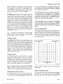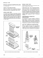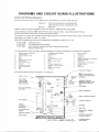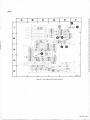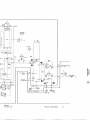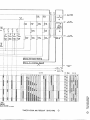
1
COMMITTED TO EXCELLENCE
CHECK FOR CHANGE INFORMATION
REAR O THIS MANUAL.
UIRE CLOCK
Tektronix, Inc .
P.O . Box 500
Beaverton, Oregon
070-2788-00
Product Group 42
TI ON MANUAL
97077
Serial Number
First Printing APR 1980
Revised JAN 1986
Copyright
1980 Tektronix, Inc. All rights reserved .
Contents of this publication may not be reproduced in any
form without the written permission of Tektronix, Inc .
Ll~
Products of Tektronix, Inc. and its subsidiaries are covered
by U .S . and foreign patents and/or pending patents .
TEKTRONIX, TEK, SCOPE-MOBILE, and
19!!44
are
registered trademarks of "Tektronix, Inc . TELEOUIPMENT
is a registered trademark of Tektronix U.K . Limited .
Printed in U.S .A. Specification and price change privileges
are reserved .
INSTRUMENT SERIAL NUMBERS
Each instrument has a serial number on a parlel insert, tag,
or stamped on the chassis . The first number or letter
designates the country of manufacture. The last five digits
of the serial number are assigned sequentially and are
unique to each instrument . Those manufactured in the
United States have six unique digits . The country of
manufacture is identified as follows :
13000000
100000
200000
300000
700000
"Tektronix, Inc., Beaverton, Oregon, USA
Tektronix Guernsey, Ltd ., Channel Islands
Tektronix United Kingdom, Ltd ., London
Sony/Tektronix, Japan
Tektronix Holland, NV, Heerenveen,
The Netherlands
71387 Instruction
PAGE
LIST OF ILLUSTRATIONS . . . . . . . . . .
LIST OF TABLES . . . . . . . . . . . . . . . . . .
OPERATORS SAFETY SUMMARY . .
SERVICING SAFETY SUMMARY . . . .
.. .
. ..
...
.. .
..
..
..
..
.
.
.
.
..
..
..
..
.
.
.
.
...
. ..
...
...
.. .
. ..
...
.. .
.. .
. ..
.. .
...
.
.
.
.
..
..
..
..
.
.
.
.
SECTION 1----OPERATING INSTRUCTIONS
INSTALLATION . . . . . . . . . . . . . . . . . . . . . . . . . . . . . . . . . . .
CONTROLS, CONNECTORS, AND INDICATORS . . . . . .
FUNCTIONAL CHECK . . . . . . . . . . . . . . . . . . . . . . . . . . . . . .
SETUP PROCEDURE . . . . . . . . . . . . . . . . . . . . . . . . . . .,
SWEEP FUNCTIONS . . . . . . . . . . . . . . . . . . . . . . . . . . . .
TRIGGERING FUNCTIONS . . . . . . . . . . . . . . . . . . . . . .
PRETRIGGER ACQUIRE CLOCK FUNCTIONS . . . . .
GENERAL OPERATING INFORMATION . . . . . . . . . . . . . .
TRIGGERING SWITCH LOGIC . . . . . . . . . . . . . . . . . . .
TRIGGERING MODES . . . . . . . . . . . . . . . . . . . . . . . . . .
TRIGGER COUPLING . . . . . . . . . . . . . . . . . . . . . . . . . . .
TRIGGER SOURCE . . . . . . . . . . . . . . . . . . . . . . . . . . . . .
TRIGGER SLOPE . . . . . . . . . . . . . . . . . . . . . . . . . . . . . .
TRIGGER LEVEL. . . . . . . . . . . . . . . . . . . . . . . . . . . . . . .
HORIZONTAL SWEEP RATES . . . . . . . . . . . . . . . . . .
TIME MEASUREMENT . . . . . . . . . . . . . . . . . . . . . . ., .
SWEEP MAGNIFICATION . . . . . . . . . . . . . . . . . . . . . .
VARIABLE HOLD OFF . . . . . . . . . . . . . . . . . . . . . . . . .
MAINFRAME OPERATING MODES . . . . . . . . . . . . .
APPLICATIONS . . . . . . . . . . . . . . . . . . . . . . . . . . . . . . . . . . . . .
TIME INTERVAL MEASUREMENTS . . . . . . . . . . . . . . . .
PERIOD AND FREQUENCY MEASUREMENTS . . .
RISE-TIME AND FALL-TIME MEASUREMENTS . .
PULSE WIDTH MEASUREMENTS . . . . . . . . . . . . . . .
. iii
. iv
. .v
vii
1-1
1-1
1-1
1-1
1-4
1-4
1-5
1-6
1-6
1-6
1-9
1-9
1-11
1-11
1-11
1-11
1-11
1-12
1-12
1-12
1-12
1-12
1-13
1-14
SECTION 2--SPECIFICATION
STANDARD ACCESSORIES . . . . . . . . . . . . . . . . . . . . . . . . 2-4
-----------WARNING
THE REMAINING PORTION OF THIS TABLE OF CONTENTS
LISTS SERVICING INSTRUCTIONS . THESE SERVICING
INSTRUCTIONS ARE FOR USE BY QUALIFIED PERSONNEL
ONLY . T O AVOID ELECTRICAL SHOCK, DO NOT PERFORM
ANY SERVICING OTHER THAN THAT CALLED OUT IN THE
OPERATING INSTRUCTIONS UNLESS QUALIFIED TO DO
SO .
SECTION 3---THEORY OF OPERATION
BLOCK DIAGRAM DESCRIPTION . . . . . . . . . .
TRIGGER GENERATOR . . . . . . . . . . . . . . . .
SWEEP GENERATOR . . . . . . . . . . . . . . . . . .
PICKOFF AMPLIFIER AND DELAY GATE
GENERATOR . . . . . . . . . . . . . . . . . . . . . .
LOGIC . . . . . . . . . . . . . . . . . . . . . . . . . . . . . . . .
DIGITAL VOLTMETER . . . . . . . . . . . . . . . . .
CLOCK GENERATOR . . . . . . . . . . . . . . . . . .
REV JUN 1981
..........
..........
..........
. . 3-1
. . 3-1
. . 3-1
.
.
.
.
.
.
.
.
.
.
.
.
.
.
.
.
.
.
.
.
.
.
.
.
.
.
.
.
.
.
.
.
.
.
.
.
.
.
.
.
.
.
.
.
.
.
.
.
3-1
3-1
3-1
3-1
PAGE
DETAILED CIRCUIT DESCRIPTION . . . . . . . . . . . . . . . . . . . . . 3-1
FRONT-PANEL DISTRIBUTION . . . . . . . . . . . . . . . . . . . . . 3-3
TRIGGER GENERATOR . . . . . . . . . . . . . . . . . . . . . . . . . . . . 3-3
EXTERNAL SOURCE . . . . . . . . . . . . . . . . . . . . . . . . . . . . 3-3
INTERNAL AND LINE SOURCE . . . . . . . . . . . . . . . . . . 3-3
TRIGGER SOURCE SELECTOR AND
AMPLIFIER . . . . . . . . . . . . . . . . . . . . . . . . . . . . . . . . . 3-3
PEAK-TO-PEAK AUTO . . . . . . . . . . . . . . . . . . . . . . . . . . 3-3
SLOPE SELECTOR AND TRIGGER
GENERATOR . . . . . . . . . . . . . . . . . . . . . . . . . . . . . . . 3-5
GATE GENERATOR . . . . . . . . . . . . . . . . . . . . . . . . . . . . 3-5
LOGIC . . . . . . . . . . . . . . . . . . . . . . . . . . . . . . . . . . . . . . . . . . . . 3-5
SWEEP MODES . . . . . . . . . . . . . .. . . . . . . . . . . . . . . . . . 3-5
HOLD OFF TIMING . . . . . . . . . . . . . . . . . . . . . . . . . . . . . 3-6
LOCKOUT BUFFER AMPLIFIER . . . . . . . . . . . . . . . . . . 3-7
HOLD OFF OUTPUT AMPLIFIER . . . . . . . . . . . . . . . . . 3-7
SWEEP GENERATOR . . . . . . . . . . . . . . . . . . . . . . . . . . . . . . 3-7
TIMING CURRENT SOURCE . . . . . . . . . . . . . . . . . . . . . 3-7
RAMP GENERATOR . . . . . . . . . . . . . . . . . . . . . . . . . . . 3-10
HORIZONTAL PREAMPLIFIER . . . . . . . . . . . . . . . . . . 3-10
SWEEP GATE GENERATOR . . . . . . . . . . . . . . . . . . . . 3-10
DVM . . . . . . . . . . . . . . . . . . . . . . . . . . . . . . . . . . . . . . . . . . . . 3-10
DELAY TIME COMPARATOR AND DELAY
GATE GENERATOR . . . . . . . . . . . . . . . . . . . . . . . . 3-10
DIGITAL VOLTMETER . . . . . . . . . . . . . . . . . . . . . . . . . . . . 3-11
DELAY COMPARISON VOLTAGE-TO-RAMP
CONVERTER . . . . . . . . . . . . . . . . . . . . . . . . . . . . . . . 3-12
COMPARATOR . . . . . . . . . . . . . . . . . . . . . . . . . . . . . . . 3-12
REFERENCE CURRENT SOURCE . . . . . . . . . . . . . . . 3-12
REFERENCE CURRENT INVERTER . . . . . . . . . . . . . . 3-12
COUNTER AND ENCODER . . . . . . . . . . . . . . . . . . . . . 3-12
CLOCK GENERATOR . . . . . . . . . . . . . . . . . . . . . . . . . . . . . 3-12
CONTROL LOGIC . . . . . . . . . . . . . . . . . . . . . . . . . . . . . 3-13
OSCILLATOR . . . . . . . . . . . . . . . . . . . . . . . . . . . . . . . . . 3-13
FIRST DIVIDER . . . . . . . . . . . . . . . . . . . . . . . . . . . . . . . . 3-15
X1-X10MULTIPL-EXER . . . . . . . . . . . ., . . . . .3-15
DECADE DIVIDER . . . . . . . . . . . . . . . . . . . . . . . . . . . . . 3-15
INTERNAL CLOCK MULTIPLEXER . . . . . . . . . . . . . . 3-15
OUTPUT CLOCK MULTIPLEXER . . . . . . . . . . . . . . . . 3-15
INTENSIFY CIRCUIT . . . . . . . . . . . . . . . . . . . . . . . . . . . 3-15
71387 IN A HORIZ PLUG-IN COMPARTMENT . . . . . . . 3-16
IN] ERNAL BUTTON PRESSED . . . . . . . . . . . . . . . . . . 3-16
71387 IN B HORIZ PLUG-IN COMPARTMENT . . . . . . . 3-16
INTERNAL BUTTON PRESSED . . . . . . . . . . . . . . . . . . 3-16
TIME/DIVISION AND READOUT SWITCHING . . . . . . . 3-17
BASIC READOUT SYSTEM . . . . . . . . . . . . . . . . . . . . . 3-17
TIME/DIVISION READOUT . . . . . . . . . . . . . . . . . . . . . 3-17
ACQUIRE-STOP DELAY TIME READOUT . . . . . . . . 3-17
INTERFACE CONNECTIONS AND POWER
SUPPLY . . . . . . . . . . . . . . . . . . . . . . . . . . . . . . . . . . . . . . 3-17
SEC'T'ION 4-MAINTENANCE
PREVENTIVE MAINTENANCE .
CLEANING . . . . . . . . . . . . . . . .
EXTERIOR . . . . . . . . . . . . .
INTERIOR . . . . . . . . . . . . . .
SWITCH CONTACTS . . . .
...
...
...
...
.. .
...
...
...
...
...
...............
. . . . .. . .. . . . . . .
. . . . . . . . . . . . . ..
.. . . . . . . . . . . . . .
...............
. . . 4-1
. . . 4-1
. . . 4-1
. . . 4,1
. . . 4-1
71387 Instruction
PAGE
PAGE
VISUAL INSPECTION . . . . . . . . . . . . . . . . . . . . . . . . . . . . . . 4-1
LUBRICATION . . . . . . . . . . . . . . . . . . . . . . . . . . . . . . . . . . . . 4-1
CAM SWITCH LUBRICATION . . . . . . . . . . . . . . . . . . . . 4-2
SEMICONDUCTOR CHECKS . . . . . . . . . . . . . . . . . . . . . . . 4-2
ADJUSTMENT AFTER REPAIR . . . . . . . . . . . . . . . . . . . . . 4-2
TROUBLESHOOTING . . . . . . . . . . . . . . . . . . . . . . . . . . . . . . . . . 4-2
TROUBLESHOOTING AIDS . . . . . . . . . . . . . . . . . . . . . . . . . 4-2
DIAGRAMS . . . . . . . . . . . . . . . . . . . . . . . . . . . . . . . . . . . . 4-2
VOLTAGES AND WAVEFORMS . . . . . . . . . . . . . . . . . 4-2
CIRCUIT-BOARD ILLUSTRATIONS . . . . . . . . . . . . . . . 4-2
SWITCH CAM IDENTIFICATION . . . . . . . . . . . . . . . . . 4-4
DIODE COLOR CODE . . . . . . . . . . . . . . . . . . . . . . . . . . . 4-4
WIRING COLOR CODE . . . . . . . . . . . . . . . . . . . . . . . . . 4-4
SEMICONDUCTOR LEAD CONFIGURATIONS . . . . . 4-4
INTER-BOARD PIN CONNECTOR
IDENTIFICATION . . . . . . . . . . . . . . . . . . . . . . . . . . . . 4-4
MULTI-PIN CONNECTOR IDENTIFICATION . . . . . . . 4-4
INTERFACE CONNECTOR PIN LOCATIONS . . . . . . . 4-5
PERFORMANCE CHECK AND ADJUSTMENT . . . . . 4-5
STATIC SENSITIVE DEVICES . . . . . . . . . . . . . . . . . . . . . . . 4-5
TROUBLESHOOTING EQUIPMENT . . . . . . . . . . . . . . . . . . 4-6
TROUBLESHOOTING TECHNIQUES . . . . . . . . . . . . . . . . . 4-6
TROUBLESHOOTING PROCEDURE . . . . . . . . . . . . . . 4-6
CORRECTIVE MAINTENANCE . . . . . . . . . . . . . . . . . . . . . . . . . 4-8
OBTAINING REPLACEABLE PARTS . . . . . . . . . . . . . . . . . 4-8
SOLDERING TECHNIQUES . . . . . . . . . . . . . . . . . . . . . . . . . 4-9
COMPONENT REMOVAL AND REPLACEMENT . . . . . 4-10
CIRCUIT BOARDS . . . . . . . . . . . . . . . . . . . . . . . . . . . . . 4-10
SWITCHES . . . . . . . . . . . . . . . . . . . . . . . . . . . . . . . . . . . 4-12
SEMICONDUCTORS . . . . . . . . . . . . . . . . . . . . . . . . . . . 4-15
INTERCONNECTING PINS . . . . . . . . . . . . . . . . . . . . . . 4-15
CIRCUIT-BOARD PINS . . . . . . . . . . . . . . . . . . . . . . . . . 4-15
FRONT-PANEL LIGHTS . . . . . . . . . . . . . . . . . . . . . . . . 4-16
ADJUSTMENT AFTER REPAIR . . . . . . . . . . . . . . . . . . . . 4-16
INSTRUMENT' REPACKAGING . . . . . . . . . . . . . . . . . . . . . 4-16
SECTION 5 .--.-PERFORMANCE CHECK AND
ADJUSTMENT
PRELIMINARY INFORMATION . . . . . . . . . .
ADJUSTMENT INTERVAL . . . . . . . . . . .
TEKTRONIX FIELD SERVICE . . . . . . . . .
USING THIS PROCEDURE . . . . . . . . . .
TEST EQUIPMENT REQUIRED . . . . . . . . . .
SPECIAL FIXTURES . . . . . . . . . . . . . . . .
TEST EQUIPMENT ALTERNATIVES . .
INDEX TO PERFORMANCE CHECK AND
ADJUSTMENT PROCEDURE . . . . . . . .
PRELIMINARY PROCEDURE . . . . . . . . . . . .
A . TRIGGERING SYSTEM . . . . . . . . . . . . . . . . .
B . HORIZONTAL/AQS SYSTEM . . . . . . . . . . .
.
.
.
.
.
.
.
.
.
.
.
.
.
.
.
.
.
.
.
.
.
.
.
.
.
.
.
.
.
.
.
.
.
.
.
.
.
.
.
.
.
.
.
.
.
.
.
.
.
.
.
.
.
.
.
.
..
..
..
..
..
..
..
.
.
.
.
..
..
. .
. .
.
.
.
.
..
..
. .
. .
.
.
.
.
...
...
. ..
. ..
.
.
.
.
.
.
.
.
.
.
.
.
.
.
5-1
5-1
5-1
5-1
5-1
5-1
5-1
. . 5-4
. . 5-4
. . 5-5
. 5-10
SECTION &---INSTRUMENT OPTIONS
SECTION f --REPLACEABLE ELECTRICAL PARTS
SECTION 8--DIAGRAMS AND CIRCUIT BOARD
ILLUSTRATIONS
SECTION 9---REPLACEABLE MECHANICAL PARTS
CHANGE INFORMATION
REV JUN 1981
713£37 Instruction
FIG .
NO .
Frontispiece
1-1
1-2
1-3
1-4
1-6
1-7
2-1
3-1
3-2
3-3
3-4
3-5
3-6
4-2
4-3
AGE
71387 Features . . . . . . . . . . . . . . . . . . . . . . . . . . . . . . . . . viii
of release latch . . . . . . . . . . . . . . . . . . . . . . . .Locatin 1 -1
Front-panel controls, connectors, and
indicators . . . . . . . . . . . . . . . . . . . . . . . . . . . . . . . . . . . . . 1-2
Single Sweep Acquisition . . . . . . . . . . . . . . . . . . . . . . . 1-5
Effect of LEVEL control and SLOPE switch
on crt display . . . . . . . . . . . . . . . . . . . . . . . . . . . . . . . . . 1-10
of graticule used for most accurate
.Area
time measurements . . . . . . . . . . . . . . . . . . . . . . . . . . . 1-11
Operation of sweep magnifier . . . . . . . . . . . . . . . . . . 1-12
Measuring the period and determining the
frequency of a displayed waveform . . . . . . . . . . . . . 1-13
Measuring the rise time and fall time of
a displayed waveform . . . . . . . . . . . . . . . . . . . . . . . . . 1-14
Measuring the pulse width of a displayed
waveform . . . . . . . . . . . . . . . . . . . . . . . . . . . . . . . . . . . . 1-14
71387 dimensional drawing . . . . . . . . . . . . . . . . . . . 2-5
Basic block diagram of the 71387 Delaying
Time Base Unit . . . . . . . . . . . . . . . . . . . . . . . . . . . . . . . . 3-2
Detailed block diagram of Trigger Generator . . . . . 3-4
Timing diagram for Gate Generator stage
(092, Q96, 098) . . . . . . . . . . . . . . . . . . . . . . . . . . . . . . . 3-6
Detailed block diagram of Logic circuit . . . . . . . . . . . 3-7
Detailed block diagram of Sweep Generator . . . . . . 3-8
Timing of events that form the Delay
Gate signal . . . . . . . . . . . . . . . . . . . . . . . . . . . . . . . . . . . 3-11
Lubrication procedure for a typical
cam switch . . . . . . . . . . . . . . . . . . . . . . . . . . . . . . . . . . . . 4-2
Semiconductor lead configuration . . . . . . . . . . . . . . . 4-3
Inter-board multi-pin connector assembly . . . . . . . . 4-4
REV JUN 1981
FIG .
NO .
4-4
4-5
4-6
4-7
4-8
4-9
4-10
4-11
4-12
4-13
PAGE
End-lead multi-pin connector assembly . . . . .
Location of pin numbers on Interface
connector . . . . . . . . . . . . . . . . . . . . . . . . . . . . . . . .
71387 troubleshooting chart . . . . . . . . . . . . . . . .
Readout board removal procedure . . . . . . . . . .
Coaxial end-lead connector assembly . . . . . . .
Location of securing screws and inter-board
multi-pin connectors on clock circuit board . .
Cam switch removal procedure . . . . . . . . . . . .
Removal procedure for typical pushbutton
switch . . . . . . . . . . . . . . . . . . . . . . . . . . . . . . . . . . .
Exploded view of circuit-board pin and
ferrule . . . . . . . . . . . . . . . . . . . . . . . . . . . . . . . . . . .
Front-panel light socket assembly . . . . . . . . . .
. . . . . 4-4
.
.
.
.
...
...
...
...
. 4-5
. 4-7
4-10
4-11
. . . . 4-12
. . . . 4-13
. . . . 4-14
. . . . 4-16
. . . . 4-16
The illustrations in Section 8 are located near their associated
diagrams on the foldout pages .
8-1
8-2
8-3
8-4
8-5
8-6
8-7
8-8
8-9
8-10
8-11
Semiconductor Lead Configurations .
Locations of circuit boards in the 71387 .
A2-Trigger circuit board assembly.
A1-Interface circuit board assembly .
A1-Interface circuit board assembly .
A1-Interface circuit board assembly .
A4-Clock circuit board assembly .
A4-Clock circuit board assembly .
A3-Readout circuit board assembly .
A1-Interface circuit board assembly .
Test Point and Adjustment Locations .
TABLE
NO .
1-1
2-1
2-2
2-3
2-4
3-1
3-2
3-3
3-4
3-5
4-1
5-1
5-2
5-3
5-4
5-5
5-6
PAG E
TIME/DIV Setting Relationship To 7887
Internal Acquire Clock Rep Rate . . . . . . . . . . . . . . . . . 1-7
Electrical Characteristics . . . . . . . . . . . . . . . . . . . . . . . 2-1
Mainframe Horizontal Compatibility . . . . . . . . . . . . . 2-3
Environmental Characteristics . . . . . . . . . . . . . . . . . . 2-4
Physical Characteristics . . . . . . . . . . . . . . . . . . . . . . . . 2-4
Truth Table, TIME/DIV Setting vs . Strobes
for U637 and U638 . . . . . . . . . . . . . . . . . . . . . . . . . . . 3-13
Selected Inputs or X1 and X10 Multiplexers . . . . . 3-14
Operation of Output Multiplexer U655 . . . . . . . . . . 3-15
Current in CH1 Readout Line vs . Acquire
Clock Mode, During TS10 . . . . . . . . . . . . . . . . . . . . . . 3-16
Readout Character Selection . . . . . . . . . . . . . . . . . . . 3-18
Relative Susceptibility . . . . . . . . . . . . . . . . . . . . . . . . . . 4-5
Test Equipment . . . . . . . . . . . . . . . . . . . . . . . . . . . . . . . . 5-2
Acquire Clock Repetition Rate Output . . . . . . . . . . . 5-11
Delay Time Linearity . . . . . . . . . . . . . . . . . . . . . . . . . . 5-12
Acquire-Stop Delay Accuracy . . . . . . . . . . . . . . . . . . 5-13
Sweep Timing . . . . . . . . . . . . . . . . . . . . . . . . . . . . . . . . 5-14
Magnified Sweep Timing . . . . . . . . . . . . . . . . . . . . . . 5-15
7'1381 Instruction
The general safety information in this part of the summary is for both operating and servicing personnel. Specific
warnings and cautions will be found throughout the manual where they apply, but may not appear in this summary.
TERMS
IN THIS MANUAL
CAUTION statements identify conditions or practices that could result in damage to the equipment or other property .
WARNING statements identify conditions or practices that could result in personal injury or loss of life .
AS MARKED ON EQUIPMENT
CAUTION indicates a personal injury hazard not immediately accessible as one reads the marking, or a hazard to
property including the equipment itself .
DANGER indicates a personal injury hazard immediately accessible as one reads the marking .
SYMBOLS
IN THIS MANUAL
Static-Sensitive Devces .
This symbol indicates where applicable cautionary or other information is to be found.
AS MARKED ON EQUIPMENT
DANGER----High voltage.
Protective ground (earth) terminal .
ATTENTION-----refer to manual .
WARNINGS
POWER SOURCE
This product is intended to operate in a mainframe connected to a power source that will not apply more than 250 volts
rms between the supply conductors or between either supply conductor and ground . A protective ground connection by
way of the grounding conductor in the mainframe power cord is essential for safe operation .
GROUNDING THE PRODUCT
This product is grounded through the grounding conductor of the mainframe power cord . To avoid electrical shock, plug
the mainframe power cord into a properly wired receptacle before connecting to the product input or output terminals . A
protective ground connection by way of the grounding conductor in the mainframe power cord is essential for safe
operation.
71387 Instruction
DANGER ARISING FROM LOSS OF GROUND
Upon loss of the protective-ground connection, all accessible conductive parts (including knobs and controls that may
appear to be insulating), can render an electric shock.
DO NOT OPERATE IN EXPLOSIVE ATMOSPHERES
To avoid explosion, do not operate this product in an atmosphere of explosive gases unless it has been specifically
certified for such operation .
DO NOT OPERATE PLUG-IN UNIT WITHOUT COVERS
To avoid personal injury, do not operate this product without covers or panels installed . Do not apply power to the plug-in
unit via a plug-in extender .
713$7 Instruction
FOR QUALIFIED SERVICE PERSONNEL ONLY
Refer also to the preceding Operators Safety Summary
DO NOT SERVICE ALONE
Do not perform internal service or adjustment of this product unless another person capable of rendering first aid and
resuscitation is present.
USE CARE WHEN SERVICING WITH POWER ON
Dangerous voltages exist at several points in this product. To avoid personal injury, do not touch exposed connections
and components while power is on .
Disconnect power before removing protective panels, soldering, or replacing components .
POWER SOURCE
This product is intended to operate in a mainframe connected to a power source that will not apply more than 250 volts
rms between the supply conductors or between either supply conductor and ground . A protective ground connection by
way of the grounding conductor in the mainframe power cord is essential for safe operation .
71387 Instruction
TRIGGERING
Yoaf
F-P AU T0
Flit
COMING
AUTO
AC LF W
*OW
AC IF KJ
Poernow
OC
HOLD
OFF
MAG
II '~
O~IrT
XI
aI ~' IAN
ACQUIRE STOP DELAY
EXT CLOCK IN
Its IIh USX)
SWIM CAL
II + 1
OUT+1!
EXT TRIG IN
y
S 2f4y
2788-1
71387 FEATURES
The 71387 Time-Base unit Pretrigger Acquire Clock provides calibrated sweep rates from 5 seconds to 10 nanoseconds and triggering to 400
megahertz for 7000-Series Oscilloscopes. A X10 Magnifier increases each sweep rate by a factor of 10 and a VARIABLE TIME/ DIV control
provides continuously-variable sweep rates between calibrated steps . Variable holdoff and alphanumeric readout are provided . Also, when
operating in the AUTO TRIGGERING MODE, a bright baseline trace is displayed in the absence of a trigger signal . The 7887 can be operated
as an independent time base or as a delayed-sweep unit with a companion delaying time-base unit . Sweep mode is determined by the
companion delaying time base .
The 71387 also features an internally-generated clock and an external clock input for sequential single sweep acquisition when operating in a
7000-series digitizing oscilloscope . The frequency range of the internally generated clock is 20 .48 mHz (millihertz) to 20 .48 MHz as
determined by the TIME/DIV, X10 MAG, and INT _ 1000 switches. Also, an ACQUIRE-STOP DELAY function varies delay pickoff, and
therefore pretrigger time, in compatible digitizing plug-in oscilloscopes . The portion of the oscilloscope real-time display between the
triggering event and the end of delay time is intensified . The exact delay time is displayed on the crt readout .
VIII
Section 1--71387
The 71387 Time-Base unit operates with a Tektronix 7700-, 7800-, or 7900-series oscilloscope mainframe and a 7Aseries amplifier unit to form a complete oscilloscope system . This section describes the operation of the front-panel
controls and connectors, provides general operating information, a functional check procedure, and basic applications for
this instrument .
INSTALLATION
The time-base unit operates in the horizontal plug-in
compartment of the mainframe . When used for single
sweep acquisition with a Tektronix 7000-series digitizing
oscilloscope (7854) the 71387 must be installed in the B
horizontal compartment of the mainframe . This
instrument can also be installed in a vertical plug-in
compartment to provide a vertical sweep on the crt .
However, when used in this manner, there are no
internal triggering or retrace blanking provisions, and the
unit may not meet the specifications given in Section 2,
Specification .
To install the unit in a plug-in compartment, push it in
until it fits firmly into the compartment . The front panel
of the unit should be flush with the front panel of the
mainframe . Even though the gain of the mainframe is
standardized, the sweep calibration of the unit should be
checked when installed . The procedure for checking the
unit is given under Sweep Functions in the Functional
Check procedure in this section .
SETUP PROCEDURE
1 . Install the time-base unit
compartment of the mainframe .
2 . Install an
compartment .
amplifier
plug-in
in
the
unit
A
in
a
vertical
3 . Set the time-base unit controls as follows :
SLOPE . . . . . . . . .
MODE . . . . . . . . .
COUPLING . . . . .
SOURCE . . . . . . .
POSITION . . . . . .
.TIME/DIV . . . . . .
VARIABLE (CAL
HOLD OFF . . . . .
MAG . . . . . . . . . .
.
.
.
.
.
.
. ..
. ..
. ..
. ..
. ..
...
IN)
. ...
. .. .
.. .. .
.. .. .
.. .. .
.. .. .
. . ...
. ....
.....
. MIN
. .. ..
..
.
.
.
.
.
. . . . . . . . . . . . . . . . . . . (+)
. . . . . . . . . . . P-P AUTO
. . . . . . . . . . . . . . . . . . AC
. . . . . . . . . . . . . . . . . . INT
. . . . . . . . . . . . Midrange
. . . . . . . . . . . . . . . . 1 ms
Calibrated (Pushed in)
(fully counterclockwise)
. . . . . . . . X1 (pushed in)
.
.
.
.
.
.
To remove the unit, first turn the power off, then pull the
release latch (see Fig . 1 -1) to disengage the unit from the
mainframe, and pull it out of the plug-in compartment .
CONTROLS, CONNECTORS, AND
INDICATORS
All controls, connectors, and indicators required for the
operation of the time-base unit are located on the front
panel . Figure 1-2 shows and provides a brief description
of all front-panel controls, connectors, and indicators .
More detailed information is given in the General
Operating Instructions .
FUNCTIONAL CHECK
The following procedures are provided for checking basic
instrument functions . Refer to the description of the
controls, connectors, and indicators while performing
this procedure . If performing the functional check
procedure reveals a malfunction or possible improper
adjustment, first check the operation of the associated
plug-in units, then refer to the instruction manual for
maintenance and adjustment procedures .
horizontal
Figure 1-1 . Location of release latch .
Operating Instructions 7B87
TIME BASE
uwn
W/PRETRIGGER ACQUIRE CLOCK
Figure 1-2 . Front-panel controls, connectors, and indicators .
Operating Instructions---71387
TRIGGERING
LEVEL Control---Selects a point on the trigger signal where triggering occurs .
SLOPE Switch
Permits sweep to be triggered on negative- or positive-going portions of the trigger signal .
READY Indicator--Illuminates when sweep circuit is armed (SINGLE SWEEP Mode) .
TRIG'D Indicator
Illuminates when the display is triggered .
MODE Pushbuttons---Selects the operating mode of the triggering circuit .
COUPLING Pushbuttons---Selects the method of coupling the trigger signal to triggering circuit .
SOURCE
Selects source of the trigger signal .
SWEEP
POSITION Control---Provides horizontal positioning .
FINE Control-----Provides precise horizontal positioning .
@
@
MAG Pushbutton---Selects magnified X10 or unmagnified sweep .
HOLD OFF Control----Permits hold off period to be varied to improve trigger stability on repetitive, complex waveforms .
@) TIME/DIV Selector-Selects the sweep rate of the sweep generator .
VARIABLE Control and CAL Switch---Selects calibrated or uncalibrated sweep rates . Uncalibrated sweep rates can be
continuously reduced to at least the sweep rate of the next slower position .
SWP CAL Adjustment---Compensates for basic timing changes due to the differences in sensitivity of mainframes .
EXTERNAL TRIGGER INPUT
EXT TRIG ATTENUATOR--Selects attenuation factor for external trigger signals .
@
EXT TRIG IN Connector---Connector (BNC type) provides input for external trigger signals .
PRETRIGGER ACQUIRE CLOCK
~~
AQS (acquire single-shot) CLOCK/AQR (acquire repetitive)---Selects the source of clock pulses from the 71387 to
the 7854 digitizing plug-in oscilloscope (71387 must be installed in B horizontal compartment of companion
oscilloscope mainframe) .
18
ACQUIRE-STOP DELAY Control---A variabledelaygatefunctionthatallowspretriggertimetobevariedincompatible
7000-series digitizing oscilloscopes . Exact delay time is displayed on oscilloscope crt readout .
EXT CLOCK IN Connector-- Provides input for external TTL clock signals .
2788 38
Figure 1- 2 (cont) . Front-panel controls, connectors, and indicators .
Operating Instructions--713187
4. Turn on the mainframe and allow at least 20 minutes
warmup .
TRIGGERING
5 . Set the mainframe vertical and horizontal modes to
display the plug-in units used and adjust the intensity
and focus for a well-defined display . See the oscilloscope
mainframe and amplifier unit instruction manuals for
detailed operating instructions .
1 . Obtain a display as described in the preceding Normal
Sweep procedure .
SWEEP FUNCTIONS
NORMAL SWEEP . Perform the following procedure to
obtain a normal sweep and to demonstrate the function
of the related controls :
the
3 . Set the amplifier unit deflection factor for 4 divisions
of display .
4 . Adjust the LEVEL control for a stable display .
5 . Turn the POSITION control and note that the trace
moves horizontally .
6 . Turn the FINE control and note that the display can be
precisely positioned horizontally .
7 . Check the display for one complete cycle per division .
If necessary, adjust the front-panel SWP CAL screwdriver
adjustment for one complete cycle per division over the
center 8 graticule divisions . Be sure that the timing of the
mainframe calibrator signal is accurate to within 0 .25%
(+20° to +30° C) .
8 . Press to release the VARIABLE (CAL IN) control . Turn
the VARIABLE (CAL IN) control fully counterclockwise
and note that the displayed sweep rate changes to at
least the next slower TIME/DIV switch setting (i .e ., 2
milliseconds/division) . Press the VARIABLE (CAL IN)
knob in (to the calibrated position) .
MAGNIFIED SWEEP . Perform the following procedure
to obtain a X10 magnified display and to demonstrate the
function of the related controls :
1 . Obtain a one cycle per division display as described in
the preceding Normal Sweep procedure .
2 . Press to release the MAG button (X10) . Note that the
unmagnified display within the center division of the
graticule is magnified to about 10 divisions .
3 . Press the MAG button (X1) .
Perform the following procedure to obtain a triggered
sweep and to demonstrate the functions of the related
controls :
2 . Press the AUTO MODE button and turn the LEVEL
control fully counterclockwise to obtain a free-running
sweep .
3 . Slowly turn the HOLD OFF control clockwise and note
that a stable display can be obtained at several positions
of the HOLD OFF control . Return the HOLD OFF control
to the fully counterclockwise (MIN) position .
NOTE
1 . Perform the preceding Setup Procedure .
2 . Connect a 0 .4-volt, 1-kilohertz signal from
mainframe calibrator to the amplifier unit input .
FUNCTIONS
The HOLD OFF control varies the sweep holdoff time which effectively changes the
repetition-rate of the horizontal sweep signal.
However, its primary function is to obtain a
stable display of complex waveforms which
are otherwise difficult to trigger.
4 . Press the AC, AC HF REJ, and DC COUPLING buttons
for both the + and - positions of the SLOPE switch and
check for a stable display (LEVEL control may be
adjusted, if necessary, to obtain a stable display) .
5 . Apply the 0 .4-volt, 1-kilohertz signal from the
mainframe calibrator to the amplifier unit and to the EXT
TRIG IN connector .
6 . Press the EXT SOURCE button and set the amplifier
unit deflection factor for a 4-division display .
7 . Press the AC, AC HF REJ, and DC COUPLING buttons
for both the + and - positions of the SLOPE switch and
check for a stable display (LEVEL control may be
adjusted, if necessary, for a stable display) .
8 . Press the AC COUPLING, INT SOURCE, and NORM
MODE buttons . Adjust the LEVEL control for a stable
display .
9 . Press the AUTO MODE button and adjust the LEVEL
control for a free-running display .
10 . Press the NORM MODE button and check for no
display .
11 . Adjust the LEVEL control for a stable display and
press the SINGLE SWP MODE button .
12 . Note that one trace occurs when the RESET MODE
button is pressed .
13 . Disconnect the mainframe calibrator signal from the
amplifier unit input and press the RESET MODE button .
Check for no display and note that the READY indicator is
lit .
Operating Instructions-71387
14 . Note that one trace occurs and that the READY
indicator extinguishes when the mainframe calibrator
signal is reconnected to the amplifier unit input.
PRETRIGGER ACQUIRE CLOCK FUNCTIONS
NOTE
The following procedure must be performed
with the 71387 installed in the B horizontal
compartment of a Tektronix 7854
Oscilloscope.
1 . Install the 71387 in the 7854 Oscilloscope B horizontal
compartment and install an amplifier unit in the
mainframe left vertical compartment . Turn on
oscilloscope power. See Tektronix 7854 Oscilloscope
Operators Manual for detailed operating information .
2. Set the time-base unit controls as follows :
SLOPE . . . . . . . . . . . . . . . . . . . . . . . . . . . . . . . . . . . . . . . (+)
MODE . . . . . . . . . . . . . . . . . . . . . . . . . . . . . . . . . . . AUTO
COUPLING . . . . . . . . . . . . . . . . . . . . . . . . . . . . . . . . . . AC
SOURCE . . . . . . . . . . . . . . . . . . . . . . . . . . . . . . . . . . . . INT
POSITION . . . . . . . . . . . . . . . . . . . . . . . . . . . . . Midrange
TIME/DIV . . . . . . . . . . . . . . . . . . . . . . . . . . . . . . . . . 1 ms
VARIABLE . . . . . . . . . . . . . . . . . . Calibrated (CAL IN)
HOLDOFF . . . . . . . . . . . MIN (fully counterclockwise)
MAG . . . . . . . . . . . . . . . . . . . . . . . . . . . X1 (pushed in)
AQS CLOCK/AQR . . . . . . . . . . . . . . . . . . . . INTERNAL
ACQUIRE STOP DELAY . . . . . . . . . . . . . . . . Midrange
3. Set the 7854 vertical and horizontal modes to display
the plug-in units and set WFM ACQUISITION to SCOPE.
Set the intensity and focus for a well-defined, intensified
display.
4. Connect the 0.4-volt, 1-kilohertz signal from the
mainframe calibrator to the amplifier unit input .
5. Set the amplifier unit deflection factor for 4 divisions
of display.
NOTE
Four divisions of intensified display at 1
msldiv relates to delay-time readout of
approximately 4 ms.
9. Set the amplifier unit input coupling switch to off or
ground . Set the 71387 to SINGLE SWEEP MODE and
press the RESET pushbutton so that READY light is on .
10 . Set the 7854 to Stored CRT Display and then to
Acquire Single-Shot Waveform Acquisition (AQS) .
INTENSIFIED ZONE
POST-TRIGGER
SCOPE (REAL-TIME) MODE
TIME
SWEEP SPEED
r
MEMO
M
Emma
ENMEM
MOMMM
MEMEM
ME
\1
V
_TRIGGER
POINT
No
fr
ACQUIRE
. STOP
ACQUIRE-STOP DELAY TIME-L.
-1-- (POST-TRIGGER TIME)
(A) 7854 REAL-TIME DISPLAY (SCOPE MODE)
PRE-TRIGGER TIME IN
THE 71387 INTERNAL
AQS CLOCK MODE
OPW "
V2R~"
POSTTRIGGER
TIME
1"w
SINGLE SWEEP
TRIGGER POINT
6. Set the TRIGGERING MODE to NORM and adjust the
LEVEL control for a stable display (TRIG'D light on).
7. Rotate the ACQUIRE-STOP DELAY control fully
counterclockwise . Notice that delay-time readout (located
in the lower right-hand corner of the crt) is near 0.2 ms .
(Zero delay time means that the acquired signal occurred
prior to the triggering event .)
8. Rotate the ACQUIRE-STOP DELAY control until the
delay-time readout is approximately 4 ms . Notice that the
first four divisions of squarewave display are intensified .
The 4 ms intensified display relates to four divisions of
post-trigger in the subsequent single-sweep display.
Therefore, the remaining 6 divisions in the subsequent
display would be pre-trigger (see Fig. 1-3) .
(B) 7854 STORED SINGLE SWEEP DISPLAY.
2788 6
Figure 1-3 . Single Sweep Acquisition .
Operating Instructions---7887
11 . To trigger the single-sweep display, set the amplifier
unit input coupling to dc . Triggering occurs when the
amplifier coupling switch is set to dc . The first six
milliseconds of the display is pretrigger . (Noise in the
Stored Single Sweep may be displayed at the Single
Sweep Trigger Point as a result of the coupling switch
contact closure .)
GENERAL. OPERATING
INFORMATION
TRIGGERING SWITCH
LOGIC
The MODE, COUPLING, and SOURCE pushbuttons of the
TRIGGERING switches are arranged in a sequence which
places the most-often used position at the top of each
series of pushbuttons . With this arrangement, a stable
display can usually be obtained by pressing the top
pushbuttons : P-P AUTO, AC, INT . When an adequate
trigger signal is applied and the LEVEL control is correctly
set, the unit is triggered as indicated by the illuminated
TRIG'D light . If the TRIG'D light is not on, the LEVEL
control is either at a setting outside the range of the
trigger signal applied to this unit from the vertical unit,
the trigger signal amplitude is inadequate, or its
frequency is below the lower frequency limit of the AC
COUPLING switch position . If the desired display is not
obtained with these buttons pushed in, other selections
must be made . Refer to the following discussions or the
instruction manuals for the associated oscilloscope
mainframe and vertical unit(s) for more information .
TRIGGERING MODES
The MODE pushbutton switches
which the sweep is triggered .
select the mode in
P-P AUTO . The P-P AUTO MODE provides a triggered
display at any setting of the LEVEL control whenever an
adequate trigger signal is applied . The range of the
LEVEL control in the P-P AUTO MODE is between
approximately 10% and 90% of the peak-to-peak
amplitude of the trigger signal . The LEVEL control can be
set so that the displayed waveform starts at any point
within this range on either slope . 'The trigger circuits
automatically compensate for a change in trigger signal
amplitude . Therefore, if the LEVEL control is set to start
the waveform display at a certain percentage point on the
leading edge of a low-amplitude signal, it also triggers at
the same percentage point on the leading edge of a highamplitude signal, if the LEVEL control is not changed .
When the trigger repetition rate is outside the parameter
given in the Specification section, or when the trigger
signal is inadequate, the sweep free runs at the rate
indicated by the TIME/DIV switch to produce a bright
base-line, reference trace (TRIG'D light off) . When an
adequate trigger signal is again applied, the free-running
condition ends and a triggered display is presented .
The P-P AUTO MODE is particularly useful when
observing a series of waveforms, since it is not necessary
to reset the LEVEL control for each observation . The P-P
AUTO MODE is used for most applications because of the
ease of obtaining a triggered display . The AUTO, NORM,
and SINGLE-SWP MODE settings may be used for
special applications .
AUTO . The AUTO MODE provides a triggered display
with the correct setting of the LEVEL control whenever
an adequate trigger signal is applied (see Trigger Level
discussions) . The TRIG'D light indicates when the display
is triggered .
When the trigger repetition rate is outside the frequency
range selected by the COUPLING switch or the trigger
signal is inadequate, the sweep free runs at the rate
indicated by the TIME/DIV switch (TRIG'D indicator off) .
An adequate trigger signal ends the free-running
condition and a triggered display is presented . The sweep
also free runs at the rate indicated by the TIME/DIV
switch when the LEVEL control is at a setting outside the
amplitude range of the trigger signal . This type of freerunning display is useful when it is desired to measure
only the peak-to-peak amplitude of a signal without
observing the waveshape (such as bandwidth
measurements) .
NORMAL . The NORM MODE provides a triggered
display with the correct setting of the LEVEL control
whenever an adequate trigger signal is applied . The
TRIG'D light indicates when the display is triggered .
The normal trigger mode must be used to produce
triggered displays with trigger repetition rates below
about 30 hertz . When the TRIG'D light is off, no trace is
displayed .
SINGLE-SWEEP OPERATION . The 71387 single-sweep
function can be used with both digitizing and nondigitizing oscilloscopes . A discussion of each follows :
Non-Digitizing Oscilloscope Single Sweep . When the
signal to be displayed is not repetitive or varies in
amplitude, waveshape, or repetition rate, a conventional
unstable
repetitive type display may produce an
presentation . Under these circumstances, a stable
display can often be obtained by using the single-sweep
feature of this unit . The single-sweep mode is useful to
photgraph non-repetitive or unstable displays .
To obtain a single-sweep display of a repetitive signal,
first obtain the best possible display in the NORM MODE .
Then, without changing the other TRIGGERING controls,
press the SINGLE SWP RESET button . A single trace is
presented each time this button is pressed . Further
sweeps cannot be presented until the SINGLE SWP
RESET button is pressed again . If the display signal is a
complex waveform composed of varying amplitude
pulses, successive single-sweep displays may not start at
the same point on the waveform . To avoid confusion due
to the crt persistance, allow the display to disappear
before pressing the SINGLE SWP RESET button again . At
fast sweep rates, it may be difficult to view the singlesweep display . The apparent trace intensity can be
increased by reducing the ambient light level or by using
a viewing hood as recommended in the mainframe
instruction manual .
Operating Instructions---7887
When using the single-sweep mode to photograph
waveforms, the graticule may have to be photographed
separately in the normal manner to prevent over
exposing the film . Be sure the camera system is well
protected against stray light, or operate the system in a
darkened room . For repetitive waveforms, press the
SINGLE SWP RESET button only once for each waveform
unless the signal is completely symmetrical . Otherwise,
multiple waveforms may appear on the film . For random
signals, the camera shutter can be left open until the
signal
triggers
the
unit .
Further information on
photographic techniques is given in the appropriate
camera instruction manual .
1 . INTERNAL----The clock is generated internally, with the
clock frequency determined by the TIME/DIV and MAG
settings (see Table 1-1) .
Single-Sweep Acquisition Using a 7854 Oscilloscope .
"The ACQUIRE-STOP DELAY control and AQS CLOCK
switches function only with the 71387 installed in the
7854 Oscilloscope B Horiz compartment . The 7854
requires a sequential clock signal to acquire a singlesweep display : this is provided by the 71387 time-base
unit with the AQS CLOCK/AQR clock switch in the
INTERNAL or INI - 1000 positions or externally through
the EX1- CLOCK IN, when in the EXT/AQR position .
Occasionally, when using the 7B87l7854, the first
point of single-shot acquired (A OS) waveform will be
displayed at the end of the trace (extreme right) and
will appear that the waveform has made a transition
on the last point. To determine if the last point is
erroneous, check that the first and last points have
nearly the same vertical value at any setting of the
71387 ACQUIRE-STOP DELAY control.
Table 1-1 shows the internal clock frequencies at
different TIME/DIV switch settings, at X10 MAG settings
and at the INTERNAL and INT = 1000 settings of the AQS
CLOCK/AQR switches .
The AQS CLOCK/AQR
operating modes :
switches
select
three
clock
The ACQUIRE-STOP DELAY control varies the allocation
of pretrigger and post-trigger time in the subsequent
stored single-sweep display . The post-trigger portion is
intensified in the real-time display and the exact time is
displayed by CRT readout (see Fig . 1-3) .
NOTE
2 . IN1 - 1000----In this AQS CLOCK mode the internal
clock frequency is divided by 1,000 (see Table 1-1) . The
real-time display is the same as the internal mode with
the intensified zone and associated ACQUIRE-STOP
DELAY readout corresponding to post-trigger time in the
subsequent stored single-sweep display .
TABLE 1-1
TIME/DIV Setting Relationship To
7887 Internal Acquire Clock Rep Rate
X10 - 1000
1 .024 kHz
2 .048 kHz
_
5 .12 kHz _
20 .48 kHz
2 ms
51 .2 kHz
102 .4 kHz
.5 ms
1
204 .8 kHz
ms
1 .024 MHz
50 pS
__20
NS
2 .048 MHz
10 pS
REV A MAR 1981
2 .048 kHz
.
5 .12 kHz
10 .24 _-kHz
20 .48 kHz
Operating Instructions--71387
The AQS stored single-sweep display is effectively 1000
times slower than the real-time display; however, the
ACQUIRE-STOP DELAY time (post-trigger time) remains
unchanged and becomes insignificant compared to the
digitized sweep . Therefore, the stored single-sweep
display is for practical purposes all pretrigger .
EXT TIME/DIV = 102.4
x
External Clock Period
or
102.4
x -EXT
_ 1
CLOCK 1FREQUENCY
NOTE
During single-shot acquisition with an external clock
input the 7854 may not necessarily sample one data
point for each clock pulse, as shown below.-
NOTE
The 7854 may notreturn from the acquire single-shot
(AQS) mode if the acquire-stop occurs before the
memory is filled once. This is most noticeable at slow
sweep speeds, especially in the internal : 1000 clock
mode . When the 7854 AQS button is pressed, the
7854 begins to sample the waveform and fill the
memory. The acquire-stop signal occurs at a set
interval after the 7887 is triggered,- this interval is the
acquire-stop delay time. if the acquire-stop is
generated before the 7854 has filled the memory
once (one digital sweep) the 7854 will not recognize
it, and the system will keep on digitizing.
3 . EXT/AQR (EXT CLOCK IN)----This mode connects the
external TTL compatible clock signal, applied to the frontpanel EXT CLOCK IN connector, to the companion
digitizing oscilloscope mainframe (7854) .
When the 7854 is used for non-single-sweep acquisition
(AQR), the 71387 clock should be disabled by selecting the
EXT/AQR pushbutton and removing any connection from
the EXT CLOCK IN connector. This prevents the 71387
clock signal from interfering with the 7854 acquisition
mode .
The real-time display is the same as the internal mode
with the intensified zone and associated ACQUIRE-STOP
DELAY readout corresponding to post-trigger time in the
subsequent stored single-sweep display. When the AQS
(acquire single-shot) display is stored, the ACQUIRESTOP DELAY time is as displayed on the readout but the
effective TIME/DIV of the display changes at a rate
determined by the frequency of the external clock signal .
The resulting TIME/DIV for the stored single-sweep
display acquired in the external clock mode can be
determined by the following formula:
To obtain a stored single-sweep display of a repetitive
signal with a 7854 digitizing oscilloscope, first obtain a
real-time display (7854 set to Scope CRT Display Mode)
in the NORM TRIGGERING MODE . Then select the
portion of pretrigger and post-trigger desired for the
subsequent stored single-sweep display with the
ACQUIRE-STOP DELAY control . The displayed intensified
zone relates to the portion of the single-sweep displayed
after the single-sweep trigger event (post-trigger) and the
non-intensified zone relates to the portion of singlesweep displayed before the single-sweep trigger event
REV A MAR 1981
Operating Instructions--7887
occurs (pretrigger---see Fig . 1-3) . The exact amount of the
post-trigger display is indicated by the CRT readout.
Then, without changing other triggering controls, select
the single-sweep mode by pressing the SINGLE SWP
RESET pushbutton . Set the 7854 to the Stored CRT
Display mode and to the AQS (acquire single-shot) WFIVI
Acquisition mode . When the AQ.S button is presed, the
7854 will respond by lighting the "Busy" LED and
blanking the entire screen . Arm the single-sweep
function by pressing the SINGLE SWP RESET pushbutton
again. After the trigger event occurs, the stored
waveform will be displayed on screen . A single stored
trace is displayed each time the 7854 AQS function is
selected and the 71387 SINGLE SWP RESET pushbutton
is pressed .
If an Error message is displayed at the bottom of the CRT,
the 71387 clock is running faster than the 7854 can
digitize, and the single sweep will not be acquired . To
remedy this error condition, select a slower TIME/DIV
setting and re-acquire the single-sweep display until the
Error message disappears and the single-sweep display
is stored . If the 7854 does not return from the "Busy"
state or if it is desired to abort the AQS before the trigger
event has occurred, press Stop Ext Acquire button on the
7854 rear panel.
TRIGGER COUPLING
The TRIGGERING COUPLING pushbuttons select the
method in which the trigger signal is connected to the
trigger circuits . Each position permits selection or
rejection of some frequency components of the signal
which triggers the sweep .
AC . AC COUPLING blocks the do component of the
trigger signal . Signals with low-frequency components
below about 30 hertz are attenuated . In general, AC
COUPLING can be used for most applications . However,
if the signal contains unwanted frequency components or
if the sweep is to be triggered at a low repetition rate or a
do level, one of the other COUPLING switch positions will
provide a better display.
REV A MAR 1981
AC LF REJ . AC LF REJ COUPLING rejects dc, and
attenuates low-frequency trigger signals below about 30
kilohertz. Therefore, the sweep is triggered only by the
higher-frequency components of the trigger signal . This
position is particularly useful for providing stable
triggering if the trigger signal contains line-frequency
components . Also, the AC LF REJ position provides the
best alternate-mode vertical displays at fast sweep rates
when comparing two or more unrelated signals.
AC HF REJ . AC HE REJ COUPLING passes all lowfrequency signals between about 30 hertz and 50
kilohertz. Dc is rejected and signals outside the above
range are attenuated . When triggering from complex
waveforms, this position is useful to provide a stable
display of the low-frequency components .
DC . DC COUPLING can be used to provide stable
triggering from low-frequency signals which would be
attenuated in other COUPLING switch positions . DC
COUPLING can be used to trigger the sweep when the
trigger signal reaches a do level set by the LEVEL control.
When using internal triggering, the setting of the vertical
unit position control affects the triggering point.
TRIGGER SOURCE
The TRIGGERING SOURCE pushbuttons select the
source of the trigger signal which is connected to the
trigger circuits .
INTERNAL . The INT position causes the 71387 to trigger
on the trigger signal from the vertical plug-in unit .
Further selection of the internal trigger signal may be
provided by the vertical plug-in unit or by the mainframe ;
see the instruction manuals for these instruments for
more information . For most applications, the internal
source can be used . However, some applications require
special triggering which cannot be obtained in the INT
position . In such cases, the LINE or EXT positions of the
SOURCE switches must be used .
Operating Instructions---71387
0000
(SLOPE)
(LEVEL)
CRT DISPLAY
OBTAINED WITH
SLOPE SWITCH
SET TO POSITIVE(+)
POSITIVE
(+) SLOPE
TRIG'D
@dOPL
LEVEL
0000
TRIGV
gLC-D[E ;:
LEVEL
0- +
0000
CRT DISPLAY
OBTAINED WITH
SLOPE SWITCH
SET TO NEGATIVE (-)
TRIG'D
&dOO FCi ; ;
LEVEL
- -0- +
090
C19588
-7 1
Figure 1-4 . Effect of LEVEL control and SLOPE switch on crt display .
1-10
REV A MAR 1981
Operating Instructions-71387
LINE . The LINE position connects a sample of the powerline voltage from the mainframe to the trigger circuit .
Line triggering is useful when the input signal is timerelated (multiple or submultiple) to the line frequency . It
is also useful for providing a stable display of a linefrequency component in a complex waveform .
EXTERNAL . The EXT position connects the signal from
the EXT TRIG IN connector to the trigger circuit . The
external signal must be time-related to the displayed
waveform for a stable display . An external trigger signal
can be used to provide a triggered display when the
internal signal is either too low in amplitude for correct
triggering or contains signal components on which
triggering is not desired . It is also useful when signal
tracing in amplifiers, phase-shift networks, wave-shaping
circuits, etc . The signal from a single point in the circuit
can be connected to the EXT TRIG IN connector through a
probe or cable . The sweep is then triggered by the same
signal
at all times and allows amplitude, time
relationship, or waveshape changes of signals at various
points in the circuit to be examined without resetting the
TRIGGERING controls .
The - 10 pushbutton attenuates the external trigger
signal by a factor of 10 . Attenuation of high-amplitude
external trigger signals is desirable to increase the
effective range of the LEVEL control .
be in the calibrated position and the MAG switch set to
X1 to obtain the sweep rate indicated by the TIME/DIV
switch . However, the mainframe CRT readout will display
the appropriate sweep rate .
The VARIABLE TIME/DIV control includes a two-position
switch to determine if the sweep rate is calibrated, or
uncalibrated . When the VARIABLE control is pressed in,
it is inoperative and the sweep rate is calibrated . When
pressed and released outward, the VARIABLE control is
activated for uncalibrated sweep rates, to at least the
sweep rate of the next slower position .
A calibrated sweep rate can be obtained in any position
of the VARIABLE control by pressing the VARIABLE
control . This feature is particularly useful when a specific
uncalibrated sweep rate has been obtained and it is
desired to switch between calibrated and uncalibrated
displays .
TIME MEASUREMENT
When making time measurements from the graticule, the
area between the second and tenth vertical lines of the
graticule provides the most linear time measurements
(see Fig . 1-5) . Position the start of the timing area to the
second vertical line and adjust the TIME/DIV switch so
the end of the timing area falls between the second and
tenth vertical lines .
TRIGGER SLOPE
The TRIGGERING SLOPE switch (concentric with the
TRIGGERING LEVEL control) determines whether the
trigger circuit responds on the positive- or negative-going
portion of the trigger signal . When the SLOPE switch is
in the (+) (positive-going) position, the display starts on
the positive--going portion of the waveform (see Fig . 1-4) .
When several cycles of a signal appear in the display, the
setting of the SLOPE switch is often unimportant .
However, if only a certain portion of a cycle is to be
displayed, correct setting of the SLOPE switch is
necessary to provide a display that starts on the desired
slope of the input signal .
SECOND-VERTICAL
LINE
t
v
TENTH-VERTICAL
LINE
+44-+-
TRIGGER LEVEL
The TRIGGERING LEVEL control determines the voltage
level on the trigger signal at which the sweep is
triggered . When the LEVEL control is set in the + region,
the trigger circuit responds at a more positive point on
the trigger signal . When the LEVEL control is set in the region, the trigger circuit responds at a more negative
point on the trigger signal . Figure 1-4 illustrates this
effect with different settings of the SLOPE switch .
To set the LEVEL control, first select the TRIGGERING
MODE, COUPLING, SOURCE, and SLOPE . Then set the
LEVEL control fully counterclockwise and rotate it
clockwise until the display starts at the desired point .
HORIZONTAL SWEEP RATES
The TIME/DIV switch provides calibrated sweep rates
from 5 seconds/division to 10 nanoseconds/division in a
1-2-5 sequence . The VARIABLE TIME/DIV control must
REV A MAR 1981
-TIME MEASUREMENT
AREA
C 1752-06
Figure 1-5 . Area of graticule used for most accurate time
measurements .
SWEEP MAGNIFICATION
The sweep magnifier can be
by a factor of 10 . 'The center
display is the portion visible
form (see Fig . 1-6) . The
used to expand the display
division of the unmagnified
on the crt in the magnified
equivalent length of the
Operating Instructions----7387
magnified sweep is more than 100 divisions; any 10division portion can be viewed by adjusting the POSITION
and FINE POSITION controls to bring the desired portion
into the viewing area .
When the MAG switch is set to X10 (OUT), the
equivalent magnified sweep rate can be determined by
dividing the TIME/DIV setting by 10 ; the equivalent
magnified sweep rate is displayed on the crt readout.
VARIABLE HOLD OFF
The HOLD OFF control improves triggering stability on
repetitive complex waveforms by effectively changing the
repetition rate of the horizontal sweep signal . The HOLD
OFF control should normally be set to its minimum
setting. When a stable display cannot be obtained with
the TRIGGERING LEVEL control, the HOLD OFF control
can be varied for an improved display. If a stable display
cannot be obtained at any setting of the LEVEL and HOLD
OFF controls, check the TRIGGERING COUPLING and
SOURCE switch settings .
MAINFRAME OPERATING MODES
Figure 1-6 . Operation of sweep magnifier.
The time-base unit can be operated either as an
independent time base in any Tektronix 1700-, 7800-, or
7900-series oscilloscope mainframe, or as a delayedsweep unit in those mainframes that have two horizontal
compartments . A companion delaying time-base unit is
required for delayed-sweep operation . Refer to the
delaying tirne-base unit instruction manual for additional
information .
The following information describes procedures and techniques for making basic time measurements with the time-base
unit installed in a Tektronix 7700-, 7800-, or 7900-series oscilloscope . These procedures provide enough detail to enable
the operator to adapt them to other related time measurements . Contact your Tektronix Field Office or representative for
assistance in making measurements that are not described in this manual .
TIME-INTERVAL MEASUREMENTS
Since the sweep rate and the horizontal distance (in
divisions) that the sweep travels across the graticule in a
calibrated-sweep oscilloscope system is a function of
time, the time interval between any two points on a
waveform can be accurately measured . The following
procedures provide methods to measure some of the
more common time-related definable characteristics of a
waveform such as period, frequency, rise time, fall time,
and pulse width. The procedure for each of these
measurements is essentially the same, except for the
points between which the measurements are made . The
time interval between any two selected points on a
displayed waveform can be measured with basically the
same technique .
PERIOD AND FREQUENCY MEASUREMENTS
Perform the following procedure to measure the period
and determine the frequency of a displayed waveform :
1 . Install the time-base unit in a mainframe horizontal
compartment (either A or B Horiz in a four-compartment
mainframe) .
2 . Connect the signal to be measured to the vertical unit
input .
3 . Set the mainframe Horizontal and Vertical Mode
switches to display the time base and vertical units.
(Check that the time base VARIABLE (CAL IN) control is
pushed in and the HOLD OFF control is in the MIN
position .)
REV A MAR 1981
Operating Instructions---71387
4. Set the TRIGGERING switches and LEVEL control for a
stable display (see General Operating Information for
selecting proper triggering) .
5 . Set the vertical deflection factor and position control
for about a 5-division display, vertically centered on the
graticule.
6. Set the TIME/DIV switch and POSITION control for 1
complete cycle displayed within the center 8 graticule
divisions as shown in Figure 1-7 .
7 . Measure the horizontal distance in divisions over 1
complete cycle of the displayed waveform (see Fig . 1-7) .
8. Multiply the horizontal distance measured in step 7 by
the TIME/DIV switch setting. (Divide the answer by 10 if
sweep magnification is used .)
Example: Assume that the horizontal distance over 1
complete cycle is 7 divisions, and the TIME/DIV switch
setting is 0.1 ms (see Fig. 1-7) .
Using the formula:
Period =
Horizontal distance x TIME/DIV
(divisions)
setting
Substituting values :
x 0.1----ms_
Period = - 7------ 0.7 millisecond
9. Determine the frequency of the displayed waveform
obtained in steps 1 through 8 by taking the reciprocal of
the period of 1 cycle .
Example:
Assume that the period of the displayed
waveform is 0.7 millisecond .
Using the formula:
Frequency = - ~-- _
Period
Substituting values :
Frequency
ms-= 1 .43 kilohertz
RISE-TIME AND FALL-TIME MEASUREMENTS
Perform the following procedure to measure the rise time
and fall time of a displayed waveform :
1 . Install the time-base unit in a mainframe horizontal
compartment (either A or B Horiz in a four-compartment
mainframe) .
2 . Connect the signal to be measured to the vertical unit
input .
3 . Set the mainframe Horizontal and Vertical Mode
switches to display the time base and the vertical unit .
(Check that the time base VARIABLE (CAL IN) control is
pushed in and the HOLD OFF control is in the MIN
position .)
4. Set the TRIGGERING switches and LEVEL control for a
stable display (see General Operating Information for
selecting proper triggering) .
5 . Set the vertical deflection factor and position control
for a vertically-centered display with an exact number of
divisions of amplitude.
6. Set the TIME/DIV switch and POSITION control to
display the rising or falling portion of the waveform
within the center 8 graticule divisions as shown in Figure
1-8 (see General Operating Information in this section for
discussion of timing measurment accuracy).
7. Determine rise time or fall time by measuring the
horizontal distance in divisions between the point on the
rising or falling portion of the waveform that is 10% and
the point that is 90% of the total display amplitude (see
Fig . 1-8) .
NOTE
Figure 1-7. Measuring the period and determining the
frequency of a displayed waveform .
REV A MAR 1981
The left edge of the oscilloscope graticule is
scribed with 0, 10, 90, and 100% lines for
convenience when measuring rise time or fall
time. To use this feature, adjust the vertical
deflection factor and position control to fit the
display between the 0 and 100% graticule
lines. Then measure the horizontal distance
between the points where the waveform
crosses the 10% and 90% graticule lines.
1- 1 3
Operating Instructions---711387
PULSE WIDTH MEASUREMENTS
Perform the following procedure to measure the pulse
width of a displayed waveform :
1 . Install the time-base unit in a mainframe horizontal
compartment (either A or B Horiz in a four-compartment
mainframe) .
2. Connect the signal to be measured to the vertical unit
input .
MEASURE HORIZONTAL DISTANCE FROM!
A TO B (10% TO 90%)
3. Set the mainframe horizontal- and vertical-mode
switches to display the time base and vertical unit .
(Check that the time base VARIABLE (CAL IN) control is
pushed in and the HOLD OFF control is in the MIN
position .)
4. Set the 1RIGGERING switches and LEVEL control for a
stable display (see General Operating Information for
selecting proper triggering) .
FALL TIME
5 . Set the vertical deflection factor and position control
for about a 5-division pulse, vertically centered on the
graticule .
6 . Set the i"IME/DIV switch and POSrriON control for 1
complete pulse displayed within the center 8 graticule
divisions as shown in Figure 1-9.
7 . Measure the horizontal distance in divisions between
the 50% amplitude points of the displayed pulse (see Fig.
1-9) .
MEASURE HORIZONTAL DISTANCE FROM
A TO B (90% TO 10%)
C1985 11A
8. Multiply the horizontal distance measured in step 7 by
the TIME/DIV switch setting . (Divide the answer by 10 if
sweep magnification is used).
Figure 1-8 . Measuring the rise time and fall time of a
displayed waveform .
8. Multiply the horizontal distance measured in step 7 by
the TIME/DIV switch setting. (Divide the answer by 10 if
sweep magnification is used .)
Example : Assume that the horizontal distance from the
10 to 90% points is 2.5 divisions and the TIME/DIV
switch setting is .1 us (see Fig. 1-8) .
Using the formula :
Rise Time
Horizontal distance x TIME/DIV
(divisions)
setting
_.
- ..-- Magnification
- -,
MEASURE HORIZONTAL DISTANCE FROM
Substituting values :
Rise Time = 2. :5-'`-- 0 . 1 --E-is -
1- 1 4
C1985-12
0 .25 microsecond
Figure 1-9 .
waveform .
Measuring
the
pulse width of a displayed
REV A MAR 1981
Operating Instructions--7887
Example : Assume that the horizontal distance between
the 50% amplitude points is 3 divisions, and the
TIME/DIV switch setting is 0 .1 ms (see Fig . 1-9) .
Substituting values :
Pulse Width = -3-X-1' -ms- = 0 .3 millisecond
Using the formula :
Horizontal distance x TIME/DIV
_^
-------(divisions
)
__ _-s__ett_in
Pulse Width =
~Ma4nification
MAR 1981
1- 1 5
Section 2--7887
IFI
This instrument will meet the electrical characteristics listed in Table 2-1, following complete adjustment . The following
electrical characteristics apply over an ambient temperature range of 0° to +50° C, except as otherwise indicated .
Warmup time for given accuracy is 20 minutes.
TABLE 2-1
Electrical Characteristics
Performance Requirement
SWEEP GENERATOR
Sweep Rates
Calibrated Range
5 s/div to 10 ns/div in 27 steps . X10 Magnifier extends
fastest calibrated sweep rate to 1 ns/div .
Variable Range
Continuously variable uncalibrated sweep rate to at least
2.5 times the calibrated sweep rate setting .
SweepMAccuracy' s(With 7700, 7800, Yor e
7900-Series Mainframes)
~TM With SWP^ CAL adjusted at 1 ms/div within the temperature
range of +200 to +30° C to a timing reference of 0.25% or
better .
Over^- Center -8 Div
5 s/Div to 1 s/Div
0.5 s/Div to 0.1 us/Div
50 ns/Div to 10 ns/Div
Excluded Portions of Sweep
Start of Sweep
First 10 ns in 7100, 7800, and 7900-series mainframes .
First 20 ns in 7700-series mainframes .
First 50 ns in all other 7000-series mainframes .
End of Sweep
Beyond 10th div unmagnified.
Beyond 100th div magnified .
__
Sweep Length (Unmagnified)
At least 10 .2 div yat all sweep rates.^
MAG Registration
0.5 div or less from graticule center when changing from
MAG X10 to MAG X1 .
Position Range
POSITION Controls Fully Clockwise
Start of sweep must be to the right of graticule center at
POSITION Controls Fully Counterclockwise
End of sweep must be to the left of graticule center at
1 ms/div .
'The fastest calibrated sweep rate is limited by some mainframes .
Specification---71387
TABLE 2-1 (CONT)
Electrical Characteristics
Performance Requirement
SWEEP GENERATOR (CON
Trigger Holdoff Time
Minimum Holdoff Setting
5 s/Div to 1 us/Div
2 times TIME/DIV setting or less .
0.5 u/Div to 10 ns/Div
2.0 Ns or less .
Extends holdoff time through at least 2 sweep lengths for
sweep rates of 20 ms/div or faster .
TRIGGERING
Triggering Sensitivity from Repetitive Signal
(Auto, Norm and Single Sweep Modes)
Triggering
Frequency
Range2
Coupling
AC
30 Hz to50MHz
50 MHz to 400 MHz
AC LF REJ3
30 kHz to 50 MHz
50 MHz to400MHz
AC HF REJ
30 Hz to 50 kHz
DC4
Internal Trigger Jitter
Minimum Triggering
Signal Required
External
50 mV
250 mV
Dc to 50 MHz
50 - MHz Tto ^ 400- MHz
0.3 div
1 .5 div
50 mV
250 mV
0.1 ns or less at 400 MHz.
External Trigger Input
Maximum Input Voltage
250 V (dc plus peak ac) .
Input R and C
1 MQ within 5%, 20 pF within 10%.
Level Range (Excluding P-P AUTO)
EXT~-~1
(Checked on 1 kHz sine wave .)
__
At least + and -1 .5 volts.
EXT _ 10
At least + and -15 volts.
Triggering
Frequency
Range
P-P AUTO Operation Sensitivity (AC or
DC Coupling)
200 Hz to 50 MHz
50 MHz to 400 MHzmm
Low Frequency Response
2 The
-
At least 50 a Hz~~~M
I
Minimum Triggering
Signal Required
Internal
I
External
0.5 div
125 mV
1 .5 div
375 mV
-2.0 div
500 mV
triggering frequency ranges given here are limited to the -3 de frequency of the oscilloscope vertical system (mainframe and amplifier unit)
when operating from an internal source .
'Will not trigger on sine waves at or below 60 Hz when amplitudes are less than 8 divisions internal or 3 volts external .
'The Triggering Frequency Range for DC COUPLING applies to frequencies above 30 Hz when operating in the AUTO TRIGGERING MODE .
Specification--71387
TABLE 2-1 (CONT)
Electrical Characteristics
Characteristic
Performance Requirement
PR TRIGGER ACQUIRE CLOCK
Internal Acquire (AQS) Clock Frequency
Accuracy (INTERNAL and - INT
20 .48 mHz (millihertz) to 20.48 MHz as determined by
the TIME/DIV X10 MAG, and INT _ 1000 switches .
1-000)
Range
INTERNAL (X1 MAG)
18 steps in a 1-2-5 sequence from 20 .48 Hz to 10 .24 MHz.
INTERNAL (X10 MAG)
X10 magnifier increases frequency by a factor of 10 to
a maximum of 20 .48 MHz (16 steps to 50 /is/Div setting) .
INT _ 1000 (X1 MAG)
18 steps in a 1-2-5 sequence from 20 .48 mHz (millihertz)
to 10 .24 kHz.
TNT _ 1000 (X10 MAG)
X10 magnifier increases frequency by a factor of 10 to
a maximum of 20 .48 kHz (16 steps to 50 Ns/Div setting) .
..._ .__
Front-panel- b~nc connector.
._~-~~_
_
_ _
External Clock Input (EXT/AQR)
Maximum~lnput Voltage
W%_____
.
-1 00 kf2 within5
Input Characteristic
Threshold Voltage
~_
Maximum Input Frequency
BNC to Interface Delay
fTLcompatible .
10 MHz.
0.5 Ns~or less
.-_... _.
-Acquire Stop Delay
Range
0.2 or less to at least 9.9 times TIME/DIV setting .
Jitter (5 s/div to 10 Ns/div)
0.02% of TIME/DIV setting or less .
Delay Accuracy (+15° C to +35° C)
0.5 s/Div to 10 ,us/Div
Within 0.5% of measurement plus 5% of TIME/DIV setting .
TABLE 2-2
Mainframe Horizontal Compatibility
g________._ .
Mainframe
7844
1844
Option 21
Operatin
Conditions
When the B Horizontal
compartment is displayed
by both Beam 1 and
Beam 2, a 71387 in the
A Horizontal compartment
will terminate the
B sweep display at the
end of the A sweep.
Symptom
The B sweep display may
be shortened or disappear
as determined by the 71387
ACQUIRE-STOP DELAY
control .
Fully ~Compatible
Cause
7000-Series Mainframes with
four plug-in compartments have
interface connection A16 HI
in the A Horizontal compartment
and A16 LO in the B Horizontal
compartment. In the 7844, the
state of A16 is switchable
as determined by the selection
of Beam 1 or Beam 2 display.
TABLE 2.3
Environmental Characteristics
Red*, to the Specification section of the associated mainframe manual .
TABLE 2-4
Physical Characteristics
Characteristic
Information
Net Weight
Approximately 2 .6 pounds <1 .3 kilogram) .
Dimensions
See Figure 2'1 ' dimensional drawing .
STANDARD ACCESSORIES
1 oo . . . . . . . . . . . . . . . . . . . . . . . . . . . . . . . . . . . . . . . . . . . . . . . . . . . . . . . . . . . . . . . . . . . . . . . . . . . . . . Instruction Manual
Specification--71387
a
rN
F_Z
U) 00z
0
:_
J FQ
Q
W W
Q
W
d
O
3
0
N O N
cO c U
In .c c
C O O
N v
m
.2) .o-.
.
W
H
Figure 2-1 . 7887 dimensional drawing .
2-J
Section 3---7887
This section of the manual describes the circuitry used in the 71387 Time-Base . The description begins with a discussion
of the instrument, using the block diagram shown in Figure 3-1 . Next, each circuit is described in detail with a block
diagram provided to show the major interconnections between circuits, and the relationship of the front-panel controls to
each circuit . Detailed schematic diagrams of each circuit are located in the diagrams foldout section at the back of this
manual . Refer to these diagrams throughout the following discussions for specific electrical values and relationships .
LOCK DIAGRAM DESCRIPTION
The following discussion is provided to aid in understanding the overall concept of the 7B87 before the individual circuits
are discussed in detail . A basic block diagram is shown in Figure 3-1 . The numbered diamond in each block refers to the
corresponding circuit diagram at the rear of this manual .
TRIGGER GENERATOR
The Trigger Generator provides a stable crt display by
starting each sweep at the same point on the waveform .
Circuitry is included for selection of trigger-mode,
coupling, and source . The output of the Trigger Generator
is a fast-rise gate which enables the Sweep Generator .
SWEEP GENERATOR
The sweep sawtooth signal is initiated when the Trigger
Generator output is applied to the Sweep Generator . The
rate of change (slope) of the sawtooth signal is
determined by the TIME/DIV switch setting . The
sawtooth signal provides horizontal deflection for the
mainframe (oscilloscope) and is used by the Pickoff
Amplifier and the Delay Gate Generator in the 71387 . The
Sweep Generator also generates a Sweep Gate pulse
which unblanks the mainframe crt .
PICKOFF AMPLIFIER AND DELAY
GATE GENERATOR
The Pickoff Amplifier and Delay Gate Generator circuits
produce a delay gate when the sawtooth signal from the
sweep generator reaches the level set by the ACQUIRESTOP DELAY control . The ACQUIRE-STOP DELAY control
TAILED
determines where the intensified zone ends . The Delay
Gate signal enables the companion delayed time-base
unit .
LOGIC
`The Logic circuit determines the acquire mode (acquire
single-shot, AQS ; or acquire repetitive, AQR) of the
71387 . The 71387 can operate independently or as a
delayed time base . The Logic circuit also determines the
trigger mode and generates the holdoff signal for the
mainframe
DIGITAL VOLTMETER
The Digital Voltmeter circuit converts the delay
comparison voltage, from the ACQUIRE-STOP DELAY
control, to a calibrated delay time readout on the crt . The
readout indicates the time between the start of the
sweep and the end of the intensified zone .
CLOCK GENERATOR
The Clock Generator produces three signals for the
mainframe : (1) the Clock pulse, (2) the channel 1 Row
Data for the 7854 mainframe, and (3) the Aux Z-Axis
signal which intensifies the display .
CRI 'TI
N
The operation of circuits unique to this instrument is described in detail in this discussion . Circuits commonly used in the
electronics industry are not described in detail .
The following circuit analysis, with supporting illustrations, names the individual stages and shows how they are
connected to form major circuits . These illustrations show the inputs and outputs for each circuit and the relationship of
the front-panel controls to the individual stages . The detailed circuit diagrams from which the illustrations are derived
are shown in the Diagrams section .
Theory of Operation---71387
ROW & COLUMN
DATA
TIME/DIV
READOUT
(INT)
TRIGGER IN
A20
~ 1320
SIGNAL
(SWEEP)
OUTPUT
LINE
TRIGGER
'44
1311
SWEEP GATE
(UNBLANKING)
CH 1
ROW DATA
B37
B5 CLOCK
A17 AUX Z-AXIS
_-(AUTO) --
HOLD OFF
~4
A 16-B7-
r
B16
B4
A38
B9
AUX Y-AXIS
HOLD OFF
CH 2 COLUMN
DATA
DELAY TIME
( READOUT
DELAY GATE
C1961-1
Figure 3-1 . Basic block diagram of the 71387 Delaying Time Base Unit .
3- 2
Theory of Operation---7B87
FRONT-PANEL DISTRIBUTION
The Front-Panel Distribution diagram shows the
interconnections between front-panel functions (controls,
connectors, and indicators) and circuit boards in the
7887 .
TRIGGER GENERATOR
The Trigger Generator provides a stable display by
starting the Sweep Generator (diagram 4) at a selected
point on the input waveform . The triggering point can be
varied by the LEVEL control and may occur on either the
positive or negative slope of the waveform . The triggering
signal source may come from the signal being displayed
(INT), and external source (EXT), or a sample of the
power-line voltage (LINE) . Figure 3-2 is a block diagram
of the Trigger Generator.
EXTERNAL SOURCE
The external trigger signal is connected to the Trigger
Generator through EXT TRIG IN connector J2 . When
released, push-button switch S10 provides 10 times
attenuation of the external trigger input signal .
When SOURCE switch (S50) is set to EXT and the
COUPLING control set to AC, external signals below
approximately 16 kilohertz are coupled through R15, C15
and R20 to Q22. Triggering signals above 16 kilohertz are
coupled through C20 to the gate of Q22A .
Field-effect transistors Q22A and Q22B form a unity-gain
source follower, which couples the external trigger signal
to the Trigger Source Selector and Amplifier stage (U65
pin 4) . Diodes CR23 and CR24 protect the input by
clamping it within a diode drop of ground (approximately
0.7 volt).
INTERNAL AND LINE SOURCE
The internal trigger signal from the vertical channel(s) of
the mainframe is connected to the Internal Trigger
Amplifier stage (U35) differentially via interface
connector pins A20 and B20.
Internal trigger signals with frequencies above 16
kilohertz are coupled through C37 directly into the
Trigger Source Selector and Amplifier stage (U65 pin 8) .
Internal trigger signals with frequencies below 16
kilohertz are coupled differentially through R31 and R33
to U35 pins 2 and 3 . The single-ended output at U35 pin
6 is coupled, along with the offset from LEVEL control
R60, to U65 pin 10 . Ac coupling is provided by C43 .
A sample of the line voltage is connected to the trigger
circuits via interface connector pin A4 . The line signal
connects to the Trigger Source Selector and Amplifier
stage at U65 pin 2 .
TRIGGER SOURCE SELECTOR AND AMPLIFIER
The Trigger Source Selector and Amplifier stage (partial
U65) selects the triggering signal source from the signal
being displayed (INT), an external source (EXT), or a
sample of the power line voltage (LINE) .
The trigger source is selected by SOURCE switch S50.
The voltage offset from LEVEL control R60 is coupled to
U65 pin 10 . The differential trigger output signal from
U65 pins 16 and 17 is coupled to the Slope Selector and
Trigger Generator stage (U85).
High-frequency reject coupling is provided in the Trigger
Source Selector stage . When the AC HF REJ push button
is pressed, R68, C68 and components internal to U65 pin
9 form a high-frequency rejection filter . Only lowfrequency ac triggering signals are accepted .
PEAK-TO-PEAK AUTO
The Peak-to-Peak Auto function can be divided into 3
distinct blocks . First, the Peak Detector determines signal
size and do positioning . Second, a DC Centering loop
centers the peak-detected output regardless of the do
input and off-set voltages . "Third, the Peak-to-Peak Level
Range output voltage is automatically adjusted until the
trigger output reaches the clamp level set by the
Automatic Gain Control to achieve full level range (refer
to the Specification section in this manual for level range
parameters).
Peak Detector
The peak detector outputs from U65 pins 14 and 15,
rectified within U65, are externally filtered by C73 and
C74. Secondary stages of peak detection for the positive
and negative detector signals are provided by U75ACR71-C72 and U75B-CR75-C76 . Outputs from the Peak
Detector stage are coupled to the Peak-to-Peak Level
Range and DC Centering stages .
DC Centering
Operational amplifier U55B adjusts the input level at U65
pin 10 to null the do input voltage and accumulated do
offsets. This allows the trigger outputs at U65 pins 16
and 17 to balance when LEVEL control R60 is set to zero .
DC Balance adjustment R85 provides centering for offset
voltages due to U85 .
Peak-to-Peak Level Range
The Peak-to Peak Level Range stage amplifies the peak
Detector signals to provide constant-amplitude trigger
signals and to establish the range of the front-panel
LEVEL control . Peak Detector signal amplitude depends
on triggering (input) signal amplitude.
Peak Detector signals from R58-R59 are coupled to U55A
pin 3 of the Peak-to-Peak Level Range stage. The gain of
3-3
T
m
0
0
O
CD
d
0
sio
S50
S20
s
W
co
9
SLOPE
BALANCE
AUTO NABLs.
GATE
DIAG
RSO
v
LINE TRIGGER
~
A4 E-.
CD .
CL
O
0
7C
+ A20
TRIGGER IN
a
-
E--
TRIGGER SOURCE
7
GATE
GATE
GENERATOR
088, 092
096, 098
TRIGGER
DISABLE
DIAG
01
R60
1
U65
820
f9
-131
TRIGGER
TRIGGER
SOURCE
SELECTOR
AND
AMPLIFIER
PEAK-TO-PEAK
LEVEL RANGE
AND
AUTOMATIC GAIN
CONTROL
U55A
PARTIAL
U65
Z-AXIS
GATE
DIAG
AUTOSENSE
DIAG
DELAY MODE
CONTROL
MAINFRAME
DIAG
fD
G1
O
PEAK-TO-PEAK AUTO
TRIGGER GENERATOR .
C1986-61
Theory of Operation-71387
the feedback amplifier (consisting of_ U55A and pins 1
and 20 of U65) increases as the Peak Detector signal
amplitude is reduced, thereby producing a constant
trigger signal level at U65 pins 16 and 17 .
6 and 10 . A high level disables the Trigger Generator to
allow enough time for the sweep generator to stabilize
before another trigger pulse starts the next sweep .
The range of the front-panel LEVEL control is zero at
minimum triggering signal amplitude . The LEVEL range
increases as triggering signal amplitude increases, until
it reaches maximum level range at the Automatic Gain
Control threshold . Refer to the Specification section in
this manual for triggering sensitivity and triggering
LEVEL range parameters .
GATE GENERATOR
Automatic Gain Control
The Automatic Gain Control stage limits the trigger
signal amplitude to approximately 450 millivolts peak-topeak (at U65 pins 16 and 17) regardless of the trigger
input signal amplitude . The level of the peak-detected
signal from R58-59 is sensed by a feedback amplifier
stage (U55A and pins 1 and 20 of U65) . When the peak
detected signal is above the Automatic Gain Control
threshold (resulting from approximately 2 divisions of
internal trigger signal or approximately 50 millivolts of
external trigger signal), the Automatic Gain Control stage
limits the output trigger signal amplitude at U65 pins 16
and 17 . Current into U65 pin 3 (established by R51)
determines the current reference that sets the Automatic
Gain Control threshold .
SLOPE SELECTOR AND TRIGGER GENERATOR
Integrated circuit U85 converts the differential trigger
signal from the Trigger Source Selector and Amplifier
block to a differential gate waveform for use by the Gate
Generator stage.
SLOPE switch S60 is connected to U85 pin 1 to
determine whether the trigger occurs on the positive- or
negative-going slope . When the SLOPE switch is set to +,
a positive going signal on pin 13 produces a positivegoing gate on pin 3 and a negative-going gate on pin 4.
When the SLOPE switch is set to -, a negative-going
signal on pin 13 produces a positive-going gate on pin 3
and a negative-going gate on pin 4. Slope Balance
adjustment R80 provides optimum input balance for both
+ and - SLOPE operation.
The Delay Mode In signal (to U85 pin 16) functions only
when the unit is operating as a delayed sweep in the B
Horizontal compartment of a mainframe with 2 horizontal
compartments . When the unit is operating in the
"independent" or "triggerable after delay" modes (as
determined by the delaying sweep time-base unit in the
A horizontal compartment), there is no effect on the
Trigger Generator circuits . However, when the unit is
operating in the "B starts after delay" mode, a high level
at U85 pin 16 supplies a trigger gate pulse to U85 pins 3
and 4 in the absence of a trigger disable pulse at the
emitter of 0242 .
At the end of each sweep, the Logic circuits (diagram 3)
supply a trigger disable pulse through Q242 to U85 pins
The Gate Generator stage provides an auto enable gate
and Z-axis gate (unblanking) to the Sweep Generator
circuit (diagram 4) . Figure 3-3 shows the timing of the
Gate Generator Functions.
When an adequate trigger signal is applied to U85 pins
13 and 14, it produces high and low levels, respectively,
at its pin 3 and pin 4 outputs.
The high level from U85 pin 3 is coupled through emitter
follower Q88 and J200-2 into the Logic circuit (diagram
3) to indicate that a triggering signal has been received .
The Logic circuit (diagram 3) sets the Auto Sense line at
J200-3 high, turning off Q98. Simultaneously, the low
level at U85 pin 4 gates comparator 096-092. The
collector of Q92 rises high to provide a Sweep Start Gate
at J200-5 and the collector of Q96 falls low to provide a
Z-Axis Gate (unblanking) at J200-4 .
In the absence of a trigger output at U85 pins 13 and 14,
pin 3 is set low and pin 4 is set high . The low level from
U85 pin 3 is coupled through J200-2 to the Logic circuit
(diagram 3) to indicate the lack of a triggering signal . The
Logic circuit provides a low-level Auto Sense pulse
through J200-3 to the base of Q98 . The low level gates
the comparator (098 and Q96) . The collector of Q98 of
Q96 falls low to provide a Z-Axis Gate (unblanking) at
J200-4 .
LOGIC
The Logic circuit controls the sweep modes and
associated functions of the time-base unit (e .g ., sweep
display, hold off, auto sweep, single sweep, etc .) . The
Logic circuit also generates control signals for the
mainframe. Figure 3-4 is a block diagram for the Logic
circuit .
SWEEP MODES
Integrated circuit U220 controls the Norm, Auto, and
Single Sweep Modes and also generates control signals .
P-P Auto operation is described in the Trigger Generator
circuit description (diagram 2) .
Normal Mode
The Norm Mode is provided when U220 pin 12 is low. In
the Norm Mode, only an appropriate trigger signal can
initiate a sweep gate to the Sweep Generator (diagram
4) . Sweep Control integrated circuit U220 controls sweep
lockout and hold-off functions .
Theory of Operation--7887
AUTO MODE OPERATION
WITH TRIGGER SIGNAL
AUTO MODE OPERATION
WITHOUT TRIGGER SIGNAL
Figure 3-3. Timing diagram for Gate Generator stage (Q92, Q96, Q98) .
Auto Mode
The Auto Control stage produces a free-running
reference trace (bright base line) in the absence of a
trigger signal .
A high level from MODE switch S230 is inverted by
Q230 to set U220 pin 19 low, which selects AUTO
MODE operation. In the presence of a trigger pulse from
the Trigger Generator (diagram 2), a high level at U220
pin 1 discharges the auto stage which inhibits the Auto
Sense signal from U220 pin 3. In the absence of a trigger
pulse, the low level at U220 pin 1 enables the Auto
Control stage. After a time delay determined by R228,
C228, and circuitry internal to U220 pin 6, an Auto
Sense signal is initiated from U220 pin 3 to the Trigger
Generator (diagram 2) .
Single Sweep Mode
Single Sweep operation provides display of only one
sweep . After one sweep has run the sweep is inhibited
until the SINGLE SWP RESET button is pressed . The
READY light indicates that the sweep is ready to accept a
trigger .
3- 6
After completion of one sweep, the Holdoff Start pulse at
U220 pin 16 causes the Swp Disable Out at pin 17 to rise
high . A high level at U220 pin 12 initiates single sweep
operation and holds the sweep disable out at U220 pin
17 after completion of the sweep . Momentary contact of
the RESET push button places a low at U220 pins 14 and
15, which removes the sweep disable out from pin 17
and allows the Sweep Generator (diagram 4) to accept a
trigger . Interface connector B15 provides a remote
Single-Sweep Reset input from compatible mainframes .
HOLD OFF TIMING
The hold off stages prevent the Sweep Generator
(diagram 4 from being retriggered until the sweep timing
capacitors are discharged .
At the end of each sawtooth waveform from the Sweep
Generator (diagram 4), a Holdoff Start pulse (high) is
coupled to U220 pin 16 . This pulse enables the hold off
timing circuits at U220 pin 8, which sets the sweep
disable out at U220 pin 17 high and the Hold Off signal
at pin 10 low for the duration of the hold-off cycle. Holdoff timing (U220 pin 8) is provided by capacitors C211
through C215, and resistors R212 through R214 .
Transistors Q203 and 0204 prevent the Swp Disable Out
Theory of Operation---7B87
pulse at U220 pin 17 from falling low until the timing
capacitors have discharged . Transistors Q212 and Q214
and front-panel HOLD OFF control R210 provide variable
current to the timing components to change the hold-off
time period .
LOCKOUT BUFFER AMPLIFIER
A Sweep Lockout pulse (high) may be initiated at
interface connector pin B8 by mainframe switching
functions . A high level, coupled from interface connector
B8 through the Lockout Buffer Amplifier Q202 and Q206
to the Lockout input at U220 pin 18, initiates a Swp
Disable pulse at U220 pin 17, thereby disabling the
sweep. The Lockout pulse (high) is also applied through
Q358 (diagram 4) to the hold off start input at U220 pin
16 to enable the hold off cycle.
HOLD OFF OUTPUT AMPLIFIER
The Hold Off Output Amplifier inverts and amplifies the
Hold Off signal from U220 for the mainframe.
Transistor 0272 inverts the Hold Off signal from U220 to
provide a high level when hold off is present. The
inverted signal is coupled through emitter follower 0274
to interface connector B4 .
SWEEP GENERATOR
The Sweep Generator produces a linear ramp waveform
for the mainframe when gated by the Trigger Generator.
The sweep trace is displayed either independently or as
the intensified sweep (when used with a companion
delayed time base unit) of an alternate display. The
sweep ramp is also used as a time reference for the delay
pickoff comparator (diagram 5) . A sweep gate
(unblanking) is also generated in this circuit block .
The linear sweep ramp waveform is produced by
charging a capacitor from a constant-current source . The
slope of the ramp determines the sweep rate of the
displayed trace. Figure 3-5 is a block diagram of the
Sweep Generator .
TIMING CURRENT SOURCE
The Timing Current Source stages generate a constant
current for the Ramp Generator stages (see Figure 3-5) .
-
C
AQ
AQR
5645
- . ..m._
I
s~
NH
-'---~ R2
DELAY MODE
CONTROL OUT
DIAG
DELAY GATE
INHIBIT
DIAG
01961-4
Figure 3-4. Detailed block diagram of Logic circuit.
3-7
Theory of Operation---71387
S800
I
I
I
I
I
I
I
I
VARIABLE
R725
TIMING RESISTORS
R'741-R749
I
I
I
I
SWP
CAL
R705
I
I
I
I
I
I
I
REFERENCE
--4-j VOLTAGE SOURCE
R710-R715,R717
SOURCE
CURRENT GENERATOR
U722,0732
SWP CAL
REFERENCE
VOLTAGE
TO DIAG
TIMING CURRENT SOURCE
RAMP
VOLTAGE FOLLOWER
Q334A,0334B
Q338
SWEEP
START
GATE
DIAG
TIMING
CAPACITORS
C330, C331
C332, C334
C336
(1961-5)2788-105A
Figure 3-5 . Detailed block diagram of Sweep Generator .
3- 8
REV JUN 1981
Theory of Operation.----7B57
Z-AXIS
GATE °
DIAG
SWEEP
LOCKOUT'
DIAG
I
SWEEP GATE
GENERATOR
Q362,0372
0382
A1
SWEEP GATE
(UNBLANKING)
SWEEP GATE GENERA - OR
A
SWEEP
AUXILIARY SWEEP
PREAMPLIFIER
0344 0346
B
SWEEP
AUX
~~ SAWTOOTH
OUT
SWEEP
RAMP
S435
MAG
HORIZONTAL
PREAMPLIFIER
Q424,0428
0448,Q434
0438, 0458
COLUMN
ANALOG
DATA
(READOUT MAG
STATUS)
DIAG
OU -fPUI PREAMPLIFIER
(1961--5)2788-107
Figure 3-5 (cont) . Detailed block diagram of Sweep Generator .
REV JUN 1981
3-9
Theory of Operation--711387
A Reference Voltage Source is established by the -+50
volt supply and R710, R711, and R705 (front-panel SWP
CAL adjustment) .
1 he MAG switch, S435, increases the Horizontal
Preamplifier gain ten times by connecting R431 and
R430 in parallel with R442 .
The reference voltage is applied to the Source Current
Generator stage . Operational amplifier U722 provides
unity voltage gain and low output impedance. The output
of U722 is connected through Q732 to the Timing
Resistors (R741 through R749). Timing current is the
result of the voltage across the Timing Resistors and
flows through the collector of Q732 to the Ramp
Generator stages .
The Position Voltage Source stage combines the do
voltages of the FINE and POSITION controls to produce a
position voltage level at the output of operational
amplifier U416 . This voltage level on the base of Q434
provides a ramp-waveform-offset voltage to horizontally
position the displayed trace.
RAMP GENERATOR
The Ramp Generator stages produce a linear positive
going ramp for the Output Preamplifier and Sweep Gate
Generator stages, and for delay pickoff in the Logic DVM
(diagram 5). Refer to Figure 3-5.
Upon the arrival of a high-level Sweep Start Gate at the
Current Switch stage, Q322 turns on and Q324 turns off .
The source current from Q732 charges the Timing
Capacitors (C332, C334, C336) in a positive ramp . Field
effect transistors 0334A, Q334B, and transistor 0338
form a unity-gain Ramp Voltage Follower for the sweep
ramp . The output of 0338 is connected to the Horizontal
Preamplifier, Sweep Stop Comparator, Delay-Time
Comparator, and Baseline Stabilizer stages .
When the Sweep Start Gate is low, Q322 turns off and
Q324 turns on causing the Timing Capacitors (C332,
C334, and C336) to discharge . The Baseline Stabilizer
stage (Q304, 0314) maintains a constant level from
which the ramp begins . The output of Q338 is compared
(via Q304A) with the reference level at the base of
0304B. If the output of Q338 is less than the reference,
Q314 will charge the timing capacitors through CR323
until the output and reference voltages are equal . If the
output of Q338 is greater than the reference, Q314
conducts more and CR323 conducts less causing the
Timing Capacitors to discharge through 0324 and R322 .
When the output and reference voltages are equal, the
current through CR323 and Q732 equal the current
through Q324 .
The Auxiliary Sweep Preamplifier stage provides a
negative-going sweep ramp to the mainframe (via
interface connector pins A3 and 133) for sawtooth output
and special plug-in unit functions. Transistors Q344 and
Q346 form a unity-gain inverting amplifier for the
sawtooth signal from the Ramp Voltage Follower Stage .
Diode CR344 provides emitter-base compensation .
SWEEP GATE GENERATOR
The Sweep Gate Generator produces an unblanking gate,
at interface pin A1, for the Z-Axis system of the
mainframe. When the sweep is displayed, the crt is
unblanked (gate level high). The sweep is blanked (gate
level low) between sweeps . Refer to Figure 3-5.
The sweep ramp is applied to the Sweep Stop
Comparator stage. A reference voltage is set at the base
of 0356 . When the ramp voltage exceeds the reference
voltage, Q352 turns off and Q356 couples a high level
through common-base transistor Q358 . The Sweep Stop
Comparator output is coupled to the Sweep Gate
Generator stage and to the Logic circuit (diagram 3) to
initiate hold off.
The Z-Axis gate from the Trigger Generator circuit
(diagram 2) is low at the start of the sweep. This low level
turns off Q372 . The resultant high-level sweep gate
pulse at the collector of Q372 is coupled through emitter
follower Q382 to the mainframe for sweep unblanking .
At the end of the sweep, the high level from the Sweep
Stop Comparator stage turns Q362 off and Q372 on . The
resultant low is coupled through emitter follower Q382
to the mainframe for sweep blanking .
HORIZONTAL PREAMPLIFIER
The Horizontal Preamplifier stages connect the
differential sweep signal to the mainframe and provide
an offset voltage for trace positioning . Provisions are
made in these stages for sweep magnification, and a
negative-going sawtooth signal is supplied to the
mainframe for sawtooth output and special plug-in unit
functions. Refer to Figure 3-5 .
The sweep ramp voltage from Q338 is coupled to the
Horizontal Preamplifier stage at the base of Q424.
Transistors Q424 and Q434 form a single-ended to pushpull converter with Q428 and 0438 as current follower
stages for the push-pull signal . Output Q448 and Q458
provide final amplification and connect the sweep signal
to the mainframe .
3- 1 0
DVM
DELAY TIME COMPARATOR AND DELAY
GATE GENERATOR
The Delay Time Comparator (DTC) produces a signal that
goes positive when the sweep voltage is more positive
than the delay comparison voltage from the ACO.U1RESTOP DELAY control. The DTC consists of Q51 2B and
Q522A. (Q512A and 0522E are not used because +5V
turns off Q528 via R529 .) The DTC operates at sweep
speeds from 5 s to 10 Ns/Div. At sweep speeds above 10
ps/Div, a low level from 0607 (diagram 6) turns Q518
off. When Q518 is turned off, the DTC does not function,
Theory of Operation--71387
and no Delay Gate occurs . Unity-gain buffer U535A
couples the voltage from the ACQUIRE-STOP DELAY
control to the comparator . When the Sweep Ramp
voltage at the base of Q522A exceeds the reference
voltage from U535A, Q522A shuts off and 0512B turns
on . Because Q522A is turned off, the low level at its
collector turns off Q564, the input of Schmitt trigger pair
Q564-Q568 . With Q564 turned off, Q568 conducts a
greater current through 0574 .
Q574, whose collector voltage falls and forms the trailing
edge of the Delay Gate . Emitter-follower Q578 applies
the Delay Gate to pin B9 of the Interface Board's edge
connector . Figure 3-6 shows the timing of the events that
form the Delay Gate Signal .
If the 71387 is in the A Horiz plug-in compartment and the
INTERNAL AQS CLOCK/AQR button is pressed, S645
grounds the Delay Mode line . The Delay Mode line turns
on 0576, which saturates and removes the collector
voltage from 0574 . In this situation the Delay Gate line
stays at a low-logic level . This permits a time base in the
B Horiz plug-in compartment to operate independently .
The Delay Gate Generator (DGG) produces the Delay
Gate signal in response to the output of the Delay Time
Comparator and the Z-Axis Gate line . The DGG consists
of Q572 and Q574 .
The Delay Gate starts when a low-logic level on the ZAxis Gate line turns Q572 off . When Q572 is shut off,
0574 conducts all the current from Q568, which is off
because the Sweep Ramp voltage is lower than the
voltage from the ACQUIRE-STOP DELAY control . This
causes Q574's collector voltage to produce a positive
transition, which is the leading edge of the Delay Gate .
When the Sweep Ramp voltage exceeds the voltage from
the ACQUIRE-STOP DELAY control, Q522A turns off and
Q512B turns on . This causes the Schmitt trigger
transistor Q568 to conduct a greater current through
IGITAL VOLTMETER
The
Digital Voltmeter circuit converts the Delay
Comparison Voltage, determined by the ACQUIRE-STOP
DELAY front-panel control, to an accurate time
measurement which is displayed on the crt by the
mainframe readout system . The schematic for the Digital
Voltmeter circuit is shown on diagram 5 .
TRIGGER EVENT
SWEEP
II
Z-AXIS GATE
Q568 COLLECTOR
DELAY GATE
Q574 COLLECTOR
II
II
II
I
II
11
11
II
(I
II
BRIEF
DELAY
I
I
I
I
I
"ACQUIRE STOP"
VOLTAGE FROM
ACQUIRE-$1 OP
DELAY CONTROL
II
II
I
II
11
I
I
I
I
I
I
I
II
II
I
I
II
I
I
I
I
II
II
2788-106
Figure 3-6 . Timing of events that form the Delay Gate signal .
3- 1 1
Theory of Operation 71387
DELAY COMPARISON VOLTAGE-'TO-RAMP
CONVERTER
The Delay Comparison Voltage-to-Ramp Converter,
U547, develops a negative-going ramp at CR552's anode .
The current that flows through R537 and R539 (delay
comparison current, determined by the ACQUIRE-STOP
DELAY front-panel control) is integrated by U547 and
C547 to form a negative-going ramp with a slope
proportional to the delay comparison voltage .
Consequently, the more positive the delay comparison
voltage, the more negative the ramp will run .
After a period of time (determined by U590) diode CR547
turns on and adds reference current to the delay
comparison current . This reference current polarity is
opposite to the delay comparison current and at least 10
times greater . Therefore, the output of U547 becomes a
positive-going ramp . When the positive-going ramp
reaches about 7 volts, the Comparator stage switches
and the Ramp control turns off CR547 . The output of
U547 becomes a negative-going ramp, completing the
cycle .
The DVM Zero adjustment, R550, provides a do offset
current to set the quiescent operating level of the Delay
Scaling
Comparison . Voltage to Ramp Converter .
adjustment R538 allows for calibration of the delay
comparison current .
COUNTER AND ENCODER
The Counter and Encoder circuit consists essentially of a
four-decade counter with a multiplexer and associated
circuitry.
An integration cycle of 100,000 counts begins with the
ramp control (pin 16) going high and starting a short
internal delay . During the delay, the counters are cleared
and set to their initial state . After the delay, the counters
are enabled and increment until a transition occurs on
the comparison input (pin 8) signaling that the counters
contain the desired digital output which is a direct
function of the delay comparison voltage . At this point
clock pulses to the counters are disabled, the ramp
control is set low, and the contents of the counter are
latched . The counter then resumes operation .
Each decade counter counts synchronously with data
read out by sequentially strobing U590's select lines,
pins 3, 4, 5, and 6 . The output appears at pin 18 as a
current which varies from 0 ma to 1 ma in 100/ja steps .
Integrated circuit U590 uses S800 cam-switch control
voltages at pins 10 and 11 for accurate 1, 2, and 5
sweep-speed scaling . The presence of voltages at pins 10
or 1 1 allows U590 to determine if it should be dividing by
two or by five . An absence of voltage at both pins is
interpreted as "divide by one ."
COMPARATOR
The Comparator circuitry drives the comparator input of
U590 . When the output of U547 rises to about 7 volts, it
forward biases CR552, which turns on 0552- . Inverters
U556B and U566D provide rapid latchup of the positivegoing signal from Q552 and U556C applies it to the
comparator input of U590 .
REFERENCE CURRENT SOURCE
The Reference Current Source determines the amount of
current to be used for cornparison with the delay
comparison current . The front-panel SWP CAL control
determines the absolute value of reference current . The
Swp Cal reference input, on pin 1 of J100, changes the
reference current value to compensate for different frontpanel SWP CAL settings .
REFERENCE CURRENT INVERTER
The Reference Current Inverter acts as a current "mirror"
to produce an equivalent current in opposite polarity .
Thus, current flowing through R546 is reversed as it
flows through R547 . Reversing current flow allows U547
to sum the reference current with the delay comparison
current .
The ramp control output of U590 controls the reference
current switching . A high on pin 16 of U590 causes a
low at U556A's output, which reverse biases CR555 .
This causes U535 to forward-bias CR547 and allows
reference current to flow from the summing node at pin
2 of U547 . A low at pin 16 of U590 forward-biases
CR555, turning off CR547 and routing the reference
current away from U547's summing node .
3- 1 2
CLOCK GENERATOR
The Clock board generates a Clock signal for digitizing
mainframes such as the 7854 . Diagram 6 depicts the
circuitry on the Clock board . There are 10 groups of
circuitry on diagram 6, as follows :
1 . Control Logic . The Control Logic generates the signals
that operate the X1-X10 Multiplexer .
2 . Oscillator . The Oscillator produces a 20 .48-MHz signal
that serves as the reference for the Clock Generator .
3 . First Divider . The First Divider produces outputs of
10 .24, 5 .12, 2. .048, and 1 .024 MHz and 512 kHz for the
X1-X10 multiplexer .
4 . X1-X10 Multiplexer . The X1-X10 Multiplexer selects
its output based on the position of the MAG X1-X10
control .
5 . Decade Divider . The Decade Divider furnishes five
inputs to the Internal Clock Multiplexer . It produces the
five inputs by dividing the output of the X1-X10
Multiplexer by 10, 100, 1,000, and 100,000 .
6 . Internal Clock Multiplexer . The Internal Clock
Multiplexer selects one of the outputs of the Decade
Divider as the input to the Output Clock Multiplexer .
Theory of Operation--- .7B87
7 . Output Clock Multiplexer . The Output Clock
Multiplexer selects the output of the Internal Clock
Multiplexer, the Internal Clock divided by 1000, or the
signal from the EXT CLOCK IN connector to be the
"acquire clock" signal .
8 . Intensify Circuit . The Intensify Circuit causes the
mainframe to intensify the display between sweep start
and the point selected by the ACQUIRE-STOP DELAY
control .
9 . External Clock Buffer . The External Clock Buffer is a
high-impedance source follower which ensures that the
71387 will not load the external signal source .
10 . AQS CLOCK/AQR Switches . The AQS CLOCK/AQR
switches control the Output Clock Multiplexer and the
Intensify circuit .
CONTROL LOGIC
The Control Logic (CL) circuit produces a
Output Multiplexer U660, and enable
multiplexer U638 and X10 multiplexer
circuit consists of U621A, U622A, B,
U623B, C and D .
select input for
inputs for X1
U637 . The CL
C and D, and
When section 18 or 35 of TIME/DIV switch S800 is
closed, U621A will be active and apply a high-logic level
to multiplexer U660's pin 15 input . One or both of
sections 18 and 35 is closed from 5s to 50 /us/div, and
frorn 2 us to 50 us/div . Because of this, U621 A applies a
high-logic level to U660's pin 15 input at all TIME/DIV
settings except 20, 10, and 5 us, and 20 and 10 ns .
Gates U622A, B, C and D and U623B, C and D are wired
so that they provide low-logic levels to the enable inputs
of : a) X1 multiplexer U638 from 5s to 10 ,us/div when
the MAG button is set to X1, and b) X10 multiplexer
U637 from 5s to 50 us/div when the MAG button is set
to X10 . Table 3-1 is a truth table that gives details of this
operation .
When the TIME/DIV switch is set between 5 s and 10
us/Div, section 1 of S800 turns Q607 off . The high level
output of Q607 permits the Delay Time Comparator
(diagram 5) to operate . At settings between 5 us and 10
ns/Div, Q607 is turned on, producing a low output level
that disables the Delay Time Comparator .
OSCILLATOR
The Oscillator generates a 20 .48-MHz signal that serves
as the reference for the clock-generating circuitry . Gates
U621 B and C and crystal Y626 form the Oscillator .
the Oscillator has two enable inputs, which are
connected to the TIME/DIV switch, via U622D, and to the
AOS CLOCK/AQR switch . Both enable inputs must be at
high-logic levels to allow oscillation .
When the TIME/DIV switch (S800) is set from 5 s to 10
/us/Div, section 11 is closed . The ground from S800
section 11 causes U622D to assert a high-logic level to
U621 B's pin 5 input, which enables the oscillator .
When the AQS CLOCK/AQR control is set to INTERNAL
or INT - 1000, R646 applies a high-logic level to U621 C's
pin 10 input . When the AQS CLOCK/AQR control is set
TABLE 3-1
Truth Table, TIME/DIV Setting vs . Strobes for U637 and U638
MAG
Strobe for
U638
(U623B)
5s to 50us
20 & 10Ns
L
L
2jis to 50ns
L
20ns, 10ns
L
5s to 50us
20/is,
5us
10us
--------------
2us to 50ns
20ns, 10 ns
H
H
H__
H
'Operates from 5s to 10us/div, in X1 MAG .
2 0perates from 5s to 50us/div, in X10 MAG .
3- 1 3
-4
m
TABLE 3-2
Selected inputs or X1 and X10 Multiplexers
X1 MAG
0.h
il
Selected Multiplexer Input
i
i
U638
Setting of
TIME/DIV
Frequency of
Clock (pin B5)
5 s
2 s
1 s
.5 s
.2 s
.1 s
50 ms
20 ms
10 ms
5 ms
2 ms
1 ms
.5 ms
.2 ms
.1 ms
50 Ps
20 Ns
10 Ps
20 .48 Hz
51 .2 Hz
102.4 Hz
204.8 Hz
512 Hz
1 .024 kHz
2 .048 kHz
5 .12 kHz
10 .24k z
20 .48 kHz
512 kHz
102.4 kHz
204.8 kHz
512 kHz
1 .024 MHz
MHz
2 .048
5.12 MHz
10 .24 MHz
5
2
1
.5
.2
.1
50
20
10
ps
ps
Ps
/is
us
Ps
ns
ns
ns
o N
a 13
N
.1.
V
.1.
a
0 0
I-- N
+
I.
X
X
X
X
X
X
X
X
Cq
N
m Ln
r- LU
w
w
T-
T-
7
.
U)
X
X
X
X
X
0
I+
Selected Multiplexer Input
U660
to
w
I.
0
I.
0
0
T-
+
.V
X
X
X
X
X
X
X
)X
X
X
X
X
X
X
X
X
II
U637
LO
TLU
N
UJ
X
7I.
W-
-V
0
X
X
0
X30 SAG
X
X
0
0
I.
X
U660
to
Frequency of
Clock (pin 85)
204 .8 Hz
512 Hz
1 .024 kHz
2.048 kH z
5.12 kHz
10 .24 kHz
20 .48 kH z
51 .2 kHz
102.4 kHz
204 .8 kHz
512 kHz
1 .024 MHz
2.048 MHz
5 .12 MHz
10 .24 MHz
20 .48 MHz
i
Ln
I
r+
1 ,
X
X
X
X
X
X
M
N
I.
X
X
X
X
X
The acquire Clock does not run above 10 /is in X1 MAG, or above 50 /is in X10 MAG .
,
,t
+
.
N
,
I.
m LO
W-
LU
0
I.
W
0
0
V+
,
LU
r+
X
X
X
X
X
0
X
X
X
X
X
X
X
X
X
X
X
X
LO
rW
X
0
I-+
X
X
X
00
.4
N
W
0
0
+
Theory of Operation.--7138'7
to EXT/AQR, S645 grounds the enable line and stops the
oscillator .
FIRST DIVIDER
The First Divider (FD) receives the reference frequency
from the oscillator and divides it to form five subfrequencies (10 .24, 5.12, 2 .56, and 1 .28 MHz, and 512
kHz) . The FD consists of U635 and U636 .
Counter U635 receives the 20 .48-MHz reference
frequency on its A input and produces a half-frequency
output (10.24 MHz) . The 10 .24-MHz signal clocks
counter U636, which provides signals at one-half (5 .12
MHz) and one-fifth (2 .048 MHz) the 10 .24-MHz input
frequency.
The 2 .048-MHz output from U636 clocks U635's B input,
and U635 provides signals at one-half (1 .024 MHz) and
one-fourth (512 kHz) the 2.048-MHz input.
X1-X10 MULTIPLEXER
The X1-X10 Multiplexer selects the input frequency
designated by the levels on its A, B and C inputs . The
circuit consists of X1 multiplexer U638, X10 multiplexer
U637 and gate U621 D. Table 3-2 shows which inputs the
X1, X10 and Internal Clock multiplexers select for each
setting of the TIME/DIV control .
DECADE DIVIDER
The Decade Divider (DD) receives the output of the X1X10 Multiplexer, and from it provides five submultiple
frequencies to the Internal Clock Multiplexer . The DD
consists of counters U651, U652, U653 and U654 .
Counters U651, 0652 and U653 divide the output of the
X1-X10 Multiplexer and furnish the - 10, - 100, - 1 k,
10 k and = 100 k signals to the Internal Clock Multiplexer .
Counter U654 receives the - 10 signal from U653, and
divides it by 100 to form the Int _ 1000 input for the
output Clock Multiplexer .
INTERNAL CLOCK MULTIPLEXER
The Internal Clock Multiplexer receives the outputs of the
Decade Divider, and selects the one designated by the
outputs of the TIME/DIV switch as the Internal Clock.
One-of-sixteen multiplexer U660 is the Output Clock
Multiplexer . Table 3-2 shows which inputs U660 selects
for each setting of the TIME/DIV control .
OUTPUT CLOCK MULTIPLEXER
The Output Clock Multiplexer receives the Internal Clock,
the Int - 1000 clock, and the Ext Clock signals and
selects one of them to be the output Clock signal .
Multiplexer U655, Q663, Q667 and 0671 form the
Output Multiplexer .
The AQS CLOCK/AQR switch, S645, controls pins 10
and 11 of U655, and causes U655 to select one of its
three inputs . Table 3-3 shows the three positions of
S645 and the resulting output of multiplexer U655 .
Transistors Q663, 0667 convert the TTL output of U655
to a level suitable for the mainframe.
INTENSIFY CIRCUIT
The Intensify circuit produces the Aux Z Axis signal,
which intensifies the display via the mainframe's z-axis
amplifier, when :
a. The '71387 is in the B Horiz plug-in compartment,
and
b. The Display B (pin 137) line is at a high-logic level.
If the Display B line is at a low-logic level when the 71387
is in the B Horiz plug-in compartment, or if the 71387 is in
the A Horiz plug-in compartment, the Intensify circuit
does not produce the Aux Z-Axis signal .
Although the 71387 is not called a "delaying" time base,
its "acquire stop" signal is identical to the Delay Gate in
a delaying time base, and its delay-mode operation is the
same . That is, the Delay Gate in the 71387 has two
functions- it sets the boundaries of the acquisition time
in a digitizing mainframe, such as the 7854, and operates
TABLE 3-3
Operation of Output Multiplexer U655
S645
AQS CLOCK/AQR
INTERNAL
__ , .._IN T
1000
EXT/AQR .
Output of U655
Internal Clock
Internal Clock = 1000
v External Clock
3- 1 5
Theory of Operation---71387
like the Delay Gate of a delaying time base . By setting the
voltage on the Delay Mode line, the three AQS
CLOCK/AQR pushbuttons, INTERNAL, INT - 1000, and
EXT/AQR, cause operating modes that correspond to
Independent, B Starts After Dly, and B Triggerable After
Dly, respectively (if the 71387 is in the A Horiz plug-in
compartment) . The Delay Mode line controls Q576 and
Q574 . The voltage on the Delay Mode line, that goes to
pin B2, is 0 V, +5 .0 V, and +3 .6 V, respectively, when the
INTERNAL, INT divided by 1000, or EXT/AQR button is
pressed.
7887 IN A HORIZ PLUG-IN
COMPARTMENT
INTERNAL BUTTON PRESSED
A low-logic level on the Delay Mode line turns on Q576
(refer to diagram 5), which saturates and removes the
collector voltage from Q574 . Without collector voltage,
0574 produces no Delay Gate signal . Transistor 0678
controls intensification in response to the voltage on pin
A16. When the 71387 is in the A Horiz plug-in
compartment pin Al 6 will be at +5 V. Intensification then
cannot occur because Q678 and Q680 keep Q681 turned
off. When 0681 is off, its output turns off Q687, which
prevents Q574 (diagram 5) from producing the Delay
Gate . Either of these events will prevent a Delay Gate
from occurring in the A Horiz compartment with the
INTERNAL button pressed; one would be sufficient .
When there is no Delay Gate there is no Aux Z-Axis
signal and no intensification.
71387 IN B HORI PLUG-IN
COMPARTMENT
INTERNAL BUTTON PRESSED
A low-logic level on the Delay Mode line turns off Q576
(refer to diagram 5) . The pin A16 input is at ground,
which turns off Q680 via Q678, and Q680 turns on
Q681 . The output of Q681 turns on Q687, which has two
effects:
a . It supplies collector voltage for Q574 via R687, and
b. If the Display B line is at a high-logic level, it turns
on Q691 via R688 .
Transistor Q691 conducts current from the mainframe,
which intensifies the display .
When the TIME/DIV control is set to 10 Ns or faster, +5 V
turns on CR677 via R611 . This clamps the emitter of
Q691 to about +3 .4 V, which turns it off and prevents
intensification .
Source-follower 0642 and current source Q643 present
a high impedance to the input signal . Inverter U623A
applies an inverted, TTL version of the Ext Clock In signal
to multiplexer U655 . Diodes CR641 and CR642 limit the
voltage at Q642's gate to the -0 .6 V to +5 .6 V range.
AQS CLOCK/AQR Switches
the AQS CLOCK/AQR Switches control the Output Clock
Multiplexer, activate the Delay Mode line for the Intensify
circuit, and insert different resistances in the Ch 1,
Analog Data Row line .
Two sections of S645, operated by the INTERNAL and
EXT/AQR buttons, control the select lines for multiplexer
U655 . When a button is released, that switch's output
line will be at a high-logic level; and when a button is
pressed that switch's output line will be at a low-logic
level. When the EXT/AQR line is pressed, the low-logic
level on the output line stops the Oscillator .
Two sections of S645 select the voltages on the Delay
Mode line, which are :
INTERNAL,-,I NT
_ 1000
+5 V
EXT/AQR
Acquire Clock Mode
When the 71387 is in the B Horiz plug-in compartment,
the current in the TS10 line indicates the Acquire Clock
Mode, as follows:
TABLE 3-4
Current in CH1 Readout Line vs
Acquire Clock Mode, During TS10
Acquire
Clock Mode
Internal - 1000
External
CH
_Current
1 Row m~ CH 2 Column
0.2 mA
External Clock Buffer
The External Clock Buffer receives the signal from the
EXT CLOCK IN connector, buffers it, and applies it to the
Output Clock Multiplexer . The External Clock Buffer
consists of Q642, Q643 and U623A .
3-16
When the 71387 is installed in the B Horiz plug-in
compartment, the information during TS10 is used by a
digitizing mainframe (such as the 7854) to sense the
7B87's clock mode .
Theory of Operation--71387
TIME/DIVISION READOUT
TIME/DIVISION AND READOUT
SWITCHING;
The Readout Switching circuits provide sweep rate and
delay time information to the mainframe readout system .
Readout circuitry appears on the Time/Division and
Readout Switching diagram (7) at the rear of this manual .
BASIC READOUT SYSTEM
The readout system in 7000-series mainframes provides
alpha-numeric display of information encoded by the
plug-in units . This display is presented on the crt, and is
written by the crt beam on a time-shared basis with the
analog waveform display .
The readout system produces a pulse train consisting of
ten negative-going pulses called time-slots . Each pulse
represents a possible character in a readout word, and is
assigned a time-slot number corresponding to its position
in the word . Each time-slot pulse is directed to one of ten
output lines, labeled fS 1 through TS 10 (time slots one
through ten), which are connected to the vertical and
horizontal plug-in compartments . Two output lines, row
and column, are connected from each channel (two
channels per plug-in compartment) back to the readout
system .
Data is encoded on these output lines either by
connecting resistors between them and the time-slot
input lines or by generating equivalent currents . The
resultant output is a sequence of analog current levels on
the row and column output lines . The row and column
current levels are decoded by the readout system to
address a character matrix during each time slot, thus
selecting a character to be displayed or a special
instruction to be followed .
Time/Division readout is displayed on channel 1 (top of
the graticule) corresponding to the plug-in compartment
in which the time-base unit is installed . The sweep rate
is selected by TIME/DIV switch S800, which also selects
the resistors that determine the various readout
characters shown in Table 3-5 .
ACQUIRE-STOP DELAY TIME READOUT
The Acquire-Stop delay time is displayed on Channel 2
(bottom of graticule) corresponding to the plug-in
compartment where the 71387 is installed . The AcquireStop delay time is selected by the ACQUIRE-STOP DELAY
control, R535, as explained in the Delay Line Comparator
and Delay Gate Generator description (diagram 5) .
The resistors that control the various delay time readout
functions are shown in the channel 2 portions of Table 35 . Numerical scaling for delay time readout (1, 2, 5
sequence) is explained in the Digital Voltmeter
description (diagram 3) .
INTERFACE CONNECTIONS AND
POWER SUPPLY
The Interface Connectors connect control signals and
power supply voltages between the mainframe and the
time-base .
The Power Supply derives supply voltages from the
mainframe supplies for power requirements unique to
this instrument . Additional voltage regulation is also
provided within the 71387 .
0
0
0
O
TABLE 3-5
Readout Character Selection
Encoded By
Characters
Time-Slot
Decimal
Uncalibrated
(>)
TS-1
i
0 through 9
blank space
TS-3
1
i
l
'
3
TS-4
TS-5
TS-6
TS-7
Determines decimal magnitude
(number of zeros displayed
or prefix change information)
Indicates calibrated or
uncalibrated sweep rates
and delay times .
13751, 13752,
13756
'
i
Scaling (Delay Time)
s
i
6
Defines the unit of
measurement.
i
Indicates differential delaytime measurement.
i
TS-10
Indicates Acquire Clock
Mode by magnitude of
now current" . (Used by
7854 mainframe.)
S280, 13762,
13763
U686
TS-9
r
7
3
13753, 13754,
R754, 8757
;
Defines the prefix which
modifies the units of
measurement.
;
13761, 13764
Channel 2
(Delay Time)
13771, 8772,
13773
TS-8
TS-2
j
i
d
Scaling (TIME/DIV) .
TS-4
m, u, n
s (seconds)
l
i
2, 5
Channel l
(Time/Division)
Description
.°+
o'
i
13781, 13782
13783, 8784
R793,13794
I
?
j
R785,13786
8787
13791, 8792
8542, 8543
5
13645, 8647
Section 4---71387
This section of the manual contains information for performing preventive maintenance, troubleshooting, and corrective
maintenance for this instrument .
NTIV
M
I NTNAN C
Preventive maintenance consists of cleaning, visual inspection, lubrication, etc . Preventive maintenance performed on a
regular basis may prevent instrument breakdown and will improve the reliability of the instrument . The severity of the
environment to which this instrument is subjected determines the frequency of maintenance . A convenient time to
perform preventive maintenance is preceding adjustment of the instrument .
CLEANING
This instrument should be cleaned as often as operating
conditions require . Accumulation of dirt on components
acts as an insulating blanket and prevents efficient heat
dissipation which can cause overheating and component
breakdown .
CAUTION
Avoid the use of chemical cleaning agents
which might damage the plastics used in this
instrument. In particular, avoid chemicals that
contain benzene, toluene, xylene, acetone, or
similar solvents.
SWITCH CONTACTS
Switch contacts and pads are designed to operate dry for
the life of the switch . However, as the switches are not
sealed, dust attracted to the contact area may cause
switch contacts to become electrically noisy . Cleaning
may be accomplished by flushing the contact area with
isopropl alcohol or kelite (1 part kelite to 20 parts water) .
Do not use chemical cleaning agents that leave a film or
that might damage plastic parts . Do not use cotton swabs
or similar applicators to apply cleaning agents, as they
tend to snag and leave strands of cotton on switch
contacts . Should it become necessary to remove a switch
for replacement or cleaning, refer to Component Removal
and Replacement in this section .
VISUAL INSPECTION
EXTERIOR
Loose dust accumulated on the front panel can be
removed with a soft cloth or small brush . Dirt that
remains can be removed with a soft cloth dampened with
a mild detergent and water solution . Abrasive cleaners
should not be used .
INTERIOR
Dust in the interior of the instrument should occasionally
be removed due to its electrical conductivity under highhumidity conditions . The best way to clean the interior is
to blow off the accumulated dust with dry, low-pressure
air . Remove any dirt which remains with a soft brush or a
cloth dampened with a mild detergent and water
solution . A cotton-tipped applicator is useful for cleaning
in narrow spaces .
This instrument should be inspected occasionally for
such defects as broken connections, improperly seated
semiconductors, damaged circuit boards, and heatdamaged parts .
The corrective procedure for most visible defects is
obvious ; however, particular care must be taken if heatdamaged components are found . Overheating usually
indicates other trouble in the instrument ; therefore, it is
important that the cause of overheating be corrected to
prevent recurrence of the damage .
LUBRICATION
Generally, there are no components in this instrument
that require a regular lubrication program during the life
of the instrument .
Maintenance----7B87
CAM SWITCH LUBRICATION
In most cases, factory lubrication should be adequate for
the life of the instrument . However, if the switch has
been disassembled for replacement of switch sub-parts,
a lubrication kit containing the necessary lubricating
materials and instructions is available through any
Tektronix Field Office . Order Tektronix Part 003-0342-01 .
General Electric Versilube? silicone grease should be
applied sparingly so that the lubricant does not get on the
contacts . Refer to Figure 4-1 for lubrication instructions .
SEMICONDUCTOR CHECKS
Periodic checks of the semiconductors in this instrument
are not recommended. The best check of semiconductor
performance is actual operation in the instrument . More
details on checking semiconductor operation are given
under Troubleshooting.
ADJUSTMENT AFTER REPAIR
After any electrical component has been replaced, the
adjustment of that particular circuit should be checked,
as well as the adjustment of other closely related circuits .
The Performance Check and Adjustment procedure in
this manual provides a quick and convenient means of
checking instrument operation. In some cases, minor
troubles may be revealed or corrected by adjustment .
Apply lubricant to the drum journals and
mating surface in the mounting bearings .
Apply lubricant to the wear surface of the
index wheel .
Apply lubricant to the index roller and roller
guide in the front bearing. A thin film should
be applied to the inner face of the detent
springs if more than one spring is replaced .
Ensure that some lubricant is present at the
interface between the bearing and retainer clip .
Figure 4-1 . Lubrication procedure for a typical cam switch .
TROU
IN
The following information is provided to help troubleshoot this instrument . Information contained in other sections of
this manual should be used along with the following information to aid in locating the defective component. An
understanding of the circuit operation is very helpful in locating troubles, particularly where integrated circuits are used .
TROUBLESHOOTING AIDS
DIAGRAMS
Circuit diagrams are given on foldout pages in section 8 .
The component number and electrical value of each
component in this instrument is shown on the diagrams .
Components that are mounted on circuit boards are
outlined on the diagrams with a heavy black line .
VOLTAGES AND WAVEFORMS
Typical operating voltages are shown on the diagrams .
Voltage conditions given on the diagrams page indicate
the test equipment used and the front-panel control
status necessary to obtain the given voltages .
4- 2
Typical operating waveforms are shown next to the
diagram where they were measured . Each waveform is
numbered to locate on the diagram the point where the
waveform was taken. Waveform Conditions given on the
diagram page list the test equipment used and the frontpanel control status necessary to obtain the given
waveform .
CIRCUIT-BOARD ILLUSTRATIONS
Circuit-board illustrations are shown on the foldout page
preceding the associated diagram . Each board-mounted
electrical component is identified by its circuit number,
as are interconnecting wires and connectors .
Maintenance--7881
DUAL
SINGLE
B
L-
SIGNAL DIODE
LIGHT EMITTING
DIODE (II
METAL CASE ,
TRANSISTORS
a.
.e. ... .._.-..,...a
NOTE
LEAD CONFIGURATIONS AND CASE STYLES ARE TYPICAL, BUT MAY
VARY DUE TO VENDOR CHANGES OR INSTRUMENT MODIFICATIONS .
C
E
G
S
G
ti~il nip~l
~ '1
I( f
j
.1
dl
S
D
PLASTIC CASE,
TRANSISTORS
--
PLASTIC CASE
FE7S
w.Y
i
L-, DUAL METAL _j
CASE FET
(1986-66)2788-51
Figure 4-2 . Semiconductor lead configuration .
REV SEP 1981
B
Maintenance---71387
Figure 8-2, in the front of the diagrams section, shows
the location and assembly number of each circuit board
in this instrument .
WIRING COLOR CODE
SWITCH CAM IDENTIFICATION
SEMICONDUCTOR LEAD CONFIGURATIONS
Switch cam numbers shown on diagrams indicate the
position of each cam in the complete switch assembly .
The switch cams are numbered from front to rear .
DIODE COLOR CODE
The cathode end of each glass-encased diode is indicated
by a stripe, a series of stripes, or a dot. The cathode and
anode ends of metal-encased diodes are identified by the
diode symbol marked on the case . For most silicon or
germanium diodes with a series of stripes, the color code
identifies the four significant digits of the JEDEC or
vendor number using the resistor color-code system (e .g .,
a diode color-coded yellow-brown-green-red indicates a
1N-4152 diode).
Insulated wire and cable used in this instrument is colorcoded to facilitate circuit tracing .
Figure 4-2 illustrates the lead configurations for all
semiconductors used in this instrument . Some plasticcase transistors have lead configurations that do not
agree with those shown here . If a replacement transistor
is made by a different manufacturer than the original,
check the manufacturer's lead configuration diagram. All
transistor sockets in this instrument are wired for the
standard lead configuration used for metal-case
transistors .
INTER-BOARD PIN CONNECTOR
IDENTIFICATION
The inter-board pin connector sockets are installed on
circuit boards, in groups of 5 sockets (as in Fig. 4-3) .
Socket number 1 is indexed on the circuit board with
either a triangular mark or the number 1 . Each group of
sockets is identified by its J (jack) number etched on the
circuit board . The J numbers correlate to the J (jack) and
P (plug) circuit numbers on the schematic diagrams.
MULTI-PIN CONNECTOR IDENTIFICATION
Multi-pin connectors mate with groups of pins soldered
to circuit boards . Pin number 1 is indexed with a
triangular mark on the circuit board and molded on the
holder of the multi-pin connector, as shown in Figure 44. Each group of pins is identified by its corresponding J
END-LEAD
MULTI-PIN
CONNECTOR
INDEX
END-LEAD
MULTI-PIN
CONNECTOR
Figure 4- 3 . Inter-board multi-pin connector assembly .
Figure 4-4 . End-lead multi-pin connector assembly .
Maintenance----71387
number etched on the circuit board . The J numbers, on
the circuit boards, correlate to the J and P component
numbers on the schematic diagrams .
INTERFACE CONNECTOR PIN LOCATIONS
The Interface circuit board couples the plug-in unit to the
associated mainframe (oscilloscope) . Figure 4-5 identifies
the pins on the interface connector as shown on
Interface Connectors and Power Supply diagram 8 in the
diagrams section .
PERFORMANCE CHECK AND ADJUSTMENT
The Performance
given in section 5
convenient means
some cases, minor
by adjustment .
Check and Adjustment procedure,
of this manual, provides a quick and
of checking instrument operation . In
troubles may be revealed or corrected
STATIC-SENSITIVE DEVICES
Static discharge can damage any
semiconductor component in this instrument .
This instrument contains electrical components that are
susceptible to damage from static discharge . See Table
4-1 for relative susceptibility of various classes of
semiconductors . Static voltage of 1 kV to 30 kV are
common in unprotected environments .
Observe the following precautions to avoid damage .
TABLE 4-1
Relative Susceptibility to Static Discharge Damage
Relative
Susceptibility
Levels'
Semiconductor Classes
MOS or CMOS microcircuits or
discretes, or linear microcircuits
with MOS inputs . (Most sensitive)
Schottktl diodes -_
Schottky TTL
High-frequency bipolar transistors
JFETs
Linear Microcircuits
~~
1`iL (Least sensitive) ^
2 . Transport and store static-sensitive components or
assemblies in their original containers, on a metal rail or
on conductive foam . Label any package that contains
static-sensitive assemblies or components .
3 . Discharge the static voltage from your body by wearing
a wrist strap while handling these components . Servicing
static-sensitive assemblies or components should be
performed only at a static-free work station by qualified
service personnel .
4 . Nothing capable of generating or holding a static
charge should be allowed on the work station surface .
6 . Pick up components by the body, never by the leads .
equivalent for levels :
1 = 100 to 500 V 4 = 500 V
2 = 200 to 500 V 5 = 400 to 600 V
3=250V
6=600to800V
1 . Minimize handling of static-sensitive components .
5 . Keep the component leads shorted together whenever
possible .
Low-power Schott
tt_ky TTL
' Voltage
Figure 4-5 . Location of pin numbers on Interface connector .
7 = 400 to 1000 V (est .)
8 = 900 V
9=1200V
(Voltage discharged from a 100 pF capacitor through a resistance of
100 ohms .)
7 . Do not slide the components over any surface .
8 . Avoid handling components in areas that have a floor
or work-surface covering capable of generating a static
charge .
a4-5
Maintenance--7[387
9. Use a soldering iron that is connected to earth ground .
10 . Use only special anti-static suction type or wick type
desoldering tools.
TROUBLESHOOTING EQUIPMENT
The following equipment, in addition to that listed in the
Performance Check and Adjustment section, is useful for
troubleshooting.
Transistor Tester
Description : Dynamic-type tester .
Purpose: Test semiconductors .
Recommended Tektronix types: 576 Curve Tracer,
577/177 Curve bracer system, 7CT1 N Curve Tracer
unit and a 7000-series oscilloscope system, or a
5CT1 N Curve Tracer unit and a 5000-series
oscilloscope .
Multimeter
Description : Voltmeter, 10 megohm input impedance
and a range from 0 to at least 50 volts dc ; accuracy,
within 0.1%. Ohmmeter, 0 to 20 megohms. Test
probes should be insulated to prevent accidental
shorting .
Purpose: Check voltage and resistance .
Test Oscilloscope
Description : Frequency response, do to 100
megahertz minimum; deflection factor, 5 millivolts to 5
volts/division . A 10X, 10 megohm voltage probe
should be used to reduce circuit loading .
Purpose: Check operating waveforms.
TROUBLESHOOTING TECHNIQUES
The following troubleshooting procedure is arranged to
check the simple trouble possibilities before proceeding
with extensive troubleshooting . The first few checks
ensure proper connection, operation, and adjustment . If
the trouble is not located by these checks, the remaining
steps aid in locating the defective component. When the
defective component is located, it should be replaced
using the replacement procedure given under Corrective
Maintenance.
TROUBLESHOOTING PROCEDURE
1 . CHECK CONTROL SETTINGS . Incorrect control
settings can indicate a trouble that does not exist. If there
is any question about the correct function or operation of
any control, see Operating Instructions, Section 2.
2 . CHECK ASSOCIATED EQUIPMENT . Before
troubleshooting, check that the equipment used with this
instrument is operating correctly. Check that the signal is
properly connected and that the interconnecting cables
are not defective . Also, check the power source . If the
trouble persists, the time-base unit is probably at fault.
3. VISUAL CHECK. Visually check the portion of the
instrument in which the trouble is located . Many troubles
can be located by visible indications such as unsoldered
connections, broken wires, damaged circuit boards,
damaged components, etc.
4. CHECK INSTRUMENT ADJUSTMENT . Check the
adjustment of this instrument, or the affected circuit if
the trouble appears in one circuit. The apparent trouble
may be the result of misadjustment . Complete
adjustment instructions are given in the Performance
Check and Adjustment, Section 5 .
5. ISOLATE TROUBLE TO A CIRCUIT. To isolate
trouble to a circuit, note the trouble symptom. The
symptom often identifies the circuit in which the trouble
is located. When trouble symptoms appear in more than
one circuit, check the affected circuits by taking voltage
and waveform readings . Incorrect operation of all circuits
often indicates trouble in the power supply . Check first
for correct voltages of the individual supplies . However, a
defective component elsewhere in the instrument can
appear as a power-supply trouble and may also affect the
operation of other circuits .
Figure 4-6 provides a guide for locating a defective
circuit. Start at the top of the chart and perform the
checks given on the left side of the page until a step is
found that does not produce the indicated results.
Further checks, or the circuit in which the trouble is
probably located, are listed to the right of the step . The
shaded blocks on the Troubleshooting Chart indicate
circuit(s) that may cause instrument malfunction . The
circuit(s) listed in shaded blocks are discussed in detail in
the Theory of Operation section of this manual . This
chart does not include checks for all possible defects; use
steps 6 and 7 in such cases.
After the defective circuit has been located, proceed with
steps 6 and 7 to locate the defective component(s) .
6. CHECK VOLTAGES AND WAVEFORMS . Often the
defective component can be located by checking for the
correct voltages and waveforms in the circuit. Refer to
the diagrams section at the rear of the manual for typical
voltages and waveforms.
NOTE
Voltages and waveforms given on the
diagrams are not absolute and may vary
slightly between instruments. To obtain
operating conditions similar to those used to
take these readings, see the voltage and
waveforms page adjacent to each schematic
diagram. Note the recommended test
equipment, front-panel control settings,
voltage and waveform conditions, and test
equipment cable connection instructions .
Connect oscilloscope to be used (7700,
7800 or 7900 series Tektronix
oscilloscope) to correct power source .
Turn poweron . Set vertical mode switch
to left- Set horizontal mode switch to B.
Set B trigger source switch to left vent .
Install 7887 in B horiz compartment .
Install 7000-series amplifier unit in the
left vert compartment . Set 71387
triggering for P-P AUTO, with AC
coupling from the internal source . Set
7887 MAG to IN and TIME/DIV switch
tto
1 ms .
Press oscilloscope
o
control Rotateederandroute
B intensity
trigger LEVEL
knob
No trace
i displayed TRIG'D
indicator on
Trace displayed
Connect the calibrator output to the Unstable display
amplifier input . Set calibrator and
amplifier controls for a 2 division cnt
display. Rotate 71387 trigger LEVEL, TRIG'D Indicator
~ .. off
knob .
¬ TRIG'D indicator
on and display
I
stable
C
CD
J
W
00
Timing correct
Apply time marks to the input of the~
;
-amplifier unit andchecktiming at several
settings of the 71387 TIME/DIV switch i
Check TIME/DIV readout display.
Readout incorrect
Timing
and
readout display
correct
O
C
!T
CD
N
S
O
O
7
f0
nS
>y
1
M
Rotate ACQUIRE-STOP DELAY control
clockwise. The intensified zone should
begin at left edge of screen and move to
the right.
71387 n 7854
compartment .
mainframe
B
Horiz
No stored display
busy light remains
on (ADS doesn't
Display BOTH stored and realtime . Set'
complete(
AQS Clock/AQR mode switch to ~internal , Press ADS.
,
TROUBLESHOOTING CHART INSTRUCTIONS :
1 Proceed down the left side of chart until the instrument
does not perform as indicated. Then proceed to the right as the
symptom(s) indicates.
2 . Follow thepath(s) of symptoms until a shaded block is reached . The
shaded blockindicatesthe circuit(s) that maycause instrument
malfunction . Refer to the Theory of Operation section for a detailed
discussion of the circuit(s) .
NOTE
The upper case titles in shaded blocks are the same titles as used in the
Theory of Operation section and on
tabs in the diagrams section.
G1
7.
rt
(D
7
If trouble still persists after completion of
tees in chart, see steps 6 and 7
Troubleshooting Techniques in this
section.
n(D
2788-55
V
00
00
Maintenance---71387
7 . CHECK INDIVIDUAL COMPONENTS . The following
procedures describe methods for checking individual
components . Two-lead components that are soldered in
place are best checked by first disconnecting one end .
"this isolates the measurement from the effects of
surrounding circuitry .
Diodes . A diode can be checked for an open or shorted
condition by measuring the resistance between terminals
with an ohmmeter having a low internal source current,
such as the R X 1 K scale . The resistance should be very
high in one direction and very low when the meter leads
are reversed .
To avoid component damage, disconnect the
power source before removing or replacing
semiconductors .
The cathode end of each glass-encased diode is indicated
by a stripe, a series of stripes, or a dot . The cathode and
anode ends of a metal-encased diode are identified by
the diode symbol marked on the case . For most silicon or
germanium diodes with a series of stripes, the color code
identifies the four significant digits of the JEDEC or
vendor number using the resistor color-code system (e .g .,
a diode color-coded yellow-brown-green-red indicates a
1N-4152 diode) .
Transistors . The best check of transistor operation is
actual performance under operating conditions . A
transistor can be most effectively checked by substituting
a new component or one that has been checked
previously . However, be sure that circuit conditions are
not such that a replacement transistor might also be
damaged . If substitute transistors are not available, use a
dynamic tester . Static-type testers are not recommended,
since they do not check operation under simulated
operating conditions .
Integrated Circuits . IC's can be checked with a
voltmeter, test oscilloscope, or by direct substitution . A
good understanding of circuit operation is desirable when
troubleshooting circuits using IC's . Use care when
checking voltages and waveforms around the IC's so that
adjacent leads are not shorted together . A convenient
means of clipping a test probe to the 14- and 16-pin IC's
is with an IC test clip . This device also serves as an
extraction tool . The lead configuration for the
semiconductors used in this instrument are shown in
Figure 4-2, and also on a pullout page in the front of the
diagrams section .
Do not use an ohmmeter scale that has a
high internal current. High currents may
damage the diode.
Resistors . Check resistors with an ohmmeter . See the
Replaceable Electrical Parts list for the tolerance of the
resistors used in this instrument . Resistors normally do
not need to be replaced unless the measured value varies
widely from that specified .
Inductors . Check for open inductors by checking
continuity with an ohmmeter . Shorted or partially shorted
inductors can usually be found by checking the waveform
response when high-frequency signals are passed
through the circuit . Partial shorting often reduces highfrequency response .
Capacitors . A leaky or shorted capacitor can usually be
detected by checking resistance with an ohmmeter on
the highest scale . Do not exceed the voltage rating of the
capacitor . The resistance reading should be high after
initial charge of the capacitor . An open capacitor can best
be detected with a capacitance meter or by checking that
the capacitor passes ac signals .
8 . REPAIR AND ADJUSTMENT . If any defective parts
are located, follow the replacement procedures given in
Corrective Maintenance . Be sure to check the
performance of any circuit that has been repaired or had
any electrical components replaced .
MAI NT NAN
Corrective maintenance consists of component replacement and instrument repair . Special techniques required to
replace components in this instrument are given here .
OBTAINING REPLACEMENT PARTS
NOTE
All electrical and mechanical part replacervrents can be
obtained
through your Tektronix Field Office or
representative . However, many of the standard electronic
components can be obtained locally in less time than is
required to order them from Tektronix, Inc . Before
purchasing or ordering replacement parts check the parts
list for value, tolerance, rating, and description .
When selecting replacement parts, remember
that the physical size and shape of a
component may affect the performance of the
instrument, particularly at high frequenies.
All parts should be direct replacements
unless a different component will not
adversely affect instrument performance .
4-8
Maintenance--7B87
Some parts are manufactured or selected by Tektronix,
Inc . t o satisfy particular requirements, or are
manufactured to specifications for Tektronix, Inc . Most of
the mechanical parts used in this instrument have been
manufactured by Tektronix, Inc . To determine the
manufacturer of parts, first refer to parts list, then to the
Cross Index---Mfr . Code Number to Manufacturer .
For metal terminals (e .g ., switch terminals,
potentiometers, etc .) a higher wattage-rating soldering
iron may be required . Match the soldering iron to the
work being done . For example, if the component is
connected to the chassis or other large heat-radiating
surface, it will require a 75-watt or larger soldering iron .
When ordering replacement parts from Tektronix, Inc .,
include the following information :
The following techniques should be used to replace a
component on a circuit board :
1 . Instrument type .
1 . Grip the component lead with long-nose pliers . Touch
the soldering iron to the lead at the solder connection . Do
not lay the iron directly on the board, as it may damage
the board .
2 . Instrument serial number .
3 . A description of the part (if electrical, include circuit
number) .
4 . Tektronix part number .
2 . When the solder begins to melt, gently pull the lead
out . If unable to pull out the lead without using force, try
removing the other end of the component as it may be
more easily removed .
NOTE
SOLDERING TECHNIQUES
To avoid electrical shock, disconnect the
instrument from the power source before
soldering.
The reliability and accuracy of this instrument can be
maintained only if proper soldering techniques are used
when repairing or replacing parts . General soldering
techniques, which apply to maintenance of any precision
electronic equipment, should be used when working on
this instrument . Use only 60/40 rosin-core, electronicgrade solder . The choice of soldering iron is determined
by the repair to be made . When soldering on circuit
boards, use a 15- to 40-watt pencil-type soldering iron
with a 1/8-inch wide, wedge-shaped tip . A higher
wattage soldering iron may separate the printed wiring
from its base material . Keep the tip properly tinned for
best heat transfer to the solder joint . Avoid excessive
heat ; apply only enough heat to remove the component
or to make a good solder joint . Also, apply only enough
solder to make a firm solder joint ; do not apply too much
solder .
All circuit boards, except the readout circuit
board, in this instrument are multilayer type
boards with a conductive path(s) laminated
between the top and bottom board layers . All
soldering on these boards should be done
with extreme care to prevent breaking the
connections to the center conductor(s), only
experienced maintenance personnel should
attempt repair of these boards.
The reason some component leads are
troublesome to remove is due to a bend
placed on each lead during the manufacturing
process . The bent leads hold components in
place during a process that solders many
components at one time .
If a component lead is extremely difficult to remove, it
may be helpful to straighten the leads on the back side of
the board with a small screwdriver or pliers while
heating the soldered connection .
Use only enough heat to remove the component lead
without removing the solder from the board . If it is
desired to remove solder from a circuit-board hole for
easier installation of a new component, a solderremoving wick should be used .
3 . Bend the leads of the new component to fit the holes
in the board . If the component is replaced while the
board is mounted in the instrument, cut the leads so they
will just protrude through the board . Insert the leads into
the holes so the component is firmly seated against the
board (or as positioned originally) . If it does not seat
properly, heat the solder and gently press the component
into place .
4 . Touch the iron to the connection and apply a small
amount of solder to make a firm solder-joint . To protect
heat-sensitive components, hold the lead between the
component body and the solder joint with a pair of longnose pliers or other heat sink .
5 . Clip any excess lead protruding through the board (if
not clipped in step 3) .
6 . Clean the area around the solder connection with a
flux-removing solvent . Be careful not to remove
information printed on the board .
4- 9
Maintenance--7B87
COMPONENT REMOVAL AND
REPLACEMENT
removal or disassembly of individual components or
subassemblies . Component location and circuit board
locations are shown in the diagrams section .
CIRCUIT" BOARDS
To avoid electrical shock, disconnect the
instrument from the power source before
replacing components.
If a circuit board is damaged beyond repair, replace the
entire board assembly . Part numbers for completely
wired boards are given in the Replaceable Electrical Parts
list .
The exploded-view drawing associated with the
Replaceable Mechanical Parts list may be helpful in the
A3-READOUT CIRCUIT BOARD . To remove the circuit
board, follow the procedure given in Figure 4-7 .
REMOVE READOUT BOARD AS FOLLOWS :
1 . Note index of multi-pin connector attached to board and disconnect cable .
2 . Loosen set screw on variable switch assembly .
3 . Remove VARIABLE (CAL IN) TIME/DIV knob and attached shaft out the front of the instrument .
4 . Remove the 8 securing screws from board .
5 . Lift board away from cam switch assembly .
TO REPLACE READOUT BOARD, REVERSE THE ORDER OF REMOVAL .
C1986-70I
Figure 4-7 . Readout board removal procedure .
4- 1 0
Maintenance-- 71387
A2-TRIGGER CIRCUIT BOARD . To remove the circuit
board :
A4-CLOCK CIRCUIT BOARD . To remove the circuit
board :
1 . Remove 3 inter-board multi-pin connectors (see Fig . 43 for identification) .
1 . Note color of multi-pin connectors (see F ig 4-4 for
identification) and P numbers to which each attach .
Disconnect all multi-pin connectors from board .
2 . Remove 2 screws from circuit board .
3 . Lift rear of circuit board away from frame and slide
board to the rear until pushbutton switches are clear of
the front panel .
4 . Note wire color on single-conductor shielded cables
(see Fig . 4-8) and connector to which each is attached .
5 . Disconnect cables from back of circuit board .
To replace the circuit board, reverse the order of removal .
2 . Remove 4 inter-board multi-pin connectors shown in
Figure 4-9 . See Figure 4-3 for identification .
3 . Remove 4 screws that secure circuit board as shown
in Figure 4-9 .
4 . Lift rear of circuit board away from the frame and slide
board to the rear until pushbutton switches are clear of
front panel .
5 . Disconnect coaxial end-lead connector from bottom of
board (see Fig . 4-8 for identification) . Remove board from
instrument .
6 . Remove remaining
shield .
5 screws to detach aluminium
7 . To replace circuit board, reverse order of removal .
Al-INTERFACE CIRCUIT BOARD . To remove circuit
board :
1 . Remove Trigger and Clock
procedures given previously .
circuit
boards
using
2 . Set TIME/DIV knob to 2 ms position and VARIABLE
TIME/DIV knob to expose the set screw .
3 . With hex-key wrench, loosen set screws in both knobs .
Remove knobs from shafts .
4 . Note color of multi-pin connectors (see Fig 4-4 for
identification) and P numbers to which each connect .
Disconnect all multi-pin connectors from board .
5 . Remove 4 screws that secure gray plastic rear panel to
instrument frame .
6 . Remove 6 screws that secure perimeter of board to
instrument frame
7 . Remove
instrument .
Interface
circuit
board
through
rear
of
To install the Interface circuit board :
1 . Guide TIME/DIV switch shaft through hole in frontpanel .
Figure 4-8 . Coaxial end-lead connector assembly .
2 . Install 6 screws that secure perimeter of board to
instrument frame .
Maintenance-788°7
INTER-BOARD
MULTI-PIN
CONNECTORS
2788-62
Figure 4-9 . Location of securing screws and inter-board multi-pin connectors on clock circuit board .
3 . Install gray plastic rear panel with 4 securing screws .
4 . Replace TIME/DIV knob on shaft . Align knob index
with 2 ms position ; then, tighten 2 set screws on knob .
5 . Replace VARIABLE knob and tighten set screw .
CAM SWITCHES . Cam switches consist of a rotating
cam that mates with contacts on the adjacent circuit
board . These contacts are activated by lobes on the care
as the switch is rotated . A cam switch can be
disassembled for inspection, cleaning, repair, or
replacement ; however, it is recommended that the switch
be removed and replaced as a unit . Refer to Figure 4-10
for special instructions on cam switch removal .
6 . Replace all cables as noted during removal procedure .
7 . Replace Trigger and Clock circuit boards .
SWITCHES
Two types of switches are used in this instrument .
Contact alignment and spacing are critical to the
operation of the pushbutton and cam switches .
Therefore, defective switches should either be replaced
as a unit or repaired only by personnel experienced with
these types of switches . Your local Tektronix Field Office
or representative can provide additional repair
information . The following special maintenance
information is provided for switch replacement .
4- 1 2
Repair of a cam switch should be undertaken
only by experienced maintenance personnel.
Switch alignment and contact spacing must
be carefully maintained for proper operation .
A cam switch repair kit is available (Tektronix
part 040-0541-00) which contains special
alignment tools for use in repairing or
replacing the switch contacts. For information
or assistance on maintenance of cam
switches, contact your local Tektronix Field
Office or representative .
Maintenance---7887
Remove Trigger circuit board as follows :
a . Remove the 3 inter-board multi-pin connectors .
b . Remove 2 screws from circuit board .
c . Lift rear of board away from frame and slide toward rear of instrument.
d . Note wire color of single-conductor shielded cables and connector to
which each attach . Then, disconnect cables .
3 . Remove the TIME/DIV and VARIABLE (CAL IN) knobs as follows :
a . Set the TIME/DIV switch to the 2 ms position and the VARIABLE (CAL IN)
to expose set screw .
b . With a hex key wrench loosen the set screws in both knobs . Remove knobs from shaft .
4 . Remove 8 screws securing cam-type switch to the Interface circuit board .
5 . Disconnect multi-pin connector from Readout circuit board .
To reinstall the cam-type switch, reverse the order of removal .
Figure 4-10 . Cam switch removal procedure .
4- 1 3
Maintenance----7'11387"
6-INCH STEEL RULE
(OR EQUIVALENT)
CD
Make sure that all switch shafts are in the OUT position to clear the rear clip .
Place the long edge of a six-inch rule or similar thin straight edge between the top edge of the rear clip
and the switch body .
Carefully pry the rear clap back just far enough to push the steel rule down between the clip and switch
body .
CAUTION
When the switch is removed, the contacts may drop free and be damaged or lost.
Body salts or acids can contaminate the switch contacts. Wear cotton gloves to
prevent touching the contacts in the switch or on the board with bare hands.
Pull the rear of the switch up, remove the steel rule, and pull the switch out of the front clip .
To replace the ew,tch, first check that the slide contacts are properly installed in the carrier . Then,
place the front of the switch into the front clip and push the rear of the switch down until the rear clip
catches and holds the switch in place .
- ci ss7-3
Figure 4-11 . Removal procedure for typical pushbutton switch .
4- 1 4
Maintenance---71387
PUSHBUTTON SWITCHES . Removal and replacement
instructions for pushbutton switches are shown in Figure
4-11 .
SEMICONDUCTORS
To avoid component damage, power must be
turned off before removing or replacing
semiconductors .
Semiconductors should not be replaced unless actually
defective . If semiconductors are removed during routine
maintenance, return them to their original sockets .
Unnecessary replacement of semiconductors may affect
the adjustment of this instrument . When semiconductors
are replaced, check the operation of that part of the
instrument which may be affected .
Handle silicone grease with care. Avoid
getting silicone grease in eyes . Wash hands
throroughly after use .
Replacement devices should be of the original type or a
direct replacement . Figure 4-2 shows the lead
configurations of the semiconductor devices used in this
instrument . Some plastic-case transistors have lead
configurations that do not agree with those shown here .
When replacing, check the manufacturer's lead
configuration diagram . All transistor sockets in this
instrument are wired for the standard lead configuration
used for metal-case transistors . Semiconductors that
have heat radiators use silicone grease to increase heat
transfer . Replace the silicone grease when replacing
these semiconductors .
An extraction tool should be used to remove the 14- and
16-pin integrated circuits to prevent damage to the pins .
This tool is available from Tektronix, Inc . Order Tektronix
part 003-0619-00 . If an extraction tool is not available
when removing one of these integrated circuits, pull
slowly and evenly on both ends of the device . Try to avoid
having one end of the integrated circuit disengage from
the socket before the other, as the pins may be damaged .
INTERCONNECTING PINS
Three methods of interconnection are used to connect
the circuit boards with other boards and components .
When the interconnection is made with a coaxial cable, a
special end-lead connector plugs into a socket on the
board (Fig . 4-8) . When the interconnection is made with
a wire lead, an end-lead connector is used which mates
with the interconnecting pin soldered into the board (Fig .
4-4) . When the interconnection is made between
adjacent boards, an inter-board multi-pin connector is
used (Fig . 4-3) . The following informaton provides the
removal and replacement procedure for the various types
of interconnection methods .
COAXIAL END-LEAD CONNECTORS . Replacement of
the coaxial-type end-lead connectors requires special
tools and techniques; only experienced maintenance
personnel should attempt to remove and replace these
connectors . It is recommended that the cable be replaced
as a unit . For cable part numbers see the Replaceable
Mechanical Parts list . An alternative solution is to refer
the replacement of the defective connector to your local
Tektronix Field Office or representative .
END-LEAD CONNECTORS . The pin connectors used to
connect the wires to the interconnecting pins are
clamped to the ends of the associated leads . To remove
and replace damaged end-lead pin connectors, remove
the old pin connector from the end of the lead and clamp
the replacement connector to the lead .
Some of the pin connectors are grouped together and
mounted in a plastic holder ; the overall result is that
these connectors are removed and installed as a multipin connector (see Fig . 4-4) . To provide correct
orientation of this multi-pin connector when it is
replaced, an arrow is marked on the circuit board and a
matching arrow is molded into the plastic holder of the
multi-pin connector . Be sure these arrows are aligned as
the multi-pin connector is replaced . If the individual endlead pin connectors are removed from the plastic holder,
note the color of the individual wires for replacement .
INTER-BOARD MULTI-PIN CONNECTOR . The interboard multi-pin connector pin-holder is not repairable
and should be replaced as a unit (see Fig . 4-3) . Refer to
the Replaceable Mechanical Parts list for part number .
Inter-board multi-pin connector pin-sockets are soldered
to circuit boards (see Fig . 4-3) . To replace a socket, first
remove the guide . Then, remove the old socket using
soldering techniques previously described . Solder the
new socket in place, making sure it will align properly
with the inter-board connector pins .
CIRCUIT-BOARD PINS
AC
UTION
All circuit boards in this instrument, except
the Readout circuit board, are multilayer type
boards with a conductive path(s) laminated
between the top and bottom board layers. All
soldering on these boards should be done
with extreme care to prevent breaking the
connection to the center conductor(s), only
experienced maintenance personnel should
attempt repair on these boards.
A circuit-board pin replacement kit including the
necessary tools, instructions, and replacement pins is
available from Tektronix, Inc . Order Tektronix part 0400542-00 . Replacement of circuit-board pins on multilayer boards is not recommended ; refer such repairs to
your local Tektronix Field Office or representative .
To replace a damaged pin which is mounted on a singlelayer circuit board, first disconnect any pin connectors .
4- 1 5
Maintenance-7887
Then (using Soldering Techniques given earlier in this
section), unsolder the damaged pin and pull it from the
board with a pair of pliers, leaving the ferrule (see Fig . 412) in the hole, if possible . If the ferrule remains in the
circuit board, remove the spare ferrule from the
replacement pin and press the new pin into the hole in
the circuit board . If the ferrule is removed with the
damaged pin, clean out the hole, using a solder-removing
wick and a scribe . Then, press the replacement pin with
attached spare ferrule into the hole . Position the
replacement pin in the same manner as the damaged
pin . Solder the pin to the circuit board on each side of the
board . If the old pin was bent at an angle to mate with a
connector, carefully bend the new pin to the same angle .
Replace the pin connector .
FRONT-PANEL LIGHTS
This instrument uses LED's (light-emitting diodes) and
incandescent lamps for front-panel lights .
LED's are used to illuminate the TRIG'D and SINGLE
SWP READY lights . To replace LED's, remove the cap
from the sleeve as in Figure 4-13 . Note lead wire color
coding and LED lead configuration . Unsolder wire leads
and remove LED from the cap . Solder the replacement
LED and lead wires to the socket cap as noted previously .
Install the cap in the sleeve .
Figure 4-13 . Front-panel light socket assembly .
Incandescent lamps are used to illuminate the
transparent pushbutton switches . To replace
incandescent lamps unsolder the lead wires from the
rear of the cap (see Fig . 4-13), pull the cap and bulb out
of the sleeve . Solder the replacement lamp and lead
wires to the cap . Install the assembly in the sub-panel
sleeve .
ADJUSTMENT AFTER REPAIR
After any electrical component has been replaced, the
adjustment of that particular circuit should be checked,
as well as other closely related circuits . See section 5 for
a complete adjustment procedure .
INSTRUMENT REPACKAGING
If the Tektronix instrument is to be shipped to a Tektronix
Service Center for service or repair, attach a tag showing :
owner (with address) and the name of an individual at
your firm that can be contacted, complete instrument
serial number and a description of the service required .
Save and re-use the package in which your instrument
was shipped . If the original packaging is unfit for use or
not available, repackage the instrument as follows :
1 . Obtain a corrugated cardboard carton having inside
dimensions of no less than six inches more than the
instrument dimensions ; this will allow for cushioning .
The shipping carton test strength for this instrument is
200 lbs .
PROPER
PLACEMENT OF
FERRULES IN
CIRCUIT BOARD
2 . Surround the instrument with polyethylene sheeting to
protect the finish of the instrument .
C1967-5
Figure 4-12 . Exploded view of circuit-board pin and ferrule .
4-16
3 . Cushion the instrument on all sides by tightly packing
dunnage or
urethane foam between carton and
instrument, allowing three inches on all sides .
4 . Seal carton with shipping tape or industrial stapler .
Section 5----71387
This section contains information necessary to perform a complete instrument performance check and adjustment .
Limits given in the procedure are adjustment guides and should not be interpreted as performance requirements unless
preceeded by a check mark J . Where possible, instrument performance is checked before an adjustment is made .
PRELIMINARY INFORMATION
ADJUSTMENT INTERVAL
To maintain instrument accuracy, check the performance
of the 71387 every 1000 hours of operation, or every 6
months if used infrequently . Before complete adjustment,
thoroughly clean and inspect this instrument as outlined
in Section 4, Maintenance .
TEKTRONIX FIELD SERVICE
Tektronix Field Service Centers and the Factory Service
Center provide
instrument repair and adjustment
services . Contact your Tektronix Field Office or
representative for further information .
USING THIS PROCEDURE
This Performance Check and Adjustment procedure can
be used either for complete adjustment or as a check of
instrument performance . Completion of each step in the
procedure ensures that the instrument is correctly
adjusted and operating within specified limits . Refer to
the following discussion for instructions on a complete or
partial check and adjustment .
Index
An index precedes the procedure to aid in locating
Performance Check and Adjustment steps .
Performance Check
Instrument performance can be checked by performing
the complete Performance Check and Adjustment
procedure and omitting only the ADJUST parts of the
steps . A check mark J preceding a CHECK indicates that
the limit given is a performance requirement specified in
Section 2, Specification .
Adjustment
Completion of each step in the Performance Check and
Adjustment procedure ensures that the instrument is
correctly adjusted and performing within specified limits .
Where possible, instrument performance is checked
before an adjustment is made . For best overall
performance when performing the complete adjustment
procedure, make each adjustment to the exact setting
indicated .
Partial Procedures
The following procedure is written to completely check
and adjust the instrument to the Performance
Requirements listed in Section 2, Specification . If the
applications for which the instrument is used do not
require the full available performance, the procedures
and the required equipment list can be shortened
accordingly .
A partial performance check and adjustment may be
desirable after replacing components, or to touch up the
adjustment of a portion of the instrument . To check or
adjust only part of the instrument, refer to the Equipment
Required list which precedes that portion of the
procedure to be performed . To avoid unnecessary
adjustment of other parts, adjust only if the tolerance
given in each CHECK is not met .
TEST EQUIPMENT REQUIRED
The test equipment listed in Table 5-1 is required for a
complete performance check and adjustment of this
instrument . The specifications given in Table 5-1 for test
equipment are the minimum required to meet the
Performance Requirements listed in Section 2,
Specification . Detailed operating instructions for test
equipment are omitted in this procedure . Refer to the test
equipment instruction manual if more information is
needed .
SPECIAL FIXTURES
Special fixtures are used only where they facilitate
instrument adjustment . These fixtures are available from
Tektronix, Inc . Order by part number from Tektronix Field
Offices or representatives .
TEST EQUIPMENT ALTERNATIVES
The test equipment listed in the Examples of Applicable
Test Equipment column, Table 5-1, is required to check
and adjust this instrument . The Performance Check and
Adjustment procedure is based on the first item of
equipment given as an example . If other equipment is
substituted, control settings or setups may need to be
altered . If the exact item of equipment given as an
example is not available, refer to the Minimum
Specifications column to determine if other equipment
may be substituted . Then check the Purpose column . If
you determine that your measurement requirements will
not be affected, the item and corresponding step(s) can
be deleted .
Performance Check and Adjustment--7887
TABLE 5-1
Test Equipment
Description
Minimum Specifications
Purpose
Examples of Applicable
Test Equipment
1 . Oscilloscope -`
Mainframe
ektronix 7000-series ;
bandwidth, 400 MHz
with 2 horizontal plugin compartments .
Provides a display for
unit under test .
a . TEKTRONIX 7854
Oscilloscope system .
2. Amplifier Plugin Units
Tektronix 7A-series;
bandwidth, 400 MHz;
deflection factor, 10 mV
to 0.5 V.
Provides vertical input
to oscilloscope mainframe .
a . TEKTRONIX 7A1 6A
Amplifier and 7A19
Amplifier plug-in units.
3. Time-Base Plugin Unit
Sweep rate, 5 ps/
division .
Provides a delayed trace
for the Delay Time
Accuracy check and
adjustments.
a. TEKTRONIX 71380
Time Base plug-in unit .
b . TEKTRONIX 71385
Delaying Time Base
plug-in unit .
4 . Test Oscilloscope
Bandwidth, dc to 50 MHz;
minimum deflection
factor, 1 volt/division ;
Provides a means to
check the internal and
and external clock
signal amplitudes .
a. TEKTRONIX 465
Oscilloscope with P6105
probe.
5 . Frequency
Counter
Range, 20 .00 Hz to
20 .48 MHz ; accuracy,
within 0.02% .
Provides a means to
check the internal
and external clock
frequencies.
a. TEKTRONIX DC 504
Counter/Timer, with
power module .
6. Pulse Generator
Frequency, 10 MHz;
output, square wave ;
Amplitude, 5 V (0 to
peak) into 100 KQ .
External clock input
check.
a . TEKTRONIX PG 501
Pulse Generator with
power module .
7. High-Frequency
Signal Generator
Frequency, 400 MHz;
output amplitude,
variable from 50 mV
to 0.5 V into 50 0.
High-frequency triggering checks .
a . TEKTRONIX SG 504
Leveled Sine Wave
Generator .
Medium-Frequency
Signal Generator
Frequency, 50 MHz;
output amplitude range,
50 mV to 125 mV .
Medium-frequency
triggering checks .
a . TEKTRONIX SG 503
Leveled Sine Wave
Generator.
9 . Low-Frequency
Sine-Wave Generator
Frequency, 30 Hz to
50 kHz; output amplitude, variable from
50 mV to 3 V into
500.
Low-frequency triggering checks and adjustments.
a . TEKTRONIX FG 503
Function Generator with
power module .
_.8 .
10 . Time-Mark
Generator
Marker outputs, 2 ns
to 5 s; accuracy
within 0 .1 %.
b. Wavetek 1002 Sweep/
Signal Generator.
b. General Radio 1310-B
Oscillator .
a . TEKTRONIX TG 501
Time Mark Generator
with power module .
b. TEKTRONIX 2901
Time-Mark Generator.
c. TEKTRONIX 184
Time-Mark Generator .
Performance Check and Adjustment-711387
TABLE 5-1 (CONT)
Toot Equipment
Minimum Specifications
14 . Coaxial Cables
<2 required)
Purpose
Exump!ou of Apn!inab!o
Test Equipment
a. TEKTRON!x Did 5O1
Digital Multimeter, with
power module .
Ranges, 200 K and
2IVID; accuracy,
within 1% .
Special readout encoding check.
Compatible with frequency ooumorboing
used (see item 5,
frequency counter) .
Provides signal
connection from frequency Counto,.
a. TEKTRONIX P6028
probe .
Tektronix 7000-series
extender .
Provides access to
internal adjustments
and test points .
aTnhvnnixPat
067-0589-00 Calibration
Fixture.
Impedance, 50 D; type
RG 58/U ; length, 18
inches ; connectors,
Provides signal interconnections .
a . Tektronix Part
012'0057'01
15 . T Connector
b. TEKTRONIX P6101
a. Tektronix Part
103-0030'00.
a . Tektronix Part
011-0069-02 (2X)
Tektronix Part
011-0058-)2(10X) .
Impedance, 50( ;
accuracy, within 2% ;
connectors, 8NC .
a . TeMronix Part
011-0048-01 .
o . Xoo!hvR3323 .
Performance Check and Adjustment--71387
INDEX TO PERFORMANCE CHECK
AND ADJUSTMENT PROCEDURE
A. TRIGGERING SYSTEM
1 . Adjust DC Balance and Slope Balance
(R85,R80) . . . . . . . . . . . . . . . . . . . . . . . . . . . . . . . .
J 2. Check Triggering Modes . . . . . . . . . . . . . . .
V 3. Check External Level Range . . . . . . . . . . .
4. Adjust Trigger Sensitivity (R49) . . . . . . . .
J 5 . Check External Triggering Sensitivity . . .
J 6. Check Internal Triggering Sensitivity . . .
J 7 . Check Internal Trigger Jitter . . . . . . . . . . .
V 8. Check Line Triggering . . . . . . . . . . . . . . . . .
PAGE
.
.
.
.
.
.
.
.
.
.
.
.
.
.
.
.
.
.
.
.
.
.
.
.
.
.
.
.
.
.
.
.
B. HORIZONTAL/AQS SYSTEM
1 . Set Basic Sweep Calibration . . . . . . . . . . . . . . .
J 2 . Check Sweep Length and Positioning
Range . . . . . . . . . . . . . . . . . . . . . . . . . . . . . . . . . . . . . . .
J 3 . Check/Adjust Magnifier Gain and
Registration (R430,R445) . . . . . . . . . . . . . . . . . . . . .
V 4. Check Variable Time/Division and Variable
Hold Off . . . . . . . . . . . . . . . . . . . . . . . . . . . . . . . . . . . . .
5 . Adjust 50 ns Sweep Timing (C330) . . . . . . .
V 6. Check Internal Clock Frequency Ranges . . .
J 7 . Check External Clock Input . . . . . . . . . . . . . . . .
8. Adjust Delay Start and Pickoff Bias
(R305,R530) . . . . . . . . . . . . . . . . . . . . . . . . . . . . . . . . . .
9 . Adjust DVM Zero and Scaling
(R550,R538) . . . . . . . . . . . . . . . . . . . . . . . . . . . . . . . . . .
10 . Adjust 10 ps and 10 ms Sweep Timing
(R710,R715) . . . . . . .
.. .... .... .... .... .... ..
V 11 . Check Delay Time
. . . Accuracy . . . . . . . . . . . . . .
J 12 . Check Sweep Timing . . . . . . . . . . . . . . . . . . . . .
V 13 . Check Magnified Sweep Timing . . . . . . . . . .
J 14 . Check Special Readout Encoding . . . . . . . . .
.
.
.
.
.
.
.
.
1 . Install a 7A16A Amplifier unit in the left vertical
compartment, and a 7A19 Amplifier unit in the right
vertical compartment of the oscilloscope mainframe .
5-5
5-5
5-6
5-6
5-6
5-7
5-9
5-9
2. Install the 067-0580-00 plug-in extender in the B
horizontal compartment of the mainframe. Remove the
side covers and install the 71387 in the plug-in extender .
5-10
4. Turn on the mainframe and allow at least 20 minutes
warmup before beginning the procedure.
5-10
5-11
5-11
5-11
5-11
5-12
5-12
5-12
5-13
5-13
5-14
5-14
5-15
J Performance Requirement check; see introductory information.
5- 4
PRELIMINARY PROCEDURE
3 . Set the mainframe vertical mode switch to display the
left vertical unit and the horizontal mode switch to
display the B horizonal unit . Set the mainframe intensity
controls fully counterclockwise and set the trigger source
switches to vertical mode .
NOTE
The performance of this instrument can be
checked at any ambient temperature within
the 0° to +50° C range unless stated
otherwise. This instrument must be adjusted
at an ambient temperature of +20° to +30° C
for quoted accuracy .
Performance Check and Adjustment--7B87
Equipment Required : (Refer to Table 5-1, Test Equipment .)
1 . Oscilloscope mainframe.
7 . 50-ohm cables (2).
2. Amplifier plug-in units.
8. BNC T connector.
3. Low-frequency sine-wave generator.
9. 2X attenuator .
4. Medium-frequency signal generator .
10 . 10X attenuator .
5 . High-frequency signal generator.
6. Plug-in extender .
BEFORE YOU BEGIN, see
in the Diagrams section.
CONTROL SETTINGS
e. Check for a stable display with TRIG'D light on .
Set the 7887 controls as follows:
TRIGGERING
MODE . . . . . . . . . . . . . . . . . . . . .
COUPLING . . . . . . . . . . . . . . . . .
SOURCE . . . . . . . . . . . . . . . . . . .
SWEEP
POSITION .
TIME/DIV .
VARIABLE .
MAG . . . . . .
HOLD OFF
.
.
.
.
.
.
.
.
.
.
.
.
.
.
.
..
. .
. .
. .
..
.
.
.
.
.
.
.
.
.
.
.
.
.
.
.
.
.
.
.
.
.
.
.
.
.
.
.
.
.
.
.
.
.
.
.
.
.
.
.
.
.
.
.
.
.
.
.
.
.
.
.
.
.
.
.
.
.
.
.
.
f. ADJUST---1385 (DC Balance) for a stable crt display.
. . . . . . . P-P AUTO
. . . . . . . . . . . . . . AC
. . . . . . . . . . . . . .INT
.
.
.
.
.
.
.
.
.
.
.. ...
. .. ..
. . IN
.....
.....
. Midrange
. . . . 20 Ns
(calibrated)
. . . . . . . X1
. . . . . . MIN
Al . ADJUST' DC BALANCE AND SLOPE
BALANCE (R85, R80)
a . Connect the low-frequency sine-wave generator to
the amplifier unit input with a 50-ohm cable.
b. Set the oscilloscope mainframe intensity and focus
controls for the desired display.
c. Set the low-frequency sine-wave generator and the
amplifier unit deflection factor for a 0 .3-division
display at 50 kilohertz. Center the display vertically .
d . Set the TRIGGERING LEVEL control to
approximately 0 (midrange) and TRIGGERING SLOPE
to (+).
g . Set the SLOPE switch to (-) and check for a stable
display.
h. ADJUST--1380 (Slope Balance) for a stable display.
i. Check for a stable display when the SLOPE switch is
set to (+) and (-).
j. INTERACTION--Repeat the adjustment of R85 (DC
Balance) and R80 (Slope Balance) until a stable
display is obtained while changing TRIGGERING
SLOPE.
NOTE
If any of the CHECK parts in the following
steps cannot be met, repeat step Al .
V A2 . CHECK TRIGGERING MODES
a. Set the low-frequency sine--wave generator and the
amplifier unit deflection factor for approximately a 2division display.
V b. CHECK---For a stable display at all LEVEL control
settings (P-P AUTO MODE).
c. Set the TRIGGERING MODE to AUTO .
J Performance Requirement check; see introductory information .
5-5
Performance Check and Adjustment 711387
V d. CHECK---Set the TRIGGERING LEVEL control for a
stable display (TRIG'D light on).
J e. CHECK---For a free-running display with TRIG'D
light off when the TRIGGERING LEVEL control is set
fully clockwise and fully counterclockwise .
f. Set the TRIGGERING MODE to NORM .
J g. CHECK---Set the TRIGGERING LEVEL control for a
stable display (TRIG'D light on).
J h . CHECK-For no display (TRIG'D light off) when the
TRIGGERING LEVEL control is set fully clockwise and
fully counterclockwise .
i . Set the TRIGGERING LEVEL control for a stable
display (TRIG'D light on).
j. Set the TRIGGERING MODE to SINGLE SWP and the
SOURCE to EXT.
J k . CHECK-Press the SINGLE SWP RESET
pushbutton and check that the READY light is on .
,/ I. CHECK---Rotate the oscilloscope intensity control
clockwise slightly and check for one sweep and that
the READY light is out after completion of that sweep
when the INT SOURCE push button is pressed .
m. Remove signal connection .
V A3 . CHECK EXTERNAL LEVEL RANGE
a. Connect the low-frequency sine-wave generator to
the EXT TRIG IN connector with a 42-inch 50-ohm
cable and T connector. Connect the output of the T
Connector to the amplifier unit input with an 18-inch
50-ohm cable.
b. Set the TRIGGERING MODE to AUTO, SLOPE to (+),
and SOURCE to EXT. SET the TIME/DIV switch to 0.5
ms and the EXT TRIG IN attenuator to IN - 1 .
c. Set the amplifier unit deflection factor for 0.5
volts/division . Set the low-frequency sine-wave
generator for a 6-division display (3 volts) at 1
kilohertz.
V d . CHECK--That all levels of the positive slope may
be selected for the sweep starting point as the
TRIGGERING LEVEL control is rotated throughout its
range (indicates an external level range of at least plus
and minus 1 .5 volts) . Check that the display is not
triggered at either end of the LEVEL control rotation .
J e. CHECK----Change the TRIGGERING LEVEL to (-)
and repeat part d for the negative slope of the
waveform .
J Performance Requirement check; see introductory information .
5-6
A4 . ADJUST TRIGGERING SENSITIVITY
(R49)
a . Set the TRIGGERING LEVEL control to 0. Set the
TRIGGERING MODE to NORM, and SOURCE to INT .
b. Set the amplifier unit deflection factor to 50
millivolts/division . Set the low-frequency sine-wave
generator for a 5-division display (250 millivolts) at 1
kilohertz.
c. Set the amplifier unit deflection factor to 1
volt/division (0 .25 division). Set the TRIGGERING
LEVEL control for a stable display.
d . ADJUST----R49 (Trigger Sensitivity) for a stable crt
display.
e. Set the amplifier unit deflection factor to 2
volts/division (0 .125 division). Set the TRIGGERING
LEVEL control for a stable display (stable display may
not be possible).
f. ADJUST---R49 (Trigger Sensitivity) to a setting that
provides a visible trace, but the display remains
unstable .
g. Repeat part c of this step .
h . Set the amplifier unit deflection factor to
volts/division (0 .05 division).
5
J i . CHECK----rotate the TRIGGERING LEVEL control
throughout its range and check for no trace (one
displayed sweep will occur when control passes the
midrange point) .
V A5 . CHECK EXTERNAL TRIGGERING
SENSITIVITY
a. Remove the 7887 and plug-in extender; then install
the 7B87 directly into the B horizontal compartment.
Set the amplifier unit deflection factor for 10
millivolts/division . Set the low-frequency sine-wave
generator for a 5-division display (50 millivolts) at 30
hertz.
b. Set TRIGGERING SLOPE to (+) MODE to NORM,
TIME/DIV to 20 ms, and set the LEVEL control for a
stable display.
V c. CHECK----Set the TRIGGERING MODE to AUTO and
check for a stable display (TRIG'D light on) with the
COUPLING pushbutton set to :
1 . AC
2. AC HF REJ
3. DC
(Set TRIGGERING LEVEL control as necessary) .
Performance Check and Adjustment----713$7
J d. CHECK---Change the TRIGGERING SLOPE to (-)
and repeat part c.
e. Set the TRIGGERING MODE to P-P AUTO and
COUPLING to AC .
f. Set the amplifier unit deflection factor for 0.1
volt/division and the low-frequency sine-wave
generator for a 5-division display (500 millivolts) at 50
hertz.
J g. CHECK---For a stable display (TRIG'D light on) at
all settings of the LEVEL control with COUPLING set
to :
1 . AC
2. DC
J h . CHECK---Set the SLOPE to (+) and repeat part g .
i. Set the amplifier unit deflection factor for 50
mill ivolts/division and the low-frequency sine-wave
generator for a 2.5-division display (125 millivolts) at
200 hertz. Set the TIME/DIV switch to 5 ms .
J j. CHECK---Repeat part g for both the (+) and (-)
SLOPE .
k. Disconnect the low-frequency sine-wave generator
from the T connector and connect the mediumfrequency signal generator to the T connector .
I . Set the TRIGGERING MODE to AUTO and the
SLOPE to (+). Set the TIME/DIV switch to 20 ns .
m . Set the amplifier unit deflection factor to 10
millivolts/division and the medium-frequency signal
generator for a 5 division display (50 millivolts) at 50
megahertz.
J n . CHECK----For a stable display (TRIG'D light on) with
the COUPLING switch set to :
1 . AC
2 . AC LF REJ
3 . DC
(Set the TRIGGERING LEVEL control as necessary.)
J o . CHECK----Set the SLOPE switch to (-) and repeat
part n .
p. Set the amplifier unit deflection factor to 50
millivolts/division and set the medium-frequency
signal generator for a 2 .5-division display (125
millivolts).
J Performance Requirement check; see introductory information .
J q . CHECK--Set the TRIGGERING MODE to P-P AUTO
and check for a stable display (TRIG'D light on) at all
settings of the LEVEL control with the COUPLING
switch set to :
1 . AC
2 . DC
J r . CHECK----Set the SLOPE to (+) and repeat part q .
s . Disconnect the medium-frequency sine-wave
generator and T-connector from the left vertical plugin unit . Connect the high-frequency signal generator
through the T-connector to the right vertical plug-in
unit .
t. Set the mainframe vertical mode switch to display
the right vertical plug-in unit .
u . Set the high-frequency signal generator for a 7 .5division display (375 millivolts) at 400 megahertz . Set
the TIME/DIV switch to 10 ns and the MAG switch to
X10.
J v. CHECK---Set the TRIGGERING MODE to P-P AUTO
and check for a stable display (TRIG'D light on) when
the LEVEL control setting is within the ends of the
arrows on the front panel. Repeat for both the (+) and
(-) SLOPE.
w. Set the high-frequency signal generator for a 5division display (250 millivolts) at 400 megahertz. Set
the -TRIGGERING MODE to AUTO and the SLOPE to
(+).
V x. CHECK----For a stable display (TRIG'D light on) with
the COUPLING switch set to :
1 . AC
2. AC LF REJ
3. DC
(Set TRIGGERING LEVEL control as necessary .)
J y. CHECK--Set the SLOPE to (-) and repeat part x.
,/ A6 . CHECK INTERNAL TRIGGERING
SENSITIVITY
a . Remove all signal connections, then connect the
low-frequency sine-wave generator to the amplifier
unit input .
b. Set the TIME/DIV switch to 20 ms and the MAG
switch to X1 .
Performance Check and Adjustment----7887
c. Set the low-frequency sine-wave generator and the
amplifier unit deflection factor for a 0.3-division
display at 30 hertz.
d. Set TRIGGERING for (+) SLOPE, NORM MODE, AC
COUPLING, INT SOURCE, and set the LEVEL control
for a stable display (TRIG'D light on) .
J e. CHECK---Set the TRIGGERING MODE to AUTO and
check for a stable display (TRIG'D light on) with the
COUPLING switch set to :
1 . AC
2 . AC HFREJ
3. DC
(Set TRIGGERING LEVEL control as necessary.)
J f. CHECK---Change the TRIGGERING SLOPE to (--)
and repeat part e .
g . Set the TRIGGERING MODE to P-P AUTO and
COUPLING to AC .
h . Set the low-frequency sine-wave generator and the
amplifier unit deflection factor for a 2-division display
at 50 hertz.
J i. CHECK---For a stable display (TRIG'D light on) at all
settings of the LEVEL control with the COUPLING
switch set to :
1 . AC
2. DC
J j . CHECK----Set the SLOPE to (+) and repeat part i.
k. Set the low-frequency sine-wave generator and the
amplifier unit deflection factor for a 0.5-division
display at 200 hertz. Set the TIME/DIV switch to 5 ms .
J I . CHECK--Repeat part i for both the (+) and (-)
SLOPE.
m. Disconnect the low-frequency sine-wave generator
and connect the medium-frequency signal generator
to the amplifier unit input .
n . Set the TRIGGERING MODE to AUTO and the
SLOPE to (+). Set the TIME/DIV switch to 20 ns .
o. Set the medium-frequency signal generator and the
amplifier unit deflection factor for a 0.3-division
display at 50 megahertz .
J Performance Requirement check; see introductory information .
5-8
J p. CHECK--For a stable display (TRIG'D light on) with
the COUPLING switch set to :
1 . AC
2. AC LF REJ
3. DC
(Set TRIGGERING LEVEL control as necessary.)
J q. CHECK---Set the SLOPE to (-) and repeat part p.
r. Set the medium-frequency signal generator and the
amplifier unit deflection factor for a 0.5 division
display.
J s. CHECK---Set the TRIGGERING MODE to P-P AUTO
and check for a stable display at all settings of the
LEVEL control (TRIG'D light on) with the COUPLING
switch set to :
1 . AC
2 . DC
J t. CHECK-----Set the SLOPE to (+) and repeat part s.
u . Disconnect the medium-frequency sine-wave
generator and connect the high-frequency signal
generator to the amplifier unit input.
v. Set the high-frequency signal generator and the
amplifier unit deflection factor for a 1 .5-division
display at 400 megahertz. Set the TIME/DIV switch to
10 ns and the MAG switch to X10.
J w. CHECK----Set the TRIGGERING MODE to P-P
AUTO and check for a stable display (TRIG'D light on)
when the LEVEL control setting is within the ends of
the arrows on the front panel . Repeat for both the (+)
and (-) SLOPE.
x. Set the TRIGGERING MODE to AUTO and SLOPE to
(+),
J y. CHECK---For a stable display (TRIG'D light on) with
the COUPLING switch set to :
1 . AC
2. AC LF REJ
3. DC
(Set TRIGGERING LEVEL control as necessary.)
J z. CHECK---Set the SLOPE to (-) and repeat part y.
Performance Check and Adjustment---71387
V A°7. CHECK INTERNAL TRIGGER JITTER
a. Set TRIGGERING COUPLING to AC and set the
LEVEL control for a stable display (TRIG'D light on).
,/ b. CHECK---For a stable display with no more than
0.1 division (0 .1 nanosecond) of jitter .
,/ A8 . CHECK LINE TRIGGERING
a . Remove all signal connections .
b. Set the TRIGGERING SOURCE to LINE, the
TIME/DIV switch to 1 ms, and the MAG switch to X1 .
V c. CHECK---Set the TRIGGERING LEVEL to approximately midrange and check that the TRIG'D light is
on .
V d. CHECK--That the display is not triggered (TRIG'D
light off) at either end of the LEVEL control rotation .
J Performance Requirement check; see introductory information .
5- 9
Performance Check and Adjustment----7887
HORIZON
Equipment Required : (Refer to Table 5-1, Test Equipment.)
1 . Oscilloscope mainframe.
8 . Digital multimeter .
2. Test oscilloscope .
9 . Plug-in extender .
3. Amplifier plug-in units.
10 . 1 X probe.
4. Time-base plug-in unit .
11 . 50-ohm cables (2).
5 . Time-mark generator.
12 . 50-ohm termination .
6 . Frequency counter.
7 . Pulse generator.
BEFORE YOU BEGIN, see
"x lN
Ez ; i
in the Diagrams section .
c. Set the LEVEL control for a stable display (TRIG'D
light on). Set the amplifier unit for approximately a 2division display centered vertically on the graticule .
CONTROL SETTINGS
Set the 71387 controls as follows:
`TRIGGERING
MODE . . . . .
SLOPE . . . . .
COUPLING .
SOURCE . . .
SWEEP
POSITION .
TIME/DIV .
VARIABLE .
MAG . . . . . .
HOLD OFF
.
.
.
.
.
.
.
.
.
.
.
.
.
.
.
.
.
.
.
.
.
.
.
.
.
.
.
.
.
.
.
.
.
.
.
.
.
.
.
.
.
.
.
.
.
.
.
.
.
.
.
.
.
.
.
.
.
.
.
.
.
.
.
.
.
.
.
.
.
.
.
.
.
.
.
.
.
.
.
.
.
.
.
.
.
.
.
.
.
.
.
.
.
.
.
.
.
.
.
.
.
.
.
.
.
.
.
.
.
.
.
.
.
.
.
.
.
.
.
.
.
.
.
.
.
.
.
.
.
.
.
.
.
.
.
.
.
.
.
.
.
.
.
.
.
.
.
.
.
.
.
.
.
.
.
.
.
.
.
.
.
.
.
.
.
.
.
.
.
.
.
.
.
.
.
.
.
.
.
.
.
.
.
.
.
.
.
.
.
.
.
.
... .
....
. IN
....
.. ..
.
.
.
.
.
.
.
.
.
.
.
.
.
.
.
.
AUTO
. .. .. +
. . . AC
. . .INT
. Midrange
. . . . . 1 ms
(calibrated)
. . . . . . . X1
. . . . . . MIN
B1 . SET BASIC SWEEP CALIBRATION
a . Remove the 71387 from the oscilloscope mainframe
and install the plug-in extender in the A horizontal
compartment . Then, install the 71387 in the plug-in
extender . Install a time base in the B horizontal
compartment . Set the horizontal mode switch to
display the A horizontal plug-in compartment.
b . Connect the time-mark generator to the amplifier
unit input with a 50-ohm cable. Set the time-mark
generator for 1-millisecond markers . Set the
mainframe intensity and focus for the desired display.
J Performance Requirement check; see introductory information .
5- 1 0
d . Set the front-panel SWP CAL adjustment for exactly
1 marker/ division over the center 8 divisions (position
as necessary) .
./ B2 . CHECK SWEEP LENGTH AND
POSITIONING RANGE
a . Horizontally position the display to place the second
time marker to the first graticule line .
J b. CHECK----That the end of sweep is beyond 9.2
graticule divisions (indicates sweep length of at least
10 .2 divisions) .
c. Set the POSrriON and FINE controls fully clockwise.
J d. CHECK---The start of sweep must be to the right of
graticule center .
e. Set the POSITION
counterclockwise .
and
FINE
controls
fully
J f. CHECK---The end of sweep must be to the left of
graticule center .
Performance Check and Adjustment---71387
J B3 . CHECK/ADJUST MAGNIFIER GAIN
AND REGISTRATION (R430,R445)
a. Set the time-mark generator for 0.1-millisecond
markers.
b. Set the MAG switch to X10 and set the POSITION
controls to midrange . Set the mainframe intensity
controls for the desired display .
c . Check for 1 marker/division over the center 8
divisions of display (position as necessary) .
d. ADJUST---13430 (Mag Gain) for 1 marker/division
over the center 8 divisions of display.
e. Set the time-mark generator for 0.5-millisecond
markers. Align the center time marker with graticule
center .
J f. CHECK----Set the MAG switch to X1 and check that
the center time marker is at graticule center within
0.5 division .
g . ADJUST-----13445 (Mag Reg) to align the center time
marker with graticule center .
h . INTERACTION---Set the MAG switch to X10 and
repeat parts e, f, and g as necessary.
J B4 . CHECK VARIABLE TIME/DIVISION
AND VARIABLE HOLD OFF
B5 . ADJUST 50 ns SWEEP TIMING (C330)
a. Set the TIME/DIV switch to 50 ns and set the time
mark generator for 50-nanosecond markers.
b. Check for 1 marker/division over the center 8
divisions of display (position as necessary) .
c. ADJUST---C330 (50 ns Timing) for 1 marker/
division over the center 8 divisions of display (position
as necessary) .
V B6 . CHECK INTERNAL CLOCK FREQUENCY
RANGES
a . Set the 71381 TIME/DIV switch to 10 ,us.
b . Connect the frequency counter IIX probe tip to
TP673 and the ground lead to the GND test point .
V c. CHECK----That the clock frequency is 10 .240 MHz,
within the limits of 10 .230 to 10 .250 MHz. Check that
the repetition rate output for each TIME/DIV switch
setting is approximately the same as that shown in
Table 5-2 .
d. Set the AQS CLOCK/AQR switch to I NT = 1000, the
TIME/DIV switch to 50 ors, and the MAG switch to X1
(in) .
TABLE 5-2
Acquire Clock Repetition Rate Output
TIME/DIV
a . Press and release the VARIABLE TIME/DIV control
for uncalibrated sweep rates . Set the VARIABLE
control fully clockwise and note 3 time markers in 10
graticule divisions.
J b . CHECK---Set the VARIABLE control fully counterclockwise and check for 2 divisions or less between 5millisecond markers .
.1 ms
MAG X1
2.048 MHz
.024^M-Hz
1`
2 ms
512.0 kHz
c. Press the VARIABLE control in for calibrated sweep
rates .
5 ms
204 .8 kHz
1 ms
102.4 kHz
d. Set the LEVEL control for a free-running display
(TRIG'D light off) .
5 ms
20 .48 kHz
e. Set the HOLD OFF control fully counterclockwise .
V f. CHECK----Rotate the HOLD OFF control slowly
clockwise throughout its range and check that the
display (3 time markers in 10 divisions) will stabalize
at least 3 times throughout the range of the HOLD
OFF control (disregard any slow drift) .
g. Set the HOLD OFF control counterclockwise to MIN
and set the LEVEL control for a stable display.
~~~
10 ms
__
20 ms
MAG X10
(Button Out)
20 .48 MHz T
~
10 .24 MHz
_L.. ..m- ._ .-_---------5.12 MHz
------------2.048 MHz
1 .024 MHz '------_^vW
51 .2 kHz
-k-__
0.24Hz
_5
_
.12...kHz
50 ms
2.048 kHz
.1 s
1 .024- kHz
.__.__
512.0 Hz
.5 s
1 s
---------------2 s
5_S
2048-. Hz W
11
102.4 Hz
512H?
_
20 :
-_ .
48_
.H?-
_
__ 512.0 ~kHz .__..~
_
204.8 kHz
-_
_-' 102- .4 kHz
_.. ..._-.5_1_.2_
._kHz
._ __ ._
20.48 kHz- .
...__.._
10.24 WkHz -__
.-------- _._.
--5
.12 kHz
2.048 kHz -
_
1 .024 kHz
T
512.0
..__._Hz
_. ._ ..--------- __204 .8 Hz
._._._.-
J Performance Requirement check; see introductory information .
5- 1 1
Performance Check and Adjustment--"71387
V. e. CHECK--That the repetition rate is 2.048 kHz,
within the limits of 2 .045 to 2.050 kHz.
V B7 . CHECK EXTERNAL CLOCK INPUT
a. Set the AQS CLOCK/AQR switch to EXT/AQR.
b. Connect a +5 volt (0 to peak), 10 MHz signal from
the pulse generator to the 71387 EXT CLOCK IN
connector. The frequency counter probe and ground
lead must remain on TP673 and TP644.
k. INTERACTION--Repeat parts b through j until the
intensified zone is on the 2nd (0.2 ms) and 11th (1 ms)
markers when the ACQUIRE-STOP DELAY is rotated
fully counterclockwise and fully clockwise.
B9 . ADJUST DVM ZERO AND SCALING
(R550, R538)
a . Set the ACQUIRE-STOP
counterclockwise .
DELAY control fully
J c. CHECK--That the external clock output repetition
rate is 10 MHz.
b. Check that the channel 2 readout indicates 0 .200
B8 . ADJUST DELAY START AND PICKOFF
BIAS (8305, R530)
c. ADJUST----R550 (DVM Zero) for a channel 2
readout display of exactly 0.200 ms .
a . Set the B horizontal time-base unit time/div switch
to 5 ps/div, and the triggering to + slope, auto, ac , int.
Set the AQS CLOCK/AQR switch to INT _ 1000, and
the TIME/DIV switch to 1 ms .
b. Connect the time-mark generator to the amplifier unit
input with a 50-ohm cable. Set the time-mark generator to
display 0.2 millisecond markers with an amplitude of about
1-division . Align every fifth marker with the vertical
graticule lines using the 71387 POSITION control.
c. Set the mainframe horizontal mode to alternate, and
adjust the intensity and focus for the desired display.
d. Position the start of the B horizontal trace to the left
graticule edge . Rotate the ACQUIRE-STOP DELAY
control fully counterclockwise .
e. Check that the intensified zone is on the second
time marker, and the rising edge of the delayed sweep
marker is at the start of the delayed sweep trace.
f. ADJUST---R305 (Delay Start) to position the
intensified zone to the 2nd time marker on the
delaying sweep trace and the rising edge of the
delayed sweep marker to the start of the delayed
sweep trace.
Ms .
d . Rotate the ACQUIRE-STOP DELAY control fully
clockwise .
e. Check that the channel 2 readout indicates 9.995 ms .
f. ADJUST-8538 (Scaling) for a channel 2 readout of
exactly 9 .995 ms .
g. INTERACTION Repeat parts a through f until the
channel 2 readout indicates 0 .200 ms (ACQUIRE-STOP
DELAY control fully counterclockwise), and 9.995 ms
(ACQUIRE-STOP control fully clockwise) .
h. Rotate the ACQUIRE-STOP DELAY control to position the instensified zone on the 2nd time marker and
position horizontally the rising edge of the delayed time
marker (reference point) to the first graticule line .
i . Progressively check each time marker using the above
reference point and note the readout count display as
shown in Table 5-3 .
TABLE 5-3
Delay Time Linearity
Within
g. Rotate the ACQUIRE-STOP DELAY control fully
clockwise.
0.990-1 .010
h . Set the time-mark generator for 1 millisecond
markers.
2.980-3 .020
i . Check that the intensified zone is on the 11th time
marker .
j. ADJUST----R530 (Pickoff Bias) to position the
intensified zone to the 11th marker and the rising
edge of the delayed sweep marker to 5 divisions (25
/is) from the start of the delayed sweep.
1 .985-2 .015
3 .975-4.025
4.970-5 .030
5 .975-6.025
7 .985-8.015
8.990-9 .010
J Performance Requirement check; see introductory information.
5- 1 2
REV SEP 1983
Performance Check and Adjustment---71387
1310 . ADJUST 10 /is AND 10
TIMING (R710, 13715)
s SWEEP
g. Set the time mark generator for 10 ms markers.
h . Set the TIME/DIV switch to 10 ms, the delayed time
base sweep rate to 50 ps/div, and the oscilloscope
mainframe horizontal mode to chop .
NOTE
The 50 ns timing has been previously
checked or adjusted in step B5.
i. Rotate the ACQUIRE-STOP DELAY control to display
a channel 2 readout of approximately 9.7 ms; further
adjust the control to align the rising portion of the
delayed sweep marker with the center vertical
graticule line . Note the exact channel 2 readout value
and add 80 .000 to that amount .
a . Set the time mark generator for 10ps time markers.
b. Set the TIME/DIV switch to 10 ps, and the delayed
time base sweep rate for 50 ns .
c. Rotate the ACQUIRE-STOP DELAY control for a
channel 2 readout of approximately 9.7 ps ; further
adjust the control to align the rising portion of the
delayed sweep marker with the center vertical
graticule line . Note the exact channel 2 readout value
and add 80 .00 to that amount .
j. Rotate the ACQUIRE-STOP DELAY control clockwise
to the amount calculated in part i .
k. ADJUST--13715 (10 ms Timing) to align the rising
portion of the delayed sweep marker with the center
vertical graticule line .
d. Rotate the ACQUIRE-STOP DELAY control
clockwise to the amount calculated in part c.
I . INTERACTION----Repeat parts i through k until
interaction is eliminated .
e. ADJUST--13710 (10 ps Timing) to align the rising
portion of the delayed sweep marker with the center
vertical graticule line .
V B11 . CHECK DELAY TIME ACCURACY
a . Remove the 7887 and plug-in extender from the A
horizontal compartment. Then, install the 7B87
directly in the A horizontal compartment .
f. INTERACTION---Repeat parts c through e until
interaction is eliminated .
TABLE 5-4
Acquire-Stop Delay Accuracy
71380
Time Base
Sweep Rate
71387
TIME/)IV
10 us
__2o_ps
50 ps
.1 ms
.2 ms
.5 ms
-. Y 1 ms
I
1 us
2 ps
__
5 ps
10
Time Mark
Generator
10 ps
1
1 ms
5 ms
50 Ps
.1 ms
20 ms
.2 ms
20 ms
--.._ 50 ms
5 ms
50 ms
5ms
1 .782-1 .818.__._
5 ms
5 ms
.5s
397 .7-402 .3
.2 ms
/IS
ms
Y158 .9-1611 -_-~
50,as
10 ms
.1 s
79 ._57-80.43^
20 ps
5 /is_
1 N__
2 Ns
Channel 2 Readout Display
_
__
2nd Delayed
Differential
"rime Marker
Time Delay
4.455-4 .545
.5 s
__1.. .589 .. .1.:_611
3.977-4 .023 ^._
-7 .9-57-8.043-,15 .89-16 .11
39 .77-40 .23
10 ms
s
__795 :_7-,804 . .3
79 .57-80 .43
158.9-161 .1
^
47 .2-52._
8_ V
_94_5-1. 05 .5
0 .189-0 .211
397.7-40_2.3
891 .0-909 .0 ~`
1 .782-1 .818
^ 4 .455-4 .545
795. 7-804. 3
1 .589-1 .611
3.977-4 .023 _~.
J Performance Requirement check; see introductory information .
5- 1 3
Performance Check and Adjustment---7887
b . Set the time-mark generator for 10 ps markers . Set
the TIME/DIV switch to 10 ps and the companion
time-base unit for a 0 .1 /is/division sweep rate
(unmagnified) .
c . Position the display for 1 marker/division over the
center 8 divisions of intensified display .
d . Position the start of the delayed sweep to the left
graticule edge . Then set the ACQUIRE-STOP DELAY
control to start the first intensified zone on the second
time marker, and the rising portion of the delayed time
marker to the start of the delayed sweep .
e . CHECK--That the channel 2 readout indicates 10 .00
ps within 09 .45 to 10 .55 ps .
f . Rotate the ACQUIRE-STOP DELAY control to
position the intensified zone on the 10th marker and the
rising portion of the delayed time marker to the start of
the delayed sweep .
J g . CHECK----That the channel 2 readout indicates 90 .00
us within 89 .10 to 90 .90 ws .
TABLE 5-5
- 10ns~
_._20_ns . ._ .__
_ 10 ns ..- ...
20VnS_
Within 0.2 div
Within 0.2 div
50 ns
1 /is
---- --------- --2 /is
Within 0 .12 div
5 ps
Within 0.12 div
Within 0.12 div
10 /is
10 ps
__.._.__-.._ .___.__.__.__ .__-..__ .__ ..._
50 ps
50 ps
Within 0 .12 div
.1
ms
1
ms
V h . CHECK----Follow the procedure outlined in parts c
through g and check the ACQUIRE-STOP DELAY
accuracy as given in Table 5-4 .
Within 0 .12 div
Within 0 .12 div
,/ 1312 . CHECK SWEEP TIMING
NOTE
The tolerances given in Table 5-5 are for an
ambient temperature range of +15° to +35° C.
If outside this range, see the Specification
section for applicable tolerances .
a . Remove the 7887 and plug-in extender from the
mainframe ; then install the 7887 directly into the B
horizontal compartment .
b . Set the POSITION controls
TRIGGERING MODE to NORM .
to
midrange
and
V c . CHECK---Using the TIME/DIV setting and timemark generator settings from Table 5-5, check sweep
accuracy for 1 time mark/division over the center 8
divisions within the tolerance given in Table 5-5 . Set
the POSITION controls and TRIGGERING LEVEL
control as necessary for a stable display aligned with
the vertical graticule lines .
NOTE
If the time-mark generator used does not
have 1-2-5 sequence markers, apply 1 unit
markers in place of 2 unit markers and check
for 2 markers/division, over the center eight
divisions of display, to the tolerances given in
Table 5-5 .
50 ms
Within 0 .12 div
.2 s
Within 0.12 div
.5 s
- s---____..^~2~
5 s
--.-Within
ithin
W
0 .12 div
^. .
dive
0.32 div ~
Within 0.32
Within 0 .32 div
J 1313. CHECK MAGNIFIED SWEEP TIMING
NOTE
The tolerances in Table 5-6 are for an
ambient temperature range of +15° to +35 ° C.
If outside this range, see the Specification
section for applicable tolerances.
a . Center the display horizontally on the graticule . Set
the MAG switch to X10 and the SOURCE switch to
.
EXT
b . Connect the time-mark generator trigger output to
the EXT TRIG IN connector with a 50-ohm cable and
50-ohm termination .
J Performance Requirement check; see introductory information.
5- 1 4
REV AUG 1982
Performance Check and Adjustment-71387
TABLE 5-6
Magnified Sweep Timing
Tolerance
(+-150 to 35 0 C)
Within 0.32 div
Within 0.2 div
Within 0 .2 div
Within 0 .2 div
Within 0.2 div
Within 0.2 div
Within 0 .2 div
Within 0.2 div
Within 0.2 div
Within 0.2 div
Within 0.2 div
v B14. CHECK SPECIAL READOUT ENCODING
a. Remove the 71387 from the oscilloscope mainframe .
b. Set the AQS CLOCK/AQR switch to INTERNAL .
c. Connect the digital multimeter between pins A29 and
B37 on the plug-in rear interface connector. Refer to Figure 4-5 in the Maintenance section for the location of pin
numbers on the interface connector.
v d. CHECK-The resistance should measure
within the limits of 142.5 to 172.5 kQ .
150 ko,
e. Set the AQS CLOCK/AQR switch to INT :-- 1000 .
f. CHECK-The resistance should measure 75 kQ, within
the limits of 71 .25 to 78 .75 k52.
g . Set the AQS CLOCK/AQR switch to EXTERNAL .
v h. CHECK-The resistance should measure 50 kQ, within
the limits of 47 .5 to 54 .1 ko .
This completes the Performance Check and Adjustment
procedure.
Within 0.2 div
Within 0.2 div
Within 0.2 div
Within 0.2 div
Within 0.2 div
Within 0.2 div
Within 0.2 div
Within 0.2 div
Within 0 . 2 d iv
Within 0.4 div
Within 0 .4 div
5s
Within 0.4 div
Check for 1 time-marker in 2 divisions over the center eight divisions .
v Performance Requirement check; see introductory information .
REV APR 1985
5- 1 5
Section 6---7887
No options were available for this instrument at the time of this printing .
Information on any subsequent options may be found in the CHANGE INFORMATION section in the back of this manual .
Section 7--7887
PARTS ORDERING INFORMATION
Replacement parts are available from or through your local
Tektronix, Inc. Field Office or representative .
Changes to Tektronix instruments are sometimes made to
accommodate improved components as they become available,
and to give you the benefit of the latest circuit improvements
developed in our engineering department . It is therefore impor-
tant, when ordering parts, to include the following information in
your order: Part number, instrument type or number, serial
number, and modification number if applicable .
If a part you have ordered has been replaced with a new or
improved part, your local Tektronix, Inc. Field Officeor representative will contact you concerning any change in part number.
Change information, if any, is located at the rear of this
manual .
LIST OF ASSEMBLIES
A list of assemblies can be found at the beginning of the
Electrical Parts List . The assemblies are listed in numerical order.
When the complete component number of a part is known, this list
will identify the assembly in which the part is located.
CROSS INDEX-MFR. CODE NUMBER TO
MANUFACTURER
The Mfr . Code Number to Manufacturer index for the
Electrical Parts List is located immediately after this page . The
Cross Index provides codes, names and addresses of manufac-
turers of components listed in the Electrical Parts List .
Only the circuit number will appear on the diagrams and
circuit board illustrations. Each diagram and circuit board
illustration is clearly marked with the assembly number.
Assembly numbers are also marked on the mechanical exploded
views located in the Mechanical Parts List . The component
number is obtained by adding the assembly number prefix to the
circuit number .
The Electrical Parts List is divided and arranged by
assemblies in numerical sequence (e .g ., assembly A1 with its
subassemblies and parts, precedes assembly A2 with its subassemblies and parts) .
Chassis-mounted parts have no assembly number prefix
and are located at the end of the Electrical Parts List .
TEKTRONIX PART NO. (column two of the
Electrical Parts List)
Indicates part number to be used when ordering replacement part from Tektronix.
SERIAL/MODEL NO . (columns three and four
of the Electrical Parts List)
Column three (3) indicates the serial number at which the
part was first used . Column four (4) indicates the serial number at
which the part was removed. No serial number entered indicates
part is good for all serial numbers.
ABBREVIATIONS
Abbreviations conform to American National Standard Y1 .1 .
COMPONENT NUMBER (column one of the
Electrical Parts List)
A numbering method has been used to identify assemblies,
subassemblies and parts. Examples of this numbering method
and typical expansions are illustrated by the following :
Example a.
component number
A23R1234
A23
Read : Resistor 1234 of Assembly 23
A23A2R1234
Assembly
In the Parts List, an Item Name is separated from the
description by a colon ( :) . Because of space limitations, an Item
Name may sometimes appear as incomplete . For further Item
Name identification, the U.S . Federal Cataloging Handbook H6-1
can be utilized where possible .
MFR . CODE (column six of the Electrical Parts
List)
R1234
Assembly number
Example b.
NAME & DESCRIPTION (column five of the
Electrical Parts List)
Indicates the code number of the actual manufacturer of the
part . (Code to name and address cross reference can be found
immediately after this page .)
component number
A23
A2
R1234
number
Read: Resistor 1234 of Subassembly 2 of Assembly 23
MFR . PART NUMBER (column seven of the
Electrical Parts List)
Indicates actual manufacturers part number .
Replaceable Electrical Farts - 7887
Mfr .
Code,
00853
01121
01295
02111
02114
02735
03508
04222
CROSS INDEX
MFR .
Manufacturer___, -
Address
City,- State, Z_ ~Code.~_..
SANGAMO HESTON INC
SANGAMO CAPACITOR DIV
ALLEN-BRADLEY CO
TEXAS INSTRUMENTS INC
SEMICONDUCTOR GROUP
SPECTROL ELECTRONICS CORP
SUB OF CARRIER CORP
AMPEREX ELECTRONIC CORP
FERROXCUBE DIV
RCA CORP
SOLID STATE DIVISION
GENERAL ELECTRIC CO
SEMI-CONDUCTOR PRODUCTS DEPT
AVX CERAMICS DIV OF AVX CORP
SANGAMO RO
P 0 BOX 128
1201 SOUTH 2ND ST
13500 N CENTRAL EXPRESSWAY
P 0 BOX 225012 M/S 49
17070 E GALE AVE
P 0 BOX 1220
5083 KINGS HWY
PICKENS SC 29671
ROUTE 202
SOMERVILLE NJ 08876
W GENESEE ST
AUBURN NY 13021
19TH AVE SOUTH
P 0 BOX 867
5005 E MCOOMELL RO
MYRTLE BEACH SC 29577
11901 MADISON AVE
CLEVELAND OH 44101
464 ELLIS ST
MOUNTAIN VIEW CA 94042
2850 MT PLEASANT AVE
BURLINGTON IA 52601
LOWER WASHINGTON ST
310 PENN ST
2830 S FAIRVIEW ST
811 E ARQUES
900 FOLLIN LANE S E
DOVER NH 03820
HOLLIDAYSBURG PA 16648
SANTA ANA CA 92704
SUNNYVALE CA 94086
VIENNA VA 22180
P 0 BOX 760
MINERAL WELLS TX 76067
825 STEWART OR
S"YVALE CA 94086
550 HIGH ST
2900 SEMICONDUCTOR OR
8081 WALLACE RO
10900 N TANTAU AVE
1200 COLUMBIA AVE
BRADFORD PA 16701
SANTA CLARA CA 95051
EDEN PRAIRIE MN 55343
CUPERTINO CA 95014
RIVERSIDE CA 92507
640 PAGE MILL RO
PALO ALTO CA 94304
2820 E COLLEGE AVE
2741 PROSPERITY AVE
ONE PANASONIC WAY
87 MARSHALL ST
16931 MILLIKEN AVE
3400 HILLVIEW AVE
STATE COLLEGE PA 16801
FAIRFAX VA 22031
SECAUCUS NJ 07094
NORTH ADAMS MA 01247
IRVINE CA 92713
PALO ALTO CA 94304
60 BOSTON ST
SALEM MA 01970
2155 N FORBES BLVD
299 10TH AVE S M
401 N BROAD ST
TUCSON, ARIZONA 85705
WASECA MN 56093
PHILADELPHIA PA 19108
4900 S M GRIFFITH OR
P 0 BOX 500
P 0 BOX 609
BEAVERTON OR 97077
80009
MOTOROLA INC
SEMICONDUCTOR GROUP
UNION CARBIDE CORP MATERIALS SYSTEMS
DIV
FAIRCHILD CAMERA AND INSTRUMENT CORP
SEMICONDUCTOR DIV
TRW INC
TRW ELECTRONICS COMPONENTS
TRW IRC FIXED RESISTORS/BURLINGTON
CLAROSTAT MFG CO INC
ANDERSON ELECTRONICS INC
MICRO/SEMICONDUCTOR CORP
SIGNETICS CORP
ILLINOIS TOOL WORKS INC
PAKTRON DIVISION
MEPCO/ELECTRA INC
A NORTH AMERICAN PHILIPS CO
TRW MICROWAVE INC
SUB OF TRW INC
CORNING GLASS WORKS
NATIONAL SEMICONDUCTOR CORP
ITT SCHADOW INC
INTERSIL INC
BOURNS INC
TRIMPOT DIV
HEWLETT-PACKARD CO OPTOELECTRONICS
DIV
CENTRE ENGINEERING INC
NEC AMERICA INC
MATSUSHITA ELECTRIC CORP OF AMERICA
SPRAGUE ELECTRIC CO
ROHN CORP
GENERAL INSTRUMENT CORP
OPTOELECTRONICS DIV
GTE PRODUCTS CORP
LIGHTING PRODUCTS GROUP
TUSONIX INC
JOHNSON E F CO
TRW INC
TRW ELECTRONIC COMPONENTS
IRC FIXED RESISTORS PHILADELPHIA DIV
TEKTRONIX INC
91637
BALE ELECTRONICS INC
04713
05397
07263
07716
12697
14301
14552
18324
19396
19701
21847
24546
27014
31918
32293
32997
50434
51642
51984
54473
56289
57668
58361
58854
59660
74970
75042
7- 2
CODE NUMBER TO MANUFACTURER
MILWAUKEE WI 53204
DALLAS TX 75265
CITY OF INDUSTRY CA 91749
SAUGERTIES NY 12477
PHOENIX AZ 85008
COLUMBUS NE 68601
REV AUG 1985
Replaceable Electrical Parts - 713®7
Tektronix
C9
. . .,_-mpanent, No------Part No . -
Serial/Assembly No .
EffectiveDscont
A4
REV AUG 1985
Mfr .
Code
MfrA _,Part
o
CKT BOARD ASSYANTERFACE
A1
A2
A3
A4
Name 8 Description
670-4181-01
670-4183-00
670-6184-00
670-6184-01
(REPLACEABLE AS A UNIT KITH 672-0829-XX)
CIRCUIT BO ASSY :TRIGGER
B010100
B023315
B023314
CIRCUIT BO ASSY :READOUT
CIRCUIT BD ASSY :CLOCK
CIRCUIT BO ASSY :CLOCK
009
80009
80009
80009
670-4181-01
670-4183-00
670-6184-00
670-6184-01
7- 3
Replaceable Electrical Parts - 71387
Mfr .
Code
Mfr .
281-0786-00
281-0772-00
283-06'72-00
283-0555-00
285-0683-00
CKT BOARD ASSY :INTERFACE
(REPLACEABLE AS A UNIT WITH 672-0829-XX)
CAP,IXO,CER OI :150PF,10%,100V
CAP,FXO,CER 01 :4700PF,10%,100V
CAP,FXO,MICA DI :200PF,1X,500V
CAP,FXO,MICA OI :2000PF,1X,500V
CAP,FXO,PLASTIC :0 .022UF,5X,100V
04222
04222
00853
00853
19396
MAIOI4151KAA
MA201C47209
0155F2010FO
0195F202FO
223JOlPT485
AIC214
AIC221
41C222
OIC225
A1C228
41C273
290-0269-00
281-0775-00
281-0772-00
290-0536-00
290-0534-00
281-0815-00
CAP,FXO,ELCTLT :0 .22UF,5X,35V
CAP,FXO,CER DI :0 .1UF,20%,50V
CAP,FXO,CER 01 :4700PF,10%,100V
CAP,FXD,ELCTLT :10UF,20%,25V TANTALUM
CAP,FXO,ELCTLT :1UF,20%,35V
CAP,FXO,CER 01 :0 .027UF,20%,50V
05397
04222
04222
05397
05397
04222
T3204224JO35AS
MA205E104MAA
MA201C472KAA
T3688106NO25AS
T368A105M035AZ
MA205C273M4A
41012
A1024
41033
A1035
41053
A1C356
283-0691-00
281-0775-00
281-0775-00
281-0775-00
281-0763-00
283-0616-00
CAP,FXD,MICA 01 :650PF,1%,300V
CAP,FXO,CER 01 :0 .1UF,20%,50V
CAP,FXD,CER DI :0 .1UF,20%,50V
CAP,FXD,CER 01 :0,1UF,20%,50V
CAP,FXO,CER 01 :47PF,10%,100V
CAP,FXD,MICA OI :75PF,5%,500V
00853
04222
04272
04222
04222
00853
0153F651FO
M4205E1004A
MA205E104144A
MA205E104MAA
MA101A470KAA
0155E750JO
A1C416
OIC432
A1C440
41C441
131C522
AIC523
290-0534-00
281-0775-00
281-0616-00
281-0592-00
283-0119-00
290-0527-00
CAP,FXD,ELCTLT :1UF,20%,35V
CAP,FXD,CER OI :0 .1UF,20%,50V
CAP,FXO,CER 01 :6 .8PF,+/-0.5PF,200V
CAP,FXO,CER 0I :4 .7PF,+/-0.5PF,500V
CAP,FXD,CER 01 :2200PF,5%,200V
CAP,FXD,ELCTLT :15UF,20X,20V
05397
04222
59660
59660
59660
05397
T3684105MO359L
M4205EI04HOA
374-018-COH06890
301-OOOCOHO-4790
855-XXXY5EO222J
T368BI56MO209S
41C526
41073
AIC576
A1C712
AIC730
41C731
290-0527-00
290-0527-00
281-0775-00
290-0420-00
281-0772-00
281-0772-00
CAP,FXO,ELCTLT :15UF,20%,20V
CAP,FXO,ELCTLT :15UF,20%,20V
CAP,FXD,CER OI :0 .1UF,20%,50V
CAP,FXO,ELCTLT :0 .68UF,20%,75V
CAP,FXO,CER OI :4700PF,10X,100V
CAP,FXO,CER 01 :4700PF,10%,100V
05397
05397
04222
05397
04222
04222
T3688156MO20AS
T3680156MO20AS
MA205E104MAA
T110A684M075AS
MA20lC4?2KA4
M9201C47209
41C810
AlCO10
AlCB20
AIC822
A1C830
A1C840
281-0775-00
283-0167-00
290-0745-00
281-0815-00
290-0745-00
290-0745-00
CAP,FXO,CER 01 :0 .1UF,20%,SOV
CAP,FXD,CE7R 01 :0 .1UF,10%,100V
CAP,FXO,ELCTLT :22UF,+50-10%,25V
CAP,FXD,CER 01 :0 .027UF,20%,50V
CAP,FXD,ELCTLT :22UF,+50-10%,25V
CAP,FXO,ELCTLT :22UF,+50-10%,25V
04222
04222
54473
04222
54473
54473
MA205E1041,199
3430-1000-104K
ECE-A25V22L
MA205C273MAA
ECE-A25V22L
ECE-A25V22L
A1C844
A1CR202
PICR206
A1CR208
MOM
A1CR225
281-0815-00
152-0153-00
152-0141-02
152-0141-02
152-0141-02
152-0141-02
CAP,FXD,CER DI :0 .027UF,20%,50V
SEMICONO OVC,OI :SM,SI,10V,50MA, .00-7
SE41CONO DVC,01 :SM,SI,30V,150MA,30V,00-35
SEMICOND OVC,01 :SM,SI,30V,150MA,30V,00-35
SEMICONO OVC,DI :SM,SI,30V,150MA,30V,DO-35
SEMICONO DVC,0I :SM,SI,30V,150MA,30V,00-35
04222
07263
03508
03508
03508
03508
MA205C273MAA
FO7003
092527 (1144152)
092527 (1144152)
DA2527 (1144152)
DA2527 (1144152)
AICR226
AICR273
AICR301
91CR302
41CR314
41CR323
152-0141-02
152-0141-02
152-0141-02
152-0141-02
152-0141-02
152-0322-00
SEMICONO
SEMICONO
SEMICONO
SEMICONO
SEMICONO
SEMICONO
OVC,01 :SW,SI,30V,150MA,30V,00-35
OVC,DI :SW,S1,30V,150MA,30V,00-35
OVC,OI :SW,S1,30V,15OMA,30V,00-35
DVC,DI :SW,S1,30V,150MA,30V,D0-35
DVC,01 :SW,SI,30V,150MA,30V,00-35
DVC,DI :SCHOTTKY BARRIER,SI,15V
03508
03508
03508
03508
03508
21847
D42527
DA2527
DA2527
DA2527
DA2527
92X600
(1144152)
(1144152)
(1144152)
(1144152)
(1144152)
AICR324
A1CR334
AICR344
AICR356
AICR362
AlCR372
152-0141-02
152-0141-02
152-0141-02
152-0141-02
152-0141-02
152-0322-00
SEMICONO
SEMICONO
SEMICONO
SEMICONO
SE}IICONO
SEMICONO
DVC,DI :SM,SI,30V,150MA,30V,00-35
DVC,01 :SW,SI,30V,150MA,30V,00-35
DVC,DI :SW,SI,30V,150MA,30V,00-35
OVC,01 :SW,SI,30V,150NA,30V,00-35
DVC,OI :SM,SI,30V,150MA,30V,00-35
OVC,DI :SCHOTTKY BARRIER,SI,15V
03508
03508
03508
03508
03508
21847
DA2527
092527
DA2527
092527
042527
92X600
(1144152)
(1144152)
(1144152)
(1144152)
(1144152)
AlCR423
41CR433
91CR435
41CR526
152-0141-02
152-0141-02
152-0141-02
152-0141-02
SEMICONO
SEMICONO
SEMICONO
SEMICOND
DVC,DI
DVC,01
OVC,DI
OVC,DI
03508
03508
03508
03508
DA2527
092527
DA2527
DA2527
(1144152)
(1144152)
(1144152)
(1144152)
Component No .
Tektronix
Part No,,
Q1
_---- -~-_°
A1C99
41C204
AlC211
A1C212
AIC213
7-4
Serial/Assembly No .
Effective, , Dscont_
8010100
8023286
8023285
Name & Description
:SM,SI,30V,150MA,30V,00-35
:SM,SI,30V,150MA,30V,00-35
:SM,SI,30V,150MA,30V,00-35
:SM,SI,30V,150MA,30V,00-35
Part No .
REV AUG 1985
Replaceable Electrical Parts - 71387
Comnponent No,
Tektronix
Serial/Assembly No .
Part No,__.
ffecbye
Oscont Name 8 Description -~.
p,
.
Mfr .
Cocie-,Mfr . ParNo. _
41CR567
01CR578
AlCR579
A1CR717
AICR718
AICR723
152-0141-02
152-0141-02
152-0141-02
152-0141-02
152-0141-02
152-0141-02
SEMICOND
SENICOND
SEMICOND
SFMICOND
SEMICOND
SEMICOND
DVC,D1 :SK,SI,30V,150MA,30V,DO-35
DVC,DI :SN,SI,30V,150MA,30V,DO-35
DVC,DI :SN,SI,30V,15OMA,30V,D0-35
DVC,DI :SN,SI,30V,150MA,30V,D0-35
DVC,DI :SN,SI,30V,150MA,30V,DO-35
DVC,DI :SN,S1,30V,150MA,30V,D0-35
03508
03508
03508
03508
03508
03508
DA2527
042527
DA2527
DA2527
DA2527
DA2527
A1CR724
A1CR844
A1E274
AIE382
A1E578
A1LRB10
152-0141-02
152-0141-02
276-0507-00
276-0507-00
276-0507-00
108-0537-00
SEMICOND DVC,DI :SH,S1,30V,150MA,30V,D0-35
SEMICOND DVC,DI :SN,SI,30V,150MA,30V,D0-35
SHLD BEAD,ELEK:FERRITE
SHLD BEAD,ELEK:FERRITE
SHLD BEAD,ELEK:FERRITE
COIL,RF:FIXED,2000H
03508
03508
02114
02114
02114
80009
DA2527 (1N4152)
DA2527 (1N4152)
56-590-658/38
56-590-658/38
56-590-658/3B
106-0537-00
A1LRB20
AlLR830
A1LR840
A10201
A10202
A10203
A1Q203
108-0537-00
108-0537-00
108-0537-00
151-0221-00
151-0325-00
151-0220-00 8010100
151-0216-00 8011050
COIL,RF:FIXED,2000H
COIL,RF:FIXED,2000H
COIL,RF:FIXED,2000N
TRANSISTOR :PNP,SI,TO-92
TRANSISTOR :PNP,SI,TO-92,SEL
TRANSISTOR :PNP,SI,TO-92
TRANSISTOR :1305I,TO-92
80009
80009
80009
04713
80009
04713
04713
108-0537-00
108-0537-00
108-0537-00
SPS246
151-0325-00
SPS8867
SPS8803
410204
A10206
A10210
AIQ214
A1Q230
AlQ234
151-0223-00
151-0223-00
151-0273-00
151-0220-00
151-0302-00
151-0301-00
TRANSISTOR :NPN,SI,TO-92
TRANSISTOR :NPN,SI,TO-92
TRANSISTOR :SELECTED
TRANSISTOR :PNP,SI,T0-92
TRANSISTOR :NPN,SI,TO-18
TRANSISTOR :PNP,S1,TO-18
04713
04713
03508
04713
04713
04713
SPS8026
SPS8026
X1613616
SPS8867
ST899
ST898
AlQ242
A10272
A1Q274
410304
A1Q314
A1Q322
151-0223-00
151-0223-00
151-0223-00
151-0354-00
151-0220-00
151-0367-00
TRANSISTOR :NPN,SI,TO-92
TRANSISTORMN5I,TO-92
TRANSISTORMN,SI,TO-92
TRANSISTOR :PNP,SI,TO-78
TRANSISTOR :PNP,SI,TO-92
TRANSISTOR :NPN,SI,X-55
04713
04713
04713
32293
04713
04713
SPS8026
SPS8026
SPS8026
ITS-1200-9
SPS8867
SPS 8811
A1Q324
IIIQ334
AIQ338
A1Q338
A10344
A10346
151-0367-00
151-1036-00
151-0437-00
151-0127-00
151-0220-00
151-0220-00
TRANSISTOR :NPN,Sl,X-55
TRANSISTOR :FET,N-CHAN,SI,TO-71
TRANSISTOR :SELECTED
TRANSISTOR :NPN,SI,TO-18
TRANSISTOR :PNP,SI,TO-92
TRANSISTOR :PNP,SI,TO-92
04713
80009
07263
04713
04713
04713
SPS 8811
151-1036-00
5038704
SL60734
SPS8867
SPS8867
A10352
410356
AlQ358
A1Q362
A1Q372
A1Q382
151-0221-00
151-0221-00
151-0223-00
151-0221-00
151-0223-00
151-0367-00
TRANSISTOR :PNP,SI,TO-92
TRANSISTOR :PNP,SI,TO-92
TRANSISTORMN,SI,TO-92
TRANSISTOR :PNP,SI,TO-92
TRANSISTOR :NPN,SI,TO-92
TRANSISTOR :NPN,SI,X-55
04713
04713
04713
04713
04713
04713
SPS246
SPS246
SPS8026
SPS246
SPS6026
SPS 8811
A10424
A10428
A10434
410438
A10448
410458
151-0220-00
151-0325-00
151-0220-00
151-0325-00
151-0472-00
151-0472-00
TRANSISTOR :PNP,SI,TO-92
TRANSISTOR :PNP,SI,TO-92,SEL
TRANSISTOR :PNP,SI,TO-92
TRANSISTOR :PNP,SI,TO-92,SEL
TRANSISTOR :NPN,SI,TO-92
TRANSISTOR :NPN,SI,TO-92
04713
80009
04713
80009
51984
51984
SPS8867
151-0325-00
SPS8867
151-0325-00
NE41632B
NE41632B
A10512
A1Q518
AlQ522
AIQ528
A1Q562
A1Q564
151-0354-00
151-0410-00
151-0354-00
151-0410-00
151-0223-00
151-0223-00
TRANSISTOR :PNP,SI,TO-78
TRANSISTOR :PNP,SI,TO-92
TRANSISTOR :PNP,SI,TO-78
TRANSISTOR :PNP,S1,TO-92
TRANSISTOR :NPN,SI,TO-92
TRANSISTORMN,SI,TO-92
32293
04713
32293
04713
04713
04713
ITS-1200-A
SPS6765
ITS-1200-A
SPS6765
SP58026
SPS8026
A1Q568
A1Q572
A1Q574
A1Q576
151-0223-00
151-0223-00
151-0223-00
151-0223-00
TRANSISTORMN,SI,TO-92
TRANSISTOR :NPN,SI,TO-92
TRANSISTOR :NPN,SI,TO-92
TRANSISTOR :NPN,SI,TO-92
04713
04713
04713
04713
SPS8026
SPS8026
SPS8026
SPS8026
REV AUG 1985
8010100
8011050
8011049
8011049
(1N4152)
(1N4152)
(1N4152)
(1N4152)
(1N4152)
(1N4152)
7-5
Replaceable Electrical Parts - 71387
Serial/Assembly No .
Tektronix
Com
N..a . ._. ..._._.Effective
Dscont
_ .._ ...._ .. .onent
...m~.No
.--._ Part .-o
_._
.
AIQ578
151-0190-00
151-0301-00
Name 8 Descri
tion
.__.- .._.,. ~_.
._ .
Mfr .
Code
Mfr . Part No .
TR4NSISTOR :NPN,SI,TO-92
TR4NSISTOR :PNP,S1,TO-18
RES,FXD,CMPSN :8 .2K OHM,5%,0 .25H
RES,FXO,CMPSN :10 OHM,5%,0 .25M
RES,FXD,CMPSN :910 OHM,SX,0 .25M
80009
04713
19701
19701
57668
151-0190-00
ST898
5043CX8K200J
RES,FXD,CNPSN :22K OHN,5X,0 .25M
19701
5043CX22KOOJ92U
315-0202-00
315-0391-00
315-0392-00
315-0471-00
321-0219-00
321-0173-00
RES,FXO,CMPSN :2K OHM,S,0 .25M
RES,FXD,CMPSN :390 OHM,S%,0 .25H
RES,FXO,CMPSN :3 .9K OHM,5%,0 .25H
RES,FXD,CMPSN :470 OHM,5%,0 .75N
RES,FXD,FILM :1 .87K OHM,1%,0 .125M,TC=TO
RES,FXD,FILM :619 OHM,1X,0 .125N,TC=TO
57668
57658
57668
57668
07716
07716
NTR25J-E 2K
NTR25J-E390E
NTR25J-E03K9
NTR25J-E470E
CEAD1870OF
CEAD619ROF
A1R208
418209
418211
A1R212
AlR213
A1R214
315-0102-00
321-0274-00
301-0752-00
321-0373-00
321-0373-00
321-0689-00
RES,FXD,CMPSN :IK OHM,5%,0 .25H
RES,FXD,FILM :6 .98K OHM,I%,0 .125K,TC=TO
RES,FXD,CMPSN :7 .5K OHM,SX,0 .5M
RES,FXD,FILM :75 .OK OHM,I%,0 .125M,TC=TO
RES,FXD,FILM :75 .OK OHM,1%,0 .125M,TC=TO
RES,FXO,FILM :24 .9K OHM,0 .5%,0 .125M,TC=TO
57668
19701
19701
19701
19701
91637
NTR25JE01KO
5043ED6K980F
5053CX7K500J
5033E075KOOF
5033EO75KOOF
MFF18166249010
91R215
AIR216
418217
418218
4182;1.2
418224
315-0101-00
321-0689-00
321-0291-00
321-0267-00
315-0472-00
315-0622-00
RES,FXO,CMPSN :100 OHM,5%,0 .25H
RES,FXD,FILM :24 .9K OHN,0 .5%,0 .125M,TC=TO
RES,FXO,FILM :10 .5K OHM,I%,0 .125M,TC=TO
RES,FXO,FILM :5 .90K OHM,1%,0 .125- ,TC=TO
RES,FXO,CMPSN :4 .7K OHM,SX,0 .25M
RES,FXO,CMPSN :6 .2K OHM,5%,0 .25H
57668
91637
NTR25J-E 100E
MFF1816G249010
80009
19701
321-0291-00
5033ED5K900F
57668
19701
NTR25J-E04K?
5043CX6K200J
AIR225
A1R226
A1R227
418228
AlR231
AIR232
315-0103-00
315-0393-00
315-0121-00
315-0184-00
315-0432-00
315-0121-00
RES,FXO,CMPSN :IOK OHM,5%,0 .25M
RES,FXD,CMPSN :39K OHM,5%,0 .25H
RES,FXO,CMPSN :120 OHM,5%,0 .25H
RES,FXO,CMPSN :180K OHM,5%,0 .25H
RES,FXD,CMPSN :4 .3K OHM,5%,0 .25H
RES,FXO,CMPSN :120 OHM,5%,0 .25H
19701
5043CXIOKOOJ
57668
19701
19701
57668
19701
NTR25J-E39KO
5043CX120ROJ
5043CX180KOJ
NTR25J-E04K3
5043CX120ROJ
A1R233
A1R234
AlR240
AlR241
418242
A1R243
315-0561-00
315-0430-00
315-0471-00
315-0241-00
315-0332-00
315-0821-00
RES,FXD,CMPSN :560 OHM,S%,0 .25H
RES,FXO,CMPSN :43 OHM,5%,0 .25H
RES,FXD,CMPSN :470 OHM,5X,0 .25M
RES,FXD,CMPSN :240 OHM,5%,0 .25M
RES,FXD,CMPSN :3 .3K OHM,5%,0 .25H
RES,FXD,CMPSN :820 OHM,5%,0 .25H
19701
19701
5043CX560ROJ
5043CX43ROOJ
57668
19701
57668
19701
NTR25J-E470E
5043CX240ROJ
NTR25J-E03K3
5043CX820ROJ
AIR244
AlR271
418272
A1R274
A1R275
A1R301
315-0432-00
315-0221-00
RES,FXD,CNPSN :4 .3K OHM,5%,0 .25H
RES,FXD,CMPSN :2 .2K OHM,5X,0 .25M
RES,FXO,CMPSN :4 .7K OHM,5%,0 .25H
RES,F'XO,CMPSN :3K OHM,5%,0 .25M
RES,FXD,CMPSN :51 OHM,5%,0 .25H
RES,FXD,CMPSN :220 OHM,5X,0 .25H
57668
57668
57668
57668
19701
57668
NTR25J-EO4K3
NTR25J-EO2K2
NTR25J-E04K?
NTR25J-E03KO
5043CX51ROOJ
NTR25J-E220E
4IR303
AIR304
315-0470-00
315-0103-00
311-1228-00
321-0301-00
321-0275-00
315-0201-00
RES,FXO,CMPSN :47 OHM,5%,0 .25M
RES,FXO,CMPSN :10K OHM,5%,0 .25H
RES,VAR,NO
:TRMR,10K OHM,0 .5M
RES,FXO,FILM .13 .3K OHM,1X,0 .125N,TC=TO
RES,FXD,FILM :7 .15K OHM,1X,0 .125M,TC=TO
RES,FXD,CMPSN :200 OHM,SG,0 .25M
57668
19701
32997
07716
07716
57668
NTR25J-E47EO
5043CXIOKOOJ
3386F-704-103
CE4013301F
CE907150OF
NTR25J-E200E
RES,FXO,CMPSN :100 OHM,5%,0 .25H
RES,FXD,CMPSN :100 OHM,5%,0 .25H
RES,FXO,CMPSN :1 .1K OHM,5%,0 .25H
RES,FXD,CMPSN :100 OHM,5%,0 .25H
RES,FXD,FILM :649 OHM,1X,0 .5N,TC=TO
RES,FXD,CNPSN :100 OHM,5%,0 .25N
57668
NTR25J-E 100E
57668
19701
NTR25J-E 100E
5043CXlKlOOJ
A1R323
315-0101-00
315-0101-00
315-0112-00
315°-0101-00
323-0175-00
315-0101-00
57668
75042
57668
NTR25J-E 100E
CECTO-649OF
NTR25J-E 100E
A1R324
A1R325
AlR326
AlR333
AIR334
315-0100-00
315-0221-00
315-0227.-00
315-0470-00
315-0101-00
RES,FXO,CMPSN :10 OHM,5X,0 .25M
RES,FXO,CMPSN :220 OHM,5%,0 .25H
RES,FXD,CMPSN :2 .2K OHM,5%,0 .25H
RES,FXO,CMPSN :47 OHM,5%,0 .25H
RES,FXO,CMPSN :100 OHM,5Z,0 .25M
19701
57668
57668
57668
57668
5043CX10RROOJ
NTR25J-E220E
NTR25J-EO2K2
NTR25J-E47EO
NTR25J-E 100E
410844
AIR28
A1R88
AIR99
A1R201
315-0822-00
315-0100-00
315-0911-00
315--0223-00
418202
A1R203
A1R204
418205
A1R206
AlR207
A1R305
A1R307
A1R308
AlR312
AIR313
A1R314
AIR315
418321
A1R322
7°" 6
315-0222-00
315-0472-00
315-0302-00
315-0510-00
5043CX10RROOJ
NTR25J-E910E
REV AUG 1985
Replaceable Electrical Parts - 71387
Component
No .
A1R335
A1R336
AlR337
Tektronix
Serial/Assembly No .
Fart No, _ Effective .-Dscont
Name DescriRtion
&
Mfr .
RES,FXD,CMPSN :47 OHM,5%,0 .25M
RES,FXD,CMPSN :100 OHM,5X,0 .25H
A1R338
A1R339
A1R341
315-0470-00
315-0101-00
315-0272-00
315-0120-00
315-0470-00
321-0260-00
RES,FXD,CNPSN :2 .7K OHM,5%,0 .25H
RES,FXD,CNPSN :12 OHM,5%,0 .25H
RES,FXD,CMPSN :47 OHM,5%,0 .25H
RES,FXD,FILM :4 .99K OHM,1X,0 .125N,TC=TO
57668
57668
57668
57668
57668
19701
NTR25J-E47EO
NTR25J-E 100E
NTR25J-E02K7
NTR25J-R12
NTR25J-E47EO
5033E04K990F
A1R342
AIR343
AIR344
AIR345
A1R346
AlR347
315-0474-00
321-0263-00
315-0431-00
315-0242-00
315-0472-00
315-0510-00
RES,FXD,CMPSN :470K OHH,5%,0 .25N
RES,FXD,FILM :5 .36K OHM,1%,0 .125N,TC=TO
RES,FXD,CMPSN :430 OHM,5%,0 .25H
RES,FXD,CMPSN :2 .4K OHM,5%,0 .25H
RES,FXD,CMPSN :4 .7K OHM,5%,0 .25N
RES,FXD,CMPSN :51 OHM,5%,0 .25H
19701
07716
19701
57668
57668
19701
5043CX470KOJ92U
A1R350
A1R351
A1R352
AIR353
A1R354
A1R355
315-0751-00
315-0161-00
315-0222-00
321-0222-07
321-0196-00
315-0162-00
RES,FXD,CMPSN :750 OID#,5%,0 .25H
RES,FXD,CMPSN :160 01 ,5X,0 .25H
RES,FXD,CNPSN :2 .2K OHM,5%,0 .25H
RES,FXD,FILM :2 .OK OHN,0 .1X,0 .125N,TC=T9
RES,FXD,FILM :1 .07K OHM,1X,0 .125N,TC=TO
RES,FXD,CMPSN :1 .6K OHM,5%,0 .25H
57668
57668
07716
19701
NTR25J-E750E
NTR25J-E 160E
NTR25J-EO2K2
5033RE2K0008
CE401070OF
5043CX1KSOOJ
A1R356
A1R358
A1R362
A1R371
A1R372
11111373
321-0229-00
321-0185-00
315-0122-00
315-0121-00
315-0102-00
321-0173-00
RES,FXD,FILM :2 .37K OHM,1%,0 .125N,TC=TO
RES,FXD,FILM :825 OHM,1%,0 .125N,TC=TO
RES,FXD,CMPSN :1 .2K OHM,5%,0 .25H
RES,FXD,FILM :619 OHM,1%,0 .125M,TC=TO
19701
07716
57668
19701
57668
07716
5043ED2K37F
CEAD825ROF
NTR25J-E01K2
5043CX120RDJ
NTR25JEOIKO
CE40619ROF
A1R381
A1R383
A1R414
A1R416
315-0202-00
315-0510-00
315-0513-00
315-0105-00
321-0362-00
321-0289-03
RES,FXD,CMPSN :2K OHM,5%,0 .25H
RES,FXD,CMPSN :51 OHM,5X,0 .25H
RES,FXD,CMPSN :51K OHM,5%,0 .25H
RES,FXD,CMPSN :IM OHM,5%,0 .25H
RES,FXD,FILM :57 .6K OHM,1X,0 .125N,TC=TO
RES,FXD,FILM :10 .OK OHM,0 .25%,0 .125N,TC=T2
57668
19701
57668
19701
19701
07716
NTR25J-E 2K
5043CX51ROOJ
NTR25J-E51KO
5043CXINDOOJ
5043ED57K60F
CEAC10001C
AIR422
AlR424
A1R426
A1R427
AlR428
A1R430
315-0680-00
323-0285-00
315-0180-00
315-0103-00
315-0473-00
311-1423-00
RES,FXD,CMPSN :68 CHM,5%,0 .25H
RES,FXD,FILM :9 .09K OHM,1%,0 .5N,TC=TO
RES,FXD,CMPSN :18 OHM,5%,0 .25H
RES,FXD,CMPSN :10K OHM,5%,0 .25H
RES,FXD,CMPSN :47K OHM,5%,0 .25H
RES,VAR,N
:TRMR,20 OHM,0 .5N
57668
19701
19701
19701
57668
32997
NTR25J-E68EO
5053RD9KO90F
5043CX18RCOJ
5043CXIOKOOJ
NTR25J-E47KO
3386F-704-200
AIR431
AlR432
A1R433
A1R434
A1R435
A1R436
321-0122-00
315-0180-00
315-0820-00
323-0285-00
321-0400-00
315-0180-00
RES,FXD,FILM :182 OHM,1X,0 .125N,TC=TO
RES,FXD,CMPSN :18 OHM,5%,0 .25H
RES,FXD,CMPSN :82 OHM,5%,0 .25N
RES,FXD,FILM :9 .09K OHM,1%,0 .5N,TC=TO
RES,FXD,FILM :143K OHM,1%,0 .125N,TC=TO
RES,FXD,CMPSN :18 OHM,5%,0 .25H
19701
19701
57668
19701
19701
19701
5033ED182ROF
5043CX18ROOJ
NTR25J-E82EO
5053RD9KC90F
5043ED143KOF
5043CX18ROOJ
AlR437
AIR438
A1R439
RES,FXD,CMPSN :10K OHM,5%,0 .25H
RES,FXD,CMPSN :47K OHM,5%,0 .25H
RES,FXD,CMPSN :150 OHM,5%,0 .25H
RES,FXD,CMPSN :47 OlfM,5%,0 .25N
RES,FXD,CMPSN : 6 .8K OHH,5X,0 .25H
RES,FXD,FILM :2 .15K OHM,0 .25X,0 .125N,T=TgkI
19701
57668
57668
57668
57668
07716
5043CX10KOOJ
NTR25J-E47KO
NTR25J-E150E
NTR25J-E47EO
A1R442
315-0103-00
315-0473-00
315-0151-00
315-0470-00
315-0682-00
321-0225-06
A1R444
A1R"5
A1R446
AIR447
AlR448
A1R449
322-0210-00
311-1226-00
315-0682-00
321-0928-00
322-0218-00
322-0224-00
RES,FXD,FILM :1 .50K OHM,1X,0 .25N,TC=TO
RES,VAR,N
:TRMR,2 .5K OHM,0 .5N
RES,FXD,CMPSN :6 .8K OHM,5%,0 .25H
RES,FXD,FILM :250 OHM,1%,0 .125N,TC=TO
RES,FXD,FILM :1 .82K OHM,1X,0 .25N,TC=TO
RES,FXO,FILM :2 .10K OHM,1X,0 .25N,TC=TO
75042
CEBTO-1501F
32997
57668
19701
3386F-TO4-252
NTR25J-E06K8
MFF18160250ROC
CERTO-1821F
5043RD2K100F
A1R454
A1R455
AIR456
AIR457
A1R458
322-0210-00
321-0124-00
315-0682-00
321-0928-03
RES,FXD,FILM :1 .50K OHM,1X,0 .25N,TC=TO
RES,FXD,FILM :191 OHM,1%,0 .125M, TC=TO
RES,FXD,CMPSN :6 .BK OHM,5%,0 .25H
RES,FXD,FILM :250 OHM,0 .25%,0 .125H,TC=T2
RES,FXD,FILM :1 .82K OHM,1X,0 .25N,TC=TO
75042
07716
57668
91637
75042
CERTO-1501F
CFAD191ROF
NTR25J-E06K8
MFF18160250ROC
CENTO-1821F
A1R412
A1R413
A1R440
AIR441
REV AUG 1985
322-0218-DO
RES,FXD,CMPSN :120 OHM,5%,0 .25H
RES,FXD,CMPSN :IK OHM,5%,0 .25H
57668
19701
91637
75042
CEA05360OF
5043CX430RDJ
NTR25J-E02K4
NTR25J-EO4K7
5043CX51ROOJ
NTR25J-EO6K8
CEAE21500C
7-7
Replaceable Electrical Parts - 7887
Tektronix
Component No ._Part No
Serial/Assembly No,
Effective
Dscont
__Namem& Description-
Mfr .
Code
Mfr . Part No .
19701
57668
19701
57668
57668
19701
5043RO2K100F
NTR25J-F220E
5033ED4K990F
NTR25J-E330E
NTR25J-E220E
5033ED4K990F
CEA09090OF
AlR459
AlR514
AIR518
AIR522
41R524
AIR526
322-0224-00
315-0221-00
315-0221-00
321-0260-00
RES,FXD,FILM :2 .10K OHM,1X,0 .25H,TC=TO
RES,FXD,CMPSN :220 OHM,5%,0 .25H
RES,FXD,FILM :4 .99K OHM,1X,0 .125H,TC=TO
RES,FXD,CMPSN :330 OHM,5%,0 .25H
RES,FXD,CMPSN :220 OHM,5%,0 .25H
RES,FXO,FILM :4 .99K OHM,1%,0 .125H,TC=TO
A1R527
A1R528
A1R560
AlR561
A1R562
A1R563
321-0285-00
321-0260-00
321-0196-00
321-0302-00
315-0242-00
315-0102-00
RES,FXO,FILM :9 .09K OHM,1%,0 .125H,TC=TO
RES,FXD,FILM :4 .99K OHM,1X,0 .125W,TC=TO
RES,FXO,FILH :1 .07K OHM,1X,0 .125H,TC=TO
RES,FXD,FILM :13 .7K OHM,1X,0 .125H,TC=TO
RES,FXD,CMPSN :2 .4K OHM,5%,0 .25H
RES,FXO,CMPSN :IK OHM,5X,0 .25H
07716
19701
07716
07716
57668
A1R564
A1R567
AIR569
AIR570
A1R571
AlR572
315-0510-00
315-0242-00
315-0223-00
315-0511-00
315-0153-00
315-0270-00
RES,FXD,CMPSN :51 OHM,SX,0 .25H
RES,FXO,CMPSN :2 .4K OHM,5%,0 .25H
RES,FXD,CMPSN :22K OHM,5X,0 .25H
RES,FXO,CMPSN :510 OHM,5%,0,25H
RES,FXD,CMPSN :15K OHM,5%,0 .25H
RES,FXD,CMPSN :27 OHM,5X,0 .25H
19701
57668
19701
19701
19701
19701
5043CX51ROOJ
NTR25J-EO2K4
5043CX22KOOJ92U
5043CX510ROJ
5043CX15KOOJ
5043CX27ROOJ
41R573
A1R574
A1R575
A1R576
A1R577
AIR578
315-0153-00
315-0242-00
315-0392-00
315-0112-00
315-0302-00
315-0510-00
RES,FXD,CMPSN :15K OHM,5%,0 .25H
RES,FXD,CMPSN :2 .4K OHM,5`X,0 .25H
RES,FXD,CMPSN :3 .9K OHM,5%,0 .25H
RES,FXO,CMPSN :1 .1K OHM,5X,0 .25H
RES,FXD,CMPSN :3K OHM,5X,0,25H
RES,FXD,CMPSN :51 OHM,5X,0 .25H
19701
57668
57668
19701
57668
19701
5043CX15KOOJ
NTR25J-EO2K4
NTR25J-EO3K9
5043CXlKlOOJ
NTR25J-EO3KO
5043CX51ROOJ
AIR579
AlR706
AlR710
AIR711
AIR712
A1R713
315-0122-00
321-0438-00
311-1232-00
321-0458-00
315-0273-00
315-0273-00
RES,FXO,CMPSN :1 .2K OHM,5"%,0 .25H
RES,FXD,FILM :357K OHM,1%,0 .125H,TC=TO
RES,VAR,NONHH :TRMR,50K OHM,0 .5H
RES,FXD,FILM :576K OHM,1x,0 .125H,TC=TO
RES,FXD,CMPSN :27K OHM,5X,0,25H
RES,FXD,CMPSN :27K OHM,5%,0 .25H
57668
07716
32997
07716
57668
57668
NTR25J-E01K2
CE9035702F
3386F-704-503
CE9057602F
NTR25J-E27KO
NTR25J-E27KO
A1R714
AlR715
A1R717
AlR721
A1R722
41R723
321-0363-00
311-1232-00
321-0360-00
RES,FXD,FILM :59 .OK OHM,1X,0 .125H,TC=TO
RES,VAR,NONHH :TRMR,50K OHM,0 .5H
RES,FXD,FILM :54 .9K OHM,1%,0 .125H,TC=TO
RES,FXO,CMPSN :120 OHM,5%,0 .25H
RES,FXO,FILM :2 .15K OHM,0 .25%,0 .125H,T=T9MI
RES,FXD,FILM :20 .3K OHM,0 .25%,0 .125H,T=T9
07716
32997
19701
19701
07716
91637
CE4059001F
3386F-704-503
5033ED54K90F
5043CX120ROJ
CEAE215000
MFF1816C20301C
A1R724
A1R728
AIR729
A1R731
A1R741
AlR742
315-0682-00
301-0432-00
RES,FXO,CMPSN :6 .SK OHM,5X,0 .25H
RES,FXO,CMPSN :4 .3K OHM,5%,0 .5H
RES,FXO,CMPSN :100 OHM,5%,0 .25H
RES,FXD,CMPSN :220 OHM,5%,0 .25H
RES,FXD,FILM :4 MEG OHM,0 .1%,0 .5H,TC=T9
RES,FXO,FILH :2 .667ME6 OHM,0 .1%,0 .5H,TC=T9
57668
19701
57668
57668
24546
19701
NTR25J-EO6KB
5053CX4K300J
NTR25J-E 100E
NTR25J-E2.20E
NE65E4004B
5053REM667B
A1R743
A1R744
AIR745
AIR746
AIR747
AlR748
323-1500-07
323-0620-07
323-0806-07
323-1404-07
323-0805-07
323-0802-07
RES,FXD,FILM :1 .6MEG OHM,0 .1%,0 .5H,TC=T2
RES,FXO,FILM :BOOK OHM,0 .1%,0 .5H,TC=T9
RES,FXO,FILM :266 .7K OHM,0 .1%,0 .5H,TC=T9
RES,FXO,FILM :160K OHM,0 .1%,0 .5H,TC=T9
RES,FXD,FILM :80 .OK OHM,0 .1%,0 .5H,TC=T9
RES,FXD,FILA :26 .67K OHM,0 .1%,0 .5H,TC=T9
24546
24546
24546
24546
24546
07716
NE65E1604B
NE65E8003B
A1R749
41R803
AIR806
AIR821
4IR832
AIR841
323-1308-07
321-0308-00
315-0154-00
315-0510-00
315-0150-00
321-0260-00
RES,FXO,FILM :16 .OK OHM,0 .1%,0 .5H,TC=T9
RES,FXD,FIU4 :15 .8K OHM,1%,0 .125H,TC=TO
RES,FXO,CMPSN :150K OHM,5%,0 .25H
RES,FXD,CMPSN :51 OHM,5X,0 .25H
RES,FXD,CMPSN :15 OHM,5%,0 .25H
RES,FXO,FILM :4 .99K OHM,1%,0 .125H,TC=TO
24546
07716
57668
19701
19701
NE65E16028
A1R842
41R844
A1S435
AIT35
AIU220
321-0289-03
315-0241-00
260-1771-00
120-0444-00
155-0049-02
RES,FXD,FILM :10 .OK OHM,0 .25%,0 .125H,TC=T2
RES,FXD,CMPSN :240 OHM,5%,0 .25H
SHITCH,PUSH :1 BUTTON,2 POLE,SLOPE
XFMR,TOROID :
MICROCKT,DGTL :SHEEP CONTROL,N/LOCKOUT
07716
19701
7-8
321-0260-00
315-0331-00
315-0121-00
321-0225-06
321-0642-00
315-0101-00
315-0221-00
323°0810-07
323-0809-07
57668
19701
31918
80009
80009
5033ED4K99OF
CEAD1070OF
CEAD 13701E
NTR25J-EO2K4
NTR25JEOIKO
ADVISE
NE65E16038
NE65E00028
CECE266718
CE90 15801E
NTR25J-E150K
5043CX51ROOJ
5043CX15ROOJ
5033E04K990F
CEAC10001C
5043CX240ROJ
OROLR BY OESCR
120-0444-00
155-0049-02
REV AUG
1985
Replaceable Electrical Parts - 71387
Component, No.
Tektronix
-P-qtNo . ,
A1U416
A1U722
A1U842
A1VR314
41VR728
AIM
156-0067-02
156-1149-00
156-0067-02
152-0168-00
152-0226-00
131-0566-00
MICROCKT,LINEAR :OPNL AMPL,SELECTED
MICROCKT,LINEAR :OPERATIONAL AMP,JFET INPUT
MICROCKT,LINEAR :OPNL AMPL,SELECTED
SEMICOND DVC,01 :ZEN,S1,12V,5X,0 .4M,DO-7638
SEMICOND DVC,DI :ZEN,SI,5 .1V,5%,0 .4M,DO-7
BUS,COND :DUMMY RES,0 .094 00 X 0 .225 L
AIM2
AM
A1M4
AIM5
131-0566-00
131-0566-00
131-0566-00
131-0566-00
BUS,COND :DUMMY
BUS,COND :DUMMY
BUS,COND :DUMMY
BUS,COND :DUMMY
REV AUG 1985
Serial/Assembly No .
Effective -__Dscont
Name - 8, Qesc
tion,_
RES,0 .094
RES,0 .094
RES,0 .094
RES,0 .094
OD
OD
OD
OD
X
X
X
X
0 .225
0 .225
0.225
0.225
L
L
L
L
Mfr .
,C ode -Mfr. Part No, v _
02735
27014
02735
14552
04713
24546
85147
LF351N/GLEA134
85147
T0331689
SZ12262RL
ONA 07
24546
24546
24546
24546
OMA
OMA
OMA
OMA
07
07
07
07
Replaceable Electrical Parts - 71387
Tektronix
Comdponent No . _ Part
Serial/Assembly No .
Effective_ Dscont _
Name,8,. Description__ Mfr .
Code _Mfr . _Part No .
A2
A2C3
A2C5
A2C7
AM
A2C12
670-4181-01
290-0748-00
290-0748-00
290-0748-00
290-0534-00
281-0661-00
CIRCUIT BO ASSY :TRISGER
CAP,FXO,ELCTL1 :10UF,+50-10%,25V
CAP,FXD,ELCTLT :10UF,+50-10%,25V
CAP,FXD,ELCTLT :10UF,+50-10%,25V
CAP,FXD,ELCTLT :IUF,20%,35V
CAP,FXD,CER OI :0 .8PF,+/-0 .1PF,500V
80009
54473
54473
54473
05397
59660
670-4181-01
ECE-BIEV100S
ECE°°BIEV1OOS
ECE-BIEVIOOS
T36BA105M035AZ
0301-08000K08088
42C14
42C15
A2C20
42C21
92C22
42023
281-0503°00
283-0005-00
281-0505-00
283-0299-00
283-0299-00
281-0812-00
CAP,FXO,CER OI :BPF,+/-0 .5PF,500V
CAP,FXD,CER OI :0 .01UF,+100-0%,250V
CAP,FXO,CER OI :12PF,10%,500V
CAP,FXD,CER 01 :51PF,5%,SDOV
CAP,FXD,CER 01 :51PF,5%,500V
CAP,FXO,CER 01 :1000PF,10%,100V
59660
04222
59660
51642
51642
04222
301-OOOCOHO-8090
SR303E103ZAA
301-OOOCOGO-120K
200-500-NPO-510J
200-500--NPO-510J
M9101C102KAA
A2C30
A2C34
42035
A2C37
A2C43
A2C46
281-0813-00
281-0525-00
281-0551-00
281-0773-00
283-0203°00
281-0792-00
CAP,FXD,CER DI :0 .047UF,20%,50V
CAP,FXD,CER DI :470PF,+/-94PF,5OOV
CAP,FXO,CER 01 :390PF,10%,500V
CAP,FXD,CER OI :0 .01UF,10%,100V
05397
59660
59660
04222
CAP,FXD,CER DI :0 .47UF,20%,50V
CAP,FXD,CER DI :82PF,10X,100V
04222
04222
C412C473M5V2CA
301000X5U471M
301-00OX5PO-391K
MA201C103KAA
SR305SC474MAA
MAIOI4820KAA
A2C51
42052
A2C53
42056
A2C57
A2C65
283-0111-00
283-0111-00
283-0773-00
283-0341-00
283-0203-00
283-0005-00
CAP,FXD,CER DI :0 .1UF,20%,50V
CAP,FXD,CER 01 :0 .1UF,20%,50V
CAP,FXD,MIC4 01 :578 PF,1%,300V
CAP,FXD,CER DI :0 .047UF,10%,100V
CAP,FXO,CER OI :0 .47UF,20%,50V
CAP,FXD,CER DI :0 .01UF,+100-OX,250V
05397
05397
00853
04222
04222
04222
C330C104M5UICA
42066
A2C67
92068
283-0111-00
281-0773-00
283-0195-00
42069
A2C71
A2C72
281-0773-00
281-0773-00
290-0580-00
CAP,FXD,CER DI :0 .1UF,20%,50V
CAP,FXO,CER DI :0 .01UF,10%,100V
CAP,FXO,CER OI :680PF,5X,50V
CAP,FXO,CER OI :0 .01UF,10%,100V
CAP,FXO,CER DI :0 .01UF,10%,100V
CAP,FXO,ELCTLT :0 .27UF,20%,50V
05397
04222
04222
0427..2
04222
05397
C330C1O4M5U1CA
M4201C103KAA
SR2054681JAA
MA201C1O3K4A
MA201C103KAA
T3689274MO50A1
02C73
A2C74
A2C75
02C76
A2C84
A2C85
283-0114-00
283-0114-00
281-0773-00
290-0580-00
281-0773-00
283-0111-00
CAP,FXO,CER DI
CAP,FXD,CER DI
CAP,FXO,CER 01
CAP,FXD,ELCTLT
CAP,FXD,CER OI
CAP,FXD,CER DI
59660
59660
04222
05397
04222
05397
805-534-Y500152J
805-534-Y500152J
M4201003011
T3689274NO50OZ
MA201C103KAR
C330C104M5U1CA
92COO
92C89
A2C92
42C99
92CR23
02CR24
281-0773-00
281-0786-00
281-0773-00
281-0786-00
152-0141-02
152-0141-02
CAP,FXD,CER DI :0 .01UF,10%,100V
CAP,FXD,CER OI :150PF,10%,100V
CAP,FXD,CER OI :0 .01UF,10%,100V
CAP,FXD,CER OI :150PF,10%,100V
SEMICONO OVC,DI :SN,SI,30V,150MA,30V,00-35
SEMICOND DVC,01 :SN,SI,30V,150MA,30V,00-35
04222
04222
04222
04222
03508
03508
MA20IC103KAA
A2CR53
42CR55
92CR71
A2CR75
42LR3
A2LR5
152-0141-02
152-0141-02
152-0141-02
152-0141-02
108-0543-00
108-0537-00
SEMICOND DVC,D[ :S49,SI,30V,150MA,30V,00-35
SEMICOND DVC,OI :SM,SI,30V,150MA,30V,00-35
SEMICOND DVC,01 :SN,SI,30V,150MA,30V,00-35
SEMICONO DVC,01 :SM,SI,30V,150MA,30V,00-35
COIL,RF :FIXEU,1 .1UH
COIL,RF :FIXED,2000H
03508
03508
03508
03508
80009
80009
D42527 (1N4152)
DA2527 (1N4152)
042527 (1N4152)
042527 (1N4152)
108-0543-00
108-0537-00
A2LR7
42LR70
42LR75
42422
02448
02488
108-0543-00
108°-0328-00
108-0328-DO
151-1042-00
151-0190-00
151-0223-00
COIL,RF :FIXED,1 .1UH
COIL,RF :FIXEIO,0 .3UH
COIL,RF :FIXE0,0 .3UH
SEMICONO OVC SE :FET,SI,TO-92
TRANSISTOR :NPN,SI,TO-92
TRANSISTOR :NPN,SI,TO-92
80009
80009
80009
04713
80009
04713
108-0543-00
108-0328-00
108--328-00
SPf627M2
151-0190-00
SPS8026
42092
02496
02498
A2RB
A2R9
151-0221-00
151-0221-00
151-0342-00
315-0622-00
315-0102-00
TRANSISTOR :PNP,S1,TO-92
TRANSISTOR :PNP,SI,TO-92
TR4NSISTOR :PNP,SI,TO-92
RES,FXD,CMPSN :6 .2K OHM,5%,0 .25N
RES,FXO,CNPSN :IK OHM,SX,0 .25H
04713
04713
07263
19701
57668
SPS246
SPS246
8035928
5043CX6K200J
NTR25JEOIKO
7-10
:1500PF,5%,200V
:1500PF,5%,200V
:0 .01UF,10%,100V
:0 .27UF,20X,50V
:0 .01UF,10%,100V
:0 .1UF,20%,50V
C330C1O4M5U1CA
0153F5780FO
34301000473K
SR305SC474MAA
SR303E1031AA
M41010151KAA
MA201C103KAA
MA101A151KAA
002527 (1N4152)
042527 (1N4152)
REV AUG 1985
Replaceable Electrical Parts -
Component
No, .
A2R12
A2R13
Tektronix
- Part No
Serial/Assembly No .
Effective ~-Dscont-
- NameDes
88 -cry i n
315-0915-00
317-0470-00
315-0105-00
315-0824-00
315-0274-00
315-0274-00
RES,FXD,CMPSN :9 .1M CHM,5X,0 .25H
RES,FXD,CMPSN :47 OIAi,5%,0 .125H
RES,FXD,CMPSN :IM OHM,5X,0 .25N
RES,FXD,CMPSN :820K OHM,5%,0 .25N
A2R20
A2R21
A2R22
A2R23
A2R29
A2R30
315-0103-00
A2R31
A2R32
A2R33
A2R34
71387
Mfr .
01121
01121
CB9155
BB4705
RES,FXD,CMPSN :270K OHM,5%,0 .25H
RES,FXD,CMPSN :270K OHM,5%,0 .25H
19701
19701
57668
576
5043CXIMDOGJ
5043CX820KOJ
NTR25J-E270K
NTR25J-E270K
315-0104-00
RES,FXD,CMPSN :10K OHN,5%,0 .25H
RES,FXD,CMPSN :51 OHM,5%,0 .25M
RES,FXD,CNPSN :2 .7K OHN,5%,0 .25H
RES,FXD,CMPSN :750 OHN,5%,0 .25N
RES,FXD,CMPSN :2 .2K OHM,5%,0 .25H
RES,FXD,CMPSN :100K OHN,5%,0 .25M
19701
19701
57668
57668
57668
57668
5043CX10KOOJ
5043CX51RDOJ
NTR25J-E02K7
NTR75JE
NTR25J-ED2K2
NTR25J-E100K
A2R35
A2R36
315-0202-00
315-0510-00
315-0202-00
315-0203-00
315-0203-00
315-0203-00
RES,FXD,CMPSN :2K
,5%,0 .25H
RES,FXD,CMPSN :51 ONM,5X,0 .25H
RES,FXD,CMPSN :2K OHM,5%,0 .25M
RES,FXD,CMPSN :20K OHM,5%,0 .25H
RES,FXD,CMPSN :20K OHM,5%,0 .25M
RES,FXD,CMPSN :20K 0194,5%,0 .25H
57668
19701
57668
57668
NTR25J-E 2K
5043CX51ROOJ
NTR25J-E 2K
NTR25J-E 2OK
57668
57668
NTR25J-E 20K
NTR25J-E 2OK
A2R37
02R38
A2R41
A2R42
A2R43
A2R44
315-0560-00
317-0101-00
315-0102-00
315-0473-00
315-0752-00
315-0103-00
RES,FXD,CMPSN :56 0194,5%,0 .25N
RES,FXD,CMPSN :100 OHM,5%,0 .125H
RES,FXD,CMPSN :IK OHM,5%,0 .25H
RES,FXD,CMPSN :47K 04N,5%,0 .25M
RES,FXD,CMPSN :7 .5K OIR4,5X,0 .25H
RES,FXD,CMPSN :10K DIg4,5X,0 .25H
57668
01121
57668
57668
57668
19701
NTR25J-E56EO
BB1015
UTR25JEOIKO
NTR25J-E47KO
NTR25J-EO7K5
5043CXIOKOOJ
A2R45
AM?
A2R48
A2R49
A2R50
A2R51
315-0102-00
315-0101-00
RES,FXD,CMPSN :1K OHM,5%,0 .254
RES,FXD,CMPSN :100 04 ,5%,0 .25M
RES,FXD,CNPSN :6 .8K OHM,5%,0 .25N
RES,VAR,NO
JRMR,500 0491,0 .5N
RES,FXD,CHPSN :13K OHN,5%,0 .25H
RES,FXD,FILM :6 .98K OHM,1%,0 .125N,TC=TO
57668
57668
57668
32997
19701
19701
NTR25JE01KO
NT
-E 100E
NTR25J-EO6K8
3352T-CKS°501
5043CX13KOOJ
5043ED6K980F
07716
19701
19701
57668
57668
57668
CE4030102F
5043CX120KOJ
5043CX6K200J
NTR25J-E 2K
NTR25J-E100K
NTR25J-E100K
5043ED402KOF
A2R14
A2R15
A2R16
42R19
315-0510-00
315-0272-00
315-0751-DO
315-0222-00
315-0682-00
311-1564-00
315-0133-00
321-0274-00
A2R52
A2R53
92R54
A2R55
A2R56
A2R57
321-0431-00
315-0104-00
RES,FXD,FILM :301K 0191,I%,0 .125M,TC=TO
RES,FXD,CMPSN :120K OHM,5%,0 .25H
RES,FXD,CMPSN :6 .2K OHM,5%,0 .25N
RES,FXD,CMPSN :2K OHM,5%,0 .25H
RES,FXD,CMPSN :100K OHM,5%,0 .25H
RES,FXD,CMPSN :100K OHM,5%,0 .25M
A2R58
A2R59
RES,FXD,FILM :402K OHM,1X,0 .125N,TC=TO
RES,FXD,FILM :402K OHM,1X,0 .125N,TC=TO
RES,FXD,CMPSN :20K OHM,5X,0 .25N
RES,FXD,CMPSN :5 .IK OHM,5%,0 .25H
RES,FXD,CMPSN :1 .5K OHM,5X,0 .25H
RES,FXD,CMPSN :12K OHM,5X,0 .25N
19701
19701
57668
A2R63
A2R64
321-0443-00
321-0443-00
315-0203-00
315-0512-DO
315-0152-00
315-0123-00
57668
5043ED402KOF
N'IR25J-E 20K
NTR25J-E05KI
NTR25J-E01K5
NTR25J-E12KO
AZR65
A2R67
A2R6O
A2R69
A2R72
A2R73
315-0511-00
323-0155-00
315-0162-00
315-0820-00
315-0205-00
315-0514-00
RES,FXD,CMPSN :510 OHM,5X,0 .25N
RES,FXD,FILM :402 OHM,1X,0 .5N,TC=TO
RES,FXD,CMPSN :1 .6K OHM,5X,0 .25M
RES,FXD,CNPSN :82 OHN,5%,0 .25H
RES,FXD,CMPSN :2M OHM,5%,0 .25M
RES,FXD,CMPSN :510K OHM,5%,0 .25H
19701
75042
19701
57668
01121
19701
5043CX510ROJ
CECTO-402OF
5043CXIK600J
NTR25J-E82E0
CB205.S
5043CX510KOJ
A2R74
A2R76
A2R80
A2R83
A2R84
A2R85
315-0514-00
315-0205-00
311-1228-00
315-0470-00
315-0680-00
311-1594-00
RES,FXD,CMPSN :510K OHN,5%,0 .25H
RES,FXD,CMPSN :2M OHM,5X,0 .25M
RES,VAR,NO
:TRNR,IOK OHM,0 .5N
RES,FXD,CMPSN :47 OHM,5%,0 .25N
RES,FXD,CMPSN :68 OHN,5%,0 .25H
RES,VAR,NO
:TRNR,10 OHM,0 .5H
19701
01121
32997
57668
57668
32997
5043CX510KOJ
082055
3386F-TO4-103
NTR25J-E47EO
NTR25J-E68EO
3352T-1-100
A2R86
A2R89
A2R90
A2R91
A2R92
315-0470-00
315--0103-00
RES,FXD,CMPSN :47 OHH,5%,0 .25M
RES,FXD,CMPSN :10K OM,5%,0 .25H
RES,FXD,CNPSN :1K OHM,5%,0 .25H
RES,FXD,CMPSN :47 OHM,5%,0 .25H
RES,FXD,CMPSN :IK OHM,5%,0 .25N
57668
19701
57668
57668
NT
-E47EO
5043CXIOKOOJ
315-0124-00
315-0622-00
315-0202-00
315-0104-00
A2R61
A2R62
REV AUG
315-0102-00
315-0470-00
315-0102-00
1985
57668
57668
57668
NTR25JE01KO
NTR25J-E47EO
NTR25JE01KO
T-11
Replaceable Electrical Parts - 71381
Co
Tektronix
Serial/Assembly No .
vent_ Nos Part No . - Etfective ,Dscon
Name 8 . Description_
Mfr,
Code . _Mfrs_Part _No ._ ,_
A2R93
A2R94
A2R95
A2R96
A2R97
An10
321-0260-00
321-0202-00
315-0470-00
315-0470-00
315-0221-00
263-0010-01
RES,FXO,FILM :4 .99K OHM,1%,0 .125W,TC=TO
RES,FXD,FILM :1 .24K OHM,1%,0 .125W,TC=TO
RES,FXD,CMPSN :47 OHM,5%,0 .25W
RES,FXO,CMPSN :47 OHM,5%,0 .25W
RES,FXO,CMPSN :22O OHM,5%,0 .25W
SWITCH P8 ASSY :1 PUSH,7 .5 MM,1 CONTACT
19701
24546
57668
57668
57668
80009
5033EO4K990F
N45501241F
NTR25J-E47EO
N'IR25J-E47EO
NTR25J-F220E
263-0010-01
A2S20
263-0016-00
80009
263-0016-00
A2S50
A2U35
421155
421165
263-0015-00
156-0067-02
156-0158-00
155-0126-00
SWITCH f4; ASSY :4 LATCHING,7 .5 MM,5 CONTACT
SAFETY CONTROLLED
SWITCH P® ASSY :3 LATCHING,7 .5 MM
MICROCKT,LINEAR :OPNL AMPL,SELECTE0
MICROCKT,LINF-QR :OUAL OPNL AMPL
MICROCKT,LINEAR :TRIGGER AMPLIFIER
80009
02735
04713
80009
263-0015-00
85147
MC1458P1/MC1458U
155-0126-00
921175
A2U85
156-0158-00
155-0109-01
MICROCKT,LINFAR :OUAL OPNL AMPL
MICROCKT,LINEAR :MONOLITHIC TRIG
04713
80009
MC1458P1/MC1458U
155-0109-01
7-12
REV AUG 1985
Replaceable Electrical Parts - 713187
Tektronix
Com onent_,No . _Part, No. ._,-
Serial/Assembly No .
Effective
Dscont
-_Name&_"i
estion
Mfr .
Mfr
Pa
No
A3
A3CR725
A3CR751
A3CR752
43CR753
A3CR754
670-4183-00
152-0141-02
152-0141-02
152-0141-02
152-0141-02
152-0141-02
CIRCUIT BO ASSY :READOUT
SENIC
DVC,DI :SN,SI,30V,150NA,30V,00-35
SENICOND DVC,DI :SM,SI,30V,150NA,30V,D0-35
SEMICOND DVC,DI :SN,SI,30V,150NA,30V,DO-35
SENICOND DVC,DI :SN,SI,30V,150NA,30V,DO-35
SENICOND DVC,DI :SN,SI,30V,150NA,30V,00-35
9
03508
03508
03508
03508
03508
670-4183-00
DA2527 (1N4152)
DA2527 (1N4152)
DA2527 (1N4152)
DA2527 (1N4152)
042527 (1N4152)
A3CR763
A3CR772
A3CR773
A3CR782
A3CR783
A3CR785
152-0141-02
152-0141-02
152-0141-02
152-0141-02
152-0141-02
152-0141-02
SENICOND
SENICOND
SEMICOND
SEMICOND
SENICOND
SFMICOND
DVC,DI :SN,SI,30V,1
,30V,DO-35
DVC,DI :SH,SI,30V,150NA,30V,D0-35
DVC,DI :SN,SI,30V,150NA,30V,DO-35
DVC,DI :SN,SI,30V,150MA,30V,DO-35
DVC,DI :SN,SI,30V,150MA,30V,00-35
DVC,D1 :SN,SI,30V,150NA,30V,DO-35
03508
03508
03508
03508
03508
03508
DA2527
DA2527
002527
DA2527
DA2527
DA2527
A3CR786
A3R751
A3R752
A3R753
A3R754
A3R755
152-0141-02
315-0154-00
315-0154-00
315-0154-00
315-0154-00
321-0344-00
SENICOND DVC,D1 :SN,S1,30V,150NA,30V,DO-35
RES,FXD,CMPSN :150K O141,5%,0 .25H
RES,FXD,CNPSN :150K O191,5%,0 .25N
RES,FXD,CNPSN :150K OM,5%,0 .25H
RES,FXD,CNPSN :150K OHN,5%,0 .25N
RES,FXD,FILN :37 .4K CM,1X,0 .125N,TC=TO
03508
57668
57668
57668
5`1668
19701
DA2527 (1N4152)
NTR25J-E150K
NTR25J-E150K
NTR25J-E150K
NTR25J-E150K
5033ED 37K40F
A3R756
A3R757
A3R761
A3R762
A3R763
A3R764
315-0753-00
321-0327-00
315-0154-00
315-0154-00
315-0133-00
315-0133-00
RES,FXO,CNPSN :75K OHN,5%,0 .25H
RES,FXD,FILN :24 .9K OHN,1%,0 .125M,TC=TO
RES,FXD,CNPSN :150K OHN,5%,0 .25H
RES,FXD,CNPSN :150K OHN,5%,0 .25H
RES,FXD,CNPSN :13K OHM,5%,0 .25M
RES,FXD,CMPSN :13K 0146,5X,0 .25H
57668
07716
57668
57668
19701
19701
NTR25J-E75KO
CEAD24901F
NTR25J-EI50K
NTR25J-E150K
5043CX13KOOJ
5043CX13KOOJ
A3R771
A3R772
A3R773
A3R779
A3R781
A3R782
315-0753-00
321-0356-00
315-0154-00
315-0151-00
315-0154-00
315-0753-00
RES,FXD,CNPSN :75K O101,5%,0 .25H
RES,FXD,FILN :49 .9K OHN,1%,0 .125N,TC=TO
RES,FXD,CNPSN :150K OHN,5X,0 .25H
RES,FXD,CMPSN :150 OHN,5%,0 .25M
RES,FXD,CMPSN :150K ONN,5X,0 .25H
RES,FXD,CNPSN :75K 0161,5X,0 .25N
57668
19701
57668
57668
57668
57668
NTR25J-E75KO
5033ED49K90F
NTR25J-E150K
NTR25J-E150E
NTR25J-E150K
NT
-E75KO
A3R783
A3R784
A3R785
A3R786
A3R787
A3R791
315-0154-00
32.1-0356-00
315-0154-00
315-0753-00
321-0356-00
321-0344-00
RES,FXD,CNPSN :150K OPM,5%,0 .25H
RES,FXD,FILN :49 .9K ONM,1%,0 .125N,TC=TO
RES,FXD,CNPSN :150K OlfN,5X,0 .25H
RES,FXD,CNPSN :75K OHM,5X,0 .25N
RES,FXD,FILN :49 .9K OHN,1X,0 .125N,TC=TO
RES,FXD,FILN :37 .4K OHN,1%,0 .125H,TC=T0
57668
19701
57668
57668
19701
19701
NTR25J-E150K
5033 ED49K90F
NTR25J-E15OK
NTR25J-E75KO
5033ED49K90F
5033ED 37K40F
A3Rl92
A3R793
A3R794
315-0154-00
321-0344-00
315-0154-00
RES,FXD,CNPSN :150K OHN,5X,0 .25N
RES,FXD,FILN :37 .4K 0101,1%,0 .125N,TC=TO
RES,FXD,CNPSN :150K OHN,5X,0 .25H
57668
19701
57668
NTR25J-E150K
5033ET1 37K40F
NTR25J-E150K
REV AUG 1985
(1N4152)
(1N4152)
(1M4152)
(1N415
a2)
(1N4152)
(1N4152)
7- 1 3
Replaceable Electrical Parts - 7E387
Component No .
Tektronix
Part No . _
Serial/Assembly No .
Effective _Dscont .,_
44
A4
A4C535
A4C536
A4C540
44C541
670-6184-00
670-6184-01
281-0775-00
283-0211-00
281-0775-00
281-0775-00
6010100
6023315
A4C547
285-0809-00
281-0762-00
281-0775-00
281-0773-00
283-0691-00
281-0775-00
A4C552
A4C556
94C559
94C583
A4C622
94C625
44C626
44C627
A4C631
8023314
8010100
8023314
8010121
8010100
8010100
8010120
6010120
Name 8 Description
Mfr .
Code -- Mfr . Part _No ._
CIRCUIT 00 ASSY :CLOCK
CIRCUIT 80 ASSY :CLOCK
CAP,FXO,CER OI :0 .1UF,20X,50V
CAP,FXO,CER DI :O .IUF,10%,200V
CAP,FXO,CER OI :0 .1UF,20X,50V
CAP,FXO,CER 01 :0 .1UF,20%,50V
042.22
04222
04222
670-6184-01
MA205EI04MAA
SR406C104KA4
MA205EI04MOA
MA205E10044
CAP,FXO,PLASTIC :IUF,10%,50V
CAP,FXO,CER 01 :27PF,20%,100V
CAP,FXO,CER OI :0 .1UF,20X,50V
C4P,FXD,CER 01 :0 .01UF,10%,100V
CAP,FXO,MICA 01 :650PF,1X,300V
CAP,FXO,CER OI :0 .1UF,20X,50V
56289
04222
04222
04222
00853
04222
LP66AIA105K
M41019270MA9
MA205E104MAA
MA201003KA4
0153F651FO
M9205E10099
C4P,FXO,CER OI :0 .1UF,20X,50V
CAP,FXO,CER 01 :10PF,10%,100V
CAP,FXO,CER 01 :27PF,20%,100V
CAP,FXD,ELCTLT :IOUF,+50-10%,25V
CAP,FXO,CER OI :0 .1UF,20X,50V
CAP,FXD,ELCTLT :10UF,+50-10%,25V
04222
04222
04222
54473
04722
54473
MA205E1041,199
MA1019100KOA
M910111270MAA
ECE-BIEV100S
M9205EI04HAA
ECE-BIEVIOOS
ECE-BIEV100S
MAIOIC102MAA
80009
80009
04222
670-6184-00
A4C632
44C633
281-0775-00
281-0811-00
281-0762-00
290-0748-00
281-0775-00
290-0748-00
A4C634
A4C641
44C642
44C643
94C655
04C660
290-0748-00
281-0770-DO
281-0775-00
281-0775-00
281-0775-00
281-0775-00
CAP,FXD,ELCTLT :10UF,+50-10%,25V
CAP,FXO,CER OI :1000PF,20%,100V
CAP,FXO,CER OI :0 .1UF,20X,50V
CAP,FXO,CER OI :0 .1UF,20X,50V
CAP,FXO,CER 01 :0 .1UF,20%,50V
CAP,FXD,CER 01 :0 .1UF,20%,50V
54473
04222
04222
042,22
04222
04222
M4205EI04MAA
MA20SE104HAA
M4205E104MA9
MA205E1O4MAA
114C661
A4C663
44C668
A4CR544
44CR547
A4CR552
281-0775-00
281-0775-00
281-0775-00
152-0141-02
152-0141-02
152-0141-02
C4P,FXO,CER 01 :0 .1UF,20%,50V
CAP,FXO,CER OI :0 .1UF,20X,50V
C4P,FXO,CER 01 :0 .1UF,20%,50V
SEMICOND DVC,01 :SN,SI,30V,150M4,30V,00-35
SE?IICOND OVC,DI :SW,SI,30V,150MA,30V,00-35
SEHICONO OVC,01 :SH,SI,30V,150MA,30V,00-35
04222
0427..2
04222
03508
03508
03508
MA205EI04MAA
MA205E104MAA
MA205E104MAA
092527 (1N4152)
DA2527 (1N4152)
092527 (1N4152)
44CR554
152-0141-02
152-0141-02
152-0141-02
152-0141-02
152-0141-02
152-0141-02
SEMICOND
SE}IICONO
SEMICONO
SEMICQNO
SEMICOND
SEMICONO
DVC,01 :SH,SI,30V,150MA,30V,00-35
OVC,01 :SN,SI,30V,150MA,30V,00-35
DVC,01 :SH,SI,30V,150MA,30V,00-35
DVC,01 :SM,SI,30V,150MA,30V,00-35
DVC,DI :SH,SI,30V,150MA,30V,00-35
DVC,01 :SN,SI,30V,150MA,30V,00-35
03508
03508
03508
03508
03508
03508
0112527
042527
042527
042527
DA2527
092527
152-0141-02
152-0141-02
152-0322-00
152-0141-02
SEMICOND DVC,DI :SN,SI,30V,150MA,30V,00-35
SEMICOND DVC,DI :SH,SI,30V,150MA,30V,00-35
SEMICONO OVC,DI :SCHOTTKY BARRIER,SI,15V
SEMICOND DVC,01 :SH,SI,30V,150MA,30V,00-35
COIL,RF :FIXED,1 .1UH
COIL,RF :FIXED,2000H
03508
03508
21847
03508
80009
80009
002527 (1N4152)
OA2527 (1N4152)
92X600
092527 (1N4152)
108-0543-00
108-0537-00
80009
80009
04713
04713
04713
80009
108-0543-00
108-0797-00
SPS6765
SPS6765
44CR555
44CR640
44CR641
A4CR677
94CR678
MCR679
A4CR680
44CR691
94CR695
1141-631
941-632
108-0543-00
108-0537-00
(1N4152)
(1N4152)
(1N4152)
(1N4152)
(1N4152)
(1N4152)
94L634
A4LR626
940531
A40545
440552
A4Q607
108-0543-00
151-0410-00
151-0301-00
151-0190-00
COIL,RF :FIXE9,1 .1UH
COIL,RF :FIXED,2 .45UH
TRANSISTOR :PNP,S1,TO-92
TRANSISTOR :PNP,S1,TO-92
TRANSISTOR :PNP,S1,TO-18
TRANSISTOR :NPN,SI,TO-92
440642
440643
151-1042-00
___-- -°~-151-0192-00
151-0192-00
151-0192-00
151-0192-00
SEMICONO OVC SE:FET,S1,TO-92
(PART OF 0642)
TR4NSISTOR :SELECTED
TRANSISTOR :SELECTED
TRANSISTOR :SELECTED
TRANSISTOR :SELECTED
04713
SPF62792
04713
SPS8801
SPS8801
SPS8801
SPS8801
151-0192-00
151-0192-00
151-0168-00
151-0192-00
151-0192-00
TRANSISTOR :SELECTEO
TRANSISTOR :SELECTED
TRANSISTOR :PNP,SI,TO-92
TRANSISTOMELECTED
04713
04713
80009
04713
04713
940663
A4Q667
940671
440678
440680
440681
A4Q687
440691
940695
7-14
108-0797-00
151-0410-00
6010121
TRANSISTOMELECTED
04713
04713
04713
ST898
151-0190-00
SPS8801
SPS8801
151-0188-00
SPS8801
SPS8801
REV AUG 1985
Replaceable Electrical Parts - 71387
Tektronix
Component No;_. Part _No
A4R523
A4R529
WHO
A4R531
A4R532
A4R533
315-0101-00
315-0102-00
311-1560-00
Serial/Assembly No .
Effective ,_ Dscont _,
.
_ Name &
Description
Mfr .
Code_ Mfr. ,Part No. .
321-0340-00
315°-0511-00
315-0512-00
RES,FXD,CMPSN :100 OHM,57,0 .25H
RES,FXD,CMPSN :1K OHM,5%,0 .25H
RES,VAR,NONNN :TRMR,5K OHM,0 .5N
RES,FXD,FIL14 :34 .OK OHM,17,0 .125N,TC=TO
RES,FXD,CMPSN :510 OHM,5X,0 .25M
RES,FXD,CMPSN :5 .1K OHM,5%,0 .25H
32997
19701
19701
57668
A4R536
A4R537
A4R538
44R539
A4R540
A4R541
315-0101-00
321-0360-00
311-1336-00
321-0995-00
315-0100-00
315-0100-00
RES,FXD,CMPSN :100 OHM,57,0 .25H
RES,FXD,FILM :54 .9K OHM,17,0 .125N,TC=TO
RES,VAR,NO
:TRMR,100K OHM,0 .5H
RES,FXD,FILM :549K OHM,17,0 .125N,TC=TO
RES,FXD,CMPSN :10 OHM,54,0 .25H
RES,FXD,CMPSN :10 OHM,5%,0 .25H
57668
19701
02111
24546
19701
19701
NTR25J-E 100E
5033EO54K90F
43P104T672
N45505493F
5043CXIORROOJ
A4R544
A4R545
A4R546
A4R547
A4R548
110549
321-0820-06
321-0259-00
321-0289-00
321-0289-00
315-0513-00
315-0101-00
RES,FXD,FILM :42K OHM,0 .257,0 .125H,TC=T9
RES,FXD,FILM :4 .87K OHM,17,0 .125N,TC=TO
RES,FXD,FILM :10 .OK OHM,17,0 .125N,TC=TO
19701
07716
19701
19701
57668
57668
5033RE42K000
CE404870OF
A4R550
A4R551
A4R551
A4R552
A4R553
A4R554
311-1230-00
315-0104-00
315-0823-00
315-0182-00
315-0391-00
315-0392-00
RES,VAR,NO
:TRMR,20K OHH,0 .5N
RES,FXO,CMPSN :100K OHM,5%,0 .25H
RES,FXD,CHPSN :82K OHM,57,0 .25H
RES,FXD,CMPSN :1 .8K OHM,5%,0 .25H
RES,FXD,CMPSN :390 OHM,57,0 .25H
RES,FXD,CNPSN :3 .9K OHM,57,0 .25H
32997
57668
57668
57668
3386F-TO4-203
NTR25J-E100K
NTR25J-E82K
NTR25J-ElK8
NTR25J-E390E
NTR25J-EO3K9
A4R555
315-0222-00
315-0563-00
315-0103-00
57668
19701
19701
57668
91637
57668
NTR25J-EO2K2
5043CX56KOOJ
5043CXIOKOOJ
NTR25J-E330E
315-0202-00
RES,FXD,CMPSN :2 .2K OHM,57,0 .25H
RES,FXD,CMPSN :56K OHM,57,0 .25H
RES,FXO,CMPSN :10K OHM,5%,0 .25H
RES,FXD,CMPSN :330 OHM,57,0 .25H
RES,FXD,FILM :37 .5K OHM,0 .17,0 .125N,TC=T2
RES,FXO,CMPSN :2K OHM,57,0 .25H
A4R582
A4R591
A4R606
A4R607
A4R608
A4R611
315-0332-00
315-0101-00
307-0542-00
315-0103-00
315-0512-00
315-0102-00
RES,FXD,CMPSN :3 .3K OHM,57,0 .25H
RES,FXD,CMPSN :100 OHM,5%,0 .25H
RES NTNK,FXD,FI :(5)10K OHM,57,0 .125H
RES,FXD,CMPSN :10K OHM,5%,0 .25H
RES,FXD,CMPSN :5 .1K OHM,5%,0 .25H
RES,FXD,CMPSN :1K OHM,57,0 .25H
57668
NTR25J-E03K3
NTR25J-E 100E
1064103OR706AI03
5043CXIOKOOJ
NTR25J-EO5K1
NTR25JEOIKO
A4R621
A4R622
A4R623
315-0473-00
315-0203-00
315-0473-00
57668
57668
57668
57668
57668
57668
NTR25J-E47KO
NTR25J-E 20K
NTR25J-E47KO
A4R627
315-0203-00
315-0751-00
315-0751-00
RES,FXD,CMPSN :47K
RES,FXD,CMPSN :20K
RES,FXD,CMPSN :47K
RES,FXD,CMPSN :20K
RES,FXD,CNPSN :750
RES,FXD,CMPSN :750
A4R640
A4R641
A4R642
A4R643
A4R644
A4R645
315-0104-00
315-0104-00
315-0100-00
315-0100-00
315-0103-00
315-0154-00
RES,FXD,CMPSN :100K OHM,57,0 .25H
RES,FXD,CMPSN :100K OHM,5%,0 .25H
RES,FXD,CMPSN :10 OHM,57,0 .25H
RES,FXD,CMPSN :10 OHM,57,0 .25N
RES,FXD,CMPSN :10K OHM,57,0 .25N
RES,FXD,CMPSN :150K OHM,5%,0 .25H
57668
57668
19701
57668
NTR25J-E100K
NTR25J-E100K
5043CX10RROOJ
5043CXIORROOJ
5043CXIOKOOJ
NTR25J-E150K
A4R646
A4R647
A4R648
A4R649
A4R660
44R663
315-0103-00
315-0753-00
315-0820-00
315-0201-00
315-0471-00
315-0510-00
RES,FXD,CMPSN :10K OHM,5%,0 .25H
RES,FXD,CMPSN :75K OHM,57,0 .25H
RES,FXD,CMPSN :82 OHM,57,0 .25H
RES,FXD,CMPSN :200 OHM,57,0 .25N
RES,FXD,CMPSN :470 OHM,5%,0 .25H
19701
57668
57668
57668
57668
A4R664
14R667
A4R668
A4R669
44R671
321-0169-00
321-0239-00
321-0237-00
321-0218-00
315-0510-00
RES,FXD,FILM :562 OHM,17,0 .125N,TC=TO
RES,FXD,FILM :3 .01K OHM,17,0 .125N,TC=TO
RES,FXD,FILM :2 .87K OHM,17,0 .125N,TC=TO
RES,FXD,FILM :1 .82K OHM,17,0 .125N,TC=TO
RES,FXD,CMPSN :51 OHM,5%,0 .2514
A4R556
A4R557
94R558
A4R559
A4R581
A4R624
A4R626
REV AUG 1985
315-0331-00
321-1651-04
RES,FXD,FILM :10 .OK OHM,17,0 .125N,TC=TO
RES,FXD,CMPSN :51K OHM,57,0 .25H
RES,FXD,CMPSN :100 OHM,5%,0 .25H
8010100
8023315
8023314
OHM,5X,0
OHM,5%,0
OHM,5%,0
OHM,57,0
OHM,5%,0
OHM,5%,0
.25H
.25H
.25H
.25H
.25H
.25H
RES,FXD,CMPSN :51 OHM,5%,0 .25H
57668
57668
57668
57668
57668
01121
19701
57668
57668
19701
19701
19701
07716
19701
07716
19701
19701
NTR25J-E 100E
NTR25JE01KO
3352T-1-502
5043ED34KOOF
5043CX510ROJ
NTR25J-EO5K1
5043CXIORROOJ
5033ED10KOF
5033EDIOKOF
NTR25J-E51KO
NTR25J-E 100E
MFF1816037501B
NTR25J-E 2K
NTR25J-E 20K
NTR25J-E750E
NTR25J-E750E
5043CX10KOOJ
NTR25J-E75KO
NTR25J-E82E0
NTR25J-E200E
NTR25J-E470E
5043CX51ROOJ
CEAD562ROF
5043ED3KO10F
CEAD 2870OF
5033FD1K82F
5043CX51ROOJ
7-15
Replaceable Electrical Parts - 7Ei87
Component Nq -.
a
Tektronix
Part No .
Serial/Assembly No .
ffective ,Dscont m __ a ____,_Name 8 Description-,
Mfr .
Code
. Part No .
Mfr
E3B1025
5043CX51ROOJ
NTR25JEOIKO
NTR25J-E 2K
5043CXIOKOOJ
5043CX15KOOJ
40672
40673
A4R677
40678
A4R680
A4R681
301-0102-00
315-0510-00
315-0102-00
315-0202-00
315-0103-00
315-0153°-00
RES,FXO,CMPSN :IK OHM,5X,0 .50H
RES,FXD,CMPSN :51 OHM,SX,0 .25N
RES,FXD,CMPSN :IK OHM,5%,0 .25H
RES,FXD,CMPSN :2K OHM,S%,0 .25N
RES,FXD,CMPSN :10K OHM,5%,0 .25H
RES,FXO,CMPSN :15K OHM,5%,0 .25N
01121
19701
57668
57668
19701
19701
A4R682
A4R683
A4R684
A4R687
1106
A4R689
315-0302-00
315-0302-00
315-0102-00
315-0162-00
315-0203-00
315-0154-00
RES,FXD,CMPSN :3K OHM,5%,0 .25H
RES,FXO,CNPSN :3K OHM,5X,0 .25M
RES,FXO,CMPSN :IK OHN,SX,0 .25H
RES,FXO,CMPSN :1 .6K OHN,5%,0 .25h
RES,FXO,CNPSN :20K OHM,5%,0 .25H
RES,FXO,CMPSN :150K OHM,5%,0 .25H
57668
57668
57668
19701
57668
57668
NTR25J-E03KO
NTR25J-E03KO
NTR25JEOIKO
5043CX1K6OOJ
NTR25J-E 20K
NTR25J-E150K
A4R692
A4R694
A4R695
94S645
A4U535
40545
315-0104-00
315-0102-00
315-0103-00
263-0015-02
156-0158--00
156-1149-01
RES,FXO,CMPSN :100K OHM,S%,0 .25H
RES,FXO,CMPSN :IK OHM,5X,0 .25N
RES,FXD,CMPSN :10K OHM,S%,0 .25N
SNITCH P8 ASSY :3 LCH,7.5MM,6 CONTACTS
MICROCKT,LINEAR:DUAL OPNL AMPL
MICROCKT,LINF.nR:OPERATION AMP JFET INPUT
57668
57668
19701
80009
04713
27014
NTR25J-E100K
NTR25JE01KO
5043CXIOKOOJ
263-0015-02
MC1458P1/MC1458U
AL160307
44U547
A4U547
A4U556
94US90
A4U621
A4U622
156-0105-02
156-1149-01
156-°0382-02
155-0185-00
156-0180-04
156-0382-02
MICROCKT,LINEAR:OPNL AMPL,SELECTEO
MICROCKT,LINEAR:OPL72ATION AMP JFET INPUT
MICROCKT,OGTL:QUAO 2 INP NANO GATE BURN
MICROCKT,INTFC :ML 4 OECAOE OGTL VOLTMETER
MICROCKT,OGTL:QUAO 2 INP NANO GATE,
MICROCKT,OGTL:QUAD 2 INP NANO GATE BURN
01295
27014
18324
80009
18324
18324
LM301AJ64
AL160307
N74LSOOND
155-0185-00
N74S00(NB OR FO)
N74LSOONB
A4U623
A4U635
A4U636
A4U637
A4U638
A4U651
156-0721-02
156-0646-02
156-0656-02
156-0994-00
156-0994-00
156-0910-02
MICROCKT,OGTL:QUAD ST 2-INP NANO GATES,SCRN
MICROCKT,OGTL :4°BIT BINARY CNTR,SCRN
MICROCKT,OGTL :OECAOE COUNTER,SCRN
NICROCKT,OGTL :8 INPUT OATH SEUMUX
NICROCKT,OGTL :8 INPUT OATA SEUMUX
MICROCKT,OGTL :OUAL DECADE COUNTER,SCRN
01295
04713
01295
04713
04713
01295
SN74LS132NP3
SN74LS93NDS
SN74L590NP3
74LS151(N OR J)
74LS151(N OR J)
SN74LS390N3
A4U652
A4U653
A4U654
A4U655
A4U660
A4YR552
156-0910-02
156-0910-02
156-°0910-02
156-0994-00
156-0299-02
152-0217-00
MICROCKT,OGTL :OUAL DECADE COUNTER,SCRN
MICROCKT,OGTL :OUAL OECAOE COUNTER,SCRN
MICROCKT,OGTL :OUAL OECAOE COUNTER,SCRN
MICROCKT,OGTL :8 INPUT OATA SEUMUX
MICROCKT,DGTL :TTL,16°BIT DATA SELECTOR
SENICONO OVC,DI :ZEN,SI,8 .2V,5'X,0 .4N,00-7
01295
01295
01295
04713
18324
04713
SN74LS390N3
SN74LS390N3
SN74LS390N3
74LS151(N OR J)
N74150(NB OR F8)
SZG20
4414627
A4Y626
131-0566-00
158-0203-00
BUS,CON0 :OUMMY RES,0 .094 00 X 0 .225 L
XTAL UNIT,QTZ :20 .48MH1,0 .01%,SERIES
24546
14301
OMA 07
X#1943
7- 1 6
8010100
8023315
8010121
8023314
REV AUG 1985
Replaceable Electrical Parts - 78187
Tektronix
Serial/Assembly No .
Comeonent No -Part,No. Effective Dscont
C211
Name&Descr,Description
0215
C330
0331
C332
C334
283-0672-00
290-0523-00
281-0166-00
283-0633-00
295-0172-00
295-0172-00
CAP,FXO,MICA D1 :200PF,1%,500V
CAP,FXD,ELCTLT :2 .2UF,20%,20V
CAP,V4R,AIR 01 :1 .9-15 .7 PF,250V
CAP,FXO,MICA D1 :77PF,1%,100V
CAP SET,MATCHED :O .1UF,10UF,898PF,MATCHED
CAP SET,MATCHED :0 .1UF,10UF,898PF,MATCHED
C336
----- ------
US2220
US232
150-1029-00
150-1033-00
DS810
05820
150-0048-01
150-0048-01
(PART OF C332)
,35MA
LT EMITTING D10 :GREEN,
LT EMITTING DIO :
ER,
,40MA MAX
LAMP,INCAND :5V,0 .O6A,4683,AGEO 8 SEL
LAMP,INCANO :5V,0 .06A, "683,AGEO 8 SEL
J2
131-1315-01
COW,RCPT,ELEC :BNC,FEMALE
J640
L326
0732
R60
131-1315-01
108-0271-00
151-0410-00
311-1192-00
R210
R330
Mfr .
Code Mfr
PmtNo
._-
00853
05397
74970
00853
80009
80009
D155F2010FO
T3684225MO20AS
187-0109-055
D155E770FO
295-0172-00
295-0172-00
58361
50434
80009
06480/MV5274C
HLMP 1401
683AS15
683AS15
131-1315-01
CONN,RCPT,ELEC :BNC,F
LE
COIL,RF :FIXEO,235NH
TRANSISTOR :PNP,S1,TO-92
RES,VAR,NO
:PNL,10K 01 ,1M,M/SM
80009
80009
131-1315-01
108-0271-00
04713
12697
SPS6765
381-CM39695
311-0467-00
315-0330-00
RES,VAR,
:PNL,100K OHM,0 .5M
RES,FXD,CMPSN :33 0161,5X,0 .251
01121
19701
11177058
5043CX33RDDJ
8331
R332
R410
R534
R535
8705
315-0330-00
315-0560-00
311-1781-00
321-0193-00
311-1889-00
311-0467-00
RES,FXD,CMPSN :33 OIR4,5%,0 .251
RES,FXD,CMPSN :56 OHM,5X,0 .25M
RES,VAR,N
:PNL,10K OHN,10%,0 .5N
RES,FXD,FILM :IK OHM,I%,0 .125M,TC=TO
RES,VAR,MM :PNL,50K OHM,2M
RES,VAR,NO
:PNL,100K OHM,0 .5M
19701
57668
12697
19701
32997
01121
5043CX33RDDJ
NTR25J-E56EO
388CM40913
5033®1KOOF
3541S-458-503
N7705B
R725
R732
S60
5230
S725
5800
311-1590-00
315-0104-00
-----
RES,VAR,NO
:PNL,10K 0191,1M,COMPOSITION
RES,FXD,CMPSN :100K OHN,5%,0 .25M
(PART OF R60)
SMITCH PB ASSY :3 LCH & 1 CANC,7 .
,5 CONT
ACTUATOR,51. SM :VARIABLE CAL
SM CAN ACTR AS :TIME/CM
12697
57668
CM40256
NTR25J-E100K
80009
80009
80009
263-0016-01
214-1136-00
263-1181-00
REV AUG 1985
263-0016-01
214-1136-00
263-1181-00
54
54
7- 1 7
Symbols and Reference Designators
Electrical components shown on the diagrams are in the following units unless noted otherwise :
Capacitors =
Values one or greater are in picofarads (pF) .
Values less than one are in microfarads (pF) .
Ohms (S2) .
Resistors =
Graphic symbols and class designation letters are based on ANSI Standard Y32 .2-1975 .
Logic symbology is based on ANSI Y32 .14-1973 in terms of positive logic . Logic symbols depict the logic
function performed and may differ from the manufacturer's data .
The overline on a signal name indicates that the signal performs its intended function when it goes to the low state .
Abbreviations are based on ANSI Y1 .1-1972 .
Other ANSI standards that are used in the preparation of diagrams by Tektronix, Inc . are :
Y14 .15, 1966
Y14 .2, 1973
Y10 .5, 1968
Drafting Practices .
Line Conventions and Lettering .
Letter Symbols for Quantities Used in Electrical Science and
Electrical Engineering .
The following prefix letters are used as reference designators to identify components or assemblies on the diagrams .
A
AT
B
BT
C
CB
CR
DL
DS
E
F
FL
Assembly, separable or repairable
(circuit board, etc)
Attenuator. fixed or variable
Motor
Battery
Capacitor, fixed or variable
Circuit breaker
Diode, signal or rectifier
Delay line
Indicating device (lamp)
Spark Gap, Ferrite bead
Fuse
Filter
H
HR
HY
I(
L
M
P
p
R
RI
Heat dissipating device (heat sink,
heat radiator, etc)
Heater
Hybrid circuit
Connector, stationary portion
Relay
Inductor, fixed or variable
Meter
Connector, movable portion
Transistor or silicon-controlled
rectifier
Resistor, fixed or variable
Thermistor
S
T
TC
TP
u
V
VR
W
Y
z
Plug to E .C . Board
The following special symbols may appear on the diagrams :
Strap or Link
Switch or contactor
Transformer
Thermocouple
Test point
Assembly, inseparable or non-repairable
(integrated circuit, etc .)
Electron tube
Voltage regulator (zener diode, etc .)
Wirestrap or cable
Crystal
Phase shifter
CB- x] Identifies Panel
.< Controls, Connectors and
Indicators
,~*
Cam Switch
Closure Chart
(Dot indicates
switch closure)
Modified Component
(Depicted in Greys, or with
Grey Outline)-see Parts
List
Plug Index
J l4
,
Coaxial Connector
Decoupled or Filtered
Voltage
Etched Circuit Board
Outlined in Black
VERTICAL_ AMPLIFIER
Maintenance-- 7B87
DUAL
L- SIGNAL DIODE ._-J
LIGHT EMITTING
DIODE (L .E .D .)
METAL CASE
TRANSISTORS
NOTE
LEAD CONFIGURATIONS AND CASE STYLES ARE TYPICAL, BUT MAY
VARY DUE TO VENDOR CHANGES OR INSTRUMENT MODIFICATIONS .
E
G
B
D
PLASTIC CASE
TRANSISTORS
._ ,
PLASTIC CASE ..
FETE
,~
DUAL METAL
CASE FET
10
INTEGRATED CIRCUITS
Figure 8-1 . Semiconductor Lead Configurations .
REV SEP 1981
J
(1986-66)2788-- -51B~
Section 8 ---7587
A1
INTERFACE
Shown on dings
1,2,3.4.5 .6 .7 & 8
A4
CLOCK
Shown on dings
1,3,5,6 & 7
A3
READOUT
Shown on drags .
1, 4 & 7
A2
TRIGGER
Shown on dings
1 & 2
2 788 75
Figure 8-2. Locations of circuit boards in the 7(387.
/T
~~_
s
~~
~~
~
18-zoo
V SEP 1981
FROM' PANEL
DISTRIBUTION
O
A
0
C
E
D
S50 :FRONT
S20
BACK
F
R97
R90
R91
C85
R61
u
R93
R94
R1
ROO
R44
R62
C88
R96
088
R89
C89
092
85
C5
R53
C9
U55
R52
R65
C69
R69
C66
s
U6
939
R92
A 022 8
fl20
CR23
CR24
R22
_
C76
U35
C12
R12
R21
C21
R67
C75
CR15
R76
R13
C73
C35
R35
R14
C14
C22
R19
C34
R13
J16
R49
U75
fl36
R31
C31
C67
048
R74
C71
LR37
R41
~'
R4B
R83
C72
m
315
C20
J12
R57
1870
C74
R86
R9 8
A84
R43
R72
CR71
C68
S10
R15
5
R56
R50
R59
R58
P60
CR 55
R54
R68
C51
R8
C30
R30
RBfi
CR53
R55
R64
R51
J300
7
CIE
C2(
C21
C2i
C2 ;
C3(
C3~
C3E
C3,
C4 ;
C4(
C51
C5 :
C5 :
C5(
C5 -,
C6(
C6 :
C6(
C6S
C7'
C73
C7 .
C7~
C7E
C7(
C8d
098
096
C92
C15
C3
C5
C7
C9
CIi
C 1~
J200
R63
R29
RIB
R45
'l
C53
C52
CKl
NO
C5
J400
R33
R32
R34
LR5
LR3
CBE
LR7
C7
C8(
CSQ
_
2788-10
Figure 8-3 . A2-Trigger circuit board assembly .
REV SEP 1981
C3
C5
C7
C9
C12
C14
C15
C20
C21
C22
C23
C30
C34
C35
C37
C43
C46
C51
C52
C53
C56
C57
C66
C67
C68
C69
C71
C72
C73
C74
C75
C'76
C84
C85
C88
C89
5E
4E
5E
4A
4B
5C
2B
5B
5B
5C
4C
4B
5D
4D
4C
2C
3C
3B
2B
2B
2C
2C
3C
4C
4C
3B
3D
3D
4D
3D
4D
4D
2D
2D
1E
2E
CKT rt
NO
GRID
COORD
CKT
NO
GRID
COO RD
CKl'
NO
GRID
COORD
C92
2E
CR23
CR24
CR53
CR55
CR71
CR75
4B
4B
2C
38
3D
4D
J12
J15
J16
J200
J300
J400
5B
4C
5C
1E
2C
5D
LR3
LR5
LR7
LR70
LR 75
5D
5E
5E
3C
4D
P60
3B
Q22
Q48
Q88
Q92
Q96
Q98
4B
2E
2E
2E
1E
1E
2D
1D
3B
3C
5B
3B
3C
3D
4D
3D
4D
1D
2D
3D
2D
2D
2E
2E
2E
2E
1E
1E
1E
2E
1E
2E
S10
S20
S50
4B
1C
1C
3B
4B
5B
5C
4C
4B
1D
5C
4B
58
4B
4C
1D
4B
4D
5D
5D
5D
40
4D
4D
4B
4C
4B
3D
2D
1D
3C
2E
2E
3C
3B
3B
3B
3B
3B
2C
3C
3C
3C
R62
R63
R64
R65
R67
R68
R69
R72
R73
R74
R76
R80
R83
R84
R85
R86
R89
R90
R91
R92
R93
R94
R95
R96
R97
R98
RS
R9
R12
R13
R14
R15
R16
R19
R20
R21
R22
R23
R29
R30
R31
R32
R33
R34
R35
R36
R37
R38
R41
R42
R43
R44
R45
R47
R48
R49
R50
R51
R52
R53
R54
R55
R56
R57
R58
R59
U35
U55
U65
U75
U85
4C
3C
3C
3D
2.D
VOLTAGE AND WAVEFORM CONDITIONS
The voltages and waveforms shown were obtained with the 71387 installed in the B HORIZ compartment and controls set as follows .
TIME /DIV, 1 ms ; VARIABLE (CAL IN), knob in ; MAX, X1 (button in), HOLD OFF, fully counterclockwise ; SWP CAL, midranged ;
POSITION, midranged; TRIGGERING : LEVEL, midranged ; MODE, P-P AUTO ; COUPLING, AC ; SOURCE, LINE ; SLOPE, + ; ACQUIRE
STOP DELAY, counterclockwise .
Voltage Conditions . The voltages shown on the diagram were obtained using a digital multimeter with a 10 Mfg input impedance
(Tektronix DM 501 Digital Multimeter or Tektronix 7D13 Digital Multimeter used with readout equipped, 7000-series oscilloscope) .
Waveform Conditions . The waveforms shown below were obtained using a test oscilloscope system with 10 Mfg input impedance
and at least 60 MHz bandwidth (Tektronix 7603 Oscilloscope, 7853A Time Base, and 7A13 Differential Comparator equipped with
1OX probe),
0v
200 ,v
s ~,s
" 35
50
2788-11
7481
2788-201
REV SEP 1981
-15V
u 65
PARTIAL $20
COUPLINf
_~..
"O HP ¢EJ
T
SLOGE BAL
EV
507E
SELECTOR
ANO
TRIygER
CIENERATOP.
Q99
I
cot
ISO
I
J200 1
_.__._ .......__i
241
6.511,
.2
AUTO ENABLE GATE
u210TO
-ISV
hsv
DELAY MODE IN
cR0
FREE RUN
91
099
II
3
LR 10
m,w
, -11
I \) sbk
r""I `T,3 50~
R,A
' a114
2788-201
REV SEP
1981
TRICaGI ER
CIENERATOR
I
t ~ RC9
10
910 ~
T
AUTO SENSE
FROM
U T10-1
7B87
8106
0573
Rt03
CR314
Pt
8345
834!
R 346
R3 l7
TP10
P3
P2
Q344
m. ~c
C$40
J5
I
TP345
~~
C810
R426
R" 21
8441
CON
18120
T35
Q346
Q421
8440
0440
R459
0130
8454
18130
9!
W4
W5
,Q451
__ ._
I
Rl37
Rl31
/
._ .
p439
0424
9 -2
°9m °`°2
'M
Q3f2
E382
sa
E578
Q521
Q574
Q5M Q576
\
8301
R337
8307
CR302
8301
8333
L33S
_
C312
833!
8335
8312
8355
0351
8352
830!
8303
Q352
C
0
Q356
8350
8354
CR356
Q314
a331
Q30!
R313
R339
CR33"
Q33!
0
2202 5
8713
8714
$712
C353
R314
R7
8353
VR314
RM
R7 I1
CR71
C324
8315
CR3K
8321
831'
832
R]21
8325
R335
Rl41
s
t
Q324
CR323
VA 7:
CR7i
CR3~
871
Q321
731~
A
R451
R434
Q434
R432
8430
C432
011f
!
C822
C576
Q272
ZE274a
a
u
^'
Q274
C332
CR724
8723
F722
w
c~ rasaa
C314
0:
8414
Q572
2 a aca
R305
S435
P373
N
0511
CR301
C313
R21
\Q372
C524
R439
8446
If
R71S
CR526
8521
8422
8424
CR433
R435
R433
TP26
W3
Q561
Q441
R44f
U1g0
Q522
C522
8522
8524
8521
8445
R<41
A
QS12
as"
8441
8"26
CR423
R710
R52t
8511
8514
Q562
CR567
8562
R563
R567
857]
R343
8342
8341
CR4]5
8435
LRNO
8510
8561
8564
C523
me a ac
n
°c
e~
s
e
x x
a s
a
J700
J600
Figure 8-4 . A1-Interface circuit board assembly .
C
R713
P820
R706
R7u
712
ilea
PRO
J206
R832
352
(1356
8350
C353
R314
R353
R72t
R354
CR356
R711
CR711
24R326
R24
1331
C324
R315
(13u
R313
R339
8335
ca3u
R323
:321
R25
0]24
CRM
R721
8729
CR727
CR324
R731
^~
°r J0330 J\
8641
R842
R216
R209
Re17
0210
R213
8215
C730
iP644
s
m
C336
0204
J300
R204
R207
n10
8358
CR206
R206
0358
(1206
U220
s
s
8271
03f2
x
W1
C213 C212
J600
(1242
CR2ae
R202
C356
8231
CR362
a
C99
R99
R241
a
3c
R243
1112"
8240
8242
CR225
R224
R88
N
zR
0844
C225
C228
CR224
R226
CR226
R22t
R214
R212
U722
" ;
11644
C844
11842
0214
VR729
0322
C11344
g218
R322
C731
2
R11
C712
8711
VRM
is
N
e
0203
\
R233
8234
205
CR202
R225
8201
P410
a
N
JSOe
circuit board assembly .
A4
CLOCK
Shown on diags
1,3,5,6 & 7
Al
INTERFACE
Shown on drags.
1, .4
.3 & 8 '
2
.5,6,7,
REV OCT 1984
CKT
NO
GRID
COORD
CKT
NO
C99
C204
C211
C212
C213
C214
C215
C221
C222
C225
C228
C273
C312
C324
C330
C331
C332
C333
C334
C335
C336
C353
C356
C416
C432
C440
C441
C522
C523
C526
C573
C576
C712
C730
C731
C810
C820
C822
C830
C840
C844
C4206
C4301
CR202
CR206
CR208
CR224
CR225
CR226
CR273
CR301
CR302
CR314
CR323
CR324
CR334
CR344
CR356
CR362
CR372
CR423
CR433
CR435
CR526
CR567
CR578
CR579
CR717
CR718
CR723
CR724
3J
4K
31
51
51
5J
41
3.1
51
3J
3J
5D
3F
2G
2G
213
4F
3E
4F
3E
5H
2H
4K
4D
4D
3C
3D
2E
1D
2E
1D
5D
2H
3H
2G
3C
3B
5D
3B
3B
2 .1
3K
3E
4K
3K
3K
3 .1
3J
3J
5D
3E
3F
2G
2G
3H
3F
20
2G
41
5B
3C
4C
2B
2E
2C
5A
5C
2H
2H
3H
4E
CR044
f
1
E274
E278
E382
J5
J6
J100
J200
J300
J400
J500
J600
J700
LR 326
LR810
LR 820
LR830
L R 840
P1
P2
P3
P8
P10
P210
P230
P410
P705
P810
P820
Q201
Q202
0203
Q204
G206
Q210
Q214
Q230
Q234
Q242
Q272
0274
0304
Q314
0322
Q324
Q334
Q338
Q344
0346
G352
0356
Q358
Q362
Q372
G382
Q424
Q428
Q434
0438
Q448
Q458
Q512
Q518
Q522
Q528
Q562
Q564
E
'.
E
'.
4
4
4
i
i
2
i
2
i
CKT
NO
GRID
COORD
CKI
NO
GRID
COORD
CKT
NO
C99
C204
C211
C212
C213
C214
C215
C221
C222
C225
C228
C273
C312
C324
C330
C331
C332
C333
C334
C335
C336
C353
C356
C416
C432
C440
C441
C522
C523
C526
C573
C576
C02
C730
C731
C810
C820
C822
C830
C840
C844
C4206
C4301
CR202
CR206
CR208
CR224
CR225
CR226
CR273
CR301
CR302
CR314
CR323
CR324
CR334
CR344
CR356
CR362
CR372
CR423
CR433
CR435
CR526
CR567
CR578
CR579
CR717
CR718
CR723
C R724
3.1
4K
31
51
51
5J
41
3J
51
3J
3J
5D
3F
2G
2G
2G
4F
3E
4F
3E
5H
2H
4K
4D
4D
3C
3D
2E
1D
2E
1D
5D
2H
3H
2G
3C
3B
5D
3B
3B
2J
3K
3E
4K
3K
3K
3J
3J
3J
5D
3E
3F
2G
2G
3H
3F
2B
2G
41
5B
3C
4C
2B
2E
2C
5A
5C
2H
2H
3H
4E
CR844
21
E274
E278
E382
5D
5C
5B
J5
J6
i100
J200
J300
J400
J500
J600
J700
3A
3A
1H
11
3K
5J
5J
5G
5E
Q568
Q572
0574
Q576
0578
0732
Q844
2D
5C
5C
5C
5C
2G
2J
LR326
LR810
LR820
LR830
LR840
2G
3B
3B
4B
3B
P1
P2
P3
P8
P10
P210
P230
P410
P705
P810
P820
2A
2B
2B
4A
3B
3L
4L
5L
4L
1K
1K
0201
Q202
Q203
0204
0206
0210
0214
Q230
Q234
0242
0272
0274
0304
0314
0322
0324
0334
0338
Q344
Q346
0.352
0.356
0358
0362
G372
0382
0424
Q428
Q434
0438
0448
0458
0512
Q518
0522
G528
Q562
0564
4K
4K
5J
3K
4K
21
21
4J
4K
3J
5D
5D
2F
2G
2G
2G
3F
2F
2C
2C
2F
2G
4K
5J
5B
5B
3D
3C
4D
4C
3C
4C
2D
2E
2D
2E
2D
2D
R28
R88
R99
R201
R202
R203
R204
R205
R206
R207
R208
R209
R211
R212
R213
R214
R215
R216
R217
R218
R222
R224
R225
R226
R227
R228
R231
R232
R233
R234
R240
R241
R242
R243
R244
R255
R271
R272
R274
R275
R301
R303
R304
R305
R307
R308
R312
R313
R314
R05
R321
R322
R323
R324
R325
R326
R330
R331
R332
R333
R334
R335
R336
48
3J
3J
5K
4K
4K
3K
5K
3K
3K
3K
21
21
31
31
31
31
21
21
21
51
3J
5K
3J
4K
3J
4K
4K
4K
5K
3K
3K
3K
3K
3K
5K
4J
5D
5E
5A
3F
2F
2F
2F
2F
2F
3F
2G
2G
2G
2G
2H
2G
2H
2G
2H
2G
3F
3F
3E
3F
2G
3F
'- GIF----- 'T CKT
COORD NO
R337
R338
R339
R341
R342
R343
R344
R345
R346
R347
R350
R351
R352
R353
R354
R355
R356
R358
R362
R371
R372
R373
R381
R383
R412
R413
R414
R416
R422
R424
R426
R427
R428
R430
R431
R432
R433
R434
R435
R436
R437
R438
R439
R440
R441
R442
R444
R445
R446
R447
R448
R449
R454
R455
R456
R457
R458
R459
R514
R518
R522
R524
R526
R527
R528
R560
R561
R562
R563
R564
GRID
COORD
CKT
NO
__,
GRID
COORD
2F
5F
2G
2C
2C
2C
2B
2C
2B
2B
2G
2F
2F
2G
2G
2F
4K
3K
5 .1
5B
58
4C
5B
5A
5E
5E
4E
4D
2E
3D
3C
3C
3C
4D
3D
4D
4C
4D
28
4C
4C
4C
3D
3C
3C
3D
3C
3D
3C
3C
3D
3C
4C
3C
4C
4C
4D
3C
2E
2E
2E
2E
2E
2E
2E
2C
2C
2C
2C
2C
R567
R569
R570
R571
R572
R573
R574
R575
R576
R577
R578
R579
R706
R710
R711
R712
R713
R714
R715
R717
R721
R722
R723
R724
R728
R729
R731
R732
R741
R742
R743
R744
R745
R746
R747
R748
R749
R803
R806
R821
R832
R841
R842
R844
5230
S435
S800
2C
5C
5B
5c
4B
2C
5C
5D
5D
5C
5B
5D
1H
1F
2H
1H
1H
1H
1F
2H
2H
5E
5E
4E
2H
5F
3H
4H
51
5H
5H
5H
5G
5G
5G
5G
5F
1B
18
5B
2J
2 .1
2J
2J
2K
3D
4G
T35
3A
TP10
TP26
TP345
TP844
2B
4C
2C
3J
U220
U416
U722
U842
4J
4D
3H
21
VR314
VR728
2G
3H
w1
W3
W4
W5
51
4B
4B
4B
VOLTAGE AND WAVEFORM CONDITIONS
The voltages and waveforms shown were obtained with the 71387 installed in the B HORIZ compartment and controls set as follows :
TIME ; DIV, 1 ms ; VARIABLE (CAL IN), knob in ; MAG, X1 (button in) ; HOLD OFF, fully counterclockwise ; SWP CAL, midranged ;
POSITION, midranged ; TRIGGERING : LEVEL, midranged ; MODE, P-P AUTO ; COUPLING, AC ; SOURCE, LINE ; SLOPE, + ; ACOUIRESTOP DELAY, counterclockwise
Voltage Conditions . The voltages shown on the diagram were obtained using a digital multimeter with a 10 MO input impedance
(Tektronix DM 501 Digital Multimeter or Tektronix 7D1 3 Digital Multimeter used with readout equipped, 7000-series oscilloscopel .
Waveform Conditions . The waveforms shown below were obtained using a test oscilloscope system with 10 M0 input impedance
and at least 60 MHz bandwidth (Tektronix 7603 Oscilloscope, 71353A Time Base, and 7A13 Differential Comparator equipped with
10X probe) .
NOTE
Some voltages and waveforms were measured with the Clock board removed .
ov
0v
s
" 20
a
i
0v
0v
2788-13
_5_nrv~LE
SWEEP_
T
T
Bt5
IAIS
PARTIAL
TOIFROM J200-2,9
I
AUTO
ENABLE
SENSE
f,ATE
0230
,
IG1
RESET
START
-
-~-y
a222~ 1C222
4 .1V
T.0047
0
MF
3 DELAY MODE
CED
5230
_ _TMP-PE ~
51NyLE SWP RESET
NORM
R231
Oak
T aly D T -(p,' '~
UyHT ~READYI LIIHT
+15V
'-.
_ .-. .. .
-ISV
2788-202
7687
REV
OCTI°.
PAItTIAL 5230
5CE ALSO
msvCT .~a+
7788-202
LOW
VOLTAGE AND WAVEFORM CONDITIONS
The voltages and waveforms shown weir obtained with the 7B87 installed to tIic , B HORIZ compartment and controls set as follows
TIME DIV, 1 ms . VARIABLE (CAL IN), knob in, MAG, X1 (button in), HOLD OFF . fully counterclockwise ; SWP CAL, midranged,
POSITION, midranged . TRIGGERING LEVEL, midranged, MODE P -P AUTO, COUPLING, AC, SOURCE, LINE, SLOPE, -, ACQUIRESTOP DELAY . counterclockwise .
Voltage Conditions . The voltages shown on the diagram were obtained using a digital multimeter with a 10 MO input impedance
(Tektronix DM 501 Digital Multimeter or Tektronix 7D1 3 Digital Multimeter used with readout equipped . 7000-series oscilloscope(
Waveform Conditions . The waveforms shown below were obtained using a test oscilloscope system with 10 Mfg input impedance
and at least 60 MHz bandwidth (Tektronix 7603 Oscilloscope, 7B53A Time Base, and 7A13 Differential Comparator equipped with
10X probe)
NOTE
Some voltages and waveforms were measured with the Clock hoard removed
" 20
1 V
-20
" 20
t us
" 20
Ov
30
0v
'»q9 ",
L~4SWP_
4705
leak
" ASV
TSI
F "OM
P y
O
-ISY
-15~
78 al
2788-203
REV SEP 1981
F4
17
R4
2788-203
REV 5EP 1991
SWEEP GENERATOR
7B87
R530
~ to
NN
¢ ¢G
U
U547
U621
U636
R660
U654
C633
P68
LR631
R692
R607
CR678
CR691
R688
R689
CR695
R695
0691
TP645
J700
TP673
R608
C634
Q663
C631
C663
R663
R672
0695
R673
R694
T0644
R621
R622
R623
R624
8611
U660
o
0667
0671
0678
CR677
R668
C668
R671
R667
R669
R678
R677
TP636
TP627
U652
U
Ik
U638
C547
U
U622
N
w
U
U535 ,
R538
U637
R550
R646
C655
R606
C552
CR547
8537
R539
R548
R549
R551
R536
R531 ~}.
CR552X
8552
VR552R546 ,;%.
R547 -
U655
R681
R684
R683
8687
R682
J600
0680
0681
0687
J500
CR554
CR555
R55
R556
CR679
R680 0
R642
C642
U623
R643
Q642
J641
Figure 8-5. A4-Clock circuit board assembly.
REV AUG 1985
k
1
-547
U
U547
C552
CR547
R537
R539
R548
R549
R551
R536
R531
C R 552
R552
V R 552
R546
R547
U535
C535
8533 P530
R532
R544
R545
Q552 0545 0531
R541
C541
R540
C540
R538
8550
Q680
0681
0687
J500
R646
CR554
CR555
P555
R556
CR679
CR680
R680
R642
C642
R647
R645
U623
R643
Q642 0643
J641
R649
R648
R644
CR641
CR640
R641
C641
eau
0613
TP643
CKT
NO
GRID
COORD
C535
C536'
C540
C541
C547
C552'
C556
C559
C583
C622
C625'
C626
C627'
C631
C632
C633
C634
C641
C642
C643
C655
C660
C661
C663
C668
1H
2F
2H
2H
2F
2G
2B
1B
2A
4E
1E
1D
1D
4B
3B
3B
4B
4H
4G
5H
4E
3D
2E
4B
4C
CR547
CR552
CR554
CR555
CR640
CR641
CR647
CR677
CR678
CR679
CR680
CR691
CR695
2G
1G
4G
4G
4H
4H
2G
5C
4B
4G
4G
4B
4B
J100
J500
J600
J641
J700
1E
5F
5D
5G
5A
L632
3A
LR626 "
4A
LR631
LR634 4A
CKT
NO
GRID
COORD
P11
P32
P33
P68
P530
1A
2A
3A
4A
1H
0522
0531
0545
0607
0642
0643
0663
0667
0671
0678
0680
0681
0687
t]691
Q695
2H
2H
2H
4A
5G
5H
3C
4C
4C
4C
4F
4F
4F
5A
4B
R523
R529
R530
R531
R532
R533
R536
R537
R538
R539
R540
R541
R544
R545
R546
R547
R548
R549
R550
R551
R552
R553
R554
R555
R556
R557
R558
R559
R581
R582
1D
3A
1F
1G
1H
1H
3G
2G
3G
2G
2H
2H
1H
1H
2G
2G
2G
2G
3F
2G
1G
2B
2B
4G
4G
3A
2A
1B
3B
3B
'See Parts List for
serial number ranges .
"Located on back of board .
REV AUG 1985
CKT
NO
GRID
COORD
R591
R606
R607
R608
R611
R621
R622
R623
R624
R626
R627
R630
R640
R641
R642
R643
R644
R645
R646
R647
R648
R649
R660
R663
R664
R667
R668
R669
R671
R672
R673
R677
R678
R680
R681
R682
R683
R684
R687
R688
R689
R692
R694
R695
1A
4D
4B
3B
3E
3E
3E
3E
3E
2E
2E
1F
4H
4H
4G
4H
4H
3H
3G
3H
4H
4H
2D
4B
3C
4C
3C
4C
4C
4B
4B
4C
4C
4G
4F
4F
4F
4F
4F
4B
4B
4A
5B
4B
S645
3H
TP627
TP636
TP643
TP644
TP645
TP673
2F
2F
5H
5B
5A
5B
CKT
NO
GRID
COORD
U535
U545
U547
U556
U590
U621
U622
U623
U635
U636
U637
U638
2G
2H
2G
2B
2A
2E
4E
4G
2D
2E
3F
3F
U651
U652
U653
U654
U655
U660
2C
3C
2C
3B
4E
3D
VR552
2G
Y626
2D
W627'
1D
VOLTAGE AND WAVEFORM CONDITIONS
The voltages and waveforms shown were obtained with the 71387 installed in the B HORIZ compartment and controls set as follows :
TIME/DIV, 1 ms ; VARIABLE (CAL IN), knob in ; MAG X1 (button in) ; HOLD OFF, fully counterclockwise; SWP CAL, midranged,
POSITION, midranged, TRIGGERING LEVEL, midranged ; MODE, AUTO, COUPLING, AC, SOURCE, EXT; SLOPE, + : EXT TRIG IN, IN (1
Mfg) ; ACQUIRE-STOP DELAY, counterclockwise .
Voltage Conditions. The voltages shown on the diagram were obtained using a digital multimeter with a 1 Mfg input impedance
(Tektronix DM 501 Digital Multimeter or Tektronix 7D13 Digital Multimeter used with readout equpped, 7000-series oscilloscope).
Waveform Conditions . The waveforms shown below were obtained using a test oscilloscope system with 10 Mfg input impedance
and at least 60 MHz bandwidth (Tektronix 7603 Oscilloscope, 7853A Time Base, and 7A1 3 Differential Comparator equipped with
10X probe) . A 4 volt, 1 kHz square wave signal was fed to the EXT TRIG IN connector .
""""
""N""""
""""""
""N1""
50 ms
W
. 9.37 V offset
MEMENME
N""""//
IM"II""M
26V
0.66 V
N"""
W
""
0
"
W
"l~SS
""""I
"""""
CJ"G"d
"""" WFR
1 .8 V
2788-18
0v
a15V
R518
4.99k
FROM R608
RS28
4.ggk
+SV
t15V
R526
4 .99k 5z
CRS26
Q528
+ISV
-1^ IS,u F
7 +10526
ti~ J
Q518
;R527
'9 .Ogk
7
Q5229
SWEEP RAMP
FROM Q3384~
C522
.0022
R569
22k
R514
220
R522
330
C573
Q522A
INSI
PARTIAL A4
CLOCK BOARD
LF351
R537
54 .9k
T!I : ET"f-I_L"Z_T_L-1:11"51.T":
:1w.F"TSIKII".IZ :I"LL~LC_LT.lwi"I~~
N2wN-N - ~OONN_ N N-NNO
.__.._ ...5_., . . .__n .._..,._ms_~_.... .._ .._ ..r.~.,. ._...
ms
~s
Il~
[~
.Ili
N~
-`PARTIAL 5800
T54
T55
T56
T57
7087
2788-204
REV AU& 1`905
DELAY MODE
CONTROL OUT
+15V
DELAY MODE_ OUT
m TO CR679
J500
I I
q
" 5V
J100
DELAY
3,>---.
TO
R687,R688©
a5V
x R648
82
~
~ 6._
1
INT=1000
_GATE
~AQS CLOCK/AQR
PARTIAL 5645
.L4 EXT/AQR) (SEE©)
* R649
DELAY
GATE
i15V
TYPE
-ISV
LM301
LF351
150V
^4
-15V
CURRENT 8
_._
OUT
. ..
v~
P32
.1
1
l'9 I
SI
..,~
R591
100
754 ._._
19",
TS6
I8
TS7
-15V
NOTE * SHOWN ALSO ON
2788-204
REV Au& 1905
PARTIAL AI
INTERFACE
A38
CH2 COLUMN
ANALOG DATA
~LU~"~sr~T"z"~~r_ ~zczzz~rrw
r
16 ---~
2
I
+SV
6066
IOk
I
4
I 5S R606A
2zI0k
35-___.~
s
-
sv
G
R606E
6
U621 A
74500
+SV
R611
Ik
5VR'O'D
U623D
13, . 74 L5132
IOk
U6221:
74L5001~
x
11
6
_
U622A
TIME /DIV
SHOWN IN ImS POSITION
~INDICA"rF.S SWITCHCLOSEO
PARTIAL 5435
_IN : x_I
OUT:' K)
74L5132
R621 8622
To US90-p]O
47k
5
s TO 0590_I5V0kII
-- .
___ .___R623 8624
471, 20k
.48M"4
20
FROM 5205 I0
TP627
-ISv
R646
6
U621B
74500
R626
m
'7'27
. ._.
+f
U623C
74LSOO
74LSOO
(PARTIAL 5800)
9,I-Or~,~~~w
U622B
R435
143K }R439
ISO
O
741
3
_ . ._.._- ... .iyy~_..
J700
ft
Y626
20 .48MHZ
i
?
VJ~Z.7
r40
EN
U621C
74500
1
2~ SEL
4
`CAPACITANCE)
TPG36
DP
DI
Dx
D3
U635
74LS93
+ISv
U636
74L590
U638
74LS151
E%T CLOCK IN
UPPER AND LOWER"-'~
FRONT MOUNTING HOLE
LOWER REAR
MOUNTING HOLE
I
74L5132
ANALOG GND
TP643
-ISv
P
TP644
77L GND
R606
(SHOWN IN INTERNAL)
INTERNAL
56_45_
AOS CLOCK/AOR] INT+1000
EXT/AOR
.?SIO
A29 .;.. ._.._
A16
PB
.MAM , FRAME , MODE - INFO_. ,
MAIN FRAME CHANNEL SWITCHSIGNAL
P68
(DISPLAY 8)
Q607
-R607
IOk
R608
5" Ik
TO P33-3
NOTE : * SHOWN ALSO ON
x 5 BYPASSING CAPACITO
7887
2788-205
REV OGT 1984
P_33
+50V
LR
II7
_--.-wCE.-.m_aISV
2.. I
.ISV
P3
10 F~
L632
1 41 ._ .~~(.4
.m,-."--I_.t._.
j.,._..._
.
.m._t5V
c633
C
a10,F
5x0.1 CJ
LR634
1 .1 u H
Coj4 .~
F
-ISV ~a..--.-ISV
"5V
1
.r
TYPE
"SV
74500 m -74L500
74L590
74LS9
74L5132
74150
74LSIS1
74L5390
~
~
POWER
FROM
I 1
b
14
5
7
14
24
10
10
7
12
8
B
Ib
16
©Static Sensitive Devices
See Maintenance Sect-
F15V
.15V
CLOCK
TP673
Q671
R673
R664
562
8668
2.87k
I
J700
pU% SWEEP 6ATE
"
R672
I.Ok
-ISV
0668
0.1
-ISV
FROM PI-4/,\~
NAL
.5V
CHI ROW
ANALO(,DATA
R645
000
~B37
DELAY MODE
,\OUT
TO Q576/
----> 82
.SV
R683
3k
R687
$1 .bk
DELAY GATE
' J700
TP645
1
DELAY WE
-°.-°-y-< -."'PROM Q574
'3 ,
Q691
NOTE : * SHOWN ALSO ON
+ 5 BYPASSING CAPAC170R5 (O.q : C622,C632,C655,C660,C66I
2788-205
REV CDC71984
CR677
CLOCK
GENERATOR
A
a
~oem~ais~~^
U
U
U
U
r~
sic^"'r~"
.
U
U
a
sr°.' oc~
¢ m^ocw~srmsm~ tis~s
¢
U
U
U
U
Figure 8-6. A3-Readout circuit board assembly.
CKT
NO
GRID
COORD
CKT
NO
GRID
COORD
CR725
CR751
CR752
CR753
CR754
CR763
CR772
CR773
CR782
CR783
CR785
CR786
1G
2B
28
2B
2B
1F
2D
2D
2D
2D
2A
2A
P21
1H
R725
R751
R752
R752
R753
R754
R755
R756
1H
1B
18
1F
18
1B
1C
1C
R757
R761
R763
R764
R771
R772
R773
R779
R781
R782
R783
R784
R785
R786
R787
R791
R792
R793
R794
1C
1F
1H
1F
1D
1D
1D
2D
1C
1D
1D
1C
1A
1A
1C
1E
1E
1E
1E
S725
S800
1G
1C
~v ,^
o
¢ss s
B
board assembly .
CKT
NO
GRID
COORD
R757
R761
R763
R764
R771
R772
R773
R779
R781
R782
R783
R784
R785
R786
R787
R791
R792
R793
R794
1C
1F
1H
1F
1D
1D
1D
2D
1C
1D
1D
1C
1A
1A
1C
1E
1E
1E
1E
S725
5800
1G
1C
I SEP 1981
2788-16
A4
CLOCK
Shown on diags
1, 3.5,6 & 7
A1
INTERFACE
Shown on diags .
1,2.3,4,5.6 .7. & 8
9763
13 k
T5 9
TS I
Ts a
TS S
TS 9
531 ~°-...~-._.~. ®.de.~
1
633(I
A32 ,
1
A10;°--°-~
_.w.,
..
PI P21
IF
-1
...Y ._y,~.._.
.(
i IYI
o 's
91 1 1.2,5
;11
m.
fI
6
829 '
1
I
.
;lob
."'°
I 1
E"°"°"".'®'°
6,
S
m5
n5
5800
PARTIAL AI INTrkr^I-E so*RO
SHOWN IN 1°M-6 POS.
]INDICATED SWITCH CLOSE
7887
7.788-206
REV OCT 1984
m -+
ob
c
-1
5800
TIME /DIY
I N 1 N 17x.4 POs .
%TED SWITCH CLOSED
TIMVDIVISION AND READOUT SWITCHING
QQ
38 <-
COLUMN
ANALOCA DATA
FROM P2-2 5O
1
36 <
1
35 <
1
34 <
33
1
r
TS4 32 <I
TS 4
TS6 31 F--4° TS b~
I
SEE
TSS SO <--
TSSTO PI-q
TS 10 29 <I,
1
Ts 10
TO PIO- Z©
28 <
1
21 <
1
26 <
I
25 <
24
23
Q844
I
I
22 <
1
21 <
* TRIG,
1N
20
+SV LIgHTS
s
+SY POWER
5
INTENSITY LIMIT
l
I
To T33
,~ +sy
6
3
LINE TRIC-4~~9.
4
A SWEEP
3
2
SWEEPWE
I
2788-207
REV STEP 1981
a8I
i
TO CR226, 5230 °-" 16
®
SINC;LE 5W EEP RESET
! 14
Is
FROM ri5
~--~ I 1
.
___ ._. ._.__........._. .~.,._..__..>j, I I
NC
II
----> IO
FROM R5T8
9
'9O gZOI -,*-) S
.4>
1
TO PS-2
©
-->
'
I
- SIGNAL
X-Y COMPENSATION
DELAY GATE
SWEEP LOCKOUT
MAIN FRAME CHANNEL. SWITCH
SI4NAL (DISPLAY 6)
6
FROM J70©2
FROM
aI
R2'15 -0--> 4
II
FROM QS76,
J500-I
TO U220-I3
I NTERFACE
AUX SWEEP GATE
©
HOLD OFF
3
II
_~
I
b
1
OUT
.j
I
IN
CONNECTORS
AND
POWER
SUPPLY
SWEEP
DELAY MODE
CONTROL
R305
DELAY START
R445
MAG REG
R430
MAG GAIN
\
R710
10 Ns TIMING
R715
10 ms TIMING
C330
50 ns TIMING
R80
SLOPE BAL
Figure 8-7 . Test Point and Adjustment Loc;
REV SEP 1981
7B87
R538
SCALING
TP673
oint and Adjustment Locations .
REV SEP 1981
GND
R550
DVIV ZERO
2788-22
Section 9-7B87
PARTS ORDERING INFORMATION
INDENTATION SYSTEM
Replacement parts are available from or through your local
Tektronix. Inc. Field Office or representative .
This mechanical parts list is indented to indicate item
relationships. Following is an example of the indentation system
used in the description column .
Changes to Tektronix instruments are sometimes made to
accommodate improved components as they become available,
and to give you the benefit of the latest circuit improvements
developed in our engineering department . It is therefore
important . when ordering parts, to include the following
information in your order: Part number, instrument type or
number, serial number, and modification number if applicable .
1 2 3 4 5
Assembly and/or Component
Attaching parts for Assembly and/or Component
Detail Part of Assembly and/or Component
Attaching parts for Detail Part
If a part you have ordered has been replaced with a new or
improved part, your local Tektronix, Inc. Field Office or
representative will contact you concerning any change in part
number .
Parts of Detail Part
Attaching parts for Parts o1 Detail Part
Change information, if any. i s located at the rear of this
manual .
Attaching Parts always appear in the same indentation as
the item it mounts, while the detail parts are indented to the right.
Indented items are part of, and included with, the next higher
indentation . The separation symbol ---' --- indicates the end of
attaching parts .
SPECIAL NOTES AND SYMBOLS
X000
Part first added at this serial number
00X
Part removed after this serial number
Name & Description
Attaching parts must be purchased separately, unless otherwise
specified.
FIGURE AND INDEX NUMBERS
ITEM NAME
Items in this section are referenced by figure and index
numbers to the illustrations .
In the Parts List, an Item Name is separated from the
description by a colon ( :) . Because of space limitations, an Item
Name may sometimes appear as incomplete . For further Item
Name identification, the U.S . Federal Cataloging Handbook H6-1
can be utilized where possible .
VIATIONS
++
ACTR
ADPTR
ALIGN
AL
ASSEM
ASSY
ATTEN
AWG
BD
BRKT
BRS
BRZ
BSHG
CAB
CAP
CER
CHAS
CKT
COMP
CONN
COV
CPLG
CRT
DEG
DWR
INCH
NUMBER SIZE
ACTUATOR
ADAPTER
ALIGNMENT
ALUMINUM
ASSEMBLED
ASSEMBLY
ATTENUATOR
AMERICAN WIRE GAGE
BOARD
BRACKET
BRASS
BRONZE
BUSHING
CABINET
CAPACITOR
CERAMIC
CHASSIS
CIRCUIT
COMPOSITION
CONNECTOR
COVER
COUPLING
CATHODE RAY TUBE
DEGREE
DRAWER
ELCTRN
ELEC
ELCTLT
ELEM
EPL
EQPT
EXT
FIL
FLEX
FLH
FLTR
FR
FSTNR
FT
FXD
GSKT
HDL
HEX
HEX HD
HEX SOC
HLCPS
HLEXT
HV
IC
ID
IDENT
IMPLR
ELECTRON
ELECTRICAL
ELECTROLYTIC
ELEMENT
ELECTRICAL PARTS LIST
EQUIPMENT
EXTERNAL
FILLISTER HEAD
FLEXIBLE
FLAT HEAD
FILTER
FRAME or FRONT
FASTENER
FOOT
FIXED
GASKET
HANDLE
HEXAGON
HEXAGONAL HEAD
HEXAGONAL SOCKET
HELICAL COMPRESSION
HELICAL EXTENSION
HIGH VOLTAGE
INTEGRATED CIRCUIT
INSIDE DIAMETER
IDENTIFICATION
IMPELLER
IN
INCAND
INSUL
INTL
LPHLDR
MACH
MECH
MTG
NIP
NON WIRE
OBD
OD
OVH
PH BRZ
PL
PLSTC
PN
PNH
PWR
RCPT
RES
RGD
RLF
RTNR
SCH
SCOPE
SCR
INCH
INCANDESCENT
INSULATOR
INTERNAL
LAMPHOLDER
MACHINE
MECHANICAL
MOUNTING
NIPPLE
NOT WIRE WOUND
ORDER BY DESCRIPTION
OUTSIDE DIAMETER
OVALHEAD
PHOSPHOR BRONZE
PLAIN or PLATE
PLASTIC
PART NUMBER
PAN HEAD
POWER
RECEPTACLE
RESISTOR
RIGID
RELIEF
RETAINER
SOCKET HEAD
OSCILLOSCOPE
SCREW
SE
SECT
SEMICOND
SHLO
SHLDR
SKT
SL
SLFLKG
SLVG
SPR
SO
SST
STL
SW
T
TERM
THD
THK
TNSN
TPG
TRH
V
VAR
Wi
WSHR
XFMR
XSTR
SINGLE END
SECTION
SEMICONDUCTOR
SHIELD
SHOULDERED
SOCKET
SLIDE
SELF-LOCKING
SLEEVING
SPRING
SQUARE
STAINI...ESS STEEL
STEEL
SWITCH
TUBE
TERMINAL
THREAD
THICK
TENSION
TAPPING
TRUSS HEAD
VOLTAGE
VARIABLE
WITH
WASHER
TRANSFORMER
TRANSISTOR
Replaceable Mechanical Parts - 7B87
Mfr .
Code,
01536
07707
08261
09922
22526
22599
24546
27238
71159
73743
74445
77900
78189
79136
80009
83385
83486
85471
87308
93907
TKO507
CROSS INDEX --- MFR .
Manufacturer____., .__
TEXTRON INC
CAMCAR DIV
SEWS PRODUCTS UNIT
USM CORP
SUB OF EMHART INDUSTRIES INC
USN FASTENER DIV
SPECTRA-STRIP AN ELTRA CO
BURNOY CORP
OU PONT E I DE NEMOURS AND CO INC
OU PONT CONNECTOR SYSTEMS
ANERACE CORP ESNA DIV
CORNING GLASS HORKS
BRISTOL INDUSTRIES
BRISTOL SOCKET SCRElf CO
FISCHER SPECIAL MFG CO
HOLD-KRONE CO
SHAKEPROOF
DIV OF ILLINOIS TOOL HORKS
ILLINOIS TOOL HORKS INC
SHAKEPROOF DIVISION
HALOES KOHINOOR INC
TEKTRONIX INC
MICROOOT MANUFACTURING INC
GREER-CENTRAL DIV
ELCO INDUSTRIES INC
BOYD INDUSTRIAL RUBBER
DIV OF A 8 BOYD CO
N L INDUSTRIES INC
N L FASTENERS
TEXTRON INC
CARCAR DIV
0 MARA METAL PRODUCTS CO
CODE NUMBER TO MANUFACTURER
Address w. __ n _ .
1818 CHRISTINA ST
City,_ State. ZiD Code
ROCKFORD IL 61108
510 RIVER RD
SHELTON CT 06484
7100 LAMPSON AVE
RICHARDS AVE
30 HUNTER LANE
GARDEN GROVE CA 92642
NORNALK CT 06852
CAMP HILL PA 17011
15201 BURBANK BLVD SUITE C
550 HIGH ST
630 E
ERT RD
P 0 BOX 630
VAN NUYS CA 91411
BRADFORD PA 16701
BREA CA 92621
446 MORGAN ST
31 BROOK ST
SAINT CHARLES RD
WATERBURY CT
CINCINNATI OH 45206
NEST HARTFORD CT 06110
ELGIN IL 60120
ST CHARLES ROAD
ELGIN IL 60120
47-16 AUSTEL PLACE
4900 S H GRIFFITH OR
P 0 BOX 500
3221 H BIG BEAVER RD
LONG ISLAND CITY NY 11101
BEAVERTON OR 97077
1101 SAMUELSON RD
2527 GRANT AVE
ROCKFORD IL 61101
SAN LEANDRO CA 94579
BARKLEY RD
P 0 BOX 1360
600 18TH AVE
STATESVILLE NC 28677
542 BR
SAN FRANCISCO CA 94107
N ST
TROY MI 48098
ROCKFORD IL 61101
Digitally signed by
http://www.aa4df.com
9" 2
REV AUG 1985
Replaceable Mechanical Parts - 7887
Fig . 8
Index
No
1-1
-2
-3
-4
-5
-6
-7
-8
-9
-10
-11
-12
-13
Tektronix
Part_- No
337-1064-04
337-1064-12
366-1391-02
213-0075--00
366-1077-00
213-0246-00
366-1319-02
213-0075-00
426-0681-00
366°1189-00
213-0246-00
366-1023-01
213-0246-00
366-1166-00
213-0246-00
366-1103-00
213-0153-00
426-1072-00
366-1058-79
Serial/Assembly No .
Effective__Dscont
8010100
8022300
8022299
8010100
8021476
8021475
,_QQty. .,_.-12345Name8De scriotion
2
2
1
1
2
2
1
1
1
1
1
1
1
1
1
1
2
1
1
-14
214-1095-00
105-0076-02
105-0076-04
214-1280-00
-15
333-1213-17
1
-16
358-0342-00
1
-17
-18
-19
-20
-21
-22
-23
-24
-25
352-0157-00
351-0469-00
351-0469-01
,__...-- -----
348-0235-00
----- -- -_
--°°-- -----
2
2
2
2
2
1
1
2
1
1
-27
-28
210-0583-00
210-0046-00
2
3
-29
-30
-31
_32
366-1257-93
384--1292-00
384-1100-00
1
1
1
1
-33
-34
210-0583-00
210-0046-00
2
1
-35
-36
-37
-38
386-3440-00
386-3439-00
200-0935-00
1
1
4
1
-39
-40
210-0583-00
210-0046-00
2
1
-26
129-0290-00
210-0046-00
348-0067-00
-41
1
1
1
1
1
-42
-43
210-0583-00
210-0046-00
1
1
-44
386-4181-00
1
REV AUG 1985
SHIELD,ELEC :SIDE FOR PLUG-IN UNIT
SHIELO,ELEC :SIDE FOR PLUG-IN UNIT
KNOB :LT GY,0 .081 10 X 0 .28 00 X 0 .32 H
.SETSCREH:4-40 X 0 .094,STL
KN08 :GRAY H/SETSCREH
.SETSCREN:5-40 X 0 .094,STL
KN08 :GY,0 .079 10 X 0 .28 00 X 0.32 H
.SETSCRETI :4-40 X 0 .094,STL
FRAME,PUSH 8TN:
KNOB :GY,0 .127 10 X 0 .5 00 X 0 .531
.SETSCREM :5-40 X 0 .094,STL
KNOB :GY,0 .127 10 X 0 .392 00 X 0 .531 H
.SETSCREN :5-40 X 0 .094,STL
KNOB :RED,0 .127 10 X 0 .392 00 X 0 .4 H
.SETSCREM :5-40 X 0.094,STL
KN08 :GY,0 .252 10 X 1.095 00 X 0 .79 H
.SETSCREH :5-40 X 0.125,STL BK OXD,HEX SKT
FRAME,PUSH BTN :SILVER GRAY PLSTC
KNOB :GRAY,7887
(ATTACHING PARTS)
PIN,SPRING :0 .187 L X 0.094 OD,STL,CO PL
RELEASE BAR,LCH :PLUG-IN UNIT
RELEASE BAR,LCH:PLUG-IN UNIT
SPRING,HLCPS :0 .14 00 X 1 .126 L,THIST LOOP,
MUSIC HIRE
(ENO ATTACHING PARTS)
PANEL,FRONT :
(ATTACHING PARTS)
BSHG,MACH TH0 : .25-32X .159 10,9L AND1, .352
(END ATTACHING PARTS)
LAMPHOLDER :(1)T-2 UNBASED,HHITE
GUIDE,PUSH ETNA BUTTON
GUIDE,PUSH BTN :3 BUTTON
COM,RCPT,ELEC :BNC,FENALE(SEE J2,J640 REPL)
SHLO GSKT,ELEK :FINGER TYPE,4 .734 L
RESISTOR,VAR :(SEE 8705 REPL)
SPACER,POST :0 .635 L,0.25-32 THRU,AL,0 .312
HASHER,LOCK:0,261 [O,INTL,0 .018 THK,STL
GR
E1°,PLASTIC:GRAY,ROUNO,0 .252 10
RESISTOR,VAR :(SEE R210 REPL)
(ATTACHING PARTS)
NUT,PLAIN,HEX:0 .25-32 X 0.312,BRS CO PL
NASHER,LOCK :0 .261 I0,INTL,0.018 THK,STL
(ENO ATTACHING PARTS)
PUSH BUTTON :SIL GY,X1 X10
EXTENSION SHAFT :2 .417 L,GL FILLED NYLON
EXTENSION SHAFT :6 .215 L X 0.187 SQ,PLASTIC
RESISTOR,VAR : (SEE R535 REPL)
(ATTACHING PARTS)
NUT,PLAIN,HEX :0 .25-32 X 0 .312,BR5 CO PL
HASHER,LOCK:0 .261 10,INTL,0 .018 THK,STL
(ENO ATTACHING PARTS)
LT CNDCT,PB ILL:3 BUTTON,7 .SHM SPACING
LT CNOCT,P8 ILL:10 BUTTON,7 .5MM SPACING
BASE,I-AMPHOLDER :0,29 00 X 0 .19 L,BK PLSTC
RESISTOR,VAR : (SEE R415 REPL)
(ATTACHING PARTS)
NUT,PLAIN,HEX :0 .25-32 X 0.312,BRS CO PL
HASHER,LOCK:0 .261 10,INTL,0.018 THK,STL
(ENO ATTACHING PARTS)
RESISTOR,VAR : (SEE R410 REPL)
(ATTACHING PARTS)
NUT,PLAIN,HEX :0 .25-32 X 0 .312,BRS CO PL
HASHER,LOCK:0 .261 IO,INTL,0 .016 THK,STL
(ENO ATTACHING PARTS)
SUBPANEL,FRONT :
(ATTACHING PARTS)
Mfr .
Code
Mfr,, Part No.__
80009 337-1064-04
80009 337-1064-12
80009 366-1391-02
74445 ORDER BY DESCR
80009 366-1077-00
71159 ORDER BY DESCR
80009 366-1319-02
74445 ORDER BY DESCR
80009 426-0681-00
80009 366-1189-00
71159 ORDER BY DESCR
80009 366-1023-01
71159 ORDER BY DESCR
80009 366-1166-00
71159 ORDER BY DESCR
80009 366-1103-00
27236 ORDER BY DESCR
80009 426-1072-00
80009 366-1058-79
22599
80009
80009
80009
52-022-094-0187
105-0076-02
105-0076-04
214-1280-00
80009
333-1213-17
80009
358-0342-00
80009
80009
80009
352-0157-00
351-0469--00
351-0469-01
92101
ORDER BY DESCR
80009
77900
80009
129-0290-00
1214-05-00-0541C
348-0067-00
73743
77900
2X-20319-402
1214-05-DO-0541C
80009
80009
80009
366-1257-93
384-1292-00
384-1100-00
73743
77900
2X-20319-402
1214-05-00-0541C
80009
80009
80009
386-3440-00
386°-3439-00
200-0935--00
73743
77900
2X-20319°402
1214-05-00-0541C
73743
77900
2X-20319-402
1214-05°00-0541C
80009
386-4181-00
9w- 3
Replaceable Mechanical Parts - 7B87
Fig, &
Index
Tektronix
No .
Part No .
Serial/Assembly No .
Effective. Dscont _Qom., 12345
1-45
213-0192-00
213-0793-00
-46
-47
-48
-49
-50
378-0074-00
366-1650-00
131-1820-00
384-1382-00
---- ------
7
14
7
7
1
-51
211-0008-DO
9
-52
-53
---343-0495-03
1
1
-54
210-3033-00
3
-55
343-0499-03
1
-56
210-3033-00
3
-57
-58
--59
-60
-61
-62
-66
-67
136-0252-07
131-0566-00
136-0263-04
253-0176-00
214-0579-00
136-0634-00
136-0752-00
131-0589-00
131-1003-00
131-0566-00
337-2671-00
337-2671-01
366-1559-00
°--°- -_----
37
1
20
1
6
1
1
22
1
2
1
1
1
1
-68
211-0008-00
2
-69
-70
---°-~ -----°------ --__-
-71
343-0495-04
1
1
1
-72
-73
210-3050-00
210-3033-00
3
1
-74
-75
343-0495-03
343-0499-04
343-0499-13
8010100
8010600
8010599
1
1
1
-76
-77
210-3050-00
210-3033-00
343-0499-12
8010100
8010600
8010599
3
1
1
-78
343-0499-03
343-0499-12
136°-0263-04
136-0260-02
136-0729-00
136-0514-00
136-0727-00
136-0634-00
136-0752-00
214-0579-00
----- °-°--343-0499-01
8010100
8010600
8010599
8010100
8021626
8010100
8021628
8010100
8021626
8021627
-63
-64
-65
-79
-80
-81
-82
-83
-84
-85
9_ 4
8010100
8010390
8010100
8021628
8010121
8010100
6010576
8010389
8021627
8010575
8021627
8021627
4
4
1
1
15
1
1
3
3
1
1
2
1
1
rName & Descrir)tion
SCREW,TPG,TF :6-32 X 0 .5,SPCL TYPE,FILH,STL
SCREW,TPG,TF :6-32 X O.4375,TAPTITE,FILH
(END ATTACHING PARTS)
REFLECTOR,LIGHT:PUSH BUTTON
PUSH BUTTON :CLEAR,0 .184 X 0 .214 X 8.0
CONN,PLUG,ELEC :CKT 80,5 CONTACT MALE
EXTENSION SHAF-f :1 .09 L,OFFFSET,MLO PLSTC
CKT BOARD ASSY :CLOCK(SEE 44 REPL)
(ATTACHING PARTS)
SCREW,MACHINEA-40 X O .25,PNH,STL
(END ATTACHING PARTS)
CKT BOARD ASSY INCLUDES :
SWITCH PB ASSY :(SEE 5205 REPL)
.CLIP,SHITCH :FRONT,7 .5MM X 3 UNIT
.(ATTACHING PARTS)
.EYELET,METALLIC :0 .059 00 X 0.156 L,BRS
.(END ATTACHING PARTS)
.CLIP,SHITCH :REAR,7 .5MM X 3 UNIT
.(ATTACHING PARTS)
.EYELCT,ML-TALLIC :0 .059 00 X 0 .156 L,BRS
.(ENO ATTACHING PARTS)
SOCKET,PIN CONN :W/O DIMPLE
.8US,CONO :OUMMY RES,0 .094 00 X 0 .225 L
SOCKET,PIN TERM :U/W 0 .025 SO PIN
JAPE,PRESS SENS :VINYL FOAM,0 .5 X 0.062,
TERM,TEST POINT:
.SKT,PL-IN ELEK :MICROCIRCUIT,20 DIP
.SKT,PL-IN ELEK :MICROCIRCUIT,20 DIP
.TERMINAL,PIN :0 .46L X 0 .025 SO BRI GLO PL
.CONN,RCPT,ELEC :CKT BO MT,3 PRONG
.8US,CONO :DUMMY RES,0 .094 00 X 0.225 L
SHIELD,ELEC :CLOCK
SHIEt.O,ELEC:CLOCK
PUSH BUTTON :SIL GY,0 .18 SO X 0.43
CKT BOARD ASSY :TRIGGER(SEE 42 REPL)
(ATTACHING PARTS)
SCREW,MACHINE :4-40 X O.25,PNH,STL
(END ATTACHING PARTS)
CKT BOARD ASSY INCLUDES :
SWITCH P8 ASSY :(SEE S20 REPL)
SWITCH PB ASSY :(SEE S50 REPL)
.CLIP,SHITCH :FRONT,7 .5MN X 4 UNIT
.(ATTACHING PARTS)
.EYELET,METALLIC :0 .059 00 X 0 .218 L,BRS
.EYELET,METALLIC :0 .059 00 X 0 .156 L,BRS
.(ENO ATTACHING PARTS)
.CLIP,SKITCH :FRONT,7 .5MM X 3 UNIT
.CLIP,SHITCH :REAR,7 .5MM X 4 UNIT
.CLIP,SHITCH :7 .5KM X 4 UNIT
.(ATTACHING PARTS)
.EYELET,METALLIC :0 .059 00 X 0 .218 L,BRS
.EYELET,NETALLIC :0 .059 00 X 0 .156 L,BRS
.CLIP,SHITCH :FRONT,7 .5MM X 3 UNIT
.(END ATTACHING PARTS)
.CLIP,SHITCH :REAR,7 .5MM X 3 UNIT
.CLIP,SKITCH :FRONT,7 .5MM X 3 UNIT
SOCKET,PIN TERM :U/W 0 .025 SO PIN
.SKT,PL-IN ELEK :MICROCKT,16 OIP,LOW CL
.SKT,PL-IN ELEK :MICROCKT,16 CONTACT
.SKT,PL-IN ELEK :MICROCIRCUIT,8 DIP
.SKT,PL-IN ELEK :MICROCKT,8 CONTACT
.SKT,PL-IN ELEK :MICROCIRCUIT,20 DIP
.SKT,PL-IN ELEK :MICROCIRCUIT,20 DIP
TERM,TEST POINT :
SWITCH PS ASSY :(SEE S10 REPL)
.CLIP,SWITCH :REAR,7.5MM X 1 UNIT
.(ATTACHING PARTS)
Mfr,
Code Mfr . Part No .
87308
83486
ORDER BY DESCR
239-006-406043
80009
80009
22526
80009
378-0074-00
366-1650-00
65306-002
384-1382-00
93907
ORDER BY DESCR
80009
343-0495-03
07707
SE-25
80009
343-0499-03
07707
SE-25
22526
24546
22526
85471
80009
09922
09922
22526
80009
24546
80009
80009
80009
75060-012
DMA 07
75377-001
ORDER BY DESCR
214-0579-00
OIL820P-108
DIL82OP-108
48283-029
131-1003-00
DNA 07
337-2671-00
337-2671-01
3669-1559-00
93907
ORDER BY DESCR
80009
343-0495-04
07707
07707
SE-27
SE-25
80009
80009
80009
343-0495-03
343-0499-04
343-0499-13
07707
07707
80009
SE-27
SE-25
343-0499-12
80009
80009
22526
09922
09922
09922
09922
09922
09922
80009
343-0499-03
343-0499-12
75377-001
DIlB16P-108T
OILB16P-108T
BILBSP-108
DILBOP-108
DIL82OP-108
DILB20P-108
214-0579-00
80009
343-0499-01
REV AUG 1985
Replaceable Mechanical Parts - 7138'%
Fig . 8
Index
Tektronix
Serial/Assembly No .
Mfr .
No . .__ .__, ._Part_-No_:Effective . .. ...._Dscont_ ._. -.-Qtr.--- .?2.345, . ..--._Name ._$. _DescriptionCodeMfr
.__... ...
. Part No . _
1-86
210-3033-00
1
-87
--88
214-0973-00
343-0495-01
1
1
-89
210-3033-00
1
-90
-91
-92
-93
136-0252-07
131-1003-00
131-0608-00
129-0198-00
24
3
5
4
-94
211-0008-00
4
-95
-96
204-0683-00
386-1402-00
7
1
-97
213-0192-00
213-0793-00
0010100
8010390
8010389
4
4
672-0829-00
672-0829-01
8010100
8023286
8023285
1
1
-98
211-0008-00
6
-99
200-1362-00
2
-100
-101
211-0244-00
211-0292-00
210-0406-00
-102
-°--- ---°--
-103
-104
211-0008-00
211-0244-00
211-0292-00
-105
-106
-107
-108
131-0604-00
131-0589-00
136-0263-04
-----
13
10
3
1
-109
-110
210-0583-DO
210-0046-00
1
1
-111
-112
-113
-114
-115
407-0803-00
351-0180-00
214-1136-00
214-1190-00
129-0570-00
1
1
1
1
1
-116
211-0008-00
1
-117
-118
-119
-120
-121
131-0593-00
352-0274-00
------~ ------361-0411-00
136-0252-07
3
1
1
2
5
-122
211-0244-00
211-0292-00
-123
210-0406-00
REV AUG 1985
8010100
8010671
8010670
6
6
6
1
8010100
8010671
8010100
8010671
8010670
8010670
1
7
7
4
4
7
.EYELEI,METALLIC :0 .059 00 X 0 .156 L,BRS
.(END ATTACHING PARTS)
HEAT SINK,XSTR :TO-92,CU BE CO PL
.CLIP,SNITCH :FRONT,7 .5MM X 1 UNIT
.(ATTACHING PARTS)
.EYELET,MET4LLIC :0 .059 00 X 0.156 L,BRS
.(ENO ATTACHING PARTS)
SOCKET,PIN CONNWO DIMPLE
.CONN,RCPT,ELEC :CKT 80 MT,3 PRONG
.TUMINAL,PIN :0 .365 L X 0 .025 BRZ GLO PL
SPACER,POST :0 .75 L,4-40 EA END,BRS,0 .188
(ATTACHING PARTS)
SCREW,MACHINE :4-40 X 0 .25,PNH,STL
(ENO ATTACHING PARTS)
CONN BOOY,RCPT :5 FEMALE PV CONTACTS
PANEL,REAR :
(ATTACHING PARTS)
SCRETI,TPG,TF :6-32 X O .5,SPCL TYPE,FILH,STL
SCREK,TPG,TF :6-32 X 0.4375,TAPTITE,FILH
(END ATTACHING PARTS)
CIRCUIT 80 ASSY :TIME/CM
CIRCUIT 80 9SSY :TIME/CM
(ATTACHING PARTS)
SCREW,MACHINE :4-40 X 0.25,PNH,STL
(ENO ATTACHING PARTS)
CKT BOARD ASSY INCLUDES :
COVER,CAM SW :30 ELEMENTS
.(ATTACHING PARTS)
SCR,ASSEM NSHR :4-40 X 0 .312,PNH STL
SCR,ASSEM NSHR :4-40 X 0 .29,PNH,BRS
.NUT,PLAIN,HEX :4-40 X 0.188,BRS CO PL
.(END ATTACHING PARTS)
CKT BOARD ASSY :READOUT(SEE A3 REPL)
.(ATTACHING PARTS)
.SCREN,MACHINE :4-40 X 0 .25,PNH,STL
SCR,ASSEM WSHR :4-40 X 0 .312,PNH STL
SCR,ASSEM NSHR :4-40 X O .29,PNH,8RS
.(ENO ATTACHING PARTS)
.CKT BOARD ASSY INCLUDES :
. .CONTACT,ELEC:CKT BO SW,SPR,CU BE
. .TERMINAL,PIN:0 .46L X 0 .025 SO BRZ GLO PL
. .SOCKET,PIN TERM :U/W 0.025 SO PIN
.RESISTOR,VAR :(SEE R725 REPL)
.(ATTACHING PARTS)
.NUT,PLAIN,HEX :0 .25-32 X 0.312,BRS CO PL
MASHER,LOCK :0 .261 10,INTL,0.018 THK,STL
.(END ATTACHING PARTS)
BRACKET,ELEC SW :BRASS
GUIDE,SLIDE SN :SKITCH ACTUATOR
.ACTUATOR,SL SW :VARIABLE CAL
.CPLG,SHAFT,RGD :0 .125 00 TO 0 .125 OO,AL
.SPACER,POST :0 .976 L,4-40 INT EA END,0 .188
.(ATTACHING PARTS)
.SCREW,MACHINE :4-40 X O .25,PNH,STL
.(END ATTACHING PARTS)
.TERMINAL,PfN :1 .15 L X 0 .025 SO BRS TIN
.HOLDER,TERMINAL :8 SQUARE PINS
.SHITCH,PUSH : (SEE R435 REPL)
.SP4CER,PUSH SW :0 .109 L,BLUE POLYCARBONATE
SOCKET,PIN CONN :W/0 DIMPLE
.ACTR ASSY,CAM S:(SEE 5800 REPL)
.(ATTACHING PARTS)
SCR,ASSEM NSHR :4-40 X 0.312,PNH STL
SCR,ASSEM 14SHR :4-40 X 0 .29,PNH,BRS
.(ENO ATTACHING PARTS)
.ACTUATOR ASSY INCLUDES :
. .NUT,PLAIN,HEX :4-40 X 0 .1 ,BRS CO PL
07707
SE-25
80009
80009
214-0973-00
343-0495-01
07707
SE-25
22526
80009
22526
80009
75060-012
131-1003-00
48283-036
129-0198-00
93907
ORDER BY DESCR
22526
80009
65058-001
386-1402-00
87308
83486
ORDER BY DESCR
239-006-406043
80009
80009
672-0829-00
672-0829-01
93907
ORDER BY DESCR
80009
200-1362-00
01536
78189
73743
ORDER BY DESCR
51-040445-01
12161-50
93907
01536
78189
ORDER BY DESCR
ORDER BY DESCR
51-040445-01
80009
22526
22526
131-0604-00
48283-029
75377-001
73743
77900
2X-20319-402
1214-05-00-0541C
80009
80009
80009
80009
80009
407-0803-00
351-0180-00
214-1136-00
214-1190-00
129-0570-00
93907
ORDER BY DESCR
22526
80009
47354
352-0274-00
80009
22526
361-0411-00
75060-012
01536
78189
ORDER BY DESCR
51-040445-01
73743
12161-50
9-_-5
Replaceable Mechanical Parts - 7887
Fig . &
Index
Tektronix
No .,
Part dNo,
1-124
-125
-126
Serial/Assembly No .
Effective Dscont, _ Qtv,
214-1139-03
2
214-1752-00
214-1139-00
214-1139-02
401-0180-00
214-1139-00
214-1139-02
2
1
1
1
1
1
8010900
8010900
8010900
8010900
-127
354-0390-00
1
-128
384-0878-08
1
-129
-130
-131
-132
-133
-134
-135
105-0826-00
401-0178-04
352-0196-00
131-0963-00
384-1417-00
------ -----
1
1
2
1
1
1
1
-136
-137
136-0634-00
136-0752-00
343-0495-04
-138
210-3033-00
-139
343-0499-04
343-0499-13
-140
210-3033-00
-141
136-0514-00
136-0727-00
136-0263-04
-142
-143
-144
-145
6010100
8021628
8021627
4
8010100
8010600
8010599
1
1
4
8010100
8021628
8021627
131-0604-00
214-0579-00
136-0252-07
136-0252-07
1
1
1
8010100
8011050
8011049
3
3
35
32
5
137
134
4
48
2
1
1
6
-146
-147
-148
-149
-150
-151
131-0566-00
131-0608-00
131-1003-00
214-1054-00
105-0075-00
220-0547-01
-152
211-0101-00
6
-153
426-0499-11
214-1061-00
426-0505-11
198--4213-00
131-0707-00
175-0825-00
175-0830-00
175-0832-00
175-0833-00
352-0169-01
352-0169-08
352-0165-03
352-0167-02
352-0168-00
198-4214-00
131-0707-00
175-0825-00
175-0826-00
175-0827-00
175-0828-00
1
1
1
1
60
AR
AR
AR
AR
2
2
2
2
2
1
26
AR
AR
AR
AR
-154
-155
-156
-157
-158
-159
-160
-161
-162
-163
-164
-165
-166
-167
9-- 6
12345 __. Name &.-DescriDtion
. .SPRING,FLAT :0 .885 X 0 .156 CU BE RED CLR
. .ROLLER,OETENT :0 .125 00 X 0 .16,SST
. .SPRING,FLAT :0 .885 X 0 .156 CU BE GLO CLR
. .SPRING,FLAT :0 .885 X 0 .156 CU BE GRN CLR
. .BEARING,CAM SW :FR & REAR,0 .8 & 0 .83 OIA
. .SPRING,FLAT :0 .885 X 0 .156 CU BE GLO CLR
. .SPRING,FLAT :0 .885 X 0 .156 CU BE GRN CL .R
. .(ATTACHING PARTS)
. .RING,RETAINING :BASIC EXT,U/O 0 .3750IA SFT
. .(END ATTACHING PARTS)
. .SHAFT,CAM SW :4 .964 L X 0 .248 OD OUTER CON
. .CENTRIC W/DRIVER
. .ACTUATOR,CAM SK :TIME/CM,ORUM
. .BEARING,CAM SW :CENTER/REAR
.HOLDER,RESISTOR :PANEL MOUNT,OELRIN
.CONTACT,ELEC :GROUNOING,PH BRZ,W/BRACKE'T
EXTENSION SHAFT :10 .275 L X 0 .125 OO,AL
SWITCH PB ASSY :(SEE S230 REPL)
CKT BOARD ASSY :INTERFACE(SEE A1 RLPL)
.(REPLACEABLE AS A UNIT WITH 672-0829-XX)
. .SKT,PL-IN ELEK :MICROCIRCUIT,20 DIP
. .SKT,PL-IN ELEK :MICROCIRCUIT,20 DIP
. .CLIP,SHITCH :FRONT,7 .
X 4 UNIT
. .(ATTACHING PARTS)
. .EYELET,METALLIC :0 .059 00 X 0 .156 L,BRS
. .(END ATTACHING PARTS)
. .CLIP,SWITCH :REAR,7 .5MM X 4 UNIT
. .CLIP,SWITCH :7 .
X 4 UNIT
. .(ATTACHING PARTS)
. .EYELET,METALLIC :0 .059 OD X 0 .156 L,BRS
. .(END ATTACHING PARTS)
. .SKT,PL-IN ELEK :MICROCIRCUIT,8 DIP
. .SKT,PL-IN ELEK :MICROCKT,S CONTACT
. .SOCKET,PIN TERM :U/W 0 .025 SO PIN
. .CONTACT,ELEC :CKT 80 SW,SPR,CU BE
. .TERM,TEST POINT :
. .SOCKET,PIN CONN :W/O DIMPLE
. .SOCKE"f,PIN CONN :W/O DIMPLE
. .BUS,COND :D
Y RES,0 .094 OD X 0 .225 L
. .TERMINAL,PIN :0 .365 L X 0 .025 BRI GLD PL
. .CONN,RCPT,ELEC :CKT BO MT,3 PRONG
SPRING,FLAT :0 .825 X 0 .322,SST
BOLT,LATCH :
NUT BLOCK :4-40 X O .282,NI SIL NP
(ATTACHING PARTS)
SCREW,MACHINE :4-40 X 0 .250,FLH,100 OG,STL
(END ATTACHING PARTS)
FR SECT,PLUG-IN :BOT1'OM
CONTACT,ELEC :6ROUNDING,CU BE
FR SECT,PLUG-IN :TOP
WIRE SET,ELEC :
.CONTACT,ELEC :22-26 AWG,BRS,CU BE GLD PL
.CA8LE,SP,ELEC :2,26 ANG,STRO,PVC JKT,RBN
.CABLE,SP,ELEC :7,26 AWG,STRO,PVC JKT,RBN
.CABLE,SP,ELEC .9,26 AWG,STRO,PVC JKT,RBN
.CABLE,SP,ELEC :10,26 ANG STRD,PVC JKT,RBN
HLOR,TERN CONN :2 HIRE,BROHN
HLOR,TERW CONN :2 HIRE,GRAY
.HLOR,TE'RN CONN :7 WIRE,ORANGE
HLOR,TERW CONN :9 WIRE,RFD
HLOR,TERM CONN :10 NIRE,BLACK
WIRE SET,ELEC :
.CONTACT,ELEC :22-26 AWG,BRS,CU BE GLO PL
.CABLE,SP,ELEC :2,26 AWG,STRD,PVC JKT,RBN
.CABLE,SP,ELEC :3,26 AWG,STRO,PVC JKT,RBN
.CABLE,SP,ELEC :4,26 AWG,STRO,PVC JKT,RBN
.CABLE,SP,ELEC :5,26 AWG,STRO,PVC JKT,RBN
Mfr .
Code
Mfr, Part No,
__
80009
80009
80009
80009
80009
80009
80009
214-1139-03
214-1752-00
214-1139-00
214-1139-02
401-0180-00
214-1139-00
214-1139-02
79136
5100-37-ZO
80009
384-0878-08
80009
80009
80009
TKO507
80009
105-0826-00
401-0178-04
352-0196-00
ORDER BY DESCR
384-1417-00
09922
09922
OIL82OP-108
OIL82OP-108
80009
343-0495-04
07707
SE-25
80009
80009
343-0499-04
343-0499-13
07707
SE-25
09922
09922
22526
80009
80009
22526
22526
24546
22526
80009
80009
80009
80009
OILB8P-108
BILBBP-108
75377-001
131-0604-00
214-0579-00
75060-012
75060-012
DNA 07
48283-036
131-1003-00
214-1054-00
105-0075-00
220-0547-01
83385
ORDER BY DESCR
80009
426°-0499-11
80009
80009
214-1061-00
426-0505-11
198-4213-00
47439-000
175-0825-00
111-2699-972
111-2699-956
111-2699-970
352-0169-01
352-0169-08
352-0165-03
352-0167-02
352-0168-00
198-4214-00
47439-000
175-0825-00
175-0826-00
111-2699-954
111-2699-955
80009
22526
80009
08261
08261
08261
80009
80009
80009
80009
80009
80009
22526
80009
80009
08261
08261
REV AUG 1985
Replaceable Mechanical Parts - 71387
Fig . 8
Index
Tektronix
Serial/Assembly No .
. Part_ No . _.-,..--, Effective _ Dscont
No,
1352-0163-06
352-0169-00
-168
352-0161-00
352-0161-05
352-0161-07
-169
352-0162-00
352-0162-04
Qtv
T
1
2
1
1
1
1
1
12345 Name 8Description
HLOR,TERN
.HL)R,TERM
HLOR,TERM
HLOR,TERN
HLOR,TERM
.HU)R,TERK
.HLf)R,TERN
CONN :5
COiN :2
CONN :3
CONN :3
CONN :3
CONN :4
CONN :4
HIRE,BLUE
KIRE,BLACK
HIRE,BLACK
WIRE,GREEN
HIRE,VIOLET
HIRE,BLACK
HIRE,YELLOH
Mtr .
Code
Mfr
80009
80009
80009
80009
80009
80009
80009
352-0163-06
352-0169-00
352-0161-00
352-0161-05
352-0161-07
352-0162-00
352-0162-04
Part No .
STAMOARO ACCESSORIES
070-2788-00
REV AUG 1985
1
L,TECH :INSTR
80009 070-2
-00
9- 7
u 01
m
Lei
WASOF
51
s
P
e,
r
IT
MOM
9
13
5l
98
Ill~y®'
v
"zo
-,19
O
O
&M20
-
Lal
--- 61
7B87 TIME BASE
MANUAL CHANGE INFORMATION
At Tektronix, we continually strive to keep up with latest electronic developments
by adding circuit and component improvements to our instruments as soon as they
are developed and tested .
Sometimes, due to printing and shipping requirements, we can't get these
changes immediately into printed manuals. Hence, your manual may contain new
change information on following pages.
A single change may affect several sections . Since the change information sheets
are carried in the manual until all changes are permanently entered, some
duplication may occur. If no such change pages appear following this page, your
manual is correct as printed .
COMMITTED TO EXCEtLErvce
M NUAL CHANGE INFORMATION
Date : .._..___2/10/1986___
Product:_ 7887 Time Base
Change Reference: ., .,_.. ..__M57812
Manual Part No .: -
DESCRIPTION
070-22788800
Manual Insert for Product Group 42
These changes are effective at serial number 8023665.
RS LAC
CT ICAL PARTS LIST CHANGES
CHANGE TO :
A1
----- -----
CKT BOARD ASSY :INTERFACE
(REPLACEABLE AS A UNIT WITH 672-0829-02)
A1 R227
315-0201-00
RES .,FXD,FILM :200 OHM,5%,0 .25W
DS220
150-1078-00
LT EMITTING DIO :GREEN,565NM,20MA
DIAGRAM CHANG
SECTION 8 DIAGRAMS AND CIRCUIT BOARD ILLUSTRATIONS
LOGIC
Change R227 from 120 to 200. R227 is located in the center-right portion of the schematic .