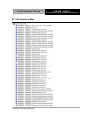
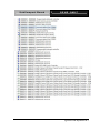
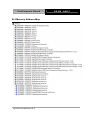
1
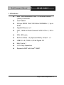
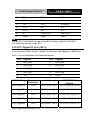
SubCompact Board GENE-QM67 GENE-QM67 Intel® 2nd Generation CoreTM i5/Celeron® Processor 10/100/1000Base-TX Ethernet 8 USB2.0, 4 COM, 8-bit Digital I/O 2 SATA 6.0Gb/s (Optional RAID) CFast 1 Mini Card, LPC GENE-QM67 Manual Rev.A 1st Ed. December 2011 SubCompact Board GENE-QM67 Copyright Notice This document is copyrighted, 2011. All rights are reserved. The original manufacturer reserves the right to make improvements to the products described in this manual at any time without notice. No part of this manual may be reproduced, copied, translated, or transmitted in any form or by any means without the prior written permission of the original manufacturer. Information provided in this manual is intended to be accurate and reliable. However, the original manufacturer assumes no responsibility for its use, or for any infringements upon the rights of third parties that may result from its use. The material in this document is for product information only and is subject to change without notice. While reasonable efforts have been made in the preparation of this document to assure its accuracy, AAEON assumes no liabilities resulting from errors or omissions in this document, or from the use of the information contained herein. AAEON reserves the right to make changes in the product design without notice to its users. i SubCompact Board GENE-QM67 Acknowledgments All other products’ name or trademarks are properties of their respective owners. AMI is a trademark of American Megatrends Inc. CFast™ is a trademark of the Compact Flash Association. Intel®, Core, and Celeron® are trademarks of Intel® Corporation. Microsoft Windows® is a registered trademark of Microsoft Corp. ITE is a trademark of Integrated Technology Express, Inc. IBM, PC/AT, PS/2, and VGA are trademarks of International Business Machines Corporation. SoundBlaster is a trademark of Creative Labs, Inc. Please be notified that all other products’ name or trademarks not be mentioned above are properties of their respective owners. ii SubCompact Board GENE-QM67 Packing List Before you begin installing your card, please make sure that the following materials have been shipped: 1 GENE-QM67 1 Cooler 1 DVD-ROM for Manual (in PDF Format) and Drivers If any of these items should be missing or damaged, please contact your distributor or sales representative immediately. iii SubCompact Board GENE-QM67 Contents Chapter 1 General Information 1.1 Introduction................................................................ 1-2 1.2 Features .................................................................... 1-3 1.3 Specifications ............................................................ 1-4 Chapter 2 Quick Installation Guide 2.1 Safety Precautions .................................................. 2-2 2.2 Location of Connectors and Jumpers ...................... 2-3 2.3 Mechanical Drawing ................................................ 2-5 2.4 List of Jumpers ........................................................ 2-7 2.5 List of Connectors ..................................................... 2-7 2.6 Setting Jumpers ....................................................... 2-9 2.7 LVDS Port 2 Operating VDD Selection (JP2) ......... 2-10 2.8 LVDS Port 1 Backlight Inverter VCC Selection (JP3) ....................................................................................... 2-10 2.9 LVDS Port 2 Backlight Inverter VCC Selection (JP4) ....................................................................................... 2-10 2.10 LVDS Port 2 Operating VDD Selection (JP5) ....... 2-10 2.11 LVDS Port 1 Backlight Lightness Control Mode Selection (JP6) .............................................................. 2-10 2.12 LVDS Port 2 Backlight Lightness Control Mode Selection (JP7) .............................................................. 2-10 2.13 COM2 Pin8 Function Selection (JP8) ................... 2-11 2.14 Front Panel Connector (JP9) ................................ 2-11 iv SubCompact Board GENE-QM67 2.15 Touch Screen 4/5/8-wire Selection (JP10) ........... 2-11 2.16 Clear CMOS Selection (JP11) .............................. 2-11 2.17 AT/ATX Power Supply Mode Selection (JP12)..... 2-12 2.18 LVDS Port 1 Inverter/Backlight Connector (CN1) . 2-12 2.19 External +12V Input Connector (CN2) .................. 2-12 2.20 USB2.0 Port 7 and 8 (CN3)................................... 2-12 2.21 USB2.0 Port 5 and 6 (CN4)................................... 2-13 2.22 USB2.0 Port 3 and 4 (CN5)................................... 2-13 2.23 External +5VSB Input (CN6) ................................. 2-13 2.24 LVDS Port 2 Inverter/Backlight Connector (CN7) . 2-13 2.25 Audio I/O Port (CN8) ............................................. 2-14 2.26 LVDS Port 1 (CN9)................................................ 2-14 2.27 LVDS Port 2 (CN10).............................................. 2-15 2.28 COM Port 2 (CN11)............................................... 2-15 2.29 LPT/ Digital I/O Port (CN12).................................. 2-16 2.30 COM Port 3 (CN13) ............................................. 2-18 2.31 LPC Port (CN14) ................................................... 2-18 2.32 COM Port 4 (CN15)............................................... 2-19 2.33 UIM Card Module (CN16) ..................................... 2-19 2.34 PS/2 Keyboard/Mouse Combo Port (CN17) ......... 2-19 2.35 +5VSB Output with SMBus (CN18) ...................... 2-20 2.36 Touch Screen Connector (CN19).......................... 2-20 2.37 CPU FAN (CN20) .................................................. 2-21 2.38 +5V Output for SATA HDD (CN22)....................... 2-21 2.39 Realtek LAN (RJ-45) Port (CN23)......................... 2-22 v SubCompact Board GENE-QM67 2.40 Intel LAN (RJ-45) Port (CN24) .............................. 2-22 2.41 USB Port 1 and 2 (CN25)...................................... 2-22 2.42 VGA/ DVI Ports (depends on hardware configuration) (CN26) ........................................................................... 2-23 2.43 COM Port 1 (D-SUB 9) (CN27) ............................. 2-24 2.44 CFast™ Slot (CN28) ............................................. 2-24 2.45 DDR3 SODIMM Slot (CN29)................................. 2-25 2.46 Mini Card Slot (CN30) ........................................... 2-25 2.47 SATA Port 1 (SATA1)............................................ 2-26 2.48 SATA Port 2 (SATA2)............................................ 2-26 2.49 Cooler & Fan Installations ..................................... 2-27 Chapter 3 AMI BIOS Setup 3.1 System Test and Initialization. .................................. 3-2 3.2 AMI BIOS Setup ........................................................ 3-3 Chapter 4 Driver Installation 4.1 Installation……………………………………………..4-3 Appendix A Programming The Watchdog Timer A.1 Programming .........................................................A-2 A.2 ITE8728F Watchdog Timer Initial Program ...........A-6 Appendix B I/O Information B.1 I/O Address Map ....................................................B-2 B.2 Memory Address Map............................................B-4 B.3 IRQ Mapping Chart ................................................B-5 vi SubCompact Board GENE-QM67 B.4 DMA Channel Assignments.……………………… .B-7 Appendix C Mating Connector C.1 List of Mating Connectors and Cables.................. C-2 Appendix D RAID & AHCI Settings D.1 Setting RAID ......................................................... D-2 D.2 Setting AHCI ....................................................... D-12 vii SubCompact Board GENE-QM67 Chapter 1 General Information Chapter 1 General Information 1- 1 SubCompact Board GENE-QM67 1.1 Introduction The GENE-QM67 supports Intel® 2nd Generation Intel® Core™ i5 Mobile/Celeron® processor which when paired with the Intel® QM67 chipset offers a high performance computing platform with low power consumption. This new product supports 204-pin DDR3 SODIMM at speeds of 1066/1333 MHz, up to 8 GB. One CFast™ and two SATA 6.0Gb/s (Optional RAID) interfaces provide ample storages. With dual Gigabit Ethernet, four COM ports, and eight USB2.0, the GENE-QM67 meets the requirements of today’s demanding applications. Display requirements are met with an abundance of interfaces such as CRT, DVI, and LVDS. The graphic engine adopts 2nd generation Intel® QM67 to offer high definition display function. In addition, it supports up to two 24-bit Dual-Channel LVDS, and one DVI output interface. With all of its integrated features, the GENE-QM67 strikes a balance of performance and price. This versatile product targets Industrial Automation, Entertainment, Networking, KIOSK/POS, Transportation, Banking, Healthcare and Digital Signage applications that require high performance and high reliability. Chapter 1 General Information 1-2 SubCompact Board GENE-QM67 1.2 Features Intel® 2nd Generation Core™ i5 Mobile/Celeron® (32nm) Processor Intel® QM67 204-pin DDR3 1066/1333 MHz SODIMM x 1, Up to 8 GB Gigabit Ethernet x 2 CRT, 18/24-bit Dual-Channel LVDS LCD x 2, DVI x 1 2CH HD Audio SATA 6.0Gb/s x 2 (Optional RAID), CFast x 1 USB2.0 x 8, COM x 4, 8-bit Digital I/O Mini Card x 1 +12V Only Operation Supports iAMT with Intel® QM67 Chapter 1 General Information 1-3 SubCompact Board GENE-QM67 1.3 Specifications System From Factor 3.5” Processor Intel® 2nd Generation Core™i5 / Celeron® (32nm) processor System Memory 204-pin DDR3 1066/1333 MHz SODIMM x 1, up to 8GB Chipset Intel® QM67 Ethernet Intel® 82579LM & Realtek RTL-8111E, 10/100/1000Base-TX, RJ-45 x 2 BIOS AMI BIOS-8MB SPI Flash Wake On LAN Yes Watchdog Timer Generates a time-out system reset H/W Status Monitoring Supports power supply voltages and temperature monitoring Expansion Interface Mini Card x 1, LPC Battery Lithium Battery Power Requirement +12V, AT/ATX Board Size 5.75" x 4" (146mm x 101.6mm) Gross Weight 0.88 lb (0.4Kg) Operating Temperature 32°F~140°F (0°C~60°C) Storage Temperature -40°F~176°F (-40°C~80°C) Operating Humidity Chapter 1 General Information 1-4 0% ~ 90% relative humidity, non-condensing SubCompact Board GENE-QM67 Display: Supports CRT/LCD, DVI/LCD simultaneous / dual view displays Intel® QM67 integrated Chipset Memory Shared system memory up to 512MB Resolution Up to 2048x1536 for CRT Up to 1920 x 1200 for LCD, DVI DVI DVI x 1 I/O: ITE IT8728F + Fintek F81216D SATA 6.0Gb/s x 2 , CFast™ x 1 Storage Serial Port RS-232 x 3 RS-232/422/485 (auto flow) x 1 USB USB2.0 x 8 PS/2 Port Keyboard x 1, Mouse x 1 Digital I/O 8-bit Programmable Audio Line-in, Line-out, Mic-in Chapter 1 General Information 1-5 SubCompact Board GENE-QM67 Chapter 2 Quick Installation Guide Chapter 2 Quick Installation Guide 2 - 1 SubCompact Board GENE-QM67 2.1 Safety Precautions Always completely disconnect the power cord from your board whenever you are working on it. Do not make connections while the power is on, because a sudden rush of power can damage sensitive electronic components. Always ground yourself to remove any static charge before touching the board. Modern electronic devices are very sensitive to static electric charges. Use a grounding wrist strap at all times. Place all electronic components on a static-dissipative surface or in a static-shielded bag when they are not in the chassis Chapter 2 Quick Installation Guide 2 - 2 SubCompact Board GENE-QM67 2.2 Location of Connectors and Jumpers Component Side Chapter 2 Quick Installation Guide 2 - 3 SubCompact Board Solder Side Chapter 2 Quick Installation Guide 2 - 4 GENE-QM67 SubCompact Board GENE-QM67 2.3 Mechanical Drawing Component Side Chapter 2 Quick Installation Guide 2 - 5 SubCompact Board Solder Side Chapter 2 Quick Installation Guide 2 - 6 GENE-QM67 SubCompact Board GENE-QM67 2.4 List of Jumpers The board has a number of jumpers that allow you to configure your system to suit your application. The table below shows the function of each of the board's jumpers: Label Function JP2 LVDS Port 2 Operating VDD Selection JP3 LVDS Port 1 Backlight Inverter VCC Selection JP4 LVDS Port 2 Backlight Inverter VCC Selection JP5 LVDS Port 1 Operating VDD Selection JP6 LVDS Port 1 Backlight Lightness Control Mode Selection JP7 LVDS Port 2 Backlight Lightness Control Mode Selection JP8 COM2 Pin8 Function Selection JP9 Front Panel Connector JP10 Touch Screen 4/5/8-wire Mode Selection JP11 Clear CMOS Selection JP12 AT/ATX Power Supply Mode Selection 2.5 List of Connectors The board has a number of connectors that allow you to configure your system to suit your application. The table below shows the function of each of the board's connectors: Label Function CN1 LVDS Port 1 Inverter / Backlight Connector CN2 External +12V Input CN3 USB2.0 Port 7 and 8 CN4 USB2.0 Port 5 and 6 CN5 USB2.0 Port 3 and 4 CN6 External +5VSB Input CN7 LVDS Port 2 Inverter / Backlight Connector Chapter 2 Quick Installation Guide 2 - 7 SubCompact Board CN8 Audio I/O Port CN9 LVDS Port 1 CN10 LVDS Port 2 CN11 COM Port 2 CN12 LPT / Digital IO Port CN13 COM Port 3 GENE-QM67 CN15 COM Port 4 CN16 UIM Card Module CN17 PS/2 Keyboard/Mouse Combo Port CN18 +5VSB Output with SMBus CN19 Touch Screen Connector CN20 CPU FAN CN22 +5V Output for SATA HDD CN23 Realtek LAN (RJ-45) Port CN24 Intel LAN (RJ-45) Port CN25 USB Ports 1 and 2 CN26 VGA / DVI Ports (depend on hardware configuration) CN27 COM Port 1 (D-SUB 9) CN28 CFast™ Slot CN29 DDR3 SODIMM Slot CN30 Mini Card Slot SATA1 SATA Port 1 Connector SATA2 SATA Port 2 Connector Chapter 2 Quick Installation Guide 2 - 8 SubCompact Board GENE-QM67 2.6 Setting Jumpers You configure your card to match the needs of your application by setting jumpers. A jumper is the simplest kind of electric switch. It consists of two metal pins and a small metal clip (often protected by a plastic cover) that slides over the pins to connect them. To “close” a jumper you connect the pins with the clip. To “open” a jumper you remove the clip. Sometimes a jumper will have three pins, labeled 1, 2 and 3. In this case you would connect either pins 1 and 2 or 2 and 3. 3 1 2 Open Closed Closed 2-3 A pair of needle-nose pliers may be helpful when working with jumpers. If you have any doubts about the best hardware configuration for your application, contact your local distributor or sales representative before you make any change. Generally, you simply need a standard cable to make most connections. Chapter 2 Quick Installation Guide 2 - 9 SubCompact Board GENE-QM67 2.7 LVDS Port 2 Operating VDD Selection (JP2) JP2 Function 1-2 +5V 2-3 +3.3V (Default) 2.8 LVDS Port 1 Backlight Inverter VCC Selection (JP3) JP3 Function 1-2 +12V 2-3 +5V (Default) 2.9 LVDS Port 2 Backlight Inverter VCC Selection (JP4) JP4 Function 1-2 +12V 2-3 +5V (Default) 2.10 LVDS Port 2 Operating VDD Selection (JP5) JP5 Function 1-2 +5V 2-3 +3.3V (Default) 2.11 LVDS Port 1 Backlight Lightness Control Mode Selection (JP6) JP6 Function 1-2 VR Mode (Default) 2-3 PWM Mode 2.12 LVDS Port 2 Backlight Lightness Control Mode Selection (JP7) JP7 Function 1-2 VR Mode (Default) 2-3 PWM Mode Chapter 2 Quick Installation Guide 2 - 10 SubCompact Board GENE-QM67 2.13 COM2 Pin8 Function Selection (JP8) JP8 Function 1-2 +12V 3-4 Ring (Default) 5-6 +5V 2.14 Front Panel Connector (JP9) 1 3 5 7 9 2 4 6 8 10 Pin Signal Pin Signal 1 PWRBTN(-) 2 PWRBTN(+) 3 HDLED(-) 4 HDLED(+) 5 SPEAKER(-) 6 SPEAKER(+) 7 PWRLED(-) 8 PWRLED(+) 9 RESET(-) 10 RESET(+) 2.15 Touch Screen 4/5/8-wire Selection (JP10) JP10 Function 1-2 4/8-wire Mode (Default) 2-3 5-wire Mode 2.16 Clear CMOS Selection (JP11) JP11 Function 1-2 Normal (Default) 2-3 Clear CMOS Chapter 2 Quick Installation Guide 2 - 11 SubCompact Board GENE-QM67 2.17 AT/ATX Power Supply Mode Selection (JP12) JP12 Function 1-2 AT Mode (Default) 2-3 ATX Mode 2.18 LVDS Port 1 Inverter/Backlight Connector (CN1) Pin Signal 1 VDD 2 BKL_CTL 3 GND 4 GND 5 BKL_EN Note: LVDS1 VDD can be set to +5V or +12V by JP3. LVDS1 BKL_CTL can be set by JP6. 2.19 External +12V Input Connector (CN2) Pin Signal 1 +12V 2 GND 2.20 USB2.0 Port 7 and 8 (CN3) Pin Signal Pin Signal 1 +5V 2 GND 3 D- 4 GND 5 D+ 6 D+ 7 GND 8 D- 9 GND 10 +5V Chapter 2 Quick Installation Guide 2 - 12 SubCompact Board GENE-QM67 2.21 USB2.0 Port 5 and 6 (CN4) Pin Signal Pin Signal 1 +5V 2 GND 3 D- 4 GND 5 D+ 6 D+ 7 GND 8 D- 9 GND 10 +5V 2.22 USB2.0 Port 3 and 4 (CN5) Pin Signal Pin Signal 1 +5V 2 GND 3 D- 4 GND 5 D+ 6 D+ 7 GND 8 D- 9 GND 10 +5V 2.23 External +5VSB Input (CN6) Pin Signal 1 PSON# 2 GND 3 +5VSBY 2.24 LVDS Port 2 Inverter/Backlight Connector (CN7) Pin Signal 1 VDD 2 BKL_CTL 3 GND 4 GND 5 BKL_EN Chapter 2 Quick Installation Guide 2 - 13 SubCompact Board GENE-QM67 UNote: LVDS2 VDD can be set to +5V or +12V by JP4. LVDS2 BKL_CTL can be set by JP7. 2.25 Audio I/O Port (CN8) Pin Signal 1 Microphone Left Channel 2 Microphone Left Channel 3 GND 4 Line-In Left Channel 5 Line-In Right Channel 6 GND 7 Line-Out Left Channel 8 GND 9 Line-Out Right Channel 10 +5V 2.26 LVDS Port 1 (CN9) Pin Signal Pin Signal 1 BKL_EN 2 BKL_CTL 3 VCC 4 GND 5 CLK_A- 6 CLK_A+ 7 VCC 8 GND 9 DATA_A0- 10 DATA_A0+ 11 DATA_A1- 12 DATA_A1+ 13 DATA_A2- 14 DATA_A2+ 15 DATA_A3- 16 DATA_A3+ 17 DDC_DAT 18 DDC_CLK 19 DATA_B0- 20 DATA_B0+ 21 DATA_B1- 22 DATA_B1+ Chapter 2 Quick Installation Guide 2 - 14 SubCompact Board GENE-QM67 23 DATA_B2- 24 DATA_B2+ 25 DATA_B3- 26 DATA_B3+ 27 VCC 28 GND 29 CLK_B30 Note: LVDS1 VCC can be set by JP5. CLK_B+ 2.27 LVDS Port 2 (CN10) Pin Signal Pin Signal 1 BKL_EN 2 BKL_CTL 3 VCC 4 GND 5 CLK_A- 6 CLK_A+ 7 VCC 8 GND 9 DATA_A0- 10 DATA_A0+ 11 DATA_A1- 12 DATA_A1+ 13 DATA_A2- 14 DATA_A2+ 15 DATA_A3- 16 DATA_A3+ 17 DDC_DAT 18 DDC_CLK 19 DATA_B0- 20 DATA_B0+ 21 DATA_B1- 22 DATA_B1+ 23 DATA_B2- 24 DATA_B2+ 25 DATA_B3- 26 DATA_B3+ 27 VCC 28 GND 29 CLK_B- 30 CLK_B+ Note: LVDS2 VCC can be set by JP2. U 2.28 COM Port 2 (CN11) Pin RS-232 RS-422 RS-485 1 DCD TX- B (Data-) 2 DSR N.C N.C Chapter 2 Quick Installation Guide 2 - 15 SubCompact Board GENE-QM67 3 RX RX+ N.C 4 RTS N.C N.C 5 TX TX+ A (Data+) 6 CTS N.C N.C 7 DTR RX- N.C 8 RI +5V/+12V +5V/+12V 9 GND GND GND Note: COM2 RS-232/422/485 can be set by BIOS setting. Default is RS-232. Pin 8 function can be set by JP8. 2.29 LPT/ Digital I/O Port (CN12) This connector offers 4-pair of digital I/O functions and address is A06h and A07h. The pin definitions are illustrated below: Pin Signal Pin Signal 1 DIO_P#1 2 DIO_P#2 3 DIO_P#3 4 DIO_P#4 5 DIO_P#5 6 DIO_P#6 7 DIO_P#7 8 DIO_P#8 9 +5V 10 GND BIOS Setting Port 8 @A07h Connector Definition Pin 8 GPIO Set 8 / Bit 3 IT8728F GPIO Setting U18 Pin103(GPIO 83) Port 7 @A07h Pin 7 GPIO Set 8 / Bit 2 U18 Pin102(GPIO 82) Port 6 @A07h Pin 6 GPIO Set 8 / Bit 1 U18 Pin101(GPIO 81) Port 5 @A07h Pin 5 GPIO Set 8 / Bit 0 U18 Pin100(GPIO 80) Port 4 @A06h Pin 4 GPIO Set 7 / Bit 3 U18 Pin111(GPIO 73) Chapter 2 Quick Installation Guide 2 - 16 Address SubCompact Board GENE-QM67 Port 3 @A06h Pin 3 GPIO Set 7 / Bit 2 U18 Pin110(GPIO 72) Port 2 @A06h Pin 2 GPIO Set 7 / Bit 1 U18 Pin109(GPIO 71) Port 1 @A06h Pin 1 GPIO Set 7 / Bit 0 U18 Pin108(GPIO 70) LPT Mode Pin Signal Pin Signal 1 STROBE# 2 AFD# 3 D0 4 ERR# 5 D1 6 PRINT# 7 D2 8 SLIN# 9 D3 10 GND 11 D4 12 GND 13 D5 14 GND 15 D6 16 GND 17 D7 18 GND 19 ACK# 20 GND 21 BUSY 22 GND 23 PE 24 GND 25 SLCT 26 N.C Digital I/O Mode Pin Signal Pin Signal 1 N.C 2 N.C 3 D0 4 N.C 5 D1 6 N.C 7 D2 8 N.C 9 D3 10 GND 11 N.C 12 GND 13 N.C 14 GND Chapter 2 Quick Installation Guide 2 - 17 SubCompact Board GENE-QM67 15 N.C 16 GND 17 N.C 18 GND 19 D7 20 GND 21 D6 22 GND 23 D5 24 GND 25 D4 26 N.C Note: LPT / Digital IO can be set by BIOS setting. Default is LPT Function. 2.30 COM Port 3 (CN13) Pin Signal 1 DCD 2 DSR 3 RX 4 RTS 5 TX 6 CTS 7 DTR 8 RI 9 GND 2.31 LPC Port (CN14) Pin Signal 1 AD0 2 AD1 3 AD2 4 AD3 5 +3.3VCC 6 FRAME# 7 RESET# 8 GND Chapter 2 Quick Installation Guide 2 - 18 SubCompact Board 9 33MCLK 10 DRQ0# 11 DRQ1# 12 SERIRQ GENE-QM67 2.32 COM Port 4 (CN15) Pin Signal 1 DCD 2 DSR 3 RX 4 RTS 5 TX 6 CTS 7 DTR 8 RI 9 GND 2.33 UIM Card Module (CN16) Pin Signal 1 PWR 2 RST 3 CLK 4 GND 5 VPP 6 DAT 2.34 PS/2 Keyboard/Mouse Combo Port (CN17) Pin Signal Pin Signal 1 KB_DAT 2 KB_CLK Chapter 2 Quick Installation Guide 2 - 19 SubCompact Board GENE-QM67 3 GND 4 +5V 5 MS_DAT 6 MS_CLK 2.35 +5VSB Output with SMBus (CN18) Pin Signal 1 SMB_DAT 2 GND 3 SMB_CLK 4 GND 5 PSON# 6 +5VSB 2.36 Touch Screen Connector (CN19) 8-wire Pin Signal 1 GND 2 TOP_EXC 3 BOTTOM_EXC 4 LEFT_EXC 5 RIGHT_EXC 6 TOP_SENSE 7 BOTTOM_SENSE 8 LEFT_SENSE 9 RIGHT_SENSE 4-wire Pin Signal 1 GND 2 TOP 3 BOTTOM 4 LEFT Chapter 2 Quick Installation Guide 2 - 20 SubCompact Board 5 RIGHT 6 N.C 7 N.C 8 N.C 9 N.C GENE-QM67 5-wire Pin Signal 1 GND 2 UL(Y-) 3 UR(Y+) 4 LL(X-) 5 LR(X+) 6 SENSE 7 N.C 8 N.C 9 N.C 2.37 CPU FAN (CN20) Pin Signal 1 GND 2 VDD 3 TACH 2.38 +5V Output for SATA HDD (CN22) Pin Signal 1 +5V 2 GND Chapter 2 Quick Installation Guide 2 - 21 SubCompact Board 2.39 Realtek LAN (RJ-45) Port (CN23) Pin Signal 1 BI_DA+ 2 BI_DA- 3 BI_DB+ 4 BI_DC+ 5 BI_DC- 6 BI_DB- 7 BI_DD+ 8 BI_DD- 2.40 Intel LAN (RJ-45) Port (CN24) Pin Signal 1 BI_DA+ 2 BI_DA- 3 BI_DB+ 4 BI_DC+ 5 BI_DC- 6 BI_DB- 7 BI_DD+ 8 BI_DD- 2.41 USB Port 1 and 2 (CN25) Pin Signal 1 VCC (+5V) 2 D- 3 D+ 4 GND Chapter 2 Quick Installation Guide 2 - 22 GENE-QM67 SubCompact Board GENE-QM67 2.42 VGA/ DVI Ports (depends on hardware configuration) (CN26) VGA Pin Signal Pin Signal 1 RED 2 GREEN 3 BLUE 4 N.C 5 GND 6 RED_RTN 7 GREEN_RTN 8 BLUE_RTN 9 +5V 10 GND 11 N.C 12 DDC Data 13 HSYNC 14 VSYNC 15 DDC Clock Pin Signal Pin Signal 1 TMDS Data 2- 2 TMDS Data 2+ 3 GND 4 Analog DDC Clock* 5 Analog DDC Data* 6 DDC Clock 7 DDC Data 8 Analog VSYNC 9 TMDS Data 1- 10 TMDS Data 1+ 11 GND 12 TMDS Data 3- 13 TMDS Data 3+ 14 +5V 15 GND 16 Hot Plug Detect 17 TMDS data 0- 18 TMDS data 0+ 19 GND 20 N.C 21 N.C 22 GND DVI 23 TMDS clock+ 24 TMDS clock- C1 Analog red C2 Analog green C3 Analog blue C4 Analog HSYNC C5 Analog ground Chapter 2 Quick Installation Guide 2 - 23 SubCompact Board GENE-QM67 2.43 COM Port 1 (D-SUB 9) (CN27) Pin Signa l Pin Sign al 1 DCD 6 DSR 2 RX 7 RTS 3 TX 8 CTS 4 DTR 9 RI 5 GND 2.44 CFast™ Slot (CN28) Pin Signal S1 GND S2 A+ S3 A- S4 GND S5 B- S6 B+ S7 GND PC1 N.C PC2 GND PC3 N.C PC4 N.C PC5 N.C PC6 N.C PC7 GND PC8 N.C PC9 N.C PC10 N.C PC11 N.C PC12 N.C Chapter 2 Quick Installation Guide 2 - 24 SubCompact Board PC13 +3.3V PC14 +3.3V PC15 GND PC16 GND PC17 N.C GENE-QM67 2.45 DDR3 SODIMM Slot (CN29) Standard specification 2.46 Mini Card Slot (CN30) P in Signa l Pin Signal 1 PCIE_WAKE# 2 +3.3VSB 3 N.C 4 GND 5 N.C 6 +1.5V 7 CLK_REQ# 8 UIM_PWR 9 GND 10 UIM_DATA 11 CLK- 12 UIM_CLK 13 CLK+ 14 UIM_RESET 15 GND 16 UIM_VPP 17 N.C 18 GND 19 N.C 20 Wireless DISABLE# 21 GND 22 Reset# 23 RX- 24 +3.3VSB 25 RX+ 26 GND 27 GND 28 +1.5V 29 GND 30 SMB_CLK 31 TX- 32 SMB_DATA 33 TX+ 34 GND 35 GND 36 USB_DChapter 2 Quick Installation Guide 2 - 25 SubCompact Board GENE-QM67 37 GND 38 USB_D+ 39 +3.3VSB 40 GND 41 +3.3VSB 42 N.C 43 GND 44 N.C 45 N.C 46 N.C 47 N.C 48 +1.5V 49 N.C 50 GND 51 N.C 52 +3.3VSB 2.47 SATA Port 1 (SATA1) Standard specification 2.48 SATA Port 2 (SATA2) Standard specification Chapter 2 Quick Installation Guide 2 - 26 SubCompact Board GENE-QM67 2.49 Cooler & Fan Installations Please follow the installation steps to make sure the proper installation of the cooler and fan. Step 1: Check the cable’s location to see if it is on the left-up corner Step 2: Fasten the screw at the left-down side first Chapter 2 Quick Installation Guide 2 - 27 SubCompact Board Step 3 : Fasten the screw at the right-up side Step 4 : Fasten the screw at the right-down side Chapter 2 Quick Installation Guide 2 - 28 GENE-QM67 SubCompact Board GENE-QM67 Step 5 : Fasten the screw at the left-up side as the picture Step 6 : Connect the Fan Cable to the Fan Connector Chapter 2 Quick Installation Guide 2 - 29 SubCompact Board GENE-QM67 Below Table for China RoHS Requirements 产品中有毒有害物质或元素名称及含量 AAEON Main Board/ Daughter Board/ Backplane 有毒有害物质或元素 部件名称 铅 汞 镉 六价铬 多溴联苯 多溴二苯醚 (Pb) (Hg) (Cd) (Cr(VI)) (PBB) (PBDE) × ○ ○ ○ ○ ○ × ○ ○ ○ ○ ○ 印刷电路板 及其电子组件 外部信号 连接器及线材 O:表示该有毒有害物质在该部件所有均质材料中的含量均在 SJ/T 11363-2006 标准规定的限量要求以下。 X:表示该有毒有害物质至少在该部件的某一均质材料中的含量超出 SJ/T 11363-2006 标准规定的限量要求。 备注:此产品所标示之环保使用期限,系指在一般正常使用状况下。 Chapter 2 Quick Installation Guide 2 - 30 SubCompact Board GENE-QM67 Chapter 3 AMI BIOS Setup Chapter 3 AMI BIOS Setup 3-1 SubCompact Board 3.1 GENE-QM67 System Test and Initialization These routines test and initialize board hardware. If the routines encounter an error during the tests, you will either hear a few short beeps or see an error message on the screen. There are two kinds of errors: fatal and non-fatal. The system can usually continue the boot up sequence with non-fatal errors. System configuration verification These routines check the current system configuration against the values stored in the CMOS memory. If they do not match, the program outputs an error message. You will then need to run the BIOS setup program to set the configuration information in memory. There are three situations in which you will need to change the CMOS settings: 1. You are starting your system for the first time 2. You have changed the hardware attached to your system 3. The CMOS memory has lost power and the configuration information has been erased. The GENE-QM67 CMOS memory has an integral lithium battery backup for data retention. However, you will need to replace the complete unit when it finally runs down. Chapter 3 AMI BIOS Setup 3-2 SubCompact Board 3.2 GENE-QM67 AMI BIOS Setup AMI BIOS ROM has a built-in Setup program that allows users to modify the basic system configuration. This type of information is stored in battery-backed CMOS RAM so that it retains the Setup information when the power is turned off. Entering Setup Power on the computer and press <Del> or <F2> immediately. This will allow you to enter Setup. Main Set the date, use tab to switch between date elements. Advanced Enable disable boot option for legacy network devices. Chipset host bridge parameters. Boot Enables/disable quiet boot option. Security Set setup administrator password. Save&Exit Exit system setup after saving the changes. Note: 1. If the "Onboard LVDS2 (CH7511)" has been set "Disable," the status of "Primary IGFx Boot Display" is "Auto Detect." The screen cannot be Chapter 3 AMI BIOS Setup 3-3 SubCompact Board GENE-QM67 switched to LVDS2 under the OS. 2. If the "Onboard LVDS2 (CH7511)" has been set "Enable," the status of the "Primary IGFx Boot Display" is concealed. The screen can be switched to LVDS2 under the OS. Chapter 3 AMI BIOS Setup 3-4 SubCompact Board GENE-QM67 Chapter 4 Driver Installation . Chapter 4 Driver Installation 4 -1 SubCompact Board GENE-QM67 The GENE-QM67 comes with an AutoRun DVD-ROM that contains all drivers and utilities that can help you to install the driver automatically. Insert the driver DVD, the driver DVD-title will auto start and show the installation guide. If not, please follow the sequence below to install the drivers. Follow the sequence below to install the drivers: Step 1 – Install Chipset Driver Step 2 – Install VGA Driver Step 3 – Install LAN1 Driver (Intel® LAN Chip) Step 4 – Install LAN2 Driver (Realtek LAN Chip) Step 5 – Install Audio Driver Step 6 – Install ME Driver Step 7 – Install RAID & AHCI Driver Step 8 – Install TPM Driver Step 9 – Install Touch Driver Please read instructions below for further detailed installations. Chapter 4 Driver Installation 4 -2 SubCompact Board 4.1 GENE-QM67 Installation: Insert the GENE-QM67 DVD-ROM into the DVD-ROM drive. And install the drivers from Step 1 to Step 9 in order. Step 1 – Install Chipset Driver Click on the STEP 1-CHIPSET folder and double click on the infinst_autol.exe file 1. Follow the instructions that the window shows 2. The system will help you install the driver automatically Step 2 – Install VGA Driver 1. Click on the STEP2-VGA folder and select the OS folder your system is 2. Double click on the Setup.exe file located in each OS folder 3. Follow the instructions that the window shows 4. The system will help you install the driver automatically Note 1: This motherboard supports VGA and LVDS display devices. In Single Display mode, use the hot keys to switch between VGA to LVDS device or vice versa. By default, press <Ctrl>+<Alt>+<F1> to switch to VGA device and press <Ctrl>+<Alt>+<F3> to switch to LVDS device. Before removing the current display device, connect the display device that you want to use, and then press the hot keys to switch to that device. Note 2: If the OS is Windows® XP, you have to install the driver of dotNet Framework first. Simply click on dotnetfx35.exe located in dotNet Framwork folder. Chapter 4 Driver Installation 4 -3 SubCompact Board GENE-QM67 Step 3 –Install LAN1 Driver (Intel® LAN Chip) 1. Click on the STEP3-LAN1 folder and select the OS folder your system is 2. Double click on the .exe file located in each OS folder 3. Follow the instructions that the window shows 4. The system will help you install the driver automatically Step 4 –Install LAN2 Driver (Realtek LAN Chip) 1. Click on the STEP4-LAN2 folder and select the OS folder your system is 2. Double click on the setup.exe file located in each OS folder 3. Follow the instructions that the window shows 4. The system will help you install the driver automatically Step 5 –Install Audio Driver 1. Click on the STEP5-AUDIO folder and select the OS folder your system is 2. Double click on the Setup.exe file located in each OS folder 3. Follow the instructions that the window shows 4. The system will help you install the driver automatically Step 6 – Install ME Driver 1. Click on the STEP6-ME SW folder and select the OS folder Chapter 4 Driver Installation 4 -4 SubCompact Board GENE-QM67 your system is 2. Double click on the Setup.exe file located in each OS folder 3. Follow the instructions that the window shows 4. The system will help you install the driver automatically Step 7 – Install RAID & AHDI Driver Please refer to the Appendix D RAID & AHDI Settings Step 8 – Install TPM Driver 1. Click on the STEP8-TPM DRIVER folder and select the OS folder your system is 2. Double click on the Setup.exe file located in each OS folder 3. Follow the instructions that the window shows 4. The system will help you install the driver automatically Step 9 –Install Touch Driver 1. Click on the STEP9-TOUCH folder and select the OS folder your system is 2. Double click on the Setup.exe file located in each OS folder 3. Follow the instructions that the window shows 4. The system will help you install the driver automatically Chapter 4 Driver Installation 4 -5 SubCompact Board GENE-QM67 Appendix A Programming the Watchdog Timer Appendix A Programming the Watchdog Timer A-1 SubCompact Board GENE-QM67 A.1 Programming GENE-QM67 utilizes ITE IT8728F chipset as its watchdog timer controller. Below are the procedures to complete its configuration and the AAEON intial watchdog timer program is also attached based on which you can develop customized program to fit your application. Configuring Sequence Description After the hardware reset or power-on reset, the ITE 8728F enters the normal mode with all logical devices disabled except KBC. The initial state (enable bit ) of this logical device (KBC) is determined by the state of pin 121 (DTR1#) at the falling edge of the system reset during power-on reset. Appendix A Programming the Watchdog Timer A-2 SubCompact Board GENE-QM67 There are three steps to complete the configuration setup: (1) Enter the MB PnP Mode; (2) Modify the data of configuration registers; (3) Exit the MB PnP Mode. Undesired result may occur if the MB PnP Mode is not exited normally. (1) Enter the MB PnP Mode To enter the MB PnP Mode, four special I/O write operations are to be performed during Wait for Key state. To ensure the initial state of the key-check logic, it is necessary to perform four write operations to the Special Address port (2EH). Two different enter keys are provided to select configuration ports (2Eh/2Fh) of the next step. (2) Modify the Data of the Registers All configuration registers can be accessed after entering the MB PnP Mode. Before accessing a selected register, the content of Index 07h must be changed to the LDN to which the register belongs, except some Global registers. (3) Exit the MB PnP Mode Set bit 1 of the configure control register (Index=02h) to 1 to exit the MB PnP Mode. Appendix A Programming the Watchdog Timer A-3 SubCompact Board GENE-QM67 WatchDog Timer Configuration Registers Configure Control (Index=02h) This register is write only. Its values are not sticky; that is to say, a hardware reset will automatically clear the bits, and does not require the software to clear them. Appendix A Programming the Watchdog Timer A-4 SubCompact Board GENE-QM67 WatchDog Timer Control Register (Index=71h, Default=00h) WatchDog Timer Configuration Register (Index=72h, Default=00h) WatchDog Timer Time-out Value Register (Index=73h, Default=00h) Appendix A Programming the Watchdog Timer A-5 SubCompact Board GENE-QM67 A.2 ITE8728F Watchdog Timer Initial Program .MODEL SMALL .CODE Main: CALL Enter_Configuration_mode CALL Check_Chip mov cl, 7 call Set_Logic_Device ;time setting mov cl, 10 ; 10 Sec dec al Watch_Dog_Setting: ;Timer setting mov al, cl mov cl, 73h call Superio_Set_Reg ;Clear by keyboard or mouse interrupt mov al, 0f0h mov cl, 71h call Superio_Set_Reg ;unit is second. mov al, 0C0H mov cl, 72h call Superio_Set_Reg Appendix A Programming the Watchdog Timer A-6 SubCompact Board GENE-QM67 ; game port enable mov cl, 9 call Set_Logic_Device Initial_OK: CALL Exit_Configuration_mode MOV AH,4Ch INT 21h Enter_Configuration_Mode PROC NEAR MOV SI,WORD PTR CS:[Offset Cfg_Port] MOV DX,02Eh MOV CX,04h Init_1: MOV AL,BYTE PTR CS:[SI] OUT DX,AL INC SI LOOP Init_1 RET Enter_Configuration_Mode ENDP Exit_Configuration_Mode PROC NEAR MOV AX,0202h CALL Write_Configuration_Data Appendix A Programming the Watchdog Timer A-7 SubCompact Board GENE-QM67 RET Exit_Configuration_Mode ENDP Check_Chip PROC NEAR MOV AL,20h CALL Read_Configuration_Data CMP AL,87h JNE Not_Initial MOV AL,21h CALL Read_Configuration_Data CMP AL,12h JNE Not_Initial Need_Initial: STC RET Not_Initial: CLC RET Check_Chip ENDP Read_Configuration_Data PROC NEAR MOV DX,WORD PTR CS:[Cfg_Port+04h] OUT DX,AL Appendix A Programming the Watchdog Timer A-8 SubCompact Board GENE-QM67 MOV DX,WORD PTR CS:[Cfg_Port+06h] IN AL,DX RET Read_Configuration_Data ENDP Write_Configuration_Data PROC NEAR MOV DX,WORD PTR CS:[Cfg_Port+04h] OUT DX,AL XCHG AL,AH MOV DX,WORD PTR CS:[Cfg_Port+06h] OUT DX,AL RET Write_Configuration_Data ENDP Superio_Set_Reg proc near push ax MOV DX,WORD PTR CS:[Cfg_Port+04h] mov al,cl out dx,al pop ax inc dx out dx,al ret Superio_Set_Reg endp.Set_Logic_Device proc near Set_Logic_Device proc near Appendix A Programming the Watchdog Timer A-9 SubCompact Board GENE-QM67 push ax push cx xchg al,cl mov cl,07h call Superio_Set_Reg pop cx pop ax ret Set_Logic_Device endp ;Select 02Eh->Index Port, 02Fh->Data Port Cfg_Port DB 087h,001h,055h,055h DW 02Eh,02Fh END Main Note: Interrupt level mapping 0Fh-Dh: not valid 0Ch: IRQ12 . . 03h: IRQ3 02h: not valid 01h: IRQ1 00h: no interrupt selected Appendix A Programming the Watchdog Timer A-10 SubCompact Board GENE-QM67 Appendix B I/O Information Appendix B I/O Information B-1 SubCompact Board B.1 I/O Address Map Appendix B I/O Information B-2 GENE-QM67 SubCompact Board GENE-QM67 Appendix B I/O Information B-3 SubCompact Board B.2 Memory Address Map Appendix B I/O Information B-4 GENE-QM67 SubCompact Board GENE-QM67 B.3 IRQ Mapping Chart Appendix B I/O Information B-5 SubCompact Board Appendix B I/O Information B-6 GENE-QM67 SubCompact Board GENE-QM67 B.4 DMA Channel Assignments Appendix B I/O Information B-7 SubCompact Board GENE-QM67 Appendix C Mating Connector Appendix C Mating Connector C - 1 SubCompact Board GENE-QM67 C.1 List of Mating Connectors and Cables The table notes mating connectors and available cables. Connector Label Mating Connector Function Vendor Model No. Available Cable Cable P/N CN1 LVDS#1 Inverter Connector JST PHR-5 N/A N/A CN2 +12V Vin Connector N/A N/A Power Cable 1702002010 CN3 USB Port #7, #8 Connector Molex 51110-1050 USB Cable 1709100201 CN4 USB Port #5, #6 Connector Molex 51110-1050 USB Cable 1709100201 CN5 USB Port #3, #4 Connector Molex 51110-1050 USB Cable 1709100201 CN6 External +5VSB Power Input and PS_ON# JST PHR-3 ATX Cable 170220020B CN7 LVDS#2 Inverter Connector JST PHR-5 N/A N/A CN8 Audio Connector Molex 51021-1000 Audio Cable 1709100254 CN9 LVDS#1 Connector HIROSE DF13-30DS -1.25C N/A N/A CN10 LVDS#2 Connector HIROSE DF13-30DS -1.25C N/A N/A CN11 COM Port 2 Connector Molex 51021-0900 Serial Port Cable 1701090150 CN12 LPT / Digital IO Port Molex 51110-2650 Parallel Port Cable 1701260200 Appendix C Mating Connector C - 2 SubCompact Board GENE-QM67 CN13 COM Port 3 Connector Molex 51021-0900 Serial Port Cable 1701090150 CN14 LPC Port JST SHR-12V-SB AAEON LPC Cable 1703120130 CN15 COM Port 4 Connector Molex 51021-0900 Serial Port Cable 1701090150 CN16 UIM Connector Molex 51021-0600 N/A N/A CN17 P/S2 KB/MS Connector JST PHDR-06V S P/S2 KB/MS Cable 1700060152 CN18 External AUX Power and PS_ON# JST PHR-6 N/A N/A CN19 Touch Screen Connector JST SHR-9V-SB N/A N/A CN20 CPU Fan Connector Molex 22-01-2035 N/A N/A CN22 +5Vout Connector JST PHR-2 2 Pins For HDD Power 1702150155 BAT1 External RTC Connector Molex 51021-0200 Battery Cable 175011901C Appendix C Mating Connector C - 3 SubCompact Board GENE-QM67 Appendix D RAID & AHCI Settings Appendix D RAID & AHCI Settings D-1 SubCompact Board GENE-QM67 D.1 Setting RAID OS installation to setup RAID Mode Step 1: Copy the files below from “Driver CD -> Step 7RAID&AHCI\WinXP_32“ to Disk Step 2: Connect the USB Floppy (disk with RAID files) to the board Appendix D RAID & AHCI Settings D-2 SubCompact Board GENE-QM67 Step 3: The setting procedures “ In BIOS Setup Menu” A: Advanced -> SATA Configuration -> SATA Mode -> RAID Mode Step 4: The setting procedures “In BIOS Setup Menu” B: Advanced -> Launch Storage OpROM -> Enabled Appendix D RAID & AHCI Settings D-3 SubCompact Board GENE-QM67 Step 5: The setting procedures “In BIOS Setup Menu” C: Boot -> Boot Option #1 -> DVD-ROM Type Step 6: The setting procedures “In BIOS Setup Menu” D: Save & Exit -> Save Changes and Exit Appendix D RAID & AHCI Settings D-4 SubCompact Board GENE-QM67 Step 7: Press Ctrl-I to enter MAIN MENU Step 8: Choose “1.Create RAID Volume” Appendix D RAID & AHCI Settings D-5 SubCompact Board Step 9: RAID Level -> RAID0(Stripe) Step 10: Choose “Create Volume” Appendix D RAID & AHCI Settings D-6 GENE-QM67 SubCompact Board GENE-QM67 Step 11: Choose “Y” Step 12: Choose “5. Exit” Appendix D RAID & AHCI Settings D-7 SubCompact Board Step 13: Choose “Y” Step 14: Setup OS Appendix D RAID & AHCI Settings D-8 GENE-QM67 SubCompact Board GENE-QM67 Step 15: Press “F6” Step 16: Choose “S” Appendix D RAID & AHCI Settings D-9 SubCompact Board GENE-QM67 Step 17: Choose “Intel(R) Mobile Express Chipset SATA RAID Controller” Step 18: It will show the model number you select and then press “ENTER” Appendix D RAID & AHCI Settings D-10 SubCompact Board GENE-QM67 Step 19: Setup is starting Windows Appendix D RAID & AHCI Settings D-11 SubCompact Board GENE-QM67 D.2 Setting AHCI OS installation to setup AHCI Mode Step 1: Copy the files below from “Driver CD -> Step 7RAID&AHCI\WinXP_32“ to Disk Step 2: Connect the USB Floppy (disk with RAID files) to the board Appendix D RAID & AHCI Settings D-12 SubCompact Board GENE-QM67 Step 3: The setting procedures “ In BIOS Setup Menu” A: Advanced -> SATA Configuration -> SATA Configuration -> SATA Mode -> AHCI Mode Step 4: The setting procedures “In BIOS Setup Menu” B: Boot -> Boot Option #1 -> DVD-ROM Type Appendix D RAID & AHCI Settings D-13 SubCompact Board GENE-QM67 Step 5: The setting procedures “In BIOS Setup Menu” C: Save & Exit -> Save Changes and Exit Step 6: Setup OS Appendix D RAID & AHCI Settings D-14 SubCompact Board GENE-QM67 Step 7: Press “F6” Step 8: Choose “S” Appendix D RAID & AHCI Settings D-15 SubCompact Board GENE-QM67 Step 9: Choose “Intel(R) Mobile Express Chipset SATA AHCI Controller” Step 10: It will show the model number you select and then press “ENTER” Appendix D RAID & AHCI Settings D-16 SubCompact Board GENE-QM67 Step 11: Setup is loading files Appendix D RAID & AHCI Settings D-17