1
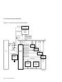
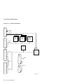
AlphaPC64 Motherboard
User’s Manual
Order Number: EC–QLJKB–TE
Revision/Update Information:
Digital Equipment Corporation
Maynard, Massachusetts
This document supersedes the
AlphaPC64 Motherboard User’s Manual
(EC–QLJKA–TE).
July 1995
Possession, use, or copying of the software described in this publication is authorized only
pursuant to a valid written license from Digital or an authorized sublicensor.
While Digital believes the information included in this publication is correct as of the date of
publication, it is subject to change without notice.
Digital Equipment Corporation makes no representations that the use of its products in the
manner described in this publication will not infringe on existing or future patent rights, nor do
the descriptions contained in this publication imply the granting of licenses to make, use, or sell
equipment or software in accordance with the description.
© Digital Equipment Corporation 1995.
All rights reserved.
Printed in U.S.A.
AlphaGeneration, DEC, DECchip, DECladebug, Digital, OpenVMS, VAX, VAX DOCUMENT,
VMS, the AlphaGeneration design mark, and the DIGITAL logo are trademarks of Digital
Equipment Corporation.
Digital Semiconductor is a Digital Equipment Corporation business.
Digital UNIX Version 3.2 for Alpha is a UNIX 93 branded product.
Centronics is a trademark of Genicom Corporation.
CompuServe is a registered trademark of CompuServe, Inc.
GRAFOIL is a registered trademark of Union Carbide Corporation.
IEEE is a registered trademark of The Institute of Electrical and Electronics Engineers, Inc.
Intel and UPI are trademarks of Intel Corporation.
MACH is a trademark of Advanced Micro Devices, Inc.
Micron is a registered trademark of Micron Corporation.
Motorola is a registered trademark of Motorola, Inc.
National is a registered trademark of National Semiconductor Corporation.
Microsoft is a registered trademark, NT, and Windows NT are trademarks of Microsoft
Corporation.
OSF and OSF/1 are registered trademarks of Open Software Foundation, Inc.
PHOENIX is a registered trademark of Phoenix Technologies, Ltd.
PS/2 is a registered trademark of International Business Machines Corporation.
SPEC is a trademark of Standard Performance Evaluation Corporation.
TriQuint is a registered trademark of TriQuint Semiconductor, Inc.
UNIX is a registered trademark in the United States and other countries, licensed exclusively
through X/Open Company Ltd.
All other trademarks and registered trademarks are the property of their respective owners.
This document was prepared using VAX DOCUMENT Version 2.1.
Contents
About This Manual . . . . . . . . . . . . . . . . . . . . . . . . . . . . . . . . . . . . . . . . . . .
vii
1 AlphaPC64 Introduction
1.1
The AlphaPC64 Motherboard . . . . . . . . .
1.2
System Components and Features . . . . .
1.2.1
Memory Subsystem . . . . . . . . . . . . .
1.2.2
DECchip 21072 Support Chipset . . .
1.2.3
PAL Control Set . . . . . . . . . . . . . . . .
1.2.4
Level 2 Cache Subsystem Overview .
1.2.5
Clock Subsystem Overview . . . . . . .
1.2.6
PCI Interface Overview . . . . . . . . . .
1.2.7
ISA Interface Overview . . . . . . . . . .
1.2.8
Software Support . . . . . . . . . . . . . . .
1.2.9
Component Layout . . . . . . . . . . . . . .
1.2.10
System Summary . . . . . . . . . . . . . . .
.
.
.
.
.
.
.
.
.
.
.
.
.
.
.
.
.
.
.
.
.
.
.
.
.
.
.
.
.
.
.
.
.
.
.
.
.
.
.
.
.
.
.
.
.
.
.
.
.
.
.
.
.
.
.
.
.
.
.
.
.
.
.
.
.
.
.
.
.
.
.
.
.
.
.
.
.
.
.
.
.
.
.
.
.
.
.
.
.
.
.
.
.
.
.
.
.
.
.
.
.
.
.
.
.
.
.
.
.
.
.
.
.
.
.
.
.
.
.
.
.
.
.
.
.
.
.
.
.
.
.
.
.
.
.
.
.
.
.
.
.
.
.
.
.
.
.
.
.
.
.
.
.
.
.
.
.
.
.
.
.
.
.
.
.
.
.
.
.
.
.
.
.
.
.
.
.
.
.
.
.
.
.
.
.
.
.
.
.
.
.
.
.
.
.
.
.
.
.
.
.
.
.
.
.
.
.
.
.
.
.
.
.
.
.
.
.
.
.
.
.
.
.
.
.
.
.
.
1–1
1–1
1–1
1–4
1–4
1–4
1–5
1–5
1–5
1–6
1–6
1–6
.
.
.
.
.
.
.
.
.
.
.
.
.
.
.
.
.
.
.
.
.
.
.
.
.
.
.
.
.
.
.
.
.
.
.
.
.
.
.
.
.
.
.
.
.
.
.
.
.
.
.
.
.
.
.
.
.
.
.
.
.
.
.
.
.
.
.
.
.
.
.
.
.
.
.
.
2–1
2–1
2–6
2–7
Hardware Requirements . . . . . . . . . . . . . . . . . . . . . . . . .
Software Requirements . . . . . . . . . . . . . . . . . . . . . . . . . .
Hardware Configuration . . . . . . . . . . . . . . . . . . . . . . . . .
Software Configuration . . . . . . . . . . . . . . . . . . . . . . . . . .
Starting Windows NT ARC Firmware . . . . . . . . . . . .
Going to the Debug Monitor from Windows NT ARC
Firmware . . . . . . . . . . . . . . . . . . . . . . . . . . . . . . . . . .
.
.
.
.
.
.
.
.
.
.
.
.
.
.
.
.
.
.
.
.
.
.
.
.
.
.
.
.
.
.
3–1
3–2
3–2
3–9
3–9
......
3–9
2 System Jumpers and Connectors
2.1
2.1.1
2.1.2
2.2
Configuration Jumpers . . . . . . . . . . . .
Software Configuration Jumpers .
Hardware Configuration Jumpers
AlphaPC64 Board Connectors . . . . . .
.
.
.
.
.
.
.
.
3 Starting and Using the AlphaPC64
3.1
3.2
3.3
3.4
3.4.1
3.4.2
iii
3.4.3
Returning to Windows NT ARC Firmware from the Debug
Monitor . . . . . . . . . . . . . . . . . . . . . . . . . . . . . . . . . . . . . . . . .
3–10
4 Functional Elements
4.1
4.1.1
4.1.2
4.2
4.3
4.4
4.4.1
4.4.2
4.4.3
PCI Interrupts and Arbitration .
System Interrupts . . . . . . . .
PCI/ISA Arbitration . . . . . . .
ISA Devices . . . . . . . . . . . . . . . .
dc Power Distribution . . . . . . . .
Flash ROM (System ROM) . . . . .
Special Flash ROM Headers
Flash ROM Structure . . . . . .
Flash ROM Access . . . . . . . .
.
.
.
.
.
.
.
.
.
.
.
.
.
.
.
.
.
.
.
.
.
.
.
.
.
.
.
.
.
.
.
.
.
.
.
.
.
.
.
.
.
.
.
.
.
.
.
.
.
.
.
.
.
.
.
.
.
.
.
.
.
.
.
.
.
.
.
.
.
.
.
.
.
.
.
.
.
.
.
.
.
.
.
.
.
.
.
.
.
.
.
.
.
.
.
.
.
.
.
.
.
.
.
.
.
.
.
.
.
.
.
.
.
.
.
.
.
.
.
.
.
.
.
.
.
.
.
.
.
.
.
.
.
.
.
.
.
.
.
.
.
.
.
.
.
.
.
.
.
.
.
.
.
.
.
.
.
.
.
.
.
.
.
.
.
.
.
.
.
.
.
.
.
.
.
.
.
.
.
.
.
.
.
.
.
.
.
.
.
.
.
.
.
.
.
.
.
.
.
.
.
.
.
.
.
.
.
.
.
.
.
.
.
.
.
.
.
.
.
.
.
.
.
.
.
4–1
4–1
4–5
4–6
4–7
4–9
4–9
4–12
4–14
Power Requirements . . . . . . . . . . . . . . . . . . . . . . . . . . . . . . . . . .
Environmental Characteristics . . . . . . . . . . . . . . . . . . . . . . . . . . .
Physical Board Parameters . . . . . . . . . . . . . . . . . . . . . . . . . . . . .
5–1
5–2
5–2
5 Board Requirements and Parameters
5.1
5.2
5.3
A Supporting Vendor Products
A.1
A.2
Products Included . . . . . . . . . . . . . . . . . . . . . . . . . . . . . . . . . . . .
Products Not Included . . . . . . . . . . . . . . . . . . . . . . . . . . . . . . . . .
A–1
A–2
B Technical Support and Ordering Information
B.1
B.2
B.3
B.4
Technical Support . . . . . . . . . . . . . . . . . .
Ordering Digital Semiconductor Products
Ordering Associated Literature . . . . . . . .
Ordering Third-Party Documentation . . .
C Warranty Registration Information
iv
.
.
.
.
.
.
.
.
.
.
.
.
.
.
.
.
.
.
.
.
.
.
.
.
.
.
.
.
.
.
.
.
.
.
.
.
.
.
.
.
.
.
.
.
.
.
.
.
.
.
.
.
.
.
.
.
.
.
.
.
.
.
.
.
.
.
.
.
.
.
.
.
B–1
B–1
B–2
B–4
Index
Figures
1–1
1–2
1–3
2–1
2–2
2–3
3–1
3–2
4–1
4–2
4–3
4–4
4–5
5–1
AlphaPC64 Functional Block Diagram . . . . . . . . . . . . .
Maximum and Minimum SIMM Bank Layouts . . . . . .
AlphaPC64 Component Layout and Board Dimensions
AlphaPC64 Board Jumpers . . . . . . . . . . . . . . . . . . . . .
J3 Jumpers/Connectors . . . . . . . . . . . . . . . . . . . . . . . .
AlphaPC64 Board Connectors . . . . . . . . . . . . . . . . . . .
Fan/Heat Sink Assembly . . . . . . . . . . . . . . . . . . . . . . .
AlphaPC64 Power Connectors . . . . . . . . . . . . . . . . . . .
Interrupt Control and PCI Arbitration . . . . . . . . . . . . .
Interrupt and Interrupt Mask Registers . . . . . . . . . . .
ISA Devices . . . . . . . . . . . . . . . . . . . . . . . . . . . . . . . . .
dc Power Distribution . . . . . . . . . . . . . . . . . . . . . . . . .
Special Header Content . . . . . . . . . . . . . . . . . . . . . . . .
Board Component Layout . . . . . . . . . . . . . . . . . . . . . .
.
.
.
.
.
.
.
.
.
.
.
.
.
.
.
.
.
.
.
.
.
.
.
.
.
.
.
.
.
.
.
.
.
.
.
.
.
.
.
.
.
.
.
.
.
.
.
.
.
.
.
.
.
.
.
.
.
.
.
.
.
.
.
.
.
.
.
.
.
.
1–2
1–3
1–7
2–2
2–3
2–8
3–4
3–7
4–2
4–5
4–6
4–8
4–9
5–3
L2 Cache SIMM Sizes . . . . . . . . . . . . . . . . . . . . . . .
AlphaPC64 Summary . . . . . . . . . . . . . . . . . . . . . . . .
Jumper Position Descriptions . . . . . . . . . . . . . . . . . .
AlphaPC64 Board Jumpers . . . . . . . . . . . . . . . . . . .
Module Connector Descriptions . . . . . . . . . . . . . . . .
CPU Interrupt Assignment . . . . . . . . . . . . . . . . . . .
Special Header Entry Descriptions . . . . . . . . . . . . .
Higher 512KB Flash ROM Image Selection . . . . . . .
Power Supply dc Current Requirements (275 MHz) .
Board Component Descriptions . . . . . . . . . . . . . . . .
.
.
.
.
.
.
.
.
.
.
.
.
.
.
.
.
.
.
.
.
.
.
.
.
.
.
.
.
.
.
.
.
.
.
.
.
.
.
.
.
.
.
.
.
.
.
.
.
.
.
1–5
1–8
2–4
2–6
2–9
4–3
4–10
4–12
5–1
5–4
Tables
1–1
1–2
2–1
2–2
2–3
4–1
4–2
4–3
5–1
5–2
.
.
.
.
.
.
.
.
.
.
.
.
.
.
.
.
.
.
.
.
v
About This Manual
This manual describes Digital’s AlphaPC64 motherboard, a module for
computing systems based on the Alpha 21064A microprocessor and the
DECchip 21072 chipset.
Audience
This guide is intended for users of the AlphaPC64 to assist them in installing
the board and populating it with memory modules and peripheral cards.
Scope
This guide describes the features, configuration, and installation of the
AlphaPC64. This guide does not include specific bus specifications (for
example, PCI or ISA buses). Additional information is available in the
appropriate vendor and IEEE specifications. See Appendix B for information
about how to obtain additional technical support and how to order additional
documentation.
Content
This guide contains the following chapters and appendixes:
•
Chapter 1, AlphaPC64 Introduction, is an overview of the AlphaPC64,
including its components, uses, and features.
•
Chapter 2, System Jumpers and Connectors, describes the user
environment configuration; board connectors and functions; jumper
functions; and identifies jumper and connector locations.
•
Chapter 3, Starting and Using the AlphaPC64, lists additional hardware
and software requirements, provides information on how to configure the
hardware and software, and describes the board startup procedures.
•
Chapter 4, Functional Elements, describes some of the functional elements
of the AlphaPC64, such as, interrupt assignments, flash ROM contents,
and power distribution.
vii
•
Chapter 5, Board Requirements and Parameters, describes the AlphaPC64
power and environmental requirements, and identifies major board
components.
•
Appendix A, Supporting Vendor Products, lists suggested vendor sources
for supporting components, such as, power supply, SIMMs, enclosure, and
so forth.
•
Appendix B, Technical Support and Ordering Information, describes how to
obtain Digital Semiconductor information and technical support, and how
to order Digital Semiconductor products and associated literature.
•
Appendix C, Warranty Registration Information, provides information on
how to register your AlphaPC64 motherboard and be notified of changes
and updates.
Document Conventions
This section provides the conventions used in this document.
Caution: Cautions indicate potential damage to equipment or data.
Note: Notes provide additional information.
Numbering: All numbers are decimal or hexadecimal unless otherwise
indicated. In case of ambiguity, a subscript indicates the radix of nondecimal
numbers. For example, 19 is a decimal number, but 1916 and 19A are
hexadecimal numbers.
Extents: Extents are specified by a single number, or a pair of numbers in
angle brackets ( < > ) separated by a colon ( : ) and are inclusive. For example,
bits <7:3> specify an extent including bits 7, 6, 5, 4, and 3. Multiple bit fields
are shown as extents.
Register Figures: Register figures have bit and field position numbering
starting at the right (low-order) and increasing to the left (high-order).
Signal Names: Signal names in text are printed in boldface lowercase type.
For example, ‘‘ . . . bits data<127:0> are delivered to the Bcache SIMM
connectors . . . ’’
viii
1
AlphaPC64 Introduction
This chapter provides an overview of the AlphaPC64, its components, features,
and uses.
1.1 The AlphaPC64 Motherboard
The AlphaPC64 Motherboard (AlphaPC64) is a module for computing systems,
based on the Alpha 21064A microprocessor and the DECchip 21072 chipset.
The AlphaPC64 runs the Windows NT operating system. For information
on Digital UNIX or OpenVMS operating system support, contact your local
distributor or your Digital sales representative.
1.2 System Components and Features
The AlphaPC64 is implemented in industry-standard parts and uses a 21064A
microprocessor (CPU) running at 200 MHz to 275 MHz. The functional
components are shown in Figure 1–1 and are introduced in the following
subsections.
1.2.1 Memory Subsystem
The AlphaPC64 memory subsystem supports DRAM memory arrays of 16MB
to 512MB with a 128-bit data bus. The memory is contained in two banks of
four commodity single inline memory modules (SIMMs). Each SIMM is 36 bits
wide, with 32 data bits, 1 parity bit, and 3 unused bits with 70-ns or less
access. Figure 1–2 shows the maximum and minimum SIMM bank layouts.
The following SIMM sizes are supported:
1M x 36
2M x 36
4M x 36
8M x 36
16M x 36
AlphaPC64 Introduction 1–1
1.2 System Components and Features
Figure 1–1 AlphaPC64 Functional Block Diagram
21064A Support
L2 Cache Interface
- L2 Cache PALs
- TriQuint PLL
Clock
- External Clock
Oscillator
- Serial Boot ROM
- Power Supply
- Supervisor
- System Clocking
L2 Cache
Control
- Address Buffers
Alpha 21064A
Microprocessor
Address
Running at
200 MHz to
275 MHz
L2 Cache SIMMs
buff_
address
- 512KB
oe and we
- 2MB
- 8MB
tag_adr
- Longword Parity
data<127:0>
21072 Chipset
Check Bits<21, 14, 7, 0>
Address
data<15:0>
PCI Devices *
DECchip 21071-DA
DECchip 21071-CA
DECchip 21071-BA
- PCI Bridge
- Cache/Memory
Control
- 208-Pin Package
- 128-Bit Data Path
PCI
Bus
- 208-Pin Package
- Requires Four
DECchip
21071-BA Chips
PCI Arbitration
ISA Interface
*Three PCI Expansion Slots with
One Shared Expansion Slot
ISA Bus
ISA Expansion
- 2 or 3 Expansion
Slots
- National 87312
- Intel 8242 Mouse
and Keyboard
- System Support
- IDE
Memory
Control
Address
Memory
data<127:0>
Memory Buffering
ABT162244
Buffers
Memory SIMMs
- 128-bit Data Path
b_addr
- Longword Parity
b_mctl
- 16MB to 512MB
- 2 Banks
LJ04129A.AI5
1–2 AlphaPC64 Introduction
1.2 System Components and Features
Figure 1–2 Maximum and Minimum SIMM Bank Layouts
Maximum 512MB DRAM Layout - Populated with 16M x 36 SIMMs
DRAM 2 - 64MB SIMM
memData64 - 95 + Parity
J9
DRAM 3 - 64MB SIMM
memData96 - 127 + Parity
J8
DRAM 0 - 64MB SIMM
memData0 - 31 + Parity
J11
DRAM 1 - 64MB SIMM
memData32 - 63 + Parity
J10
Bank 0
256MB
512MB
DRAM 2 - 64MB SIMM
memData64 - 95 + Parity
J5
DRAM 0 - 64MB SIMM
memData0 - 31 + Parity
J7
Bank 1
256MB
DRAM 3 - 64MB SIMM
memData96 - 127 + Parity
J4
DRAM 1 - 64MB SIMM
memData32 - 63 + Parity
J6
Minimum 16MB DRAM Layout - Populated with 1M x 36 SIMMs
DRAM 2 - 4MB SIMM
memData64 - 95 + Parity
J9
DRAM 0 - 4MB SIMM
memData0 - 31 + Parity
J11
Bank 0
16MB
DRAM 3 - 4MB SIMM
memData96 - 127 + Parity
J8
DRAM 1 - 4MB SIMM
memData32 - 63 + Parity
J10
16MB
DRAM 2
Unpopulated
J5
DRAM 0
Unpopulated
J7
Bank 1
0MB
DRAM 3
Unpopulated
J4
DRAM 1
Unpopulated
J6
LJ04134A.AI
AlphaPC64 Introduction 1–3
1.2 System Components and Features
1.2.2 DECchip 21072 Support Chipset
The 21064A is supported by a DECchip 21072 ASIC chipset (21072), with a
128-bit memory interface. The chipset consists of the following three chips:
•
DECchip 21071-CA (21071-CA) provides the interface from the CPU to
cache and main memory, and includes the cache and memory controller.
•
DECchip 21071-BA (21071-BA) provides a 32-bit data path from the CPU
to memory and I/O. Four chips provide the 128-bit interface.
•
DECchip 21071-DA (21071-DA) provides an interface from the CPU to the
peripheral component interconnect (PCI) bus.
The chipset includes the majority of functions required for a high-performance
PC or workstation, requiring minimum discrete logic on the motherboard. The
chipset provides flexible and generic functions to allow its use in a wide range
of systems.
For more information on the DECchip 21072 chipset, see the DECchip 21071
and DECchip 21072 Core Logic Chipsets Data Sheet.
1.2.3 PAL Control Set
The AlphaPC64 contains a 4-PAL control set and includes the following:
•
Two 16V8-5 PALs provide L2 cache output-enable and write-enable
functions.
•
One 22V10-25 PAL provides interrupt address decode functions and utility
bus (Ubus) control.
•
One MACH210-20 PAL provides the PCI and ISA interrupts.
1.2.4 Level 2 Cache Subsystem Overview
The external level 2 (L2) cache subsystem supports 512KB, 2MB, or 8MB
cache sizes by using a 128-bit data bus. The L2 cache size can be reconfigured
through onboard hardware and software jumpers.
The AlphaPC64 supports the L2 cache SIMM sizes shown in Table 1–1. SIMM
types currently available and supported are 512KB @15 ns and 2MB @12 ns.
Two SIMMs are required per system. See Appendix A for ordering information.
1–4 AlphaPC64 Introduction
1.2 System Components and Features
Table 1–1 L2 Cache SIMM Sizes
L2 Cache Size
Static RAM Access Times
512KB
6 ns, 8 ns, 10 ns, 12 ns, 15 ns
2MB
6 ns, 8 ns, 10 ns, 12 ns, 15 ns
8MB
6 ns, 8 ns, 10 ns, 12 ns, 15 ns
1.2.5 Clock Subsystem Overview
The clock subsystem provides clocks to the 21072 chipset and PCI devices. Two
oscillators provide clocks for the ISA and combination chip functions.
1.2.6 PCI Interface Overview
The PCI interface provides a selectable PCI speed between 25 MHz and
33 MHz (based on the 21064A clock divisor). An Intel 82378ZB Saturn IO
(SIO) chip provides a PCI-to-ISA bridge.
The PCI has three dedicated slots and one shared slot with the ISA.
1.2.7 ISA Interface Overview
The ISA provides an expansion bus and the following system support functions:
•
Mouse and keyboard controller functions provided through an Intel 8242
chip
•
A National 87312 chip used as the combination chip providing a diskette
controller; two universal asynchronous receiver–transmitters (UARTs); an
integrated device electronics (IDE) interface; a bidirectional parallel port;
and an interface to the utility bus (Ubus) for ISA interrupts and jumper
status
•
A time-of-year (TOY) function provided by a Dallas Semiconductor DS1287
chip
•
A 1MB flash ROM memory using the Intel 28F008SA chip
The ISA has two dedicated expansion slots and one shared expansion slot with
the PCI.
AlphaPC64 Introduction 1–5
1.2 System Components and Features
1.2.8 Software Support
Software support includes an industry-standard, 1MB flash ROM containing
Windows NT ARC firmware and debug monitor code. The debug monitor
allows you to:
•
Download files through serial port, I/O diskette, and optional Ethernet
port.
•
Load data from the flash ROM through the debug monitor.
•
Examine and deposit the AlphaPC64 system register, 21064A internal
processor registers (IPRs), and I/O mapped registers.
•
Examine and modify DRAM and I/O mapped memory.
•
Disassemble CPU instructions in memory.
•
Transfer control to programs in memory.
•
Perform native debugging, including breakpoints and single stepping.
•
Perform full source-level debugging, using DECladebug running on a host
communicating through an Ethernet connection.
Development code can be generated on a host system and loaded into the
AlphaPC64 through the serial line, optional Ethernet port, diskette, or flash
ROM. Full design database and user documentation are provided.
A serial ROM (SROM) contains the 21064A initialization code. When reset
is deasserted, the contents of the SROM are read into the Icache and are
executed to perform initialization. During initialization, code is loaded from
the flash ROM to memory. Following initialization, control is transferred to the
code in memory.
1.2.9 Component Layout
Figure 1–3 shows the AlphaPC64 board component layout and dimensions.
1.2.10 System Summary
Table 1–2 lists the physical, performance, and operating characteristics of the
AlphaPC64 motherboard.
1–6 AlphaPC64 Introduction
1.2 System Components and Features
33.0 cm (13.0 in ± 0.0005 in)
Figure 1–3 AlphaPC64 Component Layout and Board Dimensions
22.1 cm (8.7 in ± 0.0005 in)
Scale = 90% LJ-04458.AI5
AlphaPC64 Introduction 1–7
1.2 System Components and Features
Table 1–2 AlphaPC64 Summary
Characteristic
Description
Operating Systems
Supported operating
systems
Microsoft Windows NT. For information on Digital UNIX
or OpenVMS operating system support, see your local
distributor or your Digital sales representative.
System Characteristics
CPU and clock speed
Alpha 21064A at 200 MHz, 233 MHz, or 275 MHz
CPU upgradable
ZIF socket for Alpha 21064A upgrade
Instruction issue
Up to 2 instructions issued per clock cycle
Word size
64 bits
Address size
34-bit physical address, 43-bit virtual address
Floating-point format
Memory (DRAM)
1
VAX (F and G) and IEEE (S and T) data types
Minimum DRAM 16MB plus parity
Maximum DRAM 512MB plus parity
Memory (ROM)
1MB flash ROM
External L2 cache
Configurable for 512KB, 2MB, 8MB (128-bit data)
Memory bus width
128 bits plus parity
Performance metrics
Alpha 21064A running
at 275 MHz
Cache
SPECint92
SPECfp92
512KB @15 ns
176
217
2MB @12 ns
193
259
2MB @8 ns
205
272
1 Minimum
DRAM recommended:
16MB for Windows NT
32MB for Digital UNIX
32MB for OpenVMS
(continued on next page)
1–8 AlphaPC64 Introduction
1.2 System Components and Features
Table 1–2 (Cont.) AlphaPC64 Summary
Characteristic
Description
Graphics
Graphics options
Refer to the Microsoft Hardware Compatibility List for
Windows NT to determine which graphics cards are
supported. See Section B.4 for information on how to obtain
the listing.
Input/Output
Input device interfaces
PS/2 style keyboard and mouse
Serial
Two RS423-compatible (9-position) serial communications
ports
Parallel
One parallel (Centronics compatible) communications port
Bus options
Total of 6 option slots
PCI bus
Supports four 5-V/32-bit PCI option slots at 33 MHz
maximum–one long and three short cards
ISA bus
Supports three 16-bit ISA option slots
IDE
One IDE interface supporting up to 2 drives
Diskette
One 82077-compatible diskette controller supporting up to 2
drives with 1.44MB and 2.88MB formats
Physical Characteristics
Form factor
Baby-AT-size system board
Width/depth
22.1 cm (8.7 in)
Weight
840 grams (1.85 lb) with high-profile heat sink
2 33.0 cm (13.0 in)
(continued on next page)
AlphaPC64 Introduction 1–9
1.2 System Components and Features
Table 1–2 (Cont.) AlphaPC64 Summary
Characteristic
Description
Environmental Characteristics (Operating)
Temperature
10°C to 40°C (50°F to 104°F)
Temperature change
rate (maximum)
20°C/hr (36°F/hr)
Relative humidity
Maximum wet bulb
Minimum dew point
10%–90% noncondensing
32°C (90°F)
2°C (36°F)
EMC compliance
Compliance certification is the responsibility of the system
integrator. The AlphaPC64 was tested in industryrepresentative enclosures to prove feasibility of emissions
compliance.
Shock and vibration
Passing of shock and vibration tests is dependent on the
method used to mount the system board, the design of the
enclosure, and how the enclosure is supported. Testing is
the responsibility of the system integrator.
1–10 AlphaPC64 Introduction
2
System Jumpers and Connectors
The AlphaPC64 uses jumpers to implement variations in clock frequency and
L2 cache size and speed. These jumpers must be configured for the user’s
environment. Onboard connectors are provided for the I/O, memory SIMMs,
serial and parallel peripherals, integrated device electronics (IDE) devices, and
L2 cache SIMMs.
After the module is configured, you can apply power and run the debug
monitor. The debug monitor and its commands are described in the Alpha
Microprocessors Evaluation Board Debug Monitor User’s Guide. Appendix B
provides information about other software design tools.
2.1 Configuration Jumpers
The software and hardware configuration jumpers are identified in Figures 2–1
and 2–2, and are described in Tables 2–1 and 2–2.
2.1.1 Software Configuration Jumpers
The software configuration jumpers are completely programmable. Each
jumper position is described in Table 2–1.
The SROM code defines the software configuration jumpers sp_bit<7:0>, as
shown in Figure 2–2 (see also Chapter 4).
The board ships with the jumpers listed in Tables 2–1 and 2–2 in the default
position.
System Jumpers and Connectors 2–1
2.1 Configuration Jumpers
Figure 2–1 AlphaPC64 Board Jumpers
J16
J15
J3
Scale = 90%
2–2 System Jumpers and Connectors
LJ-04459.AI5
2.1 Configuration Jumpers
Figure 2–2 J3 Jumpers/Connectors
sysclkdiv
1
2
jmp_irq2
3
4
jmp_irq1
5
6
jmp_irq0
7
8
toy_clr
9
10
sp_bit0
11
12
sp_bit1
13
14
sp_bit2
15
16
sp_bit3
17
18
sp_bit4
19
20
sp_bit5
21
22
sp_bit6
23
24
sp_bit7
25
26
gnd
reset_button
27
28
hd_act_l
29
30
hd_led_l
31
32
gnd
spkr
33
34
key_lock
Vdd
35
36
gnd
37
38
gnd
Vdd
39
40
power_led_l
To Speaker
LJ-04132.AI
System Jumpers and Connectors 2–3
2.1 Configuration Jumpers
Table 2–1 Jumper Position Descriptions
Select Bit
Register Bit
Name
sp_bit7
BOOT_OPTION
Jumper out—Boot first image in flash ROM.
Jumper in (default)—Boot one of several alternate
images in flash ROM as specified by NVRAM
location 3F in TOY RAM. See Section 4.4.
sp_bit6
MINI_DEBUG
Jumper out (default)—Boot selected image in
flash ROM.
Jumper in—Trap to SROM debug port (J2).
sp_bit<5:3>
BC_SPEED<2:0>
L2 cache speed selection is shown here.
Function
<2>
J3-21
1 Jumper
in (logical 0)
2 Jumper
out (logical 1)
BC_SPEED
<1>
<0>
J3-19
J3-17
L2 Cache Period
In1
In
In
Reserved
In
In
Out2
6 ns
In
Out
In
8 ns
In
Out
Out
10 ns
Out
In
In
12 ns (default for
21A02–A3 and 21A02–A4)
Out
In
Out
15 ns (default for
21A02–A5)
Out
Out
In
Reserved
Out
Out
Out
Reserved
(continued on next page)
2–4 System Jumpers and Connectors
2.1 Configuration Jumpers
Table 2–1 (Cont.) Jumper Position Descriptions
Select Bit
Register Bit
Name
Function
sp_bit<2:0>
BC_SIZE<2:0>
L2 cache size selection is shown here.
BC_SIZE
<2> <1>
<0>
J3-15 J3-13
J3-11
1
In
1 Jumper
in (logical 0)
2 Jumper
out (logical 1)
In
In
L2 Cache Size
Disables L2 cache
2
In
In
Out
In
Out
In
1MB
In
Out
Out
2MB (default for
21A02–A3 and 21A02–A4)
Out
In
In
4MB
Out
In
Out
8MB
Out
Out
In
Reserved
Out
Out
Out
Reserved
512KB (default for
21A02–A5)
System Jumpers and Connectors 2–5
2.1 Configuration Jumpers
2.1.2 Hardware Configuration Jumpers
Hardware configuration jumpers are shown in Figure 2–1 and are described in
Table 2–2.
Table 2–2 AlphaPC64 Board Jumpers
Connector
Pins
Description
L2 Cache Address Lines
J15
4
Adr<22:19> L2 cache
J15-1
Adr19
J15-2
Adr20
J15-3
Adr21
J15-4
Adr22
Out2
Out
Out
Out
512KB (default for
21A02–A5)
In1
Out
Out
Out
1MB
In
In
Out
Out
2MB (default for
21A02–A3 and
21A02–A4)
In
In
In
Out
4MB
In
In
In
In
8MB
Size
Flash ROM
J16
3
Flash ROM update enable/disable connector.
Jumper from pin 1 to pin 2 disables flash ROM update.
Jumper from pin 2 to pin 3 enables flash ROM update
(default).
1 Jumper
in (logical 0)
2 Jumper
out (logical 1)
(continued on next page)
2–6 System Jumpers and Connectors
2.1 Configuration Jumpers
Table 2–2 (Cont.) AlphaPC64 Board Jumpers
Connector
Pins
Description
System Clock Functions
J3
4
21064A CPU clock divisor selection.
J3-1
sysclkdiv
J3-3
jmp_irq2
J3-5
jmp_irq1
J3-7
jmp_irq0
Divisor
In
In
In
In
2
In
In
In
Out
3
In
In
Out
In
4
In
In
Out
Out
5
In
Out
In
In
6
Divisor 6 is used for 200 MHz.
In
Out
In
Out
7
Divisor 7 is used for 233 MHz.
In
Out
Out
In
8
In
Out
Out
Out
9
Divisor 9 is used for 275 MHz (default).
Out
In
In
In
10
Out
In
In
Out
11
Out
In
Out
In
12
Out
In
Out
Out
13
Out
Out
In
In
14
Out
Out
In
Out
15
Out
Out
Out
In
16
Out
Out
Out
Out
17
2.2 AlphaPC64 Board Connectors
The module connectors are shown in Figure 2–3 and are described in Table 2–3.
System Jumpers and Connectors 2–7
2.2 AlphaPC64 Board Connectors
Figure 2–3 AlphaPC64 Board Connectors
J32
J33
J34
J31
J30
J28
J25
J27
J24
J29
J26
J17
J18
J19
J20
J21
J22
J23
J14
J3
J4
J5
J6
J7
J8
J9
J10
J11
J12
J13
J2
J1
Scale = 90%
2–8 System Jumpers and Connectors
LJ-04457.AI5
2.2 AlphaPC64 Board Connectors
Table 2–3 Module Connector Descriptions
Connector
Pins
Description
PCI Connectors
J23
124
PCI expansion connector 3
J22
124
PCI expansion connector 2
J21
124
PCI expansion connector 1
J20
124
PCI expansion connector 0
ISA Connectors
J19
98
ISA expansion connector 2
J18
98
ISA expansion connector 1
J17
98
ISA expansion connector 0
L2 Cache SIMMs Connectors
J13
160
L2 cache SIMMs connector 1, data<127:64>
J12
160
L2 cache SIMMs connector 0, data<63:00>
Keyboard Connector
J33
6
Keyboard connector
J34
6
Mouse connector
Mouse Connector
(continued on next page)
System Jumpers and Connectors 2–9
2.2 AlphaPC64 Board Connectors
Table 2–3 (Cont.) Module Connector Descriptions
Connector
Pins
Description
Memory SIMMs
J11
72
Bank 0, DRAM 0 SIMM
J10
72
Bank 0, DRAM 1 SIMM
J9
72
Bank 0, DRAM 2 SIMM
J8
72
Bank 0, DRAM 3 SIMM
J7
72
Bank 1, DRAM 0 SIMM
J6
72
Bank 1, DRAM 1 SIMM
J5
72
Bank 1, DRAM 2 SIMM
J4
72
Bank 1, DRAM 3 SIMM
SROM Test
J2
6
SROM test data serial port input connector
Note: This connector can be used as a terminal port for
the Mini-Debugger.
National 87312 Connectors
J25
26
Combination chip parallel port connector
J26
40
IDE supports two devices.
J32
10
Combination chip serial communication port 1 (COM1)
connector
Note: This connector can be used as a terminal port for
the Debug Monitor.
J30
10
Combination chip serial communication port 2 (COM2)
connector
J24
34
Combination chip diskette drive connector
(continued on next page)
2–10 System Jumpers and Connectors
2.2 AlphaPC64 Board Connectors
Table 2–3 (Cont.) Module Connector Descriptions
Connector
Pins
Description
Power Connectors
J27
J28
6
6
Module power connector (GND, +3.3 V)
Pin
Voltage/Signal
1
Ground
2
Ground
3
Ground
4
+3.3 V
5
+3.3 V
6
+3.3 V
Module power connector (+3.3 V, GND)
Pin
Voltage/Signal
1
+3.3 V
2
+3.3 V
3
+3.3 V
4
Ground
5
Ground
6
Ground
(continued on next page)
System Jumpers and Connectors 2–11
2.2 AlphaPC64 Board Connectors
Table 2–3 (Cont.) Module Connector Descriptions
Connector
Pins
Description
J29
6
Module power connector (GND, –5 V, +5 V [Vdd])
J31
6
Pin
Voltage/Signal
1
Ground
2
Ground
3
–5 V
4
Vdd
5
Vdd
6
Vdd
Module power connector (GND, +12 V, –12 V, +5 V
[Vdd], p_dcok)
Pin
Voltage/Signal
1
p_dcok
2
Vdd
3
+12 V
4
–12 V
5
Ground
6
Ground
Note: Power for the AlphaPC64 is provided by a usersupplied, standard PC power supply that includes
3.3 V dc. Digital does not provide this power supply.
J14
3
CPU fan power and sensor
Caution: Fan sensor required
The fan must have a built-in sensor that drives a signal
if the airflow stops. The sensor is connected to J14. The
fan supplied with the AlphaPC64 includes an airflow
sensor.
(continued on next page)
2–12 System Jumpers and Connectors
2.2 AlphaPC64 Board Connectors
Table 2–3 (Cont.) Module Connector Descriptions
Connector
Pins
Description
Enclosure Fan
J1
3
Enclosure fan connector (+12 V, GND)
System Reset
J3 (Pins 28, 30)
2
System reset switch connector
Speaker Connector
J3 (Pins 33, 35,
37, 39)
4
Speaker should be connected to pins 33, 35, 37, and 39.
System Jumpers and Connectors 2–13
3
Starting and Using the AlphaPC64
This chapter lists hardware, software, and accessories that users must obtain
to completely furnish a functioning computer system. The chapter then
describes how to configure the hardware and software. Finally, the chapter
describes how to start and use the AlphaPC64.
3.1 Hardware Requirements
Before turning on the power to your AlphaPC64, you must provide the
following components in addition to those supplied with your board. The
components listed here round out the complement of parts needed to run the
Windows NT operating system on the AlphaPC64 motherboard.
•
An Alpha 21064A microprocessor (200-MHz, 233-MHz, or 275-MHz speed).
•
If a 200-MHz or 233-MHz microprocessor is used, the oscillator and PLL
must be changed. Refer to Appendix A for part numbers and sources. The
board ships with parts to complement a 275-MHz microprocessor.
•
Four or eight, 72-pin, 36-bit, 5-V, DRAM SIMM memory modules
(connectors J4 through J11). SIMMs must be installed in groups of
four consisting of identical devices. Digital recommends that all SIMMs be
purchased from the same vendor.
•
Two Alpha L2 cache SRAM SIMMs (connectors J12 and J13). Part
numbers for 512KB or 2MB cache sizes are listed in Appendix A.
•
An industry-standard PC power supply that includes a 3.3-V dc output,
rated at a minimum of 275 W (refer to Appendix A).
•
A PS/2 compatible 101-key keyboard.
•
A PS/2 compatible mouse.
•
A supported PCI or ISA bus graphics card, cables, and a compatible
monitor.
•
A supported PCI bus SCSI controller card and cables.
Starting and Using the AlphaPC64 3–1
3.1 Hardware Requirements
•
A SCSI CD–ROM drive.
•
An IDE or SCSI hard drive.
•
A 3.5-in diskette drive and cable.
•
A 9-pin serial line cable.
•
A terminal or a serial line connection to a host system with appropriate
cables.
Refer to the Alpha Microprocessors Evaluation Board Windows NT 3.51
Installation Guide provided in the AlphaPC64 Windows NT 3.51 Installation
Kit and the Hardware Compatibility List for Windows NT to determine which
SCSI controllers and graphics cards are supported.
For more information about hardware requirements and for the location of
board connectors and jumpers, see Chapter 2.
3.2 Software Requirements
The following software media is required to install and run the Windows NT
operating system:
•
A Windows NT 3.5 or 3.51 CD–ROM
•
An AlphaPC64 Windows NT 3.5 or 3.51 installation diskette
3.3 Hardware Configuration
Once you have acquired the necessary hardware, it must be assembled into
a system. This section lists the necessary steps. The system does not have
to be assembled in the order presented. However, if you are installing the
motherboard into an enclosure, Digital recommends that you install the
microprocessor and heat sink first.
Caution: Static-Sensitive Component
Due to the sensitive nature of electronic components to static electricity,
Digital strongly advises that anyone handling the Alpha 21064A wear
a properly grounded antistatic wrist strap. Use of antistatic mats,
ESD approved workstation, or exercising other good ESD practices is
recommended.
3–2 Starting and Using the AlphaPC64
3.3 Hardware Configuration
1. Install the Alpha 21064A microprocessor in ZIF socket U36.
a. Observe antistatic precautions.
b. Lift the ZIF socket actuator handle to a full 90° angle.
c.
Make sure that all the pins on the Alpha 21064A are straight.
d. The ZIF socket and Alpha 21064A are keyed to allow for proper
installation. Align the Alpha 21064A, with its missing AD01 pin, with
the corresponding plugged AD01 position on the ZIF socket. Gently
lower into position.
e.
Close the ZIF socket actuator handle to its locked position.
2. If you are installing a 275-MHz microprocessor, you do not need to change
any other components or associated jumper settings.
If you are installing a 200-MHz or 233-MHz microprocessor, you must
replace oscillator U41 and PLL U40 with the appropriate parts. Refer to
Appendix A for part listings. You must also reconfigure the clock divisor
jumpers on header J3, as described in Table 2–2.
3. Install the heat sink and heat sink fan as directed in the following steps.
Heat sinks and accompanying fans are available from Digital in kit form,
or from recommended vendors as kits or component piece parts.
A TS30 manual nut/torque driver with the following attachments is
required to affix the heat sink and fan to an Alpha 21064A:
•
1/4-in hex bit
•
3/8-in socket with 1/4-in hex drive
•
#2 Phillips screwdriver bit
Note
Install the heat sink only after the Alpha 21064A has been assembled
to the board ZIF socket.
Starting and Using the AlphaPC64 3–3
3.3 Hardware Configuration
Refer to Figure 3–1 for heat sink and fan assembly details.
Figure 3–1 Fan/Heat Sink Assembly
Screw, 6-32 x 0.875 in
Qty 4
Guard, Fan
Fan
Clip, Heat Sink/Chip/Fan
Nut, Hex, 10-32, 2011-T3
Aluminum, 0.375 in Across
Flats, Qty 2
Torque to 15 +/- 2 in-lb
Heat Sink, with Fan
Mounting Holes
Thermal Pad
Alpha 21064A
LJ-04412.AI5
3–4 Starting and Using the AlphaPC64
3.3 Hardware Configuration
a. Put the GRAFOIL thermal pad in place. The GRAFOIL pad is used
to improve the thermal conductivity between the chip package and the
heat sink by replacing micro air pockets with a less insulative material.
Perform the following steps to position the GRAFOIL pad:
1) Perform a visual inspection of the package slug to ensure that it is
free of contamination.
2) Wearing clean gloves, pick up the GRAFOIL pad. Do not do this
with bare hands because skin oils can be transferred to the pad.
3) Place the GRAFOIL pad on the gold-plated slug surface and align
it with the threaded studs.
b. Attach the microprocessor heat sink. The heat sink material is clear
anodized, hot-water-sealed, 6061-T6 aluminum. The nut material is
2011-T3 aluminum (this grade is critical). Perform the following steps
to attach the heat sink:
1) Observe antistatic precautions.
2) Align the heat sink holes with the threaded studs on the ceramic
package.
3) Handle the heat sink by the edges and lower it on to the chip
package, taking care not to damage the stud threads.
4) Set a calibrated torque driver to 15 in-lb, 62 in-lb, (1.7 N m,
60.2 N m). The torque driver should have a mounted 3/8-in
socket.
5) Insert a nut into the 3/8-in socket, place on one of the studs, and
tighten to the specified torque. Repeat for second nut.
6) If the sink/chip/fan clip is used, install it properly by positioning
it over the assembly and hooking its ends around the ZIF socket
retainers.
Starting and Using the AlphaPC64 3–5
3.3 Hardware Configuration
c.
Perform the following steps to attach the heat sink fan assembly:
1) Place the fan assembly on top of the heat sink, aligning the fan
mounting holes with the corresponding threaded heat sink holes.
Align the fan so that the fan power/sensor wires exit the fan closest
to connector J14 (see Figure 2–3). Fan airflow must be directed
into the heat sink (fan label facing down toward the heat sink).
2) Place the fan guard on top of the fan. Orient the guard so that the
corner mounting areas lay flush against the heat sink.
3) Secure the fan and fan guard to the heat sink with four
6–32 2 0.875-in screws.
4) Plug the fan power/sensor cable into connector J14 (see
Figure 2–3).
4. Install the two L2 cache SRAM SIMMs into sockets J12 and J13. Refer to
Table 2–3 for socket locations.
5. Install either four or eight system memory DRAM SIMMs. Refer to
Section 1.2.1 for configuration information and Table 2–3 for socket
locations.
a. Observe antistatic precautions. Handle SIMMs at the edges only to
prevent damage.
b. SIMMs must be installed in groups of four consisting of identical
devices.
c.
Hold the SIMM at an angle with the notch facing the key in the socket.
d. Firmly push the module into the connector and stand the module
upright.
e.
Make sure that the SIMM snaps into the metal locking clips on both
ends.
6. If you intend to mount the motherboard in a system enclosure, do so now.
Install the power supply into the enclosure first, then the motherboard.
Appendix A lists a suggested enclosure and a suggested power supply.
The enclosure you use should be able to accept a standard baby-AT-size
motherboard.
7. Connect the power supply to the motherboard, as shown in Figure 3–2,
with standard power to J29 and J31 and with 3.3-V dc power to J27 and
J28.
3–6 Starting and Using the AlphaPC64
3.3 Hardware Configuration
Figure 3–2 AlphaPC64 Power Connectors
J31
AlphaPC64 Board
1
J28
J27
1
1
1
J29
Alpha 21064A
Microprocessor
J27
Pin Voltage/Signal
1
Ground
2
Ground
3
Ground
4
+3.3 V
5
+3.3 V
6
+3.3 V
J28
Pin Voltage/Signal
1
+3.3 V
2
+3.3 V
3
+3.3 V
4
Ground
5
Ground
6
Ground
J29
Pin Voltage/Signal
1
Ground
2
Ground
3
−5 V
4
Vdd (+5 V)
5
Vdd (+5 V)
6
Vdd (+5 V)
J31
Pin Voltage/Signal
p_dcok
1
2
Vdd (+5 V)
3
+12 V
4
−12 V
5
Ground
6
Ground
MK−2306−33
Starting and Using the AlphaPC64 3–7
3.3 Hardware Configuration
8. If you are using an enclosure, mount the 3.5-in diskette drive, hard drive,
and CD–ROM drive. Refer to the manufacturer’s instructions for installing
these devices.
9. Connect the 3.5-in diskette drive. The 34-pin diskette drive cable goes from
connector J24 on your AlphaPC64 to the diskette drive. The drive should
be connected at the very end of the cable closest to the twist in the cable.
Make sure to insert the connector in the proper orientation so that pin 1
on the cable matches pin 1 on the board header (as indicated on the board).
Attach a power connector to the drive.
10. Attach a SCSI cable to the SCSI controller card and install the card in a
free PCI or ISA connector, depending on the card you are using. Attach
the opposite end of the cable to the CD–ROM drive. If you will be using an
IDE hard drive, attach a SCSI bus terminator at the CD–ROM drive.
If you will be using a SCSI hard drive, daisy-chain a SCSI cable from the
CD–ROM drive to the hard drive. Attach a SCSI bus terminator to the
hard drive. Verify that a unique SCSI ID is assigned to each device you
attach to the SCSI bus.
11. If you will be using an IDE hard drive, attach your IDE cable to connector
J26 in the proper orientation and at the opposite end to your hard drive.
The disk should be configured as the primary device on the IDE bus. Refer
to the manufacturer’s instructions for setting up the hard drive.
12. Install the graphics card into either a PCI or ISA connector, depending on
the card you are using. Connect the graphics card to a compatible monitor,
following the graphics card manufacturer’s instructions.
13. Connect the keyboard cable to connector J33.
14. Connect the mouse cable to connector J34.
15. Connect a 9-pin serial port adapter cable to the COM1 connector at J32.
Insert the connector in the proper orientation, so that pin 1 on the cable
matches pin 1 on the board header (as indicated on the board).
16. Connect your host system or terminal to the COM1 port by using an
appropriate cable arrangement. Set the host system communications port
or terminal to 9600 baud, 8 data bits, 1 stop bit, no parity.
17. Connect miscellaneous items such as, enclosure fans, reset button, speaker,
power indicator, hard drive active indicator (if using an IDE drive),
keyboard lock switch, and so forth.
3–8 Starting and Using the AlphaPC64
3.4 Software Configuration
3.4 Software Configuration
Two firmware programs have been loaded into the AlphaPC64 1MB flash
ROM. They are the debug monitor and the Windows NT ARC firmware. The
debug monitor is a serial line monitor program used to perform software and
hardware debug functions. The Windows NT ARC firmware is used to load
and boot Windows NT. The AlphaPC64 system has been configured to start the
Windows NT ARC firmware by default.
The serial ROM firmware uses a value stored in the nonvolatile RAM of the
real-time clock to determine which firmware image to load. Once the Windows
NT ARC firmware is running, you can switch to the debug monitor firmware.
3.4.1 Starting Windows NT ARC Firmware
Start the Windows NT ARC firmware using the following procedure:
1. Verify that the jumper from J16–2 to J16–3 is inserted, allowing the flash
ROM to be written. If the Windows NT ARC firmware is unable to write to
flash ROM, it prints the device error message and stops.
2. Verify that the jumper from J3–25/26 is installed (see SP7 on the board).
The presence of the jumper at J3–25/26 forces the serial ROM firmware
to load the alternate image selected by the value in the nonvolatile TOY
RAM. The absence of this jumper overrides the value stored in the TOY
RAM and causes the first image, the debug monitor, to be loaded.
3. Turn on the power to the AlphaPC64. After the power-up diagnostics are
run, the ARC console boot menu appears on the graphics display.
If the ARC console boot menu does not appear, check the output of COM1
for error messages and review your hardware configuration.
You are ready for software installation. Refer to the Alpha Microprocessors
Evaluation Board Windows NT 3.51 Installation Guide for instructions.
3.4.2 Going to the Debug Monitor from Windows NT ARC Firmware
You may use either of these two methods to access the debug monitor from the
Windows NT ARC firmware.
A. Use the ARC firmware menus to choose the debug monitor.
1. At the Boot menu, choose Supplementary menu....
2. At the Supplementary menu, choose Setup the system....
3. At the Setup the system menu, choose Machine specific setup....
4. At the Machine specific setup menu, choose Debug Monitor.
Starting and Using the AlphaPC64 3–9
3.4 Software Configuration
5. Turn off the power to the AlphaPC64, and then turn the power back
on.
B. Turn off the power to the AlphaPC64, remove the jumper from J3-25/26
(SP7 on the board), and then turn on the power to the AlphaPC64.
3.4.3 Returning to Windows NT ARC Firmware from the Debug Monitor
The following methods may be used to return to the Windows NT ARC
firmware from the debug monitor.
A. If you used item A in Section 3.4.2 to enter the debug monitor, then use
this procedure to return to Windows NT ARC firmware.
The firmware contained in the the serial ROM on your AlphaPC64
determines which firmware image is loaded from the flash ROM at
power-up. The serial ROM firmware uses a value stored in the nonvolatile
RAM of the real-time clock to determine which firmware image to load.
At this point, you want the serial ROM to load the Windows NT ARC
firmware.
1. Use the following debug monitor commands to select Windows NT ARC
firmware, by writing the value 1 to the TOY RAM, and to verify the
selection:
AlphaPC64> bootopt nt
O/S type selected: "The Windows NT Operating System"
....Firmware type: "Windows NT Firmware"
AlphaPC64> bootopt
Predefined bootoptions are...
"0" "Alpha Evaluation Board Debug Monitor" "DBM"
"1" "The Windows NT Operating System" "NT"
"2" "OpenVMS" "VMS"
"3" "Digital UNIX" "UNIX"
O/S type selected: "The Windows NT Operating System"
....Firmware type: "Windows NT Firmware"
AlphaPC64>
2. Turn off the power to the AlphaPC64. Verify the presence of a jumper
at J3-25/26 (see SP7 on the board).
3. Turn on the power to the AlphaPC64. After the power-up diagnostics
are run, the ARC console boot menu appears on the graphics display.
3–10 Starting and Using the AlphaPC64
3.4 Software Configuration
B. If you used item B in Section 3.4.2 to enter the debug monitor, then use
this procedure to return to Windows NT ARC firmware:
1. Turn off the power to the AlphaPC64 and install the jumper at J3-25/26
(see SP7 on the board).
2. Turn on the power to the AlphaPC64. After the power-up diagnostics
are run, the ARC console boot menu appears on the graphics display.
If the ARC console boot menu does not appear, check the output of
COM1 for error messages and review your hardware configuration.
Starting and Using the AlphaPC64 3–11
4
Functional Elements
This chapter describes some of the functional elements of the AlphaPC64.
Information, such as bus timing and protocol, found in other specifications,
data sheets, and reference documentation is not duplicated. Appendix B
provides a list of supporting documents and order numbers.
Note
For a detailed description of the Alpha 21064A, refer to the
Alpha 21064 and Alpha 21064A Microprocessors Hardware Reference
Manual.
For detailed descriptions of chipset logic, operations, and transactions,
refer to the DECchip 21071 and DECchip 21072 Core Logic Chipsets
Data Sheet.
For details of the PCI interface, refer to the PCI System Design Guide
and the PCI Local Bus Specification.
4.1 PCI Interrupts and Arbitration
The following subsections describe the PCI interrupt and arbitration (arbiter)
logic.
4.1.1 System Interrupts
Figure 4–1 shows the AlphaPC64 interrupt logic. Interrupt logic is
implemented in two programmable logic devices (PLDs), MACH210–20 and
22V10–25. The PLDs allow each PCI and PCI-to-ISA bridge chip interrupt to
be individually masked. The PLDs also allow the current state of the interrupt
lines to be read.
Functional Elements 4–1
4.1 PCI Interrupts and Arbitration
Figure 4–1 Interrupt Control and PCI Arbitration
sys_irq0
pci_isa_irq (0)
21071-DA
System
Interrupt
PLDs
pci_inta<3:0>
pci_intb<3:0>
pci_intc<3:0>
pci_intd<3:0>
rtc_irq_l (1)
nmi (2)
PCI Bus
sio_int
cpu_irq
<5,2:0>
pci_req_s0_l
MUX
pci_gnt_s0_l
PCI
Slot 0
pci_req_s1_l
PCI
Slot 1
pci_gnt_s1_l
CPU
irq_resetd_l
jmp_irq<2:0>
Clock
Multiplier
Jumpers
PCI-to-ISA
Bridge
pci_req_s2_l
PCI
Slot 2
pci_gnt_s2_l
pci_req_s3_l
PCI
Slot 3
pci_gnt_s3_l
drq<7:5,3:0>
ISA
Slots
Combination
Control
Keyboard/
Mouse
Control
<7:3>
<12, 1>
irq<15:3, 1>
LJ04140A.AI5
4–2 Functional Elements
4.1 PCI Interrupts and Arbitration
The AlphaPC64 interrupt controller has 17 interrupts: four from each of the
four PCI slots (16) and one from the SIO bridge.
All PCI interrupts are combined in the PLD and drive a single output signal,
pci_isa_irq. This signal drives CPU input cpu_irq0 through a multiplexer.
There is also a memory controller error interrupt and an I/O controller error
interrupt within the CPU.
Table 4–1 lists the CPU interrupt assignment during normal operation.
Table 4–1 CPU Interrupt Assignment
Interrupt
Source
CPU
Interrupt
Description
pci_isa_irq
cpu_irq0
Combined output of the interrupt PLD
rtc_irq_l
cpu_irq1
Real-time clock interrupt from DS1287
nmi
cpu_irq2
Nonmaskable interrupt from the SIO bridge
—
cpu_irq3,
cpu_irq4
Not used; tied to ground
sys_irq0
cpu_irq5
Hardware interrupt from the PCI host bridge
(21071-CA)
Three jumpers (J3-3, J3-5, and J3-7) connect to one side of the multiplexer.
The jumper configuration sets the CPU clock multiplier value through the
cpu_irqn inputs during reset.
Functional Elements 4–3
4.1 PCI Interrupts and Arbitration
The ISA bus interrupt signals (irq0 through irq8 and irq12 through irq14)
are all nested through the SIO and then into the CPU. The interrupt
assignment is configurable but is normally used as follows:
Interrupt Level
Interrupt Source
IRQ0
Interval timer
IRQ1
Keyboard
IRQ2
Chains interrupt from slave peripheral interrupt controller (PIC)
IRQ3
8-bit ISA from serial port COM2
IRQ4
8-bit ISA from serial port COM1
IRQ5
8-bit ISA from parallel port (or irq7)
IRQ6
8-bit ISA from diskette controller
IRQ7
8-bit ISA from parallel port (or irq5)
IRQ8
Unused (real-time clock internal to the SIO)
IRQ9, IRQ10,
IRQ11
16-bit ISA
IRQ12
Mouse
IRQ13
16-bit ISA
IRQ14
IDE
IRQ15
16-bit ISA
The AlphaPC64 timer interrupt is generated by the real-time clock by means
of cpu_irq1, rather than by the timer within the SIO, which would route the
interrupt through the ISA bus interrupts.
4–4 Functional Elements
4.1 PCI Interrupts and Arbitration
Interrupt PLDs Function
The MACH210 PLD acts as an 8-bit I/O slave on the ISA bus at addresses
804h, 805h, and 806h. This is accomplished by a decode of the three ISA
address bits sa<2:0> and the three ecas_addr<2:0> bits.
Each interrupt can be individually masked by setting the appropriate bit in the
mask register. An interrupt is disabled by writing a 1 to the desired position
in the mask register. An interrupt is enabled by writing a 0. For example,
bit <7> set in interrupt mask register 1 indicates that the INTB2 interrupt is
disabled. There are three mask registers located at ISA addresses 804h, 805h,
and 806h.
An I/O read transaction at ISA addresses 804h, 805h, and 806h returns the
state of the 17 PCI interrupts rather than the state of the masked interrupts.
On read transactions, a 1 means that the interrupt source shown in Figure 4–2
has asserted its interrupt. The mask register can be updated by writing
addresses 804h, 805h, or 806h. The mask register is write-only.
Figure 4–2 Interrupt and Interrupt Mask Registers
Interrupt and Interrupt Mask Register 1 (ISA Address 804h)
7
6
5
4
3
2
intb2
intb1
intb0
sio
inta3
inta2
Interrupt and Interrupt Mask Register 2 (ISA Address 805h)
7
6
5
4
3
2
intd2
intd1
intd0
intc3
intc2
intc1
Interrupt and Interrupt Mask Register 3 (ISA Address 806h)
7
6
5
4
3
2
RAZ
RAZ
RAZ
RAZ
RAZ
RAZ
1
0
inta1
inta0
1
0
intc0
intb3
1
0
RAZ
intd3
Notes: RAZ = Read-as-Zero, Read-Only
Interrupt Mask Register Is Write-Only
LJ-04211.AI
4.1.2 PCI/ISA Arbitration
Arbitration logic is implemented in the Intel 82378ZB Saturn IO (SIO) chip.
The arbitration scheme is flexible and software programmable. Refer to
the Intel 82420/82430 PCIset ISA and EISA Bridges document for more
information about programmable arbitration.
Functional Elements 4–5
4.2 ISA Devices
4.2 ISA Devices
Figure 4–3 shows the AlphaPC64 ISA bus implementation with peripheral
devices and connectors. Also shown is the utility bus (Ubus) with system
support devices.
Figure 4–3 ISA Devices
PCI Bus
la<23:17>
sd<15:0>
sd<7:0>
ubus<7:0>
Transceiver
PCI-to-ISA
Bridge
82378ZB
Diskette J24
Combo
Chip
87312
Parallel J25
COM1 J32
Flash ROM
1M x 8
TOY
1287
Keyboard/
Mouse
8242
ISA
Slot
0
ISA
Slot
1
ISA
Slot
2
J17
J18
J19
COM2 J30
IDE J26
sa<9:0>
sa<18:0>
flash_adr19
sa<2>
sa<19:0>
86.5%
4–6 Functional Elements
LJ04141A.AI5
4.3 dc Power Distribution
4.3 dc Power Distribution
The AlphaPC64 derives its system power from a user-supplied, industrystandard PC power supply. The power supply must provide +12 V dc, –12 V
dc, –5 V dc, Vdd (+5 V dc), and +3.3 V dc. The dc power is supplied through
power connectors J27, J28, J29, and J31 (see Figure 4–4). Power is distributed
to the board logic through dedicated power planes within the 6-layer board
structure.
Functional Elements 4–7
4.3 dc Power Distribution
Figure 4–4 dc Power Distribution
J31
1
p_dcok
3
+12 V dc
4
-12 V dc
IC
Devices
Clocks
PCI
Slots
ISA
Slots
J29
3
4
-5 V dc
Vdd
5
6
3 V dc
Logic
Fan
J28
1
3 V dc
21064A
2
3
4
J31
5
2
Vdd
6
5
Ground
6
J27
1
Ground
2
J29
3
4
3 V dc
5
1
2
6
LJ04143A.AI5
4–8 Functional Elements
4.4 Flash ROM (System ROM)
4.4 Flash ROM (System ROM)
The flash ROM, sometimes called the system ROM, is a 1MB, nonvolatile,
writable ROM. After the SROM code initializes the AlphaPC64 system, flash
ROM code prepares the system for booting. The flash ROM headers, structure,
and access methods are described here.
4.4.1 Special Flash ROM Headers
The MAKEROM tool is used to place a special header on ROM image files. The
SROM allows the flash ROM to contain several different ROM images, each
with its own header. The header informs the SROM where to load the image,
and whether or not it has been compressed with the MAKEROM tool. The
header is optional for flash ROM containing a single image. If the header does
not exist, the 1MB flash ROM is loaded and executed at physical address zero.
Figure 4–5 shows the header content.
Figure 4–5 Special Header Content
31
00
Validation Pattern 5A5AC3C3
00
Inverse Validation Pattern A5A53C3C
04
Header Size (Bytes)
08
Image Checksum
0C
Image Size (Memory Footprint)
10
Decompression Flag
14
Destination Address Lower Longword
18
Destination Address Upper Longword
1C
Reserved<31:16>
Firmware ID<15:8>
Header Rev<7:0>
20
Flash ROM Image Size
24
Optional Firmware ID<31:0>
28
Optional Firmware ID<63:32>
2C
Header Checksum (excluding this field)
30
LJ04171A.AI5
Table 4–2 describes each entry in the special header.
Functional Elements 4–9
4.4 Flash ROM (System ROM)
Table 4–2 Special Header Entry Descriptions
Entry
Description
Validation and inverse
validation pattern
This quadword contains a special signature pattern used to
validate that the special ROM header has been located. The
pattern is 5A5AC3C3A5A53C3C.
Header size (bytes)
This longword contains the size of the header block, which
varies among versions of the header specification.
When the header is located, SROM code determines where
the image begins based on the header size. Additional data
added to the header will be ignored by older SROM code.
A header size of 32 bytes implies version 0 of the header
specifications.
Image checksum
This longword is used to verify the integrity of the ROM.
Image size
(memory footprint)
The image size is used by the SROM code to determine how
much of the flash ROM should be loaded.
Decompression flag
The decompression flag informs the SROM code whether
the MAKEROM tool was used to compress the ROM image
with a repeating byte algorithm. The SROM code contains
routines that execute the decompression algorithm. Other
compression and decompression schemes, which work
independently from this scheme, may be employed.
Destination address
This quadword contains the destination address for the
image. The SROM code will load the image at this address
and begin execution.
Firmware ID
The firmware ID is a byte that specifies the firmware type.
This information facilitates image boot options necessary to
boot different operating systems.
Firmware Name
Firmware
Type
Debug monitor
0
Alpha evaluation board
debug monitor
Windows NT
1
Windows NT firmware
Alpha SRM
2
Alpha System Reference
Manual console
Firmware Description
(continued on next page)
4–10 Functional Elements
4.4 Flash ROM (System ROM)
Table 4–2 (Cont.) Special Header Entry Descriptions
Entry
Description
Header revision
The revision of the header specifications used in this header.
This is necessary to provide for changes to the header
specification. Version 0 headers are identified by the size of
the header (32 bytes).
Flash ROM image size
The flash ROM image size reflects the size of the image as
it is contained in the flash ROM.
Optional firmware ID
This optional field can be used to provide additional
firmware information such as firmware revision or a
character descriptive string up to 8 characters.
Header checksum
The checksum of the header. This is used to validate the
presence of a header beyond the validation provided by the
validation pattern.
Functional Elements 4–11
4.4 Flash ROM (System ROM)
4.4.2 Flash ROM Structure
During the power-up and initialization sequence, the AlphaPC64 always loads
the first image if the BOOT_OPTION jumper J3-25/26 is not installed. Then
the first image (the debug monitor) will be booted.
If jumper J3-25/26 is installed, the AlphaPC64 reads the value at location 3F
of the TOY NVRAM. The AlphaPC64 uses the value found there to determine
which image will be selected (see Table 4–3). The selected image is loaded and
executed.
Table 4–3 Higher 512KB Flash ROM Image Selection
TOY RAM Value1
Firmware ID2
Image Description
00
0
Evaluation board debug monitor firmware
01
1
Windows NT ARC firmware
02
2
Alpha SRM firmware (OpenVMS)3
03
2
Alpha SRM firmware (Digital UNIX)3
4
8n
NA
1 Operating
2 Found
SROM code will load the nth image from
flash ROM.
If n=0, the SROM code loads the entire
flash ROM contents.
If n=1, 2, ..., the SROM code loads the first
image, second image, and so on.
system type. Found at TOY RAM address 3F.
in image header.
3 Note:
SRM firmware is not included in the AlphaPC64 kit.
The flash ROM contains only one of these images.
4 Not
applicable.
If an image is specified and is not found, the AlphaPC64 loads the first image
in the flash ROM with a valid header. If no valid header is found, the entire
1MB flash image is loaded at address 0000 0000.
The following sequence of steps describes how to change the value stored in
TOY RAM location 3F by using either the basic debug monitor commands or
the debug monitor bootopt command.
4–12 Functional Elements
4.4 Flash ROM (System ROM)
Changing TOY RAM Location 3F—Debug Monitor bootopt Command
Use the debug monitor bootopt command to change the value in location 3F.
In the example shown here, the bootopt command is used to change the value
in location 3F from 0 to 1:
AlphaPC64> bootopt 1
Predefined bootoptions are...
"0" "Alpha Evaluation Board Debug Monitor" "DBM"
"1" "The Windows NT Operating System" "NT"
"2" "OpenVMS" "VMS"
"3" "Digital UNIX" "UNIX"
O/S type selected: "Alpha Evaluation Board Debug Monitor"
....Firmware type: "DBM Firmware"
AlphaPC64> bootopt nt 2
O/S type selected: "The Windows NT Operating System"
....Firmware type: "Windows NT Firmware"
AlphaPC64> bootopt 3
Predefined bootoptions are...
"0" "Alpha Evaluation Board Debug Monitor" "DBM"
"1" "The Windows NT Operating System" "NT"
"2" "OpenVMS" "VMS"
"3" "Digital UNIX" "UNIX"
O/S type selected: "The Windows NT Operating System"
....Firmware type: "Windows NT Firmware"
AlphaPC64>
1
Use the debug monitor bootopt command to see the image choices and note
which image is selected.
2
Use the debug monitor bootopt nt command to change the selected image
from 0 to 1.
3
Use the debug monitor bootopt command to verify that the selected image
has changed from 0 to 1.
Functional Elements 4–13
4.4 Flash ROM (System ROM)
4.4.3 Flash ROM Access
The flash ROM can be viewed as two banks of 512KB each. At power-up,
the lower 512KB bank is accessed using the address range 3 FFF8 0000 to
3 FFFF FFFF.
Setting address bit 19 will allow you to access the higher 512KB of flash ROM.
Write a 1 to the register at address 800 to set address bit 19. Manually deposit
a 1 to address 1 C001 0000 or enter the following command from the debug
monitor:
> wb 800 1
The address range for the higher bank is 3 FFF8 0000 to 3 FFFF FFFF, the
same as for the lower bank. Access is now to the higher bank and will continue
until the AlphaPC64 is reset or a 0 is written to the register at address 800.
Note
The update-enable jumper must be installed from pin J16-2 to pin
J16-3 to enable writing to the flash ROM. See connector J16 in
Table 2–3.
4–14 Functional Elements
5
Board Requirements and Parameters
This chapter describes the evaluation board power and environmental
requirements, and physical board parameters.
5.1 Power Requirements
The AlphaPC64 derives its main dc power from a user-supplied, industrystandard PC power supply. The board has a total power dissipation of 96.2 W,
excluding PCI and ISA devices. Table 5–1 lists the power requirements of each
dc supply voltage.
The power supply must supply signal p_dcok to the system reset logic.
Table 5–1 Power Supply dc Current Requirements (275 MHz)
Voltage
Current
+5 V dc
10 A (maximum)
+3.3 V dc
10 A (maximum)
–5 V dc
0A
+12 V dc
1 A (maximum)
–12 V dc
0.1 A (maximum)
Caution: Fan Sensor Required
The 21064A cooling fan must have a built-in sensor that drives a signal
if the airflow stops. The sensor is connected to J14.
When airflow is interrupted, the sensor signal fan_conn_l is asserted
causing the signal cpu_dcok to be deasserted to the 21064A. This
protects the 21064A under fan-failure conditions because the 21064A
dissipates less heat when cpu_dcok is deasserted.
Board Requirements and Parameters 5–1
5.2 Environmental Characteristics
5.2 Environmental Characteristics
The AlphaPC64 board environmental characteristics are:
•
Operating temperature range of 10°C to 40°C (50°F to 104°F)
•
Storage temperature range of –55°C to 125°C (–67°F to 257°F)
5.3 Physical Board Parameters
The AlphaPC64 board consists of a 6-layer printed-wiring board. The board
is populated with integrated circuit packages together with supporting active
and passive components. The AlphaPC64 is a baby-AT-size board with the
following dimensions:
•
Width: 22.1 cm (8.7 in ± 0.0005 in)
•
Length: 33.0 cm (13.0 in ± 0.0005 in)
The board can be used in certain desktop systems that have adequate
clearance for the 21064A heat sink. All ISA and PCI expansion slots are
usable in standard desktop or deskside enclosures.
Figure 5–1 shows the board and component outlines and identifies key
components. The components are described in Table 5–2. Refer to Chapter 2
for jumper and connector locations.
5–2 Board Requirements and Parameters
5.3 Physical Board Parameters
Figure 5–1 Board Component Layout
41
39
37
38
43
40
42
44
45
46
51
47
48
50
49
36
6
28
27
30
24
1
35
34
29
7
33
8
23
2
26
25
22
31
32
17
16
9
4
10
21
15
11
20
14
19
13
3
12
5
18
Scale = 90%
LJ-04460.AI5
Board Requirements and Parameters 5–3
5.3 Physical Board Parameters
Table 5–2 Board Component Descriptions
Number
Device
Component Description
1
U36
Alpha 21064A–275 microprocessor—431 PGA,
275 MHz
2
U24
DECchip 21071–BA0, 208-pin PQFP, ASIC
3
U8
DECchip 21071–BA1, 208-pin PQFP, ASIC
4
U13
DECchip 21071–BA2, 208-pin PQFP, ASIC
5
U2
DECchip 21071–BA3, 208-pin PQFP, ASIC
6
U35
DECchip 21071–DA, 208-pin PQFP, ASIC
7
U31
DECchip 21071–CA, 208-pin PQFP, ASIC
8, 9
U25, 17
PALCE16V8–5, 5-ns, 125-mA, 20-pin PLCC
10, 11, 12
U14, U9, U5
74FCT162244ETPV—48 SSOP
13, 14, 15,
16, 17
U4, U7, U11,
U12, U16
74ABT162244—48-pin SSOP, 16-bit buffer/driver
18
U1
64K 2 1 CMOS OTP serial ROM (initialization
code)
19, 20
U3, U6
74F244 buffer/line driver
21
U10
Dallas Semiconductor DS1287—24-pin DIP, realtime clock and 50-byte RAM with crystal
22
U15
Intel N8242PC/PHOENIX/1991 mouse and
keyboard controller, 44-pin PLCC
23
U19
E28F008SA–120, 40-pin TSOP, 1MX8 CMOS flash
ROM, 120 ns
24
U28
74F245 transceiver
25
U18
74LS05 inverter gate
26
U20
74F14 trigger, SOIC
27
U26
74F02D NOR gate
28
U32
74F257 data selector/multiplexer
29
U27
PLD, MACH210–20, 20-ns, 180-mA, 44-pin PLCC,
interrupt controller
30
U33
14.3-MHz crystal oscillator, PCI-to-ISA bridge
(SIO) oscillator
31
U21
74F04 hex inverter
(continued on next page)
5–4 Board Requirements and Parameters
5.3 Physical Board Parameters
Table 5–2 (Cont.) Board Component Descriptions
Number
Device
Component Description
32, 33
U22, U23
74F08 AND gate
34
U30
PALCE22V10H–25JC, 28-pin PLCC, 25 ns
35
U29
74ACT244
36
U34
S82378ZB—208-pin PQFP, PCI-to-ISA bridge chip
37
U47
24-MHz crystal oscillator
38
U43
PC87312VF combination diskette controller chip—
100-pin PQFP
39, 41, 43
U48, U50, U52
SN75189 receiver
40, 42
U49, U51
SN75188 driver
44, 45
U44, U45
74F245 transceiver
46
U46
74F244 buffer/line driver
47, 48
U37, U38
IDC FCT805CT—20-pin SOIC
49
U39
AMCC S4402 PLL—28-pin PLCC
50
U40
TriQuint TQ2061—28-pin PLCC, PLL 500-MHz to
700-MHz output
51
U41
27.50-MHz crystal oscillator
Board Requirements and Parameters 5–5
A
Supporting Vendor Products
To obtain components and accessories that are not included with your
AlphaPC64 motherboard, Digital Equipment Corporation suggests the
following vendors. In doing so, Digital does not warrant these components or
guarantee that they will function in all configurations.
A.1 Products Included
The following products are included in the AlphaPC64 motherboard kit.
•
Alpha microprocessor clock solution. Components available from:
TriQuint Semiconductor
2300 Owen Street
Santa Clara CA 95054
Phone: 408.982.0900 ext 142
FAX: 408.982.0222
NEL Frequency (crystal oscillator source)
•
CPU Frequency
Oscillator
Frequency
TriQuint PLL Part Number
21064A-200
40.0 MHz
TQ2060 (optional)
21064A-233
46.66 MHz
TQ2060 (optional)
21064A-275
27.5 MHz
TQ2061 (included)
Heat sink and fan solution. Components included: heat sink, GRAFOIL
pad, 2 hex nuts, heat sink clips, 60-mm fan, fan guard, and 4 screws.
Components available from:
United Machine and Tool Design
River Road
Fremont NH 03044
Phone 603.642.5040
FAX 603.642.5819
Supporting Vendor Products A–1
A.1 Products Included
•
L2 cache SIMMs (21A02-A3 does not include cache SIMMs)
Cache Size
SIMM
Configuration Qty
512KB, 15 ns1
32K
2MB, 12 ns2
128K
1 Included
2 Included
2 96
2 92
Vendor/Part Number
2
Digital PN, 21A02-M1
Motorola PN, MCM96AA32SG15
2
Digital PN, 21A02-M2
Motorola PN, MCM92AA128SG12
Micron PN, MBDLS12896G-12
in 21A02-A5.
in 21A02-A4.
A.2 Products Not Included
The following products are not included in the AlphaPC64 motherboard kit.
•
DRAM system memory—70 ns DRAM SIMMs (5 V, 72 pin)
1M 2 36, 2M 2 36, 4M 2 36, 8M 2 36, 16M 2 36. DRAM SIMMs must
include provisions for parity.
•
Power supply—+3.3 V, +5 V, –5 V, +12 V, –12 V, available from:
Emacs Electronics USA, Inc.
1410 Gail Borden Place C-4
El Paso TX 79935
Phone: 915.599.2688
Part number: AP2-5300F (300 W)
Autec Power System
69 Moreland Road
Simi Valley CA 93065
Phone: 805.522.0888
Part number: PCB-3330-1010-D (275 W)
•
Enclosure
Axxion Group
7801 Trade Center Avenue
El Paso TX 79912
Phone: 915.877.3990
Part number: DL09-P51
A–2 Supporting Vendor Products
B
Technical Support and Ordering
Information
B.1 Technical Support
If you need technical support or help deciding which literature best
meets your needs, call the Digital Semiconductor Information Line:
United States and Canada
Outside North America
1–800–332–2717
+1–508–628–4760
B.2 Ordering Digital Semiconductor Products
To order the AlphaPC64 evaluation board and related products, contact your
local distributor.
You can order the following semiconductor products from Digital:
Product
Order Number
Alpha 21064A–200 Microprocessor
21064–AB
Alpha 21064A–233 Microprocessor
21064–BB
Alpha 21064A–275 Microprocessor
21064–DB
Alpha 21064PC–275 Microprocessor for PC products
21064–P1
AlphaPC64 P3 Motherboard
21A02–A3
AlphaPC64 P3 Motherboard with 2MB, 12-ns L2 Cache SIMMs
21A02–A4
AlphaPC64 P3 Motherboard with 512KB, 15-ns L2 Cache
SIMMs
21A02–A5
AlphaPC64 Evaluation Board 275-MHz Kit
21A02–03
AlphaPC64 Evaluation Board Design Kit
QR–21A02–13
512KB, 15-ns L2 Cache SIMM for AlphaPC64
21A02–M1
Technical Support and Ordering Information B–1
B.2 Ordering Digital Semiconductor Products
Product
Order Number
2MB, 12-ns L2 Cache SIMM for AlphaPC64
21A02–M2
Heat Sink Assembly
2106H–AA
Alpha 21064 Evaluation Board Design Package
21A01–13
B.3 Ordering Associated Literature
The following table lists some of the available Digital Semiconductor literature.
For a complete list, contact the Digital Semiconductor Information Line.
Title
Order Number
Alpha 21064 and Alpha 21064A Documentation
Alpha AXP Architecture Handbook
EC–QD2KA–TE
Alpha 21064A Microprocessor Product Brief
EC–QH0RA–TE
Alpha 21064A–233, –275 Microprocessor Data Sheet
EC–QFGKA–TE
Alpha 21064 and Alpha 21064A Microprocessors Hardware
Reference Manual
EC–Q9ZUB–TE
SPICE Models for Alpha Microprocessors and Peripheral
Chips: An Application Note
EC–QA4XB–TE
Alpha Microprocessor Motherboard Software Documentation
PALcode for Alpha Microprocessors System Design Guide
EC–QFGLB–TE
Alpha Microprocessors Evaluation Board Debug Monitor User’s
Guide
EC–QHUVB–TE
Alpha Microprocessors Evaluation Board Software Design
Tools User’s Guide
EC–QHUWA–TE
Alpha Microprocessors SROM Mini-Debugger User’s Guide
EC–QHUXA–TE
Alpha Microprocessors Evaluation Board Windows NT 3.51
Installation Guide
EC–QLUAB–TE
Alpha Evaluation Boards Software Developer’s Kit Read Me
First
EC–QERSC–TE
B–2 Technical Support and Ordering Information
B.3 Ordering Associated Literature
Title
Order Number
Associated DECchip Documentation
DECchip 21071 and DECchip 21072 Core Logic Chipsets
Product Brief
EC–QH0QA–TE
DECchip 21071 and DECchip 21072 Core Logic Chipsets Data
Sheet
EC–QAEMA–TE
Designing a Memory/Cache Subsystem for the DECchip 21064
Microprocessor: An Application Note
EC–N0301-72
Designing a System with the DECchip 21064 Microprocessor:
An Application Note
EC–N0107–72
Calculating a System I/O Address for the DECchip 21064
Evaluation Board: An Application Note
EC–N0567–72
Technical Support and Ordering Information B–3
B.4 Ordering Third-Party Documentation
B.4 Ordering Third-Party Documentation
You can order the following documentation directly from the vendor:
Documentation
Order Number
82420/82430 PCIset ISA and EISA Bridges
(includes 82378ZB SIO)
Intel No 290483
PC87311/PC87312 (Super I/O™ II/III) Floppy
Disk Controller with Dual UARTs, Parallel
Port, and IDE Interface
National Semiconductor No 11362
UPI-41AH/42AH Universal Peripheral Interface
8-Bit Slave Microcontroller
Intel No 210393
Peripheral Components
Intel No 296467
Flash Memory
Intel No 210830
PCI Local Bus Specification, Rev 2.0
Contact PCI Special Interest Group
PCI System Design Guide
Contact PCI Special Interest Group
Hardware Compatability List
Contact Microsoft’s Customer Service
representatives at 1-800-426-9400 or,
access CompuServe Information
Systems in Library 1 of the
WINNT forum (GO WINNT) or
Library 17 of the MSWIN32 forum
(GO MSWIN32).
Vendor Addresses
Intel Corporation
2200 Mission College Boulevard
PO Box 58119
Santa Clara CA 95052–8119
1–800–548–4725
National Semiconductor
2900 Semiconductor Drive
PO Box 58090
Santa Clara CA 95052–8090
1–800–272–9959
PCI Special Interest Group
M/S HF3-15A
5200 NE Elam Young Parkway
Hillsboro OR 97124–6497
1–503–696–2000
B–4 Technical Support and Ordering Information
C
Warranty Registration Information
To register your AlphaPC64 motherboard and be notified of changes and
updates, as well as new kits and products available from Digital Equipment
Corporation, please complete the registration card included in the kit, or send
the following information to the address listed below:
Name
Company
Address
Phone number
FAX phone number
Product purchased
Serial number
Date purchased
Mail the information to:
Digital Equipment Corporation
Marketing/Product Updates
HLO2-2/M9
77 Reed Road
Hudson, MA 01749-2895
Warranty Registration Information C–1
Index
A
C
Alpha documentation, B–2
Arbitration
PCI, 4–1
scheme, 4–5
Associated literature, B–2
Cache
See L2 cache
Chipset support, 1–4
Clock subsystem overview, 1–5
COM1 connector, 2–10
COM2 connector, 2–10
Components, 1–1
Configuration, 2–1
hardware, 3–2
software, 3–9
Connectors, 2–7 to 2–13
COM1, 2–10
COM2, 2–10
CPU fan, 2–12
DRAM SIMM, 2–10
Enclosure fan, 2–13
IDE, 2–10
ISA, 2–9
keyboard, 2–9
L2 cache SIMM, 2–9
mouse, 2–9
parallel port, 2–10
PCI, 2–9
power, 2–11
speaker, 2–13
SROM test, 2–10
system reset, 2–13
Console interface
code in flash ROM, 1–6
Conventions, viii
B
Backup cache
See L2 cache
Bank selection
flash ROM, 4–12
BC_SIZE<2:0> jumpers, 2–5
BC_SPEED<2:0> jumpers, 2–4
Block diagram
interrupt control and PCI arbitration
logic, 4–1
system, 1–1
Board
configuration, 2–1
connectors, 2–7, 2–9
overview, 1–1
parameters, 5–1, 5–2
BOOT_OPTION jumper, 2–4
Bridge
See SIO chip
Index–1
CPU clock divisor jumpers, 2–7
CPU fan connector, 2–12
D
dc power distribution, 4–7
See also Power requirements
Debugging
native, 1–6
source-level, 1–6
Debug monitor, 3–9
code in flash ROM, 1–6
starting, 3–9
DECchip 21071-BA, 1–4
DECchip 21071-CA, 1–4
DECchip 21071-DA, 1–4
DECchip 21072 chipset, 1–1, 1–4
DECladebug, 1–6
Digital Semiconductor Information Line,
B–1
Diskette controller, 1–5
Diskette drive
connector, 2–10
Documentation, B–2
DRAM, 1–1
SIMM connectors, 2–10
Dynamic RAM
See DRAM
E
Enclosure fan connector, 2–13
Environmental characteristics, 5–2
F
Fan, heat sink, 3–3, 3–4, 3–6
Fan connectors
CPU, 2–12
enclosure, 2–13
Features, 1–1
Flash ROM, 4–9
access, 4–14
address bit 19, 4–14
enable/disable jumpers, 2–6
Index–2
Flash ROM (cont’d)
header content, 4–9, 4–10
higher bank image selection, 4–12
jumper, 2–6
MAKEROM tool, 4–9
special headers, 4–9
structure, 4–12
TOY RAM location 3F, 4–12
update-enable jumper, 4–14
Floppy drive
See Diskette drive
G
GRAFOIL pad, 3–5
H
Hardware configuration jumpers, 2–6
Hardware requirements, 3–1 to 3–2
Heat sink, 3–3, 3–5
Heat sink fan, 3–3, 3–4, 3–6
I
IDE, 1–5
connector, 2–10
Industry Standard Architecture
See ISA
Integrated device electronics
See IDE
Interrupt
assignment, 4–3
control, 4–1
mask registers, 4–5
scheme, 4–1
sources, 4–4
Interrupt control and PCI arbitration logic
block diagram, 4–1
ISA
arbitration, 4–5
connectors, 2–9
devices, 4–6
interface overview, 1–5
J
O
Jumpers
BC_SIZE<2:0>, 2–5
BC_SPEED<2:0>, 2–4
BOOT_OPTION, 2–4
configuration, 2–1 to 2–7
CPU clock divisor, 2–7
flash ROM, 2–6
L2 cache address, 2–6
MINI_DEBUG, 2–4
sp_bit6, 2–4
sp_bit7, 2–4
sp_bit<2:0>, 2–5
sp_bit<5:3>, 2–4
Operating Systems
See OS
Ordering products, B–1
OS
software support, 1–6
P
L2 cache
address jumper, 2–6
SIMM connectors, 2–9
subsystem, 1–4
Level 2 cache
See L2 cache
Literature, B–2
PAL control set, 1–4
Parallel interface, 1–5
Parallel port connector, 2–10
Parameters, 5–1, 5–2
Parts
ordering, B–1
PCI
arbitration, 4–1, 4–5
arbitration logic, 4–1
connectors, 2–9
interface overview, 1–5
interrupt logic, 4–1
Peripheral component interconnect
See PCI
Physical board parameters, 5–2
Power connectors, 2–11
Power distribution, 4–7
Power requirements, 5–1
See also Power distribution
M
R
Memory subsystem, 1–1
See DRAM
MINI_DEBUG jumper, 2–4
Mouse connector, 2–9
Mouse controller, 1–5
RAM
See DRAM; SRAM
Registers
interrupt mask, 4–5
Related documentation, B–2
ROM
See Flash ROM; SROM
K
Keyboard connector, 2–9
Keyboard controller, 1–5
L
Index–3
S
Saturn IO chip
See SIO chip
Serial interface, 1–5
Serial ROM
See SROM, code; SROM, test connector
SIMM
bank layouts, 1–1
DRAM, 1–1
SRAM, 1–4
Single inline memory module
See SIMM
SIO chip, 1–5, 4–1
interrupt logic, 4–1
Software configuration jumpers, 2–1, 2–3,
2–4
Software requirements, 3–2
Software support, 1–6
Speaker connector, 2–13
sp_bit6 jumper, 2–4
sp_bit7 jumper, 2–4
sp_bit<2:0> jumpers, 2–5
sp_bit<5:3> jumpers, 2–4
SRAM, 1–5
SROM
code, 1–6
test connector, 2–10
Static RAM
See SRAM
Support chipset, 1–4
System block diagram, 1–1
Index–4
System components, 1–1
System features, 1–1
System I/O chip
See SIO chip
System interrupts, 4–1
System reset connector, 2–13
System ROM
See Flash ROM
System software support, 1–6
T
Technical support, B–1
Tools, 3–3
U
UART, 1–5
Ubus, 1–5
Universal asynchronous receiver–transmitter
See UART
Utility bus
See Ubus
V
Vendor products, A–1
W
Windows NT ARC firmware, 3–9, 3–10, 3–11