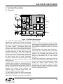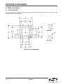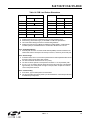
1
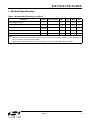
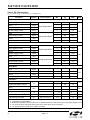
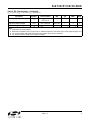
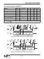
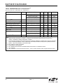
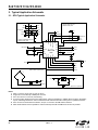
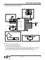
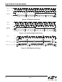
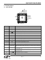
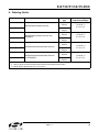
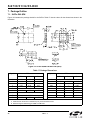
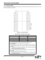
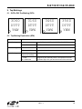
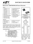
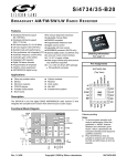
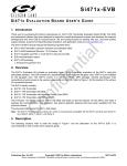
Si4730/31/34/35-D60 B ROADCAST AM/FM/SW/LW R ADIO R ECEIVER Features Ordering Information: See page 33. Pin Assignments Si473x-D60 (QFN) DFS/[RIN] GPO3/[DCLK] Multiplexed stereo audio AUXIN ADC with 85 dB dynamic range Seven selectable AM channel filters AM/FM/SW/LW digital tuning EN55020 compliant No manual alignment necessary Programmable reference clock Adjustable soft mute control RDS/RBDS processor (Si4731/35) Digital audio out 2-wire and 3-wire control interface Integrated LDO regulator Wide range of ferrite loop sticks and air loop antennas supported QFN and SSOP packages RoHS compliant GPO2/[INT] GPO1 Worldwide FM band support (64–108 MHz) Worldwide AM band support (520–1710 kHz) SW band support (Si4734/35) (2.3–26.1 MHz) LW band support (Si4734/35) (153–279 kHz) Excellent real-world performance Integrated VCO Advanced AM/FM seek tuning Automatic frequency control (AFC) Automatic gain control (AGC) Digital FM stereo decoder Programmable de-emphasis Advanced Audio Processing NC 20 19 18 17 16 Applications NC 1 FMI 2 RD S (S i4731/ 35) FM I LN A AMI AD C VA GND LD O Rev. 1.1 11/11 RO UT DA C LO UT CO NTR O L INTER FAC E AFC VD 1.62 - 3.6 V RST M ux RCLK + AGC DA C D SP SEN 2.7~5.5 V (Q FN ) 2.0~5.5 V (SSO P) AD C M ux LN A SDIO R FG N D DFS 8 9 10 VD 11 VA Si473x-D60(SSOP) DOUT/[LIN] 1 24 LOUT/[DFS] DFS/[RIN] 2 23 ROUT/[DOUT] GPO3/[DCLK] 3 22 DBYP GPO2/[INT] 4 21 VA GPO1 5 20 VD NC 6 19 RCLK SDIO NC 7 18 FMI 8 17 SCLK RFGND 9 16 SEN NC 10 15 RST NC 11 14 GND AMI 12 13 GND G PO /D CLK LO W -IF AGC A M / LW A NT DO UT DIG ITA L AU D IO 12 GND 7 RCLK SEN Si473x-D60 R IN LIN SCLK FM / SW AN T 13 ROUT/[DOUT] RST 5 Description Functional Block Diagram 14 LOUT/[DFS] GND PAD AMI 4 6 The Si473x-D60 digital CMOS AM/FM radio receiver IC integrates the complete tuner function from antenna input to digital audio output and includes a stereo audio AUXIN ADC input for converting analog audio into standard I2S digital audio, enabling a cost efficient digital audio platform for consumer electronic applications with high TDMA noise immunity, superior radio performance, and high fidelity audio power amplification. When enabling the analog inputs in stereo AUXIN ADC-mode, the Si473x-D60 supports I2S digital audio output only (no analog output). 15 DOUT/[LIN] RFGND 3 SDIO Modules for consumer electronics Clock radios Mini HiFi and docking stations Entertainment systems SCLK Table and portable radios Mini/micro systems CD/DVD and Blu-ray players Stereo boom boxes Copyright © 2011 by Silicon Laboratories This product, its features, and/or its architecture is covered by one or more of the following patents, as well as other patents, pending and issued, both foreign and domestic: 7,127,217; 7,272,373; 7,272,375; 7,321,324; 7,355,476; 7,426,376; 7,471,940; 7,339,503; 7,339,504. Si473x-D60 Si4730/31/34/35-D60 2 Rev. 1.1 Si4730/31/34/35-D60 TABLE O F C ONTENTS Section Page 1. Electrical Specifications . . . . . . . . . . . . . . . . . . . . . . . . . . . . . . . . . . . . . . . . . . . . . . . . . . .5 2. Typical Application Schematic . . . . . . . . . . . . . . . . . . . . . . . . . . . . . . . . . . . . . . . . . . . . . 20 2.1. QFN Typical Application Schematic . . . . . . . . . . . . . . . . . . . . . . . . . . . . . . . . . . . . . 20 2.2. SSOP Typical Application Schematic . . . . . . . . . . . . . . . . . . . . . . . . . . . . . . . . . . . . 21 3. Bill of Materials . . . . . . . . . . . . . . . . . . . . . . . . . . . . . . . . . . . . . . . . . . . . . . . . . . . . . . . . . . 22 3.1. QFN/SSOP Bill of Materials . . . . . . . . . . . . . . . . . . . . . . . . . . . . . . . . . . . . . . . . . . . 22 4. Functional Description . . . . . . . . . . . . . . . . . . . . . . . . . . . . . . . . . . . . . . . . . . . . . . . . . . . 23 4.1. Overview . . . . . . . . . . . . . . . . . . . . . . . . . . . . . . . . . . . . . . . . . . . . . . . . . . . . . . . . . . 23 4.2. Operating Modes . . . . . . . . . . . . . . . . . . . . . . . . . . . . . . . . . . . . . . . . . . . . . . . . . . . . 24 4.3. FM Receiver . . . . . . . . . . . . . . . . . . . . . . . . . . . . . . . . . . . . . . . . . . . . . . . . . . . . . . .24 4.4. AM Receiver . . . . . . . . . . . . . . . . . . . . . . . . . . . . . . . . . . . . . . . . . . . . . . . . . . . . . . .24 4.5. SW Receiver . . . . . . . . . . . . . . . . . . . . . . . . . . . . . . . . . . . . . . . . . . . . . . . . . . . . . . . 24 4.6. LW Receiver . . . . . . . . . . . . . . . . . . . . . . . . . . . . . . . . . . . . . . . . . . . . . . . . . . . . . . .24 4.7. Stereo Audio AUXIN ADC . . . . . . . . . . . . . . . . . . . . . . . . . . . . . . . . . . . . . . . . . . . . . 24 4.8. Digital Audio Interface . . . . . . . . . . . . . . . . . . . . . . . . . . . . . . . . . . . . . . . . . . . . . . . . 25 4.9. Stereo Audio Processing . . . . . . . . . . . . . . . . . . . . . . . . . . . . . . . . . . . . . . . . . . . . . . 27 4.10. Received Signal Qualifiers . . . . . . . . . . . . . . . . . . . . . . . . . . . . . . . . . . . . . . . . . . . 27 4.11. Volume Control . . . . . . . . . . . . . . . . . . . . . . . . . . . . . . . . . . . . . . . . . . . . . . . . . . . . 27 4.12. Stereo DAC . . . . . . . . . . . . . . . . . . . . . . . . . . . . . . . . . . . . . . . . . . . . . . . . . . . . . . . 27 4.13. Soft Mute . . . . . . . . . . . . . . . . . . . . . . . . . . . . . . . . . . . . . . . . . . . . . . . . . . . . . . . . . 27 4.14. FM Hi-Cut Control . . . . . . . . . . . . . . . . . . . . . . . . . . . . . . . . . . . . . . . . . . . . . . . . . . 27 4.15. De-emphasis . . . . . . . . . . . . . . . . . . . . . . . . . . . . . . . . . . . . . . . . . . . . . . . . . . . . . . 28 4.16. RDS/RBDS Processor (Si4731/35 Only) . . . . . . . . . . . . . . . . . . . . . . . . . . . . . . . . . . . . . . . . . . . . . . . . . . . . . . . . . . .28 4.17. Tuning . . . . . . . . . . . . . . . . . . . . . . . . . . . . . . . . . . . . . . . . . . . . . . . . . . . . . . . . . . . 28 4.18. Seek . . . . . . . . . . . . . . . . . . . . . . . . . . . . . . . . . . . . . . . . . . . . . . . . . . . . . . . . . . . . 28 4.19. Reference Clock . . . . . . . . . . . . . . . . . . . . . . . . . . . . . . . . . . . . . . . . . . . . . . . . . . . 28 4.20. Control Interface . . . . . . . . . . . . . . . . . . . . . . . . . . . . . . . . . . . . . . . . . . . . . . . . . . . 29 4.21. GPO Outputs . . . . . . . . . . . . . . . . . . . . . . . . . . . . . . . . . . . . . . . . . . . . . . . . . . . . . . 30 4.22. Firmware Upgrades . . . . . . . . . . . . . . . . . . . . . . . . . . . . . . . . . . . . . . . . . . . . . . . . .30 4.23. Reset, Powerup, and Powerdown . . . . . . . . . . . . . . . . . . . . . . . . . . . . . . . . . . . . . . 30 4.24. 2 V Operation (SSOP Only) . . . . . . . . . . . . . . . . . . . . . . . . . . . . . . . . . . . . . . . . . . 30 4.25. Programming with Commands . . . . . . . . . . . . . . . . . . . . . . . . . . . . . . . . . . . . . . . . 30 5. Pin Descriptions . . . . . . . . . . . . . . . . . . . . . . . . . . . . . . . . . . . . . . . . . . . . . . . . . . . . . . . . . 31 5.1. Si473x-D60-GM . . . . . . . . . . . . . . . . . . . . . . . . . . . . . . . . . . . . . . . . . . . . . . . . . . . .31 5.2. Si473x-D60-GU . . . . . . . . . . . . . . . . . . . . . . . . . . . . . . . . . . . . . . . . . . . . . . . . . . . . . 32 6. Ordering Guide . . . . . . . . . . . . . . . . . . . . . . . . . . . . . . . . . . . . . . . . . . . . . . . . . . . . . . . . . . 33 7. Package Outline . . . . . . . . . . . . . . . . . . . . . . . . . . . . . . . . . . . . . . . . . . . . . . . . . . . . . . . . . 34 7.1. Si473x-D60 QFN . . . . . . . . . . . . . . . . . . . . . . . . . . . . . . . . . . . . . . . . . . . . . . . . . . . . 34 7.2. Si473x-D60 SSOP . . . . . . . . . . . . . . . . . . . . . . . . . . . . . . . . . . . . . . . . . . . . . . . . . . 35 8. PCB Land Pattern . . . . . . . . . . . . . . . . . . . . . . . . . . . . . . . . . . . . . . . . . . . . . . . . . . . . . . . .36 Rev. 1.1 3 Si4730/31/34/35-D60 8.1. Si473x-D60 QFN . . . . . . . . . . . . . . . . . . . . . . . . . . . . . . . . . . . . . . . . . . . . . . . . . . . . 36 8.2. Si473x-D60 SSOP . . . . . . . . . . . . . . . . . . . . . . . . . . . . . . . . . . . . . . . . . . . . . . . . . . 38 9. Top Markings . . . . . . . . . . . . . . . . . . . . . . . . . . . . . . . . . . . . . . . . . . . . . . . . . . . . . . . . . . .39 9.1. Si473x-D60 Top Marking (QFN) . . . . . . . . . . . . . . . . . . . . . . . . . . . . . . . . . . . . . . . . 39 9.2. Top Marking Explanation (QFN) . . . . . . . . . . . . . . . . . . . . . . . . . . . . . . . . . . . . . . . . 39 9.3. Si473x-D60 Top Marking (SSOP) . . . . . . . . . . . . . . . . . . . . . . . . . . . . . . . . . . . . . . . 40 9.4. Top Marking Explanation (SSOP) . . . . . . . . . . . . . . . . . . . . . . . . . . . . . . . . . . . . . . . 40 10. Additional Reference Resources . . . . . . . . . . . . . . . . . . . . . . . . . . . . . . . . . . . . . . . . . . 41 Document Change List . . . . . . . . . . . . . . . . . . . . . . . . . . . . . . . . . . . . . . . . . . . . . . . . . . . . .42 Contact Information . . . . . . . . . . . . . . . . . . . . . . . . . . . . . . . . . . . . . . . . . . . . . . . . . . . . . . . .44 4 Rev. 1.1 Si4730/31/34/35-D60 1. Electrical Specifications Table 1. Recommended Operating Conditions1 Parameter Symbol Test Condition Min Typ Max Unit Analog Supply Voltage VA 2.72 — 5.5 V Digital and I/O Supply Voltage VD 1.62 — 3.6 V Power Supply Powerup Rise Time VDDRISE 10 — — µs Interface Power Supply Powerup Rise Time VIORISE 10 — — µs TA –20 25 85 C Ambient Temperature Notes: 1. All minimum and maximum specifications apply across the recommended operating conditions. Typical values apply at VA = 3.3 V and 25 C unless otherwise stated. 2. SSOP devices operate down to 2 V at 25 °C. See section “4.24. 2 V Operation (SSOP Only)” for details. Rev. 1.1 5 Si4730/31/34/35-D60 Table 2. DC Characteristics (VA = 2.7 to 5.5 V, VD = 1.62 to 3.6 V, TA = –20 to 85 °C) Parameter Symbol Test Condition Min Typ Max — 8.2 9.5 — 10.5 13.5 — 18.5 21.5 Unit FM Mode VAQFN Supply Current IFMVA VDQFN Supply Current IFMVD VASSOP Supply Current IFMVA VDSSOP Supply Current IFMVD — 0.15 0.6 VAQFN Supply Current IFMVA — 9.1 10.3 VDQFN Supply Current IFMVD — 9.9 12.8 VASSOP Supply Current IFMVA — 19.1 21.3 VDSSOP Supply Current IFMVD 0.1 0.6 — 6.5 7.5 — 8.5 11.0 — 14.5 16.5 Digital Output Mode1 Analog Output Mode2 mA AM Mode VAQFN Supply Current IAMVA VDQFN Supply Current IAMVD VASSOP Supply Current IAMVA VDSSOP Supply Current IAMVD — 0.15 0.50 VAQFN Supply Current IAMVA — 7.5 8.5 VDQFN Supply Current IAMVD — 8 10.2 VASSOP Supply Current IAMVA — 15.3 17.2 VDSSOP Supply Current IAMVD — 0.1 0.4 VAQFN Supply Current IAUXVA — 5.7 6.3 VDQFN Supply Current IAUXVD — 6.5 8.0 VASSOP Supply Current IAUXVA — 0.3 0.4 VDSSOP Supply Current IAUXVD — 11.8 13.0 — 4 15 — 9.5 15 SCLK, RCLK inactive — 3 10 SCLK, RCLK inactive — 3 10 Digital Output Mode Analog Output Mode mA AUXIN Mode mA Powerdown VAQFN Powerdown Current VASSOP Powerdown Current VDQFN Powerdown Current VDSSOP Powerdown Current IAPD IDPD µA µA High Level Input Voltage3 VIH 0.7 x VD — VD + 0.3 V Voltage3 VIL –0.3 — 0.3 x VD V 3 IIH –10 — 10 µA Low Level Input High Level Input Current VIN = VD = 3.6 V Notes: 1. Guaranteed by characterization. 2. Backwards compatible mode to rev B and rev C. Additional features on this device may increase typical supply current. 3. For input pins SCLK, SEN, SDIO, RST, RCLK, DCLK, DFS, GPO1, GPO2, and GPO3. 4. For output pins SDIO, DOUT, GPO1, GPO2, and GPO3. 6 Rev. 1.1 Si4730/31/34/35-D60 Table 2. DC Characteristics (Continued) (VA = 2.7 to 5.5 V, VD = 1.62 to 3.6 V, TA = –20 to 85 °C) Parameter Symbol Test Condition Min Typ Max Unit IIL VIN = 0 V, VD = 3.6 V –10 — 10 µA High Level Output Voltage4 VOH IOUT = 500 µA 0.8 x VD — — V Low Level Output Voltage4 VOL IOUT = –500 µA — — 0.2 x VD V 3 Low Level Input Current Notes: 1. Guaranteed by characterization. 2. Backwards compatible mode to rev B and rev C. Additional features on this device may increase typical supply current. 3. For input pins SCLK, SEN, SDIO, RST, RCLK, DCLK, DFS, GPO1, GPO2, and GPO3. 4. For output pins SDIO, DOUT, GPO1, GPO2, and GPO3. Rev. 1.1 7 Si4730/31/34/35-D60 Table 3. Reset Timing Characteristics1,2,3 (VA = 2.7 to 5.5 V, VD = 1.62 to 3.6 V, TA = –20 to 85 °C) Parameter Symbol Min Typ Max Unit RST Pulse Width and GPO1, GPO2/INT Setup to RST tSRST 100 — — µs GPO1, GPO2/INT Hold from RST tHRST 30 — — ns Important Notes: 1. When selecting 2-wire mode, the user must ensure that a 2-wire start condition (falling edge of SDIO while SCLK is high) does not occur within 300 ns before the rising edge of RST. 2. When selecting 2-wire mode, the user must ensure that SCLK is high during the rising edge of RST, and stays high until after the first start condition. 3. When selecting 3-wire mode, the user must ensure that a rising edge of SCLK does not occur within 300 ns before the rising edge of RST. 4. If GPO1 and GPO2 are actively driven by the user, then minimum tSRST is only 30 ns. If GPO1 or GPO2 is hi-Z, then minimum tSRST is 100 µs, to provide time for on-chip 1 M devices (active while RST is low) to pull GPO1 high and GPO2 low. tSRST RST tHRST 70% 30% GPO1 70% GPO2/ INT 70% 30% 30% Figure 1. Reset Timing Parameters for Busmode Select 8 Rev. 1.1 Si4730/31/34/35-D60 Table 4. 2-Wire Control Interface Characteristics1,2,3 (VA = 2.7 to 5.5 V, VD = 1.62 to 3.6 V, TA = –20 to 85 °C) Parameter Symbol Test Condition Min Typ Max Unit SCLK Frequency fSCL 0 — 400 kHz SCLK Low Time tLOW 1.3 — — µs SCLK High Time tHIGH 0.6 — — µs SCLK Input to SDIO Setup (START) tSU:STA 0.6 — — µs SCLK Input to SDIO Hold (START) tHD:STA 0.6 — — µs SDIO Input to SCLK Setup tSU:DAT 100 — — ns SDIO Input to SCLK Hold4,5 tHD:DAT 0 — 900 ns SCLK input to SDIO Setup (STOP) tSU:STO 0.6 — — µs STOP to START Time tBUF 1.3 — — µs SDIO Output Fall Time tf:OUT — 250 ns — 300 ns Cb 20 + 0.1 ----------1pF SDIO Input, SCLK Rise/Fall Time tf:IN tr:IN Cb 20 + 0.1 ----------1pF SCLK, SDIO Capacitive Loading Cb — — 50 pF Input Filter Pulse Suppression tSP — — 50 ns Notes: 1. When VD = 0 V, SCLK and SDIO are low impedance. 2. When selecting 2-wire mode, the user must ensure that a 2-wire start condition (falling edge of SDIO while SCLK is high) does not occur within 300 ns before the rising edge of RST. 3. When selecting 2-wire mode, the user must ensure that SCLK is high during the rising edge of RST, and stays high until after the first start condition. 4. The Si473x-D60 delays SDIO by a minimum of 300 ns from the VIH threshold of SCLK to comply with the minimum tHD:DAT specification. 5. The maximum tHD:DAT has only to be met when fSCL = 400 kHz. At frequencies below 400 KHz, tHD:DAT may be violated as long as all other timing parameters are met. Rev. 1.1 9 Si4730/31/34/35-D60 SCLK SDIO tSU:STA tHD:STA tLOW START tr:IN tHIGH tr:IN tf:IN tSP tSU:STO tBUF 70% 30% 70% 30% tf:IN, tf:OUT tHD:DAT tSU:DAT STOP START Figure 2. 2-Wire Control Interface Read and Write Timing Parameters SCLK A6-A0, R/W SDIO START ADDRESS + R/W D7-D0 ACK DATA D7-D0 ACK DATA ACK Figure 3. 2-Wire Control Interface Read and Write Timing Diagram 10 Rev. 1.1 STOP Si4730/31/34/35-D60 Table 5. 3-Wire Control Interface Characteristics (VA = 2.7 to 5.5 V, VD = 1.62 to 3.6 V, TA = –20 to 85 °C) Parameter Symbol Test Condition Min Typ Max Unit SCLK Frequency fCLK 0 — 2.5 MHz SCLK High Time tHIGH 25 — — ns SCLK Low Time tLOW 25 — — ns tS 20 — — ns SDIO Input to SCLKHold tHSDIO 10 — — ns SEN Input to SCLKHold tHSEN 10 — — ns SCLKto SDIO Output Valid tCDV Read 2 — 25 ns SCLKto SDIO Output High Z tCDZ Read 2 — 25 ns SCLK, SEN, SDIO, Rise/Fall time tR, tF — — 10 ns SDIO Input, SEN to SCLKSetup Note: When selecting 3-wire mode, the user must ensure that a rising edge of SCLK does not occur within 300 ns before the rising edge of RST. SCLK 70% 30% tS SEN SDIO tR tF 70% tHSDIO tHIGH tLOW tHSEN tS 30% 70% 30% A7 A6-A5, R/W, A4-A1 A0 D15 D14-D1 Address In D0 Data In Figure 4. 3-Wire Control Interface Write Timing Parameters SCLK 70% 30% tHSDIO tS SEN 70% tCDV tHSEN tCDZ tS 30% 70% SDIO A7 30% A6-A5, R/W, A4-A1 Address In A0 D15 ½ Cycle Bus Turnaround D14-D1 D0 Data Out Figure 5. 3-Wire Control Interface Read Timing Parameters Rev. 1.1 11 Si4730/31/34/35-D60 Table 6. Digital Audio Interface Characteristics (VA = 2.7 to 5.5 V, VD = 1.62 to 3.6 V, TA = –20 to 85 °C) Parameter Symbol Test Condition Min Typ Max Unit DCLK Cycle Time tDCT 26 — 1000 ns DCLK Pulse Width High tDCH 10 — — ns DCLK Pulse Width Low tDCL 10 — — ns DFS Set-up Time to DCLK Rising Edge tSU:DFS 5 — — ns DFS Hold Time from DCLK Rising Edge tHD:DFS 5 — — ns tPD:DOUT 0 — 50 ns DOUT Propagation Delay from DCLK Falling Edge tDCH tDCL DCLK tDCT DFS tHD:DFS tSU:DFS DOUT tPD:OUT Figure 6. Digital Audio Interface Timing Parameters, I2S Mode 12 Rev. 1.1 Si4730/31/34/35-D60 Table 7. FM Receiver Characteristics1,2 (VA = 2.7 to 5.5 V, VD = 1.62 to 3.6 V, TA = –20 to 85 °C) Parameter Symbol Min Typ Max Unit 76 — 108 MHz (S+N)/N = 26 dB — 2.2 3.5 µV EMF f = 2 kHz, RDS BLER < 5% — 10 — µV EMF 3 4 5 k 4 5 6 pF 100 105 — dBµV EMF m = 0.3 40 50 — dB Adjacent Channel Selectivity ±200 kHz 35 50 — dB Alternate Channel Selectivity ±400 kHz 60 70 — dB In-band 35 — — dB 72 80 90 mVRMS — — 1 dB Input Frequency fRF Sensitivity3,4,5,6 RDS Test Condition Sensitivity6,7 LNA Input Resistance7,8 7,8 LNA Input Capacitance Input IP37,9 AM Suppression3,4,7,8 Spurious Response Rejection7 3,4,8 Audio Output Voltage 3,8,10 Audio Output L/R Imbalance Audio Frequency Response Low7 –3 dB — — 30 Hz Audio Frequency Response High7 –3 dB 15 — — kHz 35 42 — dB 55 63 — dB — 58 — dB — 0.1 0.5 % FM_DEEMPHASIS = 2 70 75 80 µs FM_DEEMPHASIS = 1 45 50 54 µs f = ±400 kHz — 34 — dBµV f = ±4 MHz — 30 — dBµV Audio Stereo Separation Audio Mono 8,10 S/N3,4,5,8 Audio Stereo S/N4,5,7,8 Audio THD3,8,10 7 De-emphasis Time Constant 3,4,5,6,7,11, 12 Blocking Sensitivity Notes: 1. Additional testing information is available in “AN388: Si470x/1x/2x/3x/4x Evaluation Board Test Procedure.” Volume = maximum for all tests. Tested at RF = 98.1 MHz. 2. To ensure proper operation and receiver performance, follow the guidelines in “AN383: Si47xx Antenna, Schematic, Layout, and Design Guidelines.” Silicon Laboratories will evaluate schematics and layouts for qualified customers. 3. FMOD = 1 kHz, 75 µs de-emphasis, MONO = enabled, and L = R unless noted otherwise. 4. f = 22.5 kHz. 5. BAF = 300 Hz to 15 kHz, A-weighted. 6. Analog audio output mode. 7. Guaranteed by characterization. 8. VEMF = 1 mV. 9. |f2 – f1| > 2 MHz, f0 = 2 x f1 – f2. AGC is disabled. 10. f = 75 kHz. 11. Sensitivity measured at (S+N)/N = 26 dB. 12. Blocker Amplitude = 100 dBuV. 13. At temperature (25 °C). 14. At LOUT and ROUT pins. Rev. 1.1 13 Si4730/31/34/35-D60 Table 7. FM Receiver Characteristics1,2 (Continued) (VA = 2.7 to 5.5 V, VD = 1.62 to 3.6 V, TA = –20 to 85 °C) Parameter Symbol Test Condition Min Typ Max Unit f = ±400 kHz, ±800 kHz — 40 — dBµV f = ±4 MHz, ±8 MHz — 35 — dBµV RL Single-ended 10 — — k CL Single-ended — — 50 pF RCLK tolerance = 100 ppm — — 60 ms/channel Powerup Time7 From powerdown — — 110 ms RSSI Offset12,13 Input levels of 8 and 60 dBµV at RF Input –3 — 3 dB Intermod Sensitivity3,4,5,6,7,11,12 Audio Output Load Audio Output Load Capacitance7,11,14 Seek/Tune Time7 Resistance7,11,14 Notes: 1. Additional testing information is available in “AN388: Si470x/1x/2x/3x/4x Evaluation Board Test Procedure.” Volume = maximum for all tests. Tested at RF = 98.1 MHz. 2. To ensure proper operation and receiver performance, follow the guidelines in “AN383: Si47xx Antenna, Schematic, Layout, and Design Guidelines.” Silicon Laboratories will evaluate schematics and layouts for qualified customers. 3. FMOD = 1 kHz, 75 µs de-emphasis, MONO = enabled, and L = R unless noted otherwise. 4. f = 22.5 kHz. 5. BAF = 300 Hz to 15 kHz, A-weighted. 6. Analog audio output mode. 7. Guaranteed by characterization. 8. VEMF = 1 mV. 9. |f2 – f1| > 2 MHz, f0 = 2 x f1 – f2. AGC is disabled. 10. f = 75 kHz. 11. Sensitivity measured at (S+N)/N = 26 dB. 12. Blocker Amplitude = 100 dBuV. 13. At temperature (25 °C). 14. At LOUT and ROUT pins. 14 Rev. 1.1 Si4730/31/34/35-D60 Table 8. 64–75.9 MHz Input Frequency FM Receiver Characteristics1,2,3 (VA = 2.7 to 5.5 V, VD = 1.62 to 3.6 V, TA = –20 to 85 °C) Parameter Symbol Min Typ Max Unit 64 — 75.9 MHz — 3.5 — µV EMF 3 4 5 k 4 5 6 pF — 105 — dBµV EMF m = 0.3 — 50 — dB Adjacent Channel Selectivity ±200 kHz — 50 — dB Alternate Channel Selectivity ±400 kHz — 70 — dB 72 80 90 mVRMS — — 1 dB Input Frequency fRF Sensitivity4,5,6,8 LNA Input Test Condition (S+N)/N = 26 dB Resistance3,7 3,7 LNA Input Capacitance Input IP3 9 AM Suppression3,4,5,7 Audio Output Voltage4,5,7 Audio Output L/R Imbalance4,7,10 3 –3 dB — — 30 Hz 3 –3 dB 15 — — kHz Audio Mono S/N4,3,5,7,11 — 63 — dB Audio THD4,7,10 — 0.1 — % FM_DEEMPHASIS = 2 70 75 80 µs FM_DEEMPHASIS = 1 45 50 54 µs Audio Frequency Response Low Audio Frequency Response High De-emphasis Time Constant Audio Output Load Resistance3,11 RL Single-ended 10 — — k Audio Output Load Capacitance3,11 CL Single-ended — — 50 pF RCLK tolerance = 100 ppm — — 60 ms/channel From powerdown — — 110 ms Input levels of 8 and 60 dBµV EMF –3 — 3 dB Seek/Tune Time Powerup Time3 12 RSSI Offset 3 Notes: 1. Additional testing information is available in “AN388: Si470x/1x/2x/3x/4x Evaluation Board Test Procedure.” Volume = maximum for all tests. Tested at RF = 98.1 MHz. 2. To ensure proper operation and receiver performance, follow the guidelines in “AN383: Si47xx Antenna, Schematic, Layout, and Design Guidelines.” Silicon Laboratories will evaluate schematics and layouts for qualified customers. 3. Guaranteed by characterization. 4. FMOD = 1 kHz, 75 µs de-emphasis, MONO = enabled, and L = R unless noted otherwise. 5. f = 22.5 kHz. 6. BAF = 300 Hz to 15 kHz, A-weighted. 7. VEMF = 1 mV. 8. Analog output mode. 9. |f2 – f1| > 2 MHz, f0 = 2 x f1 – f2. AGC is disabled. 10. f = 75 kHz. 11. At LOUT and ROUT pins. 12. At temperature (25 °C). Rev. 1.1 15 Si4730/31/34/35-D60 Table 9. AM/SW/LW Receiver Characteristics1,2 (VA = 2.7 to 5.5 V, VA = 1.62 to 3.6 V, TA = –20 to 85 °C) Parameter Symbol Test Condition Min Typ Max Unit fRF Long Wave (LW) 153 — 279 kHz Medium Wave (AM) 520 — 1710 kHz Short Wave (SW) 2.3 — 26.1 MHz (S+N)/N = 26 dB — 25 35 µV EMF THD < 8% — 300 — mVRMS ∆VDD = 100 mVRMS, 100 Hz — 40 — dB Audio Output Voltage3,7 54 60 67 mVRMS 3,4,7 — 60 — dB — 0.1 0.5 % Long Wave (LW) — 2800 — µH Medium Wave (AM) 180 — 450 µH From powerdown — — 110 ms Input Frequency Sensitivity 3,4,5 Large Signal Voltage Handling5,6 5 Power Supply Rejection Ratio Audio S/N Audio THD3,7 5,8 Antenna Inductance 5 Powerup Time Notes: 1. Additional testing information is available in “AN388: Si470x/1x/2x/3x/4x Evaluation Board Test Procedure.” Volume = maximum for all tests. Tested at RF = 520 kHz. 2. To ensure proper operation and receiver performance, follow the guidelines in “AN383: Si47xx Antenna, Schematic, Layout, and Design Guidelines.” Silicon Laboratories will evaluate schematics and layouts for qualified customers. 3. FMOD = 1 kHz, 30% modulation, 2 kHz channel filter. 4. BAF = 300 Hz to 15 kHz, A-weighted. 5. Guaranteed by characterization. 6. See “AN388: Si470x/1x/2x/3x/4x Evaluation Board Test Procedure” for evaluation method. 7. VIN = 5 mVrms. 8. Stray capacitance on antenna and board must be < 10 pF to achieve full tuning range at higher inductance levels. 16 Rev. 1.1 Si4730/31/34/35-D60 Table 10. AC Receiver Characteristics—AUXIN Analog to Digital Converter (VA = 2.7 to 5.5 V, VD = 1.62 to 3.6 V, TA = –20 to 85 °C) Parameter Symbol Test Condition Min Typ Max Unit THD+N f = 1 kHz; measured 20 Hz—20 kHz — 0.035 0.06 % SNR f = 1 kHz at –60 dBFS A-weighted — 85 — dB f = 1 kHz at –60 dBFS non-weighted — 78 — dB f = 1 kHz with 3% Bandpass filter — 90 — dB Gain Mismatch — 0.03 — dB Gain Drift — 100 — PPM/°C Total Harmonic Distortion + Noise Dynamic Range/Signal to Noise Ratio Crosstalk Input Sample Rate FS — 48 — kHz Input Voltage VAI — — 1.8 Vpkpk Input Resistance RAI — 60 — k Input Capacitance CAI — 10 — pF LIATTEN[1:0] Table 11. Digital Filter Characteristics—AUXIN Analog to Digital Converter (VA = 2.7 to 5.5 V, VD = 1.62 to 3.6 V, TA = –20 to 85 °C) Parameter Test Condition Min Typ Max Unit –0.1 dB 0.02 — 20 kHz 20—20 kHz –0.1 — 0.1 dB Stopband Corner Frequency 25 — — kHz Stopband Attenuation 70 — — dB Passband Frequency Response Passband Ripple Symbol Rev. 1.1 17 Si4730/31/34/35-D60 Table 12. Reference Clock and Crystal Characteristics (VA = 2.7 to 5.5 V, VD = 1.62 to 3.6 V, TA = –20 to 85 °C) Parameter Symbol Test Condition Min Typ Max Unit 31.130 32.768 40,000 kHz –100 — 100 ppm 1 — 4095 31.130 32.768 34.406 kHz — 32.768 — kHz –100 — 100 ppm Board Capacitance — — 3.5 pF ESR — — 50 CL3 7 12 22 pF CL–single ended3 14 24 44 pF Reference Clock RCLK Supported Frequencies1 RCLK Frequency Tolerance 2 REFCLK_PRESCALE REFCLK Crystal Oscillator Crystal Oscillator Frequency Crystal Frequency Tolerance2 Notes: 1. The Si473x-D60 divides the RCLK input by REFCLK_PRESCALE to obtain REFCLK. There are some RCLK frequencies between 31.130 kHz and 40 MHz that are not supported. For more details, see Table 6 of “AN332: Si47xx Programming Guide”. 2. A frequency tolerance of ±50 ppm is required for FM seek/tune using 50 kHz channel spacing and AM seek/tune in SW frequencies. 3. Guaranteed by characterization. Table 13. Thermal Conditions Parameter Symbol Min Typ Max Unit Thermal Resistance* JA — 80 — °C/W Ambient Temperature TA –15 25 85 °C Junction Temperature TJ — — 92 °C *Note: Thermal resistance assumes a multi-layer PCB with the exposed pad soldered to a topside PCB pad. 18 Rev. 1.1 Si4730/31/34/35-D60 Table 14. Absolute Maximum Ratings1,2 Parameter Symbol Value Unit Analog Supply Voltage VA –0.5 to 5.8 V Digital and I/O Supply Voltage VD –0.5 to 3.9 V Input Current3 IIN 10 mA 3 VIN –0.3 to (VIO + 0.3) V Operating Temperature TOP –40 to 95 C Storage Temperature TSTG –55 to 150 C 0.4 Vpk Input Voltage RF Input Level4 Notes: 1. Permanent device damage may occur if the above Absolute Maximum Ratings are exceeded. Functional operation should be restricted to the conditions as specified in the operational sections of this data sheet. Exposure beyond recommended operating conditions for extended periods may affect device reliability. 2. The Si473x-D60 devices are high-performance RF integrated circuits with certain pins having an ESD rating of < 2 kV HBM. Handling and assembly of these devices should only be done at ESD-protected workstations. 3. For input pins DFS, SCLK, SEN, SDIO, RST, RCLK, GPO1, GPO2, GPO3, and DCLK. 4. At RF input pins FMI and AMI. Rev. 1.1 19 Si4730/31/34/35-D60 2. Typical Application Schematic 2.1. QFN Typical Application Schematic DFS DOUT GP03/DCLK LOUT ROUT 16 C7 15 C8 Optional: Digital Audio Out RIN OPMODE: 0xB0, 0xB5 LIN 17 R3 14 R2 13 R1 DCLK C9 GPO1 DFS GPO2/INT DOUT R3 Si473x GPO3/DCLK R2 16 17 DOUT DFS 19 18 GPO3/DCLK LOUT ROUT Si473x GND RSTB VA 15 14 LOUT 13 ROUT 12 2.7 to 5.5 V 11 VA VD C1 10 6 DFS R1 DOUT D60 SENB 5 AMI RCLK C3 RFGND 9 4 L1 FMI SDIO 3 NC 8 FM Antenna 2 SCLK 1 C2 GPO2/INT NC OPMODE: 0x5B, 0x0B GPO1 20 C9 7 Optional: AUXIN/Digital Audio Out 1.62 to 3.6 V C4 RSTB VD RCLK SDIO SCLK SENB Optional: AM Air Loop Antenna 1 GPO3 T1 1 C3 RCLK X1 AMI C5 3 2 L2 C6 RFGND Optional: For Crystal OSC Notes: 1. Place C1 close to VA pin and C4 close to VD pin. 2. All grounds connect directly to GND plane on PCB. 3. Pins 1 and 20 are no connects, leave floating. 4. To ensure proper operation and receiver performance, follow the guidelines in “AN383: Si47xx Antenna, Schematic, Layout, and Design Guidelines.” Silicon Laboratories will evaluate schematics and layouts for qualified customers. 5. Pin 2 connects to the FM antenna interface, and pin 4 connects to the AM antenna interface. 6. Place Si473x-D60 as close as possible to antenna and keep the FMI and AMI traces as short as possible. 20 Rev. 1.1 Si4730/31/34/35-D60 2.2. SSOP Typical Application Schematic DFS DOUT GP03/DCLK LOUT ROUT Optional: Digital Audio Out OPMODE: 0xB0, 0xB5 2 C7 1 C8 RIN LIN 3 R3 24 R2 23 R1 DCLK DFS DOUT Si473x Optional: AUXIN/Digital Audio Out C9 C9 OPMODE: 0x5B, 0x0B GPO3/DCLK R2 2 R3 3 4 GPO2/INT 5 GPO1 C2 FM Antenna DOUT LOUT DFS ROUT GPO3/DCLK DBYP GPO2/INT GPO1 6 NC 7 NC 8 9 C3 VA VD RCLK FMI RFGND 10 NC L1 D60 DFS 1 Si473x DOUT R1 SDIO SCLK SENB RSTB 24 ROUT 22 C1 21 2.0 to 5.5 V 20 SCLK 16 SENB 15 GND 13 C4 SDIO 17 12 1.62 to 3.6 V RCLK 18 GND 14 VA VD 19 11 NC AMI LOUT 23 RSTB Optional: AM Air Loop Antenna 1 GPO3 T1 1 C3 RCLK X1 AMI C5 3 2 L2 C6 RFGND Optional: For Crystal OSC Notes: 1. Place C1 close to VA and C4 close to VD pin. 2. All grounds connect directly to GND plane on PCB. 3. Pins 6 and 7 are no connects, leave floating. 4. Pins 10 and 11 are unused. Tie these pins to GND. 5. To ensure proper operation and receiver performance, follow the guidelines in “AN383: Si47xx Antenna, Schematic, Layout, and Design Guidelines.” Silicon Laboratories will evaluate schematics and layouts for qualified customers. 6. Pin 8 connects to the FM antenna interface, and pin 12 connects to the AM antenna interface. 7. Place Si473x-D60 as close as possible to antenna and keep the FMI and AMI traces as short as possible. Rev. 1.1 21 Si4730/31/34/35-D60 3. Bill of Materials 3.1. QFN/SSOP Bill of Materials Table 15. Si473x-D60 QFN/SSOP Bill of Materials Component(s) Value/Description Supplier C1 Supply bypass capacitor, 22 nF, ±20%, Z5U/X7R Murata C2 Coupling capacitor, 1 nF, ±20%, Z5U/X7R Murata C3 Coupling capacitor, 0.47 μF, ±20%, Z5U/X7R Murata C4 Supply bypass capacitor, 100 nF, 10%, Z5U/X7R Murata L1 Ferrite loop stick, 180–450 μH Jiaxin U1 Si47xx AM/FM Radio Tuner Silicon Laboratories Optional Components C5, C6 22 Crystal load capacitors, 22 pF, ±5%, COG (Optional for crystal oscillator) Venkel C7 Coupling capacitor, 0.39 μF, ±20%, Z5U/X7R (Optional for AUXIN) Murata C8 Coupling capacitor, 0.39 μF, ±20%, Z5U/X7R (Optional for AUXIN) Murata C9 Noise mitigating capacitor, 2~5 pF (Optional for digital audio) Murata R1 Resistor, 600 Ω (Optional for digital audio) Venkel R2 Resistor, 2 kΩ (Optional for digital audio) Venkel R3 Resistor, 2 kΩ (Optional for digital audio) Venkel L2 Air Loop, 10-20 µH (Optional for AM Input) Jiaxin T1 Transformer, 1:5 turns ratio (Optional for AM Input) X1 32.768 kHz crystal (Optional for crystal oscillator) Jiaxin, UMEC Epson Rev. 1.1 Si4730/31/34/35-D60 4. Functional Description 4.1. Overview Si473x-D60 RIN LIN RDS (Si4731/ 35) FMI LNA AMI AGC 2.7~5.5 V ROUT DAC LOUT CONTROL INTERFACE AFC SEN RCLK LDO DAC DSP ADC Mux VA GND GPO/DCLK ADC Mux LNA DFS VD 1.62~3.6 V RST RFGND DIGITAL AUDIO SDIO AM / LW ANT DOUT LOW-IF AGC SCLK FM / SW ANT Figure 7. Functional Block Diagram The Si473x-D60 CMOS AM/FM radio receiver IC integrates the complete tuner function from antenna input to audio output, including a stereo audio AUXIN ADC input for converting analog audio to digital signals. This feature enables a cost-efficient digital audio platform for consumer electronics applications with high cell phone noise immunity, superior radio performance, and high fidelity audio power amplification. Offering unmatched integration and PCB space savings, the Si473x-D60 requires only a few external components and less than 15 mm2 of board area, excluding the antenna inputs. The Si473x-D60 AM/FM radio provides the space savings and low power consumption necessary for portable devices while delivering the high performance and design simplicity desired for all AM/FM solutions. Leveraging Silicon Laboratories' proven and patented Si4700/01 FM tuner's digital low intermediate frequency (low-IF) receiver architecture, the Si473x-D60 delivers superior RF performance and interference rejection in the AM, FM, SW, and LW bands. The high level of integration and complete system production test simplifies design-in, increases system quality, and improves reliability and manufacturability. audio processing. In addition, the Si473x-D60 provides analog and digital audio outputs and a programmable reference clock. The device supports I2C-compatible 2-wire control interface, and a Si4700/01 backwards-compatible 3-wire control interface. The Si473x-D60 utilizes digital signal processing to achieve high fidelity, optimal performance, and design flexibility. The chip provides excellent pilot rejection, selectivity, and unmatched audio performance, and offers both the manufacturer and the end-user extensive programmability and a better listening experience. The Si4731/35 incorporates a digital signal processor for the European Radio Data System (RDS) and the North American Radio Broadcast Data System (RBDS) including all required symbol decoding, block synchronization, error detection, and error correction functions. Using this feature, the Si4731/35 enables broadcast data such as station identification and song name to be displayed to the user. The Si473x-D60 is a feature-rich solution that includes advanced seek algorithms, soft mute, auto-calibrated digital tuning, FM stereo processing and advanced Rev. 1.1 23 Si4730/31/34/35-D60 4.2. Operating Modes The Si473x-D60 operates in either an FM receive, AM receive, or audio AUXIN ADC mode. In FM mode, radio signals are received on FMI and processed by the FM front-end circuitry. In AM mode, radio signals are received on AMI and processed by the AM front-end circuitry. In audio AUXIN ADC mode, stereo audio signals on LIN/RIN are sampled, converted to digital, filtered, and decimated to 32, 44.1, or 48 kHz for the I2S digital audio interface. In addition to the receiver mode, there is a clocking mode to choose to clock the Si473xD60 from a reference clock or crystal. On the Si473xD60, there is an audio output mode to choose between an analog and/or digital audio output. In the analog audio output mode, ROUT and LOUT are used for the audio output pins. In the digital audio mode, DOUT, DFS, and DCLK pins are used. Concurrent analog/digital audio output mode is also available requiring all five pins. 4.3. FM Receiver The Si473x-D60 FM receiver is based on the proven Si4700/01 FM tuner. The receiver uses a digital low-IF architecture allowing the elimination of external components and factory adjustments. The Si473x-D60 integrates a low noise amplifier (LNA) supporting the worldwide FM broadcast band (64 to 108 MHz). An AGC circuit controls the gain of the LNA to optimize sensitivity and rejection of strong interferers. An imagereject mixer downconverts the RF signal to low-IF. The quadrature mixer output is amplified, filtered, and digitized with high resolution analog-to-digital converters (ADCs). This advanced architecture allows the Si473x-D60 to perform channel selection, FM demodulation, and stereo audio processing to achieve superior performance compared to traditional analog architectures. 4.4. AM Receiver The highly-integrated Si473x-D60 supports worldwide AM band reception from 520 to 1710 kHz using a digital low-IF architecture with a minimum number of external components and no manual alignment required. This digital low-IF architecture allows for high-precision filtering offering excellent selectivity and SNR with minimum variation across the AM band. The DSP also provides adjustable channel step sizes in 1 kHz increments, AM demodulation, soft mute, seven different channel bandwidth filters, and additional features, such as a programmable automatic volume control (AVC) maximum gain allowing users to adjust the level of background noise. Similar to the FM receiver, the integrated LNA and AGC 24 optimize sensitivity and rejection of strong interferers allowing better reception of weak stations. The Si473x-D60 provides highly-accurate digital AM tuning without factory adjustments. To offer maximum flexibility, the receiver supports a wide range of ferrite loop sticks from 180–450 µH. An air loop antenna is supported by using a transformer to increase the effective inductance from the air loop. Using a 1:5 turn ratio inductor, the inductance is increased by 25 times and easily supports all typical AM air loop antennas which generally vary between 10 and 20 µH. 4.5. SW Receiver The Si4734/35 is the first fully integrated IC to support AM and FM, as well as short wave (SW) band reception from 2.3 to 26.1 MHz fully covering the 120 meter to 11 meter bands. The Si4734/35 offers extensive shortwave features such as continuous digital tuning with minimal discrete components and no factory adjustments. Other SW features include adjustable channel step sizes in 1 kHz increments, adjustable channel bandwidth settings, advanced seek algorithm, and soft mute. The Si4734/35 uses the FM antenna to capture short wave signals. These signals are then fed directly into the AMI pin in a wide band configuration. See "AN332: Si47xx Programming Guide” and “AN383: Si47xx Antenna and Schematic Guidelines" for more details. 4.6. LW Receiver The Si4734/35 supports the long wave (LW) band from 153 to 279 kHz. The highly integrated Si4734/35 offers continuous digital tuning with minimal discrete components and no factory adjustments. The Si4734/35 also offers adjustable channel step sizes in 1 kHz increments, adjustable channel bandwidth settings, advanced seek algorithm, and soft mute. The Si4734/35 uses a separate ferrite bar antenna to capture long wave signals. 4.7. Stereo Audio AUXIN ADC The Si473x-D60 stereo audio AUXIN ADC can be multiplexed between low-IF input for radio operation and analog audio input for high fidelity data conversion at 32, 44.1, or 48 kHz sample rate. When operated in ADC-mode, the Si473x-D60 supports I2S digital audio output only (no analog output) while enabling the analog inputs and the stereo ADC. Rev. 1.1 Si4730/31/34/35-D60 4.8. Digital Audio Interface The digital audio interface operates in slave mode and supports a variety of MSB-first audio data formats including I2S and left-justified modes. The interface has three pins: digital data input (DIN), digital frame synchronization input (DFS), and a digital bit synchronization input clock (DCLK). The Si473x-D60 supports a number of industry-standard sampling rates including 32, 44.1, and 48 kHz. The digital audio interface enables low-power operation by eliminating the need for redundant DACs and ADCs on the audio baseband processor. 4.8.1. Audio Data Formats The digital audio interface operates in slave mode and supports three different audio data formats: I2S Left-Justified DSP Mode In I2S mode, by default the MSB is captured on the second rising edge of DCLK following each DFS transition. The remaining bits of the word are sent in order, down to the LSB. The left channel is transferred first when the DFS is low, and the right channel is transferred when the DFS is high. In left-justified mode, by default the MSB is captured on the first rising edge of DCLK following each DFS transition. The remaining bits of the word are sent in order, down to the LSB. The left channel is transferred first when the DFS is high, and the right channel is transferred when the DFS is low. In DSP mode, the DFS becomes a pulse with a width of 1DCLK period. The left channel is transferred first, followed right away by the right channel. There are two options in transferring the digital audio data in DSP mode: the MSB of the left channel can be transferred on the first rising edge of DCLK following the DFS pulse or on the second rising edge. In all audio formats, depending on the word size, DCLK frequency, and sample rates, there may be unused DCLK cycles after the LSB of each word before the next DFS transition and MSB of the next word. In addition, if preferred, the user can configure the MSB to be captured on the falling edge of DCLK via properties. The number of audio bits can be configured for 8, 16, 20, or 24 bits. 4.8.2. Audio Sample Rates The device supports a number of industry-standard sampling rates including 32, 44.1, and 48 kHz. The digital audio interface enables low-power operation by eliminating the need for redundant DACs on the audio baseband processor. Rev. 1.1 25 Si4730/31/34/35-D60 (OFALL = 1) INVERTED DCLK (OFALL = 0) DCLK LEFT CHANNEL DFS I2S (OMODE = 0000) RIGHT CHANNEL 1 DCLK 1 DCLK 1 DOUT 2 n-2 3 n-1 MSB n 1 LSB MSB 2 n-2 3 n-1 n LSB Figure 8. I2S Digital Audio Format (OFALL = 1) INVERTED DCLK (OFALL = 0) DCLK DFS LEFT CHANNEL RIGHT CHANNEL Left-Justified (OMODE = 0110) 1 DOUT 2 3 n-2 n-1 MSB n 1 LSB MSB 2 n-2 3 n-1 n LSB Figure 9. Left-Justified Digital Audio Format DCLK (OFALL = 0) DFS RIGHT CHANNEL LEFT CHANNEL (OMODE = 1100) DOUT (MSB at 1 rising edge) 1 st 2 3 n-2 n-1 MSB DOUT (MSB at 2 rising edge) nd 1 LSB MSB n-1 n 1 LSB MSB 2 3 1 2 3 n-2 MSB Rev. 1.1 n-1 n LSB RIGHT CHANNEL 2 Figure 10. DSP Digital Audio Format 26 n-2 LEFT CHANNEL 1 DCLK (OMODE = 1000) n 3 n-2 n-1 n LSB Si4730/31/34/35-D60 4.10. Received Signal Qualifiers The output of the FM demodulator is a stereo multiplexed (MPX) signal. The MPX standard was developed in 1961, and is used worldwide. Today's MPX signal format consists of left + right (L+R) audio, left – right (L–R) audio, a 19 kHz pilot tone, and RDS/RBDS data as shown in Figure 11 below. The quality of a tuned signal can vary depending on many factors including environmental conditions, time of day, and position of the antenna. To adequately manage the audio output and avoid unpleasant audible effects to the end-user, the Si473x-D60 monitors and provides indicators of the signal quality, allowing the host processor to perform additional processing if required by the customer. The Si473x-D60 monitors signal quality metrics including RSSI, SNR, and multipath interference on FM signals. These metrics are used to optimize signal processing and are also reported to the host processor. The signal processing algorithms can use either Silicon Labs' optimized settings (recommended) or be customized to modify performance. Modulation Level 4.9. Stereo Audio Processing Mono Audio Left + Right 0 Stereo Pilot 15 19 23 Stereo Audio Left - Right 38 RDS/ RBDS 53 57 Frequency (kHz) 4.11. Volume Control Figure 11. MPX Signal Spectrum 4.9.1. Stereo Decoder The Si473x-D60's integrated stereo decoder automatically decodes the MPX signal using DSP techniques. The 0 to 15 kHz (L+R) signal is the mono output of the FM tuner. Stereo is generated from the (L+R), (L–R), and a 19 kHz pilot tone. The pilot tone is used as a reference to recover the (L–R) signal. Output left and right channels are obtained by adding and subtracting the (L+R) and (L–R) signals respectively. 4.9.2. Stereo-Mono Blending Adaptive noise suppression is employed to gradually combine the stereo left and right audio channels to a mono (L+R) audio signal as the signal quality degrades to maintain optimum sound fidelity under varying reception conditions. Three metrics, received signal strength indicator (RSSI), signal-to-noise ratio (SNR), and multipath interference, are monitored simultaneously in forcing a blend from stereo to mono. The metric which reflects the minimum signal quality takes precedence and the signal is blended appropriately. All three metrics have programmable stereo/mono thresholds and attack/release rates. If a metric falls below its mono threshold, the signal is blended from stereo to full mono. If all metrics are above their respective stereo thresholds, then no action is taken to blend the signal. If a metric falls between its mono and stereo thresholds, then the signal is blended to the level proportional to the metric’s value between its mono and stereo thresholds, with an associated attack and release rate. The audio output may be muted. Volume is adjusted digitally by the RX_VOLUME property. 4.12. Stereo DAC High-fidelity stereo digital-to-analog converters (DACs) drive analog audio signals onto the LOUT and ROUT pins. The audio output may be muted. 4.13. Soft Mute The soft mute feature is available to attenuate the audio outputs and minimize audible noise in very weak signal conditions. The soft mute feature is triggered by the SNR metric. The SNR threshold for activating soft mute is programmable, as are soft mute attenuation levels and attack and release rates. 4.14. FM Hi-Cut Control Hi-cut control is employed on audio outputs with degradation of the signal due to low SNR and/or multipath interference. Two metrics, SNR and multipath interference, are monitored concurrently in forcing hi-cut of the audio outputs. Programmable minimum and maximum thresholds are available for both metrics. The transition frequency for hi-cut is also programmable with up to seven hi-cut filter settings. A single set of attack and release rates for hi-cut are programmable for both metrics from a range of 2 ms to 64 s. The level of hi-cut applied can be monitored with the FM_RSQ_STATUS command. Hi-cut can be disabled by setting the hi-cut filter to audio bandwidth of 15 kHz. Rev. 1.1 27 Si4730/31/34/35-D60 4.15. De-emphasis Pre-emphasis and de-emphasis is a technique used by FM broadcasters to improve the signal-to-noise ratio of FM receivers by reducing the effects of high-frequency interference and noise. When the FM signal is transmitted, a pre-emphasis filter is applied to accentuate the high audio frequencies. The Si473x-D60 incorporates a de-emphasis filter which attenuates high frequencies to restore a flat frequency response. Two time constants are used in various regions. The deemphasis time constant is programmable to 50 or 75 µs and is set by the FM_DEEMPHASIS property. 4.16. RDS/RBDS Processor (Si4731/35 Only) The Si4731/35 implements an RDS/RBDS* processor for symbol decoding, block synchronization, error detection, and error correction. The Si4731/35 device is user configurable and provides an optional interrupt when RDS is synchronized, loses synchronization, and/or the user configurable RDS FIFO threshold has been met. The Si4731/35 reports RDS decoder synchronization status and detailed bit errors in the information word for each RDS block with the FM_RDS_STATUS command. The range of reportable block errors is 0, 1–2, 3–5, or 6+. More than six errors indicates that the corresponding block information word contains six or more non-correctable errors or that the block checkword contains errors. The pilot does not have to be present to decode RDS/RBDS. *Note: RDS/RBDS is referred to only as RDS throughout the remainder of this document. 4.17. Tuning The tuning frequency is directly programmed using the FM_TUNE_FREQ and AM_TUNE_FREQ commands. The Si473x-D60 supports channel spacing steps of 10 kHz in FM mode and 1 kHz in AM mode. 4.18. Seek The Si473x-D60 seek functionality is performed completely on-chip and will search up or down the selected frequency band for a valid channel. A valid channel is qualified according to a series of programmable signal indicators and thresholds. The seek function can be made to stop at the band edge and provide an interrupt, or wrap the band and continue seeking until arriving at the original departure frequency. The device sets interrupts with found valid stations or, if the seek results in zero found valid stations, the device indicates failure and again sets an interrupt. Refer to “AN332: Si47xx Programming Guide”. 28 The Si473x-D60 uses RSSI, SNR, and AFC to qualify stations. Most of these variables have programmable thresholds for modifying the seek function according to customer needs. RSSI is employed first to screen all possible candidate stations. SNR and AFC are subsequently used in screening the RSSI qualified stations. The more thresholds the system engages, the higher the confidence that any found stations will indeed be valid broadcast stations. The Si473x-D60 defaults set RSSI to a mid-level threshold and add an SNR threshold set to a level delivering acceptable audio performance. This trade-off will eliminate very low RSSI stations while keeping the seek time to acceptable levels. Generally, the time to auto-scan and store valid channels for an entire FM band with all thresholds engaged is very short depending on the band content. Seek is initiated using the FM_SEEK_START command. The RSSI, SNR, and AFC threshold settings are adjustable using properties. 4.19. Reference Clock The Si473x-D60 reference clock is programmable, supporting RCLK frequencies listed in Table 12, “Reference Clock and Crystal Characteristics,” on page 18. Refer to Table 2, “DC Characteristics,” on page 6 for switching voltage levels and Table 12 for frequency tolerance information. An onboard crystal oscillator is available to generate the 32.768 kHz reference when an external crystal and load capacitors are provided. Refer to "2. Typical Application Schematic" on page 20. This mode is enabled using the POWER_UP command. Refer to “AN332: Si47xx Programming Guide”. The Si473x-D60 performance may be affected by data activity on the SDIO bus when using the integrated internal oscillator. SDIO activity results from polling the tuner for status or communicating with other devices that share the SDIO bus. If there is SDIO bus activity while the Si473x-D60 is performing the seek/tune function, the crystal oscillator may experience jitter, which may result in mistunes, false stops, and/or lower SNR. For best seek/tune results, Silicon Laboratories recommends that all SDIO data traffic be suspended during Si473x-D60 seek and tune operations. This is achieved by keeping the bus quiet for all other devices on the bus, and delaying tuner polling until the tune or seek operation is complete. The seek/tune complete (STC) interrupt should be used instead of polling to determine when a seek/tune operation is complete. Rev. 1.1 Si4730/31/34/35-D60 4.20. Control Interface A serial port slave interface is provided, which allows an external controller to send commands to the Si473xD60 and receive responses from the device. The serial port can operate in two bus modes: 2-wire mode and 3wire mode. The Si473x-D60 selects the bus mode by sampling the state of the GPO1 and GPO2 pins on the rising edge of RST. The GPO1 pin includes an internal pull-up resistor, which is connected while RST is low, and the GPO2 pin includes an internal pull-down resistor, which is connected while RST is low. Therefore, it is only necessary for the user to actively drive pins which differ from these states. See Table 16. Table 16. Bus Mode Select on Rising Edge of RST Bus Mode 2-Wire 3-Wire GPO1 1 0 (must drive) GPO2 0 0 After the rising edge of RST, the pins GPO1 and GPO2 are used as general purpose output (O) pins, as described in Section “4.21. GPO Outputs”. In any bus mode, commands may only be sent after VD and VA supplies are applied. In any bus mode, before sending a command or reading a response, the user must first read the status byte to ensure that the device is ready (CTS bit is high). 4.20.1. 2-Wire Control Interface Mode When selecting 2-wire mode, the user must ensure that SCLK is high during the rising edge of RST, and stays high until after the first start condition. Also, a start condition must not occur within 300 ns before the rising edge of RST. The 2-wire bus mode uses only the SCLK and SDIO pins for signaling. A transaction begins with the START condition, which occurs when SDIO falls while SCLK is high. Next, the user drives an 8-bit control word serially on SDIO, which is captured by the device on rising edges of SCLK. The control word consists of a 7-bit device address, followed by a read/write bit (read = 1, write = 0). The Si473x-D60 acknowledges the control word by driving SDIO low on the next falling edge of SCLK. Although the Si473x-D60 will respond to only a single device address, this address can be changed with the SEN pin (note that the SEN pin is not used for signaling in 2-wire mode). Refer to “AN332: Si47xx Programming Guide” For write operations, the user then sends an 8-bit data byte on SDIO, which is captured by the device on rising edges of SCLK. The Si473x-D60 acknowledges each data byte by driving SDIO low for one cycle, on the next falling edge of SCLK. The user may write up to 8 data bytes in a single 2-wire transaction. The first byte is a command, and the next seven bytes are arguments. For read operations, after the Si473x-D60 has acknowledged the control byte, it will drive an 8-bit data byte on SDIO, changing the state of SDIO on the falling edge of SCLK. The user acknowledges each data byte by driving SDIO low for one cycle, on the next falling edge of SCLK. If a data byte is not acknowledged, the transaction will end. The user may read up to 16 data bytes in a single 2-wire transaction. These bytes contain the response data from the Si473x-D60. A 2-wire transaction ends with the STOP condition, which occurs when SDIO rises while SCLK is high. For details on timing specifications and diagrams, refer to Table 4, “2-Wire Control Interface Characteristics” on page 9; Figure 2, “2-Wire Control Interface Read and Write Timing Parameters,” on page 10, and Figure 3, “2Wire Control Interface Read and Write Timing Diagram,” on page 10. 4.20.2. 3-Wire Control Interface Mode When selecting 3-wire mode, the user must ensure that a rising edge of SCLK does not occur within 300 ns before the rising edge of RST. The 3-wire bus mode uses the SCLK, SDIO, and SEN_ pins. A transaction begins when the user drives SEN low. Next, the user drives a 9-bit control word on SDIO, which is captured by the device on rising edges of SCLK. The control word consists of a 9-bit device address (A7:A5 = 101b), a read/write bit (read = 1, write = 0), and a 5-bit register address (A4:A0). For write operations, the control word is followed by a 16-bit data word, which is captured by the device on rising edges of SCLK. For read operations, the control word is followed by a delay of one-half SCLK cycle for bus turn-around. Next, the Si473x-D60 will drive the 16-bit read data word serially on SDIO, changing the state of SDIO on each rising edge of SCLK. A transaction ends when the user sets SEN high, then pulses SCLK high and low one final time. SCLK may either stop or continue to toggle while SEN is high. In 3-wire mode, commands are sent by first writing each argument to register(s) 0xA1–0xA3, then writing the command word to register 0xA0. A response is retrieved by reading registers 0xA8–0xAF. For details on timing specifications and diagrams, refer to Table 5, “3-Wire Control Interface Characteristics,” on page 11; Figure 4, “3-Wire Control Interface Write Rev. 1.1 29 Si4730/31/34/35-D60 Timing Parameters,” on page 11, and Figure 5, “3-Wire Control Interface Read Timing Parameters,” on page 11. 4.21. GPO Outputs The Si473x-D60 provides three general-purpose output pins. The GPO pins can be configured to output a constant low, constant high, or high-impedance. The GPO pins can be reconfigured as specialized functions. 4.22. Firmware Upgrades The Si473x-D60 contains on-chip program RAM to accommodate minor changes to the firmware. This allows Silicon Labs to provide future firmware updates to optimize the characteristics of new radio designs and those already deployed in the field. 4.23. Reset, Powerup, and Powerdown Setting the RST pin low will disable analog and digital circuitry, reset the registers to their default settings, and disable the bus. Setting the RST pin high will bring the device out of reset. A powerdown mode is available to reduce power consumption when the part is idle. Putting the device in powerdown mode will disable analog and digital circuitry while keeping the bus active. 4.25. Programming with Commands To ease development time and offer maximum customization, the Si473x-D60 provides a simple yet powerful software interface to program the receiver. The device is programmed using commands, arguments, properties, and responses. To perform an action, the user writes a command byte and associated arguments, causing the chip to execute the given command. Commands control an action such as powerup the device, shut down the device, or tune to a station. Arguments are specific to a given command and are used to modify the command. Properties are a special command argument used to modify the default chip operation and are generally configured immediately after powerup. Examples of properties are de-emphasis level, RSSI seek threshold, and soft mute attenuation threshold. Responses provide the user information and are echoed after a command and associated arguments are issued. All commands provide a 1-byte status update, indicating interrupt and clear-to-send status information. For a detailed description of the commands and properties for the Si473x-D60, see “AN332: Si47xx Programming Guide.” 4.24. 2 V Operation (SSOP Only) The Si473x-D60 is capable of operating down to 2 V as the battery drains in an application. Any power-up or reset is not guaranteed to work below the DC characteristics defined in Table 2. This capability enables a much longer run time in battery operated devices. 30 Rev. 1.1 Si4730/31/34/35-D60 5. Pin Descriptions GPO2/[INT] GPO3/[DCLK] DFS/[RIN] 1 GPO1 NC NC 5.1. Si473x-D60-GM 20 19 18 17 16 FMI 2 15 DOUT/[LIN] RFGND 3 14 LOUT/[DFS] GND PAD AMI 4 13 ROUT/[DOUT] 6 7 8 9 10 SCLK SDIO RCLK VD 12 GND SEN RST 5 11 VA Pin Number(s) Name 1, 20 NC No connect. Leave floating. 2 FMI FM RF inputs. FMI should be connected to the antenna trace. 3 RFGND 4 AMI AM RF input. AMI should be connected to the AM antenna. 5 RST Device reset input (active low). 6 SEN Serial enable input (active low). 7 SCLK Serial clock input. 8 SDIO Serial data input/output. 9 RCLK External reference oscillator input. 10 VD Digital and I/O supply voltage. 11 VA Analog supply voltage. May be connected directly to battery. 12, GND PAD GND 13 Description RF ground. Connect to ground plane on PCB. Ground. Connect to ground plane on PCB. ROUT/[DOUT] Right audio line output for analog output mode. 14 LOUT/[DFS] Left audio line output for analog output mode. 15 DOUT/[LIN] Digital output data for digital output mode or Left channel input for AUXIN ADC mode. 16 DFS/[RIN] Digital frame synchronization input for digital output mode or Right channel input for AUXIN ADC mode. 17 GPO3/[DCLK] General purpose output, crystal oscillator, or digital bit synchronous clock input in digital output mode. 18 GPO2/[INT] 19 GPO1 General purpose output or interrupt pin. General purpose output. Rev. 1.1 31 Si4730/31/34/35-D60 5.2. Si473x-D60-GU DOUT/[LIN] 1 24 LOUT/[DFS] DFS/[RIN] 2 23 ROUT/[DOUT] GPO3/[DCLK] 3 22 DBYP GPO2/[INT] 4 21 VA GPO1 5 20 VD NC 6 19 RCLK NC 7 18 SDIO FMI 8 17 SCLK RFGND 9 16 SEN NC 10 15 RST NC 11 14 GND AMI 12 13 GND Pin Number(s) Name Description 1 DOUT/[LIN] Digital output data for digital output mode or Left channel input for AUX IN ADC mode. 2 DFS/[RIN] Digital frame synchronization input for digital output mode or Right channel input for AUXIN ADC mode. 3 4 GPO2/[INT] 5 GPO1 General purpose output or interrupt pin. General purpose output. 6,7 NC No connect. Leave floating. 8 FMI FM RF inputs. FMI should be connected to the antenna trace. 9 RFGND 10,11 NC Unused. Tie these pins to GND. 12 AMI AM/SW/LW RF input. 13,14 GND Ground. Connect to ground plane on PCB. 15 RST Device reset input (active low). 16 SEN Serial enable input (active low). 17 SCLK Serial clock input. 18 SDIO Serial data input/output. 19 RCLK External reference oscillator input. 20 VD Digital and I/O supply voltage. 21 VA Analog supply voltage. May be connected directly to battery. 22 DBYP 23 24 32 GPO3/[DCLK] General purpose output, crystal oscillator, or digital bit synchronous clock input in digital output mode. RF ground. Connect to ground plane on PCB. Bypass capacitor. ROUT/[DOUT] Right audio line output in analog output mode. LOUT/[DFS] Left audio line output in analog output mode. Rev. 1.1 Si4730/31/34/35-D60 6. Ordering Guide Description Part Number1 Package Type Si4730-D60-GM Si4730-D60-GU 2 AM/FM Broadcast Radio Receiver Si4731-D60-GM Si4731-D60-GU 2 AM/FM Broadcast Radio Receiver with RDS/RBDS Si4734-D60-GM Si4734-D60-GU 2 AM/FM/SW/LW Broadcast Radio Receiver Si4735-D60-GM Si4735-D60-GU 2 AM/FM/SW/LW Broadcast Radio Receiver with RDS/RBDS QFN Pb-free SSOP Pb-free QFN Pb-free SSOP Pb-free QFN Pb-free SSOP Pb-free QFN Pb-free SSOP Pb-free Operating Temperature/Voltage –20 to 85 °C 2.7 to 5.5 V –20 to 85 °C 2.7 to 5.5 V –20 to 85 °C 2.7 to 5.5 V –20 to 85 °C 2.7 to 5.5 V Notes: 1. Add an “(R)” at the end of the device part number to denote tape and reel option. 2. SSOP devices operate down to VA = 2 V at 25 °C. Rev. 1.1 33 Si4730/31/34/35-D60 7. Package Outline 7.1. Si473x-D60 QFN Figure 12 illustrates the package details for the Si473x. Table 17 lists the values for the dimensions shown in the illustration. Figure 12. 20-Pin Quad Flat No-Lead (QFN) Table 17. Package Dimensions Symbol Millimeters Symbol Min Nom Max A 0.50 0.55 0.60 A1 0.00 0.02 0.05 L 0.35 0.40 0.45 b 0.20 0.25 0.30 L1 0.00 — 0.10 c 0.27 0.32 0.37 aaa — — 0.05 bbb — — 0.05 D D2 Min f 3.00 BSC 1.65 2.53 BSC ccc — — 0.08 ddd — — 0.10 E 3.00 BSC eee — — 0.10 1.70 1.75 Max 0.50 BSC 1.65 1.70 Nom e E2 1.75 Notes: 1. All dimensions are shown in millimeters (mm) unless otherwise noted. 2. Dimensioning and tolerancing per ANSI Y14.5M-1994. 34 Millimeters Rev. 1.1 Si4730/31/34/35-D60 7.2. Si473x-D60 SSOP Figure 13 illustrates the package details for the Si473x. Table 18 lists the values for the dimensions shown in the illustration. Figure 13. 24-Pin SSOP Table 18. Package Dimensions Dimension A A1 b c D E E1 e L L2 θ aaa bbb ccc ddd Min — 0.10 0.20 0.10 Nom — — — — 8.65 BSC 6.00 BSC 3.90 BSC 0.635 BSC — 0.25 BSC — 0.20 0.18 0.10 0.10 0.40 0° Max 1.75 0.25 0.30 0.25 1.27 8° Notes: 1. All dimensions shown are in millimeters (mm) unless otherwise noted. 2. Dimensioning and Tolerancing per ANSI Y14.5M-1994. 3. This drawing conforms to the JEDEC Solid State Outline MO-137, Variation AE. 4. Recommended card reflow profile is per the JEDEC/IPC J-STD-020 specification for Small Body Components. Rev. 1.1 35 Si4730/31/34/35-D60 8. PCB Land Pattern 8.1. Si473x-D60 QFN Figure 14 illustrates the PCB land pattern details for the Si473x-D60-GM QFN. Table 19 lists the values for the dimensions shown in the illustration. Figure 14. PCB Land Pattern 36 Rev. 1.1 Si4730/31/34/35-D60 Table 19. PCB Land Pattern Dimensions Symbol Millimeters Min D D2 Symbol Max 2.71 REF 1.60 1.80 Min Max GE 2.10 — W — 0.34 — e 0.50 BSC X E 2.71 REF Y E2 f GD 1.60 1.80 2.53 BSC 2.10 Millimeters 0.28 0.61 REF ZE — 3.31 ZD — 3.31 — Notes: General 1. All dimensions shown are in millimeters (mm) unless otherwise noted. 2. Dimensioning and Tolerancing is per the ANSI Y14.5M-1994 specification. 3. This Land Pattern Design is based on IPC-SM-782 guidelines. 4. All dimensions shown are at Maximum Material Condition (MMC). Least Material Condition (LMC) is calculated based on a Fabrication Allowance of 0.05 mm. Notes: Solder Mask Design 1. All metal pads are to be non-solder mask defined (NSMD). Clearance between the solder mask and the metal pad is to be 60 µm minimum, all the way around the pad. Notes: Stencil Design 1. A stainless steel, laser-cut, and electro-polished stencil with trapezoidal walls should be used to assure good solder paste release. 2. The stencil thickness should be 0.125 mm (5 mils). 3. The ratio of stencil aperture to land pad size should be 1:1 for the perimeter pads. 4. A 1.45 x 1.45 mm square aperture should be used for the center pad. This provides approximately 70% solder paste coverage on the pad, which is optimum to assure correct component stand-off. Notes: Card Assembly 1. A No-Clean, Type-3 solder paste is recommended. 2. The recommended card reflow profile is per the JEDEC/IPC J-STD-020 specification for Small Body Components. Rev. 1.1 37 Si4730/31/34/35-D60 8.2. Si473x-D60 SSOP Figure 15 illustrates the PCB land pattern details for the Si473x-D60-GU SSOP. Table 20 lists the values for the dimensions shown in the illustration. Figure 15. PCB Land Pattern Table 20. PCB Land Pattern Dimensions Dimension Min Max C 5.20 5.30 E 0.635 BSC X 0.30 0.40 Y1 1.50 1.60 General: 1. All dimensions shown are in millimeters (mm) unless otherwise noted. 2. This land pattern design is based on the IPC-7351 guidelines. Solder Mask Design: 3. All metal pads are to be non-solder mask defined (NSMD). Clearance between the solder mask and the metal pad is to be 60 µm minimum, all the way around the pad. Stencil Design: 4. A stainless steel, laser-cut and electro-polished stencil with trapezoidal walls should be used to assure good solder paste release. 5. The stencil thickness should be 0.125 mm (5 mils). 6. The ratio of stencil aperture to land pad size should be 1:1 for all perimeter pads. Card Assembly: 7. A No-Clean, Type-3 solder paste is recommended. 8. The recommended card reflow profile is per the JEDEC/IPC J-STD-020 specification for Small Body Components. 38 Rev. 1.1 Si4730/31/34/35-D60 9. Top Markings 9.1. Si473x-D60 Top Marking (QFN) 3460 DTTT YWW 3160 DTTT YWW 3060 DTTT YWW 3560 DTTT YWW 9.2. Top Marking Explanation (QFN) Mark Method: YAG Laser Line 1 Marking: Part Number 30 = Si4730, 31 = Si4731, 34 = Si4734, 35 = Si4735. Firmware Revision 60 = Firmware Revision 6.0. Die Revision D = Revision D Die. TTT = Internal Code Internal tracking code. Line 2 Marking: Line 3 Marking: Circle = 0.5 mm Diameter Pin 1 Identifier. (Bottom-Left Justified) Y = Year WW = Workweek Assigned by the Assembly House. Corresponds to the last significant digit of the year and work week of the mold date. Rev. 1.1 39 Si4730/31/34/35-D60 9.3. Si473x-D60 Top Marking (SSOP) 473XD60GU YYWWTTTTTT 9.4. Top Marking Explanation (SSOP) Mark Method: Line 1 Marking: Line 2 Marking: 40 YAG Laser Part Number 4730 = Si4730; 4731 = Si4731; 4734 = Si4734; 4735 = Si4735. Die Revision D = Revision D die. Firmware Revision 60 = Firmware Revision 6.0. Package Type GU = 24-pin SSOP Pb-free package YY = Year WW = Work week Assigned by the Assembly House. TTTTTT = Manufacturing code Rev. 1.1 Si4730/31/34/35-D60 10. Additional Reference Resources Contact your local sales representatives for more information or to obtain copies of the following references: EN55020 Compliance Test Certificate AN332: Si47xx Programming Guide AN383: Si47xx Antenna, Schematic, Layout, and Design Guidelines AN388: Si470x/1x/2x/3x/4x Evaluation Board Test Procedure Si47xx EVB User’s Guide Customer Support Site: www.silabs.com This site contains all application notes, evaluation board schematics and layouts, and evaluation software. NDA is required for complete access. Please visit the Silicon Labs Technical Support web page: https://www.silabs.com/support/pages/contacttechnicalsupport.aspx and register to submit a technical support request. Rev. 1.1 41 Si4730/31/34/35-D60 DOCUMENT CHANGE LIST Revision 1.0 to Revision 1.1 42 Updated part number throughout. Updated pin assignments on front page. Updated block diagram on front page. Updated Table 6, “Digital Audio Interface Characteristics,” on page 12. Updated Table 12, “Reference Clock and Crystal Characteristics,” on page 18. Added Table 13, “Thermal Conditions,” on page 18. Updated Section "2. Typical Application Schematic" on page 20. Updated Section "4. Functional Description" on page 23. Updated Section "5. Pin Descriptions" on page 31. Rev. 1.1 Si4730/31/34/35-D60 NOTES: Rev. 1.1 43 Si4730/31/34/35-D60 CONTACT INFORMATION Silicon Laboratories Inc. 400 West Cesar Chavez Austin, TX 78701 Tel: 1+(512) 416-8500 Fax: 1+(512) 416-9669 Toll Free: 1+(877) 444-3032 Email: [email protected] Internet: www.silabs.com The information in this document is believed to be accurate in all respects at the time of publication but is subject to change without notice. Silicon Laboratories assumes no responsibility for errors and omissions, and disclaims responsibility for any consequences resulting from the use of information included herein. Additionally, Silicon Laboratories assumes no responsibility for the functioning of undescribed features or parameters. Silicon Laboratories reserves the right to make changes without further notice. Silicon Laboratories makes no warranty, representation or guarantee regarding the suitability of its products for any particular purpose, nor does Silicon Laboratories assume any liability arising out of the application or use of any product or circuit, and specifically disclaims any and all liability, including without limitation consequential or incidental damages. Silicon Laboratories products are not designed, intended, or authorized for use in applications intended to support or sustain life, or for any other application in which the failure of the Silicon Laboratories product could create a situation where personal injury or death may occur. Should Buyer purchase or use Silicon Laboratories products for any such unintended or unauthorized application, Buyer shall indemnify and hold Silicon Laboratories harmless against all claims and damages. Silicon Laboratories and Silicon Labs are trademarks of Silicon Laboratories Inc. Other products or brandnames mentioned herein are trademarks or registered trademarks of their respective holders. 44 Rev. 1.1