1
about.book Page 1 Wednesday, July 21, 1999 11:10 AM
Am186™CC Microcontroller
ISDN-to-Ethernet Router
Reference Design
User’s Manual
Order #22792A
about.book Page ii Wednesday, July 21, 1999 11:10 AM
Am186™CC Microcontroller Router Reference Design User’s Manual
© Copyright 1999 Advanced Micro Devices, Inc. All rights reserved.
The contents of this document are provided in connection with Advanced Micro Devices, Inc. ("AMD") products. AMD
makes no representations or warranties with respect to the accuracy or completeness of the contents of this publication and
reserves the right to make changes to specifications and product descriptions at any time without notice. No license, whether
express, implied, arising by estoppel or otherwise, to any intellectual property rights is granted by this publication. Except
as set forth in AMD's Standard Terms and Conditions of Sale, AMD assumes no liability whatsoever, and disclaims any
express or implied warranty, relating to its products including, but not limited to, the implied warranty of merchantability,
fitness for a particular purpose, or infringement of any intellectual property right.
AMD's products are not designed, intended, authorized or warranted for use as components in systems intended for surgical
implant into the body, or in other applications intended to support or sustain life, or in any other application in which the
failure of AMD's product could create a situation where personal injury, death, or severe property or environmental damage
may occur. AMD reserves the right to discontinue or make changes to its products at any time without notice.
NO SUPPORT OBLIGATION: AMD is not obligated to furnish, support, or make any further information, software, technical
information, know-how, or show-how available to you.
AMD, the AMD logo, combinations thereof, Am186, Am188, Comm86, DSC, DSLAC, E86, E86MON, PCnet, and
SmartDMA are trademarks and FusionE86 is a service mark of Advanced Micro Devices, Inc.
Microsoft, Windows, and Windows NT are registered trademarks of Microsoft Corporation.
Other product names used in this publication are for identification purposes only and may be trademarks of their respective
companies.
about.book Page iii Wednesday, July 21, 1999 11:10 AM
IF YOU HAVE QUESTIONS, WE’RE HERE TO HELP YOU.
The AMD customer service network includes U.S. offices, international offices, and a customer
training center. Expert technical assistance is available from the AMD worldwide staff of field
application engineers and factory support staff to answer E86™ family hardware and software
development questions.
Frequently accessed numbers are listed below. Additional contact information is listed on the back
of this manual. AMD’s WWW site lists the latest phone numbers.
Technical Support
Answers to technical questions are available online, through e-mail, and by telephone.
Go to AMD’s home page at www.amd.com and follow the Service link for the latest AMD technical
support phone numbers, software, and Frequently Asked Questions.
For technical support questions on all E86 products, send e-mail to [email protected] (in the
US and Canada) or [email protected] (in Europe and the UK).
You can also call the AMD Corporate Applications Hotline at:
(800) 222-9323
44-(0) 1276-803-299
Toll-free for U.S. and Canada
U.K. and Europe hotline
WWW Support
For specific information on E86 products, access the AMD home page at www.amd.com and follow
the Embedded Processors link. These pages provide information on upcoming product releases,
overviews of existing products, information on product support and tools, and a list of technical
documentation. Support tools include online benchmarking tools and CodeKit software—tested
source code example applications. Many of the technical documents are available online in PDF form.
Questions, requests, and input concerning AMD’s WWW pages can be sent via e-mail to
[email protected].
Documentation and Literature Support
Data books, user’s manuals, data sheets, application notes, and product CDs are free with a simple
phone call. Internationally, contact your local AMD sales office for product literature.
To order literature, call:
(800) 222-9323
(512) 602-5651
(512) 602-7639
Toll-free for U.S. and Canada
Direct dial worldwide
Fax
Third-Party Support
AMD FusionE86SM program partners provide an array of products designed to meet critical time-to-market
needs. Products and solutions available include emulators, hardware and software debuggers, board-level
products, and software development tools, among others. The WWW site and the E86™ Family Products
Development Tools CD, order #21058, describe these solutions. In addition, mature development
tools and applications for the x86 platform are widely available in the general marketplace.
about.book Page iv Wednesday, July 21, 1999 11:10 AM
about.book Page v Wednesday, July 21, 1999 11:10 AM
Contents
About the Am186™CC Microcontroller ISDN-to-Ethernet
Router Reference Design
Theory of Operation .......................................................................................... xiii
Am186CC Microcontroller Router Reference Design Features ....................... xiii
ISDN Background ...............................................................................................xv
Documentation .................................................................................................. xvi
About This Manual ....................................................................................... xvi
Suggested Reference Material...................................................................... xvii
Documentation Conventions....................................................................... xviii
Chapter 1
Quick Start
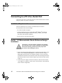
Connecting to a PC Via a Serial Port
............................................................ 1-2
Installation Requirements ............................................................................. 1-2
Am186CC Microcontroller Router Reference Design Installation............... 1-2
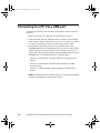
Connecting to a PC Via a USB port .................................................................. 1-4
Connecting a Test Interface Port ....................................................................... 1-5
Troubleshooting Installation Problems.............................................................. 1-6
For More Information........................................................................................ 1-7
$P&&0LFURFRQWUROOHU5RXWHU5HIHUHQFH'HVLJQ8VHU¶V0DQXDO
v
about.book Page vi Wednesday, July 21, 1999 11:10 AM
Chapter 2
System Features and Components
Layout and Placement........................................................................................ 2-2
Power Supply.................................................................................................... 2-7
5 V @ 3 A ..................................................................................................... 2-7
3.3 V @ 500 mA ........................................................................................... 2-7
–24 V @ 50 mA and –70 V @ 60 mA .......................................................... 2-8
–5 V @ 200 mA ............................................................................................ 2-8
Am186CC Microcontroller ............................................................................... 2-9
Am186CC Microcontroller Power Supply.................................................. 2-10
Am186CC Microcontroller Clocking.......................................................... 2-11
Am186CC Microcontroller Reset ............................................................... 2-12
System Memory............................................................................................... 2-13
DRAM/SRAM Memory.............................................................................. 2-13
Flash Memory.............................................................................................. 2-14
10BaseT Ethernet Interface ............................................................................. 2-15
ISDN Interface................................................................................................. 2-18
ISDN S/T Interface...................................................................................... 2-19
ISDN U Interface......................................................................................... 2-20
Serial PC Interface........................................................................................... 2-22
USB PC Interface ............................................................................................ 2-23
POTS Interface ................................................................................................ 2-25
DSLAC PCM Interface ............................................................................... 2-25
RSLIC Interface .......................................................................................... 2-27
Dual Tone Multiple Frequency (DTMF)..................................................... 2-27
Debug Circuitry ............................................................................................... 2-28
TIP Interface................................................................................................ 2-28
RESCON Configuration.............................................................................. 2-30
vi
$P&&0LFURFRQWUROOHU5RXWHU5HIHUHQFH'HVLJQ8VHU¶V0DQXDO
about.book Page vii Wednesday, July 21, 1999 11:10 AM
Appendix A
Default Jumper Settings
Appendix B
Am186CC Microcontroller Router Reference Design PIO
Resources, Chip Selects, Interrupts, and LEDs
Appendix C
Bill of Materials
Appendix D
PLD Equations
IOM-2/GCI Mode............................................................................................. D-2
SBP/PCM Mode ............................................................................................... D-7
Appendix E
Glossary of Terms
Index
$P&&0LFURFRQWUROOHU5RXWHU5HIHUHQFH'HVLJQ8VHU¶V0DQXDO
vii
about.book Page viii Wednesday, July 21, 1999 11:10 AM
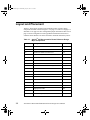
List of Figures
Figure 0-1. Router Block Diagram........................................................................................ xii
Figure 0-2. ISDN Reference Point Diagram ......................................................................... xv
Figure 2-1. Router Reference Design Component Layout................................................... 2-3
Figure 2-2. Am186CC Microcontroller Block Diagram .................................................... 2-10
Figure 2-3. DRAM and Flash Memory Map...................................................................... 2-13
Figure 2-4. Front View of the RJ-45 Connector................................................................. 2-15
Figure 2-5. RESCON Register ........................................................................................... 2-30
YLLL
$P&&0LFURFRQWUROOHU5RXWHU5HIHUHQFH'HVLJQ8VHU¶V0DQXDO
about.book Page ix Wednesday, July 21, 1999 11:10 AM
List of Tables
Table 0-1.
Notational Conventions ................................................................................... xviii
Table 1-1.
Installation Troubleshooting.............................................................................. 1-6
Table 2-1.
Am186CC Microcontroller Router Reference Design Major Components ...... 2-2
Table 2-2.
Configuration Jumper Functions ....................................................................... 2-4
Table 2-3.
Configuration Jumper Combinations ................................................................ 2-4
Table 2-4.
Configuration Resistor Population .................................................................... 2-5
Table 2-5.
CPU PLL Clock Modes................................................................................... 2-11
Table 2-6.
USB PLL Clock Modes................................................................................... 2-11
Table 2-7.
RJ-45 Connector Pin Functions....................................................................... 2-16
Table 2-8.
PCnet-ISA II Ethernet Controller LED Status Information ............................ 2-16
Table 2-9.
U Interface LED Status ................................................................................... 2-20
Table 2-10. Router Board Configuration Bit Assignments ................................................ 2-31
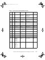
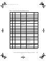
Table A-1.
Default Jumper Settings ................................................................................... A-1
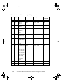
Table B-1.
PIO Resource Assignments ...............................................................................B-1
Table B-2.
Chip Select Assignments...................................................................................B-2
Table B-3.
Interrupt Assignments .......................................................................................B-2
Table B-4.
LED Status.........................................................................................................B-3
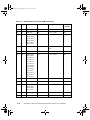
Table C-1.
Router Reference Design BOM.........................................................................C-1
$P&&0LFURFRQWUROOHU5RXWHU5HIHUHQFH'HVLJQ8VHU¶V0DQXDO
L[
about.book Page x Wednesday, July 21, 1999 11:10 AM
[
$P&&0LFURFRQWUROOHU5RXWHU5HIHUHQFH'HVLJQ8VHU¶V0DQXDO
about.book Page xi Wednesday, July 21, 1999 11:10 AM
About the Am186™CC
Microcontroller ISDN-to-Ethernet
Router Reference Design
The AMD Am186CC microcontroller ISDN-to-Ethernet router reference design
(hereafter referred to as the Am186CC microcontroller router reference design) is
used for customer development of ISDN and Ethernet interfaces, High-Speed
universal asynchronous receiver/transmitters (UARTs), USB ports, Flash memory,
and plain old telephone Service (POTS) circuitry. The board includes the
Am186CC microcontroller, Am79C961A PCnet™-ISA II 10BaseT Ethernet
controller, Am79C031 DSLAC™ device, two Am79R79 ringing SLICs,
Am79C32A ISDN S/T data controller, T7237A ISDN U data controller, and
Am29F800 Flash memory.
The Am186CC microcontroller router reference design consists of a single board
with an external power supply module. The block diagram is shown in Figure 0-1
on page xii.
The reference design provides a glueless interface to Flash memory, DRAM and
SRAM system main memory, communication interfaces such as a High-Speed
UART, universal serial bus (USB), and four HDLC channels.
Other features include a debug interface that allows connection to the optional test
interface port (TIP) debug board.
Am186™CC Microcontroller Router Reference Design User’s Manual
xi
about.book Page xii Wednesday, July 21, 1999 11:10 AM
For more information about the Am186CC microcontroller router reference design
features, refer to “Am186™CC Microcontroller Router Reference Design
Features” on page xiii, and Chapter 2, “System Features and Components”.
Figure 0-1. Router Block Diagram
xii
Am186™CC Microcontroller Router Reference Design User’s Manual
about.book Page xiii Wednesday, July 21, 1999 11:10 AM
Theory of Operation
The reference design demonstrates the Am186CC microcontroller’s functionality
in an ISDN/Ethernet application. You can use this board as a reference to create
your own designs. The small size and simplicity of this design highlight the benefits
of the Am186CC microcontroller’s many integrated peripherals.
Am186™CC Microcontroller Router
Reference Design Features
The Am186CC microcontroller router reference design provides the following
features:
• Am186CC 3.3-V, 50-MHz microcontroller
• External power supply (generates 3.3 V, 5.0 V, –5.0 V, –24 V, and –70 V from
a 12VDC source)
• Memory interfaces
– Main system memory
• 4-Mbit, 256K x 16, 40-ns EDO DRAM
• 128K x 8, 35-ns SRAM configured as 64K x 16
– 8-Mbit configurable 512K x 16, or 1M x 8, 55-ns Flash memory
• Communication interfaces
– HDLC synchronous communications
– 12-Mbit/s USB port
Am186™CC Microcontroller Router Reference Design User’s Manual
xiii
about.book Page xiv Wednesday, July 21, 1999 11:10 AM
• UARTs
– One 460-Kbaud, RS-232, DB-9 DCE connection
• Debug and configuration
– 60-pin connector interface to the optional test interface port (TIP) debug board
• 10BaseT Ethernet port
• 2B+D ISDN interface (for more information about ISDN, see “ISDN
Background” on page xv)
– S/T interface
– U interface
• Two POTS interfaces
• E86TM family boot monitor (E86MONTM software board-resident utility)
xiv
Am186™CC Microcontroller Router Reference Design User’s Manual
about.book Page xv Wednesday, July 21, 1999 11:10 AM
ISDN Background
Integrated services digital network (ISDN) is an alternative to analog phone lines.
ISDN provides greater performance than analog and is still affordable to
consumers. There are many different variations of ISDN available, but the most
common is 128-Kbit/s data transfer rate over two B (bearer) channels, plus 16Kbit/s of signaling data over the D channel; this is the 2B+D configuration, the
configuration used by the Am186CC microcontroller router reference design
discussed in this manual. Another configuration uses a single B channel and
transfers data at 64 Kbit/s. Broadband ISDN is available and can achieve data rates
in the 100-Mbit/s range.
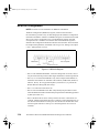
There are a number of reference points in an ISDN system. Figure 0-2 shows a
graphical representation of the ISDN reference points. The U reference point is the
local loop between the Local Exchange (LE) and the Network Termination (NT)
device. The U interface is a two-wire interface, which in North America and Asia
is typically supplied by a telecommunications service provider. The U interface
operates in 2B1Q (two binary, one quaternary) format, and can travel for miles
without repeaters. The T reference point is used only with customer premises
switching equipment (NT2). The S/T reference point is the four-wire interface
between the network termination device (NT1) and the terminal equipment (TE1)
or Terminal Adapter (TA). The S/T interface is offered in Europe, and is also used
with stand-alone NT1 devices.
Network
Termination Type 2
(NT2)
S
ISDN Terminal
Equipment
(TE1)
or
T Network
U
Termination Type 1
(NT1)
S/T
Terminal
Adapter
(TA)
ISDN
Local
Exchange
(LE)
R Non-ISDN
Terminal
Equipment (TE2)
Figure 0-2. ISDN Reference Point Diagram
Am186™CC Microcontroller Router Reference Design User’s Manual
xv
about.book Page xvi Wednesday, July 21, 1999 11:10 AM
Documentation
The Am186™CC Microcontroller ISDN-to-Ethernet Router Reference Design
User’s Manual provides information on the design and function of the Am186CC
microcontroller router reference design.
About This Manual
Chapter 1, “Quick Start” helps you quickly set up and start using the Am186CC
microcontroller router reference design.
Chapter 2, “System Features and Components” describes the basic sections of the
reference design: layout, jumper settings, microcontroller, power supply, memory
interfaces, communication interfaces, debug and configuration, 10BaseT Ethernet
port, ISDN interface, and POTS interfaces.
Appendix A, “Default Jumper Settings” provides a table with the default jumper
settings.
Appendix B, “Am186™CC Microcontroller Router Reference Design PIO
Resources, Chip Selects, Interrupts, and LEDs” provides tables with PIO, chip
select, and interrupt assignments as well as LED status.
Appendix C, “Bill of Materials” contains the bill of materials for the Am186CC
microcontroller router reference design.
Appendix D, “PLD Equations” contains PLD code for the PLD at location U43.
Appendix E, “Glossary of Terms” contains a glossary of communications terms.
xvi
Am186™CC Microcontroller Router Reference Design User’s Manual
about.book Page xvii Wednesday, July 21, 1999 11:10 AM
Suggested Reference Material
• Am186TMCC/CH/CU Microcontrollers User’s Manual
Advanced Micro Devices, order #21914
• Am186TMCC Communications Controller Data Sheet
Advanced Micro Devices, order #21915
• Am186TMCH HDLC Microcontroller Data Sheet
Advanced Micro Devices, order #22024
• Am186TMCU USB Microcontroller Data Sheet
Advanced Micro Devices, order #22025
• Am186TMCC/CH/CU Microcontroller Register Set Manual
Advanced Micro Devices, order #21916
• Am186TM and Am188TM Family Instruction Set Manual
Advanced Micro Devices, order #21076
• E86MONTM Software User’s Manual
Advanced Micro Devices, order #21891
• E86TM Family Products and Development Tools CD
Advanced Micro Devices, order #21508
• AMD Test Interface Port Board User’s Manual
Advanced Micro Devices, Order #22505
• Am79C961A PCnetTM-ISA II Jumperless, Full Duplex Single-Chip Ethernet
Controller for ISA
Advanced Micro Devices, order #19364
• Am79C02/03/031(A) Dual Subscriber Line Audio Processing Circuit
(DSLACTM) Devices
Advanced Micro Devices, order #09875
• Am79R79 Ringing Subscriber Line Interface Circuit
Advanced Micro Devices, order #19752
• Am79C30A/32A Digital Subscriber ControllerTM (DSCTM) Circuit
Advanced Micro Devices, order #09893
• Am29F800B 8 Megabit Boot Sector Flash Memory Data Sheet
Advanced Micro Devices, order #21504
Am186™CC Microcontroller Router Reference Design User’s Manual
xvii
about.book Page xviii Wednesday, July 21, 1999 11:10 AM
• Lucent Technologies T7237 ISDN U-Interface Transceiver Data Sheet
Lucent Technologies, order #DS97-411ISDN, available at www.lucent.com
• ISDN Concepts, Facilities, and Services
Gary C. Kessler, ISBN: 0-07-034242-3
• ISDN For Dummies, 2nd Edition
David Angell, ISBN: 0-7645-0064-3
• ISDN Implementor’s Guide: Standards, Protocols, Services
Charles K. Summers, ISBN: 0-07-069416-8
• Digital Telephony, Second Edition
John Bellamy, ISBN: 0-471-62056-4
• International Telecommunication Union Standards at www.itu.ch.
Documentation Conventions
Table 0-1. Notational Conventions
Symbol
Usage
Boldface
Indicates that characters must be entered exactly as
shown, except that the alphabetic case is only
significant when indicated.
Typewriter face Indicates computer text input or output in an example
or listing.
xviii
Am186™CC Microcontroller Router Reference Design User’s Manual
about.book Page 1 Wednesday, July 21, 1999 11:10 AM
Chapter 1
Quick Start
This chapter provides information to help you quickly set up and start using the
Am186CC microcontroller router reference design.
The Am186CC microcontroller router reference design is supported by the
E86MON board-resident debugger. The E86MON boot monitor software enables
you to load, run, and debug programs on the Am186CC microcontroller router
reference design. For detailed information on using the E86MON software, refer
to the E86MONTM Software User’s Manual included in your kit.
• )RULQIRUPDWLRQRQKRZWRFonnect the Am186CC microcontroller router
reference design to a PC via a serial port, see page 1-2.
• )RULQIRUPDWLRQRQKRZWR connect the Am186CC microcontroller router
reference design to a PC via a USB port, see page 1-4.
• )RULQIRUPDWLRQRQKRZWRFonnect the TIP to the reference design, see page 1-5.
• )RULQIRUPDWLRQRQKRZWRLnvoke the E86MON software, see step 5 on page 1-3.
• )RULQIRUPDWLRQRQKRZWRWroubleshoot installation problems, see page 1-6.
• )RULQIRUPDWLRQRQKRZWROocate related sources of information, see page 1-7.
Am186™CC Microcontroller Router Reference Design User’s Manual
1-1
ch1.fm Page 2 Thursday, July 22, 1999 11:43 AM
Connecting to a PC Via a Serial Port
Follow the steps below to connect the Am186CC microcontroller router reference
design to your PC via your PC’s serial port.
Installation Requirements
The items listed below are necessary to install and run the Am186CC
microcontroller router reference design:
• PC with an available COM port
• Terminal emulation software (such as Microsoft® Windows® Terminal or
ProComm Plus) that supports ASCII file transfers, software flow control
(Xon/Xoff), and send break capability
• Power source for universal power supply
Am186™CC Microcontroller Router Reference Design
Installation
!
CAUTION: As with all computer equipment, the Am186CC
microcontroller router reference design may be damaged by
Electrostatic Discharge (ESD). Please take proper ESD
precautions when handling any board.
1. Remove the board from the shipping carton. Visually inspect the board to verify
that it was not damaged during shipment. Connect the reference design’s
DB-9 high speed serial port to an available COM port. Use the serial cable
included in the Am186CC microcontroller router reference design kit and note
that a DB-9 to DB-25 serial connector adapter is provided if your host system
requires it.
2. Connect the power supply to the barrel connector (connector P6 at location
A-8 in Figure 2-1 on page 2-3) at the corner of the Am186CC microcontroller
router reference design board.
1-2
Am186™CC Microcontroller Router Reference Design User’s Manual
ch1.fm Page 3 Thursday, July 22, 1999 11:43 AM
3. Apply power to the board by connecting the power supply to an electrical outlet.
When the board is powered up, LED CR8 (at location H-5 in Figure 2-1 on
page 2-3) comes on for one second and then goes off. This indicates that the U
transceiver (T7237A at location H-5 in Figure 2-1 on page 2-3) has powered
up. The same thing happens when you reset the board.
If all of the LEDs are not illuminated, remove the power supply immediately
and contact AMD technical support. See “Technical Support” on page iii for
contact information.
!
CAUTION: If using your own power supply, be sure it is a
12VDC supply and is capable of providing at least 2 A.
4. Invoke the terminal emulation program at 19200 baud, no parity, 8 data bits,
and 1 stop bit; enable the software flow control (Xon/Xoff), if supported.
5. Reset the board by depressing and releasing the RESET switch (see SW1 at
location E-9 in Figure 2-1 on page 2-3).
Type an a in the terminal window to ensure that the E86MON software uses
the correct baud rate. When the E86MON software receives an a, it adjusts its
baud rate (if necessary) and displays the welcome message and prompt.
NOTE: If you type a character other than an a, or type no character at all, the
E86MON software still displays the welcome message and prompt, but may
be using an incorrect baud rate. Depressing and releasing the RESET switch
(SW1 at location E-9) gives you another opportunity to type an a.
6. To display the version of the monitor and the commands available, type ? and
press Enter.
For detailed information about using the E86MON software, refer to the
E86MONTM Software User’s Manual included in your kit.
Am186™CC Microcontroller Router Reference Design User’s Manual
1-3
about.book Page 4 Wednesday, July 21, 1999 11:10 AM
Connecting to a PC Via a USB port
To connect the Am186CC microcontroller router reference design to your PC’s
USB port:
1. Insert the flat end of your USB cable into the USB port on your PC.
2. Connect the other end of the USB cable into the Am186CC microcontroller
router reference design’s USB connector (see P9 at J-1 in Figure 2-1 on page
2-3) that is located near the corner of the board and is labeled “USB”.
3. Download the USB CodeKit software from the AMD website. Go to
www.amd.com and click on Embedded Processors to get to the USB CodeKit
software packages used in the Am186CC microcontroller router reference
design. Each CodeKit software package includes installation instructions in a
README.TXT file. Download these three CodeKit packages:
– Am186CC Communications Controller USB Driver CodeKit Software
Package
– Am186CC Communications Controller USB-UART Driver CodeKit
Software Package
– Am186CC/CU Microcontroller USB Port Expander CodeKit Software
Package
NOTE: In addition to the three CodeKit packages, you also need to download
the Expose-USB Diagnostic Tool from the same site.
1-4
Am186™CC Microcontroller Router Reference Design User’s Manual
about.book Page 5 Wednesday, July 21, 1999 11:10 AM
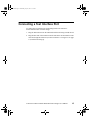
Connecting a Test Interface Port
To connect the test interface port (TIP) debug board to the Am186CC
microcontroller router reference design:
1. Plug the TIP connector into the TIP board with the tab facing towards the left.
2. Plug the other end of the connector into the Am186CC microcontroller router
reference design TIP connector (see P10 at location L-7 in Figure 2-1 on page
2-3) with the tab facing up.
Am186™CC Microcontroller Router Reference Design User’s Manual
1-5
about.book Page 6 Wednesday, July 21, 1999 11:10 AM
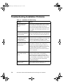
Troubleshooting Installation Problems
Table 1-1. Installation Troubleshooting
1-6
Problem
Solution
Nothing happens when
pushing the RESET
button.
Sometimes it is difficult to make a good connection
when pushing the small RESET button. If all else
fails, remove the power supply from the AC
electrical outlet and disconnect and reconnect the
power supply. The LEDs light up when the reset is
successful.
The computer does not
respond with the E86MON
software prompt.
Reset the board by pressing the RESET switch and
typing an a immediately after power up. If this does
not work, verify the power, check the cables, etc.
After typing a during reset,
the terminal emulation
software displays
unreadable characters.
Check the baud rate setting for the terminal
emulation software. It should be set to 19200. Also
check the word length (8), stop bits (1), and
parity (N), and turn off any hardware flow control.
The terminal emulation
program locks up the
software or PC.
Check the COM port connection with the target
board. Make sure that the same COM port is
selected in the terminal emulation software. In
some PCs if the correct COM port is not specified,
the software fails to function—it locks in a
continuous loop waiting for an answer from the
incorrect serial port.
The power LED (CR8)
does not turn on with
power.
This LED should turn on for one second and then
turn off. If it doesn’t turn on, immediately
disconnect the power supply. Ensure that the
polarity of the power connector is correct. This is a
very serious failure of the hardware. If the power
source is connected incorrectly, the board is
permanently damaged.
There is a problem you
cannot resolve.
Contact AMD Technical Support (see page iii for
phone numbers and more information).
Am186™CC Microcontroller Router Reference Design User’s Manual
about.book Page 7 Wednesday, July 21, 1999 11:10 AM
For More Information...
If you need more information about:
• Am186CC microcontroller router reference design hardware,
see Chapter 2.
• E86MON software,
see the E86MONTM Software User’s Manual included in your kit.
• Problems with the reference design or the E86MON software,
see the customer support information on page iii.
• 7KH$P&&PLFURFRQWUROOHUURXWHUUHIHUHQFHGHVLJQ¶VFRPSRQHQWOD\RXW
see Chapter 2.
• 7KH$P&&PLFURFRQWUROOHUURXWHUUHIHUHQFHGHVLJQ¶V schematics,
see the schematics document included in your kit.
• The Am186CC microcontroller,
see the following documents included in your kit:
– Am186TMCC Communications Controller Data Sheet
– Am186TMCC/CH/CU Microcontrollers User’s Manual
– Am186TMCC/CH/CU Microcontrollers Register Set Manual
– Am186TM/Am188TM Family Instruction Set Manual
• The latest release and updates,
see Demo Board Updates under Embedded Processors at www.amd.com.
Am186™CC Microcontroller Router Reference Design User’s Manual
1-7
about.book Page 8 Wednesday, July 21, 1999 11:10 AM
1-8
Am186™CC Microcontroller Router Reference Design User’s Manual
about.book Page 1 Wednesday, July 21, 1999 11:10 AM
Chapter 2
System Features and Components
The Am186CC microcontroller router reference design is a single-sided,
6.5 x 9.75-inch, printed circuit board that integrates the Am186CC microcontroller
and I/O interfaces onto one board, enabling you to develop ISDN, Ethernet, HighSpeed UART, USB, and POTS applications.
The following sections explain the operation of the board in detail:
• “Layout and Placement” on page 2-2
• “Power Supply” on page 2-7
• “Am186™CC Microcontroller” on page 2-9
• “System Memory” on page 2-13
• “10BaseT Ethernet Interface” on page 2-15
• “ISDN Interface” on page 2-18
• “Serial PC Interface” on page 2-22
• “USB PC Interface” on page 2-23
• “POTS Interface” on page 2-25
• “Debug Circuitry” on page 2-28
Am186™CC Microcontroller Router Reference Design User’s Manual
2-1
about.book Page 2 Wednesday, July 21, 1999 11:10 AM
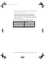
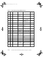
Layout and Placement
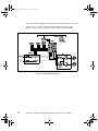
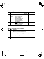
Table 2-1 shows major Am186CC microcontroller router reference design
components and their location in Figure 2-1 on page 2-3. Table 2-2 on page 2-4
and Table 2-3 on page 2-4 show configuration jumper information. Table 2-4 on
page 2-5 shows configuration resistor population information. References to
schematic sheet numbers refer to the schematics document included in your kit.
Table 2-1. Am186™CC Microcontroller Router Reference Design
Major Components
2-2
Part
Description
Location
U1
Am186CC microcontroller
F-7
U2
Am79C961A Ethernet controller
K-5
U6
Am79C32A ISDN S/T transceiver
F-4
U11
T7237A ISDN U transceiver
H-4
U15, U18
Am79R79 RSLIC
B-3, D-3
U20
Am79C031 DSLAC
C-5
U21, U22
M-8870-01SM DTMF
D-5, D-6
U24
Am29F800 1M x 8 Flash memory
K-7
U25
256K x 16 DRAM
H-7
U27
64K x 16 SRAM
I-7
U43
PAL26V12
E-4
P1
Ethernet RJ-45 connector
L-1
P3
ISDN U RJ-45 connector
H-1
P2
ISDN S RJ-45 connector
F-1
P4, P5
POTS RJ-11 connectors
B-1, D-1
P7
High-Speed UART
H-9
P9
USB connector
J-1
P10
Test interface port (TIP)
L-7
Am186™CC Microcontroller Router Reference Design User’s Manual
about.book Page 3 Wednesday, July 21, 1999 11:10 AM
L
K
J
I
H
G
F
E
D
C
B
A
1
2
3
4
5
6
7
8
9
Figure 2-1. Router Reference Design Component Layout
Am186™CC Microcontroller Router Reference Design User’s Manual
2-3
about.book Page 4 Wednesday, July 21, 1999 11:10 AM
Table 2-2. Configuration Jumper Functions
Part
Function
Description
Figure 2-1
Reference
Schematic Sheet #
JP1
Flash
memory
selection
JP1 selects the Flash memory
CE input, either sourced by
the TIP or by the router
board’s Am186CC
microcontroller. This allows
the TIP to program the
Am29F800 Flash memory on
the router board.
L-5
13
JP5
8/16-bit boot
Selects 8- or 16-bit boot from
UCS space. Enables booting
from 8-bit TIP memory.
I-6
13
Table 2-3. Configuration Jumper Combinations
JP1
JP5
Operation
1-2
2-3
Am186CC microcontroller UCS (CNTL6) is connected to FLASH_CE.
Boot from 16-bit memory (normal operation).
2-3
1-2
TIP Flash Chip Select. Used to reprogram Flash memory. Forces Am186CC
microcontroller to boot from 8-bit memory on TIP and enables router Flash
memory programming.
1-2
1-2
Not valid
2-3
2-3
Not valid
2-4
Am186™CC Microcontroller Router Reference Design User’s Manual
about.book Page 5 Wednesday, July 21, 1999 11:10 AM
Table 2-4. Configuration Resistor Population
Functionality
Populate
Do Not
Populate
Schematic
Sheet #
Comments
ISDN S
R137,
R139
R_UFS,
R136,
R138
6, 9
Normal operation
ISDN U
R_UFS,
R136,
R138
R137,
R139
6, 9
The Am186CC
microcontroller router
reference design is
shipped configured for
the S/T interface. To use
the U interface, make the
resistor changes and do
not access the
Am79C32A chip with
software.
Clock modes
R54
R51, R52,
R53
10
Enable clock CPU 2X
PLL, USB 2X PLL. See
Table 2-5 on page 2-11
and Table 2-6 on page 211.
Board ID
R93, R95,
R98, R100
R94, R96,
R97, R99
10
See “RESCON
Configuration” on
page 2-30.
Am186™CC Microcontroller Router Reference Design User’s Manual
2-5
about.book Page 6 Wednesday, July 21, 1999 11:10 AM
Table 2-4. Configuration Resistor Population (Continued)
Functionality
Populate
Do Not
Populate
Schematic
Sheet #
Comments
Am186CC
microcontroller transmit
to DSLAC using TXDD
R170,
R171,
R172,
R167
R166,
R169
2, 14
See “DSLAC PCM
Interface” on page 2-25.
R166,
R169
R171,
R172,
R167,
R170
2, 14
See “DSLAC PCM
Interface” on page 2-25
R42
9
See “DSLAC PCM
Interface” on page 2-25
9
See “DSLAC PCM
Interface” on page 2-25
Am186CC
microcontroller transmit
using TXDA controlled
by DSTSC
DSLAC transmit to
Am186CC
microcontroller using
RXDD controlled by
CTSHU
High-Speed UART flow
control using Channel C
No Am186CC
microcontroller/DSLAC
communication
Am186CC
microcontroller always
transmits on Channel A
High-Speed UART flow
control using Channel D
Enable individual
programming of DSLAC
Channels 1 and 2
Disable individual
programming of DSLAC
Channels 1 and 2
2-6
R42
Am186™CC Microcontroller Router Reference Design User’s Manual
about.book Page 7 Wednesday, July 21, 1999 11:10 AM
Power Supply
The Am186CC microcontroller router reference design is powered by a universal
power supply that converts 100–200 VAC power to 12 VDC, 2.5 A. The 12 V enters
the Am186CC microcontroller router reference design through a 5.5-mm barrel
connector, where the center post is VCC and the outer ring is GND. From the
12-VDC input, the on-board power supply provides 5 V, 3.3 V, –5 V, –24 V,
and –70 V. The following sections provide details about the power supply.
5V@3A
NOTE: See sheet 11 in the schematics for power supply circuits.
A MIC4576 (U44 at location D-7) voltage regulator generates 5 V from the 12-V
source. The voltage regulator provides power to most of the components in the
reference design, including the DRAM, SRAM, and Flash memory components;
the DCE and High-Speed UART transceiver; the HDLC clock generator; and the
3.3-V low drop out (LDO) regulator (MIC5209, U32 at location D-8). This power
supply is also routed to the TIP connector.
3.3 V @ 500 mA
NOTE: See sheet 11 in the schematics for power supply circuits.
The 3.3-V LDO regulator, MIC5209 (U32 at location D-8), generates 3.3 V from
the 5-V source. This power supply provides power to the Am186CC
microcontroller and the USB detect circuitry.
Am186™CC Microcontroller Router Reference Design User’s Manual
2-7
about.book Page 8 Wednesday, July 21, 1999 11:10 AM
–24 V @ 50 mA and –70 V @ 60 mA
NOTE: See sheet 11 in the schematics for power supply circuits.
A switching flyback circuit from the 12-V source generates the –24 V and the
–70 V. These outputs are routed to the Am186CC microcontroller router reference
design and are used in the POTS interface.
–5 V @ 200 mA
NOTE: See sheet 11 in the schematics for power supply circuits.
A 5-V buck-boost switching circuit from the 12-V source generates the –5 V. This
power supply provides power to the Am79C031 DSLAC.
2-8
Am186™CC Microcontroller Router Reference Design User’s Manual
about.book Page 9 Wednesday, July 21, 1999 11:10 AM
Am186™CC Microcontroller
The Am186CC microcontroller router reference design supports a 160-pin plastic
quad flat pack (PQFP) Am186CC microcontroller operating at 50 MHz. The
integrated features of the Am186CC microcontroller provide a glueless interface
to DRAM, SRAM, and Flash memory. The microcontroller also integrates a UART
(not supported on the Am186CC microcontroller router reference design) and
High-Speed UART (which requires only an external transceiver), a high-speed (12
Mbit/s) USB peripheral controller with internal transceiver, and HDLC channels
that provide external interfaces to gluelessly connect to communications
peripherals.
The Am186CC microcontroller is designed as a cost-effective, high-performance
microcontroller solution for communication applications. The Am186CC
microcontroller offers the advantages of the x86 development environment’s
widely available native development tools, applications, and system software.
For detailed information about the specific features of the Am186CC
microcontroller, refer to the corresponding documentation included in your kit.
Am186™CC Microcontroller Router Reference Design User’s Manual
2-9
about.book Page 10 Wednesday, July 21, 1999 11:10 AM
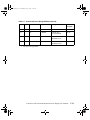
Figure 2-2 shows the Am186CC microcontroller block diagram.
Serial Communications Peripherals
Am186
CPU
Chip
Selects
(14)
PIOs
(48)
Watchdog
Timer
Interrupt
Controller
17 Ext Sources
UART
High-Speed
UART with
Autobaud
USB
Synchronous
Serial
Interface (SSI)
Physical
Interface
Glueless
Interface
to RAM/ROM
DRAM
Controller
Timers
(3)
GeneralPurpose
DMA (4)
Memory Peripherals System Peripherals
Smart
DMA (8)
Controller
HDLC TSA
Raw DCE
HDLC TSA
Muxing
PCM
Highway
HDLC TSA
HDLC TSA
GCI
(IOM-2)
Figure 2-2. Am186™CC Microcontroller Block Diagram
Am186™CC Microcontroller Power Supply
The Am186CC microcontroller router reference design provides a 3.3-V power
supply for the Am186CC microcontroller. The power supply is sourced from a
3.3-V LDO regulator (U32) from a 5-V switching power supply. The digital and
analog power pins are isolated by filtering to prevent noise on the digital circuitry
from affecting the internal analog block.
2-10
Am186™CC Microcontroller Router Reference Design User’s Manual
about.book Page 11 Wednesday, July 21, 1999 11:10 AM
Am186™CC Microcontroller Clocking
NOTE: See sheet 10 of the schematics for clock information.
The Am186CC microcontroller router reference design uses an internal 2x PLL to
provide a 48-MHz system clock and the required 48-MHz USB clock. The presence
or absence of resistors R51, R52, R53, and R54 determine the CPU and USB
clocking speeds. R52 is at location F-6. R51, R53, and R54 are located at location
E-8. If the resistor is present, the associated CPU signal is pulled Low. If absent,
the signal is High. Table 2-5 and Table 2-6 list resistor population information for
CPU PLL and USB PLL clock modes. The Am186CC microcontroller router
reference design only has R54 populated.
On reset or when booting up, the CPU reads its HLDA (CLKSEL1) and PCS4
(CLKSEL2) pins for the CPU clocking speed and PCS0 (USBSEL1) and PCS1
(USBSEL2) for the USB clocking speed.
Table 2-5. CPU PLL Clock Modes
CLKSEL1 (R52)
CLKSEL2 (R51)
CPU PLL Mode
1
1
2x PLL (default)
1
0
4x PLL
0
1
1x PLL
0
0
PLL bypass
Table 2-6. USB PLL Clock Modes
USBSEL1 (R54)
USBSEL2 (R53)
USB PLL Mode
1
1
Use CPU clock, USBPLL
disabled
1
0
4x PLL
0
1
2x PLL (default)
0
0
PLL bypass
Am186™CC Microcontroller Router Reference Design User’s Manual
2-11
about.book Page 12 Wednesday, July 21, 1999 11:10 AM
Am186™CC Microcontroller Reset
NOTE: See sheet 10 in the schematics for the reset circuitry.
The Am186CC microcontroller requires the RES input to be asserted for at least
1 ms to allow the internal circuitry to stabilize. The Am186CC microcontroller
router reference design uses an external device that monitors the 3.3-V VCC to
provide a reset output with an internal 21-ms RC delay to drive the 3.3-V RES
input to the Am186CC microcontroller. Depressing the reset switch (SW1 at
location E-9) causes a system reset without cycling power.
2-12
Am186™CC Microcontroller Router Reference Design User’s Manual
about.book Page 13 Wednesday, July 21, 1999 11:10 AM
System Memory
The Am186CC microcontroller router reference design uses DRAM and Flash
memory for system memory. Figure 2-3 shows the DRAM and Flash memory map.
A small SRAM device is also used as an Ethernet packet buffer.
FFFFFh
Flash Memory
80000h
7FFFFh
DRAM Memory
00000h
Figure 2-3. DRAM and Flash Memory Map
DRAM/SRAM Memory
NOTE: See sheet 4 in the schematics for the DRAM and SRAM circuitry.
A 256K x 16 EDO, 40-ns DRAM allows zero wait state operation at up to 50 MHz.
The DRAM resides in the lower 512 Kbyte of LCS memory space (0h–7FFFFh).
The Am186CC microcontroller provides the DRAM memory address on the odd
Am186CC microcontroller addresses A1–A17 to provide a direct connection to
the DRAM device. The DRAM RAS and CAS signaling is provided on the
LCS0/RAS0, MCS1/CAS1, and MCS2/CAS0 signals from the Am186CC
microcontroller.
The Am186CC microcontroller router reference design is populated with a
64K x 16, 35-ns TSOP II SRAM device used as shared memory (shared by the
system and by the Ethernet controller). The Am186CC uses MCS0 to select the
SRAM. The SRAM can be mapped into memory space at various addresses
(mapping SRAM to 80000h is common). The space the SRAM resides in can be
moved from 00000h up to FFFFFh in increments equal to the SRAM block size.
There is no fixed location for the SRAM as it is chosen by the programmer.
Am186™CC Microcontroller Router Reference Design User’s Manual
2-13
about.book Page 14 Wednesday, July 21, 1999 11:10 AM
Flash Memory
NOTE: See sheet 4 in the schematics for the Flash memory circuitry.
A single, surface-mount, TSOP Am29F800, 55-ns, 8-Mbit Flash memory device
allows for zero wait state operation at 50 MHz.
The Am29F800 Flash memory CE is connected to chip select UCS and mapped
to address range 0x80000-0xFFFFFh. This is 4 megabits of addressable memory
that only allows access to one-half of the Am29F800 device. The high-order
address bit of the Am29F800 device, A18, is connected to PIO35. This allows bank
selecting between the upper and lower halves of the 8 megabit Flash memory
device. PIO35 defaults to a logic High using a 10K-Ω pullup resistor. PIO35 can
be driven low to enable access to the lower half of the Flash memory device. The
Am29F400 device can be used as a direct replacement for the Am29F800 device.
A18 connects to pin 16 of the Am29F400 Flash device. Pin 16 is a true no connect
on this device and bank selecting is not available.
2-14
Am186™CC Microcontroller Router Reference Design User’s Manual
ch2.fm Page 15 Thursday, July 22, 1999 11:44 AM
10BaseT Ethernet Interface
NOTE: See sheet 4 in the schematics for the Ethernet SRAM packet buffer circuitry
and sheet 3 for the Ethernet controller circuitry.
The Am186CC microcontroller router reference design uses an AMD
Am79C961A PCnet-ISA II Ethernet controller configured in bus master mode for
its Ethernet interface. The Ethernet interface consists of a connection between the
PCnet-ISA II twisted pair interface to an RJ-45 connector, a 20-MHz crystal, an
optional EEPROM for Plug-n-Play (PnP) capability, three status LEDs, SRAM
used to transfer Ethernet packet data, and a small amount of glue logic required to
interface the Am186CC microcontroller to the PCnet-ISA II Ethernet controller.
The Am186CC microcontroller router reference design provides Ethernet through
the PCnet-ISA II twisted pair interface with the addition of a single 10BaseT
transformer (U4 at location L-2) to the RJ-45 connector (P1 at location L-1). To
link the Ethernet station to a network, connect the straight-through cable provided
in your kit to a hub that sits on the network.
Figure 2-4, below, and Table 2-7 on page 2-16 show the pin assignment and pin
functions for the RJ-45 connector.
2
TXRX+
NC
NC
RXNC
NC
3
1
TX+
4
5
6
7
8
Figure 2-4. Front View of the RJ-45 Connector
Am186™CC Microcontroller Router Reference Design User’s Manual
2-15
about.book Page 16 Wednesday, July 21, 1999 11:10 AM
Table 2-7. RJ-45 Connector Pin Functions
Pin Number
Function
1
TX+
2
TX–
3
RX+
4
Not used
5
Not used
6
RX–
7
Not used
8
Not used
Three LEDs (CR1–CR3 at location K-9) provide status information for the Ethernet
port. The function of these LEDs is controlled by the ISA bus configuration
registers on the PCnet-ISA II Ethernet controller and can be modified through
software or the EEPROM. The default functions of the LEDs are shown in
Table 2-8.
Table 2-8. PCnet-ISA II Ethernet Controller LED Status Information
LED
Ethernet Controller
Signal Name
LED Function
CR1
LED0
Indicates a good 10BaseT connection.
CR2
LED1
Indicates receive activity from the network.
CR3
LED3
Indicates transmit activity from the network.
The default configuration of the Am186CC microcontroller router reference design
uses DRAM as main system memory and the 64K x 16 SRAM as the Ethernet
packet memory. In this configuration, the DRAM resides in the lower 512 Kbytes
of memory space from 00000–7FFFFh, and the 128 Kbytes of Ethernet packet
SRAM use MCS0 space located from 80000–9FFFFh. The space the SRAM
resides in can be moved from 00000h up to FFFFFh in increments equal to the
SRAM block size. There is no fixed location for the SRAM as it is chosen by the
programmer.
2-16
Am186™CC Microcontroller Router Reference Design User’s Manual
about.book Page 17 Wednesday, July 21, 1999 11:10 AM
The Ethernet controller is a bus mastering device and DMAs directly to packet
buffer memory space. The Ethernet controller supports DMA to SRAM, not
DRAM. Because main system memory is DRAM, the 64K x 16 SRAM must be
used as packet buffer memory.
A small amount of glue logic is required to interface the PCnet-ISA II Ethernet
controller to the Am186CC microcontroller because the PCnet-ISA II Ethernet
controller is an ISA peripheral device. The logic is implemented using discrete
devices: U3F (D-9), U47A (I-6) and U48A (E-5). See sheet 3 of the schematics
for details. The logic controls two signals between the Ethernet controller and the
Am186CC microcontroller: SR_CE and BHLDA.
U48A creates the Ethernet packet SRAM chip select, SRAM_CE, from the
MASTER output when the PCnet-ISA II Ethernet controller is the bus master.
When the Am186CC microcontroller is the bus master, the SRAM_CE output is
three-stated and MCS0 is used as the packet SRAM chip select.
BHLDA is an inverted Am186CC microcontroller HLDA and becomes the
PCnet-ISA II DMA acknowledge input (DACK). Refer to U3F, U47A, and U48A
on sheet 3 of the schematics.
Am186™CC Microcontroller Router Reference Design User’s Manual
2-17
about.book Page 18 Wednesday, July 21, 1999 11:10 AM
ISDN Interface
The Am186CC microcontroller router reference design provides both ISDN
S/T and U interfaces. The four-wire 2B+D S/T interface connects through an
RJ-45 jack (P2 at location F-1) by using the Am186CC microcontroller with the
AMD Am79C32A digital subscriber controller (DSC) circuit. This connection
provides the path between the router and an NT1 device. The S/T interface is the
ISDN interface commonly used in Europe.
The two-wire 2B+D U interface uses the Lucent T7237A U transceiver. The U
transceiver provides terminal adapter functionality connected through an RJ-45
jack (P3 at location H-1). The U interface is the main ISDN interface used in North
America and Asia.
Three LEDs (CR4–CR6) at location F-9 (schematic sheet 5) are used to indicate
activity on the ISDN B1, B2, and D channels using Am186CC microcontroller
signals PIO18, PIO39, and PIO32, respectively.
2-18
Am186™CC Microcontroller Router Reference Design User’s Manual
about.book Page 19 Wednesday, July 21, 1999 11:10 AM
ISDN S/T Interface
NOTE: See sheet 5 in the schematics for the ISDN S/T interface circuitry.
The glueless connection between the Am186CC microcontroller and the
Am79C32A ISDN DSC provides the four-wire 2B+D S/T interface. The DSC
serial interface is capable of being configured as an IOM-2 or SBP serial
microprocessor interface. This interface is used to transfer data to and from the
Am186CC microcontroller using the microcontroller’s integrated HDLC in GCI
or PCM mode; I/O cycles via the address and data bus for AM79C32A
initialization.
The Am186CC microcontroller provides a full-duplex path between the TE and
NT device or the PABX linecard. It processes the ISDN BRI bit stream, which
consists of two 64-Kbit/s B channels and a single 16-Kbit/s D channel. The fourwire ISDN S/T interface is first directed through line filtering devices that isolate
and protect the modem from the outside lines.
In the default S/T configuration, the Am79C32A DSC is operating in SBP mode.
The Am79C32A DSC is also providing the clock and frame sync to the Am186CC
microcontroller across the integrated HDLC A interface, which is configured in
PCM mode, and to the Am79C031 DSLAC device (PCM codec) used for the POTS
interface.
An alternate configuration uses the Am79C32A DSC in an IOM-2 mode. The
Am186CC microcontroller provides a GCI-to-PCM (pulse code modulation)
conversion of the data clock and frame sync to enable the Am79C031 DSLAC
device (PCM codec), to communicate directly between the Am79C32A DSC and
the Am79C031 codec for the POTS interface. See “POTS Interface” on page 2-25
for more information about this configuration.
The Am79C32A DSC uses the PCS1 (peripheral chip select 1) signal, which asserts
between addresses 100h and 1FFh, and the INT6 (interrupt 6) signal, which is edgetriggered as an active Low interrupt. The Am79C32A DSC MCLK signal is set to
12.288 MHz. The PAL (U43 at location E-4) divides it by 3 to provide the
4.096 MHz used to drive the MCLK input to the Am79C031 DSLAC device on
the POTS interface. The PAL (U43 at location E-4) is used to synchronize MCLK
and PCLK for the DSLAC. See “DSLAC PCM Interface” on page 2-25.
Am186™CC Microcontroller Router Reference Design User’s Manual
2-19
about.book Page 20 Wednesday, July 21, 1999 11:10 AM
ISDN U Interface
NOTE: See sheet 6 in the schematics for the ISDN U interface circuitry.
The Lucent T7237A U transceiver provides the two-wire 2B+D U interface for
terminal adapter functionality. The T7237A processes the ISDN BRI bit stream
that consists of two 64-Kbit/s B channels and a single 16-Kbit/s D channel.
The T7237A U transceiver uses the Am186CC microcontroller SSI interface to
configure itself; the T7237A’s time-division multiplexed (TDM) bus is used to
transfer data between itself and either the microcontroller’s integrated HDLC in
PCM mode, or the POTS interface.
The microcontroller’s SSI interface to the T7237A U transceiver’s serial interface
is controlled by U48D (location E-5) and PIO38 (see sheet 6 of the schematics).
U48D is required to select the T7237A U transceiver serial interface because the
T7237A does not have an SSI chip enable, and the Am186CC microcontroller
router reference design’s POTS interface DSLAC device also has an SSI interface.
U48D uses the Am186CC microcontroller’s PIO38 signal asserted Low to pass the
SSI clock to the T7237A U transceiver during T7237A configuration.
The T7237A U transceiver’s TDM bus is the PCM clock master and the upstream
device to the Am186CC microcontroller and the DSLAC device in the POTS
interface. In this configuration, the TDM bus drives the PCM data clock and frame
sync, and transmits data directly to and from the Am186CC microcontroller and
the DSLAC device in the POTS interface.
CR8 (location H-5) is used for T7237A U transceiver device status. Table 2-9
shows the U interface LED status.
Table 2-9. U Interface LED Status
2-20
CR8 State
CR8 Function
Off
Interface not active
1 Hz flashing
U interface activation in progress
8 Hz flashing
U interface active
On
U and S/T interface fully active
Am186™CC Microcontroller Router Reference Design User’s Manual
about.book Page 21 Wednesday, July 21, 1999 11:10 AM
In the ISDN U configuration, the Am186CC microcontroller uses the SSI and INT2
as an edge-triggered, active Low interrupt to configure the T7237A device though
its serial microprocessor interface. The T7237A 2B+D channel communication is
performed across the T7237A TDM bus, which is directly connected to Am186CC
microcontroller HDLC Channel A, configured in PCM mode. The T7237A device
provides a 2.048-MHz clock and frame sync to transfer data between the TDM
and the Am186CC microcontroller PCM interface, and the Am79C031 codec PCM
bus for the POTS interface.
Am186™CC Microcontroller Router Reference Design User’s Manual
2-21
about.book Page 22 Wednesday, July 21, 1999 11:10 AM
Serial PC Interface
NOTE: See sheet 12 in the schematics for the serial PC interface circuitry.
The high-speed serial port may be used for communication with a PC. The Sipex
high-speed RS-232 transceiver (at location J-9) is used to provide serial data rates
up to 460 Kbaud. The DCE serial connection is made through a standard female
DB-9 connector (at location H-9), which uses a straight-through serial cable (no
null-modem). PIO0, PIO1, PIO27, and PIO28 can be used to provide extra flow
control signaling to support Plug and Play (PnP) operation. LED CR9 (at location
J-9) indicates transmit and receive activity (green is transmit, red is receive).
2-22
Am186™CC Microcontroller Router Reference Design User’s Manual
about.book Page 23 Wednesday, July 21, 1999 11:10 AM
USB PC Interface
NOTE: See sheet 12 in the schematics for the USB PC interface circuitry.
The Am186CC microcontroller router reference design provides a full-speed
(12 Mbit/s) peripheral USB port that enables the reference design to be used as a
self-powered USB peripheral.
You can configure the reference design to use the Am186CC microcontroller fullspeed (12 Mbit/s) USB peripheral controller’s integrated USB transceiver. Using
the internal USB transceiver enables the USB differential signaling (USBD+ and
USBD–) to directly connect to the USB connector and to a USB host or hub through
a standard USB full-speed cable.
When the USB port is active, the Am186CC microcontroller’s PIO8 signal is driven
Low, which illuminates LED CR7 (at location F-9).
The Am186CC microcontroller can be used only as a self-powered USB peripheral
because of the power requirements needed in typical applications. Because of the
USB electrical requirements of self-powered USB peripherals, there is a small
amount of glue logic needed to meet the USB specifications. The attach/detach
scenarios addressed with this logic are described in the following paragraphs.
Attach
1. The Am186CC microcontroller polls PIO42 for a logic High level to detect an
active host/hub upstream connection (USBVCC is on). In the case where an
active USB host/hub is connected to the Am186CC microcontroller router
reference design USB port and power is not applied to the reference design,
Q2 (at location J-2) isolates the USBVCC from the reference design to prevent
damage to the Am186CC microcontroller.
2. The Am186CC microcontroller drives PIO43 High to enable Q1 (at location
J-2), which pulls R67 up to 3.3 V. This pulls up the USBD+ signal to indicate
to the host that a full-speed USB device is present.
Am186™CC Microcontroller Router Reference Design User’s Manual
2-23
about.book Page 24 Wednesday, July 21, 1999 11:10 AM
Detach
1. Am186CC microcontroller polls PIO42 for a logic Low level to detect a
disconnect condition from the host/hub.
2. The Am186CC microcontroller three-states USBD+ and USBD– in response
to the disconnect.
3. The Am186CC microcontroller drives PIO43 to a logic Low level, which
disables Q1 and removes the pullup (R67) from USBD+.
2-24
Am186™CC Microcontroller Router Reference Design User’s Manual
about.book Page 25 Wednesday, July 21, 1999 11:10 AM
POTS Interface
NOTE: See sheets 7, 8, and 9 of the schematics for POTS circuitry.
The Am186CC microcontroller router reference design provides two POTS
connections on RJ-11 connectors (P4 and P5 at locations D-1 and B-1 respectively).
These POTS connections are used to connect standard POTS telephones.
To accomplish this, the reference design’s Am79R79 Ringing SLIC (RSLIC)
device and one half of an Am79C031 DSLAC device provide an interface to plug
in a POTS telephone to communicate across an ISDN B channel.
The basic premise of this type of application is to bring all the functions normally
performed at a central office on a normal POTS line to the user’s home or office
by the ISDN loop. The Am79R79 RSLIC device provides the DC power, ringing,
and supervisory functions to the phone. The Am79C031 DSLAC device provides
the analog voice-to-digital conversion to allow communication to the ISDN
interface transceivers.
The appropriate voltages are provided for the DSLAC and RSLIC devices,
signaling for ring generation to the Am79R79 RSLIC device, and DTMF decoders
that detect dial tone pairs from the POTS telephone, and transfer that information
to the Am186CC microcontroller.
DSLAC PCM Interface
The DSLAC PCM interface connects directly to one of the following:
• Am79C32A S/T transceiver PCM Highway, configured in serial bus port (SBP)
mode
• T7237A U transceiver TDM bus
• Am79C32A S/T transceiver configured in GCI bus mode
Am186™CC Microcontroller Router Reference Design User’s Manual
2-25
about.book Page 26 Wednesday, July 21, 1999 11:10 AM
The S/T or U transceiver provides the clock and frame sync for the PCM interface
and transfers data between the ISDN interface and the POTS interface. MCLK is
the master clock used to drive the DSLAC device’s internal DSP. MCLK must be
2.048 MHz or 4.096 MHz and must be synchronous to the DSLAC’s PCLK. The
MCLK input is derived from whichever ISDN transceiver is being used as the
upstream ISDN device. If the U interface is selected using the T7237A as the clock
master, MCLK is derived directly from the 2.048-MHz CLKA output from the
T7237A. If the S/T interface is selected, PCLK_DSLAC is derived from the output
of PLD U43 (at location E-5) which synchronizes the DSLAC MCLK input and
the DSLAC PCLK input. See the Am79C32A DSC and DSLAC synchronization
application note included in your kit for details.
The Am186CC microcontroller SSI interfaces to the DSLAC device’s
microprocessor interface for programming and control of the DSLAC device. The
default configuration uses PIO17 for the SSI enable for POTS channel 1, and the
SDEN signal is used for the SSI enable for POTS channel 2. This allows the two
channels to be individually configured. An optional configuration allows the two
DSLAC channels to be identically programmed by using SDEN as the SSI enable
for both channels. This is achieved by populating R42 (at location C-5) and
configuring PIO17 as an input.
Because the Am186CC microcontroller and the Am79C031 DSLAC are both
downstream from the ISDN controller, the PCM/GCI data is driven from the ISDN
device transmit pin (TXD) to the Am186CC microcontroller and the DSLAC
receive pins (RXD) and vice-versa. See sheet 14 of the schematics for a diagram.
The Am186CC Transmit pin is connected to the DSLAC Transmit pin and the
Am186CC Receive pin is connected to the DSLAC Receive pin. This configuration
causes a problem when the Am186CC microcontroller needs to communicate
directly with the DSLAC device on the PCM bus (for example, for PABX
applications).
To solve this problem, the Am186CC microcontroller router reference design has
logic to use the Am186CC microcontroller HDLC interface D to transmit directly
to the DSLAC device on the PCM bus. This is achieved by using the Am186CC
microcontroller PCM time-slot control (TSCD) pin and the DSLAC device timeslot control (TSC) to transmit only PCM data on the appropriate time slot. U48B
(at location E-5) and U48C provide three-state buffer control (see sheet 14 of the
schematics). Table 2-4 on page 2-5 shows resistor configuration options.
2-26
Am186™CC Microcontroller Router Reference Design User’s Manual
about.book Page 27 Wednesday, July 21, 1999 11:10 AM
Using HDLC channel D for Am186CC microcontroller-to-DSLAC
communication causes the Low-Speed UART to be non-functional (the HighSpeed UART is functional). The HDLC channel D pins are multiplexed with the
UART. The High-Speed UART flow control is also unavailable because the HDLC
channel D time-slot control is multiplexed with one of these pins. The UART flow
control signals (channel C) are used for the High-Speed UART.
RSLIC Interface
NOTE: See sheets 7, 8, and 9 in the schematics for DSLAC and RSLIC circuitry.
The DSLAC device provides a direct connection to the Am79R79 RSLIC through
two sets of data and control I/O signals used for each channel. The data signals are
analog signals from the RSLIC device. These analog signals are digitized and
transmitted to the PCM bus. The control signals are used to control telephone states
and to detect status.
The RSLIC device ringing is generated via a 20-Hz, CMOS-compatible signal.
The signal is created using U3D and U3C from the Am186CC microcontroller’s
PIO40 and PIO41 signals, which correspond to POTS channels 1 and 2,
respectively. The inverter takes the 3.3-V, peak-to-peak PIO outputs and converts
them to 5-V peak-to-peak to satisfy the requirements for the RSLIC device.
Dual Tone Multiple Frequency (DTMF)
NOTE: See sheet 9 in the schematics for the DTMF circuitry.
The two DTMF receivers are used to detect valid tone pairs from each POTS
telephone interface, and then translate them into digital signaling. The digital
signaling is used by the Am186CC microcontroller to set up and place a call. When
a DTMF detects a valid tone pair from the RSLIC device, the DTMF sends an
active High interrupt (INT4 for POTS channel 1 and INT5 for POTS channel 2)
to the Am186CC microcontroller. The DTMF becomes available on AD3–AD0
after the Am186CC microcontroller issues an active High output enable to the
corresponding DTMF OE pin. The output enables are generated by inverting PCS5
and PCS4 for POTS channels 1 and 2, respectively, in the PLD (U43 at location
E-5).
Am186™CC Microcontroller Router Reference Design User’s Manual
2-27
about.book Page 28 Wednesday, July 21, 1999 11:10 AM
Debug Circuitry
The Am186CC microcontroller router reference design provides the following
debug circuitry.
TIP Interface
NOTE: See sheet 13 in the schematics for the TIP interface connector circuitry.
Several debug and configuration options make the Am186CC microcontroller
router reference design a useful tool for the development of specific applications.
The reference design offers an interface to the TIP debug board (available
separately from AMD) that provides status indicators and debug peripherals, debug
headers to provide access to most critical pins on the Am186CC microcontroller,
a reset configuration switch to define specific system parameters, and a pinstrap
configuration switch to define particular pin functions.
The TIP is a small debug board to aid in testing, debug, and software development
of system applications based on the Am186CC microcontroller. The TIP provides
the following features:
• An 8-bit on-board Flash memory that you can select as the default boot device
• A 2-line x 20-character LCD to provide status information
• Eight hexadecimal LED displays to use for status codes
• Eight readable and writable LEDs for status indication
• Two RS-232 DCE serial ports to enable direct connection to a PC
• A PC-compatible parallel port
• A secondary reset button for the Am186CC microcontroller router reference
design.
• A 10BaseT Ethernet port
2-28
Am186™CC Microcontroller Router Reference Design User’s Manual
about.book Page 29 Wednesday, July 21, 1999 11:10 AM
The interface between the reference design and the TIP is set up so it does not use
many Am186CC microcontroller resources. The general interface between the
Am186CC microcontroller router reference design and TIP is as follows:
• A19–A0, AD7–AD0, RD, and WLB on the Am186CC microcontroller are used
to provide communication between the TIP peripherals and the router reference
design.
• The UCS signal on the Am186CC microcontroller provides a specific chip select
to the 8-bit Flash memory on the TIP. When selecting the TIP as a boot device,
the UCS signal must be routed to the TIP Flash memory. See Table 2-2 and
Table 2-3 on page 2-4 for configuration jumper settings for Flash memory boot
options.
• INT0 on the Am186CC microcontroller is used as the TIP Ethernet interrupt
signal.
• INT7 on the Am186CC microcontroller is used as the TIP serial port 1 interrupt
signal.
• INT8 on the Am186CC microcontroller is used as the TIP serial port 0 interrupt
signal.
• PCS3 on the Am186CC microcontroller is used as a chip select (AEN) for the
TIP Ethernet controller.
NOTE: AD7 is also individually interfaced to the TIP board to identify the TIP
being attached through the Am186CC microcontroller RESCON register (see page
2-30).
Am186™CC Microcontroller Router Reference Design User’s Manual
2-29
ch2.fm Page 30 Wednesday, July 21, 1999 3:44 PM
RESCON Configuration
NOTE: See sheet 10 in the schematics for RESCON information.
The Reset Configuration (RESCON) register (located in the Am186CC
microcontroller) provides a way to make design-specific hardware configuration
information available to software. The RESCON register is read from AD15-AD0
after a reset. AD15 corresponds to bit 15 of the RESCON register and AD0
corresponds to bit 0. Software can read the value of the RESCON register to
determine the configuration information. Because the Am186CC microcontroller
has weak internal pulldowns, the default value is logic Low. Setting a bit requires
a 10-kΩ pullup resistor to VCC5.
Figure 2-5. RESCON Register
• Bit 15 is the Validation Board Bit. A reference design has its own bit, since it
may be used to develop code for other targets and behave as those target boards.
• Bits 14, 13, 12 are the Board ID Bits. They form a unique board identifier to
determine what features are available to the software (USB, POTS, ISDN S/T,
ISDN U, PCnet). D12 is populated by R93 (at location L-7) to provide the
Router Reference Design ID (001 binary).
• Bit 11 is 0 and reserved for future use.
• Bits 10-9 are the Board Revision Bits. They identify unique board revisions
where modifications made to the board may impact software. Bit D9 is populated
by R95 (at location L-7).
• Bit 8 is the Panic Bit. It can be used by software to boot in a safe mode. For
example, software might allow the user to configure a certain board function. If
the user sets this function incorrectly, the user can then set the Panic Bit on the
board to signal software to come up in a valid configuration. No resistor is
installed.
2-30
Am186™CC Microcontroller Router Reference Design User’s Manual
about.book Page 31 Wednesday, July 21, 1999 11:10 AM
• Bit 7 is the TIP bit. It indicates that the TIP board is installed and available for use.
• Bits 6-4 are 0 and reserved for future use.
• Bits 3-0 are the Board Configuration Bits. They identify a population
configuration (option) for the board. Each reference design has its own
configuration assignments. D0 and D2 are populated by R100 and R98
respectively (at location L-7) to set the board configuration at 0101 binary. See
Table 2-10 for the Am186CC microcontroller router reference design’s board
configuration bit assignments.
Table 2-10. Router Board Configuration Bit Assignments
Board Configuration Bits (3-0)
Assignment
0001b
ISDN S interface
0010b
ISDN U interface
0100b
POTS
Am186™CC Microcontroller Router Reference Design User’s Manual
2-31
about.book Page 32 Wednesday, July 21, 1999 11:10 AM
2-32
Am186™CC Microcontroller Router Reference Design User’s Manual
about.book Page 1 Wednesday, July 21, 1999 11:10 AM
Appendix A
Default Jumper Settings
Table A-1 contains the default jumper settings.
Table A-1. Default Jumper Settings
Jumper
Number1
Position
JP1
1-2
NC
2-3
Connected
1-2
NC
2-3
Connected
JP5
1. Pin 1 of JP1 is the pin farthest from the TIP connector. Pin 1 of JP5 is
the pin farthest from the high-speed serial port connector.
Am186™CC Microcontroller Router Reference Design User’s Manual A-1
about.book Page 2 Wednesday, July 21, 1999 11:10 AM
A-2
Am186™CC Microcontroller Router Reference Design User’s Manual
about.book Page 1 Wednesday, July 21, 1999 11:10 AM
Appendix B
Am186™ CC Microcontroller
Router Reference Design PIO
Resources, Chip Selects,
Interrupts, and LEDs
This appendix provides Am186CC microcontroller router reference design PIO
resources, chip selects, interrupts, and LED status in Table B-1 through Table B-4.
Table B-1. PIO Resource Assignments
PIO
Signal
Function
PIO35
SRDY
Flash memory bank select
PIO31
PCS7
Flash memory RY/BY input
PIO42
RXD_C
USB_DETECT
PIO43
TXD_C
USB_VCC
PIO18
RTRA
LED ISDN B1
PIO39
RTR_B
LED ISDN B2
PIO32
PCS6
LED ISDN D
PIO8
ARDY
LED USB
PIO17
CTSA
CE for DSLAC
PIO28
TMROUT0
High-Speed UART Pnp - DSR
PIO27
TMRIN0
High-Speed UART PnP - RI
PIO1
TMROUT1
High-Speed UART Pnp - DTR
PIO0
TMRIN1
High-Speed UART Pnp - CD
Am186™CC Microcontroller Router Reference Design User’s Manual
B-1
about.book Page 2 Wednesday, July 21, 1999 11:10 AM
Table B-1. PIO Resource Assignments (Continued)
PIO
Signal
Function
PIO38
CTS_B
T7237A SCLK CNTL
PIO40
RCLK_B
POTS Line 1 ringing signal
PIO41
TCLK_B
POTS Line 2 ringing signal
PIO2
PCS5
DTMF1 OE
PIO3
PCS4
DTMF2 OE
PIO44
CTSC
High-Speed UART CTSHU
PIO45
RTRC
High-Speed UART RTRHU
Table B-2. Chip Select Assignments
Chip Select
Device
Interface
UCS
Flash
16-bit
LCS/RAS0
DRAM
16-bit
MCS1/CAS1
DRAM
16-bit
MCS2/CAS0
DRAM
16-bit
MCS0
SRAM
16-bit
PCS1
Am79C32A
8-bit
PCS2
PCnet-ISA II
8-bit
PCS3
TIP Ethernet
8-bit
PCS4
DTMF2
4-bit
PCS5
DTMF1
4-bit
Table B-3. Interrupt Assignments
B-2
Interrupt
Device
Polarity
INT6
Am79C32A
Active Low edge
INT2
T7237A
Active Low edge
INT3
PCnet-ISA II
Active High edge
Am186™CC Microcontroller Router Reference Design User’s Manual
about.book Page 3 Wednesday, July 21, 1999 11:10 AM
Table B-3. Interrupt Assignments (Continued)
Interrupt
Device
Polarity
INT0
TIP Ethernet
Active High edge
INT7
TIP serial port 1
Active High edge
INT8
TIP serial port 0
Active High edge
INT4
DTMF 1
Active High
INT5
DTMF 2
Active High
INT1
USB
Internal
Table B-4. LED Status
LED
Status
CR11
Ethernet status - indicates a good 10BaseT connection.
Corresponds to the PCnet-ISA II LED0 signal name.
CR21
Ethernet status - indicates receive activity from the network.
Corresponds to the PCnet-ISA II LED1 signal name.
CR31
Ethernet status - indicates transmit activity from the
network. Corresponds to the PCnet-ISA II LED3 signal
name.
CR4
ISDN B1
CR5
ISDN B2
CR6
ISDN D
CR7
USB
CR8
ISDN U T7237A
CR9
High-Speed UART; transmit = green, receive = red, receive
and transmit = orange
1. These are the default functions for CR1, CR2, and CR3. Their functions can be changed with the ISA bus configuration registers of the
PCnet-ISA II Ethernet controller and can be modified by software or
the EEPROM.
Am186™CC Microcontroller Router Reference Design User’s Manual
B-3
about.book Page 4 Wednesday, July 21, 1999 11:10 AM
B-4
Am186™CC Microcontroller Router Reference Design User’s Manual
about.book Page 1 Wednesday, July 21, 1999 11:10 AM
Appendix C
Bill of Materials
This appendix provides the Am186CC microcontroller router reference design bill
of materials.
Table C-1. Router Reference Design BOM
Item
Qty
Reference
Part
Part Spec.
PCB
Footprint
1
4
CBX1, CAX1,
CBX2, CAX2
4700 pF
± 10%, X7R, 100V
805
2
2
CDCR_1,
CDCR_2
0.022 µF
± 10%, X7R, 100V
805
3
2
CDC_1, CDC_2
0.56 µF
± 10%, X7R, 100V
1206
4
2
CHP1, CHP2
0.047 µF
± 10%, X7R, 100V
1206
5
2
CRT1, CRT2
1.0 µF
± 10%, X7R, 100V
2225
6
9
CR1, CR2, CR3,
CR4, CR5, CR6,
CR7, CR8, CR9
LED SOT-23
Lumex SSLLX15IGC-RP-TR
SOT-23
7
2
CSLEW1,
CSLEW2
0.33 µF
± 10%, X7R, 50V
805
8
2
CT1, CT2
100 pF
± 10%, X7R, 100V
805
9
4
C2, C3, C12,
C13
27 pF
± 10%, COG, 50V
805
Am186™CC Microcontroller Router Reference Design User’s Manual C-1
about.book Page 2 Wednesday, July 21, 1999 11:10 AM
Table C-1. Router Reference Design BOM (Continued)
Item
Qty
Reference
10
40
11
2
12
Part Spec.
PCB
Footprint
C5, C8, C9, C10, 0.1 µF
C11, C16, C17,
C29, C30, C31,
C33, C34, C35,
C36, C37, C38,
C39, C40, C41,
C42, C43, C44,
C45, C46, C47,
C61, C62, C63,
C64, C65, C66,
C67, C74, C76,
C90, C91, C98,
C99, C110, C116
± 10%, X7R, 100V
805
C6, C7
22 µF
Tantalum, C CASE,
16V
C-CASE
2
C15, C14
680 pF
± 10%, X7R, 50V
805
13
1
C18
1.0 µF
Phillips 2222 370
75105
TH-2
14
10
C19, C20, C21,
C24, C26, C28,
C32, C56, C60,
C89
0.01 µF
± 10%, X7R, 50V
805
15
2
C22, C27
3300 pF
Kemet
C1206C332F5RAC
1206
16
1
C23
820 pF
Kemet
C0805C821J5GAC
805
17
1
C25
1.0 µF
Phillips 2222 373
41105, or Vitramon
VJ9253Y105KXPM
TH-2
18
1
C49
30 pF
± 10%, COG, 50V
805
19
4
C54, C113,
C114, C119
10 µF
Tantalum, C CASE,
16V
C-CASE
C-2
Part
Am186™CC Microcontroller Router Reference Design User’s Manual
about.book Page 3 Wednesday, July 21, 1999 11:10 AM
Table C-1. Router Reference Design BOM (Continued)
Item
Qty
Reference
Part
Part Spec.
PCB
Footprint
20
2
C55, C59
0.001 µF
± 10%, X7R, 50V
805
21
1
C58
4.7 µF
Tantalum, C CASE,
16V
C-CASE
22
6
C69, C70, C71, 22 pF
C72, C111, C112
± 10%, X7R, 50V
805
23
1
C73
1.0 µF
Tantalum, A CASE,
16V
A-CASE
24
6
C75, C81, C82,
C83, C84, C85
22 µF
AVX
TPSE226M035R0300
E CASE
25
2
C77, C120
10 µF
± 10%, Y5V, 25V
1812
26
5
C78, C121,
C137, C138,
C139
330 µF
AVX
TPSE337M010#100
E-CASE
27
2
C80, C118
0.1 µF
± 10%, X7R, 50V
805
28
1
C86
3300 pF
AVX
12065C104MATMA
1206
29
1
C87
0.22 µF
AVX
12063C224MATMA
1206
30
1
C88
220 pF
AVX
08055C221MATMA
805
31
8
C92, C93, C94,
C95, C96, C97,
C146, C147
1000 pF
± 10%, X7R, 50V
805
Am186™CC Microcontroller Router Reference Design User’s Manual
C-3
about.book Page 4 Wednesday, July 21, 1999 11:10 AM
Table C-1. Router Reference Design BOM (Continued)
Item
Qty
Reference
Part
Part Spec.
PCB
Footprint
32
17
C122, C123,
C124, C125,
C126, C127,
C128, C129,
C130, C131,
C132, C133,
C134, C135,
C136, C140,
C145
0.1 µF
± 10%, X7R, 16V
603
33
4
C141, C142,
C143, C144
1000 pF
± 10%, X7R, 16V
603
34
4
D1, D2, D3, D4
DIODE
BAV70A
Philips BAV70A
SOT-23
35
1
D5
DIODE
ROHM RB160L-40
SMA
36
4
D6, D9, D10,
D11
DIODE
General Semi ES2D
DO-214AA
37
1
D7
DIODE
ZENER
General Semi
SMZJ3797B
DO-214AA
38
1
D8
DIODE
ZENER
ROHM RSZ5228B
SOT-23
39
1
D12
DIODE
ROHM RB400D
SOT-23
40
2
D13, D14
DIODE
ZENER
ROHM RSZ5234B
SOT-23
41
1
D15
SCHOTTKY
RECTIFIER
International Rectifier
30BQ015
SMT-2
42
2
FB1, FB2
FB
MURATA
BLM31P500SPB
1206
43
2
FB3, FB4
FB
MURATA
BLM21A121SPB
805
C-4
Am186™CC Microcontroller Router Reference Design User’s Manual
about.book Page 5 Wednesday, July 21, 1999 11:10 AM
Table C-1. Router Reference Design BOM (Continued)
Item
Qty
Reference
Part
Part Spec.
PCB
Footprint
44
2
FR1, FR2
FUSE
RESISTOR
Microelectronic
Modules Corp.
L11A050AA
TH-6
45
1
F1
FUSE
Raychem TR600-150
TH-2
46
1
F2
2A
Bussmann 3216FF2.5A
1206
47
2
JP1, JP5
HEADER 3
AMP 87224-3
TH-3
48
1
L1
10 µH
Coiltronics CTX10-252
SMT
49
1
L2
33 µH
Coiltronics UP2B-330
SMT-2
50
3
P1, P2, P3
RJ45A
AMP 555153-1
TH-12
51
2
P4, P5
RJ11
AMP 555154-2
TH-10
52
1
P6
BARREL
CONNECTOR
KYCON KLD-0202BC
TH-3
53
1
P7
CONNECTOR
DB9
AMP 745781-5
TH-9
54
1
P9
USB CON
AMP 787780-1
TH-4
55
1
P10
COND60
AMP 104069-7
SMT-2x30
56
2
Q2, Q1
TN0200T
Temic TN0200T
SOT-23
57
4
RDCR11,
RDCR12,
RDCR21,
RDCR22
20.0K
± 1%, 1/10W
805
58
6
RSGH1,
RSGH2,
RDC1_1,
RDC1_2,
RDC2_1,
RDC2_2
56.2K
± 1%, 1/10W
805
Am186™CC Microcontroller Router Reference Design User’s Manual
C-5
about.book Page 6 Wednesday, July 21, 1999 11:10 AM
Table C-1. Router Reference Design BOM (Continued)
Item
Qty
Reference
Part
Part Spec.
PCB
Footprint
59
2
RD1, RD2
22.1K
± 1%, 1/10W
805
60
2
RRT1_1,
RRT1_2
511K
± 1%, 1/10W
805
61
2
RRT2_1,
RRT2_2
12.1K
± 1%, 1/10W
805
62
4
RSLEW1,
RRX_1,
RSLEW2,
RRX_2
150K
± 1%, 1/10W
805
63
5
RSGL_1,
RSGL_2, R42,
R166, R169
01
± 5%, 1/10W
805
64
4
RT1B1, RT1A1,
RT2B1, RT2A1
124K
± 1%, 1/10W
805
65
3
R136, R138,
R_UFS
01
± 5%, 1/10W
603
66
5
R1, R2, R3, R63,
R65
270
± 5%, 1/10W
805
67
26
R4, R5, R7, R9,
R10, R11, R12,
R13, R14, R15,
R16, R39, R40,
R41, R49, R50,
R54, R93, R95,
R98, R100,
R101, R151,
R156, R157,
R168
10K
± 5%, 1/10W
805
68
1
R6
1K
± 5%, 1/10W
805
69
1
R8
5
± 5%, 1/8W
1206
C-6
Am186™CC Microcontroller Router Reference Design User’s Manual
about.book Page 7 Wednesday, July 21, 1999 11:10 AM
Table C-1. Router Reference Design BOM (Continued)
Item
Qty
Reference
Part
Part Spec.
PCB
Footprint
70
6
R17, R44, R45,
R47, R48, R57
100K
± 5%, 1/10W
805
71
2
R18, R20
3.6K
± 1%, 1/4W
1206
72
2
R19, R22
100
± 1%, 1/8W
1206
73
3
R21, R105, R106 22.6
± 1%, 1/2W
1210
74
1
R23
22.6
± 1%, 1/8W
1210
75
4
R24, R25, R26,
R27
68
± 5%, 1/10W
805
76
1
R28
17.8K
Dale
CRCW12061783F
1206
77
1
R29
10K
Dale CRCW1206103J
1206
78
2
R30, R32
137
Dale
CRCW12061370F
1206
79
2
R31, R33
1.1K
Dale WSC-2
SMT-2
80
1
R34
820
± 5%, 1/10W
805
81
1
R35
2.2M
Dale CRCW1206225J
1206
82
1
R36
21
± 1%, 1/10W
1206
83
2
R37, R38
16.9
Dale
CRCW120616R9FF
1206
84
2
R43, R46
300K
± 1%, 1/10W
805
85
7
R51, R52, R53,
R94, R96, R97,
R99
10K1
± 5%, 1/10W
805
86
2
R58, R59
13.7K
± 1%, 1/4W, 150V
1206
87
1
R60
487
± 1%, 1/4W, 150V
1206
88
1
R61
3.32K
± 1%, 1/4W, 150V
1206
89
1
R62
10K
± 5%, 1/4W, 150V
1206
Am186™CC Microcontroller Router Reference Design User’s Manual
C-7
about.book Page 8 Wednesday, July 21, 1999 11:10 AM
Table C-1. Router Reference Design BOM (Continued)
Item
Qty
Reference
Part
Part Spec.
PCB
Footprint
90
1
R67
1.5K
± 5%, 1/10W
805
91
2
R68, R69
36
± 5%, 1/10W
603
92
12
R80, R159,
R160, R161,
R162, R163,
R164, R165,
R167, R170,
R171, R172
0
± 5%, 1/10W
805
93
1
R92
0
KOA RM73Z2B, 5%,
1W
1206
94
2
R103, R104
2K
± 1%, 1/4W
1206
95
26
R107, R108,
R109, R110,
R111, R112,
R113, R114,
R115, R116,
R117, R118,
R119, R120,
R121, R122,
R123, R125,
R126, R127,
R129, R131,
R132, R133,
R134, R135
56
± 5%, 1/10W
603
96
2
R124, R128
33
± 5%, 1/10W
603
97
2
R137, R139
0
± 5%, 1/10W
603
98
8
R140, R141,
R142, R143,
R144, R145,
R173, R174
100
± 5%, 1/10W
603
99
1
R150
100K
± 5%, 1/10W
805
100
1
SW1
RESET
C+K KT11P2SM
SMT-4
C-8
Am186™CC Microcontroller Router Reference Design User’s Manual
about.book Page 9 Wednesday, July 21, 1999 11:10 AM
Table C-1. Router Reference Design BOM (Continued)
Item
Qty
Reference
Part
Part Spec.
PCB
Footprint
101
1
T1
Flyback
Transformer
Beckman HM0098519
SMT
102
1
U1
AM186CC
AM186CC
PQFP-160
103
1
U2
Am79C961A
Am79C961A KC
PQFP-132
104
1
U3
74ACT04
74ACT04
SOIC-14
105
1
U4
LAN TRANSFORMER
Pulse E2003
SMT-16
106
1
U5
SERIAL
EPROM DIP
National NM93C56N
DIP-8
107
1
U6
Am79C32A
PLCC
Am79C32A JC
PLCC-44
108
1
U7
S Transformer
Pulse PE-65799
SMT-16
109
1
U8
PE65554
Pulse PE65554
TH-8
110
1
U9
6N139
Siemens 6N139
DIP-8
111
1
U10
LH1465AB
Lucent LH1465AB
DIP-8
112
1
U11
T7237A PLCC
Lucent T7237A- -ML- PLCC-44
DT
113
1
U12
U Transformer
Pulse T4008
TH-10
114
1
U13
SM6T6V8CA
SGS-Thomson
SM6T6V8CA
SMB
115
1
U14
P2300SB
Teccor P2300SB, or
SGS-Thomson
SMP100-200
DO-214
116
2
U15, U18
Am79R79
Am79R79-1JC
PLCC-32
117
2
U16, U19
TISP61089
Power Innovations
TISP61089
SOIC-8
118
1
U20
Am79C031
Am79C031JC
PLCC-32
Am186™CC Microcontroller Router Reference Design User’s Manual
C-9
about.book Page 10 Wednesday, July 21, 1999 11:10 AM
Table C-1. Router Reference Design BOM (Continued)
Item
Qty
Reference
Part
Part Spec.
119
2
U21, U22
DTMF M8870-01
Teltone M-8870-01SM SOIC-18
120
1
U24
Am29F800
TSOP
Am29F800BT-70EC
TSOP-48
121
1
U25
DRAM 256X16
SOJ
Mosel Vitelic
V53C16258HK40
SOJ-40
122
1
U27
64Kx16 SRAM
Samsung
KM6161000BLT-5L
TSOP II-44
123
1
U29
TLC7733ID
TI TLC7733ID
SOIC-8
124
1
U30
M5V
REGULATOR
Micrel MIC45755.0BU
TO-263-5
125
1
U32
LDO-3.3
Micrel MIC52093.3BS
SOT-223
126
1
U33
SLIC
REGULATOR
Micrel MIC2171BU
TO-263
127
1
U34
OP AMP
Micrel MIC6211BM5
SOT-23-5
128
1
U35
SP207HB
Sipex SP207HBCT
SOIC-28
129
1
U43
PAL26V12
PLCC-28
PAL26V12H-15JC
PLCC-28
130
1
U44
MIC4576
Micrel MIC45765.0BT
TO-263-5
131
2
U46, U45
LC03-6
Semtech LC03-6
SO-8
132
1
U47
74ACT08
74ACT08
SOIC-14
133
1
U48
74ACT125
74ACT125
SOIC-14
134
1
X1
20.000MHz
Ecliptek EC-20.000M- HC-49
ITR
135
1
X2
12.228MHz
Ecliptek EC-12.228M- HC-49
ITR
C-10
PCB
Footprint
Am186™CC Microcontroller Router Reference Design User’s Manual
about.book Page 11 Wednesday, July 21, 1999 11:10 AM
Table C-1. Router Reference Design BOM (Continued)
Item
Qty
Reference
Part
Part Spec.
PCB
Footprint
136
1
X3
15.36011MHz
Saronix SRX5144
HC-49
137
1
X4
3.58MHz
Ecliptek EC23.579545M-ITR
HC-49
138
1
X5
20.000MHz
Ecliptek EC220.000M-CL150
TH-2
139
1
X6
24.000 MHz
Ecliptek EC224.000M-CL150
TH-2
1. This part is not populated.
Am186™CC Microcontroller Router Reference Design User’s Manual
C-11
about.book Page 12 Wednesday, July 21, 1999 11:10 AM
C-12
Am186™CC Microcontroller Router Reference Design User’s Manual
about.book Page 1 Wednesday, July 21, 1999 11:10 AM
Appendix D
PLD Equations
This appendix contains a listing of PLD equations for the PLD (U43) located at
location E-4 on the Am186CC microcontroller router reference design.
Two sets of PLD equations are included. The first equations are for running in
IOM-2/GCI mode. The second set of equations are for running in SBP/PCM mode.
Am186™CC Microcontroller Router Reference Design User’s Manual
D-1
about.book Page 2 Wednesday, July 21, 1999 11:10 AM
IOM-2/GCI Mode
"""""""""""""""""""""""""""""""""""""""""""""""""""""""""""""""""""""""""""""""""""""""""""""""""""""""
" U43 PLD code for the Am186CC Router Reference Design Revision 2.0
"
"
"
" An AMD PLCC-28 PAL26V12 provides the logic functions needed for the POTS interface.
"
" Includes providing output enables for the DTMF’s, and the PCLK/MCLK clock
"
" sync between the Am79C031 DSLAC and the Am79C32A when running in IOM-2/GCI
"
" mode to fix
"
" an anomaly with the DSLAC
"
"
"
" Written:
Feb. 1999
"
"
For : Advanced Micro Devices - Austin EPD
"
"
By : LDB - System Engineering
"
"
"
" Revision 1.0
2/98 Original Code
"
"
"
D-2
Am186™CC Microcontroller Router Reference Design User’s Manual
about.book Page 3 Wednesday, July 21, 1999 11:10 AM
"
"
"""""""""""""""""""""""""""""""""""""""""""""""""""""""""""""""""""""""""""""""""""""""""""""""""""""""
"
Declarations
"
"""""""""""""""""""""""""""""""""""""""""""""""""""""""""""""""""""""""""""""""""""""""""""""""""""""""
INPUT
/pcs4;
"PIN 9 PCS4# used for DTMF output enable for channel 2
INPUT
/pcs5;
"PIN 8 PCS5# used for DTMF output enable for channel 1
INPUT
mclk_c32;
"PIN 1 12.288 MHz clock signal from the Am79C32A
INPUT
bclk_c32;
"PIN 3 BCLK signal produced by the Am79C32A
INPUT
resout;
"PIN 2 RESOUT output from 186CC
OUTPUT
dtmf2oe;
"PIN 19 DTMF Channel 2 output enable
OUTPUT
dtmf1oe;
"PIN 23 DTMF Channel 1 output enable
OUTPUT
mclk4;
"PIN 22 4.096 MHz clock signal for the DSLAC
OUTPUT
pclk;
"PIN 25 Modified BCLK signal
"
Equations
"
"""""""""""""""""""""""""""""""""""""""""""""""""""""""""""""""""""""""""""""""""""""""""""""""""""""""
dtmf2oe
= pcs5;"inverted pcs5 to create active high OE when tones are transmitted.
dtmf1oe
= pcs4;"inverted pcs4 to create active high OE when tones are transmitted.
STATE_MACHINE divider CLOCKED_BY mclk_c32 RESET_BY resout;
" This state machine generates the 2MHz and the 4MHz clock signal
" for the DSLAC.
" It is a simple divide by 3 and by 6 circuit
STATE one:
mclk4=0;
goto two;
STATE two:
mclk4=0;
goto three;
STATE three:
mclk4=1;
goto one;
Am186™CC Microcontroller Router Reference Design User’s Manual
D-3
about.book Page 4 Wednesday, July 21, 1999 11:10 AM
END divider;
STATE_MACHINE DPLL CLOCKED_BY mclk_c32 RESET_BY resout;
" Jitter reduction circuit, implemented as free running up-counter,
" that counts 15, 16 or 17 clock cycles to form a window.
" The entire circuit can be viewed as a DPLL
STATE one:
pclk=1; " set the PCLK output to one
goto two; " on the next rising edge of the CLK signal go to the next state !
STATE two:
pclk=1;
goto three;
STATE three:
pclk=1;
goto four;
STATE four:
pclk=1;
goto five;
STATE five:
pclk=1;
goto six;
STATE six:
pclk=1;
goto seven;
STATE seven:
pclk=1;
goto eight;
STATE eight:
pclk=0;
goto nine;
STATE nine:
pclk=0;
D-4
Am186™CC Microcontroller Router Reference Design User’s Manual
about.book Page 5 Wednesday, July 21, 1999 11:10 AM
goto ten;
STATE ten:
pclk=0;
goto eleven;
STATE eleven:
pclk=0;
goto twelve;
STATE twelve:
pclk=0;
goto thirteen;
STATE thirteen:
pclk=0;
goto fourteen;
STATE fourteen:
pclk=0;
goto fifteen;
" States 15 to 17 form a window to catch the BCLK signal
STATE fifteen:
" max. frequency
IF bclk_c32=1 THEN
pclk=0;
goto sixteen;
ELSE
pclk=1;
goto one;" return to state one if BCLK is high
END IF;
STATE sixteen:
" If the DPLL is synchronized,
" the state machine is reset to state one in this stages.
IF bclk_c32=1 THEN
pclk=0;
Am186™CC Microcontroller Router Reference Design User’s Manual
D-5
about.book Page 6 Wednesday, July 21, 1999 11:10 AM
goto seventeen;
ELSE
pclk=1;
goto one;
END IF;
STATE seventeen:
" min. frequency
" forces reset to state one
IF bclk_c32=1 THEN
pclk=0;
ELSE
pclk=1;
END IF;
goto one;
" force reset to stage one
END DPLL;
D-6
Am186™CC Microcontroller Router Reference Design User’s Manual
about.book Page 7 Wednesday, July 21, 1999 11:10 AM
SBP/PCM Mode
"""""""""""""""""""""""""""""""""""""""""""""""""""""""""""""""""""""""""""""""""""""""""""""""""""""""
" U43 PLD code for the Am186CC Router Reference Design Revision 2.0
"
"
"
" An AMD PLCC-28 PAL26V12 provides the logic functions needed for the POTS interface.
"
" Includes providing output enables for the DTMF’s, and the PCLK/MCLK clock
"
" sync between the Am79C031 DSLAC and the Am79C32A when running in SBP/PCM
"
" mode to fix
"
" an anomaly with the DSLAC
"
"
"
" Written:
Feb. 1999
"
"
For :
Advanced Micro Devices - Austin EPD
"
By : LDB - System Engineering
"
"
"
"
" Revision 00
02/98
Original Code
"
"
"
"
"
"""""""""""""""""""""""""""""""""""""""""""""""""""""""""""""""""""""""""""""""""""""""""""""""""""""""
"
Declarations
"
"""""""""""""""""""""""""""""""""""""""""""""""""""""""""""""""""""""""""""""""""""""""""""""""""""""""
INPUT
2
/pcs4;
"PIN 9 PCS4# used for DTMF output enable for channel
INPUT
1
/pcs5;
INPUT
"
mclk_c32;
"PIN 2: Am79C32A 12.288 MHz MCLK output
INPUT
"
bclk_c32;
"PIN 3:Am79C32A BCLK output
INPUT
"
resout;
"PIN 4: Am186CC Active High Reset output
INPUT
"
pclk_c32;
"PIN 5: CLKA output from the Am79C32A
"
"PIN 8 PCS5# used for DTMF output enable for channel
"
Am186™CC Microcontroller Router Reference Design User’s Manual
D-7
about.book Page 8 Wednesday, July 21, 1999 11:10 AM
OUTPUT
"
dtmf2oe;
"PIN 19 DTMF Channel 2 output enable
OUTPUT
"
dtmf1oe;
"PIN 23 DTMF Channel 1 output enable
OUTPUT
"
mclk4;
"PIN 18: 4.096 MHz Am79C031 MCLK input
OUTPUT
"
pclk;
"PIN 25: modified BCLK signal
"
Equations
"
"""""""""""""""""""""""""""""""""""""""""""""""""""""""""""""""""""""""""""""""""""""""""""""""""""""""
dtmf2oe = pcs5;
"inverted pcs5 to create active high OE when tones are
transmitted.
dtmf1oe = pcs4;
transmitted.
"inverted pcs4 to create active high OE when tones are
STATE_MACHINE divider CLOCKED_BY mclk_c32 RESET_BY resout;
" This state machine generates 4.096MHz clock signal for the DSLAC.
STATE one:
mclk4=0;
goto two;
STATE two:
mclk4=0;
goto three;
STATE three:
mclk4=1;
goto one;
END divider;
STATE_MACHINE DPLL CLOCKED_BY mclk_c32 RESET_BY resout;
" Jitter reduction circuit, implemented as free running up-counter, that counts 15, 16 or 17
" clock cycles to form a window. The entire circuit can be viewed as a DPLL
STATE one:
pclk=1;
" set the PCLK output to one
goto two;
" on the next rising edge of the CLK signal go to the next state !
STATE two:
pclk=1;
D-8
Am186™CC Microcontroller Router Reference Design User’s Manual
about.book Page 9 Wednesday, July 21, 1999 11:10 AM
goto three;
STATE three:
pclk=1;
goto four;
STATE four:
pclk=1;
goto five;
STATE five:
pclk=1;
goto six;
STATE six:
pclk=1;
goto seven;
STATE seven:
pclk=1;
goto eight;
STATE eight:
pclk=1;
goto nine;
STATE nine:
pclk=1;
goto ten;
STATE ten:
pclk=1;
goto eleven;
STATE eleven:
pclk=1;
goto twelve;
STATE twelve:
pclk=1;
goto thirteen;
Am186™CC Microcontroller Router Reference Design User’s Manual
D-9
about.book Page 10 Wednesday, July 21, 1999 11:10 AM
STATE thirteen:
pclk=1;
goto fourteen;
STATE fourteen:
pclk=1;
goto fifteen;
STATE fifteen:
pclk=1;
goto sixteen;
STATE sixteen:
pclk=1;
goto seventeen;
STATE seventeen:
pclk=0;
goto eighteen;
STATE eighteen:
pclk=0;
goto nineteen;
STATE nineteen:
pclk=0;
goto twenty;
STATE twenty:
pclk=0;
goto twentyone;
STATE twentyone:
pclk=0;
goto twentytwo;
STATE twentytwo:
pclk=0;
goto twentythree;
STATE twentythree:
D-10
Am186™CC Microcontroller Router Reference Design User’s Manual
about.book Page 11 Wednesday, July 21, 1999 11:10 AM
pclk=0;
goto twentyfour;
STATE twentyfour:
pclk=0;
goto twentyfive;
STATE twentyfive:
pclk=0;
goto twentysix;
STATE twentysix:
pclk=0;
goto twentyseven;
STATE twentyseven:
pclk=0;
goto twentyeight;
STATE twentyeight:
pclk=0;
goto twentynine;
STATE twentynine:
pclk=0;
goto thirty;
STATE thirty:
pclk=0;
goto thirtyone;
STATE thirtyone:
pclk=0;
goto thirtytwo;
STATE thirtytwo:
pclk=0;
goto thirtythree;
STATE thirtythree:
pclk=0;
Am186™CC Microcontroller Router Reference Design User’s Manual
D-11
about.book Page 12 Wednesday, July 21, 1999 11:10 AM
goto thirtyfour;
STATE thirtyfour:
pclk=0;
goto thirtyfive;
STATE thirtyfive:
pclk=0;
goto thirtysix;
STATE thirtysix:
pclk=0;
goto thirtyseven;
STATE thirtyseven:
pclk=0;
goto thirtyeight;
STATE thirtyeight:
pclk=0;
goto thirtynine;
STATE thirtynine:
pclk=0;
goto forty;
STATE forty:
pclk=0;
goto fortyone;
STATE fortyone:
pclk=0;
goto fortytwo;
STATE fortytwo:
pclk=0;
goto fortythree;
STATE fortythree:
pclk=0;
goto fortyfour;
D-12
Am186™CC Microcontroller Router Reference Design User’s Manual
about.book Page 13 Wednesday, July 21, 1999 11:10 AM
STATE fortyfour:
pclk=0;
goto fortyfive;
STATE fortyfive:
pclk=0;
goto fortysix;
STATE fortysix:
pclk=0;
goto fortyseven;
STATE fortyseven:
pclk=0;
goto fortyeight;
STATE fortyeight:
pclk=0;
goto fortynine;
STATE fortynine:
pclk=0;
goto fifty;
STATE fifty:
pclk=0;
goto fiftyone;
STATE fiftyone:
pclk=0;
goto fiftytwo;
STATE fiftytwo:
pclk=0;
goto fiftythree;
STATE fiftythree:
pclk=0;
goto fiftyfour;
STATE fiftyfour:
Am186™CC Microcontroller Router Reference Design User’s Manual
D-13
about.book Page 14 Wednesday, July 21, 1999 11:10 AM
pclk=0;
goto fiftyfive;
STATE fiftyfive:
pclk=0;
goto fiftysix;
STATE fiftysix:
pclk=0;
goto fiftyseven;
STATE fiftyseven:
pclk=0;
goto fiftyeight;
STATE fiftyeight:
pclk=0;
goto fiftynine;
STATE fiftynine:
pclk=0;
goto sixty;
STATE sixty:
pclk=0;
goto sixtyone;
STATE sixtyone:
pclk=0;
goto sixtytwo;
STATE sixtytwo:
pclk=0;
goto sixtythree;
" States 63 to 65 form a window to catch the PCLK signal
STATE sixtythree:
" max. frequency
IF pclk_c32=1 THEN
pclk=0;
D-14
Am186™CC Microcontroller Router Reference Design User’s Manual
about.book Page 15 Wednesday, July 21, 1999 11:10 AM
goto sixtyfour;
ELSE
pclk=1;
goto one;
" return to state one if BCLK is high
END IF;
STATE sixtyfour:
" If the DPLL is synchronized, the state machine is reset to state one in this stages.
IF pclk_c32=1 THEN
pclk=0;
goto sixtyfive;
ELSE
pclk=1;
goto one;
END IF;
STATE sixtyfive:
" min. frequency
" forces reset to state one
IF pclk_c32=1 THEN
pclk=0;
ELSE
pclk=1;
END IF;
goto one;
" force reset to stage one
END DPLL;
Am186™CC Microcontroller Router Reference Design User’s Manual
D-15
about.book Page 16 Wednesday, July 21, 1999 11:10 AM
D-16
Am186™CC Microcontroller Router Reference Design User’s Manual
about.book Page 1 Wednesday, July 21, 1999 11:10 AM
Appendix E
Glossary of Terms
2B+D - Describes the BRI configuration for ISDN of two bearer channels and one
D channel.
2B1Q - Two binary, one quaternary, data format for the U-interface. One quaternary
symbol (±3, ±1) represents two bits.
10BaseT Ethernet - A popular type of Ethernet network using twisted-pair cable
and RJ-45 connectors. (See RJ-45.)
B Channel - Bearer channel, 64kbps voice/data channel for ISDN.
bps - Bits per second.
BRI - Basic Rate Interface. The simple 2B+D access method defined by CCITT
recommendation I.430.
CCITT/ITU - International Telegraph and Telephone Consultative Committee /
International Telecommunications Union. ITU is an agency of the UN. CCITT is
a committee of the ITU which makes recommendations for network
communications.
C.O. - Central Office.
CPE - Customer Premises Equipment. Devices such as the NT1, designated to be
the customer's responsibility to provide.
D Channel - 16-Kbit/s channel used to carry out-of-band network signaling or
packet-mode user data. (Refer to the ITU standards found at www.itu.ch.)
DSLAC - A single device containing two SLACs. (See SLAC.)
DTMF - Dual Tone Multi Frequency - An audio signal containing two distinct
tones used for “touch-tone” telephone dialing and signalling.
Am186™CC Microcontroller Router Reference Design User’s Manual
E-1
about.book Page 2 Wednesday, July 21, 1999 11:10 AM
Ethernet - A type of network capable of high-speed digital data communication.
Typical speeds range from 10-Mbit/s to 100-Mbit/s.
FCC - Federal Communications Commission. Regulates the U.S. telephone
industry.
GCI - General Circuit Interface.
HDLC - High-Level Data-Link Controller. ISO standard for layer-2 data bitoriented communications protocol. HDLC is used for LAPB, LAPD, V.120 and
SS7.
IDC - ISDN Data Controller. Performs D channel processing on the S/T reference
point data.
IOM-2 - Industry standard serial bus developed by Siemens.
ISDN - Integrated Services Digital Network.
ISO - International Standardization Organization. Developed the OSI reference
model and HDLC standards.
LAPB - Link Access Procedure Balanced. The X.25 data link layer protocol. X.25
is a special case of HDLC.
LAPD - Link Access Procedures on the D channel. ISDN data link layer protocol
defined by CCITT. LAPD is a special case of HDLC
LE - Local Exchange. Class 5 C.O.
MPI - Microprocessor Interface.
NT1 - Network Termination Type 1. Termination device located on the customer
premises that converts the two wire U-interface to a four wire S/T-interface.
NT2 - Network Termination Type 2. Termination device separating the S and T
reference points used for customer-controlled communication distribution (such
as PBX or LAN)
OSI - Open Systems Interconnection reference model. Seven layer architecture
developed by ISO for open system communications.
E-2
Am186™CC Microcontroller Router Reference Design User’s Manual
about.book Page 3 Wednesday, July 21, 1999 11:10 AM
PBX - Private Branch Exchange. Customer site switch.
PCM - Pulse Code Modulation.
PIO - Programmable Input/Output.
POTS - Plain Old Telephone Service. The analog telephone service found in many
homes and businesses today.
R -Interface - Reference point between non-ISDN devices and terminal adapters.
RJ-45 - An 8-conductor connector often used for Ethernet connections. Looks
similar to a standard telephone jack and plug.
Router - A device that routes network signals from one segment of a network to
another. The Am186CC Router Reference Design routes signals between an ISDN
network and an Ethernet network.
RSLIC - Ringing SLIC (Subscriber Line Interface Circuit). Provides the telephone
line interface (analog) for digital communication devices.
SBP - Serial Bus Port. The simple PCM highway used by the Am79C32A device.
SLAC - Subscriber Line Audio Processing Circuit. A device that provides analogto-digital and digital-to-analog conversion, filtering, compression and expansion
functions to interface the analog voice signal from a telephone to the digital PulseCode Modulated (PCM) highway. (See PCM.)
SS7 - Signal System 7. High-speed, common channel interoffice signaling system
necessary for ISDN implementation.
SSI - Synchronous Serial Interface. An Am186CC bus that interfaces directly with
an AMD Subscriber Line Audio Processing Circuit. ( See SLAC.)
S/T-interface - The reference point comprising the 4 wire interface between the
network termination device (NT1) and the terminal equipment (TE1) or terminal
adapter (TA). If an NT2 is used for on-site switching, the S and T reference points
are considered to be separated at the NT2 device. The T reference point is between
the NT1 and NT2, and the S reference point is between the NT2 and the TE1 or TA.
TA - Terminal Adapter. Converts non-ISDN information from a TE2 device to a
format that can be used for ISDN.
Am186™CC Microcontroller Router Reference Design User’s Manual
E-3
about.book Page 4 Wednesday, July 21, 1999 11:10 AM
TDM - Time Division Multiplexing.
TE - Terminal Equipment. Equipment that may be placed on ISDN (directly or
indirectly).
TE1 - Terminal Equipment Type 1. ISDN compatible terminal equipment.
TE2 - Terminal Equipment Type 2. Non-ISDN compatible terminal equipment,
which requires a terminal adapter.
U-interface - Reference point comprising the two-wire interface between the LE
and NT device.
USB - Universal serial bus. Intel standard; used for PC-to-peripheral
communication.
E-4
Am186™CC Microcontroller Router Reference Design User’s Manual
about.book Page 1 Wednesday, July 21, 1999 11:10 AM
Index
Numerics
C
10BaseT Ethernet, 2-15
chip select usage, B-2
CodeKit software, iii
components
major, xi, 2-2
configuration
jumper combinations, 2-4
jumper functions, 2-4
resistors, 2-5
configuration bits, 2-31
connecting
router board to PC, 1-2
router board to PC with USB port, 1-4
TIP, 1-5
A
Am186CC microcontroller, 2-9
block diagram, 2-10
clocking, 2-11
description, 2-9
PLL clock modes, 2-11
power supply, 2-10
reset, 2-12
B
bill of materials (BOM), C-1
block diagram, xii
board configuration bits, 2-31
board ID bits, 2-30
board layout, 2-3
booting
8-bit or 16-bit, 2-4
D
debugging
TIP, 2-28
documentation, xvi
conventions used in this manual, xviii
support, iii
DRAM, 2-13
drivers, 1-4
DSLAC PCM interface, 2-25
DTMF, 2-27
,QGH[
about.book Page 2 Wednesday, July 21, 1999 11:10 AM
E
E86MON software utility, xiv, 1-1, 1-3
troubleshooting, 1-6
equations
PLD, D-1
Ethernet
10BaseT, 2-15
Ethernet controller LEDs, 2-16
PCNet-ISA II, 2-16
RJ-45 connector, 2-15
RJ-45 connector pin functions, 2-16
F
features
router reference design, xiii
Flash memory, 2-14
Flash memory selection, 2-4
J
jumper settings
JP1, A-1
JP5, A-1
jumpers
combinations, 2-4
functions, 2-4
JP1, 2-4
JP5, 2-4
L
G
glossary, E-1
I
ID bits, 2-30
installation
requirements, 1-2
interfaces
DSLAC PCM, 2-25
ISDN, 2-18
POTS, 2-25
RSLIC, 2-27
serial PC, 2-22
USB PC interface, 2-23
,QGH[
interrupt assignments, B-2
ISDN, 2-18
background, xv
interface, 2-18
LEDs, 2-18, 2-20, B-1
reference point diagram, xv
reference points, xv
S/T interface, xv, 2-18, 2-19
U interface, xv, 2-18, 2-20
layout and placement diagram, 2-3
LEDs
CR1, 2-16, B-3
CR2, 2-16, B-3
CR3, 2-16, B-3
CR4, 2-18, B-3
CR5, 2-18, B-3
CR6, 2-18, B-3
CR7, 2-23, B-3
CR8, 1-3, 2-20, B-3
CR9, 2-22, B-3
during reset, 1-6
during startup, 1-3
ISDN, B-1
LED status, B-3
power, 1-6
Am186™CC Microcontroller Router Reference Design User’s Manual
about.book Page 3 Wednesday, July 21, 1999 11:10 AM
USB, B-1
literature support, iii
M
memory
DRAM, 2-13
Flash, 2-14
mapping, 2-16
SRAM, 2-13
P
PC
connecting router board to, 1-2
peripheral controller, 2-23
PIO resource assignments, B-1
PLD equations, D-1
POTS interface, 2-25
DSLAC PCM interface, 2-25
DTMF, 2-27
Power supply
-24 V @ 50 mA, 2-8
3.3 V @ 500 mA, 2-7
-5 V @ 200 mA, 2-8
5 V @ 3 A, 2-7
-70V @ 60 mA, 2-8
Am186CC microcontroller, 2-10
R
resistors
configuration, 2-5, 2-11
RJ-45 connector, 2-15
pin functions, 2-16
RSLIC interface, 2-27
S
S/T ISDN interface, xv, 2-18, 2-19
serial PC Interface, 2-22
software drivers, 1-4
SRAM
memory location, 2-13, 2-16
support, iii
switches
SW1, 1-3
system memory
DRAM, 2-13
Flash memory, 2-14
mapping, 2-16
SRAM location, 2-13
T
technical support, iii
third-party support, iii
TIP, 2-28
connecting, 1-5
features, 2-28
Troubleshooting, 1-6
reference material, xvii
RESCON configuration, 2-30
RESCON register, 2-30
reset
Am186CC microcontroller, 2-12
reset switch, 1-3
Am186™CC Microcontroller Router Reference Design User’s Manual
,QGH[
about.book Page 4 Wednesday, July 21, 1999 11:10 AM
U
U ISDN interface, 2-18, 2-20
USB
attach, 2-23
connecting router board using USB port,
1-4
detach, 2-24
driver software, 1-4
interface, 2-23
LEDs, 2-23, B-1
PC interface, 2-23
PLL clock modes, 2-11
W
WWW support, iii
,QGH[
Am186™CC Microcontroller Router Reference Design User’s Manual