1
XL-MP60
SERVICE MANUAL
No. S2509XLMP60U/
MICRO COMPONENT SYSTEM
MODEL
XL-MP60
XL-MP60 Micro Component System consisting of XL-MP60
(main unit), CP-MP60F (front speakers) and CP-MP60SW
(subwoofer).
• In the interests of user-safety the set should be restored to its original condition and only parts identical to those specified be used.
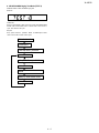
CONTENTS
CHAPTER 1. GENERAL DESCRIPTION
[1] PRECAUTIONS FOR USING LEAD-FREE
SOLDER ........................................................ 1-1
[2] IMPORTANT SERVICE NOTES (FOR
U.S.A. ONLY) ................................................. 1-2
[3] SPECIFICATIONS ......................................... 1-2
[4] NAMES OF PARTS........................................ 1-4
CHAPTER 2. ADJUSTMENTS
[1] ADJUSTMENT ............................................... 2-1
[2] TEST MODE .................................................. 2-2
CHAPTER 3. MECHANICAL DESCRIPTION
[1] REMOVING AND REINSTALLING THE
MAIN PARTS ................................................. 3-1
[2] DISASSEMBLY .............................................. 3-2
CHAPTER 4. DIAGRAMS
[1] BLOCK DIAGRAM MAIN ............................... 4-1
[2] BLOCK DIAGRAM TUNER............................ 4-3
[3] BLOCK DIAGRAM CD/MP3 DISPLAY........... 4-5
CHAPTER 5. CIRCUIT DESCRIPTION
[1] WAVEFORMS OF CD CIRCUIT .................... 5-1
[2] VOLTAGE....................................................... 5-3
CHAPTER 6. CIRCUIT SCHEMATICS AND PARTS
LAYOUT
[1] NOTES ON SCHEMATIC DIAGRAM ............6-1
[2] TYPES OF TRANSISTOR AND LED ............6-1
[3] SCHEMATIC DIAGRAM MAIN/POWER
AMP. ..............................................................6-2
[4] SCHEMATIC DIAGRAM TUNER...................6-4
[5] SCHEMATIC DIAGRAM CD/MP3 .................6-6
[6] SCHEMATIC DIAGRAM DISPLAY ................6-8
[7] WIRING SIDE OF PWB ..............................6-10
[8] WIRING SIDE OF PWB MAIN TOP/POWER AMP./JACK ............................................6-12
[9] WIRING SIDE OF PWB MAIN BOTTOM......6-14
[10] WIRING SIDE OF PWB TUNER .................6-16
[11] WIRING SIDE OF PWB CD/MP3 ................6-18
[12] WIRING SIDE OF PWB DISPLAY/
SWITCH ......................................................6-20
CHAPTER 7. FLOWCHART
[1] TROUBLESHOOTING ..................................7-1
CHAPTER 8. OTHERS
[1] FUNCTION TABLE OF IC .............................8-1
[2] FL DISPLAY ..................................................8-9
Parts Guide
SHARP CORPORATION
This document has been published to be used
for after sales service only.
The contents are subject to change without notice.
XL-MP60
CHAPTER 1. GENERAL DESCRIPTION
XL-MP60
Service Manual
[1] PRECAUTIONS FOR USING LEAD-FREE SOLDER
1. Employing lead-free solder
"MAIN,TUNER,CD/MP3,DISPLAY,POWER AMP.,JACK,SWITCH" of this model employs lead-free solder.
The LF symbol indicates lead-free solder, and is attached on the PWB and service manuals. The alphabetical character
following LF shows the type of lead-free solder.
Example:
Indicates lead-free solder of tin, silver and copper.
2. Using lead-free wire solder
When fixing the PWB soldered with the lead-free solder, apply lead-free wire solder. Repairing with conventional lead wire solder
may cause damage or accident due to cracks.
As the melting point of lead-free solder (Sn-Ag-Cu) is higher than the lead wire solder by 40 C, we recommend you to use a
dedicated soldering bit, if you are not familiar with how to obtain lead-free wire solder or soldering bit, contact our service station
or service branch in your area.
3. Soldering
As the melting point of lead-free solder (Sn-Ag-Cu) is about 220 C which is higher than the conventional lead solder by 40 C,
and as it has poor solder wettability, you may be apt to keep the soldering bit in contact with the PWB for extended period of
time. However, Since the land may be peeled off or the maximum heat-resistance temperature of parts may be exceeded,
remove the bit from the PWB as soon as you confirm the steady soldering condition.
Lead-free solder contains more tin, and the end of the soldering bit may be easily corrected. Make sure to turn on and off the
power of the bit as required.
If a different type of solder stays on the tip of the soldering bit, it is alloyed with lead-free solder. Clean the bit after every use
of it.
When the tip of the soldering bit is blackened during use, file it with steel wool or fine sandpaper.
Be careful when replacing parts with polarity indication on the PWB silk.
Lead-free wire solder for servicing
Ref No.
PWB-A
Description
Parts No.
DCEKKV517SJ03
Main(A1)/Tuner(A2)/CD/MP3(A3)/Display(A4)/POWER AMP.(A5)/Jack(A6)/Switch(A7)
1–1
XL-MP60
FOR A COMPLETE DESCRIPTION OF THE OPERATION OF THIS UNIT, PLEASE REFER TO THE OPERATION MANUAL.
[2] IMPORTANT SERVICE NOTES (FOR
U.S.A. ONLY)
BEFORE RETURNING THE AUDIO PRODUCT
(Fire & Shock Hazard)
Before returning the audio product to the user, perform the following
safety checks.
VTVM
AC SCALE
1. Inspect all lead dress to make certain that leads are not pinched or
that hardware is not lodged between the chassis and other metal
parts in the audio product.
1.5k ohms
10W
2. Inspect all protective devices such as insulating materials, cabinet,
terminal board, adjustment and compartment covers or shields,
mechanical insulators etc.
3. To be sure that no shock hazard exists, check for leakage current in
the following manner.
*
Plug the AC line cord directly into a 120 volt AC outlet.
*
Using two clip leads, connect a 1.5k ohm, 10 watt resistor paralleled by a 0.15µF capacitor in series with all exposed metal cabinet
parts and a known earth ground, such as conduit or electrical
ground connected to earth ground.
*
Use a VTVM or VOM with 1000 ohm per volt, or higher, sensitivity
to measure the AC voltage drop across the resistor (See diagram).
*
Connect the resistor connection to all exposed metal parts having a
return path to the chassis (antenna, metal cabinet, screw heads,
knobs and control shafts, escutcheon, etc.) and measure the AC
voltage drop across the resistor.
0.15 µ F
TO EXPOSED
METAL PARTS
TEST PROBE
CONNECT TO
KNOWN EARTH
GROUND
All check must be repeated with the AC line cord plug connection
reversed.
Any reading of 0.3 volt RMS (this corresponds to 0.2 milliamp. AC.) or
more is excessive and indicates a potential shock hazard which must
be corrected before returning the audio product to the owner.
[3] SPECIFICATIONS
For U.S.A.
■ General
Power source
■ Tuner
AC 120 V, 60 Hz
Power consumption 121 W
Dimensions
Width: 6-5/16" (160 mm)
Height: 9-7/16" (240mm)
Depth: 12-9/16" (319mm)
Weight
11.5 lbs. (5.2 kg)
Frequency range
■ Front speaker
Type
■ Amplifier
Output power
Output terminals
Input terminals
Front speakers: 37.5 watts minimum RMS
per channel into 6 ohms from 100 Hz to
20 kHz, 10% total harmonic distortion
Subwoofer: 45 watts minimum RMS into
6 ohms from 70 Hz to 130 Hz, 10% total
harmonic distortion
Front speakers and subwoofer: 6 ohms
Headphones: 16 - 50 ohms
(recommended: 32 ohms)
Video/Auxiliary (audio signal):
500 mV/47 k ohms
Maximum input
power
Rated input power
Type
5-disc multi-play compact disc player
Signal readout
Non-contact, 3-beam semiconductor laser
pickup
D/A converter
1-bit D/A converter
Frequency response 20 - 20,000 Hz
Dynamic range
90 dB (1 kHz)
2-way type speaker system
(magnetic shield)
1.5" (4 cm) tweeter
4" (10 cm) woofer
75 W
37.5 W
Impedance
6 ohms
Dimensions
Width: 6-1/2" (165 mm)
Height: 9-7/16" (240 mm)
Depth: 8-3/16" (208 mm)
4.9 lbs. (2.2 kg)/each
Weight
■ Subwoofer
Type
■ CD player
FM: 87.5 - 108 MHz
AM: 530 - 1,720 kHz
Maximum input
power
Rated input power
Impedance
Dimensions
Weight
1–2
5-1/8" (13 cm) subwoofer system
(magnetic shield)
90 W
45 W
6 ohms
Width: 6-5/16" (160 mm)
Height: 9-7/16" (240 mm)
Depth: 11-1/4" (285mm)
7.3 lbs. (3.3 kg)/each
XL-MP60
Except for U.S.A
■ General
Power source
■ Tuner
AC 120 V, 60 Hz
Frequency range
Dimensions
Weight
Width: 160 mm (6-5/16")
Height: 240 mm (9-7/16")
Depth: 319 mm (12-9/16" )
5.2 kg (11.5 lbs.)
■ Front speaker
Front speakers:
Maximum input
power
75 W
Rated input power
37.5 W
Impedance
6 ohms
Dimensions
Width: 165 mm (6-1/2")
Height: 240 mm (9-7/16")
Depth: 208 mm (8-3/16")
2.2 kg (4.9 lbs.)/each
Type
■ Amplifier
Output power
RMS: 45 W (10 % T.H.D.)
Input terminals
Front speakers and subwoofer: 6 ohms
Headphones: 16 - 50 ohms
(recommended: 32 ohms)
Weight
Video/Auxiliary (audio signal):
500 mV/47 k ohms
■ Subwoofer
Type
■ CD player
Type
2-way type speaker system
(magnetic shield)
4 cm (1.5") tweeter
10 cm (4") woofer
RMS: 75 W (37.5 W + 37.5 W)
(10 % T.H.D.)
Subwoofer:
Output terminals
FM: 87.5 - 108 MHz
AM: 530 - 1,720 kHz
Power consumption 121 W
5-disc multi-play compact disc player
Signal readout
Non-contact, 3-beam semiconductor laser
pickup
D/A converter
1-bit D/A converter
Frequency response 20 - 20,000 Hz
Dynamic range
90 dB (1 kHz)
Maximum input
power
13 cm (5-1/8") subwoofer system
(magnetic shield)
90 W
Rated input power
Impedance
45 W
6 ohms
Dimensions
Width: 160 mm (6-5/16")
Height: 240 mm (9-7/16")
Depth: 285 mm (11-1/4" )
Weight
3.3 kg (7.3 lbs.)
Specifications for this model are subject to change without prior
notice.
1–3
XL-MP60
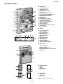
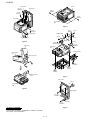
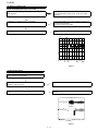
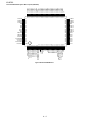
[4] NAMES OF PARTS
■ Front panel
1
2
11
3
12
13
14
15
16
17
4
5
6
7
8
18
9
1. Video/Auxiliary Button
2. Tuner (Band) Button
3. CD Button
4. Power On/Stand-by Button
5. Timer Indicator
6. Disc Stop, Tuning Down Button
7. Disc Play or Repeat, Tuning Up Button
8. Extra Bass/Demo Mode Button
9. Equalizer Mode Select Button
10. Headphone Jack
11. Remote Sensor
12. Disc Number Select Buttons
13. Disc Track Down or Fast Reverse,
Tuner Preset Down Button
14. Disc Track Up or Fast Forward,
Tuner Preset Up Button
15. Memory/Set Button
16. Disc Compartment Open/Close Button
17. Volume Control
18. Disc Compartment
■ Display
10
1
2 34 5
6 7 8
9
10 11
12
13
1. Disc Number Indicators
2. Disc Play Indicator
3. Disc Pause Indicator
4. Memory Indicator
5. Disc Repeat Play Indicator
6. WMA Track Indicator
7. CD Indicator
8. MP3 Track Indicator
9. Extra Bass Indicator
10. Sleep Indicator
11. Timer Play Indicator
12. FM Stereo Mode Indicator
13. FM Stereo Receiving Indicator
■ Rear panel
1. AC Power Input Jack
2. Speaker Terminals
3. FM/AM Loop Antenna Jack
4. Video/Auxiliary (Audio Signal) Input Jacks
5. Cooling Fan
1
3
4
2
5
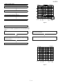
■ Front speaker
1
2
3
1. Tweeter
2. Woofer
3. Bass Reflex Duct
4. Speaker Wire
4
■ Subwoofer
1. Sub Duct Pipe
2. Subwoofer
3. Speaker Wire
2
1
3
1–4
Note:
The speaker grilles are not removable.
XL-MP60
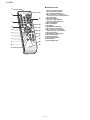
■ Remote control
1
12
2
13
3
14
4
15
5
16
6
17
7
18
8
19
9
20
10
21
1. Remote Control Transmitter
2. Power On/Stand-by Button
3. Direct Track Search Buttons
4. Disc Track Down or Fast Reverse,
Tuner Preset Down, Time Down Button
5. Disc Stop Button
6. Extra Bass Button
7. Disc Play or Repeat Button
8. Volume Up and Down Buttons
9. Memory/Set Button
10. Disc Clear Button
11. CD Button
12. MP3/WMA Display Button
13. Disc Number Select Buttons
14. Disc Track Up or Fast Forward,
Tuner Preset Up, Time Up Button
15. Disc Pause Button
16. Equalizer Mode Select Button
17. Disc Random Button
18. Timer/Sleep Button
19. Video/Auxiliary Button
20. Clock Button
21. Tuner (Band) Button
11
1–5
XL-MP60
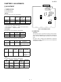
CHAPTER 2. ADJUSTMENTS
XL-MP60
Service Manual
TUNER PWB
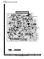
[1] ADJUSTMENT
R311
TP-VT
FM BAND
COVERAGE fL
1. TUNER SECTION
L307
fL: Low-range frequency
36
IC301
• AM IF/RF
Signal generator: 400 Hz, 30%, AM modulated
Test Stage
IF
AM Band
Coverage
AM Tracking
Frequency
Frequency
Display
450 kHz
—
1,602 kHz
522 kHz
990 kHz
990 kHz
23
L304
FM RF
Instrument
Connection
Setting/
Adjusting
Parts
L305
(fL): L306
1.1 ± 0.1 V
L302
AM BAND
COVERAGE fL
L306
CNP301
fH: High-range frequency
L305
AM IF
*1
*2
L302
AM
Tracking
*3
*1. Input: IC301 1Pin Output: IC301 23Pin
*2. Input: Input is not connected
Output: TP-VT(IC301 28Pin)
*3. Input: Antenna
Output:IC301 23Pin
Figure 1 ADJUSTMENT POINTS
• Check FM VT
Signal generator: 1 kHz, 40 kHz dev., FM modulated
Frequency
87.5 MHz
108 MHz
Display
Check
Point
1.5V ± 1.0V
5.0V ± 1.0V
87.5 MHz
108 MHz
2. CD SECTION
Instrument
Connection
TP-VT
TP-VT
•
Since this CD system incorporates the following automatic adjustment functions, readjustment is not needed when replacing the
pickup. Therefore, different PWBs and pickups can be combined
freely.
• FM Mute Level
Each time a disc is changed, these adjustments are performed
automatically. Therefore, playback of each disc can be performed
under optimum conditions.
Signal generator: 1 kHz, 40 kHz dev., FM modulated
Frequency
Display
98.00 MHz
(30 dBµV)
98.00 MHz
Adjusting
Parts
—
Instrument
Connection
Input: Antenna
Output: Speaker Terminal
• FM Detection
Signal generator: 10.7 MHz FM sweep generator
Test
Stage
FM IF
Frequency
Frequency
Display
10.7 MHz
98.00 MHz
Setting/
Adjusting
Parts
—
Instrument
Connection
Input: Pin 36 of
IC301
Output: Pin 23
of IC301
• FM RF
Signal generator: 1 kHz, 75 kHz dev., FM modulated
Test
Stage
FM Band
Coverage
FM RF
Frequency
Frequency
Display
—
87.50 MHz
98.00 MHz
(10 ~ 20dB)
98.00 MHz
*1. Input: Antenna
Setting/
Adjusting
Parts
(fL): L307
1.5 ± 0.1 V
L304
Adjustment
Instrument
Connection
*1
*1
Output: 23 Pin of IC301
2–1
XL-MP60
[2] TEST MODE
"STOP"..............................
"VIDEO/AUX"....................
The test mode applied to this microcomputer has three modes, namely
the ordinary test mode for adjustment or measurement, the aging test
mode, and the self-diagnosis test mode for self-judgment in case of
final product inspection.
Invalid
CLV
2. Step 2 Mode
Press the "MEMORY/SET" button in this mode to transmit the laser
lighting command LDON (8400) and turn on the laser. Any other
operations are not performed in this case.
1. Turning on the test mode
For obtaining each test mode, press the Power ON/STAND BY button,
while keeping pressing the following two buttons in the ordinary standby mode (power off). In this case, the main unit buttons are valid.
When turning the POWER on with remote control buttons, test modes
are not obtained.
Press the following buttons in this state to obtain the operations
specified below.
[Ordinary test mode]
"POWER ON/STAND BY"...
1. CD Test Mode (TEST 1)...........................................................
CD + DISC1
2. Tuner Test Mode (TEST 2)........................................................
TUNER(BAND) + DISC1
3. Electronic Volume Test Mode (TEST 3).....................................
TUNING DOWN + VOLUME UP
4. Timer Test Mode (TEST 4).......................................................
TUNING UP + DISC5
5. FL Test Mode (TEST 5)...........................................................
PRESET DOWN + VOLUME DOWN
6. CD MECHANISM Aging Test Mode (TEST 8)...........................
CD + Equalizer
"FWD".................................
"REV"..................................
"MEMORY/SET"................
Test mode and power turned off to
shift to the ordinary standby mode.
The pickup slides toward the outer
periphery while this button is pressed.
The pickup slides toward the inner
periphery while this button is pressed.
If PICKUP IN is on, input is invalid.
Shift to step 3
3. Step 3 Mode
While the laser keeps lighting, CD initialization operation flow proceeds up to 'CLV servo ON' to wait for the following buttons to be
pressed.(Focus servo turned on for focus search)
The focus search is repeated to take focus.
[Self-diagnosis Test Mode]
1. Button input diagnosis test mode (TEST 6)...............................
PRESET UP + DISC5
Processes are different depending on destinations at initial settings.
Press the following buttons in this state to obtain the operations
specified below.
2. CD Test Mode (TEST 1)
In the CD test mode the operation of each step is possible even if the
LID-SW is off. If focus cannot be taken in step 3 or any error is processed, it is impossible to proceed to the next step. During error processing, end the test mode by pressing the Power ON/STAND BY
button or return to the step 1 by pressing the CD STOP button. Any
other operations are inhibited.
"POWER ON/STAND BY".....
"FWD"...................................
"REV"....................................
1. Step 1 Mode
"MEMORY/SET"..................
When the CD test mode is obtained, the following display lights up.
Then CD initialization operation flow proceeds up to CD STB off to
wait for the following buttons to be pressed.
Test mode and power turned off to shift
to the ordinary standby mode.
The pickup slides toward the outer
periphery while this button is pressed.
The pickup slides toward the inner
periphery while this button is pressed.
If PICKUP IN is on, input is invalid.
If focus has been taken, shift to step 4 is
executed. If not, acceptance is inhibited.
*If the focus is not received after it has been taken, the process
returns to step 1.
4. Step 4 Mode
The CLV servo ON command (8600) is transmitted to wait for the
following buttons to be pressed. (The disc is rotated for CLV lock.)
One second after display lights up
The time display always indicates "0:00".
Press the following buttons in this state to obtain the operations
specified below.
Press the following buttons in this state to obtain the operations
specified below.
"POWER ON/STAND BY"...
"FWD"..........................
"REV"......................
"MEMORY/SET"................
"POWER ON/STAND BY"....
Test mode and power turned off to shift
to the ordinary standby mode.
After the pickup returns to the innermost
periphery, it slides toward the outer
periphery while this button is pressed.
After the pickup returns to the innermost
periphery, it slides toward the inner
periphery while this button is pressed. If
PICKUP IN is on, input is invalid.
Shift to step 2
2–2
"FWD"..................................
"REV"...................................
"MEMORY/SET"..................
Test mode and power turned off to
shift to the ordinary standby mode.
The pickup slides toward the outer
periphery while this button is pressed.
The pickup slides toward the inner
periphery while this button is pressed.
If PICKUP IN is on, input is invalid.
Return to step 5
*If the focus is not received, the process returns to step 1.
XL-MP60
•
5. Step 5 Mode
When the CD initialization operation flow is completed, the mute is
turned off, and playback is started. Even if playback reaches the
outermost periphery of disc, the operation does not stop. The LCD
display indicates the playback passage time as in case of ordinary
CD playback.
The TUNER TEST 2 mode is obtained with >> + MEMORY/SET +
POWER ON/STAND-BY. ->Turn off AC in the TEST 2 mode to
restore the initial state.
Turn off POWER to protect the memory of TEST 2 mode.
Turn off POWER again to obtain the ordinary operation while the
data is stored in the memory (besides TUNER).
Press the following buttons in this state to obtain the operations
specified below.
"POWER ON/STAND BY"....
"FWD"..................................
"REV"...................................
"PLAY"...............................
"STOP"...............................
If AC OFF state is maintained in this state for about 1/2 day, start is
executed in the initial state.
Test mode and power turned off to shift
to the ordinary standby mode.
The pickup slides toward the outer
periphery while this button is pressed.
The pickup slides toward the inner
periphery while this button is pressed.
If PICKUP IN is on, input is invalid.
Invalid
Return to step 1
•
3. Preset frequencies for various destinations
(random preset memory)
CH
1
2
3
4
5
*If the focus is not received, the process returns to step 1.
Other cautions
•
To clear the whole memory, insert the AC cord, pressing
TUNER(BAND) + DISC2.
TOC IL is not available for this test mode.
3. Tuner Test Mode (TEST 2)
BAND
FM STEREO
CH
6
7
8
9
10
1. Outline of tuner (radio) test mode
The tuner test mode is intended to store the adjustment and measurement frequencies in the preset memory CH. When adjusting
the tuner section in the production line, adjusting personnel are not
required to set frequency.
2. Details of tuner test mode
BAND
AM
CH
16-35
36
37
38
39
40
Press the "TUNER(BAND)" and "DISC1" buttons in POWER OFF
state and turn on the power by the use of "POWER ON/STAND BY"
button to preset and store frequency for adjustment and measurement of destination specified by the AREA terminal in the preset
memory CH. However, Ordinary 1 and Ordinary 2 are stored in the
destinations when the test mode is obtained.
(As for frequencies to be preset and stored for each destination, refer
to item 3.)
•
The tuner test mode is started from preset No.1.
BAND
FM MONO
FM
FM 87.5 MHz
FM108.0 MHz
FM 98.0 MHz
FM 90.0 MHz
FM106.0 MHz
FM
AM 530 kHz
AM1720 kHz
AM 990 kHz
AM 600 kHz
AM1400 kHz
FM
——————
FM106.0 MHz
FM 90.0 MHz
FM 98.0 MHz
FM108.0 MHz
FM 87.5 MHz
The slant line sections of the table store no memory.
4. Electronic volume Test Mode (TEST 3)
The operations of test mode are identical with the ordinary operations
of TUNER function. FUNCTION switching is invalid.
When this test mode is obtained, the following display lights for one
second.
It is necessary to discard the content of preset memory when the tuner
test mode is ended; be sure to write "0000" or "1111" bits in the memory to be checked for judging memory error at initial setting and to initialize memory.
When the tuner test mode is obtained, the following display lights for
one second.
In this mode, volume is Volume -14 dB (STEP 23), FLAT AND X-BASS
ON, and start-up function to CD, respectively. The button operations in
the test mode are the same as those of ordinary operation except volume UP/DOWN.
1) The display is the same as that of ordinary operation except test
mode setting.
2) Unlike the ordinary state, the volume is controlled with the volume
UP/DOWN button in accordance with the following three steps.
Volume- ∞ (STEP 0) <-> Volume-14 dB (STEP 23) <-> Volume-0
(STEP 30)
3) X-BASS is switched when button is pressed.
2–3
XL-MP60
5. Timer test Mode (TEST 4)
7. Button input diagnosis Test Mode (TEST 6)
When this test mode is obtained, the following display lights for one
second.
When the test mode is obtained, the following is displayed.
(STAND-BY AND DEMO OFF STATUS)
Set the current time and timer time according to the following procedure to reproduce the timer.
This test mode is intended to check whether all the main unit buttons
can be detected. Accordingly, in this test mode, it is checked whether
the "POWER ON/STAND BY" button was pressed after all the buttons
shown below were pressed. If the result is OK, OK is displayed. If any
one of keys was not pressed, an error is displayed. In both cases of
OK termination or error termination, the mode is shifted to the standby
mode if the "POWER ON/STAND BY" button is pressed subsequently.
1. Set the current time to 1:00, the timer to ON time 1:05, the function
to CD, and volume to STEP 12, respectively. One minute is
counted as one second, and the timer is reproduced. The fade-in
(when playback is started) is executed at a rate of one step for 1
sec. After completion of fade-in, the fade-out is executed at a rate
of one step for 1 sec (WAIT 1 sec inserted).
After completion of fade-out, the power is turned off (after WAIT 1
sec), and the mode is shifted to the standby.
All models using this type of microcomputer are not always provided
with the same buttons. Since the buttons used are different depending
on models, types of buttons to be used are determined by whether
SURROUND, and an electric lid are available at the initial setting by
MODEL port.
The display during operation is the same as that of ordinary timer
operation.
6. FL Test Mode (TEST 5)
The order of buttons to be pressed is not determined. Accordingly, it is
checked whether all buttons have been pressed.
When the FL test mode is obtained, all the FL segments are lighted.
Then pressing the "PLAY" button switches display as below.
1. PU-IN buttons: CUE/PRESET UP + CD STOP
————–
Since this model is provided with SURROUND (HAVE OR NOT),
and electric CD lid, the following 10 buttons are detected as all buttons.
Lighting of all segments
PLAY, X-BASS/DEMO, FUNCTION, VOLUME UP/DOWN, MEMORY/SET, REV, FWD, STOP, CD-OPEN/CLOSE
The OK/ERROR display of test result is as follows.
Lighting of odd segments
Lighting of even segments
__________
2–4
XL-MP60
8. CD MECHANISM Aging Test Mode (TEST 8)
OPEN/CLOSE & 5 DISC CHANGER aging test.
DISPLAY:
FUNCTION:
Enter the TEST MODE 8, MCU control the 5 DISC CHANGER OPEN/
CLOSE. After close finished, disc1 to disc5 move in then out for 1
cycle. Then start the next cycle.
Request:
Every period include 4 operation. Below is TIMING:open->close>disc1->disc2->disc3->disc4->disc5->open
Enter test mode
CHANGER
Find the disc 1 position
open
delay 3S after open finish
rotate 1 circle
close
delay 3S after close finish
rotate 1 circle
2–5
XL-MP60
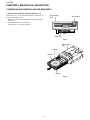
CHAPTER 3. MECHANICAL DESCRIPTION
Home Stereo
Service
XL-MP60
E
Market
Manual
Service Manual
[1] REMOVING AND REINSTALLING THE MAIN PARTS
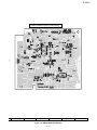
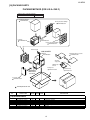
1. How to remove CD Disc manually (See Fig. 1,2)
CD Changer
Unit
Perform steps 1 to 10 of the disassembly method to remove the CD
Changer unit.(see page 3-2,3-3)
Arm switch C
1. Rotate the gear cam until the arm switch C becomes the position of
the Figure 1.
2. Pull the drawer to the front like the Figure 2.
And the CD disc on the carriage is taken out.
Gear cam
Figure 1
CD Changer
Unit
Carriage
CD Disc
Drawer
Figure 2
3–1
XL-MP60
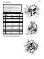
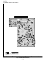
[2] DISASSEMBLY
Top Cabinet
Caution on Disassembly
Follow the below-mentioned notes when disassembling the unit and
reassembling it, to keep it safe and ensure excellent performance:
1) Be sure to remove the power supply plug from the wall outlet
before starting to disassemble the unit.
2) Take off nylon bands or wire holders where they need to be
removed when disassembling the unit. After servicing the unit,
be sure to rearrange the leads where they were before disassembling.
3) Take sufficient care on static electricity of integrated circuits and
other circuits when servicing.
STEP
1
2
3
4
REMOVAL
Top Cabinet
Side Panel
Rear Panel
Tuner PWB
5
Main PWB
6
POWER AMP.
PWB
Transformer
Fan Motor
Front Panel/CD
Tray Cover
7
8
9
10
11
Chassis
CD/MP3 PWB
(Note 1)
12
13
14
CD Changer Unit
CD Mechanism
Display PWB
15
Jack PWB
(A1) x2
ø3x10mm
(A1) x2
ø3x10mm
Side Panel
(Right)
(B1) x2
ø3x10mm
PROCEDURE
1. Screw...........................(A1) x 5
1. Screw...........................(B1) x 8
1. Screw..........................(C1) x 6
1. Screw..........................(D1) x 1
2. Socket.........................(D2) x 3
1. Screw...........................(E1) x 3
2. Socket.......................(E2) x 10
1. Screw...........................(F1) x 4
FIGURE
1
1
2
2
1. Screw..........................(G1) x 4
1. Screw..........................(H1) x 2
1. Screw...........................(J1) x 2
2. Flat cable......................(J2) x 1
3. Socket..........................(J3) x 1
4. CD Tray cover..............(J4) x 1
2. Screw..........................(K1) x 6
1. Flat cable.....................(L1) x 1
2. Socket..........................(L2) x 2
3. Screw...........................(L3) x 4
4. Screw...........................(L4) x 2
1. Screw..........................(M1) x 6
1. Screw..........................(N1) x 4
1. Knob............................(P1) x 1
2. Screw.........................(P2) x 10
1. Screw..........................(Q1) x 1
4
4
4
(A1) x1
ø3x10mm
(B1) x2
ø3x10mm
(B1) x2
ø3x10mm
(B1) x2
ø3x12mm
Side Panel
(Left)
Rear
Panel
3
Figure 1
3
5
6
7
(D2) x3
(D1) x1
ø3x6mm
Main PWB
7
7
8
Tuner PWB
8
Note 1:
(C1) x1
ø3x12mm
(C1) x5
ø3x10mm
Rear
Panel
After removing the connector for the optical pickup from the connector,
wrap the conductive aluminium foil around the front end of the connector so as to protect the optical pickup from electrostatic damage.
Figure 2
(E2) x1
(E2) x2
(E1) x2
ø3x6mm
Front Panel
(E2) x2
(E2) x2
(E1) x1
ø3x12mm
Main PWB
POWER AMP.
PWB
(F1) x3
ø3x6mm
(E2) x1
(F1) x1
ø3x6mm
(E2) x2
Figure 3
3–2
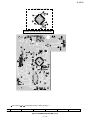
XL-MP60
Chassis
Transformer
Front Panel
(G1) x4
ø4x10mm
(K1) x3
ø3x8mm
(H1) x2
ø3x6mm
(K1) x3
ø3x8mm
Fan Motor
CD Changer
Unit
Figure 6
(L3) x4
ø3x6mm
(J1) x2
ø3x12mm
Display PWB
CD/MP3 PWB
(L2) x1
(J2) x1
(L1) x1
(L2) x1
(J3) x1
Bracket
Figure 4
Bracket
(L4) x1
ø3x6mm
(L4) x1
ø3x6mm
Front Panel
CD Changer
Unit
CD Mechanism
DVD Changer
Unit
DVD Tray Cover
(N1) x4
ø2.5x8mm
(M1) x3
ø3x8mm
(M1) x3
ø3x8mm
DVD Tray Cover
(J4) x1
Figure 7
Front Panel
(P1) x1
Nut
DVD Changer
Unit
Figure 5
Display PWB
(P2) x10
ø2.5x8mm
(Q1) x1
ø2.5x8mm
Jack PWB
Figure 8
CP-MP60F, CP-MP60SW
These speaker CP-MP60F, CP-MP60SW are available in assembles
only and may not be disassembled.
3–3
XL-MP60
-MEMO-
3–4
XL-MP60
CHAPTER 4. DIAGRAMS
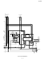
TO TUNER PWB
CNP602
4
4
5
5
7
8
TO CD SERVO PWB
CNS407
AUDIO+B
+8V
M_GND
+8V
D_GND
NC
1
2
3
+B
R_CH
S/W_CH
ÐB
D_GND
6
7
+B
+12V
+B
+7V
+8V
8
9
CNS602
1
2
3
4
5
A_GND
3
3
6
L_CH
1
2
VEE
1
2
VCC
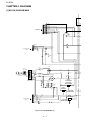
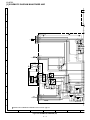
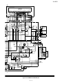
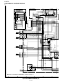
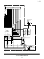
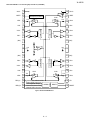
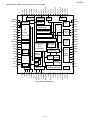
[1] BLOCK DIAGRAM MAIN
+B
Q101
Q102
CNW602
Q103
+8V
Q413
A GND
CNP407
Q414
+B
DGND
+B
+B
+B
+B
+B
D201
F201
6.3A 125V
SO202
AC SOCKET
+B
+B1
+B
1
F202
6.3A 125V
AGND
2
+B
C211
ÐB1
D205~D208
F203
1.6A 125V
C212
ÐB
+B2
ÐB
T201
POWER
TRANSFORMER
IC203
KIA7808API
VOLTAGE
REGULATOR
DGND
ZD201
Q201
IC202
KIA7812API
+B
1
2
3
TO DISPLAY PWB
CNS101
4
5
6
7
3.8V
IC201
KIA7805API
VF2
ÐB
D_GND
+5.6V
+B
+B
+B
+B
MGND
+12V
VOLTAGE
REGULATOR
VF1
3.8V
Ð30V
+B
+B
DGND
ZD202
AC POWER
SUPPLY CODE
AC 120V 60Hz
+B
+B
CNP101
Figure 4-1 BLOCK DIAGRAM (1/6)
4–1
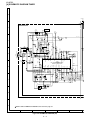
VOLTAGE
REGULATOR
+B
GND
MUTE3
S/W_RF
S/W_IN
12
13
14
15
16
17
18
19
20
21
22
23
24
25
26
27
SO101
SPEAKER TERMINAL
S/W_OUT
11
NC
MUTE1
10
R_RF
GND
9
MUTE2
NC
8
GND
VEE
7
NC
L_OUT
6
VEE
NC
5
R_IN
VCC
4
R_OUT
NC
3
VCC
NC
2
L_IN
VEE
1
IC101
LM4781TA
POWER AMP.
L_RF
VCC
XL-MP60
+
+B
Ð
L-CH
+
ÐB
ÐB
Ð
R-CH
+
Ð
SUB WOOFER
+B
RLY102
CNP103A/B
L IN
1
L OUT
2
A_GND
3
R OUT
4
R IN
5
SUB_RLY IN
6
SUB_RLY OUT
7
RLY101
+B
JK101
HEADPHONES
1
3
11
10
2
9
8
7
6
5
4
Q112
Q113
Q114
+B
+B
+B
Q110
Q111
ÐB
Q107
Q108
+B
Q109
SP_RELAY
SINGAL_LVL
FAN_ATART
SP_DETECT
P_MUTE
FAN_PRO
+B
+B
+B
+B
CD+B
1
2
3
4
5
6
7
CNP102
Q205
Q204
Q203
M201
FAN MOTOR
Q202
M
Figure 4-1 BLOCK DIAGRAM (1/6)
4–2
TO DISPLAY PWB
CNS102
XL-MP60
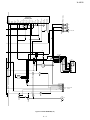
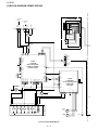
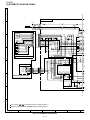
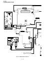
[2] BLOCK DIAGRAM TUNER
AM BAND
COVERAGE fL
TO CD DIS
CNS3
L306
D305
AM OSC
4
2
5
1
6
CNP302
6 5 4 3
DI
CE
CL
D GND
3
TP-VT
+B
+12V
+B
4
5
D307
FM OSC
L307
L302
AM ANT.
6
FM RF
BAND PASS
FILTER
L304
D308
BF301
X301
75KHz
4
5
6
7
8
9
10 11 12 13 14 15 16 17 18
CF302
FM IF
FM IF
FM FRONT END
PLL(TUNER)
FM IF DET./FM MPX./AM IF
XIN
DO
3
IC301
LV23002M
VDD
XOUT
MPX-IN
CL
DET-OUT
CE
DI
AMLOWOUT
P-CCMP
VSS
P-DET
R-OUT
B01
FM IFIN
PD
B02
AM IFIN
AGC
AM-OSC
VCC1
2
LP-IN
VCC2
FM-OSC
AM-MIX
1
LP-OUT
FMRF-OUT
GND1
L-OUT
23 22 21 20 19
FM-IET
36 35 34 33 32 31 30 29 28 27 26 25 24
FM-MIX
1
2
3
1
REG
FM ANTENNA
1
2
3
AM
Tracking
2
AMRF-IN FMRF-IN
CNP301
3
D306
Q302
AM LOOP
ANTENNA
DO
CLK
CF301
CF303
DI
CE
FM IF
Q303
TUNÐR
TUNÐL
3
4
CF304
2 L305
1
6
AM IF
AM IF
Figure 4-3 BLOCK DIAGRAM (3/6)
4–3
+8V
XL-MP60
TO CD DISPLAY PWB
CNS302
6 5 4 3 2 1
1
2
3
CD R
CD L
+B
CD_A_GND
CNP406
DI
CE
CL
D_GND
DO
+8V
CNP302
TO CD SERVO PWB
CNS406
+B
DI
CE
CL
TUN R
CD R
308
IC602
NJM4558D
BUFFER
AUX R
RSL0
RIN
RTRE
RBS
ROUT
VREF
VDD
CL
LSL0
LIN
LTRE
LBS
LOUT
VSS
CE
DI
R3
R4
8
7
6
5
4
3
2
1
AUX_R
R-CH
A_GND
L-CH
A_GND
12 11 10 9
DO
A_GND
SO601
VIDEO/AUX
IN
13 14 15 16 17 18 19 20 21 22 23 24
L4
4
L3
3
R1
2
+B
R2
1
5
L2
+
Ð
6
Ð
L1
7
IC601
LC75341M
AUDIO PROCESSOR
8
+B
+
PLL(TUNER)
FM IF DET./FM MPX./AM IF
+B
CD L
AUX L
CLK
DI
CHASSIS
GND
CE
TUN L
+B
TUNÐR
TUNÐL
+B
+B
+8V
+B +B
+B
Figure 4-4 BLOCK DIAGRAM (4/6)
4–4
CNP602
L_CH
1
A_GND
2
R_CH
3
S/W_CH
4
D_GND
5
+12V
6
+7V
7
+8V
8
TO MAIN PWB
CNS602
XL-MP60
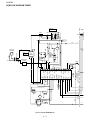
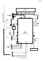
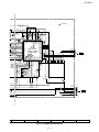
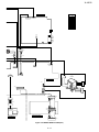
[3] BLOCK DIAGRAM CD/MP3 DISPLAY
CD CHANGER PWB ASS'Y
TO TUNER PWB
CNP406
TO MAIN PWB
D_GND
SW4
SW3
SW5
SW6
SW2
SW1
SW7
CD_PH2
CD_PH3
MM+
CD_SOL1
MMÐ
CD_SOL2
SW8
5
4
AUDIO+B
+8V
1
DGND
MGND
2
+8V
AGND
3
L-CH
CNS406
R-CH
CNP407
3
2
1
CNS407
Q806
1
2
3
4
5
6
7
8
9
10
11
12
13
14
15
PHOTO
INTERRUPTER
M
MOTOR
CONSTANT
VOLTAGE
SOLENOID
Q805
CNP405A
CE
DI
CL
DO
LRVDD
LCHO
RCHO
47 46 45 44 43
76
75
RESB
78
7
CD_CL
20 AVSS
6
CD_DI
26 VVSS1
5
CD_DO
37 DVSS
40 VVSS3
4
IC801
LC78690
MP3 DECODER
DIGITAL SIGNAL
PROCESSOR
42 DVSS
~
53
57
65 VVSS2
71 DVSS
3
2
CD_RES
1
CD_CE
PUIN 32
72 XOUT
CONT2 50
LDD
LDS
EIN
FIN
17
BIN
DIN
VREF
30 36 41 68 74
AIN
CIN
XVDD
DVDD
DVDD
DVDD
73 XIN
VVDD1
2 MUTE
SPDO 25
4 VG1
SLDO 24
11 VG2
FDO 22
25 VG4
TDO 23
18 VG3
5 6 7 8 13 14 19 18
+8V
+3.3V
CONSTANT
VOLTAGE
1 VCC
28 VCC
VO2+
VO1+
VO1-
+3.3V
Q801
VO2-
LASER
DRIVER
REG_OUT
Q802
VO3-
27 VREF
VO3+
+3.3V
IC402
LA6548NH
FOCUS/TRACKING/
SPIN/SLED
DRIVER
VO4VO4+
X801
16.9344 MHz
77 LRVSS
23 24
19 20
13
9 10
5
6
+3.3V
CD PICKUP UNIT
FOCUS COIL
TRACKING COIL
MD
LD
F
C
B
A
D
E
VC
VCC
+5V
TO M
C
SPINDLE
MOTOR
SLED
MOTOR
Figure 4-5 BLOCK DIAGRAM (5/6)
4–5
+
M
-
M
PICKUP IN
+
XL-MP60
VFD701
FL DISPLAY
VF2
40 39
VF1
~
37
22
21
~
18
14
~
4
2 1
CNS101
6
12V
7
P20
63
~ 52
~
50
~ 47
~
51
45
~ 42
~
40
D_GND
30
1
REMOTE
SENSOR
RX701
IRQ 29
~
~
64 SW1
~
~
TIMER_LED
M_GND
+5.6V
+5.6V
1G
5
Q705
11G
+5.6V
LED701
Ð30V
P1
4
P4
D_GND
3.8V
VP
3
2
P5
ÐB2
P8
1
P9
TO MAIN PWB
CNP101
VF1
VF2
3.8V
71 SW8
SW709
POWER
POWER_KEY 20
KEY
73
74
75
76
Q502
Q503
Q511
KEY2
CD_PH
MM+
MMCD_SOL
19
SW710~SW716
SW717
OPEN/
CLOSE
KEY1
18
KEY
SW701~SW708
Q505~Q509
CHANGER
MOTOR
DRAIVER
+5V
IC701
IXA033SJ
SYSTEM
MICROCOMPUTER
78 JOG_UP
Q510
CF1 15
VSS1 14
89 VSS2
CNS302
TO TUNER PWB
CNP302
+8V
1
DO
2
D_GND
XT2 13
91 DO
XT1 12
3
CL
4
87 CL
CE
5
85 CE
DI
6
86 DI
X701
32.768 kHz
CONSTANT
VOLTAGE
CF2 16
X702
8 MHz
77 JOG_DOWN
SW700
VOLUME
JOG
VDD1 17
TO MAIN PWB
CNP102
1
SIGAL_LVL
2
FAN_START
3
SP_DETECT
4
P_MUTE
5
FAN_PRO
6
CD+B
7
7 92
2 23 83
95 96 97 98 99
SYS_STOP
RESET
CD/MP3 RES
CD_CE
CD/MP3 CL
CD/MP3 DO
CD/MP3 DI
CD+B
FAN_PRO
P_MUTE
SP_DETECT
FAN_START
SIGAL_LVL
88 94
CNS102
SP_RELAY
SP_RELAY
VDD2 90
79
80
81
82
84
VDD3 46
VDD4 72
11 26
RESET
Q702,Q703,Q704
CNP405B
CD_CE
1
CD_RES
2
3
4
CD_DO
5
CD_DI
6
CD_CL
7
Figure 4-6 BLOCK DIAGRAM (6/6)
4–6
+5.6V
XL-MP60
CHAPTER 5. CIRCUIT DESCRIPTION
Home Stereo
Service
XL-MP60
E
Market
Manual
Service Manual
[1] WAVEFORMS OF CD CIRCUIT
T
Stopped
CH1=10 V
DC 10:1
1
CH2=1 V
DC 10:1
100 ms/div
(100 ms/div)
NORM:100 kS/s
IC801 22
TE
3
2
IC801 16
2
IC801 23
=Filter=
Smoothing : ON
BW : FULL
1
IC801 22
1
IC801 22
3
IC801 16
5
IC801 25
=Offset=
CH1 :
0.0 V
CH2 :
0.00 V
CH3 :
0.00 V
CH4 :
0.00 V
Stopped
CH1=500 mV
DC 10:1
=Record Length=
Main :
100 K
Zoom :
2K
CH3=1 V
DC 10:1
=Trigger=
Mode : NORMAL
Type : EDGE CH1
Delay :
2.924 ms
Hold off :
0.2 µs
1999/04/05 17:33:17
CH4=1 V
500 ms/div
(500 ms/div)
DC 10:1
NORM:20 kS/s
PDOUT0
6
4
IC801 28
3
4
IC801 2
7
PDOUT1
IC801 27
T
1
IC801 22
FDO
1
CH1
v/DIV
500 mV
=Filter=
Smoothing : ON
BW : FULL
5–1
=Offset=
CH1 :
0.000 V
CH2 :
0.0 V
CH3 :
0.00 V
CH4 :
0.00 V
=Record Length=
Main :
100 K
Zoom :
2K
=Trigger=
Mode : AUTO
Type : EDGE CH2
Delay :
0.0 ns
Hold off :
0.2 µs
XL-MP60
Stopped
CH1=2 V
DC 10:1
T
1999/04/07 09:25:28
500 ns/div
(500 ns/div)
NORM:200 MS/s
T
8
IC801 69
1
DOUT
=Filter=
Smoothing : ON
BW : FULL
Stopped
CH1=2 V
DC 10:1
9
=Offset=
CH1 :
0.00 V
CH2 :
0.00 V
CH3 :
0.00 V
CH4 :
0.00 V
=Record Length=
Main :
1K
Zoom :
100
T
CH2=2 V
DC 10:1
CH3=2 V
DC 10:1
=Trigger=
Mode : NORMAL
Type : EDGE CH1
Delay :
2.887 ms
Hold off :
0.2 µs
1999/04/05 20:50:17
5 µs/div
(5 µs/div)
NORM:100 kS/s
IC801 60
1
LRSY
10
IC801 59
2
DATACK
11
IC801 58
T
3
DATA
=Filter=
Smoothing : ON
BW : FULL
1
IC801 22
12
IC801 24
CH3
v/DIV
2V
=Offset=
CH1 :
0.00 V
CH2 :
0.00 V
CH3 :
0.00 V
CH4 :
0.00 V
=Record Length=
Main :
5K
Zoom : 100
=Trigger=
Mode : AUTO
Type : EDGE CH3
Delay :
0.0 ns
Hold off :
0.2 µs
5–2
XL-MP60
[2] VOLTAGE
IC101
PIN
NO.
1
2
3
4
5
6
7
8
9
10
11
12
13
14
15
16
17
18
19
20
21
22
23
24
25
26
27
VOLTAGE
30 V
-30 V
30 V
-30 V
30 V
-30 V
0V
-30 V
0V
0V
-3 V
0V
0V
30 V
0V
0V
-30 V
0V
0V
-3 V
0V
0V
0V
0V
-3 V
0V
0V
IC201
PIN
NO.
1
2
3
VOLTAGE
10 V
0.6 V
5.6 V
IC202
PIN
NO.
1
2
3
VOLTAGE
19.8 V
0V
12 V
IC203
PIN
NO.
1
2
3
VOLTAGE
19.8 V
0V
8V
VOLTAGE
1.65 V
1.6 V
1.6 V
1.8 V
1.7 V
1.7 V
1.7 V
1.7 V
1.6 V
1.7 V
1.7 V
2.8 V
1.7 V
1.7 V
1.7 V
1.7 V
1.7 V
3.4 V
0V
0V
3.3 V
1.7 V
1.7 V
1.7 V
1.7 V
0V
0V
0.8 V
1V
3.1 V
0V
3.1 V
0V
0V
0V
3.1 V
0V
1.8 V
3.1 V
0V
3.1 V
0V
0V
3.6 V
3.6 V
0V
3.6 V
0V
0V
0V
0V
0V
0V
0V
0V
0V
0V
0V
0V
0V
2.9 V
1.5 V
1.9 V
1.9 V
0V
1.8 V
0V
3.1 V
0V
0V
0V
1.3 V
1.4 V
3V
1.6 V
3.1 V
0V
1.6 V
3.2 V
1.6 V
IC601
IC301
IC801
PIN
NO.
1
2
3
4
5
6
7
8
9
10
11
12
13
14
15
16
17
18
19
20
21
22
23
24
25
26
27
28
29
30
31
32
33
34
35
36
37
38
39
40
41
42
43
44
45
46
47
48
49
50
51
52
53
54
55
56
57
58
59
60
61
62
63
64
65
66
67
68
69
70
71
72
73
74
75
76
77
78
79
80
PIN
NO.
1
2
3
4
5
6
7
8
9
10
11
12
13
14
15
16
17
18
19
20
21
22
23
24
25
26
27
28
29
30
31
32
33
34
35
36
VOLTAGE
2.23 V
2.23 V
2.5 V
0V
5.1 V
5.1 V
2.2 V
2.2 V
4.1 V
3.96 V
2.9 V
2.3 V
2.3 V
0V
0V
0V
3.4 V
3.4 V
1.6 V
1.7 V
3.5 V
2.2 V
2.26 V
0V
0.75 V
0V
2V
1.45 V
2.7 V
0V
5V
5V
5V
5V
0V
0.98 V
PIN
NO.
1
2
3
4
5
6
7
8
9
10
11
12
13
14
15
16
17
18
19
20
21
22
23
24
VOLTAGE
0V
0V
0V
3.6 V
3.6 V
3.6 V
3.6 V
3.6 V
0V
3.6 V
3.6 V
3.6 V
3.6 V
3.6 V
3.6 V
3.6 V
3.6 V
3.6 V
3.6 V
3.6 V
3.6 V
3.6 V
7.3 V
0V
IC602
PIN
NO.
1
2
3
4
5
6
7
8
VOLTAGE
6V
6V
6V
0V
6V
6V
6V
12 V
IC402
PIN
NO.
1
2
3
4
5
6
7
8
9
10
11
12
13
14
15
16
17
18
19
20
21
22
23
24
25
26
27
28
29
30
VOLTAGE
7.7 V
0V
1.65 V
1.65 V
3.4 V
3.4 V
0V
0V
0V
3.3 V
3.3 V
1.65 V
1.65 V
3.3 V
7.12 V
3.3 V
4V
1.65 V
1.65 V
3.5 V
3.5 V
0V
0V
0V
3.3 V
3.5 V
3.5 V
1.65 V
1.65 V
7.7 V
PIN
NO.
1
2
3
4
5
6
7
8
9
10
11
12
13
14
15
16
17
18
19
20
21
22
23
24
25
26
27
28
29
30
31
32
33
34
35
36
37
38
39
40
41
42
43
44
45
46
47
48
49
50
VOLTAGE
0V
0V
0.6 V
PIN
NO.
E
C
B
VOLTAGE
0V
0V
0.6 V
PIN
NO.
1
2
3
Q103
PIN
NO.
E
C
B
0V
0V
0.6 V
PIN
NO.
1
2
3
VOLTAGE
5.5 V
0V
5.6 V
VOLTAGE
0V
4.8 V
0V
0V
5.7 V
0V
PIN
NO.
E
C
B
VOLTAGE
0V
0.2 V
0.84 V
0V
5.7 V
0V
5–3
PIN
NO.
E
C
B
VOLTAGE
0V
0V
0.8 V
0V
4V
0V
VOLTAGE
-28.6 V
-36.8 V
-29.2 V
VOLTAGE
-0.4 V
0V
0.7 V
VOLTAGE
-0.3 V
5V
-0.1 V
VOLTAGE
5.6 V
0V
5.6 V
1V
2.8 V
1.8 V
VOLTAGE
0V
3.6 V
0.8 V
VOLTAGE
0V
7.8 V
0V
VOLTAGE
0.7 V
0V
0.3 V
VOLTAGE
0V
11.3 V
0V
VOLTAGE
11.4 V
0.3 V
11.3 V
VOLTAGE
0V
0V
0V
VOLTAGE
5V
0V
4.7 V
VOLTAGE
0V
4.7 V
0V
Q507
PIN
NO.
E
C
B
VOLTAGE
0V
4.7 V
0V
Q508
PIN
NO.
E
C
B
VOLTAGE
5V
0V
4.7 V
Q509
PIN
NO.
E
C
B
VOLTAGE
0V
0V
0V
0V
4.8 V
0V
VOLTAGE
0.3 V
4.8 V
0.3 V
VOLTAGE
0.3 V
4.8 V
6.8 V
VOLTAGE
0V
3.6 V
0V
Q801
PIN
NO.
E
C
B
VOLTAGE
3.5 V
0V
3.4 V
Q802
PIN
NO.
E
C
B
VOLTAGE
3.3 V
7.8 V
4V
Q805
PIN
NO.
E
C
B
VOLTAGE
3.1 V
7.8 V
3.8 V
Q806
Q506
PIN
NO.
E
C
B
VOLTAGE
Q705
PIN
NO.
E
C
B
Q505
PIN
NO.
E
C
B
0V
0V
0V
Q704
PIN
NO.
E
C
B
Q504
PIN
NO.
E
C
B
VOLTAGE
Q703
PIN
NO.
E
C
B
Q503
PIN
NO.
E
C
B
5V
7.2 V
5.8 V
Q702
PIN
NO.
1
2
3
Q502
PIN
NO.
1
2
3
VOLTAGE
Q511
PIN
NO.
E
C
B
Q414
PIN
NO.
E
C
B
Q204
PIN
NO.
E
C
B
VOLTAGE
Q413
PIN
NO.
E
C
B
Q203
PIN
NO.
E
C
B
0V
5.6 V
0V
PIN
NO.
E
C
B
Q303
PIN
NO.
E
C
B
Q202
PIN
NO.
E
C
B
Q113
VOLTAGE
VOLTAGE
VOLTAGE
Q302
PIN
NO.
E
C
B
Q201
PIN
NO.
E
C
B
Q112
VOLTAGE
Q108
PIN
NO.
E
C
B
0V
5.7 V
0V
PIN
NO.
E
C
B
Q114
PIN
NO.
E
C
B
Q111
VOLTAGE
Q107
PIN
NO.
E
C
B
0V
-3.9 V
-28.5 V
-3.9 V
-3.1 V
-3.9 V
-3.9 V
-3.1 V
-3.9 V
-28.5 V
-3.9 V
-3.1 V
-3.9 V
4.77 V
4.77 V
4.77 V
4.77 V
4.77 V
4.77 V
4.77 V
4.77 V
4.86 V
4.77 V
0V
0V
0V
4.77 V
4.77 V
-0.4 V
-0.4 V
-0.4 V
-0.4 V
0V
0V
0V
0V
0V
5V
0V
5V
3.5 V
4.8 V
0V
5.6 V
0V
0.3 V
0V
0V
0.5 V
0.5 V
Q110
Q102
PIN
NO.
E
C
B
0V
0V
0V
0V
0V
5V
0V
0V
0V
0V
4.85 V
2V
2.4 V
0V
2.3 V
2.5 V
4.9 V
4.9 V
4.9 V
4.9 V
0V
0V
0V
0V
0V
4.9 V
4.9 V
0V
5.1 V
-26.4 V
-26.4 V
-26.4 V
-26.4 V
-26.4 V
-26.4 V
-26.4 V
-26.4 V
-26.4 V
-26.4 V
-26.4 V
0V
-28.5 V
-28.5 V
-28.5 V
-3.94 V
4.8 V
-28.5 V
-28.5 V
-3.9 V
-3.1 V
VOLTAGE
Q510
Q205
VOLTAGE
Q109
Q101
PIN
NO.
E
C
B
IC701
PIN
NO.
51
52
53
54
55
56
57
58
59
60
61
62
63
64
65
66
67
68
69
70
71
72
73
74
75
76
77
78
79
80
81
82
83
84
85
86
87
88
89
90
91
92
93
94
95
96
97
98
99
100
VOLTAGE
PIN
NO.
E
C
B
VOLTAGE
7.8 V
7.4 V
0.5 V
XL-MP60
CHAPTER 6. CIRCUIT SCHEMATICS AND PARTS LAYOUT
Home Stereo
Service
XL-MP60
E
Market
Manual
Service Manual
[1] NOTES ON SCHEMATIC DIAGRAM
•
•
Resistor:
To differentiate the units of resistors, such symbol as K and M are
used: the symbol K means 1000 ohm and the symbol M means
1000 kohm and the resistor without any symbol is ohm-type resistor. Besides, the one with “Fusible” is a fuse type.
•
The indicated voltage in each section is the one measured by Digital Multimeter between such a section and the chassis with no signal given.
1. In the tuner section,
( ) indicates AM
Capacitor:
< > indicates FM stereo
To indicate the unit of capacitor, a symbol P is used: this symbol P
means micro-micro-farad and the unit of the capacitor without such
a symbol is microfarad. As to electrolytic capacitor, the expression
“capacitance/withstand voltage” is used.
2. In the main section, a tape is being played back.
3. In the deck section, a tape is being played back.
( ) indicates the record state.
(CH), (TH), (RH), (UJ): Temperature compensation
4. In the power section, a tape is being played back.
(ML): Mylar type
5. In the CD section, the CD is stopped.
(P.P.): Polypropylene type
•
•
Schematic diagram and Wiring Side of P.W.Board for this model
are subject to change for improvement without prior notice.
REF. NO
SW700
SW701
SW702
SW703
SW704
SW705
SW706
SW707
SW708
DESCRIPTION
VOLUME
EQUALIZER
TUNING DOWN/STOP
TUNING UP/PLAY
PRESET UP
PRESET DOWN
DISC1
DISC2
MEMORY/SET
Parts marked with “
” (
) are important for
maintaining the safety of the set. Be sure to replace these parts
with specified ones for maintaining the safety and performance of
the set.
REF. NO
SW709
SW710
SW711
SW712
SW713
SW714
SW715
SW716
SW717
POSITION
ON—OFF
ON—OFF
ON—OFF
ON—OFF
ON—OFF
ON—OFF
ON—OFF
ON—OFF
ON—OFF
DESCRIPTION
POWER ON/STAND-BY
X-BASS/DEMO
CD
TUNER(BAND)
VIDEO/AUX
DISC3
DISC4
DISC5
OPEN/CLOSE
POSITION
ON—OFF
ON—OFF
ON—OFF
ON—OFF
ON—OFF
ON—OFF
ON—OFF
ON—OFF
ON—OFF
[2] TYPES OF TRANSISTOR AND LED
C
B
FRONT
VIEW
FRONT
VIEW
E
2SC5477++
2SA1235 F+
E C B
(S) (G) (D)
(1) (2) (3)
2HC1815 GR
KRA107 M
KRC107 M
2SC535 C
KTC3200 GR
2SB562 C
KTC3203 Y
KTA1271 Y
KRC102 M
2HA1015 GR
LP3052A+
6–1
FRONT
VIEW
SVC347S
SVC201
XL-MP60
[3] SCHEMATIC DIAGRAM MAIN/POWER AMP.
POWE
A
CNW205
B
CNS20
CNP20
MAIN PWB-A1
Q101
2HC1815 GR
C134
R104
10/16
10K
R154
6.8K
+B
+B
+B
CNW602
CNS602
R105
10K
Q102
TO TUNER PWB
A_GND
R-CH
S/W_CH
D_GND
+12V
+7V
+8V
2HC1815 GR
CNP602
6-5 12 - G
C
1
2
3
4
5
6
7
8
9
1
2
3
4
5
6
7
8
FM SIGNAL
L-CH
C101
220P
R107 C102
2.2K 220P
R108
Q103
2.2K 2HC1815
GR
R106
10K
D
C103
220P
R109
1K
+B
+B
3.3K
AUDIO+B
1
+8V
CNS407
2
D_GND
6-7 11 - F
3
+8V
FROM CD SERVO PWB 4
M_GND
5
CNP407
+B
R155
+B
Q414
2HC1815 GR
A GND
3
2
2
1
1
C201
47/50
3
R432
560
D217
1N4148
E
+B
+B
+8V
Q413
2SB562 C
SO202
AC SOCKET
AC POWER
SUPPLY CODE
AC 120V 60Hz
R433
1K
+B
CNP201
6.3A 125V
2
1
F202
CNP204
T201
POWER
TRANSFORMER
4
F203
D205
D206
C205
0.1
1.6A 125V
C206
0.1
C225
100/50
C226
100/50
C207
220/50
D208
D207
ZD201
DZH3001+
C208
47/50
R204
47K
R203
10
D211 R202
1N4004 22K Q201
2HA1015 GR
G
R206
330
CNS101
6-8 3 - C
FROM DISPLAY PWB
1
2
3
4
5
6
7
CNP101
C212
4700/35
-B
+B
DGND
R205
12K
+B
+B
C215
0.047
+B
1
3
2
D212
1N4004
D214
D215
1N4004 1N4004
Figure 6-2 SCHEMATIC DIAGRAM (1/8)
6–2
3
+B
2
5
6
+B
C222
C221
0.047
VOLTAGE
REGULATOR
4
+B
+B
IC201
+B
KIA7805API
C220
220/25
+B
3
3
1
C219
0.022
NOTES ON SCHEMATIC DIAGRAM can be found on page 6-1
2
1
2
H
1
IC203
KIA7808API
VOLTAGE
REGULATOR
C216
0.022
IC202
KIA7812API
VOLTAGE
+B REGULATOR
+B
+B
+B
VF1
3.8V
VF2
3.8V
-B
-30V
D_GND
+5.6V +B
MGND
+12V
C211
4700/35
+B2
1N4004
D209
1N4004
+B
R218
62
R219
62
3
1
2
3
4
+B
DGND
R207
330
1
2
-B
C209
330/35
2
C204
0.1
C210
100/50
F
6.3A 125V
ZD202
DZH06C2+
1
+B1
AGND
-B1
Q203
3
2
C217
R208 470/16
10K
C218
0.022
3
D201
TS6B04GM-1
C203
0.1
D210
1N4004
1
F201
C214
6800/25
CNP202
47/50
XL-MP60
1
2
3
4
5
6
7
8
9
10 11 12 13 14 15
CNS205
1
2
3
4
5
6
7
8
9
NC
VEE
L_IN
S/W_IN
10 11 12 13 14 15 16 17 18 19
S/W_RF
9
MUTE3
GND
8
GND
NC
7
NC
VEE
6
R_RF
L_OUT
5
MUTE2
NC
4
GND
VCC
3
R_IN
NC
R_OUT
NC
2
VCC
VEE
1
L_RF
VCC
MUTE1
IC101
LM4781TA
POWER AMP.
S/W_OUT
POWER AMP. PWB-A5
20 21 22 23 24 25 26 27
CNW206
8
9
10
10 11 12 13 14
1
2
3
4
5
6
7
8
9
10
10 11 12 13 14
1
2
9
10 11 12 13
8
S/W_RF
7
GND
GND
6
11 12 13 CNS206
MUTE2
5
VEE
VEE
S/W_IN
4
3
R_IN
7
VCC
6
L_RF
5
MUTE3
9
4
S/W_OUT
8
3
R_RF
7
VEE
5
1
11 12 13 14
2
GND
6
R_OUT
4
L_IN
3
MUTE1
VCC
2
L_OUT
1
CNP205
VCC
CNW205
CNP206
+B
C117
47/50
R151
330
C109
10/50
C131
0.0047
R118
+
-
+
-
+
+
-
-
+
+
-
-
39K
C105
1/50
Q103
2HC1815 GR
TWEETER
R112
1K
C126
0.1
C129
0.1
R144
4.7
C106
1/50
C130
0.1
C127
0.1
R145
4.7
C133
R109
1K
+B
0.0047
SO101
C103
220P
SPEAKER TERMINAL
1K
R111
22K
L-CH SPEAKER BOX Ass'y
C132
0.0047
C102
220P
R143
4.7
C125
0.1
C128
0.1
R124
22K
R116
39K
39K 10/50 220
R123
22K
R117 C108 R150
R122
C101
220P
R110
1K
C104
1/50
C135
100/35
C107 R149
C137
0.1
C138
0.1
10/50 220
-B
R119
12K
C136
100/35
Q102
2HC1815 GR
-B
6 ohm
WOOFER
6 ohm
WOOFER
TWEETER
R-CH SPEAKER BOX Ass'y
SUB WOOFER BOX Ass'y
6 ohm
C213
0.047
CHASSIS
GND
GND
L IN
L OUT
A_GND
R OUT
R IN
SUB_RLY IN
SUB_RLY OUT
+B
R160
220
C122
0.022
6
DZH06B2+
L105
2.2µH
CNP103A
1
2
3
4
5
6
7
1
1
2
2
3
3
4
4
5
5
6
6
7
7
CNW103
7 6 5 4 3 2 1
Q113
2HC1815 GR
Q114
2HC1815 GR
R162
4.7K
Q112
2HC1815 GR
R159
47K
SUB_RLY OUT
SUB_RLY IN
R IN
R OUT
L103 A_GND
10µH L OUT
L IN
5
4
D109
1N4004
CFW101B
C119 R134
0.022 6.8
+B
R135
C123 C120 0.022
6.8
0.022
R136
C124 C121 0.022 6.8
0.022
3
RLY101
1
3
2
4
ZD101
RLY102
1
2
D110
1N4004
CFW101
CFW101A
+B
R163
22K
R161
4.7K
C142
47/50
+B
+B
C222
47/50
R210
3.3K
R211
10K
C223
47/50
22K
D213
1N4004
R212
+B
Q203
KTC3200 GR
+B
D104 R140
1N4004 100K
R141
100K
Q111
KRC107 M
Q110
KRA107 M
C141
3.3/16
JACK PWB-A6
R142
100K
D106
1N4004
SP_RELAY
SINGAL_LVL
FAN_START
SP_DETECT
P_MUTE
FAN_PRO
CD+B
+B
1
2
3
CNS102
4
6-8 2 - F
5 FROM DISPLAY PWB
6
7
CNP102
+B
R209
22K
5API
1N4004
D105
1N4004
R208 470/16
10K
C218
0.022
Q109
2HC1815 GR
D107
R157
18K
+B
21
47
R138
56K
R156
5.6K
+B
+B
C140
0.0022
56K
47/50
-B
R137
56K
R139
C139
Q107
D108
2HC1815 GR 1N4148
API
E
OR
Q108
2HC1815 GR
+B R216
27K
R213
470K
Q204
2HA1015 GR
Q202
2SC535 C
C224
10
JK101
HEADPHONES
1
R146 3
390 11
R147 10
390
2
9
8
7
6
5
4
+B
+B
CNP103B
R215
3.3K
Q205
2HC1815 GR
R214
56
(1/2W)
3
2
1
CNP203
3
2
1
CNW203
M
M201(218-4)
FAN MOTOR
E
OR
7
8
9
10
Figure 6-3 SCHEMATIC DIAGRAM (2/8)
6–3
11
12
XL-MP60
[4] SCHEMATIC DIAGRAM TUNER
A
FROM DIS
6-8 2
CNS3
CNP302
B
D305
SVC347S
R303
100K
AM BAND
COVERAGE fL
L306
C311
560P
AM OSC.
R304
100K
C305
12P(CH)
TP-VT
C310
27P
(UJ)
C308
0.018
JR304
0
C348
0.022
R305
100K
R311
1K
R315
4.7K
R310
100K
C349
0.0047
C318
0.01
+12V
C326
0.1
+B
R335
470
C330
22/50
23
22
B01
LP-OUT
LP-IN
PD
AGC
AMLOWOUT
DET-OUT
MPX-IN
R-OUT
VSS
CE
DI
CL
D0
10
11
12
13
14
15
16
17
18
C337
100P
(CH)
R312
3.3K
DI
CE
A_GND
C322
1/50
JR303
C334
100P(CH)
CLK
C331
0.01
C340
+B
DO
C336
100P
(CH)
C319
1/50
R321
1K
C327
0.01
CF303
FM IF
R320
47K
R323
390
L-OUT
9
D310
DZH05C2+
FM DET
8
CF302
P-CCMP
7
FM IF
P-DET
C339
0.01
6
R309
0
Q303
2SC5477++
19
IC301
LV23002M
FM FRONT END/ PLL(TUNER)/
FM IF DET./FM MPX./AM IF
+B
R333
680
CF301
FM IF
20
5
+B
R331
33
21
XIN
24
VDD
25
XOUT
26
C315
22/50
F
C333
4.7/50 C332
0.001
C335
22/50
27
C313
0.1
R332
2.2K
C325
22/50
28
B02
R316
10K
29
FM IFIN
4
C329
0.033
R313
10K
30
AM IFIN
GND1
3
C342
10P
(CH)
C341
10P
(CH)
R319 X301
100K 75KHZ
VCC1
FM-MIX
2
D308
MTZJ3.6B
AM-MIX
REG
R334
330
1
R314
4.7K
C320
100P (CH)
CFW301A
C343
5P
31
AM-OSC
VCC2
FMRF-OUT
33
+B
C347
0.047
E
R329
330
32
34
C323
1/50
C303
0.1
0.1
CFW301
C312
0.015
C316
33P(CH)
C346
47/50
L303
10µH
C659
CFW301B
R327
220
D307
SVC201
L307
35
GND2
C302
1/50
36
FMRF-IN
R302
10
AMRF-IN
C301
0.001
C321
0.33/50
+B
+B
R306
10
L301
1µH
R308
1K
FM-OSC
L304 FM RF
R336
100
CNP301
FM BAND COVERAGE fL
C306
0.01
D303
1SS133
1
2
3
C344
33P(CH)
C317
0.001
1 2 3
AM
GND
FM
C345
5P(UJ)
FM OSC.
C307
10P(UJ)
2
D302
1SS133
FROM
FM/AM LOOP ANTENNA
D
BAND PASS
FILTER
BF301
C309
0.001
AM ANT.
L302
C314
3 45 6
Q302
2SC5477++
R328
100K
0.01
D306
SVC201
R307
2.2K
C
AM
Tracking 1
C328
1/50
C324
1/50
L308
+B
0.1
47µH
+B
R318
27K
R325
51
0
3
2
1
L305
CF304
4
AM IF
6
AM IF
G
H
NOTES ON SCHEMATIC DIAGRAM can be found on page 6-1
2
3
4
Figure 6-4 SCHEMATIC DIAGRAM (3/8)
6–4
5
+8V
TUN R
TUN L
R317
27K
+B
1
6 5 4 3
DI
CE
CL
D_GND
TUNER PWB-A2
6
XL-MP60
FROM DISPLAY PWB
6-8 2 - D
CNS302
6 5 4 3 2 1
1
2
3
CD L
CD R
+B
CD_A_GND
CNP406
DI
CE
CL
D_GND
DO
+8V
CNP302
FROM CD SERVO PWB
6-6 3 - B
CNS406
AM SIGNAL
FM SIGNAL
CD SIGNAL
AUX SIGNAL
B
DI
CE
CL
1K
1K
1K
R603
R602
R601
R622
100K
AUX R
R621
3.3K
C625
10/50
R619
4.7K
+B
R691
10K
TUN R
C656
C658
220P C629
10/50
R689
10/50
TUN L
C606
10/50
R624
CD L 12K
TUN L
R620
3.3K
5.6K
R647
100K
R648
100K
R103
1K
C618
100/50
C623
0.1
C614
0.1
C616
2.2/16
C610
1/50
C612
0.0027
C608
1/50
R628
1K
C605
10/50
RBS
ROUT
VREF
LBS
LOUT
VSS
CE
DI
CL
RTRE
LTRE
4
3
2
1
R667
22K
R618
4.7K
VDD
RIN
LIN
R643
C620 1K
220P
R641
22K
R644
1K
R665
22K
C613
0.1
R3
R4
5
RSL0
LSL0
R2
6
R606
1K
R669
1K
R630
220
+B
7
C622
0.1 C615
2.2/16
R668
1K
8
C611
0.0027
R604
1K
C604
47/50
SO601
VIDEO/AUX
IN
AUX_R
R612
3.9K
C640 R660
100/50 22K
R338
6.8K
A_GND
12 11 10 9
C609
1/50
R339
6.8K
C621
220P
+B
13 14 15 16 17 18 19 20 21 22 23 24
C607
1/50
R655
R663 10K R651
22K
100K
R690
10K
DI
CE
R659
8.2K
C652
10/50
R337
6.8K
(CH)
CLK
4
L4
3
L3
DO
+8V
2
R687
22K
C653
47/50
1
C651
0.27/63
(ML)
C657
0.047
+
-
R629
1K
R607
1K
R605
1K
5
R649 C635
8.2K 0.22/63(ML)
+B
C639
47/50
6
-
R1
7
+
R662
22K
8
L1
+B
R661
10
C602
10/50
C601
10/50
IC601
LC75341M
AUDIO PROCESSOR
R656
47K
C617
33/16
R666
22K
L2
C636
0.0033
R664
270
IC602
NJM4558D
BUFFER
C603
10/50
R613
3.9K
TUN R
CD R
R625
12K
C619
220P
C624
10/50
R623
100K
L-CH
AUX_L
D604
1N4148
D605
1N4148
AUX L
+B
R101
L_CH
A_GND
R_CH
S/W_CH
D_GND
+12V
+7V
+8V
1K
R102
1K
+B
+B
+B
R-CH
A_GND
L601
2.2µH
+B
1
2
3
4
5
6
7
8
CNS602
6-2 3 - C
FROM MAIN PWB
CNP602
CHASSIS
GND
7
8
9
10
Figure 6-5 SCHEMATIC DIAGRAM (4/8)
6–5
11
12
XL-MP60
[5] SCHEMATIC DIAGRAM CD/MP3
A
CD/MP3 PWB-A3
CNS406
1
1
L-CH
L811
1K
GND
L803
0.82µH
R-CH
L812
1K
R810
100K
2
CNP406
6-2 4 - B
TO TUNER PWB
B
2
3
3
4
R811
100K
SHORT
LAND
F
C
1
FC401
CNP401
1
A
D
E
C809
0.001
C808
0.1
3.3
R812
9.1K
10K
R8
3
0.01
0.047
C813
C814
C815
0.056
C816
C817
0.01/25
100/16
C818
0.056
C857
0.022
D
C807
100/16
C803
0.1
+B
C801
0.1
R804
B
C802
33/16
DZH05C2+
Q8
2HC18
C812
0.047/50
R806
470
CD PICK-UP UNIT
+B
+B
L809
1K
L807
VR
ZD801
+B
0.82µH
LD
9
8
7
6
5
4
3
2
1
+B
R807
100
MD
9
8
7
6
5
4
3
2
1
FOTRTR+
FO+
MD
VR R801
0
LD
GND
F R802
C 8.2K
B
A
D
E R803
VCC 8.2K
VC
330
C
16
15
14
13
12
11
10
C853
0.0056
ACTUATOR
16
Q801
2SA1235F+ R805
TR+
FO+
16
16
15
14
13
12
11
10
0.1
FOTRTR+
FO+
MD
VR
LD
GND
F
C
B
A
D
E
VCC
VC
TR-
C804
FO-
R813
CNW406
R828
15K
+B
R829
SLED
MOTOR
PICKUP IN
SP+
SPSL+
- SLPU-IN
GND
+
M
1
2
3
4
5
6
1
2
3
4
5
6
1
2
3
4
5
6
CNW402
1
2
3
4
5
6
SP+
SPSL+
SLPU-IN
D_GND
CNP402
R853
10K
CD MECHANISM UNIT (220)
R816
M
7 6 5 4 3 2 1
15 16 17 18 19 20 21
22 23 2425 26 2728
R820
1
SPINDLE
MOTOR
14 13 12 11 10 9 8
REG_IN
REG_OUT
VIN2
VG2
VO2+
VO2NC
GND
NC
VO1VO1+
VG1
VIN1
MUTE
VCC
E
+
RESET
CD
VIN3
VG3
VO3+
VO3NC
GND
NC
VO4VO4+
VG4
VIN4
VREF
VCC
CD MOTOR PWB
IC402
LA6548NH
FOCUS/TRACKING/
SPIN/SLED DRIVER
6.8K
C855
0.022
F
+B
+B
+
C806
0.1
+B
Q802
KTC3203 Y
H
The numbers 1 to 12are waveform numbers shown in page 5-1
NOTES ON SCHEMATIC DIAGRAM can be found on page 6-1
1
2
3
4
Figure 6-6 SCHEMATIC DIAGRAM (5/8)
6–6
5
6
+B
ZD802
C811
0.1
G
560
C805
470/10
R814
+B
DZH04B2+
XL-MP60
CD SIGNAL
C830
0.1
6.8K
6.8K
R845
5
7
6
12
100P
100P
C822 21 22 23 2425 26 27 28 29 30 31 3233 34 35 36 37 38 39 40
C841
100/16
0.1
VVSS3
2
C847
1.5K
1.5K
1.5K
1.5K
1.5K
R844
100K
C845
C819
0.1
CNP405A
CD_CE
1
CD_RES
2
3
4
CD_DO
5
CD_DI
6
CD_CL
7
R831
R848
R849
R850
R851
R852
C820
0.01
LDS
AVSS
R828
15K
IC801
LC78690
MP3 Decoder
DIGITAL SIGNAL
PROCESSOR
11
100P
6.8K
3
8
10
C843
R842
18
056
10
11
12
13
14
15
16
17
18
19
20
9
LRSY 60
DATACK 59
DATA 58
TEST1 57
STDATA 56
STCK 55
STREQ 54
TEST0 53
CONT0 52
CONT1 51
CONT2 50
INTB1 49
INTB0 48
RESB 47
DO 46
DI 45
CL 44
CE 43
DVSS 42
DVDD 41
100P
6.8K
C821
0.0047
EFMIN
RF
LPF
PHLPF
AIN
CIN
BIN
DIN
FEC
RFMON
VREF
JITTC
EIN
FIN
TEC
TE
TEIN 1
LDD
100P
1
2
3
4
5
6
7
8
9
C842
R841
100/16
VVDD2
80 79 78 77 76 75 74 73 72 71 70 69 68 67 66 65 64 63 62 61
4
6.8K
816
17
/25
R840
82
R835
150
R855
0.056
C840
0.1
C846
0.01
0.047
R837
3.3K
C834
1/16
VVDD3
R819
330
815
X801
C831
16.9344MHz 10P(CH)
C832
0.1
+B
2
7/50
813
814
C829
10P(CH)
C849 0.1
AVDD
SLCO
C833
0.1
RCHO
LRVSS
LRVDD
LCHO
XVDD
XIN
XOUT
XVSS
AMUTEB
DOUT
DVDD
DVSS
DVDD1.8
VVSS2
VPDOUT2
9.1K
C848
470/10
+B
C838
100/16
AVDD
FDO
TDO
SLDO
SPDO
VVSS1
PDOUT1
PDOUT0
PCKIST
VVDD1
DMUTEB
PUIN
DEFECT
FSEQ
C2F
DVDD
DVSS
DVDD1.8
R812
10K
+B
Q805
2HC1815 GR
R830 L804
82 0.82µH
C854
0.1
C824
10/16
R824
3.9K
R813
C852
0.1
R834
20K
VCOC2
VPREF2
C823
10/16
R823
3.9K
CNW405
6-2 4 - B
FROM DISPLAY PWB
C839
0.1
C837
100/16
R829
C810
0.47/16
R825
680
R826
C826 0.047 680
C827
R827
68K
0.1
R822
2.2M
C825
1/16
C835
0.1
C836
100/16
R832
R833
1
C856
0.01/25
C850
470/10
C851
0.1
R820
1
+B
+B
82
C828
0.1
L810
0.82µH
R816
10K
R815
12K
6.8K
+B
+B
+B
1K
+8V
L802
0.82µH
560
R814
CNW407
MGND
L808
+B
+B
DGND
Q806
2SB562 C
5
5
4
4
3
3
2
2
ZD802
1
+8V
CNS407
6
AUDIO+B
DZH04B2+
1
CNP407
6-2 4 - B
TO MAIN PWB
1
R854
470
7
8
9
10
Figure 6-7 SCHEMATIC DIAGRAM (6/8)
6–7
11
12
XL-MP60
[6] SCHEMATIC DIAGRAM DISPLAY
+B
+9V
MOTOR DRIVER
+5V
+B
R525
270
(1/2W)
L503
0.82µH
1
15
R508A
D701
+B
+B
L707
0.82µH
R738
10K
R737
10K
+B
R739
10K
R756
10K
+B
R719
D706
1N4004
CNP405A
6-7 11 - C
TO CD SERVO PWB
CNP102
6-3 11 - G
TO MAIN PWB
F
1
1
2
2
3
3
4
4
5
5
6
6
7
7
CNW405
1
2
3
4
5
6
7
1
1
2
3
4
5
6
7
8
2
3
4
5
6
7
CNS102
CD_CE
CD_RES
R750
R755
R702
R730
+B
R701
R706
C701
0.1
R746
R747
R748
R749
R728
R729
CD_DO
CD_DI
CD_CL
CNP405B
SP_RELAY
SINGAL_LVL
FAN_START
SP_DETECT
P_MUTE
FAN_PRO
CD+B
R703
1K
+B
F2
F2
1 2
24P
C721
L708
CNW102
R773
270
0.82µH
LED701
LP3052A+
Q705
2HC1815 GR
R797
10K
G
C714
0.001
SW700
VOLUME
JOG
A
C
D710 D709
1N4148 1N4148
C720
330P
B
+B
+B
C715
0.001
CFW701
+B
+B
CHASSIS
GND
H
NOTES ON SCHEMATIC DIAGRAM can be found on page 6-1
2
MICR
1 2 3 4 5 6 7 8 9 10 11 12 13 14 15 16
R705
R740
1K
1K
C703
3
1
24P
R733
2.7K
C704
L704
0.82µH
+B
1
R513
470
81 SPAN
82
1K P_STB
83 CD+B
84 NC
1K 85
CE
1K 86
DI
1K 87
CL
1K 88
SP_RELAY
89 VSS2
90 VDD2
1K 91
DO
1K 92
SP_DETECT
93 NC
1K 94
SINGAL_LVL
1K 95
CD/MP3DI
1K 96
CD/MP3DO
1K 97
CD/MP3CL
1K 98
CD_CE
1K 99
CD/MP3RES
100 NC
R741
10M
E
80 79 78 77 76 75 74 73 72 71 70 69 68 67 66 65
C702
0.1
3
4
Figure 6-8 SCHEMATIC DIAGRAM (7/8)
6–8
5
6
0.022
2
1K X702
8MHz
D_GND
CL
CE
DI
CNW302
L702
DO
X701
32.768kHz
2
3
4
5
6
1N4004 +B
SD
FM_ST
JOG_UP
JOG_DOWN
CD_SOL
MMMM+
CD_PH
VDD4
SW8
SW7
SW6
SW5
SW4
SW3
SW2
CNP302
6-5 7 - B
TO TUNER PWB
+B
D708
L706
0.82µH
NC
NC
NC
P_CON
FAN_START
PROG1
PROG2
PROG3
RESET
XT1
XT2
VSS1
CF1
CF2
D
+8V
1N4004
R716
R727
1
2
3
4
5
6
7
1
R787
10K
R789 10K
R508B
R507B
R501B
R502B
R504B
R503B
R505B
R506B
F1
F2
1K
CNP501
10K
10K
3.8V
3.8V
-30V
D_GND
+5.6V
M_GND
+12V
1K
1K
1K
1K
1K
1K
1K
TIMER_LED
P_MUTE
FC501
CNW101
CNS302
MMMM+
R516
100
10K
10K
10K
10K
10K
10K
10K
10K
15
2
3
4
5
6
7
40 39
5-DISC_M_GND
R517
22K
R504A
R503A
R505A
R506A
R502A
R501A
R507A
SOLENOID
(124)
CNP101
6-2 3 - H
TO MAIN PWB
R512
22K
R721 1K
R720 1K
R712 220
R725 220
R724 220
R758 1K
MOTOR
(125)
1
2
3
4
5
6
7
8
Q506
2HC1815 GR
R788 10K
10
11
12
13
14
15
CNS101
R509
390
CD_M_GND
Q511
KTC3203 Y
D_GND
SW4
SW3
SW5
SW6
SW2
SW1
SW7
CD_PH2
CD_PH3
MM+
CD_SOL1
MMCD_SOL2
SW8
1
2
3
4
5
6
7
8
9
M
1
Q507
2HC1815 GR
R510
470
R521
390
1
PHOTO
INTERRUPTER
C
C506
47/16
R526
56K
Q504
KTC3203 Y
+9V
ZD502
DZH06B2+
C515
0.022
L502
0.82µH
B
R518
220
Q503
2SB562 C
1
2
3
4
5
6
7
8
9
10
11
12
13
14
15
Q502
KRC107 M
D_GND
SW4
SW3
SW5
SW6
SW2
SW1
SW7
CD_PH2
CD_PH3
MM+
CD_SOL1
MMÐ
CD_SOL2
SW8
R511
22K
CD CHANGER PWB ASS'Y(132)
Q509
KTC3203 Y
Q508
KTA1271 Y
Q505
KTA1271 Y
R514
390
A
Q510
KTC3203 Y
DISPLAY PWB-A4
5-DISC CHANGER
SWITCH PWB ASS'Y(133)
R745B
0
XL-MP60
Q509
KTC3203 Y
1Y
F2
F2
NP
P20
P19
P18
P17
P16
P15
P14
P13
P12
P11
P10
P9
P8
P7
P6
P5
P4
P3
P2
P1
NP
NP
NP
11G
10G
9G
8G
7G
6G
5G
4G
3G
2G
1G
NP
F1
F1
VFD701
FL DISPLAY
37 36 35 34 33 32 31 30 29 28 27 26 25 24 23 22 21 20 19 18
14 13 12 11 10 9 8 7 6 5 4
2 1
390
40 39
SWITCH PWB-A7
SW717
OPEN/CLOSE
1
2 CNW702B
1
2 CNW702A
+B
SW8
SW7
SW6
SW5
SW4
SW3
SW2
SW1
P20
P19
P18
P17
P16
P15
P14
P13
P12
P11
P10
P9
VP
71 70 69 68 67 66 65 64 63 62 61 60 59 58 57 56 55 54 53 52 51
P8 50
P7 49
P6 48
P5 47
VDD3 46
P4 45
P3 44
P2 43
P1 42
NC 41
11G 40
10G 39
9G 38
8G 37
7G 36
6G 35
5G 34
4G 33
3G 32
2G 31
IC701
IXA033SJ
PROG3
RESET
XT1
XT2
VSS1
CF1
CF2
VDD1
KEY1
KEY2
POWER_KEY
RDS_VSM
RDS_DATA
FAN_PRO
PATCH
MODEL
SYS_STOP
NC
RDS_CLE
IRQ
1G
2
R772
5.6K
R770
3.9K
SW705 PRE SET DOWN R769
2.7K
SW704 PRE SET UP R768
2K
SW703 TUNNING UP/PLAY R767
1.5K
R766
SW702 TUNNING DOWN/STOP 1.2K
R765
SW701
EQ
1.2K
1K
R714
R718 1K
1K
R713
R715 1K
1K
1K
1K
R708
R709
R710
SW713
SW712
SW711
SW710
RX701
GP1UD261
REMOTE
SENSOR
1 2 3
C709
100/16
R751
C710
1K
0.047
C708
100P
R760
47
R745B
0
D703
1N4148
+B
L705
R704
10K
+B
+B
+B
+B
7
8
9
R763
3.3K
R762
1K
C711
0.1
10
Figure 6-9 SCHEMATIC DIAGRAM (8/8)
6–9
C712
33/16
R764
100K
C713
0.01
ZD701
R776 1K
DZH03C3+
Q703
R778
2HC1815 GR 10K
R779
R777
10K
120
Q704
2HC1815 GR
C716
47/16
11
R799
1K
D702
+B 1N4148
R775
82
0.82µH
C707
0.1
Q702
KRC102 M
D705
1N4148
L701
C706
220/10
D704
1N4148
10K
10K
10K
L703
0.82µH
R742
R743
R744
022
SW714
R791
0
2
1K X702
8MHz
P
721
X701
32.768kHz
704
SW715 DISC4
SW709 POWER
L702
R741
10M
703
P
SW716 DISC5
SW706 DISC1
C722
0.022
10 11 12 13 14 15 16 17 18 19 20 21 22 23 24 25 26 27 28 29 30
R740
1K
3
1
R786
5.6K
R785
3.9K
R784
DISC3
2.7K
R783
VIDEO/AUX
2K
TUNER(BAND) R782
1.5K
R781
CD
1.2K
X-BASS/DEMO R780
1.2K
SW707 DISC2
0.82µH
R761
1K
P_MUTE
SYSTEM
MICROCOMPUTER
SW708 MEMORY/SET
C705 0.1
12
XL-MP60
[7] WIRING SIDE OF PWB
1 2 3 4 5 6 7
CNS101
RED LINE
DISPLAY PWB-A4
CNW101 1 2 3 4 5 6 7 8
RED LINE
1
2
3
4
5
6
7
8
CNW302
CNS302
6
5
4
3
2
1
7
6
5
4
3
2
1
SWITCH PWB ASS'Y(133)
CNS102
RED LINE
WH-LINE
CNW102
1
2
3
4
5
6
7
SWITCH PWB-A7
2
CNW702B
1
SOLENOID
(124)
2
4
6
8
10
12
14
1
3
5
7
9
11
13
15
CNW702A
CNP501
2 4 6 8 10 12 14
1 3 5 7 9 11 13 15
CNP405B
1 2 3 4 5 6 7
1
1 2
1
M201(218-4)
FAN MOTOR
RED
FC501
15
15
MOTOR
(125)
CD CHANGER PWB ASS'Y(132)
CNS406
RD
BK
WH
1 2 3
BK
1 2 3 4 5 6 7
TO
CHASSIS
CNW405
RED LINE
CFW701
CNW405
WH
BK
RD
CD/MP3 PWB-A3
1 2 3 4 5 6 7
CNW406 4 3 2 1
CNP405A
1
2
3
4
5
6
7
CNP201
3
2
1
SO202
CNP
1 2 3 4
CNP401
CD MECHANISM UNIT(220)
16
14 15
12 13
10 11
8 9
6 7
4 5
2 3
1
CD PICKUP UNIT
SPINDLE
MOTOR
CD MOTOR PWB
1
16
PICKUP IN
SLED
MOTOR
1
6
5
4
3
2
1
16
CNW407
654321
CNP402
1 2 3 4 5 6
FC401
RED LINE
6 5 4 3 2 1
1
CNS407
16
7 6 5 4
GY
GY
GY
GY
GY
RD
GY
GY
GY
GY
GY
CNW402
1 2 3 4 5
6 5 4 3 2 1
7 6 5 4
7 6 5
CN
AC 120V,60Hz
AC POWER SUPPLY CORD
JACK
Figure 6-10 WIRING SIDE OF PWB (1/12)
6 – 10
XL-MP60
TUNER PWB-A2
COLOR TABLE
BR
1 2 3 4 5 67 8
CNP602
BROWN
6 5 4 3 2 1
RD(R)
RED
CNP302
OR
ORANGE
YL
YELLOW
GR
GREEN
BL
BLUE
VL
VIOLET
GY
GRAY
WH(W)
WHITE
BK
BLACK
PK
PINK
CNP301
CNP406
1
2
3
BK
RD
BK
CNS602
WH
8 7 6 5 4 3 2 1
WH
RED
BK
3 2 1
CNW203
CNP203
RED LINE
1 2 3
7 6 5 4 3 2 1
CNP101
1 2 3 4 5
CNP407
1 2 3 4 5 6 7
BK
RD
BK
CNP103A
WH
CNP102
9 8 7 6 5 4 3 2 1
CNW602
1 2 3 4 5 6 7
1
2
T201
POWER
TRANSFORMER
3
MAIN PWB-A1
YL
YL
CNP204
RD
4
3
2
1
RD
RD
RD
4
3
2
1
CNP205 14 13 12 11 10 9 8 7 6 5 4 3 2 1
13 12 11 10 9 8 7 6 5 4 3 2 1
1
RD
CNP206
2
YL
3
RD
CNP202
CNS206
13 12 11 10 9 8 7 6 5 4 3 2 1
GY
GY
GY
GY
GY
GY
BK
7 6 5 4 3 2 1
CNW103
7 6 5 4 3 2 1
CNW206 14 13 12 11 10 9 8 7 6 5 4 3 2 1
7 6 5 4 3 2 1
CNW205 15 14 13 12 11 10 9 8 7 6 5 4 3 2 1
CNP103B
JACK PWB-A6
POWER AMP. PWB-A5
14 13 12 11 10 9 8 7 6 5 4 3 2 1
CNS205
Figure 6-11 WIRING SIDE OF PWB (2/12)
6 – 11
1
2
3
XL-MP60
[8] WIRING SIDE OF PWB MAIN TOP/POWER AMP./JACK
A
MAIN PWB-A1 (TOP VIEW)
B
C
AC INPUT
SOCKET
AC 120V,60Hz
CFW101B
SO101
SPEAKERS
D
LEFT
FRONT
RIGHT
E
SUB
WOOFER
F
G
POWER AMP. PWB-A5
Lead-free solder indication
H
Lead-free solder is used in there MAIN, POWER, JACK PWB.
Refer to "Precautions for handling lead-free solder" for instructions
and precautions.
1
2
3
4
Figure 6-12 WIRING SIDE OF PWB (3/12)
6 – 12
5
6
XL-MP60
CFW101A
JACK PWB-A6
HEADPHONES
7
8
9
10
Figure 6-13 WIRING SIDE OF PWB (4/12)
6 – 13
11
12
XL-MP60
[9] WIRING SIDE OF PWB MAIN BOTTOM
A
B
C
D
E
F
G
Lead-free solder indication
H
Lead-free solder is used in there MAIN, POWER, JACK PWB.
Refer to "Precautions for handling lead-free solder" for instructions
and precautions.
1
2
3
4
Figure 6-14 WIRING SIDE OF PWB (5/12)
6 – 14
5
6
XL-MP60
MAIN PWB-A1 (BOTTOM VIEW)
CHASSIS
GND
7
8
9
10
Figure 6-15 WIRING SIDE OF PWB (6/12)
6 – 15
11
12
XL-MP60
[10] WIRING SIDE OF PWB TUNER
A
TUNER PWB-A2 (TOP VIEW)
B
TP-VT
FM BAND
COVERAGE fL
C
FM RF
AM BAND
COVERAGE fL
D
AM IF
FROM
FM/AM LOOP
ANTENNA
E
AM
Tracking
LEFT
VIDEO/AUX
IN
RIGHT
F
G
Lead-free solder indication
Lead-free solder is used in the TUNER PWB.
Refer to "Precautions for handling lead-free solder" for instructions
and precautions.
H
1
2
3
4
Figure 6-16 WIRING SIDE OF PWB (7/12)
6 – 16
5
6
XL-MP60
TUNER PWB-A2 (BOTTOM VIEW)
OP
A
C659
CHASSIS
GND
X
7
8
9
10
Figure 6-17 WIRING SIDE OF PWB (8/12)
6 – 17
11
12
XL-MP60
[11] WIRING SIDE OF PWB CD/MP3
A
B
CD/MP3 PWB-A3 (TOP VIEW)
C
D
E
F
G
Lead-free solder indication
H
Lead-free solder is used in the CD MP3 PWB.
Refer to "Precautions for handling lead-free solder" for instructions
and precautions.
1
2
3
4
Figure 6-18 WIRING SIDE OF PWB (9/12)
6 – 18
5
6
XL-MP60
WAVEFORM NUMBERS
9
10 11
61 60
8
65 55
70
80
1
75
5
4
50
45
IC1
35
10
30
15 25
3
41
40
6
5
2 12
1
20 21
7
CD/MP3 PWB-A3 (BOTTOM VIEW)
13
12
24
1
The numbers 1 to 12are waveform numbers shown in page 5-1
7
8
9
10
Figure 6-19 WIRING SIDE OF PWB (10/12)
6 – 19
11
12
XL-MP60
[12] WIRING SIDE OF PWB DISPLAY/SWITCH
A
DISPLAY PWB-A4 (TOP VIEW)
B
C
D
E
F
G
SWITCH PWB-A7
Lead-free solder indication
H
Lead-free solder is used in there DISPLAY,SWITCH PWB.
Refer to "Precautions for handling lead-free solder" for instructions
and precautions.
1
2
3
4
Figure 6-20 WIRING SIDE OF PWB (11/12)
6 – 20
5
6
XL-MP60
DISPLAY PWB-A4 (BOTTOM VIEW)
7
8
9
10
Figure 6-21 WIRING SIDE OF PWB (12/12)
6 – 21
11
12
XL-MP60
CHAPTER 7. FLOWCHART
[1] TROUBLESHOOTING
1. When the CD does not function
The CD section may not operate when the objective lens of the optical pickup is dirty. Clean the objective lens, and check the playback operation.
When this section does not operate even after the above step is taken, check the following items.
Remove the cabinet and follow the trouble shooting instructions.
"Track skipping and/or no TOC (Table Of Contents) may be caused by build up of dust other foreign matter on the laser pickup lens. Before attempting
any adjustment make certain that the lens is clean. If not, clean it as mentioned below."
Turn the power off.
Gently clean the lens with a lens cleaning tissue and a small amount of isopropyl alcohol.
Do not touch the lens with the bare hand.
1.
Parts code
UDSKA0004AFZZ
CD optical pickup Lens cleaner disc
HOW TO USE
1. Using the brush in the cleaner cap, apply 1 or 2 drops of the cleaning fluid to the
brush on the CD cleaner disc which has the mark next to it.
2. Place the CD cleaner disc onto the CD disc tray with the brush side down,then
press the play button.
3. You will hear music for about 20 seconds and the CD player will automatically stop.
If it still play continuously, press the stop button.
Cleaning fluid
CAUTION
The CD lens cleaner should be effective for 30-50 operations, however if the
brushes become worn out earlier then please replace the cleaner disc.
If the CD cleaner brushes become very wet then wipe off any excess fluid with a soft
cloth.
Do not drink the cleaner fluid or allow it contact with the eyes. In the event of this
happening then drink and / or rinse with clean water and seek medical advice.
The CD cleaner disc must not be used on car CD players or on computer CD-ROM
drives.
All rights reserved. Unauthorized duplicating, broadcasting and renting this product
is prohibited by law.
2. When a CD cannot be played
2.1. Pressing the CD operation key is accepted, but playback does not occur.
1) Focus-HF system check
2) Tracking system check
3) Spin system check
4) PLL system check
5) Others
7–1
Cleaner disc
XL-MP60
(1) Focus-HF system check.
Although a CD is inserted and the cover is closed, "NO
DISC" is displayed.
Press the OPEN/CLOSE switch (SW717) without inserting a
disc, and try starting the playback operation.
Figure 1
1. Does the pickup move to the PICKUP-IN Switch position?
No
Sled motor.
Yes
2. Does the focus (lens) move up and down?
(Waveform drawing Figure 1)
No
Check the focus peripheral circuit.
No
Check the laser diode driver Q801 peripheral circuit.
No
Spindle motor.
No
Pins 5~9,11, 14 and 18,19 on IC801.
Check the laser diode driver Q801 peripheral circuit.
Yes
3. Is the laser lit?
Yes
4. Is the turntable rotating?
When a disc is loaded, start playback operation.
1. Is focus servo activated?
(Waveform drawing Figure 2)
Yes
2. Does DRF change from "L" to "H"?
No
Is the disc rotating?
No
If the disc is spinning and a HF waveform
is generated, DRF will go H.
Yes
3. Is the HF waveform normal?
(Waveform drawing Figure 3)
Check the spin system.
No
If the level is not normal.
Figure 3
Figure 2
7–2
XL-MP60
(2) Tracking system check.
Check the TE waveform at pin 16 on IC 801.
If the waveform shown in Figure 4 appears and soon after NO
DISC appears?
Yes
The tracking servo is not activated.
Check the peripheral circuits at pins 15, 16 and 23 on IC801,
and FC401.
Yes
A normal jump operation cannot be completed or the beginning
of the track cannot be found.
Check the around pin 23 on IC801.
No
"Initialization" is possible, but play is not possible?
No
"Initialization" is not possible.
Data cannot be read. Check the VCO-PLL (Pin26~30 on IC801)
system.
Stopped
CH1=10 V
DC 10:1
T
CH2=1 V
DC 10:1
100 ms/div
(100 ms/div)
NORM:100 kS/s
TE
2
T
1
=Filter=
Smoothing : ON
BW : FULL
=Offset=
CH1 :
0.0 V
CH2 :
0.00 V
CH3 :
0.00 V
CH4 :
0.00 V
=Record Length=
Main :
100 K
Zoom :
2K
=Trigger=
Mode : NORMAL
Type : EDGE CH1
Delay :
2.924 ms
Hold off :
0.2 µs
Figure 4
(3) Spin system check.
Press the OPEN/CLOSE switch without inserting a disc, and
then try starting the play operation.
1. The turntable rotates a little?
(Waveform drawing Figure 5)
The spin driver circuit is OK.
Yes
No
2. The turntable doesn't rotate.
Check around pin 25 on IC801, pins 10 and 11 on IC402, and
CNP402.
Figure 5
7–3
XL-MP60
(4) PLL system check.
Stopped
CH1=500 mV
DC 10:1
When a disc is loaded, start play operation.
CH3=1 V
DC 10:1
1999/04/05 17:33:17
CH4=1 V
500 ms/div
(500 ms/div)
DC 10:1
NORM:20 kS/s
PDOUT0
3
The HF waveform is normal, but the TOC data cannot be read.
4
PDOUT1
T
Check the PDOUT waveform. (Figure 6)
FDO
1
CH1
v/DIV
500 mV
=Filter=
Smoothing : ON
BW : FULL
Check around pins 26~30 on IC801.
=Offset=
CH1 :
0.000 V
CH2 :
0.0 V
CH3 :
0.00 V
CH4 :
0.00 V
=Record Length=
Main :
100 K
Zoom :
2K
=Trigger=
Mode : AUTO
Type : EDGE CH2
Delay :
0.0 ns
Hold off :
0.2 µs
Figure 6
(5) Others.
The HF waveform is normal and the time is displayed normally, but no sound is produced. Or the sound has dropouts.
Is pin 35 (C2F) on IC801 "L"?
No
Yes
1. When playing at normal speed.
Check the peripheral circuit at pin 69 (DOUT) on IC801 and the
waveform (Figure 7).
There are too many error flags on a damaged disc which makes
error correction impossible.
Check again using a known good disc.
If OK, Check the unit.
Stopped
CH1=2 V
DC 10:1
T
1999/04/07 09:25:28
500 ns/div
(500 ns/div)
NORM:200 MS/s
T
1
DOUT
=Filter=
Smoothing : ON
BW : FULL
=Offset=
CH1 :
0.00 V
CH2 :
0.00 V
CH3 :
0.00 V
CH4 :
0.00 V
=Record Length=
Main :
1K
Zoom :
100
Figure 7
7–4
=Trigger=
Mode : NORMAL
Type : EDGE CH1
Delay :
2.887 ms
Hold off :
0.2 µs
XL-MP60
CHAPTER 8. OTHERS
XL-MP60
Service Manual
[1] FUNCTION TABLE OF IC
IC402 VHILA6548NH-1: Focus/Tracking/Spin Sled Driver (LA6548NH)
Pin No.
1
2
3*
4
5
6
7*
8*
9
10
11
12*
13
14*
15*
16*
17*
18
19
20
21*
22*
23
24
25
26*
27
28
Terminal Name
VCC1
MUTE
VIN1
VG1
VO1+
VO1NC
NC
VO2VO2+
VG2
VIN2
REG_C
REG_B
RESET
CD
VIN3
VG3
VO3+
VO3NC
NC
VO4VO4+
VG4
VIN4
VREF
VCC2
Function
Power supply (short-circuited with VCC 2, pin 28)
Output ON/OFF
CH 1, input
CH 1, input (gain setting)
CH 1, output (+)
CH 1, output (-)
Not available
Not available
CH 2, output (-)
CH 2, output (+)
CH 2, input (gain setting)
CH 2, input
Connect the collector of the external PNP transistor. 3.3 V regulator output.
Connect the base of the external PNP transistor.
RESET output
Connect RESET delay time setting capacitor.
CH 3, input (gain setting)
CH 3, input (gain setting)
CH 3, output (+)
CH 3, output (-)
Not available
Not available
CH 4, output (-)
CH 4, output (+)
CH 4, input (gain setting)
CH 4, input (gain setting)
Apply reference voltage.
Power supply (short-circuited with VCC 1, pin 1)
In this unit, the terminal with asterisk mark (*) is (open) terminal which is not connected to the outside.
8–1
XL-MP60
IC402 VHILA6548NH-1: Focus/Tracking/Spin Sled Driver (LA6548NH)
MUTE
2
4
VO1+
5
VO1-
6
(NC)
7
FR
(NC)
8
VO2-
9
VO2+
10
VG2
11
+
LEVEL SHIFT
VG1
+
GND
GND
15.4k
12
REG_C
13
REG_B
14
27
VREF
26
VIN4
25
VG4
24
VO4+
23
VO4-
22
(NC)
FR
21
(NC)
20
VO3-
19
VO3+
18
VG3
17
VIN3
16
CD
15
RESET
15.4k
11k
VIN2
VCC2
11k
+
LEVEL SHIFT
3
28
15.4k
15.4k
11k
VIN1
+
MUTE(OUTPUT ON/OFF)
LEVEL SHIFT
1
LEVEL SHIFT
VCC1
11k
+
+
Connect the collector of the
external PNP transistor.
3.3V regulator output.
3.3VREG
Connect the base of the
external PNP transistor.
RESET
Figure 1 BLOCK DIAGRAM OF IC
8–2
XL-MP60
IC701 RH-iXA033SJZZ: System Microcomputer (IXA033SJ)
Pin No.
14,89
17,46,
72,90
51
85,86,87,
88,91,92,
93*,94
Port Name
VSS1,VSS2
VDD1,VDD2,
VDD3,VDD4
VP
PORT0 P00 to
P07
Input/Output
-
1,2,95,96,
97,98,99,
100*
PORT1 P10 to
P17
I/O
5*,6*,7,8*,
9*,10*
PORT3 P32 to
P37
I/O
26,27*,
28*,29
PORT7 P70 to
P73
I/O
• 4bit input/output port
• Data direction can be specified for each bit
• Use of pull-up resistor can be specified for each bit
• Other functions
P70:
INT0 input / HOLD release input / Timer0L capture input / Output for watchdog timer
P71
INT1 input / HOLD release input / Timer0H capture input
P72:
INT2 input / HOLD release input / Timer 0 event input / Timer0L capture input / High
speed clock counter input
INT3 input(noise rejection filter attached input) / Timer 0 event input /Timer 0H capture
P73:
input
AD input port: AN8(P70), AN9(P71)
The following types of interrupt detection are possible:
Rising
Falling
Rising/
H level
L level
Falling
INT0
Yes
Yes
No
Yes
Yes
INT1
Yes
Yes
No
Yes
Yes
INT2
Yes
Yes
Yes
No
No
INT3
Yes
Yes
Yes
No
No
18,19,20,
21*,22*,
23,24,25
PORT8 P80 to
P87
I/O
•
•
•
I/O
Function
•
•
Power supply (-)
Power supply (+)
•
•
•
•
•
•
•
•
VFD Power supply (-)
8bit input/output port
Data direction programmable in nibble units
Use of pull-up resistor can be specified in nibble units
Input for HOLD release
Input for port 0 interrupt
14V withstand at N-channel open drain output
Other functions
P05: clock output (system clock / can selected from sub clock)
P06: timer 6 toggle output
P07: timer 7 toggle output
• 8bit input/output port
• Data direction programmable for each bit
• Use of pull-up resistor can be specified for each bit
• Other pin functions
P10: SIO0 data output
P11: SIO0 data input / bus input / output
P12: SIO0 clock input / output
P13: SIO1 data output
P14: SIO1 data input / bus input / output
P15: SIO1 clock input / output
P16: Timer 1 PWML output
P17: Timer 1 PWMH output / Buzzer output
• 6bit input/output port
• Data direction can be specified for each bit
• Use of pull-up resistor can be specified for each bit
• 14V withstand at P32 to P35 N-channel open drain output
• Other functions:
P32, P33: INT4 input / HOLD release input / Timer 1 event input / Timer 0L capture input / Timer
0H capture input
INT5 input / HOLD release input / Timer 1 event input / Timer 0L capture input / Timer
P34 to
0H capture input
P37:
AN12(P36), AN13(P37)
AD input
port:
The following types of interrupt detection are possible:
Rising
Falling
Rising/
H level
L level
Falling
INT4
Yes
Yes
Yes
No
No
INT5
Yes
Yes
Yes
No
No
8bit input/output port
Input/output can be specified in a bit unit
Other functions:
AD input port: AN0 to AN7
Weak signal detector input port: MICIN(P87)
8–3
XL-MP60
Pin No.
3*
Port Name
PWM2
Input/Output
I/O
Function
PWM2 output port, general input/output port
Other functions
PWM2:INT4 input / HOLD release input / Timer 1 event input / Timer0L
capture input / Timer0H capture input
The following types of interrupt detection are possible:
Rising
Falling
Rising/
H level
L level
Falling
INT4
Yes
Yes
Yes
No
No
4*
PWM3
I/O
•
•
30,31,32,
33,34,35,
36,37,38
39,40,
41*,42,43,
44,45
47,48,49,
50,52,53,
54,55
56,57,58,
59,60,61,
62,63
64,65,66,
67,68,69,
70,71
73,74,75,
76,77,78,
79,80
81,82,83,
84
S0/T0 to S8/
T8
O
•
Large current output for VFD display controller digit
(can be used for segment)
S9/T9 to S15/
T15
O
•
Large current output for VFD display controller segment/digit
S16 to S23
I/O
•
•
S24 to S31
I/O
S32 to S39
I/O
S40 to S47
I/O
S48 to S51
I/O
11
12
RES
XT1
I
I
13
XT2
I/O
15
16
CF1
CF2
I
O
•
•
PWM3 output port, general input/output port
Other functions
PWM3:INT4 input / HOLD release input / Timer 1 event input / Timer0L
capture input / Timer0H capture input
The following types of interrupt detection are possible:
Rising
Falling
Rising/
H level
L level
Falling
INT4
Yes
Yes
Yes
No
No
Output for VFD display controller segment/digit
Other functions:
High voltage input port: PC0 to PC7
• Output for VFD display controller segment
• Other functions:
High voltage input port: PD0 to PD7
• Output for VFD display controller segment
• Other functions:
High voltage input port: PE0 to PE7
• Output for VFD display controller segment
• Other functions:
High voltage input/output port: PF0 to PF7
• Output for VFD display controller segment
• Other functions:
High voltage input/output port: PG0 to PG7
Reset terminal
• Input for 32.768kHz crystal oscillation
• Other functions:
General purpose input port
When not in use, connect to VDD1.
AD input port: AN10
• Output for 32.768kHz crystal oscillation
• Other functions:
General purpose input/output port
When not in use, set to oscillation mode and leave open circuit.
AD input port: AN11
Input terminal for ceramic oscillator
Output terminal for ceramic oscillator
In this unit, the terminal with asterisk mark (*) is (open) terminal which is not connected to the outside.
8–4
1
2
3
4
5
6
7
8
9
10
11
12
13
14
15
16
17
18
19
20
21
22
23
24
25
26
27
28
29
30
S48/PG0
S49/PG1
S50/PG2
S51/PG3
P00
P01
P02
P03
VSS2
VDD2
P04
P05/CKO
P06/T6O
P07/T7O
P10/SO0
P11/SI0/SB0
P12/SCK0
P13/SO1
P14/SI1/SB1
P15/SCK1
P16/T1PWML
P17/T1PWMH/BUZ
PWM2/INT4/T1IN
PWM3/INT4/T1IN
P32/INT4/T1IN
P33/INT4/T1IN
P34/INT5/T1IN
P35/INT5/T1IN
P36/INT5/T1IN/AN12
P37/INT5/T1IN/AN13
RES
XT1/AN10
XT2/AN11
VSS1
CF1
CF2
VDD1
P80/AN0
P81/AN1
P82/AN2
P83/AN3
P84/AN4
P85/AN5
P86/AN6
P87/AN7/MICIN
P70/INT0/T0LCP/AN8
P71/INT1/T0HCP/AN9
P72/INT2/T0IN/NKIN
P73/INT3/T0IN
S0/T0
80
79
78
77
76
75
74
73
72
71
70
69
68
67
66
65
64
63
62
61
60
59
58
57
56
55
54
53
52
51
S47/PF7
S46/PF6
S45/PF5
S44/PF4
S43/PF3
S42/PF2
S41/PF1
S40/PF0
VDD4
S39/PE7
S38/PE6
S37/PE5
S36/PE4
S35/PE3
S34/PE2
S33/PE1
S32/PE0
S31/PD7
S30/PD6
S29/PD5
S28/PD4
S27/PD3
S26/PD2
S25/PD1
S24/PD0
S23/PC7
S22/PC6
S21/PC5
S20/PC4
VP
XL-MP60
IC701 RH-iXA033SJZZ: System Microcomputer (IXA033SJ)
81
82
83
84
85
86
87
88
89
90
91
92
93
94
95
96
97
98
99
100
50
49
48
47
46
45
44
43
42
41
40
39
38
37
36
35
34
33
32
31
Figure 2 BLOCK DIAGRAM OF IC
8–5
S19/PC3
S18/PC2
S17/PC1
S16/PC0
VDD3
S15/T15
S14/T14
S13/T13
S12/T12
S11/T11
S10/T10
S9/T9
S8/T8
S7/T7
S6/T6
S5/T5
S4/T4
S3/T3
S2/T2
S1/T1
XL-MP60
IC801 VHiLC7890/-1: MP3 Decoder Digital Signal Processor (LC78690)
Pin No.
1
2
3
4
5
6
7
8
9
10*
11
12
13
14
15
16
17
18
19
20
21
22
23
24
25
26
27
28
29
30
31*
32
33*
34*
Terminal Name
EFMIN
RFOUT
LPF
PHLPF
AIN
CIN
BIN
DIN
FEC
RFMON
VREF
JITTC
EIN
FIN
TEC
TE
TEIN
LDD
LDS
AVSS
AVDD
FDO
TDO
SLDO
SPDO
VVSS1
PDOUT1
PDOUT0
PCKIST
VVDD1
DMUTEB
PUIN
DEFECT
FSEQ
Input/Output
Input
Output
Output
Output
Input
Input
Input
Input
Output
Output
Output
Output
Input
Input
Output
Output
Input
Output
Input
Output
Output
Output
Output
Output
Output
Input
Output
Input/Output
Output
Output
Setting in Reset
Input
Unfix
Unfix
Unfix
Input
Input
Input
Input
Unfix
Unfix
AVDD/2
Unfix
Input
Input
Unfix
Unfix
Input
Unfix
Input
AVDD/2
AVDD/2
AVDD/2
AVDD/2
Unfix
Unfix
Input
L
Input
L
L
35*
36
37
38
39
40
41
42
43
44
45
46
47
48*
49*
50
C2F
DVDD
DVSS
DVDD1.8
VVDD3
VVSS3
DVDD
DVSS
CE
CL
DI
DO
RESB
INTB0
INTB1
CONT2
Output
Output
Input
Input
Input
Output
Input
Output
Output
Input/Output
L
H
Input
Input
Input
(H)
H
H
Input
51*
CONT1
Input/Output
Input
52*
CONT0
Input/Output
Input
53
54
55
56
57
58*
59*
TEST0
STREQ
STCK
STDATA
TEST1
DATA
DATACK
Input
Input/Output
Input/Output
Input/Output
Input
Output
Output
L
Input
Input
Input
L
L
L
Function
RF signal input.
RF signal output.
To LPF capacitor for detecting DC level of RF signal.
To LPF capacitor for detecting scratch.
A signal input.
C signal input.
B signal input.
D signal input.
To LPF capacitor for FE signal.
Monitoring for LSI internal analog signal.
VREF voltage output.
For jitter detection capacitor.
E signal input.
F signal input.
To LPF capacitor for TE signal.
TE signal output.
TE signal input for TES signal generation.
Laser power control signal output.
Laser power detection signal input.
Analog GND. Connected to 0V.
Analog power supply.
Focus control signal output. D/A output.
Tracking control signal output. D/A output.
Sled control signal output. D/A output.
Spindle control signal output. D/A output.
For EFM
GND for built-in VCO. Connected to 0V.
PLL
Phase comparison output pin 1 for built-in VCO control.
Phase comparison output pin 0 for built-in VCO control.
To resistance for current setting of PDOUT0, 1 output.
Power supply for built-in VCO
DMUTEB (general-purpose) output
PUIN (general-purpose) input/output (Built-in Pull-Up resistance)
Scratch detection signal output
Sync signal output. Switches to "H" when sync signal detected from EFM
signal and sync signal generated internally are the same.
C2 error signal output.
Digital power supply.
Digital GND. Connected to 0V.
To power supply capacitor for digital circuit.
Power supply for built-in PLL.
GND for built-in PLL. Connected to 0V.
Digital power supply.
Digital GND. Connected to 0V.
Enable signal input.
For microprocessor
Data transfer clock input.
interface
Data input
Data output (Tri-state output: Built-in Pull-Up resistance)
Reset input for this LSI. Set as "L" when turning power on.
Interrupt signal output pin 0 (Servo section)
Interrupt signal output pin 1 (Decoder section)
General-purpose input/
Controlled by command from microprocessor.
output pin 2
When not in use, set as input and connect to
0V, or set as output and leave open.
General-purpose input/
output pin 1
General-purpose input/
output pin 0 (Built-in PullUp resistance)
Input for testing. Connected to 0V.
Stream data request signal output.
Bit clock input for stream data.
Stream data input.
Input for testing. Connected to 0V.
L/R channel data output.
Bit clock output
8–6
XL-MP60
Pin No.
60*
61
62
63
64
65
66
67
68
69*
70*
71
72
73
74
75
76
77
78
79
80
Terminal Name
LRSY
VVDD2
VPREF2
VCOC2
VPDOUT2
VVSS2
DVDD1.8
DVSS
DVDD
DOUT
AMUTEB
XVSS
XOUT
XIN
XVDD
LCHO
LRVDD
LRVSS
RCHO
AVDD
SLCO
Input/Output
Output
Input
Input
Output
Output
Output
Output
Output
Input
Output
Output
Output
Setting in Reset
L
Input
Input
Unfix
H
L
L
Oscillator
Oscillator
LRVDD/2
LRVDD/2
Unfix
Function
L/R ch clock output
For EFM
Power supply for built-in VCO
PLL
Input for oscillation range setting of built-in VCO.
Input for control voltage setting of built-in VCO.
Output for controlling built-in VCO.
GND for built-in VCO. Connected to 0V.
To power supply capacitor for digital circuit.
Digital GND. Connected to 0V.
Digital power supply.
Digital OUT output. EIAJ format.
AMUTEB (general-purpose) output.
Digital GND. Connected to 0V.
For crystal
To 16.9344 MHz oscillator
oscillation
Digital power supply
D/A conL channel output.
verter
Power supply for LR channel.
GND for LR channel. Connected to 0V.
R channel output.
Analog power supply.
Slice level control output.
In this unit, the terminal with asterisk mark (*) is (open) terminal which is not connected to the outside.
8–7
XL-MP60
AVDD
RCHO
LRVSS
LRVDD
LCHO
XVDD
XIN
XOUT
XVSS
AMUTEB
DOUT
DVDD
DVSS
DVDD1.8
VVSS2
VPDOUT2
VCOC2
VPREF2
VVDD2
78
77
76
75
74
73
72
71
70
69
68
67
66
65
64
63
62
61
CLOCK
GENERATOR
LPF
JITTC
12
EIN
13
14
MONITOR
18
LDS
19
AVSS
20
ERROR
CORRECTION
D/A
APC
SUBCODE DECODE
CD PLL
21
22
23
24
25
26
VVSS1
LDD
A/D
SPDO
17
SLDO
TEIN
PORT
CONTROL
ROM
DECODER
TEXT
TDO
16
SERVO
CONTROL
FDO
TE
CPU I/F
&
Memory I/F
JITTER
15
MP3 & WMA
DECODER
Synchronization
Detection
EFM
Demodulation
TES, HFL,
DEFECT
Memory
1M
PLL3
27
28
29
30
31
32
33
34
35
36
37
38
39
40
VVSS3
VREF
11
VREF
VVDD3
RFMON
10
Audio FLT MUTE
DVDD1.8
FEC
9
INTERPOLATION MUTE
PROCESSOR
DVSS
DIN
8
DVDD
BIN
7
Stream
I/F
SIGNAL
C2F
6
ATTENUATION CONTROL
FSEQ
CIN
RF
DEFECT
5
PUIN
AIN
DMUTEB
4
8FS DIGITAL FILTER
DEEMPHASIS
VVDD1
PHLPF
AUDIO
I/F
PCKIST
3
1bit DAC
PDOUT0
LPF
SLICE LEVEL
CONTROL
PLL2
DOUT
PDOUT1
2
TEC
79
1
RFOUT
FIN
80
AVDD
EFMIN
SLCO
IC801 VHiLC7890/-1: MP3 Decoder Digital Signal Processor (LC78690)
Figure 3 BLOCK DIAGRAM OF IC
8–8
60
LRSY
59
DATACK
58
DATA
57
TEST1
56
STDATA
55
STCK
54
STREQ
53
TEST0
52
CONT0
51
CONT1
50
CONT2
49
INTB1
48
INTB0
47
RESB
46
DO
45
DI
44
CL
43
CE
42
DVSS
41
DVDD
XL-MP60
[2] FL DISPLAY
VFD701 VVK251116//-1
GRID ASSIGNMENT
ANODE CONNECTION
OUTER DRAWING
PIN CONNECTION
8–9
XL-MP60
PARTS GUIDE
MICRO COMPONENT SYSTEM
MODEL
XL-MP60
XL-MP60 Micro Component System consisting of XL-MP60
(main unit), CP-MP60F (front speakers) and CP-MP60SW
(subwoofer).
CONTENTS
[1]
INTEGRATED CIRCUITS
[10] OTHER CIRCUITRY PARTS
[2]
TRANSISTORS
[11] CHANGER MECHANISM PARTS
[3]
DIODES
[12] CABINET PARTS
[4]
FILTERS
[13] SPEAKER BOX PARTS
[5]
TRANSFORMERS
[14] PACKING PARTS
[6]
COILS
[15] ACCESSORIES
[7]
VIBRATORS
[16] P.W.B. ASSEMBLY (Not
Replacement Item)
[8]
CAPACITORS
[17] OTHER SERVICE PARTS
[9]
RESISTORS
INDEX
Parts marked with " " are important for maintaining the safety of the set. Be sure to replace these
parts with specified ones for maintaining the safety and performance of the set.
SHARP CORPORATION
This document has been published to be used
for after sales service only.
The contents are subject to change without notice.
XL-MP60
NO.
PARTS CODE
PRICE NEW PART
RANK MARK RANK
DESCRIPTION
[1] INTEGRATED CIRCUITS
IC101
IC201
IC202
IC203
IC301
IC402
IC601
IC602
IC701
IC801
VHILM4781TA-1
VHIKIA7805API
VHIKIA7812API
VHIKIA7808API
VHILV23002M-1
VHILA6548NH-1
VHILC75341M-1
VHINJM4558D-1
RH-IXA033SJZZ
VHILC78690/-1
AZ
AF
AE
AF
AS
AL
AM
AH
BF
BE
Power Amp.,LM4781TA
Voltage Regulator,KIA7805API
Voltage Regulator,KIA7812API
Voltage Regulator,KIA7808API
FM FRONT END/PLL (Tuner)/FM IF Det./FM Mpx./AM IF,
Focus/Tracking/Spin/Sled Driver,LA6548NH
Audio Processor,LC75341M
Buffer,NJM4558D or AN4558
System Microcomputer,IXA033SJ
MP3 Decoder Digital Signal Processor,LC78690
AB
AB
AB
AB
AB
AB
AE
AC
AB
AB
AB
AB
AC
AC
AB
AB
AD
AD
AD
AB
AC
AD
AC
AC
AB
AB
AC
AC
AC
AC
AC
AB
AB
AB
AD
AC
AB
AD
Silicon,NPN,2HC1815 GR
Silicon,NPN,2HC1815 GR
Silicon,NPN,2HC1815 GR
Silicon,NPN,2HC1815 GR
Silicon,NPN,2HC1815 GR
Silicon,NPN,2HC1815 GR
Digital,PNP,KRA107 M
Digital,NPN,KRC107 M
Silicon,NPN,2HC1815 GR
Silicon,NPN,2HC1815 GR
Silicon,NPN,2HC1815 GR
Silicon,PNP,2HA1015 GR
Silicon,NPN,2SC535 C
Silicon,NPN,KTC3200 GR
Silicon,PNP,2HA1015 GR
Silicon,NPN,2HC1815 GR
Silicon,NPN,2SC5477++
Silicon,NPN,2SC5477++
Silicon,PNP,2SB562 C
Silicon,NPN,2HC1815 GR
Digital,NPN,KRC107 M
Silicon,PNP,2SB562 C
Silicon,NPN,KTC3203 Y
Silicon,PNP,KTA1271 Y
Silicon,NPN,2HC1815 GR
Silicon,NPN,2HC1815 GR
Silicon,PNP,KTA1271 Y
Silicon,NPN,KTC3203 Y
Silicon,NPN,KTC3203 Y
Silicon,NPN,KTC3203 Y
Digital,NPN,KRC102 M
Silicon,NPN,2HC1815 GR
Silicon,NPN,2HC1815 GR
Silicon,NPN,2HC1815 GR
Silicon,PNP,2SA1235 F+
Silicon,NPN,KTC3203 Y
Silicon,NPN,2HC1815 GR
Silicon,PNP,2SB562 C
AB
AB
AB
AB
AA
AB
AB
AP
AB
AB
AB
AB
AB
AB
AB
AB
AB
AB
AB
AA
AA
AA
AG
AE
AE
AC
AB
AA
AA
AB
AA
AA
Silicon,1N4004
Silicon,1N4004
Silicon,1N4004
Silicon,1N4004
Silicon,1N4148
Silicon,1N4004
Silicon,1N4004
Silicon,TS6B04GM-1
Silicon,1N4004
Silicon,1N4004
Silicon,1N4004
Silicon,1N4004
Silicon,1N4004
Silicon,1N4004
Silicon,1N4004
Silicon,1N4004
Silicon,1N4004
Silicon,1N4004
Silicon,1N4004
Silicon,1N4148
Silicon,1SS133
Silicon,1SS133
Variable Capacitance,SVC347S
Variable Capacitance,SVC201
Variable Capacitance,SVC201
Zener,3.6V,MTZJ3.6B
Zener,5.1V,DZH05C2+
Silicon,1N4148
Silicon,1N4148
Silicon,1N4004
Silicon,1N4148
Silicon,1N4148
[2] TRANSISTORS
Q101
Q102
Q103
Q107
Q108
Q109
Q110
Q111
Q112
Q113
Q114
Q201
Q202
Q203
Q204
Q205
Q302
Q303
Q413
Q414
Q502
Q503
Q504
Q505
Q506
Q507
Q508
Q509
Q510
Q511
Q702
Q703
Q704
Q705
Q801
Q802
Q805
Q806
VS2HC1815GR-1
VS2HC1815GR-1
VS2HC1815GR-1
VS2HC1815GR-1
VS2HC1815GR-1
VS2HC1815GR-1
VSKRA107M//-1
VSKRC107M//-1
VS2HC1815GR-1
VS2HC1815GR-1
VS2HC1815GR-1
VS2HA1015GR-1
VS2SC535-C/-1
VSKTC3200GR-1
VS2HA1015GR-1
VS2HC1815GR-1
VS2SC5477++-1
VS2SC5477++-1
VS2SB562-C/-1
VS2HC1815GR-1
VSKRC107M//-1
VS2SB562-C/-1
VSKTC3203Y/-1
VSKTA1271Y/-1
VS2HC1815GR-1
VS2HC1815GR-1
VSKTA1271Y/-1
VSKTC3203Y/-1
VSKTC3203Y/-1
VSKTC3203Y/-1
VSKRC102M//-1
VS2HC1815GR-1
VS2HC1815GR-1
VS2HC1815GR-1
VS2SA1235F+-1
VSKTC3203Y/-1
VS2HC1815GR-1
VS2SB562-C/-1
[3] DIODES
!
!
!
!
!
D104
D105
D106
D107
D108
D109
D110
D201
D205
D206
D207
D208
D209
D210
D211
D212
D213
D214
D215
D217
D302
D303
D305
D306
D307
D308
D310
D604
D605
D701
D702
D703
VHD1N4004//-1
VHD1N4004//-1
VHD1N4004//-1
VHD1N4004//-1
VHD1N4148//-1
VHD1N4004//-1
VHD1N4004//-1
VHDTS6B04GM-1
VHD1N4004//-1
VHD1N4004//-1
VHD1N4004//-1
VHD1N4004//-1
VHD1N4004//-1
VHD1N4004//-1
VHD1N4004//-1
VHD1N4004//-1
VHD1N4004//-1
VHD1N4004//-1
VHD1N4004//-1
VHD1N4148//-1
VHD1SS133//-1
VHD1SS133//-1
VHCSVC347S/-1
VHCSVC201//-1
VHCSVC201//-1
VHEMTZJ3R6B-1
VHEDZH05C2+-1
VHD1N4148//-1
VHD1N4148//-1
VHD1N4004//-1
VHD1N4148//-1
VHD1N4148//-1
2
XL-MP60
NO.
PARTS CODE
PRICE NEW PART
RANK MARK RANK
DESCRIPTION
[3] DIODES
D704
D705
D706
D708
D709
D710
LED701
ZD101
ZD201
ZD202
ZD502
ZD701
ZD801
ZD802
VHD1N4148//-1
VHD1N4148//-1
VHD1N4004//-1
VHD1N4004//-1
VHD1N4148//-1
VHD1N4148//-1
VHPLP3052A+-1
VHEDZH06B2+-1
VHEDZH3001+-1
VHEDZH06C2+-1
VHEDZH06B2+-1
VHEDZH03C3+-1
VHEDZH05C2+-1
VHEDZH04B2+-1
AA
AA
AB
AB
AA
AA
AC
AB
AB
AB
AB
AB
AB
AB
Silicon,1N4148
Silicon,1N4148
Silicon,1N4004
Silicon,1N4004
Silicon,1N4148
Silicon,1N4148
LED,Red,LP3052A+
Zener,6.2V,DZH06B2+
Zener,30V,DZH3001+
Zener,6.2V,DZH06C2+
Zener,6.2V,DZH06B2+
Zener,3.3V,DZH03C3+
Zener,5.1V,DZH05C2+
Zener,3.9V,DZH04B2+
AD
AE
AK
AE
AF
Band Pass Filter
FM IF
FM IF
FM IF
AM IF
BA
Power
AB
AB
AC
AC
AB
AA
AC
AC
AD
AB
AE
AE
AB
AE
AB
AE
AE
AE
AE
AE
AE
AE
AE
AE
AE
AB
AB
AE
AB
AB
10 µ H,Choke
2.2 µ H,Peaking
1µH
AM Antenna
10 µ H,Choke
FM RF
AM IF
AM OSC.
FM OSC.
47 µ H,Choke
0.82 µ H,Choke
0.82 µ H,Choke
2.2 µ H,Peaking
0.82 µ H,Choke
Ferrite Bead,1 kohms
0.82 µ H,Choke
0.82 µ H,Choke
0.82 µ H,Choke
0.82 µ H,Choke
0.82 µ H,Choke
0.82 µ H,Choke
0.82 µ H,Choke
0.82 µ H,Choke
0.82 µ H,Choke
0.82 µ H,Choke
Ferrite Bead,1 kohms
Ferrite Bead,1 kohms
0.82 µ H,Choke
220 ohms (100MHz)
220 ohms (100MHz)
AF
AE
AG
AE
Crystal,75 kHz
Crystal,32.768 kHz
Ceramic,8 MHz
Crystal,16.9344 MHz
AA
AA
AA
AB
AB
AB
AB
AB
AB
AB
AB
AB
AB
AB
AB
AB
AC
AC
AC
AC
220 pF,50V
220 pF,50V
220 pF,50V
1 µ F,50V,Electrolytic
1 µ F,50V,Electrolytic
1 µ F,50V,Electrolytic
10 µ F,50V,Electrolytic
10 µ F,50V,Electrolytic
10 µ F,50V,Electrolytic
47 µ F,50V,Electrolytic
0.022 µ F,50V
0.022 µ F,50V
0.022 µ F,50V
0.022 µ F,50V
0.022 µ F,50V
0.022 µ F,50V
0.1 µ F,50V,Thin Film
0.1 µ F,50V,Thin Film
0.1 µ F,50V,Thin Film
0.1 µ F,50V,Thin Film
[4] FILTERS
BF301
CF301
CF302
CF303
CF304
RFILRA001SJZZ
RFILFA001SJZZ
RFILF0003AWZZ
RFILFA001SJZZ
RFILA0003SJZZ
[5] TRANSFORMERS
!
T201
RTRNPA031SJZZ
[6] COILS
L103
L105
L301
L302
L303
L304
L305
L306
L307
L308
L502
L503
L601
L701
L702
L703
L704
L705
L706
L707
L708
L802
L803
L804
L807
L808
L809
L810
L811
L812
VP-DH100K0000
VP-DH2R2K0000
VP-DH1R0K0000
RCILAA002SJZZ
VP-DH100K0000
RCILRA001SJZZ
RCILIA001SJZZ
RCILBA006SJZZ
RCILBA004SJZZ
VP-DH470K0000
VP-DHR82K0000
VP-DHR82K0000
VP-DH2R2K0000
VP-DHR82K0000
RBLN-A003SJZZ
VP-DHR82K0000
VP-DHR82K0000
VP-DHR82K0000
VP-DHR82K0000
VP-DHR82K0000
VP-DHR82K0000
VP-DHR82K0000
VP-DHR82K0000
VP-DHR82K0000
VP-DHR82K0000
RBLN-A003SJZZ
RBLN-A003SJZZ
VP-DHR82K0000
RBLN-A005SJZZ
RBLN-A005SJZZ
[7] VIBRATORS
X301
X701
X702
X801
RCRSPA006SJZZ
RCRSPA007SJZZ
RCRM-0008SJZZ
RCRSPA002SJZZ
[8] CAPACITORS
C101
C102
C103
C104
C105
C106
C107
C108
C109
C117
C119
C120
C121
C122
C123
C124
C125
C126
C127
C128
VCKYCY1HB221K
VCKYCY1HB221K
VCKYCY1HB221K
RC-GZA105AF1H
RC-GZA105AF1H
RC-GZA105AF1H
RC-GZA106AF1H
RC-GZA106AF1H
RC-GZA106AF1H
RC-GZA476AF1H
VCKYPA1HF223Z
VCKYPA1HF223Z
VCKYPA1HF223Z
VCKYPA1HF223Z
VCKYPA1HF223Z
VCKYPA1HF223Z
VCFYFA1HA104J
VCFYFA1HA104J
VCFYFA1HA104J
VCFYFA1HA104J
3
XL-MP60
NO.
PARTS CODE
PRICE NEW PART
RANK MARK RANK
DESCRIPTION
[8] CAPACITORS
C129
C130
C131
C132
C133
C134
C135
C136
C137
C138
C139
C140
C141
C142
C201
C203
C204
C205
C206
C207
C208
C209
C210
C211
C212
C213
C214
C215
C216
C217
C218
C219
C220
C221
C222
C223
C224
C225
C226
C301
C302
C303
C305
C306
C307
C308
C309
C310
C311
C312
C313
C314
C315
C316
C317
C318
C319
C320
C321
C322
C323
C324
C325
C326
C327
C328
C329
C330
C331
C332
C333
C334
C335
C336
C337
C339
C340
C341
C342
C343
C344
C345
C346
C347
C348
VCFYFA1HA104J
VCFYFA1HA104J
VCKYPA1HB472K
VCKYPA1HB472K
VCKYPA1HB472K
RC-GZA106AF1C
RC-EZ3001SJZZ
RC-EZ3001SJZZ
VCKYPA1HB104K
VCKYPA1HB104K
RC-GZA476AF1H
VCKYCY1HB222K
RC-GZA335AF1C
RC-GZA476AF1H
RC-GZA476AF1H
VCFYFA1HA104J
VCFYFA1HA104J
VCFYFA1HA104J
VCFYFA1HA104J
RC-GZV227AF1H
RC-GZA476AF1H
RC-GZV337AF1V
RC-GZA107AF1H
RC-GZW478AF1V
RC-GZW478AF1V
VCKYPA1HF473Z
RC-GZW688AF1E
VCKYCY1HB473K
VCKYPA1HF223Z
RC-GZA477AF1C
VCKYCY1HF223Z
VCKYPA1HF223Z
RC-GZA227AF1E
VCFYFA1HA473J
RC-GZA476AF1H
RC-GZA476AF1H
RC-GZA106AF1H
RC-GZA107AF1H
RC-GZA107AF1H
VCKYCY1HB102K
RC-GZA105AF1H
VCKYCY1HF104Z
VCCCPA1HH120J
VCKYCY1EB103K
VCCUPA1HJ100D
VCKYCY1EB183K
VCKYPA1HB102J
VCCUPA1HJ270J
VCKYPA1HB561K
VCKYCY1EB153K
VCKYCY1HF104Z
VCKYCY1EB103K
RC-GZA226AF1H
VCCCPA1HH330J
VCKYPA1HB102J
VCKYCY1EB103K
RC-GZA105AF1H
VCCCCY1HH101J
RC-GZA334AF1H
RC-GZA105AF1H
RC-GZA105AF1H
RC-GZA105AF1H
RC-GZA226AF1H
VCKYCY1HF104Z
VCKYCY1EB103K
RC-GZA105AF1H
VCKYCY1EB333K
RC-GZA226AF1H
VCKYCY1EB103K
VCKYCY1HB102K
RC-GZA475AF1H
VCCCCY1HH101J
RC-GZA226AF1H
VCCCCY1HH101J
VCCCCY1HH101J
VCKYCY1HF103Z
VCKYCY1HF104Z
VCCCCY1HH100J
VCCCCY1HH100J
VCCSCY1HL5R0C
VCCCPA1HH330J
VCCUPA1HJ5R0C
RC-GZA476AF1H
VCKYCY1HB473K
VCKYCY1HB223K
AC
AC
AB
AB
AB
AB
AB
AB
AC
AC
AB
AA
AB
AB
AB
AC
AC
AC
AC
AC
AB
AB
AC
AH
AH
AB
AH
AB
AB
AC
AA
AB
AB
AB
AB
AB
AB
AC
AC
AA
AB
AB
AA
AA
AA
AB
AA
AA
AA
AA
AB
AA
AB
AA
AA
AA
AB
AA
AA
AB
AB
AB
AB
AB
AA
AB
AC
AB
AA
AA
AB
AA
AB
AA
AA
AB
AB
AA
AA
AD
AA
AA
AB
AB
AA
0.1 µ F,50V,Thin Film
0.1 µ F,50V,Thin Film
0.0047 µ F,50V
0.0047 µ F,50V
0.0047 µ F,50V
10 µ F,16V,Electrolytic
100 µ F,35V,Electrolytic
100 µ F,35V,Electrolytic
0.1 µ F,50V
0.1 µ F,50V
47 µ F,50V,Electrolytic
0.0022 µ F,50V
3.3 µ F,16V,Electrolytic
47 µ F,50V,Electrolytic
47 µ F,50V,Electrolytic
0.1 µ F,50V,Thin Film
0.1 µ F,50V,Thin Film
0.1 µ F,50V,Thin Film
0.1 µ F,50V,Thin Film
220 µ F,50V,Electrolytic
47 µ F,50V,Electrolytic
330 µ F,35V,Electrolytic
100 µ F,50V,Electrolytic
4700 µ F,35V,Electrolytic
4700 µ F,35V,Electrolytic
0.047 µ F,50V
6800 µ F,25V,Electrolytic
0.047 µ F,50V
0.022 µ F,50V
470 µ F,16V,Electrolytic
0.022 µ F,50V
0.022 µ F,50V
220 µ F,25V,Electrolytic
0.047 µ F,50V,Thin Film
47 µ F,50V,Electrolytic
47 µ F,50V,Electrolytic
10 µ F,50V,Electrolytic
100 µ F,50V,Electrolytic
100 µ F,50V,Electrolytic
0.001 µ F,50V
1 µ F,50V,Electrolytic
0.1 µ F,50V
12 pF (CH),50V
0.01 µ F,25V
10 pF (UJ),50V
0.018 µ F,25V
0.001 µ F,50V
27 pF (UJ),50V
560 pF,50V
0.015 µ F,25V
0.1 µ F,50V
0.01 µ F,25V
22 µ F,50V,Electrolytic
33 pF (CH),50V
0.001 µ F,50V
0.01 µ F,25V
1 µ F,50V,Electrolytic
100 pF (CH),50V
0.33 µ F,50V,Electrolytic
1 µ F,50V,Electrolytic
1 µ F,50V,Electrolytic
1 µ F,50V,Electrolytic
22 µ F,50V,Electrolytic
0.1 µ F,50V
0.01 µ F,25V
1 µ F,50V,Electrolytic
0.033 µ F,25V
22 µ F,50V,Electrolytic
0.01 µ F,25V
0.001 µ F,50V
4.7 µ F,50V,Electrolytic
100 pF (CH),50V
22 µ F,50V,Electrolytic
100 pF (CH),50V
100 pF (CH),50V
0.01 µ F,50V
0.1 µ F,50V
10 pF (CH),50V
10 pF (CH),50V
5 pF,50V
33 pF (CH),50V
5 pF (UJ),50V
47 µ F,50V,Electrolytic
0.047 µ F,50V
0.022 µ F,50V
4
XL-MP60
NO.
PARTS CODE
PRICE NEW PART
RANK MARK RANK
DESCRIPTION
[8] CAPACITORS
C349
C506
C515
C601
C602
C603
C604
C605
C606
C607
C608
C609
C610
C611
C612
C613
C614
C615
C616
C617
C618
C619
C620
C621
C622
C623
C624
C625
C629
C635
C636
C639
C640
C651
C652
C653
C656
C657
C658
C659
C701
C702
C703
C704
C705
C706
C707
C708
C709
C710
C711
C712
C713
C714
C715
C716
C720
C721
C722
C801
C802
C803
C804
C805
C806
C807
C808
C809
C810
C811
C812
C813
C814
C815
C816
C817
C818
C819
C820
C821
C822
C823
C824
C825
C826
VCKYCY1HB472K
RC-EZD476AF1C
VCKYCY1EF223Z
RC-GZA106AF1H
RC-GZA106AF1H
RC-GZA106AF1H
RC-GZA476AF1H
RC-GZA106AF1H
RC-GZA106AF1H
RC-GZA105AF1H
RC-GZA105AF1H
RC-GZA105AF1H
RC-GZA105AF1H
VCKYPA1HB272K
VCKYPA1HB272K
VCFYFA1HA104J
VCFYFA1HA104J
RC-GZA225AF1C
RC-GZA225AF1C
RC-GZA336AF1C
RC-GZA107AF1H
VCKYCY1HB221K
VCKYCY1HB221K
VCKYPA1HB221K
VCKYPA1HB104K
VCKYPA1HB104K
RC-GZA106AF1H
RC-GZA106AF1H
RC-GZA106AF1H
VCQYKA1JM224J
VCKYCY1HB332K
RC-GZA476AF1H
RC-GZA107AF1H
VCQYKA1JM274J
RC-GZA106AF1H
RC-GZA476AF1H
RC-GZA106AF1H
VCKYCY1EF473Z
VCKYCY1HB221K
VCKYCY1HB104K
VCKYCY1EB104K
VCKYCY1EB104K
VCCCCY1HH240J
VCCCCY1HH240J
VCKYCY1EB104K
RC-EZD227AF1A
VCKYCY1EB104K
VCCSCY1HL101J
RC-EZD107AF1C
VCKYCY1EF473Z
VCKYCY1EB104K
RC-EZD336AF1C
VCKYCY1EB103K
VCKYCY1HB102K
VCKYCY1HB102K
RC-EZD476AF1C
VCKYPA1HB331K
VCKYCY1EF223Z
VCKYCY1EF223Z
VCKYCY1EF104Z
RC-EZD336AF1C
VCKYCY1EF104Z
VCKYCY1EF104Z
RC-EZD477AF1A
VCKYCY1EF104Z
RC-EZD107AF1C
VCKYCY1EF104Z
VCKYCY1HB102K
RC-EZD474AF1C
VCKYCY1EF104Z
VCKYPA1HF473Z
VCKYCY1EF103Z
VCKYCY1EF473Z
VCKYCY1EB563K
RC-EZD107AF1C
VCKYPA1EF103Z
VCKYPA1HB563K
VCKYCY1EF104Z
VCKYCY1EF103Z
VCKYCY1HB472K
RC-EZD107AF1C
RC-EZD106AF1C
RC-EZD106AF1C
RC-EZD105AF1C
VCKYCY1EF473Z
AA
AC
AB
AB
AB
AB
AB
AB
AB
AB
AB
AB
AB
AA
AA
AC
AC
AC
AC
AB
AC
AA
AA
AA
AC
AC
AB
AB
AB
AC
AA
AB
AC
AC
AB
AB
AB
AB
AA
AD
AD
AD
AA
AA
AD
AC
AD
AA
AC
AB
AD
AB
AA
AA
AA
AC
AA
AB
AB
AA
AB
AA
AA
AB
AA
AC
AA
AA
AA
AA
AB
AA
AB
AD
AC
AA
AC
AA
AA
AA
AC
AB
AB
AB
AB
0.0047 µ F,50V
47 µ F,16V,Electrolytic
0.022 µ F,25V
10 µ F,50V,Electrolytic
10 µ F,50V,Electrolytic
10 µ F,50V,Electrolytic
47 µ F,50V,Electrolytic
10 µ F,50V,Electrolytic
10 µ F,50V,Electrolytic
1 µ F,50V,Electrolytic
1 µ F,50V,Electrolytic
1 µ F,50V,Electrolytic
1 µ F,50V,Electrolytic
0.0027 µ F,50V
0.0027 µ F,50V
0.1 µ F,50V,Thin Film
0.1 µ F,50V,Thin Film
2.2 µ F,16V,Electrolytic
2.2 µ F,16V,Electrolytic
33 µ F,16V,Electrolytic
100 µ F,50V,Electrolytic
220 pF,50V
220 pF,50V
220 pF,50V
0.1 µ F,50V
0.1 µ F,50V
10 µ F,50V,Electrolytic
10 µ F,50V,Electrolytic
10 µ F,50V,Electrolytic
0.22 µ F,63V,Mylar
0.0033 µ F,50V
47 µ F,50V,Electrolytic
100 µ F,50V,Electrolytic
0.27 µ F,63V,Mylar
10 µ F,50V,Electrolytic
47 µ F,50V,Electrolytic
10 µ F,50V,Electrolytic
0.047 µ F,25V
220 pF,50V
0.1 µ F,50V
0.1 µ F,25V
0.1 µ F,25V
24 pF,50V
24 pF,50V
0.1 µ F,25V
220 µ F,10V,Electrolytic
0.1 µ F,25V
100 pF,50V
100 µ F,16V,Electrolytic
0.047 µ F,25V
0.1 µ F,25V
33 µ F,16V,Electrolytic
0.01 µ F,25V
0.001 µ F,50V
0.001 µ F,50V
47 µ F,16V,Electrolytic
330 pF,50V
0.022 µ F,25V
0.022 µ F,25V
0.1 µ F,25V
33 µ F,16V,Electrolytic
0.1 µ F,25V
0.1 µ F,25V
470 µ F,10V,Electrolytic
0.1 µ F,25V
100 µ F,16V,Electrolytic
0.1 µ F,25V
0.001 µ F,50V
0.47 µ F,16V,Electrolytic
0.1 µ F,25V
0.047 µ F,50V
0.01 µ F,25V
0.047 µ F,25V
0.056 µ F,25V
100 µ F,16V,Electrolytic
0.01 µ F,25V
0.056 µ F,50V
0.1 µ F,25V
0.01 µ F,25V
0.0047 µ F,50V
100 µ F,16V,Electrolytic
10 µ F,16V,Electrolytic
10 µ F,16V,Electrolytic
1 µ F,16V,Electrolytic
0.047 µ F,25V
5
XL-MP60
NO.
PARTS CODE
PRICE NEW PART
RANK MARK RANK
DESCRIPTION
[8] CAPACITORS
C827
C828
C829
C830
C831
C832
C833
C834
C835
C836
C837
C838
C839
C840
C841
C842
C843
C845
C846
C847
C848
C849
C850
C851
C852
C853
C854
C855
C856
C857
VCKYCY1EF104Z
VCKYCY1EF104Z
VCCCCY1HH100J
VCKYCY1HB104K
VCCCCY1HH100J
VCKYCY1HB104K
VCKYCY1HB104K
RC-EZD105AF1C
VCKYCY1HB104K
RC-EZD107AF1C
RC-EZD107AF1C
RC-EZD107AF1C
VCKYCY1HB104K
VCKYCY1HB104K
VCKYCY1HB104K
VCKYCY1HB101K
VCKYPA1HB101K
VCKYPA1HB101K
VCCSCY1HL101J
VCKYPA1HB101K
RC-EZD477AF1A
VCKYCY1EF104Z
RC-EZD477AF1A
VCKYCY1EF104Z
VCKYPA1HB104K
VCKYCY1HB562K
VCKYPA1HB104K
VCKYCY1EF223Z
VCKYPA1EF103Z
VCKYPA1HF223Z
AA
AA
AA
AD
AA
AD
AD
AB
AD
AC
AC
AC
AD
AD
AD
AB
AA
AA
AA
AA
AB
AA
AB
AA
AC
AA
AC
AB
AA
AB
0.1 µ F,25V
0.1 µ F,25V
10 pF (CH),50V
0.1 µ F,50V
10 pF (CH),50V
0.1 µ F,50V
0.1 µ F,50V
1 µ F,16V,Electrolytic
0.1 µ F,50V
100 µ F,16V,Electrolytic
100 µ F,16V,Electrolytic
100 µ F,16V,Electrolytic
0.1 µ F,50V
0.1 µ F,50V
0.1 µ F,50V
100 pF,50V
100 pF,50V
100 pF,50V
100 pF,50V
100 pF,50V
470 µ F,10V,Electrolytic
0.1 µ F,25V
470 µ F,10V,Electrolytic
0.1 µ F,25V
0.1 µ F,50V
0.0056 µ F,50V
0.1 µ F,50V
0.022 µ F,25V
0.01 µ F,25V
0.022 µ F,50V
AA
AA
AA
AA
AA
AA
AA
AA
AA
AA
AA
AA
AA
AA
AA
AA
AA
AA
AA
AA
AA
AA
AA
AA
AA
AA
AA
AA
AA
AA
AA
AA
AA
AA
AA
AA
AA
AA
AA
AA
AA
AA
AA
AA
AA
AA
AA
AA
AA
AA
AA
AA
AA
0 ohm,Jumper,0.8x1.55mm,Green
0 ohm,Jumper,0.8x1.55mm,Green
1 kohm,1/16W
1 kohm,1/16W
1 kohm,1/6W
10 kohm,1/16W
10 kohm,1/16W
10 kohm,1/16W
2.2 kohms,1/16W
2.2 kohms,1/16W
1 kohm,1/16W
1 kohm,1/16W
1 kohm,1/6W
1 kohm,1/16W
39 kohms,1/16W
39 kohms,1/16W
39 kohms,1/16W
12 kohms,1/4W
22 kohms,1/16W
22 kohms,1/6W
22 kohms,1/6W
6.8 ohms,1/4W
6.8 ohms,1/4W
6.8 ohms,1/4W
56 kohms,1/16W
56 kohms,1/16W
56 kohms,1/16W
100 kohm,1/6W
100 kohm,1/6W
100 kohm,1/6W
4.7 ohms,1/4W
4.7 ohms,1/4W
4.7 ohms,1/4W
390 ohms,1/4W
390 ohms,1/4W
220 ohms,1/4W
220 ohms,1/4W
330 ohms,1/16W
6.8 kohms,1/16W
3.3 kohms,1/4W
5.6 kohms,1/16W
18 kohms,1/16W
47 kohms,1/16W
220 ohms,1/6W
4.7 kohms,1/16W
4.7 kohms,1/4W
22 kohms,1/6W
22 kohms,1/16W
10 ohm,1/4W
47 kohms,1/6W
12 kohms,1/6W
330 ohms,1/6W
330 ohms,1/6W
[9] RESISTORS
JR303
JR304
R101
R102
R103
R104
R105
R106
R107
R108
R109
R110
R111
R112
R116
R117
R118
R119
R122
R123
R124
R134
R135
R136
R137
R138
R139
R140
R141
R142
R143
R144
R145
R146
R147
R149
R150
R151
R154
R155
R156
R157
R159
R160
R161
R162
R163
R202
R203
R204
R205
R206
R207
VRS-CY1JB000J
VRS-CY1JB000J
VRS-CY1JB102J
VRS-CY1JB102J
VRD-ST2CD102J
VRS-CY1JB103J
VRS-CY1JB103J
VRS-CY1JB103J
VRS-CY1JB222J
VRS-CY1JB222J
VRS-CY1JB102J
VRS-CY1JB102J
VRD-ST2CD102J
VRS-CY1JB102J
VRS-CY1JB393J
VRS-CY1JB393J
VRS-CY1JB393J
VRD-ST2EE123J
VRS-CY1JB223J
VRD-ST2CD223J
VRD-ST2CD223J
VRD-ST2EE6R8J
VRD-ST2EE6R8J
VRD-ST2EE6R8J
VRS-CY1JB563J
VRS-CY1JB563J
VRS-CY1JB563J
VRD-ST2CD104J
VRD-ST2CD104J
VRD-ST2CD104J
VRD-ST2EE4R7J
VRD-ST2EE4R7J
VRD-ST2EE4R7J
VRD-ST2EE391J
VRD-ST2EE391J
VRD-ST2EE221J
VRD-ST2EE221J
VRS-CY1JB331J
VRS-CY1JB682J
VRD-ST2EE332J
VRS-CY1JB562J
VRS-CY1JB183J
VRS-CY1JB473J
VRD-ST2CD221J
VRS-CY1JB472J
VRD-ST2EE472J
VRD-ST2CD223J
VRS-CY1JB223J
VRD-ST2EE100J
VRD-ST2CD473J
VRD-ST2CD123J
VRD-ST2CD331J
VRD-ST2CD331J
6
XL-MP60
NO.
PARTS CODE
PRICE NEW PART
RANK MARK RANK
DESCRIPTION
[9] RESISTORS
R208
R209
R210
R211
R212
R213
R214
R215
R216
R218
R219
R302
R303
R304
R305
R306
R307
R308
R309
R310
R311
R312
R313
R314
R315
R316
R317
R318
R319
R320
R321
R323
R325
R327
R328
R329
R331
R332
R333
R334
R335
R336
R337
R338
R339
R432
R433
R501A
R501B
R502A
R502B
R503A
R503B
R504A
R504B
R505A
R505B
R506A
R506B
R507A
R507B
R508A
R508B
R509
R510
R511
R512
R513
R514
R516
R517
R518
R521
R525
R526
R601
R602
R603
R604
R605
R606
R607
R612
R613
R618
VRD-ST2CD103J
VRS-CY1JB223J
VRS-CY1JB332J
VRS-CY1JB103J
VRS-CY1JB223J
VRS-CY1JB474J
VRS-VV3AA560J
VRS-CY1JB332J
VRS-CY1JB273J
VRD-RT2HD620J
VRD-RT2HD620J
VRD-ST2CD100J
VRD-ST2CD104J
VRS-CY1JB104J
VRS-CY1JB104J
VRS-CY1JB100J
VRS-CY1JB222J
VRS-CY1JB102J
VRS-CY1JB000J
VRD-ST2CD104J
VRD-ST2CD102J
VRS-CY1JB332J
VRS-CY1JB103J
VRS-CY1JB472J
VRS-CY1JB472J
VRS-CY1JB103J
VRS-CY1JB273J
VRS-CY1JB273J
VRS-CY1JB104J
VRS-CY1JB473J
VRS-CY1JB102J
VRD-ST2CD391J
VRD-ST2EE510J
VRS-CY1JB221J
VRS-CY1JB104J
VRS-CY1JB331J
VRS-CY1JB330J
VRS-CY1JB222J
VRS-CY1JB681J
VRS-CY1JB331J
VRD-ST2EE471J
VRS-CY1JB101J
VRS-CY1JB682J
VRS-CY1JB682J
VRS-CY1JB682J
VRD-ST2EE561J
VRD-ST2CD102J
VRS-CY1JB102J
VRS-CY1JB103J
VRS-CY1JB102J
VRS-CY1JB103J
VRS-CY1JB102J
VRS-CY1JB103J
VRS-CY1JB102J
VRS-CY1JB103J
VRS-CY1JB102J
VRS-CY1JB103J
VRS-CY1JB102J
VRS-CY1JB103J
VRS-CY1JB102J
VRS-CY1JB103J
VRS-CY1JB102J
VRS-CY1JB103J
VRD-ST2CD391J
VRS-CY1JB471J
VRD-ST2CD223J
VRS-CY1JB223J
VRS-CY1JB471J
VRD-ST2CD391J
VRD-ST2EE101J
VRD-ST2CD223J
VRS-CY1JB221J
VRS-CY1JB391J
VRS-VV3AA271J
VRS-CY1JB563J
VRD-ST2CD102J
VRD-ST2CD102J
VRS-CY1JB102J
VRS-CY1JB102J
VRS-CY1JB102J
VRS-CY1JB102J
VRS-CY1JB102J
VRD-ST2CD392J
VRD-ST2CD392J
VRS-CY1JB472J
AA
AA
AA
AA
AA
AA
AB
AA
AA
AA
AA
AA
AA
AA
AA
AA
AA
AA
AA
AA
AA
AA
AA
AA
AA
AA
AA
AA
AA
AA
AA
AA
AA
AA
AA
AA
AA
AA
AA
AA
AA
AA
AA
AA
AA
AA
AA
AA
AA
AA
AA
AA
AA
AA
AA
AA
AA
AA
AA
AA
AA
AA
AA
AA
AA
AA
AA
AA
AA
AA
AA
AA
AA
AB
AA
AA
AA
AA
AA
AA
AA
AA
AA
AA
AA
10 kohm,1/6W
22 kohms,1/16W
3.3 kohms,1/16W
10 kohm,1/16W
22 kohms,1/16W
470 kohms,1/16W
56 ohms,1W
3.3 kohms,1/16W
27 kohms,1/16W
62 ohms,1/2W
62 ohms,1/2W
10 ohm,1/6W
100 kohm,1/6W
100 kohm,1/16W
100 kohm,1/16W
10 ohm,1/16W
2.2 kohms,1/16W
1 kohm,1/16W
0 ohm,Jumper,0.8x1.55mm,Green
100 kohm,1/6W
1 kohm,1/6W
3.3 kohms,1/16W
10 kohm,1/16W
4.7 kohms,1/16W
4.7 kohms,1/16W
10 kohm,1/16W
27 kohms,1/16W
27 kohms,1/16W
100 kohm,1/16W
47 kohms,1/16W
1 kohm,1/16W
390 ohms,1/6W
51 ohms,1/4W
220 ohms,1/16W
100 kohm,1/16W
330 ohms,1/16W
33 ohms,1/16W
2.2 kohms,1/16W
680 ohms,1/16W
330 ohms,1/16W
470 ohms,1/4W
100 ohm,1/16W
6.8 kohms,1/16W
6.8 kohms,1/16W
6.8 kohms,1/16W
560 ohms,1/4W
1 kohm,1/6W
1 kohm,1/16W
10 kohm,1/16W
1 kohm,1/16W
10 kohm,1/16W
1 kohm,1/16W
10 kohm,1/16W
1 kohm,1/16W
10 kohm,1/16W
1 kohm,1/16W
10 kohm,1/16W
1 kohm,1/16W
10 kohm,1/16W
1 kohm,1/16W
10 kohm,1/16W
1 kohm,1/16W
10 kohm,1/16W
390 ohms,1/6W
470 ohms,1/16W
22 kohms,1/6W
22 kohms,1/16W
470 ohms,1/16W
390 ohms,1/6W
100 ohm,1/4W
22 kohms,1/6W
220 ohms,1/16W
390 ohms,1/16W
270 ohms,1W
56 kohms,1/16W
1 kohm,1/6W
1 kohm,1/6W
1 kohm,1/16W
1 kohm,1/16W
1 kohm,1/16W
1 kohm,1/16W
1 kohm,1/16W
3.9 kohms,1/6W
3.9 kohms,1/6W
4.7 kohms,1/16W
7
XL-MP60
NO.
PARTS CODE
PRICE NEW PART
RANK MARK RANK
DESCRIPTION
[9] RESISTORS
R619
R620
R621
R622
R623
R624
R625
R628
R629
R630
R641
R643
R644
R647
R648
R649
R651
R655
R656
R659
R660
R661
R662
R663
R664
R665
R666
R667
R668
R669
R687
R689
R690
R691
R701
R702
R703
R704
R705
R706
R708
R709
R710
R712
R713
R714
R715
R716
R718
R719
R720
R721
R724
R725
R727
R728
R729
R730
R733
R737
R738
R739
R740
R741
R742
R743
R744
R745B
R746
R747
R748
R749
R750
R751
R755
R756
R758
R760
R761
R762
R763
R764
R765
R766
R767
VRD-ST2CD472J
VRS-CY1JB332J
VRS-CY1JB332J
VRD-ST2CD104J
VRD-ST2CD104J
VRD-ST2CD123J
VRD-ST2CD123J
VRS-CY1JB102J
VRS-CY1JB102J
VRD-ST2EE221J
VRD-ST2CD223J
VRD-ST2CD102J
VRS-CY1JB102J
VRD-ST2CD104J
VRD-ST2CD104J
VRS-CY1JB822J
VRS-CY1JB104J
VRS-CY1JB103J
VRS-CY1JB473J
VRS-CY1JB822J
VRS-CY1JB223J
VRD-ST2EE100J
VRS-CY1JB223J
VRS-CY1JB223J
VRS-CY1JB271J
VRD-ST2CD223J
VRS-CY1JB223J
VRS-CY1JB223J
VRD-ST2CD102J
VRD-ST2CD102J
VRS-CY1JB223J
VRD-ST2CD562J
VRS-CY1JB103J
VRS-CY1JB103J
VRD-ST2CD102J
VRS-CY1JB102J
VRD-ST2CD102J
VRD-ST2CD103J
VRD-ST2CD102J
VRD-ST2CD102J
VRD-ST2CD102J
VRD-ST2CD102J
VRD-ST2CD102J
VRS-CY1JB221J
VRS-CY1JB102J
VRD-ST2CD102J
VRD-ST2CD102J
VRD-ST2CD103J
VRS-CY1JB102J
VRS-CY1JB102J
VRS-CY1JB102J
VRS-CY1JB102J
VRS-CY1JB221J
VRS-CY1JB221J
VRD-ST2CD103J
VRD-ST2CD102J
VRD-ST2CD102J
VRD-ST2CD102J
VRD-ST2CD272J
VRS-CY1JB103J
VRD-ST2CD103J
VRS-CY1JB103J
VRS-CY1JB102J
VRS-CY1JB106J
VRD-ST2CD103J
VRD-ST2CD103J
VRD-ST2CD103J
VRS-CY1JB000J
VRD-ST2CD102J
VRD-ST2CD102J
VRD-ST2CD102J
VRD-ST2CD102J
VRD-ST2CD102J
VRS-CY1JB102J
VRD-ST2CD102J
VRS-CY1JB103J
VRS-CY1JB102J
VRD-ST2EE470J
VRS-CY1JB102J
VRS-CY1JB102J
VRS-CY1JB332J
VRS-CY1JB104J
VRD-ST2CD122J
VRD-ST2CD122J
VRD-ST2CD152J
AA
AA
AA
AA
AA
AA
AA
AA
AA
AA
AA
AA
AA
AA
AA
AA
AA
AA
AA
AA
AA
AA
AA
AA
AA
AA
AA
AA
AA
AA
AA
AA
AA
AA
AA
AA
AA
AA
AA
AA
AA
AA
AA
AA
AA
AA
AA
AA
AA
AA
AA
AA
AA
AA
AA
AA
AA
AA
AA
AA
AA
AA
AA
AA
AA
AA
AA
AA
AA
AA
AA
AA
AA
AA
AA
AA
AA
AA
AA
AA
AA
AA
AA
AA
AA
4.7 kohms,1/6W
3.3 kohms,1/16W
3.3 kohms,1/16W
100 kohm,1/6W
100 kohm,1/6W
12 kohms,1/6W
12 kohms,1/6W
1 kohm,1/16W
1 kohm,1/16W
220 ohms,1/4W
22 kohms,1/6W
1 kohm,1/6W
1 kohm,1/16W
100 kohm,1/6W
100 kohm,1/6W
8.2 kohms,1/16W
100 kohm,1/16W
10 kohm,1/16W
47 kohms,1/16W
8.2 kohms,1/16W
22 kohms,1/16W
10 ohm,1/4W
22 kohms,1/16W
22 kohms,1/16W
270 ohms,1/16W
22 kohms,1/6W
22 kohms,1/16W
22 kohms,1/16W
1 kohm,1/6W
1 kohm,1/6W
22 kohms,1/16W
5.6 kohms,1/6W
10 kohm,1/16W
10 kohm,1/16W
1 kohm,1/6W
1 kohm,1/16W
1 kohm,1/6W
10 kohm,1/6W
1 kohm,1/6W
1 kohm,1/6W
1 kohm,1/6W
1 kohm,1/6W
1 kohm,1/6W
220 ohms,1/16W
1 kohm,1/16W
1 kohm,1/6W
1 kohm,1/6W
10 kohm,1/6W
1 kohm,1/16W
1 kohm,1/16W
1 kohm,1/16W
1 kohm,1/16W
220 ohms,1/16W
220 ohms,1/16W
10 kohm,1/6W
1 kohm,1/6W
1 kohm,1/6W
1 kohm,1/6W
2.7 kohms,1/6W
10 kohm,1/16W
10 kohm,1/6W
10 kohm,1/16W
1 kohm,1/16W
10 Mohm,1/16W
10 kohm,1/6W
10 kohm,1/6W
10 kohm,1/6W
0 ohm,Jumper,0.8x1.55mm,Green
1 kohm,1/6W
1 kohm,1/6W
1 kohm,1/6W
1 kohm,1/6W
1 kohm,1/6W
1 kohm,1/16W
1 kohm,1/6W
10 kohm,1/16W
1 kohm,1/16W
47 ohms,1/4W
1 kohm,1/16W
1 kohm,1/16W
3.3 kohms,1/16W
100 kohm,1/16W
1.2 kohms,1/6W
1.2 kohms,1/6W
1.5 kohms,1/6W
8
XL-MP60
NO.
PARTS CODE
PRICE NEW PART
RANK MARK RANK
DESCRIPTION
[9] RESISTORS
R768
R769
R770
R772
R773
R775
R776
R777
R778
R779
R780
R781
R782
R783
R784
R785
R786
R787
R788
R789
R791
R797
R799
R801
R802
R803
R804
R805
R806
R807
R810
R811
R812
R813
R814
R815
R816
R819
R820
R822
R823
R824
R825
R826
R827
R828
R829
R830
R831
R832
R833
R834
R835
R837
R840
R841
R842
R844
R845
R848
R849
R850
R851
R852
R853
R854
R855
VRD-ST2CD202J
VRS-CY1JB272J
VRS-CY1JB392J
VRS-CY1JB562J
VRS-CY1JB271J
VRS-CY1JB820J
VRS-CY1JB102J
VRS-CY1JB103J
VRS-CY1JB103J
VRS-CY1JB121J
VRD-ST2CD122J
VRD-ST2CD122J
VRD-ST2CD152J
VRD-ST2CD202J
VRS-CY1JB272J
VRS-CY1JB392J
VRD-ST2CD562J
VRS-CY1JB103J
VRS-CY1JB103J
VRS-CY1JB103J
VRS-CY1JB000J
VRD-ST2CD103J
VRD-ST2CD102J
VRS-CY1JB000J
VRD-ST2CD822J
VRD-ST2CD822J
VRS-CY1JB331J
VRS-CY1JB3R3J
VRD-ST2CD471J
VRS-CY1JB101J
VRS-CY1JB104J
VRS-CY1JB104J
VRD-ST2CD912J
VRS-CY1JB103J
VRD-ST2CD561J
VRD-ST2CD123J
VRD-ST2CD103J
VRS-CY1JB331J
VRS-CY1JB1R0J
VRS-CY1JB225J
VRS-CY1JB392J
VRS-CY1JB392J
VRS-CY1JB681J
VRS-CY1JB681J
VRS-CY1JB683J
VRD-ST2CD153J
VRD-ST2CD682J
VRS-CY1JB820J
VRD-ST2CD104J
VRS-CY1JB820J
VRS-CY1JB1R0J
VRS-CY1JB203J
VRS-CY1JB151J
VRS-CY1JB332J
VRS-CY1JB820J
VRS-CY1JB682J
VRD-ST2CD682J
VRD-ST2CD682J
VRS-CY1JB682J
VRS-CY1JB152J
VRS-CY1JB152J
VRS-CY1JB152J
VRS-CY1JB152J
VRS-CY1JB152J
VRS-CY1JB103J
VRD-ST2EE471J
VRD-ST2CD682J
AA
AA
AA
AA
AA
AA
AA
AA
AA
AA
AA
AA
AA
AA
AA
AA
AA
AA
AA
AA
AA
AA
AA
AA
AA
AA
AA
AA
AA
AA
AA
AA
AA
AA
AA
AA
AA
AA
AA
AA
AA
AA
AA
AA
AA
AA
AA
AA
AA
AA
AA
AA
AA
AA
AA
AA
AA
AA
AA
AA
AA
AA
AA
AA
AA
AA
AA
2 kohms,1/6W
2.7 kohms,1/16W
3.9 kohms,1/16W
5.6 kohms,1/16W
270 ohms,1/16W
82 ohms,1/16W
1 kohm,1/16W
10 kohm,1/16W
10 kohm,1/16W
120 ohms,1/16W
1.2 kohms,1/6W
1.2 kohms,1/6W
1.5 kohms,1/6W
2 kohms,1/6W
2.7 kohms,1/16W
3.9 kohms,1/16W
5.6 kohms,1/6W
10 kohm,1/16W
10 kohm,1/16W
10 kohm,1/16W
0 ohm,Jumper,0.8x1.55mm,Green
10 kohm,1/6W
1 kohm,1/6W
0 ohm,Jumper,0.8x1.55mm,Green
8.2 kohms,1/6W
8.2 kohms,1/6W
330 ohms,1/16W
3.3 ohms,1/16W
470 ohms,1/6W
100 ohm,1/16W
100 kohm,1/16W
100 kohm,1/16W
9.1 kohms,1/6W
10 kohm,1/16W
560 ohms,1/6W
12 kohms,1/6W
10 kohm,1/6W
330 ohms,1/16W
1 ohm,1/16W
2.2 Mohms,1/16W
3.9 kohms,1/16W
3.9 kohms,1/16W
680 ohms,1/16W
680 ohms,1/16W
68 kohms,1/16W
15 kohms,1/6W
6.8 kohms,1/6W
82 ohms,1/16W
100 kohm,1/6W
82 ohms,1/16W
1 ohm,1/16W
20 kohms,1/16W
150 ohms,1/16W
3.3 kohms,1/16W
82 ohms,1/16W
6.8 kohms,1/16W
6.8 kohms,1/6W
6.8 kohms,1/6W
6.8 kohms,1/16W
1.5 kohms,1/16W
1.5 kohms,1/16W
1.5 kohms,1/16W
1.5 kohms,1/16W
1.5 kohms,1/16W
10 kohm,1/16W
470 ohms,1/4W
6.8 kohms,1/6W
[10] OTHER CIRCUITRY PARTS
!
CFW101
CFW301
CFW701
CFW702
CNP101
CNP102
CNP103A
CNP103B
CNP201
CNP202
CNP203
CNP204
CNP205
CNP206
CNP301
CNP302
QCNWNA341SJZZ
QCNWNA374SJZZ
QCNWNA373SJZZ
QCNWNA377SJZZ
QCNCM059GSJZZ
QCNCMA015SJ07
QCNCMA014SJ07
QCNCMA014SJ07
QCNCM017BSJZZ
QCNCM018CSJZZ
QCNCM999CAFZZ
QCNCM998DAFZZ
QCNCM999PAFZZ
QCNCM999NAFZZ
QCNCM052CSJZZ
QCNCM999FAFZZ
AB
AB
AB
AB
AD
AC
AG
AB
AC
AC
AB
AE
Lead Wire,A-B
Lead Wire,A-B
Lead Wire Ass'y
Flat Wire,A-B
Plug,7Pin
Plug,7Pin
Plug,7Pin
Plug,7Pin
Plug,3Pin
Plug,3Pin
Plug,3Pin
Plug,4Pin
Plug,14Pin
Plug,13Pin
Plug,3Pin
Plug,6Pin
9
XL-MP60
NO.
PARTS CODE
PRICE NEW PART
RANK MARK RANK
DESCRIPTION
[10] OTHER CIRCUITRY PARTS
!
!
!
!
CNP402
CNP405A
CNP405B
CNP406
CNP407
CNP501
CNP602
CNP801
CNW101
CNW102
CNW103
CNW203
CNW205
CNW206
CNW302
CNW402
CNW405
CNW406
CNW407
CNW602
CNW702
F201
F202
F203
FC401
FC501
JK101
M201
RLY101
RLY102
RX701
SO101
SO202
SO601
SW700
SW701
SW702
SW703
SW704
SW705
SW706
SW707
SW708
SW709
SW710
SW711
SW712
SW713
SW714
SW715
SW716
SW717
VFD701
QCNCMA018SJ06
QCNCMA013SJ07
QCNCMA013SJ07
QCNCM073CSJZZ
QCNCM999EAFZZ
QCNCW015QSJZZ
QCNCM999HAFZZ
QCNCW014RSJZZ
QCNWNA368SJZZ
QCNWNA369SJZZ
QCNWNA340SJZZ
QCNWNA314SJZZ
QCNWNA376SJZZ
QCNWNA375SJZZ
QCNWNA371SJZZ
QCNWNA372SJZZ
QCNWNA370SJZZ
QCNWNA296SJZZ
QCNWNA313SJZZ
QCNWNA367SJZZ
QCNWNA295SJZZ
QFS-D632BSJNI
QFS-D632BSJNI
QFS-D162BSJNI
QCNWNA287SJZZ
QCNWNA286SJZZ
QJAKMA001SJZZ
RMOTV0409AFZZ
RRLYD0014AWZZ
RRLYDA001SJZZ
VHLGP1UD261-1
QTANAA001SJZZ
QSOCA0214AWZZ
QSOCJ0003SJZZ
QSW-Z0003SJZZ
QSW-K0002SJZZ
QSW-K0002SJZZ
QSW-K0002SJZZ
QSW-K0002SJZZ
QSW-K0002SJZZ
QSW-K0002SJZZ
QSW-K0002SJZZ
QSW-K0002SJZZ
QSW-K0002SJZZ
QSW-K0002SJZZ
QSW-K0002SJZZ
QSW-K0002SJZZ
QSW-K0002SJZZ
QSW-K0002SJZZ
QSW-K0002SJZZ
QSW-K0002SJZZ
QSW-K0002SJZZ
VVK251116//-1
AB
AC
AC
AB
AG
AE
AD
AD
AB
AE
AB
AC
AC
AE
AD
AG
AL
AK
AH
AK
AF
AD
AG
AG
AC
AC
AC
AC
AC
AC
AC
AC
AC
AC
AC
AC
AC
AC
AC
AC
AC
AV
Plug,6Pin
Plug,7Pin
Plug,7Pin
Plug,3Pin
Plug,5Pin
Socket,15Pin
Plug,8Pin
Socket,16Pin
Connector Ass'y,8/7Pin with CNS101
Connector Ass'y,8/7Pin with CNS102
Connector Ass'y,7/7Pin
Connector Ass'y,3Pin
Connector Ass'y,15/14Pin with CNS205
Connector Ass'y,14/13Pin with CNS206
Connector Ass'y,7/6Pin with CNS302
Connector Ass'y,6/6Pin
Connector Ass'y,7/7Pin
Connector Ass'y,4/3Pin with CNS406
Connector Ass'y,6/5Pin with CNS407
Connector Ass'y,9/8Pin with CNS602
Flat Wire,A-B
Fuse,6.3A/125V
Fuse,6.3A/125V
Fuse,1.6A/125V
Flat Cable,16Pin
Flat Cable,15Pin
Jack,Headphones
Motor,Air Cooling Fan (218-4)
Relay
Relay
Remote Sensor,GP1UD261
Terminal,Speaker
Socket AC Input
Socket,Video/AUX Input
Jog [VOLUME]
Switch,Key Type [EQUALISER]
Switch,Key Type [TUNING DOWN/STOP]
Switch,Key Type [TUNING UP/PLAY]
Switch,Key Type [PRESET UP]
Switch,Key Type [PRESET DOWN]
Switch,Key Type [DISC 1]
Switch,Key Type [DISC 2]
Switch,Key Type [MEMORY/SET]
Switch,Key Type [POWER ON/STAND-BY]
Switch,Key Type [X-BASS/DEMO]
Switch,Key Type [CD]
Switch,Key Type [TUNER (BAND)]
Switch,Key Type [VIDEO/AUX]
Switch,Key Type [DISC 3]
Switch,Key Type [DISC 4]
Switch,Key Type [DISC 5]
Switch,Key Type [OPEN/CLOSE]
FL Display
10
XL-MP60
[11] CHANGER MECHANISM PARTS
A
161
161
114
146
153
139
138
164
164
104
115
B
161
164
165
151
164
169
112
103
109
105
107
C
152
113
148
106
168
108
145
157
D
150
116
141
142
140
144
154
123
110
155
147
158
133
162
165
129
127
159
170
143
156
111
149
E
124
118
130
131
134
167
119
164
126
135
160
117
136
F
120
128
137
125
121
132
101
122
102
164
166
G
163
H
1
2
3
4
11
5
6
XL-MP60
NO.
PARTS CODE
PRICE NEW PART
RANK MARK RANK
DESCRIPTION
[11] CHANGER MECHANISM PARTS
101
102
103
104
105
106
107
108
109
110
111
112
113
114
115
116
117
118
119
120
121
122
123
124
125
126
127
128
129
130
131
132
133
134
135
136
137
138
139
140
141
142
143
144
145
146
147
148
149
150
151
152
153
154
155
156
157
158
159
160
161
162
163
164
165
166
167
168
169
170
9GD662641004
9GD662641033
9GD660934115H
9GD662192019
9GD662393025
9GD662224013
9GD662224014
9GD662393018
9GD662393024
9GD662393020
9GD582593021
9GD581194039
9GD662224010
9GD661192094
9GD660934103H
9GD662392085
9GD662393007
9GD662393005
9GD662112002
9GD662393008
9GD662113026
9GD662393006
9GD662101001
9GD660934077H
9GD660934073H
9GD662392022
9GD662224015
9GD662393039
9GD662224016
9GD663634068
9GD662393017
9GD660934076H
9GD660934072H
9GD662393023
9GD662233009
9GD662192003
9GD662213021
9GD662593086
9GD662593090
9GD662224088
9GD662224089
9GD660004091
9GD010814711
9GD010814710
9GD010814712
9GD660824059
9GD660824060
9GD010824696
9GD010804727
9GD010824717
9GD010824718
9GD010824735
9GD010824736
9GD010824737
9GD010824738
9GD010814739
9GD660934117H
9GD660934118H
9GD660934119H
9GD660934120H
9GDGSL20A2606
9GDGSP14A2504
9GDGSL15A2616
9GDGSL15A2608
9GD033004585
9GD033004581
9GD033004577
GEP65X110030
9GD020834262
9GD033004584
AU
AP
AT
AP
AE
AD
AD
AG
AF
AE
AE
AE
AG
AU
AP
AP
AK
AK
AR
AK
AN
AK
AZ
AM
AN
AL
AD
AF
AD
AG
AF
BA
AK
AF
AL
AL
AM
AG
AL
AH
AH
AD
AC
AC
AC
AD
AD
AD
AC
AG
AD
AC
AD
AD
AD
AH
AT
AT
AT
AT
AB
AC
AC
AC
AB
AB
AC
AD
AG
AB
Drawer L
Drawer R
Disc 1 Carriage Ass'y
Frame
Arm Switch C
Gear D1
Gear D2
Arm Switch D
Arm Switch B
Arm Lock
Lever GC
S Bracket
Gear Pulley
Cover
Clamper SA-S Ass'y
Arm Clamper
Lift Slider L
PP Slider
FL Base
Lift Slider R
Up/Down Base
Up/Down Slider
Main Chassis
Solenoid Ass'y
Motor Ass'y
Arm Lift
Gear E
Arm CC Switch
Gear F
Gear E Collar
Arm P Switch
CD Changer PWB Ass'y
Switch PWB Ass'y
Arm Switch A
Gear B
Plate Cam
Gear Cam
Lever CL 1
Lever CL 2
Gear 1
Gear 2
Felt
Gear E Spring
Gear 1 Spring
Gear D Spring
Stop Spring L
Stop Spring R
Spring
Spring A
Spring B
Spring C
Spring 1
Spring 2
Spring SL
Spring SR
Spring Gear B
Disc 2 Carriage Ass'y
Disc 3 Carriage Ass'y
Disc 4 Carriage Ass'y
Disc 5 Carriage Ass'y
Screw,M2.5x6mm
Screw,M2.5x4mm
Screw,M2.5x16mm
L Screw,M2.5x8mm
Screw,M2x6mm
Screw,M2x3mm
Screw,M2x16mm
Washer
Belt
Screw,M2.5x5mm
12
XL-MP60
[12] CABINET PARTS
208
A
610
604
607
613
238
614
606
B
202
241
603
613
240
606
613
613
232
242
602
242
610
606
227
222
224
610
613
218-3
606
609
218-2
218-4
C
606
237
616
218-1
606
207
606 223
218
606
610
606
610
606
D
239
242
228
242
609
226
606
610
243
235
615
230
225
603
606
201
609
E
219
233
608
231
609
216
234
608
201-1
204
214
233
212
201-3
220
205
608
F
609
608
244
217
221
206
245
215
605
601
604
209
213
G
201-2
211
210
201-4
614
614
612
236
614
H
612
203
229
1
2
613
3
4
13
5
6
XL-MP60
NO.
PARTS CODE
PRICE NEW PART
RANK MARK RANK
DESCRIPTION
[12] CABINET PARTS
!
!
201
201-1
201-2
201-3
201-4
202
203
204
205
206
207
207
208
209
210
211
212
213
214
215
216
217
218
218-1
218-2
218-3
218-4
219
220
221
222
223
224
225
226
227
228
229
230
231
232
233
234
235
236
237
238
239
240
241
242
243
244
245
601
602
603
604
605
606
607
608
609
610
612
613
614
615
616
CPNLCA009SJ01
-------HDECQA093SJSA
HDECQA092SJSA
PCUSG0017SJSA
GCABCA004SJSC
GCABDA005SJSC
GCOVAA036SJSA
GCOVAA035SJSA
GCOVAA039SJSA
GITARA044SJSA
GITARA045SJSA
GITASA003SJSC
GITASA004SJSC
JKNBKA010SJSA
JKNBZA053SJSA
JKNBZA054SJSA
JKNBZA055SJSA
JKNBZA056SJSA
JKNBZA057SJSA
JKNBZA058SJSA
JKNBZA059SJSA
CFANPA002SJ01
LANGKA067SJFW
MSPRKA005SJFJ
NFANPA002SJSA
RMOTV0409AFZZ
KMECZA001SJZZ
KRPLE0025SJM2
LANGKA076SJFW
LANGKA086SJFW
LANGKA087SJFW
LANGKA088SJFW
LANGKA089SJFW
LANGKA090SJFW
LANGKA091SJFW
LCHSSA004SJFW
LHLDW1001SJZZ
LHLDZA011SJSA
LHLDZA072SJSA
MSPRKA001SJFW
MSPRKA002SJFW
MSPRKA003SJFW
MSPRKA004SJFW
PCUSG0017SJSA
PRDARA004SJFW
PRDARA031SJFW
PRDARA033SJFW
PRDARA037SJFW
PSHEZA001SJZZ
PSPAIA002SJZZ
QFSHD1013CEZZ
9GD450633201
9GD450633202
LX-JZA001SJFN
LX-JZA009SJFN
LX-JZA011SJFN
LX-JZA014SJF9
LX-JZA015SJFN
XHBSN30P06000
XHBY930P08000
XJBSN25P08000
XJBSN30P06000
XJBSN30P08000
XJBY930P08000
XJBY930P10000
XJBY930P12000
XJPY930P06000
XHBSN20P03000
AA
AA
AA
AA
Front Panel Ass'y
Front Panel
Decoration Panel,Center
Window
Cushion,Leg
Top Cabinet
Chassis,Main
Indicator
Cover,Sensor
Changer Cover
Rear Panel [For U.S.A.]
Rear Panel [Except for U.S.A.]
Side Panel,Left
Side Panel,Right
Knob,Jog
Button,OPEN/CLOSE
Button,X-BASS
Button,MEMORY
Button,PLAY
Button,PRESET
Button,POWER
Button,5CD Select
Fan Motor Ass'y
Bracket,Fan Motor
Spring,Fan Stoper
Fan
Motor,Air Cooling Fan (M201)
CD Changer Unit Ass'y
CD Mechanism Unit Ass'y
Bracket,Main PWB
Bracket,Tuner PWB
Bracket,Back Support,Right
Bracket,Back Support,Left
Bracket,MP3/CD PWB,Right
Bracket,MP3/CD PWB,Left
Bracket,Heat Sink,Main
Chassis,Sub
Nylon Band
Holder,FL Display
Holder,LED
Plate Spring
Plate Spring,A
Plate Spring,B
Plate Spring,C
Cushion,Leg
Heat Sink (IC)
Heat Sink,Main
Heat Sink (Diode)
Heat Sink,Sub
Silicon Sheet
Spacer,PWB
Holder,Fuse
Insulator (Purple)
Insulator (Gray)
Screw,M2.5x8mm
Screw,M4x10mm
Screw,M3x12mm
Screw,M3x10mm
Screw,M2.5x8mm
Screw,M3x6mm
Screw,M3x8mm
Screw,M2.5x8mm
Screw,M3x6mm
Screw,M3x8mm
Screw,M3x8mm
Screw,M3x10mm
Screw,M3x12mm
Screw,M3x6mm
Screw,M2x3mm
BD
AZ
Speaker Box Ass'y,L-CH/R-CH
Sub Woofer Box Ass'y
AR
AF
AE
AB
AK
AK
AB
AB
AF
AG
AG
AK
AK
AF
AD
AE
AE
AC
AC
AC
AD
AM
AE
AB
AD
AL
BM
BB
AB
AC
AC
AC
AD
AD
AE
AM
AD
AC
AB
AC
AB
AB
AB
AB
AE
AN
AC
AB
AC
AB
AB
AE
AE
AB
AB
AB
AB
AB
AA
AA
AA
AA
AA
[13] SPEAKER BOX PARTS
B3CPMP60F
B3CPMP60SW
14
XL-MP60
[14] PACKING PARTS
PACKING METHOD (FOR U.S.A. ONLY)
Setting position of switches and knobs
CD Lid
CLOSE
Polyethylene Bag,Unit
SSAKHA040SJZZ
Packing Add.,Unit,Left/Right
SPAKAA066SJZZ
Label,Pop
TLABZA076SJZZ
Label,UL
TLABSA003SJZZ
Packing Add.,Unit,Left/Right
SPAKAA067SJZZ
Remote Control
SUB WOOFER
ASS'Y
Polyethylene Bag,Accessories
SSAKA0014SJZZ
B3CPMP60SW
AC Power
Supply Cord
FM/AM Loop
Antenna
Packing Case
SPAKCA121SJZZ
SPEAKER
BOX ASS'Y
Quick Guide
Operation Manual
BSCPMP60F
Accessories Pad
SPAKPA022SJZZ
: Not Replacement Item
NO.
PARTS CODE
PRICE NEW PART
RANK MARK RANK
DESCRIPTION
[14] PACKING PARTS
SPAKAA066SJZZ
SPAKAA067SJZZ
SPAKCA122SJZZ
SPAKPA022SJZZ
SSAKA0014SJZZ
SSAKHA040SJZZ
TLABS0046SJZZ
TLABZA063SJZZ
AG
AG
AU
AE
AB
AD
AB
Packing Add.,Unit,Left
Packing Add.,Unit,Right
Packing Case
Pad,Accessories
Polyethylene Bag,Accessories
Polyethylene Bag,Unit
Label,CUL
Label,VJ
15
XL-MP60
NO.
PARTS CODE
PRICE NEW PART
RANK MARK RANK
DESCRIPTION
[15] ACCESSORIES
!
3
3-1
QACCU0003SJ00
QANTL0009SJZZ
TINSEA043SJZZ
TINSEA044SJZZ
TINSKA006SJZZ
RRMCGA029SJSA
GCOVAA026SJSA
AH
AG
AE
AD
AE
AP
AC
AC Power Supply Cord
FM/AM Loop Antenna
Operation Manual [For U.S.A.]
Quick Guide [For U.S.A. Only]
Operation Manual [Except for U.S.A.]
Remote Control
Battery Lid,Remote Control
[16] P.W.B. ASSEMBLY (Not Replacement Item)
!
PWB-A
DCEKKV517SJ03
-
Main/Tuner/etc.(A1)-(A7)
[17] OTHER SERVICE PARTS
UDSKA0004AFZZ
AZ
CD Optical Pickup Lens Cleaner Disc
16
XL-MP60
INDEX
PARTS CODE
[ B
B3CPMP60F
B3CPMP60SW
[ C
CFANPA002SJ01
CPNLCA009SJ01
[ D
DCEKKV517SJ03
[ G
GCABCA004SJSC
GCABDA005SJSC
GCOVAA026SJSA
GCOVAA035SJSA
GCOVAA036SJSA
GCOVAA039SJSA
GEP65X110030
GITARA044SJSA
GITARA045SJSA
GITASA003SJSC
GITASA004SJSC
[ H
HDECQA092SJSA
HDECQA093SJSA
[ J
JKNBKA010SJSA
JKNBZA053SJSA
JKNBZA054SJSA
JKNBZA055SJSA
JKNBZA056SJSA
JKNBZA057SJSA
JKNBZA058SJSA
JKNBZA059SJSA
]
[ K
KMECZA001SJZZ
KRPLE0025SJM2
[ L
LANGKA067SJFW
LANGKA076SJFW
LANGKA086SJFW
LANGKA087SJFW
LANGKA088SJFW
LANGKA089SJFW
LANGKA090SJFW
LANGKA091SJFW
LCHSSA004SJFW
LHLDW1001SJZZ
LHLDZA011SJSA
LHLDZA072SJSA
LX-JZA001SJFN
LX-JZA009SJFN
LX-JZA011SJFN
LX-JZA014SJF9
LX-JZA015SJFN
[ M
MSPRKA001SJFW
MSPRKA002SJFW
MSPRKA003SJFW
MSPRKA004SJFW
MSPRKA005SJFJ
[ N
NFANPA002SJSA
[ P
PCUSG0017SJSA
"
PRDARA004SJFW
PRDARA031SJFW
PRDARA033SJFW
PRDARA037SJFW
PSHEZA001SJZZ
PSPAIA002SJZZ
[ Q
QACCU0003SJ00
QANTL0009SJZZ
QCNCM017BSJZZ
QCNCM018CSJZZ
QCNCM052CSJZZ
QCNCM059GSJZZ
QCNCM073CSJZZ
QCNCM998DAFZZ
]
No.
PRICE NEW PART
RANK MARK RANK
1313-
BD
AZ
12-218
12-201
AM
AR
PARTS CODE
QCNCM999CAFZZ
QCNCM999EAFZZ
QCNCM999FAFZZ
QCNCM999HAFZZ
QCNCM999NAFZZ
QCNCM999PAFZZ
QCNCMA013SJ07
"
QCNCMA014SJ07
"
QCNCMA015SJ07
QCNCMA018SJ06
QCNCW014RSJZZ
QCNCW015QSJZZ
QCNWNA286SJZZ
QCNWNA287SJZZ
QCNWNA295SJZZ
QCNWNA296SJZZ
QCNWNA313SJZZ
QCNWNA314SJZZ
QCNWNA340SJZZ
QCNWNA341SJZZ
QCNWNA367SJZZ
QCNWNA368SJZZ
QCNWNA369SJZZ
QCNWNA370SJZZ
QCNWNA371SJZZ
QCNWNA372SJZZ
QCNWNA373SJZZ
QCNWNA374SJZZ
QCNWNA375SJZZ
QCNWNA376SJZZ
QCNWNA377SJZZ
QFS-D162BSJNI
QFS-D632BSJNI
"
QFSHD1013CEZZ
QJAKMA001SJZZ
QSOCA0214AWZZ
QSOCJ0003SJZZ
QSW-K0002SJZZ
"
"
"
"
"
"
"
"
"
"
"
"
"
"
"
"
QSW-Z0003SJZZ
QTANAA001SJZZ
[ R ]
RBLN-A003SJZZ
"
"
RBLN-A005SJZZ
"
RC-EZ3001SJZZ
"
RC-EZD105AF1C
"
RC-EZD106AF1C
"
RC-EZD107AF1C
"
"
"
"
"
"
RC-EZD227AF1A
RC-EZD336AF1C
]
]
16-PWB-A
-
]
12-202
12-203
15-3-1
12-205
12-204
12-206
11-168
12-207
12-207
12-208
12-209
AK
AK
AC
AB
AB
AF
AD
AG
AG
AK
AK
12-201-3
12-201-2
AE
AF
12-210
12-211
12-212
12-213
12-214
12-215
12-216
12-217
AF
AD
AE
AE
AC
AC
AC
AD
12-219
12-220
BM
BB
12-218-1
12-221
12-222
12-223
12-224
12-225
12-226
12-227
12-228
12-229
12-230
12-231
12-601
12-602
12-603
12-604
12-605
AE
AB
AC
AC
AC
AD
AD
AE
AM
AD
AC
AB
AB
AB
AB
AB
AB
12-232
12-233
12-234
12-235
12-218-2
AC
AB
AB
AB
AB
12-218-3
AD
12-236
12-201-4
12-237
12-238
12-239
12-240
12-241
12-242
AB
AB
AE
AN
AC
AB
AC
AB
151510-CNP201
10-CNP202
10-CNP301
10-CNP101
10-CNP406
10-CNP204
AH
AG
AD
AC
AB
AB
AB
AB
]
]
]
]
]
]
]
17
No.
10-CNP203
10-CNP407
10-CNP302
10-CNP602
10-CNP206
10-CNP205
10-CNP405A
10-CNP405B
10-CNP103A
10-CNP103B
10-CNP102
10-CNP402
10-CNP801
10-CNP501
10-FC501
10-FC401
10-CNW702
10-CNW406
10-CNW407
10-CNW203
10-CNW103
10-CFW101
10-CNW602
10-CNW101
10-CNW102
10-CNW405
10-CNW302
10-CNW402
10-CFW701
10-CFW301
10-CNW206
10-CNW205
10-CFW702
10-F203
10-F201
10-F202
12-243
10-JK101
10-SO202
10-SO601
10-SW701
10-SW702
10-SW703
10-SW704
10-SW705
10-SW706
10-SW707
10-SW708
10-SW709
10-SW710
10-SW711
10-SW712
10-SW713
10-SW714
10-SW715
10-SW716
10-SW717
10-SW700
10-SO101
6-L702
6-L808
6-L809
6-L811
6-L812
8-C135
8-C136
8-C825
8-C834
8-C823
8-C824
8-C709
8-C807
8-C816
8-C822
8-C836
8-C837
8-C838
8-C706
8-C712
PRICE NEW PART
RANK MARK RANK
AG
AG
AE
AD
AC
AC
AC
AC
AB
AB
AB
AB
AD
AE
AD
AB
AB
AE
AE
AC
AC
AB
AG
AD
AG
AC
AC
AC
AC
AC
AC
AC
AC
AC
AC
AC
AC
AC
AC
AC
AC
AC
AG
AF
AB
AB
AB
AB
AB
AB
AB
AB
AB
AB
AB
AC
AC
AC
AC
AC
AC
AC
AC
AB
XL-MP60
PARTS CODE
"
RC-EZD474AF1C
RC-EZD476AF1C
"
RC-EZD477AF1A
"
"
RC-GZA105AF1H
"
"
"
"
"
"
"
"
"
"
"
"
RC-GZA106AF1C
RC-GZA106AF1H
"
"
"
"
"
"
"
"
"
"
"
"
"
RC-GZA107AF1H
"
"
"
"
RC-GZA225AF1C
"
RC-GZA226AF1H
"
"
"
RC-GZA227AF1E
RC-GZA334AF1H
RC-GZA335AF1C
RC-GZA336AF1C
RC-GZA475AF1H
RC-GZA476AF1H
"
"
"
"
"
"
"
"
"
"
RC-GZA477AF1C
RC-GZV227AF1H
RC-GZV337AF1V
RC-GZW478AF1V
"
RC-GZW688AF1E
RCILAA002SJZZ
RCILBA004SJZZ
RCILBA006SJZZ
RCILIA001SJZZ
RCILRA001SJZZ
RCRM-0008SJZZ
RCRSPA002SJZZ
RCRSPA006SJZZ
RCRSPA007SJZZ
RFILA0003SJZZ
RFILF0003AWZZ
RFILFA001SJZZ
"
RFILRA001SJZZ
No.
8-C802
8-C810
8-C506
8-C716
8-C805
8-C848
8-C850
8-C104
8-C105
8-C106
8-C302
8-C319
8-C322
8-C323
8-C324
8-C328
8-C607
8-C608
8-C609
8-C610
8-C134
8-C107
8-C108
8-C109
8-C224
8-C601
8-C602
8-C603
8-C605
8-C606
8-C624
8-C625
8-C629
8-C652
8-C656
8-C210
8-C225
8-C226
8-C618
8-C640
8-C615
8-C616
8-C315
8-C325
8-C330
8-C335
8-C220
8-C321
8-C141
8-C617
8-C333
8-C117
8-C139
8-C142
8-C201
8-C208
8-C222
8-C223
8-C346
8-C604
8-C639
8-C653
8-C217
8-C207
8-C209
8-C211
8-C212
8-C214
6-L302
6-L307
6-L306
6-L305
6-L304
7-X702
7-X801
7-X301
7-X701
4-CF304
4-CF302
4-CF301
4-CF303
4-BF301
PRICE NEW PART
RANK MARK RANK
PARTS CODE
AB
AA
AC
AC
AB
AB
AB
AB
AB
AB
AB
AB
AB
AB
AB
AB
AB
AB
AB
AB
AB
AB
AB
AB
AB
AB
AB
AB
AB
AB
AB
AB
AB
AB
AB
AC
AC
AC
AC
AC
AC
AC
AB
AB
AB
AB
AB
AA
AB
AB
AB
AB
AB
AB
AB
AB
AB
AB
AB
AB
AB
AB
AC
AC
AB
AH
AH
AH
AC
AD
AC
AC
AA
AG
AE
AF
AE
AF
AK
AE
AE
AD
RH-IXA033SJZZ
RMOTV0409AFZZ
"
RRLYD0014AWZZ
RRLYDA001SJZZ
RRMCGA029SJSA
RTRNPA031SJZZ
[ S
SPAKAA066SJZZ
SPAKAA067SJZZ
SPAKCA122SJZZ
SPAKPA022SJZZ
SSAKA0014SJZZ
SSAKHA040SJZZ
[ T
TINSEA043SJZZ
TINSEA044SJZZ
TINSKA006SJZZ
TLABS0046SJZZ
TLABZA063SJZZ
[ U
UDSKA0004AFZZ
[ V
VCCCCY1HH100J
"
"
"
VCCCCY1HH101J
"
"
"
VCCCCY1HH240J
"
VCCCPA1HH120J
VCCCPA1HH330J
"
VCCSCY1HL101J
"
VCCSCY1HL5R0C
VCCUPA1HJ100D
VCCUPA1HJ270J
VCCUPA1HJ5R0C
VCFYFA1HA104J
"
"
"
"
"
"
"
"
"
"
"
VCFYFA1HA473J
VCKYCY1EB103K
"
"
"
"
"
VCKYCY1EB104K
"
"
"
"
VCKYCY1EB153K
VCKYCY1EB183K
VCKYCY1EB333K
VCKYCY1EB563K
VCKYCY1EF103Z
"
VCKYCY1EF104Z
"
"
"
"
"
"
"
"
"
18
No.
PRICE NEW PART
RANK MARK RANK
1-IC701
10-M201
12-218-4
10-RLY101
10-RLY102
15-3
5-T201
BF
AL
AL
AK
AH
AP
BA
141414141414-
AG
AG
AU
AE
AB
AD
1515151414-
AE
AD
AE
AB
17-
AZ
]
]
]
]
8-C341
8-C342
8-C829
8-C831
8-C320
8-C334
8-C336
8-C337
8-C703
8-C704
8-C305
8-C316
8-C344
8-C708
8-C846
8-C343
8-C307
8-C310
8-C345
8-C125
8-C126
8-C127
8-C128
8-C129
8-C130
8-C203
8-C204
8-C205
8-C206
8-C613
8-C614
8-C221
8-C306
8-C314
8-C318
8-C327
8-C331
8-C713
8-C701
8-C702
8-C705
8-C707
8-C711
8-C312
8-C308
8-C329
8-C815
8-C813
8-C820
8-C801
8-C803
8-C804
8-C806
8-C808
8-C811
8-C819
8-C827
8-C828
8-C849
AA
AA
AA
AA
AA
AA
AA
AA
AA
AA
AA
AA
AA
AA
AA
AD
AA
AA
AA
AC
AC
AC
AC
AC
AC
AC
AC
AC
AC
AC
AC
AB
AA
AA
AA
AA
AA
AA
AD
AD
AD
AD
AD
AA
AB
AC
AD
AA
AA
AA
AA
AA
AA
AA
AA
AA
AA
AA
AA
XL-MP60
PARTS CODE
"
VCKYCY1EF223Z
"
"
"
VCKYCY1EF473Z
"
"
"
VCKYCY1HB101K
VCKYCY1HB102K
"
"
"
"
VCKYCY1HB104K
"
"
"
"
"
"
"
VCKYCY1HB221K
"
"
"
"
"
VCKYCY1HB222K
VCKYCY1HB223K
VCKYCY1HB332K
VCKYCY1HB472K
"
VCKYCY1HB473K
"
VCKYCY1HB562K
VCKYCY1HF103Z
VCKYCY1HF104Z
"
"
"
VCKYCY1HF223Z
VCKYPA1EF103Z
"
VCKYPA1HB101K
"
"
VCKYPA1HB102J
"
VCKYPA1HB104K
"
"
"
"
"
VCKYPA1HB221K
VCKYPA1HB272K
"
VCKYPA1HB331K
VCKYPA1HB472K
"
"
VCKYPA1HB561K
VCKYPA1HB563K
VCKYPA1HF223Z
"
"
"
"
"
"
"
"
VCKYPA1HF473Z
"
VCQYKA1JM224J
VCQYKA1JM274J
VHCSVC201//-1
"
VHCSVC347S/-1
VHD1N4004//-1
No.
8-C851
8-C515
8-C721
8-C722
8-C855
8-C657
8-C710
8-C814
8-C826
8-C842
8-C301
8-C332
8-C714
8-C715
8-C809
8-C659
8-C830
8-C832
8-C833
8-C835
8-C839
8-C840
8-C841
8-C101
8-C102
8-C103
8-C619
8-C620
8-C658
8-C140
8-C348
8-C636
8-C349
8-C821
8-C215
8-C347
8-C853
8-C339
8-C303
8-C313
8-C326
8-C340
8-C218
8-C817
8-C856
8-C843
8-C845
8-C847
8-C309
8-C317
8-C137
8-C138
8-C622
8-C623
8-C852
8-C854
8-C621
8-C611
8-C612
8-C720
8-C131
8-C132
8-C133
8-C311
8-C818
8-C119
8-C120
8-C121
8-C122
8-C123
8-C124
8-C216
8-C219
8-C857
8-C213
8-C812
8-C635
8-C651
3-D306
3-D307
3-D305
3-D104
PRICE NEW PART
RANK MARK RANK
PARTS CODE
AA
AB
AB
AB
AB
AB
AB
AB
AB
AB
AA
AA
AA
AA
AA
AD
AD
AD
AD
AD
AD
AD
AD
AA
AA
AA
AA
AA
AA
AA
AA
AA
AA
AA
AB
AB
AA
AB
AB
AB
AB
AB
AA
AA
AA
AA
AA
AA
AA
AA
AC
AC
AC
AC
AC
AC
AA
AA
AA
AA
AB
AB
AB
AA
AC
AB
AB
AB
AB
AB
AB
AB
AB
AB
AB
AB
AC
AC
AE
AE
AG
AB
"
"
"
"
"
"
"
"
"
"
"
"
"
"
"
"
"
"
"
VHD1N4148//-1
"
"
"
"
"
"
"
"
"
VHD1SS133//-1
"
VHDTS6B04GM-1
VHEDZH03C3+-1
VHEDZH04B2+-1
VHEDZH05C2+-1
"
VHEDZH06B2+-1
"
VHEDZH06C2+-1
VHEDZH3001+-1
VHEMTZJ3R6B-1
VHIKIA7805API
VHIKIA7808API
VHIKIA7812API
VHILA6548NH-1
VHILC75341M-1
VHILC78690/-1
VHILM4781TA-1
VHILV23002M-1
VHINJM4558D-1
VHLGP1UD261-1
VHPLP3052A+-1
VP-DH100K0000
"
VP-DH1R0K0000
VP-DH2R2K0000
"
VP-DH470K0000
VP-DHR82K0000
"
"
"
"
"
"
"
"
"
"
"
"
"
VRD-RT2HD620J
"
VRD-ST2CD100J
VRD-ST2CD102J
"
"
"
"
"
"
19
No.
3-D105
3-D106
3-D107
3-D109
3-D110
3-D205
3-D206
3-D207
3-D208
3-D209
3-D210
3-D211
3-D212
3-D213
3-D214
3-D215
3-D701
3-D706
3-D708
3-D108
3-D217
3-D604
3-D605
3-D702
3-D703
3-D704
3-D705
3-D709
3-D710
3-D302
3-D303
3-D201
3-ZD701
3-ZD802
3-D310
3-ZD801
3-ZD101
3-ZD502
3-ZD202
3-ZD201
3-D308
1-IC201
1-IC203
1-IC202
1-IC402
1-IC601
1-IC801
1-IC101
1-IC301
1-IC602
10-RX701
3-LED701
6-L103
6-L303
6-L301
6-L105
6-L601
6-L308
6-L502
6-L503
6-L701
6-L703
6-L704
6-L705
6-L706
6-L707
6-L708
6-L802
6-L803
6-L804
6-L807
6-L810
9-R218
9-R219
9-R302
9-R103
9-R111
9-R311
9-R433
9-R601
9-R602
9-R643
PRICE NEW PART
RANK MARK RANK
AB
AB
AB
AB
AB
AB
AB
AB
AB
AB
AB
AB
AB
AB
AB
AB
AB
AB
AB
AA
AA
AA
AA
AA
AA
AA
AA
AA
AA
AA
AA
AP
AB
AB
AB
AB
AB
AB
AB
AB
AC
AF
AF
AE
AL
AM
BE
AZ
AS
AH
AK
AC
AB
AB
AC
AB
AB
AB
AE
AE
AE
AE
AE
AE
AE
AE
AE
AE
AE
AE
AE
AE
AA
AA
AA
AA
AA
AA
AA
AA
AA
AA
XL-MP60
PARTS CODE
"
"
"
"
"
"
"
"
"
"
"
"
"
"
"
"
"
"
"
"
"
VRD-ST2CD103J
"
"
"
"
"
"
"
"
"
VRD-ST2CD104J
"
"
"
"
"
"
"
"
"
VRD-ST2CD122J
"
"
"
VRD-ST2CD123J
"
"
"
VRD-ST2CD152J
"
VRD-ST2CD153J
VRD-ST2CD202J
"
VRD-ST2CD221J
VRD-ST2CD223J
"
"
"
"
"
"
VRD-ST2CD272J
VRD-ST2CD331J
"
VRD-ST2CD391J
"
"
VRD-ST2CD392J
"
VRD-ST2CD471J
VRD-ST2CD472J
VRD-ST2CD473J
VRD-ST2CD561J
VRD-ST2CD562J
"
VRD-ST2CD682J
"
"
"
VRD-ST2CD822J
"
No.
9-R668
9-R669
9-R701
9-R703
9-R705
9-R706
9-R708
9-R709
9-R710
9-R714
9-R715
9-R728
9-R729
9-R730
9-R746
9-R747
9-R748
9-R749
9-R750
9-R755
9-R799
9-R208
9-R704
9-R716
9-R727
9-R738
9-R742
9-R743
9-R744
9-R797
9-R816
9-R140
9-R141
9-R142
9-R303
9-R310
9-R622
9-R623
9-R647
9-R648
9-R831
9-R765
9-R766
9-R780
9-R781
9-R205
9-R624
9-R625
9-R815
9-R767
9-R782
9-R828
9-R768
9-R783
9-R160
9-R123
9-R124
9-R163
9-R511
9-R517
9-R641
9-R665
9-R733
9-R206
9-R207
9-R323
9-R509
9-R514
9-R612
9-R613
9-R806
9-R619
9-R204
9-R814
9-R689
9-R786
9-R829
9-R842
9-R844
9-R855
9-R802
9-R803
PRICE NEW PART
RANK MARK RANK
PARTS CODE
AA
AA
AA
AA
AA
AA
AA
AA
AA
AA
AA
AA
AA
AA
AA
AA
AA
AA
AA
AA
AA
AA
AA
AA
AA
AA
AA
AA
AA
AA
AA
AA
AA
AA
AA
AA
AA
AA
AA
AA
AA
AA
AA
AA
AA
AA
AA
AA
AA
AA
AA
AA
AA
AA
AA
AA
AA
AA
AA
AA
AA
AA
AA
AA
AA
AA
AA
AA
AA
AA
AA
AA
AA
AA
AA
AA
AA
AA
AA
AA
AA
AA
VRD-ST2CD912J
VRD-ST2EE100J
"
VRD-ST2EE101J
VRD-ST2EE123J
VRD-ST2EE221J
"
"
VRD-ST2EE332J
VRD-ST2EE391J
"
VRD-ST2EE470J
VRD-ST2EE471J
"
VRD-ST2EE472J
VRD-ST2EE4R7J
"
"
VRD-ST2EE510J
VRD-ST2EE561J
VRD-ST2EE6R8J
"
"
VRS-CY1JB000J
"
"
"
"
"
VRS-CY1JB100J
VRS-CY1JB101J
"
VRS-CY1JB102J
"
"
"
"
"
"
"
"
"
"
"
"
"
"
"
"
"
"
"
"
"
"
"
"
"
"
"
"
"
"
"
"
"
"
VRS-CY1JB103J
"
"
"
"
"
"
"
"
"
"
"
"
"
"
20
No.
9-R812
9-R203
9-R661
9-R516
9-R119
9-R149
9-R150
9-R630
9-R155
9-R146
9-R147
9-R760
9-R335
9-R854
9-R162
9-R143
9-R144
9-R145
9-R325
9-R432
9-R134
9-R135
9-R136
9-R309
9-R791
9-R801
9-JR303
9-JR304
9-R745B
9-R306
9-R336
9-R807
9-R101
9-R102
9-R109
9-R110
9-R112
9-R308
9-R321
9-R603
9-R604
9-R605
9-R606
9-R607
9-R628
9-R629
9-R644
9-R702
9-R713
9-R718
9-R719
9-R720
9-R721
9-R740
9-R751
9-R758
9-R761
9-R762
9-R776
9-R501A
9-R502A
9-R503A
9-R504A
9-R505A
9-R506A
9-R507A
9-R508A
9-R104
9-R105
9-R106
9-R211
9-R313
9-R316
9-R655
9-R690
9-R691
9-R737
9-R739
9-R756
9-R777
9-R778
9-R787
PRICE NEW PART
RANK MARK RANK
AA
AA
AA
AA
AA
AA
AA
AA
AA
AA
AA
AA
AA
AA
AA
AA
AA
AA
AA
AA
AA
AA
AA
AA
AA
AA
AA
AA
AA
AA
AA
AA
AA
AA
AA
AA
AA
AA
AA
AA
AA
AA
AA
AA
AA
AA
AA
AA
AA
AA
AA
AA
AA
AA
AA
AA
AA
AA
AA
AA
AA
AA
AA
AA
AA
AA
AA
AA
AA
AA
AA
AA
AA
AA
AA
AA
AA
AA
AA
AA
AA
AA
XL-MP60
PARTS CODE
"
"
"
"
"
"
"
"
"
"
"
"
VRS-CY1JB104J
"
"
"
"
"
"
"
VRS-CY1JB106J
VRS-CY1JB121J
VRS-CY1JB151J
VRS-CY1JB152J
"
"
"
"
VRS-CY1JB183J
VRS-CY1JB1R0J
"
VRS-CY1JB203J
VRS-CY1JB221J
"
"
"
"
VRS-CY1JB222J
"
"
"
VRS-CY1JB223J
"
"
"
"
"
"
"
"
"
"
VRS-CY1JB225J
VRS-CY1JB271J
"
VRS-CY1JB272J
"
VRS-CY1JB273J
"
"
VRS-CY1JB330J
VRS-CY1JB331J
"
"
"
"
VRS-CY1JB332J
"
"
"
"
"
"
VRS-CY1JB391J
VRS-CY1JB392J
"
"
"
VRS-CY1JB393J
"
"
VRS-CY1JB3R3J
No.
9-R788
9-R789
9-R813
9-R853
9-R501B
9-R502B
9-R503B
9-R504B
9-R505B
9-R506B
9-R507B
9-R508B
9-R304
9-R305
9-R319
9-R328
9-R651
9-R764
9-R810
9-R811
9-R741
9-R779
9-R835
9-R848
9-R849
9-R850
9-R851
9-R852
9-R157
9-R820
9-R833
9-R834
9-R327
9-R518
9-R712
9-R724
9-R725
9-R107
9-R108
9-R307
9-R332
9-R122
9-R202
9-R209
9-R212
9-R512
9-R660
9-R662
9-R663
9-R666
9-R667
9-R687
9-R822
9-R664
9-R773
9-R769
9-R784
9-R216
9-R317
9-R318
9-R331
9-R151
9-R329
9-R334
9-R804
9-R819
9-R210
9-R215
9-R312
9-R620
9-R621
9-R763
9-R837
9-R521
9-R770
9-R785
9-R823
9-R824
9-R116
9-R117
9-R118
9-R805
PRICE NEW PART
RANK MARK RANK
PARTS CODE
AA
AA
AA
AA
AA
AA
AA
AA
AA
AA
AA
AA
AA
AA
AA
AA
AA
AA
AA
AA
AA
AA
AA
AA
AA
AA
AA
AA
AA
AA
AA
AA
AA
AA
AA
AA
AA
AA
AA
AA
AA
AA
AA
AA
AA
AA
AA
AA
AA
AA
AA
AA
AA
AA
AA
AA
AA
AA
AA
AA
AA
AA
AA
AA
AA
AA
AA
AA
AA
AA
AA
AA
AA
AA
AA
AA
AA
AA
AA
AA
AA
AA
VRS-CY1JB471J
"
VRS-CY1JB472J
"
"
"
VRS-CY1JB473J
"
"
VRS-CY1JB474J
VRS-CY1JB562J
"
VRS-CY1JB563J
"
"
"
VRS-CY1JB681J
"
"
VRS-CY1JB682J
"
"
"
"
"
VRS-CY1JB683J
VRS-CY1JB820J
"
"
"
VRS-CY1JB822J
"
VRS-VV3AA271J
VRS-VV3AA560J
VS2HA1015GR-1
"
VS2HC1815GR-1
"
"
"
"
"
"
"
"
"
"
"
"
"
"
"
"
VS2SA1235F+-1
VS2SB562-C/-1
"
"
VS2SC535-C/-1
VS2SC5477++-1
"
VSKRA107M//-1
VSKRC102M//-1
VSKRC107M//-1
"
VSKTA1271Y/-1
"
VSKTC3200GR-1
VSKTC3203Y/-1
"
"
"
"
VVK251116//-1
[ X ]
XHBSN20P03000
XHBSN30P06000
XHBY930P08000
XJBSN25P08000
XJBSN30P06000
XJBSN30P08000
XJBY930P08000
XJBY930P10000
21
No.
PRICE NEW PART
RANK MARK RANK
9-R510
9-R513
9-R161
9-R314
9-R315
9-R618
9-R159
9-R320
9-R656
9-R213
9-R156
9-R772
9-R137
9-R138
9-R139
9-R526
9-R333
9-R825
9-R826
9-R154
9-R337
9-R338
9-R339
9-R841
9-R845
9-R827
9-R775
9-R830
9-R832
9-R840
9-R649
9-R659
9-R525
9-R214
2-Q201
2-Q204
2-Q101
2-Q102
2-Q103
2-Q107
2-Q108
2-Q109
2-Q112
2-Q113
2-Q114
2-Q205
2-Q414
2-Q506
2-Q507
2-Q703
2-Q704
2-Q705
2-Q805
2-Q801
2-Q413
2-Q503
2-Q806
2-Q202
2-Q302
2-Q303
2-Q110
2-Q702
2-Q111
2-Q502
2-Q505
2-Q508
2-Q203
2-Q504
2-Q509
2-Q510
2-Q511
2-Q802
10-VFD701
AA
AA
AA
AA
AA
AA
AA
AA
AA
AA
AA
AA
AA
AA
AA
AA
AA
AA
AA
AA
AA
AA
AA
AA
AA
AA
AA
AA
AA
AA
AA
AA
AB
AB
AB
AB
AB
AB
AB
AB
AB
AB
AB
AB
AB
AB
AB
AB
AB
AB
AB
AB
AB
AD
AD
AD
AD
AC
AD
AD
AE
AC
AC
AC
AC
AC
AC
AC
AC
AC
AC
AC
AV
12-616
12-606
12-607
12-608
12-609
12-610
12-612
12-613
AA
AA
AA
AA
AA
AA
AA
XL-MP60
PARTS CODE
XJBY930P12000
XJPY930P06000
[ 9 ]
9GD010804727
9GD010814710
9GD010814711
9GD010814712
9GD010814739
9GD010824696
9GD010824717
9GD010824718
9GD010824735
9GD010824736
9GD010824737
9GD010824738
9GD020834262
9GD033004577
9GD033004581
9GD033004584
9GD033004585
9GD450633201
9GD450633202
9GD581194039
9GD582593021
9GD660004091
9GD660824059
9GD660824060
9GD660934072H
9GD660934073H
9GD660934076H
9GD660934077H
9GD660934103H
9GD660934115H
9GD660934117H
9GD660934118H
9GD660934119H
9GD660934120H
9GD661192094
9GD662101001
9GD662112002
9GD662113026
9GD662192003
9GD662192019
9GD662213021
9GD662224010
9GD662224013
9GD662224014
9GD662224015
9GD662224016
9GD662224088
9GD662224089
9GD662233009
9GD662392022
9GD662392085
9GD662393005
9GD662393006
9GD662393007
9GD662393008
9GD662393017
9GD662393018
9GD662393020
9GD662393023
9GD662393024
9GD662393025
9GD662393039
9GD662593086
9GD662593090
9GD662641004
9GD662641033
9GD663634068
9GDGSL15A2608
9GDGSL15A2616
9GDGSL20A2606
9GDGSP14A2504
No.
PRICE NEW PART
RANK MARK RANK
12-614
12-615
AA
AA
11-149
11-144
11-143
11-145
11-156
11-148
11-150
11-151
11-152
11-153
11-154
11-155
11-169
11-167
11-166
11-170
11-165
12-244
12-245
11-112
11-111
11-142
11-146
11-147
11-133
11-125
11-132
11-124
11-115
11-103
11-157
11-158
11-159
11-160
11-114
11-123
11-119
11-121
11-136
11-104
11-137
11-113
11-106
11-107
11-127
11-129
11-140
11-141
11-135
11-126
11-116
11-118
11-122
11-117
11-120
11-131
11-108
11-110
11-134
11-109
11-105
11-128
11-138
11-139
11-101
11-102
11-130
11-164
11-163
11-161
11-162
AC
AC
AC
AC
AH
AD
AG
AD
AC
AD
AD
AD
AG
AC
AB
AB
AB
AE
AE
AE
AE
AD
AD
AD
AK
AN
BA
AM
AP
AT
AT
AT
AT
AT
AU
AZ
AR
AN
AL
AP
AM
AG
AD
AD
AD
AD
AH
AH
AL
AL
AP
AK
AK
AK
AK
AF
AG
AE
AF
AF
AE
AF
AG
AL
AU
AP
AG
AC
AC
AB
AC
22
XL-MP60
“HOW TO ORDER REPLACEMENT PARTS”
To have your order filled promptly and correctly, please furnish the
following information.
1. MODEL NUMBER
2. REF. No.
3. PART NO.
4. DESCRIPTION
For U.S.A. only
Contact your nearest SHARP Parts Distributor to order.
For location of SHARP Parts Distributor,
Please call Toll-Free;
1-800-BE-SHARP
MARK: SPARE PARTS-DELIVERY SECTION
Explanation of capacitors/resistors parts codes
Capacitors
Resistors
VCC ....................... Ceramic type
VCK ........................ Ceramic type
VCT ........................ Semiconductor type
VC • • MF ............... Cylindrical type (without lead wire)
VC • • MN ............... Cylindrical type (without lead wire)
VC • • TV ................ Square type (without lead wire)
VC • • TQ ............... Square type (without lead wire)
VC • • CY ............... Square type (without lead wire)
VC • • CZ ............... Square type (without lead wire)
VC • • • • • • • • • J .. The 13th character represents capacity difference.
("J" ±5%, "K" ±10%, "M" ±20%, "N" ±30%,
"C" ±0.25 pF, "D" ±0.5 pF, "Z" +80-20%.)
VRD ....................... Carbon-film type
VRS ........................ Carbon-film type
VRN ....................... Metal-film type
VR • • MF ............... Cylindrical type (without lead wire)
VR • • MN ............... Cylindrical type (without lead wire)
VR • • TV ................ Square type (without lead wire)
VR • • TQ ............... Square type (without lead wire)
VR • • CY ............... Square type (without lead wire)
VR • • CZ ............... Square type (without lead wire)
VR • • • • • • • • • J .. The 13th character represents error.
("J" ±5%, "F" ±1%, "D" ±0.5%.)
If there are no indications for the electrolytic capacitors, error is ±20%.
If there are no indications for other parts, the resistors are ±5%
carbon-film type.
CAUTION:FOR CONTINUED
PROTECTION AGAINST FIRE
HAZARD, REPLACE ONLY WITH
SAME TYPE F201 6.3A, 125V,F202 6.3A, 125V,
F203 1.6A, 125V FUSES.
ATTENTION:POUR ASSURER
UNE LONGUE PROTECTION CONTRE
UN INCENDIE, REMPLACER SEULEMENT
PAR UN FUSIBLE DE
TYPE F201 6.3A, 125V,F202 6.3A, 125V,
F203 1.6A, 125V FUSES.
XL-MP60
-MEMO-
XL-MP60
-MEMO-
XL-MP60
COPYRIGHT © 2005 BY SHARP CORPORATION
ALL RIGHTS RESERVED.
No part of this publication may be reproduced,
stored in a retrieval system, or transmitted in
any form or by any means, electronic, mechanical,
photocopying, recording, or otherwise, without
prior written permission of the publisher.
SHARP CORPORATION
AV Systems Group
Quality & Reliability Control Center
Higashihirosima, Hiroshima 739-0192, Japan
Printed in Japan
A0503-210SS•HA•C
SC•SL