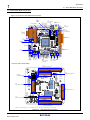
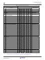
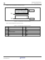
1
To our customers,
Old Company Name in Catalogs and Other Documents
On April 1st, 2010, NEC Electronics Corporation merged with Renesas Technology
Corporation, and Renesas Electronics Corporation took over all the business of both
companies. Therefore, although the old company name remains in this document, it is a valid
Renesas Electronics document. We appreciate your understanding.
Renesas Electronics website: http://www.renesas.com
April 1st, 2010
Renesas Electronics Corporation
Issued by: Renesas Electronics Corporation (http://www.renesas.com)
Send any inquiries to http://www.renesas.com/inquiry.
Notice
1.
2.
3.
4.
5.
6.
7.
All information included in this document is current as of the date this document is issued. Such information, however, is
subject to change without any prior notice. Before purchasing or using any Renesas Electronics products listed herein, please
confirm the latest product information with a Renesas Electronics sales office. Also, please pay regular and careful attention to
additional and different information to be disclosed by Renesas Electronics such as that disclosed through our website.
Renesas Electronics does not assume any liability for infringement of patents, copyrights, or other intellectual property rights
of third parties by or arising from the use of Renesas Electronics products or technical information described in this document.
No license, express, implied or otherwise, is granted hereby under any patents, copyrights or other intellectual property rights
of Renesas Electronics or others.
You should not alter, modify, copy, or otherwise misappropriate any Renesas Electronics product, whether in whole or in part.
Descriptions of circuits, software and other related information in this document are provided only to illustrate the operation of
semiconductor products and application examples. You are fully responsible for the incorporation of these circuits, software,
and information in the design of your equipment. Renesas Electronics assumes no responsibility for any losses incurred by
you or third parties arising from the use of these circuits, software, or information.
When exporting the products or technology described in this document, you should comply with the applicable export control
laws and regulations and follow the procedures required by such laws and regulations. You should not use Renesas
Electronics products or the technology described in this document for any purpose relating to military applications or use by
the military, including but not limited to the development of weapons of mass destruction. Renesas Electronics products and
technology may not be used for or incorporated into any products or systems whose manufacture, use, or sale is prohibited
under any applicable domestic or foreign laws or regulations.
Renesas Electronics has used reasonable care in preparing the information included in this document, but Renesas Electronics
does not warrant that such information is error free. Renesas Electronics assumes no liability whatsoever for any damages
incurred by you resulting from errors in or omissions from the information included herein.
Renesas Electronics products are classified according to the following three quality grades: “Standard”, “High Quality”, and
“Specific”. The recommended applications for each Renesas Electronics product depends on the product’s quality grade, as
indicated below. You must check the quality grade of each Renesas Electronics product before using it in a particular
application. You may not use any Renesas Electronics product for any application categorized as “Specific” without the prior
written consent of Renesas Electronics. Further, you may not use any Renesas Electronics product for any application for
which it is not intended without the prior written consent of Renesas Electronics. Renesas Electronics shall not be in any way
liable for any damages or losses incurred by you or third parties arising from the use of any Renesas Electronics product for an
application categorized as “Specific” or for which the product is not intended where you have failed to obtain the prior written
consent of Renesas Electronics. The quality grade of each Renesas Electronics product is “Standard” unless otherwise
expressly specified in a Renesas Electronics data sheets or data books, etc.
“Standard”:
8.
9.
10.
11.
12.
Computers; office equipment; communications equipment; test and measurement equipment; audio and visual
equipment; home electronic appliances; machine tools; personal electronic equipment; and industrial robots.
“High Quality”: Transportation equipment (automobiles, trains, ships, etc.); traffic control systems; anti-disaster systems; anticrime systems; safety equipment; and medical equipment not specifically designed for life support.
“Specific”:
Aircraft; aerospace equipment; submersible repeaters; nuclear reactor control systems; medical equipment or
systems for life support (e.g. artificial life support devices or systems), surgical implantations, or healthcare
intervention (e.g. excision, etc.), and any other applications or purposes that pose a direct threat to human life.
You should use the Renesas Electronics products described in this document within the range specified by Renesas Electronics,
especially with respect to the maximum rating, operating supply voltage range, movement power voltage range, heat radiation
characteristics, installation and other product characteristics. Renesas Electronics shall have no liability for malfunctions or
damages arising out of the use of Renesas Electronics products beyond such specified ranges.
Although Renesas Electronics endeavors to improve the quality and reliability of its products, semiconductor products have
specific characteristics such as the occurrence of failure at a certain rate and malfunctions under certain use conditions. Further,
Renesas Electronics products are not subject to radiation resistance design. Please be sure to implement safety measures to
guard them against the possibility of physical injury, and injury or damage caused by fire in the event of the failure of a
Renesas Electronics product, such as safety design for hardware and software including but not limited to redundancy, fire
control and malfunction prevention, appropriate treatment for aging degradation or any other appropriate measures. Because
the evaluation of microcomputer software alone is very difficult, please evaluate the safety of the final products or system
manufactured by you.
Please contact a Renesas Electronics sales office for details as to environmental matters such as the environmental
compatibility of each Renesas Electronics product. Please use Renesas Electronics products in compliance with all applicable
laws and regulations that regulate the inclusion or use of controlled substances, including without limitation, the EU RoHS
Directive. Renesas Electronics assumes no liability for damages or losses occurring as a result of your noncompliance with
applicable laws and regulations.
This document may not be reproduced or duplicated, in any form, in whole or in part, without prior written consent of Renesas
Electronics.
Please contact a Renesas Electronics sales office if you have any questions regarding the information contained in this
document or Renesas Electronics products, or if you have any other inquiries.
(Note 1) “Renesas Electronics” as used in this document means Renesas Electronics Corporation and also includes its majorityowned subsidiaries.
(Note 2) “Renesas Electronics product(s)” means any product developed or manufactured by or for Renesas Electronics.
User’s Manual
SH7086 CPU Board
M3A-HS86
User’s Manual
Renesas 32-Bit RISC Microcomputers
SuperH™ RISCengine Family / SH7080 Group
Rev.1.00 2007.02
Microsoft, MS-DOS, Windows and Windows.NET are registered trademarks of Microsoft Corporation of the U.S. in the U.S.
and other countries.
IBM and AT are registered trademarks of International Business Machines Corporation of the U.S.
Adobe and Acrobat are registered trademarks of Adobe Systems Incorporated.
All other brand names and product names are registered trademarks or trademarks of the respective proprietors.
Requests for Safety Design
• Renesas is constantly making efforts to improve the quality and reliability of its products. However, not all
semiconductor products are trouble-free, they may become faulty or operate erratically. To ensure that no
accidents such as injury or a fire or no social damage may arise from Renesas semiconductor products
should they become faulty or operate erratically, please pay careful attention to the safety design of your
system by, for example, considering redundancy design and incorporating measures to check the spread of a
fire and prevent device malfunction.
Precautions on Using This Manual
• This manual only provides reference information to help customers purchase the appropriate type of
Renesas Technology product that suits the intended purpose of use, and the technical information
contained herein does not implicitly or otherwise grant a license or rights to use the intellectual property
or other rights of Renesas Technology.
• Renesas Technology will not assume any responsibility for damage or losses or infringement on the
third parties’ rights arising from the use of product data, diagrams, tables, programs, algorithms or
example application circuits presented in this manual.
• The product data, diagrams, tables, programs, algorithms and all other information presented herein
reflect the latest that was available at the time this manual was issued, and Renesas Technology
reserves the right to change the products or specifications described herein without prior notice. When
purchasing Renesas Technology semiconductor products, please contact Renesas Technology or
Renesas Technology Sales or other distributors to obtain the latest information, and also keep abreast
of the information published at the Renesas Technology home page (http://www.renesas.com) or
through other media.
• The information contained herein was carefully prepared and is believed to be correct. However,
Renesas Technology will not assume responsibility for losses that the customers by any possibility may
suffer because of erroneous description in this manual.
• To use the technical contents in product data, diagrams or tables or the programs or algorithms
presented herein for your system, please carefully evaluate their suitability as part of the entire system,
not singly as a technical content, program or algorithm alone, to determine in advance whether they
are actually suitable for your system. Renesas Technology will not assume responsibility for the
suitability of said items in user systems.
• The products presented herein are not designed or manufactured for use in equipment or systems that
are used under conditions where human life is concerned. If you plan to use the products presented
herein for special applications such as transportation, mobile, medical, aerospace, nuclear control or
submarine repeater equipment or systems, please consult Renesas Technology or Renesas
Technology Sales or other distributors.
• This manual may not be copied or reproduced, in whole or part, without prior written consent of
Renesas Technology.
• For more detailed information or for questions or doubts about this manual, please consult Renesas
Technology or Renesas Technology Sales or other distributors.
Revision History
Rev.
SH7086 CPU Board M3A-HS86User's Manual
Date of Issue
Content of Revision
Page
1.0
Feb. 6, 2007
-
Contents
1st edition issued.
Table of Contents
Chapter1 Overview..................................................................................................................................... 1-1
1.1 Overview .................................................................................................................................................................... 1-2
1.2 Configuration .............................................................................................................................................................. 1-2
1.3 External Specifications ............................................................................................................................................... 1-3
1.4 External View ............................................................................................................................................................. 1-4
1.5 M3A-HS86 Block Diagram.......................................................................................................................................... 1-5
1.6 M3A-HS86 Board Overview ....................................................................................................................................... 1-6
1.7 M3A-HS86 Memory Mapping ..................................................................................................................................... 1-8
1.8 Absolute Maximum Ratings...................................................................................................................................... 1-11
1.9 Recommended Operating Conditions ...................................................................................................................... 1-11
Chapter2 Functional Overview .................................................................................................................. 2-1
2.1 Functional Overview................................................................................................................................................... 2-2
2.2 CPU............................................................................................................................................................................ 2-3
2.3 Memory ...................................................................................................................................................................... 2-4
2.3.1 SH7086 On-chip Memory.................................................................................................................................. 2-4
2.3.2 SDRAM ............................................................................................................................................................. 2-4
2.3.3 Expand of Flash Memory .................................................................................................................................. 2-7
2.4 Serial Port Interface.................................................................................................................................................... 2-8
2.5 I/O Ports ..................................................................................................................................................................... 2-9
2.6 Power Supply Circuit ................................................................................................................................................ 2-13
2.7 Clock Module............................................................................................................................................................ 2-14
2.8 Reset Module ........................................................................................................................................................... 2-15
2.9 Interrupt Switches..................................................................................................................................................... 2-16
2.10 E10A-USB Interface ............................................................................................................................................... 2-17
Chapter 3 Operational Specifications ......................................................................................................... 3-1
3.1 M3A-HS86 Connectors Outline .................................................................................................................................. 3-2
3.1.1 H-UDI Connector (J1,J2)................................................................................................................................... 3-3
3.1.2 Serial Port Connector (J3)................................................................................................................................. 3-5
3.1.3 External Power Supply Connectors for the SH7086 (J4) .................................................................................. 3-6
3.1.4 Power Supply Connector (J5) ........................................................................................................................... 3-7
3.1.5 User I/O Connector (J6-J8) ............................................................................................................................... 3-8
3.1.6 Extension Connectors (J9-J13) ....................................................................................................................... 3-10
3.1.7 Extension Connector (J14).............................................................................................................................. 3-16
3.2 Outline of Switches and LEDs .................................................................................................................................. 3-17
3.2.1 SH7086 Power Supply Select Jumpers (JP1) ................................................................................................. 3-18
3.2.2 FWE Pin Select Jumper (JP2)......................................................................................................................... 3-19
3.2.3 Switch and LED Functions .............................................................................................................................. 3-20
3.3 Board Dimensions of M3A-HS86.............................................................................................................................. 3-22
Appendix .................................................................................................................................................... A-1
M3A-HS86 SCHEMATICS
Rev. 1.0 Feb. 6. 2007
REJ10J0916-0100
(i)
Chapter1 Overview
Chapter1
Overview
1-1
Overview
1
1.1 Overview
1.1 Overview
The M3A-HS86 is the CPU board designed for users to evaluate the functionality and performance of the SH7086
group of Renesas Technology original microcomputers, as well as develop and evaluate the application software for
this group of microcomputers. The SH7086's data bus, address bus and various internal peripheral circuit function pins
are connected to the extension connector of the M3A-HS86, allowing users to evaluate the timing relationship with
peripheral devices using measurement instruments or develop extension boards tailored to suit development
purposes. Furthermore, the E10A-USB or the on-chip emulator made by Renesas Technology can also be connected
to the M3A-HS86.
1.2 Configuration
Figure1.2.1 shows an example of system configuration using the M3A-HS86.
*
5V DC
Power Supply
(1.5A min.)
SH7086 CPU Board
M3A-HS86
Serial Port
Connector
H-UDI Connector
(14-pin or 36-pin)
SH7086
Extension
Board
* Can be created according
to applications
Extension
Connector
HEW
debugger
E10A-USB *
High-performance
*
Embeded Workshop(HEW)
SuperH RISC engine
C/C++ Compiler Package*
USB
Host
Computer*
*: It is necessary to buy separately for software development.
Figure1.2.1 System Configuration Example of M3A-HS86
Rev.1.0 Feb 6, 2007
REJ10J0916-0100
1-2
Overview
1
1.3 External Specifications
1.3 External Specifications
Table1.3.1 lists external specifications of M3A-HS86.
Table1.3.1 External Specifications of M3A-HS86
No.
Item
Content
SH7086
1
CPU
• Input(XIN) clock : 10MHz
• Bus clock : 40MHz,max
• CPU clock : 80MHz,max
• On-chip memory
Flash memory : 512KB
RAM : 32KB
2
Memory
*M3A-HS86(3.3V version) only
3
Connectors
4
LED
5
Switches
6
Package Dimensions
Rev.1.0 Feb 6, 2007
REJ10J0916-0100
• SDRAM : 16 Mbytes.(16-bit bus width) 1pc
• External flash memory enabled to mount
• Extension connector (Bus, I/O, VCC, GND)
• User I/O connector (SH7086’s MTU2 and A/D function pins)
• Serial port connector (D-sub 9pins)
• H-UDI connector (36pins)
• H-UDI connector (14pins)
• POWER LED (1pc.)
• LED for interrupt switch (1pc.)
• User LED (7pcs.)
• Reset switch (1pc.)
• NMI switch (1pc.)
• IRQ1 switch (1pc.)
• DIP switch for system setting (1pc.,4 poles)
• DIP switch for users (1pc.,4 poles)
• Dimensions :100mm x 100mm
• Mounting form :6-layer, double-side mounted
• Board configuration :1 board
1-3
Overview
1
1.4 External View
1.4 External View
Figure1.4.1 shows the external view of M3A-HS86.
Figure1.4.1 External View of M3A-HS86 (IC socket mounted version)
Rev.1.0 Feb 6, 2007
REJ10J0916-0100
1-4
Overview
1
1.5 M3A-HS86 Block Diagram
1.5 M3A-HS86 Block Diagram
Figure1.5.1 shows the system block diagram of M3A-HS86.
H-UDI Connector
(36pin)
H-UDI Connector
(14pin)
AUD
Flash Memory
(Not mounted)
*
16
User I/O
Connector
Serial Port
Connector
H-UDI
SH7086
(80MHz)
SDRAM *
16MB
16 or 32
16
Bus Clock: 40MHz
16 or 32
SH7086 CPU Board
M3A-HS86
* : Only for M3A-HS86 (3.3V version)
Extension Connectors
Figure1.5.1 System Block Diagram of M3A-HS86
Rev.1.0 Feb 6, 2007
REJ10J0916-0100
1-5
Overview
1
1.6 M3A-HS86 Board Overview
1.6 M3A-HS86 Board Overview
Figure1.6.1 shows the M3A-HS86 board overview.
< Top View of the Component Side >
JP2
FWE Pin
Select
Jumper
J5
Power Supply
JP1
Connector
Ppower Supply
Select Jumper
*1
U2 Clock Buffer
SW1
Power Switch
LED1
Power LED
SW4
DIP Switch
for System Setting
J3
Serial Port
Connector
J1
H-UDI Connector
(36-pin)
U5
RS232C Driver
J14
*1
Extension Connector
U1
SH7086
User LED
6-8
J2
H-UDI Connector
(14-pin)
J7,J8
User I/O Connector *1
SW2
RESET
Switch
SW3
DIP Switch
for Users
U6
Reset IC
LED2-5
User LED
LED9
LED for Interrupt
Confirmation
SW6
SW5
SW7
NMI MRES IRQ1
Switch
Switch Switch
*1
< Top View of the Solder Side >
J13
Extension Connector*1
J12
Extension Connector*1
U8 3.3V
Voltage Regulator
U4 *2
SDRAM
J11
Extension Connector*1
J6
User I/O Connector *1
U3 *3
Flash Memory
J9
Extension Connector*1
J10
Extension Connector*1
Notes: *1: Not mounted *2: 3.3V version only *3: Can be mounted only for 3.3V version
Figure1.6.1
Rev.1.0 Feb 6, 2007
REJ10J0916-0100
M3A-HS86 Board Overview
1-6
Overview
1
1.6 M3A-HS86 Board Overview
Table1.6.1 lists main components mounted in the M3A-HS86.
Table1.6.1 Main Components Mounted in the M3A-HS86
Symbol
Parts Name
Remarks
Recommended parts number for
not-mounted components
U1
CPU
SH7086 (Renesas)
U1
CPU socket
NQPACK176SD
U2
Clock buffer
Not mounted
CY2305SC-1 (Cypress)
Not mounted
U3
Flash memory
(Can be mounted only
for 3.3V version)
U4
SDRAM
3.3V version only
U5
RS-232C driver
U6
Reset IC
U7
Logic IC
U8
3.3V voltage regulator
X1
Oscillator
10.00MHz
J1
H-UDI connector
36-pin type
J2
H-UDI connector
14-pin type
J3
Serial port connector
J4
External power supply connector
J5
Power supply connector
J6
M51957BFP (Renesas)
Not mounted
A2-2PA-2.54DSA (Hirose)
User I/O connector
Not mounted
XG4C-2634 (Omron)
J7,J8
User I/O connector
Not mounted
A2-3PA-2.54DSA (Hirose)
J9,J11,J12
Extension connector
Not mounted
XG4C-2031 (Omron)
J10.J13
Extension connector
Not mounted
XG4C-4031 (Omron)
J14
Extension connector
Not mounted
LED1
Power LED
Blue
LED2-8
User LED
Green
LED9
LED for interrupt confirmation
SW1
Power switch
SW2
Reset switch
SW3
DIP switch for users
SW4
DIP switch for system setting
SW5
NMI switch
SW6
IRQ1 switch
SW7
MRES switch
Rev.1.0 Feb 6, 2007
REJ10J0916-0100
3428-6002LCSC
(Sumitomo 3M)
Red/Yellow green
(Two colors)
Not mounted
B3SN-3012 (Omron)
1-7
Overview
1
1.7 M3A-HS86 Memory Mapping
1.7 M3A-HS86 Memory Mapping
Figure1.7.1, Figure1.7.2 and Figure1.7.3 show a memory mapping example of SH7086 in the M3A-HS86.
Logical space of the SH7086
MCU mode 3
(Single Chip mode)
H'0000 0000
Memory Mapping
of the M3A-HS86
H'0000 0000
On-chip ROM (512KB)
On-chip ROM (512KB)
H'0007 FFFF
H'0008 0000
H'0007 FFFF
H'0008 0000
Reserved
Reserved
H'FFFF
H'FFFF
H'FFFF
H'FFFF
3FFF
4000
BFFF
C000
On-chip RAM
(32KB)
On-chip peripheral Module
H'FFFF FFFF
Figure1.7.1
Rev.1.0 Feb 6, 2007
REJ10J0916-0100
H'FFFF
H'FFFF
H'FFFF
H'FFFF
H'FFFF
3FFF
4000
BFFF
C000
FFFF
On-chip RAM
(32KB)
On-chip peripheral Module
Memory Mapping Example of SH7086 (MCU mode 3)
1-8
Overview
1
1.7 M3A-HS86 Memory Mapping
Logical space of the SH7086
MCU mode 0,1
(On-chip ROM disabled mode)
H'0000 0000
CS0 space: 64MB
H'03FF FFFF
H'0400 0000
Memory Mapping
of the M3A-HS86
H'0000
H'007F
H'03FF
H'0400
0000
FFFF
FFFF
0000
Flash Memory (8MB)
User Area
CS1 space: 64MB
User Area
H'07FF FFFF
H'0800 0000
H'07FF FFFF
H'0800 0000
CS2 space: 64MB
H'0BFF FFFF
H'0C00 0000
CS3 space: 64MB
H'0FFF FFFF
H'1000 0000
User Area
H'0BFF
H'0C00
H'0CFF
H'0FFF
H'1000
FFFF
0000
FFFF
FFFF
0000
SDRAM(16MB)
User Area
H'13FF FFFF
H'1400 0000
CS5 space: 64MB
User Area
H'17FF FFFF
H'1800 0000
H'17FF FFFF
H'1800 0000
CS6 space: 64MB
User Area
H'1BFF FFFF
H'1C00 0000
H'1BFF FFFF
H'1C00 0000
CS7 space: 64MB
User Area
H'1FFF FFFF
H'2000 0000
H'1FFF FFFF
H'2000 0000
Reserved
H'3FFF FFFF
H'4000 0000
Reserved
H'3FFF FFFF
H'4000 0000
CS8 space: 1GB
User Area
H'7FFF FFFF
H'8000 0000
H'7FFF FFFF
H'8000 0000
Reserved
FFFF
0000
FFFF
0000
H'FFFF 3FFF
H'FFFF 4000
H'FFFF BFFF
H'FFFF C000
*2
User Area
CS4 space: 64MB
H'13FF FFFF
H'1400 0000
H'FFF7
H'FFF8
H'FFF9
H'FFFA
*1
SDRAM Mode setting
Reserved
On-chip RAM
(32KB)
On-chip peripheral Module
Reserved
H'FFF7
H'FFF8
H'FFF9
H'FFFA
FFFF
0000
FFFF
0000
SDRAM Mode setting
H'FFFF
H'FFFF
H'FFFF
H'FFFF
3FFF
4000
BFFF
C000
On-chip RAM
(32KB)
Reserved
On-chip peripheral Module
H'FFFF FFFF
H'FFFF FFFF
Notes
*1: For the case that 8MB flash memory is mounted (M3A-HS86(3.3V version) only)
*2: M3A-HS86(3.3V version) only
Figure1.7.2
Rev.1.0 Feb 6, 2007
REJ10J0916-0100
Memory Mapping Example of SH7086 (MCU mode 0,1)
1-9
Overview
1
1.7 M3A-HS86 Memory Mapping
Logical space of the SH7086
MCU mode 2
(On-chip ROM enabled mode)
H'0000
H'0007
H'0008
H'01FF
H'0200
0000
FFFF
0000
FFFF
0000
On-chip ROM (512KB)
Reserved
CS0 space: 32MB
H'03FF FFFF
H'0400 0000
Memory Mapping
of the M3A-HS86
H'0000
H'0007
H'0008
H'01FF
H'0200
H'027F
H'03FF
H'0400
0000
FFFF
0000
FFFF
0000
FFFF
FFFF
0000
On-chip ROM (512KB)
Reserved
Flash Memory (8MB)
User Area
CS1 space: 64MB
H'07FF FFFF
H'0800 0000
H'07FF FFFF
H'0800 0000
User Area
CS2 space: 64MB
H'0BFF FFFF
H'0C00 0000
CS3 space: 64MB
H'0FFF FFFF
H'1000 0000
H'0BFF
H'0C00
H'0CFF
H'0FFF
H'1000
FFFF
0000
FFFF
FFFF
0000
SDRAM(16MB)
User Area
H'13FF FFFF
H'1400 0000
User Area
CS5 space: 64MB
H'17FF FFFF
H'17FF FFFF
H'1800 0000
H'1800 0000
User Area
CS6 space: 64MB
H'1BFF FFFF
H'1BFF FFFF
H'1C00 0000
H'1C00 0000
User Area
CS7 space: 64MB
H'1FFF FFFF
H'1FFF FFFF
H'2000 0000
H'2000 0000
Reserved
Reserved
H'3FFF FFFF
H'4000 0000
H'3FFF FFFF
H'4000 0000
User Area
CS8 space: 1GB
H'7FFF FFFF
H'8000 0000
H'7FFF FFFF
H'8000 0000
Reserved
Reserved
FFFF
0000
FFFF
0000
H'FFFF
H'FFFF
H'FFFF
H'FFFF
3FFF
4000
BFFF
C000
*2
User Area
CS4 space: 64MB
H'13FF FFFF
H'1400 0000
H'FFF7
H'FFF8
H'FFF9
H'FFFA
*1
*1
User Area
SDRAM Mode setting
H'FFF7
H'FFF8
H'FFF9
H'FFFA
FFFF
0000
FFFF
0000
H'FFFF
H'FFFF
H'FFFF
H'FFFF
3FFF
4000
BFFF
C000
SDRAM Mode setting
Reserved
Reserved
On-chip RAM
(32KB)
On-chip peripheral Module
On-chip RAM
(32KB)
On-chip peripheral Module
H'FFFF FFFF
H'FFFF FFFF
Notes
*1: For the case that 8MB flash memory is mounted (M3A-HS86(3.3V version) only)
*2: M3A-HS86(3.3V version) only
Figure1.7.3
Rev.1.0 Feb 6, 2007
REJ10J0916-0100
Memory Mapping Example of SH7086 (MCU mode 2)
1-10
Overview
1
1.8
Absolute Maximum Ratings
1.8 Absolute Maximum Ratings
Table1.8.1 lists the absolute maximum ratings of M3A-HS86.
Table1.8.1 Absolute Maximum Ratings of M3A-HS86
Symbol
Parameter
Rated Value
Remarks
5VCC
5V system power supply voltage
-0.3V to 6.0V
Relative to VSS
3VCC
3.3V system power supply voltage
-0.3V to 4.6V
Relative to VSS
Operating ambient temperature
-0°C to 50°C
No dewdrops allowed.
Topr
Use in corrosive gas environment prohibited.
Tstr
Storage ambient temperature
-10°C to 60°C
No dewdrops allowed.
Use in corrosive gas environment prohibited.
Note: The ambient temperature refers to the air temperature in places closest possible to the board.
1.9 Recommended Operating Conditions
Table1.9.1 lists the recommended operating conditions of M3A-HS86.
Table1.9.1 Recommended Operating Conditions of M3A-HS86
Symbol
Parameter
5VCC
5V system power supply voltage
3VCC
3.3V system power supply voltage
-
Maximum current consumption in the
Rated Value
Remarks
4.75V to 5.25V
Relative to VSS
3.0V to 3.6V
Relative to VSS
Within 1A
board
Topr
Operating ambient temperature
0°C to 50°C
No dewdrops allowed.
Use in corrosive gas environment prohibited.
Rev.1.0 Feb 6, 2007
REJ10J0916-0100
1-11
Overview
1
1.8
Absolute Maximum Ratings
* This is a blank page *
Rev.1.0 Feb 6, 2007
REJ10J0916-0100
1-12
Chapter2 Functional Overview
Chapter2
Functional Overview
2-1
Functional Overview
2
2.1 Functional Overview
2.1 Functional Overview
The M3A-HS86 is the SH7086 CPU board that has the functions listed in Table2.1.1.
Table2.1.1 lists the functional modules of M3A-HS86.
Table2.1.1 Functional Modules of M3A-HS86
Sections
2.2
Functions
CPU
Contents
SH7086
• Input(XIN) clock : 10MHz
• Bus clock : 40MHz,max
• CPU clock : 80MHz,max
• On-chip memory
- Flash memory: 512KB
- RAM : 32KB
*M3A-HS86(3.3V version) only
• SDRAM : 16 Mbytes(16-bit bus width) 1pc.
• External flash memory enabled to mount
2.4
Serial Port Interface
Connects SCI1 of the SH7086 to the Serial Port connector
2.5
I/O Ports
Connects to the input/output ports of the SH7086
2.6
Power Supply Circuit
Controls the system power supply of the M3A-HS86
2.7
Clock Module
Controls the system clock
2.8
Reset Module
Controls device reset mounted on the M3A-HS86
2.9
Interrupt Switches
Connect to the NMI and IRQ1 pins
2.10
E10A-USB Interface
SH7086 H-UDI/AUD interface
Operational specifications
Connectors, switches and LEDs
2.3
-
Memory
• SH7086 extension connector
• Switches and LEDs
• H-UDI connector
Detailed in Chapter 3.
Rev.1.0 Feb 06. 2007
REJ10J0916-0100
2-2
Functional Overview
2
2.2 CPU
2.2 CPU
The M3A-HS86 contains the 32-bit RISC microcomputer SH7086 that operates with a maximum 80MHz of CPU
clock frequency. The SH7086 includes 512-Kbyte flash memory, and 32-Kbyte SRAM, making it useful in a wide
range of applications from data processing to equipment control.
The M3A-HS86 can be operated with a maximum 80MHz of CPU clock frequency (external bus 40MHz, max) using
a 10MHz input clock.
Figure2.2.1 shows the SH7086 block diagram in the M3A-HS86.
SH7086
Clock
EXTAL
XTAL
PA15/CK
Mode
MD1
MD0
FWE
System
Control
NMI Switch
IRQ1 Switch
H-UDI
Connector
Serial Port
Connector
User LED
User DIP
Switch
PC0/A0-PC15/A15
PB0/A16
PB1/A17
PC18/A18
PC19/A19
PC20/A20
PC21/A21
PC22/A22
PC23/A23
PC24/A24
PC25/A25
PA26/A26/IRQ0
PA27/A27/IRQ1
PA28/A28/IRQ2
PA29/A29/IRQ3
WDTOVF
RES
PA18/BREQ
PA19/BACK
NMI
PA5/IRQ1/DREQ1
PE12/TCK
PE8/TMS
PE10/TDI
PE11/TDO
PE9/TRST
ASEMD0
PE13/ASEBRKAK/ASEBRK/MRES
PE6/AUDATA0
PE5/AUDATA1
PE4/AUDATA2
PE3/AUDATA3
PE0/AUDCK
PA16/AUDSYNC
PA3/RXD1
PA4/TXD1
PE1
PE2
PE7
PE14
PE16
PE17
PE18
PB6
PB7
PB8
PB9
PD0/D0-PD31/D31
16
Address Bus
32
PA10/CS0
PA11/CS1
PA6/CS2
PA7/CS3
PA20/CS4
PA21/CS5/CE1A/CASU/TIC5U
PA14/RD
PB4/RASL/IRQ2
PB5/CASL/IRQ3
PA13/WRH/DQMLU/WE
PA12/WRL/DQMLL
PA23/WRHH/ICIOWR/AH/DQMUU
PA22/WRHL/ICIORD/DQMUL
PA8/RDWR/IRQ2
PA9/FRAME/CKE/IRQ3
Bus Control
PA0/CS4/RXD0
PA1/CS5/CE1A/TXD0
PA2/A25/DREQ0/IRQ0/SCK0
PB2/IRQ0/POE0/SCL
PB3/IRQ1/POE1/SDA
PE15/IRQOUT/CKE/DACK1/TIOC4D
PE19/TIOC4BS
PE20/TIOC4CS
PE21/TIOC4DS
PA17/WAIT/DACK2
PA24/CE2A/DREQ3
PA25/CE2B/DACK3/POE8
PF0/AN0-PF15/AN15
Data Bus
SCI/IIC/DMAC/
GPIO/IRQ/
MTU2S
16
A/D
Converter
Figure2.2.1 SH7086 Block Diagram
Rev.1.0 Feb 06. 2007
REJ10J0916-0100
2-3
Functional Overview
2
2.3 Memory
2.3 Memory
2.3.1 SH7086 On-chip Memory
The SH7086 includes 512-Kbyte flash memory and 32-Kbyte SRAM.
2.3.2 SDRAM
The M3A-HS86 (3.3V version) mounts 16MB SDRAM as standard equipment. SDRAM is controlled by the bus
state controller built into SH7086. Table2.3.1 lists SDRAM specifications used in M3A-HS86. Figure2.3.1 shows the
block diagram of SDRAM connection.
Table2.3.1 SDRAM Specifications
Specifications
Contents
Configuration
16 Mbytes (16-bit bus) x 1pc.
Capacity
16 Mbytes
Access Time
5.4ns
CAS Latency
2(at 40MHz bus clock)
Refresh Interval
4,096 refresh cycles every 64ms
Row Address
A11- A0
Column Address
A8 - A0
Number of Banks
4-bank operation controlled by BA0 and BA1
SDRAM
SH7086
(8M Word x 16bit)
A14
A13
A12-A1
11
BA1
BA0
A11-A0
-A0
A11
CK
CKE
CLK
CKE
CS3
CS#
CS
RASL
AS
R
#
RAS
CASL
CAS
RDWR
WE#
WE
DQMLU
DQMU
DQMLL
D15-D0
DQML
16
DQ15-DQ0
Figure2.3.1 Block Diagram of SDRAM Connection
Rev.1.0 Feb 06. 2007
REJ10J0916-0100
2-4
Functional Overview
2
2.3 Memory
Table2.3.2 lists an example of bus state controller settings for operation with the SH7086 Bus clock at 40MHz.
Table2.3.2 Example of Bus State Controller Settings at SDRAM
User Area
CS3
SDRAM Controller Settings
CS3 Space Bus Control Register(CS3BCR)
Initial value :H'36DB 0600
Recommended set value : H'1000 4400
- Specify idle cycles between write-read cycles and write-write cycles
IWW[2:0] = 001 ; 1 idle cycle inserted
- Specify memory type : TYPE[2:0] = 100 ;SDRAM
- Data bus size : BSZ[1:0] = B'10 ;16-bit size
CS3 Space Wait Control Register(CS3WCR)
Initial value : H'0000 0500
Recommended set value :H'0000 4891
- Number of Auto-Precharge Completion Wait Cycles
TRP[1:0] = 10 ;3 cycles
- Wait Cycles between ACTV Command and READ(A)/WRIT(A) Command
TRCD[1:0] = 10 ;3 cycles
- Area 3 CAS latency
A3CL[1:0] = 01 ;2 cycles
- WRIT(A) command→Number of Auto-Precharge/PRE Command cycles
TRWL[1:0] = 10 ;2 cycles
- REF Command/Self-Refresh Release→Number of ACTV/REF/MRS Command cycles.
TRC[1:0] = 01 ; 4 cycles
SDRAM Control Register(SDCR)
Initial value : H'0000 0000
Recommended set value : H'0000 0809
- Refresh control
RFSH = 1 ; Refresh enabled
- Refresh control
RMODE = 0 ; Auto refresh
- Bank active mode
BACTV = 0 ;Auto precharge mode
- Number of area3 row address bits
A3ROW[1:0] = 01 ;12 bits
- Number of area3 column address bits
A3COL[1:0] = 01 ;9 bits
Refresh Timer Control/Status Register(RTCSR)
Initial value : H'0000 0000
Recommended set value : H’A55A 0010
- Clock select
CKS[2:0] = 010 ;Bφ/16
- Refresh times
RRC[2:0] = 000 ; 1 time
Refresh Time Constant Register(RTCOR)
Initial value : H'0000 0000
Recommended set value : H'A55A 0027
*The following shows refresh request intervals in cases when clock select is set to Bφ/16.
1 cycle :400nsec(40MHz/16 = 2.5MHz)
Refresh request intervals for the SDRAM : every 15.625μsec
15.625μsec /400nsec = 39(0x27) cycles / refresh
Rev.1.0 Feb 06. 2007
REJ10J0916-0100
2-5
Functional Overview
2
2.3 Memory
Figure2.3.2 shows an example of SDRAM single read/write timing for operation with the SH7086 Bus clock at
40MHz.
SDRAM SINGLE READ
SDRAM SINGLE WRITE
tRC
tRC
tRCD
tRCD
tRAS
tcyc
(25ns)
tRAS
Tr
Trw
Trw
Tc1
Tcw
Td1
Tde
Tap1
Tap2
Tr
Trw1
Trw2
Tc1
Trwl1
Trwl2
Tap1
Tap2
ACT
DESEL
DESEL
READA
DESEL
DESEL
DESEL
DESEL
DESEL
ACT
DESEL
DESEL
WRITA
DESEL
DESEL
DESEL
DESEL
CKIO
CKE
tCSD
tCSD
tSI
tCSD
tHI
tHI
tSI
tCSD
CS3
tRASD
tRASD
tSI
tSI
RASL
tRASD
tHI
tRASD
tHI
tCASD
tCASD
tSI
tSI
CASL
tCASD
tHI
tCASD
tHI
tRWD
tSI
RDWR
tRWD
tHI
tDQMD
tDQMD
tDQMD
tSI
tHI
tSI
tDQMD
tHI
DQMUU-LL
tAD1
tAD1
tAD1
tSI
tAD1
tSI
MA0-9,11
tAD1
tHI
tAD1
tHI
tAD1
MA10
tAD1
BA0-1
tRDS2
tAC
D0-31
tRDH2
tOH
tWDD2
tSI
Data
tWDH2
tHI
Figure2.3.2 Example of SDRAM Single Read/Write Timing
Rev.1.0 Feb 06. 2007
REJ10J0916-0100
2-6
Functional Overview
2
2.3.3 Expand of Flash Memory
2.3.3 Expand of Flash Memory
M3A-HS86 has installed the mounting space to which the flash memory can be expanded externally.
The mountable flash memory is 32M bit or 64M bit flash memory with 3.3V power-supply voltage, 16-bit bus width,
and TSOP-48 pin (20 x 12mm).
By a DIP switch (SW4-4), the validity or invalidity of write protect for flash memory can be switched.
Figure2.3.3 shows an example of 32-Mbit Flash Memory connection.
Flash Memory
32Mbit(2M Word x16bit) or
64Mbit(4M Word x16bit)
SH7086
22
A22 - A1
A21 - A0
16
D15 - D0
DQ15 - DQ0
3.3V
BYTE
RD
OE
WRL
WE
CS0
CE
Reset
Vcc
RP
NC
RY/BY
WP
DIP SW
SW4-4
Figure2.3.3 Connection Example with Flash Memory
Note: Only the M3A-HS86 (3.3V version) can connect the flash memory to outside.
Rev.1.0 Feb 06. 2007
REJ10J0916-0100
2-7
Functional Overview
2
2.4 Serial Port Interface
2.4 Serial Port Interface
The SH7086 included in the M3A-HS86 contains a UART module. In the M3A-HS86, SCI channel 1 is connected to
Serial Port connector J3.
Figure2.4.1 shows the block diagram of serial port interface in the M3A-HS86.
SH7086
VCC
Serial Port
Connector (J3)
RS232C
Driver
NC
1
2
PA3/RXD1
3
PA4/TXD1
4
GND
5
6
7
8
NC
9
DCD
RxD
TxD
DTR
GND
DSR
RTS
CTS
RI
Figure2.4.1 Block Diagram of Serial Port Interface
Rev.1.0 Feb 06. 2007
REJ10J0916-0100
2-8
Functional Overview
2
2.5 I/O Ports
2.5 I/O Ports
In the M3A-HS86, all of the SH7086's I/O ports are connected to the extension bus connector. Some I/O ports are
connected to DIP switches and LEDs of the M3A-HS86 board. Users are free to use these ports.
Figure2.5.1 shows the Block Diagram of DIP Switch and LEDs in the M3A-HS86.
Table2.5.1 to Table 2.5.3 list a function of the SH7086 I/O ports in the M3A-HS86.
VCC
LED8
GREEN
LED7
GREEN
LED6
GREEN
LED5
GREEN
LED4
GREEN
LED3
GREEN
LED2
GREEN
SH7086
PE1
PE2
PE7
PE14
PE16
PE17
PE18
VCC
SW3-1
PB6
SW3-2
PB7
SW3-3
PB8
SW3-4
PB9
Figure2.5.1 Block Diagram of DIP Switch and LEDs in M3A-HS86
Rev.1.0 Feb 06. 2007
REJ10J0916-0100
2-9
Functional Overview
2
2.5 I/O Ports
Table2.5.1 Functions of SH7086 I/O Ports
SH7086
Pin
Connection Destinations on M3A-HS86
Extension Connector
Pin Name
No.
J6
J7
J8
J9
J10
J11
J12
Other Connections
J13
J14
_______
1
PE12/TIOC4A/TXD3/SCS/TCK
___________ ____________________ _______________
2
PE13/TIOC4B/MRES/ASEBRKAK/ASEBRK
3
PA23/WRHH/ICIOWR/AH/DQMUU/TIC5W
H-UDI connector (J1,J2)
H-UDI connector (J1,J2)
MRES SW (Not mounted)
____________ ______________ _____
____________ ______________ _____
4
PE14/WRHH/ICIOWR/AH
LED5
/DQMUU/DACK0/TIOC4C
___________ _____________
5
PA22/WRHL/ICIORD/DQMUL/TIC5V
6
PA21/CS5/CE1A/CASU/TIC5U
7
PE15/CKE/DACK1/TIOC4D/IRQOUT
_______ __________ __________
_______________
_______
9
PE16/CS8/TIOC3BS
User Port (LED6)
10
PE17/TIOC3DS
User Port (LED7)
12
PE18/TIOC4AS
User Port (LED8)
13
PE19/TIOC4BS
14
PE20/TIOC4CS
15
PE21/TIOC4DS
16
PC0/A0
17
PC1/A1
Flash, SDRAM *1
18
PC2/A2
Flash, SDRAM *1
19
PC3/A3
Flash, SDRAM *1
20
PC4/A4
Flash, SDRAM *1
22
PC5/A5
Flash, SDRAM *1
24
PC6/A6
Flash, SDRAM *1
25
PC7/A7
Flash, SDRAM *1
26
PC8/A8
Flash, SDRAM *1
27
PC9/A9
Flash, SDRAM *1
28
PC10/A10
Flash, SDRAM *1
29
PC11/A11
Flash, SDRAM *1
30
PC12/A12
Flash, SDRAM *1
31
PC13/A13
Flash, SDRAM *1
32
PC14/A14
Flash, SDRAM *1
33
PC15/A15
Flash *1
34
PB0/A16/TIC5WS
Flash *1
36
PB1/A17/TIC5W
Flash *1
38
PA20/CS4/RASU
39
PA19/BACK/TEND1
40
PB2/IRQ0/POE0/SCL
41
PB3/IRQ1/POE1/SDA
42
PA18/BREQ/TEND0
_______ __________
__________
__________
__________
__________
__________
43
__________
PB4/RASL/IRQ2/POE2
__________
45
SDRAM *1
__________
PB5/CASL/IRQ3/POE3
SDRAM *1
__________
46
PB6/A18/BACK/IRQ4/RXD0
47
PB7/A19/BREQ/IRQ5/TXD0
User Port (Dip SW)
__________
User Port (Dip SW)
_________
49
PB8/A20/WAIT/IRQ6/SCK0
50
PB9/A21/IRQ7/ADTRG/POE8
User Port (Dip SW)
52
PA14/RD
Flash *1
54
PC18/A18
Flash *1
_____________ __________
User Port (Dip SW)
_____
Note *1: Only for 3.3V version
Rev.1.0 Feb 06. 2007
REJ10J0916-0100
2-10
Functional Overview
2
2.5 I/O Ports
Table 2.5.2 Functions of SH7086 I/O Ports
SH7086
Pin
Connection destinations on M3A-HS86
Extension Connector
Pin Name
No.
J6
J7
J8
J9
J10
J11
J12
Other Connections
J13
J14
55
PC19/A19
Flash *1
56
PC20/A20
Flash *1
58
PC21/A21
Flash *1
59
PC22/A22
60
PC23/A23
61
PC24/A24
62
PC25/A25
63
PA26/A26/IRQ0
65
PA27/A27/IRQ1
67
PA28/A28/IRQ2
68
PA29/A29/IRQ3
69
PD31/D31/TIOC3AS/ADTRG
70
PD30/D30/TIOC3CS/IRQOUT
_____________
_______________
_________
______ __________
72
PA13/WRH/DQMLU/WE/POE7
73
PA12/WRL/DQMLL/POE6
________
SDRAM *1
__________
Flash, SDRAM *1
_______ __________
75
PA11/CS1/POE5
76
PA10/CS0/POE4
_______ __________
Flash *1
_____________
77
PA9/FRAME/CKE/IRQ3/TCLKD
SDRAM *1
78
PA8/RDWR/IRQ2/TCLKC
SDRAM *1
79
PA7/CS3/TCLKB
_______
SDRAM *1
_______
80
PA6/CS2/TCLKA
81
PD29/D29/CS3/TIOC3BS
82
PD28/D28/CS2/TIOC3DS
83
PD27/D27/DACK1/TIOC4AS
_______
_______
84
PD26/D26/DACK0/TIOC4BS
85
PD25/D25/DREQ1/TIOC4CS
87
PD24/D24/DREQ0/TIOC4DS
88
PD23/D23/IRQ7/AUDSYNC
89
PD22/D22/IRQ6/TIC5US/AUDCK
90
PD21/D21/IRQ5/TIC5VS/AUDMD
91
PD20/D20/IRQ4/TIC5WS/AUDRST
92
PD19/D19/IRQ3/POE7/AUDATA3
93
PD18/D18/IRQ2/POE6/AUDATA2
95
PD17/D17/IRQ1/POE5/AUDATA1
97
PD16/D16/IRQ0/POE4/AUDATA0
98
PD15/D15/TIOC4DS
Flash, SDRAM *1
__________________
_______________
__________
__________
__________
__________
99
PD14/D14/TIOC4CS
Flash, SDRAM *1
100
PD13/D13/TIOC4BS
Flash, SDRAM *1
101
PD12/D12/TIOC4AS
Flash, SDRAM *1
103
PD11/D11/TIOC3DS
Flash, SDRAM *1
105
PD10/D10/TIOC3CS
Flash, SDRAM *1
106
PD9/D9/TIOC3BS
Flash, SDRAM *1
107
PD8/D8/TIOC3AS
Flash, SDRAM *1
108
PD7/D7/TIC5WS
Flash, SDRAM *1
110
PD6/D6/TIC5VS
Flash, SDRAM *1
111
PD5/D5/TIC5US
Flash, SDRAM *1
Note *1: Only for 3.3V version
Rev.1.0 Feb 06. 2007
REJ10J0916-0100
2-11
Functional Overview
2
2.5 I/O Ports
Table 2.5.3 Functions of SH7086 I/O Ports
SH7086
Pin
Connection Destinations on M3A-HS86
Extension Connector
Pin Name
No.
J6
J7
J8
J9
J10
J11
J12
Other Connections
J13
J14
112
PD4/D4/TIC5W
Flash, SDRAM *1
113
PD3/D3/TIC5V
Flash, SDRAM *1
114
PD2/D2/TIC5U
Flash, SDRAM *1
115
PD1/D1
Flash, SDRAM *1
116
PD0/D0
Flash, SDRAM *1
____________ ______________ _____
124
PA16/WRHH/ICIOWR/AH/DQMUU
H-UDI connector (J1)
__________________
/CKE/DREQ2/AUDSYNC
__________
125
PA17/WAIT/DACK2
126
PA24/CE2A/DREQ3
127
PA25/CE2B/DACK3/POE8
__________
__________
__________
131
PA15/CK
133
PE0/DREQ0/TIOC0A/AUDCK
SDRAM *1
H-UDI connector (J1)
134
PE1/TEND0/TIOC0B/AUDMD
LED2
135
PE2/DREQ1/TIOC0C/AUDRST
137
PE3/TEND1/TIOC0D/AUDATA3
_______________
LED3
*2
H-UDI connector (J1)
*2
H-UDI connector (J1)
*2
H-UDI connector (J1)
*2
H-UDI connector (J1)
___________
138
PE4/IOIS16/TIOC1A/RXD3/AUDATA2
139
PE5/CS6/CE1B/TIOC1B/TXD3/AUDATA1
140
PE6/CS7/TIOC2A/SCK3/AUDATA0
143
PF0/AN0
144
PF1/AN1
145
PF8/AN8
146
PF9/AN9
147
PF2/AN2
148
PF3/AN3
149
PF10/AN10
150
PF11/AN11
152
PF4/AN4
153
PF5/AN5
154
PF12/AN12
155
PF13/AN13
157
PF6/AN6
158
PF7/AN7
159
PF14/AN14
160
PF15/AN15
164
PA0/CS4/RXD0
165
PA1/CS5/CE1A/TXD0
166
PA2/A25/DREQ0/IRQ0/SCK0
_______ __________
_______
_______
_______ __________
167
PA3/A24/RXD1
Serial port (J3)
169
PA4/A23/TXD1
Serial port (J3)
170
PA5/A22/DREQ1/IRQ1/SCK1
171
PE7/BS/TIOC2B/UBCTRG/RXD2/SSI
LED4
172
PE8/TIOC3A/SCK2/SSCK/TMS
H-UDI connector (J1,J2)
174
PE9/TIOC3B/SCK3/RTS3/TRST
H-UDI connector (J1,J2)
175
PE10/TIOC3C/TXD2/SSO/TDI
H-UDI connector (J1,J2)
176
PE11/TIOC3D/RXD3/CTS3/TDO
_____
IRQ1 SW
________________
__________ __________
_________
H-UDI connector (J1,J2)
Note *1: Only for 3.3V version
*2: Connected only when the 0Ω resistance is mounted. It is not mounted Initially.
Rev.1.0 Feb 06. 2007
REJ10J0916-0100
2-12
Functional Overview
2
2.6 Power Supply Circuit
2.6 Power Supply Circuit
The M3A-HS86 accepts a 5V power supply as its input and generates 3.3V from it by using a regulator.
The M3A-HS86 (3.3V version) and M3A-HS86 (5V version) are different according to whether R37 and R38 are
mounted.
- M3A-HS86 (3.3V version) : R37 is not mounted, R38 is mounted
- M3A-HS86 (5V version) : R37 is mounted, R38 is not mounted
Figure2.6.1 shows the block diagram of power supply circuit in the M3A-HS86.
Extension Connector
5V
5VCC
SW1
R37
5V⎝
3.3V
JP1
VCC
VCC_CPU
VCC
3VCC
R38
VCC_EX
3.3V Device
SH7086
External Power Supply
(Only for CPU)
SDRAM
Extension Connector
AVCC
AVREF
Flash
Memory
(Not mounted)
M3A-HS86 (3.3V version) only
Figure2.6.1 Block Diagram of Power Supply Circuit
Rev.1.0 Feb 06. 2007
REJ10J0916-0100
2-13
Functional Overview
2
2.7 Clock Module
2.7 Clock Module
The clock module in the M3A-HS86 consists of the following two blocks:
•
•
Output from a oscillator connected to EXTAL of the SH7086
Ceramic resonator connected to EXTAL and XTAL
The M3A-HS86 has a 10MHz oscillator connected to it as standard specification.
The system clock output (PA15/CK) of SH7086 is connected to an extension connector through the damping
resister. To connect an extension board to an extension connector, we recommend including a clock buffer that
contains a PLL to ensure that the board will be supplied with a stable clock signal.
Figure2.7.1 shows the block diagram of clock module.
R7 *2
Oscillator
CLK
R3
*1
SH7086
EXTAL
Clock Buffer *2
PA15/CK
XTAL
CY2305SC-1H(Cypress)
EXCLK
(Extension
Connector)
Ceramic Oscillator *1
10MHz
PA15/CK(SDRAM Clock, Extension Connector)
*1: To mount the ceramic oscillator, remove R3.
*2: To mount the clock buffer, remove R7.
Not mounted parts
Figure2.7.1 Block Diagram of Clock Module
Rev.1.0 Feb 06. 2007
REJ10J0916-0100
2-14
Functional Overview
2
2.8 Reset Module
2.8 Reset Module
Reset module controls the reset signal connected to the SH7086, which mounted on the M3A-HS86. Moreover,
when the flash memory is mounted, it is used as a reset signal of the flash memory.
Figure2.8.1 shows the block diagram of reset module in the M3A-HS86.
Reset IC output delay time ,td = 0.34 × Cd(pF)usec = 34ms
Reset IC output detection voltage, Vs
・M3A-HS86(3.3V Version)
Ra=10KΩ、Rb=10KΩ
Vs = 1.25 × (Ra+Rb)/Rb = 2.50V
・M3A-HS60(5V Version)
Ra=20KΩ、Rb=10KΩ
Vs = 1.25 × (Ra+Rb)/Rb = 3.75V
Flash Memory
H-UDI Connector(J1,J2)
RP
RESET
(not mounted)
Vcc
Extension Connector(J10)
Vcc
Ra
RESET
Reset IC
M51957BP
Open-collector output
Input
SH7086
RES
Output
Rb
Extension
Connector(J14)
Delay capacitance
Cd
0.1uF
Reset Switch
SW2
Figure2.8.1 Block Diagram of Reset Module
Rev.1.0 Feb 06. 2007
REJ10J0916-0100
2-15
Functional Overview
2
2.9 Interrupt Switches
2.9 Interrupt Switches
In the M3A-HS86, the switch is connected with the PA5/IRQ1 pin and NMI pin of the SH7086. LED to confirm that
_____________
the switch has been pushed is connected. In addition, MRES switch can be mounted on PE13/MRES pin.
_____________
However, it cannot be mounted when E10A-USB is used because MRES pin is multiplexed with the signal
___________________ ______________
ASEBRKAK/ASEBRK.
Figure2.9.1 shows the interrupt block diagram in the M3A-HS86.
VCC
LED9
VCC
RED
Yellowgreen
SH7086
NMI
SW5
NMI Switch
VCC
IRQ1(PA5)
SW6
IRQ1 Switch
VCC
PE13/MRES/ASEBRKAK/ASEBRK
SW7
MRES Switch
: Not mounted
Figure2.9.1 Interrupt Block Diagram
Rev.1.0 Feb 06. 2007
REJ10J0916-0100
2-16
Functional Overview
2
2.10 E10A-USB Interface
2.10 E10A-USB Interface
The M3A-HS86 has a 36-pin H-UDI connector and 14-pin H-UDI connector included in it for connection to the
E10A-USB.
Because the SH7086's H-UDI pins and AUD pins are being output to the extension connector, do not use the
applicable pins of the extension connector when debugging with the H-UDI connector.
Figure2.10.1 shows the block diagram of E10A-USB interface.
Vcc
Vcc
J1
H-UDI Connector(36-pin)
2
4
6
8
10
GND
AUDCK
GND
AUDATA0
GND
AUDATA1
GND
AUDATA2
GND
12
GND
14
GND
16
GND
18
GND
20
GND
22
(GND)
24
GND
26
GND
28
GND
30
GND
32
GND
34
GND
36
GND
AUDATA3
AUDSYNC
N.C.
N.C.
TCK
TMS
TRST
TDI
TDO
ASEBRKAK/ASEBRK
UVCC
RES
GND
N.C.
SH7086
1
AUDCK
3
AUDATA0
5
AUDATA1
7
AUDATA2
9
AUDATA3
11
AUDSYNC
13
15
17
19
21
J2
H-UDI Connector(14-pin)
23
(GND)
TCK
TCK
25
GND
TMS
TMS
27
29
GND
TRST
TRST
GND
TDI
TDI
31
GND
TDO
TDO
ASEBRKAK/ASEBRK
33
ASEBRKAK/ASEBRK
35
N.C.
ASEMODE0
RES
RES
Reset signal
Figure2.10.1 Block Diagram of E10A-USB Interface
Note: 36-pin type and 14 pin type of the H-UDI connector cannot be used at the same time.
Rev.1.0 Feb 06. 2007
REJ10J0916-0100
2-17
Functional Overview
2
2.10 E10A-USB Interface
This is a blank page
Rev.1.0 Feb 06. 2007
REJ10J0916-0100
2-18
Chapter 3 Operational Specifications
Chapter 3
Operational Specifications
3-1
Operational Specifications
3
3.1 M3A-HS86 Connectors Outline
3.1 M3A-HS86 Connectors Outline
Figure3.1.1 shows M3A-HS86 connector assignments.
<Top View of the Component Side >
J5
Power Supply Connector
J4
External Power
Supply Connector
J3
Serial Port
Connector
J1
H-UDI Connector
(36-pin)
J14
Extension Connector
J2
H-UDI Connector
(14-pin)
J7,J8
User I/O Connector
< Top View of the Solder Side >
J13
Extension Connector
J12
Extension Connector
J11
Extension Connector
J6
User I/O Connector
J9
Extension Connector
J10
Extension Connector
Figure3.1.1 M3A-HS86 Connector Assignments
Rev.1.0 Feb 6, 2007
REJ10J0916-0100
3-2
Operational Specifications
3
3.1.1 H-UDI Connector (J1,J2)
3.1.1 H-UDI Connector (J1,J2)
M3A-HS86 has the 36-pin H-UDI (J1) connector and 14-pin H-UDI (J2) connector included in it for connection to
the E10A-USB emulator.
Figure3.1.2 shows a pin assignment of H-UDI (J1) connector.
35
1
36
2
Top View of the
Component Side
35
1
Side View
36
2
Board
Edge
Board
Edge
Figure3.1.2 Pin Assignment of H-UDI (J1) Connector
Table3.1.1 lists pin assignments of H-UDI connector.
Table3.1.1 Pin Assignments of H-UDI (J1) Connector
Pin
1
Signal Name
Pin
Signal Name
AUDCK
19
TMS
2
GND
20
GND
3
AUDATA0
21
TRST
4
GND
22
(GND)
5
AUDATA1
23
TDI
6
GND
24
GND
7
AUDATA2
25
TDO
GND
8
_________
GND
26
9
AUDATA3
27
ASEBRKAK/ASEBRK
10
GND
28
GND
________________
___________________ ______________
11
AUDSYNC
29
UVCC
12
GND
30
GND
13
NC
31
RES
14
GND
32
GND
15
NC
33
GND
GND
34
GND
TCK
35
NC
GND
36
GND
16
17
18
Rev.1.0 Feb 6, 2007
REJ10J0916-0100
_______
3-3
Operational Specifications
3
3.1.1 H-UDI Connector (J1,J2)
Figure3.1.3 shows a pin assignment of H-UDI (J2) connector.
7
6
5
4
3
2
1
14
13
12
11
10
9
8
Board
Edge
Top View of the
Component Side
J2
Board
Edge
Side View
Figure3.1.3 Pin Assignment of H-UDI (J2) Connector
Table3.1.2 lists pin assignments of H-UDI (J2) connector.
Table3.1.2 Pin Assignments of H-UDI (J2) Connector
Pin
1
Signal Name
TCK
_________
Pin
Signal Name
8
NC
2
TRST
9
(GND)
3
TDO
10
GND
ASEBRKAK/ASEBRK
11
UVCC
TMS
12
GND
TDI
13
GND
14
GND
4
5
6
7
___________________ ______________
_______
RES
Rev.1.0 Feb 6, 2007
REJ10J0916-0100
3-4
Operational Specifications
3
3.1.2 Serial Port Connector (J3)
3.1.2 Serial Port Connector (J3)
The M3A-HS86 includes a serial port connector (J3) for serial communication.
Figure3.1.4 shows a pin assignment of serial port connector.
1
5
6
9
1
5
6
9
Top View of the
Component Side
Board Edge
Side View
Board Edge
Figure3.1.4 Pin Assignment of Serial Port Connector (J3)
Table3.1.3 lists pin assignments of serial port connector.
Table3.1.3 Pin Assignments of Serial Port Connector (J3)
Pin
Signal Name
Pin
Signal Name
_______
1
NC
6
DSR
_______
2
RXD
7
RTS
_______
3
TXD
8
CTS
9
NC
_______
4
DTR
5
GND
Pins 4-6 are loop back-connected. Pins 7-8 are loop back-connected.
Rev.1.0 Feb 6, 2007
REJ10J0916-0100
3-5
Operational Specifications
3
3.1.3 External Power Supply Connectors for the SH7086 (J4)
3.1.3 External Power Supply Connectors for the SH7086 (J4)
The M3A-HS86 includes the external power supply connector pin for the SH7086.
Figure3.1.5 shows a pin assignment of power supply connector.
1
2
Top View of the
Component Side
J4
VCC
Board
Edge
Figure3.1.5 Pin Assignment of Power Supply Connector (J4)
Table3.1.4 lists a pin assignment of power supply connector for the SH7086.
Table3.1.4 Pin Assignment of Power Supply Connector (J4)
Pin
1
Signal Name
+3.3V or +5.0V
Rev.1.0 Feb 6, 2007
REJ10J0916-0100
Pin
2
Signal Name
GND
3-6
Operational Specifications
3
3.1.4 Power Supply Connector (J5)
3.1.4 Power Supply Connector (J5)
The M3A-HS86 includes a power supply connector for the board itself.
Figure3.1.6 shows a pin assignment of power supply connector.
1
2
Top View of the
Component Side
Board Edge
J5
1
2
Side View
Board Edge
Figure3.1.6 Pin Assignment of Power Supply Connector (J5)
Table3.1.5 lists a pin assignment of power supply connector for the M3A-HS86.
Table3.1.5 Pin Assignment of Power Supply Connector (J5)
Pin
1
Signal Name
+5V
Rev.1.0 Feb 6, 2007
REJ10J0916-0100
Pin
2
Signal Name
GND
3-7
Operational Specifications
3
3.1.5 User I/O Connector (J6-J8)
3.1.5 User I/O Connector (J6-J8)
The M3A-HS86 includes user I/O connectors to which the internal peripheral function pins of the SH7086
applicable for motor control (e.g.,MTU2 and AD functions) are connected. Figure3.1.7 shows a pin assignment of
each user I/O connector. Table3.1.6 lists pin assignments of user I/O connectors (J6).
Board
Edge
Board
Edge
Top View of the
Solder Side
Top View of the
Solder Side
J6
1 2
J7 J8
1
2
3
1
2
3
Board
Edge
Board
Edge
25 26
Figure3.1.7 Pin Assignment of User I/O Connectors (J6-J8)
Table3.1.6 Pin Assignments of User I/O Connector (J6)
Pin
Signal Name
Other Connection
1
2
+5V
3
PF8/AN8
4
PA21/CS5/CE1A/CASU/TIC5U
5
PA22/WRHL/ICIORD/DQMUL/TIC5V
6
PA23/WRHH/ICIOWR/AH/DQMUU/TIC5W
7
PE16/CS8/TIOC3BS
Extension connector (J11), LED6
8
PE18/TIOC4AS
LED8
-
GND
_______ _________ __________
__________ ____________
___________ _____________ _____
_______
Extension connector (J10)
Extension connector (J11)
Extension connector (J11)
9
PE19/TIOC4BS
-
10
PE17/TIOC3DS
LED7
11
PE20/TIOC4CS
-
12
PE21/TIOC4DS
-
13
PA26/A26/IRQ0
Extension connector (J9)
14
PA27/A27/IRQ1
Extension connector (J9)
15
PA28/A28/IRQ2
Extension connector (J9)
16
PA29/A29/IRQ3
Extension connector (J9)
17
PF2/AN2
-
18
PF3/AN3
-
19
PF4/AN4
-
20
-
21
PF9/AN9
__________
PB6/A18/BACK/IRQ4/RXD0
22
PB7/A19/BREQ/IRQ5/TXD0
23
PB8/A20/WAIT/IRQ6/SCK0
24
PB9/A21/IRQ7/ADTRG/POE8
DIP switch (SW3)
25
PF1/AN1
-
26
PF7/AN7
-
__________
_________
_____________ _________
Rev.1.0 Feb 6, 2007
REJ10J0916-0100
DIP switch (SW3)
DIP switch (SW3)
DIP switch (SW3)
3-8
Operational Specifications
3
3.1.5 User I/O Connector (J6-J8)
Table3.1.7 lists pin assignments of user I/O connector (J7).
Table3.1.7 Pin Assignments of User I/O Connector (J7)
Pin
Signal Name
Other Connection
1
PD20/D20/IRQ4/TIC5WS
Extension connector (J13)
2
PD21/D21/IRQ5/TIC5VS
Extension connector (J13)
3
PD22/D22/IRQ6/TIC5US
Extension connector (J13)
Table3.1.8 lists pin assignments of user I/O connector (J8).
Table3.1.8 Pin Assignments of User I/O Connector (J8)
Pin
Signal Name
Other Connection
1
PF0/AN0
-
2
PF6/AN6
-
3
PF5/AN5
-
Rev.1.0 Feb 6, 2007
REJ10J0916-0100
3-9
Operational Specifications
3
3.1.6 Extension Connectors (J9-J13)
3.1.6 Extension Connectors (J9-J13)
The M3A-HS86 includes extension connectors to which the I/O pins of the SH7086 are connected.
MIL standard connectors can be connected to J9-J13, allowing the user to create extension board or monitor the
SH7086 bus signals.
Figure3.1.8 shows a pin assignment of extension connector.
Board
Edge
2
40
1
39
19 20
2
20
J13
1
19
J12
Top View of the
Solder Side
J11
J9
1
Board
Edge
2
20
2
19
1
J10
40
2
39
1
2
Board
Edge
40
1
39
J13
2
20
1
19
20 19
J12
J11
Top View of the
Component Side
J9
J10
2
20
1
19
2
40
1
39
2
1
Board
Edge
[Note]:The pin numbers on CPU board are defined based on that extension connectors
are mounted on the component side. Thus, the pin assignments on the extension
connector side and the CPU board side are different when mounting extension
connectors on the solder side.
Figure3.1.8 Pin Assignment of Extension Connectors (J9-J13)
Rev.1.0 Feb 6, 2007
REJ10J0916-0100
3-10
Operational Specifications
3
3.1.6 Extension Connectors (J9-J13)
Table3.1.9 lists pin assignments of extension connector (J9).
Table3.1.9 Pin Assignments of Extension Connectors (J9)
Pin
Signal Name
Other Connection
1
2
NC
-
NC
-
3
NC
-
4
NC
_______
5
PA0/RXD0/CS4
6
PA1/TXD0/CS5 /CE1A
-
7
PA2/A25/DREQ0/IRQ0/SCK0
-
8
PA5/A22/DREQ1/IRQ1/SCK1
9
PA6/CS2 /TCLKA
Extension connector (J10)
10
PA26/A26/IRQ0
User I/O connector (J6)
11
PA27/A27/IRQ1
User I/O connector (J6)
12
PA28/A28/IRQ2
User I/O connector (J6)
13
PA29/A29/IRQ3
User I/O connector (J6)
14
PF10/AN10
-
15
PF11/AN11
-
16
PF12/AN12
-
17
PF13/AN13
-
18
PF14/AN14
-
19
PF15/AN15
-
20
GND
-
-
_______ _________
IRQ switch (SW6)
_______
Rev.1.0 Feb 6, 2007
REJ10J0916-0100
3-11
Operational Specifications
3
3.1.6 Extension Connectors (J9-J13)
Table3.1.10 lists pin assignments of extension connectors.
Table3.1.10 Pin Assignments of Extension Connectors (J10)
Pin
1
2
Signal Name
Other Connection
3.3V
-
3.3V
-
_______________
3
WDTOVF
-
4
PC25/A25
-
5
PC24/A24
-
6
PC23/A23
-
7
PC22/A22
-
8
PC21/A21
Flash memory
9
PC20/A20
Flash memory
10
PC19/A19
Flash memory
11
PC18/A18
Flash memory
12
PB1/A17
Flash memory
13
PB0/A16
Flash memory
14
PC15/A15
Flash memory
*2
*2
*2
*2
*2
*2
*2
*1
*2
*1
*2
*1
*2
*1
*2
*1
*2
15
PC14/A14
SDRAM , Flash memory
16
PC13/A13
SDRAM , Flash memory
17
PC12/A12
SDRAM , Flash memory
18
PC11/A11
SDRAM , Flash memory
19
PC10/A10
SDRAM , Flash memory
20
GND
-
21
NC
-
22
NC
-
23
PA15/CK (EXCLK)
Extension connector (J12), SDRAM , Clock buffer
*1
*1
*2
*1
*2
*1
*2
*1
*2
*1
*2
*1
*2
*1
*2
*1
*2
*1
*2
24
PC9/A9
SDRAM , Flash memory
25
PC8/A8
SDRAM , Flash memory
26
PC7/A7
SDRAM , Flash memory
27
PC6/A6
SDRAM , Flash memory
28
PC5/A5
SDRAM , Flash memory
29
PC4/A4
SDRAM , Flash memory
30
PC3/A3
SDRAM , Flash memory
31
PC2/A2
SDRAM , Flash memory
32
PC1/A1
SDRAM , Flash memory
33
PC0/A0
-
_______ _________
34
PA10/CS0 /POE4
*2
*2
Flash memory
_______ _________
35
PA11/CS1 /POE5
36
PA6/CS2 /TCLKA
-
_______
Extension connector (J9)
_______ __________
37
PA20/CS4 /RASU
38
PA21/CS5 /CASU/CE1A/TIC5U
-
_______ _________ _________
User I/O connector (J6)
_______
*2
39
RES
Reset module, Flash memory
40
GND
-
Notes *1: M3A-HS86 (3.3V version) only.
*2: Not mounted.
Rev.1.0 Feb 6, 2007
REJ10J0916-0100
3-12
Operational Specifications
3
3.1.6 Extension Connectors (J9-J13)
Table3.1.11 lists pin assignments of extension connectors.
Table3.1.11 Pin Assignments of Extension Connectors (J11)
Pin
Signal Name
Other Connection
_________
1
2
PB2/IRQ0/POE0/SCL
3
PA7/CS3 /TCLKB
4
PA8/RDWR/IRQ2/TCLKC
-
_________
PB3/IRQ1/POE1/SDA
-
_______
________
5
*1
SDRAM
*1
_________
PA12/W R L /DQMLL/POE6
________
6
SDRAM
*1
PA13/WRH/DQMLU/W E /POE7
*2
SDRAM , Flash memory
______ _________
SDRAM
*1
__________ ____________
7
PA22/WRHL/ICIORD/DQMUL/TIC5V
User I/O connector (J6)
___________ ____________ _____
8
PA23/WRHH /ICIOWR/AH /DQMUU/TIC5W
9
PA9/FRAME/CKE/IRQ3/TCLKD
User I/O connector (J6)
____________
_________
10
*1
SDRAM
*1
SDRAM
*1
__________
PB4/RASL/IRQ2/P O E 2
_________
11
SDRAM
_________
PB5/CASL/IRQ3/POE3
_______
12
PE16/CS8 /TIOC3BS
User I/O connector (J6), LED6
13
PE8/SCK2/TIOC3A/SSCK/TMS
H-UDI connector (J1,J2)
14
PE10/TXD2/TIOC3C/SSO/TDI
15
PE7/RXD2/B S /TIOC2B/UBCTRG/SSI
16
PA24/CE2A/DREQ3
_____
H-UDI connector (J1,J2)
______________
Extension connector (J12), LED4
_________
_________
__________
17
PA25/CE2B/DACK3/P O E 8
18
PA18/BREQ /TEND0
19
PA19/BACK/TEND1
-
20
GND
-
-
__________
-
_________
Notes *1: M3A-HS86 (3.3V version) only.
*2: Not mounted.
Rev.1.0 Feb 6, 2007
REJ10J0916-0100
3-13
Operational Specifications
3
3.1.6 Extension Connectors (J9-J13)
Table3.1.12 lists pin assignments of extension connectors.
Table3.1.12 Pin Assignments of Extension Connectors (J12)
Pin
Signal Name
Other Connection
1
NC
-
2
NC
-
3
NC
-
4
NC
-
5
NC
-
6
PE0/DREQ0/TIOC0A/AUDCK
H-UDI connector (J1)
7
NC (PE3/TEND1/TIOC0D/AUDATA3 when R68 mounted)
H-UDI connector (J1)
__________
8
NC (PE4/IOIS16/TIOC1A/RXD3/AUDATA2 when R69 mounted)
9
NC (PE5/CS6/CE1B/TIOC1B/TXD3/AUDATA1(when R70 mounted)
H-UDI connector (J1)
_______ _________
H-UDI connector (J1)
_______
10
NC (PE6/CS7/TIOC2A/SCK3/AUDATA0 when R71 mounted)
_____
H-UDI connector (J1)
______________
11
PE7/RXD2/BS/TIOC2B/UBCTRG/SSI
12
PE9/TIOC3B/SCK3/RTS3/TRST
Extension connector (J11), LED4
_________ __________
H-UDI connector (J1,J2)
__________
13
PE11/TIOC3D/RXD3/CTS3/TDO
H-UDI connector (J1,J2)
________
14
PE12/TIOC4A/TXD3/SCS/TCK
15
PE13/TIOC4B/MRES/ASEBRKAK/ASEBRK
H-UDI connector (J1,J2)
___________ __________________ ______________
*2
H-UDI connector (J1,J2), MRES switch
___________ _____________ _____
16
PE14/WRHH/ICIOWR/AH/DQMUU/DACK0/TIOC4C
17
PE15/CKE/DACK1/TIOC4D/IRQOUT
LED5
18
PA15/CK
19
PA16/WRHH/ICIOWR/AH/DQMUU/CKE/DREQ2/AUDSYNC
H-UDI connector (J1)
20
GND
-
_____________
*1
___________ _____________ _____
Extension connector (J12), SDRAM ,
*2
Clock buffer
________________
Notes *1: M3A-HS86 (3.3V version) only.
*2: Not mounted.
Rev.1.0 Feb 6, 2007
REJ10J0916-0100
3-14
Operational Specifications
3
3.1.6 Extension Connectors (J9-J13)
Table3.1.13 lists pin assignments of the extension connectors.
Table3.1.13 Pin Assignments of the Extension Connectors (J13)
Pin
Other Connection
Signal Name
1
2
5V
-
5V
-
3
PA17/WAIT /DACK2
4
PD31/D31/TIOC3AS/ADTRG
_________
____________
-
______________
5
PD30/D30/TIOC3CS/IRQOUT
-
_______
6
PD29/D29/CS3 /TIOC3BS
7
PD28/D28/CS2 /TIOC3DS
-
8
PD27/D27/DACK1/TIOC4AS
-
9
PD26/D26/DACK0/TIOC4BS
-
10
PD25/D25/DREQ1/TIOC4CS
-
11
PD24/D24/DREQ0/TIOC4DS
-
-
_______
_________________
12
PD23/D23/IRQ7/AUDSYNC
-
13
PD22/D22/IRQ6/TIC5US/AUDCK
Extension connector (J7)
14
PD21/D21/IRQ5/TIC5VS
Extension connector (J7)
15
PD20/D20/IRQ4/TIC5WS
Extension connector (J7)
16
PD19/D19/IRQ3/POE7/AUDATA3
_________
-
_________
17
PD18/D18/IRQ2/POE6/AUDATA2
18
PD17/D17/IRQ1/POE5/AUDATA1
-
_________
-
_________
19
PD16/D16/IRQ0/POE4/AUDATA0
-
20
GND
-
21
PE2/DREQ1/TIOC0C
LED3
22
PE1/TEND0/TIOC0B
LED2
_____
23
PA14/RD
*2
Flash memory
*1 ,
*2
*1
*2
*1
*2
*1
*2
*1
*2
*1
*2
*1
*2
*1
*2
*1
*2
*1
*2
*1
*2
*1
*2
*1
*2
*1
*2
*1
*2
*1
*2
24
PD15/D15/TIOC4DS
SDRAM , Flash memory
25
PD14/D14/TIOC4CS
SDRAM , Flash memory
26
PD13/D13/TIOC4BS
SDRAM , Flash memory
27
PD12/D12/TIOC4AS
SDRAM , Flash memory
28
PD11/D11/TIOC3DS
SDRAM , Flash memory
29
PD10/D10/TIOC3CS
SDRAM , Flash memory
30
PD9/D9/TIOC3BS
SDRAM , Flash memory
31
PD8/D8/TIOC3AS
SDRAM , Flash memory
32
PD7/D7/TIC5WS
SDRAM , Flash memory
33
PD6/D6/TIC5VS
SDRAM , Flash memory
34
PD5/D5/TIC5US
SDRAM , Flash memory
35
PD4/D4/TIC5W
SDRAM , Flash memory
36
PD3/D3/TIC5V
SDRAM , Flash memory
37
PD2/D2/TIC5U
SDRAM , Flash memory
38
PD1/D1
SDRAM , Flash memory
39
PD0/D0
SDRAM , Flash memory
40
GND
-
Notes *1: M3A-HS86 (3.3V Version) only.
*2: Not mounted.
Rev.1.0 Feb 6, 2007
REJ10J0916-0100
3-15
Operational Specifications
3
3.1.7 Extension Connector (J14)
3.1.7 Extension Connector (J14)
Extension connector(J14) connects the pins necessary for writing a on-chip flash memory of SH7086.
Figure 3.1.9 lists pin assignments of the extension connectors.
Board Edge
2
1
J14
20
19
Top View of the
Component Side
Board Edge
Figure 3.1.9 Pin Assignments of the Extension Connector (J14)
Table 3.1.14 lists pin assignments of the extension connector (J14).
Table 3.1.14 Pin Assignments of the Extension Connector (J14)
Pin
1
2
Signal Name
Other Connection
________
RES
-
GND
-
3
FWE
FWE pin select jumper (JP2)
4
GND
-
5
MD0
DIP switch for system setting (SW4-3)
6
GND
-
7
MD1
DIP switch for system setting (SW4-2)
8
GND
-
9
NC
-
10
GND
-
11
NC
-
12
GND
-
13
NC
-
14
GND
-
15
PA4/A23/TXD1
Serial port connector (J3)
16
GND
-
17
PA3/A24/RXD1
Serial port connector (J3)
18
VCC
-
19
NC
-
20
VCC
-
*
Note *: It is connected to the output pin of RS-232C driver.
Rev.1.0 Feb 6, 2007
REJ10J0916-0100
3-16
Operational Specifications
3
3.2 Outline of Switches and LEDs
3.2 Outline of Switches and LEDs
The M3A-HS86 includes switches and LEDs as its operational components.
Figure3.2.1 shows the M3A-HS86 operational component assignment.
<Top View of the Component Side >
JP1
Power Supply
Select Jumper
SW1
Power Switch
LED1
Power LED
SW4
DIP Switch
for System Setting
JP2
FWE Pin
Select
Jumper
User LED
6-8
LED9
LED for Interrupt
Confirmation
SW2
RESET
Switch
SW3
DIP Switch
for User
User
LED2-5
SW5
NMI
Switch
SW7
MRES
Switch *
SW6
IRQ1
Switch
Note : * Not mounted
Figure3.2.1 M3A-H86 Operational Component Assignment
Rev.1.0 Feb 6, 2007
REJ10J0916-0100
3-17
Operational Specifications
3
3.2.1 SH7086 Power Supply Select Jumpers (JP1)
3.2.1 SH7086 Power Supply Select Jumpers (JP1)
The JP1 allow the sources for the SH7086 power supply voltages to be selected.
Figure3.2.2 shows the SH7086 power supply voltage select jumper assignment (JP1). Table3.2.1 lists the jumper
setting for selecting SH7086 Power Supply Voltage (JP1).
Top View of the
Component Side
1
2
3
JP1 PWRSEL
Board
Edge
Board
Edge
Figure3.2.2 SH7086 Power Supply Voltage Select Jumpers Assignment (JP1)
Table3.2.1 Jumper Setting for Selecting SH7086 Power Supply Voltage (JP1)
Jumper
Setting
Function
JP1
1-2
5V fixed power supply voltage (supplied from J5)
PWRSEL
2-3
External power supply voltage (supplied from J4)
: Initial Setting
Note: Do not change jumper settings during the operation of M3A-HS86. Ensure to turn off the power for the
M3A-HS86 before changing jumper settings.
Rev.1.0 Feb 6, 2007
REJ10J0916-0100
3-18
Operational Specifications
3
3.2.2 FWE Pin Select Jumper (JP2)
3.2.2 FWE Pin Select Jumper (JP2)
The JP2 allows the connection for the FWE pin to be selected.
Figure3.2.3 shows FWE pin select jumper (JP2) assignment. Table3.2.2 lists jumper setting for selecting FWE
pin (JP2).
Top View of the
Component Side
1
2
3
JP2 FDMSEL
Board
Edge
Board
Edge
Figure3.2.3 FWE Pin Select Jumper (JP2) Assignment
Table3.2.2 Jumper Setting FWE Pin (JP2)
Jumper
Setting
Function
JP2
1-2
The FWE pin of SH7086 is connected with SW4-1.
FDMSEL
2-3
The FWE pin of SH7086 is connected with J14 connector.
: Initial Setting
Note: Do not change jumper settings during the operation of M3A-HS86. Ensure to turn off the power for the
M3A-HS86 before changing jumper settings.
Rev.1.0 Feb 6, 2007
REJ10J0916-0100
3-19
Operational Specifications
3
3.2.3 Switch and LED Functions
3.2.3 Switch and LED Functions
The M3A-HS86 includes six switches and nine LEDs. The MRES switch can be mounted as the option. However,
_____________________ ________________
_____________
MRES pin is multiplexed with ASEBRKAK /ASEBRK pin, so do not mount the switch MRES when H-UDI
connectors (J1, J2) are used. Figure3.2.4 shows the switch and LED pin layout on M3A-HS86 board. Table3.2.3
lists switches mounted on M3A-HS86.
<Top View of the Component Side >
ON
OFF
SW1
LED1
SW4
FLWP
MD0
ON
MD1
FWE
PE16
LED6
PE17
LED7
LED9
PE14
LED5
PE7
LED4
ON
PE2
LED3
PE1
LED2
PB9
PB8
PB7
RESET
PB6
PE18
LED8
SW3
SW2
1
2
3
SW5
SW7
SW6
NMI
MRES
IRQ1
4
Figure3.2.4 Switch and LED Pin Assignment on M3A-HS86 Board
Table3.2.3 Switches Mounted on M3A-HS86
No.
Function
Remarks
SW1
System power on/off switch
-
SW2
System reset input switch
See section 2.8 for details.
SW3
DIP switch open to the user (4-pole)
PB6, PB7, PB8 and PB9 are pulled up.
SW3-1
OFF : PB6=H, ON : PB6=L
SW3-2
OFF : PB7=H, ON : PB7=L
SW3-3
OFF : PB8=H, ON : PB8=L
SW3-4
OFF : PB9=H, ON : PB9=L
See section 2.5 on chapter 2 for details.
SW4
System setup DIP switch (4-pole)
See Table3.2.4 for the functions
SW5
NMI input switch
See section 2.9 of chapter 2 for details.
SW6
IRQ1 input switch
See section 2.9 of chapter 2 for details.
SW7
*
MRES input switch
Not mounted.
*: By MRES (manual reset), each register of the on-chip peripheral module is not initialized though an internal state of
CPU is initialized.
Rev.1.0 Feb 6, 2007
REJ10J0916-0100
3-20
Operational Specifications
3
3.2.3 Switch and LED Functions
Table3.2.4 lists functions of switch SW4. SH7086 operating mode is determined by the combination of the MD0,
MD1 and FWE pins. Table3.2.5 lists the selection of SH7086 operating modes.
Table3.2.4 Functions of Switch SW4
No.
Setting
Function
SW4-1
OFF
FWE=H (Releasing the writing/erasing protects of on-chip flash memory)
FWE
ON
FWE=L (Setting the writing erasing protects of on-chip flash memory)
SW4-2
OFF
MD1 pin state “H”
MD1
ON
MD1 pin state “L”
SW4-3
OFF
MD0 pin state “H”
MD0
ON
MD0 pin state “L”
SW4-4
OFF
Releasing the write protect in the on-chip flash memory (WP#pin is “H”)
FLASH Lock
ON
Setting the write protect in the on-chip flash memory (WP#pin is “L”)
MCU operating
mode setting
(See.Table3.2.5)
: Initial Setting
Table3.2.5 Selection of SH7086 Operating Mode
SH7086 Operating Mode
SW4-1
SW4-2
SW4-3
(FWE)
(MD1)
(MD0)
Operating Mode
ON
ON
ON
Mode0
ON
ON
OFF
Mode1
ON
OFF
ON
Mode2
MCU extension mode2 (On-chip ROM active)
ON
OFF
OFF
Mode3
Single chip mode (On-chip ROM active)
Boot mode (On-chip ROM active)
Mode Name
MCU extension mode0
(On-chip ROM not active, CSO space:16bit bus)
MCU extension mode1
(On-chip ROM not active, CSO space:32bit bus))
OFF
ON
ON
Mode4
OFF
ON
OFF
Mode5
User boot mode (On-chip ROM active)
OFF
OFF
ON
Mode6
User programming mode (On-chip ROM active)
OFF
OFF
OFF
Mode7
User programming mode (On-chip ROM active)
: Initial Setting
Table3.2.6 lists functions of LEDs mounted in M3A-HS86.
Table3.2.6 Functions of LEDs mounted in M3A-HS86
No.
Color
Functions/Remarks
LED1
Blue
LED2
Green
Open to user (LED2 lights when PE1 outputs “L”)
LED3
Green
Open to user (LED3 lights when PE2 outputs “L”)
LED4
Green
Open to user (LED4 lights when PE7 outputs “L”)
LED5
Green
Open to user (LED5 lights when PE14 outputs “L”)
LED6
Green
Open to user (LED6 lights when PE16 outputs “L”)
LED7
Green
Open to user (LED7 lights when PE17 outputs “L”)
LED8
Green
Open to user (LED8 lights when PE18 outputs “L”)
LED9
Red
Yellow green
Rev.1.0 Feb 6, 2007
REJ10J0916-0100
Power-on LED (LED1 lights when power is supplied)
Interrupt confirmation (LED9 lights red when pushing NMI switch (SW5)).
Interrupt confirmation (LED9 lights yellow green when pushing IRQ1 switch (SW6)).
3-21
Operational Specifications
3
3.3 Board Dimensions of M3A-HS86
3.3 Board Dimensions of M3A-HS86
Figure3.3.1 shows board dimensions of M3A-HS86.
<Top View of the Component Side >
< Top View of the Solder Side >
Figure3.3.1 Board Dimensions of M3A-HS86
Rev.1.0 Feb 6, 2007
REJ10J0916-0100
3-22
Appendix
M3A-HS86 SCHEMATICS
A-1
This is a blank page
A-2
1
2
3
4
5
SH7086 CPU BOARD M3A-HS86 SCHEMATICS
A
A
B
TITLE
PAGE
INDEX
CPU SH7086
FLASH
SDRAM
UDI/RESET/UART/POWER
BUS CONNECTORS/PUSH SW
OTHERS
1
2
3
4
5
6
7
B
Note:
5VCC = 5V
3VCC = 3.3V
VCC = 3.3V(M3A-HS86G50,M3A-HS86G51)
5V(M3A-HS86G55,M3A-HS86G56)
C
R
RA
C
CE
CP
[Note]
=
=
=
=
=
C
Fixed Resistors
Resistor Array
Ceramic Caps
Tantalum Electrolytic Caps
Decoupling Caps
:not mounted
D
D
CHANGE
RENESAS SOLUTIONS CORPORATION
DRAWN
SCALE
DATE
Ver. 1.0
1
2
CHECKED
DESIGNED
INDEX
( 1
DK30504
07-01-18
3
APPROVED
M3A-HS86
4
5
/ 7
)
1
"1"
A
R2
U1
SH7086
[5,6] MD1
[5,6] MD0
119
121
MD1
MD0
[5] FWE
123
FWE
118
120
XTAL
EXTAL
131
PA15/CK
R5
R6
[4,6] PA15/CK
22Ω
22Ω
132
_RES
[6] NMI
[6] PA5/IRQ1
122
170
NMI
IRQ1/PA5/A22/DREQ1/SCK1
[6] _WDTOVF
53
_WDTOVF
76
75
80
79
38
6
_CS0/PA10/_POE4
_CS1/PA11/_POE5
_CS2/PA6/TCLKA
_CS3/PA7/TCLKB
_CS4/_RASU/PA20
_CS5/_CE1A/_CASU/PA21/TIC5U
[3,5,6] _RESET
[3,6]
[6]
[6]
[4,6]
[6]
[6]
[3,6]
[4,6]
[4,6]
[4,6]
[3,4,6]
[4,6]
[4,6]
[6]
[6]
[6]
4
VCC OUT
3
2
GND OE
1
R3
18Ω
XIN
User Port
SG8002CA_10.00MHz
10.00MHz
XOUT
R4
1MΩ
X2
1
2
3
10.00MHz
CERALOCK
R7
0Ω
U2
R8
4.7KΩ
3VCC
1
C
CP2
0.1µF
REF
A/D
3VCC
CK
CLK0
CLK1
CLK2
CLK3
CLK4
8
3
2
5
7
R9
PA10/_CS0
PA11/_CS1
PA6/_CS2
PA7/_CS3
PA20/_CS4/_RASU
PA21/_CS5/_CASU
52
43
45
72
73
77
78
3
5
125
PA14/_RD
PB4/_RASL
PB5/_CASL
PA13/DQMLU/_WRH
PA12/DQMLL/_WRL
PA9/CKE
PA8/RDWR
PA23/_WRHH
PA22/_WRHL
PA17/_WAIT
[6] PE15/_IRQOUT
[6] PA19/_BACK
[6] PA18/_BREQ
X1
CP1
0.1µF
B
22Ω
EXCLK
[6]
_RD/PA14
_RASL/PB4/IRQ2/_POE2
_CASL/PB5/IRQ3/_POE3
DQMLU/_WRH/_WE/PA13/_POE7
DQMLL/_WRL/PA12/_POE6
CKE/_FRAME/PA9/IRQ3/TCLKD
RDWR/PA8/IRQ2/TCLKC
_WRHH/_ICIOWR/_AH/DQMUU/PA23/TIC5W
_WRHL/_ICIORD/DQMUL/PA22/TIC5V
_WAIT/PA17/DACK2
7
39
42
_IRQOUT/PE15/CKE/DACK1/TIOC4D
_BACK/PA19/TEND1
_BREQ/PA18/TEND0
46
47
49
50
PB6/RXD0/A18/_BACK/IRQ4
PB7/TXD0/A19/_BREQ/IRQ5
PB8/SCK0/A20/_WAIT/IRQ6
PB9/_ADTRG/A21/IRQ7/_POE8
[5,6]
[5,6]
[5,6]
[5,6]
PB6/RXD0/IRQ4
PB7/TXD0/IRQ5
PB8/SCK0/IRQ6
PB9/_ADTRG/IRQ7
[5,6]
[5,6]
[5,6]
[5,6]
[6]
[6]
[6]
PE1/TIOC0B
PE2/TIOC0C
PE7/TIOC2B
PE14/_WRHH
PE16/TIOC3BS
PE17/TIOC3DS
PE18/TIOC4AS
134
135
171
4
9
10
12
PE1/TEND0/TIOC0B/AUDMD
PE2/DREQ1/TIOC0C/_AUDRST
PE7/_BS/TIOC2B/_UBCTRG/RXD2/SSI
PE14/_WRHH/_ICIOWR/_AH/DQMUU/DACK0/TIOC4C
PE16/_CS8/TIOC3BS
PE17/TIOC3DS
PE18/TIOC4AS
[6]
[6]
[6]
[6]
[6]
PE19/TIOC4BS
PE20/TIOC4CS
PE21/TIOC4DS
PA24/DREQ3
PA25/DACK3
13
14
15
126
127
PE19/TIOC4BS
PE20/TIOC4CS
PE21/TIOC4DS
PA24/_CE2A/DREQ3
PA25/_CE2B/DACK3/_POE8
[6]
[6]
[6]
[6]
[6]
[6]
[6]
[6]
[6]
[6]
[6]
[6]
[6]
[6]
[6]
[6]
AN0
AN1
AN2
AN3
AN4
AN5
AN6
AN7
AN8
AN9
AN10
AN11
AN12
AN13
AN14
AN15
143
144
147
148
152
153
157
158
145
146
149
150
154
155
159
160
AN0/PF0
AN1/PF1
AN2/PF2
AN3/PF3
AN4/PF4
AN5/PF5
AN6/PF6
AN7/PF7
AN8/PF8
AN9/PF9
AN10/PF10
AN11/PF11
AN12/PF12
AN13/PF13
AN14/PF14
AN15/PF15
PF0
PF1
PF2
PF3
PF4
PF5
PF6
PF7
PF8
PF9
PF10
PF11
PF12
PF13
PF14
PF15
A[0:29]
A0/PC0
A1/PC1
A2/PC2
A3/PC3
A4/PC4
A5/PC5
A6/PC6
A7/PC7
A8/PC8
A9/PC9
A10/PC10
A11/PC11
A12/PC12
A13/PC13
A14/PC14
A15/PC15
A16/PB0/TIC5WS
A17/PB1/TIC5W
A18/PC18
A19/PC19
A20/PC20
A21/PC21
A22/PC22
A23/PC23
A24/PC24
A25/PC25
A26/PA26/IRQ0
A27/PA27/IRQ1
A28/PA28/IRQ2
A29/PA29/IRQ3
16
17
18
19
20
22
24
25
26
27
28
29
30
31
32
33
34
36
54
55
56
58
59
60
61
62
63
65
67
68
A0
A1
A2
A3
A4
A5
A6
A7
A8
A9
A10
A11
A12
A13
A14
A15
A16
A17
A18
A19
A20
A21
A22
A23
A24
A25
A26
A27
A28
A29
R10
Serial
For SH7086 Bus Connector CLK
(Only 3.3V Version corresponds)
H1
AVCC
[6] PA0/RXD0/_CS4
[6] PA1/TXD0/_CS5
[6] PA2/SCK0/IRQ0
[6] PB2/SCL/IRQ0
[6] PB3/SDA/IRQ1
0Ω
1
H2
AVREF
116
115
114
113
112
111
110
108
107
106
105
103
101
100
99
98
D0
D1
D2
D3
D4
D5
D6
D7
D8
D9
D10
D11
D12
D13
D14
D15
97
95
93
92
91
90
89
88
87
85
84
83
82
81
70
69
D16
D17
D18
D19
D20
D21
D22
D23
D24
D25
D26
D27
D28
D29
D30
D31
A
D[0:31]
D0/PD0
D1/PD1
D2/PD2/TIC5U
D3/PD3/TIC5V
D4/PD4/TIC5W
D5/PD5/TIC5US
D6/PD6/TIC5VS
D7/PD7/TIC5WS
D8/PD8/TIOC3AS
D9/PD9/TIOC3BS
D10/PD10/TIOC3CS
D11/PD11/TIOC3DS
D12/PD12/TIOC4AS
D13/PD13/TIOC4BS
D14/PD14/TIOC4CS
D15/PD15/TIOC4DS
D16/PD16/IRQ0/_POE4/AUDATA0
D17/PD17/IRQ1/_POE5/AUDATA1
D18/PD18/IRQ2/_POE6/AUDATA2
D19/PD19/IRQ3/_POE7/AUDATA3
D20/PD20/IRQ4/TIC5WS/_AUDRST
D21/PD21/IRQ5/TIC5VS/AUDMD
D22/PD22/IRQ6/TIC5US/AUDCK
D23/PD23/IRQ7/_AUDSYNC
D24/PD24/DREQ0/TIOC4DS
D25/PD25/DREQ1/TIOC4CS
D26/PD26/DACK0/TIOC4BS
D27/PD27/DACK1/TIOC4AS
D28/PD28/_CS2/TIOC3DS
D29/PD29/_CS3/TIOC3BS
D30/PD30/TIOC3CS/_IRQOUT
D31/PD31/TIOC3AS/_ADTRG
TCK/PE12/TIOC4A/TXD3/_SCS
TMS/PE8/TIOC3A/SCK2/SSCK
TDI/PE10/TIOC3C/TXD2/SSO
TDO/PE11/TIOC3D/RXD3/_CTS3
_TRST/PE9/TIOC3B/SCK3/_RTS3/
_ASEMD0
_ASEBRKAK/_ASEBRK/PE13/TIOC4B/_MRES
161
AVREF
164
165
166
RXD0/PA0/_CS4
TXD0/PA1/_CS5/_CE1A
SCK0/PA2/A25/DREQ0/IRQ0
40
41
167
169
[5,6] PA3/RXD1
[5,6] PA4/TXD1
AUDCK/PE0/DREQ0/TIOC0A
_AUDSYNC/PA16/_WRHH/_ICIOWR/_AH/DQMUU/CKE/DREQ2
AUDATA0/PE6/_CS7/TIOC2A/SCK3
AUDATA1/PE5/_CS6/_CE1B/TIOC1B/TXD3
AUDATA2/PE4/_IOIS16/TIOC1A/RXD3
AUDATA3/PE3/TEND1/TIOC0D
D0
D1
D2
D3
D4
D5
D6
D7
D8
D9
D10
D11
D12
D13
D14
D15
D16
D17
D18
D19
D20
D21
D22
D23
D24
D25
D26
D27
D28
D29
D30
D31
1
172
175
176
174
51
2
133
124
140
139
138
137
PE12/TCK [5,6]
PE8/TMS [5,6]
PE10/TDI [5,6]
PE11/TDO [5,6]
PE9/_TRST [5,6]
_ASEMD0 [5]
PE13/_ASEBRKAK/_ASEBRK [5,6]
AUDCK
_AUDSYNC
AUDATA0
AUDATA1
AUDATA2
AUDATA3
5
10
RA1
A4.7KΩ
B
5
10
RA2
A4.7KΩ
5
10
RA3
A4.7KΩ
5
10
RA4
A4.7KΩ
PE0/AUDCK [5,6]
PA16/_AUDSYNC [5,6]
PE6/AUDATA0 [5,6]
PE5/AUDATA1 [5,6]
PE4/AUDATA2 [5,6]
PE3/AUDATA3 [5,6]
1
2
3
4
6
7
8
9
5
10
PF4
PF12
PF6
PF14
PF15
PF7
PF13
PF5
1
2
3
4
6
7
8
9
5
10
C
RA5
A4.7KΩ
RA6
A4.7KΩ
VSS
VSS
VSS
VSS
VSS
VSS
VSS
130
PF0
PF8
PF2
PF10
PF11
PF3
PF9
PF1
8
23
57
86
96
104
141
VSS
CP6
163
VSS
VCL
173
CP5
117
VCL
VSS
64
CP4
129
VSS
VCL
71
44
VCL
AVSS
AVSS
37
CP3
1
9
2
8
3
7
4
6
6
4
7
3
8
2
9
1
1
9
2
8
3
7
4
6
6
4
7
3
8
2
9
1
5VCC
RXD1/PA3/A24
TXD1/PA4/A23
PLLVSS
VCC_CPU
[3,4,6]
SCL/PB2/IRQ0/_POE0
SDA/PB3/IRQ1/_POE1
142
156
0Ω
[3,4,6]
AVREF
CY2305SC-1H
1
AVREF
CK
VCC
0Ω
VCC_CPU
XOUT
XIN
VCC
AVCC
R1
11
21
35
48
66
74
94
102
109
128
136
168
"0"
5VCC
VDD
VDD
VDD
VDD
VDD
VDD
VDD
VDD
VDD
VDD
VDD
VDD
"1"
5
AVCC
SH7086
"1"
Mode
MCU extension mode 0
MCU extension mode 1
MCU extension mode 2
Single chip mode
Boot mode
User Boot mode
User Programming mode
4
151
162
MD0
"0"
"1"
"0"
"1"
"0"
"1"
"0"
"1"
3
AVCC
AVCC
MD1
"0"
FWE
"0"
2
Decoupling Caps
0.47µF
0.47µF
0.47µF
0.47µF
VCC_CPU
+
CP7
0.1µF
CP8
0.1µF
CP9
0.1µF
CP10
0.1µF
CP11
0.1µF
CP12
0.1µF
CP13
0.1µF
CP14
0.1µF
CP15
0.1µF
CP16
0.1µF
CP17
0.1µF
CE1
4.7µF
D
D
CHANGE
RENESAS SOLUTIONS CORPORATION
DRAWN
CHECKED
DESIGNED
APPROVED
M3A-HS86
CPU SH7086
( 2
SCALE
DATE
Ver. 1.0
1
2
DK30504
07-01-18
3
4
5
/ 7
)
1
2
3
4
5
[2,4,6] D[0:31]
FVDD
3VCC
R11 0Ω
1
R13
4.7KΩ
FVDD
[2,5,6] _RESET
[2,6] PA10/_CS0
[2,6] PA14/_RD
[2,4,6] PA12/DQMLL/_WRL
C
[5]
47
12
BYTE
RP
26
28
11
CE
OE
WE
14
FLASH_WP#
DQ15/A-1
DQ14
DQ13
DQ12
DQ11
DQ10
DQ9
DQ8
DQ7
DQ6
DQ5
DQ4
DQ3
DQ2
DQ1
DQ0
M5M29KT331AVP
3VCC
RY/BY
NC
A20
A19
A18
A17
A16
A15
A14
A13
A12
A11
A10
A9
A8
A7
A6
A5
A4
A3
A2
A1
A0
45
43
41
39
36
34
32
30
44
42
40
38
35
33
31
29
D15
D14
D13
D12
D11
D10
D9
D8
D7
D6
D5
D4
D3
D2
D1
D0
WP
Decoupling Caps
C
FVDD
27
46
M5M29KT331AVP
B
FLASH CSC CHANNEL 0
16bit access = 4MB
GND
GND
B
U3
15
13
10
9
16
17
48
1
2
3
4
5
6
7
8
18
19
20
21
22
23
24
25
3VCC
R12 0Ω
A23
A22
A21
A20
A19
A18
A17
A16
A15
A14
A13
A12
A11
A10
A9
A8
A7
A6
A5
A4
A3
A2
A1
A
37
[2,4,6] A[0:29]
A
H3
FVDD
CP18
0.1µF
[Note]
M3A-HS86G50,M3A-HS86G51(3.3V Version): U3,R12,R13 not mounted
M3A-HS86G55,M3A-HS86G56(5V Version): U3,R11,R12,R13,CP18 not mounted
D
D
CHANGE
RENESAS SOLUTIONS CORPORATION
DRAWN
SCALE
DATE
Ver. 1.0
1
2
CHECKED
DESIGNED
FLASH MEMORY
( 3
DK30504
07-01-18
3
APPROVED
M3A-HS86
4
5
/ 7
)
1
2
3
4
5
A
A
[2,3,6]
D[0:31]
[2,3,6]
A[0:29]
A[0:29]
SVDD
H4
SVDD
3VCC
R14
SVDDQ
1
1
H5
SVDDQ
3VCC
0Ω
R15
0Ω
DUMPING REGISTER for SDRAM
1
14
27
3
9
43
49
SD[15:0]
RA7
SD7
SD6
SD5
SD4
SD3
SD2
SD1
SD0
B
[2,6]
[2,6]
[2,6]
[2,6]
PA7/_CS3
PB4/_RASL
PB5/_CASL
PA8/RDWR
[2,6] PA13/DQMLU/_WRH
[2,3,6] PA12/DQMLL/_WRL
21
20
BA1
BA0
A12
A11
A10
A9
A8
A7
A6
A5
A4
A3
A2
A1
35
22
34
33
32
31
30
29
26
25
24
23
A11
A10
A9
A8
A7
A6
A5
A4
A3
A2
A1
A0
R17
R16
R18
R19
0Ω
0Ω
0Ω
0Ω
19
18
17
16
CS
RAS
CAS
WE
R21
R20
0Ω
0Ω
39
15
DQMU
DQML
R22
0Ω
37
38
CKE
CLK
DQ15
DQ14
DQ13
DQ12
DQ11
DQ10
DQ9
DQ8
DQ7
DQ6
DQ5
DQ4
DQ3
DQ2
DQ1
DQ0
53
51
50
48
47
45
44
42
13
11
10
8
7
5
4
2
NC
NC
40
36
SD15
SD14
SD13
SD12
SD11
SD10
SD9
SD8
SD7
SD6
SD5
SD4
SD3
SD2
SD1
SD0
1
2
3
4
5
6
7
8
D7
D6
D5
D4
D3
D2
D1
D0
16
15
14
13
12
11
10
9
B
N0Ω
RA8
SD15
SD14
SD13
SD12
SD11
SD10
SD9
SD8
1
2
3
4
5
6
7
8
D15
D14
D13
D12
D11
D10
D9
D8
16
15
14
13
12
11
10
9
N0Ω
EDS1216AATA
C
28
41
54
6
12
46
52
VSS
VSS
VSS
VSSQ
VSSQ
VSSQ
VSSQ
[2,6] PA9/CKE
[2,6] PA15/CK
A14
A13
EDS1216AATA
VDD
VDD
VDD
VDDQ
VDDQ
VDDQ
VDDQ
U4
C
Decoupling Caps
SVDD
CP19
0.1µF
CP20
0.1µF
CP21
0.1µF
CP22
0.1µF
[Note]
M3A-HS86G50,M3A-HS86G51(3.3V Version): U4,R14-R22,RA7,RA8,CP19-CP22 mounted
M3A-HS86G55,M3A-HS86G56(5V Version): U4,R14-R22,RA7,RA8,CP19-CP22 not mounted
D
RENESAS SOLUTIONS CORPORATION
CHANGE
D
SVDDQ
DRAWN
CHECKED
DESIGNED
APPROVED
M3A-HS86
SDRAM
( 4
SCALE
DATE
Ver. 1.0
1
2
DK30504
07-01-18
3
4
5
/ 7
)
1
2
3
4
5
H-UDI INTERFACE
VCC
VCC
SERIAL CONNECTOR(COM)
R79
4.7KΩ
R23
4.7KΩ
R24
4.7KΩ
C1
0.1µF
1
2
3
4
6
7
8
9
VCC
J1
29
A
[2,6]
[2,6]
[2,6]
[2,6]
[2,6]
PE0/AUDCK
PE6/AUDATA0
PE5/AUDATA1
PE4/AUDATA2
PE3/AUDATA3
R25
R28
R27
R26
1
3
5
7
9
22Ω
22Ω
22Ω
22Ω
11
[2,6] PA16/_AUDSYNC
17
19
21
23
25
27
31
[2,6] PE12/TCK
[2,6] PE8/TMS
[2,6] PE9/_TRST
[2,6] PE10/TDI
[2,6] PE11/TDO
[2,6] PE13/_ASEBRKAK/_ASEBRK
UVCC
NC
NC
NC
AUDCK
AUDATA0
AUDATA1
AUDATA2
AUDATA3
GND
GND
GND
GND
GND
GND
GND
GND
GND
GND
GND
GND
GND
GND
GND
GND
GND
GND
GND
_AUDSYNC
TCK
TMS
_TRST
TDI
TDO
_ASEBRAK
_RES
2
4
6
8
10
12
14
16
18
20
22
24
26
28
30
32
33
34
36
VCC
PA4/TXD1
[2,6]
PA3/RXD1
16
3
4
C1C2+
C2
0.1µF
5
CTS#
TxD
RTS#
RxD
12
11
10
9
R1OUT
T1IN
T2IN
R2OUT
R1OUT, T2IN, Internal
Pull-down
SP3232E
15
13
35
[2,6]
C1+
VCC
R30
4.7KΩ
U5
1
V+
2
V-
6
UART connector
mount hole = GND
C4
0.1µF
J3
C3
0.1µF
R1IN
T1OUT
T2OUT
R2IN
13
14
7
8
VCC
5
9
4
8
3
7
2
6
1
RI#
DTR#
CTS#
TxD
RTS#
RxD
DSR#
DCD#
C2-
GND
R78
4.7KΩ
A4.7KΩ
RA9
15
5
10
VCC
+
CP23
0.1µF
A
Decoupling Caps
for SP3232E
XM2C-0912-112
R29
4.7KΩ
CE2
4.7µF
_ASEMD0 [2]
EXTERNAL POWER
5V TO 3.3V LINEAR REGULATOR
VCC_EX
1-2 Power On
2-3 Power Off
DX10M-36
POWER LED
5VCC
J4
1
2
+
A2-2PA-2.54DSA
VCC
5VCC
1
2
3
4
5
6
7
UVCC
NC
8
J5
S2B-XH-A
TCK
_TRST
TDO
_ASEBRAK
TMS
TDI
_RES
GND
GND
GND
GND
GND
9
10
12
13
14
1
2
Power
Switch
SW1
2
3
IN
1
3
MS-12AAH1
+ CE4
10µF
Power
Connector
+ CE10
10µF
OUT
CE3
10µF
Ra
LED1
UB1111C
BLUE
R32
110Ω
VCC_EX
VCC
VCC_CPU
JP1
+ CE5
22µF
+ CE6
22µF
1
2
3
B
7614-6002
Power On Reset
IADJ = 25µA
Rb
R33
180Ω
1-2 Fixed VCC
2-3 External VCC
VCC
R34
10KΩ
7
4
IN
VCC
[6]
GND
VCC
2
Decoupling Caps
Rb
R80
4.7KΩ
R35
4.7KΩ
U6
OUT
6
Cd
5
R39
10KΩ
VOUT = VREF * (1 + Rb/Ra) + IADJ * (Rb)
1
_RES_FDM
4
U7
TC7SZ08
SW2
B3SN-3012
CP24
0.1µF
Decoupling Caps
CP25
0.1µF
RESET
SWITCH
C
[6]
FWE_FDM
VCC
1-2 FWE:DIP-Switch(SW4-1)
2-3 FWE:FDM
VCC
R44
4.7KΩ
R41
150Ω
R42
150Ω
R43
150Ω
R45
4.7KΩ
R46
4.7KΩ
VCC
LED3
GREEN
LED4
GREEN
LED5
GREEN
R48
4.7KΩ
R49
4.7KΩ
R50
4.7KΩ
1
2
3
4
R51
4.7KΩ
SW3
PE1
PE2
PE7
PE14
1
2
3
4
ON 8
7
6
5
PB6
PB7
PB8
PB9
PB6/RXD0/IRQ4 [2,6]
PB7/TXD0/IRQ5 [2,6]
PB8/SCK0/IRQ6 [2,6]
PB9/_ADTRG/IRQ7 [2,6]
R47
4.7KΩ
HW-3P
ON 8
7
6
5
1
2
3
ON
ON
ON
OFF
ON
ON
ON
OFF
3
2
1
SW4
PE1/TIOC0B
PE2/TIOC0C
PE7/TIOC2B
PE14/_WRHH
0Ω
C
Mode
Switch
User Port
[2,6]
[2,6]
[2,6]
[2,6]
R38
M3A-HS86G50,M3A-HS86G51:R38 mounted
M3A-HS86G55,M3A-HS86G56:R37 mounted
7S08
td = 34ms[0.34*Cd(pF)usec]
M3A-HS86G50,M3A-HS86G51:Ra=10K,Rb=10K
Vs = 2.5V[1.25*((Ra+Rb)/Rb)]
M3A-HS86G55,M3A-HS86G56:Ra=20K,Rb=10K
Vs = 3.75V[1.25*((Ra+Rb)/Rb)]
LED2
GREEN
0Ω
VCC
C5
0.1µF
R40
150Ω
VCC
R37
3VCC
All regulator TABs are VOUT.
R36
100Ω
Cd
5VCC
_RESET [2,3,6]
2
M51957BFP
B
HW-3P
VCC
Ra
R31
1KΩ
Vout = 3.302V
2
1
11
U8
RC1587M
ADJ/GND
J2
3VCC
FWE
[2]
OFF
JP2
MD1
[2,6]
MD0
[2,6]
FLASH_WP# [3]
OFF
OFF
A6S-4101
OFF
ON
Mode
MCU extension mode 0
MCU extension mode 1
MCU extension mode 2
Single chip mode
Boot mode
User Boot mode
User Programming mode
OFF
A6S-4104
4:ON FLASH WRITE PROTECT
4:OFF FLASH UNLOCK
D
D
CHANGE
RENESAS SOLUTIONS CORPORATION
DRAWN
CHECKED
DESIGNED
APPROVED
M3A-HS86
H-UDI/RESET/UART/POWER ( 5 / 7 )
SCALE
DATE
Ver. 1.0
1
2
DK30504
07-01-18
3
4
5
1
2
3
4
5
Extension Connector
3VCC
R52
R53
0Ω
0Ω
5VCC
J6
A
[2]
[2]
[2]
[2]
[2]
[2]
[2]
[2]
[2]
[2]
[2]
[2]
[2]
[2]
[2,5]
[2,5]
[2,5]
[2,5]
[2]
[2]
AN8
AN8
PA21/_CS5/_CASU
PA22/_WRHL
PA23/_WRHH
PE16/TIOC3BS
PE18/TIOC4AS
PE19/TIOC4BS
PE17/TIOC3DS
PE20/TIOC4CS
PE21/TIOC4DS
PE16
PE18
PE17
PA26/A26/IRQ0
PA27/A27/IRQ1
PA28/A28/IRQ2
PA29/A29/IRQ3
AN2
AN3
AN4
AN9
AN2
AN3
AN4
AN9
PB6/RXD0/IRQ4
PB7/TXD0/IRQ5
PB8/SCK0/IRQ6
PB9/_ADTRG/IRQ7
AN1
AN7
AN1
AN7
J7
D20/PD20/IRQ4
D21/PD21/IRQ5
D22/PD22/IRQ6
1
2
3
4
5
6
7
8
9
10
11
12
13
14
15
16
17
18
19
20
21
22
23
24
25
26
A
1
2
3
[2]
A2-3PA-2.54DSA
J10
_WDTOVF
[2,3,4] A[0:29]
PC25
PC24
PC23
PC22
PC21
PC20
PC19
PC18
PB1
PB0
PC15
PC14
PC13
PC12
PC11
PC10
J8
[2]
[2]
[2]
AN0
AN6
AN5
AN0
AN6
AN5
1
2
3
A2-3PA-2.54DSA
J9
XG4C-2634
PA0/RXD0/_CS4
PA1/TXD0/_CS5
PA2/SCK0/IRQ0
PA5/IRQ1
PA6/_CS2
PA26/A26/IRQ0
PA27/A27/IRQ1
PA28/A28/IRQ2
PA29/A29/IRQ3
VCC
R57
150Ω
R58
150Ω
R59
150Ω
B
LED6
GREEN
LED7
GREEN
[2]
[2]
[2]
[2]
[2]
[2]
LED8
GREEN
PE16
PE17
PE18
A26
A27
A28
A29
AN10
AN11
AN12
AN13
AN14
AN15
[2]
1
2
3
4
5
6
7
8
9
10
11
12
13
14
15
16
17
18
19
20
1
2
3
4
5
6
7
8
9
10
11
12
13
14
15
16
17
18
19
20
21
22
23
24
25
26
27
28
29
30
31
32
33
34
35
36
37
38
39
40
_WDTOVF
A25
A24
A23
A22
A21
A20
A19
A18
A17
A16
A15
A14
A13
A12
A11
A10
EXCLK
EXCLK
A9
A8
A7
A6
A5
A4
A3
A2
A1
A0
PA10/_CS0
PA11/_CS1
PA6/_CS2
PA20/_CS4/_RASU
PA21/_CS5/_CASU
_RESET
[2,3] PA10/_CS0
[2] PA11/_CS1
[2] PA6/_CS2
[2] PA20/_CS4/_RASU
[2] PA21/_CS5/_CASU
[2,3,5] _RESET
J11
[2]
[2]
[2,4]
[2,4]
[2,3,4]
[2,4]
[2]
[2]
[2,4]
[2,4]
[2,4]
[2]
[2,5]
[2,5]
[2,5]
[2]
[2]
[2]
[2]
R55
R56
PB2/SCL/IRQ0
PB3/SDA/IRQ1
PA7/_CS3
PA8/RDWR
PA12/DQMLL/_WRL
PA13/DQMLU/_WRH
PA22/_WRHL
PA23/_WRHH
PA9/CKE
PB4/_RASL
PB5/_CASL
PE16/TIOC3BS
PE8/TMS
PE10/TDI
PE7/TIOC2B
PA24/DREQ3
PA25/DACK3
PA18/_BREQ
PA19/_BACK
0Ω
0Ω
1
2
3
4
5
6
7
8
9
10
11
12
13
14
15
16
17
18
19
20
XG4C-4031
XG4C-2031
B
XG4C-2031
VCC
NMI SWITCH CIRCUIT
5VCC
VCC
R61
150Ω
R62
120Ω
R60
10KΩ
LED9
YELLOWGREEN
RED
R65
SW5
B3SN-3012
100Ω
R66
0Ω
NMI
[2]
[2]
[2]
[2]
[2]
PA0/RXD0/_CS4
PA1/TXD0/_CS5
PA2/SCK0/IRQ0
PA5/IRQ1
PA6/_CS2
PA0/RXD0/_CS4
PA1/TXD0/_CS5
PA2/SCK0/IRQ0
PA5/IRQ1
PA6/_CS2
[2,3,4]
D22/PD22/IRQ6
D21/PD21/IRQ5
D20/PD20/IRQ4
0Ω
J12
PA5/IRQ1 [2]
+ CE8
4.7µF
IRQ
SWITCH
SW6
B3SN-3012
R73
[2,5]
[2,5]
[2,5]
[2,5]
[2,5]
[2,5]
[2,5]
[2,5]
[2,5]
[2,5]
[2,5]
[2]
[2,4]
[2,5]
MRES SWITCH CIRCUIT
R75
100Ω
R76
0Ω
PE0/AUDCK
PE3/AUDATA3
PE4/AUDATA2
PE5/AUDATA1
PE6/AUDATA0
PE7/TIOC2B
PE9/_TRST
PE11/TDO
PE12/TCK
PE13/_ASEBRKAK/_ASEBRK
PE14/_WRHH
PE15/_IRQOUT
PA15/CK
PA16/_AUDSYNC
R68
R69
R70
R71
0Ω
0Ω
0Ω
0Ω
1
2
3
4
5
6
7
8
9
10
11
12
13
14
15
16
17
18
19
20
PE13/_ASEBRKAK/_ASEBRK [2,5]
[2,3]
D31
D30
D29
D28
D27
D26
D25
D24
D23
D22
D21
D20
D19
D18
D17
D16
PE2
PE1
_RD
D15
D14
D13
D12
D11
D10
D9
D8
D7
D6
D5
D4
D3
D2
D1
D0
PA14/_RD
VCC
J13
D[0:31]
R67
10KΩ
100Ω
0Ω
PA17/_WAIT
[2] PA17/_WAIT
IRQ SWITCH CIRCUIT
R72
0Ω
VCC
VCC
C
R64
[2]
+ CE7
4.7µF
NMI
SWITCH
R63
XG4C-2031
VCC
R81
47KΩ
1
2
3
4
5
6
7
8
9
10
11
12
13
14
15
16
17
18
19
20
21
22
23
24
25
26
27
28
29
30
31
32
33
34
35
36
37
38
39
40
R82
47KΩ
J14
1
2
3
4
5
6
7
8
9
10
11
12
13
14
15
16
17
18
19
20
[5] _RES_FDM
[5] FWE_FDM
[2,5] MD0
[2,5] MD1
[2,5] PA4/TXD1
[2,5] PA3/RXD1
C
3428-6002LCSC
R74
47KΩ
XG4C-4031
SW7
B3SN-3012
MRES
SWITCH
+ CE9
4.7µF
[2,5] PE2/TIOC0C
[2,5] PE1/TIOC0B
PE2
PE1
D
D
CHANGE
RENESAS SOLUTIONS CORPORATION
DRAWN
CHECKED
DESIGNED
APPROVED
M3A-HS86
BUS CONNECTORS/PUSH SW ( 6 / 7 )
SCALE
DATE
Ver. 1.0
1
2
DK30504
07-01-18
3
4
5
1
2
3
4
5
TEST PIN
A
A
MH1
VCC
3VCC
5VCC
H6
H7
H8
H9
1
1
1
1
VCC
3VCC
5VCC
GND
1
H10
1
MOUNT-HOLE
MH2
1
GND
1
B
1
B
MOUNT-HOLE
MH3
1
1
MOUNT-HOLE
MH4
C
C
AGND-GND
1
R77
0Ω
1
MOUNT-HOLE
D
D
CHANGE
RENESAS SOLUTIONS CORPORATION
DRAWN
SCALE
DATE
Ver. 1.0
1
2
CHECKED
DESIGNED
OTHERS
( 7
DK30504
07-01-18
3
APPROVED
M3A-HS86
4
5
/ 7
)
This is a blank page
SH7086 CPU Board
M3A-HS86
User's Manual
Publication Data
Feb. 6. 2007
Rev. 1.0
Published by
Renesas Technology Corp.
Renesas Solutions Corp.
© 2007. Renesas Technology Corp., All rights reserved. Printed in Japan.
SH7086 CPU Board
M3A-HS86
User’s Manual
1753, Shimonumabe, Nakahara-ku, Kawasaki-shi, Kanagawa 211-8668 Japan
REJ10J0916-0100