1
Service Manual
TV/VCR IN ONE BOARD
CHASSIS : CN-140
NTSC-M SYSTEM
MODEL : TVZ 1321
TVZ 1341
TVZ 1341X
DAEWOO ELECTRONICS CO., LTD.
SPECIFICATIONS
Format
: VHS standard
Playback System
: 2 rotary heads(14F8N)
4 rotary heads(14F8N4), helical
scanning system
Luminance : FM azimuth
recording
Color Signal : Converted
sub-carrier
phase shift
recording
Video Signal System
: NTSC-type color signal'
Audio Track
: 1 track
Tape Width
: 12.65 mm (1/2 inch)
Tape Speed
: (SP) : 33.35 mm/s (1.5/16 ips)
(LP) : 16.67mm/s (21/32 ips)
(SLP) : 11.12 mm/s (7/16 ips)
Video Horizontal
Resolution
: More than 220 lines
Audio Frequency
: SP : 100 Hz-10KHz
LP : 100Hz-7KHz
SLP : 100Hz-5KHz
Signal-to-Noise Ratio
: Video : better than 43 dB (SP)
Audio : better than 36 dB (with TV)
Operating Temperature : 5°C-40°C
Weight
: 13Kg(SET)
Dimensions
Provided Accessories
Picture Tube
Sound Output Power
:
:
:
:
379x400x381
Remote control unit
A34JLL40x01
1W (80% Modulation)
SPEAKER
Maximum Recording Time : (SLP) : 480min. with T-160
Video cassette
Power Source
: 120V AC, 60Hz
Power Consumption
Input Level
: 60W
: Video : VIDEO IN jack(RCA)
1.0Vp-p, 75Ω unbalanced
Audio : AUDIO IN jack (RCA)
-3.8dBm. over 100K OHM
unbalanced
TV Tuner : VHF input CH2-CH13
Cable channels
"A" - "W"
75Ω unbalanced
UHF input CH14-CH 69
* Design and specification are subject to change without
notice. our legal obligations.
1
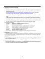
• Safety Check after Servicing
Examine the area surrounding the repaired location for damage or deterioration. Observe that screws, parts and wires have
been returned to original positions. Afterwards, perform the following tests and confirm the specified values in order to verify compliance with safety standards.
1. Insulation resistance test
Confirm the specified insulation resistance or greater between power cord plug prongs and externally exposed parts of
the set (RF terminals, antenna terminals, video and audio input and output terminals, microphone jacks, earphone jacks,
etc.). See table below.
2. Dielectric strength test.
Confirm specified dielectric or strength or greater between power cord plug prongs and exposed accessible parts of the
set(RF terminals, antenna terminals, video and audio input and output terminals, microphone jacks, earphone jacks,
etc.) See table below.
3. Clearance distance
When replacing primary circuit components, confirm specified clearance distance (d), (d") between soldered terminals, and between terminals and surrounding metallic
parts. see table below.
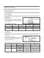
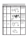
Fig. 1
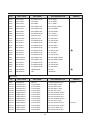
Table 1 : Rating for selected areas
Japan
USA & Canada
Insulation
Resistance
≥1MΩ500 V DC
---
Dielectric
Strength
1kV 1 minute
900V 1 minute
South America
≥10 MΩ/500 V DC
4 kV 1 minute
AC Line Voltage
Region
100V
110 to 130V
* 100 to 250V
Clearance
Distance (d), (d')
≥3 mm
≥3.2mm
≥6mm(d)
≥8mm(d')
(z:Power cord)
Note : This table is unofficial and for reference only. Be sure to confirm the precise values for your particular country and
locality.
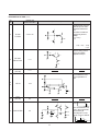
4. Leakage current test
Confirm specified or lower leakage current between B (earth ground, power cord plug prongs) and externally exposed
accessible parts (RF terminals, antenna terminals, video and audio input and output terminals, microphone jacks, earphone jacks, etc.)
Measuring Method : (Power ON)
Insert load Z between B (earth ground, power cord plug
prongs) and exposed accessible parts. Use an AC voltmeter to measure across both terminals of load Z.
See figure and following table:
Fig. 2
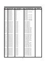
Table 2 : Leakage current ratings for selected areas
AC Line Voltage
Region
100V
Japan
110 to 130 V
USA & Canada
Load Z
1kΩ
1.5kµF
1.5kΩ
100 to 130 V
200 to 250 V
South America
i ≤ 1mA rms
Earth Ground
(B) to :
Exposed accessible parts
i ≤ 0.5 mA rms
Exposed accessible parts
Leakage Current (i)
i ≤ 0.7 mA peak
i ≤ 2mA dc
i ≤ 0.7 mA peak
i ≤ 2mA dc
2kΩ
50kΩ
Antenna earth terminals
Other terminals
Note : This table is unofficial and for reference only. Be sure to confirm the precise values for your particular country and
locality.
2
IMPORTANT SERVICE NOTES
Connect at 1500 ohm watt resistor, paralleled by a 0.15
mfd, AC type capacitor, between a known good earth
ground (water pipe, conduit, etc.) and the exposed metallic
parts, one at a time. Measure the AC voltage across the
combination of 1500 ohm resistor and o.15 mfd capacitor.
Reverse the AC plug at the AC output and repeat AC voltage measurements for each exposed metallic part. Voltage
measured much not exceed 0.3 volts RMS. this corresponds to 0.2 milliamp AC. Any value exceeding this limit
constitutes a potential shock hazard and must be corrected
immediately.
1. X-RAY RADIATION PRECAUTION
1) Excessive high voltage can produce potentially hazardous X-RAY RADIATION to avoid such hazards, the
high voltage must not be above the specified limit. The
nominal value of the high voltage of this receiver is
24.4kv (27.5kv) at zero beam current (minimum brightness) under a 120V AC power source. The high voltage
must not, under any circumstance, exceed 27kv
(28.5kv). Each time a receiver requires servicing, the
high voltage should be checked following the HIGH
VOLTAGE CHECK procedure on page 4 of this manual.
It is recommend as parts of the service record. It is important to use an accurate and reliable high voltage meter.
2) This receiver is equipped with X-RADIATION PROTECTION circuit which prevents the receiver from producing
an excessively high voltage even if the B+ voltage
increases abnormally. Each time the receiver is serviced,
X-RADIATION PROTECTION circuit must be checked to
determine that the circuit is properly functioning, following
the X-RADIATION PROTECTION CIRCUIT CHECK
procedure on page 4 of this manual.
3) The only source of X-RAY RADIATION in this TV receiver is the picture tube. For continued X-RAY RADIATION
PROTECTION, the replacement tube must be exactly
the same type tube as specified in the parts list.
4) Some parts in the receiver have special safety-related
characteristics for X-RAY RADIATION PROTECTION.
for continued safety, parts replacement should be undertaken only after referring to the PRODUCT SAFETY
NOTICE below.
2. SAFETY PRECAUTION
3. PRODUCT SAFETY NOTICE
WARNING : Service should not be attempted by anyone
unfamiliar with the necessary precautions on this receiver.
The following are the necessary precaution to be observed
before servicing.
1) Since the chassis of this receiver has hazardous potential to ground whenever the receiver is plugged in (floating chassis), an isolation transformer must be used during service to avoid shock hazard.
2) Always discharge the picture tube anode to the CRT conductive coating before handling the picture tube.
The picture tube is highly evacuated and if broken, glass
fragments will be violently expelled. Use shatter-proof
goggles and keep picture tube away from the body while
handling.
3) When replacing a chassis in the cabinet, always be certain that all the protective devices are put back in place,
such as; non-metallic control knobs, insulating covers,
shields, isolation resistor-capacitor network etc.
4) Before returning the set to the customer, always perform
an AC leakage current check on the exposed metallic
parts of the cabinet, such as antennas, terminals, screwheads, metal overlays, control shafts etc. to be sure the
set is safe to operate without danger of electrical shock.
(Plug the AC line cord directly into a 120V AC outlet do
not use a line isolation transformer during this check).
Use an AC voltmeter having 5000 ohms per volt or more
sensitivity in the following manner.
Many electrical and mechanical parts in this chassis have
special safety-related characteristics. These characteristics
are often passed unnoticed by a visual inspection and the
protection afforded by them cannot necessarily be obtained
by using replacement components rated for higher voltage,
wattage, etc. Replacement parts which have these special
safety characteristics are identified in this manual and its
supplements; electrical components having such features
are identified on the schematic diagram and the parts list.
Before replacing any of these components, read the parts
list in this manual carefully. The use of substitute replacement parts which do not have the same safety characteristics as specified in the parts list may create X-ray radiation
or other hazards.
4. SERVICE NOTES
1) Which replacing parts or circuit boards, clamp the lead
wires to terminals before soldering.
2) When replacing a high wattage resistor (metal oxide film
resistor) in the circuit board, keep the resistor min 1/2 inch
away from circuit board.
3) Keep wires away from high voltage or high temperature
components.
3
GENERAL ADJUSTMENT
R410 is shorted.
1. GENERAL
In the majority of cases, color television will need only slight
touch-up adjustment upon installation. Check the basic
characteristics such as height, focus and sub-bright.
Observe the picture for good black and white details without
objectionable color shading. If color shading is evident,
demagnetize the receiver. If color shading still persists, perform purity and convergence adjustments. this should be all
that is necessary to achieve optimum receiver performance.
7.WHITE BALANCE ADJUSTMENT
1) Receive MONOSCOPE PATTERN signal.
2) Set the each BIAS VR (VR903, VR904, VR905) and
DRIVE VR(VR901, VR902) to center position and Minimize SCREEN using SCREEN VR on the side of FBT.
3) Open LEVER SW(S901) of CRT PCB.
4) Make straight and horizontal line by pushing service
key(V/H) on the SERVICE remocon.
5) Turn the SCREEN VR slowly until first color is brightened and turn the appropriate BIAS VR to the counterclockwise until that line's color disappears.
6) Turn the SCREEN VR slowly again until another color is
brightened and turn the appropriate BIAS VR to the
counter-clockwise until that line's color disappears.
7) Turn the SCREEN VR slowly again until third color is
brightened and turn the appropriate BIAS VR to the
counterclockwise until that line's color disappears.
8) Adjust the BIAS VR to become white appropriate line by
turning the BIAS VR in concerned with step 4-6, and 4-7
to clock direction (to be brightened).
9) Although you did step 4-5, 4-6, 4-7,
If it is not bright each step's color but bright first color,
stop turn the SCREEN VR at the position which color is
hardly to be seen, and concerned BIAS VR to clock
direction (to be brightened).
10) Turn LEVER SW(S901) of CRT PCB on.
11) Let the straight and horizontal line disappear by pushing
service key(V/H) on the SERVICE remocon.
12) Set CONTRAST to maximum and set brightness to
center, and adjust WHITE BALANCE using R's and B's
DRIVE VR.
13) Inspect TRACKING for WHITE BALANCE by varying
CONTRAST and brightness.
If tracking not correct, Repeat step 4-5 to 4-9.
2. VERTICAL HEIGHT ADJUSTMENT
1) Tune in an active channel.
2) Adjust brightness and contrast control for a good picture.
3) Adjust vertical height control (R304) for approximately
one half inch over scan at top and bottom of picture
screen.
3. FOCUS ADJUSTMENT
1) Tune in an active channel.
2) Adjust brightness, sharpness and contrast controls for a
good picture, sharp scanning lines and/or sharp picture.
4. RF AGC ADJUSTMENT
1) Tune in an active channel.
2) Using the attenuator, apply the signal of 60dBµV to the
Antenna input terminal
3) Turn RF AGC control (R106) so that it is 1.0V±0.3V
lower than maximum voltage.
5. HIGH VOLTAGE CHECK
High voltage is not adjustable but must be checked verify
that the receiver is operating within safe and efficient design
limitations as specified :
1) Operate receiver for at least 15 minutes at 100-140V AC
line.
2) Set brightness, sharpness, contrast and color controls to
minimum position (Zero beam).
3) Connect an accurate high voltage meter to CRT anode.
The reading should be as follows.
13”
24KV~26KV
20”
26KV~28KV
NOTE :
1. When performing any adjustments to resistor controls
and transformers use non-metallic screw driver or TV
alignment tools.
2. Before performing adjustments TV set must be on at
least 15 minutes.
If a correct reading cannot be obtained, check circuitry for
malfunctioning components.
6. X-RADIATION PROTECTION CIRCUIT TEST
When service has been performed on the horizontal deflection system, high voltage system or B+ system, the X-RADIATION PROTECTION circuit must be tested for proper
operation as follows:
1) Operate the receiver for at least 15 minutes at 120V AC
line.
2) Confirm high voltage protector when R409 of power
PCB is connected to 30kΩ(1/4w) in parallel.
3) If high voltage protector is operated, remove 30kΩ(1/4w)
and confirm whether high voltage protector is still on.
4) Confirm normal operation on sound and video when
4
LEADLESS(CHIP) INSTRUCTIONS
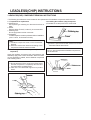
1.LEADLESS(CHIP) COMPONENT REMOVAL INSTRUCTIONS
• The following procedures are recommended for the replacement of the leadless components used in this unit.
1-1. Preparation for replacement
a. Soldering Iron
Use a pencil-type soldering iron that uses less than 3o
watts.
b. Solder
Eutectic solder (Tin 63%, Lead 37%) is recommended.
c. Soldering time
Do not apply heat more than 4 seconds.
d. Preheating
Leadless capacitor must be preheated before installation.
(130°C~150°C, for about two minutes).
1-3. Installing the Leadless (chip) Component
1) Presolder the contact points of the circuit board.
Note :
a. Leadless components must not be reused after
removal.
b. Excessive mechanical stress and rubbing of the
components electrode must be avoided.
2) Press the part downward with tweezers and solder
both electrodes as show below.
Note :
Do not glue the replacement leadless component to
the circuit board.
1-2. Removing the leadless component (Resistors,
Capacitors)
Grasp the leadless component body with tweezers and
alternately apply heat to both electrodes. When the solder
on both electrodes is melted, remove leadless components
with a twisting motion.
Note :
a. Do not attempt to lift the component off the board
until the component is completely disconnected
from the board by a twisting action.
b. Take care not to break the copper foil on printed
board.
7
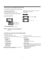
2.LEADLESS (CHIP) COMPONENT IDENTIFICATION
2-1. Check the following before S. M. D Troubleshooting
• Cracked Chipped component Body
• Cracked Separated Solder Joints
• Peeling end Terminations Fractured Leads
• Rejection of Solder from copper Pads or Component
• Foreign Matter on Copper Pads
• Solder Bridges
2-2. S.M.D (Surface Mounted Devices) Identification
Examples
1) Chip Resistor Identification
* Standard chip Resistor code
XXX
123
= 12x103 (1000) = 12000Ω
= 12KΩ
470
= 47x 10°(1) = 47Ω
MULTIPLIER (0-9)
2nd SIG. DIGHT (0-9)
1st SIG. DIGHT (1-9)
2) Chip Capacitor Identification
There is no identification of chip capacitor
REMARK Leadless (CHIP) components are identified on
schematic by means of "(C)" adjacent to symbol numbers.
CLEANING AND LUBRICATION OF DECK MECHANISM
Cleaning and Lubrication
A. Cleaning the Tape Transport System
The following parts should be cleaned after every 500
hours of use.
•TENSION POLE
• S-GUIDE POST
• FE HEAD
• S-SLANT POLE
• VIDEO HEAD/DRUM
• T-SLANT POLE
• T-GUIDE ROLLER
• AC HEAD/AE HEAD
• T-GUIDE POST
• CAPSTAN SHAFT
• PINCH ROLLER
NOTE : After cleaning with alcohol, allow the parts to dry
thoroughly before using a cassette tape.
B. Cleaning the Drive System
The following parts should be cleaned after every 500
hours of use.
• REEL TABLE
• T MAIN BRAKE
• S MAIN BRAKE
• T MAIN BRAKE
• CAPSTAN FLYWHEEL/PULLEY
• REEL PULLEY
C. Lubrication points
The following parts should be cleaned and lubricated
after every 500 hours of use. apply one (1) or two (2)
drops of oil. Refer to the "Replacement Parts List" for the
stock number of the recommended oil.
• S REEL TABLE POST
• T REEL TABLE POST
• IDLER PULLEY
8
5) Remove the Rubber Wedges.
6) Rotate and spread the tabs of the purity magnet (see figure 2) around the neck of the picture tube until the green
belt is in the center of the screen. At the same time, center the raster vertically.
7) Move the yoke slowly forward until a uniform green
screen is obtained. Tighten the clamp screw on the yoke
temporarily.
8) Check the purity of the red and blue raster by adjusting
the BIAS controls.
9) Obtain a white raster, referring "CRT GRAY SCALE
ADJUSTMENT" on the CRT board.
10) Proceed with convergence adjustment.
8. CONVERGENCE MAGNET ASSEMBLY
POSITIONING
Convergence magnet assembly and rubber wedges need
mechanical positioning following the figure 2.
8-1. COLOR PURITY ADJUSTMENT
NOTE : Before attempting any purity adjustments, the
receiver should be operated for at least 15 minutes.
1) Demagnetize the picture tube using a degaussing coil.
2) Vary the CONTRAST and BRIGHTNESS controls to
maximum.
3) Adjust RED and BLUE Bias controls (RJ04 and RJ24) to
provide only a green raster. Adjust the GREEN BIAS
control (RJ13) if necessary.
4) Loosen the clamp screw holding the yoke, and slide the
yoke backward to provide a vertical green belt (zone) in
the picture screen.
5
B. CIRCUMFERENCE CONVERGENCE ADJUSTMENT
NOTE : This adjustment requires Rubber Wedge Kit.
1) Loosen the clamping screw on the deflection yoke to
allow to yoke to tilt.
2) Place a wedge as shown on figure 2 temporarily. (Do not
remove cover paper on adhesive part of the wedge).
3) Tilt front of the deflection yoke up or down to obtain better convergence in circumference. (See Fig. 4) Push the
mounter wedge into the space between picture and the
yoke to hold the yoke temporarily.
4) Place other wedge into bottom space and remove the
cover paper to stick.
5) Tilt front of the yoke right or left to obtain better convergence in circumference. (See Fig. 4).
6) Hold the yoke position and put another wedge in either
upper space. Remove cover paper and stick the wedge
on picture tube to hold the yoke.
7) Detach the temporarily mounted wedge and put it in
another upper space. Stick it on picture tube to fix the
yoke.
8) After placing three wedges, recheck overall convergence.
Tighten the screw firmly to hold the yoke tightly in place.
9) Stick 3 adhesive tapes on wedges as shown in figure 2.
8-2. CONVERGENCE ADJUSTMENTS
NOTE : Before attempting any convergence adjustments,
the receiver should be operated for at least 15 minutes.
A. CENTER CONVERGENCE ADJUSTMENT
1) Receive crosshatch pattern with a crosshatch signal
generator.
2) Adjust the BRIGHTNESS and CONTRAST Controls for
a good picture.
3) Adjust two tabs of the 4-Pole Magnets to change the
angle between them (See Fig 3) and superimpose red
and blue vertical lines in the center area of the picture
screen. (See Fig. 4)
4) Turn both tabs at the same time keeping their angles
constant to superimpose red and blue horizontal lines at
the center of the screen. (See Fig. 4)
5) Adjust two tabs of 6-Pole Magnets to superimpose
red/blue line with green one. Adjusting the angle affects
the vertical lines and rotating both magnets affects the
horizontal lines.
6) Repeat adjustments 3) 4) 5) keeping in mind red, green
and blue movement, because 4-Pole Magnets and 6Pole Magnets interact and make dot movement complex.
Fig. 3
Fig. 4 Dot Movement Pattern
6
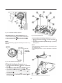
MECHANICAL DISASSEMBLY(DECK)
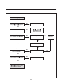
1.TOP VIEW
Fig. 9- Tape Transport Mechanism Identification (Top View)
1.
2.
3.
4.
5.
6.
7.
8.
9.
Earth Bracket Ass'y
FE Head
S-Slant Pole Ass'y
Tension Lever Ass'y
Reel Table
Main Base Ass'y
S-Sub Brake Ass'y
S-Main Brake Ass'y
Idler Plate Total Ass'y
10. T-Main Brake Ass'y
11. T-Sub Brake Ass'y
12. Relay Lever
13. Capstan Motor
14. Pinch Lever Total Ass'y
15. L/C Bracket Total Ass'y
16. Cam Gear
17. AC Head Total Ass'y
18. T-Slant Pole Ass'y
9
MECHANICAL DISASSEMBLY(DECK)
1.TOP VIEW
Fig. 9- Tape Transport Mechanism Identification (Top View)
1.
2.
3.
4.
5.
6.
7.
8.
9.
Earth Bracket Ass'y
FE Head
S-Slant Pole Ass'y
Tension Lever Ass'y
Reel Table
Main Base Ass'y
S-Sub Brake Ass'y
S-Main Brake Ass'y
Idler Plate Total Ass'y
10. T-Main Brake Ass'y
11. T-Sub Brake Ass'y
12. Relay Lever
13. Capstan Motor
14. Pinch Lever Total Ass'y
15. L/C Bracket Total Ass'y
16. Cam Gear
17. AC Head Total Ass'y
18. T-Slant Pole Ass'y
9
2.BOTTOM VIEW
Fig. 10- Tape Transport Mechanism Identification (Bottom View)
20. Capstan Motor
21. F/L Rack
22. Connect Plate
23. Reel Belt
24. Reel Gear Total Ass'y
25. Record Safety Lever
26. Loading Lever L
27. Loading Lever R
28. Drum Total Ass'y
29. Loading Rack
10
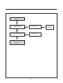
3.F/L MECHANISM VIEW
Fig. 11- Front Loading Mechanism Identification (Top view)
1.
2.
3.
4.
5.
6.
Top Plate Ass'y
F/L Bracket R
Prism Cap
Release Lever
Loading Lever R
CST Holder Ass'y
7. Loading Shaft
8. Loading Lever L
9. Door opener
10. Safety Lever
11. Safety Lever R
11
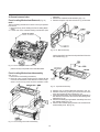
assembly.
3. Remove the cassette holder assembly (Fig. 13)
4. Remove the prism cap and remove one (1) screw hold-
4. General removal view
Front Loading Mechanism Removal (Fig. 12)
NOTE :
The front loading mechanism must be in the eject position
to remove it.
1. Remove two (2) screw holding the Front Loading Mechanism.
2. Lift the rear of the cassette loading mechanism (hole
Fig. 14- F/L Brkt Disassembly
ing the prism link R and remove the prism link R from the
F/L bracket R (Fig. 4)
Fig. 12- Front Loading Mechanism Removal
parts for screw) to separate it from the Main Base.
Front Loading Mechanism disassembly
(Fig. 13~17)
1. Remove the front loading mechanism.
2. Remove one(1) screw holding the F/L bracket R and
move the F/L bracket R in the direction of arrow to separate it from the top plate and the cassette holder
Fig. 15- Top Plate Disassembly
5. Remove one (1) screw holding the prism link L (Fig. 15).
6. Release hook B by pushing it in the direction of the
arrow and remove the door opener (Fig. 15).
7. Press the linked section of the loading lever assembly in
the direction of the arrow and remove the loading lever
assembly (Fig. 16)
8. Remove the safety spring between the safety lever and
the cassette holder (Fig. 16)
9. Remove the release spring between the release lever
and the safety lever R (Fig. 16)
Fig. 13- Front loading mechanism disassembly
12
Fig. 16- Loading Lever Ass'y Disassembly
NOTE :
Reassemble the cassette loading mechanism using the
reverse procedures. Confirm that the two (2) bosses on the
left side of the cassette holder are inserted into the groove
in the left side of the top plate. Insert the two (2) bosses on
the right side into the F/L bracket R (Fig. 17)
Fig. 18- Replacement of the Drum total Ass'y and Earth Brkt Ass'y
Reel belt, Loading Rack, Loading Gears, and
S/T Slant Pole Removal (Fig. 19, 20)
1. Turn the Deck Mechanism upside down and remove the
reel belt.
2. Remove one (1) poly washer ¤ and remove the loading
rack (2).
3. Remove Right and left loading gears ¤Øand ¤Œ.
4. Remove the S and T slant poles ¤º and ¤ by pulling
them in the direction of the arrow.
NOTE :
• Take care not to get grease on the guide rollers.
• When reinstalling, realign the gears as shown in Fig 20.
Fig. 17- F/L Brkt R
Replacement of the Drum Assembly/Earth
Bracket (fig. 18)
1. Remove three (3) screw (3).
2. Remove the earth bracket (5).
3. Carefully lift drum assembly (4) from the deck mechanism taking care not to damage or touch the video
heads.
NOTE :
After reassembling the assembly, confirm that the tape runs
smoothly and confirm all tape path adjustment procedures
in the "Mechanical Adjustment" section of this service publication.
Fig. 19- Reel belt, Loading Rack, Loading Gears, S/T slant pole
Removal
13
L/C Bracket Assembly removal (Fig. 22)
1. Remove one (1) screw
from the L/C bracket assembly and remove the L/C bracket assembly from the
deck mechanism (Fig. 22)
NOTE :
When reassembling, refer to Fig. 23 for alignment instructions.
Replacement of Pinch Lever Total Assembly
Removal (Fig. 22)
1. Remove one (1) washer .
2. Unhook the pinch spring from the main base
remove the pinch lever total assembly .
and
NOTE :
Take care not to get oil on the outside surface of the pinch
roller .
Fig. 20- Loading Gears/Loading Rack Alignment
A/C Head Assembly Removal (Fig. 21)
1. Remove one (1) nut hex from the A/C head assembly
(Fig. 21)
2. Remove the A/C head assembly and remove the A/C
head spring from the A/C head assembly
NOTE :
After reinstalling, perform all A/CHead adjustment procedures and all tape path alignment procedures in publication.
Perform the "Audio Bias Level Adjustment" in the "Electrical
Adjustment" section of this service manual.
Fig. 22- Replacement of L/C Bracket Total Assembly/Pinch
Lever Total Assembly/cam Gear/Relay Lever/F/L Rack
Fig. 21- A/C Head Assembly Removal
14
Fig. 23- L/C Bracket Assembly Alignment
Cam Gear, and F/L Rack Removal (fig. 22)
Fig. 25- Main Plate Removal
1. Remove the cam gear form the deck mechanism.
2. Remove the relay lever from the main base .
3. Remove the F/L rack from the deck mechanism.
Tension Band Assembly Removal (Fig. 26, 27)
1. Remove the tension spring
from the main base
(Fig. 26)
2. Turn the deck mechanism upside down (fig. 27) is facing
down (fig. 27)
NOTE :
When reassembling, align the assembly as shown in Fig.
23 & 24.
NOTE :
• After reassembling, adjust the position of the tension pole
as shown in fig. 28.
• Avoid getting grease or oil on the felt section of the band
brake.
Fig. 24- Cam Gear/F/L Rack Alignment
S/T Main & Sub Brakes Removal (Fig. 25)
1. Unhook the main brake spring from the T main brake
lever .
2. Disconnect the main brake lever assembly
and T
main brake lever from the main base .
3. Unhook the s sub brake spring
from the main base
and disconnect the s sub brake lever assembly
from
the main base .
4. Unlook the T sub brake spring
from the main base
and disconnect the T sub brake lever assembly from
the main base .
Fig. 26- Tension Band Assembly Removal (1)
15
FE Head Removal (fig. 31)
Remove one (1) screw (1) and lift the FE head (2) from the
main base.
Fig. 27- Tension Band Assembly Removal (2)
Fig. 28- Tension Band Assembly Alignment With
Main Base
Capstan Motor Removal (Fig. 29)
Remove three (3) screws and remove the capstan motor.
Fig. 31- FE Head Removal
Reel Gear Total Ass'y and Connect Plate
Removal (fig. 32)
1. Turn the deck mechanism upside down and remove one
¤ polywasher ¤ .
2. Release the tab "B" of the main base and part the reel
gear total ass'y ¤Łfrom the main base.
3. Push the connect plate ¤Øto the left direction and separate it from the main base.
Fig. 29-Capstan Motor Removal
Idler Plate/Reel Table Removal (fig. 30)
1. Remove one ¤ polywasher ¤ from the idler plate ¤Ł
and remove the idler plate ¤Łfrom the main base.
2. Remove the reel tables ¤Øand the two ¤Łpolysliders ¤Œ
from the deck mechanism.
NOTE :
• When removing the connect plate with the the F/L rack
installed, take care not to damage/bend the connect plate.
• When assembling or disassembling, take care not to get
oil or grease on the reel belt.
Fig. 32- Reel gear total ass'y and Connect Plate Removal
Fig. 30- Idler Plate/Reel Table Removal
16
Some disassembly is required to access the adjustment locations. Refer to the "Disassembly Selection" in this publication
for disassembly instructions.
Caution : Use an isolation transformer when servicing.
5. Mechanical Checks/Gear Alignment (fig. 1, 2, 3, 4, 5)
When mechanical problems occur or when reassembling parts in this mechanism, be sure to confirm the following instructions to confirm the following:
1. Make sure that the pilot hole on the cam gear "A" is aligned with the hole "B" in the main base in the EJECT mode
(fig. 1)
Fig. 1– Mechanical Checks/Cam Gear and F/L Alignment
2. Make sure that the part of the relay lever "A" which is assembled with CONNECT PLATE is fully rotated up to the left and
of the hole "B" (Fig. 2)
Fig. 2- Mechanical Checks/relay Lever and Cam Gear Alignment
17
3. There are two (2) triangular marks on the mode sense switch. When installing the L/C bracket assembly on the main
base, confirm that the two (2) triangular marks align with each other in the EJECT mode (Fig. 3)
Fig. 3 - Mechanical checks/Mode Sense S/W Alignment
4. Make sure that the boss "A" of the Pinch Lever Total Ass'y is positioned at the point "B" of the cam gear in EJECT mode
(fig. 4).
Fig. 4 – Mechanical Checks/Pinch Lever and Cam Gear Alignment
18
5. Confirm that the triangular mark "A" on the Loading Gear L Ass'y is aligned with the notch "B" in the Loading Gear R
Ass'y in EJECT mode (Fig. 5)
6. Make sure that the teeth of the Loading Rack are aligned with the those of the Loading Gear R so that hole "C" of the
Loading Rack aligns with the circular mark "D" on the Loading Gear R (fig. 5)
Fig. 5- Mechanical Checks/Loading Loading Rack and Loading Gear Alignment
19
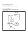
6. Tension checks
Back Tension Measurement /Adjustment (fig. 6, 7)
1. Confirm that the position of the tension pole is correctly positioned. If not, refer to the "Tension Pole Position Adjustment
Procedures"
2. Play back a T-120 tape from the beginning for about 20 seconds (wait until tape transporting system becomes stable).
3. Insert the Tensiometer on the tape path (fig. 6) and measure the back tension. the measured result must meet the specification (25-33gr).
4. If the result is not within the specification, adjust the tension spring (If the measured result exceeds the specification,
relocate the spring on the hook "A". If the value does not reach the specification, relocate the spring on the hook "B".)
and repeat the step 1 thru 3 of "Tension Pole Position Adjustment" (fig. 7).
NOTE :
• Make sure that all of the three probes of the Tensiometer are in contact with the tape, but not with any other parts of the
Deck mechanism.
• It is recommended that the measurement should repeated at least three times to guarantee an accurate reading.
TENSIOMETER
PROBE
Fig. 6 - Back Tension Measurement/Adjustment
20
Operating the VCR Without a Cassette Tape
1.
2.
3.
4.
Remove the cassette Loading Mechanism.
By hand revolve the worm gear counterclockwise 7-8 times until pole base loading process starts automatically.
Then PLAY mode appears. If you want ANOTHER mode, Press the desired button.
If the mechanism is in the desired mode, remove the Power(by unplugging cord).
Tension Pole Position Adjustment
1. Make the mode PLAY without a cassette loaded. Refer to "Operating the VCR Without a Cassette Tape".
2. Confirm that the pilot hole on the tension lever coincides with that of the main base.
3. If the above confirmation is not satisfied, turn Band Brake Cap clockwise or counterclockwise until the two holes are
coincide with each other.
Fig. 7- Tension Pole Position Adjustment
21
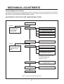
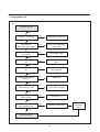
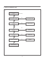
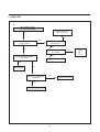
MECHANICAL ADJUSTMENTS
Tape Path Alignment Procedures
The tape transporting system is precisely aligned at the factory and under the normal circumstances will not require adjustment. However, if noise appears in the playback picture, it can be considered that the tape damage has occurred or the
tape path has changed, readjustment of the tape path is necessary.
ADJUSTMENT FLOW FOR THE TAPE TRANSPORTING SYSTEM
CLEANING
CHANGE
• DRUM TOTAL ASS'Y
• A/C HEAD ASS'Y
• PINCH LEVER
TOTAL ASS'Y
PATH ROUGH ADJ.
S GUIDE ROLLER HEIGHT ADJ.
S GUIDE POST FLANGE
T GUIDE ROLLER HEIGHT ADJ.
A/C HEAD HEIGHT ADJ.
PATH PRE-ADJ.
PG(PHASE GENERATOR)
LINEARITY ADJ.
ENTRANCE ENVELOPE
CHANGE
• S-POLE BASE ASS'Y
• T-POLE BASE ASS'Y
• TENSION LEVER
ASS'Y
EXIT ENVELOPE WAVEFORM
ENTRANCE & EXIT ENVELOPE
WAVEFORM FINE ADJ,
• X-POSITION ROUGH ADJ.
• ENTRANCE & EXIT ENVELOPE
WAVEFORM FINE ADJ.
• REVIEW ¤APLAY
AUDIO ADJ.
AUDIO TILT, HEIGHT
AZIMUTH ADJ.
X-POSITION ADJ.
SP, EP
TRACKING
Table. 8 Flow Chart of Tape Path Alignment
22
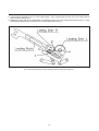
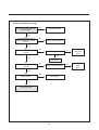
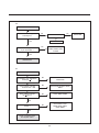
THE SCHEMATIC DIAGRAM OF TAPE TRANSPORTING SYSTEM
TENSION POLE
S-GUIDE POST
FE HEAD
S-GUIDE ROLLER(P2)
S-SLANT POLE
DRUM
T-SLANT POLE
23
T-GUIDE ROLLER(P3)
A/C HEAD
T-GUIDE POST
CAPSTAN SHAFT
PINCH ROLLER
VERTICAL POST
CORN SCREW
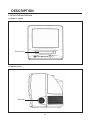
DESCRIPTION
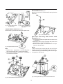
1. TVZ1321/TVZ1341/TVZ1341X
1-1. FRONT OF TV/VCR
FRONT DOOR
1-2. SIDE OF TV/VCR
SPEAKER
24
1-3. REAR OF TV/VCR
VHF INPUT
*Rear of TV/VCR’s
VHF Input
Connect VHF antenna to this terminal.
25
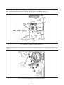
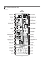
2. PANEL VIEW
2-1. FRONT PANEL
The section below summarizes the buttons, controls, and terminals that you will use with your TV.
Your TV/VCR's Front Panel
Below you will find short descriptions of the buttons and indicators on the front panel. These are used following functions.
1 VIDEO IN jack
Use this jack to receive a video signal from another A/V component.
2 AUDIO IN jack
Use this jack to receive an audio signal from another A/V component.
3 Remote control receiver
This receiver receives a signal from your remote control. Do not block it.
4 STAND-BY (red) indicator
This indicator lights up when the power is off.
5 REC (Green) indicator
this indicator blinks when recording and lights up when set for timer recording.
6. CHILD LOCK (Yellow) indicator
This indicator lights up when the child lock is set.
7. REC button (record)
Press this button to begin recording. Press repeatedly to set a recording time using One-Touch Recording (OTR).
8 REW button (rewind)
Use this button to rewind the tape.
9 PLAY button
Press this button to begin normal playback of a tape.
10 FF button (fast forward)
Use this button to "fast forward" a tape.
11 ST/EJ button (stop/eject)
Press this button when a tape is moving to stop the tape. Press this button when the tape is stopped to eject it.
12
VOL buttons (volume)
Use these buttons to change your TV/VCR's volume.
13
CH buttons (channel)
Use these buttons to change channels on your TV/VCR. You will also use these buttons to adjust the tracking.
14 Power button
Use this button to turn your TV on or off.
26
3. Remote control
1 POWER
Use this button to turn your TV/VCR on or off.
2 TV/CATV
Use the button to set up your TV/VCR to receive signals
from an antenna (TV) or a cable system (CATV).
POWER
MUTE
RECALL
1
TV/CATV
1
2
3
TV/LINE
4
5
6
RESET
7
8
9
SLEEP
0
100
2
3
4
COUNTER
0 STOP
5
6
VISS
7
VOL/V-LOCK
CH/TRK
REC ON/OFF
PLAY
CLEAR
STOP/EJECT
11
12
13
14
TRACKING
6 VISS
Press this button to find the next index mark on a tape
and begin playing.
7 VISS
Press this button to find the most recent index mark on a
tape and begin playing.
FF
SPEED
10 REW (rewind)
Use this button to rewind the tape or to change items in
the menu system.
10
REC/OTR
5 O STOP
Press this button to automatically rewind the tape to the
0:00:00 point.
9 MENU
Press this button to turn the on-screen menu system on
and off.
9
REW
4 RESET
Press this button to reset the counter to 0:00:00.
8 REC ON/OFF
Use this bulletin to enable or disable timer recording.
8
MENU
3 TV/LINE
Use this button to select between viewing the signal
coming from the antenna terminal (TV) or the signal
coming from the A/V jacks (LINE).
PAUSE/STILL
SLOW
11 REC/OTR
Press this button to begin recording.
Press repeatedly to set a recording time using OneTouch Recording (OTR).
12 PAUSE/STILL
Press to temporarily stop the tape during recording or
playback, or to move the cursor in the menu system.
13 ATK (Auto Tracking)
Press this button to Automatically set tracking point.
14 SLOW
Use this button to enable slow playback.
27
15 MUTE
Use to turn the TV/VCR's sound on and off.
15
POWER
MUTE
RECALL
16
TV/CATV
1
2
TV/LINE
4
RESET
7
8
9
SLEEP
0
100
5
6
17
18
19
VISS
VOL/V-LOCK
CH/TRK
20
REC ON/OFF
MENU
REW
PLAY
STOP/EJECT
REC/OTR
PAUSE/STILL
TRACKING
SLOW
17 Number buttons (0-9)
Use these buttons to change channels or select menu
items.
3
COUNTER
0 STOP
16 RECALL
Press this button to display the current time, the counter,
channel number or other status items.
CLEAR
FF
SPEED
21
22
23
24
25
26
18 100
Use this button if you wish to view a channel greater than
99.
19 SLEEP
Use this button to program the TV/VCR to turn off after a
certain time.
20 CH/TRACKING
Use these buttons to change channels on your TV or to
adjust the tracking of a video tape during playback.
21 VOL/V-LOCK
Press to adjust the volume of the TV/VCR. You can also
use these button to eliminate video noise when displaying a still frame.
22 CLEAR
Press this button to erase timer recording settings.
23 PLAY
Press this button to begin normal playback of a tape, or
to move the cursor in the menu system.
24 FF (fast forward)
Use this button to "fast-forward" a tape or to change
items in the menu system.
25 SPEED
Use this button to select the SP, LP, or SLP tape speed.
26 STOP/EJECT
Press this button when a tape is moving to stop the tape
; press it when the tape is stopped to eject it. Also use
this button to activate items in the menu system.
28
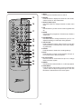
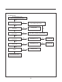
4. Remote controller (Service)
1
POWER
Use this button to turn your TV/VCR on or off.
2
ATK (Auto tracking)
If the screen has noise and abnormal when playback
mode, Press this button to get fine playback Quality.
3
STOP (ENTER)
Press this button when a tape is moving to stop the tape;
press it when the tape is stopped to eject it. Also use this
button to activate items in the menu system.
4
PLAY
Press this button to begin normal playback of a tape, or
to move the cursor in the menu system.
5
REW (Rewind)
Use this button to rewind the tape or to change items in
the menu system.
6
7
6
MENU
Press this button to turn on the screen menu system on
and off.
8
7
CRT ON
Not used.
8
CH/TRACKING
Use this button to change channels on your TV or to
adjust the tracking of a video tape during playback.
9
STD
If you press this button, The TV/VCR become to manufacturer’s Mode.
1
2
3
4
5
9
10
11
12
13
10 VOL/V-LOCK
Press to adjust the volume of the TV/VCR.
You can also use these button to eliminate video noise
when displaying a still frame.
11 H/R
Press this button to set Heat-Run mode.
14
12 REC/B (Record Bias)
Use this button to adjust Record-Bias.
If you press this button,
The TV/VCR operates in Record-Mode in spite of having
no tape.
13 Mute
Use to turn the TV/VCR’s sound on and off.
14 REC/OTR
Press this button to begin recording.
Press repeatedly to set a recording time using OneTouch Recording(OTR).
29
15 TV/CATV
Use this button to set up your TV/VCR to receive signals
from an antenna(TV) or a cable system(CATV).
15
16 TV/LINE
Use this button to select between viewing the signal
coming from an antenna terminal(TV) or the signal
coming from the A/V Jacks(LINE).
16
17 FF (Fast Forward)
Use this button to “Fast Forward” a tape or to change
items in the menu system.
17
18
18 PAU./STILL
Press to temporarily stop the tape during recording or
playback, or to move the cursor in the menu system.
19
20
19 V/H
This is a one of the adjustment mode.
When press this button, only horizontal line is showed up
the screen.
21
22
23
24
25
26
20 S/TEST
Not used.
21 ATK OFF (Autotracking OFF)
Press this button to adjust x-path Adjustment and to confirm fine tracking.
Front Panel’s leds are lighted up if you press this button.
Use only adjustment tape.(DN-1:color bar)
After adjustment, Press this button repeatedly until leds
are off. and Press stop button twice.
After then, Insert tape and confirm fine tracking operation.
22 P/TEST (Picture Test)
Use this button to confirm screen’s condition.
(contrast, bright, tint, color, sharpness)
23 CLOCK
Use this button to test time operation. If you press this
button, the time go( 60)faster than normal mode.
27
28
24 D.P (Digital Preset)
Use this button to adjust screen menu.
(contrast, bright, tint, color, sharpness)
25 REC/T (Record Test)
Use this button to confirm self record-playback.
Operation
{Recording(SP:5sec, SLP:5sec) Zero stop(REW)}
26 RECALL
Press this button to display the current time, the counter,
channel number or other status items.
27 SLOW (only 4HD)
Press this button to begin slow playback.
28 SPEED (only 4HD)
Press this button to change slow playback speed.
30
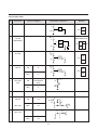
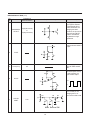
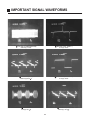
ELECTRICAL ADJUSTMENTS
1. SERVO
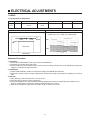
1-1) X-path and P2, P3 Adjustment
Item
X-path
P2, P3
Mode
PLAY
Adjustment parts
CONE SCREW
P2, P3
Check point
PY09
PY05
Location of Adjustment Parts
MAIN PCB
PY09
PY05
Test equipment
Oscilloscope
Test tape
COLOR BAR
Input signal
Observation Waveform
Horizontal Axis : S/DIV
Vertical Axis : CH1 : H/SW, CH2 : ENVELOPE
Y/C
BOARD
CH1
RN90
DECK AS
CH2
MAIN PCB
Adjustment Procedure
1. Preparation
1) Set the AUTO TRACKING to OFF using the Service REMOCON.
2) Play back the Test tape (DN-1:Color Bar)
3) Set the oscilloscope to the CHOP mode. Connect CHI to the H/W (PY09) and CH2 to the ENVELOPE (PY09) and
trigger the scope with the signal from CH1.
2. Adjustments
1) Adjust CONE SCREW to position to maximize the height of the ENVELOPE waveform.
2) Adjust P2 to position where the edge of ENVELOPE waveform are equal and symmetrical. Adjusting P3 is same to
P2's.
3. Remarks
1) After adjusting, Press this button twice. (so leds are off.)
2) Insert the tape into deck to confirm Autotracking.
3) If the picture appears soon after the tape has been threaded around the drum, adjustments are probably correct.
However if autotracking is repeatedly, operating, the adjustments are incorrect.
4) Refer to the illustration on page 23 for the location of p2, p3 and the cone screw.
31
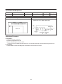
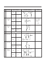
1-2) PLAYBACK PHASE Adjustment
Mode
Play
Adjustment parts
RN90
Check point
PY05
Test equipment
Oscilloscope
Location of Adjustment Parts
MAIN PCB
PY09
PY05
Test tape
COLOR BAR
Input signal
Observation Waveform
Horizontal Axis : 50µS/DIV
Vertical Axis : CH1 : SW30, CH2:V.OUT
Y/C
BOARD
RN90
DECK AS
(t=412 sec 20 sec)
• Adjustment Procedure
1. Preparation
1) Play the Test tape (Color Bar).
2) Connect scope probe to PY 09
3) Set the Oscilloscope to the chop mode.
Connect CH1 to the H/SW(PY09) and CH2 to the V-OUT(PY09) and trigger the scope with the signal from CH1.
2. Adjustment
1) Adjust RN90 to position the falling edge of SW PULSE at 6.5H from the V-SYNC.
32
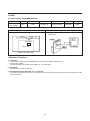
2. AUDIO
2-1) AUDIO CIRCUIT ADJUSTMENT METHOD
Item
Audio
Record Bias
Mode
Adjustment parts
Check point
Test equipment
Test tape
Input signal
REC
RU57
RC HEAD 10Ω
Audio level meter
Blank tape
NONE
Location of Adjustment Parts
MAIN PCB
PY05
PY09
RU57
Observation Waveform
Horizontal Axis :
Vertical Axis :
Y/C
BOARD
RC HEAD
DECK AS
MAIN PCB PARTS SIDE
• Adjustment Procedure
1. Preparation
1) Select REC mode using Service REMOCON. (then, front panel REC LED will be on.)
2) No signal is applied..
3) Connect the Audio level meter to RC HEAD 10Ω (on solder side).
2. Adjustment
1) Adjust RU57 to obtain [3.0]mVrms.
3. Adjustment Inspection Standard : [3.0 ± 0.1mVrms]
• If you don't have Service Remocon, You can select rec mode by inserting a tape (with record tab removed) and pushing the rec button.
33
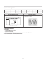
2-2) Audio Azimuth Adjustment
Item
Audio Azimuth
Adjustment
Mode
PLAY
Adjustment parts
AC HEAD
SCREW
Check point
P602
Oscilloscope
Location of Adjustment Parts
MAIN PCB
P602
PY05
PY09
Test equipment
Signal GEN.
Test tape
MONO Bar
Observation Waveform
Horizontal Axis : 0.1mS/DIV
Vertical Axis : 0.1V/DIV
Y/C
BOARD
RC HEAD
DECK AS
MAIN PCB PARTS SIDE
• Adjustment Procedure
1. Preparation
1) Set the VCR to the PLAY mode
2) Connect scope to P602.
3) Adjust first screw on the plate under the AC head to maximize scope's signal height.
2. Adjustment Inspection standard : [Maximum Point]
34
Input signal
7KHz
3. VIDEO
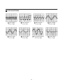
3-1) Y NOISE REDUCTION
Mode
EE
Adjustment parts
RY 34
Check point
PY05, PY09
Test equipment
Oscilloscope
Signal gen.
Location of Adjustment Parts
Input signal
Multi Burst
with 3.58 MHz
Observation Waveform
Horizontal Axis : 10µS/DIV
Vertical Axis : 20 mV/DIV
Y/C PCB
PY09
PY05
Test tape
RY34
IY02
IY01
CH-2 (PY05YNR)
IY03
PAY02
PAY01
Horizontal:10µs/DIV
Vertical:20mv/DIV
Y/C PCB SOLDER SIDE
• Adjustment Procedure
1. Preparation
1) Supply the MULTI BURST signal to the VIDEO IN JACK.
2. Adjustment
1) Set the VCR to the STOP(EE) MODE.
2) Set the Oscilloscope to the chop mode.
Connect CH1 to the V-OUT(PY09) and CH2 to the CNR TP(PY05) and trigger the scope with the signal from CH1.
3) Adjust RY34 to minimize the 3.58MHz Y component of the MULTI BURST signal becomes less than [20]mVp-p.
35
3-2) COLOR NOISE REDUCTION
Mode
EE
Adjustment parts
RY 91
Check point
PY09
Test equipment
Signal gen.
Oscilloscope
Location of Adjustment Parts
Input signal
Color Bar
Observation Waveform
Horizontal Axis : 10µS/DIV
Vertical Axis : 50 mV/DIV
Y/C PCB
PY05
Test tape
PY09
RY91
IY02
IY01
CH-2(PY09(NR)
IY03
PAY02
PAY01
Horizontal:10µs/DIV
Vertical:50mv/DIV
Y/C PCB SOLDER SIDE
• Adjustment Procedure
1. Preparation
1) Supply the Color bar signal to the VIDEO LINE IN JACK.
2) Supply 5V to PY05.
2. Adjustment
1) Set the VCR to the STOP(EE) Mode.
2) Set the Oscilloscope to the chop mode.
Connect CH1 to the V-OUT(RY09) and CH2 to the YNR TP (PY05) and trigger the scope with the signal from CH1.
3) Adjust RY91 until Color signal becomes minimum.
36
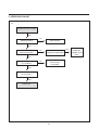
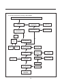
SIGNAL FLOW
1. VIDEO & AUDIO
1-1. FROM RF TO COMPOSITE VIDEO
1-1. To select a channel the tuner must receive CLOCK, DATA and ENABLE from the TIMER IC (I701). Then the
tuner(U101) selects a channel frequency by means of PLL circuit operation and outputs a IF signal(Intermediate Frequency).
The signal from the tuner IF output is amplified by Q103, pre-amp. and then passes through the SAW filter. Now the IF
signal is input to pins 8 and 9 of I501, where it is optimized by the VCO and AFT circuits.
The composite video output at pin 51 of I501, contains the 4.5MHZ audio component. However the composite video signal at pin 45 of I501, does not contain the 4.5MHZ audio signal. Trap Z102 removes the audio signal. Pin 48 of I501,
contains only the 4.5MHZ audio signal which is filtered by Z103.
Pin 1 of switching IC 503 receives it, s signal directly from pin 43 of I501. The signal at this point is selected by an internal switch in I501. The signal source is either TV video at pin 45 or from pin 42 of I501. There are three video signals,
tuner, external, A/V and PB. video.
Switching IC 503 controls these signals.
1-2. COMPOSITE VIDEO SIGNAL
This CHASSIS includes three video signals. One is from RF(above mentioned), another is from A/V, and the third is from
PLAY MODE.
Switching IC I503 controls these three final video signal.
Once one of the two signals(TV video signal from pin 45 of I501 and A/V video signal from pin 42 of I501) is selected, the
selected signal is from pin 43 of I501 and it is input to pin 1 of I503.
Another video signal from PLAY MODE is input to pin 4 of I503.
Also, One of the two signals(video signal from pin 1 of I503 and video signal from PLAY MODE) is selected, and the
selected signal is transmitted to pin 2 and pin 3 of I503.
Final video signal is input to pin 22 of I701 to detect the CAPTION SIGNAL and it is also input to pin 38(C INPUT), pin
(Y INPUT), pin 44(SYNC INPUT).
And R-Y signal is from pin 23, G-Y signal is from pin 24, B-Y signal is from pin 22, -Y signal is from pin 22, and those
color difference signals are sent to CRT BOARD.
In CRT BOARD, those color difference signals are mixed and amplified by color difference drive method.
1-3. AUDIO SIGNAL
This CHASSIS includes three audio signals. One is from RF(above mentioned), another is from A/V, and the third is
from PLAY MODE.
Switching IC I503 also controls these three audio signals.
TV Audio signal from pin 3 of I501 is input to pin 8 of I503.
A/V audio signal from A/V JACK is input to pin 11 of I503 and outputted to pin 9, pin 10.
So, that audio signal is input to pin 16 of IU01.
Audio signal from PLAY MODE is input to pin 2 of IU01.
One of the two audio signals(audio signal from PLAY MODE, audio signal from A/V mode) is selected and output to pin
22 of IU01 and input to pin 1 of I501.
Audio signal to be input pin 1 of I501 and controlled volume is output to pin 4 of I501.
That audio signal is input to pin 3 of I601(SOUND AMP), and amplified by I601 and output to pin 5 of I601.
Finally the audio signal goes to the SPEAKER.
37
SWITCHING TABLE OF I503
MODE
PIN
RF
(EE)
A/V
PLAY
TOGGLE
5
L
L
H
VIDEO
6
H
L
L
AUDIO
12
L
H
H
AUDIO
13
H
H
L
VIDEO
* The input signal is routed to the output port when the switching
port is at logic high state.
38
(Top View)
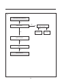
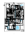
2. Power circuit (Power supply circuit)
2-1. Abstract and Pin Function
The SMPS(Switch Mode Power Supply) can supply a stable output voltage to each circuit, provided that the input voltage
is within the range of between 108-132 VAC at 60HZ.
Regulation is accomplished by PWM(Pulse Width Modulation) of IC STR-S5707.
The table below identifies the various output volatges:
NO.SUPPLY ELECTRIC
RESOURCES
SOURCE
SUPPLY CIRCUIT
APPLICATION
1
DC 125V
TRANS SECOND RECTIFIED
VOLTAGE
D814
FBT
PIF
FBT B+
For channel
selecting(33V)
2
DC 12V
(MOTOR 12V)
REGULATOR IC
I805(PQ12RF11)
SERVO circuit
For driving DRUM,
CAPSTAN MOTOR
3
DC 12V
(ON/OFF 12V)
REGULATOR IC
I804(PQ12RF11)
TUNER
IF AMP circuit
AUDIO circuit
VIDEO circuit
For channel selecting(9V, 5V)
IF amp. circuit(9V), V/SIF(5V)
For driving AUDIO I/O circuit
For driving VIDEO, ANALOG circuit
4
DC 6.0V
(EVER 5.3V)
REGULATOR IC
I803(KIA7806)
SERVO, TIMER IC
SYSCON IC circuit
For driving SYSCON, TIMER,
SERVO circuit
5
DC 14V
TRANS SECOND
RECTIFIED VOLTAGE
D813
AUDIO circuit
AUDIO AMP. B+
6
DC 9V
REGULATOR IC
I806 (KIA7809)
DEFLECTION circuit
VERTICAL IC B+
H. VCC
2-2. I801 STRS-5707
1) BLOCK DIAGRAM
9
VIN
START UP
Tr2
OVP
LA TCH
8 DRIVD
PROPORTIONAL
DRIVE
R3
4 SINK
SENS
PRB RBG
7
OSC
PNP
+2D
OCP
Trl
R6
R1
R7
R8
3
B
1
C
2
GND
5
OCP
T.S.D
R9
R4
C1
C2
R2
R5
C4
6
INH
39
C3
2) Function of Each Termiinal
No. of Terminal
Symbol
Description
Function
1
C
Collector Terminal
Collector of TRr(Power Transistor)
2
GND
Ground Terminal
Ground(Emitter of PTr)
3
B
Base Terminal
Base of PTr
4
SINK
Sink Terminal
Base Current (IS) Input
5
OCP
Overcurrent Protection Terminal
Overcurrent Sensing Signal Input
6
INH
Inhibit Terminal
Off Time Synchronizing
Latch Terminal
Latch Circuit Operation Signal Input
7
SENS
Sensing Terminal
Constant Voltage Control Signal Input
8
DRIVE
Drive Terminal
Base Drive Current(ID) Output
9
VIN
VIN Terminal
Control Circuit Power Supply Input
3) Other Function
Symbol
Function
OVP
Built-in Overvoltage Protecton circuit
TSD
Built-In Thermal Shutdown Circuit
4) Internal Circuit Constant
R1
T ON Adjustment Trimming Resistor
R7
14KΩ
C4
0.01µF
R2
T OFF Adjustment Trimming Resistor
R8
2.5K
C5
1500pF
R3
1.0kΩ
R9
35kΩ
R4
100Ω
C1
3300pF
R5
85Ω
C2
0.01µF
R6
Vs Adjustment Trimming Resistor
C3
820pF
40
2-3. SMPS BASIC OPERATING DESCRIPTION
1) Power supply block circuit
F801
AC 125V 4A
PWC1
C801
O.1U(M)
AC250V
D802-D805
:1S1888
D803
C803
L801
TLF-472BE
T810
TSM-4242A3
C802-C805
4700P 500V
D805
C805
R812
120K
1/2W
R803
1 OHM 7W
CEMENT
Z801
SVC2710
VARISTOR
R804
2.2M(COMP)
1/2W
D802
C802
D804
C804
C806
330U(LWF)
200V
8
9
7
10
6
11
5
12
R806
36K
2W
R813
100K
1/4W
Vin
1
C809
10U
100V
PROPORTION
ORIVE
DVP LATCM
PRE REA
7
OCP
3
REF
T.S.D
S
4
B
DSC
SENSE
13
3
14
2
4
START UP
4
C
1
R807
18 1W
C808
220U
25V
D810
BYV950
C814
470U
25V
15
8.5V
D811
BYV95C
1
C828
0.01U
15V
D812
BYV95C
R819
2.2
1/4W
R833
4.7K
1/4W
DR
C815
100U
160V
15V
D813
BYW95C
D808
BYV95C
1801
STR-S5707
1
123V
D814
BYW95C
D807
BYV95C
C807
220U
25V
C827
1000P(HIKR)
2KV
C812
470U
25V
C810
470U
16V
16
D809
BYV95C
R815
1.8K
1/4W
L803
MD-5
C823
3900P
630VPL
E
2
R1
OCP
C1
C2 R2 C4
6
C3
R816 C822
1K 1500P
1/4W 50V
3
R832
240(*200)
1/4W
C824
4700P
AC400V
R809
0.27(F)
2W
2) Initial Operating Conditions
– When AC voltage is applied at PWC1, the bridge rectifier converts the output voltage to DC and is filtered by C806.
– This voltage is applied to pin 9(V in term.) of I801, through R806 thus starting the operation of I801.
– After C807 charges up to approx. 8V through series resistance R806, then the CTRL circuit starts operating.
– The time constant created by R806 and C807 determines the time delay before the CTRL circuit operation begins
after the AC power is applied. Therefore if the value of C807 is high, it could delay the starting of I801 circuit.
– CTRL circuit operation begins when drive(oscillation) at pin 3 of T801, forward biases D808 and charges C807.
– When the voltage increases at pin 4 of T801, this forward biases D807 and charges C809. When the voltage across
C809 turns off the power to T810.
– This results in the energy stored in the primary being induced into the secondary circuit.
41
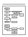
3. DEFLECTION CIRCUIT
Vertical, horizontal drive pulses originate at M52335ASP(I501). The vertical drive pulses are connected to
Vertical Drive IC TA8445K(I301) and drive vertical deflection coils. This horizontal deflection drive pulses drive
the horizontal output circuits and deflection coils and also supply 26.5v, 180v, high voltage 25kV, focus voltage
and screen voltage by driving the FBT.
4. u-COM CIRCUITS.
Timer IC is M37267MX(I701) is made by Mitsubishi. Syscon receives the signal from the user's remocon
and it becomes serial-communication CLOCK/S DATA IN/S DATA OUT signal. Timer IC selects channel
with CLOCK /DATA /EN and receives the functions to control TV and VCR driving(OSD, VOL CTRL, TV
ON/OFF), and such functions as brightness, contrast, color, tint, sharpness, video signal, volume, caption and
program recording.
5. CHANNEL SELECTION AND MEMORY
User selects the channel, then the appropriate PLL data, clock and enable signals are sent out by the -com, to
the tuner.
The -com communicates with I702(IC24LC01B) to memorize, channel numbers, volume and video settings.
42
6. SERVO/SYSCON CIRCUIT OPERATION
1) Summary
• When power is applied to the TV/VCR. The Servo-Syscon 1 chip confirms the operating mode of the deck
mechanism, via the CAM SW. If the mechanism is not in it’s initial mode, the capstan motor will advance the
mechanism to the proper position, depending if a tape is present or not. The deck is now ready to receive serial data from the timer IC.
• The Timer IC determines which function button has been pressed either on the unit or by the remote sensor.
Then the timer IC sends data to the Syscon IC to initiate the selected mode of operation.
• When loading a tape, the L/C motor, capstan and drum motors are activated momentairly until the tape is
threaded around the drum. This must occur before a normal screen will be observed.
• The drum servo system keeps the picture in sync both horizontally and vertically, by controlling the drum speed and
phase.
In PB mode the D-PG is compared against the reference signal, if required a error signal is sent to the D.PWM.
This will correct for speed errors.
• Capstan servo system controls, the speed and phase of the tape. This prevents distorted audio and eliminates noise bands on screen. In addition it helps prevent a lot of on screen noise caused by tracking problems. Capstan control is accomplished by comparing the CTL signal, measured from the lower section of the
A/C head. The Syscon IC then computes the error signal which is then sent to the C-PWM.
2) VCR OPERATING MODES
(1) EJECT
: MODE that a cassette ejects from the compartment.
(2) STAND-BY : MODE that a cassette is unloading.
(3) STOP
: MODE that a cassette is loading.
(4) FF
: Fast Forward MODE that moves the tape forward from the STOP mode
(5) REW
: REWind MODE that moves the tape reversely from the STOP mode
(6) REC
: RECord MODE that records video and audio signal on the tapes.
(7) PAUSE
: record PAUSE MODE that makes recording stop.
(8) PLAY
: MODE that plays the record tape
(9) STILL
: play STILL MODE that playback is paused
(10) CUE & REV : MODE that allows a tape to be searched in the forward or reverse direction.
7. NORMAL AUDIO CIRCUIT OPERATION
1. REC Mode
The input is applied to pin 16 of IU01 and is amplified by the Line Amp., through the ALC circuit. One output at
pin 22 connects to the speaker. The second output through the REC AMP., pin 21, connects to the R/P head
and 70KHZ bias oscillator circuit.
2. PB Mode
The audio signal from R/P head is input to pin 2 where it is amplified and equalized, then the signal is directed
by the #1, SW to the appropriate mode. In normal mode the audio signal is once again amplified by the Line
Amp. and re-directed to the TV.
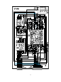
8. VIDEO CIRCUIT OPERATION
1. EE mode
In EE mode video is applied to pin 31 of IY01 then it is output at pin 28. By the time the signal reaches the video output terminal, it’s amplitude has increased 2X by the AGC and video amp.
43
2. REC mode
VIDEO IN
VIDEO OUT
31
REC EQ
28
IY01
LA7423A
Y/C PROCESS IC
9
11
17
PRE-AMP
IC
7
15
1
4
18
7.1M LPF
4
IY02
LC89960
IH CCD IC
IY03
LA7411
8
14
HA SW
R/T
R/T
REC "H"
1
8
• Composite video enters, IY01 at pin 31 where both the chroma and FM luminance signals are down converted to
lower frequencies. These signals then pass through the REC EQ circuit where they are processed for the correct
REC characteristics.
• The input signals at pins 7 and 8 of IY03 are processed by the AGC and REC CURRENT AMP., before they
are recorded onto the tape through the video head assembly.
2-1. REC mode(TVZ-1341 : 4HD)
44
• All signal flow is same to TVZ1321(2HD).
• But, the difference between TVZ1321(2HD) and TVZ1341(4HD) is EP(SLP) Recording.
• In case of 2HD, SP(H) & SP(L) heads are operated.
• In case of 4HD, EP(H) & EP(L) heads are operated.
3. PB mode
• In the case of SP, the signals on pins #17, #20 of IY03(LA7411) are amplified to 60dB respectively and are output
to pin #7 IY03 and is routed to pin #4 IY01(LA7423A)
• The FM signal input to pin #14 of IY01 where it is at FM DEMODULATED after passing through FM EQ. within IC
and then is routed to the Y/C MIXER after passing through 3.0MHz LPF.
• The FM signal at pin 14 of IY01 is passed through the 1.3MHz LPF to allow only the low frequency chroma signals
to pass through.
• The color signal is converted to 3.58MHz at Main CONVERTER and is routed to the Y/C MIXER after being ampli
fied 6dB and then goes through ACC/BURST EMPHASIS. The Y/C signal is output at pin #28.
3-1. PB Mode ( TVZ1321 : 4HD)
• All signal flow is same to TVZ1321(2HD).
• Pin number of LA7416 is differ from LA7411.
• But special playback case, in example Que, Review, Still, Slow, Some signals are needed.
• H.A switching and comp out and color Rotary.
• In case of 2HD, only 2 heads are operated, But in case of 4HD, 4 heads are operated.
• Above 3 signals are input and output through multiplexer IC(refer from TC4053BP).
• Comp out is output from LA7416 pin 3.
• This signal can switch SP and EP and detect large RF signal(Envelope).
• Color Rotary signal is exclusive OR Logic function of H.A sw and comp out.
• If these signals are correct, special playback function is normally operated.
45
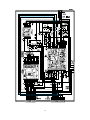
IMPORTANT IC'S OPERATION
IY03 (LA7411)
1. Case Outline : DIP-24S (300mil) Plastic Package
2. Application : VHS format VTR Record and Playback Head Amplifiers
3. Maximum Ratings at Ta = 25°C
Parameter
Maximum supply voltage
Allowable power dissipation
Operating temperature
Storage temperature
Symbol
VCC max
Pd max
Topg
Tstg
Conditions
Ta
6.5°C
Ratings
7.0
700
-10 to +65
-40 to +150
Unit
V
mW
°C
°C
Ratings
5.0
4.80 to 5.50
Unit
V
V
4. Operating conditions at Ta = 25°C
Parameter
Recommended supply voltage
Operating supply voltage range
Symbol
VC
VCC opg
Conditions
5. Electrical Characteristics at Ta = 25°C
Parameter
Symbol
In-put
Out
-put
PB mode
Current dissipation
I CCP
Conditions
T1
T12:5.0V T10:OPEN
EP/ SW30
T4:OPEN (PB)
SP
The current flowing
into pins 12
Voltage gain
L
CH1
GVP 1
T17A T7A
H
CH2
GVP 2
T20A
Voltage gain difference
GVP 1
Vi = 38mVpp. f = 1MHz
CH1
VNIN 1
T17A T7A
VOUT/GVP1.2
noise distortion
CH2
VNIN2
T20A
after 1.1MHz LPF
Frequency
CH1
V fp 1
T17A T7A
Vi=38mVpp. f=7MHz
characteristics
CH2
Vfp 2
T20A
V OUT/GVP1.2
typ
14
18
max Unit
MUTE
0
0
2.5
GVP1-GVP2
Input conversion
min
T2
22
56.5 59.5 62.5
-1
0
0
1.1
2.5
1
mA
dB
dB
1.5 µVrms
0
2.5
-2.5
1
dB
output ratio
Second harmonic CH1
V HDP 1 T17A T7A
Vi=38mVpp. f=4MHz
distortion
VHDP 2
(8M component)/
CH2
T20A
0
-40
-35
dB
2.5
(4M component)
Vi=38mVpp
output ratio
Maximum output level
CH1
V OMP 1 T17A T7A
f=1MHz
CH2
V OMP 2 T20A
The output level when
the third harmonic
is-30dB.
46
0
2.5
1.0
1.2
Vpp
6. Pin Function Table
No
Pin-function
1
HA (EP/SP)
Type DC voltage(V)
Input/Output configuration
Remarks
1kΩ
HA
COMP
EP
100kΩ
2
RF-SW
(REC-MUTE)
1.6V
RF
COMP
1.0V
RECMUTE
COMP
3.2V
H-SYNC
1.0V
20kΩ
80kΩ
REC-H
PB
O
1.2V
80kΩ
5
PB
See attached
sheet
100Ω
REC
0
20kΩ
6
22
GND
7
PB-OUT
PB
2.3
PB OUT
100Ω
REC-C-IN
8
REC
3.6
REC-Y-IN
REC
3.6
47
3.2V
OFF
2.0V
1.6V
REC
ON
REC
PB
VCC
ENV DET
OUT
LCH
20kΩ
REC/PB
COMP
5
HCH
Syac
H
1.5V
L
H.SYNC
COMP
4
SP
SW30 REC MUTE
1kΩ
50kΩ
3
1.6V
5kΩ
25kΩ
300Ω
5kΩ
100Ω
REC
C IN
No
Pin-function
9
AGC-FLT
Type DC voltage(V)
PB
0
REC
1.6
PB
2.5
Input/Output configuration
20k
10k
10
REC-CUR
ADJ2
Remarks
500
VCC
4V : +3.5dB
2.5V : ±0dB
(OPEN)
100
COMP
100
REC
2.5
PB
4.5
REC
5.0
PB
0
REC
1.7
PB
0
REC
4.2
1V : -6dB
COMP
11
REC-CUR
ADJI
12
VCC
13
REC-BIAS
14
16
19
REC-OUT
PB Amp
2'nd Filt
1k
5k
From
REC
ACC
1k
16.7k
VCC
PB
2.0
1.5k
1.6k
REC
10k
3.6
48
3.3k
100
No
Pin-function
17
20
PB-L-IN
PB-H-IN
Type DC voltage(V)
PB
0.7
REC
0
Input/Output configuration
Remarks
REC ON
VCC
18
21
PB-L-SW
PB-H-SW
PB
REC ON
0
ON resistance
4 to 6Ω
PB ON
REC
15
23
24
4.2
NC
7. Pin Operation
VIDEO PREAMP IC LA7411
PIN
MODE
1
2
3
4
5
6
7
8
9
10
11
12
13
14
15
16
17
18
19
20
21
22
23
24
STOP
0
0
0
0
0.9
0
2.3
0
0
2.6
5.1
5.1
0
0
5.2
2.1
0.7
0
2.1
0.7
0
0
0
0
REC
0
0
0
5.2
0
0
3.5
0
1.6
.2.6
4.3
5.2
1.7
4.2
5.2
3.8
0.7
4.2
3.8
0.9
4.2
0
0
0
PLAY
0
0
0
0
0.9
0
2.3
0
0
2.6
5.1
5.1
0
0
5.2
2.1
0.7
0
2.1
0.7
0
0
0
0
REW/FWD
0
0
0
0
2.4
0
2.3
0
0
2.6
5.2
5.2
0
0
5.2
2.1
0.7
0
2.1
0.7
0
0
0
0
49
REV/FF
0
1.4
0
0.5
2.5
0
2.3
0
0
2.6
5.2
5.2
0
0
5.2
2.1
0.7
0
2.1
0.7
0
0
0
0
PAUSE
0
1.4
0
0
1.6
0
2.3
0
0
2.6
5.2
5.2
0
0
5.2
2
0.7
0
2.1
0.7
0
0
0
0
STILL
0
1.4
0
0
2.1
0
2.3
0
0
2.6
5.2
5.2
0
0
5.2
2.1
0.7
0
2.1
0.7
0
0
0
0
IY03 (LA7416)
1. Application : 4HD VHS format VTR Record and Playback Head Amplifiers
2. Maximum Ratings at Ta = 25°C
Parameter
Maximum supply voltage
Allowable power dissipation
Operating temperature
Storage temperature
Symbol
VCC max
Pd max
Topg
Tstg
Conditions
Ta
6.5°C
Ratings
7.0
650
-10 to +65
-40 to +150
Unit
V
mW
°C
°C
Ratings
5.0
4.8 to 5.5
Unit
V
V
3. Operating conditions at Ta = 25°C
Parameter
Recommended supply voltage
Operating supply voltage range
Symbol
VC
VCC opg
4. IC Logic Diagram
50
Conditions
5. Pin Function Table
No
1
19
22
28
2
Pin-function
PB Amp
2’ nd Filt
Type DC voltage(V)
PB
2.0
REC
3.6
Input/Output configuration
Remarks
TRICK-H
Trick 1
3.0V
NORMAL
1.0V
Trick 2
3
COMP-OUT
H : 4.5 or more
PB
EP>SP ENV
: High
L : 0.7 or less
REC
4
OPEN
HA (EP/SP)
EP
1.6V
5
RF-SW
(REC-MUTE)
SW30 REC MUTE
HCH
1.0V
LCH
6
SP
H-SYNC
1.5V
ON
OFF
Syac
H
L
51
3.2V
No
Pin-function
7
REC-H
Type DC voltage(V)
PB
Input/Output configuration
Remarks
0.0
REC
2.0V
8
ENV DET
OUT
REC
5.0
PB
See attached
sheet
REC
0.0
9
GND
10
PB-OUT
PB
2.3
REC-C-IN
REC
3.6
REC
3.6
PB
0
REC
1.6
PB
2.5
REC
2.5
PB
4.5
REC
5.0
11
12
13
14
15
PB
REC-Y-IN
AGC-FLT
REC-CUR
ADJ2
REC-CUR
ADJ1
4V : +3.5dB
2.5V : ±0dB
(OPEN)
1V : -6dB
VCC
52
No
Pin-function
Type DC voltage(V)
16
REC-BIAS
PB
0
REC
1.7
PB
0
REC
4.2
PB
0.7
REC
0
PB
0
REC
4.2
17
18
20
23
27
30
21
24
26
29
25
REC-SP OUT
REC-EP OUT
SP-L-IN
SP-H-IN
EP-L-IN
EP-H-IN
SP-L-SW
SP-H-SW
EP-L-SW
EP-H-SW
Input/Output configuration
PRE-GND
53
Remarks
IY02 (LC89960)
1. Overview
The SANYO LC89960 is a 1H delay line for NTSC television systems.
Only an external low-pass filter is required to implement a 1H delay line.
2. Features
• Single 5V power supply.
• 1H delay signal can be obtained with low-pass filter and 3.58MHz clock input.
• Minimum number of external components required because of timing generator, bias generator, output Amp, on
chipped.
• The phase of output signal is reversed to the phase of input signal.
3. Functions.
• 905 stage CCD shift register.
• Timing generator and clock driver for CCD.
• Auto-bias circuit.
• Sync tip clamp circuit.
• Sample and hold circuit and output Amp.
• 4fsc clock generator with PLL circuit.
• VCO (4fsc) output circuit.
4. Absolute Maximum Ratings
Items
Supply Voltage
Operating Temperature
Storage Temperature
Allowable Power : Dissipation
Symbol
VDD
TOPR
TSTG
PD
Unit
V
°C
°C
mW
Min.
-0.3
-10
-55
-
max.
+6.0
+60
+150
450
Conditions
Ta = 25°C
Ta = 25°C
5.Pin Operation
Y/C CCD IC LC89960
PIN
MODE
STOP
REC
PLAY
REW/FWD
REV/FF
PAUSE
STILL
1
2.2
2.2
2.2
2.2
2.2
2.2
2.2
2
2.5
2.5
2.5
2.5
2.5
2.5
2.5
3
0
0
0
0
0
0
0
4
2
2
2
2
2
2
2
5
0
0
0
0
0
0
0
6
0
0
0
0
0
0
0
7
0
0
0
0
0
0
0
8
1.2
1.2
1.2
1.2
1.2
1.2
1.2
9
5.2
5.2
5.2
5.2
5.2
5.2
5.2
10
2.1
2.1
2.1
2.1
2.1
2.1
2.1
11
2.1
2.1
2.1
2.1
2.1
2.1
2.1
12
5.2
5.2
5.2
5.2
5.2
5.2
5.2
13
9.4
9.4
9.4
9.4
9.4
9.4
9.4
14
0
0
0
0
0
0
0
54
IY01 (LA7423A)
1. Case Outline : DIP-36S(400mil) Plastic Package
2. Application : VHS VTR Video signal Processor (Y/C single-chip)
3. Maximum Ratings at Ta = 25°C
Parameter
Maximum supply voltage
Allowable power dissipation
Operating temperature
Storage temperature
Symbol
VCC max
Pd max
Topg
Tstg
Conditions
Ta
65°C
Ratings
7.0
1070
-10 to + 65
-40 to + 150
Unit
V
mW
°C
°C
4. Pin Operation
Y/C 1CHIP IC LA 7423
PIN
MODE
1
2
3
4
5
6
7
8
9
10
11
12
13
14
15
16
17
18
19
20
21
22
23
24
25
26
27
28
29
30
31
32
33
34
35
36
STOP
0
2.4
3
2.3
2.3
3.1
0
3.1
2.1
0
1.1
2.5
2.5
2.5
2.1
2.1
3.9
2.8
2.7
2.7
1.9
2
1.6
5.1
4.2
0
5.1
1.8
0
2.7
3
1.5
0
3.1
0
5.2
REC
0
2.4
3
2.3
2.3
3.1
0
3.1
2.1
0
1.1
2.5
2.5
2.5
2.1
2.1
3.9
2.8
2.7
2.7
1.9
2
1.6
5.1
4.2
0
5.1
1.8
0
2.7
3
1.5
0
3.1
0
5.2
PLAY
4.8
1.9
3.2
4.7
4.7
3
3.6
3.1
2.1
0
1.1
2.5
2.5
3.3
2.1
2.1
3.8
2.7
2.7
2.7
1.9
2
1.6
5.1
4.2
0
5.1
1.8
0
2.7
3.5
1.8
0
3.7
3.6
3.7
REW/FWD
0
2.4
3
2.3
2.3
3.1
1.8
3.1
2.1
0
1.1
2.5
2.6
2.5
2.3
2.1
3.9
2.8
2.7
2.7
1.9
2
1.6
5.1
4.2
0
5.1
1.8
0
2.7
3
1.5
0
3.1
0
5.2
55
REV/FF
4.8
2
3.1
4.7
4.7
3
3.6
3.1
2.1
0
1.1
2.5
2.5
3.3
2.1
4.6
3.8
2.7
2.7
2.7
1.9
2
1.6
5.1
4.2
0
5
1.7
0
2.7
3.5
1.7
0
4.6
3.6
3.7
PAUSE
0
2.4
3
2.3
2.3
3.1
1.8
3.1
2.1
0
1.1
2.5
2.6
2.5
2.3
2
3.9
2.8
2.7
2.7
1.9
2
1.6
5.1
4.2
0
5.1
1.8
0
2.7
3
1.5
0
3.1
0
5.2
STILL
4.8
2
3.1
4.7
4.7
3
3.6
3.1
2.1
0
1.1
2.5
2.5
3.3
2.1
5
3.8
2.7
2.7
2.7
1.9
2
1.6
5.1
4.2
0
5
1.8
0
2.7
3.5
1.6
0
4.6
3.6
3.7
5. IY01 (LA7423A : Y/C PROCESS IC)
No
Pin-function
Type voltage(V)
Signal waveform
SYNC-DET
-OUT
1
DC
S-DET-OUT
REC-Y
REC = 2.4V
MAIN. DE.
EMPH-OUT
PB = 2.0V
2
REC = 3.0V
3
CLAMP
PB = 3.2V
EMPH-OUT
REC = 2.1V
R/P CTL
PB = 4.4V
4
REC = 2.1V
5
MAIN-EMPH
-FILT
PB = 4.4V
REC = 3V
6
NL FILT
PB = 3V
56
Input/Output configuration
Remarks
No
Pin-function
7
MODE-CTL
Type voltage(V)
Signal waveform
SP 0~1.5 [V]
LP 1.5~3.2 [V]
EP 3.2~5.0 [V]
REC = 3V
8
VCA-FILT
DC
PB = 3V
REC = 2.2V
9
VCA-IN
PB = 2.2V
10
GND
0V
REC = 1.0V
11
CCD DRIVE
PB = 1.0V
PIC-CTL
REC = 3V
SOFT : 2.0~2.5V
HARD : 2.6V~3.2V
PB = 3V
EDIT when over 3.5V
12
EDIT
57
Input/Output configuration
Remarks
No
Pin-function
Type voltage(V)
Signal waveform
REC = 2.5V
13
NC-CTL
PB = 2.5V
REC C-OUR
REC =2.4V
PB-YC-IN
PB = 3.2V
AGC-TC 1
REC = 2.4V
BALANCER
PB = 2.3V
REC-APC-
REC = 2.3V
under 1.5V N.C OFF
2.0~3.0V N.C CTL
over 3.8V Y/CMix
OFF (N.C. Center)
14
Y-FM
+Low Chroma
15
16
FILT
TRICK-H
PB = over 3.5V
(SP Mode)
REC = 3.8V
17
VXO-IN
PB = 3.8V
REC = 2.3V
18
XO-OUT
PB = 2.4V
58
Input/Output configuration
Remarks
No
Pin-function
Type voltage(V)
Signal waveform
REC = 2.8V
19
SLD-FILT
PB = 2.8V
REC =2.8V
20
AFC/APC
FILT
PB = 2.8V
REC = 1.9V
XO mode
when over 3.5V
21
C-OUT
PB = 1.9V
CNR ON
when over 3.5V
Color = 1.9V
22
KILL-FILT
Killer = 3.1V
REC = 1.7V
23
CNR-CD-IN
PB = 1.7V
CNR OFF
when over 2.5V
24
VCC-2
5.0V
D.C
59
Input/Output configuration
Remarks
No
Pin-function
Type voltage(V)
25
REG = 4.2
4.2V
26
SYNC OUT
Signal waveform
D.C
1.75V when CNR
mode
27
VCC-1
28
VIDEO OUT
29
QV. QH INS.
CHARA INS
30
ROT-PLS
60
Input/Output configuration
Remarks
No
Pin-function
Type voltage(V)
Signal waveform
REC = 2.7V
31
VIDEO-IN
PB = 2.7V
REC = 1.6V
32
AGC-TC2
D.C
PB = 1.6V
REC = 0V
33
SVHS-FM-IN
PB = 3.7V
Normal
VHS 0V
MOD-OUT
REC = 3.0V
DOC-STOP-H
PB = 3.6V
34
3.95 DOC-STOP
REC = 0V
35
NOR-FM-IN
PB = 3.8V
REC = 1V
36
FM-EQ-OUT
PB = 3.8V
61
Input/Output configuration
Remarks
IU01 (BA7790LS)
1. FUNCTION
(1) Circuit essential for a standard sound signal processing system as a PB AMP, REC AMP, ALC circuit, EQ selecting
switch and high voltage head switch have been integrated onto a single 1 chip.
(2) Built-in LINE/TUNER INPUT selecting switch.
(3) Built-in summary 3 mode EQ switch and it can be obtained EQ characteristics of each mode.
(4) PB AMP is low noise and high performance.
(5) Built-in ALC circuit with variable ALC level setting.
(6) No shock noise or ALC attack noise is generated when power source is turned ON or the mode is changed by means
of a ALC loop outside mute system.
2. Absolute Maximum Ratings (Ta = 25°C)
Parameter
Supply voltage
Power dissipation
Operating temperature
Storage temperature
Symbol
Vcc
Pd
Topr
Tstg
Limits
13
400
-10~+65
-55~+125
Unit
V
mW
°C
°C
Range
7.5~12.5
Unit
V
Derate 4.0mW/°C for the operating above Ta = 25°C
3. Recommended Operational Conditions (Ta = 25°C)
Parameter
Power supply voltage
Symbol
Vcc
4. Pin
PIN
AUDIO IC BA7790LS
MODE
1
2
3
4
5
6
7
8
9
10
11
12
13
14
15
16
17
18
19
20
21
22
23
24
STOP
0
4.6
0
0
11.2
4.7
11.4
4.7
0
4.7
0.6
5.3
4.6
0.6
5.4
5.3
0
5.3
5.4
0
5.4
5.4
0
0.5
REC
0
4.6
0
0
11.2
4.7
11.4
4.7
0
4.7
0.6
5.3
4.6
0.6
5.4
5.3
0
5.3
5.4
0
5.4
5.4
0
5.2
PLAY
0
4.6
0
0
11.2
4.7
11.4
4.7
3.8
4.7
5.2
5.3
4.6
0
5.3
5.3
0
5.3
5.3
0
5.3
5.3
0
0.5
REW/FWD
0
4.6
0
0
11.2
4.7
11.4
4.7
0
4.7
0.6
5.3
4.6
0.5
5.4
5.3
0
5.3
5.3
0
5.4
5.4
1
0.5
62
REV/FF
0
4.6
0
0
11.2
4.7
11.4
4.7
3.7
4.7
5.2
5.3
4.6
0
5.3
5.3
5
5.3
5.4
0
5.4
5.4
0
0
PAUSE
0
4.6
0
0
11.2
4.7
11.4
4.7
0
4.7
0.6
5.3
4.6
0.5
5.4
5.3
0
5.3
5.4
0
5.4
5.3
0
0.5
STILL
0
4.6
0
0
11.2
4.7
11.4
4.7
0
4.7
5.2
5.3
4.6
0
5.4
5.3
5
5.3
5.4
0
5.4
5.3
0
0.5
5. Terminal Function Table
Terminal No.
Description
Function
Terminal
Voltage
Terminal Form
1
HEAD EQ
Switch for selecting the
head resonance capacitor
0.0V
220kΩ/27Ω(ON)
2
PB IN
PB AMP input/PB side head switch
3.4V
REC : 120kΩ
3
REC HSW
REC side high voltage head switch
0.0V
REC : 11Ω(ON)
REC : OPEN
4
GND
GND (for PB AMP, Head switch)
0.0V
–
5
RIPPLE FILTER
Ripple filter
9.0V
10kΩ(Vcc)
6
PB NFB
PB AMP feedback
3.5V
B(NPN)
7
Vcc
Vcc
9.0V
–
8
PB EQ
PB EQ selecting switch
3.5V
55Ω(ON)/OPEN
9
EQ CTRL
EQ control
10
PB OUT
EQ AMP output
11
PB/TU/EE CTRL
PB/TU/EE control
–
12
PB LINE IN
Line input for PB
4.1V
120kΩ
13
ALC LEVEL
ALC Level setting terminal
–
B(PNP)
14
ALC FILTER
Terminal for ALC filter with time
constant
(Setting attack and recovery time)
PB : 0.0V
PB : variable
EE(NPN)~220Ω
15
BIAS
Bias
4.1V
EE(NPN)
Isink = 670µA
16
LINE IN
Line input
4.1V
120kΩ
17
MUTE CTRL
MUTE control
18
TUNER IN
Tuner input
4.1V
120kΩ
19
REC NFB
REC AMP feedback
4.1V
B(NPN)
20
GND
GND
0.0V
–
21
REC OUT
REC AMP output
4.1V
EE(P-P)
22
BF OUT
Line AMP OUTPUT
4.1V
EE(P-P)
23
REC EQ
REC EQ selecting switch
0.0V
100kΩ/22Ω(ON)
24
REC/EE CTRL
REC/EE control
REC : 11Ω(ON)
–
3.5V
EE
–
–
NOTE :
• Terminal form abbreviations : EE : emitter follower, P-P : push pull, B : base, C : collector.
• All figures are measured at Vcc = 9V at no signal condition.
• All figures show standard values.
63
IN05(BA6209)
1. Function : Reversible Motor Driver
2. Pin Operation
V.OUT1
VZ.1
V.REF
F.IN
R.IN
VCC1
VCC2
VZ.2
V.OUT2
1
2
3
4
5
6
7
8
9
10
MOTOR 12V
3.9 2W
CN10
0.0I
RN21
CND
IN05 BA6209 LM DRIVE
To DECK
CCN11
0.01
DN13
ZPD 6.2
RCN 22
3.3K
51
+
CN35
100U
25V
LM (+)
LM (-)
50
Pin 51 : LM ON(H)
Pin 50 : LM (+)/(-)
IN01
IN03 (MC4558C)
1. Function : Dual wideband operational amplifier
2. Pin Operation
DUAL OP AMP MC4558C
PIN
MODE
1
2
3
4
5
6
7
8
STOP
3.2
3.1
3.1
0
2.8
0.9
1.4
6
REC
3
3
3
0
2.7
0.9
1.4
6
PLAY
3.3
3.2
3.2
0
3.3
3.2
3.7
6
REW/FWD
3.3
3.2
3.2
0
3.3
3.2
3.7
6
REV/FF
3.3
3.2
3.2
0
3.3
3.2
3.7
6
PAUSE
3.2
3.2
3.3
0
3.6
3.3
5.3
6
STILL
3.4
3.2
3.3
0
3.6
3.3
5.3
6
REC
0
0
5.7
3.7
3.8
3.8
2.6
PLAY
0
0
0
4
2.6
2.6
2.6
I503(TC4066BP)
1. Four independent circuits of bidirectional switches
2. Pin operation
SWITCHNG IC TC4066BP
PIN
MODE
1
2
3
4
5
6
7
STOP
6
5.3
0
0
3.5
3.5
3.6
REC
6
0
0
0
0
0
4.2
PLAY
6
5.3
0
0
0
0
4.1
PIN
64
MODE
8
9
10
11
12
13
14
STOP
0
5.7
0
3.8
2.3
2.3
2.3
I301(TA8445K)
RAMP GENERATOR
50/60Hz
S/W
Vertical Out
Output Vcc
V. OUT
GND
Phase compensation
Pump up output
Pump up Vcc
V. NFB
Pump up
RAMP
50/60 SW
V. SIZE
INPUT
Vertical trig
Drive Vcc
Vertical Drive
1. Operating Conditions (Ta = 25°C)
Item
Symbol
Min
Typ.
Max.
Unit
Drive vcc
VCC1
8.1
9.0
9.9
V
Pump up Vcc
VCC2
–
2.4
2.9
V
Vertical Output Vcc
I11 P-P
–
–
2.2
Ap-p
2. Operating Characteristics (Ta = 25°C, Vcc1 = 9V, Vcc2 = 24V)
Symbol
Measurement
Condition
Min
Typ.
Max.
Unit
Icc1
1
2.0
5.0
12
mA
Trig input threshold Voltage
Vertical range control voltage (1)
V2
V60/3
2
3
–
1.0
–
1.5
1.0
2.0
V
V
Vertical range control voltage (2)
V50/3
11
0.75
1.25
1.75
V
V5
4
3.5
4.8
6.0
V
V5P-P
4
3.5
4.5
5.5
VP-P
Output transistor saturation Voltage(1)
Vs11-10
5
0.3
0.5
1.0
V
Output transistor saturation Voltage(2)
Vs12-11
6
1.0
1.8
3.6
V
Pump up output Voltage (1)
Vs7-8
7
1.0
2.0
3.0
V
Pump up output Voltage (2)
Vs8-10
8
0.2
0.8
1.6
V
Ib
9
–
2.6
–
mA
VCENTER
10
8.0
12.0
14.0
V
Item
Drive current
Maximum output voltage
Maximum peak to peak Voltage
No signal Current
Center Voltage
65
IN01 (Syscon : TMP91C642AN-3227)
SYSCON IN01
PIN
MODE
1
2
3
4
5
6
7
8
9
10
11
12
13
14
15
16
17
18
19
20
21
22
23
24
25
26
27
28
29
30
31
32
33
34
35
36
37
38
39
40
41
42
43
44
45
STOP
5.2
3.5
4.6
5.2
0
5.2
0
0
3.6
2.8
5.2
0
5.2
0
0
0
5
0
0
4.7
5.2
0
0
0
0
4.5
3.7
3.7
0
2.4
0
0
0
0
5.2
5.2
0
5.2
2.9
5.2
0
0
0
5.2
2.5
REC
5.2
3.4
4.6
5.2
0
5.2
0
0
3.1
2.8
0
0
5.2
var
0
0
2.6
4.8
2.7
3.2
5.2
0
2.6
0
0
var
3.7
3.7
0
2.4
2.8
0
0
0
0
5.2
5.2
0
5.2
3.1
5.2
0
0
5.2
2.5
PLAY
5.2
3.8
4.6
5.2
0
5.2
0
0
3.3
2.8
0
0
5.2
var
0
0
2.5
4.8
2.7
3.2
5.3
0
2.6
0
0
3.9
4.2
4.2
4.7
2.5
2.8
0
0
0
5.2
0
5.2
0
5.2
3
5.2
0
0
5.2
2.5
REW/FWD
5.1
3.5
4.6
5.2
0
5.2
0
0
3.3
2.8
0
0
5.2
var
0
0
2.5
4.8
2.7
3.2
5.3
0
2.6
0
0
3.8
3.8
3.7
0
2.4
2.8
0
0
0
5.2
5.2
5.2
0
5.2
3
5.2
0
0
5.2
2.5
66
REV/FF
5.1
3.6
4.6
5.2
0
5.2
0
0
3.3
2.8
5.2
0
5.2
var
0
0
2.6
4.8
2.7
3.2
5.3
0
2.6
0
0
3.8
3.8
3.7
4.7
2.5
2.8
0
0
0
5.2
0
0
0
5.2
3
5.2
5.2
0
5.2
2.5
PAUSE
5.1
3.6
4.6
5.2
0
5.2
0
0
2.8
2.8
5.2
0
5.2
5
0
0
2.6
4.8
2.7
4.7
5.3
0
2.6
0
0
0
3.8
3.7
0
2.4
0
0
0
0
5.2
5.2
5.2
0
5.2
2.9
5.2
0
0
5.2
2.5
STILL
5.1
3.7
4.6
5.2
0
5.2
0
0
3.6
0
0
0
5.2
0
0
0
2.6
4.8
2.7
4.7
5.3
0
2.6
0
0
3.8
3.8
3.7
4.7
2.5
5.2
0
0
0
5.2
0
0
0
5.2
2.9
5.2
5.2
0
5.2
2.5
PIN
MODE
46
47
48
49
50
51
52
53
54
55
56
57
58
59
60
61
62
63
64
STOP
5.2
2.2
2.1
0
0
0
0
0
2.1
2.6
5
5.2
5.3
3.1
0.6
5.3
5.3
0
5.3
REC
5.2
2.2
2.1
0
0
0
0
0
3.5
2.6
5
5.2
5.3
3.1
0
5.3
5.3
0
5.3
PLAY
5.2
2.2
2.1
0
0
0
0
0
3.5
2.6
5
5.2
5.3
3.1
2.9
5.3
5.3
0
5.3
REW/FWD
5.2
2.2
2.1
0
0
0
0
0
3.5
2.1
5
5.2
5.3
3.1
2.1
5.3
5.3
0
5.3
67
REV/FF
5.2
2.2
2.1
0
0
0
0
0
2.1
5.2
5
5.2
5.3
3.1
2.4
5.3
5.3
0
5.3
PAUSE
5.2
2.2
2.1
0
0
0
0
0
3.5
2.6
5
5.2
5.3
3.1
1.8
5.3
5.3
0
5.3
STILL
5.2
2.2
2.1
0
0
0
0
0
3.5
2.6
5
5.2
5.3
3.1
2.1
5.3
5.3
0
5.3
PIN
PIN NAME
PIN
DESCRIPTION
1
S/CLK
Serial Clock
2
S/OUT
Serial OUT, Contact with TIMER IC Serial IN
3
S/IN
Serial IN, Contact with TIMER IN Serial OUT
4
SYNC (L)
NOT USED
5
VCR/ON(L)
NOT USED
6
LINE/TV
NOT USED
7
NOT USED
8
C/SYNC
Composite Sync
9
SLOW STEP
Adjusting Vth of CTL/P, Sets “L” during SLOW mode
10
C. I LIMITER
Limit the current of CAP. M/T
Sets 'L' during SLOW MODE
11
CAP F/R
Switching forward(H)/reverse(L) of CAP. M/T
12
C/SYNC
Composite SYNC
13
REMOCON IN
REMOTE controller signal
14
REEL PULSE
Take Up Reel Pulse IN
15
STROBE
Port to have S.DATA with TUNER
16
RENTAL(H)
Set on 'H' when rental
17
D/FG
Drum FG
18
D/PG
Drum PG
19
C/FG
Caption FG
20
PB/CTL
Caption APC, SLOW & RTC & VISS DETECT
21
EVER 5.3V
EVER 5.3V
22
QV/SYNC
WHen special play, Quasi Vertical SYNC
23
V/SW
Video head Switching
24
A/SW
Audio head Switching
25
H. A. SW
Video head switching out, SP(L)
26
REC-LED(L)
Light up when REC
27
STAND-BY(L)
Light up when STAND-BY
28
T. REC
Lights up when timer recording stand-by and blinks when timer recording REPEAT
68
PIN
PIN NAME
PIN
DESCRIPTION
29
AUDIO SLP(H)
Set 'H' When SLP mode.
30
D/PWM
Drum motor control PWM output
*period of PWM : 23.4KHz (6MHz/256)
31
C/PWM
Capstan motor PWM output
* period of PWM : 23.4KHz (6MHz/256)
32
GND(D)
33
Digital GND
NOT USED
34
CST IN(L)
NOT USED
35
REC(L)
Set 'L' when recording
36
EE(H)
Set 'H' when EE/REC mode with TIME delay, in case of VIDEO mode
37
TRICK (L)
Set 'L' when special play, Audio MUTE output
38
SP(L)
Tape speed SP(L) output
39
LP(L)
Tape speed LP(L) output
40
R/CTL
Change Record CTL DUTY when MARK & ERASE mode
41
2HD/4HD
4HD (L) OR 2HD (H)
42
A. MUTE (H)
Audio Mute output when special record
43
NTSC(L)
NTSC(L)/PAL(H) switching output
44
SP TRICK(L)
Set 'L' when SP mode
45
CLK
NOT USED
46
RESET(L)
RESET
47
OSC/IN
SYSTEM CLOCK CRYSTAL(10MHz)
48
OSC/OUT
SYSTEM CLOCK CRYSTAL (10MHz)
49
GND
50
LM(+)/LM(-)
Loading motor forward(L), reverse(H)
51
LM ON(H)
Set 'H' when operates loading motor
52
T/START(L)
Tape START sensor input
53
T/END(L0
Tape END sensor input
69
PIN
PIN NAME
54
CAM A
55
CAM B
CAM C
CAM D
PIN
DESCRIPTION
CAM Detection input port
POWER
A
B
C
D
MODE
2.9 ~ 3.7
L
H
H
H
EJECT 4.35(H)
3.7 ~ 4.5
L
H
H
L
STAND-BY(INITIAL) 4.35(L)
2.2 ~ 2.9
H
H
H
L
REV 5.30(L)
2.9 ~ 3.7
H
H
L
L
STOP 2.65(L)
0.0 ~ 2.2
H
H
L
H
PLAY, QUE 2.65(H)
2.2 ~ 2.9
H
L
H
L
FF/REW 2.10(L)
4.5 ~ 5.0
H
H
H
H
CAM 5.0(H)
56
KEY 1 &
VTR function key input
57
KEY 2
58
TRK DLY
PATH adjustment TRACKING DELAY
59
PG DLY
PG DLY adjustment * PG DLY adjustment range
5.625 degree – 11.25 degree – 28.125 degree
(0V) – (CENTER) – (5V)
60
ENVE DET.
*Maximum POINT SEARCH DC ENVE input
*AUTO TRACKING RESTART CONDITION.
(SP : 2~5V, SPL, LP : 1.5`5V)
• CASSETTE IN
in play mode
• When tape speed is changed, in play mode
• PB/CTL PULSE off
61
SYSTEM SEL
NOT USED
62
EVER 5.3V
EVER 5.3V
63
GND(A)
Analogue GND
64
EVER 5.3V
EVER 5.3V
PB/CTL PULSE on
70
I701(Timer : M37267M6 - 103SP)
1. Pin Layout
M37267M6 - 103SP
HSYNC INPUT
1
HSYNC
P52/R
52
R OUT
VSYNC INPUT
2
VSYNC
P53/G
51
G OUT
AFT INPUT
3
P40/MXR/AD4
P54/B
50
B OUT
4
P41/INT2/MXG
P55/OUT1
49
BLINKING OUTPUT
5
P42/TIM2/MXB
P04/PWMO
48
CONTRAST PWM OUTPUT
N. C.
6
P43/TIM3/MXOUT
P05/PWM1
47
BRIGHT PWM OUTPUT
N. C.
7
P24/AD3
P06/PWM2
46
SHARPNESS PWM OUTPUT
N. C.
8
P25/AD2
P07/PWM3
45
VOLUME PWM OUTPUT
MONITOR POWER ON(L) OUTPUT
9
P26/AD1
P20
44
AUDIO MUTE (H) OUTPUT
SERIAL STROBE OUTPUT
10
P27
P21
43
VIDEO MUTE (H) OUTPUT
TINT PWM OUTPUT
11
P00/PWM4
P22
42
TV(L)/AV/(H) OUTPUT
COLOR PWM OUTPUT
12
P001PWM5
P23
41
VER SW OUTPUT
PLL STROBE OUTPUT
13
P02/PWM6
P10/OUT2
40
SERIAL DATA OUTPUT
14
P17/SIN
P11/SCL1
39
POWER FAIL OUTPUT
15
P44/INT1
P12/SCL2
38
SERIAL/PLL DATA OUTPUT
16
P45/SOUT
P13/SDA1
37
SERIAL/PLL CLOCK OUTPUT
17
P46/SCLK
P14/SDA2
34
N. C.
+5V
18
AVCC
P05
35
N. C.
R,C FILTER CONNECT
19
HLF
P16
34
N. C.
R CONNECT
20
RVCO
P03
33
N. C.
C CONNECT
21
VHOLD
P30
32
N. C.
COMPOSITE VIDEO INPUT
22
CVIN
P31
31
N. C.
GND
23
CNVSS
RESET
30
RESET INPUT
MAIN CLOCK (4.19MHz)
24
XIN
P64/OSC2/XCOUT
29
SUB CLOCK(32.768KHz)
MAIN CLOCK (4.19MHz)
25
XOUT
P63/OSC2/XCIN
28
SUB CLOCK (32.768KHz)
GND
26
VSS
VCC
27
+5V
N. C.
SYNC DETECT INPUT
71
N. C.
EEPROM CLOCK OUTPUT
N. C.
EEPROM DATA INPUT/OUTPUT
2. Pin Description
PIN NO
NO
NAME
DESCRIPTION
1/O
ACTIVE
1
HSYNC
HSYNC
HSYNC INPUT TERMINAL
I
2
VSYNC
VSYNC
V SYNC INPUT TERMINAL
I
3
P40/MXR/AD4
AFT
AFT SIGNAL INPUT TERMINAL
I
4
P41/INT2/MXG
N. C.
NOT USED
–
5
P42/TIM2/MXB
SD
SYNC DETECT INPUT TERMINAL
I
6
P43/TIM3/MXOUT
N. C.
NOT USED
–
7
P24/AD3
N. C.
NOT USED
–
8
P25/AD2
N. C.
NOT USED
–
9
P26/AD1
MONITOR ON
MONITOR POWER ON OUTPUT SIGNAL
O
LOW
10
P27
S. STROBE
SERIAL STROBE OUTPUT SIGNAL
O
LOW
11
P00/PWM4
TINT
TINT PWM OUTPUT SIGNAL
O
12
P01/PWM5
COLOR
COLOR PWM OUTPUT SIGNAL
O
13
P02/PWM6
PLL STROBE
PLL STROBE OUTPUT SIGNAL
O
14
P17/SIN
S. DATA IN
SERIAL DATA INPUT SIGNAL
I
15
P44/INT1
POWER FAIL
POWER DATA INPUT SIGNAL
I
16
P45/SOUT
S. DATA OUT
SERIAL/PLL DATA OUTPUT SIGNAL
O
17
P46/SCLK
S. CLOCK
SERIAL/PLL CLOCK OUTPUT SIGNAL
O
18
AVcc
AVCC
Analog Vcc(+5V)
–
19
HLF
HLF
R,C FILTER CONNECT TERMINAL
20
RVCO
RVCO
R CONNECT TERMINAL
21
VHOLD
V HOLD
C CONNECT TERMINAL
22
CVIN
CVIN
Composite video INPUT TERMINAL
I
23
CNVSS
GND
ANALOG GND terminal
–
72
HIGH
LOW
PIN NO
NO
NAME
DESCRIPTION
1/O
ACTIVE
24
XIN
X IN
MAIN CLOCK (4.19MHz)
I
25
XOUT
X OUT
MAIN CLOCK (4.19MHz)
O
26
VSS
GND
MAIN CPU GND TERMINAL
–
27
VCC
VCC
MAIN CPU POWER TERMINAL (+5 CONNECT)
–
28
P63/OSC2/XCIN
OSC2
SUB CLOCK (32.768KHz)
I
29
P64/OSC2/XCOUT
OSC1
SUB CLOCK (32.768KHz)
O
30
RESET
RESET
CPU RESET INPUT TERMINAL
I
31
P31
N. C.
NOT USED
–
32
P30
N. C.
NOT USED
–
33
P03
N. C.
NOT USED
–
34
P16
N. C.
NOT USED
–
35
P05
N. C.
NOT USED
–
36
P14/SDA2
N. C.
NOT USED
–
37
P13/SDA1
E2PROM DATA
E2 PROM DATA IN/OUT TERMINAL
38
P12/SCL2
N. C.
NOT CONNECTED
I
39
P11/SCL1
E2PROM CLOCK
E2 PROM CLOCK OUTPUT TERMINAL
O
40
P10/OUT2
N. C.
NOT CONNECTED
O
41
P23
VER SW
42
P22
TV/AV
TV (L) AV(H) OUTPUT TERMINAL
O
43
P21
V MUTE
VIDEO MUTE(H) OUTPUT TERMINAL
O
HIGH
44
P20
A MUTE
AUDIO MUTE(H) OUTPUT TERMINAL
O
HIGH
45
P07/PWM3
VOLUME
VOLUME PWM OUTPUT TERMINAL
O
46
P06/PWM2
SHARP
SHARPNESS PWM OUTPUT TERMINAL
O
LOW
I/O
0
73
PIN NO
NO
NAME
DESCRIPTION
1/O
47
P05/PWM1
BRIGHT
BRIGHT PWM OUTPUT TERMINAL
I
48
P04/PWM0
CONTRAST
CONTRAST PWM OUTPUT TERMINAL
O
49
P55/OUT1
BLANK
BLINKING OUTPUT TERMINAL
O
50
P54/B
B
B OUTPUT TERMINAL
O
51
P53/G
G
G OUTPUT TERMINAL
I
52
P52/R
R
R OUTPUT TERMINAL
O
74
ACTIVE
I501 (CHROMA IC : M52335SP - 600)
1. Pin Layout
1501
M52335SP
VIF IN
10
VCC-1(VIF SIF)
11
APC FILTER
12
VCC-2(DEF)
13
AFC FILTER
14
AFC FBP IN
15
32fH OSC
16
X-RAY PROTECT
17
COINCIDENCE OUT
18
V. OUT
19
Vcc-2(VC)
20
H. OUT
21
COLOR CONT
22
- Y OUT
23
R-Y OUT
24
G-Y OUT
25
B-Y OUT
26
OSD
VIF IN
9
+9V
VCC
VC
GND-1(VIF, SIF)
8
DET
COINCIDENCE
RF AGC DELAY ADJ
7
OSC
32fH
IF AGC FILTER
6
AFC
AF OUT
5
VCC+9V
D
VCO
SOUND DET OUT
4
VCC+9V
V/SIF
HCD
SOUND DET COIL
3
GND
AMP
VIF
AFC2
EXT AUDIO IN
2
DET
FM
75
1
ATT
SIF
Y SINC
27
AMP
VIF
28
OSD G
AGC
RF
29
OSD R
AGC
IF
30
TINT. CONT.
LIM
31
FAST BLK IN
AMP
AF
32
APC FILTER
±45 °
33
CHROMA OSC
APC DET
34
ACC FILTER
BGP
35
BLACK HOLD
BLK
SEP
36
KILLER FILTER
Y AMP
37
CONTRAST CONT
DET
ACC/KILLER
38
GND-2(VCJ)
AMP
CHROMA
39
CHROMA IN/
BRIGHT CONT.
BRIGHT
40
PEDESTAL CLAMP
Y DL
41
VIDEO TONE CONT.
APC
42
Y IN
DET
LOCK
43
EXT. VIDEO IN
TINT
NTSC
44
Y SW OUT
RAST
CONT
45
SYNC IN
DET
VIDEO
46
TV IN
AMP
EQ
47
VIDEO VCO COIL
AMP
CHROMA
48
VIDEO VCO COIL
TONE
VIDEO
49
SIF IN
STRECH
BLACK
50
AFT DEFEAT
SEP
SYNC
51
AFT OUT
VCO
52
VIDEO OUT
AFT
RF AGC OUT
OSD B
2. DESCRIPTION OF PINS
Pin
No.
Function
Voltage and
wave Information
Peripheral circuitry
9V
1
EXT
AUDIO
IN
The Input impedance is
18kΩ. Add bias to the
outside as shown right
for use.
2.4k
4.7k
3.25V
Circuit description
2.4k
18k
3.9k
4.5V
2k
10k
30p
25k
10k
10k
2
SOUND
DET
COIL
25k
20p
5p
2.5V
9V
0.01
µF
GND to EXT(Y-DL)
OPEN to TV(Y-DL)
Vcc(5V) to TV(S input)
10k
Sound detector output
pin.
for de-emphasis, connect a capacitor
between this pin and
GND.
2.4k
3
SOUND
DET
OUT
3.75V
(Varies with
coil position)
The EM detector is a
quadrature detector and
externally connects to a
tank coll or discriminator.
This is also used as an
AV switching pin to
apply voltage through a
10kΩ.
2.4k
18k
4.5V
2k
Sound output pin
through ATT.
23k
4
AF OUT
4.2V
9k
76
5.0V
DESCRIPTION OF PINS (cont.)
Pin
No.
5
Function
IF AGC
FILTER
Voltage and
wave Information
Peripheral circuitry
Circuit description
Dynamic AGC circuit is
used to improve AGC
response characteristics.
Set a filter constant to
avoid a sag around
70dBµ.
4.4 to 1.5V
1k
IF AGC Voltage
4.4V
7.5k
50dBµ
RF AGC
DELAY ADJ.
100dBµ
IF Input
RFAGC delay point is
set by the voltage
applied to this pin.
1k
6
70dBµ
––––––
2k
7
GND-1
(YIF SIF)
––––––
Input resistance is 1kΩ.
Input capacitance is
7pF.
8
9
VIF IN
1.2k
1.5V
1.2k
80
320
10
Vcc-1
(VIF SIF)
320
1.5V
5V
11 pin
Output
fc frequency
11
APC FILTER
3V
14k
3.4k
3V
60p
R
3.4k
The f characteristic of a
loop in the locked state
can be set by R.
Normally set to in the
range of 100 to 150kHz.
V11
fo
IF frequency
77
DESCRIPTION OF PINS (cont.)
Pin
No.
12
13
Function
Voltage and
wave Information
Peripheral circuitry
Circuit description
Power supply pin for
horizontal and vertical
systems. it's current is
about 34mA.
H. Vcc
AFC FILTER
Increasing R provides a
faster AFC response to
minimize picture skewing in the VCR mode.
However this will
increase horizontal jitter
in weak signal areas
24k
6.25V
3k
6.25V
R
14
AFC FSP IN
4V
1.35k
FDP
Flyback pulse is limited
to 4V, to generate the
AFC 2 detector pulse.
Peaks around 4V causes jitter;also the picture
is displaced to the right
due to the integration of
the flyback pulse.
CSB500F18 is used.
300
300 300
300
15
32H OSC
3.8V
CSB
500F18
2k
16
X-RAY
PROTECT
1.2k
2k
2k
3k
78
1.2k
Applying voltage of 0.7V
or more operates the Xray protector. connect to
GND if not using the pin.
DESCRIPTION OF PINS (cont.)
Pin
No.
17
Function
COINCIDENCE OUT
Voltage and
wave Information
Peripheral circuitry
8V(Synchronous)
to
0V(Asynchronous)
Circuit description
Voltage goes up if a
sync signal is entered
and horizontal AFC is
locked; otherwise, the
voltage goes down.
therefore, the pin can be
also used as a MUTE
detector. At that time,
pay attention to high
impedance.
1k
Pulse as shown below is
putput.
60k
18
V.OUT
30k
19
Vcc-2(VCJ)
Power supply for VC,
AFT, RF AGC and SIF
DET.
9V
200
20
Horizontal pulse of 24 µ
s wide is output. It is
open emitter output.
2k
H.OUT
3.8V
200
OV
33k
200
21
COLOR
CONT.
5.6k
640
10k
4.5V
4.5V
Killer Service SW
79
Color control pin. Its
voltage goes to. 0V
when service SW is ON.
DESCRIPTION OF PINS (cont.)
Pin
No.
Function
Voltage and
wave Information
Peripheral Circuitry
10k
600
Circuit description
Video output pin. The
flyback pulse is required
to trigger an internal
blanking pulse, which
also blanks chroma signal.
200
30k
20
Y. OUT
10k
2k
200
1k
60
23
24
25
26
27
28
R-Y OUT
G-Y OUT
B-Y OUT
Open emitter output with
maximum current of
about 5mA.
5.4V
OSD B
OSD G
OSD R
Input impedance is
50kΩ. Input voltage
must exceed 2.5V, to
insert a character signal.
Vth
2.5V
300
50k
Tint control pin.
12k
29
TINT CONT.
4.5V
2k
4.5V
80
DESCRIPTION OF PINS (cont.)
Pin
No.
Function
Voltage and
wave Information
Peripheral circuitry
Circuit description
Applying voltage of 2.5V
or more causes blanking
30
Vth
2.5V
FAST BLK IN
300
0V
50k
Cap character is
changed by R. As R is
decreased, the cap
character becomes narrower, but phase, jittering is reduced.
4k
31
APC FILTER
6.5V
R
666
666
Use XTAL of the series
capacitance type.
300
3p
1k
32
CHROMA
OSC
300
1k
6.8V
1k
M351T01
Vcc
3k
R
33
2k
ACC FILTER
22k
1.6k
81
As R is decreased, chroma output increases but
ACC is not activated
smoothly.
DESCRIPTION OF PINS (cont.)
Pin
No.
Function
Voltage and
wave Information
Peripheral circuitry
Circuit description
Pin used for holding the
most dark parts of a
video signal. The black
peaks are averaged out
by this circuitry. As R
increases more of the
blacks are held.
R
34
BLACK
HOLD
About 3.2V
1.5k 1.5k
1.15k
375
2k
To decrease killer sensitivity, connect a high M
resistor between the pin
and GND.
4.7k
35
KILLER
FILTER
7.6V
with signal input
1.7k
3.2k
40k
36
37
CONTRAST
Normally 4.8V
Applied
externally
5k
200
20k
GND-2
(VCD)
100
30p
20k
20k
38
Can be controlled by
5.1V center
CHROMA IN/
BRIGHTNESS
4.5V
40k
33p
4.5V
82
670
Chroma signal standard.
Chroma signal level is
200mVP-P. This pin is
also used as a brightness control pin. DC
reproduction ratio is
100%.
DESCRIPTION OF PINS (cont.)
Pin
No.
Function
Voltage and
wave Information
Peripheral circuitry
Circuit description
Used to connect the
hold capacitor.
3.9k
39
PEDESTAL
CLAMP
1k
About 2.2V
1.07k
1.4k
1.2k
1.5k
15k
40
VIDEO TONE
CONT.
Sharpness control pin.
By increasing the voltage at this pin;the picture becomes softer.
10k
4.5V
6.2k
4.5V
41
Y IN
3.3V
5k
42
1.4k
EXT VIDEO
IN
83
Video level at this pin is
0.5V P-P. Input level
must be kept low to
avoid, the pedestal
clamp. Typical coupling
capacitor of 0.1uF is
used.
Video input level is
1Vp-p.
DESCRIPTION OF PINS (cont.)
Pin
No.
Function
Voltage and
wave Information
Peripheral circuitry
Circuit description
Output signal level is
1.5Vp-p.
50
43
Y SW OUT
2.5V
1.125k
1k
44
SYNC IN.
6.6V
7.35V
Sync separation is of the
emitter input type. Vertical sync separation is
done inside the 1C.
Signal level is 1V p-p
150
45
TV IN
2.5V
40k
2.5V
850
46
47
VCO COIL
4V
84
850
Reference tuning capacitance is 27pF. As the
capacitance is
decreased, the variable
range becomes wider
but stability becomes
worse.
DESCRIPTION OF PINS (cont.)
Pin
No.
Function
Voltage and
wave Information
Peripheral circuitry
Circuit description
Volume control pin.
20p
48
SIF IN/ATT
4.5V
15k
10k
29.3p
10k
2.4k
4.5V
A voltage above 2.5V,
defeats the AFT.
49
AFT
DEFEAT
23.3k
10k
Current output type. As
load resistor R is
increased, detector sensitivity becomes higher
but output becomes
larger.
1k
50
AFT OUT
8.2 to 0.5V
The sync tip level is
between 1.4V and
1.75V p-p
7.5k
51
12.5k
VIDEO OUT
32.5k
2.7k
85
250
DESCRIPTION OF PINS (cont.)
Pin
No.
Function
Voltage and
wave Information
Peripheral circuitry
0.4mA
52
50
RF AGC OUT
0.4mA
86
Circuit description
Max. current output is
0.4mA.
IN04(TC4053BP)
1. Function : Triple 2 Channel Analog Multiplexer/Demultiplexer.
2. Signal Input & Output Diagram
3. Operation Summary
This IC operates in case of Slow, Still, Que and Review in 4HD.
To obtain exact signal waveform, various signals are input to each channel following are each controlled signal logics.
1) Que
Ch1 : SW PULSE
Ch2 : pin 15
Ch3 : pin 9
2) STILL
Ch1 : SW PULSE
Ch2 : pin 15
Ch3 : pin 9
* Logic AND function
CH3 = CH1 CH2
87
* Logic AND function
CH3 = CH1 CH2
3) Que
Ch1 : SW PULSE
Ch2 : pin 15
Ch3 : pin 11
4) Que
Ch1 : SW PULSE
Ch2 : comp SP SLP
Ch3 : C Rotary
* Logic OR function
CH3 = CH1 CH2
88
* Logic AND function
CH3 = CH1 CH2
IMPORTANT SIGNAL WAVEFORMS
IY01 PIN 14 (PB ENVELOPE)
500mVp-p 34mS
IN03 PIN 1(CTL HEAD +)
2.5Vp-p 34mS
IY01 PIN 2 (PLAY)
500mVp-p 63.5 S
IN01 PIN 20 (CTL PULSE)
5.2Vp-p 34mS
I501 PIN 38
2.5Vp-p 63.5 S
IY01 PIN 2 (REC)
500mVp-p 63.5 S
89
I501 PIN 43 & IY01 PIN 31 VIDEO
2.2Vp-p 63.5 S
IY01 PIN 28 VIDEO OUT (PLAY)
2.2Vp-p 63.5 S
IY01 PIN 26 (C SYNC)
3.6Vp-p 63.5 S
P504 PIN 4 (-Y)
34Vp-p 63.5 S
PH502 PIN 2 (HEATER PULSE)
24Vp-p 63.5 S
90
AUDIO WAVEFORMS.
(IU01-3) REC
50Vp-p 14.5 S
(IU01-10) PLAY
1.5Vp-p 10 S
(IU01-12) PLAY
0.5Vp-p 10 S
(IU01-16) REC
150mVp-p 10 S
(IU01-21) REC
1.1Vp-p 10 S
(IU01-22) REC
1.5Vp-p 10 S
(IU01-23) REC (SP Mode)
150mVp-p 10 S
(LU06-7) REC
25Vp-p 14.5 S
91
TROUBLESHOOTING ACCORDING TO CAUSE AND SYMPTOM
1. POWER SUPPLY UNIT
2. VERTICAL, HORIZONTAL UNIT
3. SERVO/SYSCON UNIT
4. VIDEO UNIT
5. AUDIO UNIT
– Before Troubleshooting, Read the following.
• Picture will not appear, if the following problems exist.:
1) When power supply is dead.
2) When horizontal output TR is dead
3) When operation of overcurrent protection circuit.
4) When +125V is not supplied to FBT.
• Suggestions when servicing the power supply unit.
1) Before changing components, unplug the power cord. Then discharge both terminals of C806, through a high
wattage resistor measuring in the k ohm region.
2) When servicing this unit, it is recommended that an isolation transformer be used. This will protect personnel and
test equipment from a potential shock hazard.
3) Whenever the fuse blows, measure the resistance of the cement type power resistors.
4) Check solder connections on components mounted on heat sinks and other parts after completing services.
92
1. Power supply unit
A.
TV will not turn ON
Yes
Is there AC power Input
No
Check F801 & Power cord
Yes
Are diodes ok?
D802, D803, D804, D805
No
Check L801, D802, D803,
D804, D805
Yes
Is there voltage at the +terminal of C806?
No
Check R803, C806
Yes
Are D811, D812, D813, D814
ok?
No
Check D811, D812, D813,
D814
No
Check each Regulator IC
I804, I805, I806
Yes
Are I804, I805,I806
ok?
Yes
Is the Voltage at pin 40
of I701 "L" ?
No
Check I701
Yes
No
Check P803 pin 2 125V
Check D814 and trans
Yes
Is waveform of base
of Q301 normal?
No
Check I701 1, 2
Yes
Is feedback Voltage of
T801 TRANS normal ?
No
Check I801 STRS-5707
Yes
Above Circuits ok
93
Check the
secondary
circuit
– Check 125V unit(Deflection PCB)
Is the over current protection
circuit activated ?
No
Check R832, R809
Yes
Are voltages at the base &
collector terminals of Q402
normal ?
No
Check T401 and Q402
Yes
Is the 26.5V output from FBT
normal?
No
No
Change
R301 and
D301
No
Change
R403
D401
Check R301 and D301
Yes
Yes
Check I301
Is the 180V output from FBT
normal?
No
Check R403 and D401
Yes
No
Is FBT correct ?
Check FBT
Yes
Check CRT PCB
94
2. VERTICAL, HORIZONTAL UNIT.
A.
Horizontal Line only on the
screen.
(No Vertical)
Yes
Is there 25V and 9V
at pin 7 and pin 1 of I301 ?
No
Check power circuit
Yes
Is waveform at pin 2 of I301
normal ?
No
Check I701 pin 2
Yes
No
Check the waveform at pin
5 of I301
Check C312
Yes
Check the waveform at pin
11 of I301
No
Check I 301
Yes
Check DY connections
No
Yes
Above circuits ok
95
Resolder
B.
Horizontal screen is abnormal
Yes
Is the collector waveform of
Q402 normal ?
No
Is base waveform of
Q401 normal ?
Yes
Check T401
and L401
Yes
Check the capacitance of C412 and
solder connection
Yes
Check R406, C413, L402, C409, D404,
R407.
Yes
Above circuits ok
96
No
Check T402
pin 10
3. SERVO/SYSCON UNIT
A.
Playback picture is not good.
Yes
Noise appears although
adjusting tracking
No
Adjust tracking
Yes
Noise streaks moving up and
down on the screen.
No
Noise appears although
changed the cassette tape.
No
Check PY 03
and CTL Amp
circuit IN03
Yes
Is there CTL pulses at
pin 7 of IN03 ?
Yes
Is there CTL pulses at
pin 20 of IN01 ?
Yes
Check IN 01
97
Yes
Check and
readjust the
tape path on the
Deck
B.
Playback picture
is not good.
Yes
Noise appears over
the entire screen
No
The entire screen scrolls up and down
Yes
Yes
Are SW pulses
applied to
PRE-AMP circuit ?
Check P.G Adjustment
No
Is the SW pulse supplied
from pin 23 of IN01
No
Check D. PG
input IN01 pin
18 and connector
(PY04)
Yes
Yes
Check pattern
Is the Enve. waveform
supplied to pin 3
of PY 09
No
Yes
Check connector, Head
Amp and Clean heads.
Check VIDEO circuit.
C.
Instrument goes to
auto stop during
playback
Are Reel pulses applied
to pin 14 of IN01
No
Check REEL
sensor part.
Yes
Is D. FG applied to
pin 17 of IN01
Yes
Check IN01
98
No
Check connector
PY03
D.
Drum Motor dose not rotate.
Is the Motor 12V supplied
to PY04 pin 1
No
No
Is I805 ok ?
Yes
Yes
Is D. PWM applied
to pin 30 of IN01 ?
Check IN05
No
Check PY04 and
RCN47, RN44, CN21,
CCN44
Yes
Check connector PY04 and
DRUM Motor
E.
Capstan Motor does not rotate.
Is the Motor 12V supplied to
PY03 pin
?
No
Check I805
Yes
Is the voltage of pin
PY03 2~3.5V ?
No
Check circuit of RN77, RN76,
RN75
Yes
Is the voltage of PY03
pin 2.5V ?
No
Check RN67, RN66
Yes
Is CAP. PWM applied pin 31
of IN01 ?
Check IN01, PY03,
RN48, RN46, CN43,
CN22, RN50
No
Yes
Check connector PY03
and capstan motor
99
Check I805
F.
Drum Motor and Capstan
M/T rotate at irregular speed
(In REC mode)
No
Is C. sync applied to
pin 12 of IN01
No
Check C. Sync (PIN26) of
VIDEO IC (IY01) and pattern
Yes
Check IN01
G.
The instrument goes into the
emergency mode. Though AC power is
connected, STAND-BY LED blinks.
Is EVER 6V supplied ?
No
Check I803
Yes
No
Does XN01 crystal oscillate ?
Check IN01 and XN01
Yes
Is CAM SW DATA at pin
54 and 55 of IN01 Correct?
No
Yes
Check IN05 and loading motor.
Yes
Check IN01
100
Check connector
PAN04 CAM SW in
DECK Mechanism
H.
Cassette loading inoperative.
Is Motor 12V
IN05 pin and supplied ?
No
Check I805
YES
Are there changes in the cam
data when the cassette is in ?
No
Check connector PAN04 pin
and
and CAM SW and
DECK Mechanism
YES
Is 6V applied to pin of IN05
when cassette IN ?
No
Is 5V supplied at pin
of IN01?
No
Check IN01
YES
YES
Check pattern.
YES
Is 5V applied to pin
of IN05
when cassette IN ?
No
No
Check pattern.
YES
Is 6.2V applied to pin
of IN05
when cassette IN ?
No
Check DN13, RCN22, RN21
YES
Check connector PAN04 pin
and and loading motor
in DECK Mechanism.
101
4. VIDEO UNIT
A.
EE MODE Picture NG
Yes
Is video signal input into pin 42
(Video jack) and 45 of I501
No
Check PIF circuit and
LINE IN JACK
Yes
Is 5V supplied at pin 10
and 9V supplied at pin 12 of I501
No
Check ON/OFF
9V circuit.
Yes
Is signal output from pin
43 of I501
No
Check I501
Yes
Is signal input into pin 4 of I503
No
Check Y/C PCB
Yes
Is signal input into pin 38 of I501
No
Check pin 5 of I503
EE MODE : L, PLAY : High
Yes
Change I501
Yes
Check P504 and CRT PCB
102
No
Check Q706
and I503
B.
Power supply is normal
No video
Check clock, enable and
data of tuner
No
Check pin 35, 36, 37
of I701
Yes
Is IF signal from tuner normal ?
No
Check Tuner
Yes
Refer from EE mode
no video trouble shooting
flow chart
103
No
Check
oscillation
at pin 24 of I701
C.
PB video signal missing
Yes
Is envelope output from
IY03 pin 7 ?
No
Is 5V supplied at
IY03 pin 15 ?
No
Check power
circuit
No
Check IN01
pin 23
Yes
Is SW pulse input into
IY03 pin 2 ?
Yes
Yes
No
Is signal output from
IY01 pin 36 ?
Clean head or
change head
Check IY01 pin
24, 27 5V ?
No
Check Power
circuit
Low
Check IN01
pin 36
Yes
Is signal input into
IY01 pin 35 ?
No
Yes
Check
QY05, QY04
Yes
Is color signal output from
IY01 pin 2 ?
Check IY01 pin 4
EE mode : L,
PB mode : H
No
High
Change IY01
Yes
Is signal input into pin 3 ?
No
Change QY01
Yes
Is composite video signal
out from IY01 pin 11 ?
No
Yes
Change IY01
Yes
Is composite video signal
input into IY01 pin 9 ?
No
Check QY09 and
QY07, QY08, QY10
Yes
Is composite video signal
output from IY01 pin 28 ?
Is 5V supplied to pin
IY02 9, 12 ?
Yes
No
No
Change IY01
Change TR
No
Is signal output from
pin 3 of I503?
Yes
Above circuits ok
No
Does XY01
crystal(3.58M
Hz) oscillate ?
No
Change XY01
(15PPM)
Yes
Check I503 pin 5
PLAY : H, EE : L
Is CLOCK
(3.58MHz)
Supplied at
IY01 pin 18 ?
Yes
Check pattern
104
No
Change I503
D.
Self Record playback video signal NG
Yes
Check EP mode
Yes
Is REC(H) output from
PAY01 pin3?
No
Check QY06 and IN01 pin36
Yes
Is REC color signal
output from
IY01 pin 14 ?
No
Is signal input into IY01
pin 31 ?
Yes
Is luminance signal output
from IY01 pin 2 ?
No
Check IY01
Yes
Is luminance input
to IY01 pin3?
No
Check QY01 and
side components
Yes
Is REC-Y(FM) signal output
from IY01 pin34?
No
Check IY01
Yes
Is C. sync : signal supplied
IY01 pin 3 ?
No
Check C. sync
Yes
Is SW pulse input into
IY01 pin 2 ?
No
Check IN01 pin 23
Yes
Is +5V supplied at
PAY02 pin7?
No
Check power circuit
Yes
Check video head
and connector
105
No
Check IY01
E. TVZ1341 only
Special Playback is NG.
(STILL, SLOW, REVIEW, QUE)
Yes
Is H.A SW input to IY03
pin4?
No
Check IN04, RN17, RN92,DN18,
DN19, DN20, DN21, RN91
Yes
Is comp out output from
IY03 pin3?
No
Change IY03
No
Yes
Is Color Rotary input to
IY01 pin 30 ?
No
Check QN11, RCN20, RCN86, RCN87
Yes
Is trick(H) input to
IY01 pin 34 ?
No
Check IN01 pin 37
No
Change IN01
Yes
Is QU sync input to
IY01 pin 29?
No
Check IN01 pin 22
No
Change CCY81
Yes
Check CCY81 of Y/C
Board
Clean head and drum
106
No
Change IN01
5. AUDIO UNIT.
A.
NO AUDIO SOUND
AT EE(STOP) MODE
Check Z103, CC115,
CC116, L104
No
No
Check if there is output
at pin 4 of I501
Check if there is input at
pin 48 of I501
Yes
Yes
Check if there is input at
pin 2 of I501
No
Yes
Check if there is output at
pin 5 of I601
Check I501
Yes
sound output
No
Check of 14V applied to
pin 6 of I601
No
Check power circuit
Yes
Check I601
107
Check Q101
Base
TV : L
AV : H
B.
No sound in the playback mode
Yes
No
Is the output at pin 22
of IU01 ?
Is 11V applied to pin
7 of IU01 ?
Yes
Is the signal applied to pin
1 of I501
Check power
circuit
Yes
No
Is Q101 No
base 'H'?
Is 5V applied to pin
11 of IU01 ?
Yes
Yes
Is the output at pin 4 of I501
No
Check QN07
Yes
Check
I501
No
No
Check I701
pin42
Check
I601
Yes
Is pin 24 of of
IU01 0V ?
No
Check QN06
Yes
Check I501
Is pin 3 of IU01
grounded ?
Yes
Check pin 3,4
of PAN05
108
No
Check IU01
C. This flow chart must be used only in Record Mode.
Audio sound is not output when self Record-Playback
AV
RF/AV
No
Check I503 pin 12
RF(L)/AV(H)
Check I701
Yes
RF
No
Check I503 pin 11
Check I503 pin 6
RF(H)/AV(L)
Check A/V Jack
No
'H'
Yes
Check
I701
Yes
Check I501
pin 3
Yes
Check
Q105
No
Check I503 pin 8
No
Yes
Change
I501
Check IU01 pin 24
When recording
'L"
Check QN06
and IN01
'H'
Does LU06 pin 5
oscillate ?
No
No
Check QU05
Is record current
3.0mVrms
Yes
Yes
Check LU06
Check IU01
pin 3 & pin 21
No
Check power
circuit
No
QU05 and side
components.
Yes
Yes
Adjust record
current
Is the voltage
12V at pin 3
of LU06 ?
No
Check IU01
Yes
Check and clean
FE head &
Audio head
109
ELECTRICAL PARTS LIST
1. STANDARD PART NUMBER CODING
1-1. RESISTOR CODING
1. Fixed Resistor Coding
Type of Resistor
Composition Resistor
Carbon Resistor
Fusible Resistor
Ceramic Resistor
Metal Film Resistor
Metal-Oxide Film
Resistor
W Wire Wound Resistor
X Cement Resistor
Y Chip Resistor
C
D
F
K
N
S
Type of Resistor
Code Wattage
-A
1/6w
-B
1/8W
-4
1/4W
-2
1/2W
01
1W
02
2W
Code
A
B
C
D
E
F
G
H
G
H
J
K
X
Z
Distance
Distance
2.5mm
5.0mm
7.5mm
10.0mm
12.5mm
15.0mm
17.5mm
20.0mm
17.5mm
20.0mm
22.5mm
25.0mm
Auto Insertion
Auto Insertion
Value
Example
478
479
470
471
472
473
0.47Ω
4.7Ω
47Ω
470Ω
472Ω
47Ω
Tolerance
Symbol
tolerance
F
±1%
G
±2%
J
±5%
K
±10%
M
±20%
N
±30%
2. Semi-Fixed Resistor Coding
Pin Length
Material
CARBON
FILM
METAL
GRAZE
Shape
VERTICAL
1
HORIZONTAL
VERTICAL
5
HORIZONTAL
VERTICAL
CARBON
SOLID
5
CERAMIC
6
HORIZONTAL
VERTICAL
HORIZONTAL
Knob
WITH
WITHOUT
WITH
WITHOUT
WITH
WITHOUT
WITH
WITHOUT
WITH
WITHOUT
WITH
WITHOUT
WITH
WITHOUT
WITH
WITHOUT
1
2
3
4
1
2
3
4
1
2
3
4
1
2
3
4
Code
11
12
13
14
21
22
23
24
51
52
53
54
61
62
63
64
110
Value
(Same as Fixed Type)
Knob
Type
1-2. CAPACITOR CODING
1. Normal
Code
A
B
C
E
L
M
S
N
Q
T
Distance
(Same As
Fixed
Resistor)
Type
Type
Aluminum
Barrier Layer
Ceramic
Electrolytic
Line Across
Mylar
Styrol
Metalized Polyester
Mica
Oil
Tantal
Shape
or
Characteristic
Value (Same as Fixed
Resistor)
Distance
Code Voltage
0J
6.3V
1A
10V
1C
16V
1D
20V
1E
25V
1V
35V
1G
40V
1H
50V
1J
63V
2A
100V
2B
125V
2C
160V
2D
200V
2E
250V
2F
315V
(Same as Fixed
Resistor)
2. Temperature Compensation
Distance
(Same As Fixed
Resistor)
Characteristic
Capacitance
Temperature
coefficient(ppm/°C) Coefficient(ppm/°C)
A
+100
F
±15
B
+30
G
±30
C
0
H
±60
H
-30
J
±120
L
-80
K
±250
P
-150
L
±500
R
-220
M
±1000
S
-230
N
±2500
T
-470
U
-750
V
-1000
SI
+350~
-1000
Voltage
(Same as Normal)
Value
(Same ad Fixed Resistor
Tolerance
(Same ad Fixed Resistor
1-3. FUSE CODING
Regulation
F
G
L
T
W
C
P
Type
Fiber
Glass Tube
Lead Type
Glass Tube
Temperature
Wire
Ceramic
Plastic
Size
A MF41
4.6x16
B MF51
5.2x20
C MF60
6.3x30
D MF61 6.3x31.8
E MF01 10.3x38.1
F MF04 14.3x50.8
G MF05 20.5x76.2
111
Value
(Same as Fixed resistor)
1
2
3
Voltage
AC125V
AC250V
125/250V
Characteristics
2.PARTS LIST
LOC.
PART-CODE
PART-NAME
PART-DESCRIPTION
REMARK
13100
58G0000078
COIL DEGAUSSING
DC-1400
13200
48519A4610
CRT GROUND AS
1401H-1015-1P
V901A
48A96414N1
CRT BARE
A34JLL40X
00010
58D1000046
COIL DY
ODY-M1401
PA601
4850703S46
CONN AS
YH025-03+YST025+USW=400
SP01
4858309110
SPEAKER
3W 8 OHM A30C-560
ZTR10
48B3035A01
T/REMOCON
R-35A01
TVZ1321
ZTR10
48B3035A04
T/REMOCON
R-35A04
TVZ1341
CRT PCB
LOC.
PART-CODE
PART-NAME
PART-DESCRIPTION
A001
4859824613
PCB CRT
T1.6X70X90(197X305/2X4)
C901
CCXB1H391K
C CERA
50V B 390PF K (TAPPING)
C902
CCXB1H561K
C CERA
50V B 560PF K (TAPPING)
C903
CCXB1H391K
C CERA
50V B 390PF K (TAPPING)
C904
CCXB1H271K
C CERA
50V B 270PF K (TAPPING)
C905
CCXB1H271K
C CERA
50V B 270PF K (TAPPING)
C906
CCXB1H271K
C CERA
50V B 270PF K (TAPPING)
C907
CCXB3D102K
C CERA
2KV B 1000PF K (TAPPING)
C908
CEXF2E100C
C ELECTRO
250V RUS 10MF (10*20) TP
D901
D1N4148—-
DIODE
1N4148 (TAPPING)
D902
D1N4148—-
DIODE
1N4148 (TAPPING)
D903
D1N4148—-
DIODE
1N4148 (TAPPING)
PH502
4850703S18
CONN AS
YH025-03+YST025+ULW=200
PH701
4850704S03
CONN AS
YH025-04+YST025+ULW=300
Q901
TKTC3207—
TR
KTC3207
Q902
TKTC3207—
TR
KTC3207
Q903
TKTC3207—
TR
KTC3207
R901
RS01Y153J-
R M-OXIDE FILM
1W 15K OHM J
R902
RS01Y153J-
R M-OXIDE FILM
1W 15K OHM J
R903
RS01Y153J-
R M-OXIDE FILM
1W 15K OHM J
R904
RD-2Z272J-
R CARBON FILM
1/2 2.7K OHM J
R905
RD-2Z272J-
R CARBON FILM
1/2 2.7K OHM J
R906
RD-2Z272J-
R CARBON FILM
1/2 2.7K OHM J
R910
RD-AZ121J-
R CARBON FILM
1/6 120 OHM J
112
REMARK
LOC.
PART-CODE
PART-NAME
PART-DESCRIPTION
R911
RD-AZ151J-
R CARBON FILM
1/6 150 OHM J
R912
RD-AZ151J-
R CARBON FILM
1/6 150 OHM J
R913
RD-AZ151J-
R CARBON FILM
1/6 150 OHM J
R914
RD-AZ821J-
R CARBON FILM
1/6 820 OHM J
R915
RD-AZ821J-
R CARBON FILM
1/6 820 OHM J
R916
RD-AZ821J-
R CARBON FILM
1/6 820 OHM J
R917
85801065GY
WIRE COPPER
AWG22 1/0.65 TIN COATING
R918
85801065GY
WIRE COPPER
AWG22 1/0.65 TIN COATING
R919
85801065GY
WIRE COPPER
AWG22 1/0.65 TIN COATING
S901
5S40403035
SW LEVER
JRS-1301
SK901
4859302430
SOCKET CRT
1SMM03
VR901
RV4121201P
R SEMI FIXED
NVZ6THT 200 OHM
VR902
RV4121201P
R SEMI FIXED
NVZ6THT 200 OHM
VR903
RV4121502P
R SEMI FIXED
NVZ6THT 5K OHM
VR904
RV4121502P
R SEMI FIXED
NVZ6THT 5K OHM
VR905
RV4121502P
R SEMI FIXED
NVZ6THT 5K OHM
REMARK
POWER PCB
LOC.
PART-CODE
PART-NAME
PART-DESCRIPTION
A001
4859810311
PCB POWER
164.5X94.5(330X246/2X2)
C301
CCXB2H102K
C CERA
500V B 1000PF K (TAPPING)
C302
CMXM2A103J
C MYLAR
100V 0.01MF J (TP)
C304
CMXM2A103J
C MYLAR
100V 0.01MF J (TP)
C305
CMXM2A104J
C MYLAR
100V 0.1MF J TP
C307
CEXF1V471V
C ELECTRO
35V RSS 470MF (10X20) TP
C308
CEXF1E101V
C ELECTRO
25V RSS 100MF (6.3X11) TP
C309
CEXF1V102V
C ELECTRO
35V RSS 1000MF (13X25) TP
C311
CEXF1V101V
C ELECTRO
35V RSS 100MF (8X11.5) TP
C312
CMXL1H105J
C MYLAR
50V 1MF J (MEU)
C313
CEXF1H229V
C ELECTRO
50V RSS 2.2MF (5X11) TP
C401
CCXB2H221K
C CERA
500V B 220PF K (TAPPING)
C403
CCXB3D271K
C CERA
2KV B 270PF K (T)
C404
CCXB2H102K
C CERA
500V B 1000PF K (TAPPING)
C405
CCYB2H103K
C CERA
500V B 0.01MF K
C407
CEXF1H100V
C ELECTRO
50V RSS 10MF (5X11) TP
C408
CEXF2E479V
C ELECTRO
250V RSS 4.7MF (10X16)TP
C409
CEXF2C479V
C ELECTRO
160V RSS 4.7MF (8X16) TP
C412
CMYH3C602J
C MYLAR
1.6KV 6000PF J (BUP)
C413
CMYE2D334J
C MYLAR
200V 0.33MF J (PL)
C414
CMXM2A104J
C MYLAR
100V 0.1MF J TP
113
REMARK
LOC.
PART-CODE
PART-NAME
PART-DESCRIPTION
C816
CEXF2C101V
C ELECTRO
160V RSS 100MF (16X25) TP
C818
CCZF1E103Z
C CERA
25V F 0.01MF Z (AXIAL)
C821
CEXF1H220V
C ELECTRO
50V RSS 22MF (5X11) TP
D301
DBYV95C—-
DIODE
BYV95C (TAPPING)
D302
D1N4003—-
DIODE
1N4003 (TAPPING)
D401
DBYV95C—-
DIODE
BYV95C (TAPPING)
D402
D1N4003—-
DIODE
1N4003 (TAPPING)
D404
DBYV95C—-
DIODE
BYV95C (TAPPING)
I301
1TA8445K—
IC
TA8445K
I301A
4857027103
HEAT SINK
ETSD T1.0
I301B
7174301011
SCREW TAPPTITE
TT2 RND 3X10 MFZN
L301
5CPZ100K02
COIL PEAKING
10UH K (AXIAL 3.5MM)
L401
58C0000026
COIL BEAD
HC-4035
L402
58H0000019
COIL H-LINEARITY
L-178
L403
58C9430599
COIL CHOKE
AZ-9004Y(94MH)
P401
4859240020
CONN WAFER
YFW500-05
P402
485923162S
CONN WAFER
YW025-03 (STICK)
PA403
4850709S02
CONN AS
YH025-09+YST025+ULW=300
PA803
4850702S15
CONN AS
YPH500-02+YLT500+ULW=300
PA804
4850701S06
CONN AS
YFH800-01+YPT018+ULW=300
Q301
TKSC945CY-
TR
KSC 945C-Y (TAPPING)
Q401
TKTC3207 —
TR
KTC3207
Q402
T2SD2499 —
TR
2SD2499
Q802
TKSA1013Y-
TR
KSA1013Y
Q803
TKTC3207 —
TR
KTC3207
Q804
TKSC945CY-
TR
KSC 945C-Y (TAPPING)
R301
RF01Y369J-
R FUSIBLE
1W 3.6 OHM J
R302
RD-2Z229J-
R CARBON FILM
1/2 2.2 OHM J
R303
RS01Y331J-
R M-OXIDE FILM
1W 330 OHM J
R304
RV4121103P
R SEMI FIXED
NVZ6THT 10K OHM
R305
RV4121202P
R SEMI FIXED
NVZ6THT 2K OHM
R306
RD-4Z102J-
R CARBON FILM
1/4 1K OHM J
R309
RD-4Z822J-
R CARBON FILM
1/4 8.2K OHM J
R310
RD-4Z561J-
R CARBON FILM
1/4 560 OHM J
R311
RD-4Z822J-
R CARBON FILM
1/4 8.2K OHM J
R312
RD-4Z102J-
R CARBON FILM
1/4 1K OHM J
R313
RD-4Z563J-
R CARBON FILM
1/4 56K OHM J
R314
RD-4Z473J-
R CARBON FILM
1/4 47K OHM J
R315
RD-2Z391J-
R CARBON FILM
1/2 390 OHM J
114
REMARK
LOC.
PART-CODE
PART-NAME
PART-DESCRIPTION
R316
RD-2Z102J-
R CARBON FILM
1/2 1K OHM J
R402
RF01Y369J-
R FUSIBLE
1W 3.6 OHM J
R403
RF01Y479J-
R FUSIBLE
1W 4.7 OHM J
R405
RS02Y560JS
R M-OXIDE FILM
2W 56 OHM J SMALL
R406
RS01Y272J-
R M-OXIDE FILM
1W 2.7K OHM J
R407
RS01Y562J-
R M-OXIDE FILM
1W 5.6K OHM J
R408
RD-4Z270J-
R CARBON FILM
1/4 27 OHM J
R409
RN-4Z2402F
R METAL FILM
1/4 24K OHM F
R410
RN-4Z2402F
R METAL FILM
1/4 24K OHM F
R411
RD-2Z134J-
R CARBON FILM
1/2 130K OHM J
R412
RD-4Z561J-
R CARBON FILM
1/4 560 OHM J
R413
RD-4Z561J-
R CARBON FILM
1/4 560 OHM J
R414
RD-4Z562J-
R CARBON FILM
1/4 5.6K OHM J
R415
RD-2Z224J-
R CARBON FILM
1/2 220K OHM J
R416
RD-4Z102J-
R CARBON FILM
1/4 1K OHM J
R820
RD-4Z104J-
R CARBON FILM
1/4 100K OHM J
R821
RS03Y362JS
R M-OXIDE FILM
3W 3.6K OHM J SMALL
R822
RS03Y362JS
R M-OXIDE FILM
3W 3.6K OHM J SMALL
R823
RD-4Z103J-
R CARBON FILM
1/4 10K OHM J
R826
RD-4Z104J-
R CARBON FILM
1/4 100K OHM J
R834
RD-4Z103J-
R CARBON FILM
1/4 10K OHM J
T401
50D0000022
TRANS DRIVE
HD-15D
T402
50H0000178
FBT
1403SPND
REMARK
Y/C PCB
LOC.
A001
CCY02
CCY03
CCY04
CCY05
CCY09
CCY10
CCY13
CCY16
CCY18
CCY20
CCY21
CCY22
CCY24
PART-CODE
4859804324
HCQK201JCA
HCQK300JCA
HCQK391JCA
HCQK309CCA
HCBK223KCA
HCBK103KCA
HCBK103KCA
HCBK223KCA
HCQK300JCA
HCBK103KCA
HCBK473KCA
HCFK104ZCA
HCBK103KCA
PART-NAME
PART-DESCRIPTION
PCB Y/C
C CHIP CERA
C CHIP CERA
C CHIP CERA
C CHIP CERA
C CHIP CERA
C CHIP CERA
C CHIP CERA
C CHIP CERA
C CHIP CERA
C CHIP CERA
C CHIP CERA
C CHIP CERA
C CHIP CERA
145X85.5(330X197/4) D
50V CH 200PF J 2012
50V CH 30PF J 2012
50V CH 390PF J 2012
50V CH 3PF C 2012
50V X7R 0.022MF K 2012
50V X7R 0.01MF K 2012
50V X7R 0.01MF K 2012
50V X7R 0.022MF K 2012
50V CH 30PF J 2012
50V X7R 0.01MF K 2012
50V X7R 0.047MF K 2012
50V Y5V 0.1MF Z 2012
50V X7R 0.01MF K 2012
115
REMARK
TVZ1321
TVZ1321
LOC.
CCY26
CCY27
CCY28
CCY29
CCY30
CCY32
CCY33
CCY35
CCY36
CCY39
CCY40
CCY43
CCY44
CCY45
CCY47
CCY48
CCY49
CCY50
CCY51
CCY52
CCY55
CCY56
CCY57
CCY58
CCY59
CCY61
CCY63
CCY64
CCY65
CCY67
CCY68
CCY69
CCY91
CCY92
CCY93
CY01
CY06
CY07
CY08
CY12
CY14
CY15
CY17
CY19
PART-CODE
HCBK103KCA
HCFK104ZCA
HCQK390JCA
HCQK680JCA
HCBK103KCA
HCQK821JCA
HCQK101JCA
HCQK100DCA
HCQK270JCA
HCBK103KCA
HCBK103KCA
HCFK104ZCA
HCFK104ZCA
HCFK104ZCA
HCFK104ZCA
HCBK102KCA
HCQK120JCA
HCQK390JCA
HCFK104ZCA
HCQK470JCA
HCBK103KCA
HCBK103KCA
HCBK103KCA
HCFK104ZCA
HCFK104ZCA
HCBK103KCA
HCBK103KCA
HCQK220JCA
HCQK809DCA
HCBK103KCA
HCBK103KCA
HCFK104ZCA
HCBK103KCA
HCQK100DCA
HCBK103KCA
CEXF1H109V
CEXF1H100V
CEXF1H100V
CEXF1H109V
CEXF1H109V
CEXF1H109V
CEXF1H109V
CEXF1H109V
CEXF1E101V
PART-NAME
PART-DESCRIPTION
C CHIP CERA
C CHIP CERA
C CHIP CERA
C CHIP CERA
C CHIP CERA
C CHIP CERA
C CHIP CERA
C CHIP CERA
C CHIP CERA
C CHIP CERA
C CHIP CERA
C CHIP CERA
C CHIP CERA
C CHIP CERA
C CHIP CERA
C CHIP CERA
C CHIP CERA
C CHIP CERA
C CHIP CERA
C CHIP CERA
C CHIP CERA
C CHIP CERA
C CHIP CERA
C CHIP CERA
C CHIP CERA
C CHIP CERA
C CHIP CERA
C CHIP CERA
C CHIP CERA
C CHIP CERA
C CHIP CERA
C CHIP CERA
C CHIP CERA
C CHIP CERA
C CHIP CERA
C ELECTRO
C ELECTRO
C ELECTRO
C ELECTRO
C ELECTRO
C ELECTRO
C ELECTRO
C ELECTRO
C ELECTRO
50V X7R 0.01MF K 2012
50V Y5V 0.1MF Z 2012
50V CH 39PF J 2012
50V CH 68PF J 2012
50V X7R 0.01MF K 2012
50V CH 820PF J 2012
50V CH 100PF J 2012
50V CH 10PF D 2012
50V CH 27PF J 2012
50V X7R 0.01MF K 2012
50V X7R 0.01MF K 2012
50V Y5V 0.1MF Z 2012
50V Y5V 0.1MF Z 2012
50V Y5V 0.1MF Z 2012
50V Y5V 0.1MF Z 2012
50V X7R 1000PF K 2012
50V CH 12PF J 2012
50V CH 39PF J 2012
50V Y5V 0.1MF Z 2012
50V CH 47PF J 2012
50V X7R 0.01MF K 2012
50V X7R 0.01MF K 2012
50V X7R 0.01MF K 2012
50V Y5V 0.1MF Z 2012
50V Y5V 0.1MF Z 2012
50V X7R 0.01MF K 2012
50V X7R 0.01MF K 2012
50V CH 22PF J 2012
50V CH 8PF D 2012
50V X7R 0.01MF K 2012
50V X7R 0.01MF K 2012
50V Y5V 0.1MF Z 2012
50V X7R 0.01MF K 2012
50V CH 10PF D 2012
50V X7R 0.01MF K 2012
50V RSS 1MF (5X11) TP
50V RSS 10MF (5X11) TP
50V RSS 10MF (5X11) TP
50V RSS 1MF (5X11) TP
50V RSS 1MF (5X11) TP
50V RSS 1MF (5X11) TP
50V RSS 1MF (5X11) TP
50V RSS 1MF (5X11) TP
25V RSS 100MF (6.3X11) TP
116
REMARK
TVZ1321
TVZ1321
TVZ1321
TVZ1321
TVZ1321
LOC.
CY23
CY25
CY31
CY37
CY38
CY41
CY42
CY46
CY54
CY60
CY62
CY89
CY90
DLY01
DY01
DY02
DY03
DY04
DY05
DY11
DY12
IY01
IY02
IY03
LY01
LY03
IY03
LY04
LY05
LY07
LY09
LY10
LY15
LY16
LY17
LY18
LY30
LY31
PAY01
PAY01
PAY02
PAY04
PAY04
PY05
PART-CODE
CEXF1E101V
CEXF1E470V
CEXF1C101A
CEXF1H100V
CEXF1H220V
CEXF1E101V
CEXF1H109V
CEXF1E101V
CEXF1E101V
CEXF1H100V
CEXF1H109A
CEXF1E470V
CEXF1E101V
58Q0000083
D1N4148—D1N4148—D1N4148—D1N4148—D1N4148—D1N4148—D1N4148—1LA7423A—
1LC89960—
1LA7411—5CPZ180K02
5CPZ390K02
1LA7416—
5CPZ220K02
5CPZ680K02
5CPZ150K02
5CPZ100K02
5CPZ270K02
5CPZ101K04
5CPZ101K04
5CPZ101K04
5CPZ101K02
5CPZ150K02
5CPZ150K02
4859231710
4859231910
4859232310
4859245710
4859246010
4859271421
PART-NAME
PART-DESCRIPTION
C ELECTRO
C ELECTRO
C ELECTRO
C ELECTRO
C ELECTRO
C ELECTRO
C ELECTRO
C ELECTRO
C ELECTRO
C ELECTRO
C ELECTRO
C ELECTRO
C ELECTRO
COIL DELAY LINE
DIODE
DIODE
DIODE
DIODE
DIODE
DIODE
DIODE
IC VIDEO
IC VIDEO
IC PREAMP
COIL PEAKING
COIL PEAKING
IC PREAMP
COIL PEAKING
COIL PEAKING
COIL PEAKING
COIL PEAKING
COIL PEAKING
COIL PEAKING
COIL PEAKING
COIL PEAKING
COIL PEAKING
COIL PEAKING
COIL PEAKING
CONN HOUSING
CONN HOUSING
CONN HOUSING
CONN HOUSING
CONN HOUSING
CONN WAFER
25V RSS 100MF (6.3X11) TP
25V RSS 47MF (5X11) TP
16V RSM 100MF (6.3X7) TP
50V RSS 10MF (5X11) TP
50V RSS 22MF (5X11) TP
25V RSS 100MF (6.3X11) TP
50V RSS 1MF (5X11) TP
25V RSS 100MF (6.3X11) TP
25V RSS 100MF (6.3X11) TP
50V RSS 10MF (5X11) TP
50V RSM 1MF (4X7) TP
25V RSS 47MF (5X11) TP
25V RSS 100MF (6.3X11) TP
SDL-345
1N4148 (TAPPING)
1N4148 (TAPPING)
1N4148 (TAPPING)
1N4148 (TAPPING)
1N4148 (TAPPING)
1N4148 (TAPPING)
1N4148 (TAPPING)
LA7423A Y/C 1CHIP (NTSC)
LC89960 1H CCD (NTSC)
LA7411 2CH PRE/REC AMP
18UH K (AXIAL 3.5MM)
39UH K (AXIAL 3.5MM)
LA7416 4CH PREAMP
22UH K (AXIAL 3.5MM)
68UH K (AXIAL 3.5MM)
15UH K (AXIAL 3.5MM)
10UH K (AXIAL 3.5MM)
27UH K (AXIAL 3.5MM)
100UH K (AXIAL 10.5MM)
100UH K (AXIAL 10.5MM)
100UH K (AXIAL 10.5MM)
100UH K (AXIAL 3.5MM)
15UH K (AXIAL 3.5MM)
15UH K (AXIAL 3.5MM)
BH254-08
BH245-10
BH254-14
00-8370-041-000-800
00-8370-071-000-800
00-8283-0511-00000 ANGLE
117
REMARK
TVZ1321
TVZ1341
TVZ1341
TVZ1341
TVZ1341
LOC.
PY09
QY01
QY02
QY03
QY04
QY05
QY06
QY07
QY08
QY09
QY10
RCJ01
RCJ02
RCJ03
RCJ10
RCJ11
RCJ12
RCY02
RCY03
RCY04
RCY05
RCY06
RCY07
RCY09
RCY11
RCY12
RCY13
RCY14
RCY15
RCY17
RCY20
RCY21
RCY23
RCY24
RCY25
RCY26
RCY28
RCY29
RCY30
RCY31
RCY32
RCY33
RCY36
RCY39
PART-CODE
4859271521
TKTA1266YTKSC945CYTKTA1266YTKTA1266YTKSC945CYTKTA1266YTKSC945CYTKTA1266YTKSC945CYTKSC945CYHRFT000-CA
HRFT000-CA
HRFT000-CA
HRFT000-CA
HRFT000-CA
HRFT000-CA
HRFT472JCA
HRFT132JCA
HRFT272JCA
HRFT681JCA
HRFT822JCA
HRFT182JCA
HRFT272JCA
HRFT122JCA
HRFT391JCA
HRFT361JCA
HRFT561JCA
HRFT102JCA
HRFT182JCA
HRFT820JCA
HRFT911JCA
HRFT102JCA
HRFT221JCA
HRFT203JCA
HRFT823JCA
HRFT105JCA
HRFT472JCA
HRFT153JCA
HRFT102JCA
HRFT221JCA
HRFT221JCA
HRFT103JCA
HRFT332JCA
PART-NAME
PART-DESCRIPTION
CONN WAFER
TR
TR
TR
TR
TR
TR
TR
TR
TR
TR
R CHIP
R CHIP
R CHIP
R CHIP
R CHIP
R CHIP
R CHIP
R CHIP
R CHIP
R CHIP
R CHIP
R CHIP
R CHIP
R CHIP
R CHIP
R CHIP
R CHIP
R CHIP
R CHIP
R CHIP
R CHIP
R CHIP
R CHIP
R CHIP
R CHIP
R CHIP
R CHIP
R CHIP
R CHIP
R CHIP
R CHIP
R CHIP
R CHIP
00-8283-0611-00000 ANGLE
KTA1266Y
KSC 945C-Y (TAPPING)
KTA1266Y
KTA1266Y
KSC 945C-Y (TAPPING)
KTA1266Y
KSC 945C-Y (TAPPING)
KTA1266Y
KSC 945C-Y (TAPPING)
KSC 945C-Y (TAPPING)
1/10 0 OHM 2012
1/10 0 OHM 2012
1/10 0 OHM 2012
1/10 0 OHM 2012
1/10 0 OHM 2012
1/10 0 OHM 2012
1/10 4.7K OHM J 2012
1/10 1.3K OHM J 2012
1/10 2.7K OHM J 2012
1/10 680 OHM J 2012
1/10 8.2K OHM J 2012
1/10 1.8K OHM J 2012
1/10 2.7K OHM J 2012
1/10 1.2K OHM J 2012
1/10 390 OHM J 2012
1/10 360 OHM J 2012
1/10 560 OHM J 2012
1/10 1K OHM J 2012
1/10 1.8K OHM J 2012
1/10 82 OHM J
1/10 910 OHM J 2012
1/10 1K OHM J 2012
1/10 220 OHM J 2012
1/10 20K OHM J 2012
1/10 82K OHM J 2012
1/10 1M OHM J 2012
1/10 4.7K OHM J 2012
1/10 15K OHM J 2012
1/10 1K OHM J 2012
1/10 220 OHM J 2012
1/10 220 OHM J 2012
1/10 10K OHM J 2012
1/10 3.3K OHM J 2012
118
REMARK
LOC.
RCY40
RCY41
RCY42
RCY43
RCY44
RCY45
RCY46
RCY48
RCY90
RCY92
RY01
RY08
RY10
RY18
RY27
RY34
RY35
RY37
RY38
RY91
XY01
PART-CODE
HRFT331JCA
HRFT102JCA
HRFT152JCA
HRFT222JCA
HRFT102JCA
HRFT473JCA
HRFT102JCA
HRFT822JCA
HRFT000-CA
HRFT202JCA
RD-AZ222JRD-AZ201JRD-AZ103JRD-AZ152JRD-AZ102JRV4121102P
RD-AZ102JRD-AZ223JRD-AZ182J
RV4121202P
5XE3R5795B
PART-NAME
PART-DESCRIPTION
R CHIP
R CHIP
R CHIP
R CHIP
R CHIP
R CHIP
R CHIP
R CHIP
R CHIP
R CHIP
R CARBON FILM
R CARBON FILM
R CARBON FILM
R CARBON FILM
R CARBON FILM
R SEMI FIXED
R CARBON FILM
R CARBON FILM
R CARBON FILM
R SEMI FIXED
CRYSTAL QUARTZ
1/10 330 OHM J 2012
1/10 1K OHM J 2012
1/10 1.5K OHM J 2012
1/10 2.2K OHM J 2012
1/10 1K OHM J 2012
1/10 47K OHM J 2012
1/10 1K OHM J 2012
1/10 8.2K OHM J 2012
1/10 0 OHM J 2012
1/10 2K OHM J 2012
1/6 2.2K OHM J
1/6 200 OHM J
1/6 10K OHM J
1/6 1.5K OHM J
1/6 1K OHM J
NVZ6TH 1K OHM
1/6 1K OHM J
1/6 22K OHM J
1/6 1.8K OHM J
NVZ6THT 2K OHM
HC-49/U 3.579545MHZ 15PPM
PART-NAME
PART-DESCRIPTION
REMARK
TVZ1321
Y/C PCB (4HD)
LOC.
A001
CCY68
CCY71
CCY72
CCY73
CCY74
CCY75
CCY76
CCY77
CCY81
CCY83
CCY78
CCY79
CCY80
CCY82
RCY89
DY06
RY03
RY04
RY44
PART-CODE
4859807324
HCFK104ZCA
HCBK103KCA
HCBK103KCA
HCBK103KCA
HCBK103KCA
HCBK103KCA
HCBK103KCA
HCBK103KCA
HCBK103KCA
HCBK103KCA
HCQK390JCA
HCQK390JCA
HCB102KCA
HCB102KCA
HRFT203JCA
DIN4148--RD-AZ102JRD-AZ502JRD-AZ102J-
PCB Y/C
C CHIP CERA
C CHIP CERA
C CHIP CERA
C CHIP CERA
C CHIP CERA
C CHIP CERA
C CHIP CERA
C CHIP CERA
C CHIP CERA
C CHIP CERA
C CHIP CERA
C CHIP CERA
C CHIP CERA
C CHIP CERA
R CHIP
DIODE
R CARBON FILM
R CARBON FILM
R CARBON FILM
145X85.5(330X197/4)D
50V Y5V 0.1MF Z 2012
50V X7R 0.01MF K 2012
50V X7R 0.01MF K 2012
50V X7R 0.01MF K 2012
50V X7R 0.01MF K 2012
50V X7R 0.01MF K 2012
50V X7R 0.01MF K 2012
50V X7R 0.01MF K 2012
50V X7R 0.01MF K 2012
50V X7R 0.01MF K 2012
50V CH 39PF J 2012
50V CH 39PF J 2012
50V X7R 1000PF K 2012
50V X7R 1000PF K 2012
1/10 20K OHM J 2012
IN4148
1/6 1K OHM J
1/6 5K OHM J
1/6 1K OHM J
119
REMARK
TVZ1341
TVZ1341
TVZ1341
TVZ1341
TVZ1341
TVZ1341
TVZ1341
TVZ1341
TVZ1341
TVZ1341
TVZ1341
TVZ1341
TVZ1341
TVZ1341
TVZ1341
TVZ1341
TVZ1341
TVZ1341
TVZ1341
TVZ1341
PCB CONTROL
LOC.
A001
CQ01
CQ03
CQ04
CQ05
DQ01
DQ02
DQ03
DQ04
DQ05
DQ06
DQ07
DQ08
DQ09
IQ01
JP01
PA501
PAN03
QQ01
RQ01
RQ02
RQ03
RQ04
RQ05
RQ06
RQ07
RQ08
RQ09
RQ10
RQ11
RQ12
RQ13
RQ15
RQ16
RQ17
RQ18
RQ19
RQ20
RQ21
RQ22
SWQ01
SWQ02
SWQ03
SWQ04
SWQ05
SWQ06
SWQ07
SWQ08
SWQ09
PART-CODE
4859827814
CEXF1H100V
CEXF1H229V
CCZF1E103Z
CEXF1C221V
DKLR114L—
DKLG114L—
DKLY114L—
DUZ5R6BM—
DUZ5R6BM—
DUZ5R6BM—
DUZ9R1BM—
DUZ9R1BM—
D1N4148—1TFMW53804859104940
4850704S07
4859241810
TKSC945CYRD-AZ161JRD-AZ161JRD-AZ221JRD-AZ361JRD-AZ511JRD-AZ112JRD-AZ221JRD-AZ202JRD-AZ102JRD-AZ102JRD-AZ331JRD-AZ331JRD-AZ271JRD-AZ103JRD-AZ220JRD-AZ103JRD-AZ820JRD-AZ102JRD-AZ224JRD-AZ392JRD-AZ331J5S50101090
5S50202002
5S50202002
5S50101090
5S50101090
5S50101090
5S50101090
5S50101090
5SN0101Z20
PART-NAME
PART-DESCRIPTION
PCB CONTROL
C ELECTRO
C ELECTRO
C CERA
C ELECTRO
LED
LED
LED
DIODE ZENER
DIODE ZENER
DIODE ZENER
DIODE ZENER
DIODE ZENER
DIODE
IC PREAMP
JACK PHONO
CONN AS
CONN AS
TR
R CARBON FILM
R CARBON FILM
R CARBON FILM
R CARBON FILM
R CARBON FILM
R CARBON FILM
R CARBON FILM
R CARBON FILM
R CARBON FILM
R CARBON FILM
R CARBON FILM
R CARBON FILM
R CARBON FILM
R CARBON FILM
R CARBON FILM
R CARBON FILM
R CARBON FILM
R CARBON FILM
R CARBON FILM
R CARBON FILM
R CARBON FILM
SW TACT
SW TACT
SW TACT
SW TACT
SW TACT
SW TACT
SW TACT
SW TACT
SW DETECT
T1.6X280X68.6
50V RSS 10MF (5X11) TP
50V RSS 2.2MF (5X11) TP
25V F 0.01MF Z (AXIAL)
16V RSS 220MF (8X11.5) TP
KLR114L
KLG-114L
KLY 114-L (YELLOW)
UZ-5.6BM(TAPPING)
UZ-5.6BM(TAPPING)
UZ-5.6BM(TAPPING)
UZ-9.1BM 9.1V
UZ-9.1BM 9.1V
1N4148 (TAPPING)
TFMW5380
YSC02P-4100-13A
YH025-04+YST025+USW=600
YJN250-10
KSC 945C-Y (TAPPING)
1/6 160 OHM J
1/6 160 OHM J
1/6 220 OHM J
1/6 360 OHM J
1/6 510 OHM J
1/6 1.1K OHM J
1/6 220 OHM J
1/6 2K OHM J
1/6 1K OHM J
1/6 1K OHM J
1/6 330 OHM J
1/6 330 OHM J
1/6 270 OHM J
1/6 10K OHM J
1/6 22 OHM J
1/6 10K OHM J
1/6 82 OHM J
1/6 1K OHM J
1/6 220K OHM J
1/6 3.9K OHM J
1/6 330 OHM J
SKHV17910A
JTM-1108B 2C-2P
JTM-1108B 2C-2P
SKHV17910A
SKHV17910A
SKHV17910A
SKHV17910A
SKHV17910A
JDS1105-6X
120
REMARK
PCB MAIN
LOC.
PART-CODE
PART-NAME
PART-DESCRIPTION
A001
4859808391
PCB MAIN
T1.6X330X240
C103
CEXF1H100V
C ELECTRO
50V RSS 10MF (5X11) TP
C104
CMXM2A472J
C MYLAR
100V 4700PF J TP
C105
CEXF1H228V
C ELECTRO
50V RSS 0.22MF (5X11) TP
C110
CEXF1E470V
C ELECTRO
25V RSS 47MF (5X11) TP
C111
CEXF1H478V
C ELECTRO
50V RSS 0.47MF (5X11) TP
C113
CCZF1E103Z
C CERA
25V F 0.01MF Z (AXIAL)
C117
CEXF1H100V
C ELECTRO
50V RSS 10MF (5X11) TP
C119
CEXF1H479V
C ELECTRO
50V RSS 4.7MF (5X11) TP
C121
CEXF1H479V
C ELECTRO
50V RSS 4.7MF (5X11) TP
C123
CEXF1H479V
C ELECTRO
50V RSS 4.7MF (5X11) TP
C126
CEXF1E101V
C ELECTRO
25V RSS 100MF (6.3X11) TP
C128
CEXF1H100V
C ELECTRO
50V RSS 10MF (5X11) TP
C130
CEXF1E470V
C ELECTRO
25V RSS 47MF (5X11) TP
C501
CEXF1C471V
C ELECTRO
16V RSS 470MF (10X12.5)TP
C502
CEXF1C102V
C ELECTRO
16V RSS 1000MF (10X20) TP
C503
CMXM2A682J
C MYLAR
100V 6800PF J TP
C504
CEXF1H109V
C ELECTRO
50V RSS 1MF (5X11) TP
C505
CMXM2A103J
C MYLAR
100V 0.01MF J (TP)
C506
CMXM2A182J
C MYLAR
100V 1800PF J TP
C507
CEXF1H479V
C ELECTRO
50V RSS 4.7MF (5X11) TP
C509
CEXF1E101V
C ELECTRO
25V RSS 100MF (6.3X11) TP
C512
CEXF1H100V
C ELECTRO
50V RSS 10MF (5X11) TP
C515
CEXD1H109F
C ELECTRO
50V RND 1MF (5X11) TP
C518
CEXD1H109F
C ELECTRO
50V RND 1MF (5X11) TP
C521
CEXF1H109V
C ELECTRO
50V RSS 1MF (5X11) TP
C522
CEXF1H100V
C ELECTRO
50V RSS 10MF (5X11) TP
C523
CEXF1H100V
C ELECTRO
50V RSS 10MF (5X11) TP
C524
CEXF1H228V
C ELECTRO
50V RSS 0.22MF (5X11) TP
C527
CEXF1H228V
C ELECTRO
50V RSS 0.22MF (5X11) TP
C532
CEXF1H220V
C ELECTRO
50V RSS 22MF (5X11) TP
C534
CEXF1H109V
C ELECTRO
50V RSS 1MF (5X11) TP
C560
CEXF1H220V
C ELECTRO
50V RSS 22MF (5X11) TP
C570
CEXF1H100V
C ELECTRO
50V RSS 10MF (5X11) TP
C601
CEXF1H229V
C ELECTRO
50V RSS 2.2MF (5X11) TP
C602
CEXF1E101V
C ELECTRO
25V RSS 100MF (6.3X11) TP
C604
CEXF1C471V
C ELECTRO
16V RSS 470MF (10X12.5)TP
C605
CEXF1C331V
C ELECTRO
16V RSS 330MF (8X11.5) TP
C606
CMXM2A104J
C MYLAR
100V 0.1MF J TP
C607
CEXF1E101V
C ELECTRO
25V RSS 100MF (6.3X11) TP
C609
CEXF1E470V
C ELECTRO
25V RSS 47MF (5X11) TP
121
REMARK
LOC.
PART-CODE
PART-NAME
PART-DESCRIPTION
C706
CBZF1H104Z
C CERA SEMI
50V F 0.1MF Z (AXIAL)
C707
CEXF1H478V
C ELECTRO
50V RSS 0.47MF (5X11) TP
C708
CEXF1H100V
C ELECTRO
50V RSS 10MF (5X11) TP
C709
CEXF1H100V
C ELECTRO
50V RSS 10MF (5X11) TP
C710
CEXF1H100V
C ELECTRO
50V RSS 10MF (5X11) TP
C714
CEXF1C102V
C ELECTRO
16V RSS 1000MF (10X20) TP
C720
CBZF1H104Z
C CERA SEMI
50V F 0.1MF Z (AXIAL)
C723
CEXF1H109V
C ELECTRO
50V RSS 1MF (5X11) TP
C724
CEXF1E221V
C ELECTRO
25V RSS 220MF (8X11.5) TP
C726
CEXF1H100V
C ELECTRO
50V RSS 10MF (5X11) TP
C728
CEXF1E470V
C ELECTRO
25V RSS 47MF (5X11) TP
C730
CEXF1H100V
C ELECTRO
50V RSS 10MF (5X11) TP
C731
CEXF1E101V
C ELECTRO
25V RSS 100MF (6.3X11) TP
C732
CEXF1C102V
C ELECTRO
16V RSS 1000MF (10X20) TP
C733
CEXF1H109V
C ELECTRO
50V RSS 1MF (5X11) TP
C801
CL1UC3104M
C LINE ACROSS
WORLD AC250V 0.1UF M R.47
C802
CCXE2H472P
C CERA
500V E 4700PF P (TAPPING)
C803
CCXE2H472P
C CERA
500V E 4700PF P (TAPPING)
C804
CCXE2H472P
C CERA
500V E 4700PF P (TAPPING)
C805
CCXE2H472P
C CERA
500V E 4700PF P (TAPPING)
C806
CEYM2D331T
C ELECTRO
200V LWF 330MF (25X50)
C807
CEXF1E221V
C ELECTRO
25V RSS 220MF (8X11.5) TP
C808
CEXF1E221V
C ELECTRO
25V RSS 220MF (8X11.5) TP
C809
CEXF2A100V
C ELECTRO
100V RSS 10MF (6.3X11) TP
C810
CEXF1C471V
C ELECTRO
16V RSS 470MF (10X12.5)TP
C811
CEXF1E221V
C ELECTRO
25V RSS 220MF (8X11.5) TP
C812
CEXF1E471V
C ELECTRO
25V RSS 470MF (10X16) TP
C813
CEXF1E101V
C ELECTRO
25V RSS 100MF (6.3X11) TP
C814
CEXF1E471V
C ELECTRO
25V RSS 470MF (10X16) TP
C815
CEXF2C101V
C ELECTRO
160V RSS 100MF (16X25) TP
C817
CEXF1E101V
C ELECTRO
25V RSS 100MF (6.3X11) TP
C819
CCZF1E103Z
C CERA
25V F 0.01MF Z (AXIAL)
C820
CEXF1E101V
C ELECTRO
25V RSS 100MF (6.3X11) TP
C822
CCXB1H152K
C CERA
50V B 1500PF K (TAPPING)
C823
CMYE2J222J
C MYLAR
630V PL 2200PF J
C824
CH1BFE472M
C CERA AC
AC400V 4700PF M U/C/V
C827
CCXB3D102K
C CERA
2KV B 1000PF K (TAPPING)
C828
CCXF1H103Z
C CERA
50V F 0.01MF Z (TAPPING)
C829
CEXF1E471V
C ELECTRO
25V RSS 470MF (10X16) TP
C840
CEXF1C101A
C ELECTRO
16V RSM 100MF (6.3X7) TP
C845
CEXF1E101V
C ELECTRO
25V RSS 100MF (6.3X11) TP
CC102
HCBK103KCA
C CHIP CERA
50V X7R 0.01MF K 2012
CC106
HCBK103KCA
C CHIP CERA
50V X7R 0.01MF K 2012
122
REMARK
LOC.
PART-CODE
PART-NAME
PART-DESCRIPTION
CC107
HCBK103KCA
C CHIP CERA
50V X7R 0.01MF K 2012
CC108
HCBK103KCA
C CHIP CERA
50V X7R 0.01MF K 2012
CC109
HCBK103KCA
C CHIP CERA
50V X7R 0.01MF K 2012
CC112
HCBK103KCA
C CHIP CERA
50V X7R 0.01MF K 2012
CC114
HCBK103KCA
C CHIP CERA
50V X7R 0.01MF K 2012
CC115
HCQK270JCA
C CHIP CERA
50V CH 27PF J 2012
CC116
HCBK103KCA
C CHIP CERA
50V X7R 0.01MF K 2012
CC118
HCQK270JCA
C CHIP CERA
50V CH 27PF J 2012
CC120
HCBK103KCA
C CHIP CERA
50V X7R 0.01MF K 2012
CC122
HCBK103KCA
C CHIP CERA
50V X7R 0.01MF K 2012
CC125
HCBK103KCA
C CHIP CERA
50V X7R 0.01MF K 2012
CC127
HCBK103KCA
C CHIP CERA
50V X7R 0.01MF K 2012
CC129
HCBK103KCA
C CHIP CERA
50V X7R 0.01MF K 2012
CC131
HCBK103KCA
C CHIP CERA
50V X7R 0.01MF K 2012
CC132
HCBK103KCA
C CHIP CERA
50V X7R 0.01MF K 2012
CC133
HCBK103KCA
C CHIP CERA
50V X7R 0.01MF K 2012
CC134
HCBK103KCA
C CHIP CERA
50V X7R 0.01MF K 2012
CC510
HCBK103KCA
C CHIP CERA
50V X7R 0.01MF K 2012
CC511
HCBK103KCA
C CHIP CERA
50V X7R 0.01MF K 2012
CC513
HCQK431JCA
C CHIP CERA
50V CH 430PF J 2012
CC514
HCBK103KCA
C CHIP CERA
50V X7R 0.01MF K 2012
CC516
HCBK103KCA
C CHIP CERA
50V X7R 0.01MF K 2012
CC517
HCQK101JCA
C CHIP CERA
50V CH 100PF J 2012
CC519
HCBK103KCA
C CHIP CERA
50V X7R 0.01MF K 2012
CC520
HCQK180JCA
C CHIP CERA
50V CH 18PF J 2012
CC525
HCBK103KCA
C CHIP CERA
50V X7R 0.01MF K 2012
CC526
HCBK103KCA
C CHIP CERA
50V X7R 0.01MF K 2012
CC528
HCBK103KCA
C CHIP CERA
50V X7R 0.01MF K 2012
CC529
HCQK470JCA
C CHIP CERA
50V CH 47PF J 2012
CC530
HCBK103KCA
C CHIP CERA
50V X7R 0.01MF K 2012
CC531
HCQK820JCA
C CHIP CERA
50V CH 82PF J 2012
CC533
HCQK681JCA
C CHIP CERA
50V CH 680PF J 2012
CC536
HCQK151JCA
C CHIP CERA
50V CH 150PF J 2012
CC540
HCQK151JCA
C CHIP CERA
50V CH 150PF J 2012
CC603
HCQK681JCA
C CHIP CERA
50V CH 680PF J 2012
CC608
HCFK104ZCA
C CHIP CERA
50V Y5V 0.1MF Z 2012
CC701
HCQK101JCA
C CHIP CERA
50V CH 100PF J 2012
CC702
HCQK101JCA
C CHIP CERA
50V CH 100PF J 2012
CC703
HCQK101JCA
C CHIP CERA
50V CH 100PF J 2012
CC704
HCQK101JCA
C CHIP CERA
50V CH 100PF J 2012
CC711
HCFK104ZCA
C CHIP CERA
50V Y5V 0.1MF Z 2012
CC712
HCFK104ZCA
C CHIP CERA
50V Y5V 0.1MF Z 2012
CC713
HCFK104ZCA
C CHIP CERA
50V Y5V 0.1MF Z 2012
123
REMARK
LOC.
PART-CODE
PART-NAME
PART-DESCRIPTION
CC715
HCQK220JCA
C CHIP CERA
50V CH 22PF J 2012
CC716
HCQK180JCA
C CHIP CERA
50V CH 18PF J 2012
CC717
HCQK180JCA
C CHIP CERA
50V CH 18PF J 2012
CC718
HCQK220JCA
C CHIP CERA
50V CH 22PF J 2012
CC719
HCQK561JCA
C CHIP CERA
50V CH 560PF J 2012
CC721
HCBK102KCA
C CHIP CERA
50V X7R 1000PF K 2012
CC722
HCQK201JCA
C CHIP CERA
50V CH 200PF J 2012
CC725
HCFK104ZCA
C CHIP CERA
50V Y5V 0.1MF Z 2012
CC727
HCBK103KCA
C CHIP CERA
50V X7R 0.01MF K 2012
CC729
HCBK103KCA
C CHIP CERA
50V X7R 0.01MF K 2012
CC734
HCFK104ZCA
C CHIP CERA
50V Y5V 0.1MF Z 2012
CCN06
HCQK120JCA
C CHIP CERA
50V CH 12PF J 2012
CCN09
HCBK103KCA
C CHIP CERA
50V X7R 0.01MF K 2012
CCN11
HCBK103KCA
C CHIP CERA
50V X7R 0.01MF K 2012
CCN13
HCQK101JCA
C CHIP CERA
50V CH 100PF J 2012
CCN14
HCQK101JCA
C CHIP CERA
50V CH 100PF J 2012
CCN15
HCQK101JCA
C CHIP CERA
50V CH 100PF J 2012
CCN16
HCQK221JCA
C CHIP CERA
50V CH 220PF J 2012
CCN17
HCQK221JCA
C CHIP CERA
50V CH 220PF J 2012
CCN18
HCQK221JCA
C CHIP CERA
50V CH 220PF J 2012
CCN20
HCBK103KCA
C CHIP CERA
50V X7R 0.01MF K 2012
CCN24
HCQK120JCA
C CHIP CERA
50V CH 12PF J 2012
CCN25
HCQK120JCA
C CHIP CERA
50V CH 12PF J 2012
CCN26
HCFK104ZCA
C CHIP CERA
50V Y5V 0.1MF Z 2012
CCN28
HCFK104ZCA
C CHIP CERA
50V Y5V 0.1MF Z 2012
CCN29
HCFK104ZCA
C CHIP CERA
50V Y5V 0.1MF Z 2012
CCN31
HCBK103KCA
C CHIP CERA
50V X7R 0.01MF K 2012
CCN33
HCQK221JCA
C CHIP CERA
50V CH 220PF J 2012
CCN34
HCBK103KCA
C CHIP CERA
50V X7R 0.01MF K 2012
CCN36
HCQK471JCA
C CHIP CERA
50V CH 470PF J 2012
CCN37
HCQK471JCA
C CHIP CERA
50V CH 470PF J 2012
CCN38
HCQK471JCA
C CHIP CERA
50V CH 470PF J 2012
CCN39
HCQK471JCA
C CHIP CERA
50V CH 470PF J 2012
CCN44
HCBK102KCA
C CHIP CERA
50V X7R 1000PF K 2012
CCN46
HCBK103KCA
C CHIP CERA
50V X7R 0.01MF K 2012
CCN48
HCBK103KCA
C CHIP CERA
50V X7R 0.01MF K 2012
CCN62
HCBK103KCA
C CHIP CERA
50V X7R 0.01MF K 2012
CCN63
HCBK103KCA
C CHIP CERA
50V X7R 0.01MF K 2012
CCU01
HCBK102KCA
C CHIP CERA
50V X7R 1000PF K 2012
CCU02
HCBK272KCA
C CHIP CERA
X7R 50V 2700PF K 2012
CCU04
HCBK103KCA
C CHIP CERA
50V X7R 0.01MF K 2012
CCU11
HCFK104ZCA
C CHIP CERA
50V Y5V 0.1MF Z 2012
CCU12
HCBK103KCA
C CHIP CERA
50V X7R 0.01MF K 2012
124
REMARK
LOC.
PART-CODE
PART-NAME
PART-DESCRIPTION
CCU14
HCFK104ZCA
C CHIP CERA
50V Y5V 0.1MF Z 2012
CCU15
HCBK153KCA
C CHIP CERA
50V X7R 0.015MF K 2012
CCU19
HCBK103KCA
C CHIP CERA
50V X7R 0.01MF K 2012
CCU31
HCBK122KCA
C CHIP CERA
50V X7R 1200PF K 2012
CN04
CCZB1H102K
C CERA
50V B 1000PF K (AXIAL)
CN05
CEXF1E470V
C ELECTRO
25V RSS 47MF (5X11) TP
CN07
CEXF1C100A
C ELECTRO
16V RSM 10MF 5X7
CN08
CEXF1E470V
C ELECTRO
25V RSS 47MF (5X11) TP
CN10
CCZF1E103Z
C CERA
25V F 0.01MF Z (AXIAL)
CN21
CCXF1H223Z
C CERA
50V F 0.022MF Z (TAPPING)
CN22
CCXF1H223Z
C CERA
50V F 0.022MF Z (TAPPING)
CN23
CEXF1H109A
C ELECTRO
50V RSM 1MF (5X11) TP
CN27
CBZF1H104Z
C CERA SEMI
50V F 0.1MF Z (AXIAL)
CN30
CEXF1H109V
C ELECTRO
50V RSS 1MF (5X11) TP
CN32
CEXF1E101V
C ELECTRO
25V RSS 100MF (6.3X11) TP
CN35
CEXF1E101V
C ELECTRO
25V RSS 100MF (6.3X11) TP
CN40
CEXF1C101A
C ELECTRO
16V RSM 100MF (6.3X11) TP
CN41
CEXF1C101A
C ELECTRO
16V RSM 100MF (6.3X11) TP
CN42
CEXF1C101A
C ELECTRO
16V RSM 100MF (6.3X11) TP
CN43
CCZB1H102K
C CERA
50V B 1000PF K (AXIAL)
CN45
CCZF1E103Z
C CERA
25V F 0.01MF Z (AXIAL)
CN47
CCZF1E103Z
C CERA
25V F 0.01MF Z (AXIAL)
CN64
CCZF1E103Z
C CERA
25V F 0.01MF Z (AXIAL)
CU01
CMXM2A153J
C MYLAR
100V 0.015MF J TP
CU03
CEXF1H220V
C ELECTRO
50V RSS 22MF (5X11) TP
CU05
CEXF1E470V
C ELECTRO
25V RSS 47MF (5X11) TP
CU06
CEXF1H479V
C ELECTRO
50V RSS 4.7MF (5X11) TP
CU07
CMXM2A153J
C MYLAR
100V 0.015MF J TP
CU09
CEXF1H220V
C ELECTRO
50V RSS 22MF (5X11) TP
CU10
CEXF1C100A
C ELECTRO
16V RSM 10MF 5X7
CU13
CEXF1C100A
C ELECTRO
16V RSM 10MF 5X7
CU16
CMXM2A103J
C MYLAR
100V 0.01MF J (TP)
CU17
CEXF1H220V
C ELECTRO
50V RSS 22MF (5X11) TP
CU18
CEXF1H339V
C ELECTRO
50V RSS 3.3MF (5X11) TP
CU20
CMXM2A822J
C MYLAR
100V 8200PF J TP
CU21
CEXF1E470V
C ELECTRO
25V RSS 47MF (5X11) TP
CU22
CMXM2A472J
C MYLAR
100V 4700PF J TP
CU23
CMXM2A682J
C MYLAR
100V 6800PF J TP
CU24
CMXM2A473J
C MYLAR
100V 0.047MF J TP
CU25
CCXB2H221K
C CERA
500V B 220PF K (TAPPING)
CU26
CMXM2A103J
C MYLAR
100V 0.01MF J (TP)
CU27
CMXM2A473J
C MYLAR
100V 0.047MF J TP
CU28
CMXM2A472J
C MYLAR
100V 4700PF J TP
125
REMARK
LOC.
PART-CODE
PART-NAME
PART-DESCRIPTION
CU29
CEXF1H479V
C ELECTRO
50V RSS 4.7MF (5X11) TP
CU30
CCZF1E103Z
C CERA
25V F 0.01MF Z (AXIAL)
D102
DUZ5R1BM—
DIODE ZENER
UZ-5.1BM
D103
DUZ5R6BM—
DIODE ZENER
UZ-5.6BM(TAPPING)
D104
DUZ5R6BM—
DIODE ZENER
UZ-5.6BM(TAPPING)
D105
DUZ5R6BM—
DIODE ZENER
UZ-5.6BM(TAPPING)
D106
1UPC574J—
IC
UPC574J
D107
DUZ5R1BM—
DIODE ZENER
UZ-5.1BM
D501
D1N4148—-
DIODE
1N4148 (TAPPING)
D502
D1N4148—-
DIODE
1N4148 (TAPPING)
D504
DUZ12BM—-
DIODE ZENER
UZ-12BM (UNIZON)
D505
D1N4148—-
DIODE
1N4148 (TAPPING)
D506
D1N4148—-
DIODE
1N4148 (TAPPING)
D507
D1N4148—-
DIODE
1N4148 (TAPPING)
D508
D1N4148—-
DIODE
1N4148 (TAPPING)
D510
D1N4148—-
DIODE
1N4148 (TAPPING)
D511
D1N4148—-
DIODE
1N4148 (TAPPING)
D512
D1N4148—-
DIODE
1N4148 (TAPPING)
D513
D1N4148—-
DIODE
1N4148 (TAPPING)
D701
DUZ5R6BM—
DIODE ZENER
UZ-5.6BM(TAPPING)
D702
D1N4148—-
DIODE
1N4148 (TAPPING)
D703
D1N4003—-
DIODE
1N4003 (TAPPING)
D704
D1N4003—-
DIODE
1N4003 (TAPPING)
D707
D1N4148—-
DIODE
1N4148 (TAPPING)
D708
D1N4148—-
DIODE
1N4148 (TAPPING)
D801
D1N4148—-
DIODE
1N4148 (TAPPING)
D802
D1S1888—-
DIODE
1S1888 (TAPPING)
D803
D1S1888—-
DIODE
1S1888 (TAPPING)
D804
D1S1888—-
DIODE
1S1888 (TAPPING)
D805
D1S1888—-
DIODE
1S1888 (TAPPING)
D807
DBYV95C—-
DIODE
BYV95C (TAPPING)
D808
DBYV95C—-
DIODE
BYV95C (TAPPING)
D809
DBYV95C—-
DIODE
BYV95C (TAPPING)
D810
DBYV95C—-
DIODE
BYV95C (TAPPING)
D811
DBYV95C—-
DIODE
BYV95C (TAPPING)
D812
DBYV95C—-
DIODE
BYV95C (TAPPING)
D813
DBYW95C—-
DIODE
BYW95C (TAPPING)
D814
DBYW95C—-
DIODE
BYW95C (TAPPING)
D820
D1N4148—-
DIODE
1N4148 (TAPPING)
D821
D1N4148—-
DIODE
1N4148 (TAPPING)
DN01
D1N4148—-
DIODE
1N4148 (TAPPING)
DN02
D1N4148—-
DIODE
1N4148 (TAPPING)
DN03
D1N4148—-
DIODE
1N4148 (TAPPING)
126
REMARK
LOC.
PART-CODE
PART-NAME
PART-DESCRIPTION
REMARK
DN06
D1N4003—-
DIODE
1N4003 (TAPPING)
DN07
D1N4003—-
DIODE
1N4003 (TAPPING)
DN13
DUZ6R2BM—
DIODE ZENER
UZ-6.2BM 6.2V
DN15
D1N4148—-
DIODE
1N4148 (TAPPING)
DN17
DS15312H—
LED IR
SI5312-H
DN18
DIN4148––
DIODE
IN4148
TVZ1341
DN19
DIN4148––
DIODE
IN4148
TVZ1341
DN20
DIN4148––
DIODE
IN4148
TVZ1341
DN21
DIN4148––
DIODE
IN4148
TVZ1341
DN22
DIN4148––
DIODE
IN4148
TVZ1341
DN23
DIN4148––
DIODE
IN4148
TVZ1341
DN24
D1N4003—-
DIODE
1N4003 (TAPPING)
DU01
D1N4148—-
DIODE
1N4148 (TAPPING)
DU02
D1N4148—-
DIODE
1N4148 (TAPPING)
DU03
D1N4148—-
DIODE
1N4148 (TAPPING)
F801
5F1GB4021M
FUSE GLASS TUBE
UL/CSA MF51 4A 125V NM
F801A
4857415001
CLIP FUSE
PFC5000-0702
F801B
4857415001
CLIP FUSE
PFC5000-0702
I501
NM52335SP-
IC CHROMA
M52335SP-600
I502
1K1A7809P1
IC REGULATOR
K1A7809PI
I502A
4857026900
HEAT SINK
AL EX
I503
1TC4066BP-
IC
TC 4066BP
I601
1KA2201N—
IC AMP
KA2201N
I701
1M37267103
IC MICOM
M37267M6-103SP
I702
124LC01B—
IC MEMORY
24LC01B
I703
1MN1380L—
IC COMPARATOR(RESET)
MN1380-L(RESET IC)
I801
1STRS5707-
IC POWER
STR-S5707
I801A
4857025403
HEAT SINK
AL050P-H24 T=2
I803
1K1A7806P1
IC REGULATOR
KIA7806PI
I803A
4857027301
HEAT SINK
AL 6063S-T5
I804
1PQ12RF11-
IC REGULATOR
PQ12RF11
I805
1PQ12RF11-
IC REGULATOR
PQ12RF11
I806
1K1A7809P1
IC REGULATOR
K1A7809PI
IN01
1642AN3227
IC MICOM
TMP91C642AN-3227
IN03
1KA4558—-
IC AMP
KA4558
IN04
ITC4053BP---
IC
TC4053BP
IN05
1BA6209—-
IC
BA6209
IN06
1K1A7042P-
IC SWITCH
KIA7042P
IN07
1SG239S—-
IC SENSOR
SG-239S
IU01
1BA7790LS-
IC AUDIO
BA7790LS
L102
58B25R2S60
COIL PIF
TRF-0082(STICK)
L103
58C5580019
COIL CHOKE
TRF-9225 (0.55UH)
L104
5CPZ470K02
COIL PEAKING
47UH K (AXIAL 3.5MM)
127
TVZ1341
LOC.
PART-CODE
PART-NAME
PART-DESCRIPTION
REMARK
L105
5CPZ101K04
COIL PEAKING
100UH K (AXIAL 10.5MM)
L106
58C5580019
COIL CHOKE
TRF-9225 (0.55UH)
L107
5CPZ150K02
COIL PEAKING
15UH K (AXIAL 3.5MM)
L108
58B0000S81
COIL PIF
TRF-4524 (STICK)
L501
85801065GY
WIRE COPPER
AWG22 1/0.65 TIN COATING
L502
5CPZ479K02
COIL PEAKING
4.7UH K (AXIAL 3.5MM)
L504
5CPZ569K02
COIL PEAKING
5.6UH K (AXIAL 3.5MM)
L505
5CPZ829K02
COIL PEAKING
8.2UH K (AXIAL 3.5MM)
L601
58S0000S41
COIL SIF
TRF-5004C(STICK)
L703
5CPZ100K02
COIL PEAKING
10UH K (AXIAL 3.5MM)
L801
5PTLF472BE
FILTER LINE
TLF-472BE
L803
5MC0000100
COIL BEAD
MD-5 (HC-3550)
L804
58C0000090
COIL CHOKE
L-45S
L805
58C0000090
COIL CHOKE
L-45S
LN04
5CPZ101K02
COIL PEAKING
100UH K (AXIAL 3.5MM)
LN05
5CPZ101K04
COIL PEAKING
100UH K (AXIAL 10.5MM)
LN06
5CPZ101K04
COIL PEAKING
100UH K (AXIAL 10.5MM)
LU01
5CPZ101K04
COIL PEAKING
100UH K (AXIAL 10.5MM)
LU02
5CPX103J—
COIL PEAKING
10MH 5MM J RADIAL
LU03
5CPZ101K04
COIL PEAKING
100UH K (AXIAL 10.5MM)
LU04
5CPX103J—
COIL PEAKING
10MH 5MM J RADIAL
LU06
5800000027
COIL OSC
DE0-008
P102
485923162S
CONN WAFER
YW025-03 (STICK)
P403
485923522S
CONN WAFER
YW025-09 (STICK)
P501
485923172S
CONN WAFER
YW025-04 (STICK)
P504
485923172S
CONN WAFER
YW025-04 (STICK)
P601
485923162S
CONN WAFER
YW025-03 (STICK)
P602
485923162S
CONN WAFER
YW025-03 (STICK)
P802
4859242220
CONN WAFER
YFW800-02
P803
4859238620
CONN WAFER
YPW500-02
P804
4857417500
TERM PIN
DA-IB0214(D2.3/DY PIN)
PAN04
4850707V03
CONN AS
60-8283-3078-45+ULW=100
PAN05
4850706V10
CONN AS
60-8283-3068-45+UAW=150
PAN06
4850702V07
CONN AS
BIC-02H-20T+USW=100
PN03
4859267420
CONN WAFER
BMW 250-10
PWC01
4859903610
CORD POWER
KKP-8W SPT-2#18AWG(ST)
PWC01
4859904310
CORD POWER AS
WS-87(SPT-2)
TVZ1341X
PY01
4859249420
CONN WAFER
YF254-08
TVZ1321
PY01
4859249620
CONN WAFER
YF254-10
TVZ1341
PY02
4859250020
CONN WAFER
YF254-14
PY03
4859278220
CONN WAFER
TKC-G10P-A1
PY04
4859278120
CONN WAFER
TKC-G06P-A1
Q101
TKSC945CY-
TR
KSC 945C-Y (TAPPING)
128
LOC.
PART-CODE
PART-NAME
PART-DESCRIPTION
Q102
TKSC945CY-
TR
KSC 945C-Y (TAPPING)
Q103
TKTC3197—
TR
KTC 3197
Q104
TKSC945CY-
TR
KSC 945C-Y (TAPPING)
Q105
TKSC945CY-
TR
KSC 945C-Y (TAPPING)
Q106
TKSC945CY-
TR
KSC 945C-Y (TAPPING)
Q502
TKTA1266Y-
TR
KTA1266Y
Q503
TKSC945CY-
TR
KSC 945C-Y (TAPPING)
Q504
TKSC945CY-
TR
KSC 945C-Y (TAPPING)
Q505
TKSC945CY-
TR
KSC 945C-Y (TAPPING)
Q507
TKSC945CY-
TR
KSC 945C-Y (TAPPING)
Q510
TKSC945CY-
TR
KSC 945C-Y (TAPPING)
Q520
TKSC945CY-
TR
KSC 945C-Y (TAPPING)
Q521
TKTA1266Y-
TR
KTA1266Y
Q522
TKSC945CY-
TR
KSC 945C-Y (TAPPING)
Q701
TKSC945CY-
TR
KSC 945C-Y (TAPPING)
Q702
TKSC945CY-
TR
KSC 945C-Y (TAPPING)
Q704
TKSC945CY-
TR
KSC 945C-Y (TAPPING)
Q705
TKSC945CY-
TR
KSC 945C-Y (TAPPING)
Q706
TKSC945CY-
TR
KSC 945C-Y (TAPPING)
Q801
TKTC3203Y-
TR
KTC3203-Y
Q805
TKSC945CY-
TR
KSC 945C-Y (TAPPING)
Q806
TKSC945CY-
TR
KSC 945C-Y (TAPPING)
QN03
TKTA1266Y-
TR
KTA1266Y
QN04
TKTA1266Y-
TR
KTA1266Y
QN05
TKTA1266Y-
TR
KTA1266Y
QN06
TKTA1266Y-
TR
KTA1266Y
QN07
TKTA1266Y-
TR
KTA1266Y
QN08
TKTA1266Y-
TR
KTA1266Y
QN09
TKTA1266Y-
TR
KTA1266Y
QN11
TKSC945CY-
TR
KSC 945C-Y (TAPPING)
QU01
TKSC945CY-
TR
KSC 945C-Y (TAPPING)
QU02
TKTA1266Y-
TR
KTA1266Y
QU03
TKTC3197—
TR
KTC 3197
QU05
TKTC3202Y-
TR
KTC3202Y
R106
RV5426472P
R SEMI FIXED
RH0638C 4.7K OHM B
R109
RS02Z121JS
R M-OXIDE FILM
2W 120 OHM J SMALL
R118
RD-AZ472J-
R CARBON FILM
1/6 4.7K OHM J
R123
RD-AZ102J-
R CARBON FILM
1/6 1K OHM J
R124
RD-AZ102J-
R CARBON FILM
1/6 1K OHM J
R126
RS01Z750J-
R M-OXIDE FILM
1W 75 OHM J (TAPPING)
R503
DR320K——
THERMISTOR
R-320K
R504
RV5426472P
R SEMI FIXED
RH0638C 4.7K OHM B
R507
RD-AZ332J-
R CARBON FILM
1/6 3.3K OHM J
129
REMARK
LOC.
PART-CODE
PART-NAME
PART-DESCRIPTION
REMARK
R524
RD-4Z241J-
R CARBON FILM
1/4 240 OHM J
R525
RD-AZ101J-
R CARBON FILM
1/6 100 OHM J
R528
RD-AZ683J-
R CARBON FILM
1/6 68K OHM J
R530
RD-AZ101J-
R CARBON FILM
1/6 100 OHM J
R536
RD-AZ184J-
R CARBON FILM
1/6 180K OHM J
R538
RD-AZ103J-
R CARBON FILM
1/6 10K OHM J
R547
RD-AZ104J-
R CARBON FILM
1/6 100K OHM J
R549
RD-AZ103J-
R CARBON FILM
1/6 10K OHM J
R551
RD-AZ184J-
R CARBON FILM
1/6 180K OHM J
R570
RD-AZ303J-
R CARBON FILM
1/6 30K OHM J
R572
RD-AZ122J-
R CARBON FILM
1/6 1.2K OHM J
R604
RD-AZ512J-
R CARBON FILM
1/6 5.1K OHM J
R606
RD-4Z109J-
R CARBON FILM
1/4 1 OHM J
R607
RD-4Z560J-
R CARBON FILM
1/4 56 OHM J
R701
RD-AZ102J-
R CARBON FILM
1/6 1K OHM J
R702
RD-AZ102J-
R CARBON FILM
1/6 1K OHM J
R703
RD-AZ102J-
R CARBON FILM
1/6 1K OHM J
R704
RD-AZ102J-
R CARBON FILM
1/6 1K OHM J
R707
RD-AZ562J-
R CARBON FILM
1/6 5.6K OHM J
R712
RD-AZ101J-
R CARBON FILM
1/6 100 OHM J
R714
RD-AZ512J-
R CARBON FILM
1/6 5.1K OHM J
M1911
4851923800
DECK AS
SVR-K7200
TVZ1321
M1911
4851927200
DECK AS
SVR-K7400
TVZ1341
R719
RD-AZ822J-
R CARBON FILM
1/6 8.2K OHM J
R723
RD-AZ272J-
R CARBON FILM
1/6 2.7K OHM J
R724
RD-AZ332J-
R CARBON FILM
1/6 3.3K OHM J
R725
RD-AZ273J-
R CARBON FILM
1/6 27K OHM J
R726
RD-AZ432J-
R CARBON FILM
1/6 4.3K OHM J
R727
RD-AZ682J-
R CARBON FILM
1/6 6.8K OHM J
R746
RD-AZ822J-
R CARBON FILM
1/6 8.2K OHM J
R747
RD-AZ561J-
R CARBON FILM
1/6 560 OHM J
R750
RD-AZ103J-
R CARBON FILM
1/6 10K OHM J
R754
RD-AZ102J-
R CARBON FILM
1/6 1K OHM J
R756
RD-AZ103J-
R CARBON FILM
1/6 10K OHM J
R766
RD-AZ101J-
R CARBON FILM
1/6 100 OHM J
R801
DEC7R0M140
POSISTOR
ECPAC7R0M140
R803
RX07B109JN
R CEMENT
7W 1 OHM J BENCH 4P
R804
RC-2Z225J-
R CARBON COMP
1/2 2.2M OHM J
R805
RS02Z153JS
R M-OXIDE FILM
2W 15K OHM J SMALL
R806
RS02Z363JS
R M-OXIDE FILM
2W 36K OHM J SMALL
R807
RS01Z180J-
R M-OXIDE FILM
1W 18 OHM J (TAPPING)
R808
RS01Z473J-
R M-OXIDE FILM
1W 47K OHM J (TAPPING)
R809
RF02Z278J-
R FUSIBLE
2W 0.27 OHM J (TAPPING)
130
LOC.
PART-CODE
PART-NAME
PART-DESCRIPTION
R812
RD-2Z124J-
R CARBON FILM
1/2 120K OHM J
R813
RD-4Z104J-
R CARBON FILM
1/4 100K OHM J
R814
RD-4Z680J-
R CARBON FILM
1/4 68 OHM J
R815
RD-4Z182J-
R CARBON FILM
1/4 1.8K OHM J
R816
RD-4Z102J-
R CARBON FILM
1/4 1K OHM J
R819
RD-4Z229J-
R CARBON FILM
1/4 2.2 OHM J
R824
RD-4Z472J-
R CARBON FILM
1/4 4.7K OHM J
R825
RD-AZ103J-
R CARBON FILM
1/6 10K OHM J
R827
RD-AZ223J-
R CARBON FILM
1/6 22K OHM J
R828
RD-AZ472J-
R CARBON FILM
1/6 4.7K OHM J
R829
RD-AZ103J-
R CARBON FILM
1/6 10K OHM J
R830
RS02Z759JS
R M-OXIDE FILM
2W 7.5 OHM J SMALL
R831
RS02Z759JS
R M-OXIDE FILM
2W 7.5 OHM J SMALL
R832
RD-4Z241J-
R CARBON FILM
1/4 240 OHM J
R833
RD-4Z472J-
R CARBON FILM
1/4 4.7K OHM J
RC102
HRFT152JCA
R CHIP
1/10 1.5K OHM J 2012
RC103
HRFT683JCA
R CHIP
1/10 68K OHM J 2012
RC104
HRFT104JCA
R CHIP
1/10 100K OHM J 2012
RC105
HRFT104JCA
R CHIP
1/10 100K OHM J 2012
RC107
HRFT683JCA
R CHIP
1/10 68K OHM J 2012
RC108
HRFT102JCA
R CHIP
1/10 1K OHM J 2012
RC110
HRFT331JCA
R CHIP
1/10 330 OHM J 2012
RC112
HRFT221JCA
R CHIP
1/10 220 OHM J 2012
RC113
HRFT331JCA
R CHIP
1/10 330 OHM J 2012
RC114
HRFT562JCA
R CHIP
1/10 5.6K OHM J 2012
RC115
HRFT152JCA
R CHIP
1/10 1.5K OHM J 2012
RC116
HRFT153JCA
R CHIP
1/10 15K OHM J 2012
RC117
HRFT222JCA
R CHIP
1/10 2.2K OHM J 2012
RC119
HRFT563JCA
R CHIP
1/10 56K OHM J 2012
RC121
HRFT331JCA
R CHIP
1/10 330 OHM J 2012
RC122
HRFT102JCA
R CHIP
1/10 1K OHM J 2012
RC125
HRFT101JCA
R CHIP
1/10 100 OHM J 2012
RC127
HRFT124JCA
R CHIP
1/10 120K OHM J 2012
RC128
HRFT682JCA
R CHIP
1/10 6.8K OHM J 2012
RC129
HRFT103JCA
R CHIP
1/10 10K OHM J 2012
RC132
HRFT101JCA
R CHIP
1/10 100 OHM J 2012
RC133
HRFT102JCA
R CHIP
1/10 1K OHM J 2012
RC134
HRFT102JCA
R CHIP
1/10 1K OHM J 2012
RC135
HRFT822JCA
R CHIP
1/10 8.2K OHM J 2012
RC136
HRFT683JCA
R CHIP
1/10 68K OHM J 2012
RC137
HRFT474JCA
R CHIP
1/10 470K OHM J 2012
RC140
HRFT330JCA
R CHIP
1/10 33 OHM J 2012
RC141
HRFT120JCA
R CHIP
1/10 12 OHM J 2012
131
REMARK
LOC.
PART-CODE
PART-NAME
PART-DESCRIPTION
RC142
HRFT102JCA
R CHIP
1/10 1K OHM J 2012
RC143
HRFT272JCA
R CHIP
1/10 2.7K OHM J 2012
RC144
HRFT124JCA
R CHIP
1/10 120K OHM J 2012
RC145
HRFT623JCA
R CHIP
1/10 62K OHM J 2012
RC501
HRFT682JCA
R CHIP
1/10 6.8K OHM J 2012
RC502
HRFT471JCA
R CHIP
1/10 470 OHM J 2012
RC505
HRFT222JCA
R CHIP
1/10 2.2K OHM J 2012
RC508
HRFT824JCA
R CHIP
1/10 820K OHM J 2012
RC509
HRFT104JCA
R CHIP
1/10 100K OHM J 2012
RC512
HRFT912JCA
R CHIP
1/10 9.1K OHM J 2012
RC514
HRFT392JCA
R CHIP
1/10 3.9K OHM J 2012
RC515
HRFT512JCA
R CHIP
1/10 5.1K OHM J 2012
RC516
HRFT102JCA
R CHIP
1/10 1K OHM J 2012
RC517
HRFT512JCA
R CHIP
1/10 5.1K OHM J 2012
RC518
HRFT331JCA
R CHIP
1/10 330 OHM J 2012
RC519
HRFT102JCA
R CHIP
1/10 1K OHM J 2012
RC520
HRFT331JCA
R CHIP
1/10 330 OHM J 2012
RC521
HRFT102JCA
R CHIP
1/10 1K OHM J 2012
RC522
HRFT331JCA
R CHIP
1/10 330 OHM J 2012
RC523
HRFT102JCA
R CHIP
1/10 1K OHM J 2012
RC526
HRFT471JCA
R CHIP
1/10 470 OHM J 2012
RC527
HRFT273JCA
R CHIP
1/10 27K OHM J 2012
RC529
HRFT561JCA
R CHIP
1/10 560 OHM J 2012
RC531
HRFT101JCA
R CHIP
1/10 100 OHM J 2012
RC532
HRFT393JCA
R CHIP
1/10 39K OHM J 2012
RC533
HRFT333JCA
R CHIP
1/10 33K OHM J 2012
RC534
HRFT333JCA
R CHIP
1/10 33K OHM J 2012
RC535
HRFT474JCA
R CHIP
1/10 470K OHM J 2012
RC537
HRFT395JCA
R CHIP
1/10 3.9M OHM J 2012
RC539
HRFT562JCA
R CHIP
1/10 5.6K OHM J 2012
RC540
HRFT102JCA
R CHIP
1/10 1K OHM J 2012
RC541
HRFT102JCA
R CHIP
1/10 1K OHM J 2012
RC542
HRFT472JCA
R CHIP
1/10 4.7K OHM J 2012
RC543
HRFT511JCA
R CHIP
1/10 510 OHM J 2012
RC544
HRFT102JCA
R CHIP
1/10 1K OHM J 2012
RC545
HRFT392JCA
R CHIP
1/10 3.9K OHM J 2012
RC546
HRFT684JCA
R CHIP
1/10 680K OHM J 2012
RC548
HRFT181JCA
R CHIP
1/10 180 OHM J 2012
RC550
HRFT151JCA
R CHIP
1/10 150 OHM J 2012
RC552
HRFT103JCA
R CHIP
1/10 10K OHM J 2012
RC561
HRFT101JCA
R CHIP
1/10 100 OHM J 2012
RC562
HRFT103JCA
R CHIP
1/10 10K OHM J 2012
RC563
HRFT103JCA
R CHIP
1/10 10K OHM J 2012
132
REMARK
LOC.
PART-CODE
PART-NAME
PART-DESCRIPTION
RC564
HRFT122JCA
R CHIP
1/10 1.2K OHM J 2012
RC565
HRFT273JCA
R CHIP
1/10 27K OHM J 2012
RC566
HRFT561JCA
R CHIP
1/10 560 OHM J 2012
RC567
HRFT114JCA
R CHIP
1/10 110K OHM J 2012
RC571
HRFT513JCA
R CHIP
1/10 51K OHM J 2012
RC573
HRFT683JCA
R CHIP
1/10 68K OHM J 2012
RC602
HRFT681JCA
R CHIP
1/10 680 OHM J 2012
RC605
HRFT121JCA
R CHIP
1/10 120 OHM J 2012
RC705
HRFT102JCA
R CHIP
1/10 1K OHM J 2012
RC706
HRFT222JCA
R CHIP
1/10 2.2K OHM J 2012
RC708
HRFT102JCA
R CHIP
1/10 1K OHM J 2012
RC709
HRFT103JCA
R CHIP
1/10 10K OHM J 2012
RC710
HRFT103JCA
R CHIP
1/10 10K OHM J 2012
RC711
HRFT101JCA
R CHIP
1/10 100 OHM J 2012
RC713
HRFT122JCA
R CHIP
1/10 1.2K OHM J 2012
RC715
HRFT332JCA
R CHIP
1/10 3.3K OHM J 2012
RC716
HRFT472JCA
R CHIP
1/10 4.7K OHM J 2012
RC717
HRFT512JCA
R CHIP
1/10 5.1K OHM J 2012
RC718
HRFT223JCA
R CHIP
1/10 22K OHM J 2012
RC720
HRFT103JCA
R CHIP
1/10 10K OHM J 2012
RC721
HRFT103JCA
R CHIP
1/10 10K OHM J 2012
RC722
HRFT103JCA
R CHIP
1/10 10K OHM J 2012
RC730
HRFT000-CA
R CHIP
1/10 0 OHM 2012
RC731
HRFT102JCA
R CHIP
1/10 1K OHM J 2012
RC732
HRFT102JCA
R CHIP
1/10 1K OHM J 2012
RC733
HRFT102JCA
R CHIP
1/10 1K OHM J 2012
RC738
HRFT106JCA
R CHIP
1/10 10M OHM J 2012
RC739
HRFT334JCA
R CHIP
1/10 330K OHM J 2012
RC740
HRFT471JCA
R CHIP
1/10 470 OHM J 2012
RC741
HRFT105JCA
R CHIP
1/10 1M OHM J 2012
RC742
HRFT153JCA
R CHIP
1/10 15K OHM J 2012
RC743
HRFT102JCA
R CHIP
1/10 1K OHM J 2012
RC748
HRFT102JCA
R CHIP
1/10 1K OHM J 2012
RC749
HRFT821JCA
R CHIP
1/10 820 OHM J 2012
RC751
HRFT472JCA
R CHIP
1/10 4.7K OHM J 2012
RC755
HRFT223JCA
R CHIP
1/10 22K OHM J 2012
RC760
HRFT472JCA
R CHIP
1/10 4.7K OHM J 2012
RC761
HRFT103JCA
R CHIP
1/10 10K OHM J 2012
RC762
HRFT103JCA
R CHIP
1/10 10K OHM J 2012
RC763
HRFT474JCA
R CHIP
1/10 470K OHM J 2012
RC764
HRFT473JCA
R CHIP
1/10 47K OHM J 2012
RC765
HRFT683JCA
R CHIP
1/10 68K OHM J 2012
RC767
HRFT471JCA
R CHIP
1/10 470 OHM J 2012
133
REMARK
TVZ1321Only
LOC.
PART-CODE
PART-NAME
PART-DESCRIPTION
RC769
HRFT101JCA
R CHIP
1/10 100 OHM J 2012
RC770
HRFT103JCA
R CHIP
1/10 10K OHM J 2012
RC817
HRFT103JCA
R CHIP
1/10 10K OHM J 2012
RCJ01
HRFT000-CA
R CHIP
1/10 0 OHM 2012
RCJ02
HRFT000-CA
R CHIP
1/10 0 OHM 2012
RCJ03
HRFT000-CA
R CHIP
1/10 0 OHM 2012
RCJ04
HRFT000-CA
R CHIP
1/10 0 OHM 2012
RCJ05
HRFT000-CA
R CHIP
1/10 0 OHM 2012
RCJ06
HRFT000-CA
R CHIP
1/10 0 OHM 2012
RCJ07
HRFT000-CA
R CHIP
1/10 0 OHM 2012
RCJ08
HRFT000-CA
R CHIP
1/10 0 OHM 2012
RCJ09
HRFT000-CA
R CHIP
1/10 0 OHM 2012
RCJ10
HRFT000-CA
R CHIP
1/10 0 OHM 2012
RCJ11
HRFT000-CA
R CHIP
1/10 0 OHM 2012
RCJ12
HRFT000-CA
R CHIP
1/10 0 OHM 2012
RCJ13
HRFT000-CA
R CHIP
1/10 0 OHM 2012
RCJ14
HRFT000-CA
R CHIP
1/10 0 OHM 2012
RCJ15
HRFT000-CA
R CHIP
1/10 0 OHM 2012
RCJ16
HRFT000-CA
R CHIP
1/10 0 OHM 2012
RCJ17
HRFT000-CA
R CHIP
1/10 0 OHM 2012
RCJ18
HRFT000-CA
R CHIP
1/10 0 OHM 2012
RCJ19
HRFT000-CA
R CHIP
1/10 0 OHM 2012
RCJ20
HRFT000-CA
R CHIP
1/10 0 OHM 2012
RCN06
HRFT221JCA
R CHIP
1/10 220 OHM J 2012
RCN07
HRFT105JCA
R CHIP
1/10 1M OHM J 2012
RCN08
HRFT752JCA
R CHIP
1/10 7.5K OHM J 2012
RCN09
HRFT752JCA
R CHIP
1/10 7.5K OHM J 2012
RCN11
HRFT912JCA
R CHIP
1/10 9.1K OHM J 2012
RCN12
HRFT103JCA
R CHIP
1/10 10K OHM J 2012
RCN13
HRFT103JCA
R CHIP
1/10 10K OHM J 2012
RCN14
HRFT473JCA
R CHIP
1/10 47K OHM J 2012
RCN15
HRFT472JCA
R CHIP
1/10 4.7K OHM J 2012
RCN18
HRFT472JCA
R CHIP
1/10 4.7K OHM J 2012
RCN20
HRFT472JCA
R CHIP
1/10 4.7K OHM J 2012
RCN22
HRFT332JCA
R CHIP
1/10 3.3K OHM J 2012
RCN24
HRFT102JCA
R CHIP
1/10 1K OHM J 2012
RCN25
HRFT472JCA
R CHIP
1/10 4.7K OHM J 2012
RCN31
HRFT472JCA
R CHIP
1/10 4.7K OHM J 2012
RCN32
HRFT472JCA
R CHIP
1/10 4.7K OHM J 2012
RCN33
HRFT472JCA
R CHIP
1/10 4.7K OHM J 2012
RCN35
HRFT201JCA
R CHIP
1/10 200 OHM J 2012
RCN36
HRFT273JCA
R CHIP
1/10 27K OHM J 2012
RCN40
HRFT472JCA
R CHIP
1/10 4.7K OHM J 2012
134
REMARK
TVZ1321
LOC.
PART-CODE
PART-NAME
PART-DESCRIPTION
RCN44
HRFT472JCA
R CHIP
1/10 4.7K OHM J 2012
RCN47
HRFT473JCA
R CHIP
1/10 47K OHM J 2012
RCN49
HRFT472JCA
R CHIP
1/10 4.7K OHM J 2012
RCN51
HRFT472JCA
R CHIP
1/10 4.7K OHM J 2012
RCN56
HRFT274JCA
R CHIP
1/10 270K OHM J 2012
RCN68
HRFT472JCA
R CHIP
1/10 4.7K OHM J 2012
RCN69
HRFT472JCA
R CHIP
1/10 4.7K OHM J 2012
RCN70
HRFT202JCA
R CHIP
1/10 2K OHM J 2012
RCN78
HRFT102JCA
R CHIP
1/10 1K OHM J 2012
RCN80
HRFT472JCA
R CHIP
1/10 4.7K OHM J 2012
RCN82
HRFT103JCA
R CHIP
1/10 10K OHM J 2012
RCN83
HRFT472JCA
R CHIP
1/10 4.7K OHM J 2012
RCN84
HRFT472JCA
R CHIP
1/10 4.7K OHM J 2012
RCN85
HRFT472JCA
R CHIP
1/10 4.7K OHM J 2012
RCN86
HRFT473JCA
R CHIP
1/10 47K OHM J 2012
RCN87
HRFT473JCA
R CHIP
1/10 47K OHM J 2012
RCN89
HRFT202JCA
R CHIP
1/10 2K OHM J 2012
RCU01
HRFT104JCA
R CHIP
1/10 100K OHM J 2012
RCU03
HRFT562JCA
R CHIP
1/10 5.6K OHM J 2012
RCU04
HRFT272JCA
R CHIP
1/10 2.7K OHM J 2012
RCU05
HRFT183JCA
R CHIP
1/10 18K OHM J 2012
RCU06
HRFT331JCA
R CHIP
1/10 330 OHM J 2012
RCU08
HRFT473JCA
R CHIP
1/10 47K OHM J 2012
RCU09
HRFT103JCA
R CHIP
1/10 10K OHM J 2012
RCU10
HRFT103JCA
R CHIP
1/10 10K OHM J 2012
RCU12
HRFT153JCA
R CHIP
1/10 15K OHM J 2012
RCU13
HRFT473JCA
R CHIP
1/10 47K OHM J 2012
RCU14
HRFT473JCA
R CHIP
1/10 47K OHM J 2012
RCU15
HRFT473JCA
R CHIP
1/10 47K OHM J 2012
RCU17
HRFT105JCA
R CHIP
1/10 1M OHM J 2012
RCU18
HRFT822JCA
R CHIP
1/10 8.2K OHM J 2012
RCU19
HRFT682JCA
R CHIP
1/10 6.8K OHM J 2012
RCU20
HRFT472JCA
R CHIP
1/10 4.7K OHM J 2012
RCU21
HRFT123JCA
R CHIP
1/10 12K OHM J 2012
RCU22
HRFT334JCA
R CHIP
1/10 330K OHM J 2012
RCU23
HRFT121JCA
R CHIP
1/10 120 OHM J 2012
RCU26
HRFT272JCA
R CHIP
1/10 2.7K OHM J 2012
RCU27
HRFT561JCA
R CHIP
1/10 560 OHM J 2012
RCU28
HRFT153JCA
R CHIP
1/10 15K OHM J 2012
RCU29
HRFT100JCA
R CHIP
1/10 10 OHM J 2012
RCU30
HRFT100JCA
R CHIP
1/10 10 OHM J 2012
RCU33
HRFT104JCA
R CHIP
1/10 100K OHM J 2012
RCU34
HRFT102JCA
R CHIP
1/10 1K OHM J 2012
135
REMARK
LOC.
PART-CODE
PART-NAME
PART-DESCRIPTION
REMARK
RLY1
5SC0101328
SW RELAY
SDT-SS-112DM
RN05
RD-AZ391J-
R CARBON FILM
1/6 390 OHM J
RN10
RD-AZ102J-
R CARBON FILM
1/6 1K OHM J
RN16
RD-AZ472J-
R CARBON FILM
1/6 4.7K OHM J
RN17
RD-AZ102J-
R CARBON FILM
1/6 1K OHM J
RN19
RD-AZ392J-
R CARBON FILM
1/6 3.9K OHM J
RN21
RS02Z399JS
R M-OXIDE FILM
2W 3.9 OHM J SMALL
RN27
RD-AZ201J-
R CARBON FILM
1/6 200 OHM J
RN28
RD-AZ201J-
R CARBON FILM
1/6 200 OHM J
RN29
RD-AZ201J-
R CARBON FILM
1/6 200 OHM J
RN34
RD-AZ102J-
R CARBON FILM
1/6 1K OHM J
RN37
RD-AZ201J-
R CARBON FILM
1/6 200 OHM J
RN38
RD-AZ102J-
R CARBON FILM
1/6 1K OHM J
RN39
RD-AZ102J-
R CARBON FILM
1/6 1K OHM J
RN43
RD-AZ102J-
R CARBON FILM
1/6 1K OHM J
RN44
RD-AZ103J-
R CARBON FILM
1/6 10K OHM J
RN45
RD-AZ102J-
R CARBON FILM
1/6 1K OHM J
RN46
RD-AZ103J-
R CARBON FILM
1/6 10K OHM J
RN48
RD-AZ473J-
R CARBON FILM
1/6 47K OHM J
RN50
RD-AZ102J-
R CARBON FILM
1/6 1K OHM J
RN53
RD-AZ103J-
R CARBON FILM
1/6 10K OHM J
RN54
RD-AZ103J-
R CARBON FILM
1/6 10K OHM J
RN55
RD-AZ274J-
R CARBON FILM
1/6 270K OHM J
RN57
RD-4Z151J-
R CARBON FILM
1/4 150 OHM J
RN58
RD-4Z151J-
R CARBON FILM
1/4 150 OHM J
RN60
RD-AZ201J-
R CARBON FILM
1/6 200 OHM J
RN61
RD-AZ201J-
R CARBON FILM
1/6 200 OHM J
RN62
RD-AZ273J-
R CARBON FILM
1/6 27K OHM J
RN65
RD-AZ201J-
R CARBON FILM
1/6 200 OHM J
RN66
RD-AZ182J-
R CARBON FILM
1/6 1.8K OHM J
RN67
RD-AZ182J-
R CARBON FILM
1/6 1.8K OHM J
RN71
RN-AZ2001F
R METAL FILM
1/6 2.0K OHM F
RN72
RD-AZ152J-
R CARBON FILM
1/6 1.5K OHM J
RN73
RN-AZ9101F
R METAL FILM
1/6 9.1K OHM F
RN74
RN-AZ3901F
R METAL FILM
1/6 3.90K OHM F
RN75
RD-AZ103J-
R CARBON FILM
1/6 10K OHM J
RN76
RD-AZ332J-
R CARBON FILM
1/6 3.3K OHM J
RN77
RD-AZ153J-
R CARBON FILM
1/6 15K OHM J
RN79
RD-AZ102J-
R CARBON FILM
1/6 1K OHM J
RN81
RD-AZ102J-
R CARBON FILM
1/6 1K OHM J
RN90
RV5426473P
R SEMI FIXED
RH0638C 47K OHM B
RN91
RD-AZ224J-
R CARBON FILM
1/6 220K OHM J
TVZ1341
RN92
RD-AZ224J-
R CARBON FILM
1/6 220K OHM J
TVZ1341
136
LOC.
PART-CODE
PART-NAME
PART-DESCRIPTION
RN94
RD-AZ472J-
R CARBON FILM
1/6 4.7K OHM J
RN95
RD-AZ472J-
R CARBON FILM
1/6 4.7K OHM J
RN96
RD-AZ472J-
R CARBON FILM
1/6 4.7K OHM J
RN97
RD-AZ472J-
R CARBON FILM
1/6 4.7K OHM J
RN98
RD-AZ472J-
R CARBON FILM
1/6 4.7K OHM J
RN99
RD-AZ472J-
R CARBON FILM
1/6 4.7K OHM J
RU02
RD-AZ333J-
R CARBON FILM
1/6 33K OHM J
RU07
RD-AZ153J-
R CARBON FILM
1/6 15K OHM J
RU11
RD-AZ472J-
R CARBON FILM
1/6 4.7K OHM J
RU13
RD-AZ473J-
R CARBON FILM
1/6 47K OHM J
RU16
RD-AZ122J-
R CARBON FILM
1/6 1.2K OHM J
RU24
RD-AZ104J-
R CARBON FILM
1/6 100K OHM J
RU25
RD-AZ472J-
R CARBON FILM
1/6 4.7K OHM J
RU31
RD-AZ122J-
R CARBON FILM
1/6 1.2K OHM J
RU32
RD-AZ104J-
R CARBON FILM
1/6 100K OHM J
RU57
RV5426204P
R SEMI FIXED
EVN-DJA A03 200K OHM B
SN03
TST5811—-
TR PHOTO
ST-5811
SN04
TST5811—-
TR PHOTO
ST-5811
SW01
5SB0101166
SW TACT
KPT-1105A
T801
50M4242A3-
TRANS SMPS
TSM-4242A3
U101
4859715330
TUNER VARACTOR
DT9-NF03F
X501
NCSB503F18
RESONATOR CERA
CSB503F18
X502
5XEX3R579C
CRYSTAL QUARTZ
HC-49U 3.579545M 20PPM TA
X701
5XYR03276C
CRYSTAL QUARTZ
S0-38 32.768000KHZ 20PPM
X702
5XE8R0000E
CRYSTAL QUARTZ
HC-49/U 8.000000MHZ 30PPM
XN01
5XE10R000E
CRYSTAL QUARTZ
HC-49/U 10.00000MHZ 30PPM
Z101
5PDSW1003S
FILTER SAW
DSW 1003S
Z102
5PXPS45MB-
FILTER CERA
TPS-4.5MB TRAP (TAPPING)
Z103
5PXFSH4R5M
FILTER CERA
SFSH4.5MCB-TF21 TAPING
Z801
DSVC271D14
VARISTOR
SVC271D14A
REMARK
The exclamation point within an equilateral triangle is intended to alert the user to the presence of important
operating and maintenance(servicing) instructions in the literature accompanying the appliance.
137
140
141
142
143
144
145
EXPLODED VIEW AND SERVICE PARTS LIST
1-1. EXPLODED VIEW OF DECK ASS’Y (TOP VIEW)
1-2. EXPLODED VIEW OF DECK ASS’Y (BOTTOM VIEW)
1-3. EXPLODED VIEW OF F/L ASS’Y
1-4. SERVICE PARTS LIST OF DECK ASS’Y
LOC
S/N
DESCRIPTION
REMARK
MODEL
M01
M01
AD001
AD001
AF001
A0100
A0200
A0300
A0400
A0500
A0600
A0700
A0800
A0900
A1000
A1000
A1100
A1200
A1300
A1400
A1500
A1600
A1700
A1800
A1900
A2000
A2100
A2200
A2300
A2400
A2500
A2600
A2700
A2800
A2900
A3000
A3100
A3200
A3300
A3400
A3500
A3600
A3700
A3800
A3900
A4000
A4100
A4200
4851923800
4851927200
97PA255101
97PA251801
97SA251400
97SA309700
97S0901400
97S2701800
97SA310900
97SA311000
97SA308500
97SA308600
97SA308400
97S3101800
97S8100700
97S8100800
97S3102000
97S3004000
97SA311200
7391300211
97S2604100
97S2701400
97SA310700
97S3117300
97SA310400
7274300611
97SA311600
97S3108200
97S2901600
97S3903600
97SA310800
97S3003500
97SA309300
97SA309400
97SA309100
97SA309200
97S8012900
97S3102100
97SA309000
97S3108200
97S5500400
97S2603500
97SB381100
7274301011
7274301211
7274300611
2291129004
2291131304
DECK AS
DECK AS
DRUM PRICE ASS Y
DRUM PRICE ASS Y
F/L AS
MAIN BASE AS
PLATE CONNECT
RACK F/L
S SLANT POLE AS
T SLANT POLE AS
L LOADING AS
R LOADING AS
LOADING LACK AS
WASHER POLY
MOTOR CAPSTAN
MOTOR CAPSTAN
SCREW TAPTITE
SPG AC HEAD
AC HEAD AS
NUT HEX
LEVER RELAY
GEAR CAM
PINCH LEVER TOTAL AS
WASHER POLY
L/C BRKT TOT AS
SCREW TAPTITE
IDLER PLATE AS
POLY WASHER
TABLE REEL
POLY SLIDER
TENSION BAND AS
SPG TENSION
S SUB BRAKE AS
T SUB BRAKE AS
S MAIN BRAKE AS
T MAIN BRAKE AS
HEAD FE
SCREW TAPTITE
REEL GEAR TOT AS
POLY WASHER
BELT REEL
LEVER RECORD SAFETY
EARTH BRACKET AS
SCREW TAPTITE
SCREW TAPTITE
SCREW TAPTITE
OIL LUBRICANT
GREASE
K-MECHA 2HD
K-MECHA 4HD
(2HD SP/EP NON DLC MONO)
(4HD NON DLC MONO)
K-MECHA
K-MECHA
SECC T1.0
PBT(KP213G30) NATURAL
K-MECHA
K-MECHA
K-MECHA
K-MECHA
K-MECHA
K-MECHA
F2QTB12
DMVCMC06D
P-TITE 2.6X7 MFZN
SUS304WPB D1.2
K-MECHA
6N-1-5 MFZN
ZDC-2
DELIN 100 BLACK
K-MECHA
D3.6XD8XT0.5
K-MECHA
TT3 RND 3X6 MFZN
K-MECHA
D2.6XD8XT0.5
POM(KEPITAL F20) BLACK
D3.1XD6XT0.5
K-MECHA
SWPB D0.4
K-MECHA
K-MECHA
K-MECHA
K-MECHA
HVFHF0004AK
P-TITE 2.6X10 MFZN
K-MECHA
D2.6XD6.0XT0.5
CR73
F20-03 NATURAL
G-MECHA, K-MECHA
TT3 RND 3X10 MFZN
TT3 RND 3X12 MFZN
TT3 RND 3X6 MFZN
OA-305A
DELUXE 5221G(NAM-YOUNG)+D23
TVZ-1321
TVZ-1341/1341X
TVZ-1321
TVZ-1341/1341X
ALL MODEL
ENGINEER NOTE
DAEWOO ELECTRONICS CO., LTD.
686, AHYEON-DONG, MAPO-GU,
SEOUL, KOREA.
C.P.O. BOX 8003 SEOUL KOREA
TELEX : DWELEC K28177-8
F A X : (02) 364-5588,5305
T E L : (02) 360-7360 4, 7315 7
S/M NO : CN140N-020
PRINTED DATE: APR. 1997