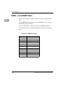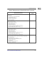
1
PPCBug Diagnostics
Users Manual
PPCDIAA/UM3
November 2000 Edition
Notice
While reasonable efforts have been made to assure the accuracy of this document,
Motorola, Inc. assumes no liability resulting from any omissions in this document, or from
the use of the information obtained therein. Motorola reserves the right to revise this
document and to make changes from time to time in the content hereof without obligation
of Motorola to notify any person of such revision or changes.
Electronic versions of this material may be read online, downloaded for personal use, or
referenced in another document as a URL to the Motorola Computer Group website. The
text itself may not be published commercially in print or electronic form, edited, translated,
or otherwise altered without the permission of Motorola, Inc.
It is possible that this publication may contain reference to or information about Motorola
products (machines and programs), programming, or services that are not available in your
country. Such references or information must not be construed to mean that Motorola
intends to announce such Motorola products, programming, or services in your country.
Limited and Restricted Rights Legend
If the documentation contained herein is supplied, directly or indirectly, to the U.S.
Government, the following notice shall apply unless otherwise agreed to in writing by
Motorola, Inc.
Use, duplication, or disclosure by the Government is subject to restrictions as set forth in
subparagraph (b)(3) of the Rights in Technical Data clause at DFARS 252.227-7013 (Nov.
1995) and of the Rights in Noncommercial Computer Software and Documentation clause
at DFARS 252.227-7014 (Jun. 1995).
Motorola, Inc.
Computer Group
2900 South Diablo Way
Tempe, Arizona 85282
Preface
The PPCBug Diagnostics Manual provides general information, installation procedures,
and a diagnostic firmware guide for the PPCBug Debugging Package. All information
contained herein is specific to Motorola’s PowerPC™-based boards. In this manual, they
are collectively referred to as the PowerPC board or board. When necessary to refer to
them individually, they are identified by their respective models, such as MVME210x,
MVME240x, MVME510x, MCP750, and MTX.
Use of the PPCBug debugger, the debugger command set, the one-line
assembler/disassembler, and system calls for the debugging package are all described in the
two-volume PPCBug Firmware Package User’s Manual (PPCBUGA1/UM and
PPCBUGA2/UM).
Summary of Changes: A new section on INET was added to this version of the manual.
This section describes the Intel Ethernet Controller tests.
This manual is intended for anyone who wants to program these boards in order to design
OEM systems, supply additional capability to an existing compatible system, or work in a
lab environment for experimental purposes.
A basic knowledge of computers and digital logic is assumed.
To use this manual, you should be familiar with the publications listed in Appendix A,
Related Documentation.
Conventions Used in This Manual
The following typographical conventions are used in this document:
bold
is used for user input that you type just as it appears; it is also used for commands,
options and arguments to commands, and names of programs, directories and files.
italic
is used for names of variables to which you assign values. Italic is also used for
comments in screen displays and examples, and to introduce new terms.
courier
is used for system output (for example, screen displays, reports), examples, and system
prompts.
<Enter>, <Return> or <CR>
represents the carriage return or Enter key.
CTRL
represents the Control key. Execute control characters by pressing the Ctrl key and the
letter simultaneously, for example, Ctrl-d.
Motorola® and the Motorola symbol are registered trademarks of Motorola, Inc.
PowerStackTM is a trademark of Motorola, Inc.
PowerPCTM, and PowerPC 750TM are trademarks of IBM Corp, and are used by Motorola,
Inc. under license from IBM Corp.
AIXTM is a trademark of IBM Corp.
All other products mentioned in this document are trademarks or registered trademarks of
their respective holders.
©Copyright Motorola 1998, 2000
All Rights Reserved
Printed in the United States of America
Contents
CHAPTER 1
General Information
Introduction................................................................................................................1-1
Overview of PPCBug Firmware ................................................................................1-1
Debugger and Diagnostic Directories ........................................................................1-2
Command Entry .........................................................................................................1-3
Installation, Configuration, and Start-Up...................................................................1-6
CHAPTER 2
Diagnostic Utilities
Introduction................................................................................................................2-1
Utilities.......................................................................................................................2-1
AEM - Append Error Messages Mode ...............................................................2-2
CEM - Clear Error Messages..............................................................................2-3
CF - Test Group Configuration Parameters Editor .............................................2-3
DE - Display Error Counters ..............................................................................2-4
DEM - Display Error Messages..........................................................................2-4
DP - Display Pass Count.....................................................................................2-5
HE - Help ............................................................................................................2-5
HEX - Help Extended .........................................................................................2-8
LA - Loop Always Mode....................................................................................2-8
LC - Loop-Continue Mode .................................................................................2-9
LE - Loop-On-Error Mode .................................................................................2-9
LF - Line Feed Suppression Mode ...................................................................2-10
LN - Loop Non-Verbose Mode.........................................................................2-10
MASK - Display/Revise Self Test Mask ..........................................................2-11
NV - Non-Verbose Mode..................................................................................2-12
SD - Switch Directories ....................................................................................2-12
SE - Stop-On-Error Mode.................................................................................2-13
ST and QST - Self Test and Quick Self Test ....................................................2-13
ZE - Clear (Zero) Error Counters .....................................................................2-15
ZP - Zero Pass Count ........................................................................................2-15
CHAPTER 3
Test Descriptions
CL1283 - Parallel Interface Tests...............................................................................3-2
REG - Register....................................................................................................3-3
vii
DEC - Ethernet Controller Tests................................................................................ 3-4
CINIT - Chip Initialization................................................................................. 3-6
CLOAD - Continuous Load ............................................................................... 3-7
CNCTR - Connector........................................................................................... 3-8
ERREN - PERREN/SERREN Bit Toggle.......................................................... 3-9
ILR - Interrupt Line Register Access ............................................................... 3-10
IOR - I/O Resource Register Access ................................................................ 3-11
REGA - PCI Header Register Access .............................................................. 3-12
SPACK - Single Packet Send/Receive ............................................................. 3-13
XREGA - Extended PCI Register Access ........................................................ 3-14
DEC Error Messages ........................................................................................ 3-15
INET - Intel Ethernet Controller Tests .................................................................... 3-20
BINT - Basic Interrupt Test.............................................................................. 3-20
EEPT - EEPROM Test...................................................................................... 3-21
INST - Internal Self Test .................................................................................. 3-22
MDIT - MDI Interface Test.............................................................................. 3-22
MPACK - Multiple Packet Interrupt Loopback Test........................................ 3-23
PERT - Parity Error Response Test .................................................................. 3-24
SERT - SERR# Enable Response Test ............................................................. 3-25
SPACK - Single Packet Interrupt Loopback Test............................................. 3-25
INET Error Messages ....................................................................................... 3-26
EIDE - EIDE Tests .................................................................................................. 3-29
General Test Description: ................................................................................. 3-29
General Configuration Description: ................................................................. 3-30
ACC - Device Access....................................................................................... 3-32
REG - Register Access ..................................................................................... 3-36
RW - Read/Write Device.................................................................................. 3-38
ISABRDGE - PCI/ISA Bridge Tests ....................................................................... 3-41
IRQ - Interrupt.................................................................................................. 3-42
REG - Register ................................................................................................. 3-43
KBD8730x - Keyboard Controller Tests ................................................................. 3-44
KBCONF - Keyboard Device Confidence/Extended....................................... 3-45
KBFAT - Keyboard Test ................................................................................... 3-46
KCCONF - Keyboard Controller Confidence/Extended.................................. 3-47
KCEXT - Keyboard/Mouse Controller Extended Test .................................... 3-48
MSCONF - Mouse Device Confidence/Extended ........................................... 3-49
MSFAT - Mouse Test........................................................................................ 3-50
KBD8730x Error Messages.............................................................................. 3-51
L2CACHE - Level 2 Cache Tests............................................................................ 3-55
DISUPD - Disable Updating ............................................................................ 3-56
ENUPD - Enable Updating .............................................................................. 3-57
viii
PATTERN - WriteThru Pattern.........................................................................3-58
SIZE - Verify Cache Size..................................................................................3-59
WBFL - Write Back w/Flush ............................................................................3-60
WBINV - Write Back w/Invalidate ..................................................................3-61
WRTHRU - WriteThru .....................................................................................3-62
L2CACHE Error Messages ..............................................................................3-63
NCR - 53C8xx SCSI I/O Processor Tests ................................................................3-64
ACC1 - Device Access .....................................................................................3-66
ACC2 - Register Access ...................................................................................3-68
DFIFO - DMA FIFO.........................................................................................3-70
IRQ - Interrupts.................................................................................................3-72
PCI - PCI Access ..............................................................................................3-75
SCRIPTS - SCRIPTs Processor ........................................................................3-77
SFIFO - SCSI FIFO ..........................................................................................3-80
PAR8730x - Parallel Port Test .................................................................................3-81
REG - Register..................................................................................................3-82
UART - Serial Input/Output Tests ...........................................................................3-83
BAUD - Baud Rates .........................................................................................3-84
IRQ - Interrupt Request ....................................................................................3-85
LPBK - Internal Loopback ...............................................................................3-86
LPBKE - External Loopback ............................................................................3-87
REGA - Device/Register Access ......................................................................3-88
UART Error Messages......................................................................................3-89
PCIBUS - Generic PCI/PMC Slot Tests ..................................................................3-91
REG - PCI/PMC Slot Register Access .............................................................3-92
PCIBUS Error Messages ..................................................................................3-93
RAM - Local RAM Tests.........................................................................................3-94
ADR - Memory Addressing..............................................................................3-95
ALTS - Alternating Ones/Zeros........................................................................3-97
BTOG - Bit Toggle ...........................................................................................3-98
CODE - Code Execution/Copy.......................................................................3-100
MARCH - March Pattern................................................................................3-101
PATS - Data Patterns.......................................................................................3-102
PED - Local Parity Memory Error Detection .................................................3-103
PERM - Permutations .....................................................................................3-105
QUIK - Quick Write/Read ..............................................................................3-106
REF - Memory Refresh Testing......................................................................3-107
RNDM - Random Data ...................................................................................3-109
RTC - MK48Txx Timekeeping Tests ....................................................................3-110
ADR - MK48Txx BBRAM Addressing ......................................................... 3-111
ALARM - Alarm Interrupt .............................................................................3-113
ix
CLK - Real Time Clock Function .................................................................. 3-114
RAM - Battery Backed-Up RAM .................................................................. 3-116
WATCHDOG - Watchdog Time-Out Reset.................................................... 3-117
SCC - Serial Communication Controller (Z85230) Tests ..................................... 3-118
ACCESS - Device/Register Access ............................................................... 3-120
BAUDS - Baud Rates..................................................................................... 3-121
DMA - Receive/Transmit DMA..................................................................... 3-122
ELPBCK - External Loopback....................................................................... 3-124
ILPBCK - Internal Loopback ......................................................................... 3-125
IRQ - Interrupt Request .................................................................................. 3-126
MDMC - Modem Control .............................................................................. 3-127
SCC Error Messages ...................................................................................... 3-128
VGA54XX - Video Diagnostics Tests................................................................... 3-130
ATTR - Attribute Register .............................................................................. 3-132
BLT - Bit Blitter ............................................................................................. 3-133
CRTC - CRT Controller Registers.................................................................. 3-134
DSTATE - DAC State Register ...................................................................... 3-135
EXTN - Extended Registers ........................................................................... 3-136
GRPH - Graphics Controller Registers .......................................................... 3-137
MISC - Miscellaneous Register ..................................................................... 3-138
PAL - Color Palette ........................................................................................ 3-139
PCI - PCI Header Verification........................................................................ 3-140
PELM - Pixel Mask Register.......................................................................... 3-141
SEQR - Sequencer Registers .......................................................................... 3-142
VRAM - Video Memory ................................................................................ 3-143
VME2 - VME Interface ASIC Tests...................................................................... 3-144
VME3- Universe VME to PCI Bridge Tests ......................................................... 3-144
REGR - Register Read ................................................................................... 3-146
REGW - Register Write/Read ........................................................................ 3-147
VME3 Error Messages ................................................................................... 3-148
Z8536 - Counter/Timer Tests................................................................................. 3-149
CNT - Counter................................................................................................ 3-150
IRQ - Interrupt................................................................................................ 3-151
LNK - Linked Counter ................................................................................... 3-152
REG - Register ............................................................................................... 3-153
APPENDIX A
Related Documentation
Motorola Computer Group Documents .................................................................... A-1
Microprocessor and Controller Documents.............................................................. A-3
Related Specifications .............................................................................................. A-9
x
List of Figures
Figure 2-1. Help Screen (Sheet 1 of 2) ......................................................................2-6
xi
xii
List of Tables
Table 2-1. Diagnostic Utilities ...................................................................................2-1
Table 3-1. Diagnostic Test Groups.............................................................................3-1
Table 3-2. CL1283 Test Group ..................................................................................3-2
Table 3-3. DEC Test Group........................................................................................3-4
Table 3-4. DEC Error Messages ..............................................................................3-15
Table 3-5. INET Test Group.....................................................................................3-20
Table 3-6. INET Error Messages .............................................................................3-27
Table 3-7. EIDE Test Group.....................................................................................3-29
Table 3-8. ISABRDGE Test Group..........................................................................3-41
Table 3-9. KBD8730x Test Group ...........................................................................3-44
Table 3-10. KBD8730x Error Messages ..................................................................3-51
Table 3-11. L2CACHE Test Group..........................................................................3-55
Table 3-12. L2CACHE Error Messages ..................................................................3-63
Table 3-13. NCR Test Group ...................................................................................3-64
Table 3-14. PAR8730x Test Group ..........................................................................3-81
Table 3-15. UART Test Group .................................................................................3-83
Table 3-16. UART Error Messages..........................................................................3-89
Table 3-17. PCIBUS Test Group..............................................................................3-91
Table 3-18. PCIBUS Error Messages ......................................................................3-93
Table 3-19. RAM Test Group ..................................................................................3-94
Table 3-20. RTC Test Group ..................................................................................3-110
Table 3-21. SCC Test Group ..................................................................................3-118
Table 3-22. SCC Error Messages ...........................................................................3-128
Table 3-23. VGA543X Test Group ........................................................................3-130
Table 3-24. VME2 Test Group...............................................................................3-144
Table 3-25. VME3 Test Group...............................................................................3-145
Table 3-26. VME3 Error Messages........................................................................3-148
Table 3-27. Z8536 Test Group ...............................................................................3-149
Table A-1. Motorola Computer Group Documents .................................................A-1
Table A-2. Microprocessor and Controller Documents ...........................................A-3
Table A-3. Related Specifications ...........................................................................A-9
xiii
xiv
1General Information
1
Introduction
This manual describes the complete set of hardware diagnostics included
in the PPCBug Debugging Package, intended for testing and
troubleshooting Motorola’s PowerPC-based boards. This member of the
PPCBug firmware family, known as PPCBug diagnostics, is implemented
on many of the Motorola PowerPC-based products as part of a standard
proprietary debugging and diagnostic tool set.
Boards using this tool set are referred to in this manual as the PowerPC
board or board. When necessary to refer to them individually, they are
referred to by their individual product names, such as MVME210x,
MVME230x, MVME360x, MVME510x, MCP750, MTX, etc.
This introductory chapter includes information about the operation and use
of the diagnostics. Chapter 2 contains descriptions of the diagnostic
utilities. Chapter 3 contains descriptions of the diagnostic test routines.
Before using the PPCBug diagnostics, ensure that the PowerPC board and
other hardware are properly configured and connected, according to the
installation guide for that particular PowerPC board. The two-volume
manual for the PPCBug Debugging Package, PPCBug Firmware Package
User’s Manual, should also be available. It contains a complete description
of PPCBug, the start-up procedure, all general software debugging
commands, and other information about the debugger.
Overview of PPCBug Firmware
The PPCBug firmware consists of three parts:
❏
A command-driven, user-interactive software debugger, described
in the PPCBug Firmware Package User’s Manual.
❏
A command-driven diagnostics package for the PowerPC board
hardware, described in this manual. The diagnostic firmware
1-1
1
General Information
contains a battery of utilities and tests for exercise, test, and debug
of hardware in the PowerPC board environment. The diagnostics
are menu-driven for ease of use.
❏
A user interface or debug/diagnostics monitor that accepts
commands from the system console terminal. The tests described in
this manual are implemented by the firmware, commands are input,
and results are reported via this monitor, which is the common
device used for both the debugger and the diagnostics. The monitor
is command-line driven and provides input and output facilities,
command parsing, error reporting, interrupt handling, and a multilevel directory for menu selection.
Debugger and Diagnostic Directories
When using PPCBug, operate from either the debugger directory or the
diagnostic directory:
❏
Note
❏
When in the debugger directory, the debugger prompt PPCx-Bug> is
displayed and all of the debugger commands are available.
Earlier versions of this firmware, e.g., PPC1Bug, will not
contain all commands available in later versions, such as
PPC6Bug.
When in the diagnostic directory, the diagnostic prompt PPCxis displayed and all of the diagnostic commands are
available, as well as all of the debugger commands.
Diag>
To use the diagnostic part of the firmware, the diagnostic directory must
be open. If the PPCx-Bug> prompt (debugger directory) is displayed, the
wrong directory is open. To switch to the diagnostic directory enter SD
(Switch Directories command). This displays the diagnostic prompt
PPCx-Diag>.
To examine the commands in the current open directory use the Help (HE)
command.
1-2
Computer Group Literature Center Web Site
Command Entry
Because PPCBug is command-driven, it performs various operations in
response to commands that are entered at the keyboard. PPCBug executes
the command and the prompt reappears. However, a command is entered
that causes execution of some user target code (e.g., GO), then control may
or may not return to PPCBug, depending on the outcome of the user
program.
The Help (HE) command displays a menu of all available diagnostic
functions; i.e., the tests and utilities. Several tests have a subtest menu,
which may be called using the HE command. In addition, some utilities
have subfunctions, and as such have subfunction menus.
Command Entry
Enter the name of a diagnostic command when the prompt
PPCx-Diag> appears, and then press the RETURN or ENTER key.
The command may be the name of a diagnostic utility routine and may
include one or more arguments; or it may be the name of one or more test
groups listed in a main (root) directory and may include one or more
subcommands (individual test names) listed in the subdirectory for a
particular test group.
The utility routines are described in Chapter 2. The test groups are
described in Chapter 3. Examples of command entry for both are given
below.
Root-Level Command (Utility):
The utility or root-level commands affect the operation of the tests that are
subsequently run. A test group name may be entered on the same
command line. For example:
PPCx-Diag>CF RAM
causes an interactive dialog to begin, during which parameters for the
RAM tests may be entered.
Command entry may also include a subcommand (individual test name).
For example:
PPCx-Diag>HE DEC2 ERREN
http://www.motorola.com/computer/literature
1-3
1
1
General Information
causes a help screen to appear that gives information about the ERREN
test in the DEC test group.
Root-Level Command (Test Group):
Entering just the name of a test group causes all individual tests that are
part of that group to execute in sequence (with some exceptions). For
example:
PPCx-Diag>RAM
causes all Random Access Memory (RAM) tests to execute, except for
two that only execute if specified.
Subdirectory-Level Command (Individual Test):
Entering the name of a test group followed by the name of an individual
test from that group causes just that test to execute.
For example, to call up a particular Random Access Memory (RAM) test,
enter:
PPCx-Diag>RAM ADR
This causes the monitor to find the RAM test group subdirectory, and then
to execute the Memory Addressing test command ADR from that
subdirectory.
To call up a particular DEC test, enter:
PPCx-Diag>DEC REGA
This causes the monitor to find the DEC test group subdirectory, and then
to execute the PCI Register Access command REGA from that
subdirectory.
Multiple Subdirectory-Level Commands (Individual Tests):
If the first part of a command is a test group name, any number and/or
sequence of tests from that test group may be entered after the test group
name so long as the debugger’s input buffer size limit is not exceeded. For
example:
PPCx-Diag>RAM PATS ADR
This causes both the Data Patterns (PATS) and the Memory Addressing
(ADR) tests from the RAM test group to execute.
1-4
Computer Group Literature Center Web Site
Command Entry
Multiple Root-Level Commands (Test Groups):
Multiple commands may be entered. If a command expects parameters and
another command is to follow it, separate the two with a semicolon (;).
For example, to invoke the command RTC CLK (to execute the Real
Time Clock Function test from the MK48Txx Real Time Clock test group)
after the command RAM ADR, the command line would read:
PPCx-Diag>RAM ADR; RTC CLK
Spaces are not required before or after the semicolon but are shown here
for legibility. Spaces are required between commands and their arguments.
Several commands may be combined on one line.
http://www.motorola.com/computer/literature
1-5
1
1
General Information
Installation, Configuration, and Start-Up
The PPCBug firmware is installed by Motorola at the factory when your
PowerPC board is manufactured.
Refer to your PowerPC board installation manual and ensure that all
necessary hardware preparation, board installation, connection of
peripherals, and hardware configuration, including console selection and
configuration of Software Readable Headers (where applicable), has been
correctly done.
After the hardware is configured and installed according to the installation
manual, refer to the PPCBug Firmware Package User’s Manual for the
start-up procedure before powering up the system.
1-6
Computer Group Literature Center Web Site
2Diagnostic Utilities
2
Introduction
This chapter contains descriptions and examples of the various diagnostic
utilities available in PPCBug.
Utilities
In addition to individual or sets of tests, the diagnostic package supports
the utilities (root-level commands or general commands) listed in the table
below and described on the following pages.
Table 2-1. Diagnostic Utilities
Command
Description
AEM
Append Error Messages Mode
CEM
Clear Error Messages
CF
Test Group Configuration Parameters Editor
DE
Display Error Counters
DEM
Display Error Messages
DP
Display Pass Count
HE
Help
HEX
Help Extended
LA
Loop Always Mode
LC
Loop-Continue Mode
LE
Loop-On-Error Mode
LF
Line Feed Suppression Mode
LN
Loop Non-Verbose Mode
MASK
Display/Revise Self Test Mask
NV
Non-Verbose Mode
QST
Quick Self Test
SD
Switch Directories
2-1
Diagnostic Utilities
Table 2-1. Diagnostic Utilities (Continued)
2
Command
Description
SE
Stop-On-Error Mode
ST
Self Test
ZE
Clear (Zero) Error Counters
ZP
Zero Pass Count
Notes You may enter command names in either uppercase or
lowercase.
Terminate all command lines by pressing the RETURN key.
AEM - Append Error Messages Mode
The AEM command allows you to accumulate error messages in the
internal error message buffer of the diagnostic monitor.
This command sets the internal append error messages flag of the
diagnostic monitor. The default of the internal append error messages flag
is clear. The internal flag is not set until it is encountered in the command
line by the diagnostic monitor.
The contents of the buffer can be displayed with the DEM command.
When the internal append error messages flag is not set or is cleared with
CEM, the diagnostic error message buffer is erased (cleared of all
character data) before each test is executed.
The duration of this command is for the life of the command line being
parsed by the diagnostic monitor.
Example:
PPCx-Diag>aem; ram ref
RAM
REF: Memory Refresh Test............ Running ---> FAILED
(error message written to error message buffer)
PPCx-Diag>
2-2
Computer Group Literature Center Web Site
Utilities
CEM - Clear Error Messages
2
This command allows you to clear the internal error message buffer of the
diagnostic monitor manually.
Example:
PPCx-Diag>cem
(error message buffer is cleared)
PPCx-Diag>
CF - Test Group Configuration Parameters Editor
The CF parameters control the operation of all tests in a test group.
For example, the RAM test group has parameters such as starting address,
ending address, parity enable, etc. At the time of initial execution of the
diagnostic monitor, the default configuration parameters are copied from
the firmware into the debugger work page. Here you can modify the
configuration parameters via the CF command.
When you invoke the CF command, you are interactively prompted with
a brief parameter description and the current value of the parameter. You
may enter a new value for that parameter, or a RETURN to accept the
current value and proceed to the next configuration parameter. To
discontinue the interactive process, enter a period ( . ) followed by
RETURN.
You may specify one or more test groups as argument(s) immediately
following the CF command on the command line. If no arguments follow
the CF command, the parameters for all test groups are presented so you
may change them if you wish.
Examples:
http://www.motorola.com/computer/literature
2-3
Diagnostic Utilities
PPC1-Diag>cf
RAM Configuration Data:
Starting/Ending Address Enable [Y/N] =N ?RETURN
Starting Address =00004000 ?RETURN
Ending Address
=00F84FFC ?RETURN
Random Data Seed =12301983 ?RETURN
March Address Pattern =00000000 ?RETURN
Instruction (Code) Cache Enable [Y/N] =Y ? .RETURN
PPC1-Diag>cf scc
SCC Configuration Data:
SCC Memory Space Base Address
=80000840 ? RETURN
Internal-Loopback/Baud-Rates Port Mask
=00000003 ? RETURN
External-Loopback/Modem-Control Port Mask =00000003 ?RETURN
PPC1-Diag>
2
DE - Display Error Counters
Each test or command in the diagnostic monitor has an individual error
counter. As errors are encountered in a particular test, that error counter is
incremented. If you were to run a self test or just a series of tests, the results
could be broken down as to which tests passed by examining the error
counters.
To display all error counters after the conclusion of a test, enter DE. DE
displays the results of a particular test if the name of that test follows DE.
Only nonzero values are displayed.
Example:
PPCx-Diag>de ram addr
PPCx-Diag>
DEM - Display Error Messages
This command allows you to display (dump) the internal error message
buffer of the diagnostic monitor manually.
Example:
PPCx-Diag>dem
(contents of error message buffer are displayed)
PPCx-Diag>
2-4
Computer Group Literature Center Web Site
Utilities
DP - Display Pass Count
2
A count of the number of passes in Loop-Continue (LC) mode is kept by
the monitor. This count is displayed with other information at the
conclusion of each pass. To display this information without using LC,
enter DP.
Example:
PPCx-Diag>dp
Pass Count =19
PPCx-Diag>
HE - Help
The Help command provides on-line documentation. Entering HE at the
diagnostics prompt (PPCx-Diag>) displays a menu of the top level
directory of utility commands and test group names if no parameters are
entered, or the menu of a subdirectory if the name of that subdirectory, or
test group name, is entered following HE.
The display of the top level directory lists “(DIR)” after the name of each
command that has a subdirectory.
Note
If HE is entered to the debugger prompt (PPCx-Bug>), the
debugger commands are displayed.
Examples:
To display the menu of all utility and test group names, enter:
PPCx-Diag>he
(see Figure 2-1)
When a menu is too long to fit on the screen, it pauses until you press
RETURN again.
http://www.motorola.com/computer/literature
2-5
Diagnostic Utilities
2
PPC1-Diag>he
AEM
Append Error Messages Mode
CEM
Clear Error Messages
CF
Configuration Editor
CL1283
Parallel Interface (CL1283) Tests (DIR)
CS4231
cs4231 Audio Codec (DIR)
DE
Display Errors
DEC
Ethernet Controller (DEC21x40) Tests (DIR)
DEM
Display Error Messages
DP
Display Pass Count
EIDE
EIDE Tests (DIR)
HE
Help on Tests/Commands
HEX
Help Extended
ISABRDGE ISA Bridge Tests (DIR)
KBD8730X Keyboard/Mouse Controller Tests (DIR)
L2CACHE L2-Cache (DIR)
LA
Loop Always Mode
LC
Loop Continuous Mode
LE
Loop on Error Mode
LF
Line Feed Mode
LN
Loop Non-Verbose Mode
MASK
Self Test Mask
NCR
NCR 53C8XX SCSI I/O Processor Tests (DIR)
NV
Non-Verbose Mode
PAR8730X Parallel Interface (PC8730x) Tests (DIR)
PCIBUS
PCI/PMC Generic
Press "RETURN" to continue
Figure 2-1. Help Screen (Sheet 1 of 2)
2-6
Computer Group Literature Center Web Site
Utilities
2
QST
Quick Self Test (DIR)
RAM
Random Access Memory Tests (DIR)
RTC
MK48Txx Timekeeping (DIR)
SCC
Serial Communication Controller(Z85C230)Tests (DIR)
SE
Stop on Error Mode
ST
Self Test (DIR)
UART
Serial Input/Output Tests (DIR)
VGA54XX VGA Controller (GD54XX) Tests (DIR)
VME2
VME2Chip2 Tests (DIR)
Z8536
z8536 Counter/Timer Input/Output Tests (DIR)
ZE
Zero Errors
ZP
Zero Pass Count
PPC1-Diag>
Figure 2-1. Help Screen (Sheet 2 of 2)
To bring up a menu of all the RAM memory tests, enter:
PPC1-Diag>he ram
RAM
Random Access Memory Tests (DIR)
ADR
Addressability
ALTS
Alternating Ones/Zeroes
BTOG
Bit Toggle
CODE
Code Execution/Copy
MARCH
March Address
PATS
Patterns
PED
Local Parity Memory Error Detection
PERM
Permutations
QUIK
Quick Write/Read
REF
Memory Refresh Test
RNDM
Random Data
PPC1-Diag>
To review a description of an individual test, enter the full name:
PPC1-Diag>he ram code
RAM
Random Access Memory Tests (DIR)
CODE
Code Execution/Copy
PPC1-Diag>
This displays information on the RAM Code Execution/Copy test routine.
http://www.motorola.com/computer/literature
2-7
Diagnostic Utilities
2
HEX - Help Extended
The HEX command goes into an interactive, continuous mode of the HE
command.
The prompt displayed for HEX is the question mark (?). You may then
type the name of a directory or command. You must type QUIT to exit.
Example:
PPCx-Diag>HEX
Extended Help, Type <QUIT> to Exit
? lc
LC
Loop Continuous Mode
? ISABRDGE irq
ISABRDGE
ISA Bridge Tests (DIR)
IRQ
Interrupt Request
? quit
PPCx-Diag>
LA - Loop Always Mode
To repeat a test or series of tests endlessly, enter the prefix LA. The LA
command modifies the way that a failed test is endlessly repeated.
The LA command has no effect until a test failure occurs, at which time,
if the LA command has been previously encountered in the user command
line, the failed test is endlessly repeated. To break the loop, press the
BREAK key on the diagnostic video display terminal.
Certain tests disable the BREAK key interrupt, so it may become
necessary to press the abort or reset switches on the PowerPC board front
panel.
Example:
PPCx-Diag>la;ram adr
RAM
ADR: Addressability............. Running ---> PASSED
(no errors detected so LA is ignored)
PPCx-Diag>
2-8
Computer Group Literature Center Web Site
Utilities
LC - Loop-Continue Mode
2
To repeat a test or series of tests endlessly, enter the prefix LC. This loop
includes everything on the command line.
To break the loop, press the BREAK key on the diagnostic video display
terminal. Certain tests disable the BREAK key interrupt, so it may become
necessary to press the abort or reset switches on the PowerPC board front
panel.
Example:
PPCx-Diag>lc;ram adr
RAM
ADR: Addressability................. Running --->
Pass Count =1, Errors This Pass =0, Total Errors =0
RAM
ADR: Addressability................. Running --->
Pass Count =2, Errors This Pass =0, Total Errors =0
RAM
ADR: Addressability................. Running --->
Pass Count =3, Errors This Pass =0, Total Errors =0
RAM
ADR: Addressability................. Running --->
--Break Detected-PPCx-Diag>
PASSED
PASSED
PASSED
<BREAK>
LE - Loop-On-Error Mode
Occasionally, when an oscilloscope or logic analyzer is in use, it becomes
desirable to repeat a test endlessly (loop) while an error is detected. The
LE command modifies the way a failed test is endlessly repeated.
The LE command has no effect until a test failure occurs, at which time, if
the LE command has been previously encountered in the user command
line, the failed test is re-executed as long as the previous execution returns
failure status.
To break the loop, press the BREAK key on the diagnostic video display
terminal. Certain tests disable the BREAK key interrupt, so it may become
necessary to press the abort or reset switches on the PowerPC board front
panel.
Example:
http://www.motorola.com/computer/literature
2-9
Diagnostic Utilities
PPCx-Diag>le;scc
SCC
ACCESS: Device/Register Access...... Running ---> PASSED
SCC
IRQ: Interrupt Request.............. Running ---> FAILED
2
SCC/IRQ Test Failure Data:
(error message)
SCC
IRQ: Interrupt Request.............. Running ---> FAILED
SCC/IRQ Test Failure Data:
(error message)
SCC
IRQ: Interrupt Request.............. Running --->
<BREAK>
--Break Detected-PPCx-Diag>
LF - Line Feed Suppression Mode
Entering LF on a command line sets the internal line feed mode flag of the
diagnostic monitor. The duration of the LF command is the life of the user
command line in which it appears.
The default state of the internal line feed mode flag is clear, which causes
the executing test title/status line(s) to be terminated with a line feed
character (scrolled).
The line feed mode flag is normally used by the diagnostic monitor when
executing a System Mode self test. Although rarely invoked as a user
command, the LF command is available to the diagnostic user.
Example:
PPCx-Diag>LF;RAM
RAM
ADR: Addressability................ Running ---> PASSED
(display of subsequent RAM test messages overwrite this line)
PPCx-Diag>
LN - Loop Non-Verbose Mode
The LN command modifies the way a failed test is endlessly repeated.
2-10
Computer Group Literature Center Web Site
Utilities
The LN command has no effect until a test failure occurs, at which time,
if the LN command has been previously encountered in the user command
line, further printing of the test title and pass/fail status is suppressed. This
is useful for more rapid execution of the failing test; i.e., the LN command
contributes to a “tighter” loop.
Example:
PPC1-Diag>LN;RAM ADR
RAM ADR: RAM
ADR: Addressability........ Running --->
Pass Count =1, Errors This Pass =0, Total Errors =0
RAM
ADR: Addressability................. Running --->
Pass Count =2, Errors This Pass =0, Total Errors =0
RAM
ADR: Addressability................. Running --->
Pass Count =3, Errors This Pass =0, Total Errors =0
RAM
ADR: Addressability................. Running --->
--Break Detected-PPC1-Diag>
PASSED
PASSED
PASSED
<BREAK>
MASK - Display/Revise Self Test Mask
Using MASK with an argument enables/disables the specified test from
running under self test. The argument must be a specific test name. If mask
is invoked without arguments, the current self test mask, showing disabled
tests, is displayed.
The mask command is a “toggle” command -- if the specified test name
mask was set, it will be reset; if it was reset, it will be set. After the toggle,
the new self test mask is displayed.
If the mask command is invoked with an invalid test name or a test
directory (as opposed to a specific test name), an appropriate error message
is output.
When the mask command is used on a PowerPC board system, the mask
values are preserved in non-volatile memory. This allows the system to be
completely powered down without disturbing the self test mask.
Example:
http://www.motorola.com/computer/literature
2-11
2
Diagnostic Utilities
PPC1-Diag>mask ram adr
Update Non-Volatile RAM (Y/N)? y
RAM/ADR
PPC1-Diag>mask
RAM/ADR
PPC1-Diag>
2
NV - Non-Verbose Mode
Upon detecting an error, the tests display a substantial amount of data. To
avoid the necessity of watching the scrolling display, you can choose a
mode that suppresses all messages except test name and PASSED or FAILED.
This mode is called non-verbose and you can invoke it prior to calling a
command by entering NV.
Example:
PPC1-Diag>nv;uart lpbke
UART LPBKE:External Loopback .......Running --> FAILED
PPC1-Diag>
NV causes the monitor to run the UART external loopback test, but show
only the name of the test and the results (pass/fail).
PPC1-Diag>uart lpbke
UART LPBKE:External Loopback .......Running --> FAILED
UART/LPBKE Test Failure Data:
RTS loopback to CTS or RI Failed: COM2
PPC1-Diag>
Without nv, the failure data is displayed.
SD - Switch Directories
The SD command allows you to switch back and forth between PPCBug’s
diagnostic directory (the prompt reads PPCx-Diag>) and the debug
directory (the prompt reads PPCx-Diag>).
2-12
Computer Group Literature Center Web Site
Utilities
If you are in the diagnostic directory and enter SD, you will return to the
debug directory. At this point, only the debug commands for PPC1Bug can
be entered.
If you are in the debug directory and enter SD, you will return to the
diagnostic directory. You may enter either the diagnostic or debug
commands from the diagnostics directory.
Example:
PPC1-Diag>sd
PPC1-Bug>sd
PPC1-Diag>
SE - Stop-On-Error Mode
Sometimes you may want to stop a test or series of tests at the point where
an error is detected. SE accomplishes that for most of the tests. To invoke
SE, enter it before the test or series of tests that is to run in Stop-On-Error
mode.
Example:
PPC1-Diag>se; dec ior ilr; scc dma irq
DEC IOR:I/O Resource Register Access...Running --> PASSED
DEC ILR:Interrupt Line Register Access.Running --> PASSED
SCC
DMA: DMA Test..................... Running --> FAILED
(error message)
(error encountered in DMA test so IRQ test not run)
PPC1-Diag>
ST and QST - Self Test and Quick Self Test
The diagnostics monitor provides an automated test mechanism called self
test. This mechanism runs all the tests included in an internal self test
directory.
Entering the QST command executes the suite of self tests that are run at
start-up. Entering ST causes more tests to execute than does QST, but also
requires more test time.
http://www.motorola.com/computer/literature
2-13
2
Diagnostic Utilities
The commands HE ST and HE QST list the top level commands of the
self test directory in alphabetical order. Each test for that particular
command is listed in the section pertaining to the command.
2
For details on extended self test operation, refer to the PPCBug Firmware
Package User’s Manual.
Example:
PPC1-Diag>qst
RAM
ADR: Addressability..............
UART REGA: Register Access...............
UART IRQ: Interrupt......................
UART BAUD: Baud Rate.....................
UART LPBK: Internal Loopback.............
Z8536
CNT: Counter.....................
Z8536
LNK: Linked Counter..............
Z8536
IRQ: Interrupt...................
Running
Running
Running
Running
Running
Running
Running
Running
--->
--->
--->
--->
--->
--->
--->
--->
PASSED
PASSED
PASSED
PASSED
PASSED
PASSED
PASSED
PASSED
(all tests in quick self test directory are run)
PPC1-Diag>
2-14
Computer Group Literature Center Web Site
Utilities
ZE - Clear (Zero) Error Counters
2
The error counters originally come up with the value of zero, but it is
occasionally desirable to reset them to zero at a later time. This command
resets all of the error counters to zero.
Example:
PPC1-Diag>ze
PPC1-Diag>
This clears all error counters.
ZP - Zero Pass Count
Invoking the ZP command resets the pass counter to zero. This is
frequently desirable before typing in a command that invokes the LoopContinue mode. Entering this command on the same line as LC results in
the pass counter being reset on every pass.
Example:
PPC1-Diag>lc;ram adr ;zp
RAM
ADR: Addressability................. Running ---> PASSED
Pass Count =1, Errors This Pass =0, Total Errors =0
RAM
ADR: Addressability................. Running ---> PASSED
Pass Count =1, Errors This Pass =0, Total Errors =0
RAM
ADR: Addressability................. Running ---> PASSED
Pass Count =1, Errors This Pass =0, Total Errors =0
RAM
ADR: Addressability................. Running --->
<BREAK>
--Break Detected-PPC1-Diag>
http://www.motorola.com/computer/literature
2-15
Diagnostic Utilities
2
2-16
Computer Group Literature Center Web Site
3Test Descriptions
3
Detailed descriptions of PPCBug’s diagnostic tests are presented in this
chapter. The test groups are described in the order shown in the following
table. Some test groups do not run on all PowerPC boards. The column
PowerPC Board lists the boards on which each group of tests will run.
Table 3-1. Diagnostic Test Groups
Test Group
Description
PowerPC Board
CL1283
Parallel Interface (CL1283) Tests
MTX
DEC
DEC21x40 Ethernet Controller Tests
All
INET
Intel 82559/ER Ethernet Controller Tests
All
EIDE
IDE/EIDE Device Tests
MTX, MCP750
ISABRDGE
PCI/ISA Bridge Tests
All
KBD8730X
PC8730x Keyboard/Mouse Tests
All
L2CACHE
Level 2 Cache Tests
All
NCR
NCR 53C8xx SCSI2 I/O
Processor Tests
All
PAR8730X
Parallel Interface (PC8730x) Tests
All
UART
Serial Input/Output Tests
All
PCIBUS
PCI/PMC Generic Tests
All
RAM
Local RAM Tests
All
RTC
MK48Txx Timekeeping Tests
All
SCC
Serial Communication
Controller (Z85C230) Tests
All except MVME230x
VGA54XX
Video Diagnostics Tests
MVME360x, MVME460x
VME2
VMEchip2 VME Interface ASIC Tests
None
VME3
VMEchip3 VME Interface ASIC Tests
None
Z8536
Z8536 Counter/Timer Tests
All except MVME230x
3-1
Test Descriptions
Notes 1. You may enter command names in either uppercase or
lowercase.
2. Some diagnostics depend on restart defaults that are set up only
in a particular restart mode. Refer to the documentation on a
particular diagnostic for the correct mode.
3
CL1283 - Parallel Interface Tests
This section describes the CL1283 parallel Interface (CL1283) tests.
Note
These tests apply only to the MTX boards. They are not
available on the other PowerPC boards: MVME230x,
MVME260x, MVME2700, MVME360x, MVME460x, and
PMCspan.
Entering CL1283 without parameters causes all CL1283 tests to execute
in the order shown in the following table.
To run an individual test, add that test name to the CL1283 command.
The individual tests are described in alphabetical order on the following
pages.
Table 3-2. CL1283 Test Group
3-2
Name
Description
REG
Register
Computer Group Literature Center Web Site
CL1283 - Parallel Interface Tests
REG - Register
Command Input
3
PPCx-Diag>CL1283 REG
Description
This test verifies that the CL1283 registers can be read and written. Data
patterns verify that every read/write bit can be modified.
Response/Messages
After the command has been issued, the following line is printed:
CL1283 REG: cl1283 Register Access...... Running --->
If all parts of the test are completed correctly, then the test passes:
CL1283 REG: cl1283 Register Access...... Running ---> PASSED
If the board does not support the CL1283, the following is displayed:
CL1283 REG: cl1283 Register Access......Running ---> BYPASSED
If any failures occur, the following is displayed (more descriptive text then
follows):
CL1283 REG: cl1283 Register Access...... Running ---> FAILED
If the test fails because the pattern written does not match the one read back
from the CL1283 register, the following is printed:
CL1283 INDIRECT:Local Parity Memory Detection..Running --> FAILED
cl1283 Register: xxx, Expected bit#_ to be high/low, Actual reg
value xx
http://www.motorola.com/computer/literature
3-3
Test Descriptions
DEC - Ethernet Controller Tests
These sections describe the individual DEC21x4x Ethernet Controller
tests.
3
The firmware now provides support for testing of multiple Ethernet
controllers within PCI configuration space. This means that the DEC
diagnostics can now be run on multiple DEC Controllers. This is “only”
true for any firmware supported DEC21x4x Ethernet devices.
Examples of where DEC tests run on multiple controllers include:
1. On a PowerPC that has two (2) DEC21x4x devices on the board.
2. On a PowerPC board that has one (1) DEC21x4x device on the
board and one (1) DEC21x4x device on the board and one
DEC21x4x PMC/PCI card attached to the board.
3. On a PowerPC board that has one (1) DEC21x4x device on the
board and a DEC21x4x card attached to a PMC carrier plugged into
the backplane of the chassis.
Entering DEC without parameters causes all DEC tests to run in the order
shown in the table below, except as noted.
To run an individual test, add that test name to the DEC command.
The individual tests are described in alphabetical order on the following
pages.
Table 3-3. DEC Test Group
3-4
Name
Description
REGA
Register Access
XREGA
Extended Register Access
SPACK
Single Packet Transmit and Receive
ILR
Interrupt Line Register Access
ERREN
PERREN and SERREN Bit Toggle
IOR
I/O Resource Register Access
Computer Group Literature Center Web Site
DEC - Ethernet Controller Tests
Table 3-3. DEC Test Group
Name
Description
CINIT
Chip Initialization
3
Executed only when specified:
CLOAD
Continuous Load
CNCTR
Connector
None of these tests need any external hardware hooked up to the Ethernet
port, with the exception of the CNCTR test, which needs external
loopback “plugs” in the external connector.
http://www.motorola.com/computer/literature
3-5
Test Descriptions
CINIT - Chip Initialization
Command Input
3
PPCx-Diag>dec cinit
Description
This test checks the DEC chip initialization sequence for proper operation
while using interrupts and reading the initialization blocks and rings
structures used for Ethernet communications.
Response/Messages
After the command has been issued, the following line is printed:
DEC CINIT: Chip Initialization:..........Running --->
If all parts of the test are completed correctly, then the test passes:
DEC CINIT: Chip Initialization:..........Running ---> PASSED
If any part of the test fails, then the display appears as follows:
DEC CINIT: Chip Initialization:..........Running ---> FAILED
DEC/CINIT Test Failure Data:
(error message)
Refer to the section DEC Error Messages for a list of the error messages
and their meaning.
3-6
Computer Group Literature Center Web Site
DEC - Ethernet Controller Tests
CLOAD - Continuous Load
Command Input
3
PPCx-Diag>DEC CLOAD
Description
This test verifies that a continuous load can be placed on the controller by
transmitting/receiving a sequence of packets totalling at least 1 megabyte
of throughput, comparing the input data with the output data.
Response/Messages
After the command has been issued, the following line is printed:
DEC CLOAD: Continuous Load:..............Running --->
If all parts of the test are completed correctly, then the test passes:
DEC CLOAD: Continuous Load:..............Running ---> PASSED
If any part of the test fails, then the display appears as follows:
DEC CLOAD: Continuous Load:..............Running ---> FAILED
DEC/CLOAD Test Failure Data:
(error message)
Refer to the section DEC Error Messages for a list of the error messages
and their meaning.
http://www.motorola.com/computer/literature
3-7
Test Descriptions
CNCTR - Connector
Command Input
PPCx-Diag>dec cnctr
3
Description
This test verifies that the data path through the external (AUI
or TP (twisted pair)) connection is functional, by transmitting and
receiving packets and comparing the data. This test requires the presence
of an external loopback “plug” for AUI or TP.
Note
It is recommended that the board under test not be connected to a
live network while this test is running. The suggested “loopback”
setup for AUI is an AUI-to-thinnet transceiver attached to a BNC
tee with terminators on each arm of the tee. For TP setup, an
external shunt needs to be put in the TP socket (it cannot be
connected to a live network).
Response/Messages
After the command has been issued, the following line is printed:
DEC CNCTR: Connector:..................Running --->
If all parts of the test are completed correctly, then the test passes:
DEC CNCTR: Connector:...............Running ---> PASSED
If any part of the test fails, then the display appears as follows:
DEC CNCTR: Connector:....................Running ---> FAILED
DEC/CNCTR Test Failure Data:
(error message)
Refer to the section DEC Error Messages for a list of the error messages
and their meaning.
You can use the CF command to select the port to be tested (whether AUI
or TP). The following example uses the CF command to select port 1 (the
TP port), skipping port 0 (the AUI port).
Example:
PPCx-Diag>CF DEC
DEC Configuration Data:
Port Select =00000000 ? 1
3-8
Computer Group Literature Center Web Site
DEC - Ethernet Controller Tests
ERREN - PERREN/SERREN Bit Toggle
Command Input
3
PPCx-Diag>DEC ERREN
Description
This test toggles the PERREN and SERREN (Address and Data Parity
Error status) bits in the command register found in the PCI header address
space to verify that this register functions properly. Each bit is toggled
(written) and then read to verify that they are indeed toggled.
Response/Messages
After the command has been issued, the following line is printed:
DEC ERREN:PERREN and SERREN bit toggle:...Running --->
If all parts of the test are completed correctly, then the test passes:
DEC ERREN:PERREN and SERREN bit toggle:...Running ---> PASSED
If any part of the test fails, then the display appears as follows:
DEC ERREN:PERREN and SERREN bit toggle:...Running ---> FAILED
DEC/ERREN Test Failure Data:
(error message)
Refer to the section DEC Error Messages for a list of the error messages
and their meaning.
http://www.motorola.com/computer/literature
3-9
Test Descriptions
ILR - Interrupt Line Register Access
Command Input
3
PPCx-Diag>DEC ILR
Description
This test sends all possible byte patterns (0x00 - 0xFF) to the Interrupt Line
register in the PCI register space. It verifies that the register can be read and
written for all possible bit combinations. It checks that the byte read is the
same as the byte previously written to verify that the register holds data
correctly.
Response/Messages
After the command has been issued, the following line is printed:
DEC ILR:Interrupt Line Register Access:..Running --->
If all parts of the test are completed correctly, then the test passes:
DEC ILR:Interrupt Line Register Access:. Running ---> PASSED
If any part of the test fails, then the display appears as follows:
DEC ILR:Interrupt Line Register Access:..Running ---> FAILED
DEC/ILR Test Failure Data:
(error message)
Refer to the section DEC Error Messages for a list of the error messages
and their meaning.
3-10
Computer Group Literature Center Web Site
DEC - Ethernet Controller Tests
IOR - I/O Resource Register Access
Command Input
3
PPCx-Diag>dec ior
Description
This test reads all the I/O resource registers (pointed to by the PCI Base
Address register) and all the indexed registers read indirectly through the
RAP index register, and CSR/BCR data registers. This test verifies that the
registers can be accessed and that the data paths to the device are
functioning.
Response/Messages
After the command has been issued, the following line is printed:
DEC IOR: I/O Resource Register Access:....Running --->
If all parts of the test are completed correctly, then the test passes:
DEC IOR: I/O Resource Register Access:....Running --->PASSED
If any part of the test fails, then the display appears as follows:
DEC IOR: I/O Resource Register Access:....Running ---> FAILED
DEC/IOR Test Failure Data:
(error message)
Refer to the section DEC Error Messages for a list of the error messages
and their meaning.
http://www.motorola.com/computer/literature
3-11
Test Descriptions
REGA - PCI Header Register Access
Command Input
3
PPCx-Diag>DEC REGA
Description
This test performs a read test on the Vendor ID and the Device ID registers
in the DEC PCI header space and verifies that they contain the correct
values. This test verifies that the registers can be accessed and that the data
paths to the device are functioning.
Response/Messages
After the command has been issued, the following line is printed:
DEC
REGA: PCI Register Access.......... Running --->
If all parts of the test are completed correctly, then the test passes:
DEC
REGA: PCI Register Access........Running --->PASSED
If any part of the test fails, then the display appears as follows:
DEC
REGA: PCI Register Access........Running ---> FAILED
DEC/REGA Test Failure Data:
(error message)
Refer to the section DEC Error Messages for a list of the error messages
and their meaning.
3-12
Computer Group Literature Center Web Site
DEC - Ethernet Controller Tests
SPACK - Single Packet Send/Receive
Command Input
3
PPCx-Diag>DEC SPACK
Description
This test verifies that the DEC Ethernet Controller can successfully send
and receive an Ethernet packet, using interrupts in internal loopback mode.
Response/Messages
After the command has been issued, the following line is printed:
DEC
SPACK: Single Packet Xmit/Recv:..... Running --->
If all parts of the test are completed correctly, then the test passes:
DEC
SPACK: Single Packet Xmit/Recv:..Running --->PASSED
If any part of the test fails, then the display appears as follows:
DEC
SPACK: Single Packet Xmit/Recv:..Running --->FAILED
DEC/SPACK Test Failure Data:
(error message)
Refer to the section DEC Error Messages for a list of the error messages
and their meaning.
http://www.motorola.com/computer/literature
3-13
Test Descriptions
XREGA - Extended PCI Register Access
Command Input
3
PPCx-Diag>DEC XREGA
Description
This test performs a read test on all of the registers in the DEC PCI header
space and verifies that they contain the correct values. This test verifies
that the registers can be accessed and that the data paths to the device are
functioning.
Response/Messages
After the command has been issued, the following line is printed:
DEC
XREGA:Extended PCI register Access:.Running --->
If all parts of the test are completed correctly, then the test passes:
DEC
XREGA:Extended PCI register Access..Running ---> PASSED
If any part of the test fails, then the display appears as follows:
DEC
XREGA:Extended PCI register Access:.Running ---> FAILED
DEC/XREGA Test Failure Data:
(error message)
Refer to the section DEC Error Messages for a list of the error messages
and their meaning.
3-14
Computer Group Literature Center Web Site
DEC - Ethernet Controller Tests
DEC Error Messages
The DEC test group error messages generally take the following form:
3
DEC CLOAD: Continuous Load:..........Running ---> FAILED
DEC/CLOAD Test Failure Data:
Ethernet packet data mismatch:
Iter: nnnn Element: nnn Value sent: xxxx Value returned: xxxx
The first line of the test failure data identifies what type of failure occurred.
The following line provides additional information about the failure.
Table 3-4. DEC Error Messages
Error Message
Symptom or Cause
Initialization Error: Init.Block Address
mismatch
Init. Block address given to
controller was not properly
stored after initialization.
Initialization Error: Transmit Ring Size
mismatch
Controller did not properly
detect Transmit Descriptor
Ring size after initialization.
Initialization Error: Receive Ring Size mismatch
Controller did not properly
detect Receive Descriptor
Ring size after initialization.
Initialization Error: Logical Ethernet Address
Filter, byte N mismatch
Controller not properly
storing Nth byte of the
Logical Ethernet filter
address after initialization.
Initialization Error: Physical Ethernet Address,
byte N mismatch
Controller not properly
storing Nth byte of the
Physical Ethernet Address
after initialization.
Initialization Error: Mode Register mismatch
Controller not properly
storing the operating mode
register after initialization.
Initialization Error: Receive Descriptor Ring
address mismatch
Controller not properly
storing the address of the
Receive Descriptor ring after
initialization.
http://www.motorola.com/computer/literature
3-15
Test Descriptions
Table 3-4. DEC Error Messages (Continued)
3
Error Message
Symptom or Cause
Initialization Error: Transmit Descriptor Ring
address mismatch
Controller not properly
storing the address of the
Transmit Descriptor ring
after initialization.
Not enough diagnostics memory to accommodate DEC
buffers.
There was not enough
diagnostics memory space
available for use by the
Initialization block,
Descriptor Rings, and
buffers.
PCI XXX register contains invalid data.
Detected Value: NNN Should Be: NNN
The PCI Header Register, as
listed, contains a bad value,
other than a fixed,
predetermined constant.
May indicate a bad device,
or faulty interface to it.
Interrupt Line register mismatch error
Value sent: NNN Value returned: NNN
The value read is not the
same as what was written,
indicating that there is a
problem storing data in the
PCI Header register space.
Unable to set(reset) the PERREN(SERREN) bit in
the PCI command register.
Inability to toggle bits in the
PCI command register,
which may indicate faulty
interface to the PCI header
registers.
Unsolicited Exception:
Exception Time IP NNN
Vector NNN
An interrupt occurred where
it was not supposed to,
usually because of a bus
error, indicating a basic
system problem interfacing
to the controller.
Transmit of Ethernet Packet Failed: Lost Carrier
(LCAR)
Carrier Signal got lost
during a packet transmit, in
AUI or TP (twisted pair)
mode.
3-16
Computer Group Literature Center Web Site
DEC - Ethernet Controller Tests
Table 3-4. DEC Error Messages (Continued)
Error Message
Symptom or Cause
Transmit of Ethernet Packet Failed: Late
Collision (LCOL)
A Collision occurred after
the slot time of the channel
had elapsed.
Transmit of Ethernet Packet Failed: Too many
Retries (RTRY)
Transmit failed too many
times, indicating a
transmission problem over
the network.
Transmit of Ethernet Packet Failed: Buffer Error
(BUFF)
ENP flag not found at the
end of a transmitted frame,
and the next packet is not
owned by controller.
Transmit of Ethernet Packet Failed: Underflow
error (UFLO)
Transmitter truncated a
message, due to data
unavailability.
Transmit of Ethernet Packet Failed: Excessive
Deferral (EXDEF)
IEEE/ANSI 802.3 defined
excessive deferral of
transmitted packet.
Receive of Ethernet Packet Failed: Invalid
Checksum (CRC)
Packet Checksum vs. Data is
invalid, indicating bad
transmission of packet.
Receive of Ethernet Packet Failed: Framing Error
(FRAM)
Some bits were missing on
an incoming byte in a frame.
Receive of Ethernet Packet Failed: Overflow
condition (OFLO)
FIFO unable to store
incoming packet, usually
because packet is too large
to fit in buffer.
Receive of Ethernet Packet Failed: Buffer error
(BUFF)
Buffer is not available to
receive incoming frame,
usually because ownership
has not been given back to
controller.
http://www.motorola.com/computer/literature
3-17
3
Test Descriptions
Table 3-4. DEC Error Messages (Continued)
3
Error Message
Symptom or Cause
Time out waiting for Interrupt
An expected interrupt, either
from Initialization, Transmit
or Receive was never
received, indicating some
other problem has occurred.
Memory Error interrupt encountered (MERR)
Interrupt that occurs when
the controller cannot access
the memory bus.
Time Out interrupt encountered (BABL)
Interrupt indicating that
transmitter has taken too
long to transmit a frame.
Collision Error interrupt encountered (CERR)
Interrupt indicating that the
AUI port collision inputs
failed to activate in a timely
manner after a frame was
transmitted.
Missed Frame interrupt encountered (MISS)
Interrupt indicating that the
receiver missed an incoming
frame because there was no
place to put it (no buffers
owned by controller).
Jabber Error interrupt encountered (JAB)
Interrupt indicating that the
twisted pair transmission
limit has been exceeded.
Collision Counter Overflow interrupt encountered
(RCVCCO)
Too many collisions have
occurred.
3-18
Computer Group Literature Center Web Site
DEC - Ethernet Controller Tests
Table 3-4. DEC Error Messages (Continued)
Error Message
Symptom or Cause
Receive interrupt occurred, but no data
available.
Controller interrupted
indicating that data has been
received, but the incoming
byte count does not reflect
this.
Received packet is the wrong size.
Size of packet is not the
same size as it was when it
was sent.
Requested packet size of %d illegal
Must be in range NN to NNN
Size of packet to send is out
of boundaries, as defined by
standard Ethernet packet
sizings.
Ethernet packet data mismatch
Iter: NNN Element: NN Value sent: XXXX Value
returned: XXXX
Data in packet received does
not equal data in the packet
that was sent.
http://www.motorola.com/computer/literature
3-19
3
Test Descriptions
INET - Intel Ethernet Controller Tests
These sections describe the individual Intel 82559/ER Ethernet Controller
tests.
3
Entering INET without parameters causes all INET tests to run in the order
shown in the table below, except as noted.
To run an individual test, add that test name to the INET command.
The individual tests are described in alphabetical order on the following
pages.
Table 3-5. INET Test Group
Name
Description
BINT
Basic Interrupt Test
EEPT
EEPROM Test
INST
Internal Self Test
MDIT
MDI Interface Test
MPACK
Multiple Packet Interrupt Loopback Test
PERT
Parity Error Response Test
SERT
SERR# Enable Response Test
SPACK
Single Packet Interrupt Loopback Test
Executed only when specified:
Note
An external hardware connection to the Ethernet port is not
required for any INET test.
BINT - Basic Interrupt Test
Command Input
PPCx-Diag>inet bint
3-20
Computer Group Literature Center Web Site
INET - Intel Ethernet Controller Tests
Description
This test verifies that the Interrupt Line Register of the PCI Header of the
device can be programmed to any possible value.
Response/Messages
After the command has been issued, the following line is printed:
INET BINT: Basic Interrupt Testing...Running-->
If all parts of the test are completed correctly, the test passes:
INET BINT: Basic Interrupt Testing...Running-->PASSED
If any part of the test fails, the display appears as follows:
INET BINT: Basic Interrupt Testing...Running-->FAILED
INET/BINT Test Failure Data:
(error message)
Refer to the section INET Error Messages for a list of the error messages
and their meaning.
EEPT - EEPROM Test
Command Input
PPCx-Diag>inet eept
Description
This test verifies that the EEPROM can be read and that the checksum is
valid.
Response/Messages
After the command has been issued, the following line is printed:
INET EEPT: EEPROM Test...................Running -->
If all parts of the test are completed correctly, the test passes:
INET EEPT: EEPROM Test.................Running-->PASSED
If any part of the test fails, the display appears as follows:
http://www.motorola.com/computer/literature
3-21
3
Test Descriptions
INET EEPT: EEPROM Test.................Running-->FAILED
INET/EEPT Test Failure Data:
(error message)
3
Refer to the section INET Error Messages for a list of the error messages
and their meaning.
INST - Internal Self Test
Command Input
PPCx-Diag>inet inst
Description
This test configures the device to perform an internal self test and
determines whether the device itself detected an error.
Response/Messages
After the command has been issued, the following line is printed:
INET INST: Internal Self Test ........Running--->
If all parts of the test are completed correctly, the test passes:
INET INST: Internal Self Test ....Running-->PASSED
If any part of the test fails, the display appears as follows:
INET INST: Internal Self Test.....Running-->FAILED
INET/INST Test Failure Data:
(error message)
Refer to the section INET Error Messages for a list of the error messages
and their meaning.
MDIT - MDI Interface Test
Command Input
PPCx-Diag>inet mdit
3-22
Computer Group Literature Center Web Site
INET - Intel Ethernet Controller Tests
Description
This test verifies that the bits in the MDI Control Register can be set and
reset.
Response/Messages
After the command has been issued, the following line is printed:
INET MDIT: MDI Interface Test..........Running-->
If all parts of the test are completed correctly, the test passes:
INET MDIT: MDI Interface Test........Running-->PASSED
If any part of the test fails, the display appears as follows:
INET MDIT: MDI Interface Test........Running-->FAILED
INET/MDIT Test Failure Data:
(error message)
Refer to the section INET Error Messages for a list of the error messages
and their meaning.
MPACK - Multiple Packet Interrupt Loopback Test
Command Input
PPCx-Diag>inet mpack
Description
This test verifies that the Intel Ethernet Controller can successfully send
and receive multiple Ethernet packets, using interrupts in the internal
loopback mode.
Response/Messages
After the command is issued, the following line is printed:
INET MPACK: Multi Pkt Interrupt LB Testing. Running->
If all parts of the test are completed correctly, the test passes:
INET MPACK: Multi Pkt Interrupt LB Testing. Running->PASSED
http://www.motorola.com/computer/literature
3-23
3
Test Descriptions
If any part of the test fails, the display appears as follows:
INET MPACK: Multi Pkt Interrupt LB Testing. Running->FAILED
INET/MPACK Test Failure Data:
(error message)
3
Refer to the section INET Error Messages for a list of the error messages
and their meaning.
PERT - Parity Error Response Test
Command Input
PPCx-Diag>inet pert
Description
This test toggles the PER (Parity Error Response) bit in the command
register found in the PCI header address space to verify that this register
functions properly. The bit is toggled (written) and then read to verify that
it is indeed toggled.
Response/Messages
After the command has been issued, the following line is printed:
INET PERT: Parity Error Response Test....Running --->
If all parts of the test are completed correctly, the test passes
INET PERT: Parity Error Response Test..Running--> PASSED
If any part of the test fails, the display appears as follows:
INET PERT: Parity Error Response Test..Running--> FAILED
INET/PERT Test Failure Data:
(error message)
Refer to the section titled INET Error Messages for a list of the error
messages and their meaning.
3-24
Computer Group Literature Center Web Site
INET - Intel Ethernet Controller Tests
SERT - SERR# Enable Response Test
Command Input
3
PPCx-Diag>inet sert
Description
This test toggles the SERR (System Enable Response) bit in the command
register found in the PCI header address space to verify that this register
functions properly. The bit is toggled (written) and then read to verify that
it is indeed toggled.
Response/Messages
After the command has been issued, the following line is printed:
INET SERT: SERR# Enable Response Test...Running--->
If all parts of the test are completed correctly, the test passes:
INET SERT: SERR# Enable Response Test..Running-->PASSED
If any part of the test fails, the display appears as follows:
INET SERT: SERR# Enable Response Test..Running-->FAILED
INET/SERT Test Failure Data:
(error message)
Refer to the section INET Error Messages for a list of the error messages
and their meaning.
SPACK - Single Packet Interrupt Loopback Test
Command Input
PPCx-Diag>inet spack
Description
This test verifies that the Intel Ethernet Controller can successfully send
and receive Ethernet packets, using interrupts in internal loopback mode.
http://www.motorola.com/computer/literature
3-25
Test Descriptions
Response/Messages
After the command is issued, the following line is printed:
INET SPACK: Single Pkt Interrupt LB Testing. Running-->
3
If all parts of the test are completed correctly, the test passes:
INET SPACK: Single Pkt Interrupt LB Testing. Running->PASSED
If any part of the test fails, the display appears as follows:
INET SPACK: Single Pkt Interrupt LB Testing. Running->FAILED
INET/SPACK Test Failure Data:
(error message)
Refer to the section INET Error Messages for a list of the error messages
and their meaning.
INET Error Messages
The INET test group error messages generally take the following form:
INET SPACK: Single Pkt Interrupt LB Testing. Running-->FAILED
INET/SPACK Test Failure Data:
RX data mismatch
Iteration =
NN
Element =
NN
Value sent = 0xXX
Value received = 0xXX
The first line of the test failure data identifies what type of failure occurred.
The following line provides additional information about the failure.
3-26
Computer Group Literature Center Web Site
INET - Intel Ethernet Controller Tests
Table 3-6. INET Error Messages
Error Message
3
Symptom or Cause
EEPROM read error
Acknowledgement for an EEPROM address is not being
returned during a read access.
EEPROM checksum error
The checksum calculated from the EEPROM data does not
match the checksum stored in the data itself.
Unable to allocate PORT test
memory
Software is unable to allocate the memory needed for the
PORT self test results.
Port self-test failed
The device reports a failure after performing a PORT self
test.
CU command execution error
The CBL status bits (C and OK) indicate that a previous
action command has not completed successfully.
Illegal CU action command
requested
An illegal or unknown CU action command is being
requested.
Requested TX exceeds devices
transmit buffers
The desired transmit data size is larger than the devices
allocated TX buffers can support.
RX TCO packet processing
The receiver is processing a TCO packet.
RX Individual Address mismatch The destination address of the received frame does not
match the individual address.
RX no Individual Address match
The destination address of the received frame does not
match the individual address, the multicast address or the
broadcast address.
RX invalid header type size
The received frame is a TYPE frame (Ethernet header
Type/Length is 0 or greater than 1500).
RX indeterminant error
Unknown receive error is encountered.
Unable to allocate memory for
diagnostics
Software is unable to allocate memory for the diagnostic
tests.
PCI Config Header Parity Error
Response error
Inability to toggle PER bit in the PCI command register,
which may indicate faulty interface to the PCI header
registers.
PCI Config Header SERR Bit
error
Inability to toggle SERR bit in the PCI command register,
which may indicate faulty interface to the PCI header
registers.
http://www.motorola.com/computer/literature
3-27
Test Descriptions
Table 3-6. INET Error Messages (Continued)
Error Message
3
Symptom or Cause
PCI Config Header Interrupt
Line error.
Written Value = 0xXX
Read Value = 0xXX
Value written to the PCI header Int Line register does not
match the value read back.
MDI control register error
Value written to the MDI control register does not match the
value read back.
CU unexpectedly active
Command Unit expected to be idle or suspended but is
actually active.
Device self diagnostic reports
failure
Self diagnose command reports failure.
RX header destination address
mismatch
Received loopback packet header destination address does
not match the one transmitted.
RX header source address
mismatch
Received loopback packet header source address does not
match the one transmitted.
RX header type mismatch
Received loopback packet header TYPE field does not
match the one transmitted.
RX data mismatch
Iteration = NN
Element = NN
Value sent = 0xXX
Value received = 0xXX
Received loopback packet data portion does not match the
one transmitted.
No interrupts detected
No interrupts were detected by the MPU and handler was
not invoked.
Unexpected number of received
packets.
Expected pckts = NN
Received pckts = NN
Number of correctly received loopback packets does not
match the number that was requested for.
Undefined program error
Software detected an undefined error.
3-28
Computer Group Literature Center Web Site
EIDE - EIDE Tests
EIDE - EIDE Tests
This section describes the EIDE tests. These tests consist of REG, ACC,
and RW.
Entering EIDE without parameters causes all EIDE tests to execute in the
order shown in the table below.
Table 3-7. EIDE Test Group.
Name
Description
REG
Register Access Test.
ACC
Device Address Test.
RW
Read/Write Device (Destructive Device Access)
To run an individual test, append the test name to the EIDE command.
Note that the EIDE test needs to be manually configured using the "cf"
command prior to execution.
General Test Description:
The EIDE tests require the attachment of an IDE/EIDE device to the
interface since all tests access registers in the physical device. The device
may be either a hard drive, an ATA-compatible compact flash memory, or
an ATAPI CD-ROM. The use of ATA hard drives is strongly
recommended since results are generally more predictable and test
coverage is more thorough.
ATAPI CD-ROM’s may be tested, but, due to the emerging nature of the
CD interface, testing is less complete. Also, the newer technology of
writeable CD-ROMs is not covered and causes the RW test to be bypassed
when attempted on a CD-ROM.
The tests listed in Table 3-7 are arranged in order of severity to the drive's
configuration and/or data. The REG test is the least intrusive while the RW
test is not only intrusive, but will corrupt data as well.
Data is written to the disk for the number of blocks specified by the
configuration parameters. Since these blocks are overwritten with test
data, use a disk with expendable or no data.
http://www.motorola.com/computer/literature
3-29
3
Test Descriptions
Prior to the execution of any of the EIDE tests, a validity check is
performed on the CLUN/DLUN pair specified by the EIDE “cf”
parameters. If either one of the values provided is invalid, the test aborts
and an error message is displayed.
3
General Configuration Description:
The EIDE diagnostics require some manual setup using the “cf” command
prior to execution. The default values are shown below:
Before running these tests, make sure that the CLUN/DLUN fields have
valid data as illustrated in Step 1 below. Additional parameters may be
changed as shown in Step 2 through Step 6.
PPC1-Diag>cf eide
EIDE Configuration Data:
EIDE CLUN =00 ?
EIDE DLUN [00 - 70] =00 ?
Test Sector Number (start) =00000000 ?
Number of Sectors To Test (Sector Size: HD = 256, CD-ROM =2048)
=00000001 ?
Fill Data =0000 ?
Test Data Increment/Decrement Step =0001 ?
Enable Destructive Tests (R/W, DMA) [Y/N] =N ?
PPC1-Diag>
1.
EIDE CLUN and DLUN Fields.
The “EIDE CLUN and DLUN” fields are the most important fields in the
“cf” EIDE setup since they specify which drive is tested. The best way to
determine CLUN and DLUN field values for use in the “cf” setup is to run
the “ioi” command.
PPC1-Bug>ioi
I/O Inquiry Status:
CLUN DLUN CNTRL-TYPE DADDR DTYPE RM Inquiry-Data
1
0 PC8477
0
$00
Y <None>
14
0 PBC-EIDEF1 0
$00
N WDC
AC21200H
PPC1-Bug>
2.
1E55
Test Sector Number Field.
The “Test Sector Number” field specifies a sector number to be used as a
starting location for several of the EIDE tests.
3-30
Computer Group Literature Center Web Site
EIDE - EIDE Tests
3.
Number of Sectors to Test.
The “Number of Sectors to Test” field specifies the number of device
sectors to be tested. For example, if two (2) sectors are specified and the
test sector number field is specified as zero (0), then sectors 0 and 1 are
tested.
4.
Fill Data.
The “Fill Data” field is used as a seed data value for tests that write to the
disk. Depending upon the “Test Data Increment/Decrement Step” field,
“Fill Data” may remain constant, be incremented, or be decremented after
each 16-bit word write operation.
5.
Test Data Increment/Decrement Step.
The “Test Data Increment/Decrement Step” parameter increments or
decrements the data pattern using a user-assigned value. This value is
added to the current data pattern after each 16-bit write operation. The
initial data pattern is defined by the “Fill Data” parameter and, if set to
zero, allows writing a fixed data pattern.
6.
Enable Destructive Tests [Y/N]?
If “N” is specified, destructive data tests are disabled. If “Y” is specified,
destructive data tests are enabled. It is important to use a “scratch” EIDE
device since destructive read/write tests are used as part of the EIDE or
“EIDE R/W” test commands.
http://www.motorola.com/computer/literature
3-31
3
Test Descriptions
ACC - Device Access
Command Input
3
PPCx-Diag>eide acc
Description
The ACC test performs five non-data EIDE commands: NOP, EXECUTE
DEVICE DIAGNOSTICS, RESET, IDENTIFY DEVICE, and SEEK. The
test is non-destructive since data is not read from or written to the disk
itself. Data integrity of the disk is not altered.
The BSY bit in the status register is first checked to verify that the device
registers are valid (provided a device is attached). If a time-out occurs
while waiting for a “ready” condition, the test aborts and an error is
reported. Otherwise, a short walking bit test is performed followed by
execution of the following five commands:
1.
NOP.
“NOP” forces an abort error condition, setting the ERR bit in the status
register and the ABORT bit in the error register. The test ensures that this
condition occurs.
2.
EXECUTE DEVICE DIAGNOSTICS.
“EXECUTE DEVICE DIAGNOSTICS” forces pre-determined values
into cylinder high, cylinder low, error, sector count, sector number, and
device/head registers. These values are compared to expected values.
Allowances are made for differences between ATA drives and ATAPI
CD-ROM dirves.
3.
RESET
“RESET” performs two functions: it tests the reset bit of the Device
Control register and establishes known device signatures. Once the device
signature is in place, the correct interface protocol (ATA or ATAPI) may
be invoked.
3-32
Computer Group Literature Center Web Site
EIDE - EIDE Tests
4.
IDENTIFY DEVICE
“IDENTIFY DEVICE” provides further testing of the EIDE interface in
that it causes the first transfer of data across the channel, although in one
direction only (data in). Several of the identify words provide
configuration information to allow the test driver to properly construct a
command packet.
5.
SEEK.
“SEEK” is issued three times. It first seeks block 0, then the last block, and
then block 0 again.
Response/Messages
After the command has been issued, this message is displayed:
EIDE ACC: EIDE Device Access Tests... Running --->
If all parts of the test are completed correctly, the test has been passed and
this message is displayed:
EIDE ACC: EIDE Device Access Tests... Running ---> PASSED
If any part of the test fails, then this message is displayed:
EIDE ACC: EIDE Device Access Tests... Running ---> FAILED
EIDE/ACC Test Failure Data:
(ERROR MESSAGE)
http://www.motorola.com/computer/literature
3-33
3
Test Descriptions
(ERROR MESSAGE) may be one of the following:
Status Register Error.
EIDE Device Access Test, Status Register Error:
Register Address = _________, Error Bits = __, Bit Test Mask = __
Register Contents = __
3
Walking Bit High Error.
EIDE Device Access Test, Walking Bit High Error:
Register Address = _________, Error Bits = __, Bit Test Mask = __
Walking Bit Low Error.
EIDE Device Access Test, Walking Bit Low Error:
Register Address = _________, Error Bits = __, Bit Test Mask = __
NOP Command Test Error #1.
EIDE Device Access Test, NOP Command Test Error:
Register Address = _________, Error Bits = __, Bit Test Mask = __
Register Contents = __
NOP Command Test Error #2.
EIDE Device Access Test, NOP Command Test Error:
Register Address = _________, Error Bits = __, Bit Test Mask = __
Register Contents = __
Register Address = _________, Error Bits = __, Bit Test Mask = __
Register Contents = __
Execute Device Diagnostics Test Error.
EIDE Device Access Test, Execute Device Diagnostics Test Error:
Register Address = _________, Error Bits = __, Bit Test Mask = __
Register Contents = __
Device Reset Error.
EIDE Device Access Test, Device Reset Error:
Register Address = _________, Error Bits = __, Bit Test Mask = __
Register Contents = __
Identify Device, Start Unit, Seek Tests Aborted: Can Not Identify
Device Type
Identify Device Command Test Error
EIDE Device Access Test, Identify Device Command Test Error:
(DEVICE ACCESS ERROR)
3-34
Computer Group Literature Center Web Site
EIDE - EIDE Tests
Seek Operation Error.
EIDE Device Access Test, Seek Operation Error:
(DEVICE ACCESS ERROR)
3
Start Unit Command Test Error.
EIDE Device Access Test, Start Unit Command Test Error:
(DEVICE ACCESS ERROR)
Initialize Device Parameters Error.
EIDE Device Access Test, Initialize Device Parameters Error:
(DEVICE ACCESS ERROR)
(DEVICE ACCESS ERROR)
may be one of the following:
Register Address = __________, Error Bits = __, Bit Test Mask = __
Register Contents = __
Register Address = __________, Error Bits = __, Bit Test Mask = __
Register Contents = __
Additional Error: Register Address = _____, Register Contents = __
Illegal Data Request Entered
http://www.motorola.com/computer/literature
3-35
Test Descriptions
REG - Register Access
Command Input
3
PPCx-Diag>eide reg
Description
The REG test performs non-intrusive device access for initial address and
accessibility checks. Bit patterns of data written to and read from several
of the ATA Task File registers are compared with expected values.
Failures indicate addressing errors or data line corruption of data bits 0
through 7 only (D0-D7).
The BSY bit in the status register is first checked to verify that the device
registers are valid (provided a device is attached). If a time-out occurs
while waiting for a “ready” condition, the failure is logged and the test
continues.
The test walks both a '1' and a '0' through the modifiable Task File registers
and performs a sanity check on the feature/error register pair as well as the
control/alternate status register pair. Finally, the alternate status register is
compared to the status register.
This test is run in its entirety regardless of failures. All failures are reported
after the test is complete to aid analysis of failures.
Response/Messages
After the command has been issued, the following is displayed:
EIDE REG: EIDE Register Access Tests... Running --->
If all parts of the test are completed correctly, then the test passes:
EIDE REG: EIDE Register Access Tests... Running ---> PASSED
If any part of the test fails, then the following is displayed:
EIDE REG: EIDE Register Access Tests... Running ---> FAILED
EIDE/REG Test Failure Data:
(ERROR MESSAGE)
3-36
Computer Group Literature Center Web Site
EIDE - EIDE Tests
(ERROR MESSAGE)
may be one of the following:
Status Register Error.
EIDE Register Test, Status Register Error:
Register Address = _________, Error Bits = __, Bit Test Mask = __
Register Contents = __
Walking Bit High Error.
EIDE Register Test, Walking Bit High Error:
Register Address = _________, Error Bits = __, Bit Test Mask = __
Walking Bit Low Error.
EIDE Register Test, Walking Bit Low Error:
Register Address = _________, Error Bits = __, Bit Test Mask = __
Feature/Error Register Error.
EIDE Register Test, Feature/Error Register Error:
Change in a Non-Changeable Bit Detected:
Register Address = __________, Error Bits = __, Bit Test Mask = __
Register Contents = __
Device Control/Alternate Status Error.
EIDE Register Test, Device Control/Alternate Status Error:
Change in a Non-Changeable Bit Detected:
Register Address = __________, Error Bits = __, Bit Test Mask = __
Register Contents = __
Alternate Status Register Error.
EIDE Register Test, Alternate Status Register Error:
Register Address = _________, Error Bits = __, Bit Test Mask = __
Register Contents = %02X
http://www.motorola.com/computer/literature
3-37
3
Test Descriptions
RW - Read/Write Device
Command Input
3
PPC1-Diag>eide rw
Note
The test must first be enabled by setting the EIDE "cf"
destructive test parameter to true.
Description
The RW test performs a write-read-verify cycle that verifies the overall
integrity of the IDE/EIDE interface. The starting block and number of test
sectors are defined by the EIDE "cf" parameters.
The RW test first checks the BSY bit in the status register to ensure the
device registers are valid (provided a device is attached). If a timeout
occurs while waiting for the device to become ready, the test aborts and an
error condition is reported. If no error is detected, the RW test performs a
short walking bit test (sanity check), and issues an Identify Device
Command to determine the device type prior to executing the remainder of
the test. If the attached device is determined to be an ATAPI device, the
test is bypassed.
Once the device type is determined, the RW test performs a read, a write,
and another read. The first read tests the waters, so to speak, prior to
attempting a write which could potentially destroy data on the disk. The
write-read-verify cycle is then executed. If an error is detected, the test is
aborted and an error condition reported. Otherwise, the test executes on all
specified sectors.
The read-write-read-verify cycle is performed on a sector-by-sector basis.
The starting sector and sector count are configurable through the "cf"
parameters for EIDE. The test data value and increment size are specified
by the "cf" parameters as well.
3-38
Computer Group Literature Center Web Site
EIDE - EIDE Tests
Response/Messages
After the command has been issued, the following is displayed:
3
EIDE RW: EIDE Read/Write Tests... Running --->
If all parts of the test are completed correctly, then the test passes:
EIDE RW: EIDE Read/Write Tests... Running ---> PASSED
If any part of the test fails, the following is displayed:
EIDE RW: EIDE Read/Write Tests... Running ---> FAILED
EIDE/RW Test Failure Data:
(ERROR MESSAGE)
(ERROR MESSAGE)
may be one of the following:
Status Register Error.
EIDE Read/Write Test, Status Register Error:
Register Address = _________, Error Bits = __, Bit Test Mask = __
Register Contents = __
Walking Bit High Error.
EIDE Read/Write Test, Walking Bit High Error:
Register Address = _________, Error Bits = __, Bit Test Mask = __
Walking Bit Low Error.
EIDE Read/Write Test, Walking Bit Low Error:
Register Address = _________, Error Bits = __, Bit Test Mask = __
Identify Device Error.
EIDE Read/Write Test, Identify Device Error:
Register Address = _________, Error Bits = __, Bit Test Mask = __
Register Contents = __
Probe Operation Error.
EIDE Read/Write Test, Probe Operation Error:
(DEVICE ACCESS ERROR)
Initialize Device Parameters Error.
EIDE Read/Write Test, Initialize Device Parameters Error:
(DEVICE ACCESS ERROR)
Read Operation Error.
EIDE Read/Write Test, Read Operation Error:
http://www.motorola.com/computer/literature
3-39
Test Descriptions
Block # = ____:
(DEVICE ACCESS ERROR)
Write Operation Error.
3
EIDE Read/Write Test, Write Operation Error:
Block # = ____:
(DEVICE ACCESS ERROR)
Data Verification Error.
EIDE Read/Write Test, Data Verification Error:
Block # = ____:
(DEVICE ACCESS ERROR)
Write Operation (Restore Data) Error.
EIDE Read/Write Test, Write Operation (Restore Data) Error:
Block # = ____:
(DEVICE ACCESS ERROR)
(DEVICE ACCESS ERROR)
may be one of the following:
Register Address = _________, Error Bits = __, Bit Test Mask = __
Register Contents = __
Register Address = _________, Error Bits = __, Bit Test Mask = __
Register Contents = __
Additional Error: Register Address = _____, Register Contents = __
Illegal Data Request Entered
3-40
Computer Group Literature Center Web Site
ISABRDGE - PCI/ISA Bridge Tests
ISABRDGE - PCI/ISA Bridge Tests
This section describes the individual Isabrdge (PCI/ISA Bridge) tests.
Entering ISABRDGE without parameters causes all ISABRDGE tests to
execute in the order shown in the following table.
To run an individual test, add that test name to the ISABRDGE command.
The individual tests are described in alphabetical order on the following
pages.
Table 3-8. ISABRDGE Test Group
Name
Description
REG
Register
IRQ
Interrupt
http://www.motorola.com/computer/literature
3-41
3
Test Descriptions
IRQ - Interrupt
Command Input
3
PPCx-Diag>ISABRDGE IRQ
Description
This test verifies that the ISABRDGE can generate interrupts.
Response/Messages
After the command has been issued, the following line is printed:
ISABRDGE IRQ: Interrupt...................... Running --->
If all parts of the test are completed correctly, then the test passes.
ISABRDGE IRQ: Interrupt...................... Running ---> PASSED
If any failures occur, the following is displayed (more descriptive text then
follows):
ISABRDGE IRQ: Interrupt...................... Running ---> FAILED
If the test fails because an interrupt request from the ISABRDGE is
pending, after masking the ISABRDGE interrupt in the IEN register, the
following is displayed:
ISABRDGE/IRQ Test Failure Data:
Unexpected ISABRDGE IRQ pending
Address =________, Expected =________, Actual =________
This test makes use of the ISABRDGE counters, to generate the test
interrupt. If after running the counters to “terminal count”, an interrupt has
not been requested by the ISABRDGE, the following message is
displayed:
ISABRDGE/IRQ Test Failure Data:
ISABRDGE IRQ not pending in IST register
Address =________, Expected =________, Actual =________
3-42
Computer Group Literature Center Web Site
ISABRDGE - PCI/ISA Bridge Tests
REG - Register
Command Input:
3
PPC1-Diag>ISABRDGE REG
Description
This test verifies that the ISABRDGE registers can be written and read.
Data patterns verify that every read/write bit can be modified.
Response/Messages
After the command has been issued, the following line is printed:
ISABRDGE REG: Register....................... Running --->
If all parts of the test are completed correctly, then the test passes.
ISABRDGE REG: Register....................... Running ---> PASSED
If any failures occur, the following is displayed (more descriptive text then
follows):
ISABRDGE REG: Register....................... Running ---> FAILED
If the test fails because the pattern written does not match the data read
back from the ISABRDGE register, the following is printed:
ISABRDGE/LNK Test Failure Data:
Register xxx Miscompare Error:Address =____,Expected =_,Actual =_
http://www.motorola.com/computer/literature
3-43
Test Descriptions
KBD8730x - Keyboard Controller Tests
These sections describe the individual PC8730x Keyboard Controller,
Mouse, and Keyboard Device tests.
3
Entering KBD8730x without parameters causes all KBD8730x tests to run
in the order shown in the table below, except as noted.
To run an individual test, add that test name to the KBD8730x command.
The individual tests are described in alphabetical order on the following
pages.
Table 3-9. KBD8730x Test Group
Name
Description
KCCONF
Keyboard Controller Confidence
KBCONF
Keyboard Device Confidence/Extended
MSCONF
Mouse Device Confidence/Extended
Executed only when specified:
KCEXT
Keyboard/Mouse Controller Extended Test
KBFAT
Keyboard Test
MSFAT
Mouse Test
There are no configuration parameters for these tests. The KBFAT and
MSFAT tests assume that there is a keyboard and a mouse present,
otherwise they will fail. The other tests need not have any keyboard or
mouse connected in order to operate successfully.
3-44
Computer Group Literature Center Web Site
KBD8730x - Keyboard Controller Tests
KBCONF - Keyboard Device Confidence/Extended
Command Input
3
PPCx-Diag>KBD8730x KBCONF
Description
This test performs an interface test of the keyboard controller to ensure
correct operation of the interface to the keyboard device.
Response/Messages
After the command has been issued, the following line is printed:
KBD8730x kbconf:Keyboard Device Confidence/Extended:Running ->
If all parts of the test are completed correctly, then the test passes:
KBD8730x kbconf:Keyboard Device Confidence/Extended:Running ->
PASSED
If any part of the test fails, then the display appears as follows:
KBD8730x kbconf:Keyboard Device Confidence/Extended:Running ->
FAILED
KBD8730x/kbconf Test Failure Data:
(error message)
Refer to the section KBD8730x Error Messages for a list of the error
messages and their meaning.
http://www.motorola.com/computer/literature
3-45
Test Descriptions
KBFAT - Keyboard Test
Command Input
3
PPCx-Diag>kbd8730x kbfat
Description
This test performs all the tests found in the keyboard device
confidence/extended (kbconf) tests, issues an echo test to the keyboard
device, issues a reset command to the keyboard device, and reads the
keyboard device ID from the keyboard to ensure that the keyboard is
plugged in and functioning correctly. These tests can only function with a
keyboard device present.
Response/Messages
After the command has been issued, the following line is printed:
KBD8730x KBFAT: Keyboard Test:................ Running --->
If all parts of the test are completed correctly, then the test passes:
KBD8730x KBFAT: Keyboard Test:................. Running --->
PASSED
If any part of the test fails, then the display appears as follows:
KBD8730x KBFAT: Keyboard Test:................. Running --->
FAILED
KBD8730x/KBFAT Test Failure Data:
(error message)
Refer to the section KBD8730x Error Messages for a list of the error
messages and their meaning.
3-46
Computer Group Literature Center Web Site
KBD8730x - Keyboard Controller Tests
KCCONF - Keyboard Controller Confidence/Extended
Command Input
3
PPCx-Diag>KBD8730x KCCONF
Description
This test writes a command byte and reads it back from the PC8730x
keyboard controller to place it in correct operation mode, and test that the
registers can be accessed and that the data paths to the device are
functioning. It then issues a keyboard controller self-command to invoke
the internal diagnostics that are performed in the keyboard controller itself.
Response/Messages
After the command has been issued, the following line is printed:
KBD8730x KCCONF:Keyboard Controller Confidence:.Running --->
If all parts of the test are completed correctly, then the test passes:
KBD8730x KCCONF:Keyboard Controller Confidence:.Running --->
PASSED
If any part of the test fails, then the display appears as follows:
KBD8730x KCCONF:Keyboard Controller Confidence:.Running --->
FAILED
KBD8730x/KCCONF Test Failure Data:
(error message)
Refer to the section KBD8730x Error Messages for a list of the error
messages and their meaning.
http://www.motorola.com/computer/literature
3-47
Test Descriptions
KCEXT - Keyboard/Mouse Controller Extended Test
Command Input
3
PPC1-Diag>KBD8730x KCEXT
Description
This test performs all the functions in the keyboard controller confidence
tests (kcconf), tests the keyboard controller RAM locations by writing all
possible byte values (0x00-0xff) to all possible RAM locations, and tests
the Password functionality of the controller.
Response/Messages
After the command has been issued, the following line is printed:
KBD8730x KCEXT:Keyboard Controller Extended/Test:.Running ->
If all parts of the test are completed correctly, then the test passes:
KBD8730x KCEXT:Keyboard Controller Extended/Test:.Running ->
PASSED
If any part of the test fails, then the display appears as follows:
KBD8730x KCEXT:Keyboard Controller Extended/Test:.Running ->
FAILED
KBD8730x/KCEXT Test Failure Data:
(error message)
Refer to the section KBD8730x Error Messages for a list of the error
messages and their meaning.
3-48
Computer Group Literature Center Web Site
KBD8730x - Keyboard Controller Tests
MSCONF - Mouse Device Confidence/Extended
Command Input
3
PPCx-Diag>kbd8730x msconf
Description
This test performs an interface test of the keyboard controller to ensure
correct operation of the interface to the mouse device.
Response/Messages
After the command has been issued, the following line is printed:
KBD8730x MSCONF:Mouse Device Confidence/Extended:.Running -->
If all parts of the test are completed correctly, then the test passes:
KBD8730x MSCONF:Mouse Device Confidence/Extended:.Running --> PASSED
If any part of the test fails, then the display appears as follows:
KBD8730x MSCONF:Mouse Device Confidence/Extended:.Running --> FAILED
KBD8730x/MSCONF Test Failure Data:
(error message)
Refer to the section KBD8730x Error Messages for a list of the error
messages and their meaning.
http://www.motorola.com/computer/literature
3-49
Test Descriptions
MSFAT - Mouse Test
Command Input
3
PPC1-Diag>KBD8730x MSFAT
Description
This test performs all the tests found in the mouse device
confidence/extended (msconf) tests, reads the Mouse Device Type byte
from the mouse device, and reads the status bytes from the mouse device
to ensure that the mouse is plugged in and functioning correctly. These
tests can only function with a mouse device present.
Response/Messages
After the command has been issued, the following line is printed:
KBD8730x MSFAT: Mouse Test:.................. Running --->
If all parts of the test are completed correctly, then the test passes:
KBD8730x MSFAT: Mouse Test:.................. Running ---> PASSED
If any part of the test fails, then the display appears as follows:
KBD8730x MSFAT: Mouse Test:.................. Running ---> FAILED
KBD8730x/MSFAT Test Failure Data:
(error message)
Refer to the section KBD8730x Error Messages for a list of the error
messages and their meaning.
3-50
Computer Group Literature Center Web Site
KBD8730x - Keyboard Controller Tests
KBD8730x Error Messages
The KBD8730x test group error messages generally take the following
form:
KBD8730x KBFAT: Keyboard Test:............... Running ---> FAILED
KBD8730x/KBFAT Test Failure Data:
Failure during command: XX
Keyboard Controller timed out waiting for Output Buffer Full
The first line of the test failure data identifies what type of failure occurred.
The following line provides additional information about the failure.
Table 3-10. KBD8730x Error Messages
Error Message
Symptom or Cause
Failure during command: XX
(Writing byte: XX to controller port 60h)
Keyboard Controller timed out waiting for Input
Buffer Empty
Keyboard controller never
became ready to receive
command or data byte.
Possible problem with
keyboard controller
embedded firmware.
Failure during Keyboard command: XX
Time out: possible device not present
Failure of keyboard
controller or keyboard
device to send back a byte as
a result of a command given
to the keyboard device.
Indicates problem with
keyboard controller
embedded firmware or the
keyboard device itself.
Failure during Mouse command: XX
Time out: possible device not present
Failure of keyboard
controller or mouse device
to send back a byte as a
result of a command given to
the mouse device. Indicates
problem with keyboard
controller embedded
firmware or the mouse
device itself.
http://www.motorola.com/computer/literature
3-51
3
Test Descriptions
Table 3-10. KBD8730x Error Messages (Continued)
3
Error Message
Symptom or Cause
Failure during command: XX
Keyboard Controller timed out waiting for Output
Buffer Full
Failure of keyboard
controller to send back a
byte as a result of a
command given to the
keyboard controller itself.
Indicates a possible problem
with the keyboard controller
embedded firmware or
hardware.
Controller Command mismatch error
Value written: XX Value read: XX
Command byte read from
keyboard controller does not
equal what was sent.
Indicates possible problem
with bus interface to
keyboard controller, or its
embedded firmware.
Keyboard Controller Failed Self Test (0xAA)
Keyboard controller self-test
command returned result
that indicates a failure. May
indicate a problem with the
embedded firmware.
Controller RAM mismatch error
Value written: XX Value read: XX
The value read from one of
the keyboard controller
RAM locations does not
equal to what was written,
indicating a possible
problem with the controller,
or it’s embedded firmware.
Invalid result from Password Test command
The password test command
failed, returning an invalid
result, indicating that there
may be a problem with the
embedded firmware.
3-52
Computer Group Literature Center Web Site
KBD8730x - Keyboard Controller Tests
Table 3-10. KBD8730x Error Messages (Continued)
Error Message
Symptom or Cause
Password Test failed, password should exist, but
doesn’t
A password that was given
to the keyboard controller
was not stored properly,
indicating a possible
problem with the embedded
firmware.
Password Test failed, password should not exist,
but does
There was a failure in
clearing out the password
from the keyboard
controller, indicating a
possible problem with the
embedded firmware.
Unsolicited Exception:
Exception Time IP NNNN
Vector NNNN
An unexpected interrupt
occurred, indicating a
possible bus error, or faulty
interface to the keyboard
controller.
Keyboard Interface test failed
Clock(Data) line is stuck high(low).
There is a problem with the
interface to the keyboard
device, or the keyboard
device itself. One of the data
or clock lines is not
operating correctly.
Keyboard Interface test failed
Invalid test result from controller
There was a complete failure
of the interface test to the
keyboard device. May be a
problem with the embedded
firmware itself.
Keyboard Echo test failed:Invalid result code=
XX
The echo test to the
keyboard failed, indicating
that the keyboard may not be
present or working properly.
http://www.motorola.com/computer/literature
3-53
3
Test Descriptions
Table 3-10. KBD8730x Error Messages (Continued)
3
Error Message
Symptom or Cause
Keyboard Internal Diagnostic test failure: Check
keyboard
Invalid result code (%x) from Keyboard Internal
Diagnostic test
The keyboard device
internal diagnostics test
failed, indicating a problem
with the keyboard device
itself.
Invalid ACK from Keyboard Read ID test.Getting
XX
Keyboard device failed to
send an Acknowledge byte,
indicating that it may be not
present or working correctly.
Keyboard Read ID failed: First(Second) byte, XX,
should be XX.
Keyboard sending the wrong
ID byte(s) back, indicating
wrong device type being
used, or a problem with the
device.
Mouse Interface test failed
Clock(Data) line is stuck high(low).
There is a problem with the
interface to the mouse
device, or the mouse device
itself. One of the data or
clock lines is not operating
correctly.
Mouse Interface test failed
Invalid test result from controller
Indicates a complete failure
of the interface test to the
mouse device. May be a
problem with the embedded
firmware itself
Mouse Read ID failed, returning XX, should be
XX.
Mouse is sending the wrong
ID byte(s) back, indicating
wrong device type being
used, or a problem with the
device.
3-54
Computer Group Literature Center Web Site
L2CACHE - Level 2 Cache Tests
L2CACHE - Level 2 Cache Tests
This section describes the individual Level 2 (L2) Cache tests.
Entering L2CACHE without parameters causes all L2CACHE tests to
run in the order shown in the table below, except as noted.
To run an individual test, add that test name to the L2CACHE command.
The individual tests are described in alphabetical order on the following
pages.
Table 3-11. L2CACHE Test Group
Name
Description
WBFL
Write Back w/Flush
WBINV
Write Back w/Invalidate
WRTHRU
WriteThru
DISUPD
Disable Updating
ENUPD
Enable Updating
PATTERN
WriteThru Pattern
Executed only when specified:
SIZE
Verify Cache Size
http://www.motorola.com/computer/literature
3-55
3
Test Descriptions
DISUPD - Disable Updating
Command Input
3
PPC1-Diag>l2cache disupd
Description
This test performs a write/read test on the L2 Cache. The main objective
of this test is to exercise the L2 Cache with Cache Updating disabled. The
test flow is as follows:
Turn on the cache with updating and WriteBack. Write an incrementing
pattern to cache original region. Verify the incrementing pattern. Turn off
cache updating. Write a decrementing pattern to displacing memory
region. Turn off the cache. Write decrementing pattern to original memory
region. Verify the decrementing pattern. Turn on the cache with
WriteBack. Verify the decrementing pattern in the cache.
Response/Messages
After the command has been issued, the following line is printed:
L2CACHE DISUPD: L2-Cache Disable Updating... Running --->
If all parts of the test are completed correctly, then the test passes:
L2CACHE DISUPD: L2-Cache Disable Updating... Running ---> PASSED
If any part of the test fails, then the display appears as follows:
L2CACHE DISUPD: L2-Cache Disable Updating... Running ---> FAILED
L2CACHE/DISUPD Test Failure Data:
(error message)
Refer to the section L2CACHE Error Messages for a list of the error
messages and their meaning.
3-56
Computer Group Literature Center Web Site
L2CACHE - Level 2 Cache Tests
ENUPD - Enable Updating
Command Input
3
PPC1-Diag>l2cache enupd
Description
This test performs a write/read test on the L2 Cache. The main objective
of this test is to exercise the L2 Cache with Cache Updating enabled. The
test flow is as follows:
Turn on the cache with WriteBack. Write an incrementing pattern to cache
original region. Verify the incrementing pattern. Turn off cache. Write a
decrementing pattern to original memory region. Turn on the cache with
WriteBack and enable updating. Write decrementing pattern to displacing
memory region. Verify the incrementing pattern from the original region.
Response/Messages
After the command has been issued, the following line is printed:
L2CACHE ENUPD: L2-Cache Enable Updating... Running --->
If all parts of the test are completed correctly, then the test passes:
L2CACHE ENUPD: L2-Cache Enable Updating... Running ---> PASSED
If any part of the test fails, then the display appears as follows:
L2CACHE ENUPD: L2-Cache Enable Updating... Running ---> FAILED
L2CACHE/ENUPD Test Failure Data:
(error message)
Refer to the section L2CACHE Error Messages for a list of the error
messages and their meaning.
http://www.motorola.com/computer/literature
3-57
Test Descriptions
PATTERN - WriteThru Pattern
Command Input
3
PPC1-Diag>l2cache pattern
Description
This test performs a write/read test on the L2 Cache. The main objective
of this test is to exercise the L2 Cache WriteThru control, using multiple
bit patterns. The test flow is as follows:
Turn on the cache with WriteThru. Write an incrementing pattern to
memory and the cache. Verify pattern is in the cache. Turn off the cache.
Verify the pattern is outside of cache.
Response/Messages
After the command has been issued, the following line is printed:
L2CACHE PATTERN: L2-Cache WriteThru Pattern... Running --->
If all parts of the test are completed correctly, then the test passes:
L2CACHE PATTERN: L2-Cache WriteThru Pattern... Running ---> PASSED
If any part of the test fails, then the display appears as follows:
L2CACHE PATTERN: L2-Cache WriteThru Pattern... Running ---> FAILED
L2CACHE/PATTERN Test Failure Data:
(error message)
Refer to the section L2CACHE Error Messages for a list of the error
messages and their meaning.
3-58
Computer Group Literature Center Web Site
L2CACHE - Level 2 Cache Tests
SIZE - Verify Cache Size
Command Input
3
PPCx-Diag>l2cache size
Description
The main objective of this test is to verify the size of the L2 Cache, as
indicated by the CPU Type Register. An error is reported if the size is
incorrect.
Response/Messages
After the command has been issued, the following line is printed:
SIZE: Verify Cache Size................ Running --->
If all parts of the test are completed correctly, then the test passes:
SIZE: Verify Cache Size................ Running ---> PASSED
If any part of the test fails, then the display appears as follows:
SIZE: Verify Cache Size................ Running ---> FAILED
L2CACHE/SIZE Test Failure Data:
(error message)
Refer to the section L2CACHE Error Messages for a list of the error
messages and their meaning.
http://www.motorola.com/computer/literature
3-59
Test Descriptions
WBFL - Write Back w/Flush
Command Input
3
PPCx-Diag>l2cache wbfl
Description
This test performs a write/read test on the L2 Cache. This test verifies that
the device can be both accessed and that the L2 Cache Flush control works.
The test flow is as follows:
Turn off the cache. Write an incrementing pattern to memory and verify
that the pattern is in memory. Turn on the cache with WriteBack. Write a
decrementing pattern to the cache. Turn off the cache. Verify that the
incrementing pattern is still in memory. Turn on the cache with WriteBack.
Flush the cache, which should flush the cache contents to memory. Turn
off the cache. Verify that the decrementing pattern is in memory.
Response/Messages
After the command has been issued, the following line is printed:
L2CACHE WBFL: L2-Cache WriteBack w/ Flush... Running --->
If all parts of the test are completed correctly, then the test passes:
L2CACHE WBFL: L2-Cache WriteBack w/ Flush... Running ---> PASSED
If any part of the test fails, then the display appears as follows:
L2CACHE WBFL: L2-Cache WriteBack w/ Flush... Running ---> FAILED
L2CACHE/WBFL Test Failure Data:
(error message)
Refer to the section L2CACHE Error Messages for a list of the error
messages and their meaning.
3-60
Computer Group Literature Center Web Site
L2CACHE - Level 2 Cache Tests
WBINV - Write Back w/Invalidate
Command Input
3
PPCx-Diag>l2cache wbinv
Description
This test performs a write/read test on the L2 Cache. This test verifies that
the device can be both accessed and that the L2 Cache Invalidate control
is working. The test flow is as follows:
Turn off the cache. Write an incrementing pattern to memory. Turn on the
cache with WriteBack. Write a decrementing pattern to cache while
invalidating the cache. Flush the cache, which should have no effect.
Verify that the incrementing pattern is still in memory.
Response/Messages
After the command has been issued, the following line is printed:
L2CACHE WBINV: L2-Cache WriteBack w/Invalidate... Running --->
If all parts of the test are completed correctly, then the test passes:
L2CACHE WBINV: L2-Cache WriteBack w/Invalidate... Running --->
PASSED
If any part of the test fails, then the display appears as follows:
L2CACHE WBINV: L2-Cache WriteBack w/Invalidate... Running --->
FAILED
L2CACHE/WBINV Test Failure Data:
(error message)
Refer to the section L2CACHE Error Messages for a list of the error
messages and their meaning.
http://www.motorola.com/computer/literature
3-61
Test Descriptions
WRTHRU - WriteThru
Command Input
3
PPC1-Diag>l2cache wrthru
Description
This test performs a write/read test on the L2 Cache. This test verifies that
the device can be both accessed and that the L2 Cache WriteThru control
is working. The test flow is as follows:
Turn on the cache with WriteThru. Write an incrementing pattern to
memory and the cache. Verify the incrementing pattern. Turn off the
cache. Verify that the incrementing pattern is in memory. Write
decrementing pattern to memory. Verify the decrementing pattern. Turn
on the cache with WriteThru, and verify the incrementing pattern in cache.
Response/Messages
After the command has been issued, the following line is printed:
L2CACHE WRTHRU: L2-Cache WriteThru......... Running --->
If all parts of the test are completed correctly, then the test passes.
L2CACHE WRTHRU: L2-Cache WriteThru......... Running ---> PASSED
If all parts of the test are not completed correctly, then the test does not
pass:
L2CACHE WRTHRU: L2-Cache WriteThru......... Running ---> FAILED
L2CACHE/WRTHRU Test Failure Data:
(error message)
Refer to the section L2CACHE Error Messages for a list of the error
messages and their meaning.
3-62
Computer Group Literature Center Web Site
L2CACHE - Level 2 Cache Tests
L2CACHE Error Messages
The L2 Cache test group error messages generally take the following form:
L2CACHE DISUPD: L2-Cache Disable Updating... Running ---> FAILED
L2CACHE/DISUPD Test Failure Data:
Data Miscompare Failure:
Address =00040000, Expected =00000000, Actual =FFFFFFFF
The first line of the failure identifies what type of failure occurred. The
following line provides additional information about the failure.
Table 3-12. L2CACHE Error Messages
Error Message
Symptom or Cause
f_l2cache_init: internal error: unexpected cmd=0xYY Init function called with
something other than INIT,
DONE, or SETUP.
L2-Cache Size Miscompare Error: Address = %08X,
Expected = %s, Actual = %s
Cache Size does not match
expected.
Data Miscompare Failure:
Address =00040000, Expected =00000000, Actual
=FFFFFFFF
Data write does not match
data read.
http://www.motorola.com/computer/literature
3-63
3
Test Descriptions
NCR - 53C8xx SCSI I/O Processor Tests
These sections describe the individual NCR 53C8xx (SCSI I/O Processor)
tests.
3
The firmware now provides support for testing of multiple SCSI
controllers within PCI configuration space. This means that the SCSI
diagnostics can now be run on multiple SCSI controllers. This is “only”
true for any firmware supported SCSI devices.
Examples of where SCSI tests run include:
1. On a PowerPC board that has two (2) SCSI devices on the board.
2. On a PowerPC board that has one (1) SCSI device on the board and
one (1) SCSI PMC/PCI card attached to the board.
3. On a PowerPC board that has one (1) SCSI device on the board and
a SCSI PMC attached to the PMC Carrier plugged into the
backplane of the chassis.
Entering NCR without parameters causes all NCR tests in the order shown
in the table below.
To run an individual test, add that test name to the NCR command.
The individual tests are described in alphabetical order on the following
pages.
Table 3-13. NCR Test Group
3-64
Name
Description
PCI
PCI Access
ACC1
Device Access
ACC2
Register Access
SFIFO
SCSI FIFO
DFIFO
DMA FIFO
SCRIPTS
SCRIPTs Processor
IRQ
Interrupts
Computer Group Literature Center Web Site
NCR - 53C8xx SCSI I/O Processor Tests
The error message displays following the explanation of an NCR test
pertain to the test being discussed.
3
http://www.motorola.com/computer/literature
3-65
Test Descriptions
ACC1 - Device Access
Command Input
3
PPCx-Diag>NCR ACC1
Description
This procedure tests the basic ability to access the NCR 53C8xx device.
1. All device registers are accessed (read) on 8-bit and 32-bit
boundaries. (No attempt is made to verify the contents of the
registers.)
2. The device data lines are checked by successive writes and reads to
the SCRATCH register, by walking a 1 bit through a field of zeros
and walking a 0 bit through a field of ones.
If no errors are detected, the NCR device is reset; otherwise the device is
left in the test state.
Response/Messages
After the command has been issued, the following line is printed:
NCR ACC1: Device Access..................... Running --->
If all parts of the test are completed correctly, then the test passes:
NCR ACC1: Device Access..................... Running ---> PASSED
If any part of the test fails, then the display appears as follows:
NCR ACC1: Device Access..................... Running ---> FAILED
NCR/ACC1 Test Failure Data:
(error message)
Here (error message) is one of the following:
SCRATCH Register is not initially cleared
Device Access Error:
Address =________, Expected =________, Actual =________
Device Access Error:
3-66
Computer Group Literature Center Web Site
NCR - 53C8xx SCSI I/O Processor Tests
Bus Error Information:
Address ________
Data ________
Access Size __
Access Type _
Address Space Code _
Vector Number ___
3
Unsolicited Exception:
Program Counter ________
Vector Number ___
Status Register ____
Interrupt Level _
Notes 1. All error message data is displayed as hexadecimal values.
2. The Unsolicited Exception information is only displayed if
the exception was not a Bus Error.
3. Access Size is displayed in bytes.
4. Access Type is: 0 (write), or 1 (read).
http://www.motorola.com/computer/literature
3-67
Test Descriptions
ACC2 - Register Access
Command Input
3
PPCx-Diag>ncr acc2
Description
This procedure tests the basic ability to access the NCR 53C8xx registers,
by checking the state of the registers from a software reset condition and
checking their read/write ability. Status registers are checked for initial
clear condition after a software reset. Writable registers are written and
read with a walking 1 through a field of zeros.
If no errors are detected, the NCR device is reset; otherwise the device is
left in the test state.
Response/Messages
After the command has been issued, the following line is printed:
NCR ACC2: Register Access................... Running --->
If all parts of the test are completed correctly, then the test passes:
NCR ACC2: Register Access................... Running ---> PASSED
If any part of the test fails, then the display appears as follows:
NCR ACC2: Register Access................... Running ---> FAILED
NCR/ACC2 Test Failure Data:
(error message)
Here (error message) is one of the following:
ISTAT Register is not initially cleared
SSTAT0 Register is not initially cleared
SSTAT1 Register is not initially cleared
SSTAT2 Register is not initially cleared
SIEN Register Error:
Address =________, Expected =__, Actual =__
3-68
Computer Group Literature Center Web Site
NCR - 53C8xx SCSI I/O Processor Tests
SDID Register Error:
Address =________, Expected =__, Actual =__
SODL Register Error:
Address =________, Expected =__, Actual =__
3
SXFER Register Error:
Address =________, Expected =__, Actual =__
SCID Register Error:
Address =________, Expected =__, Actual =__
DSA Register Error:
Address =________, Expected =________, Actual =________
TEMP Register Error:
Address =________, Expected =________, Actual =________
DMA Next Address Error:
Address =________, Expected =________, Actual =________
Register Access Error:
Bus Error Information:
Address ________
Data ________
Access Size __
Access Type _
Address Space Code _
Vector Number ___
Unsolicited Exception:
Program Counter ________
Vector Number ___
Status Register ____
Interrupt Level _
Notes 1. All error message data is displayed as hexadecimal values.
2. The Unsolicited Exception information is only displayed if
the exception was not a Bus Error.
3. Access Size is displayed in bytes.
4. Access Type is: 0 (write), or 1 (read).
http://www.motorola.com/computer/literature
3-69
Test Descriptions
DFIFO - DMA FIFO
Command Input
3
PPCx-Diag>NCR DFIFO
Description
This procedure tests the basic ability to write data into the DMA FIFO and
retrieve it in the same order as written. The DMA FIFO is checked for an
empty condition following a software reset, then the FBL2 bit is set and
verified. The FIFO is then filled with 16 bytes of data in the four byte lanes
verifying the byte lane full or empty with each write. Next the FIFO is read
verifying the data and the byte lane full or empty with each read.
If no errors are detected, the NCR device is reset; otherwise the device is
left in the test state.
Response/Messages
After the command has been issued, the following line is printed:
NCR DFIFO: DMA FIFO......................... Running --->
If all parts of the test are completed correctly, then the test passes:
NCR DFIFO: DMA FIFO......................... Running ---> PASSED
If any part of the test fails, then the display appears as follows:
NCR DFIFO: DMA FIFO......................... Running ---> FAILED
NCR/DFIFO Test Failure Data:
(error message)
Here (error message) is one of the following:
DMA FIFO is not initially empty
DMA FIFO Byte Control not enabled
Address =________, Expected =__, Actual =__
DMA FIFO Byte Control Error:
Address =________, Expected =__, Actual =__
DMA FIFO Empty/Full Error:
Address =________, Expected =__, Actual =__
3-70
Computer Group Literature Center Web Site
NCR - 53C8xx SCSI I/O Processor Tests
DMA FIFO Parity Error:
Address =________, Expected =__, Actual =__ DMA FIFO Byte Lane _
DMA FIFO Error:
Address =________, Expected =__, Actual =__ DMA FIFO Byte Lane _
http://www.motorola.com/computer/literature
3-71
3
Test Descriptions
IRQ - Interrupts
Command Input
3
PPCx-Diag>NCR IRQ
Description
This test verifies that interrupts can be generated and received and that the
appropriate status is set.
Response/Messages
After the command has been issued, the following line is printed:
NCR IRQ: NCR 53C8xx Interrupts.............. Running --->
If all parts of the test are completed correctly, then the test passes:
NCR IRQ: NCR 53C8xx Interrupts.............. Running ---> PASSED
If any part of the test fails, then the display appears as follows:
NCR IRQ: NCR 53C8xx Interrupts.............. Running ---> FAILED
NCR/IRQ Test Failure Data:
(error message)
Here (error message) is one of the following:
Test Initialization Error:
Not Enough Memory, Need =________, Actual =________
Test Initialization Error:
Memory Move Byte Count to Large, Max =00ffffff, Requested
=________
Test Initialization Error:
Test Memory Base Address Not 32 Bit Aligned =________
SCSI Status Zero “SGE” bit not set
Address =________, Expected =__, Actual =__
Interrupt Status “SIP” bit not set
Address =________, Expected =__, Actual =__
SCSI Status Zero “SGE” bit will not clear
Address =________, Expected =__, Actual =__
3-72
Computer Group Literature Center Web Site
NCR - 53C8xx SCSI I/O Processor Tests
Interrupt Status “SIP” bit will not clear
Address =________, Expected =__, Actual =__
Interrupt Control Reg. not initially clear
Address =________, Expected =__, Actual =__
3
SCSI Interrupt Enable “SGE” bit not set
Address =________, Expected =__, Actual =__
Interrupt Control “IEN” bit not set
Address =________, Expected =__, Actual =__
Interrupt Status bit did not set
Status: Expected =__, Actual =__
Vector: Expected =__, Actual =__
State : IRQ Level =_, VBR =__
Interrupt Control “INT” bit will not clear
Address =________, Expected =__, Actual =__
SCSI Interrupt Enable Reg. will not mask interrupts
Address =________, Expected =__, Actual =__
Incorrect Vector type
Status: Expected =__, Actual =__
Vector: Expected =__, Actual =__
State : IRQ Level =_, VBR =__
SCSI Interrupt
Status: Expected =__, Actual =__
DMA Interrupt
Status: Expected =__, Actual =__
Unexpected Vector taken
Status: Expected =__, Actual =__
Vector: Expected =__, Actual =__
State : IRQ Level =_, VBR =__
Interrupt did not occur
Status: Expected =__, Actual =__
Vector: Expected =__, Actual =__
State : IRQ Level =_, VBR =__
Interrupt Status bit did not set
Status: Expected =__, Actual =__
Vector: Expected =__, Actual =__
State : IRQ Level =_, VBR =__
Interrupt Control “INT” bit will not clear
Address =________, Expected =__, Actual =__
http://www.motorola.com/computer/literature
3-73
Test Descriptions
Bus Error Information:
Address ________
Data ________
Access Size __
Access Type _
Address Space Code _
Vector Number ___
3
Unsolicited Exception:
Program Counter ________
Vector Number ___
Status Register ____
Interrupt Level _
3-74
Computer Group Literature Center Web Site
NCR - 53C8xx SCSI I/O Processor Tests
PCI - PCI Access
Command Input
3
PPC1-Diag>ncr pci
Description
This procedure tests the basic ability to access the PCI Configuration
register address space for the NCR 53C8xx device. It performs a read of
the address space and copies it into local memory and checks for bus errors
and other catastrophic errors during this process.
If no errors are detected, the NCR device is reset; otherwise the device is
left in the test state.
Response/Messages
After the command has been issued, the following line is printed:
NCR
PCI: PCI Access..................... Running --->
If all parts of the test are completed correctly, then the test passes:
NCR
PCI: PCI Access..................... Running ---> PASSED
If any part of the test fails, then the display appears as follows:
NCR
PCI: PCI Access..................... Running ---> FAILED
NCR/PCI Test Failure Data:
(error message)
Here (error message) is one of the following:
Unsolicited Exception:
Exception Time IP xxxxxxx
Vector nnnn
http://www.motorola.com/computer/literature
3-75
Test Descriptions
If it happens that the exception is a bus error, more information follows:
Data-Access/Machine-Check Information:
Address xxxxxxxx
Data dddddddd
Access Size nnnn
Access Type xxxx
Address Space Code xxxx
bus error vector xxxxxxxx
3
Notes 1. All error message data is displayed as hexadecimal values.
2. Access Size is displayed in bytes.
3. Access Type is: 0 (write), or 1 (read).
3-76
Computer Group Literature Center Web Site
NCR - 53C8xx SCSI I/O Processor Tests
SCRIPTS - SCRIPTs Processor
Command Input
3
PPCx-Diag>NCR SCRIPTS
Description
This test initializes the test structures and makes use of the diagnostic
registers for test, as follows:
❏
Verifies that the following registers are initially clear:
SIEN
SCSI Interrupt Enable
DIEN
DMA Interrupt Enable
SSTAT0
SCSI Status Zero
DSTAT
DMA Status
ISTAT
Interrupt Status
SFBR
SCSI First Byte Received
❏
Sets SCSI outputs in high impedance state, disables interrupts using
the “MIEN”, and sets NCR device for Single Step Mode.
❏
Loads the address of a simple “INTERRUPT instruction” SCRIPT
into the DMA SCRIPTs Pointer register. The SCRIPTs processor is
started by hitting the “STD” bit in the DMA Control Register.
Single Step is checked by verifying that ONLY the first instruction
executed and that the correct status bits are set. Single Step Mode is
then turned off and the SCRIPTs processor started again. The
“INTERRUPT instruction” should then be executed and a check for
the correct status bits set is made.
❏
Loads the address of the “JUMP instruction” SCRIPT into the DMA
SCRIPTs Pointer register, and the SCRIPTs processor is
automatically started. JUMP “if TRUE” (Compare = True,
Compare = False) conditions are checked, then JUMP “if FALSE”
(Compare = True, Compare = False) conditions are checked.
http://www.motorola.com/computer/literature
3-77
Test Descriptions
❏
3
Builds the “Memory Move instruction” SCRIPT in a script buffer to
allow the “Source Address”, “Destination Address”, and “Byte
Count” to be changed by use of the “config” command. If a
parameter is changed, the only check for validity is the “Byte
Count” during test structures initialization.
The “Memory Move” SCRIPT copies the specified number of bytes
from the source address to the destination address.
Response/Messages
After the command has been issued, the following line is printed:
NCR SCRIPTS: NCR 53C8xx SCRIPTs Processor... Running --->
If all parts of the test are completed correctly, then the test passes:
NCR SCRIPTS: NCR 53C8xx SCRIPTs Processor... Running ---> PASSED
If any part of the test fails, then the display appears as follows:
NCR SCRIPTS: NCR 53C8xx SCRIPTs Processor... Running ---> FAILED
NCR/SCRIPTS Test Failure Data:
(error message)
Here (error message) is one of the following:
Test Initialization Error:
Not Enough Memory, Need =________, Actual =________
Test Initialization Error:
Memory Move Byte Count to Large, Max =00ffffff, Requested
=________
Test Initialization Error:
Test Memory Base Address Not 32 Bit Aligned =________
SCSI Interrupt Enable Reg. not initially clear
Address =________, Expected =__, Actual =__
DMA Interrupt Enable Reg. not initially clear
Address =________, Expected =__, Actual =__
SCSI Status Zero Reg. not initially clear
Address =________, Expected =__, Actual =__
DMA Status Reg. not initially clear
Address =________, Expected =__, Actual =__
3-78
Computer Group Literature Center Web Site
NCR - 53C8xx SCSI I/O Processor Tests
Interrupt Status Reg. not initially clear
Address =________, Expected =__, Actual =__
SCSI First Byte Received Reg. not initially clear
Address =________, Expected =__, Actual =__
3
SCSI First Byte Received Reg. not set
Address =________, Expected =__, Actual =__
DMA Status “SSI” bit not set
Address =________, Expected =__, Actual =__
Interrupt Status “DIP” bit not set
Address =________, Expected =__, Actual =__
SCSI Status Zero Reg. set during single step
Address =________, Expected =__, Actual =__
Test Timeout during: INTERRUPT SCRIPTs Test
Address =________, Expected =__, Actual =__
“SIR” not detected during: INTERRUPT SCRIPTs Test
Address =________, Expected =__, Actual =__
Test Timeout during: JUMP SCRIPTs Test
Address =________, Expected =__, Actual =__
“SIR” not detected during: JUMP SCRIPTs Test
Address =________, Expected =__, Actual =__
Jump if “True”, and Compare = True; Jump not taken
Jump if “True”, and Compare = False; Jump taken
Jump if “False”, and Compare = True; Jump taken
Jump if “True”, and Compare = False; Jump not taken
Test Timeout during: Memory Move SCRIPTs Test
Address =________, Expected =__, Actual =__
“SIR” not detected during: Memory Move SCRIPTs Test
Address =________, Expected =__, Actual =__
http://www.motorola.com/computer/literature
3-79
Test Descriptions
SFIFO - SCSI FIFO
Command Input
3
PPCx-Diag>ncr sfifo
Description
This procedure tests the basic ability to write data into the SCSI FIFO and
retrieve it in the same order as written. The SCSI FIFO is checked for an
empty condition following a software reset, then the SFWR bit is set and
verified. The FIFO is then filled with 8 bytes of data verifying the byte
count with each write. Next the SFWR bit is cleared and the FIFO read,
verifying the byte count with each read.
If no errors are detected, the NCR device is reset; otherwise the device is
left in the test state.
Response/Messages
After the command has been issued, the following line is printed:
NCR SFIFO: SCSI FIFO....................... Running --->
If all parts of the test are completed correctly, then the test passes:
NCR SFIFO: SCSI FIFO....................... Running ---> PASSED
If any part of the test fails, then the display appears as follows:
NCR SFIFO: SCSI FIFO....................... Running ---> FAILED
NCR/SFIFO Test Failure Data:
(error message)
Here (error message) is one of the following:
SCSI FIFO is not initially empty
SCSI FIFO writes not enabled
SCSI FIFO Count Error:
Address =________, Expected =__, Actual =__
SCSI FIFO Error:
Address =________, Expected =__, Actual =__
3-80
Computer Group Literature Center Web Site
PAR8730x - Parallel Port Test
PAR8730x - Parallel Port Test
This section describes the PC8730x parallel port test. This test is
performed using only one processor.
3
You may enter PAR8730x with or without specifying the REG test. REG
is the only test in the PAR8730x group.
The REG test is described on the following page.
Table 3-14. PAR8730x Test Group
Name
Description
REG
Register
http://www.motorola.com/computer/literature
3-81
Test Descriptions
REG - Register
Command Input:
3
PPCx-Diag>PAR8730x REG
Description
This test verifies that all of the PC8730x registers can be written and read.
Data patterns verify that every read/write bit can be modified.
Response/Messages
After the command has been issued, the following line is printed:
PAR8730x REG:PC8730x Parallel Port’s Register/Data..Running -->
If all parts of the test are completed correctly, then the test passes:
PAR8730x REG:PC8730x Parallel Port’s Register/Data..Running -->
PASSED
If any failures occur, the following is displayed (more descriptive
text then follows):
PAR8730x REG:PC8730x Parallel Port’s Register/Data..Running -->
FAILED
If the test fails because the pattern written doesn’t match the data
read back from the PAR8730x register, the following is printed:
PAR8730x/REG Test Failure Data:
Register xxx Miscompare Error:Address =____,Expected =_,Actual =_
3-82
Computer Group Literature Center Web Site
UART - Serial Input/Output Tests
UART - Serial Input/Output Tests
These sections describe the individual UART tests.
Entering UART without parameters causes all UART tests to run in the
order shown in the table below, except as noted.
To run an individual test, add that test name to the UART command.
The individual tests are described in alphabetical order on the following
pages.
Table 3-15. UART Test Group
Name
Description
REGA
Register Access
IRQ
Interrupt Request
BAUD
Baud Rate tests
LPBK
Internal loopback
Executed only when specified:
LPBKE
External Loopback
You can use the CF command to select the ports to be tested. This example
uses the CF command to select port 0, skipping 1.
Example:
PPCx-Diag>CF UART
External-Loopback Port Mask =00000002? 01
(Bit 0 selects port 0, Bit 1 selects port 1, etc. -- see note below.)
The next parameter is the port selection mask. This mask is used during
testing to identify which ports are to be tested. The default is to test every
port except the console port. The External-Loopback Port Mask is used for
the LPBKE test suite.
http://www.motorola.com/computer/literature
3-83
3
Test Descriptions
BAUD - Baud Rates
Command Input
3
PPCx-Diag>UART BAUD
Description
This test transmits 18 characters at various baud rates. The data is received
and compared. If any protocol errors are created or the data is not correct
when received, the test failed.
The bauds tested are:
300
1200
2400
9600
19200
38400
Response/Messages
After the command has been issued, the following line is printed:
UART
BAUD: Baud Rates.................. Running --->
If all parts of the test are completed correctly, then the test passes:
UART
BAUD: Baud Rates.................. Running ---> PASSED
If any part of the test fails, then the display appears as follows:
UART
BAUD: Baud Rates.................. Running ---> FAILED
UART/BAUD Test Failure Data:
(error message)
Refer to the section UART Error Messages for a list of the error messages
and their meaning.
3-84
Computer Group Literature Center Web Site
UART - Serial Input/Output Tests
IRQ - Interrupt Request
Command Input
3
PPCx-Diag>UART IRQ
Description
This test verifies that the UARTs can generate interrupts to the local
processor. This is done using the transmitter empty interrupt from the
UART under test.
Response/Messages
After the command has been issued, the following line is printed:
UART
IRQ: Interrupt Request............ Running --->
If all parts of the test are completed correctly, then the test passes:
UART
IRQ: Interrupt Request............ Running --->PASSED
If any part of the test fails, then the display appears as follows:
UART
IRQ: Interrupt Request............ Running --->FAILED
UART/IRQ Test Failure Data:
(error message)
Refer to the section UART Error Messages for a list of the error messages
and their meaning.
http://www.motorola.com/computer/literature
3-85
Test Descriptions
LPBK - Internal Loopback
Command Input
3
PPCx-Diag>UART lpbk
Description
This test transmits 18 characters at 9600 baud. The data is received and
compared. If any protocol errors are created or the data is not correct when
received, the test failed.
Response/Messages
After the command has been issued, the following line is printed:
UART
LPBK: Internal Loopback........... Running --->
If all parts of the test are completed correctly, then the test passes:
UART
LPBK: Internal Loopback........... Running --->PASSED
If any part of the test fails, then the display appears as follows:
UART
LPBK: Internal Loopback........... Running --->FAILED
UART/LPBK Test Failure Data:
(error message)
Refer to the section UART Error Messages for a list of the error messages
and their meaning.
3-86
Computer Group Literature Center Web Site
UART - Serial Input/Output Tests
LPBKE - External Loopback
Command Input
3
PPCx-Diag>UART lpbke
Description
This test transmits 18 characters at 9600 baud. The data is received and
compared. If any protocol errors are created or the data is not correct when
received, the test failed. This test also verifies that modem control lines
may be asserted and deasserted and that these signals are received back by
the UART.
This test does require an external loopback connector to be installed. For
this test, the following connections need to be made in the loopback
connector:
TxD connected to RxD
DTR connected to DCD and DSR
RTS connected to CTS and RI
Response/Messages
After the command has been issued, the following line is printed:
UART
LPBKE: External Loopback.......... Running --->
If all parts of the test are completed correctly, then the test passes:
UART
LPBKE: External Loopback.......Running --->PASSED
If any part of the test fails, then the display appears as follows:
UART
LPBKE: External Loopback......Running --->FAILED
UART/LPBKE Test Failure Data:
(error message)
Refer to the section UART Error Messages for a list of the error messages
and their meaning.
http://www.motorola.com/computer/literature
3-87
Test Descriptions
REGA - Device/Register Access
Command Input
3
PPCx-Diag>UART REGA
Description
This test performs a read test on all registers in the UARTs. It also verifies
that the UART scratch registers are readable and writable. This test verifies
that the device can be both accessed and that the data paths to the device
are functioning.
Response/Messages
After the command has been issued, the following line is printed:
UART
REGA: Register Access............. Running --->
If all parts of the test are completed correctly, then the test passes:
UART
REGA: Register Access.........Running ---> PASSED
If any part of the test fails, then the display appears as follows:
UART
REGA: Register Access.........Running ---> FAILED
UART/REGA Test Failure Data:
(error message)
Refer to the section UART Error Messages for a list of the error messages
and their meaning.
3-88
Computer Group Literature Center Web Site
UART - Serial Input/Output Tests
UART Error Messages
The UART test group error messages generally take the following form:
3
UART BAUD: Baud Rates..............Running ---> FAILED
UART/BAUD Test Failure Data:
Data Miscompare Error:
Address =XXXXXXXX, Register Index =XX
Expected =XX, Actual =XX
The first line of the test failure data identifies what type of failure occurred.
The following line provides additional information about the failure.
Table 3-16. UART Error Messages
Error Message
Symptom or Cause
Unsolicited Exception:
Vector XX
An unexpected
exception occurred.
Data Miscompare Error:
Address =XXXXXXXX, Register Index =XX
Expected =XX, Actual =XX
Data write does not
match data read.
Transmit buffer failed to empty: channel %d
Transmitter buffer
remained full.
Time out waiting for transmitter interrupt:channel
XX
During Interrupt testing,
no interrupt was
generated or received.
Baud rate failure, expected %d took %d:channel XX
Measured baud rate was
not the same as that
expected.
Receiver line status interrupt occurred:channel XX
<additional error information>
Data transmission error
occurred. Possible
errors are: framing,
parity, or data overrun.
Unexpected modem status interrupt occurred:channel
XX
An unexpected change
of modem signals was
received during testing.
http://www.motorola.com/computer/literature
3-89
Test Descriptions
Table 3-16. UART Error Messages (Continued)
3
Error Message
Symptom or Cause
Transmit/Receive character mismatch:channel XX
Data transmitted does
not match data received.
Receiver Ready (Character Available) Time-Out
PC16550 Base Address =XXXXXXXX, Channel =XX
Baud Rate =XXXX
The receiver has not
received a character in
the allotted time.
DTR loopback to DSR and DCD Failed: Channel=XX
When DTR was driven,
DCD or DSR did not
follow.
RTS loopback to CTS and RI Failed: Channel=XX
When RTS was driven,
CTS or RI did not
follow.
3-90
Computer Group Literature Center Web Site
PCIBUS - Generic PCI/PMC Slot Tests
PCIBUS - Generic PCI/PMC Slot Tests
These sections describe the individual PCIBUS tests. These tests are
available on all PowerPC boards.
3
Entering PCIBUS without parameters causes all PCIBUS tests to run in
the order shown in the table below, except as noted.
To run an individual test, add that test name to the PCIBUS command.
The individual tests are described in alphabetical order on the following
pages.
Table 3-17. PCIBUS Test Group
Name
Description
REG
Register Access
http://www.motorola.com/computer/literature
3-91
Test Descriptions
REG - PCI/PMC Slot Register Access
Command Input
3
PPCx-Diag>pcibus reg
Description
The purpose of this function is to test any available PCI or PMC slots on
PowerPC based boards. The test loops through all possible slots for the
current board. The test then checks to see if the slot is inhabited, if not, the
test is not performed. If a device is present, then access to the device’s PCI
configuration space is made, and the interrupt line register is written with
a sixteen byte pattern. Each of these bytes written is verified, and finally
the register is restored to its initial value.
Note
The test passes if all the conditions are met, or if the slot is not
populated (some boards have multiple slots).
Response/Messages
After the command has been issued, the following line is printed:
PCIBUS REG: PCI/PMC Slot Register Access:... Running --->
If all parts of the test are completed correctly, then the test passes:
PCIBUS REG: PCI/PMC Slot Register Access:..Running ---> PASSED
If any part of the test fails, then the display appears as follows:
PCIBUS REG: PCI/PMC Slot Register Access:...Running ---> FAILED
(error message)
Refer to the section PCIBUS Error Messages for a list of the error
messages and their meaning.
3-92
Computer Group Literature Center Web Site
PCIBUS - Generic PCI/PMC Slot Tests
PCIBUS Error Messages
The PCIBUS test group error messages generally take the following form:
3
PCIBUS REG: PCI/PMC:........... Running ---> FAILED
BIST failed to complete.
The first line of the test failure data identifies what type of failure occurred.
Table 3-18. PCIBUS Error Messages
Error Message
Symptom or Cause
BIST failed to complete.
The Built-In-Self-Test of the
PCI or PMC device did not
complete before timing out.
Interrupt Line Register Write Error.
The value read from the
Interrupt Line Register does
match what was written.
http://www.motorola.com/computer/literature
3-93
Test Descriptions
RAM - Local RAM Tests
These sections describe the individual Random Access Memory (RAM)
tests.
3
Entering RAM without parameters causes all RAM tests to execute in the
order shown in the table below.
To run an individual test, add that test name to the RAM command.
The individual tests are described in alphabetical order on the following
pages.
Table 3-19. RAM Test Group
3-94
Name
Description
MARCH
March Pattern
QUIK
Quick Write/Read
ALTS
Alternating Ones/Zeros
PATS
Data Patterns
ADR
Memory Addressing
CODE
Code Execution/Copy
PERM
Permutations
RNDM
Random Data
BTOG
Bit Toggle
PED
Parity Error Detection
REF
Memory Refresh
Computer Group Literature Center Web Site
RAM - Local RAM Tests
ADR - Memory Addressing
Command Input
3
PPCx-Diag>RAM ADR
Description
This is the memory addressability test, the purpose of which is to verify
addressing of memory in the range specified by the configuration
parameters for the RAM test group. Addressing errors are sought by using
a memory locations address as the data for that location. This test is coded
to use only 32-bit data entities. The test proceeds as follows:
1. A Locations Address is written to its location (n).
2. The next location (n+4) is written with its address complemented.
3. The next location (n+8) is written with the most significant (MS) 16
bits and least significant (LS) 16 bits of its address swapped with
each other.
4. Steps 1, 2, and 3 are repeated throughout the specified memory
range.
5. The memory is read and verified for the correct data pattern(s) and
any errors are reported.
6. The test is repeated using the same algorithm as above (steps 1
through 5) except that inverted data is used to insure that every data
bit is written and verified at both “0” and “1”.
Response/Messages
After the command has been issued, the following line is printed:
RAM
ADR: Addressability.............. Running --->
If all parts of the test are completed correctly, then the test passes:
RAM
ADR: Addressability.............Running ---> PASSED
If the test fails, then the display appears as follows:
http://www.motorola.com/computer/literature
3-95
Test Descriptions
RAM
ADR: Addressability............Running ---> FAILED
RAM/ADR Test Failure Data:
Data Miscompare Error:
Address =________, Expected =________, Actual =________
3
3-96
Computer Group Literature Center Web Site
RAM - Local RAM Tests
ALTS - Alternating Ones/Zeros
Command Input
3
PPCx-Diag>RAM ALTS
Description
This test verifies addressing of memory in the range specified by the
configuration parameters for the RAM test group. Addressing errors are
sought by using a memory locations address as the data for that location.
This test is coded to use only 32-bit data entities. The test proceeds as
follows:
1. Location (n) is written with data of all bits 0.
2. The next location (n+4) is written with all bits 1.
3. Steps 1 and 2 are repeated throughout the specified memory range.
4. The memory is read and verified for the correct data pattern(s) and
any errors are reported.
Response/Messages
After the command has been issued, the following line is printed:
RAM
ALTS: Alternating Ones/Zeroes........... Running --->
If all parts of the test are completed correctly, then the test passes:
RAM
ALTS: Alternating Ones/Zeroes...Running ---> PASSED
If the test fails, then the display appears as follows:
RAM
ALTS: Alternating Ones/Zeroes...Running ---> FAILED
RAM/ALTS Test Failure Data:
Data Miscompare Error:
Address =________, Expected =________, Actual =________
http://www.motorola.com/computer/literature
3-97
Test Descriptions
BTOG - Bit Toggle
Command Input
3
PPCx-Diag>ram btog
Description
The memory range is specified by the RAM test directory configuration
parameters. (Refer to CF - Test Group Configuration Parameters Editor
in Chapter 2.) The RAM test directory configuration parameters also
determine the value of the global random data seed used by this test. The
global random data seed is incremented after it is used by this test. This test
uses the following test data pattern generation algorithm:
1. Random data seed is copied into a work register.
2. Work register data is shifted right one bit position.
3. Random data seed is added to work register using unsigned
arithmetic.
4. Data in the work register may or may not be complemented.
5. Data in the work register is written to current memory location.
If the RAM test directory configuration parameter for code cache enable
equals “Y”, the microprocessor code cache is enabled. This test is coded to
operate using the 32-bit data size only. Each memory location in the
specified memory range is written with the test data pattern. Each memory
location in the specified memory range is then written with the test data
pattern complemented before it is written. The memory under test is read
back to verify that the complement test data is properly retained. Each
memory location in the specified memory range is then written with the
test data pattern. The memory under test is read back to verify that the test
data is properly retained.
3-98
Computer Group Literature Center Web Site
RAM - Local RAM Tests
Response/Messages
After the command has been issued, the following line is printed:
RAM
BTOG: Bit Toggle........................ Running --->
3
If all parts of the test are completed correctly, then the test passes:
RAM
BTOG: Bit Toggle........................ Running ---> PASSED
If the test fails, then the display appears as follows:
RAM
BTOG: Bit Toggle........................ Running ---> FAILED
RAM/BTOG Test Failure Data:
Data Miscompare Error:
Address =________, Expected =________, Actual =________
http://www.motorola.com/computer/literature
3-99
Test Descriptions
CODE - Code Execution/Copy
Command Input
3
PPCx-Diag>RAM CODE
Description
Copy test code to memory and execute. The code in the memory under test
copies itself to the next higher memory address and executes the new copy.
This process is repeated until there is not enough memory, as specified by
the configuration parameters, to perform another code copy and execution.
Response/Messages
After the command has been issued, the following line is printed:
RAM CODE: Code Execution/Copy..............Running --->
If all parts of the test are completed correctly, then the test passes:
RAM CODE: Code Execution/Copy.......Running ---> PASSED
The test failure mode is typified by the nonjudicial of the PASSED message
above after more than about 1 minute, which indicates that the MPU has
irrecoverably crashed.
Hardware reset is required to recover from this error.
3-100
Computer Group Literature Center Web Site
RAM - Local RAM Tests
MARCH - March Pattern
Command Input
3
PPCx-Diag>ram march
Description
This is the memory march test, the purpose of which is to verify addressing
of memory in the range specified by the configuration parameters for the
RAM test group. Addressing errors are sought by writing a pattern and its
complement to each location. This test is coded to use only 32-bit data
entities. The test proceeds as follows:
1. Starting at the beginning test address and proceeding towards the
ending address, each location is written with the starting pattern.
2. Starting at the beginning test address and proceeding towards the
ending address, each location is verified to contain the starting
pattern and is written with the complement of the starting pattern.
3. Starting at the ending test address and decreasing to the starting test
address, each location is verified to contain the complement of the
starting pattern and is then written with the starting pattern.
Response/Messages
After the command has been issued, the following line is printed:
RAM
MARCH: March Address.............. Running --->
If all parts of the test are completed correctly, then the test passes:
RAM
MARCH: March Address............Running ---> PASSED
If the test fails, then the display appears as follows:
RAM
MARCH: March Address...........Running ---> FAILED
RAM/MARCH Test Failure Data:
Data Miscompare Error:
Address =________, Expected =________, Actual =________
http://www.motorola.com/computer/literature
3-101
Test Descriptions
PATS - Data Patterns
Command Input
3
PPCx-Diag>RAM PATS
Description
If the test address range (test range) is less than 8 bytes, the test
immediately returns pass status. The effective test range end address is
reduced to the next lower 8-byte boundary if necessary. Memory in the test
range is filled with all ones ($FFFFFFFF). For each location in the test
range, the following patterns are used:
$00000000
$01010101
$03030303
$07070707
$0F0F0F0F
$1F1F1F1F
$3F3F3F3F
$7F7F7F7F
Each location in the test range is, individually, written with the current
pattern and the 1’s complement of the current pattern. Each write is read
back and verified. This test is coded to use only 32-bit data entities.
Response/Messages
After the command has been issued, the following line is printed:
RAM
PATS: Patterns................... Running --->
If all parts of the test are completed correctly, then the test passes:
RAM
PATS: Patterns................... Running ---> PASSED
If the test fails, then the display appears as follows:
RAM
PATS: Patterns................... Running ---> FAILED
RAM/PATS Test Failure Data:
Data Miscompare Error:
Address =________, Expected =________, Actual =_________
3-102
Computer Group Literature Center Web Site
RAM - Local RAM Tests
PED - Local Parity Memory Error Detection
Command Input
3
PPCx-Diag>RAM PED
Description
The memory range and address increment is specified by the RAM test
directory configuration parameters. (Refer to CF - Test Group Configuration
Parameters Editor in Chapter 2.)
First, each memory location to be tested has the data portion verified by
writing/verifying all zeros, and all ones. Each memory location to be tested
is tested once with parity interrupt disabled, and once with parity interrupt
enabled. Parity checking is enabled, and data is written and verified at the
test location that causes the parity bit to toggle on and off (verifying that
the parity bit of memory is good). Next, data with incorrect parity is written
to the test location. The data is read, and if a parity error exception does
occur, the fault address is compared to the test address. If the addresses are
the same, the test passed and the test location is incremented until the end
of the test range has been reached.
Response/Messages
After the command has been issued, the following line is printed:
RAM
PED: Local Parity Memory Detection.....Running --->
If the board under test does not support Parity error detection, the test is
bypassed:
RAM
PED: Local Parity Memory Detection....Running --> BYPASS
If all parts of the test are completed correctly, then the test passes:
RAM
PED: Local Parity Memory Detection.....Running ---> PASSED
If any part of the test fails, then the display appears as follows:
RAM
PED: Local Parity Memory Detection...... Running ---> FAILED
RAM/PED Test Failure Data:
(error message)
http://www.motorola.com/computer/literature
3-103
Test Descriptions
Here (error message) is one of the following:
If a data verification error occurs:
Data Miscompare Error:
Address =________, Expected =________, Actual =________
3
If an unexpected exception, such as a parity error being detected as the
parity bit was being toggled:
Unexpected Exception Error, Vector =________
Address Under Test =________
If no exception occurred when data with bad parity was read:
Parity Error Detection Exception Did Not Occur
Exception Vector =________
Address Under Test =________
If the exception address was different from that of the test location:
Fault Address Miscompare, Expected =________, Actual =________
3-104
Computer Group Literature Center Web Site
RAM - Local RAM Tests
PERM - Permutations
Command Input
3
PPCx-Diag>RAM PERM
Description
This command performs a test which verifies that the memory in the test
range can accommodate 8-bit, 16-bit, and 32-bit writes and reads in any
combination. The test range is the memory range specified by the RAM
test group configuration parameters for starting and ending address. If the
test address range (test range) is less than 16 bytes, the test immediately
returns pass status. The effective test range end address is reduced to the
next lower 16-byte boundary if necessary.
This test performs three data size test phases in the following order: 8, 16,
and 32 bits. Each test phase writes a 16-byte data pattern (using its data
size) to the first 16 bytes of every 256-byte block of memory in the test
range. The 256-byte blocks of memory are aligned to the starting address
configuration parameter for the RAM test group. The test phase then reads
and verifies the 16-byte block using 8-bit, 16-bit, and 32-bit access modes.
Response/Messages
After the command has been issued, the following line is printed:
RAM
PERM: Permutations...................Running --->
If all parts of the test are completed correctly, then the test passes:
RAM
PERM: Permutations............Running ---> PASSED
If the test fails, then the display appears as follows:
RAM
PERM: Permutations............Running ---> FAILED
RAM/PERM Test Failure Data:
Data Miscompare Error:
Address =________, Expected =________, Actual =________
http://www.motorola.com/computer/literature
3-105
Test Descriptions
QUIK - Quick Write/Read
Command Input
3
PPCx-Diag>ram quik
Description
Each pass of this test fills the test range with a data pattern by writing the
current data pattern to each memory location from a local variable and
reading it back into that same register. The local variable is verified to be
unchanged only after the write pass through the test range. This test uses a
first pass data pattern of 0, and $FFFFFFFF for the second pass. This test
is coded to use only 32-bit data entities.
Response/Messages
After the command has been issued, the following line is printed:
RAM
QUIK: Quick Write/Read................. Running --->
If all parts of the test are completed correctly, then the test passes:
RAM
QUIK: Quick Write/Read................. Running ---> PASSED
If the test fails, then the display appears as follows:
RAM
QUIK: Quick Write/Read................. Running ---> FAILED
RAM/QUIK Test Failure Data:
Data Miscompare Error:
Expected =________, Actual =________
3-106
Computer Group Literature Center Web Site
RAM - Local RAM Tests
REF - Memory Refresh Testing
Command Input
3
PPCx-Diag>RAM REF
Description
The memory range and address increment is specified by the RAM test
directory configuration parameters. (Refer to CF - Test Group Configuration
Parameters Editor in Chapter 2.)
First, the real time clock is checked to see if it is functioning properly.
Second, each memory location to be tested has the data portion verified by
writing/verifying all zeros, and all ones. Next a data pattern is written to
the test location. After all the data patterns are filled for all test locations,
a refresh wait cycle is executed. After the wait cycle, the data is read, and
if the previously entered data pattern does not match the data pattern read
in, a failure occurs. If the data patterns match, then the test is passed.
Response/Messages
After the command has been issued, the following line is printed:
RAM
REF: Memory Refresh Test..............Running --->
If all parts of the test are completed correctly, then the test passes:
RAM
REF: Memory Refresh Test........Running ---> PASSED
If any part of the test fails, then the display appears as follows:
RAM
REF: Memory Refresh Test........Running ---> FAILED
RAM/REF Test Failure Data:
(error message)
Here (error message) is one of the following:
If the real time clock is not functioning properly, one of the following is
printed:
RTC is stopped, invoke SET command.
Or:
http://www.motorola.com/computer/literature
3-107
Test Descriptions
RTC is in write mode, invoke SET command.
Or:
RTC is in read mode, invoke SET command.
3
If a data verification error occurs before the refresh wait cycle:
Immediate Data Miscompare Error:
Address =________, Expected =________, Actual =________
If a data verification error occurs following the refresh wait cycle:
Unrefreshed Data Miscompare Error:
Address =________, Expected =________, Actual =________
3-108
Computer Group Literature Center Web Site
RAM - Local RAM Tests
RNDM - Random Data
Command Input
3
PPCx-Diag>RAM RNDM
Description
The test block is the memory range specified by the RAM test group
configuration parameters. The test proceeds as follows:
1. A random pattern is written throughout the test block.
2. The random pattern complemented is written throughout the test
block.
3. The complemented pattern is verified.
4. The random pattern is rewritten throughout the test block.
5. The random pattern is verified.
This test is coded to use only 32-bit data entities. Each time this test is
executed, the random seed in the RAM test group configuration
parameters is post incremented by 1.
Response/Messages
After the command has been issued, the following line is printed:
RAM
RNDM: Random Data....................Running --->
If all parts of the test are completed correctly, then the test passes:
RAM
RNDM: Random Data.............Running ---> PASSED
If the test fails, then the display appears as follows:
RAM
RNDM: Random Data.............Running ---> FAILED
RAM/RNDM Test Failure Data:
Data Miscompare Error:
Address =________, Expected =________, Actual =________
http://www.motorola.com/computer/literature
3-109
Test Descriptions
RTC - MK48Txx Timekeeping Tests
These tests check the BBRAM and clock portions of the MK48Txx Real
Time Clock (RTC) chips.
3
Entering RTC without parameters causes all RTC tests to execute in the
order shown in the table below, except as noted.
To run an individual test, add that test name to the RTC command.
The individual tests are described in alphabetical order on the following
pages.
Table 3-20. RTC Test Group
Name
Description
RAM
Battery Backed-Up RAM
ADR
BBRAM Addressing
ALARM
Alarm Interrupt
Executed only when specified:
3-110
CLK
Real Time Clock Function
WATCHDOG
Watchdog Time-Out Reset
Computer Group Literature Center Web Site
RTC - MK48Txx Timekeeping Tests
ADR - MK48Txx BBRAM Addressing
Command Input
3
PPCx-Diag>RTC ADR
Description
This test is designed to assure proper addressability of the MK48Txx
BBRAM. The algorithm used is to fill the BBRAM with data pattern “a”,
a single address line of the MK48Txx is set to one, and pattern “b” is
written to the resultant address. All other locations in the BBRAM are
checked to ensure that they were not affected by this write. The “a” pattern
is then restored to the resultant address. All address lines connected to the
MK48Txx are tested in this manner.
Since this test overwrites all memory locations in the BBRAM, the
BBRAM contents are saved in debugger system memory prior to writing
the BBRAM. The RTC test group features a configuration parameter
which overrides automatic restoration of the BBRAM contents. The
default for this parameter is to restore BBRAM contents upon test
completion.
Response/Messages
After the command has been issued, the following line is printed:
RTC ADR: MK48Txx RAM Addressing............Running --->
If all parts of the test are completed correctly, then the test passes:
RTC ADR: MK48Txx RAM Addressing.....Running ---> PASSED
If any part of the test fails, then the display appears as follows:
RTC ADR: MK48Txx RAM Addressing.....Running ---> FAILED
RTC/ADR Test Failure Data:
(error message)
Here (error message) is one of the following:
http://www.motorola.com/computer/literature
3-111
Test Descriptions
If debugger system memory cannot be allocated for use as a save area for
the BBRAM contents:
RAM allocate
3
memc.next=________ memc.size=________
If the BBRAM cannot be initialized with pattern “a”:
Data Verify Error: Address =________, Expected =__, Actual =__
Memory initialization error
If a pattern “b” write affects any BBRAM location other than the resultant
address:
Data Verify Error: Address =________, Expected =__, Actual =__
Memory addressing error - wrote __ to ________
3-112
Computer Group Literature Center Web Site
RTC - MK48Txx Timekeeping Tests
ALARM - Alarm Interrupt
Command Input
3
PPCx-Diag>rtc alarm
Description
This test sets the alarm of the Real Time Clock (RTC) MK48Txx to go off
every second, and verifies that interrupt IRQ8 occurs and the AF (Alarm
Flag) bit of the RTC is set.
Response/Messages
After the command has been issued, the following line is printed:
RTC ALARM: MK48Txx Alarm Interrupt........Running --->
If all parts of the test are completed correctly, then the test passes:
RTC ALARM: MK48Txx Alarm Interrupt...Running ---> PASSED
If any part of the test fails, then the display appears as follows:
RTC ALARM: MK48Txx Alarm Interrupt...Running ---> FAILED
RTC/ALARM Test Failure Data:
(error message)
Here (error message) is one of the following:
If the expected interrupt IRQ8 did not occur, (error message) is:
Interrupt failed to occur. Int Stat Reg : xx hex
where xx is the contents in hex of the Interrupt Status Register of the PCIto_ISA Bridge.
If an interrupt other than IRQ8 occurred, (error message) is:
Spurious interrupt occurred instead of IRQ8.
Int Stat Reg : xx hex
If interrupt IRQ8 did occur but the AF (Alarm Flag) was not set, (error
message) is:
AF (Alarm Flag) bit was not set
http://www.motorola.com/computer/literature
3-113
Test Descriptions
CLK - Real Time Clock Function
Command Input
3
PPCx-Diag>RTC CLK
Description
This test verifies the functionality of the Real Time Clock (RTC). This test
does not check clock accuracy.
This test requires approximately nine seconds to run. At the conclusion of
the test, nine seconds are added to the clock time to compensate for the test
delay. Because the clock can only be set to the nearest second, this test may
induce one second of error into the clock time.
Response/Messages
After the command has been issued, the following line is printed:
RTC CLK: MK48Txx Real Time Clock............ Running --->
If all parts of the test are completed correctly, then the test passes:
RTC CLK: MK48Txx Real Time Clock............ Running ---> PASSED
If the test fails, then the display appears as follows:
RTC CLK: MK48Txx Real Time Clock............ Running ---> FAILED
RTC/CLK Test Failure Data:
(error message)
Here (error message) is one of the following:
If the check for low battery fails:
RTC low battery
The RTC time registers are configured for constant updating by the clock
internal counters. The seconds register is read initially and then monitored
(read) to verify that the seconds value changes. A predetermined number
of reads are made of the seconds register.
3-114
Computer Group Literature Center Web Site
RTC - MK48Txx Timekeeping Tests
If the predetermined number of reads are made before the seconds register
changed, the following message is printed:
RTC not running
The RTC time registers are configured for reading. A pre-determined
number of MPU “do nothing” loops are executed. If the seconds register
changes before the full count of MPU loops is executed, the following
message is printed:
RTC did not freeze for reading
If the real-time clock registers fail the data pattern test:
Data Miscompare Error:
Address =________, Expected =________, Actual =________
The following message indicates a programming error and should never be
seen by the diagnostics user:
WARNING -- Real Time Clock NOT compensated for test delay.
3Test Descriptions
http://www.motorola.com/computer/literature
3-115
3
Test Descriptions
RAM - Battery Backed-Up RAM
Command Input
3
PPCx-Diag>rtc ram
Description
This test performs a data test on each BBRAM location of the MK48Txx
“Timekeeper” RAM. RAM contents are unchanged upon completion of
test, regardless of pass or fail test return status. This test is coded to test
only byte data entities. The test proceeds as follows:
For each of the following patterns: $1, $3, $7, $f, $1f, $3f, $7f;
for each valid byte of the “Timekeeper” RAM:
1. Write and verify the current data test pattern.
2. Write and verify the complement of the current data test pattern.
Response/Messages
After the command has been issued, the following line is printed:
RTC
RAM: MK48Txx Battery Backed Up RAM...... Running --->
If all parts of the test are completed correctly, then the test passes:
RTC
RAM: MK48Txx Battery Backed Up RAM...... Running ---> PASSED
If the test fails, then the display appears as follows:
RTC
RAM: MK48Txx Battery Backed Up RAM...... Running ---> FAILED
RTC/RAM Test Failure Data:
(error message)
Here (error message) is the following:
Data Miscompare Error:
Address =________, Expected =________, Actual =________
3-116
Computer Group Literature Center Web Site
RTC - MK48Txx Timekeeping Tests
WATCHDOG - Watchdog Time-Out Reset
Command Input
3
PPCx-Diag>rtc watchdog
Description
This test sets the Real Time Clock’s Watchdog Timer to time out in one
second. If the Watchdog Timer is functional, the WDF (Watchdog Flag)
bit will be set and a microprocessor reset will be generated.
!
If this test passes, the Real Time Clock will reset the board.
Caution
Response/Messages
After the command has been issued, the following line is printed:
RTC
WATCHDOG: MK48Txx Battery Backed Up RAM.. Running --->
If all parts of the test are completed correctly, then the test passes by
resetting the board.
If the test fails, then the display appears as follows:
RTC
WATCHDOG: MK48Txx Battery Backed Up RAM.. Running ---> FAILED
RTC/WATCHDOG Test Failure Data:
(error message)
Here (error message) is the following:
If the Watchdog Timer failed to reset the microprocessor when a time-out
condition occurred, (error message) is:
Processor reset failed to occur.
If the WDT bit failed to be set when a time-out condition occurred, (error
message) is:
WDF (Watchdog Flag) bit was not set.
http://www.motorola.com/computer/literature
3-117
Test Descriptions
SCC - Serial Communication Controller
(Z85230) Tests
3
These sections describe the individual Serial Communication Controller
(SCC) tests. These tests are not available on the MVME230x boards.
Entering SCC without parameters causes all SCC tests to run in the order
shown in the table below, except as noted.
To run an individual test, add that test name to the SCC command.
The individual tests are described in alphabetical order on the following
pages.
Table 3-21. SCC Test Group
Name
Description
ACCESS
Device/Register Access
IRQ
Interrupt Request
Executed only when specified:
BAUDS
Baud Rates
ELPBCK
External Loopback
ILPBCK
Internal Loopback
MDMC
Modem Control
DMA
Receive/Transmit DMA
Note
These tests number the ports of the Z85230 starting with the first
Z85230 channel 0 as being port A, the second channel 1 as being
port B. For the PowerPC family of boards there are only ports A
and B.
You can use the CF command to select the ports to be tested. The
following example uses the CF command to select port 1, skipping port 0.
3-118
Computer Group Literature Center Web Site
SCC - Serial Communication Controller (Z85230) Tests
Example:
PPC1-Diag>CF SCC
SCC Memory Space Base Address
=80000840?RETURN
Internal-Loopback/Baud-Rates Port Mask =00000003? 2
3
(Bit 0 selects port 0, Bit 1 selects port 1; see note below.)
External-Loopback/Modem-Control Port Mask=00000003?
The first parameter is the base address space for the Z85230 devices. This
is preset for the PowerPC family of boards and should not be changed.
The next two parameters are the port selection masks. These masks are
used during testing to identify which ports are to be tested. The default is
to test every port. The Internal-Loopback/Baud-Rates Port Mask is used
for the BAUDS and ILPBCK test suites. The External-Loopback/ModemControl Port Mask is only used for the ELPBCK and MDMC test suites.
http://www.motorola.com/computer/literature
3-119
Test Descriptions
ACCESS - Device/Register Access
Command Input
3
PPCx-Diag>SCC ACCESS
Description
This test performs a write/read test on two registers in the Z85230. This
test verifies that the device can be both accessed and that the data paths to
the device are functioning.
Response/Messages
After the command has been issued, the following line is printed:
SCC ACCESS: Device/Register Access...... Running --->
If all parts of the test are completed correctly, then the test passes:
SCC ACCESS: Device/Register Access...... Running ---> PASSED
If any part of the test fails, then the display appears as follows:
SCC ACCESS: Device/Register Access...... Running ---> FAILED
SCC/ACCESS Test Failure Data:
(error message)
Refer to the section SCC Error Messages for a list of the error messages
and their meaning.
3-120
Computer Group Literature Center Web Site
SCC - Serial Communication Controller (Z85230) Tests
BAUDS - Baud Rates
Command Input
3
PPCx-Diag>scc bauds
Description
This test transmits 256 characters at various baud rates. The data is
received and compared. If any protocol errors are created or the data is not
correct when received, the test failed.
The bauds tested are:
1200
2400
4800
Note
9600
19200
38400
Because of the design of the Z85230, when internal loopback
testing is performed, data is still transmitted out of the device on
the TxD line. This may cause problems with terminals, modem,
printers, and any other device attached.
Response/Messages
After the command has been issued, the following line is printed:
SCC BAUDS: Baud Rates................... Running --->
If all parts of the test are completed correctly, then the test passes:
SCC BAUDS: Baud Rates...............Running ---> PASSED
If any part of the test fails, then the display appears as follows:
SCC BAUDS: Baud Rates...............Running ---> FAILED
SCC/BAUDS Test Failure Data:
(error message)
Refer to the section SCC Error Messages for a list of the error messages
and their meaning.
http://www.motorola.com/computer/literature
3-121
Test Descriptions
DMA - Receive/Transmit DMA
Command Input
3
PPCx-Diag>SCC DMA
Description
This test will verify that the SCC can transmit and receive via internal
loopback, a 256-byte block of data that consists of all numbers between
0x00 and 0xFF.
The test will be performed under DMA control. A match of the contents of
the transmit and receive buffers will be verified. Due to the nature of
DMA, use of the ISA Bridge IC is also necessary.
Note
Because of the design of the Z85230, when DMA testing is
performed, data is still transmitted out of the device on the TxD
line. This may cause problems with terminals, modem, printers,
and any other device attached.
Response/Messages
After the command has been issued, the following line is printed:
SCC DMA: DMA Test....................... Running --->
If all parts of the test are completed correctly, then the test passes.
SCC DMA: DMA Test..................Running ---> PASSED
If all parts of the test are not completed correctly, then the test does not
pass. The receiver buffer may not be filled with the data before terminal
count. This results in either one or both controllers giving error messages:
SCC DMA: DMA Test..................Running ---> FAILED
SCC/DMA Test Failure Data:
(error message)
3-122
Computer Group Literature Center Web Site
SCC - Serial Communication Controller (Z85230) Tests
In the first case, the Serial Port 3 Receiver (Z85230 Port A Rx, ISA DMA
Controller 1 and Channel 0) has reached terminal count before receiving
all the data. In the second case, the Serial Port 4 Receiver (Z85230 Port B
Rx, ISA DMA Controller 2 and Channel 5) has reached terminal count
before receiving all the data.
If the receiver buffer is filled with data before terminal count, it may still
be an incorrect match to the data transmitted. This results in an error:
SCC DMA: DMA Test...................Running ---> FAILED
SCC/DMA Test Failure Data:
(error message)
The Verify Counter used in this error message gives the amount of data
transferred correctly. The values in the two buffers that did not match are
shown also.
Refer to the section SCC Error Messages for a list of the error messages
and their meaning.
http://www.motorola.com/computer/literature
3-123
3
Test Descriptions
ELPBCK - External Loopback
Command Input
3
PPCx-Diag>SCC ELPBCK
Description
This test transmits 256 characters at 38400 baud. The data is received and
compared. If any protocol errors are created or the data is not correct when
received, the test fails.
This test does require an external loopback connector to be installed. For
this test, the following connections need to be made in the loopback
connector:
TxD connected to RxD
Response/Messages
After the command has been issued, the following line is printed:
SCC ELPBCK: External Loopback............ Running --->
If all parts of the test are completed correctly, then the test passes:
SCC ELPBCK: External Loopback.......Running ---> PASSED
If any part of the test fails, then the display appears as follows:
SCC ELPBCK: External Loopback.......Running ---> FAILED
SCC/ELPBCK Test Failure Data:
(error message)
Refer to the section SCC Error Messages for a list of the error messages
and their meaning.
3-124
Computer Group Literature Center Web Site
SCC - Serial Communication Controller (Z85230) Tests
ILPBCK - Internal Loopback
Command Input
3
PPCx-Diag>SCC ILPBCK
Description
This test transmits 256 characters at 38400 baud. The data is received and
compared. If any protocol errors are created or the data is not correct when
received, the test failed.
Note
Because of the design of the Z85230, when internal loopback
testing is performed, data is still transmitted out of the device on
the TxD line. This may cause problems with terminals, modem,
printers, and any other device attached.
Response/Messages
After the command has been issued, the following line is printed:
SCC ILPBCK: Internal Loopback........... Running --->
If all parts of the test are completed correctly, then the test passes:
SCC ILPBCK: Internal Loopback......Running ---> PASSED
If any part of the test fails, then the display appears as follows:
SCC ILPBCK: Internal Loopback......Running ---> FAILED
SCC/ILPBCK Test Failure Data:
(error message)
Refer to the section SCC Error Messages for a list of the error messages
and their meaning.
http://www.motorola.com/computer/literature
3-125
Test Descriptions
IRQ - Interrupt Request
Command Input
3
PPCx-Diag>scc irq
Description
This test verifies that the Z85230 can generate interrupts to the local
processor. This is done using the baud rate zero counter interrupt from the
Z85230.
Response/Messages
After the command has been issued, the following line is printed:
SCC IRQ: Interrupt Request.............. Running --->
If all parts of the test are completed correctly, then the test passes:
SCC IRQ: Interrupt Request.........Running ---> PASSED
If any part of the test fails, then the display appears as follows:
SCC IRQ: Interrupt Request.........Running ---> FAILED
SCC/IRQ Test Failure Data:
(error message)
Refer to the section SCC Error Messages for a list of the error messages
and their meaning.
3-126
Computer Group Literature Center Web Site
SCC - Serial Communication Controller (Z85230) Tests
MDMC - Modem Control
Command Input
3
PPCx-Diag>SCC MDMC
Description
This test verifies that the Z85230 can negate/assert selected modem control
lines and that the appropriate input control functions properly.
This test does require an external loopback connector to be installed. For
this test the following connections need to be made in the loopback
connector:
DTR connected to DCD
RTS connected to CTS and DSR
Note that DTR is asserted through the Z8536, not the Z85230, in this test.
Response/Messages
After the command has been issued, the following line is printed:
SCC MDMC: Modem Control................. Running --->
If all parts of the test are completed correctly, then the test passes:
SCC MDMC: Modem Control...........Running ---> PASSED
If any part of the test fails, then the display appears as follows:
SCC MDMC: Modem Control...........Running ---> FAILED
SCC/MDMC Test Failure Data:
(error message)
Refer to the section SCC Error Messages for a list of the error messages
and their meaning.
http://www.motorola.com/computer/literature
3-127
Test Descriptions
SCC Error Messages
The SCC test group error messages generally take the following form:
3
SCC
BAUDS: Baud Rates....................... Running ---> FAILED
SCC/BAUDS Test Failure Data:
Transmit/Receive Character Miscompare Error:
Expected =55, Actual =5F
SCC Base Address =80000840, Channel =01
Baud Rate =1200
The first line of the failure identifies what type of failure occurred. The
following line provides additional information about the failure.
Table 3-22. SCC Error Messages
Error Message
Symptom or Cause
Exception, Vector xx
An unexpected exception
occurred.
Data Miscompare Error:
Address =xxxxxxxx, Register Index =xx
Expected =xx, actual =xx
Data write does not match
data read.
Exception Vector Serviced Error:
Expected =xxx, Actual =xxx
Interrupt Level =x
SCC Base Address =xxxxxxxx, Channel =xx
Incorrect vector taken or
provided during interrupt
service.
Exception failed to occur, Vector Expected =xxx
Interrupt Level =X
SCC Base Address =xxxxxxxx, Channel =xx
During Interrupt testing, no
interrupt was generated or
received.
Interrupt Not (Stuck-At) Error:
Vector =xxx, Interrupt Level =x
SCC Base Address =xxxxxxxx, Channel =xx
A preexisting interrupt could
not be cleared.
SCC Receiver Error: Status =XXX
SCC Base Address =xxxxxxxx, Channel =xx
Baud Rate =xxxx
<Additional error info>
Data transmission error
occurred. Possible error are:
framing, parity, or data
overrun
3-128
Computer Group Literature Center Web Site
SCC - Serial Communication Controller (Z85230) Tests
Table 3-22. SCC Error Messages (Continued)
Error Message
Symptom or Cause
SCC Receiver Error: Status =xx
Break Sequence detected in the RXD stream
SCC Base Address =xxxxxxxx, Channel =xx
Baud Rate =xxxx
An unexpected break was
received during testing.
Transmit/Receive Character Miscompare Error:
Expected =xx, Actual =xx
SCC Base Address =xxxxxxxx, Channel =xx
Baud Rate =xxxx
Data transmitted does not
match data received.
Transmitter Ready Time-Out
SCC Base Address =xxxxxxxx, Channel =xx
Baud Rate =xxxx
The selected ports
transmitter never indicated
ready to transmit.
Receiver Ready (Character Available) Time-Out
SCC Base Address =xxxxxxxx, Channel =xx
Baud Rate =xxxx
The receiver has not
received a character in the
allotted time.
DTR assertion failed to assert DCD
SCC Base Address =xxxxxxxx, Channel =xx
When DTR was driven,
DCD did not follow.
DTR negation failed to negate DCD
SCC Base Address =xxxxxxxx, Channel =xx
RTS assertion failed to assert CTS
SCC Base Address =xxxxxxxx, Channel =xx
When RTS was driven, CTS
did not follow.
RTS negation failed to negate CTS
SCC Base Address =xxxxxxxx, Channel =xx
SCC DMA #1 Error: Time-out before Terminal Count
SCC Base Address =xxxxxxxx
The receiver (controller #1)
did not receive all the data
before TC.
SCC DMA #2 Error: Time-out before Terminal Count
SCC Base Address =xxxxxxxx
The receiver (controller #2)
did not receive all the data
before TC.
SCC DMA Error: Data Miscompare Error
Data transmitted does not
match data received.
SCC Base Address =xxxxxxxx, SCC Channel =xx
Verify Counter =xx
xmit buffer =xxxxxxxx, receive buffer =xxxxxxxx
http://www.motorola.com/computer/literature
3-129
3
Test Descriptions
VGA54XX - Video Diagnostics Tests
These sections describe the individual Video Graphics Array (VGA) tests.
These tests are not available on PowerPC boards that don’t have a VGA
device on-board.
3
The firmware now provides support for testing of multiple VGA
controllers within PCI configuration space. This means that the VGA
diagnostics can now be run on multiple Cirrus Logic VGA 54XX
Controllers. This is “only” true for any firmware supported VGA devices.
Examples of where the VGA tests run include:
1. On a PowerPC board that has one (1) Cirrus Logic VGA54XX
device on the board and one Cirrus Logic VGA54XX PMC/PCI
card attached to the board.
2. On a PowerPC board that has one (1) Cirrus Logic VGA54XX
device on the board and a Cirrus Logic VGA54XX PMC card
attached to the PMC carrier plugged into the backplane of the
chassis.
Entering VGA54XX without parameters causes all VGA tests to execute
in the order shown in the table below.
To run an individual test, add that test name to the VGA54XX command.
The individual tests are described in alphabetical order on the following
pages.
Table 3-23. VGA543X Test Group
3-130
Name
Description
ATTR
Attribute Registers
CRTC
CRT Controller Registers
DSTATE
DAC State Register
EXTN
Extended Registers
GRPH
Graphics Controller
MISC
Miscellaneous Register
Computer Group Literature Center Web Site
VGA54XX - Video Diagnostics Tests
Table 3-23. VGA543X Test Group (Continued)
Name
Description
PAL
Color Palette
PCI
PCI Header Verification
PELM
Pixel Mask Register
SEQR
Sequencer Registers
VRAM
Video Memory
BLT
Bit Blitter
http://www.motorola.com/computer/literature
3
3-131
Test Descriptions
ATTR - Attribute Register
Command Input
3
PPCx-Diag>VGA54XX ATTR
Description
This test verifies the correct operation of the VGA Attribute Registers. The
test proceeds as follows:
1. Each Attribute Register is initialized with one of 256 possible
values, with reserved bits being masked off to a value of zero.
2. The Attribute Register is read back to verify that the data that was
written to the register in step 1 was written correctly.
Response/Messages
After the command has been issued, the following line is printed:
VGA54XX
ATTR: Attribute Registers........Running ->
If all parts of the test are completed correctly, then the test passes:
VGA54XX
ATTR: Attribute Registers...Running -> PASSED
If the test fails, then the display appears as follows:
VGA54XX
ATTR: Attribute Registers...Running -> FAILED
VGA54XX/ATTR Test Failure Data:
Read Register: _________ Index register: ________
Value Read: ________ Expected: ________
3-132
Computer Group Literature Center Web Site
VGA54XX - Video Diagnostics Tests
BLT - Bit Blitter
Command Input
3
PPCx-Diag>vga543x blt
Description
This test verifies that the Bit BLT of the Cirrus Logic CL-54XX chip is
functioning correctly by invoking a blitter operation to copy a block of data
from system memory to video DRAM, then invoking a blitter operation to
copy the block from one area in video DRAM to another and then finally
a blitter operation to copy the block of data back into system memory. The
contents of the original block of system memory are compared to that of
the destination block. The test fails if the block which was blittered does
not match the original block.
Response/Messages
After the command has been issued, the following line is printed:
VGA54xx BLT: Cirrus vga54xx BitBLT........Running ->
If all parts of the test are completed correctly, then the test passes:
VGA54xx BLT: Cirrus vga54xx BitBLT...Running -> PASSED
If any part of the test fails, then the display appears as follows:
VGA54xx BLT: Cirrus vga54xx BitBLT ..Running -> FAILED
VGA54xx/BLT Test Failure Data:
Memory compare error in BitBLT test
Source
byte at 0x ______,is 0x __ .
Destination
byte at 0x ______,is 0x __ .
http://www.motorola.com/computer/literature
3-133
Test Descriptions
CRTC - CRT Controller Registers
Command Input
3
PPCx-Diag>VGA54XX CRTC
Description
This test verifies the correct operation of the VGA CRT Controller
Registers. The test proceeds as follows:
1. Each CRT Controller Register is initialized with one of 256 possible
values, with reserved bits being masked off to a value of zero.
2. The CRT Controller Register is read back to verify that the data that
was written to the register in step 1 was written correctly.
Response/Messages
After the command has been issued, the following line is printed:
VGA54XX CRTC:CRT Controller Registers....Running -->
If all parts of the test are completed correctly, then the test passes:
VGA54XX CRTC:CRT Controller Registers...Running --> PASSED
If the test fails, then the display appears as follows:
VGA54XX CRTC:CRT Controller Registers..Running --> FAILED
VGA54XX/CRTC Test Failure Data:
Data Register: ________ Index: _____
Value Read: ________ Expected: _______
3-134
Computer Group Literature Center Web Site
VGA54XX - Video Diagnostics Tests
DSTATE - DAC State Register
Command Input
3
PPCx-Diag>vga54xx dstate
Description
Test the DAC State Register. This test verifies that the VGA controller
changes when set to the various mode states.
Response/Messages
After the command has been issued, the following line is printed:
VGA54XX
DSTATE: DAC State Registers......Running ->
If all parts of the test are completed correctly, then the test passes:
VGA54XX
DSTATE: DAC State Registers..Running -> PASSED
If the test fails, then the display appears as follows:
VGA54XX
DSTATE: DAC State Registers..Running -> FAILED
VGA54XX/DSTATE Test Failure Data:
Unexpected state read from DAC State Reg
Depending upon which mode failed, then the display appears as follows:
Expected read mode (11B) Found: _____
Or:
Expected write mode (11B) Found: _____
http://www.motorola.com/computer/literature
3-135
Test Descriptions
EXTN - Extended Registers
Command Input
3
PPCx-Diag>VGA54XX EXTN
Description
This test verifies that the Extended Sequencer, Graphics, CRT Controller,
and Pel Mask Registers are correctly functioning. Each possible pattern for
each of the registers is used with reserved bits being masked to a value of
zero.
1. Each extended register is initialized with one of 256 possible values,
with reserved bits being masked off to a value of zero.
2. The extended register is read back to verify that the data that was
written to the register in step 1 was written correctly.
Response/Messages
After the command has been issued, the following line is printed:
VGA54XX
EXTN: Extended Registers........Running --->
If all parts of the test are completed correctly, then the test passes:
VGA54XX
EXTN: Extended Registers..Running ---> PASSED
If the test fails, then the display appears as follows:
VGA54XX
EXTN: Extended Registers...Running ---> FAILED
VGA54XX/EXTN Test Failure Data:
Read register: _____ Index Register: _____ loaded with _____
Value read: ________ Expected: ________
3-136
Computer Group Literature Center Web Site
VGA54XX - Video Diagnostics Tests
GRPH - Graphics Controller Registers
Command Input
3
PPCx-Diag>VGA54XX GRPH
Description
This test verifies the correct operation of the VGA Graphics Controller
Registers. The test proceeds as follows:
1. Each Graphics Controller Register is initialized with one of 256
possible values, with reserved bits being masked off to a value of
zero.
2. The Graphics Controller Register is read back to verify that the data
that was written to the register in step 1 was written correctly.
Response/Messages
After the command has been issued, the following line is printed:
VGA54XX GRPH: Graphics Control Registers ...Running ->
If all parts of the test are completed correctly, then the test passes:
VGA54XX GRPH: Graphics Control Registers....Running -> PASSED
If the test fails, then the display appears as follows:
VGA54XX GRPH: Graphics Control Registers ...Running -> FAILED
VGA54XX/GRPH Test Failure Data:
(error message)
If the error is in one of the index registers, then (error message) is:
Index register: _____
Value read: _____ Expected: _____
Otherwise, (error message) is:
Data register: _____
Value read: _____ Expected: _____
http://www.motorola.com/computer/literature
3-137
Test Descriptions
MISC - Miscellaneous Register
Command Input
3
PPCx-Diag>VGA54XX MISC
Description
This test verifies the correct operation of the VGA Miscellaneous Control
Register. The test proceeds as follows:
1. Each Graphics Controller Register is initialized with one of 256
possible values, with reserved bits being masked off to a value of
zero.
2. The Graphics Controller Register is read back to verify that the data
that was written to the register in step 1 was written correctly.
Response/Messages
After the command has been issued, the following line is printed:
VGA54XX
MISC: Miscellaneous Registers....Running --->
If all parts of the test are completed correctly, then the test passes:
VGA54XX
MISC: Miscellaneous Registers....Running ---> PASSED
If the test fails, then the display appears as follows:
VGA54XX
MISC: Miscellaneous Registers....Running ---> FAILED
VGA54XX/MISC Test Failure Data:
Read Register: _____
Write Register: _____
Value read: ________ Expected: ________
3-138
Computer Group Literature Center Web Site
VGA54XX - Video Diagnostics Tests
PAL - Color Palette
Command Input
3
PPCx-Diag>VGA54XX PAL
Description
This test verifies the correct operation of the 256 possible color palette
entries. Each palette red, green, and blue entry is verified by checking for
the setting of all bits to 1s and 0s.
Response/Messages
After the command has been issued, the following line is printed:
VGA54XX
PAL: Palette Register.........Running --->
If all parts of the test are completed correctly, then the test passes:
VGA54XX
PAL: Palette Register....Running ---> PASSED
If the test fails, then the display appears as follows:
VGA54XX
PAL: Palette Register....Running ---> FAILED
VGA54XX/PAL Test Failure Data:
Palette index: _____
Value read: ________ red: ________ green: _____ blue: _____
http://www.motorola.com/computer/literature
3-139
Test Descriptions
PCI - PCI Header Verification
Command Input
3
PPCx-Diag>vga54XX pci
Description
This is the PCI header verification test, the purpose of which is to verify
that the system has a supported Cirrus Logic graphics controller. The test
proceeds as follows:
❏
Searches the PCI bus for the Cirrus Logic controller by looking at
the chip identification register. If a supported Cirrus Logic
controller is found, the test passes.
Response/Messages
After the command has been issued, the following line is printed:
VGA54XX
PCI: Cirrus vga54xx PCI Access....Running --->
If all parts of the test are completed correctly, then the test passes:
VGA54XX
PCI: Cirrus vga543x PCI Access ...Running ---> PASSED
If the test fails, then the display appears as follows:
VGA54XX
PCI: Cirrus vga54xx PCI Access ...Running ---> FAILED
VGA54XX/PCI Test Failure Data:
PCI register test failure
3-140
Computer Group Literature Center Web Site
VGA54XX - Video Diagnostics Tests
PELM - Pixel Mask Register
Command Input
3
PPCx-Diag>VGA543X PELM
Description
This test verifies the correct operation of the VGA Pixel Mask Register.
The test proceeds as follows:
1. The Pixel Mask Register is initialized with one of 256 possible
values, with reserved bits being masked off to a value of zero.
2. The Pixel Mask Register is read back to verify that the data that was
written to the register in step 1 was written correctly.
Response/Messages
After the command has been issued, the following line is printed:
VGA54XX
PELM: Pixel Mask Register........Running ->
If all parts of the test are completed correctly, then the test passes:
VGA54XX
PELM: Pixel Mask Register...Running -> PASSED
If any part of the test fails, then the display appears as follows:
VGA54XX
PELM: Pixel Mask Register...Running -> FAILED
VGA54XX/PELM Test Failure Data:
Value read: ________ Expected: ________
http://www.motorola.com/computer/literature
3-141
Test Descriptions
SEQR - Sequencer Registers
Command Input
3
PPCx-Diag>VGA54XX SEQR
Description
This test verifies the correct operation of the VGA Sequencer Controller
Registers. The test proceeds as follows:
1. Each Sequencer Controller Register is initialized with one of 256
possible values, with reserved bits being masked off to a value of
zero.
2. The Sequencer Controller Register is read back to verify that the
data that was written to the register in step 1 was written correctly.
Response/Messages
After the command has been issued, the following line is printed:
VGA54XX
SEQR: Sequencer Registers.......Running --->
If all parts of the test are completed correctly, then the test passes:
VGA54XX
SEQR: Sequencer Registers....Running ---> PASSED
If the test fails, then the display appears as follows:
VGA54XX
SEQR: Sequencer Registers...Running ---> FAILED
VGA54XX/SEQR Test Failure Data:
(error message)
If the error is in one of the index registers, then (error
message) is:
Index register: _____
Value read: _____ Expected: _____
Otherwise, (error message) is:
Data register: _____
Value read: _____ Expected: _____
3-142
Computer Group Literature Center Web Site
VGA54XX - Video Diagnostics Tests
VRAM - Video Memory
Command Input
3
PPCx-Diag>VGA54XX VRAM
Description
This test verifies the first 1 megabyte of video RAM. Each location is
written as a 16-bit value with alternating 1s and 0s.
Response/Messages
After the command has been issued, the following line is printed:
VGA54XX
VRAM: Cirrus vga54Xx VRAM Test...Running --->
If all parts of the test are completed correctly, then the test passes:
VGA54XX
VRAM: Cirrus vga54Xx VRAM.Test...Running ---> PASSED
If any part of the test fails, then the display appears as follows:
VGA54XX
VRAM: Cirrus vga54Xx VRAM.Test...Running ---> FAILED
VGA54XX/VRAM Test Failure Data:
Data Error: Expected: = 0x ____ Actual: =0x_____
Address: 0x_____, offset = ____
http://www.motorola.com/computer/literature
3-143
Test Descriptions
VME2 - VME Interface ASIC Tests
This section lists the individual VMEchip2 tests, but does not describe
them. These tests are available only on the MVME160x PowerPC boards.
For all other PowerPC boards, these tests are bypassed.
3
Entering VME2 without parameters causes all VME2 tests to execute in
the order shown in the table below.
To run an individual test, add that test name to the VME2 command.
Table 3-24. VME2 Test Group
Name
Description
REGA
Register Access
REGB
Register Walking Bit
TMRA
Tick Timer 1 Increment
TMRB
Tick Timer 2 Increment
TMRC
Prescaler Clock Adjust
TMRD
Tick Timer 1 No Clear On Compare
TMRE
Tick Timer 2 No Clear On Compare
TMRF
Tick Timer 1 Clear On Compare
TMRG
Tick Timer 2 Clear On Compare
TMRH
Tick Timer 1 Overflow Counter
TMRI
Tick Timer 2 Overflow Counter
TMRJ
Watchdog Timer Counter
SWIA
Software Interrupts (Polled Mode)
SWIB
Software Interrupts (Processor Interrupt Mode)
SWIC
Software Interrupts Priority
VME3- Universe VME to PCI Bridge Tests
These sections describe the individual tests which can be used to verify
operation of the Universe (tm) and Universe II (tm) VME to PCI Bridge
chips.
3-144
Computer Group Literature Center Web Site
VME3- Universe VME to PCI Bridge Tests
Entering VME3 without parameters causes all VME3 tests to run in the
order shown in the table below, except as noted.
To run an individual test, add that test name to the VME3 command. The
individual tests are described in alphabetical order on the following pages.
Table 3-25. VME3 Test Group
Name
Description
REGR
Register Read
REGW
Register walking bits (write/read)
The PPCBUG Diagnostics engine includes a test init function, which is run
prior to each of the tests in the test group. For the Universe diagnostics,
several things will be tested during test init.
The init phase testing verifies that there is agreement between the board’s
Base Module Feature Register (BMFR) and the actual installation of the
board’s Universe chip. If the VME Present bit in the BMFR indicates the
Universe is not installed, all post-init phase Universe testing will be
bypassed. Whether this is an error condition or not depends on the
following sets of conditions. In order to establish whether the Universe is
actually installed, the Universe’s PCI Configuration Space Vendor ID
value (at offset 2) is read. If the Vendor ID indicates that the Universe is
installed, but the VME Present bit indicates it should not be, an error will
be logged and the currently-running test will exit. If the Vendor ID cannot
be read and the VME Present bit indicates the device should be installed,
an error will be logged and the currently-running test will exit.
There are currently no active CF parameters for the Universe Tests.
http://www.motorola.com/computer/literature
3-145
3
Test Descriptions
REGR - Register Read
Command Input
3
PPCx-Diag>VME3 REGR
Description
This test reads all registers in the Universe chip. The 4 Kilobyte UCSR
space is read as 32-bit, 16-bit, and 8-bit values. No check will be made as
to the actual contents of the registers. An error in this test would be
reported as an unsolicited exception.
Response/Messages
After the command has been issued, the following line is printed:
VME3 regr:..................................Running ->
If all parts of the test are completed correctly, then the test passes:
VME3 regr: Register Read ..............Running -> PASSED
If any part of the test fails, then the display appears as follows:
VME3 regr: Register Read ...............Running -> FAILED
3-146
Computer Group Literature Center Web Site
VME3- Universe VME to PCI Bridge Tests
REGW - Register Write/Read
Command Input
3
PPCx-Diag>VME3 regw
Description
This test performs a “read / modify / read / restore / verify” sequence to
selected registers in the Universe chip. The registers are part of the 4
Kilobyte UCSR, and are accessed as PCI Memory space. The values
written are chosen in order to verify as many device address and data lines
as is safely possible. If the registers contain the expected value(s) at the
second read and the final verify step, then the test will pass. The test will
fail if either the modified value could not be subsequently read, or if the
restoration of the original value could not be accomplished.
Response/Messages
After the command has been issued, the following line is printed:
VME3 regw: Register Write/Read ............Running --->
If all parts of the test are completed correctly, then the test passes:
VME3 regw: Register Write/Read :......Running ---> PASSED
If any part of the test fails, then the display appears as follows:
VME3 regw: Register Write/Read :......Running ---> FAILED
VME3 regw Test Failure Data:
(error message)
Refer to the section VME3 Error Messages for a list of the error messages
and their meaning.
http://www.motorola.com/computer/literature
3-147
Test Descriptions
VME3 Error Messages
The VME3 test group error messages generally take the following form:
3
VME3 regr: Register Read:.............Running ---> FAILED
VME3 regr Test Failure Data:
Detail of Failure
Table 3-26. VME3 Error Messages
Error Message
Notes
Universe Vendor ID seen in config space, but VME Present
bit indicates chip isn’t installed.
Address =nnnnnnnn, Expected =ddX, Actual =aaX
the Base
Module
Feature
Register
contents
are shown
Universe Vendor ID not seen in config space, but VME
Present bit indicates chip is installed.
Address =nnnnnnnn, Expected =eeX, Actual =aaX
the Base
Module
Feature
Register
contents
are shown
Could not write test value to Universe register.
Address =nnnnnnnn, Expected =eeeeeeeeX, Actual =aaaaaaaaX
values are
in Hex
Couldn’t restore original contents to Universe register.
Address =nnnnnnnn, Expected =eeeeeeeeX, Actual =aaaaaaaaX
values are
in Hex
Unable to restore original content to Universe register.
Address =nnnnnnnn, Expected =eeeeeeeeX, Actual =aaaaaaaaX
values are
in Hex
Write Err during restore of original Universe register.
Address =nnnnnnnn, Expected =eeeeeeeeX, Actual =aaaaaaaaX
values are
in Hex
Couldn’t correctly modify contents of Universe register.
Address =nnnnnnnn, Expected =eeeeeeeeX, Actual =aaaaaaaaX
values are
in Hex
3-148
Computer Group Literature Center Web Site
Z8536 - Counter/Timer Tests
Z8536 - Counter/Timer Tests
This section describes the individual Z8536 CIO counter/timer tests. These
tests are not available on the MVME230x PowerPC boards.
Entering Z8536 without parameters causes all Z8536 tests to execute in
the order shown in the following table.
To run an individual test, add that test name to the Z8536 command.
The individual tests are described in alphabetical order on the following
pages.
Table 3-27. Z8536 Test Group
Name
Description
CNT
Counter
LNK
Linked Counter
IRQ
Interrupt
REG
Register
http://www.motorola.com/computer/literature
3-149
3
Test Descriptions
CNT - Counter
Command Input
3
PPCx-Diag>z8536 cnt
Description
This test verifies the functionality of the counter in the Z8536 chip.
Response/Messages
After the command has been issued, the following line is printed:
Z8536 CNT: Counter.......................... Running --->
If all parts of the test are completed correctly, then the test passes:
Z8536 CNT: Counter.......................... Running ---> PASSED
If any failures occur, the following is displayed (more descriptive text then
follows):
Z8536 CNT: Counter.......................... Running ---> FAILED
Z8536/CNT Test Failure Data:
(error message)
If the test fails because one of the counters does not generate an interrupt
request in the correct time frame, the following message is displayed:
z8536 Timer A/B/C, No Terminal Count
Counter has not generated a Terminal Count IRQ in allotted time
3-150
Computer Group Literature Center Web Site
Z8536 - Counter/Timer Tests
IRQ - Interrupt
Command Input
3
PPCx-Diag>Z8536 IRQ
Description
This test verifies that the Z8536 can generate interrupts.
Response/Messages
After the command has been issued, the following line is printed:
Z8536 IRQ: Interrupt.......................Running --->
If all parts of the test are completed correctly, then the test passes:
Z8536 IRQ: Interrupt.................Running ---> PASSED
If any failures occur, the following is displayed (more descriptive text then
follows):
Z8536 IRQ: Interrupt.................Running ---> FAILED
Z8536/CNT Test Failure Data:
(error message)
If the test fails because an interrupt request from the Z8536 is pending,
after masking the Z8536 interrupt in the IEN register, the following is
displayed:
Unexpected z8536 IRQ pending
Address =________, Expected =________, Actual =________
This test makes use of the Z8536 counter to generate the test interrupt. If
after running the counters to “terminal count”, an interrupt has not been
requested by the Z8536, the following message is displayed:
z8536 IRQ not pending in IST register
Address =________, Expected =________, Actual =________
http://www.motorola.com/computer/literature
3-151
Test Descriptions
LNK - Linked Counter
Command Input
3
PPCx-Diag>Z8536 LNK
Description
This test verifies the functionality of the timers in the Z8536. Counter 1
output is linked to counter 2 input. This test does not check timer accuracy.
Response/Messages
After the command has been issued, the following line is printed:
Z8536 LNK: Linked Counter................... Running --->
If all parts of the test are completed correctly, then the test passes:
Z8536 LNK: Linked Counter.............Running ---> PASSED
If any failures occur, the following is displayed (more descriptive text then
follows):
Z8536 LNK: Linked Counter.............Running ---> FAILED
Z8536/LNK Test Failure Data:
(error message)
If the test fails because “terminal count” does not generate an interrupt
request within a reasonable amount of time, the following message is
displayed:
No Terminal Count occurred with in time limit
3-152
Computer Group Literature Center Web Site
Z8536 - Counter/Timer Tests
REG - Register
Command Input
3
PPCx-Diag>z8536 reg
Description
This test verifies that all of the Z8536 registers can be written and read.
Data patterns verify that every read/write bit can be modified.
Response/Messages
After the command has been issued, the following line is printed:
Z8536 REG: Register.........................Running --->
If all parts of the test are completed correctly, then the test passes:
Z8536 REG: Register...................Running ---> PASSED
If any failures occur, the following is displayed (more descriptive text then
follows):
Z8536 REG: Register..................Running ---> FAILED
Z8536/REG Test Failure Data:
(error message)
If the test fails because the pattern written doesn’t match the data read back
from the Z8536 register, the following message is displayed:
Register xxx Miscompare Error:Address =____,Expected =_,Actual =_
http://www.motorola.com/computer/literature
3-153
Test Descriptions
3
3-154
Computer Group Literature Center Web Site
ARelated Documentation
A
Motorola Computer Group Documents
The Motorola publications listed below are referenced in this manual. You
can obtain paper or electronic copies of Motorola Computer Group
publications by:
❏
Contacting your local Motorola sales office
❏
Visiting Motorola Computer Group’s World Wide Web literature
site, http://www.motorola.com/computer/literature
.
Table A-1. Motorola Computer Group Documents
Document Title
Publication
Number
MCP750 CompactPCI Single Board Computer Installation and Use*
MCP750A/IH1
MCP750 CompactPCI Single Board Computer Programmer’s Reference
Guide
MCP750A/PG
MVME2100 Single Board Computer Installation and Use
V2100A/IH
MVME2100 Single Board Computer Programmer’s Reference Guide
V2100A/PG
MVME2600 Series Single Board Computer Installation and Use
V2600A/IH
MVME2600 Series Single Board Computer Programmer’s Reference
Guide
V2600A/PG
MVME3600/4600 Series VME Processor Module Installation and Use
V36V46A/IH
MVME3600/4600 Series VME Processor Module Programmer’s
Reference Guide
V36V46A/PG
MVME2300 VME Processor Modules Installation and Use
V2300A/IH
MVME2300 VME Processor Modules Programmer’s Reference Guide
V2300A/PG
MVME5100 Single Board Computer Installation and Use
V5100A/IH
MVME5100 Single Board Computer Programmer’s Reference Guide
V5100A/PG
A-1
A
Motorola Computer Group Documents
Table A-1. Motorola Computer Group Documents (Continued)
Publication
Number
Document Title
MTX Embedded ATX Motherboard Installation and Use
MTXA/IH
MTX Embedded ATX Motherboard Programmer’s Reference Guide
MTXA/PG
PMCSpan PMC Adapter Carrier Module Installation and Use
PMCSPANA/IH
PPCBug Firmware Package User’s Manual (Parts 1 and 2)
PPCBUGA1/UM
PPCBUGA2/UM
TMCP700 Transition Module Installation and Use
TMCP700A/IH1
MVME712M Transition Module and P2 Adapter Board Installation and
Use
VME712MA/IH
MVME761 Transition Module Installation and Use
VME761A/IH
A-2
Computer Group Literature Center Web Site
Related Documentation
Microprocessor and Controller Documents
For additional information, refer to the following table for manufacturers’
data sheets or user’s manuals. As an additional help, a source for the listed
document is also provided. Please note that in many cases, the information
is preliminary and the revision levels of the documents are subject to
change without notice..
Table A-2. Microprocessor and Controller Documents
Document Title and Source
Publication
Number
PowerPC 603TM RISC Microprocessor Technical Summary
Literature Distribution Center for Motorola
Telephone: (800) 441-2447
FAX: (602) 994-6430 or (303) 675-2150
E-mail: [email protected]
MPC603/D
PowerPC 603TM RISC Microprocessor User’s Manual
Literature Distribution Center for Motorola
Telephone: (800) 441-2447
FAX: (602) 994-6430 or (303) 675-2150
E-mail: [email protected]
OR
IBM Microelectronics
Mail Stop A25/862-1
PowerPC Marketing
1000 River Street
Essex Junction, Vermont 05452-4299
Telephone: 1-800-PowerPC
Telephone: 1-800-769-3772
FAX: 1-800-POWERfax
FAX: 1-800-769-3732
MPC603UM/AD
MPC750TM RISC Microprocessor User’s Manual
Motorola Literature Distribution Center
Telephone: (800) 441-2447 or (303) 675-2140
FAX: (303) 675-2150
E-mail: [email protected]
INTERNET: http://motorola.com/sps
INTERNET: http://www.mot.com/PowerPC
MPC750UM/AD
http://www.motorola.com/computer/literature
MPR603UMU-01
A-3
A
A
Microprocessor and Controller Documents
Table A-2. Microprocessor and Controller Documents (Continued)
Publication
Number
Document Title and Source
PowerPC 604TM RISC Microprocessor User’s Manual
Literature Distribution Center for Motorola
Telephone: (800) 441-2447
FAX: (602) 994-6430 or (303) 675-2150
E-mail: [email protected]
OR
IBM Microelectronics
Mail Stop A25/862-1
PowerPC Marketing
1000 River Street
Essex Junction, Vermont 05452-4299
Telephone: 1-800-PowerPC
Telephone: 1-800-769-3772
FAX: 1-800-POWERfax
FAX: 1-800-769-3732
MPC604UM/AD
PowerPCTM Microprocessor Family: The Programming Environments
Motorola Literature Distribution Center
Telephone: (800) 441-2447
FAX: (602) 994-6430 or (303) 675-2150
E-mail: [email protected]
OR
IBM Microelectronics
Mail Stop A25/862-1
PowerPC Marketing
1000 River Street
Essex Junction, Vermont 05452-4299
Telephone: 1-800-PowerPC
Telephone: 1-800-769-3772
FAX: 1-800-POWERfax
FAX: 1-800-769-3732
MPCFPE/AD
MPC2604GA Integrated Secondary Cache for PowerPC Microprocessors
Data Sheets
Literature Distribution Center for Motorola
Telephone: (800) 441-2447
FAX: (602) 994-6430 or (303) 675-2150
E-mail: [email protected]
MPC2604GA
A-4
MPR604UMU-01
MPRPPCFPE-01
Computer Group Literature Center Web Site
Related Documentation
Table A-2. Microprocessor and Controller Documents (Continued)
Document Title and Source
Publication
Number
AlpineTM VGA Family - CL-GD543X/’4X Technical Reference Manual
Fourth Edition
Cirrus Logic, Inc. (or nearest Sales Office)
3100 West Warren Avenue
Fremont, California 94538-6423
Telephone: (510) 623-8300
FAX: (510) 226-2180
385439
DECchip 21040 Ethernet LAN Controller for PCI
Hardware Reference Manual
Digital Equipment Corporation
Maynard, Massachusetts
DECchip Information Line
Telephone (United States and Canada): 1-800-332-2717
TTY (United States only): 1-800-332-2515
Telephone (outside North America): +1-508-568-6868
EC-N0752-72
DECchip 21140 PCI Fast Ethernet LAN Controller
Hardware Reference Manual
Digital Equipment Corporation
Maynard, Massachusetts
DECchip Information Line
Telephone (United States and Canada): 1-800-332-2717
TTY (United States only): 1-800-332-2515
Telephone (outside North America): +1-508-568-6868
EC-QC0CA-TE
PC87303VUL (Super I/OTM Sidewinder Lite) Floppy Disk Controller,
Keyboard Controller, Real-Time Clock, Dual UARTs, IEEE 1284 Parallel
Port, and IDE Interface
National Semiconductor Corporation
Customer Support Center (or nearest Sales Office)
2900 Semiconductor Drive
P.O. Box 58090
Santa Clara, California 95052-8090
Telephone: 1-800-272-9959
PC87303VUL
http://www.motorola.com/computer/literature
A-5
A
A
Microprocessor and Controller Documents
Table A-2. Microprocessor and Controller Documents (Continued)
Publication
Number
Document Title and Source
PC87307VUL ( Super I/OTM Enhanced Sidewinder Lite) Floppy Disk
Controller,, Keyboard Controller, Real-Time Clock, Dual UARTs,
IEEE 1284 Parallel Port, and IDE Interface
National Semiconductor Corporation
Customer Support Center (or nearest Sales Office)
2900 Semiconductor Drive
P.O. Box 58090
Santa Clara, California 95052-8090
Telephone: 1-800-272-9959
PC87307VUL
PC87308VUL (Super I/OTM Enhanced Sidewinder Lite) Floppy Disk
Controller, Keyboard Controller, Real-Time Clock, Dual UARTs,
IEEE 1284 Parallel Port, and IDE Interface
National Semiconductor Corporation
Customer Support Center (or nearest Sales Office)
2900 Semiconductor Drive
P.O. Box 58090
Santa Clara, California 95052-8090
Telephone: 1-800-272-9959
PC87308VUL
PC16550 UART
National Semiconductor Corporation
Customer Support Center (or nearest Sales Office)
2900 Semiconductor Drive
P.O. Box 58090
Santa Clara, California 95052-8090
Telephone: 1-800-272-9959
PC16550DV
MK48T559 Address/Data Multiplexer 8K x 8 TIMEKEEPERTM SRAM Data
Sheet
SGS-Thomson Microelectronics Group
Faxback (Document-on-Demand) system
Carrollton, TX
Telephone: (972) 4667-7788
M48T559
A-6
Computer Group Literature Center Web Site
Related Documentation
Table A-2. Microprocessor and Controller Documents (Continued)
Document Title and Source
Publication
Number
SYM 53CXX (was NCR 53C8XX) Family PCI-SCSI I/O Processors
Programming Guide
Symbios Logic Inc.
1731 Technology Drive, suite 600
San Jose, CA95110
Telephone: (408) 441-1080
Hotline: 1-800-334-5454
T72961II
SCC (Serial Communications Controller) User’s Manual
(for Z85230 and other Zilog parts)
Zilog, Inc.
210 East Hacienda Ave., mail stop C1-0
Campbell, California 95008-6600
Telephone: (408) 370-8016
FAX: (408) 370-8056
DC-8293-02
AMD-645™ Peripheral Bus Controller Data Sheet
Advanced Micro Devices, Inc.
or
VT82C586B PIPC
PCI Integrated Peripheral Controller
PC97 Compliant PCI-to-ISA Bridge with ACPI,
Distributed DMA, Plug and Play, Master Mode
PCI-IDE Controller with Ultra DMA-33
USB Controller, Keyboard Controller, and RTC
VIA Technologies, Inc.
5020 Brandin Court
Fremont, CA 94538
Telephone: (510) 683-3300
FAX: (510) 683-3301
21095A/O
Digital Semiconductor 21154
PCI-to-PCI Bridge Data Sheet
Digital Equipment Corporation
Maynard, MA
Telephone (United States and Canada): 1-800-332-2717
Telephone (Outside North America): +1-508-628-4760
EC-R24JA-TE
http://www.motorola.com/computer/literature
VT82C586B
A-7
A
A
Microprocessor and Controller Documents
Table A-2. Microprocessor and Controller Documents (Continued)
Publication
Number
Document Title and Source
Z8536 CIO Counter/Timer and Parallel I/O Unit
Product Specification and User’s Manual
(in Z8000® Family of Products Data Book)
Zilog, Inc.
210 East Hacienda Ave., mail stop C1-0
Campbell, California 95008-6600
Telephone: (408) 370-8016
FAX: (408) 370-8056
DC-8319-00
W83C553 Enhanced System I/O Controller with PCI Arbiter (PIB)
Winbond Electronics Corporation
Winbond Systems Laboratory
2730 Orchard Parkway
San Jose, CA 95134
Telephone: 1-408-943-6666
FAX: 1-408-943-6668
W83C553
Universe User Manual
Tundra Semiconductor Corporation
603 March Road
Kanata, ON K2K 2M5, Canada
Telephone: 1-800-267-7231
Telephone: (613) 592-1320
OR
695 High Glen Drive
San Jose, California 95133, USA
Telephone: (408) 258-3600
FAX: (408) 258-3659
Universe
(Part Number
9000000.MD303.01)
A-8
Computer Group Literature Center Web Site
Related Documentation
Related Specifications
For additional information, refer to the following table for related
specifications. As an additional help, a source for the listed document is
also provided. Please note that in many cases, the information is
preliminary and the revision levels of the documents are subject to change
without notice.
Table A-3. Related Specifications
Document Title and Source
Publication
Number
ANSI Small Computer System Interface-2 (SCSI-2), Draft Document
Global Engineering Documents
15 Inverness Way East
Englewood, CO 80112-5704
Telephone: 1-800-854-7179
Telephone: (303) 792-2181
X3.131.1990
Compact PCI Specification
PCI Industrial Manufacturers Group (PICMG)
401 Edgewater Pl, Suite 500
Wakefield, MA 01880
Telephone: 781-246-9318
Fax: 781-224-1239
CPCI Rev. 2.1
Dated 9/2/97
http://www.motorola.com/computer/literature
A-9
A
A
Related Specifications
Table A-3. Related Specifications (Continued)
Publication
Number
Document Title and Source
VME64 Specification
VITA (VMEbus International Trade Association)
7825 E. Gelding Drive, Suite 104
Scottsdale, Arizona 85260-3415
Telephone: (602) 951-8866
FAX: (602) 951-0720
ANSI/VITA 1-1994
NOTE: An earlier version of this specification is available as:
Versatile Backplane Bus: VMEbus
Institute of Electrical and Electronics Engineers, Inc.
Publication and Sales Department
345 East 47th Street
New York, New York 10017-21633
Telephone: 1-800-678-4333
OR
Microprocessor system bus for 1 to 4 byte data
Bureau Central de la Commission Electrotechnique Internationale
3, rue de Varembé
Geneva, Switzerland
ANSI/IEEE
Standard 1014-1987
IEEE - Common Mezzanine Card Specification (CMC)
Institute of Electrical and Electronics Engineers, Inc.
Publication and Sales Department
345 East 47th Street
New York, New York 10017-21633
Telephone: 1-800-678-4333
P1386 Draft 2.0
IEEE - PCI Mezzanine Card Specification (PMC)
Institute of Electrical and Electronics Engineers, Inc.
Publication and Sales Department
345 East 47th Street
New York, New York 10017-21633
Telephone: 1-800-678-4333
P1386.1 Draft 2.0
A-10
IEC 821 BUS
Computer Group Literature Center Web Site
Related Documentation
Table A-3. Related Specifications (Continued)
Document Title and Source
Publication
Number
Bidirectional Parallel Port Interface Specification
Institute of Electrical and Electronics Engineers, Inc.
Publication and Sales Department
345 East 47th Street
New York, New York 10017-21633
Telephone: 1-800-678-4333
IEEE Standard 1284
Peripheral Component Interconnect (PCI) Local Bus Specification,
Revision 2.1
PCI Special Interest Group
2575 NE Kathryn St. #17
Hillsboro, OR 97124
Telephone: (800) 433-5177 (inside the U.S.)
or (503) 693-6232 (outside the U.S.)
FAX: (503) 693-8344
PCI Local Bus
Specification
PowerPC Reference Platform (PRP) Specification,
Third Edition, Version 1.0, Volumes I and II
International Business Machines Corporation
Power Personal Systems Architecture
11400 Burnet Rd.
Austin, TX 78758-3493
Document/Specification Ordering
Telephone: 1-800-PowerPC
Telephone: 1-800-769-3772
Telephone: 708-296-9332
MPR-PPC-RPU-02
ATX Specification
Version 2.01
created by Intel Corporation
available on the World Wide Web through Teleport Internet Services
at URL http://www.teleport.com/~atx/index.htm
IEEE Standard for Local Area Networks: Carrier Sense Multiple Access
with Collision Detection (CSMA/CD) Access Method and Physical Layer
Specifications
Institute of Electrical and Electronics Engineers, Inc.
Publication and Sales Department
345 East 47th Street
New York, New York 10017-21633
Telephone: 1-800-678-4333
http://www.motorola.com/computer/literature
IEEE 802.3
A-11
A
A
Related Specifications
Table A-3. Related Specifications (Continued)
Publication
Number
Document Title and Source
Information Technology - Local and Metropolitan Networks - Part 3:
Carrier Sense Multiple Access with Collision Detection (CSMA/CD)
Access Method and Physical Layer Specifications
Global Engineering Documents
15 Inverness Way East
Englewood, CO 80112-5704
Telephone: 1-800-854-7179
Telephone: (303) 792-2181
(This document can also be obtained through the national standards body of
member countries.)
ISO/IEC 8802-3
Interface Between Data Terminal Equipment and Data Circuit-Terminating
Equipment Employing Serial Binary Data Interchange (EIA-232-D)
Electronic Industries Association
Engineering Department
2001 Eye Street, N.W.
Washington, D.C. 20006
ANSI/EIA-232-D
Standard
A-12
Computer Group Literature Center Web Site
Index
Numerics
53C8xx SCSI I/O Processor Tests - NCR
3-64
A
ACC1 3-66
ACC2 3-68
ACCESS 3-120
Address and Data Parity Error status 3-9
addressing memory 3-95
ADR 3-95, 3-111
ADR (BBRAM Addressing)
MK48Txx Timekeeping Tests 3-111
AEM 2-2
ALARM 3-113
ALARM interrupt - ALARM 3-113
Alternating Ones/Zeros - ALTS 3-97
ALTS 3-97
Append Error Messages Mode - AEM 2-2
ATA device
use with EIDE tests 3-29
ATTR 3-132
Attribute Register - ATTR 3-132
Audio Codec Tests - CS4231 3-29
AUI connection 3-8
B
Battery Backed-Up RAM - RAM 3-116
BAUD 3-84
BAUD (Baud Rates)
Serial I/O Tests 3-84
Baud Rates - BAUD 3-84
Baud Rates - BAUDS 3-121
BAUDS 3-121
BBRAM addressing - ADR 3-111
BEEP 3-32
BINT
Basic Interrupt Test 3-22
Bit Blitter - BLT 3-133
Bit Toggle - BTOG 3-98
Bit Toggle - ERREN/PERREN/SERREN 3-9
BLT 3-133
BTOG 3-98
C
CEM 2-3
CF 2-3
Chip Initialization - CINIT 3-6
CINIT 3-6
CL1283 - parallel Interface Tests 3-2
Clear (Zero) Error Counters - ZE 2-15
Clear Error Messages - CEM 2-3
CLK 3-114
CLK (Real Time Clock Function)
RTC Timekeeping Tests 3-114
CLOAD 3-7
CLOAD(Continuous Load) 3-7
CNCTR 3-8
connector 3-8
CNT 3-150
CODE 3-100
Code Execution/Copy - CODE 3-100
Codec audio tests 3-29
Color Palette - PAL 3-139
command entry examples 1-3
commands, root-level 2-1
IN-1
Index
configuration parameters 2-3
Connector
CNCTR 3-8
Continuous Load
CLOAD 3-7
controller device documents A-3
controller, Cirrus Logic 3-140
conventions used in the manual 4
Counter - CNT 3-150
Counter/Timer Tests
CNT (Counter) 3-150
IRQ (Interrupt) 3-151
LNK (Linked Counter) 3-152
REG (Register) 3-153
Counter/Timer Tests - Z8536 3-149
CRT Controller Registers - CRTC 3-134
CRTC 3-134
CS4231 - Audio Codec Tests 3-29
D
I
N
D
E
X
DAC State Register - DSTATE 3-135
DE 2-4
debugger
directory 1-2
prompt 1-2
DEC
Ethernet Controller Tests (CLOAD) 3-7
Ethernet Controller Tests (CNCTR) 3-8
Ethernet Controller Tests (ERREN) 3-9
Ethernet Controller Tests (ILR) 3-10
Ethernet Controller Tests (IOR) 3-11
Ethernet Controller Tests (REGA) 3-12
Ethernet Controller Tests (SPACK) 3-13
Ethernet Controller Tests (XREGA)
3-14
DEC error messages 3-15
DEC Ethernet Controller Tests 3-4
DEC21x40 error messages 3-15
DEM 2-4
description of PPCBug 1-1
Device Access - ACC1 3-66
Device/Register Access - ACCESS 3-120
IN-2
Device/Register Access - REGA 3-88
DFIFO 3-70
diagnostics
directory 1-2
facilities 1-2
firmware 2-1
prompt 1-2
test groups 3-1
utilities 2-1
directories, switching 2-12
Disable Updating - DISUPD 3-56
Display Error Counters - DE 2-4
Display Error Messages - DEM 2-4
Display Pass Count - DP 2-5
Display/Revise Self Test Mask - MASK 2-11
DISUPD 3-56
DMA - Receive/Transmit DMA 3-122
DMA FIFO - DFIFO 3-70
DP 2-5
DSTATE 3-135
E
EEPT
EEPROM Test 3-23
EIDE
test requirement 3-29
EIDE test
CD test limitations 3-29
EIDE tests
execution parameters 3-30
intrusiveness 3-29
preliminary steps 3-30
types 3-29
ELPBCK 3-124
Enable Updating - ENUPD 3-57
ENUPD 3-57
ERREN 3-9
error counters 2-4, 2-15
error detection 3-103
error messages
accumulate 2-2
buffer 2-2
Computer Group Literature Center Web Site
clear 2-3
DEC21x40 3-15
display 2-4
KBD8730x 3-51, 3-148
L2CACHE 3-63
PCIBUS 3-93
SCC 3-63, 3-128
UART 3-89
Ethernet Controller Tests - DEC21x40 3-4
examples of command entry 1-3
Extended PCI Register Access - XREGA
3-14
Extended Registers - EXTN 3-136
External Loopback - ELPBCK 3-124
External Loopback - LPBKE 3-87
EXTN 3-136
G
general commands 2-1
Generic PCI/PMC Slot Tests - PCIBUS 3-91
Graphics Controller Register 3-138
Graphics Controller Registers - GRPH 3-137
graphics tests 3-130
GRPH 3-137
H
HE 1-2, 1-3, 2-5
header verification 3-140
Help - HE 2-5
Help command 1-2
Help Extended - HEX 2-8
help screen 1-3, 2-5
HEX 2-8
INET Error Messages 3-26
initialization, chip 3-6
INST
Internal Self Test 3-24
installation 1-6
Intel Ethernet Controller Tests
Error Messages 3-26
PERT 3-20
SERT 3-21
Intel Ethernet Controller Tests (BINT) 3-22
Intel Ethernet Controller Tests (EEPT) 3-23
Intel Ethernet Controller Tests (INST) 3-24
Intel Ethernet Controller Tests (MDIT) 3-23
Intel Ethernet Controller Tests (MPACK)
3-26
Intel Ethernet Controller Tests (SPACK)
3-25
Intel tests 3-20
Internal Loopback - ILPBCK 3-125
Internal Loopback - LPBK 3-86
Interrupt - IRQ 3-42, 3-151
Interrupt Line Register Access - ILR 3-10
Interrupt Request - IRQ 3-85, 3-126
Interrupts - IRQ 3-72
IOR 3-11
IRQ 3-42, 3-72, 3-85, 3-126, 3-151
PCI/ISA Bridge Test 3-42
IRQ (Interrupt Request)
Serial I/O Tests 3-85
ISABRDGE - PCI/ISA Bridge Tests 3-41
K
I/O processor tests 3-64
I/O Resource Register Access - IOR 3-11
ILPBCK 3-125
ILR 3-10
indexed registers 3-11
INET
Intel Ethernet Controller Tests 3-20
KBCONF 3-45
KBD8730x error messages 3-51, 3-148
KBFAT 3-46
KBFAT (Keyboard Test) 3-46
KCCONF 3-47
KCEXT 3-48
Keyboard Controller Confidence/Extended KCCONF 3-47
Keyboard Controller Tests
KBFAT (Keyboard Test) 3-46
http://www.motorola.com/computer/literature
IN-3
I
I
N
D
E
X
Index
KCCONF (Keyboard Controller Confidence/Extended 3-47
KCEXT (Keyboard/Mouse Controller
Extended Test) 3-48
MSCONF (Mouse Device Confidence/Extended) 3-49
MSFAT (Mouse Test) 3-50
Keyboard Device Confidence/Extended KBCONF 3-45
Keyboard Test - KBFAT 3-46
Keyboard/Mouse Controller Extended Test KCEXT 3-48
L
I
N
D
E
X
L2CACHE Error Messages 3-63
LA 2-8
LC 2-9
LE 2-9
Level 2 Cache Tests
DISUPD (Disable Updating) 3-56
ENUPD (Enable Updating) 3-57
PATTERN (Write Thru Pattern) 3-58
SIZE (Verify Cache Size) 3-59
WBFL (Write Back w/Flush) 3-60
WBINV (Write Back w/Invalidate) 3-61
WRTHRU (Write Thru) 3-62
Level 2 Cache Tests - L2CACHE 3-55
LF 2-10
Line Feed Suppression Mode - LF 2-10
Linked Counter - LNK 3-152
LN 2-10
LNK 3-152
Local Parity Memory Error Detection - PED
3-103
Local RAM Test
MARCH (March Pattern) 3-101
Local RAM Tests - RAM 3-94
Loop Always Mode - LA 2-8
Loop Non-Verbose Mode - LN 2-10
loopback plug 3-8
Loop-Continue Mode - LC 2-9
Loop-On-Error Mode - LE 2-9
IN-4
lowercase 2-2, 3-2
LPBK 3-86
LPBK (Internal Loopback)
Serial I/O Test 3-86
LPBKE 3-87
M
manual conventions 4
MARCH 3-101
MARCH (March Pattern)
Local RAM Test 3-101
march pattern 3-101
MASK 2-11
MDIT
MDI Interface Test 3-23
MDMC 3-127
Memory Addressing - ADR 3-95
Memory Refresh Testing - REF 3-107
microprocessor documents A-3
MIEN 3-77
MISC 3-138
Miscellaneous Register - MISC 3-138
MK48Txx Timekeeping Tests
ADR (BBRAM Addressing) 3-111
Modem Control - MDMC 3-127
monitor
debug 1-2
Mouse Device Confidence/Extended MSCONF 3-49
Mouse Test - MSFAT 3-50
MPACK
Multiple Packet Interrupt Loopback Test
3-26
MSCONF 3-49, 3-148
MSFAT 3-50
N
NCR 53C8xx registers
ACC2 - Register Access 3-68
NCR 53C8xx SCSI I/O Processor Tests 3-64
Non-Verbose Mode - NV 2-12
NV 2-12
Computer Group Literature Center Web Site
O
Q
overview of firmware 1-1
QST 2-13
Quick Self Test - QST 2-13
Quick Write/Read - QUIK 3-106
QUIK 3-106
P
PAL 3-139
PAR8730x - Parallel Port Test 3-81
parallel interface tests 3-2
Parallel Interface Tests - CSL1283 3-2
Parallel Port Test
REG (Register) 3-82
Parallel Port Test - PAR8730x 3-81
pass count 2-5
PATS 3-102
PATTERN 3-58
pattern march 3-101
PC8730x - Keyboard Controller Tests 3-44
PCI 3-75, 3-140
PCI Access - PCI 3-75
PCI Bus Tests
REG (PCI/PMC Slot Register Access)
3-92
PCI Header Register Access - REGA 3-12
PCI Header Verification - PCI 3-140
PCI/ISA Bridge Tests 3-41
IRQ 3-42
REG (Register) 3-43
PCI/PMC Slot Register Access - REG 3-92
PCIBUS Error Messages 3-93
PED 3-103
PELM 3-141
PERM 3-105
Permutations - PERM 3-105
PERREN 3-9
PERT
Parity Error Response Test 3-20
Pixel Mask Register - PELM 3-141
PowerPC board 1-1
PPC1-Bug> 1-2
PPC1-Diag> 1-2
PPCBug
overview 1-1
http://www.motorola.com/computer/literature
R
RAM 3-116
RAM - Local RAM Tests 3-94
Random Data - RNDM 3-109
Real Time Clock Function - CLK 3-114
Receive/Transmit DMA - DMA 3-122
REF 3-107
REG 3-3, 3-43, 3-82, 3-92, 3-153
REG (PCI/PMC Slot Register Access) 3-92
REG (Register) 3-43
REGA 3-12, 3-88
REGA (Device/Register Access)
Serial I/O Tests 3-88
Register - REG 3-3, 3-43, 3-82, 3-153
Register Access - ACC2 3-68
related documentation A-1
related specifications A-9
restart mode 3-2
RNDM 3-109
root-level command examples 1-3
root-level commands 2-1
RTC - MK48Txx Timekeeping Tests 3-110
RTC Timekeeping Tests
CLK (Real Time Clock Function) 3-114
RAM (Battery Backed-Up RAM) 3-116
S
SCC - Serial Communication Controller
(Z85230) Tests 3-118
SCC error messages 3-128
SCC Tests
BAUDS (Baud Rates) 3-121
scope 2-1
SCRIPTS 3-77
SCRIPTS Processor - SCRIPTs 3-77
SCSI FIFO - SFIFO 3-80
IN-5
I
N
D
E
X
Index
I
N
D
E
X
SCSI I/O Processor Tests
PCI (PCI Access) 3-75
SCRIPTS (SCRIPTs Processor) 3-77
SCSI I/O Processor Tests - NCR 3-64
SCSI Tests
ACC1 - Device Access 3-66
SD 2-12
SE 2-13
Self Test - ST 2-13
Self Test Mask 2-11
SEQR 3-142
Sequencer Controller Register 3-142
Sequencer Registers - SEQR 3-142
Serial I/O Tests
BAUD (Baud Rates) 3-84
IRQ (Interrupt Request) 3-85
LPBK (Internal Loopback) 3-86
REGA (Device/Register Access 3-88
SERREN 3-9
SERT
System Enable Response Test 3-21
SFIFO 3-80
Single Packet Send/Receive - SPACK 3-13
Single Step Mode 3-77
SIZE 3-59
SPACK 3-13
Single Packet Interrupt Loopback Test
3-25
ST 2-13
Stop-On-Error Mode - SE 2-13
subcommands 1-3
subdirectory-level command examples 1-4
switch directories 1-2
Switch Directories - SD 2-12
System Mode 2-10
T
test descriptions 3-1
test directory 2-11
test failure 2-11
Test Group Configuration Parameters Editor
- CF 2-3
IN-6
Timekeeper 3-116
typeface, meaning of 4
U
UART - Serial Input/Output Tests 3-83
UART error messages 3-89
uppercase 2-2, 3-2
utilities 2-1
utility command entry 1-3
V
Verify Cache Size - SIZE 3-59
Verify Chip ID - ID 3-38
VGA controller 3-135
VGA CRT Controller Register 3-134
VGA543X - Video Diagnostics Tests 3-130
Video Diagnostics Tests
BLT (Bit Blitter) 3-133
PAL (Color Palette) 3-139
PCI (PCI Header Verification) 3-140
SEQR (Sequencer Registers) 3-142
VRAM (Video Memory) 3-143
Video Diagnostics Tests - VGA543X 3-130
Video Memory - VRAM 3-143
VME Interface ASIC Tests - VME2 3-144
VME2 tests 3-144
VME3 Tests
REGR (Register Read) 3-146
REGW (Register Wrtie/Read) 3-147
VMEchip2 3-144
VRAM 3-143
W
WATCHDOG 3-117
Watchdog Time-Out Reset - WATCHDOG
3-117
WBFL 3-60
WBINV 3-61
World Wide Web address A-1
Write Back w/Flush - WBFL 3-60
Write Back w/Invalidate - WBINV 3-61
write/read 3-106
Computer Group Literature Center Web Site
WriteThru - WRTHRU 3-62
WriteThru Pattern - PATTERN 3-58
WRTHRU 3-62
X
XREGA 3-14
Z
ZE 2-15
Zero Pass Count - ZP 2-15
ZP 2-15
I
N
D
E
X
http://www.motorola.com/computer/literature
IN-7
Index
I
N
D
E
X
IN-8
Computer Group Literature Center Web Site