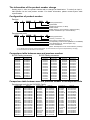
1
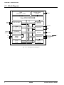
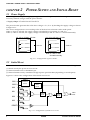
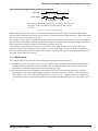
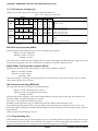
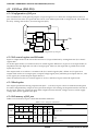
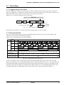
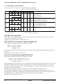
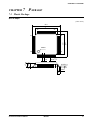
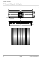
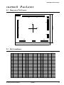
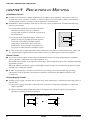
MF1112-02
CMOS 4-BIT SINGLE CHIP MICROCOMPUTER
S1C60N04
Technical Manual
S1C60N04 Technical Hardware
NOTICE
No part of this material may be reproduced or duplicated in any form or by any means without the written permission of Seiko
Epson. Seiko Epson reserves the right to make changes to this material without notice. Seiko Epson does not assume any
liability of any kind arising out of any inaccuracies contained in this material or due to its application or use in any product or
circuit and, further, there is no representation that this material is applicable to products requiring high level reliability, such
as medical products. Moreover, no license to any intellectual property rights is granted by implication or otherwise, and there
is no representation or warranty that anything made in accordance with this material will be free from any patent or copyright
infringement of a third party. This material or portions thereof may contain technology or the subject relating to strategic
products under the control of the Foreign Exchange and Foreign Trade Law of Japan and may require an export license from
the Ministry of International Trade and Industry or other approval from another government agency.
© SEIKO EPSON CORPORATION 2001 All rights reserved.
The information of the product number change
Starting April 1, 2001, the product number will be changed as listed below. To order from April 1,
2001 please use the new product number. For further information, please contact Epson sales
representative.
Configuration of product number
Devices
S1
C
60N01
F
0A01
00
Packing specification
Specification
Package (D: die form; F: QFP)
Model number
Model name (C: microcomputer, digital products)
Product classification (S1: semiconductor)
Development tools
C
60R08
S5U1
D1
1
00
Packing specification
Version (1: Version 1 ∗2)
Tool type (D1: Development Tool ∗1)
Corresponding model number (60R08: for S1C60R08)
Tool classification (C: microcomputer use)
Product classification
(S5U1: development tool for semiconductor products)
∗1: For details about tool types, see the tables below. (In some manuals, tool types are represented by one digit.)
∗2: Actual versions are not written in the manuals.
Comparison table between new and previous number
S1C60 Family processors
Previous No.
E0C6001
E0C6002
E0C6003
E0C6004
E0C6005
E0C6006
E0C6007
E0C6008
E0C6009
E0C6011
E0C6013
E0C6014
E0C60R08
New No.
S1C60N01
S1C60N02
S1C60N03
S1C60N04
S1C60N05
S1C60N06
S1C60N07
S1C60N08
S1C60N09
S1C60N11
S1C60N13
S1C60140
S1C60R08
S1C62 Family processors
Previous No.
E0C621A
E0C6215
E0C621C
E0C6S27
E0C6S37
E0C623A
E0C623E
E0C6S32
E0C6233
E0C6235
E0C623B
E0C6244
E0C624A
E0C6S46
New No.
S1C621A0
S1C62150
S1C621C0
S1C6S2N7
S1C6S3N7
S1C6N3A0
S1C6N3E0
S1C6S3N2
S1C62N33
S1C62N35
S1C6N3B0
S1C62440
S1C624A0
S1C6S460
Previous No.
E0C6247
E0C6248
E0C6S48
E0C624C
E0C6251
E0C6256
E0C6292
E0C6262
E0C6266
E0C6274
E0C6281
E0C6282
E0C62M2
E0C62T3
New No.
S1C62470
S1C62480
S1C6S480
S1C624C0
S1C62N51
S1C62560
S1C62920
S1C62N62
S1C62660
S1C62740
S1C62N81
S1C62N82
S1C62M20
S1C62T30
Comparison table between new and previous number of development tools
Development tools for the S1C60/62 Family
Previous No.
ASM62
DEV6001
DEV6002
DEV6003
DEV6004
DEV6005
DEV6006
DEV6007
DEV6008
DEV6009
DEV6011
DEV60R08
DEV621A
DEV621C
DEV623B
DEV6244
DEV624A
DEV624C
DEV6248
DEV6247
New No.
S5U1C62000A
S5U1C60N01D
S5U1C60N02D
S5U1C60N03D
S5U1C60N04D
S5U1C60N05D
S5U1C60N06D
S5U1C60N07D
S5U1C60N08D
S5U1C60N09D
S5U1C60N11D
S5U1C60R08D
S5U1C621A0D
S5U1C621C0D
S5U1C623B0D
S5U1C62440D
S5U1C624A0D
S5U1C624C0D
S5U1C62480D
S5U1C62470D
Previous No.
DEV6262
DEV6266
DEV6274
DEV6292
DEV62M2
DEV6233
DEV6235
DEV6251
DEV6256
DEV6281
DEV6282
DEV6S27
DEV6S32
DEV6S37
EVA6008
EVA6011
EVA621AR
EVA621C
EVA6237
EVA623A
New No.
S5U1C62620D
S5U1C62660D
S5U1C62740D
S5U1C62920D
S5U1C62M20D
S5U1C62N33D
S5U1C62N35D
S5U1C62N51D
S5U1C62560D
S5U1C62N81D
S5U1C62N82D
S5U1C6S2N7D
S5U1C6S3N2D
S5U1C6S3N7D
S5U1C60N08E
S5U1C60N11E
S5U1C621A0E2
S5U1C621C0E
S5U1C62N37E
S5U1C623A0E
Previous No.
EVA623B
EVA623E
EVA6247
EVA6248
EVA6251R
EVA6256
EVA6262
EVA6266
EVA6274
EVA6281
EVA6282
EVA62M1
EVA62T3
EVA6S27
EVA6S32R
ICE62R
KIT6003
KIT6004
KIT6007
New No.
S5U1C623B0E
S5U1C623E0E
S5U1C62470E
S5U1C62480E
S5U1C62N51E1
S5U1C62N56E
S5U1C62620E
S5U1C62660E
S5U1C62740E
S5U1C62N81E
S5U1C62N82E
S5U1C62M10E
S5U1C62T30E
S5U1C6S2N7E
S5U1C6S3N2E2
S5U1C62000H
S5U1C60N03K
S5U1C60N04K
S5U1C60N07K
CONTENTS
CONTENTS
CHAPTER
1 INTRODUCTION ____________________________________________ 1
1.1
1.2
1.3
1.4
CHAPTER
Features ........................................................................................................ 1
Block Diagram .............................................................................................. 2
Pin Layout ..................................................................................................... 3
Pin Description ............................................................................................. 3
2 POWER SUPPLY AND INITIAL RESET _____________________________ 4
2.1
2.2
Power Supply ................................................................................................ 4
Initial Reset ................................................................................................... 4
2.2.1 Power-on reset circuit ................................................................................ 5
2.2.2 Reset pin (RESET) ...................................................................................... 5
2.2.3 Simultaneous high input to input ports (K00–K03) .................................. 5
2.2.4 Internal register following initialization ................................................... 5
2.3
CHAPTER
3 CPU, ROM, RAM________________________________________ 6
3.1
3.2
3.3
CHAPTER
Test Pin (TEST) ............................................................................................. 5
CPU ............................................................................................................... 6
ROM .............................................................................................................. 6
RAM .............................................................................................................. 6
4 PERIPHERAL CIRCUITS AND OPERATION __________________________ 7
4.1
4.2
4.3
Memory Map ................................................................................................. 7
Oscillation Circuit ........................................................................................ 9
Input Ports (K00–K03) ................................................................................ 10
4.3.1 Configuration of input port ....................................................................... 10
4.3.2 Interrupt function ...................................................................................... 10
4.3.3 Mask option ............................................................................................... 11
4.3.4 I/O memory of input port .......................................................................... 12
4.3.5 Programming note ..................................................................................... 12
4.4
Output Ports (R00–R03) .............................................................................. 13
4.4.1 Configuration of output port ..................................................................... 13
4.4.2 Mask option ............................................................................................... 13
4.4.3 I/O memory of output port ........................................................................ 14
4.4.4 Programming note ..................................................................................... 15
4.5
I/O Ports (P00–P03) .................................................................................... 16
4.5.1 Configuration of I/O port .......................................................................... 16
4.5.2 I/O control register and I/O mode ............................................................ 16
4.5.3 Mask option ............................................................................................... 16
4.5.4 I/O memory of I/O port ............................................................................. 16
4.5.5 Programming note ..................................................................................... 17
4.6
LCD Driver (COM0–COM3, SEG0–SEG25) ............................................. 18
4.6.1 Configuration of LCD driver .................................................................... 18
4.6.2 Mask option ............................................................................................... 23
4.6.3 I/O memory of LCD driver ........................................................................ 24
4.6.4 Programming note ..................................................................................... 24
S1C60N04 TECHNICAL MANUAL
EPSON
i
CONTENTS
4.7
Clock Timer .................................................................................................. 25
4.7.1 Configuration of clock timer ..................................................................... 25
4.7.2 Interrupt function ...................................................................................... 25
4.7.3 I/O memory of clock timer ........................................................................ 26
4.7.4 Programming notes ................................................................................... 27
4.8
Interrupt and HALT/SLEEP ........................................................................ 28
4.8.1 Interrupt factors ........................................................................................ 30
4.8.2 Specific masks for interrupt ...................................................................... 30
4.8.3 Interrupt vectors ........................................................................................ 31
4.8.4 I/O memory of interrupt ............................................................................ 31
4.8.5 Programming notes ................................................................................... 32
CHAPTER
5 BASIC EXTERNAL WIRING DIAGRAM ____________________________ 33
CHAPTER
6 ELECTRICAL CHARACTERISTICS ________________________________ 34
6.1
6.2
6.3
6.4
6.5
6.6
CHAPTER
7 PACKAGE ________________________________________________ 37
7.1
7.2
CHAPTER
ii
Plastic Package............................................................................................ 37
Ceramic Package for Test Samples ............................................................. 38
8 PAD LAYOUT _____________________________________________ 39
8.1
8.2
CHAPTER
Absolute Maximum Rating ........................................................................... 34
Recommended Operating Conditions .......................................................... 34
DC Characteristics ...................................................................................... 35
Current Consumption .................................................................................. 36
Oscillation Characteristics .......................................................................... 36
LCD Characteristic ..................................................................................... 36
Diagram of Pad Layout ............................................................................... 39
Pad Coordinates .......................................................................................... 39
9 PRECAUTIONS ON MOUNTING _________________________________ 40
EPSON
S1C60N04 TECHNICAL MANUAL
CHAPTER 1: INTRODUCTION
CHAPTER 1
INTRODUCTION
The S1C60N04 is a single-chip microcomputer which uses an S1C6200B CMOS 4-bit CPU as the core. It
contains a 1,536 (words) × 12 (bits) ROM, 144 (words) × 4 (bits) RAM, LCD driver, 4-bit input port (K00–
K03), 4-bit output port (R00–R03), 4-bit I/O port (P00–P03) and a timer.
1.1 Features
Core CPU ........................................... S1C6200B
Built-in oscillation circuit ............. CR oscillation circuit, 2 MHz (Typ.) (VSS = -5 V)
Instruction set .................................. 100 instructions
ROM capacity ................................... 1,536 words × 12 bits
RAM capacity ................................... 144 words × 4 bits
Input port .......................................... 4 bits
(pull-down resistors are available by mask option)
Output ports ..................................... 4 bits
(clock and buzzer outputs are possible by mask option)
R03 output port drivability: 15 mA (VSS = -4.5 V)
I/O port .............................................. 4 bits
LCD driver ........................................ 26 segments × 4, 3 or 2 commons
(1/4, 1/3 or 1/2 duty are selectable by mask option)
Timer .................................................. 1 system built-in
Interrupt ............................................ External: Input port interrupt
Internal: Timer interrupt
1 system
1 system
Supply voltage ................................. 2.7 V to 3.6 V, 4.5 V to 5.5 V
Current consumption (Typ.) ......... During SLEEP:
100 nA (3 V)
100 nA (5 V)
During HALT:
330 µA (3 V)
(LCD ON)
1000 µA (5 V)
During operation: 450 µA (3 V)
(LCD ON)
1100 µA (5 V)
Supply form ..................................... Die form or QFP12-48pin plastic package
S1C60N04 TECHNICAL MANUAL
EPSON
1
CHAPTER 1: INTRODUCTION
1.2 Block Diagram
ROM
System Reset
Control
1,536 words × 12 bits
RESET
Core CPU S1C6200B
OSC1
OSC2
OSC / SLEEP
Interrupt
Generator
RAM
Input Port
K00–K03
144 words × 4 bits
COM0–3
SEG0–25
VDD
VSS
TEST
LCD Driver
I/O Port
26 SEG × 4 COM
Power
Divider
P00–P03
VL1
VL2
R00 (FOUT, BUZZER)∗1
R01 (BUZZER)∗1
R02, R03
Output Port
Clock
Timer
FOUT
& Buzzer
∗1: Terminal specifications can be selected by mask option.
Fig. 1.2.1 S1C60N04 block diagram
2
EPSON
S1C60N04 TECHNICAL MANUAL
CHAPTER 1: INTRODUCTION
1.3 Pin Layout
QFP12-48pin
36
25
37
No. Pin name No. Pin name No. Pin name No. Pin name
24
INDEX
48
13
1
12
1
2
3
4
5
6
7
8
9
10
11
12
K02
K01
K00
P03
P02
P01
P00
R03
R02
R01
R00
SEG25
13
14
15
16
17
18
19
20
21
22
23
24
SEG24
SEG23
SEG22
SEG21
SEG20
SEG19
SEG18
SEG17
SEG16
SEG15
SEG14
SEG13
25
26
27
28
29
30
31
32
33
34
35
36
SEG12
SEG11
SEG10
SEG9
SEG8
SEG7
SEG6
SEG5
SEG4
SEG3
SEG2
SEG1
37
38
39
40
41
42
43
44
45
46
47
48
SEG0
COM0
COM1
COM2
COM3
TEST
RESET
VDD
OSC1
OSC2
VSS
K03
Fig. 1.3.1 S1C60N04 pin layout (QFP12-48pin)
1.4 Pin Description
Table 1.4.1 Pin description
Pin name
VDD
VSS
OSC1
OSC2
K00–K03
P00–P03
R00
R01
R02, R03
SEG0–25
COM0–3
RESET
TEST
Pin No.
44
47
45
46
3–1, 48
7–4
I/O
(I)
(I)
I
O
I
I/O
11
10
9, 8
37–12
38–41
43
42
O
O
O
O
O
I
I
Function
Power supply pin (+)
Power supply pin (-)
CR oscillation input pin
CR oscillation output pin
Input port pin
I/O port pin
Output port pin, BUZZER or FOUT output pin *
Output port pin or BUZZER output pin *
Output port pin
LCD segment output pin or DC output pin *
LCD common output pin (1/4 duty, 1/3 or 1/2 duty are selectable *)
Initial reset input pin
Input pin for test
∗ Can be selected by mask option
S1C60N04 TECHNICAL MANUAL
EPSON
3
CHAPTER 2: POWER SUPPLY AND INITIAL RESET
CHAPTER 2
POWER SUPPLY AND INITIAL RESET
2.1 Power Supply
With a single external power supply (∗) supplied to VDD through VSS, the S1C60N04 generates the
necessary internal voltages with the power divider.
∗ Supply voltage: 2.7 to 3.6 V or 4.5 V to 5.5 V
The power divider generates the LCD drive voltages <VL1, VL2> by dividing the supply voltage as shown
in Figure 2.1.1.
The circuit configuration is set according to the LCD drive bias selection with a mask option.
When 1/3 bias is selected, the supply voltage is divided by 3 to generate VL1 and VL2.
When 1/2 bias is selected, the supply voltage is divided by 2 and VL1 and VL2 is shorted internally.
1/4, 1/3 or 1/2 duty, 1/3 bias
1/4, 1/3 or 1/2 duty, 1/2 bias
VDD
VDD
VL1 = 1/3·VSS
VL1 = 1/2·VSS
3.0/5.0 V
3.0/5.0 V
VL2 = 2/3·VSS
VL2 = 1/2·VSS
VSS
VSS
Note: VL1 and VL2 are
shorted internally.
Fig. 2.1.1 Configuration of power divider
2.2 Initial Reset
To initialize the S1C60N04 circuits, an initial reset must be executed. There are three ways of doing this.
(1) Initial reset by the power-on reset circuit
(2) External initial reset via the RESET pin
(3) External initial reset by simultaneous high input to pins K00–K03 (depending on mask option)
Figure 2.2.1 shows the configuration of the initial reset circuit.
OSC1
OSC1
OSC2
Oscillation
circuit
K00
Power-on
reset
circuit
Vss
K01
Noise
rejection
circuit
K02
Noise
rejection
circuit
Initial
reset
K03
RESET
Vss
Fig. 2.2.1 Configuration of initial reset circuit
4
EPSON
S1C60N04 TECHNICAL MANUAL
CHAPTER 2: POWER SUPPLY AND INITIAL RESET
2.2.1 Power-on reset circuit
The power-on reset circuit outputs the initial reset signal at power-on until the oscillation circuit starts
oscillating.
Note: The power-on reset circuit may not work properly due to unstable or lower voltage input. The
following two initial reset method are recommended to generate the initial reset signal.
2.2.2 Reset pin (RESET)
An initial reset can be invoked externally by making the reset pin high.
When the reset pin goes low the CPU begins to operate.
2.2.3 Simultaneous high input to input ports (K00–K03)
Table 2.2.3.1 Input port combinations
Another way of invoking an initial reset externally is to input a
high signal simultaneously to the input ports (K00–K03) selected
A
Not used
with the mask option. The specified input port pins must be kept
B
K00*K01
high for at least 1 sec (when oscillating frequency fosc = 2 MHz),
C
K00*K01*K02
tolerance is within 5%, because of the noise rejection circuit. Table
D
K00*K01*K02*K03
2.2.3.1 shows the combinations of input ports (K00–K03) that can be
selected with the mask option.
When, for instance, mask option D (K00*K01*K02*K03) is selected, an initial reset is executed when the
signals input to the four ports K00–K03 are all high at the same time.
When this function is used, make sure that the specified ports do not go high at the same time during
normal operation.
2.2.4 Internal register following initialization
An initial reset initializes the CPU as shown in the table below.
Table 2.2.4.1 Initial values
CPU Core
Name
Symbol Bit size
Program counter step
PCS
8
Program counter page
PCP
4
New page pointer
NPP
4
Stack pointer
SP
8
Index register X
X
8
Index register Y
Y
8
Register pointer
RP
4
General-purpose register A
A
4
General-purpose register B
B
4
Interrupt flag
I
1
Decimal flag
D
1
Zero flag
Z
1
Carry flag
C
1
Initial value
00H
1H
1H
Undefined
Undefined
Undefined
Undefined
Undefined
Undefined
0
0
Undefined
Undefined
Peripheral Circuits
Bit size
Initial value
RAM
144×4
Undefined
Display memory
26×4
Undefined
Other peripheral circuits
–
∗
∗ See Section 4.1, "Memory Map".
Name
2.3 Test Pin (TEST)
This pin is used when IC is inspected for shipment. During normal operation connect it to VSS.
S1C60N04 TECHNICAL MANUAL
EPSON
5
CHAPTER 3: CPU, ROM, RAM
CHAPTER 3
CPU, ROM, RAM
3.1 CPU
The S1C60N04 employs the S1C6200B core CPU, so that register configuration, instructions, and so forth
are virtually identical to those in other processors in the family using the S1C6200/6200A/6200B.
Refer to the "S1C6200/6200A Core CPU Manual" for details of the S1C6200B, which is compatible with
the S1C6200A.
Note the following points with regard to the S1C60N04:
(1) Since the S1C60N04 provides the SLEEP function, the SLP instruction can be used.
(2) Because the ROM capacity is 1,536 words, 12 bits per word, bank bits are unnecessary, and PCB and
NBP are not used.
(3) The RAM page is set to 0 only, so the page part (XP, YP) of the index register that specifies addresses is
invalid.
PUSH XP
POP XP
LD XP,r
LD r,XP
PUSH YP
POP YP
LD YP,r
LD r,YP
3.2 ROM
The built-in ROM, a mask ROM for the program, has a capacity of 1,536 × 12-bit steps. The program area
is 6 pages (0–5), each consisting of 256 steps (00H–FFH). After an initial reset, the program start address is
set to page 1, step 00H. The interrupt vectors are allocated to page 1, steps 01H–07H.
Bank 0
Step 00H
Page 0
Step 01H
Interrupt vector area
Page 1
Page 2
Page 3
Program start address
Step 07H
Step 08H
Page 4
Page 5
Program area
Step FFH
12 bits
Fig. 3.2.1 ROM configuration
3.3 RAM
The RAM, a data memory for storing a variety of data, has a capacity of 144 words, 4-bit words. When
programming, keep the following points in mind:
(1) Part of the data memory is used as stack area when saving subroutine return addresses and registers,
so be careful not to overlap the data area and stack area.
(2) Subroutine calls and interrupts take up three words on the stack.
(3) Data memory 000H–00FH is the memory area pointed by the register pointer (RP).
6
EPSON
S1C60N04 TECHNICAL MANUAL
CHAPTER 4: PERIPHERAL CIRCUITS AND OPERATION (Memory Map)
CHAPTER
4
PERIPHERAL CIRCUITS AND OPERATION
Peripheral circuits (timer, I/O, and so on) of the S1C60N04 are memory mapped. Thus, all the peripheral
circuits can be controlled by using memory operations to access the I/O memory. The following sections
describe how the peripheral circuits operate.
4.1 Memory Map
The data memory of the S1C60N04 has an address space of 188 words, of which 32 words are allocated to
display memory and 12 words, to I/O memory. Figure 4.1.1 show the overall memory map for the
S1C60N04, and Table 4.1.1, the memory maps for the peripheral circuits (I/O space).
Address
Low
0
Page
1
2
3
4
5
6
7
8
9
A
B
C
D
E
F
High
0
M0 M1 M2 M3 M4 M5 M6 M7 M8 M9 MA MB MC MD ME MF
1
2
3
4
5
RAM area (000H–08FH)
144 words × 4 bits (R/W)
6
0
7
8
9
A
Display memory area (090H–0AFH)
32 words × 4 bits (W only)
B
C
D
E
I/O memory
See Table 4.1.1
F
Unused area
Fig. 4.1.1 Memory map
Note: Memory is not mounted in unused area within the memory map and in memory area not indicated
in this chapter. For this reason, normal operation cannot be assured for programs that have been
prepared with access to these areas.
S1C60N04 TECHNICAL MANUAL
EPSON
7
CHAPTER 4: PERIPHERAL CIRCUITS AND OPERATION (Memory Map)
Table 4.1.1 I/O memory map
Address
Register
Comment
1
0
Name Init ∗1
∗2
High
K03
Low
–
K03
K02
K01
K00
– ∗2 High
K02
Low
0E0H
K0 input port data
– ∗2 High
K01
Low
R
– ∗2 High
K00
Low
TM3
Clock timer data (2 Hz)
– ∗2
TM3
TM2
TM1
TM0
– ∗2
TM2
Clock timer data (4 Hz)
0E4H
– ∗2
TM1
Clock timer data (8 Hz)
R
– ∗2
TM0
Clock timer data (16 Hz)
EIK03
0
Enable Mask Interrupt mask register (K03)
EIK03 EIK02 EIK01 EIK00
EIK02
0
Enable Mask Interrupt mask register (K02)
0E8H
EIK01
0
Enable Mask Interrupt mask register (K01)
R/W
EIK00
0
Enable Mask Interrupt mask register (K00)
0 ∗3
Unused
– ∗2
–
–
0
EIT2
EIT8
EIT32
EIT2
0
Enable Mask Interrupt mask register (clock timer 2 Hz)
0EBH
EIT8
0
Enable Mask Interrupt mask register (clock timer 8 Hz)
R
R/W
EIT32
0
Enable Mask Interrupt mask register (clock timer 32 Hz)
0 ∗3
– ∗2
Unused
–
–
0
0
0
IK0
0 ∗3
– ∗2
Unused
–
–
0EDH
0 ∗3
– ∗2
Unused
–
–
R
IK0 ∗4
0
Interrupt factor flag (K00–K03)
Yes
No
0 ∗3
– ∗2
Unused
–
–
0
IT2
IT8
IT32
IT2 ∗4
0
Interrupt factor flag (clock timer 2 Hz)
Yes
No
0EFH
IT8 ∗4
0
Interrupt factor flag (clock timer 8 Hz)
Yes
No
R
IT32 ∗4
0
Interrupt factor flag (clock timer 32 Hz)
Yes
No
High
R03
Low R03 output port data
0
R00
R01
High
R02
Low R02 output port data
0
R03
R02
FOUT
High
Low R01 output port data
0
BUZZER BUZZER R01
0F3H
On
Buzzer output On/Off control
BUZZER
Off
0
High
R00
Low R00 output port data
0
R/W
On
FOUT output On/Off control
FOUT
Off
0
Buzzer inverted output On/Off control
On
BUZZER
Off
0
P03
– ∗2 High
Low
P03
P02
P01
P00
– ∗2 High
P02
Low
0F6H
P0 I/O port data
– ∗2 High
P01
Low
R/W
∗2
–
P00
High
Low
0 ∗3
– ∗2
–
Unused
–
0
TMRST
0
0
TMRST∗3 Reset Reset
Clock timer reset
–
0F9H
0 ∗3
– ∗2
–
Unused
–
R
W
R
0 ∗3
– ∗2
–
Unused
–
0 ∗3
Unused
– ∗2
–
–
0
0
0
PDON
0 ∗3
– ∗2
Unused
–
–
0FBH
0 ∗3
– ∗2
Unused
–
–
R
R/W
PDON
0
LCD power supply On/Off control
On
Off
0 ∗3
Unused
– ∗2
–
–
0
0
0
IOC
0 ∗3
– ∗2
Unused
–
–
0FCH
0 ∗3
– ∗2
Unused
–
–
R
R/W
IOC
0
Output Input I/O port I/O control
XBZR
0
2 kHz 4 kHz Buzzer frequency control
XBZR
0
0
0
0 ∗3
– ∗2
–
Unused
–
0FDH
0 ∗3
– ∗2
–
Unused
–
R/W
R
0 ∗3
– ∗2
–
Unused
–
∗1 Initial value at initial reset
∗3 Always "0" being read
∗2 Not set in the circuit
∗4 Reset (0) immediately after being read
8
D3
D2
D1
D0
EPSON
S1C60N04 TECHNICAL MANUAL
CHAPTER 4: PERIPHERAL CIRCUITS AND OPERATION (Oscillation Circuit)
4.2 Oscillation Circuit
The S1C60N04 has a CR oscillation circuit.
The CR oscillation circuit generates the operating clock for the CPU and the peripheral circuits. The
oscillation frequency is 2 MHz (Typ.). Figure 4.2.1 is the circuit diagram of the CR oscillation circuit.
OSC1
RCR
CPU
and peripheral circuits
CCR
OSC2
Fig. 4.2.1 CR oscillation circuit
As shown in Figure 4.2.1, the CR oscillation circuit can be configured simply by connecting the resistor
RCR between the OSC1 and OSC2 terminals.
See Chapter 6, "Electrical Characteristics" for resistance value of RCR.
S1C60N04 TECHNICAL MANUAL
EPSON
9
CHAPTER 4: PERIPHERAL CIRCUITS AND OPERATION (Input Ports)
4.3 Input Ports (K00–K03)
4.3.1 Configuration of input port
The S1C60N04 has a 4-bit general-purpose input port. Each of the input port pins (K00–K03) has an
internal pull-down resistor. The pull-down resistor can be selected for each bit with the mask option.
Figure 4.3.1.1 shows the configuration of input port.
VDD
Data bus
Interrupt
request
K0x
Address
VSS
Mask option
Fig. 4.3.1.1 Configuration of input port
Selecting "pull-down resistor enabled" with the mask option allows input from a push button, key matrix,
and so forth. When "pull-down resistor disabled" is selected, the port can be used for slide switch input
and interfacing with other LSIs.
4.3.2 Interrupt function
All four input port bits (K00–K03) provide the interrupt function. The conditions for issuing an interrupt
can be set by the software for the four bits. Also, whether to mask the interrupt function can be selected
individually for all four bits by the software. Figure 4.3.2.1 shows the configuration of K00–K03.
Data bus
K0x
Noise
rejector
Address
Interrupt factor
flag (IK0)
Interrupt
request
Address
Interrupt mask
register (EIK)
Mask option
(K00–K03)
Address
Fig. 4.3.2.1 Input interrupt circuit configuration (K00–K03)
The interrupt mask registers (EIK00–EIK03) enable the interrupt mask to be selected individually for
K00–K03. An interrupt occurs when the input value which are not masked change and the interrupt
factor flag (IK0) is set to 1.
10
EPSON
S1C60N04 TECHNICAL MANUAL
CHAPTER 4: PERIPHERAL CIRCUITS AND OPERATION (Input Ports)
Input interrupt programming related precautions
Port K input
Active status
Mask register
➀
Factor flag set Not set
When the content of the mask register is rewritten, while the port
K input is in the active status. The input interrupt factor flag is
set at ➀.
Fig. 4.3.2.2 Input interrupt timing
When using an input interrupt, if you rewrite the content of the mask register, when the value of the
input terminal which becomes the interrupt input is in the active status (input terminal = high status), the
factor flag for input interrupt may be set.
For example, a factor flag is set with the timing of ➀ shown in Figure 4.3.2.2. However, when clearing the
content of the mask register with the input terminal kept in the high status and then setting it, the factor
flag of the input interrupt is again set at the timing that has been set.
Consequently, when the input terminal is in the active status (high status), do not rewrite the mask
register (clearing, then setting the mask register), so that a factor flag will only set at the rising edge in
this case. When clearing, then setting the mask register, set the mask register, when the input terminal is
not in the active status (low status).
4.3.3 Mask option
The contents that can be selected with the input port mask option are as follows:
(1) An internal pull-down resistor can be selected for each of the four bits of the input ports (K00–K03).
Having selected "pull-down resistor disabled", take care that the input does not float. Select "pulldown resistor enabled" for input ports that are not being used.
(2) The input interrupt circuit contains a noise rejection circuit to prevent interrupts form occurring
through noise. The mask option enables selection of the noise rejection circuit for each separate pin
series. When "use" is selected, a maximum delay of 0.5 msec (fosc = 2 MHz), tolerance is within 5%,
occurs from the time an interrupt condition is established until the interrupt factor flag (IK0) is set to
1.
S1C60N04 TECHNICAL MANUAL
EPSON
11
CHAPTER 4: PERIPHERAL CIRCUITS AND OPERATION (Input Ports)
4.3.4 I/O memory of input port
Table 4.3.4.1 list the input port control bits and their addresses.
Table 4.3.4.1 Input port control bits
Address
Register
D3
D2
D1
D0
K03
K02
K01
K00
EIK01
EIK00
0E0H
R
EIK03
EIK02
0E8H
R/W
0
0
0
IK0
0EDH
R
Name
K03
K02
K01
K00
EIK03
EIK02
EIK01
EIK00
0 ∗3
0 ∗3
0 ∗3
IK0 ∗4
∗1 Initial value at initial reset
∗2 Not set in the circuit
Comment
1
0
Init ∗1
– ∗2 High
Low
– ∗2 High
Low
K0 input port data
– ∗2 High
Low
– ∗2 High
Low
0
Enable Mask Interrupt mask register (K03)
0
Enable Mask Interrupt mask register (K02)
0
Enable Mask Interrupt mask register (K01)
0
Enable Mask Interrupt mask register (K00)
– ∗2
Unused
–
–
– ∗2
Unused
–
–
– ∗2
Unused
–
–
0
Interrupt factor flag (K00–K03)
Yes
No
∗3 Always "0" being read
∗4 Reset (0) immediately after being read
K00–K03: Input port data (0E0H)
The input data of the input port pins can be read with these registers.
When 1 is read: High level
When 0 is read: Low level
Writing: Invalid
The value read is 1 when the pin voltage of the four bits of the input port (K00–K03) goes high (VDD), and
0 when the voltage goes low (VSS). These bits are reading, so writing cannot be done.
EIK00–EIK03: Interrupt mask registers (0E8H)
Masking the interrupt of the input port pins can be done with these registers.
When 1 is written: Enable
When 0 is written: Mask
Reading: Valid
With these registers, masking of the input port bits can be done for each of the four bits. After an initial
reset, these registers are all set to 0.
IK0: Interrupt factor flag (0EDH•D0)
This flag indicates the occurrence of an input interrupt.
When 1 is read: Interrupt has occurred
When 0 is read: Interrupt has not occurred
Writing: Invalid
The interrupt factor flag IK0 is associated with K00–K03. From the status of this flag, the software can
decide whether an input interrupt has occurred.
This flag is reset when the software has read it.
Reading of interrupt factor flag is available at EI, but be careful in the following cases.
If the interrupt mask register value corresponding to the interrupt factor flag to be read is set to 1, an
interrupt request will be generated by the interrupt factor flag set timing, or an interrupt request will not
be generated.
After an initial reset, this flag is set to 0.
4.3.5 Programming note
When modifying the input port from high level to low level with pull-down resistor, a delay will occur at
the fall of the waveform due to time constant of the pull-down resistor and input gate capacities. Provide
appropriate waiting time in the program when performing input port reading.
12
EPSON
S1C60N04 TECHNICAL MANUAL
CHAPTER 4: PERIPHERAL CIRCUITS AND OPERATION (Output Ports)
4.4 Output Ports (R00–R03)
4.4.1 Configuration of output port
The S1C60N04 has a 4-bit general output port (R00–R03).
Output specification of the output port can be selected in a bit units with the mask option. Two kinds of
output specifications are available: complementary output and Pch open drain output. Also, the mask
option enables the output ports R00 and R01 to be used as special output ports. Figure 4.4.1.1 shows the
configuration of the output port.
Data bus
VDD
Register
R0x
Complementary
Pch open drain
Address
VSS
Mask option
Fig. 4.4.1.1 Configuration of output port
4.4.2 Mask option
The mask option enables the following output port selection.
(1) Output specification of output port
The output specifications for the output port (R00–R03) may be either complementary output or Pch
open drain output for each bit. However, even when Pch open drain output is selected, a voltage
exceeding the source voltage must not be applied to the output port.
(2) Special output
In addition to the regular DC output, special output can be selected for output ports R00 and R01, as
shown in Table 4.4.2.1. Figure 4.4.2.1 shows the structure of output ports R00–R03.
Table 4.4.2.1 Special output
Data bus
Output port
R00
R01
Special output
FOUT or BUZZER output
BUZZER output
Register R03
R03
Register R02
R02
BUZZER
Register R01
R01
BUZZER
Register R00
R00
FOUT
Address 0F3H
Mask option
Fig. 4.4.2.1 Structure of output ports R00–R03
S1C60N04 TECHNICAL MANUAL
EPSON
13
CHAPTER 4: PERIPHERAL CIRCUITS AND OPERATION (Output Ports)
FOUT (R00)
When output port R00 is set for FOUT output, this port will generate fosc (CPU operating clock frequency) clock.
BUZZER, BUZZER (R01, R00)
Output ports R01 and R00 may be set to BUZZER output and BUZZER output (BUZZER reverse output),
respectively, allowing for direct driving of the piezo-electric buzzer.
BUZZER output (R00) may only be set if R01 is set to BUZZER output. In such case, whether ON/OFF of
the BUZZER output is done through R00 register or is controlled through R01 simultaneously with
BUZZER output is also selected by mask option.
The frequency of buzzer output may be selected by software to be either 2 kHz or 4 kHz.
4.4.3 I/O memory of output port
Table 4.4.3.1 lists the output port control bits and their addresses.
Table 4.4.3.1 Control bits of output port
Address
Register
Comment
Name Init ∗1
1
0
High
R03
Low R03 output port data
0
R01
High
R02
Low R02 output port data
0
R03
R02
FOUT
High
Low R01 output port data
0
BUZZER BUZZER R01
0F3H
On
Buzzer output On/Off control
BUZZER
Off
0
High
R00
Low R00 output port data
0
R/W
On
FOUT output On/Off control
FOUT
Off
0
Buzzer inverted output On/Off control
On
BUZZER
Off
0
XBZR
0
2 kHz 4 kHz Buzzer frequency control
XBZR
0
0
0
0 ∗3
– ∗2
–
Unused
–
0FDH
0 ∗3
– ∗2
–
Unused
–
R/W
R
0 ∗3
– ∗2
–
Unused
–
∗1 Initial value at initial reset
∗3 Always "0" being read
∗2 Not set in the circuit
∗4 Reset (0) immediately after being read
D3
D2
D1
D0
R00
R00–R03: Output port data (0F3H)
Sets the output data for the output ports.
When 1 is written: High output
When 0 is written: Low output
Reading: Valid
The output port pins output the data written to the corresponding registers (R00–R03) without changing
it. When 1 is written to the register, the output port pin goes high (VDD), and when 0 is written, the
output port pin goes low (VSS).
After an initial reset, all the registers are set to 0.
R00 (when FOUT is selected): Special output port data (0F3H•D0)
Controls the FOUT (fosc clock) output.
When 1 is written: Clock output
When 0 is written: Low level (DC) output
Reading: Valid
FOUT output can be controlled by writing data to R00.
After an initial reset, this register is set to 0.
Figure 4.4.3.1 shows the output waveform for FOUT output.
14
EPSON
S1C60N04 TECHNICAL MANUAL
CHAPTER 4: PERIPHERAL CIRCUITS AND OPERATION (Output Ports)
R00 register
0
1
FOUT output
waveform
Fig. 4.4.3.1 FOUT output waveform
Note: A hazard may occur when the FOUT signal is turned ON or OFF.
R00, R01 (when buzzer output is selected): Special output port data (0F3H•D0, D1)
Controls the buzzer output.
When 1 is written: Buzzer output
When 0 is written: Low level (DC) output
Reading: Valid
BUZZER and BUZZER output can be controlled by writing data to R00 and R01.
When BUZZER output by R01 register control is selected by mask option, BUZZER output and BUZZER
output can be controlled simultaneously by writing data to R01 register.
After an initial reset, these registers are set to 0.
Figure 4.4.3.2 shows the output waveform for buzzer output.
R01 (R00) register
0
1
BUZZER output
waveform
BUZZER output
waveform
Fig. 4.4.3.2 Buzzer output waveform
Note: A hazard may occur when the BUZZER or BUZZER signal is turned ON or OFF.
XBZR: Buzzer frequency control (0FDH•D3)
Selects the frequency of the buzzer signal.
When 1 is written: 2 kHz
When 0 is written: 4 kHz
Reading: Valid
When R00 and R01 port is set to buzzer output, the frequency of the buzzer signal can be selected by this
register.
When 1 is written to this register, the frequency is set in 2 kHz, and in 4 kHz when 0 is written.
After an initial reset, this register is set to 0.
4.4.4 Programming note
The buzzer output signal may produce hazards when the output ports R00 and R01 are turned on or off.
S1C60N04 TECHNICAL MANUAL
EPSON
15
CHAPTER 4: PERIPHERAL CIRCUITS AND OPERATION (I/O Ports)
4.5 I/O Ports (P00–P03)
4.5.1 Configuration of I/O port
Data bus
The S1C60N04 has a 4-bit general-purpose I/O port. Figure 4.5.1.1 shows the configuration of the I/O
port. The four bits of the I/O port P00–P03 can be set to either input mode or output mode. The mode can
be set by writing data to the I/O control register (IOC).
Input
control
Register
P0x
Address
I/O control
register
(IOC)
Address
Vss
Fig. 4.5.1.1 Configuration of I/O port
4.5.2 I/O control register and I/O mode
Input or output mode can be set for the four bits of I/O port P00–P03 by writing data into I/O control
register IOC.
To set the input mode, 0 is written to the I/O control register. When an I/O port is set to input mode, its
impedance becomes high and it works as an input port. However, the input line is pulled down when
input data is read.
The output mode is set when 1 is written to the I/O control register (IOC). When an I/O port set to
output mode works as an output port, it outputs a high signal (VDD) when the port output data is 1, and
a low signal (VSS) when the port output data is 0.
After an initial reset, the I/O control register is set to 0, and the I/O port enters the input mode.
4.5.3 Mask option
The output specification during output mode (IOC = 1) of the I/O port can be set with the mask option
for either complementary output or Pch open drain output. This setting can be performed for each bit of
the I/O port. However, when Pch open drain output has been selected, voltage in excess of the supply
voltage must not be applied to the port.
4.5.4 I/O memory of I/O port
Table 4.5.4.1 lists the I/O port control bits and their addresses.
Table 4.5.4.1 I/O port control bits
Address
Register
D3
D2
D1
D0
P03
P02
P01
P00
0
IOC
0F6H
R/W
0
0
0FCH
R
∗1 Initial value at initial reset
∗2 Not set in the circuit
16
R/W
Name
P03
P02
P01
P00
0 ∗3
0 ∗3
0 ∗3
IOC
Init ∗1
1
0
– ∗2 High
Low
– ∗2 High
Low
P0 I/O port data
– ∗2 High
Low
∗2
–
High
Low
Unused
– ∗2
–
–
– ∗2
Unused
–
–
– ∗2
Unused
–
–
0
Output Input I/O port I/O control
∗3 Always "0" being read
∗4 Reset (0) immediately after being read
EPSON
Comment
S1C60N04 TECHNICAL MANUAL
CHAPTER 4: PERIPHERAL CIRCUITS AND OPERATION (I/O Ports)
P00–P03: I/O port data (0F6H)
I/O port data can be read and output data can be written through the port.
When writing data
When 1 is written: High level
When 0 is written: Low level
When an I/O port is set to the output mode, the written data is output from the I/O port pin unchanged.
When 1 is written as the port data, the port pin goes high (VDD), and when 0 is written, the level goes low
(VSS). Port data can also be written in the input mode.
When reading data
When 1 is read: High level
When 0 is read: Low level
The pin voltage level of the I/O port is read. When the I/O port is in the input mode the voltage level
being input to the port pin can be read; in the output mode the output voltage level can be read. When
the pin voltage is high (VDD) the port data read is 1, and when the pin voltage is low (VSS) the data is 0.
Also, the built-in pull-down resistor functions during reading, so the I/O port pin is pulled down.
IOC: I/O control register (0FCH•D0)
The input or output I/O port mode can be set with this register.
When 1 is written: Output mode
When 0 is written: Input mode
Reading: Valid
The input or output mode of the I/O port is set in units of four bits. For instance, IOC sets the mode for
P00–P03.
Writing 1 to the I/O control register makes the I/O port enter the output mode, and writing 0, the input
mode.
After an initial reset, the IOC register is set to 0, so the I/O port is in the input mode.
4.5.5 Programming note
When in the input mode, I/O ports are changed from high to low by pull-down resistor, the fall of the
waveform is delayed on account of the time constant of the pull-down resistor and input gate capacitance. Hence, when fetching input ports, set an appropriate wait time.
Particular care needs to be taken of the key scan during key matrix configuration.
Make this waiting time the amount of time or more calculated by the following expression.
10 × C × R
C: terminal capacitance 5 pF + parasitic capacitance ? pF
R: pull-down resistance 60 kΩ
S1C60N04 TECHNICAL MANUAL
EPSON
17
CHAPTER 4: PERIPHERAL CIRCUITS AND OPERATION (LCD Driver)
4.6 LCD Driver (COM0–COM3, SEG0–SEG25)
4.6.1 Configuration of LCD driver
The S1C60N04 has four common pins and 26 (SEG0–SEG25) segment pins, so that an LCD with a maximum of 104 (26 × 4) segments can be driven. The power for driving the LCD is generated by the CPU
internal circuit, so there is no need to supply power externally.
The driving method is 1/4 duty (or 1/3, 1/2 duty by mask option) dynamic drive, adopting the four
types of potential (1/3 bias), VDD, VL1, VL2 and VSS. Moreover, the 1/2 bias dynamic drive that uses three
types of potential, VDD, VL1 = VL2 and VSS, can be selected by setting the mask option (drive duty can also
be selected from 1/4, 1/3 or 1/2).
The LCD drive voltages VL1 and VL2 are generated by the power divider inside the IC. However it is
necessary to turn the power divider on by writing 1 to the PDON register before starting LCD display.
The frame frequency is about 30.5 Hz for 1/4 duty and 1/2 duty, and 40.7 Hz for 1/3 duty (in the case of
fosc = 2 MHz), tolerance is within 5%.
Figures 4.6.1.1 to 4.6.1.6 show the drive waveform for each duty and bias.
Note: "fosc" indicates the oscillation frequency of the oscillation circuit.
18
EPSON
S1C60N04 TECHNICAL MANUAL
CHAPTER 4: PERIPHERAL CIRCUITS AND OPERATION (LCD Driver)
VDD
VL1
VL2
VSS
COM0
COM1
LCD lighting status
COM0
COM1
COM2
COM3
COM2
SEG0–25
COM3
Off
On
VDD
VL1
VL2
VSS
SEG0
–SEG25
Frame frequency
Fig. 4.6.1.1 Drive waveform for 1/4 duty (1/3 bias)
S1C60N04 TECHNICAL MANUAL
EPSON
19
CHAPTER 4: PERIPHERAL CIRCUITS AND OPERATION (LCD Driver)
VDD
VL1
VL2
VSS
COM0
COM1
LCD lighting status
COM0
COM1
COM2
SEG0–25
COM2
Off
On
COM3
VDD
VL1
VL2
VSS
SEG0
–SEG25
Frame frequency
Fig. 4.6.1.2 Drive waveform for 1/3 duty (1/3 bias)
VDD
VL1
VL2
VSS
COM0
COM1
LCD lighting status
COM0
COM1
SEG0–25
COM2
COM3
VDD
VL1
VL2
VSS
Off
On
SEG0
–SEG25
Frame frequency
Fig. 4.6.1.3 Drive waveform for 1/2 duty (1/3 bias)
20
EPSON
S1C60N04 TECHNICAL MANUAL
CHAPTER 4: PERIPHERAL CIRCUITS AND OPERATION (LCD Driver)
-VDD
-VL1, L2
-VSS
COM0
COM1
LCD lighting status
COM0
COM1
COM2
COM3
SEG0–25
COM2
Off
On
COM3
-VDD
-VL1, L2
-VSS
SEG
0–25
Frame frequency
Fig. 4.6.1.4 Drive waveform for 1/4 duty (1/2 bias)
S1C60N04 TECHNICAL MANUAL
EPSON
21
CHAPTER 4: PERIPHERAL CIRCUITS AND OPERATION (LCD Driver)
-VDD
-VL1, L2
-VSS
COM0
COM1
LCD lighting status
COM0
COM1
COM2
SEG0–25
COM2
Off
On
COM3
-VDD
-VL1, L2
-VSS
SEG
0–25
Frame frequency
Fig. 4.6.1.5 Drive waveform for 1/3 duty (1/2 bias)
-VDD
-VL1, L2
-VSS
COM0
COM1
LCD lighting status
COM0
COM1
SEG0–25
COM2
Off
On
COM3
-VDD
-VL1, L2
-VSS
SEG
0–25
Frame frequency
Fig. 4.6.1.6 Drive waveform for 1/2 duty (1/2 bias)
22
EPSON
S1C60N04 TECHNICAL MANUAL
CHAPTER 4: PERIPHERAL CIRCUITS AND OPERATION (LCD Driver)
4.6.2 Mask option
(1) Segment allocation
As shown in Figure 4.l.1, the S1C60N04 display data is decided by the data written to the display
memory (write-only) at address 090H–0AFH.
The address and bits of the display memory can be made to correspond to the segment pins (SEG0–
SEG25) in any combination through mask option. This simplifies design by increasing the degree of
freedom with which the liquid crystal panel can be designed.
Figure 4.6.2.1 shows an example of the relationship between the LCD segments (on the panel) and the
display memory in the case of 1/3 duty.
Address
Common 0
Common 1
Common 2
9A, D0
9B, D1
9B, D0
(a)
(f)
(e)
SEG11
9A, D1
9B, D2
9A, D3
(b)
(g)
(d)
SEG12
9D, D1
9A, D2
9B, D3
(f')
(c)
(p)
Data
D3
D2
D1
D0
09AH
d
c
b
a
09BH
p
g
f
e
09CH
d'
c'
b'
a'
09DH
p'
g'
f'
e'
SEG10
Display data memory allocation
Pin address allocation
a
a'
g'
g
e
c
c'
e'
p
d
SEG10
b'
f'
b
f
SEG11
p'
d'
SEG12
Common 0
Common 1
Common 2
Fig. 4.6.2.1 Segment allocation
(2) Drive duty
According to the mask option, either 1/4, 1/3 or 1/2 duty can be selected as the LCD drive duty.
Table 4.6.2.1 shows the differences in the number of segments according to the selected duty.
Table 4.6.2.1 Differences according to selected duty
Duty
COM used
1/4 COM0–COM3
1/3 COM0–COM2
1/2 COM0–COM1
Max. number of segments Frame frequency *
104 (26 × 4)
30.5 Hz
78 (26 × 3)
40.7 Hz
52 (26 × 2)
30.5 Hz
∗ When fOSC = 2 MHz, tolerance is within 5%
(3) Output specification
➀ The segment pins (SEG0–SEG25) are selected by mask option in pairs for either segment signal output
or DC output (VDD and VSS binary output). When DC output is selected, the data corresponding to
COM0 of each segment pin is output.
➁ When DC output is selected, either complementary output or Pch open drain output can be selected
for each pin by mask option.
Note: The pin pairs are the combination of SEG (2∗n) and SEG (2∗n + 1) (where n is an integer from 0 to 12).
(4) Drive bias
For the drive bias of the S1C60N04, either 1/3 bias or 1/2 bias can be selected by the mask option.
S1C60N04 TECHNICAL MANUAL
EPSON
23
CHAPTER 4: PERIPHERAL CIRCUITS AND OPERATION (LCD Driver)
4.6.3 I/O memory of LCD driver
Table 4.6.3.1 shows the control bits of the LCD driver and their addresses. Figure 4.6.3.1 shows the
display memory map.
Table 4.6.3.1 Control bits of LCD driver
Address
Register
D3
D2
D1
D0
0
0
0
PDON
0FBH
R
R/W
Name
0 ∗3
0 ∗3
0 ∗3
PDON
∗1 Initial value at initial reset
∗2 Not set in the circuit
Address
0
1
2
Comment
Init ∗1
1
0
Unused
– ∗2
–
–
– ∗2
Unused
–
–
– ∗2
Unused
–
–
0
LCD power supply on/off control
On
Off
∗3 Always "0" being read
∗4 Reset (0) immediately after being read
3
4
090
5
6
7
8
9
A
B
C
D
E
F
Display memory (Write only)
32 words x 4 bits
0A0
Fig. 4.6.3.1 Display memory map
PDON: LCD power supply On/Off control (0FBH•D0)
Controls the power supply for LCD display.
When 1 is written: LCD power On
When 0 is written: LCD power Off
Reading: Valid
By writing 1 to PDON, the LCD display can work normally. When 0 is written, all the segment and
common signals will go to the same voltage level, and the LCD display goes off.
This control dose not affect the contents of display memory.
After an initial reset, this register is set to 0.
Display memory (090H–0AFH)
The LCD segments are turned on or off according to this data.
When 1 is written: On
When 0 is written: Off
Reading: Invalid
By writing data into the display memory allocated to the LCD segment (on the panel), the segment can be
turned on or off.
After an initial reset, the contents of the display memory are undefined.
4.6.4 Programming note
Because the display memory is for writing only, re-writing the contents with computing instructions (e.g.,
AND, OR, etc.) which come with read-out operations is not possible. To perform bit operations, a buffer
to hold the display data is required on the RAM.
24
EPSON
S1C60N04 TECHNICAL MANUAL
CHAPTER 4: PERIPHERAL CIRCUITS AND OPERATION (Clock Timer)
4.7 Clock Timer
4.7.1 Configuration of clock timer
The S1C60N04 has a built-in clock timer that uses the oscillation circuit as the clock source. The clock
timer is configured as a 7-bit binary counter that counts with a 256 Hz source clock from the divider. The
high-order 4 bits of the counter (16 Hz–2 Hz) can be read by the software.
Figure 4.7.1.1 is the block diagram of the clock timer.
Data bus
Oscillation
circuit
Divider
256 Hz
128 Hz–32 Hz
16 Hz–2 Hz
32 Hz, 8 Hz, 2 Hz
Interrupt
control
Clock timer reset signal
Interrupt
request
Fig. 4.7.1.1 Block diagram of clock timer
Normally, this clock timer is used for all kinds of timing purpose, such as clocks.
4.7.2 Interrupt function
The clock timer can generate interrupts at the falling edge of the 32 Hz, 8 Hz, and 2 Hz signals. The
software can mask any of these interrupt signals.
Figure 4.7.2.1 is the timing chart of the clock timer.
Address
0E4H
Register
Frequency
bits
D0
16 Hz
D1
8 Hz
D2
4 Hz
D3
2 Hz
Clock timer timing chart
Occurrence of
32 Hz interrupt request
Occurrence of
8 Hz interrupt request
Occurrence of
2 Hz interrupt request
Fig. 4.7.2.1 Timing chart of the clock timer
As shown in Figure 4.7.2.1, an interrupt is generated at the falling edge of the 32 Hz, 8 Hz, and 2 Hz
signals. At this point, the corresponding interrupt factor flag (IT32, IT8, IT2) is set to 1. The interrupts can
be masked individually with the interrupt mask register (EIT32, EIT8, EIT2). However, regardless of the
interrupt mask register setting, the interrupt factor flags will be set to 1 at the falling edge of their corresponding signal (e.g. the falling edge of the 2 Hz signal sets the 2 Hz interrupt factor flag to 1).
S1C60N04 TECHNICAL MANUAL
EPSON
25
CHAPTER 4: PERIPHERAL CIRCUITS AND OPERATION (Clock Timer)
4.7.3 I/O memory of clock timer
Table 4.7.3.1 shows the clock timer control bits and their addresses.
Table 4.7.3.1 Control bits of clock timer
Address
Register
D3
D2
D1
TM3
TM2
TM1
0E4H
R
0
EIT2
EIT8
0EBH
R
0
R/W
IT2
IT8
0EFH
R
0
TMRST
R
W
0F9H
∗1 Initial value at initial reset
∗2 Not set in the circuit
0
Comment
1
0
Name Init ∗1
TM3
Clock timer data (2 Hz)
– ∗2
TM0
– ∗2
TM2
Clock timer data (4 Hz)
– ∗2
TM1
Clock timer data (8 Hz)
– ∗2
TM0
Clock timer data (16 Hz)
0 ∗3
Unused
– ∗2
–
–
EIT32
EIT2
0
Enable Mask Interrupt mask register (clock timer 2 Hz)
EIT8
0
Enable Mask Interrupt mask register (clock timer 8 Hz)
EIT32
0
Enable Mask Interrupt mask register (clock timer 32 Hz)
0 ∗3
– ∗2
Unused
–
–
IT32
IT2 ∗4
0
Interrupt factor flag (clock timer 2 Hz)
Yes
No
IT8 ∗4
0
Interrupt factor flag (clock timer 8 Hz)
Yes
No
IT32 ∗4
0
Interrupt factor flag (clock timer 32 Hz)
Yes
No
0 ∗3
– ∗2
–
Unused
–
0
TMRST∗3 Reset Reset
Clock timer reset
–
0 ∗3
– ∗2
–
Unused
–
R
0 ∗3
– ∗2
–
Unused
–
∗3 Always "0" being read
∗4 Reset (0) immediately after being read
D0
TM0–TM3: Timer data (0E4H)
The l6 Hz to 2 Hz timer data of the clock timer can be read from this register. These four bits are readonly, and write operations are invalid.
At initial reset, the timer data is initialized to "0H".
EIT32, EIT8, EIT2: Interrupt mask registers (0EBH•D0–D2)
These registers are used to mask the clock timer interrupt.
When 1 is written: Enabled
When 0 is written: Masked
Reading: Valid
The interrupt mask registers (EIT32, EIT8, EIT2) mask the corresponding interrupt frequencies (32 Hz, 8
Hz, 2 Hz).
At initial reset, these registers are all set to 0.
IT32, IT8, IT2: Interrupt factor flags (0EFH•D0–D2)
These flags indicate the status of the clock timer interrupt.
When 1 is read: Interrupt has occurred
When 0 is read: Interrupt has not occurred
Writing: Invalid
The interrupt factor flags (IT32, IT8, IT2) correspond to the clock timer interrupts (32 Hz, 8 Hz, 2 Hz). The
software can determine from these flags whether there is a clock timer interrupt. However, even if the
interrupt is masked, the flags are set to 1 at the falling edge of the signal. These flags can be reset when
the register is read by the software.
Reading of interrupt factor flags is available at EI, but be careful in the following cases.
If the interrupt mask register value corresponding to the interrupt factor flag to be read is set to 1, an
interrupt request will be generated by the interrupt factor flag set timing, or an interrupt request will not
be generated. Be very careful when interrupt factor flags are in the same address.
At initial reset, these flags are set to 0.
26
EPSON
S1C60N04 TECHNICAL MANUAL
CHAPTER 4: PERIPHERAL CIRCUITS AND OPERATION (Clock Timer)
TMRST: Clock timer reset (0F9H•D2)
This bit resets the clock timer.
When 1 is written: Clock timer reset
When 0 is written: No operation
Reading: Always 0
The clock timer is reset by writing 1 to TMRST. The clock timer starts immediately after this. No operation results when 0 is written to TMRST.
This bit is write-only, and so is always 0 when read.
4.7.4 Programming notes
(1) Note that the frequencies and times differ from the description in this section when the oscillation
frequency is not 2 MHz. In the case of S1C60N04, tolerance is within 5%.
(2) Reading of interrupt factor flags is available at EI, but be careful in the following cases.
If the interrupt mask register value corresponding to the interrupt factor flag to be read is set to 1, an
interrupt request will be generated by the interrupt factor flag set timing, or an interrupt request will
not be generated. Be very careful when interrupt factor flags are in the same address.
S1C60N04 TECHNICAL MANUAL
EPSON
27
CHAPTER 4: PERIPHERAL CIRCUITS AND OPERATION (Interrupt and HALT/SLEEP)
4.8 Interrupt and HALT/SLEEP
Interrupt types
The S1C60N04 provides the following interrupt settings, each of which is maskable.
External interrupt:
Internal interrupt:
Input port interrupt (one)
Timer interrupt (one)
To enable interrupts, the interrupt flag must be set to 1 (EI) and the necessary related interrupt mask
registers must be set to 1 (enable). When an interrupt occurs, the interrupt flag is automatically reset to 0
(DI) and interrupts after that are inhibited.
Figure 4.8.1 shows the configuration of the interrupt circuit.
SLEEP
cancellation
K00
Interrupt vector
EIK00
(MSB)
K01
EIK01
IK0
:
K02
Program counter of CPU
(three low-order bits)
:
EIK02
K03
(LSB)
EIK03
IT2
EIT2
IT8
INT
(Interrupt request)
IT32
EIT32
Interrupt factor flag
Interrupt mask register
Interrupt flag
EIT8
Fig. 4.8.1 Configuration of interrupt circuit
28
EPSON
S1C60N04 TECHNICAL MANUAL
CHAPTER 4: PERIPHERAL CIRCUITS AND OPERATION (Interrupt and HALT/SLEEP)
HALT and SLEEP modes
When the HALT instruction is executed, the CPU stops operating and enters the HALT mode. The
oscillation circuit and the peripheral circuits operate in the HALT mode. By an interrupt, the CPU exits
the HALT mode and resumes operating.
Executing the SLP instruction set the IC in the SLEEP mode that stops operations of the CPU and oscillation circuit. The SLEEP mode will be canceled by an input interrupt request from the input port K00–K03.
Consequently, at least one input port (K00, K01, K02 or K03) interrupt must be enabled before shifting to
the SLEEP status. When the SLEEP status is canceled by a K0n input interrupt, the CPU waits for oscillation to stabilize then restarts operating.
Refer to the "S1C6200/6200A Core CPU Manual" for transition to the HALT/SLEEP status and timing of
its cancellation.
Figures 4.8.2, 4.8.3 and 4.8.4 show the sequence to enter and cancel the SLEEP mode, respectively.
Program counter
PC
PC+1
PC+2
PC+3
PC+4
USLP (controlled by software
command "SLP")
CLK
K input
Interrupt mask register
Fig. 4.8.2 Entering SLEEP mode
Interrupt service routine
Key interrupt vector
start address
Program counter
PC+4
PC+4
Interrupt service routine
end address
104H
PC+4
PC+5
USLP (controlled by software
command "SLP")
CLK
K input
Interrupt mask register
Waiting for clock stabilization
Execute K-input interrupt service routine
Fig. 4.8.3 Wakeup from SLEEP mode by K-input
Program counter
PC+4
100H
101H
102H
103H
USLP (controlled by software
command "SLP")
CLK
RESET input
Interrupt mask register
Fig. 4.8.4 Wakeup from SLEEP mode by RESET pad
S1C60N04 TECHNICAL MANUAL
EPSON
29
CHAPTER 4: PERIPHERAL CIRCUITS AND OPERATION (Interrupt and HALT/SLEEP)
4.8.1 Interrupt factors
Table 4.8.1.1 shows the factors that generate interrupt requests.
The interrupt factor flags are set to 1 depending on the corresponding interrupt factors.
The CPU is interrupted when the following two conditions occur and an interrupt factor flag is set to 1.
• The corresponding mask register is 1 (enabled)
• The interrupt flag is 1 (EI)
The interrupt factor flag is a read-only register, but can be reset to 0 when the register data is read.
At initial reset, the interrupt factor flags are reset to 0.
Note: Reading of interrupt factor flag is available at EI, but be careful in the following cases.
If the interrupt mask register value corresponding to the interrupt factor flag to be read is set to 1,
an interrupt request will be generated by the interrupt factor flag set timing, or an interrupt request
will not be generated. Be very careful when interrupt factor flags are in the same address.
Table 4.8.1.1 Interrupt factors
Interrupt factor
Clock timer 2 Hz falling edge
Clock timer 8 Hz falling edge
Clock timer 32 Hz falling edge
Input (K00–K03) port rising edge
Interrupt factor flag
IT2
(0EFH•D2)
IT8
(0EFH•D1)
IT32
(0EFH•D0)
IK0
(0EDH•D0)
4.8.2 Specific masks for interrupt
The interrupt factor flags can be masked by the corresponding interrupt mask registers. The interrupt
mask registers are read/write registers. The interrupts are enabled when 1 is written to them, and
masked (interrupt disabled) when 0 is written to them.
At initial reset, the interrupt mask register is set to 0.
Table 4.8.2.1 shows the correspondence between interrupt mask registers and interrupt factor flags.
Table 4.8.2.1 Interrupt mask registers and interrupt factor flags
Interrupt mask register
EIT2
(0EBH•D2)
EIT8
(0EBH•D1)
EIT32
(0EBH•D0)
EIK03* (0E8H•D3)
EIK02* (0E8H•D2)
EIK01* (0E8H•D1)
EIK00* (0E8H•D0)
Interrupt factor flag
IT2
(0EFH•D2)
IT8
(0EFH•D1)
IT32
(0EFH•D0)
IK0
(0EDH•D0)
∗ There is an interrupt mask register for each input port pin.
30
EPSON
S1C60N04 TECHNICAL MANUAL
CHAPTER 4: PERIPHERAL CIRCUITS AND OPERATION (Interrupt and HALT/SLEEP)
4.8.3 Interrupt vectors
When an interrupt request is input to the CPU, the CPU starts interrupt processing. After the program
being executed is suspended, interrupt processing is executed in the following order:
➀ The address data (value of the program counter) of the program step to be executed next is saved on
the stack (RAM).
➁ The interrupt request causes the value of the interrupt vector (page 1, 01H–07H) to be loaded into the
program counter.
➂ The program at the specified address is executed (execution of interrupt processing routine).
Note: The processing in steps 1 and 2, above, takes 12 cycles of the CPU system clock.
Table 4.8.3.1 Interrupt vector addresses
Page
1
Step
00H
01H
04H
05H
Interrupt vector
Initial reset
Clock timer interrupt
Input (K00–K03) interrupt
Clock timer & Input (K00–K03) interrupt
4.8.4 I/O memory of interrupt
Table 4.8.4.1 shows the interrupt control bits and their addresses.
Table 4.8.4.1 Control bits of interrupt
Address
Register
D3
D2
D1
D0
EIK03
EIK02
EIK01
EIK00
0E8H
R/W
0
EIT2
EIT8
EIT32
0EBH
R
0
R/W
0
0
IK0
IT8
IT32
0EDH
R
0
IT2
0EFH
R
∗1 Initial value at initial reset
∗2 Not set in the circuit
Comment
Name Init ∗1
1
0
EIK03
0
Enable Mask Interrupt mask register (K03)
EIK02
0
Enable Mask Interrupt mask register (K02)
EIK01
0
Enable Mask Interrupt mask register (K01)
EIK00
0
Enable Mask Interrupt mask register (K00)
0 ∗3
Unused
– ∗2
–
–
EIT2
0
Enable Mask Interrupt mask register (clock timer 2 Hz)
EIT8
0
Enable Mask Interrupt mask register (clock timer 8 Hz)
EIT32
0
Enable Mask Interrupt mask register (clock timer 32 Hz)
0 ∗3
– ∗2
Unused
–
–
0 ∗3
– ∗2
Unused
–
–
0 ∗3
– ∗2
Unused
–
–
IK0 ∗4
0
Interrupt factor flag (K00–K03)
Yes
No
0 ∗3
– ∗2
Unused
–
–
IT2 ∗4
0
Interrupt factor flag (clock timer 2 Hz)
Yes
No
IT8 ∗4
0
Interrupt factor flag (clock timer 8 Hz)
Yes
No
IT32 ∗4
0
Interrupt factor flag (clock timer 32 Hz)
Yes
No
∗3 Always "0" being read
∗4 Reset (0) immediately after being read
EIT32, EIT8, EIT2: Interrupt mask registers (0EBH•D0–D2)
IT32, IT8, IT2: Interrupt factor flags (0EFH•D0–D2)
...See Section 4.7, "Clock Timer".
EIK00–EIK03: Interrupt mask registers (0E8H)
IK0: Interrupt factor flag (0EDH•D0)
...See Section 4.3, "Input Ports".
S1C60N04 TECHNICAL MANUAL
EPSON
31
CHAPTER 4: PERIPHERAL CIRCUITS AND OPERATION (Interrupt and HALT/SLEEP)
4.8.5 Programming notes
(1) Restart from the HALT mode is performed by an interrupt. The return address after completion of the
interrupt processing will be the address following the HALT instruction.
(2) Restart from the SLEEP mode is performed by an input interrupt from the input port (K00–K03). The
return address after completion of the interrupt processing will be the address following the SLP
instruction. At least one input port interrupt must be enabled before shifting to the SLEEP mode.
(3) When an interrupt occurs, the interrupt flag will be reset by the hardware and it will become DI
status. After completion of the interrupt processing, set to the EI status through the software as
needed.
Moreover, the nesting level may be set to be programmable by setting to the EI state at the beginning
of the interrupt processing routine.
(4) The interrupt factor flags must always be reset before setting the EI status. When the interrupt mask
register has been set to 1, the same interrupt will occur again if the EI status is set unless of resetting
the interrupt factor flag.
(5) The interrupt factor flag will be reset by reading through the software. Because of this, when multiple
interrupt factor flags are to be assigned to the same address, perform the flag check after the contents
of the address has been stored in the RAM. Direct checking with the FAN instruction will cause all the
interrupt factor flag to be reset.
(6) Reading of interrupt factor flag is available at EI, but be careful in the following cases.
If the interrupt mask register value corresponding to the interrupt factor flag to be read is set to 1, an
interrupt request will be generated by the interrupt factor flag set timing, or an interrupt request will
not be generated. Be very careful when interrupt factor flags are in the same address.
32
EPSON
S1C60N04 TECHNICAL MANUAL
CHAPTER 5: BASIC EXTERNAL WIRING DIAGRAM
CHAPTER 5
BASIC EXTERNAL WIRING DIAGRAM
Piezo Buzzer Single Terminal Driving
I
COM3
K00
COM0
SEG0
SEG25
LCD PANEL
K03
VDD
OSC1
RCR
P00
I/O
P03
OSC2
S1C60N04
[The potential of the substrate
RESET
(back of the chip) is VDD.]
C1
O
R01 (BZ)
R00 (FOUT)
R02
R03
TEST
Cp
VSS
Piezo
Buzzer
Coil
Piezo Buzzer Direct Driving
K03
COM3
COM0
I
SEG25
K00
SEG0
LCD PANEL
VDD
OSC1
RCR
P00
I/O
P03
S1C60N04
OSC2
[The potential of the substrate
RESET
(back of the chip) is VDD.]
C1
R03
R00 (BZ)
O
R01 (BZ)
R02
R1
TEST
Cp
VSS
R2
Piezo
Buzzer
RCR
Resistor
50 kΩ (VSS = -5.0 V), 39 kΩ (VSS = -3.0 V)
C1
Capacitor
0.1 µF
Cp
Capacitor
3.3 µF
R1, R2
Resistor
100 Ω
Note: The above table is simply an example, and is not guaranteed to work.
S1C60N04 TECHNICAL MANUAL
EPSON
33
CHAPTER 6: ELECTRICAL CHARACTERISTICS
CHAPTER 6
ELECTRICAL CHARACTERISTICS
6.1 Absolute Maximum Rating
(VDD=0V)
Item
Rated value
Unit
Symbol
Supply voltage
-7.0 to 0.5
V
VSS
Input voltage (1)
VI
VSS - 0.3 to 0.5
V
Input voltage (2)
VIOSC
VS1 - 0.3 to 0.5
V
Permissible total output current ∗1 ΣIVSS
40
mA
Operating temperature
Topr
-20 to 70
°C
Storage temperature
Tstg
-65 to 150
°C
Soldering temperature / time
Tsol
260°C, 10sec (lead section)
–
Permissible dissipation ∗2
PD
250
mW
∗1 The permissible total output current is the sum total of the current (average current) that simultaneously flows from the
output pin (or is drawn in).
∗2 In case of plastic package (QFP12-48pin).
6.2 Recommended Operating Conditions
Item
Supply voltage
Oscillation frequency
34
Symbol
Condition
VSS
3 V system, VDD=0V
5 V system, VDD=0V
fOSC
CR oscillation, RCR=50kΩ, VSS=-5V
EPSON
Min.
-3.6
-5.5
Typ.
-3.0
-5.0
2
(Ta=-20 to 70°C)
Max. Unit
-2.7
V
-4.5
V
MHz
S1C60N04 TECHNICAL MANUAL
CHAPTER 6: ELECTRICAL CHARACTERISTICS
6.3 DC Characteristics
Unless otherwise specified:
VDD=0V, VSS=-5.0V, fosc=2MHz, Ta=25°C
Item
Symbol
Condition
High level input voltage (1) VIH1
K00–03, P00–03
High level input voltage (2) VIH2
RESET
Low level input voltage (1)
VIL1
K00–03, P00–03
Low level input voltage (2)
VIL2
RESET
High level input current (1)
IIH1
VIH1=0V, No pull-down K00–03, P00–P03
High level input current (2)
IIH2
VIH2=0V, Pull-down
K00–03
High level input current (3)
IIH3
VIH3=0V, Pull-down
P00–03, RESET
Low level input current
VIL=VSS
IIL
K00–03, P00–03,
RESET, TEST
High level output current (1) IOH1
VOH1=0.1·VSS
R02, R03, P00–03
High level output current (2) IOH2
VOH2=0.1·VSS
R00, R01
(with protection resistor)
High level output current (3) IOH3
VOH3=0.1·VSS , VSS=-4.5V R03
Low level output current (1) IOL1
VOL1=0.9·VSS
R02, R03, P00–03
Low level output current (2) IOL2
VOL2=0.9·VSS
R00, R01
(with protection resistor)
Common output current
VOH4=-0.05V
IOH4
COM0–3
IOL4
VOL4=VSS+0.05V
Segment output current
IOH5
VOH5=-0.05V
SEG0–25
(during LCD output)
IOL5
VOL5=VSS+0.05V
Segment output current
VOH6=0.1·VSS
IOH6
SEG0–25
(during DC output)
IOL6
VOL6=0.9·VSS
Unless otherwise specified:
VDD=0V, VSS=-3.0V, fosc=2MHz, Ta=25°C
Item
Condition
Symbol
High level input voltage (1) VIH1
K00–03, P00–03
High level input voltage (2) VIH2
RESET
Low level input voltage (1)
VIL1
K00–03, P00–03
Low level input voltage (2)
VIL2
RESET
High level input current (1)
IIH1
VIH1=0V, No pull-down K00–03, P00–P03
High level input current (2)
VIH2=0V, Pull-down
IIH2
K00–03
High level input current (3)
IIH3
P00–03, RESET
VIH3=0V, Pull-down
Low level input current
VIL=VSS
IIL
K00–03, P00–03,
RESET, TEST
High level output current (1) IOH1
VOH1=0.1·VSS
R02, R03, P00–03
High level output current (2) IOH2
VOH2=0.1·VSS
R00, R01
(with protection resistor)
High level output current (3) IOH3
VOH3=0.1·VSS , VSS=-2.7V R03
Low level output current (1) IOL1
VOL1=0.9·VSS
R02, R03, P00–03
Low level output current (2) IOL2
VOL2=0.9·VSS
R00, R01
(with protection resistor)
Common output current
VOH4=-0.05V
IOH4
COM0–3
VOL4=VSS+0.05V
IOL4
Segment output current
IOH5
VOH5=-0.05V
SEG0–25
(during LCD output)
VOL5=VSS+0.05V
IOL5
Segment output current
VOH6=0.1·VSS
IOH6
SEG0–25
(during DC output)
IOL6
VOL6=0.9·VSS
S1C60N04 TECHNICAL MANUAL
EPSON
Min.
0.2·VSS
0.1·VSS
VSS
VSS
0
20
50
-0.5
Typ.
40
100
Max.
0
0
0.8·VSS
0.9·VSS
0.5
70
150
0
Unit
V
V
V
V
µA
µA
µA
µA
-3.0
-3.0
mA
mA
-15
mA
mA
mA
-3
µA
µA
µA
µA
µA
µA
3.0
3.0
3
-3
3
-450
450
Min.
0.2·VSS
0.1·VSS
VSS
VSS
0
10
30
-0.5
Typ.
25
60
Max.
0
0
0.8·VSS
0.9·VSS
0.5
40
100
0
Unit
V
V
V
V
µA
µA
µA
µA
-1.0
-1.0
mA
mA
-5
mA
mA
mA
-3
µA
µA
µA
µA
µA
µA
3.0
3.0
3
-3
3
-200
200
35
CHAPTER 6: ELECTRICAL CHARACTERISTICS
6.4 Current Consumption
Unless otherwise specified:
VDD=0V, fosc=2MHz, Ta=25°C
Item
Symbol
Current consumption
ISLP2
IHALT2
IHALT4
IEXE2
IEXE4
ISLP1
IHALT1
IHALT3
IEXE1
IEXE3
Condition
During SLEEP, LCD off
During HALT, LCD off
During HALT, LCD on
During operation, LCD off
During operation, LCD on
During SLEEP, LCD off
During HALT, LCD off
During HALT, LCD on
During operation, LCD off
During operation, LCD on
Min.
Vss=-3.0V
no panel load
RCR=39kΩ
Typ.
300
330
420
450
Vss=-5.0V
no panel load
RCR=50kΩ
950
1000
1050
1100
Max.
100
800
800
1000
1000
100
1500
1500
1800
1800
Unit
nA
µA
µA
µA
µA
nA
µA
µA
µA
µA
6.5 Oscillation Characteristics
Oscillation characteristics will vary according to different conditions (elements used, board pattern). Use
the following characteristics are as reference values.
CR Oscillation
Unless otherwise specified:
VDD=0V, VSS=-5.0V, RCR=50kΩ, Ta=25°C
Item
Symbol
Frequency voltage dispersion ∆f/∆V1 VSS=-4.5 to -5.5V
Frequency IC dispersion
∆f/∆IC1 VSS=-5V
Oscillation start time
tsta
VSS=-4.5 to -5.5V
Unless otherwise specified:
VDD=0V, VSS=-3.0V, RCR=39kΩ, Ta=25°C
Item
Symbol
Frequency voltage dispersion ∆f/∆V2 VSS=-2.7 to -3.6V
Frequency IC dispersion
∆f/∆IC2 VSS=-3V
Oscillation start time
tsta
VSS=-2.7 to -3.6V
Condition
Condition
Min.
Typ.
-20
(2MHz)
3
Min.
Typ.
-20
(2MHz)
3
Min.
(VSS/3)
-0.1
Typ.
VSS/3
Max.
20
20
Unit
%
%
mS
Max.
30
20
Unit
%
%
mS
6.6 LCD Characteristic
Unless otherwise specified:
VDD=0V, VSS=VL3, Ta=25°C
Item
Symbol
Condition
Internal voltage
VL1
Connect 1 MΩ load resistor between VDD and
common pad (without panel load)
36
EPSON
Max. Unit
(VSS/3) V
×0.9
S1C60N04 TECHNICAL MANUAL
CHAPTER 7: PACKAGE
CHAPTER 7
PACKAGE
7.1 Plastic Package
QFP12-48pin
(Unit: mm)
9±0.4
7±0.1
36
25
7±0.1
9±0.4
24
37
INDEX
13
48
1
12
+0.1
0.18 –0.05
0.1 1.4±0.1
1.7max
0.5
0.125±0.05
0°
10°
0.5±0.2
1
S1C60N04 TECHNICAL MANUAL
EPSON
37
CHAPTER 7: PACKAGE
7.2 Ceramic Package for Test Samples
(Unit: mm)
81.3
PIN NO. 1 2
23.1
34 33
22.8
64 63
31 32
INDEX MARK
2.54
78.7
No.
1
2
3
4
5
6
7
8
9
10
11
12
13
14
15
16
38
Pin name
SEG5
SEG4
SEG3
SEG2
SEG1
SEG0
N.C.
N.C.
N.C.
N.C.
N.C.
COM0
COM1
COM2
COM3
TEST
No.
17
18
19
20
21
22
23
24
25
26
27
28
29
30
31
32
Pin name
RESET
VDD
OSC1
OSC2
VSS
K03
N.C.
N.C.
N.C.
N.C.
N.C.
K02
K01
K00
P03
P02
No.
33
34
35
36
37
38
39
40
41
42
43
44
45
46
47
48
Pin name No. Pin name
P01
49 SEG18
P00
50 SEG17
R03
51 SEG16
R02
52 SEG15
R01
53 SEG14
R00
54 SEG13
N.C.
55 SEG12
N.C.
56 N.C.
N.C.
57 N.C.
SEG25
58 N.C.
SEG24
59 SEG11
SEG23
60 SEG10
SEG22
61 SEG9
SEG21
62 SEG8
SEG20
63 SEG7
SEG19
64 SEG6
N.C. = No Connection
EPSON
S1C60N04 TECHNICAL MANUAL
CHAPTER 8: PAD LAYOUT
CHAPTER 8
PAD LAYOUT
8.1 Diagram of Pad Layout
Die No.
10
5
1
48
15
45
20
(0, 0)
2.44 mm
Y
X
40
25
30
35
2.79 mm
8.2 Pad Coordinates
No.
1
2
3
4
5
6
7
8
9
10
11
12
13
14
15
16
Pad name
SEG25
SEG24
SEG23
SEG22
SEG21
SEG20
SEG19
SEG18
SEG17
SEG16
SEG15
SEG14
SEG13
SEG12
SEG11
SEG10
X
885
755
625
495
365
211
82
-48
-178
-308
-438
-568
-698
-828
-1226
-1226
S1C60N04 TECHNICAL MANUAL
Y
1053
1053
1053
1053
1053
1053
1053
1053
1053
1053
1053
1053
1053
1053
670
540
No.
17
18
19
20
21
22
23
24
25
26
27
28
29
30
31
32
Pad name
SEG9
SEG8
SEG7
SEG6
SEG5
SEG4
SEG3
SEG2
SEG1
SEG0
COM0
COM1
COM2
COM3
TEST
RESET
X
-1226
-1226
-1226
-1226
-1226
-1226
-1226
-1226
-1226
-1226
-1054
-924
-794
-664
-14
116
EPSON
Y
410
280
150
20
-109
-240
-370
-500
-630
-760
-1053
-1053
-1053
-1053
-1053
-1053
No.
33
34
35
36
37
38
39
40
41
42
43
44
45
46
47
48
Pad name
VDD
OSC1
OSC2
VSS
K03
K02
K01
K00
P03
P02
P01
P00
R03
R02
R01
R00
Unit: µm
X
Y
667 -1053
797 -1053
927 -1053
1057 -1053
1187 -1053
1226
-776
1226
-646
1226
-516
1226
-67
1226
63
1226
193
1226
323
1226
469
1226
603
1226
742
1226
960
39
CHAPTER 9: PRECAUTIONS ON MOUNTING
CHAPTER 9
PRECAUTIONS ON MOUNTING
<Oscillation Circuit>
● Oscillation characteristics change depending on conditions (board pattern, components used, etc.).
In particular, when a ceramic oscillator or crystal oscillator is used, use the oscillator manufacturer’s
recommended values for constants such as capacitance and resistance.
● Disturbances of the oscillation clock due to noise may cause a malfunction. Consider the following
points to prevent this:
(1) Components which are connected to the OSC1
and OSC2 terminals, such as oscillators,
resistors and capacitors, should be connected in
the shortest line.
Sample VDD pattern
OSC1
(2) As shown in the right hand figure, make a VDD
pattern as large as possible at circumscription
of the OSC1 and OSC2 terminals and the
components connected to these terminals.
Furthermore, do not use this VDD pattern for
any purpose other than the oscillation system.
OSC2
VDD
● In order to prevent unstable operation of the oscillation circuit due to current leak between OSC1 and
VSS, please keep enough distance between OSC1 and VSS or other signals on the board pattern.
<Reset Circuit>
● The power-on reset signal which is input to the RESET terminal changes depending on conditions
(power rise time, components used, board pattern, etc.).
Decide the time constant of the capacitor and resistor after enough tests have been completed with the
application product.
When the built-in pull-down resistor of the RESET terminal, take into consideration dispersion of the
resistance for setting the constant.
● In order to prevent any occurrences of unnecessary resetting caused by noise during operating,
components such as capacitors and resistors should be connected to the RESET terminal in the
shortest line.
<Power Supply Circuit>
● Sudden power supply variation due to noise may cause malfunction. Consider the following points to
prevent this:
(1) The power supply should be connected to the VDD and VSS terminal with patterns as short and
large as possible.
(2) When connecting between the VDD and VSS terminals with a bypass capacitor, the terminals
should be connected as short as possible.
Bypass capacitor connection example
40
VDD
VDD
VSS
VSS
EPSON
S1C60N04 TECHNICAL MANUAL
CHAPTER 9: PRECAUTIONS ON MOUNTING
<Arrangement of Signal Lines>
● In order to prevent generation of electromagnetic induction noise caused by mutual inductance, do
not arrange a large current signal line near the circuits that are sensitive to noise such as the oscillation unit.
● When a signal line is parallel with a high-speed line in long distance or intersects a high-speed line,
noise may generated by mutual interference between the signals and it may cause a malfunction.
Do not arrange a high-speed signal line especially near circuits that are sensitive to noise such as the
oscillation unit.
Prohibited pattern
OSC1
OSC2
Large current signal line
High-speed signal line
<Precautions for Visible Radiation (when bare chip is mounted)>
● Visible radiation causes semiconductor devices to change the electrical characteristics. It may cause
this IC to malfunction. When developing products which use this IC, consider the following precautions to prevent malfunctions caused by visible radiations.
(1) Design the product and implement the IC on the board so that it is shielded from visible radiation
in actual use.
(2) The inspection process of the product needs an environment that shields the IC from visible
radiation.
(3) As well as the face of the IC, shield the back and side too.
S1C60N04 TECHNICAL MANUAL
EPSON
41
International Sales Operations
AMERICA
ASIA
EPSON ELECTRONICS AMERICA, INC.
EPSON (CHINA) CO., LTD.
- HEADQUARTERS -
28F, Beijing Silver Tower 2# North RD DongSanHuan
ChaoYang District, Beijing, CHINA
Phone: 64106655
Fax: 64107319
1960 E. Grand Avenue
EI Segundo, CA 90245, U.S.A.
Phone: +1-310-955-5300
Fax: +1-310-955-5400
SHANGHAI BRANCH
4F, Bldg., 27, No. 69, Gui Jing Road
Caohejing, Shanghai, CHINA
Phone: 21-6485-5552
Fax: 21-6485-0775
- SALES OFFICES West
150 River Oaks Parkway
San Jose, CA 95134, U.S.A.
Phone: +1-408-922-0200
Fax: +1-408-922-0238
Central
101 Virginia Street, Suite 290
Crystal Lake, IL 60014, U.S.A.
Phone: +1-815-455-7630
Fax: +1-815-455-7633
Northeast
301 Edgewater Place, Suite 120
Wakefield, MA 01880, U.S.A.
Phone: +1-781-246-3600
Fax: +1-781-246-5443
EPSON HONG KONG LTD.
20/F., Harbour Centre, 25 Harbour Road
Wanchai, Hong Kong
Phone: +852-2585-4600 Fax: +852-2827-4346
Telex: 65542 EPSCO HX
EPSON TAIWAN TECHNOLOGY & TRADING LTD.
10F, No. 287, Nanking East Road, Sec. 3
Taipei
Phone: 02-2717-7360
Fax: 02-2712-9164
Telex: 24444 EPSONTB
HSINCHU OFFICE
Southeast
3010 Royal Blvd. South, Suite 170
Alpharetta, GA 30005, U.S.A.
Phone: +1-877-EEA-0020 Fax: +1-770-777-2637
13F-3, No. 295, Kuang-Fu Road, Sec. 2
HsinChu 300
Phone: 03-573-9900
Fax: 03-573-9169
EPSON SINGAPORE PTE., LTD.
No. 1 Temasek Avenue, #36-00
Millenia Tower, SINGAPORE 039192
Phone: +65-337-7911
Fax: +65-334-2716
EUROPE
EPSON EUROPE ELECTRONICS GmbH
SEIKO EPSON CORPORATION KOREA OFFICE
- HEADQUARTERS Riesstrasse 15
80992 Munich, GERMANY
Phone: +49-(0)89-14005-0
Fax: +49-(0)89-14005-110
SALES OFFICE
Altstadtstrasse 176
51379 Leverkusen, GERMANY
Phone: +49-(0)2171-5045-0
Fax: +49-(0)2171-5045-10
UK BRANCH OFFICE
Unit 2.4, Doncastle House, Doncastle Road
Bracknell, Berkshire RG12 8PE, ENGLAND
Phone: +44-(0)1344-381700
Fax: +44-(0)1344-381701
50F, KLI 63 Bldg., 60 Yoido-dong
Youngdeungpo-Ku, Seoul, 150-763, KOREA
Phone: 02-784-6027
Fax: 02-767-3677
SEIKO EPSON CORPORATION
ELECTRONIC DEVICES MARKETING DIVISION
Electronic Device Marketing Department
IC Marketing & Engineering Group
421-8, Hino, Hino-shi, Tokyo 191-8501, JAPAN
Phone: +81-(0)42-587-5816
Fax: +81-(0)42-587-5624
ED International Marketing Department Europe & U.S.A.
FRENCH BRANCH OFFICE
1 Avenue de l' Atlantique, LP 915 Les Conquerants
Z.A. de Courtaboeuf 2, F-91976 Les Ulis Cedex, FRANCE
Phone: +33-(0)1-64862350
Fax: +33-(0)1-64862355
BARCELONA BRANCH OFFICE
Barcelona Design Center
Edificio Prima Sant Cugat
Avda. Alcalde Barrils num. 64-68
E-08190 Sant Cugat del Vallès, SPAIN
Phone: +34-93-544-2490
Fax: +34-93-544-2491
421-8, Hino, Hino-shi, Tokyo 191-8501, JAPAN
Phone: +81-(0)42-587-5812
Fax: +81-(0)42-587-5564
ED International Marketing Department Asia
421-8, Hino, Hino-shi, Tokyo 191-8501, JAPAN
Phone: +81-(0)42-587-5814
Fax: +81-(0)42-587-5110
In pursuit of “Saving” Technology, Epson electronic devices.
Our lineup of semiconductors, liquid crystal displays and quartz devices
assists in creating the products of our customers’ dreams.
Epson IS energy savings.
S1C60N04
Technical Manual
ELECTRONIC DEVICES MARKETING DIVISION
EPSON Electronic Devices Website
http://www.epson.co.jp/device/
First issue September, 1998
Printed February, 2001 in Japan M A