1
Freescale Semiconductor
Application Note
Document Number: AN2295
Rev. 13, 10/2013
Developer’s Serial Bootloader
by: Pavel Lajsner, Pavel Krenek, Petr Gargulak
1
Project objectives
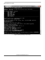
The developer's serial bootloader offers to user easiest
possible way how to update existing firmware on most of
Freescale microcontrollers in-circuit. In-circuit
programming is not intended to replace any of debugging
and developing tool but it serves only as simple option of
embedded system reprogramming via serial
asynchronous port or USB. The microcontrollers
supported by the developer's serial boot loader include
8-bit families HC08 and HCS08, and 32-bit families,
ColdFire and Kinetis. New Kinetis families include
support for K and L series.
This application note is for embedded-software
developers interested in alternative reprogramming
tools. Because of its ability to modify MCU memory
in-circuit, the serial bootloader is a utility that may be
useful in developing applications.
The developer’s serial bootloader is a complementary
utility for either demo purposes or applications originally
developed using MMDS and requiring minor
© 2013 Freescale Semiconductor, Inc. All rights reserved.
Contents
1
2
3
4
5
5
6
7
8
9
Project Objectives . . . . . . . . . . . . . . . . . . . . . . . . . . . . . . 1
FC Protocol Description. . . . . . . . . . . . . . . . . . . . . . . . . . 3
FC Protocol, Version 1, M68HC908 Implementation. . . 12
FC Protocol, Version 2, HC9S08 Implementation . . . . . 18
FC Protocol, Version 3, Large M68HC08
Implementation . . . . . . . . . . . . . . . . . . . . . . . . . . . . . . . 23
FC protocol, version 4, ColdFire (V1)
MCU Slave Software . . . . . . . . . . . . . . . . . . . . . . . . . . . 23
PC Bootloader Master Software . . . . . . . . . . . . . . . . . . 41
Bootloading Procedure Demonstration . . . . . . . . . . . . . 46
References . . . . . . . . . . . . . . . . . . . . . . . . . . . . . . . . . . 51
Project objectives
modifications to be done in-circuit. The serial bootloader offers a zero-cost solution to applications already
equipped with a serial interface and SCI pins available on a connector. This document also describes other
programming techniques:
• FLASH reprogramming using ROM routines
• Simple software SCI
• Software for USB (HC08JW, HCS08JM and MCF51JM MCUs)
• Use of the internal clock generator
• PLL clock programming
• EEPROM programming (AS/AZ HC08 families)
• CRC protection of serial protocol option
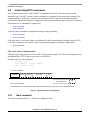
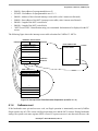
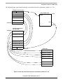
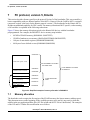
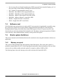
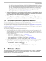
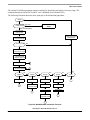
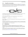
Figure 1. Top-level view
1.1
Project goals
Freescale Semiconductor M68HC08 MCUs use a standard monitor-mode interface for FLASH
programming. Configuration of monitor mode requires a specific clock and high-voltage (monitor-mode
entry voltage VTST = VDD + 2.5 = 8 V) applied to the IRQ pin upon MCU startup. Also, establishing
monitor-mode communication uses a few pins. If the application already uses a standard serial SCI
interface for communication, a different code (the bootloader) can be used to communicate with the PC
using the same interface used for reprogramming.
The bootloader can be used for only reprogramming, not for in-circuit debugging. The bootloader is a
low-cost in-circuit programming solution.
1.2
Bootloader application requirements
The following points described important parameters of the bootloader application:
• Low memory use — The bootloader must use as little memory as possible. Other versions of
bootloaders use more than 1 KB of memory, which is unacceptable on devices with 3 KB of
memory available (such as the MC68HC908JK3). The solution described in this document
Developer’s Serial Bootloader, Rev. 13
2
Freescale Semiconductor
FC protocol description
•
•
1.3
implements all features as simply as possible, excluding checksums, and so forth. The target size
is less than 500 B for the 8-bit MCUs. The USB version of bootloaders included drivers for the
communication over the USB. For this bootloaders is needed 8KB memory available (HCS08JM
and MCF51JM). The Kinetis K and L series have a similar sizes (less than 2 KB).
Low pin-count — This bootloader uses already implemented standard means of communication
(typically SCI on boards primarily intended for communication). The standard SCI uses two wires,
RxD and TxD. No additional wires are used to start bootloader.
Transparency with respect to the user S19 file — The complete application should be
transparent to the user code S19 file. This means no adjustments are required in the S19 file. Other
M68HC08, HCS08, and ColdFire V1 bootloader applications require modification to interrupt
vectors or other modifications to the S19 file for it to accept the bootloader.
Demo features of bootloader application
This document describes several different M68HC(S)08, ColdFire V1 (CFV1), and Kinetis bootloader
implementations that vary mainly because the targets M68HC(S)08, CFV1, and Kinetis MCUs have
different features. Several features of the M68HC(S)08, CFV1, and Kinetis Family are also demonstrated,
making this document useful to a wider audience than those who require only the bootloader. The different
M68HC(S)08, CFV1, and Kinetis implementations also demonstrate the following features:
• Use of built-in ROM routines for FLASH self-programming (see also AN1831, AN2545, and
AN2635 in References).
• User implementation of in-circuit reprogramming routines on ROM-less MCUs such as the
MC68HC908GP Family or the MC9S08GB/GT Family.
• Use of different implementations of the FLASH block protection technique (MC68HC908GP,
MC68HC908GR, MC68HC908EY, versus MC68HC908JK/JL Families).
• Implementation of software SCI on SCI-less MCUs, such as the MC68HC908JK/JL Family.
• Use of the internal clock generator and its trimming (for the MC68HC908KX Family), for HCS08
Families (MC9S08GB/GT).
• EEPROM programming (for the MC68HC908AB/AS/AZ Family).
• USB communication implementation on USB2.0 Full-speed HS08 MCUs, such as the
MC68HC908JW Family, HCS08JM and MCF51JM Family.
• Use implementation of flash programming routines for the HCS08 and the ColdFire (V1) devices
(see also AN3492 in References).
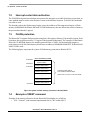
2
FC protocol description
As described in Bootloader application requirements implementation must be simple and use low memory.
Therefore, the protocol running between the master PC and slave MCU is also very simple. It is called FC
protocol because one significant character (acknowledge or ACK) 0xFC or 11111100b is used.
This section describes the protocol used to communicate between the PC and target MCU to reprogram
the MCU. An explanation of family-specific implementation features follows a general description.
Developer’s Serial Bootloader, Rev. 13
Freescale Semiconductor
3
FC protocol description
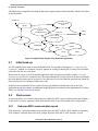
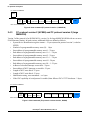
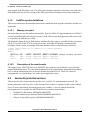
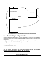
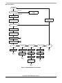
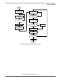
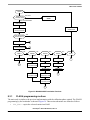
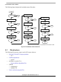
The following is a simplified state diagram that shows separate states of the bootloader, which is described
in this document:
POWER-ON
RESET SOURCE
TEST
RESET
HOOK-UP
COMMUNICATION
USER
TIME-OUT
CODE
CALIBRATION
QUIT
COMMANDS
ERASE
READ
WRITE
IDENT
Figure 2. Simplified flow diagram of the bootloader application
2.1
Initial hook-up
Several methods can be used to enter bootloader mode. Several other solutions use a “certain level on
certain pin” method. For example, if logic 0 appears on an IRQ pin during MCU startup, the bootloader
code starts else the user code starts.
Because the developer’s serial bootloader application must use the lowest number of pins, a “certain
character at a certain time” method is used. This means that the MCU sends out an ACK character through
the serial interface and waits for an answer. If no character is received within the specified time (hook-up
time-out), the process continues with the user code.
If this becomes a limitation for any reason, the user may modify the bootloader code to meet the
application needs (for example, an additional simple IRQ pin test at startup can be implemented). For more
details, see M68HC08 system limitations.
2.2
Clock source
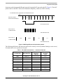
FC protocol allows two scenarios, depending on whether the MCU runs on a known and exact frequency
or uses an RC (resistor, capacitor) clock or an internal clock (or any clock unknown at compile time).
2.2.1
Unknown MCU communication speed
If the frequency is uncertain (unknown at compile time), the MCU will not check whether an incoming
ACK character conforms only to the 0xFC pattern. Because of the MCU clock tolerance, several
Developer’s Serial Bootloader, Rev. 13
4
Freescale Semiconductor
FC protocol description
characters can be interpreted differently instead of original 0xFC sent out by the PC (Figure 3). The 0xFC
pattern check on the MCU side can be eliminated completely, which saves MCU memory.
PC TRANSMITS 0XFC CHARACTER AT PROPER DATA RATE:
TIME
BOTH MCU AND PC
IDLE START
DATA RATES ARE EQUAL
D0
D1
D2
D3
D4
D5
D6
D7
STOP
IDLE
START
D0
D1
D2
D3
D4
D5
D6
D7
STOP
MCU RECEIVES 0XFC
MCU CLOCK IS
3 TIMES FASTER
MCU RECEIVES 0X00
MCU CLOCK IS
IDLE
3 TIMES SLOWER
START
D0
D1
MCU RECEIVES 0XFF
Figure 3. Matching different communication speeds
The following table shows the characters that can be correctly received (without framing or noise errors)
if transmit and receive speeds are not equal:
.
Table 1. PC to MCU transmission — unmatched data rate
PC Data Rate
MCU Data Rate
Character
Received
in Binary
Character
Received
in Hex
9600
9600*1/3
11111111b
0xFF
9600
9600*2/3
11111110b
0xFE
9600
9600*3/3
11111100b
0xFC
9600
9600*4/3
11111000b
0xF8
9600
9600*5/3
11110000b
0xF0
9600
9600*6/3
11100000b
0xE0
9600
9600*7/3
11000000b
0xC0
9600
9600*8/3
10000000b
0x80
9600
9600*9/3
00000000b
0x00
Developer’s Serial Bootloader, Rev. 13
Freescale Semiconductor
5
FC protocol description
If the MCU transmits to the PC at an unmatched data rate, the PC receives (and accepts) characters that
are different from the 0xFC character. The PC accepts all characters from the mentioned set (0xFF, 0xFE,
0xFC, 0xF8, 0xF0, 0xE0, 0xC0, 0x80, and 0x00). If a character is received, an ACK is immediately sent
back to the MCU. After the MCU recognizes this answer, it enters the next phase, Slave frequency
calibration.
2.2.2
Known MCU communication speed
If the frequency is certain (known at compile time), the MCU will be configured to match exactly the
communication speed of the PC. All characters are received correctly without any distortion.
The MCU sends 0xFC to the PC, which immediately sends an ACK to the MCU. After the ACK is
received, the MCU also (formally) enters the Slave frequency calibration phase.
2.3
Slave frequency calibration
During this phase, the MCU clock is calibrated. Until now, the PC has communicated with the MCU at a
speed that could be from 33% to 300% tolerance. During this phase, the MCU communication speed must
be adjusted to match the PC communication speed.
After the PC enters the calibration phase, the no-break timeout starts. If a correct ACK character (0xFC)
is not received within this period, a break character is sent at the communication data rate.
A break character consists of 10 consecutive logical zeros. For example, at a 9600 bd rate, its
high-low-high pulse lasts 10 x 104 s = 1.04 ms.
The MCU then measures the break character length and determines whether its clock is too fast or too slow.
The MCU then makes an adjustment to its system clock (or an adjustment of receive routines if, for
example, software serial communication is used). This can be repeated as many times as required for the
MCU to achieve the proper clock speed.
NOTE: Virtual ports workaround
Most of the users are using virtual serial ports and some of these standards
are not able to transfer break calibration character. For this reason, new
feature using zero calibration character was added in place of the break
character pulse (Figure 4). A zero calibration character consists of nine
consecutive logical zeros.
The calibration feature with zero character is implemented in master
application as “short TRIM” (checkbox “short TRIM’, Master applications
user guides). The target must be configured for using short calibration (trim)
pulse.
After the MCU is calibrated to the correct clock (or after the receive routines are calibrated), the ACK
character is sent to the PC to stop sending calibration characters (Figure 4).
Developer’s Serial Bootloader, Rev. 13
6
Freescale Semiconductor
FC protocol description
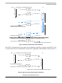
PC
ACK IS SENT AT UNCERTAIN DATA RATE
HOOK-UP TIME-OUT
zero pulse
NO-ZERO TIME-OUT
break
NO-BREAK TIME-OUT
ACK
CALIBRATION UNSUCCESSFUL
OR ONLY ROUGH CORRECTION DONE
zero pulse
CALIBRATION SUCCESSFUL
NO-BREAK TIME-OUT
ACK
NO-ZERO TIME-OUT
MCU
break
FROM NOW ON, THE COMMUNICATION IS AT THE CORRECTLY SPECIFIED DATA RATE
ACK IS SENT AT CORRECT DATARATE
ACK
ONLY 0XFC CHARACTER CAN BE RECEIVED
Figure 4. StartUp communication with calibration
PC
ACK IS SENT AT SPECIFIED DATA RATE
ACK
ACK
NO CALIBRATION REQUIRED
ACK
ACK IS SENT AT CORRECT DATA RATE
NO-BREAK TIME-OUT
MCU
HOOK-UP TIME-OUT
If the MCU is operating at the correct data rate (no calibration is possible or required, and the MCU clock
is crystal driven), the PC can immediately send an ACK, skipping the calibration phase entirely (Figure 2).
CORRECT 0xFC CHARACTER IS RECEIVED WITHIN TIME-OUT
Figure 5. Start-Up communication without calibration
Developer’s Serial Bootloader, Rev. 13
Freescale Semiconductor
7
FC protocol description
2.4
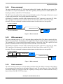
Interpreting MCU commands
After communication between MCU and PC is established, then MCU enters the main command
interpreter loop. The MCU executes simple commands to reprogram its own nonvolatile memory. The
communication is conducted on a master-slave mechanism: the PC issues the commands, the MCU
executes them and acknowledges the completion of each command either by data or single ACK character.
The minimal set of commands is composed of:
• Ident command
• Quit command
Two more basic commands are implemented for pure reprogramming:
• Erase command
• Write command
If the user needs a verification feature, one additional (read) command must be compiled into the MCU
code. This command is not required for pure reprogramming purposes (minimal configuration).
• Read command
CRC safety protocol implementation
The protocol provides option to switch on CRC safety for all messages. For CRC is used standard 16 bit
implementation CCITT16 and as reset value is used 0xFFFF.
Example value for erase command:
'E'-1byte - 0x45
'start address' - 2 bytes - 0x1234
'CRC - 2 bytes' - 0x2907
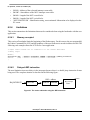
PC TO MCU COMMAND
COMMAND
ADDRESS
LENGTH
DATA TO MCU
CRC
DATA FROM MCU
CRC
MCU TO PC RESPONSE
* Dashed fields are not always implemented, data from the MCU may contain only an ACK character instead.
Figure 6. Typical command and response
2.4.1
Ident command
The ident command (coded as ‘I’, $49) has no additional fields.
Developer’s Serial Bootloader, Rev. 13
8
Freescale Semiconductor
FC protocol description
This command is immediately issued by the PC after communication is established. The purpose of the
ident command is to notify the PC about several basic properties of the MCU being programmed. All
multibyte fields are sent with MSB first.
• Version number and capability table - 1 byte
BIT
7
RCS
6
CRCS
5
4
RESERVED
3
2
1
0
VERSION NUMBER
Figure 7. Version number and capability table
•
•
•
•
2.4.2
RCS - The Read Command Supported (RCS) flag informs the PC if the read command is supported
(implemented). If not, all calls to the read routine are ignored by the MCU and no response is sent
back to the PC. The PC software warns the user that no read capabilities are available.
• Supported - Not supported (usually due to memory constraints)
CRCS - The CRC Serial Protocol Supported flag informs the PC that all rest communication
(including Ident command) is secured by CRC-CCITT checksum.
• Supported1 - Not supported (usually due to memory constraints)
RSVD - These bits are reserved for future use, unused, and should be set to 0.
VER — Protocol Version
FC protocol version 1 (M68HC08)
Version 1 of the protocol is for M68HC08 MCUs. Additional fields in version 1 are defined as follows:
• Start address of reprogrammable memory area - 2 bytes.
• End address of reprogrammable memory area + 1 - 2 bytes.
• Address of Bootloader user table - 2 bytes.
• Start address of MCU interrupt vector table - 2 bytes.
• Length of MCU erase block - 2 bytes.
• Length of MCU write block - 2 bytes.
• Bootloader data (specific bootloader information, see device-specific implementation; compared
in Table 2) - 8 bytes.
• Identification string, zero terminated - <n> bytes.
• If the CRC capability of serial protocol is enabled, then follows CRC-CCITT checksum - 2 bytes.
1.Available since Q3 2011
Developer’s Serial Bootloader, Rev. 13
Freescale Semiconductor
9
FC protocol description
PC TO MCU COMMAND
I ($49)
VERSION
AND
CAPS.
START
END
BOOTLOADER
MEM
MEM
USER TABLE
INTERRUPT
ERASE
VECTOR TABLE BLOCK SIZE
WRITE
BLOCK SIZE
BOOTLOADER
DATA
ID STRING
0
CRC
MCU TO PC RESPONSE
Figure 8. Ident command (FC protocol version 1, M68HC08)
2.4.3
FC protocol version 2 (HCS08) and FC protocol version 3 (large
M68HC08)
Version 2 of the protocol is for HCS08 MCUs; version 3 is for large M68HC08 (HC08 with two or more
FLASH memory banks). In both versions, additional fields are defined as follows:
• System device Identification register content — 2 bytes (unused in protocol version 3, coded as
$FFFF)
• Number of reprogrammable memory areas (N) - 1 byte
• Start address of reprogrammable memory area #1 - 2 bytes
• End address of reprogrammable memory area #1 + 1 - 2 bytes
• Start address of reprogrammable memory area #2 - 2 bytes
• End address of reprogrammable memory area #2 + 1 - 2 bytes
• Start address of reprogrammable memory area #N - 2 bytes
• End address of reprogrammable memory area #N + 1 - 2 bytes
• Address of relocated interrupt vector table - 2 bytes
• Start address of MCU interrupt vector table - 2 bytes
• Length of MCU erase block - 2 bytes
• Length of MCU write block - 2 bytes
• Identification string, zero terminated - <n> bytes
• If the CRC capability of serial protocol is enabled, then follows CRC-CCITT checksum - 2 bytes
PC TO MCU COMMAND
I ($49)
VERSION
AND
CAPS.
SDID
#
START
END
OF MEM
MEM #1
MEM #1
...
RELOCATED INTERRUPT ERASE
WRITE
ID
VECTOR TABLE VECTOR TABLE BLOCK SIZE BLOCK SIZE STRING
0
CRC
MCU TO PC RESPONSE
Figure 9. Ident command (FC protocol versions 2 and 3, HCS08)
Developer’s Serial Bootloader, Rev. 13
10
Freescale Semiconductor
FC protocol description
2.4.4
Erase command
The erase command (coded as ‘E’, $45) has only address field, length or data fields are not present. The
start address is a 2-byte field, MSB first. If the CRC capability of serial protocol is enabled, then the 16
bits(2 bytes) follows with CRC-CCITT checksum.
The MCU erases the address block where the specified address resides. The length of block to be erased
is equal to the erase-block size (typically depends on hardware).
After the MCU completes execution of the command, the ACK ($FC) character is sent to the PC. If the
CRC capability of serial protocol is enabled, then the 16 bits(2 bytes) follows with CRC-CCITT
checksum. The erase command’s minimum and maximum execution times are not specified.
PC TO MCU COMMAND
E ($45)
START
CRC
ADDRESS
COMMAND EXECUTION
MCU TO PC RESPONSE
ACK
CRC
Figure 10. Erase command
2.4.5
Write command
The write command (coded as ‘W’, $57) has both address and data fields. The address contains the first
address to be programmed. The first byte is the length followed by the number of bytes to be programmed.
The start address is a 2-byte field, MSB first and the length is a 1-byte field. If the CRC capability of serial
protocol is enabled, then the 16 bits(2 bytes) follows with CRC-CCITT checksum.
After the MCU completes execution of the command, the ACK ($FC) character is sent to the PC. If the
CRC capability of serial protocol is enabled, then the 16 bits(2 bytes) follows with CRC-CCITT
checksum. The write command’s minimum and maximum execution times are not specified.
PC TO MCU COMMAND
W ($57)
START
ADDRESS
LENGTH
BINARY DATA
CRC
COMMAND EXECUTION
MCU TO PC RESPONSE
ACK
CRC
Figure 11. Write command
2.4.6
Read command
The read command (coded as ‘R’, $52) has address and data fields. The address contains the first address
to be programmed; the single byte is the length of data to be read. The start address is a 2-byte field, MSB
first and the length is a 1-byte field. If the CRC capability of serial protocol is enabled, then the 16 bits(2
bytes) follows with CRC-CCITT checksum.
Developer’s Serial Bootloader, Rev. 13
Freescale Semiconductor
11
FC protocol, version 1, M68HC908 implementation
The MCU sends this number of read bytes to the PC. If the CRC capability of serial protocol is enabled,
then the 16 bits(2 bytes) follows with CRC-CCITT checksum.
PC TO MCU COMMAND
R ($52)
START
ADDRESS
LENGTH
CRC
BINARY DATA
MCU TO PC RESPONSE
CRC
Figure 12. Read command
2.4.7
Quit command
The quit command (coded as ‘Q’, $51) has no address or data fields. Execution of bootloader code is
immediately finished, and the user code is started. No ACK ($FC) character is sent to the PC.
PC TO MCU COMMAND
Q ($51)
CRC
MCU TO PC RESPONSE
<NO RESPONSE>
Figure 13. Quit command
2.4.8
Bootloader user table
The bootloader user table is a reprogrammable memory area intended for storage of bootloader-specific
data. This memory area is unavailable for the user program. For this table’s memory allocation, refer to
FC protocol, version 1, M68HC908 implementation.
3
FC protocol, version 1, M68HC908 implementation
This section describes features specific to the M68HC908 bootloader implementation. The memory
allocation is heavily MCU specific, so the meaning of all variables is explained in this section in detail.
Figure 14 shows the typical memory allocation for M68HC908 MCUs with the bootloader
preprogrammed. For example, the MC68HC908KX8 MCU memory map includes:
• 7680 bytes of FLASH memory ($E000–$FDFF)
• 192 bytes of random-access memory (RAM) ($0040–$00FF)
• 36 bytes of user-defined vectors ($FFDC–$FFFF)
Developer’s Serial Bootloader, Rev. 13
12
Freescale Semiconductor
FC protocol, version 1, M68HC908 implementation
0xFFFF
INTERRUPT VECTOR TABLE
0xFFDC
UNIMPLEMENTED AREA
0xFE00
THIS AREA OF FLASH IS PROTECTED
USING FLBPR REGISTER
BOOTLOADER CODE
0xFCC0
BOOTLOADER USER TABLE
0xFC80
FLASH MEMORY AVAILABLE
ON MC68HC908KX8 MCU
FLASH MEMORY AVAILABLE
FOR USER CODE
FREE MEMORY AREA
FOR USER CODE
0xE000
UNIMPLEMENTED AREA
0x0100
RAM
0x0040
I/O REGISTERS
0x0000
Figure 14. Simplified example of memory allocation in MC68HC908KX8
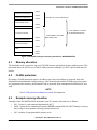
3.1
Memory allocation
The bootloader code occupies the top-end of FLASH memory (the highest memory address space). This
placement allows an effective use of the FLASH block protection technique (see the specific MCU data
sheet for details).
3.2
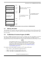
FLASH Block Protection Register (FLBPR)
By setting a FLBPR (FLASH block protection register), all address space above this address is protected
from intentional and unintentional erasing/rewriting. After both bootloader and FLBPR register are
programmed into memory, the bootloader code is protected from unintentional modification by user code.
NOTE
Some M68HC908 MCUs have an FLBPR register in RAM instead of
FLASH (for example, the MC68HC908JK/JL Families). The bootloader
code sets this register properly but the user code can eventually modify
FLBPR and erase/write the bootloader code. See FLBPR not usable (in
some M68HC08 family MCUs).
For example, the MC68HC908KX8 bootloader to the PC memory allocation is:
• $01 - Version 1, read command not implemented (bit 7).
• $E000 - Start address of reprogrammable memory area.
• $FC80 - End address of reprogrammable memory area + 1.
Developer’s Serial Bootloader, Rev. 13
Freescale Semiconductor
13
FC protocol, version 1, M68HC908 implementation
•
•
•
•
•
•
3.3
$FC80 - Address of Bootloader user table.
$FFDC - Start address of MCU interrupt vector table.
$0040 - Length of MCU erase block.
$0020 - Length of MCU write block.
0,0,0,0,0,0,0,0 - Bootloader data. No strictly defined syntax; different M68HC08 implementations
provide different values (for example, the sixth value in the MC68HC908KX8 implementation is
the value of the internal clock generator [ICG] trim register after calibration). All these bootloader
data are then programmed back into the bootloader user table and can be retrieved during all
subsequent starts (for example, to trim the MCU’s ICG to the best-known value before user code
start).
‘KX8-IR’,0 - Identification string, zero terminated. Information to be displayed on PC screen.
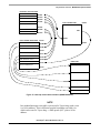
Interrupt vector table relocation
Because the FLASH block protection technique also protects the interrupt vector table from being
overwritten, some method must be used to relocate these vectors to the different locations. To do this, the
bootloader user table is used. It is a part of memory not protected by the FLBPR, but it is unavailable to
the user program. All standard interrupt vectors are pointing to this table where JMP instructions are
expected to be stored for each interrupt. The only exception is the reset vector that points to the bootloader
code start. When an interrupt occurs, the vector is fetched from protected memory and directs execution
to continue at the corresponding JMP instruction in the bootloader user table.
The following figure shows interrupt vector table relocation for M68HC08 MCUs.
Developer’s Serial Bootloader, Rev. 13
14
Freescale Semiconductor
FC protocol, version 1, M68HC908 implementation
INTERRUPT VECTOR TABLE
RESET VECTOR
0xFFFE
INTERRUPT VECTOR 1
0xFFEC
INTERRUPT VECTOR 2
0xFFEA
INTERRUPT VECTOR 3
0xFFE8
BOOTLOADER CODE
0xFE00
...
0xFFE0
INTERRUPT VECTOR 16
0xFFDE
INTERRUPT VECTOR 17
EXIT
...
0xFFDC
START
BOOTLOADER USER TABLE 0xFCC0
JMP USER INT. VECT. 17
0xFD00
0xFCBB
JMP USER INT. VECT. 16
0xFCB8
...
0xFC84
JMP USER INT. VECT. 3
0xFC81
JMP USER INT. VECT. 2
0xFC8E
JMP USER INT. VECT. 1
0xFC8B
JMP USER RESET VECTOR
0xFC88
USER CODE
START (RESET)
BOOTLOADER DATA
0xFC80
INTERRUPT ROUTINE 1
INTERRUPT ROUTINE 2
...
INTERRUPT ROUTINE 16
INTERRUPT ROUTINE 17
Figure 15. Interrupt vector table relocation (M68HC08 MCUs)
NOTE
In a standard interrupt vector table, each record is 2 bytes long (each vector
is a 16-bit address). This is different from the bootloader user table, for
which each record is 3 bytes long - a JMP opcode ($CC) plus a 16-bit
address.
Developer’s Serial Bootloader, Rev. 13
Freescale Semiconductor
15
FC protocol, version 1, M68HC908 implementation
3.3.1
S19 file
Because the bootloader operation must be transparent to the user S19 file, another piece of intelligence is
built into the PC master code (instead of the MCU slave). The relocation works as follows:
If the data from an S19 record corresponds to an address in the interrupt vector table, the value is relocated
into the corresponding area in the bootloader user table, including a JMP instruction (opcode $CC). For
example, if the user S19 file contains #3 interrupt vector $E123 at address $FFE8, such a vector is
relocated into the sequence $CC, $E1, $23 (JMP $E123) programmed to the $FC81 address in the
bootloader user table.
Using this method, the user S19 file does not need to be modified, but the lower address of the end of
FLASH memory must be considered. In addition, this JMP instruction (3T) delays every interrupt, as
explained in Each interrupt 3T delayed.
3.4
User code start
The user code is started in an unusual way to provide a register setup similar to how it appears after MCU
reset.
3.4.1
Software reset
If the bootloader must quit and run user code, an illegal operation is intentionally executed (M68HC08
illegal opcode $32). This causes an illegal operation reset, and the MCU restarts. During bootloader
startup, the System Integration Module (SIM) Reset Status Register (SRSR) is tested. If a power-on-reset
is not detected, the user code is started instead of the bootloader code. This allows the transparent operation
of all other resets (such as illegal address, and so forth) with only a short additional delay caused by testing
the SRS register and executing associated jump instructions.
3.4.2
Hardware reset
In some implementations, a pin reset (caused by external reset pin) is also included as a valid source of
reset for the bootloader to start. This allows remote in-circuit reprogramming in embedded applications
able to drive the M68HC08 reset pin.
Another test has been added to the real bootloader application: if no reset source is detected (that is, if the
SRS register is 0), the bootloader is selected by default. This may happen when an external pin causes
reset, but the reset pulse is shorter than specified. In that case, the minimum length of reset pulse that will
cause reset is shorter than the length needed for the proper propagation of the external reset flag to the SRS
register.
Because the SRS register is one-time readable (it clears after read), no subsequent reads of this register
provide a valid value. See M68HC08 system limitations for details.
Developer’s Serial Bootloader, Rev. 13
16
Freescale Semiconductor
FC protocol, version 1, M68HC908 implementation
3.5
M68HC08 system limitations
This section summarizes limitations that must be considered when using the bootloader with the user
application.
3.5.1
Memory occupied
One of the most important requirements is to use the smallest code possible. Typical M68HC908
implementations are between 300 to 500 bytes, including the bootloader user table. If the target M68HC08
MCU is capable of FLASH programming using internal ROM routines, the memory consumption is near
the lower limit. Larger M68HC08 MCUs (which are not usually equipped with ROM code for FLASH
programming) will require approximately 500 bytes of FLASH of the total 32 KB (as is the case with the
MC68HC908GP32).
The bootloader is placed at the upper end of FLASH memory; therefore, the only modification required in
the user code is in the memory mapping (typically found in the linker parameter file).
The M68HC08 MCU signals the actual available FLASH addresses. The PC Bootloader software will not
allow programming if the user code overlaps with bootloader code.
3.5.2
Time delay upon startup and initial communication
The number of pins with specific meanings during bootloader startup must be as small as possible.
Especially in communication systems (for example, those using a standard serial port), pin overhead is
zero and a “certain level character at a certain time” method is used. So, the bootloader waits a certain
amount of time to receive an answer from the PC at startup. If none is received, the user code starts. The
typical delay is in the range of several hundred milliseconds.
If this startup delay becomes an issue for the final application, the user may modify the bootloader code
and use a “certain level on a certain pin” method instead. A simple test of the voltage level on the IRQ pin
(or any other input pin) can be used to indicate whether the bootloading sequence is required.
3.5.3
Each interrupt 3T delayed
Every interrupt call is delayed by 3T bus clocks required to execute the JMP instruction stored in the
bootloader user table. This interrupt vector relocation (as described in Interrupt vector table relocation) has
been chosen as the best solution for achieving user code transparency and security of the bootloader code.
The interrupt latency is about 10 to 15T (assuming that no interrupt is being executed), so this additional
delay is not significant for the most applications.
3.5.4
FLBPR not usable (in some M68HC08 family MCUs)
The bootloader uses a FLASH block protection technique to protect itself from being overwritten (where
applicable; see FLASH Block Protection Register (FLBPR) for details).
Some M68HC08 MCUs (such as the KX, GP, and GR devices) have this FLASH block protection register
stored in FLASH, so it cannot be modified in user mode. The FLBPR can be erased or programmed only
Developer’s Serial Bootloader, Rev. 13
Freescale Semiconductor
17
FC protocol, version 2, HC9S08 implementation
with an external voltage, VTST, present on the IRQ pin (normal monitor mode). Because this feature is
completely dedicated to bootloader code protection, it is unavailable to the user application code. If the
value for FLPBR appears in the user S19 code, a warning is displayed. Such an occurrence should be
omitted from user S19 code.
Some families have the FLASH block protection register stored in RAM instead (the MC68HC908JK/JL
Families are like this). The bootloader sets the correct value at the beginning of its execution to protect
itself. However, user code can modify this register and protect its own memory areas as needed. This also
implies that the bootloader is not 100% protected from user code.
See the specific MCU data sheet for a detailed explanation.
3.5.5
SRS register unusable
The bootloader uses an SRS register (as described in User code start) to recognize the reset source to
determine whether the user code will run. Because the SRS register is one-time readable (that is, it is reset
after first read), the user code does not have access to the SRS register value (if the bootloader is present
in the memory and makes the first read after each reset). There is no simple solution for this situation. After
the SRS register is read by the bootloader, it is stored in one RAM location. Its memory location may differ
from one implementation to another. If the application requires the SRS register and bootloader, the user
must redirect the SRSR reading to this specific RAM location. This location can be obtained from the
bootloader’s MAP file.
4
FC protocol, version 2, HC9S08 implementation
This section describes features that are specific to the HC9S08 bootloader implementation. The memory
allocation is heavily MCU specific so the meaning of variables is explained in this section.
Figure 16 shows the memory allocation typical to the HC9S08 devices with the bootloader
preprogrammed. For example, the MC9S08GB/GT60 device memory map includes:
• 60 KB of FLASH memory ($1080–$17FF, $182C–$FFAF)
• 4 KB of random-access memory (RAM) ($0080–$107F)
• 16 bytes of nonvolatile registers ($FFB0–$FFBF)
• 64 bytes of user-defined vectors ($FFC0–$FFFF)
Developer’s Serial Bootloader, Rev. 13
18
Freescale Semiconductor
FC protocol, version 2, HC9S08 implementation
0xFFFF
INTERRUPT VECTOR TABLE
0xFFC0
NONVOLATILE REGISTERS
0xFFB0
THIS AREA OF FLASH IS PROTECTED
BOOTLOADER CODE
0xFE00
RELOCCTOR TABLE
0xFDC0
FLASH MEMORY AVAILABLE
ON MC9S08GB/GT60 MCU
FLASH 58772 BYTES
0x182C
FLASH MEMORY AVAILABLE
FOR USER CODE
HIGH PAGE REGISTERS
0x1800
FLASH 1920 BYTES
0x1080
RAM
0x0080
I/O REGISTERS
0x0000
Figure 16. Simplified example of memory allocation in MC9S08GB/GT60
4.1
Memory allocation
The bootloader code occupies the top-end of FLASH memory (the highest memory address space). This
placement allows an effective use of the FLASH protection technique (see MCU specific data sheet for
details).
4.2
FLASH protection
By setting a FLASH protection register, all address space above this address is protected from both
intentional and unintentional erasing/rewriting. After the bootloader and the FLASH protection register
are programmed into memory, the bootloader code is protected from unintentional modification by user
code.
NOTE
See FLASH protection technique not usable for limitations.
4.3
Example memory allocation
Examples of the MC9S08GB/GT60 bootloader to the PC memory allocation are as follows:
• $82 - Version 2, read command implemented (bit 7)
• $r002 - System device identification register (SDIDR) content ($002 for GB/GT Family, r (four top
bits) is chip revision number reflecting current silicon level
• $02 - Number of reprogrammable memory areas
Developer’s Serial Bootloader, Rev. 13
Freescale Semiconductor
19
FC protocol, version 2, HC9S08 implementation
•
•
•
•
•
•
•
•
•
4.4
$1080 - Start address of reprogrammable memory area #1
$1800 - End address of reprogrammable memory area #1 + 1
$182C - Start address of reprogrammable memory area #2
$FDC0 - End address of reprogrammable memory area #2 + 1
$FDC0 - Address of relocated interrupt vector table
$FFC0 - Start address of MCU interrupt vector table
$0200 - Length of MCU erase block
$0040 - Length of MCU write block
‘GB/GT60’,0 - Identification string, zero terminated. Information to be displayed on PC screen
Interrupt vector table relocation
The reset and interrupt vectors would be protected if the flash protection is enabled. Vector redirection
(HCS08 hardware feature) allows the user to modify memory allocation of interrupt vector information.
Vector redirection is enabled by programming the NVOPT (nonvolatile option) register. For redirection to
occur, at least some portion but not all of the FLASH memory must be block-protected by programming
the NVPROT (nonvolatile protection) register. All the interrupt vectors (memory locations
$FFC0–$FFFD) are redirected except the reset vector ($FFFE:FFFF).
For example, if 512 bytes of FLASH are protected, the protected address region is from $FE00 through
$FFFF. The interrupt vectors ($FFC0–$FFFD) are redirected to the locations $FDC0–$FDFD.
For example, if an SPI interrupt is taken, the values in the locations $FDE0:FDE1 are used for the vector
instead of the values in the locations $FFE0:FFE1. This allows the user to reprogram the unprotected
portion of the FLASH with new program code, including new interrupt vector values while leaving the
protected area, which includes unchanged default vector locations.
4.4.1
S19 file
Because bootloader operation must be transparent to the user S19 file, another piece of intelligence is built
into the PC master code (instead of the MCU slave). If the record in the interrupt vector table is detected
in the user S19 file, the vector is relocated into the corresponding area in the relocated interrupt vector
table. For example, if the user S19 file contains #2 interrupt vector at address $FFEA, such a vector is
relocated to the $FDEA address in the relocated interrupt vector table.
Using this method, the user S19 file does not need to be modified, but the lower address of the end of
FLASH memory must be considered.
The following figure illustrates HC9S08 interrupt vector table relocation:
Developer’s Serial Bootloader, Rev. 13
20
Freescale Semiconductor
FC protocol, version 2, HC9S08 implementation
INTERRUPT VECTOR TABLE
RESET VECTOR (bootloader start)
0XFFFE
BOOTLOADER CODE
0XFFB0
START
original interrupt vector table
is empty (unused)
its content is relocated
EXIT
0XFFC0
0XFE00
RELOCATED INTERRUPT VECTOR TABLE
RESET VECTOR
INTERRUPT VECTOR 1
INTERRUPT VECTOR 2
INTERRUPT VECTOR 3
0XFDFE
0XFDEC
0XFDEA
0XFDE8
...
0XFDC4
INTERRUPT VECTOR 30
INTERRUPT VECTOR 31
0XFDC2
0XFDC0
USER CODE
START (RESET)
INTERRUPT ROUTINE 1
INTERRUPT ROUTINE 2
...
INTERRUPT ROUTINE 30
INTERRUPT ROUTINE 31
Figure 17. Interrupt vector table relocation explanation (HCS08)
4.5
User code start
To provide a register setup similar to how it appears after MCU reset, the user code is started in an unusual
way.
4.5.1
Software reset
If the bootloader must quit and run user code, an illegal operation is intentionally executed (HCS08 illegal
opcode $8D). This causes an illegal operation reset and the MCU restarts. During bootloader startup, the
System Reset Status (SRS) register is tested. If a power-on-reset is not detected, the user code starts instead
Developer’s Serial Bootloader, Rev. 13
Freescale Semiconductor
21
FC protocol, version 2, HC9S08 implementation
of the bootloader code. This allows the transparent operation of all other resets (such as illegal address and
so forth) with only a small additional delay caused by testing of the SRS register and executing associated
jump instructions.
4.5.2
Hardware reset
In some implementations, pin reset (caused by external reset pin) is a valid source of reset for the
bootloader to start. This allows remote in-circuit reprogramming in embedded applications that are able to
drive the HCS08 MCU reset pin.
4.6
HCS08 system limitations
This section summarizes limitations that must be considered when using the bootloader with the user
application.
4.6.1
Memory occupied
One of the strongest requirements is to use the smallest possible code. Typical HC9S08 implementations
are 432 bytes (minimal memory size that can be protected) plus another 64 bytes page for relocated
interrupt vector table.
The bootloader is placed at the upper-end of FLASH memory, therefore, the only modification required in
the user code is in the memory mapping (typically found in the linker parameter file).
The HCS08 MCU signals the actual FLASH addresses available. The PC Bootloader software will warn
before programming if the user code overlaps with bootloader code.
4.6.2
Time delay upon startup and initial communication
The number of pins with specific meaning during bootloader startup must be as small as possible.
Especially in communication systems (for example, those using a standard serial port), pin overhead is
zero and a “certain character at a certain time method” is used. So, the bootloader waits a certain amount
of time to receive an answer from the PC at startup. If none is received, the user code starts. The typical
delay is the range of several hundred milliseconds.
If this startup delay becomes an issue for the final application, the user may modify the bootloader code
and use a “certain level on certain pin” method. A simple test of the voltage level on the IRQ pin (or any
other input pin) can be used to decide whether the bootloading sequence is required.
4.6.3
FLASH protection technique not usable
The bootloader uses a FLASH block protection technique to protect itself from being overwritten,
therefore, this feature is not available for the user code. This includes FLASH memory security-related
registers (namely NVPROT, NVOPT, and NVBACKKEY) used for protection and interrupt-vector
relocation by bootloader.
Developer’s Serial Bootloader, Rev. 13
22
Freescale Semiconductor
FC protocol, version 3, large M68HC08 implementation
5
FC protocol, version 3, large M68HC08
implementation
This section describes features specific to the protocol version 3 of the bootloader. This is intended for
large HC08s (with two or more FLASH memory banks or, more precisely, with two or more separated
FLASH memory areas). The format of the Ident command from version 2 is used; the rest remains same
as with protocol version 1 (HC08) namely Interrupt vector table relocation.
6
FC protocol, version 4, ColdFire (V1)
The protocol version 4 is divided into two versions, version A and version B. The main reason for this
separation is the possibility of protecting the bootloader source code. This feature is important for flash
programming because protection of the bootloader prevents the source code from being erased. The
implementation of version A bootloader is not protected where as the version B implementation is
protected.
6.1
Version A (unprotected version)
This section describes the features that are specific to Cold Fire V1 implementation version A. The
memory allocation is MCU specific, so the meaning of all variables is explained in this section.
Figure 18 shows the memory allocation typical to the ColdFire V1 devices with the bootloader
preprogrammed. For example, the MCF51JM128 device memory map includes:
• 128 KB of FLASH memory ($00000000-$0001FFFF)
• 16 KB of random access memory (RAM) ($00800000-$00803FFF)
• 16 bytes of nonvolatile registers ($00000400-$0000040F)
• 444 bytes of user-defined vectors ($00000000-$000001B8)
Developer’s Serial Bootloader, Rev. 13
Freescale Semiconductor
23
FC protocol, version 4, ColdFire (V1)
0x0001FFFF
BOOTLOADER
0x001FB000
USER FLASH 120 KB
Nonvolatile registers
INIT_SP RESET_APP
FLASH MEMORY AVAILABLE
FOR USER CODE
FLASH MEMORY AVAILABLE
ON MCF51JM128
0x00000410
0x00000400
Flash memory
0x000001C0
INTERRUPT VECTOR TABLE
INIT_SP
RESET_BL
0x00000000
Figure 18. Simplified Example of Memory Allocation in MCF51JM128
6.1.1
Memory allocation
The bootloader code occupies the top of the FLASH memory (the highest memory address space). This
placement reduces only the top of the memory space and it is necessary to modify the end of the user
application LCF file; see Memory occupied.
6.1.2
FLASH protection
This version of MCU supports a flash protection technique from the beginning of the memory, from
address 0x0, for 2 KB sectors.
Flash protection is not implemented in the version A of the protocol, because this version uses the original
vector table at address 0x0 for placement of the user vector table.
6.1.3
Example of IDENT command
Example of the memory allocation for the ColdFire (V1) bootloaders are as follows:
• $84 - Version 4, read command implemented (bit 7)
• $rC16 - System Device Identification Register (SDIDR) content ($C16 for JM Family), r (four top
bits) is the chip revision number reflecting the current silicon level
• $02 - Number of reprogrammable memory areas
• $00000 - Start address of reprogrammable area #1
• $003FF - End address of reprogrammable area #1 + 1
Developer’s Serial Bootloader, Rev. 13
24
Freescale Semiconductor
FC protocol, version 4, ColdFire (V1)
•
•
•
•
•
•
•
$00410 - Start address of reprogrammable area #2
$1FAFF - End address of reprogrammable area #2 + 2
$00000 - Address of the relocated interrupt vector table (value 0 means not allocated)
$00000 - Start address of the MCU interrupt vector table (value 0 means not allocated)
$00400 - Length of the MCU erase blocks
$00080 - Length of the MCU write blocks
‘MCF51xxxx/USB’ - Identification string, zero terminated. Information to be displayed on the PC
screen
The following figure shows the interrupt vector table relocation for ColdFire V1 MCUs:
INTERRUPT VECTOR TABLE
0X00000000
RESET Bootloader 0X00000004
INIT SP
BOOTLOADER CODE
INTERRUPT VECTOR 3
INTERRUPT VECTOR 4
0x1FAFF
Bootloader START
INTERRUPT VECTOR 5
...
INTERRUPT VECTOR 110
INTERRUPT VECTOR 111
RESET APP
INIT SP
0x000001BC
0x000001C0
EXIT
0x1FFAF
USER CODE
INTERRUPT ROUTINE 111
INTERRUPT ROUTINE 110
...
INTERRUPT ROUTINE 5
INTERRUPT ROUTINE 4
INTERRUPT ROUTINE 3
START APP
Figure 19. Interrupt Vector Table Relocation Explanation (ColdFire V1 - A)
6.1.4
Software reset
If the bootloader must quit and run user code, an illegal operation is intentionally executed (ColdFire
illegal opcode stop #0). This causes an illegal operation reset and the MCU restarts. During bootloader
startup, the system reset status register (SRS) is tested. If a power-on-reset is not detected, the user code
Developer’s Serial Bootloader, Rev. 13
Freescale Semiconductor
25
FC protocol, version 4, ColdFire (V1)
starts instead of the bootloader code. This allows the transparent operation of all other resets with only a
short additional delay caused by testing of the SRS register and executing associated jump instruction.
6.1.5
ColdFire system limitations
This section summarizes the limitations that must be considered when using the bootloader with the user
application.
6.1.5.1
Memory occupied
One major thing is to use the smallest code possible. Typical ColdFire V1 implementations are 1 KB (SCI
version) and 8 KB (USB version for JM version). For the USB version, the biggest part of the source code
is occupied by the USB drivers (5 KB).
The bootloader limits the top of flash memory, and therefore there must be a modified Linker Command
File (LCF) user file. If the LCF file is not set correctly, bootloader will display a warning and the
bootloader will be erased. An example of the modification is shown in the following code block:
# Sample Linker Command File for CodeWarrior for ColdFire MCF51JM128
# Memory ranges
MEMORY {
vectors
(RX) : ORIGIN = 0x00000000, LENGTH = 0x00000200
application (RX) : ORIGIN = 0x00000410, LENGTH = 0x0001ABEF //example of memory allocation
buffer
(RWX) : ORIGIN = 0x00800000, LENGTH = 0x00000100
userram
(RWX) : ORIGIN = 0x00800100, LENGTH = 0x00003F00
}
6.1.5.2
Description of the reset transfer
The original vector 1(INIT SP) and vector 2(RESET) are rewritten to the bootloader’s reset and stack
pointer initialization values. The value of the beginning of the user application is programmed into address
0x1C0, and the initialization value of the stack pointer into address 0x1C4. These two values are
reprogrammed every bootloading cycle to the current application values.
6.2
Version B (protected version)
This section describes features that are specific to the Cold Fire V1 implementation version B. The
memory allocation is MCU specific, so the meaning of all variables is explained in this section in detail.
Figure 20 shows the memory allocation typical to the ColdFire V1 devices with the bootloader
pre-programmed. For example, the MCF51JM128 device memory map includes:
• 128 KBof FLASH memory ($00000000-$0001FFFF)
• 16 KB of random access memory (RAM) ($00800000-$00803FFF)
• 16 bytes of nonvolatile registers ($00000400-$0000040F)
Developer’s Serial Bootloader, Rev. 13
26
Freescale Semiconductor
FC protocol, version 4, ColdFire (V1)
0x0001FFFF
FLASH MEMORY AVAILABLE
FOR USER CODE
FLASH 120 KB
FLASH MEMORY AVAILABLE
ON MCF51JM128
0x00003800
RELOCATED INTERUPT
VECTOR TABLE
0x00003000
BOOTLOADER CODE
Nonvolatile registers
INTERRUPT VECTOR TABLE
0x00000410
THIS AREA OF FLASH
IS PROTECTED
0x00000400
0x00000000
Figure 20. Simplified example of memory allocation in MCF51JM128 version B
6.2.1
Memory allocation
The bootloader code occupies the bottom of FLASH memory in the range 0x0410 to 0x3000 above the
original interrupt vector table. This placement moves the start of memory space and for that reason it is
necessary to modify the LCF file (see the MCU specific data sheet for details).
6.2.2
FLASH protection
By setting a FLASH protection register (FPROT), all address space under this address is protected from
both intentional and unintentional erasing/rewriting. After the bootloader and the FLASH protection
register are programmed into memory, the bootloader code is protected from unintentional modification
by user code.
6.2.3
Example memory allocation
For example, the memory allocation for the ColdFire (V1) bootloaders is:
• $84 - Version 4, read command implemented (bit 7).
• $rC16 - System Device Identification Register (SDIDR) content ($C16 for the JM Family), r (four
top bits) is chip revision number reflecting the current silicon level.
• $01 - Number of reprogrammable memory areas.
• $03800 - Start address of the reprogrammable area.
• $1FFFF - End address of the reprogrammable area +1.
Developer’s Serial Bootloader, Rev. 13
Freescale Semiconductor
27
FC protocol, version 4, ColdFire (V1)
•
•
•
•
•
$03000 - Address of the relocated interrupt vector table.
$001BC - Start address of the MCU interrupt vector table.
$00400 - Length of the MCU erase blocks.
$00080 - Length of the MCU write blocks.
‘MCF51JM128/USB’ - Identification string, zero terminated. Information to be displayed on the
PC screen.
6.2.4
Limitations
This section summarizes the limitations that must be considered when using the bootloader with the user
application.
6.2.4.1
Memory occupied
This version of bootloader limits the beginning of the flash memory. For this reason, the user must modify
the Linker Command File (LCF) and the boundary of the user flash start is moved to address 0x3800. The
following code example shows the LCF file for a user application.
# Sample Linker Command File for CodeWarrior for the ColdFire MCF51JM128
# Memory ranges
MEMORY {
application (RX) : ORIGIN = 0x00003800, LENGTH = 0x0001C7FF //memory allocation
userram
(RWX) : ORIGIN = 0x00800000, LENGTH = 0x00003FFF
}
6.2.4.2
Delayed JMP instruction
The next limitation increases delays in the interrupts because there is a double jump instruction feature
being used. The complete situation is described in the following figure:
0x6000
JMP + address
IRQ INTERUPT
0x3180
0x00000100
0x4EF9 0x6000
IRQ interrupt
routine
0x00003180
Figure 21. The vector redirection using the JMP instruction
Developer’s Serial Bootloader, Rev. 13
28
Freescale Semiconductor
FC protocol, version 4, ColdFire (V1)
The following figure represents the interrupt vector table relocation explanation (ColdFire V1 - B):
INTERRUPT VECTOR TABLE
INIT SP
RESET_Bootloader 0X00000004
BOOTLOADER CODE
ADDR. OF INTERRUPT VECTOR 3
ADDR. OF INTERRUPT VECTOR 4
0x0410
START
ADDR. OF INTERRUPT VECTOR 5
ADDR. OF INTERRUPT VECTOR 110
EXIT
0x000001BC ADDR. OF INTERRUPT VECTOR 111
0x2FFF
RELOCATED INTERRUPT
VECTOR TABLE
0x00003800
JMP USER INT. VECT. 111
JMP USER INT. VECT. 110
...
JMP USER INT. VECT. 5
JMP USER INT. VECT. 4
JMP USER INT. VECT. 3
RESET APP
INIT_SP
0x00003000
USER CODE
START application
INTERRUPT ROUTINE 3
INTERRUPT ROUTINE 4
INTERRUPT ROUTINE 5
INTERRUPT ROUTINE 110
INTERRUPT ROUTINE 111
Figure 22. Interrupt vector table relocation explanation (ColdFire V1 - B)
Developer’s Serial Bootloader, Rev. 13
Freescale Semiconductor
29
FC protocol, version 5, Kinetis
7
FC protocol, version 5, Kinetis
This section describes features specific to the protocol Version 5 of the bootloader. This was created for a
better compatibility with new Kinetis families of the MCUs. Protocol 4 for the ColdFire MCUs version B
(protected version) is the basis for the Kinetis protocol version 5. The bootloader for the Kinetis MCUs
includes an additional capability for CRC control. The memory allocation is MCU specific, so the meaning
of all variables is explained in the following subsections.
Figure 23 shows the memory allocation typical to the Kinetis K60 devices with the bootloader
preprogrammed. For example, the PK60N512 device memory map includes:
• 495 KB of FLASH memory ($00004000 - $0007FFFF)
• 128 KB of random access memory (RAM) ($001FFE0000-$002001FFFF)
• 16 bytes of nonvolatile registers ($00000400-$0000040F)
• 444 bytes of user-defined vectors ($00000000-$000001B8)
0x0007FFFF
USER FLASH (512KB - 16KB)
FLASH MEMORY AVAILABLE
FOR USER CODE
RELOCATED
INTERRUPT VECTOR TABLE
FLASH MEMORY AVAILABLE
ON PK60N512
0x00004400
0x00004000
BOOTLOADER
Nonvolatile registers
Flash memory
0x00000410
0x00000400
FLASH PROTECTED
AREA
0x000001C0
INTERRUPT VECTOR TABLE
INIT_SP
RESET_BL
0x00000000
Figure 23. Simplified example of memory allocation in PK60N512
7.1
Memory allocation
The bootloader code occupies the first region of the FLASH memory (the lowest memory address space).
This placement moves at the beginning of the available memory space and it is necessary to shift this
address in the user application linker files (ICF file in IAR and in LCF file in CodeWarrior). The examples
of the ICF and LCF linker files modification are as follows:
Developer’s Serial Bootloader, Rev. 13
30
Freescale Semiconductor
FC protocol, version 5, Kinetis
Kinetis K60
Example of modification ICF file in IAR6.4
// default linker file
define symbol __ICFEDIT_region_ROM_start__
define symbol __code_start__ = 0x00000410;
= 0x00000000;
// modified linker file for Kinetis K60 with 512KB flash memory
define symbol __ICFEDIT_region_ROM_start__ = 0x00004000;
define symbol __code_start__ = 0x000004400;
Example of modification LCF file in CodeWarrior 10.2
# Default linker command file.
MEMORY {
m_interrupts (RX) : ORIGIN = 0x00000000,
m_text
(RX) : ORIGIN = 0x00000800,
m_data
(RW) : ORIGIN = 0x1FFF8000,
m_cfmprotrom (RX) : ORIGIN = 0x00000400,
}
# Modified linker command file.
MEMORY {
m_interrupts (RX) : ORIGIN = 0x00000000,
m_text
(RX) : ORIGIN = 0x00004400,
m_data
(RW) : ORIGIN = 0x1FFF8000,
m_cfmprotrom (RX) : ORIGIN = 0x00000400,
}
LENGTH
LENGTH
LENGTH
LENGTH
=
=
=
=
0x000001E0
0x00040000-0x00000800
0x00010000
0x00000010
LENGTH
LENGTH
LENGTH
LENGTH
=
=
=
=
0x000001E0
0x00040000-0x00004400
0x00010000
0x00000010
Kinetis KL25
Example of modification ICF file in IAR6.4
// default linker file
define symbol __ICFEDIT_region_ROM_start__
define symbol __code_start__ = 0x00000410;
= 0x00000000;
// modified linker file for Kinetis K60 with 512KB flash memory
define symbol __ICFEDIT_region_ROM_start__ = 0x00001000;
define symbol __code_start__ = 0x0000010C0;
Example of modification LCF file in CodeWarrior 10.2
# Default linker command file.
MEMORY {
m_interrupts (RX) : ORIGIN = 0x00000000,
m_text
(RX) : ORIGIN = 0x00000800,
m_data
(RW) : ORIGIN = 0x1FFF8000,
m_cfmprotrom (RX) : ORIGIN = 0x00000400,
}
# Modified linker command file.
MEMORY {
m_interrupts (RX) : ORIGIN = 0x00000000,
m_text
(RX) : ORIGIN = 0x000010C0,
m_data
(RW) : ORIGIN = 0x1FFF8000,
m_cfmprotrom (RX) : ORIGIN = 0x00000400,
}
LENGTH
LENGTH
LENGTH
LENGTH
=
=
=
=
0x000001E0
0x00010000-0x00000800
0x00010000
0x00000010
LENGTH
LENGTH
LENGTH
LENGTH
=
=
=
=
0x000001E0
0x00010000-0x000010C0
0x00010000
0x00000010
Developer’s Serial Bootloader, Rev. 13
Freescale Semiconductor
31
FC protocol, version 5, Kinetis
7.2
Interrupt vector table redirection
The FLASH block protection technique also protects the interrupt vector table from being overwritten, so
some method must be used to relocate these vectors to the different locations. To do this, the bootloader
user table is used.
The boundary where the flash memory begins is moved to address of first unprotected region of flash
memory (0x00004000 for Kinetis K60 with 512 KB flash memory) because below this section of memory
the protected bootloader is placed.
7.3
FLASH protection
The Kinetis MCU supports flash protection using four 8-bit registers allowing 32 protectable regions. Each
bit in these four registers protects a 1/32 region of the program flash memory. For example, for the Kinetis
K60 with 512 KB flash memory, the smallest protected area is 16 KB. For the bootloader purposes,
protection area of the first flash memory block between addresses $00000000-$00003FFF by Kinetis K60
with 512 KB is used.
The following figure represents the system of flash memory protection in Kinetis MCUs:
Kinetis Flash Memory 512KB
0x00000000
PROTECTABLE AREA 1
(BOOTLOADER)
0x00004000
PROTECTABLE AREA 2
0x00008000
PROTECTABLE AREA 3
32 PROTECTABLE AREAS
PROTECTABLE AREA 4
IS AVAILABLE IN KINETIS MCUs
(16KB is size of one area on K60 with 512KB)
...................
PROTECTABLE AREA 31
0x007FFFF
PROTECTABLE AREA 32
Figure 24. System of flash memory protection in Kinetis MCUs
7.4
Example of IDENT command
Example of the memory allocation for the Kinetis K60 bootloader are as follows:
• $C8 - Version 5, read command implemented (bit 8), CRC enabled (bit 7)
Developer’s Serial Bootloader, Rev. 13
32
Freescale Semiconductor
FC protocol, version 5, Kinetis
•
•
•
•
•
•
•
•
7.5
$r14A -System Device Identification Register (SDID) content ($14A for the K60 Family), r(13-16
bits) is the chip revision number reflecting the current silicon level
$01 - Number of reprogrammable memory areas
$0004400 - Start address of the reprogrammable area
$007FFFF - End address of the reprogrammable area
$0000000 - Address of the original vector table (1KB)
$0004000 - Address of the new vector table (1KB)
$00400 - Length of the MCU erase blocks
$0080 - Length of the MCU write blocks
Software reset
If the bootloader must quit and run user code, an MCU reset operation is intentionally executed by using
the system reset sequence bit in register AIRCR (Application Interrupt and Reset Control Register).
During bootloader startup, the System Reset Status (SRS) register is tested. If a power-on-reset is not
detected, the user code starts instead of the bootloader code. This allows a transparent operation of all other
resets with only a short additional delay caused by testing of the SRS register.
7.6
Kinetis system limitations
This section summarizes the limitations that must be considered, when using the bootloader with the user
application.
7.6.1
Memory occupied
This version of the bootloader limits the beginning of the flash memory. Due to this, there must be a
modified command linker file (ICF) for the target application and the memory boundary of the user flash
start moved to an address under protected region (for example to address $4400 by K60).
The following figure shows the interrupt vector table relocation for Kinetis K60 MCU:
Developer’s Serial Bootloader, Rev. 13
Freescale Semiconductor
33
FC protocol, version 5, Kinetis
INTERRUPT VECTOR TABLE
0x00000000
INIT SP
RESET Bootloader 0x00000004
BOOTLOADER CODE
0x410
Bootloader START
BOOTLOADER INTERRUPT
VECTOR TABLE
PROTECTED
EXIT
Redirection
0x000001C0
USER CODE
0xd00
0x4400 - 0x7FFFF
USER APPLICATION
0x00004400
APPLICATION INTERRUPT
VECTOR TABLE
0x00004000
Figure 25. Interrupt Vector Table Relocation Explanation for Kinetis (Version 5)
7.7
Correct setting of configuration file
Bootloader configuration file bootloader_cfg.h offers a new feature to the users with using predefined
configuration files for many of Kinetis evaluation boards and also allows the user to create any specific
configuration.
Configuration file bootloader_cfg.h (for example using predefined
configuration for TOWER K60 board)
#ifdef KINETIS_K
#include "AN2295_TWR_K60_cfg.h"
#endif
For the correct function of the bootloader must be defined the following
macros (configuration file AN2295_TWR_K60_cfg.h):
/**************************************************/
Developer’s Serial Bootloader, Rev. 13
34
Freescale Semiconductor
FC protocol, version 5, Kinetis
/** USER SETTINGS OF KINETIS MCU */
/** Kinetis ARM Cortex-M4 model */
//K10_50MHz K11_50MHz K12_50MHz K10_72MHz K10_100MHz K10_120MHz
//K20_50MHz K21_50MHz K22_50MHz K20_72MHz K20_100MHz K20_120MHz
//K30_72MHz K30_100MHz
//K40_72MHz K40_100MHz
//K50_72MHz K51_72MHz K50_100MHz
//K60_100MHz K60_120MHz
//K70_120MHz
/** Kinetis ARM Cortex-M0+ model */
//KL0_48MHz
//KL1_48MHz
//KL2_48MHz KL25_48MHz
#define KINETIS_MODEL K60_100MHz
/*
the
/*
//
//
in the case of using USB VIRTUAL SERIAL LINK you must activate No break TRIM CHECKBOX in
master AN2295 PC Application */
the break impulse is replaced by using only 9 bits zero impulse */
BREAK IMPULSE
|START| |0| |0| |0| |0| |0| |0| |0| |0| |0| |0| STOP|
ZERO IMPULSE
|START| |0| |0| |0| |0| |0| |0| |0| |0| |0| |STOP|
#define BOOTLOADER_SHORT_TRIM
1
Kinetis flash memory can be defined in different sizes and supported sizes are 32, 64, 128,
256, 512 and 1024 KBytes.
#define KINETIS_FLASH FLASH_512K
Following define determines if the bootloader code will be protected or not (protection is
recommended). First section of the flash will be protected (protected_size = flash_size / 32).
protection enabled - 1 , protection disabled - 0
#define BOOTLOADER_FLASH_PROTECTION 1
Flash write access allows change mode of access to flash memory. Each model of MCU can support
different write access. Supported write access macros are defined as follows:
FLASH_WRITE_ACCESS_LONG - 32 Bytes
FLASH_WRITE_ACCESS_PHRASES - 64 Bytes
FLASH_WRITE_ACCESS_DOUBLE_PHRASES - 128 Bytes
#define FLASH_WRITE_ACCESS FLASH_WRITE_ACCESS_PHRASES
Address of base pointer to actual used UART module
#define BOOT_UART_MODULE UART2_BASE_PTR
Range of UART baudrates is between (9600 - 115200 Baud)
#define BOOT_UART_BAUD_RATE 115200
Address of peripheral base pointer for GPIO port (number of GPIO port shared with UART module)
#define BOOT_UART_GPIO_PORT PORTE_BASE_PTR
Setting of multiplexer for UART alternative of the pin
#define BOOT_PIN_UART_ALTERNATIVE 3
Setting of multiplexer for GPIO alternative of the pin
#define BOOT_PIN_GPIO_ALTERNATIVE 1
Developer’s Serial Bootloader, Rev. 13
Freescale Semiconductor
35
FC protocol, version 5, Kinetis
Number of UART & GPIO pin for receiver (Rx)
#define BOOT_UART_GPIO_PIN_RX
17
Number of UART & GPIO pin for transmitter (Tx)
#define BOOT_UART_GPIO_PIN_TX
16
/**************************************************/
/* Actual used PIN reset setting */
#define BOOT_PIN_ENABLE_PORT_BASE PORTC_BASE_PTR
#define BOOT_PIN_ENABLE_GPIO_BASE
PTC_BASE_PTR
#define BOOT_PIN_ENABLE_NUM
9
Following macros allows using of voluntary bootloader features:
Read command feature allows to check the flash memory.
#define BOOTLOADER_ENABLE_READ_CMD 1
Watchdog timer can be enabled or disabled.
#define BOOTLOADER_INT_WATCHDOG
0
Verification of memory without CRC functions
#define BOOTLOADER_ENABLE_VERIFY
1
Verification of memory with CRC functions
#define BOOTLOADER_CRC_ENABLE
1
Autotrimming function allows to calibrate internal oscillator of MCU. If these feature is not
enabled user must define your own clock initialization or trimming of internal oscillator.
#define BOOTLOADER_AUTO_TRIMMING
1
This feature allows using external pin for the bootloader starting
#define BOOTLOADER_PIN_ENABLE
0
/**************************************************/
/** CALIBRATION OF BOOTLOADER TRIM SETTINGS */
Address of flex timer base pointer
#define BOOT_CALIBRATION_TIMER FTM0_BASE_PTR
Address of GPIO PORT base pointer
#define BOOT_CALIBRATION_GPIO_PORT
7.8
PTE_BASE_PTR
Quick guide: How to prepare the user Kinetis application for
AN2295 bootloader
There are three limitations that must be taken care to modify the user application to be ready to run with
AN2295 bootloader:
1. Linker File: The user application has to be moved above the bootloader code. The following rules
inform where to move the user application:
Developer’s Serial Bootloader, Rev. 13
36
Freescale Semiconductor
MCU slave software
– The MCU with bigger/equal flash than 64 KB (2048 B flash protection block): In this case
the start of the user application should start on the second protection block plus vector table
size. The vector table basically should be placed on the start of second protection block.
– The MCU with smaller flash than 64KB: In this case the user application should start on
0x800 with interrupt vectors and the application follows above the interrupt table.
– To modify linker file in more detail, see Memory allocation.
2. Flash configuration registers: The configuration of Flash (protection, security and others) is placed
in Kinetis on address 0x400 because this address is placed in area of bootloader code, it should be
removed definition of these registers from the user application.
3. VTOR register: Some user applications setup the VTOR(Vector Table Offset Register) register on
startup with default value (0x0000), so the configuration of this register could be removed or
updated to point to currently used vector table (In general case is the first byte of user application).
7.9
Using Kinetis bootloader for MQX based application
Kinetis bootloader can be used for programming of MQX based application. This topic explains what has
to be done in MQX application to be ready for use with AN2295 bootloader.
The following steps are similar to the user application described in the Quick guide: How to prepare the
user Kinetis application for AN2295 bootloader section, modification of VTOR register does not required
by MQX based application.
The following two things must be updated in the MQX project:
1. Linker File: In the linker file of MQX the situation is similar to bare metal user application. The
MQX application has to be moved above the AN2295 bootloader code. The MQX Linker file is
using as standard linker definition as own some. For example the updated lines from Linker file for
K60N512 and IAR6.4 tool:
• define symbol __ICFEDIT_intvec_start__ = 0x00004000;
• define symbol __ICFEDIT_region_ROM_start__ = 0x00004000;
• define exported symbol __INTERNAL_FLASH_BASE = 0x00004000;
• define exported symbol __VECTOR_TABLE_ROM_START = 0x00004000;
2. Flash configuration registers: The setting of the flash configuration registers is simpler in MQX
application than in general bare metal application. It is enough to define one MQX macro:
• #define BSPCFG_ENABLE_CFMPROTECT
0
NOTE
There could be with disabling the CFMPRROTECT with some BSP, but this
should be solved individually.
8
MCU slave software
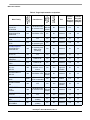
This section provides a detailed description of the five typical M68HC(S)08, Cold Fire V1 and Kinetis
bootloader implementations. All code is written in assembly language. Several selected targets and
different features are described in the following table:
Developer’s Serial Bootloader, Rev. 13
Freescale Semiconductor
37
MCU slave software
.
FLASH
Memory Use
(in Bytes)
Clock Source
ROM
Routines
Usage
Calibration
Conducted
Table 2. Target implementation comparison
SCI
MC68HC908AP
AP8/AP16/
AP32/AP64
592
32768 Hz XTAL
or external clock.
Yes,
different
version
No
Hardware
512
64
MC68HC908AB/AS/AZ
AB32/AS32/AZ32
AS60/AZ60
640
4.9152MHz XTAL
No
No
Hardware
128
64
MC68HC908EY
EY16
384
ICG
Yes
Yes
Hardware
64
32
512
32768 Hz XTAL
or external clock.
No
No
Hardware
128
64
320
32768 Hz XTAL
or external clock;
8MHz XTAL
(A Family)
Yes
No
Hardware
64
32
384
ICG
Yes
Yes
Hardware
64
32
512
8 MHz XTAL
Yes
No
Hardware
64
32
512
8 MHz XTAL
No
No
Hardware
128
64
MC68HC908JK/JL
JK1/JL1/
JK3/JL3
395
XTAL, RC
oscillator or ext.
source
Yes
Yes
Software,
single-wire
possible
64
32
MC68HC908JK/JL
JK8/JL8
384
Yes,
4.9152MHz XTAL different
version
No
Hardware
64
32
MC68HC908JW
JW32
1968
4MHz or 6MHz
XTAL or resonator
Yes
N/A
USB2.0
512
64
384
ICG
Yes
Yes
Software,
single-wire
possible
64
32
324
32768 Hz XTAL
or external clock.
Yes,
different
version
No
Hardware
128
64
384
ICG
Yes
Yes
Hardware
64
32
461
PLL with XTAL
(4 MHz)
No
No
Hardware
64
32
461
PLL with XTAL
(4 MHz)
No
No
Hardware
128
64
MCU Family
MC68HC908GP
GP32
MC68HC908GR
GR4/GR8/GR16
GR8A/GR16A
MC68HC908GT
GT8/GT16
MC68HC908GZ
GZ8/GZ16
MC68HC908GZ
GZ60
MC68HC908LB
LB8
MC68HC908LJ
LJ12/
LJ/LK24
MC68HC908KX
KX2/KX8
MC68HC908MR
MR8
MC68HC908MR
MR16/MR32
FLASH
FLASH
Program
Erase
Page Size Page Size
(in Bytes) (in Bytes)
Developer’s Serial Bootloader, Rev. 13
38
Freescale Semiconductor
MCU slave software
FLASH
Memory Use
(in Bytes)
Clock Source
ROM
Routines
Usage
Calibration
Conducted
Table 2. Target implementation comparison (continued)
SCI
362/302
QB/QC ICG
Yes
Yes/No
Hardware
64
32
387/323
QB/QC ICG
Yes
Yes/No
Hardware
64
32
320
Simpler ICG
Yes
Yes
Software,
single-wire
possible
64
32
512
32768 Hz XTAL
No
No
Hardware
128
64
MC9S08AW
HCS08AW32/48/64
576
HCS08 ICG
No
Yes
Hardware
512
64
HCS08AC8
HCS08AC16
HCS08AC32
HCS08AC48
HCS08AC60
432
HCS08 ICG
No
Yes
Hardware
512
64
HCS08AC128
694
HCS08 ICG
No
Yes
Hardware
512
128
MC9S08GB/GT
HCS08GB/GT32
HCS08GB/GT60
576
HCS08 ICG
No
Yes
Hardware
512
64
HCS08QE4
HCS08QE8
HCS08QE16
HCS08QE32
432
HCS08 ICG
No
No
Hardware
512
64
MC9S08QG
HCS08QG4/8
576
HCS08 ICG
No
No (HW) Hardware
Yes (SW) Software
512
64
MC9S08Rx
HCS08RD/RG/RE8
HCS08RD/RG/RE16
HCS08RD/RG/RE32
HCS08RD/RG/RE60
335
16MHz XTAL
No
No
Hardware
512
64
HCS08JM32
HCS08JM60
6000
12MHz external
clock
No
No
USB 2.0
512
64
MCF51JM64
MCF51JM128
1108
S08 MCGV3
No
No
Hardware
1024
128
MCF51QE32
MCF51QE64
MCF51QE128
1104
S08 ICSV3
No
No
Hardware
1024
128
MCF51CN64
MCF51CN128
1132
MCG
No
No
Hardware
1024
128
MCU Family
MC68HC908QB
QB4/QB8
MC68HC908QC
QC8/QC16
MC68HC908QT/QY
QT1/QT4/
QY1/QY4
MC68HC908SR
SR12
FLASH
FLASH
Erase
Program
Page Size Page Size
(in Bytes) (in Bytes)
Developer’s Serial Bootloader, Rev. 13
Freescale Semiconductor
39
MCU slave software
FLASH
Memory Use
(in Bytes)
Clock Source
ROM
Routines
Usage
Calibration
Conducted
Table 2. Target implementation comparison (continued)
SCI
MCF51AC128
MCF51AC256
1116
MCG
No
No
Hardware
1024
128
MCF51AG96
MCF51AG128
1120
ICS
No
No
Hardware
1024
128
MCF51EM128
MCF51EM256
1284
ICS
No
No
Hardware
1024
128
MCF51JM64
MCF51JM128
1116
MCG
No
No
Hardware
1024
128
MCF51JM64
MCF51JM128
8000
12MHz external
clock
No
No
USB 2.0
1024
128
K10N1M0
K10N512
K10N256
K10N128
K10N64
32768
16384
8192
4096
2048
MCG
No
No
Hardware
2048
128
K20N512
K20N256
K20N128
K20N64
K20N32
16384
8192
4096
2048
1024
MCG
No
No
Hardware
2048
128
K30N512
K30N256
16384
8192
MCG
No
No
Hardware
2048
128
K40N512
K40N256
K40N128
16384
8192
4096
MCG
No
No
Hardware
2048
128
K50N512
K50N256
16384
8192
MCG
No
No
Hardware
2048
128
K60N1024
K60N512
32768
16384
MCG
No
No
Hardware
2048
128
K70N1M
32768
MCG
No
No
Hardware
2048
128
K22N1M0
32768
MCG
No
No
Hardware
2048
128
KL05Z32
2048
MCG
No
No
Hardware
1024
128
KL25Z128
4096
MCG
No
No
Hardware
1024
128
KM34Z128
4096
MCG
No
No
Hardware
1024
128
MCU Family
8.1
FLASH
FLASH
Erase
Program
Page Size Page Size
(in Bytes) (in Bytes)
MC68HC908KX
The M68HC908KX Family has an Internal Clock Generator (ICG) module. This allows an effective
implementation of the bootloader without a crystal.
Developer’s Serial Bootloader, Rev. 13
40
Freescale Semiconductor
MCU slave software
The on-chip FLASH programming routines simplify the bootloader and improve memory usage. The
communication between the MCU and PC uses a Standard Serial Channel (SCI).
The following flowchart shows the basic principle of the bootloading algorithm:
RESET
SRSR RESET NOT POR
SOURCE TEST
USER CODE
START
POR CAUSED RESET
MCU CONFIG
ICG, SCI INIT
EXECUTE ILLEGAL
OPERATION
SEND ACK AND
WAIT FOR ANSWER
TIMEOUT EXPIRED
YES
?
NO
DISABLE SCI
WAIT FOR HI-LO EDGE
MEASURE BREAK
TRIM ICG, ENABLE SCI
SEND ACK
1
WAIT FOR COMMAND
2
YES
IDENT?
NO
ERASE?
YES
SEND IDENT DATA
2
NO
WRITE?
YES
NO
READ?
YES
NO
QUIT?
NO
YES
RECEIVE ADDRESS
RECEIVE ADDRESS
RECEIVE ADDRESS
CALL ERASE
RECEIVE LENGTH
RECEIVE LENGTH
2
ROUTINE IN ROM
RECEIVE DATA
SEND DATA
2
CALL WRITE
ROUTINE IN ROM
2
1
Figure 26. MC68HC908KX bootloader flowchart
Developer’s Serial Bootloader, Rev. 13
Freescale Semiconductor
41
MCU slave software
8.1.1
Internal Clock Generator (ICG) — initialization
The ICG is simple to initialize because the ICG is active and the clock monitor is disabled after reset. The
only action required is the modification of ICG multiply register. Then, the ICGS flag (bit 2) of the ICG
control register indicates whether the ICG is stable after the frequency change.
ICGMRINIT
LOOP:
8.1.2
EQU
MOV
BRCLR
$20
#ICGMRINIT,ICGMR
2,ICGCR,LOOP
; set 9.8304MHz BUS clock
; wait until ICG stable
Internal Clock Generator — trimming
Even though the trimming routine is in ROM, a small bug renders this code unusable; therefore, the source
code has been taken and inserted in the bootloader code.
Although AN1831/D provides the procedure for calculating the trim factor from the measured CPU speed,
the code itself omits the final doubling of the number of cycles.
* FOLLOWING LOOP IS EXECUTED UNTIL THE END OF THE BREAK SIGNAL. THE BREAK
* SIGNAL LASTS 10 BIT TIMES. IF COMMUNICATING AT f OP /256 BPS, THEN 10 BIT
* TIMES IS 2560 CYCLES. EACH TIME THROUGH THE LOOP IS 10 CYCLES, SO WE
* EXPECT TO EXECUTE THE LOOP 256 TIMES IF THE KX8 IS IN SYNC SERIALLY WITH
* THE HOST. IF WE STAY IN THE LOOP FOR > 256 LOOP CYCLES, THEN THE KX8
* MUST BE RUNNING FASTER THAN EXPECTED, AND NEEDS TO BE SLOWED DOWN. IF WE
* STAY IN THE LOOP FOR < 256 LOOP CYCLES THEN THE KX8 MUST BE RUNNING SLOWER
* THAN EXPECTED AND NEEDS TO BE SPEEDED UP. THE AMOUNT THAT WE CHANGE THE
* CPU SPEED IS EQUAL TO THE NUMBER OF LOOP CYCLES OVER OR UNDER 256. SO IF
* WE GO THROUGH THE LOOP 240 TIMES, THEN WE ARE RUNNING
* (256-240)/256 = 6.25% FAST. EACH INCREMENTAL CHANGE WE MAKE TO THE TRIM REGISTER
* (ICGTR) WILL MAKE A 0.195% CHANGE TO THE INTERNAL CLOCK. THAT IS, INCREMENTING
* THE REGISTER BY ONE OVER THE DEFAULT VALUE OF $80 STORED THERE WILL
* DECREASE THE INTERNAL CLOCK BY 0.195%, AND VICE VERSA.
* NOW EACH EXECUTION OF THE LOOP OVER OR UNDER WHAT IS EXPECTED (256 TIMES)
* REPRESENTS AN ERROR OF 1/256 = .391% ERROR. SO WE'LL NEED TO DOUBLE THE
* NUMBER OF LOOP CYCLES AND USE THIS NUMBER TO CORRECT THE TRIM REGISTER.
* OUR PRECISION FOR TRIMMING IS THEREFORE 0.391%.
The actual code adds an ASLA instruction which doubles the trim factor before the actual write to the ICG
trim register.
ICGTRIM:
CLRX
CLRH
MONPTB4:
BRSET
CHKPTB4:
BRSET
AIX
BRA
BRKDONE:
PSHH
PULA
TSTA
4,PTB,MONPTB4
;WAIT FOR BREAK SIGNAL TO START
4,PTB,BRKDONE
#1
CHKPTB4
;(5) GET OUT OF LOOP IF BREAK IS OVER
;(2) INCREMENT THE COUNTER
;(3) GO BACK AND CHECK SIGNAL AGAIN
;PUT HIGH BYTE IN ACC AND WORK WITH A:X
;IF MSB OF LOOP CYCLES = 0, THEN BREAK TAKES TOO
Developer’s Serial Bootloader, Rev. 13
42
Freescale Semiconductor
MCU slave software
TXA
BEQ
FAST:
CMP
BGE
ASLA
ADD
BRA
SLOW:
CMP
BLT
ASLA
SUB
ICGDONE:
STA
OOR:
RTS
SLOW
#$40
OOR
#$80
ICGDONE
#$C0
OOR
;FEW CYCLES THAN EXPECTED, SO TRIM BY SPEEDING
;UP f OP .
;SEE IF BREAK IS WITHIN TOLERANCE
;DON'T TRIM IF OUT OF RANGE
;multiply by two to get right range
;BREAK LONGER THAN EXPECTED, SO SLOW DOWN f OP
;SEE IF BREAK IS WITHIN TOLERANCE
;DON'T TRIM IF OUT OF RANGE
;multiply by two to get right range
#$80
ICGTR
The complete explanation of the trimming procedure can be found in AN1831/D. See References.
8.2
MC68HC908JK/JL
MC68HC908JK/JL MCUs are among the least expensive in the M68HC08 Family, and they have no
hardware SCI. Therefore, a software SCI must be implemented. This allows the unrestricted selection of
which pins are used for serial communication (the provisions are made in the code so an IRQ pin can also
be used as an input serial line).
The MC68HC908JK/JL Family has a RC version (an RC oscillator is used instead of a crystal). The
bootloader’s calibration compensates for any speed variation. If the desired clock frequency is outside the
specified range covered by the calibration system, the code must be modified.
The MC68HC908JK/JL Family has on-chip FLASH programming routines. Using FLASH programming
saves memory.
The main program flowchart (Figure 27) is very similar to the previous case. The following figure
represents the MC68HC908JK/JL Bootloader flowchart:
Developer’s Serial Bootloader, Rev. 13
Freescale Semiconductor
43
MCU slave software
RESET
NOT POR
SRSR RESET
SOURCE TEST
USER CODE
START
POR CAUSED RESET
MCU CONFIG
...
EXECUTE ILLEGAL
OPERATION
SEND ACK AND
WAIT FOR ANSWER
TIMEOUT EXPIRED
YES
?
NO
...
WAIT FOR HI-LO EDGE
MEASURE BREAK
CALIBRATE SOFT-SCI
1
SEND ACK
WAIT FOR COMMAND
2
YES
IDENT?
NO
ERASE?
YES
SEND IDENT DATA
2
NO
WRITE?
YES
NO
READ?
YES
NO
NO
YES
RECEIVE ADDRESS
RECEIVE ADDRESS
RECEIVE ADDRESS
CALL ERASE
ROUTINE IN ROM
RECEIVE LENGTH
RECEIVE LENGTH
RECEIVE DATA
SEND DATA
1
QUIT?
CALL WRITE
ROUTINE IN ROM
2
2
1
Figure 27. MC68HC908JK/JL bootloader
Developer’s Serial Bootloader, Rev. 13
44
Freescale Semiconductor
MCU slave software
8.2.1
Software-SCI transmit char routine
A detailed description of the software-SCI transmit and receive subroutines is provided in this section.
They both are based on a 16-bit timer and the output-compare event is polled in the background loop.
The following figure represents the software-SCI transmit char routine flowchart:
SHIFT-OUT TRANSMIT
CHAR INTO CARRY FLAG
ENTER
TEST CARRY
INITIALIZE, FEED AND
RUN 16-BIT TIMER
SET
CLEAR
TXD PIN HIGH
TXD PIN LOW
TXD PIN LOW
TXD PIN HIGH
CLEAR TIMER FLAG
CLEAR TIMER FLAG
SET BIT COUNTER
TO 9
WAIT FOR
TIMER FLAG
WAIT FOR
TIMER FLAG
TIMER FLAG
RECEIVED?
NO
NO
YES
YES
DECREMENT
TIMER FLAG
RECEIVED?
STOP TIMER
BITS AND TEST
=0
EXIT
Figure 28. Software-SCI transmit char routine
The two routines’ source code is shown in Figure 29. Other than a few counters, a 16-bit ONEBIT variable
is used. It contains the actual length of 1 bit at the current communication speed in 16-bit timer clock
cycles. This variable is initialized during the calibration phase (Slave frequency calibration).
The following figure represents the source code of software-SCI transmit char routine:
Developer’s Serial Bootloader, Rev. 13
Freescale Semiconductor
45
MCU slave software
;*******************************************************************************************
SCITX:
PSHH
PSHX
BCLR
LDHX
STHX
BSET
BCLR
7,TSC
ONEBIT
TMOD
4,TSC
5,TSC
; and clear TOF
MOV
BRA
#9,BITS
SCITX1
; number of bits + 1
; jump to loop
LSRA
BCC
DATALOW
; clear timer
; run timer
TXDCLR
SCITX2:
; shift out lowest bit
TXDSET
SKIP2
DATALOW:
TXDCLR
BCLR
SCITX1: BRCLR
DBNZ
; skip next two bytes
7,TSC
7,TSC,SCITX1
; and clear TOF
; wait for TOF
BITS,SCITX2
; and loop for next bit
7,TSC
7,TSC,SCITX3
; and clear TOF
; wait for TOF
5,TSC
; stop timer
SCISTOP:
TXDSET
BCLR
SCITX3: BRCLR
EPILOG:
BSET
PULX
PULH
RTS
Figure 29. Software-SCI transmit char routine source code
8.2.2
Software-SCI receive char routine
The software-SCI receive char routine is similar to software-SCI transmit. When the 16-bit
output-compare event is polled, the value of the receive pin is scanned. No provisions are made for stop-bit
checking, framing check, noise detection, and others, mainly because of memory restrictions. The
following figure shows the software-SCI receive routine flowchart, and the source code is provided in
Figure 31.
Developer’s Serial Bootloader, Rev. 13
46
Freescale Semiconductor
MCU slave software
ENTER
INITIALIZE AND FEED
16-BIT TIMER
WITH 1.5 BIT TIME
WAIT FOR
TIMER FLAG
WAIT FOR
RXD LOW
TIMER FLAG
RECEIVED?
RXD LOW
?
NO
YES
NO
SHIFT-IN RECEIVE
CHAR AND CLEAR MSB
YES
RUN TIMER
RXD PIN IS
SET
SET OR CLEAR?
SET BIT COUNTER
TO 9
SET MSB
CLEAR
FEED 16-BIT TIMER
WITH 1 BIT TIME
CLEAR TIMER FLAG
DECREMENT
BITS AND TEST?
=0
STOP TIMER
EXIT
Figure 30. Software-SCI receive char routine
Developer’s Serial Bootloader, Rev. 13
Freescale Semiconductor
47
MCU slave software
;*******************************************************************************************
SCIRX:
BRRXDLO SCIRX
; loop until RXD high (idle)
SCIRXNOEDGE:
PSHH
PSHX
BCLR
7,TSC
; and clear TOF
LDX
LDA
LSRX
RORA
STX
STA
ONEBIT
ONEBIT+1
BSET
4,TSC
TMODH
TMODL
; clear timer
SCIRX1:
BRRXDHI SCIRX1
; loop until RXD low (wait for start bit)
BCLR
MOV
5,TSC
#9,BITS
; run timer
; number of bits + 1
7,TSC,SCIRX2
; wait for TOF
SCIRX2: BRCLR
LSRA
BRRXDLO RXDLOW
ORA
#$80
RXDLOW: LDHX
STHX
; shift data right (highest bit cleared)
; skip if RXD low
; set highest bit if RXD high
ONEBIT
TMOD
BCLR
DBNZ
7,TSC
BITS,SCIRX2
BRA
EPILOG
; and clear TOF
; and loop for next bit
Figure 31. Software-SCI receive char routine source code
8.2.3
Macros
Several macros are defined across the two code listings. They improve the readability and memory
consumption (Figure 32). The following figure represents the source code of software-SCI macros:
Developer’s Serial Bootloader, Rev. 13
48
Freescale Semiconductor
MCU slave software
SKIP1
MACRO
DC.B
ENDM
$21
; BRANCH NEVER (saves memory)
SKIP2
MACRO
DC.B
ENDM
$65
; CPHX (saves memory)
BRRXDLO
MACRO
IFNE
RXDISIRQ
IFNE
SCIRXINV
BIH
\1
; branch if RXD low
ELSE
BIL
\1
; branch if RXD low
ENDIF
ELSE
; RXD uses normal I/O pin
IFNE
SCIRXINV
BRSET
RXDPIN,RXDPORT,\1
; branch if RXD low
ELSE
BRCLR
RXDPIN,RXDPORT,\1
; branch if RXD low
ENDIF
ENDIF
ENDM
BRRXDHI
MACRO
IFNE
RXDISIRQ
IFNE
SCIRXINV
BIL
\1
; branch if RXD hi
ELSE
BIH
\1
; branch if RXD hi
ENDIF
ELSE
; RXD uses normal I/O pin
IFNE
SCIRXINV
BRCLR
RXDPIN,RXDPORT,\1
; branch if RXD hi
ELSE
BRSET
RXDPIN,RXDPORT,\1
; branch if RXD hi
ENDIF
ENDIF
ENDM
TXDCLR
MACRO
IFNE
BSET
ELSE
BCLR
ENDIF
SCITXINV
TXDPIN,TXDPORT
; clr bit
TXDPIN,TXDPORT
; clr bit
ENDM
TXDSET
MACRO
IFNE
BCLR
ELSE
BSET
ENDIF
SCITXINV
TXDPIN,TXDPORT
; set bit
TXDPIN,TXDPORT
; set bit
ENDM
Figure 32. Software-SCI macros source code
Developer’s Serial Bootloader, Rev. 13
Freescale Semiconductor
49
MCU slave software
8.3
MC68HC908GP
On-chip FLASH programming routines are not available in MC68HC908GP MCU. Therefore, all FLASH
programming must be done by the bootloader, as demonstrated in this section.
MC68HC908GP MCUs are primarily targeted for use with a low-cost 32.768 kHz crystal. Because the
frequency of the crystal is known, no calibration is performed, which saves MCU memory. Therefore, this
MCU uses the Known MCU communication speed method.
The following figure is a flowchart of MC68HC908GP bootloader process:
Developer’s Serial Bootloader, Rev. 13
50
Freescale Semiconductor
MCU slave software
RESET
SRSR RESET
SOURCE TEST
NOT POR
USER CODE
START
POR CAUSED RESET
MCU CONFIG
ICG, SCI INIT
EXECUTE ILLEGAL
OPERATION
SEND ACK AND
WAIT FOR ANSWER
ACK RECEIVED
YES
BEFORE TIMEOUT
NO
SEND ACK
1
WAIT FOR COMMAND
2
YES
IDENT?
NO
YES
SEND IDENT DATA
2
ERASE?
NO
WRITE?
YES
RECEIVE ADDRESS
CALL ERASE
NO
READ?
YES
NO
QUIT?
NO
YES
RECEIVE ADDRESS
RECEIVE ADDRESS
RECEIVE LENGTH
RECEIVE LENGTH
RECEIVE DATA
SEND DATA
2
ROUTINE IN ROM
COPY ERASE
COPY WRITE
ROUTINE TO RAM
ROUTINE TO RAM
2
CALL WRITE
ROUTINE IN ROM
1
Figure 33. MC68HC908GP bootloader flowchart
8.3.1
FLASH programming routines
The main code is similar to the previous implementation with the calibration phase omitted. The FLASH
programming by the bootloader is shown in Figure 34. Three main subroutines are defined as follows:
• CPY_PRG — copies the selected routine into RAM
Developer’s Serial Bootloader, Rev. 13
Freescale Semiconductor
51
MCU slave software
•
•
ERASE_ALG — whole FLASH erase routine
WR_ALG — whole WRITE erase routine
Because the flow is straightforward, no flowchart is provided. Basically, the sequence of events is executed
according to FLASH erasing/programming specifications.
;*******************************************************************************************
CPY_PRG:
TSX
;
STHX
STACK
; copy stack for later re-call
LDHX
TXS
LDHX
CPY_PRG_L1:
PULA
STA
AIX
DBNZ
SOURCE
; LOAD WRITE ALGORITHM TO RAM
#PRG
X
#1
STAT,CPY_PRG_L1
LDHX
STACK
TXS
; restore stack
RTS
;*******************************************************************************************
ERASE_ALG:
LDA
STA
LDA
#%00000010
FLCR
FLBPR
; ERASE bit on
; dummy read FLBPR
LDHX
STA
D_US
ADRS
X
#T10US
; write anything
; to desired range
; wait 10us
LDA
STA
D_MS
#%00001010
FLCR
#T1MS
; set HVEN, keep ERASE
; wait 1ms
LDA
STA
D_US
#%00001000
FLCR
#T5US
; keep HVEN, ERASE off
; wait 5us
CLRA
STA
D_US
FLCR
#T1US
; HVEN off
; wait 1us
JMP
SUCC
; finish with ACK
ERASE_ALG_END:
;*******************************************************************************************
WR_ALG:
LDA
#%00000001
STA
FLCR
; PGM bit on
LDA
FLBPR
; dummy read FLBPR
LDHX
STA
D_US
ADRS
X
#T10US
; prepare addresses
; and write to desired range
; wait 10us
Developer’s Serial Bootloader, Rev. 13
52
Freescale Semiconductor
MCU slave software
LDA
STA
D_US
LDHX
TXS
LDHX
MOV
WR_ALG_L1:
PULA
STA
AIX
D_US
DBNZ
#%00001001
FLCR
#T5US
; set HVEN, keep PGM
; wait 5us
#DAT
; prepare addresses
ADRS
LEN,POM
X
#1
#T30US
POM,WR_ALG_L1
; wait 30us
; copy desired block of data
LDA
STA
D_US
#%00001000
FLCR
#T5US
; keep HVEN, PGM off
; wait 5us
CLRA
STA
D_US
FLCR
#T1US
; HVEN off
; wait 1us
RETWR
; finish with ACK (& restore STACK before)
JMP
WR_ALG_END:
END
Figure 34. FLASH programming routines source code
For improved readability, two timing macros (D_US and D_MS) are used in the code (Figure 35).
;*******************************************************************************************
D_MS:
MACRO
LDA
\1
; [2] ||
\@L2:
CLRX
; [1] ||
\@L1:
NOP
; [1] |
DBNZX
\@L1
; [3] |
256*4 = 1024T
DBNZA
\@L2
; [3] || (1024+4)*(arg-1) + 2 T
ENDM
D_US:
\@L1:
MACRO
LDA
NOP
DBNZA
ENDM
\1
\@L1
; [2]
; [1]
; [3] 4*(arg-1) + 2 T
Figure 35. FLASH programming macros source code
8.4
MC68HC908GR
MC68HC908GR MCUs are smaller members of the MC68HC908GP Family, equipped with ROM
memory with on-chip FLASH programming routines available in the user mode.
Developer’s Serial Bootloader, Rev. 13
Freescale Semiconductor
53
MCU slave software
MC68HC908GP and MC68HC908GR MCUs are primarily targeted for use with a low-cost 32.768 kHz
crystal. Because the frequency of the crystal is known, no calibration is performed, which saves MCU
memory. Therefore, these MCUs use the Known MCU communication speed method.
8.5
MC68HC908MR
MC68HC908MR MCUs are motor-control oriented members of the M68HC08 Family. The
MC68HC908MR MCUs have no on-chip FLASH programming routines available. Therefore, all FLASH
programming must be done by the bootloader.
The MC68HC908MR Family has a PLL (phase-locked loop) circuit that can multiply the crystal
frequency. Typically, a 4-MHz XTAL is used as the reference frequency. This implementation
demonstrates how the PLL circuit is initialized for 8 times the crystal frequency. Therefore, the source PLL
frequency is 32 MHz, and the bus frequency is 8 MHz.
Because the frequency of the crystal is known, no calibration is performed, which saves MCU memory.
Therefore, these MCUs use the Known MCU communication speed method.
8.6
MC68HC908EY
The code for MC68HC908GT and MC68HC908EY MCUs is similar to MC68HC908KX code, except for
the memory maps and ROM routine locations. One minor difference is that the MC68HC908GT Family
cannot use the CGMXCLK clock as the SCI module source. Therefore, the bus clock is the only possible
clock source.
8.7
MC68HC908QT/QY
MC68HC908QT/QY MCUs are the smallest members of the M68HC08 Family. They have a simple ICG
module (running on fixed frequency 12.8 MHz 25%). ROM routines are available.
There are several spare FLASH locations (mainly among unused interrupt vectors) also used for storing
the bootloader code.
8.7.1
SCI Application Program Interface (SCIAPI)
Software SCI communication is implemented on MC68HC908QT/QY, MC68HC908JK/JL, and
MC68HC908LB MCUs to reduce cost and enable the user code to call the SCI send and receive routines
(with certain limitations). The bootloader code now implements SCIAPI, which is the defined way to call
the SCI send and receive routines.
The detailed information, implementation notes, and limitations are provided in the sci.h file (of the
QTQY folder). This file is the only resource that must be included in the user C code. The calling
convention and overall usage is described in this file, too. The main limiting factor for most applications
will be that the SCI receive routine is a blocking one. This means that routines will not return until an SCI
character is received. The 16-bit timer registers are also manipulated. Some applications will use this code
without problems.
Developer’s Serial Bootloader, Rev. 13
54
Freescale Semiconductor
MCU slave software
8.7.2
Single-Wire communication
Because of the small number of pins on MC68HC908QT devices, the single-wire SCI version has been
developed to keep the number of pins occupied by communication to a minimum. Figure 36 illustrates an
example single-wire RS-232 interface. The single-wire option has been ported to MC68HC908JK/JL and
MC68HC908LB bootloader because they also use a software SCI.
VDD
10k
RXD
RS-232
CONNECTION
TTL/232 SHIFTER
MC68HC908QT/QY
MCU
TXD
Figure 36. Example single-wire schematic
The bootloader’s master side must be informed that the single-wire communication is used. This can be
done by calling the hc08sprg.exe software. Use the following extended calling convention:
hc08sprg.exe 1:S filename.s19
where, 1 specifies which COM port is used for communication and S stands for single-wire.
Original (old) format: hc08sprg.exe 1 filename.s19
Now defaults to:
hc08sprg.exe 1:D filename.s19
where, D stands for dual-wire mode. The bootloader master can also detect the presence of a single-wire
interface if called:
hc08sprg.exe 1:? filename.s19
The detection is only possible if the serial interface (mainly the level shifter) is powered up and working
before the bootloading process starts. Because this is not usually the case, always specify the bootloading
mode by including either “:S” or “:D” in the parameter.
8.8
MC68HC908LJ
MC68HC908LJ MCUs are members of the M68HC08 Family used to drive LCD displays.
MC68HC908LJ MCUs have the ROM on-chip FLASH programming routines available. The calling
convention is slightly different from other M68HC08s (see MC68HC908LJ data sheet, monitor ROM
section).
MC68HC908LJ MCUs are primarily targeted to use with a low-cost 32.768 kHz crystal. Because the
frequency of the crystal is known, no calibration is performed, which saves MCU memory. Therefore,
these MCUs use the Known MCU communication speed method.
Developer’s Serial Bootloader, Rev. 13
Freescale Semiconductor
55
MCU slave software
8.9
MC68HC908AP
MC68HC908AP devices are members of the M68HC08 Family that have two SCIs (the SCI channel must
be selected at compile time). MC68HC908AP MCUs have ROM on-chip FLASH programming routines
available. The calling convention is slightly different from other M68HC08s (same as MC68HC908LJ
devices).
Because of the internal oscillator’s simplicity, it does not have the accuracy and stability of the RC
oscillator or the XTAL oscillator. Therefore, the internal oscillator is not suitable if an accurate bus clock
is required and it should not be used as the bus clock source.
A low-cost 32.768 kHz crystal was selected as default source clock for bootloader and user application.
Because the frequency of the crystal is known, no calibration is performed, which saves MCU memory.
Therefore, these MCUs use the Known MCU communication speed method.
8.10
MC68HC908AB/AS/AZ
MC68HC908AB/AS/AZ devices are members of the M68HC08 Family that also have EEPROM memory.
This code also demonstrates the way to program these EEPROM cells using AUTO (automatic clear of
EEPGM) mode.
Since the memory map is not continuous, FC protocol version 3 needs to be used (it allows the “holes” in
the memory map, that is, several separate memory blocks).
8.11
MC9S08GB/GT
MC9S08GB/GT devices are the first members of the HCS08 Family. Because of different hardware
features and FLASH memory allocation, another version of the protocol was required. The protocol is
detected automatically by the latest hc08sprg.exe PC Bootloader software and becomes invisible to
the user.
MC9S08GB/GT MCUs have two SCIs (the SCI channel must be selected at compile time).
These MCUs have no on-chip FLASH programming routines. Therefore, the bootloader must do all
FLASH programming, and this implementation demonstrates this (it has been entirely adopted from
HCS08 Family Reference Manual Volume 1 (Freescale Semiconductor order number HCS08RMv1/D; see
References).
8.12
MC68HC908JW
The HC908JW family has a built-in USB 2.0 Full Speed module. This allows a direct connection via a true
USB interface with the PC. As described in AN3153: Using the Full-Speed USB Module on the
MCHC908JW32 application note, the emulation of the serial COM port can be easily designed. This way,
a fully compatible bootloader (written in C) for the JW32 family has been designed. Once the bootloader
is programmed into the JW32 device, the user code can be reprogrammed anytime using a native USB
connection (serial COM port emulation in Windows).
The installation and usage details are documented in ZSTARRM: Wireless Sensing Triple Axis Reference
design, chapter 5.5 and 6.1.2, out of which the JW32 USB bootloader has been derived. The PC drivers
Developer’s Serial Bootloader, Rev. 13
56
Freescale Semiconductor
PC bootloader master software
required for USB are also inside the JW32 folder of the AN2295SW software package. Alternatively, the
latest on-line version of the PC drivers is available on the ZSTAR summary page (RD3152MMA7260Q).
NOTE
Although serial COM emulation on the JW32 has been successfully tested
in Linux, a Linux port of hc08sprg executable of the AN2295 bootloader
master was not tested together with theJW32 bootloader USB
implementation.
8.13
HCS08JM and MCF51JM
The MCF51JM family has a built-in USB 2.0 Full Speed module. This allows a direct connection through
a true USB interface with the PC. As described in AN3492: USB and Using the CMX USB Stack
application note, the emulation of the serial COM port can be easily designed. This way, a fully compatible
bootloader (written in C) for the HCS08JM and MCF51JM families has been designed. This USB driver
is used for communication with the PC Communication Device Class (CDC). The basis of this
communication is creating a Virtual Serial Port on the PC side. This feature allows using master bootloader
software without any modification of the source code. For more information, refer AN3492 : USB and
Using the CMX USB Stack.
9
PC bootloader master software
This section provides a detailed description of the bootloader host computer master software, which is
downloadable as a zip file from the Freescale Semiconductor website, freescale.com. All code is written
in C language and is compatible with Linuxand Win32 platforms.
The bootloader specifications dictate that, as much as possible, intelligence is executed in the host
computer instead of MCU, minimizing MCU memory consumption. Only primitive functions are
implemented in the MCU.
In this section, portions of the master bootloader code will be described in more detail. All actions required
for reprogramming the M68HC(S)08, Coldfire V1, and Kinetis devices are described in the slave
implementation and protocol sections of this document. The specific master characteristics are
emphasized.
The host computer master software design is straightforward and is a sequence of several steps:
• Opening the serial port
• Opening the source S19 file
• Waiting for the reset of the MCU
• Calibrating the MCU
• Reading MCU information
• Remapping MCU interrupt vectors
• Checking if the source S19 data fits into the physical MCU memory
• Erasing and programming MCU
• Cleaning up, exiting program
Developer’s Serial Bootloader, Rev. 13
Freescale Semiconductor
57
PC bootloader master software
The following figure displays the bootloader master flowchart:
START
NO
ENOUGH
ARGUMENTS
?
X(0)
CALIBRATE MCU
YES
OK?
INIT UART
NO
CHECK S19
IMAGE TO FIT
X(4)
YES
OK?
NO
X(1)
DISPLAY WARNING
IF NOT
READ MCU INFO
YES
SURE?
OPEN S19 FILE
OK?
NO
X(5)
OK?
X(2)
PROGRAM MCU
PRINT MCU INFO
YES
OK?
WAIT (HOOK) FOR
MCU RESET
OK?
NO
SET UP INTERRUPT
VECTOR TABLE
X(3)
YES
X($FF)
YES
YES
NO
NO
OK?
NO
NO
X(8)
YES
UNHOOK MCU
CLOSE UART
X(6)
YES
EXIT
NOTE: X(2) MEANS EXIT WITH EXIT CODE
Figure 37. Bootloader master flowchart
9.1
File structure
The following file structure setup is used in PC master software:
• 8-Bit and 32-Bit MCU image operations:
— s19.c
• UART manipulations:
— serial.h
• seriallinux.c (serialw32.c)
— System platform dependent files:
• sysdep.h
— sysdeplinux.h
— sysdepw32.h
• Generic and main program files:
Developer’s Serial Bootloader, Rev. 13
58
Freescale Semiconductor
PC bootloader master software
•
9.2
— hc08sprg.h
— main.c
M68HC(S)08, ColdFire and Kinetis specific programming files:
— prog.c
8-Bit and 32-Bit MCU image operations
To perform the necessary operations with the code, the master software keeps a binary image of the
memory. In addition, it stores the information about whether an actual byte is to be programmed into the
MCU is stored. This can be achieved using the following structure:
typedef struct {
BYTE d[0x10000];
BYTE f[0x10000];
} BOARD_MEM;
// data
// valid flag 0=empty; 1=usercode; 2=systemcode
where, image is the actual variable defined as follows:
BOARD_MEM image;
After the source S19 files are read, this array contains the actual data to be programmed into the MCU
irrespective of its original order in the S19 file. The function int read_s19(char *fn) defined in s19.c
implements the S19 file opening, reading, and relocation from S19 hexadecimal format into this binary
array.
9.2.1
Interrupt vector table relocation
After the ident information is read out by the MCU, the following operations within the image are
performed:
• The code is scanned to determine if any interrupt vectors are present between the MCU interrupt
vector table address and 0xFFFF (the last existing physical address of the M68HC(S)08 MCU).
• If interrupt vectors are present, relocation of these vectors is done as described in Interrupt vector
table relocation. Then, the original address spaces in the interrupt vector table are marked as
unused, thus, not being reprogrammed.
These operations are executed in the function int setup_vect_tbl(void) defined in prog.c file.
9.2.2
Checking memory boundaries
The last check performed before the code is actually programmed into the MCU is to determine if the code
from the S19 file is in the correct memory locations (between the memory boundaries reported by the
MCU in the ident table).
If any value outside the range of addresses between the start address of reprogrammable memory area and
the end address of reprogrammable memory area is found, a warning is generated.
This check is done in int check_image(void) also defined in the prog.c file.
Developer’s Serial Bootloader, Rev. 13
Freescale Semiconductor
59
PC bootloader master software
9.3
UART manipulations
In seriallinux.c or serialw32.c, depending on the platform used, the following UART manipulation
functions are defined:
int
int
int
int
int
int
init_uart(char* nm);
close_uart(void);
send_break10(void);
flush_uart(int out, int in);
wb(const void* data, unsigned len);
rb(void* dest, unsigned len);
The pair int init_uart(char* nm) and int close_uart(void) manage opening (initialization) and
closing of the specified UART port.
The pair int wb(const void* data, unsigned len) and int rb(void* dest, unsigned len) is
used for writing and reading blocks of data into/out of UART.
Two additional functions are required for the bootloader to work:, int send_break10(void) and
int flush_uart(int out, int in). The first sends a BREAK character to the UART, the second cleans
up both directions (in/out) of the UART buffers.
9.4
System platform dependent files
The header file sysdep.h includes either sysdeplinux.h or sysdepw32.h, depending on the platform
software being compiled. The platform-specific declarations are then used.
9.5
Generic and main program files
The header file hc08sprg.h contains the rest of the generic declarations needed to compile the application.
The file main.c contains the main program and is shown at the beginning of this section (Figure 37).
9.6
M68HC(S)08, ColdFire and Kinetis specific programming files
The most important part of the PC Bootloader software is contained in the file prog.c implements most
of the intelligence of the PC bootloader software as mentioned in previous sections.
Numerous routines are implemented in the prog.c file:
int
int
int
int
int
int
int
int
int
int
int
int
int
int
int
hook_reset(void)
could_be_ack(unsigned b)
calibrate_speed(void)
read_mcu_info(void)
setup_vect_tbl(void)
check_image()
read_blk(unsigned adr, int len, BYTE *dest)
erase_blk(unsigned a)
prg_blk(unsigned a, int len)
prg_area(unsigned start, unsigned end)
prg_mem(void)
erase_mem(unsigned all)
verify_mem(int byS19_range)
prg_only_mem(void)
unhook(void)
Developer’s Serial Bootloader, Rev. 13
60
Freescale Semiconductor
PC bootloader master software
void CRC_AddByte(unsigned short *pCrc, unsigned char data)
void CRC_AddWord(unsigned short *pCrc, unsigned short data)
void CRC_Add3Bytes(unsigned short *pCrc, unsigned long data)
void CRC_AddLong(unsigned short *pCrc, unsigned long data)
void CRC_AddByteArray(unsigned short *pCrc, unsigned char* data, int size)
void CRC_AddString(unsigned short *pCrc, unsigned char* str)
void CRC_ResetCRC(unsigned short *pCrc, unsigned short seed)
unsigned short CRC_GetCRC(unsigned short *pCrc)
9.6.1
Initial hook (waiting for MCU reset)
Immediately after all initializations are done in the PC, a loop starts to wait for communication from the
MCU. The int hook_reset(void) routine implements all necessary steps to establish initial
communication with the MCU.
9.6.2
Checking ACK
A routine int could_be_ack(unsigned b) checks if a received character fits the possible set of
characters that can be received due to a communication speed mismatch (See Unknown MCU
communication speed).
9.6.3
Speed calibration
A speed calibration loop, implemented in the int calibrate_speed(void) routine, follows the scenario
described in Slave frequency calibration. If no ACK is received from the MCU, another break character is
sent.
9.6.4
MCU information reading
Immediately after the calibration is successfully completed, the PC requests the Ident command, to which
the MCU responds with information about itself. This is achieved in the int read_mcu_info(void)
routine.
9.6.5
Image manipulations
The two functions, int setup_vect_tbl(void) and int check_image(), are described in 8-Bit and
32-Bit MCU image operations.
9.6.6
Block operations
Three main data exchange operations are performed:
• Erase block
• Read block
• Write (program) block
These basic operations are implemented in the functions:
int erase_blk(unsigned a)
Developer’s Serial Bootloader, Rev. 13
Freescale Semiconductor
61
Master applications user guides
int read_blk(unsigned adr, int len, BYTE *dest)
int prg_blk(unsigned a, int len)
The actual implementation is straightforward and follows the rules described in Interpreting MCU
commands.
9.6.7
Main programming loop
The core of the bootloader’s programming capabilities is implemented in the function int
prg_area(unsigned start, unsigned end). The function of this routine is to read data from an image
and split the data into appropriately sized blocks (minimum erase/write block sizes). Then the erase block
and write block routines are called, in that order.
The routine also prints the progress information to the standard I/O (for example, block boundary
addresses and progress indicator).
One additional auxiliary function, int prg_mem(void), is included. It retrieves the lowest and highest
memory addresses that must be programmed because those addresses are used for calling the int
prg_area(unsigned start, unsigned end) function.
9.6.8
CRC calculation
The new version of bootloader protocol add option to secure serial communication protocol by
CRC-CCITT check. So the PC source code contains a few basic primitive functions to support this
possibility:
void CRC_AddByte(unsigned short *pCrc, unsigned char data)
void CRC_AddWord(unsigned short *pCrc, unsigned short data)
void CRC_Add3Bytes(unsigned short *pCrc, unsigned long data)
void CRC_AddLong(unsigned short *pCrc, unsigned long data)
void CRC_AddByteArray(unsigned short *pCrc, unsigned char* data, int size)
void CRC_AddString(unsigned short *pCrc, unsigned char* str)
void CRC_ResetCRC(unsigned short *pCrc, unsigned short seed)
unsigned short CRC_GetCRC(unsigned short *pCrc)
9.6.9
Final unhook
Function int unhook(void) sends out the Quit command.
10
Master applications user guides
The bootloader binary code (S19 file) is loaded in the MCU like any other regular 8-bit MCU (using
MON08 serial programmer or other, for HCS08 using BDM interface). Then the MCU is soldered, or
socketed, in the application.
Using the bootloader preprogrammed into the MCU, the user can download the 8-bit MCU user
application code via SCI interface using the bootloader utility.
Developer’s Serial Bootloader, Rev. 13
62
Freescale Semiconductor
Master applications user guides
10.1
Bootloading operation (command line version)
Open a command prompt in the Linux or Windows directory where the copy of hc08sprg executable
and S19 files are.
Assuming the serial board is connected to, for example, a second serial port (COM3 /dev/ttyS1, with speed
sets to 115200 bd/s and short trim is used) and is not yet powered on, invoke the bootloader using following
sequence: hc08sprg.exe 3:D* 115200 k60_test.s19
Figure 38. Bootloader invocation
The bootloader now expects the ACK command to be received from the MCU bootloader-enabled
application. Then turn the power on for serial board and if all connections are OK, the MCU begins
communication with the PC. The calibration procedure does not occur if the bootloader version with
known communication speed is used followed by IDENT command. The information that is acquired from
the MCU is then displayed on the screen (Figure 39).
Developer’s Serial Bootloader, Rev. 13
Freescale Semiconductor
63
Master applications user guides
Figure 39. First stage of bootloading
Confirm by pressing ‘y’ and bootloading (FLASH reprogramming) will continue. The user application
will then start.
Developer’s Serial Bootloader, Rev. 13
64
Freescale Semiconductor
Master applications user guides
Figure 40. Bootloading completed
10.1.1
Memory boundary overlap example
If the user tries to bootload an application that will not fit in the actual MCU memory, a warning message
is displayed. The user may decide to continue, but some memory locations may be programmed
incorrectly (the user code is either out of available FLASH memory or it overlaps with the bootloader
code).
Developer’s Serial Bootloader, Rev. 13
Freescale Semiconductor
65
Master applications user guides
Figure 41. Memory boundary overlap example
Developer’s Serial Bootloader, Rev. 13
66
Freescale Semiconductor
Master applications user guides
10.2
Bootloading operation (windows version)
A version of the PC master application is also present (based on the same source codebase) in the Windows
user friendly form. The application allows carrying out individual steps with the bootloader and also
automatic steps as with the command line version.
Figure 42. Windows based PC master application
Developer’s Serial Bootloader, Rev. 13
Freescale Semiconductor
67
Master applications user guides
10.2.1
10.2.1.1
How to use the Windows version of master application
Open the “win_hc08sprg.exe”
Figure 43. The PC master release folder
This is stored in release folder of PC master applications.
10.2.1.2
Setup the application for connection with target
1
2
3
4
Figure 44. Setup the application for connection with target
1. Select the right Communication port. In case that the port is not in list, try to re scan communication
ports in your PC by button “Rescan”.
2. Setup the communication option to meet the settings of target.
— Communication speed - select the communication baud rate
— Single Wire - check if the target is connected through the one wire connection
Developer’s Serial Bootloader, Rev. 13
68
Freescale Semiconductor
Master applications user guides
— Short TRIM - check if the target is configured to used short clock calibration (trim) pulse.
3. Select the S19 file - To add the new S19 file into list use the “Open S19” button, for reuse the any
file that has been already opened just select it from the combo box.
4. Connect the target - hit the button “Connect” and run the target with bootloader startup options
enabled
10.2.1.3
Using the Windows version of master application
4.
5.
6.
1.
7.
8.
9.
10.
2.
3.
11.
Figure 45. The Windows version of Bootloader window connected to target
1. Identification information - in this frame the application shows all knows information about target
and used AN2295 serial protocol.
2. Console window - this console window is showing exactly same information as the command line
version of application.
3. Progress bar - progress bar is showing status of current active operation (erase, program, compare
and so forth).
4. Quit/Run - This button ends the active bootloader session and invoke to run the user application if
it’s available.
Developer’s Serial Bootloader, Rev. 13
Freescale Semiconductor
69
Merging bootloader and application images
5. Erase - this button invokes erase of whole user flash memory area.
6. Blank check - this command check the memory if it’s erased. The command is implemented by
read command.
7. Program - the button try to download the prepared image to the target. Be sure that before this
operation the target memory is already erased.
8. Compare - this button compare the content of the target memory with prepared image
9. Read - this command read the full target user area and store it into new S19 file.
10. AutoProgram - this command invoke exactly same procedure as is using command line version of
the AN2295 master application. To add extra verification after write the image the AutoProgram
Verify must be checked.
11. Exit - this button exits from the bootloader application
11
Merging bootloader and application images
This section provides a detailed description of the computer software that merges the bootloader and user
application S19 files into one output S19 file, which is downloadable as a zip file from the Freescale
Semiconductor website, freescale.com. All code is written in C language and is compatible with the
Win32 platform.
Typical case of a merged bootloader and user application S19 file is the final mass production of the MCU
flash image with bootloader capability. The merge tool simplifies the operation of flashing the bootloader
itself by debugging the interface of bootloading the application by the flashed bootloader.
The merge tool application is using the same base of source files as all other AN2295 PC software (Master
bootloader applications: command line and standard windows form versions).
The Merge tool windows form application is designed to load two S19 files (application and bootloader),
and select the type of MCU and interrupt vector tables (original and redirected). The application also
contains the log window that provides all detailed information on the merge process and all possible
warnings.
Developer’s Serial Bootloader, Rev. 13
70
Freescale Semiconductor
References
Application S19
file box
Bootloader S19
file box
MCU type select
box
Output S19
file name box
Bootloader
protocol box
Vector table
definition boxes
Log window
Exit button
Start conversion button
Figure 46. The AN2295 S19 Merge tool
12
References
For additional information, refer to these documents from the Freescale Semiconductor website,
freescale.com
• AN2295SW: Contains all of the software files for this application note in a zip file.
• HCS08RMv1: HCS08 Family Reference Manual Volume 1
• AN1831: Using MC68HC908 On-Chip FLASH Programming Routines
• AN2140: Serial Monitor for MC9S08GB/GT
• AN2498: Initial trimming of the MC68HC908 ICG
• AN2504: On-Chip FLASH Programming API for CodeWarrior Software
• AN2508: Generating Clocks for HC908 MCU Families
• AN2545: On-Chip FLASH Programming Routines for MC68HC908GR/GZ
• AN2637: Software SCI MC68HC908QT/QY MCU
• AN2635: On-Chip FLASH Programming Routines for LB8 and other FLASH-based MCUs
• AN2874: Using M68HC908 ROM-Resident Routines
• AN3153: Using the Full-Speed USB Module on the MCHC908JW32
Developer’s Serial Bootloader, Rev. 13
Freescale Semiconductor
71
References
•
•
•
•
•
•
•
ZSTARRM: Wireless Sensing Triple Axis Reference design
CFPRM: ColdFire® Family Programmer’s Reference Manual
K60P100M100SF2RM: K60 Sub-Family Reference Manual
AN3942: Flash Programming Routines for the HCS08 and the ColdFire (V1) devices
The Master applications user guides: Section 10, Master applications user guides
The description of Kinetis version of protocol including the changes in user application: Section 7,
FC protocol, version 5, Kinetis
The quick start guide how to modify the user Kinetis application to be ready for AN2295
bootloader: Section 7.8, Quick guide: How to prepare the user Kinetis application for AN2295
bootloader
Developer’s Serial Bootloader, Rev. 13
72
Freescale Semiconductor
How to Reach Us:
Home Page:
freescale.com
Web Support:
freescale.com/support
Information in this document is provided solely to enable system and software
implementers to use Freescale Semiconductor products. There are no express or
implied copyright licenses granted hereunder to design or fabricate any integrated
circuits or integrated circuits based on the information in this document.
Freescale reserves the right to make changes without further notice to any products
herein. Freescale makes no warranty, representation, or guarantee regarding the
suitability of its products for any particular purpose, nor does Freescale assume any
liability arising out of the application or use of any product or circuit, and specifically
disclaims any and all liability, including without limitation consequential or incidental
damages. “Typical” parameters that may be provided in Freescale data sheets and/or
specifications can and do vary in different applications, and actual performance may
vary over time. All operating parameters, including “typicals,” must be validated for each
customer application by customer’s technical experts. Freescale does not convey any
license under its patent rights nor the rights of others. Freescale sells products pursuant
to standard terms and conditions of sale, which can be found at the following address:
freescale.com/SalesTermsandConditions.
Freescale, the Freescale logo, ColdFire, and Kinetis are trademarks of Freescale
Semiconductor, Inc., Reg. U.S. Pat. & Tm. Off. All other product or service names are
the property of their respective owners. ARM and Cortex are the registered trademarks
of ARM Limited.
© 2013 Freescale Semiconductor, Inc. All rights reserved.
Document Number: AN2295
Rev. 13
10/2013
References
Developer’s Serial Bootloader, Rev. 13
74
Freescale Semiconductor