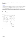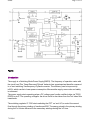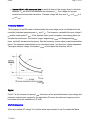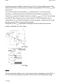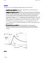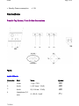
1
Philips Consumer Electronics Manual 7629 Model no.: 27PS60S321 First Publish: 12740 T8 Rev. Date: 2002-06-06 Print Date: 7/8/2004 Technical Service Data Service and Quality Service Publications Dept. One Philips Drive P.O. Box 14810 Knoxville, TN 37914 Pg. SCHEMATIC DIAGRAMS AND PC BOARDS 17. Side AV and Headphone Panel (Diagram C) 18. PIP Panel (Diagram P) 19. Main Panel (component side) 20. Main Panel (copper side) 21. CRT Panel (component side) 22. CRT Panel (copper side) 23. Headphone Panel (component side) 24. Side AV Panel (component side) 25. PIP panel (component side) 26. PIP panel (copper side) 27. Top Control Panel (component side) 28. EPS Panel PCB (Top View only) 29. Card Interface Panel PCB (Top View) 30. Card Interface Panel PCB (Bottom View) 1. PCB Locations 2. Power Supply (Diagram A1) 3. Line Deflection (Diagram A2) 4. Frame Deflection (Diagram A3) 5. Tuner IF (Diagram A4) 6. Video IF And Sound IF (Diagram A5) 7. Synchronization (Diagram A6) 8. Control (Diagram A7) 9. Audio Amplifier (Diagram A8) 10. BTSC (Stereo/SAP) Decoder (Diagram A9) 11. Audio/Video Source Switching (Diagram A10) 12. BTSC - NDBX Stereo Decoder (Diagram A11) 13. Front I/O + Control, Headphone (Diagram A12) 14. Rear I/O Cinch (Diagram A13) 15. PIP Interface (Diagram A16) 16. CRT Panel (Diagram B1) REFER TO SAFETY GUIDELINES SAFETY NOTICE: ANY PERSON ATTEMPTING TO SERVICE THIS CHASSIS MUST FAMILIARIZE HIMSELF WITH THE CHASSIS AND BE AWARE OF THE NECESSARY SAFETY PRECAUTIONS TO BE USED WHEN SERVICING ELECTRONIC EQUIPMENT CONTAINING HIGH VOLTAGES. CAUTION: USE A SEPARATE ISOLATION TRANSFORMER FOR THIS UNIT WHEN SERVICING © Philips Electronics North America Corporation Visit our World Wide Web Site at http://www.forceonline.com Philips Consumer Electronics Manual 7629 Model no.: 27PS60S321 First Publish: 12740 T8 Rev. Date: 2002-06-06 Print Date: 7/8/2004 Technical Service Data Service and Quality Service Publications Dept. One Philips Drive P.O. Box 14810 Knoxville, TN 37914 Mechanical Diagrams REFER TO SAFETY GUIDELINES SAFETY NOTICE: ANY PERSON ATTEMPTING TO SERVICE THIS CHASSIS MUST FAMILIARIZE HIMSELF WITH THE CHASSIS AND BE AWARE OF THE NECESSARY SAFETY PRECAUTIONS TO BE USED WHEN SERVICING ELECTRONIC EQUIPMENT CONTAINING HIGH VOLTAGES. CAUTION: USE A SEPARATE ISOLATION TRANSFORMER FOR THIS UNIT WHEN SERVICING © Philips Electronics North America Corporation Visit our World Wide Web Site at http://www.forceonline.com MAIN CABINET EXPLODED VIEW Page: 1 of 1 Philips Consumer Electronics Manual 7629 Model no.: 27PS60S321 First Publish: 12740 T8 Rev. Date: 2002-06-06 Print Date: 7/8/2004 Technical Service Data Service and Quality Service Publications Dept. One Philips Drive P.O. Box 14810 Knoxville, TN 37914 Electrical Adjustments REFER TO SAFETY GUIDELINES SAFETY NOTICE: ANY PERSON ATTEMPTING TO SERVICE THIS CHASSIS MUST FAMILIARIZE HIMSELF WITH THE CHASSIS AND BE AWARE OF THE NECESSARY SAFETY PRECAUTIONS TO BE USED WHEN SERVICING ELECTRONIC EQUIPMENT CONTAINING HIGH VOLTAGES. CAUTION: USE A SEPARATE ISOLATION TRANSFORMER FOR THIS UNIT WHEN SERVICING © Philips Electronics North America Corporation Visit our World Wide Web Site at http://www.forceonline.com Alignments Index of this chapter: 1. General Alignment Conditions 2. Commercial Models SDAM Entry 3. Hardware Alignments 4. Software Alignments and Settings Note: The Service Default Alignment Mode (SDAM) is described in the "Service Modes, Error Codes and Fault Finding" section. SDAM menu navigation is performed by using the MENU UP, MENU DOWN, MENU LEFT, and MENU RIGHT keys of the remote control transmitter. General Alignment Conditions Perform all electrical adjustments under the following conditions: AC voltage and frequency: 110 V (± 10 %), 60 Hz (± 5 %). Connect the television set to the AC power via an isolation transformer. Allow the television set to warm up for approximately20 minutes. Measure the voltages and waveforms in relation to chassis ground (with the exception of the voltages on the primary side of the power supply). Never use heatsinks as ground. Test probe: Ri > 10 MO; Ci < 2.5pF. Use an isolated trimmer/screwdriver to perform the alignments. Service Default Alignment Mode (SDAM) Entry for Commercial Models Note: For commercial models, a master setup remote control is required in order to access the Service Default Alignment Mode (SDAM). 1. Use the master setup remote control to identify the television’s operational mode (either “consumer” or “commercial”). Place the master setup remote control in setup mode by pressing the TV SETUP key. 2. Press the RECALL key. Information similar to the following will be displayed. Status Item Status Data Meaning SYSTEM STATUS (L011TV-US4PV) MODE CHANNEL DCM CODES SIGNAL OP HRS ERRORS COMMERCIAL/CONSUMER CHANNEL, INPUT OFF/ON 209 222 1 33 TUNED/NOT TUNED 0031h 00000 Information title Operational mode Currently tuned channel/input Data Comm. Module online/offline Internal data for factory/service use Valid signal present/absent Number of hours set has operated (hex) Internal data for factory/service use VERSION 3. 3.3 Microprocessor software version To change the television’s mode, ensure the master setup remote control is in setup mode, then press the 0-2-4-9-9-5-MENU keys in order, without permitting the display to time out while entering the key sequence. Note: If the operational mode is changed, the television must be turned off and then back on to complete the mode change. When the television is in consumer mode, do not use the master setup remote control to activate commercial mode features. 4. When the television is in commercial mode, the Institutional Television Menu may be accessed by pressing the MENU button. Though the specific items in the menu will vary, information similar to the following will be displayed. Menu Item Settings / Options (MENU TITLE) LANGUAGE CHANNEL INSTALL CABLE TUNING BRIGHTNESS COLOR CONTRAST SHARPNESS TINT NOISE REDUCTION SOUND MODE SAP AUDIO OUT BALANCE TREBLE BASS INCRED STEREO AVL VOLUME BAR MIN VOLUME MAX VOLUME SWITCH ON VOLUME SWITCH ON CHANNEL POWER ON CHANNEL DISPLAY KEYBOARD LOCK ESP AUDIO / VIDEO MUTE EXT AUD / VID OUT WELCOME MESSAGE CHANNEL GUIDE REMINDER 3 DIGIT ENTRY A/CH A/V SWITCH CC SAVE CC V-CHIP MENU ITEM SETUP MENU / MAIN MENU ENGLISH / ESPANOL / FRANCAIS > ON / OFF - - - | - - - 31 - - - | - - - 31 - - - | - - - 31 - - - | - - - 31 ---||---0 ON / OFF MONO / STEREO OFF / NO SAP / ON FIXED / VARIABLE ---|---0 - - - | - - - 31 - - - | - - - 31 ON / OFF ON / OFF ON / OFF |------0 - - - - - - | 63 - - - | - - - 31 CH. 1-125 / FRONT / AUX / S-VIDEO / CVI / STANDARD STANDARD / FORCED NUMBER / LABEL / ALL / NONE ON / OFF 1 – 99 / OFF OFF / BLACK / BLUE ON / OFF > POWER ON / OFF / ON ON / OFF ON / OFF ON – OFF OFF / CC-1 / CC-2 / CC ON MUTE ON / OFF ON / OFF SAVE V-CHIP V-CHIP SETUP SLEEPTIMER EXIT 5. ON / OFF > OFF / 15 / 30 / 45 / 60 / 90 / 120 / 180 / 240 > After making changes to the settings, the EXIT option may be used to leave the Institutional Television Menu. Hardware Alignments Figure: Mono Carrier (Top View) LS Vg2 Adjustment 1. Enter SDAM: 2. Press the following key sequence on the remote control transmitter: 0-6-2-5-9-6-MENU Do not allow the display to time out between entries while keying the sequence. 3. Use the MENU UP/DOWN keys to highlight the WHITE TONE sub menu. 4. Press the MENU LEFT or MENU RIGHT key to enter the WHITE TONE sub menu. 5. In the WHITE TONE sub menu, press the MENU UP/DOWN keys to select NORMAL RED, NORMAL GREEN, or NORMAL BLUE. 6. Use the MENU LEFT/RIGHT keys to set the values of NORMAL RED, NORMAL GREEN and NORMAL BLUE to 40. 7. Press the MENU button twice to enter the normal user menu. 8. In the normal user menu, use the MENU UP/DOWN keys to highlight the PICTURE sub menu (if necessary). 9. Press the MENU LEFT/RIGHT keys to enter the PICTURE sub menu. 10. Use the MENU UP/DOWN keys to select PICTURE. Be sure to record the current value of PICTURE. 11. Use the MENU LEFT/RIGHT keys to set the value of PICTURE to zero. 12. Use the MENU UP/DOWN keys to select BRIGHTNESS. Be sure to record the current value of BRIGHTNESS. 13. Use the MENU LEFT/RIGHT keys to set the value of BRIGHTNESS to minimum (OSD just visible in a dark room). 14. Press the MENU button twice to return to the top level SDAM menu. 15. Press the STATUS/EXIT button to hide the SDAM onscreen display. 16. Connect the RF output of a video pattern generator to the antenna input. 17. Input a "black picture" test pattern to the television set. 18. Set the oscilloscope to 50 V/div and the time base to 0.2 milliseconds (external triggering on the vertical pulse). 19. Ground the scope at the CRT panel and connect a 10:1 probe to one of the cathodes of the picture tube socket (see schematic diagram B). 20. Measure the cut off pulse during first full line after the frame blanking (see Fig. 8-2). You will see two pulses, one being the cut off pulse and the other being the white drive pulse. Choose the one with the lowest value; this is the cut off pulse. 21. Select the cathode with the highest VDC value for the alignment. Adjust the V Cut-Off of this gun with the SCREEN potentiometer (see Fig. 8-1) on the LOT to the correct value (see table below). 22. Press the STATUS/EXIT button to display the SDAM onscreen display. 23. Press the MENU button to enter the normal user menu. 24. In the normal user menu, use the MENU UP/DOWN keys to highlight the PICTURE sub menu (if necessary). 25. Press the MENU LEFT/RIGHT keys to enter the PICTURE sub menu. 26. Use the MENU UP/DOWN keys to select PICTURE. 27. Use the MENU LEFT/RIGHT keys to reset the value of PICTURE to the original value. 28. Use the MENU UP/DOWN keys to select BRIGHTNESS. 29. Use the MENU LEFT/RIGHT keys to reset the value of BRIGHTNESS to the original value. 30. Press the MENU button twice to return to the top level SDAM menu. 31. Use the POWER button on the remote control transmitter or the POWER button on the television set to turn off the television set. This will save the changes made in SDAM. Figure: V Cut-Off Table: Cut-off Voltage, Large Screen Screen Size Cut-off Voltage 25/28Tesla, 25/28BLD +140V +/- 4V 20RF/21RF/25RF/29RF,21RF Pin-Free, 25"HF LA, 25V/27V/32V/35V/25"/33"/28BLS, 29",29SF EU, +145V +/- 4V 21RF AP/CH, 25" AP/CH, 25RF/29RFAP/CH, 29SF AP +155V +/- 4V 21RF Ph, 24/28/32WS BLD,29RF (Eu), 28/32WSRF +160V +/- 4V Focusing 1. Connect the RF output of a video pattern generator to the antenna input. 2. Input a circle or crosshatch test pattern to the television set. 3. Press the AUTO PICTURE button on the remote control transmitter repeatedly to choose PERSONAL or MOVIES picture mode. 4. Adjust the FOCUS potentiometer (see Fig. 8-1)until the vertical lines near the left and right sides of the screen, and near the horizontal center of the screen, are at minimum width without visible haze. Software Alignments and Settings The following options are performed in the Service Default Alignment Mode (SDAM). SDAM is described in the "Service Modes, Error Codes and Fault Finding" section. The following alignments are explained: 1. OPTIONS 2. TUNER 3. WHITE TONE 4. GEOMETRY 5. AUDIO Options Figure: Options Menu Options are used to control the presence or absence of certain features and hardware. How to change an Option Byte An Option Byte represents a number of different options. Changing these bytes directly makes it possible to set all options very quickly. All options are controlled via seven option bytes. To change Option Byte(s): 1. Enter SDAM: Press the following key sequence on the remote control transmitter: 0-6-2-5-9-6-MENU Do not allow the display to time out between entries while keying the sequence. 2. Use the MENU UP/DOWN keys to highlight the OPTIONS sub menu. 3. Press the MENU LEFT or MENU RIGHT key to enter the OPTIONS sub menu. 4. In the OPTIONS sub menu, press the MENU UP/DOWN keys to select OP 1 through OP 7. 5. Use the number keys on the remote control transmitter to enter a new value for the selected option byte. The value must be entered as a three-digit value (for example, "4" would be entered as "0-0-4"). 6. The selected value must be between 0 and 255. 7. When all desired changes to the option bytes are made, press the MENU button to return to the top level SDAM menu. This will save changes to the option byte settings. 8. To ensure the option byte changes take effect: Turn the television set OFF by using the POWER button on the remote control transmitter or the local keyboard. Disconnect the television set from AC power for at least ten seconds. Reconnect the television set to AC power. Turn the television set ON by using the POWER button on the remote control transmitter or the local keyboard. T8 Option Byte Codes MODEL OPTION BYTES OP1 20RF40 S321 20RF40 S325 20RF50 S321 20RF50 S325 21PT63 9A85 21PT83 9B85 25PS40 S321 25PS40 S325 25PS50 S321 26LL50 0131 26LW50 2231 27PS50 B321 27PS55 S321 27PS60 S321 27RF50 S325 27RF72 S325 29LL60 0131 29LW60 2231 29PV70 2235 32PS55 S321 32PS60 B321 32PS61 S321 33LL80 1131 CH0119 C322 CH0127 C321 MS2530 C321 HC0113 C321 HC0119 C322 MS2530 C325 MS2730 C321 MS3250 C321 MS3650 C329 PA0113 C321 PA0132 C321 PC0119 C322 PC0125 C321 PC0127 C321 PCW227 C321 PCW227 S321 PL0119 C322 PL0125 C321 PL0127 C321 PLW225 S321 PPC132 C321 PPC132 C331 PPC136 C327 PRF227 S325 OP2 OP3 * NOT AVAILABLE * NOT AVAILABLE 0 23 129 0 23 129 * NOT AVAILABLE * NOT AVAILABLE 0 23 1 0 23 1 0 23 1 16 23 1 16 23 1 0 23 1 0 23 1 0 23 1 0 23 129 * NOT AVAILABLE 16 23 1 16 23 1 16 23 129 0 23 129 0 23 129 0 23 129 0 23 129 133 16 2 213 18 2 0 5 0 1 16 148 1 16 148 0 5 0 0 5 0 0 215 129 0 215 129 221 218 35 223 222 43 133 16 2 133 16 2 213 18 2 213 222 3 213 222 3 1 16 0 1 16 0 193 16 0 213 254 3 223 222 43 223 222 43 223 222 43 215 254 3 OP4 OP5 OP6 OP7 162 162 252 252 152 152 0 0 1 1 162 1 162 162 162 162 162 144 144 252 144 252 252 252 253 252 153 153 152 153 152 152 152 152 152 0 0 0 0 0 0 0 0 0 162 162 162 162 162 162 162 132 64 10 148 148 10 1 162 162 36 40 132 64 64 33 33 132 128 64 35 40 40 40 35 252 252 252 252 253 253 253 0 0 192 0 0 192 192 164 164 128 0 0 0 0 0 0 128 128 128 128 0 0 0 128 152 152 152 152 152 152 152 9 9 9 88 88 - 0 0 0 0 0 0 0 0 0 0 0 0 - SC3127 N321 SC3132 N321 SC3132 N331 213 223 223 18 222 222 2 43 43 64 40 40 0 0 0 - - * Option Byte Data for these models was not available at manual release. Refer to future updates to this manual regarding these models. Tuner Note: Described alignments are only necessary when the NVM (part reference number7602) is replaced. Figure: Tuner Menu IF PLL This adjustment is auto-aligned. Therefore, no action is required. AGC (AGC take over point) 1. Connect the RF output of a video pattern generator to the antenna input. 2. Input a color bar test pattern to the television set. 3. Set the amplitude of the video pattern generator to 10 mV and set the frequency to 61.25 MHz (channel 3). 4. Connect a DC multimeter to pin 1 of the tuner(item 1000 on the main chassis). 5. Enter SDAM: Press the following key sequence on the remote control transmitter: 0-6-2-5-9-6-MENU Do not allow the display to time out between entries while keying the sequence. 6. Use the MENU UP/DOWN keys to highlight the TUNER sub menu. 7. Press the MENU LEFT/RIGHT keys to enter the TUNER sub menu. 8. Use the MENU UP/DOWN keys to select AGC. 9. Use the MENU LEFT/RIGHT keys to adjust the AGC value (default value is 27) until the voltage at pin 1 of the tuner lies between 3.8V and 2.3V. 10. Press the MENU button to return to the top level SDAM menu. 11. To ensure the AGC change takes effect: Turn the television set OFF by using the POWER button on the remote control transmitter or the local keyboard. Disconnect the television set from AC power for at least ten seconds. Reconnect the television set to AC power. Turn the television set ON by using the POWER button on the remote control transmitter or the local keyboard. SL (Slicing Level) This adjustment sets the sync slicing level for non-standard signals. SL should be turned ON to help correct picture instability in premium decoded cable channels. OFF: slicing level dependent on noise detector ON: fixed slicing level of 70% To adjust SL: 1. Enter SDAM: Press the following key sequence on the remote control transmitter: 0-6-2-5-9-6-MENU Do not allow the display to time out between entries while keying the sequence. 2. Use the MENU UP/DOWN keys to highlight the TUNER sub menu. 3. Press the MENU LEFT/RIGHT keys to enter the TUNER sub menu. 4. Use the MENU UP/DOWN keys to select SL. 5. Use the MENU LEFT/RIGHT keys to toggle SL "Off" and "On" 6. Press the MENU button to return to the top level SDAM menu. 7. To ensure the SL setting is saved: Turn the television set OFF by using the POWER button on the remote control transmitter or the local keyboard. Disconnect the television set from AC power for at least ten seconds. Reconnect the television set to AC power. Turn the television set ON by using the POWER button on the remote control transmitter or the local keyboard. White Tone Figure: White Tone Menu The values of the black cut off level can be adjusted in the WHITE TONE sub menu. Normally, no alignment is needed for WHITETONE, and the given default values are used. Default settings: NORMAL (color temperature = 9600 K): NORMAL RED = 40 NORMAL GREEN = 40 NORMAL BLUE = 40 To adjust NORMAL RED, NORMAL GREEN, and NORMAL BLUE: 1. Enter SDAM: Press the following key sequence on the remote control transmitter: 0-6-2-5-9-6-MENU Do not allow the display to time out between entries while keying the sequence. 2. Use the MENU UP/DOWN keys to highlight the WHITE TONE sub menu. 3. Press the MENU LEFT/RIGHT keys to enter the WHITE TONE sub menu. 4. Use the MENU UP/DOWN keys to select NORMAL RED, NORMAL GREEN, or NORMAL BLUE. 5. Use the MENU LEFT/RIGHT keys to adjust the value of NORMAL RED, NORMAL GREEN, or NORMAL BLUE. 6. When all desired changes to the WHITE TONE submenu values are made, press the MENU button to return to the top level SDAM menu. 7. To ensure the WHITE TONE settings are saved: Turn the television set OFF by using the POWER button on the remote control transmitter or the local keyboard. Disconnect the television set from AC power for at least ten seconds. Reconnect the television set to AC power. Turn the television set ON by using the POWER button on the remote control transmitter or the local keyboard. Geometry The geometry alignments menu contains several Items for correct picture geometry alignment. 1. Connect the RF output of a video pattern generator to the antenna input. 2. Input a crosshatch test pattern to the television set. 3. Set the amplitude of the video pattern generator to at least 1 mV and set the frequency to 61.25 MHz (channel 3). 4. Press the AUTO PICTURE button on the remote control transmitter repeatedly to choose PERSONAL or MOVIES picture mode. 5. Enter SDAM: Press the following key sequence on the remote control transmitter: 0-6-2-5-9-6-MENU Do not allow the display to time out between entries while keying the sequence. 6. Use the MENU UP/DOWN keys to highlight the GEOMETRY sub menu. 7. Press the MENU LEFT/RIGHT keys to enter the GEOMETRY sub menu. 8. Use the MENU UP/DOWN keys to highlight either the HORIZONTAL sub menu or the VERTICAL sub menu. 9. Press the MENU LEFT/RIGHT keys to enter either the HORIZONTAL sub menu or the VERTICAL sub menu. 10. Use the MENU UP/DOWN keys to select items in the HORIZONTAL sub menu or the VERTICAL sub menu. 11. Use the MENU LEFT/RIGHT keys to adjust the values of items in the HORIZONTAL and VERTICAL sub menus. 12. When all desired changes to the HORIZONTAL and VERTICAL sub menu values are made, press the MENU button twice to return to the top level SDAM menu. 13. To ensure the GEOMETRY settings are saved: Turn the television set OFF by using the POWER button on the remote control transmitter or the local keyboard. Disconnect the television set from AC power for at least ten seconds. Reconnect the television set to AC power. Turn the television set ON by using the POWER button on the remote control transmitter or the local keyboard. The following alignments can be performed in the GEOMETRY submenu: Figure: Horizontal Menu Horizontal: Horizontal Parallelogram (HP) Aligns straight vertical lines at the top and the bottom of the screen; vertical rotation round the center. Horizontal Bow(HB) Aligns straight horizontal lines at the top and the bottom of the screen; horizontal rotation around the center. Horizontal Shift(HSH) Aligns the horizontal center of the picture to the horizontal center of the CRT. East West Width(EWW) Aligns the width of the picture. East West Parabola(EWP) Aligns straight vertical lines at the sides of the screen. Upper Corner Parabola (UCP) Aligns straight vertical lines in the upper corners of the screen. Lower Corner Parabola (LCP) Aligns straight vertical lines in the lower corners of the screen. East West Trapezium(EWT) Align straight vertical lines at the middle of the screen. Figure: Vertical Menu Vertical: Vertical slope (VSL) Aligns the picture so the proportions are the same at the top and bottom of the screen. This alignment must be performed first, before all other vertical alignments. Turning SBL ON will assist in performing this alignment. Vertical Amplitude(VAM) Aligns the height of the picture (other vertical alignments are NOT compensated). Vertical S-Correction (VSC) Aligns the vertical linearity, so that the vertical intervals of the grid-patterns are the same over the entire height of the screen. Vertical Shift(VSH) Aligns the vertical center of the picture to the vertical center of the CRT. After performing this alignment, it may be necessary to perform the VAM alignment again. Vertical Zoom(VX) Adjusts picture height. Service blanking(SBL) Turns the blanking of the lower half of the screen ON or OFF (to be used in combination with the vertical slope alignment). The table below lists the default GEOMETRY values for the different television sets. Table: Default Geometry Values Alignment Description 20RFL260/37R 21PT839B/85R 27RFL260/37R 20RFL250/37R 21PT639A/85R BTSC BTSC DBX BTSC DBX BISONIC BISONIC NON-DBX HP Hor. Parallelogram 31 33 33 31 33 HB Hor. Bow 30 30 30 30 30 HSH Hor. S hift 35 39 39 35 39 EWW East West Width 34 35 35 34 35 EWP East West Parabola 33 22 22 33 22 UCP Upper Corner Parabola 35 41 41 35 41 LCP Lower Corner Parabola 35 41 41 35 41 EWT East West Trapezium 43 31 31 43 31 VSL Vert. Slope 33 31 31 33 31 VAM Vert. Amplitude 33 25 25 33 25 VSC Vert. S -correction 32 35 35 32 35 VSH Vert. S hift 35 21 21 35 21 VX Vert. Zoom 33 25 25 33 25 Audio Figure: Audio Menu No alignments are necessary for the AUDIO sub menu. Use the default values. AF-M Default value is 300. A2T TV A2 Threshold Default value is 250. To adjust AF-M: 1. Enter SDAM: Press the following key sequence on the remote control transmitter: 0-6-2-5-9-6-MENU Do not allow the display to time out between entries while keying the sequence. 2. Use the MENU UP/DOWN keys to highlight the AUDIO sub menu. 3. Press the MENU LEFT/RIGHT keys to enter the AUDIO sub menu. 4. Use the MENU UP/DOWN keys to select AF-M. 5. Use the MENU LEFT/RIGHT keys to adjust the value of AF-M to 300. 6. Press the MENU button to return to the top level SDAM menu. 7. To ensure the AF-M setting is saved: Turn the television set OFF by using the POWER button on the remote control transmitter or the local keyboard. Disconnect the television set from AC power for at least ten seconds. Reconnect the television set to AC power. Turn the television set ON by using the POWER button on the remote control transmitter or the local keyboard. To adjust A2T: 1. Enter SDAM: Press the following key sequence on the remote control transmitter: 0-6-2-5-9-6-MENU Do not allow the display to time out between entries while keying the sequence. 2. Use the MENU UP/DOWN keys to highlight the AUDIO sub menu. 3. Press the MENU LEFT/RIGHT keys to enter the AUDIO sub menu. 4. 5. 6. 7. Use the MENU UP/DOWN keys to select A2T. Use the MENU LEFT/RIGHT keys to adjust the value of A2T to 250. Press the MENU button to return to the top level SDAM menu. To ensure the A2T setting is saved: Turn the television set OFF by using the POWER button on the remote control transmitter or the local keyboard. Disconnect the television set from AC power for at least ten seconds. Reconnect the television set to AC power. Turn the television set ON by using the POWER button on the remote control transmitter or the local keyboard. Philips Consumer Electronics Manual 7629 Model no.: 27PS60S321 First Publish: 12740 T8 Rev. Date: 2002-06-06 Print Date: 7/8/2004 Technical Service Data Service and Quality Service Publications Dept. One Philips Drive P.O. Box 14810 Knoxville, TN 37914 Parts List REFER TO SAFETY GUIDELINES SAFETY NOTICE: ANY PERSON ATTEMPTING TO SERVICE THIS CHASSIS MUST FAMILIARIZE HIMSELF WITH THE CHASSIS AND BE AWARE OF THE NECESSARY SAFETY PRECAUTIONS TO BE USED WHEN SERVICING ELECTRONIC EQUIPMENT CONTAINING HIGH VOLTAGES. CAUTION: USE A SEPARATE ISOLATION TRANSFORMER FOR THIS UNIT WHEN SERVICING © Philips Electronics North America Corporation Visit our World Wide Web Site at http://www.forceonline.com 27PS60S321 - Manual no. 7629 Cabinet & Accessory Parts Cabinet & Accessory Parts S AC01 AC Cord. . . . . . . . . . . . . . . AC03 Battery, 1.5V, 2-PACK. . . . . . . . AC04 Cabinet Back Assembly. . . . . . . . AC09 Clip, Anode Lead . . . . . . . . . . S AC10 CRT, A68AJB82X11 . . . . . . . . . . AC11 Customer Control Buttons . . . . . . S AC12 Degaussing Coil. . . . . . . . . . . AC13 Holder, Degaussing Coil (4 Used) . . AC16 Owner's Manual . . . . . . . . . . . AC16b Quick Use Guide. . . . . . . . . . . REMOTE Remote Transmitter, RC19041001/01. . AC20 Cabinet Front Assembly f/27PS60S321. AC20a Cabinet Front. . . . . . . . . . . . AC20b Chassis Guide. . . . . . . . . . . . AC20d Light Guide. . . . . . . . . . . . . AC20f Power Button . . . . . . . . . . . . AC20j Speaker, Full Range, 16ohm, 5W (2 Use d). . . . . . . . . . . . . . . . . . S AC21 Deflection Yoke. . . . . . . . . . . Main Chassis Assembly Parts Main Chassis Assembly Parts 0127 Socket Fuse. . . . . . . . . . . . . S 0211 Connector, 2 Pin . . . . . . . . . . S 0212 Connector, 2 Pin . . . . . . . . . . 0217 Connector, 5 Pin . . . . . . . . . . 0219 Connector, 6 Pin . . . . . . . . . . 0220 Connector, 5 Pin . . . . . . . . . . S 0221 Connector, 4 Pin . . . . . . . . . . S 0222 Connector, 2 Pin . . . . . . . . . . 0223 Socket, Cinch, 9 Pin . . . . . . . . 0225 Socket, MDIN, 10 Pin . . . . . . . . 0226 Connector, 4 Pin . . . . . . . . . . 0229 Connector, 7 Pin . . . . . . . . . . 0240 Connector, 4 Pin . . . . . . . . . . 0242 Connector, 5 Pin . . . . . . . . . . 0243 Connector, 6 Pin . . . . . . . . . . 0246 Connector, 5 Pin . . . . . . . . . . 0267 Connector, 3 Pin . . . . . . . . . . 0269 Socket, Cinch, 3 Pin . . . . . . . . 0284 Connector, 4 Pin . . . . . . . . . . 1000 Tuner, V+U PLL . . . . . . . . . . . 1002 SAW Filter, 45MHZ75, OFWM1971M L . 1200 Filter, Ceramic, 4MHz5 . . . . . . . S 1500 Fuse, 4A, 250V, IEC. . . . . . . . . S 1515 Relay, 1P, 12V . . . . . . . . . . . 1600 Tact Switch. . . . . . . . . . . . . 1601 Tact Switch. . . . . . . . . . . . . 1602 Tact Switch. . . . . . . . . . . . . 1603 Tact Switch. . . . . . . . . . . . . 1606 Tact Switch. . . . . . . . . . . . . 1660 Crystal Resonator, 12 MHz, 20P, HC49/ U A. . . . . . . . . . . . . . . . . 1831 Crystal Resonator, 18MHZ432 12P HC49 /U A . . . . . . . . . . . . . . . . 2004 Cap, 47n, 10%, 16v, Ceramic. . . . . 2005 Cap, 10u, 20%, 50v, Electrolytic . . 2006 Cap, 470u, 20%, 16v, Electrolytic. . 2007 Cap, 100n, +80/-20%, 25v, Ceramic. . 2008 Cap, 100u, 20%, 25v, Electrolytic. . 2009 Cap, 22n, 10%, 25v, Ceramic. . . . . 2101 Cap, 470n, +80/-20%, 16v, Ceramic. . 2102 Cap, 22p, 5%, 50v, Ceramic . . . . . 2103 Cap, 330p, 10%, 50v, Ceramic . . . . 2104 Cap, 330p, 5%, 50v, Ceramic. . . . . 2105 Cap, 10u, 20%, 50v, Electrolytic . . 2106 Cap, 10u, 20%, 50v, Electrolytic . . 2111 Cap, 22p, 5%, 50v, Ceramic . . . . . 2112 Cap, 22p, 5%, 50v, Ceramic . . . . . 2113 Cap, 22p, 5%, 50v, Ceramic . . . . . 2121 Cap, 22p, 5%, 50v, Ceramic . . . . . 2122 Cap, 330p, 5%, 50v, Ceramic. . . . . 2123 Cap, 2u2, +80/-20%, 10v, Ceramic . . 2124 Cap, 330p, 5%, 50v, Ceramic. . . . . 2125 Cap, 2u2, +80/-20%, 10v, Ceramic . . 2131 Cap, 330p, 5%, 50v, Ceramic. . . . . 2132 Cap, 2u2, +80/-20%, 10v, Ceramic . . 2133 Cap, 330p, 5%, 50v, Ceramic. . . . . 2134 Cap, 2u2, +80/-20%, 10v, Ceramic . . 2135 Cap, 22p, 5%, 50v, Ceramic . . . . . 2136 Cap, 22p, 5%, 50v, Ceramic . . . . . 2141 Cap, 330p, 5%, 50v, Ceramic. . . . . 2143 Cap, 100n, +80/-20%, 25v, Ceramic. . 2150 Cap, 150n, 10%, 16v, Ceramic . . . . 2171 Cap, 2n2, 10%, 50v, Ceramic. . . . . 2181 Cap, 22p, 5%, 50v, Ceramic . . . . . 2184 Cap, 2u2, +80/-20%, 10v, Ceramic . . 2201 Cap, 100n, +80/-20%, 25v, Ceramic. . 2202 Cap, 100n, +80/-20%, 25v, Ceramic. . 2203 Cap, 100n, +80/-20%, 25v, Ceramic. . S = Safety Part Page: 1 3135 9299 3121 3135 9301 3139 2422 3135 3121 3121 3139 3121 3139 3139 3139 3139 010 000 237 014 891 137 549 013 235 233 228 237 137 124 124 137 03831 65263 52451 04471 90631 83131 43967 01641 20111 40911 86501 51791 83171 31381 35111 83141 2422 264 00411 3313 203 01242 2422 2422 2422 2422 2422 2422 2422 2422 2422 2422 2422 2422 2422 2422 2422 2422 2412 2422 2422 2422 2422 2422 2422 2422 2422 2422 2422 2422 2422 088 025 025 025 025 025 025 025 026 026 025 025 025 025 025 025 020 026 025 542 549 549 086 132 128 128 128 128 128 00271 16269 16375 12481 12482 04853 15503 10646 05236 04926 12479 11244 12479 12481 04854 12481 00725 05182 12479 90108 44518 40807 10914 07444 02742 02742 02742 02742 02742 2422 543 01203 2422 3198 3198 3198 3198 3198 3198 3198 3198 3198 3198 3198 3198 3198 3198 3198 3198 3198 3198 3198 3198 3198 3198 3198 3198 3198 3198 3198 3198 2238 3198 3198 3198 3198 3198 3198 543 017 025 025 023 025 017 017 016 017 016 025 025 016 016 016 016 016 017 016 017 016 017 016 017 016 016 016 023 780 019 016 017 023 023 023 00842 34730 51090 24710 41040 31010 32230 24740 02290 33310 33310 51090 51090 02290 02290 02290 02290 33310 22250 33310 22250 33310 22250 33310 22250 02290 02290 33310 41040 15652 12220 02290 22250 21040 21040 41040 Be sure to use exact replacement part. 2204 2205 2208 2209 2210 2211 2213 2214 2215 2216 2217 2219 2220 2221 2241 2242 2243 2244 2245 2247 2248 2249 2250 2252 2253 2254 2405 2441 2443 2444 2450 2451 2452 2455 2457 2458 2459 2460 2462 2463 2463 2465 2471 2472 2473 2474 2475 2476 2480 2481 2482 2485 2486 2487 2488 2489 2491 S 2500 2501 2502 2503 2505 2507 2508 S 2515 2520 2521 2522 2523 2525 2527 2528 2540 2541 2560 2561 2562 2563 2564 2566 2567 2568 2580 2581 2601 2602 2606 2607 Cap, 100n, +80/-20%, 25v, Ceramic. . Cap, 220n, +80/-20%, 25v, Ceramic. . Cap, 100n, +80/-20%, 25v, Ceramic. . Cap, 4u7, 20%, 50v, Electrolytic . . Cap, 1u, +80/-20%, 16v, Ceramic. . . Cap, 470n, +80/-20%, 10v, Ceramic. . Cap, 22n, 10%, 50v, Ceramic. . . . . Cap, 22n, 10%, 50v, Ceramic. . . . . Cap, 22n, 10%, 50v, Ceramic. . . . . Cap, 1000u, 20%, 16v, Electrolytic . Cap, 22n, 10%, 25v, Ceramic. . . . . Cap, 220n, +80/-20%, 25v, Ceramic. . Cap, 470n, 10%, 50v, Polyester . . . Cap, 22n, 10%, 50v, Ceramic. . . . . Cap, 1n5, 10%, 50v, Ceramic. . . . . Cap, 1u, +80/-20%, 10v, Ceramic. . . Cap, 2n2, 10%, 50v, Ceramic. . . . . Cap, 100n, 5%, 63v, Metallized Polyes ter. . . . . . . . . . . . . . . . . Cap, 220n, +80/-20%, 16v, Ceramic. . Cap, 1000u, 20%, 16v, Electrolytic . Cap, 22n, 10%, 50v, Ceramic. . . . . Cap, 22n, 10%, 25v, Ceramic. . . . . Cap, 2u2, 20%, 50v, Electrolytic . . Cap, 1n, 5%, 25v, Ceramic. . . . . . Cap, 1n, 5%, 25v, Ceramic. . . . . . Res, Zero ohm, Chip Jumper . . . . . Cap, 220u, 20%, 25v, Electrolytic. . Cap, 1u, 20%, 50v, Electrolytic. . . Cap, 47n, +80/-20%, 50v, Ceramic . . Cap, 1u, 20%, 50v, Electrolytic. . . Cap, 47u, 20%, 160v, Electrolytic. . Cap, 15n, 10%, 50v, Polyester. . . . Cap, 180p, 5%, 50v, Ceramic. . . . . Cap, 47u, 20%, 25v, Electrolytic . . Cap, 470n, 5%, 250v, Polypropylene . Cap, 2u2, 20%, 100v, Electrolytic. . Cap, 680p, 10%, 500v, Ceramic. . . . Cap, 100p, 5%, 50v, Ceramic. . . . . Cap, 330n, 10%, 250v, Polypropylene Cap, 680p, 10%, 2kV, Ceramic . . . . Cap, 1.2nF, 10%, 2kV, Ceramic. . . . Cap, 11n, 5%, 1600v, Polypropylene . Cap, 100n, 10%, 50v, Polyester . . . Cap, 150n, 10%, 63v, Metallized Polye ster . . . . . . . . . . . . . . . . Cap, 100n, 10%, 63v, Metallized Polye ster . . . . . . . . . . . . . . . . Cap, 2n2, 10%, 50v, Ceramic. . . . . Cap, 2n2, 10%, 50v, Ceramic. . . . . Cap, 4n7, 10%, 50v, Ceramic. . . . . Cap, 47u, 20%, 25v, Electrolytic . . Cap, 470p, 10%, 500v, Ceramic. . . . Cap, 68n, 10%, 250v, Polyester . . . Cap, 4u7, 20%, 250v, Electrolytic. . Cap, 470u, 20%, 16v, Electrolytic. . Cap, 47u, 20%, 50v, Electrolytic . . Cap, 1000u, 20%, 16v, Electrolytic . Cap, 470u, 20%, 16v, Electrolytic. . Cap, 1n, 10%, 500v, Ceramic. . . . . Cap, 470n, 20%, 275v, Metallized Poly propylene. . . . . . . . . . . . . . Cap, 2n2, 10%, 1000v, Ceramic. . . . Cap, 2n2, 10%, 1000v, Ceramic. . . . Cap, 470u, 20%, 200v, Electrolytic . Cap, 2n2, 10%, 1000v, Ceramic. . . . Cap, 470p, 10%, 50v, Ceramic . . . . Cap, 470p, 10%, 1000v, Ceramic . . . Cap, 1n5, 20%, v, Ceramic. . . . . . Cap, 100n, 10%, 16v, Ceramic . . . . Cap, 22u, 20%, 50v, Electrolytic . . Cap, 100n, 10%, 16v, Ceramic . . . . Cap, 1n5, 10%, 2000v, Ceramic. . . . Cap, 470p, 10%, 50v, Ceramic . . . . Cap, 2n2, 10%, 50v, Ceramic. . . . . Cap, 1n, 10%, 50v, Ceramic . . . . . Cap, 10n, 10%, 50v, Ceramic. . . . . Cap, 10n, 10%, 50v, Ceramic. . . . . Cap, 680p, 10%, 1000v, Ceramic . . . Cap, 100u, 20%, 160v, Electrolytic . Cap, 1n, 10%, 50v, Ceramic . . . . . Cap, 100n, 10%, 50v, Polyester . . . Cap, 2u2, 20%, 25v, Electrolytic . . Cap, 470u, 20%, 6.3v, Electrolytic . Cap, 47u, 20%, 25v, Electrolytic . . Cap, 1u, 20%, 50v, Electrolytic. . . Cap, 47u, 20%, 16v, Electrolytic . . Cap, 22u, 20%, 50v, Electrolytic . . Cap, 220n, +80/-20%, 25v, Ceramic. . Cap, 100p, 5%, 50v, Ceramic. . . . . Cap, 1n, 10%, 50v, Ceramic . . . . . Cap, 33p, 5%, 50v, Ceramic . . . . . 3198 3198 3198 3198 3198 3198 3198 3198 3198 3198 3198 3198 3198 3198 3198 3198 3198 023 023 023 025 017 017 017 017 017 026 017 023 014 017 017 017 017 41040 22240 41040 54780 21050 44740 02230 02230 02230 21020 32230 22240 04740 02230 31520 41050 02220 2222 3198 3198 3198 3198 3198 3198 3198 3198 3198 3198 3198 3198 2020 3198 3198 3198 2222 2020 3198 3198 2022 2020 2020 2222 3198 370 023 026 017 017 025 016 016 021 025 025 017 025 021 014 016 025 479 021 019 016 333 558 558 375 014 76104 22240 21020 02230 32230 52280 31020 31020 90020 32210 51080 24730 51080 91139 01530 01810 34790 90023 91331 46810 01010 00084 90485 90488 90155 01040 2222 365 75154 2222 3198 3198 3198 2020 3198 2222 2020 2020 2020 2020 2020 3198 365 017 017 017 021 019 347 021 021 021 021 021 019 75104 02220 02220 04720 90586 44710 90234 90856 91577 90854 91049 91577 41020 2222 3198 3198 2020 3198 3198 3198 2020 3198 3198 3198 2020 3198 3198 3198 3198 3198 2020 2020 3198 3198 2020 3198 3198 3198 3198 3198 3198 3198 3198 3198 336 019 019 024 019 017 019 554 017 025 017 558 017 017 017 017 017 558 021 019 014 021 025 025 025 028 025 023 016 017 016 29148 52220 52220 90626 52220 04710 64710 90128 01040 52290 01040 90489 04710 02220 01020 01030 01030 90472 91654 11020 01040 91353 04710 34790 51080 24790 52290 22240 01010 01020 33390 27PS60S321 (continued) 2608 2609 2611 2612 2613 2615 2618 2619 2691 2801 2802 2804 2805 2806 2831 2832 2833 2834 2835 2836 2837 2840 2841 2842 2843 2844 2845 2846 2849 2850 2851 2852 2853 2854 2855 2856 2857 2860 2894 2895 2897 2898 2902 2903 2904 2905 2906 2907 2908 2910 2911 2950 3000 3001 3002 3003 3004 3005 3101 3102 3103 3104 3105 3106 3111 3112 3113 3114 3115 3116 3122 3123 3124 3125 3126 3131 3132 3133 3134 3135 3136 3138 3141 3149 3150 3154 3156 3157 3158 3159 3170 3172 Cap, Cap, Cap, Cap, Cap, Cap, Cap, Cap, Cap, Cap, Cap, Cap, Res, Res, Cap, Cap, Cap, Cap, Cap, Cap, Cap, Cap, Cap, Cap, Cap, Cap, Cap, Cap, Cap, Cap, Res, Cap, Res, Cap, Cap, Cap, Cap, Cap, Cap, Cap, Cap, Cap, Cap, Cap, Cap, Cap, Cap, Cap, Cap, Cap, Cap, Cap, Res, Res, Res, Res, Res, Res, Res, Res, Res, Res, Res, Res, Res, Res, Res, Res, Res, Res, Wire Res, Res, Res, Res, Res, Res, Res, Res, Res, Res, Wire Res, Res, Res, Res, Res, Res, Res, Res, Res, Res, 1u, +80/-20%, 10v, Ceramic. . . 33p, 5%, 50v, Ceramic . . . . . 1u, +80/-20%, 10v, Ceramic. . . 68p, 5%, 50v, Ceramic . . . . . 68p, 5%, 50v, Ceramic . . . . . 1n, 10%, 50v, Ceramic . . . . . 1u, +80/-20%, 10v, Ceramic. . . 1u, +80/-20%, 16v, Ceramic. . . 10u, 20%, 50v, Electrolytic . . 22u, 20%, 50v, Electrolytic . . 220n, +80/-20%, 25v, Ceramic. . 2u2, +80/-20%, 10v, Ceramic . . Zero ohm, Chip Jumper . . . . . Zero ohm, Chip Jumper . . . . . 1p, 25%, 50v, Ceramic . . . . . 1p, 25%, 50v, Ceramic . . . . . 47p, 5%, 50v, Ceramic . . . . . 470p, 5%, 50v, Ceramic. . . . . 220p, 5%, 50v, Ceramic. . . . . 1n5, 10%, 50v, Ceramic. . . . . 4u7, 20%, 50v, Electrolytic . . 100n, +80/-20%, 25v, Ceramic. . 10u, 20%, 50v, Electrolytic . . 100n, +80/-20%, 25v, Ceramic. . 10u, 20%, 50v, Electrolytic . . 10u, 20%, 50v, Electrolytic . . 100n, +80/-20%, 25v, Ceramic. . 100u, 20%, 25v, Electrolytic. . 1n, 5%, 25v, Ceramic. . . . . . 1n, 5%, 25v, Ceramic. . . . . . Zero ohm, Chip Jumper . . . . . 1n, 5%, 25v, Ceramic. . . . . . Zero ohm, Chip Jumper . . . . . 1n, 5%, 25v, Ceramic. . . . . . 33p, 5%, 50v, Ceramic . . . . . 47p, 5%, 50v, Ceramic . . . . . 150p, 5%, 50v, Ceramic. . . . . 180p, 5%, 50v, Ceramic. . . . . 220p, 5%, 50v, Ceramic. . . . . 560p, 5%, 25v, Ceramic. . . . . 390p, 5%, 50v, Ceramic. . . . . 10n, 10%, 50v, Ceramic. . . . . 1000u, 20%, 16v, Electrolytic . 1u, 20%, 50v, Electrolytic. . . 470n, +80/-20%, 16v, Ceramic. . 1n, 10%, 50v, Ceramic . . . . . 470n, +80/-20%, 16v, Ceramic. . 1n, 10%, 50v, Ceramic . . . . . 10u, 20%, 50v, Electrolytic . . 3n3, 10%, 50v, Ceramic. . . . . 3n3, 10%, 50v, Ceramic. . . . . 330p, 5%, 50v, Ceramic. . . . . 100 ohm, 5%, 1/6W, Carbon Film. 100 ohm, 5%, 1/6W, Carbon Film. Zero ohm, 'Chip' Jumper . . . . 1K5, 5%, 1/16W, Metallized Glass 8K2, 5%, 1/16W, Metallized Glass 100 ohm, 5%, 1/6W, Carbon Film. 68 ohm, 5%, 1/6W, Carbon Film . 1K, 5%, 1/16W, Metallized Glass 150 ohm, 5%, 1/6W, Carbon Film. 220K, 5%, 1/16W, Metallized Glas 150 ohm, 5%, 1/6W, Carbon Film. 220K, 5%, 1/16W, Metallized Glas 75 ohm, 5%, 1/6W, Carbon Film . 100 ohm, 5%, 1/6W, Carbon Film. 75 ohm, 5%, 1/6W, Carbon Film . 100 ohm, 5%, 1/6W, Carbon Film. 75 ohm, 5%, 1/6W, Carbon Film . 100 ohm, 5%, 1/6W, Carbon Film. Jumper, 0.58MM. . . . . . . . . 150 ohm, 5%, 1/6W, Carbon Film. 47K, 5%, 1/16W, Metallized Glass 150 ohm, 5%, 1/6W, Carbon Film. 47K, 5%, 1/16W, Metallized Glass 150 ohm, 5%, 1/6W, Carbon Film. 47K, 5%, 1/16W, Metallized Glass 150 ohm, 5%, 1/6W, Carbon Film. 47K, 5%, 1/16W, Metallized Glass 75 ohm, 5%, 1/6W, Carbon Film . 100 ohm, 5%, 1/6W, Carbon Film. Jumper, 0.58MM. . . . . . . . . 1K, 5%, 1/6W, Carbon Film . . . 100K, 5%, 1/16W, Metallized Glas 150K, 5%, 1/16W, Metallized Glas 5K6, 5%, 1/6W, Carbon Film. . . 10K, 5%, 1/6W, Carbon Film. . . 1K5, 5%, 1/16W, Metallized Glass 10K, 5%, 1/16W, Metallized Glass 1K2, 1%, 1/10W, Metallized Glass 4K7, 5%, 1/6W, Carbon Film. . . 68K, 5%, 1/6W, Carbon Film. . . S = Safety Part Page: 2 3198 3198 3198 3198 3198 3198 3198 3198 3198 3198 3198 3198 3198 3198 3198 3198 3198 3198 3198 3198 3198 3198 3198 3198 3198 3198 3198 3198 3198 3198 3198 3198 3198 3198 3198 3198 3198 3198 3198 3198 3198 3198 3198 3198 3198 3198 3198 3198 3198 3198 3198 3198 3198 3198 3198 3198 3198 3198 3198 3198 3198 3198 3198 3198 3198 3198 3198 3198 3198 3198 3198 3198 3198 3198 3198 3198 3198 3198 3198 3198 3198 3198 3198 3198 3198 3198 3198 3198 3198 2120 3198 3198 017 016 017 016 016 017 017 017 025 025 023 017 021 021 016 016 016 016 016 017 025 023 025 023 025 025 023 025 016 016 021 016 021 016 016 016 016 016 016 016 016 017 026 025 017 017 017 017 025 017 017 016 011 011 021 021 021 011 011 021 011 021 011 021 011 011 011 011 011 011 036 011 021 011 021 011 021 011 021 011 011 036 011 021 021 011 011 021 021 108 011 011 41050 33390 41050 06890 06890 01020 41050 21050 51090 52290 22240 22250 90020 90020 31080 31080 34790 34710 32210 31520 54780 41040 51090 41040 51090 51090 41040 31010 31020 31020 90020 31020 90020 31020 33390 34790 31510 31810 32210 35610 33910 31030 21020 51080 24740 01020 24740 01020 51090 03320 03320 33310 01010 01010 90030 31520 38220 01010 06890 31020 01510 32240 01510 32240 07590 01010 07590 01010 07590 01010 90010 01510 34730 01510 34730 01510 34730 01510 34730 07590 01010 90010 01020 31040 31540 05620 01030 31520 31030 92616 04720 06830 Be sure to use exact replacement part. 3173 3174 3175 3176 3177 3178 3179 3200 3201 3202 3203 3204 3206 3207 3208 3209 3212 3213 3214 3215 3216 3217 3218 3219 3220 3221 3222 3223 3226 3235 3241 3242 3244 3245 3246 3247 3248 3249 3250 3251 3256 3257 3258 3259 3441 3442 3443 3445 3446 3447 3448 3449 3450 S 3451 3452 3453 3454 3455 3456 3457 3458 3459 3460 3463 3465 3468 3469 3470 3471 3472 3473 3474 3475 3477 3478 3479 3480 3481 3482 3484 3486 3488 3490 3492 Res, Res, Res, Res, Res, Res, Res, Res, Res, Res, Res, Res, Res, Res, Res, lass Res, ass. Res, lass Res, Res, lass Res, lass Res, Res, Res, Res, Res, Res, Res, Res, lass Res, lass Res, Res, Res, Res, Res, Res, Res, Res, Res, Res, Res, Res, Res, Res, Res, Res, lass Res, Res, Res, Res, Res, Res, Res, Res, Res, Res, Res, Res, Res, Res, Res, Res, Res, Res, Res, Res, Res, Res, Res, Res, Res, Res, Res, Res, Res, Res, Res, Res, Res, Res, Res, Res, Res, Res, Res, 10K, 5%, 1/6W, Carbon Film. . . 8K2, 5%, 1/6W, Carbon Film. . . 8K2, 5%, 1/6W, Carbon Film. . . 100 ohm, 5%, 1/6W, Carbon Film. 8K2, 5%, 1/6W, Carbon Film. . . 3K9, 5%, 1/6W, Carbon Film. . . 2K2, 5%, 1/6W, Carbon Film. . . 390 ohm, 5%, 1/6W, Carbon Film. 100 ohm, 5%, 1/6W, Carbon Film. 100 ohm, 5%, 1/6W, Carbon Film. 100 ohm, 5%, 1/6W, Carbon Film. 22K, 5%, 1/6W, Carbon Film. . . 33K, 5%, 1/16W, Metallized Glass 1K, 5%, 1/6W, Carbon Film . . . 220 ohm, 5%, 1/16W, Metallized G . . . . . . . . . . . . . . . . 68 ohm, 5%, 1/16W, Metallized Gl . . . . . . . . . . . . . . . . 470 ohm, 5%, 1/16W, Metallized G . . . . . . . . . . . . . . . . 560 ohm, 5%, 1/6W, Carbon Film. 100 ohm, 5%, 1/10W, Metallized G . . . . . . . . . . . . . . . . 560 ohm, 5%, 1/16W, Metallized G . . . . . . . . . . . . . . . . 68 ohm, 5%, 1/6W, Carbon Film . 330K, 5%, 1/16W, Metallized Glas 82K, 5%, 1/16W, Metallized Glass 2K2, 5%, 1/16W, Metallized Glass 100 ohm, 5%, 1/6W, Carbon Film. 560 ohm, 5%, 1/6W, Carbon Film. 100 ohm, 5%, 1/6W, Carbon Film. 100 ohm, 5%, 1/10W, Metallized G . . . . . . . . . . . . . . . . 560 ohm, 5%, 1/16W, Metallized G . . . . . . . . . . . . . . . . 100 ohm, 5%, 1/6W, Carbon Film. 22K, 5%, 1/16W, Metallized Glass 12K, 5%, 1/10W, Metallized Glass 820 ohm, 5%, 1/6W, Carbon Film. 39K, 1%, 1/10W, Metallized Glass 10k, 5%, Carbon . . . . . . . . 680K, 5%, 1/10W, Metallized Glas 33K, 5%, 1/10W, Metallized Glass 820 ohm, 5%, 1/6W, Carbon Film. 8K2, 5%, 1/6W, Carbon Film. . . 100 ohm, 5%, 1/6W, Carbon Film. 1k, 5%, Carbon. . . . . . . . . 10M, 5%, 1/10W, Metallized Glass 100K, 5%, 1/10W, Metallized Glas 470K, 5%, 1/10W, Metallized Glas 100 ohm, 5%, 1/10W, Metallized G . . . . . . . . . . . . . . . . Zero ohm, Chip Jumper . . . . . 1M, 5%, 1/10W, Metallized Glass 15K, 5%, 1/6W, Carbon Film. . . 5K6, 5%, 1/6W, Carbon Film. . . 56 ohm, 5%, 1/4W, Carbon Film . 470 ohm, 5%, 1/6W, Carbon Film. 68 ohm, 5%, 1/6W, Carbon Film . 33 ohm, 5%, 1/6W, Carbon Film . 10 ohm, 5%, 1/3W, Metal Film. . 10K, 1%, 3/5W, Metal Film . . . 1K, 5%, 1/6W, Carbon Film . . . 3K9, 1%, 3/5W, Metal Film . . . 6R8, 5%, 1 1/3W, Metal Film . . Zero ohm, Chip Jumper . . . . . Zero ohm, Chip Jumper . . . . . 1K, 5%, 1/6W, Carbon Film . . . 15K, 5%, 1 1/3W, Metal Film . . 3K9, 5%, 1/6W, Carbon Film. . . 33 ohm, 5%, 1/6W, Carbon Film . 27K, 1%, 3/5W, Metal Film . . . 220 ohm, 5%, 1/6W, Carbon Film. 3K3, 5%, 1/6W, Carbon Film. . . 330K, 5%, 1/10W, Metallized Glas 3R3, 1%, 3/5W, Metal Film . . . 3R3, 1%, 3/5W, Metal Film . . . 3R3, 1%, 3/5W, Metal Film . . . 2K2, 1%, 3/5W, Metal Film . . . 2K2, 1%, 3/5W, Metal Film . . . 150 ohm, 5%, 1/6W, Carbon Film. 150 ohm, 5%, 1/6W, Carbon Film. 2K7, 5%, 1/10W, Metallized Glass 1R5, 5%, 1/4W, Carbon Film. . . 12k, 1%, Metal Film . . . . . . 12k, 1%, Metal Film . . . . . . 3K9, 5%, 1/6W, Carbon Film. . . 33 ohm, 5%, 2 1/2W, Metal Film. 4R7, 5%, 1/2W, Metal Film . . . 8K2, 5%, 1/6W, Carbon Film. . . 1k, 5%, Carbon. . . . . . . . . 3198 3198 3198 3198 3198 3198 3198 3198 3198 3198 3198 3198 3198 3198 011 011 011 011 011 011 011 011 011 011 011 011 021 011 01030 08220 08220 01010 08220 03920 02220 03910 01010 01010 01010 02230 33330 01020 3198 021 32210 3198 021 36890 3198 021 34710 3198 011 05610 3198 021 51010 3198 3198 3198 3198 3198 3198 3198 3198 021 011 021 021 021 011 011 011 35610 06890 33340 38230 32220 01010 05610 01010 3198 021 51010 3198 3198 3198 3198 3198 2120 3198 3198 3198 3198 3198 3198 3198 3198 3198 3198 021 011 021 021 011 108 021 021 021 011 011 011 021 021 021 021 35610 01010 32230 51230 08210 92633 51030 56840 53330 08210 08220 01010 51020 51060 51040 54740 3198 3198 3198 3198 3198 2120 3198 3198 3198 2306 2312 3198 2312 3198 3198 3198 3198 3198 3198 3198 2312 3198 3198 3198 2312 2312 2312 2312 2312 3198 3198 3198 2120 2312 2312 3198 3198 2306 3198 3198 021 021 021 011 011 101 011 011 011 204 915 011 915 012 021 021 011 012 011 011 915 011 011 021 915 915 915 915 915 011 011 021 101 915 915 011 012 207 011 021 51010 90020 51050 01530 05620 74569 04710 06890 03390 03109 11003 01020 13902 26880 90020 90020 01020 21530 03920 03390 12703 02210 03320 53340 13308 13308 13308 12202 12202 01510 01510 52720 74158 11203 11203 03920 33390 03478 08220 51020 27PS60S321 (continued) 3493 3494 3495 3496 3497 3498 3499 S 3500 S 3501 3504 S 3506 S 3507 S 3508 3510 3519 3520 3521 3522 S 3523 3524 3525 3526 3527 3528 3529 3530 3531 S 3532 3541 3542 3543 3544 3545 3548 3552 3557 3560 3561 3562 3563 3564 3565 3566 3567 3568 3569 3580 3594 3595 3596 3601 3603 3604 3605 3606 3607 3608 3609 3610 3611 3618 3622 3623 3624 3625 3626 3627 3628 3630 3632 3634 3635 3636 3638 3639 3681 3682 3683 3684 3685 Res, 6R8, 5%, 1/3W, Metal Film . . . Res, 4R7, 5%, 1/2W, Metal Film . . . Res, 22k, 5%, Carbon . . . . . . . . Res, 100K, 5%, 1/10W, Metallized Glas Res, 100K, 5%, 1/10W, Metallized Glas Res, 12K, 5%, 1/10W, Metallized Glass Res, 10k, 5%, Carbon . . . . . . . . Res, 3M3, 5%, 1/2W, Metallized Glass Res, 3M3, 5%, 1/2W, Metallized Glass Res, 3 ohm, +30%/-20%, 144v, PTC, Car bon Film . . . . . . . . . . . . . . Res, 1M5, 5%, 1/2W, Metallized Glass Surge Protector, DSP-301N-A21F A. . Res, 220 ohm, 20%, 1/2W, Carbon Film Res, 4.7 ohm, 20%, 3W1, NTC, Carbon F ilm. . . . . . . . . . . . . . . . . Res, 270 ohm, 5%, 1/6W, Carbon Film. Res, 1K2, 5%, 1/10W, Metallized Glass Res, 4R7, 5%, 1/6W, Carbon Film. . . Res, 330K, 5%, 1/10W, Metallized Glas Res, 100 ohm, 5%, 1/3W, Metal Film . Res, 56K, 5%, 1/10W, Metallized Glass Res, 1k, 5%, Carbon. . . . . . . . . Res, 0R1, 5%, 3/5W, Metal Film . . . Res, 0R33, 5%, 3/5W, Metal Film. . . Res, Zero ohm, Chip Jumper . . . . . Res, 47K, 5%, 1/10W, Metallized Glass Res, 10k, 5%, Carbon . . . . . . . . Res, 4K7, 5%, 1/10W, Metallized Glass Res, 2K2, 5%, 1/3W, Metal Film . . . Res, 470 ohm, 5%, 1/10W, Metallized G lass . . . . . . . . . . . . . . . . Res, 1K5, 5%, 1/10W, Metallized Glass Res, 82K, 1%, 3/5W, Metal Film . . . Res, 4K7, 1%, 1/8W, Metallized Glass Res, 270K, 5%, 1/8W, Metallized Glass Res, 15K, 5%, 1/10W, Metallized Glass Res, 4K7, 5%, 1/10W, Metallized Glass Res, 1k, 5%, Carbon. . . . . . . . . Res, 47 ohm, 5%, 1/6W, Carbon Film . Res, 100 ohm, 5%, 1/6W, Carbon Film. Res, 12K, 5%, 1/10W, Metallized Glass Res, 5K6, 5%, 1/10W, Metallized Glass Res, 0R1, 5%, 1 1/3W, Metal Film . . Res, 330 ohm, 5%, 1W, Metal Film . . Res, 2K2, 5%, 1/10W, Metallized Glass Res, 1K8, 5%, 1/16W, Metallized Glass Res, 8K2, 5%, 1/10W, Metallized Glass Res, 5K6, 5%, 1/10W, Metallized Glass Res, 47K, 5%, 1/10W, Metallized Glass Res, 330 ohm, 5%, 1/10W, Metallized G lass . . . . . . . . . . . . . . . . Res, 220K, 5%, 1/10W, Metallized Glas Res, 220K, 5%, 1/10W, Metallized Glas Res, 8K2, 5%, 1/6W, Carbon Film. . . Res, 100 ohm, 5%, 1/6W, Carbon Film. Res, 100 ohm, 5%, 1/6W, Carbon Film. Res, 4K7, 5%, 1/16W, Metallized Glass Res, 2K2, 5%, 1/6W, Carbon Film. . . Res, 2K2, 5%, 1/6W, Carbon Film. . . Res, 100 ohm, 5%, 1/6W, Carbon Film. Res, 1K, 5%, 1/6W, Carbon Film . . . Res, 8K2, 5%, 1/6W, Carbon Film. . . Res, 100 ohm, 5%, 1/16W, Metallized G lass . . . . . . . . . . . . . . . . Res, 6K8, 5%, 1/6W, Carbon Film. . . Res, 100 ohm, 5%, 1/10W, Metallized G lass . . . . . . . . . . . . . . . . Res, 4K7, 5%, 1/16W, Metallized Glass Res, 100 ohm, 5%, 1/6W, Carbon Film. Res, 100 ohm, 5%, 1/6W, Carbon Film. Res, 4K7, 5%, 1/16W, Metallized Glass Res, 4K7, 5%, 1/16W, Metallized Glass Res, 10K, 5%, 1/16W, Metallized Glass Res, 2K2, 5%, 1/16W, Metallized Glass Res, Zero ohm, Chip Jumper . . . . . Res, 100 ohm, 5%, 1/6W, Carbon Film. Res, 100 ohm, 5%, 1/6W, Carbon Film. Res, 100 ohm, 5%, 1/10W, Metallized G lass . . . . . . . . . . . . . . . . Res, 75 ohm, 5%, 1/16W, Metallized Gl ass. . . . . . . . . . . . . . . . . Res, Zero ohm, Chip Jumper . . . . . Res, 390 ohm, 5%, 1/16W, Metallized G lass . . . . . . . . . . . . . . . . Res, 3K3, 5%, 1/16W, Metallized Glass Res, 390 ohm, 5%, 1/16W, Metallized G lass . . . . . . . . . . . . . . . . Res, 560 ohm, 5%, 1/16W, Metallized G lass . . . . . . . . . . . . . . . . Res, 560 ohm, 5%, 1/16W, Metallized G lass . . . . . . . . . . . . . . . . S = Safety Part Page: 3 2306 2306 3198 3198 3198 3198 3198 2322 2322 204 207 021 021 021 021 021 242 242 03688 03478 52230 51040 51040 51230 51030 13335 13335 3686 3691 2122 2322 2422 3198 663 242 549 013 00019 13155 43073 02210 3810 2122 3198 3198 3198 3198 2306 3198 3198 3198 3198 3198 3198 3198 3198 2306 612 011 021 011 021 204 021 021 012 012 021 021 021 021 204 00056 02710 51220 04780 53340 03101 55630 51020 11070 13370 90020 54730 51030 54720 03222 3198 3198 2312 2322 2322 3198 3198 3198 3198 3198 3198 3198 3198 3198 3198 3198 3198 3198 3198 021 021 915 734 730 021 021 021 011 011 021 021 012 012 021 021 021 021 021 54710 51520 18203 64702 61274 51530 54720 51020 04790 01010 51230 55620 21070 13310 52220 31820 58220 55620 54730 3198 3198 3198 3198 3198 3198 3198 3198 3198 3198 3198 3198 021 021 021 011 011 011 021 011 011 011 011 011 53310 52240 52240 08220 01010 01010 34720 02220 02220 01010 01020 08220 3198 021 31010 3198 011 06820 3198 3198 3198 3198 3198 3198 3198 3198 3198 3198 3198 021 021 011 011 021 021 021 021 021 011 011 51010 34720 01010 01010 34720 34720 31030 32220 90020 01010 01010 3198 021 51010 3198 021 37590 3198 021 90020 3198 021 33910 3198 021 33320 3198 021 33910 3198 021 35610 3198 021 35610 Be sure to use exact replacement part. 3693 3694 3801 3802 3809 3831 3832 3833 3836 3837 3838 3839 3843 3901 3902 3903 3904 3905 3906 3907 4001 4002 4170 4181 4209 4216 4217 4401 4402 4430 4500 4601 4613 4614 4615 4617 4618 4619 4622 4623 4691 4692 4693 4696 4801 4831 4833 4835 4901 4903 4982 5001 5002 5201 5202 5204 5205 5206 5241 5242 S 5445 5451 5452 5457 5461 5471 5472 5480 S 5501 S 5520 5521 5560 5561 5562 5564 5602 5603 5604 5831 5832 5833 5835 6001 6006 Res, 1K5, 5%, 1/16W, Metallized Glass Res, 330 ohm, 5%, 1/16W, Metallized G lass . . . . . . . . . . . . . . . . Res, 220 ohm, 5%, 1/16W, Metallized G lass . . . . . . . . . . . . . . . . Res, 4K7, 5%, 1/16W, Metallized Glass Res, 220 ohm, 5%, 1/6W, Carbon Film. Res, 1K, 5%, 1/6W, Carbon Film . . . Res, 75 ohm, 5%, 1/16W, Metallized Gl ass. . . . . . . . . . . . . . . . . Res, 75 ohm, 5%, 1/16W, Metallized Gl ass. . . . . . . . . . . . . . . . . Res, 47K, 5%, 1/16W, Metallized Glass Res, 100 ohm, 5%, 1/6W, Carbon Film. Res, 100 ohm, 5%, 1/6W, Carbon Film. Res, 1K, 5%, 1/16W, Metallized Glass Res, 100 ohm, 5%, 1/6W, Carbon Film. Res, 1K, 5%, 1/16W, Metallized Glass Res, 100 ohm, 5%, 1/6W, Carbon Film. Res, 2K2, 5%, 1/16W, Metallized Glass Res, 1K, 5%, 1/16W, Metallized Glass Res, 3K3, 5%, 1/16W, Metallized Glass Res, 3K3, 5%, 1/16W, Metallized Glass Res, 10K, 5%, 1/16W, Metallized Glass Res, 3K3, 5%, 1/16W, Metallized Glass Res, 10K, 5%, 1/16W, Metallized Glass Res, 8K2, 5%, 1/16W, Metallized Glass Res, Zero ohm, 'Chip' Jumper . . . . Res, Zero ohm, 'Chip' Jumper . . . . Res, Zero ohm, Chip Jumper . . . . . Res, Zero ohm, 'Chip' Jumper . . . . Res, Zero ohm, 'Chip' Jumper . . . . Res, Zero ohm, 'Chip' Jumper . . . . Res, Zero ohm, 'Chip' Jumper . . . . Res, Zero ohm, Chip Jumper . . . . . Res, Zero ohm, Chip Jumper . . . . . Res, Zero ohm, Chip Jumper . . . . . Res, Zero ohm, Chip Jumper . . . . . Res, Zero ohm, Chip Jumper . . . . . Res, Zero ohm, Chip Jumper . . . . . Res, Zero ohm, Chip Jumper . . . . . Res, Zero ohm, 'Chip' Jumper . . . . Res, Zero ohm, Chip Jumper . . . . . Res, Zero ohm, Chip Jumper . . . . . Res, Zero ohm, Chip Jumper . . . . . Res, Zero ohm, Chip Jumper . . . . . Res, Zero ohm, Chip Jumper . . . . . Res, Zero ohm, Chip Jumper . . . . . Res, Zero ohm, Chip Jumper . . . . . Res, Zero ohm, Chip Jumper . . . . . Res, Zero ohm, Chip Jumper . . . . . Res, Zero ohm, Chip Jumper . . . . . Res, Zero ohm, Chip Jumper . . . . . Res, Zero ohm, Chip Jumper . . . . . Res, Zero ohm, Chip Jumper . . . . . Res, Zero ohm, Chip Jumper . . . . . Res, Zero ohm, Chip Jumper . . . . . Res, Zero ohm, Chip Jumper . . . . . Coil, 27u. . . . . . . . . . . . . . Coil, 820n . . . . . . . . . . . . . Coil, 6u8. . . . . . . . . . . . . . Coil, 10u. . . . . . . . . . . . . . Fixed, Inductor, 100MHz, 80 ohm. . . Fixed, Inductor, 100MHz, 80 ohm. . . Wire Jumper, 0.58MM. . . . . . . . . Coil, 10u. . . . . . . . . . . . . . Coil, 10u. . . . . . . . . . . . . . Transformer, LOT, USLOT+U AT2078 . . Coil, 33u. . . . . . . . . . . . . . Fixed, Inductor, 100MHz, 80 ohm. . . Coil, Linear Correction, 42u . . . . Transformer, Signal Driver, SC10015-0 0 B. . . . . . . . . . . . . . . . . Coil, 3u3. . . . . . . . . . . . . . Coil, 3u3. . . . . . . . . . . . . . Fixed Inductor, 39u, 10%, LAL04. . . Filter, Mains, 5mH, 2A . . . . . . . Transformer, SMT Layer, SS39009-04 B Fixed, Inductor, 100MHz, 50R. . . . Fixed, Inductor, 100MHz, 50R. . . . Coil, 27u. . . . . . . . . . . . . . Fixed, Inductor, 100MHz, 50R. . . . Fixed, Inductor, 100MHz, 50R. . . . Coil, 5u6. . . . . . . . . . . . . . Coil, 5u6. . . . . . . . . . . . . . Coil, 5u6. . . . . . . . . . . . . . Coil, 6u8. . . . . . . . . . . . . . Coil, 6u8. . . . . . . . . . . . . . Coil, 6u8. . . . . . . . . . . . . . Coil, 12u. . . . . . . . . . . . . . Zener Diode, 33 volt . . . . . . . . Diode, Signal, 1N4148. . . . . . . . 3198 021 31520 3198 021 33310 3198 3198 3198 3198 021 021 011 011 32210 34720 02210 01020 3198 021 37590 3198 3198 3198 3198 3198 3198 3198 3198 3198 3198 3198 3198 3198 3198 3198 3198 3198 3198 3198 3198 3198 3198 3198 3198 3198 3198 3198 3198 3198 3198 3198 3198 3198 3198 3198 3198 3198 3198 3198 3198 3198 3198 3198 3198 3198 3198 3198 3198 3198 3198 3198 3198 3198 3198 3198 3198 3128 3198 3198 2422 021 021 011 011 021 011 021 011 021 021 021 021 021 021 021 021 021 021 021 021 021 021 021 021 021 021 021 021 021 021 021 021 021 021 021 021 021 021 021 021 021 021 021 021 021 021 021 018 018 018 018 018 018 036 018 018 138 018 018 535 37590 34730 01010 01010 31020 01010 31020 01010 32220 31020 33320 33320 31030 33320 31030 38220 90030 90030 90020 90030 90030 90030 90030 90020 90020 90020 90020 90020 90020 90020 90030 90020 90020 90020 90020 90020 90020 90020 90020 90020 90020 90020 90020 90020 90020 90020 90020 22790 18270 16880 21090 90020 90020 90010 21090 11090 21401 73390 90020 94865 2422 3198 3198 2422 2422 2422 3198 3198 3198 3198 3198 3198 3198 3198 3198 3198 3198 3198 3198 3198 531 018 018 535 549 531 018 018 018 018 018 018 018 018 018 018 018 018 010 010 02465 73380 23380 97336 43432 02459 90010 90010 22790 90010 90010 15680 15680 15680 16880 16880 16880 31290 23390 10010 27PS60S321 (continued) 6007 6150 6201 6202 6206 6445 6447 6448 6449 6453 6460 6461 6462 6465 6466 6467 6468 6469 6470 6476 6481 6482 6483 6485 6486 6487 6488 6500 6520 6523 6524 6525 6526 6540 6541 6560 6562 6563 6565 6566 6569 6570 6580 6681 6691 6692 6831 6901 7101 7102 7103 7172 7173 7174 7200 7201 7204 7205 7208 7441 7443 7450 7460 7461 7462 7463 7471 7480 7482 S 7515 7520 7521 7522 7540 7541 7542 7560 7561 7562 7564 7580 7602 7801 7802 7831 7901 9001 9171 9172 9173 9175 9176 Diode, Signal, 1N4148. . . . . . Diode, Signal, BAS316. . . . . . Diode, Signal, BAS316. . . . . . Diode, Signal, BAS316. . . . . . Zener Diode, 6.8 volt. . . . . . Zener Diode, 10 volt . . . . . . Diode, Signal, 1N4148. . . . . . Zener Diode, 6.2 volt. . . . . . Diode, Signal, BAV99 . . . . . . Zener Diode, 6.8 volt. . . . . . Diode, Rect, BY228/24. . . . . . Diode, Rect, RGP30J-L7004. . . . Zener Diode, 9.1 volt. . . . . . Diode, Signal, BAV21 . . . . . . Diode, Signal, BAV21 . . . . . . Diode, Signal, BAS316. . . . . . Diode, Signal, BAS316. . . . . . Diode, Rect, BYD33J . . . . . . Diode, Signal, BAV99 . . . . . . Zener Diode, 15 volt . . . . . . Zener Diode, 5.6 volt. . . . . . Zener Diode, 9.1 volt. . . . . . Zener Diode, 33 volt . . . . . . Diode, Rect, BYD33J . . . . . . Diode, Rect, EGP20DL-5100. . . . Diode, Rect, BYD33D . . . . . . Diode, Rect, EGP20DL-5100. . . . Diode, Bridge Rect, GBU4JL-7002. Diode, Rect, BYD33D . . . . . . Diode, Signal, 1N4148. . . . . . Diode, Rect, 1N5062 . . . . . . Diode, Rect, 1N5062 . . . . . . Zener Diode, 22 volt . . . . . . Zener Diode, 6.2 volt. . . . . . Zener Diode, 9.1 volt. . . . . . Diode, Rect, BYV29X-500. . . . . Diode, Rect, EGP20DL-5100. . . . Diode, Signal, BAS316. . . . . . Diode, Signal, BAV70 . . . . . . Diode, Signal, 1N4148. . . . . . Diode, Signal, BAS316. . . . . . Zener Diode, 6.8 volt. . . . . . Diode, Signal, BAS316. . . . . . Diode Signal, IG BAT85 . . . . . LED, VS LTL-10224WHCR. . . . . . IR, Receiver, TSOP1836UH3V . . . Diode, Signal, 1N4148. . . . . . Res, Zero ohm, Chip Jumper . . . Transistor, NPN, BC847B. . . . . Transistor, PNP, BC857B. . . . . Transistor, NPN, BC847B. . . . . Transistor, PNP, BC857B. . . . . Transistor, NPN, BC847B. . . . . Transistor, PNP, BC857B. . . . . IC, SM TDA9587H/N1/3 . . . . . . Transistor, NPN, BC847B. . . . . Transistor, PNP, BC857B. . . . . Transistor, PNP, BC857B. . . . . Transistor, PNP, BC857B. . . . . Transistor, PNP, BC857B. . . . . Transistor, PNP, BC557B. . . . . Transistor, PNP, PDTA114ET . . . Transistor, NPN, BU4508DX. . . . Transistor, NPN, BC337-25. . . . Transistor, NPN, PDTC143ZT . . . Transistor, PNP, BC327-25. . . . IC, TDA8359J/N2. . . . . . . . . Transistor, NPN, BD135 . . . . . Transistor, NPN, BD135 . . . . . Optical Coupler, TCET1104(G) . . IC, TEA1507P/N1. . . . . . . . . FET Power STP8NC50FP . . . . . . Transistor, NPN, BC847B(COL) . . Transistor, NPN, BC547B(COL) . . Transistor, NPN, PDTC114ET . . . Transistor, PNP, BC857B(COL) . . IC, L78L33ACZ. . . . . . . . . . Transistor, NPN, PDTC143ZT . . . Transistor, PNP, BC857B(COL) . . Transistor, PNP, BC857B(COL) . . Transistor, PNP, BC857B(COL) . . IC, M24C08-WBN6. . . . . . . . . IC, SM HEF4052BT . . . . . . . . IC, SM HEF4052BT . . . . . . . . IC, MSP3445G-PO-B8 . . . . . . . IC, AN7522N. . . . . . . . . . . Wire Jumper, 0.58MM. . . . . . . Wire Jumper, 0.58MM. . . . . . . Wire Jumper, 0.58MM. . . . . . . Wire Jumper, 0.58MM. . . . . . . Wire Jumper, 0.58MM. . . . . . . Wire Jumper, 0.58MM. . . . . . . S = Safety Part Page: 4 . . . . . . . . . . . . . . . . . . . . . . . . . . . . . . . . . . . . . . . . . . . . . . . . . . . . . . . . . . . . . . . . . . . . . . . . . . . . . . . . . . . . . . . . . . . . . . . . . . . . . . . . . . . . . . . . . . . . . . . . . . . . . . . . . . . . . . . . . . . . . . . . . . . . . . . . . . . . . . . . . . . . . . . . . . . . . . . . . . . . . . . . 3198 3198 3198 3198 3198 3198 3198 9331 3198 3198 9340 9338 9331 3198 3198 3198 3198 9337 3198 3198 3198 9331 3198 9337 9322 9337 9322 9322 9337 3198 3198 3198 3198 9331 9322 9340 9322 3198 9331 3198 3198 3198 3198 9336 9322 9322 3198 3198 3198 3198 3198 3198 3198 3198 9352 3198 3198 3198 3198 3198 3198 3198 9340 3198 9340 3198 9352 3198 3198 9322 9352 9322 3198 3198 9340 3198 9322 9340 3198 3198 3198 9322 9333 9333 9322 9322 3198 3198 3198 3198 3198 3198 010 010 010 010 020 020 010 668 010 020 559 617 177 010 010 010 010 234 010 010 010 177 010 234 164 234 164 132 234 010 010 010 020 668 150 555 164 010 849 010 010 020 010 247 050 127 010 021 010 010 010 010 010 010 716 010 010 010 010 010 020 010 550 020 547 020 701 020 020 175 673 160 010 020 310 010 134 547 010 010 010 154 729 729 160 158 036 036 036 036 036 036 10010 10630 10630 10630 56880 51090 10010 30133 10620 56880 50112 60682 80133 10070 10070 10630 10630 20133 10620 21590 25680 80133 23390 20133 42682 00133 42682 55667 00133 10010 10120 10120 52290 30133 08685 59127 42682 10630 10215 10010 10630 56880 10630 60133 99682 54667 10010 90020 42030 42150 42030 42150 42030 42150 32557 42030 42150 42150 42150 42150 40110 44010 92127 43530 00215 43430 64112 41010 41010 72667 56112 72687 42030 40030 10215 42150 92676 00215 42150 42150 42150 38682 50653 60653 81682 65667 90010 90010 90010 90010 90010 90010 Be sure to use exact replacement part. 9178 9179 9181 9182 9183 9192 9193 9406 9407 9408 9409 9410 9411 9412 9413 9415 9416 9417 9418 9419 9421 9422 9423 9425 9427 9453 9460 9500 9501 9503 S 9506 S 9507 9510 9512 9513 9514 9515 9516 9518 9520 9521 9522 9524 9525 9528 9610 9611 9612 9613 9614 9615 9616 9617 9618 9619 9620 9621 9622 9623 9624 9625 9626 9627 9628 9629 9630 9631 9632 9633 9634 9637 9638 9639 9640 9641 9642 9643 9644 9645 9646 9648 9650 9654 9655 9656 9657 9658 9659 9660 9661 9662 9663 Wire Jumper, Wire Jumper, Wire Jumper, Wire Jumper, Wire Jumper, Wire Jumper, Wire Jumper, Wire Jumper, Wire Jumper, Wire Jumper, Wire Jumper, Wire Jumper, Wire Jumper, Wire Jumper, Wire Jumper, Wire Jumper, Wire Jumper, Wire Jumper, Wire Jumper, Wire Jumper, Wire Jumper, Wire Jumper, Wire Jumper, Wire Jumper, Wire Jumper, Wire Jumper, Wire Jumper, Wire Jumper, Wire Jumper, Wire Jumper, Wire Jumper, Wire Jumper, Wire Jumper, Wire Jumper, Wire Jumper, Wire Jumper, Wire Jumper, Wire Jumper, Wire Jumper, Wire Jumper, Wire Jumper, Wire Jumper, Wire Jumper, Wire Jumper, Wire Jumper, Wire Jumper, Coil, 27u. . Wire Jumper, Wire Jumper, Wire Jumper, Wire Jumper, Wire Jumper, Wire Jumper, Wire Jumper, Wire Jumper, Wire Jumper, Wire Jumper, Wire Jumper, Wire Jumper, Wire Jumper, Wire Jumper, Wire Jumper, Wire Jumper, Wire Jumper, Wire Jumper, Wire Jumper, Wire Jumper, Wire Jumper, Wire Jumper, Wire Jumper, Wire Jumper, Wire Jumper, Wire Jumper, Wire Jumper, Wire Jumper, Wire Jumper, Wire Jumper, Wire Jumper, Wire Jumper, Wire Jumper, Wire Jumper, Wire Jumper, Wire Jumper, Wire Jumper, Wire Jumper, Wire Jumper, Wire Jumper, Wire Jumper, Wire Jumper, Wire Jumper, Wire Jumper, Wire Jumper, 0.58MM. 0.58MM. 0.58MM. 0.58MM. 0.58MM. 0.58MM. 0.58MM. 0.58MM. 0.58MM. 0.58MM. 0.58MM. 0.58MM. 0.58MM. 0.58MM. 0.58MM. 0.58MM. 0.58MM. 0.58MM. 0.58MM. 0.58MM. 0.58MM. 0.58MM. 0.58MM. 0.58MM. 0.58MM. 0.58MM. 0.58MM. 0.58MM. 0.58MM. 0.58MM. 0.58MM. 0.58MM. 0.58MM. 0.58MM. 0.58MM. 0.58MM. 0.58MM. 0.58MM. 0.58MM. 0.58MM. 0.58MM. 0.58MM. 0.58MM. 0.58MM. 0.58MM. 0.58MM. . . . . 0.58MM. 0.58MM. 0.58MM. 0.58MM. 0.58MM. 0.58MM. 0.58MM. 0.58MM. 0.58MM. 0.58MM. 0.58MM. 0.58MM. 0.58MM. 0.58MM. 0.58MM. 0.58MM. 0.58MM. 0.58MM. 0.58MM. 0.58MM. 0.58MM. 0.58MM. 0.58MM. 0.58MM. 0.58MM. 0.58MM. 0.58MM. 0.58MM. 0.58MM. 0.58MM. 0.58MM. 0.58MM. 0.58MM. 0.58MM. 0.58MM. 0.58MM. 0.58MM. 0.58MM. 0.58MM. 0.58MM. 0.58MM. 0.58MM. 0.58MM. 0.58MM. 0.58MM. . . . . . . . . . . . . . . . . . . . . . . . . . . . . . . . . . . . . . . . . . . . . . . . . . . . . . . . . . . . . . . . . . . . . . . . . . . . . . . . . . . . . . . . . . . . . . . . . . . . . . . . . . . . . . . . . . . . . . . . . . . . . . . . . . . . . . . . . . . . . . . . . . . . . . . . . . . . . . . . . . . . . . . . . . . . . . . . . . . . . . . . . . . . . . . . . . . . . . . . . . . . . . . . . . . . . . . . . . . . . . . . . . . . . . . . . . . . . . . . . . . . . . . . . . . . . . . . . . . . . . . . . . . . . . . . . . . . . . . . . . . . . . . . . . . . . . . . . . . . . . . . . . . . . . . . . . . . . . . . . . . . . . . . . . . . . . . . . . . . . . . . . . . . . . . . . . . . . . . . . . . . . . . . . . . . . . . . . . . . . . . . . . . . . . . . . . . . . . . . . . . . . . . . . . . . . . . . . . . . . . . . . . . . . . . . . . . . . . . . . . . . . . . . . . . . . . . . . . . . . . . . . . . . . . . . . . . . . . . . . . . . . . . . . . . . . . . . . . . . . . . . . . . . . . . . . . . . . . . . . . . . . . . . . . . . . . . . . . . . . . . . . . . . . . . . . . . . . . . . . . . . . . . . . . . . . . . . . . . . . . . . . . . . . . . . . . . . . . . . . . . . . . . . . . . . . . . . . . . . . . . . . . . . . . . . . . . . . . . . . . . . . . . . . . . . . . . . . . . . . . . . . . . . . . . . . . . . . . . . . . . . . . . . . . . . . . . . . . . . . . . . . . . . . . . . . . . . . . . . . . . . . . . . . . . . . . . . . 3198 3198 3198 3198 3198 3198 3198 3198 3198 3198 3198 3198 3198 3198 3198 3198 3198 3198 3198 3198 3198 3198 3198 3198 3198 3198 3198 3198 3198 3198 3198 3198 3198 3198 3198 3198 3198 3198 3198 3198 3198 3198 3198 3198 3198 3198 3198 3198 3198 3198 3198 3198 3198 3198 3198 3198 3198 3198 3198 3198 3198 3198 3198 3198 3198 3198 3198 3198 3198 3198 3198 3198 3198 3198 3198 3198 3198 3198 3198 3198 3198 3198 3198 3198 3198 3198 3198 3198 3198 3198 3198 3198 036 036 036 036 036 036 036 036 036 036 036 036 036 036 036 036 036 036 036 036 036 036 036 036 036 036 036 036 036 036 036 036 036 036 036 036 036 036 036 036 036 036 036 036 036 036 018 036 036 036 036 036 036 036 036 036 036 036 036 036 036 036 036 036 036 036 036 036 036 036 036 036 036 036 036 036 036 036 036 036 036 036 036 036 036 036 036 036 036 036 036 036 90010 90010 90010 90010 90010 90010 90010 90010 90010 90010 90010 90010 90010 90010 90010 90010 90010 90010 90010 90010 90010 90010 90010 90010 90010 90010 90010 90010 90010 90010 90010 90010 90010 90010 90010 90010 90010 90010 90010 90010 90010 90010 90010 90010 90010 90010 22790 90010 90010 90010 90010 90010 90010 90010 90010 90010 90010 90010 90010 90010 90010 90010 90010 90010 90010 90010 90010 90010 90010 90010 90010 90010 90010 90010 90010 90010 90010 90010 90010 90010 90010 90010 90010 90010 90010 90010 90010 90010 90010 90010 90010 90010 27PS60S321 (continued) 9664 9665 9666 9668 9669 9670 9672 9674 9675 9676 9678 9679 9680 9683 9685 9686 9687 9688 9689 9690 9691 9694 9695 9697 9698 9699 9821 9822 9824 9825 9827 9828 9829 9830 9831 9832 9834 9835 9836 9837 9838 9839 9840 9841 9842 9843 9844 9845 9846 9847 9848 9849 9851 9901 9902 9903 9904 9905 9911 9912 9913 9914 9915 9916 9918 9919 9920 9921 9922 9991 9994 9996 9998 CBA Wire Wire Wire Wire Wire Wire Wire Wire Wire Wire Wire Wire Wire Wire Wire Wire Wire Wire Wire Wire Wire Wire Wire Wire Wire Wire Wire Wire Wire Wire Wire Wire Wire Wire Wire Wire Wire Wire Wire Wire Wire Wire Wire Wire Wire Wire Wire Wire Wire Wire Wire Wire Wire Wire Wire Wire Wire Wire Wire Wire Wire Wire Wire Wire Wire Wire Wire Wire Wire Wire Wire Wire Wire Main Jumper, Jumper, Jumper, Jumper, Jumper, Jumper, Jumper, Jumper, Jumper, Jumper, Jumper, Jumper, Jumper, Jumper, Jumper, Jumper, Jumper, Jumper, Jumper, Jumper, Jumper, Jumper, Jumper, Jumper, Jumper, Jumper, Jumper, Jumper, Jumper, Jumper, Jumper, Jumper, Jumper, Jumper, Jumper, Jumper, Jumper, Jumper, Jumper, Jumper, Jumper, Jumper, Jumper, Jumper, Jumper, Jumper, Jumper, Jumper, Jumper, Jumper, Jumper, Jumper, Jumper, Jumper, Jumper, Jumper, Jumper, Jumper, Jumper, Jumper, Jumper, Jumper, Jumper, Jumper, Jumper, Jumper, Jumper, Jumper, Jumper, Jumper, Jumper, Jumper, Jumper, Chassis 0.58MM. . 0.58MM. . 0.58MM. . 0.58MM. . 0.58MM. . 0.58MM. . 0.58MM. . 0.58MM. . 0.58MM. . 0.58MM. . 0.58MM. . 0.58MM. . 0.58MM. . 0.58MM. . 0.58MM. . 0.58MM. . 0.58MM. . 0.58MM. . 0.58MM. . 0.58MM. . 0.58MM. . 0.58MM. . 0.58MM. . 0.58MM. . 0.58MM. . 0.58MM. . 0.58MM. . 0.58MM. . 0.58MM. . 0.58MM. . 0.58MM. . 0.58MM. . 0.58MM. . 0.58MM. . 0.58MM. . 0.58MM. . 0.58MM. . 0.58MM. . 0.58MM. . 0.58MM. . 0.58MM. . 0.58MM. . 0.58MM. . 0.58MM. . 0.58MM. . 0.58MM. . 0.58MM. . 0.58MM. . 0.58MM. . 0.58MM. . 0.58MM. . 0.58MM. . 0.58MM. . 0.58MM. . 0.58MM. . 0.58MM. . 0.58MM. . 0.58MM. . 0.58MM. . 0.58MM. . 0.58MM. . 0.58MM. . 0.58MM. . 0.58MM. . 0.58MM. . 0.58MM. . 0.58MM. . 0.58MM. . 0.58MM. . 0.58MM. . 0.58MM. . 0.58MM. . 0.58MM. . Assembly. Page: 5 . . . . . . . . . . . . . . . . . . . . . . . . . . . . . . . . . . . . . . . . . . . . . . . . . . . . . . . . . . . . . . . . . . . . . . . . . . . . . . . . . . . . . . . . . . . . . . . . . . . . . . . . . . . . . . . . . . . . . . . . . . . . . . . . . . . . . . . . . . . . . . . . . . . . . . . . . . . . . . . . . . . . . . . . . . . . . . . . . . . . . . . . . . . . . . . . . . . . . . . . . . . . . . . . . . . . . . . . . . . . . . . . . . . . . . . . . . . . . . . . . . . . . . . . . . . . . . . . . . . . . . . . . . . . . . . . . . . . . . . . . . . . . . . . . . . . . . . . . . . . . . . . . . . . . . . . . . . . . . . . . . . . . . . . . . . . . . . . . . . . . . . . . . . . . . . . . . . . . . . . . . . . . . . . . . . . . . . . . . . . . . . . . . . . . . . . . . . . . . . . . . . . . . . . . . . . . . . . . . . . . . . . . . . . . . . . . . . . . . . . . . . . . . . . . . . . . . . . . . . . . . . . . . . . . . . . . . . . . . . . . . . . . . . . . . . . . . . . . . . . . . . . . . . . . . . . . . . . . . CRT Panel Parts (Part of Main Chassis) CRT Panel Parts (Part of Main Chassis 0244 Connector, 5 Pin . . . . . . . . . . 0245 Connector, 6 Pin . . . . . . . . . . S 0254 CRT Socket, 9 Pin. . . . . . . . . . 2330 Cap, 100n, 10%, 250v, Metallized Poly ester. . . . . . . . . . . . . . . . 2340 Cap, 10u, 20%, 250v, Electrolytic. . 2341 Cap, 3n3, 10%, 500v, Ceramic . . . . 2342 Cap, 560p, 5%, 50v, Ceramic. . . . . 2343 Cap, 3n3, 10%, 2000v, Ceramic. . . . 2344 Cap, 100n, +80/-20%, 25v, Ceramic. . 2345 Cap, 1n, 10%, 500v, Ceramic. . . . . 3331 Res, 100 ohm, 5%, 1/6W, Carbon Film. 3332 Res, 1K, 20%, 1/2W, Carbon Film. . . 3333 Res, 100 ohm, 5%, 1/6W, Carbon Film. 3334 Res, 1K, 20%, 1/2W, Carbon Film. . . S = Safety Part 3198 3198 3198 3198 3198 3198 3198 3198 3198 3198 3198 3198 3198 3198 3198 3198 3198 3198 3198 3198 3198 3198 3198 3198 3198 3198 3198 3198 3198 3198 3198 3198 3198 3198 3198 3198 3198 3198 3198 3198 3198 3198 3198 3198 3198 3198 3198 3198 3198 3198 3198 3198 3198 3198 3198 3198 3198 3198 3198 3198 3198 3198 3198 3198 3198 3198 3198 3198 3198 3198 3198 3198 3198 3139 036 036 036 036 036 036 036 036 036 036 036 036 036 036 036 036 036 036 036 036 036 036 036 036 036 036 036 036 036 036 036 036 036 036 036 036 036 036 036 036 036 036 036 036 036 036 036 036 036 036 036 036 036 036 036 036 036 036 036 036 036 036 036 036 036 036 036 036 036 036 036 036 036 177 90010 90010 90010 90010 90010 90010 90010 90010 90010 90010 90010 90010 90010 90010 90010 90010 90010 90010 90010 90010 90010 90010 90010 90010 90010 90010 90010 90010 90010 90010 90010 90010 90010 90010 90010 90010 90010 90010 90010 90010 90010 90010 90010 90010 90010 90010 90010 90010 90010 90010 90010 90010 90010 90010 90010 90010 90010 90010 90010 90010 90010 90010 90010 90010 90010 90010 90010 90010 90010 90010 90010 90010 90010 27041 2422 025 04853 2422 025 04854 2422 500 80076 2222 2020 3198 3198 2020 3198 3198 3198 3198 3198 3198 368 012 019 016 558 023 019 011 013 011 013 90177 93495 43320 05610 90529 21040 41020 01010 01020 01010 01020 Be sure to use exact replacement part. 3335 3336 S 3340 S 3341 S 3342 3343 3344 3345 3346 3347 3350 3353 5342 6331 6332 6333 6335 7330 9311 9341 9342 9343 Res, 100 ohm, 5%, 1/6W, Carbon Film. Res, 1K, 20%, 1/2W, Carbon Film. . . Res, 10 ohm, 5%, 1/2W, Metal Film. . Res, 1 ohm, 5%, 1/3W, Metal Film . . Res, 1 ohm, 5%, 1/3W, Metal Film . . Res, 1K5, 20%, 1/2W, Carbon Film . . Res, 22 ohm, 5%, 1/6W, Carbon Film . VDR DC 1MA/ 50V S MAX 115V A . . . Res, 22 ohm, 5%, 1/6W, Carbon Film . Res, Zero ohm, Chip Jumper . . . . . Res, Zero ohm, Chip Jumper . . . . . Res, Zero ohm, Chip Jumper . . . . . Coil, 22u. . . . . . . . . . . . . . Diode, Signal, BAV21 . . . . . . . . Diode, Signal, BAS316. . . . . . . . Diode, Signal, BAV21 . . . . . . . . Diode, Signal, BAV21 . . . . . . . . IC, TDA6107Q/N2. . . . . . . . . . . Wire Jumper, 0.58MM. . . . . . . . . Wire Jumper, 0.58MM. . . . . . . . . Wire Jumper, 0.58MM. . . . . . . . . Wire Jumper, 0.58MM. . . . . . . . . 3198 3198 2306 2306 2306 3198 3198 2322 3198 3198 3198 3198 2422 3198 3198 3198 3198 9352 3198 3198 3198 3198 011 013 207 204 204 013 011 593 011 021 021 021 535 010 010 010 010 576 036 036 036 036 01010 01020 03109 03108 03108 01520 02290 13507 02290 90020 90020 90020 97333 10070 10630 10070 10070 50112 90010 90010 90010 90010 Side AV+HP Panel Parts - 313912723881 Side AV+HP Panel Parts - 313912723881 CBA Side AV+HP Panel Assembly. . . . . . 0232 1 Pin Headphone Socket . . . . . . . 0250 3 Pin Cinch Socket . . . . . . . . . 0251 6 Pin Connector. . . . . . . . . . . 0254 5 Pin Connector. . . . . . . . . . . 0255 4 Pin Connector. . . . . . . . . . . 2171 Cap, 470p, 10%, 50v, Ceramic . . . . 2172 Cap, 470p, 10%, 50v, Ceramic . . . . 2173 Cap, 470p, 10%, 50v, Ceramic . . . . 2174 Cap, 470p, 10%, 50v, Ceramic . . . . 2176 Cap, 470p, 10%, 50v, Ceramic . . . . 2177 Cap, 10u, 20%, 50v, Electrolytic . . 2178 Cap, 470p, 10%, 50v, Ceramic . . . . 2179 Cap, 10u, 20%, 50v, Electrolytic . . 3150 Res, 47K, 5%, 1/6W, Carbon Film. . . 3151 Res, 150 ohm, 5%, 1/6W, Carbon Film. 3152 Res, 47K, 5%, 1/6W, Carbon Film. . . 3153 Res, 150 ohm, 5%, 1/6W, Carbon Film. 3156 Res, 120 ohm, 5%, 1/6W, Carbon Film. 3157 Res, 120 ohm, 5%, 1/6W, Carbon Film. 6161 Zener Diode, 6.8 volt. . . . . . . . 9153 Jumper . . . . . . . . . . . . . . . 9170 Jumper . . . . . . . . . . . . . . . 9171 Jumper . . . . . . . . . . . . . . . 3139 2422 2422 2422 2422 2422 3198 3198 3198 3198 3198 3198 3198 3198 3198 3198 3198 3198 3198 3198 3198 3198 3198 3198 127 026 026 025 025 025 019 019 019 019 019 025 019 025 011 011 011 011 011 011 010 036 036 036 23881 04747 04815 12482 12481 12479 14710 14710 14710 14710 14710 51090 14710 51090 04730 01510 04730 01510 01210 01210 26880 90010 90010 90010 PIP Panel Parts - 313917721831 PIP Panel Parts - 313917721831 CBA PIP Panel Assembly . . . . . . . . 0134 Bracket, PIP . . . . . . . . . . . 0192 Cable, 4 Pin, 280mm. . . . . . . . 0193 Cable, 7 Pin, 280mm. . . . . . . . 0194 Cable, 5 Pin, 280mm. . . . . . . . 0195 Cable, 5 Pin, 280mm. . . . . . . . 0197 Cable, 4 Pin, 280mm. . . . . . . . 0198 Cable, 4 Pin, 280mm. . . . . . . . 0216 Connector, 3 Pin . . . . . . . . . 0226 Connector, 4 Pin . . . . . . . . . 0229 Connector, 2 Pin,. . . . . . . . . 0235 Connector, 2 Pin . . . . . . . . . 0240 Connector, 4 Pin . . . . . . . . . 0242 Connector, 5 Pin . . . . . . . . . 0243 Connector, 2 Pin . . . . . . . . . 0266 Connector, 3 Pin . . . . . . . . . 0284 Connector, 4 Pin . . . . . . . . . 1802 Resinator Crystal, 14M31818, 20P . 2800 Cap, 470n, +80/-20%, 16v, Ceramic. 2801 Cap, 100n, +80/-20%, 25v, Ceramic. 2802 Cap, 100n, +80/-20%, 25v, Ceramic. 2803 Cap, 47u, 20%, 25v, Electrolytic . 2804 Cap, 10u, 20%, 50v, Electrolytic . 2805 Cap, 100n, +80/-20%, 25v, Ceramic. 2806 Cap, 100u, 20%, 25v, Electrolytic. 2807 Cap, 47p, 5%, 50v, Ceramic . . . . 2808 Cap, 10u, 20%, 50v, Electrolytic . 2809 Cap, 10n, 10%, 50v, Ceramic. . . . 2810 Cap, 10n, 10%, 50v, Ceramic. . . . 2811 Cap, 10n, 10%, 50v, Ceramic. . . . 2812 Cap, 47u, 20%, 25v, Electrolytic . 2813 Cap, 10u, 20%, 50v, Electrolytic . 2814 Cap, 10n, 10%, 50v, Ceramic. . . . 2815 Cap, 10n, 10%, 50v, Ceramic. . . . 2816 Cap, 10n, 10%, 50v, Ceramic. . . . 2819 Cap, 12p, 5%, 50v, Ceramic . . . . 2820 Cap, 220n, +80/-20%, 25v, Ceramic. 2821 Cap, 220n, +80/-20%, 25v, Ceramic. 2822 Cap, 33n, 10%, 50v, Ceramic. . . . 2823 Cap, 10n, 10%, 50v, Ceramic. . . . 3139 3139 3139 3139 3139 3139 3139 3139 2412 2422 2422 2412 2422 2422 2412 2412 2422 2422 3198 3198 3198 3198 3198 3198 3198 3198 3198 3198 3198 3198 3198 3198 3198 3198 3198 3198 3198 3198 3198 3198 177 124 110 131 110 131 110 110 020 025 025 020 025 025 020 020 025 543 017 023 023 025 025 023 025 016 025 017 017 017 025 025 017 017 017 016 023 023 017 017 21831 33161 38681 01731 38811 01741 38681 38681 00725 12479 16343 00724 12479 12481 00724 00725 12479 00904 24740 21040 21040 34790 51090 21040 31010 04790 51090 01030 01030 01030 34790 51090 01030 01030 01030 01290 22240 22240 03330 01030 . . . . . . . . . . . . . . . . . . . . . . . . . . . . . . . . . . . . . . . . 27PS60S321 (continued) 2824 2825 2826 2827 2828 2829 2830 2831 2832 2833 2834 2837 2858 2859 2862 2890 2891 2892 2893 2894 3801 3802 3803 3804 3805 3806 3807 3808 3809 3810 3812 3813 3814 3815 3816 3817 3818 3819 3820 3821 3822 3823 3824 3827 3828 3829 3830 3831 3832 3833 3834 3836 3838 3839 3840 3843 3844 3845 3848 3849 3850 3852 3853 3854 3856 3857 3858 3859 3860 3862 3865 3890 4800 4870 Cap, 47u, 20%, 25v, Electrolytic . . Cap, 10n, 10%, 50v, Ceramic. . . . . Cap, 560p, 5%, 50v, Ceramic. . . . . Cap, 10n, 10%, 50v, Ceramic. . . . . Cap, 100n, +80/-20%, 25v, Ceramic. . Cap, 47u, 20%, 25v, Electrolytic . . Cap, 100n, +80/-20%, 25v, Ceramic. . Cap, 47u, 20%, 25v, Electrolytic . . Cap, 100n, +80/-20%, 25v, Ceramic. . Cap, 47u, 20%, 25v, Electrolytic . . Cap, 100n, 10%, 16v, Ceramic . . . . Cap, 10n, 10%, 50v, Ceramic. . . . . Cap, 47u, 20%, 25v, Electrolytic . . Cap, 470n, +80/-20%, 16v, Ceramic. . Cap, 390p, 5%, 50v, Ceramic. . . . . Cap, 100u, 20%, 25v, Electrolytic. . Cap, 10n, 10%, 50v, Ceramic. . . . . Cap, 47u, 20%, 25v, Electrolytic . . Cap, 47u, 20%, 25v, Electrolytic . . Cap, 10n, 10%, 50v, Ceramic. . . . . Res, 100 ohm, 5%, 1/10W, Metalized Gl ass. . . . . . . . . . . . . . . . . Res, 100 ohm, 5%, 1/10W, Metalized Gl ass. . . . . . . . . . . . . . . . . Res, 1K, 5%, 1/6W, Carbon Film . . . Res, 1K5, 5%, 1/6W, Carbon Film. . . Res, 100 ohm, 5%, 1/10W, Metalized Gl ass. . . . . . . . . . . . . . . . . Res, 2K7, 5%, 1/10W, Metalized Glass Res, 8K2, 5%, 1/10W, Metalized Glass Res, 8K2, 5%, 1/10W, Metalized Glass Res, 8K2, 5%, 1/10W, Metalized Glass Res, 10K, 5%, 1/10W, Metalized Glass Res, 10K, 5%, 1/10W, Metalized Glass Res, 15K, 5%, 1/6W, Carbon Film. . . Res, 1K, 5%, 1/10W, Metalized Glass. Res, 1K, 5%, 1/10W, Metalized Glass. Res, 820 ohm, 5%, 1/10W, Metalized Gl ass. . . . . . . . . . . . . . . . . Res, 1K, 5%, 1/10W, Metalized Glass. Res, 15K, 5%, 1/10W, Metalized Glass Res, 10K, 5%, 1/10W, Metalized Glass Res, 1K, 5%, 1/6W, Carbon Film . . . Res, 390 ohm, 5%, 1/10W, Metalized Gl ass. . . . . . . . . . . . . . . . . Res, 390 ohm, 5%, 1/10W, Metalized Gl ass. . . . . . . . . . . . . . . . . Res, 390 ohm, 5%, 1/10W, Metalized Gl ass. . . . . . . . . . . . . . . . . Res, 15K, 5%, 1/10W, Metalized Glass Res, 330 ohm, 5%, 1/10W, Metalized Gl ass. . . . . . . . . . . . . . . . . Res, 4M7, 5%, 1/10W, Metalized Glass Res, 15K, 5%, 1/10W, Metalized Glass Res, 2K2, 5%, 1/10W, Metalized Glass Res, 1M, 5%, 1/10W, Metalized Glass. Res, 100 ohm, 5%, 1/6W, Carbon Film. Res, 100 ohm, 5%, 1/10W, Metalized Gl ass. . . . . . . . . . . . . . . . . Res, 100 ohm, 5%, 1/10W, Metalized Gl ass. . . . . . . . . . . . . . . . . Res, 1K, 5%, 1/10W, Metalized Glass. Res, 220 ohm, 5%, 1/10W, Metalized Gl ass. . . . . . . . . . . . . . . . . Res, 390 ohm, 5%, 1/10W, Metalized Gl ass. . . . . . . . . . . . . . . . . Res, Zero ohm, "Chip" Jumper . . . . Res, 220 ohm, 5%, 1/10W, Metalized Gl ass. . . . . . . . . . . . . . . . . Res, 390 ohm, 5%, 1/10W, Metalized Gl ass. . . . . . . . . . . . . . . . . Res, Zero ohm, "Chip" Jumper . . . . Res, 220 ohm, 5%, 1/10W, Metalized Gl ass. . . . . . . . . . . . . . . . . Res, 390 ohm, 5%, 1/10W, Metalized Gl ass. . . . . . . . . . . . . . . . . Res, Zero ohm, "Chip" Jumper . . . . Res, 12K, 5%, 1/10W, Metalized Glass Res, 12K, 5%, 1/10W, Metalized Glass Res, 15K, 5%, 1/10W, Metalized Glass Res, 820 ohm, 5%, 1/10W, Metalized Gl ass. . . . . . . . . . . . . . . . . Res, Zero ohm, "Chip" Jumper . . . . Res, 1K2, 5%, 1/10W, Metalized Glass Res, 47K, 5%, 1/10W, Metalized Glass Res, 1K8, 5%, 1/10W, Metalized Glass Res, 33 ohm, 5%, 1/10W, Metalized Gla ss. . . . . . . . . . . . . . . . . . Res, 150 ohm, 5%, 1/6W, Carbon Film. Res, 68 ohm, 5%, 1/6W, Carbon Film . Res, Zero ohm, "Chip" Jumper . . . . Res, Zero ohm, "Chip" Jumper . . . . S = Safety Part Page: 6 3198 3198 3198 3198 3198 3198 3198 3198 3198 3198 3198 3198 3198 3198 3198 3198 3198 3198 3198 3198 025 017 016 017 023 025 023 025 023 025 017 017 025 017 016 025 017 025 025 017 34790 01030 05610 01030 21040 34790 21040 34790 21040 34790 01040 01030 34790 24740 03910 31010 01030 34790 34790 01030 3198 021 51010 3198 021 51010 3198 011 01020 3198 011 01520 3198 3198 3198 3198 3198 3198 3198 3198 3198 3198 021 021 021 021 021 021 021 011 021 021 51010 52720 58220 58220 58220 51030 51030 01530 51020 51020 3198 3198 3198 3198 3198 021 021 021 021 011 58210 51020 51530 51030 01020 3198 021 53910 3198 021 53910 3198 021 53910 3198 021 51530 3198 3198 3198 3198 3198 3198 021 021 021 021 021 011 53310 54750 51530 52220 51050 01010 3198 021 51010 3198 021 51010 3198 021 51020 3198 021 52210 3198 021 53910 3198 021 90020 3198 021 52210 3198 021 53910 3198 021 90020 3198 021 52210 3198 3198 3198 3198 3198 021 021 021 021 021 53910 90020 51230 51230 51530 3198 3198 3198 3198 3198 021 021 021 021 021 58210 90020 51220 54730 51820 3198 3198 3198 3198 3198 021 011 011 021 021 53390 01510 06890 90020 90020 Be sure to use exact replacement part. 4871 4872 4909 5890 5891 5892 6800 6801 6802 6890 7801 7802 7803 7804 7805 7806 7807 7810 7813 7816 7818 7820 7890 7891 9800 9810 9912 9913 9914 9915 9917 9919 9920 9921 9922 9924 9925 9927 9928 9929 Res, Zero ohm, "Chip" Jumper Res, Zero ohm, "Chip" Jumper Res, Zero ohm, "Chip" Jumper Coil, 10u. . . . . . . . . . Coil, 10u. . . . . . . . . . Coil, 10u. . . . . . . . . . Diode, Signal, BAT85 . . . . Diode, Signal, BAT85 . . . . Diode, Signal, BAT85 . . . . Zener Diode, 3.9 volt. . . . IC, HEF4053BT. . . . . . . . IC, N74F06N. . . . . . . . . IC, M65669SP . . . . . . . . Transistor, NPN, BC847B. . . Transistor, NPN, BC847B. . . Transistor, NPN, BC847B. . . Transistor, NPN, BC847B. . . Transistor, NPN, BC847B. . . Transistor, NPN, BC847B. . . Transistor, NPN, BC847B. . . IC, HEF4053BT. . . . . . . . Transistor, NPN, BC847B. . . IC, MC78M05CT. . . . . . . . Transistor, NPN, BC337 . . . Wire Jumper, 0.58MM. . . . . Wire Jumper, 0.58MM. . . . . Wire Jumper, 0.58MM. . . . . Wire Jumper, 0.58MM. . . . . Wire Jumper, 0.58MM. . . . . Wire Jumper, 0.58MM. . . . . Wire Jumper, 0.58MM. . . . . Wire Jumper, 0.58MM. . . . . Wire Jumper, 0.58MM. . . . . Wire Jumper, 0.58MM. . . . . Wire Jumper, 0.58MM. . . . . Wire Jumper, 0.58MM. . . . . Wire Jumper, 0.58MM. . . . . Wire Jumper, 0.58MM. . . . . Wire Jumper, 0.58MM. . . . . Wire Jumper, 0.58MM. . . . . . . . . . . . . . . . . . . . . . . . . . . . . . . . . . . . . . . . . . . . . . . . . . . . . . . . . . . . . . . . . . . . . . . . . . . . . . . . . . . . . . . . . . . . . . . . . . . . . . . . . . . . . . . . . . . . . . . . . . . . . . . . . . . . . . . . . . . . . . . . . . . . . . . . . . . . . . . . . . . . . 3198 3198 3198 3198 3198 3198 9336 9336 9336 3198 9333 9339 9322 3198 3198 3198 3198 3198 3198 3198 9333 3198 9334 9331 3198 3198 3198 3198 3198 3198 3198 3198 3198 3198 3198 3198 3198 3198 3198 3198 021 021 021 018 018 018 247 247 247 020 729 990 146 010 010 010 010 010 010 010 729 010 703 796 036 036 036 036 036 036 036 036 036 036 036 036 036 036 036 036 90020 90020 90020 21090 21090 21090 60133 60133 60133 53980 60653 90602 60682 42030 42030 42030 42030 42030 42030 42030 60653 42030 90687 00126 90010 90010 90010 90010 90010 90010 90010 90010 90010 90010 90010 90010 90010 90010 90010 90010 SPMS Page 1 of 32 CircuitDescription Index of this chapter: 1. 2. 3. 4. 5. 6. 7. 8. Introduction Audio signal processing Video signal processing Synchronization Deflection Power supply Control Abbreviations Note : For complete block diagrams a reference is made to Block diagram . Introduction The S8/T8 chassis is a global TV chassisfor the model year 2001 and is used for TV sets with screen sizesfrom 25” - 36” (large screen), in Super Flat,Real Flat and Wide Screen executions. The standard architecture consists of a Main panel, aPicture Tube panel, a Side I/O panel and a Top Controlpanel. In some executions, a Picture In Picture (PIP) panel is used. The Main panel consists primarily of conventional components withhardly any surface mounted devices. 7/8/2004 SPMS Page 2 of 32 Figure: The functions for video processing, microprocessor (μP)and teletext (TXT) decoder are combined in one IC (TDA958xH), theso-called Ultimate One Chip (UOC). This chip is (surface) mountedon the copper side of the LSP. 7/8/2004 SPMS Page 3 of 32 Figure: The S8/T8 is divided into 2 basic systems, i.e.mono and stereo sound. While the audio processing for the mono soundis done in the audio block of the UOC, an external audio processingIC is used for stereo sets. The tuning system features 181 channels with on-screen display.The main tuning system uses a tuner, a microcomputer, and a memoryIC mounted on the main panel. The microcomputer communicates with the memory IC, the customerkeyboard, remote receiver, tuner, signal processor IC and the audiooutput IC via the I 2 Cbus. The memory IC retains the settings for favorite stations, customer-preferredsettings, and service / factory data. The on-screen graphics and closed caption decoding aredone within the microprocessor, and then sent to the signal processorIC to be added to the main signal. The chassis utilizes a Switching Mode Power Supply (SMPS) forthe main voltage source. The chassis has a ‘hot’ ground referenceon the primary side and a cold ground reference on the secondaryside of the power supply and the rest of the chassis. Audio Signal Processing Block diagram Audio Stereo In stereo sets, the signal goes via the SAWfilter (position 1002), to the audio demodulator part of the UOCIC 7200. The audio output on pin 48 goes to the stereo decoder 7831or 7861. The switch inside this IC selects either the internal decoderor an external source. There are two stereo decoders used: 1. a BTSC DBXstereo/SAP decoder (MSP34X5 at position 7831) for the highestspecified sets and 2. a BTSC non-DBX stereo decoder (TDA 9853 at position 7861)for BTSC Economic. The output is fed to the to the audio amplifier (AN7522at position 7901). The volume level is controlled at this IC (pin9) by a control line (VolumeMute) from the microprocessor. The audiosignal from 7901 is then sent to the speaker / headphone outputpanel. Mono 7/8/2004 SPMS Page 4 of 32 In mono sets, the signal goes via the SAW filter(position 1002), to the audio demodulator part of the UOC IC 7200.The audio output on pin 48 goes, via the smart sound circuit (7941for Bass and 7942 for Treble) and buffer 7943, to the audio amplifier(AN7523 at position 7902). The volume level is controlled at this IC (pin 9) by a ‘VolumeMute’ controlline from the microprocessor. The audio signal from IC 7902 is then sent to the speaker / headphoneoutput panel. Figure: Video Signal Processing Introduction The video signal-processing path consists ofthe following parts: z z z z z z RF signalprocessing. Video source selection. Video demodulation. Luminance / Chrominance signal processing. RGB control. RGB amplifier The processing circuits listed above are all integratedin the UOC TV processor. The surrounding components are for the adaptationof the selected application. The I 2 Cbus is for defining and controlling the signals. RF signal processing 7/8/2004 SPMS Page 5 of 32 The incoming RF signal goes to the tuner (pos.1000), where the 45.75 MHz IF signal is developed and amplified.The IF signals then exits the tuner from pin 11 to pass throughthe SAW filters (pos. 1002). The shaped signal is then applied to theIF processor part of the UOC (pos. 7200). Tuner AGC (Automatic Gain Control) will reduce the tunergain and thus the tuner output voltage when receiving strong RF signals.Adjust the AGC takeover point via the Service Alignment Mode (SAM).The tuner AGC starts working when the video-IF input reaches a certaininput level. Adjust this level via the I 2 C bus. The tuner AGCsignal goes to the tuner (pin 1) via the open collector output (pin22) of the UOC. The IC also generates an Automatic Frequency Control (AFC) signal that goes to the tuning system via the I 2 C bus, to provide frequencycorrection when needed. The demodulated composite video signal is available atpin 38 and then buffered by transistor 7201. Video source selection The Composite Video Blanking Signal (CVBS)from buffer 7201 goes to the audio carrier trap filters (1200, 1201,or 1202 depending on the system used) to remove the audio signal. Thesignal then goes to pin 40 of IC 7200. The internal input switchselects the following input signals: z z z z Pin 40: terrestrialCVBS input Pin 42: external AV1 CVBS input Pin 44: external Side I/O CVBS or AV2Luminance (Y) input Pin 45: external AV2 Chrominance (C) input 7/8/2004 SPMS Page 6 of 32 Figure: Once the signal source is selected, a chroma filter calibrationis performed. The received color burst sub-carrier frequency is usedfor this. Correspondingly, the chroma band pass filter for PAL/NTSCprocessing or the cloche filter for SECAM processing is switchedon. The selected luminance (Y) signal is supplied to the horizontaland vertical synchronization processing circuit and to the luminanceprocessing circuit. In the luminance-processing block, the luminancesignal goes to the chroma trap filter. This trap is switched "on" or "off" dependingon the color burst detection of the chroma calibration circuit. The group delay correction part can be switched betweenthe BG and a flat group delay characteristic. This has the advantagethat in multi-standard receivers no compromise has to be made forthe choice of the SAW filter. Video demodulation The color decoder circuit detects whether thesignal is a PAL, NTSC or SECAM signal. The result is made knownto the auto system manager. The PAL/NTSC decoder has aninternal clock generator, which is stabilized to the required frequency byusing the 12 MHz clock signal from the reference oscillator of themicrocontroller / teletext decoder. The base-band delay line is used to obtain a good suppression ofcross color effects. The Y signal and the delay line outputs U and V are appliedto the luminance / chroma signal processing part of theTV processor. 7/8/2004 SPMS Page 7 of 32 Luminance / Chrominance signalprocessing The output of the YUV separator is fed to theinternal YUV switch, which switches between the output of the YUV separatoror the external YUV (for DVD or PIP) on pins 51-53. Pin 50 is theinput for the insertion control signal called ‘FBL-1’. Whenthis signal level becomes higher than 0.9 V (but less than 3 V),the RGB signals at pins 51, 52 and 53 are inserted into the pictureby using the internal switches. Also some picture improvement features are implementedin this part: z z z Black stretch This functioncorrects the black level of incoming signals, which have a differencebetween the black level and the blanking level. The amount of extension dependsupon the difference between actual black level and the darkest partof the incoming video signal level. It is detected by means of aninternal capacitor. White stretch Thisfunction adapts the transfer characteristic of the luminance amplifierin a non-linear way depending on the average picture content ofthe luminance signal. It operates in such a way that maximum stretching isobtained when signals with a low video level are received. For brightpictures, stretching is not active. Dynamic skintone correction This circuit corrects (instantaneouslyand locally) the hue of those colors which are located in the areain the UV plane that matches the skin tone. The correction is dependenton the luminance, saturation and distance to the preferred axis. The YUV signal is then fed to the color matrix circuit,which converts it to R, G and B signals. The OSD/TXT signal from the microprocessor ismixed with the main signal at this point, before being output tothe CRT board (pins 56, 57 and 58). Picture in picture (if present) The PIP controller M65669FP is an NTSC videoprocessor for TV applications. It contains all of the analog signalprocessing, control logic and memory, necessary to provide sub-picture insertionfrom a second, non-synchronized, video source into the main pictureof the TV. This can be an external source (via the rear I/Oinputs) or the video signal of the tuner. Sync signals are derived from the sandcastle signal and separatedby circuit 7171-7174 on the PIP-interface, and then fed to pins32 and 33 of the PIP processor 7803. RGB control The RGB control circuit enables the pictureparameters contrast, brightness and saturation to be adjusted, byusing a combination of the user menus and the remote control. Additionallyautomatic gain control for the RGB signals via cut-off stabilizationis achieved in this functional block to obtain an accurate biasingof the picture tube. Therefor this block inserts the cut-off pointmeasuring pulses into the RGB signals during the vertical retraceperiod. 7/8/2004 SPMS Page 8 of 32 The following additional controls are used: z z z Black current calibration loop Becauseof the 2-point black current stabilization circuit, both the blacklevel and the amplitude of the RGB output signals depend on the drivecharacteristics of the picture tube. The system checks whether thereturning measuring currents meet the requirements, and adapt theoutput level and gain of the circuit when necessary. After stabilizationof the loop, the RGB drive signals are switched on. The 2-pointblack level system adapts the drive voltage for each cathode insuch a way that the two measuring currents have the right value. Thisis done with the measurement pulses during the frame flyback. Duringthe first frame, three pulses with a current of 8 μA aregenerated to adjust the cut off voltage. During the second frame,three pulses with a current of 20 μA are generated to adjustthe ‘white drive’. This has as a consequence,that a change in the gain of the output stage will be compensatedby a gain change of the RGB control circuit. Pin 55 (BLKIN) of theUOC is used as the feedback input from the CRT base panel. Blue stretch Thisfunction increases the color temperature of the bright scenes (amplitudeswhich exceed a value of 80% of the nominal amplitude).This effect is obtained by decreasing the small signal gain of thered and green channel signals, which exceed this 80% level. Beam currentlimiting A beam current limiting circuit inside the UOChandles the contrast and brightness control for the RGB signals.This prevents the CRT from being overdriven, which could otherwisecause serious damage in the line output stage. The reference usedfor this purpose is the DC voltage on pin 54 (BLCIN) of the TV processor.Contrast and brightness reduction of the RGB output signals is thereforeproportional to the voltage present on this pin. Contrast reductionstarts when the voltage on pin 54 is lower than 2.8 V. Brightnessreduction starts when the voltage on pin 54 is less than 1.7 V.The voltage on pin 54 is normally 3.3 V (limiter not active). Duringset switch-off, the black current control circuit generates a fixedbeam current of 1 mA. This current ensures that the picture tubecapacitance is discharged. During the switch-off period, the verticaldeflection is placed in an over-scan position, so that the dischargeis not visible on the screen. RGB amplifier From outputs 56, 57 and 58 of IC 7200 the RGBsignals are applied to the integrated output amplifier (7330) onthe CRT panel. Via the outputs 7, 8 and 9 the picture tube cathodesare driven. The supply voltage for the amplifier is +200V and is derived from the line output stage. Synchronization 7/8/2004 SPMS Page 9 of 32 Inside IC 7200 part D the vertical and horizontalsync pulses are separated. These ‘H’ and ‘V’ signalsare synchronised with the incoming CVBS signal. They are then fedto the H- and Vdrive circuits and to the OSD/TXT circuitfor synchronization of the On Screen Display and Teletext (CC)informationrmation. Deflection Horizontal drive The horizontal drive signal is obtained froman internal VCO, which is running at twice the line frequency. Thisfrequency is divided by two, to lock the first control loop to theincoming signal. When the IC is switched ‘on’, the ‘Hdrive’ signalis suppressed until the frequency is correct. The ‘Hdrive’ signal is available atpin 30. The ‘Hflybk’ signal is fed to pin 31 tophase lock the horizontal oscillator, so that Q7462 cannot switch ‘on’ duringthe flyback time. The ‘EWdrive’ signal for the E/Wcircuit (if present) is available on pin 15, where it drives transistor7400 to make linearity corrections in the horizontal drive. When the set is switched on, the ‘+8V’ voltagegoes to pin 9 of IC 7200. The horizontal drive starts up in a softstart mode. It starts with a very short T ON time of the horizontaloutput transistor. The T OFF ofthe transistor is identical to the time in normal operation. Thestarting frequency during switch on is therefore about 2 times higherthan the normal value. The ‘on’ time is slowlyincreased to the nominal value in 1175 ms. When the nominal valueis reached, the PLL is closed in such a way that only very smallphase corrections are necessary. The ‘EHTinformation’ line on pin 11is intended to be used as a ‘X-ray’ protection.When this protection is activated (when the voltage exceeds 6 V),the horizontal drive (pin 30) is switched "off" immediately.If the ‘H-drive’ is stopped, pin 11 will become lowagain. Now the horizontal drive is again switched on via the slowstart procedure. The ‘EHTinformation’ line (Aquadag)is also fed back to the UOC IC 7200 pin 54, to adjust the picturelevel in order to compensate for changes in the beam current. The ‘filament’ voltage is monitoredfor ‘no voltage’ or ‘excessive voltage’.This voltage is rectified by diode 6447 and fed to the emitter oftransistor 7443. If this voltage goes above 6.8 V, transistor 7443will conduct, making the ‘EHT0’ line ‘high’.This will immediately switch off the horizontal drive (pin 30) viathe slow stop procedure. The horizontal drive signal exits IC 7200 at pin 30 andgoes to 7462, the horizontal driver transistor. The signal is amplified andcoupled to the base circuit of 7460, the horizontal output transistor.This will drive the line output transformer (LOT) and associatedcircuit. The LOT provides the extra high voltage (EHT), the VG2voltage and the focus and filament voltages for 7/8/2004 SPMS Page 10 of 32 the CRT, while theline output circuit drives the horizontal deflection coil. Vertical drive A divider circuit performs the vertical synchronization.The vertical ramp generator needs an external resistor (R3245, pin 20)and capacitor (C2244, pin 21). A differential output is availableat pins 16 and 17, which are DC-coupled with the vertical outputstage. During the insertion of RGB signals, the maximum vertical frequencyis increased to 72 Hz so that the circuit can also synchronize onsignals with a higher vertical frequency like VGA. To avoid damage of the picture tube when the vertical deflectionfails, the guard output is fed to the beam current limiting input.When a failure is detected the RGB-outputs are blanked. When novertical deflection output stage is connected this guard circuitwill also blank the output signals. These ‘V_DRIVE+’ and ‘V_DRIVE-‘ signalsare applied to the input pins 1 and 2 of IC 7471 (full bridge verticaldeflection amplifier). These are voltage driven differential inputs.As the driver device (IC 7200) delivers output currents, R3474 and R3475convert them to voltage. The differential input voltage is comparedwith the voltage across measuring resistor R3471 that provides internalfeedback information. The voltage across this measuring resistoris proportional to the output current, which is available at pins4 and 7 where they drive the vertical deflection coil (connector0222) in phase opposition. IC 7471 is supplied by +13 V. The vertical flybackvoltage is determined by an external supply voltage at pin 6 (VlotAux+50V).This voltage is almost totally available as flyback voltage acrossthe coil, this being possible due to the absence of a coupling capacitor(which is not necessary, due to the ‘bridge’ configuration). Deflection corrections The linearity correction A constant voltage on the horizontal deflectioncoil should result in a sawtooth current. This however is not thecase as the resistance of the coil is not negligible. In order tocompensate for this resistance, a pre-magnetised coil L5457 is used.R3485 and C2459 ensure that L5457 does not excite, because of its ownparasite capacitance. This L5457 is called the "linearity coil". The Mannheim effect When clear white lines are displayed, the high-voltagecircuit is heavily loaded. During the first half of the flyback,the high voltage capacitors are considerable charged. At that pointin time, the deflection coil excites through C2465. This current peak,through the high-voltage capacitor, distorts the flyback pulse.This causes synchronisation errors, causing an oscillation underthe 7/8/2004 SPMS Page 11 of 32 white line. During t3 - t5, C2490//2458 is chargedvia R3459. At the moment of the flyback, C2490//2458is subjected to the negative voltage pulses of the parabola as aresult of which D6465 and D6466 are conducting and C2490//2458is switched in parallel with C2456//2457. Thisis the moment the high-voltage diodes are conducting. Now extraenergy is available for excitation through C2465 and the line deflection. Asa consequence the flyback pulse is less distorted. The S-Correction Since the sides of the picture are furtheraway from the point of deflection than from the centre, a linearsawtooth current would result in a non-linear image being scanned(the center would be scanned slower than the sides). For the center-horizontal line,the difference in relation of the distances is larger then thosefor the top and bottom lines. An S-shaped current will have to besuperimposed onto the sawtooth current. This correction is calledfinger-length correction or S-correction. C2456//2457 is relatively small, asa result of which the sawtooth current will generate a parabolicvoltage with negative voltage peaks. Left and right, the voltageacross the deflection coil decreases, and the deflection will slowdown; in the center, the voltage increases and deflection is faster.The larger the picture width, the higher the deflection current throughC2456//2457. The current also results in a parabolic voltageacross C2484//2469, resulting in the fingerlength correctionproportionally increasing with the picture width. The east/westdrive signal will ensure the largest picture width in the centerof the frame. Here the largest correction is applied. East/West correction In the T8, there are three types of CRTs, namelythe 100º, 110º and wide screen CRTs. The 100º CRTis raster-correction-free and does not need East/West correction. The 110º 4:3 CRT comes with East/Westcorrection and East/West protection. The wide screen TV sets have all the correction of the110 4:3 CRT and also have additional picture format like the 4:3format, 16:9, 14:9, 16:9 zoom, subtitle zoom and the Super-Wide pictureformat A line, written at the upper- or lower side of the screen,will be larger at the screen center when a fixed deflection currentis used. Therefore the amplitude of the defelection current must beincreased when the spot approaches the center of the screen. Thisis called the East/West or pincushion correction. The ‘Ewdrive’ signal from pin 15 ofIC 7200 takes care for the correct correction. It drives FET 7400.It also corrects breathing of the picture, due to beam current variations(the EHT varies dependent of the beam current). This correctionis derived from the ‘EHTinformation’ line. 7/8/2004 SPMS Page 12 of 32 Two protections are built-in for the E/W circuit:over-current and over-voltage protection. See paragraph 9.3.5. Panorama The panorama function is only used in 16:9sets. This is a function to enable the 4:3 and SuperWide feature.It drives the ‘Bass_panorama’ line, toactivate relay 1400. When this relay is switched on, the capacitors2453//2454 are added in parallel to the defaultS-correction capacitors 2456//2457. This results inan increased capacitance, a lower resonance frequency of the linedeflection coil and the S-correction capacitors and therefore aless steep S-corrected line deflection current. Power Supply Figure: 7/8/2004 SPMS Page 13 of 32 Figure: Introduction The supply is a Switching Mode Power Supply(SMPS). The frequency of operation varies with the circuit load.This ‘Quasi-Resonant Flyback’ behavior has someimportant benefits compared to a ‘hard switching’ fixedfrequency Flyback converter. The efficiency can be improved up to90%, which results in lower power consumption. Moreoverthe supply runs cooler and safety is enhanced. The power supply starts operating when a DC voltage goes fromthe rectifier bridge via T5520, R3532 to pin 8. The operating voltagefor the driver circuit is also taken from the ‘hot’ sideof this transformer. The switching regulator IC 7520 starts switching the FET ‘on’ and ‘off’,to control the current flow through the primary winding of transformer5520. The energy stored in the primary winding during the ‘on’ timeis delivered to the secondary windings during the ‘off’ time. 7/8/2004 SPMS Page 14 of 32 The ‘MainSupply’ line is the referencevoltage for the power supply. It is sampled by resistors 3543 and3544 and fed to the input of the regulator 7540 / 6540.This regulator drives the feedback optocoupler 7515 to set the feedbackcontrol voltage on pin 3 of 7520. The power supply in the set is ‘on’ anytime AC power goes to the set. Derived Voltages The voltages supplied by the secondary windingsof T5520 are: z z z ‘MainAux’ forthe audio circuit (voltage depends on set execution, see table below), 3.3 V and 3.9 V for the microprocessor and ‘MainSupply’ for the horizontaloutput (voltage depends on set execution, see table below). Other supply voltages are provided by the LOT. It supplies +50 V(only for large screen sets), +13 V, +8 V, +5V and a +200 V source for the video drive. The secondaryvoltages of the LOT are monitored by the ‘EHTinformation’ lines.These lines are fed to the video processor part of the UOC IC 7200on pins 11 and 34. This circuit will shut ‘off’ the horizontaldrive in case of over-voltage or excessive beam current. 7/8/2004 SPMS Page 15 of 32 Figure: Figure: Degaussing When the set is switched on, the degaussingrelay 1515 is immediately activated as transistor 7580 is conducting.Due to the RC-time of R3580 and C2580, it will last about 3 to 4 secondsbefore transistor 7580 is switched off. Basic IC Functionality For a clear understanding of the Quasi-Resonantbehavior, it is possible to explain it by a simplified circuit diagram(see Figure below). In this circuit diagram, the secondary sideis transferred to the primary side and the transformer is replacedby an inductance L P .C D is the totaldrain capacitance including the resonance capacitor C R , parasitic output capacitorC OSS of the MOSFETand the winding capacitance C W ofthe transformer. The turns ratio of the transformer is representedby n (N P /N S ). 7/8/2004 SPMS Page 16 of 32 Figure: In the Quasi-Resonant mode each period can be dividedinto four different time intervals, in chronological order: z z Interval 1: t0 < t < t1primary stroke At the beginning of the first interval,the MOSFET is switched ‘on’ and energy is storedin the primary inductance (magnetization). At the end, the MOSFETis switched ‘off’ and the second interval starts. Interval 2:t1 < t < t2 commutation time In thesecond interval, the drain voltage will rise from almost zero to V IN +n•(V OUT +V F ). V F is the forward voltagedrop of de diode that will be omitted from the equations from nowon. The current will change its positive derivative, correspondingto V IN /L P , to a negative derivative, correspondingto -n•V OUT z /L P . Interval 3:t2 < t < t3 secondary stroke In thethird interval, the stored energy is transferred to the output,so the diode starts to conduct and the inductive current I L will decrease. In otherwords, the transformer will be demagnetized. When the inductivecurrent has become zero the next interval begins. 7/8/2004 SPMS z Page 17 of 32 Interval 4:t3 < t < t00 resonance time In thefourth interval, the energy stored in the drain capacitor C D will start to resonatewith the inductance L P .The voltage and current waveforms are sinusoidal waveforms. Thedrain voltage will drop from V IN +n•V OUT to V IN -n•V OUT . Frequency Behavior The frequency in the QR-mode is determinedby the power stage and is not influenced by the controller (important parametersare L P and C D ). The frequency varieswith the input voltage V IN andthe output power P OUT .If the required output power increases, more energy has to be storedin the transformer. This leads to longer magnetizing t PRIM and demagnetizingt SEC times, whichwill decrease the frequency. See the frequency versus output powercharacteristics below. The frequency characteristic is not onlyoutput power-, but also input voltage dependent. The higher theinput voltage, the smaller t PRIM ,so the higher the frequency will be. Figure: Point P1 is the minimum frequency f MIN that occurs at the specifiedminimum input voltage and maximum output power required by the application.Of course the minimum frequency has to be chosen above the audiblelimit (>20 kHz). Start-Up Sequence When the rectified AC voltage V IN (via the center tapconnected to pin 8) reaches the Mains 7/8/2004 SPMS Page 18 of 32 dependent operation level(Mlevel: between 60 and 100 V), the internal ‘Mlevel switch’ willbe opened and the start-up current source is enabled to charge capacitorC2521 at the V CC pinas shown below. The ‘soft start’ switch is closed whenthe V CC reachesa level of 7 V and the ‘soft start’ capacitorC SS (C2522, betweenpin 5 and the sense resistor R3526), is charged to 0.5 V. Once the V CC capacitoris charged to the start-up voltage V CC-start (11V), the IC starts driving the MOSFET. Both internal current sourcesare switched ‘off’ after reaching this start-up voltage.Resistor R SS (3524)will discharge the ‘soft start’ capacitor, suchthat the peak current will slowly increase. This to prevent ‘transformerrattle’. During start-up, the V CC capacitorwill be discharged until the moment that the primary auxiliary windingtakes over this voltage. Figure: The moment that the voltage on pin 1 drops below the ‘under voltagelock out‘ level (UVLO = ± 9 V), the ICwill stop switching and will enter a safe restart from the rectifiedmains voltage. 7/8/2004 SPMS Page 19 of 32 Operation The supply can run in three different modesdepending on the output power: z z Quasi-Resonant mode (QR) TheQR mode, described above, is used during normal operation. Thiswill give a high efficiency. Frequency Reductionmode (FR) The FR mode (also called VCO mode) is implementedto decrease the switching losses at low output loads. In this waythe efficiency at low output powers is increased, which enables powerconsumption smaller than 3 W during standby. The voltage at thepin 3 (Ctrl) determines where the frequency reduction starts. Anexternal Ctrl voltage of 1.425 V corresponds with an internal VCOlevel of 75 mV. This fixed VCO level is called V VCO,start . The frequencywill be reduced in relation to the VCO voltage between 75 mV and 50mV (at levels larger than 75 mV, Ctrl voltage < 1.425V, theoscillator will run on maximum frequency f oscH = 175 kHztypically). At 50 mV (V VCO,max z )the frequency is reduced to the minimum level of 6 kHz. Valley switchingis still active in this mode. Minimum Frequencymode (MinF) At VCO levels below 50 mV, the minimum frequencywill remain on 6 kHz, which is called the MinF mode. Because ofthis low frequency, it is possible to run at very low loads withouthaving any output regulation problems. Figure: 7/8/2004 SPMS Page 20 of 32 Safe-Restart Mode This mode is introduced to prevent the componentsfrom being destroyed during eventual system fault conditions. Itis also used for the Burst mode. The Safe-Restart mode will be enteredif it is triggered by one of the following functions: z z z z z z Over voltageprotection, Short winding protection, Maximum ‘on time’ protection, V CC reachingUVLO level (fold back during overload), Detecting a pulse for Burst mode, Over temperature protection. When entering the Safe-Restart mode, the output driveris immediately disabled and latched. The V CC winding will not chargethe V CC capacitoranymore and the V CC voltagewill drop until UVLO is reached. To recharge the V CC capacitor, the internalcurrent source (I (restart)(VCC) ) will be switched ‘on’ to initiate a new start-upsequence as described before. This Safe-Restart mode will persistuntil the controller detects no faults or burst triggers. Standby The set goes to Standby in the following cases: z z After pressingthe ‘standby’ key on the remote control. When the set is in protection mode. In Standby, the power supply works in ‘burstmode’. Burst mode can be used to reduce the power consumption below1 W at stand-by. During this mode, the controller is active (generatinggate pulses) for only a short time and for a longer time inactivewaiting for the next burst cycle. In the active period the energy is transferred to thesecondary and stored in the buffer capacitor C STAB in front of the linear stabilizer(see Figure below). During the inactive period, the load (e.g. microprocessor)discharges this capacitor. In this mode, the controller makes useof the Safe-Restart mode. 7/8/2004 SPMS Page 21 of 32 Figure: The system enters burst mode standby when the microprocessoractivates the ‘Stdby_con’ line. Whenthis line is pulled high, the base of Q7541 is allowed to go high.This is triggered by the current from collector Q7542. When Q7541 turns ‘on’,the opto-coupler (7515) is activated, sending a large current signalto pin 3 (Ctrl). In response to this signal, the IC stops switchingand enters a ‘hiccup’ mode. This burst activationsignal should be present for longer than the ‘burst blank’ period(typically 30 μs): the blanking time prevents false bursttriggering due to spikes. Burst mode standby operation continues until the microcontrollerpulls the ‘Stdby_con’ signal low again.The base of Q7541 is unable to go high, thus cannot turn ‘on’.This will disable the burst mode. The system then enters the start-upsequence and begins normal switching behavior. For a more detailed description of one burst cycle, threetime intervals are defined: z t1: Discharge of V CC when gate drive is active During thefirst interval, energy is transferred, which result in a ramp-upof the output voltage (V STAB )in front of the stabilizer. When enough energy is stored in thecapacitor, the IC will be switched ‘off’ by acurrent pulse generated at the secondary side. This pulse is transferredto the primary side via the opto coupler. The controller will disablethe output driver (safe restart mode) when the current pulse reachesa threshold level of 16 mA into the Ctrl pin. A resistor R 1 (R3519) is placed inseries with the opto coupler, to limit the current going into theCtrl pin. Meanwhile the V CC capacitoris discharged but has to stay above V UVLO . z t2: Dischargeof V CC when gate drive is inactive During thesecond interval, the V CC 7/8/2004 SPMS Page 22 of 32 isdischarged to V UVLO .The output voltage will decrease depending on the load. z t3: Charge ofV CC when gate drive is inactive Thethird interval starts when the UVLO is reached. The internal currentsource charges the V CC capacitor(also the soft start capacitor is recharged). Once the V CC capacitor is chargedto the start-up voltage, the driver is activated and a new burstcycle is started. Figure: Protection Events The SMPS IC 7520 has the following protectionfeatures: Demagnetization sense This feature guarantees discontinuous conductionmode operation in every situation. The oscillator will not starta new primary stroke until the secondary stroke has ended. Thisis to ensure that FET 7521 will not turn on until the demagnetization oftransformer 5520 is complete.The function is an additional protectionfeature against: z z z saturationof the transformer, damage of the components during initial start-up, an overload of the output. The demag(netization) sense is realized by an internalcircuit that guards the voltage (Vdemag) at pin 4 that is connectedto V CC winding byresistor R 1 (R3522). The Figure below shows the circuit and the idealized waveformsacross this winding. 7/8/2004 SPMS Page 23 of 32 Figure: Over Voltage Protection The Over Voltage Protection ensures that theoutput voltage will remain below an adjustable level. This worksby sensing the auxiliary voltage via the current flowing into pin4 (DEM) during the secondary stroke. This voltage is a well-defined replicaof the output voltage. Any voltage spikes are averaged by an internalfilter. If the output voltage exceeds the OVP trip level, theOVP circuit switches the power MOSFET ‘off’. Next, the controller waits until the ‘under voltagelock out‘ level (UVLO = ± 9 V) is reachedon pin 1 (V CC ).This is followed by a safe restart cycle, after which switchingstarts again. This process is repeated as long as the OVP conditionexists. The output voltage at which the OVP function trips, is setby the demagnetization resistor R3522. Over Current Protection The internal OCP protection circuit limitsthe ‘sense’ voltage on pin 5 to an internal level. Over Power Protection 7/8/2004 SPMS Page 24 of 32 During the primary stroke, the rectified ACinput voltage is measured by sensing the current drawn from pin4 (DEM). This current is dependent on the voltage on pin 9 of transformer 5520and the value of R3522. The current informationrmation is used toadjust the peak drain current, which is measured via pin I SENSE . Short Winding Protection If the ‘sense’ voltage onpin 5 exceeds the short winding protection voltage (0.75 V), theconverter will stop switching. Once V CC drops below the UVLOlevel, capacitor C2521 will be recharged and the supply will startagain. This cycle will be repeated until the short circuit is removed(safe restart mode). The short winding protection will also protectin case of a secondary diode short circuit. This protection circuit is activated after the leadingedge blanking time (LEB). LEB time The LEB (Leading Edge Blanking) time is aninternally fixed delay, preventing false triggering of the comparatordue to current spikes. This delay determines the minimum ‘on’ timeof the controller. Over Temperature protection When the junction temperature exceeds the thermalshutdown temperature (typ. 140º C), the IC will disablethe driver. When the V CC voltagedrops to UVLO, the V CC capacitorwill be recharged to the V (start) level.If the temperature is still too high, the V CC voltage will drop againto the UVLO level (Safe-Restart mode). This mode will persist untilthe junction temperature drops 8 degrees typically below the shutdowntemperature. Mains dependent operation enabling level To prevent the supply from starting at a lowinput voltage, which could cause audible noise, a mains detectionis implemented (Mlevel). This detection is provided via pin 8, thatdetects the minimum start-up voltage between 60 and 100 V. As previous mentioned,the controller is enabled between 60 and 100 V. An additional advantage of this function is the protection againsta disconnected buffer capacitor (C IN ).In this case, the supply will not be able to start-up because theV CC capacitor willnot be charged to the start-up voltage. Control 7/8/2004 SPMS Page 25 of 32 Figure: Introduction The microprocessor part of the UOC, has thecomplete control and teletext on board. User menu, Service DefaultMode, Service Alignment Mode and Customer Service Mode are generatedby the μP. Communication to other ICs is done via the I 2 C-bus. I 2 C-Bus The main control system, which consists ofthe microprocessor part of the UOC (7200), is linked to the externaldevices (tuner, NVM, MSP, etc) by means of the I 2 C-bus. An internalI 2 C-bus is usedto control other signal processing functions, like video processing,sound IF, vision IF, synchronization, etc. User Interface The S8/T8 uses a remote control withRC5 protocol. The incoming signal is connected to pin 67 of theUOC. The "Top Control" keyboard, connectedto UOC pin 80, can also control the set. Button 7/8/2004 SPMS Page 26 of 32 recognition is donevia a voltage divider. The front LED (6691) is connected to an output controlline of the microprocessor (pin 5). It is activated to provide theuser information about whether or not the set is working correctly (e.g.,responding to the remote control, normal operation (USA only) orfault condition) In- And Output Selection For the control of the input and output selections,there are three lines: z z z STATUS1 This signal providesinformationrmation to the microprocessor on whether a video signalis available on the SCART1 AV input and output port (only for Europe). Thissignal is not connected in NAFTA sets. STATUS2 Thissignal provides informationrmation to the microprocessor on whethera video signal is available on the SCART2 AV input and output port(only for Europe). For sets with an SVHS input it provides the additional informationrmationif a Y/C or CVBS source is present. The presence of anexternal Y/C source makes this line ‘high’ whilea CVBS source makes the line ‘low’. SEL-MAIN-FRNT-RR Thisis the source select control signal from the microprocessor. Thiscontrol line is under user control or can be activated by the othertwo control lines. Power Supply Control The microprocessor part is supplied with 3.3V and 3.9 V both derived from the ‘MainAux’ voltagevia a 3V3 stabilizer (7560) and a diode. Two signals are used to control the power supply: z z Stdby_con This signalis generated by the microprocessor when over-current takes placeat the ‘MainAux’ line. This is done to enablethe power supply into standby burst mode, and to enable this modeduring a protection. This signal is ‘low’ undernormal operation conditions and goes to ‘high’ (3.3V) under ‘standby’ and ‘fault’ conditions. POWER_DOWN Thissignal is generated by the power supply. Under normal operatingconditions this signal is ‘high’ (3.3 V). During ‘standby’ mode,this signal is a pulse train of approx. 10 Hz and a ‘high’ durationof 5 ms. It is used to give information to the UOC about the fault conditionin the Audio amplifier supply circuit. This information is generatedby sensing the current on the ‘MainAux’ line (usingvoltage drop across R3564 to trigger Q7562). This signal goes ‘low’ whenthe DC-current on the ‘MainAux’ line exceeds 1.6- 2.0 A. It is also used to give an early warning to the UOC abouta power failure. Then the information is used to mute the soundamplifier to prevent a switch off noise and to solve the switch-offspot. 7/8/2004 SPMS Page 27 of 32 Protection Events Several protection events are controlled bythe UOC: z z z BC protection , to protect thepicture tube from a too high beam current. The UOC has the capabilityof measuring the normal back level current during the vertical flyback.So if for some reason the CRT circuit is malfunctioning (i.e. highbeam current), the normal black current will be out of the 75 μArange, and the UOC will trigger the power supply to shut down. However,this is a high beam-current situation, the TV screen will be brightwhite before the set is shut down. E/Wprotection , two protection mechanisms are built in, over-currentand over-voltage. In case ofover-current due to defective parts in the line deflection outputstage, a high current will flow through resistors 3405//3406.If this current is large enough to create a voltage drop of 0.7V across 3405//3406, transistor Q7606 (in A7 diagram) will conduct and pin 80 of the UOC will be pulled down. Thereafter,the UOC will shut down the power supply. In case of further currentincrease, the fused resistor 3411 is built-in for double protection. In case of a high voltage appearing across capacitor 2401(dependent of the tube size), which is high enough to trigger zenerdiode 6401 into conduction, transistor Q7606 (in A7 diagram) willconduct and UOC is triggered to shut down the power supply. I 2 C protection , to check whetherall I 2 C IC"sare functioning. In case one of these protections is activated, the setwill go into ‘standby’. The ‘on’ and ‘standby’ LEDsare controlled via the UOC. Abbreviation list Abbreviation Description 2CS 2 Carrier (or Channel) Stereo ACI Automatic Channel Installation: algorithm that installsTV sets directly from cable network by means of a predefined TXTpage ADC Analogue to Digital Converter AFC Automatic Frequency Control: control signal used totune to the correct frequency AFT Automatic Fine Tuning AGC Automatic Gain Control: algorithm that controls thevideo 7/8/2004 SPMS Page 28 of 32 input of the featurebox AM Amplitude Modulation AP Asia Pacific AR Aspect Ratio: 4 by 3 or 16 by 9 ATS Automatic Tuning System AV External Audio Video AVL Automatic Volume Level BC-PROT Beam Current Protection BCL Beam Current Limitation B/G Monochrome TV system. Sound carrier distance is 5.5MHz BLC-INFORMATION Black current informationrmation BTSC Broadcast Television Standard Committee. MultiplexFM stereo sound system, originating from the USA and used e.g. inLATAM and AP-NTSC countries B-TXT Blue teletext CC Closed Caption ComPair Computer aided rePair CRT Cathode Ray Tube or picture tube CSM Customer Service Mode CTI Colour Transient Improvement: manipulates steepnessof chroma transients CVBS Composite Video Blanking and Synchronisation DAC Digital to Analogue Converter DBE Dynamic Bass Enhancement: extra low frequency amplification DBX Dynamic Bass Expander D/K Monochrome TV system. Sound carrier distance is 6.5MHz DFU Direction For Use: description for the end user DNR Dynamic Noise Reduction DSP Digital Signal Processing 7/8/2004 SPMS Page 29 of 32 DST Dealer Service Tool: special remote control designedfor dealers to enter e.g. service mode DVD Digital Versatile Disc EEPROM Electrically Erasable and Programmable Read Only Memory EHT Extra High Tension EHT-INFORMATION Extra High Tension informationrmation EU Europe EW East West, related to horizontal deflection of theset EXT External (source), entering the set via SCART or Cinch FBL Fast Blanking: DC signal accompanying RGB signals FILAMENT Filament of CRT FLASH Flash memory FM Field Memory FM Frequency Modulation HA Horizontal Acquisition: horizontal sync pulse comingout of the HIP HFB Horizontal Flyback Pulse: horizontal sync pulse fromlarge signal deflection HP Headphone Hue Colour phase control for NTSC (not the same as ‘Tint’) I Monochrome TV system. Sound carrier distance is 6.0MHz I2C Integrated IC bus IF Intermediate Frequency IIC Integrated IC bus Interlaced Scan mode where two fields are used to form one frame.Each field contains half the number of the total amount of lines.The fields are written in “pairs”, causing lineflicker. ITV Institutional TV LATAM Latin America 7/8/2004 SPMS Page 30 of 32 LED Light Emitting Diode L/L’ Monochrome TV system. Sound carrier distance is 6.5MHz. L’ is Band I, L is all bands except for Band I LNA Low Noise Amplifier LS Large Screen LS Loudspeaker LSP Large signal panel M/N Monochrome TV system. Sound carrier distance is 4.5MHz MSP Multistandard Sound Processor: ITT sound decoder MUTE Mute-Line NC Not Connected NICAM Near Instantaneous Compounded Audio Multiplexing. Thisis a digital sound system, mainly used in Europe. NTSC National Television Standard Committee. Colour systemmainly used in North America and Japan. Colour carrier NTSC M/N = 3.579545 MHz,NTSC 4.43 = 4.433619 MHz (this is a VCR norm, it is not transmittedoff-air) NVM Non Volatile Memory: IC containing TV related datae.g. alignments OB Option Byte OC Open Circuit OSD On Screen Display PAL Phase Alternating Line. Colour system mainly used inWest Europe (colour carrier = 4.433619 MHz) and South America (colour carrier PAL M = 3.575612 MHz and PAL N = 3.582056 MHz) PCB Printed Circuit board PIP Picture In Picture PLL Phase Locked Loop. Used for e.g. FST tuning systems.The customer can give directly the desired frequency POR Power-On Reset Progressive Scan Scan mode where all scan lines are displayed in oneframe 7/8/2004 SPMS Page 31 of 32 at the same time, creating a double vertical resolution. PTP Picture Tube Panel (or CRT-panel) RAM Random Access Memory RC Remote Control handset RC5 Remote Control system 5, signal from the remote controlreceiver RGB Red Green Blue ROM Read Only Memory SAM Service Alignment Mode SAP Second Audio Program SC Sandcastle: pulse derived from sync signals S/C Short Circuit SCAVEM Scan Velocity Modulation SCL Serial Clock SDA Serial Data SDM Service Default Mode SECAM SEequence Couleur Avec Memoire. Colour system mainlyused in France and East Europe. Colour carriers = 4.406250MHz and 4.250000 MHz SIF Sound Intermediate Frequency SS Small Screen STBY Standby SVHS Super Video Home System SW Software THD Total Harmonic Distortion TXT Teletext μP Microprocessor UOC Ultimate One Chip VA Vertical Acquisition VBAT 7/8/2004 SPMS Page 32 of 32 Main supply voltage for the deflection stage (mostly141 V) V-chip Violence Chip VCR Video Cassette Recorder WYSIWYR What You See Is What You Record: record selection thatfollows main picture and sound XTAL Quartz crystal YC Luminance (Y) and Chrominance (C) signal 7/8/2004 SPMS Page 1 of 16 Service Modes, Error Codes and Fault Finding Index: 1. 2. 3. 4. 5. 6. 7. 8. Test points. Service Modes. Problems and Solving Tips (related to CSM). Compair. Error Codes. The Blinking LED Procedure. Protections. Repair Tips. Supporting Overviews z z z I2C-IC overview Test points overview Main Panel Test points overview CRT Panel Test Points The chassis is equipped with test points printedon the circuit board assemblies. These test points refer to thefunctional blocks: Table: TestpointOverview Test point Circuit Diagram A1-A2-A3-.. Audio processing A8, A9 / A11 C1-C2-C3-.. Control A7 F1-F2-F3-.. Frame drive and output A3 I1-I2-I3-.. Tuner & IF A4 L1-L2-L3-. Line drive and output A2 P1-P2-P3-.. Power supply A1 S1-S2-S3-.. Synchronisation A6 V1-V2-V3-.. Video processing A5, B1 7/8/2004 SPMS Page 2 of 16 The numbering is in a logical sequence for diagnostics.Always start diagnosing within a functional block in the sequenceof the relevant test points for that block. Perform measurements under the following conditions: z z z Televisionset in Service Default Alignment Mode. Video input: Color bar signal. Audio input: 3 kHz left channel, 1 kHz rightchannel. Service Modes Service Default Alignment Mode (SDAM) offersseveral features for the service technician, while the CustomerService Mode (CSM) is used for communication between the servicer andthe customer. The T8 chassis also offers the option of using ComPair,a hardware interface between a computer and the TV chassis. It offersthe abilities of structured troubleshooting, error code reading,and software version readout for all T8 chassis. Minimum requirementsfor ComPair: a 486 processor, Windows 3.1 and a CD-ROM drive. Note : ComPairproducts will become available as they are developed. Table: ServiceModes SWCluster 7/8/2004 Software name UOC type UOCDiversity SpecialFeatures SPMS Page 3 of 16 2US9 L01UM9x.y TDA9577 55K ROM (SS) Size Mono (Magnavox) 3US2 L01UN2x.y TDA9577 55K ROM (SS) (LS) Size Stereo non-dBx (Magnavox) 1US5 TDA9588 64K ROM L01US5x.y (LS) Size Stereo non-dBx (Magnavox), Non PIP 2US2 L01UM2x.y TDA9577 55K ROM (LS) Size Mono(Philips) 3US3 L01UN3x.y TDA9577 55K ROM (SS) (LS) Size Stereo non-dBx (Philips), CVI 1US4 TDA9587 (SS), 64K ROM L01US4x.y TDA9588 Size (LS) Stereo non-dBx (Philips), PIP Abbreviations in Software name:U = USA (NAFTA), M = Mono, N = StereonondBx and S = Stereo dBx. Service Default Alignment Mode (SDAM) Purpose z z z z z z Tocreate a predefined setting for measurements to be made. To override software protections. To start the blinking LED procedure. To change option settings. To display / clear the error code buffer. To perform alignments. 7/8/2004 SPMS Page 4 of 16 Specifications z z z z z z z z z z Tuningfrequency: 61.25 MHz (channel 3) Color system: NTSC M All picture settings at 50% (brightness,color contrast, hue) Bass, treble and balance at 50%; volumeat 25%. All service-unfriendly modes (if present) aredisabled. The service unfriendly modes are: (sleep) timer child/parental lock blue mute hotel/hospitality mode auto shutoff (when no "IDENT" videosignal is received for 15 minutes) skipping of non-favorite presets / channels auto-storage of personal presets auto user menu timeout Run timer (maximum four digits displayed) Software version Option settings Error buffer reading and erasing Software alignments How to enter SDAM To enter SDAM, use one of the following methods: z z z z z Press thefollowing key sequence on the remote control transmitter: 0-6-2-5-9-6-MENU Do not allow the display to time out betweenentries while keying the sequence. Short jumper wires 9631 and 9641 on the monocarrier (see Fig. 8-1) and apply AC power. Then press the power button(remove the short after start-up). Caution :Entering SDAM by shorting wires 9631 and 9641 will override the +8V-protection.Do this only for a short period. When doing this, the service-technicianmust know exactly what he is doing, as it could damage the televisionset. Or via ComPair (with the ComPair "Tools" RC7150Service Remote, it should be possible to enter SDAM via the ComPairinterface IR). After entering SDAM, the following screen is visible,with S at the upper right side for recognition. 7/8/2004 SPMS Page 5 of 16 Figure: SDAM Menu Explanation of SDAM Menu 1. LLLL Thisrepresents the run timer. The run timer counts normal operationhours, but does not count standby hours. (maximum four digits displayed). 2. AAABCD-X.Y This is the software identificationof the main microprocessor: A = theproject name (L01). B = the region: E= Europe,A= Asia Pacific, U= NAFTA, L= LATAM. C = the feature of software diversity:N = stereo non-dBx, S = stereo dBx, M = mono,D = DVD D = the language cluster number: X = the main software version number Y = the sub software version number 3. S Indication of the service mode. S= SDAM= Service DefaultAlignment Mode. 4. Error Buffer Showsall errors detected since the last time the buffer was erased. Fiveerrors possible. 5. Option Bytes Usedto set the option bytes. See "Options" in the Alignments sectionfor a detailed description. Seven codes possible. 6. Clear Erasesthe contents of the error buffer. Select the CLEAR menu item andpress the MENU RIGHT key. The contents of the error buffer are cleared. 7. Options Usedto set the option bits. See "Options" in the Alignments sectionfor a detailed description. 8. AKB Used to disable (0) or enable (1) the "blackcurrent loop" (AKB = Auto Kine Bias). 9. Tuner Usedto align the tuner. See "Tuner" in the Alignments section for adetailed description. 10. White Tone Usedto align the white tone. See "White Tone" in the Alignments sectionfor a 7/8/2004 SPMS Page 6 of 16 detailed description. 11. Geometry Usedto align the geometry settings of the television. See "Geometry"in the Alignments section for a detailed description. 12. Audio Noaudio alignment is necessary for this television set. How to navigate in SDAM z z z z InSDAM, select menu items with the MENU UP/DOWN keys on theremote control transmitter. The selected item will be highlighted.When not all menu items fit on the screen, use the MENU UP/DOWNkeys to display the next / previous menu items. With the MENU LEFT/RIGHT keys, it ispossible to: Activate theselected menu item. Change the value of the selected menu item. Activate the selected submenu. In SDAM, When you press the MENU button, theset will switch to the normal user menus (with the SDAM mode still activein the background). To return to the SDAM menu press the STATUS/EXITbutton. When you press the MENU key in while in an SDAM submenu,you will return to the previous menu. How to store SDAM settings To store settings changed in SDAM leave thetop level SDAM menu by using the POWER button on the remote control transmitteror the television set. How to exit SDAM Switch the set to STANDBY by pressing the POWERbutton on the remote control transmitter or the television set. If you turn the television set off by removing the ACpower (i.e., unplugging the television) without using the POWERbutton, the television set will remain in SDAM when AC power isreapplied, and the error buffer is not cleared. Customer Service Mode (CSM) Purpose The Customer Service Mode shows error codesand information on the TV operation settings. The servicer can instructthe customer to enter CSM by telephone and read off the informationdisplayed. This helps the servicer to diagnose problems and failuresin the TV set 7/8/2004 SPMS Page 7 of 16 before making a service call. The CSM is a read-only mode; therefore, modificationsare not possible in this mode. How to enter CSM To enter CSM, press the following key sequenceon the remote control transmitter: 1-2-3-6-5-4 Do not allow the display to time out between entries while keyingthe sequence. Upon entering the Customer Service Mode, the following screenwill appear: Figure: CSM Menu Explanation of CSM Menu 1. Indicationof the service mode CSM = Customer Service Mode 2. Reserved. 3. Software identification of the main microprocessor(see "Service Default Alignment Mode" for an explanation) 4. Reserved item. 5. Indicates the type of TV system or whether ornot the television is receiving an "IDENT" signal on the selected source.If no "IDENT" signal is detected, the display will read "NOT TUNED" 6. Error code buffer. Displays the last five errorsdetected in the error code buffer. How to exit CSM To exit CSM, use one of the following methods: z z Press theMENU, STATUS/EXIT, or POWER button on the remote controltransmitter. Press the POWER button on the television set. Problems and SolvingTips Related to CSM 7/8/2004 SPMS Page 8 of 16 Picture Problems Note :The problems described below are all related to the TV settings.The procedures used to change the value (or status) of the differentsettings are described. Picture too dark or too bright If: z z The pictureimproves when you have press the AUTO PICTURE button on the remotecontrol transmitter, or The picture improves when you enter the Customer ServiceMode Then: 1. Press theAUTO PICTURE button on the remote control transmitter repeatedly(if necessary) to choose PERSONAL picture mode. 2. Press the MENU button on the remote controltransmitter. This brings up the normal user menu. 3. In the normal user menu, use the MENU UP/DOWNkeys to highlight the PICTURE sub menu (if necessary). 4. Press the MENU LEFT/RIGHT keys to enterthe PICTURE sub menu. 5. Use the MENU UP/DOWN keys (if necessary)to select BRIGHTNESS. 6. Press the MENU LEFT/RIGHT keys to increaseor decrease the BRIGHTNESS value. 7. Use the MENU UP/DOWN keys to selectPICTURE. 8. Press the MENU LEFT/RIGHT keys to increaseor decrease the PICTURE value. 9. Press the MENU button on the remote controltransmitter twice to exit the user menu. 10. The new PERSONAL preference values are automatically stored. White line around picture elements and text If: The picture improves after you have pressed the "Smart Picture"button on the remote control transmitter Then: 1. Press theAUTO PICTURE button on the remote control transmitter repeatedly(if necessary) to choose PERSONAL picture mode. 2. Press the MENU button on the remote controltransmitter. This brings up the normal user menu. 3. In the normal user menu, use the MENU UP/DOWNkeys to highlight the PICTURE sub menu (if necessary). 7/8/2004 SPMS 4. 5. 6. 7. 8. Page 9 of 16 Press the MENU LEFT/RIGHT keys to enterthe PICTURE sub menu. Use the MENU UP/DOWN keys to selectSHARPNESS. Press the MENU LEFT key to decrease the SHARPNESS value. Press the MENU button on the remote controltransmitter twice to exit the user menu. The new PERSONAL preference value is automatically stored. Snowy picture Enter CSM, by pressing the following key sequenceon the remote control transmitter: 1-2-3-6-5-4 Do not allow the display to time out between entries while keyingthe sequence. Check CSM line 5. If this line reads "Not Tuned," checkthe following: z z z Antenna notconnected. Connect the antenna. No antenna signal or bad antenna signal. Connecta proper antenna signal. The tuner is faulty (in this case line 6, theError Buffer line, will contain error number 10). Check the tunerand replace/repair the tuner if necessary. Black and white picture If: z The pictureimproves after you have pressed the "Smart Picture" button on theremote control transmitter Then: 1. Press theAUTO PICTURE button on the remote control transmitter repeatedly(if necessary) to choose PERSONAL picture mode. 2. Press the MENU button on the remote controltransmitter. This brings up the normal user menu. 3. In the normal user menu, use the MENU UP/DOWNkeys to highlight the PICTURE sub menu (if necessary). 4. Press the MENU LEFT/RIGHT keys to enterthe PICTURE sub menu. 5. Use the MENU UP/DOWN keys to selectCOLOR. 6. Press the MENU RIGHT key to increase the COLORvalue. 7. Press the MENU button on the remote controltransmitter twice to exit the user menu. 8. The new PERSONAL preference value is automatically stored. Menu text not sharp enough 7/8/2004 SPMS Page 10 of 16 If: z The pictureimproves after you have pressed the "Smart Picture" button on theremote control transmitter. Then: 1. Press theAUTO PICTURE button on the remote control transmitter repeatedly(if necessary) to choose PERSONAL picture mode. 2. Press the MENU button on the remote controltransmitter. This brings up the normal user menu. 3. In the normal user menu, use the MENU UP/DOWNkeys to highlight the PICTURE sub menu (if necessary). 4. Press the MENU LEFT/RIGHT keys to enterthe PICTURE sub menu. 5. Use the MENU UP/DOWN keys to selectPICTURE. 6. Press the MENU LEFT key to decrease the PICTURE value. 7. Press the MENU button on the remote controltransmitter twice to exit the user menu. 8. The new PERSONAL preference value is automatically stored. ComPair Introduction ComPair (Computer Aided Repair) is a servicetool for Philips Consumer Electronics products. ComPair is a further developmentof the DST (special remote control transmitter for Service), whichallows faster and more accurate diagnostics. ComPair has three bigadvantages: z z z ComPair helpsyou quickly get an understanding on how to repair the chassis ina short time by guiding you systematically through the repair procedures. ComPair allows very detailed diagnostics (onI2C level) and is therefore capable of accurately indicating problem areas.You do not have to know anything about I2C commands yourself becauseComPair takes care of this. ComPair speeds up the repair time since it can automaticallycommunicate with the chassis (when the microprocessor is working)and all repair information is directly available. When ComPair isinstalled together with the Force electronic manual of the T8 chassis,schematics and CBAs are only a mouse-click away. Specifications ComPair consists of a Windows based faultfindingprogram and an interface box between PC 7/8/2004 SPMS Page 11 of 16 and the product. The ComPairinterface box is connected to the PC via a serial or RS232 cable. In the case of the L01 chassis, the ComPair interfacebox and the TV communicate via a bidirectional service cable viathe service connector (Connector 0267). The ComPair faultfinding program is able to determinethe problem of the television set. ComPair can gather diagnostic informationin two ways: z z Automatic(by communication with the television): ComPair can automaticallyread the contents of the entire error buffer. Diagnosis is doneon I2C level. ComPair can access the I2C bus of the television.ComPair can send and receive I2C commands to the microprocessorof the television. In this way, it is possible for ComPair to communicate (read and write) to devices on the I2C busses of the TV-set. Manually (by asking questions to the servicer): Automatic diagnosis is only possible if the microprocessor of the televisionis working correctly, and only to a certain extent. When this isnot the case, ComPair will guide you through the faultfinding treeby asking you questions (for example; Does the screen gives a picture?Click on the correct answer: YES / NO) and showing youexamples (for example; Measure test-point I7 and click on the correct oscillogramyou see on the oscilloscope). You can answer by clicking on a link (for example, text or a waveform picture) that will bring you tothe next step in the faultfinding process. By a combination of automatic diagnostics and an interactive questionand answer procedure, ComPair will enable you to find most problemsin a fast and effective way. Beside fault finding, ComPair provides some additional features like: z z z Uploadingor downloading of presets. Management of preset lists. If both ComPair and the Force electronic servicemanual are installed, all the schematics and CBAs of the television setare available by clicking on the appropriate hyperlink. Example:Measure the DC-voltage on capacitor C2568 (Schematic/Panel)at the Monocarrier. Click on the "Panel" hyperlinkto automatically show the CBA with a highlighted capacitor C2568.Click on the "Schematic" hyperlink to automatically show the electronicposition of the highlighted capacitor. How To Connect 1. Firstinstall the ComPair Browser software (see the Quick Reference Cardfor installation instructions). 2. Connect the RS232 interface cable between afree serial (COM) port of your PC and the PC connector (marked with "PC")of the ComPair interface. 3. Connect the AC power adapter to the supply connector (marked"POWER 9V DC") on the ComPair interface. 7/8/2004 SPMS Page 12 of 16 4. Switch the ComPair interface OFF. 5. Switch the television set OFF (and remove theAC power). 6. Connect the ComPair interface cable betweenthe connector on the rear side of the ComPair interface (marked"I2C") and the ComPair connector on the mono carrier (Connector0267). 7. Plug the AC power adapter in the AC power outletand switch on the ComPair interface. The green and red LEDs lightup together. The red LED turns off after approximately 1 second,while the green LED remains lit. 8. Start the ComPair program and read the "introduction" chapter. Figure: ComPair Connection How To Order ComPair order codes: z z z z z z z ComPair InterfaceBox 4822 727 21631 CDR Interface board 3122 785 90200 TV cable 3122 785 90004 DVD cable 3122 785 90017 BETA CALIBRATION DISK 7104 099 93132 Extra Com Cable S83-940 AC Adapter T405-ND Error Buffer The error code buffer contains all errors detectedsince the last time the buffer was erased. The 7/8/2004 SPMS Page 13 of 16 buffer is writtenfrom left to right. When an error occurs that is not yet in theerror code buffer, it is displayed at the left side and all othererrors shift one position to the right. How To Read The Error Buffer You can read the error buffer in 3 ways: z z z On screenvia the SDAM (if you have a picture). Examples: ERROR: 0 00 0 0 : No errors detected ERROR: 6 0 0 0 0 : Error code 6 is the lastand only detected error ERROR: 9 6 0 0 0 : Error code 6 was detectedfirst and error code 9 is the last detected (newest) error Via (when you have no picture). See "The BlinkingLED Procedure" Via ComPair. How To Clear The Error Buffer z z z Theerror code buffer is cleared in the following cases: By using the CLEAR command in the SDAM menu: To enter SDAM,Press the following key sequence on the remote control transmitter: 0-6-2-5-9-6-MENU Do not allow the display to time out betweenentries while keying the sequence. Make sure the menu item CLEAR is highlighted.Use the MENU UP/DOWN buttons, if necessary. Press the MENU RIGHT button to clear the error buffer.The text on the right side of the "CLEAR" line will change from"CLEAR?" to "CLEARED" If the contents of the error buffer have notchanged for 50 hours, the error buffer resets automatically. Note: If SDAM is exited by disconnecting the AC power from the televisionset, the error buffer is not reset. Error Codes In case of non-intermittent faults, write downthe errors present in the error buffer and clear the error bufferbefore you begin the repair. This ensures that old error codes are no longer present. If possible, check the entire contents of the error buffer.In some situations an error code is only the result of another error andnot the actual cause of the problem (for example, a fault in theprotection detection circuitry can also lead to a protection). 7/8/2004 SPMS Page 14 of 16 Table: Error Code Table ERROR Device Error description 0 Not applicable No Error 1 Not applicable X-Ray Protection 2465, 7460 A2 Horizontal Protection 7460, 7461, A2 7462, 7463, 6467 Check item Diagram 2 Not applicable 3 Vertical TDA8359/TDA9302 Protection 7861, VloAux +13v 4 MAP I2C MSP34X5/TDA9853 identification error 7831, 7861 A9 or A11 A2, A3 5 TDA95XX A1, A2. POR 3.3V / 8V 7200, A5, A6, Protection 7560, 7480 A7 6 I2C bus General I2C bus error 7200, A7 3624, 3625 7 Not applicable - - Not applicable 7400, E/W Protection 3405, A2 (Large Screen) 3406, 3400 M24C08 NVM I2C identification error 7602, A7 3611, 3603, 3604 10 Tuner Tuner I2C identification error 1000, 7482 A2, A4 11 TDA6107/8 Black current 7330, RGB B1, B2 loop protection amps, CRT 12 M65669 MAP I2C identification 8 9 7/8/2004 7803 - P SPMS Page 15 of 16 error Note: Error 7 is not applicable. TheBlinking LED Procedure Using this procedure, you can make the contentsof the error buffer visible via the front LED. This is especiallyuseful when there is no picture. When the SDAM is entered, the LED will blink the contentsof the error-buffer: z z z 1-12 shortblinks (indicates error number 1-12) when all the error-codes are displayed, thesequence finishes with an "ON" LED blink of 3 seconds the sequence starts again Example of error buffer: 12 9 6 0 0 After entering SDAM, the following occurs: z z z z z 12 shortblinks followed by a pause of 3 seconds 9 short blinks followed by a pause of 3 seconds 6 short blinks followed by a pause of 3 seconds 1 long "ON" blink of 3 seconds to finish thesequence the sequence starts again. Protections If a fault situation is detected, an errorcode will be generated; and, if necessary, the television set willgo in to protection mode. Blinking of the red LED at a frequencyof 3 Hz indicates the protection mode. In some error cases, themicroprocessor does not put the set in protection mode. The errorcodes of the error buffer and the blinking LED procedure can beread via the Service Default Alignment Menu (SDAM), or via ComPair. To get a quick diagnosis the chassis has two service modes implemented: z z The CustomerService Mode (CSM). The Service Default Alignment Mode (SDAM). For a detailed description see Chapter 9 paragraphs 3.4and 4.5. 7/8/2004 SPMS Page 16 of 16 Repair Tips Below some failure symptoms are given, followedby a repair tip. z z z z z z Set is dead and makes hiccuping sound "Main Power Supply" is available. Hiccupping stops when L5561is de-soldered, meaning that problem is in the "Main Power Supply"line. No output voltages at LOT, no horizontal deflection. Reason:line transistor 7460 is defective. Set is dead,and makes no sound Check power supply IC 7520. Result: voltage at pins 1,3, 4, 5 and 6 are about 180 V and pin 8 is 0 V. The reason why thevoltage on these pins is so high is because the output driver (pin6) has an open load. That is why MOSFET 7521 is not able to switch.Reason: feedback resistor 3523 is defective. Caution : Be careful measuringthe gate of 7521; circuitry is very high ohmic and can easily bedamaged! Set is in hiccupmode and shuts down after 8 seconds Blinking LED (setis in SDAM mode) indicates error 5. As it is unlikely that P "POR"and "+8V protection" happen at the same time, measure the"+8V" supply. If this voltage is missing, check transistor7480. Set is in non-stophiccup mode Set is in over-current mode; check the secondary sensing (optocoupler 7515) and the "Main Power Supply" voltage. Signal "Stdby_con"must be logic low under normal operation conditions and goes tohigh (3.3 V) under standby and fault conditions. Set turns on,but without picture and sound The screen shows snow, but OSD and other menus are okay.Blinking LED procedure indicates error 11, so problem is expectedin the tuner (part reference number 1000). Check presence of supplyvoltages. "Vlotaux+5V" voltages at pin 5 and 7 are okay;"VT_supply" at pin 9 is missing. Conclusion: resistor 3460is defective. Set turns on,but with a half screen at the bottom. Sound is okay Blinking LED (set is in SDAM mode) indicates error 3. Check"Vlotaux+11V" and "+50V". If they are okay, problemis expected in the vertical amplifier IC 7471. Use an oscilloscopeto measure the waveform on pin 17 of the UOC. Also measure the waveformat pin 1 of IC 7471. If the signal there is missing, a defectiveresistor R3244 caused the problem 7/8/2004 SPMS Page 1 of 7 Mechanical Instructions Rear Cover Removal 1. Removeall fixation screws of the rear cover. 2. Now pull the rear cover backward to remove it. Service Position Main Panel There are 2 configurations. With and withoutpanel bracket. Both have a different service position: Main panel without bracket. 1. Disconnectthe strain relief of the AC power cord. 2. Remove the main panel, by pushing the two centerclips outward [1]. At the same time pull the panelaway from the CRT [2]. 3. Disconnect the degaussing coil by removing thecable from (red) connector 0201. 4. Turn the panel 90 degrees counter clockwise [3]. 5. Flip the panel 90 degrees [4],with the components towards the CRT. 6. Turn the panel with the rear I/O towardsthe CRT [5]. 7. Slide the metal heatsink (near the mains transformer5520) underneath the right chassis bracket, so the panel is secured [6]. 7/8/2004 SPMS Figure: 7/8/2004 Page 2 of 7 SPMS Page 3 of 7 Main panel with bracket. 1. Disconnectthe strain relief of the AC power cord. 2. Disconnect the degaussing coil by removing thecable from (red) connector 0201 [1]. 3. Remove the panel bracket from the bottom tray,by pulling it backward [2] and turn the chassistray 90 degrees counter clockwise. 4. Move the panel somewhat to the left and flipit 90 degrees [3], with the components towardsthe CRT. 5. Turn the panel with the rear I/O towardsthe CRT. 6. Place the hook of the tray in the fixation holeof the cabinet bottom [4] and secure it. 7/8/2004 SPMS 7/8/2004 Page 4 of 7 SPMS Page 5 of 7 Figure: Side I/O PanelRemoval 1. Removethe complete Side I/O assembly after unscrewing the 2 fixationscrews. 2. Release the 2 fixation clamps and lift the boardout of the bracket. Figure: Pip Module (If Present) Service Position 1. Removethe module bracket from the bottom tray by pulling it backward. 2. Hook the bracket in the first row of the cabinetbottom. In other words: reposition the bracket from [1] to [2]. 7/8/2004 SPMS Figure: Panel Removal 1. Liftthe board out of its bracket after releasing the 2 fixation clamps. Figure: Rear Cover Mounting 7/8/2004 Page 6 of 7 SPMS Before you mount the rear cover, perform thefollowing checks: 1. Check whetherthe AC power cord is mounted correctly in its guiding brackets. 2. Replace the strain relief of the AC power cordinto the cabinet. 3. Check whether all cables are replaced in theiroriginal position. 7/8/2004 Page 7 of 7 Philips Consumer Electronics Manual 7629 Model no.: 27PS60S321 First Publish: 12740 T8 Rev. Date: 2002-06-06 Print Date: 7/8/2004 Technical Service Data Service and Quality Service Publications Dept. One Philips Drive P.O. Box 14810 Knoxville, TN 37914 Scope Patterns REFER TO SAFETY GUIDELINES SAFETY NOTICE: ANY PERSON ATTEMPTING TO SERVICE THIS CHASSIS MUST FAMILIARIZE HIMSELF WITH THE CHASSIS AND BE AWARE OF THE NECESSARY SAFETY PRECAUTIONS TO BE USED WHEN SERVICING ELECTRONIC EQUIPMENT CONTAINING HIGH VOLTAGES. CAUTION: USE A SEPARATE ISOLATION TRANSFORMER FOR THIS UNIT WHEN SERVICING © Philips Electronics North America Corporation Visit our World Wide Web Site at http://www.forceonline.com 27PS60S321(7629) Page: 1 P 1 P 2 P 3 P 4 P 5 P 6 L 1 L 2 L 3 L 5 L 6 L 7 L 8 L 9 L10 L11 F 1 F 2 F 3 F 4 27PS60S321(7629) Page: 2 I 1 I 2 I 3 I 4 V 1 V 2 V 3 V 4 V 5 V 6 V 7 V 8 V 9 V10 S 1 S 2 S 3 S 4 S 5 C 1 27PS60S321(7629) Page: 3 C 2 C 3 C 4 C 5 A 1 A 2 A 3 A 4 A 5 A 6 A 7 A 8 A 8a A 9 A10 A11 A11a A12 A13 A14 27PS60S321(7629) Page: 4 A15 A16 C 6 V20 V21 V22 V11 V12 V13 V14 V15 V16 27PS60S321(7629) - PCB Locations Page: 1 of 30 27PS60S321(7629) - Power Supply (Diagram A1) Page: 2 of 30 27PS60S321(7629) - Line Deflection (Diagram A2) Page: 3 of 30 27PS60S321(7629) - Frame Deflection (Diagram A3) Page: 4 of 30 27PS60S321(7629) - Tuner IF (Diagram A4) Page: 5 of 30 27PS60S321(7629) - Video IF And Sound IF (Diagram A5) Page: 6 of 30 27PS60S321(7629) - Synchronization (Diagram A6) Page: 7 of 30 27PS60S321(7629) - Control (Diagram A7) Page: 8 of 30 27PS60S321(7629) - Audio Amplifier (Diagram A8) Page: 9 of 30 27PS60S321(7629) - BTSC (Stereo/SAP) Decoder (Diagram A9) Page: 10 of 30 27PS60S321(7629) - Audio/Video Source Switching (Diagram A10) Page: 11 of 30 27PS60S321(7629) - BTSC - NDBX Stereo Decoder (Diagram A11) Page: 12 of 30 27PS60S321(7629) - Front I/O + Control, Headphone (Diagram A12) Page: 13 of 30 27PS60S321(7629) - Rear I/O Cinch (Diagram A13) Page: 14 of 30 27PS60S321(7629) - PIP Interface (Diagram A16) Page: 15 of 30 27PS60S321(7629) - CRT Panel (Diagram B1) Page: 16 of 30 27PS60S321(7629) - Side AV and Headphone Panel (Diagram C) Page: 17 of 30 27PS60S321(7629) - PIP Panel (Diagram P) Page: 18 of 30 27PS60S321(7629) - Main Panel (component side) Page: 19 of 30 27PS60S321(7629) - Main Panel (copper side) Page: 20 of 30 27PS60S321(7629) - CRT Panel (component side) Page: 21 of 30 27PS60S321(7629) - CRT Panel (copper side) Page: 22 of 30 27PS60S321(7629) - Headphone Panel (component side) Page: 23 of 30 27PS60S321(7629) - Side AV Panel (component side) Page: 24 of 30 27PS60S321(7629) - PIP panel (component side) Page: 25 of 30 27PS60S321(7629) - PIP panel (copper side) Page: 26 of 30 27PS60S321(7629) - Top Control Panel (component side) Page: 27 of 30 27PS60S321(7629) - EPS Panel PCB (Top View only) Page: 28 of 30 27PS60S321(7629) - Card Interface Panel PCB (Top View) Page: 29 of 30 27PS60S321(7629) - Card Interface Panel PCB (Bottom View) Page: 30 of 30 Directions For Use (DFU's) Directions For Use (DFU) For Customer Operating Instructions, please visit our web site: www.p4c.philips.com. 7/8/2004 Page 1 of 1 SPMS Page 1 of 3 Safety & MaintenanceInstructions, Warnings, And Notes Safety Instructions For Repairs Safety regulations require that during a repair: z z z Due to the ‘hot’ partsof this chassis, the set must be connected to the AC power via anisolation transformer. Safety components, indicated by the symbol , should be replaced bycomponents identical to the original ones. When replacing the CRT, safety goggles mustbe worn. Safety regulations require that after a repair, the setmust be returned in its original condition. Pay particular attentionto the following points: z General repairinstruction: as a strict precaution, we advise you to re-solderthe solder connections through which the horizontal deflection currentis flowing, in particular: all pins ofthe line output transformer (LOT) fly-back capacitor(s) S-correction capacitor(s) line output transistor pins of the connector with wires to the deflectioncoil other components through which the deflectioncurrent flows. Note: This re-soldering is advised to prevent bad connections dueto metal fatigue in solder connections and is therefore only necessaryfor television sets more than two years old. z z z z Route thewire trees and EHT cable correctly and secure them with the mountedcable clamps. Check the insulation of the AC power cord forexternal damage. Check the strain relief of the AC power cordfor proper function, to prevent the cord from touching the CRT,hot components, or heat sinks. Check the electrical DC resistance between theAC plug and the secondary side (only for sets that have an isolated powersupply). Do this as follows: 1. Unplug theAC power cord and connect a wire between the two pins of the ACplug. 2. Turn on the main power switch (keep the AC power cordunplugged!). 3. Measure the resistance value between the pinsof the AC plug and the metal shielding of the tuner or the aerialconnection of the set. The reading should be 7/8/2004 SPMS z Page 2 of 3 between 4.5 MΩ and12 MΩ. 4. Switch the TV OFF and remove the wire betweenthe two pins of the AC plug. Check the cabinet for defects, to prevent thepossibility of the customer touching any internal parts. Maintenance Instructions It is recommended to have a maintenance inspectioncarried out by qualified service personnel. The interval dependson the usage conditions: z z z When theset is used under normal circumstances, for example in a livingroom, the recommended interval is three to five years. When the set is used in an environment withhigher dust, grease or moisture levels, for example in a kitchen,the recommended interval is one year. The maintenance inspection includes the followingactions: 1. Perform the "generalrepair instruction" noted above. 2. Clean the power supply and deflection circuitryon the chassis. 3. Clean the picture tube panel and the neck ofthe picture tube. Warnings z Inorder to prevent damage to ICs and transistors, avoid all high voltageflashovers. In order to prevent damage to the picture tube, usethe method shown in Fig. 2-1, to discharge the picture tube. Usea high voltage probe and a multi-meter (position VDC). Dischargeuntil the meter reading is 0 V (after approx. 30 s). Figure: z All ICs andmany other semiconductors are susceptible to electrostatic discharges(ESD). 7/8/2004 SPMS z z z z Page 3 of 3 Careless handling during repair can reduce life drastically.When repairing, make sure that you are connected with the same potentialas the mass of the set by a wristband with resistance. Keep componentsand tools also at this potential. Available ESD protection equipment: Complete kitESD3 (small tablemat, wristband, connection box, extension cable,and ground cable) 4822 310 10671. Wristband tester 4822 344 13999. Together with the deflection unit and any multi-poleunit, flat square picture tubes form an integrated unit. The deflectionand the multi-pole units are set optimally at the factory. Adjustmentof this unit during repair is therefore not recommended. Be careful during measurements in the high voltage sectionand on the picture tube. Never replace modules or other components whilethe unit is switched ON. When you align the set, use plastic rather thanmetal tools. This will prevent any short circuits and the dangerof a circuit becoming unstable. Notes z z z z z Measurethe voltages and waveforms with regard to the chassis (= tuner)ground (/ ), or hotground (0 ), depending onthe area of circuitry being tested. The voltages and waveforms shown in the diagramsare indicative. Measure them in the Service Default Mode (see chapter5) with a color bar signal and stereo sound (L: 3 kHz, R: 1 kHzunless stated otherwise) and picture carrier at 475.25 MHz (PAL)or 61.25 MHz (NTSC, channel 3). Where necessary, measure the waveforms and voltages with(+ ) and without (, ) aerial signal. Measurethe voltages in the power supply section both in normal operation (. ) and in standby(- ). These valuesare indicated by means of the appropriate symbols. The picture tube panel has printed spark gaps.Each spark gap is connected between an electrode of the picturetube and the Aquadag coating. The semiconductors indicated in the circuitdiagram and in the parts lists are completely interchangeable perposition with the semiconductors in the unit, irrespective of thetype indication on these semiconductors. 7/8/2004 SPMS Page 1 of 4 TechnicalSpecifications, Connections And Chassis Overview Technical Specifications Reception Feature Data z Tuning system : PLL z Color systems : NTSC M : (3.58 - 4.5 MHz) z Sound systems : FM-mono M : (4.5 MHz) : BTSC DBX : (4.5 MHz) z A/V connections : NTSC M : (3.58 - 4.5 MHz) z Channel selections : 181 channels, full cable z IF frequency : 45.75 MHz z Aerial input : 75 Ω, Coax Miscellaneous Feature Data z AC voltage : 90 - 140 V (± 10 %) z AC frequency : 60 Hz (± 5 %) z Ambient temperature : + 5 to + 45 deg. C z Maximum humidity : 90 % z Power consumption : 36 W (14”) : 100 W (32”) 7/8/2004 SPMS z Page 2 of 4 Standby Power consumption :<3W Connections Front Or Top Control, Front Or Side Connections Figure: Audio / Video In Connector Kind Value Symbol 1 Video 1 Vpp / 75 Ω 2 Audio L (0.2 Vrms / 10 kΩ) 3 Audio R (0.2 Vrms / 10 kΩ) 4 Headphone (3.5 mm) 8 - 600 Ω / 4 mW ! 7/8/2004 SPMS Page 3 of 4 Rear Connections Figure: Monitor Out Connector Kind Value Symbol 1 Video 1 Vpp / 75 Ω 2 Audio L (0.5 Vrms / 1 kΩ) 3 Audio R (0.5 Vrms / 1 kΩ) Connector Kind Value Symbol 1 Y 0.7 Vpp / 75 Ω 2 U 0.7 Vpp / 75 Ω 3 V 0.7 Vpp / 75 Ω Connector Kind Value Symbol 4 Video 1 Vpp / 75 Ω 5 Audio L (0.5 Vrms / 10 kΩ) 6 Audio R (0.5 Vrms / 10 kΩ) YUV In AV1 In AV2 In 7/8/2004 SPMS Page 4 of 4 Connector Kind Value Symbol 1 Video 1 Vpp / 75 Ω 2 Audio L (0.5 Vrms / 10 kΩ) 3 Audio R (0.5 Vrms / 10 kΩ) Value Symbol 1 gnd # 2 gnd # AV2 In (SVHS) Connector Kind 3 Y 1 Vpp / 75 Ω 4 C 0.3 Vpp / 75 Ω 7/8/2004