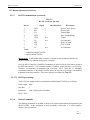
1
TABLE OF CONTENTS
SECTION I:
GENERAL INFORMATION
1.1
1.2
1.3
SECTION II:
General Description ..................................................................1-1
Power Supplies.........................................................................1-1
Specifications ...........................................................................1-1
OPERATING INSTRUCTIONS
2.1
2.2
2.2.1
2.2.2
SECTION III:
OPERATION
General............................................................................2-1
Amplifier Operation ..........................................................2-2
Local Operation........................................................................2-3
Remote Operation.....................................................................2-3
................................................................................................THEORY OF
3.1
3.2
3.3
3.4
3.5
SECTION IV:
Introduction ..............................................................................3-1
Amplifier Section ......................................................................3-1
Power Supply ...........................................................................3-2
Operate/Control Board..............................................................3-2
A3 Gain Control........................................................................3-2
MAINTENANCE
4.1
General Maintenance Information ..............................................4-1
4.2
4.3
4.3.1
Disassembly Procedures ...................................................4-1
Troubleshooting ........................................................................4-2
Front Panel Vacuum Fluorescent Display (VFD) Doesn’t Indicate
“Power On” ...........................................................................4-2
Unit Cannot be Operated Remotely............................................4-3
Thermal Fault ...........................................................................4-3
Interlock Fault ..........................................................................4-3
Voltage/Amplifier Faults............................................................4-4
Low or No Power Output (DC Tests)........................................4-5
4.3.2
4.3.3
4.3.4
4.3.5
4.3.6
SECTION V:
REPLACEABLE PARTS
5.1
5.2
5.3
Introduction ..............................................................................5-1
Ordering Information.................................................................5-1
Non-Listed Parts ......................................................................5-1
TABLE OF CONTENTS ( CONTINUED) iii
SECTION V:
5.4
REPLACEABLE PARTS (CONTINUED)
Circuit Designators ...........................................................................................5-1
5.5
5.6
5.7
Manufacturers’ Abbreviation Listing ..........................................5-2
Master List...............................................................................5-3
Schematics and Bills of Material (BOMs)...................................5-3
APPENDIX A: STANDARD ABBREVIATIONS FOR M ANUFACTURERS ....................A-1
SECTION VI:
RECOMMENDED SPARE PARTS
6.1
Level of Maintenance ...............................................................6-1
WARRANTIES : LIMITATION OF LIABILITIES
LIST OF FIGURES
2-1
2-2
Model 75A250A Front Panel.................................................... 2-2
Model 75A250A Rear Panel..................................................... 2-2
LIST OF TABLES
2-1
2-2
2-3
IEEE-488 Device Address Selection ......................................... 2-5
Remote Error Codes/Messages ................................................ 2-6
RS-232 Connector Pin-Outs ..................................................... 2-7
Model 75A250A
Manual Text
SECTION I
GENERAL INFORMATION
1.1
GENERAL DESCRIPTION
The Amplifier Research (AR) Model 75A250A is a self-contained, broadband Radio Frequency (RF)
amplifier designed for laboratory applications where instantaneous bandwidth, high gain, and moderate
power output are required. Solid state technology is used exclusively to offer significant advantages in
reliability and cost. When used with a frequency-swept signal source, the AR Model 75A250A will
provide 75 watts of swept power output from 10KHz to 250 megahertz (MHz). Typical applications
include antenna and component testing, wattmeter calibration, electromagnetic interference (EMI)
susceptibility testing, use as a driver for frequency multipliers and higher power amplifiers, and use as an
RF energy source for Magnetic Resonance Imaging (MRI) studies. The Model 75A250A can be
operated locally by using the unit’s front panel controls, or remotely by using its built-in IEEE-488 or RS232 interfaces.
1.2
POWER SUPPLIES
The Model 75A250A contains two switching power supplies. The input voltage range to these power
supplies is 90–132 Volts Alternating Current (VAC) and 180–264 VAC, 50/60Hz, universal or
automatically selected. The user does not have to switch or change anything on the Model 75A250A
when changing the unit’s AC input voltage. The unit’s AC power consumption is 400 watts nominal. A
built-in circuit breaker provides primary AC circuit protection.
1.3
SPECIFICATIONS
Refer to the “Amplifier Research Data Sheet” on the following pages for detailed specifications.
All voltage measurements referenced in this manual are Direct Current (DC) unless stated otherwise.
1-1
REV A
Model 75A250A
Manual Text
SECTION II
OPERATING INSTRUCTIONS
2.1
GENERAL
Operation of the Model 75A250A broadband RF amplifier is simple. The amplifier’s input signal, whether
swept or fixed in frequency, is fed into the jack labeled INPUT, and the amplifier’s output signal is taken
from the jack labeled RF OUTPUT. The unit is turned on by activating the POWER switch. A circuit
breaker in the AC power line provides protection in the event of a unit malfunction. A polarized, threewire AC power cord is also included with the unit to provide cabinet and chassis grounding to the power
mains.
CAUTION:
OPERATION OF THE M ODEL 75A250A BROADBAND RF AMPLIFIER IS NOT CRITICAL IN REGARD TO
SOURCE AND LOAD VOLTAGE STANDING-WAVE R ATIO (VSWR), AND IT WILL REMAIN
UNCONDITIONALLY STABLE UNDER ANY MAGNITUDE AND PHASE CONDITIONS OF SOURCE AND LO AD.
IT HAS ALSO BEEN DESIGNED TO WITHSTAND INPUT POWER LEVELS UP TO TWENTY (20) TIMES ITS
RATED INPUT OF 1MW WITHOUT SUSTAINING DAMAGE. HOWEVER, SIGNAL LEVELS > 20MW OR
TRANSIENTS WITH HIGH PEAK VOLTAGES CAN DAMAGE THE AMPLIFIER. ALSO, ACCIDENTAL
CONNECTION OF THE AMPLIFIER’S OUTPUT TO ITS INPUT CAN CAUSE OSCILLATIONS THAT WILL
PERMANENTLY DAMAGE ITS INPUT CIRCUITRY.
NOTE:
ALTHOUGH THE M ODEL 75A250A HAS BEEN DESIGNED FOR THE OVERDRIVE AND LOAD TOLERANCE
CONDITIONS DESCRIBED ABOVE, SUBJECTING THE AMPLIFIER TO THESE CONDITIONS
SIMULTANEOUSLY CAN CAUSE FAILURE OF THE UNIT’S OUTPUT TRANSISTORS . REPEATED FAILURES OF
THIS NATURE WILL NOT BE COVERED UNDER THE UNIT’S WARRANTY.
The Model 75A250A Amplifier is protected from input overdrive by a diode limiter on the RF input.
The Model 75A250A power transistors are protected from over-temperature by a sensor that senses the
heat sink temperature near the RF output transistors. In the event of a cooling fan failure or an air flow
blockage, the DC voltage will be removed from the RF stages; if and when the heat sink temperature
reaches approximately 70°C, the unit’s front panel vacuum fluorescent display (VFD) will read
THERMAL FAULT. Normal operation can be resumed by resetting the Model 75A250A after the heat
sink temperature drops below 70°C.
2-1
REV A
Model 75A250A
2.2
Manual Text
AMPLIFIER OPERATION
Figure 2-1 shows the front panel of the Model 75A250A broadband RF amplifier.
Figure 2-1
Model 75A250A Front Panel
Figure 2-2 shows the rear panel of the Model 75A250A broadband RF amplifier.
Figure 2-2
Model 75A250A Rear Panel
2-2
REV A
Model 75A250A
2.2
Manual Text
AMPLIFIER OPERATION (CONTINUED)
2.2.1 Local Operation
Power-up Sequence:
1.
2.
Connect the input signal to the unit’s RF INPUT connector. The input signal level should be
0dBm maximum.
Connect the load to the unit’s RF OUTPUT connector.
3.
Check to see that the MAIN POWER switch (circuit breaker) on the unit’s rear panel is set to
the 1 (“on”) position.
4.
Press the POWER switch: the front panel vacuum fluorescent display (VFD) should read
POWER ON, STATUS OK when power is applied.
(NOTE: The amplifier changes state each time the POWER switch is depressed—if the
unit is on when the POWER switch is depressed, it will turn off; if the unit is off when the
POWER switch is depressed, it will turn on.)
5.
In the event of a fault, press the FAULT/RESET switch; if the fault does not clear, refer to
subsection 4.3 (“Troubleshooting”) of this manual.
2.2.2 Remote Operation
2.2.2.1
Introduction
This subsection describes remote operation of the Model 75A250A amplifier by utilizing either the
IEEE-488 parallel interface or the RS-232 serial interface and a controlling devic e, such as a bus
controller or a personal computer (PC).
2-3
REV A
Model 75A250A
2.2.2.2
Manual Text
Selecting Remote Operation
The Model 75A250A can be placed in the remote operation mode at any time by
switching the FUNCTION switch on the front panel to the REMOTE position. In this
mode, control is transferred to the selected remote interface and all front panel
controls are inoperative with the exception of the FUNCTION switch. The amplifier’s
initial state will be Power Off. The front panel VFD will indicate REMOTE until the unit
is returned to the local operation mode.
2.2.2.3
Interface Selection
The Model 75A250A can be controlled via either the IEEE-488 or RS-232 interface; which
interface is active is determined by the position of Switch 6 of the rear panel Dual In-Line
Package (DIP) switch located between the two interface connectors. If Switch 6 is in the “on”
(1) position, the RS-232 interface will be active; if Switch 6 is in the “off” (0) position, the
IEEE-488 interface will be active.
2.2.2.4
Interface Set-up
Switches 1–5 of the rear panel DIP switch are used to select either the RS-232 communication
(BAUD) rate or the IEEE-488 device address, depending upon which interface is active. (Note:
These switches are only read at device power-up. In order for changes made in these switch
settings to take place, AC power must be removed and then re-applied to the Model 75A250A.)
2.2.2.4.1 RS-232 BAUD rate selection
The serial communication (BAUD) rate can be set to five different levels. Selections are made
by the positions of Switches 1–5 of the rear panel DIP switch. The following is a list of the
available BAUD rates and the corresponding DIP switch positions:
BAUD Rate
Switch On (1)
1200
1 only
2400
2 only
9600
3 only
19,600
4 only
76,800
5 only
(Note: Any other combination of switch settings will result in a BAUD rate equal to 1200.)
2.2.2.4.2 IEEE-488 device address selection
The IEEE-488 device address can be set to any number between 1 and 30. This selection is
made by setting Switches 1–5 of the rear panel DIP switch to the binary equivalent of the
number. Table 2-1 illustrates this switch selection.
2-4
REV A
Model 75A250A
Manual Text
2.2.2 Remote Operation (continued)
2.2.2.4.2 IEEE-488 device address selection (continued)
Table 2-1
IEEE-488 Device Address Selection
Device Address
Switch 1
Switch 5
Switch 4
Switch 3
Switch 2
1
off (0)
off (0)
off (0)
off (0)
on (1)
2
off (0)
off (0)
off (0)
on (1)
off (0)
3
off (0)
off (0)
off (0)
on (1)
on (1)
4
off (0)
off (0)
on (1)
off (0)
off (0)
5
off (0)
off (0)
on (1)
off (0)
on (1)
on (1)
on (1)
on (1)
on (1)
off (0)
:
:
30
2.2.2.5
Command Set Format
Each command is composed of one alpha character, up to four numeric parameters, and a
command termination character. The command termination character is the “line feed”
command, which is denoted and entered as <LF>. Commands are case-sensitive and must be
entered in upper case only in order to be recognized.
2.2.2.6
IEEE-488 Communications
For IEEE-488 communications, the “End or Identify” (EOI) control line may also be used for
command termination. When sending commands to the Model 75A250A via the IEEE-488 bus,
terminate each command with a <LF>, an EOI, or both. No characters are permitted after the
<LF> or EOI; the 75A250Ainterprets characters following the <LF> or EOI as the start of the
next command.
When an error condition is present at the Model 75A250A, the
“Service Request” (SRQ) line is asserted; the operator can then perform a serial poll operation.
The Model 75A250A error code (in binary) is contained in the returned serial poll status byte
(STB). These error codes are defined in Table 2-2.
2-5
REV A
Model 75A250A
Manual Text
2.2.2 Remote Operation (continued)
2.2.2.6
IEEE-488 Communications (continued)
Table 2-2
Remote Error Codes/Messages
2.2.2.7
IEEE-488 Serial Poll
Response (STB)
(binary/decimal)
Model 75A250A Error Condition
RS-232
Error
Message
(01000001) 65
BPM FAULT
E1
(01000010) 66
THERMAL FAULT
E2
(01000011) 68
INTERLOCK FAULT
E3
(01000100) 72
PS1 FAULT
E4
RS-232 Communications
If the RS-232 interface is active, the Model 75A250A will test for a properly connected RS-232
interface when it is switched into the remote operation mode. In order for the Model 75A250A to
recognize an RS-232 connection, the “Data Carrier Detect” (DCD) line must be asserted. This
line is sampled continuously to determine if the RS-232 connection is broken; therefore, it must
remain asserted in order for the RS-232 interface to function. The “Clear To Send” (CTS) line is
also used to gate information from the Model 75A250A. This line must be asserted in order to
receive information from the Model 75A250A. The CTS line can be used as a “handshake” line
to inform the Model 75A250A when it is permissible to send information. If the CTS line is deasserted in the middle of a transmission, the character in the process of being transmitted will be
completed and further transmission will halt until the CTS line is re-asserted. The
Model 75A250A itself asserts two lines: “Data Terminal Ready” (DTR) and “Request To Send”
(RTS). The DTR line is continuously asserted, while the RTS line is used to gate information into
the Model 75A250A. Connector pin-out information is given in Table 2-3.
2-6
REV A
Model 75A250A
Manual Text
2.2.2 Remote Operation (continued)
2.2.2.7
RS-232 Communications (continued)
Table 2-3
RS-232 Connector Pin-Outs
Pin No.
Signal
1
DCD
<
2
RD
<
3
TD
>
4
DTR
>
5
GND
N/A
6
NC
N/A
7
RTS
>
8
CTS
<
9
NC
N/A
*Note:
> = Output from Model 75A250A
< = Input to Model 75A250A
Data Direction*
Description
Device Carrier Detect
Receive Data
Transmit Data
Data Terminal Ready
Ground
No Connection
Ready To Send
Clear To Send
No Connection
Special Note: A null modem cable or adapter is required in order to properly interface the
Model 75A250A to a standard serial port on a computer.
Once the RS-232 interface is established, commands are processed in the same manner as that of
the IEEE-488 interface. The command structure is identical, except that there is no EOI line.
Therefore, all commands are terminated with a line feed (<LF>). Since this is a full-duplex
asynchronous interface, if the Model 75A250A detects an error, the error message is immediately
transmitted to the host controller. These error messages are defined in Table 2-2.
2.2.2.7.1 RS-232 port settings
The RS-232 port settings used for communication with the Model 75A250A are as follows.
Word Length: 8 bits
Stop Bits:
1
Baud Rate:
1200–76,800 (switch-selectable)
Parity: None
2.2.2.8
Remote Commands
The following commands are available to the user for remote communication and operation of the
Model 75A250A. In the descriptions of these commands, a lower-case “x” is used to signify a
numeric value or parameter.
2-7
REV A
Model 75A250A
Manual Text
2.2.2 Remote Operation (continued)
2.2.2.8
Remote Commands (continued)
2.2.2.8.1 Power On/Off
Controls the power on/off state of the Model 75A250A.
Syntax: Px
Parameters:
0 = power off
1 = power on
Example: To turn the power on, send the following command:
P1<LF>
2.2.2.8.2 Gain Set
Sets the gain in steps of (Max Gain)/4096 W.
Syntax: Gxxxx
Parameters:
0000 = Minimum Gain
4095 = Maximum Gain
2.2.2.8.3 Reset
Resets the Model 75A250A, clearing all faults, if possible.
Syntax: R
Parameters:
None
Example: To clear a fault, send the following command:
R<LF>
2-8
REV A
Model 75A250A
3.1
Manual Text
INTRODUCTION
The Model 75A250A amplifier consists of two (2) modules. The first module (A1) consists of three (3)
cascaded mosfet amplifier stages that provide approximately 33dB of gain. This module drives the second
module (A2) which consists of a dual mosfet amplifier operated as a push-pull stage that provides
approximately 16dB of gain. Input and output networks are utilized to provide optimum power transfer of
the RF signal when the amplifier is connected to a source and load impedance of 50 ohms. Interstage
coupling is the accomplished by means of capacitors between the three (3) cascaded stages and
transformer coupling between these stages and the push-pull output stage. This provides an overall flat
frequency response that is further enhanced by utilizing negative feedback around each transistor stage.
The self-contained power supply consists of 2 switching power supplies, which feature universal input
voltage capability. Gate bias stability is provided by a three (3) terminal regulator set for 15 VDC.
3.2
AMPLIFIER SECTION
Refer to Schematic Diagram No. 1007868 and 1007872
The input signal to the amplifier is fed through the gain control assy to the gate of Q1, which is input level
limited by diodes CR2 and CR3. Biasing for Q1 is accomplished by R10, R14 and R16 which drives the
gate of Q1. Bias voltage for Q2 is adjusted via R6 through R11 and R17. Output of Q2 is coupled
through C4 to the gate of Q3. The output of Q3 is coupled to transformer T1 of the A2 module which is
utilized to drive push-pull stage Q1A and Q1B. Resistor R12 sets bias voltages for Q1A and Q1B, in
conjunction with R10 which is used to equalize the bias voltage on gates of Q1A and Q1B.
The output of Q1A and Q1B are coupled through matching transformers T3 and T4 to the coaxial
connector on front panel of the unit.
Power gain of each of the three (3) cascaded stages are approximately +11 dB and +16 dB for push-pull
stage, giving an overall gain of better that +49 dB for the amplifier.
U1 and U4 with their associated circuitry provided over-dissipation protection for the FET’s in the final
amplifier. This is done by sensing the DC input current. When the DC input current exceeds a preset
level, the bias voltage on the output transistor is reduced, limiting the current.
3.3
POWER SUPPLY
Refer to Schematic Diagram No 1011806.
The Power Supply Assembly consists of two switching power supplies: PS1 and PS2. PS2 is a 25-watt,
triple-output power supply with three regulated output: +5V, +12V, and –12V, has a universal input range
of 85-264VAC, 50/60Hz. PS2 supplies ±12V and +5V to the operate/control board and to the gain
control. PS1 is a 28V, 11A supply with a Power Factor Corrected front end: it will operate over an input
voltage range of 85-264VAC, 50/60Hz. PS1 supplies +28V to all of the RF Amplifier gain stages. PS1
also supplies to operate Blower B1, which supplies air flow to cool the heat sink and the power supplies.
3-1
REV A
Model 75A250A
3.4
Manual Text
A4 OPERATE/CONTROL BOARD (SCHEMATIC DIAGRAM No. 1008597)
The A4 Operate/Control Board is a microcontroller-based printed wiring board (PWB) assembly that
allows sensing and control of internal signals as well as remote personal computer (PC) control via onboard RS-232 and IEEE-488 data communications ports. The A4 Operate/Control Board utilizes a stateof-the-art, Reduced Instruction Set Computing (RISC) microcontroller that can quickly and reliably
perform all front panel control and monitoring tasks, thereby allowing real-time control to the Model
75A250A via either remote bus. Besides being reported remotely, all amplifier faults are continuously
monitored and indicated via the unit’s front panel VFD.
3.5
A3 GAIN CONTROL (SCHEMATIC DIAGRAM NO. 1009914
The gain control allows for gain adjustment either from the front panel or from the RS-232 Port or the
IEEE-488 Port. U4 and U5 are 2 electronic attenuators connected in series to give a minimum adjustment
range of 18 dB. U1 is a switch that selects front panel control or remote control.
3-2
REV A
Model 75A250A
Manual Text
SECTION IV
MAINTENANCE
4.1
GENERAL MAINTENANCE INFORMATION
The Model 75A250A should require very little maintenance since it is a relatively simple instrument. It is built with
etched circuit wiring and solid state devices which should ensure long, trouble-free life. However, should trouble
occur special care must be taken in servicing to avoid damage to the devices or the etched circuit board.
Since the components are soldered in place, substitution of components should not be resorted to unless there is
some indication that they are faulty. In addition, take care when troubleshooting not to short voltages across the
amplifier. Small bias changed may ruin the amplifier due to excessive dissipation or transients.
Components with Amplifier Research instruments are conservatively operated to provide maximum instrument
reliability. In spite of this, parts within an instrument may fail. Usually, the instrument must be immediately repaired
with a minimum of "down time". A systematic approach can greatly simplify and thereby speed up the repair.
However, due to the importance of the amplifier's alignment, it is recommended that when failure is caused by
breakdown of any of the components in the signal circuits, the amplifier be returned to the factory for part
replacement and amplifier realignment. Shipping instructions are as follows:
Ship PREPAID via United Parcel Service to:
AMPLIFIER RESEARCH
160 SCHOOL HOUSE ROAD
SOUDERTON, PA 18964
See warranty statement at rear of manual.
4.2
COVER AND CIRCUIT BOARD REMOVAL
CAUTION:
REMOVE POWER CORD FROM RECEPTACLE BEFORE SERVICING.
4.2.1
The amplifier can be removed from the housing by removing 4 screws from the front panel and 4 screws
from the back panel. The amplifier can then be slid from the housing.
4.2.2
The top cover can be removed to gain access to the RF assembly. The bottom cover can be removed to
gain access to the power supply assembly..
4-1
REV A
Model 75A250A
4.3
Manual Text
TROUBLESHOOTING
The techniques used in troubleshooting solid state instruments are similar to those used in vacuum tube
instruments. For instance, a good way to start troubleshooting is to check the supply voltage at the amplifier supply
voltage terminal. If it is low or nonexistent, check the power supply components starting with the AC fuse.
The power supply for the driver should be a nominal 28 volts, and the power supply for the output stage should be
a nominal 28 volts. Incorrect voltage can result in over-dissipation in the transistors or severe distortion and nonlinearity of the amplifier. The power supplies may be disconnected from the RF board to enable troubleshooting
without danger of damaging the RF circuitry.
Finally, determine if the individual amplifier stages are operational by injecting a signal into the transistor gate and
looking for an indication of output.
CAUTION:
BEWARE OF VOLTAGES APPLIED TO THE GATE OF A MOSFET TRANSISTOR IN EXCESS
OF ± 20 VOLTS, THIS WILL RESULT IN TRANSISTOR GAT FAILURE.
4.3
Troubleshooting
Troubleshooting the Model 75A250A in a logical manner can speed the solution to a problem. The settings
of potentiometers (“pots”), capacitors (“caps”), or other variables should not be disturbed until other
problems have been eliminated. Comparing the measured DC voltages to those shown on the schematics
can solve many problems. Before measuring circuit voltages, first verify that the voltages to the circuits
are correct.
Model 75A250A Troubleshooting Categories:
Subsection 4.3.1—Front Panel Vacuum Fluorescent Display (VFD) Doesn’t Indic ate “Power On”
when the POWER Switch is Depressed
Subsection 4.3.2—The Unit Cannot be Operated Remotely
Subsection 4.3.3—Thermal Fault
Subsection 4.3.4—Interlock Fault
Subsection 4.3.5—Voltage Faults
Subsection 4.3.6—Low or No Power Output (DC Tests)
4.3.1 Front Panel Vacuum Fluorescent Display (VFD) Doesn’t Indicate “Power On” when the
POWER Switch is Depressed (Schematic Diagram No. 1011806)
4.3.1.1
If the Model 75A250A is operating in an otherwise normal fashion, the unit’s front panel
vacuum fluorescent display (VFD) or the wiring to it could be defective.
4-2
REV A
Model 75A250A
Manual Text
4.3.1.2
Check the FUNCTION switch on the unit’s front panel; it must be set to the LOCAL
position in order to operate the front panel POWER switch. Check the circuit breaker on
the unit’s rear panel; it must be set to the “1” (“ON”) position.
4.3.1.3
4.3.1.3 If the “Power On” indication is not displayed and the cooling fan (Blower B1) is
not running, check to see that the unit is plugged into a live outlet and that the AC line
cord is plugged securely into the unit.
4.3.1.4
Check the output voltages from PS3; these voltages should be as follows:
PS3 J2, Pin 1
PS3 J2, Pin 2
PS3 J2, Pin 6
+12.0 ± 0.3VDC
+ 5.0 ± 0.2VDC
-12.0 ± 0.3VDC
If output voltages are not present on PS3, check the AC input to PS3.
4.3.1.5
Check the voltages to the A4 Operate/Control Board on connector A4 J3; the voltages
should be as follows:
A4 J3, Pin 16
A4 J3, Pin 29
A4 J3, Pin 31
-12.0 ± 0.3VDC
+ 5.0 ± 0.2VDC
+12.0 ± 0.3VDC
4.3.1.6
Check the voltage on A4 J3, Pin 3; it should be ≥4V when the POWER switch (S1) is in
the normal position and <0.1V when S1 is depressed. S1 is normally open; it is closed only
when it is depressed. The amplifier should change state every time the POWER switch is
depressed.
4.3.1.7
If all voltages are correct and the unit still does not operate, contact Amplifier Research to
arrange for repair or replacement of the A4 Operate/Control Board.
4.3.2 The Unit Cannot be Operated Remotely
4.3.2.1
Verify that the front panel FUNCTION switch is set to the REMOTE position.
4.3.2.2
Verify that the unit operates locally by resetting the FUNCTION switch to the LOCAL
position; if the unit does not operate locally, see subsection 4.3.1 of this manual.
4.3.2.3
Check the position of the “ADDRESS” switch assembly (SW1) on the A4
Operate/Control Board; this assembly can be accessed through the unit’s rear panel. Check
to see that these switches are properly set for either RS-232 or IEEE-488 operation, as
desired.
(See subsection 2.2.2 of this manual for the proper “ADDRESS” switch settings.)
(Note: Address switches are only read at unit power-up; remove and re-apply AC power
(i.e., reset the circuit breaker) after changes are made.)
4-3
REV A
Model 75A250A
Manual Text
4.3.3 Thermal Fault (Schematic Diagram No 1011806)
During a Thermal Fault, the front panel VFD should read “THERMAL FAULT.”
4-3
REV A
Model 75A250A
Manual Text
4.3.3 Thermal Fault (Schematic Diagram No 1011806) (continued
4.3.3.1
Try to reset the unit; if the unit resets and operates normally, check to see that the cooling
fan (B1) is operating normally and that the air inlet on the bottom of the unit and the air
outlets on the rear of the unit are not blocked.
4.3.3.2
If the unit does not reset and the cooling fan is operating normally, check the voltage at
the A4 Operate/Control Board, J3, Pin 21; it should be ≤0.1V.
4.3.3.3
If the voltage on A4 J3, Pin 21 is high, check the thermal daisy chain through A2S1 to
ground.
4.3.4 Interlock Fault (Schematic Diagram No. 1011806)
The Model 75A250A is equipped with an interlock connector, which is located on the rear panel. The
interlock circuit can be used to sense the openings of doors to screen rooms, test chambers, and so forth,
and to turn off RF energy when these doors are opened.
Note: The Model 75A250A is shipped with a mating connector, which has a jumper between
Pins 1 and 8, installed in the rear panel interlock connector. The unit will not operate unless
the interlock circuit is closed.
4.3.4.1
In the event of an Interlock Fault, the unit’s front panel VFD should indicate
“INTERLOCK FAULT.”
4.3.4.2
Check to see if it is safe to power up the unit—are there personnel present in the screen
room, or are doors to the screen room open?
4.3.4.3
After checking for safety, try to clear the Interlock Fault from the front panel by using the
RESET switch.
4.3.4.4
If the Interlock Fault will not clear, check for continuity in the External Interlock Circuit
(Pin 1 to Pin 8 in the connector, which mates with J2 in the rear panel).
4.3.4.5
Check the voltage on A4 J3, Pin 5; it should be ≤0.1V.
4.3.4.6
If all of the above voltages are correct and the unit still will not reset, check for defective
wiring and/or PWB connections, then try the RESET switch again. If the unit still will
not reset, the A4 Operate/Control Board is defective. Contact Amplifier Research to
arrange for repair or replacement of the A4 Operate/Control Board.
4-4
REV A
Model 75A250A
4.3.5
Manual Text
Voltage/Amplifier Faults (Schematic Diagram Nos. 1011806)
The model 75A250A fault circuits sense voltage faults from PS1 (28V). They also sense an over
current fault in the final amplifier stage.
4.3.5.1
Power Supply Faults (Schematic Diagram 1011806). PS1 sends a BUSS OK signal to
the operate/control board (A4). This signal gives an early indication of over voltage or
over current conditions. If either condition occurs the power supply sends a fault signal to
the operate/control board which in turn sends a disable signal to the power supply turning
off the outputs.
4.3.5.2
The Final Amplifier Assy Faults. (Schematic Diagram 1007872 and 1011806). The final
amplifier incorporates two stage protection for the output transistors. U1 monitors the
device current which is normally 6.0 amps. If the amplifier is over driven so that the
current rises to 8.0 amps U1 will decrease the bias voltage thereby decreasing the
current. If the amplifier is over driven to the point that the active bias cannot control the
current to less than 9.0 amps U4 will generate a fault signal which will turn the power
supplies off.
4.3.6 Low or No Power Output (DC Tests) (Schematic Diagram No. 1011806)
All indicators on the Model 75A250A VFD are normal, the VFD indicates “POWER ON” and
“STATUS OK,” and the cooling fan (Blower B1) is operating.
4.3.6.1
4.3.6.2
4.3.6.3
Check the RF input to the unit—is it the correct amplitude and frequency?
Check the RF output connection from the unit—is it correctly connected to the load?
Is the coaxial cable okay?
Check the voltages at the following locations. Troubleshoot any incorrect voltages.
Feed-through Cap.
Normal Voltage
Remarks
A3 C9
A3
A1 C1
A2 C1
A2 C2
+12V
Gain Control
Gain Control
Driver Stage
Final Amp
Final Amp
C12
-12V
+28V
+28V
+28V
Note: The locations of the feed-through capacitors can be found on the RF Assembly
Drawing (Schematic Diagram No. 1010613).
4-5
REV A
Model 75A250A
Manual Text
4-1
REV -