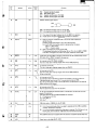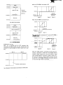
1
SHARP
SERVICE MANUAL
CODE: OOZPC1600SME2
""
"J=
GlLe
--
.
..,,'w,~"""
.g.
_VCR
1\1 ST'~
__ _ • •
_.. _.....
__ • • • • • • • • 111111 III llilllil
• • • • • • • • • ~ • • • I!!I
iii • • • • • • • • • • • ~IIII!!I
.......
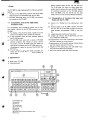
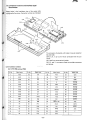
MODEL
PC-1600
This manual contents CE· 1600P/CE-1S00F/
CE-1600M/CE-1600L/C E-1601 L/ CE-1602L/
CE-1603L/ CE-1604L
~---------------------CONTENTS----------------------~
1. SCope ................ •• ... . ..............• o • • • • • • • • • • • • • • • • • • • • • • • • 1
2. Specification ........... _• . . . . . . . . . . . . . . . . • • • . . . . . . • . • . . . . . • • • . • • . . . .. 1
3. System configuration . .... • ....... .• . . ......• .. .. . ... •• • • •.• . .•• •••... . 3
i
4.
5.
6.
7.
8.
9.
10.
11.
12.
•
*
•
•
•
•
*
•
PC-1600 b lock diagram ....•.. . .. . .• . ••• •• • • • • •• •• . ••• • • • •• • . • • •. . . ..... 4
Memory mapping .... . ... • •• • • • .. • •• •. . .. .. .• ••. .....••..... . • •........ 7
Power suppl y ........ . .. .• •.......• •........ • •... . ..•• . .....••....... 11
System operation ....... •• •.... .. . ......... •• •......••...... ••••. .... 11
Serv ice precations ...... ......... . . ... , ....•...... . .. • • ••••• • • • ••••.. • 15
LSI pin descriptions .. .......•....•......•.•.... ... • . •• •... •.••• •... . . 20
Connection locations and interface signal identi f ication ......••..... . .• • •.. ... 35
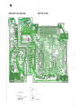
Circuit diagram and P.W.B parts & signal position •. ...... . . . . • ••..... ••• •. ... 39
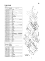
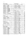
Parts list and parts gued .. ......... ............ . ......• •• •• • • • •• • • ••.... 57
CE-1600P ........... .. ... _.. .. . __.... . _..... . . ___ _. . .. ...... .. . _... 63
CE-1600F ...............• • •• •• •••• •• •... . ........... • • .. . ..•••..... 98
CE -1600M .......... ... . .. ...... . ........ . . . . _. __ •• •••• ••• • • • ••.... 105
CE-1600L ........ .. ... . . , . ... .. _.......... . .... . . .. . ............... 110
CE-1601L .......... . .. . ............................................ 111
CE-1602L .............................. _......... .. ...... ... .. ..... 112
CE-1603L .... •• . .....• • • • •• . • . . • • • • •• • . .• • •• • • . •• ••• ••• ..•••• .• • •.. 113
CE-1604L .......... . .. .. . .. . __ . _........... .. ...... . .... . . .. . ...... 114
SHARP CORPORATION
~
-------------------------------------..~---l
PC- l 600
1. Scope
(Memory modules usable: CE- 151, 155, 159, and 161.)
The CE·160 does not meet the upper grade compatibility test for software that uses the REM· ' because
of a functional restriction on the PC·l600 OPtional
printer CE·1600P, since the CE·l50 has two data
The PC-l600 has been designed with the following versatile
features:
, . The most of PC-1500 BAS IC software and the PC·1500
hardware options are compatible with the PC·l600.
2. Advanced technology gives the PC- l 600 new features
not available on the PC 1500.
rec order remote control terminals ( RE M-O and REM-1).
1-2. Implementation of functions that were not
feasible with the PC-1500
1·1. Compatibility with the PC-l500 BASIC
simulation mode
(a) Adoption of a 26-digit by 4-line alphanumeric LCD
unit.
(b) Operation speed of the PC· 1600 is approx. 2.5 times
faster than that of the PC· 1500 as a result of using the
general purpose microprocessor (Z·BO) as the main
CPU.
(c) Increased expansion module slot (two slots).
(d) Increased user memory area (11 ,834 Bytes user area
out of 16KB basic RAM area).
Ie) Implementation of the EIA. conforming to the internal
RS-232C interface for communication .
(f) Implementation of the system wake-up (modem phone
and timer started) and alarm functions.
(g) Adoption of the analog input, bar code reader input,
and external keyboard input interface.
(hi Use of the internal optical fiber (SIOJ interface.
For compatibility with succeeding models, most of software created in BASIC for the PC·150D can also run o:n the
PC· 1600.
(a) For display in the simulation mode. a single line on the
bottom of the display rows is subject for execution .
(b) In the simulation mode, the same character codes of
the PC-1500 are used.
(c) The PC-1600 must work with a variety of PC-1500
software programs that include an option controlling system. and the PC-16OO system bus signals are
upper grade compatible with the PC-l500 system bus.
(Consideration is given for the use of the CE-l50. 158.
and 162E.)
(d) The slot signals are also upper grade compatible; this
allows the use of the PC-1500 memory module on
1he PC-1600.
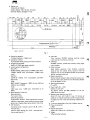
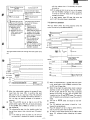
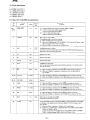
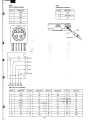
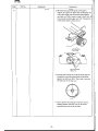
2. Specifications
,
• Model name : PC-16OO
• Keyboard layout:
5
cb
(1)Alphabetic key.
(2)SmaU kay
(3) Shift k.y
(4) Function k.y.
(5) On end Off key
(61 CllNlr k.y
(7) Mod. key
(8) Num.ric and Arithmetic Operation keys
191 Enter key
- ) -
-
PC- l600
•
Display unit :
FEM-LCD (LF·7204E)
Graphic display : 156 x 32 dots, 16 symbols
Character display : 26 digits x 4 lines
. II ...
( U ) U76
7
.."
L'"
0.'
BUSY SH I fT [!I(I>
I
i
/
.!!
.... ~1J1")
.
6."
.'"
... '"
S~ L L
DEGRAO
!!!..
~
0.58 0.06
""
~[ ~
~
.
....
M.
...
...
•
.."
· 0'
' ."-
-
.,.
~
I"
.
RES ERVE
RUNPRO
.
OEF
I'.
~
4 • .5 )
!
~
.--•-
!BATT!
~
l i56x82 Do!.
0;
•
~,.,tIIC*WI~f
.
=
~II
IS :18
.. m. 101 .' 26 ..... R O.S /
R., ....... II... /
90.43
fl.ll11.2$6 +8]
" "
Notl 1 unit: m m
Fig. 1
• Calculation capacity :
10 digits (mantissa) + 2 digits (index)
• Calculation method :
Formula based (with priority discrimination feature)
• Programming language :
BASIC (PC-l500 upper grade compatible)
•
•
•
Internal system configuration :
Main CPU:
•
SC7B52 (CMOS, Z·80 compatible, 3.58MHz basic clock)
LH5803 (CMOS, B-bit microprocessor, 2.6M Hz basic
clock)
Sub CPU :
LU57813P (CMOS,
•
4·bit microprocessor, 307.2KHz
basic clock)
ROM :
96KS (SASIC interpreter) - (aaKS for the l ·80 and
l6KS for the LH ·5803 )
RAM :
16KS (user area : 11 ,834 bytes), incremental up to
BOKB.
• Basic calculation funct ions :
Basic calculation :
Four rules of math .
Scientific calculation :
Trigonometric function , inverse trigonometric function ,
logarithm, exponential, angular conversion, power raising,
square root, integral, absolute value, signum, circle ratio.
• Edit functions :
Horizontal cursor movement control ( II>, ""' , CTA L +
character key)
Insertion !INS), deletion (DE L, CTAL + character key)
Line up and down (+, t)
•
•
•
•
•
•
•
- 2,
Interrupts :
Timer interrupt, RS-232C interface interrupt, analog
input interrupt, function key interrupt
Interfaces :
RS·232C interface, optical SIO interface, analog signal
input interface
Other functions :
Weak battery detection, timer function, automatic
power·on (by the internal t imer), power-on from the
telephone line (to the AS-232C interface via the modem
phone ), automatic power-off
Memory protection:
Battery backup (program , data and reserve memory contents are saved upon power-off, and the backup battery
of the AC adaptor in use)
Operating temperature :
0° t o 40°C
Power supply 6V .. . (DC):
SUM-3 x 4 (AA) (x4)
AC adaptor option (EA-160) (accessory of the CE1600P optional printer)
Battery power retention time (AA) :
About 25 hours with SUM ·3 in use; 10 minutes of
operation or program execution and 50 minutes of data
on display per hou r under the operating temperatu re of
20°C.
It may vary depending on the kind of bat tery and use ,
Power consumption :
O,4BW
Physical dimensions:
195mm (W) x 86mm (D) x 25.5mm (H)
Weight :
375g (including batteries)
-------------------------------------------------,...
PC - l600
• Accessories:
Soft csse, template Ix 11. SUM·3 batteries (AAI (x 4),
instruction manual, BASIC language manual, name
label
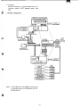
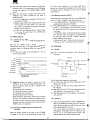
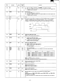
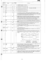
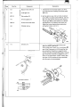
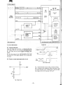
3. System configuration
CEol600P Printer with CAsK"' tnttrfK'
I"'own.
1i. ,~
I
Recorder
CE· I600l
Optical
OptiGiI
Seri,l Port Fi~r Cable
o
I
I
!::::;:::::
RS-232(
S.,i,1 Port
P".lleIlnt,rf,cf Unit
Interfac,
CE·SI6L
..0.., ..~'~':bI~'..,
:~~~~tj ..0.., "",,"=""-t
CE· '60'L
CE-1602L
Cable
CE· l603L
Cable
CE· I604l
c.bl,
NOTE : The PC-1600 option (CE·1600P) cannot be used
in conjunction with the PC·1500 option (CE- 15D,
CE·158, CE·l62).
- 3-
An....
Input Port
CE· ,saseri,l . nd
~
I
<>----*---C:>
1
PC 1600
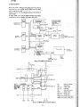
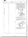
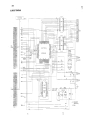
4. PC-1600
blo~
diagram
H D6 1203 (51)
LCD
C. DR IVEA
s ry
S
T
LCD
-
E
M
B
Leo s. DRIVE
LC D S. DR IVE
LH ·5803
THD61102
HD61102
.....
MAIN CPU
2
U
S
S
L
-
-
a
T
1
~
I
SC7852
LA38041
GA TE ARRA
32KB ROM
aKe RAM
,3
,2
TC8576F
S
L
r-
a
T
2
L-
-
LU57813P
SUB·CPU
UART
-
ON
AESET
BX7269W
I
2
3
2
C
1
KEYBOARD
o
S
MAIN CPU
ON
S
I
R
.....
CONVER T
ANALOG IN
3.58 MHz
rDICGC
I
LH II F
Z·80
Z·80 BUS
LH-5810
compatible
Keyboard
Interrupt
Memory
control
control
Timer
I/ O control
Main unit RAM
Buner
RS232C
Cassette
System bu.
SLOTt
SLOT2
Main un it ROM
Mai n CPU internal block
Fig. 2
-,-
d i~ ram
UART
ItC.
MAIN CPU 2
LH·5803
Then, t'CH goes to a low leV1!1 so that the LH·5803 bus
is activated_ LHWAI T now goes to low wh ich causes
the LH·5803 to operate.
4·1 . Relation of the main CPU·1 to the main
CPU-2
Since two CPUs are linked together, the bus line of ont
CPU is on the sytem bus; the other CPU bus is kept in the
floa ting state.
Shown in the following table are the bus signals of the two
CPUs in connection.
SC7852 signal name
Z.sO signal nama
LH.o803 signal nlml
A15 - AO
A15 - AO
A15 - AO
OB7 - DBO
07- DO
07- 00
MREQ
Oppos~rity
of
R
OPPOSi~' lty
of
Mel
If!!
If!!
00 ·
WR
WR
RIW
• The OD output of the LH-5803 is connected to
the SC7852 via the gate array (LR38041).
The operating CPU is indicated by the ELH signal.
ELH '" Low: LH-5803
ELH '" High: Z-80
uue_
~~T38H)A
The sub CPU has the following roles.
(1) Main power·on and main power·off
When the system.off command is received from the
main CPU, the system is turned off,
® The system is turned on when the system is switched
on by tl'lelONlkey.
<D
MeO
IORC
z.eo Inttnoctlon
L H ~ I ..
4-2. Sub CPU role
(2) Real timer
Similar to the PC-1500; month, day, hours, minutes,
and seconds are controlled by the PC·l600, though a
leap year is not issued .
® A single wake-up timer and two alarm timers (in .
cremented at every 0.5 second) are controlled .
<D
AD of
(3) Weak battery detection
A weak battery condition is monitored by the AI D
converter function held by tl'le sub CPU .
<D Thelevel of the PC-1600main power supply is checked.
® Also, the level of the power supply to the PC-1600
option is cl'l ecked.
When it drops below the given level, the symboli BATTI
is activated on tl'l e LCD . When the hardware-monitored
weak battery Signal is turned to high, the system is
tl'len turned off.
HALT
OUT(38H). A
(4) Analog input
The level of the input signal received through the
PC 1600 analog input jack is AI D converted and
returned to the main CPU .
Also, an external keyboard input through the same
jack may be read and returned to the main CPU.
STA Ir AOlllH. A
Fig. 3
The following takes place when a reset is applied to the
SC7852 (AsfiN · Low).
<D ELH goes to high to indicate that the Z·80 is in
operation. At the same time, a reset is applied to the
LH-5803 . This allows the Z·80 to operate after the
completion of the reset_
® With the following instruction, the Z.aO hands down
the control to the LH-5803.
OUT(38H), A .... A is don't care.
HALT
After the execution of the above instruction, the Z-80
bus is set in the floating state. At the same time, £IR
goes to low along with RSTO, and the reset is cleared
to the LH -5803 to start its operation.
® With the following instructiory, the LH-5803 hands
down the control to the 2-80,
STA # A038H
A wait is appl ied to the LH·580J (L HWA1T"" High) to
stop the operation of the LH·5803. When E LH goes to
high, the LH-5803 bus is set in the floati ng state, With
this, the Z·80 starts to operate.
(5) CI ick sound
A click sound feature is supported by the PC-16(lO.
When a keyboard entry is sensed in the click generate
mode, tl'le command is issued from the main CPU to
generate a click sound .
(6) Reset signal
Two reset Signal input lines are supported . When a
signal is received on eitl'ler line, a reset is applied to the
system for the prescribed time (30 milliseconds).
CD RESET switch on the back of the PC-1600
® RESET switch on the back of tl'le CE-1 600P
(7) System-on function with the CI signal of the RS·232C
interface (checked at every 0.5 second)
(8) Timer signal output (1 / 64 sec.)
G) In order that the 2·80 may hand down the control to
the LH-5803. the 2-80 stops after the operation as in
step 2 and the Z-80 bus is set in tl'le floating state.
- 5-
PC- l600
<D
4·3. Sub CPU operation
(Interfacing w ith the main CPU)
TC8516 F (UART)
LU5181JP !wbCPU)
DSTB
KI
IIDSV
ZIO
z'
ACK
DAIAS
uxh-r
RI B-ROO
roo •• ·······1
,,,
,
,
,
,
07- DO
(dal a bus)
Buffer
,
,
,
,
IORP
r
(from SC1852)
,,
,
,
R33- R20
,
Conlained in the LR38041 gallluay
Fig. 4
Signals interfaced with the main CPU are KI, Z10, Z9,
A13-AOO, and A33- R20.
Rt3- ROO=::)<
kt
Comm.1Id
Xc________
I \3". r;;;:l
'"
"
R• ..,
The following shows signal timings.
R.ody
y
Sand
c;ommend
Send command strobe
ACK ntCailild
N
-- -- - --- . .,
- 6-
Before the Z-BO CPU sends a command to the sub
CPU, the sub CPU is asked if it is ready to receive the
command. If it is not, the Z-BO waits until the sub
CPU becomes ready .
The Z-80 assumes the sub CPU to be ready if the
BUSY input of the UART is high.
® Next, 8-bit command data are sent to the sub CPU.
The Z-BO sends the data on the DATA1-DATAB port
of the UART, which are received by the sub CPU
through A13-ROO. Unless ACK is returned withi n one
second, the Z-BO proceeds to the next processing.
® The Z.aO sends a pulse signal on DSTB of the UART in
order , to inform the sub CPU a command request,
which the sub CPU receilles of through the Klline.
With the Kt line of the sub CPU high. an interrupt
is sent to the sub CPU, and the command is processed
in the interrupt service routine.
(!) One of the fo llowing requests may be made depending
on the command issued from the Z·80.
(i) A request far return data
(ii) A request not to return data
The sub CPU then interprets the abolle to proceed to
the next step.
(i) A pulse signal is sent on Z9 after sending the
return data on R33- R20, to indicate completion
of the command execution.
(i j) A pulse signal is sent on Z9 to indicate receiPt
of the command.
In either case, the Z-80 waits for a high pulse signal
state on Z9.
The high state received on Z9 is then input to the
ACK line of the UART and latched internally, The
Z-80 checks the latch if it is okay.
® When the Z-80 accesses 33H of liD to request the
return data, it forces IORP to low so that the LR38041
gate array internal buffer is opened to send the return
data (R33- R20) on the Z.aO bus D7- DO.
-
PC- l600
5. Memory mapping
5·1 . Memory map as seen from the Z-80 (SC7852)
OOOOH
PC-'600
ROM
(CSOO,)
,
4000H
PC-1S00
ROM
,
(CS24)
,,
52
ROM
(e)
(CSOOi)
CE·l600P
CE·'SOOP
PC·'SOO
Slot 2
ROM
ROM
(Printer)
(Fl oppy
disk)
Ca$Sel1e
8000H
PC·1600
Slot 1
S1
Slot 1
51
52
52
(A)
(8)
(e)
(0)
Slot 2
Slot 2
ROM
(CS24)
(CS123)
ooooH
PC-1S00
(RAM3)
FFFFH
Bank 0
I
Bank 1
Bank 2
Bank 3
The memory space directly accessible by the Z·80 is 64KB,
however, the memory space is expanded to 320KB for the
PC·1OO0 by means of bank selection. Bank selection is done
according to the contents of the Z·80 I/ F address 31 H.
When the Z·80 accesses a space in OOOH""3FFFH, bank
o or bank 1 is selected depending on the status in bit
o (bO) of the I/O address 31 H.
If bO = 0, bank 0 -+ PVaUT : 0
If bO = 1, bank 1 -+ PVOUT: 1
PVaUT (SC7852 output) is used to represent the chosen
bank (0 or 1). PVaUT is 0 when bank 0 is selected. It is
1 when bank 1 is selected.
Similarly, when the Z·80 accesses a space in 4000H '""
7FF FH , bank 0 '"" bank 7 is selected depending on the
status in the bits, b3 - b1. pvaUT, PU, and PT are used
to represent bank 0 thru bank 7.
The PVOUT, PU, and PT conform to the I/ O address 31H
and the space accessed by the Z-80.
It is possible to sense the status of the 1/ 0 address 31 H.
Bank 5
Bank 4
Bank 7
BankS
Table-2
Bank
Z-80 ace_ing
St'tul in 1he 1/0
No.
lilac,
addreu 31H
o
,
o
,
PT
PU PV
U
o
OQOOH-3FFFH
,
,
40(X)H -1FfFH
·
00'·00'
2
.·· .
·
··
0'0·010
3
•• •• 0 1 1 . 0 ' 1
c
,
,
t
7
,
· · · · 11
1·1
11
o
8000H - BFFFH
• 0 0 0
•
•
0
1
.001
••••
001
00 . · ••
100
•
•
0
0
2
3
c
.
'
,
,
t
.101
••••
101
7
t
·111
••••
1
o
,
COOOH- FFFFH
t
10
o • • • • • • • •
•
0
,
°
1
•
•
•
•
•
•
•
•
0: DON'T CARE
- 7-
--
PC-l600
5·2. Chip select signal
(1) CSOOl
This signal must be low to access the memory space in
aKB RAM
OOOOH-7FFFH of bank O. The signal is also an input
to the ~ line of the ADM .
(2) CS123
Th is signal must be low to access the memory space
of SOOOtt-BFFFH of bank 6. The remaining l6Ke
area of the second half is for the LH·5803 control
ROM . Th is signal is also an input to the CS line of
Csm
input
Memory space chosen
A13
COOOH- DFFFH
A13A linvened A13 ~a arrav output)
EOOOH-FFFFH
(5) RAM2
Memory select signal for the memory slot 1 (5 1).
This signal must be low to access the memory space in
BOOO H...... BFFFH of either bank 0 or bank 1.
1.
the ROM .
The ROM (64K B) selected bV CSOOl or
m
is
(6) RAM1
cleared when a high signal is given to the INH line
which is connected to the system bus and slot (pulled
Memory select signal for the memory slot 2 (S2).
This signal must be low to access the memory space
in 8000H-"'SFFFH of either bank 2 or bank 3.
It is possible by means of software to copy 16KB
of memory space in 8000H...... BFFFH onto 16K S
of memory space in 4000H......7FFFH of bank 1. (This
area is reserved for the application modu le which is
expected to be made avaiJabel soon.)
down to low within the main unit),
(3) CS24
This signal must be low to access anyone of the l6KS
spaces.
(a) For accessing of bank 3 of the memory space in
4000H -7 FFFH.
• CS24 is an input to the CS li ne of 256K biu
ROM .
• A 15 is connected to DE of the ROM.
• This l eKB space is further banked by another
port signal to compose a 32KB area.
(4) RAM3
This signal must be high to access the memory space
in COOOH ...... FFFF H of bank O. This signal is connected
to CE2 of the two 8KB RAMs. A 13 is used to
determine which RAM is to be selected.
5·3. Memory map as seen from the LH·5803
ooooH
51
51
=
=
51
51
RAMf
RAI!T
m;
Bank 2
Bank 3
Bank 4
4000H
RAM
16KS
RAM3
8000H
-- -- --
CE-l50
PVQU T - 0
------CE-I58
PVQUT- l
COOOH
ROM
16KB
(C$1231
FFFFH
Bank 0
Sank 1
- 8-
Bank 5
Bank 6
Bank 7
•
PC- lGOO
(1) The memory space in OOOOH"""3FFFH is the same as
the memory space in 8000H- BFFFH of the l-80. The
method of accessing is also the same.
(2) The memory space in BOOOH.... FFFFH is the same as
that in the PC-1500. The PV signal of the LH·5803
is used to se lect the bank for SOOOH.... BFFFH. (The
PV signal of the lH·5803 is directly sent by PVOUT
of the SC7852.)
5-4. 110 mapping
The I/ O space of the Z·80 consists of 256 bytes in OOH....
FFH.
ooH
O'H
Use prohibited.
10H
IFH
Port cor re$Pondlng to LH-5810 ILH·5811) contained
in the SC7852 (not IYnchronlzed with .pas).
,OH
27H
TC8576F UART sel8<:tlon
28H
2FH
S2 (slot 2)
30H
lFH
SC7852 intern.1 LSI control register pon
4<lH
4FH
Synem r8$lrve
50H
58H
HD61202 (fC21, (lC3)
-58H
-
z.aO I/O
.ddre..
LH-6803
. ddrlU
Reed
Write
,,
HD61202 (fell
HD61202 (lC2)
System ""rve
60H
SFH
S2 blot 21
7BH
7FH
CE-1600F
SOH
83H
Ce·1S00P
,,
,
B4H
NOTES:
# (Areg) :
FSH
~:
- 9-
Indicates the contents of the memory (M El
accessed) which are implied by the lH·5803
CPU internal register (R register) .
Vacancy in the Z-BO I/ O map which is not used
at present.
(iii) VEE
VE E is supplied when the system is turned on.
(iv) VDD
VOO is supplied when the PRIME output is at a
high level with the system on .
6. Power supply
..-
6-1. Kinds of power supplies
supply
Voltage
range
Dueription
VGG
4.0 -4.7V
• Logie driving power whieh is on while
th. sy"lm is not operating. Power is
supplied to th. el'iipl thet M.d protei:>
tion.
6-3. System-on/system-off
The on/off state of the system is controlled by
57B13P. The on/off state of the system is seen
BFO output. When BFO is low, the system is
vee and VEE are available. When the system is
power is supplied except VGG,
(1)AAM16KB
Memory proteclion
(2) LU57813P
A"I 'lim' timer I nd wake-up timer
prottlC1ion
(3) HD61102
011911v data protection whieh II
rlquirid to aetiv.te Ihe display.1
pOwer..on Ihlll" auto pOwer-off.
(4 ) LA38041
To m.lntain th l signal level of sud!
Ih' memory select signal at I non·
active level.
vee
4.0 - 4.7 V
the LU
on the
on and
off, no
(1) System.off to system-on
There are fi ve ways.
(i) Use of the BREAK/ON key
Iii) By means of the wake-up function
Possible to disable with mask
(iii) By means of the RS·232C interfacing CI signal
(iv) Use of the AL L RESET switch (AC L signal)
located on the back of the PC· l600
(vi By means of the reset input from the CE·16OQP
Normally, the system is turned off with (i).
(2) System-on to system-off
There are two ways.
(i) By means of the Z·BO command
(ii) By means of the weak banery detect signal (03)
II
• Logic driving po_r whieh is shut off
when the Iyrtem is turned off. Power II
supplied to the chips met do not need
prOll(:tion when the system is off.
11) ROM
256Kbit
12)CPU
SC7852, LH5803
13) H061203(S)
LCD eommon driver ehip
1. System operation
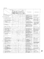
14) TCSS76F
UART LSI
VEE
Approx.
_ 8.SV
• For e r"llon of e low voltage 10 thl
LCD driVil volUige and the RS·232C
Int.rfee. sign.l l.
VOO
Approx
6.0V
• For er.llion of I high voltage to th.
RS -232C intlrflee li91'1811. Thil voIUlQI,
how ..... r, II suppli ed when PA IME II at
I high l.veIIRS·232C is ehosen) and
shut off whln PRIME is • low level.
1-1. System-off operation
lSls operated by VGG, except for the LU57813P, are
assigned to protect their contents,
For the LU 57813P, the real timer needs to be revised when
the system is off. So, an interrupt is sent to the LU57813P
by the internal timer every 0,5 second to revise the real
timer. When seconds are carried to a minute, the time is
verified with the wake ·up timer and the alarm time. There·
fore, a system clock (153.6KHz or 307.2KHz) is issued on
FOUT of the LU57813P avery 0.5 second.
6-2. Power generation method
The system starts to rise when 01 of the el connected
subcontroller remains high for more than the predeter.
mined time; the system wake·up is also possible by the CI
input of the RS·232C interface which is input at 0.5
second intervals.
But, if the system is forced off because of a weak battery
conditiOrt (03 input at high), the 0.5 second interval timer
interrupt is not activated even if the weak battery condition is cleared,
The fo llowing power supply sources are used to generate
the above power requiremenu,
(1) Internal dry battery cells (x 4)
(2) Through the AC adaptor
(3) Supplied through the VBA T of the system bus
A high voltage supply level is used by the PC-1600.
(i) V GG
A voltage of about 4.7V is nonnally suppl ied
from the above source, The voltage drops when
the level of power supply decreases,
(ii) vec
VGG is supplied through this line, when BFO is at
a low level or AC L is at a high level.
vec is not supplied when the system is off .
- 10-
~
1\
Syltltm-(lff (downl in th t
03 Itltt
The real -time time r is not
1
relliled.
A timet' interrupt is i$Sued
every 0.5 second to revise the
real -time timer.
2
FOUT is not Issued.
FOUT is Issu ed every 0.5
second.
3
Th. rynem can Ia turned
on by one of the foll owing
oPM"ions .ft.r cle.rlng th e
_ k bettery condition.
~resllo n of Ihe
BREAK/ON key
Oepression of tht ALL
A ESET .witCh loe.ted
on the back of the
PC·l 600
The ry""'" ean be turned on
by one of the following
oper.tions.
<D
®
with the wakeup time. If it coincides, the system
is turned on.
(b) If the wake-up timer is set to turn on the system
with the RS-232C interface CI input, the system
is turned on with the input of the CI signal as it
has been monitored.
If the weak battery signal Q3 goes high when the
system is off, the system down is established.
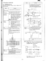
Norm.1 system-off
The figure below ~ows the timing sequence when the
system is turned on by the BREAK/ON key.
(j)
Depression of the
BREAK / ON key
@
Depress ion of the ALL
HESET SWITC H located on
the back of the PC-l600
®
ill
®
7-2. System-on operation
Depression of the RESET
switch lOCated on the back
of tht CE·1600P
Wh en the Wilke-up tim e
meets Ihe real time as
programmed bV the
WAKES/Oj statement
When Ih e AS-232C interface
C I inp!J l is set high by the
WAKES(1) statement
The figure below shows the timings when the system turns
off.
l
"' _ __--.;._---.J----f- -- =
- -----,l .................................. .
'" _____--'rn ..
-nn.
voo
:~ ~';.-_';.';.';. ';.:
_____ __________ n
____ n _
_ 'fIg
;'~:~: ,.~..~
...~...~
....~t..~...~
...~
... ....
~ ~...~
...~
... ~
....~
....
•
MREO
:
VDD _____ _ •• ________
PO_ASTIN
CKO- 211I<H.
C I. IC.J .&8 ~H .
"""::::::
!~T~ :~: ~ ~ ~ ~-_ ~ ~~::: _
j ':==========j:~'~..~.~.~.========
" . SlCB
ell(·3.58MH.
••
-_._----_ .. _---- --:--_....,
,
~
------_._----_ .. _- -,.-----_.
: .:.
';:;;:; :; ___ • _______ ____________ __ ___ ____ _
1'2. SLCT
215 ~ lO, Rll - R20
-
.:. Prohi:>'t
ICC' ''''''''
to eSR ol T857t1F
PR IME __________ ______ -'---:::::::::c!-.~o,,;""~~., ~.~""
~~-:::::;;;;:
~
_. - ----- -- --- -----.;
I
WU1fHlfL ___ •. ____ ______ •__ . _. _. ___.• __ •. _____ _
Jl....JL. __ ________ . ______________________ _
_ ___ _ • ___ • ___:. - - - --- --- - -----
Wi!
001
CD
When the BREAK/ON key is pushed while the system
is off. the ON input of the LR38041 converU to low.
As Z13 is low. KH goes high.
® When KH goes high, the subcontroller starts to operate
assuming the start of the system. First, P3 is set low,
P2 low, Pl high , and PO low. Now, VCC is activated
because P3 and BFO are low, and the system reset
is applied with low PO and RSTIN states. The memory
and I/O selections are prohibited in low P2 and SLCT
states_
(§) Low PO and RSTIN' states are issued for 30 milli·
seconds.
(j) The Z15 peripheral reset output is issued for 1 millisecond to reset peripherals.
® First, P2 and SLCT are set to high to select memory
and I/O, then the system reset is cleared.
® In order to supply stable clocking to the Z-80, it takes
about 0 .3 millisecond before supplying the system
clock.
FOUT
0 .5_
'"
CD
®
When the subcontroller receives the system-off command from the main CPU, it confirms that both
ao and KH are at a low level. Then, P2 and SLCT
are forced to low to disable the memory selection. If
KH is at high, the control proceeds to the system in
sequence.
Then, P3 and BFO are set to high to tum off the
system power supply. With this, all inputs and outputs
of the SC7852 and LH·5803 are turned to a low or
high impedance.
® The subcontroller goes into the standby mode, but
the real-ti mer issues a timer interrupt ever 0,5 second,
second,
(a) 11 the wake-up timer has been set, the time on
the real·timer is checked for whether it coincides
- 11 -
-
PC - l600
®
this pulse width continues for more than 300 micro·
seconds, the subcontroller proceeds in the same way as
the system power-on procedure so that a reset is applied
to the system.
After the system reset has been cleared, the Z-80 starts
operation within 10 microseconds and the Z-80 begins
to read the contents of the address OOOOH . (MREQ
®
issued)
Now, the Z-80 starts to supply clock pulse to the
7-3·3. Difference from ALL RESET
HD61203 LCD driver (217KHz on the eKO) to
activate the LCD.
• The LCD vol tage VeE is activated at the same time
the system is turned on.
•
•
The subcontroller interrogates the state of the BREAK/ ON
key at 7·3· ' and 7·3·2 above in the following manner.
(1) If the BREAK/ON key is depressed, the all reset is
assumed and all internals are intialized.
(2) If the BREAK/ON key is not depressed, the reset is
assumed - the procedure to turn the system on from
the system-off state. The internals are not initialized
in this case.
It is possible to return reset from all reset by a request
from the main CPU, the Z-BO asks the su bcontroller
for the cause when the reset is applied, Processing
differs depending on the cause,
In the case of all reset ... Clears all memory contents.
In the case of reset ... Retains all memory contents,
Supply lIoltage VOD on the RS·232C high level side
will be issued only when PAlM is at a high state.
But. VOD is not supplied during power-on because
PRIM is at a low level then.
A high ELH state indicates that the Z·80 is started
at the time of system reset. The LH·5803 stays
reset (ASTO- High) .
7-3. Reset operat ion
7·3-1 . Reset by t he ALL RESeT swit ch on the back of t he
PC·1600
When the ALL RESET switch is pressed, it causes the
subcontroller input ACL to go high . With this, the subcontroller takes the following action by means of the
hardware.
(1) All input and output lines, including P3 - PO, are
set in the input mode.
7-4. LCD block
7-4-1. Gene r, 1
The LCD is 1/64 duty and consists of 156 x 32 dots and
has 16 symbols.
Y64I1C3)
I
VO<
(I V)
1'3 - BFa
P2- SLCT
=
PI - SLCI
'"
r
1'0 - RSTIN
RESETSW
ACL.S0341C
ACL· LU578I3P
j $W'Id!
- - I d!!>,..-!
--.J
Y I -Y 6~
'
YI~64
(111)
r==
XU - X64
YI - Y28
(iC31
~--~----------ume
....:, P3 _ PO ;.... ",t
In Iht Ifll>Ul modo
'!foll IS .y.tem-On
(80 micrOHlCondsl
<D
1111
Y' - Y64I1C21
The 32 vertical dots comprise the following:
(1) Xl-X32 of the IC2 LCD driver outputs take care of
64 dots from the left.
(2) Xl -X32 of the IGJ LCD driver outputs take care of
65- 12B dots,
(3) X33-X64 of the 1C2 LCD driver outputs take care of
129-156 dots in conjunction with Y1-Y2B.
(4) X49-X64 take care of 16 symbol dots in conjunction
with IC3 Y64.
Regardless whether the system is turned on or off,
P3-PO are set in the input mode and are kept in the
floating condition while the reset is applied to the
subcontroller,
P3 is pulled up with the resistor.
P2 is pulled down with the resistor.
P1 is pulled up with the resistor.
PO is pulled dow n w ith the resistor.
While P2-PO are pulled down towards the non·active
direction, P3 is pulled up towards the systel1l-Qff. So,
the system's power supply is turned off in those states.
However, the power is supplied to the system while the
RESET switch is in depression.
7-4·2. Operation
(1) The LCD driving basic clock (217KHz) supplied from
CKO of the SC7852 is connected to the LCD common
driver. Without this signal, the LCD will burn out when
a DC voltage is applied to the LCD.
This signal is issued only during the system-on time
which appears immediately after the clearing of the
reset. As it is in a low state during the reset, a DC
voltage is added to the LCD during that period ,
7-3-2. Reset by the RES ET swit ch on t he back of t he
CE-1600P
When the RESET switch on the back of the CE-1600P
is pressed, KL and Z15 of the subcontroller go high . When
- 12 -
. ...
..............................................................................................................!.
then set in the input mode. So, a low signal is issued to
PA7 ,.., PAO and P86 at every 1/64 second to discri·
minate a key depression. In this instance, a low signal
is sent to all strobe lines to sense a key oepression.
When a key depression is sensed, that particular key is
distinguished after sencling a strobe to each line.
As the key input appears on KIN7 ...... KINO of the
SC78S2, a row of the keys in a low state is judged to be
the row at which the key entry occurred. Since input
not having a key entry is internally pulled up in the
LS I, it is in a high level.
(2) The HDS1202 LCD dri ver is for the 6800 series; the
timing clock E required for this interface is sent from
the SC7852.
The clock E goes high when the Z·80 acasses 40H5FH of 110. (It has a half clock delay against lORa
and its pulse width is 540 nanoseconds.)
But, the HDS1102 will not be $elected unless all three
chip select lines (CST, CS2 . CS3) are enabled. Two
HD61102s have the following address inputs as shown
in the next table.
HD6tl02I1C2)
H06tl02 (ICl)
CSI
A2
A3
CS2
A'
A'
C53
A'
M
Selected I/O 'PICe
SOH - 53H
SOH -53H
58H - 58H
54H - 57H
7-6. Buzzer block
7-6-1. General
These two lines activate the buzzer.
• PC6 output of the SC7852
• Subcontroller r- output
(3) For the LCD drive voltage, VCC-VEE are divided by
a resistor to obtain the LCD drive voltages, V1 ...... V6
and VEE .
VEE is derived from the power supply hybrid IC
50347C.
+
V)Rl
-
+
R2
-
R.
g:
,g:
R5
:
RS
VR
I
It
V
VEE
(=
V,
( H061203 (S) , H061102 )
V.
( H061203 )
Hi·2. De.cription
As the buzz.er is sandwiched between two lines, oscillation
from either line causes the buzzer to activate. Consumption
current is 3 mA, maximum.
(Conditions : input voltage· 4.5Vp-p square wave, input
frequency · 4 .1 KHz)
PC' --@--- F
(1) PC6
V,
( H061102 )
V,
( H061203 )
V.
( H061102 )
V,
( H061203 (S) , H061102 )
The following three signal sources are connected to this
line.
<D PB2 ..... Cassene playback signal
® PC7 ..... Cassette recording signal and beep by a
BEEP statement
® SOC ..... Recording signal by the CE·150 or CEo
162E
But, when the beep is turned off, sound is not
generated no matter what the above signals may be.
The above three signal lines are normally high.
12) F
The following three Signal sources are connected to this
line .
(!) Click .... In the click mode, a click is generated
each time a key is pushed.
@ Sound generated upon wake·up.
® Sound generated before issuing an alarm message.
Normally , these three lines are low.
VEE ( H061203 (5) ,H061102 \
- 8.5V)
7·5. Keyboard block
7-5-1. Key scan timi ngs
Keyboard key scan is done by a Z·80 interrupt with a 1/ 64
second timer interrupt (subcontroller output INT4 ).
7·7. RS·232C interface and SIO interface
The following $erial interfaces are provided for the PC1600.
(1) RS·232C interface (COM 1:)
(2) 510 interface (COM2:)
It incorporates the UART TC8576T as the hardware.
While the PC· 1600 has two interfaces with single supported
channel, only one interface can be active at one time. The
OPEN or SETOEV statement is used to selectively activate
the channel and the PRIME signal is used to activate the
hardware.
7-6·2. Method of scanning
Nine key strobe signals are obtained through PA7 ...... PAO and
P86 of the SC7B52 I/ O port.
Key scan is done in the following ways:
<D Only the strobe signal of the Y row to be scanned is set
low with other strobe signals set for the input mode.
® To ,can another strobe row after the current strobing
row, a high signal is issued to that strobing row first,
- 13 -
(1) Input signa ls are received by the transistor and are
output through the open collector and pulled up
to VCC using a resistor, as shown in the hybrid
Ie BX7269W. A diode is inserted across the base and
emitter of the input which will bring the signal below
the GNO level (stop bit , etc.) and make it assume to
be at the GNO level. Therefo re, the input signal is
converted in the hybrid Ie to be handled as a logiC
signal.
UART
RS·232C Interflce
Ree,iv,
d."
(2) On the other hand, the output signal is output
through the circu it shown below (hybrid Ie).
C 1 ( l SOPF )
Vo>
SOFI~~~~o-___________________________
mumn
ROFIll
mmmn
C2 (O.i1f)
While the input level is CMOS compatible (G-4.7V),
the output is converted to the VDO-V EE level.
The figure below illustrates this.
.""'=~~
com
CI III
U
h
__
•
_
____
_____
____
J
"
T)(O{UAA~'------------------------------"liJll!llUJnTTTTmrRXO I UAftT}
UlllllIIl
.4
N45S4 (C) ( 2.7KO )
;;:~f,:-'~'~~'~"~'~'~~'~'"~~'; ;';'~":':'2mmmn~~~:~~~~~~
OTR 101
VOO
~-------- G ND
---
PRIM E:-~~;C__________~----------------------
TXO 101· - - - -. -. - - - - - - - ---- , ,
UIJIllIID
' " ----.Jr------,'--_________________
GND
.-. --··----------·- ---V11lH
'''j\
---------uv.--u-u-u--
Va:
.--
CND - .-- . ..
ill
When PRIME is at a low state, the RS·232C interface
outputs either in a high impedance or a low state (non·
active).
® When PRIME is at a low state, the SIO interface I/O
signals, SOF and ROF, are in an opposite polarity with
the UART input/output signa ls, TXO and RXO. The
start bit is high and the stop bit is low. So, both are
in a low state when no data are sent or received (UART
TXO and RXO are at a high level).
® When PRIME is at a high state, both SOF and ROF are
at a low level and non·active (stop bit I.
<f) When PRIME is at a high state, TXO and RXO of the
RS-232C interface are opposite in their polarity as are
those of TXO and RXO of the UART.
® When PRIME goes high, VOD is activated (RS-232C
interface high side voltage),
® The R5-232C interface input/output signals-CTS,
DSR, CD, and CI- are input to the UART (opposite
polarity), regardless of the state of PRIME (high or
low) .
r-- - - - Vee
-----,
At the same time the RS·232C interface is selected with a
high PRIME state, VOO is supplied from the high side of
the RS·232C interface.
The SIO interface is selected with a low PRIME state and
VDD is turned off. DUring the system on and reset, PRIME
is at low.
.. ------------------
--VT H~
'"
'·' l
,
'"
GND
'"
CD
'--__________..J
When the input (a) is low (GNOI. the level (b) is below
GN D and is assumed by the MN4584 to be at a low
level.
The MN4584 IC is a Schmitt inverter to which VOO
and VEE is supplied. This Ie has a hysteresis against
input.
OutpUt
7·7·1. RS-232C Interf.ce Signal
Although signals of this interface conform to the EIA
standards, they are used for controls that differ in some
ways from the RS·232C interface in general.
V[ [
- 14-
VTHL GND
VTHH
VOD
Input
...
~----------------------------------------------------
~----~
PC- l600
above VTH L by means of the capacitor C1 between
VTHL and GND . As a result, the signal (e) changes
from low to high.
A signal transition is latched on the output side using
the pulse by means of the capacitor and characteristics
of the Schmitt IC for convenion of a logic signal into
the RS·232C interface signat.
The role of the R4 output is to prevent the possible
destruction of the IC4584 which may occur by an
accidental shon in connection with the RS.232C inter·
face or the connection of outputs together.
The capacitor C2 is for increasing speed for conveying
a change in the MN4584.
In order to change from high to low, the input must
be above VTHH. On the other hand, for the output to
rurn from low to high, the input must be below VTHl.
For the PC·1600, three resistors (Al, R2, R3) are
®
chosen to for maintain {bl level is in between VTHH
and VTHl under the normal ,tate,
When the input (a) changes from low to high, the signal
(bl is sent to the VOO side as a pulse above VTHH by
means of the capacitor Cl between VTHH and GN D
as a normal level. As a result, the signal {el changes
from high to low.
@ On the other hand, when input (a) changes from high to
low, the signal (bl is sent to the VeE side as a pulse
8. Service precautions
Before servicing of the PC·1600, it is mandatory that you
release static power in your body by using the eanh band.
(When removing the key PWB from the top cabinet, it is
recommended that you secure the key tops and display
filter using cellopane tape.)
In order to open the cabinet, remove the RS.232C interface
connector cover, system bus connector cover, expansion
slot covers {1 , 2l, battery cover, batteries, and the ex·
pansion module .
Remove the five screws (see figu re) and slowly lift the
bottom cabinet with care so that you do not damage the
chips installed on the FPC PWB.
Now, you will see the signal levels. To get power by using
the AC adaptor or battery cells, connect the oscilloscope
probe to the negative side of the battery.
Fig. 8·2
8-1. Replacing t he FPC PWB
1. With the connector PWB secured on the bottom cabinet.
pry the holder (A) at (A) using a flat tip screwdriver.
Next. remove the holder (B) .
Bottom c:.binel
HOlder (A I
HoldM (8)
Fig.
8·'
Fig. 8·3
- 15 -
PC 1600
2. Remove the eleven screws (see figure) and remove the
key PWB (with the FPC PWB) from the top cabinet.
NOTE : This job is required for the reuse of the key
PWB.
4. How to solder the FPC PWB with the key PWB
(1) Apply a thin layer of solder over the soldered portion
of the FPC PWB.
(2) Cut away 1.5 to 2.0 m illimeters of the tip of the FPC
PWB usi ng a knife or scissors, in order to check
whether the solder melted at the exposed portiOrt
of the key PWB will function when heating at (4).
(3) Remove the backing paper of the double tack tape
bonded on the back of the FPC and temporarily fit the
FPC PWB to the key PWB.
(4) Usi ng a soldering pencil heated to 260° ± 5° C and a
pair of tweezers, hold the FPC with the tweezen
because the FPC may separate when heated from
above. After removi ng the pencil , hold the FPC with
the tweezen for five seconds more.
®
......
•
....
iU==j ------ -- - r=~~-I
Fig. 8-4
NOTE : Do not drop the rubber connector and rubber
1.5-2.0mm
spring sheet that are used to hold the soft key.
If the electrically conductive part of the rubber
connector were to be contaminated, it could
be a cause of a failure after the assembly of the
1.5- 2.0 mm
F=
FPC unh
unit.
3. Generally. the FPC PWB should not be used again once
removed from the key PW8 because the soldered pattern
might separate from the board.
Since the key ?WB is bonded to the FPC PWB, to
remove, hold the shadowed portion at (AI with a double
tack tape and warm the area with a hair dryer; then
separate this portion from the solder using a soldering
pencil ,
®
Key PWB
"
FPC unit
Fig, 8·6
I1Q100llQQITmJlUI/lJlJlJUIJlIUl/ODJOOanuvvOtn17tl1llJ
o
0
o
0
lA'
Fig. 8·6
- 16-
.,'............................................................................................................
~
-
PC - I600
c. Lift the PWB with your hand and carefully mount it
over the leads of the LSI. When the solder on the leads
melts after five to six seconds, remove the LSI from the
PYlB using a tweezers (or a small flat tip screwdriver) .
d . Clean away solder fragments remaining on the pattern
side of the LSI using a solder wick. Then, evenly apply a
thin layer of solder over the surface.
e. Apply a small amount of solder to the leads of the new
LSI , and solder the leads with care. Press the mold of
the LSI with your finger tip while soldering the leads .
8·2. Removing and installing the LSI and chip
components on the FPC PWB
(When a defective component is known without separating
the FPC PWB from the key PWB)
(1) Removing the LSI
a. Connect the LSI soldering tip to the soldering pencil
(see figure), set the surface temperature of the tool to
260o ±S" C, and secure it on the vise installed on the
workbench .
....~_·Tip of
the soldering pencil
(2) How to remove and install the chip component
So ldering
a. Melt both sides of the chip component using two
soldering pencils at the same time. Remove the component quickly.
pencil
2:"'~~- Sold";,,, pencils
If it is heated above the given temperatlJre, it might
separate the circuit pattern or the FPC PWB itself.
The soldering pencil is held up to prevent solder, flux,
and gas from invading the back of the key PWB, where
the key contact pattern. the LCD rubber connector, is
mounted.
b. Evenly apply a proper amount of flux over the leads of
the LSI, and fill up the back side of the chip with solder.
- 17 -
Chip component
b. After the removal of the chip component, clean the
pattern with a sold er wick.
c, Solder one side of the new chip component. Let it
cool for ten seconds; then solder the other side.
---
PC - t Ern
8·3. List of tools
Parts name
No.
1
So ldltri ng pIl'ICi l !FP)
Parts code
U..
Price rank
eA
{ 0 C H - MAC H -F P 1 V
OC H - M AC H -FP2V
l 00- 120V
200-240V
UKOGE OO 24CSZZ
..
Solder wick
U KOG-Oq!7CSZZ
AT
For absorption of solder
•
Solder tip holder
OC H -
F P T iP H OLO
AC
F P solder tip holder
5
Solder tip
H iC T i P - l 0 0 2
BB
Forchlp replacement
6
Solder tip
7
Soldtr tip
B
Solder tip
9
Solder t ip
10
Sol d et" tip
11
Solder tip
12
So lder tip
oC
oC
oC
oC
oC
oC
oC
oC
oC
oC
oC
2
Solder thermometer
3
13
Solder tip
14
Solder tip
15
Solder t ip
BS
For measu rement of solder tip temperatu re
H i C T i P - l 003
eB
For thip replacement
H 1 C T iP - l 00 '
BB
f or ch ip replacement
H iC T iP - l 0 0 5
BB
For ch ip replacement
H 1 C T IP -
1 006
Be
For chip replacement
H i C T iP -
1 0 1 0
Be
Fo r chip replacement
H iCTiP-l01 1
BB
Forchip Telacement
H iCTiP- l 0 1 2
BB
for chip replacement
o13
1 o1
eB
For chip replacement
BB
For chip replacement
H 1C T IP - 1 0 20
AX
For chip replacement
H 1C T i P H 1C T i P -
1
•
No. 5-9
(F lit pac kage IC type)
1.6
Size of ch ip
A
No.
A
B
C
D
B
A l.S
o
'===~"" 1.6
No. 10-14
(Mi n i-flat package IC tvpe)
o
I
1
I====t::!:,
No. 15
1.5
5
12.5
9.5
12.5
9.5
5
15.5
12.5
15.5
12.5
13.0
7
16.3
13.3
16.3
B
17.0
14.0
17.0
14.0
9
23.0
20.0
17.0
14.0
-
10
5.0
5.0
-
11
6.0
10.0
-
12
7.0
12.5
-
13
9.0
15.2
"
9.0
lao
-
-
-
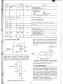
84. Measuring power consumption
(Spec ial tvpe)
1I ) p
h~
Supply power:
EA·l 60
9.5-'--1-
Or, 8.4V DC±O.1 V supplied through the adaptor jack.
Current:
OFF time: More than 200 microamperes must be
checked.
ON t ime: More than 30 milliamperes must be checked.
(N EWO? :CHECK on the display)
jack r-;:====;----i
0---.< A ) - Adaptor
.....,.,
EA·160
"
8.4VDCtO.
1V
PC·1600
- 18 -
...
~----------------------------------------~
~--~
pc-um
IReference I
SPEC
Actual UII
IDLE
3.3mA /4MHz
3.3rnA/3.58MHz
Operat ing
3OmA/ 4MHz
26.BmA/3. 58MHz
HALT
SmAl3.8MHz
S.5mA/2.6MHz
Operating
l SmA/3 .BM Hz
10.lmA/2.6MHz
LS I block
SC7852
LH5803
LU57813P
Standby
Operating
lR38041
Standby
Operating
HD61 102
Su ndby
Displaying
AcC8l$ing
so,.A
5.OmA/500KHz
IOIi A
10mA/ 4MHz
lS"A
l00~A
5OO.A
--
O.36mA/217KHz
TC8576F
lOmA/10MHz
1.2lmA/l.229MHz
Accessing
P'ROM
Standby
Aceessing
RAM
Standby
Accessing
Po wer l upplv
3.A
,5mA{,MHz
,OJ.lA
8mA/1MHz
1.0"A
10mA/1M Hz
OFF
100,uA
ON
2.OmA
Display
4.OmA
SID operation
20mA
lie regulator ICl)
Po we r supply
(convener l e I )
LCD bleeder
O.52mA
Not applied
8t
1, .JMHzl
this t im•.
FOI" timer only
3.25mA/l .3MHz
1.0mAI600KHz
Su mdbv
D&plndent on \fIOS
3.1mA/307KHz
HD61203
SC6976T0220
Note
-
6mA/4OOKHz
3.2mA/400KHz
4.OmA/400KHz
M ajor component conwmption power
8·5. Measurement check
8·8. Weak banery detection circuit test
The quartz meter must be used in this measurement test.
t 1.5 second/ day under ambient tempera·
Tolerance :
ture of 25°± 5°C.
NOTE: Do not perform the measurement test in the earlv
morning as the internal temperature may differ
even if the room ttlmperature is within the required limits. The same is applicable to the quartz
meter.
(1) Make sure that the machine operates normally with a
supply voltage of 7 .OVDCtO.l v.
(2) Make sure that the alarm symbol lights up with a
supply voltage of 6.0VDCt O.l V.
(~) Make sure that auto-power-off takes place when the
supply voltage Is 5.4VOCt O.l v .
(This test must be conducted under the temperature of
25°±5°C or 79.2° ±10°F.I
8-6. Power-off test
Press the RESET switch on the back of the unit while
pressing the ON/ BRK key and check for the following :
Power does not turn off within nine m inutes (typical is
ten minutes).
But, the power tu rns off within eleven minutes.
8-7. Shock test
With the d isplay digits activated, lift up the display side 45
degrees, then drop it on a desk top.
Then, check to see that there any changes in the display.
- 19-
-
PC- l600
9, LSI pin descriptions
(main CPU 1)
• SC7852
LH5803
CPU 2)
• LU57813P(main
(sub
CPU)
• LR3804 1 (gat e array)
• TC8576F (UAAl)
•
9-1, Main CPU 2 (SC7852) pin description
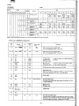
Pin
Symbol
No.
95-
KiNO-Ki'lii7
InlOut
"0
Active
Function
level
Low
100-2
(ll
(2)
Internallv pulled up to vee by the resistor (2ooK - SOOOK).
T inpu t · low {normal model keyboard input.
(3)
A key in Ihe low input line Is pressed.
T input · High (emulation mode),
Used for connection of the Z..aO ICE.
3
LHWAIT
A"
High
Wait output to the lH·5803.
The signal goes high in onll of the following:
0)
(21
(31
4
.OS
'0
JlJ
When the WAI T input is at a high I,wl.
When the LH·5803 8C(:lI$$es "ooH or 8000H-FFFFH of the ME' $pllce, it goes
high for one cycle time 10 insert one wail .
When the Z-80;s running with the LH·5803 8t halt.
LH·5803 basic clock (t.3MHz).
This clock is used for the sync signal of tile internal LH·581 0 corresponding port and
generation of the LCD CLOCK (2l7KH~).
PT
,,",
Memory bank. signal.
PU
,,",
Memory bank. signal.
7
PVOUT
,,",
Memory bank. signal.
S
PVIN
• '0
LH-5803's PV signal input .
As PV is k.ept in the flouting state when the Z-80 is operating, it is internally pulled
down by th& resistor.
9
WR
5
,
10----25
A15-AO
InlOut
Low
"'I n/Out
(11
(2)
Wh&n th& Z-80 is in operation, the Z-80's WR is a direct output on this line.
Wh&n the LH -5803 is in op&r.nion, it becomes an input to enable R/W for
the LH-5803.
(11
When the Z-80 is in operation, th& Z-80 address bus is an output on this line.
(2) Wh&n the LH -5803 il in operation, the LH·5803 address bus is an input on this line.
26-33
087-080
In/Out
Data bus.
34
lORa
"'ln/Out
(11
(21
When the Z-80 is in operation, the Z-80 lORa is an output o n this line.
When the LH-5803 is in operation, the LH -5803 ME' is an input on this line.
35
MREa
.. InlOut
(11
(21
When th~ Z-80 is in operation, the Z·ao MREa is an output on this line.
When the LH-5803 is in operation, the LH-5803 MEO is an input on this line.
36
RO
InlOut
(11
121
When the Z·80 is in operation, the Z-80 RO is an output on this line.
When the LH-5803 is in operation, the LH-5803 00 is an input on this line.
37
WAIT
• '0
38
LH ASO
,,",
High
WA IT input to the Z-80 and LH-5803.
Pulled down internally by a resistor.
Among the RAMs (the bank. of the spaces COOOH-FFFFH) connected to the RAM3,
it is an input to the addrMs A9 of the RAM of EOOOH- F FFFH (the side A 13A is
Input to CEl I.
111 When the Z-80 is in operetion, "LHA90 · AS" is esteblished.
121 Except that "LHA90 · high" is established when the LH-5803 accesses 7400H744FH and 7500 H-754F H.
In other words, when the LH·5803 tries to access 7400 H-744FH and 7500H754FH, it acttJally afXlmes 7600H-764FH end 7700H-774FH.
- 20 -
PC- I600
Pi n
N,.
J9
Symbol
",
In/ Out
Actille
I....el
eN,
low
F\lnctiOn
In
When th e Z·80 il in operat ion, the Z·80~l i'ln outpUt on thi,l ine,
121 When the LH·5B03 il in operltion, thelignll crea led from the OP F ,ignll of th.
LH·5803 is IInl o n this line.
40
RffiI
eN,
L,w
Refresh signel.
The Z·80 FfI!S'R signa l i, on this li n •.
121 When Ih e LH-5803 is in operetion, the , ignal c reated from the OPF signal of the
LH·5803 illl nl o n th is l i~e.
In
41
VDD
42
' DE
vee
eN,
High
Thillignel il issued when the LH-5803 tri ll to access ··OOH- · ·OF H and 8OOOHOF FFH of the MEl JPK4I . When thl.lignel il llnt OUt, one we lt i,"nllO the
LH·5803. In lerml o f timing, th e lignll il lint with. hlllf cl oc k delay on thl MEl .
I
ODS
MEl
~
LHWAIT
'DE
I
I
I
I
eSOD'
eN,
Low
Z-80 conlro l ROM IIIIC I signal.
OOOOH-7F FFH m emory space (bank 0).
44
C5123
<110u1
low
In
45
CS24
eN,
low
.
Z·BO control ROM seltc:t l ignal.
111 4OQOH-7FF F H memory space ll»nk 3).
121 SOOOH-COOOH memory splICe (ba nk 4).
One wlit JI In.lUd .
LH 53
tHS2
eN,
' eN,
low
Low
L,w
=
• C>"
I,
,
43
47
48
I
.. ---
L
L
Z·80 control ROM 5eleet 5igna l.
BOOO H- BF FF H memory space (bank 6).
121 LH ·5803 control ROM $llect lignll.
COOOH- FFFF H mem ory spece,
I
Me mory letect 'Ignal.
Depending on t he lte te of bit "6" of I/O 3CH, the memory space selected
differ•.
b6 · 0
om
ASOO H- AF F FH
TIm
=
b6- 1
(bank 01
BOOOH - B7FFH
(!>enk 0)
8OOOH-B7 FFH
(bank 0)
ASOOH- FAFFH
(blink 0)
B800H- BF FF H
(blnk 0)
AOOOH- A7 FF H (bank 0 )
LH51 I nd LHS2 .re pulled up inlernelly.
~ oeech to be pulled up externa lly. (pulled up Ixtemllly.)
49
RAM3
eN,
High
Memory IIlect lignel !loternll 16KB RAM ).
COOOH-FF F FH (bank 0).
SO
RAM2
eM
L.w
Mem ory lelect l igOl1 (51 :1.
8000H-BFFF H (bank 0 , bank 11.
8000H-BFFFH (bank 2, bank 3),
51
RAM '
eN,
low
Memory flllC t , igl'llli (52: ).
8000H- BFFFH (bank 2, bank 3).
52
5LCT
'"
H;gh
Wheo th il'illnal i, at low, OIJtpu t of Ihe memory ..... d I/O select signal il
disebled.
Oi$llbled lig nll l Irl: CSOOi, 'CST23,
RAM3 , ii'AM2, 'RAMi, 10E,
KA2 ,
KA 1, KAQ, C/O, Ind iOFfi5:
This input is In OUlput to the subcontro ller Ind is . t I h igh level wheo th e Iystem II
em,
'".
- 21-
rnso,
-
PC- l600
Pi.
Symbol
No.
In/Out
Actille
level
Function
63
KAl
00"
L~
Goes low when the Z..aO I/O 28H- 2FH i. written.
54
KA.
""0
L~
Goes low when the Z.ao I/ O 28H-2FH i. read.
.
KAO
L~
Goes low when the Z-80 I/O 60H-6F H II accessed.
55
CKO
"",
"",
A 2 17KHz ~S outpUt. Th llslgn.1 is supplied to the H061 203 (5) LCD driver .
This signal is issuad olliV when bit "b4" of the Z-80 I/O 37H is at "''', Bit
" b4" il .1 "0" ., ~,-on, but turns to " 1" in the power-on routine 10 activlte the
LCD.
"
IOAP
68
C/~
"",
L~
"",
High
Goes low when thl 2-80 reed.33 H of 110.
This .ignalls uled by the Z-80 to , ..d the return dete from the LU578 13P,
Goes h igh when the Z-80 wr ites 3DH of I /O.
Dall life 'etched It • low 10 high transition of c/D. When the signel rises wi th . helf
clock delav from lORa, th e dIU! bu,l. IUlble.
59
10SiJ
"",
L~
Goes low when the Z-80 110 20H-27H is acee$Sed.
This sign.l ls uMd for Mlec tlon of the TC8576F UART.
60
•
"",
High
Goes high when lhe Z·80 I/O 40H- 5FH is accessed.
This Ilgnll Is uMd to Intarfle. with the 6800 Ilerl.1 LSI Ind il connected to the
H061 202 LCD driver Input.
This signalllluultd with . half clock delay stower than 10RO.
6.
OMEO
"",
H i~
LH-5803 memory Mllet lignal.
Th is lignalllOlS hilJl! when the LH-5803 acC1S1fII t ha memory.
62-70
PAQ- PA7
v In /Out
Correspondlto th l port PA of thl LH·5810 I/O port.
Thil lignal ls ued for the key . trobe signal. To restore the original state of the lowforced urobt lignal, thll.lgnll mu st be turned high Ind then set in the input mode.
The Input Ilgnllls pulled up internilly.
.w
6.
VSS
71
P02
V ln
72
P66
v In/ Out
Used for In input po rt by the PC-16CX)'
Input to t hil IInlIs 11/64 Mcond puille whic h is issued from the LU57813P subcontroller. Pulled up Internally.
73
PBS
v InfOut
Used for the key ItrObe Ilgnal.
Application i, the..me I I for the PA7-PAO.
Pulled up internilly.
74
P.7
.,.
75
Pes
"",
UMd for the cassette tape to reproduce Illgnal.
Pulled up internally.
Receivelthe.tate of thllB R EAK/ONlkey lent from the subcontroUer.
Pulled down internally.
Used by thl Z-80 for I beep generltion.
The fol lowing circuit II internally composed in the LSI.
'82
3
PCG ' ==:
PC7 '
suo
P-----DI'CG
Whln either the PB2, PC6', pcr, or SDO goel low, PC6 beeomel high.
To d rive the boUlr, one of Ilgnal, illUes a pulse.
- 22-
PC-l600
Plo
Symbol
No,
,.
In/Out
Active
Iellel
Function
PB2: Clssette reproducing ' ,gnet
PCS': Beep diSlible sJ~.1.
PC7'; Cassette reeordlng slgn.1 (PC-1600).
Soo'; Cassette recording sign-' (PC-' 500).
SIlO
Cassette recording IIIg!'llll OUtput.
Qu,
SIlO'
PC7'
I )
D
SDO
500' is the canene recordl~ outPUt by the CE-l50.
PC7' is the canette recording outjXIt by the CE-'600P.
77
ELH
(n A low state of this ,Ignal Indlcues that tha LH·5803 il in operation.
Qu,
(2)
78
PCSTS
A high Ilate of thi' signa l indicatel that Ihe Z-80 i. in operalion.
In Goes into the input mode when reset. This current state is latched in
In lOut
the PB3 flip·flop.
Therefo re, either pulled down or up by an Itxtemal resinor.
For the PC-1600, th e machine vel'1lon i. rapr_nted by thb signal.
PS3 - 0 : Japan ver,ion
pa3 - 1: Ex port version
121 Goes to thltoutjXIt lin e In the normal modlt.
The signal goes high when me Z-80 writes lBH or I/O or the LH-5803 i, FOOSH
of the MEl . This lignall. not uMd in the output mode with the PC-I600.
79
ASTIN
00
'AQ
81
INTO
82
INTI
83
INT4
.
8'
.
87
L~
A reset input to the SC7852. This signal il forced low for 30 millisecOnds by the sub
CPU when ACL or AESET i, i,sued or at po_-on.
-'"
High
An intenupt to th e CPU (Z.ao, LH -58031.
This line i. input as an interrupt request from the PC-I500 peripheral.
'"
High
An interrupt to the CPU.
This line Is Input as an interrupt requast from the TB576F.
L~
An intltl"rupt to th e CPU.
This line Is input as an interrupt reQUest from thlt PC-l600 peripheral.
Pulled up internally.
'"
.,"
'"
L
An interrupt to th e CPU.
An Interrupt i. sent to the CPU at I high to low transition. This line is input at a
1/64 second pulse from the , ub CPU. It i. externally shorted with PB5.
But, the sub CPU ou tpUt, which Is a P-ch open drain, is pul.led down by the external
resistor to assure a lOW output.
High
An interrupt to the CPU.
This line inputs the output from the sub CPU .
L~
At the time the powtr-oH command Is sent to the sub CPU, the sub CPU turns the
power off (active low).
This signll gotl low Itter the Z~O completas the following:
(I) 11 H written 10 1/0 37H
HI) OUT I38Hl. A
(til) HALT
'N16
-'"
PCTAL
Qu,
eLK
Qu,
Z-80 cloc k outpUt . 3.58MH:r for th, PC-1600.
T
-"
(1)
(2)
88
89
XOUT
X'N
90
VDD
"",
'"
It i. in th e normal mode when e low 1Ig!'llli is received and the Z-ao is operating
normally. Pulled down intltl"nlily.
It il in me simulltion mode when I high sign ll is feceived. The Z-80 bus is in the
floating stete, I nd the Z-SO (or Z-BO ICE I can be connected IXnrnally.
The 3.58MHz Z-80 clock i' lUPPlied when th e oscillator is ettached ecross these lines.
Power Input to the high side (4-5.5VI.
- 23 -
-
PC- l600
Pin
Symbol
No.
91
L H MIO
92
LHNMIO
In /Out
Active
18II'ei
Function
Qu.
High
An interrupt is sent to tna SC7852. When there is an interrupt request to the LH·5803,
this signal goes high.
In/Out
High
111 Goes high when the LH·5803 is 94 u H and when PU - PV is high (CE-158 internel
ROMI.
121
Bacom8$ an input during reset. So, it mu st be pulled up or down with the external
resinor. With the PC-1600, it is pulled down.
93
LH OPFI
-I,
High
Receives the OPF output of the LH-5803. Pulled down internallv .
94
RSTO
Qu.
High
Reset output (high) to the LH-5803. When 8 rll$et is issued to the Z·80 (RSTIN al lowl.
it makM RSTO high. The rest can only be cleared when the Z-80 first hands down the
control to the LH -5803. With this th e LH·5803 starts to run.
lI: Pulled up to vee with the internal resistor, lOOK ohms - 500K ohms •
.. : Internal resistfloce of 200K ohms - 500K ohms is active when the CPU is on, but no MOS resistance is met when th e CPU is off.
9·2. Main CPU 1 (LH5803) pin descript ion
Pin
SVmbol
No.
In /Out
Active
level
Function
CPU reset input. A high on this line causes the rll$et. The contents of the add ress
FF FEH are transferred to the PH register and the contenU of FFFFH to the PL
register. When the reset input changes from high to low, the p rogram starts to 8)(ecute
from the addrass sat in the program counter.
RESET
2
(NC)
3
BRa
10
Bus request. Connected to ELH of the SC7852 output.
4
BFI
10
BF flip -flop output (BFO) end input (BF I).
The BF fiip-flop is reset by the OFF command of the CPU .
It can be reset when the BF I is set high.
T he BFa Is at a low level when the BF flip·flop is active and at a high level when not
active.
The contents of the BF flip -flop are protected (1$ long as VGG is in supplV.
Because VGG is VCC in t he PC· 1600, this function is not used and VCC is used for
an input.
5
VGG
Power supply (system's VCC input).
6
BFO
See Pin No.4.
7
OPF
Op code fetch signal which appears when the CPU fetches the OP code.
OPF Is the signal that Is i$$ued onlv when the Operation code is fetched and is not there·
fore issued in fetching the address data, immed iate data, and the second byte of a 2-step
command.
.os
A~D15
,
,
'
i, X.- _____,...
:C
,
MEO. j ..........
~
OPF W ' \
:
.
Writa •...;_ _ _ Op code_ __ :
:-- cycle
fli tch
B
BAK
Bus ackoowledge signal.
When BRQ is set at a h igh level, the CPU issues a high BAK state in response to it.
When BAK is at a high lewl, the CPU sets the addrll$s bus (ADO - A015), date bus
(00-D7), MEO, MEl, R/W, and aD in high impedance.
9
vee
Power supplV (system's VCC Input).
- 24 -
I
-
PC - l600
Pin
Symbol
No.
Inl OuI
Act;"',
function
lllYe'
Power $lJpply (system's vee input).
10
VGG
11
VM
'0
LCD
"
VOis
'"
LCD backplate power supply input.
'0
'0
'0
~kpl at.
power supplv input.
Not used by the PC, '600.
13
VA
14
VB
15
NM'
\6
M'
'"
Maskabl. interrupt inpu t. When th, IE flag (I nte rrupt Enable' II set on, an interrupt
request is caused by a high Ml input lIate, end the CPU $IafU 10 execute Ihe interrupt routine from the address whose high order address is represented by th e contenu
o f the address F FFSH and the low order Iddress by the contints of FFF9H.
17
H'N
'0
Input to th e counter by which the LCD and backplate signals, HO- H7. are generated.
Normally connected to the HA pin of the CPU. With the PC· 1600, this functi on is not
18
HA
0."
CPU internal d ivider ootput through which is de livered the ba1ic clock for the LCD
driver and connected to HiN and the regment signa l generator LSI.
19
OISP
0."
LCD display o n/off control signal output.
Can be set and resat by mean, of a command. With the PC· 1600, this fu nction is not
used.
H7-HO
0."
LCD backplate signal output.
When the LCD is driven by the backplate signal and the segment signal. the backplate
si gnal is issued by the CPU.
00
Qu .
OutpUt disable lignll. When 00 is I t I high level, the CPU disables the data outpUt
onto the dati bus for the external device. This signal is issued when writing data in the
memory.
20-27
28
LCD backpl.l. power supply inPlII.
LCD backplate power supply inPlJl.
Non -msskabll1 interrupt input. A high Input state causes en Interrupt to th. CPU.
The CPU unconditionally accepls Ih. request and staru to '''Icult the interrupt routine
from th e addr.., whose high order idd,ess is represented by the contents of the address
FF FCH end the low o rder acidness by the contents of FFFDH.
,.....
.as ,
AOOA01S
::;::::::x
:
I
MEOo.
M"
RIW
:
:
(
MEO
MEl
0"
0"
31-38
00-07
In/ Out
39-46
AO-A7
0"
I
x:=
\
\
:
i
:
'C
MemOry mola >----{CPU Int.....1data
Memory rtad cycle
29
30
I
\
oo=::J>
00- 07
:
:
X
Memory write iignal
Memory enable lignal. This signal il enabled 10 direclly Kcns the 128K8 memory area;
MEO accesses a 64KB area and ME' accelln a 64K8 arel.
Th e memory area accessible by the program COUnter P and steek pointer S is64KB,
fO( MEO is used by the felch Ind sl8<:k com mands. FO( aceening dati, both ME.
and ME l memory arees can be acclHSlld by the CPU command.
Bidirectional dala bus which is used to write data in the external memory or to read
data from Ihe aXlernal memory.
Address bus which may be in three nates. Goes to high impedance with the 8Ra (bos
requntl s ignal . It is possible to access the memory arel of 64KB. It is also pO$sibla to
access the memory of '28KB USing the M EO or MEl signal.
- 25 -
r
-
p c:.... 1600
47
GND
48
A8
49
VGG
50-56
A9- A15
POWII' supply.
0"
Addr.u bus bee Pin No.39).
POWBf l upplv .
D,,,
57
INC)
-
58
R/W
0..,
Addr'" bus (see Pin No.391,
Memory write signel. With . low A/W stete, the del. in the CPU are sent on the data
b UI .
59
p.
D,,,
External latch clock. With . high "ete of this clock, thl contents of th, accu mulator af.
transferred onto the data bus. Use of the In::h Ie permits its use as Ihe output pan !see
the ATP eommand).
60
6'
PV
PU
0..,
0.. ,
TheM .re the CPU intlrne' flip-flop outtlUt pins IPU. PVI.
The ... ert commands to Jet and reset PU end PV.
"
.as
0..,
Ttle clock, in t he NIITlIl ph, . nth. CPU inllrnel basic clock, is on thil line to supply
clock pulse to t he externel lystem,
When . 2.6MHz crystells conntcted &eross XL.O end XL 1, . 1.3MHz clock I. supplied.
63
64
XLO
XLI
0..,
65
WAI T
,.
,.
Crynal connect ion pin.. X LO i. en input and X l1 i. 11'1 outpUt.
Inlld e l he CPU , the clock I. divided in h'lf , Whe n. 2 .6MHz crystal i. connected , t he
mlChiM cycle within 1M CPU is at 1.3MHz.
CPU wait signal. When th is Input Is high, the CPU'. Intern a' operation c lock "11>" SlOpS
and tha CPU thareforeilopi execu ting a command. When It resu mes II low ltate, the
CPU lIarll to execute a command.
Int .... nal basic clock
.as
CPU Op....ating clock
•
WAIT input
CPU internal
flip·flopWA
\
/
I
\
NOTE :
WA I. th e CPU inllrnel flip·flOp for WA IT. At. high to low transition o f ttle clock
4105, Input of WAI T ilaccepted.
The CPU Operating clock 11> ItOpS whe n WA lilt hlgh;!he CPU h • •ts. comm.nd
execution temporarilv as a result.
66-73
IN7-I NO
74-76
INC)
,.
Input PO". The CPU c.n send the signal input on th . INQ-IN7 to the CPU ICCUm ulator
...n 8-bit data.
It hH.n Internal pull-up rHl nor. When not conn ected, the CPU IIsum" the line to
be In high impedance.
-
NOTE : NC : No Connection
- 26-
PC- l600
9-3. Sub CPU (LU57813P) pin description
Pin
No.
Symbol
In/Out
Active
State
level
atACL
L~
'"
Function
,
ao
2
vaa
3
ACL
4
CLl
CL2
Qu,
Th. system clock generating ceramic oscillator is atteched ecross these two
lines. With the PC· 1600, 8 1.229MHz oscillator is used for the basic clock of
the RS-232C baud rata.
•
FOUT
Qu,
System clock output. Not used .
7
PO
Qu,
5
'"
When t he system -off command is received from the Z.aO, the SV$1:1IITl is
turnad off after this signal g0e5 low. It hes PCTA L output from the SC7852
as its Input.
High side VGG is supplied.
'"
The pu lJe widt h of AC L must be IIreeter thin 1 microsecond in duration to be
recognized by the h.rdware. It likes .bout 80 microseeonds befoll! the LSI
s18rtS 10 operate after inp!Jt of AC L. This pin i. uted IS reset input from the
ALL RESET switch of the PC-1600.
High
'"
L~
S
P1
Qu,
Low
9
P2
0"
High
10
P3
Qu,
Low
11
KH
'"
High
'"
-
Reset input to the SC7852.
T his line is maintained low for 30 milliseconds during system-on and reset.
'"
'"
In a low sUite wh an the main CPU is permitted to access the memory and
I/O.
'"
In a low state during system-on .
Used to turn on the system.
In an opposite level of Pl. Input to SLCT o f the SC7852.
This signal goes high with an input of the ON key. When the system is off,
t h is LSI is in the stendby m ode, and it tums on the system with e high KH
S13te.
J
12
K'
'"
13
T
14
OSCOUT
OSC IN
'"
'"
15
,.
A command request from the main CPU. Interrupt is caused by a high Kl
state.
High
Test pin which is NC.
Qu,
The 32.768 KHl timer crystal oscillator is attached across these lines.
Reset input from t he peripheral unit. As monitored by the software, if this
input is high for more than tha given.timl, the reset is executed.
KL
'"
High
17
Z15
00,
High
'"
Z15 and KL are shorted outside and externally pulled down by the resistor .
Z15 is turned high for 1 mill isecond in the reset routine to be convened
into the RSTE signal, and sent to peripherals as the reset signal via the
system bus. So, both Z15 and KL can be handled as an input/output line,
which may be used to apply reset to the peripheral or to receive reset from
the peripheral. This signa l is used as the rlset input of the CE· 1600P.
18
Z14
Qu,
High
'"
The sub CPU monitors t h e state of the BREAK/ON key via the KH input
lin e and its state is sent throu!t1 Z1 4 and supplied to PB7 of the SC7852.
Therefore, key chattering and bouncing of the BREAK/ON key are com·
p letely controlled the sub CPU.
19
Z13
Qu,
Low
'"
The sub CPU goes into the powar-down mode except when one of the
conditions mentioned below holds true.
111 When 8 command Is received from the main CPU.
121 When iii timer interrupt is received.
13' If the BREAK/ON key sensing KH input is at II high level.
To prevent these conditions from occurr ing, Z 13 is set low 8t every time
interrupt!1/128 second) . If KH is at a high level, depression of the
BREAK/ON key is sensed.
- :r/ -
•
.
-
PC- l600
Pin
No.
Svmbol
In/Out
Actill.
'w.
SI.t.
AC l
FU ne1lon
It
~V~
*lQRJ Z\So- J
ZIB
V
KH
0,,,
20
Z12
21
Zl1
,.
22
ZIO
Cu,
High
,.
23
Z.
0,,,
High
,.
2.
Z8
Cu,
26
Z7
0,,,
2B
GNO
27
Z'
Cu,
Low
,.
2B
Z'
0..,
High
,.
29
Z'
0"'
High
,.
30
31
32
33
Z3
Z'
ZI
ZO
,.,.
,.,.
34
SOUT
SCLOCK
35
"
37
F
VR"
Cu,
In lOu t
Cu,
,.
L~
'",.
,.
H igh
,.
,.,.
,.,.
,.
1J
~
I
I
IL.Jl
For the PC-l 600,' high signa' n.lIls normallv issued (.t ONI.
NC.
Tn il ligna lll used to Interface with tht main CPU. il goel high when the
sub CPU _I" for. commend (r..dyl, and gaes lowwhen bulY.
This signel i. , lso used to inte rf_ with the m ein CPU. A high pulse i.
i$$ued when t ht sub CPU lerm in.! • • comme nd execution,
Used to $IItup the tn.log input mode.
11 1 VO ll'~ i. AID conv.rted when low !initial value l. The input impedance
i. 100K ohm ••
121 Current I. AID cOlli/Mud whln high,
Th. PC-l 600 IUpporu t111n BASIC, but it needs to progrltn In m .:h ine
Ienguegt for 121.
Th e sub CPU uu this sign,l h igh when the command $peelfled Int errupt has
been ac knowledged, This sign,l is connected to INT6 input at the SC7852.
There ere fcu re.u.s which force thlsslgn.llevel to high.
)I) The wek.up time metched th l rll l·time timer.
(1 ) Th e time of Ill rm ·1 or ·2 mltchld the rlel·time timer.
(III) Rl"Clipt of I n input from thl llIIte rnl l keyboard .
(IV ) At O.S second cycle of the real·time timer.
This sig nal goft low when thl intlrrupt caUK status is read or whln all inpul1
from the eIItlrnal keyboa rd have been read.
' OV
A 1/64 t8COnd pulSi of SO% duty Is sent.
Connec t ed 10 iFif4 end PBS inpull of lhl SC78S2.
As t~ ref.,.encl lIoltage is requi red whln the w b CPU AI D corwensthe sig""
input to KCG- KC2, ZS iSKt high only d.oring the A ID cotlllllt"llon to obtain
the CornlCt Y RH . This 1$ u$ed for YRH accuracy IS well 1$ powe r lIVing.
Used fo r hand shaking of the IIlIternal keyboard input thro ugh the a nalog
input connector.
Shoned with the anal~ input KC1.
Normally an open output.
Not used.
t:lsecI 10f" genlf"ttion of cl ick and alarm sou nds.
AID corwersion h igh side reference voltage (2.47SV In 5Upply ).
- 28 -
.
KH
PC-l600
Pin
No.
Symbol
:l8
KC3
J9
KC2
40
.
..
42
4J
...
...
45
47
49
KC'
InlOut
Actille
level
Stfte
el ACL
'"
Not u58d.
"
Used for ch ecking the CE· 1600P ~r supply lewl . VPP suppll&l;l from
the CE· l 600P vie the ryltem bus Is AID COfl'llerted. If it is below the given
level, the peripheral is assumed to hlYl II weak battery condition .
"
Used fOl" c hecking the PC· l600 main POWIt!" supply level . The lewl of the
main power supply is AID converted and checked. If It is below the lIiven
level, a weak battery condition Is assumed.
"
Recll1v H th e lillnal input from the analO1l input connectOl".
Fo r the analog input, AID COfl'llefJl on is dont!.
For the axternal keyboard input, ill logic level Is in1e.-regated.
KCO
A33
A32
A31
A30
A23
A22
A"
A20
Function
"'
'"
MSB
,,",
"
""
""
'"
,,",
"
,,",
"
'"
'""
,,",
,,",
,,",
Return date to the Z-80.
LSa
"
"
"
"
53
54
56
56
"
58
59
60
S'N
NC
"
VOO
A13
A"
An
A"
AOJ
A02
AO'
AOO
"
03
•2
Q2
63
NC
VAL
High power supplV voltege llMll IVGG) .
Msa
"
"
"
"
"
"
"
"
"
'"
'"
"
"
"
Low
"
"
"
"
Lsa
Hardwera sensed week banery detection slgnel.
A hillh on this line causes the CPU to force the syltem to 110 down. The only
means to turn the system on e fter rlllCOYlfy of power supply is the depression
of the BREAKION key or ALL RESET switch. The time in the .... I·time
timer would not be rwised.
Not used. Pulled down .
01
Low
"
64
Commend from tha Z-80.
"
"
ao
'"
Opposite polarity as CI of the A5-232C intmec •. It i. possible with CI to
ru rn on the system wh.n thesvuem i. off (when thl.lin . is at .Iow lwei).
"
If this sillnal I. at a low level when the svltem-off commend i$ rectived from
the Z-80, th. system is wrned off.
L~
"
-"'-
--,
I
PC 1600
-
- -
-
-
9 -4. Gate array (LR38041) pin description
I
This gafe array is an integration of ICs required for connec·
ion of _LSls.
;
-
Pin
Symbol
No.
SLCB
1
In/Out
Active
Fu nctio n
level
It Is an input of the su b CPU· iuued signal PI wh ich indica t es commencement 01 Ihe
system operetion.
PI IS Le B) goes h ig h when the sy stem is off and does the fol1owir'lg.
Da ta bullts, 02- DO. are fixed at iii low level.
EXc:&pt for A 1lA, all outpUt leve ls are fixed 10 tow or high.
1~
-
"'
12'
Z
Q3
'"
Hardware WIIak blIttery detett signal.
When a weak battery condit ion is detected, it fo rces Q3 high ; S I , S2, S3, KO, Kl ,
and K2 ou tputs&re sel high ; KH outpUt is set low; and AD is set to high impedance
111
(inecli...,).
121 Q3 is at a low level when, w,", k battery is "01 established.
3
Z12
4
213
I,
When on , tM input is high .
L~
"
5
ON
The sub CPU is n ormall y in the SII'Idby mode 10 AVe power when 8 eommand is nOl
received. But, lt would not go into the power save mode if the BREAK/ON key
I, continu Ollily depressed, n it goa. OUt of the n.ndby m ode if KH i, .. I hi gh I_I.
To prwent thiS, the nate o f the BREAK/ON key must be inte rrogated with Z13 whe n
~ ired . During the pOWllr save mode , Z 13 is set to high to keep the KH output ...
low leve l.
"
BREAK/ ON key input.
The l ignalllO" low w hen the BREAK/ ON key il d!lpreued ; otherwise, it il in I h igh
ltat •.
Low
S
KCl
I,
Sig nal input from th e analog Input connector.
7
C Ll
Sub CPU 1.229M Hz c lock Input.
•
'"
AD
Qu,
....
,.
17
,.
,.
L~
Return data from the sub CPU. The data becomes the Z-ao date when the Z-aO reeds
33H of 110 .
A2D- R3 3
"
PA lM
'"
TXD
Reid signal crMted by f jy& lignels (MEO, MEl , 0 0 , CKOS . and BRO) wh ich ara
exte rnally wired OR with Ro of th l Z-80.
When the Z-aO Is In operation, AD ;' a t a hi gh Impedance.
The PC-1600 hal two serill inputloutpu t interfacl : thl RS·232C interface and the SID
interface. But, ei ther one mUlt be assigned al onlv o n&hardware i. fo r the serial input/
OU tPUI.
III The 510 Interface illtllected with I low PAl M nlte.
121 The R5-232C interface Is Mltcted with a high PR IM lUte.
PRIME - " Low"
PRIME · " High"
Output SoA
LOW
TXo
Output SoF
TXl5
LOW
Input RXD
ADF
AD A
~
Transmit da" whic h is an output from the TB576F UART.
"
AXD
Qu,
Low
Receive d at. which is a n input to the T8576F UAR T.
20
A DA
'"
Low
Receivl dati wh ich i. an input from th. A5-232C Interfacl.
21
SDA
Ou'
High
Transmit dati outpUt is sent Ihrough the RS·232C interface connector. A low , ign&1
state Is sent when PR 1M is at • low level.
2Z
ADF
High
Receive data wh ic h i. an input from thl SID inurface.
23
SDF
'"
"",
High
Transmit dall w hich is an outpUt 10 the S ID interface connector. A low s.i gnal nate
Is sent when PR 1M i, at a high level.
- 00 -
Ii
PC-l600
Pin
N,.
Symbol
In/ Out
Activ.
FU l'ICtion
1....1
24
CKOS
I,
The 00 slgnll indiclte1i that the CPU !LH 58.03) read timing II It • low level wh.n not
writing, So, It mlV pO$siblV be It • tow level when not reldlng, .nd It also may not
matCh the 2-80', timing during dll. Inpu~outPUt of the 5C7852 Internal dIIla.
To prevent these problems, the signll goat low onlv when the lH·5803 is reading the
memory or I/ O II created with five lignll (M EO, MEl, 00, CKOS, an"d BR05).
25
,.
vee
-
Power supplV (input of VGG of th'lynem).
aND
-
POWIt supplv.
27
BAD
I,
See Pin No. 24.
In/Ou t
D.n
2-80 dIItl bus.
28-30
31-35
0<>-02
03- 07
When the sub CPU outpUt PI (SlCB), which is len1 out when the svstern.is oH, illt
I high I_I, 02-00 becom.low, thus filling the leve l of the input sinal during
systam-off81 02-00 are inputs also.
em line of the SC7852 goes high when th e 2-80 wlrl"; 30H of the liD.
.-
36
elD
I,
High
Th.
37
1M!'
I,
L~
The signll used to send A33- R20 on the Z..aO dall bus.
It goes low when Ih. 2-80 re lds 33H of the 110.
38
eL
"
L~
SyStem r_t input. When t h ll signal illt I low level, it forces Al6A to high, A 15A
to low,and A1 4A to high.
39
AI3
I,
CPUaddreQA13.
""
AI'
I,
Input of the CPU address A 14 IInlignlflcanl).
41
DSA
Qu.
Not uMd .
.2
e lKI
Qu,
When the SVStam i. on, CL.2I. I.....ed on this lin. Ind becomes the basic clock for the
UART. A low Is on this line when th.syltem is off.
43
KH
Qu,
44
A13A
Qu,
Opposlt. polarity of the A 13 Input I. tent.
45-47
AI4A- AI6A
Qu,
CIO Iltched 02-00 output.
Also, A16A is used for separlting the ~ selected 16 K8 m.mory spac. 4000H7FFFH (bank 3) into two benks.
48-60
lHS1- LHS3
KAO-K2
I,
L,.
51-53
I,
L~
54-56
59-61
SI-S3
KO-K2
Qu,
L,.
L,.
.
62
63
MEl
MEO
00
Qu,
"
I,
High
Oppollte polarity of the BREAK/O N key input illlnt
10
th 'lub CPU.
M.mory Ml leet Ind I/O seleet sign lis from the SC7852 Ire MInt 10 IIOIS of SI : and
S2 : lIil the gat. arrav. The reason why il that it has to be MIt at a high level at
SVltem-off .. the 5C7852 power IIJpplV Is shut off when thalyltem is off.
III Wh.n th'SVltem is on but not In a _ak ben.ry condition the status of IIch
sign al ac>PIln on SI, 52, 53, KO, Kl , and K2 .
121 All Ire high when tha svnem Is off or a weak benary I. detected.
LHS1 -KA2 OUtpUtL
All er. high outpuU when th'IVltem" off.
See pin No.24.
I,
-31-
,
.
-
PC - l600
9-5. TC8576F UART pin description
The TC8578P Standard Microcomputer Interface (SMI) is a
single chip C·MOS LSI which supports the R5-232C serial
interface and Centronics compatible parallel interface, both
of which are standard interfaces for microcomputers.
In the LSI is contained the RS-232C ART (Asynchronous
Receiver Transmitter), its "'ud rate generator, and the
Centronics transm itter/ receiver interface. Fo,
Con·
tronies interface, either tho transmitter or
recei ver
mode must be selected.
When the ART receives data f rom the CPU, the data are
converted into serial form and sent out on the TXO line.
On the othe r hand, the serial data received on the RCO line
are converted into parallel form before being handed to the
CPU. The ART is able to inform the CPU at any time of
the completion of sending the data received from the
CPU or the reception of the data to be handed to the CPU.
The clock input of the Ie is divided by a 4-bi t programmabie prescaler and becomes the internal clock (SYS-CLK ),
w h ich is further divided by the baud rate generator com·
posed of a 12-bit programmable divider, for the creatioo of
any baud rate of 50 to 38,400 bauds.
The transmission /reception handshake pins are prov ided for
the Centronics parallel interface. When the a-bit data are
received from the CPU in the transmit mode, a strobe of
the programmed pulse width is automatically issued. In the
receive mode, when data are received with a strobe singal
from the external source, a busy singal is returned to automatically inform the CPU .
,h.
,h.
Pin
Symbol
No.
In/Oul
Active
level
Function
1
INC)
-
-
2
RD
In
L~
A low on this line QUMS the CPU to read data or rt .. us informat ion from the SMI.
3
WR
In
Low
A low on this line causes the SM I to receive data or control words ,ent from the CPU
via thl date bus.
4
es
In
Low
A low on this lint! causes the SM Ito be activated. Whln B is at I high IIVII, both RO
and WR arl disabled.
Not used.
AI
0
0
,
D
RXO-data bus, .Irial
0
0
,
0
D
Data bus - TXD, serial
0
1
0
PIN _ data bYs. par,lIel
0
,
0
1
0
0
,
,
Data bus - PVOUT, parallel
0
0
1
0
Serial
0
0
Data bus _ paraml llr regiltar
0
P'r,lIel rtll1UI- dltl bus
0
Data bus - command'" plramlter address
1
0
,
1
0
,
1
1
0
,
. . . . ,
. . , ,
0
5,.
1
GNO
8
INT
9-16
I
A1 ,AD
11
07- 00
vee
In
Power
IUpply
GND
Data bus, high impedance
~
• don't
~"
Data bus. high impedance
-
Power supply.
High
In/Out
-
Dati bu$.
-
Power supply.
-
Power supply.
Po_
data bus
11"1 combining this signal with RD or WR, the CPU selects the contennol the dll1a
trlnsfer with the SMI .
log ical OR of four internal signals (RXRDY, TXRDY, PRROY. and PTADY) which is
used to cause an interrupt to the CPU.
supply
IS
statui -
-
"u
p ~~
Function
0
,
I
AO RD WR ~
SUpplV
- 32-
Pin
No.
Symbol
In / Out
Active
lwei
OATA1 - DATA8
In/Ou t
-
Bidirect ional perallel dete bul fixed to the outpU t mode.
The inPlII mode il esteblil hed with e high CDS stete .nd the ou tput mode il
esta blished with a low CDS st.te. Th. coflt.nu of date are in the reverse phase.
27
DSTB
In/Ou t
-
Perallel mode deta ItrObe liinel.
Data strobe Is sent when CDS il " 1."
Data strobe il received when COS is "0."
28
ACK
In/ Out
-
Parallel mode acknowledge Ilinel.
ACK illllnt when COS is "'."
ACK is received when CDS II "0:'
29
F AULT
In /Ou l
-
30
BUSY
In /Ou t
-
Parellel mode bu,y ,ignll.
When CDS il " 1," I bu,y ,Ignal illllnt .
When CDS is "0," I busy Ilgnllll reclived.
31
PRIME
In/Oul
-
Plrlllel mode input PR IME lignll.
When CDS i, " 1," illllrvn n I li ngle b ll Input port .
Whe n CDS is "0 ," il serv., I ' I single tJil OUtput line, but it still would be poui ble to
choose I high level,low level, or o ne-shot pulse sign,1.
32
S LCT
In/Ou t
-
Plrallel mode select li gnel.
When CDS is " 1," the co ntenuof the bit " 1" o f Ihe command byleare sent o ut.
When COS is "0," the co nt entlof thllslgnliline Cln be known by the statU I bit " I ."
Mlinly used for I device II lect.
33
RT'S
"",
34
=
'"
Serial mode data set ready ,ignel.
A general purpose l · bit input port in the rwerse phase. II is possible to know the state
of th l,ign al by interrogetlng thanlw,lnformation (bit 7 ) of the serial interlace. Th is
signal is norml ily used lor t esu by the modem for such IS e data set ready. With Ihe
PC,'600, this ,Ignal is connected with the AX 0 line.
35
CTS
'"
Seria l mode cleer to send signal. Connected to GND.
If tha TXEN bit of tha commend byte hIS been $at to " 1," a high on Ihis lina anables
the SM I transm it (serial).
36
li'Ilf
"",
-
Serial mode date terminal re&dy signal.
A general purposel·blt Inpu t ponln th e ,werM phase. By programming the bit "5" o f
the command byte, it il set to "0." The lignll il norm Illy used for the modem control
as a data terminal relldy.
37
TX D
"",
.
Serial mode transmit datI l igneL
Serial data output fOf" the serial inlerfact.
38
RX D
,"
-
Serial mode receive data l ignel.
Serial data input for t he serIal Interface.
39
vee
-
Power supp ly.
40
CDS
'"
-
Parall,l mode d irection selection lin,. Fi xed to GND, it', ,n input signello determin'
the direction of the par,lIel int,rf~. When the ,ign,ll, at I low IlIVel, the par,lIel
interface iloperlted in th a output mode. When Ihe signll il 81 I high IlIVel, the parl ilel
interface i, operated in the input mode .
4'
XC LK
,"
-
F ixed to GND.
This line is an input to the intern,l 4-blt programmable prescaler. Its output"becomes
the system clOCk (SYS-CLK) which II used fo r Inte rn,l timing generation end baud rate
generation. Normally~ 400KHz - 10M Hz II uled as Ih ' Iystem clock frequency.
,....,.
Pow'r
Rlpply
Funetian
Parallel mode fau lt Ilgnll .
When CDS i, " ' ," Ihe co ntents o f t he bit "0" of Ihe command byte ara IIInt o ut.
When CDS il "0," Ihe co nlenu o f th l, ,lgn,llIne can be known by Ihe statUI bit "0."
Meinly used for detection of a feultln the device.
Serill mode r&quest to ..nd ,Iinll.
A general pu rpose I·bit output port In th e revers. phlSe. By programming the bit "5"
of Ih e commlnd byte, it il sel to ' '0.'' The signal il normlily used by Ihe modem
control IS I request to send.
- 33 -
,
~-~
-
PC - l600
Pin
No.
Symbol
InlOu t
42
43
44
PSV
PE
'"
'"
IOu ,
InlOu t
Act ive
level
Low
-
Function
IC reset pin. A low on this line disables all the functions of the IC,
Pora II e I m ode signa vv
IC
"" "
When CDS is "'," it serves as a '·bit o utput pan .
When COS is "0," it serves as a supplV voltage input of the external device.
Perellel mode peper end signal.
When COS is "'," it serves 85 e l·bit output pan.
Whon CDS is "0," it receives the paper end signal from the e)(ternol device.
- 34 -
PC- l600
10. Connection locations and interface signal
identification
Shown below is the breakdown view of the system after
removeing the five screws. Connector numbers are indicated.
<D
~-"
CN'
~ ~~ll
<D •..
CN3~:-:~·.:.[~L.
®"': ~
CN l
""~:">-~~~ ~
I
The connectors illustrated with broken lines are located on
the other side.
CN-4, 5,6,7,8,9, and 10 are connected with the connector.
CN-1 and 2 are connected with solder.
CN-2, 3, and 11 are pressure fitted using rubber connectors
and springs.
list of connector numbers
eN·' (FPC PVVB and key PWB)
Pin No.
Signal name
1
VCC
,.
2
GND
I.
3
,
K I NO
20
KINl
21
5
KIN2
22
6
KIN3
7
Signal name
Pin No.
Signal name
Pin No.
Signal name
DO
35
PAl
52
CDA
01
36
PAl
63
PSV
RD
37
PAO
54
DTR
02
38
E
55
DATAS
03
39
IOSU
56
DATA?
23
0'
40
CKO
57
DATAG
K I N4
24
05
41
RSTIN
58
DATA5
K I N5
25
06
42
VGG
5.
DAfA4
K ING
26
07
43
RXD
60
DATA3
10
KIN7
27
INTO
44
TXD
61
DATA2
11
WR
2.
PC6
45
PRI
62
6Ai'Ai
12
AS
2.
PB6
'6
[5"§"j!f or NC
63
VEE
13
A4
30
PA7
47
64
DSTB
14
A3
31
PA6
48
ON
65
BUSY
15
A2
32
PAS
,.
XCLK
A'fS
66
ACK
16
Al
33
PA'
50
CSA
67
F
17
AD
34
PA3
51
ORA
•
•
Pin No.
- 35 -
--
-
P C-l600
eN·2 (FPC PWB and connector PWB)
Pin No.
Sigoll nlme
Pin No.
Signal Nlme
Pin No.
Signal name
Pin No,
Signal name
1
ACL
41
.oS
61
P.T
2
SOA
"
A16A
22
A15A
42
OMEO
62
ASTE
3
ROA
23
A14A
43
ELH
63
Ml
•,
~
2•
A13A
44
64
I NTl
CSA
25
CSOOl
.,
10E
lA O
6'
AO
6
DAAor NC
26
CS123
'6
CMTOUT
66
Al
7
COA
27
LH A9
47
WA IT
67
A2
,•
PRI
28
RAM3
48
CMTIN
o TA
29
RAM2
lORa
10
AIN
30
RAMl
••
11
SOF
31
12
RoF
13
A3
A.
60
00
70
A5
51
51
01
71
A6
32
S2
52
02
72
A7
01
33
53
53
03
73
A9
14
L.
34
00
D.
74
A9
15
SFo
35
01
55
0,
75
AIO
16
GNO
36
02
56
06
76
Al1
17
VCC
37
RO
67
07
77
A12
18
VGG
38
WR
58
OC2
78
A13
VEE
3.
N.C.
5.
PVOUT
7.
A14
'0
MREQ
60
P1J
.0
A15
"
20
CS2 4
eN·3 (key PWB and programmabIe fu nction key)
I
..
68
..
CN·4 (RS·232C connector )
Pin No.
Signal nama
Pin NO.
Sign.1 !'I,ma
1
PA6
1
FG
2
K IN4
2
SO (TXO)
3
KINl
3
RO (RXO)
•
PAl
•
AS (ATS)
5
PA'
5
CS leTS)
6
PA5
6
os (DSR)
7
PA7
7
50 IGND)
•
PA2
•
PA3
10
'86
.
•
•
CO
CI
10
VCl
11
NC
12
NC
13
NC
14
ER IOTR )
15
NC
I
-36-
CN..
CN..
(SIO (FIVER) connector'
(analog input connector)
Pin No.
Signet nefTI'
Pin No.
Signel nam.
I
RDF
I
GND
,
GND
,
Not uS&d.
3
SDF
3
AIN
•
vee
S
vee
AI
3.5mm plu g
•
, '
"
® Vee 2
~----C CD Vee l
®SD
CD RD
~------''------<
@GND
5
Vcc2 Vcc l SO
eN·7 (51 : slot 1 connector)
Pin No.
Signal ",m.
Pin No.
Signal nam.
Pin No.
Signal name
Pin No.
I
..
Sig~1
n.-n.
,
vee
11
03
21
Ne
31
PV IN
12
0'
22
A15
32
3
PU
13
01
23
A14
33
A'
4
RAM'
14
DO
24
A13
34
A3
S
PVOUT
I.
INH
,'1-
25
AI2
3S
A'
•
MReQ
I.
51
26
All
36
AI
7
07
17
52
'n
AI D
37
AD
,•
os
I.
53
,.
A'
3.
RD
OS
19
PT
39
WR
04
20
VGG
"
A.
10
A7
40
GND
.1
"
27
30
- 37 -
AS
J
-
P C-l600
CN-8 182 : dot 2 connector)
,
Signel name
Pin No.
Sigl'l" Mme
Pin No.
Signell'llme
Pin No.
Sign.' name
VCC
03
21
NC
31
AI)
2
PVIN
"
12
02
22
A15
32
A'
3
PU
13
0'
23
A14
33
A4
4
Pin No.
,
RAM1
14
DO
24
A13
34
A3
PVOUT
15
,NH
25
A12
35
A2
6
MREQ
'6
K.
26
A"
36
A'
27
A'.
37
A.
38
RO
7
07
17
K,
8
DO
'8
K2
28
A'
OS
19
29
A8
39
WR
20
"'
VGG
30
A7
4.
GNO
•
10
04
eN·g (system bus 6().p connector)
,
Sign, l nam e
Pil'lNo.
Sign, ' nam e
Pin No.
Signal name
Pin No.
A7
'6
PVOUT
31
AS
46
VSAT
2
·A6
17
07
32
A'
47
VP
3
AS
18
D6
33
A' .
48
NC
,
4
A4
19
06
34
A"
49
MReQ
A3
2.
04
35
A12
50
8FO
6
A2
21
03
36
A13
51
OOS
7
A'
22
D2
37
A14
52
GNO
8
A.
23
0'
38
A.1S
53
,.•
TIm
24
DO
39
VGG
54
GNO
M'
25
,NH
40
NC
6S
NC
"
vee
26
IORC
41
VCCj
56
DMfD
12
NC
27
CMTlN
42
NC
57
Wif
13
RSTE
28
WAIT
43
FG
58
EL~
14
PT
29
CMTOUT
44
FG
59
'OE
15
PU
J<i
,RO
45
VSAT
6.
1jli
Pin No.
CN·10 (AC adaptor)
Sign"
-
fWWTl l
GND-
I
eN·" (LCD rubber connector)
CN-12 (PWB memory and PWB connector)
Pin No.
,.
Sigl\lll name
Pin No.
SigneJ name
Pin No.
Signel name
A'.
19
GNO
28
A4
A13
20
29
AS
RAM3
"
12
07
21
02
3.
A6
,
Signa' name
2
WR
3
4
VGG
Pin No.
=
,
A8
13
DO
22
0'
31
A7
A'
14
0'
23
DO
32
A12
6
LH A90
15
04
24
A.
33
CS123
7
A"
16
03
25
A'
34
A14
8
A13A
17
,NH
26
A2
35
A15
•
RO
'8
VCC
27
A3
36
CS24
- 38 -
-
i
P C-l600
11. CIRCUIT DIAGRAM . PARTS POSITION
KEY P.W.B. (LCD SIDE)
- 39 -
-40-
-
P C-1600
KEY P.W.B. (LSI SIDE)
-41- .
- 42-
•
PC-I600
KEY CIRCUIT DIAGRAM
enit cnde:DUNTK1029EC2Z
Parts
Parts name
NQ
ICI
HD61203
HIJ61102
LF 72f1)4E
IC2
IC3
IC4
HIJ61102
TC8576
RI
R2
3.6KU± 5 % I/IOW
3.6KU± 5 %1/10W
R3
R4
R5
R6
IIKU±5%1/IOW
3.6KU± 5 %1/10W
3.6K U± 5 %1/10W
RI
lOOK U±5 %I/IOW
lOOK O± 5 %1/10W
R3
R7
R8 lOOK a± 5 % 1/10W
R9 lOOK U±5 % I/IOW
RIO 100KU± 5 %1/10W
R11 IKU±5%1/IOW
RI2 IKU± 5 %I/IOW
CI I,
C2 I,
C3 I,
C4 1,
C5 I,
C6 0.1,
C7 0.1,
VR ZOK VR
SP Buzzer
y'
Y
R2
,---.-
HD61203
ICl
R4
R5
HD611f1) 21C2
HD611f1)2
VR
r---~---!
,--..;:-ttr~1
XCLK(CNl
IO.SUlCNl
R-DlCNl
WilICNl
{eN1
IlIlCNl
{eN1
4(CNl
(all
ICNl
Im
ICNl
3
CN1
INT00l1~1~~~~~~gnTITIIT...J
Rll
DRAICNl
CDAIeNl
CSA{CNl
RXOleNl
FeE/CNl 028 ........
Cl SP
RSTlflICNlj~~~~~~~~~~~==W
~~m
PRHCNI
R12
~l
TXDICNI
F(CNl-67~
-43-
-44-
I
-
P C-1600
F.P.C. P.W.B.
-45-
-46-
pc-:::j600
F.P.C. CIRCUIT DIAGRAM
Unit code: DUNTKlOOSECZZ
Parts
III
.,.
Parts name
ICI
SC7852
'11
mc"' ~"
IC2
LH580a
Ica
LUS7813P
ICI
LR38011
ICS
IR9431N
! -",.
~4. 7KO
!~H'
1i
RI-13100KQ±5XI/IOW
R14
-
± 5 XI/lOW
:~8
~I~~i~~
JPNi~.;~,
~~F,~~Nl~2"7
Ri5-38 lOOK 0 ± 5 X I/lOW
R40
R41
RI
33KO±2%1/IOW
RH
IMU ±5 Xl/lOW
RI5
IKQ±S% l/IOW
R4G- SO lOOK a± S X l/ lOW
10K0 ±5 %l/IOW
R52.S3 lOOK Q± S % l/IOW
RS4
22K 0 ±5 % l/IOW
R57-59 IOOKQ± 5 % lilOW
CI.2
C3
looP± 5 %CH50V
%
0.1,
C4.5
100P± 5" CHSOV
CG.7
0.1,
X
C8.9 22P± 5 " CHSOV
CIO.ll 47PH,X CHSOV
.(;13
XI
~ X2
[
.r
EICNI ' 38
~_.'c..Nl
;j!~~!
I
g ,~l:
~.
. ~~~~
;
I~
~~
I
~~~i;~;~
:N I ~
r~
(n
r~
:
.. j~.
ill
IC I
~I
mJ
"ms
CSA
3.58M
CSA seti" 2.GM .
mr-
QI
2SDl048
RGO
IKQ±S%l1W
KGI
56KQ±5 Xl1 W
..
~(
k.--.c:c.1 - _
Q
r"!i-
To le4 PINS
LA 38,041
lC.
.
'i .~
3x8 type 32.168K
CSB seriesl.229M
'R5'
RR
o..'!_~
1 !X~1
, Rit
.
1,1
,,;;..;--
~r,':
~t++t-++++++H r~' ~ ~
;i~~~~ ~~r""
xaCOverefbr shrinking tube
X4
.~! R
Ie 3
~~~2'
470Y
~·1I
~~
>',
oR2.
'~
1 I 1,1 I
::l
LU 57813P
;,
_~J
SC7852
."AAA A
r++-+-- f -'---,
;llmrgg~~F
. ri "1~_-,----;l--1----ljp:.ei
.""
PU
-,. i
,:ll !.--
rat,, :'
L~j
,
ON I
""
~A
i~:
.
e n, - 03
\j!1~
~.
I
~~~~~~
47K a± 2 Xl/lOW
R42 .43 IooKOH% I/lOW
RSI
m
~;;..;;
C&
· ·.U.f<"
@§l
~.'
\~
'"."f'
.
~! I~~~ m~m~f~~~H:~~~~~
- .~
. -43
~41
Itl!!.CN 1-20
ATS1CN1-49
DTiilC Nl -54
ORA1CNl -5 1
COA1CN1 ·52
CSA1CNl-50
P5vtCN 1·SJ .....;:;
m
-41-
- 48-
-
PC- l600
CONNECTOR P.W.B.
-49-
- 50-
PC-1600
CONNECTOR P.W.B.
AS:>3~€O t~
-51 -
-52 -
-
PC- lIlOO
Intentiona lly Blank
,
-53--54-
I
-
PCC:l600
CONNECTOR CIRCUIT DIAGRAM
Unit
Parts
N,
ICI
IC2
IC3
IC4
IC5
IC6
IC7
ICS
Ql
QZ
Q3
Q4
RI
R2
R3
R4
R5
Cl
C2
C3
C4
C5
C6
C7
C8
C9
CIO
C11
Cl2
Tl
Ll
D1
D2
D3
ende· DUNTKIOl1ECZA
.
VEEtCN2-19
VGGtCN2-18
.
Par.tsname
Hybrid Ie2
Not used
Hybrid leI
64K S- RAM
64K R RAM
IC ROMI
IC ROM2
IC ROM3
Digitral transistot(144M)
Digitrai transistor(114YM)
Digitral transistor(lMM)
Digitra! transistor(114YM)
15K a (chip)
33K a (chip)
22K 0 (chip)
lOOK Q (chip)
10K 0 (chip)
470P(chip)
6.3V 47,
6.3V 22,
6.3V 22,
IOV 47,
0.1, (chip)
0.1, (chip)
10V 2Z,
IOV 22,
0.01 p (chip)
0.1, (chip)
0.1, (chip)
Converter transformer
Noise filter
DAN202
DAP202
11 DQ03
10EIN
10EIN
10EIN
Reset SW
RS 232C
FIVER
ANALOG
SLOT I
SLOTZ
SYSTEM BUS
Adaptor
Filter coil
D4
D5
D6
SW
CN4
CN5
CN6
CN7
CNS
CN9
CNIO
L2
L3 Filter coil
.-
. . VDD
":s lei
I""
~
'Lil'R"\CN2 -09
I
Q1CN2-13
PRltCN2 08
=
I~~
'~~"
~'
I
~i
v~: :
.-.----tl~
l~
OTR
rL__~ltr~<~~:---'
"==-====111
SDf(CN2-11
ROfIC",
L2~:;
A1N(CN2--10
~~
.------------~ftffi1
(524 1(1'12 ·20
AI6AK:N2-21
AI54.«N2-22
A14AICN2-23
AUA(CN 2 - 24
25
C'>12j (:1'1 2 - 26
~O'i(CN2'
LHAQ(}(CN2-27
RAM3!U12-28
In)ICN2-37
W!CN2-)B
DO(CN2-'~
o 1ICN2-51
o 21eH2-52
031(1'12.;,.53
04((1'12-54
D5«:N2-55
D61CN2-56
D7((N2';"51
AQtCN2-f,5
A U:,N2-66
A2 !(N2",6 7
A]{CN2 -68
Ml:N2-69
A5((N?-70
A6 (. N2-11
/.7((,1'12.,..12
AB(CN2- 7:3
A91CN2-74
Al01CN2-15
Al1((N2-76
A121CN2-77
Al JIU12- 78
A14tCfl2 -79
Al SICN2-:80
I C
-55-
b
-56 -
12. PARTS LIST & GUIDE
rn Exteriors
NO.
DESCRIPTION
PARTS CODE
N
O'yl lilt"
,
2
DI
i
'rna
I
, E
ZZ
AA
MS
I
mw
iii
N
ip,'O, "bb"
iii
.M
,
.F i
I
,
N
,-
""a'o, sheo'
I
,,,",w
AA
ZZ
:A 'H
AB
N
'm'oct cop
:B
28
23p#
WB
o/
:-:. c?;it>
,
,'-
,A
,
lottom cab'oo'
N
/
·,w
,"
Z
'T 'N
o0 4
""y '''"'00',
AA
8)
"oey ',m'oo'
B
Z
,NALOG '0 cop
:,y 'op (OFF
,
"Y .op (BS k,y
~
,,'op (SPACE
,yo~~(:
,yop
; B
IK
iA
'SHE
.0.5
'1so
, . k,y:
A
A
, I pi", B
I
Sh'. I pi" , A
I
I
I
~DIJNT-.08H
I2J
:ZZ
: C
N
C
~"'
E
I K,y
00 cobb"
Key PWB unit
NO.
DESCRIPTION
PARTS CODE
:-
063Eezz
3
-57-
.
-58-
/
/
•
.
-
\
PC - HllO
FPC PWB unit
PARTS CODE
DESCR IPTI O N
Connector PWB unit
NO.
PARTS CODE
DESCRIPTION
- 59 -
1
-
~
PC - l600
JJ
Connector PWB unit
NO.
~~:'K ~~~~
PARTS CODE
DESCRIPTION
;
~.;
901
19
NO.
PARTS CODE
II
~
~~IS~ I ~
~
'" I ~: ~~
~
I
- 60-
DE SCRI PTION
.Index
PARTS CODE
PARTS CODE
NO.
m:!
~
~
i
I
ij
m
I
- 61 -
NO.
I~~'~l l ~m
-
PC - I600
.~
PARTS CODE
NO~~
PARTS CODE
NO.
PR'"
PART
RANK MARK RANK
NEW
~
- 62-
ID)
-
PC - l600
MODEL
CE·1600P
• 4-color plotting printer
, - - - - - - - - - - - - - - - - - - T a b l e of contents - - - - - - - - - - - - - - - - - - -___
1. Specifications . . . . . . . . . .. . .• ... . . . . . . . . 63
2. Block diagram
. . ..... a . • • .
64
3, Description of each block. . . . . . • . . . . . . .
65
4. CMT interface . . . .
. .. •• ......• .. .. 68
5, Power supply circuit .... _ ....•• . •• • • .• .. 68
6. Service precautions
.... . . • . •.. . .. .... 69
7. Printer block (PTMPG3308) ...
71
8. Circuit diagram . . . . . . . . . . . . . • •. ... •• .... 85
9. Parts signal layout.
. ....• • . . . . . . . . ···87
10. Parts list and parts guide
9,
1. Specifications
Weight :
About 1.6 kg including the pocket.
Accessories:
EA·160 AC adaptor, hard case, roll paper (1 pel. pen (2
pes each of black, blue , green, and red!, tape recorder
interfacing cable (1 pc), paper holder (1 set), shaft (1
pc), instruction book
Model name:
CE·1600P
Type :
Printer/cassette interface
Print method:
X·Y plotting
Print capacity:
160 printing positions/line (with minimum size print
., About output error On account of a mechanical accuracy, a slight error may
appear on the output. The error is larger in the direction
Y (vertical) than in the direction X (horizontal). It is
preferable to have accurate output to avoid repeated
operation in the direction Y (paper feeding direction)
when programming.
characters.
Printing colors:
Four colors of black, blue, green, and red
Printing character size:
Nine sizes (0.8 mm x 1.2 mm ~ 7.2 mm x 10.8 mm).
Printing directions:
Four directions.
Minimum print pen moving distance:
O.2mm
Printing speed:
5 characters/second, average (printing the size 2 char·
acters in black with all kinds of ASCII characters (96)).
The printing speed is subject to variation depending on
the print contents and program.
Print form:
210 mm wide roll paper whose roll size is up to 40 mm
(EA4AA l ).
OPtions
The following options are available for the CE·1600P.
,,~
216 mm wide roll paper (EA·' LA1).
Cut sheet (A4 or letter size)
Pawer supply:
From the internal rechargeable batteries which can be
recharged through the AC adaptor (EA·l60).
Power consumption:
6VDC ,5.7W
Maximum printable Jines per charge:
About 250 Jines after 8 hours of recharge (continuous
printing 40 digits of "5" of the print size 2 in black on a
single line under the operating temperature of 20°C).
Operating temperature:
5°C"'" 40°C
Phvsical dimensions:
320 mm (W) x 221.5 mm (D) x 46 mm (H)
- 63 -
Product
name
Note
1
Roll paper
EA-4AR1
210mm wide, 14m long.
40mm roll
2
Roll paper
EA·1 LA1
(onlv in
U.SA.8nd
Canada)
216mm wide,4Omm roll
3
Print pen
EA-850B
Contents of 4 pens of black.
4
Print pan
EA-85OC
Contents of one each pen of
black, blue, green, and red.
5
Floppy disk
drive
CE·1600F
2.5" floppV disk drive unit
6
Canatta tape
recorder
CE·152
I
-
PC- l600
2. Block diagram
Since the printer, cassette, and floppy disk drive are all
controlled by the PC-1600, the CE·1600P and PC·1BOOF
can not operate by itself.
Battery. however, can be recharged without intervention of
the PC· l 600.
A 32K B ROM within the CE·l600P contains the program
to operate the printer, cassette, and floppy disk drive.
6O-pin
SVII..., bu.
!.~~nlio"
;;;-
4-color plolting print.r
PTMPG3308A
r-
f..."le
1("" (!;(liar
fol'Wllrd .nd
SwilCMI (remote,
Printtr drl". tleln,l
prim)
I-
Dri... r
LB1247 (x2)
Prlnte•• nd ..I....
Fl el,v drl"l
tlgllil
eR
detection
F-
Gate "" y
LA38045
Aemot.
Oth,,,
drlll"leIn,I,
PC'''''
(M,in un III
reverse
p~leedl
r
6O.pin
mil,
chIong'.
~ead Ii!;;;!
etlHlt1
int erface
REM)
~
t--
MIC Ce· I S2
EAR
(cas~te!lllt rewrde,j
Write ,ign,l
Chip select
32KB ADM
CE, '600F
5O-9ln
f .....I.
,-
SC21C256
Addreu/D.t
Po_. ,
wppl
12.5" FOD
•
•
[•
Piou ing print ••
Cauettl rteXl.de.
IOtlrf.ce
1
VP
VBAT
~E·'600F IOft_re vCCl
In m«l'lOry
EA-I60
(AC IdllPiorl
l ____, _ , _
Ni<d
PC-'600
IAAX5)
Po_r ""ppl." circuit
(Fig. 1) CE· 1600P block diagram
:........
·~r~···
:
PA7B
CMT
,
,
,
,
,
,,
080-1
AO-11
A14. ' SA
:
:
~
~
./ F
r
,
,
,
FF'}= )NT
'--~~F~'l:;st:
~
.--)-1 :
.-OATA
.....; ........:
.RO
PA71
P.o-6'
.U F--<!MUF~~~={~9FF2~ PBON-7N
'T
~
~;~A~D~D~R~E~SS~=]r==~'-,-~:""---~I-r-~
:.
r-
PT I. PUI. EZI ;
MINI, lORa •
MRQ •• RON I :
WRNI
:
~
~
DC'
DC
~
!+-9FF3~,
''-_ _ _ _ _~_~]
0C3
1
:
~
~
I
RST'-~:--I----t-{:~R~S~T~)----.-J
......[........... ····· f · r
CSNO
I01N
PCQN - 7N
RSTN
j
GNO vec
(Fig.1) LR38045 gate arrey block diag ram
- 64-
Bu :
8 bits I/O Buffer
Mu:
Multiplexer
FFl -3:
8 bits Latch
DCl-3:
Decorder
INT :
interrupt circuit
RST :
Reset circuit
CMT I/ F : Serial input
PAo-7 1: 8 bits input
PAO N- 7N : 8 bits output port
PCQN- 7N : 8 bits o~tPut port
-
PC - l600
3. Description of each block
Block
Fu nction
3·1. LR38045 gate array
It is possible without an input o n RSTIto
output RSTN by means of software.
(Fig. 4 shows the equivalent circuit of the
reset circuit and Fig. 5 shows its timings.)
Table below sh ows the functions and port add ress of the
gate array block.
Block
._,_~/{ ,: =C
Function
B,
A bidirectional B·bit input/output buffer.
,J-r-~~~-;;-
(S-bit 110 buffer)
M,
U58d to $ltleet FF1 . FF2, FF3, or PA port
when data are read from the gate arrav.
(multiplexer)
~'''TfWi.
FFI : The interrupt circuit is controlled with
an F Fl output. For instance, when a
cenain bit is $Itt to " 1", the input
signal to the PA pon (PAO-6tl which
corresponds to the bit is sent on the
IRQ line as an interru pt signal.
FF2: PB pon (PBO-7N) latch
FF3 : PC port (PCO-7N) letch
FF 1- FF3
(S·bit latch)
DCI-3
(decoder)
ntli
'T
:
(Fig. 4) Reset circuit
(Fig. 5) Reset circuit tImings
CMT IIF
(cusene interface
circuit!
Inputs to the PA port (PAO-B l ) are ORed
and Sent on the IRQ line u an interrupt
signal.
As PAD-61 correspond to 00-06 of FFI.
the interrupt is enabled when FFI is set
with " 1".
(Fig. 3 shows the quiva!ent circuit of t he
interrupt circuit,)
The cassette signal received from the EAR
jack is amplified and waveform shaped.
to be sent on PA7e. (See Fig.6 for its
equivalent circuit.}
P_A1"_______ ,
PAT I ,
r----'
,
:,
,
., r;,
'"
----= 1b-
O.
O.
:
~--------------------.
(Fig. 6) Cassette interface circuit equivalent
circuit
NOTE : Ports, PA, PB, and PC, are all active h igh within
the gate array, but they are converted to active
low signals outside of the gate array.
P,..,
PAil
PAU
PAil
PA"
PAOI
"0'
"
"
~
I1JlJl
,
. L-.
T
.,,"
:
: pn
.......,---
""
0\$":L__________________
HI-lRUET
____ .;
DC1 : For generation of 32KB ROM chip
select signal. (CSNO)
OC2: For 9I!neralion of 2.5" FDD select
signal. (l07N)
DC3: For selection of FF1-FF3 and FFD
reset latch al the time of data write.
Or selection of FF1- FF3 or PA pon
et the t ime of data relcl.
INT
(interrupt circuit)
- --,
Gatll array
,
PA"
Inside', Outside
To multiplexer
PAD-61
(F ig. 3) Interrupt circuit
RST
(reset circuit)
FFI -3 are reset by this circuit, when a reset
signa l is received on RSTI.
At the same time, t he 2/5" FOD reset signal
(RSTN) is issued which will be k8Pt active
until cleared by software.
FF2
PBON-7N
FFJ
PCON-7N
ACTIVE HIGH
ACTIVE LOW
For instance, if "1" is set to
PBON output becomes low.
- 65-
ao
of FF2, the
I
r
PC
18X)
TABLE·3
I PO" add,.,. I
.......
lORa
A> ". AS A<
"', ,
0
0
0
., .., .,
0
0
0
0
0
0
.. "" ""
0
0
,
,
0
,
0
0
,
0
0
,
0
0
_....,
, ,
0
,
,
T, bI. 1
Om
OT
Writ. -.. to FFI
0
0
,
Reid dli' from FF I
,
".
'"
'" sw
P,inter CA P,lnn.
'NT
'NT
e...lII,
e"obIt
,
,
,
0'
(1SIlF""11
CMTln
e ".bl.
'01
,
,
MOIO<
"OM
"•
YO
RIM! dltllrom FFE
0
Printer
OR
Print
ON
R"T
R"T
ON
0'"
,
'0
,
(1fiC)-"'71
, """""
•
~Sh" ~j to FFE
0
Read ",-" f rom FF3
OO,,,,
PF k..,'NT
e",bI.
,
,.....
'NT
,
'0
eMT
input
W<IIt dill' to FFO
00
0'
Roo
R_ _
AI"';! PAO-1
,
R_
PF klY
' NT
,...... ,,
,
FO INT
RI ..I FD
(._wll" "0 " 1
0
0'
•
"0_
YO
•
Motor
VA
•
'NT
PF k.y
MOlOr
MOl or
'0
,
"•
Motor
Motor
,.
•
"•
" ''''
"•
MOtor
Mo_
<X
''''
,.
MOlD'
•
,.
MOlor
"•
•
NOTE : Abov •• r••11 high ICtiV' IS seen from tn. CPU side, txeept thlt FO reset is low ICtiv •.
• Gate array (LR38046) pin description
Pin
No.
Symbol
I/O
Active
'w.
lIveilit ,eset
,-a
PC7N - PCON
n"
Lo.
High
Description
8-bit ou tput port (port .ddresl: 83H IDO - 07 COfre5pond to PCO - 7N vii FF3 '
9 -16
P87N - PBON
n"
Lo.
High
a-bit output port (pOrt address: 82H).
DO - 07 correspond to PSO - 7N via FF2.
17
INC)
18
20
"
PU'
PT'
EZ'
"
22
MINI
IOAO
23
MAOI
2'
RST'
2.
2.
vee
27
'RQ
2.
ADN I
WANI
(Low)
"
"
(High)
(High)
PU signal input.
PT signal input.
EI'H signal input.
[ Used for crNtion of 8 32KB ROM signal
(CSNO).
(High)
High
Ml signal Input.
IOAO signal Inpu t.
[ Used fo r crllllon of lhe I07 N and gate
a rray intarnal enable signal.
J
"
29
30-39
"
"
'"
'"
High
MAEQ II gnal input l used for genel'llion of CSNO).
High
Re set signal input.
When the I'Iset signal Is received o n t his line, it Issues t he internal
f lipflop reset signal 8 1'K1 ASTN (2.6" F CD reset signat).
!
GNO
.4.01- .4.71
A1 41, A1S I
.0
(NC)
41
RSTN
n"
'0
'0
"
n"
Low
High impedance
Lo.
Low
1
Power supply.
IntelTUpt t ignal OUtput.
The OUtpUI is N<fIannel open drain 1YP& and il pulled up to vce
on the f>C.1600 slda.
RD signal input.
WA signa l input.
Address input.
Low
Low
2.5" F 00 reset slgnel outPut.
The active stete of the signal is unconditionally Issued with a reset
signal end It must be cleared bV mean. of software. It is a lso pOlSlb1e
to create the signal bV .ahwilre. (Addnm: 81H, DO, WA)
- 66 -
PC- l600
Pin
No.
Active
I/O
Symbol
42
107N
"",
43
CSNO
"",
Descri ption
''''.
Level at reset
Low
(High)
2.5" Foo select signal.
(Out t hrough the address 70H - 7fH)
Low
(High)
32KB ROM select signal.
[ ELH, MREQ, PT , , , "
High
PU .. . .••••••••• Low
Address . . . . • . . . . . 4000H - 7FFFH
(PV ... Low; printer, High; Foo, CMT)
44- 51
oBO - oB7
]
(S· bit) data input/output.
In/Out
'0
Input POrt (pOrt address; B1H).
{PAD - 61 correspond to DO - 6.
52
PA01 - PAS I
57
60
PASI
{Interrupt controlled by FFl (address; 80H) outputs
58
GND
Power supply.
6.
iNC)
-
"
PA7B
62
64
PA6N
PA71
.3
INC)
Low
6.)
"",
(High)
High
CMT IIF circuit output.
(The cassette signal that has been amplified and w8IIeform shaped is
sent from this line.) (See Fig. 6.)
(Out)
(Low)
High
Comprise an amplifier when a feed beck resiS10r is connectad across
PA7N and PA71. (See Fig. 6.)
(tnpot signal is given from PA71.)
'0
3·2. Printer drive Ie (LB-1247)
Eight circuits shown in Fig .7 are contained in a single driver
circuit. The driller 1 is sued for drilling of printer X and Z
motors and the driver 2 is used for driving of printer Y
motor and and remote relay. (Two circuits are not used for
the driver 2.)
'"
-_.
I ,....
li:~"C""'-~
QO -
IN
"",
o.;-.,.':.;---"T"-----"'--'
As shown abolle, the output transistor within the driver is
turned active in the period that the driver input signal
(signal from the gate array) is low level, so that current
flows across the load connected to the output terminal of
the driver. Fig.7 shows the equivalent circuit of the driver.
U
(Fig.S) Remote circuit
To increase the torque of the printer Y motor, a 5V zener
diode (HZ5C1 ) is inserted across two VCC2 (which con·
tains reverse surge absorb diode) of. the driver 2.
VOD VCCl VCC2
IN
D'
10KO
F T"
3.3, Printer (PTMPG3308A)
"on
6.81(0
The PTMPG3308A ball point pen type, 4·color, plotting
printer consists of three stepping motors which are used to
control the direction X (horizontal pen movement), the
direction Y (vertical pen movement), and the di rection Z
(pen up/down and color change). Each motor is driven by
coils of A, B, C. and D. The CA detect switch is attached to
the left side of the printer for detection of a CR via the pin
PAS I of the gate array. The X and y motors are 1-2 phase
excited and the Z motor 2·2 phase excited.
See Section 7, Printer, for detail of PTMPG3308A printer
spe"Cifications, characteristics. drive method. etc.
D'
H
M
20Kn
,,'
""'
'''''
-
."'
(Fig.]) Driver (L81247) equivalent circuit
- 67 -
--
PC - 1GOO
The following signal formats are used for the cassette
interfacing signals.
PWM method (1600 method)
Write
PWM method (1600 method) and
Read
, 500 method
4. CMT interface
The CMT int erface consis t s o f the followin g ci rcui ts:
• Write circuit
• Read circuit
• Remote circuit
5. Power supply circuit
4-1 . Write circuit
As shown below, the logic level signals are converted into
5-1. Power supply
signals of mi cro level.
•
VP, VBAT, and battery recharge circuits
High frequency component of signal is eliminated. -+
ILow pass
•
filter I
As a 3KHz component drops 6dB than a 105KHz com·
ponent because of the low pass filt.ef, compensation is
therefore done .... IHigh frequency compensation I
•
•
AM -l0Z (x2)
AC Adaptor
01
02
03
About 8.4V.
- __...- .__~........
c_,_---------- VP (6.4V)
RK-13
The output level is set to the micro level. -+IAttenuation I
DC component is cut. "'1 DC decoupling I
Ac
50
05
04
~...,.-ll!---.....--~--T· V BAT
AK-13
Nicd ..:..
• Low pan filter
High frequency
•
CM T O U T _
4. 7VPP - vee
•
•
r:--.nnfi
AAx5 :
compltn"tjon ~ MIC
Al1enu.'ion
DC dec:oYpling
1
N\I\-=:I ~.5mV PP
lmVAMS
RI
C2
RZ
12KO
O.047pF
6.81(0
CMTOUTOO--~·~'~'C-~lr--1IC_--~--'_----.n
Cl
T
Low PI"
filt...
R3
'--v--'
Hig h
freque ncy
01 :
FQ( prevention of reverse current to the rechargeable battery to the adaptor.
To achieve efficient recharging of the battery, a
Schottky barrier type diode RK-13 (1.7 Al is used.
02. 03 : These diodes are used to drop the voltage from the
printer to less than printer driving voltage (7 .15V
max.).
For prevention of reverse current fr om VP to the
04 :
rechargeable battery. when the adaptor is being
used.
For prevention of reverse current fro m VBAl
05 :
(PC-l600) to VP (printer).
The diode is a Schottky battery type for avoiding
battery exhaustion when the adaptor is used.
To
avoid exhaustion of the battery in the main
06 :
unit when the rechargeable battery is used, OS is
used to bypass 04 and 05.
To meet the printer drive voltage (5.0V, min.1. tile
rechargeable battery low voltage is set to 5.S5V
limit (1.13V per battery).
After t he main unit battery is ORad with the VBAT supplv
from the CE . l600P, vec is regulated to 4.7V before
supplied to tile CE -l600P. (See the figure below.)
When the main unit power is turned off. vce is not sup.
plied.
MIC
680n
•
Attenunion
~olnlM""'l ion
Cl , C2 : DC dec uppling
Output level : 3mV rms
Output impeadance: APR OX 600n
4-2. Read circuit
1Mn
-~~-(-----t'l--4- - -}-....'~1.........O_.{' "~F...._V"
CMT IN ...
:looKO
EAR
1
CONTRO'L.. __
__________
...1t
06
'10Q03 j lA ) x 2
1Kn
Inside gate .r!'lV
The read signal amplifier circuit consists of the same type as
that of the CE·l50 . The circuitry is contained inside the
gate array in the case of the CE-l600P.
PC 1600 (Main unit)
CE 1600P
vee
4-3. Remote circuit
VB AT
For th e relay (AG8229 or G5AK·287 P) is a two-coil
latching type, A ON (or OFF) pulse must be given to tho
activate (or deactive) the relay through the driver of the
gate array, in order to tur n the relay active. {See Fig.S.)
The width of pulse must be more than 5 milliseconds than
that mentioned in the relay specification . With the CEo
1600P, it is set to about 10 milliseconds.
.!, 1 '0_'
regulator
-:-UM-3
~ (x 4)
- 68 -
rLJ
•
5-2. A C adaptor (EA·1 60 )
The following is a brief specification.
• Primary side input rating
l00VAC, 50/6OHz, 20VA (Japan use)
• Secondary side output
Rated voltage: 8.4VDC
Rated current: l A
Peak current: 2A
Overcurrent protection: About 2.5A
(Output short protection)
VP-6V
Con~mption
ru~'"
Printer
f---- - ---,
RS-232C not
in operation
Gete arrav (L R38045)
ROM (SC27C256)
Driver iLB1247)
Max.3.25mA
Max.3.2OmA
Mlx. l00mA
at 1.3MHz
At 400KHz
When 45 0 donad line
is printed
When print ASCII
ch..-actM
When "555 ... :'
printed
V,/tum the earrlega it
is retu rni ng
Max. 803mA
450 doned line
(
Abt. SOOmA
Note
Max. SOmA
PC·1600
v
' .4V
Consumption current
~~~.I..~~,~r6Cttr
Max . 638mA
Max . 6OSmA
Max. 242mA
Mal( . 959.45mA
Max. 794.45mA
Max. 761.45mA
Abl.2.5A
NOTE; Printing character standard "2"
• Maximum printi ng ti me
(i) When printin9 45° dotted line : 28 minutes
(ii) When printing ASCII character: 34 minutes
(iii) When printing "555 .... ": 35 minutes
Regulator type: Chopper
• Size of case and weight
67.2 mm (WI x 115.2 mm (0) x 53.5 mm (H) excluding
the stand of 1 mm high.
695 9
" Rechargeable battery capacity: 500mAH !at full
charge)
.... Maximum printable characters: About 10,000
characters (at print speed of 5 CPS)
• •• Maximum printable lines: About 240 lines (at the
print speed of 5 CPS, with one second considered
for a carriage return after printing 40 character
positions on a line)
6. Service precautions
• All components must be closely installed on the board.
• Observe the following torque in tightening the tapping
saew. Too much force may damage such as cabinet. For
the type of the screw to be used, refer to Parts Guide .
Screw loc.tion number
(See Pa rts Guide).
Tlgl'll.nlng torque (kg.cm)
A
2.0 kg • em
•
2.5 kg • em
C
3.0 kg • em
6· 1_ Removal of the FPC PWB
To remove the FPC PWB from the main PWB, heat the
surface of the FPC PWB from above using the soldering
pencil , then lift up the FPC PWB from the m<lin PWB, The
job may be slightly difficult as both sides of solder are
secured with the double tack tape .
Marking in Parts Guide
The symbol (A to C) is attached to the lower right side
of the parts number.
Ex : 4A
- 69 -
I
-
PC - l600
6-2. Soldering FPC and connector
6-3. Soldering the FPC PWB (DUNTK 1060ECZZ I
Insert the SO·pin male connector (GCNCM1295CC6J) and
the SO-pin female connector (QCNCW1293CCZZI to the
ill
FPC PWB (OPWBM 1009ECZZ) and secure them with
screws. Then , solder the connectors with the soldering
pencil, with care for line intervention by solder. Connect
and main PWB
Fold the FPC in reference to the line shown on the
surface of the FPC {the side the solder terminal is not
on I.
the male connector to the 1.6 mm thick reinfo rcing plate
and the female connector to the 1.0 mm thick reinforcing
plate .
Next, align the longer connector with the shorter con·
nector. then cut it to the same length as the shorter con·
nector.
_--1L- FPC surface
Connector I'Iolding screws
Folding line
6O-pin,
mare
connector
1.6mm thick
r.inforclng
platt
Solder terminar
connector
FPC back side
. -_.
'.
~r---- --- ---,
®
Connector holding
screws
r.L...",L.~..J,L.,.... 1.0"'m rei nforcing
Evenly solder the solder terminal area on the surface of
the main PWB and clean the area with alcohol . Match
the bores in the FPC with the bores in the main PWB,
then temporarily fix using the double tack tape of the
FPC .
plate
..
6O.pin, female connector
"7'---fPC
/$///$'U/#$'/
I
®
- 70 -
Heat the FPC PWB fr om above using the soldering
pencil to solder it. (Solder temperature: 260°C)
pc - UiOO
Plotting range
7. Prin18r block (PTMPG330BA)
1) Plotting directioo
Horizontal pen movement to the right is along the +X
direction and to the left is along the -X direction Paper
feed is along the Y direction, having the paper fed derection
along the - Y direction.
As specifications given in this section are for servicing of
lhe printer mechanism, they may differ from those given in
Page 00 which take precedence over the specifications in
this section.
7·1. Specificat ions o f the PTMPG 3308A
2) Plotting range
(1) X·axis
192mm, 1920 steps
Model name : PTMPG33QBA
Recording media : Four-eolor rotary ball point pen recorded
Mechanisum : Drum type X·Y plotter
Print speed: Differs depending on the size of the printed
character.
For the character size 1: Average 14cps to print 96 ASCII
~
§
character set.
Pl otting range : 192mm
For the character size 2: Average 7cps to print 96 ASCII
Home position : 14 %1mm
character set.
Maximum print positions: 80 character positions for the
character size 2. (Choice of 160, 120, 40 character posi-
PIper guide width: 220mm
tions and so on.)
Pen moving speed:
X axis. _ ... 650 steps/second (1-2 phase excitation)
325 steps/second (2.2 phase excitation)
Y axis. . . . . 650 steps/second
(2) Y·axis
A4 size and letter sizes
iI
Pen moving distance :
X axis ..... 0.1 mm (0.2mm during initialization)
Yaxis ..... O.lmm
Pen plotting speed:
65mm/se<:ond IX and Y axis)
92mm/Se<:ond (45 degrees)
Character size: Character size differs depending on the
character fOnTI.
5 It 7
r- - - -- ----,
1
1
I
I
I
I
I
I
I
IL
m81rix
I 1.
~
10
1
I
I
I
I
I
I
I
I
_ ________ .JI
2-16.
iii
Z
'"I
~
ill
z
'"I
~
2-16 ..
Paper roll (recommended ty pe)
12
I
I
I
I
I
I
I
I
I
• Character dimensioos:
O.8mm x 1.2mm (minimum)
(1.05mm x 1.45mm in the case of 0.25mm line width)
• Print pitch : 1.2mm±10%
• Paper feed pitch : 2.4mmt 10 %
I
I
2-16 ..
2
3
• , ,
Characters/Line
160 80
53
'0
ChalllCter h.lght
1.2 2.' 3 .• '.8 6.0 7.2 8.' 9 .• 10.8
ChllllCter lize
1
(mm)
Ch.rlCter width
(mml
O~
32
2-16.
214±2.
7
26 22
1.8 2.' 3.2 '.0 '.8 5.6
8
9
20
17
•••
(A variation of 2 to 16 mm may occur depending on how
the paper is set.)
7.2
- 71 -
-
PC- l600
4 . Circuit Diagram
Recording paper
The following paper specificat ions are recommended to
meet the write and paper feed requirements of the ball
point pen .
1) Cut sh.e et
(1) Kind :
Below is a circu it diagram of the PTMPG Printer Cireuit
Board.
N~o
Pha.
Color
Carria",
Position
Detector
8
Gray
A
Yellow
Must be a high-quality paper wh ose surface smoothne$$
X -molOr
COM
Bleek
is more than 25 seconds without oil material on surface.
Movement)
0
A••
C
Plain paper
No.
.
17
I
I.
"
0-
I
White
13
<>-'
8
Blue
12
~
A
Yellow
11
0-
COM
Bl ac::k
I.
0
Ao.
0
0-
C
White
8
0-
8
Blue
7
<>-'
A
Yellow
6
~
Z-motor
(Pen-Up!
COM
Bleck
5
Down &
0
Ao.
•
0-
Color·
Chllnlilll
C
White
3
0-
0
Blue
2
~
A
Yellow
1
~
fCerriege
(3) Thickness:
60 to 110 microns (70 microns, preferable) which
equals 52 .3g/m
.
(4) Width :
Y -m otor
(Paper·
Feedlngl
A4: 210±2mm
Letter : 2 15.9±2mm (B Y..±O.078")
Paper roll : EA4AAl (A4 size paper roll)
EAl LRl (letter size paper roll)
Recommended ball point pen : specifications are as follows.
(1) Kind :
Water based
(2) Size:
¢5 x 23.3mm, +Omm, -O.l mm
(3) Life :
250m or more (when EA4ARI is USED )
(More than 43,000 characters of 96 ASC II
~haracte r
0---0""""---0
0
(2) Paper qualitY :
2
CirctJit
set of
,~
I
I
Figure VII ·2 : Circuit Difllram
2.4mm heig,t.)
Drive pulse train
X-axis and Y-axis drive motors (1 ·2 phase excitation)
3. A Wiring Diagram
Below is a wiring diagram of the PTMPG Printer Circuit
Board.
Step No.
1
Carriage POlltlon O",,,,~
"
Z-Motor
X-Motor
r::-_ _--,c:=_ ,_ _
-;::-, Iupside)
A
ON
0
C
0
Motor
shaft
rotating
direction
MOYing direction
X .. xls
V-aldl
OFF OFF ON
2
OFF OFF OFF ON
3
OFF
ON
OFF ON
•
OFF
ON
OFF OFF
5
OFF
ON
ON OFF
6
OFF OFF
ON OFF
7
ON
OFF
ON OFF
8
ON
OFF OFF OFF
Counterclockwise
•
Clock·
wi",
•
RewfM
f.od
The X-axis motor operates under the 2·2 phase excitation
mode during initial ization.
Z·axis drive motor (2·2 phase excitation)
O'~:d(MOLEXJAPANCO
lT~:05;rl ~;t;.A,;':
Wof" 17 ';0'
.. LT D)
Step No.
8
C
0
1
ON
OFF OFF
ON
2
OFF
ON
OFF
ON
3
OFF
ON
ON OFF
•
ON
OFF
ON
Figure VII· 1: Wiring Diagram
- 72 -
A
OFF
Mot()r II.,.ft
rotsti ng direction
direction
Counterclockw ife
Pen down
MOYing
•
PC- lGOO
1) The Pen Drive Mechanism
The pen drive mechanism consists of a Z-motor unit, a
Z·cam gear, an ejection lever shaft unit, a roller lever
and a ball point pen.
The pen's up/down movements are performed by the
rotation of the cam gear, whose motive power is tra nsferred to the ejection lever through a pin. Considering
the E point be low as an origin, the pen comes down
when the cam gear rotates three (3) steps along Z (+)
direction, and the pen CXlmes up when the cam gear
rotates three (3) steps from the pen-down position
along Z (-) direction.
7-2. Physical Characteristics of the printer
The PTMPG printer is composed of five parts: a frame unit,
an X~irection drive unit. a Y~irection drive unit, a pen
drive mechanism & color-chan ge mechanism, and a pen
take-out mechanism_ Each part is described below.
1. The Frame unit
The frame unit consists of a right side·plate, a left sideplate, support plate and paper guide. The lower end of the
frame is used for mounting.
2. The X·Direction Drive unit
The X ~irection drive unit con\ists of an X stepping motor,
an idler gear, a pulley gear, a pulley support rest (left)
unit, a pulley support rest (right) unit, a slider unit, and a
wire. The gear reduction ratio of the stepping motor and
pulley gear is 1 :13.9. A single pulse of the stepping motor
(18 degrees/360) moves the slider unit or pen by O.2mm in
the X direction. Power transmission from the pulley gear
to the slider unit is made by t he wire, which is tensioned
by a coil spring.
®
®. ~~©
(1) View of the Z-Cam Gear
Pulley Support
Idler Gear X Stepping Motor
Rest (right) Unit
®
®
Pulley Support
Rest lIeft) Unit
Slider Unit
@
Wire
15 Jt9ps
3. The Y·Direction Drive unit
The Y~i rection drive unit is the paper·feed mechanism.
It consists of a Y stepping motor, an idler gear, a platen
roller unit, a paper holder installing plate (left), and a
paper holder installing plate (r ight). The reduction ratio
between the Y stepping motor (Y motor) and the platen
gear is 1:.7.88. One pulse of the Y motor moves the platen
rolier, or reco rdi ng paper, by O.2mm in the Y direction.
(2) Z·Cam Gear steps
2) The Color·Change Mechanism
The color change mechanism is composed of a Z-motor
unit, a Z·cam gear unit, an ejection lever shaft unit, a
rotary holder which is in the slider unit, and a colorchange lever.
The color-change is performed by the movement of the
Z-cam gear gram from E point to 0 point and then the
reci procat ion of it between 0 and A points. The gear
of the rotary holder has 32 teeth, and eight (8) reciprocations of the 15·step movement make for a color
change once.
Platen Roller unit
\
Paper Holder
Installing
"-~~~~~ Plate
(right)
~
4. The Pen Drive Mechanism & Color~han98 Mechanism
This part consisu of two main blocks: the pen drive
mechanism and the color-change mechanism, each of which
is described below.
- 73 -
5 _ The Pen Take-Out Mechanism
The pen take-out mechanism is a leve r which is attached to
the slider unit. To replace the pen with a new one, fi rst
press down the pen take-out lever. Then, pid< up the pen
from the rotary holder and replace it. A pen can be repalced at any position on the slider unit.
-
PC - l600
7-3. Disassembly and Assembly
This section gives step-by-step instructions for taking apart and a 55embling the PTMPG printer. It also contains the adjustment
methods of each part, and wiring and circuit d iagrams for the circuit board on the printer.
1. DilUJembly
To take apart the PTMPG printer, remove the components from the frame in the order shown below. Where necessary, an
explanation is supplied in the right-hand column.
Ste p
1
Part No.
Component
4·1
Z-motor u nit
4-3
Z-cam gear unit
44
Z-motor spacer unit
4·2
Ejection lever shaft unit
Explanation
1 . Remove the reta ining r ing IE tYpe) (RE1.5 ) and the
plain w asher (WF2.2) from the Z-cam gear unit w ith
a Keystone screwdriver.
2. Remove two Phillips round head screws (SP2 x 5) frOll
the Z-motor unit (4-1).
3 . Remove the Z·motor (4-1) and the Z-motor spacer unit
(4·4), and then the Z-can gear unit (4·3).
NOTE 1: Do not deform the plastic part of the ejection
lever shaft unit.
NOTE 2 : 00 not lose the washer (W F2.2) inside of the
ZO(:anl gear unit.
2
3-3
1. Remove the retaining ring (E type ) (RE2) at the outside-
Platen roller unit
left of the frame from the platen roller unit (3·3 ) with
a Keysto ne screwdriver.
NOTE , : Do not deform the paper holder plates (thin
plates) of the paper holder installing rest units,
right (3-4) and left (3-5) .
NOTE 2 : Do not deform the pins of the platen roller
unit (3-3) when hand ling or storing.
3
2·1
X-motor unit
Remove the two Phi ll ips round head screws
(SP2 .3 x 3.5) .
3·1
V-motor u nit
Remove the two Phi ll ips round head screws
(SP2.3 x 3.5).
4·7
Switch unit
Remove the two Phillips round head screws
(SP2 x 3.5 ).
6 ·1
Rubber bush ing
6-3
Lead guide (left)
64
Lead guide (right)
6 ·2
Wafer assembly
Remove $older w ith a soldering iron or a solder remover.
4-6
Stopper
Remove the Phillips round head screw
(SP2 x 2.5).
Remove the left and right lead guides by inserting a
Keystone screwdriver between the frame on each of them
- 74 -
pc-urn
2. Assembly
To assemble the PTMPG printer, follow the assembling order of the instructions shown below.
Before assembling the Z·motor un it. adjust for pen-stroke and motor phase.
Step
Part No.
Explanation
Component
2-1
X-motor unit
SP2 x 3.5
Phill ips ro und head
screws (2)
SP2 x 2.5
Phillips round head
screws (2)
3-1
V-motor unit
SP2
--
19'
SP2.2
It
3.5
SP2 x 2.5
/
Phillips round head
screws (2)
6-1
Ph illips round head
screw (2)
4-7
Switch unit
SP2 x 3.5
Phillips round head
screws (2)
6-1
Rubber bushing
6-3
Lead guide (left)
6-4
Lead guide (right)
1-1
q __ SPh 2.5
3-1
1-1
2
3-3
Platen roller unit
3-6
Platen spring
WF3.3
Washer (2)
RE2
Retaining ring (E type)
3-3
- 75 -
It
2.5
Step
3
4
5
Component
Part No.
Explanation
3-4
Paper holder installing plate (left)
unit
SP2 x 2.5
Phillips round head
screws (2)
3·5
Paper holder installing plate
(right) unit
SP2 x 2.5
Phillips round head
screws (2)
The paper holder installing plate (right) unit serves as a
fixer of the bearing or the platen roller unit (3·3), too.
Set it with the parallel part of the bearing up.
The screw·tightening torque is 2.5 kg/em.
After tightening the screws, hook the paper holder
spring onto the hook of the paper guide A of the frame
(1·' ).
2·5
Pulley support rest (left) unit
Press the pulley support rest (left) unit (2·5) into the
frame (1·1).
4-6
Stopper
The screw· tightening torque is 2.5 kg/em.
SP2 x 2.5
Phillips round head screw
2·2
Idler gear
RE1.5
Retaining ring (E type)
Set the pulley gear unit (2-3) to shift into double-gear
with the cog. (Mark the cog first.)
2·2
2-3
Pulley gear unit
RE1.5
Retaining ring IE type)
- 76 -
PC- I6<XI
Step
6
7
,
Part No.
Explanation
Component
Shift the double-gear (platen gear) of the roller unit
(303) with the cog, and set the idler gear (3·2). (Mark
the cog first.)
3-2
Idler gear
RE1.5
Retaining ring (E type)
3-7
Release lever
RE2
Retaining ring (E type)
3-8
Release lever spring
4-5
Slider unit
2-7
Slider shaft
RE4
Retaining ring (E type)
2-6
Pulley support rest (right) unit
Press the pulley support rest (right) unit (2.s) into
the frame (1-1).
J
2-7
2~
~~
8
24·1
Wire unit A
1. Move the slider unit (4·5) to the right side of the
24·2
Wire unit B
printer and hook the end of the wire unit B (the
shorter one) onto the hook of the slider unit.
I
24-3
Wire spring
- 77 -
PC 1600
Step
Part No.
Component
Explanation
8
2. Wind the wire around the pulley of the pulley
support rest (right) unit (2-6). After winding the wire
unit A (the longer one) around the pulley support
rest (left) unit (2-6) as shown in stepl, wind it four (4)
times around the pulley gear unit (2-3). The position
of the second figure is shown be lox.
Wind the Wire
FOI,IrTimes
o
Slit of the PlJlley
Gear Unit
3. Pass the wire through the slit of the pulley gear unit
and wind it around the other pulley of the pulley
support rest (teft) unit (2-5). Then, hook it onto the
left·side hook of the slider unit.
4. Test to confirm the condition of the wire unit by
checking whether the slider unit can be moved
smoothing front side to side by hand.
- 78 -
pc- um
Step
9
Explanation
Component
Part No.
4:2
Ejection lever shaft unit
4-3
Z-cam gear unit
WF2.2
Pla in washers (2)
44
Z·motor spacer unit
SP2x 5
Phillips round head screw
4-8
Z-damper spring
1. Temporarily fix the Z·motor spacer unit (4·4)
onto the frame with a Ph illips round head screw
(SP2
x 5) .
2. Set the eject ion lever shaft unit (4-2), Z-damper
spring (4·8), two plain washers (WF2.2), and Z-cam
gear unit (4-3), and fix them with the retaining
ring (E type) (RE1.5). Be careful not to deform
the plastic part of the ejection lever shaft unit
Adjust the motor phase and pen stroke when
setting the Z·motor unit (4-11 .
~.
RE1 .6
\WF2.2
~~.I
JJ4
.3WF2.2
~.m,.
~
10
1. Setting the Z-motor unit: remove the screw
(SP2 x 5) which is tack ing the Z·motor spacer unit
(4-4) , and set the Z·motor unit At this setting, the
cam of the Z-cam gear unit (4·3) shou ld be in the
pen·up position (E position on page 34) and the
Z-motor should be energized (BC phase). The Z·cam
gear and Z-Iever should be so engaged that value A
shown in the figure below is 0.8 to 1.0mm. Adju$t
the value of A by rotating the motor poniori gear
sh ile the motor is being energiz.ed .
Z-motor unit
4· 1
,
Be PhaslI Energizi ng
5V
/4"
.J.
Black
Black
Yellow
Blull
Whitt
R od
- 79 -
---
PC- lGOO
Step
Part No.
Explanation
Component
2. Adjustment of the pen stroke: usjng the pen stroke
adjustment jigs, A and B, rotate the d epressed
part of the connecting ring of the ejection lever
shaft unit. Using a standard pen (L " 23.3 +0 or
- 0 .11. the pen stroke (the gap between a pen tip
and a platen) must be 0.6 to O.7mm at pen-up
position (the horizontal part of the Z·cam gear
10
in Figure V l ·4). To make the pen stroke smatier,
move the pen stroke adjustment jigs of A and
B in each direction indicated by the arrows in the
figure below.
,
After adjustment, apply the Screw Locking Agent
to position E in the above f igure.
3. Adjustment of the Z·motor phase: adjust the motorsetting angle by printi ng characters with a standard
pen
( l~23.3+oor -O. 11 .
•
4. Tightening the screw : tighten the Phillips reoud
head screws (SP2 )( 5) . The torque is 2.5 kg/em.
Applv the Screw Lock ing Agent.
- 80 -
PC- l600
1) The Repair Technician
There are three levels of repair technicians: A, B, and C.
Each level is based on the level of knowledge about and
the skills required in repairing the PTMPG printer.
7-4. Maintenance and Repair
This section gives general instructions for handling the
PTMPG printer. Directions for maintenance and repair are
also included.
Level A:
This technician has little experience. He has general knowl·
edge of the principles of operation and structure of the
printer. He does not require extensive ex perience or skill.
For example, suppose the printer does not print. The l evel
A technicia n would first check to see if the solenoid were
energizing. If necessary, he would replace it or repair the
driving circuit. If the solenoid were enegizing properly,
he would check the battery voltage and, if neccessary,
recharge it.
level B:
This technician has some experience. He should have more
understanding of the principles of operation and structure
of the printer than the level A technician. He knows how
to d isassemble and reassemble the printer and can use
measuring instruments and tools to repai r it. For example,
if the printer were not working, the l evel B technician
could check the same things as the level A technician. In
addition, he would measure the length of the pen and replace it if it were too short. He could check the actuator, or
look for a broken spring in the solenoid, and replace the
un it if necessary. He could also replace the rotary holder
for the pen if it were defective.
1. Handling the PTMPG Printer
The PTMPG printer should be handled carefully and gently.
If you follow the instructions given below , yo ur PTMPG
printer shou ld give years of service. The sections below give
tips for proper handling of the printer.
1) Hold ing the Pr inter
Hold the fr ont and rear of the printer (marked w ith.Q. ),
as shown in Figure IX-1 below. Theprinter cou ld malfunction if it is held on the sides (marked wi th~). Do not
SQueeze the ejection lever shaft unit when you hold the
printer.
o
Ej ection
Lewr Shaft U nit
Figurl lX- l
2) Parts That Should Not Be Touched
• Do not touch the slider unit, except to take out the
l evel c :
Th is technician is highly experienced . He shou ld have detai led know ledge of the prinCi ples of operat ion and structure
of the p rinter, a h igh level of capabil ity in printer disassembly and reassembly, experience with measuring instru ·
ments and tools, and the ability to repair all parts of the
prin ter. The level C technician would perform all of the
tasks of levels A and B. In addition, he would replace
the ejection lever if it were bent, and replace the ejection
lever shalt unit, if the bearing were defective.
PO".
• Do not touch the wire. If you do, it may come out of
the pulley.
• Do not touch any shafts.
• Do not to uch the ejectio n lever shaft unit. If you do,
the relation between the connecting ring and the shaft
will be shifted. and the pen-up/down or color-change
fun ctions may not be performed.
3) Handling the Pen
Be careful not to drop the pen.
2) Repa ir Tools
Following is 8 list of the tools a technician needs to repair the PTMPG printer.
• Tweezers
• ET holders (ET4, En , and ET1.5 )
• Screwdrivers for precision instrument:
Phillips screwdrivers: No. 0 and NO. 1
Keystone screwdrivers: 1.4m/ m and 2.9m/ m
• l ong nose pliers or lead pliers
• Soldering iron and solder remover
• Special Tools:
a set of pen·stroke adjustment jigs:
Adjustment jig A OOP72-OO12/11 FG
Adjustment jig B OOP72-OO1311/ FG
Th ick ness gauge
2. Maintenance
The PTMPG printer should be cleaned every th ree months,
or after using 5 rolls of paper, wh ichever comes first .
Remove paper debris, dirt, and dust by suction (using a
vacuum cleaner). If necessary, apply alcohol or petroleum
benzine to rem ove dirt. Do no t use lacquer thinner, trichloroethylene or ketone solvents. They can damage the p lastic
parts.
Grease the printer, if necessary. Apply the grease to specified
parts onty,
3. Repairing the PTMPG Printer
This section covers instructions for repairing. the PTMPG
printer, includ ing descriptions of the levels of ski ll a tech·
nician must have to perform diHerent types of repai r jobs,
a list of the tools a technician w ill need, and a comprehen·
sive Repair Guide that shows remedies for problems that
might occur.
3) The Repair Guide
A Repair Guide is shown in the following pages. It is
divided into five columns for ease of reference. Descriptions of the five co lumns are shown on the n'ext page :
- 81 -
PC 1600
"Problem": This column contains the problem you have
identified. look here first.
"Cause" : This column describes the causes of a problem
under the specified conditions.
"level" : This is the level of expertise o f the repair technidan.
"Checking Method": This column describes the points
in the printer to be checked to locate the malfunctioning
part.
" Repairing Method": Th is column contains instructions
for repairing the printer.
l ook up "Problem" on Table X-l first to identify
your problem and find its "Cause." The reference
numbers of each "Cause" correspond with the ones of
the "Checking Method" and "Repairing Method" on
Table X-2 in the following pages_
- 82-
Repair Guide
I
PRO BL EM
~
E
"'0
0
~
~
0
•
~
""-- ,2
0
0
•
~
•
-
etl
0
"
••
E"
.I!
o·
.
0
• ,g " ~~
t- ~1! "'~
l't
f.
0
"e
."
>-
Ii
0"
~ ~
~ ;: l!!
C
3'
Eo
_ 0
~
REF.
~
~
~
••CO
•.2
x
'00
~
••
>.=
~
0
Eu
~~
=3
~
"•
~
•
e
0
~
00
0
c
" '~"
~c f ~
•
i•
~
0
~
u
~
l5 l "~,
~~ ;!OJ! 0'0 :i! iD me
x
~
o
"0
• "00
'e 0 •0
e ~ .0• e.
~ • '0
2 , ii 0 "ee.
•
0
c
0
C
~ :g ~
0
0
.
. C
~
~
l;
"0
O.
C o
0e.
5-1i'
CAUSE
NO.
•
""
CHECKI NG M ETH OD
"
0
x
~
~
•
-'
.
1
Improper installation of the pen
0
2
Using an unspecified pen
0
0
0
0
0
0
0
0
0
0
0
0
.
0
0
A
Check that tile p en is installed in the
right pOSition.
Attach the pen correctly .
A
Check that t he specified pen (length:
Attach the specifi6d pen,
A
23.3 +0 or -0.1 mmlls attached .
Check whethc( t he PCn Is out of in k
by handwriting.
At tac h a new pen .
B
Check ·t hat the proper current f lows
Replace the X-motor unit .
3
The pen Is out of Ink
•
Th e lead wire of the V-motor is cut
6
Malfunction o f the 'X-motor un it
0
0
0
8
6
7
Broken or deformed X idler gear
Broken or deformed pu lley gear unit
0
0
0
0
0
0
8
Foreign matftrials in the teeth of
X-drive gear
0
0
0
•
The battery voltage d rops
0
0
10
Unsmooth sliding of slider unit
0
0
11
12
The wrre is cut
T he wire is taken off
.
0
0
·
0
0
0
into each phase of t he X-motor.
0
0
0
0
0
0
0
0
0
Replace the
A
Rem ove .t he X, Idler gear andchec~ the
motor gear fo r any unusual load b
tu rn ing it slowjy.
Check,t hli! X' idiergear.
B
Check the pulley goar.
Re place the pulley gear unit.
A
Chec'k for foregln mMerials
8
Check t he:batt&rY Voltage make sure '
t he voltage is m ore t han 5.15V
11 Charge or replace the battery
Remove 'the wire a nd make sure that
the slide r unit can be moved smoothly
from side to. side by hand .
1) Remove fo reign materials.
2) Replace t he slider unit.
3) Clean-the shaft and add a
lubrican t.
Replace the wi re unit.
Rewire correctly .
.
B
·
.
.
B
.
0
B
.'
..
13
B
I
0
Deformed ejectIon lover shaft unit
0
0
0
0
C
0
Rollers of t he pulley suppOrt rests
fA & U do not rOtate
Slider unit Is in contact with the
paper guide or Its rollen
16
-
t--
.... -
B
0
0
.
B
."
..
-
"
.--
0
-
;--,
.-
0
.. '
-.
.'.
A
Check the relDt"lve position of the two
gears of the pulley gear_
Check that the proper c urrent fl ows
into each pilose of the motor_
Check fo r the 'd eformation of the
Z-cam gear, especially thl,tgrooveson it.
Check for for~ign materials.
0
0
0
0
0
0
C
Deformed Z-cam gear
0
0
0
0
0
0
C
20
Fore;gn materials in the teeth of
the Z-drive gear
0
0
0
0
0
0
A
21
Bigger pen stroke
,.
18
0
0
0
0
Small er pe'n st roke
.0
0
'. I
23
Defective switch of the switch unit
2'
26 , The lead wire o f the switch unit
! jscut
26
Defo rmation o r breakage of the
penreturn sPring of t he slider un it
27
Deform ed or broken det ent plate
of the slider un it
Removed holder ,ing of the sl ider
28
unit
I
30
0
0
I
0
0
0
0
0
0
0
'
Check whether the color-chilnge lever
spring is either removed or deformed.
Replace t he color-changc laver
spring.
Check that the proper·c urrent flows
into the switch.
Check for defo rmat io n or breakage
of the pen-return spring.
Check for deformat ion or breakage
of the de.tent pin e.
.Replace t he switch unit.
Set t he holder ri ng 1n the rotary
holder properly. Aepla(:e the
holder ri ng, if its click is broken,
Rep lace the V-motor u ni t'.
0
0
B
0
0
8
0
0
A
Check if the. holder ring is removed
from the rotary holder.
B
Check that tl:le proper current fl ows
in to each phase of t~e mot or.
Remove t h,e' Y-Idl er gear and chec k the
motor gea'r for any ,unsual loed by
t urn ihg
Check the V-id ler gear.
B
.
•
31
32
Deform ed o r broken V-idler gear
Platen roller does not rotate
0
0
0
0
33
Foreign materials in the teet h of
the Y-drive gear
0
0
3'
The rollers of the paper guide do
not rotate smoothly
Foreign materials in the paper gu ide
0
0
0
0
0
0
35
36
37
Deformed paper-ho lder installing
platll's IL &
.
R'
.'
....
A
0
0
B
.
A
--'-
A
.. '
O.
.
7
0
Unspecifted paper is used
'.
0
0
1
0
A
A
Improper ralat ion betweem the tvvo
gears of tha pleten roller unit
0
0
39
Worn bearing pert of the rubber
ro ll er
0
0
-------
-
Replace the switch unit.
Heplace the slider unit.
Replace t he slide r unit.
1
Replace the Y -mot o r unit.
Replace the V-idler gear.
Ram ove t he V-idler gear and check the
rotat ion 'o f t he platen roller.
Check for foreign materiels.
Replace t he platen roller.
Check thet t he rollers of the
guide rOlate smoo th ly.
Check for foreign m at erials.
Aeplace the printer mfK:hanism.
papet'"
.
••
Remove foreign materials.
B emove foreign m aterials..
--'- Replace the paper·holder installir,g
Check if the paper-ho lder install ing
plate unit is doformed a nd_to uches t he ' plate u nit.
slider uoit or t he plalen ro lle r.
Check the paper size, thickness, a nd _ -_ Use specified paper.
quality,
..
'.
•
A
.
38
Remove foreign mate ria ls.
B
B
.
Replace the 2-cam gear.
Adjust t he pen stroke correctly.
B
·
Put the two gears together
correctlv.
Replace._the Z-motor ·unlt.
Measu re the ,pen stroke of t he specified
pen (lengt h: 23.3 +0 or ,- 0.1 mm ) to
make sure t het th e gap is 0.7 to
0.8mm.
0
·
Replace the eject ion lever shaft
u nit .
Replace t he pulley suppon rost
unit.
Replace the slider u nit. If the rol1er
~ring Of: the paper gu ide is
ef-of'med, replace the spring.
C
.0
i
I
The lead wi re of the V-motor is
cut
Mul fu nction o f the V~motQr un it
0
Replace the wi re unit. '
Adjust t he pe n suoke correctl y.
i
Removed or defo rm ed color-change
lever spring of the slider unit
Remove foreginmatftrials
Meas,u~e' the pen stroke of t he specifi ed
pen (length : 23.3 +0 or - O.1 mm ) to
make sure that the gap is 0.7 to
0.8mm.
·
.
I
.
- re1ease:-leveF-J...oN,
uhlt.
C
·
I
22
Remove the wire and c heck that the
rotate sl"!lOQthly.
Check for confect by moving the
slider from side to side when the
pulh~ys
Improper relation b etween t he t Vlo()
gears of t he pu lley gear unit
The lead wire o f t he Z-motor is cut
17
2.
Ch'eck whether the wire is cut .
Chec'k if t he wires have come off from
the pulley gear and from ,the pu lleys
of t he 'pu lley support , rest ri,ght and
IElft un its.
Check ,whether the wire is st retched,
arid that t he wire spring is worn .
X~moto r
Replace the X idle'r gear.
.
.
15
~
0
Worn wire spri ng or Stret ched
wire
"
REPA IR ING METH OD
0
a
A
Check the relative pos ition of the two
gears of t he platen gear.
Put the two gears t oget her
correctly.
A
Chec k fo r a bigger backlash of t he R
shaft and the bearing,
Replace t he platen roller unit.
..
ZI
§
8; CIRCUIT DIAGRAM
External Bus
Vee
1« "
""" " FI
~
E
-
~
~~
-
R0
CMTout
Ern
I
II
MRE Q
~
.........J
,
'15
,
PV""t
PT
,
~
IPrinter
~
~FC,
_ '?g~~ .
" ,,'f,
he
IRESE / -
"'-'.J
~*
-
1
I
-
'.0.°.'
,
LR38 0 45
0.1,
IDANZO"
II
-
. .
.
=
0
.. ~
--
"f!!ill
or
AG8229
G5AK-287P
.......
. .
I
,
'H'
:~,
'A
2;
:-,.r.1
I~~!
'Al ;
:-,. r.1
tOOK
.,-" REl
RE~OT~ ON
r
lOOK
+-'
C"H,,'
", - 0,0047•
O,r,.
16,0
-
GND
I07N
i:J;;
t °.1 p
L
I--
to
CE-1600l'tAii
~~::::;::::::!J
~
~I
,
"
M-ROM
I
R~!'
AC Adaptor ~'::il:
IEA-1S01
FGNO
,\wz l.·
ro
~I.·
~FG
~~ 102 (x21
o.\u f
11 0Q,03
0.1,
150 pi" F I
V.., I ·
-
V,
-
GND
-85 -
El2'
V~
--
1~~~P
0.1~
E5 D-H-14fl
-
• Vp
,
~rEA R
GNn
-
Vau
c
(12)
L--
I
~,
T;,;;J
~!~~Itw RK-B
n" IA~;:'~
,
- y.o..tV n M
I
32 KB
SC53257F
5216
RSTN
6:.,
l'.
EAR
-
.
U ;';:-lVARISTOR)
I
.~I:·)
PAOi
4·Q·JV n RE M
~I .
PRINT
100'
,
-
,G_ ;9
-:-
Vp
~ U;.JJTIj
I RMT ON
I RMTOFF
2
..':l?!_
"1
•
LB1 247
Fc
--
~
1
J
~
~
10K
nBta R" ,
4rl~"" R,
!!ttl
, "!'CI
Driver
2
~
.IMl _,o.o.' -0,1p
If--
6Ii
1<'
,;,
RST E
AO'15
~
LB1247
~
11
Ga t e Arr ay
PU
00-7
-
-
VaAT
ISOpin M I
"'"
1
, '--'
GN0
C
~
-
1
10RO.
vc
:2S
Driver
"'"
GM Tin
FGND
=
e.
T
vm
Yp
1 '--' ''
GND
- 86-
* L1,LZ :IA3CE1600P
RC iLZ1032 CCZZ
U OI1l l
y
J1,J2 :totherl
PC - l600
9. PARTS & SIGNAL POSITION
MAIN P.W.B. (CONNECTOR-SIDE)
POWER SUPPLY P.W.B. (FRONT VIEW)
.p
Top view
!
PWB
0000000
PRINT
01
•
ON
[ill[]
!
No gap between PoW.B.
Pattern Side)
(Partsside)
REMOTE
OFF
,,,,m,,,_"o,,",,reo,,.W.,.
I
57 /lZZZZ
QPWB F 1008 E CZ Z (
QPWBF 1 008ECZZ
,
I
1
~:.)
P
ITIIID
Slide SW (OSW-S1074CCZZ) x 2)
o
rii
r+I
~~~
o
o
o
_IN
o .- .- .- --
a: a:
<!l a.. a.. a..
o
a..
o
'-----------------~f-f-
f-I-t------------------'
Tact SW (OSW-M0131 FCZZ) (x 3)
"'""------- Lead with 7pinconnector(F)
-87 -
o
~ON_
wwZ««««
- 88-
-
PC - l600
MAIN P.W.B. (LSI SIDE)
POWER SUPPLY P.W.B. (BACK VIEW)
20° - 25°
Capacitor (l00"F 10V) mounting
Bent
r:JG
PWBZZ~"~_
Bottom View
1
-------
No gap between P.W.B.
TI~
::=
'---_:~--'-
_ ______' PWB Bottom View
- 89-
-90 -
-
PC- lIlOO
Intentionally Blank
,
- 91 -
I
10 "PARTS LIST & GUIDE
rn Exteriors
NO.
1
2
3
4
5
6
7
8
9
10
11
12
13
14
15
16
17
18
19
20
21
22
23
24
25
26
27
28
29
..,
31
32
33
34
35
36
37
38
39
40
41
42
43
44
45
46
47
48
49
50
51
52
53
PARTS CODE
LHlDZIOO2.ECZZ
LHlDZIOO3ECZZ
L PiN
1 0 OlE CZ Z
XBSSM20P060QO
GCABBIOIOECZZ
CC VAIOO3ECOl
HDECAI 0 12ECZZ
H DEC A 1 0 1 IE C Z Z
PTPEHIOO6ECZZ
QTANZIOO3ECZZ
LX
BZ1155CCZZ
JKNBZ1952CCSA
J KN B Z 1 9 5 2 C C S B
JKNBZ1952CCSC
QSW SlO74CCZZ
SW M0131FCZZ
CNCWIOQ7ECOG
DUNTKI057ECZZ
XUBSD20P06000
LBNDJ2003SCZZ
LX WZIOIOECZZ
DUNT
I042ECZZ
XUBSD20P04000
GiTAZIOO2ECZZ
QCNCWl293CCZZ
QCNCMl295CC6J
DUNTKI060ECZZ
XBBSD20P06000
PSLDCIOO8ECZZ
QCNCWIOO6ECIG
LANGK 1006 ECZZ
UBATNIOO3ECZZ
LANGKIOO5ECZZ
QCNCM5016SCOG
QCNCW1008ECOB
QJAKCIOO3CCZZ
QJAKCI016CCZZ
QJAKCI013CCZZ
QCNCM1338CCOB
CNW lOllECZZ
DUNTKI059ECZA
DUNTKI059ECZZ
PSLDC I 0 0 7 ECZZ
GCABAIOO9ECZZ
XUBSD26P08000
GLEGPIOO9CCZZ
PTPEHIOO5ECZZ
LANGKIOO7ECZZ
XUBSD26P06000
GWAKP 1 041CCZZ
GFTAA1267CCSA
D-U N T
1058ECZZ
X B B SM 20 P 06 0 0 0
PTPEHI084CCZZ
PRICE
NEW
PART
N
D
D
C
C
D
D
D
D
C
C
C
C
C
C
B
B
C
E
C
C
C
E
C
C
C
C
E
C
C
C
C
A
C
C
B
B
C
B
B
C
E
E
C
D
C
C
C
C
C
C
D
E
C
C
AB
AB
AB
AA
AT
AL
AE
AF
AD
AC
AA
AM
AM
AM
AE
AC
AE
AV
AA
AA
AA
BW .
AA
AF
AY
AV
BN
AA
AE
AN
AD
BA
AG
AB
AB
AD
AC I
AC
AA
AC
aT
BT
AF
AQ
AA
AA
AF
AC
AA
AF
AB
AW
AA
AA
N
N
N
N
N
N
N
N
N
N
N
N
N
N
N
N
N
N
N
N
N
N
N
N
N
N
N
N
N
N
N
N
ft
DESCRIPTION
RANK MARK RANK
p, r holder Left
,
Paper holder Ri ht
Pin
Strew 2X6)
To cabinet
Printer cover
Switch anel
Dec.panel
-~
Static ta e B
Static terminal
Screw 2XB
Color chan' e ke lapeS set
Reverse a er feed key 18PeS/set
18PeS/set
Pa er feed ke
Slide switch
Ke switch
Connector 7 in
Switch PWB unit
~.' ~!.his
.
Screw 2x6
Cable clam
Washer
Printer unit PTMPG3308A
Screw 2X4)
FPC,fixin
late
Connector 60pin)
Conn'ector 60 in
FPC PWB unit
Screw 2x6
Connector shield late
Connector 17 in
Batter fixin an Ie
Battery (NI CD AA3X5
Connector fixin an 'Ie
Con~ec!.2r 7pin
Connector 2 in
Jack for ACadaptor
Jack socket for Remote
Jack for MIC
Connector 2 in
includes No.15-17
..
(This i'lsludesNo.2~~
FPC
MainoP6wersu I PWB unit USA only)
Maino_PoWer su I PWB unit Other countries
Shield plate
.
Bottom cabinet
Screw 2.6X8
Rubber foot
Static tape A
Fixin an le
Screw 2.6X6
Connector frame
Connector cover
Dummy case unit
Screw 2X6
T?pe 47X5
This, includes No.28 33,34 36-40
This includes No.28,33,34 36 40
,,
I
--
-[2J Main " Power supply PWB unit
NO.
PARTS CODE
PRICE
RANK
7 QCNCWIOO4EC5J
CNW lOllECZZ
8
9 QJAKCIOO3CCZZ
AG
AD
AA
AB
AA
AB
AS
AC
AD
10 QJAKCI013CCZZ
AC
1 LANGKIOO5ECZZ
2 RCi LZI032CCZZ
3 PSHEZl144CCZZ
CNTMI 0 51CCZZ
4
CNCM1338CCOB
5
6
11
12
13
14
15
16
17
18
CNCM5016SCOG
QJAKCI016CCZZ
Q LUG E 1 0 0 5 CC Z Z
RC CZI021CCZZ
RC CZI039CCZZ
RC CZ1077CCZZ
RFiLNIOO8CCZZ
RRLYZ2400QCZZ
VCEAGU 1 AWl 0 7M
AC
AA
AB
Aa
AC
AH
AP
AB
NEW
MARK
N
N
N
PART
RANK
C
C
C
C
B
C
C
C
B
a
C
C
C
C
C
C
B
C
DESCRIPTION
Connector fixin
Coil (USA only)
Sheet USA onl
Reset terminal
Connector 2 in
Connector 7 in)
Connector 50 in
'"
Ie
.
FPC
Jack for AC adaptor
Jack for MIC
Jack socket for Remote
Lu terminal
CapaCitor 0.1 F
Ca aeitor 4700
Ca adtor 16WVIOOOO F
Filter ESO H 14B
Rela
Ca aeitor 10WV 100 F
. -92-
o A""" C Screws
are required
torque control See service precation
on section 6. (page 69) ,
-Q,'=!;-
I1l
Main-Power ~LJPply PWB unit '.
NO.
I~~~~ I,,\'};('K
PARTS CODE
I]J Packing material & AcceSSOries
~:~~
DESCRIPTION
"
(lOWV
I
I
I
~
II
I v R ,AA
'S 1
:Z Z
I
A
,-
I xB
ON
'A
\A
IV
CI'!?}'
.,
,,
;-
0 E S
"SO
1B A
;
··
I
[Q]
unit
I NO.
PARTS CODE
.
'.
I ~~~~ I ~};('K I ~:~~
'.
SA
IF" meu, '"
.
.
DESCRIPTION
.•
.'.
I
/ / / //
BB
I x mot"
u,lt
I I
I
I
I
901
I
I
i
j
I
;
I
~fI""' base~
'/
]] FPC PWB unit"
NO.
"'ew
1-
PRICE
RANK
PARTS CODE
NEW
MARK
I P~~T
I RI 'lK
. 0 ESC RIP TJ 0 N
,
'.::.
.
ype
!-
.
I'
I
"to,
,0 0 P
1-
I
I I
'/
'apec hoi,
1
I
" ,t]
'///
NO.
2
PWB unit
~~'~~
PARTS CODE
I
SW-M
:Z Z
r=l ~~~~..
A'
B
.
I
I Key
switch
.
.a
'.'
0 P
'//
A
/
~
""'"''5'''
. NO.
PARTS ' CODE
"
&
,,,m
,- I
~
..
, • • , .. ,
;
DES C RIP TI ON
I
r<;i 0 , '
I
,
'Iaten '''' "g
A
.
Al .:!Wllell
A
A
Ii
'On' guide
j
A
A
o )p
. .
I~~'~:E I,,\'l;('K I k~~~
.
0 ESC R IP TIO N
I
iolder · i
,
P
'/
I
~ '
'Z 1
3
i i
'/
///
~*
1-
I
N
,N
RADP
62
:a,t I
/
wI~e~
,-,
N
2
'-A
I
/
'///
A
P
i
i
....
-94-
- 95 -
!.Inde x
PARTS CODE
NO.
PARTS CODE
-96 -
NO.
PC- l600
PARTS CODE
NO.
PARTS CODE
tm
Par ts code
Voltage(V) Type o f plug
RADPAIOO4ECZZ U.S.A.
Co untry
120
Flat 2-p
U.S.A .
FI at 2- p
Canada
"
ZY Canada
120
"
ZA
MV
220
"
ZB
MB
240
"
ZC
MA
240
"
ZD
SH
220
Round 2-p
Republic of South Afl ica
"
ZE
SE
200
Round 3-p
Hong Kong
2- p
Germany , Fin land, Sweden.
Norway, Denmark ,
Swi tz erland (SEV)
---
Eng land
Round (SEV)
Square (NSW) Aus tralia, Nev Zealand,
2- P
Fiii
"
ZF
SB
220
Round 2- p
"
ZG
SC
110
Flat 2-p
"
ZH
SK
240
Round 2-p
"
ZI
SN
127/220
Flat 2-p
"
ZJ
SM
240
Square 3- p
"
ZK
SJ
220
Flat 2-p
"
ZL
SO
120
Flat 2-p
- f!l -
R........ i • • Sp. I .... T~<~e7, u.s.s._ . YUio , l ... il ,
"<",ntina, lIoIi~ i • • _< .. il, ",. , td . ,
IIoI ' i ... . ,.I I.d • • C.. cho ' loYa~i . , F. .n.e,
CIIil . , P" ' ,U' Y. !'en" U'.I.'Y, FTe n.h Gui . .... .
Cuad, I.. ""., Cuoc • • 1I'.~hld "' d • • K~nI1T7,
leol . .... Italy . l'o l.nd , POTt.I.I,
A(,hani " &<!, Th.il.nd . s.. .... . I ... di o , IlI4on .. i ••
h . .... iToq . Jorda n, L.b.""n, ~.p a\ ,
Po~i ... n. Q" . T,
AI , .,;., 0' _
7, Ethiopia, Chin. ,
Republic of. ho Ivory Co... , CIIN 'ou"" Keny.,
i'lal.wi, ltali , IIw,<>4o, S«<I, .. , TOIO . T"" Io I •• y ...... ,
Boo,I .... . h, 1Io . . . biquo, Liby., ConS" , "'1\$010 ,
n o lItIit.d ..... b fAh •• u , S.l. of Vi .. N••.
Taiwan, Jamica , Liberia, Gum
Kuwait, Zambia , Uganda
Saudi Arabia
Singapore, Malaysia
Honduras, Philippines
lIopublL.
Tdaidl<l
v,.u.I"
!cuador,
of , ....... , tl Sllvldor ,
. 1>11 Toh... . CoI01lbi • • Ni .... pa ,
Ked.o . . . ..-.I• • Cuc.-Rlca , DoooI.ic • •
Cur.n •• C....... Io, a"bodo ••
MODEL
CE--1600F
• 2.5" floppy disk drive
• Since individual parts replacement is not possible with
this model, when a failure is discovered after the test
mention in Section 7, Test program, the unit must be replaced with new one.
1. Specifications . . . . . . . . . . . . . . . . . . . . . . . . . . . 98
2. Cautions in installing and removing the CE·1600F ... 98
3. Block diagram ....... , ...... , •..•..... , .. 99
4. Circuit description . . . . . . . . . . . . . . . . . . . , .... 99
I
5.
6.
7.
8.
Brief description of floppy disk drive ........ , . 100
Circuit diagram and parts positions , .. ,., ..... 100
Test methods . . . . . . . . . . . . . . . . . . . . . . . . . . 102
Parts list and Parts Guide , .........••..... 103
2_ Cautions in installing and removing the
1. Specifications
CE·1600F
Model name : CE-1600F
I
Product name: Floppy disk drjve
Drives: One drive (one sidel/ unit
Recording media: 2.5" two-sided floppy disk
Recording method: GCR (4/ 5)
Tracks: 16 tracks/side
Capacity : 64KB (one side)
(8 sectors/track)
Power supply : SVDC : Supplied from the unit connected.
Power consumption : 2.5W
Operating temperature: 10°C ...... 35°C
(drive operating requirement)
Humidity : 20% ...... 80% (without moisture condensation)
Physical dimensions: 96mm(W) x 122mm(D) x 39mm(H)
Weight: 470 grams
Accessories: 2.5" two-sided floppy disk (x 1) , instruction
book (x 1)
Option : CE-1650F
(contents of 10 2.5" two-sided floppy disks)
2-1, Cautions in installing the CE-1600F
Power must be shut off to the CE·16QOP before connecting
the CE-l600F to the CE ·l600P.
Pay special attention to hold the unit in a way as shown in
the figure below with care not to touch the disk holder, in
order to avoid a read/write failure because of center devia·
tion .
Bouam of unit
NOTE : '2.5" (63.5 mm)' indicates the diameter of the
floppy disk media.
2-2. Cautions in removing the CE -1600F
Before the removal of the CE-l600F, make sure that the
power is off and remove it without adding force to the disk
holder (see the figure below) .
Bottom of unit
- 98 -
PC 1GOO
3. Block diagram
O~
B
D. - 0 ,
- D,
RAN
FDC
FROM
CE -l6OOP
(PR INTER)
•
,
A. -AI
,
I07N. WR, AD,
~
~
RO
LOGIC
A. - A.
A STN
RIW AMP
LSI
r
SO LE NOID
REST
r--'
~ ERASE
I<-
GATE
ARREY
eso, WA, AD ,
1ft
SOLENOID
I
POWER ON
RESET
C IRCU IT
'I
CONTROL
CIRCUIT
.,v
Vee (+5V)
,
r--'
AEGURATED
POWEA
SUPPLY
~
p-
'VB
n
,ve
CIRCU IT
MOTOR
CONTROL
_6v
V p I-tfiV)
CIRCU IT
FOU-250 MICRO FLOPPY DISK DRIV E UNIT
SOP CONNECTOR
POWER ON
4. Circuit description
:/~------- ~+~~
4·', Internal operation
Since the floppy disk controller is contained within the
2.5" floppy disk drive unit and directly interfaced wit h the
bus line, data line and control signals are directly connected.
So, only the power-cn-reset signal generation circuit and
vee _ _ _--"O 'I ~V
~~ ~
, '
<&> _ _~'~:
"
,
the amp's 5VC (+5V) supply regulator circuit are provided
for circuit.
L
System re$E!t
,, ,
,
~':~ ""---X----,, ,I------,rlJ
--
4·2. Power-on-reset signal gene ration circuit
vee
H
L
Fig. 2 R.-t tim ings
R'
+____
RSTN _ _ _ __ _
REST
Fi9. 1 shows the reset c ircuit and Fig. 2 shows iu timings.
RS is a charge current regulating resistor C3 which is used
for pullup and delay. D4 is a diode which is used to bypass
the charge in C3 to vee line when vee is off.
vc<
04
Fig. 1 R.-t circuit
- 99 -
5. Brief description of floppy disk drive
The floPPV disk controller is implemented within the 2.5"
floppy disk drive, and the floPPV disk dri ving and head
seeking are done bV one motor. The floppy d isk is driven
by the belt and the head is seeked using the solenoid and
The reason why the reset signal is required at power on is to
hold it in the standby mode so as to avoid malfunction in
the floPPV disk controller inside the floppv disk unit.
com.
4·3. Regulated power supply circuit
TR l
Vo (+5V)
~
_ - .______~
The floppy disk controller and its peripheral logic are
contained in a single chip gate array (2700 gates) and the
read/write amplifier is also in a single chip LSI, which are
directly bus connected to permit a low voltage driving.
F loPPV disk format and write method are un ique to the
fl oppy disk. Though the floppy disk drive is for one·sided
operation, both sides of the media can be used .
5VC
Specification of FDU 250
11 Memory capacity:
64KB (512 Bytes/sector, 8 sectors!track)
21 Recording method:
GCR (4/ 5)
3) Transfer speed:
250K bits (25K Bytes/sec)
4) Track density:
R3
L--------------------. 5VB
Fig. 3 R.lned power supply circu it
48 TPI
Fig.3 shows the regulated voltage supply circuit. In this
circuit, floppy disk unit's 5Ve (5V of am p) is supplied
from VP (battery voltage), because 5Ve can not be sup·
plied from vee on account of current restriction .
For the voltage of 5Ve is used with a voltage difference of
O.5V minimum against vee, the power is produced in
reference to 5VB through the differentiation circuit com·
posed of TR2 and TR3, not merely the regulator circu it.
5VB is a transistor output which is employed to turn on/off
vee with the MOTOR ON signal, and it has less voltage
drop caused in the transistor, as compared with vee , So,
0 1 is inserted to the output voltage feedback t ra nsistor
TR3 to correct 5VC to be 0.2 to 0.3 volts higher then 5V B
in appearance. (A schottky barrier d iode is used for D1 .)
5) Total tracks:
16
6) Revolutions:
270 rpm
7) Access time :
One step 80 milliseconds from track 00 to track 15.
170 milliseconds to restore from track 15 to track 00.
Settling time:
50 milliseconds
8) Motor startup time:
0.5 second
NOTE : GeA is an ab breviation of of Group eoded Re·
cord ing. A single byte, 8 bits, data are d ivided into
two 4·bit data which is also converted onto a 5·bit
data. Thus, a single byte (8 bits) is recorded on the
media as a 1O·bit data.
6. Circuit diagram and parts positions
CO NI
.
CO NI
..==
CONI
CO N1
,
ill!
"." 0 .. 01
" mT
15-11
AO~Al
1
y"
GNO
Rll
,m
- .-..!
!NIT
v•
-"
""'• WJj
,
Rll
'"
~
• ill
,
I 0 7 N,g
AO"'A2
r==
•
00"'07
RSTN 9
.'!l.50
••
rtl
..
ri'I'l
"'"~T~l..
",,*.11.
ISSI08
~!~~l:!L
J:F 112
~:,
2SC2<l2 \11
" •.
- 100 -
~
h
m~
D'~
"
O.1~
Gl9EGl iJiCl
eo,
1I _1SlS8W
'::1"
,
r
,..
- 6v
, -sv
, IVC
SVB
GNO
'---
......
GO.
---
PC - UlOO
Parts layout
LED VHPGL9EG21/·'
LDI
~__~C~O~N~2C2~'~P~;'COC~~N~CW~I~OO~'E~C2~E~____________________________~C03~0~.I~'~'~__~KATHOO
~
K
. 04:;;.__,
-------1 II
A
l-
M
Rod
o
o
10.'
J1
,
A
~...
:n
n
:
E ~E1 E
TA 3 TR2
e
E
C
B
12V
C2c
104M
RJ
~
....
a: g
- - { 4 .7Kn } - -
...
Rl
- - { lOOKa}-
CONl SOf>;n
caCNCM100JEC5J
(Peuero lid.,
NOTE : Slack in the jumper (Jl ) must be treated in the
opposite direction as the 25-pin connector, because the rib is provided between the connect or
and
J 1.
Ttntalum
Note Ihe notch
ea~citor
01
01
(C2021R
I}---'J
2SC2021
e
2SA1286
E!)
longer pin il@
•
E
C
l SS108
A (Anode'
Diode
GL9EG2
,
A~
K (Cathode)
J)}~
()
Bleck""'hite
The imode must be
instelled to the side
A of tht board.
A
K
A (Anode) ~
(j
A.....-K
K (C,thode)
II )
Green/blu'
lS1588L1 1
K (Cat hode)
A (Anode)
- 101 -
A
R
Ll
Jumper wire Iceman sheathed)
01
ANODE
7·2, Items required
7. Test methods
1) PC· 1600
2) CE·1600P
3) CE·1600F
4) EA-160
5) Test program stored media (UKOGC3018CSZZ)
61 Test media which has been prepared by the data write
program.
7) Printout paper
As the 2,5" floppy disk drive used in the CEo 1 BOOF in·
corporates the floppy disk controller within the drive unit,
it operates as an external memory unit of the I/O space as
seen from the PC-l600.
The follOWing five test items are tested.
1) Motor on/off
21 Head seek
31 Sector read/write
4) Sense media
5) Sense write protect
7-3. Preparing test media
The test media required for the test can be prepared in the
following way :
1) InstaH the PC- l 6()Q, CE-1600P, and CE-l600F (test
installation) with the EA·l60 in connection.
2) Turn on the PC-l600 and insert the test program con·
tained media,
31 Type the command ' lOAD"X:WM EDIA'" and push
thelENTER lkey .
4) When the prompt symbol appears, remove the test
program stored disk and ensure that the machine is in
the RUN mode. Next, type the command 'R.(AUN )',
then push the lENTER lkey .
7·1 . Test items
1) Detection of motor on action (ready check)
2) Read and verify of the data on the media
3) Write test data onto the media without write protect
4)
Read and verify of the data on the media. again
5) Sense write protect
Test results are represented by the status register and IOCS
error code,
St... t
Slop
Oispl. y mftSlge
NOli
RUNI ENTERI
•• 'I NIT & DATA WR ITE •••
SET BLANK MEDIA
& HIT (ENTER] KEVil
Set the bl.nk
medie
(CE·1650F).
Set dllkette for X:
MEDIA INTIALIZE NOWII
acx:_ IIITlP of
···INIT & DATA WR ITE'"
MEDIA INITIALIZE NOW
The green LEO
comes act ive
for 20 te(:ondl.
·· ·INIT & DATA WRITE ' "
WRITE DATA NOWII
The green LEO
comes .ctive
for 3 $tIcondl.
· ··INIT & DATA WRITE' "
DATA READ NOWI !
The green LEO
come l -=tive
lor 7 sewnds.
·· · INI T & DATA WRITE' "
MEDIA IN IT & DATA WRITE
OKII
Forml! . nd
dati write ...e
completed
b ide AI.
Motor on
CHECK
0'
Set the side A
of • bl.nk disk
(CE·1650F).
•
I ENTER
CHECK
02
I
I ENTER I
CHECK
04
The green
the CE-l 600 F
comes -=t ive
for 5 seconds.
5) If an error is encountered, check the display message for
CHECK
OS
(
an error indication.
6) Since the side B should be formatted only, set the media
in the RUN mode. Type the command ' INIT"X :"', then
push thelENTER]key to format the media.
7) After successful termination, set the write protect tab
(side Bl to the WP side.
Bl The test media has been complete with the above
procedure.
Error indicatio n
ERROR?
YES
NO
Error indication
'od
1-4. Operational test procedure
Test flowchart
1) Install the PC·1600, CE·1600P, and CE·1600F (test
Installation) with the fA·160 in connection .
2) Turn on the PC·1600 and insert the test program con·
- 102 -
PC 1600
tained media.
3) Type the command ' lOAD"X:CE·1600F"· and push
thelEN TE Alkey .
4 ) When the prompt symbol appears, rem ove t he test
program stored disk and turn off the PC-l600 ,
5) Disconnect the test insta1lation CE·1600F from the
CE·1600P.
6) Connect the CE· l6OQF to be tested with the CE·l600P.
7) Turn on the PC-l600.
8) Type the command ' A.(RUNI', then push the lENlERI
e·lde
[<>-+- ® side
key ,
9) When the prompt is issued fo r setting of t he media,
insert the test media with the side A face up.
10) Push the lENTER lkey. If other key is pushed , the test
resumes from 8).
11) After continuous test of test items, 1 thru 4, " OK"
is displayed when the test has been successful . If not
successful, the error is indicated on the d isplay and the
5VC voltage test location (pattern side)
printer.
12) After successful ending of test items, 1 thru 4, remove
the test media and set the side B of the media whose
write protect tab is set to WP,
13) Push the IENTE RI key now to check the funct ion of the
write protect switch . If it has been successful, the
de$Cl'iption is printed and the test terminates,
14 ) During this write protect test period, measure the +5VC
check point of the interface board with the dc voltmete r
to check that it is w ithin a range of 4.5VDC to 5,5VDC
(5VtO.5V).
7-5, Write protect test
This ten is eonducted to eheck prope r funct ioning of the
write protect of the floppy disk drive .
• Test description
• Check class 05 (CHECK 05)
Insertion of the media is checked after the motor has
turned on and functio ning of the w rite protect is
checked. That is, it checks that it is the media that
write protected.
• Check items
1) During the test (while the access LED is active).
measure the voltage across pads at two locations of
the pattern side using the de voltmeter (6 to 10VDC)
to ensu re that it is 5VDCtO.5VDC (4 ,5V - 5.5V).
2) When the access lamp goes out, make sure that 5VC is
now turned to OV .
3) After completion of the test, check the display
metsage on the PC-1600 that "O K" is on display.
- 103 -
...
---------------------------------------,
PC- I9JO
8 PARTS UST & GUIDE
rn Exteriors
NO.
PARTS CODE
DESCRIPTION
I
II
15
14
\.. ------..".
- 104 -
-
P C;-l600
MODEL
CE.1600M
• 32KB RAM module
1. Specifications . . .....•.. . ..•••••. . ..... . 105
2. Parts identification . . . . . . . . . • • • • • . . . . . . . .. 105
3, Use .•..• ,., . . . . . . . . . . . . . . ... . ......... 105
5, Parts signal layout ....... , ......... • • ..... 107
6. Circuit diagram ............••.. . . , • •.... 108
7. Parts list and Parts Guide ....... ', . . , • •.... 109
4. Con,umption current test ...... • . . . . . . . . . . . . 107
1. Specificat ions
Product name: Program module
Protect switch
When the switch is set to the side marked with ". ".
memory write is prohibited so that it disables to write,
erase. and revise the memory contents.
When the switch is at the side not marked. the write protect
is cleared.
• When it has been write protected. cover the switch with
the cover label to avoid incidental manipulation of the
switch.
Model name: CE-1600M
Type: Module ( RAM)
Capacity: 32KB
Backup battery: 3V( De) lithium battery (CR2032 x l )
Battery life: About 5 years in the pocket computer, or,
abo ut 24 month when removed from t he
pocket computer under temperature of 20°C.
(Subject to variation depending on the usage
and environment.)
Operating temperature: 0 to 40° C
Physical dimensions: 4O.9mm (WI x 42.8 mm (0) x 8.5
mm( H)
~
Weight: 15 grams, including the battery cell
Accessories: Case, cover label (x 3). space cover, lithium
battery (in the main unit). instruction book.
~
2. Parts identificat ion
Cover label
3. Use
This RAM module may be used in the following way:
For expansion of user's area.
For program module separate from the computer's
internal memory .
RAM fi le
The INIT statement of BAS IC must be used to assign it to
the above mode.
CD
®
Proteet
Space cover
®
User area
The maximum size of the user memory run under the
PC·l600 memory only is 11,834 bytes. (Fig. 1) If the
machine language area is reserved or a buffer is reserved
using the command 'MAXF ILES' or 'IN IT"COMn: .. •• it wiJl
become less than 11.834 bytes.
- 105 -
..
~--------------------------------~PC-l600~--
COOOH
COOOH
coeSH
When the CE·1600M is connected to 52:
Header
SGOGH
Reterve 8fll
BASIC
I
text .r..
/
COOOH
11,834 byte,
maximum
(EFOOH)
r
V.riable erea
V
User area
(44,612 by!".
maximum!
IEFOOH)
FFFFH
(Bank 2)
(elnk 0)
Work .re.
(Bank 3)
When the CE ·1600M is connected to 51:
FFFFH
8000H
Fig. 1 &Ink 0 u.....r.. map
COO 0 H r--~Hc.-",7,,-----'
COOOH r-~==~~--~
Reserve area
BOOOI I
COC5 Hr-------------~
Machine language erel
V
/
User area
}
(44,612 byte S, m8>1imum)
tEFOOH)
FFFFH
(Sank 0)
BASIC text .rea
_
tEFOOH) '-_,V~.,"i.,b~I.'"."'.:.C_
r
_1
When the CE·159 is connected to 51: and the CE-1600M is
connected to 52:
W«k .rea
FFFFHL-____________
8000H
~
AGOOH
Fit. 2 Bank 0 u.- _
mI9
COOOH
Expansion of user area
When "M" is specified with the IN IT statement after
connecting the RAM module into the memory slot, the
computer will acknowledge the RAM module as the user
area,
(Slot "
/
/'
V
V
/
User ar,.
152,794 byle,
maximum)
( fOOOH I
t' fffH
(Blnk 01
(SInk 21
(Sink 3)
When the RAM module is connected to both slots of 51:
and 52:, connection is made from the smallest memory
module to larger modu le and to the main memory, If they
have the same capacity. connection is made in order of 51:,
52: and main memory, A larger capacity memory must be
the CE-161 or CE·1600M, Otherwise, the control assumes
as if only the larger module is connected,
ISlot 21
8000H
COOOtI
-
I--Computltf internal memory
FFFFH
(e'tlk l)
Fig. 3 COmputer int"'MI memory Ind INIn'IOry Ilot INlmory map
- 106 -
--
PC- I600
Program module
4. Consumption current test
The program modules discussed here is the one that used as
a software cartridge. The already compiled programs are
stored in the module and connected with the computer for
operation.
Assume now that there are five program modules as an
e)(ample.
1. Static electricity stor~ in human body must be released
before removal of the board.
2. First, remove the lithium battery, and check for a short
circuit between electrodes and diodes using an ohm·
meter (R x 1 range).
3 Connected the 3VDC power supply source as shown in
the figure below and check that the consumption power
is less than 8 microamperes.
PC-1600K / 1600
• •• •
G.me
IOftwer.
A
Scientific
Calories
Com.
c.ICUrl11on computing munication
IOftw.r.
IOftwara
$Oftware
•
C
D
P.S 3V
o
"'M
,
statistic
software
a",A, maximum
Program modules
5, Parts signal layout
According to the need, the desired program module is
connected for an immediate program execution.
011
IDip switch
~;;;;~~ ( OSW -S I34lCCZZ )
®
Two program modules can be used at the same time.
When used as the program module, no user area can be
contained. But, if the module has been d ivided into a
program module and a user area using the INIT statement, only the declared user area conforms to the user
area of (1),
Creating the program module:.
After declaring the program area with the INIT state·
ment, the program is written or loaded to that area.
The memory protected CE·159, CE.161, or CE.1600M
must be used for the program module.
voo~
CR2U2
1
01
DDDDDDOO
r---l
{1-E:J
lSSIl
(V HOISSU III- I )
L--.J
1~
OUODDDQO
(RC - SZ1007CClZ)
r~~: ~::::~: :::: ::~~l
RAM file module
With this usage, the completed program or data are saved
into the memory module, to be loaded onto the user area
when so required.
If used as a RAM module, the module is not included in the
area.
CD The module that can be used the RAM file module is
the CE·161 and CE·l600M.
The RAM file module can be accessed free from the
main unit. While it is removed from the main unit, the
contents are retained by the internal battery .
• What program and data are contained within the RAM
file module can be known by means of the FILES
statement or LFI LES statement. It is possible to change
the name or delete the program or data,
"
®
- 107 -
m~mmm
_r--- -..
PC- l600
6. Circuit diagram
~
~
,
--
I-
-
~
,
If
Ir
,, ~
~9\
'
0
"
0
1!4
!..Q.
.;r
~
flW,n
' ~ ..
,
~~
....'1-
~
..
~
0
~
~r=
~
f-
,, \,iJi
~
~lt
-
k
:~ II
~
r-l
~
~
£
-••
~ ~
0
~~~~~~~~~~~~~
~
"'c
•
"
0
~
•
•
0
j
•~
[[
0
~~
I
NOTE : Replacement is not permitted for the RAM chip as
the wire bonding type RAM chip is used .
- 108 -
"•
0
~
•
-
PC - l 600
7. PARTS LIST & GUIDE
NO.
PARTS CODE
DE SCRI PTI O N
15
- 109 -
...
~----------------------------------------~PC- l600~----
CE.1600L
MODEL
• Optical fiber cable
• No service parts is available for this product.
Appearance of cable and pin configu ration
I:l
111111
em'
I
1m}
III III
El
I
5m
2
3
Pin No.
Signal name
I
3
RO
GNO
SO
5
Vo<
Vo<
1
2
•
5
•
4
Plug
50<""
r-----~ ® Vcc 2 --t~----------,
r-----<~ ®
r----<~ ®
r---<~Q)
LED
Vee l
DrIver
SO
RO
Receiver
PO
® GND
Pin name and circuil confl~r1Itlon
- 110 -
~
~~~~~~5=T~W~O<~O~~ plastic fiber
PC 1600
CE.1601 L
MODEL
• RS-232C interface cable
•
•
Cable used to inerface with PC.1600 and Modem unit.
No service parts is available for this product.
Appear.nce of clble Ifld pin configu ration
Pin description
PC·1600
Pin No.
Cable length :
1 meter
Signal nam l
1
FG
FG
1
TXD (SD)
2
3
SO
RD
RXD(RD)
3
4
RS
4
5
6
CS
DR
RTS (RS)
CTS (CS)
DSR ( DR)
5
6
7
GND
sa
7
8
14
9
CD
ER
CD
DTR (ER)
20
CI
CI
22
·
•
Pin No.
2
0
71
MODEM SIDE
Signal neme
..·•
·,
- 111-
8
------------------------------------------111~~-PC-l600
MODEL
CE.1602L
• RS·232C interface cable
• Cable used to interface wit h PCl600 and the MZ·5600
(or MZ·5500).
• No service parts is available for this product.
Appearance of cable and pin configuration
Pin description
pc·1600
PinNo.
Sign.' name
3
RXD ( RD)
SD
2
2
TXD (SD)
RD
,
CD
RTS ( RS )
CTS(CS)
RS
CS
,
8
•
MZ-5600, MZ-6500
5
7
14
6
- 112 -
SG
DTR ( ER )
DSR(DR )
Pin No.
Signal nam e
3
GND
DR
5
6
7
8
ER
12
READY
-
P C-l600
MODEL
CE.1603L
• RS-232C interface cable
• Cahle used to interface with PC-1600 and the PC·5000
•
(or CE-1S8)
No service parts is available for this product.
Appearance of cable and pin configuration
Pin description
PC·5000. CE·158
PC·1600
Cable length:
1.5meter
Signal
name
Pin No.
Signal name
Pin No.
1
8
2
FG
RXD ( RD)
FG
TXD (SD)
TXD
RXD
8
8
CD
RTS
,
14
CD
DTR ( ER )
CTS
DSR
5
6
,
SG
GND
7
RTS (RS)
CD
CRR)
8
11
5
CTS(CS)
DTR
20
7
1
2
3
1----~'-------1_tJ:;::;;:~~ M
- 113 -
.~PC-lGOO
MODEL
CE.1604L
• RS·232C interface cable
• Cable used to interface with PC-1600 and the PC70Q0
•
No service part s is available for this product.
Appearance of cable and pin configuration
Pin description
PC· 1600
Cebh! length:
1.5meter
PC-7000
Pin No.
Slgnl' nwn.
Pin No.
Silln81 name
I
FG
I
3
2
RC
FG
SO
RD
RTS
CTS
DSR
GND
CD
DTR
( CIl
8
8
14
7
4
5
SO
CD
CD
ER
SO
RS
CS
2
3
4
5
6
7
8
20
22
80
o
•
- 114 -
-
PC- l600
...
SHARP
SHARP CORPORATION
Information Systems Group
Quality & Reliability Control Center
Yamatokoriyama, Nara 639-11, Japan
1986 July Printed in Japan
®