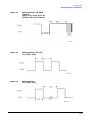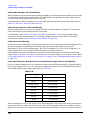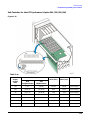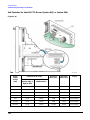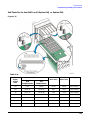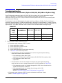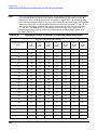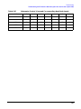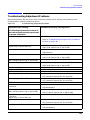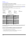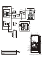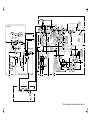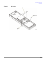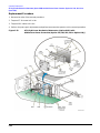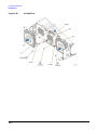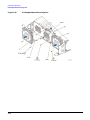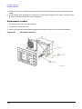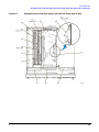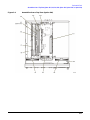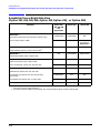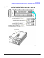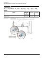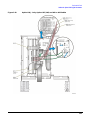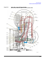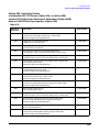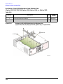
1
Service Guide
Agilent Technologies
ESG Vector Signal Generator
This guide applies to signal generator models and associated serial number prefixes listed below.
Depending on your firmware revision, signal generator operation may vary from descriptions in this guide.
E4438C: US4146
Part Number: E4400-90511
Printed in USA
March 2002
© Copyright 2001, 2002 Agilent Technologies, Inc.
Notice
The material contained in this document is provided “as is”, and is subject to being changed, without notice,
in future editions.
Further, to the maximum extent permitted by applicable law, Agilent disclaims all warranties, either express
or implied with regard to this manual and to any of the Agilent products to which it pertains, including but
not limited to the implied warranties of merchantability and fitness for a particular purpose. Agilent shall
not be liable for errors or for incidental or consequential damages in connection with the furnishing, use, or
performance of this document or any of the Agilent products to which it pertains. Should Agilent have a
written contract with the User and should any of the contract terms conflict with these terms, the contract
terms shall control.
For signal generator warranty information, refer to the Installation Guide or Service Guide.
Questions or Comments about our Documentation?
We welcome any questions or comments you may have about our documentation. Please email us at
[email protected].
ii
Contents
1. Troubleshooting
Before Troubleshooting . . . . . . . . . . . . . . . . . . . . . . . . . . . . . . . . . . . . . . . . . . . . . . . . . . . . . . . . .1-2
ESD Information . . . . . . . . . . . . . . . . . . . . . . . . . . . . . . . . . . . . . . . . . . . . . . . . . . . . . . . . . . .1-2
Getting Started with Troubleshooting . . . . . . . . . . . . . . . . . . . . . . . . . . . . . . . . . . . . . . . . . . . . .1-3
Troubleshooting Aids . . . . . . . . . . . . . . . . . . . . . . . . . . . . . . . . . . . . . . . . . . . . . . . . . . . . . . . .1-3
ILT-1 Power Supply Failure and Self-Test . . . . . . . . . . . . . . . . . . . . . . . . . . . . . . . . . . . . . . .1-4
ILT-2 A12 CPU Power-On Test . . . . . . . . . . . . . . . . . . . . . . . . . . . . . . . . . . . . . . . . . . . . . . . .1-5
ILT3 Front Panel Display Troubleshooting . . . . . . . . . . . . . . . . . . . . . . . . . . . . . . . . . . . . . .1-9
Symptom: If the Display is Dark . . . . . . . . . . . . . . . . . . . . . . . . . . . . . . . . . . . . . . . . . . . . .1-10
Symptom: If the Display is Bright, but without Characters . . . . . . . . . . . . . . . . . . . . . . . .1-12
Symptom: If Hardkeys or Softkeys are Not Functioning . . . . . . . . . . . . . . . . . . . . . . . . . .1-15
Symptom: If the RPG Knob is Not Functioning. . . . . . . . . . . . . . . . . . . . . . . . . . . . . . . . . .1-17
Symptom: If the Screen Saver is Not Functioning. . . . . . . . . . . . . . . . . . . . . . . . . . . . . . . .1-18
Self-Test Failures and Related Troubleshooting . . . . . . . . . . . . . . . . . . . . . . . . . . . . . . . . . . . .1-19
Overview. . . . . . . . . . . . . . . . . . . . . . . . . . . . . . . . . . . . . . . . . . . . . . . . . . . . . . . . . . . . . . . . .1-19
To Run Self-Test. . . . . . . . . . . . . . . . . . . . . . . . . . . . . . . . . . . . . . . . . . . . . . . . . . . . . . . . . . .1-20
Troubleshooting Assembly Level Problems . . . . . . . . . . . . . . . . . . . . . . . . . . . . . . . . . . . . . . . .1-23
Power Supplies. . . . . . . . . . . . . . . . . . . . . . . . . . . . . . . . . . . . . . . . . . . . . . . . . . . . . . . . . . . .1-23
Self-Tests 1xx for the A10 I/Q Multiplexer. . . . . . . . . . . . . . . . . . . . . . . . . . . . . . . . . . . . . .1-30
Self-Tests 2xx for the A15 Sampler (Option UNJ or Option 506) . . . . . . . . . . . . . . . . . . . .1-32
Self-Tests 4xx for the A13 Output. . . . . . . . . . . . . . . . . . . . . . . . . . . . . . . . . . . . . . . . . . . . .1-35
Self-Tests 5xx for the A17 Synthesizer (Option 501, 502, 503, 504) . . . . . . . . . . . . . . . . . .1-39
Self-Tests 6xx for the A21 YTO Driver (Option UNJ or Option 506) . . . . . . . . . . . . . . . . .1-42
Self-Tests 7xx for the A16 Frac-N (Option UNJ or Option 506) . . . . . . . . . . . . . . . . . . . . .1-45
Self-Tests 8xx for the A18 Reference . . . . . . . . . . . . . . . . . . . . . . . . . . . . . . . . . . . . . . . . . .1-50
Self-Tests 11xx for the A12 CPU. . . . . . . . . . . . . . . . . . . . . . . . . . . . . . . . . . . . . . . . . . . . . .1-52
Self-Tests 14xx for the A11 Internal Bit Error Rate Analyzer (Option UN7) . . . . . . . . . .1-54
Self-Tests 15xx
for the A9 Digital Demodulator (Option 501, 502, 503, 504 with Option 300). . . . . . . . . .1-56
Self-Tests 16xx for the A7 Baseband Generator (Option 001 or Option 002). . . . . . . . . . .1-58
Self-Tests 20xx for the A14 Extended Frequency Output (Option 506) . . . . . . . . . . . . . . .1-62
Self-Tests 21xx for the A23 Motherboard . . . . . . . . . . . . . . . . . . . . . . . . . . . . . . . . . . . . . . .1-66
Troubleshooting Unlocks . . . . . . . . . . . . . . . . . . . . . . . . . . . . . . . . . . . . . . . . . . . . . . . . . . . . . . .1-68
514 Reference Oven Cold. . . . . . . . . . . . . . . . . . . . . . . . . . . . . . . . . . . . . . . . . . . . . . . . . . . .1-68
515 10 MHz Signal Bad . . . . . . . . . . . . . . . . . . . . . . . . . . . . . . . . . . . . . . . . . . . . . . . . . . . . .1-68
512 Reference Unlocked . . . . . . . . . . . . . . . . . . . . . . . . . . . . . . . . . . . . . . . . . . . . . . . . . . . .1-69
513 1 GHz Out of Lock. . . . . . . . . . . . . . . . . . . . . . . . . . . . . . . . . . . . . . . . . . . . . . . . . . . . . .1-69
iii
Contents
508 Frac-N Loop Unlock (Option 501, 502, 503, 504) . . . . . . . . . . . . . . . . . . . . . . . . . . . . . 1-69
508 Frac-N Loop Unlock (Option UNJ and Option 506) . . . . . . . . . . . . . . . . . . . . . . . . . . . 1-69
520 Sampler Unlocked (Option UNJ and Option 506) . . . . . . . . . . . . . . . . . . . . . . . . . . . . 1-70
521 YO Loop Unlocked (Option UNJ and Option 506) . . . . . . . . . . . . . . . . . . . . . . . . . . . . 1-71
516 Baseband Generator Unlock . . . . . . . . . . . . . . . . . . . . . . . . . . . . . . . . . . . . . . . . . . . . . 1-71
623 Demod Unlock . . . . . . . . . . . . . . . . . . . . . . . . . . . . . . . . . . . . . . . . . . . . . . . . . . . . . . . . 1-72
Troubleshooting Unlevels and the RF Path . . . . . . . . . . . . . . . . . . . . . . . . . . . . . . . . . . . . . . . . 1-73
Troubleshooting a Leveling Problem . . . . . . . . . . . . . . . . . . . . . . . . . . . . . . . . . . . . . . . . . . 1-74
Troubleshooting the
AT1 Electronic Attenuator (Option 501, 502, 503, 504 or Option UNJ). . . . . . . . . . . . . . . . . . 1-79
Troubleshooting the
AT1 High-Power Mechanical Attenuator (Option UNB) . . . . . . . . . . . . . . . . . . . . . . . . . . . . . . 1-82
Troubleshooting Adjustment Problems . . . . . . . . . . . . . . . . . . . . . . . . . . . . . . . . . . . . . . . . . . . 1-85
Troubleshooting Analog Bus ADC Calibration Failures . . . . . . . . . . . . . . . . . . . . . . . . . . . . . . 1-88
Procedure for Signal Generators with Option 501, 502, 503, 504 . . . . . . . . . . . . . . . . . . . 1-88
Procedure for Signal Generators with Option UNJ . . . . . . . . . . . . . . . . . . . . . . . . . . . . . . 1-89
Procedure for Signal Generators with Option 506 . . . . . . . . . . . . . . . . . . . . . . . . . . . . . . . 1-90
Troubleshooting Performance Test Problems . . . . . . . . . . . . . . . . . . . . . . . . . . . . . . . . . . . . . . 1-91
Troubleshooting Harmonic Spurious . . . . . . . . . . . . . . . . . . . . . . . . . . . . . . . . . . . . . . . . . . . . 1-101
Troubleshooting Harmonic Spurious by Fundamental Frequency . . . . . . . . . . . . . . . . . 1-101
To Verify Harmonic Performance at the RF Output . . . . . . . . . . . . . . . . . . . . . . . . . . . . . 1-102
To Verify Harmonic Performance at the Coherent Carrier Output . . . . . . . . . . . . . . . . . 1-103
Troubleshooting Non-Harmonic Spurious . . . . . . . . . . . . . . . . . . . . . . . . . . . . . . . . . . . . . . . . 1-104
Troubleshooting Phase Noise (Option UNJ and Option 506 Only) . . . . . . . . . . . . . . . . . . . . 1-106
Troubleshooting Pulse Modulation and LF Out . . . . . . . . . . . . . . . . . . . . . . . . . . . . . . . . . . . 1-107
To Verify the Pulse Waveform at the A19 Daughterboard (All Options) . . . . . . . . . . . . . 1-108
To Verify the Pulse Waveform at the A19 Daughterboard (Option 506 Only). . . . . . . . . 1-110
No Pulse Signal from LF Out . . . . . . . . . . . . . . . . . . . . . . . . . . . . . . . . . . . . . . . . . . . . . . . 1-112
Contacting Agilent Technologies . . . . . . . . . . . . . . . . . . . . . . . . . . . . . . . . . . . . . . . . . . . . . . . 1-113
Review the Warranty . . . . . . . . . . . . . . . . . . . . . . . . . . . . . . . . . . . . . . . . . . . . . . . . . . . . . 1-113
Contacting Agilent Sales and Service Offices . . . . . . . . . . . . . . . . . . . . . . . . . . . . . . . . . . 1-114
Important Information Needed by an Agilent Service Representative . . . . . . . . . . . . . . 1-114
Returning Your Signal Generator for Service . . . . . . . . . . . . . . . . . . . . . . . . . . . . . . . . . . 1-115
Block Descriptions for Option 501, 502, 503, 504 . . . . . . . . . . . . . . . . . . . . . . . . . . . . . . . . . . 1-116
Overall Block Description for Option 501, 502, 503, 504 . . . . . . . . . . . . . . . . . . . . . . . . . 1-117
Frequency Synthesis Block Description for Option 501, 502, 503, 504 . . . . . . . . . . . . . . 1-120
iv
Contents
RF Path Block Description for Option 501, 502, 503, 504 . . . . . . . . . . . . . . . . . . . . . . . . .1-122
Analog Modulation
Block Description for All Options . . . . . . . . . . . . . . . . . . . . . . . . . . . . . . . . . . . . . . . . . . . .1-125
Digital Modulation Block Description for All Options. . . . . . . . . . . . . . . . . . . . . . . . . . . .1-128
Block Descriptions for Option UNJ and Option 506 . . . . . . . . . . . . . . . . . . . . . . . . . . . . . . . .1-130
Overall Block Description for Option UNJ and Option 506 . . . . . . . . . . . . . . . . . . . . . . .1-131
Frequency Synthesis Block Description for Option UNJ and Option 506 . . . . . . . . . . . .1-135
RF Path Block Description for Option UNJ or Option 506 . . . . . . . . . . . . . . . . . . . . . . . .1-138
Analog Modulation
Block Description for All Options . . . . . . . . . . . . . . . . . . . . . . . . . . . . . . . . . . . . . . . . . . . .1-142
Digital Modulation Block Description for All Options. . . . . . . . . . . . . . . . . . . . . . . . . . . .1-145
Overall Block Diagram for Option 501, 502, 503, 504 . . . . . . . . . . . . . . . . . . . . . . . . . . . . . . .1-147
Frequency Synthesis Block Diagram for Option 501, 502, 503, 504 . . . . . . . . . . . . . . . . . . . .1-149
RF Path Block Diagram for Option 501, 502, 503, 504 . . . . . . . . . . . . . . . . . . . . . . . . . . . . . .1-151
Analog Modulation Block Diagram for All Options . . . . . . . . . . . . . . . . . . . . . . . . . . . . . . . . .1-153
Digital Modulation Block Diagram for All Options . . . . . . . . . . . . . . . . . . . . . . . . . . . . . . . . .1-155
Overall Block Diagram for Option UNJ and Option 506 . . . . . . . . . . . . . . . . . . . . . . . . . . . . .1-157
Frequency Synthesis Block Diagram
for Option UNJ and Option 506 (Page 1 of 2) . . . . . . . . . . . . . . . . . . . . . . . . . . . . . . . . . . . . . .1-159
Frequency Synthesis Block Diagram
for Option UNJ and Option 506 (Page 2 of 2) . . . . . . . . . . . . . . . . . . . . . . . . . . . . . . . . . . . . . .1-161
RF Path Block Diagram
for Option UNJ and Option 506 (Page 1 of 2) . . . . . . . . . . . . . . . . . . . . . . . . . . . . . . . . . . . . . .1-163
RF Path Block Diagram
for Option UNJ and Option 506 (Page 2 of 2) . . . . . . . . . . . . . . . . . . . . . . . . . . . . . . . . . . . . . .1-165
Analog Modulation Block Diagram for All Options . . . . . . . . . . . . . . . . . . . . . . . . . . . . . . . . .1-167
Digital Modulation Block Diagram for All Options . . . . . . . . . . . . . . . . . . . . . . . . . . . . . . . . .1-169
2. Assembly Replacement
Before You Replace an Assembly. . . . . . . . . . . . . . . . . . . . . . . . . . . . . . . . . . . . . . . . . . . . . . . . . .2-2
After Replacing an Assembly . . . . . . . . . . . . . . . . . . . . . . . . . . . . . . . . . . . . . . . . . . . . . . . . .2-2
Assemblies That You Can Replace . . . . . . . . . . . . . . . . . . . . . . . . . . . . . . . . . . . . . . . . . . . . . . . .2-3
Outer and Inner Instrument Covers . . . . . . . . . . . . . . . . . . . . . . . . . . . . . . . . . . . . . . . . . . . . . . .2-4
Tools Required . . . . . . . . . . . . . . . . . . . . . . . . . . . . . . . . . . . . . . . . . . . . . . . . . . . . . . . . . . . . .2-4
Removal Procedures . . . . . . . . . . . . . . . . . . . . . . . . . . . . . . . . . . . . . . . . . . . . . . . . . . . . . . . .2-4
Replacement Procedure . . . . . . . . . . . . . . . . . . . . . . . . . . . . . . . . . . . . . . . . . . . . . . . . . . . . .2-4
Front Panel . . . . . . . . . . . . . . . . . . . . . . . . . . . . . . . . . . . . . . . . . . . . . . . . . . . . . . . . . . . . . . . . . . .2-6
v
Contents
Tools Required . . . . . . . . . . . . . . . . . . . . . . . . . . . . . . . . . . . . . . . . . . . . . . . . . . . . . . . . . . . . 2-6
Removal Procedure . . . . . . . . . . . . . . . . . . . . . . . . . . . . . . . . . . . . . . . . . . . . . . . . . . . . . . . . . 2-6
A1 Keyboard . . . . . . . . . . . . . . . . . . . . . . . . . . . . . . . . . . . . . . . . . . . . . . . . . . . . . . . . . . . . . . . . . 2-8
Tools Required . . . . . . . . . . . . . . . . . . . . . . . . . . . . . . . . . . . . . . . . . . . . . . . . . . . . . . . . . . . . 2-8
Removal Procedure . . . . . . . . . . . . . . . . . . . . . . . . . . . . . . . . . . . . . . . . . . . . . . . . . . . . . . . . 2-8
Replacement Procedure . . . . . . . . . . . . . . . . . . . . . . . . . . . . . . . . . . . . . . . . . . . . . . . . . . . . . 2-8
A2 Display . . . . . . . . . . . . . . . . . . . . . . . . . . . . . . . . . . . . . . . . . . . . . . . . . . . . . . . . . . . . . . . . . . 2-10
Tools Required . . . . . . . . . . . . . . . . . . . . . . . . . . . . . . . . . . . . . . . . . . . . . . . . . . . . . . . . . . . 2-10
Removal Procedure . . . . . . . . . . . . . . . . . . . . . . . . . . . . . . . . . . . . . . . . . . . . . . . . . . . . . . . 2-10
Replacement Procedure . . . . . . . . . . . . . . . . . . . . . . . . . . . . . . . . . . . . . . . . . . . . . . . . . . . . 2-10
A2DS1 Display Backlight . . . . . . . . . . . . . . . . . . . . . . . . . . . . . . . . . . . . . . . . . . . . . . . . . . . . . . 2-12
Tools Required . . . . . . . . . . . . . . . . . . . . . . . . . . . . . . . . . . . . . . . . . . . . . . . . . . . . . . . . . . . 2-12
Removal Procedure . . . . . . . . . . . . . . . . . . . . . . . . . . . . . . . . . . . . . . . . . . . . . . . . . . . . . . . 2-12
Replacement Procedure . . . . . . . . . . . . . . . . . . . . . . . . . . . . . . . . . . . . . . . . . . . . . . . . . . . . 2-12
A3 Front Panel Auxilary Board . . . . . . . . . . . . . . . . . . . . . . . . . . . . . . . . . . . . . . . . . . . . . . . . . 2-14
Tools Required . . . . . . . . . . . . . . . . . . . . . . . . . . . . . . . . . . . . . . . . . . . . . . . . . . . . . . . . . . . 2-14
Removal Procedure . . . . . . . . . . . . . . . . . . . . . . . . . . . . . . . . . . . . . . . . . . . . . . . . . . . . . . . 2-14
Replacement Procedure . . . . . . . . . . . . . . . . . . . . . . . . . . . . . . . . . . . . . . . . . . . . . . . . . . . . 2-14
A4 Inverter . . . . . . . . . . . . . . . . . . . . . . . . . . . . . . . . . . . . . . . . . . . . . . . . . . . . . . . . . . . . . . . . . 2-16
Tools Required . . . . . . . . . . . . . . . . . . . . . . . . . . . . . . . . . . . . . . . . . . . . . . . . . . . . . . . . . . . 2-16
Removal Procedure . . . . . . . . . . . . . . . . . . . . . . . . . . . . . . . . . . . . . . . . . . . . . . . . . . . . . . . 2-16
Replacement Procedure . . . . . . . . . . . . . . . . . . . . . . . . . . . . . . . . . . . . . . . . . . . . . . . . . . . . 2-16
A5 10 GB Hard Drive (Option 005) . . . . . . . . . . . . . . . . . . . . . . . . . . . . . . . . . . . . . . . . . . . . . . 2-18
Tools Required . . . . . . . . . . . . . . . . . . . . . . . . . . . . . . . . . . . . . . . . . . . . . . . . . . . . . . . . . . . 2-18
Removal Procedure . . . . . . . . . . . . . . . . . . . . . . . . . . . . . . . . . . . . . . . . . . . . . . . . . . . . . . . 2-18
Replacement Procedure . . . . . . . . . . . . . . . . . . . . . . . . . . . . . . . . . . . . . . . . . . . . . . . . . . . . 2-18
A6 Power Supply . . . . . . . . . . . . . . . . . . . . . . . . . . . . . . . . . . . . . . . . . . . . . . . . . . . . . . . . . . . . . 2-20
Tools Required . . . . . . . . . . . . . . . . . . . . . . . . . . . . . . . . . . . . . . . . . . . . . . . . . . . . . . . . . . . 2-20
Removal Procedure . . . . . . . . . . . . . . . . . . . . . . . . . . . . . . . . . . . . . . . . . . . . . . . . . . . . . . . 2-20
Replacement Procedure . . . . . . . . . . . . . . . . . . . . . . . . . . . . . . . . . . . . . . . . . . . . . . . . . . . . 2-20
A7 Baseband Generator (Option 001 or Option 002). . . . . . . . . . . . . . . . . . . . . . . . . . . . . . . . . 2-22
Tools Required . . . . . . . . . . . . . . . . . . . . . . . . . . . . . . . . . . . . . . . . . . . . . . . . . . . . . . . . . . . 2-22
Removal Procedure . . . . . . . . . . . . . . . . . . . . . . . . . . . . . . . . . . . . . . . . . . . . . . . . . . . . . . . 2-22
Replacement Procedure . . . . . . . . . . . . . . . . . . . . . . . . . . . . . . . . . . . . . . . . . . . . . . . . . . . . 2-22
A9 Digital Demodulator (Option 501, 502, 503, 504 with Option 300) . . . . . . . . . . . . . . . . . . 2-24
Tools Required . . . . . . . . . . . . . . . . . . . . . . . . . . . . . . . . . . . . . . . . . . . . . . . . . . . . . . . . . . . 2-24
Removal Procedure . . . . . . . . . . . . . . . . . . . . . . . . . . . . . . . . . . . . . . . . . . . . . . . . . . . . . . . 2-24
vi
Contents
Replacement Procedure . . . . . . . . . . . . . . . . . . . . . . . . . . . . . . . . . . . . . . . . . . . . . . . . . . . .2-24
A10 I/Q Multiplexer . . . . . . . . . . . . . . . . . . . . . . . . . . . . . . . . . . . . . . . . . . . . . . . . . . . . . . . . . . .2-26
Tools Required . . . . . . . . . . . . . . . . . . . . . . . . . . . . . . . . . . . . . . . . . . . . . . . . . . . . . . . . . . . .2-26
Removal Procedure . . . . . . . . . . . . . . . . . . . . . . . . . . . . . . . . . . . . . . . . . . . . . . . . . . . . . . . .2-26
Replacement Procedure . . . . . . . . . . . . . . . . . . . . . . . . . . . . . . . . . . . . . . . . . . . . . . . . . . . .2-27
A11 Internal Bit Error Rate Analyzer (Option UN7). . . . . . . . . . . . . . . . . . . . . . . . . . . . . . . . .2-28
Tools Required . . . . . . . . . . . . . . . . . . . . . . . . . . . . . . . . . . . . . . . . . . . . . . . . . . . . . . . . . . . .2-28
Removal Procedure . . . . . . . . . . . . . . . . . . . . . . . . . . . . . . . . . . . . . . . . . . . . . . . . . . . . . . . .2-28
Replacement Procedure . . . . . . . . . . . . . . . . . . . . . . . . . . . . . . . . . . . . . . . . . . . . . . . . . . . .2-29
A12 CPU . . . . . . . . . . . . . . . . . . . . . . . . . . . . . . . . . . . . . . . . . . . . . . . . . . . . . . . . . . . . . . . . . . . .2-30
Tools Required . . . . . . . . . . . . . . . . . . . . . . . . . . . . . . . . . . . . . . . . . . . . . . . . . . . . . . . . . . . .2-30
Removal Procedure . . . . . . . . . . . . . . . . . . . . . . . . . . . . . . . . . . . . . . . . . . . . . . . . . . . . . . . .2-30
Replacement Procedure . . . . . . . . . . . . . . . . . . . . . . . . . . . . . . . . . . . . . . . . . . . . . . . . . . . .2-31
A13 Output . . . . . . . . . . . . . . . . . . . . . . . . . . . . . . . . . . . . . . . . . . . . . . . . . . . . . . . . . . . . . . . . .2-32
Tools Required . . . . . . . . . . . . . . . . . . . . . . . . . . . . . . . . . . . . . . . . . . . . . . . . . . . . . . . . . . . .2-32
Removal Procedure . . . . . . . . . . . . . . . . . . . . . . . . . . . . . . . . . . . . . . . . . . . . . . . . . . . . . . . .2-32
Replacement Procedure . . . . . . . . . . . . . . . . . . . . . . . . . . . . . . . . . . . . . . . . . . . . . . . . . . . .2-32
A14 Extended Frequency Output (Option 506) . . . . . . . . . . . . . . . . . . . . . . . . . . . . . . . . . . . . .2-34
Tools Required . . . . . . . . . . . . . . . . . . . . . . . . . . . . . . . . . . . . . . . . . . . . . . . . . . . . . . . . . . . .2-34
Removal Procedure . . . . . . . . . . . . . . . . . . . . . . . . . . . . . . . . . . . . . . . . . . . . . . . . . . . . . . . .2-34
Replacement Procedure . . . . . . . . . . . . . . . . . . . . . . . . . . . . . . . . . . . . . . . . . . . . . . . . . . . .2-34
A15 Sampler (Option UNJ or Option 506) . . . . . . . . . . . . . . . . . . . . . . . . . . . . . . . . . . . . . . . . .2-36
Tools Required . . . . . . . . . . . . . . . . . . . . . . . . . . . . . . . . . . . . . . . . . . . . . . . . . . . . . . . . . . . .2-36
Removal Procedure . . . . . . . . . . . . . . . . . . . . . . . . . . . . . . . . . . . . . . . . . . . . . . . . . . . . . . . .2-36
Replacement Procedure . . . . . . . . . . . . . . . . . . . . . . . . . . . . . . . . . . . . . . . . . . . . . . . . . . . .2-36
A16 Frac-N (Option UNJ or Option 506) . . . . . . . . . . . . . . . . . . . . . . . . . . . . . . . . . . . . . . . . . .2-38
Tools Required . . . . . . . . . . . . . . . . . . . . . . . . . . . . . . . . . . . . . . . . . . . . . . . . . . . . . . . . . . . .2-38
Removal Procedure . . . . . . . . . . . . . . . . . . . . . . . . . . . . . . . . . . . . . . . . . . . . . . . . . . . . . . . .2-38
Replacement Procedure . . . . . . . . . . . . . . . . . . . . . . . . . . . . . . . . . . . . . . . . . . . . . . . . . . . .2-38
A17 Synthesizer (Option 501, 502, 503, 504) . . . . . . . . . . . . . . . . . . . . . . . . . . . . . . . . . . . . . . .2-40
Tools Required . . . . . . . . . . . . . . . . . . . . . . . . . . . . . . . . . . . . . . . . . . . . . . . . . . . . . . . . . . . .2-40
Removal Procedure . . . . . . . . . . . . . . . . . . . . . . . . . . . . . . . . . . . . . . . . . . . . . . . . . . . . . . . .2-40
Replacement Procedure . . . . . . . . . . . . . . . . . . . . . . . . . . . . . . . . . . . . . . . . . . . . . . . . . . . .2-40
A18 Reference . . . . . . . . . . . . . . . . . . . . . . . . . . . . . . . . . . . . . . . . . . . . . . . . . . . . . . . . . . . . . . . .2-42
Tools Required . . . . . . . . . . . . . . . . . . . . . . . . . . . . . . . . . . . . . . . . . . . . . . . . . . . . . . . . . . . .2-42
Removal Procedure . . . . . . . . . . . . . . . . . . . . . . . . . . . . . . . . . . . . . . . . . . . . . . . . . . . . . . . .2-42
Replacement Procedure . . . . . . . . . . . . . . . . . . . . . . . . . . . . . . . . . . . . . . . . . . . . . . . . . . . .2-42
vii
Contents
A19 Daughterboard . . . . . . . . . . . . . . . . . . . . . . . . . . . . . . . . . . . . . . . . . . . . . . . . . . . . . . . . . . . 2-44
Tools Required . . . . . . . . . . . . . . . . . . . . . . . . . . . . . . . . . . . . . . . . . . . . . . . . . . . . . . . . . . . 2-44
Removal Procedure . . . . . . . . . . . . . . . . . . . . . . . . . . . . . . . . . . . . . . . . . . . . . . . . . . . . . . . . 2-44
Replacement Procedure . . . . . . . . . . . . . . . . . . . . . . . . . . . . . . . . . . . . . . . . . . . . . . . . . . . . 2-44
A19 Daughterboard Cable Removal . . . . . . . . . . . . . . . . . . . . . . . . . . . . . . . . . . . . . . . . . . . . . . 2-46
Tools Required . . . . . . . . . . . . . . . . . . . . . . . . . . . . . . . . . . . . . . . . . . . . . . . . . . . . . . . . . . . 2-46
Removal Procedure . . . . . . . . . . . . . . . . . . . . . . . . . . . . . . . . . . . . . . . . . . . . . . . . . . . . . . . . 2-46
Replacement Procedure . . . . . . . . . . . . . . . . . . . . . . . . . . . . . . . . . . . . . . . . . . . . . . . . . . . . 2-46
A20 Downconverter (Option 501, 502, 503, 504 with Option 300) . . . . . . . . . . . . . . . . . . . . . . 2-48
Tools Required . . . . . . . . . . . . . . . . . . . . . . . . . . . . . . . . . . . . . . . . . . . . . . . . . . . . . . . . . . . 2-48
Removal Procedure . . . . . . . . . . . . . . . . . . . . . . . . . . . . . . . . . . . . . . . . . . . . . . . . . . . . . . . . 2-48
Replacement Procedure . . . . . . . . . . . . . . . . . . . . . . . . . . . . . . . . . . . . . . . . . . . . . . . . . . . . 2-48
A21 YTO Driver (Option UNJ or Option 506)
and A22 Coupler (Option 506) . . . . . . . . . . . . . . . . . . . . . . . . . . . . . . . . . . . . . . . . . . . . . . . . . . 2-50
Tools Required . . . . . . . . . . . . . . . . . . . . . . . . . . . . . . . . . . . . . . . . . . . . . . . . . . . . . . . . . . . 2-50
Removal Procedure . . . . . . . . . . . . . . . . . . . . . . . . . . . . . . . . . . . . . . . . . . . . . . . . . . . . . . . . 2-50
Replacement Procedure . . . . . . . . . . . . . . . . . . . . . . . . . . . . . . . . . . . . . . . . . . . . . . . . . . . . 2-51
A23 Motherboard . . . . . . . . . . . . . . . . . . . . . . . . . . . . . . . . . . . . . . . . . . . . . . . . . . . . . . . . . . . . . 2-52
Tools Required . . . . . . . . . . . . . . . . . . . . . . . . . . . . . . . . . . . . . . . . . . . . . . . . . . . . . . . . . . . 2-52
Removal Procedure . . . . . . . . . . . . . . . . . . . . . . . . . . . . . . . . . . . . . . . . . . . . . . . . . . . . . . . . 2-52
Replacement Procedure . . . . . . . . . . . . . . . . . . . . . . . . . . . . . . . . . . . . . . . . . . . . . . . . . . . . 2-53
A23BT1 Battery. . . . . . . . . . . . . . . . . . . . . . . . . . . . . . . . . . . . . . . . . . . . . . . . . . . . . . . . . . . . . . 2-55
Tools Required . . . . . . . . . . . . . . . . . . . . . . . . . . . . . . . . . . . . . . . . . . . . . . . . . . . . . . . . . . . 2-55
Removal Procedure . . . . . . . . . . . . . . . . . . . . . . . . . . . . . . . . . . . . . . . . . . . . . . . . . . . . . . . . 2-55
Replacement Procedure . . . . . . . . . . . . . . . . . . . . . . . . . . . . . . . . . . . . . . . . . . . . . . . . . . . . 2-55
A24 Line Module . . . . . . . . . . . . . . . . . . . . . . . . . . . . . . . . . . . . . . . . . . . . . . . . . . . . . . . . . . . . . 2-56
Tools Required . . . . . . . . . . . . . . . . . . . . . . . . . . . . . . . . . . . . . . . . . . . . . . . . . . . . . . . . . . . 2-56
Removal Procedure . . . . . . . . . . . . . . . . . . . . . . . . . . . . . . . . . . . . . . . . . . . . . . . . . . . . . . . . 2-56
Replacement Procedure . . . . . . . . . . . . . . . . . . . . . . . . . . . . . . . . . . . . . . . . . . . . . . . . . . . . 2-56
Rear Panel . . . . . . . . . . . . . . . . . . . . . . . . . . . . . . . . . . . . . . . . . . . . . . . . . . . . . . . . . . . . . . . . . . 2-57
Tools Required . . . . . . . . . . . . . . . . . . . . . . . . . . . . . . . . . . . . . . . . . . . . . . . . . . . . . . . . . . . 2-57
Removal Procedure . . . . . . . . . . . . . . . . . . . . . . . . . . . . . . . . . . . . . . . . . . . . . . . . . . . . . . . 2-57
Replacement Procedure . . . . . . . . . . . . . . . . . . . . . . . . . . . . . . . . . . . . . . . . . . . . . . . . . . . . 2-57
A25 Rear Panel Board . . . . . . . . . . . . . . . . . . . . . . . . . . . . . . . . . . . . . . . . . . . . . . . . . . . . . . . . . 2-59
Tools Required . . . . . . . . . . . . . . . . . . . . . . . . . . . . . . . . . . . . . . . . . . . . . . . . . . . . . . . . . . . 2-59
Removal Procedure . . . . . . . . . . . . . . . . . . . . . . . . . . . . . . . . . . . . . . . . . . . . . . . . . . . . . . . 2-59
Replacement Procedure . . . . . . . . . . . . . . . . . . . . . . . . . . . . . . . . . . . . . . . . . . . . . . . . . . . . 2-59
viii
Contents
A26 Rear Panel LVDS Board (Option 1EM)
and A27 Rear Panel SMB Board (Option 1EM) . . . . . . . . . . . . . . . . . . . . . . . . . . . . . . . . . . . . .2-61
Tools Required . . . . . . . . . . . . . . . . . . . . . . . . . . . . . . . . . . . . . . . . . . . . . . . . . . . . . . . . . . . .2-61
Removal Procedure . . . . . . . . . . . . . . . . . . . . . . . . . . . . . . . . . . . . . . . . . . . . . . . . . . . . . . . .2-61
Replacement Procedure . . . . . . . . . . . . . . . . . . . . . . . . . . . . . . . . . . . . . . . . . . . . . . . . . . . .2-61
AT1 High-Power Mechanical Attenuator (Option UNB) with
A28 Reverse Power Protection (Option 501, 502, 503, 504 or Option UNJ) . . . . . . . . . . . . . . .2-63
Tools Required . . . . . . . . . . . . . . . . . . . . . . . . . . . . . . . . . . . . . . . . . . . . . . . . . . . . . . . . . . . .2-63
Removal Procedure . . . . . . . . . . . . . . . . . . . . . . . . . . . . . . . . . . . . . . . . . . . . . . . . . . . . . . . .2-63
Replacement Procedure . . . . . . . . . . . . . . . . . . . . . . . . . . . . . . . . . . . . . . . . . . . . . . . . . . . .2-64
AT1 High-Power Mechanical Attenuator (Option UNB) . . . . . . . . . . . . . . . . . . . . . . . . . . . . . .2-65
Tools Required . . . . . . . . . . . . . . . . . . . . . . . . . . . . . . . . . . . . . . . . . . . . . . . . . . . . . . . . . . . .2-65
Removal Procedure . . . . . . . . . . . . . . . . . . . . . . . . . . . . . . . . . . . . . . . . . . . . . . . . . . . . . . . .2-65
Replacement Procedure . . . . . . . . . . . . . . . . . . . . . . . . . . . . . . . . . . . . . . . . . . . . . . . . . . . .2-65
AT1 Electronic Attenuator (Option 501, 502, 503, 504 or Option UNJ) . . . . . . . . . . . . . . . . . .2-67
Tools Required . . . . . . . . . . . . . . . . . . . . . . . . . . . . . . . . . . . . . . . . . . . . . . . . . . . . . . . . . . . .2-67
Removal Procedure . . . . . . . . . . . . . . . . . . . . . . . . . . . . . . . . . . . . . . . . . . . . . . . . . . . . . . . .2-67
Replacement Procedure . . . . . . . . . . . . . . . . . . . . . . . . . . . . . . . . . . . . . . . . . . . . . . . . . . . .2-67
A29 DC Blocking Capacitor (Option 506) . . . . . . . . . . . . . . . . . . . . . . . . . . . . . . . . . . . . . . . . . .2-69
Tools Required . . . . . . . . . . . . . . . . . . . . . . . . . . . . . . . . . . . . . . . . . . . . . . . . . . . . . . . . . . . .2-69
Removal Procedure . . . . . . . . . . . . . . . . . . . . . . . . . . . . . . . . . . . . . . . . . . . . . . . . . . . . . . . .2-69
Removal Procedure for Option 1EM . . . . . . . . . . . . . . . . . . . . . . . . . . . . . . . . . . . . . . . . . . .2-69
Replacement Procedure . . . . . . . . . . . . . . . . . . . . . . . . . . . . . . . . . . . . . . . . . . . . . . . . . . . . .2-69
B1 Power Supply Fan . . . . . . . . . . . . . . . . . . . . . . . . . . . . . . . . . . . . . . . . . . . . . . . . . . . . . . . . . .2-71
Tools Required . . . . . . . . . . . . . . . . . . . . . . . . . . . . . . . . . . . . . . . . . . . . . . . . . . . . . . . . . . . .2-71
Removal Procedure . . . . . . . . . . . . . . . . . . . . . . . . . . . . . . . . . . . . . . . . . . . . . . . . . . . . . . . .2-71
Replacement Procedure . . . . . . . . . . . . . . . . . . . . . . . . . . . . . . . . . . . . . . . . . . . . . . . . . . . .2-71
B2 Small Fan . . . . . . . . . . . . . . . . . . . . . . . . . . . . . . . . . . . . . . . . . . . . . . . . . . . . . . . . . . . . . . . .2-73
Tools Required . . . . . . . . . . . . . . . . . . . . . . . . . . . . . . . . . . . . . . . . . . . . . . . . . . . . . . . . . . . .2-73
Removal Procedure . . . . . . . . . . . . . . . . . . . . . . . . . . . . . . . . . . . . . . . . . . . . . . . . . . . . . . . .2-73
Replacement Procedure . . . . . . . . . . . . . . . . . . . . . . . . . . . . . . . . . . . . . . . . . . . . . . . . . . . .2-73
B3 Daughterboard/Card Cage Fan . . . . . . . . . . . . . . . . . . . . . . . . . . . . . . . . . . . . . . . . . . . . . . .2-75
Tools Required . . . . . . . . . . . . . . . . . . . . . . . . . . . . . . . . . . . . . . . . . . . . . . . . . . . . . . . . . . . .2-75
Removal Procedure . . . . . . . . . . . . . . . . . . . . . . . . . . . . . . . . . . . . . . . . . . . . . . . . . . . . . . . .2-75
Replacement Procedure . . . . . . . . . . . . . . . . . . . . . . . . . . . . . . . . . . . . . . . . . . . . . . . . . . . .2-75
RF Output Connector . . . . . . . . . . . . . . . . . . . . . . . . . . . . . . . . . . . . . . . . . . . . . . . . . . . . . . . . . .2-77
Tools Required . . . . . . . . . . . . . . . . . . . . . . . . . . . . . . . . . . . . . . . . . . . . . . . . . . . . . . . . . . . .2-77
ix
Contents
Removal Procedure . . . . . . . . . . . . . . . . . . . . . . . . . . . . . . . . . . . . . . . . . . . . . . . . . . . . . . . . 2-77
Removal Procedure for Option 1EM . . . . . . . . . . . . . . . . . . . . . . . . . . . . . . . . . . . . . . . . . . 2-77
Replacement Procedure . . . . . . . . . . . . . . . . . . . . . . . . . . . . . . . . . . . . . . . . . . . . . . . . . . . . 2-78
3. Replaceable Parts
Ordering Information . . . . . . . . . . . . . . . . . . . . . . . . . . . . . . . . . . . . . . . . . . . . . . . . . . . . . . . . . . 3-2
Call (800) 227-8164 to Order Parts Fast (U.S. Only) . . . . . . . . . . . . . . . . . . . . . . . . . . . . . . . 3-2
Save Money with Rebuilt-Exchange Assemblies . . . . . . . . . . . . . . . . . . . . . . . . . . . . . . . . . . . . . 3-3
Shipping a Defective Assembly Back to Agilent Technologies . . . . . . . . . . . . . . . . . . . . . . . . . . 3-4
Frequency, Hardware, and Personality Options . . . . . . . . . . . . . . . . . . . . . . . . . . . . . . . . . . . . . 3-5
Assemblies and Hardware Options . . . . . . . . . . . . . . . . . . . . . . . . . . . . . . . . . . . . . . . . . . . . . . . 3-6
Assemblies from a Top View
(Option 501, 502, 503, 504, Option 300, Option UNJ, or Option 506) . . . . . . . . . . . . . . . . . . . . 3-8
Assemblies from a Right-Side View
(Option 501, 502, 503, 504, Option 300, Option UNJ, or Option 506) . . . . . . . . . . . . . . . . . . . 3-12
Assemblies of the Front Panel
(Option 501, 502, 503, 504, Option 300, Option UNJ, or Option 506) . . . . . . . . . . . . . . . . . . . 3-14
Assemblies of the Inside Rear Panel
(Option 501, 502, 503, 504, Option 300, Option UNJ, Option 506,
or Option 1EM) . . . . . . . . . . . . . . . . . . . . . . . . . . . . . . . . . . . . . . . . . . . . . . . . . . . . . . . . . . . . . . 3-15
A23BT1 Battery
(Option 501, 502, 503, 504, Option 300, Option UNJ, or Option 506) . . . . . . . . . . . . . . . . . . . 3-16
Cables . . . . . . . . . . . . . . . . . . . . . . . . . . . . . . . . . . . . . . . . . . . . . . . . . . . . . . . . . . . . . . . . . . . . . . 3-17
Cables for the Inside Front Panel and Fans (B1, B2, and B3) . . . . . . . . . . . . . . . . . . . . . . . . . 3-19
Cables for Option 501, 502, 503, 504 Signal Generators. . . . . . . . . . . . . . . . . . . . . . . . . . . . . . 3-21
Option 501, 502, 503, 504 - Overall Cables
(also includes cables for Option UN7, 300, 005, and 001 or 002) . . . . . . . . . . . . . . . . . . . . 3-21
Option 501, 502, 503, 504 - Front Panel Cables . . . . . . . . . . . . . . . . . . . . . . . . . . . . . . . . . 3-24
Option 501, 502, 503, 504 - Standard Cables
(does not include cables for the front panel,
Option UN7, Option 300, or Option 005) . . . . . . . . . . . . . . . . . . . . . . . . . . . . . . . . . . . . . . . 3-26
Option 501, 502, 503, 504 - Only Option UN7, 300, 005, and 001 or 002 Cables . . . . . . . 3-28
Option 501, 502, 503, 504 - Semi-Rigid Cables
includes the AT1 Electronic Attenuator (Option 501, 502, 503, 504 or Option UNJ)
or the AT1 High-Power Mechanical Attenuator (Option UNB)
with the A28 Reverse Power Protection (Option 501, 502, 503, 504 or Option UNJ) . . . 3-30
Option 501, 502, 503, 504 - Option 1EM Overall Cables
(also includes cables for Option UN7, 300, 005, and 001 or 002) . . . . . . . . . . . . . . . . . . . . 3-32
Option 501, 502, 503, 504 - Option 1EM Semi-Rigid Cables
x
Contents
includes the AT1 Electronic Attenuator (Option 501, 502, 503, 504 or Option UNJ)
or the AT1 High-Power Mechanical Attenuator (Option UNB)
with the A28 Reverse Power Protection (Option 501, 502, 503, 504 or Option UNJ) . . . .3-35
Cables for Option UNJ Signal Generators . . . . . . . . . . . . . . . . . . . . . . . . . . . . . . . . . . . . . . . . .3-37
Option UNJ - Overall Cables
(also includes cables for Option UN7, 005, and 001 or 002) . . . . . . . . . . . . . . . . . . . . . . . .3-37
Option UNJ - Front Panel Cables . . . . . . . . . . . . . . . . . . . . . . . . . . . . . . . . . . . . . . . . . . . . .3-40
Option UNJ - Standard Cables
(does not include cables for the front panel, Option UN7, or Option 005) . . . . . . . . . . . . .3-42
Option UNJ - Only Option UN7, 005, and 001 or 002 Cables. . . . . . . . . . . . . . . . . . . . . . .3-44
Option UNJ - Semi-Rigid Cables
includes the A21 YTO Driver (Option UNJ or Option 506)
and the AT1 Electronic Attenuator (Option 501, 502, 503, 504 or Option UNJ)
or the AT1 High-Power Mechanical Attenuator (Option UNB)
with A28 Reverse Power Protection (Option 501, 502, 503, 504 or Option UNJ) . . . . . . .3-46
Option UNJ - Option 1EM Overall Cables
(also includes cables for Option UN7, 005, and 001 or 002) . . . . . . . . . . . . . . . . . . . . . . . .3-49
Option UNJ - Option 1EM Semi-Rigid Cables
includes the A21 YTO Driver (Option UNJ or Option 506)
and the AT1 Electronic Attenuator (Option 501, 502, 503, 504 or Option UNJ)
or the AT1 High-Power Mechanical Attenuator (Option UNB)
with A28 Reverse Power Protection (Option 501, 502, 503, 504 or Option UNJ) . . . . . . .3-52
Cables for Option 506 Signal Generators . . . . . . . . . . . . . . . . . . . . . . . . . . . . . . . . . . . . . . . . . .3-55
Option 506 - Overall Cables
(also includes cables for Option UN7, 005, and 001 or 002) . . . . . . . . . . . . . . . . . . . . . . . .3-55
Option 506 - Front Panel Cables. . . . . . . . . . . . . . . . . . . . . . . . . . . . . . . . . . . . . . . . . . . . . .3-58
Option 506 - Standard Cables
(does not include cables for the front panel, Option UN7, or Option 005) . . . . . . . . . . . . .3-60
Option 506 - Only Option UN7, 005, and 001 or 002 Cables. . . . . . . . . . . . . . . . . . . . . . . .3-63
Option 506 - Semi-Rigid Cables
includes the A21 YTO Driver (Option UNJ or Option 506)
and the AT1 High-Power Mechanical Attenuator (Option UNB)
with an A29 DC Blocking Capacitor (Option 506) . . . . . . . . . . . . . . . . . . . . . . . . . . . . . . . .3-65
Option 506 - Option 1EM Overall Cables
(also includes cables for Option UN7, 005, and 001 or 002) . . . . . . . . . . . . . . . . . . . . . . . .3-67
Option 506 - Option 1EM Semi-Rigid Cables
includes the A21 YTO Driver (Option UNJ or Option 506)
and the AT1 High-Power Mechanical Attenuator (Option UNB)
with an A29 DC Blocking Capacitor (Option 506) . . . . . . . . . . . . . . . . . . . . . . . . . . . . . . . .3-70
Hardware and Other Instrument Parts . . . . . . . . . . . . . . . . . . . . . . . . . . . . . . . . . . . . . . . . . . .3-72
Hardware of the Front Panel . . . . . . . . . . . . . . . . . . . . . . . . . . . . . . . . . . . . . . . . . . . . . . . .3-73
Hardware of a Disassembled Front Panel . . . . . . . . . . . . . . . . . . . . . . . . . . . . . . . . . . . . . .3-75
xi
Contents
Hardware of the Rear-Panel
(Option 501, 502, 503, 504, Option 300, Option UNJ, or Option 506) . . . . . . . . . . . . . . . . 3-77
Hardware of the Rear-Panel (Option 1EM) . . . . . . . . . . . . . . . . . . . . . . . . . . . . . . . . . . . . . 3-79
Hardware of a Disassembled
AT1 Electronic Attenuator (Option 501, 502, 503, 504 or Option UNJ) . . . . . . . . . . . . . . 3-81
Hardware of a Disassembled
AT1 High-Power Mechanical Attenuator (Option UNB)
and A28 Reverse Power Protection (Option 501, 502, 503, 504 or Option UNJ). . . . . . . . 3-82
Hardware of a Disassembled
AT1 High-Power Mechanical Attenuator (Option UNB)
on Option 506 Only . . . . . . . . . . . . . . . . . . . . . . . . . . . . . . . . . . . . . . . . . . . . . . . . . . . . . . . . 3-84
Hardware of the A6 Power Supply Shield and Left-Side
(Option 501, 502, 503, 504, Option 300, Option UNJ, or Option 506) . . . . . . . . . . . . . . . . 3-85
Hardware of the A23 Motherboard and Bottom-Side
(Option 501, 502, 503, 504, Option 300, Option UNJ, or Option 506) . . . . . . . . . . . . . . . . 3-86
Hardware of the Outside Instrument Covers and Associated Parts
(Option 501, 502, 503, 504, Option 300, Option UNJ, or Option 506) . . . . . . . . . . . . . . . . 3-87
Hardware of the Inside Instrument Covers and Associated Parts
(Option 501, 502, 503, 504, Option 300, Option UNJ, or Option 506) . . . . . . . . . . . . . . . . 3-89
Miscellaneous. . . . . . . . . . . . . . . . . . . . . . . . . . . . . . . . . . . . . . . . . . . . . . . . . . . . . . . . . . . . . . . . 3-90
Accessories. . . . . . . . . . . . . . . . . . . . . . . . . . . . . . . . . . . . . . . . . . . . . . . . . . . . . . . . . . . . . . . 3-90
Documentation . . . . . . . . . . . . . . . . . . . . . . . . . . . . . . . . . . . . . . . . . . . . . . . . . . . . . . . . . . . 3-90
Abbreviations Used in Part Descriptions . . . . . . . . . . . . . . . . . . . . . . . . . . . . . . . . . . . . . . . . . . 3-91
4. Post-Repair Procedures
Post-Repair Procedures Matrix. . . . . . . . . . . . . . . . . . . . . . . . . . . . . . . . . . . . . . . . . . . . . . . . . . . 4-2
5. Safety and Regulatory
Safety Notes . . . . . . . . . . . . . . . . . . . . . . . . . . . . . . . . . . . . . . . . . . . . . . . . . . . . . . . . . . . . . . . . . . 5-2
General Safety Considerations . . . . . . . . . . . . . . . . . . . . . . . . . . . . . . . . . . . . . . . . . . . . . . . . . . . 5-3
Lithium Battery Disposal . . . . . . . . . . . . . . . . . . . . . . . . . . . . . . . . . . . . . . . . . . . . . . . . . . . . . . . 5-4
Warranty . . . . . . . . . . . . . . . . . . . . . . . . . . . . . . . . . . . . . . . . . . . . . . . . . . . . . . . . . . . . . . . . . . . . 5-5
Assistance . . . . . . . . . . . . . . . . . . . . . . . . . . . . . . . . . . . . . . . . . . . . . . . . . . . . . . . . . . . . . . . . . . . 5-6
Notice . . . . . . . . . . . . . . . . . . . . . . . . . . . . . . . . . . . . . . . . . . . . . . . . . . . . . . . . . . . . . . . . . . . . . . . 5-7
Certification . . . . . . . . . . . . . . . . . . . . . . . . . . . . . . . . . . . . . . . . . . . . . . . . . . . . . . . . . . . . . . . . . . 5-8
xii
1 Troubleshooting
1- 1
Troubleshooting
Before Troubleshooting
Before Troubleshooting
WARNING
These troubleshooting instructions are for use by qualified personal only. To avoid
electrical shock, do not perform any troubleshooting unless qualified.
WARNING
The opening of covers or removal of parts is likely to expose dangerous voltages.
Disconnect the signal generator from all voltage sources before it is opened.
WARNING
The following techniques related to ESD and static-safe workstations should not be
used when working on circuitry with a voltage potential greater than 500 volts.
ESD Information
Protection from Electrostatic Discharge
Electrostatic discharge (ESD) can damage or destroy electronic components. All work on electronic assemblies
should be performed at a static-safe workstation using two types of static-safe workstation protection:
• conductive table-mat and wrist-strap combination
• conductive floor-mat and heel-strap combination
Both types, when used together, provide a significant level of ESD protection. Of the two, only the table-mat
and wrist-strap combination provides adequate ESD protection when used alone. To ensure user safety, the
static-safe accessories must provide at least 1 meg ohm of isolation from ground.
Handling of Electronic Components and ESD
CAUTION
Many of the assemblies in this signal generator are very susceptible to damage from
electrostatic discharge (ESD). Perform troubleshooting procedures only at a static-safe
workstation and wear a grounding strap.
CAUTION
Always handle printed circuit board assemblies by the edges. This will reduce the possibility of
ESD damage to components and prevent contamination of exposed plating.
The possibility of unseen damage caused by ESD is present whenever components are transported, stored, or
used. The risk of ESD damage can be greatly reduced by close attention to how all components are handled.
• Perform work on all components at a static-safe workstation.
• Keep static-generating materials at least one meter away from all components.
• Store or transport components is static-shielding containers.
1-2
Troubleshooting
Getting Started with Troubleshooting
Getting Started with Troubleshooting
Determine the starting point in Table 1-1 to begin troubleshooting.
• Problems should be worked on in the order they are presented in this table.
• Overviews of Self-Test, Frequency Synthesis, RF Path, Analog Modulation, and Digital Modulation are
found in this chapter. The information in these overviews may help the reader better understand how the
signal generator operates and the function of each assembly. Each overview is also intended to be used to
troubleshoot the signal generator.
Table 1-1
If able to run self-test...
Go to this section...
Run Self-Test
“Self-Test Failures and Related Troubleshooting” on page 1-19
and refer to the procedure “To Run Self-Test” on page 1-20.
If unable to run self-test,
check...
Go to this section...
Power Supply Failures
“ILT-1 Power Supply Failure and Self-Test” on page 1-4
A12 CPU Power-on Failures
“ILT-2 A12 CPU Power-On Test” on page 1-5
Front Panel Display
or Keyboard Operations
“ILT3 Front Panel Display Troubleshooting” on page 1-9
If other conditions occur...
Go to this section...
Unlocked Conditions
“Troubleshooting Unlocks” on page 1-68
Unleveled Conditions
“Troubleshooting Unlevels and the RF Path” on page 1-73
Adjustment Problems
“Troubleshooting Adjustment Problems” on page 1-85
Performance Test Problems
“Troubleshooting Performance Test Problems” on page 1-91
Troubleshooting Aids
• semi-rigid cable-extender probe
The Agilent E8251-20088 semi-rigid cable-extender probe is used for measuring signals from connectors
that are located inside the A19 Daughterboard card-cage.
• ribbon cable extender
The ribbon cable extender needs to be assembled by the user. It consists of two connector plugs (part
number 1252-1010) and approximately eight inches of ribbon cable (part number 8120-2226). The ribbon
cable contains 26 wires; six of these wires, on either the right or the left side, need to be stripped off before
being connected to the plugs.
1- 3
Troubleshooting
Getting Started with Troubleshooting
ILT-1 Power Supply Failure and Self-Test
When the signal generator appears to be dead (no display or fan) there is often little evidence that points
directly to the cause. This section provides steps and solutions to typical failure modes.
CAUTION
Immediately unplug the signal generator from the ac power line if the unit shows any of the
following symptoms:
• Smoke, arcing, or unusual noise from inside the signal generator.
• A circuit breaker or fuse on the main ac power line opens.
These potentially serious faults must be corrected before proceeding.
Power Supply LED Checks
❏ Check the front panel LEDs (located next to the LINE switch) for normal operation in both standby and
power-on conditions. Normal operation is indicated as follows:
Table 1-2
Power Switch
Yellow LED
Green LED
Standby
On
Off
Power-On
Off
On
— If normal operation is not observed, refer to “Power Supplies” on page 1-23.
— If the fan does not operate when the signal generator is powered on, refer to the assembly level
troubleshooting section and verify the fan voltage.
— If the fan operates when the signal generator is powered on,
refer to “ILT-2 A12 CPU Power-On Test” on page 1-5.
1-4
Troubleshooting
Getting Started with Troubleshooting
ILT-2 A12 CPU Power-On Test
A12 CPU Power-On Test
At power-on, the A12 CPU is designed to complete a series of operational checks. If all power supply voltages
are present and the A12 CPU is working correctly, the operational checks are completed. Errors are reported
if the A12 CPU has problems identifying other assemblies.
Failure Symptoms
• A2 Display is not functioning
• A12 CPU fails to complete the power-on check
• no LAN activity
• no signal generator control from the front panel
• error message is displayed after power-on
A2 Display is Not Functioning
Refer to ILT3 Front Panel Display Troubleshooting on page 1-9.
A12 CPU Fails to Complete the Power-On Check
1. Turn the power off and remove outer and inner covers.
2. Turn the power on and verify that LEDs DS18 through DS25 of the A12 CPU are on.
(Refer to Figure 1-1 for the location of LEDs DS18 through DS25 of the A12 CPU.)
• If any of the LEDs are off, turn the signal generator on its side
and check the voltages in Table 1-3 at the A23 Motherboard.
• If the voltages are not present on connector J15 and J5 of the A23 Motherboard,
refer to “Power Supplies” on page 1-23.
• If the voltages are present on connector J15 and J5 of the A23 Motherboard,
turn the power off and remove the A12 CPU.
3. Use a DVM and ohm out J15 to J8 and J5 to J7.
• If the connector is open, change the A23 Motherboard.
• If the connector ohms out good, change the A12 CPU.
1- 5
Troubleshooting
Getting Started with Troubleshooting
Figure 1-1
LEDs DS18 through DS25 of the A12 CPU
Table 1-3
Power
Supply
Voltage
(Vdc)
1-6
Connector Pins on the
A12 CPU
Minimum
Value (Vdc)
Maximum
Value (Vdc)
A23
Motherboard
LED on
top-right
corner of
A12 CPU
+15
J8-103
J15-103
+14.1
+15.9
DS22
−15
J8-43
J15-43
−15.9
−14.1
DS19
+32
J8-44
J15-44
+31.04
+32.96
DS23
+5.2
J7-59, 60, 119, 120
J5-59, 60, 119, 120
+4.68
+5.72
DS25
+3.4
J7-55, 56, 57, 58,
115, 116, 117, 118
J5-55, 56, 57, 58,
115, 116, 117, 118
+3.298
+3.502
DS24
+9
J8-58
J15-58
+8.73
+9.27
DS20
−6
J8-57
J15-57
−6.36
−5.64
DS21
−5.2
J8-101
J15-101
−5.356
−5.044
DS18
Troubleshooting
Getting Started with Troubleshooting
Verifying the A12 CPU Power-On Sequence
1. Before verifying the power-on sequence, ensure that all eight DIP switches of S1 are in the CLOSED (up)
position. (Refer to Figure 1-2 and locate S1 in the upper left-hand corner of the A12 CPU.)
2. Verify the A12 CPU power-on sequence by observing DS1 through DS8.
When the power-on sequence is complete, DS1 through DS7 should be on and DS8 should be off.
• If the lights fail to step through the sequence, replace A12 CPU.
(Refer to “A12 CPU” on page 2-30.)
Figure 1-2
S1 and LEDs DS1 through DS8 and DS11 through DS17 of the A12 CPU
Verifying the A5 10 GB Hard Drive (Option 005)
At power on, the hard drive’s file structure is verified.
• If the hard drive is not formatted, the A12 CPU formats it.
• If the file structure is corrupted, the A12 CPU recreates the structure; this may take up to 30 seconds
during the power-on sequence.
• If the power-on sequence does not complete, perform the following:
a. Turn power off to the signal generator.
b. Disconnect the hard drive’s W26 ribbon cable from P3 of the A12 CPU.
c. Turn power on to the signal generator.
— If the power-on sequence does not complete,
refer to A12 CPU Fails to Complete the Power-On Check on page 1-5.
— If the power-on sequence does complete, either the A5 10 GB Hard Drive (Option 005) or the A12
CPU hard drive interface is bad; these can be isolated by substitution.
1- 7
Troubleshooting
Getting Started with Troubleshooting
No LAN Activity
The signal generator supports 10-Base T-LAN. When the instrument is connected to an active LAN, a green
LED (DS16) should blink on the A12 CPU; the blinking LED represents data communication over the LAN.
(Refer to Figure 1-2 and locate DS16 in the upper middle of the A12 CPU.)
No Instrument Control From the Front Panel
Refer to ILT3 Front Panel Display Troubleshooting on page 1-9.
Error Messages Displayed After Power-On
If error messages are reported after the power-on check is completed, refer to the Error Messages manual for
details.
1-8
Troubleshooting
Getting Started with Troubleshooting
ILT3 Front Panel Display Troubleshooting
The Front Panel Display consists of the following four assemblies:
• A1 Keyboard
• A2 Display (640 x 320 pixel liquid crystal display)
• A3 Front Panel Auxilary Board
• A4 Inverter
The A1 Keyboard contains the front panel hardkeys and softkeys, the power on/off switch along with the
standby LED, and the power-on LED. The eight LCD data lines for the A2 Display are routed through the A3
Front Panel Auxilary Board; the A12 CPU controls these eight LCD data lines.
The A4 Inverter turns the A2 Display on and off using control lines routed through the A3 Front Panel
Auxilary Board, which originate on the A12 CPU. The A4 Inverter is used to convert a +5.2 Vdc signal into a
40 kHz 290 Vac signal (approximately); this ac signal is then used to drive the A2 Display.
A2 Display Contrast and Brightness Controls
There are two contrast hardkeys below the A2 Display. The left up-arrow key increases the contrast while the
right down-arrow key decreases the contrast.
The A2 Display brightness can be adjusted from 50 (high brightness) to 1 (low brightness) using the RPG,
arrow keys, or the numeric keypad.
Softkey Location: Utility > Display > Brightness
A2 Display Tests
There are two screen tests for the A2 Display: the Black Pixel Screen Test and the White Pixel Screen Test.
The Black Pixel Screen Test turns the display dark and the White Pixel Screen Test turns the display bright.
To exit either test, press any front panel key.
Softkey Location: Utility > Display > More (1 or 2)
1- 9
Troubleshooting
Getting Started with Troubleshooting
Symptom: If the Display is Dark
The control lines for the A4 Inverter are routed from the A12 CPU through the A23 Motherboard
and the A3 Front Panel Auxilary Board to the A4 CN1 connector. The +5.2 Vdc is routed from the A6 Power
Supply through the A23 Motherboard and the A3 Front Panel Auxilary Board to the CN1 connector
of the A4 Inverter.
Figure 1-3
A4 Inverter Connections
❏ Check that the screen saver is not on.
— Press any front panel key to disable the screen saver.
❏ Check that the signal generator is powered-on and the front-panel green LED is lit.
— If the green LED is not lit, refer to Troubleshooting Assembly Level Problems on page 1-23.
WARNING
High voltage is present at the A4 Inverter output (CN2-1). Also, while measuring
CN2, be careful of the fan blades on B1, B2, and B3. Keep hands and fingers away
from the fan blades to avoid injury!
❏ Check the voltage, using a DVM, at the A4 Inverter output (CN2-1).
— To access this connector and measure the voltage:
1. Disconnect the front panel assembly from the chassis frame.
2. Slide the front panel display away from the chassis while ensuring that the ribbon cables to the
A23 Motherboard stay connected.
1-10
Troubleshooting
Getting Started with Troubleshooting
❏ Check that there is approximately 290 Vac, 40 kHz signal at CN2-1. (This check should be made with the
A4 Inverter connected to the A2 Display.)
— If the signal is present at the A4 Inverter output, replace the A2 Display.
(Refer to “A2 Display” on page 2-10.)
— If the signal is not present at CN2, use a DVM to measure the signals shown in Table 1-4 at CN1 on the
A4 Inverter. Probe CN1 from the top of the connector while it is still connected to the A3 Front Panel
Auxilary Board.
Table 1-4
Signal
State
CN1-1
5.2 Vdc
CN1-3 LIGHT_EN
>3 Vdc
CN1-4 VDISP
Brightness = 50, VDSP < 50 mVdc
Brightness = 1, VDSP = 3 Vdc
— If the signals in Table 1-4 are correct, replace the A4 Inverter.
(Refer to “A4 Inverter” on page 2-16.)
— If any of the signals are incorrect:
a. Using a DVM, measure the signals shown in Table 1-5 at J30 of the A23 Motherboard.
— If the signals in Table 1-5 are correct, replace the A3 Front Panel Auxilary Board.
(Refer to “A3 Front Panel Auxilary Board” on page 2-14.)
— If the 5.2 VD_LCD line is incorrect, refer to the “ILT-1 Power Supply Failure and Self-Test” on
page 1-4.
— If either the LIGHT_EN or VDISP are incorrect:
a. Using a DVM, measure the signals at J15-37 (LIGHT_EN)
or J15-97 (VDISP) of the A23 Motherboard.
— If either signal is incorrect, replace the A12 CPU.
(Refer to “A12 CPU” on page 2-30.)
Table 1-5
Signal
State
J30-32 5.2 VD_LCD
5.2 Vdc
J30-20 LIGHT_EN
>3 Vdc
J30-30 VDISP
Brightness = 50, VDSP < 50 mVdc
Brightness = 1, VDSP = 3 Vdc
1- 11
Troubleshooting
Getting Started with Troubleshooting
Symptom: If the Display is Bright, but without Characters
❏ Check that the signal generator is powered-on and the front panel green LED is lit. If the green LED is not
lit, refer to the Power Supply Troubleshooting section in this manual. Press any front panel key to disable
the screen saver.
— If the green LED is lit and the display is too bright, try adjusting the contrast controls on the front
panel. Refer to “Symptom: If the Display is Dark” on page 1-10.
— If adjusting the contrast controls has no effect, use an oscilloscope to check the signals in Table 1-6. The
pulse-state signals listed are control, clock, and data lines for the A2 Display. Probe the signals on the
back of the ribbon cable on P1 of the A3 Front Panel Auxilary Board.
Table 1-6
Signal
State
J1-7 VLCD
approximately 21 Vdc
J1-4 LCD_EN_L
>3 Vdc
J1-5
5.2 Vdc
J1-8 to 15
Refer to Figure 1-4.
— If the signals in Table 1-6 are correct, replace the A2 Display.
(Refer to “A2 Display” on page 2-10.)
— If the signals are incorrect, use an oscilloscope to check J30 on the A23 Motherboard for signals shown
in Table 1-7.
Table 1-7
Signal
1-12
State
J30-3 VLCD
approximately 21 Vdc
J30-5 LCD_EN_L
>3 Vdc
Pulsing Activity
LCD_DATA
J1-8 to 15,
J30-13, 14, 17, 18, 23, 24, 27, 28,
J15-24, 25, 28, 29, 32, 33, 86, 90
Refer to Figure 1-4.
Pulsing Activity
LCD_CLK
J1-3, J30-4, J15-94
Refer to Figure 1-5.
Pulsing Activity
LCD_LOAD
J1-2, J30-8, J15-36
Refer to Figure 1-6.
Pulsing Activity
LCD_FRAME
J1-1, J30-7, J15-93
Refer to Figure 1-7.
Troubleshooting
Getting Started with Troubleshooting
Figure 1-4
Pulsing Activity LCD_DATA
J1-8 to 15,
J30-13, 14, 17, 18, 23, 24, 27, 28,
J15-24, 25, 28, 29, 32, 33, 86, 90
Figure 1-5
Pulsing Activity LCD_CLK
J1-3, J30-4, J15-94
Figure 1-6
Pulsing Activity
J1-2, J30-8, J15-36
1- 13
Troubleshooting
Getting Started with Troubleshooting
Figure 1-7
Pulsing Activity
J1-1, J30-7, J15-93
— If the signals in Table 1-7 are correct, replace the A3 Front Panel Auxilary Board.
(Refer to “A3 Front Panel Auxilary Board” on page 2-14.)
— If any of the signals are incorrect, use an oscilloscope to check J15 on the A23 Motherboard for signals
shown in Table 1-8.
Table 1-8
Signal
State
J15-35 VLCD
approximately 21 Vdc
J15-95 LCD_EN_L
>3 Vdc
J15-24, 25, 28, 29, 32, 33,
36, 86, 90, 93, 94
Refer to Figure 1-4.
— If the signals in Table 1-8 are incorrect, replace the A12 CPU.
(Refer to “A12 CPU” on page 2-30.)
1-14
Troubleshooting
Getting Started with Troubleshooting
Symptom: If Hardkeys or Softkeys are Not Functioning
The A1 Keyboard contains the switches for the hardkeys and softkeys. These hardkeys and softkeys are
arranged in a matrix, as shown in Table 1-9, with the control lines KEYCOLx and KEYROWy on the x and
y-axis. When a hardkey or softkey is pressed, one cell of the matrix is activated. The normally TTL low
KEYROWy, of the active cell, will pulse high and the normally TTL high KEYCOLx, of the active cell, will
pulse low. These TTL signals may be measured with an oscilloscope at J32 on the A23 Motherboard. Use
Table 1-9 for hardkey and softkey matrix locations.
Figure 1-8
J30 and J32 of the A23 Motherboard
❏ Ensure that the signal generator is powered-on, that the front panel green LED is lit, and that the signal
generator is not being controlled remotely.
— If the signal generator is powered-on and the green LED is lit:
a. Press the Local hardkey to place the signal generator in local-control mode.
b. Press any suspected defective hardkeys or softkeys while monitoring their corresponding KEYCOLx
and KEYROWy line at J32 of the A23 Motherboard.
— If either signal is incorrect, refer to the Table 1-10 and check the signal at J15
on the A23 Motherboard.
J15 is where the signal leaves the A12 CPU.
— If the signal is incorrect at J15, replace the A12 CPU.
(Refer to “A12 CPU” on page 2-30.)
— If both signals at the J32 and J15 connectors are correct, replace the A1 Keyboard.
(Refer to “A1 Keyboard” on page 2-8.)
— If the signal generator is powered-on and the green LED is not lit,
refer to “Power Supplies” on page 1-23.
1- 15
Troubleshooting
Getting Started with Troubleshooting
Table 1-9
A1 Keyboard Control Lines (KEYCOLx and KEYROWy)
KEYCOL0
J32-1
KEYCOL1
J32-3
KEYCOL2
J32-5
KEYCOL3
J32-7
KEYCOL4
J32-9
KEYCOL5
J32-11
KEYCOL6
J32-13
KEYCOL7
J32-15
KEYROW0
J32-17
Softkey 3
NA
Cont Up
NA
NA
Mode Menu
Mode Sel
NA
KEYROW1
J32-19
Softkey 2
Incr/Set
Cont Down
Ampl
Ampl Menu
AM
Pulse
Utility
KEYROW2
J32-21
Softkey 1
Up
NA
Freq
Freq Menu
FM/ΦM
Dig Mod
Cal
KEYROW3
J32-23
Softkey 4
NA
NA
Right Arrow
Help
Save
Recall
Trigger
KEYROW4
J32-25
Softkey 6
NA
Local
Hold
Mod On/Off
4
5
6
KEYROW5
J32-26
Softkey 5
NA
Return
Down Arrow
NA
7
8
9
KEYROW6
J32-24
NA
NA
NA
Left Arrow
RF On/Off
0
.
+/−
KEYROW7
J32-22
Softkey 7
NA
Preset
NA
NA
1
2
3
Table 1-10
Figure 1-9
1-16
J15 Control Lines (KEYCOLx and KEYROWy)
KEYROW0
J32-17
J15-111
KEYCOL0
J32-1
J15-46
KEYROW1
J32-19
J15-51
KEYCOL1
J32-3
J15-47
KEYROW2
J32-21
J15-112
KEYCOL2
J32-5
J15-108
KEYROW3
J32-23
J15-52
KEYCOL3
J32-7
J15-48
KEYROW4
J32-25
J15-53
KEYCOL4
J32-9
J15-109
KEYROW5
J32-26
J15-114
KEYCOL5
J32-11
J15-49
KEYROW6
J32-24
J15-54
KEYCOL6
J32-13
J15-110
KEYROW7
J32-22
J15-55
KEYCOL7
J32-15
J15-50
J15 of the A23 Motherboard
Troubleshooting
Getting Started with Troubleshooting
Symptom: If the RPG Knob is Not Functioning
When the RPG Knob is functioning properly, DS11 on the A12 CPU should blink each time that the RPG knob
is rotated.
Figure 1-10
Blinking of DS11 Indicates RPG Knob Activity
• Ensure that the signal generator is powered-on and that the front panel green LED is lit.
— If the green LED is lit and the RPG knob is not functioning:
a. Check J32-12 for +5.2 VD_LCD.
— If the voltage is present on J32-12:
a. Press the Frequency hardkey on the front panel.
b. Using an oscilloscope, monitor J32-14 and J32-10 while rotating the RPG knob.
The display frequency value should change and both signals at J32-14 and J32-10 should
pulse to a TTL high.
— If either of the signals do not pulse to a TTL high, replace the A1 Keyboard.
(Refer to “A1 Keyboard” on page 2-8.)
— If the signals are pulsing to a TTL high:
a. Check the signal at J15-106 and J15-107 of the A23 Motherboard.
— If the signals are pulsing to a TTL high, replace the A12 CPU.
(Refer to “A12 CPU” on page 2-30.)
— If the voltage is not present on J32-12, refer to “Power Supplies” on page 1-23.
— If the green LED is not lit, refer to “Power Supplies” on page 1-23.
Figure 1-11
J30 and J32 of the A23 Motherboard
1- 17
Troubleshooting
Getting Started with Troubleshooting
Symptom: If the Screen Saver is Not Functioning
The screen saver delay may be set for any integer from 1 to 12 hours. The A12 CPU controls the screen saver
by pulling the LIGHT_EN line low.
• Ensure that the signal generator is powered-on and that the front panel green LED is lit.
— If the green LED is lit, the delay time has elapsed, and the display hasn’t gone dark:
a. Check the LIGHT_EN signal at J30-20. (Refer to Figure 1-11.)
— If the signal is a TTL low, replace the A4 Inverter.
(Refer to “A4 Inverter” on page 2-16.)
— If the signal is a TTL high:
a. Check J15-37 of the A23 Motherboard. (Refer to Figure 1-9.)
— If the signal is a TTL high, replace the A12 CPU.
(Refer to “A12 CPU” on page 2-30.)
— If the green LED is not lit, refer to “Power Supplies” on page 1-23.
1-18
Troubleshooting
Self-Test Failures and Related Troubleshooting
Self-Test Failures and Related Troubleshooting
Overview
The philosophy behind self-test is, “It is better to pass a defective signal generator than to fail a good signal
generator.” Self- Test is designed as a diagnostic tool used to check signal generator hardware. Self-tests do
not require the signal generator to be calibrated before self-tests will pass. This philosophy implies that some
failures will not be detected and reported as bad, but will pass. If the signal generator powers on and
self-tests can be run, troubleshooting should always start by running self-tests and resolving reported
problems first.
Embedded in the signal generator’s firmware is a group of tests (self-tests) that can be used to evaluate the
condition of the circuitry on many of the assemblies. Self-tests check hardware performance under controlled
conditions and compare test results to predetermined limits. If the results fall within the limits, the signal
generator passes. If one or more test results fall outside the limits, the self-test routine evaluates the failures
and reports the most independent failure.
1. When the signal generator is tested at the factory, self-test limits are loaded into the A12 CPU memory
from devices on each assembly or from fixed files. Most assemblies contain limit information while
microcircuit limits must be loaded.
2. When the program runs, latches and DACs are set to a known state.
3. An analog multiplexer routes the detected dc signals from the selected rest node to the A12 CPU.
4. The A12 CPU compares the detected dc level to the test limit. If the detected value is within the limits, the
A12 CPU reports a pass.
5. If one or more detected values fall outside the limits, the most independent failure is determined and
reported.
Independent failures can best be understood by using an example where there are three assemblies in a
series: A1 is the first assembly, A2 the second assembly, and A3 the third assembly. A1 output is the input for
A2 and A2 output is the input for A3. If A1 output is bad, A2 and A3 outputs are also bad. If A2 output is bad,
A3 output is bad.
A file in the signal generator contains this dependency knowledge for the signal generator to use when
identifying the most independent failure. If A1, A2, and A3 self-tests all fail, the signal generator reports A1
as the most independent failure. If A1 passes, but A2 and A3 fail, self-test reports A2 as the most independent
failure. If A2 passes and A3 fails, self-test reports A3 as the most independent failure. If two independent
failures occur, self-test reports only one failure at a time and reports the second failure after the first reported
failure is repaired. The troubleshooting procedure is based on the most independent failure and no lower level
information is needed. Although not needed for troubleshooting the signal generator, the self-test overhead
provides features to view lower level detailed information about the subroutines and select specific routines to
run.
These features include:
•
•
•
•
•
Select/Deselect Test
Select/Deselect All
Run Highlighted Tests
Run Selected Tests
View Details
When View Details is selected, the measured value, lower, and upper limits are displayed or the
highlighted test.
1- 19
Troubleshooting
Self-Test Failures and Related Troubleshooting
To Run Self-Test
1. Press the Utility key.
2. Press the Instrument Info/Help Mode softkey.
3. Press the Self Test softkey.
4. Press the Run Complete Self Test softkey.
This following section has a two column table: one column has a list of self-test errors while the second
column points to the section that describes assembly level troubleshooting procedures related to the self test.
Table 1-11
Self-Test Failures and Related Troubleshooting
If the following self-test fails...
Go to this assembly troubleshooting section...
100 Power Supply
101 Cal Source
102 ExtIn Offset DAC and Switch
103 Path 1&2 and ExtOut
104 Path1 Atten+Summing Amp
105 Path2 Atten+Summing Amp
106 DC-Coupled Mode Test
107 Drift Canceller Test
108 IQ Polarity Switch
109 RMS to DC Conv Test
“Self-Tests 1xx for the A10 I/Q Multiplexer” on page 1-30
200 Power Supply
201 Tuning + Bias Test
203 YO Loop Detector
“Self-Tests 2xx for the A15 Sampler (Option UNJ or Option 506)” on
page 1-32
400 Ground and PTAT Test
401 Prelevel Loop Test
402 Quadrature DAC Test
403 VBLO Test
404 Marble Test
405 Gain Adjustment Test
406 Prelevel Bypass Test
407 Switched Filters Test
408 ALC Reference Test
409 ALC Modulation Test
410 Burst Modulation Test
411 ALC Detector Test
412 Het Band Test
413 Bulk R DAC Test
414 Log Offset Test
“Self-Tests 4xx for the A13 Output” on page 1-35
500 Power Supply
501 Loop Gain
502 Tuning Voltage
503 RF Detector
504 FM Inversion
“Self-Tests 5xx for the A17 Synthesizer (Option 501, 502, 503, 504)”
on page 1-39
1-20
Troubleshooting
Self-Test Failures and Related Troubleshooting
Table 1-11
Self-Test Failures and Related Troubleshooting
If the following self-test fails...
Go to this assembly troubleshooting section...
600 Post Regulators
601 DACs Test
602 PLL Interface
603 FM Driver
“Self-Tests 6xx for the A21 YTO Driver (Option UNJ or Option 506)”
on page 1-42
700 Power Supply
701 Loop Gain
702 Tuning Voltage
703 Output Voltage
704 Filter Test
705 F/2 Test
706 FM Path Test
“Self-Tests 7xx for the A16 Frac-N (Option UNJ or Option 506)” on
page 1-45
800 1 GHz Detector
801 Tuning Voltage
802 AM MUX and DACs
803 FM MUX and DACs
“Self-Tests 8xx for the A18 Reference” on page 1-50
1100 Power Supply
“Self-Tests 11xx for the A12 CPU” on page 1-52
1400 Power Supply
“Self-Tests 14xx for the A11 Internal Bit Error Rate Analyzer (Option
UN7)” on page 1-54
1500 Power Supply
“Self-Tests 15xx for the A9 Digital Demodulator
(Option 501, 502, 503, 504 with Option 300)” on page 1-56
1600 Host <-> BBG Comm
1601 Apps1 <-> Apps2 Comm
1602 Apps1 <-> SH4 Comm
1603 Apps2 <-> SH4 Comm
1604 Fliegen <-> Apps2 Comm
1605 SRAM Test
1606 SDRAM Test
1607 Paren <-> SH4 Comm
1608 VCO Tune Test
1609 IQ DAC Output Test
1610 PLL Test
“Self-Tests 16xx for the A7 Baseband Generator (Option 001 or Option
002)” on page 1-58
2000 Ground and PTAT Test
2001 Prelevel Loop Test
2002 Quadrature DAC Test
2003 VBLO Test
2004 Marble Test
2005 Gain Adjustment Test
2006 ALC Reference Test
2007 ALC Modulation Test
2008 Burst Modulation Test
2009 ALC Detector Test
2010 Bulk R DAC Test
2011 Log Offset Test
“Self-Tests 20xx for the A14 Extended Frequency Output (Option
506)” on page 1-62
1- 21
Troubleshooting
Self-Test Failures and Related Troubleshooting
Table 1-11
Self-Test Failures and Related Troubleshooting
If the following self-test fails...
Go to this assembly troubleshooting section...
2100 Power Supply
2101 Sweep Diag
2102 LCD Bias
“Self-Tests 21xx for the A23 Motherboard” on page 1-66
1-22
Troubleshooting
Troubleshooting Assembly Level Problems
Troubleshooting Assembly Level Problems
WARNING
Wait 30 seconds after unplugging the instrument to allow the power supplies to
discharge before removing or installing any assemblies.
Power Supplies
The power supply is a switching supply that has an automatic line-voltage and frequency selection. There are
no switches to change for 115 Vac or 240 Vac operation. The power line fuse is not replaceable. If the fuse
opens, the power supply must be replaced. To troubleshoot the signal generator’s power supplies, refer to
Table 1-12, Table 1-13, Table 1-14, and Table 1-15.
NOTE
Many of the power supplies voltages shown in Table 1-12, Table 1-13, Table 1-14,
and Table 1-15 are filtered or regulated on the A23 Motherboard. In some cases, the voltage
level may be correct when measured at the A6 Power Supply, but wrong when measured at a
destination connector. If this type of situation occurs, it could be due to an open inductor, a
shorted capacitor in a filtering circuit, or a bad regulator located on the A23 Motherboard; this
would indicate that the A23 Motherboard needs to be changed.
1- 23
Troubleshooting
Troubleshooting Assembly Level Problems
Table 1-12
A23 Motherboard test points for:
+32
+15
MB LED
+12.5ab
MB LED
-12.5
ab
+9 VFc
+5.2 VA
c
MB LED
+5.2
VD
ac
Filtered
+9
Filtered
+5.2 VD
J28-19,
42
J28-14,
15, 46, 47
J28-14,
15, 46, 47
A2 Display
A3 Front Panel Auxilary Board
A6 Power Supply
J28-7
J28-25,
36
Top-SLOT 1d
A7 Baseband Generator (Option 001 or Option 002)
J11-4
J11-28
J11-2, 27
J1-64,
65, 129,
130
Top-SLOT 2
A9 Digital Demodulator (Option 501, 502, 503, 504 with
Option 300)
J12-4
J12-28
J12-2, 27
J2-64,
65, 129,
130
Top-SLOT 3
A10 I/Q Multiplexer
J13-4
J13-28
J13-2, 27
J3-64,
65, 129,
130
J14-28
J14-2, 27
J4-64,
65, 129,
130
J5-59,
60, 119,
120
Top-SLOT 4
A11 Internal Bit Error Rate Analyzer (Option UN7)
Top-SLOT 5
A12 CPU
J15-44
J15-103
J15-58
J15-42
A19 Daughterboard
J10-83
J10-32,
82
J10-34,
84
J10-30,
31, 80, 81
A20 Downconverter (Option 501, 502, 503, 504 with
Option 300)
A21 YTO Driver (Option UNJ or Option 506)
A25 Rear Panel Board
or A26 Rear Panel LVDS Board (Option 1EM)
and A27 Rear Panel SMB Board (Option 1EM)
AT1 Electronic Attenuator (Option 501, 502, 503, 504 or
Option UNJ)
J25-1
J25-14
J25-13
J25-15
or AT1 High-Power Mechanical Attenuator (Option UNB)
and A28 Reverse Power Protection
(Option 501, 502, 503, 504 or Option UNJ)
J25-1
J22-5
J25-14
J22-3
J25-13
J22-4
J25-15
B1 Power Supply Fan
B2 Small Fan
B3 Daughterboard/Card Cage Fan
a.
b.
c.
d.
1-24
MB LED means that an LED for this power supply is visible from the top-side of the A23 Motherboard.
The voltage regulator for this power supply is located on the A23 Motherboard.
The voltage for this power supply is filtered on the A23 Motherboard.
Top-Slot numbers one through five (where one is on the left) refer to the position of an assembly in the top card-cage of the signal generator
when viewed from the top.
Troubleshooting
Troubleshooting Assembly Level Problems
Table 1-13
A23 Motherboard test points for:
MB LED
+3.4
VDFa
MB LED
+2.6
VD_1
ab
MB LED
+2.6
VD_2
ab
Self-Test
Node
+1.8
VD_1
bc
Self-Test
Node
+1.8
VD_2
bc
Self-Test
Node
+1.95
VD_1
bc
Self-Test
Node
+1.95
VD_2
bc
A2 Display
A3 Front Panel Auxilary Board
A6 Power Supply
J28-1, 2,
5, 6, 9,
10, 51,
52, 55,
56, 59, 60
Top-SLOT 1
J1-60,
61, 62,
63, 125,
126, 127,
128
A7 Baseband Generator (Option 001 or Option 002)
J1-57,
58, 59,
123, 124
J1-55,
56, 120,
121, 122
Top-SLOT 2
A9 Digital Demodulator (Option 501, 502, 503, 504 with
Option 300)
J2-60,
61, 62,
63, 125,
126, 127,
128
J2-57,
58, 59,
123, 124
Top-SLOT 3
A10 I/Q Multiplexer
J3-60,
61, 62,
63, 125,
126, 127,
128
J3-57,
58, 59,
123, 124
Top-SLOT 4
A11 Internal Bit Error Rate Analyzer (Option UN7)
J4-60,
61, 62,
63, 125,
126, 127,
128
Top-SLOT 5
A12 CPU
J5-55,
56, 57,
58, 115,
116, 117,
118
J1-52,
118
J2-55,
56, 120,
121, 122
J2-52,
118
J4-57,
58, 59,
123, 124
A19 Daughterboard
A20 Downconverter (Option 501, 502, 503, 504 with
Option 300)
A21 YTO Driver (Option UNJ or Option 506)
A25 Rear Panel Board
J36-1
or A26 Rear Panel LVDS Board (Option 1EM)
and A27 Rear Panel SMB Board (Option 1EM)
AT1 Electronic Attenuator (Option 501, 502, 503, 504 or
Option UNJ)
or AT1 High-Power Mechanical Attenuator (Option UNB)
and A28 Reverse Power Protection
(Option 501, 502, 503, 504 or Option UNJ)
B1 Power Supply Fan
B2 Small Fan
B3 Daughterboard/Card Cage Fan
a. MB LED means that an LED for this power supply is visible from the top-side of the A23 Motherboard.
b. The voltage regulator for this power supply is located on the A23 Motherboard.
c. Self-Test Node means that the voltage for this power supply is measured from the analog bus during Self-Test.
1- 25
Troubleshooting
Troubleshooting Assembly Level Problems
Table 1-14
A23 Motherboard test points for:
MB LED
-6 VFab
-15 VF
b
MB LED
-5.2
VF
Filtered
-6
Filtered
-15
ab
+15
STBY
Filtered
-5.2
+15
STBY
LCDc
+5.2 VD
Filtered
+15.2
STBY
Filtered
+5.2 VD
A2 Display
J32-12
A3 Front Panel Auxilary Board
A6 Power Supply
b
LCD
Fan
+8.5 to
+12 Vdc
J30-31
J28-38
J28-23
J28-21,
40
J11-3
J11-1, 26
Top-SLOT 2
A9 Digital Demodulator (Option 501, 502, 503, 504 with
Option 300)
J12-3
J12-1, 26
Top-SLOT 3
A10 I/Q Multiplexer
J13-3
J13-1, 26
Top-SLOT 4
A11 Internal Bit Error Rate Analyzer (Option UN7)
J14-3
J14-1, 26
Top-SLOT 1d
J30-32
J28-34
A7 Baseband Generator (Option 001 or Option 002)
Top-SLOT 5
A12 CPU
J15-57
J15-43
J15-101
J15-102
A19 Daughterboard
J10-37,
87
J10-36,
86
J10-35,
85
J10-33
A20 Downconverter (Option 501, 502, 503, 504 with
Option 300)
A21 YTO Driver (Option UNJ or Option 506)
A25 Rear Panel Board
or A26 Rear Panel LVDS Board (Option 1EM)
and A27 Rear Panel SMB Board (Option 1EM)
AT1 Electronic Attenuator (Option 501, 502, 503, 504 or
Option UNJ)
or AT1 High-Power Mechanical Attenuator (Option UNB)
and A28 Reverse Power Protection
(Option 501, 502, 503, 504 or Option UNJ)
B1 Power Supply Fan
J33-1
B2 Small Fan
J27-1
B3 Daughterboard/Card Cage Fan
J29-1
a.
b.
c.
d.
1-26
MB LED means that an LED for this power supply is visible from the top-side of the A23 Motherboard.
The voltage for this power supply is filtered on the A23 Motherboard.
The voltage for this power supply is generated by filtering the +15_STBY on the A23 Motherboard.
Top-Slot numbers one through five (where one is on the left) refer to the position of an assembly in the top card-cage of the signal generator
when viewed from the top.
Troubleshooting
Troubleshooting Assembly Level Problems
Table 1-15
A23 Motherboard test points for:
+32 VYa
a
+15 VY
+5.2
VY
a
Filtered
+32 VF
Filtered
+15 VF
A20 Downconverter (Option 501, 502, 503, 504 with
Option 300)
J26-14
J26-13
J26-12
A21 YTO Driver (Option UNJ or Option 506)
J34-55,
57
J34-54,
56
J34-51
Filtered
+5.2 VA
+3.4
VDY
a
+5.2
VDY
a
a
a
-15 VY
-5.2 VY
Filtered
+3.4
VDF
Filtered
+5.2 VD
Filtered
-15 VF
Filtered
-5.2 VF
J34-45
J34-44
J34-49
J34-50
A2 Display
A3 Front Panel Auxilary Board
A6 Power Supply
Top-SLOT 1b
A7 Baseband Generator (Option 001 or Option 002)
Top-SLOT 2
A9 Digital Demodulator (Option 501, 502, 503, 504 with
Option 300)
Top-SLOT 3
A10 I/Q Multiplexer
Top-SLOT 4
A11 Internal Bit Error Rate Analyzer (Option UN7)
Top-SLOT 5
A12 CPU
A19 Daughterboard
A25 Rear Panel Board
or A26 Rear Panel LVDS Board (Option 1EM)
and A27 Rear Panel SMB Board (Option 1EM)
AT1 Electronic Attenuator (Option 501, 502, 503, 504 or
Option UNJ)
or AT1 High-Power Mechanical Attenuator (Option UNB)
and A28 Reverse Power Protection
(Option 501, 502, 503, 504 or Option UNJ)
B1 Power Supply Fan
B2 Small Fan
B3 Daughterboard/Card Cage Fan
a. The voltage for this power supply is filtered on the A23 Motherboard.
b. Top-Slot numbers one through five (where one is on the left) refer to the position of an assembly in the top card-cage of the signal generator
when viewed from the top.
1- 27
Troubleshooting
Troubleshooting Assembly Level Problems
If the Amber Standby LED is Not Working
With the power turned off and the signal generator plugged in, the front panel amber standby LED should be
on. The amber Standby LED is controlled by a +15 Vdc standby line supplied by the power supply, which is
routed through the A23 Motherboard to the front panel.
To troubleshoot the +15 Vdc Standby line, turn the signal generator off and follow the signal path. Refer to
Table 1-12, Table 1-13, Table 1-14, and Table 1-15.
If the Green Line Power LED is Not Working
When the power switch is turned on, the amber LED goes out and the green LED comes on. The fans start
rotating and the front panel display becomes illuminated.
To troubleshoot, refer to Table 1-12, Table 1-13, Table 1-14, and Table 1-15 and verify the power supply
voltages at J28 of the A23 Motherboard. If the supply voltages are correct, replace the A3 Front Panel
Auxilary Board. (Refer to “A3 Front Panel Auxilary Board” on page 2-14.)
If the Fans are Not Working
There are three fans located near the front of the instrument that are connected to the A23 Motherboard. The
fan control voltages are supplied by the A6 Power Supply and may be measured at J28 of the A23
Motherboard. The fan control voltage range is +8.5 Vdc (at 23 degrees C) to +12.0 Vdc (at 55 degrees C). At
higher temperatures, the fan voltage increases along with the rotation of the fan.
To troubleshoot, disconnect each fan (one at a time) from the A23 Motherboard and check the fan voltage.
Refer to Table 1-12, Table 1-13, Table 1-14, and Table 1-15. If the fan voltage is correct, replace the fan. (Refer
to “B1 Power Supply Fan” on page 2-71, “B2 Small Fan” on page 2-73, or “B3 Daughterboard/Card Cage Fan”
on page 2-75.)
If the Signal Generator Does Not Power-on and the Power Supply LEDs are Not Working
Each of the power supplies has an LED located on the bottom of the A23 Motherboard. If the power supply is
functioning, the green LED is on. Use a voltmeter to measure the supplies on the A23 Motherboard to ensure
the voltages meet the power supply specifications in Table 1-16.
Table 1-16
Power Supply
Acceptable Voltage
+32 Vdc
32.0 ± 0.96 Vdc
+15 Vdc
15.0 ± 0.45 Vdc
+15 Vdc Standby
15.0 ± 0.45 Vdc
+9.0 Vdc
9.0 ± 0.27 Vdc
+5.2 Vdc
5.2 ± 0.16 Vdc
+3.3 Vdc
3.3 ± 0.10 Vdc
−6.0 Vdc
−6.0 ± 0.18 Vdc
−15 Vdc
−15.0 ± 0.45 Vdc
With the exceptions of the +15 Vdc and the +15 Vdc Standby power supply, each power supply should have a
maximum of 10 mVp-p ripple. The +15 Vdc and the +15 Vdc Standby power supply have a maximum ripple
specification of 20 mV p-p. The ripple may be measured using an oscilloscope. If any of the supplies LEDs are
1-28
Troubleshooting
Troubleshooting Assembly Level Problems
not on or the measured voltage is less than the acceptable value, one of the assemblies may be loading down
the power supply. To find where each power supply is being used, refer to Table 1-12, Table 1-13, Table 1-14,
and Table 1-15.
To troubleshoot and isolate a defective assembly, turn power off to the signal generator and remove one of the
assemblies being biased by the faulty power supply.
NOTE
It is important to have only a minimum number of assemblies removed at one time. The power
supply expects to see a minimum load, otherwise the power supply voltage will increase until
an over-voltage condition exists.
Turn power back on to the signal generator and check the suspected faulty power supply. If the condition is
still bad, turn power off to the signal generator and re-install the first assembly that was removed. Remove
one of the other assemblies being biased by the faulty power supply and see if the problem is alleviated.
Continue this process until the power supply is functioning properly. Replace the last assembly that was
removed.
If the Front Panel Power Switch is Not Functioning
When the front-panel power switch is switched on, the control line (ON/OFF) from the A1 Keyboard is
momentarily grounded and the A6 Power Supply is enabled. The ON/OFF signal is routed from the
A1 Keyboard through J32-20 to the A23 Motherboard. Circuitry on the A23 Motherboard uses the ON/OFF
signal to generate the Pwr_On_L. This line is routed to the A6 Power Supply and the A12 CPU; the A6 Power
Supply is disabled when the Pwr_On_L line is a TTL high or open.
To troubleshoot
1. Measure J28-34 with a DVM to assure that the +15 Vdc Standby voltage (+15 STBY) is correct.
• If the +15 Vdc Standby voltage is good, use the DVM to measure J32-20 (ON/OFF).
The DVM should read approximately +5 Vdc.
a. While monitoring the DVM, depress and hold the front panel power switch.
This grounds the ON/OFF signal and the DVM should read less than a few millivolts.
b. Release the front panel power switch.
The ON/OFF control signal should again be approximately +5 Vdc.
2. With the front panel power switch off, the Pwr_On_L line at J28-32 of the A23 Motherboard should be at
approximately +5.8 Vdc; this signal is generated on the A23 Motherboard.
• If the voltage is less than +3.5 Vdc, remove the A6 Power Supply and ohm the connection from J28-32
to ground; the impedance should be ≥ 1 Megaohm.
— If the impedance is correct, replace the A6 Power Supply.
3. When the front panel power switch is turned on, the Pwr_On_L line goes to < +50 mV.
• If the A1 Keyboard is functioning properly and the Pwr_On_L line is not, replace the A23 Motherboard.
• If the Pwr_On_L line is functioning properly, replace the A6 Power Supply.
1- 29
Troubleshooting
Troubleshooting Assembly Level Problems
Self-Tests 1xx for the A10 I/Q Multiplexer
NOTE
These self-test errors apply to the A10 I/Q Multiplexer (Option 506)
and the A10 I/Q Multiplexer (Option 501, 502, 503, 504 or Option UNJ).
Figure 1-12
Table 1-17
Power
Supply
Voltage
(Vdc)
1-30
Connector
Pins on the
Minimum
Value (Vdc)
Maximum
Value (Vdc)
Origin
A23
Motherboa
rd
+15
J13-28
14.55
15.45
Main Supply
−15
J13-3
−15.45
−14.55
Main Supply
+5.2
J13-2, 27
5.044
5.356
Main Supply
−5.2
J13-1, 26
−5.356
−5.044
Main Supply
+5 VD
J3-64, 65, 129,
130
5.044
5.356
Main Supply
Troubleshooting
Troubleshooting Assembly Level Problems
100 Power Supply
• If the power supply voltages are good on the connector pins indicated:
a. Remove the A10 I/Q Multiplexer and ohm the connection between the appropriate pins of J3/J13 (A23
Motherboard side) and sockets of J3/J13 (A10 I/Q Multiplexer side).
b. If the connection is good, replace the A10 I/Q Multiplexer.
(Refer to “A10 I/Q Multiplexer” on page 2-26.)
c. If the connection is bad, replace the A23 Motherboard.
(Refer to “A23 Motherboard” on page 2-52.)
• If the supply voltages are bad on any of the connector pins indicate:
a. Check the origin of the power supply.
b. If the power supply voltages are good at the origin, replace the A23 Motherboard.
(Refer to “A23 Motherboard” on page 2-52.)
c. If the power supply voltages are bad at the origin, troubleshoot the problem using the assembly’s
troubleshooting procedure.
101 Cal Source
• Replace the A10 I/Q Multiplexer.
102 ExtIn Offset DAC and Switch
• Replace the A10 I/Q Multiplexer.
103 Path1&2 and ExtOut
• Replace the A10 I/Q Multiplexer.
104 Path1 Atten+Summing Amp
• Replace the A10 I/Q Multiplexer.
105 Path2 Atten+Summing Amp
• Replace the A10 I/Q Multiplexer.
106 DC-Coupled Mode Test
• Replace the A10 I/Q Multiplexer.
107 Drift Canceller Test
• Replace the A10 I/Q Multiplexer.
108 IQ Polarity Switch
• Replace the A10 I/Q Multiplexer.
109 RMS to DC Conv Test
• Replace the A10 I/Q Multiplexer.
1- 31
Troubleshooting
Troubleshooting Assembly Level Problems
Self-Tests 2xx for the A15 Sampler (Option UNJ or Option 506)
Figure 1-13
Table 1-18
1-32
Power
Supply
Voltage
(Vdc)
Connector Pins on the
Minimum
Value (Vdc)
Maximum
Value (Vdc)
Origin
A19
Daughterboard
A23
Motherboard
+32
J32-7
J10-83
+31.04
+32.96
Main Supply
+15
J32-6, 21
J10-32, 82
+14.1
+15.9
Main Supply
−15
J32-2, 17
J10-36, 86
−15.9
−14.1
Main Supply
+9
J32-5, 20
J10-34, 84
+8.73
+9.27
Main Supply
+5.2 VD
J32-14, 29
J10-35, 85
+4.68
+5.72
Main Supply
Troubleshooting
Troubleshooting Assembly Level Problems
200 Power Supply
• If the supply voltages are good on the J10 connector pins indicated:
a. Turn power off to the signal generator.
b. Remove the A15 Sampler (Option UNJ or Option 506) and ohm the connection between the appropriate
J32 and J10 pins.
— If the connection is good, replace the A15 Sampler (Option UNJ or Option 506).
(Refer to “A15 Sampler (Option UNJ or Option 506)” on page 2-36.)
— If the connection is bad, replace the A19 Daughterboard.
(Refer to “A19 Daughterboard” on page 2-44.)
• If the supply voltages are bad on the J10 connector pins indicated:
a. Check the origin of the supply.
— If the supply voltages are good at the origin, replace the A23 Motherboard.
(Refer to “A23 Motherboard” on page 2-52.)
— If the supply voltages are bad at the origin, troubleshoot the problem using that assembly's
troubleshooting procedure.
201 Tuning + Bias Test
CAUTION
Do not install the A18 Reference or the A15 Sampler (Option UNJ or Option 506) with the
signal generator powered up or serious damage to the signal generator may be caused.
• With the signal generator powered up, carefully remove the A15 Sampler (Option UNJ or Option 506)
from the signal generator.
• Connect a semi-rigid cable-extender probe to P1 and connect a signal analyzer to the probe.
P1 delivers a 1 GHz signal from J3 of the A18 Reference
to J1 of the A15 Sampler (Option UNJ or Option 506) through W44.
• Check for a 1 GHz signal with a power level ≥ 0 dBm.
— If the signal is present and at the correct power,
replace the A15 Sampler (Option UNJ or Option 506).
(Refer to “A15 Sampler (Option UNJ or Option 506)” on page 2-36.)
— If the signal is not present or at the correct power:
a. Turn power off to the signal generator.
b. Remove the A18 Reference.
c. Ohm the center pin of W44; it should measure as a short.
d. Ohm between the center pin and the shield of W44; it should measure as an open.
— If the cable measures good (as defined in the previous two steps), refer to the A18 Reference
troubleshooting procedure.
— If the cable measures bad, replace the cable.
1- 33
Troubleshooting
Troubleshooting Assembly Level Problems
203 YO Loop Detector
CAUTION
Do not install the A13 Output with the signal generator powered up or serious damage to the
signal generator may be caused.
• With the signal generator powered up, carefully remove the A15 Sampler (Option UNJ or Option 506)
from the signal generator.
• Set the signal generator to a frequency of 625 MHz.
• Connect a semi-rigid cable-extender probe to P3 and connect a signal analyzer to the probe.
P3 delivers the YTO output signal from J8 of the A21 YTO Driver (Option UNJ or Option 506)
to J3 of the A15 Sampler (Option UNJ or Option 506) through W37.
• Check for a 5 GHz (± 5 MHz) signal at a power level > -10 dBm.
— If the signal is present and at the correct power:
a. Connect a semi-rigid cable-extender probe to P6 and connect a signal analyzer to the probe.
P6 delivers the VCO output signal from J2 of the A16 Frac-N (Option UNJ or Option 506) to J6 of
the A15 Sampler (Option UNJ or Option 506) through W11.
b. Set the signal generator to a frequency of 625 MHz.
c. Check for an 859.375 MHz signal at a power level ≥ +5 dBm.
— If the signal is good, replace the A15 Sampler (Option UNJ or Option 506).
(Refer to “A15 Sampler (Option UNJ or Option 506)” on page 2-36.)
— If the signal is bad, refer to the A16 Frac-N (Option UNJ or Option 506) troubleshooting
procedure.
— If the signal is not present or at the correct power,
refer to the A21 YTO Driver (Option UNJ or Option 506) troubleshooting procedure.
1-34
Troubleshooting
Troubleshooting Assembly Level Problems
Self-Tests 4xx for the A13 Output
These self-test errors apply to the A13 Output (Option 501, 502, 503, 504 or Option UNJ)
and A13 Output (Option UNB).
NOTE
Figure 1-14
Table 1-19
Power
Supply
Voltage
(Vdc)
Connector Pins on the
Minimum
Value (Vdc)
Maximum
Value (Vdc)
Origin
A19
Daughterboard
A23
Motherboard
+15
J12-6, 21
J10-32, 82
+14.1
+15.9
Main Supply
−15
J12-2, 17
J10-36, 86
−15.9
−14.1
Main Supply
+5.2
J12-14, 29
J10-30, 31, 80, 81
+4.68
+5.72
Main Supply
+9
J12-5, 20
J10-34, 84
+8.73
+9.27
Main Supply
−6
J12-3, 18
J10-37, 87
−6.36
−5.64
Main Supply
−5.2
J12-4, 19
J10-35, 85
−5.356
−5.044
Main Supply
1- 35
Troubleshooting
Troubleshooting Assembly Level Problems
400 Ground and PTAT Test
• Using a DVM, measure the voltages on J10 (the PTAT voltage is derived from the ± 15 Vdc):
— If the supply voltages are good on the J10 connector pins indicated:
a. Turn off the power and remove the A13 Output.
b. Ohm the connection between the appropriate pins of J12 and J10.
— If the connection is good, replace the A13 Output.
(Refer to “A13 Output” on page 2-32.)
— If the connection is bad, replace the A19 Daughterboard.
(Refer to “A19 Daughterboard” on page 2-44.)
— If the supply voltages are bad on any of the J10 connector pins indicated:
a. Check the origin of the supply.
— If the supply voltages are good at the origin, replace the A23 Motherboard.
(Refer to “A23 Motherboard” on page 2-52.)
— If the supply voltages are bad at the origin, troubleshoot the problem using that assembly's
troubleshooting procedure.
401 Prelevel Loop Test
CAUTION
Do not install the A13 Output with the signal generator powered up or serious damage to the
signal generator may be caused.
• With the signal generator powered up, carefully remove the A13 Output from the signal generator.
• Set the signal generator to a frequency of 900 MHz.
• At J4 of the A13 Output, connect a spectrum analyzer to the A16 Frac-N (Option UNJ or Option 506) or
A17 Synthesizer (Option 501, 502, 503, 504) RF output and measure the signal; it should be 900 MHz at
an amplitude ≥ 5 dBm.
— If the signal is not present or at the correct amplitude, refer to the A16 Frac-N (Option UNJ or Option
506) or A17 Synthesizer (Option 501, 502, 503, 504) troubleshooting.
— If the signal is present, replace the A13 Output.
(Refer to “A13 Output” on page 2-32.)
402 Quadrature DAC Test
• Replace the A13 Output.
403 VBLO Test
• Replace the A13 Output.
1-36
Troubleshooting
Troubleshooting Assembly Level Problems
404 Marble Test
• Measure the Q signal from the A10 I/Q Multiplexer.
a. Disconnect the cable from J3 of the A19 Daughterboard and connect it to a DVM.
b. Set the CW frequency to 2 GHz.
c. Turn on the I/Q modulation and adjust the Q offset.
d. Press the following keys:
— I/Q hardkey / I/Q On / I/Q Adjustments / I/Q Adjustments On / Q Offset
e. Rotate the RPG and observe the DVM. The voltage should vary from approximately +0.25 Vdc for an
offset of 50% to approximately -0.25 Vdc for an offset of -50%.
— If the signal is bad, check it at J10 of the A10 I/Q Multiplexer.
— If the signal is bad at J10, refer to A10 I/Q Multiplexer troubleshooting.
— If the signal is good at J10, change the cable.
• Measure the I signal from the A10 I/Q Multiplexer.
a. Disconnect the cable from J2 of the A19 Daughterboard and connect it to a DVM.
b. Set the CW frequency to 2 GHz.
c. Turn on the I/Q modulation and adjust the I offset.
d. Press the following keys:
— I/Q hardkey / I/Q On / I/Q Adjustments / I/Q Adjustments On / I Offset
e. Rotate the RPG and observe the DVM. The voltage should vary from approximately +0.25 Vdc for an
offset of 50% to approximately -0.25 Vdc for an offset of -50%.
— If the signal is bad, check it at J9 of the A10 I/Q Multiplexer.
— If the signal is bad at J9, refer to A10 I/Q Multiplexer troubleshooting.
— If the signal is good at J9, change the cable.
•
If the I and Q signals are good, replace the A13 Output.
(Refer to “A13 Output” on page 2-32.)
405 Gain Adjustment Test
• Replace the A13 Output.
406 Prelevel Bypass Test
• Replace the A13 Output.
407 Switched filters Test
• Replace the A13 Output.
408 ALC Reference Test
• Replace the A13 Output.
1- 37
Troubleshooting
Troubleshooting Assembly Level Problems
409 ALC Modulation Test
• Replace the A13 Output.
410 Burst Modulation Test
• Replace the A13 Output.
411 ALC Detector Test
• Replace the A13 Output.
412 Het Band Test
• Measure the 1 GHz signal from the A18 Reference.
a. With the power off, remove the A13 Output and insert a ribbon cable extender into J11 of the A19
Daughterboard.
b. Power on the signal generator and tune to a CW frequency of 200 MHz.
c. Using a spectrum analyzer, probe pin 19 of the ribbon cable extender1 for a 1 GHz signal with
an amplitude > -20 dBm:
— If the signal is present, replace the A13 Output.
(Refer to “A13 Output” on page 2-32.)
— If the signal is not present, power down the signal generator and remove the A18 Reference.
(Refer to “A18 Reference” on page 2-42.)
d. Using a DVM, ohm between J11-19 and J51-19:
— If the path is open, replace the A19 Daughterboard.
(Refer to “A19 Daughterboard” on page 2-44.)
— If the path is good (zero ohms), refer to the A18 Reference troubleshooting for the 1 GHz VCO.
413 Bulk R DAC Test
• Replace the A13 Output.
414 Log Offset Test
• Replace the A13 Output.
1. The ribbon cable extender needs to be assembled by the user. It consists of two connector plugs
(part number 1252-1010) and approximately eight inches of ribbon cable (part number 8120-2226).
The ribbon cable contains 26 wires; six of these wires need to be stripped off before being connected
to the plugs.
1-38
Troubleshooting
Troubleshooting Assembly Level Problems
Self-Tests 5xx for the A17 Synthesizer (Option 501, 502, 503, 504)
Figure 1-15
Table 1-20
Connector Pins on the
Minimum
Value (Vdc)
Maximum
Value (Vdc)
Origin
J10-83
+31.04
+32.96
Main Supply
J42-6, 21
J10-32, 82
+14.1
+15.9
Main Supply
−15
J42-2, 17
J10-36, 86
−15.9
−14.1
Main Supply
+9
J42-5, 20
J10-34, 84
+8.73
+9.27
Main Supply
−6
J42-3, 18
J10-37, 87
−6.36
−5.64
Main Supply
−5.2
J42-4, 19
J10-35, 85
−5.356
−5.044
Main Supply
+5.2
J42-14, 29
J10-30, 31, 80, 81
+4.68
+5.72
Main Supply
Power
Supply
Voltage
(Vdc)
A19
Daughterboard
A23
Motherboard
+32
J42-7
+15
1- 39
Troubleshooting
Troubleshooting Assembly Level Problems
500 Power Supply
• If the ± 15 V and +5.2 V supplies are good on the connector pins indicated:
a. Turn power off, remove the A17 Synthesizer (Option 501, 502, 503, 504) and ohm the connection
between the appropriate J42 and J10 pins.
— If the connection is good, replace the A17 Synthesizer (Option 501, 502, 503, 504).
(Refer to “A17 Synthesizer (Option 501, 502, 503, 504)” on page 2-40.)
— If the connection is bad, replace the A19 Daughterboard.
(Refer to “A19 Daughterboard” on page 2-44.)
• If the ± 15 V and +5.2 V supplies are bad on the connector pins indicated:
a. Check the origin of the supply.
— If the supply voltage is good at the origin, replace the A23 Motherboard.
(Refer to “A23 Motherboard” on page 2-52.)
— If the supply voltage is bad at the origin, troubleshoot the problem using that assembly's
troubleshooting procedure.
501 Loop Gain
• Replace the A17 Synthesizer (Option 501, 502, 503, 504).
502 Tuning Voltage
• If the +32 V and +9 V supplies are good on the connector pins indicated:.
a. Turn power off, remove the A17 Synthesizer (Option 501, 502, 503, 504), and ohm the connection
between the appropriate J42 and J10 pins.
— If the connection is good:
a. Re-insert the A17 Synthesizer (Option 501, 502, 503, 504).
b. Turn power on and check the 10 MHz signal on the A23 Motherboard at J10 pin 99 using an
oscilloscope.
The signal should have a period of 100 ns and an amplitude of greater than 1.2 Vp-p.
— If the signal is good, replace the A17 Synthesizer (Option 501, 502, 503, 504).
(Refer to “A17 Synthesizer (Option 501, 502, 503, 504)” on page 2-40.)
— If the signal is bad, troubleshoot the A18 Reference.
(Refer to “A18 Reference” on page 2-42.)
— If the connection is bad replace the A19 Daughterboard.
(Refer to “A19 Daughterboard” on page 2-44.)
• If the +32 V and +9 V supplies are bad on the connector pins indicated:.
a. Check the origin of the supply.
— If the supply voltage is good at the origin, replace the A23 Motherboard.
(Refer to “A23 Motherboard” on page 2-52.)
— If the supply voltage is bad at the origin, troubleshoot the problem using that assembly's
troubleshooting procedure.
1-40
Troubleshooting
Troubleshooting Assembly Level Problems
503 RF Detector
• If the -6 V supply is good on the connector pins indicated:
a. Turn power off, remove the A17 Synthesizer (Option 501, 502, 503, 504) and ohm the connection
between the appropriate J52 and J10 pins.
— If the connection is good, replace the A17 Synthesizer (Option 501, 502, 503, 504).
(Refer to “A17 Synthesizer (Option 501, 502, 503, 504)” on page 2-40.)
— If the connection is bad, replace the A19 Daughterboard.
(Refer to “A19 Daughterboard” on page 2-44.)
• If the -6 V supply is bad on the connector pins indicated:
a. Check the origin of the supply.
— If the supply voltage is good at the origin, replace the A23 Motherboard.
(Refer to “A23 Motherboard” on page 2-52.)
— If the supply voltage is bad at the origin, troubleshoot the problem using that assembly's
troubleshooting procedure.
504 FM Inversion
• Replace the A17 Synthesizer (Option 501, 502, 503, 504).
1- 41
Troubleshooting
Troubleshooting Assembly Level Problems
Self-Tests 6xx for the A21 YTO Driver (Option UNJ or Option 506)
Figure 1-16
Table 1-21
Power
Supply
Voltage
(Vdc)
1-42
Connector Pins on the
Minimum
Value (Vdc)
Maximum
Value (Vdc)
Origin
A21 YTO Driver
(Option UNJ or
Option 506)
A23
Motherboard
+32
J1-55, 57
J34-55, 57
+31.04
+32.96
Main Supply
+15
J1-54, 56
J34-54, 56
+14.1
+15.9
Main Supply
−15
J1-49
J34-49
−15.9
−14.1
Main Supply
−5.2
J1-50
J34-50
−5.356
−5.044
Main Supply
+5.2
J1-51
J34-51
+4.68
+5.72
Main Supply
+5.2 VD
J1-44
J34-44
+4.68
+5.72
Main Supply
+3.4 VDY
J1-45
J34-45
+3.298
+3.502
Main Supply
Troubleshooting
Troubleshooting Assembly Level Problems
600 Post Regulators
• If the +5.2 VD, +3.4 VDY, and ± 15 V supplies are good on the J34 connector pins indicated:
a. Remove the W27 ribbon cable from J1 of the A21 YTO Driver (Option UNJ or Option 506).
b. Measure the +5.2 VD, +3.4 VDY, and ± 15 V on the appropriate pins of the W27 ribbon cable.
— If the voltages are good, replace the A21 YTO Driver (Option UNJ or Option 506).
(Refer to “A21 YTO Driver (Option UNJ or Option 506) and A22 Coupler (Option 506)” on
page 2-50.)
— If the voltages are bad:
a. Remove the W27 ribbon cable from the J34 connector on the A23 Motherboard.
b. On W27, ohm the appropriate pins from one end of the cable to the other.
— If the pins on W27 measure good (indicated as zero ohms), replace the A23 Motherboard.
(Refer to “A23 Motherboard” on page 2-52.)
— If the pins on W27 measure bad (indicated as infinite ohms), replace the W27 cable.
• If the +5.2 VD, +3.4 VDY, and ± 15 V supplies are bad on the J34 connector pins indicated:
a. Check the origin of the supply.
— If the supply voltage is good at the origin, replace the A23 Motherboard.
(Refer to “A23 Motherboard” on page 2-52.)
— If the supply voltage is bad at the origin, troubleshoot the problem using that assembly's
troubleshooting procedure.
601 DACs Test
• If the +32 V, +5.2 V, and −5.2 V supplies are good on the J34 connector pins indicated:
a. Remove the W27 ribbon cable from J1 of the A21 YTO Driver (Option UNJ or Option 506).
b. Measure the +32 V, +5.2 V, and −5.2 V supplies on the appropriate pins of the W27 ribbon cable.
— If the voltages are good, replace the A21 YTO Driver (Option UNJ or Option 506).
(Refer to “A21 YTO Driver (Option UNJ or Option 506) and A22 Coupler (Option 506)” on
page 2-50.)
— If the voltages are bad:
a. Remove the W27 ribbon cable from the J34 connector on the A23 Motherboard.
b. On W27, ohm the appropriate pins from one end of the cable to the other.
— If the pins on W27 measure good (indicated as zero ohms), replace the A23 Motherboard.
(Refer to “A23 Motherboard” on page 2-52.)
— If the pins on W27 measure bad (indicated as infinite ohms), replace the W27 cable.
• If the +32 V, +5.2 V, and −5.2 V supplies are bad on the J34 connector pins indicated:
a. Check the origin of the supply.
— If the supply voltage is good at the origin, replace the A23 Motherboard.
(Refer to “A23 Motherboard” on page 2-52.)
— If the supply voltage is bad, troubleshoot the problem using that assembly's procedure.
1- 43
Troubleshooting
Troubleshooting Assembly Level Problems
602 PLL Interface
• Check for A15 Sampler (Option UNJ or Option 506) YO phase lock interference.
a. Disconnect the cable from J4 of the A21 YTO Driver (Option UNJ or Option 506).
— If test 602 still fails, replace the A21 YTO Driver (Option UNJ or Option 506).
(Refer to “A21 YTO Driver (Option UNJ or Option 506) and A22 Coupler (Option 506)” on page 2-50.)
— If test 602 passes, troubleshoot the A15 Sampler (Option UNJ or Option 506).
(Refer to “A15 Sampler (Option UNJ or Option 506)” on page 2-36.)
603 FM Driver
• Measure the FM modulation signal from the A16 Frac-N (Option UNJ or Option 506).
a. Disconnect the cable at J3 of the A21 YTO Driver (Option UNJ or Option 506).
b. Select the FM/ϕM menu.
c. Select the following:
— FM mode
— FM Path 1
— FM Dev 100 kHz
— FM Source (Internal)
— FM Rate 400 Hz
— More (1 of 2) >> FM Waveform (Square)
— FM On
d. Select Mode On/Off to On.
e. Use an oscilloscope and probe the center pin of W28 (the cable that connects to J3 of A21 YTO Driver
(Option UNJ or Option 506)) to measure a 400 Hz square-wave signal with an amplitude > 2 Vp-p.
— If the signal is good, replace the A21 YTO Driver (Option UNJ or Option 506).
(Refer to “A21 YTO Driver (Option UNJ or Option 506) and A22 Coupler (Option 506)” on
page 2-50.)
— If the signal is bad, turn power off and remove the A15 Sampler (Option UNJ or Option 506) and
A16 Frac-N (Option UNJ or Option 506).
a. Ohm the center pin connection between W28 and J14 of the A19 Daughterboard.
This should be a short.
b. Ohm the connection between the center pin of W28 and ground.
This should be an open.
— If the connections are bad, check the W28 cable.
— If the W28 cable is good, replace the A19 Daughterboard.
(Refer to “A19 Daughterboard” on page 2-44.)
— If the connections are good, troubleshoot the A16 Frac-N (Option UNJ or Option 506).
1-44
Troubleshooting
Troubleshooting Assembly Level Problems
Self-Tests 7xx for the A16 Frac-N (Option UNJ or Option 506)
Figure 1-17
Table 1-22
Connector Pins on the
Minimum
Value (Vdc)
Maximum
Value (Vdc)
Origin
J10-83
+31.04
+32.96
Main Supply
J42-6, 21
J10-32, 82
+14.1
+15.9
Main Supply
−15
J42-2, 17
J10-36, 86
−15.9
−14.1
Main Supply
+9
J42-5, 20
J10-34, 84
+8.73
+9.27
Main Supply
−6
J42-3, 18
J10-37, 87
−5.64
−6.36
Main Supply
−5.2
J42-4, 19
J10-35, 85
−5.356
−5.044
Main Supply
+5.2
J42-14, 29
J10-30, 31, 80, 81
+4.68
+5.72
Main Supply
Power
Supply
Voltage
(Vdc)
A19
Daughterboard
A23
Motherboard
+32
J42-7
+15
1- 45
Troubleshooting
Troubleshooting Assembly Level Problems
700 Power Supply
• If the +5.2 V, +15 V, and −15 V supplies are good on the connector pins indicated:
a. Turn power off to the signal generator.
b. Remove the A16 Frac-N (Option UNJ or Option 506) and ohm the connection between the appropriate
J42 and J10 pins.
— If the connection is good, replace the A16 Frac-N (Option UNJ or Option 506).
(Refer to “A16 Frac-N (Option UNJ or Option 506)” on page 2-38.)
— If the connection is bad, replace the A19 Daughterboard.
(Refer to “A19 Daughterboard” on page 2-44.)
• If the +5.2 V, +15 V, and −15 V supplies are bad on the connector pins indicated:
a. Check the origin of the supply.
— If the supply voltage is good at the origin, replace the A23 Motherboard.
(Refer to “A23 Motherboard” on page 2-52.)
— If the supply voltage is bad at the origin, troubleshoot the problem using that assembly's
troubleshooting procedure.
701 Loop Gain
• Replace the A16 Frac-N (Option UNJ or Option 506).
702 Tuning Voltage
• If the +32 V, −5.2 V, and +9 V supplies are good on the connector pins indicated:
a. Turn power off to the signal generator.
b. Remove the A16 Frac-N (Option UNJ or Option 506) and ohm the connection between the appropriate
J42 and J10 pins.
— If the connection is good:
a. Re-insert the A16 Frac-N (Option UNJ or Option 506).
b. Turn power on to the signal generator.
c. Check the 10 MHz signal on the A23 Motherboard at J10 pin 99 using an oscilloscope.
The signal should have a period of 100 ns and an amplitude greater than 1.2 Vp-p.
— If the signal is good, replace the A16 Frac-N (Option UNJ or Option 506).
(Refer to “A16 Frac-N (Option UNJ or Option 506)” on page 2-38.)
— If the signal is bad, troubleshoot the A18 Reference.
— If the connection is bad, replace the A19 Daughterboard.
(Refer to “A19 Daughterboard” on page 2-44.)
• If the +32 V, −5.2 V, and +9 V supplies are bad on the connector pins indicated:
a. Check the origin of the supply.
— If the supply voltage is good at the origin, replace the A23 Motherboard.
(Refer to “A23 Motherboard” on page 2-52.)
1-46
Troubleshooting
Troubleshooting Assembly Level Problems
— If the supply voltage is bad at the origin, troubleshoot the problem using that assembly's
troubleshooting procedure.
703 Output Voltage
• Replace the A16 Frac-N (Option UNJ or Option 506).
704 Filter Test
• If the -6 V supply is good on the connector pins indicated:
a. Turn power off to the signal generator.
b. Remove the A16 Frac-N (Option UNJ or Option 506) and ohm the connection between the appropriate
J42 and J10 pins.
— If the connection is good:
a. Re-insert the A16 Frac-N (Option UNJ or Option 506).
b. Remove the A13 Output (Option 501, 502, 503, 504 or Option UNJ).
c. Turn power on to the signal generator.
d. Connect a semi-rigid cable-extender probe to P4 and connect a signal analyzer to the probe; P4
delivers the RF output of the A16 Frac-N (Option UNJ or Option 506) through W41.
To locate W41, refer to “Option UNJ - Semi-Rigid Cables includes the A21 YTO Driver (Option
UNJ or Option 506) and the AT1 Electronic Attenuator (Option 501, 502, 503, 504 or
Option UNJ) or the AT1 High-Power Mechanical Attenuator (Option UNB) with A28 Reverse
Power Protection (Option 501, 502, 503, 504 or Option UNJ)” on page 3-46.
e. Tune the signal generator to the following frequencies and check for the presence of a signal:
Table 1-23
Options
Tune
(MHz)
Check
(MHz)
Level
(dBm)
All
300
300 ± 10
> +5
All
500
500 ± 10
> +5
All
900
900 ± 10
> +5
502/503/504/506
1300
1300 ± 10
> +5
503/504/506
2250
2250 ± 10
> +5
503/504/506
3000
3000 ± 10
> +5
— If these signals are good, replace the A16 Frac-N (Option UNJ or Option 506).
1- 47
Troubleshooting
Troubleshooting Assembly Level Problems
— If these signals are bad, carefully remove the A16 Frac-N (Option UNJ or Option 506) with
the power on.
a. Connect a semi-rigid cable-extender probe to P1 and connect a signal analyzer to the
probe; P1 delivers the YO input of the A16 Frac-N (Option UNJ or Option 506) through
W38.
To locate W38, refer to “Option UNJ - Semi-Rigid Cables includes the A21 YTO Driver
(Option UNJ or Option 506) and the AT1 Electronic Attenuator (Option 501, 502, 503, 504
or Option UNJ) or the AT1 High-Power Mechanical Attenuator (Option UNB) with A28
Reverse Power Protection (Option 501, 502, 503, 504 or Option UNJ)” on page 3-46.
b. Tune the signal generator to the following frequencies and check for the presence of a
signal:
Table 1-24
Options
Tune
(MHz)
Check
(MHz)
Level
(dBm)
All
300
4800 ± 300
> −10
All
500
8000 ± 300
> −10
All
900
7200 ± 300
> −10
502/503/504/506
1300
5200 ± 300
> −10
503/504/506
2250
4500 ± 300
> −10
503/504/506
3000
6000 ± 300
> −10
— If these signals are good, replace the A16 Frac-N (Option UNJ or Option 506).
(Refer to “A16 Frac-N (Option UNJ or Option 506)” on page 2-38.)
— If these signals are bad, replace the A21 YTO Driver (Option UNJ or Option 506)
(Refer to “A21 YTO Driver (Option UNJ or Option 506) and A22 Coupler (Option 506)”
on page 2-50.)
— If the connection is bad, replace the A19 Daughterboard.
(Refer to “A19 Daughterboard” on page 2-44.)
• If the -6 V supply is bad on the connector pins indicated:
a. Check the origin of the supply.
— If the supply voltage is good at the origin, replace the A23 Motherboard.
(Refer to “A23 Motherboard” on page 2-52.)
— If the supply voltage is bad at the origin, troubleshoot the problem using that assembly's
troubleshooting procedure.
705 F/2 Test
• Replace the A16 Frac-N (Option UNJ or Option 506).
1-48
Troubleshooting
Troubleshooting Assembly Level Problems
706 FM Path Test
• Measure the FM modulation signal from the A18 Reference.
a. Turn power off to the signal generator.
b. Remove the A16 Frac-N (Option UNJ or Option 506) and insert a ribbon cable extender1 into J41 of the
A19 Daughterboard.
c. Turn power on to the signal generator.
d. Select the FM/ϕM menu.
e. Select the following:
— FM mode
— FM Path 1
— FM Dev 100 kHz
— FM Source (Internal)
— FM Rate 400 Hz
— More (1 of 2) >> FM Waveform (Square)
— FM On
f. Select Mode On/Off to On.
g. Use an oscilloscope and probe pin 11 of the ribbon cable extender to measure a 400 Hz square-wave
signal with an amplitude > 4 Vp-p.
— If the signal is good, replace the A16 Frac-N (Option UNJ or Option 506).
(Refer to “A16 Frac-N (Option UNJ or Option 506)” on page 2-38.)
— If the signal is bad, turn power off and remove the A18 Reference.
(Refer to “A18 Reference” on page 2-42.)
a. Ohm the connection between J41-11 and J53-11 of the A19 Daughterboard.
This should be a short.
b. Ohm the connection between J41-11 and ground.
This should be an open.
— If the connections are bad, replace the A19 Daughterboard.
(Refer to “A19 Daughterboard” on page 2-44.)
— If the connections are good, troubleshoot the A18 Reference.
1. The ribbon cable extender needs to be assembled by the user. It consists of two connector plugs
(part number 1252-1010) and approximately eight inches of ribbon cable (part number 8120-2226).
The ribbon cable contains 26 wires; six of these wires need to be stripped off before being connected
to the plugs.
1- 49
Troubleshooting
Troubleshooting Assembly Level Problems
Self-Tests 8xx for the A18 Reference
These self-tests apply to the A18 Reference (Option 501, 502, 503, 504),
A18 Reference (Option 501, 502, 503, 504 with Option 1E5),
and A18 Reference (Option UNJ or Option 506).
NOTE
Figure 1-18
Table 1-25
1-50
Connector Pins on the
Minimum
Value (Vdc)
Maximum
Value (Vdc)
Origin
J10-83
+31.04
+32.96
Main Supply
J52-6, 21
J10-32, 82
+14.1
+15.9
Main Supply
−15
J52-2, 17
J10-36, 86
−15.9
−14.1
Main Supply
−5.2
J52-4, 19
J10-35, 85
−5.356
−5.044
Main Supply
+5.2
J52-14, 29
J10-30, 31, 80, 81
+4.68
+5.72
Main Supply
+15 STBY
J52-26
J10-33
+14.55
+15.45
Main Supply
Power
Supply
Voltage
(Vdc)
A19
Daughterboard
A23
Motherboard
+32
J52-7
+15
Troubleshooting
Troubleshooting Assembly Level Problems
800 1 GHz Detector
• Replace the A18 Reference.
801 Tuning Voltage
• If the supply voltages are good on the J10 connector pins indicated:
a. Turn power off to the signal generator.
b. Remove the A18 Reference and ohm the connection between the appropriate J52 and J10 pins.
— If the connection is good, replace the A18 Reference.
(Refer to “A18 Reference” on page 2-42.)
— If the connection is bad, replace the A19 Daughterboard.
(Refer to “A19 Daughterboard” on page 2-44.)
• If the supply voltages are bad on the J10 connector pins indicated:
a. Check the origin of the supply.
— If the supply voltage is good at the origin, replace the A23 Motherboard.
(Refer to “A23 Motherboard” on page 2-52.)
— If the supply voltage is bad at the origin, troubleshoot the problem using that assembly's
troubleshooting procedure.
802 AM Mux and DACs
• Replace the A18 Reference.
803 FM Mux and DACs
• Replace the A18 Reference.
1- 51
Troubleshooting
Troubleshooting Assembly Level Problems
Self-Tests 11xx for the A12 CPU
Figure 1-19
Table 1-26
Power
Supply
Voltage
(Vdc)
1-52
Connector Pins on the
Minimum
Value (Vdc)
Maximum
Value (Vdc)
Origin
A12 CPU
A23
Motherboard
+32
J8-44
J15-44
+31.04
+32.96
Main Supply
+15
J8-103
J15-103
+14.55
+15.45
Main Supply
−15
J8-43
J15-43
−15.45
−14.55
Main Supply
+9
J8-58
J15-58
+8.73
+9.27
Main Supply
−6
J8-57
J15-57
−6.18
−5.82
Main Supply
−5.2
J8-101
J15-101
−5.356
−5.044
Main Supply
+5.2
J7-59, 60, 119, 120
J5-59, 60, 119, 120
+5.044
+5.356
Main Supply
+3.4
J7-55, 56, 57, 58,
115, 116, 117, 118
J5-55, 56, 57, 58,
115, 116, 117, 118
+3.298
+3.502
Main Supply
Troubleshooting
Troubleshooting Assembly Level Problems
1100 Power Supply
• Run the Self-Test to verify that the A12 CPU is receiving the following power supplies: +10 V Ref,
−6 V Ref, −5.2 V Ref, and the +9 V Ref.
— If the power supply voltages are correct on the J15 and J5 connector pins indicated:
a. Ohm the connection between the connectors J8 and J15, or J7 and J5.
— If the connection is good, replace the A12 CPU.
(Refer to “A12 CPU” on page 2-30.)
— If the connection is bad, replace the A23 Motherboard.
(Refer to “A23 Motherboard” on page 2-52.)
— If the power supply voltages are incorrect on the J15 and J5 connector pins indicated:
a. Check the origin of the power supply.
— If the power supply voltages are good at the origin, replace the A23 Motherboard.
(Refer to “A23 Motherboard” on page 2-52.)
— If the power supply voltages are bad, troubleshoot the problem using the assembly’s
troubleshooting procedure.
1- 53
Troubleshooting
Troubleshooting Assembly Level Problems
Self-Tests 14xx for the A11 Internal Bit Error Rate Analyzer (Option UN7)
Figure 1-20
Table 1-27
Power
Supply
Voltage
(Vdc)
1-54
Connector Pins on the
A23 Motherboard
Minimum
Value (Vdc)
Maximum
Value (Vdc)
Origin
+15
J14-28
+14.55
+15.45
Main Supply
−15
J14-3
−15.45
−14.55
Main Supply
−5.2
J14-1, 26
−5.356
−5.044
Main Supply
+5.2 VD
J4-64, 65
+5.044
+5.356
Main Supply
+3.4 VD
J4-60, 61, 62, 63
+3.298
+3.502
Main Supply
+2.6 VD
J4-57, 58, 59
+2.425
+2.575
A23 Motherboard
Troubleshooting
Troubleshooting Assembly Level Problems
1400 Power Supply
• If the supply voltages are good on the connector pins indicated:
a. Turn power off to the signal generator.
b. Remove the A11 Internal Bit Error Rate Analyzer (Option UN7) and ohm the connection between the
appropriate pins of J14/J4, and sockets J14/J4.
— If the connection is good, replace the A11 Internal Bit Error Rate Analyzer (Option UN7).
(Refer to “A11 Internal Bit Error Rate Analyzer (Option UN7)” on page 2-28.)
— If the connection is bad, replace the A23 Motherboard.
(Refer to “A23 Motherboard” on page 2-52.)
• If the supply voltages are bad on the connector pins indicated:
a. Check the origin of the supply.
— If the supply voltage is good at the origin, replace the A23 Motherboard.
(Refer to “A23 Motherboard” on page 2-52.)
— If the supply voltage is bad at the origin, troubleshoot the problem using that assembly's
troubleshooting procedure.
1- 55
Troubleshooting
Troubleshooting Assembly Level Problems
Self-Tests 15xx
for the A9 Digital Demodulator (Option 501, 502, 503, 504 with Option 300)
Figure 1-21
Table 1-28
Power
Supply
Voltage
(Vdc)
1-56
Connector Pins on the
A23 Motherboard
Minimum
Value (Vdc)
Maximum
Value (Vdc)
Origin
+15
J12-28
+14.55
+15.45
Main Supply
−15
J12-3
−15.45
−14.55
Main Supply
−5.2
J12-1, 26
−5.356
−5.044
Main Supply
+5.2
J12-2, 27
+5.044
+5.356
Main Supply
+5.2 VD
J2-64, 65
+5.044
+5.356
Main Supply
+3.4 VD
J2-60, 61, 62, 63
+3.298
+3.502
Main Supply
+2.6 VD
J2-57, 58, 59
+2.425
+2.575
A23
Motherboard
Troubleshooting
Troubleshooting Assembly Level Problems
1500 Power Supply
• If the supply voltages are good on the connector pins indicated:
a. Turn power off to the signal generator.
b. Remove the A9 Digital Demodulator (Option 501, 502, 503, 504 with Option 300) and ohm the
connection between the appropriate pins of J12/J2, and sockets J12/J2.
— If the connection is good,
replace the A9 Digital Demodulator (Option 501, 502, 503, 504 with Option 300).
(Refer to “A9 Digital Demodulator (Option 501, 502, 503, 504 with Option 300)” on page 2-24.)
— If the connection is bad, replace the A23 Motherboard.
(Refer to “A23 Motherboard” on page 2-52.)
• If the supply voltages are bad on the connector pins indicated:
a. Check the origin of the supply.
— If the supply voltage is good at the origin, replace the A23 Motherboard.
(Refer to “A23 Motherboard” on page 2-52.)
— If the supply voltage is bad at the origin, troubleshoot the problem using that assembly's
troubleshooting procedure.
1- 57
Troubleshooting
Troubleshooting Assembly Level Problems
Self-Tests 16xx for the A7 Baseband Generator (Option 001 or Option 002)
Figure 1-22
Table 1-29
Power
Supply
Voltage
(Vdc)
1-58
Connector Pins on the
A23 Motherboard
Minimum
Value (Vdc)
Maximum
Value (Vdc)
Origin
+32
J11-4
+31.04
+32.96
Main Supply
+15
J11-28
+14.1
+15.9
Main Supply
−15
J11-3
−15.9
−14.1
Main Supply
−5.2
J11-1, 26
−5.356
−5.044
Main Supply
+5.2
J11-2, 27
+4.68
+5.72
Main Supply
+3.4 VD
J1-60, 61, 62, 63
+3.298
+3.502
Main Supply
+2.6 VD
J1-57, 58, 59
+2.425
+2.575
A23
Motherboard
+1.9 VD
J1-52
+1.843
+1.957
A23
Motherboard
+1.8 VD
J1-55, 56
+1.746
+1.854
A23
Motherboard
Troubleshooting
Troubleshooting Assembly Level Problems
1600 Host <-> BBB Comm
• If the +3.4 VD, +2.6 VD, and +1.9 VD supply voltages are good on the connector pins indicated:
a. Turn power off to the signal generator.
b. Remove the A7 Baseband Generator (Option 001 or Option 002) and ohm the connection between the
appropriate pins of J1, on the A23 Motherboard side, and socket J1, on the A7 Baseband Generator
(Option 001 or Option 002) side.
— If the connection is good, replace the A7 Baseband Generator (Option 001 or Option 002).
(Refer to “A7 Baseband Generator (Option 001 or Option 002)” on page 2-22.)
— If the connection is bad, replace the A23 Motherboard.
(Refer to “A23 Motherboard” on page 2-52.)
• If the +3.4 VD supply voltage is bad on the connector pins indicated:
a. Check the origin of the supply.
— If the supply voltage is good at the origin, replace the A23 Motherboard.
(Refer to “A23 Motherboard” on page 2-52.)
— If the supply voltage is bad at the origin, troubleshoot the problem using that assembly's
troubleshooting procedure.
• If the +2.6 VD and +1.9 VD supply voltages are bad on the connector pins indicated:
a. Replace the A23 Motherboard.
1601 Apps1 <-> Apps2 Comm
• If the +1.8 VD supply voltages is good on the connector pins indicated:
a. Turn power off to the signal generator.
b. Remove the A7 Baseband Generator (Option 001 or Option 002) and ohm the connection between the
appropriate pins of J1, on the A23 Motherboard side, and socket J1, on the A7 Baseband Generator
(Option 001 or Option 002) side.
— If the connection is good, replace the A7 Baseband Generator (Option 001 or Option 002).
(Refer to “A7 Baseband Generator (Option 001 or Option 002)” on page 2-22.)
— If the connection is bad, replace the A23 Motherboard.
(Refer to “A23 Motherboard” on page 2-52.)
• If the supply voltages are bad on the connector pins indicated:
a. Check the origin of the supply.
— If the supply voltage is good at the origin, replace the A23 Motherboard.
(Refer to “A23 Motherboard” on page 2-52.)
— If the supply voltage is bad at the origin, troubleshoot the problem using that assembly's
troubleshooting procedure.
1602 Apps1 <-> SH4 Comm
• Replace the A7 Baseband Generator (Option 001 or Option 002).
1- 59
Troubleshooting
Troubleshooting Assembly Level Problems
1603 Apps2 <-> SH4 Comm
• Replace the A7 Baseband Generator (Option 001 or Option 002).
1604 Fliegen <-> Apps2 Comm
• Replace the A7 Baseband Generator (Option 001 or Option 002).
1605 SRAM Test
• Replace the A7 Baseband Generator (Option 001 or Option 002).
1606 SDRAM Test
• Replace the A7 Baseband Generator (Option 001 or Option 002).
1607 Paren <-> SH4 Comm
• Replace the A7 Baseband Generator (Option 001 or Option 002).
1608 VCO Tune Test
• If the +32 V, ±15 V, and ±5.2 V supply voltages are good on the connector pins indicated:
a. Turn power off to the signal generator.
b. Remove the A7 Baseband Generator (Option 001 or Option 002) and ohm the connection between the
appropriate pins of J11/J1, on the A23 Motherboard side, and socket J11/J1, on the A7 Baseband
Generator (Option 001 or Option 002) side.
— If the connection is good:
a. Re-insert the A7 Baseband Generator (Option 001 or Option 002).
b. Turn power on to the signal generator.
c. Check the 10 MHz signal on the A23 Motherboard at J1 pins 26 and 91 using an oscilloscope.
The signal should be 100 ns with an amplitude of approximately 1.0 Vp-p or higher.
— If the 10 MHz signal is good, replace the A7 Baseband Generator (Option 001 or Option 002).
(Refer to “A7 Baseband Generator (Option 001 or Option 002)” on page 2-22.)
— If the 10 MHz signal is bad, troubleshoot the A23 Motherboard and the A7 Baseband
Generator (Option 001 or Option 002).
— If the connection is bad, replace the A23 Motherboard.
(Refer to “A23 Motherboard” on page 2-52.)
• If the +32 V, ±15 V, and ±5.2 V supply voltages are bad on the connector pins indicated:
a. Check the origin of the supply.
— If the supply voltage is good at the origin, replace the A23 Motherboard.
(Refer to “A23 Motherboard” on page 2-52.)
— If the supply voltage is bad at the origin, troubleshoot the problem using that assembly's
troubleshooting procedure.
1-60
Troubleshooting
Troubleshooting Assembly Level Problems
1609 IQ DAC Output Test
• Replace the A7 Baseband Generator (Option 001 or Option 002).
1610 PLL Test
• Replace the A7 Baseband Generator (Option 001 or Option 002).
1- 61
Troubleshooting
Troubleshooting Assembly Level Problems
Self-Tests 20xx for the A14 Extended Frequency Output (Option 506)
Figure 1-23
Table 1-30
1-62
Connector Pins on the
Minimum
Value (Vdc)
Maximum
Value (Vdc)
Origin
J10-32, 82
+14.1
+15.9
Main Supply
J22-2, 17
J10-36, 86
−15.9
−14.1
Main Supply
+9
J22-5, 20
J10-34, 84
+8.73
+9.27
Main Supply
−6
J22-3, 18
J10-37, 87
−6.36
−5.64
Main Supply
−5.2
J22-4, 19
J10-35, 85
−5.356
−5.044
Main Supply
+5.2
J22-14, 29
J10-30, 31, 80, 81
+4.68
+5.72
Main Supply
Power
Supply
Voltage
(Vdc)
A19
Daughterboard
A23
Motherboard
+15
J22-6, 21
−15
Troubleshooting
Troubleshooting Assembly Level Problems
2000 Ground and PTAT Test
• Using a DVM, measure the voltages on J10 (the PTAT voltage is derived from the ± 15 Vdc):
— If the supply voltages are good on the J10 connector pins indicated:
a. Turn off the power to the signal generator.
b. Remove the A14 Extended Frequency Output (Option 506).
c. Ohm the connection between the appropriate pins of J22 and J10.
— If the connection is good, replace the A14 Extended Frequency Output (Option 506).
(Refer to “A14 Extended Frequency Output (Option 506)” on page 2-34.)
— If the connection is bad, replace the A19 Daughterboard.
(Refer to “A19 Daughterboard” on page 2-44.)
— If the supply voltages are bad on any of the J10 connector pins indicated
a. Check the origin of the supply.
— If the supply voltages are good at the origin, replace the A23 Motherboard.
(Refer to “A23 Motherboard” on page 2-52.)
— If the supply voltages are bad at the origin, troubleshoot the problem using that assembly's
troubleshooting procedure.
2001 Prelevel Loop Test
CAUTION
Do not install the A14 Extended Frequency Output (Option 506) with the signal generator
powered up or serious damage to the signal generator may be caused.
• This test checks the Prelevel loop at three frequencies: 4.1 GHz, 5 GHz, and 6 GHz.
— If the test fails:
a. Press the View Test Info softkey and use the RPG to highlight this test.
b. Press the View Details softkey to display the failed test frequency.
c. With the signal generator powered on, carefully remove the A14 Extended Frequency Output
(Option 506).
d. Set the signal generator to the failed test frequency (either 4.1 GHz, 5 GHz, or 6 GHz).
e. Connect a spectrum analyzer to J4 of the A14 Extended Frequency Output (Option 506); this is the
output signal of the A16 Frac-N (Option UNJ or Option 506).
f. The signal at J4 should be at the failed test frequency with an amplitude ≥ −5 dBm.
— If the signal is not present or at the correct level, refer to troubleshooting for the A16 Frac-N
(Option UNJ or Option 506).
— If the signal is present, replace the A14 Extended Frequency Output (Option 506).
(Refer to “A14 Extended Frequency Output (Option 506)” on page 2-34.)
2002 Quadrature DAC Test
• Replace the A14 Extended Frequency Output (Option 506).
1- 63
Troubleshooting
Troubleshooting Assembly Level Problems
2003 VBLO Test
• Replace the A14 Extended Frequency Output (Option 506).
2004 Marble Test
• Measure the Q signal from the A10 I/Q Multiplexer (Option 506).
a. Disconnect the cable at J9 of the A19 Daughterboard and connect it to a DVM.
b. Set the CW frequency to 6 GHz.
c. Turn on the I/Q modulation and adjust the Q offset with the following keys:
— I/Q hardkey
— I/Q On
— I/Q Adjustments
— I/Q Adjustments On
— Q Offset
d. Rotate the RPG and observe the DVM.
The voltage should vary from approximately +0.30 Vdc for an offset of 50% to approximately -0.20 Vdc
for an offset of 50%.
— If the signal is bad, check the signal at J6 of the A10 I/Q Multiplexer (Option 506).
— If the signal is bad at J6, refer to troubleshooting the A10 I/Q Multiplexer (Option 506).
— If the signal is good at J6, change the cable.
• Measure the I signal from the A10 I/Q Multiplexer (Option 506).
a. Disconnect the cable at J8 of the A19 Daughterboard and connect it to a DVM.
b. Set the CW frequency to 6 GHz.
c. Turn on the I/Q modulation and adjust the I offset with the following keys:
— I/Q hardkey
— I/Q On
— I/Q Adjustments
— I/Q Adjustments On
— I Offset
d. Rotate the RPG and observe the DVM.
The voltage should vary from approximately +0.25 Vdc for an offset of 50% to approximately -0.25 Vdc
for an offset of 50%.
— If the signal is bad, check the signal at J5 of the A10 I/Q Multiplexer (Option 506).
— If the signal is bad at J5, refer to troubleshooting the A10 I/Q Multiplexer (Option 506).
— If the signal is good at J5, change the cable.
1-64
Troubleshooting
Troubleshooting Assembly Level Problems
— If both the I and Q signals are good, replace the A14 Extended Frequency Output (Option 506).
(Refer to “A14 Extended Frequency Output (Option 506)” on page 2-34.)
2005 Gain Adjustment Test
• Replace the A14 Extended Frequency Output (Option 506).
2006 ALC Reference Test
• Replace the A14 Extended Frequency Output (Option 506).
2007 ALC Modulation Test
• Replace the A14 Extended Frequency Output (Option 506).
2008 Burst Modulation Test
• Replace the A14 Extended Frequency Output (Option 506).
2009 ALC Detector Test
• Replace the A14 Extended Frequency Output (Option 506).
2010 Bulk R DAC Test
• Replace the A14 Extended Frequency Output (Option 506).
2011 Log Offset Test
• Replace the A14 Extended Frequency Output (Option 506).
1- 65
Troubleshooting
Troubleshooting Assembly Level Problems
Self-Tests 21xx for the A23 Motherboard
Figure 1-24
Table 1-31
Power
Supply
Voltage
(Vdc)
Minimum
Value (Vdc)
Maximum
Value (Vdc)
Origin
+32
J28-27
+31.04
+32.96
Main Supply
+15
J28-25, 26
+14.55
+15.45
Main Supply
−15
J28-23
−15.45
−14.55
Main Supply
+9
J28-19, 42
+8.73
+9.27
Main Supply
−6
J28-38
−6.18
−5.82
Main Supply
J28-21, 40
−5.356
−5.044
Main Supply
+5.2 VD
J28-14, 15, 46, 47
+5.044
+5.356
Main Supply
+3.4 VD
J28-1, 2, 5, 6, 9, 10, 51, 52,
55, 56, 59, 60
+3.298
+3.502
Main Supply
−5.2
1-66
Connector Pins on the
A23 Motherboard
Troubleshooting
Troubleshooting Assembly Level Problems
2100 Power Supply
• If the supply voltages are good on the connector pins indicated, replace the A23 Motherboard.
(Refer to “A23 Motherboard” on page 2-52.)
• If the supply voltages are bad on the connector pins indicated:
a. Check the origin of the supply.
— If the supply voltage is good at the origin, replace the A23 Motherboard.
(Refer to “A23 Motherboard” on page 2-52.)
— If the supply voltage is bad at the origin, troubleshoot the problem using that assembly's
troubleshooting procedure.
2101 Sweep Diag
• Replace the A23 Motherboard.
2102 LCD Bias
• Use a DVM to probe A23J15-35 for a signal of approximately 21 Vdc.
— If the voltage is good, replace the A23 Motherboard.
(Refer to “A23 Motherboard” on page 2-52.)
— If the voltage is bad, troubleshoot the A12 CPU.
1- 67
Troubleshooting
Troubleshooting Unlocks
Troubleshooting Unlocks
The phase lock loop refers to that part of the frequency generating circuit used to maintain the phase
relationship between the frequency generation loop and a reference frequency. By maintaining the phase
relationship, the frequency accuracy of the signal generator is guaranteed.
To maintain accuracy, the phase lock loop compares the phase of a signal from the reference assembly to the
phase of the frequency loop signal. If the two signals are slightly out of phase, the phase comparator circuit
adjusts the frequency loop signal until the signals are in phase. If the phase comparator circuit cannot adjust
the phase of the frequency loop signal to agree with the reference signal, the phase comparator rails and
generates an unlocked message. The unlock message is immediately displayed on the front panel display.
Troubleshoot multiple Loop unlock messages in the following order:
1. “514 Reference Oven Cold” on page 1-68
2. “515 10 MHz Signal Bad” on page 1-68
3. “512 Reference Unlocked” on page 1-69
4. “513 1 GHz Out of Lock” on page 1-69
5. “508 Frac-N Loop Unlock (Option 501, 502, 503, 504)” on page 1-69
or “508 Frac-N Loop Unlock (Option UNJ and Option 506)” on page 1-69
6. “520 Sampler Unlocked (Option UNJ and Option 506)” on page 1-70
7. “521 YO Loop Unlocked (Option UNJ and Option 506)” on page 1-71
8. “516 Baseband Generator Unlock” on page 1-71
9. “623 Demod Unlock” on page 1-72
514 Reference Oven Cold
A 514 Reference Oven Cold message indicates that the reference has not been connected to electrical power
for 5 minutes. This message appears when the signal generator is unplugged or the A18 Reference is
removed. The message is controlled by a timer and should turn off after 5 minutes. This is not a failure unless
the message does not go off after 5 minutes.
❏ Check that the message goes away after 5 minutes.
— If the message continues to be displayed after 5 minutes, replace the A18 Reference.
(Refer to “A18 Reference” on page 2-42.)
515 10 MHz Signal Bad
A 515 10 MHz Signal Bad message indicates a problem with the output of the 10 MHz reference oscillator on
the A18 Reference.
❏ Check the display for this unlock message.
— If the message is present, replace the A18 Reference.
(Refer to “A18 Reference” on page 2-42.)
1-68
Troubleshooting
Troubleshooting Unlocks
512 Reference Unlocked
A 512 Reference Unlocked message indicates a problem with the 10 MHz reference phase-lock loop
on the A18 Reference.
❏ Check for and disconnect any external reference signals that are connected to the instrument.
— If the unlock message goes away when the external reference signal has been disconnected, check that
the external reference signal meets the specifications for an external reference.
— If the unlock message is present with the external reference disconnected, replace the A18 Reference.
(Refer to “A18 Reference” on page 2-42.)
513 1 GHz Out of Lock
A 513 1GHz Out of Lock message indicates a problem with the 1 GHz phase-lock loop on the A18 Reference.
❏ Check for and disconnect any external reference signals that are connected to the instrument.
— If the unlock message goes away when the external reference signal has been disconnected, check that
the external reference signal meets the specifications for an external reference.
— If the unlock message is present with the external reference disconnected, replace the A18 Reference.
(Refer to “A18 Reference” on page 2-42.)
508 Frac-N Loop Unlock (Option 501, 502, 503, 504)
A 508 Frac-N Loop Unlock message indicates a problem with the Voltage Control Oscillator's (VCO)
phase-lock loop on the A17 Synthesizer (Option 501, 502, 503, 504).
❏ Check the 10 MHz signal on the A23 Motherboard at J10 pin 99 using an oscilloscope.
The signal should have a period of 100 ns and an amplitude of greater than 1.2 Vp-p.
— If the signal is good, replace the A17 Synthesizer (Option 501, 502, 503, 504).
(Refer to “A17 Synthesizer (Option 501, 502, 503, 504)” on page 2-40.)
— If the signal is bad, troubleshoot the A18 Reference.
(Refer to “Self-Tests 8xx for the A18 Reference” on page 1-50.)
508 Frac-N Loop Unlock (Option UNJ and Option 506)
A 508 Frac-N Loop Unlock message indicates a problem with the Voltage Control Oscillator's (VCO)
phase-lock loop on the A16 Frac-N (Option UNJ or Option 506).
❏ Check the 10 MHz signal on the A23 Motherboard at J10 pin 99 using an oscilloscope.
The signal should have a period of 100 ns and an amplitude of greater than 1.2 Vp-p.
— If the signal is good, replace the A16 Frac-N (Option UNJ or Option 506).
(Refer to “A16 Frac-N (Option UNJ or Option 506)” on page 2-38.)
— If the signal is bad, troubleshoot the A18 Reference.
(Refer to “Self-Tests 8xx for the A18 Reference” on page 1-50.)
1- 69
Troubleshooting
Troubleshooting Unlocks
520 Sampler Unlocked (Option UNJ and Option 506)
A 520 Sampler Unlocked message indicates a problem with the Voltage Control Oscillator’s (VCO) phase-lock
loop on the A15 Sampler (Option UNJ or Option 506).
❏ Run self-tests.
— If self-tests fail, troubleshoot the problem reported.
— If self-tests pass:
1. Turn power on to the signal generator.
2. Remove the A15 Sampler (Option UNJ or Option 506).
3. Connect a signal analyzer to the A15 Sampler (Option UNJ or Option 506) J1 input (W44 cable that
comes from the A18 Reference).
4. Check for the presence of a 1 GHz signal with a power level of 0 dBm or greater.
— If the signal is good on W44 cable connector for J1,
replace the A15 Sampler (Option UNJ or Option 506).
(Refer to “A15 Sampler (Option UNJ or Option 506)” on page 2-36.)
— If the signal is bad on the W44 cable connector for J1:
a. Turn power off to the signal generator.
b. Remove the A18 Reference.
(Refer to “A18 Reference” on page 2-42.)
c. Ohm the cable between the center pins (a short should be measured) and between the center
pin and shielding (an open should be measured) at J3 of the A18 Reference and J1
of the A15 Sampler (Option UNJ or Option 506).
— If the cable is good, troubleshoot the A18 Reference.
(Refer to “Self-Tests 8xx for the A18 Reference” on page 1-50.)
— If an open is measured between the center pins or a short between the center pins and the
shielding, replace the W44 cable.
1-70
Troubleshooting
Troubleshooting Unlocks
521 YO Loop Unlocked (Option UNJ and Option 506)
A 521 YO Loop Unlocked message indicates a problem with the YO phase detector
on the A15 Sampler (Option UNJ or Option 506).
1. Turn power on to the signal generator.
2. Remove the A15 Sampler (Option UNJ or Option 506).
3. Set the signal generator to 525 MHz.
4. Using a signal analyzer, check for the presence of signals as shown in Table 1-32:
• If all signals are good, replace the A15 Sampler (Option UNJ or Option 506).
(Refer to “A15 Sampler (Option UNJ or Option 506)” on page 2-36.)
• If any signal is bad, troubleshoot one of the following two assemblies:
— either the A21 YTO Driver (Option UNJ or Option 506)
(Refer to “Self-Tests 6xx for the A21 YTO Driver (Option UNJ or Option 506)” on page 1-42.)
— or the A16 Frac-N (Option UNJ or Option 506)
(Refer to “Self-Tests 7xx for the A16 Frac-N (Option UNJ or Option 506)” on page 1-45.)
Table 1-32
Signal Generator Output
(MHz)
Output of A21 YTO Driver
(Option UNJ or Option 506)
Sampler End of W37
Output of A15 Sampler
(Option UNJ or Option 506)
Sampler End of W11
Tune
A15J3
( > −20 dBm, ±10 MHz )
A15J6
( > +5 dBm, ±10 MHz )
525
4200
796.875
750
6000
644.53
500
8000
593.75
516 Baseband Generator Unlock
A 516 Baseband Generator Unlock message indicates a problem with the Voltage Control Oscillator's (VCO)
phase-lock loop on the A7 Baseband Generator (Option 001 or Option 002).
❏ Check the 10 MHz signal on the A23 Motherboard at J1 pins 26 and 91 using an oscilloscope.
The signal period should be 100 ns with an amplitude of approximately 1.0 Vp-p or greater.
— If the 10MHz signal is good, replace the A7 Baseband Generator (Option 001 or Option 002).
(Refer to “A7 Baseband Generator (Option 001 or Option 002)” on page 2-22.)
— If the signal is not present, troubleshoot one of the following two assemblies:
— either the A23 Motherboard
(Refer to “Self-Tests 21xx for the A23 Motherboard” on page 1-66.)
— or the A18 Reference
(Refer to “Self-Tests 8xx for the A18 Reference” on page 1-50.)
1- 71
Troubleshooting
Troubleshooting Unlocks
623 Demod Unlock
A 623 Demod Unlock message indicates a problem with the Voltage Control Oscillator’s (VCO) phase-lock loop
on the A9 Digital Demodulator (Option 501, 502, 503, 504 with Option 300).
❏ Check the 10 MHz signal on the A23 Motherboard at J2 pins 26 and 91 using an oscilloscope.
The signal period should be 100 ns with an amplitude of approximately 1.0 Vp-p or greater.
— If the signal is good, replace the A9 Digital Demodulator (Option 501, 502, 503, 504 with Option 300).
(Refer to “A9 Digital Demodulator (Option 501, 502, 503, 504 with Option 300)” on page 2-24.)
— If the signal is bad, troubleshoot one of the following two assemblies:
— either the A23 Motherboard
(Refer to “Self-Tests 21xx for the A23 Motherboard” on page 1-66.)
— or the A18 Reference
(Refer to “Self-Tests 8xx for the A18 Reference” on page 1-50.)
1-72
Troubleshooting
Troubleshooting Unlevels and the RF Path
Troubleshooting Unlevels and the RF Path
Depending on the signal generator’s frequency range and option selection, there are either one or two output
boards used in the RF path:
• Signal generators with Option 501, 502, 503, 504, and Option UNJ contain either the:
— A13 Output (Option 501, 502, 503, 504 or Option UNJ)
— or the A13 Output (Option UNB)
• Signal generators with Option 506 contain both the:
— A13 Output (Option UNB)
— and the A14 Extended Frequency Output (Option 506)
On the output boards, a leveled output power is obtained by comparing a detected voltage with a reference
voltage. The reference voltage is generated using DACs on the output boards. The detected voltage is
generated by coupling off a portion of the RF output signal and converting it to dc using detector diodes. When
the reference and detected levels are the same, the integrated output level remains constant. When the
reference and detected levels are not the same, the integrator output ramps either up or down to increase or
decrease the detected level. If the integrator can not achieve a match between the detected voltage and the
reference voltage, an unleveled annunciator is displayed.
Each output board has an Automatic Leveling Control (ALC) circuit which consists of a detector and two
modulator diodes. The A13 Output controls the power level for frequencies 4 GHz and below
and the A14 Extended Frequency Output (Option 506) controls the power level for frequencies above
4 GHz and ≤ 6 GHz.
The RF path must provide a minimum power level to the ALC loop in order for the ALC loop to work properly
and this minimum required power is slightly higher than the maximum-leveled power.
1- 73
Troubleshooting
Troubleshooting Unlevels and the RF Path
Troubleshooting a Leveling Problem
NOTE
Before proceeding to troubleshoot with this section, run a full self-test and correct any reported
failures and unlock problems. (Refer to “Self-Test Failures and Related Troubleshooting” on
page 1-19 and “Troubleshooting Unlocks” on page 1-68.)
❏ Check the RF path power level against the values in Table 1-33.
Table 1-33
Frequencies
Standard Power
Option UNB
250 kHz to 1 GHz
+13 dBm
+17 dBm
> 1 GHz to 3 GHz
+10 dBm
+16 dBm
> 3 GHz to 4 GHz
+7 dBm
+13 dBm
N/A
+10 dBm
> 4 GHz to 6 GHz (Option 506)
— If the instrument cannot achieve the maximum power levels listed in Table 1-33,
perform the ALC Calibration and the Power Level Accuracy, High Power Calibration.
(Refer to the Calibration Guide.)
— If these adjustments fail or the instrument still cannot achieve the maximum power levels listed in
Table 1-33, proceed to “Troubleshooting the RF Path” on page 1-76.
❏ Check for an Unleveled Annunciator
— If the Unleveled Annunciator is on:
1. Check that the signal generator's amplitude is not set higher than the maximum level specified on
the Specifications data sheet.
— If the unleveled indication turns off after resetting the amplitude, the signal generator is
operating correctly.
2. Check that the signal generator's RF output is terminated into 50 ohms.
— If the unleveled indication turns off after terminating the RF output into 50 ohms, the signal
generator is operating correctly.
— If the Unleveled Annunciator remains on:
1. Use a spectrum analyzer to check the RF signal level at the RF Output connector.
— Signal Generator Setup
a. Set ALC On/Off to Off
b. Set Amplitude to +25 dBm
c. Set Modulation to Off
d. Set RF On/Off to On
e. Set Sweep to Frequency
f. Set Sweep Type to Step
1-74
Troubleshooting
Troubleshooting Unlevels and the RF Path
g. Set Start Frequency to 250 kHz
h. Set Stop Frequency to 1 GHz
i. Set Number of Points to 500
— Spectrum Analyzer Setup
a. Set Start Frequency to 225 kHz
b. Set Stop Frequency to 1.25 GHz
c. Set Reference Level to +30 dBm
d. Set Display to Max Hold
2. Connect the RF output of the signal generator to the spectrum analyzer.
3. Measure and record the minimum power level.
4. Set the signal generator and spectrum analyzer start/stop frequencies
to the next start/stop frequencies in Table 1-34.
Table 1-34
Signal Generator
Spectrum Analyzer
Start
Stop
Start
Stop
1 GHz
3 GHz
999 MHz
3.1 GHz
3 GHz
4 GHz
2.99 GHz
4.1 GHz
4.000000001 GHz
6 GHz
4 GHz
6.1 GHz
5. Measure and record the minimum power level at each start/stop frequency.
— If any of the frequency ranges do not produce power levels equal to the maximum leveled power
shown in Table 1-33, set the signal generator to the frequency with the lowest power level and
measure the power with a power meter.
— If the power level is low, troubleshoot the RF path before proceeding.
— If the RF signal levels are good, turn ALC On and set the signal generator to
maximum-leveled power.
Note the frequencies where the unleveled condition occur. Later, when troubleshooting in
ALC Off mode, the unleveled indication is turned off.
For each of the unleveled conditions listed, always start with the signal generator set to the
following settings.
a. Set ALC Mode to ALC Off
b. Set Amplitude to +25 dBm
c. Set Attenuator Hold Mode to On
d. Set RF On/Off to On
e. Set Modulation to Off
1- 75
Troubleshooting
Troubleshooting Unlevels and the RF Path
Troubleshooting the RF Path
Depending on the frequency range that an unlevel is occurring, refer to one of the following:
• Unleveled or Low Power for Frequencies ≥ 250 kHz and < 250 MHz on page 1-76
• Unleveled or Low Power for Frequencies ≥ 250 MHz and ≤ 4 GHz on page 1-77
• Unleveled or Low Power for Frequencies > 4 GHz and ≤ 6 GHz (Option 506 Only) on page 1-78
Unleveled or Low Power for Frequencies ≥ 250 kHz and < 250 MHz
NOTE
Before proceeding to troubleshoot with this section, run a full self-test and correct any reported
failures and unlock problems. (Refer to “Self-Test Failures and Related Troubleshooting” on
page 1-19 and “Troubleshooting Unlocks” on page 1-68.)
1. Set the signal generator to the frequency where the signal generator is unleveled.
2. With the signal generator powered on, carefully remove the A13 Output.
3. Use a semi-rigid cable extender and connect a spectrum analyzer to the A16 Frac-N (Option UNJ or
Option 506) or A17 Synthesizer (Option 501, 502, 503, 504) RF output at J4 of the A13 Output and
measure the power level.
The amplitude of the signal at J4 should be ≥ 5 dBm and the RF frequency at J4 is determined by the
following equation:
J4 Frequency = 1 GHz - Front Panel RF Frequency
• If the J4 signal is good, replace the A13 Output.
• If the J4 signal is bad and the instrument is an:
— Option 501, 502, 503, 504, replace the A17 Synthesizer (Option 501, 502, 503, 504)
— Option UNJ or Option 506, check the signal leaving
the YIG oscillator.
The YIG frequency is determined by the equation:
YIG Frequency = (1 GHz - Front Panel RF Frequency) * 8
— If the signal is good out of the YIG, replace the A16 Frac-N (Option UNJ or Option 506).
— If the signal is bad out of the YIG, replace the A21 YTO Driver (Option UNJ or Option 506).
— Option 506, check the signal at the input of the A22 Coupler (Option 506).
— If the signal is good, replace the A22 Coupler (Option 506).
— If the signal is bad, check the signal leaving the YIG oscillator.
The YIG frequency is determined by the equation:
YIG Frequency = (1 GHz - Front Panel RF Frequency) * 8
— If the signal is good, replace the semi-rigid cable (W54) between the YIG Oscillator and the
input of the A22 Coupler (Option 506)
— If the signal is bad, replace the A21 YTO Driver (Option UNJ or Option 506).
1-76
Troubleshooting
Troubleshooting Unlevels and the RF Path
Unleveled or Low Power for Frequencies ≥ 250 MHz and ≤ 4 GHz
NOTE
Before proceeding to troubleshoot with this section, run a full self-test and correct any reported
failures and unlock problems. (Refer to “Self-Test Failures and Related Troubleshooting” on
page 1-19 and “Troubleshooting Unlocks” on page 1-68.)
1. Set the signal generator to the unleveled frequency.
2. With the signal generator powered on, carefully remove the A13 Output.
3. Use a semi-rigid cable extender and connect a spectrum analyzer to the A16 Frac-N (Option UNJ or
Option 506) or A17 Synthesizer (Option 501, 502, 503, 504) RF output at J4 of the A13 Output.
The signal at J4 should be the same frequency that the signal generator is set to and the amplitude
at J4 should be ≥ 0 dBm.
• If the J4 signal is good, replace the A13 Output.
• If the J4 signal is bad and the instrument is an:
— Option 501, 502, 503, 504, change the A17 Synthesizer (Option 501, 502, 503, 504)
— Option UNJ, check the signal leaving the YIG Oscillator.
The YIG frequency will be higher that the front panel frequency. It is divided down with the divisor
being dependent on the front panel frequency.
— If the signal is good, change the A16 Frac-N (Option UNJ or Option 506).
— If the signal is bad out of the YIG, change the A21 YTO Driver (Option UNJ or Option 506)
— Option 506, check the signal at the input of the A22 Coupler (Option 506).
— If the signal is good, replace the A22 Coupler (Option 506).
— If the signal is bad, check the signal leaving the YIG Oscillator.
The YIG frequency will be higher than the front panel frequency. It is divided down with the
divisor being dependent on the front panel frequency.
— If the signal is good, replace the semi-rigid cable (W54) between the YIG Oscillator and the
input of the A22 Coupler (Option 506).
(Refer to “Option 506 - Semi-Rigid Cables includes the A21 YTO Driver (Option UNJ or
Option 506) and the AT1 High-Power Mechanical Attenuator (Option UNB) with an A29 DC
Blocking Capacitor (Option 506)” on page 3-65.)
— If the signal is bad, change the A21 YTO Driver (Option UNJ or Option 506).
1- 77
Troubleshooting
Troubleshooting Unlevels and the RF Path
Unleveled or Low Power for Frequencies > 4 GHz and ≤ 6 GHz (Option 506 Only)
NOTE
Before proceeding to troubleshoot with this section, run a full self-test and correct any reported
failures and unlock problems. (Refer to “Self-Test Failures and Related Troubleshooting” on
page 1-19 and “Troubleshooting Unlocks” on page 1-68.)
1. Set the signal generator to the unleveled frequency.
2. With the signal generator powered on, carefully remove
the A14 Extended Frequency Output (Option 506).
3. Use a semi-rigid cable extender and connect a spectrum analyzer to the A22 Coupler (Option 506) on the
coupled output at J4 of the A14 Extended Frequency Output (Option 506).
The signal at J4 should be the same frequency that the signal generator is set to and the amplitude at J4
should be ≥ - 8 dBm.
• If the J4 signal is good, replace the A14 Extended Frequency Output (Option 506).
• If the J4 signal is bad, measure the signal at the cable (W54) connected to the input
of the A22 Coupler (Option 506).
— If the signal is good, change the A22 Coupler (Option 506).
— If the signal is bad, check the signal leaving the YIG Oscillator.
The YIG frequency will be the same as the front panel frequency.
— If the signal is good, replace the semi-rigid cable (W54) between the YIG Oscillator and the input
of the A22 Coupler (Option 506).
(Refer to “Option 506 - Semi-Rigid Cables includes the A21 YTO Driver (Option UNJ or Option
506) and the AT1 High-Power Mechanical Attenuator (Option UNB) with an A29 DC Blocking
Capacitor (Option 506)” on page 3-65.)
— If the signal is bad, change the A21 YTO Driver (Option UNJ or Option 506).
1-78
Troubleshooting
Troubleshooting the AT1 Electronic Attenuator (Option 501, 502, 503, 504 or Option UNJ)
Troubleshooting the
AT1 Electronic Attenuator (Option 501, 502, 503, 504 or Option UNJ)
The AT1 Electronic Attenuator (Option 501, 502, 503, 504 or Option UNJ) has an attenuation range of
130 dB in 5 dB steps. This attenuator is used to coarse-tune the power level while the
Automatic Leveling Control (ALC) loop is used to fine-tune the power level; the ALC fine-tunes the power
level within each 5 dB step.
The attenuator is set to 0 dB attenuation for power levels from 0 dBm to +25 dBm. The first 5 dB step is
switched in at approximately −0.5 dBm, the second step is switched in at approximately −5.5 dBm, the third
step is switched in at approximately −10.5 dBm; this pattern repeats until the last 5 dB step is switched in at
approximately −125.5 dBm. Attenuator control comes from the A23 Motherboard through A23J25.
Table 1-35
Power
Supply
Voltage
(Vdc)
Connector Pins
on the
A23 Motherboard
Minimum
Value (Vdc)
Maximum
Value (Vdc)
Origin
+12
J25-14
+12.10
+12.90
A23 Motherboard
−12
J25-13
−12.90
−12.10
A23 Motherboard
+5
J25-15
+4.5
+5.356
Main Supply
❏ Check the power supply voltage on A23J25.
— If the power supply voltage on A23J25 is good:
1.
2.
3.
4.
5.
Set the amplitude to +0 dBm.
Set the amplitude increment to 5 dB.
Set the RF On/Off to RF On.
Set the amplitude level using the Down arrow key.
Use Table 1-38 to isolate the problem.
— If the attenuator control line voltages are correct for the given amplitude setting,
check the attenuator ribbon cable (W57):
— If the attenuator ribbon cable is good,
replace the AT1 Electronic Attenuator (Option 501, 502, 503, 504 or Option UNJ).
— If the attenuator ribbon cable is bad,
replace W57.
— If the attenuator control line voltages are wrong for the given amplitude setting,
check the that the control voltages change within a 5 dB range (Refer to Table 1-38.):
— If the attenuator control line voltages change within 5 dB, return the unit back to
Agilent Technologies for calibration.
— If the attenuator control line voltages do not change within 5 dB,
replace the A23 Motherboard.
(Refer to “Self-Tests 21xx for the A23 Motherboard” on page 1-66.)
— If the power supply voltage on A23J25 is bad, troubleshoot the A6 Power Supply.
(Refer to “Power Supplies” on page 1-23.)
1- 79
Troubleshooting
Troubleshooting the AT1 Electronic Attenuator (Option 501, 502, 503, 504 or Option UNJ)
Table 1-36 shows the amplitude levels and the corresponding attenuator control line voltages.
The amplitude levels are chosen so that they are approximately in the center of each 5 dB
switch point. Due to calibration variations, the absolute range of each 5 dB attenuation step
may have to be re-established. This can be accomplished by decreasing the power setting while
monitoring A23J25 pin 9. Note the power setting when the control line goes TTL-high (+5 V)
and continue decreasing the power and noting the power setting when the control line goes
TTL low (0 V). The difference in the two settings is the new range. Once a new range is
established, use the mid-point of each new range as the amplitude settings in place of the
settings in Table 1-36.
NOTE
Table 1-36
Attenuator Control Lines and Corresponding Amplitude Levels
A23J25 Pin Numbers and Voltages
1-80
Amplitude Level
(dBm)
Pin 4
5 dB
Step
Pin 9
5 dB
Step
Pin 6
10 dB
Step
Pin 7
10 dB
Step
Pin 3
20 dB
Step
Pin 5
40 dB
Step
Pin 10
40 dB
Step
+0
0
0
0
0
0
0
0
−5
+5
0
0
0
0
0
0
−10
+5
+5
0
0
0
0
0
−15
+5
0
+5
0
0
0
0
−20
+5
+5
+5
0
0
0
0
−25
+5
0
+5
+5
0
0
0
−30
+5
+5
+5
+5
0
0
0
−35
+5
0
+5
0
+5
0
0
−40
+5
+5
+5
0
+5
0
0
−45
+5
0
+5
+5
+5
0
0
−50
+5
+5
+5
+5
+5
0
0
−55
+5
0
+5
0
0
+5
0
−60
+5
+5
+5
0
0
+5
0
−65
+5
0
+5
+5
0
+5
0
−70
+5
+5
+5
+5
0
+5
0
−75
+5
0
+5
0
+5
+5
0
−80
+5
+5
+5
0
+5
+5
0
−85
+5
0
+5
+5
+5
+5
0
−90
+5
+5
+5
+5
+5
+5
0
−95
+5
0
+5
0
0
+5
+5
−100
+5
+5
+5
0
0
+5
+5
Troubleshooting
Troubleshooting the AT1 Electronic Attenuator (Option 501, 502, 503, 504 or Option UNJ)
Table 1-36
Attenuator Control Lines and Corresponding Amplitude Levels
−105
+5
0
+5
+5
0
+5
+5
−110
+5
+5
+5
+5
0
+5
+5
−115
+5
0
+5
0
+5
+5
+5
−120
+5
+5
+5
0
+5
+5
+5
−125
+5
0
+5
+5
+5
+5
+5
−130
+5
+5
+5
+5
+5
+5
+5
1- 81
Troubleshooting
Troubleshooting the AT1 High-Power Mechanical Attenuator (Option UNB)
Troubleshooting the
AT1 High-Power Mechanical Attenuator (Option UNB)
The AT1 High-Power Mechanical Attenuator (Option UNB) has an attenuation range of 130 dB in 5 dB steps.
This attenuator is used to coarse-tune the power level while the Automatic Leveling Control (ALC) loop is
used to fine-tune the power level; the ALC fine-tunes the power level within each 5 dB step.
The attenuator is set to 0 dB attenuation for power levels from 0 dBm to +25 dBm. The first 5 dB step is
switched in at approximately −0.5 dBm, the second step is switched in at approximately −5.5 dBm, the third
step is switched in at approximately −10.5 dBm; this pattern repeats until the last 5 dB step is switched in at
approximately −125.5 dBm. Attenuator control comes from the A23 Motherboard through A23J25.
Table 1-37
Power
Supply
Voltage
(Vdc)
Connector Pins
on the
A23 Motherboard
Minimum
Value (Vdc)
Maximum
Value (Vdc)
Origin
+15
J25-1
+14.1
+15.9
Main Supply
❏ Check the power supply voltage on A23J25 pin 1.
— If the power supply voltage on A23J25 pin 1 is good:
1. Set the amplitude to +2 dBm.
2. Set the amplitude increment to 5 dB.
3. Set the RF On/Off to RF On.
4. Set the amplitude level using the Down arrow key.
5. Use Table 1-38 to isolate the problem.
— If the attenuator control line voltages are correct for the given amplitude setting,
check the attenuator ribbon cable (W57):
— If the attenuator ribbon cable is good,
replace the AT1 High-Power Mechanical Attenuator (Option UNB).
— If the attenuator ribbon cable is bad,
replace W57.
— If the attenuator control line voltages are wrong for the given amplitude setting,
check the that the control voltages change within a 5 dB range (Refer to Table 1-38.):
— If the attenuator control line voltages change within 5 dB, return the unit back to
Agilent Technologies for calibration.
— If the attenuator control line voltages do not change within 5 dB,
replace the A23 Motherboard.
(Refer to “Self-Tests 21xx for the A23 Motherboard” on page 1-66.)
— If the power supply voltage on A23J25 pin 1 is bad, troubleshoot the A6 Power Supply.
(Refer to “Power Supplies” on page 1-23.)
1-82
Troubleshooting
Troubleshooting the AT1 High-Power Mechanical Attenuator (Option UNB)
NOTE
Table 1-38 shows the amplitude levels and the corresponding attenuator control line voltages.
The amplitude levels are chosen so that they are approximately in the center of each 5 dB
switch point. Due to calibration variations, the absolute range of each 5 dB attenuation step
may have to be re-established. This can be accomplished by decreasing the power setting while
monitoring A23J25 pin 10. Note the power setting when the control line goes TTL-high (+5 V)
and continue decreasing the power and noting the power setting when the control line goes
TTL low (0 V). The difference in the two settings is the new range. Once a new range is
established, use the mid-point of each new range as the amplitude settings in place of the
settings in Table 1-38.
Table 1-38
Attenuator Control Lines and Corresponding Amplitude Levels
A23J25 Pin Numbers and Voltages
Amplitude Level
(dBm)
Pin 10
5 dB Step
Pin 9
10 dB Step
Pin 6
20 dB Step
Pin 7
40 dB Step
Pin 5
60 dB Step
+2
0
0
0
0
0
−3
+5
0
0
0
0
−8
0
+5
0
0
0
−13
+5
+5
0
0
0
−18
0
0
+5
0
0
−23
+5
0
+5
0
0
−28
0
+5
+5
0
0
−33
+5
+5
+5
0
0
−38
0
0
0
+5
0
−43
+5
0
0
+5
0
−48
0
+5
0
+5
0
−53
+5
+5
0
+5
0
−58
0
0
0
0
+5
−63
+5
0
0
0
+5
−68
0
+5
0
0
+5
−73
+5
+5
0
0
+5
−78
0
0
+5
0
+5
−83
+5
0
+5
0
+5
−88
0
+5
+5
0
+5
−93
+5
+5
+5
0
+5
−98
0
0
0
+5
+5
1- 83
Troubleshooting
Troubleshooting the AT1 High-Power Mechanical Attenuator (Option UNB)
Table 1-38
1-84
Attenuator Control Lines and Corresponding Amplitude Levels
−103
+5
0
0
+5
+5
−108
0
+5
0
+5
+5
−113
+5
+5
0
+5
+5
−118
0
0
+5
+5
+5
−123
+5
0
+5
+5
+5
−128
0
+5
+5
+5
+5
Troubleshooting
Troubleshooting Adjustment Problems
Troubleshooting Adjustment Problems
When an adjustment does not work or fails to resolve a problem and all self-tests have passed, use the
following table to locate the most likely failure.
Table 1-39
Troubleshooting Adjustment Problems
Adjustment that is failing...
Assemblies most likely causing failure...
The following adjustments are listed in
the order that they should be performed
for proper calibration.
Analog Bus ADC Calibration
• A12 CPU
• Refer to “Troubleshooting Analog Bus ADC Calibration
Failures” on page 1-88
Pretune Calibration
(Option UNJ or Option 506 Only)
• A21 YTO Driver (Option UNJ or Option 506)
Internal Source Calibration
• A16 Frac-N (Option UNJ or Option 506)
• A23 Motherboard
VCO Bias Potentiometer Calibration
• A18 Reference
• A17 Synthesizer (Option 501, 502, 503, 504)
Lock Angle Potentiometer Calibration
(Not Used with Option UNJ or Option 506)
KV versus Frequency Calibration
• A16 Frac-N (Option UNJ or Option 506)
• A17 Synthesizer (Option 501, 502, 503, 504)
• A17 Synthesizer (Option 501, 502, 503, 504)
Timebase DAC Calibration
FM Scale DAC Offset Calibration
FM Path Offset Calibration
FM In-Band DAC Offset Calibration
•
•
•
•
•
FM Inverting Amplifier Offset Calibration
• A17 Synthesizer (Option 501, 502, 503, 504)
• A16 Frac-N (Option UNJ or Option 506)
FM 1/2 Path Ratio Gain Calibration
Modulation Source Relative Gain
Calibration
FM Out-of-Band Calibration
(Not Used with Option UNJ or Option 506)
FM/PM YO Frequency Compensation
Calibration
(Option UNJ or Option 506 Only)
DCFM Calibration
Low Frequency (LF) Output Calibration
A16 Frac-N (Option UNJ or Option 506)
A18 Reference
A18 Reference
A18 Reference
A16 Frac-N (Option UNJ or Option 506)
• A17 Synthesizer (Option 501, 502, 503, 504)
• A18 Reference
• A18 Reference
• A23 Motherboard
• A16 Frac-N (Option UNJ or Option 506)
• A21 YTO Driver (Option UNJ or Option 506)
• A21 YTO Driver (Option UNJ or Option 506)
• A16 Frac-N (Option UNJ or Option 506)
• A17 Synthesizer (Option 501, 502, 503, 504)
• A18 Reference
• A23 Motherboard
1- 85
Troubleshooting
Troubleshooting Adjustment Problems
Table 1-39
Troubleshooting Adjustment Problems
Adjustment that is failing...
Assemblies most likely causing failure...
The following adjustments are listed in
the order that they should be performed
for proper calibration.
External Input Peak Detector Calibration
Burst Modulator Calibration
• A18 Reference
• A13 Output
Burst Audio Path Gain Calibration
• A14 Extended Frequency Output (Option 506)
• A13 Output
• A14 Extended Frequency Output (Option 506)
AM Audio Path Offset Calibration
Prelevel Calibration
• A18 Reference
• A18 Reference
• A13 Output
VBLO Mixer Bias Calibration
• A14 Extended Frequency Output (Option 506)
• A13 Output
Digital Gain Adjust Calibration
• A14 Extended Frequency Output (Option 506)
• A13 Output
Bypass Gain Adjust Calibration
• A14 Extended Frequency Output (Option 506)
• A13 Output
ALC Calibration
• A14 Extended Frequency Output (Option 506)
• A13 Output
Power Level Accuracy, High Power
Calibration
• A14 Extended Frequency Output (Option 506)
• AT1 High-Power Mechanical Attenuator (Option UNB)
• A28 Reverse Power Protection (Option 501, 502, 503, 504
or Option UNJ)
• A13 Output (Option UNB)
• A14 Extended Frequency Output (Option 506)
ALC Modulation Driver Bias Calibration
• A29 DC Blocking Capacitor (Option 506)
• A13 Output
• A14 Extended Frequency Output (Option 506)
1-86
Troubleshooting
Troubleshooting Adjustment Problems
Table 1-39
Troubleshooting Adjustment Problems
Adjustment that is failing...
Assemblies most likely causing failure...
The following adjustments are listed in
the order that they should be performed
for proper calibration.
Power Level Accuracy, Low Power
Calibration
• AT1 High-Power Mechanical Attenuator (Option UNB)
• A28 Reverse Power Protection (Option 501, 502, 503, 504
or Option UNJ)
Power Search Calibration
• Loose or leaky RF cables.
• A13 Output
AM Gain Calibration
• A14 Extended Frequency Output (Option 506)
• A13 Output
I/Q Gain/Offset/Quadrature Calibration
• A14 Extended Frequency Output (Option 506)
• A10 I/Q Multiplexer
• A13 Output (Option 501, 502, 503, 504 or Option UNJ)
• A14 Extended Frequency Output (Option 506)
I/Q Impairment Calibration
• A7 Baseband Generator (Option 001 or Option 002)
• A10 I/Q Multiplexer
• A13 Output
• A14 Extended Frequency Output (Option 506)
1- 87
Troubleshooting
Troubleshooting Analog Bus ADC Calibration Failures
Troubleshooting Analog Bus ADC Calibration Failures
The Analog Bus ADC Calibration adjusts the ADC reference voltage to match the A12 CPU +10 Vdc
reference.
There are three main reasons that this calibration could fail:
• problems with the +10 Vdc reference
• A12 CPU problems
• an analog multiplexer on another assembly is starting to fail
Depending on the option of your signal generator, perform one of the following:
• Procedure for Signal Generators with Option 501, 502, 503, 504 on page 1-88
• Procedure for Signal Generators with Option UNJ on page 1-89
• Procedure for Signal Generators with Option 506 on page 1-90
Procedure for Signal Generators with Option 501, 502, 503, 504
• Run Self-Test 1100.
— If Self-Test 1100 passes:
a. Turn the power off to the signal generator and remove the A17 Synthesizer
(Option 501, 502, 503, 504)
and A18 Reference.
b. Using service software, run the Analog Bus ADC Calibration.
— If the calibration passes:
a. Turn the power off to the signal generator.
b. Re-install the A17 Synthesizer (Option 501, 502, 503, 504).
c. Re-run the Analog Bus ADC Calibration.
— If the calibration passes, replace the A18 Reference.
— If the calibration fails, replace the A17 Synthesizer (Option 501, 502, 503, 504).
— If the calibration fails:
a. Turn the power off to the signal generator.
b. Re-install both the A17 Synthesizer (Option 501, 502, 503, 504) and A18 Reference.
c. Remove the A13 Output.
d. Re-run the Analog Bus ADC Calibration.
— If the calibration passes, replace the A13 Output.
— If the calibration fails, replace the A12 CPU.
— If Self-Test 1100 fails, refer to “Self-Tests 11xx for the A12 CPU” on page 1-52.
1-88
Troubleshooting
Troubleshooting Analog Bus ADC Calibration Failures
Procedure for Signal Generators with Option UNJ
• Run Self-Test 1100.
— If Self-Test 1100 passes:
a. Turn the power off to the signal generator and remove the A15 Sampler (Option UNJ or Option
506), A16 Frac-N (Option UNJ or Option 506), and A18 Reference.
b. Using service software, run the Analog Bus ADC Calibration.
— If the calibration passes:
a. Turn the power off to the signal generator.
b. Re-install the A15 Sampler (Option UNJ or Option 506).
c. Re-run the Analog Bus ADC Calibration.
— If the calibration passes:
a. Re-install the A16 Frac-N (Option UNJ or Option 506).
b. Re-run the calibration.
— If the calibration passes, replace the A18 Reference.
— If the calibration fails, replace the A16 Frac-N (Option UNJ or Option 506).
— If the calibration fails, replace the A15 Sampler (Option UNJ or Option 506).
— If the calibration fails:
a. Turn the power off to the signal generator.
b. Re-install the A15 Sampler (Option UNJ or Option 506), A16 Frac-N (Option UNJ or Option
506), and A18 Reference.
c. Remove the A13 Output.
d. Re-run the Analog Bus ADC Calibration.
— If the calibration passes, replace the A13 Output.
— If the calibration fails, replace the A12 CPU.
— If Self-Test 1100 fails, refer to “Self-Tests 11xx for the A12 CPU” on page 1-52.
1- 89
Troubleshooting
Troubleshooting Analog Bus ADC Calibration Failures
Procedure for Signal Generators with Option 506
• Run Self-Test 1100.
— If Self-Test 1100 passes:
a. Turn the power off to the signal generator and remove the A15 Sampler (Option UNJ or Option
506), A16 Frac-N (Option UNJ or Option 506), and A18 Reference.
b. Using service software, run the Analog Bus ADC Calibration.
— If the calibration passes:
a. Turn the power off to the signal generator.
b. Re-install the A15 Sampler (Option UNJ or Option 506).
c. Re-run the Analog Bus ADC Calibration.
— If the calibration passes:
a. Re-install the A16 Frac-N (Option UNJ or Option 506).
b. Re-run the calibration.
— If the calibration passes, replace the A18 Reference.
(Refer to “A18 Reference” on page 2-42.)
— If the calibration fails, replace the A16 Frac-N (Option UNJ or Option 506).
(Refer to “A16 Frac-N (Option UNJ or Option 506)” on page 2-38.)
— If the calibration fails, replace the A15 Sampler (Option UNJ or Option 506).
(Refer to “A15 Sampler (Option UNJ or Option 506)” on page 2-36.)
— If the calibration fails:
a. Turn the power off to the signal generator.
b. Re-install the A15 Sampler (Option UNJ or Option 506), A16 Frac-N (Option UNJ or Option
506), and A18 Reference.
c. Remove the A13 Output and A14 Extended Frequency Output (Option 506).
d. Re-run the Analog Bus ADC Calibration.
— If the calibration passes:
a. Re-install the A13 Output.
b. Re-run the calibration.
— If the calibration passes, replace the A14 Extended Frequency Output (Option 506).
(Refer to “A14 Extended Frequency Output (Option 506)” on page 2-34.)
— If the calibration fails, replace the A13 Output.
(Refer to “A13 Output” on page 2-32.)
— If the calibration fails, replace the A12 CPU.
(Refer to “A12 CPU” on page 2-30.)
— If Self-Test 1100 fails, refer to “Self-Tests 11xx for the A12 CPU” on page 1-52.
1-90
Troubleshooting
Troubleshooting Performance Test Problems
Troubleshooting Performance Test Problems
1- 91
Troubleshooting
Troubleshooting Performance Test Problems
Table 1-40
Troubleshooting Performance Test Problems
Performance test that is failing...
Action to perform...
Internal AM Accuracy
• Perform:
This is part of the Internal AM Accuracy and
Distortion performance test.
— Internal Source Calibration
— All AM Adjustments
• If still failing and:
Note
— problem is at carrier frequencies ≤ 4 GHz,
troubleshoot the following assemblies:
— A18 Reference
When a performance test fails and all
self-tests have passed, use this table to
locate the most likely cause. These
performance tests are listed in the
order that they should be performed to
minimize changes in test equipment
configurations.
Internal FM Accuracy
This is part of the Internal FM Accuracy and
Distortion performance test.
— A13 Output
— A23 Motherboard
— problem is only at carrier frequencies > 4 GHz,
troubleshoot the following assemblies:
— A14 Extended Frequency Output (Option 506)
• Perform:
— Internal Source Calibration
— KV versus Frequency Calibration
— All FM adjustments
• If still failing, troubleshoot the following assemblies:
— A17 Synthesizer (Option 501, 502, 503, 504)
or A16 Frac-N (Option UNJ or Option 506)
— A18 Reference
— A23 Motherboard
Internal PM Accuracy
This is part of the Phase Modulation
Accuracy and Distortion performance test.
• Perform:
— Internal FM Accuracy and Distortion
• If still failing, troubleshoot the following assemblies:
— A17 Synthesizer (Option 501, 502, 503, 504)
or A16 Frac-N (Option UNJ or Option 506)
— A18 Reference
1-92
Troubleshooting
Troubleshooting Performance Test Problems
Table 1-40
Troubleshooting Performance Test Problems
Performance test that is failing...
Action to perform...
Internal AM Distortion
• Perform:
This is part of the Internal AM Accuracy and
Distortion performance test.
— Internal AM Accuracy (This is part of the Internal AM
Accuracy and Distortion performance test.)
— All AM Adjustments
• If still failing and:
— problem is at carrier frequencies ≤ 4 GHz,
troubleshoot the following assemblies:
— A18 Reference
— A13 Output
— A23 Motherboard
— problem is only at carrier frequencies > 4 GHz,
troubleshoot the following assemblies:
— A14 Extended Frequency Output (Option 506)
Internal FM Distortion
This is part of the Internal FM Accuracy and
Distortion performance test.
• Perform:
— Internal FM Accuracy (This is part of the Internal FM
Accuracy and Distortion performance test.)
• If still failing, troubleshoot the following assemblies:
— A17 Synthesizer (Option 501, 502, 503, 504)
or A16 Frac-N (Option UNJ or Option 506)
— A18 Reference
— A23 Motherboard
Internal PM Distortion
This is part of the Phase Modulation
Accuracy and Distortion performance test.
• Perform:
— Internal PM Accuracy (This is part of the Phase
Modulation Accuracy and Distortion performance
test.)
• If still failing, troubleshoot the following assemblies:
— A17 Synthesizer (Option 501, 502, 503, 504)
or A16 Frac-N (Option UNJ or Option 506)
— A18 Reference
1- 93
Troubleshooting
Troubleshooting Performance Test Problems
Table 1-40
Troubleshooting Performance Test Problems
Performance test that is failing...
Action to perform...
AM Frequency Response
• Perform:
— Internal AM Accuracy (This is part of the Internal AM
Accuracy and Distortion performance test.)
• If still failing and:
— problem is at carrier frequencies ≤ 4 GHz,
troubleshoot the following assemblies:
— A13 Output
— problem is only at carrier frequencies > 4 GHz,
troubleshoot the following assemblies:
— A14 Extended Frequency Output (Option 506)
FM Frequency Response
• Perform:
— Internal FM Accuracy (This is part of the Internal FM
Accuracy and Distortion performance test.)
• If still failing, troubleshoot the following assemblies:
— A17 Synthesizer (Option 501, 502, 503, 504)
or A16 Frac-N (Option UNJ or Option 506)
Phase Modulation Frequency Response
• Perform:
— Internal PM Accuracy (This is part of the Phase
Modulation Accuracy and Distortion performance
test.)
• If still failing, troubleshoot the following assemblies:
— A17 Synthesizer (Option 501, 502, 503, 504)
or A16 Frac-N (Option UNJ or Option 506)
DCFM Frequency Offset Relative to CW
• Perform:
— DCFM Calibration
• If still failing, troubleshoot the following assemblies:
— A18 Reference
— A23 Motherboard
1-94
Troubleshooting
Troubleshooting Performance Test Problems
Table 1-40
Troubleshooting Performance Test Problems
Performance test that is failing...
Action to perform...
Residual FM
(Not Used with Option UNJ or Option 506)
• Perform:
— No adjustments.
• If failing, troubleshoot the following assemblies:
— A18 Reference
— A17 Synthesizer (Option 501, 502, 503, 504)
Phase Noise and Residual FM
(Manual Test - Option UNJ or
Option 506 Only)
• Perform:
— No adjustments.
• If failing, refer to:
— “Troubleshooting Phase Noise (Option UNJ and
Option 506 Only)” on page 1-106
Harmonics
Part of the Harmonic, Subharmonic, and
Nonharmonic Spurious Signals performance
test.
• Perform:
— No adjustments.
• If failing, refer to:
— “Troubleshooting Harmonic Spurious” on page 1-101
Subharmonics
Part of the Harmonic, Subharmonic, and
Nonharmonic Spurious Signals performance
test.
• Perform:
— No adjustments.
• If failing, troubleshoot the following assemblies:
— A17 Synthesizer (Option 501, 502, 503, 504)
Nonharmonics
Part of the Harmonic, Subharmonic, and
Nonharmonic Spurious Signals performance
test.
• Perform:
— No adjustments.
• If failing, refer to:
— “Troubleshooting Non-Harmonic Spurious” on
page 1-104
1- 95
Troubleshooting
Troubleshooting Performance Test Problems
Table 1-40
Troubleshooting Performance Test Problems
Performance test that is failing...
Action to perform...
Power Level Accuracy
If the problem shows up at high power levels ≥ −55 dBm:
• Perform:
— Digital Gain Adjust Calibration
— Bypass Gain Adjust Calibration
— ALC Modulation Driver Bias Calibration
— ALC Calibration
— Power Level Accuracy, High Power Calibration
• If still failing, at high power levels ≥ −55 dBm, refer to:
— “Troubleshooting Unlevels and the RF Path” on
page 1-73
If the problem shows up only at low power levels < −55 dBm:
• Perform:
— Power Level Accuracy, Low Power Calibration
— Check the AT1 step attenuator
and all semi-rigid cabling in the RF path.
Timebase Aging Rate
(Manual Test - Option UNJ, Option 506, or
Option 1E5 Only)
• Perform:
— Timebase DAC Calibration
• If failing, troubleshoot the following assemblies:
— A18 Reference
Digital Modulation Level Accuracy
• Perform:
— All I/Q calibrations
• If failing, troubleshoot the following assemblies:
— A13 Output (fails only ≤ 4 GHz)
— A14 Extended Frequency Output (Option 506)
(fails only > 4 GHz)
1-96
Troubleshooting
Troubleshooting Performance Test Problems
Table 1-40
Troubleshooting Performance Test Problems
Performance test that is failing...
Action to perform...
Internal Digital Modulation Quality
(Option 402 Only)
• Perform:
— All I/Q calibrations
— I/Q Modulation Quality
(Option 402 Only)
• If still failing, troubleshoot the failure.
• If it passes, troubleshoot the following assemblies:
— A10 I/Q Multiplexer
— A13 Output (fails only ≤ 4 GHz)
— A14 Extended Frequency Output (Option 506)
(fails only > 4 GHz)
Custom I/Q RF Modulation Quality
(Option 402 Only)
• Perform:
— All I/Q calibrations
— I/Q Modulation Quality
(Option 402 Only)
• If still failing, troubleshoot the failure.
• If it passes, troubleshoot the following assemblies:
— A10 I/Q Multiplexer
— A13 Output (fails only ≤ 4 GHz)
— A14 Extended Frequency Output (Option 506)
(fails only > 4 GHz)
I/Q Modulation Quality
(Option 402 Only)
• Perform:
— All I/Q calibrations
• If still failing, troubleshoot the following assemblies:
— A7 Baseband Generator (Option 001 or Option 002)
— A10 I/Q Multiplexer
1- 97
Troubleshooting
Troubleshooting Performance Test Problems
Table 1-40
Troubleshooting Performance Test Problems
Performance test that is failing...
Action to perform...
Pulse Modulation On/Off Ratio
• Perform:
— No adjustments
• If failing, troubleshoot the following assemblies:
— A18 Reference (fails at all frequencies)
— A13 Output (fails only ≤ 4 GHz)
— A14 Extended Frequency Output (Option 506)
(fails only > 4 GHz)
Burst Modulation On/Off Ratio
• Perform:
— All Burst adjustments
• If failing, troubleshoot the following assemblies:
— A18 Reference (fails at all frequencies)
— A13 Output (fails only ≤ 4 GHz)
— A14 Extended Frequency Output (Option 506)
(fails only > 4 GHz)
1-98
Troubleshooting
Troubleshooting Performance Test Problems
Table 1-40
Troubleshooting Performance Test Problems
Performance test that is failing...
Action to perform...
CDMA Adjacent Channel Power
(Not Used with Option UNB or Option 506)
• Perform:
Used for Option 401 Only with CDMA 2000.
• If failing, troubleshoot the following assemblies:
— All I/Q adjustments
— A7 Baseband Generator (Option 001 or Option 002)
(fails at all frequencies)
— A10 I/Q Multiplexer
— A13 Output (fails only ≤ 4 GHz)
— A14 Extended Frequency Output (Option 506)
(fails only > 4 GHz)
WCDMA Adjacent Channel Power
(Not Used with Option UNB or Option 506)
• Perform:
Used for Option 400 Only.
• If failing, troubleshoot the following assemblies:
— All I/Q adjustments
— A7 Baseband Generator (Option 001 or Option 002)
(fails at all frequencies)
— A10 I/Q Multiplexer
— A13 Output (fails only ≤ 4 GHz)
— A14 Extended Frequency Output (Option 506)
(fails only > 4 GHz)
Alternate Timeslot Power Settling Time
(Not Used with Option UNB or Option 506)
• Perform:
— No adjustments
• If failing, troubleshoot the following assemblies:
— AT1 Electronic Attenuator (Option 501, 502, 503, 504
or Option UNJ)
or AT1 High-Power Mechanical Attenuator (Option
UNB)
— A13 Output
Dual Arbitrary Waveform Generator Check
Used for Option 001 or Option 002 Only.
• Perform:
— All I/Q adjustments
• If failing, troubleshoot the following assemblies:
— A7 Baseband Generator (Option 001 or Option 002)
(fails at all frequencies)
— A10 I/Q Multiplexer
1- 99
Troubleshooting
Troubleshooting Performance Test Problems
Table 1-40
Troubleshooting Performance Test Problems
Performance test that is failing...
Action to perform...
GSM Loopback BER Check
(Option 300 Only)
• Perform:
— All I/Q adjustments
— Internal Digital Modulation Quality
(Option 402 Only)
• If the Internal Digital Modulation Quality
(Option 402 Only) performance test passes, troubleshoot
the following assemblies:
— A9 Digital Demodulator (Option 501, 502, 503, 504
with Option 300)
— A11 Internal Bit Error Rate Analyzer (Option UN7)
— A20 Downconverter (Option 501, 502, 503, 504 with
Option 300)
1-100
Troubleshooting
Troubleshooting Harmonic Spurious
Troubleshooting Harmonic Spurious
Harmonics are multiples of the fundamental output frequency produced by a signal generator. Specifically,
the second harmonic is two times the output frequency and its amplitude is measured relative to the
fundamental (carrier) output frequency’s amplitude; the power level of a harmonic is expressed as −xx dBc.
• If the frequency of a harmonic falls beyond the frequency range of a signal generator, that particular
harmonic is not specified or measured.
• If the frequency of a harmonic falls within the frequency range of a signal generator, the harmonic’s power
level is obtained with the following procedure:
1. The signal generator and spectrum analyzer are initially set to the same harmonic frequency.
2. The signal generator is also set to a specific power level and its output peak power level is measured on
the spectrum analyzer; this peak power level is the reference level used for the harmonic
measurement.
3. The signal generator is then set to the fundamental frequency and the power level of the fundamental
frequency is measured by using Peak Search and Marker Delta.
This measurement obtains the power level of the harmonic and is expressed as a dBc value; it is the
difference between the fundamental peak power level and the harmonic frequency power level.
Troubleshooting Harmonic Spurious by Fundamental Frequency
Because the RF Output frequency is derived from a mixer on the A13 Output and the A14 Extended
Frequency Output (Option 506), harmonic spurious problems are determined by the frequency range of their
fundamental frequency.
Fundamental Frequencies ≤ 250 MHz
Problems with the RF Output frequency ≤ 250 MHz are most likely the A13 Output.
Fundamental Frequencies > 250 MHz and ≤ 3 GHz
Problems with frequencies > 250 MHz and ≤ 3 GHz are best determined by measuring the harmonic levels at
both the RF Output and the Coherent Carrier outputs with the following procedures:
• “To Verify Harmonic Performance at the RF Output” on page 1-102
• “To Verify Harmonic Performance at the Coherent Carrier Output” on page 1-103
Fundamental Frequencies > 3 GHz
The harmonic frequency is outside the upper frequency limit
of the Agilent E4438C ESG vector signal generator and is therefore not specified.
1-101
Troubleshooting
Troubleshooting Harmonic Spurious
To Verify Harmonic Performance at the RF Output
1. Signal Generator Settings
a. Set the frequency of the signal generator to the harmonic frequency being measured.
For example, when planning to measure the second harmonic of a 1 GHz signal,
set the frequency of the signal generator to 2 GHz.
b. Set the power level of the signal generator to +4 dBm (+7.5 dBm for Option UNB).
2. Spectrum Analyzer Settings
a. Connect a spectrum analyzer to the RF Output connector of the signal generator.
b. Set the frequency of the spectrum analyzer to the harmonic frequency being measured.
To continue with our example, set the frequency of the spectrum analyzer to 2 GHz.
c. On the spectrum analyzer, press the Peak Search and Marker Delta keys.
The Marker should indicate approximately 0 dBm.
3. Signal Generator Settings
a. Set the signal generator to the fundamental frequency of the harmonic being measured.
To continue with our example, since the harmonic being measured was at 2 GHz,
the signal generator should be set to 1 GHz.
4. Spectrum Analyzer Settings
a. On the spectrum analyzer, read the power level (and record it for future reference in case further
troubleshooting is necessary).
The Marker should indicate a power level in dBc; this is the power level of the harmonic being
measured.
b. Compare the power level of the Marker against the specified harmonic performance level for your
signal generator.
1-102
Troubleshooting
Troubleshooting Harmonic Spurious
To Verify Harmonic Performance at the Coherent Carrier Output
1. Signal Generator Settings
a. Set the frequency of the signal generator to the fundamental frequency being measured.
For example, when planning to measure the second harmonic of a 1 GHz signal
(which would be 2 GHz), set the frequency of the signal generator to 1 GHz.
b. Set the power level of the signal generator to +4 dBm (+7.5 dBm for Option UNB).
2. Spectrum Analyzer Settings
a. Connect a spectrum analyzer to the Coherent Carrier Output connector of the signal generator.
b. Set the frequency of the spectrum analyzer to the fundamental frequency being measured.
To continue with our example, set the frequency of the spectrum analyzer to 1 GHz.
c. Press the Peak Search and Marker Delta keys.
The Marker should indicate approximately 0 dBm.
d. Set the frequency of the spectrum analyzer to the harmonic frequency being measured.
To continue with our example, set the frequency of the spectrum analyzer to 2 GHz.
e. Press the Peak Search key and read the power level (and record it for future reference in case further
troubleshooting is necessary).
The Marker should indicate the harmonic power level in dBc.
f. Compare the power level of the Marker against the specified harmonic performance level for your
signal generator.
Filtering on the A13 Output should improve the harmonic performance at the RF Output versus the
Coherent Carrier output. However, the magnitude of this difference changes with frequency and actual
harmonic content. Therefore, it is hard to define an absolute acceptable harmonic level at the
Coherent Carrier output.
• If the harmonic level at the Coherent Carrier output is significantly higher than the harmonic level
of the RF Output, the most likely causes are one of the following:
— Signal Generators with Option 501, 502, 503, 504,
replace the A17 Synthesizer (Option 501, 502, 503, 504) followed by the A13 Output.
(Refer to “A17 Synthesizer (Option 501, 502, 503, 504)” on page 2-40
and “A13 Output” on page 2-32.)
— Signal Generators with Option UNJ or Option 506,
replace the A16 Frac-N (Option UNJ or Option 506) followed by the A13 Output.
(Refer to “A16 Frac-N (Option UNJ or Option 506)” on page 2-38 and “A13 Output” on page 2-32.)
1-103
Troubleshooting
Troubleshooting Non-Harmonic Spurious
Troubleshooting Non-Harmonic Spurious
There are many different groupings a spur can fall into. The grouping determines what assembly is most
likely generating the spur. Each data point in the service software test report indicates what type of spur is
tested. The procedure for troubleshooting spurs is to identify the grouping based on failing a performance
test, checking for loose or broken cables or castings, and replacing the assembly.
Table 1-41
Type of Spur
Options
Description
Mixing Spurs
All
These spurs are generated by the mixing products
of the RF and IF signals on the A13 Output. The
instrument is tuned to a frequency in the
Heterodyne-Band (≤ 250 MHz) to measure these
spurs.
The most likely cause is the A13 Output.
Power Supply Spurs
All
These spurs are generated by the power supply
switching at a 75 kHz rate.
The most likely cause is the A6 Power Supply.
Offset Reference Spurs
All
These spurs are generated by the 10 MHz frequency
reference on the A18 Reference.
The most likely cause is the A18 Reference.
RF and LO Feedthrough Spurs
All
When the signal generator is tuned to a
heterodyne band frequency (≤ 250 MHz), the RF
and LO signals feed through from the mixer on the
A13 Output and generate spurs on the RF output.
The most likely cause is the A13 Output
Frac-N Spurs
All
These spurs are generated by the Frac-N phase-lock
loop. They show up at a small offset from the
carrier, so they are checked at a 3 kHz offset.
The most likely cause is the
A16 Frac-N (Option UNJ or Option 506) or the
A17 Synthesizer (Option 501, 502, 503, 504).
1-104
Troubleshooting
Troubleshooting Non-Harmonic Spurious
Table 1-41
Sampler Spurs
Option UNJ and
Option 506
These spurs are generated when the sampler IF
frequency, divided by two, equals a harmonic of the
sampling frequency.
The most likely cause is the
A15 Sampler (Option UNJ or Option 506).
F/2 Spurs
All
These spurs are exactly one half of the RF output
frequency.
If these spurs occur, perform the VCO Bias
Potentiometer Calibration. If the spurs still occur,
the most likely cause is the
A17 Synthesizer (Option 501, 502, 503, 504) or the
A16 Frac-N (Option UNJ or Option 506).
Comb Feedthrough
Option UNJ and
Option 506
These spurs are harmonics of the sampling
frequency and are at an absolute frequency, not at
an offset from the carrier.
The most likely cause is the
A15 Sampler (Option UNJ or Option 506).
WCDMA
Option 400
These spurs are offset spurs that are generated
when the WCDMA modulation format is running.
The most likely cause is the
A7 Baseband Generator (Option 001 or Option 002).
Baseband Generator
Sideband Spurs
Option 001 or
Option 002
These spurs are mixing spurs that are generated by
the baseband generator at offsets up to 2.5 MHz. A
modulation format must be running to generate
these spurs.
The most likely cause is the
A7 Baseband Generator (Option 001 or Option 002).
Baseband Generator
Bit Clock Spurs
Option 001 or
Option 002
These spurs occur at the symbol rate of a digital
modulation format. A modulation format must be
running to generate these spurs.
The most likely cause is the
A7 Baseband Generator (Option 001 or Option 002).
1-105
Troubleshooting
Troubleshooting Phase Noise (Option UNJ and Option 506 Only)
Troubleshooting Phase Noise (Option UNJ and Option 506 Only)
Poor grounding or shielding problems in either the test environment or the measurement system can cause
the phase noise measurement to fail. Physical vibration is another common cause of phase noise. Before
performing a phase noise measurement, assure that all instrument covers are installed, the work surface is
free of physical vibrations, and the phase noise system is working properly.
Phase noise failures at specific offsets are fairly predictable. After assuring that the phase noise
measurement accurately reflects a failure, use Table 1-42 to troubleshoot phase noise problems. The
troubleshooting procedure consists of assembly substitution.
Table 1-42
1-106
Frequency Offset...
Most Likely Assembly Causing Phase Noise Failure...
0 to 10 kHz
A18 Reference (Option UNJ or Option 506)
>10 kHz to 100 kHz
A15 Sampler (Option UNJ or Option 506)
>100 kHz to 1 MHz
A21 YTO Driver (Option UNJ or Option 506)
Frequencies ≤ 4 GHz
A13 Output
Frequencies > 4 GHz
A14 Extended Frequency Output (Option 506)
Troubleshooting
Troubleshooting Pulse Modulation and LF Out
Troubleshooting Pulse Modulation and LF Out
The pulse waveform originates on the A23 Motherboard, is routed through the A18 Reference, and then is
routed out to the A13 Output and A14 Extended Frequency Output (Option 506). When pulse modulation is
switched on, the pulse waveform is used to turn on and off the burst modulator on the A13 Output and A14
Extended Frequency Output (Option 506).
To configure the signal generator for pulse mode and check the pulse waveform on an oscilloscope from the
front panel LF Out:
1. Press the Pulse hardkey and the Pulse On softkey.
2. Press the LF Out hardkey and the LF Out On softkey.
3. Press the LF Out Amplitude softkey and use the numeric keypad to enter 5 Vp.
There should be a square wave on the oscilloscope with a period of 80 us and an amplitude of
approximately 10 Vpp. The period and pulse width of the pulse waveform may be varied using softkeys
under the Pulse menu.
• If the pulse waveform is good at the LF Out port, check it at the A19 Daughterboard with one of the
following procedures:
— “To Verify the Pulse Waveform at the A19 Daughterboard (All Options)” on page 1-108
— “To Verify the Pulse Waveform at the A19 Daughterboard (Option 506 Only)” on page 1-110
• If there is no pulse waveform at the LF Out port, proceed to “No Pulse Signal from LF Out” on
page 1-112.
1-107
Troubleshooting
Troubleshooting Pulse Modulation and LF Out
To Verify the Pulse Waveform at the A19 Daughterboard (All Options)
1. Turn power off to the signal generator.
2. Remove the A13 Output.
3. Install a ribbon cable extender1 into J12 on the A19 Daughterboard.
J12 is a 30-pin connector and the ribbon cable extender has only 20 pins. Align the ribbon cable extender
with the pins on the left side of J12. When the ribbon cable extender is properly installed, you will see
two rows (5 pins each) on the right-side of the ribbon cable extender.
Figure 1-25
1. The ribbon cable extender needs to be assembled by the user. It consists of two connector plugs
(part number 1252-1010) and approximately eight inches of ribbon cable (part number 8120-2226).
The ribbon cable contains 26 wires; six of these wires need to be stripped off before being connected
to the plugs.
1-108
Troubleshooting
Troubleshooting Pulse Modulation and LF Out
4. Turn power on to the signal generator and configure it for pulse mode.
a. Press the Pulse hardkey and the Pulse On softkey.
b. Press the LF Out hardkey and the LF Out On softkey.
c. Press the LF Out Amplitude softkey and use the numeric keypad to enter 5 Vp.
5. Use an oscilloscope and probe J12-23.
There should be a square wave with a period of 80 us and an amplitude of approximately 5 Vpp. The
period and pulse width of this signal may be varied using softkeys under the Pulse menu.
• If the signal is present, replace the A13 Output.
(Refer to “A13 Output” on page 2-32.)
• If the signal is not present:
a. Turn power off to the signal generator.
b. Remove the A18 Reference. (Refer to “A18 Reference” on page 2-42.)
c. Insert a second ribbon cable extender into J53 on the A19 Daughterboard.
d. Ohm between J12-23 and J53-7 on the A19 Daughterboard.
— If the path is good, replace the A18 Reference.
(Refer to “A18 Reference” on page 2-42.)
— If the path is bad (open), replace the A19 Daughterboard.
(Refer to “A19 Daughterboard” on page 2-44.)
1-109
Troubleshooting
Troubleshooting Pulse Modulation and LF Out
To Verify the Pulse Waveform at the A19 Daughterboard (Option 506 Only)
1. Turn power off to the signal generator.
2. Remove the A14 Extended Frequency Output (Option 506).
3. Install the ribbon cable extender1 into J22 on the A19 Daughterboard.
J22 is a 30-pin connector and the ribbon cable extender has only 20 pins. Align the ribbon cable extender
with the pins on the left side of J22. When the ribbon cable extender is properly installed, you will see
two rows (5 pins each) on the right-side of the ribbon cable extender.
Figure 1-26
1. The ribbon cable extender needs to be assembled by the user. It consists of two connector plugs
(part number 1252-1010) and approximately eight inches of ribbon cable (part number 8120-2226).
The ribbon cable contains 26 wires; six of these wires need to be stripped off before being connected
to the plugs.
1-110
Troubleshooting
Troubleshooting Pulse Modulation and LF Out
4. Turn power on to the signal generator and configure it for pulse mode.
a. Press the Pulse hardkey and the Pulse On softkey.
b. Press the LF Out hardkey and the LF Out On softkey.
c. Press the LF Out Amplitude softkey and use the numeric keypad to enter 5 Vp.
5. Using an oscilloscope, probe J22-23.
There should be a square wave with a period of 80 us and an amplitude of approximately 5 Vpp. The
period and pulse width of this signal may be varied using softkeys under the Pulse menu.
— If the signal is present, replace the A14 Extended Frequency Output (Option 506).
(Refer to “A14 Extended Frequency Output (Option 506)” on page 2-34.)
• If the signal is not present:
a. Turn power off to the signal generator.
b. Remove the A18 Reference.
c. Insert a second ribbon cable extender into J53 on the A19 Daughterboard.
d. Ohm between J22-23 and J53-7 on the A19 Daughterboard.
— If the path is good, replace the A18 Reference.
(Refer to “A18 Reference” on page 2-42.)
— If the path is bad (open), replace the A19 Daughterboard
1-111
Troubleshooting
Troubleshooting Pulse Modulation and LF Out
No Pulse Signal from LF Out
To function, the internal pulse generator on the A23 Motherboard requires a 10 MHz reference signal from
the A18 Reference.
1. Assure that all self-tests have passed.
2. If an external 10 MHz reference is connected to the rear panel of the signal generator, remove the
connection.
3. Use an oscilloscope and probe J10-99 of the A23 Motherboard.
There should be a 10 MHz sine wave with an amplitude > 1.2 Vpp.
• If the signal is good at J10-99, use the oscilloscope to probe J10-50.
There should be a square wave with a period of 80 us and an amplitude of approximately 5 Vpp. The
period and pulse width of this signal may be varied using softkeys under the Pulse menu.
— If the signal is good at J10-50:
a. Turn power off to the signal generator.
b. Remove the A18 Reference.
c. Insert a ribbon cable extender1 into J53.
d. Ohm between J10-50 and J53-6.
— If the path is good between J10-50 and J53-6,
ohm between the center conductor of the LF Out and J53-13.
— If the path is good between the center conductor of the LF Out and J53-13,
replace the A18 Reference. (Refer to “A18 Reference” on page 2-42.)
— If the path is bad (open) between the center conductor of the LF Out and J53-13,
replace the A19 Daughterboard. (Refer to “A19 Daughterboard” on page 2-44.)
— If the path is bad (open) between J10-50 and J53-6, replace the A19 Daughterboard.
— If the signal is not present at J10-50, replace the A23 Motherboard.
(Refer to “A23 Motherboard” on page 2-52.)
• If the signal is not present at J10-99:
a.
b.
c.
d.
Turn power off to the signal generator.
Remove the A18 Reference.
Insert the ribbon cable extender into J51 on the A19 Daughterboard.
Ohm between J10-99 and J51-7 on the A19 Daughterboard.
— If the path is good, replace the A18 Reference.
(Refer to “A18 Reference” on page 2-42.)
— If the path is bad (open), replace the A19 Daughterboard.
(Refer to “A19 Daughterboard” on page 2-44.)
1. The ribbon cable extender needs to be assembled by the user. It consists of two connector plugs
(part number 1252-1010) and approximately eight inches of ribbon cable (part number 8120-2226).
The ribbon cable contains 26 wires; six of these wires need to be stripped off before being connected
to the plugs.
1-112
Troubleshooting
Contacting Agilent Technologies
Contacting Agilent Technologies
If you should have a problem with your signal generator, contact your nearest sales and service offices. Before
calling, please be prepared to provide the following information:
• a complete description of the failure
• is there a reported failure (Y or N) and what is the failure being reported
• was the failure dead on arrival (DOA) or did the instrument work before use
• the model number, all options, and serial number of the instrument
• the firmware revision date
• has self-test been run (Y or N)
Review the Warranty
If there is still a problem, read the warranty printed in Chapter 5. If your signal generator is covered by a
separate maintenance agreement, be familiar with its terms.
Agilent Technologies offers several maintenance plans to service your signal generator after warranty
expiration. Call your Agilent Technologies sales and service office for full details.
1-113
Troubleshooting
Contacting Agilent Technologies
Contacting Agilent Sales and Service Offices
Before contacting Agilent, read the warranty printed in Chapter 5. If your signal generator is covered under a
main ten ace agreement, be familiar with its terms.
Sales and service offices are located around the world to provide complete support for your signal generator.
To obtain servicing information, contact the nearest Agilent Sales and Service office listed in Table 1-43. For
information on ordering parts refer to Chapter 3.
By internet, phone, or fax, get assistance with all your test and measurement needs.
Table 1-43 Contacting Agilent
Online assistance:
www.agilent.com/find/assist
United States
(tel) 1 800 452 4844
Latin America
(tel) (305) 269 7500
(fax) (305) 269 7599
Canada
(tel) 1 877 894 4414
(fax) (905) 282-6495
New Zealand
(tel) 0 800 738 378
(fax) (+64) 4 495 8950
Japan
(tel) (+81) 426 56 7832
(fax) (+81) 426 56 7840
Australia
(tel) 1 800 629 485
(fax) (+61) 3 9210 5947
Europe
(tel) (+31) 20 547 2323
(fax) (+31) 20 547 2390
Asia Call Center Numbers
Country
Phone Number
Fax Number
Singapore
1-800-375-8100
(65) 836-0252
Malaysia
1-800-828-848
1-800-801664
Philippines
(632) 8426802
1-800-16510170 (PLDT Subscriber Only)
(632) 8426809
1-800-16510288 (PLDT
Subscriber Only)
Thailand
(088) 226-008 (outside Bangkok)
(662) 661-3999 (within Bangkok)
(66) 1-661-3714
Hong Kong
800-930-871
(852) 2506 9233
Taiwan
0800-047-866
(886) 2 25456723
People’s Republic of
China
800-810-0189 (preferred)
10800-650-0021
10800-650-0121
India
1-600-11-2929
000-800-650-1101
In any correspondence or telephone conversation, refer to the signal generator by its model number and full
serial number. With this information, the Agilent representative can determine whether your unit is still
within its warranty period.
Important Information Needed by an Agilent Service Representative
Be as specific as possible about the nature of the problem and include information such as:
• any error messages that appeared on the signal generator
• a complete performance test record from the calibration guide for your signal generator
• any other specific data on the performance of the signal generator
1-114
Troubleshooting
Contacting Agilent Technologies
Returning Your Signal Generator for Service
Use the information in this section if you need to return the signal generator to Agilent Technologies.
Packaging the Signal Generator
1. Use the original packaging materials or a strong shipping container that is made of double-walled,
corrugated cardboard with 159 kg (350 lb.) bursting strength. The carton must be both large enough and
strong enough to accommodate the signal generator and allow at least 3 to 4 inches on all sides of the
signal generator for packing material.
CAUTION
Signal generator damage can result from using packaging materials other than those specified.
Never use styrene pellets, in any shape, as packaging materials. They do not adequately
cushion the instrument or prevent it from shifting in the carton. Styrene pellets cause
equipment damage by generating static electricity and by lodging in the signal generator fan.
2. Surround the instrument with at least 3 to 4 inches of packing material, or enough to prevent the
instrument from moving in the carton. If packing foam is not available, the best alternative is SD-240 Air
Cap ™ from Sealed Air Corporation (Hayward, CA 94545). Air Cap looks like a pink plastic sheet covered
with 1-1/4 inch air-filled bubbles. Use the Air Cap to reduce static electricity. Wrap the instrument several
times in the material to both protect the instrument and prevent it from moving in the carton.
3. Seal the shipping container securely with strong, nylon adhesive tape.
4. Mark the shipping container “FRAGILE, HANDLE WITH CARE” to ensure careful handling.
5. Retain copies of all shipping papers.
1-115
Troubleshooting
Block Descriptions for Option 501, 502, 503, 504
Block Descriptions for Option 501, 502, 503, 504
This section contains block descriptions for all of the following functional blocks in a signal generator with
Option 501, 502, 503, 504:
• “Overall Block Description for Option 501, 502, 503, 504” on page 1-117
• “Frequency Synthesis Block Description for Option 501, 502, 503, 504” on page 1-120
• “RF Path Block Description for Option 501, 502, 503, 504” on page 1-122
• “Analog Modulation Block Description for All Options” on page 1-125
• “Digital Modulation Block Description for All Options” on page 1-128
NOTE
1-116
All corresponding block diagrams can be found at the end of this chapter.
Troubleshooting
Block Descriptions for Option 501, 502, 503, 504
Overall Block Description for Option 501, 502, 503, 504
Overview
The objective of this overall block description is to provide a functional overview of the
Agilent E4438C ESG vector signal generator with Option 501, 502, 503, 504. Some of the functional blocks
discussed are common to many types of instruments while others are more specific to signal generators.
• Common Functions:
— Power Supply
— CPU
— Input/Output Interface
• Specific Signal Generator Functions:
— Frequency Generation
— Output Power Level Control
— Modulation
A6 Power Supply
The main power supply converts line voltage (120 Vac or 240 Vac) to regulated dc voltages. Some of the
required dc voltages are not directly provided by the main power supply and are generated by converting the
main power supply voltages. Most of the conversions are performed on the A23 Motherboard, but a few are
performed on individual assemblies.
A24 Line Module
The line voltage is connected to the power supply through the A24 Line Module. Line voltage selection isn't
required because the A6 Power Supply automatically detects and adjusts to different line voltages. The power
supply has an internal line fuse, but if the fuse opens, the power supply must be replaced; it is not field
repairable.
A12 CPU
The A12 CPU controls all activities in the signal generator. It translates information entered from the front
panel keys, LAN, GPIB, or Auxiliary Interface (RS-232) into machine level instructions and communicates
these instructions on the internal buses. The A12 CPU also monitors critical circuits for unleveled and
unlocked conditions and reports these problems on the display.
Input/Output Interface
The Input/Output Interface is located on the front panel and includes the A1 Keyboard, the A2 Display, and
the On/Off power switch. The user interface consists of the front panel keypad and the display softkeys. The
current signal generator state is displayed on the A2 Display. Above the power switch, are amber and green
Light Emitting Diodes (LED). When the amber LED is lit, it indicates that line voltage is present and that the
signal generator is in standby mode. When the green LED is lit, it indicates that the signal generator is in the
power-on mode.
1-117
Troubleshooting
Block Descriptions for Option 501, 502, 503, 504
Front Panel Hardkeys, Softkeys, and Keypad
Some front panel keys are referred to as hardkeys; these keys are dedicated to specific functions. Dedicated
hardkeys are used to select the most commonly used features and control the display’s contrast and intensity.
Front panel keys along the display are referred to as softkeys and are used to select functions; these functions
are displayed to the left of each softkey on the display. As softkeys are pressed, their displayed functionality is
executed; some of these softkeys have lower-level menus which are displayed when pressed. The front panel
has a keypad that uses a row and column configuration. Pressing a key on this keypad makes a connection
between a row and column. The row and column information is routed to the A12 CPU where it is interpreted
and the appropriate action is taken.
A2 Display
A Liquid Crystal Display (LCD) provides information about the signal generator’s settings and condition. The
LCD requires a power supply, lighting, and data. The lighting, supplied from a light bulb on the
A2DS1 Display Backlight is powered by the A4 Inverter. The A4 Inverter converts a dc voltage an ac voltage.
Data is generated on the A12 CPU and routed to the LCD through the A3 Front Panel Auxilary Board.
A25 Rear Panel Board
The A24 Line Module, LAN, GPIB, and RS-232 connections are located on
the A25 Rear Panel Board. On signal generators with Option 1EM, the A25 Rear Panel Board is replaced with
the A26 Rear Panel LVDS Board (Option 1EM) and A27 Rear Panel SMB Board (Option 1EM).
RF Output Connector
The RF output connector is a female Type-N. Option 1EM routes the RF output to the signal generator's rear
panel.
RF Path - Frequencies 250 kHz to 4 GHz
The output of a Voltage Controlled Oscillator (VCO) is routed to the A13 Output which contains ALC circuitry
to maintain power leveling. AM and Pulse modulation are also implemented on the A13 Output. The signal is
further conditioned and routed through the optional AT1 Attenuator and to the front panel RF output
connector.
For frequencies below 250 MHz, the A13 Output down-converts the RF signal. To accomplish the down
conversion, the A18 Reference provides a 1 GHz LO to a mixer on the A13 Output. The resultant IF out of the
mixer is then routed to the AT1 Attenuator or to the front panel RF output connector.
Frequency Control
Frequency accuracy and stability are established with the A18 Reference, A17 Synthesizer
(Option 501, 502, 503, 504), and the A12 CPU.
Frequency Generation
The A17 Synthesizer (Option 501, 502, 503, 504) contains a VCO that generates frequencies from 500 MHz to
1 GHz. To maintain frequency accuracy, the VCO is phase locked to a 10 MHz reference from the
A18 Reference. To change the output frequency, the VCO tuning voltage is changed. Depending on the output
frequency, the VCO frequency is either divided by 2, multiplied by 2 or 4, or left unchanged.
Output Power Leveling/Automatic Leveling Control
Output power control circuitry consists of a detector, integrators, two ALC modulators, and other associated
circuitry. This circuitry is commonly referred to as the Automatic Leveling Control (ALC) loop. A small
portion of the RF signal is detected and converted to a dc voltage. In closed loop operation, a comparison is
1-118
Troubleshooting
Block Descriptions for Option 501, 502, 503, 504
made between a reference voltage and the detected voltage. If the detected and reference voltage levels agree,
the modulator drive current remains constant. If the detected and reference voltage levels do not agree, the
modulator drive current changes causing the RF output power to increase or decrease until the reference and
detected voltages agree. In open loop operation or ALC OFF mode, only the reference voltage is used to
control the modulation drive current. The reference voltage is determined by the desired power setting and
includes the stored calibration data used to compensate for any losses that occur after the detector. The
reference voltage is generated on the A13 Output by a DAC and is controlled by the A12 CPU.
Analog Modulation
An Internal Modulation Source Function Generator, located on the A23 Motherboard, is used to provide
AM, FM, PM, and Pulse modulation capabilities. To improve phase modulation control, this function
generator is tied to the 10 MHz reference signal from the A18 Reference. The function generator’s signal is
routed to the A18 Reference, which contains a multiplexer. The multiplexer is controlled through the front
panel and may be used to select the modulation source. External modulation may be applied through the
EXT 1 and EXT 2 front panel inputs. There is also a feature that allows internally generated signals to be
routed to the LF Output on the front panel. AM and Pulse modulation signals are routed to the A13 Output
while FM and PM modulations are routed to the A17 Synthesizer (Option 501, 502, 503, 504).
Digital Modulation
The A10 I/Q Multiplexer routes the front panel I/Q baseband signals to the A13 Output so that they can be
used to modulate the RF signal. The A10 I/Q Multiplexer also routes the front panel I/Q signals to the rear
panel. Along with the original I/Q signal, an inverted I/Q signal is available at the rear panel.
If the signal generator contains an A7 Baseband Generator (Option 001 or Option 002), it may provide the
baseband I/Q signals; it also has the capability of burst modulation. The A10 I/Q Multiplexer may select
which baseband signal to use and route the signal in the same manner as the external front panel I/Q signals.
The I/Q signals are simultaneously routed by the A10 I/Q Multiplexer to the A18 Reference so they may be
used to modulate AM, FM, and PM.
1-119
Troubleshooting
Block Descriptions for Option 501, 502, 503, 504
Frequency Synthesis Block Description for Option 501, 502, 503, 504
Overview
Frequency synthesis for Option 501, 502, 503, 504 signal generators is made from portions of the following:
• A18 Reference (Option 501, 502, 503, 504)
or A18 Reference (Option 501, 502, 503, 504 with Option 1E5)
• A17 Synthesizer (Option 501, 502, 503, 504)
• A13 Output (Option 501, 502, 503, 504 or Option UNJ)
or A13 Output (Option UNB)
• A23 Motherboard
The Frequency Synthesis Block consists of the A18 Reference and the A17 Synthesizer. Frequency synthesis
begins on the A18 Reference with a 10 MHz reference. The A18 Reference has a
Temperature Compensated Xtal Oscillator (TCXO), while the high stability timebase, A18 Reference
(Option 501, 502, 503, 504 with Option 1E5), has an Oven Controlled Xtal Oscillator (OCXO). Both references
may be phase locked to an external reference or operate stand-alone. The 10 MHz reference phase locks a 1
GHz discrete oscillator on the A18 Reference. The frequency accuracy of the 10 MHz reference is translated to
the final output frequency accuracy. The 10 MHz signal is distributed throughout the signal generator. In the
following description, the main focus will concentrate on the 10 MHz going to the A17 Synthesizer, but the 10
MHz is also routed to the Internal Modulation Source Function Generator located on the A23 Motherboard
and routed to the rear panel. The 1 GHz is routed to the heterodyne circuit located on the A13 Output.
The 10 MHz reference is part of a Phase Lock Loop (PLL) circuit located on the A17 Synthesizer. The PLL
tunes a Voltage Controlled Oscillator (VCO), which is divided or multiplied to achieve the final RF output
frequency.
A18 Reference
Essential to frequency accuracy and low phase noise are clean and stable reference signals. The reference
signals on the A18 Reference are a 10 MHz TCXO or OCXO and a 1 GHz discrete oscillator. To minimize
frequency drift, the 10 MHz TCXO is tuned by a DAC and the OCXO has an oven to maintain a constant
crystal temperature.
If a signal generator with an A18 Reference (Option 501, 502, 503, 504 with Option 1E5) has been without
electrical power, a "Reference Oven Cold" warning is displayed when the signal generator is powered on. The
warning message is controlled by a timer and should go out after five minutes of being connected to ac power.
The 10 MHz reference may be phase locked to an external 2, 5, or 10 MHz reference. The 10 MHz reference is
available at the signal generator's rear panel and may be used to phase lock other instruments in a system.
The 10 MHz reference is routed to the A17 Synthesizer and is part of a PLL which is used to tune a VCO.
The 1 GHz discrete oscillator is split into two paths. One path is divided down to 10 MHz and is then phase
compared to the 10 MHz signal from the A18 Reference; the difference of this comparison is used to drive an
integrator which in turn is used to tune the 1 GHz oscillator and ensure both reference signals are phase
locked together. The other path of the 1 GHz signal is routed to the A13 Output.
A17 Synthesizer (Option 501, 502, 503, 504)
The A17 Synthesizer generates the final RF output frequency. Two proprietary application specific
integrated circuits (ASIC), named Paren and Tesera, are used to tune a VCO on the
1-120
Troubleshooting
Block Descriptions for Option 501, 502, 503, 504
A17 Synthesizer. The VCO is capable of being tuned from 500 MHz to 1000 MHz.
The tuning of the VCO begins with a 10 MHz signal from the A18 Reference. The 10 MHz reference is divided
down to 5 MHz to reduce fractional spurs in the phase detector. The 5 MHz reference is then phase compared
to a divided down VCO output. The primary division of the VCO is performed within the Tesera pre scaler
ASIC; the pre scaler divisor is provided by the Paren ASIC. The output of the phase detector is integrated and
then used to tune the VCO.
Depending on the desired output frequency, the VCO is either divided by two, multiplied by two or four, or left
unchanged. The final signal is filtered and routed to the A13 Output.
The baseband FM and PM from the A18 Reference are added to the VCO on the A17 Synthesizer. Depending
on the modulation rate, there are two different paths for the modulation to be added to the VCO. If the rate is
outside the VCO PLL bandwidth, the baseband signal is scaled and applied to the VCO. If the baseband rate
is within the VCO PLL bandwidth, the baseband signal is scaled and sent to the Sigma-Delta Modulator for
digitizing. The digitized signal is used by Paren and Tesera to change the VCO tuning and implement FM.
1-121
Troubleshooting
Block Descriptions for Option 501, 502, 503, 504
RF Path Block Description for Option 501, 502, 503, 504
Overview
The RF Path for signal generators with Option 501, 502, 503, 504 is made from portions of the following:
• A18 Reference (Option 501, 502, 503, 504)
or A18 Reference (Option 501, 502, 503, 504 with Option 1E5)
• A17 Synthesizer (Option 501, 502, 503, 504)
• A13 Output (Option 501, 502, 503, 504 or Option UNJ)
or A13 Output (Option UNB)
• AT1 Electronic Attenuator (Option 501, 502, 503, 504 or Option UNJ)
or AT1 High Power Mechanical Attenuator (Standard or Option UNJ with Option UNB)
with A28 Reverse Power Protection (Option 501, 502, 503, 504 or Option UNJ)
Frequency generation is performed on the A17 Synthesizer (Option 501, 502, 503, 504) with a
Voltage Controlled Oscillator (VCO). The signal is routed to the A13 Output which contains the
Automatic Level Control (ALC) loop for maintaining leveled power.
When producing RF frequencies below 250 MHz, a heterodyne mixer located on the A13 Output is switched
into the RF path. The RF signal is mixed with a 1 GHz LO, provided by the A18 Reference, to produce the
final 100 kHz to < 250 MHz output; specifications apply to frequencies ≥ 250 kHz.
AM, Pulse, Burst, and I/Q baseband signals modulate the RF on the A13 Output. AM modulation originates
on the A18 Reference, I/Q and Burst modulation originates on the A7 Baseband Generator (Option 001 or
Option 002), and Pulse modulation originates on the A23 Motherboard. AM modulation is routed directly to
the A13 Output, I/Q modulation is routed through the A10 I/Q Multiplexer to the A13 Output, Pulse
modulation and Burst modulation are routed through the A18 Reference to the A13 Output.
The RF signal leaving the A13 Output is then routed through an electronic attenuator. The attenuator
includes a Reverse Power Protection (RPP) circuit to prevent damage to the synthesizer. Options UNB and
Option 506 replace the electronic attenuator with a mechanical attenuator. Option 506 doesn't include an
RPP circuit, but instead includes the A29 DC Blocking Capacitor (Option 506) which helps to protect the
attenuator from dc power that may inadvertently be applied to the RF output connector.
Each signal generator’s maximum frequency and power are dependent on the options that it contains.
A17 Synthesizer (Option 501, 502, 503, 504)
The A17 Synthesizer (Option 501, 502, 503, 504) is part of the Frequency Synthesis Block. It provides the
A13 Output with its input signal. The RF is generated on the A17 Synthesizer (Option 501, 502, 503, 504) by
a VCO and this VCO is either divided or multiplied to achieve a final frequency which is amplified and
filtered prior to it being routed to the A13 Output. A pre-level bias voltage generated by the A13 Output is fed
back where it is used to bias a pin diode and control the amount of RF amplification.
1-122
Troubleshooting
Block Descriptions for Option 501, 502, 503, 504
A13 Output (Option 501, 502, 503, 504 or Option UNJ)
or A13 Output (Option UNB) The functions of the A13 Output include output power leveling, A17
Synthesizer (Option 501, 502, 503, 504) pre-leveling, pulse/burst, I/Q and amplitude modulation (AM).
The RF signal from the A17 Synthesizer (Option 501, 502, 503, 504) is amplified and filtered
by the A13 Output. After the first stage of amplification on the A13 Output, the RF signal is split with one
path becoming the coherent carrier reference. The coherent carrier reference is free of any AM or Pulse/Burst
modulation and is available at the COH Carrier output on the instrument’s rear panel. The other path
continues through the A13 Output. If I/Q modulation is enabled, the RF signal is routed through the I/Q
modulator, otherwise it is bypassed. Depending on the output frequency, different bandpass filters are
switched in to remove unwanted components from the RF signal. After filtering, the RF signal is split with a
portion of the signal being detected and becoming the pre-level bias voltage used by the A17 Synthesizer
(Option 501, 502, 503, 504).
Output power leveling is accomplished with an Automatic Leveling Control (ALC) loop. The ALC has two
modes of operation: ALC open or ALC closed. For normal operation, the ALC loop is closed and the output
power is leveled. For some modulation applications, the ALC is opened and an internal Power Search routine
may be used to achieve amplitude accuracy.
When the ALC loop is closed, a portion of the RF output is detected and compared to the sum of the ALC
reference voltage and the baseband AM. The difference is then applied to an integrator. The integrator output
will ramp either positive or negative, based upon the sign of the input signal. If there is no difference between
the detected voltage and the sum of both the ALC reference voltage and baseband AM, the integrator output
will remain unchanged. The output voltage ramp is converted to a current and used to bias pin diodes in the
ALC modulator. These pin diodes vary the amount of attenuation in the RF path and thus maintain leveled
output power.
The A13 Output has two independent integrators to facilitate fast power switching. The feedback detector
voltage is compared to one ALC reference voltage for one power level, while at the same time, a second
independent ALC reference voltage is set up for the second power level. When the user changes from one
power level to the other, the hardware switches between the two integrator circuits and their respective
references. This function and its related parameters are available through the front panel Alternate Amplitude
softkey and this softkey is only present when an electronic attenuator is installed.
Depending upon the application, the user may change the ALC bandwidth from normal to narrow. The
defaults are normal if I/Q modulation is off and narrow if external I/Q modulation is on. The softkey is not
available if internal I/Q modulation is selected.
When AM is enabled, the baseband signal originates on the A18 Reference. The signal enters the A13 Output
as a Log AM signal. An Antilog circuit converts the Log AM back to Linear AM. As the baseband AM signal
changes amplitude, it causes the ALC modulator bias to change proportionately. This is due to the AM signal
being summed with the ALC Reference voltage prior to the integrator. Care must be taken to ensure that the
ALC doesn’t become unleveled due to a combination of high carrier power and large modulation depth. The
instrument's total output power equals the sum of the carrier power and the AM sidebands’ power. If this sum
is greater than the maximum output power rating, the ALC loop may become unleveled.
The ALC loop also contains a pulse/burst modulator. The pulse signal originates on the A18 Reference and the
burst signal originates on the A7 Baseband Generator (Option 001 or Option 002). The pin diodes within the
modulator are normally biased to provide minimum attenuation. When pulse/burst modulation is used, the
pin diodes are biased off and on thus providing maximum or minimum attenuation. This causes the RF signal
to pulse on and off. For narrow pulse widths, the ALC is opened. To maintain power level accuracy, a
Power Search routine may be used through the front panel. The Power Search routine shuts down the
modulation, momentarily closes the ALC loop, and levels. The ALC is then opened up and the modulation is
turned back on.
The I/Q modulator is also located on the A13 Output and may be switched in or out of the RF path. Baseband
modulation, for the I/Q modulator, is provided by the A10 I/Q Multiplexer. User-selectable lowpass filtering
1-123
Troubleshooting
Block Descriptions for Option 501, 502, 503, 504
may be applied to the baseband I and Q signals. The user may also perform a front panel I/Q calibration. The
calibration doesn’t require any external stimulus and will minimize quadrature and gain errors. A portion of
the I and Q signals are fed back to the A10 I/Q Multiplexer which minimize offset. When I/Q modulation is
enabled, the pre-level bias for the A17 Synthesizer (Option 501, 502, 503, 504) is provided by the I/Q
modulator.
AT1 Electronic Attenuator (Option 501, 502, 503, 504 or Option UNJ)
or AT1 High-Power Mechanical Attenuator (Option UNB)
with A28 Reverse Power Protection (Option 501, 502, 503, 504 or Option UNJ)
There are two different attenuator modules available. A standard instrument has a high-speed solid state
130 dB electronic attenuator. Option UNB and Option 506 have a 135 dB mechanical attenuator. The
mechanical attenuator is standard hardware for Option 506. Both attenuators step in 5 dB increments. When
the attenuator changes values, the new attenuation section is switched into the RF path prior to switching
the unused attenuator section out. This prevents damage to sensitive devices under test due to high power
being applied. Attenuation sections are switched into operation in a specific order to achieve the best input
and output matching for each level of attenuation. The attenuator modules are field replaceable, but not field
repairable.
The standard electronic attenuator has the RPP circuitry incorporated internally with the attenuator module
circuitry. In contrast, the mechanical attenuator has the A28 Reverse Power Protection
(Option 501, 502, 503, 504 or Option UNJ) circuit as an external module that is attached to the attenuator.
The RPP circuitry prevents instrument damage when power is mistakenly applied to the instrument’s
RF output. Operationally, the RPP circuitry opens an RF relay when 1 Watt of energy is sensed on the
RF output. Repeated high levels of reverse power degrade the performance of the RPP or completely bypass
the open RF relay. The RPP may be reset through front panel softkeys.
1-124
Troubleshooting
Block Descriptions for Option 501, 502, 503, 504
Analog Modulation
Block Description for All Options
Overview
Analog modulation for all options of signal generators is made from portions of the following:
• A18 Reference (Option 501, 502, 503, 504)
or A18 Reference (Option 501, 502, 503, 504 with Option 1E5)
or A18 Reference (Option UNJ or Option 506)
• A17 Synthesizer (Option 501, 502, 503, 504)
• A10 I/Q Multiplexer (Option 501, 502, 503, 504 or Option UNJ)
or A10 I/Q Multiplexer (Option 506)
• A13 Output (Option 501, 502, 503, 504 or Option UNJ)
or A13 Output (Option UNB)
• A7 Baseband Generator (Option 001 or Option 002)
• A23 Motherboard
• A15 Sampler (Option UNJ or Option 506)
• A21 YTO Driver (Option UNJ or Option 506)
The analog modulation block implements all analog modulations such as AM, FM, PM, and PULSE. The
signal generator can be modulated using internal or external signals:
• Internal modulating signals are supplied by an Internal Modulation Source Function Generator located
on the A23 Motherboard.
• External modulating signals can be ac or dc coupled through the EXT 1 and EXT 2 inputs.
The input impedance for the EXT 1 and EXT 2 inputs are 50 ohms nominal and are designed so that a
+1 Vp or a −1 Vp produces the indicated deviation or depth. When ac modulating signals are used and ac
coupled inputs are selected for FM/PM or AM, HI/LO annunciators will light if the peak input voltage
differs by more than ± 3% of 1 volt. This is accomplished using the over/under Mod detector.
I/Q and Burst signals from the Digital Modulation block can also be used as analog modulating signals. With
the exception of Burst Pulse, all modulation signals can be utilized to drive external equipment using the
LF OUTPUT port on the front panel.
Except for FM with PM, all modulation types can be simultaneously enabled. AM, FM, and PM can sum
simultaneous inputs from any two sources (INT, EXT 1, EXT 2, AUDIO 1, AUDIO 2) allowing for composite
modulating signals. Any given source (INT, EXT 1, EXT 2, AUDIO 1, AUDIO 2) can only be routed to one
activated modulation type.
1-125
Troubleshooting
Block Descriptions for Option 501, 502, 503, 504
A10 I/Q Multiplexer (Option 501, 502, 503, 504 or Option UNJ)
or A10 I/Q Multiplexer (Option 506)
The A10 I/Q Multiplexer supplies the Audio 1 (I) and the Audio 2 (Q) signals to the A18 Reference. These
signals are either from the A7 Baseband Generator (Option 001 or Option 002) or supplied externally through
the EXT IQ-IN on the front panel. Once on the A18 Reference, these two signals can be switched to function
as the AM, FM/PM, and PULSE modulating signals. In the wideband-AM mode, the user inputs the
modulation signal through the "I" input on the front panel; this signal is routed through the A10 I/Q
Multiplexer and then to the I/Q Modulator located on the A13 Output. Once there, the "I" input signal can
directly modulate the main RF signal, thus avoiding the bandwidth limitation of the ALC. This method allows
for faster AM rates of dc to 10 MHz (wideband-AM mode) compared to dc to 10 kHz (AM mode).
A7 Baseband Generator (Option 001 or Option 002)
The A7 Baseband Generator (Option 001 or Option 002) supplies the Burst Pulse signal to the A18 Reference.
The Burst Pulse is used to drive the analog pulse modulation circuitry. This signal is not routed through the
multiplexer circuit on the A18 Reference, but goes directly to the pulse drive output-summing node. Here, the
Burst Pulse signal can be summed with the multiplexed pulse drive signals or be used alone to drive the pulse
modulation circuitry located on the A13 Output.
A23 Motherboard
The Internal Modulation Source Function Generator is located on the A23 Motherboard. This circuit uses a
Digital Signal Processor (DSP) chip to create waveforms digitally. This DSP chip uses the 10 MHz reference
standard from the A18 Reference as its main clock. The digital output from the DSP chip is converted
to analog by an output Digital-to-Analog Converter (DAC) and the analog waveform is then directed to the
A18 Reference. The Internal Modulation Source Function Generator produces the following waveforms: Sine,
Triangle, Square, Ramp, Noise, Dual Sine, Swept Sine, Pulse, and dc. The amplitude can be set from 0 volts
up to +5 volts.
1-126
Troubleshooting
Block Descriptions for Option 501, 502, 503, 504
A18 Reference (Option 501, 502, 503, 504)
or A18 Reference (Option 501, 502, 503, 504 with Option 1E5)
or A18 Reference (Option UNJ or Option 506) The A18 Reference is the heart of the Analog Modulation
Block and is responsible for routing all analog modulation drive input signals to the appropriate drive
circuits. The Internal Modulation Source Function Generator (located on the A23 Motherboard), EXT 1 and
EXT 2 (located on the front panel), as well as Audio 1 and Audio 2 (located on the A10 I/Q Multiplexer) input
signals can all be individually switched to AM, FM, and Pulse modulation drive circuits.
The modulation drive outputs are:
• Frequency Modulation (FM)
— On Option 501, 502, 503, 504 signal generators, this drive signal goes to the
A17 Synthesizer (Option 501, 502, 503, 504) and is used to modulate the VCO.
— On Option UNJ and Option 506 signal generators, this drive signal goes to the
A16 Frac-N (Option UNJ or Option 506) and is used to modulate the Frac-N VCO.
It is also routed to the YO DRIVER and used to modulate the FM coil of the YIG; the YIG is located on
the A21 YTO Driver (Option UNJ or Option 506).
• Phase Modulation(PM)
PM uses the same signal flow as FM, but is filtered differently.
• PULSE Modulation
This drive signal is directed to the A13 Output and is used to drive the Scan/Burst modulator, which in
turn, pulse-modulates the main RF signal.
• Amplitude Modulation (AM)
This drive signal is directed to the A13 Output and is used to drive the Scan/Burst modulator and the
ALC modulators, which in turn, amplitude modulate the main RF signal.
• LFO out drive signal
This drive signal is directed to the front panel and is used to modulate external equipment.
1-127
Troubleshooting
Block Descriptions for Option 501, 502, 503, 504
Digital Modulation Block Description for All Options
Overview
Digital modulation for all options of signal generators is made from portions of two major assemblies:
• A7 Baseband Generator (Option 001 or Option 002)
• A10 I/Q Multiplexer (Option 501, 502, 503, 504 or Option UNJ)
or A10 I/Q Multiplexer (Option 506)
Together, these assemblies are responsible for generating and routing the baseband signals to the I/Q
modulator located on the A13 Output. The A7 Baseband Generator (Option 001 or Option 002) consists of
data generation, burst control, and symbol building circuitry. The output section of the A7 Baseband
Generator (Option 001 or Option 002) consists of two 16-bit DACs: one for the I signal and one for the
Q signal. The data produced from these I/Q signals is converted to analog, amplified, and filtered before being
routed to the A10 I/Q Multiplexer. The I/Q signals are routed from the A10 I/Q Multiplexer to the
I/Q modulator located on the A13 Output. These I/Q signals are used to modulate the main RF signal that
represents one of the many “Digital Modulation/Communications Standard” formats such as TDMA, CDMA,
W-CDMA, GSM, NADC and others.
A7 Baseband Generator (Option 001 or Option 002)
The A7 Baseband Generator (Option 001 or Option 002) can be used as a Dual Arbitrary Waveform Generator,
a Real Time I/Q Baseband Generator, or a Noise Generator. Waveform personalities can be purchased in
order to generate standard formats. Customer supplied waveforms can also be downloaded into the waveform
memory to generate customized formats.
The I/Q bandwidth is 80 MHz for internally generated I/Q signals and 160 MHz for externally generated
I/Q signals. The A7 Baseband Generator (Option 001 or Option 002) can generate symbol rates of up to
6.25 Msymbol/sec.
• A7 Baseband Generator (Option 001) has 8 Msamples of waveform memory
• A7 Baseband Generator (Option 002) has 32 Msamples of waveform memory
Data is sequenced from waveform memory by the Field Programmable Gate Array block (A1-FPGA), passed
on to the format builder block (A2-FPGA/Modulator/Filter), and finally to the output section. I and Q DACs at
the output convert the digital waveform data to analog. The I and Q output DACs are driven by a sample
clock generated by an on-board VCO. The VCO has a frequency range of 200 to 400 MHz. The 10 MHz
reference signal from the A18 Reference is supplied and used to phase-lock the sample clock signal of the
DACs to the A18 Reference; an external 10 MHz reference signal could also be used.
The Burst Pulse signal from the A7 Baseband Generator (Option 001 or Option 002) goes to the analog
modulation block on the A18 Reference (which is part of the Frequency Synthesis Block) and is used to drive
the pulse modulator located on the A13 Output. The Burst Pulse signal is used by the digital modulation
formats to synchronize the main RF path and ensure maximum on/off level ratio.
The I and Q output signals are the main signals out of the A7 Baseband Generator (Option 001 or Option
002). They are also the digital modulating signals that go to the A10 I/Q Multiplexer which are then routed to
the I/Q modulator on the A13 Output.
A10 I/Q Multiplexer
The A10 I/Q Multiplexer receives I/Q input signals from the A7 Baseband Generator (Option 001 or Option
002), external I/Q inputs signals from the front panel, and an I/Q sense feedback signal from the
I/Q modulator on the A13 Output. The A10 I/Q Multiplexer inverts and routes the I and Q signals to the rear
1-128
Troubleshooting
Block Descriptions for Option 501, 502, 503, 504
panel where these signals can then be used to modulate external equipment. Both inverted and non-inverted
signals are available at the rear panel. The A10 I/Q Multiplexer routes the main internal I and Q modulating
signal into the I/Q modulator on the A13 Output which is used to modulate the main RF output. These main
internal I and Q modulating signals can be either from the A7 Baseband Generator (Option 001 or Option
002) or supplied through the external I/Q inputs.
The A10 I/Q Multiplexer has two identical paths in which to switch the incoming I/Q signals. Each path has
individual gain control and can be switched to a summing node. The output of the summing node can be
switched to the EXT outputs and in addition continues on through more gain control circuitry and finally out
to the A13 Output. I/Q signals are supplied simultaneously to the A13 Output and to both the inverted and
non-inverted external jacks.
The I and Q inputs are 16-bit data generated in the A7 Baseband Generator (Option 001 or Option 002) either
by a waveform personality or by downloading externally. This data is converted to analog, filtered by the
I and Q DACs, filters on the A7 Baseband Generator (Option 001 or Option 002), and then goes to the A10 I/Q
Multiplexer.
The user, through the front panel, supplies the EXT IN I and EXT IN Q signals. These signals enter the A10
I/Q Multiplexer and can either be switched into a 50 or 600 ohm input impedance.
An internal calibration source supplies proper input levels in order to perform independent self tests. This
allows the firmware to check the A10 I/Q Multiplexer board by setting known levels and reading the various
nodes without actually needing an I/Q signal.
An Offset Sense signal comes in from the I/Q modulator on the A13 Output and is used to adjust for offsets
between the I and Q signals. The Offset Sense signal is compared to the I/Q signal output and the result is
used to control the amplitude; the feedback signal minimizes quadrature and gain errors.
The A10 I/Q Multiplexer also routes the Audio 1 and Audio 2 signals over to the Analog Modulation Block,
located on the A18 Reference, which enables the I (Audio 1) and Q (Audio 2) signals to be used as analog
modulation signals. These signals originate from either the I/Q signals supplied by the A7 Baseband
Generator (Option 001 or Option 002) or from the External I/Q inputs as selected by the A10 I/Q Multiplexer.
1-129
Troubleshooting
Block Descriptions for Option UNJ and Option 506
Block Descriptions for Option UNJ and Option 506
This section contains block descriptions for all of the following functional blocks in a signal generator with
Option UNJ and Option 506:
• “Overall Block Description for Option UNJ and Option 506” on page 1-131
• “Frequency Synthesis Block Description for Option UNJ and Option 506” on page 1-135
• “RF Path Block Description for Option UNJ or Option 506” on page 1-138
• “Analog Modulation Block Description for All Options” on page 1-142
• “Digital Modulation Block Description for All Options” on page 1-145
NOTE
1-130
All corresponding block diagrams can be found at the end of this chapter.
Troubleshooting
Block Descriptions for Option UNJ and Option 506
Overall Block Description for Option UNJ and Option 506
Overview
The objective of this overall block description is to provide a functional overview of the
Agilent E4438C ESG vector signal generator with Option UNJ and Option 506. Some of the functional blocks
discussed are common to many types of instruments while others are more specific to signal generators.
• Common Functions:
— Power Supply
— CPU
— Input/Output Interface
• Specific Signal Generator Functions:
— Frequency Generation
— Output Power Level Control
— Modulation
A6 Power Supply
The main power supply converts line voltage (120 Vac or 240 Vac) to regulated dc voltages. Some of the
required dc voltages are not directly provided by the main power supply and are generated by converting the
main power supply voltages. Most of the conversions are performed on the A23 Motherboard, but a few are
performed on individual assemblies.
A24 Line Module
The line voltage is connected to the power supply through the A24 Line Module. Line voltage selection isn't
required because the A6 Power Supply automatically detects and adjusts to different line voltages. The power
supply has an internal line fuse, but if the fuse opens, the power supply must be replaced; it is not field
repairable.
A12 CPU
The A12 CPU controls all activities in the signal generator. It translates information entered from the front
panel keys, LAN, GPIB, or Auxiliary Interface (RS-232) into machine level instructions and communicates
these instructions on the internal buses. The A12 CPU also monitors critical circuits for unleveled and
unlocked conditions and reports these problems on the display.
Input/Output Interface
The Input/Output Interface is located on the front panel and includes the A1 Keyboard, the A2 Display, and
the On/Off power switch. The user interface consists of the front panel keypad and the display softkeys. The
current signal generator state is displayed on the A2 Display. Above the power switch, are amber and green
Light Emitting Diodes (LED). When the amber LED is lit, it indicates that line voltage is present and that the
signal generator is in standby mode. When the green LED is lit, it indicates that the signal generator is in the
power-on mode.
1-131
Troubleshooting
Block Descriptions for Option UNJ and Option 506
Front Panel Hardkeys, Softkeys, and Keypad
Some front panel keys are referred to as hardkeys; these keys are dedicated to specific functions. Dedicated
hardkeys are used to select the most commonly used features and control the display’s contrast and intensity.
Front panel keys along the display are referred to as softkeys and are used to select functions; these functions
are displayed to the left of each softkey on the display. As softkeys are pressed, their displayed functionality is
executed; some of these softkeys have lower-level menus which are displayed when pressed. The front panel
has a keypad that uses a row and column configuration. Pressing a key on this keypad makes a connection
between a row and column. The row and column information is routed to the A12 CPU where it is interpreted
and the appropriate action is taken.
A2 Display
A Liquid Crystal Display (LCD) provides information about the signal generator’s settings and condition. The
LCD requires a power supply, lighting, and data. The lighting, supplied from a light bulb on the
A2DS1 Display Backlight is powered by the A4 Inverter. The A4 Inverter converts a dc voltage an ac voltage.
Data is generated on the A12 CPU and routed to the LCD through the A3 Front Panel Auxilary Board.
A25 Rear Panel Board
The A24 Line Module, LAN, GPIB, and RS-232 connections are located on
the A25 Rear Panel Board. On signal generators with Option 1EM, the A25 Rear Panel Board is replaced with
the A26 Rear Panel LVDS Board (Option 1EM) and A27 Rear Panel SMB Board (Option 1EM).
RF Output Connector
The RF output connector is a female Type-N. Option 1EM routes the RF output to the signal generator's rear
panel.
RF Path - Frequencies 250 kHz to 4 GHz (Option UNJ)
The output of a YIG oscillator is routed, through the A16 Frac-N, to the A13 Output which contains
ALC circuitry to maintain power leveling. AM and Pulse modulation are also implemented on the A13
Output. The signal is further conditioned and routed through the optional AT1 Attenuator and to the front
panel RF output connector.
For frequencies below 250 MHz, the A13 Output down converts the RF signal. To accomplish the down
conversion, the A18 Reference provides a 1 GHz LO to a mixer on the A13 Output. The resultant IF out of the
mixer is then routed to the AT1 Attenuator or to the front panel RF output connector.
RF Path - Frequencies > 4 GHz to ≤ 6 GHz (Option 506 Only)
The output of a YIG oscillator is routed to the A13 Output which contains ALC circuitry to maintain power
leveling. AM and Pulse modulation are also implemented on the A13 Output. The signal is further
conditioned and routed through the A14 Extended Frequency Output (Option 506), to the optional AT1
Attenuator, and then to the front panel RF output connector.
For frequencies > 4 GHz and ≤ 6 GHz, the A22 Coupler (Option 506) couples off the YIG oscillator signal and
routes it to the A14 Extended Frequency Output (Option 506) which contains similar circuitry to that of the
A13 Output.
So, depending on the desired frequency, the RF path switches between the A13 Output and the A14 Extended
Frequency Output (Option 506) before it is routed to the optional AT1 Attenuator, and then to the front panel
RF output connector. The RF path is switched on the A14 Extended Frequency Output (Option 506).
1-132
Troubleshooting
Block Descriptions for Option UNJ and Option 506
Frequency Control
Frequency accuracy and stability are established with the A18 Reference (Option UNJ or Option 506),
A15 Sampler (Option UNJ or Option 506), A16 Frac-N (Option UNJ or Option 506), and the A12 CPU.
Frequency Generation
The YIG oscillator, on the A21 YTO Driver (Option UNJ or Option 506), generates frequencies from
4 GHz to 8 GHz. For frequencies from 250 MHz to 4 GHz, the YIG oscillator is tuned in the 4 to 8 GHz range
and the output is divided by 2, 4, 8, or 16. If the desired frequency is below 250 MHz, an additional mixer is
used. For frequencies > 4 GHz and ≤ 6 GHz (Option 506) the YIG frequency is not divided.
To change frequencies, the A12 CPU controls the A21 YTO Driver and coarse tunes the YIG with a voltage
provided by the pre-tune DAC. The A15 Sampler compares the signal from the YIG to a reference signal and
generates an error voltage proportional to the frequency error. This voltage is summed with the pre-tune DAC
voltage and corrects (fine tunes) the YIG’s output frequency.
The reference signal is provided by the VCO on the A16 Frac-N that is phase-locked to a 10 MHz reference on
the A18 Reference. The A15 Sampler down converts the YIG frequencies to make the comparison with the
reference. The comparison is done by a phase detector, which generates an output voltage proportional to the
difference in frequency/phase. This voltage tunes the YIG until there is no difference in frequency/phase.
Output Power Leveling/Automatic Leveling Control
Output power control circuitry consists of a detector, integrators, two ALC modulators, and other associated
circuitry. This circuitry is commonly referred to as the Automatic Leveling Control (ALC) loop. A small
portion of the RF signal is detected and converted to a dc voltage. In closed loop operation, a comparison is
made between a reference voltage and the detected voltage. If the detected and reference voltage levels agree,
the modulator drive current remains constant. If the detected and reference voltage levels do not agree, the
modulator drive current changes causing the RF output power to increase or decrease until the reference and
detected voltages agree. In open loop operation or ALC OFF mode, only the reference voltage is used to
control the modulation drive current. The reference voltage is determined by the desired power setting and
includes the stored calibration data used to compensate for any losses that occur after the detector. The
reference voltage is generated on the A13 Output and A14 Extended Frequency Output (Option 506) by a
DAC and is controlled by the A12 CPU.
Analog Modulation
An Internal Modulation Source Function Generator, located on the A23 Motherboard, is used to provide
AM, FM, PM, and Pulse modulation capabilities. To improve phase modulation control, this function
generator is tied to the 10 MHz reference signal from the A18 Reference. The function generator’s signal is
routed to the A18 Reference, which contains a multiplexer. The multiplexer is controlled through the front
panel and may be used to select the modulation source. External modulation may be applied through the
EXT 1 and EXT 2 front panel inputs. There is also a feature that allows internally generated signals to be
routed to the LF Output on the front panel. AM and Pulse modulation signals are routed to the A13 Output
and A14 Extended Frequency Output (Option 506) while FM and PM modulations are routed to the
A16 Frac-N (Option UNJ or Option 506).
Digital Modulation
The A10 I/Q Multiplexer routes the front panel I/Q baseband signals to the A13 Output and A14 Extended
Frequency Output (Option 506) so that they can be used to modulate the RF signal. The A10 I/Q Multiplexer
also routes the front panel I/Q signals to the rear panel. Along with the original I/Q signal, an inverted I/Q
signal is available at the rear panel.
If the signal generator contains an A7 Baseband Generator (Option 001 or Option 002), it may provide the
baseband I/Q signals; it also has the capability of burst modulation. The A10 I/Q Multiplexer may select
1-133
Troubleshooting
Block Descriptions for Option UNJ and Option 506
which baseband signal to use and route the signal in the same manner as the external front panel I/Q signals.
The I/Q signals are simultaneously routed by the A10 I/Q Multiplexer to the A18 Reference so they may be
used to modulate AM, FM, and PM.
1-134
Troubleshooting
Block Descriptions for Option UNJ and Option 506
Frequency Synthesis Block Description for Option UNJ and Option 506
Overview
Frequency synthesis for Option UNJ and Option 506 signal generators is made from portions of the following:
• A18 Reference (Option UNJ or Option 506)
• A15 Sampler (Option UNJ or Option 506)
• A16 Frac-N (Option UNJ or Option 506)
• A21 YTO Driver (Option UNJ or Option 506)
• A13 Output (Option UNJ)
or A13 Output (Option UNB)
• A14 Extended Frequency Output (Option 506)
• A23 Motherboard
The Frequency Synthesis Block consists of the A18 Reference, A15 Sampler, A16 Frac-N, and the
A21 YTO Driver. Frequency synthesis begins on the A18 Reference with a 10 MHz reference Oven Controlled
Xtal Oscillator (OCXO). The OCXO may be phase-locked to an external reference or operate stand-alone. The
10 MHz OCXO phase locks a 1 GHz Surface Transverse Wave (STW) resonator on the A18 Reference. The
frequency accuracy of the 10 MHz reference is translated to the final output frequency accuracy. The 10 MHz
and 1 GHz signals are distributed throughout the signal generator. In this discussion, we will concentrate on
the 10 MHz going to the A16 Frac-N and the 1 GHz going to the A15 Sampler. The 10 MHz is also routed to
the Internal Modulation Source Function Generator located on the A23 Motherboard, and to the rear panel.
The 1 GHz is also routed to the heterodyne circuit on the A13 Output.
Frequency generation is accomplished with a YIG Oscillator (YO) on the A21 YTO Driver. When the
instrument's frequency is changed, a DAC on the A21 YTO Driver is used to coarse tune the YIG.
The 10 MHz reference is part of a Phase Lock Loop (PLL) on the A16 Frac-N. The PLL tunes a Voltage
Controlled Oscillator (VCO), which is then routed to the A15 Sampler.
On the A15 Sampler, the 1 GHz from the A18 Reference is divided down and mixed to generate 750 MHz. It is
then mixed with the VCO from the A16 Frac-N with the resulting IF being one input to a phase comparator.
The other input to the phase comparator is derived from a portion of the YO signal being fed back to the
A15 Sampler. The A15 Sampler down converts the YO signal to a Sampler IF. The Sampler IF is the other
input to the phase comparator. The output of the phase comparator is integrated and routed to the
A21 YTO Driver. The A21 YTO Driver sums the coarse tune DAC with the integrator signal from the
A15 Sampler and uses the signal to fine tune the YO.
A18 Reference
Essential to frequency accuracy and low phase noise are clean and stable reference signals. The reference
signals on the A18 Reference are a 10 MHz OCXO and a 1 GHz STW. To minimize frequency drift, the
10 MHz oscillator has an oven to maintain a constant crystal temperature. If the instrument has been
without electrical power, a "Reference Oven Cold" warning is displayed when it is powered on. The warning
message is controlled by a timer and should go out after five minutes of being connected to ac power. The
10 MHz OCXO may also be phase locked to an external 2, 5, or 10 MHz reference. The 10 MHz reference is
also available at the signal generator’s rear panel and may be used to phase lock other instruments in a
system. The 10 MHz OCXO is routed to the A16 Frac-N and is part of a PLL to tune a VCO.
1-135
Troubleshooting
Block Descriptions for Option UNJ and Option 506
The 1 GHz STW is split with one leg being divided down to 10 MHz. This signal is then phase compared to the
10 MHz OCXO with the difference driving an integrator. The integrator tunes the 1 GHz STW ensuring both
reference signals are phase locked together. The other leg of the 1 GHz signal is routed to the A15 Sampler
and A13 Output.
A16 Frac-N (Option UNJ or Option 506)
The A16 Frac-N is used to fine tune the YO on the A21 YTO Driver. Two proprietary application specific
integrated circuits (ASIC), named Paren and Tesera, are used to tune a VCO on the A16 Frac-N. The VCO is
capable of being tuned from 500 MHz to 1000 MHz. The VCO is routed to the A15 Sampler where it is down
converted and compared to a sampled frequency of the YO.
The tuning of the VCO begins with a 10 MHz signal from the A18 Reference. The 10 MHz reference is divided
down to 5 MHz to reduce fractional spurs in the phase detector. The 5 MHz reference is then phase compared
to a divided down VCO output. The primary division of the VCO is performed within the Tesera pre scaler
ASIC. The pre scaler divisor is provided by the Paren ASIC. The output of the phase detector is integrated
and then used to tune the VCO.
The baseband FM and PM from the A18 Reference are added to the VCO on the A16 Frac-N. There are two
different paths for the modulation to be added to the VCO which are dependent on the modulation rate. If the
modulation rate is outside the VCO PLL bandwidth, the baseband signal is scaled and applied to the VCO. A
portion of the baseband signal is also split off and routed to the A21 YTO Driver’s FM coil. If the baseband
rate is within the PLL bandwidth, the signal is scaled and sent to the Sigma-Delta Modulator for digitizing.
The digitized signal is used by Paren and Tesera to change the VCO tuning and implements the FM.
A15 Sampler (Option UNJ or Option 506)
A portion of the A21 YTO Driver’s YO signal is split off and routed to the A15 Sampler. This signal is sampled
and phase compared to a down converted VCO from the A16 Frac-N. The difference signal is integrated and
sent back to the A21 YTO Driver’s main coil to tune the YO.
The process begins with a 1 GHz signal from the A18 Reference. The signal is split with one leg being divided
down to 250 MHz. This signal is used as an LO for a mixer. The RF to the mixer is the 1 GHz reference. The
750 MHz IF is split twice, which means that there are three 750 MHz reference signals being used on the
A15 Sampler. For clarity, let us label these references as 750 MHz (A), 750 MHz (B), and 750 MHz (C). The
750 MHz (C) reference is multiplied by a variable fraction, which is less than one, to reduce the frequency.
This signal is phase compared to a Mixer IF (14 to 150 MHz). The difference is integrated and used to tune a
VCO (618 to 905 MHz) on the A15 Sampler.
The output of the VCO on the A15 Sampler is split with one leg being mixed with the 750 MHz (B) reference
signal to produce the Mixer IF. The other leg of the VCO on the A15 Sampler is used as the LO for the
sampler. The RF for the sampler is provided by the A21 YTO Driver’s YO signal. The Sampler IF
(30 to 70 MHz) is one input to a phase comparator. The other input to the phase comparator is the down
converted VCO on the A16 Frac-N. Depending on the instrument mode of operation, the VCO on the
A16 Frac-N has two independent paths for down conversion. Mode 1 optimizes phase noise for
offsets < 10 kHz by dividing down the VCO on the A16 Frac-N. Mode 2 optimizes phase noise for
offsets > 10 kHz, by mixing the VCO on the A16 Frac-N with the 750 MHz (A) reference. In either mode, the
down converted signal is the other input to the phase converter. The output of the phase comparator is
integrated and routed back to the A21 YTO Driver’s main coil to tune the YO.
A21 YTO Driver
The operating frequency of the YO on the A21 YTO Driver is from 4 to 8 GHz. YO tuning is accomplished by
varying the current through the main coil. This causes the coil's magnetic field to change, which tunes the YO
resonant frequency. When the signal generator's frequency is changed, a coarse tune DAC voltage is
converted to a current to bias the main coil. The YO output is split with a portion of the YO signal being fed
1-136
Troubleshooting
Block Descriptions for Option UNJ and Option 506
back to the A15 Sampler. The other portion of the YO signal is routed through the A16 Frac-N to the
A13 Output. For Option 506, the YO is coupled off of the A21 YTO Driver and routed to the A14 Extended
Frequency Output. The A15 Sampler uses the YO signal to generate a fine tune voltage, which is routed back
to the A21 YTO Driver. This voltage is summed with the coarse tune DAC voltage and converted to a current.
The current is used to bias the main coil and fine tunes the YO. The YO is split on the A13 Output with a
portion of it being routed to the rear panel as the coherent carrier (COH Carrier).
For high modulation rates, the baseband FM is routed from the A16 Frac-N to the A21 YTO Driver. The
signal is scaled and then used to bias the FM coil and tune the YIG.
1-137
Troubleshooting
Block Descriptions for Option UNJ and Option 506
RF Path Block Description for Option UNJ or Option 506
Overview
The RF Path for signal generators with Option UNJ and Option 506 is made from portions of the following:
• A18 Reference (Option UNJ or Option 506)
• A15 Sampler (Option UNJ or Option 506)
• A16 Frac-N (Option UNJ or Option 506)
• A21 YTO Driver (Option UNJ or Option 506)
• A13 Output (Option UNJ)
or A13 Output (Option UNB)
• AT1 Electronic Attenuator (Option 501, 502, 503, 504 or Option UNJ)
with A28 Reverse Power Protection (Option 501, 502, 503, 504 or Option UNJ)
or AT1 High-Power Mechanical Attenuator (Option UNB)
with A29 DC Blocking Capacitor (Option 506)
The RF Path consists of a portion of the A16 Frac-N, A21 YTO Driver, and the A13 Output. Frequency
generation is accomplished with a YIG Oscillator (YO) on the A21 YTO Driver. The YO is tuned by the
A16 Frac-N and the A15 Sampler. The YO signal is then routed through the A16 Frac-N to the A13 Output.
The A13 Output contains the Automatic Level Control (ALC) loop for maintaining leveled power. For
Option 506, an additional output board, A14 Extended Frequency Output, is added to control power for
frequencies greater than 4 GHz to 6 GHz.
For RF frequencies below 250 MHz, a heterodyne mixer is switched into the RF path. The RF signal is mixed
with a 1 GHz LO, provided by the A18 Reference, to produce the final 100 kHz to < 250 MHz output;
specifications apply to frequencies ≥ 250 kHz.
AM, Pulse/Burst, and I/Q baseband signals modulate the RF on the A13 Output. The AM and Pulse
modulation originate on the A17 Reference board. While the I/Q and Burst modulation originate on the A7
Baseband Generator. The I/Q signal is routed via the A10 I/Q Multiplexer to the A13 Output. The Burst
modulation signal is routed via the A18 Reference to the A13 Output.
The RF signal leaving the A13 Output is then routed through an electronic attenuator. The attenuator also
includes a Reverse Power Protection (RPP) circuit to prevent damage to the signal generator. Options UNB
replaces the electronic attenuator with a mechanical attenuator. Option 506 doesn't include an RPP circuit,
but instead uses the A29 DC Blocking Capacitor (Option 506).
The signal generator’s maximum frequency and power are dependent on its options.
A21 YTO Driver (Option UNJ or Option 506)
The operating frequency of the YO on the A21 YTO Driver is from 4 to 8 GHz. YO tuning is accomplished by
varying the current through the main coil. This causes the coil's magnetic field to change, which tunes the YO
resonant frequency. When FM is enabled, both the FM coil and main coil are used to tune the YO. The
A15 Sampler and A16 Frac-N tune the main coil and FM coil respectively. For more details on the tuning of
the YO, refer to “Frequency Synthesis Block Description for Option UNJ and Option 506” on page 1-135.
The YO output is then split and routed to the A16 Frac-N and the A15 Sampler. The A15 Sampler path is part
of the Frequency Synthesis Block.
1-138
Troubleshooting
Block Descriptions for Option UNJ and Option 506
A16 Frac-N (Option UNJ or Option 506)
The A16 Frac-N is part of the Frequency Synthesis Block and the RF path. Depending on the desired output
frequency, the A16 Frac-N divides down the YO frequency. The A16 Frac-N also provides amplification and
filtering for the YO signal prior to it being routed to the A13 Output.
A pre-level bias voltage generated by the A13 Output is fed back to the A16 Frac-N. The pre-level voltage is
used to bias a pin diode and control the amount of RF amplification on the A16 Frac-N.
A13 Output
The functions of the A13 Output include output power leveling, A16 Frac-N pre-leveling, pulse/burst, I/Q and
amplitude modulation (AM).
The RF signal from the A16 Frac-N is amplified and filtered by the A13 Output. After the first stage of
amplification on the A13 Output, the RF signal is split with one path becoming the coherent carrier. The
coherent carrier is free of any AM or Pulse/Burst modulation and is available to the user at the COH Carrier
on the signal generator’s rear panel. The other path continues through the A13 Output. If I/Q modulation is
enabled, the RF signal is routed through the I/Q modulator, otherwise it is bypassed. Depending on the output
frequency, different bandpass filters are switched in to remove unwanted components from the RF signal.
After filtering, the RF signal is split with a portion of the signal being detected and becoming the pre-level
bias voltage used by the A16 Frac-N.
Output power leveling is accomplished with an Automatic Leveling Control (ALC) loop. The ALC has two
modes of operation: either ALC open or ALC closed. For normal operation, the ALC loop is closed and the
output power is leveled. For some modulation applications, the ALC is opened and an internal Power Search
routine may be used to achieve amplitude accuracy.
When the loop is closed, a portion of the RF output is detected and compared to the sum of the ALC reference
voltage and baseband AM. The difference is then applied to an integrator. The integrator output will ramp
either positive or negative, based upon the sign of the input signal. If there isn’t any difference between the
detected voltage and the sum of the ALC reference voltage and baseband AM, the integrator output will
remain unchanged. The output voltage ramp is converted to a current and used to bias the pin diodes in the
ALC modulator. The pin diodes vary the amount of attenuation in the RF path and thus maintain leveled
output power.
The A13 Output has two independent integrators to facilitate fast power switching. The feedback detector
voltage is compared to one ALC reference voltage for one power level. While at the same time, a second
independent ALC reference voltage is set up for the second power level. When the user changes from one
power level to the other, the hardware switches between the two integrator circuits and their respective
references. This function and its related parameters are available through the front panel Alternate Amplitude
softkey; this softkey is only present when an electronic attenuator is installed.
Depending upon the application, the user may change the ALC bandwidth from normal to narrow. The
defaults are normal if I/Q modulation is off and narrow if external I/Q is on. The softkey is not available if
internal I/Q is selected.
When AM is enabled, the baseband signal originates on the A18 Reference. The signal enters the A13 Output
as a Log AM signal. An Antilog circuit converts the Log AM back to Linear AM. As the baseband AM signal
changes amplitude, it causes the ALC modulator bias to change proportionately; this is due to the AM signal
being summed with the ALC reference voltage prior to the integrator. Care must be taken to ensure the ALC
doesn’t become unleveled due to a combination of high carrier power and large modulation depth. The signal
generator’s total output power equals the sum of the carrier power and the AM sideband power. If this sum is
greater than the maximum output power rating, the ALC loop may become unleveled.
The ALC loop also contains a pulse/burst modulator. The pulse signal originates on the A18 Reference and the
burst signal originates on the A7 Baseband Generator (Option 001 or Option 002). The pin diodes within the
modulator are normally biased to provide minimum attenuation. When pulse/burst modulation is used, the
1-139
Troubleshooting
Block Descriptions for Option UNJ and Option 506
pin diodes are biased off and on thus providing maximum or minimum attenuation. This causes the RF signal
to pulse on and off. For narrow pulse widths, the ALC is opened. To maintain power level accuracy, a
Power Search routine may be used through the front panel. The Power Search routine shuts down the
modulation, momentarily closes the ALC loop, and levels. The ALC is then opened up and the modulation is
turned back on.
The I/Q modulator is also located on the A13 Output and may be switched in or out of the RF path. Baseband
modulation for the I/Q modulator is provided by the A10 I/Q Multiplexer. User selectable low pass filtering
may be applied to the baseband I and Q signals. The user may also perform a front panel I/Q calibration. The
calibration doesn’t require any external stimulus and will minimize quadrature and gain errors. A portion of
the I and Q signals are fed back to the A10 I/Q Multiplexer to minimize offset. When I/Q modulation is
enabled, the pre-level bias for the A16 Frac-N is provided by the I/Q modulator.
A14 Extended Frequency Output (Option 506)
Option 506 extends the output frequency from 4 GHz to 6 GHz by adding a second output board. For CW and
modulated signals 4 GHz and above, the A14 Extended Frequency Output is used. The board has the same
modulation capability as the A13 Output and the baseband modulation signals are routed to both boards.
The A13 Output and A14 Extended Frequency Output are almost identical with the following differences:
• The YO signal on the A21 YTO Driver is coupled off and routed to the input of the A14 Extended
Frequency Output.
• Having the YO bypass the A16 Frac-N, pre-leveling occurs on the A14 Extended Frequency Output.
• The pre-level circuit is prior to the I/Q modulator.
• Unlike the A13 Output, the I/Q modulator on the A14 Extended Frequency Output does not have a bypass
path. The modulator is biased off for CW operation.
• The A14 Extended Frequency Output doesn't contain a heterodyne circuit; since this circuit is only used
for frequencies below 250 MHz, the heterodyne circuit on the A13 Output is used.
• The A13 Output, 250 kHz to 4 GHz, is routed to the A14 Extended Frequency Output which contains a
switch that routes either the A13 Output or the A14 Extended Frequency Output to the optional
AT1 Attenuator and to the RF Output connector.
AT1 Electronic Attenuator (Option 501, 502, 503, 504 or Option UNJ)
with A28 Reverse Power Protection (Option 501, 502, 503, 504 or Option UNJ)
or AT1 High-Power Mechanical Attenuator (Option UNB)
with A29 DC Blocking Capacitor (Option 506)
There are two different attenuator modules available. A high-speed, solid state, 130 dB electronic attenuator
is available for signal generators with Option 501, 502, 503, 504 and Option UNJ. Signal generators with
Options UNB and Option 506 have a 135 dB mechanical attenuator. The mechanical attenuator is standard
hardware for Option 506. Both attenuators step in 5 dB increments. When the attenuator changes values the
new section is switched into the RF path prior to switching the unused attenuator section out. This prevents
damage to sensitive devices under test due to high power being applied. Attenuation sections are switched
into operation in a specific order to achieve the best input and output matching for each level of attenuation.
The attenuator modules are field replaceable, but not field repairable.
The standard electronic attenuator has the RPP incorporated internally to the attenuator module circuitry.
The mechanical attenuator has the RPP circuit as an external module with used with Option 501, 502, 503,
504 and Option UNJ signal generators; the RPP is externally attached to the mechanical attenuator. Signal
generators with Option 506 do not use this same RPP because the frequency range of the RPP is limited to
4 GHz.
1-140
Troubleshooting
Block Descriptions for Option UNJ and Option 506
The RPP circuitry prevents instrument damage when power is mistakenly applied to the instrument’s RF
output. The RPP circuitry opens an RF relay when 1 Watt of energy is sensed on the RF output. Repeated
high levels of reverse power degrade the performance of the RPP or completely bypass the open RF relay. The
RPP may be reset through the front panel softkeys.
There is no RPP module available for Option 506, which covers the frequency range of 4 GHz to 6 GHz.
Instead, an A29 DC Blocking Capacitor (Option 506) is used to block dc from damaging the AT1 High-Power
Mechanical Attenuator (Option UNB).
1-141
Troubleshooting
Block Descriptions for Option UNJ and Option 506
Analog Modulation
Block Description for All Options
Overview
Analog modulation for all options of signal generators is made from portions of the following:
• A18 Reference (Option 501, 502, 503, 504)
or A18 Reference (Option 501, 502, 503, 504 with Option 1E5)
or A18 Reference (Option UNJ or Option 506)
• A17 Synthesizer (Option 501, 502, 503, 504)
• A10 I/Q Multiplexer (Option 501, 502, 503, 504 or Option UNJ)
or A10 I/Q Multiplexer (Option 506)
• A13 Output (Option 501, 502, 503, 504 or Option UNJ)
or A13 Output (Option UNB)
• A7 Baseband Generator (Option 001 or Option 002)
• A23 Motherboard
• A15 Sampler (Option UNJ or Option 506)
• A21 YTO Driver (Option UNJ or Option 506)
The analog modulation block implements all analog modulations such as AM, FM, PM, and PULSE. The
signal generator can be modulated using internal or external signals:
• Internal modulating signals are supplied by an Internal Modulation Source Function Generator located
on the A23 Motherboard.
• External modulating signals can be ac or dc coupled through the EXT 1 and EXT 2 inputs.
The input impedance for the EXT 1 and EXT 2 inputs are 50 ohms nominal and are designed so that a
+1 Vp or a −1 Vp produces the indicated deviation or depth. When ac modulating signals are used and ac
coupled inputs are selected for FM/PM or AM, HI/LO annunciators will light if the peak input voltage
differs by more than ± 3% of 1 volt. This is accomplished using the over/under Mod detector.
I/Q and Burst signals from the Digital Modulation block can also be used as analog modulating signals. With
the exception of Burst Pulse, all modulation signals can be utilized to drive external equipment using the
LF OUTPUT port on the front panel.
Except for FM with PM, all modulation types can be simultaneously enabled. AM, FM, and PM can sum
simultaneous inputs from any two sources (INT, EXT 1, EXT 2, AUDIO 1, AUDIO 2) allowing for composite
modulating signals. Any given source (INT, EXT 1, EXT 2, AUDIO 1, AUDIO 2) can only be routed to one
activated modulation type.
1-142
Troubleshooting
Block Descriptions for Option UNJ and Option 506
A10 I/Q Multiplexer (Option 501, 502, 503, 504 or Option UNJ)
or A10 I/Q Multiplexer (Option 506)
The A10 I/Q Multiplexer supplies the Audio 1 (I) and the Audio 2 (Q) signals to the A18 Reference. These
signals are either from the A7 Baseband Generator (Option 001 or Option 002) or supplied externally through
the EXT IQ-IN on the front panel. Once on the A18 Reference, these two signals can be switched to function
as the AM, FM/PM, and PULSE modulating signals. In the wideband-AM mode, the user inputs the
modulation signal through the "I" input on the front panel; this signal is routed through the A10 I/Q
Multiplexer and then to the I/Q Modulator located on the A13 Output. Once there, the "I" input signal can
directly modulate the main RF signal, thus avoiding the bandwidth limitation of the ALC. This method allows
for faster AM rates of dc to 10 MHz (wideband-AM mode) compared to dc to 10 kHz (AM mode).
A7 Baseband Generator (Option 001 or Option 002)
The A7 Baseband Generator (Option 001 or Option 002) supplies the Burst Pulse signal to the A18 Reference.
The Burst Pulse is used to drive the analog pulse modulation circuitry. This signal is not routed through the
multiplexer circuit on the A18 Reference, but goes directly to the pulse drive output-summing node. Here, the
Burst Pulse signal can be summed with the multiplexed pulse drive signals or be used alone to drive the pulse
modulation circuitry located on the A13 Output.
A23 Motherboard
The Internal Modulation Source Function Generator is located on the A23 Motherboard. This circuit uses a
Digital Signal Processor (DSP) chip to create waveforms digitally. This DSP chip uses the 10 MHz reference
standard from the A18 Reference as its main clock. The digital output from the DSP chip is converted
to analog by an output Digital-to-Analog Converter (DAC) and the analog waveform is then directed to the
A18 Reference. The Internal Modulation Source Function Generator produces the following waveforms: Sine,
Triangle, Square, Ramp, Noise, Dual Sine, Swept Sine, Pulse, and dc. The amplitude can be set from 0 volts
up to +5 volts.
1-143
Troubleshooting
Block Descriptions for Option UNJ and Option 506
A18 Reference (Option 501, 502, 503, 504)
or A18 Reference (Option 501, 502, 503, 504 with Option 1E5)
or A18 Reference (Option UNJ or Option 506) The A18 Reference is the heart of the Analog Modulation
Block and is responsible for routing all analog modulation drive input signals to the appropriate drive
circuits. The Internal Modulation Source Function Generator (located on the A23 Motherboard), EXT 1 and
EXT 2 (located on the front panel), as well as Audio 1 and Audio 2 (located on the A10 I/Q Multiplexer) input
signals can all be individually switched to AM, FM, and Pulse modulation drive circuits.
The modulation drive outputs are:
• Frequency Modulation (FM)
— On Option 501, 502, 503, 504 signal generators, this drive signal goes to the
A17 Synthesizer (Option 501, 502, 503, 504) and is used to modulate the VCO.
— On Option UNJ and Option 506 signal generators, this drive signal goes to the
A16 Frac-N (Option UNJ or Option 506) and is used to modulate the Frac-N VCO.
It is also routed to the YO DRIVER and used to modulate the FM coil of the YIG; the YIG is located on
the A21 YTO Driver (Option UNJ or Option 506).
• Phase Modulation(PM)
PM uses the same signal flow as FM, but is filtered differently.
• PULSE Modulation
This drive signal is directed to the A13 Output and is used to drive the Scan/Burst modulator, which in
turn, pulse-modulates the main RF signal.
• Amplitude Modulation (AM)
This drive signal is directed to the A13 Output and is used to drive the Scan/Burst modulator and the
ALC modulators, which in turn, amplitude modulate the main RF signal.
• LFO out drive signal
This drive signal is directed to the front panel and is used to modulate external equipment.
1-144
Troubleshooting
Block Descriptions for Option UNJ and Option 506
Digital Modulation Block Description for All Options
Overview
Digital modulation for all options of signal generators is made from portions of two major assemblies:
• A7 Baseband Generator (Option 001 or Option 002)
• A10 I/Q Multiplexer (Option 501, 502, 503, 504 or Option UNJ)
or A10 I/Q Multiplexer (Option 506)
Together, these assemblies are responsible for generating and routing the baseband signals to the I/Q
modulator located on the A13 Output. The A7 Baseband Generator (Option 001 or Option 002) consists of
data generation, burst control, and symbol building circuitry. The output section of the A7 Baseband
Generator (Option 001 or Option 002) consists of two 16-bit DACs: one for the I signal and one for the
Q signal. The data produced from these I/Q signals is converted to analog, amplified, and filtered before being
routed to the A10 I/Q Multiplexer. The I/Q signals are routed from the A10 I/Q Multiplexer to the
I/Q modulator located on the A13 Output. These I/Q signals are used to modulate the main RF signal that
represents one of the many “Digital Modulation/Communications Standard” formats such as TDMA, CDMA,
W-CDMA, GSM, NADC and others.
A7 Baseband Generator (Option 001 or Option 002)
The A7 Baseband Generator (Option 001 or Option 002) can be used as a Dual Arbitrary Waveform Generator,
a Real Time I/Q Baseband Generator, or a Noise Generator. Waveform personalities can be purchased in
order to generate standard formats. Customer supplied waveforms can also be downloaded into the waveform
memory to generate customized formats.
The I/Q bandwidth is 80 MHz for internally generated I/Q signals and 160 MHz for externally generated
I/Q signals. The A7 Baseband Generator (Option 001 or Option 002) can generate symbol rates of up to
6.25 Msymbol/sec.
• A7 Baseband Generator (Option 001) has 8 Msamples of waveform memory
• A7 Baseband Generator (Option 002) has 32 Msamples of waveform memory
Data is sequenced from waveform memory by the Field Programmable Gate Array block (A1-FPGA), passed
on to the format builder block (A2-FPGA/Modulator/Filter), and finally to the output section. I and Q DACs at
the output convert the digital waveform data to analog. The I and Q output DACs are driven by a sample
clock generated by an on-board VCO. The VCO has a frequency range of 200 to 400 MHz. The 10 MHz
reference signal from the A18 Reference is supplied and used to phase-lock the sample clock signal of the
DACs to the A18 Reference; an external 10 MHz reference signal could also be used.
The Burst Pulse signal from the A7 Baseband Generator (Option 001 or Option 002) goes to the analog
modulation block on the A18 Reference (which is part of the Frequency Synthesis Block) and is used to drive
the pulse modulator located on the A13 Output. The Burst Pulse signal is used by the digital modulation
formats to synchronize the main RF path and ensure maximum on/off level ratio.
The I and Q output signals are the main signals out of the A7 Baseband Generator (Option 001 or Option
002). They are also the digital modulating signals that go to the A10 I/Q Multiplexer which are then routed to
the I/Q modulator on the A13 Output.
A10 I/Q Multiplexer
The A10 I/Q Multiplexer receives I/Q input signals from the A7 Baseband Generator (Option 001 or Option
002), external I/Q inputs signals from the front panel, and an I/Q sense feedback signal from the
I/Q modulator on the A13 Output. The A10 I/Q Multiplexer inverts and routes the I and Q signals to the rear
1-145
Troubleshooting
Block Descriptions for Option UNJ and Option 506
panel where these signals can then be used to modulate external equipment. Both inverted and non-inverted
signals are available at the rear panel. The A10 I/Q Multiplexer routes the main internal I and Q modulating
signal into the I/Q modulator on the A13 Output which is used to modulate the main RF output. These main
internal I and Q modulating signals can be either from the A7 Baseband Generator (Option 001 or Option
002) or supplied through the external I/Q inputs.
The A10 I/Q Multiplexer has two identical paths in which to switch the incoming I/Q signals. Each path has
individual gain control and can be switched to a summing node. The output of the summing node can be
switched to the EXT outputs and in addition continues on through more gain control circuitry and finally out
to the A13 Output. I/Q signals are supplied simultaneously to the A13 Output and to both the inverted and
non-inverted external jacks.
The I and Q inputs are 16-bit data generated in the A7 Baseband Generator (Option 001 or Option 002) either
by a waveform personality or by downloading externally. This data is converted to analog, filtered by the
I and Q DACs, filters on the A7 Baseband Generator (Option 001 or Option 002), and then goes to the A10 I/Q
Multiplexer.
The user, through the front panel, supplies the EXT IN I and EXT IN Q signals. These signals enter the A10
I/Q Multiplexer and can either be switched into a 50 or 600 ohm input impedance.
An internal calibration source supplies proper input levels in order to perform independent self tests. This
allows the firmware to check the A10 I/Q Multiplexer board by setting known levels and reading the various
nodes without actually needing an I/Q signal.
An Offset Sense signal comes in from the I/Q modulator on the A13 Output and is used to adjust for offsets
between the I and Q signals. The Offset Sense signal is compared to the I/Q signal output and the result is
used to control the amplitude; the feedback signal minimizes quadrature and gain errors.
The A10 I/Q Multiplexer also routes the Audio 1 and Audio 2 signals over to the Analog Modulation Block,
located on the A18 Reference, which enables the I (Audio 1) and Q (Audio 2) signals to be used as analog
modulation signals. These signals originate from either the I/Q signals supplied by the A7 Baseband
Generator (Option 001 or Option 002) or from the External I/Q inputs as selected by the A10 I/Q Multiplexer.
1-146
Reference / Synthesis Loop
AT1
A13 Output
5/10/40/20/40
A17 Synthesizer
< 4 GHz
In Mod
FM
Prelevel
Detector
AT1
Electronic
Attenuator
Het
Band
FM Scaling
ALC
Detector
Divider
Doubler
Filter
ALC
VCO
AT1
High-Power
Mechanical
Attenuator
I/Q Modulator
A28
Reverse
Power
Protection
(RPP)
Front Panel
A18 Reference
Modulation
A10
1 GHz
10 MHz
RF Output
250 kHz to 4 GHz
Reference
A23
I Input
Ext 1 In
QInput
Ext 2 In
Data
LF Out
Data Clk
RF Out
Symbol Sync
A18
Ext I In
AT1
From
Front Panel
Ext Q In
To Rear Panel
Ext I Out
Ext Q Out
To A13
Tp A14
(Option 506)
Internal Mod
Audio 1
A10 I/Q Multiplexer
Audio 2
I/Q Mod Out
From A23 Motherboard
Ext 1 Input
A18 Reference
Ext 2 Input
From Front Panel
LF Out
To Front Panel
Pulse Mod
A7 Baseband
Generator
Burst Pulse
AM Mod
FM Mod
To A13
To A14
(Option 506)
To A16
Rear Panel
A7
A23
A13
A20
10 MHz Out
10 MHz In
BBG Ref In
SWP Out
Trig In
Trig Out
Lan
RS232
GBIB
COH Car
321.4 MHz In
I Out
Q Out
I Out
Q Out
Event1
Event2
Pat Trig
Burst Gate
Aux I/O
Dig I/O
Bert Data In
Bert Clk In
Bert Gate In
A10
A13
A17
A18
A25
RF Output
A11
A19
AT1
A5
(Option 005)
A20 (Option 300)
A12
A11 (Option UN7)
A10
A9 (Option 300)
A12 CPU
A6 Power Supply
A7 (Option 001 or 002)
A24 Line Module
120 Vac
or
240 Vac
A6
A23 Motherboard
blk_01
Overall Block Diagram for Option 501, 502, 503, 504
A18 Reference
P1-5
P3-15
A17 Synthesizer
Oven
Cold
Timer
L_OVEN_COLD
+2.5V
5 MHz = SD_CLK
Reference
Divider (/2)
10 MHz In
+
FM
IN Band
DAC
1GHZ_VCO_ON/OFF
FM_INV_H
1 GHz STW
SOURCE_SETTLED
SWPSTART
P1-19
FM
IN Band
OFFSET
DAC
HSIG_DEL_FM
To A13 Output
P1-19
ABUS_FM
FM In
10 MHz OCXO / TCXO
From A18
Reference
P3-11
LTIMEBASEDAC
DAC_ADDR
Fine and Coarse
Tune DAC
Unlock
Detector
P1-11
SD
L_SIG_DEL_ENABLE
L_1GHZ_OUT_OF_LOCK
LOOP
GAIN
CONTROL
DAC
OUT-OF-LOCK
DET
OUT_OF_LOCK(L)
EXT_DET
/100
MOD1_OPAMP
+
XTAL
LINE
MUXING
LOGIC
Beat Note
Detector
LEXT_REF_TUNE_CNTL
SER_IO_SHIFT
P1-17
+
LEXTERNAL_OVERRIDE
Sampler
Pulse
Generator
RST
_57
_46
_11_23_22
FM
Out of Band
DAC
10 MHz Ref
L_10MHZ_OUT_OF_LOCK
10 MHz
Detector
P1-7
VCO_TUNE
Lag
Lead
Frac-N
L_SIG_DEL_ENABLE
L_SWEEP
SWPSTART
+
k*V
k*(dV/dt)
10_MHZ_OK
SET
_57
_46
_11
_23
_22
L_FM_OFF
L_SD_OFF
SER_DATA
L_SWEEP
L_WIDELBW
VCO_FM
RELOCKED_VCO/N
3
Modulus
Prescaler
500 - 1000 MHz VCO
L_FM
L_10MHz_PM
L_1MHz_PM
L_0.1MHz_PM
10 MHz External Ref In
To A18 Reference
P1-17
A23 Motherboard
J10-97
10 MHz Ref
From A18 Reference
P1-7
620 - 1000 H
396 - 620 H
256 - 396 H
500-1000 H
250 - 500 H
620 - 1000 MHz
.25 - 1 H
1-4H
J10-99
396 - 628 MHz
10 MHz Out
Rear Panel
J9
Div 2
250 - 396 MHz
Internal
Generator
DSP
10 MHz
NEG
1.6 - 2 H
1.26 - 1.6 H
1.0 - 1.26 H
P3-17
1.6 - 2.0 GHz
1-2H
2-4H
10 MHz
POS
1.26 - 1.6 GHz
10 MHz Ext.
Ref. IN
Rear Panel
From A13
Output
P3-4
1-2H
2 - 2.52 H
2.52 - 3.2 H
3.2 - 4 H
J6
To A13
Output
J4
x2
Internal
Generator
DAC
J8
1.0 - 1.26 GHz
2. - 2.52 H
2.52 - 3.2 H
3.2 - 4 H
INT
MOD
J1-26
J1-91
To A7
Baseband Generator
2.0 - 2.52 GHz
J10-50
To A18
Reference
2.52 - 3.2 GHz
FM Input
x2
3.2 - 4.0 GHz
blk_02
Frequency Synthesis Block Diagram for Option 501, 502, 503, and 504
A13 Output
H_BYPASS
Het
Select
Latch
Prelevel Detector Bypass
P3-4
Prelevel Drive
4 dB
Pads
Pre
Level
Ref
DAC
Gain
Adj.
Marble+
J4
250 MHz
to 4 GHz
Sloped
Pad
250 MHz
to 4 GHz
ALC
Mod
Burst/
Scan
Mod
Burst
Mod
Video
HPf
250
MHz
HET Band
1200
MHz
400
MHz
15 dB
5/10/40/20/40
J6
0o
90o
Gain
Adjust
DAC
Quad
DAC
Filter
Cutoff
Latch
MOD L
BW 1
&
BW2
Offset Sense Q
Offset Sense I
Ext Q Mod
Ext I Mod
ALC Mod
Driver Bias
Gain DAC
ALC Mod
Offset
DAC
Det BW
Sel
Latch
Low
Burst
Enable
Burst
Mod
Offset
DAC
J5
L
Enable
Log
Busrt
VCCS
Burst Mod
Driver
Bias Gain
DAC
ALC Ref
ALC Ref
ALC
REF
DAC
In Band AM
ALC Ref
In Band AM
ALT
ALC
REF
DAC
L Open
Loop
Pulse Mod
MOD L
BW 1
&
BW2
L
Enable
Lin AM
H
AM
Hold
En
Main ALC
BB
Filtered
Alt ALC
Deep AM Hold
Dual Slope
Logger
L Open
Loop
BB
Thru
A28
Reverse
Power
Protection
(RPP)
P1-19
Linear AM
Pulse Mod
RF Output
AT1
Electronic
Attenuator
From A18 Reference
P1-19
Lin Burst AM
Log Converter Amp
AT1
High-Power
Mechanical
Attenuator
1 GHz
Ref
Feed Forward AM
Log Burst AM
RF
Power
Detector
3 dB
Burst
MOD
Lin
DAC
L
Enable
Lin
Burst
Log AM
250 kHz to
4 GHz Output
850 to
1150
MHz
L Open
Loop
VCCS
VBLO
(LO dc
bias)
DAC
Aux. Out
Rear Panel
Sloped
Pad
250 MHz
to 4 GHz
Pulse Mod
From A17
Synthesizer
J6
RF
Power
Detector
Feed Forward AM
To A17
Synthesizer
P3-17
Detector
Offset
DAC
Log
Offset
DAC
Bulk R
Resistance
Pot
P1-6
Pulse Mod In
From A18
Reference
P3-7
Modulator Control Logic
P1-2
From A18
Reference
P3-17
L Burst Mode
L ALC Hold
L Open Loop
L RF Burst Mod
L RF Off ALC Mod
L Hold ALC
L Alt PWR Sel
L Alt PWR
L Alt Int Off
AM Mod In
LATCHES
P3-19
From A10
I/Q Multiplexer
J9
blk_03
P3-8
From A10
I/Q Multiplexer
J10
P3-6
and
P3-15
To A10
I/Q Multiplexer
P1-9
and
P1-34
RF Path Block Diagram for Option 501, 502, 503, 504
A17 Synthesizer
From
A18 Reference P1-5
P3-15
10 MHz In
Reference
Divider (/2)
FM
IN Band
DAC
FM_INV_H
FM
IN Band
OFFSET
DAC
HSIG_DEL_FM
ABUS_FM
P1-11
From
A18 Reference P3-11
VCO
Frequency
Control
FM In
L_SIG_DEL_ENABLE
SET
_57
_46
_11
_23
_22
RST
_57
_46
_11_23_22
FM
Out of Band
DAC
VCO_TUNE
k*V
k*(dV/dt)
J6
VCO_FM
To A13 Output J4
500 - 1000 MHz VCO
L_FM
L_10MHz_PM
L_1MHz_PM
L_0.1MHz_PM
A18 Reference
PULSE_MUX
Mod1_OPamp
P3-7
Mod2_Opamp
Pulse Mod Out
To A13 Output P1-6
MOD_LVL_INT
MOD_CAL_DAC1
OVER/UNDER
MOD
DETECTOR
+5VR
Ext_Mod1_AC
P3-8
MOD_CAL_DAC2
External Mod
Inputs 1 & 2
P3-19
Schmidt
Trigger
External Mod 1
Audio 1
From A23
Motherboard J10-50
P3-6
FM_OFFSET1
_DAC
AM_MUX1
AM1_DAC
2VREF
P3-5
2VREF
Audio 2
From A10
I/Q Multiplexer P1-8
FM_MUX1
External 1
P3-2
FM Mod
Ext_Mod2_AC
Internal mod
External Mod 2
External 2
Audio 2
Audio 1
P3-10
From A10
I/Q Multiplexer P1-32
External 1
External 2
Internal mod
AM_OFFST
_DAC
Audio 2
P3-17
AM Mod Out
Audio 1
To A13 Output P1-2
Internal Mod
FM_OFFSET2
_DAC
FM Out
ABUS_MUX
To A23
MotherboardJ10-93
P2-9
To ABUS
AM_MUX2
MOD1_OUT
MOD2_OUT
2VREF
P3-11
2VREF
To A17
Synthesizer P1-11
Burst Pulse In
From A7
Baseband Generator J1-53
-7V
FM_MUX2
VTUNE
MOD1_PEAK_OUT
MOD2_PEAK_OUT
ABUS_AM
1_GHZ_DET
MOD MUX
FM_SCALE_DAC
MOD_MUX
AM2_DAC
ABUS_FM
LF_OUT_DAC
LF Output
P3-13
blk_04
Analog Modulation Block Diagram for All Options
A10 I/Q Multiplexer
J11
Z600
Sel
Latch
CAL
On
Latch
Ext Out
Sellect
Ext Out
IQ Offset
DACs
Ext Out
IQ Gain
Latches
EXT I In
J7
ABUS
I EXT OUT
Q EXT OUT
J12
ABUS
600
ABUS
Cal Source
I&Q
EXT Q In
Ext In
IQ
Offset
DACs
Cal IQ
DACs
J8
Path1
Sel
Latches
axb
a
b
Path1 IQ
Gain
Latches
Ext Out
IQ Fine
Adj DACs
Sum Sw1
Latches
b
Sum Sw2
Latches
Path2
IQ Gain
Latches
Fader
On
To Q
PATH 2
IQ Pol
Sel
Latch
b
Path2 IQ
Fine Adj
DACs
P1-8
Audio 2
(Q only)
ABUS
J9 (I)
4 GHz Modulator - IQ
To A13 Output
From Q
1/64
Sum Sw4
Latches
CW Bias
IQ DACs
Coarse
Offset IQ
DACs
Offset Cancel
& Adjust
Coarse
Fine IQ
DACs
P1-32
RMS
Converters
IQ Atten
Select
Latch
axb
Path2 Sel
Latches
Audio 1
(I only)
Q EXT OUT
J10 (Q)
Sum
Sw3
Latches
a
I EXT OUT
ABUS
1/64
Path1 IQ
Fine Adj
DACs
J13
J14
axb
a
P1-20 (I)
ABUS
IQ RMS
Offset
Adj
DACs
PATH 1
P1-46 (Q)
Ext Out
IQ Bar
Offset
DACs
1/64
P1-9 (I)
P1-34 (Q)
4 GHz Mod Offset Sense - IQ
From A13 Output
I/Q Inputs
J20-50 (Q)
J20-22 (I)
To A18
Reference
P3-5
To A18
Reference
P3-2
A7 Baseband Generator
A18
Reference
10 MHz Ref
A25
Rear Panel
Ext Ref
Baseband Generator
Burst Pulse Out
blk_05
A18
Reference
Digital Modulation Block Diagram for All Options
Option 506 Only
A14 Extended Frequency Output (Option 506)
Reference / Synthesis Loop
>4 GHz
A21 YTO Driver
ALC
Detector
I/Q Modulator
FM
FM Driver
ATI
High Power
Mechanical
Attenuator
(Option UNB)
ALC
A29
DC Blocking
Capacitor
RF Output
250 kHz to 6 GHz
FM Coil
YIG
Oscillator
Main Driver
Main Coil
AT1 Option UNJ
A13 Output
5/10/40/20/40
< 4 GHz
Prelevel
Detector
Het
Band
RF Output
250 kHz to 4 GHz
ALC
Detector
A16 Frac-N (Fine Tune)
Divider and
Filter
FM Scaling
AT1
Electronic
Attenuator
ALC
AT1
High-Power
Mechanical
Attenuator
I/Q Modulator
VCO
A28
Reverse
Power
Protection
(RPP)
500-1000 MHz
A15 Sampler (Coarse Tune)
Front Panel
Modulation
Sampler/
YO Loop
Phase-Locked
Loop
YO Phase Lock
A10
YO Phase Correction
A23
I Input
Ext 1 In
QInput
Ext 2 In
Data
LF Out
Data Clk
RF Out
Symbol Sync
A18
Ext I In
From
Front Panel
Ext Q In
To Rear Panel
Ext I Out
Ext Q Out
AT1
To A13
Tp A14
(Option 506)
A18 Reference
Audio 2
I/Q Mod Out
From A23 Motherboard
Ext 1 Input
A18 Reference
Ext 2 Input
From Front Panel
LF Out
To Front Panel
Pulse Mod
A7 Baseband
Generator
1 GHz
10 MHz
Internal Mod
Audio 1
A10 I/Q Multiplexer
Burst Pulse
AM Mod
FM Mod
To A13
To A14
(Option 506)
To A16
A13
A14
(Option 506)
A15
A16
A18
Rear Panel
Reference
A18
A7
A23
A13
A20
10 MHz Out
10 MHz In
BBG Ref In
SWP Out
Trig In
Trig Out
Lan
RS232
GBIB
COH Car
321.4 MHz In
I Out
Q Out
I Out
Q Out
Event1
Event2
Pat Trig
Burst Gate
Aux I/O
Dig I/O
Bert Data In
Bert Clk In
Bert Gate In
RF Output
A10
A19
A25
AT1
A11
A5
(Option 005)
A21
A12
A11 (Option UN7)
A10
A12 CPU
A6 Power Supply
A7 (Option 001 or 002)
A24 Line Module
120 Vac
or
240 Vac
A6
A23 Motherboard
blk_06
Overall Block Diagram for Option UNJ and Option 506
A18 Reference
P1-5
Oven
Cold
Timer
L_OVEN_COLD
1GHZ_VCO_ON/OFF
To A21
YTO Driver
1 GHz STW
From A21
YTO Driver
From A13
Output
P1-19
To A13 Output
P1-19
P1-10
A16 Frac-N
10 MHz OCXO / TCXO
H_FM_INV
LTIMEBASEDAC
DAC_ADDR
Fine and Coarse
Tune DAC
J1
MOD_CONTROL
9 dB
H_SD_FM
0 to 6
dB
Z
Unlock
Detector
L_SD_OFF
L_1GHZ_OUT_OF_LOCK
P3-17
8.5
GHz
10 dB
0 to
120 dB
FM
RF
Power
Detector
6
1 MHz PM
EXT_DET
/100
MOD1_OPAMP
P1-11
XTAL
LINE
MUXING
LOGIC
LEXT_REF_TUNE_CNTL
SER_IO_SHIFT
+
LEXTERNAL_OVERRIDE
Sampler
Pulse
Generator
Paren Control
From A18
Reference
10 MHz Ref
L_10MHZ_OUT_OF_LOCK
10 MHz
Detector
DIVIDER_
CONTROL
P1-7
Atten &
Offset
5
2
16
3
LPF_SELECT
ATTEN_
CONTROL
9
10 MHz PM
FM Input
Beat Note
Detector
FM_OUT_
BAND_
DAC
7
0.1 MHz PM
+
J6
To A13
Output
6
L_FM_OFF
P1-17
10 dB
Multi Modulus
Divider
¸2 / 4 / 8 / 16
To Analog Bus
RF Out
Source Settled
Indicators
L_PAREN_RST
Paren Frac N
Prescaler Control
L_WIDELBW
5
L_POS_PHASE_INCR
Mod
Tesera
Control
16
PAREN_STRB
10_MHZ_OK
FM
Data I/O
FM_IN_BAND_DAC
7
Reclocked VCO/N
Tesera
Prescaler
FM_IN_BAND_OFFSET_DAC
10 dB
VCO
FM
10 MHz External Ref In
To A18 Reference
P1-17
A23 Motherboard
J10-97
10 MHz Ref
From A18 Reference
P1-7
P3-15
Reference Input
10 MHz TCXO
Reference
Divider /2
5 MHz
Phase
Detector
Loop Filter &
Lead-Lag
VCO
Tune
500-1000 MHz
J10-99
12 dB
10 MHz Out
Rear Panel
J9
7
GAIN_CONTROL_DAC
3
Internal
Generator
DSP
EE_POT_
CONTROL
RF
Power
Detector
To Analog Bus
VCO Out
J2
10 MHz
NEG
10 MHz
POS
To A15 Sampler
10 MHz Ext.
Ref. IN
Rear Panel
Internal
Generator
DAC
J8
INT
MOD
J1-26
J1-91
To A7
Baseband Generator
blk_07
J10-50
To A18
Reference
Frequency Synthesis Block Diagram for Option UNJ and Option 506 (Page 1 of 2)
From A16 Frac-N
500 - 1000 MHz +5 dBm
J6
A15 Sampler
A21 YTO Driver
L_YOPLL_OPEN
YO_PREDAC
H_PRESET_EN
L YOPLL Preset
FNDIV
1/P
1 - Shot
0.2 mS
FN_DIV, FM MODE, &
MULTR STROBE
1 - Shot
1.0 mS
FM_GAIN_DAC
(from YO Driver) LYOSLEW
4
1/2
YOLGAIN STROBE
Mode A
FM_FREQ_COMP
(from FRAC-N) LFNSWP
YO PLL
Unlock
Detector
0 to 66
by 6 dB
+
L_HOLD
YO_UNLOCK_CTRL
14 dB
J1
RF
750 MHz A
1 GHz RF
From
A18
Reference
Mode B
LO
FM_MODE_A_B
0 to -2.2 dB
@ 10 MHz
0, 12, 24,
36 dB
YTO OUT
4-6 GHz
+5 dB @
10 MHz
To J4
A14 Extended
Frequency
Output
(Option 506)
From
P1-10
A16
Frac-N
PRETUNE_DAC
YOLGAIN
1/4
Vernier
6 dB Range
J3
ABUS
P1-2, 12
750 MHz
1 GHz In
A22 Coupler (Option 506)
L YOL UNLK
+
230
250 MHz LO
FM
Coil
1k
800k
Sampler IF
30 to 64 MHz
4k
750 MHz
YIG
230
J4
750 MHz B
12 GHz
J6
LO
HIGH_LOW
750 MHz C
+15V
MULTR LATCH
STROBE
1 - Shot
+5V
ABUS
900 MHz
+32v
Mixer IF
14 to 150 MHz
PRETUNE_DAC
Main
Coil
Bias
+/- 1
+
Unlock
Detector
900 MHz
LO
RF
+
HOLD_DAC
618 to 905 MHz
6
MULTR
150 MHz
To J3
A15 Sampler
4 to 8 GHz
L_CRSPLL_Pretune
L CRS PLL
UNLK
M/256
M = 5 to 51
ABUS
150 MHz
RF
2k
J8
S
80 MHz
80 MHz
COMP_DAC
Sampler IF
30 to 70 MHz
Pretune
Speedup
H_SPEEDUP_EN
Vtune
VCO
LYO Loop
Hold 1
J7
YTO Output
4 to 8 GHz
J3
To A15 Sampler
blk_08
To A16 Frac-N
Frequency Synthesis Block Diagram for Option UNJ and Option 506 (Page 2 of 2)
A13 Output
H_BYPASS
Het
Select
Latch
0-3 GHz
Prelevel Drive
Pre
Level
Ref
DAC
4 dB
Pads
90
A22 Coupler (Option 506)
J3
YTO OUT
4-6 GHz
+5 dB @
10 MHz
PRETUNE_DAC
230
Aux. Out
Rear Panel
FM
Coil
1k
VBLO
(LO dc
bias)
DAC
To J4
A14 Extended
Frequency
Output
(Option 506)
From
P1-10
A16
Frac-N
Log AM
YIG
J6
+32v
Log
Converter
Amp
Det BW
Sel
Latch
Burst
MOD
Lin
DAC
1 GHz
Ref
3 dB
P1-19
Log Burst AM
From P1-19
A18
Reference
ALC Ref
ALC Ref
ALC
REF
DAC
From
P3-17
A18
Reference
LYO Loop
Hold 1
J7
YTO Output
4 to 8 GHz
P3-19
P3-8
P3-6
ALT
ALC
REF
DAC
ALC Ref
In Band AM
L Open
Loop
L
Enable
Lin AM
P1-2
9 dB
HET Band
Pulse Mod
L Burst Mode
L ALC Hold
L Open Loop
L RF Burst Mod
L RF Off ALC Mod
L Hold ALC
L Alt PWR Sel
L Alt PWR
L Alt Int Off
Pulse Mod
H_SPEEDUP_EN
J1
Burst
Mod
Offset
DAC
850 to
1150
MHz
In Band AM
BB
Thru
Pretune
Speedup
A16 Frac-N
Low
Burst
Enable
P3-15
LATCHES
To J7
A14
Extended
Frequency
Output
(Option 506)
RF
Power
Detector
Linear AM
BB
Filtered
To A15 Sampler
Burst Mod Video
HPf 250
MHz
Feed Forward AM
HOLD_DAC
From P1-2, 12
A15 Sampler
VCCS
J6
Lin Burst AM
Main
Coil
J4
Burst
Mod
Driver
Bias Gain
DAC
ALC Mod
Driver Bias
Gain DAC
L
Enable
Lin
Burst
J8
PRETUNE_DAC
COMP_DAC
VCCS
ALC Mod
Offset
DAC
To J3
A15 Sampler
4 to 8 GHz
2k
L Open
Loop
400
MHz
15 dB
J5
4k
12 GHz
Filter
Cutoff
Latch
L
Enable
Log
Burst
800k
230
Burst/
Scan
Mod
L Open
Loop
Main ALC
Alt ALC
MOD L
BW 1
&
BW2
Modulator Control Logic
Dual Slope
Logger
Deep AM Hold
0, 12, 24,
36 dB
Gain
Adjust
DAC
Offset Sense Q
0 to -2.2 dB
@ 10 MHz
Quad
DAC
Offset Sense I
Vernier
6 dB Range
MOD L
BW 1 &
BW2
o
Ext I Mod
0 to 66
by 6 dB
Sloped
Pad
250 MHz
to 4 GHz
ALC
Mod
1200
MHz
Ext Q Mod
FM_FREQ_COMP_H
Sloped
Pad
250 MHz
to 4 GHz
0o
FM_FREQ_COMP_L
FM_FREQ_COMP
250 MHz
to 4 GHz
Marble+
J4
FM_GAIN_DAC
Gain
Adj.
Pulse Mod
A21 YTO Driver
RF
Power
Detector
Prelevel Detector Bypass
Feed Forward AM
P3-4
Detector
Offset
DAC
H
AM
Hold
En
Log
Offset
DAC
Bulk R
Resistance
Pot
P2-23
Pulse Mod In
From J9
A10 I/Q
Multiplexer
From J10
A10 I/Q
Multiplexer
To
To
P1-9
P1-34
A10 I/Q
A10 I/Q
Multiplexer Multiplexer
From
P3-7
A18
Reference
P3-17
8.5
GHz
10 dB
10 dB
Multi Modulus
Divider
¸2 / 4 / 8 / 16
J6
RF
Power
Detector
To Analog Bus
RF Out
blk_09
RF Path Block Diagram for Option UNJ and Option 506 ( Page 1 of 2)
A14 Extended Frequency Output (Option 506)
Output
Band
Select
Pre
Level
Ref
DAC
4-6 GHz
ALC
Mod
Prelevel Drive
Gain
Adj.
Burst/
Scan
Mod
7 GHZ
LPF
Marble+ TFE
Lowband Input
250 kHz - 4 GHz
0o
From
A22
Coupler
MOD L
BW 1 &
BW2
90o
L Open
Loop
VCCS
3 dB Pad
ALC Mod
Offset
DAC
Log AM
From
P3-17
A18
Reference
L
Enable
Lin
Burst
Ext Q Mod
P1-2
Ext I Mod
L
Enable
Log
Burst
Low
Burst
Enable
Burst
Mod
Offset
DAC
Log Burst AM
Lin
DAC
ALC Ref
ALC Ref
Feed Forward AM
ALC
REF
DAC
In Band AM
LATCHES
From J5
A10 I/Q
Multiplexer
IQ In
P3-8
From J6
A10 I/Q
Multiplexer
P3-6
To P1-7
A10 I/Q
Multiplexer
L Open
Loop
L
Enable
Lin AM
P3-15
To P1-30
A10 I/Q
Multiplexer
L Open
Loop
Main ALC
Alt ALC
MOD L
BW 1
&
BW2
Modulator Control Logic
Dual Slope
Logger
Deep AM Hold
Pulse Mod
Offset Sense Q
Offset Sense I
In Band AM
BB
Thru
P3-19
ALT
ALC
REF
DAC
ALC Ref
Pulse Mod
L Burst Mode
L ALC Hold
L Open Loop
L RF Burst Mod
L RF Off ALC Mod
L Hold ALC
L Alt PWR Sel
L Alt PWR
L Alt Int Off
From J6
A13 Output
Burst
Lin Burst AM
Log
Converter
Amp
A29
DC Blocking
Capacitor
Det BW
Sel
Latch
Linear AM
BB
Filtered
blk_10
VCCS
AM
VBLO
(LO dc
bias)
DAC
Feed Forwa
Quad
DAC
Burst
Mod
Driver
Bias Gain
DAC
ALC Mod
Driver Bias
Gain DAC
Gain
Adjust
DAC
J7
ATI
High Power
Mechanical
Attenuator
RF
Power
Detector
Pulse Mod
J4
J6
Detector
Offset
DAC
H
AM
Hold
En
Log
Offset
DAC
Bulk R
Resistance
Pot
P2-23
From P3-7
A18
Reference
RF Path Block Diagram for Option UNJ and Option 506 (Page 2 of 2)
RF Output
A17 Synthesizer
From
A18 Reference P1-5
P3-15
10 MHz In
Reference
Divider (/2)
FM
IN Band
DAC
FM_INV_H
FM
IN Band
OFFSET
DAC
HSIG_DEL_FM
ABUS_FM
P1-11
From
A18 Reference P3-11
VCO
Frequency
Control
FM In
L_SIG_DEL_ENABLE
SET
_57
_46
_11
_23
_22
RST
_57
_46
_11_23_22
FM
Out of Band
DAC
VCO_TUNE
k*V
k*(dV/dt)
J6
VCO_FM
To A13 Output J4
500 - 1000 MHz VCO
L_FM
L_10MHz_PM
L_1MHz_PM
L_0.1MHz_PM
A18 Reference
PULSE_MUX
Mod1_OPamp
P3-7
Mod2_Opamp
Pulse Mod Out
To A13 Output P1-6
MOD_LVL_INT
MOD_CAL_DAC1
OVER/UNDER
MOD
DETECTOR
+5VR
Ext_Mod1_AC
P3-8
MOD_CAL_DAC2
External Mod
Inputs 1 & 2
P3-19
Schmidt
Trigger
External Mod 1
Audio 1
From A23
Motherboard J10-50
P3-6
FM_OFFSET1
_DAC
AM_MUX1
AM1_DAC
2VREF
P3-5
2VREF
Audio 2
From A10
I/Q Multiplexer P1-8
FM_MUX1
External 1
P3-2
FM Mod
Ext_Mod2_AC
Internal mod
External Mod 2
External 2
Audio 2
Audio 1
P3-10
From A10
I/Q Multiplexer P1-32
External 1
External 2
Internal mod
AM_OFFST
_DAC
Audio 2
P3-17
AM Mod Out
Audio 1
To A13 Output P1-2
Internal Mod
FM_OFFSET2
_DAC
FM Out
ABUS_MUX
To A23
MotherboardJ10-93
P2-9
To ABUS
AM_MUX2
MOD1_OUT
MOD2_OUT
2VREF
P3-11
2VREF
To A17
Synthesizer P1-11
Burst Pulse In
From A7
Baseband Generator J1-53
-7V
FM_MUX2
VTUNE
MOD1_PEAK_OUT
MOD2_PEAK_OUT
ABUS_AM
1_GHZ_DET
MOD MUX
FM_SCALE_DAC
MOD_MUX
AM2_DAC
ABUS_FM
LF_OUT_DAC
LF Output
P3-13
blk_04
Analog Modulation Block Diagram for All Options
A10 I/Q Multiplexer
J11
Z600
Sel
Latch
CAL
On
Latch
Ext Out
Sellect
Ext Out
IQ Offset
DACs
Ext Out
IQ Gain
Latches
EXT I In
J7
ABUS
I EXT OUT
Q EXT OUT
J12
ABUS
600
ABUS
Cal Source
I&Q
EXT Q In
Ext In
IQ
Offset
DACs
Cal IQ
DACs
J8
Path1
Sel
Latches
axb
a
b
Path1 IQ
Gain
Latches
Ext Out
IQ Fine
Adj DACs
Sum Sw1
Latches
b
Sum Sw2
Latches
Path2
IQ Gain
Latches
Fader
On
To Q
PATH 2
IQ Pol
Sel
Latch
b
Path2 IQ
Fine Adj
DACs
P1-8
Audio 2
(Q only)
ABUS
J9 (I)
4 GHz Modulator - IQ
To A13 Output
From Q
1/64
Sum Sw4
Latches
CW Bias
IQ DACs
Coarse
Offset IQ
DACs
Offset Cancel
& Adjust
Coarse
Fine IQ
DACs
P1-32
RMS
Converters
IQ Atten
Select
Latch
axb
Path2 Sel
Latches
Audio 1
(I only)
Q EXT OUT
J10 (Q)
Sum
Sw3
Latches
a
I EXT OUT
ABUS
1/64
Path1 IQ
Fine Adj
DACs
J13
J14
axb
a
P1-20 (I)
ABUS
IQ RMS
Offset
Adj
DACs
PATH 1
P1-46 (Q)
Ext Out
IQ Bar
Offset
DACs
1/64
P1-9 (I)
P1-34 (Q)
4 GHz Mod Offset Sense - IQ
From A13 Output
I/Q Inputs
J20-50 (Q)
J20-22 (I)
To A18
Reference
P3-5
To A18
Reference
P3-2
A7 Baseband Generator
A18
Reference
10 MHz Ref
A25
Rear Panel
Ext Ref
Baseband Generator
Burst Pulse Out
blk_05
A18
Reference
Digital Modulation Block Diagram for All Options
2 Assembly Replacement
2- 1
Assembly Replacement
Before You Replace an Assembly
Before You Replace an Assembly
CAUTION
Many of the assemblies in this instrument are very susceptible to damage from electrostatic
discharge (ESD). Perform service procedures only at a static-safe workstation and wear a
grounding strap.
Be sure to review the warning and caution statements described in Chapter 5, “Safety and Regulatory,” on
page 5-1 prior to replacing an assembly in your signal generator.
After Replacing an Assembly
After you have replaced or repaired an assembly, certain performance tests and adjustments may have to be
performed. Chapter 4, “Post-Repair Procedures,” on page 4-1, lists the performance tests and adjustments
required for each assembly.
2-2
Assembly Replacement
Assemblies That You Can Replace
Assemblies That You Can Replace
•
•
•
•
•
•
•
•
•
•
•
•
•
•
•
•
•
•
•
•
•
•
•
•
•
•
•
•
•
•
•
•
•
•
•
•
“Outer and Inner Instrument Covers” on page 2-4
“Front Panel” on page 2-6
“A1 Keyboard” on page 2-8
“A2 Display” on page 2-10
“A2DS1 Display Backlight” on page 2-12
“A3 Front Panel Auxilary Board” on page 2-14
“A4 Inverter” on page 2-16
“A5 10 GB Hard Drive (Option 005)” on page 2-18
“A6 Power Supply” on page 2-20
“A7 Baseband Generator (Option 001 or Option 002)” on page 2-22
“A9 Digital Demodulator (Option 501, 502, 503, 504 with Option 300)” on page 2-24
“A10 I/Q Multiplexer” on page 2-26
“A11 Internal Bit Error Rate Analyzer (Option UN7)” on page 2-28
“A12 CPU” on page 2-30
“A13 Output” on page 2-32
“A15 Sampler (Option UNJ or Option 506)” on page 2-36
“A16 Frac-N (Option UNJ or Option 506)” on page 2-38
“A17 Synthesizer (Option 501, 502, 503, 504)” on page 2-40
“A18 Reference” on page 2-42
“A19 Daughterboard” on page 2-44
“A19 Daughterboard Cable Removal” on page 2-46
“AT1 High-Power Mechanical Attenuator (Option UNB) with A28 Reverse Power Protection
(Option 501, 502, 503, 504 or Option UNJ)” on page 2-63
“A20 Downconverter (Option 501, 502, 503, 504 with Option 300)” on page 2-48
“A21 YTO Driver (Option UNJ or Option 506) and A22 Coupler (Option 506)” on page 2-50
“A23 Motherboard” on page 2-52
“A23BT1 Battery” on page 2-55
“A24 Line Module” on page 2-56
“Rear Panel” on page 2-57
“A26 Rear Panel LVDS Board (Option 1EM) and A27 Rear Panel SMB Board (Option 1EM)” on page 2-61
“AT1 High-Power Mechanical Attenuator (Option UNB) with A28 Reverse Power Protection
(Option 501, 502, 503, 504 or Option UNJ)” on page 2-63
“AT1 High-Power Mechanical Attenuator (Option UNB)” on page 2-65
“AT1 Electronic Attenuator (Option 501, 502, 503, 504 or Option UNJ)” on page 2-67
“B1 Power Supply Fan” on page 2-71
“B2 Small Fan” on page 2-73
“B3 Daughterboard/Card Cage Fan” on page 2-75
“RF Output Connector” on page 2-77
2- 3
Assembly Replacement
Outer and Inner Instrument Covers
Outer and Inner Instrument Covers
Tools Required
• T-10 driver
• T-15 driver
• T-20 driver
Removal Procedures
Removing the Outer Cover
Refer to Figure 2-1 for this procedure.
1. Disconnect the power cord.
2. Using a T-20 driver, remove the two strap handles (1) by loosening the screws.
3. Using a T-15 driver, remove the center screws (3) on the four rear-panel feet (2).
4. Remove the four bottom feet (5) and (6) from the cover by pushing and pulling the tab.
5. Slide the outer cover (4) off the frame.
Removing the Inner Covers
Refer to Figure 2-1 for this procedure.
1. Using a T-10 driver, remove the ten screws (10) from the inner-top cover (7).
2. Remove the inner-top cover.
3. Using a T-10 driver, remove the four screws (8) from the inner-side cover (9).
4. Slide the inner side cover forward to unlock the sheet metal from the chassis.
5. Remove the inner-side cover.
Replacement Procedure
1. Reverse the order of the removal procedures.
2. Torque all T-10 screws to 9 in-lbs.
3. Torque all T-15 screws to 21 in-lbs.
4. Torque all T-20 screws to 21 in-lbs.
2-4
Assembly Replacement
Outer and Inner Instrument Covers
Figure 2-1
Outer and Inner Instrument Cover Removal
2- 5
Assembly Replacement
Front Panel
Front Panel
Tools Required
• T-15 driver
• long-nose pliers
Removal Procedure
Refer to Figure 2-2 and Figure 2-3 for this procedure.
1. Disconnect the power cord.
2. Remove the covers from the signal generator. Refer to “Outer and Inner Instrument Covers” on page 2-4.
3. Remove the side trims that cover the four screws (2).
4. Using a T-15 driver, remove the four screws (1) from the sides of the frame.
CAUTION
Before removing the front panel from the signal generator, lift and support the front of the
signal generator’s frame.
5. Slide the front panel over the RF output connector.
6. If you have an A5 10 GB Hard Drive (Option 005), disconnect W26 from the A12 CPU.
7. Disconnect the W35 A3 Front Panel Auxilary Board cable from J30 of the A23 Motherboard.
8. Disconnect the W36 A1 Keyboard cable from J32 of the A23 Motherboard.
9. Using needle-nose pliers, disconnect the following cables:
• W1 (I INPUT) from J7 of the A10 I/Q Multiplexer
• W2 (Q INPUT) from J8 of the A10 I/Q Multiplexer
• W3 (DATA INPUT) from J24 of the A23 Motherboard
• W4 (DATA CLOCK) from J21 of the A23 Motherboard
• W5 (SYMBOL SYNC) from J23 of the A23 Motherboard
• W6 (EXT 1 INPUT) from the A19 Daughterboard
(refer to the connector diagram located on the A19 Daughterboard cover)
• W7 (EXT 2 INPUT) from the A19 Daughterboard
(refer to the connector diagram located on the A19 Daughterboard cover)
• W8 (LF OUTPUT) from the A19 Daughterboard
(refer to the connector diagram located on the A19 Daughterboard cover)
10. Remove the front panel.
2-6
Assembly Replacement
Front Panel
Replacement Procedure
1. Reverse the order of the removal procedure.
2. Perform the post-repair adjustments and performance tests that pertain to this removal procedure.
3. Torque all T-10 screws to 9 in-lbs.
4. Torque all T-15 screws to 21 in-lbs.
5. Torque all T-20 screws to 21 in-lbs.
Figure 2-2
Front Panel Cover Strips
Figure 2-3
Front Panel Cabling
2- 7
Assembly Replacement
A1 Keyboard
A1 Keyboard
Tools Required
• T-10 driver
Removal Procedure
Refer to Figure 2-4 for this procedure.
1. Disconnect the power cord.
2. Remove the front panel. Refer to “Front Panel” on page 2-6.
3. Disconnect the W1 cable of the A2DS1 Display Backlight cable from the A4 Inverter.
4. If you have an A5 10 GB Hard Drive (Option 005), use the T-10 to remove the four screws (5) and lift the
hard drive from the display panel’s sheet metal.
5. Disconnect the W33 ribbon cable from the A3 Front Panel Auxilary Board by lifting the white tabs on the
connector.
6. Using the T-10 driver, remove the seven screws (1) that secure the RFI shielding (2) to the front panel.
7. Remove the metal shielding.
8. Using the T-10 driver, remove the four screws (3) that secure the A2 Display to the front panel.
9. Remove the A2 Display.
10. Remove the RPG-knob by pulling it away from the front panel.
11. Using the T-10 driver, remove the nine screws (4) that secure the A1 Keyboard to the front panel.
12. Remove the A1 Keyboard.
Replacement Procedure
1. Reverse the order of the removal procedure.
2. Torque all T-10 screws to 9 in-lbs.
3. Perform the post-repair adjustments and performance tests that pertain to this removal procedure.
2-8
Assembly Replacement
A1 Keyboard
Figure 2-4
A1 Keyboard
2- 9
Assembly Replacement
A2 Display
A2 Display
Tools Required
• T-10 driver
Removal Procedure
Refer to Figure 2-5 for this procedure.
1. Disconnect the power cord.
2. Remove the front panel. Refer to “Front Panel” on page 2-6.
3. Disconnect the W1 cable of the A2DS1 Display Backlight from the A4 Inverter.
4. If you have an A5 10 GB Hard Drive (Option 005), use the T-10 to remove the four screws (4) and lift the
hard drive from the display panel’s sheet metal.
5. Disconnect the W33 ribbon cable from the A3 Front Panel Auxilary Board by lifting the white tabs on the
connector.
6. Using the T-10 driver, remove the seven screws (1) that secure the RFI shielding (2) to the front panel.
7. Remove the metal shielding.
8. Using the T-10 driver, remove the four screws (3) that secure the A2 Display to the front panel.
9. Remove the A2 Display.
Replacement Procedure
1. Reverse the order of the removal procedure.
2. Torque all T-10 screws to 9 in-lbs.
3. Perform the post-repair adjustments and performance tests that pertain to this removal procedure.
2-10
Assembly Replacement
A2 Display
Figure 2-5
A2 Display
2- 11
Assembly Replacement
A2DS1 Display Backlight
A2DS1 Display Backlight
Tools Required
• T-10 driver
• small phillips screw driver
Removal Procedure
Refer to Figure 2-6 for this procedure.
1. Disconnect the power cord.
2. Remove the front panel. Refer to “Front Panel” on page 2-6.
3. Disconnect the W1 cable of the A2DS1 Display Backlight from the A4 Inverter.
4. If you have an A5 10 GB Hard Drive (Option 005), use the T-10 to remove the four screws (1) and lift the
hard drive from the display panel’s sheet metal.
5. Disconnect the W33 ribbon cable from the A3 Front Panel Auxilary Board by lifting the white tabs on the
connector.
6. Using the T-10 driver, remove the seven screws (2) that secure the RFI shielding (3) to the front panel.
7. Remove the metal shielding.
8. Using the T-10 driver, remove the four screws (4) that secure the A2 Display to the front panel.
9. Remove the A2 Display.
10. Using a small phillips screw driver, remove the screw (5) that secures the cover (6) over the backlight.
11. Remove the A2DS1 Display Backlight.
Replacement Procedure
NOTE
When replacing the A2DS1 Display Backlight, make sure the reflective paper is behind the
light.
1. Reverse the order of the removal procedure.
2. Torque all T-10 screws to 9 in-lbs.
3. Perform the post-repair adjustments and performance tests that pertain to this removal procedure.
2-12
Assembly Replacement
A2DS1 Display Backlight
Figure 2-6
A2DS1 Backlight
2- 13
Assembly Replacement
A3 Front Panel Auxilary Board
A3 Front Panel Auxilary Board
Tools Required
• T-10 driver
WARNING
High voltage is present at the A4 Inverter output (CN2-1). Also, be careful of the fan
blades on B1, B2, and B3. Keep hands and fingers away from the fan blades to avoid
injury!
Removal Procedure
Refer to Figure 2-7 for this procedure.
1. Disconnect the power cord.
2. Remove the front panel. Refer to “Front Panel” on page 2-6.
3. If you have an A5 10 GB Hard Drive (Option 005), it may be removed to aid the removal and replacement
of W33. Refer to “A5 10 GB Hard Drive (Option 005)” on page 2-18.
4. Disconnect the W1 cable of the A2DS1 Display Backlight (3) from the A4 Inverter.
5. Disconnect the W33 ribbon cable (4) from the A3 Front Panel Auxilary Board by lifting the white tabs on
the connector.
6. Using the T-10 driver, remove the screw (5) from the A3 Front Panel Auxilary Board (6) and slide the
board to remove it from the key slots.
7. Remove the A3 Front Panel Auxilary Board.
Replacement Procedure
1. Reverse the order of the removal procedure.
2. Torque all T-10 screws to 9 in-lbs.
3. Perform the post-repair adjustments and performance tests that pertain to this removal procedure.
2-14
Assembly Replacement
A3 Front Panel Auxilary Board
Figure 2-7
A3 Front Panel Auxilary Board
2- 15
Assembly Replacement
A4 Inverter
A4 Inverter
Tools Required
• T-10 driver
WARNING
High voltage is present at the A4 Inverter output (CN2-1). Also, be careful of the fan
blades on B1, B2, and B3. Keep hands and fingers away from the fan blades to avoid
injury!
Removal Procedure
Refer to Figure 2-8 for this procedure.
1. Disconnect the power cord.
2. Remove the front panel. Refer to “Front Panel” on page 2-6.
3. Disconnect the W1 cable (2), of the A2DS1 Display Backlight, from the A4 Inverter.
4. Disconnect the W34 cable (1) from the A4 Inverter.
CAUTION
The A4 Inverter is fragile and can be damaged when pulled away from the velcro attachment.
5. Remove the A4 Inverter from the A3 Front Panel Auxilary Board by pulling it away from the printed
circuit board. The A4 Inverter is attached with velcro; there are no additional hardware attachments.
Replacement Procedure
1. Reverse the order of the removal procedure.
2. Torque all T-10 screws to 9 in-lbs.
3. Perform the post-repair adjustments and performance tests that pertain to this removal procedure.
2-16
Assembly Replacement
A4 Inverter
Figure 2-8
A4 Inverter
2- 17
Assembly Replacement
A5 10 GB Hard Drive (Option 005)
A5 10 GB Hard Drive (Option 005)
Tools Required
• T-10 driver
Removal Procedure
Refer to Figure 2-9 for this procedure.
1. Disconnect the power cord.
2. Remove the front panels. Refer to “Front Panel” on page 2-6.
3. Using the T-10 driver, remove the four screws (1).
4. Lift and remove the A5 10 GB Hard Drive (Option 005) from the display panel’s sheet metal.
Replacement Procedure
1. Reverse the order of the removal procedure.
2. Torque all T-10 screws to 9 in-lbs.
3. Perform the post-repair adjustments and performance tests that pertain to this removal procedure.
2-18
Assembly Replacement
A5 10 GB Hard Drive (Option 005)
Figure 2-9
A5 10 GB Hard Drive (Option 005)
2- 19
Assembly Replacement
A6 Power Supply
A6 Power Supply
Tools Required
• T-10 driver
Removal Procedure
Refer to Figure 2-10 for this procedure.
1. Disconnect the power cord.
2. Remove the outer cover. Refer to “Outer and Inner Instrument Covers” on page 2-4.
3. Using the T-10 driver, remove the three flathead screws (1) and the ten pan-head screws (2)
from the A6 Power Supply’s sheet metal cover (3).
4. Disconnect the A24 Line Module cable (A24W1) from the A6 Power Supply (5).
5. Using the T-10 driver, remove the ten screws (4) that hold the A6 Power Supply (5)
in place.
6. Remove the A6 Power Supply.
Replacement Procedure
1. Reverse the order of the removal procedure.
2. Torque all T-10 screws to 9 in-lbs.
3. Perform the post-repair adjustments and performance tests that pertain to this removal procedure.
2-20
Assembly Replacement
A6 Power Supply
Figure 2-10
A6 Power Supply
2- 21
Assembly Replacement
A7 Baseband Generator (Option 001 or Option 002)
A7 Baseband Generator (Option 001 or Option 002)
Tools Required
• needle-nose pliers
Removal Procedure
Refer to Figure 2-11 for this procedure and to the connector/cable diagram located on the card cage.
1. Disconnect the power cord.
2. Remove the outer cover. Refer to “Outer and Inner Instrument Covers” on page 2-4.
3. Disconnect the W10 ribbon cable from A7J13.
4. Using needle-nose pliers, disconnect the W12 cable from A7J800.
(This is W78 on an Option 1EM.)
5. Locate Top-SLOT 1, lift the retention levers, and disconnect the A7 Baseband Generator (Option 001 or
Option 002) from the A23 Motherboard.
6. Lift out the A7 Baseband Generator (Option 001 or Option 002).
Replacement Procedure
1. Reverse the order of the removal procedure.
2. Perform the post-repair adjustments and performance tests that pertain to this removal procedure.
2-22
Assembly Replacement
A7 Baseband Generator (Option 001 or Option 002)
Figure 2-11
A7 Baseband Generator (Option 001 or Option 002)
2- 23
Assembly Replacement
A9 Digital Demodulator (Option 501, 502, 503, 504 with Option 300)
A9 Digital Demodulator (Option 501, 502, 503, 504 with Option 300)
Tools Required
• needle-nose pliers
Removal Procedure
Refer to Figure 2-12 for this procedure and to the connector/cable diagram located on the card cage.
1. Disconnect the power cord.
2. Remove the outer cover. Refer to “Outer and Inner Instrument Covers” on page 2-4.
3. Using needle-nose pliers, disconnect the following cables:
• W13 cable from A9J4
• W14 cable from A9J5
• W12 cable from A7J800.
(This is W78 on an Option 1EM.)
4. Disconnect W10 from A7J13 and A9J3.
5. Locate Top-SLOT 2, lift the retention levers, and disconnect the A9 Digital Demodulator
(Option 501, 502, 503, 504 with Option 300) from the A23 Motherboard.
6. Lift out the A9 Digital Demodulator (Option 501, 502, 503, 504 with Option 300).
Replacement Procedure
1. Reverse the order of the removal procedure.
2. Perform the post-repair adjustments and performance tests that pertain to this removal procedure.
2-24
Assembly Replacement
A9 Digital Demodulator (Option 501, 502, 503, 504 with Option 300)
Figure 2-12
A9 Digital Demodulator (Option 501, 502, 503, 504 with Option 300)
2- 25
Assembly Replacement
A10 I/Q Multiplexer
A10 I/Q Multiplexer
NOTE
This procedure applies to the A10 I/Q Multiplexer (Option 501, 502, 503, 504 or Option UNJ)
and A10 I/Q Multiplexer (Option 506).
Tools Required
• needle-nose pliers
Removal Procedure
Refer to Figure 2-13 for this procedure and to the connector/cable diagram located on the card cage.
1. Disconnect the power cord.
2. Remove the outer cover. Refer to “Outer and Inner Instrument Covers” on page 2-4.
3. Using needle-nose pliers, disconnect the following cables:
• W15 cable from A10J14
(This is W77 on an Option 1EM.)
• W16 cable from A10J13
(This is W76 on an Option 1EM.)
• W17 cable from A10J12
(This is W75 on an Option 1EM.)
• W18 cable from A10J11
(This is W74 on an Option 1EM.)
• W19 cable from A10J10
• W20 cable from A10J9
• W1 cable from A10J8
(This is W73 on an Option 1EM.)
• W2 cable from A10J7
(This is W72 on an Option 1EM.)
• W12 cable from A7J800.
(This is W78 on an Option 1EM.)
4. If you have an instrument with Option 506, use needle-nose pliers and disconnect the following cables:
• W21 cable from A10J6
• W22 cable from A10J5
5. Disconnect W10 from A7J13 and A9J3.
6. Locate Top-SLOT 3, lift the retention levers, and disconnect
the A10 I/Q Multiplexer from the A23 Motherboard.
7. Lift out the A10 I/Q Multiplexer.
2-26
Assembly Replacement
A10 I/Q Multiplexer
Replacement Procedure
1. Reverse the order of the removal procedure.
2. Perform the post-repair adjustments and performance tests that pertain to this removal procedure.
Figure 2-13
A10 I/Q Multiplexer
2- 27
Assembly Replacement
A11 Internal Bit Error Rate Analyzer (Option UN7)
A11 Internal Bit Error Rate Analyzer (Option UN7)
Tools Required
• needle-nose pliers
Removal Procedure
Refer to Figure 2-14 for this procedure and to the connector/cable diagram located on the card cage.
1. Disconnect the power cord.
2. Remove the outer cover. Refer to “Outer and Inner Instrument Covers” on page 2-4.
3. Using needle-nose pliers, disconnect the following cables:
• W15 cable from A10J14
(This is W77 on an Option 1EM.)
• W16 cable from A10J13
(This is W76 on an Option 1EM.)
• W17 cable from A10J12
(This is W75 on an Option 1EM.)
• W18 cable from A10J11
(This is W74 on an Option 1EM.)
• W19 cable from A10J10
• W20 cable from A10J9
• W1 cable from A10J8
(This is W73 on an Option 1EM.)
• W2 cable from A10J7
(This is W72 on an Option 1EM.)
• W12 cable from A7J800.
(This is W78 on an Option 1EM.)
4. If you have an instrument with Option 506, use needle-nose pliers and disconnect the following cables:
• W21 cable from A10J6
• W22 cable from A10J5
5. Using needle-nose pliers, disconnect the following Option UN7 cables:
• W23 from A11J4
• W24 from A11J5
• W25 from A11J6
6. Disconnect W10 from A7J13, A9J3, and A11J3.
7. Locate Top-SLOT 4, lift the retention levers, and disconnect the A11 Internal Bit Error Rate Analyzer
(Option UN7) from the A23 Motherboard.
2-28
Assembly Replacement
A11 Internal Bit Error Rate Analyzer (Option UN7)
8. Lift out the A11 Internal Bit Error Rate Analyzer (Option UN7).
Replacement Procedure
1. Reverse the order of the removal procedure.
2. Perform the post-repair adjustments and performance tests that pertain to this removal procedure.
Figure 2-14
A11 Internal Bit Error Rate Analyzer (Option UN7)
2- 29
Assembly Replacement
A12 CPU
A12 CPU
Tools Required
• none
Removal Procedure
Refer to Figure 2-15 for this procedure and to the connector/cable diagram located on the card cage.
1. Disconnect the power cord.
2. Remove the outer cover. Refer to “Outer and Inner Instrument Covers” on page 2-4.
3. Using needle-nose pliers, disconnect the following cables:
• W15 cable from A10J14
(This is W77 on an Option 1EM.)
• W16 cable from A10J13
(This is W76 on an Option 1EM.)
• W17 cable from A10J12
(This is W75 on an Option 1EM.)
• W18 cable from A10J11
(This is W74 on an Option 1EM.)
• W19 cable from A10J10
• W20 cable from A10J9
• W1 cable from A10J8
(This is W73 on an Option 1EM.)
• W2 cable from A10J7
(This is W72 on an Option 1EM.)
• W12 cable from A7J800.
(This is W78 on an Option 1EM.)
4. If you have an instrument with Option 506, use needle-nose pliers and disconnect the following cables:
• W21 cable from A10J6
• W22 cable from A10J5
5. Using needle-nose pliers, disconnect the following Option UN7 cables:
• W23 from A11J4
• W24 from A11J5
• W25 from A11J6
6. Disconnect W10 from A7J13, A9J3, and A11J3.
7. If you have an instrument with Option 005, disconnect W26 cable from the A12P3.
8. Locate Top-SLOT 5, lift the retention levers, and disconnect the A12 CPU from the A23 Motherboard.
2-30
Assembly Replacement
A12 CPU
9. Lift out the A12 CPU.
Replacement Procedure
1. Reverse the order of the removal procedure.
2. Perform the post-repair adjustments and performance tests that pertain to this removal procedure.
Figure 2-15
A12 CPU
2- 31
Assembly Replacement
A13 Output
A13 Output
NOTE
This procedure applies to both the A13 Output (Option 501, 502, 503, 504 or Option UNJ)
and the A13 Output (Option UNB).
Tools Required
• none
Removal Procedure
Refer to Figure 2-16 for this procedure and to the connector/cable diagram located on the card cage.
1. Disconnect the power cord.
2. Remove the outer and inner-side covers. Refer to “Outer and Inner Instrument Covers” on page 2-4.
3. Locate Side-SLOT 1, lift the retention levers, and disconnect the A13 Output from
the A19 Daughterboard.
4. Slide out the A13 Output.
Replacement Procedure
1. Reverse the order of the removal procedure.
2. Perform the post-repair adjustments and performance tests that pertain to this removal procedure.
2-32
Assembly Replacement
A13 Output
Figure 2-16
A13 Output
2- 33
Assembly Replacement
A14 Extended Frequency Output (Option 506)
A14 Extended Frequency Output (Option 506)
Tools Required
• none
Removal Procedure
Refer to Figure 2-17 for this procedure and to the connector/cable diagram located on the card cage.
1. Disconnect the power cord.
2. Remove the outer and inner-side covers. Refer to “Outer and Inner Instrument Covers” on page 2-4.
3. Locate Side-SLOT 2, lift the retention levers, and disconnect
the A14 Extended Frequency Output (Option 506) from the A19 Daughterboard.
4. Slide out the A14 Extended Frequency Output (Option 506).
Replacement Procedure
1. Reverse the order of the removal procedure.
2. Perform the post-repair adjustments and performance tests that pertain to this removal procedure.
2-34
Assembly Replacement
A14 Extended Frequency Output (Option 506)
Figure 2-17
A14 Extended Frequency Output (Option 506)
2- 35
Assembly Replacement
A15 Sampler (Option UNJ or Option 506)
A15 Sampler (Option UNJ or Option 506)
Tools Required
• none
Removal Procedure
Refer to Figure 2-18 for this procedure and to the connector/cable diagram located on the card cage.
1. Disconnect the power cord.
2. Remove the outer and inner-side covers. Refer to “Outer and Inner Instrument Covers” on page 2-4.
3. Locate Side-SLOT 3, lift the retention levers, and disconnect the A15 Sampler (Option UNJ or Option 506)
from the A19 Daughterboard.
4. Slide out the A15 Sampler (Option UNJ or Option 506).
Replacement Procedure
1. Reverse the order of the removal procedure.
2. Perform the post-repair adjustments and performance tests that pertain to this removal procedure.
2-36
Assembly Replacement
A15 Sampler (Option UNJ or Option 506)
Figure 2-18
A15 Sampler (Option UNJ or Option 506)
2- 37
Assembly Replacement
A16 Frac-N (Option UNJ or Option 506)
A16 Frac-N (Option UNJ or Option 506)
Tools Required
• none
Removal Procedure
Refer to Figure 2-19 for this procedure and to the connector/cable diagram located on the card cage.
1. Disconnect the power cord.
2. Remove the outer and inner-side covers. Refer to “Outer and Inner Instrument Covers” on page 2-4.
3. Locate Side-SLOT 4, lift the retention levers, and disconnect the A16 Frac-N (Option UNJ or Option 506)
from the A19 Daughterboard.
4. Slide out the A16 Frac-N (Option UNJ or Option 506).
Replacement Procedure
1. Reverse the order of the removal procedure.
2. Perform the post-repair adjustments and performance tests that pertain to this removal procedure.
2-38
Assembly Replacement
A16 Frac-N (Option UNJ or Option 506)
Figure 2-19
A16 Frac-N (Option UNJ or Option 506)
2- 39
Assembly Replacement
A17 Synthesizer (Option 501, 502, 503, 504)
A17 Synthesizer (Option 501, 502, 503, 504)
Tools Required
• none
Removal Procedure
Refer to Figure 2-20 for this procedure and to the connector/cable diagram located on the card cage.
1. Disconnect the power cord.
2. Remove the outer and inner-side covers. Refer to “Outer and Inner Instrument Covers” on page 2-4.
3. Locate Side-SLOT 4, lift the retention levers, and disconnect the A17 Synthesizer
(Option 501, 502, 503, 504) from the A19 Daughterboard.
4. Slide out the A17 Synthesizer (Option 501, 502, 503, 504).
Replacement Procedure
1. Reverse the order of the removal procedure.
2. Perform the post-repair adjustments and performance tests that pertain to this removal procedure.
2-40
Assembly Replacement
A17 Synthesizer (Option 501, 502, 503, 504)
Figure 2-20
A17 Synthesizer (Option 501, 502, 503, 504)
2- 41
Assembly Replacement
A18 Reference
A18 Reference
NOTE
This procedure applies to the A18 Reference (Option 501, 502, 503, 504),
A18 Reference (Option 501, 502, 503, 504 with Option 1E5),
and A18 Reference (Option UNJ or Option 506).
Tools Required
• none
Removal Procedure
Refer to Figure 2-21 for this procedure and to the connector/cable diagram located on the card cage.
1. Disconnect the power cord.
2. Remove the outer and inner-side covers. Refer to “Outer and Inner Instrument Covers” on page 2-4.
3. Locate Side-SLOT 5, lift the retention levers, and disconnect the A18 Reference
from the A19 Daughterboard.
4. Slide out the A18 Reference.
Replacement Procedure
1. Reverse the order of the removal procedure.
2. Perform the post-repair adjustments and performance tests that pertain to this removal procedure.
2-42
Assembly Replacement
A18 Reference
Figure 2-21
A18 Reference
2- 43
Assembly Replacement
A19 Daughterboard
A19 Daughterboard
Tools Required
• T-10 driver
Removal Procedure
Refer to Figure 2-22 for this procedure and to the connector/cable diagram located on the card cage.
1. Disconnect the power cord.
2. Remove the outer and inner-side covers. Refer to “Outer and Inner Instrument Covers” on page 2-4.
NOTE
It is recommended to label the assembly boards before you remove them from the card cage for
easy installation.
3. Remove all of the board assemblies from the side-card cage (located on the left side of the signal generator)
by lifting the retention levers and disconnecting the assembly boards from the A19 Daughterboard.
4. Using the T-10 driver, remove the five screws that attach the A19 Daughterboard to the signal generator’s
chassis.
5. Remove the A19 Daughterboard from the card cage.
Replacement Procedure
1. Reverse the order of the removal procedure.
2. Torque all T-10 screws to 9 in-lbs.
3. Perform the post-repair adjustments and performance tests that pertain to this removal procedure.
2-44
Assembly Replacement
A19 Daughterboard
Figure 2-22
A19 Daughterboard
2- 45
Assembly Replacement
A19 Daughterboard Cable Removal
A19 Daughterboard Cable Removal
Tools Required
• external retaining ring pliers
Removal Procedure
Refer to Figure 2-23 for this procedure.
1. Disconnect the power cord.
2. Remove the outer and inner-side covers. Refer to “Outer and Inner Instrument Covers” on page 2-4.
NOTE
Before removing assemblies from the card cage, it is recommended that the assembly be
labelled. This will help during reassembly.
3. Remove all of the assembly boards from the card cage (located on the left side of the signal generator) by
lifting the retention levers and disconnecting the assembly boards from the A19 Daughterboard.
4. Slide-out all of the assembly boards in the card cage.
5. Remove the A19 Daughterboard. Refer to “A19 Daughterboard” on page 2-44.
6. Using the external retaining ring pliers (1), remove the metal retaining rings (2).
7. Remove the cable from the card cage.
Replacement Procedure
1. Reverse the order of the removal procedure.
2. Perform the post-repair adjustments and performance tests that pertain to this removal procedure.
2-46
Assembly Replacement
A19 Daughterboard Cable Removal
Figure 2-23
A19 Daughterboard Cable Removal
2- 47
Assembly Replacement
A20 Downconverter (Option 501, 502, 503, 504 with Option 300)
A20 Downconverter (Option 501, 502, 503, 504 with Option 300)
Tools Required
• T-10 driver
• needle-nose pliers
Removal Procedure
Refer to Figure 2-24 for this procedure.
1. Disconnect the power cord.
2. Remove the outer and inner covers. Refer to “Outer and Inner Instrument Covers” on page 2-4.
3. Using needle-nose pliers, disconnect the following cables
from the A20 Downconverter (Option 501, 502, 503, 504 with Option 300):
• W64
• W13
• W14
4. Disconnect the W63 ribbon cable from A23J19.
5. Using the T-10 driver, remove the two screws (1) from the hook bracket that are holding
the A20 Downconverter (Option 501, 502, 503, 504 with Option 300) to the chassis.
6. Tilt the hook bracket away from the chassis and slide out the tabs from the slots.
The hook bracket has two hinged tabs at the bottom that fit into slots in the signal generator’s chassis.
7. Using the T-10 driver, remove the four screws (2) that hold the hook bracket to
the A20 Downconverter (Option 501, 502, 503, 504 with Option 300).
8. Remove the A20 Downconverter (Option 501, 502, 503, 504 with Option 300).
Replacement Procedure
1. Reverse the order of the removal procedure.
2. Torque all T-10 screws to 9 in-lbs.
3. Perform the post-repair adjustments and performance tests that pertain to this removal procedure.
2-48
Assembly Replacement
A20 Downconverter (Option 501, 502, 503, 504 with Option 300)
Figure 2-24
A20 Downconverter (Option 501, 502, 503, 504 with Option 300)
2- 49
Assembly Replacement
A21 YTO Driver (Option UNJ or Option 506) and A22 Coupler (Option 506)
A21 YTO Driver (Option UNJ or Option 506)
and A22 Coupler (Option 506)
Tools Required
• T-10 driver
• 5/16” open ended wrench
• needle-nose pliers
Removal Procedure
Refer to Figure 2-25 for this procedure.
1. Disconnect the power cord.
2. Remove the outer and inner covers. Refer to “Outer and Inner Instrument Covers” on page 2-4.
3. Disconnect the W27 ribbon cable from the A21 YTO Driver (Option UNJ or Option 506).
4. Using needle-nose pliers, disconnect the following cables:
• W28 from A21J3
• W29 from A21J4
5. Using the 5/16” open ended wrench, disconnect the following RF cables
from the A21 YTO Driver (Option UNJ or Option 506):
• W37
• W38
• On signal generators with Option 506:
— disconnect W56
— if removing the A22 Coupler (Option 506):
— disconnect W55
— disconnect W54
— remove the two screws (3) holding the A22 Coupler (Option 506)
to the A21 YTO Driver (Option UNJ or Option 506)
6. Using the T-10 driver, remove the two screws (1) from the hook bracket that are holding
the A21 YTO Driver (Option UNJ or Option 506) to the chassis.
7. Tilt the hook bracket away from the chassis and slide out the tabs from the slots.
The hook bracket has two hinged tabs at the bottom that fit into slots in the signal generator’s chassis.
8. Using the T-10 driver, remove the four screws (2) that hold the hook bracket
to the A21 YTO Driver (Option UNJ or Option 506).
2-50
Assembly Replacement
A21 YTO Driver (Option UNJ or Option 506) and A22 Coupler (Option 506)
Replacement Procedure
NOTE
Make sure that the tabs on the A21 YTO Driver (Option UNJ or Option 506) hook bracket line
up with the slots in the chassis.
1. Reverse the order of the removal procedure.
2. Torque all T-10 screws to 9 in-lbs.
3. Torque all RF connectors to 9 in-lbs.
4. Perform the post-repair adjustments and performance tests that pertain to this removal procedure.
Figure 2-25
A21 YTO Driver (Option UNJ or Option 506)
2- 51
Assembly Replacement
A23 Motherboard
A23 Motherboard
Tools Required
• T-10 driver
• 5/8” open-ended wrench
• 3/16” nut driver
• 9/32” nut driver
• needle-nose pliers
Removal Procedure
Refer to Figure 2-26 for this procedure.
1. Disconnect the power cord.
2. Remove the outer and top inner covers. Refer to “Outer and Inner Instrument Covers” on page 2-4.
3. Remove the A6 Power Supply. Refer to “A6 Power Supply” on page 2-20.
4. Remove all of the assembly boards inserted into the A23 Motherboard.
For cable removal, refer to “A12 CPU” on page 2-30.
5. Remove the following cables from the A23 Motherboard:
• W27 ribbon cable from A23J34 (Option UNJ)
• W63 ribbon cable from A23J26 (Option 300)
• W40 ribbon cable from A23J25 (AT1 Electronic Attenuator (Option 501, 502, 503, 504 or Option UNJ)
• W57 ribbon cable from A23J25 (AT1 High-Power Mechanical Attenuator (Option UNB)
• W32 wire cable from A23J36
• W31 from A23J20, using the needle-nose pliers
• B1W1 fan cable from A23J33
• B2W1 fan cable from A23J27
• B3W1 fan cable from A23J29
6. Using the 3/16” nut driver, remove the shoulder nuts (2) and washers (1) on the RS-232 connector.
7. Using the 5/8” open-ended wrench, remove the nuts (3) and washers (4) from the 10 MHz OUT,
10 MHz IN, TRIG IN, and TRIG OUT.
8. Using the 9/32” nut driver, remove the shoulder nuts (5) and washers (6) on the GPIB connector.
9. Using the T-10 driver, remove the eight screws (7) on the Rear Panel (8).
10. Using the T-10 driver, remove the five screws (9) that hold the A23 Motherboard to the chassis.
11. Using the T-10 driver, remove the four screws (10) that hold the bottom rib (11) to the A23 Motherboard.
12. Gently pry out the Rear Panel, guide out the BNCs, and remove the A23 Motherboard from the chassis.
2-52
Assembly Replacement
A23 Motherboard
Replacement Procedure
1. Reverse the order of the removal procedure.
2. Torque all T-10 screws to 9 in-lbs.
3. Torque all RF connectors to 9 in-lbs.
4. Torque all 5/8” nuts to 9 in-lbs.
5. Torque all 5/16” nuts to 9 in-lbs.
6. Perform the post-repair adjustments and performance tests that pertain to this removal procedure.
2- 53
Assembly Replacement
A23 Motherboard
Figure 2-26
2-54
A23 Motherboard
Assembly Replacement
A23BT1 Battery
A23BT1 Battery
Tools Required
• none
Removal Procedure
Refer to Figure 2-27 for this procedure.
1. Disconnect the power cord.
2. Remove the outer cover. Refer to “Outer and Inner Instrument Covers” on page 2-4.
3. Place the signal generator on its side so that the bottom of the signal generator is visible.
4. Remove the battery.
Replacement Procedure
1. Reverse the order of the removal procedure, but pay special attention when replacing the battery; angle
the left-side of the battery so that it goes under the positive prongs before pushing it down.
2. Perform the post-repair adjustments and performance tests that pertain to this removal procedure.
Figure 2-27
A23BT1 Battery
(Option 501, 502, 503, 504, Option 300, Option UNJ, or Option 506)
2- 55
Assembly Replacement
A24 Line Module
A24 Line Module
Tools Required
• T-10 driver
Removal Procedure
Refer to Figure 2-28 for this procedure.
1. Disconnect the power cord.
2. Remove the outer cover. Refer to “Outer and Inner Instrument Covers” on page 2-4.
3. Remove the Rear Panel. Refer to “Rear Panel” on page 2-57.
4. Using a T-10 driver, remove the screw (2) that secures the A24 Line Module (1) to the Rear Panel.
5. Remove the A24 by pulling the metal tab at the top of the line module, and at the same time, pushing up
at the bottom of the line module to release it from the rear panel.
Replacement Procedure
1. Reverse the order of the removal procedure.
2. Torque all T-10 screws to 9 in-lbs.
3. Perform the post-repair adjustments and performance tests that pertain to this removal procedure.
Figure 2-28
2-56
A24 Line Module
Assembly Replacement
Rear Panel
Rear Panel
Tools Required
• T-10 driver
• 5/8” hex-nut driver
• 9/32” nut driver
• 3/16” nut driver
• needle-nose pliers
Removal Procedure
Refer to Figure 2-29 for this procedure.
1. Disconnect the power cord.
2. Remove the outer cover. Refer to “Outer and Inner Instrument Covers” on page 2-4.
3. Disconnect all cables connected to the Rear Panel.
4. Using the 9/32” nut driver, remove the nuts on the GPIB connector (1).
5. Using the 3/16” nut driver, remove the nuts on the RS-232 connector (2).
6. Using the 5/8” hex-nut driver, remove the nuts and washers from the 10 MHz OUT, 10 MHz IN, TRIG IN,
and TRIG OUT (3).
NOTE
Do not remove the screw that secures the chain and cap for the COH CARRIER.
7. Using the T-10 driver, remove the eight screws (4) from the Rear Panel.
8. Using the T-10 driver, remove the 13 screws (5) from the A6 Power Supply’s shielding.
9. Disconnect the A24W1 (6) from the A6 Power Supply.
10. Remove the Rear Panel from the chassis.
Replacement Procedure
1. Reverse the order of the removal procedure.
2. Torque the GPIB hex screw to 9 in-lb.
3. Torque the RS-232 hex screw to 6 in-lb.
4. Torque all T-10 screws to 9 in-lbs.
5. Torque all BNC nuts to 21 in-lbs.
6. Perform the post-repair adjustments and performance tests that pertain to this removal procedure.
2- 57
Assembly Replacement
Rear Panel
Figure 2-29
2-58
Rear Panel
Assembly Replacement
A25 Rear Panel Board
A25 Rear Panel Board
Tools Required
• T-10 driver
• 3/16” hex-nut driver
• 9/16” open-ended wrench
• 5 mm nut driver
• small phillips screw driver
Removal Procedure
Refer to Figure 2-30 for this procedure.
1. Disconnect the power cord.
2. Remove the outer cover. Refer to “Outer and Inner Instrument Covers” on page 2-4.
3. Disconnect W10 from the A25 Rear Panel Board.
4. Disconnect W32 from the A25 Rear Panel Board.
5. Using the 9/16” open-ended wrench, remove the nuts on the EVENT 1, EVENT 2, PATT TRIG IN,
BURST GATE IN, connectors (1).
6. Using the 5 mm nut driver, remove the shoulder nuts and washers from the AUX I/O connector (2).
7. Using a small phillips screw driver, remove the two screws from the DIG I/Q I/O connector (3).
8. Remove the A25 Rear Panel Board from the chassis.
Replacement Procedure
1. Reverse the order of the removal procedure.
2. Torque all T-10 screws to 9 in-lbs.
3. Torque all BNC nuts to 21 in-lbs.
4. Perform the post-repair adjustments and performance tests that pertain to this removal procedure.
2- 59
Assembly Replacement
A25 Rear Panel Board
Figure 2-30
2-60
A25 Rear Panel Board
Assembly Replacement
A26 Rear Panel LVDS Board (Option 1EM) and A27 Rear Panel SMB Board (Option 1EM)
A26 Rear Panel LVDS Board (Option 1EM)
and A27 Rear Panel SMB Board (Option 1EM)
Tools Required
• T-10 driver
• 5/8” hex-nut driver
• 3/16” hex-nut driver
• 9/16” open-ended wrench
• 5 mm nut driver
• needle-nose pliers
Removal Procedure
Refer to Figure 2-31 for this procedure.
1. Disconnect the power cord.
2. Remove the outer cover. Refer to “Outer and Inner Instrument Covers” on page 2-4.
3. Disconnect all cables connected to the A26 Rear Panel LVDS Board (Option 1EM)
and A27 Rear Panel SMB Board (Option 1EM).
4. Using the 9/16” open-ended wrench, remove the nuts (1)
on the A27 Rear Panel SMB Board (Option 1EM).
5. Using a small phillips screw driver, remove the two screws (2)
from the A26 Rear Panel LVDS Board (Option 1EM).
6. Using the 5 mm nut driver, remove the shoulder screws (3)
from the A26 Rear Panel LVDS Board (Option 1EM).
7. Remove the A26 Rear Panel LVDS Board (Option 1EM)
and A27 Rear Panel SMB Board (Option 1EM) from the chassis.
Replacement Procedure
1. Reverse the order of the removal procedure.
2. Torque the GPIB hex screw to 9 in-lb.
3. Torque the RS-232 hex screw to 6 in-lb.
4. Torque all T-10 screws to 9 in-lbs.
5. Torque all BNC nuts to 21 in-lbs.
6. Perform the post-repair adjustments and performance tests that pertain to this removal procedure.
2- 61
Assembly Replacement
A26 Rear Panel LVDS Board (Option 1EM) and A27 Rear Panel SMB Board (Option 1EM)
Figure 2-31
2-62
A26 Rear Panel LVDS Board (Option 1EM)
and A27 Rear Panel SMB Board (Option 1EM)
Assembly Replacement
AT1 High-Power Mechanical Attenuator (Option UNB) with A28 Reverse Power Protection (Option 501, 502, 503, 504 or
Option UNJ)
AT1 High-Power Mechanical Attenuator (Option UNB) with
A28 Reverse Power Protection (Option 501, 502, 503, 504 or
Option UNJ)
Tools Required
• T-10 driver
• 5/16” open ended wrench
Removal Procedure
Refer to Figure 2-32 for this procedure.
1. Disconnect the power cord.
2. Remove the outer and top inner cover. Refer to “Outer and Inner Instrument Covers” on page 2-4.
3. Using the 5/16” open ended wrench:
• disconnect W47 and W48
• disconnect W49
On signal generators with Option 1EM, disconnect W86. (Refer to “Option 501, 502, 503, 504 - Option
1EM Semi-Rigid Cables includes the AT1 Electronic Attenuator (Option 501, 502, 503, 504 or
Option UNJ) or the AT1 High-Power Mechanical Attenuator (Option UNB) with the A28 Reverse
Power Protection (Option 501, 502, 503, 504 or Option UNJ)” on page 3-35.)
4. Disconnect W57 from A23J25.
5. Disconnect W53 from A23J22.
6. Using the T-10 driver, remove the two screws (1) from the AT1 bracket that secures
the AT1 High-Power Mechanical Attenuator (Option UNB) and the A28 Reverse Power Protection
(Option 501, 502, 503, 504 or Option UNJ) to the chassis.
7. Tilt the AT1 bracket away from the chassis and slide out the tabs from the slots.
There are two hinged tabs at the bottom of the AT1 bracket that fit into slots in the signal generator’s
chassis.
8. Using the T-10 driver remove the four screws (2) that attach the RPP bracket
to the AT1 bracket.
9. Using the T-10 driver remove the four screws (3) that attach the AT1 High-Power Mechanical Attenuator
(Option UNB) to the AT1 bracket.
10. Using the T-10 driver remove the three screws (4) that attach the A28 Reverse Power Protection
(Option 501, 502, 503, 504 or Option UNJ) to the RPP bracket.
11. Remove the A28 Reverse Power Protection (Option 501, 502, 503, 504 or Option UNJ).
2- 63
Assembly Replacement
AT1 High-Power Mechanical Attenuator (Option UNB) with A28 Reverse Power Protection (Option 501, 502, 503, 504 or
Option UNJ)
Replacement Procedure
1. Reverse the order of the removal procedure.
2. Torque all T-10 screws to 9 in-lbs.
3. Torque all RF cables to 9 in-lbs.
4. Perform the post-repair adjustments and performance tests that pertain to this removal procedure.
Figure 2-32
2-64
AT1 High-Power Mechanical Attenuator (Option UNB) with
A28 Reverse Power Protection (Option 501, 502, 503, 504 or Option UNJ)
Assembly Replacement
AT1 High-Power Mechanical Attenuator (Option UNB)
AT1 High-Power Mechanical Attenuator (Option UNB)
On signal generators equipped with an RPP, refer to “AT1 High-Power Mechanical Attenuator
(Option UNB) with A28 Reverse Power Protection (Option 501, 502, 503, 504 or Option UNJ)”
on page 2-63 for removal instructions. The following procedure is primarily for Option 506.
NOTE
Tools Required
• T-10 driver
• 5/16” open ended wrench
Removal Procedure
Refer to Figure 2-33 for this procedure.
1. Disconnect the power cord.
2. Remove the outer and inner covers. Refer to “Outer and Inner Instrument Covers” on page 2-4.
3. On signal generators equipped with an RPP, refer to “AT1 High-Power Mechanical Attenuator (Option
UNB) with A28 Reverse Power Protection (Option 501, 502, 503, 504 or Option UNJ)” on page 2-63 for
removal instructions.
4. Using the 5/16” open ended wrench:
• disconnect W50
• disconnect W59
On signal generators with Option 1EM, disconnect W91. (Refer to “Option 506 - Option 1EM
Semi-Rigid Cables includes the A21 YTO Driver (Option UNJ or Option 506) and the AT1 High-Power
Mechanical Attenuator (Option UNB) with an A29 DC Blocking Capacitor (Option 506)” on page 3-70.)
5. Disconnect W57 from A23J25.
6. Using the T-10 driver, remove the two screws (1) that attach the AT1 High-Power Mechanical Attenuator
(Option UNB) to the chassis.
7. Tilt the AT1 bracket away from the chassis and slide out the tabs from the slots.
There are two hinged tabs at the bottom of the AT1 bracket that fit into slots in the signal generator’s
chassis.
8. Using the T-10 driver, remove the two screws (2) that attach the AT1 bracket
to the AT1 High-Power Mechanical Attenuator (Option UNB).
9. Remove the AT1 High-Power Mechanical Attenuator (Option UNB).
Replacement Procedure
1. Reverse the order of the removal procedure.
2. Torque all T-10 screws to 9 in-lbs.
2- 65
Assembly Replacement
AT1 High-Power Mechanical Attenuator (Option UNB)
3. Torque all RF connectors to 8 in-lbs.
4. Perform the post-repair adjustments and performance tests that pertain to this removal procedure.
Figure 2-33
2-66
AT1 High-Power Mechanical Attenuator (Option UNB)
Assembly Replacement
AT1 Electronic Attenuator (Option 501, 502, 503, 504 or Option UNJ)
AT1 Electronic Attenuator (Option 501, 502, 503, 504 or Option UNJ)
Tools Required
• T-10 driver
• 5/16” open ended wrench
Removal Procedure
Refer to Figure 2-34 for this procedure.
1. Disconnect the power cord.
2. Remove the outer and inner covers. Refer to “Outer and Inner Instrument Covers” on page 2-4.
3. Using the 5/16” open ended wrench:
• disconnect W43
• disconnect W9
On signal generators with Option 1EM, disconnect W85. (Refer to “Option 501, 502, 503, 504 - Option
1EM Semi-Rigid Cables includes the AT1 Electronic Attenuator (Option 501, 502, 503, 504 or
Option UNJ) or the AT1 High-Power Mechanical Attenuator (Option UNB) with the A28 Reverse
Power Protection (Option 501, 502, 503, 504 or Option UNJ)” on page 3-35.)
4. Using the T-10 driver, remove the two screws (1) that attach the AT1 Electronic Attenuator
(Option 501, 502, 503, 504 or Option UNJ) to the chassis.
5. Disconnect W40 from A23J25.
6. Remove the AT1 Electronic Attenuator (Option 501, 502, 503, 504 or Option UNJ) by leaning it forward
and guiding out the hinged tabs located at the bottom of the bracket.
7. Using the T-10 driver, remove the three screws that attach the sheet metal to the AT1 Electronic
Attenuator (Option 501, 502, 503, 504 or Option UNJ).
Replacement Procedure
1. Reverse the order of the removal procedure.
2. Torque all T-10 screws to 9 in-lbs.
3. Torque all RF connectors to 8 in-lbs.
4. Perform the post-repair adjustments and performance tests that pertain to this removal procedure.
2- 67
Assembly Replacement
AT1 Electronic Attenuator (Option 501, 502, 503, 504 or Option UNJ)
Figure 2-34
2-68
AT1 Electronic Attenuator (Option 501, 502, 503, 504 or Option UNJ)
Assembly Replacement
A29 DC Blocking Capacitor (Option 506)
A29 DC Blocking Capacitor (Option 506)
Tools Required
• 5/16” open ended wrench
Removal Procedure
Refer to Figure 2-35 for this procedure.
1. Disconnect the power cord.
2. Remove the outer and top inner cover. Refer to “Outer and Inner Instrument Covers” on page 2-4.
3. Remove the front panel. Refer to “Front Panel” on page 2-6.
4. Using the 5/16” open ended wrench, disconnect W59 from the A29 DC Blocking Capacitor (Option 506).
5. Using the 5/16” open ended wrench, disconnect A29 DC Blocking Capacitor (Option 506) from W60.
6. Remove the A29 DC Blocking Capacitor (Option 506).
Removal Procedure for Option 1EM
Refer to Figure 2-36 for this procedure.
1. Disconnect the power cord.
2. Remove the outer and top inner cover. Refer to “Outer and Inner Instrument Covers” on page 2-4.
3. Using the 5/16” open ended wrench, disconnect W91 from the A29 DC Blocking Capacitor (Option 506).
4. Using the 5/16” open ended wrench, disconnect A29 DC Blocking Capacitor (Option 506) from the
RF Output connector.
5. Remove the A29 DC Blocking Capacitor (Option 506).
Replacement Procedure
1. Reverse the order of the removal procedure.
2. Torque all RF cables to 9 in-lbs.
3. Perform the post-repair adjustments and performance tests that pertain to this removal procedure.
2- 69
Assembly Replacement
A29 DC Blocking Capacitor (Option 506)
Figure 2-35
A29 DC Blocking Capacitor (Option 506)
Figure 2-36
A29 DC Blocking Capacitor (Option 506) for Option 1EM
2-70
Assembly Replacement
B1 Power Supply Fan
B1 Power Supply Fan
Tools Required
• T-10 driver
Removal Procedure
Refer to Figure 2-37 for this procedure.
1. Disconnect the power cord.
2. Remove the outer cover. Refer to “Outer and Inner Instrument Covers” on page 2-4.
3. Remove the front panel. Refer to “Front Panel” on page 2-6.
4. Remove the four screws (1) that attach the B1 Power Supply Fan to the chassis using a T-10 driver.
5. Disconnect the B1W1 fan cable from the A23J33.
6. Remove the B1 Power Supply Fan.
Replacement Procedure
1. Reverse the order of the removal procedure.
2. Torque all T-10 screws to 9 in-lbs.
3. Perform the post-repair adjustments and performance tests that pertain to this removal procedure.
2- 71
Assembly Replacement
B1 Power Supply Fan
Figure 2-37
2-72
B1 Power Supply Fan
Assembly Replacement
B2 Small Fan
B2 Small Fan
Tools Required
• T-10 driver
Removal Procedure
Refer to Figure 2-38 for this procedure.
1. Disconnect the power cord.
2. Remove the outer and inner covers. Refer to “Outer and Inner Instrument Covers” on page 2-4.
3. Remove the front panel. Refer to “Front Panel” on page 2-6.
4. Remove the four screws (2) that attach the B2 Small Fan to the chassis using a T-10 driver.
5. Disconnect the B2W1 fan cable from the A23J27.
6. Remove the B2 Small Fan.
Replacement Procedure
1. Reverse the order of the removal procedure.
2. Torque all T-10 screws to 9 in-lbs.
3. Perform the post-repair adjustments and performance tests that pertain to this removal procedure.
2- 73
Assembly Replacement
B2 Small Fan
Figure 2-38
2-74
B2 Small Fan
Assembly Replacement
B3 Daughterboard/Card Cage Fan
B3 Daughterboard/Card Cage Fan
Tools Required
• T-10 driver
Removal Procedure
Refer to Figure 2-39 for this procedure.
1. Disconnect the power cord.
2. Remove the outer and inner covers. Refer to “Outer and Inner Instrument Covers” on page 2-4.
3. Remove the front panel. Refer to “Front Panel” on page 2-6.
4. Remove the four screws (3) that attached the B3 Daughterboard/Card Cage Fan to the chassis using a T-10
driver.
5. Disconnect the B3W1 fan cable from the A23J29.
6. Remove the B3 Daughterboard/Card Cage Fan.
Replacement Procedure
1. Reverse the order of the removal procedure.
2. Torque all T-10 screws to 9 in-lbs.
3. Perform the post-repair adjustments and performance tests that pertain to this removal procedure.
2- 75
Assembly Replacement
B3 Daughterboard/Card Cage Fan
Figure 2-39
2-76
B3 Daughterboard/Card Cage Fan
Assembly Replacement
RF Output Connector
RF Output Connector
Tools Required
• 5/16” open ended wrench
• 9/16” open ended wrench
• T-10 driver
Removal Procedure
Refer to Figure 2-40 and Figure 3-28 for this procedure.
1. Disconnect the power cord.
2. Remove the outer and top inner cover. Refer to “Outer and Inner Instrument Covers” on page 2-4.
3. Remove the front panel. Refer to “Front Panel” on page 2-6.
4. On signal generators:
• with Option 501, 502, 503, 504 or Option UNJ, using the 5/16” open ended wrench:
— disconnect W9 from the RF Output Connector
• with Option 506, using the 5/16” open ended wrench:
— disconnect W59 from the A29 DC Blocking Capacitor (Option 506)
— disconnect A29 DC Blocking Capacitor (Option 506) from W60
— disconnect W60 from the RF Output Connector
5. Using the T-10 driver, remove the two screws (1) that hold the RF Output Connector and bracket (2) to the
chassis; they are replaced as one assembly.
Removal Procedure for Option 1EM
Refer to Figure 2-41 for this procedure.
1. Disconnect the power cord.
2. Remove the outer and top inner cover. Refer to “Outer and Inner Instrument Covers” on page 2-4.
3. Remove the rear-panel chasis-support bracket. (From a top view, this covers the RF Output Connector.)
4. On signal generators:
• with Option 501, 502, 503, 504 or Option UNJ, using the 5/16” open ended wrench:
— disconnect W85 from the RF Output Connector
• with Option 506, using the 5/16” open ended wrench:
— disconnect W91 from the A29 DC Blocking Capacitor (Option 506)
— disconnect A29 DC Blocking Capacitor (Option 506) from the RF Output Connector
2- 77
Assembly Replacement
RF Output Connector
5. Using the T-10 driver, remove the two screws (1) that hold the RF Output Connector and bracket to the
chassis.
6. Using the 9/16” open ended wrench, remove the nut and washer holding the RF Output Connector to the
bracket (2); the bracket does not need to be replaced.
Replacement Procedure
1. Reverse the order of the removal procedure.
2. Torque all RF cables to 9 in-lbs.
3. Perform the post-repair adjustments and performance tests that pertain to this removal procedure.
Figure 2-40
2-78
RF Output Connector
Assembly Replacement
RF Output Connector
Figure 2-41
RF Output Connector for Option 1EM
2- 79
Assembly Replacement
RF Output Connector
2-80
3 Replaceable Parts
3- 1
Replaceable Parts
Ordering Information
Ordering Information
To order a part, do the following:
1. Determine the part number.
2. Determine the quantity required.
3. Mail this information to the nearest Agilent Technologies office or, in the U.S., call the hot-line number
listed in the following section.
To order a part not listed in the replaceable parts lists, mail the following information to the nearest Agilent
Technologies office or, in the United States, call the hot-line number listed in the following section.
• the instrument model number
• the serial number and options, if any (see rear panel)
• a description of the part
• a description of the part’s function
• the quantity required
Call (800) 227-8164 to Order Parts Fast (U.S. Only)
When you have gathered the information required to place an order, contact Agilent Technologies’ direct
ordering team by calling the toll-free hot-line number shown above. Orders may be placed Monday through
Friday, 6 AM to 5 PM (Pacific Standard Time).
The parts specialists have direct on-line access to replacement parts inventory corresponding to the
replaceable parts lists in this manual. Four day delivery time is standard; there is a charge for hot-line
one-day delivery.
This information applies to the United States only. Outside the United States, you must contact the nearest
Agilent Technologies sales and service office.
3-2
Replaceable Parts
Save Money with Rebuilt-Exchange Assemblies
Save Money with Rebuilt-Exchange Assemblies
Under the rebuilt-exchange assembly program, certain factory-repaired and tested assemblies are
available on a trade-in basis. These assemblies cost less than a new assembly and meet all factory
specifications required of a new assembly.
The defective assembly must be returned for credit under the terms of the rebuilt-exchange
assembly program. The figure below illustrates the assembly exchange procedure in flowchart
format.
Figure 3-1
Assembly Exchange Procedure
3- 3
Replaceable Parts
Shipping a Defective Assembly Back to Agilent Technologies
Shipping a Defective Assembly Back to Agilent Technologies
1. When you receive the rebuilt assembly, be careful not to damage the box in which it was shipped. You will
use that box to return the defective assembly. The box you receive should contain the following:
• the rebuilt assembly
• an exchange assembly failure report
• a return address label
2. Complete the failure report.
3. Place the failure report and the defective assembly in the box. Be sure to remove the enclosed return
address label.
4. Seal the box with tape.
If you are inside the United States, stick the pre-printed return address label over the label that is already
on the box and return the box to Agilent Technologies. (Agilent Technologies pays postage on boxes mailed
within the United States.)
If you are outside the United States, do not use the return address label; instead, address the box to the
nearest Agilent Technologies sales and service office.
3-4
Replaceable Parts
Frequency, Hardware, and Personality Options
Frequency, Hardware, and Personality Options
This section lists the options available with the Agilent E4438C ESG Vector Signal Generator.
Frequency Options
501
250 kHz to 1 GHz frequency range
502
250 kHz to 2 GHz frequency range
503
250 kHz to 3 GHz frequency range
504
250 kHz to 4 GHz frequency range
506
250 kHz to 6 GHz frequency range (Requires Option UNJ)
Hardware Options
UNB
High output power with mechanical attenuator (not compatible with Option 506)
UNJ
Enhanced phase noise performance (includes high stability timebase, Option 1E5)
UN7
Internal bit-error-rate analyzer
1E5
High stability timebase
1EM
Moves all front panel connectors to rear panel
001
Internal baseband generator with 8 Mega sample memory
002
Internal baseband generator with 32 Mega sample memory
005
10 GB hard drive (Option 001 or 002 required)
300
GSM/EDGE basestation loopback BER test capability (Requires Options UN7, 001 or 002,
and 402)
Signal Generator Personalities
400
3GPP W-CDMA-FDD personalities
401
cdma2000 and IS95A personalities
402
TDMA personalities (includes GSM, EDGE, NADC, and others)
403
Calibrated noise personalities
Software Personalities
404
cdma2000-1xEV-DO Signal Studio personality
405
Wireless LAN (802.11a) Signal Studio personality
406
Bluetooth Signal Studio personality
410
Wireless LAN (802.11b) Signal Studio personality
3- 5
Replaceable Parts
Assemblies and Hardware Options
Assemblies and Hardware Options
Assembly
Option 501,
502, 503, 504
and
Option 300
Option UNJ
Option 506
E4400-60502
E4400-60502
E4400-60502
A2 Display page 3-14
2090-0375
2090-0375
2090-0375
A2DS1 Display Backlight page 3-14
1513-5204
1513-5204
1513-5204
E4400-60503
E4400-60503
E4400-60503
A4 Inverter page 3-14
0950-3757
0950-3757
0950-3757
A5 10 GB Hard Drive (Option 005) page 3-14
0950-4166
0950-4166
0950-4166
A6 Power Supply page 3-8
0950-4031
0950-4031
0950-4031
E4400-60539
E4400-60539
E4400-60539
or A7 Baseband Generator (Option 002) page 3-8
E4400-60501
E4400-60501
E4400-60501
Top-SLOT 2
A9 Digital Demodulator (Option 501, 502, 503, 504 with
Option 300) page 3-8
E4400-60510
N/A
N/A
Top-SLOT 3
A10 I/Q Multiplexer (Option 501, 502, 503, 504 or Option UNJ)
page 3-8
E4400-60191
E4400-60191
N/A
N/A
N/A
E8251-60063
A11 Internal Bit Error Rate Analyzer (Option UN7)b page 3-8
E4400-60519
E4400-60519
E4400-60519
Top-SLOT 5
A12 CPU page 3-12
E4400-60500
E4400-60500
E4400-60500
E4400-60505
E4400-60505
N/A
E4400-60514
E4400-60514
Side-SLOT 2
A14 Extended Frequency Output (Option 506)d page 3-12
N/A
N/A
E4400-60514
used with
Side-SLOT 2
E4400-60718
Side-SLOT 3
A15 Sampler (Option UNJ or Option 506) page 3-12
N/A
E8251-60043
E8251-60043
Side-SLOT 4
A16 Frac-N (Option UNJ or Option 506) page 3-12
N/A
E8251-60044
E8251-60044
E4400-60520
N/A
N/A
A1 Keyboard page 3-14
A3 Front Panel Auxilary Board page 3-14
Top-SLOT 1a
A7 Baseband Generator (Option 001) page 3-8
or A10 I/Q Multiplexer (Option 506) page 3-8
Top-SLOT 4
Side-SLOT 1c
A13 Output (Option 501, 502, 503, 504 or Option UNJ) page 3-12
or A13 Output (Option UNB) page 3-12
or A17 Synthesizer (Option 501, 502, 503, 504) page 3-12
3-6
Replaceable Parts
Assemblies and Hardware Options
Assembly
Option 501,
502, 503, 504
and
Option 300
Option UNJ
Option 506
Side-SLOT 5
A18 Reference (Option 501, 502, 503, 504) page 3-12
E4400-60512
N/A
N/A
or A18 Reference (Option 501, 502, 503, 504 with Option 1E5)
page 3-12
E4400-60513
N/A
N/A
N/A
E4423-60500
E4423-60500
A19 Daughterboard page 3-12
E4400-60719
E4400-60719
E4400-60719
A20 Downconverter (Option 501, 502, 503, 504 with Option 300)
page 3-8
E4400-60544
N/A
N/A
A21 YTO Driver (Option UNJ or Option 506) page 3-8
N/A
E4423-60510
E4423-60510
A22 Coupler (Option 506) page 3-8
N/A
N/A
0950-0098
A23 Motherboard page 3-8
E4400-60504
E4400-60504
E4400-60504
A23BT1 Battery page 3-16
1420-0356
1420-0356
1420-0356
A24 Line Module page 3-15
E4400-60537
E4400-60537
E4400-60537
A25 Rear Panel Board page 3-15
E4400-60506
E4400-60506
E4400-60506
or A26 Rear Panel LVDS Board (Option 1EM)
and A27 Rear Panel SMB Board (Option 1EM) page 3-15
E4400-60524
E4400-60525
E4400-60524
E4400-60525
E4400-60524
E4400-60525
AT1 Electronic Attenuator (Option 501, 502, 503, 504 or
Option UNJ) page 3-8
E4400-60515
E4400-60515
N/A
33322-60014
08648-60025
33322-60014
08648-60025
N/A
N/A
33322-60014
used
with
A29
0955-1131
B1 Power Supply Fan page 3-8
3160-4133
3160-4133
3160-4133
B2 Small Fan page 3-8
3160-4135
3160-4135
3160-4135
B3 Daughterboard/Card Cage Fan page 3-8
3160-4133
3160-4133
3160-4133
E4400-60536
E4400-60536
E4400-60536
or A18 Reference (Option UNJ or Option 506) page 3-12
or AT1 High-Power Mechanical Attenuator (Option UNB)e
and A28 Reverse Power Protection (Option 501, 502, 503, 504 or
Option UNJ) page 3-8
A29 DC Blocking Capacitor (Option 506)
RF Output Connector page 3-14
a. Top-Slot numbers one through five (where one is on the left) refer to the position of an assembly in the top
card-cage of the signal generator when viewed from the top.
b. A11 Internal Bit Error Rate Analyzer (Option UN7) is used with the A9 Digital Demodulator
(Option 501, 502, 503, 504 with Option 300) and A20 Downconverter (Option 501, 502, 503, 504 with
Option 300) for GSM/EDGE basestation loopback BER test capability (it also requires Option 001 or 002 and
Option 402).
c. Side-Slot numbers one through five (where one is on top) refer to the position of an assembly in the right-hand
side card-cage of the signal generator.
d. A13 Output (Option UNB) is used together with A14 Extended Frequency Output (Option 506).
e. AT1 High-Power Mechanical Attenuator (Option UNB) is used together with either an A28 Reverse Power
Protection (Option 501, 502, 503, 504 or Option UNJ) or with an A29 DC Blocking Capacitor (Option 506).
3- 7
Replaceable Parts
Assemblies from a Top View (Option 501, 502, 503, 504, Option 300, Option UNJ, or Option 506)
Assemblies from a Top View
(Option 501, 502, 503, 504, Option 300, Option UNJ, or Option 506)
Assembly
Option 501,
502, 503, 504
and
Option 300
Option UNJ
Option 506
0950-4031
0950-4031
0950-4031
E4400-60539
E4400-60539
E4400-60539
or A7 Baseband Generator (Option 002)
E4400-60501
E4400-60501
E4400-60501
Top-SLOT 2
A9 Digital Demodulator (Option 501, 502, 503, 504 with
Option 300)
E4400-60510
N/A
N/A
Top-SLOT 3
A10 I/Q Multiplexer (Option 501, 502, 503, 504 or
Option UNJ)
E4400-60191
E4400-60191
N/A
N/A
N/A
E8251-60063
Top-SLOT 4
A11 Internal Bit Error Rate Analyzer (Option UN7)
E4400-60519
E4400-60519
E4400-60519
Top-SLOT 5
A12 CPU
E4400-60500
E4400-60500
E4400-60500
A20 Downconverter (Option 501, 502, 503, 504 with
Option 300)
E4400-60544
N/A
N/A
A21 YTO Driver (Option UNJ or Option 506)
N/A
E4423-60510
E4423-60510
A22 Coupler (Option 506)
N/A
N/A
0950-0098
A23 Motherboard
E4400-60504
E4400-60504
E4400-60504
AT1 Electronic Attenuator (Option 501, 502, 503, 504 or
Option UNJ)
E4400-60515
E4400-60515
N/A
or AT1 High-Power Mechanical Attenuator (Option UNB)
and A28 Reverse Power Protection (Option 501, 502, 503, 504
or Option UNJ)
33322-60014
08648-60025
33322-60014
08648-60025
33322-60014
used with
A29
N/A
N/A
0955-1131
B1 Power Supply Fan or B3 Daughterboard/Card Cage Fan
3160-4133
3160-4133
3160-4133
B2 Small Fan
3160-4135
3160-4135
3160-4135
A6 Power Supply
Top-SLOT 1
A7 Baseband Generator (Option 001)
or A10 I/Q Multiplexer (Option 506)
A29 DC Blocking Capacitor (Option 506)
3-8
Replaceable Parts
Assemblies from a Top View (Option 501, 502, 503, 504, Option 300, Option UNJ, or Option 506)
Figure 3-2
Assemblies from a Top View (Option 501, 502, 503, 504 or Option 300)
3- 9
Replaceable Parts
Assemblies from a Top View (Option 501, 502, 503, 504, Option 300, Option UNJ, or Option 506)
Figure 3-3
3-10
Assemblies from a Top View (Option UNJ)
Replaceable Parts
Assemblies from a Top View (Option 501, 502, 503, 504, Option 300, Option UNJ, or Option 506)
Figure 3-4
Assemblies from a Top View (Option 506)
3- 11
Replaceable Parts
Assemblies from a Right-Side View (Option 501, 502, 503, 504, Option 300, Option UNJ, or Option 506)
Assemblies from a Right-Side View
(Option 501, 502, 503, 504, Option 300, Option UNJ, or Option 506)
Assembly
Option 501,
502, 503, 504
and
Option 300
Option UNJ
Option 506
E4400-60505
E4400-60505
N/A
E4400-60514
E4400-60514
E4400-60514
also requires
Side-SLOT 2
N/A
N/A
E4400-60718
N/A
E8251-60043
E8251-60043
N/A
E8251-60044
E8251-60044
or A17 Synthesizer (Option 501, 502, 503, 504)
E4400-60520
N/A
N/A
Side-SLOT 5
E4400-60512
N/A
N/A
E4400-60513
N/A
N/A
N/A
E4423-60500
E4423-60500
E4400-60719
E4400-60719
E4400-60719
Side-SLOT 1a
A13 Output (Option 501, 502, 503, 504 or Option UNJ)
or A13 Output (Option UNB)
Side-SLOT 2
A14 Extended Frequency Output (Option 506)b
Side-SLOT 3
A15 Sampler (Option UNJ or Option 506)
Side-SLOT 4
A16 Frac-N (Option UNJ or Option 506)
A18 Reference (Option 501, 502, 503, 504)
or A18 Reference (Option 501, 502, 503, 504 with
Option 1E5)
or A18 Reference (Option UNJ or Option 506)
A19 Daughterboard
a. Side-Slot numbers one through five (where one is on top) refer to the position of an assembly in the right-hand
side card-cage of the signal generator.
b. A13 Output (Option UNB) is used together with A14 Extended Frequency Output (Option 506).
3-12
Replaceable Parts
Assemblies from a Right-Side View (Option 501, 502, 503, 504, Option 300, Option UNJ, or Option 506)
Figure 3-5
Assemblies from a Right-Side View
(Option 501, 502, 503, 504, Option 300, Option UNJ, or Option 506)
3- 13
Replaceable Parts
Assemblies of the Front Panel (Option 501, 502, 503, 504, Option 300, Option UNJ, or Option 506)
Assemblies of the Front Panel
(Option 501, 502, 503, 504, Option 300, Option UNJ, or Option 506)
Table 3-1
Option 501,
502, 503, 504
and
Option 300
Option UNJ
Option 506
E4400-60502
E4400-60502
E4400-60502
A2 Display
2090-0375
2090-0375
2090-0375
A2DS1 Display Backlight
1513-5204
1513-5204
1513-5204
E4400-60503
E4400-60503
E4400-60503
A4 Inverter
0950-3757
0950-3757
0950-3757
A5 10 GB Hard Drive (Option 005)
0950-4166
0950-4166
0950-4166
Assembly
A1 Keyboard
A3 Front Panel Auxilary Board
Figure 3-6
3-14
Assemblies of the Front Panel
(Option 501, 502, 503, 504, Option 300, Option UNJ, or Option 506)
Replaceable Parts
Assemblies of the Inside Rear Panel (Option 501, 502, 503, 504, Option 300, Option UNJ, Option 506, or Option 1EM)
Assemblies of the Inside Rear Panel
(Option 501, 502, 503, 504, Option 300, Option UNJ, Option 506,
or Option 1EM)
Table 3-2
Option 501,
502, 503, 504
and
Option 300
Option UNJ
Option 506
A24 Line Module page 3-15
E4400-60537
E4400-60537
E4400-60537
A25 Rear Panel Board page 3-15
E4400-60506
E4400-60506
E4400-60506
or A26 Rear Panel LVDS Board (Option 1EM)
and A27 Rear Panel SMB Board (Option 1EM) page 3-15
E4400-60524
E4400-60525
E4400-60524
E4400-60525
E4400-60524
E4400-60525
Assembly
Figure 3-7
Assemblies of the Inside Rear Panel
(Option 501, 502, 503, 504, Option 300, Option UNJ, Option 506, or Option 1EM)
3- 15
Replaceable Parts
A23BT1 Battery (Option 501, 502, 503, 504, Option 300, Option UNJ, or Option 506)
A23BT1 Battery
(Option 501, 502, 503, 504, Option 300, Option UNJ, or Option 506)
Table 3-3
Assembly
A23BT1 Battery
Figure 3-8
3-16
Option 501,
502, 503, 504
and
Option 300
Option UNJ
Option 506
1420-0356
1420-0356
1420-0356
A23BT1 Battery
(Option 501, 502, 503, 504, Option 300, Option UNJ, or Option 506)
Replaceable Parts
Cables
Cables
This section lists part numbers for the cables in your signal generator.
• “Cables for the Inside Front Panel and Fans (B1, B2, and B3)” on page 3-19
• Option 501, 502, 503, 504 Cables
— “Option 501, 502, 503, 504 - Overall Cables (also includes cables for Option UN7, 300, 005, and 001 or
002)” on page 3-21
— “Option 501, 502, 503, 504 - Front Panel Cables” on page 3-24
— “Option 501, 502, 503, 504 - Standard Cables (does not include cables for the front panel, Option UN7,
Option 300, or Option 005)” on page 3-26
— “Option 501, 502, 503, 504 - Only Option UN7, 300, 005, and 001 or 002 Cables” on page 3-28
— “Option 501, 502, 503, 504 - Semi-Rigid Cables includes the AT1 Electronic Attenuator
(Option 501, 502, 503, 504 or Option UNJ) or the AT1 High-Power Mechanical Attenuator (Option
UNB) with the A28 Reverse Power Protection (Option 501, 502, 503, 504 or Option UNJ)” on page 3-30
— “Option 501, 502, 503, 504 - Option 1EM Overall Cables (also includes cables for Option UN7, 300, 005,
and 001 or 002)” on page 3-32
— “Option 501, 502, 503, 504 - Option 1EM Semi-Rigid Cables includes the AT1 Electronic Attenuator
(Option 501, 502, 503, 504 or Option UNJ) or the AT1 High-Power Mechanical Attenuator (Option
UNB) with the A28 Reverse Power Protection (Option 501, 502, 503, 504 or Option UNJ)” on page 3-35
• Option UNJ Cables
— “Option UNJ - Overall Cables (also includes cables for Option UN7, 005, and 001 or 002)” on page 3-37
— “Option UNJ - Front Panel Cables” on page 3-40
— “Option UNJ - Standard Cables (does not include cables for the front panel, Option UN7, or Option
005)” on page 3-42
— “Option UNJ - Only Option UN7, 005, and 001 or 002 Cables” on page 3-44
— “Option UNJ - Semi-Rigid Cables includes the A21 YTO Driver (Option UNJ or Option 506) and the
AT1 Electronic Attenuator (Option 501, 502, 503, 504 or Option UNJ) or the AT1 High-Power
Mechanical Attenuator (Option UNB) with A28 Reverse Power Protection (Option 501, 502, 503, 504 or
Option UNJ)” on page 3-46
— “Option UNJ - Option 1EM Overall Cables (also includes cables for Option UN7, 005, and 001 or 002)”
on page 3-49
— “Option UNJ - Option 1EM Semi-Rigid Cables includes the A21 YTO Driver (Option UNJ or Option
506) and the AT1 Electronic Attenuator (Option 501, 502, 503, 504 or Option UNJ) or the AT1
High-Power Mechanical Attenuator (Option UNB) with A28 Reverse Power Protection
(Option 501, 502, 503, 504 or Option UNJ)” on page 3-52
3- 17
Replaceable Parts
Cables
• Option 506 Cables
— “Option 506 - Overall Cables (also includes cables for Option UN7, 005, and 001 or 002)” on page 3-55
— “Option 506 - Front Panel Cables” on page 3-58
— “Option 506 - Standard Cables (does not include cables for the front panel, Option UN7, or Option 005)”
on page 3-60
— “Option 506 - Only Option UN7, 005, and 001 or 002 Cables” on page 3-63
— “Option 506 - Semi-Rigid Cables includes the A21 YTO Driver (Option UNJ or Option 506) and the AT1
High-Power Mechanical Attenuator (Option UNB) with an A29 DC Blocking Capacitor (Option 506)”
on page 3-65
— “Option 506 - Option 1EM Overall Cables (also includes cables for Option UN7, 005, and 001 or 002)”
on page 3-67
— “Option 506 - Option 1EM Semi-Rigid Cables includes the A21 YTO Driver (Option UNJ or Option 506)
and the AT1 High-Power Mechanical Attenuator (Option UNB) with an A29 DC Blocking Capacitor
(Option 506)” on page 3-70
3-18
Replaceable Parts
Cables for the Inside Front Panel and Fans (B1, B2, and B3)
Cables for the Inside Front Panel and Fans (B1, B2, and B3)
Table 3-4
Reference
Designator
Description
Part Number
W1
flexible cable, I INPUT from the front panel to J7 of A10 I/Q Multiplexer
8121-0642
W2
flexible cable, Q INPUT from the front panel to J8 of A10 I/Q Multiplexer
8121-0642
W3
flexible cable, DATA from the front panel to J21 of A23 Motherboard
8121-0661
W4
flexible cable, DATA CLOCK from the front panel to J23 of A23 Motherboard
8121-0661
W5
flexible cable, SYMBOL SYNC from the front panel to J24 of A23 Motherboard
8121-0661
W6a
flexible cable, EXT 1 INPUT of front panel to EXT 1 on A19 Daughterboard
- refer to the connector diagram located on the daughterboard cover
8121-0644
W7a
flexible cable, EXT 2 INPUT of front panel to EXT 2 on A19 Daughterboard
- refer to the connector diagram located on the daughterboard cover
8121-0644
W8
flexible cable, LF OUTPUT from the front panel to A19 Daughterboard
- refer to the connector diagram located on the daughterboard cover
8121-0657
ribbon cable, A5 10 GB Hard Drive (Option 005)
to P3 of A12 CPU
8121-0685
W33
ribbon cable, A2 Display
to J1 of A3 Front Panel Auxilary Board
8121-0689
W34
wire harness, CN1 (top-side) of A4 Inverter
to P2 of A3 Front Panel Auxilary Board
8121-0687
W35
ribbon cable, A3 Front Panel Auxilary Board
to J3 of A23 Motherboard
8121-0686
W36b
ribbon cable, A1 Keyboard
to J32 of A23 Motherboard
part of A1
wire cable, A2DS1 Display Backlight
to CN2 (bottom-side) of A4 Inverter
part of A2
B1W1b
wire cable, B1 Power Supply Fan to J33 of A23 Motherboard
part of B1
B2W1b
wire cable, B2 Small Fan to J27 of A23 Motherboard
part of B2
B3W1b
wire cable, B3 Daughterboard/Card Cage Fan to J29 of A23 Motherboard
part of B3
W26
(Option 005)
A2DS1W1b
a. When comparing cables W6 and W7 between a model with Option 506 and a model with either
Option 501, 502, 503, 504, or UNJ, notice that cables W6 and W7 are connected to different (swapped) ports
of the A19 Daughterboard.
b. This cable is not replaceable by itself; it is part of an assembly.
3- 19
Replaceable Parts
Cables for the Inside Front Panel and Fans (B1, B2, and B3)
Figure 3-9
3-20
Cables for the Inside Front Panel and Fans (B1, B2, and B3)
Replaceable Parts
Cables for Option 501, 502, 503, 504 Signal Generators
Cables for Option 501, 502, 503, 504 Signal Generators
Option 501, 502, 503, 504 - Overall Cables
(also includes cables for Option UN7, 300, 005, and 001 or 002)
Table 3-5
Reference
Designator
Description
Part Number
W1
flexible cable, I INPUT from the front panel to J7 of A10 I/Q Multiplexer
8121-0642
W2
flexible cable, Q INPUT from the front panel to J8 of A10 I/Q Multiplexer
8121-0642
W3
flexible cable, DATA from the front panel to J21 of A23 Motherboard
8121-0661
W4
flexible cable, DATA CLOCK from the front panel to J23 of A23 Motherboard
8121-0661
W5
flexible cable, SYMBOL SYNC from the front panel to J24 of A23
Motherboard
8121-0661
W6a
flexible cable, EXT 1 INPUT of front panel to EXT 1 on A19 Daughterboard
- refer to the connector diagram located on the daughterboard cover
8121-0644
W7a
flexible cable, EXT 2 INPUT of front panel to EXT 2 on A19 Daughterboard
- refer to the connector diagram located on the daughterboard cover
8121-0644
W8
flexible cable, LF OUTPUT from the front panel to A19 Daughterboard
- refer to the connector diagram located on the daughterboard cover
8121-0657
W10
ribbon cable, J13 of A7 Baseband Generator (Option 001 or Option 002)
to J3 of A9 Digital Demodulator (Option 501, 502, 503, 504 with Option 300)
to J3 of A11 Internal Bit Error Rate Analyzer (Option UN7)
to P2 of A25 Rear Panel Board
8121-0679
W12
(Option 001
or 002)
flexible cable, J800 of A7 Baseband Generator (Option 001 or Option 002)
to BASEBAND GEN REF IN of the rear panel
8121-0643
W13
(Option 300)
flexible cable, J4 of A9 Digital Demodulator (Option 501, 502, 503, 504 with
Option 300)
to A20 Downconverter (Option 501, 502, 503, 504 with Option 300)
8121-0651
W14
(Option 300)
flexible cable, J5 of A9 Digital Demodulator (Option 501, 502, 503, 504 with
Option 300)
to A20 Downconverter (Option 501, 502, 503, 504 with Option 300)
8121-0651
W15
flexible cable, J14 of A10 I/Q Multiplexer (Option 501, 502, 503, 504 or
Option UNJ)
to Q bar OUT of the rear panel
8121-0640
W16
flexible cable, J13 of A10 I/Q Multiplexer (Option 501, 502, 503, 504 or
Option UNJ)
to I bar OUT of the rear panel
8121-0640
W17
flexible cable, J12 of A10 I/Q Multiplexer (Option 501, 502, 503, 504 or
Option UNJ)
to Q OUT of the rear panel
8121-0640
3- 21
Replaceable Parts
Cables for Option 501, 502, 503, 504 Signal Generators
Table 3-5
Reference
Designator
Description
Part Number
W18
flexible cable, J11 of A10 I/Q Multiplexer (Option 501, 502, 503, 504 or
Option UNJ)
to I OUT of the rear panel
8121-0640
W19
flexible cable, J10 of A10 I/Q Multiplexer (Option 501, 502, 503, 504 or
Option UNJ)
to Q IN of A19 Daughterboard
- refer to the connector diagram located on the daughterboard cover
8121-0641
W20
flexible cable, J9 of A10 I/Q Multiplexer (Option 501, 502, 503, 504 or
Option UNJ)
to I IN of A19 Daughterboard
- refer to the connector diagram located on the daughterboard cover
8121-0641
W23
(Option UN7)
flexible cable, J4 of A11 Internal Bit Error Rate Analyzer (Option UN7)
to BER DATA IN of the rear panel
8121-0659
W24
(Option UN7)
flexible cable, J5 of A11 Internal Bit Error Rate Analyzer (Option UN7)
to BER CLK IN of the rear panel
8121-0659
W25
(Option UN7)
flexible cable, J6 of A11 Internal Bit Error Rate Analyzer (Option UN7)
to BER GATE IN of the rear panel
8121-0659
ribbon cable, A5 10 GB Hard Drive (Option 005)
to P3 of A12 CPU
8121-0685
W31
flexible cable, J20 of A23 Motherboard to SWEEP OUT of the rear panel
8121-0658
W32
wire cable, J36 of A23 Motherboard to P4 of A25 Rear Panel Board
8121-0678
W40
ribbon cable, AT1 Electronic Attenuator (Option 501, 502, 503, 504 or
Option UNJ)
to J25 of A23 Motherboard
8121-6837
W43
semi-rigid cable, output of A13 Output (Option 501, 502, 503, 504 or
Option UNJ)
to input of AT1 Electronic Attenuator (Option 501, 502, 503, 504 or
Option UNJ)
- passes through the A19 Daughterboard
W26
(Option 005)
E4400-60625
W63
(Option 300)
ribbon cable, A20 Downconverter (Option 501, 502, 503, 504 with
Option 300)
to J26 of A23 Motherboard
8121-0682
W64
(Option 300)
flexible cable, A20 Downconverter (Option 501, 502, 503, 504 with
Option 300)
to 321.4 IN of the rear panel
8121-0650
a. When comparing cables W6 and W7 between a model with Option 506 and a model with either
Option 501, 502, 503, 504, or UNJ, notice that cables W6 and W7 are connected to different (swapped)
ports of the A19 Daughterboard.
3-22
Replaceable Parts
Cables for Option 501, 502, 503, 504 Signal Generators
Figure 3-10
Option 501, 502, 503, 504 - Overall Cables
(also includes cables for Option UN7, 300, 005, and 001 or 002)
3- 23
Replaceable Parts
Cables for Option 501, 502, 503, 504 Signal Generators
Option 501, 502, 503, 504 - Front Panel Cables
Table 3-6
Reference
Designator
Description
Part Number
W1
flexible cable, I INPUT from the front panel to J7 of A10 I/Q Multiplexer
8121-0642
W2
flexible cable, Q INPUT from the front panel to J8 of A10 I/Q Multiplexer
8121-0642
W3
flexible cable, DATA from the front panel to J21 of A23 Motherboard
8121-0661
W4
flexible cable, DATA CLOCK from the front panel to J23 of A23 Motherboard
8121-0661
W5
flexible cable, SYMBOL SYNC from the front panel to J24 of A23
Motherboard
8121-0661
W6a
flexible cable, EXT 1 INPUT of front panel to EXT 1 on A19 Daughterboard
- refer to the connector diagram located on the daughterboard cover
8121-0644
W7a
flexible cable, EXT 2 INPUT of front panel to EXT 2 on A19 Daughterboard
- refer to the connector diagram located on the daughterboard cover
8121-0644
W8
flexible cable, LF OUTPUT from the front panel to A19 Daughterboard
- refer to the connector diagram located on the daughterboard cover
8121-0657
a. When comparing cables W6 and W7 between a model with Option 506 and a model with either
Option 501, 502, 503, 504, or UNJ, notice that cables W6 and W7 are connected to different (swapped)
ports of the A19 Daughterboard.
3-24
Replaceable Parts
Cables for Option 501, 502, 503, 504 Signal Generators
Figure 3-11
Option 501, 502, 503, 504 - Front Panel Cables
3- 25
Replaceable Parts
Cables for Option 501, 502, 503, 504 Signal Generators
Option 501, 502, 503, 504 - Standard Cables
(does not include cables for the front panel,
Option UN7, Option 300, or Option 005)
Table 3-7
Reference
Designator
Description
Part Number
W10
ribbon cable, J13 of A7 Baseband Generator (Option 001 or Option 002)
to J3 of A9 Digital Demodulator (Option 501, 502, 503, 504 with Option 300)
to J3 of A11 Internal Bit Error Rate Analyzer (Option UN7)
to P2 of A25 Rear Panel Board
8121-0679
flexible cable, J800 of A7 Baseband Generator (Option 001 or Option 002)
to BASEBAND GEN REF IN of the rear panel
8121-0643
W15
flexible cable, J14 of A10 I/Q Multiplexer (Option 501, 502, 503, 504 or
Option UNJ)
to Q bar OUT of the rear panel
8121-0640
W16
flexible cable, J13 of A10 I/Q Multiplexer (Option 501, 502, 503, 504 or
Option UNJ)
to I bar OUT of the rear panel
8121-0640
W17
flexible cable, J12 of A10 I/Q Multiplexer (Option 501, 502, 503, 504 or
Option UNJ)
to Q OUT of the rear panel
8121-0640
W18
flexible cable, J11 of A10 I/Q Multiplexer (Option 501, 502, 503, 504 or
Option UNJ)
to I OUT of the rear panel
8121-0640
W19
flexible cable, J10 of A10 I/Q Multiplexer (Option 501, 502, 503, 504 or
Option UNJ)
to Q IN of A19 Daughterboard
- refer to the connector diagram located on the daughterboard cover
8121-0641
W20
flexible cable, J9 of A10 I/Q Multiplexer (Option 501, 502, 503, 504 or
Option UNJ)
to I IN of A19 Daughterboard
- refer to the connector diagram located on the daughterboard cover
8121-0641
W31
flexible cable, J20 of A23 Motherboard to SWEEP OUT of the rear panel
8121-0658
W32
wire cable, J36 of A23 Motherboard
to P4 of A25 Rear Panel Board
8121-0678
W40
ribbon cable, AT1 Electronic Attenuator (Option 501, 502, 503, 504 or
Option UNJ)
to J25 of A23 Motherboard
8121-6837
W43
semi-rigid cable, output of A13 Output (Option 501, 502, 503, 504 or
Option UNJ)
to input of AT1 Electronic Attenuator (Option 501, 502, 503, 504 or
Option UNJ)
- passes through the A19 Daughterboard
W12
(Option 001
or 002)
3-26
E4400-60625
Replaceable Parts
Cables for Option 501, 502, 503, 504 Signal Generators
Figure 3-12
Option 501, 502, 503, 504 - Standard Cables
(does not include cables for the front panel,
Option UN7, Option 300, or Option 005)
3- 27
Replaceable Parts
Cables for Option 501, 502, 503, 504 Signal Generators
Option 501, 502, 503, 504 - Only Option UN7, 300, 005, and 001 or 002 Cables
Table 3-8
Reference
Designator
Description
Part Number
W10
ribbon cable, J13 of A7 Baseband Generator (Option 001 or Option 002)
to J3 of A9 Digital Demodulator (Option 501, 502, 503, 504 with Option 300)
to J3 of A11 Internal Bit Error Rate Analyzer (Option UN7)
to P2 of A25 Rear Panel Board
8121-0679
W12
(Option 001
or 002)
flexible cable, J800 of A7 Baseband Generator (Option 001 or Option 002)
to BASEBAND GEN REF IN of the rear panel
8121-0643
W13
(Option 300)
flexible cable, J4 of A9 Digital Demodulator (Option 501, 502, 503, 504 with
Option 300)
to A20 Downconverter (Option 501, 502, 503, 504 with Option 300)
8121-0651
W14
(Option 300)
flexible cable, J5 of A9 Digital Demodulator (Option 501, 502, 503, 504 with
Option 300)
to A20 Downconverter (Option 501, 502, 503, 504 with Option 300)
8121-0651
W23
(Option UN7)
flexible cable, J4 of A11 Internal Bit Error Rate Analyzer (Option UN7)
to BER DATA IN of the rear panel
8121-0659
W24
(Option UN7)
flexible cable, J5 of A11 Internal Bit Error Rate Analyzer (Option UN7)
to BER CLK IN of the rear panel
8121-0659
W25
(Option UN7)
flexible cable, J6 of A11 Internal Bit Error Rate Analyzer (Option UN7)
to BER GATE IN of the rear panel
8121-0659
W26
(Option 005)
ribbon cable, A5 10 GB Hard Drive (Option 005)
to P3 of A12 CPU
8121-0685
W63
(Option 300)
ribbon cable, A20 Downconverter (Option 501, 502, 503, 504 with
Option 300)
to J26 of A23 Motherboard
8121-0682
W64
(Option 300)
flexible cable, A20 Downconverter (Option 501, 502, 503, 504 with
Option 300)
to 321.4 IN of the rear panel
8121-0650
3-28
Replaceable Parts
Cables for Option 501, 502, 503, 504 Signal Generators
Figure 3-13
Option 501, 502, 503, 504 - Only Option UN7, 300, 005, and 001 or 002 Cables
3- 29
Replaceable Parts
Cables for Option 501, 502, 503, 504 Signal Generators
Option 501, 502, 503, 504 - Semi-Rigid Cables
includes the AT1 Electronic Attenuator (Option 501, 502, 503, 504 or Option UNJ)
or the AT1 High-Power Mechanical Attenuator (Option UNB)
with the A28 Reverse Power Protection (Option 501, 502, 503, 504 or Option UNJ)
Table 3-9
Reference
Designator
Description
Part Number
W9
semi-rigid cable, output of AT1 Electronic Attenuator
(Option 501, 502, 503, 504 or Option UNJ) to front panel RF OUTPUT
E4400-20554
W31
flexible cable, J20 of A23 Motherboard
to SWEEP OUT of the rear panel
8121-0658
W32
wire cable, J36 of A23 Motherboard
to P4 of A25 Rear Panel Board
8121-0678
W40
ribbon cable, AT1 Electronic Attenuator (Option 501, 502, 503, 504 or
Option UNJ)
to J25 of A23 Motherboard
8121-6837
W41
semi-rigid cable, output of A17 Synthesizer (Option 501, 502, 503, 504)
to A13 Output
- passes through the A19 Daughterboard
E4400-60623
W42
semi-rigid cable, output of A13 Output
to COH CARRIER of the rear panel
- passes through the A19 Daughterboard
E4400-60624
W43
semi-rigid cable, output of A13 Output
to input of AT1 Electronic Attenuator (Option 501, 502, 503, 504 or
Option UNJ)
- passes through the A19 Daughterboard
E4400-60625
When using the AT1 High-Power Mechanical Attenuator (Option UNB)
with the A28 Reverse Power Protection (Option 501, 502, 503, 504 or Option UNJ)
3-30
W47
semi-rigid cable, output of A13 Output (Option UNB)
to input of AT1 High-Power Mechanical Attenuator (Option UNB)
- passes through the A19 Daughterboard
E4400-60627
W48
semi-rigid cable, AT1 High-Power Mechanical Attenuator (Option UNB)
to input of A28 Reverse Power Protection (Option 501, 502, 503, 504 or
Option UNJ)
E4400-20550
W49
semi-rigid cable, A28 Reverse Power Protection (Option 501, 502, 503, 504 or
Option UNJ)
to RF OUTPUT
E4400-20551
W53
wire-harness, control lines of the A28 Reverse Power Protection
(Option 501, 502, 503, 504 or Option UNJ) to J22 of A23 Motherboard
08647-61028
W57
ribbon cable, AT1 High-Power Mechanical Attenuator (Option UNB)
to J25 of A23 Motherboard
E4400-20132
Replaceable Parts
Cables for Option 501, 502, 503, 504 Signal Generators
Figure 3-14
Option 501, 502, 503, 504 - Semi-Rigid Cables
includes the AT1 Electronic Attenuator (Option 501, 502, 503, 504 or
Option UNJ)
or the AT1 High-Power Mechanical Attenuator (Option UNB)
with A28 Reverse Power Protection (Option 501, 502, 503, 504 or Option UNJ)
3- 31
Replaceable Parts
Cables for Option 501, 502, 503, 504 Signal Generators
Option 501, 502, 503, 504 - Option 1EM Overall Cables
(also includes cables for Option UN7, 300, 005, and 001 or 002)
Table 3-10
Reference
Designator
Description
Part Number
W10
ribbon cable, J13 of A7 Baseband Generator (Option 001 or Option 002)
to J3 of A9 Digital Demodulator (Option 501, 502, 503, 504 with Option 300)
to J3 of A11 Internal Bit Error Rate Analyzer (Option UN7)
to P2 of A25 Rear Panel Board
8121-0679
W13
(Option 300)
flexible cable, J4 of A9 Digital Demodulator (Option 501, 502, 503, 504 with
Option 300)
to A20 Downconverter (Option 501, 502, 503, 504 with Option 300)
8121-0651
W14
(Option 300)
flexible cable, J5 of A9 Digital Demodulator (Option 501, 502, 503, 504 with
Option 300)
to A20 Downconverter (Option 501, 502, 503, 504 with Option 300)
8121-0651
W19
flexible cable, J10 of A10 I/Q Multiplexer (Option 501, 502, 503, 504 or
Option UNJ)
to Q IN of A19 Daughterboard
- refer to the connector diagram located on the daughterboard cover
8121-0641
W20
flexible cable, J9 of A10 I/Q Multiplexer (Option 501, 502, 503, 504 or
Option UNJ)
to I IN of A19 Daughterboard
- refer to the connector diagram located on the daughterboard cover
8121-0641
W23
(Option UN7)
flexible cable, J4 of A11 Internal Bit Error Rate Analyzer (Option UN7)
to BER DATA IN of the rear panel
8121-0659
W24
(Option UN7)
flexible cable, J5 of A11 Internal Bit Error Rate Analyzer (Option UN7)
to BER CLK IN of the rear panel
8121-0659
W25
(Option UN7)
flexible cable, J6 of A11 Internal Bit Error Rate Analyzer (Option UN7)
to BER GATE IN of the rear panel
8121-0659
ribbon cable, A5 10 GB Hard Drive (Option 005)
to P3 of A12 CPU
8121-0685
W32
wire cable, J36 of A23 Motherboard
to P4 of A26 Rear Panel LVDS Board (Option 1EM)
8121-0678
W40
ribbon cable, AT1 Electronic Attenuator (Option 501, 502, 503, 504 or
Option UNJ)
to J25 of A23 Motherboard
8121-6837
W43
semi-rigid cable, output of A13 Output (Option 501, 502, 503, 504 or
Option UNJ)
to input of AT1 Electronic Attenuator (Option 501, 502, 503, 504 or
Option UNJ)
- passes through the A19 Daughterboard
W26
(Option 005)
W63
(Option 300)
3-32
ribbon cable, A20 Downconverter (Option 501, 502, 503, 504 with
Option 300)
to J26 of A23 Motherboard
E4400-60625
8121-0682
Replaceable Parts
Cables for Option 501, 502, 503, 504 Signal Generators
Table 3-10
Reference
Designator
Description
Part Number
W64
(Option 300)
flexible cable, A20 Downconverter (Option 501, 502, 503, 504 with
Option 300) to 321.4 IN of the rear panel
8121-0650
W70a
(Option 1EM)
flexible cable, EXT 1 from the rear panel to EXT 1 of A19 Daughterboard
- refer to the connector diagram located on the daughterboard cover
8121-0654
W71a
(Option 1EM)
flexible cable, EXT 2 from the rear panel to EXT 2 of A19 Daughterboard
- refer to the connector diagram located on the daughterboard cover
8121-0654
W72
(Option 1EM)
flexible cable, I IN from the rear panel
to J7 of A10 I/Q Multiplexer
8121-0652
W73
(Option 1EM)
flexible cable, Q IN from the rear panel
to J8 of A10 I/Q Multiplexer
8121-0652
W74
(Option 1EM)
flexible cable, J11 of A10 I/Q Multiplexer
to I OUT of the rear panel
8121-0653
W75
(Option 1EM)
flexible cable, J12 of A10 I/Q Multiplexer
to Q OUT of the rear panel
8121-0653
W76
(Option 1EM)
flexible cable, J13 of A10 I/Q Multiplexer
to I bar OUT of the rear panel
8121-0653
W77
(Option 1EM)
flexible cable, J14 of A10 I/Q Multiplexer
to Q bar OUT of the rear panel
8121-0653
W78
(Option 1EM
and
Option 001
or 002)
flexible cable, J800 of A7 Baseband Generator (Option 001 or Option 002)
to BBG REF IN of the rear panel
8121-0655
W79
(Option 1EM)
flexible cable, J20 of A23 Motherboard
to SWP OUT of the rear panel
8121-0660
W80
(Option 1EM)
flexible cable, DATA IN from the rear panel
to J21 of A23 Motherboard
8121-0660
W81
(Option 1EM)
flexible cable, DATA CLK IN from the rear panel
to J23 of A23 Motherboard
8121-0660
W82
(Option 1EM)
flexible cable, SYMBOL SYNC IN from the rear panel
to J24 of A23 Motherboard
8121-0660
W83
(Option 1EM)
flexible cable, A19 Daughterboard to LF OUT of the rear panel
- refer to the connector diagram located on the daughterboard cover
8121-0656
a. When comparing cables W70 and W71 between a model with Option 506 and a model with either
Option 501, 502, 503, 504, or UNJ, notice that cables W70 and W71 are connected to different (swapped)
ports of the A19 Daughterboard.
3- 33
Replaceable Parts
Cables for Option 501, 502, 503, 504 Signal Generators
Figure 3-15
3-34
Option 501, 502, 503, 504 - Option 1EM Overall Cables
(also includes cables for Option UN7, 300, 005, and 001 or 002)
Replaceable Parts
Cables for Option 501, 502, 503, 504 Signal Generators
Option 501, 502, 503, 504 - Option 1EM Semi-Rigid Cables
includes the AT1 Electronic Attenuator (Option 501, 502, 503, 504 or Option UNJ)
or the AT1 High-Power Mechanical Attenuator (Option UNB)
with the A28 Reverse Power Protection (Option 501, 502, 503, 504 or Option UNJ)
Table 3-11
Reference
Designator
Description
Part Number
W32
wire cable, J36 of A23 Motherboard
to P4 of A26 Rear Panel LVDS Board (Option 1EM)
8121-0678
W40
ribbon cable, AT1 Electronic Attenuator (Option 501, 502, 503, 504 or
Option UNJ) to J25 of A23 Motherboard
8121-6837
W41
semi-rigid cable, output of A17 Synthesizer (Option 501, 502, 503, 504)
to A13 Output
- passes through the A19 Daughterboard
E4400-60623
W43
semi-rigid cable, output of A13 Output
to input of AT1 Electronic Attenuator (Option 501, 502, 503, 504 or
Option UNJ)
- passes through the A19 Daughterboard
E4400-60625
W79
(Option 1EM)
flexible cable, J20 of A23 Motherboard
to SWP OUT of the rear panel
8121-0660
W84
(Option 1EM)
semi-rigid cable, output of A13 Output
to COH CARRIER of the rear panel
- passes through the A19 Daughterboard
E4400-60631
W85
(Option 1EM)
semi-rigid cable, output of AT1 Electronic Attenuator
(Option 501, 502, 503, 504 or Option UNJ) to rear panel RF OUTPUT
E4400-20555
When using the AT1 High-Power Mechanical Attenuator (Option UNB)
with the A28 Reverse Power Protection (Option 501, 502, 503, 504 or Option UNJ)
W47
semi-rigid cable, output of A13 Output (Option UNB)
to input of AT1 High-Power Mechanical Attenuator (Option UNB)
- passes through the A19 Daughterboard
E4400-60627
W48
semi-rigid cable, AT1 High-Power Mechanical Attenuator (Option UNB)
to input of A28 Reverse Power Protection (Option 501, 502, 503, 504 or
Option UNJ)
E4400-20550
W53
wire-harness, control lines of the A28 Reverse Power Protection
(Option 501, 502, 503, 504 or Option UNJ) to J22 of A23 Motherboard
08647-61028
W57
ribbon cable, AT1 High-Power Mechanical Attenuator (Option UNB)
to J25 of A23 Motherboard
E4400-20132
W84
(Option 1EM)
semi-rigid cable, output of A13 Output (Option UNB)
to COH CARRIER of the rear panel
- passes through the A19 Daughterboard
E4400-60631
W86
(Option 1EM)
semi-rigid cable, A28 Reverse Power Protection (Option 501, 502, 503, 504 or
Option UNJ) to rear panel RF OUTPUT
E4400-20552
3- 35
Replaceable Parts
Cables for Option 501, 502, 503, 504 Signal Generators
Figure 3-16
3-36
Option 501, 502, 503, 504 - Option 1EM Semi-Rigid Cables
includes the AT1 Electronic Attenuator (Option 501, 502, 503, 504 or
Option UNJ)
or the AT1 High-Power Mechanical Attenuator (Option UNB)
with the A28 Reverse Power Protection (Option 501, 502, 503, 504 or
Option UNJ)
Replaceable Parts
Cables for Option UNJ Signal Generators
Cables for Option UNJ Signal Generators
Option UNJ - Overall Cables
(also includes cables for Option UN7, 005, and 001 or 002)
Table 3-12
Reference
Designator
Description
Part Number
W1
flexible cable, I INPUT from the front panel to J7 of A10 I/Q Multiplexer
8121-0642
W2
flexible cable, Q INPUT from the front panel to J8 of A10 I/Q Multiplexer
8121-0642
W3
flexible cable, DATA INPUT from the front panel to J21 of A23 Motherboard
8121-0661
W4
flexible cable, DATA CLOCK from the front panel to J23 of A23 Motherboard
8121-0661
W5
flexible cable, SYMBOL SYNC from the front panel to J24 of A23
Motherboard
8121-0661
W6a
flexible cable, EXT 1 INPUT of front panel to EXT 1 on A19 Daughterboard
- refer to the connector diagram located on the daughterboard cover
8121-0644
W7a
flexible cable, EXT 2 INPUT of front panel to EXT 2 on A19 Daughterboard
- refer to the connector diagram located on the daughterboard cover
8121-0644
W8
flexible cable, LF OUTPUT from the front panel to A19 Daughterboard
- refer to the connector diagram located on the daughterboard cover
8121-0657
W10
ribbon cable, J13 of A7 Baseband Generator (Option 001 or Option 002)
to J3 of A11 Internal Bit Error Rate Analyzer (Option UN7)
to P2 of A25 Rear Panel Board
8121-0679
W11
semi-rigid cable, output of the A16 Frac-N (Option UNJ or Option 506)
to input of the A15 Sampler (Option UNJ or Option 506)
- passes through the A19 Daughterboard
E4400-60622
flexible cable, J800 of A7 Baseband Generator (Option 001 or Option 002)
to BASEBAND GEN REF IN of the rear panel
8121-0643
W15
flexible cable, J14 of A10 I/Q Multiplexer (Option 501, 502, 503, 504 or
Option UNJ)
to Q bar OUT of the rear panel
8121-0640
W16
flexible cable, J13 of A10 I/Q Multiplexer (Option 501, 502, 503, 504 or
Option UNJ)
to I bar OUT of the rear panel
8121-0640
W17
flexible cable, J12 of A10 I/Q Multiplexer (Option 501, 502, 503, 504 or
Option UNJ)
to Q OUT of the rear panel
8121-0640
W18
flexible cable, J11 of A10 I/Q Multiplexer (Option 501, 502, 503, 504 or
Option UNJ)
to I OUT of the rear panel
8121-0640
W12
(Option 001
or 002)
3- 37
Replaceable Parts
Cables for Option UNJ Signal Generators
Table 3-12
Reference
Designator
Description
Part Number
W19
flexible cable, J10 of A10 I/Q Multiplexer (Option 501, 502, 503, 504 or
Option UNJ)
to Q IN of A19 Daughterboard
- refer to the connector diagram located on the daughterboard cover
8121-0641
W20
flexible cable, J9 of A10 I/Q Multiplexer (Option 501, 502, 503, 504 or
Option UNJ)
to I IN of A19 Daughterboard
- refer to the connector diagram located on the daughterboard cover
8121-0641
W23
(Option UN7)
flexible cable, J4 of A11 Internal Bit Error Rate Analyzer (Option UN7)
to BER DATA IN of the rear panel
8121-0659
W24
(Option UN7)
flexible cable, J5 of A11 Internal Bit Error Rate Analyzer (Option UN7)
to BER CLK IN of the rear panel
8121-0659
W25
(Option UN7)
flexible cable, J6 of A11 Internal Bit Error Rate Analyzer (Option UN7)
to BER GATE IN of the rear panel
8121-0659
ribbon cable, A5 10 GB Hard Drive (Option 005)
to P3 of A12 CPU
8121-0685
W27
ribbon cable, J2 of A21 YTO Driver (Option UNJ or Option 506)
to J34 of A23 Motherboard
8121-0644
W28
flexible cable, J3 of A21 YTO Driver (Option UNJ or Option 506)
to A19 Daughterboard
- refer to the connector diagram located on the daughterboard cover
8121-0645
W29
flexible cable, J4 of A21 YTO Driver (Option UNJ or Option 506)
to A19 Daughterboard
- refer to the connector diagram located on the daughterboard cover
8121-0645
W30
ribbon cable, J5 of A21 YTO Driver (Option UNJ or Option 506)
to J1 of YTO Interface board
8121-0683
W31
flexible cable, J20 of A23 Motherboard
to SWEEP OUT of the rear panel
8121-0658
W32
wire cable, J36 of A23 Motherboard
to P4 of A25 Rear Panel Board
8121-0678
W40
ribbon cable, AT1 Electronic Attenuator (Option 501, 502, 503, 504 or
Option UNJ)
to J25 of A23 Motherboard
8121-6837
W43
semi-rigid cable, output of A13 Output (Option 501, 502, 503, 504 or
Option UNJ)
to input of AT1 Electronic Attenuator (Option 501, 502, 503, 504 or
Option UNJ)
- passes through the A19 Daughterboard
W26
(Option 005)
E4400-60625
a. When comparing cables W6 and W7 between a model with Option 506 and a model with either
Option 501, 502, 503, 504, or UNJ, notice that cables W6 and W7 are connected to different (swapped)
ports of the A19 Daughterboard.
3-38
Replaceable Parts
Cables for Option UNJ Signal Generators
Figure 3-17
Option UNJ - Overall Cables
(also includes cables for Option UN7, 005, and 001 or 002)
3- 39
Replaceable Parts
Cables for Option UNJ Signal Generators
Option UNJ - Front Panel Cables
Table 3-13
Reference
Designator
Description
Part Number
W1
flexible cable, I INPUT from the front panel to J7 of A10 I/Q Multiplexer
8121-0642
W2
flexible cable, Q INPUT from the front panel to J8 of A10 I/Q Multiplexer
8121-0642
W3
flexible cable, DATA from the front panel to J21 of A23 Motherboard
8121-0661
W4
flexible cable, DATA CLOCK from the front panel to J23 of A23 Motherboard
8121-0661
W5
flexible cable, SYMBOL SYNC from the front panel to J24 of A23
Motherboard
8121-0661
W6a
flexible cable, EXT 1 INPUT of front panel to EXT 1 on A19 Daughterboard
- refer to the connector diagram located on the daughterboard cover
8121-0644
W7a
flexible cable, EXT 2 INPUT of front panel to EXT 2 on A19 Daughterboard
- refer to the connector diagram located on the daughterboard cover
8121-0644
W8
flexible cable, LF OUTPUT from the front panel to A19 Daughterboard
- refer to the connector diagram located on the daughterboard cover
8121-0657
a. When comparing cables W6 and W7 between a model with Option 506 and a model with either
Option 501, 502, 503, 504, or UNJ, notice that cables W6 and W7 are connected to different (swapped)
ports of the A19 Daughterboard.
3-40
Replaceable Parts
Cables for Option UNJ Signal Generators
Figure 3-18
Option UNJ - Front Panel Cables
3- 41
Replaceable Parts
Cables for Option UNJ Signal Generators
Option UNJ - Standard Cables
(does not include cables for the front panel, Option UN7, or Option 005)
Table 3-14
Reference
Designator
Part Number
W10
ribbon cable, J13 of A7 Baseband Generator (Option 001 or Option 002)
to P2 of A25 Rear Panel Board
8121-0679
W11
semi-rigid cable, output of the A16 Frac-N (Option UNJ or Option 506)
to input of the A15 Sampler (Option UNJ or Option 506)
- passes through the A19 Daughterboard
E4400-60622
flexible cable, J800 of A7 Baseband Generator (Option 001 or Option 002)
to BASEBAND GEN REF IN of the rear panel
8121-0643
W15
flexible cable, J14 of A10 I/Q Multiplexer (Option 501, 502, 503, 504 or
Option UNJ)
to Q bar OUT of the rear panel
8121-0640
W16
flexible cable, J13 of A10 I/Q Multiplexer (Option 501, 502, 503, 504 or
Option UNJ)
to I bar OUT of the rear panel
8121-0640
W17
flexible cable, J12 of A10 I/Q Multiplexer (Option 501, 502, 503, 504 or
Option UNJ)
to Q OUT of the rear panel
8121-0640
W18
flexible cable, J11 of A10 I/Q Multiplexer (Option 501, 502, 503, 504 or
Option UNJ)
to I OUT of the rear panel
8121-0640
W19
flexible cable, J10 of A10 I/Q Multiplexer (Option 501, 502, 503, 504 or
Option UNJ)
to Q IN of A19 Daughterboard
- refer to the connector diagram located on the daughterboard cover
8121-0641
W20
flexible cable, J9 of A10 I/Q Multiplexer (Option 501, 502, 503, 504 or
Option UNJ)
to I IN of A19 Daughterboard
- refer to the connector diagram located on the daughterboard cover
8121-0641
W31
flexible cable, J20 of A23 Motherboard to SWEEP OUT of the rear panel
8121-0658
W32
wire cable, J36 of A23 Motherboard to P4 of A25 Rear Panel Board
8121-0678
W40
ribbon cable, AT1 Electronic Attenuator (Option 501, 502, 503, 504 or
Option UNJ)
to J25 of A23 Motherboard
8121-6837
W43
semi-rigid cable, output of A13 Output (Option 501, 502, 503, 504 or
Option UNJ)
to input of AT1 Electronic Attenuator (Option 501, 502, 503, 504 or
Option UNJ)
- passes through the A19 Daughterboard
W12
(Option 001
or 002)
3-42
Description
E4400-60625
Replaceable Parts
Cables for Option UNJ Signal Generators
Figure 3-19
Option UNJ - Standard Cables
(does not include cables for the front panel, Option UN7, or Option 005)
3- 43
Replaceable Parts
Cables for Option UNJ Signal Generators
Option UNJ - Only Option UN7, 005, and 001 or 002 Cables
Table 3-15
Reference
Designator
Description
Part Number
ribbon cable, J13 of A7 Baseband Generator (Option 001 or Option 002)
to J3 of A11 Internal Bit Error Rate Analyzer (Option UN7)
to P2 of A25 Rear Panel Board
8121-0679
flexible cable, J800 of A7 Baseband Generator (Option 001 or Option 002)
to BASEBAND GEN REF IN of the rear panel
8121-0643
W23
(Option UN7)
flexible cable, J4 of A11 Internal Bit Error Rate Analyzer (Option UN7)
to BER DATA IN of the rear panel
8121-0659
W24
(Option UN7)
flexible cable, J5 of A11 Internal Bit Error Rate Analyzer (Option UN7)
to BER CLK IN of the rear panel
8121-0659
W25
(Option UN7)
flexible cable, J6 of A11 Internal Bit Error Rate Analyzer (Option UN7)
to BER GATE IN of the rear panel
8121-0659
ribbon cable, A5 10 GB Hard Drive (Option 005)
to P3 of A12 CPU
8121-0685
W10
W12
(Option 001
or 002)
W26
(Option 005)
3-44
Replaceable Parts
Cables for Option UNJ Signal Generators
Figure 3-20
Option UNJ - Only Option UN7, 005, and 001 or 002 Cables
3- 45
Replaceable Parts
Cables for Option UNJ Signal Generators
Option UNJ - Semi-Rigid Cables
includes the A21 YTO Driver (Option UNJ or Option 506)
and the AT1 Electronic Attenuator (Option 501, 502, 503, 504 or Option UNJ)
or the AT1 High-Power Mechanical Attenuator (Option UNB)
with A28 Reverse Power Protection (Option 501, 502, 503, 504 or Option UNJ)
Table 3-16
Reference
Designator
3-46
Description
Part Number
W9
semi-rigid cable, output of AT1 Electronic Attenuator
(Option 501, 502, 503, 504 or Option UNJ) to front panel RF OUTPUT
E4400-20554
W11
semi-rigid cable, output of the A16 Frac-N (Option UNJ or Option 506)
to input of the A15 Sampler (Option UNJ or Option 506)
- passes through the A19 Daughterboard
E4400-60622
W31
flexible cable, J20 of A23 Motherboard
to SWEEP OUT of the rear panel
8121-0658
W32
wire cable, J36 of A23 Motherboard
to P4 of A25 Rear Panel Board
8121-0678
W37
semi-rigid cable, Sampler through A19 Daughterboard
to top connector of A21 YTO Driver (Option UNJ or Option 506)
E4423-20510
W38
semi-rigid cable, Frac-N through A19 Daughterboard
to middle connector of A21 YTO Driver (Option UNJ or Option 506)
E4423-20514
W39
semi-rigid cable, output of YTO
to the bottom connector of A21 YTO Driver (Option UNJ or Option 506)
E4423-20513
W40
ribbon cable, AT1 Electronic Attenuator (Option 501, 502, 503, 504 or
Option UNJ)
to J25 of A23 Motherboard
W41
semi-rigid cable, output of A16 Frac-N (Option UNJ or Option 506)
to A13 Output
- passes through the A19 Daughterboard
E4400-60623
W42
semi-rigid cable, output of A13 Output
to COH CARRIER of the rear panel
- passes through the A19 Daughterboard
E4400-60624
W43
semi-rigid cable, output of A13 Output
to input of AT1 Electronic Attenuator (Option 501, 502, 503, 504 or
Option UNJ)
- passes through the A19 Daughterboard
E4400-60625
W44
semi-rigid cable, output of A18 Reference (Option UNJ or Option 506)
to A15 Sampler (Option UNJ or Option 506)
- passes through the A19 Daughterboard
E4400-60626
8121-6837
Replaceable Parts
Cables for Option UNJ Signal Generators
Table 3-16
Reference
Designator
Description
Part Number
When using the AT1 High-Power Mechanical Attenuator (Option UNB)
with the A28 Reverse Power Protection (Option 501, 502, 503, 504 or Option UNJ)
W47
semi-rigid cable, output of A13 Output (Option UNB)
to input of AT1 High-Power Mechanical Attenuator (Option UNB)
- passes through the A19 Daughterboard
E4400-60627
W48
semi-rigid cable, AT1 High-Power Mechanical Attenuator (Option UNB)
to input of A28 Reverse Power Protection (Option 501, 502, 503, 504 or
Option UNJ)
E4400-20550
W49
semi-rigid cable, A28 Reverse Power Protection (Option 501, 502, 503, 504 or
Option UNJ) to RF OUTPUT
E4400-20551
W53
wire-harness, control lines of the A28 Reverse Power Protection
(Option 501, 502, 503, 504 or Option UNJ) to J22 of A23 Motherboard
08647-61028
W57
ribbon cable, AT1 High-Power Mechanical Attenuator (Option UNB)
to J25 of A23 Motherboard
E4400-20132
3- 47
Replaceable Parts
Cables for Option UNJ Signal Generators
Figure 3-21
3-48
Option UNJ - Semi-Rigid Cables
includes the A21 YTO Driver (Option UNJ or Option 506)
and the AT1 Electronic Attenuator (Option 501, 502, 503, 504 or Option UNJ)
or the AT1 High-Power Mechanical Attenuator (Option UNB)
with A28 Reverse Power Protection (Option 501, 502, 503, 504 or Option UNJ)
Replaceable Parts
Cables for Option UNJ Signal Generators
Option UNJ - Option 1EM Overall Cables
(also includes cables for Option UN7, 005, and 001 or 002)
Table 3-17
Reference
Designator
Description
Part Number
W10
ribbon cable, J13 of A7 Baseband Generator (Option 001 or Option 002)
to J3 of A11 Internal Bit Error Rate Analyzer (Option UN7)
to P2 of A25 Rear Panel Board
8121-0679
W11
semi-rigid cable, output of the A16 Frac-N (Option UNJ or Option 506)
to input of the A15 Sampler (Option UNJ or Option 506)
- passes through the A19 Daughterboard
E4400-60622
W19
flexible cable, J10 of A10 I/Q Multiplexer (Option 501, 502, 503, 504 or
Option UNJ)
to Q IN of A19 Daughterboard
- refer to the connector diagram located on the daughterboard cover
8121-0641
W20
flexible cable, J9 of A10 I/Q Multiplexer (Option 501, 502, 503, 504 or
Option UNJ)
to I IN of A19 Daughterboard
- refer to the connector diagram located on the daughterboard cover
8121-0641
W23
(Option UN7)
flexible cable, J4 of A11 Internal Bit Error Rate Analyzer (Option UN7)
to BER DATA IN of the rear panel
8121-0659
W24
(Option UN7)
flexible cable, J5 of A11 Internal Bit Error Rate Analyzer (Option UN7)
to BER CLK IN of the rear panel
8121-0659
W25
(Option UN7)
flexible cable, J6 of A11 Internal Bit Error Rate Analyzer (Option UN7)
to BER GATE IN of the rear panel
8121-0659
ribbon cable, A5 10 GB Hard Drive (Option 005)
to P3 of A12 CPU
8121-0685
W27
ribbon cable, J2 of A21 YTO Driver (Option UNJ or Option 506)
to J34 of A23 Motherboard
8121-0644
W28
flexible cable, J3 of A21 YTO Driver (Option UNJ or Option 506)
to A19 Daughterboard
- refer to the connector diagram located on the daughterboard cover
8121-0645
W29
flexible cable, J4 of A21 YTO Driver (Option UNJ or Option 506)
to A19 Daughterboard
- refer to the connector diagram located on the daughterboard cover
8121-0645
W30
ribbon cable, J5 of A21 YTO Driver (Option UNJ or Option 506)
to J1 of YTO Interface board
8121-0683
W32
wire cable, J36 of A23 Motherboard
to P4 of A26 Rear Panel LVDS Board (Option 1EM)
8121-0678
W40
ribbon cable, AT1 Electronic Attenuator (Option 501, 502, 503, 504 or
Option UNJ)
to J25 of A23 Motherboard
8121-6837
W26
(Option 005)
3- 49
Replaceable Parts
Cables for Option UNJ Signal Generators
Table 3-17
Reference
Designator
W43
Description
semi-rigid cable, output of A13 Output (Option 501, 502, 503, 504 or
Option UNJ)
to input of AT1 Electronic Attenuator (Option 501, 502, 503, 504 or
Option UNJ)
- passes through the A19 Daughterboard
Part Number
E4400-60625
W70a
(Option 1EM)
flexible cable, EXT 1 from the rear panel to EXT 1 of A19 Daughterboard
- refer to the connector diagram located on the daughterboard cover
8121-0654
W71a
(Option 1EM)
flexible cable, EXT 2 from the rear panel to EXT 2 of A19 Daughterboard
- refer to the connector diagram located on the daughterboard cover
8121-0654
W72
(Option 1EM)
flexible cable, I IN from the rear panel
to J7 of A10 I/Q Multiplexer
8121-0652
W73
(Option 1EM)
flexible cable, Q IN from the rear panel
to J8 of A10 I/Q Multiplexer
8121-0652
W74
(Option 1EM)
flexible cable, J11 of A10 I/Q Multiplexer
to I OUT of the rear panel
8121-0653
W75
(Option 1EM)
flexible cable, J12 of A10 I/Q Multiplexer
to Q OUT of the rear panel
8121-0653
W76
(Option 1EM)
flexible cable, J13 of A10 I/Q Multiplexer
to I bar OUT of the rear panel
8121-0653
W77
(Option 1EM)
flexible cable, J14 of A10 I/Q Multiplexer
to Q bar OUT of the rear panel
8121-0653
W78
(Option 1EM
and
Option 001
or 002)
flexible cable, J800 of A7 Baseband Generator (Option 001 or Option 002)
to BBG REF IN of the rear panel
8121-0655
W79
(Option 1EM)
flexible cable, J20 of A23 Motherboard
to SWP OUT of the rear panel
8121-0660
W80
(Option 1EM)
flexible cable, DATA IN from the rear panel
to J21 of A23 Motherboard
8121-0660
W81
(Option 1EM)
flexible cable, DATA CLK IN from the rear panel
to J23 of A23 Motherboard
8121-0660
W82
(Option 1EM)
flexible cable, SYMBOL SYNC IN from the rear panel
to J24 of A23 Motherboard
8121-0660
W83
(Option 1EM)
flexible cable, A19 Daughterboard to LF OUT of the rear panel
- refer to the connector diagram located on the daughterboard cover
8121-0656
a. When comparing cables W70 and W71 between a model with Option 506 and a model with either
Option 501, 502, 503, 504, or UNJ, notice that cables W70 and W71 are connected to different (swapped)
ports of the A19 Daughterboard.
3-50
Replaceable Parts
Cables for Option UNJ Signal Generators
Figure 3-22
Option UNJ - Option 1EM Overall Cables
(also includes cables for Option UN7, 005, and 001 or 002)
3- 51
Replaceable Parts
Cables for Option UNJ Signal Generators
Option UNJ - Option 1EM Semi-Rigid Cables
includes the A21 YTO Driver (Option UNJ or Option 506)
and the AT1 Electronic Attenuator (Option 501, 502, 503, 504 or Option UNJ)
or the AT1 High-Power Mechanical Attenuator (Option UNB)
with A28 Reverse Power Protection (Option 501, 502, 503, 504 or Option UNJ)
Table 3-18
Reference
Designator
Description
Part Number
E4400-60622
W11
semi-rigid cable, output of the A16 Frac-N (Option UNJ or Option 506)
to input of the A15 Sampler (Option UNJ or Option 506)
- passes through the A19 Daughterboard
W32
wire cable, J36 of A23 Motherboard
to P4 of A26 Rear Panel LVDS Board (Option 1EM)
W37
semi-rigid cable, Sampler through A19 Daughterboard
to top connector of A21 YTO Driver (Option UNJ or Option 506)
E4423-20510
W38
semi-rigid cable, Frac-N through A19 Daughterboard
to middle connector of A21 YTO Driver (Option UNJ or Option 506)
E4423-20514
W39
semi-rigid cable, output of YTO
to the bottom connector of A21 YTO Driver (Option UNJ or Option 506)
E4423-20513
W40
ribbon cable, AT1 Electronic Attenuator (Option 501, 502, 503, 504 or
Option UNJ)
to J25 of A23 Motherboard
W41
semi-rigid cable, output of A16 Frac-N (Option UNJ or Option 506)
to A13 Output
- passes through the A19 Daughterboard
E4400-60623
W43
semi-rigid cable, output of A13 Output
to input of AT1 Electronic Attenuator (Option 501, 502, 503, 504 or
Option UNJ)
- passes through the A19 Daughterboard
E4400-60625
W44
semi-rigid cable, output of A18 Reference (Option UNJ or Option 506)
to A15 Sampler (Option UNJ or Option 506)
- passes through the A19 Daughterboard
E4400-60626
8121-0678
8121-6837
W79
(Option 1EM)
flexible cable, J20 of A23 Motherboard
to SWP OUT of the rear panel
W84
(Option 1EM)
semi-rigid cable, output of A13 Output
to COH CARRIER of the rear panel
- passes through the A19 Daughterboard
E4400-60631
W85
(Option 1EM)
semi-rigid cable, output of AT1 Electronic Attenuator
(Option 501, 502, 503, 504 or Option UNJ) to rear panel RF OUTPUT
E4400-20555
3-52
8121-0660
Replaceable Parts
Cables for Option UNJ Signal Generators
Table 3-18
Reference
Designator
Description
Part Number
When using the AT1 High-Power Mechanical Attenuator (Option UNB)
with the A28 Reverse Power Protection (Option 501, 502, 503, 504 or Option UNJ)
W47
semi-rigid cable, output of A13 Output (Option UNB)
to input of AT1 High-Power Mechanical Attenuator (Option UNB)
- passes through the A19 Daughterboard
E4400-60627
W48
semi-rigid cable, AT1 High-Power Mechanical Attenuator (Option UNB)
to input of A28 Reverse Power Protection (Option 501, 502, 503, 504 or
Option UNJ)
E4400-20550
W53
wire-harness, control lines of the A28 Reverse Power Protection
(Option 501, 502, 503, 504 or Option UNJ) to J22 of A23 Motherboard
08647-61028
W57
ribbon cable, AT1 High-Power Mechanical Attenuator (Option UNB)
to J25 of A23 Motherboard
E4400-20132
W84
(Option 1EM)
semi-rigid cable, output of A13 Output (Option UNB)
to COH CARRIER of the rear panel
- passes through the A19 Daughterboard
E4400-60631
W86
(Option 1EM)
semi-rigid cable, A28 Reverse Power Protection (Option 501, 502, 503, 504 or
Option UNJ) to rear panel RF OUTPUT
E4400-20552
3- 53
Replaceable Parts
Cables for Option UNJ Signal Generators
Figure 3-23
3-54
Option UNJ - Option 1EM Semi-Rigid Cables
includes the A21 YTO Driver (Option UNJ or Option 506)
and the AT1 Electronic Attenuator (Option 501, 502, 503, 504 or Option UNJ)
or the AT1 High-Power Mechanical Attenuator (Option UNB)
with A28 Reverse Power Protection (Option 501, 502, 503, 504 or Option UNJ)
Replaceable Parts
Cables for Option 506 Signal Generators
Cables for Option 506 Signal Generators
Option 506 - Overall Cables
(also includes cables for Option UN7, 005, and 001 or 002)
Table 3-19
Reference
Designator
Description
Part Number
W1
flexible cable, I INPUT from the front panel to J7 of A10 I/Q Multiplexer
8121-0642
W2
flexible cable, Q INPUT from the front panel to J8 of A10 I/Q Multiplexer
8121-0642
W3
flexible cable, DATA from the front panel to J21 of A23 Motherboard
8121-0661
W4
flexible cable, DATA CLOCK from the front panel to J23 of A23 Motherboard
8121-0661
W5
flexible cable, SYMBOL SYNC from the front panel to J24 of A23
Motherboard
8121-0661
W6a
flexible cable, EXT 1 INPUT of front panel to EXT 1 on A19 Daughterboard
- refer to the connector diagram located on the daughterboard cover
8121-0644
W7a
flexible cable, EXT 2 INPUT of front panel to EXT 2 on A19 Daughterboard
- refer to the connector diagram located on the daughterboard cover
8121-0644
W8
flexible cable, LF OUTPUT from the front panel to A19 Daughterboard
- refer to the connector diagram located on the daughterboard cover
8121-0657
W10
ribbon cable, J13 of A7 Baseband Generator (Option 001 or Option 002)
to J3 of A11 Internal Bit Error Rate Analyzer (Option UN7)
to P2 of A25 Rear Panel Board
8121-0679
W11
semi-rigid cable, output of the A16 Frac-N (Option UNJ or Option 506)
to input of the A15 Sampler (Option UNJ or Option 506)
- passes through the A19 Daughterboard
E4400-60622
flexible cable, J800 of A7 Baseband Generator (Option 001 or Option 002)
to BASEBAND GEN REF IN of the rear panel
8121-0643
W15
flexible cable, J14 of A10 I/Q Multiplexer (Option 506)
to Q bar OUT of the rear panel
8121-0640
W16
flexible cable, J13 of A10 I/Q Multiplexer (Option 506)
to I bar OUT of the rear panel
8121-0640
W17
flexible cable, J12 of A10 I/Q Multiplexer (Option 506)
to Q OUT of the rear panel
8121-0640
W18
flexible cable, J11 of A10 I/Q Multiplexer (Option 506)
to I OUT of the rear panel
8121-0640
flexible cable, J4 of A11 Internal Bit Error Rate Analyzer (Option UN7)
to BER DATA IN of the rear panel
8121-0659
W12
(Option 001
or 002)
W23
(Option UN7)
3- 55
Replaceable Parts
Cables for Option 506 Signal Generators
Table 3-19
Reference
Designator
Description
Part Number
W24
(Option UN7)
flexible cable, J5 of A11 Internal Bit Error Rate Analyzer (Option UN7)
to BER CLK IN of the rear panel
8121-0659
W25
(Option UN7)
flexible cable, J6 of A11 Internal Bit Error Rate Analyzer (Option UN7)
to BER GATE IN of the rear panel
8121-0659
W26
(Option 005)
ribbon cable, A5 10 GB Hard Drive (Option 005)
to P3 of A12 CPU
8121-0685
W27
ribbon cable, J2 of A21 YTO Driver (Option UNJ or Option 506)
to J34 of A23 Motherboard
8121-0644
W28
flexible cable, J3 of A21 YTO Driver (Option UNJ or Option 506)
to A19 Daughterboard
- refer to the connector diagram located on the daughterboard cover
8121-0645
W29
flexible cable, J4 of A21 YTO Driver (Option UNJ or Option 506)
to A19 Daughterboard
- refer to the connector diagram located on the daughterboard cover
8121-0645
W30
ribbon cable, J5 of A21 YTO Driver (Option UNJ or Option 506)
to J1 of YTO Interface board
8121-0683
W31
flexible cable, J20 of A23 Motherboard to SWEEP OUT of the rear panel
8121-0658
W32
wire cable, J36 of A23 Motherboard to P4 of A25 Rear Panel Board
8121-0678
W50
semi-rigid cable, output of A14 Extended Frequency Output (Option 506)
to input of AT1 High-Power Mechanical Attenuator (Option UNB)
- passes through the A19 Daughterboard
E4400-60628
W57
ribbon cable, AT1 High-Power Mechanical Attenuator (Option UNB)
to J25 of A23 Motherboard
E4400-20132
W58
semi-rigid cable, output of A13 Output (Option UNB)
to input of the A14 Extended Frequency Output (Option 506)
- passes through the A19 Daughterboard
E4400-60630
W87
flexible cable, J10 of A10 I/Q Multiplexer (Option 506) to A19 Daughterboard
- refer to the connector diagram located on the daughterboard cover
8121-0641
W88
flexible cable, J9 of A10 I/Q Multiplexer (Option 506) to A19 Daughterboard
- refer to the connector diagram located on the daughterboard cover
8121-0641
W89
flexible cable, J6 of A10 I/Q Multiplexer (Option 506)
to Q-IN of A19 Daughterboard
- refer to the connector diagram located on the daughterboard cover
8121-0642
W90
flexible cable, J5 of A10 I/Q Multiplexer (Option 506)
to I-IN of A19 Daughterboard
- refer to the connector diagram located on the daughterboard cover
8121-0642
a. When comparing cables W6 and W7 between a model with Option 506 and a model with either
Option 501, 502, 503, 504, or UNJ, notice that cables W6 and W7 are connected to different (swapped)
ports of the A19 Daughterboard.
3-56
Replaceable Parts
Cables for Option 506 Signal Generators
Figure 3-24
Option 506 - Overall Cables
(also includes cables for Option UN7, 005, and 001 or 002)
3- 57
Replaceable Parts
Cables for Option 506 Signal Generators
Option 506 - Front Panel Cables
Table 3-20
Reference
Designator
Description
Part Number
W1
flexible cable, I INPUT from the front panel to J7 of A10 I/Q Multiplexer
8121-0642
W2
flexible cable, Q INPUT from the front panel to J8 of A10 I/Q Multiplexer
8121-0642
W3
flexible cable, DATA from the front panel to J21 of A23 Motherboard
8121-0661
W4
flexible cable, DATA CLOCK from the front panel to J23 of A23 Motherboard
8121-0661
W5
flexible cable, SYMBOL SYNC from the front panel to J24 of A23
Motherboard
8121-0661
W6a
flexible cable, EXT 1 INPUT of front panel to EXT 2 on A19 Daughterboard
- refer to the connector diagram located on the daughterboard cover
8121-0644
W7a
flexible cable, EXT 2 INPUT of front panel to EXT 1 on A19 Daughterboard
- refer to the connector diagram located on the daughterboard cover
8121-0644
W8
flexible cable, LF OUTPUT from the front panel to A19 Daughterboard
- refer to the connector diagram located on the daughterboard cover
8121-0657
a. When comparing cables W6 and W7 between a model with Option 506 and a model with either
Option 501, 502, 503, 504, or UNJ, notice that cables W6 and W7 are connected to different (swapped)
ports of the A19 Daughterboard.
3-58
Replaceable Parts
Cables for Option 506 Signal Generators
Figure 3-25
Option 506 - Front Panel Cables
3- 59
Replaceable Parts
Cables for Option 506 Signal Generators
Option 506 - Standard Cables
(does not include cables for the front panel, Option UN7, or Option 005)
Table 3-21
Reference
Designator
Part Number
W10
ribbon cable, J13 of A7 Baseband Generator (Option 001 or Option 002)
to J3 of A11 Internal Bit Error Rate Analyzer (Option UN7)
to P2 of A25 Rear Panel Board
8121-0679
W11
semi-rigid cable, output of the A16 Frac-N (Option UNJ or Option 506)
to input of the A15 Sampler (Option UNJ or Option 506)
- passes through the A19 Daughterboard
E4400-60622
flexible cable, J800 of A7 Baseband Generator (Option 001 or Option 002)
to BASEBAND GEN REF IN of the rear panel
8121-0643
W15
flexible cable, J14 of A10 I/Q Multiplexer (Option 506)
to Q bar OUT of the rear panel
8121-0640
W16
flexible cable, J13 of A10 I/Q Multiplexer (Option 506)
to I bar OUT of the rear panel
8121-0640
W17
flexible cable, J12 of A10 I/Q Multiplexer (Option 506)
to Q OUT of the rear panel
8121-0640
W18
flexible cable, J11 of A10 I/Q Multiplexer (Option 506)
to I OUT of the rear panel
8121-0640
W27
ribbon cable, J2 of A21 YTO Driver (Option UNJ or Option 506)
to J34 of A23 Motherboard
8121-0644
W28
flexible cable, J3 of A21 YTO Driver (Option UNJ or Option 506)
to A19 Daughterboard
- refer to the connector diagram located on the daughterboard cover
8121-0645
W29
flexible cable, J4 of A21 YTO Driver (Option UNJ or Option 506)
to A19 Daughterboard
- refer to the connector diagram located on the daughterboard cover
8121-0645
W30
ribbon cable, J5 of A21 YTO Driver (Option UNJ or Option 506)
to J1 of YTO Interface board
8121-0683
W31
flexible cable, J20 of A23 Motherboard
to SWEEP OUT of the rear panel
8121-0658
W32
wire cable, J36 of A23 Motherboard
to P4 of A25 Rear Panel Board
8121-0678
W50
semi-rigid cable, output of A14 Extended Frequency Output (Option 506)
to input of AT1 High-Power Mechanical Attenuator (Option UNB)
- passes through the A19 Daughterboard
E4400-60628
W57
ribbon cable, AT1 High-Power Mechanical Attenuator (Option UNB)
to J25 of A23 Motherboard
E4400-20132
W12
(Option 001
or 002)
3-60
Description
Replaceable Parts
Cables for Option 506 Signal Generators
Table 3-21
Reference
Designator
Description
Part Number
E4400-60630
W58
semi-rigid cable, output of A13 Output (Option UNB)
to input of the A14 Extended Frequency Output (Option 506)
- passes through the A19 Daughterboard
W87
flexible cable, J10 of A10 I/Q Multiplexer (Option 506)
to A19 Daughterboard
- refer to the connector diagram located on the daughterboard cover
8121-0641
W88
flexible cable, J9 of A10 I/Q Multiplexer (Option 506)
to A19 Daughterboard
- refer to the connector diagram located on the daughterboard cover
8121-0641
W89
flexible cable, J6 of A10 I/Q Multiplexer (Option 506)
to Q-IN of A19 Daughterboard
- refer to the connector diagram located on the daughterboard cover
8121-0642
W90
flexible cable, J5 of A10 I/Q Multiplexer (Option 506)
to I-IN of A19 Daughterboard
- refer to the connector diagram located on the daughterboard cover
8121-0642
3- 61
Replaceable Parts
Cables for Option 506 Signal Generators
Figure 3-26
3-62
Option 506 - Standard Cables
(does not include cables for the front panel, Option UN7, or Option 005)
Replaceable Parts
Cables for Option 506 Signal Generators
Option 506 - Only Option UN7, 005, and 001 or 002 Cables
Table 3-22
Reference
Designator
Description
Part Number
ribbon cable, J13 of A7 Baseband Generator (Option 001 or Option 002)
to J3 of A11 Internal Bit Error Rate Analyzer (Option UN7)
to P2 of A25 Rear Panel Board
8121-0679
flexible cable, J800 of A7 Baseband Generator (Option 001 or Option 002)
to BASEBAND GEN REF IN of the rear panel
8121-0643
W23
(Option UN7)
flexible cable, J4 of A11 Internal Bit Error Rate Analyzer (Option UN7)
to BER DATA IN of the rear panel
8121-0659
W24
(Option UN7)
flexible cable, J5 of A11 Internal Bit Error Rate Analyzer (Option UN7)
to BER CLK IN of the rear panel
8121-0659
W25
(Option UN7)
flexible cable, J6 of A11 Internal Bit Error Rate Analyzer (Option UN7)
to BER GATE IN of the rear panel
8121-0659
W26
(Option 005)
ribbon cable, A5 10 GB Hard Drive (Option 005)
to P3 of A12 CPU
8121-0685
W10
W12
(Option 001
or 002)
3- 63
Replaceable Parts
Cables for Option 506 Signal Generators
Figure 3-27
3-64
Option 506 - Only Option UN7, 005, and 001 or 002 Cables
Replaceable Parts
Cables for Option 506 Signal Generators
Option 506 - Semi-Rigid Cables
includes the A21 YTO Driver (Option UNJ or Option 506)
and the AT1 High-Power Mechanical Attenuator (Option UNB)
with an A29 DC Blocking Capacitor (Option 506)
Table 3-23
Reference
Designator
Description
Part Number
E4400-60622
W11
semi-rigid cable, output of the A16 Frac-N (Option UNJ or Option 506)
to input of the A15 Sampler (Option UNJ or Option 506)
- passes through the A19 Daughterboard
W31
flexible cable, J20 of A23 Motherboard
to SWEEP OUT of the rear panel
8121-0658
W32
wire cable, J36 of A23 Motherboard
to P4 of A25 Rear Panel Board
8121-0678
W37
semi-rigid cable, Sampler through A19 Daughterboard
to top connector of A21 YTO Driver (Option UNJ or Option 506)
E4423-20510
W38
semi-rigid cable, Frac-N through A19 Daughterboard
to middle connector of A21 YTO Driver (Option UNJ or Option 506)
E4423-20514
W41
semi-rigid cable, output of A16 Frac-N (Option UNJ or Option 506)
to A13 Output (Option UNB)
- passes through the A19 Daughterboard
E4400-60623
W42
semi-rigid cable, output of A13 Output (Option UNB)
to COH CARRIER of the rear panel
- passes through the A19 Daughterboard
E4400-60624
W44
semi-rigid cable, output of A18 Reference (Option UNJ or Option 506)
to A15 Sampler (Option UNJ or Option 506)
- passes through the A19 Daughterboard
E4400-60626
W50
semi-rigid cable, output of A14 Extended Frequency Output (Option 506)
to input of AT1 High-Power Mechanical Attenuator (Option UNB)
- passes through the A19 Daughterboard
E4400-60628
W54
semi-rigid cable, output of YTO
to A22 Coupler (Option 506)
E4400-20560
W55
semi-rigid cable, output of A22 Coupler (Option 506)
to bottom connector of A21 YTO Driver (Option UNJ or Option 506)
E4400-20561
W56
semi-rigid cable, coupled output of A22 Coupler (Option 506)
to input of A14 Extended Frequency Output (Option 506)
- passes through the A19 Daughterboard
E4400-60629
W57
ribbon cable, AT1 High-Power Mechanical Attenuator (Option UNB)
to J25 of A23 Motherboard
E4400-20132
W58
semi-rigid cable, output of A13 Output (Option UNB)
to input of the A14 Extended Frequency Output (Option 506)
- passes through the A19 Daughterboard
E4400-60630
3- 65
Replaceable Parts
Cables for Option 506 Signal Generators
Table 3-23
Reference
Designator
W59
semi-rigid cable, output of AT1 High-Power Mechanical Attenuator (Option
UNB) to input of A29 DC Blocking Capacitor (Option 506)
W60
connector, output of A29 DC Blocking Capacitor (Option 506)
to input of RF OUTPUT
Figure 3-28
3-66
Description
Option 506 - Semi-Rigid Cables
includes the A21 YTO Driver (Option UNJ or Option 506)
and the AT1 High-Power Mechanical Attenuator (Option UNB)
with an A29 DC Blocking Capacitor (Option 506)
Part Number
E4400-20573
1250-1249
Replaceable Parts
Cables for Option 506 Signal Generators
Option 506 - Option 1EM Overall Cables
(also includes cables for Option UN7, 005, and 001 or 002)
Table 3-24
Reference
Designator
Description
Part Number
W10
ribbon cable, J13 of A7 Baseband Generator (Option 001 or Option 002)
to J3 of A11 Internal Bit Error Rate Analyzer (Option UN7)
to P2 of A25 Rear Panel Board
8121-0679
W11
semi-rigid cable, output of the A16 Frac-N (Option UNJ or Option 506)
to input of the A15 Sampler (Option UNJ or Option 506)
- passes through the A19 Daughterboard
E4400-60622
W23
(Option UN7)
flexible cable, J4 of A11 Internal Bit Error Rate Analyzer (Option UN7)
to BER DATA IN of the rear panel
8121-0659
W24
(Option UN7)
flexible cable, J5 of A11 Internal Bit Error Rate Analyzer (Option UN7)
to BER CLK IN of the rear panel
8121-0659
W25
(Option UN7)
flexible cable, J6 of A11 Internal Bit Error Rate Analyzer (Option UN7)
to BER GATE IN of the rear panel
8121-0659
W26
(Option 005)
ribbon cable, A5 10 GB Hard Drive (Option 005)
to P3 of A12 CPU
8121-0685
W27
ribbon cable, J2 of A21 YTO Driver (Option UNJ or Option 506)
to J34 of A23 Motherboard
8121-0644
W28
flexible cable, J3 of A21 YTO Driver (Option UNJ or Option 506)
to PH LK of A19 Daughterboard
- refer to the connector diagram located on the daughterboard cover
8121-0645
W29
flexible cable, J4 of A21 YTO Driver (Option UNJ or Option 506)
to YTO EM of A19 Daughterboard
- refer to the connector diagram located on the daughterboard cover
8121-0645
W30
ribbon cable, J5 of A21 YTO Driver (Option UNJ or Option 506)
to J1 of YTO Interface board
8121-0683
W32
wire cable, J36 of A23 Motherboard
to P4 of A26 Rear Panel LVDS Board (Option 1EM)
8121-0678
W50
semi-rigid cable, output of A14 Extended Frequency Output (Option 506)
to input of AT1 High-Power Mechanical Attenuator (Option UNB)
- passes through the A19 Daughterboard
E4400-60628
W57
ribbon cable, AT1 High-Power Mechanical Attenuator (Option UNB)
to J25 of A23 Motherboard
E4400-20132
W58
semi-rigid cable, output of A13 Output (Option UNB)
to input of the A14 Extended Frequency Output (Option 506)
- passes through the A19 Daughterboard
E4400-60630
W70a
(Option 1EM)
flexible cable, EXT 1 from the rear panel to EXT 2 of A19 Daughterboard
- refer to the connector diagram located on the daughterboard cover
8121-0654
W71a
(Option 1EM)
flexible cable, EXT 2 from the rear panel to EXT 1 of A19 Daughterboard
- refer to the connector diagram located on the daughterboard cover
8121-0654
3- 67
Replaceable Parts
Cables for Option 506 Signal Generators
Table 3-24
Reference
Designator
Description
Part Number
W72
(Option 1EM)
flexible cable, I IN from the rear panel
to J7 of A10 I/Q Multiplexer
8121-0652
W73
(Option 1EM)
flexible cable, Q IN from the rear panel
to J8 of A10 I/Q Multiplexer
8121-0652
W74
(Option 1EM)
flexible cable, J11 of A10 I/Q Multiplexer
to I OUT of the rear panel
8121-0653
W75
(Option 1EM)
flexible cable, J12 of A10 I/Q Multiplexer
to Q OUT of the rear panel
8121-0653
W76
(Option 1EM)
flexible cable, J13 of A10 I/Q Multiplexer
to I bar OUT of the rear panel
8121-0653
W77
(Option 1EM)
flexible cable, J14 of A10 I/Q Multiplexer
to Q bar OUT of the rear panel
8121-0653
W78
(Option 1EM
and
Option 001
or 002)
flexible cable, J800 of A7 Baseband Generator (Option 001 or Option 002)
to BBG REF IN of the rear panel
8121-0655
W79
(Option 1EM)
flexible cable, J20 of A23 Motherboard
to SWP OUT of the rear panel
8121-0660
W80
(Option 1EM)
flexible cable, DATA IN from the rear panel
to J21 of A23 Motherboard
8121-0660
W81
(Option 1EM)
flexible cable, DATA CLK IN from the rear panel
to J23 of A23 Motherboard
8121-0660
W82
(Option 1EM)
flexible cable, SYMBOL SYNC IN from the rear panel
to J24 of A23 Motherboard
8121-0660
W83
(Option 1EM)
flexible cable, A19 Daughterboard to LF OUT of the rear panel
- refer to the connector diagram located on the daughterboard cover
8121-0656
W87
flexible cable, J10 of A10 I/Q Multiplexer (Option 506) to A19 Daughterboard
- refer to the connector diagram located on the daughterboard cover
8121-0641
W88
flexible cable, J9 of A10 I/Q Multiplexer (Option 506) to A19 Daughterboard
- refer to the connector diagram located on the daughterboard cover
8121-0641
W89
flexible cable, J6 of A10 I/Q Multiplexer (Option 506)
to Q-IN of A19 Daughterboard
- refer to the connector diagram located on the daughterboard cover
8121-0642
W90
flexible cable, J5 of A10 I/Q Multiplexer (Option 506)
to I-IN of A19 Daughterboard
- refer to the connector diagram located on the daughterboard cover
8121-0642
a. When comparing cables W70 and W71 between a model with Option 506 and a model with either
Option 501, 502, 503, 504, or UNJ, notice that cables W70 and W71 are connected to different (swapped)
ports of the A19 Daughterboard.
3-68
Replaceable Parts
Cables for Option 506 Signal Generators
Figure 3-29
Option 506 - Option 1EM Overall Cables
(also includes cables for Option UN7, 005, and 001 or 002)
3- 69
Replaceable Parts
Cables for Option 506 Signal Generators
Option 506 - Option 1EM Semi-Rigid Cables
includes the A21 YTO Driver (Option UNJ or Option 506)
and the AT1 High-Power Mechanical Attenuator (Option UNB)
with an A29 DC Blocking Capacitor (Option 506)
Table 3-25
Reference
Designator
3-70
Description
Part Number
E4400-60622
W11
semi-rigid cable, output of the A16 Frac-N (Option UNJ or Option 506)
to input of the A15 Sampler (Option UNJ or Option 506)
- passes through the A19 Daughterboard
W32
wire cable, J36 of A23 Motherboard
to P4 of A26 Rear Panel LVDS Board (Option 1EM)
W37
semi-rigid cable, Sampler through A19 Daughterboard
to top connector of A21 YTO Driver (Option UNJ or Option 506)
E4423-20510
W38
semi-rigid cable, Frac-N through A19 Daughterboard
to middle connector of A21 YTO Driver (Option UNJ or Option 506)
E4423-20514
W41
semi-rigid cable, output of A16 Frac-N (Option UNJ or Option 506)
to A13 Output (Option UNB)
- passes through the A19 Daughterboard
E4400-60623
W44
semi-rigid cable, output of A18 Reference (Option UNJ or Option 506)
to A15 Sampler (Option UNJ or Option 506)
- passes through the A19 Daughterboard
E4400-60626
W50
semi-rigid cable, output of A14 Extended Frequency Output (Option 506)
to input of AT1 High-Power Mechanical Attenuator (Option UNB)
- passes through the A19 Daughterboard
E4400-60628
W54
semi-rigid cable, output of YTO
to A22 Coupler (Option 506)
E4400-20560
W55
semi-rigid cable, output of A22 Coupler (Option 506)
to bottom connector of A21 YTO Driver (Option UNJ or Option 506)
E4400-20561
W56
semi-rigid cable, coupled output of A22 Coupler (Option 506)
to input of A14 Extended Frequency Output (Option 506)
- passes through the A19 Daughterboard
E4400-60629
W57
ribbon cable, AT1 High-Power Mechanical Attenuator (Option UNB)
to J25 of A23 Motherboard
E4400-20132
W58
semi-rigid cable, output of A13 Output (Option UNB)
to input of the A14 Extended Frequency Output (Option 506)
- passes through the A19 Daughterboard
E4400-60630
8121-0678
Replaceable Parts
Cables for Option 506 Signal Generators
Table 3-25
Reference
Designator
Description
W79
(Option 1EM)
flexible cable, J20 of A23 Motherboard
to SWP OUT of the rear panel
W84
(Option 1EM)
semi-rigid cable, output of A13 Output (Option UNB)
to COH CARRIER of the rear panel
- passes through the A19 Daughterboard
E4400-60631
W91
(Option 1EM)
semi-rigid cable, output of AT1 High-Power Mechanical Attenuator (Option
UNB) to input of A29 DC Blocking Capacitor (Option 506)
E4400-20574
Figure 3-30
Part Number
8121-0660
Option 506 - Option 1EM Semi-Rigid Cables
includes the A21 YTO Driver (Option UNJ or Option 506)
and the AT1 High-Power Mechanical Attenuator (Option UNB)
with an A29 DC Blocking Capacitor (Option 506)
3- 71
Replaceable Parts
Hardware and Other Instrument Parts
Hardware and Other Instrument Parts
This section lists part numbers for hardware and other instrument parts in your signal generator.
• “Hardware of the Front Panel” on page 3-73
• “Hardware of a Disassembled Front Panel” on page 3-75
• “Hardware of the Rear-Panel (Option 501, 502, 503, 504, Option 300, Option UNJ, or Option 506)” on
page 3-77
• “Hardware of the Rear-Panel (Option 1EM)” on page 3-79
• “Hardware of a Disassembled AT1 Electronic Attenuator (Option 501, 502, 503, 504 or Option UNJ)” on
page 3-81
• “Hardware of a Disassembled AT1 High-Power Mechanical Attenuator (Option UNB) and A28 Reverse
Power Protection (Option 501, 502, 503, 504 or Option UNJ)” on page 3-82
• “Hardware of a Disassembled AT1 High-Power Mechanical Attenuator (Option UNB) on Option 506 Only”
on page 3-84
• “Hardware of the A6 Power Supply Shield and Left-Side (Option 501, 502, 503, 504, Option 300, Option
UNJ, or Option 506)” on page 3-85
• “Hardware of the A23 Motherboard and Bottom-Side (Option 501, 502, 503, 504, Option 300, Option UNJ,
or Option 506)” on page 3-86
• “Hardware of the Outside Instrument Covers and Associated Parts (Option 501, 502, 503, 504, Option 300,
Option UNJ, or Option 506)” on page 3-87
• “Hardware of the Inside Instrument Covers and Associated Parts (Option 501, 502, 503, 504, Option 300,
Option UNJ, or Option 506)” on page 3-89
3-72
Replaceable Parts
Hardware and Other Instrument Parts
Hardware of the Front Panel
Table 3-26
Item No.
Description
Qty
Part
Number
1
menu overlay (Option 501, 502, 503, 504)
1
E4400-80509
2
menu overlay (Option 1EM)
1
E4400-80510
3
menu overlay (Option 506)
1
E4400-80535
4
small overlay-connectors (Option 501, 502, 503, 504)
1
E4400-80006
5
small overlay-connectors (Option 1EM)
1
E4400-80011
6
nameplate label 250 kHz to 1 GHz (Option 501)
1
E4400-80504
nameplate label 250 kHz to 2GHz (Option 502)
1
E4400-80505
nameplate label 250 kHz to 3GHz (Option 503)
1
E4400-80506
nameplate label 250 kHz to 4 GHz (Option 504)
1
E4400-80507
nameplate label 250 kHz to 6 GHz (Option 506)
1
E4400-80500
7
knob-RPG
1
E4400-40003
8
hex-nut
8
2950-0035
9
washer
8
3050-1919
3- 73
Replaceable Parts
Hardware and Other Instrument Parts
Figure 3-31
3-74
Hardware of the Front Panel
Replaceable Parts
Hardware and Other Instrument Parts
Hardware of a Disassembled Front Panel
Table 3-27
Item No.
Description
Qty
Part
Number
1
front panel frame
1
E4400-20522
2
RF OUTPUT connector and bracket
1
E4400-60536
3
screw-machine (flathead screws for RF OUTPUT connector bracket
to chassis)
2
0515-1227
4
mesh gasket (frame)
1
8160-7023
5
glass filter
1
4330-1711
6
rubber keypad
1
E4400-40502
7
bracket filter
1
E4400-00009
8
screw-machine (flathead screws for filter bracket and front panel board)
14
0515-1227
9
RFI shield
1
E4400-00515
10
screw-machine (pan-head screw for RFI Shield and A2 Display)
12
0515-0372
11
spira gasket (window)
1
8160-0660
12
white-plastic clamp
2
1400-1594
13
plastic clamp
1
1400-2293
14
bracket for A5 10 GB Hard Drive (Option 005)
1
E4400-00526
15
bushing for A5 10 GB Hard Drive (Option 005)
8
0340-1525
16
screw-machine for A5 10 GB Hard Drive (Option 005) Torque to 2.5 in-lb
4
0515-0681
17
screw-machine mounts A5 10 GB Hard Drive (Option 005) to RFI shield
4
0515-0664
18
screw-machine mounts A3 Front Panel Auxilary Board to RFI shield
1
0515-0372
3- 75
Replaceable Parts
Hardware and Other Instrument Parts
Figure 3-32
3-76
Hardware of a Disassembled Front Panel
Replaceable Parts
Hardware and Other Instrument Parts
Hardware of the Rear-Panel
(Option 501, 502, 503, 504, Option 300, Option UNJ, or Option 506)
Table 3-28
Item No.
Description
Qty
Part
Number
1
rear panel
1
E4400-00531
2
screw-machine (coherent carrier)
1
0515-0372
3
connector (coherent carrier)
1
1250-1753
4
dust cap (coherent carrier)
1
1250-2759
5
washer
10
2190-0102
6
hex nut
10
2950-0035
7
washer (Aux I/O connector to rear panel)
2
2190-0003
8
screw (Aux I/O connector to rear panel)
2
0380-2079
9
screw-machine (DIG I/Q I/O connector to rear panel)
2
0515-4439
10
washer (BNC connectors from A23 Motherboard)
4
2190-0068
11
hex nut (BNC connector from A23 Motherboard)
4
2950-0054
12
washer (GPIB)
2
2190-0577
13
standoff screw-hex (GPIB)
2
0380-0644
14
washer (RS 232)
2
2190-0003
15
screw (RS 232)
2
0380-2079
16
screw-machine (rear panel to chassis)
8
0515-0372
17
washer (BER DATA IN, BER CLK IN, BER GATE IN,
321.4 IN connectors) UNJ)
3
2190-0124
18
hex nut (BER DATA IN, BER CLK IN, BER GATE IN,
321.4 IN connectors)
3
2950-0078
3- 77
Replaceable Parts
Hardware and Other Instrument Parts
Figure 3-33
3-78
Hardware of the Rear-Panel
(Option 501, 502, 503, 504, Option 300, Option UNJ, or Option 506)
Replaceable Parts
Hardware and Other Instrument Parts
Hardware of the Rear-Panel (Option 1EM)
Table 3-29
Item No.
Description
Qty
Part
Number
1
rear panel
1
E4400-00532
2
RF OUTPUT connector and bracket
1
E4400-60542
3
screw-machine (coherent carrier)
1
0515-0372
4
connector (coherent carrier)
1
1250-1753
5
dust cap (coherent carrier)
1
1250-2759
6
washer (Aux I/O connector to rear panel)
2
2190-0003
7
screw (Aux I/O connector to rear panel)
2
0380-2079
8
screw-machine (DIG I/Q I/O connector to rear panel)
2
9
washer (BNC connector from A23 Motherboard)
4
2190-0068
10
hex nut (BNC connector from A23 Motherboard)
4
2950-0054
11
washer (RS-232 connector)
2
2190-0003
12
screw-machine (RS-232 connector)
2
0380-2079
13
washer (GPIB connector)
2
2190-0577
14
standoff screw-hex (GPIB connector)
2
0380-0644
15
washer (BER DATA IN, BER CLK IN, BER GATE IN,
321.4 IN connectors)
4
2190-0124
16
hex nut (BER DATA IN, BER CLK IN, BER GATE IN,
321.4 IN connectors)
4
2950-0078
17
washer
18
2190-0102
18
hex nut
18
2950-0035
19
screw-machine (rear panel to chassis)
8
0515-4439
0515-0372
3- 79
Replaceable Parts
Hardware and Other Instrument Parts
Figure 3-34
3-80
Hardware of the Rear-Panel
(Option 1EM)
Replaceable Parts
Hardware and Other Instrument Parts
Hardware of a Disassembled
AT1 Electronic Attenuator (Option 501, 502, 503, 504 or Option UNJ)
Table 3-30
Item No.
Description
Qty
Part
Number
1
bracket for AT1 Electronic Attenuator (Option 501, 502, 503, 504 or
Option UNJ)
1
E4400-00523
2
screw-machine (pan head screw used to attach the AT1 Electronic
Attenuator bracket to the chassis)
2
0515-0433
3
screw-machine (flathead screw used to attach the AT1 Electronic Attenuator
to the AT1 Electronic Attenuator bracket)
3
0515-0664
Figure 3-35
Hardware of a Disassembled
AT1 Electronic Attenuator (Option 501, 502, 503, 504 or Option UNJ)
3- 81
Replaceable Parts
Hardware and Other Instrument Parts
Hardware of a Disassembled
AT1 High-Power Mechanical Attenuator (Option UNB)
and A28 Reverse Power Protection (Option 501, 502, 503, 504 or Option UNJ)
Table 3-31
Item No.
3-82
Description
Qty
Part
Number
1
bracket for AT1 High-Power Mechanical Attenuator (Option UNB)
1
E4400-00523
2
bracket for A28 Reverse Power Protection (Option 501, 502, 503, 504 or
Option UNJ)
1
E4400-00524
3
screw-machine (flathead screw used to attach the AT1 Mechanical
Attenuator to AT1 Mechanical Attenuator bracket)
2
0515-1227
4
screw-machine (flathead screw used to attach the AT1 Mechanical
Attenuator bracket to the A28 RPP bracket)
4
0515-0664
5
screw-machine (flathead screw used to attach the A28 RPP to the A28 RPP
bracket)
4
0515-0664
6
screw-machine (pan head screw used to attach the AT1 Mechanical
Attenuator and A28 RPP to the chassis)
2
0515-0430
Replaceable Parts
Hardware and Other Instrument Parts
Figure 3-36
Hardware of a Disassembled
AT1 High-Power Mechanical Attenuator (Option UNB)
and A28 Reverse Power Protection (Option 501, 502, 503, 504, or Option UNJ)
3- 83
Replaceable Parts
Hardware and Other Instrument Parts
Hardware of a Disassembled
AT1 High-Power Mechanical Attenuator (Option UNB)
on Option 506 Only
Table 3-32
Item No.
Qty
Part
Number
1
bracket for AT1 High-Power Mechanical Attenuator (Option UNB)
1
E4400-00523
2
screw-machine (pan head screw used to attach the AT1 Mechanical
Attenuator bracket to chassis)
2
0515-1227
3
screw-machine (flathead screw to hold the AT1 Mechanical Attenuator to the
AT1 Mechanical Attenuator bracket)
2
0515-0664
Figure 3-37
3-84
Description
Hardware of a Disassembled
AT1 High-Power Mechanical Attenuator (Option UNB)
on Option 506
Replaceable Parts
Hardware and Other Instrument Parts
Hardware of the A6 Power Supply Shield and Left-Side
(Option 501, 502, 503, 504, Option 300, Option UNJ, or Option 506)
Table 3-33
Item No.
Description
1
screw-machine M4 x 10 FL-TX
2
screw-machine
3
shield for A6 Power Supply
Figure 3-38
Qty
Part
Number
3
0515-1269
10
0515-0372
1
E4400-00512
Hardware of the A6 Power Supply Shield and Left-Side
(Option 501, 502, 503, 504, Option 300, Option UNJ, or Option 506)
3- 85
Replaceable Parts
Hardware and Other Instrument Parts
Hardware of the A23 Motherboard and Bottom-Side
(Option 501, 502, 503, 504, Option 300, Option UNJ, or Option 506)
Table 3-34
Item No.
Qty
Part
Number
1
screw-machine M3 x 8 CW-PN-TX
9
0515-0372
2
bottom rib-bracket
1
E4400-00527
Figure 3-39
3-86
Description
Hardware of the A23 Motherboard and Bottom-Side
(Option 501, 502, 503, 504, Option 300, Option UNJ, or Option 506)
Replaceable Parts
Hardware and Other Instrument Parts
Hardware of the Outside Instrument Covers and Associated Parts
(Option 501, 502, 503, 504, Option 300, Option UNJ, or Option 506)
Table 3-35
Item No.
1
Description
Kit includes the following parts:
Qty
Part
Number
Kit
E4400-60026
assembly-strap handle
2
strap assembly
2
ground spring
4
handle retainer
4
end cap
4
screw-machine M5 x 18 FL-TX
4
2
feet-bottom
4
5041-9167
3
feet-bottom screws
4
0515-1619
4
outside instrument cover
1
E4400-00518
5
feet-rear
2
5041-9611
6
tilt stand
2
1460-1345
3- 87
Replaceable Parts
Hardware and Other Instrument Parts
Figure 3-40
3-88
Hardware of the Outside Instrument Covers and Associated Parts
(Option 501, 502, 503, 504, Option 300, Option UNJ, or Option 506)
Replaceable Parts
Hardware and Other Instrument Parts
Hardware of the Inside Instrument Covers and Associated Parts
(Option 501, 502, 503, 504, Option 300, Option UNJ, or Option 506)
Table 3-36
Item No.
Qty
Part
Number
label-connection diagram (Option 501, 502, 503, 504)
1
E4400-80513
label-connection diagram (Option 300)
1
E4400-80514
label-connection diagram (Option UNJ)
1
E4400-80501
2
chassis
1
E4400-00500
3
screw-machine (pan head screw used to attach inside-cover-side to chassis)
4
0515-0430
4
inside cover-side
4
E4400-00003
5
screw-machine (flathead screw used to attach inside cover-top to chassis)
10
0515-1269
6
inside cover-top
4
E4400-00513
1
Figure 3-41
Description
Hardware of the Inside Instrument Covers and Associated Parts
(Option 501, 502, 503, 504, Option 300, Option UNJ, or Option 506)
3- 89
Replaceable Parts
Miscellaneous
Miscellaneous
This section lists part numbers for miscellaneous items that can be used with your signal generator.
Accessories
Table 3-37
Accessories
Description
Part
Number
ESD Connector End Cap Front-Panel RF Output
1401-0247
ESD Connector End Cap-GPIB
1401-5007
ESD Connector End Cap Coherent Carrier Out
1252-4696
Transit Case
9211-1296
Retainer Cable
E4400-40002
Retainer REX
0510-1643
Documentation
Table 3-38
Documentation
Description
Part Number
CD-ROM Documentation/Intuilink
E4400-90501
Installation Guide
E4400-90502
User’s Guide
E4400-90503
Key Reference - Volume 1 of 2
E4400-90504
Key Reference - Volume 2 of 2
E4400-90515
Programming Guide
E4400-90505
SCPI Command Reference - Volume 1 of 2
E4400-90506
SCPI Command Reference - Volume 2 of 2
E4400-90535
Error Messages
E4400-90507
Calibration Guide
E4400-90509
Service Guide
E4400-90511
Specifications/Data Sheet
5988-4039EN
3-90
Replaceable Parts
Abbreviations Used in Part Descriptions
Abbreviations Used in Part Descriptions
This section defines the reference designators, abbreviations, and option numbers that are used in the part
descriptions throughout this chapter.
Reference
Designator
Definition
A
assembly
AT
attenuator
B
fan
DS
lamp
J
electrical connector; jack
W
cable; transmission path; wire
Abbreviation
Definition
BN
buttonhead (screws)
CPU
central processing unit
CW
conical washer (screws)
EXT
external
FL
flathead (screws)
Ft
feet
Hex
hexagonal
GPIB
general purpose interface bus
HX
hexagonal recess (screws)
I
in-phase
LF
low frequency
M
meters or metric hardware
PC
patch lock (screws) or printed circuit
PN
panhead (screws)
Q
quadrature
Qty
quantity
RF
radio frequency
RPP
reverse power protection
SMA
subminiature type-A
TX
TORX recess (screws)
3- 91
Replaceable Parts
Abbreviations Used in Part Descriptions
3-92
4 Post-Repair Procedures
4- 1
Post-Repair Procedures
Post-Repair Procedures Matrix
Post-Repair Procedures Matrix
Performance Tests for Assemblies A1 through A16
A3 Front Panel Auxilary Board
A4 Inverter
A5 10 GB Hard Drive (Option 005)
A6 Power Supply
A7 Baseband Generator (Option 001)
or A7 Baseband Generator (Option 002)
A9 Digital Demodulator (Option 501, 502, 503, 504 with Option 300)
A10 I/Q Multiplexer (Option 501, 502, 503, 504 or Option UNJ)
or A10 I/Q Multiplexer (Option 506)
A11 Internal Bit Error Rate Analyzer (Option UN7)
A12 CPU
A13 Output (Option 501, 502, 503, 504 or Option UNJ)
or A13 Output (Option UNB)
A14 Extended Frequency Output (Option 506)
A15 Sampler (Option UNJ or Option 506)
X
X
X
X
X
X
X
X
X
X
X
X
X
X
X
The following performance tests are listed in the
order that they should be performed to minimize
changes in test equipment configurations.
Self Test should be performed each time that any
assembly is repaired or replaced.
Self Test
Internal FM Accuracy and Distortion
Internal AM Accuracy and Distortion
Phase Modulation Accuracy and Distortion
FM Frequency Response
AM Frequency Response
Phase Modulation Frequency Response
DCFM Frequency Offset Relative to CW
Residual FM
(Not Used with Option UNJ or Option 506)
Harmonic, Subharmonic, and Nonharmonic Spurious
Signals
Power Level Accuracy
Timebase Aging Rate
(Manual Test - Option UNJ, Option 506, or
Option 1E5 Only)
Digital Modulation Level Accuracy
Internal Digital Modulation Quality
(Option 402 Only)
Custom I/Q RF Modulation Quality
(Option 402 Only)
Pulse Modulation On/Off Ratio
Burst Modulation On/Off Ratio
4-2
X
X
A16 Frac-N (Option UNJ or Option 506)
A2DS1 Display Backlight
Replaced Assembly
A2 Display
Performance Tests
A1 Keyboard
Table 4-1
X
X
X
X
X
X
X
X
X
X
X
X
X
X
X
X
X
X
X
X
X
X
X
X
X
X
X
X
X
X
X
X
Post-Repair Procedures
Post-Repair Procedures Matrix
Performance Tests for Assemblies A1 through A16
X
X
X
X
X
X
X
X
A16 Frac-N (Option UNJ or Option 506)
X
A15 Sampler (Option UNJ or Option 506)
A13 Output (Option 501, 502, 503, 504 or Option UNJ)
or A13 Output (Option UNB)
A12 CPU
A6 Power Supply
A5 10 GB Hard Drive (Option 005)
A4 Inverter
A3 Front Panel Auxilary Board
A2DS1 Display Backlight
A7 Baseband Generator (Option 001)
or A7 Baseband Generator (Option 002)
X
A14 Extended Frequency Output (Option 506)
CDMA Adjacent Channel Power
(Not Used with Option UNB or Option 506)
WCDMA Adjacent Channel Power
(Option 400)
Phase Noise and Residual FM
(Manual Test - Option UNJ or Option 506 Only)
Dual Arbitrary Waveform Generator Check
GSM Loopback BER Check
(Option 300 Only)
A2 Display
A1 Keyboard
Self Test should be performed each time that any
assembly is repaired or replaced.
A11 Internal Bit Error Rate Analyzer (Option UN7)
Replaced Assembly
The following performance tests are listed in the
order that they should be performed to minimize
changes in test equipment configurations.
A10 I/Q Multiplexer (Option 501, 502, 503, 504 or Option UNJ)
or A10 I/Q Multiplexer (Option 506)
Performance Tests
A9 Digital Demodulator (Option 501, 502, 503, 504 with Option 300)
Table 4-2
X
X
X
X
X
X
4- 3
Post-Repair Procedures
Post-Repair Procedures Matrix
Performance Tests for Assemblies A17 through A29, B1, B2, B3, and
the RF Output Connector
A25 Rear Panel Board
A26 Rear Panel LVDS Board (Option 1EM)
and A27 Rear Panel SMB Board (Option 1EM)
AT1 Electronic Attenuator (Option 501, 502, 503, 504 or Option UNJ)
or AT1 High-Power Mechanical Attenuator (Option UNB)
and A28 Reverse Power Protection (Option 501, 502, 503, 504 or Option UNJ)
or AT1 High Power Mechanical Attenuator (Option 506 with Option UNB)
A29 DC Blocking Capacitor (Option 506)
B1 Power Supply Fan
B2 Small Fan
B3 Daughterboard/Card Cage Fan
RF Output Connector
Replaced Assembly
A24 Line Module
Performance Tests
A23BT1 Battery
Table 4-3
X
X
X
X
X
X
X
X
X
X
X
X
X
X
X
The following performance tests are listed in the
order that they should be performed to minimize
changes in test equipment configurations.
A17 Synthesizer (Option 501, 502, 503, 504)
A18 Reference (Option 501, 502, 503, 504)
or A18 Reference (Option 501, 502, 503, 504 with Option 1E5)
or A18 Reference (Option UNJ or Option 506)
A19 Daughterboard
A20 Downconverter (Option 501, 502, 503, 504 with Option 300)
A21 YTO Driver (Option UNJ or Option 506)
A22 Coupler (Option 506)
A23 Motherboard
Self Test should be performed each time that any
assembly is repaired or replaced.
Self Test
X
X
X
X
X
X
X
Internal FM Accuracy and Distortion
X
X
Internal AM Accuracy and Distortion
X
X
X
Phase Modulation Accuracy and Distortion
X
X
X
FM Frequency Response
X
X
X
AM Frequency Response
X
X
X
Phase Modulation Frequency Response
X
X
DCFM Frequency Offset Relative to CW
X
X
Residual FM
(Not Used with Option UNJ or Option 506)
X
X
Harmonic, Subharmonic, and Nonharmonic Spurious
Signals
X
X
Power Level Accuracy
X
Timebase Aging Rate
(Manual Test - Option UNJ, Option 506, or
Option 1E5 Only)
X
X
X
X
X
X
X
X
X
X
X
X
X
Digital Modulation Level Accuracy
Internal Digital Modulation Quality
(Option 402 Only)
X
Custom I/Q RF Modulation Quality
(Option 402 Only)
X
Pulse Modulation On/Off Ratio
X
X
Burst Modulation On/Off Ratio
X
X
4-4
X
X
Self Test should be performed each time that any
assembly is repaired or replaced.
Phase Noise and Residual FM
(Manual Test - Option UNJ or Option 506 Only)
GSM Loopback BER Check
(Option 300 Only)
X
X
The following performance tests are listed in the
order that they should be performed to minimize
changes in test equipment configurations.
RF Output Connector
B3 Daughterboard/Card Cage Fan
B2 Small Fan
B1 Power Supply Fan
A29 DC Blocking Capacitor (Option 506)
AT1 Electronic Attenuator (Option 501, 502, 503, 504 or Option UNJ)
or AT1 High-Power Mechanical Attenuator (Option UNB)
and A28 Reverse Power Protection (Option 501, 502, 503, 504 or Option UNJ)
or AT1 High Power Mechanical Attenuator (Option 506 with Option UNB)
A26 Rear Panel LVDS Board (Option 1EM)
and A27 Rear Panel SMB Board (Option 1EM)
A25 Rear Panel Board
A24 Line Module
A23BT1 Battery
A23 Motherboard
A22 Coupler (Option 506)
A21 YTO Driver (Option UNJ or Option 506)
A20 Downconverter (Option 501, 502, 503, 504 with Option 300)
Performance Tests
A19 Daughterboard
Table 4-4
A18 Reference (Option 501, 502, 503, 504)
or A18 Reference (Option 501, 502, 503, 504 with Option 1E5)
or A18 Reference (Option UNJ or Option 506)
A17 Synthesizer (Option 501, 502, 503, 504)
Post-Repair Procedures
Post-Repair Procedures Matrix
Performance Tests for Assemblies A17 through A29, B1, B2, B3, and
the RF Output Connector
Replaced Assembly
CDMA Adjacent Channel Power
(Not Used with Option UNB or Option 506)
WCDMA Adjacent Channel Power
(Option 400)
X
Dual Arbitrary Waveform Generator Check
X
4- 5
Post-Repair Procedures
Post-Repair Procedures Matrix
Adjustments for Assemblies A1 through A16
A2DS1 Display Backlight
A3 Front Panel Auxilary Board
A4 Inverter
A5 10 GB Hard Drive (Option 005)
A6 Power Supply
A7 Baseband Generator (Option 001)
or A7 Baseband Generator (Option 002)
A9 Digital Demodulator (Option 501, 502, 503, 504 with Option 300)
A10 I/Q Multiplexer (Option 501, 502, 503, 504 or Option UNJ)
or A10 I/Q Multiplexer (Option 506)
A11 Internal Bit Error Rate Analyzer (Option UN7)
A12 CPU
A13 Output (Option 501, 502, 503, 504 or Option UNJ)
or A13 Output (Option UNB)
A14 Extended Frequency Output (Option 506)
A15 Sampler (Option UNJ or Option 506)
A16 Frac-N (Option UNJ or Option 506)
Replaced Assembly
A2 Display
Adjustments
A1 Keyboard
Table 4-5
X
X
X
X
X
X
X
X
X
X
X
X
X
X
X
X
The following adjustments are listed in the order
that they should be performed for proper
calibration.
Self Test should be performed each time that any
assembly is repaired or replaced.
Self Test
Internal Reference Oscillator Calibration
Analog Bus ADC Calibration
Pretune Calibration
(Option UNJ or Option 506 Only)
Internal Source Calibration
VCO Bias Potentiometer Calibration
Lock Angle Potentiometer Calibration
(Not Used with Option UNJ or Option 506)
KV versus Frequency Calibration
Timebase DAC Calibration
FM Scale DAC Offset Calibration
FM Path Offset Calibration
FM In-Band DAC Offset Calibration
FM Inverting Amplifier Offset Calibration
FM 1/2 Path Ratio Gain Calibration
Modulation Source Relative Gain Calibration
FM Out-of-Band Calibration
(Not Used with Option UNJ or Option 506)
FM/PM Out-of-Band Calibration
(Option UNJ or Option 506 Only)
FM/PM YO Frequency Compensation Calibration
(Option UNJ or Option 506 Only)
DCFM Calibration
External Input Peak Detector Calibration
AM Audio Path Offset Calibration
Burst Modulator Calibration
4-6
X
X
X
X
X
X
X
X
X
X
X
X
X
X
X
X
X
X
X
X
X
X
Post-Repair Procedures
Post-Repair Procedures Matrix
Adjustments for Assemblies A1 through A16
X
X
X
X
X
X
X
X
X
X
X
X
A16 Frac-N (Option UNJ or Option 506)
X
X
X
X
X
X
X
X
X
X
X
X
A15 Sampler (Option UNJ or Option 506)
A14 Extended Frequency Output (Option 506)
X
X
A12 CPU
A6 Power Supply
A5 10 GB Hard Drive (Option 005)
A4 Inverter
A3 Front Panel Auxilary Board
A2DS1 Display Backlight
A7 Baseband Generator (Option 001)
or A7 Baseband Generator (Option 002)
X
X
A13 Output (Option 501, 502, 503, 504 or Option UNJ)
or A13 Output (Option UNB)
Prelevel Calibration
VBLO Mixer Bias Calibration
Digital Gain Adjust Calibration
Bypass Gain Adjust Calibration
ALC Calibration
Power Level Accuracy, High Power Calibration
ALC Modulation Driver Bias Calibration
Power Level Accuracy, Low Power Calibration
Power Search Calibration
AM Gain Calibration
I/Q Gain/Offset/Quadrature Calibration
I/Q Impairment Calibration
A2 Display
A1 Keyboard
Self Test should be performed each time that any
assembly is repaired or replaced.
A11 Internal Bit Error Rate Analyzer (Option UN7)
Replaced Assembly
The following adjustments are listed in the order
that they should be performed for proper
calibration.
A10 I/Q Multiplexer (Option 501, 502, 503, 504 or Option UNJ)
or A10 I/Q Multiplexer (Option 506)
Adjustments
A9 Digital Demodulator (Option 501, 502, 503, 504 with Option 300)
Table 4-6
X
X
4- 7
Post-Repair Procedures
Post-Repair Procedures Matrix
Adjustments for Assemblies A17 through A29, B1, B2, B3, and
the RF Output Connector
A20 Downconverter (Option 501, 502, 503, 504 with Option 300)
A21 YTO Driver (Option UNJ or Option 506)
A22 Coupler (Option 506)
A23 Motherboard
A23BT1 Battery
A24 Line Module
A25 Rear Panel Board
A26 Rear Panel LVDS Board (Option 1EM)
and A27 Rear Panel SMB Board (Option 1EM)
AT1 Electronic Attenuator (Option 501, 502, 503, 504 or Option UNJ)
or AT1 High-Power Mechanical Attenuator (Option UNB)
and A28 Reverse Power Protection (Option 501, 502, 503, 504 or Option UNJ)
A29 DC Blocking Capacitor (Option 506)
B1 Power Supply Fan
B2 Small Fan
B3 Daughterboard/Card Cage Fan
RF Output Connector
Replaced Assembly
A19 Daughterboard
Adjustments
A18 Reference (Option 501, 502, 503, 504)
or A18 Reference (Option 501, 502, 503, 504 with Option 1E5)
or A18 Reference (Option UNJ or Option 506)
Table 4-7
X
X
X
X
X
X
X
X
X
X
X
X
X
X
X
X
The following adjustments are listed in the order
that they should be performed for proper
calibration.
A17 Synthesizer (Option 501, 502, 503, 504)
Self Test should be performed each time that any
assembly is repaired or replaced.
Self Test
X
Internal Reference Oscillator Calibration
Analog Bus ADC Calibration
X
X
X
Pretune Calibration
(Option UNJ or Option 506 Only)
X
X
Internal Source Calibration
VCO Bias Potentiometer Calibration
X
X
X
X
Lock Angle Potentiometer Calibration
(Not Used with Option UNJ or Option 506)
KV versus Frequency Calibration
Timebase DAC Calibration
X
FM Scale DAC Offset Calibration
X
X
X
FM Path Offset Calibration
X
X
X
X
X
FM In-Band DAC Offset Calibration
X
X
X
X
FM Inverting Amplifier Offset Calibration
X
X
FM 1/2 Path Ratio Gain Calibration
X
X
Modulation Source Relative Gain Calibration
X
X
FM Out-of-Band Calibration
(Not Used with Option UNJ or Option 506)
X
X
FM/PM Out-of-Band Calibration
(Option UNJ or Option 506 Only)
X
X
FM/PM YO Frequency Compensation Calibration
(Option UNJ or Option 506 Only)
X
X
DCFM Calibration
X
X
External Input Peak Detector Calibration
X
AM Audio Path Offset Calibration
X
Burst Modulator Calibration
4-8
X
X
Self Test should be performed each time that any
assembly is repaired or replaced.
Prelevel Calibration
Power Level Accuracy, High Power Calibration
ALC Modulation Driver Bias Calibration
X
X
The following adjustments are listed in the order
that they should be performed for proper
calibration.
X
Bypass Gain Adjust Calibration
X
ALC Calibration
X
X
Power Level Accuracy, Low Power Calibration
X
Power Search Calibration
X
AM Gain Calibration
X
X
RF Output Connector
B3 Daughterboard/Card Cage Fan
B2 Small Fan
B1 Power Supply Fan
A29 DC Blocking Capacitor (Option 506)
AT1 Electronic Attenuator (Option 501, 502, 503, 504 or Option UNJ)
or AT1 High-Power Mechanical Attenuator (Option UNB)
and A28 Reverse Power Protection (Option 501, 502, 503, 504 or Option UNJ)
A26 Rear Panel LVDS Board (Option 1EM)
and A27 Rear Panel SMB Board (Option 1EM)
A25 Rear Panel Board
A24 Line Module
A23BT1 Battery
A23 Motherboard
A22 Coupler (Option 506)
A21 YTO Driver (Option UNJ or Option 506)
A20 Downconverter (Option 501, 502, 503, 504 with Option 300)
Adjustments
A19 Daughterboard
Table 4-8
A18 Reference (Option 501, 502, 503, 504)
or A18 Reference (Option 501, 502, 503, 504 with Option 1E5)
or A18 Reference (Option UNJ or Option 506)
A17 Synthesizer (Option 501, 502, 503, 504)
Post-Repair Procedures
Post-Repair Procedures Matrix
Adjustments for Assemblies A17 through A29, B1, B2, B3, and
the RF Output Connector
Replaced Assembly
Digital Gain Adjust Calibration
X
X
X
I/Q Gain/Offset/Quadrature Calibration
I/Q Impairment Calibration
4- 9
Post-Repair Procedures
Post-Repair Procedures Matrix
4-10
5 Safety and Regulatory
5- 1
Safety and Regulatory
Safety Notes
Safety Notes
The following safety notes are used throughout this manual. Familiarize yourself with each of the notes and
its meaning before operating this instrument.
CAUTION
Caution denotes a hazard. It calls attention to a procedure that, if not correctly performed or
adhered to, would result in damage to or destruction of the product. Do not proceed beyond a
caution sign until the indicated conditions are fully understood and met.
WARNING
Warning denotes a hazard. It calls attention to a procedure which, if not correctly
performed or adhered to, could result in injury or loss of life. Do not proceed beyond
a warning note until the indicated conditions are fully understood and met.
5-2
Safety and Regulatory
General Safety Considerations
General Safety Considerations
The following safety notes apply specifically to signal generators. These notes also appear in other chapters of
this service guide as required.
WARNING
These servicing instructions are for use by qualified personal only. To avoid
electrical shock, do not perform any servicing unless you are qualified to do so.
WARNING
The opening of covers or removal of parts is likely to expose dangerous voltages.
Disconnect the product from all voltage sources before starting to open.
WARNING
The detachable power cord is the instrument disconnecting device. It disconnects
the mains circuits from the mains supply before other parts of the instrument. The
front panel switch is only a standby switch and is not a LINE switch (disconnecting
device).
WARNING
The power cord is connected to internal capacitors that may remain live for 5
seconds after disconnecting the plug from its power supply.
WARNING
This is a Safety Class 1 Product (provided with a protective earthing ground
incorporated in the power cord). The mains plug shall only be inserted in a socket
outlet provided with a protective earth contact. Any interruption of the protective
conductor inside or outside of the product is likely to make the product dangerous.
Intentional interruption is prohibited.
WARNING
Danger of explosion if battery if incorrectly replaced. Replace only with the same or
equivalent type recommended. Discard used batteries according to manufacturer’s
instructions.
CAUTION
Many of the assemblies in this instrument are very susceptible to damage from ESD
(electrostatic discharge). Perform service procedures only at a static-safe workstation and wear
a grounding strap.
5- 3
Safety and Regulatory
Lithium Battery Disposal
Lithium Battery Disposal
When the battery on the A14 CPU/Motherboard is exhausted and/or ready for disposal, dispose of it according
to your country’s requirements. You can return the battery to your nearest Agilent Technologies Sales and
Service office for disposal, if required
Figure 5-1
5-4
Safety and Regulatory
Warranty
Warranty
This Agilent Technologies product is warranted against defects in material and workmanship for a period of
three years from date of shipment. During the warranty period, Agilent Technologies will, at its option, either
repair or replace products which prove to be defective.
For warranty service or repair, this product must be returned to a service facility designated by Agilent
Technologies. Buyer shall prepay shipping charges to Agilent Technologies and Agilent Technologies shall pay
shipping charges to return the product to Buyer. However, Buyer shall pay all shipping charges, duties, and
taxes for products returned to Agilent Technologies from another country.
Agilent Technologies warrants that its software and firmware designated by Agilent Technologies for use
with an instrument will execute its programming instructions when properly installed on that instrument.
Agilent Technologies does not warrant that the operation of the instrument, or software, or firmware will be
uninterrupted or error-free.
Limitation of Warranty
The foregoing warranty shall not apply to defects resulting from improper or inadequate maintenance by
Buyer, Buyer-supplied software or interfacing, unauthorized modification or misuse, operation outside of the
environmental specifications for the product, or improper site preparation or maintenance.
NO OTHER WARRANTY IS EXPRESSED OR IMPLIED. AGILENT TECHNOLOGIES SPECIFICALLY
DISCLAIMS THE IMPLIED WARRANTIES OF MERCHANTABILITY AND FITNESS FOR A
PARTICULAR PURPOSE.
Should Agilent Technologies have a negotiated contract with the user, and should any of the contract terms
conflict with these terms, the contract shall control.
Exclusive Remedies
THE REMEDIES PROVIDED HEREIN ARE BUYER’S SOLE AND EXCLUSIVE REMEDIES. AGILENT
TECHNOLOGIES SHALL NOT BE LIABLE FOR ANY DIRECT, INDIRECT, SPECIAL, INCIDENTAL, OR
CONSEQUENTIAL DAMAGES, WHETHER BASED ON CONTRACT, TORT, OR ANY OTHER LEGAL
THEORY.
5- 5
Safety and Regulatory
Assistance
Assistance
Product maintenance agreements and other customer assistance agreements are available for Agilent
Technologies products. For any assistance, contact your nearest Agilent Technologies sales and service office.
5-6
Safety and Regulatory
Notice
Notice
The information contained in this document is subject to change without notice.
Agilent Technologies makes no warranty of any kind with regard to this material, including but not limited
to, the implied warranties of merchantability and fitness for a particular purpose. Agilent Technologies shall
not be liable for errors contained herein or for incidental or consequential damages in connection with the
furnishing, performance, or use of this material.
5- 7
Safety and Regulatory
Certification
Certification
Agilent Technologies Company certifies that this product met its published specifications at the time of
shipment from the factory. Agilent Technologies further certifies that its calibration measurements are
traceable to the United States National Institute of Standards and Technology, to the extent allowed by the
Institute’s calibration facility, and to the calibration facilities of other International Standards Organization
members.
5-8
Index
B
T
block description
Option 501, 502, 503, 504, 1-116
Option UNJ and Option 506, 1-130
troubleshooting
A12 CPU power-on failures, 1-5
adjustment problems, 1-85
assembly level problems, 1-23
front panel display problems, 1-9
getting started, 1-3
keyboard problems, 1-9
list of adjustments, 4-2
list of performance tests, 4-2
list of self-test failures, 1-20
performance test problems, 1-91
power supply failures, 1-4
power supply vs. assembly matrix, 1-23
ribbon cable extender, using a, 1-3
running self-test, 1-20
Self-Tests 11xx, 1-52
Self-Tests 14xx, 1-54
Self-Tests 15xx, 1-56
Self-Tests 16xx, 1-58
Self-Tests 1xx, 1-30
Self-Tests 20xx, 1-62
Self-Tests 21xx, 1-66
Self-Tests 2xx, 1-32
Self-Tests 4xx, 1-35
Self-Tests 5xx, 1-39
Self-Tests 6xx, 1-42
Self-Tests 7xx, 1-45
Self-Tests 8xx, 1-50
semi-rigid cable-extender probe, using a, 1-3
unlevels and the RF path, 1-73
unlocks, 1-68
C
cabling
front panel, 3-21, 3-37, 3-55
front panel inside with B1, B2, and B3, 3-19
Option 1EM, 3-21, 3-37, 3-55
Option 300, UN7, 005, 001 or 002, 3-21
Option 501, 502, 503, 504, 3-21
Option 506, 3-55
Option UN7, 005, 001 or 002, 3-37, 3-55
Option UNJ, 3-37
contacting Agilent Technologies
returning your signal generator, 1-115
D
differences between options, 3-6
E
exchange assemblies, 3-6
H
hardware, 3-72–3-89
L
list of exchange assemblies, 3-6
list of major assemblies, 3-6
M
major assemblies, list of, 3-6
P
post-repair procedures, 4-2
R
replaceable parts
hardware, 3-72–3-89
ordering information, 3-2
returning your signal generator, 1-115
S
servicing your signal generator, 1-115
Index
I-1
Index
I-2
Index