1
q SERVICE MANUAL
CODE : 00ZXEA102USME
ELECTRONIC
CASH REGISTER
MODEL
XE-A102
SRV KEY : Not necessary
PRINTER : M-31
(U and V version)
CONTENTS
CHAPTER 1. SPECIFICATIONS . . . . . . . . . . . . . . . . . . . . . . . . . . . . 1
CHAPTER 2. OPTIONS . . . . . . . . . . . . . . . . . . . . . . . . . . . . . . . . . . . 4
CHAPTER 3. MASTER RESET . . . . . . . . . . . . . . . . . . . . . . . . . . . . . 4
CHAPTER 4. HARDWARE DESCRIPTION . . . . . . . . . . . . . . . . . . . . 5
CHAPTER 5. TEST FUNCTION . . . . . . . . . . . . . . . . . . . . . . . . . . . . . 8
CHAPTER 6. SERVICE PRECAUTION . . . . . . . . . . . . . . . . . . . . . . 10
CHAPTER 7. CIRCUIT DIAGRAM AND PWB LAYOUT . . . . . . . . . 11
PARTS GUIDE
Parts marked with "!" are important for maintaining the safety of the set. Be sure to replace these parts with specified
ones for maintaining the safety and performance of the set.
SHARP CORPORATION
This document has been published to be used
for after sales service only.
The contents are subject to change without notice.
LEAD-FREE SOLDER
The PWB’s of this model employs lead-free solder. The “LF” marks indicated on the PWB’s and the Service Manual mean “Lead-Free” solder.
The alphabet following the LF mark shows the kind of lead-free solder.
Example:
<Solder composition code of lead-free solder>
Lead-Free
5mm
Solder composition
Solder composition
code (Refer to the
table at the right.)
a
Solder composition code
Sn-Ag-Cu
a
Sn-Ag-Bi
Sn-Ag-Bi-Cu
b
Sn-Zn-Bi
z
Sn-In-Ag-Bi
i
Sn-Cu-Ni
n
Sn-Ag-Sb
s
Bi-Sn-Ag-P
Bi-Sn-Ag
p
(1) NOTE FOR THE USE OF LEAD-FREE SOLDER THREAD
When repairing a lead-free solder PWB, use lead-free solder thread. Never use conventional lead solder thread, which may cause a
breakdown or an accident.
Since the melting point of lead-free solder thread is about 40°C higher than that of conventional lead solder thread, the use of the exclusive-use soldering iron is recommendable.
(2) NOTE FOR SOLDERING WORK
Since the melting point of lead-free solder is about 220°C, which is about 40°C higher than that of conventional lead solder, and its soldering capacity is inferior to conventional one, it is apt to keep the soldering iron in contact with the PWB for longer time. This may cause land
separation or may exceed the heat-resistive temperature of components. Use enough care to separate the soldering iron from the PWB
when completion of soldering is confirmed.
Since lead-free solder includes a greater quantity of tin, the iron tip may corrode easily. Turn ON/OFF the soldering iron power frequently.
If different-kind solder remains on the soldering iron tip, it is melted together with lead-free solder. To avoid this, clean the soldering iron tip
after completion of soldering work.
If the soldering iron tip is discolored black during soldering work, clean and file the tip with steel wool or a fine filer.
CAUTIONS
THERE IS A RISK OF EXPLOSION IF THE BATTERY
IS REPLACED BY AN INCORRECT TYPE.
PROPERLY DISPOSE OF USED BATTERIES ACCORDING
TO THE INSTRUCTIONS.
XE-A102 LEAD-FREE SOLDER
–2–
CHAPTER 1. SPECIFICATIONS
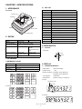
1. APPEARANCE
2)
Front view
KEY LIST
Keytop
Printer cover
Keyboard
Display
P
Drawer
Mode switch
Drawer lock
2. RATING
U
V
Weight
Approx 5.0kg
External dimension
(Including the drawer)
330 (W) x 363 (D) x 234 (H) mm
13 (W) x 14.3 (D) x 9.2 (H) inches
Power source
AC 120V (10%) 60Hz AC 220-230V (m10%)
50/10Hz
AC 230-240V (m10%)
50Hz
Power consumption
Stand-by 4W
Operating 12.5W
Working temperature
0~40°C (32 to 104°F)
Description
0-9,00
Numeric keys
CL
Clear key
@/TM
Multiplication & Time display key
2
Paper feed key
Tax 1 Shift/RA
Tax 1 shift and Received on account key
Tax2 Shift/PO
Tax 2 shift and Paid out key
%
Percent key
ESC
Error escape key
VOID
Void key
CLK#
Clerk code Entry key
PLU
PLU code entry key
SHIFT
Department shift key
#/SBTL
Non-add code & Tax Included subtotal key
CHK
Check key
CH
Charge key
CA/AT/NS
Cash Sale/ Amount Tender and No Sale key
Dept1-8
Department key
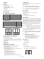
4. MODE SWITCH
1)
LAYOUT
• Rotary SW
REG
Stand-by 6.3W
Operating 13W
q
X/Flash
Z/PGM
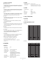
3. KEYBOARD
1) KEYBOARD LAYOUT
Type
Normal keyboard
5. DISPLAY
Key position
STD/MAX 30
1)
Key pitch
19 (W) x 19 (H) mm
Key layout
Fixed type
OPERATOR DISPLAY
Display device:
LED numeric display
Number of lines:
[U version]
SHIFT
TAX1
SHIFT
/RA
TAX2
SHIFT
/PO
@/TM
%
VOID ESC
PLU
7
3
8
4
CHK
CLK#
#/
SBTL
CH
Number of positions: 8 positions numeric display (U)
9 positions numeric display (V)
6
2
1 line
Color of display:
Yellow Green
Character size:
Numeric 14.20 (H) x 7.80 (W) mm
(Layout)
CA/AT/NS
Department code
5
1
PLU code
[V version]
SHIFT
TAX
/RA
/PO
x /
TM
%
ESC
PLU
7
3
CR
EX
#/ST
CH
8
4
Repeat
6
2
[V version]
TL/A T/NS
5
1
XE-A102
SPECIFICATIONS
–1–
2) DISPLAY CONTENTS
2) PAPER
Departments/PLU Code:
• Paper roll dimension : 57.5mm ± 0.5mm
• Paper quality
The department code or PLU code entered appears on the left. For
example, if the key for department 1 is pressed, "1" would appear in
the extreme left position.
: Bond paper (paper thickness: 0.06 to
0.085mm paper weight: 47 to 64g/m2)
3) INKING
Repeat:
Indicates the number of times the same department key is pressed. If
an entry is repeated more than ten times, only the first digit is displayed (12 displays as "2").
(E) Error:
This symbol appears, accompanied by a warning beep, when an
error is made. If this occurs during a transaction because of an excessive digit entry, simply press [CL] and re-enter correctly.
(P) Program:
Ink supply system
: Ink roll
From
: Roller
Specification
: Material - rubber
Ink roll type
: 1 million characters
Print color
: purple
4) LOGO STAMP (NONE)
This symbol remains on the display when the cash register is being
programmed in the Z/PGM mode.
5) CUTTER
(F) Finalization:
• Manual cutter
This symbol appears when a transaction is finalized by pressing
[CA/AT/NS], [CH] or [CHK].
6) PRINTING WHEEL LAYOUT
(o) Subtotal:
[U version]
This symbol appears when [#/SBTL] is pressed and the cash register
computes the subtotal and also when the amount tendered is less
than the total sale amount.
(C) Change:
This symbol appears whenever the change due amount is displayed.
(L) Low battery:
This symbol appears when the power of the installed batteries is
low or you need to replace the batteries with new ones.
(see the "Maintenance" section for explanation.)
(L) No battery:
This symbol appears when no batteries are installed. (see "Maintenance" and "Getting Started" sections for explanation.)
1
2
3
4
5
6
7
8
9 10 11 12 13
0
0
0
0
0
0
0
0
0
0
0
0
0
X
1
1
1
1
1
1
1
1
1
1
1
1
1
Z
2
2
2
2
2
2
2
2
2
2
2
2
2 RA
3
3
3
3
3
3
3
3
3
3
3
3
3 PO
4
4
4
4
4
4
4
4
4
4
4
4
4 VD
5
5
5
5
5
5
5
5
5
5
5
5
5
6
6
6
6
6
6
6
6
6
6
6
6
6 @
7
7
7
7
7
7
7
7
7
7
7
7
7 ST
8
8
8
8
8
8
8
8
8
8
8
8
8 TX
9
9
9
9
9
9
9
9
9
9
9
9
9 CA
%
10
In addition, the following appear when appropriate:
11
• The minus sign (-) can appear in positions 2 to 8.
CH
12
• The decimal point appears in positions 1 to 3.
CK
13 #
• When entry of the secret code is necessary, "---" appears in
positions 1 to 4.
#
#
#
#
#
#
#
#
#
#
# CG
[V version]
6. PRINTER
1) PRINTER
1
2
3
4
5
6
7
8
9 10 11 12 13
0
0
0
0
0
0
0
0
0
0
0
0
0
X
1
1
1
1
1
1
1
1
1
1
1
1
1
Z
2
2
2
2
2
2
2
2
2
2
2
2
2 RA
3
3
3
3
3
3
3
3
3
3
3
3
3 PO
: M-31
4
4
4
4
4
4
4
4
4
4
4
4
4 VD
• No. of stations
:1
5
5
5
5
5
5
5
5
5
5
5
5
5
• Printing system
: Print wheel selective type
6
6
6
6
6
6
6
6
6
6
6
6
6 @
: max. 13 characters
7
7
7
7
7
7
7
7
7
7
7
7
7 ST
8
8
8
8
8
8
8
8
8
8
8
8
8 TX
9
9
9
9
9
9
9
9
9
9
9
9
9 CA
• Model name
• Printing capacity
• Character size
• Print pitch
: 1.6mm (W) x 2.8mm (H)
%
: Column distance 2.1mm (numeric to
numeric), 2.6mm (numeric to symbol)
Row distance 4.6mm
10
• Print speed
: Approximate 1.4 lines/s (6 digits/line)
12
CK
• Paper feed speed
: Approximate 4.3 lines/s
13
CG
• Reliability
: MCBF 0.3 million lines
XE-A102
11
SPECIFICATIONS
–2–
CH
7. DRAWER
2) LOW BATTERY
[OUTLINE]
Low battery indication will appear on the left side of display when the
battery voltage is low.
• Standard equipment
: Yes (1)
• Max. number of drawers : 1
• The drawer consists of
CASE 1: When sitting idle or after completion of transaction.The
machine can indicate the low battery condition (Always)
:
(1) Drawer box (outer case) and drawer
CASE 2: Low battery indication will not appear during key operations,
but will appear after power up of the cash register.
(2) Money case
(3) Coin case
[Display sample]
(4) Lock (attached to the drawer)
" 0.00 " : Battery is OK.
[SPECIFICATION]
1)
"L 0.00" : Low battery (You have to change the batteries.)
DRAWER BOX AND DRAWER
After finalization
"F 12.34": Battery is OK.
"L 12.34": Low battery ("L" indicate instead of "F".)
Material
Plastic
Bell
-
Release lever
Standard equipment: situated at the bottom
Drawer open sensor
-
2)
3) NO BATTERY
If the user forgets to replace the battery and the battery voltage falls
below a certain level, or if a power failure occurs with no batteries
installed, the memory contents cannot be retained. The CPU judges it
as no battery and performs the master reset. In this case, all the settings and registrations are cleared. If, however, the power is continuously supplied to the AC cord, the memory contents are retained.
MONEY CASE
Separation from the drawer
Disallowed
Separation of the bill compartments from the coin
Allowed
compartments
-
Bill separator
-
Number of compartments
Low battery : Batteries are installed, but the voltage is low. Memory
back up can be done.
4B/5C (U)
3B/5C (V)
No battery : Batteries are not installed or the voltage is extremely low.
The master reset is executed when a power failure
occurs, when the batteries are not properly changed.
Layout:
Low battery & No battery indication will appear at the most left position
of display when the battery voltage is low.
CASE 1: When any numeric entry & item entry is not done or just after
finalization. The machine can indicate the battery condition.
(Always)
4B/5C (u)
CASE 2: When numeric entry or item entry is done.
Battery condition does not appear.
Except when power is restored after power failure, the
Low battery & No battery indication will appear on the
display only when the battery voltage is low.
And the indication will disappear after any key entry.
3B/6C (v)
3) LOCK (LOCK KEY : LKGIM7331BHZZ)
• Location of the lock: Front
• Method of locking and unlocking:
• To lock, insert the drawer lock key into the lock and turn it 90 degrees
counter clockwise. To unlock, insert the drawer lock key and turn it 90
degrees clockwise.
[Display sample]
" 0.00" : Battery is OK.
• Key No: SK1-1
"L 0.00" : Low battery
8. BATTERY
"L 0.00" : No battery
1) MEMORY BACK UP BATTERY
After finalization
For memory back up, the dry battery ULM-3 (3 ) are needed.
"F 12.34": Battery is OK.
1. Memory holding time:
Approx. 1 year after New dry batteries are installed.
"L 12.34": Low battery ("L" indicate instead of "F".)
2. Battery exchange method:
When the low battery symbol "L" lights up, replace the batteries (3
AA) replaced by the following method;
"L 12.34": No battery ("L" indicate instead of "F".)
L
1) Power on the ECR.
2) Mode switch turn to "REG" mode.
3) Remove the OLD dry batteries (3 pieces).
4) The nobattery symbol "L" light up.
5) Insert the NEW dry batteries (3 pieces).
6) Confirm the low battery symbol "L" and nobattery symbol "L" is
off.
XE-A102
SPECIFICATIONS
–3–
L
CHAPTER 2. OPTIONS
1. OPTIONS (NONE)
2. SERVICE OPTIONS (NONE)
3. SUPPLIES
NO
NAME
PARTS CODE
PRICE RANK
1
ROLL PAPER
DPAPR1025CSZZ
AS
2
INK ROLLER
NROLR1022CC05
AF
DESCRIPTION
5 ROLLS/PACK
4 SPECIAL SERVICE TOOLS (NONE)
CHAPTER 3. MASTER RESET
Master reset:
Clears all the memory and initializes each preset parameter.
The master reset should be performed by using the following procedure.
1. Turn off the power (Power OFF). (See Note 1.)
2. Remove the memory back up battery from ECR.
3. Turn the mode switch to any position other than Power OFF.
4. Turn on the power (Power ON). (See Note 2.)
When the master rest is completed, the buzzer sounds three times.
5. Install the memory back up batteries back into the ECR.
The master reset can also be accomplished in the following case.
(See Note 3.)
Note 1) Power OFF:
Means disconnecting the AC power supply to the
machine. (Specifically, unplugging the machine.)
Note 2) Power ON:
Means connecting the AC power to the machine. (Specifically, plugging in the machine.)
Note 3) In case a power failure occurs when the machine has no
battery installed, the master reset operation is automatically performed after the power has been restored.
XE-A102
OPTIONS
–4–
CHAPTER 4. HARDWARE DESCRIPTION
1. OUTLINE
2) KEYBOARD AND MODE SW
MODE SW, KEY MATRIX is follows.
• CPU
: uPD780023A (ROM 24KB, RAM 1024B)
* Note: Although the XE-A102 has 30 keys, the keyboard circuit is
actually 32 keys (+) the PF key.
• KEY BOARD : 30key including PF key
• MODE SW
: 5position slide SW
• DISPLAY
: 7seg.+DP x 8digit LED (YELLOW GREEN) FRONT only
• DRAWER
: 1ch, no open sensor
• BUZZER
: 1beep, piezo buzzer
• PRINTER
: M-31(no EURO SYMBOL) (U)
M-31V (V)
REG
3
POWER
OFF
4 X/F
2
X/Flash
(u) VOID
5 Z /PGM
1
(v)
Rotary SW
2. BLOCK DIAGRAM
POWER
AC
SUPPLY
6V
5V
MA IN
For Clock
4.19MHz
32.768kHz
22
26
1
2
3
4
5
6
31
7
8
9
10
11
12
13
14
15
16
17
18
19
21
24
25
27
28
30
FRONT display :8digit
ST1-∼ST4-,ST5
8. 8. 8. 8. 8. 8. 8. 8.
Printer
M-31
CPU
A1∼G1,DP1,A2 ~ G2,DP2
uPD 780023A
SW1
KST1 ∼KST8
BOARD
&
D RAWER
KST2
1
KE Y
KR1 ∼KR6
32
KR1
2
MODE SW
Battery
BU ZZER
KST3
3
5V
KST4
4
3. DISCRIPTION
1)
KST5
5
DISPLAY
MODE SW
KR2 KR6 KR5 KR4 KR3
ST5- (v)
ST4-
ST3-
ST2-
KCN2
ST16
7
13
25
1
1
2
8
14
2
11
12
19
9
3
ST1-
17
18
3
23
4
ST2-
28
24
20
10
5
30
26
21
4
6
32
22
15
5
7
29
31
27
16
8
(Output Timing of STROBE signal)
1ms
30~100us
Display
strobe
ST3ST4-
D13
1SS133 KST1
D14
1SS133 KST2
D15
1SS133 KST3
D16
1SS133 KST4
D17
1SS133 KST5
D18
1SS133 KST6
D19
1SS133 KST7
D20
1SS133 KST8
9
KEYBOARD
3) BUZZER
The BUZZER is driven by the P75/BUZ signal of the CPU.
Frequency : 4.095kHz
XE-A102
HARDWARE DESCRIPTION
–5–
KST1
4) REWIND MOTOR
When the rewind motor is driven by the signal of the CPU.
PRINTER
MOTOR
REWIND
MOTOR
5ms 10ms
15ms
5) DRAWER
DRAWER OPEN signal :Output high signal between 50ms
6) DETECTING "LOW VOLTAGE"
• Values obtained by AD conversion and averaging
Register value: 138 (L 2.7V) or less
3 No voltage
139 - 154 (L 2.7V - 3.0V) 3 Low voltage
more than 154
3 OK
7) DESTINATION DETECTION PORT
U and V version
P66
L
XE-A102
HARDWARE DESCRIPTION
–6–
4. CPU PORT TABLE
No.
Output/Input
Initial state
1
P50/A8
PIN Name
RWND
Signal Name
REWIND MOTOR
Description
O
L
When STBY
O/L
2
P51/A9
DR
To DRAWER
O
L
O/L
3
P52/A10
SA2
DISPLAY SEGMENT
O
L
O/L
4
P53/A11
SB2
DISPLAY SEGMENT
O
L
O/L
5
P54/A12
SC2
DISPLAY SEGMENT
O
L
O/L
6
P55/A13
SD2
DISPLAY SEGMENT
O
L
O/L
7
P56/A14
SE2
DISPLAY SEGMENT
O
L
O/L
8
P57/A15
SF2
DISPLAY SEGMENT
O
L
O/L
9
Vss0
GND
10
Vdd0
VDD
11
P30
ST1-
DISPLAY STROBE N-Ch O.D.
O
H
I
12
P31
ST2-
DISPLAY STROBE N-Ch O.D.
O
H
I
13
P32
ST3-
DISPLAY STROBE N-Ch O.D.
O
H
I
14
P33
ST4-
DISPLAY STROBE N-Ch O.D.
O
H
I
15
P34/SI31
ST5
DISPLAY STROBE (H ACTIVE)
O
L
O/L
16
P35/SO31
NU
(GND via 56k)
I
17
P36/SCK31-
NU
(GND via 56k)
I
18
P20/SI30
SA1
DISPLAY SEGMENT
O
L
O/L
19
P21/SO30
SB1
DISPLAY SEGMENT
O
L
O/L
20
P22/SCK30-
SC1
DISPLAY SEGMENT
O
L
O/L
21
P23/RXD0
SD1
DISPLAY SEGMENT
O
L
O/L
22
P24/TXD0
SE1
DISPLAY SEGMENT
O
L
O/L
23
P25/ASCK0
SF1
DISPLAY SEGMENT
O
L
O/L
24
Vdd1
VDD
25
Avss
GND
26
P17/ANI7
VBAT
BATTERY voltage
I
27
P16/ANI6
NU
RESERVE FOR KEY RETURN
I
I
28
P15/ANI5
KR6
KEY RETURN
I
I
29
P14/ANI4
KR5
KEY RETURN
I
I
30
P13/ANI3
KR4
KEY RETURN
I
I
31
P12/ANI2
KR3
KEY RETURN
I
I
32
P11/ANI1
KR2
KEY RETURN
I
I
33
P10/ANI0
KR1
KEY RETURN
I
I
34
Avref
VCC
35
Avdd
VDD
36
RESET-
RESET-
37
XT2
XT2
32.768Khz Xtal
38
XT1
XT1
32.768Khz Xtal
39
IC/VPP
GND
40
X2
X2
SYSTEM CLOCK
41
X1
X1
SYSTEM CLOCK
42
Vss1
GND
43
P00/INTP0
/POF
POWER OFF
I
I
44
P01/INTP1
T
From PRINTER
I
I
45
P02/INTP2
t
From PRINTER
I
I
46
P03/INTP3/ADTRG
R
From PRINTER
I
47
P70/TI00/TO0
SG1
DISPLAY SEGMENT
O
48
P71/TI01
SDP1
DISPLAY SEGMENT
O
L
O/L
49
P72/TI50/TO50
SG2
DISPLAY SEGMENT
O
L
O/L
DISPLAY SEGMENT
O
L
O/L
O
L
O/L
BUZZER
O
L
O/L
I
I
I
I
L
O/L
50
P73/TI51/TO51
SDP2
51
P74/PCL
NU
52
P75/BUZ
BUZ
53
P64/RD-
MTR
To PRINTER
O
L
O/L
54
P65/WR-
TRG
To PRINTER
O
L
O/L
55
P66/WAIT-
MSL1
MODEL SELECT1
I
56
P67/ASTB
MSL2
MODEL SELECT2
I
57
P40/AD0
KST1
KEY STROBE
O
L
O/L
58
P41/AD1
KST2
KEY STROBE
O
L
O/L
59
P42/AD2
KST3
KEY STROBE
O
L
O/L
60
P43/AD3
KST4
KEY STROBE
O
L
O/L
61
P44/AD4
KST5
KEY STROBE
O
L
O/L
62
P45/AD5
KST6
KEY STROBE
O
L
O/L
63
P46/AD6
KST7
KEY STROBE
O
L
O/L
64
P47/AD7
KST8
KEY STROBE
O
L
O/L
XE-A102
HARDWARE DESCRIPTION
–7–
I
I
CHAPTER 5. TEST FUNCTION
1) To execute the diag test, set the mode switch to Z/PGM. Enter the
desired JOB code, and press the PO (paid out) key.
2. KEY TEST
2) The test message is printed by the printer.
1)
3) Test contents and key operations.
NO.
Test contents
2
Key operations
Mode switch test
1 3 [PO]
2)
2
Key test
2 3 [PO]
3
Display buzzer test
3 3 [PO]
4
Drawer test
4 3 [PO]
5
Printer test
5 3 [PO]
6
CPU version NO. print
6 3 [PO]
Perform the keyboard check with the sum check data of the key code.
Enter the sum check data of each model in the four digits preceding the
diag number 02, and compare the data with the key position code which
is added until the CA/AT/NS key is pressed.
If the data coincides with the code, the completion print is performed.
If not, the error print is performed.
7
Battery level test
7 3 [PO]
8
Time display test
8 3 [PO]
9
Destination display
9 3 [PO]
TEST PROCEDURE
Completion print
Error print
02
- - -02
XXXX Sum data
3. DISPLAY BUZZER TEST
1)
KEY OPERATION
1
2)
PO
1
1. MODE SWITCH TEST
1)
KEY OPERATION
KEY OPERATION
3
PO
TEST PROCEDURE
2)
Change over the mode switch as follows. If the mode switch data in the
proper sequence is not read with the above operation, an error is
printed.
To cancel this test mode, set the mode switch to any a position other
than Z/PGM to Z/PGM. In this case, the completion print is performed.
During the test , the display indicates hard codes which correspond to
the switch positions.
PO
TEST PROCEDURE
Check the continuous buzzer sound and the display state.
Display state:
8. 7. 6. 5. 4. 3. 2. 1.
The decimal point will shift from the lower digit to the upper, step by
step (500mSEC). To cancel the test mode, press any key, and the
buzzer will stop and the completion print is performed.
Completion print
3)
03
MODE SWITCH OPERATION
Mode:
Display:
Z/PGM
X/FLASH
REG
(04)
(03)
(02)
Completion print
Error print
OFF
VOID
4. DRAWER TEST
(01)
1)
01
---
KEY OPERATION
4
01
2)
PO
TEST PROCEDURE
The drawer opens with the above key operation. Check that the drawer
is open. Press any key to terminate the test.
Completion print
XE-A102
TEST FUNCTION
–8–
04
5. PRINTER TEST
8. TIME DISPLAY TEST
1)
1)
KEY OPERATION
5
2)
KEY OPERATION
PO
8
2)
TEST PROCEDURE
PO
TEST PROCEDURE
8
With the above key operation , the print test pattern is repeatedly
printed.
Pressing any key will terminate the test after the completion of one
cycle print. (The receipt is issued at the end.)
6
7
5
4
3
2
1
Display
Hour
Second
Minute
Turn on and off(0.5s)
To terminate the test and print the date and time, press any key.
Print
X X X X X X
Year Month Date
X X X X X X
Hour Minute Second
0 8
9. DESTINATION DISPLAY
1)
KEY OPERATION
9
PO
2)TEST PROCEDURE
Display the destination code as follows.
U and A version
V version
Japan
0
1
3
Display
6. CPU VERSION NO. PRINT
Display
1)
KEY OPERATION
6
2)
To terminate the test, press any key.
Completion print
PO
DESCRIPTION
The CPU version No. are printed with above key operation.
(Print example)
0102
CPU version NO.
06
This test is terminated when printing is completed.
7. BATTERY VOLTAGE SENSOR TEST
1)
KEY OPERATION
7
2)
PO
TEST PROCEDURE
Displays A/D conversion port read value.
0155 or greater
: Normal
0154 or smaller
: Low battery display
0138 or smaller
: No battery display and MRS is done when power on.
To terminate the test, press any key.
Completion print
X (X:0)
07
XE-A102
TEST FUNCTION
–9–
09
CHAPTER 6. SERVICE PRECAUTION
1. PRINTER
Since there are no service parts for this model printer, only the printer
unit is supplied. Therefore, the printer component parts are not supplied
and no service document is issued.
For troubleshooting of the printer, refer to the table below:
* Printer life: 300 thousand lines (XE-A102: M-31)
Ink roll life: 1 million characters
Phenomena
• The printer motor is locked and the buzzer
sounds intermittently.
• The printer does not work properly
Check point/possible cause
Repair
• Check if the printer cable is disconnected.
• Check and repair the printer cable.
• Check if the printer life is reached.
• Replace the printer.
• Check if any foreign material is attached to
the printing type wheel or the gear section.
• Remove the foreign material. (After removing
the foreign material, set the mode switch to
"REG" and press "CL" key.)
• Defective print (Lack on the upper/ lower or
left/right side)
• Check if the printing type is worn down.
• Replace the printer.
• Check if any foreign material is attached to
the printing type wheel.
• Remove the foreign material. (After removing
the foreign material, set the mode switch to
"REG" and press "CL" key.)
• Thin print
• Check if the ink roll life is reached.
• Replace the ink roll.
• Check if the ink roll is properly installed.
• Install the ink roll properly.
• Check if the printing type wheel is worn down.
• Replace the printer.
• Check if the roll paper size is proper.
• Use roll paper as specified below;
Paper width
: 57.5 ±0.5mm
Outside diameter
: ϕ80mm or less
Inside diameter of paper tube: ϕ12mm or less
Paper thickness
: 0.06~0.085mm
• Check if a load is applied to the roll paper
during paper feeding. This may result from a
foreign materials attached to the roll paper.
• Remove any foreign material.
• Uneven pitch of print paper feed
XE-A102
SERVICE PRECAUTION
– 10 –
A
B
C30
10uF
R62
47K
D22
1N4148
C8
/ST 1
/ST 2
/ST 3
/ST4
ST5
R8
1k
18
17
16
15
14
13
12
11
10
1
2
3
4
5
6
7
8
9
F3
1
2
3
4
5
6
7
8
9
18
17
16
15
14
13
12
11
10
R34
R35
R36
R37
R38
R39
R40
R41
56K
D14
D15
D16
D17
D18
D19
D20
KST2
KST3
KST4
KST5
KST6
KST7
KST8
1
2
1
2
CN4
1N4148
1N4148
1N4148
1N4148
1N4148
1N4148
1N4148
MG1
MOTOR F-754
KST2
KST3
KST4
KST5
-
+
T1.0AL/250V
(F3:JUMPER)
VO
VO
56K
R14
P50/A8
P51/A9
P52/A10
P53/A11
P54/A12
P55/A13
P56/A14
P57/A15
VSS0
VDD0
P30
P31
P32
P33
P34/SI31
P35/SO31
R13
1
2
3
4
5
6
7
8
9
10
11
12
13
14
15
16
R42
R43
R44
R45
R46
R47
R48
R49
R53
6.8K
5
110
110
110
110
110
110
110
110
R55
6.8K
R57
6.8K
Q7
KTA1271YAT/P
R59
6.8K
Q8
KTA1271YAT/P
LED1
D568GWA
R60
330
R61
6.8K
R21
47K
VCC
47K
R24
MTR
TRG
47K
R23
R22
47K
7
VBAT
1
2
3
4
5
6
7
8
9
O
A1ERA132
J
D12
1N4148
1253-9P
KCN1
KV1
KV2
KV3
KV4
KV5
KV6
KV7
KV8
FEED
R11
1K
R9
4.7K
X
O
O
O
O
22P
C13
X
X
X
X
X
X
X
VCC
C10
C11
0.1uF 0.1uF
MYLAR MULTI
C12
18P
X1
32.768KHz
R26
330K
O
O
BUZZER
X
X
O
X
X
X
X
1253-5P
1
2
3
4
5
KCN2
FEED
KH1
KH2
KH3
KH4
6
KH[1:4]
C29
C22
C23
C24
C25
3300P 3300P 3300P 3300P 3300P
KH4
KH3
KH2
KH1
10K
10K
10K
R33
J6
7mm
4.19MHz
X2
1M
R31
R32
SHORT PIN
SP1
R27
C17 C18 C19 C20 C21
100P 100P 100P 100P 100P
Q3
2SC1815GR
R10
2.7K
+
C9
22uF/50V
VCC
/RESET
/POF
T
R
t
R25
BZ
O
A1XEA127
J
470
O
R15 R16 R17 R18 R19 R20
47K 47K 47K 47K 47K 47K
XT1
XT2
/RESET
AVDD
AVREF
P10/AN10
X1
X2
IC
P71/TI01
TO 0
P03/INTP3/ADTRG
P02/INTP2
INPT1
INPT0
VSS1
u P D 780023A (Q FP 64)
IC2
48
47
46
45
44
43
42
41
40
39
38
37
36
35
34
33
O
X: NOT MOUNT
O: 47K ohm
O
A3XEA102V6
A3XEA102V7
O
A3XEA102V4
A3XEA102A
V4
V7
A
V6
O
R21 R22 R23 R24
A3XEA102U
U
*CAUTION*
25
SW27
13
SW19
7
SW11
6
SW3
C16 C15 C14
0.1uF 0.1uF 0.1uF
14
SW28
8
SW20
2
SW12
1
SW4
HB0501010
2
3
4
5
1K
C7
0.1uF
MULTI
SW5
9
SW29
19
SW21
12
SW13
11
FLAT CABLE
R6
100K
5
1
2
3
4
5
6
7
8
23
SW30
3
SW22
18
SW14
17
SW6
X/FLASH(3)
Z/PGM(4)
SW1
VOID(1)
10
SW31
20
SW23
24
SW15
28
SW7
4
SW32
21
SW24
26
SW16
30
SW8
(FOR:PRINTER)
P/H CON
1
2
3
4
5
6
7
8
POWER CORD
HOLE ONLY 52011-0810
PRINTER PCB
CON3A
5
REG(2)
HOLE ONLY
MODE SW
ROTARY SWITCH PCB
4
3
2
1
HOLE ONLY
CON3
+6V
SW_CON
LEAD WIRE
1
R30
8
1
2 NC1 NC2
O1 7
3 I1
O2 6
4 I2
5
GND VCC
R28
1K
R29
1K
IC3
LB1268(DIP)
R4
5.6K
D10 1N4148
R5
56K
VCC
ZD1
HZ7B3-TA-E
VO
5
SW33
15
SW25
22
SW17
32
SW9
Q9
KTA1271YAT/ P
dp g f e d c b a dp g f e d c b a
LED2
D568GWA
R58
330
dp g f e d c b a dp g f e d c b a
LED3
D568GWA
R56
330
dp g f e d c b a dp g f e d c b a
Q6
KTA1271YAT/ P
D30
1N4002
JUMPER
+6V
dp g f e d c b a dp g f e d c b a
LED4
D568GWA
R54
330
13
dp g f e d c b a
LED5
S568GWA
110
110
110
110
110
110
110
110
IC4 IC5
9 PIN : GND
S[1:16]
R12
56K
F2
18
17
16
15
14
13
12
11
10
VDD
C27
0.1uF
18
17
16
15
14
13
12
11
10
2521P0200T
MOTOR CN
1N4148
1N4002
D11
D13
RWND
KST1
8
Q2
2SD2170 SOT- 89
D23
JUMPER
R63
1
2
3
4
5
6
7
8
9
IC4
KID65083AP(DIP)
IC5
10 PIN : N.C
KID65083AP(DIP)
1
2
3
4
5
6
7
8
9
T400mA/250V
CN3
R7
D21
1
1K
1N4002
2
3
MULTI
2541P0300T
(FOR:DRAWER)
Q1
2SD2170 SOT- 8 9
RWND
DR
SA2
SB2
SC2
SD2
SE2
SF2
KST[1:8]
SA1
SB1
SC1
SD1
SE 1
SF1
SG1
DP1
SA 2
SB 2
SC2
SD2
SE 2
SF2
SG 2
DP2
R51
12K
330
Q5
KTA1271YAT/P
Q4
2SC1815GR
R52
8
R50
4.7K
TW ONLY
14
SG1
DP1
SG2
DP2
C
14
V
3
KST8
KST7
KST6
KST5
KST4
KST3
KST2
KST1
64
63
62
61
60
59
58
57
56
55
54
53
52
51
50
49
SA1
SB1
SC1
SD1
SE1
SF1
/ST[1:5]
KR1
1
P47/AD7
P46/AD6
P45/AD5
P44/AD4
P43/AN3
P42/AD2
P41/AD1
P40/AD0
P67/ASTB
P66/-WAIT
P65/-WR
P64/-RD
P75/BUZ
P74/PCL
P73/TI51/TO51
P72/TI50/TO50
P36/-SCK31
P20/SI30
P21/SO30
P22/-SCL30
P23/RXD0
P24/TXD0
P25/ASCK0
VDD1
AVSS
P17/AN17
P16/AN16
P15/AN15
P14/AN14
P13/AN13
P12/AN12
P11/AN11
17
18
19
20
21
22
23
24
25
26
27
28
29
30
31
32
KR6
KR5
KR4
KR3
KR2
3
2
MAIN CIRCUIT
MTR
TRG
1. CIRCUIT
t
C
6
/POF
D
7
KV1
+
13
CHAPTER 7. CIRCUIT DIAGRAM AND PWB LAYOUT
8
R
5
10
9
1
2
4
6
7
KV2
+
T
4
17
18
1
2
3
15
16
9
7
12
5
6
8
10
11
14
4
17
18
1
2
3
15
16
9
7
12
5
6
8
10
11
13
4
17
18
1
2
3
15
16
9
7
12
5
6
8
10
11
13
4
17
18
1
2
3
15
16
9
7
12
5
6
8
10
11
KV3
– 11 –
KV4
CIRCUIT DIAGRAM AND PWB LAYOUT
KV5
XE-A102
KV6
ST5
14
/ST4
TRANSFORMER
4
3
Trigger(-)
Timing signal
M
common
Timing sub-signal
4
16
SW34
27
SW26
31
SW18
29
SW10
M-31 OR M-42 V
8
7
6 Re set signal
5
4 Motor (-)
3 Motor(+)
2 Trigger(+)
1
PRINT HEADER
2
1 t
4
KV8
/ST3
1
2
306 1P0202T
TR OUTPUT CN
1
2
CN1
C1
MYLAR
0.033uF
D3
C2
3300uF/25V
+
D6
C3
330uF/25V
+
12
345
TOP VIEW
Z/PGM
(3)
X/FLASH
(4)
ROTARY SW(XE-A102)
VOID
(1)
VOUT 3
IC1
LM7806TO-220
1 VIN
POWER
OFF(2) REG(5)
1N4002 1N4002
D5
2
D8
1N4148
1N4148
R70 100
1
2
2521P0200T
BATTERY CN
CN2
C4
100uF/25V
+
D7
KEY SHEET
2
22 26 1 2 3 4 5 6
31 7 8 9 10 11 12 13 14
15 16 17 18 19 20 21
23
24 25
32
27 28 29 30
D4
1N4002×4
3
D2
D1
T1.25AL/125V
T1.0A 250V
F1
3
GND
/ST2
2
/ST1
KV7
0.1uF
MYLAR
C5
R1 220
1N4148
1M
R2
R3 68K
D9
+
C6
47uF/16V
1
VBAT
VDD
VCC
+6V
VO
1/1
C26
47uF/16V
+
1
A
B
C
D
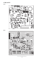
2. PWB LAYOUT
A side
B side
XE-A102
CIRCUIT DIAGRAM AND PWB LAYOUT
– 12 –
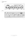
3. DISPLAY LAYOUT
A side
B side
XE-A102
CIRCUIT DIAGRAM AND PWB LAYOUT
– 13 –
q
COPYRIGHT 2005 BY SHARP CORPORATION
All rights reserved.
Printed in Japan.
No part of this publication may be reproduced,
stored in a retrieval system, or transmitted.
In any form or by any means,
electronic, mechanical, photocopying, recording, or otherwise,
without prior written permission of the publisher.
SHARP CORPORATION
Information and Communication Systems Group
Products Quality Assurance Department
Yamatokoriyama, Nara 639-1186, Japan
2005 May Printed in Japan t