1
D1025TM
D1025TM
SERVICE MANUAL
D1025TM
Equator Model
Japan Model
N. Hemisphere Model
Chassis No. SCC-L07D-A
D-1H CHASSIS
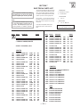
SPECIFICATIONS
0.25 mm aperture grill pitch
17 inches measured diagonally
90-degree deflection
Power Consumption
Maximum
Nominal
Video image area
(16" maximum viewing image)
Approx. 329.5 x 243 mm (w/h)
(13 x 9 5/8 inches)
Deflection frequency
Horizontal: 30 to 85 KHz
Vertical: 50 to120 Hz
AC input voltage / current
Logical resolution
Horizontal: Max. 1280 dots
Vertical: Max. 1024 lines
100 to 120 V, 50/60 Hz, 1.8 A
220 to 240V, 50/60Hz, 1A
Dimensions
Physical resolution
Horizontal: Max. 1024 dots
Vertical: Max. 768 lines
406 x 432 x 420 (w/h/d)
(16 x 17 1/8 x 16 5/8 inches)
Mass
Approx. 18.0 kg (39 lb 11 oz)
Standard image area
Approx. 312 x 234 mm (w/h)
(12 3/8 x 9 1/4 inches)
Picture tube
Input signal
Video
Sync
Analog RGB (75 ohms typical)
0.7 Vp-p, Positive
External HD/VD, Composite
Polarity Free TTL
Video Composite (Sync on Green)
0.3 Vp-p, Negative
120W
100W, 341 BTU/h
Design and specifications are subject to change without notice.
COLOR MONITOR
R
—1—
D1025TM
POWER SAVING FUNCTION
NOTE: If no video signal is input to the monitor, the
This monitor has three Power Saving modes.
By sensing the absence of a video signal from the
computer, it reduces power consumption as follows:
"NO INPUT SIGNAL" message appears. After
about 30 seconds, the Power Saving function
automatically puts the monitor into active-off
mode and the indicator lights up orange. Once
the monitor detects horizontal and vertical sync
signals, the monitor automatically resumes
normal operation mode.
Power
Consumption
Required Recovery
Time
u Power Indicator
1 Normal Operation
<110W
Green on
2 Standby (1st mode)
<15W
approx. 3 sec.
Green and orange
alternate
3 Suspend (2nd mode)
<15W
approx. 3 sec.
Green and orange
alternate
4 Active-off (3rd mode)
<8W
approx. 10 sec.
Orange
5 Power-off
0W
Off
Orange flashing
State
6 Failure mode
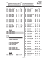
TIMING SPECIFICATION
MODE
1
2
3
4
5
6
7
8
9
10
640x480
720x400
640x480
800x600
800x600
1024x788
1024x768
1024x768
1280x1024
1280x1024
25.175
28.321
36.000
49.500
56.250
65.000
78.750
94.500
108.000
135.000
Hor. Freq. (kHz)
31.469
31.468
43.269
46.875
53.674
48.363
60.023
68.677
63.981
79.976
H-Total
31.778
31.779
23.111
21.333
18.631
20.677
16.660
14.561
15.630
12.504
Resolution (H x V)
Dot Clock (MHz)
HORIZONTAL
H-Blanking
6.356
6.356
5.333
5.172
4.409
4.923
3.657
3.725
3.778
3.022
H-Front Porch
0.636
0.636
1.556
0.323
0.569
0.369
0.203
0.508
0.444
0.119
H-Sync.
3.813
3.178
1.556
1.616
1.138
2.092
1.219
1.016
1.037
1.067
H-Back Porch
1.907
2.542
2.222
3.232
2.702
2.462
2.235
2.201
2.296
1.837
sec)
H-Active (µ
(msec)
25.422
25.423
17.778
16.162
14.222
15.754
13.003
10.836
11.852
9.481
59.940
70.084
85.008
75.000
85.061
60.004
75.029
84.997
60.020
75.025
V-Total
525
449
509
625
631
806
800
808
1066
1066
V- Blanking
45
49
29
25
31
38
32
40
42
42
V-Front Porch
10
13
1
1
1
3
1
1
1
1
V-Sync.
2
2
3
3
3
6
3
3
3
3
VERTICAL
Ver. Freq. (Hz)
V- Back Porch
33
34
25
21
27
29
28
36
38
38
V-Active (lines)
480
400
480
600
600
768
768
768
1024
1024
SYNC.
Int(G)
Ext(H/V)/Polarity
Ext (CS)/Polarity
Int/Non Int
NO
NO
NO
NO
NO
NO
NO
NO
NO
NO
YES -/-
YES -/+
YES -/-
YES +/+
YES +/+
YES -/-
YES +/+
YES +/+
YES +/+
YES +/+
NO
NO
NO
NO
NO
NO
NO
NO
NO
NO
Non Int
Non Int
Non Int
Non Int
Non Int
Non Int
Non Int
Non Int
Non Int
Non Int
—2—
D1025TM
SAFETY CHECK-OUT
After correcting the original service problem, perform
the following safety checks before releasing the set to the
customer:
1. Check the area of your repair for unsoldered or
poorly-soldered connections. Check the entire board
surface for solder splashes and bridges.
2. Check the interboard wiring to ensure that no wires
are “pinched” or contact high-wattage resistors.
3. Check that all control knobs, shields, covers, ground
straps, and mounting hardware have been replaced.
Be absolutely certain that you have replaced all the
insulators.
4. L o o k f o r u n a u t h o r i z e d re p l a c e m e n t p a r t s ,
particularly transistors, that were installed during
a previous repair. Point them out to the customer
and recommend their replacement.
5. Look for parts which, though functioning, show
obvious signs of deterioration. Point them out to
the customer and recommend their replacement.
6. Check the line cords for cracks and abrasion.
Recommend the replacement of any such line cord
to the customer.
7. Check the B+ and HV to see if they are specified
values. Make sure your instruments are accurate;
be suspicious of your HV meter if sets always have
low HV.
8. C h e c k t h e a n t e n n a t e r m i n a l s , m e t a l t r i m ,
“metallized" knobs, screws, and all other exposed
metal parts for AC Leakage. Check leakage as
described below.
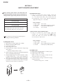
LEAKAGE TEST
The AC leakage from any exposed metal part to earth ground
and from all exposed metal parts to any exposed metal part having
a return to chassis, must not exceed 0.5 mA (500 microampere).
Leakage current can be measured by any one of three methods.
1. A commercial leakage tester, such as the Simpson 229 or
RCA WT-540A. Follow the manufacturers' instructions to
use these instructions.
2. A battery-operated AC milliammeter. The Data Precision
245 digital multimeter is suitable for this job.
3. Measuring the voltage drop across a resistor by means of
a VOM or battery-operated AC voltmeter. The "limit"
indication is 0.75 V, so analog meters must have an accurate
low voltage scale. The Simpson's 250 and Sanwa
SH-63Trd are examples of passive VOMs that are suitable.
Nearly all battery operated digital multimeters that have a
2V AC range are suitable. (See Fig. A)
WARNING!!
NEVER TURN ON THE POWER IN A CONDITION IN WHICH THE
DEGAUSS COIL HAS BEEN REMOVED.
SAFETY-RELATED COMPONENT WARNING!!
COMPONENTS IDENTIFIED BY SHADING AND MARK ¡ ON
THE SCHEMATIC DIAGRAMS, EXPLODED VIEWS AND IN THE
PARTS LIST ARE CRITICAL FOR SAFE OPERATION. REPLACE
THESE COMPONENTS WITH SONY PARTS WHOSE PART
NUMBERS APPEAR AS SHOWN IN THIS MANUAL OR IN
SUPPLEMENTS PUBLISHED BY SONY. CIRCUIT ADJUSTMENTS
THAT ARE CRITICAL FOR SAFE OPERATION ARE IDENTIFIED
IN THIS MANUAL. FOLLOW THESE PROCEDURES WHENEVER
CRITICAL COMPONENTS ARE REPLACED OR IMPROPER
OPERATION IS SUSPECTED.
AVERTISSEMENT!!
To Exposed Metal
Parts on Set
NE JAMAIS METTRE SOUS TENSION QUAND LA BOBINE DE
DEMAGNETISATION EST ENLEVEE.
ATTENTION AUX COMPOSANTS RELATIFS A LA
SECURITE!!
0.15 µF
1.5 k Ω
Earth Ground
AC
Voltmeter
(0.75 V)
LES COMPOSANTS IDENTIFIES PAR UNE TRAME ET PAR UNE
MARQUE ¡ SUR LES SCHEMAS DE PRINCIPE, LES VUES
EXPLOSEES ET LES LISTES DE PIECES SONT D'UNE
IMPORTANCE CRITIQUE POUR LA SECURITE DU
FONCTIONNEMENT. NE LES REMPLACER QUE PAR DES
COMPOSANTS SONY DONT LE NUMERO DE PIECE EST
INDIQUE DANS LE PRESENT MANUEL OU DANS DES SUPPLEMENTS PUBLIES PAR SONY. LES REGLAGES DE CIRCUIT
DONT L'IMPORTANCE EST CRITIQUE POUR LA
SECURITE DU FONCTIONNEMENT SONT IDENTIFIES DANS
LE PRESENT MANUEL. SUIVRE CES PROCEDURES LORS DE
CHAQUE REMPLACEMENT DE COMPOSANTS CRITIQUES, OU
LORSQU'UN MAUVAIS FONTIONNEMENT SUSPECTE.
—3—
D1025TM
TABLE OF CONTENTS
Section
Title
Page
1. GENERAL ................................................................................... 5
2. DISASSEMBLY
2-1.
2-2.
2-3.
2-4.
Cabinet Removal ............................................................10
Service Position .............................................................. 10
D and A Board Removal................................................ 10
Picture Tube Removal ................................................... 11
3. SAFETY RELATED ADJUSTMENT................................. 12
4. ADJUSTMENTS ........................................................................ 13
5. DIAGRAMS
5-1. Block Diagram ................................................................15
5-2. Circuit Boards Location ................................................. 18
5-3. Schematic Diagrams and Printed Wiring Boards ...... 18
1. D Board - Schematic Diagram ................................. 19
2. A Board - Schematic Diagram ................................. 23
5-4. Semiconductors ..............................................................27
6. EXPLODED VIEWS
6-1. Chassis ......................................................................... 29
6-2. Packing Materials .......................................................... 30
7. ELECTRICAL PARTS LIST ................................................ 31
—4—
The instructions given here are partial abstracts from the Operating Instruction
Manual. The page numbers shown reflect those of the Operating Instruction Manual.
SECTION 1
GENERAL
Getting Started
Getting Started
Getting Started
Parts and Controls
Table of Contents
Front
Read First! ................................................................................. 3
Damper Wire ............................................................................ 3
Setup .......................................................................................... 3
Quick Specifications ................................................................ 3
Precautions ............................................................................... 4
Plug and Play ........................................................................... 4
Parts and Controls ................................................................... 5
The OSD (On-screen Display) System ................................. 6
Resetting the Adjustments ..................................................... 9
Rear
Graphic Enhancement Mode (GEM) .................................. 10
Specifications .......................................................................... 10
Monitor Information ............................................................. 11
Power Saving Function and LED Indicators .................... 11
Preset and User Modes ......................................................... 11
Warning Messages ................................................................. 12
Troubleshooting ..................................................................... 12
Dell Computer Corporation’s Environmental Program . 14
Appendix .............................................................................. 109
Precautions
Installation
—5—
• Prevent internal heat build up by allowing adequate air
circulation. Do not place the monitor on surfaces (rugs,
blankets, etc.) or near materials (curtains, draperies) that
may block the ventilation holes.
• Do not install the monitor near heat sources such as
radiators or air ducts, or in a place subject to direct
sunlight, excessive dust, mechanical vibration or shock.
• Do not place the monitor near equipment that generates
magnetism, such as a converter, or high voltage power
lines.
Maintenance
• Clean the cabinet, panel and controls with a soft cloth
lightly moistened with a mild detergent solution. Do not
use any type of abrasive pad, scouring powder or solvent
such as alcohol or benzine.
• Do not rub, touch or tap the surface of the screen with
sharp or abrasive items such as a ball point pen or
screwdriver. This type of contact may scratch the picture
tube.
Warning on Power Connection
• Use an appropriate power cord for your local power
supply.
For customers in the U.S.A.
If you do not use an appropriate power cord, the monitor
will not conform to mandatory FCC standards.
1
(RESET) button (pages 6 and 9)
Resets the adjustments to the factory settings.
2
(GEM) button (page 10)
Selects the Graphic Enhancement Mode.
3 ¨ (BRIGHTNESS) ./> buttons (page 6)
Adjust the picture brightness.
Operate as the ./> buttons when adjusting other
items.
Examples of plug types:
4
(MENU) button (pages 6 and 11)
for 220 to 240 V AC
for 240 V AC only
• Before disconnecting the power cord, wait for at least 30
seconds after turning off the power to allow the static
electricity on the CRT display surface to discharge.
• After the power has been turned on, the CRT is
demagnetized (degaussed) for about 5 seconds. This
generates a strong magnetic field around the metal frame,
which may affect the data stored on magnetic tapes and
disks near the monitor. Place magnetic recording
equipment, tapes and disks away from this monitor.
EN
F
Provides AC power to the monitor.
ES
8 Video input connector (HD15)
D
Inputs RGB video signals and SYNC signals
J
Cs
Adjust the contrast.
Operate as the ?// buttons when adjusting other
items.
Ct
PL
Use of the Tilt/Swivel
Video Connector
With the tilt/swivel, you can adjust this monitor to any desired
angle within 180° horizontally and 20° vertically.
To turn the monitor vertically and horizontally, hold it at the
bottom with both hands as shown below.
6
1 2 3 4 5
7 8 9 10
11 12 13 14 15
15°
• Your monitor operates according to DDC2B. Only
computers that support the same guidelines and operate
at the same or higher level can make use of this feature.
• If your computer does not support the relevant
guidelines, you can still use your monitor and computer.
You may need to manually specify the appropriate
resolution in the computer.
• The highest resolution automatically selected may not
give the best result. You may need to manually select the
most suitable resolution in the computer.
90°
90°
5°
Pin No. Signal
1
Red
2
Green (Composite
Sync on Green)
3
Blue
4
Ground
5
CPU Sense
6
Red Ground
7
Green Ground
Pin No.
8
9
10
11
12
13
14
15
Signal
Blue Ground
Not used (no pin)
Ground
Ground
SDA (serial data)
Horizontal Sync
Vertical Sync
SCL (serial clock)
5
D1025TM
4
7 AC IN connector
5 > (CONTRAST) ?// buttons (page 6)
Plug and Play
DDCTM is a trademark of Video Electronics Standard
Association.
Turns the monitor on and off.
The indicator lights up green when the monitor is on,
and lights up orange when the monitor is in Power
Saving mode.
Displays the MENU OSD.
for 100 to 120 V AC
The socket should be installed near the equipment and
be easily accessible.
This monitor complies with the DDCTM1 and DDC2B Display
Data Channel (DDC) standards of VESA.
When a DDC1 host system is connected, the monitor
synchronizes with the V. CLK in accordance with the VESA
standards, and outputs the EDID (Extended Display
Identification Data) to the data line.
When a DDC2B host system is connected, the monitor
automatically switches to the appropriate standard.
6 u (POWER) switch and indicator (page 11)
D1025TM
Customizing Your Monitor
Customizing
Getting
StartedYour Monitor
Adjusting the Picture Brightness and Contrast
Adjusting the Settings
1 Using the COLOR OSD
1
Press the ¨ (BRIGHTNESS) ./> or
> (CONTRAST) ?// buttons.
You can adjust the monitor’s color temperature using the
COLOR OSD. For example, you can adjust the monitor to
match the colors of a printed picture.
You can adjust the color temperature from 9300K (blue-white)
to 5000K (warm red).
This setting is stored in memory for all input signals.
The BRIGHTNESS/CONTRAST OSD appears.
2
To adjust the brightness
Press the ¨ (BRIGHTNESS) ./> buttons.
To adjust the contrast
Press the > (CONTRAST) ?// buttons.
BRIGHTNESS/CONTRAST
1 Press the MENU button to display the MENU OSD.
Horizontal
frequency
26
26
2 Highlight the COLOR OSD using the BRIGHTNESS and
CONTRAST buttons and press the MENU button again.
Vertical
frequency
60.0kHz/ 85Hz
3 Press the ¨ (BRIGHTNESS) ./> buttons to select either the
option.
9300K, 5000K or variable
The OSD (On-screen Display) System
• The 9300K and 5000K options display accurate preset
color temperatures.
—6—
option allows you to adjust the monitor
• The variable
using the full range of color temperatures. Adjust to the
desired color temperature using the BRIGHTNESS and
CONTRAST buttons.
Introducing the OSD System
You can adjust most of the monitor’s settings using the OSDs
(On-screen Display). All of the OSDs numbered in this
illustration are described on the following pages in order. You
can access any of these OSDs from the MENU OSD. To adjust
monitor settings using the OSDs, follow the steps below:
(MENU) button to display the MENU OSD
• Use the
and to select menu items.
You can adjust the convergence of the picture and cancel the
picture’s moire using the SCREEN OSD.
Convergence is the alignment of the Red, Green and Blue
electron beams on the screen. When convergence is not aligned,
red or blue shadows may be noticeable (especially with text)
which can affect the clarity or focus of the image.
Moire is a wavy or elliptical pattern which may appear on the
screen. The moire cancel adjustment is provided to eliminate
moire.
This setting is stored in memory for all input signals.
1 Press the MENU button to display the MENU OSD.
2 Highlight the SCREEN OSD using the BRIGHTNESS and
CONTRAST buttons and press the MENU button again.
3 Press the ¨ (BRIGHTNESS) ./> buttons to select the
desired adjustment item.
4 Press the > (CONTRAST) ?// buttons to adjust the item.
5 Press the MENU button once to return to the MENU OSD,
or press it twice to return to normal viewing.
COLOR
CENTER
SCREEN
CENTER
9300K
5000K
Note
If you are using one of the GEMs (Graphic Enhancement
Mode), you can only adjust the color temperature from 11,000K
to 9300K.
For more information on GEMs refer to the “Graphic
Enhancement Mode (GEM)” section on page 10.
SCREEN
73
26
• Use the ¨ (BRIGHTNESS) ./> and > (CONTRAST)
?// buttons to highlight menu items and to adjust
settings.
26
H CONVERGENCE
ES
Select
H CONVERGENCE
1 Press the MENU button to display the MENU OSD.
GEOMETRY
GEOMETRY
2 Highlight the desired OSD using the BRIGHTNESS and
CONTRAST buttons and press the MENU button again.
OK
COLOR
26
3 If necessary, use the BRIGHTNESS buttons to select a
specific item.
MENU
ZOOM
GEOM
EXIT
ZOOM
LANG
SIZE
OPTION
5 When you finish adjusting the setting, press the MENU
button to return to the MENU OSD.
Press the MENU button twice to return to normal viewing.
*
MOIRE ADJUST
CENTER SCREEN
H
V
66
73
You can adjust the picture centering using the CENTER OSD.
This setting is stored in memory for the current input signal.
ROTATION
1 Press the MENU button to display the MENU OSD.
adjust the horizontal convergence
LANGUAGE
LANGUAGE
ENGLISH
FRANÇAIS
DEUTSCH
ESPAÑOL
SIZE
OPTION
OPTION
SIZE
73
ON
26
MANUAL DEGAUSS
*
Ct
eliminate elliptical or wavy lines on
the screen
adjust the degree of moire
cancellation
CANCEL MOIRE must be “ON” for “
appear on the screen.
(MOIRE ADJUST)” to
3 To adjust vertical centering, press the ¨ (BRIGHTNESS)
./> buttons.
4 To adjust horizontal centering, press the > (CONTRAST)
?// buttons.
5 Press the MENU button once to return to the MENU OSD,
or press it twice to return to normal viewing.
• Resetting: If you press the RESET button while an OSD is
displayed, only the current adjustment item is reset. For
additional information on using the reset function, see
the “Resetting the Adjustments” section on page 9.
• The OSD automatically disappears after 30 seconds.
6
J
adjust the vertical convergence
2 Highlight the CENTER OSD using the BRIGHTNESS and
CONTRAST buttons and press the MENU button again.
4 Adjust the monitor setting using the BRIGHTNESS and
CONTRAST buttons.
• To reset the current item to its original setting, press the
(RESET) button while the item’s adjustment OSD
is displayed.
2 Using the CENTER OSD
ZOOM
MENU
D
To
Cs
V CONVERGENCE
CANCEL MOIRE
To adjust the monitor settings:
EN
F
4 Press the MENU button once to return to the MENU OSD,
or press it twice to return to normal viewing.
COLOR
Basic controls:
3 Using the SCREEN OSD
7
PL
Customizing
Getting
StartedYour Monitor
Customizing Your Monitor
4 Using the ZOOM OSD
6 Using the SIZE OSD
8 Using the GEOMETRY OSD
You can enlarge or reduce the picture size using the ZOOM
OSD.
This setting is stored in memory for the current input signal.
You can adjust the picture size using the SIZE OSD.
This setting is stored in memory for the current input signal.
You can adjust the picture’s geometry using the GEOMETRY
OSD.
This setting is stored in memory for the current input signal.
1 Press the MENU button to display the MENU OSD.
1
Press the MENU button to display the MENU OSD.
2
Highlight the ZOOM OSD using the BRIGHTNESS and
CONTRAST buttons and press the MENU button again.
3
Press the > (CONTRAST) ?// buttons to enlarge or
reduce the picture size.
4
Press the MENU button once to return to the MENU OSD,
or press it twice to return to normal viewing.
2 Highlight the SIZE OSD using the BRIGHTNESS and
CONTRAST buttons and press the MENU button again.
3 To adjust the vertical size press the ¨ (BRIGHTNESS) ./>
buttons.
4 To adjust the horizontal size press the > (CONTRAST)
?// buttons.
5 Press the MENU button once to return to the MENU OSD,
or press it twice to return to normal viewing.
Note
You can enlarge or reduce the picture size until either the
horizontal or vertical size reaches its maximum or minimum
value.
5 Using the OPTION OSD
7 Using the LANGUAGE OSD
You can manually degauss (demagnetize) the CRT, move the
OSD position and lock the user controls using the OPTION
OSD.
You can set the OSD language to English, German, French,
Spanish or Japanese using the LANGUAGE OSD.
To reset to English, press the RESET button while the
LANGUAGE OSD is displayed.
1 Press the MENU button to display the MENU OSD.
2 Highlight the GEOMETRY OSD using the BRIGHTNESS
and CONTRAST buttons and press the MENU button again.
3 Press the ¨ (BRIGHTNESS) ./> buttons to select the
desired geometry adjustment.
4 Press the > (CONTRAST) ?// buttons to adjust the
geometry.
5 Press the MENU button once to return to the MENU OSD,
or press it twice to return to normal viewing.
Press the MENU button to display the MENU OSD.
2
Highlight the OPTION OSD using the BRIGHTNESS and
CONTRAST buttons and press the MENU button again.
—7—
3
Press the ¨ (BRIGHTNESS) ./> buttons to select the
desired adjustment item.
4
Press the > (CONTRAST) ?// buttons to activate the
manual degauss, move the OSD position or lock the user
controls.
5
Press the MENU button once to return to the MENU OSD,
or press it twice to return to normal viewing.
Degauss: If a second degauss cycle is needed, allow a minimum
interval of 20 minutes for the best result.
3 Press the ¨ (BRIGHTNESS) ./> buttons to select the
desired language.
4 Press the MENU button once to return to the MENU OSD,
or press it twice to return to normal viewing.
2 Highlight the OSD containing the adjustment you want to
reset using the BRIGHTNESS and CONTRAST buttons and
press the MENU button again.
3 Press the ¨ (BRIGHTNESS) ./> buttons to select the
adjustment you want to reset.
4 Press the
adjustment.
(RESET) button to reset this specific
EN
To
ROTATION
adjust the picture rotation
PINCUSHION
adjust the picture sides
PIN BALANCE
adjust the picture side balance
KEYSTONE
adjust the trapezoidal distortion
KEY BALANCE
adjust the picture shape balance
1 Press the MENU button to display the MENU OSD.
2 Highlight the LANGUAGE OSD using the BRIGHTNESS
and CONTRAST buttons and press the MENU button again.
Resetting a specific adjustment:
1 Press the MENU button to display the MENU OSD
Resetting all of the adjustments for
the current input signal
Select
1
Resetting the Adjustments
While there is no OSD displayed, press the
(RESET)
button.
All of the adjustments for the current input signal are reset to
the factory settings.
Adjustments not affected by changes in the input signal (such
as OSD language, OSD position and the Control Lock function)
are not reset to the factory settings.
F
ES
D
J
Resetting all of the adjustments for
all input signals
Press and hold the
(RESET) button for more than two
seconds.
All of the adjustments, including the brightness and contrast,
are reset to the factory settings.
Cs
Ct
PL
OSD Position Change: To change the OSD position, press the
¨ (BRIGHTNESS) ./> buttons to select the direction
(horizontal or vertical), then press the > (CONTRAST)
?// buttons to move the OSD in the selected direction.
User Control Lock: Once you select “ON” to lock the user
controls, you cannot select any item except “EXIT” and
“OPTION” in the MENU OSD. If you try to access any other
OSD, the H mark appears on the screen.
To cancel the Control Lock: Repeat the above procedure and
set Control Lock to “OFF.”
8
9
D1025TM
D1025TM
Customizing Your Monitor
Graphic Enhancement Mode
(GEM)
You can automatically change the characteristics of the picture
to match the way you use your monitor with the Graphic
Enhancement Mode (GEM). Simply press the
(GEM) button
to cycle through the three modes.
1
Turn on the monitor and computer.
2
Press the
(GEM) button to set the mode.
Additional Information
Warning Messages
If there is something wrong with the input signal, one of the following messages appears.
The input signal condition
“OUT OF SCAN RANGE” indicates that the input signal
is not supported by the monitor’s specifications.
INFORMATION
Input signal condition
OUT OF SCAN RANGE
“NO INPUT SIGNAL” indicates that no signal is input.
The message disappears after about 30 seconds.
To solve these problems, see the “Troubleshooting” section
below.
Troubleshooting
This section may help you isolate the cause of a problem and as a result, eliminate the need to contact technical support.
Each time you press the
(GEM) button, the mode changes
and appears on the screen as follows.
—8—
PRESENTATION MODE
n
GRAPHICS/VIDEO MODE
The STANDARD MODE is ideal for spreadsheets, word
processing, and other text oriented applications.
The PRESENTATION MODE is useful for presentation
programs that require vivid colors.
The GRAPHICS/VIDEO MODE gives movies and games
enhanced visual appeal by increasing the sharpness and
brightness.
The selected mode indication appears on the screen for about
three seconds.
If the u indicator is not lit
• Make sure the power cord is properly connected.
• Make sure the u (POWER) switch is in the “ON” position.
If the “NO INPUT SIGNAL”
message appears on the screen, or
if the u indicator is either orange
or alternating between green and
orange
• Try pressing any key on the computer keyboard.
• Make sure your computer is turned on.
• Make sure the video signal cable is properly connected and all plugs are firmly seated in
their sockets.
• Make sure none of the HD15 video input connector pins are bent or pushed in.
• Make sure the video board is completely seated in the proper bus slot.
If the “OUT OF SCAN RANGE”
message appears on the screen
• Make sure the video frequency range is within that specified for the monitor.
Horizontal: 30 – 70 kHz
Vertical: 50 – 120 Hz
Refer to your computer system’s instruction manual to adjust the video frequency range.
• If you are using a video signal cable adapter, make sure it is the correct type.
If no message is displayed and
the u indicator is green or
flashing orange
• Run the SELF TEST function:
1. Turn off the monitor and disconnect the video cable from the computer.
2. Turn on the monitor and wait five seconds. The “NO INPUT SIGNAL” message
should appear with a color bar pattern. The message and pattern are
displayed for 30 seconds.
If the monitor displays White, Red, Green and Blue colors, the monitor is
functioning properly.
• Make sure none of the HD15 video input connector pins are bent or pushed in.
If the screen appears too white, adjust the color temperature
(see “Using the COLOR OSD” on page 7).
Note
The PRESENTATION MODE and GRAPHICS/VIDEO MODE may
produce ghost images when displaying text oriented applications.
These modes change the brightness of the picture dynamically
according to changes in moving pictures. If ghost images appear,
set the GEM to STANDARD MODE.
10
Check these items
No picture
n
n STANDARD MODE
Symptom
Picture is scrambled
• Check your video board manual for the proper monitor setting.
• Check this manual and make sure the monitor supports the graphics mode and the
frequency at which you are trying to operate. Even if the frequency is within the proper
range, some video boards may have a sync pulse that is too narrow for the monitor to
sync correctly.
Color is not uniform
• Degauss the monitor (page 8).
If you place equipment which generates a magnetic field, such as a loudspeaker, near the
monitor, or you change the direction of the monitor, the color may not be uniform.
The degauss function demagnetizes the metal frame of the CRT to obtain a neutral field
for uniform color reproduction. If a second degauss cycle is needed, allow a minimum
interval of 20 minutes for the best result.
12
Getting
Started Information
Additional
Symptom
Check these items
• If the Control Lock function is set to “ON,” set it to “OFF” using the OPTION OSD (page 8).
Screen image is not centered or
sized properly
• Adjust the size (page 8) or centering (page 7).
• Some video modes do not fill the screen to the edges. This problem tends to occur with
certain video boards.
Edges of the image are curved
• Adjust the geometry (page 9).
White lines show red or blue
shadows at edges
• Adjust the convergence using the SCREEN OSD (page 7).
Picture is fuzzy
• Adjust the contrast and brightness (page 6).
• Degauss the monitor using the OPTION OSD (page 8).
If you place equipment which generates a magnetic field, such as a loudspeaker, near the
monitor, or you change the direction of the monitor, the color may not be uniform.
The degauss function demagnetizes the metal frame of the CRT to obtain a neutral field for
uniform color reproduction. If a second degauss cycle is needed, allow a minimum interval
of 20 minutes for the best result.
• If red or blue shadows appear along the edges of images, adjust the convergence using the
SCREEN OSD (page 7).
• If the moire is cancelled, the picture may become fuzzy. Decrease the moire cancellation
effect using the SCREEN OSD (page 7).
Picture bounces or has wavy
oscillations
• Isolate and eliminate any potential sources of electric or magnetic fields. Common causes
for this symptom are electric fans, fluorescent lighting and laser printers.
• If you have another monitor close to this monitor, increase the distance between them to
reduce the interference.
• Try plugging the monitor into a different AC outlet, preferably on a different circuit.
• Try using the monitor with a different computer in a different room.
Picture is flickering
• Refer to your computer system’s manual and change your display refresh rate settings so
they match the monitor’s capabilities.
Picture appears to be
ghosting
• Eliminate the use of video cable extensions and/or video switch boxes. Excessive cable
length or a weak connection can produce this symptom.
—9—
You cannot adjust the monitor
with the buttons on the front
panel
Wavy or elliptical (moire) pattern • Cancel the moire using the SCREEN OSD (page 7).
The moire may be modified depending on the connected computer.
is visible
• Due to the relationship between resolution, monitor dot pitch and the pitch of some image
patterns, certain screen backgrounds sometimes show moire. Change your desktop pattern.
One fine horizontal line (wire) is
visible
• This wire stabilizes the vertically striped aperture grille (page 3). This aperture grille allows
more light to pass through to the screen giving the Trinitron CRT more color and
brightness.
Hum is heard right after the
power is turned on
• When the power is turned on, the auto-degauss cycle is activated. While the auto-degauss
cycle is activated, a hum may be heard. The same hum is heard when the monitor is
manually degaussed. This is not a malfunction.
White does not look white
• Adjust the color temperature using the COLOR OSD (page 7).
D1025TM
13
D1025TM
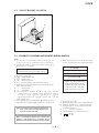
SECTION 2
DISASSEMBLY
2-2. SERVICE POSITION
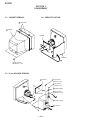
2-1. CABINET REMOVAL
3 Two claws
PUSH
2 Cabinet
PUSH
A board
1
3
D board
2
1 Two screws
(BVTP 4 x 16)
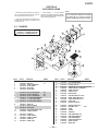
2-3. D and A BOARD REMOVAL
1 A board
3 Five screws
(BVTP 3 x 12)
4 One screw
(BVTT 4 x 8)
5 Cable stopper
6 Two screws
(BVTP 3 x 12)
2 D1 board
7 Cable bracket
8 D board
— 10 —
D1025TM
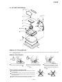
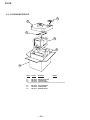
2-4. PICTURE TUBE REMOVAL
8 Demagnetization coil
9 Two screws
(BVTP 4 x 16)
7 Tension spring
6 A board
5 Neck assy
4 Deflection yoke
3 Four screws
(Tapping screw 5)
10 Stand assy
(D board)
2 Picture tube shield
1 Anode cap
Cushion
REMOVAL OF THE ANODE-CAP
NOTE: Short circuit the anode of the picture tube and the anode cap to the metal chassis, CRT shield or carbon painted on the CRT, after
removing the anode.
REMOVAL PROCEDURES
Turn up one side of the rubber cap in
the direction indicated by arrow .
Use your thumb to pull the rubber cap
firmly in the direction indicated by
arrow .
HOW TO HANDLE AN ANODE-CAP
Do not use sharp objects which may cause damage to the surface
of the anode-cap.
Do not squeeze the rubber covering too hard to avoid damaging
the anode-cap. A material fitting called a shatter-hook terminal is
built into the rubber.
Do not force turn the foot of the rubber cover. This may cause the
shatter-hook terminal to protrude and damage the rubber.
— 11 —
When one side of the rubber cap separates from the anode button, the anodecap can be removed by turning the rubber cap and pulling it in the direction of
arrow .
D1025TM
SECTION 3
SAFETY RELATED ADJUSTMENT
When replacing parts shown in the table below, the
following operational checks must be performed as a
safety precaution against X-ray emissions from the unit.
D - BOARD
b) HV Hold-Down Check
1) Using an external DC Power supply, apply the
voltage shown below between cathode of D517
on
" D " Board and GND, and confirm that the
HV Hold-Down circuit works. (Raster disappears)
Apply DC Voltage: 31.4 + 0.01 VDC
Part Replaced ([)
Check Condition
• Input voltage : 120 + 2 VAC
• Input signal
: (fH = 64 kHz), White Cross Hatch
• Controls
: CONT (max) & BRT (center)
RV501
Part Replaced (])
RV501, T501, R545, R546, R548, R550, R547, R549, R552,
D517, IC605, IC901, C540, C542, C544, C541, C535,
IC501, C558, R567, R564, C555, C553, C554, C561
• B+ Voltage
: 185 + 3.0 VDC
c) Beam Protector Check (Software logic)
1) Using an external DC power supply, apply the
voltage 8.8 + 0.01 VDC between pin 11 of FBT
(T501) and GND, and confirm that the voltage
across C541 is 3.7 VDC or less.
Allow the unit to warm up for one minute prior to
checking the following conditions:
Check Condition
• Input voltage : 120 + 2 VAC
• Input signal
: (fH = 64 kHz), White Cross Hatch
• Controls
: CONT (max) & BRT (center)
a) HV Regulator Check
1)
2)
3)
4)
5)
Input white cross hatch signal. (fH = 64 kHz)
Minimum CONT and BRT controls.
Cut off Screen VR (G2).
Input voltage: 120 + 2 VAC
Confirm that the voltage is within the voltage range
shown below.
Standard voltage: 25.0KV + 0.5KV
6) When replacing components identified by ], make
sure to recheck the High Voltage.
7) Verify the High Voltage as shown above (25.0KV + 0.5KV)
is within specification. If not, set H. SIZE data at
minimum (-127) and then adjust RV501 on "D" Board.
8) After adjusting the High Voltage within specification,
put the RV cover on RV501 as shown below and apply
sufficient amount of RTV around RV501.
d) B+ MAX. Check
1) Input white cross hatch (fH = 64 kHz) signal.
2) CONT (max) & BRT (center)
3) Input voltage: 120 + 2 VAC
Note: Use NF power supply or make sure that
distortion factor is 3% or less.
4) Confirm that the voltage is within the voltage
range shown below.
Standard voltage: 185 + 3.0 VDC
10
RV501
— 12 —
4
D1025TM
SECTION 4
ADJUSTMENTS
Connect the communication cable of the connector located on the D board on the monitor. Run the service software and
then follow the instructions.
1 1-690-391-21
2 A-1500-819-A
Interface Unit
3 3-702-691-01
Connector Attachment
IBM AT Computer
as a Jig
To BUS CONNECTOR
D-sub
(9 Pin [female])
mini Din
(8Pin)
4 Pin
4 Pin
4 Pin
*The parts above ( 1 ~ 3 ) are necessary for DAS adjustment.
Allow a 30 minute warm-up period prior to making the following adjustments:
Landing Rough Adjustment
Enter the full white signal.
Adjust the contrast to the maximum.
Input full green signal.
Moving the DY backward, and adjust coarsely the purity
magnet sothat a green raster positions in the center of
screen.
5. Moving the DY forward, adjust so that an entire screen
becomes pure green.
6. Adjust the tilt of DY, and tighten lightly with a clamp.
Convergence Fine Adjustment
Set DY four-pole magnet to mechanical center
before adjustment.
Set the
This should be prime mode.
finger
1.
2.
3.
4.
•
1.
2.
3.
4.
5.
6.
7.
Landing Fine Adjustment
Place the set in the Helmholtz coil.
Enter a green signal only.
Degauss the entire screen with hand-degausser. Then autodegauss it.
Attach a wobbling coil to the specified position of CRT
neck.
Attach a landing adjuster sensor on the CRT.
Using a landing checker, adjust the DY position, purity,
tilt of DY.
Clamp the DY screw.
Clamping torque: 22 + 2 kgcm (2.2+ 0.2 N.m)
•
1.
2.
3.
Convergence Rough Adjustment
All digital convergence data should be zero by MCP.
Enter the white crosshatch signal.
Adjust roughly the horizontal and vertical
convergence at four-pole magnet.
4. Adjust roughly HMC and VMC at six-pole
magnet.
NECK Assy
P.S
Mg
XBV
P.S Mg
6-pole Mg
DY
CRT
4-pole Mg
1.
2
Receive R.B. cross-hatch.
Adjust H.STAT and V.STAT at four-pole magnet.
Four-Pole Magnet
2
1
1
R
B
1 + 2
R
B
R
2
B
2
1
R
B
1 + 2
R
B
1
2
— 13 —
Mechanical
Center
RB
D1025TM
3.
4.
Receive White cross-hatch.
Adjust HMC and VMC at six-pole magnet.
Convergence Specification
Horizontal and Vertical
Six-Pole Magnet
2
0.30mm
0.24mm
0.30mm
0.30mm
A
B
B
G
1
A
2
G
1
5.
6.
7.
Focus adjustment
Adjust focus (V) and focus (H) for optimum focus.
Receive R.B. cross-hatch.
Adjust H.TILT by swinging the DY neck right and left.
Adjust XCV with XCV core.
XCV movement
B
R
8.
Adjust V.TILT with TLV VR.
TLV movement
B
R
R
B
B
R
R
B
9.
Focus (H)
Adjust Y.CROSS with YCH VR.
11.
YCH movement
Digital Convergence Adjustment
A. Horizontal Convergence
YBH-T
R
10.
B
CBH-LT
0
MBH-LT
12
2
9CBH-RT
11 MBH-RT
Paint lock the four-pole and six-pole magnet.
VR Adjustment on DY
APH-L
4
MBH-LB
8
CBH-LB
6
XCV
YCH
TLV
H STAT
3APH-R
7MBH-RB
1
5CBH-RB
YBH-B
Adjust each misconvergence point in sequence.
Zero Position NECK Ass'y
Purity
Four-Pole Mg
B. Vertical Convergence
Six-Pole Mg
V STAT-T
Vertical and Horizontal Position and Size
Specification
CCV-LT
0
MCV-LT
12
XBV-L
4
MCV-LB
8
CCV-LB
6
2
9CCV-RT
11 MCV-RT
V STAT
3XBV-R
a
a
a < 2.5 mm
b < 2.5 mm
A
7MCV-RB
1
5CCV-RB
V STAT-B
B
b
A
B
202
270
Adjust each misconvergence point in sequence.
C. Repeat the procedure of A and B so that the
convergence of the whole screen is within the
specification.
b
— 14 —
D1025TM
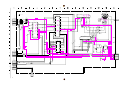
5-2. CIRCUIT BOARDS LOCATION
A
D1
J
D
5-3. SCHEMATIC DIAGRAMS AND PRINTED WIRING BOARDS
Note:
• All capacitors are in µF unless otherwise noted. pF: µµF
50 WV or less are not indicated except for electrolytic.
• Indication of resistance, which does not have one for rating
electrical power, is as follows.
•
When replacing parts shown in the table below,
be sure to perform the safety related adjustment.
D - BOARD
Pitch: 5 mm
Rating electrical power 1/4 W (CHIP: 1/10 W)
Part Replaced ([)
RV501
• All resistors are in ohms.
• f : nonflammable resistor.
• F : fusible resistor.
•
∆ : internal component.
• p : panel designation and adjustment for repair.
• All variable and adjustable resistors have characteristic curve B,
unless otherwise noted.
•
•
e
E
Part Replaced (])
RV501, T501, R545, R546, R548,
R550, R547, R549, R552, D517,
IC605, IC901, C540, C542, C544,
C541, C535, IC501, C558, R567,
R564, C555, C553, C554, C561
: earth-ground.
: earth-chassis.
The components identified by [ in this basic schematic
diagram have been carefully factory-selected for each set
in order to satisfy regulations regarding X-ray radiation.
Should replacement be required, replace only with the
value originally used.
• When replacing components identified by ], make the necessary
adjustments by using RV501 ([) as indicated. (See page 12)
•
Note: The components identified by shading and
mark ¡ are critical for safety. Replace only
with part number specified.
•
•
•
•
•
•
•
•
Note: Les composants identifies per un trame et une
marque ¡ sont critiques pour la securite. Ne les
remplacer que par une piece portant le numero specifie.
— 18 —
— 17 —
All voltages are in volts.
Readings are taken with a 10 ΜΩ digital multimeter
Readings are taken with a color-bar signal input.
Voltage variations may be noted due to normal
production tolerances.
*
: Cannot be measured.
Circled numbers are waveform references.
: B +bus.
: B - bus.
CN305
8P
+5V
8
STBY
7
GND
+12V
6
+12V
5
H1
+5V
CN307
IC006
9P
25
SHARPNESS
WHT
BGND
1
BLUE
2
GGND
3
GREEN
4
RGND
5
RED
6
GND
7
VD
8
HD
9
BIN
R-OUT
R-IN
22
R-IN
G-OUT
G-IN
B-OUT
R-OUT
CRT DRIVER
9
G-IN
3
4
G-OUT
IC002
8
19
GIN
G-OUT
3
B-IN
4
B-OUT
H
17
1
RIN
+185V
2
NC
1
+185V
7
10
B-IN
B-OUT
+80V
1
11
18
GND
J001
+80V
3
SIGNAL IN
6
21
5
5
5
8
R-OUT
KR
8
1
11
KG
CONNECTOR
15PIN
14
D-SUB
11
SYN-OUT
9
CLAMP
CLAMP
12
RGB PRE-AMP
16
T-SW
&
LEVEL
KB
IC001
13
6
G2
BLK
10
CN309
CN301
12
15
7P
R-OSD
R-OSD
1P
3
HSYNC
7
GND
6
VSOUT
5
CSYNC
4
BPCLP
3
SHRP1
2
CBLK
1
OSD
1
R-BKG
IC003
G-OSD
9
R-IN
1
R-OUT
1.2KV
13
14
CUTOFF AMP
G-OSD
4
2
8
IC004
G-IN
G-BKG
G-OUT
14
13
B-OSD
B-OSD
5
3
B-BKG
15
12
7
VIP
B-IN
B-OUT
OSD-BLK
OSD-BLK
SCL
2
SDA
G2
5
28
1
CN306
6P
+12V
10
VRTRC
1
HRTRC
2
SWITCH
GND
3
Q004
IICSCL
4
GND
5
IICSDA
6
7
VFLB
SDA
HFLB
SCL
5
8
TO
A
G2-CUT
JOO1
PICTURE TUBE
BOARD
HV
OFF
(TO
CONTROL
CN310
SPOT
KILLER
IC005
4P
HOSTGND
4
DDCSDA
3
1P
1
DDCSCL
2
NC
1
FBT)
CN302
Q001
GND
CN303
CN311
1P
3P
DDCSCL
3
DDCSDA
2
CPUGND
1
1
(VIDEO)
(
POWER
DEFLECTION
)
CN512
1P
CONV-CONTROL
CN701
CY
1
CY4-
8
CY4+
7
2
15
6
H-CONVOUT
5
CY3-
6
CY3+
5
CY2-
4
CY2+
3
V.REF
IN
7
V-CONVOUT
10
CONV AMP
IC702
11
13
8
14
H-STATICOUT
V-SIN
V-STATICOUT
9
2
CN510
1P
3
6
VPOSIN
HST
16
SDL
2
T505
14
1
1.2
KV
HD.IN
17
1
CY1+
GND
IC701
8P
CY1-
GND
SCL
1
V.REF OUT
3
4 12 13
BUFFER
5
5
1
Q521
27
3
10
V.DIV
3
V-OUT
4
4
SWITCH
2
V.SIN
SDA
FUNCTION
+IN
SCL
2
OUT
IC401
5V
8
5
-IN
V.SAW
EPROM
23
V-REF
CN903
IC905
15
7P
PB4
FBT
46
CBLANK
1
SHRP1
2
BPCLAMP
3
CSYNC
4
VSYNC
5
GND
6
HSYNC
7
3
DEF. CONTROL
CBLANK
5
48
PA5
BPCLAMP
PA6 47
12
T501
B3O
4
H-REG
PWM-CONT
RV501
Q520
IC501
V-SYNC
5
3
19
1
HV-OUT
B2O
30
13
Q510
H-SYNC
4
H-DRIVE
PH2
REF
CPU
GND
2
}
DDCSDA
HOST
23
2
26
28
LOCK
1
}
DDCSCL
H.DRIVE
12
V.
H.DRIVE
OUT
DEF
Q903,Q501,Q502
14
26
H-OUT
17
H.OUT
V-IN
27
DDCSDA
T504
17
LOCK
V-OUT
35
33
3
13
HDT
34
DDCSCL
4
IC901
RESET
IC904
FOCUS
8
54
RESET
CN902
10P
WHT
CRT
20
B1O
IC503
20
IC900
TO
14
H-CENTER
2
C-SYNC
SYN BUFF
HV
Q503
OP2+
Q901,Q902
28
1
2
HV-REG
18
B4+
IC902
DRIVER
DA4
22
Q511
H.OUT
4
H.FLY
H-IN
CN501
6P
DY
16
Q507
6
PCI
32
1
HFB
NC
4
11
SYNC
37
IICDATA
5
GND
6
IICCLK
7
LOCK
DATA
4
GND
9
VRTRC
10
CENT
Q506
8
HRTRC
H.
BUFFER
DA3
AMP
H
DY+
3
H
DY-
4
H
DY-
5
V
DY-
6
V
DY+
5
Q518
H.
9
26
DY+
2
6
1
Q522,Q523
36
CLK
H
ABL
8
CENT
4
SW
DA8
V-DRIVE
PB1
Q508
CN901
4P
WHT
REMOTE
8
BUFFER
Q517
18
6
ON/OFF
12
9
24
HTR
DGND
1
+5V
2
STDBY
15
ABL
+5V
38
RXD
3
TXD
4
RXD
39
DEGAUSS
S0-S4
7
ROTATION
10
8
11
80V
7
12
15V
6
13
5
14
4
15
3
16
185V
SRT
49-53
TO
9
T601
3
TXD
SWITCH
S-CAP
CHANGE
CN502
Q519
RELAY
9P
DRIVE
WHT
+12V
Q601
RY500
DGC
SW-REG
CN601
3P
1
Vcc
3
NC
2
DGC2
1
SW-REG
OUT
5
DGC1
+185V
CONT
IC601
3
1
+185V
2
NC
3
+80V
OUT
FLDBK
+80V
Q602
EA
13
CIS
-15V
4
7
5
HEATER
TO
2
12
17
AC-RECT
BUFF
D601
1,2
1
18
+15V
DF-AMP
6
IN1,2
OUT
+12V
IC605
TO
H1
7
+12V
Q505
1
Q504
5V,12V REG
8
GND
9
+5V
10
7
OUT
DISABLE
9
+5V
5
8
5
+5V
11
H.CENTER
IC503
IC603
CN602
2P
S-CAP
CHANGE
3
1
15V
THP601A
+12V
IC503
LF602
THP601
6
DFT
H.CENTER
T503
AC IN
NC
GND
SW
Q605,Q606
LFT
CN600
7
Q512,Q513,Q514,Q515,Q516
2
1
4
2
3
ERROR
AMP 1
IC604
STBY.CONTROL
CN503
2P
Q604
ROTATION
DRIVE
1
ROT+
2
ROT-
IC502
B-#SV9081<DELLD1H>-BLK..
11
5
4
3
B_OUT
6
G_OUT
7
GND1
R_OUT
8
GND2
9
VCC
G_IN
10
R_IN
VBIAS
11
GND3
B_IN
28
1
27
26
3
S/H_R
R_OUT
R304
68
:CHIP
C104
0.1
25V
B:CHIP
R111
47 :FPRD
R104 C055
R204
0.1
68
68
:CHIP 100V
:CHIP
:CHIP
2
1
9 G2
+5V
G_OUT
G_IN
G_GND
SYNC_CAP
S/H_G
5
B_IN
S/H_B
C204
0.1
25V
B:CHIP
C012
0.01
B:CHIP
C014
47
100V
B_GND
G_OSD
C013
470
16V
C304
0.1
25V
B:CHIP
D104
HSS82
PROT
D305
HSS82
PROT
D205
HSS82
PROT
BLK
B_OSD
OSD.BLK
16
VSS
15
2
D206
HSS82
PROT
B_IN
GND
VIP
VCC
B_OUT
G_OUT
R_OUT
2
3
4
5
6
7
8
9
FB110
C054
0.1
250V
:MPS
CN302
R109
1M
:CHIP
R033
15k
:RN
CN303
C105
0.1
25V
B:CHIP
C205
0.1
25V
B:CHIP
R208
6.8k
:CHIP
R049
82k
:CHIP
R031
1k
:CHIP
EMI
FB010
GND
IICSCL
GND
R052
10k
:CHIP
3
2
1
FB009
+80V
+185V
+12V
4
CN305
8P
WHT
:S-MICRO
8
7
STBY+5V
R046
100k
:CHIP
+12V
+12V
5
H1
4
GND
3
+80V
2
NC
1
+185V
R006
100
:CHIP
CN502
C005
0.001
B:CHIP
CN902
HOSTGND
4
DDCSDA
3
IN
DDCSCL
2
NC
GND
6
TO D.BOARD
SIGNAL
STBY+5V
FB006
Q004
2SC1623-L5
SWITCH
4
HRTRC
+12V
R051
1k
:CHIP
5
VRTRC
GND
TO D.BOARD
R021
100 :CHIP
6
R020
100 :CHIP
C027
0.01
B:CHIP
+12V
R047
10k
:CHIP
IICSDA
VCC
STBY+5V
CN903
CN306
6P
WHT
:S-MICRO
OUT
FB011
C090
0.01
B:CHIP
FB012
C028
47
25V
-
FB004
10
STBY+5V
R308
6.8k
:CHIP
+
FB001
11
C305
0.1
25V
B:CHIP
C092
0.1
25V
B:CHIP
FL002
Q001
2SC5022
SPOT KILLER
R307
5.6k
:CHIP
C022
47
25V
9
8
VDD
R045
2.2k
:CHIP
FB005
12
5
6
7
VFLB
SCL
6
R108
6.8k
:CHIP
IC005
NJM4558M
CUT-OFF-CTRL
C029
0.1
25V
B:CHIP
R053
22M
:RN
3
13
D014
1SS119-25TD
PROT
R207
5.6k
:CHIP
R014
100
:CHIP
SDA
FB007
JW(5)
R110
220k
2
R210
220k
R029
120k
:CHIP
1
C053
0.1
25V
B:CHIP
R310
220k
OSD_BLK
INT
TO D.BOARD
R209
1M
:CHIP
+185V
R107
5.6k
:CHIP
SS
R017
100
:CHIP
R309
1M
:CHIP
FB310
HFLB
R018
100
:CHIP
:RC
5
3
G_OSD
VDDA
B_OSD
7
R251
1/2W
R151
100
1/2W
:RC
L101
D306
HSS82
PROT
1
R032
3.9k
:RN
R306
10k
:CHIP
14
RP
R005
470k
:CHIP
C047
47
25V
FL001
:RC
R_OSD
4
C046
0.01
B:CHIP
R003
5.6k
:CHIP
L002
1
CN510
SG101
R133
330
FB210
C018
10
200V
R206
10k
:CHIP
VCO
C044
0.068
25V
B:CHIP
SG201
R106
10k
:CHIP
VSSA
1
STBY+5V
R004
1.8k
:CHIP
100
G_IN
IC003
CXD8688P
OSD
C042
0.1
25V
B:CHIP
R351
1/2W
R233
330
R_IN
C050
0.1
25V
B:CHIP
EMI
2
TO D.BOARD
+80V
100
C106
0.1
250V
:MPS
D106
HSS82
PROT
IC004
TDA6103Q
CUT OFF AMP
STBY+5V
3
12
1.2KV
L201
D105
HSS82
PROT
R054
2.2k
:CHIP
R025
4.7k
:CHIP
CBLK
R048
2.2M
1W
:RN
L301
15
14
CLAMP
13
11
B2_IN
12
10
GND
R002
1.5k
:CHIP
BPCLP
1
R333
330
C206
0.1
250V
:MPS
+12V
16
G2_IN
R024
4.7k
:CHIP
SHRP1
CN301
1P
4
5
11
SG301
C306
0.1
250V
:MPS
R043
0
R007
100
4
R064
10k
1/2W
:RC
D304
HSS82
PROT
D204
HSS82
PROT
22
18
R_OSD
17
C051
47
25V
11
C049
0.01
B:CHIP
B_OUT
12
DEFF.
CLAMP
13
7
8
9
GND
VCC2
T_SW&LEVEL
CSYNC
C035
470p
2kV
B
FB301
SIGNAL_SW
C019
0.1
5
6
3
KR
KR
6
18
6
3
R2_IN
VCC
19
B_OUT
C004
0.01
B:CHIP
C302
0.1
25V
B:CHIP
10
6
VCC
VCC
C011
0.1
100V
:PT
20
2
C048
0.01
B:CHIP
VSOUT
H
7
KG
7
G_OUT
C010
0.1
25V
B:CHIP
C009
47
25V
21
B1_IN
R312
150
:CHIP
R026
10k
:CHIP
GND
7
8
D003
RD5.6ESB2
GND
C202
0.1
25V
B:CHIP
19
R212
68
:CHIP
GND
20
1
D001
RD5.6ESB2
HSYNC
5
6
8
KB
10
H2
4
10
9
G2
R311
:FPRD
R211
47 :FPRD
FB201
G1
24
22
5
R_IN
23
R_OUT
R_GND
6
G1_IN
B_BKG
7
GND
GND
8
C101
0.1
25V
B:CHIP
R112
220
:CHIP
R016
10k
:CHIP
CN309
7P
WHT
:S-MICRO
11
SG001
FB101
1
13
3
47
C015
0.1
25V
B:CHIP
25
4
G_BKG
9
FL101
D101
1SS226
C102
0.1
25V
B:CHIP
17
9
EMI
16
8
HD
R_BKG
4
15
7
VD
R101
75
:RN-CP
C_SYNC
J001
1
RCV
9
FB003
R1_IN
21
6
GND
C201
0.1
25V
B:CHIP
R201
75
:RN-CP
IC006
CXA2093AS
RGB PRE-AMP
14
RED
D201
1SS226
1
5
FL201
EMI
4
IN
EMI
2
3
SIGNAL
RGND
R301
75
:RN-CP
SCL
G2
8
7
8
STBY+5V
3
GGND
GREEN
2
D301
1SS226
C301
0.1
25V
B:CHIP
4
BLUE
FL301
1
5
BGND
SDA
2
CN307
9P
WHT
:S-MICRO
12
G3
10
IC002
LM2405
RGB OUTPUT
IC001
CXA2055P
PRE-AMP
(VIDEO)
B-#SV9081<DELLD1H>-A..
1
1
2
3
DDCSCL
DDCSDA
CN311
3P
WHT
:S-MICRO
HOSTGND
CN310
4P
WHT
:S-MICRO
TO D.BOARD
CN902
2
1
0.7 Vpk-pk
3
5
4
6
4.3 Vpk-pk
4.5 Vpk-pk
7 12
8 11
42.3 Vpk-pk
0.7 Vpk-pk
0.7 Vpk-pk
4.4 Vpk-pk
9 10
42.7 Vpk-pk
42.3 Vpk-pk
KEY
SCAN
KEY
5V
SCAN
IIC CLK
IIC DATA
5VDET
DATA
CLK
DDC
IIC
55
54
53
52
51
50
RD5.6SB
46
45
43
R922
10k
:CHIP
NC
40
TDO
RDI
SDA
SCL
FLY
A2
A1
A0
HOST
WC
DDC
1
VCC
DDC
DDCSCL
2
SCL
36
IIC
DDCSDA
3
VSS
37
IIC
4
SDA
38
RXD
35
41
39
TXD
34
HEATER
DATA
CLK
PC1
DATA
CLK
5
6
7
8
IC905
CAT24C08P
EPROM
BLK
SAW
:PT
FB902
100
1/4W
R919
1k
R935
100
R938
100
R936
100
32
H
BLK
H
C909
2200
10V
30
H-SYNC
R925
R927
4.7k
0
:CHIP
:CHIP
IC904
29
28
CSI
VSS
C933
0.01
5V-2
PST600D-T
RESET
C910
0.1
:PT
R729
2.2
1W
:RS
15
15
2
ABL
THERMAL
V-REF
H
R959
3.3k
FLY
SHRP1
H
C931
BLK
D916
1SS119
470p
:CHIP
C932
0.01
:B
5
V-SYNC
V-SYNC
H-SYNC
H-SYNC
4
5V-2
1
2
FLY
V
DEGAUSS
HEATER
REMOTE ON/OFF
3
C545
0.022
B
C553
0.001
B
R556
47k
:RN-CP
C555
0.1
:PT
C562
100
16V
C546
220p
:CH
R554
150k
:RN-CP
12V
14
R612
22
3
14
S
OUTPUT
R613
E/AOUT
4
10k
GND
13
C635
0.01
:PT
FOLDBACK
IN
SENSE
9
IN
C613
10000p
R615
180k
3
16
2
17
R624
0.12
:RF
630V
R619
2.2k
D610
EL1Z
DEMAGIN
C618
100p
B
C615
0.001
:PT
R614
0.22
3W
:RS
5
2
3
R649
100k
1W
RY601
VA600
4
3
D649
1SS133T
R627
470k
C602
0.0047
250V
CN602
2P
C606
0.0047
250V
R600
1
10W
R628
270k
:RN
R405
1.5
1/2W
:RN
1.5
1/2W
:RN
3
6
C510
470p
500V
B
D516
3DL41A
Q507
BU2527AX
H-OUT
C407
0.022
:PT
THERMAL
R409
R411
6.8k
36k
:RN-CP :RN-CP
R406
12k
:RN-CP
C518
4300pF
1.8kV
22p
2kV
10
2
9
5
5V-2
D626
GP08D
R636
1k
:CHIP
D505
ERB91-02
D625
GP08D
Q605
2SB1094
PROT
R637
1.5
1W
5
4
D527
RD5.1ES-TIB2
C517
0.01
:PT
D624
ISS119-25TD
Q521
2SA1175
BUFF
R629
10k
C573
4.7
250V
R630
4.7k
:RN
RV601
5k
1
C644
47
25V
C514
0.91
200V
:PP
L506
:RS
12
3
Q510
STP5NA80F1
HV-OUT
D511
RD5.1ESB2
C570
100
25V
12
Q517
2SC2611
SW
13
FB610
0
5V-2
12V
C503
0.01
B:CHIP
6
80V 185V
C578
0.001
2kV
-15V
R604
560k 1/2W :RC
F601
4A
250V
FB614
0
FB615
0
VA601
D521
RGP02-20EL
7
C504
1000p
500V
9
5
8
D510
RGP02-20EL
6
:DFT
Q512
IRLI520GLF33
S-CAP CHANGE
8
AC
IN
TO
2
3
4
5
6
V DY-
V DY+
1.2KV 1
1
H DY-
1
H DY-
2
H DY+
3
CN501
6P
:DY
H DY+
4
5
+185V
6
NC
H1
NC
GND
+80V
9
CN502
9P
WHT
:S-MICRO
7
0
8
0
+5V
N
GND
G
+12V
FB612 FB613
L
L
CN600
N
FB608
0
G
FB609
0
C577
0.01
2kV
F
D520
RGP02-20EL
1P
TO
A.BOARD
CN301
R547
560k C542
10
:RN
D522
1SS119
C547
1
R562
12k
:RN
R566
22
1W
:RS
C549
0.068
:PT
D517
RD27ES
5V-2
:RN
9
C540
10000pF
630V
:PP
2
R552
56k
:RN
4
IC502
LA6500-FA
ROTATION DRV
C544
0.01
:PT
CN503
2P
2
ROTATION-
1
ROTATION+
R563
1.5
:FPRD
15V
R558
10k
:RN
1
3
5
C513
10
C512
0.01
B:CHIP
Q514
IRLI530GLF33
S-CAP CHANGE
R519
47k
:CHIP
S
C515
0.01
B:CHIP
Q516
IRLI520GLF33
S-CAP CHANGE
S
C520
0.01
B:CHIP
R528
22k
R537
R535
S
47k
:CHIP
C536
0.01
B:CHIP
B-SV9080<MANUAL>-D..
12V
5V
R536
1k
:FPRD
R523
R524
47k
:CHIP
1P
:TUB
C529
0.047
400V
:PP
S
47k
:CHIP
C538
0.01
B:CHIP
47k
:CHIP
TH501
R532
2.2
:FPRD
GT001 GT002
CN510
A.BOARD
CN305
C528
0.01
2kV
F
C541
4.7
R543
4.7
:FPRD
D515
RGP02-20
R559
2.7k
5
C608
100p 250V
C601
100p 250V
R548 R550
1.8k 1.8k
:RN-CP :RN
-15V
C525
0.082
200V
:PP
Q515
IRLI520GLF33
S-CAP CHANGE
R533
1k
:FPRD
R525
1k
:FPRD
R521
1k
:FPRD
S
C507
0.3
400V
C523
0.12
250V
C531
0.068
250V
:PP
:PP
Q513
2SK1307-01
S-CAP CHANGE
R515
1k
:FPRD
7
T503
R560
15k
:RN
R545
47k
:RN-CP
R510
22k
:CHIP
S4
FB611
0
4
C505
22p
2kV
R507
2.7k
:RN
R503
10k
:RN-CP
C516
0.36
250V
C530
0.12
250V
R512
4.7
Q505
2SA1175
BUFF
R501
100
C604
0.47
250V
R542
1k
:RN
R549
82k
FB503
5.0MM
S0
3
C532
0.47
100V
C556
220p
:CHIP
CN512
C511
0.3
200V
:PP
S1
4
2
10
R584
4.7k
:CHIP
12V
8
:PT
R580
15k
:CHIP
S3
C501
10
1
LF602
:LFT
3
S4
C642
0.0047
250V
IC501
5
4
C559
0.0047
R570
1k
Q518
2SC3209LK
AMP
12
R565
330k
:RN
330k
:RN
Q504
2SC3941A
V.DF.AMP
C576 R583
47p
10k
CH
:CHIP
R544
1M
:RN
R546
33k
:RN
C519
0.001
2kV
:PP
D504
RD18ESB2
R571
33k
3W
:RS
L505
2.2mmH
S2
R506
R505
10k
:CHIP
R502
180k
:RN-CP
12V
R568
47k
RV501
100k
6
S
R520
22
:FPRD
5
R573
220k
12V
Q604
DTC114ESA
STBY CONTROL
C605
1 250V
5.0mm
C548
0.001
:PT
12
C561
0.001
B
11
11
C643
0.0047
250V
S601
L507
100
16V
11
C535
4
C571
10
R575
68
1/2W
:FPRD
R578
27
2W
C550
10
D514 0.01
HSS82 :PT
3W
:RS
C580
0.01
:PT
R579
150k
L510
R572
47k
C572
4.7
250V
R576
47k
R590
22k
:RN
D512
1SS119
13
SG501
Q519
2SC2785 R574
10k
SW
-15V
1/2W
:RN
C551
0.01
B:CP
9
C554
0.1
25V
B
R540
200k
:RN
L502
17
IC503
LA6500-FA
H-CENTER AMP
D519
1SS119
R557
18k
:CHIP
C563
470p
B:CHIP
8
R541 C539
1k 0.022
:RN 100V
R538
10
D507
RD5.1ES
JW117
5.0MM
R
REF
7
16
12V
L509
HLC2
6
14
RY500
R589
4.7k
2
R553
100k
:RN-CP
5
1
FB502
0.45
R539
10
3W
:RS
FLY
1
3
R591
150 R592
1/2W 150
R516 :RN 1/2W
:RN
150
R577
27
2W
:RS
R643
3.9k
1
4
HV
D513
MUR-160
R587
1k
:CHIP
BLK
H
R526
4.7k
C526
2200p
500V
R585
1.0k
1/2W
H
100V
:PT
2
12V
Q508
2SC2785
BUFF
6
3
C552
0.01
B:CP
R551
22k
:RN
C543
100p
CH
L501
R582
56
:FPRD
1
4
R586
2.2k
1/2W
D506
FMQ-G5FMS
C508
100
25V
R511
1
:FPRD
T505
:HST
13
R
R
2
T501
NX-4400
:FBT
R531
82 3W :RS
2
L508
HCL1 R593
1.2k
:RN
14
B4
R
B4
1
R569
470
FOCUS
D524
HSS82
C521
100p
2kV
:SL
C522
0.0022
FB504
0
R518
2.2 3W
15
R
CP3
R
R
R534
100
:FPRD
S
R530
82 3W :RS
L503
4
S
D501
RD12ES
R509
22k
R522
47
16
R
D509
RD10ES
200V
Q503
2SJ449(1)
HV-REG
C579
D525
HSS82
FB505
5MM(JW)
R513
220
2W
:RS
100
C502
0.01
:PT
R631
220
Q606
DTC114ESA
HEATER SW
PWM-CONT
BLK
H
V-REF
V
7
1
IC604
TL431
ERROR AMP
D401
EGP10G
SAW
REMOTE
7
6
5
2
3
2
R517
2.2 3W
Q511
IRFU110
H.DRIVE OUT
R508
R635
1k
:CHIP
2
D648
RD13ESB2
R403
C574
0.01
250V
D502
SB340L
10
C633
470
16V
D622
RD8.2ES 8.2V
C625
0.1
:PT
C524
100
C527
0.01
250V
R561
D518
RD10ES
Q520
IRFI9620GS
H-REG
C575
100
200V
8
-15V
C624
470
16V
TH600
1
THP600A 2
:HDT
L606
0
D605
1SS119
PROT
IC603
MOC8105TV
PHOTO COUPLER
RCC CTRL
C560
0.36
250V
:PP
D654
RD2.7ES
C637
0.1
R626
220
R620
22k
3
D601
GBU4JL
TH601
:POS
2
D617
EGP20D
D618
EGP20D
1
FB506
0
T504
1
15V
18
D611
HSS82
6
R581
10k
C622
470
25V
C623
FB617
1000
5.0MM
25V
R625
0.12
:RF
R616
5.0MM
1
CN601
3P
THP600
C617
0.001
8
CUR
STBYLSET
IC601
MC44604
SW-REG-CONTROL
NC
R623
0.12 1/2W
1
7
10
C616
470p
B
DGC1
R618
390
R617
1k
CT
D602
1SS119
DGC2
R634
15k
14
15
OVP
C614
1
12V
4
6
11
SFTSTRT
185V
C632
R641
1000
10k
25V
D616
EGP20DL
17
B3
R
SAW GEN1 AGC TYPE
11
R527
10k
R410
12k
:RN
S
R622
0.12 1/2W
18
B2
CP2
R
SAW GEN2 NON AGC TYPE
185V
C506
1
C405
0.047
:PT
C406
0.0047
:PT
R404
5.6k
:RM
L605
0
D615
3DL41A
FB605
0
5
12
CLAMP E/AIN
R644
4.7k
R603
68
FB607
5.0MM
D609
RB441Q
R638
3.9k
Q601
DTC143ESA-TP
RELAY DRV
15V
19
CP1
ABL
Q602
FB604
IRFIBC40G
0
D608 SW-REG OUT
RD18ES
D607
UF4007G23
2
15
VC
E/AIN
C621
2200
25V
20
DP1
CENT
C509
100p
500V
B
Q522
2SA1175
SYNC LOCK
H
1
16
VCC
STBYMNG
R645
47k
R407
2.2k
D403
1SS119
H
C582
10
82 3W :RS
TH502
C630
0.1
RREF
R611
10k
R500
0.47
:FPRD
R408
10k
:CHIP
D402
RD4.7ES
R402
330
1W
:RS
22k
:CHIP
L604
D614
FMN-G12S
RECT
21
B1
Q523
2SA1175
SYNC LOCK
R514
THERMAL
5
R639
0.12 1/2W
C634
330
25V
C404
470
25V
C403
220
R401
1.5
:FPRD
15V
R601
JW(7.5MM)
80V
R602
100k
22
ABL
Q506
2SA1175
BUFF
R529
10k
:FPRD
7
SW
6
FB606
0 R621
0.12
13
1/2W
47k
D606
RB441Q
6
CENT
12
C620
100
100V
5
C402
0.22
100V
:PT
C401
47
100V
-15V
4
BLK
7
D613
C628
100
25V
3
H
11
INPUT1
2
FLY
10
8
INPUT2
23
E/W
12V
15V
1
H
9
FB602 EGP10D
0.45 RECT
R609
C619
220 R642
200V 220k
:HT 1/2W
1
DISABLE
185V
L603
D612
FB601FMC-26UA
0.45
RECT
R610
47k
3W
C627
220
25V
C626
220
25V
C558
1
C557
22
FLY
24
IC401
LA7840
V-OUT
R633
10k
T601
SRT
FB603
0
NC
GND
4
V.DF
HEATER
C629
470p
250V
C610
390
400V
R564 R567
10k
47k
:RN-CP:CHIP
5V-2
ON/OFF
DEGAUSS
R605
0.1
1/2W
:RF
JW602
10.0MM
A.BOARD
ROTATION
V-SYNC
D914
1SS119
BLK
V
L902
OUTPUT1
TO
CENT
5V-2
OUTPUT2
HSYNC
CN309
CSYNC
BPCLAMP
V FLY
E/W
FB616
0
GND
7
HV
H
R730
33
1W
DEGAUSS
HEATER
REMOTE ON/OFF
C640
0.0047
250V
VSYNC
6
C912
100
16V
1
D917
DTZ5.6B
JW601
10.0MM
CSYNC
5
R961
100
IC702
5V
BPCLAMP
4
C934
47pF
STK392-910
CONV-AMP
12V
3
R937
1k
5V-2
IC900
TC7SET08F
SYN BUFF
IC605
TDA8138A
5V,12V,REG.
SHRP1
3
H CENT
ROTATION
HV
SHRP1
C711
0.1
:PT
15
CBLANK
2
ROTATION
14
FLY
C908
31
VDD
1
D523
1SS119
13
H
15
HFB
HSI1
CN903
7P
WHT
:S-MICRO
C911
0.01
GND
IC901
CXD8692S-CYR
CPU
Q501
2SC2785
H.DRIVE
H
V.DF
E/W
V
12
A.BOARD
D910
RD5.6ES
BPCLAMP
V FLY
11
TO
D909
RD5.6ES
D912
SPB-26MVWF
4
9
10
VRTRC
ROTATION
9
HRTRC
CN306&CN311
FB904
0
33
LOCK
D925
MA111-TX
Q502
2SA1175
BUFF
GND
9
H
NC
3
R727
15k
R728
100
1W
:RS
C710
470
25V
IICCLK
8
CLK
CBLANK
1k
:CHIP
GND
7
R911
470
R910
330
R958
47 :CHIP
D923
MA111-TX
R632
6
10
R918
1k
DDC
Q901
2SC2785
DRIVE
FB901
5.0MM
0.01 B:CHIP
R504
0.47
:FPRD
IICDATA
22p CH
42
NC
CN902
10P
WHT
G N D :S-MICRO
NC
5
44
RD5.6SB
HSO
RD5.6SB
VSO
D929
PD3
R920
1k
:CHIP
D930
PD4
CBLANK
C914
22p CH
D928
ITA
49
CLP
48
VSI2
47
VSI1
GREEN
X901
24MHz
CLKOUT
IIC
56
1
7
8
9
10
VFB
LED
CLK
D908
1SS119
PROT
R917
15k
:CHIP
R916
15k
:CHIP
Q902
2SC2785
DRIVE
R719
15k
0.1
:PT
8
PB1
RED
CBLK
R954
10k
S4
LED
OSCIN
OSCOUT
R953
10k
S3
R957
47 :CHIP
15V
7
PB2
PA6
D907
1SS119
PROT
S2
CENT
6
PB3
PA5
R914
100
IIC
S1
D931
RD5.6SB
HV
5
PB4
PA4
DDCSDA
S0
D932
RD5.6SB
D922
MA111-TX
Q903
2SC2785
H.DRIVE
CSYNC
C708
SERVICE
DDCSCL
HOST
4
DATA
H
4
11
FLY
V-SYNC
H-USYNC
C709
470
25V
3
PA3
3
22
V-USYNC
R717
2.2
1W
:RS
CN901
4P
WHT
:S-MICRO
GND
FOR
2
R913
C924
D924
MA111-TX
-15V
2
12
C921
470
16V
C926
470
16V
R724
27
1W
1
13
V
C920
0.01
R931
2.2k
R713
0.68
1W
1W
:RS
TXD
1
R912
1k
V-REF
R716
33
1W
R718
:RS
100
15
14
HV
C918
10
R712
33
1W
:RS
15
VCC
R710
10k
C707
100pF
:CH
PB5
16
H.OUT
R709
10k
C706
100pF
:CH
PB6
17
D903
RB441Q
C916
22
YOKE
R711
0.56
1W
PB7
18
1
VDD2
19
SCAN
D919
RD5.6ES
12V
C925
0.01
B:CHIP
V-REF
1SS119
PROT
R906
10k
:CHIP
R909
2.2k
:CHIP
R908
2.2k
:CHIP
IIC
D933
RD5.6SB
D918
RD5.6ES
R933
1.5k
CONVERGENCE
VSS2
20
H.FLY
5VDET
KEY
17
AFC2
DDC
ABL
THERMAL
18
H.DF
R708
10k
R707
10k
DA8
21
CY1+
TO
9V
H.GND
RXD
4
C915
C928
0.01
B:CHIP
C927
0.01
B:CHIP
C917
0.0068
B:CHIP
2
DA7
22
CY1-
DELAY CAP
16
3
+5V
3
100
D934
RD5.6SB
1
0.01
:PT
C922
1.0
20
V.DF
13
4
DA6
23
21
R.F/V
19
11
R949
0
H.AGC
12
C913
0.1
:PT
D
2
R904
1k
RESET
2
C930
SHRP1
R929
4.7k
:CHIP
22
VCO.FI
14
6
5
PA2
24
H-USYNC
V-USYNC
KEY SCAN
V.SIN
15
7
PA1
DA5
25
23
E/W
E/W
V.SIN
C715
470
16V
V.SIN
BRIGHT-
CY2+
PA0
DA4
RD5.6ESB2
V-REF
R934
10k
CY2-
DA3
26
26
D902
25
24
REF
H.PH.FI
C923
470p
CY3-
ON/OFF
27
4
5
6
AFC1
V.SAW
SAW
10
10
9
V.AGC
L901
V
A_VCC
S909
SW
SHRP1
H-USYNC
12V
C705
0.1
:PT
R947
6.8k
:RN-CP
V.OSC
7
C905
0.068
:PT
8
11
8
C703
0.22
:MPS
H-AGC_CAP
V_STATICOUT
R948
5.0MM
H.CENT
4
R951
100
:CHIP
RESET
5
29
28
D920
RB441Q
PROT
IR
5V-2
C704
220p
CH
H_STATICOUT
R706
4.7k
H.IN
V.GND
C906
1.0
:MPS
R704 D704
10k 1SS119
H-SAW_CAP
R705
4.7k
V.DIV
SCL
9
C714
390pF
:CHIP
12
7
1.5k
:RN
R946
2.7k
:RN
GEM
X902
V-USYNC
DEGAUSS
CLK
2200
10V
13
6
V.CONVOUT
RESET
V.IN
C713
V_REFIN
R945
X5
REMOTE
DATA
IIC
H_CONVOUT
BRIGHT+
CY3+
DA2
TEST
6
ROTATION
30
1
2
IIC
HD.IN
C702
10
C903 R915
0.01 4.7k
B:CHIP:CHIP
14
5
R944
1k
:RN-CP
C902
470
16V
15
4
VREF OUT
SW
SDA
D.GND
C701
0.1
25V
C712
0.1
:PT
D_VCC
S906
LOCK
3
16
3
R703
270
1/2W
SDL
V_DF
S905
SW
D VCC
SCL
VPOSIN
S904
SW
C936
100pF
17
2
R942
470
:RN
R943
680
:RN-CP
MENU
CY4+
DA1
27
R907
100
1/2W
D_GND
V_SIN
USED
S903
SW
IC902
CXA8071P
DEF-CONTROL
18
1
R941
470
:RN-CP
CONTRAST-
8
DA0
LOCK
D935
DTZ5.1B
A_GND
1
D901
D905
D906
1SS119 1SS119
PROT
PROT
5V-2
2
5V
3
IC701
CXA8070P
CON-CONTROL
CY4-
R903
1k
RXD
5V-2
R940
2.7k
:RN
S901
SW
S902
SW
CN701
8P
WHT
:S-MICRO
CLK
DATA
5VDET
TXD
5V
CONTRAST+
(POWER DEFLECTION)
NOT
IIC
IIC
DDC
5V-2
C929
0.001
B:CHIP
2
1
4.9 Vpk-pk
3
3.1 Vpk-pk
5
4
6
1.1 KVpk-pk
5.1 Vpk-pk
7
8
1.3 Vpk-pk
10
56.9 Vpk-pk
10.1 Vpk-pk
12.1 Vpk-pk
12
8.5 Vpk-pk
11.8 Vpk-pk
15
14
0.9 Vpk-pk
63.5 Vpk-pk
9
11
13
5.1 Vpk-pk
9.5 Vpk-pk
3.5-4.0 Vpk-pk
5-4. SEMICONDUCTORS
RB441QT-77
RD4.7ES
RD5.1ES
RD5.6ES-B2
RD8.2ES-B2
RD10ES-B2
RD12ES-B2
RD18ES-BS
RD27ES-B2
1SS119-25TD
EGP10D
EGP20GPKG23
ELIZ
ERB91-02
GP08D
MUR160
RGP02-17EL
CATHODE
CATHODE
EGP30D
UF3ML-6505
UF4007G23
RGP02-20EL-6394
3DL41A (LC6-15)
HSS 82
TDA6103Q
5TUZ52
SB340L-6489
SPB-26
2SA1162-G
CATHODE
CATHODE
C
B
ANODE
9
1
2
8
E
ANODE
ANODE
364
7
ANODE
(GRN)
546
7 28
ANODE
(RED)
CATHODE
5
3
CATHODE
ANODE
9
1
ANODE
CXA2055P
UPC5021
CXA8070A
28
15
18
10
1
14
1
9
24
8
13
1
STK392-910
24IC08B
UPC4558G
CXA8071P
12
GBU4JL-6088
CXA2093S
30
16
1
15
TDA 8138A
CXD8688P
MC44604
TDA7053A
CXD8692
22
12
1
11
56
29
1
28
IRFU110
LA7840
TL 431CLP
16
9
1
8
LA 6500-FA
PST600D-T
7
{
‘
‘
|
1
6
2
3
12
1
{
1
‘
5
n
15
‘
G
1
|
MARKING SIDE VIEW
7
4
3
7
2SC3941A-Q2(TA)
3
6
2SB1094F
2SB1375
2SC3209-LK
LM2405T
BU2522AX
E C
B
IRFI9630
5
1
1
D
S
2K2101-MR
1
1
C E
3
6
E
11
2SC3941
4
5
4
GG
2
3
D
S
DS
E
C
G
C
6
12
3. D1025 semi list
B
E C
B
E C
B
M0C8105TV
G
IRL1530GLF
LETTER SIDE
B
TP6NA60F
GND
5
2A1309A
2C3311A
DTC143ES
DTC114EA
4
Vcc
4
S
8
1
2
5
D
B
12/29/98, 8:19 AM
14
G
D
S
SD
OUT
D1025TM
SECTION 6
EXPLODED VIEWS
•
Items with no part number and no descrip- • Items marked " * " are not stocked
tion are not stocked because they are sel- since they are seldom required for routine
dom required
service.
service.
Some delay shouldREF.NO.
be anticipated
REF.NO.
PART NO.for routine
DESCRIPTION
REMARK
PART NO.
when ordering these items.
• The component parts of an assembly are
indicated by the reference numbers in the
remarks column.
Note:
The components identified by shading
DESCRIPTION
and
mark ¡ a re critical forREMARK
safety.
Replace only with part number specified.
33
16
6-1. CHASSIS
r 7-685-648-79 SCREW +BVTP 3x12
¢ 7-685-663-71 SCREW +BVTP 4x16
7-685-646-79 SCREW +BVTP 3x8
15
34
35
26
25
14
8
6
17
9
24
37
13
7
.
10 11
22
27
21
12
20
28
19
5
23
4
3
32
18
2
30
29
1
31
REF.NO.
1
2
3
4
5
6
6
6
7
7
7
8
9
10
11
12
13
14
15
16
16
PART NO.
DESCRIPTION
REMARK
BEZEL ASSY
SPRING, COMPRESSION
BUTTON, POWER
GUIDE, LIGHT
BUTTON, MULTI
2-5
*
X-4035-344-1
3-653-339-01
4-062-873-01
4-062-874-01
4-062-872-01
¡
¡
¡
¡
¡
¡
8-738-723-80
8-738-733-82
8-738-733-83
8-738-733-05
8-738-734-05
8-738-735-05
ITC ASSY, 17FRFM-R3 (EQ)
ITC ASSY, 17FRFM-R3 (J)
ITC ASSY, 17FRFM-R3 (NH)
CRT, 17FRFM (M41LKN15X) (NH)
CRT, 17FRFM (M41LKN15X) (J)
CRT, 17FRFM (M41LKN15X) (EQ)
7-10
7-10
7-10
4-040-897-01
1-452-912-11
8-451-490-11
1-500-386-11
* A-1298-460-A
SPACER, DY
NECK ASSY (NA-2914)
DY Y17FRJ3-M
FILTER CLAMP (FERRITE CORE)
A BOARD, COMPLETE
¡
¡
* 4-061-329-01 CUSHION (A)
* 4-061-316-01 SPRING, TENSION
4-365-808-01 SCREW (5), TAPPING
* 4-064-033-01 CABINET (EQ)
* 4-061-989-11 CABINET (J, NH)
REF.NO.
17
18
19
20
21
22
23
¡
*
¡
24
25
26
27
28
*
28
29
30
31
32
*
33
33
33
34
35
37
— 29 —
*
*
*
*
*
*
*
*
*
PART NO.
DESCRIPTION
REMARK
1-416-282-21
A-1346-718-A
1-453-241-11
4-389-025-01
7-685-881-09
4-045-131-01
4-045-130-01
COIL, DEMAGNETIZATION
D BOARD, COMPLETE
TRANSFORMER ASSY, FLYBACK (NX-4400//X4L4)
SCREW (M4x8)(EXT. TOOTHWASHER)
SCREW + BVTT 4x8 (S)
STOPPER, CABLE
BRACKET, CABLE
1-782-837-11
4-041-021-02
4-041-758-02
4-060-360-11
4-063-533-01
CABLE ASSY VIDEO (15P D-SUB)
HOLDER, DEGAUSSING COIL (6)
HOLDER, DEGAUSSING COIL (2)
COVER, CABLE
BRACKET, CHASSIS (EQ)
4-061-987-01
X-4035-259-1
4-060-361-01
4-060-996-01
4-060-340-01
BRACKET, CHASSIS (NH, J)
STAND BASE, ASSY
SLIDER
CUSHION
STOPPER (A)
4-063-694-01
4-063-970-01
4-062-971-01
4-056-260-01
3-704-372-01
1-452-032-00
LABEL, INFORMATION (EQ)
LABEL, INFORMATION (NH)
LABEL, INFORMATION (J)
SPACER, DEGAUSSER COIL
HOLDER, HV CABLE
MAGNET, DISC
30-32
D1025TM
6-2. PART
PACKING
MATERIALS
REF.NO.
NO.
DESCRIPTION
REMARK
REF.NO. PART NO.
DESCRIPTION
53
52
51
54
55
56
REF.NO.
PART NO.
DESCRIPTION
51
52 *
53 ¡
3-861-661-21 MANUAL, INSTRUCTION
4-063-118-01 CUSHION (UPPER)
1-575-181-11 CORD SET, POWER (J)
54 *
55 *
56 *
4-041-927-31 BAG, POLYETHYLENE
4-063-119-01 CUSHION (LOWER)
4-063-117-01 INDIVIDUAL CARTON
— 30 —
REMARK
REMARK
D1025TM
A
SECTION 7
ELECTRICAL PARTS LIST
The components identified by [ in this manual
have been carefully factory-selected for each
set in order to satisfy regulations regarding XREMARK
REF.NO. PART NO.
ray radiation. Should replacement be required,
replace only with the value originally used.
Note:
The components
identified by shading
REF.NO.
PART NO.
DESCRIPTION
and mark ¡ a re critical for safety.
Replace only with part number specified.
Note:
Les composants identifies per un trame
et une marque ¡ sont critiques pour la
securite. Ne les remplacer que par une
piece portant le numero specifie.
REF.NO.
PART NO.
RESISTORS
• All resistors are in ohms
DESCRIPTION
• F : nonflammable
REMARK
CAPACITORS
•
• Items marked " * " are not stocked since they
are seldom required for routine service. Some
delay should be anticipated when ordering
these items.
INDUCTORS
•
• All variable and adjustable resistors have
characteristic curve B, unless otherwise
noted.
DESCRIPTION
REMARK
A
* A-1298-460-A A BOARD, COMPLETE
4-382-854-11 SCREW (M3X10), P, SW (+)
CAPACITOR
REF.NO.
MF = µF
UH = µH, MMH = mH
When indicating parts by reference
number, please include the board name.
PART NO.
DESCRIPTION
REMARK
C092
C101
C102
C104
C105
1-164-004-11
1-164-004-11
1-164-004-11
1-164-004-11
1-164-004-11
CERAMIC CHIP
CERAMIC CHIP
CERAMIC CHIP
CERAMIC CHIP
CERAMIC CHIP
0.1MF
0.1MF
0.1MF
0.1MF
0.1MF
10%
10%
10%
10%
10%
25V
25V
25V
25V
25V
C106
C201
C202
C204
C205
1-137-528-11
1-164-004-11
1-164-004-11
1-164-004-11
1-164-004-11
FILM
CERAMIC CHIP
CERAMIC CHIP
CERAMIC CHIP
CERAMIC CHIP
0.1MF
0.1MF
0.1MF
0.1MF
0.1MF
10%
10%
10%
10%
10%
250V
25V
25V
25V
25V
C206
C301
C302
C304
C305
C306
1-137-528-11
1-164-004-11
1-164-004-11
1-164-004-11
1-164-004-11
1-137-528-11
FILM
CERAMIC CHIP
CERAMIC CHIP
CERAMIC CHIP
CERAMIC CHIP
FILM
0.1MF
0.1MF
0.1MF
0.1MF
0.1MF
0.1MF
10%
10%
10%
10%
10%
10%
250V
25V
25V
25V
25V
250V
C004
C005
C009
C010
C011
1-164-232-11
1-163-009-11
1-104-664-11
1-164-004-11
1-106-220-00
CERAMIC CHIP
CERAMIC CHIP
ELECT
CERAMIC CHIP
MYLAR
0.01MF
0.001MF
47MF
0.1MF
0.1MF
10%
10%
20%
10%
10%
50V
50V
25V
25V
100V
C012
C013
C014
C015
C018
1-164-232-11
1-128-528-11
1-128-562-11
1-164-004-11
1-107-652-11
CERAMIC CHIP
ELECT
ELECT
CERAMIC CHIP
ELECT
0.01MF
470MF
47MF
0.1MF
10MF
10%
20%
20%
10%
20%
50V
16V
100V
25V
200V
C019
C022
C027
C028
C029
1-137-399-11
1-104-664-11
1-164-232-11
1-104-664-11
1-164-004-11
FILM
ELECT
CERAMIC CHIP
ELECT
CERAMIC CHIP
0.1MF
47MF
0.01MF
47MF
0.1MF
5%
20%
10%
20%
10%
50V
25V
50V
25V
25V
C035
C042
C044
C046
C047
1-162-134-11
1-164-004-11
1-164-344-11
1-164-232-11
1-104-664-11
CERAMIC
CERAMIC CHIP
CERAMIC CHIP
CERAMIC CHIP
ELECT
470PF
0.1MF
0.068MF
0.01MF
47MF
10%
10%
10%
10%
20%
2KV
25V
25V
50V
25V
CN309 * 1-564-510-11 PLUG, CONNECTOR 7P
CN310 * 1-564-507-11 PLUG, CONNECTOR 4P
CN311 * 1-564-506-11 PLUG, CONNECTOR 3P
C048
C049
C050
C051
C053
1-164-232-11
1-164-232-11
1-164-004-11
1-104-664-11
1-164-004-11
CERAMIC CHIP
CERAMIC CHIP
CERAMIC CHIP
ELECT
CERAMIC CHIP
0.01MF
0.01MF
0.1MF
47MF
0.1MF
10%
10%
10%
20%
10%
50V
50V
25V
25V
25V
D001
D003
D014
D101
D104
8-719-109-89
8-719-109-89
8-719-911-19
8-719-800-76
8-719-970-83
C054
C055
C090
1-137-528-11 FILM
1-104-503-12 CERAMIC CHIP
1-164-232-11 CERAMIC CHIP
0.1MF
0.1MF
0.01MF
10%
10%
10%
250V
100V
50V
D105
D106
D201
8-719-970-83 DIODE HSS82
8-719-970-83 DIODE HSS82
8-719-800-76 DIODE 1SS226
CONNECTOR
CN301
CN302
CN303
CN305
CN306 *
CN307 *
1-506-108-41
1-695-915-11
1-695-915-11
1-564-511-11
1-564-509-11
1-564-512-11
PIN, CONNECTOR (TERMINAL PIN)
TAB (CONTACT)
TAB (CONTACT)
PLUG, CONNECTOR 8P
PLUG, CONNECTOR 6P
PLUG, CONNECTOR 9P
DIODE
— 31 —
DIODE RD5.6ESB2
DIODE RD5.6ESB2
DIODE 1SS119-25
DIODE 1SS226
DIODE HSS82
D1025TM
A
Note:
REF.NO. PART NO.
DESCRIPTION
D204
D205
D206
D301
D304
8-719-970-83
8-719-970-83
8-719-970-83
8-719-800-76
8-719-970-83
DIODE HSS82
DIODE HSS82
DIODE HSS82
DIODE 1SS226
DIODE HSS82
D305
D306
8-719-970-83 DIODE HSS82
8-719-970-83 DIODE HSS82
REMARK
FB001
FB003
FB004
FB005
FB006
1-412-911-11
1-412-911-11
1-412-911-11
1-412-911-11
1-412-911-11
FERRITE
FERRITE
FERRITE
FERRITE
FERRITE
FB009
FB010
FB011
FB012
FB101 ¡
1-412-911-11
1-412-911-11
1-412-911-11
1-412-911-11
1-216-295-91
FERRITE
FERRITE
FERRITE
FERRITE
SHORT
FB110
FB201 ¡
FB210
FB301 ¡
FB310
1-412-911-11
1-216-295-91
1-412-911-11
1-216-295-91
1-412-911-11
FERRITE
SHORT
FERRITE
SHORT
FERRITE
8-752-076-89
8-759-435-33
8-759-478-65
8-759-434-40
8-759-100-96
8-752-082-65
FILTER, NOISE
FERRITE
FERRITE
FERRITE
FERRITE
IC CXA2055P
IC LM2405T
IC CXD8688P
IC TDA6103Q/N3,112
IC UPC4558G2
IC CXA2093S
JACK
J001 ¡
1-251-598-11 SOCKET, CRT
COIL
L002
L101
L201
L301
1-410-682-31
1-410-750-41
1-410-750-41
1-410-750-41
INDUCTOR
INDUCTOR
INDUCTOR
INDUCTOR
DESCRIPTION
REMARK
8-729-032-61 TRANSISTOR 2SC5022-02
8-729-120-28 TRANSISTOR 2SC1623-L5L6
RESISTOR
IC
IC001
IC002
IC003
IC004
IC005
IC006
REF.NO. PART NO.
Q001
Q004
FILTER
1-421-928-11
1-412-911-11
1-414-793-21
1-414-793-21
1-414-793-21
Les composants identifies per un trame et une marque
¡ sont critiques pour la securite. Ne les remplacer
que par une piece portant le numero specifie.
TRANSISTOR
FERRITE BEAD
FL001
FL002
FL101
FL201
FL301
Note:
The components identified by shading
and mark ¡ are critical for safety.
Replace only with part number specified.
470UH
0.47UH
0.47UH
0.47UH
R002
R003
R004
R005
R006
1-216-053-00
1-216-067-00
1-216-055-00
1-216-113-00
1-216-025-91
RES,CHIP
RES,CHIP
RES,CHIP
RES,CHIP
RES,CHIP
1.5K
5.6K
1.8K
470K
100
5%
5%
5%
5%
5%
1/10W
1/10W
1/10W
1/10W
1/10W
R007
R014
R016
R017
R018
1-216-025-91
1-216-025-91
1-216-073-00
1-216-025-91
1-216-025-91
RES,CHIP
RES,CHIP
RES,CHIP
RES,CHIP
RES,CHIP
100
100
10K
100
100
5%
5%
5%
5%
5%
1/10W
1/10W
1/10W
1/10W
1/10W
R020
R021
R024
R025
R026
1-216-025-91
1-216-025-91
1-216-065-91
1-216-065-91
1-216-073-00
RES,CHIP
RES,CHIP
RES,CHIP
RES,CHIP
RES,CHIP
100
100
4.7K
4.7K
10K
5%
5%
5%
5%
5%
1/10W
1/10W
1/10W
1/10W
1/10W
R029
R031
R032
R033
R043
1-216-099-00
1-216-049-91
1-216-063-91
1-216-077-00
1-216-295-91
RES,CHIP
RES,CHIP
RES,CHIP
RES,CHIP
SHORT
120K
1K
3.9K
15K
5%
5%
5%
5%
1/10W
1/10W
1/10W
1/10W
R045
R046
R047
R048
R049
1-216-057-00
1-216-097-91
1-216-073-00
1-211-885-21
1-216-095-00
RES,CHIP
RES,CHIP
RES,CHIP
METAL
RES,CHIP
2.2K
100K
10K
2.2M
82K
5%
5%
5%
5%
5%
1/10W
1/10W
1/10W
1W
1/10W
R051
R052
R053
R054
R064
1-216-049-91
1-216-073-00
1-219-621-91
1-216-057-00
1-202-830-00
RES,CHIP
RES,CHIP
METAL
RES,CHIP
SOLID
1K
10K
22M
2.2K
10K
5%
5%
10%
5%
20%
1/10W
1/10W
1/4W
1/10W
1/2W
R101
R104
R106
R107
R108
1-215-394-00
1-216-021-00
1-216-073-00
1-216-067-00
1-216-069-00
METAL
RES,CHIP
RES,CHIP
RES,CHIP
RES,CHIP
75
68
10K
5.6K
6.8K
1%
5%
5%
5%
5%
1/4W
1/10W
1/10W
1/10W
1/10W
R109
R110
R111
R112
R133
1-216-121-91
1-215-477-00
1-249-401-11
1-216-033-00
1-249-411-11
RES,CHIP
METAL
CARBON
RES,CHIP
CARBON
1M
220K
47
220
330
5%
1%
5%
5%
5%
1/10W
1/4W
1/4W
1/10W
1/4W
R151
R201
1-202-549-00 SOLID
1-215-394-00 METAL
100
75
20%
1%
1/2W
1/4W
— 32 —
F
D1025TM
Note:
The components identified by shading
and mark ¡ are critical for safety.
Replace only with part number specified.
REF.NO. PART NO.
DESCRIPTION
Note:
REMARK
R204
R206
R207
R208
R209
R210
1-216-021-00
1-216-073-00
1-216-067-00
1-216-069-00
1-216-121-91
1-215-477-00
RES,CHIP
RES,CHIP
RES,CHIP
RES,CHIP
RES,CHIP
METAL
68
10K
5.6K
6.8K
1M
220K
5%
5%
5%
5%
5%
1%
1/10W
1/10W
1/10W
1/10W
1/10W
1/4W
R211
R212
R233
R251
R301
1-249-401-11
1-216-021-00
1-249-411-11
1-202-549-00
1-215-394-00
CARBON
RES,CHIP
CARBON
SOLID
METAL
47
68
330
100
75
5%
5%
5%
20%
1%
1/4W
1/10W
1/4W
1/2W
1/4W
R304
R306
R307
R308
R309
1-216-021-00
1-216-073-00
1-216-067-00
1-216-069-00
1-216-121-91
RES,CHIP
RES,CHIP
RES,CHIP
RES,CHIP
RES,CHIP
68
10K
5.6K
6.8K
1M
5%
5%
5%
5%
5%
1/10W
1/10W
1/10W
1/10W
1/10W
R310
R311
R312
R333
R351
1-215-477-00
1-249-401-11
1-216-029-00
1-249-411-11
1-202-549-00
METAL
CARBON
RES,CHIP
CARBON
SOLID
220K
47
150
330
100
1%
5%
5%
5%
20%
1/4W
1/4W
1/10W
1/4W
1/2W
SPARK GAP
SG001¡
SG101¡
SG201¡
SG301¡
1-519-422-11
1-517-499-21
1-517-499-21
1-517-499-21
GAP, SPARK
GAP, SPARK
GAP, SPARK
GAP, SPARK
D
* A-1346-718-A D BOARD, COMPLETE
1-533-223-11
1-923-512-76
2-371-561-00
4-034-094-01
4-051-602-11
CLIP, FUSE
WIRE UL1032 AWG22 65MM BLU
BUSHING (P), INSULATING
SHEET, INSULATOR
SHEET, RADIATION
4-061-982-01
4-382-854-11
4-382-854-21
4-389-025-01
7-685-647-79
HOLDER, LED
SCREW (M3X10), P, SW (+)
SCREW (M3X14), P, SW (+)
SCREW (M4) (EXT TOOTH WASHER)
SCREW +BVTP
3X10 TYPE2
AD
Les composants identifies per un trame
et une marque ¡ sont critiques pour la
securite. Ne les remplacer que par une
F
F
REF.NO. PART NO.
DESCRIPTION
REMARK
C404
C405
C406
C407
C501
1-126-941-11
1-137-374-11
1-137-368-11
1-137-372-11
1-126-964-11
ELECT
FILM
FILM
FILM
ELECT
470MF 20%
0.047MF 5%
0.0047MF 5%
0.022MF 5%
10MF
20%
25V
50V
50V
50V
50V
C502
C503
C504
C505
C506
1-137-370-11
1-164-232-11
1-164-645-11
1-109-879-11
1-126-960-11
FILM
CERAMIC CHIP
CERAMIC
CERAMIC
ELECT
0.01MF
0.01MF
1000PF
22PF
1MF
5%
10%
10%
5%
20%
50V
50V
500V
2KV
50V
C507
C508
C509
C510
C511
1-117-964-11
1-104-665-11
1-162-117-00
1-102-228-00
1-119-862-11
FILM
ELECT
CERAMIC
CERAMIC
FILM
0.3MF
100MF
100PF
470PF
0.3MF
5%
20%
10%
10%
5%
400V
25V
500V
500V
200V
C512
C513
C514
C515
C516
1-164-232-11
1-126-964-11
1-119-861-11
1-164-232-11
1-117-206-21
CERAMIC CHIP
ELECT
FILM
CERAMIC CHIP
FILM
0.01MF
10MF
0.91MF
0.01MF
0.36MF
10%
20%
5%
10%
5%
50V
50V
200V
50V
250V
C517
C518
C519
C520
C521
1-137-370-11
1-117-954-11
1-136-538-11
1-164-232-11
1-107-444-11
FILM
FILM
FILM
CERAMIC CHIP
CERAMIC
0.01MF
4300PF
0.001MF
0.01MF
100PF
5%
3%
3%
10%
5%
50V
1.8KV
2KV
50V
2KV
C522
C523
C524
C525
C526
1-136-481-11
1-115-511-11
1-107-955-11
1-119-860-11
1-164-646-11
MYLAR
FILM
ELECT
FILM
CERAMIC
0.0022MF 10%
0.12MF 5%
100MF 20%
0.082MF 5%
2200PF 10%
100V
250V
200V
200V
500V
C527
C528
C529
C530
C531
1-117-879-91
1-115-349-51
1-136-060-00
1-115-511-11
1-115-509-11
CAPACITOR
CERAMIC
FILM
FILM
FILM
0.01MF
0.01MF
0.047MF
0.12MF
0.068MF
5%
5%
5%
250V
2KV
400V
250V
250V
C532
C535
C536
C538
C539
1-137-426-11
1-137-370-11
1-164-232-11
1-164-232-11
1-137-418-11
FILM
FILM
CERAMIC CHIP
CERAMIC CHIP
FILM
0.47MF
0.01MF
0.01MF
0.01MF
0.022MF
10%
5%
10%
10%
10%
100V
50V
50V
50V
100V
C540
C541 ¡
C542
C543
C544
1-136-203-11
1-126-963-11
1-126-964-11
1-102-973-00
1-137-370-11
FILM
ELECT
ELECT
CERAMIC
FILM
10000PF
4.7MF
10MF
100PF
0.01MF
5%
20%
20%
5%
5%
630V
50V
50V
50V
50V
C545
C546
C547
C548
1-163-037-11
1-163-259-91
1-126-960-11
1-137-364-11
CERAMIC CHIP
CERAMIC CHIP
ELECT
FILM
0.022MF
220PF
1MF
0.001MF
10%
5%
20%
5%
50V
50V
50V
50V
10%
CAPACITOR
C401
C402
C403
1-107-932-11 ELECT
1-106-228-00 MYLAR
1-126-969-11 ELECT
47MF
0.22MF
220MF
20%
10%
20%
100V
100V
50V
— 33 —
D1025TM
D
Note:
Note:
The components identified by shading
and mark ¡ are critical for safety.
Replace only with part number specified.
REF.NO. PART NO.
DESCRIPTION
REMARK
C549
C550
C551
C552
1-137-375-11
1-126-933-11
1-164-232-11
1-164-232-11
FILM
ELECT
CERAMIC CHIP
CERAMIC CHIP
0.068MF
100MF
0.01MF
0.01MF
5%
20%
10%
10%
C553
C554
C555
C556
C557
1-163-009-11
1-164-004-11
1-137-399-11
1-163-259-91
1-126-965-11
CERAMIC CHIP
CERAMIC CHIP
FILM
CERAMIC CHIP
ELECT
0.001MF
0.1MF
0.1MF
220PF
22MF
10%
10%
5%
5%
20%
C558
C559
C560
C561
C562
1-126-960-11
1-137-368-11
1-117-206-21
1-163-009-11
1-126-933-11
ELECT
FILM
FILM
CERAMIC CHIP
ELECT
C563
C570
C571
C572
C573
1-163-005-11
1-104-665-11
1-126-964-11
1-107-651-11
1-107-651-11
C574
C575
C576
C577
C578
Les composants identifies per un trame et une marque
¡ sont critiques pour la securite. Ne les remplacer
que par une piece portant le numero specifie.
REF.NO. PART NO.
DESCRIPTION
50V
16V
50V
50V
C627
C628
C629
C630
1-107-889-11
1-104-665-11
1-113-900-11
1-137-399-11
ELECT
ELECT
CERAMIC
FILM
220MF
100MF
470PF
0.1MF
20%
20%
10%
5%
25V
25V
250V
50V
50V
25V
50V
50V
50V
C632
C633
C634
C635
C637
1-107-914-11
1-126-935-11
1-126-940-11
1-137-370-11
1-137-399-11
ELECT
ELECT
ELECT
FILM
FILM
1000MF
470MF
330MF
0.01MF
0.1MF
20%
20%
20%
5%
5%
25V
16V
25V
50V
50V
1MF
20%
0.0047MF 5%
0.36MF 5%
0.001MF 10%
100MF 20%
50V
50V
250V
50V
16V
C640
C642 ¡
C643 ¡
C644
C701
1-113-912-11
1-113-912-11
1-113-912-11
1-104-664-11
1-164-004-11
CERAMIC
CERAMIC
CERAMIC
ELECT
CERAMIC CHIP
0.0047MF 20%
0.0047MF 20%
0.0047MF 20%
47MF
20%
0.1MF 10%
250V
250V
250V
25V
25V
CERAMIC CHIP
ELECT
ELECT
ELECT
ELECT
470PF
100MF
10MF
4.7MF
4.7MF
10%
20%
20%
20%
20%
50V
25V
50V
250V
250V
C702
C703
C704
C705
C706
1-126-964-11
1-136-169-00
1-163-259-91
1-137-399-11
1-102-973-00
ELECT
FILM
CERAMIC CHIP
FILM
CERAMIC
10MF
0.22MF
220PF
0.1MF
100PF
20%
5%
5%
5%
5%
50V
50V
50V
50V
50V
1-117-879-91
1-107-955-11
1-163-243-11
1-115-349-51
1-117-214-11
CAPACITOR
ELECT
CERAMIC CHIP
CERAMIC
CERAMIC
0.01MF
100MF
47PF
0.01MF
0.001MF
10%
20%
5%
10%
250V
200V
50V
2KV
2KV
C707
C708
C709
C710
C711
1-102-973-00
1-137-399-11
1-126-941-11
1-126-941-11
1-137-399-11
CERAMIC
FILM
ELECT
ELECT
FILM
100PF
0.1MF
470MF
470MF
0.1MF
5%
5%
20%
20%
5%
50V
50V
25V
25V
50V
C579
C580
C582
C601 ¡
C602 ¡
1-109-879-11
1-137-370-11
1-126-964-11
1-113-894-11
1-113-912-11
CERAMIC
FILM
ELECT
CERAMIC
CERAMIC
22PF
5%
0.01MF 5%
10MF
20%
100PF 10%
0.0047MF 20%
2KV
50V
50V
250V
250V
C712
C713
C714
C715
C902
1-137-399-11
1-126-927-11
1-163-131-00
1-126-935-11
1-126-935-11
FILM
ELECT
CERAMIC CHIP
ELECT
ELECT
0.1MF
2200MF
390PF
470MF
470MF
5%
20%
5%
20%
20%
50V
10V
50V
16V
16V
C604 ¡
C605 ¡
C606 ¡
C608 ¡
C610
1-104-708-11
1-107-533-11
1-113-912-11
1-113-894-11
1-109-984-11
FILM
FILM
CERAMIC
CERAMIC
ELECT(BLOCK)
0.47MF 20%
1MF
20%
0.0047MF 20%
100PF 10%
390MF 20%
250V
250V
250V
250V
400V
C903
C905
C906
C908
C909
1-164-232-11
1-137-375-11
1-136-177-00
1-164-232-11
1-126-927-11
CERAMIC CHIP
FILM
FILM
CERAMIC CHIP
ELECT
0.01MF
0.068MF
1MF
0.01MF
2200MF
10%
5%
5%
10%
20%
50V
50V
50V
50V
10V
C613
C614
C615
C616
C617
1-136-203-11
1-136-177-00
1-137-364-11
1-102-824-00
1-137-364-11
FILM
FILM
FILM
CERAMIC
FILM
10000PF
1MF
0.001MF
470PF
0.001MF
5%
5%
5%
5%
5%
630V
50V
50V
50V
50V
C910
C911
C912
C913
C914
1-137-399-11
1-137-370-11
1-126-933-11
1-137-399-11
1-102-514-11
FILM
FILM
ELECT
FILM
CERAMIC
0.1MF
0.01MF
100MF
0.1MF
22PF
5%
5%
20%
5%
5%
50V
50V
16V
50V
50V
C618
C619
C620
C621
C622
1-102-106-00
1-125-700-11
1-107-933-11
1-107-890-11
1-126-941-11
CERAMIC
ELECT(BLOCK)
ELECT
ELECT
ELECT
100PF
220MF
100MF
2200MF
470MF
10%
20%
20%
20%
20%
50V
200V
100V
25V
25V
C915
C916
C917
C918
C920
1-102-514-11
1-126-965-11
1-163-019-00
1-126-964-11
1-164-232-11
CERAMIC
ELECT
CERAMIC CHIP
ELECT
CERAMIC CHIP
22PF
5%
22MF
20%
0.0068MF 10%
10MF
20%
0.01MF 10%
50V
50V
50V
50V
50V
C623
C624
C625
C626
1-126-942-61
1-126-935-11
1-137-399-11
1-107-889-11
ELECT
ELECT
FILM
ELECT
1000MF
470MF
0.1MF
220MF
20%
20%
5%
20%
25V
16V
50V
25V
C921
C922
C923
C924
1-126-935-11
1-126-960-11
1-163-133-00
1-126-965-11
ELECT
ELECT
CERAMIC CHIP
ELECT
470MF
1MF
470PF
22MF
16V
50V
50V
50V
— 34 —
REMARK
20%
20%
5%
20%
D1025TM
Note:
The components identified by shading
and mark ¡ are critical for safety.
Replace only with part number specified.
REF.NO. PART NO.
DESCRIPTION
Note:
REMARK
REF.NO. PART NO.
DESCRIPTION
C925
C926
C927
C928
C929
1-164-232-11
1-126-935-11
1-164-232-11
1-164-232-11
1-163-009-11
CERAMIC CHIP
ELECT
CERAMIC CHIP
CERAMIC CHIP
CERAMIC CHIP
0.01MF
470MF
0.01MF
0.01MF
0.001MF
10%
20%
10%
10%
10%
50V
16V
50V
50V
50V
D520
D521
D522
D523
D524
8-719-018-82
8-719-018-82
8-719-911-19
8-719-911-19
8-719-970-83
DIODE RGP02-20EL-6394
DIODE RGP02-20EL-6394
DIODE 1SS119-25
DIODE 1SS119-25
DIODE HSS82
C930
C931
C932
C933
C934
C936
1-137-370-11
1-163-133-00
1-164-232-11
1-164-232-11
1-163-243-11
1-163-251-11
FILM
CERAMIC CHIP
CERAMIC CHIP
CERAMIC CHIP
CERAMIC CHIP
CERAMIC CHIP
0.01MF
470PF
0.01MF
0.01MF
47PF
100PF
5%
5%
10%
10%
5%
5%
50V
50V
50V
50V
50V
50V
D525
D527
D601 ¡
D602
D605
8-719-970-83
8-719-109-85
8-719-025-88
8-719-911-19
8-719-911-19
DIODE HSS82
DIODE RD5.1ESB2
DIODE GBU4JL-6088
DIODE 1SS119-25
DIODE 1SS119-25
D606
D607
D608
D609
D610
8-719-986-73
8-719-053-19
8-719-110-49
8-719-986-73
8-719-302-43
DIODE RB441Q
DIODE UF4007G23
DIODE RD18ESB2
DIODE RB441Q
DIODE EL1Z
D611
D612
D613
D614
D615
D616
8-719-970-83
8-719-067-68
8-719-979-58
8-719-058-38
8-719-051-97
8-719-048-61
DIODE HSS82
DIODE FMC-26UA
DIODE EGP10D
DIODE FMN-G12S
DIODE 3DL41A(LC6-15)
DIODE EGP20DL-6349
D617
D618
D622
D624
D625
8-719-979-84
8-719-979-84
8-719-110-08
8-719-911-19
8-719-908-03
DIODE EGP20DPKG23
DIODE EGP20DPKG23
DIODE RD8.2ESB2
DIODE 1SS119-25
DIODE GP08D
D626
D629
D648 ¡
D649 ¡
D654
8-719-908-03
1-215-449-00
8-719-110-36
8-719-991-33
8-719-109-60
DIODE GP08D
METAL
15K
DIODE RD13ESB2
DIODE 1SS133T-77
DIODE RD2.7ESB2
D704
D901
D902
D903
D905
8-719-911-19
8-719-911-19
8-719-109-89
8-719-986-73
8-719-911-19
DIODE 1SS119-25
DIODE 1SS119-25
DIODE RD5.6ESB2
DIODE RB441Q
DIODE 1SS119-25
D906
D907
D908
D909
D910
8-719-911-19
8-719-911-19
8-719-911-19
8-719-109-89
8-719-109-89
DIODE 1SS119-25
DIODE 1SS119-25
DIODE 1SS119-25
DIODE RD5.6ESB2
DIODE RD5.6ESB2
D912
D914
D916
D917
D918
D919
8-719-045-19
8-719-911-19
8-719-911-19
8-719-158-15
8-719-109-89
8-719-109-89
DIODE SPB-26MVWF
DIODE 1SS119-25
DIODE 1SS119-25
DIODE RD5.6SB
DIODE RD5.6ESB2
DIODE RD5.6ESB2
CONNECTOR
CN501 *
CN502 *
CN510 *
CN512
CN600 ¡
CN601
1-580-798-11
1-564-512-11
1-900-802-12
1-695-915-11
1-251-227-11
1-691-960-11
CONNECTOR PIN (DY) 6P
PLUG, CONNECTOR 9P
CONNECTOR, 1P MINI
TAB (CONTACT)
INLET, AC
PIN, CONNECTOR (PC BOARD) 3P
CN602 *
CN701
CN901 *
CN902
CN903 *
1-506-371-00
1-564-511-11
1-508-879-11
1-564-513-11
1-564-510-11
PIN, CONNECTOR 2P
PLUG, CONNECTOR 8P
BASE POST
PLUG, CONNECTOR 10P
PLUG, CONNECTOR 7P
D
Les composants identifies per un trame et une marque
¡ sont critiques pour la securite. Ne les remplacer
que par une piece portant le numero specifie.
REMARK
DIODE
D401
D402
D403
D501
D502
8-719-979-58
8-719-109-81
8-719-911-19
8-719-110-31
8-719-975-77
DIODE EGP10D
DIODE RD4.7ESB2
DIODE 1SS119-25
DIODE RD12ESB2
DIODE SB340
D504
D505
D506
D507
D509
8-719-110-49
8-719-941-74
8-719-061-21
8-719-109-85
8-719-110-17
DIODE RD18ESB2
DIODE ERB91-02
DIODE FMQ-G5FMS
DIODE RD5.1ESB2
DIODE RD10ESB2
D510
D511
D512
D513
D514
8-719-018-82
8-719-109-85
8-719-911-19
8-719-066-40
8-719-970-83
DIODE RGP02-20EL-6394
DIODE RD5.1ESB2
DIODE 1SS119-25
DIODE MUR160
DIODE HSS82
D515
D516
D517 ¡
D518
D519
8-719-018-82
8-719-051-97
8-719-110-67
8-719-110-17
8-719-911-19
DIODE RGP02-20EL-6394
DIODE 3DL41A(LC6-15)
DIODE RD27ESB2
DIODE RD10ESB2
DIODE 1SS119-25
— 35 —
1%
1/4W
D1025TM
D
Note:
REF.NO. PART NO.
Note:
The components identified by shading
and mark ¡ are critical for safety.
Replace only with part number specified.
DESCRIPTION
REMARK
Les composants identifies per un trame et une marque
¡ sont critiques pour la securite. Ne les remplacer
que par une piece portant le numero specifie.
REF.NO. PART NO.
DESCRIPTION
REMARK
D920
D922
D923
D924
D925
D928
8-719-986-73
8-719-404-49
8-719-404-49
8-719-404-49
8-719-404-49
8-719-158-15
DIODE RB441Q
DIODE MA111
DIODE MA111
DIODE MA111
DIODE MA111
DIODE RD5.6SB
IC502
IC503
IC601 ¡
IC603 ¡
IC604 ¡
IC605 ¡
8-759-803-42
8-759-803-42
8-759-399-81
8-749-012-59
8-759-908-15
8-759-072-98
IC LA6500-FA
IC LA6500-FA
IC MC44603P
IC MOC8105TV
IC TL431CLP
IC TDA8138A
D929
D930
D931
D932
D933
8-719-158-15
8-719-158-15
8-719-158-15
8-719-158-15
8-719-158-15
DIODE RD5.6SB
DIODE RD5.6SB
DIODE RD5.6SB
DIODE RD5.6SB
DIODE RD5.6SB
IC701
IC702
IC900
IC901
IC902
8-759-478-66
8-749-014-32
8-759-525-10
8-759-531-39
8-759-478-68
IC CXA8070P
IC STK392-910A
IC TC7SET08F(TE85L)
IC CXD8692S-CYR(OTP)
IC CXA8071P
D934
D935
8-719-158-15 DIODE RD5.6SB
8-719-976-99 DIODE DTZ5.1B
IC904
IC905
8-759-165-81 IC PST600D-T
8-759-370-34 IC ST24C08FB6
FUSE
CHIP CONDUCTOR
F601 ¡ 1-576-231-11 FUSE (H.B.C.) 4A/250V
JR001
JR002
JR003
JR004
JR005
1-216-296-91
1-216-296-91
1-216-296-91
1-216-296-91
1-216-296-91
SHORT
SHORT
SHORT
SHORT
SHORT
0.45UH
0.45UH
JR006
JR007
JR008
JR009
JR010
1-216-296-91
1-216-296-91
1-216-296-91
1-216-296-91
1-216-296-91
SHORT
SHORT
SHORT
SHORT
SHORT
0.45UH
JR011
JR013
JR014
JR015
JR016
1-216-296-91
1-216-296-91
1-216-296-91
1-216-296-91
1-216-296-91
SHORT
SHORT
SHORT
SHORT
SHORT
JR017
JR018
JR019
JR020
JR021
1-216-296-91
1-216-296-91
1-216-296-91
1-216-296-91
1-216-296-91
SHORT
SHORT
SHORT
SHORT
SHORT
JR022
JR023
JR024
JR025
JR026
1-216-296-91
1-216-296-91
1-216-296-91
1-216-296-91
1-216-296-91
SHORT
SHORT
SHORT
SHORT
SHORT
JR027
JR028
JR029
JR030
1-216-296-91
1-216-296-91
1-216-296-91
1-216-295-91
SHORT
SHORT
SHORT
SHORT
FERRITE BEAD
FB502
FB504
FB506
FB601
FB602
1-410-396-41
1-412-911-11
1-412-911-11
1-410-396-41
1-410-396-41
FERRITE
FERRITE
FERRITE
FERRITE
FERRITE
FB603
FB604
FB605
FB606
FB608 ¡
1-412-911-11
1-412-911-11
1-412-911-11
1-410-396-41
1-412-911-11
FERRITE
FERRITE
FERRITE
FERRITE
FERRITE
FB609 ¡
FB610 ¡
FB611 ¡
FB612 ¡
FB613 ¡
1-412-911-11
1-412-911-11
1-412-911-11
1-412-911-11
1-412-911-11
FERRITE
FERRITE
FERRITE
FERRITE
FERRITE
FB614 ¡
FB615 ¡
FB616
FB617
FB902
FB904
1-412-911-11
1-412-911-11
1-412-911-11
1-412-911-11
1-247-807-31
1-543-961-11
FERRITE
FERRITE
FERRITE
FERRITE
CARBON
FERRITE
TERMINAL
GT001 * 1-537-738-21 TERMINAL, EARTH
GT002 * 1-537-738-21 TERMINAL, EARTH
0.45UH
100
5%
1/4W
IC
IC401 8-759-444-83 IC LA7840L
IC501 ¡ 8-759-478-76 IC UPC5021-109
COIL
L501
— 36 —
1-412-531-31 INDUCTOR
33UH
D1025TM
Note:
The components identified by shading
and mark ¡ are critical for safety.
Replace only with part number specified.
REF.NO. PART NO.
DESCRIPTION
Note:
REMARK
L502
L503
L505
L506
L508
L509
1-412-531-31
1-411-594-11
1-412-552-11
1-412-545-11
1-416-394-11
1-416-393-11
INDUCTOR
33UH
INDUCTOR
INDUCTOR
2.2MMH
INDUCTOR
470UH
COIL, HORIZONTAL LINEARITY
COIL, HORIZONTAL LINEARITY
L510
L603
L604
L605
L606
1-416-367-11
1-412-537-31
1-412-537-31
1-406-665-11
1-406-665-11
COIL, HORIZONTAL CENTER
INDUCTOR
100UH
INDUCTOR
100UH
INDUCTOR
INDUCTOR
L901
L902
1-412-537-31 INDUCTOR
1-412-537-31 INDUCTOR
100UH
100UH
FILTER
LF602 ¡ 1-429-180-11 TRANSFORMER, LINE FILTER
TRANSISTOR
Q501
Q502
Q503
Q504
Q505
8-729-119-78
8-729-119-76
8-729-035-54
8-729-031-89
8-729-119-76
TRANSISTOR 2SC2785-HFE
TRANSISTOR 2SA1175-HFE
TRANSISTOR 2SJ449
TRANSISTOR 2SC3941A-Q(TA)
TRANSISTOR 2SA1175-HFE
Q506
Q507
Q508
Q510
Q511¡
8-729-119-76
8-729-041-64
8-729-119-78
8-729-042-45
8-729-042-34
TRANSISTOR 2SA1175-HFE
TRANSISTOR BU2527AX-ON5020
TRANSISTOR 2SC2785-HFE
TRANSISTOR STP5NA80FI
TRANSISTOR IRFU110A
Q512
Q513
Q514
Q515
Q516
8-729-043-16
8-729-021-79
8-729-041-93
8-729-043-16
8-729-043-16
TRANSISTOR IRLI520GLF33
TRANSISTOR 2SK1307
TRANSISTOR IRLI530GLF33
TRANSISTOR IRLI520GLF33
TRANSISTOR IRLI520GLF33
Q517
Q518
Q519
Q520
Q521
8-729-326-11
8-729-140-50
8-729-119-78
8-729-042-23
8-729-119-76
TRANSISTOR 2SC2611
TRANSISTOR 2SC3209LK
TRANSISTOR 2SC2785-HFE
TRANSISTOR IRFI9620GSLF35
TRANSISTOR 2SA1175-HFE
Q522
Q523
Q601
Q602 ¡
Q604 ¡
8-729-119-76
8-729-119-76
8-729-029-92
8-729-926-79
8-729-029-66
TRANSISTOR 2SA1175-HFE
TRANSISTOR 2SA1175-HFE
TRANSISTOR DTC143ESA
TRANSISTOR IRFIBC40
TRANSISTOR DTC114ESA
Q605
Q606
Q901
Q902
Q903
8-729-141-83
8-729-029-66
8-729-119-78
8-729-119-78
8-729-119-78
TRANSISTOR 2SB1094-LK
TRANSISTOR DTC114ESA
TRANSISTOR 2SC2785-HFE
TRANSISTOR 2SC2785-HFE
TRANSISTOR 2SC2785-HFE
D
Les composants identifies per un trame et une marque
¡ sont critiques pour la securite. Ne les remplacer
que par une piece portant le numero specifie.
REF.NO. PART NO.
DESCRIPTION
REMARK
RESISTOR
R401
R402
R403
R404
R405
1-249-383-11
1-215-866-11
1-214-796-00
1-215-439-00
1-214-796-00
CARBON
METAL OXIDE
METAL
METAL
METAL
1.5
330
1.5
5.6K
1.5
5%
5%
1%
1%
1%
1/4W F
1W F
1/2W
1/4W
1/2W
R406
R407
R408
R409
R410
1-216-677-11
1-249-421-11
1-216-073-00
1-216-671-11
1-215-447-00
METAL CHIP
CARBON
RES,CHIP
METAL CHIP
METAL
12K
2.2K
10K
6.8K
12K
0.50%
5%
5%
0.50%
1%
1/10W
1/4W
1/10W
1/10W
1/4W
R411
R500
R501
R502
R503
1-216-688-11
1-249-377-11
1-247-807-31
1-218-758-11
1-216-675-11
METAL CHIP
CARBON
CARBON
METAL CHIP
METAL CHIP
36K
0.47
100
180K
10K
0.50%
5%
5%
0.50%
0.50%
1/10W
1/4W F
1/4W
1/10W
1/10W
R504
R505
R506
R507
R508
1-249-377-11
1-216-073-00
1-215-481-00
1-215-431-00
1-247-807-31
CARBON
RES,CHIP
METAL
METAL
CARBON
0.47
10K
330K
2.7K
100
5%
5%
1%
1%
5%
1/4W F
1/10W
1/4W
1/4W
1/4W
R509
R510
R511
R512
R513
1-247-863-91
1-216-081-00
1-249-381-11
1-249-389-11
1-215-888-00
CARBON
RES,CHIP
CARBON
CARBON
METAL OXIDE
22K
22K
1
4.7
220
5%
5%
5%
5%
5%
1/4W
1/10W
1/4W F
1/4W
2W F
R514
R515
R516
R517
R518
1-216-081-00
1-249-417-11
9-910-999-31
1-216-393-00
1-216-393-00
RES,CHIP
CARBON
METAL
METAL OXIDE
METAL OXIDE
22K
1K
150
2.2
2.2
5%
5%
1%
5%
5%
1/10W
1/4W F
1/2W
3W F
3W F
R519
R520
R521
R522
R523
1-216-089-91
1-249-397-11
1-249-417-11
1-249-401-11
1-216-089-91
RES,CHIP
CARBON
CARBON
CARBON
RES,CHIP
47K
22
1K
47
47K
5%
5%
5%
5%
5%
1/10W
1/4W F
1/4W F
1/4W
1/10W
R524
R525
R526
R527
R528
1-216-089-91
1-249-417-11
1-249-425-11
1-249-429-11
1-247-863-91
RES,CHIP
CARBON
CARBON
CARBON
CARBON
47K
1K
4.7K
10K
22K
5%
5%
5%
5%
5%
1/10W
1/4W F
1/4W
1/4W
1/4W
R529
R530
R531
R532
R533
1-249-429-11
1-216-474-11
1-216-474-11
1-249-385-11
1-249-417-11
CARBON
METAL OXIDE
METAL OXIDE
CARBON
CARBON
10K
82
82
2.2
1K
5%
5%
5%
5%
5%
1/4W
3W
3W
1/4W
1/4W
R534
1-249-405-11 CARBON
100
5%
1/4W F
— 37 —
F
F
F
F
F
D1025TM
D
Note:
Note:
The components identified by shading
and mark ¡ are critical for safety.
Replace only with part number specified.
REF.NO. PART NO.
DESCRIPTION
REMARK
R535
R536
R537
R538
R539
1-216-089-91
1-249-417-11
1-216-089-91
1-215-905-11
1-215-905-11
RES,CHIP
CARBON
RES,CHIP
METAL OXIDE
METAL OXIDE
47K
1K
47K
10
10
5%
5%
5%
5%
5%
R540
R541
R542
R543
R544
1-215-476-00
1-215-421-00
1-215-421-00
1-249-389-11
1-215-493-00
METAL
METAL
METAL
CARBON
METAL
200K
1K
1K
4.7
1M
R545 ¡
R546 ¡
R547 ¡
R548 ¡
R549 ¡
1-216-691-11
1-215-457-00
1-215-487-00
1-216-657-11
1-215-467-00
METAL CHIP
METAL
METAL
METAL CHIP
METAL
R550 ¡
R551
R552 ¡
R553
R554
1-215-427-00
1-215-453-00
1-215-463-00
1-216-699-11
1-218-756-11
R556
R557
R558
R559
R560
Les composants identifies per un trame et une marque
¡ sont critiques pour la securite. Ne les remplacer
que par une piece portant le numero specifie.
REF.NO. PART NO.
DESCRIPTION
1/10W
1/4W F
1/10W
3W F
3W F
R585
R586
R587
R589
R590
1-260-099-11
1-260-103-11
1-216-049-91
1-249-425-11
1-215-453-00
CARBON
CARBON
RES,CHIP
CARBON
METAL
1K
2.2K
1K
4.7K
22K
5%
5%
5%
5%
1%
1/2W
1/2W
1/10W
1/4W
1/4W
1%
1%
1%
5%
1%
1/4W
1/4W
1/4W
1/4W F
1/4W
R591
R592
R593
R600 ¡
R602
9-910-999-31
9-910-999-31
1-215-423-00
1-205-998-11
1-249-441-11
METAL
METAL
METAL
CEMENTED
CARBON
150
150
1.2K
1
100K
1%
1%
1%
5%
5%
1/2W
1/2W
1/4W
10W
1/4W
47K
33K
560K
1.8K
82K
0.50%
1%
1%
0.50%
1%
1/10W
1/4W
1/4W
1/10W
1/4W
R603
R604 ¡
R605 ¡
R609
1-249-403-11
1-202-847-00
1-202-933-61
1-215-927-00
CARBON
SOLID
FUSIBLE
METAL OXIDE
68
560K
0.1
47K
5%
20%
10%
5%
1/4W
1/2W
1/2W F
3W F
METAL
METAL
METAL
METAL CHIP
METAL CHIP
1.8K
22K
56K
100K
150K
1%
1%
1%
0.50%
0.50%
1/4W
1/4W
1/4W
1/10W
1/10W
R610
R611
R612
R613
R614
1-215-927-00
1-215-445-00
1-247-791-91
1-249-429-11
1-216-381-11
METAL OXIDE
METAL
CARBON
CARBON
METAL OXIDE
47K
10K
22
10K
0.22
5%
1%
5%
5%
5%
3W F
1/4W
1/4W
1/4W
3W F
1-216-691-11
1-216-079-00
1-215-445-00
1-215-431-00
1-215-449-00
METAL CHIP
RES,CHIP
METAL
METAL
METAL
47K
18K
10K
2.7K
15K
0.50%
5%
1%
1%
1%
1/10W
1/10W
1/4W
1/4W
1/4W
R615
R617
R618
R619
R620
1-247-885-00
1-249-417-11
1-215-411-00
1-249-421-11
1-247-863-91
CARBON
CARBON
METAL
CARBON
CARBON
180K
1K
390
2.2K
22K
5%
5%
1%
5%
5%
1/4W
1/4W
1/4W
1/4W
1/4W
R561
R562
R563
R564
R565
1-216-474-11
1-215-447-00
1-249-383-11
1-216-089-91
1-215-481-00
METAL OXIDE
METAL
CARBON
RES,CHIP
METAL
82
12K
1.5
47K
330K
5%
1%
5%
5%
1%
3W F
1/4W
1/4W F
1/10W
1/4W
R621 ¡
R622 ¡
R623 ¡
R624 ¡
R625 ¡
1-211-874-11
1-211-874-11
1-211-874-11
1-219-154-11
1-219-154-11
FUSIBLE
FUSIBLE
FUSIBLE
FUSIBLE
FUSIBLE
0.12
0.12
0.12
0.12
0.12
10%
10%
10%
10%
10%
1/2W
1/2W
1/2W
1/4W
1/4W
R566
R567
R568
R569
R570
1-215-859-00
1-216-073-00
1-249-437-11
1-216-643-11
1-249-417-11
METAL OXIDE
RES,CHIP
CARBON
METAL CHIP
CARBON
22
10K
47K
470
1K
5%
5%
5%
0.50%
5%
1W F
1/10W
1/4W
1/10W
1/4W
R626
R627
R628
R630
R631
1-215-405-00
1-247-895-91
1-215-479-00
1-215-437-00
1-215-405-00
METAL
CARBON
METAL
METAL
METAL
220
470K
270K
4.7K
220
1%
5%
1%
1%
1%
1/4W
1/4W
1/4W
1/4W
1/4W
R571
R572
R573
R574
R575
1-215-926-00
1-249-437-11
1-247-887-00
1-249-429-11
1-260-314-11
METAL OXIDE
CARBON
CARBON
CARBON
CARBON
33K
47K
220K
10K
68
5%
5%
5%
5%
5%
3W F
1/4W
1/4W
1/4W
1/2W
R632
R633
R634
R635
R636
1-216-049-91
1-249-429-11
1-249-431-11
1-216-049-91
1-216-049-91
RES,CHIP
CARBON
CARBON
RES,CHIP
RES,CHIP
1K
10K
15K
1K
1K
5%
5%
5%
5%
5%
1/10W
1/4W
1/4W
1/10W
1/10W
R576
R577
R578
R579
R580
1-249-437-11
1-216-447-00
1-216-447-00
1-247-883-00
1-216-077-00
CARBON
METAL OXIDE
METAL OXIDE
CARBON
RES,CHIP
47K
27
27
150K
15K
5%
5%
5%
5%
5%
1/4W
2W F
2W F
1/4W
1/10W
R637
R638
R639 ¡
R641
R642
1-216-351-00
1-215-435-00
1-211-874-11
1-249-429-11
1-260-127-11
METAL OXIDE
METAL
FUSIBLE
CARBON
CARBON
1.5
3.9K
0.12
10K
220K
5%
1%
10%
5%
5%
1W F
1/4W
1/2W
1/4W F
1/2W
R581
R582
R583
R584
1-249-429-11
1-249-402-11
1-216-073-00
1-216-065-91
CARBON
CARBON
RES,CHIP
RES,CHIP
10K
56
10K
4.7K
5%
5%
5%
5%
1/4W
1/4W F
1/10W
1/10W
R643
R644
R645
R649 ¡
R703
1-215-435-00
1-216-667-11
1-216-691-11
1-218-642-11
1-260-092-11
METAL
METAL CHIP
METAL CHIP
METAL OXIDE
CARBON
3.9K
4.7K
47K
100K
270
1%
0.50%
0.50%
5%
5%
1/4W
1/10W
1/10W
1W F
1/2W
— 38 —
REMARK
D1025TM
Note:
REF.NO. PART NO.
DESCRIPTION
D
The components identified by [ in this manual have been
carefully factory-selected for each set in order to satisfy
regulations regarding X-ray radiation. Should replacement
be required, replace only with the value originally used.
The components identified by shading
and mark ¡ are critical for safety.
Replace only with part number specified.
REMARK
REF.NO. PART NO.
R704
R705
R706
R707
R708
1-215-445-00
1-249-425-11
1-249-425-11
1-249-429-11
1-249-429-11
METAL
CARBON
CARBON
CARBON
CARBON
10K
4.7K
4.7K
10K
10K
1%
5%
5%
5%
5%
1/4W
1/4W
1/4W
1/4W
1/4W
R709
R710
R711
R712
R713
1-249-429-11
1-249-429-11
1-216-346-00
1-215-860-11
1-216-347-11
CARBON
CARBON
METAL OXIDE
METAL OXIDE
METAL OXIDE
10K
10K
0.56
33
0.68
5%
5%
5%
5%
5%
1/4W
1/4W
1W F
1W F
1W F
R716
R717
R718
R719
R724
1-215-860-11
1-216-353-00
1-215-863-11
1-249-431-11
1-216-423-11
METAL OXIDE
METAL OXIDE
METAL OXIDE
CARBON
METAL OXIDE
33
2.2
100
15K
27
5%
5%
5%
5%
5%
1W
1W
1W
1/4W
1W
R727
R728
R729
R730
R903
1-249-431-11
1-215-863-11
1-216-353-00
1-215-860-11
1-249-417-11
CARBON
METAL OXIDE
METAL OXIDE
METAL OXIDE
CARBON
15K
100
2.2
33
1K
5%
5%
5%
5%
5%
1/4W
1W F
1W F
1W F
1/4W
R904
R906
R907
R908
R909
R910
1-249-417-11
1-216-073-00
1-260-087-11
1-216-057-00
1-216-057-00
1-249-411-11
CARBON
RES,CHIP
CARBON
RES,CHIP
RES,CHIP
CARBON
1K
10K
100
2.2K
2.2K
330
5%
5%
5%
5%
5%
5%
1/4W
1/10W
1/2W
1/10W
1/10W
1/4W
R911
R912
R913
R914
R915
1-249-413-11
1-249-417-11
1-247-807-31
1-247-807-31
1-216-065-91
CARBON
CARBON
CARBON
CARBON
RES,CHIP
470
1K
100
100
4.7K
5%
5%
5%
5%
5%
1/4W
1/4W
1/4W
1/4W
1/10W
R916
R917
R918
R919
R920
1-216-077-00
1-216-077-00
1-249-417-11
1-249-417-11
1-216-049-91
RES,CHIP
RES,CHIP
CARBON
CARBON
RES,CHIP
15K
15K
1K
1K
1K
5%
5%
5%
5%
5%
1/10W
1/10W
1/4W
1/4W
1/10W
R922
R925
R927
R929
R931
1-216-073-00
1-216-065-91
1-216-295-91
1-216-065-91
1-216-659-11
RES,CHIP
RES,CHIP
SHORT
RES,CHIP
METAL CHIP
10K
4.7K
5%
5%
1/10W
1/10W
4.7K
2.2K
5%
1/10W
0.50% 1/10W
R933
R934
R935
R936
R937
1-249-419-11
1-249-429-11
1-247-807-31
1-247-807-31
1-249-417-11
CARBON
CARBON
CARBON
CARBON
CARBON
1.5K
10K
100
100
1K
5%
5%
5%
5%
5%
1/4W
1/4W
1/4W
1/4W
1/4W
R938
R940
1-247-807-31 CARBON
1-215-431-00 METAL
100
2.7K
5%
1%
1/4W
1/4W
F
F
F
F
DESCRIPTION
REMARK
R941
R942
R943
1-216-643-11 METAL CHIP
1-215-413-00 METAL
1-216-647-11 METAL CHIP
470
470
680
0.50% 1/10W
1%
1/4W
0.50% 1/10W
R944
R945
R946
R947
R949
1-216-651-11
1-215-425-00
1-215-431-00
1-216-671-11
1-216-295-91
METAL CHIP
METAL
METAL
METAL CHIP
SHORT
1K
1.5K
2.7K
6.8K
0.50%
1%
1%
0.50%
1/10W
1/4W
1/4W
1/10W
R951
R953
R954
R957
R958
1-216-025-91
1-216-073-00
1-216-073-00
1-216-017-91
1-216-017-91
RES,CHIP
RES,CHIP
RES,CHIP
RES,CHIP
RES,CHIP
100
10K
10K
47
47
5%
5%
5%
5%
5%
1/10W
1/10W
1/10W
1/10W
1/10W
R959
R961
1-216-061-00 RES,CHIP
1-216-025-91 RES,CHIP
3.3K
100
5%
5%
1/10W
1/10W
VARIABLE RESISTOR
[ RV501 ¡ 1-241-767-21 RES, ADJ, CERMET 100K
3-710-578-01 COVER, VOLUME, 6 MOLD
RV601 1-223-480-11 RES, ADJ, CERMET 5K
RELAY
RY500 1-755-137-11 RELAY
RY601 ¡ 1-755-031-11 RELAY
SWITCH
S601 ¡
S901
S902
S903
S904
1-571-433-21
1-692-431-21
1-762-816-11
1-692-431-21
1-692-431-21
S905
S906
S909
1-692-431-21 SWITCH, TACTILE
1-692-431-21 SWITCH, TACTILE
1-692-431-21 SWITCH, TACTILE
SWITCH, PUSH (AC POWER)
SWITCH, TACTILE
SWITCH, TACTILE
SWITCH, TACTILE
SWITCH, TACTILE
SPARK GAP
SG501 ¡ 1-519-422-11 GAP, SPARK
TRANSFORMER
T501 ¡
T503
T504 ¡
T505
T601 ¡
— 39 —
1-453-241-11
1-429-109-11
1-429-103-11
1-429-211-11
1-431-534-11
TRANSFORMER ASSY, FLYBACK (NX-4400//X4L4)
TRANSFORMER, FERRITE (DFT)
TRANSFORMER, FERRITE (HDT)
TRANSFORMER, FERRITE (HST)
TRANSFORMER, CONVERTER (SRT)
D1025TM
Note:
The components identified by shading
and mark ¡ are critical for safety.
Replace only with part number specified.
REF.NO. PART NO.
DESCRIPTION
Note:
REMARK
Les composants identifies per un trame et une marque
¡ sont critiques pour la securite. Ne les remplacer
que par une piece portant le numero specifie.
REF.NO. PART NO.
DESCRIPTION
REMARK
THERMISTOR
TH501
TH502
TH600 ¡
TH601 ¡
1-807-796-11
1-807-796-11
1-809-827-11
1-809-827-11
THERMISTOR
THERMISTOR
THERMISTOR
THERMISTOR, POSITIVE
VARISTOR
VA600 ¡ 1-810-622-11 VARISTOR
VA601 ¡ 1-810-271-21 VARISTOR ZNR-14DK471U
CRYSTAL
X901
X902
1-767-641-11 VIBRATOR, CRYSTAL
1-767-933-11 OSCILLATOR, CERAMIC
MISCELLANEOUS
¡
¡
¡
¡
¡
¡
8-738-723-80
8-738-733-82
8-738-733-83
8-738-733-05
8-738-734-05
8-738-735-05
ITC ASSY, 17FRFM-R3 (EQ)
ITC ASSY, 17FRFM-R3 (J)
ITC ASSY, 17FRFM-R3 (NH)
CRT, 17FRFM (M41LKN15X) (NH)
CRT, 17FRFM (M41LKN15X) (J)
CRT, 17FRFM (M41LKN15X) (EQ)
¡ 1-452-912-11 NECK ASSY (NA-2914)
¡ 8-451-490-11 DY Y17FRJ3-M
1-500-386-11 FILTER CLAMP (FERRITE CORE)
¡ 1-416-282-21 COIL, DEMAGNETIZATION
¡ 1-453-241-11 TRANSFORMER ASSY, FLYBACK (NX-4400//X4L4)
* 1-782-837-11 CABLE ASSY VIDEO (15P D-SUB)
3-861-661-21 MANUAL, INSTRUCTION
¡ 1-575-181-11 CORD SET, POWER (J)
English
98AJ74023-1
Printed in U.S.A.
© 1998.1
9-978-836-01
— 40 —