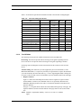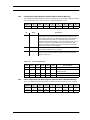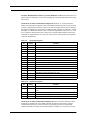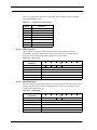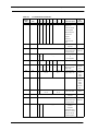
1
SanDisk CompactFlash Memory Card OEM Product Manual Version 12.0 Document No. 20-10-00038 02/2007 SanDisk Corporation Corporate Headquarters 601 McCarthy Boulevard Milpitas, CA 95035 (408) 801-1000 Phone (408) 801-8657 Fax www.sandisk.com SanDisk CompactFlash Card OEM Product Manual SanDisk® Corporation general policy does not recommend the use of its products in life support applications where in a failure or malfunction of the product may directly threaten life or injury. Per SanDisk Terms and Conditions of Sale, the user of SanDisk products in life support applications assumes all risk of such use and indemnifies SanDisk against all damages. Security safeguards, by their nature, are capable of circumvention. SanDisk cannot, and does not, guarantee that data will not be accessed by unauthorized persons, and SanDisk disclaims any warranties to that effect to the fullest extent permitted by law. This document is for information use only and is subject to change without prior notice. SanDisk Corporation assumes no responsibility for any errors that may appear in this document, nor for incidental or consequential damages resulting from the furnishing, performance or use of this material. No part of this document may be reproduced, transmitted, transcribed, stored in a retrievable manner or translated into any language or computer language, in any form or by any means, electronic, mechanical, magnetic, optical, chemical, manual or otherwise, without the prior written consent of an officer of SanDisk Corporation. All parts of the SanDisk documentation are protected by copyright law and all rights are reserved. SanDisk and the SanDisk logo are trademarks of SanDisk Corporation, registered in the United States and other countries. CompactFlash is a U.S. registered trademark of SanDisk Corporation. Product names mentioned herein are for identification purposes only and may be trademarks and/or registered trademarks of their respective companies. © 2007 SanDisk Corporation. All rights reserved. SanDisk products are covered or licensed under one or more of the following U.S. Patent Nos. 5,070,032; 5,095,344; 5,168,465; 5,172,338; 5,198,380; 5,200,959; 5,268,318; 5,268,870; 5,272,669; 5,418,752; 5,602,987. Other U.S. and foreign patents awarded and pending. Document 20-10-00038 Rev. 12.0 Revision History Date Revision Description February 2007 12.0 Merged CFlash 11.2 manual with CF ExtremeIII v1.2 to create v12.0; updated to comply with CFA Spec v4.0. © 2007 SanDisk Corporation i Rev. 12.0, 02/07 SanDisk CompactFlash Card OEM Product Manual –This page intentionally left blank– 02/07, Rev. 12.0 ii © 2007 SanDisk Corporation Table of Contents CHAPTER 1 Introduction . . . . . . . . . . . . . . . . . . . . . . . . . . . . . . . . . . . . . . . 1-1 General Description . . . . . . . . . . . . . . . . . . . . . . . . . . . . . . . . . . . . . 1-1 Features . . . . . . . . . . . . . . . . . . . . . . . . . . . . . . . . . . . . . . . . . . . . . . 1-2 Scope . . . . . . . . . . . . . . . . . . . . . . . . . . . . . . . . . . . . . . . . . . . . . . . . 1-2 CompactFlash Standard . . . . . . . . . . . . . . . . . . . . . . . . . . . . . . . . . . 1-2 PCMCIA Standard . . . . . . . . . . . . . . . . . . . . . . . . . . . . . . . . . . . . . . . 1-3 Related Documentation . . . . . . . . . . . . . . . . . . . . . . . . . . . . . . . . . . 1-3 Functional Description . . . . . . . . . . . . . . . . . . . . . . . . . . . . . . . . . . . 1-3 CHAPTER 2 Product Specifications . . . . . . . . . . . . . . . . . . . . . . . . . . . . . . 2-1 System Environmental Specifications . . . . . . . . . . . . . . . . . . . . . . . . 2-1 System Power Requirements . . . . . . . . . . . . . . . . . . . . . . . . . . . . . . 2-1 System Performance . . . . . . . . . . . . . . . . . . . . . . . . . . . . . . . . . . . . 2-3 System Reliability. . . . . . . . . . . . . . . . . . . . . . . . . . . . . . . . . . . . . . . . 2-4 Physical Specifications . . . . . . . . . . . . . . . . . . . . . . . . . . . . . . . . . . . 2-4 CHAPTER 3 Interface Description . . . . . . . . . . . . . . . . . . . . . . . . . . . . . . . 3-1 Physical Description . . . . . . . . . . . . . . . . . . . . . . . . . . . . . . . . . . . . . 3-1 Electrical Description . . . . . . . . . . . . . . . . . . . . . . . . . . . . . . . . . . . . 3-3 Electrical Specification . . . . . . . . . . . . . . . . . . . . . . . . . . . . . . . . . . . . 3-8 Card Configuration . . . . . . . . . . . . . . . . . . . . . . . . . . . . . . . . . . . . . 3-20 I/O Transfer Function . . . . . . . . . . . . . . . . . . . . . . . . . . . . . . . . . . . 3-25 True IDE Mode I/O Transfer Function . . . . . . . . . . . . . . . . . . . . . . . 3-26 CHAPTER 4 ATA Register Set and Protocol . . . . . . . . . . . . . . . . . . . . . . . . 4-1 I/O Primary and Secondary Address Configurations . . . . . . . . . . . . 4-1 Contiguous I/O Mapped Addressing . . . . . . . . . . . . . . . . . . . . . . . . . 4-2 © 2007 SanDisk Corporation i Rev. 12.0, 02/07 Table of Contents SanDisk CompactFlash Card OEM Product Manual Memory Mapped Addressing . . . . . . . . . . . . . . . . . . . . . . . . . . . . . .4-3 True IDE Mode Addressing . . . . . . . . . . . . . . . . . . . . . . . . . . . . . . . .4-4 ATA Registers . . . . . . . . . . . . . . . . . . . . . . . . . . . . . . . . . . . . . . . . . .4-4 CHAPTER 5 ATA Command Description . . . . . . . . . . . . . . . . . . . . . . . . . . 5-1 ATA Command Set . . . . . . . . . . . . . . . . . . . . . . . . . . . . . . . . . . . . . . .5-1 Error Posting . . . . . . . . . . . . . . . . . . . . . . . . . . . . . . . . . . . . . . . . . .5-29 CHAPTER 6 CIS Description . . . . . . . . . . . . . . . . . . . . . . . . . . . . . . . . . . . . 6-1 APPENDIX A Ordering Information . . . . . . . . . . . . . . . . . . . . . . . . . . . . . . . A-1 APPENDIX B Limited Warranty . . . . . . . . . . . . . . . . . . . . . . . . . . . . . . . . . . B-1 APPENDIX C Disclaimer of Liability . . . . . . . . . . . . . . . . . . . . . . . . . . . . . . C-1 02/07, Rev. 12.0 ii © 2007 SanDisk Corporation Introduction CHAPTER 1 1.1 General Description SanDisk CompactFlash® Memory Card products provide high capacity solid-state flash memory that electrically complies with the Personal Computer Memory Card International Association ATA (PC Card ATA) standard. (In Japan, the applicable standards group is JEIDA.) The CompactFlash Memory Card Series also supports a True IDE Mode that is electrically compatible with an IDE disk drive. The original CF form factor card can be used in any system that has a CF slot, and with a Type II PCMCIA adapter can be used in any system that has a PCMCIA Type II or Type III socket. CompactFlash Memory cards use SanDisk Flash memory, which was designed by SanDisk specifically for use in mass storage applications. In addition to the mass storage-specific flash memory chips, CompactFlash Memory cards include an on-card intelligent controller that provides a high level interface to the host computer. This interface allows a host computer to issue commands to the memory card to read or write blocks of memory. The host addresses the card in 512 byte sectors. Each sector is protected by a powerful Error Correcting Code (ECC). The on-card intelligent controller in the CompactFlash Memory Card manages interface protocols, data storage and retrieval as well as ECC, defect handling and diagnostics, power management and clock control. Once the card has been configured by the host, it appears to the host as a standard ATA (IDE) disk drive. Additional ATA commands have been provided to enhance system performance. The host system can support as many cards as there are CompactFlash and PCMCIA Type II or III card slots. The original form factor CompactFlash Memory cards require a PCMCIA Type II Adapter to be used in a PCMCIA Type II or Type III socket. Figure 1-1 SanDisk CompactFlash Card Block Diagram SanDisk CompactFlash Data In/Out Host Interface © 2007 SanDisk Corporation SanDisk Single Chip Controller Control 1-1 Flash Memory Rev. 12.0, 02/07 Introduction 1.2 SanDisk CompactFlash Card OEM Product Manual Features SanDisk CompactFlash Memory cards provide the following system features: • • • • • • • • • • • • • • • 1.3 Up to 16 GB of mass storage data PC Card ATA protocol compatible True IDE Mode compatible Very low CMOS power Very high performance Very rugged Low weight Noiseless Low Profile +5 Volts or +3.3 Volts operation Automatic error correction and retry capabilities Supports power down commands and sleep modes Non-volatile storage (no battery required) MTBF >1,000,000 hours Minimum 10,000 insertions Scope This document describes the key features and specifications of CompactFlash Memory cards, as well as the information required to interface this product to a host system. Retail CompactFlash specifications are not covered in this manual. 1.4 CompactFlash Standard SanDisk CompactFlash Memory cards are fully compatible with the CompactFlash Specification published by the CompactFlash Association. Contact the CompactFlash Association for more information. CompactFlash Association P.O. Box 51537 Palo Alto, CA 94303 USA Phone: 415-843-1220 Fax: 415-493-1871 www.compactflash.org 02/07, Rev. 12.0 1-2 © 2007 SanDisk Corporation SanDisk CompactFlash Card OEM Product Manual 1.5 Introduction PCMCIA Standard SanDisk CompactFlash Memory cards are fully electrically compatible with the PCMCIA specifications listed below: • PCMCIA PC Card Standard, 7.0, February 1999 • PCMCIA PC Card ATA Specification, 7.0, February 1999 These specifications may be obtained from: PCMCIA 2635 N. First Street, Suite 209 San Jose, CA 95131 USA Phone: 408-433-2273 Fax: 408-433-9558 1.6 Related Documentation ATA operation is governed by the ATA-4 specification published by ANSI. For more information, refer to the American National Standard X3.221: AT Attachment for Interface for Disk Drives document. Documentation can be ordered from IHS by calling 1-800-854-7179 or accessing their Web site: http://global.ihs.com. 1.7 Functional Description CompactFlash Memory cards contain a high level, intelligent subsystem as shown in the block diagram, Figure 1-1. This intelligent (microprocessor) subsystem provides many capabilities not found in other types of memory cards. These capabilities include the following: • Standard ATA register and command set (same as found on most magnetic disk drives). • Host independence from details of erasing and programming flash memory. • Sophisticated system for managing defects (analogous to systems found in magnetic disk drives). • Sophisticated system for error recovery including a powerful error correction code (ECC). • Power management for low power operation. • Implementation of dynamic and static wear-leveling to extend card’s life. © 2007 SanDisk Corporation 1-3 Rev. 12.0, 02/07 Introduction 1.7.1 SanDisk CompactFlash Card OEM Product Manual Technology Independence The 512-byte sector size of the CompactFlash Memory Card is the same as that in an IDE magnetic disk drive. To write or read a sector (or multiple sectors), the host computer software simply issues a Read or Write command to the card. This command contains the address and the number of sectors to write/read. The host software then waits for the command to complete. The host software does not get involved in the details of how the flash memory is erased, programmed or read. This is extremely important as flash devices are expected to get more and more complex in the future. Because the CompactFlash Memory Card Series uses an intelligent on-board controller, the host system software will not require changing as new flash memory evolves. In other words, systems that support CompactFlash Memory cards now, will be able to access future SanDisk cards built with new flash technology without having to update or change host software. 1.7.2 Defect and Error Management CompactFlash Memory cards contain a sophisticated defect and error management system. This system is analogous to the systems found in magnetic disk drives and in many cases offers enhancements. If necessary, the cards will rewrite data from a defective sector to a good sector. This is completely transparent to the host and does not consume any user data space. The CompactFlash Memory Card soft error rate specification is much better than the magnetic disk drive specification. In the extremely rare case a read error does occur, CompactFlash Memory cards have innovative algorithms to recover the data by using hardware on-the-fly Error Detection Code/Error Correction Code (EDC/ECC), based on a BCH algorithm. These defect and error management systems, coupled with the solid state construction, give SanDisk CompactFlash cards unparalleled reliability 1.7.3 Wear Leveling Wear Leveling is an intrinsic part of the erase pooling functionality of SanDisk CompactFlash using NAND memory. The CF WEAR LEVEL command is supported as a NOP operation to maintain backward compatibility with existing software utilities. Advanced features of dynamic and static wear-leveling, and automatic block management are used to ensure high data reliability and maximize flash life expectancy. 1.7.4 Using Erase Sector and Write Commands SanDisk CompactFlash Memory cards support the CF ERASE SECTOR and WRITE WITHOUT ERASE commands. In some applications, write operations may be faster if the addresses being written are first erased with the ERASE SECTOR command. WRITE WITHOUT ERASE behaves as a normal write command and no performance gain results from its use. 02/07, Rev. 12.0 1-4 © 2007 SanDisk Corporation SanDisk CompactFlash Card OEM Product Manual 1.7.5 Introduction Automatic Sleep Mode A unique feature of the SanDisk CompactFlash Memory Card is automatic entrance and exit from sleep mode. Upon completion of a command, the card will enter sleep mode to conserve power if no further commands are received within 5 msec. The host does not have to take any action for this to occur. In most systems, the CompactFlash Memory Card is in sleep mode except when the host is accessing it, thus conserving power. The delay from command completion to entering sleep mode is adjustable. When the host is ready to access the card and is in sleep mode, any command issued to it will cause the card to exit sleep and respond. The host does not have to follow the ATA protocol of issuing a reset first. It may do this if desired, but it is not needed. By not issuing the reset, performance is improved through the reduction of overhead but this must be done only for the SanDisk products as other ATA products may not support this feature. 1.7.6 Dynamic Adjustment of Performance vs. Power Consumption This feature is no longer supported. This command will be treated as a NOP (No Operation) to guarantee backward compatibility. 1.7.7 Power Supply Requirements This is a dual voltage product, which means it will operate at a voltage range of 3.30 volts ± 5% or 5.00 volts ± 10%. Per the PCMCIA specification Section 2.1.1, the host system must apply 0 volts in order to change a voltage range. This same procedure of providing 0 volts to the card is required if the host system applies an input voltage outside the desired voltage by more than 15%. This means less than 4.25 volts for the 5.00-volt range and less than 2.75 volts for the 3.30 volt range. © 2007 SanDisk Corporation 1-5 Rev. 12.0, 02/07 Introduction SanDisk CompactFlash Card OEM Product Manual –This page intentionally left blank– 02/07, Rev. 12.0 1-6 © 2007 SanDisk Corporation Product Specifications CHAPTER 2 For all the following specifications, values are defined at ambient temperature and nominal supply voltage unless otherwise stated. 2.1 System Environmental Specifications Table 2-1 contains environmental specifications which include temperature, humidity, acoustic noise, vibration, shock and altitude. Table 2-1 Environmental Specifications Temperature Humidity Acoustic Noise Vibration Shock Altitude (relative to sea level) 2.2 CompactFlash CompactFlash Extreme III 0° C to 70° C -25° C to 85° C -25° C to 85° C -25° C to 85° C Operating: 8% to 95% non-condensing 8% to 95% non-condensing Non-operating: 8% to 95% non-condensing 8% to 95% non-condensing 0 dB 0 dB Operating: Non-operating: 15 G peak to peak maximum 15 G peak to peak maximum 15 G peak to peak maximum Operating: Non-operating: 2,000 G maximum 2,000 G maximum 2,000 G maximum Operating: Non-operating: 80,000 ft. maximum 80,000 ft. maximum 80,000 ft. maximum Operating: Non-operating: At 1 meter: 15 G peak to peak maximum 2,000 G maximum 80,000 ft. maximum System Power Requirements All values quoted in Table 2-2 are typical at 25° C and nominal supply voltage unless otherwise stated. © 2007 SanDisk Corporation 2-1 Rev. 12.0, 02/07 Product Specifications SanDisk CompactFlash Card OEM Product Manual Sleep mode currently is specified under the condition that all card inputs are static CMOS levels and in a "Not Busy" operating state. Table 2-2 Power Requirements DC Input Voltage (Vcc) 100 mV max. ripple (p-p) a Memory Subsystem 3.3V +/- 5% 5V +/- 10% Up to 512 MB 300 µ 500 µ 1.0 GB 600 µ 800 µ 1 mA 1.2 mA 50 mA 55 mA CompactFlash Memory Card Sleep Over 1.0 GB Read Memory Subsystema Write 65 mA 70 mA Read/Write Peak 100 mA 100 mA Up to 512 MB 300 µ 500 µ 512 MB to 1.5 GB 600 µ 800 µ CompactFlash Extreme III Memory Card Sleep Over 1.5 GB Read 1 mA 1.2 mA 75 mA 100 mA Write 75 mA 100 mA Read/Write Peak 100 mA 100 mA a. Maximum average value. 02/07, Rev. 12.0 2-2 © 2007 SanDisk Corporation SanDisk CompactFlash Card OEM Product Manual 2.3 Product Specifications System Performance All performance timings assume the CompactFlash Memory Card Series controller is in the default (i.e., fastest) mode. Table 2-3 Performance CompactFlash Memory Card Start-up Times Sleep to Write 2.5 ms maximum Sleep to Read 20 ms maximum Reset to Ready Active to Sleep Delay Data Transfer Rate To/From Flash Data Transfer Rate To/From Host 50 ms typical; 400 ms maximum Programmable 20.0 MB/sec burst 16.0 MB/sec burst Controller Overhead Command to DRQ 50 ms maximum CompactFlash Extreme III Memory Card Start-up Times Sleep to Write 2.5 ms maximum Sleep to Read 20 ms maximum Reset to Ready Data Transfer Rate To/From Flash Data Transfer Rate To/From Host 50 ms typical; 400 ms maximum 20.0 MB/sec burst 25.0 MB/sec burst Maximum Performance Sequential Read 20.0 MB/sec Sequential Write 20.0 MB/sec NOTE: © 2007 SanDisk Corporation The Sleep to Write and Sleep to Read times are the times it takes the CompactFlash Memory Card to exit sleep mode when any command is issued by the host to when the card is reading or writing. CompactFlash Memory cards do not require a reset to exit sleep mode. 2-3 Rev. 12.0, 02/07 Product Specifications 2.4 SanDisk CompactFlash Card OEM Product Manual System Reliability Table 2-4 Reliability >1,000,000 hours MTBF (@ 25 C) None Preventative Maintenance <1 non-recoverable error in 1014 bits read Data Reliability <1 erroneous correction in 1020 bits read 2.5 Physical Specifications Refer to Table 2-5 and see Figure 2-1 for CompactFlash Memory Card physical specifications and dimensions. Table 2-5 Weight Length Width Thickness 02/07, Rev. 12.0 CompactFlash Physical Dimensions 11.4 g (.40 oz) typical, 14.2 g (.50 oz) maximum 36.40 ± 0.15 mm (1.433 ± .006 in) 42.80 ± 0.10 mm (1.685 ± .004 in) 3.3 mm ± 0.10 mm (.130 ± .004 in) (Excluding Lip) 2-4 © 2007 SanDisk Corporation SanDisk CompactFlash Card OEM Product Manual Figure 2-1 © 2007 SanDisk Corporation Product Specifications CompactFlash Memory Card Dimensions 2-5 Rev. 12.0, 02/07 Product Specifications SanDisk CompactFlash Card OEM Product Manual –This page intentionally left blank– 02/07, Rev. 12.0 2-6 © 2007 SanDisk Corporation Interface Description CHAPTER 3 3.1 Physical Description The host connects to SanDisk CompactFlash Memory cards using a standard 50-pin connector consisting of two rows of 25 female contacts each on 50 mil (1.27 mm) centers. 3.1.1 Pin Assignments and Types The signal/pin assignments are listed in Table 3-1. Low active signals have a "-" prefix. Pin types are Input, Output or Input/Output. Sections 3.3.1 and 3.3.2 define the DC characteristics for all input and output type structures.. Table 3-1 PC Card Memory Mode Pin Assignments Pin No. Signal Name Pin No. Signal Name 1 GND – 2 D03 I/O Ground 26 -CD1 O Ground I1Z,OZ3 27 D11 I/O I1Z,OZ3 3 D04 I/O 4 D05 I/O I1Z,OZ3 28 D12 I/O I1Z,OZ3 I1Z,OZ3 29 D13 I/O I1Z,OZ3 5 D06 6 D07 I/O I1Z,OZ3 30 D14 I/O I1Z,OZ3 I/O I1Z,OZ3 31 D15 I/O I1Z,OZ3 7 -CE1 8 A10 I I3U 32 -CE2 I I3U I I1Z 33 -VS1 O Ground Pin Type I/O Type Pin Type I/O Type 9 -OE I I3U 34 -IORD I I3U 10 A09 I I1Z 35 -IOWR I I3U 11 A08 I I1Z 36 -WE I I3U 12 A07 I I1Z 37 RDY/BSY O OT1 13 VCC – Power 38 VCC – Power 14 A06 I I1Z 39 -CSEL I I2Z 15 A05 I I1Z 40 -VS2 O OPEN 16 A04 I I1Z 41 RESET I I2Z 17 A03 I I1Z 42 -WAIT O OT1 18 A02 I I1Z 43 -INPACK O OT1 19 A01 I I1Z 44 -REG I I3U 20 A00 I I1Z 45 BVD2 I/O I1U,OT1 21 D00 I/O I1Z,OZ3 46 BVD1 I/O I1U,OT1 22 D01 I/O I1Z,OZ3 47 D08 I/O I1Z,OZ3 23 D02 I/O I1Z,OZ3 48 D09 I/O I1Z,OZ3 24 WP O OT3 49 D10 I/O I1Z,OZ3 25 -CD2 O Ground 50 GND – Ground © 2007 SanDisk Corporation 3-1 Rev. 12.0, 02/07 Interface Description SanDisk CompactFlash Card OEM Product Manual PC Card I/O Pin Assignments are contained in Table 3-2. Table 3-2 PC Card I/O Mode Pin Assignments Pin No. Signal Name Pin No. Signal Name 1 GND – 2 D03 I/O Ground 26 -CD1 O Ground I1Z,OZ3 27 D11 I/O I1Z,OZ3 3 D04 I/O 4 D05 I/O I1Z,OZ3 28 D12 I/O I1Z,OZ3 I1Z,OZ3 29 D13 I/O I1Z,OZ3 5 D06 6 D07 I/O I1Z,OZ3 30 D14 I/O I1Z,OZ3 I/O I1Z,OZ3 31 D15 I/O I1Z,OZ3 7 -CE1 8 A10 I I3U 32 -CE2 I I3U I I1Z 33 -VS1 O Ground Pin Type I/O Type Pin Type I/O Type 9 -OE I I3U 34 -IORD I I3U 10 A09 I I1Z 35 -IOWR I I3U 11 A08 I I1Z 36 -WE I I3U 12 A07 I I1Z 37 -IREQ O OT1 13 VCC – Power 38 VCC – Power 14 A06 I I1Z 39 -CSEL I I2Z 15 A05 I I1Z 40 -VS2 O OPEN 16 A04 I I1Z 41 RESET I I2Z 17 A03 I I1Z 42 -WAIT O OT1 18 A02 I I1Z 43 -INPACK O OT1 19 A01 I I1Z 44 -REG I 20 A00 I I1Z 45 -SPKR I/O 21 D00 I/O I1Z,OZ3 46 -STSCHG I/O I1U,OT1 22 D01 I/O I1Z,OZ3 47 D08 I/O I1Z,OZ3 23 D02 I/O I1Z,OZ3 48 D09 I/O I1Z,OZ3 24 -IOIS16 O OT3 49 D10 I/O I1Z,OZ3 25 -CD2 O Ground 50 GND – Ground I3U I1U,OT1 True IDE Mode Pin Assigments are contained in Table 3-3. Table 3-3 02/07, Rev. 12.0 True IDE Mode Pin Assignments Pin No. Signal Name Pin No. Signal Name 1 GND – 2 D03 I/O Ground 26 -CD1 O Ground I1Z,OZ3 27 D11 I/O I1Z,OZ3 3 D04 I/O 4 D05 I/O I1Z,OZ3 28 D12 I/O I1Z,OZ3 I1Z,OZ3 29 D13 I/O I1Z,OZ3 5 D06 6 D07 I/O I1Z,OZ3 30 D14 I/O I1Z,OZ3 I/O I1Z,OZ3 31 D15 I/O I1Z,OZ3 7 -CS0 8 A10 I I3Z 32 -CS1 I I3Z I I1Z 33 -VS1 O Ground Pin Type 3-2 I/O Type Pin Type I/O Type © 2007 SanDisk Corporation SanDisk CompactFlash Card OEM Product Manual Table 3-3 3.2 Interface Description True IDE Mode Pin Assignments Pin No. Signal Name Pin Type 9 -ATA SEL I Pin No. Signal Name Pin Type I3U 34 -IORD I I/O Type I/O Type I3Z 10 A09 I I1Z 35 -IOWR I I3Z 11 A08 I I1Z 36 -WE I I3U 12 A07 I I1Z 37 INTRQ O OZ1 13 VCC – Power 38 VCC – Power 14 A06 I I1Z 39 -CSEL I I2U 15 A05 I I1Z 40 -VS2 O OPEN 16 A04 I I1Z 41 RESET I I2Z 17 A03 I I1Z 42 IORDY O OT1 18 A02 I I1Z 43 -DMARQ O OZ1 19 A01 I I1Z 44 -DMACK I I3U 20 A00 I I1Z 45 -DASP I/O I1U,ON1 21 D00 I/O I1Z,OZ3 46 -PDIAG I/O I1U,ON1 22 D01 I/O I1Z,OZ3 47 D08 I/O I1Z,OZ3 23 D02 I/O I1Z,OZ3 48 D09 I/O I1Z,OZ3 24 -IOCS16 O ON3 49 D10 I/O I1Z,OZ3 25 -CD2 O Ground 50 GND – Ground Electrical Description The CompactFlash Memory Card Series is optimized for operation with hosts, which support the PCMCIA I/O interface standard conforming to the PC Card ATA specification. However, the card may also be configured to operate in systems that support only the memory interface standard. The CompactFlash card configuration is controlled using the standard PCMCIA configuration registers starting at address 200h in the Attribute Memory space of the card. Table 3-4 describes the I/O signals. Signals whose source is the host are designated as inputs while signals that the card sources are outputs. SanDisk CompactFlash Memory Card logic levels conform to those specified in Section 3.3 of the PCMCIA Release 2.1 Specification. NOTE: © 2007 SanDisk Corporation The sleep-to-write and sleep-to-read times are the time it takes the card to exit sleep mode when any command is issued by the host to when the card is reading or writing. CompactFlash Memory cards do not require a reset to exit sleep mode. 3-3 Rev. 12.0, 02/07 Interface Description SanDisk CompactFlash Card OEM Product Manual The SanDisk CompactFlash Memory Card signals are described in Table 3-4. Table 3-4 Signal Description Signal Name Dir. Pin Description A10-A0 (PC Card Memory Mode) (PC Card I/O Mode) I 8, 10, 11, 12, 14, 15, 16, 17, 18, 19, 20 These address lines, along with the -REG signal, are used to select the following: I/O port address registers within the card, memorymapped port address registers within the card, a byte in the card's information structure and its configuration control and status registers. A2-A0 (True IDE Mode) I 18, 19, 20 In True IDE Mode only A[2:0] is used to select one of eight registers in the Task File. A10-A3 (True IDE Mode) BVD1 (PC Card Memory Mode) In True IDE Mode these remaining address lines should be grounded by the host. I/O 46 -STSCHG (PC Card I/O Mode) The Status Changed signal is asserted low to alert the host to changes in the RDY/-BSY and Write Protect states, while the I/O interface is configured. Its use is controlled by the Card Config. and Status Register. -PDIAG (True IDE Mode) In the True IDE Mode, this input/output is the Pass Diagnostic signal in the master/slave handshake protocol. BVD2 (PC Card Memory Mode) I/O 45 This output line is always driven to a high state in Memory Mode since a battery is not required for this product. -SPKR (PC Card I/O Mode) This output line is always driven to a high state in I/O Mode since this product does not support the audio function. -DASP (True IDE Mode) In the True IDE Mode, this input/output is the Disk Active/Slave Present signal in the master/ slave handshake protocol. -CD1, -CD2 (PC Card Memory Mode) (PC Card I/O Mode) (True IDE Mode) O 26, 25 These Card Detect pins are connected to ground on the card. They are used by the host to determine if the card is fully inserted into its socket. -CE1, -CE2 (PC Card Memory Mode) (PC Card I/O Mode) I 7, 32 The Card Enable input signals are used both to select the card and to indicate to the card whether a byte or a word operation is being performed. -CE2 always accesses the odd byte of the word. -CE1 accesses the even byte or the Odd byte of the word depending on A0 and -CE2. A multiplexing scheme based on A0, -CE1, -CE2 allows 8 bit hosts to access all data on D0-D7. -CS0, -CS1 (True IDE Mode) -CSEL (PC Card Memory Mode) (PC Card I/O Mode) 02/07, Rev. 12.0 This signal is asserted high as the BVD1 signal since a battery is not used with this product. In True IDE Mode, -CS0 is the chip select for the Task File registers while -CS1 is used to select the Alternate Status Register and the Device Control Register. I 39 3-4 This signal is not used for PC Card Memory Mode or PC Card I/O Mode. © 2007 SanDisk Corporation SanDisk CompactFlash Card OEM Product Manual Table 3-4 Interface Description Signal Description Signal Name Dir. Pin Description -CSEL (True IDE Mode) D15-D00 (PC Card Memory Mode) (PC Card I/O Mode) This internally pulled up signal is used to configure this device as a master or slave when configured in the True IDE Mode. When this pin is grounded, this device is configured as a master. When the pin is open, this device is configured as a slave. I/O 31, 30, 29, 28, 27, 49, 48, 47, 6, 5, 4, 3, 2, 23, 22, 21 D15-D00 (True IDE Mode) GND (PC Card Memory Mode) These lines carry the data, commands and status information between the host and the controller. D00 is the LSB of the Even Byte of the word. D08 is the LSB of the Odd Byte of the word. In True IDE Mode, all Task File operations occur in byte mode on the low order bus D00 D07 while all data transfers are 16 bits using D00-D15. -- 1, 50 O 43 Ground. (PC Card I/O Mode) (True IDE Mode) -INPACK (PC Card Memory Mode) This signal is not used in this mode. -INPACK (PC Card I/O Mode) The Input Acknowledge signal is asserted by the card when it is selected and responding to an I/O read cycle at the address that is on the address bus. This signal is used by the host to control the enable of any input data buffers between the card and the CPU. -DMARQ (True IDE Mode) This signal is used for DMA data transfers between host and device and is asserted by the device when it is ready to transfer data to or from the host. The direction of data transfer is controlled by DIOR- and DIOW-. This signal is used in a handshake manner with DMACK(i.e., the device waits until the host asserts DMACK- before negating DMARQ, and reasserting DMARQ if there is more data to transfer). -IORD (PC Card Memory Mode) I 34 This signal is not used in this mode. -IORD (PC Card I/O Mode) (True IDE Mode) -IOWR (PC Card Memory Mode) © 2007 SanDisk Corporation This is an I/O read strobe generated by the host. This signal gates I/O data onto the bus from the card when the card is configured to use the I/O interface. I 35 This signal is not used in this mode. 3-5 Rev. 12.0, 02/07 Interface Description SanDisk CompactFlash Card OEM Product Manual Table 3-4 Signal Description Signal Name Dir. Pin -IOWR (PC Card I/O Mode) (True IDE Mode) -OE (PC Card Memory Mode) The I/O write strobe pulse is used to clock I/O data on the Card Data bus into the card controller registers when the card is configured to use the I/O interface. The clocking will occur on the negative to positive edge of the signal (trailing edge). I 9 This is an output enable strobe generated by the host interface. It is used to read data from the card in Memory Mode and to read the CIS and configuration registers. -OE (PC Card I/O Mode) In PC Card I/O Mode, this signal is used to read the CIS and configuration registers. -ATA SEL (True IDE Mode) To enable True IDE Mode this input should be grounded by the host. RDY/-BSY (PC Card Memory Mode) O 37 In Memory Mode, this signal is set high when the card is ready to accept a new data transfer operation and held low when the card is busy. The host memory card socket must provide a pull-up resistor. At power up and at reset, the RDY/-BSY signal is held low (busy) until the card has completed its power up or reset function. No access of any type should be made to the card during this time. The RDY/-BSY signal is held high (disabled from being busy) whenever the following condition is true: The card has been powered up with +RESET continuously disconnected or asserted. -IREQ (PC Card I/O Mode) I/O Operation–After the card has been configured for I/O operation, this signal is used as an interrupt request. This line is strobed low to generate a pulse mode interrupt or held low for a level mode interrupt. INTRQ (True IDE Mode) In True IDE Mode, this signal is the active high Interrupt Request to the host. -REG (PC Card Memory Mode) I 44 -REG (PC Card I/O Mode) 02/07, Rev. 12.0 Description This Attribute Memory Select signal is used during memory cycles to distinguish between Common Memory and Register (Attribute) Memory accesses: High for common memory, and low for attribute memory. The signal must also be active (low) during I/O cycles when the I/O address is on the bus. 3-6 © 2007 SanDisk Corporation SanDisk CompactFlash Card OEM Product Manual Table 3-4 Interface Description Signal Description Signal Name Dir. Pin Description This signal is used by the host in response to DMARQ to initiate DMA transfers. NOTE: This signal may be negated by the host to suspend the DMS transfer in process. For Multiword DMA transfers, the device may negate DMARQ with the tL specified time once the DMACK- is asserted and reasserted again at a later time to resume DMA operation. Alternatively, if the device is able to continue the data transfer, the device may leave DMARQ asserted and wait for the host to reassert DMACK-. -DMACK (True IDE Mode) RESET (PC Card Memory Mode) (PC Card I/O Mode) I 41 When the pin is high, this signal resets the card. The card is reset only at power-up if this pin is left high or open from power-up. The card is also reset when the Soft Reset bit in the Card Configuration Option Register is set. In the True IDE Mode this input pin is the active low hardware reset from the host. -RESET (True IDE Mode) VCC -- 13, 38 +5V, +3.3V power. -VS1 -VS2 (PC Card Memory Mode) (PC Card I/O Mode) (True IDE Mode) O 33, 40 Voltage Sense Signals. -VS1 is grounded so that the CompactFlash Card CIS can be read at 3.3 volts and VS2 is open and reserved by PCMCIA for a secondary voltage. -WAIT (PC Card Memory Mode) O 42 SanDisk CompactFlash Memory cards do not assert the -WAIT signal. (PC Card Memory Mode) (PC Card I/O Mode) (True IDE Mode) -WAIT (PC Card I/O Mode) SanDisk CompactFlash Memory cards do not assert the -WAIT signal. IORDY (True IDE Mode) SanDisk CompactFlash Memory cards, except when in UDMA modes, do not assert an IORDY signal. -WE (PC Card Memory Mode) I 36 This is a signal driven by the host and used for strobing memory write data to the registers of the card when it is configured in the Memory Interface Mode. It is also used for writing the configuration registers. -WE (PC Card I/O Mode) In PC Card I/O Mode, this signal is used for writing the configuration registers. -WE (True IDE Mode) In True IDE Mode this input signal is not used and should be connected to VCC by the host. WP (PC Card Memory Mode) © 2007 SanDisk Corporation O 24 Memory Mode–The CompactFlash Card does not have a write-protect switch. This signal is held low after the completion of the reset initialization sequence. 3-7 Rev. 12.0, 02/07 Interface Description SanDisk CompactFlash Card OEM Product Manual Table 3-4 Signal Description Signal Name 3.3 Dir. Pin Description -IOIS16 (PC Card I/O Mode) I/O Operation–When the card is configured for I/O Operation, pin 24 is used for the -I/O Selected is 16 Bit Port (-IOIS16) function. A low signal indicates that a 16-bit or odd-byte only operation can be performed at the addressed port. -IOCS16 (True IDE Mode) This output signal is asserted low when this device is expecting a word data transfer cycle. Electrical Specification All D.C. Characteristics for the CompactFlash Memory Card Series are defined as follows: Typical conditions unless otherwise stated: VCC = 5V +/- 10% VCC = 3.3V +/- 5% Ta = 0 ° C to 60 ° C Absolute Maximum conditions: VCC = -0.3V min. to 6.5V max. V* = 0.5V min. to VCC + 0.5V max. *Voltage on any pin except VCC with respect to GND. 3.3.1 Input Leakage Control and Input Characteristics In Table 3-5, “x” refers to the characteristics described in Table 3-6. For example–"I1U" indicates a pull-up resistor with a Type 1 input characteristic. Table 3-5 Type Parameter Symbol Conditions MIN MAX Unit lxZ Input Leakage Current IL Vih=VCC/Vil=GND -1 1 uA IxU Pull Up Resistor RPU1 VCC=5.0V 50k 500k Ohm IxD Pull Down Resistor RPD1 VCC=5.0V 50k 500k Ohm NOTE: 02/07, Rev. 12.0 Input Leakage Control The minimum pull-up resistor leakage current meets the PCMCIA specification of 10k ohms but is intentionally higher in the CompactFlash Memory Card Series product to reduce power use. 3-8 © 2007 SanDisk Corporation SanDisk CompactFlash Card OEM Product Manual Interface Description Table 3-6 defines the input characteristics of the parameters in Table 3-5. Table 3-6 Input Characteristics Min. 3.3.2 Typ. Max. Min. VCC = 3.3V Typ. Type Parameter Symbol 1 Input Voltage Vih CMOS Vil 2 Input Voltage Vih CMOS Vil 3 Input Voltage Vth 1.8 2.8 CMOS Schmitt Trigger Vtl 1.0 2.0 Max. VCC = 5.0V 2.4 Unit 4.0 V 0.6 1.5 0.8 2.0 V 0.6 0.8 V Output Drive Type and Characteristics In Table 3-7 "x" refers to the characteristics described in Table 3-8. For example–"OT3" refers to Totempole output with a Type 3 output drive characteristic. Table 3-7 Output Drive Type Type Table 3-8 Output Type Valid Conditions OTx Totempole loh & lol OZx Tri-state N-P Channel loh & lol OPx P-Channel Only loh only ONx N-Channel Only loh Only Output Drive Characteristics Type Parameter Symbol Conditions Min. 1 Output Voltage Voh loh= -4 mA VCC Vol lol= 4 mA Voh loh= -8 mA Typ. Max. Unit V -0.8V 2 Output Voltage Gnd +0.4V V VCC -0.8V 3 X © 2007 SanDisk Corporation Output Voltage Tri-State Leakage Current Vol lol= 8 mA Voh loh= -8 mA VCC Vol lol= 8 mA -0.8V Gnd +0.4V loz Vol = Gnd Voh = VCC -10 10 3-9 Gnd +0.4V V uA Rev. 12.0, 02/07 Interface Description 3.3.3 SanDisk CompactFlash Card OEM Product Manual Power Up/Power Down Timing The timing specification in Table 3-9 was defined to permit peripheral cards to perform powerup initialization. Table 3-9 Power Up/Power Down Timing Item Value a CE Signal Level Symbol Condition Min. Max. Unit Vi (CE) 0V <VCC <2.0V 0 ViMAX V 2.0V <VCC <VIH <VCC - 0.1 ViMAX <VIH <VCC VIH ViMAX CE Setup Time TSU (VCC) --- 20 --- ms CE Setup Time TSU (RESET) --- 20 --- ms CE Recover Time TREC (VCC) --- 0.001 --- ms Timeb tpr 10%-->90% of (VCC + 5%) 0.1 300 ms VCC Falling Timeb tpf 90% of (VCC + 5%)-->10% 3.0 300 ms TW (RESET) --- 10 --- µs Th (Hi-z Reset) --- 1 --- ms TS (Hi-z Reset) --- 0 --- ms VCC Rising Reset Width a. ViMAX means Absolute Maximum Voltage for Input in the period of 0V <VCC <2.0V, Vi (CE) is only 0V~ViMAX. b. The tpr and tpf are defined as "linear waveform" in the period of 10% to 90% or vice-versa. Even if the waveform is not "linear waveform," its rising and falling time must be met by this specification. Figure 3-1 Power Up/Power Down Timing for Systems supporting RESET tpr tSU(VCC) VCC Min. tSU(Reset) tSU(Reset) VIH 2V -CE1, -CE2 tW (Reset) th (Hi-z Reset) Hi-z Reset tW(Reset) VCC tpf VCC Min. trec VIH 2V -CE1, -CE2 ts (Hi-z Reset) Hi-z 02/07, Rev. 12.0 3-10 © 2007 SanDisk Corporation SanDisk CompactFlash Card OEM Product Manual Figure 3-2 Interface Description Power Up/Power Down Timing for Systems not supporting RESET tpr VCC VCC Min. tSU(VCC) VIH 2V -CE1, -CE2 Always Hi-z from system Supplied by pull-up resistor on card (if present) RESET tpf VCC VCC Min. trec VIH 2V -CE1, -CE2 3.3.4 Common Memory Read Timing Table 3-10 contains common memory read timing specifications for all types of memory. NOTE: All timings measured at the CompactFlash Memory Card. Skews and delays from the system driver/receiver to the card must be accounted for by the system. Table 3-10 Common Memory Read Timing Specification 100 ns Speed Version Item Read Cycle Time Address Access Timea Symbol IEEE Symbol Min. Max. tc (R) tAVAV 100 --- ta (A) tAVQV --- 100 Card Enable Access Time ta (CE) tELQV --- 100 Output Enable Access Time ta (OE) tGLQV --- 50 Output Disable Time from -OE tdis (OE) tGHQZ --- 50 Output Disable Time from -CE tdis (CE) tEHQZ --- 50 Output Enable Time from -CE ten (CE) tELQNZ 5 --- Output Enable Time from -OE ten (OE) tGLQNZ 5 --- Data Valid from Add Changea tv (A) tAXQX 0 --- Address Setup Time tsu (A) tAVGL 10 --- © 2007 SanDisk Corporation 3-11 Rev. 12.0, 02/07 Interface Description SanDisk CompactFlash Card OEM Product Manual Table 3-10 Common Memory Read Timing Specification 100 ns Speed Version Item Address Hold Time Symbol IEEE Symbol Min. Max. th (A) tGHAX 15 --- Card Enable Setup Time tsu(CE) tELGL 0 --- Card Enable Hold Time th (CE) tGHEH 15 --- a. The -REG signal timing is identical to address signal timing 3.3.5 Common and Attribute Memory Write Timing The write timing specifications for Common and Attribute memory are the same. All timings measured at the CompactFlash Memory Card. Skews and delays from the system driver/receiver to the card must be accounted for by the system NOTE: SanDisk CompactFlash Memory cards do not assert the -WAIT signal. Table 3-11 Common and Attribute Memory Write Timing Specification 100 ns Speed Version Symbol IEEE Symbol Min. Max. Write Cycle Time tc (W) tAVAV 100 --- Write Pulse Width tw (WE) tWLWH 60 --- tsu (A) tAVWL 10 --- tsu (A-WEH) tAVWH 70 --- tsu(CE-WEH) tELWH 70 --- tsu(D-WEH) tDVWH 40 --- th (D) tWMDX 15 --- Write Recover Time trec (WE) tWMAX 15 --- Output Disable Time from -WE tdis (WE) tWLQZ --- 50 Output Disable Time from -OE tdis (OE) tGHQZ --- 50 Output Enable Time from -WE ten (WE) tWHQNZ 5 --- Output Enable Time from -OE ten (OE) tGLQNZ 5 --- Output Enable Setup from -WE tsu(OE-WE) tGHWL 10 --- Output Enable Hold from -WE Address Setup Timea Address Setup Time for -WEa Card Enable Setup Time for -WE Data Setup Time form -WE Data Hold Time th(OE-WE) tWHGL 10 --- Card Enable Setup Time tsu (CE) tELWL 0 --- Card Enable Hold Time th (CE) tGHEH 15 --- a. The -REG signal timing is identical to address signal timing. 02/07, Rev. 12.0 3-12 © 2007 SanDisk Corporation SanDisk CompactFlash Card OEM Product Manual 3.3.6 Interface Description Attribute Memory Read Timing Specification Table 3-12 contains common memory write timing specifications for all types of memory. NOTE: SanDisk CompactFlash Memory cards do not assert the -WAIT signal. Table 3-12 Attribute Memory Read Timing Specification 300 ns Symbol IEEE Symbol Min. Max. Read Cycle Time Speed Version Item tc (R) tAVAV 300 --- Address Access Timea ta (A) tAVQV --- 300 Card Enable Access Time ta (CE) tELQV --- 300 Output Enable Access Time ta (OE) tGLQV --- 150 Output Disable Time from -OE tdis (OE) tGHQZ --- 100 Output Enable Time from -OE ten (OE) tGLQNZ 5 --- tv (A) tAXQX 0 --- tsu (A) tAVGL 30 --- Data Valid from Add Changea Address Setup Time th (A) tGHAX 20 --- Card Enable Setup Time tsu(CE) tELGL 0 --- Card Enable Hold Time th (CE) tGHEH 20 --- Address Hold Time a. The -REG signal timing is identical to address signal timing 3.3.7 Memory Timing Diagrams Figure 3-3 NOTE 1: © 2007 SanDisk Corporation Common and Attribute Memory Read Timing Diagram Shaded areas may be high or low. 3-13 Rev. 12.0, 02/07 Interface Description SanDisk CompactFlash Card OEM Product Manual Figure 3-4 02/07, Rev. 12.0 Common and Attribute Memory Write Timing Diagram NOTE 1: Shaded areas may be high or low. NOTE 2: When the data I/O pins are in the output state, no signals shall be applied to the data pins (D[15::0]) by the host system NOTE 3: May be high or low for write timing, but restrictions on -OE from previous figures apply. NOTE 4: SanDisk CompactFlash Memory Cards do not assert the -WAIT signal. 3-14 © 2007 SanDisk Corporation SanDisk CompactFlash Card OEM Product Manual 3.3.8 Interface Description I/O Read (Input) Timing Specification Figure 3-5 I/O Read Timing Diagram NOTE 1: All timings are measured at the CompactFlash Memory Card. NOTE 2: Skews and delays from the host system driver/receiver to the card must be accounted for by the system design. NOTE 3: D[15::0] signifies data provided by the card to the host system. Table 3-13 contains the read input timing specifications. NOTE: SanDisk CompactFlash Memory cards do ont assert a -WAIT signal. Table 3-13 I/O Read (Input) Timing Specification Item Symbol IEEE Symbol Min. (ns) Max. (ns) Data Delay after -IORD td (IORD) tlGLQV --- 100 Data Hold following -IORD th (IORD) tlGHQX 0 --- -IORD Width Time tw (IORD) tlGLIGH 165 --- Address Setup before -IORD tsuA(IORD) tAVIGL 70 --- Address Hold following -IORD thA(IORD) tlGHAX 20 --- -CE Setup before -IORD tsuCE(IORD) tELIGL 5 --- -CE Hold following -IORD thCE(IORD) tlGHEH 20 --- -REG Setup before -IORD tsuREG(IORD) tRGLIGL 5 --- -REG Hold following -IORD thREG(IORD) tlGHRGH 0 --- -INPACK Delay falling from -IORD tdfINPACK(IORD) tlGLIAL 0 45a -INPACK Delay rising from -IORD tdrINPACK(IORD) tlGHIAH --- 45a © 2007 SanDisk Corporation 3-15 Rev. 12.0, 02/07 Interface Description SanDisk CompactFlash Card OEM Product Manual Table 3-13 I/O Read (Input) Timing Specification Symbol Item IEEE Symbol Min. (ns) Max. (ns) -IOIS16 Delay falling from Address tdfIOIS16(ADR) tAVISL --- 35a -IOIS16 Delay rising from Address tdrIOIS16(ADR) tAVISH --- 35a a. The maximum load on -INPACK and -IOIS16 is 1 LSTTL with 50 pF total load. 3.3.9 I/O Write (Output) Timing Specification Figure 3-6 02/07, Rev. 12.0 I/O Write Timing Diagram NOTE 1: All timings are measured at the CompactFlash Memory Card. NOTE 2: Skews and delays from the host system driver/receiver to the CompactFlash Memory Card must be accounted for by the system design. NOTE 3: D[15::0] signifies data provided by the host system to the CompactFlash Memory Card. 3-16 © 2007 SanDisk Corporation SanDisk CompactFlash Card OEM Product Manual Interface Description Table 3-14 contains the specification information related to the I/O Write Timing Diagram. Table 3-14 I/O Write Timing Specification Item Symbol IEEE Symbol Min. (ns) Max. (ns) Data Setup before -IOWR tsu (IOWR) tDVIWL 60 --- Data Hold following -IOWR th (IOWR) tWHDX 30 --- -IOWR Width Time tw (IOWR) tlWLIWH 165 --- Address Setup before -IOWR tsuA(IOWR) tAVIWL 70 --- Address Hold following -IOWR thA(IOWR) tlWHAX 20 --- -CE Setup before -IOWR tsuCE(IOWR) tELIWL 5 --- -CE Hold following -IOWR thCE(IOWR) tlWHEH 20 --- -REG Setup before -IOWR tsuREG(IOWR) tRGLIWL 5 --- -REG Hold following -IOWR thREG(IOWR) tlWHRGH 0 --- -IOIS16 Delay falling from Address tdfIOIS16(ADR) tAVISL --- 35a -IOIS16 Delay rising from -IORD tdr-IOIS16(ADR) tAVISH --- 35 -IOIS16 Delay falling from Address tdfIOIS16(ADR) tAVISL --- 35 -IOIS16 Delay rising from Address tdrIOIS16(ADR) tAVISH --- 35 a. The maximum load on -IOIS16 is 1 LSTTL with 50 pF total load. 3.3.10 True IDE Mode The following sections provide valuable information for the True IDE mode. De-skewing. The host will provide cable de-skewing for all signals originating from the device. The device will provide cable de-skewing for all signals originating at the host. All timing values and diagrams are shown and measured at the connector of the selected device. Transfer Timing. The minimum cycle time supported by devices in PIO Mode 3, 4 and Multiword DMA Mode 1, 2 respectively will always be greater than or equal to the minimum cycle time defined by the associated mode (e.g., a device supporting PIO Mode 4 timing will not report a value less than 120 ns. The minimum cycle time defined for PIO mode 4 timings). • Register Transfers Figure 3-7 defines the relationships between the interface signals for register transfers. For PIO Modes 3 and above, the minimum value of t0 is specified by Word 68 in the IDENTIFY DEVICE parameter list. Table 3-15 defines the minimum value that will be placed in Word 68. In Figure 3-7, all signals shown with the asserted condition facing the top of the page. The negated condition is shown toward the bottom of the page relative to the asserted condi tion. NOTE: SanDisk CompactFlash Memory cards do not assert an -IORDY signal. © 2007 SanDisk Corporation 3-17 Rev. 12.0, 02/07 Interface Description SanDisk CompactFlash Card OEM Product Manual Figure 3-7 Register Transfer to/from Device NOTE 1: Device address consists of signals -CS0, -CS1 and -DA(2:0). NOTE 2: Data consists of DD(7:0). Table 3-15 Register Transfer to/from Device Mode 4 (ns) PIO Timing Parameters t0a Cycle time (min.) 120 t1 Address valid to IORD-/IOWR- setup (min.) 25 t2a IORD-/IOWR- pulse width 8-bit (min.) 70 t2ia IORD-/IOWR- recovery time (min.) 25 t3 IOWR- data setup (min.) 20 t4 IOWR- data hold (min.) 10 t5 IORD- data setup (min.) 20 t6 IORD- data hold (min.) 5 IORD- data tri-state (max.) 30 IORD-/IOWR- to address valid hold (min.) 10 t6z b t9 a. t0 is the minimum total cycle time, t2 is the minimum command active time, and t2i is the minimum command recovery time or command inactive time. The actual cycle time equals the sum of the actual command active time and the actual command inactive time. The three timing requirements of t0, t2, and t2i shall be met. The minimum total cycle time requirements are greater than the sum of t2 and t2i. This means a host implementation may lengthen either or both t2 or t2i to ensure that t0 is equal to or greater than the value reported in the devices IDENTIFY DEVICE data. A device imple mentation shall support any legal host implementation. b. This parameter specifies the time from the negation edge of /IORD to the time that the data bus is no longer driven by the device (tri-state). 02/07, Rev. 12.0 3-18 © 2007 SanDisk Corporation SanDisk CompactFlash Card OEM Product Manual Interface Description • PIO Data Transfers Figure 3-8 defines the relationships between the interface signals for PIO data transfers. For PIO Modes 3 and above, the minimum value of t0 is specified by Word 68 in the IDENTIFY DEVICE parameter list. Table 3-16 defines the minimum value that will be placed in Word 68. Figure 3-8 PIO Data Transfer to/from Device NOTE 1: Device address consists of signals -CS0, -CS1 and -DA(2:0). NOTE 2: Data consists of DD(15:0). © 2007 SanDisk Corporation 3-19 Rev. 12.0, 02/07 Interface Description SanDisk CompactFlash Card OEM Product Manual The PIO data transfer parameters are defined in Table 3-16. NOTE: SanDisk CompactFlash Memory cards do not assert an -IORDY signal. Table 3-16 PIO Data Transfer to/from Device PIO Timing Parameters Mode 0 (ns) Mode 1 (ns) Mode 2 (ns) Mode 3 (ns) Mode 4 (ns) t0a Cycle time (min.) 600 383 240 180 120 t1 Address valid to IORD-/IOWR- setup (min.) 70 50 30 30 25 t2a IORD-/IOWR- pulse width 16-bit (min.) 165 125 100 80 70 t2ia IORD-/IOWR- recovery time (min.) --- --- --- 70 25 t3 IOWR- data setup (min.) 60 45 30 30 20 t4 IOWR- data hold (min.) 30 20 15 10 10 t5 IORD- data setup (min.) 50 35 20 20 20 t6 IORD- data hold (min.) 5 5 5 5 5 IORD- data tri-state (max.) 30 30 30 30 30 IORD-/IOWR- to address valid hold (min.) 20 15 10 10 10 t6zb t9 a. t0 is the minimum total cycle time, t2 is the minimum command active time, and t2i is the minimum command recovery time or command inactive time. The actual cycle time equals the sum of the actual command active time and the actual command inactive time. The three timing requirements of t0, t2, and t2i shall be met. The minimum total cycle time requirements are greater than the sum of t2 and t2i. This means a host implementation may lengthen either or both t2 or t2i to ensure that t0 is equal to or greater than the value reported in the devices IDENTIFY DEVICE data. A device imple mentation shall support any legal host implementation. b. This parameter specifies the time from the negation edge of /IORD to the time that the data bus is no longer driven by the device (tri-state). 3.4 Card Configuration SanDisk CompactFlash Memory cards are identified by appropriate information in the Card Information Structure (CIS). The configuration registers are used to coordinate the I/O spaces and the interrupt level of cards that are located in the system. 02/07, Rev. 12.0 3-20 © 2007 SanDisk Corporation SanDisk CompactFlash Card OEM Product Manual Interface Description In addition, these registers provide a method for accessing status information about the card that may be used to arbitrate between multiple interrupt sources on the same interrupt level or to replace status information that appears on dedicated pins in memory cards that have alternate use in I/O cards. Table 3-17 Registers and Memory Space Decoding -CE2 -CE1 -REG -OE -WE A10 A9 A8 A4 A3 A2 A1 A0 1 1 X X X X X XX X X X X Standby X 0 0 0 1 X 1 XX X X X 0 Configuration Registers Read 1 0 1 0 1 X X XX X X X X Common Memory Read (8-bit D7-D0) 0 1 1 0 1 X X XX X X X X Common Memory Read (8-bit D15-D8) 0 0 1 0 1 X X XX X X X 0 Common Memory Read (16-bit D15-D0) X 0 0 1 0 X 1 XX X X X 0 Configuration Registers Write 1 0 1 1 0 X X XX X X X X Common Memory Write (8 bit D7-D0) 0 1 1 1 0 X X XX X X X X Common Memory Write (8 bit D15-D8) 0 0 1 1 0 X X XX X X X 0 Common Memory Write (16-bit D15-D0) Selected Space X 0 0 0 1 0 0 XX X X X 0 Card Info Structure Read 1 0 0 1 0 0 0 XX X X X 0 Invalid Access (CIS Write) 1 0 0 0 1 X X XX X X X 1 Invalid Access (Odd Attribute Read) 1 0 0 1 0 X X XX X X X 1 Invalid Access (Odd Attribute Write) 0 1 0 0 1 X X XX X X X X Invalid Access (Odd Attribute Read) 0 1 0 1 0 X X XX X X X X Invalid Access (Odd Attribute Write) NOTE: © 2007 SanDisk Corporation The location of the card configuration registers should always be read from the CIS since these locations may vary in future products. No writes should be performed to the card attribute memory except to the card configuration register addresses. All other attribute memory locations are reserved. 3-21 Rev. 12.0, 02/07 Interface Description SanDisk CompactFlash Card OEM Product Manual Decoding for the configuration registers is defined in Table 3-18. Table 3-18 3.4.1 Configuration Registers Decoding -CE2 -CE1 -REG -OE -WE A10 A9 A8 A4 A3 A2 A1 A0 Selected Register X 0 0 0 1 0 1 00 0 0 0 0 Configuration Option Read X 0 0 1 0 0 1 00 0 0 0 0 Configuration Option Write X 0 0 0 1 0 1 00 0 0 1 0 Card Status Read X 0 0 1 0 0 1 00 0 0 1 0 Card Status Write X 0 0 0 1 0 1 00 0 1 0 0 Pin Replacement Read X 0 0 1 0 0 1 00 0 1 0 0 Pin Replacement Write X 0 0 0 1 0 1 00 0 1 1 0 Socket and Copy Read X 0 0 1 0 0 1 00 0 1 1 0 Socket and Copy Write Attribute Memory Function Attribute Memory is a space where a CompactFlash Memory Card identification and configuration information is stored, and is limited to 8-bit wide accesses only at even addresses. The card configuration registers are also located there. For the Attribute Memory Read function, signals -REG and -OE must be active and -WE inactive during the cycle. As in the Main Memory Read functions, the signals -CE1 and -CE2 control the even-byte and odd-byte address, but only the even-byte data is valid during the Attribute Memory access. Refer to Table 3-19 for signal states and bus validity for the Attribute Memory function. NOTE: The -CE signal or both the -OE and -WE signal must be de-asserted between consecutive cycle operaitons. Table 3-19 Attribute Memory Function Function Mode 02/07, Rev. 12.0 -REG -CE2 -CE1 A9 A0 -OE -WE Standby X H H X X X X High Z High Z Read Byte Access CIS ROM (8 bits) L H L L L L H High Z Even Byte Write Byte Access CIS (8 bits) (Invalid) L H L L L H L Don’t Care Even Byte Read Byte Access Configuration (8 bits) L H L H L L H High Z Even Byte Write Byte Access Configuration (8 bits) L H L H L H L Don’t Care Even Byte Read Word Access CIS (16 bits) L L L L X L H Not Valid Even Byte Write Word Access CIS (16 bits) (Invalid) L L L L X H L Don’t Care Even Byte Read Word Access Configuration (16 bits) L L L H X L H Not Valid Even Byte Write Word Access Configuration (16 bits) L L L H X H L Don’t Care Even Byte 3-22 D15-D8 D7-D0 © 2007 SanDisk Corporation SanDisk CompactFlash Card OEM Product Manual 3.4.2 Interface Description Configuration Option Register (Address 200h in Attribute Memory) The Configuration Option Register is used to configure the card’s interface, address decoding and interrupt and to issue a soft reset to the CompactFlash Memory Card. Operation D7 D6 D5 D4 D3 D2 D1 D0 R/W SRESET LevIREQ Conf5 Conf4 Conf3 Conf2 Conf1 Conf0 Bit Name Description D7 SRESET Setting this bit to one (1), waiting the minimum reset width time and returning to zero (0) places the card in the Reset state. Setting this bit to "1" is equivalent to assertion of the +RESET signal except that the SRESET bit is not cleared. Returning this bit to "0" leaves the card in the same un configured, Reset state as following power-up and hardware reset. This bit is set to "0" by power-up and hardware reset. Using the PCMCIA Soft Reset is considered a hard Reset by the ATA Commands. Contrast with Soft Reset in the Device Control Register. D6 LevIREQ This bit is set to "1" when Level Mode Interrupt is selected, and"0" when Pulse Mode is selected. Set to "0" by Reset. D5-D0 Conf 5–Conf0 Table 3-20 3.4.3 Configuration Index. Set to "0" by reset. It's used to select operation mode of the card as shown below. NOTE: Conf5 and Conf4 are reserved and must be written as "0". Card Configurations Conf5 Conf4 Conf3 Conf2 Conf1 Conf0 0 0 0 0 0 0 Memory Mapped Disk Card Mode 0 0 0 0 0 1 I/O Mapped; any 16-byte system decoded boundary 0 0 0 0 1 0 I/O Mapped; 1F0-1F7/3F6-3F7 0 0 0 0 1 1 I/O Mapped; 170-177/376-377 Card Configuration and Status Register (Address 202h in Attribute Memory) The Card Configuration and Status Register contain information about the card's condition. Operation D7 D6 D5 D4 D3 D2 D1 D0 Read Changed SigChg IOis8 0 0 PwrDwn Int 0 Write 0 SigChg IOis8 0 0 PwrDwn 0 0 © 2007 SanDisk Corporation 3-23 Rev. 12.0, 02/07 Interface Description SanDisk CompactFlash Card OEM Product Manual Card Configuration and Status Register (con’t) 3.4.4 Bit Name Description D7 Changed Indicates that one or both of the Pin Replacement Register CRdy, or CWProt bits are set to "1". When the Changed bit is set, -STSCHG Pin 46 is held low if the SigChg bit is a "1" and the card is configured for the I/O interface. D6 SigChg This bit is set and reset by the host to enable and disable a state-change "signal" from the Status Register, the Changed bit control pin 46 the Changed Status signal. If no state change signal is desired, this bit should be set to zero "0" and pin 46 (-STSCHG) signal will be held high while the card is configured for I/O D5 IOis8 The host sets this bit to a one "1" if the card is to be configured in an 8-bit I/O mode. The card is always configured for both 8- and 16-bit I/O, so this bit is ignored. D2 PwrDwn This bit indicates whether the host requests the card to be in the power saving or active mode. When the bit is "1", the card enters a power down mode. When "0", the host is requesting the card to enter the active mode. The PCMCIA Rdy/-Bsy value becomes BUSY when this bit is changed. Rdy/-Bsy will not become Ready until the power state requested has been entered. The card automatically powers down when it is idle and powers back up when it receives a command D1 Int This bit represents the internal state of the interrupt request. This value is available whether or not I/O interface has been configured. This signal remains true until the condition that caused the interrupt request has been serviced. If interrupts are disabled by the -IEN bit in the Device Control Register, this bit is a "0". Pin Replacement Register (Address 204h in Attribute Memory) The Pin Replacement Register information is described below. Operation D7 D6 D5 D4 D3 D2 D1 D0 Read 0 0 CRdy/-Bsy CWProt 1 1 RRdy/-Bsy RWProt Write 0 0 CRdy/-Bsy CWProt 0 0 MRdy/-Bsy MWProt Bit Name Description D5 CRdy/-Bsy This bit is set to "1" when the bit RRdy/-Bsy changes state. This bit can also be written by the host. D4 CWProt This bit is set to "1" when the RWprot changes state. This bit may also be written by the host. D1 RRdy/-Bsy This bit is used to determine the internal state of the Rdy/-Bsy signal. This bit may be used to determine the state of the Ready/-Busy as this pin has been reallocated for use as Interrupt Request on an I/O card. When written, this bit acts as a mask for writing the corresponding bit CRdy/-Bsy. MRdy/-Bsy This bit acts as a mask for writing the corresponding bit CRdy/-Bsy. D0 02/07, Rev. 12.0 RWProt This bit is always "0" because the card does not have a write-protect switch. When written, this bit acts as a mask for writing the corresponding bit CWProt. MWProt This bit when written acts as a mask for writing the corresponding bit CWProt. 3-24 © 2007 SanDisk Corporation SanDisk CompactFlash Card OEM Product Manual Interface Description Pin replacement changed bit/mask values are contained in Table 3-21. Table 3-21 Pin Replacement Changed Bit/Mask Bit Values Written by Host 3.4.5 Initial Value of (C) Status “C” Bit “M” Bit Final “C” Bit 0 X 0 0 Comments Unchanged 1 X 0 1 Unchanged X 0 1 0 Cleared by host X 1 1 1 Set by host Socket and Copy Register (Address 206h in Attribute Memory) This register contains additional configuration information. This register is always written by the system before writing the card's Configuration Index Register. 3.5 Operation D7 D6 D5 D4 D3 D2 D1 D0 Read Reserved 0 0 Drive# 0 0 0 0 Write 0 0 0 Drive# (0) X X X X Bit Name Description D7 Reserved This bit is reserved for future standardization. This bit must be set to "0" by the software when the register is written. D4 Drive# This bit indicates the drive number of the card if twin card configuration is supported. D3-D0 (write) X The socket number is ignored by the card. I/O Transfer Function The following sections provide valuable information for the I/O Transfer function. 3.5.1 Common Memory Function The Common Memory transfer to or from SanDisk CompactFlash memory cards can be either 8 or 16 bits. The card permits both 8- and 16-bit accesses to all of its Common Memory addresses. Table 3-22 Common Memory Function Function Code -REG -CE2 -CE1 A0 -OE Standby X H H X X X High Z High Z Byte Read Access (8 bits) H H L L L H High Z Even Byte H H L H L H High Z Odd Byte Byte Write Access (8 bits) H H L L H L Don’t Care Even Byte H H L H H L Don’t Care Odd Byte © 2007 SanDisk Corporation 3-25 -WE D15-D8 D7-D0 Rev. 12.0, 02/07 Interface Description SanDisk CompactFlash Card OEM Product Manual Table 3-22 Common Memory Function Function Code 3.6 -REG -CE2 -CE1 A0 -OE -WE D15-D8 D7-D0 Word Read Access (16 bits) H L L X L H Odd Byte Even Byte Word Write Access (16 bits) H L L X H L Odd Byte Even Byte Odd Byte Read Only (8 bits) H L H X L H Odd Byte High Z Odd Byte Write Only (8 bits) H L H X H L Odd Byte Don’t Care True IDE Mode I/O Transfer Function This section contains valuable information on the True IDE Mode I/O Transfer function. 3.6.1 True IDE Mode I/O Function SanDisk CompactFlash Memory cards can be configured in a True IDE Mode of operation. Cards are configured in this mode only when the -OE input signal is grounded by the host when power is applied to the cards. In this True IDE Mode, the PCMCIA protocol and configuration are disabled and only I/O operations to the Task File and Data Register are allowed. In this mode, no Memory or Attribute registers are accessible to the host. CompactFlash cards permit 8-bit data accesses if the user issues a Set Feature Command to put the device in 8-bit Mode. NOTE: Removing and reinserting the card while the host computer's power is on will reconfigure it to PC Card ATA mode from the original True IDE Mode. To configure the card in True IDE Mode, the 50-pin socket must be power cycled with the card inserted and -OE (output enable) grounded by the host. Table 3-23 defines the function of the operations for the True IDE Mode. Table 3-23 IDE Mode I/O Function Function Code 02/07, Rev. 12.0 -CE2 -CE1 A0 -IORD -IOWR D15-D8 D7-D0 Invalid Mode L L X X X High Z High Z Standby Mode H H X X X High Z High Z Task File Write H L 1.7h H L Don’t care Data In Task File Read H L 1-7h L H High Z Data Out Data Register Write H L 0 H L Odd Byte in Even Byte In Data Register Read H L 0 L H Odd Byte Out Even Byte Out Control Register Write L H 6h H L Don’t Care Control In Alt Status Read L H 6h L H High Z Status Out 3-26 © 2007 SanDisk Corporation ATA Register Set and Protocol CHAPTER 4 SanDisk CompactFlash Memory cards can be configured as a high performance I/O device through the following ways: • Standard PC-AT disk I/O address spaces 1F0h-1F7h, 3F6h-3F7h (primary); 170h-177h, 376h-377h (secondary) with IRQ 14 (or other available IRQ). • Any system decoded 16-byte I/O block using any available IRQ. • Memory space. The communication to or from the card is done using the Task File registers, which provide all the necessary registers for control and status information. The PCMCIA interface connects peripherals to the host using four register mapping methods. Table 4-1 is a detailed description of these methods. Table 4-1 4.1 Standard I/O Configurations Config Index I/O or Memory 0 Memory 1 Address Drive Description 0-F, 400-7FF 0 Memory Mapped I/O XX0-XXF 0 I/O Mapped 16 Contiguous Registers 2 I/O 1F0-1F7, 3F6-3F7 0 Primary I/O Mapped Drive 0 2 I/O 1F0-1F7, 3F6-3F7 1 Primary I/O Mapped Drive 1 3 I/O 170-177, 376-377 0 Secondary I/O Mapped Drive 0 3 I/O 170-177, 376-377 1 Secondary I/O Mapped Drive 1 I/O Primary and Secondary Address Configurations Table 3-2 contains configurations for primary and secondary I/O decoding. Table 4-2 Primary and Secondary I/O Decoding -REG A9-A4 A3 A2 A1 A0 0 1F(17) 0 0 0 0 Even RD Data Even WR Dataa,b 0 1F(17) 0 0 0 1 Error Registera Featuresa 0 1F(17) 0 0 1 0 Sector Count Sector Count 0 1F(17) 0 0 1 1 Sector No. Sector No. 0 1F(17) 0 1 0 0 Cylinder Low Cylinder Low 0 1F(17) 0 1 0 1 Cylinder High Cylinder High 0 1F(17) 0 1 1 0 Select Card/Head Select Card/Head 0 1F(17) 0 1 1 1 Status Command 0 3F(37) 0 1 1 0 Alt Status Device Control 0 3F(37) 0 1 1 1 Drive Address Reserved © 2007 SanDisk Corporation 4-1 -IORD=0 a,b -IOWR=0 Rev. 12.0, 02/07 ATA Register Set and Protocol SanDisk CompactFlash Card OEM Product Manual a. Register 0 is accessed with -CE1 low and -CE2 low (and A0 = Do not care) as a word register on the combined Odd Data Bus and Even Data Bus (D15-D0). This register may also be accessed by a pair of byte accesses to the offset 0 with -CE1 low and -CE2 high. Note that the address space of this word register overlaps the address space of the Error and Feature byte-wide registers that lie at off set 1. When accessed twice as byte register with CE1 low, the first byte to be accessed is the even byte of the word and the second byte accessed is the odd byte of the equivalent word access. b. A byte access to register 0 with CE1 high and CE2 low accesses the error (read) or feature (write) register. 4.2 Contiguous I/O Mapped Addressing When the system decodes a contiguous block of I/O registers to select a CompactFlash Memory Card, the registers are accessed in the block of I/O space decoded by the system as follows: Table 4-3 Contiguous I/O Decoding -REG A3 A2 A1 A0 Offset 0 0 0 0 0 0 -IORD=0 -IOWR=0 Even RD Data Even WR Dataa 0 0 0 0 1 1 Error Registerb Featuresb 0 0 0 1 0 2 Sector Count Sector Count a 0 0 0 1 1 3 Sector No. Sector No. 0 0 1 0 0 4 Cylinder Low Cylinder Low 0 0 1 0 1 5 Cylinder High Cylinder High 0 0 1 1 0 6 Select Card/Head Select Card/Head 0 0 1 1 1 7 Status 0 1 0 0 0 8 Dup Even RD Data Dup Even WR Datab 0 1 0 0 1 9 Dup Odd RD Datab Dup Odd WR Datab 0 1 1 0 1 D Dup Errorb Dup Featuresb 0 1 1 1 0 E Alt Status Device Ctl 0 1 1 1 1 F Drive Address Reserved Command b a. Register 0 is accessed with -CE1 low and -CE2 low (and A0 = Do not care) as a word register on the combined Odd Data Bus and Even Data Bus (D15-D0). This register may also be accessed by a pair of byte accesses to the offset 0 with -CE1 low and -CE2 high. Note that the address space of this word register overlaps the address space of the Error and Feature byte-wide registers that lie at off set 1. When accessed twice as byte register with CE1 low, the first byte to be accessed is the even byte of the word and the second byte accessed is the odd byte of the equivalent word access. A byte access to register 0 with CE1 high and CE2 low accesses the error (read) or feature (write) register. b. Registers at offset 8, 9 and D are non-overlapping duplicates of the registers at offset 0 and 1. Register 8 is equivalent to register 0, while register 9 accesses the odd byte. Therefore, if the regis ters are byte accessed in the order 9 then 8 the data will be transferred odd byte then even byte. Repeated byte accesses to register 8 or 0 will access consecutive (even than odd) bytes from the data buffer. Repeated word accesses to register 8, 9 or 0 will access consecutive words from the data buffer. Repeated byte accesses to register 9 are not supported. However, repeated alternating byte accesses to registers 8 then 9 will access consecutive (even then odd) bytes from the data buffer. Byte accesses to register 9 access only the odd byte of the data. 02/07, Rev. 12.0 4-2 © 2007 SanDisk Corporation SanDisk CompactFlash Card OEM Product Manual 4.3 ATA Register Set and Protocol Memory Mapped Addressing When CompactFlash Memory Card registers are accessed via memory references, they appear in the common memory space window: 0-2K bytes as shown in Table 4-4. Table 4-4 Memory Mapped Decoding -REG A10 A9 A4 A3 A2 A1 A0 Offset 1 0 X 0 0 0 0 0 Even RD Data 1 0 X 0 0 0 1 1 Error Registerb Featuresb 1 0 X 0 0 1 0 2 Sector Count Sector Count 1 0 X 0 0 1 1 3 Sector No. Sector No. 1 0 X 0 1 0 0 4 Cylinder Low Cylinder Low 1 0 X 0 1 0 1 5 Cylinder High Cylinder High 1 0 X 0 1 1 0 6 Select Card/Head Select Card/Head 1 0 X 0 1 1 1 7 Status Command 1 0 X 1 0 0 0 8 Dup Even RD Datab Dup Even WR Datab 1 0 X 1 0 0 1 9 Dup Odd RD Datab Dup Odd WR Datab 1 0 X 1 1 0 1 D Dup Errorb Dup Featuresb 1 0 X 1 1 1 0 E Alt Status Device Ctl 1 0 X 1 1 1 1 F Drive Address Reserved Even WR Datac Even RD Datac -OE=0 a 1 1 X X X X 0 8 Even RD Datac 1 1 X X X X 1 9 Odd RD Datac -WE=0 Even WR Dataa a. Register 0 is accessed with -CE1 low and -CE2 low (and A0 = Do not care) as a word register on the combined Odd Data Bus and Even Data Bus (D15-D0). This register may also be accessed by a pair of byte accesses to the offset 0 with -CE1 low and -CE2 high. Note that the address space of this word register overlaps the address space of the Error and Feature byte-wide registers that lie at off set 1. When accessed twice as byte register with CE1 low, the first byte to be accessed is the even byte of the word and the second byte accessed is the odd byte of the equivalent word access. A byte access to register 0 with CE1 high and CE2 low accesses the error (read) or feature (write) register. b. Registers at offset 8, 9 and D are non-overlapping duplicates of the registers at offset 0 and 1. Register 8 is equivalent to register 0, while register 9 accesses the odd byte. Therefore, if the regis ters are byte accessed in the order 9 then 8 the data will be transferred odd byte then even byte. Repeated byte accesses to register 8 or 0 will access consecutive (even than odd) bytes from the data buffer. Repeated word accesses to register 8, 9 or 0 will access consecutive words from the data buffer. Repeated byte accesses to register 9 are not supported. However, repeated alternating byte accesses to registers 8 then 9 will access consecutive (even then odd) bytes from the data buffer. Byte accesses to register 9 access only the odd byte of the data. c. Accesses to even addresses between 400h and 7FFh access register 8. Accesses to odd addresses between 400h and 7FFh access register 9. This 1 KByte memory window to the data register is pro vided so that hosts can perform memory to memory block moves to the data register when the regis ter lies in memory space. Some hosts, such as the X86 processors, must increment both the source and destination addresses when executing the memory to memory block move instruction. Some PCMCIA socket adapters also have auto incrementing address logic embedded within them. This address window allows these hosts and adapters to function efficiently. Note that this entire window accesses the Data Register FIFO and does not allow random access to the data buffer within the card. © 2007 SanDisk Corporation 4-3 Rev. 12.0, 02/07 ATA Register Set and Protocol 4.4 SanDisk CompactFlash Card OEM Product Manual True IDE Mode Addressing When a CompactFlash Memory Card is configured in the True IDE Mode the I/O decoding is as listed in Table 4-5. Table 4-5 4.5 True IDE Mode I/O Decoding -CE2 -CE1 A2 A1 A0 1 0 0 0 0 Even RD Data -IORD=0 -IOWR=0 1 0 0 0 1 Error Register Features 1 0 0 1 0 Sector Count Sector Count 1 0 0 1 1 Sector No. Sector No. 1 0 1 0 0 Cylinder Low Cylinder Low Even WR Data 1 0 1 0 1 Cylinder High Cylinder High 1 0 1 1 0 Select Card/Head Select Card/Head 1 0 1 1 1 Status Command 0 1 1 1 0 Alt Status Device Control 0 1 1 1 1 Drive Address Reserved ATA Registers In accordance with the PCMCIA specification: each of the registers below which is located at an odd offset address may be accessed at its normal address and also the corresponding even address (normal address -1) using data bus lines (D15-D8) when -CE1 is high and -CE2 is low unless -IOIS16 is high (not asserted) and an I/O cycle is being performed. 4.5.1 Data Register (Address–1F0[170]; Offset 0, 8, 9) The Data Register is a 16-bit register, and it is used to transfer data blocks between the CompactFlash Memory Card data buffer and the host. This register overlaps the Error Register. The information in Table 3-6 describes the combinations of data register access and is provided to assist in understanding the overlapped Data Register and Error/Feature Register rather than attempt to define general PCMCIA word and byte access modes and operations. Refer to the PCMCIA PC Card Standard Release 2.0 for definitions of the Card Accessing modes for I/O and memory cycles. NOTE: Because of the overlapped registers, access to the 1F1, 171 or offset 1 are not defined for word (-CE2 = 0 and -CE1 = 0) operations. SanDisk products treat these accesses as accesses to the Word Data Register. The duplicated registers at offsets 8, 9 and Dh have no restrictions on the operations that can be performed by the socket. Table 4-6 Data Register Data Register Word Data Register 02/07, Rev. 12.0 CE2 CE1 A0 Offset Data Bus 0 0 X 0,8,9 D15-D0 Even Data Register 1 0 0 0,8 D7-D0 Odd Data Register 1 0 1 9 D7-D0 Odd Data Register 0 1 X 8,9 D15-D0 Error/Feature Register 1 0 1 1,Dh D7-D0 4-4 © 2007 SanDisk Corporation SanDisk CompactFlash Card OEM Product Manual Table 4-6 Data Register Data Register 4.5.2 ATA Register Set and Protocol CE2 CE1 A0 Offset Data Bus Error/Feature Register 0 1 X 1 D15-D0 Error/Feature Register 0 0 X Dh D15-D0 Error Register (Address–1F1[171]; Offset 1, 0Dh Read Only) This register contains additional information about the source of an error when an error is indicated in bit 0 of the Status Register. The bits are defined as follows: D7 D6 D5 D4 D3 D2 D1 D0 BBK UNC 0 IDNF 0 ABRT 0 AMNF This register is also accessed on data bits D15-D8 during a write operation to offset 0 with CE2 low and -CE1 high. Bit 4.5.3 Name Description D7 BBK Set when a bad block is detected. D6 UNC Set when an uncorrectable error is encountered. D5 0 D4 IDNF D3 0 D2 ABRT D1 0 D0 AMNF Bit set to 0. The requested sector ID is in error or cannot be found. Bit set to 0. Set if the command has been aborted because of a card status condition: (Not Ready, Write Fault, etc.) or when an invalid command has been issued. Bit set to 0. Set in case of a general error. Feature Register (Address–1F1[171]; Offset 1, 0Dh Write Only) This register provides information about CompactFlash Memory Card features the host can utilize. This register is also accessed on data bits D15-D8 during a write operation to Offset 0 with CE2 low and -CE1 high. 4.5.4 Sector Count Register (Address–1F2[172]; Offset 2) This register contains the number of sectors of data requested to be transferred on a read or write operation between the host and the card. If the value in this register is zero, a count of 256 sectors is specified. If the command was successful, this register is “0” at command completion. If not successfully completed, the register contains the number of sectors that need to be transferred in order to complete the request. 4.5.5 Sector Number (LBA 7-0) Register (Address–1F3[173]; Offset 3) This register contains the starting sector number or bits 7-0 of the Logical Block Address (LBA) for any CompactFlash Memory Card data access for the subsequent command. © 2007 SanDisk Corporation 4-5 Rev. 12.0, 02/07 ATA Register Set and Protocol 4.5.6 SanDisk CompactFlash Card OEM Product Manual Cylinder Low (LBA 15-8) Register (Address–1F4[174]; Offset 4) This register contains the low order 8 bits of the starting cylinder address or bits 15-8 of the Logical Block Address. 4.5.7 Cylinder High (LBA 23-16) Register (Address–1F5[175]; Offset 5) This register contains the high order bits of the starting cylinder address or bits 23-16 of the Logical Block Address. 4.5.8 Drive/Head (LBA 27-24) Register (Address–1F6[176]; Offset 6) The Drive/Head Register is used to select the drive and head. It is also used to select LBA addressing instead of cylinder/head/sector addressing. The bits are defined as follows: 02/07, Rev. 12.0 D7 D6 D5 D4 D3 D2 D1 D0 1 LBA 1 DRV HS3 HS2 HS1 HS0 Bit Name D7 1 D6 LBA Description Bit set to 1. LBA is a flag to select either Cylinder/Head/Sector (CHS) or Logical Block Address Mode (LBA). When LBA=0, Cylinder/Head/Sector mode is selected. When LBA=1, Logical Block Address is selected. In Logical Block Mode, the Logical Block Address is interpreted as follows: LBA07-LBA00: Sector Number Register D7-D0. LBA15-LBA08: Cylinder Low Register D7-D0. LBA23-LBA16: Cylinder High Register D7-D0. LBA27-LBA24: Drive/Head Register bits HS3-HS0. D5 1 D4 DRV Bit set to 1. This bit will have the following meaning. DRV is the drive number. When DRV=0, drive (card) 0 is selected When DRV=1, drive (card) 1 is selected. The CompactFlash Card is set to be Card 0 or 1 using the copy field of the PCMCIA Socket & Copy configuration register. D3 HS3 When operating in the Cylinder , Head, Sector mode, this is bit 3 of the head number. It is Bit 27 in the Logical Block Address mode. D2 HS2 When operating in the Cylinder , Head, Sector mode, this is bit 2 of the head number. It is Bit 26 in the Logical Block Address mode. D1 HS1 When operating in the Cylinder , Head, Sector mode, this is bit 1 of the head number. It is Bit 25 in the Logical Block Address mode. D0 HS0 When operating in the Cylinder , Head, Sector mode, this is bit 0 of the head number. It is Bit 24 in the Logical Block Address mode. 4-6 © 2007 SanDisk Corporation SanDisk CompactFlash Card OEM Product Manual 4.5.9 ATA Register Set and Protocol Status & Alternate Status Registers (Address–1F7[177]&3F6[376]; Offsets 7 & Eh) These registers return the card status when read by the host. Reading the Status Register clears a pending interrupt while reading the Auxiliary Status Register does not. The meaning of the status bits are described as follows: 4.5.10 D7 D6 D5 D4 D3 D2 D1 D0 BUSY RDY DWF DSC DRQ CORR 0 ERR Bit Name Description D7 BUSY Set when the CompactFlash Card has access to the command buffer and registers and the host is locked out from accessing the command register and buffer. No other bits in this register are valid when this bit is set to a 1. D6 RDY RDY indicates whether the device is capable of performing card operations. This bit is cleared at power-up and remains cleared until card is ready to accept a command. D5 DWF If set, indicates a write fault has occurred. D4 DSC Set when the card is ready. D3 DRQ Set when the card requires that information be transferred either to or from the host through the Data Register. D2 CORR Set when a correctable data error has been encountered and the data has been corrected. This condition does not terminate a multi-sector read operation. D1 0 D0 ERR Always set to 0. Set when the previous command has ended in some type of error. The bits in the Error Register contain additional information describing the error. Device Control Register (Address–3F6[376]; Offset Eh) This register is used to control the CompactFlash Memory Card interrupt request and to issue an ATA soft reset to the card. The bits are defined as follows: D7 D6 D5 D4 D3 D2 D1 D0 X X X X 1 SW Rst -IEn 0 © 2007 SanDisk Corporation 4-7 Rev. 12.0, 02/07 ATA Register Set and Protocol SanDisk CompactFlash Card OEM Product Manual Device Control Register (con’t) 4.5.11 Bit Name Description D7 X Don’t care. D6 X Don’t care. D5 X Don’t care. D4 X Don’t care. D3 1 Bit ignored by the card. D2 SW Rst Set to 1 in order to force the card to perform an AT Disk controller Soft Reset operation. This does not change the PCMCIA Card Configuration registers as a hardware reset does. The card remains in Reset until this bit is reset to “0”. D1 -IEn Interrupt Enable bit enables interrupts when the bit is 0. When the bit is 1, interrupts from the card are disabled. This bit also controls the Int bit in the Configuration and Status Register. This bit is set to 0 at power on and reset. D0 ERR Bit ignored by the card. Card (Drive) Address Register (Address–3F7[377]; Offset Fh) This register is provided for compatibility with the AT disk drive interface. It is recommended that this register not be mapped into the host's I/O space because of potential conflicts on Bit 7. The bits are defined as follows: 02/07, Rev. 12.0 D7 D6 D5 D4 D3 D2 D1 D0 X -WTG -HS3 -HS2 -HS1 -HS0 -nDS1 -nDS0 4-8 © 2007 SanDisk Corporation SanDisk CompactFlash Card OEM Product Manual ATA Register Set and Protocol Card (Drive) Address Register (con’t) Bit Name Description D7 X This bit is unknown. Implementation Note: Conflicts may occur on the host data bus when this bit is provided by a Floppy Disk Controller operating at the same addresses as the CompactFlash Memory Card. Following are some possible solutions to this problem for the PCMCIA implementation: 1. Locate the CompactFlash Memory Card at a non-conflicting address, i.e., Secondary address (377) or in an independently decoded Address Space when a Floppy Disk Controller is located at primary addresses. 2. Do not install a Floppy and a CompactFlash Memory Card in the system at the same time 3. Implement a socket adapter that can be programmed to (conditionally) tri-state D7 of I/0 address 3F7/377 when a CompactFlash Memory Card is installed and conversely to tri-state D6-D0 of I/O address 3F7/377 when a floppy controller is installed 4. Do not use the card's Drive Address Register. This may be accomplished by either a) If possible, program the host adapter to enable only I/O addresses 1F0-1F7, 3F6 (or 170-177, 176) to the card or b) if provided use an additional primary/secondary configuration in the card that does not respond to accesses to I/O locations 3F7 and 377. With either of these implementations, the host software must not attempt to use information in the Drive Address Register. D6 -WTG This bit is 0 when a write operation is in progress, otherwise, it is 1. D5 -HS3 This bit is the negation of bit 3 in the Drive/Head Register. D4 -HS2 This bit is the negation of bit 2 in the Drive/Head Register. D3 -HS1 This bit is the negation of bit 1 in the Drive/Head Register. D2 -HS0 This bit is the negation of bit 0 in the Drive/Head Register. D1 -nDS1 This bit is 0 when drive 1 is active and selected. D0 -nDS0 This bit is 0 when the drive 0 is active and selected. © 2007 SanDisk Corporation 4-9 Rev. 12.0, 02/07 ATA Register Set and Protocol SanDisk CompactFlash Card OEM Product Manual –This page intentionally left blank– 02/07, Rev. 12.0 4-10 © 2007 SanDisk Corporation ATA Command Description CHAPTER 5 This section defines the software requirements and the format of commands the host sends to CompactFlash Memory cards. Commands are issued to the card by loading the required registers in the command block with the supplied parameters, and then writing the command code to the Command Register. The manner in which a command is accepted varies. There are three classes (see Table 5-1) of command acceptance, all dependent on the host not issuing commands unless the card is not busy. (The BUSY bit in the status and alternate status registers is 0.) • Upon receipt of a Class 1 command, the card sets the BUSY bit within 400 nsec. • Upon receipt of a Class 2 command, the card sets the BUSY bit within 400 nsec, sets up the sector buffer for a write operation, sets DRQ within 700 µsec, and clears the BUSY bit within 400 nsec of setting DRQ. • Upon receipt of a Class 3 command, the card sets the BUSY bit within 400 nsec, sets up the sector buffer for a write operation, sets DRQ within 20 msec (assuming no re-assignments), and clears the BUSY bit within 400 nsec of setting DRQ. 5.1 ATA Command Set Table 5-1 summarizes the ATA command set with the paragraphs that follow describing the individual commands and the task file for each. Table 5-1 Primary and Secondary I/O Decoding Class Command Code FR SC SN CY DH LBA 1 Check Power Mode E5h or 98h - - - - D - 1 Execute Drive Diagnostic 90h - - - - D - 1 Erase Sector(s)a C0h - Y Y Y Y Y 2 Format Track 50h - Y - Y Y Y 1 Identify Device ECh - - - - D - 1 Idle E3h or 97h - Y - - D - 1 Idle Immediate E1h or 95h - - - - D - 1 Initialize Drive Parameters 91h - Y - - Y - 1 Read Buffer E4h - - - - D - 1 Read DMA C8 or C9 - Y Y Y Y Y 1 Read Multiple C4h - Y Y Y Y Y 1 Read Long Sector 22h or 23h - - Y Y Y Y 1 Read Sector(s) 20h or 21h - Y Y Y Y Y 1 Read Verify Sector(s) 40h or 41h - Y Y Y Y Y 1 Recalibrate 1Xh - - - - D - 1 Request Senseb 03h - - - - D - 1 Seek 7Xh - - Y Y Y Y 1 Set Features EFh Y - - - D - © 2007 SanDisk Corporation 5-1 Rev. 12.0, 02/07 ATA Command Description SanDisk CompactFlash Card OEM Product Manual Table 5-1 Primary and Secondary I/O Decoding Class Command Code FR SC SN CY DH LBA 1 Set Multiple Mode C6h - Y - - D - 1 Set Sleep Mode E6h or 99h - - - - D - 1 Stand By E2h or 96h - - - - D - 1 Stand By Immediate E0h or 94h - - - - D - 87h - Y Y Y Y Y 1 b Wear Level F5h - - - - Y - 2 Write Buffer E8h - - - - D - 2 Write DMA CA or CB - Y Y Y Y Y 2 Write Long Sector 32h or 33h - - Y Y Y Y 3 Write Multiple C5h - Y Y Y Y Y 3 Write Multiple w/o Erasea CDh - Y Y Y Y Y 2 Write Sector(s) 1 2 2 b Translate Sector 30h or 31h - Y Y Y Y Y Write Sector(s) w/o Erase 38h - Y Y Y Y Y Write Verify 3Ch - Y Y Y Y Y a a. These commands are not standard PC Card ATA commands and these features are no longer sup ported with the introduction of 256 Mbit Flash Technology. If one of these commands is issued, the sectors will be erased but there will be no net gain in write performance when using the Write Without Erase command. b. These commands are not standard PC Card ATA commands but provide additional functionality. ABBREVIATION KEY 5.1.1 FR Features Register SC Sector Count Register SN Sector Number Register CY Cylinder Registers DH Card/Drive/Head Register LBA Logical Block Address Mode Supported Y The register contains a valid parameter for this command. For the Drive/Head Register, both the CompactFlash Card and head parameters are used D The register contains a valid parameter for this command. For the Drive/Head Register, only the CompactFlash Card parameter is valid and not the head parameter Check Power Mode–98H, E5H This command checks the power mode. If the CompactFlash Card is in, going to, or recovering from the sleep mode, it sets BSY, sets the Sector Count Register to 00h, clears BSY and generates an interrupt. 02/07, Rev. 12.0 5-2 © 2007 SanDisk Corporation SanDisk CompactFlash Card OEM Product Manual ATA Command Description If the card is in Idle mode, it sets BSY, sets the Sector Count Register to FFh, clears BSY and generates an interrupt. Table 5-2 Check Power Mode Bit 7 6 5 Command (7) 3 2 1 0 E5H or 98H C/D/H (6) 5.1.2 4 X Drive X Cyl High (5) X Cyl Low (4) X Sec Num (3) X Sec Cnt (2) X Feature (1) X Execute Drive Diagnostic–90H This command performs the internal diagnostic tests implemented by the CompactFlash cards. Table 5-3 Execute Drive Diagnostic Bit 7 6 5 Command (7) 4 3 2 1 0 90H C/D/H (6) X Drive X Cyl High (5) X Cyl Low (4) X Sec Num (3) X Sec Cnt (2) X Feature (1) X The Diagnostic codes shown in Table 5-4 are returned in the Error Register at the end of the command. Table 5-4 Code Diagnostic Codes Error Type 01h No error detected 02h Formatter device error 03h Sector buffer error 04h ECC circuitry error 05h Controlling microprocessor error 8Xh Slave failed (True IDE Mode) © 2007 SanDisk Corporation 5-3 Rev. 12.0, 02/07 ATA Command Description 5.1.3 SanDisk CompactFlash Card OEM Product Manual Erase Sector(s)–C0H This command is no longer recommended. There is essentially no net gain in the use of the Erase Sectors Command and/or the Write Without Erase Commands. This command is supported to guarantee backward compatibility. Table 5-5 Erase Sectors Bit 7 6 5 4 1 LBA 1 Drive Command (7) C/D/H (6) 5.1.4 3 2 1 0 C0H Head (LBA 27-24) Cyl High (5) Cylinder High (LBA 23-16) Cyl Low (4) Cylinder Low (LBA 15-8) Sec Num (3) Sector Number (LBA 7-0) Sec Cnt (2) Sector Number (LBA 7-0) Feature (1) X Format Track–50H This command writes the desired head and cylinder of the selected drive with an FFh pattern. To remain host backward compatible, the card expects a sector buffer of data from the host to follow the command with the same protocol as the Write Sector(s) command although the information in the buffer is not used by the card. If LBA=1 then the number of sectors to format is taken from the Sec Cnt register (0=256). NOTE: The Format Track command in Table 5-6 is no longer recommended. The command is supported to guarantee backward compatibility. Table 5-6 Format Track Bit 7 6 5 4 1 LBA 1 Drive Command (7) C/D/H (6) 02/07, Rev. 12.0 3 2 1 0 50H Head (LBA 27-24) Cyl High (5) Cylinder High (LBA 23-16) Cyl Low (4) Cylinder Low (LBA 15-8) Sec Num (3) X (LBA 7-0) Sec Cnt (2) Count (LBA mode only) Feature (1) X 5-4 © 2007 SanDisk Corporation SanDisk CompactFlash Card OEM Product Manual 5.1.5 ATA Command Description Identify Device–ECH The Identify Drive command enables the host to receive parameter information from a CompactFlash Memory Card. This command has the same protocol as the Read Sector(s) command. The parameter words in the buffer have the arrangement and meanings defined in Table 5-8. All reserved bits or words are “0”. Table 5-7 Identify Device Bit 7 6 5 Command (7) 4 3 2 1 0 ECH C/D/H (6) X X X Drive X Cyl High (5) X Cyl Low (4) X Sec Num (3) X Sec Cnt (2) X Feature (1) X Table 5-8 is the definition for each field in the Identify Device Information. Table 5-8 Identify Device Information Word Address Default Value Total Bytes 0 848Ah 2 General configuration bit-significant information 1 XXXXh 2 Default number of cylinders 2 0000h 2 Reserved 3 XXXXh 2 Default number of heads 4 0000h 2 Number of unformatted bytes per track Data Field Type Information 5 0000h 2 Number of unformatted bytes per sector 6 XXXXh 2 Default number of sectors per track 7-8 XXXXh 4 Number of sectors per card (Word 7 = MSW, Word 8 = LSW) 9 0000h 2 Reserved 10-19 aaaa 20 Serial number in ASCII (right justified) 20 0000h 2 Buffer type (dual ported) 21 0000h 2 Buffer size in 512 byte increments 22 0004h 2 Number of ECC bytes passed on Read/Write Long Commands 23-26 aaa 8 Firmware revision in ASCII (Rev M.ms) set by code Big Endian Byte Order in Word 27-46 aaaa 40 Model number in ASCII (left justified) Big Endian Byte Order in Word 47 000Xh 2 Maximum No. of Sectors on Read/Write Multiple command 48 0000h © 2007 SanDisk Corporation 49 50 2 Double-word not supported 0X00h 2 Capabilities: DMA Supported (bit 8), LBA supported (bit 9) 0000h 2 Reserved a 5-5 Rev. 12.0, 02/07 ATA Command Description Table 5-8 Word Address 02/07, Rev. 12.0 SanDisk CompactFlash Card OEM Product Manual Identify Device Information Default Value Total Bytes Data Field Type Information 51 0200h 2 PIO data transfer cycle timing mode 52 0000h 2 Single word DMA data transfer cycle timing mode (not supported) 53 0003h 2 Field validity 54 XXXXh 2 Current number of cylinders 55 XXXXh 2 Current number of heads 56 XXXXh 2 Current sectors per track 57-58 XXXXh 4 Current capacity in sectors (LBAs) (Word 57 = LSW, Word 58 = MSW) 59 010Xh 2 Multiple sector setting is valid 60-61 XXXXh 4 Total number of sectors addressable in LBA Mode 62 0000h 2 Single word DMA transfer (not supported) 63 0X07h 2 0-7: Multiword DMA modes supported 15-8: Multiword DMA mode active 64 0003h 2 Advanced PIO modes supported 65 0078h (IDE Mode only) 2 Minimum multiword DMA transfer cycle time per word in ns 66 0078h (IDE Mode only) 2 Recommended multiword DMA transfer cycle time per word in ns 67 0078h 2 Minimum PIO transfer without flow control 68 0078h 2 Minimum PIO transfer with IORDY flow control 69-79 0000h 20 Reserved 80 00XXh 2 Major ATA version 81 0000h 2 Minor ATA version 82 00X0h 2 Features/command sets supported 83 4004h 2 Features/command sets supported 84 4000h 2 Features/command sets supported 85 0000h 2 Features/command sets enabled 86 0004h 2 Features/command sets enabled 87 4000h 2 Features/command sets enabled 88 0000h 2 Ultra DMA Mode supported and selected 89 XXXXh 2 Time required for security erase-unit completion 90 0000h 2 Time required for enhanced security erase-unit completion 91 XXXXh 2 Current advanced power management value 92-127 0000h 72 Reserved 128-159 0000h 64 Reserved vendor-unique bytes 160 0000h 2 Power requirement description 161 0000h 2 Reserved for assignment by the CFA 162 0000h 2 Key management schemes supported 5-6 © 2007 SanDisk Corporation SanDisk CompactFlash Card OEM Product Manual Table 5-8 ATA Command Description Identify Device Information Word Address Default Value Total Bytes 163 00XXh 2 CF Advanced True IDE Timing Mode Capability and Setting 164 001Bh 2 CF Advanced PCMCIA I/O and Memory Timing Mode Capability 165-175 0000h 22 Reserved for assignment by the CFA 176-255 0000h 140 Reserved Data Field Type Information a. Multiword DMA is supported by SanDisk PCMCIA. For all unsupported cases, 0100H is reported in word 49, and 0000H is reported in words 52, 63, and 65. CompactFlash products will support multiword. Word 0: General Configuration. This field informs the host that this is a non-magnetic, hard sectored, removable storage device with a transfer rate greater than 10 Mb/sec and is not MFM encoded. CompactFlash products report 848AH in compliance with the CFA specification. Word 1: Default Number of Cylinders. This field contains the number of translated cylinders in the default translation mode. This value will be the same as the number of cylinders. Word 3: Default Number of Heads. This field contains the number of translated heads in the default translation mode. Word 4: Number of Unformatted Bytes per Track. This field contains the number of unformatted bytes per translated track in the default translation mode. Word 5: Number of Unformatted Bytes per Sector. This field contains the number of unformatted bytes per sector in the default translation mode. Word 6: Default Number of Sectors per Track. This field contains the number of sectors per track in the default translation mode. Words 7-8: Number of Sectors per Card. This field contains the number of sectors per CompactFlash Memory Card. This double word value is also the first invalid address in LBA translation mode. Words 10-19: Memory Card Serial Number. The contents of this field are right justified and padded with spaces (20h). Word 20: Buffer Type. This field defines the buffer capability with the 0002h meaning a dual ported multi-sector buffer capable of simultaneous data transfers to or from the host and the CompactFlash Memory Card. © 2007 SanDisk Corporation 5-7 Rev. 12.0, 02/07 ATA Command Description SanDisk CompactFlash Card OEM Product Manual Word 21: Buffer Size. This field defines the buffer capacity of 2 sectors or 1 kilobyte of SRAM. Word 22: ECC Count. This field defines the number of ECC bytes used on each sector in the Read and Write Long commands. Words 23-26: Firmware Revision. This field contains the revision of the firmware for this product. Words 27-46: Model Number. This field contains the model number for this product and is left justified and padded with spaces (20h). Word 47: Read/Write Multiple Sector Count. This field contains the maximum number of sectors that can be read or written per interrupt using the Read Multiple or Write Multiple commands. Word 48: Double Word Support. This field indicates this product will not support double word transfers. Word 49: Capabilities. This field indicates if this product supports DMA Data transfers and LBA mode. All SanDisk products support LBA mode. Word 51: PIO Data Transfer Cycle Timing Mode. To determine the proper device timing category, compare the Cycle Time specified in Table 3-15 with the contents of this field with Table 3-14. t0 is the minimum total cycle time, t2 is the minimum command active time, and t2i is the minimum command recovery time or command inactive time. The actual cycle time equals the sum of the actual command active time and the actual command inactive time. The three timing requirements of t0, t2, and t2i shall be met. The minimum total cycle time requirements are greater than the sum of t2 and t2i. This means a host implementation may lengthen either or both t2 or t2i to ensure that t0 is equal to or greater than the value reported in the devices IDENTIFY DEVICE data. A device implementation shall support any legal host implementation. The IORD-data tri-state parameter specifies the time from the negation edge of /IORD to the time that the data bus is no longer driven by the device (tri-state). NOTE: For backward compatibility with BIOS' written before Word 64 was defined for advanced modes, a device reports in Word 51 the highest original PIO mode it can support (i.e., PIO mode 0, 1 or 2). Word 52: Single Word DMA Data Transfer Cycle Timing Mode. This field states this product does not support any Single Word DMA data transfer mode. 02/07, Rev. 12.0 5-8 © 2007 SanDisk Corporation SanDisk CompactFlash Card OEM Product Manual ATA Command Description Word 53: Translation Parameters Valid. Bit 0 of this field is set, indicating that words 54 to 58 are valid and reflect the current number of cylinders, heads and sectors. Bit 1 is also set, indicating values in words 64 through 70 are valid. Words 54-56: Current Number of Cylinders, Heads, Sectors/Track. These fields contain the current number of user addressable cylinders, heads, and sectors/track in the current translation mode. Words 57-58: Current Capacity . This field contains the product of the current cylinders x heads x sectors. Word 59: Multiple Sector Setting . This field contains a validity flag in the odd byte and the current number of sectors that can be transferred per interrupt for R/W Multiple in the even byte. The odd byte is always 01H, which indicates that the even byte is always valid. The even byte value depends on the value set by the Set Multiple command. The even byte of this word by default contains a 00H, which indicates that R/W Multiple commands are not valid. The only other value returned by the CompactFlash Memory Card in the even byte is a 01H value, which indicates that 1 sector per interrupt, can be transferred in R/W Multiple mode. Words 60-61: Total Sectors Addressable in LBA Mode. This field contains the number of sectors addressable for the CompactFlash Card in LBA mode only. Word 64: Advanced PIO Transfer Modes Supported. Bits 0 and 1 of this field are set to indicate support for PIO transfer modes 3 and 4, respectively. Word 65: Minimum Multiword DMA Transfer Cycle Time per Word. Word 65 of the parameter information of the IDENTIFY DEVICE command is defined as the Minimum Multiword DMA Transfer Cycle Time Per Word. This field defines, in nanoseconds, the minimum cycle time that the device can support when performing Multiword DMA transfers on a per word basis. Word 66: Recommended Multiword DMA Cycle Time. Word 66 of the parameter information of the IDENTIFY DEVICE command is defined as the Recommended Multiword DMA Transfer Cycle Time. This field defines, in nanoseconds, the minimum cycle time per word during a single sector host transfer while performing a multiple sector READ DMA or WRITE DMA commands over all locations on the media under minimal conditions. If a host runs at a faster cycle rate by operating at a cycle time of less that this value, the device may negate DMARQ for flow control. The rate at which DMARQ is negated could result in reduced throughput despite the faster cycled rate. Transfer at this rate does not ensure that flow control will not be used, but implies that higher performance may result. Word 67: Minimum PIO Transfer Cycle Time Without Flow Control. This field indicates in nanoseconds, the minimum cycle time that, if used by the host, the card guarantees data integrity during the cycle without utilization of flow control. © 2007 SanDisk Corporation 5-9 Rev. 12.0, 02/07 ATA Command Description SanDisk CompactFlash Card OEM Product Manual Word 68: Minimum PIO Transfer Cycle Time With Flow Control. This field indicates in nanoseconds, the minimum cycle time the card supports while performing data transfers using flow control. Words 82-84: Features/Command Sets Supported. Words 82, 83, and 84 indicate the features and command sets supported. The value 0000h or FFFFh was placed in each of these words by CompactFlash cards prior to ATA-3 and will be interpreted by the host as meaning that features/command sets supported are not indicated. Bits 1 through 13 of Word 83, and bits 0 through 13 of Word 84 are reserved. Bit 14 of Word 83 and Word 84 will be set to "1," and bit 15 of Word 83 and Word 84 will be cleared to zero which indicates that the features and command sets supported words are valid. The values in these words should not be depended on by host implementers. Table 5-9 Word 82 Description Bit Setting 0 0 SMART feature set not supported Indication 1 1 Security Mode feature set supported 2 0 Removable Media feature set not supported 3 1 Power Management feature set supported 4 0 Packet Command feature set not supported 5 1 Write cache supported 6 1 Look-ahead supported 7 0 Release Interrupt not supported 8 0 Service Interrupt not supported 9 0 Device Reset command not supported 10 0 Host Protected Area feature set not supported 11 --- Obsolete 12 1 Write Buffer command supported by CF Card 13 1 Read Buffer command supported by CF Card 14 1 NOP command supported by CF Card 15 --- Obsolete Table 5-10 Word 83 Description Bit Setting Indication 0 0 Download Microcode command not supported by CF Card 1 0 Read DMA Queued and Write DMA Queued commands not supported by CF Card 2 1 CFA feature set supported by CF Card 3 1 Advanced Power Management feature set supported by CF Card 4 0 Removable Media Status feature set not supported by CF Card Words 85-87: Features/Command Sets Enabled. Words 85, 86, and 87 indicates features/ command sets enabled. The value 0000h or FFFFh was placed in each of these words by CompactFlash cards prior to ATA-4 and will be interpreted by the host as meaning that features/command sets enabled are not indicated. Bits 1 through 15 of word 86 are reserved. 02/07, Rev. 12.0 5-10 © 2007 SanDisk Corporation SanDisk CompactFlash Card OEM Product Manual ATA Command Description Bits 0-13 of word 87 are reserved. Bit 14 of word 87 will be set to one and bit 15 of word 87 will be cleared to zero to provide indication that the features/command sets enabled words are valid. The values in these words should not be depended upon by host implementers. Table 5-11 Word 85 Description Bit Setting 0 0 SMART feature set not enabled Indication 1 1 Security Mode feature set enabled via the Security Set Password command 2 0 Removable Media feature set not supported 3 1 Power Management feature set supported 4 0 Packet Command feature set not enabled 5 1 Write cache enabled 6 1 Look-ahead enabled 7 0 Release Interrupt not enabled 8 0 Service Interrupt not enabled 9 0 Device Reset command not supported 10 0 Host Protected Area feature set not supported 11 --- Obsolete 12 1 Write Buffer command supported by CF Card 13 1 Read Buffer command supported by CF Card 14 1 NOP command supported by CF Card 15 --- Obsolete Table 5-12 Word 86 Description Bit Setting Indication 0 0 Download Microcode command not supported by CF Card 1 0 Read DMA Queued and Write DMA Queued commands not supported by CF Card 2 1 CFA feature set supported by CF Card 3 1 Advanced Power Management feature set by Set Features command 4 0 Removable Media Status feature set not supported by CF Card Word 163: CF Advanced True IDE Timing Mode Capabilities and Settings. This word describes the capabilities and current settings for CFA defined advanced timing modes using the True IDE interface. There are four separate fields defined that describe support and selection of Advanced PIO timing modes and Advanced Multiword DMA timing modes. The older modes are reported in Word 63: Multiword DMA Transfer and and Word 64: Advanced PIO Transfer Modes Supported. © 2007 SanDisk Corporation 5-11 Rev. 12.0, 02/07 ATA Command Description SanDisk CompactFlash Card OEM Product Manual • Bits 2-0: Advanced True IDE PIO Mode Support Indicates the maximum True IDE PIO mode supported by the card. Value Maximum PIO Mode Timing Supported 0 Specified in Word 64 1 PIO Mode 5 2 3-7 PIO Mode 6 Reserved • Bits 5-3: Advanced True IDE Multiword DMA Mode Support Indicates the maximum True IDE Multiword DMA mode supported by the card. Value Maximum Multiword DMA Mode Timing Supported 0 Specified in Word 63 1 Multiword DMA Mode 3 2 Multiword DMA Mode 4 3-7 Reserved • Bits 8-6: Advanced True IDE PIO Mode Selected Indicates the current True IDE PIO mode selected on the card. Value Current PIO Timing Mode Selected 0 Specified in Word 64 1 PIO Mode 5 2 PIO Mode 6 3-7 Reserved • Bits 11-9: Advanced True IDE Multiword DMA Mode Selected Indicates the current True IDE Multiword DMA Mode Selected on the card. Value Current Multiword DMA Timing Mode Selected 0 Specified in Word 63 1 Multiword DMA Mode 3 2 Multiword DMA Mode 4 3-7 Reserved • Bits 15-12: Reserved 02/07, Rev. 12.0 5-12 © 2007 SanDisk Corporation SanDisk CompactFlash Card OEM Product Manual ATA Command Description Word 164: CF Advanced PCMCIA I/O and Memory Timing Mode Capabilities and Set tings. This word describes the capabilities and current settings for CFA defined advanced timing modes using the Memory and PCMCIA I/O interface. • Bits 2-0: Maximum Advanced PCMCIA I/O Mode Support Indicates the maximum I/O timing mode supported by the card. Value Maximum PCMCIA I/O Timing Mode Supported 0 255 ns Cycle PCMCIA I/O Mode 1 120 ns Cycle PCMCIA I/O Mode 2 100 ns Cycle PCMCIA I/O Mode 3 80 ns Cycle PCMCIA I/O Mode 4-7 Reserved • Bits 5-3: Maximum Memory Timing Mode Supported Indicates the Maximum Memory timing mode supported by the card. Value Maximum Memory Timing Mode Supported 0 250 ns Cycle Memory Mode 1 120 ns Cycle Memory Mode 2 100 ns Cycle Memory Mode 3 80 ns Cycle Memory Mode 4-7 Reserved • Bits 15-6: Reserved 5.1.6 Idle–97H, E3H This command causes the card to set BSY, enter the Idle (Read) mode, clear BSY and generate an interrupt. If the sector count is non-zero, it is interpreted as a timer count with each count being 5 milliseconds and the automatic power down mode is enabled. If the sector count is zero, the automatic power down mode is disabled. NOTE: This time base (5 msec) is different from the ATA specification. Table 5-13 Idle Bit 7 6 5 Command (7) C/D/H (6) © 2007 SanDisk Corporation 4 3 2 1 0 E3H or 97H X Drive X Cyl High (5) X Cyl Low (4) X Sec Num (3) X Sec Cnt (2) Timer Count (5 ms increments) Feature (1) X 5-13 Rev. 12.0, 02/07 ATA Command Description 5.1.7 SanDisk CompactFlash Card OEM Product Manual Idle Immediate–95H, E1H This command causes the card to set BSY, enter the Idle (Read) mode, clear BSY and generate an interrupt. Table 5-14 Idle Immediate Bit 7 6 5 Command (7) 3 2 1 0 E1H or 95H C/D/H (6) 5.1.8 4 X Drive X Cyl High (5) X Cyl Low (4) X Sec Num (3) X Sec Cnt (2) X Feature (1) X Initialize Drive Parameters–91H This command enables the host to set the number of sectors per track and the number of heads per cylinder. Only the Sector Count and the Card/Drive/Head registers are used by this command. NOTE: SanDisk recommends not using this command in any system because DOS determines the offset to the Boot Record based on the number of heads and sectors per track. If a CompactFlash Memory Card is "Formatted" with one head and sector per track value, the same card will not operate correctly with DOS configured with another heads and sectors per track value. Table 5-15 Initialize Drive Parameters Bit 7 6 5 4 X 0 X Drive Command (7) C/D/H (6) 02/07, Rev. 12.0 3 2 1 0 91H Max. Head (no. of heads - 1) Cyl High (5) X Cyl Low (4) X Sec Num (3) X Sec Cnt (2) Number of Sectors Feature (1) X 5-14 © 2007 SanDisk Corporation SanDisk CompactFlash Card OEM Product Manual 5.1.9 ATA Command Description Read Buffer–E4H The Read Buffer command enables the host to read the current contents of the card's sector buffer. This command has the same protocol as the Read Sector(s) command. Table 5-16 Read Buffer Bit 7 6 5 4 Command (7) C/D/H (6) 5.1.10 3 2 1 0 E4H X Drive X Cyl High (5) X Cyl Low (4) X Sec Num (3) X Sec Cnt (2) X Feature (1) X Read DMA Command–C8H, C9H The Read DMA command in Table 5-17 executes in a similar manner to the READ SECTOR(S) command except for the following: • The host initializes the DMA channel prior to issuing the command. • Data transfers are qualified by DMARQ and are performed by the DMA channel. • The device issues only one interrupt per command to indicate that data transfer has termi nated and status is available. During the DMA transfer phase of a Read DMA command, the device provides status of the BSY bit or the DRQ bit until the command is completed. Table 5-17 Read DMA Command Bit 7 6 5 4 1 LBA 1 Drive Command (7) C/D/H (6) © 2007 SanDisk Corporation 3 2 1 0 C8H or C9H Head (LBA 27-24) Cyl High (5) Cylinder High (LBA 23-16) Cyl Low (4) Cylinder Low (LBA 15-8) Sec Num (3) Sector Number (LBA 7-0) Sec Cnt (2) Sector Count Feature (1) X 5-15 Rev. 12.0, 02/07 ATA Command Description 5.1.11 SanDisk CompactFlash Card OEM Product Manual Read Multiple–C4H The Read Multiple command performs similarly to the Read Sectors command. Interrupts are not generated on every sector, but on the transfer of a block, which contains the number of sectors defined by a Set Multiple, command. Table 5-18 Read Multiple Bit 7 6 5 4 1 LBA 1 Drive Command (7) C/D/H (6) 3 2 1 0 C4H Head (LBA 27-24) Cyl High (5) Cylinder High (LBA 23-16) Cyl Low (4) Cylinder Low (LBA 15-8) Sec Num (3) Sector Number (LBA 7-0) Sec Cnt (2) Sector Count Feature (1) X Command execution is identical to the Read Sectors operation except that the number of sectors defined by a Set Multiple command is transferred without intervening interrupts. DRQ qualification of the transfer is required only at the start of the data block, not on each sector. The block count of sectors to be transferred without intervening interrupts is programmed by the Set Multiple Mode command, which must be executed prior to the Read Multiple command. When the Read Multiple command is issued, the Sector Count Register contains the number of sectors (not the number of blocks or the block count) requested. If the number of requested sectors is not evenly divisible by the block count, as many full blocks as possible are transferred, followed by a final, partial block transfer. The partial block transfer is for n sectors, where: n = (sector count)-module (block count). If the Read Multiple command is attempted before the Set Multiple Mode command has been executed or when Read Multiple commands are disabled, the Read Multiple operation is rejected with an Aborted Command error. Disk errors encountered during Read Multiple commands are posted at the beginning of the block or partial block transfer, but DRQ is still set and the data transfer will take place as it normally would, including transfer of corrupted data, if any. Interrupts are generated when DRQ is set at the beginning of each block or partial block. The error reporting is the same as that on a Read Sector(s) Command. This command reads from 1 to 256 sectors as specified in the Sector Count register. A sector count of 0 requests 256 sectors. The transfer begins at the sector specified in the Sector Number Register. At command completion, the Command Block registers contain the cylinder, head and sector number of the last sector read. If an error occurs, the read terminates at the sector where the error occurred. The Command Block registers contain the cylinder, head and sector number of the sector where the error occurred. The flawed data is pending in the sector buffer. Subsequent blocks or partial blocks are transferred only if the error was a correctable data error. All other errors cause the command to stop after transfer of the block that contained the error. 02/07, Rev. 12.0 5-16 © 2007 SanDisk Corporation SanDisk CompactFlash Card OEM Product Manual 5.1.12 ATA Command Description Read Long Sector–22H, 23H The Read Long command performs similarly to the Read Sector(s) command except that it returns 516 bytes of data instead of 512 bytes. During a Read Long command, the card does not check the ECC bytes to determine if there has been a data error. Only single sector read long operations are supported. The transfer consists of 512 bytes of data transferred in word mode followed by 4 bytes of random data transferred in byte mode. Random data is returned instead of ECC bytes because of the nature of the ECC system used. This command has the same protocol as the Read Sector(s) command. Table 5-19 Read Long Sector Bit 7 6 5 Command (7) C/D/H (6) 1 LBA Cyl High (5) 5.1.13 4 3 2 1 0 22H or 23H 1 Drive Head (LBA 27-24) Cylinder High (LBA 23-16) Cyl Low (4) Cylinder Low (LBA 15-8) Sec Num (3) Sector Number (LBA 7-0) Sec Cnt (2) X Feature (1) X Read Sector(s)–20H, 21H This command reads from 1 to 256 sectors as specified in the Sector Count Register. A sector count of 0 requests 256 sectors. The transfer begins at the sector specified in the Sector Number Register. When this command is issued and after each sector of data (except the last one) has been read by the host, the CompactFlash card sets BSY, puts the sector of data in the buffer, sets DRQ, clears BSY, and generates an interrupt. The host then reads the 512 bytes of data from the buffer. At command completion, the Command Block registers contain the cylinder, head and sector number of the last sector read. If an error occurs, the read terminates at the sector where the error occurred. The Command Block registers contain the cylinder, head, and sector number of the sector where the error occurred. The flawed data is pending in the sector buffer. Table 5-20 Read Sector(s) Bit 7 6 5 Command (7) C/D/H (6) 1 LBA Cyl High (5) 5.1.14 4 3 2 1 0 20H or 21H 1 Drive Head (LBA 27-24) Cylinder High (LBA 23-16) Cyl Low (4) Cylinder Low (LBA 15-8) Sec Num (3) Sector Number (LBA 7-0) Sec Cnt (2) Sector Count Feature (1) X Read Verify Sector(s)–40H, 41H This command is identical to the Read Sectors command, except that DRQ is never set and no data is transferred to the host. When the command is accepted, the card sets BSY. © 2007 SanDisk Corporation 5-17 Rev. 12.0, 02/07 ATA Command Description SanDisk CompactFlash Card OEM Product Manual When the requested sectors have been verified, the card clears BSY and generates an interrupt. Upon command completion, the Command Block registers contain the cylinder, head, and sector number of the last sector verified. If an error occurs, the verify terminates at the sector where the error occurs. The Command Block registers contain the cylinder, head and sector number of the sector where the error occurred. The Sector Count Register contains the number of sectors not yet verified. Table 5-21 Read Verify Sector(s) Bit 7 6 5 Command (7) C/D/H (6) 1 LBA Cyl High (5) 5.1.15 4 3 2 1 0 40H or 41H 1 Drive Head (LBA 27-24) Cylinder High (LBA 23-16) Cyl Low (4) Cylinder Low (LBA 15-8) Sec Num (3) Sector Number (LBA 7-0) Sec Cnt (2) Sector Count Feature (1) X Recalibrate–1XH This command is effectively a NOP command to the CompactFlash Memory Card and is provided for compatibility purposes. After this command is executed the Cyl High and Cyl Low as well as the Head number will be 0 and Sec Num will be 1 if LBA=0 and 0 if LBA=1 (i.e., the first block in LBA is 0 while CHS mode the sector number starts at 1). Table 5-22 Recalibrate Bit 7 6 5 4 1 LBA 1 Drive Command (7) C/D/H (6) 5.1.16 3 2 1 0 1XH X Cyl High (5) X Cyl Low (4) X Sec Num (3) X Sec Cnt (2) X Feature (1) X Request Sense–03H This command requests an extended error code after a command ends with an error. Table 5-23 Request Sense Bit 7 6 5 4 1 X 1 Drive Command (7) C/D/H (6) 02/07, Rev. 12.0 3 2 1 0 03H X Cyl High (5) X Cyl Low (4) X Sec Num (3) X Sec Cnt (2) X Feature (1) X 5-18 © 2007 SanDisk Corporation SanDisk CompactFlash Card OEM Product Manual ATA Command Description Table 5-24 defines the valid extended error codes for the CompactFlash Memory Card Series product. The extended error code is returned to the host in the Error Register. This command must be the next command issued to the card following the command that returned an error. Table 5-24 Extended Error Codes Extended Error Code 00h 01h Self test OK (no error) 09h Miscellaneous error 20h Invalid command 21h Invalid address (requested head or sector invalid) 2Fh 35h, 36h Address overflow (address too large) Supply or generated voltage out of tolerance 11h Uncorrectable ECC error 18h Corrected ECC error 05h, 30-34h, 37h, 3Eh 10h, 14h Self test or diagnostic failed ID not found 3Ah Spare sectors exhausted 1Fh Data transfer error/aborted command 0Ch, 38h, 3Bh, 3Ch, 3Fh 03h 5.1.17 Description No error detected Corrupted media format Write/erase failed Seek–7XH This command is effectively a NOP command to the card although it does perform a range check of cylinder and head or LBA address and returns an error if the address is out of range. Table 5-25 Seek Bit 7 6 5 4 1 LBA 1 Drive Command (7) C/D/H (6) © 2007 SanDisk Corporation 3 2 1 0 7XH Head (LBA 27-24) Cyl High (5) Cylinder High (LBA 23-16) Cyl Low (4) Cylinder Low (LBA 15-8) Sec Num (3) Sector Number (LBA 7-0) Sec Cnt (2) X Feature (1) X 5-19 Rev. 12.0, 02/07 ATA Command Description 5.1.18 SanDisk CompactFlash Card OEM Product Manual Set Features–EFH This command is used by the host to establish or select certain features. Table 5-26 Set Features Bit 7 6 5 Command (7) 4 3 2 1 0 EFH C/D/H (6) X Drive X Cyl High (5) X Cyl Low (4) X Sec Num (3) X Sec Cnt (2) Config Feature (1) Feature Table 5-27 defines all features that are supported. The 9AH feature is unique to CompactFlash Memory cards and are not part of the ATA Specification. Table 5-27 Features Supported Feature Operation 01h Enable 8-bit data transfer 02h Enable Write Cache 03h Set Transfer Mode based on value and Sector Count register. 55h Disable Read Look Ahead 66h Disable Power on Reset (POR) establishment of defaults at Soft Reset 69h Accepted for backward compatibility with the SDP Series but has no impact on the CF Memory Card. 81h Disable 8-bit data transfer 96h Accepted for backward compatibility with the SDP Series but has no impact on the CF Memory Card 9Ah Accepted for backward compatibility with the SDP Series but has no impact on the CF Memory Card BBh 4 bytes of data apply on Read/Write Long commands CCh Enable Power on Reset (POR) establishment of defaults at Soft Reset. Features 01H and 81H are used to enable and clear 8-bit data transfer mode. If the 01H feature command is issued, all data transfers will occur on the low order D7-D0 data bus and the IOIS16 signal will not be asserted for data register accesses. 02/07, Rev. 12.0 5-20 © 2007 SanDisk Corporation SanDisk CompactFlash Card OEM Product Manual ATA Command Description A host can choose the transfer mechanism by Set Transfer Mode and specifying a value in the Sector Count register. The upper 5 bits define the type of transfer and the low order 3 bits encode the mode value. Mode Value PIO Default Transfer Mode 00000 00d PIO Flow Control Transfer Mode x 00001 nnn Multiword DMA Mode x 00100 nnn Reserved 01000 nnn Reserved 10000 nnn Where “nnn” is a valid mode number in binary; “x” is the mode number in decimal for the associated transfer type; and “d” is ignored. Features 55H and BBH are the default features for CompactFlash cards; thus, the host does not have to issue this command with these features unless it is necessary for compatibility reasons. The 9AH Feature is accepted for backward compatibility with the SDP Series but has no impact on the card. SanDisk does not recommend the use of this command in new designs. Features 66H and CCH can be used to enable and disable whether the Power On Reset (POR) Defaults will be set when a soft reset occurs. The default setting is to revert to the POR defaults when a soft reset occurs. POR defaults the number of heads and sectors along with 16 bit data transfers and the read/write multiple block count. 5.1.19 Set Multiple Mode–C6H This command enables the card to perform Read and Write Multiple operations and establishes the block count for these commands. The Sector Count Register is loaded with the number of sectors per block. The current version of the card supports only a block size of 1 sector per block. Future versions may support larger block sizes. Upon receipt of the command, the card sets BSY to 1 and checks the Sector Count Register. © 2007 SanDisk Corporation 5-21 Rev. 12.0, 02/07 ATA Command Description SanDisk CompactFlash Card OEM Product Manual If the Sector Count Register contains a valid value and the block count is supported, the value is loaded for all subsequent Read Multiple and Write Multiple commands and execution of those commands is enabled. If a block count is not supported, an Aborted Command error is posted, and Read Multiple and Write Multiple commands are disabled. If the Sector Count Register contains 0 when the command is issued, Read and Write Multiple commands are disabled. At power on, or after a hardware or (unless disabled by a Set Feature command) software reset, the default mode is Read and Write Multiple disabled. Table 5-28 Set Multiple Mode Bit 7 6 5 4 Command (7) C/D/H (6) 5.1.20 3 2 1 0 C6H X Drive X Cyl High (5) X Cyl Low (4) X Sec Num (3) X Sec Cnt (2) Sector Count Feature (1) X Set Sleep Mode–99H, E6H This command causes the card to set BSY, enter the Sleep mode, clear BSY and generate an interrupt. Recovery from sleep mode is accomplished by simply issuing another command (a reset is permitted but not required). Sleep mode is also entered when internal timers expire so the host does not need to issue this command except when it wishes to enter Sleep mode immediately. The default value for the read to sleep timer is 5 milliseconds. This time base (5 msec) is different from the ATA Specification. Table 5-29 Set Multiple Mode Bit 7 6 Command (7) 4 3 2 1 0 99H or E6H C/D/H (6) 02/07, Rev. 12.0 5 X Drive X Cyl High (5) X Cyl Low (4) X Sec Num (3) X Sec Cnt (2) X Feature (1) X 5-22 © 2007 SanDisk Corporation SanDisk CompactFlash Card OEM Product Manual 5.1.21 ATA Command Description Standby–96H, E2H This command causes the card to set BSY, enter the Sleep mode (which corresponds to the ATA "Standby" Mode), clear BSY and return the interrupt immediately. Recovery from sleep mode is accomplished by simply issuing another command (reset is not required). Table 5-30 Standby Bit 7 6 5 Command (7) 3 2 1 0 E2H or 96H C/D/H (6) 5.1.22 4 X Drive X Cyl High (5) X Cyl Low (4) X Sec Num (3) X Sec Cnt (2) X Feature (1) X Standby Immediate–94H, E0H This command causes the card to set BSY, enter the Sleep mode (which corresponds to the ATA "Standby" Mode), clear BSY and return the interrupt immediately. Recovery from sleep mode is accomplished by simply issuing another command (reset is not required). Table 5-31 Standby Immediate Bit 7 6 5 Command (7) C/D/H (6) 5.1.23 4 3 2 1 0 E0H or 94H X Drive X Cyl High (5) X Cyl Low (4) X Sec Num (3) X Sec Cnt (2) X Feature (1) X Translate Sector–87H When this command is issued, the controller responds with a 512-byte buffer of information on the desired cylinder, head and sector with the actual Logical Address. Table 5-32 Translate Sector Bit 7 6 5 4 1 LBA 1 Drive Command (7) C/D/H (6) © 2007 SanDisk Corporation 3 2 1 0 87H Head (LBA 27-24) Cyl High (5) Cylinder High (LBA 23-16) Cyl Low (4) Cylinder Low (LBA 15-8) Sec Num (3) Sector Number (LBA 7-0) Sec Cnt (2) X Feature (1) X 5-23 Rev. 12.0, 02/07 ATA Command Description SanDisk CompactFlash Card OEM Product Manual Table 5-33 represents the information in the buffer. This command is unique to SanDisk CompactFlash Memory cards. Table 5-33 Translate Sector Information Address 00 Head 01-02 Cylinder 03 Sector 04-07 LBA 08 Chip 09-0A Block 0B Page 0C-1FF 5.1.24 Information Reserved Wear Level–F5H This command is effectively a NOP command and only implemented for backward compatibility with earlier SanDisk SDP series products. The Sector Count Register will always be returned with an 00H indicating Wear Level is not needed. Table 5-34 Wear Level Bit 7 6 5 4 X X X Drive Command (7) C/D/H (6) 5.1.25 3 2 1 0 F5H Flag Cyl High (5) X Cyl Low (4) X Sec Num (3) X Sec Cnt (2) Completion Status Feature (1) X Write Buffer–E8H The Write Buffer command enables the host to overwrite contents of the card's sector buffer with any data pattern desired. This command has the same protocol as the Write Sector(s) command and transfers 512 bytes. Table 5-35 Write Buffer Bit 7 6 Command (7) 4 3 2 1 0 E8H C/D/H (6) 02/07, Rev. 12.0 5 X Drive X Cyl High (5) X Cyl Low (4) X Sec Num (3) X Sec Cnt (2) X Feature (1) X 5-24 © 2007 SanDisk Corporation SanDisk CompactFlash Card OEM Product Manual 5.1.26 ATA Command Description Write DMA Command–CAH, CBH The Write DMA command in Table 5 33 executes in a similar manner to WRITE SECTOR(S) except for the following: • The host initialised the DMA channel prior to issuing the command. • Data transfers are qualified by DMARQ and are performed by the DMA channel. • The device issues only one interrupt per command to indicate that data transfer has termi nated and status is available. During the execution of a Write DMA command, the device provides status of the BSY bit or the DRQ bit until the command is completed. Table 5-36 Write DMA Command Bit 7 6 5 Command (7) C/D/H (6) 1 LBA Cyl High (5) 5.1.27 4 3 2 1 0 CAH or CBH 1 Drive Head (LBA 27-24) Cylinder High (LBA 23-16) Cyl Low (4) Cylinder Low (LBA 15-8) Sec Num (3) Sector Number (LBA 7-0) Sec Cnt (2) Sector Count Feature (1) X Write Long Sector–32H, 33H This command is provided for compatibility purposes and is similar to the Write Sector(s) command except that it writes 516 bytes instead of 512 bytes. Only single sector Write Long operations are supported. The transfer consists of 512 bytes of data transferred in word mode followed by 4 bytes of ECC transferred in byte mode. Because of the unique nature of the solid-state CompactFlash Memory Card, the four bytes of ECC transferred by the host cannot be used by it. The card discards these four bytes and writes the sector with valid ECC fields. This command has the same protocol as the Write Sector(s) command. Table 5-37 Write Long Sector Bit 7 6 5 4 1 LBA 1 Drive Command (7) C/D/H (6) 5.1.28 3 2 1 0 32H or 33H Head (LBA 27-24) Cyl High (5) Cylinder High (LBA 23-16) Cyl Low (4) Cylinder Low (LBA 15-8) Sec Num (3) Sector Number (LBA 7-0) Sec Cnt (2) X Feature (1) X Write Multiple Command–C5H This command is similar to the Write Sectors command. The card sets BSY within 400 nsec of accepting the command. Interrupts are not presented on each sector but on the transfer of a block that contains the number of sectors defined by Set Multiple. Command execution is identical to the Write Sectors operation except that the number of sectors defined by the Set Multiple command is transferred without intervening interrupts. © 2007 SanDisk Corporation 5-25 Rev. 12.0, 02/07 ATA Command Description SanDisk CompactFlash Card OEM Product Manual DRQ qualification of the transfer is required only at the start of the data block, not on each sector. The block count of sectors to be transferred without intervening interrupts is programmed by the Set Multiple Mode command, which must be executed prior to the Write Multiple command. Table 5-38 Write Multiple Command Bit 7 6 5 Command (7) C/D/H (6) 4 3 2 1 0 C5H X Cyl High (5) LBA X Drive Head Cylinder High Cyl Low (4) Cylinder Low Sec Num (3) Sector Number Sec Cnt (2) Sector Count Feature (1) X When the Write Multiple command is issued, the Sector Count Register contains the number of sectors (not the number of blocks or the block count) requested. If the number of requested sectors is not evenly divisible by the sector/block, as many full blocks as possible are transferred, followed by a final, partial block transfer. The partial block transfer is for n sectors, where: n = remainder (sector count/block count). If the Write Multiple command is attempted before the Set Multiple Mode command has been executed or when Write Multiple commands are disabled, the Write Multiple operation will be rejected with an aborted command error. Errors encountered during Write Multiple commands are posted after the attempted writes of the block or partial block transferred. The Write command ends with the sector in error, even if it is in the middle of a block. Subsequent blocks are not transferred in the event of an error. Interrupts are generated when DRQ is set at the beginning of each block or partial block. The Command Block registers contain the cylinder, head and sector number of the sector where the error occurred and the Sector Count Register contains the residual number of sectors that need to be transferred for successful completion of the command e.g., each block has 4 sectors, a request for 8 sectors is issued and an error occurs on the third sector. The Sector Count Register contains 6 and the address is that of the third sector. 02/07, Rev. 12.0 5-26 © 2007 SanDisk Corporation SanDisk CompactFlash Card OEM Product Manual 5.1.29 ATA Command Description Write Multiple without Erase–CDH SanDisk does not recommend the use of this command in new designs but it is supported as a normal Write Sectors command for backward compatibility reasons. Table 5-39 Write Multiple w/out Erase Bit 7 6 5 4 Command (7) C/D/H (6) X LBA X Cyl High (5) 5.1.30 3 2 1 0 CDH Drive Head Cylinder High Cyl Low (4) Cylinder Low Sec Num (3) Sector Number Sec Cnt (2) Sector Count Feature (1) X Write Sector(s)–30H, 31H This command writes from 1 to 256 sectors as specified in the Sector Count Register. A sector count of zero requests 256 sectors. The transfer begins at the sector specified in the Sector Number Register. When this command is accepted, the card sets BSY, then sets DRQ and clears BSY, then waits for the host to fill the sector buffer with the data to be written. No interrupt is generated to start the first buffer fill operation. No data should be transferred by the host until BSY has been cleared by the host. For multiple sectors, after the first sector of data is in the buffer, BSY will be set and DRQ will be cleared. After the next buffer is ready for data, BSY is cleared, DRQ is set and an interrupt is generated. When the final sector of data is transferred, BSY is set and DRQ is cleared. It will remain in this state until the command is completed at which time BSY is cleared and an interrupt is generated. If an error occurs during a write of more than one sector, writing terminates at the sector where the error occurs. The Command Block registers contain the cylinder, head and sector number of the sector where the error occurred. The host may then read the command block to determine what error has occurred, and on which sector. Table 5-40 Write Sector(s) Bit 7 6 5 4 1 LBA 1 Drive Command (7) C/D/H (6) © 2007 SanDisk Corporation 3 2 1 0 30H or 31H Head (LBA 27-24) Cyl High (5) Cylinder High (LBA 23-16) Cyl Low (4) Cylinder Low (LBA 15-8) Sec Num (3) Sector Number (LBA 7-0) Sec Cnt (2) Sector Count Feature (1) X 5-27 Rev. 12.0, 02/07 ATA Command Description 5.1.31 SanDisk CompactFlash Card OEM Product Manual Write Sector(s) without Erase–38H SanDisk does not recommend the use of this command in new designs but it is supported as a normal Write Sectors command for backward compatibility reasons. Table 5-41 Write Sector(s) w/out Erase Bit 7 6 5 4 1 LBA 1 Drive Command (7) C/D/H (6) 5.1.32 3 2 1 0 38H Head (LBA 27-24) Cyl High (5) Cylinder High (LBA 23-16) Cyl Low (4) Cylinder Low (LBA 15-8) Sec Num (3) Sector Number (LBA 7-0) Sec Cnt (2) Sector Count Feature (1) X Write Verify Sector(s)–3CH This command writes from 1 to 256 sectors as specified in the Sector Count Register. A sector count of zero requests 256 sectors. The transfer begins at the sector specified in the Sector Number Register. When this command is accepted, the card sets BSY, then sets DRQ and clears BSY, then waits for the host to fill the sector buffer with the data to be written. No interrupt is generated to start the first buffer fill operation. No data should be transferred by the host until BSY has been cleared by the host. For multiple sectors, after the first sector of data is in the buffer, BSY will be set and DRQ will be cleared. After the next buffer is ready for data, BSY is cleared, DRQ is set and an interrupt is generated. When the final sector of data is transferred, BSY is set and DRQ is cleared. It will remain in this state until the command is completed at which time BSY is cleared and an interrupt is generated. Table 5-42 Write Verify Sector(s) Bit 7 6 5 4 1 LBA 1 Drive Command (7) C/D/H (6) 3 2 1 0 3CH Head (LBA 27-24) Cyl High (5) Cylinder High (LBA 23-16) Cyl Low (4) Cylinder Low (LBA 15-8) Sec Num (3) Sector Number (LBA 7-0) Sec Cnt (2) Sector Count Feature (1) X If an error occurs during a write of more than one sector, writing terminates at the sector where the error occurs. The Command Block registers contain the cylinder, head and sector number of the sector where the error occurred. The host may then read the command block to determine what error has occurred, and on which sector. 02/07, Rev. 12.0 5-28 © 2007 SanDisk Corporation SanDisk CompactFlash Card OEM Product Manual 5.2 ATA Command Description Error Posting Table 5-43 summarizes the valid status and error value for all the ATA command set. Table 5-43 Error and Status Registera Error Register BBK UNC IDNF ABRT Check Power Mode - - - V Execute Drive Diagnostic - - - - Erase Sector(s) V - V V Format Track - - V V Identify Device - - - Idle - - Idle Immediate - Initialize Drive Parameters - Command Status Register AMNF DRDY DWF DSC CORR ERR - V V V - V - V - V - V V V V V - V V V V V - V V - V V V - V - V - V V V - V - - V - V V V - V - - - - V - V - V Read Buffer - - - V - V V V - V b V V V V V V V V V V Read Multiple V V V V V V V V V V Read Long Sector V -V V V V V V V - V Read Sector(s) V V V V V V V V V V Read Verify Sectors V V V V V V V V V V Recalibrate - - - V - V V V - V Request Sense - - - V - V - V - V Seek - - V V - V V V - V Set Features - - - V - V V V - V Set Multiple Mode - - - V - V V V - V Set Sleep Mode - - - V - V V V - V Standby - - - V - V V V - V Read DMA Standby Immediate - - - V - V V V - V Translate Sector V - V V V V V V - V Wear Level V V V V V V V V - V Write Buffer - - - V - V V V - V Write DMA V - V V - V V - - V Write Long Sector V - V V V V V V - V Write Multiple V - V V V V V V - V Write Multiple w/o Erase V - V V V V V V - V Write Sector(s) V - V V V V V V - V Write Sector(s) w/o Erase V - V V V V V V - V Write Verify Sector(s) V - V V V V V V - V Invalid Command Code - - - V - V V V - V a. V = Valid on this command. b. CompactFlash products support multiword DMA. © 2007 SanDisk Corporation 5-29 Rev. 12.0, 02/07 ATA Command Description SanDisk CompactFlash Card OEM Product Manual –This page intentionally left blank– 02/07, Rev. 12.0 5-30 © 2007 SanDisk Corporation CIS Description CHAPTER 6 This section describes the Card Information Structure (CIS) for SanDisk CompactFlash Memory cards. Table 6-1 Card Information Structure Attribute Offset Data 000h 01h 002h 04h 7 6 5 4 3 2 1 0 CISTPL_DEVICE Content Description CIS Function Device Info Tuple Tuple Code Link is 4 bytes Link to next tuple 004h DFh Dev ID Type W Dh = I/O 006h 12h 79h X X 1 Speed I/O Device, Wait State, Device ID, 7h = Ext Extended Speed WPS, Speed Speed Mantissa = 2h Speed Exponent = 2h Speed Mantissa = Fh Speed Exponent = 1h 80 ns if no wait Extended Side Code = 2k units (One) 2 kB of Address Device Size Extended 120 ns if no wait Speed Speed Extreme III 008h 01h # Address Unit – 1 = 1x 00Ah FFh List End Marker End of Devices End Marker 00Ch 1Ch CISTPL_DEVICE_OC Other Conditions Tuple Code Space Info Tuple 00Eh 04h Link is 4 Bytes Link to Next Tuple 010h 03h Reserved = 0 VCC W Conditions: 3V operation 3 V Operation, A is allowed and WAIT Wait Function I is used T 012h D9h Dev ID Type W Dh = I/O 1 # Address Unit – 1 = 1x Speed = 1h 014h 01h 016h FFh List End Marker Side Code = 2k units 018h 18h CISTPL_JEDEC_C I/O Device, WPS, Device ID, Speed = 250 ns WPS, Speed 2 kB of Address Space Device Size End of Devices End Marker JEDEC ID Tuple Code Common Memory 01Ah 02h 01Ch DFh Link is 2 bytes PCMCIA JEDEC Manufacturer’s ID Link Length First byte of JEDEC ID Byte 1, for SanDisk PC Card JEDEC ID of ATA 12V Device 1 Byte 2, (0-2K) 01Eh 01h PCMCIA Code for PC Card-ATA No Vpp Required Second Byte of JEDEC ID JEDEC ID 020h 20h CISTPL_MANFID Manufacturer’s ID Tuple Tuple Code 022h 04h Link is 4 bytes Link Length 024h 45h Low Byte of PCMCIA Manufacturer’s Code SanDisk JEDEC Low Byte of Manufacturer’s ID PCMCIA Mfg ID © 2007 SanDisk Corporation 6-1 Rev. 12.0, 02/07 CIS Description SanDisk CompactFlash Card OEM Product Manual Table 6-1 Card Information Structure Attribute Offset Data 026h 00h 7 6 5 4 3 2 1 High Byte of PCMCIA Manufacturer’s Code 0 Content Description CIS Function Code of 0 because other High Byte of byte is JEDEC 1 byte PCMCIA Manufacturer’s ID Mfg ID 028h 01h Low Byte of Product Code SanDisk Code for Low Byte SDP Series Product Code 02Ah 04h High Byte of Product Code SanDisk Code for High Byte PC Card ATA Product Code Level 1 Version/Product Tuple Code 02Ch 15h CISTPL_VER_1 Info 02Eh 17h Link to next tuple is Link Length 23 bytes 030h 04h TPPLV1_MAJOR PCMCIA 2.0/JEIDA 4.1 Major Version 032h 01h TPPLV1_MINOR PCMCIA 2.0/JEIDA 4.1 Minor Version 034h 53h ASCII Manufacturer String ‘S’ String 1 036h 61h 038h 6Eh ‘n’ 03Ah 44h ‘D’ ‘a’a 03Ch 69h ‘i’ 03Eh 73h ‘s’ 040h 6Bh 042h 00h End of Manufacturer String 044h 53h ASCII Product Name String 046h 44h 048h 50h 04Ah 00h ‘k’ Null Terminator ‘S’ Info String 2 ‘D’ ‘P’ End of Product Name String Null Terminator 04Ch 35h ‘5’ 04Eh 2Fh ‘/’ 050h 33h ‘3’ 052h 20h 054h 30h 056h 2Eh Info String 3 ‘‘ SanDisk Card CIS Revision Number ‘0’ ‘.’ 058h 36h 05Ah 00h End of CIS Revision Number Null Terminator ‘6’ 05Ch FFh End of List Marker FFh List Terminator No Info String 4 05Eh 80h CISTPL_VEND_SPECIF_80 SanDisk Parameters Tuple Code Tuple 060h 03h (Field Bytes 3-4 taken as 0) Link Length is 3 Bytes Link to Next Tuple and Length of Info in this Tuple 02/07, Rev. 12.0 6-2 © 2007 SanDisk Corporation SanDisk CompactFlash Card OEM Product Manual Table 6-1 CIS Description Card Information Structure Attribute Offset Data 7 6 5 4 062h 14h W 12 NI PP 3 2 1 0 P RIA RIR SP 0 0 1 CIS Function No Wear Level & NO SanDisk D Vpp Fields, 1 to 4 N W: No Wear Level Bytes limited A 1 Content Description by link length 12: Vpp not used on 0 1 0 0 Write NI: -INPACK connected PP: Programmable Power PDNA: Pwr Down Not Abort--Cmd RIA: RBsy, ATBsy con nected RIR: RBsy Inhibited at Reset SP: No Security Present This definition applies only to cards with Manufacturer's ID tuple 1st 3 bytes 45 00 01. 064h 08h R R R R E TPR TAR R8 R8: 8 bit ROM present SanDisk 0 0 0 0 1 0 0 0 TAR: Temp Bsy on AT Fields, 1 to 4 Reset bytes limited by link length TPR: Temp Bsy on PCMCIA – Reset E: Erase Ahead Available R: Reserved, 0 for now This definition applies only to cards with Manufacturer's ID tuple 1st 3 bytes 45 00 01. 066h 00h For specific platform use only 068h 21h 06Ah 02h CISTPL_FUNCID Function ID Tuple Tuple Code Link Length is 2 Bytes Link to Next Tuple 06Ch 04h 06Eh 01h Function Type Code Disk Function Function Code R R R R R R R P Attempt installation 0 0 0 0 0 0 0 1 at POST: P: Install at POST R: Reserved (0) 070h 22h CISTPL_FUNCE Function Tuple Code Extension Tuple 072h 02h Link Length is 2 Bytes Link to Next Tuple © 2007 SanDisk Corporation 6-3 Rev. 12.0, 02/07 CIS Description SanDisk CompactFlash Card OEM Product Manual Table 6-1 Card Information Structure Attribute Offset Data 074h 01h 076h 7 6 5 4 3 2 1 0 Disk Function Extension Tuple Type Content Description CIS Function Extension Tuple Extension describes the Interface Tuple Type Protocol for Disk 01h Interface Type Code PC Card–ATA Interface Extension Info CISTPL_FUNCE Function Extension tuple Tuple Code Tuple has 3 Info Bytes Link Length 078h 22h 07Ah 03h 07Ch 02h Disk Function Extension Tuple Type Basic PCMCIA-ATA Extension Extension Tuple Tuple Type for Disk 07Eh 0Ch R R R R U S V Unique Manufacturer/ 0 0 0 0 1 1 0 Serial Number com bined string: Basic ATA Option Parameters V = 0: No Vpp Required V = 1: Vpp on Modified Media V = 2: Vpp on Any Operation V = 3: Vpp Continuous S: Silicon, else Rotating Drive U: ID Drive Mfg/SN Unique 080h 0Fh R 0 I 0 E 0 N 0 P3 1 P2 1 P1 1 P0 All power-down modes Extended 1 and power commands ATA Option are not needed to Parameters minimize power. P0: Sleep Mode Supported P1: Standby Mode Supported P2: Idle Mode Supported P3: Drive Auto Power Control N: Some Config Excludes 3X7 E: Index Bit is Emulated I: Twin–-IOis16 Data Reg Only 082h 1Ah 084h 05h CISTPL_CONF Configuration Tuple Link Length is 5 Bytes Tuple Code Link to Next Tuple 02/07, Rev. 12.0 6-4 © 2007 SanDisk Corporation SanDisk CompactFlash Card OEM Product Manual Table 6-1 CIS Description Card Information Structure Attribute Offset Data 086h 01h 7 6 5 4 3 2 1 RFS RMS RAS 00 00 01 0 Content Description Size of Reserved Field CIS Function Size of is 0 Bytes Fields Byte Size of Register Mask (TPCC_SZ) is 1 Byte Size of Config Base Address is 2 Bytes RFS: Bytes in Reserved Field RMS: Bytes in Reg Mask–1 RAS: Bytes in Base Addr–1 088h 07h TPCC_LAST Entry with Config Index Last Entry of 07h is final entry in table Config. Table Location of 08Ah 00h TPCC_RADR (LSB) Configuration Registers 08Ch 02h TPCC_RADR (MSB) located at 200h Config. in Reg. Space Registers TPCC_RMSK 08Eh 0Fh R R R R S P C I First (4) Configuration 0 0 0 0 1 1 1 1 Registers are present: I: Configuration Index C: Configuration and Status P: Pin Replacement S: Socket and Copy R: Reserved for future use 090h 1Bh CISTPL_CE Configuration Tuple Code Entry Tuple 092h 0Bh Link to Next Tuple is 11 Link to Bytes. Also limits size of Next Tuple this tuple to 13 bytes. 094h C0h I D Configuration Index Memory Mapped 1 1 0 I/O Configuration TPCE_INDX Configuration Index for this entry is 0. Interface Byte follows this byte. Default Configuration, so is not dependent on previous Default Configuration. D: Default Configuration I: Interface Byte follows © 2007 SanDisk Corporation 6-5 Rev. 12.0, 02/07 CIS Description SanDisk CompactFlash Card OEM Product Manual Table 6-1 Card Information Structure Attribute Offset Data 7 6 5 4 096h C0h W R P B 1 1 0 3 2 1 0 Interface Type Content Description Memory Only CIS Function TPCE_IF Interface(0), Bvd's and 0 wProt not used, Ready/-Busy and Wait for memory cycles active. B: Battery Volt Detects Used P: Write Protect Used R: Ready/-Busy Used W: Wait Used for Memory Cycles 098h A1h M MS IR IO T P VCC only Power; 1 1 0 0 0 1 No Timing, I/O, or IRQ; TPCE_FS 2 Byte Memory Space Length; Misc Entry Present. P: Power Info type T: Timin Info present IO :I/O Port Info present IR: Interrupt Info present MS: Mem Space Info type M: Misc Info Byte(s) present 09Ah 27h R DI PI AI SI HV LV NV 0 0 1 0 0 1 1 1 Nominal Voltage follows: Power NV: Nominal Voltage Parameters LV: Mimimum Voltage for VCC HB: Maximum Voltage SI: Static Current AI: Average Current PI: Peak Current DI: Power Down Current 09Ch 55h X 0 Ah = 5.0 5h = 1V 09Eh 4Dh X Mantissa Exponent 0 9h = 4.5 5h = 1V 0A0h 5Dh X Mantissa Exponent 0 Bh = 5.5 5h = 1V X Mantissa 0 Eh = 8.0 0A2h 0A4h 0A6h 75h 08h 00h Mantissa Exponent VCC Nominal is 5 V VCC Nominal VCC Nominal is 4.5 V VCC Min. Value Value VCC Nominal is 5.5 V VCC Max. Exponent Max. Average Current Max. Average 5h = 10 over 10 ms is 80 mA Current Length in 256 Bytes Pages (LSB) Length in 256 Bytes Pages (MSB) Value Length of Memory TPCE_MS Space is 2 kB Length LSB Start at 0 on card TPCE_MS Length MSB 02/07, Rev. 12.0 6-6 © 2007 SanDisk Corporation SanDisk CompactFlash Card OEM Product Manual Table 6-1 CIS Description Card Information Structure Attribute Offset Data 7 6 5 4 3 0A8h 21h X R P RO A 0 0 1 0 0 2 Content Description CIS Function T Power-Down and TPCE_MI 1 Twin Card. 1 0 T: Twin Cards Allowed A: Audio Supported RO: Read Only Mode P: Power Down Supported R: Reserved X: More Miscellaneous Fields Bytes 0AAh 1Bh CISTPL_CE Configuration Entry Tuple Code Tuple 0ACh 06h Link to Next Tuple is 6 Link to Bytes. Also limits size of Next Tuple this tuple to 8 bytes. 0AEh 0B0h 0B2h 00h 01h 21h I D Configuration Index Memory Mapped I/O 0 0 0 3.3V Configuration. M MS IR IO T P 0 0 0 0 0 1 TPCE_INDX P: Power Info type TPCE_FS TPCE_PD R DI PI AI SI H LV NV PI: Peak Current 0 0 1 0 0 0 0 1 NV: Nominal Operation Supply Voltage 0B4h B5h X Mantissa Exponent Nominal Operation Nominal 1 6h = 3.0 5h = 10 Supply Voltage = 3.0V Operation Supply Voltage 0B6h 1Eh X 1Eh +.30 Nominal Operation 0 Supply Voltage Extension Byte 0B8h 0BAh 4Dh 1Bh X Mantissa Exponent Max. Average Current Max. Average 0 9h = 4.5 5h = 10 over 10 ms is 45 mA Current Configuration Tuple Code CISTPL_CE Entry Tuple 0BCh 0Dh Link to Next Tuple is 13 Link to Bytes. Also limits size of Next Tuple this tuple to 15 bytes. © 2007 SanDisk Corporation 6-7 Rev. 12.0, 02/07 CIS Description SanDisk CompactFlash Card OEM Product Manual Table 6-1 Card Information Structure Attribute Offset Data 7 6 0BEh C1h I D 1 5 4 3 2 1 0 Configuration Index 1 Content Description CIS Function I/O Mapped Contiguous TPCE_INDX 16 Registers 1 Configuration. Configuration Index for this entry is 1. Interface Byte follows this byte. Default Configuration, therefore is not dependent on previous Default Configuration. D: Default Configuration I: Interface Byte follows 0C0h 41h W R P B Interface Type 0 1 0 0 1 I/O Interface(1), Bvd's TPCE_IF and wProt not used; Ready/-Busy active but Wait not used for memory cycles. B: Battery Volt Detects Used P: Write Protect Used R: Ready/-Busy Used W: Wait Used for Memory Cycles 0C2h 99h M MS IR IO T P VCC Only Power 1 0 1 1 0 1 Descriptors; No Timing; TPCE_FS I/O and IRQ present; No Memory Space; Misc Entry Present P: Power Info type T: Timing Info present IO :I/O Port Info present IR: Interrupt Info present MS: Memory Space Info type M: Misc Info Byte(s) present 0C4h 27h R DI PI AI SI HV LV NV 0 0 1 0 0 1 1 1 Nominal Voltage Follows Power NV: Nominal Voltage Parameters LV: Mimimum Voltage for VCC HB: Maximum Voltage SI: Static Current AI: Average Current PI: Peak Current DI: Power Down Current 0C6h 02/07, Rev. 12.0 55h X Mantissa Exponent 0 Ah = 5.0 5h = 1V 6-8 VCC Nominal is 5V VCC Nominal Value © 2007 SanDisk Corporation SanDisk CompactFlash Card OEM Product Manual Table 6-1 CIS Description Card Information Structure Attribute Offset Data 7 0C8h 4Dh X Mantissa Exponent 0 9h = 4.5 5h = 1V X Mantissa Exponent 0 Bh = 5.5 5h = 1V X Mantissa Exponent Max. Average Current 0 Eh = 8.0 5h = 10 over 10 ms is 80 mA Current TPCE_IO 0CAh 0CCh 0CEh 5Dh 75h 64h 6 5 4 3 2 1 0 Content Description CIS Function VCC Nominal is 4.5V VCC Min. VCC Nominal is 5.5V VCC Max. Value Value R S E IO AddeLines Supports both 8 and 16 0 1 1 4 bit I/O hosts. 4 Address Max. Average lines & no range so 16 registers and host must do all of the selection decoding. IO AddrLines:#lines decoded. E: 8-bit Only Hosts Supported S: 16-bit Hosts Supported R: Range follows 0D0h F0h S P L M V B I N IRQ Sharing Logic 1 1 1 1 0 0 0 0 Active in Card TPCE_IR Control & Status Register, Pulse and Level Mode Interrupts supported, Recommended IRQ's any of 0 through 15(F) S: Share Logic Active P: Pulse Mode IRQ Supported L: Level Mode IRQ Supported M: Bit Mask of IRQs Present V: Vendor Unique IRQ B: Bus Error IRQ I: IO Check IRQ N: Non-Maskable IRQ 0D2h FFh 7 1 6 1 5 1 4 1 3 1 2 1 1 1 0 IRQ Levels to be routed 1 0 - 15 recommended. TPCE_IR Mask Extension Byte 1 0D4h FFh F E D C B A 9 8 1 1 1 1 1 1 1 1 Recommended routing TPCE_IR to any "normal, Mask maskable" IRQ. Extension Byte 2 © 2007 SanDisk Corporation 6-9 Rev. 12.0, 02/07 CIS Description SanDisk CompactFlash Card OEM Product Manual Table 6-1 Card Information Structure Attribute Offset Data 7 6 5 4 3 0D6h 21h X R P RO A 0 0 1 0 2 Content Description CIS Function T Power-Down TPCE_MI 1 and Twin Card. 1 0 0 T: Twin Cards Allowed A: Audio Supported RO: Read Only Mode P: Power Down Supported R: Reserved X: More Misc Fields Bytes 0D8h 1Bh CISTPL_CE Configuration Tuple Code Entry Tuple 0DAh 06h Link to Next Tuple is 6 Link to Bytes. Also limits size of Next Tuple this tuple to 8 bytes. 0DCh 01h I D Configuration Index I/O Mapped Contiguous 0 0 1 16 TPCE_INDX 3.3V Configuration 0DEh 01h M MS 0 0 0 0E0h 21h R DI PI AI SI HV LV NV 0 0 1 0 0 0 0 1 0 IR 0 IO T P P: Power Info type 1 PI: Peak Current NV: Nominal Operation Supply Voltage 0E2h B5h TPCE_FS Power Parameters for VCC X Mantissa Exponent Nominal Operation Nominal 1 6h = 3.0 5h = 1 Supply Voltage = 3.0V Operation Supply Voltage 0E4h 1Eh X 1Eh +.30 Nominal Operation 0 Supply Voltage Extension Byte 0E6h 0E8h 4Dh X Mantissa Exponent Max. Average Current Max. Average 0 9h = 4.5 5h = 10 over 10 ms is 45 mA Current Configuration Tuple Code 1Bh CISTPL_CE Entry Tuple 0EAh 12h Link to Next Tuple is 18 Link to Bytes. Also limits size of Next Tuple this tuple to 20 bytes 0ECh C2h I D Configuration Index AT Fixed Disk Primary 1 1 2 I/O Address TPCE_INDX Configuration Configuration Index for this entry is 2. Interface Byte follows this byte. Default Configuration 02/07, Rev. 12.0 6-10 © 2007 SanDisk Corporation SanDisk CompactFlash Card OEM Product Manual Table 6-1 CIS Description Card Information Structure Attribute Offset Data 7 6 5 4 0EEh 41h W R P B Interface Type 0 1 0 0 1 3 2 1 0 Content Description I/O Interface(1), Bvd's CIS Function TPCE_IF and wProt not used; Ready/-Busy active but Wait not used for memory cycles. B: Battery Volt Detects Used P: Write Protect Used R: Ready/-Busy Used W: Wait Used for Memory Cycles 0F0h 99h M MS IR IO T P VCC Only Power 1 0 1 1 0 1 Description; No Timing; TPCE_FS I/O and IRQ present; No Memory Space; Misc Entry present. P: Power Info type T: Timing Info present IO: I/O Port Info present IR: Interrupt Info present MS: Memory Space Info type M: Misc Info Byte(s) present 0F2h 27h R DI PI AI SI HV LV NV 0 0 1 0 0 1 1 1 Nominal Voltage follows: Power NV: Nominal Voltage Parameters LV: Mimimum Voltage for VCC HB: Maximum Voltage SI: Static Current AI: Average Current PI: Peak Current DI: Power Down Current 0F4h 0F6h 0F8h 0FAh © 2007 SanDisk Corporation 55h 4Dh 5Dh 75h X Mantissa Exponent 0 Ah = 5.0 5h = 1V X Mantissa Exponent 0 9h = 4.5 5h = 1V X Mantissa Exponent 0 Bh = 5.5 5h = 1V X Mantissa Exponent Max. Average Current Max. Average 0 9h = 4.5 5h = 10 over 10 ms is 80 mA Current 6-11 VCC Nominal is 5V VCC Nominal Value VCC Nominal is 4.5V VCC Min. VCC Nominal is 5.5V VCC Max. Value Value Rev. 12.0, 02/07 CIS Description SanDisk CompactFlash Card OEM Product Manual Table 6-1 Card Information Structure Attribute Offset Data 7 6 5 0FCH EAh R S E 1 1 4 1 3 Content Description CIS Function IO AddeLines Supports both 8- and TPCE_IO Ah = 10 16-bit I/O hosts. 10 2 1 0 Address Lines with range so card will respond only to indicated (1F0-1F7, 3F6-3F7) on A9 through A0 for I/O cycles. IO AddrLines:#lines decoded E: 8-bit Only Hosts Supported S: 16-bit Hosts Supported R: Range follows 0FEh 61h LS AS N Ranges - 1 Number of Ranges is 2; 1 2 1 Size of each address is 2 bytes; size of each I/O Range Format Description length is 1 byte. AS: Size of Addresses 0: No Address Present 1: 1Byte (8 bit) Addresses 2: 2Byte (16 bit) Addresses 3: 4Byte (32 bit) Addresses LS: Size of length 0: No Lengths Present 1: 1Byte (8 bit) Lengths 2: 2Byte (16 bit) Lengths 3: 4Byte (32 bit) Lengths 100h F0h 1st I/O Base Address (lsb) First I/O Range Base 102h 01h 1st I/O Base Address (msb) is 1F0h 104h 07h 1st I/O Range Length - 1 8 Bytes Total ==> I/O Length–1 1F0-1F7h 106h F6h 2nd I/O Base Address (lsb) 108h 03h 2nd I/O Base Address (msb) 2nd I/O Range Base is 3F6h 10Ah 01h 2nd I/O Range Length - 1 2 Bytes Total ==> I/O Length–1 3F6-3F7h 02/07, Rev. 12.0 6-12 © 2007 SanDisk Corporation SanDisk CompactFlash Card OEM Product Manual Table 6-1 CIS Description Card Information Structure Attribute Offset Data 7 6 5 4 10Ch EEh S P L M Recommend IRQ Level 1 1 1 0 Eh = 14 3 2 1 0 Content Description CIS Function IRQ Sharing Logic TPCE_IR Active in Card Control & Status Register, Pulse and Level Mode Interrupts supported, Recommended IRQ's any of 0 through 15(F) S: Share Logic Active P: Pulse Mode IRQ Supported L: Level Mode IRQ Supported M: Bit Mask of IRQs Present M=0 so bits 3-0 are single level, binary encoded 10Eh 21h X 0 R P 0 1 RO 0 A 0 T Power-Down 1 and Twin Card. TPCE_MI T: Twin Cards Allowed A: Audio Supported RO: Read Only Mode P: Power Down Supported R: Reserved X: More Misc Fields Bytes 110h 1Bh CISTPL_CE Configuration Tuple Code Entry Tuple 112h 06h Link to Next Tuple is 6 Link to Bytes. Also limits size of Next Tuple this tuple to 8 bytes. 114h 116h 118h 02h 01h 21h I D Configuration Index AT Fixed Disk Primary 0 0 2 I/O 3.3V Configuration M MS IR IO T P 0 0 0 0 0 1 P: Power Info type R DI PI AI SI HV LV NV 0 0 1 0 0 0 0 1 TPCE_FS PI: Peak Current Power NV: Nominal Operation B5h Parameters for VCC Supply Voltage 11AH TPCE_INDX X Mantissa Exponent Nominal Operation Nominal 1 6h = 3.0 5h = 1 Supply Voltage = 3.0V Operation Supply Voltage © 2007 SanDisk Corporation 6-13 Rev. 12.0, 02/07 CIS Description SanDisk CompactFlash Card OEM Product Manual Table 6-1 Card Information Structure Attribute Offset Data 7 11Ch 1Eh X 6 5 4 3 2 1 0 Content Description 1Eh +.30 CIS Function Nominal Operation 0 Supply Voltage Extension Byte 11Eh 120h 4Dh X Mantissa Exponent Max. Average Current Max. Average 0 9h = 4.5 5h = 10 over 10 ms is 45 mA Current Configuration Tuple Code 1Bh CISTPL_CE Entry Tuple 122h 12h Link to Next Tuple is 18 Link to Bytes. Also limits size of Next Tuple this tuple to 20 bytes. 124h C3h I D Configuration Index AT Fixed Disk 1 1 3 Secondary I/O TPCE_INDX Address Configuration Configuration Index for this entry is 3. Interface Byte follows this byte. Default Configuration 126h 41h W 0 R P 1 0 B Interface Type 0 I/O Interface(1), Bvd's TPCE_IF and wProt not used; 1 Ready/-Busy active but Wait not used for memory cycles. B: Battery Volt Detects Used P: Write Protect Used R: Ready/-Busy Used W: Wait Used for Memory Cycles 128h 99h M MS IR IO T P VCC-Only Power 1 0 1 1 0 1 Descriptors; No Timing; TPCE_FS I/O and IRQ present; No Memory Space; Misc Entry Present. P: Power Info type T: Timing Info present IO: I/O Port Info present IR: Interrupt Info present MS: Memory Space Info type M: Misc Info Byte(s) present 02/07, Rev. 12.0 6-14 © 2007 SanDisk Corporation SanDisk CompactFlash Card OEM Product Manual Table 6-1 CIS Description Card Information Structure Attribute Offset Data 7 6 5 4 3 2 1 0 Content Description 12Ah 27h R DI PI AI SI HV LV NV Nominal Voltage Follows 0 0 1 0 0 1 1 1 CIS Function Power NV: Nominal Voltage Parameters LV: Mimimum Voltage for VCC HB: Maximum Voltage SI: Static Current AI: Average Current PI: Peak Current DI: Power Down Current 12Ch 12Eh 130h 132h 134h 55h 4Dh 5Dh 75h EAh X Mantissa Exponent 0 Ah = 5.0 5h = 1V X Mantissa Exponent 0 9h = 4.5 5h = 1V X Mantissa Exponent 0 Bh = 5.5 5h = 1V X Mantissa 0 Eh = 1.0 VCC Nominal is 5V VCC Nominal VCC Nominal is 4.5V VCC Min. Value Value VCC Nominal is 5.5V VCC Max. Exponent Max. Average Current Max. Average 5h = 10 over 10 ms is 80 mA Current Value R S E IO AddeLines Supports both 8- and 1 1 1 Ah = 10 16-bit I/O hosts. 10 TPCE_IO Address Lines with Range so card will respond only to indicated (170-177, 376 377) on A9 through A0 for I/O cycles. IO AddrLines:#lines decoded E: 8-bit Only Hosts Supported S: 16-bit Hosts Supported R: Range follows © 2007 SanDisk Corporation 6-15 Rev. 12.0, 02/07 CIS Description SanDisk CompactFlash Card OEM Product Manual Table 6-1 Card Information Structure Attribute Offset Data 136h 61h 7 6 5 LS 4 AS 1 3 Content Description CIS Function N Ranges–1 Number of Ranges is 2; I/O Range 1 Size of each address is 2 1 2 0 2 bytes; size of each Format Description length is 1 byte. AS: Size of Addresses 0: No Address Present 1: 1Byte (8 bit) Addresses 2: 2Byte (16 bit) Addresses 3: 4Byte (32 bit) Addresses LS: Size of length 0: No Lengths Present 1: 1Byte (8 bit) Lengths 2: 2Byte (16 bit) Lengths 3: 4Byte (32 bit) Lengths 138h 70h 1st I/O Base Address (LSB) First I/O Range Base 13Ah 01h 1st I/O Base Address (MSB) is 170h 13Ch 07h 1st I/O Range Length–1 8 Bytes Total ==> I/O Length–1 170-177h 13Eh 76h 2nd I/O Base Address (LSB) Second I/O Range 140h 03h 2nd I/O Base Address (MSB) Base is 376h 142h 01h 2nd I/O Range Length–1 2 Bytes Total ==> I/O Length–1 376-377h 144h EEh S P L M Recommend IRQ Level 1 1 1 0 Eh = 14 IRQ Sharing Logic TPCE_IR Active in Card Control & Status Register, Pulse and Level Mode Interrupts supported, Recommended IRQ's any of 0 through 15(F). S: Share Logic Active P: Pulse Mode IRQ Supported L: Level Mode IRQ Supported M: Bit Mask of IRQs Present M=0 therefore bits 3-0 are single level, binary encoded 02/07, Rev. 12.0 6-16 © 2007 SanDisk Corporation SanDisk CompactFlash Card OEM Product Manual Table 6-1 CIS Description Card Information Structure Attribute Offset Data 7 6 5 4 3 146h 21h X R P RO A 0 0 1 0 0 2 Content Description CIS Function T Power-Down, TPCE_MI 1 and Twin Card. 1 0 T: Twin Cards Allowed A: Audio Supported RO: Read Only Mode P: Power Down Supported R: Reserved X: More Misc Fields Bytes 148h 1Bh CISTPL_CE Configuration Tuple Code Entry Tuple 14Ah 06h Link to Next Tuple is 6 Link to Bytes. Also limits size of Next Tuple this tuple to 8 bytes. 14Ch 03h I D Configuration Index AT Fixed Disk 0 0 3 Secondary I/O TPCE_INDX 3.3V Configuration 14Eh 01h M MS 0 0 0 150h 21h R DI PI AI SI HV LV NV 0 0 1 0 0 0 0 1 0 IR 0 IO T P P: Power Info type TPCE_FS 1 PI: Peak Current Power NV: Nominal Operation for VCC Supply Voltage 152h B5h Parameters X Mantissa Exponent Nominal Operation Nominal 1 6h = 3.0 5h = 1 Supply Voltage = 3.0V Operation Supply Voltage 154h 1Eh X 1Eh 0.3 Nominal Operation 0 Supply Voltage Extension Byte 156h 158H 4Dh X Mantissa Exponent Max. Average Current Max. Average 0 9h = 4.5 5h = 10 over 10 ms is 45 mA Current Configuration Tuple Code 1Bh CISTPL_CE Entry Tuple 15Ah 15Ch 04h 07h Link to Next Tuple Link to is 4 bytes Next Tuple TPCE_INDX I D Configuration Index AT Fixed Disk 0 0 7 Secondary I/O 3.3V Configuration 15Eh 00h M MS IR IO T P 0 0 0 0 0 0 P: Power Info type TPCE_FS 160h 028h SanDisk Code Reserved 162h 0D3h SanDisk Code Reserved © 2007 SanDisk Corporation 6-17 Rev. 12.0, 02/07 CIS Description SanDisk CompactFlash Card OEM Product Manual Table 6-1 Card Information Structure Attribute Offset Data 164h 014h 7 6 5 4 3 CISTPL_NO_LINK 2 1 0 Content Description CIS Function Prevent scan of Tuple Code common memory 166h 000h No Bytes following Link Length is 0 Bytes Link to Next Tuple 168h 0FFh End of Tuple Chain End of CIS Tuple Code a. Legacy CompactFlash products may report "SunDisk" as the ASCII manufacture string. 02/07, Rev. 12.0 6-18 © 2007 SanDisk Corporation Ordering Information Appendix A A.1 SanDisk CompactFlash Memory Card1 To order SanDisk products directly from SanDisk, call (408) 801-1000. Capacity Capacity (formatted in bytes) Sectors/Card (Max. LBA+1) SDCFJ-128-388 128 MB 128,450,560 250,880 8 32 980 SDCFJ-256-388 256 MB 256,901,120 501,760 16 32 980 Part Number No. of Heads No. of Sectors/ Track No. of Cylinders SDCFJ-512-388 512 MB 512,483,328 1,000,944 16 63 993 SDCFJ-1024-388 1024 MB 1,024,966,656 2,001,888 16 63 1,986 SDCFJ-2048-388 2048 MB 2,048,901,120 4,001,760 16 63 3,970 SDCFJ-4096-388 4096 MB 4,110,188,544 8,027,712 16 63 7,964 SDCFH-1024-388 1024 MB 1,024,966,656 2,001,888 16 63 1,986 SDCFH-2048-388 2048 MB 2,048,901,120 4,001,760 16 63 3,970 SDCFH-4096-388 4096 MB 4,110,188,544 8,027,712 16 63 7,964 SDCFH-8192-388 8192 MB 8,195,604,480 16,007,040 16 63 15,880 SDCFH-16384-388 16384 MB 16,391,208,960 32,014,080 16 63 31,760 SDCFX3-2048-388 2048 MB 2,048,901,120 4,001,760 16 63 3,970 SDCFX3-4096-388 4096 MB 4,110,188,544 8,027,712 16 63 7,964 SDCFX3-8192-388 8192 MB 8,195,604,480 16,007,040 16 63 15,880 SDCFX3-12288-388 12288 MB 12,293,406.720 24,010,560 16 63 23,820 SDCFX3-16384-388 16384 MB 16,391,208,960 32,014,080 16 63 31,760 1. 1 megabyte (MB) = 1 million bytes; 1 gigabyte (GB) = 1 billion bytes. Some of the listed capacity is used for formatting and other functions, and thus is not available for data storage. © 2007 SanDisk Corporation A-1 Rev. 12.0, 02/07 Ordering Information SanDisk CompactFlash Card OEM Product Manual –This page intentionally left blank– Rev. 12.0, 02/07 A-2 © 2007 SanDisk Corporation Limited Warranty Appendix B I. WARRANTY STATEMENT SanDisk warrants its products to be free of any defects in materials or workmanship that would prevent them from functioning properly for one year from the date of purchase. This express warranty is extended by SanDisk Corporation. II. GENERAL PROVISIONS This warranty sets forth the full extent of SanDisk's responsibilities regarding the SanDisk SD Card. In satisfaction of its obligations hereunder, SanDisk, at its sole option, will repair, replace or refund the purchase price of the product. NOTWITHSTANDING ANYTHING ELSE IN THIS LIMITED WARRANTY OR OTHERWISE, THE EXPRESS WARRANTIES AND OBLIGATIONS OF SELLER AS SET FORTH IN THIS LIMITED WARRANTY, ARE IN LIEU OF, AND BUYER EXPRESSLY WAIVES ALL OTHER OBLIGATIONS, GUARANTIES AND WARRANTIES OF ANY KIND, WHETHER EXPRESS OR IMPLIED, INCLUDING WITHOUT LIMITATION, ANY IMPLIED WARRANTY OF MERCHANTABILITY OR FITNESS FOR A PARTICULAR PURPOSE OR INFRINGEMENT, TOGETHER WITH ANY LIABILITY OF SELLER UNDER ANY CONTRACT, NEGLIGENCE, STRICT LIABILITY OR OTHER LEGAL OR EQUITABLE THEORY FOR LOSS OF USE, REVENUE, OR PROFIT OR OTHER INCIDENTAL OR CONSEQUENTIAL DAMAGES, INCLUDING WITHOUT LIMITATION PHYSICAL INJURY OR DEATH, PROPERTY DAMAGE, LOST DATA, OR COSTS OF PROCUREMENT OF SUBSTITUTE GOODS, TECHNOLOGY OR SERVICES. IN NO EVENT SHALL THE SELLER BE LIABLE FOR DAMAGES IN EXCESS OF THE PURCHASE PRICE OF THE PRODUCT, ARISING OUT OF THE USE OR INABILITY TO USE SUCH PRODUCT, TO THE FULL EXTENT SUCH MAY BE DISCLAIMED BY LAW. SanDisk's products are not warranted to operate without failure. Accordingly, in any use of products in life support systems or other applications where failure could cause injury or loss of life, the products should only be incorporated in systems designed with appropriate redundancy, fault tolerant or back-up features. III. WHAT THIS WARRANTY COVERS For products found to be defective within one year of purchase, SanDisk will have the option of repairing or replacing the defective product, if the following conditions are met: A. A warranty registration card for each defective product was submitted and is on file at SanDisk. If not, a warranty registration card must accompany each returned defective product. This card is included in each product's original retail package. B. The defective product is returned to SanDisk for failure analysis as soon as possible after the failure occurs. C. An incident card filled out by the user, explaining the conditions of usage and the nature of the failure, accompanies each returned defective product. D. No evidence is found of abuse or operation of products not in accordance with the published specifications, or of exceeding storage or maximum ratings or operating conditions. © 2007 SanDisk Corporation B-1 Rev. 12.0, 02/07 Limited Warranty SanDisk CompactFlash Card OEM Product Manual All failing products returned to SanDisk under the provisions of this limited warranty shall be tested to the product's functional and performance specifications. Upon confirmation of failure, each product will be analyzed, by whatever means necessary, to determine the root cause of failure. If the root cause of failure is found to be not covered by the above provisions, then the product will be returned to the customer with a report indicating why the failure was not covered under the warranty. This warranty does not cover defects, malfunctions, performance failures or damages to the unit resulting from use in other than its normal and customary manner, misuse, accident or neglect; or improper alterations or repairs. SanDisk reserves the right to repair or replace, at its discretion, any product returned by its customers, even if such product is not covered under warranty, but is under no obligation to do so. SanDisk may, at its discretion, ship repaired or rebuilt products identified in the same way as new products, provided such cards meet or exceed the same published specifications as new products. Concurrently, SanDisk also reserves the right to market any products, whether new, repaired, or rebuilt, under different specifications and product designations if such products do not meet the original product's specifications. IV. RECEIVING WARRANTY SERVICE According to SanDisk's warranty procedure, defective product should be returned only with prior authorization from SanDisk Corporation. Please contact SanDisk's OEM Support Department at 866-436-6073 with the following information: product model number and description, serial numbers, nature of defect, conditions of use, proof of purchase and purchase date. If approved, SanDisk will issue a Return Material Authorization or Product Repair Authorization number and provide a shipping address where the defective product can be returned. V. STATE LAW RIGHTS SOME STATES DO NOT ALLOW THE EXCLUSION OR LIMITATION OF INCIDENTAL OR CONSEQUENTIAL DAMAGES, OR LIMITATION ON HOW LONG AN IMPLIED WARRANTY LASTS, SO THE ABOVE LIMITATIONS OR EXCLUSIONS MAY NOT APPLY TO YOU. This warranty gives you specific rights and you may also have other rights that vary from state to state. 02/07, Rev. 12.0 B-2 © 2007 SanDisk Corporation Disclaimer of Liability Appendix C C.1 SanDisk Corporation Policy SanDisk Corporation general policy does not recommend the use of its products in life support applications wherein a failure or malfunction of the product may directly threaten life or injury. Accordingly, in any use of products in life support systems or other applications where failure could cause damage, injury or loss of life, the products should only be incorporated in systems designed with appropriate redundancy, fault tolerant or back-up features. SanDisk shall not be liable for any loss, injury or damage caused by use of the Products in any of the following applications: • Special applications such as military related equipment, nuclear reactor control, and aero space • Control devices for automotive vehicles, train, ship and traffic equipment • Safety system for disaster prevention and crime prevention • Medical-related equipment including medical measurement device © 2007 SanDisk Corporation C-1 Rev. 12.0, 2/2007 Disclaimer of Liability SanDisk CompactFlash Card OEM Product Manual –This page intentionally left blank– 02/07, Rev. 12.0 C-2 © 2007 SanDisk Corporation