1
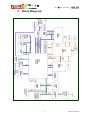
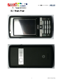
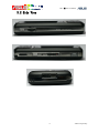
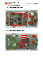
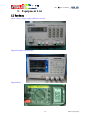
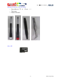
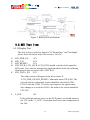
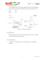
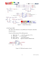
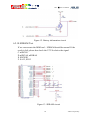
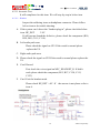
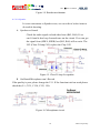
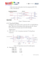
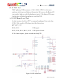
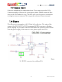
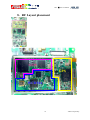
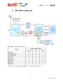
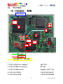
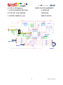
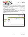
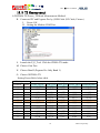
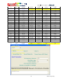
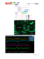
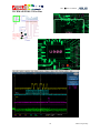
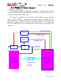
GTC ■ Service Manual
ASUS P750 Repair Guide
(Level 3 4)
Ver 1.0b
1
ASUS Proprietary
華碩電腦
GTC ■ Service Manual
CONTENT
1.
PRODUCT GENERAL SPECIFICATION............................................. 4
2.
BLOCK DIAGRAM................................................................................... 6
3.
APPEARANCE........................................................................................... 7
3.1 FRONT VIEW ................................................................................................ 7
3.2 SIDE VIEW ................................................................................................... 8
4.
PCB PLACEMENT.................................................................................... 9
4.1 MAIN BOARD TOP VIEW .............................................................................. 9
4.2 MAIN BOARD BOTTOM VIEW ...................................................................... 9
5.
EQUIPMENT LIST ................................................................................. 10
5.1
6.
HARDWARE .......................................................................................... 10
TROUBLE SHOOTING CASE .............................................................. 12
6.1 SYSTEM CAN’T BOOT!................................................................................ 12
6.1.1 Power on sequence ............................................................................ 12
6.1.2 CPU BGA .......................................................................................... 13
6.1.3 NAND Flash ...................................................................................... 13
6.2 MMI TEST ITEM ........................................................................................ 14
6.2.1 Display Test ....................................................................................... 14
6.2.2 Vibrator Test...................................................................................... 15
6.2.3 RTC Test............................................................................................. 15
6.2.4 Storage Test ....................................................................................... 15
6.2.5 Micro SD Test .................................................................................... 16
6.2.6 LED Test ............................................................................................ 16
6.2.7 Camera Test & VGA Camera............................................................ 18
6.2.8 Check SIM ......................................................................................... 20
6.2.9 Battery Test........................................................................................ 21
6.2.10 SDRAM Test .................................................................................... 22
6.2.12 Turn On/Off Radio........................................................................... 25
6.2.13 Version Check.................................................................................. 27
6.2.14 Keypad Test ..................................................................................... 27
6.2.15 WiFi Board-Level Test .................................................................... 29
2
ASUS Proprietary
華碩電腦
GTC ■ Service Manual
6.2.16 GPS Firmware Update.................................................................... 29
6.2.17 PS Board-Level Test ........................................................................ 29
6.2.18 TMC Test ......................................................................................... 30
6.2.19 BT Board-Level Test........................................................................ 30
7.
POWER CONSUMPTION ..................................................................... 31
7.1 POWER OVER STANDARD............................................................................ 31
7.2 CPU CONSUMPTION TOO HIGH .................................................................. 31
7.3 CAMERA SHORT ......................................................................................... 32
7.4 Others ................................................................................................ 32
8.
RF LAYOUT PLACEMENT .................................................................. 33
9.
RF BLOCK DIAGRAM .......................................................................... 34
9.1 TRANSMIT MODE ....................................................................................... 36
10.
WCDMA................................................................................................ 40
10.1 PLACEMENT - WCDMA .......................................................................... 40
10.2 WCDMA TX PATH ................................................................................. 42
10.3 TX MEASUREMENT.................................................................................. 43
10.4 TEST PROCEDURE:.................................................................................... 45
10.5 WCDMA RX .......................................................................................... 51
10.6 WCDMA RX PATH MEASUREMENT ....................................................... 53
10.7 RX TEST PROCEDURE .............................................................................. 54
10.8 WCDMA PA POWER CONTROL .............................................................. 60
3
ASUS Proprietary
華碩電腦
GTC ■ Service Manual
1. Product General Specification
Networking system
HSDPA 3.6Mbps, UMTS 2100,
EDGE/GSM 900/1800/1900; GPRS Class B
Operating System
Microsoft Windows Mobile 6 Professional
CPU
Marvell PXA270M 520MHz
Dimensions
113 x 58 x 17.4 mm, 130g
Battery
1300 mAh Lithium-Ion
Talk time
300 mins for 3G, 360 mins for 2G
Standby time
240 hours for 3G, 220 hours for 2G
Form Factor
Bar type with numeric keypad
Color
Black
Display
2.6“ Touch Screen / 65K TFT LCD / 240 x 320
Connectivity
WLAN 802.11 b+g / Bluetooth 2.0+EDR /
USB v1.1
Browsing
HTML 4.01, WAP 2.0 (IE)
Messaging
SMS/MMS/Email/MSN/Push E-mail
Memory
256 MB Flash + 64 MB SDRAM
Expansion Slot
Micro-SD (SDHC supports)
GPS
GPS (SiRF III with internal antenna), AGPS
(need to co-work with local operators) , TMC
(optional cable)
JAVA
J2ME (CLDC 1.1 + MIDP2.0)
Camera
3 Mega-Pixel (Auto focus)
Audio
MP3, WMA, AAC, AAC+, 3GP
4
ASUS Proprietary
華碩電腦
GTC ■ Service Manual
Video
MPEG4 / H.263 Playback and Recording
Ringtone
128-ch Polyphonic ringer & MP3
PIM/Utilities
Notes, Calendar, Alarm, and Windows Live
Messenger, Word (editor), Excel (editor), and
Power Point (viewer)
Advanced
Ur Time,
Backup,
ASUS Launcher,
Voice Commander,
Bluetooth Remote Presenter,
Travelog,
Location courier,
Business Card Recognition,
Newstation,
Meeting planner,
Auto cleaner,
GPS catcher,
OMA DRM V2.0
5
ASUS Proprietary
華碩電腦
2. Block Diagram
GTC ■ Service Manual
6
ASUS Proprietary
華碩電腦
3. Appearance
GTC ■ Service Manual
3.1 Front View
7
ASUS Proprietary
華碩電腦
GTC ■ Service Manual
3.2 Side View
8
ASUS Proprietary
華碩電腦
4. PCB Placement
GTC ■ Service Manual
4.1 Main Board Top View
Logic
Block
WIFI
PWR_EN
BAT_FAULT#
U44
MODE
M
VBAT
SYS_EN
V_BKBT
4.2 Main Board Bottom View
con1
con3
U1
U90
U42
U600
9
ASUS Proprietary
華碩電腦
5. Equipment List
GTC ■ Service Manual
5.1 Hardware
Power source: power supply (Monitor current)
Digital Phosphor Oscilloscope
Digital Meter
10
ASUS Proprietary
華碩電腦
GTC ■ Service Manual
Mechanical Auxiliary Tool & tooling
‧ Screwdriver ( T5 *
‧ Tweezers
‧ Plastic Wrench
Cross + )
Micro SD
11
ASUS Proprietary
華碩電腦
6. Trouble shooting Case
GTC ■ Service Manual
6.1 System can't Boot!
The main of the reason is related for component short and incorrect in
“Power-On Sequence” issues. First, we can check the Current of the device
during the OS booting process then try to measure the “Power ON
Sequence”. In P750 design concept; The System will auto Power On in two
conditions One is first connect to device, another the voltage drop below
2.8V from backup battery. If the voltage more than 2.8V, the system should
not booting automatically. It is recommendation for hold on the reset button
until the power supply working when we want to make sure the OS booting
process is activated.
6.1.1 Power on sequence
Please check “Power on Sequence“ for each Voltage:
A. V_BAT = power supply voltage
The proposal of V_BAT is for System power.
The check point is C228.1
B. V_BKBT = 3.3V
If V_BKBT < 3.3V,Must inspect the soldering status to eliminate
the component U44 defective ( floating and diode reverse issue ) .
It will cause the charged failure for the backup battery and OS
booting abnormal.
C. VCC_3.0V, VCC_1.8V, VCC_CORE > 1.3V, VCC_PLL = 1.3V,
VCC_SRAM = 1.1V
If found the incorrect of the voltage then we can try to check the
soldering floating or mistake component (U41, L8, L9, L10).
D. SYS_EN = 2.9V
E. PWR_EN = 2.9V
The Item C is noraml but the SYS_EN / PWR_EN< 2.9V.It always the solder
issue for CPU( U1). Try to rework the U1 and replace it.
12
ASUS Proprietary
華碩電腦
GTC ■ Service Manual
F. BAT_FAULT# = 3.3V
Please check the floating and diode reverse issue on the component (C337, U33,
U50) .
6.1.2 CPU BGA
If the device still didn’t work after item 1 trace, we can measure the signal
T12 ( NAND_CS# ) should be get the high-low transition by oscillate
scope. Check the data response from TP28 (SD15). If the answer is well it
maybe the CPU BGA issue or Chip defective. We can change the CPU to
improve the situation. According the manufacture experience for the CPU
which replace in time will be failure for the work.
6.1.3 NAND Flash
In Item 2, if the data can’t response from TP28 ( SD15 ), in my opinion is
try to re-flash the data to NAND flash via JTAG.
Figure 1. PMU
13
ASUS Proprietary
華碩電腦
GTC ■ Service Manual
Figure 2. Battery fault mechanism
6.2 MMI Test Item
6.2.1 Display Test
The item is focus verify the function ”LCM interface” and ”backlight”,
please check the below item if the result is “No Go”.
A.
B.
C.
D.
LCD_PWR_EN
1.8V
LCD_3.0V
2.9V
LCD_RESET#
2.9V
LCD_FCLK, LCD_LCLK, LCD_PCLK should exist the clock signal for
LCD panel. If we can not measure the signal should be check the soldering
/floating each side on resistor (R19, R20, R21).
E. LCD_DATA_EN 2.9V,
The white screen will happen from above items. If
“LCD_PWR_EN/LCD_RESET#” abnormal mean CPLD NG. The
color deviation or abnormal expose should be check the LCD0 ~
LCD15 with the CON1. If we can’t get improve the signal status
after change or re-work the CON1, the main of the reason should be
CPU NG.
F. V_LED
12V
If the backlight can not active on the LCD panel, we should measure
the 12V on the “V_LED”. If not then check the relate components of
the U48.
14
ASUS Proprietary
華碩電腦
GTC ■ Service Manual
6.2.2 Vibrator Test
It is less probity low for the item” board-level fail”. We can check the
below status for charge the U86 SMT or component defective issue.
U86.4
2.9V
U86.1
3.3V
Figure 3. Vibrator mechanism
6.2.3 RTC Test
We can measure the 32.768 for X2 clock signal. We can try to replace
the CPU and X2 on this item failure.
6.2.4 Storage Test
It should be U6 (Flash memory) on soldering issue or component
defective.
15
ASUS Proprietary
華碩電腦
GTC ■ Service Manual
6.2.5 Micro SD Test
We can check the below signal list to verify the Micro SD function.
A. MMC_PWR_EN 2.9V ->If not U600 NG.
2.9V->If not check U87 soldering issue.
B. MMC_3.0V
Figure 4. micro SD Power
Ps. The position of the Micro SD Socket had the mechanical position
declination. So the SD card still exist detect but it will cause lodged for
SD insert at assembly test.。
6.2.6 LED Test
The test item is for Red, blue, green Led die and key pad LED could
works. The scenario will step by step to follow the
circle ”Red->Green->Blue” on indicated LED. After the LED twinkled
at 1 Hz then keypad white LED also twinkle the key panel.
A. RGB LED Abnormal
The RGB LED signal is controlled by CPLD. The behavior code is
no exist in CPLD which will cause the RGB LED always
illuminated red light. Please replace the CPLD on PCB.
If one of the colors can’t works on RGB LED, please check the
soldering issue on R621, R622, R623 or replace the LED600.
16
ASUS Proprietary
華碩電腦
GTC ■ Service Manual
Figure 5. Indication LED Circuit
B. Keypad LED failure
Please measure the U88.4 (KEY_LED_EN) ->2.9V,if the result is
true please check the U88.
Figure 6. Keypad LED power
17
ASUS Proprietary
華碩電腦
GTC ■ Service Manual
6.2.7 Camera Test & VGA Camera
The main of the reason is for assembly issue and component defective.
The camera’s function can’t work on component defective issue. For
example: dirty lens, can’t auto focus.
Caution: The VGA socket didn’t support one direction assembly. If
VGA camera direction incorrect, it will cause the booting failure.
If the above the item already finish, try to refer to below issue.
CMOS_3.0V
2.8V
VAAM
2.8V (For Auto focus Motor power Source)
Figure 7. Camera power
The 3M camera and VGA signal:
VC_I2C_SCL, VC_I2C_SDA, CIF_DD0 ~ CIF_DD7.
The CPLD control signal
a. 3M: SENSOR_2M_PD = 0V, SENSOR_2M_RST# = 2.9V,
SENSOR_2M_CLKEN = 2.9V
b. VGA: SENSOR_VGA_PD = 0V, SENSOR_VGA_RST# = 2.9V,
SENSOR_VGA_CLKEN = 2.9V
If the signal is abnormal please try to change U600 ( CPLD).
18
ASUS Proprietary
華碩電腦
GTC ■ Service Manual
Figure 8. Camera control signal
19
ASUS Proprietary
華碩電腦
GTC ■ Service Manual
Figure 9. Camera clock source
6.2.8 Check SIM
The main of the function is verify SIM card, If fail please check the
below the items.
Check the SIM connector Pin soldering status.
I.
II.
III.
IV.
SIM_VCC_R
1.8/3.3V ( general is 3.3V )
SIM_RST
0V ( Read mode ),
SIM_CLK_R
clock (Read mode)
SIM_DAT_R
high-low transition (Read mode)
Figure 10. SIM card connector circuit
20
ASUS Proprietary
華碩電腦
GTC ■ Service Manual
6.2.9 Battery Test
The main of the function verify electricity charging ability and battery
ID information. If the result is failure please check below items to
repair.
A. Can’t charging
I. Check the U12.4 ( CHARGER_LDO_2.8V)
2.9V
II. Check the R181.2 ( CHGR_VUSB)
5V
III. Check the PSEL
2.9V,If not
U600 ( CPLD) NG.
If all of results are true then U38 (Charger IC) is NG.
Figure 11. Charger IC circuit
B.
Can’t read the battery ID
Check the HDQ_TXD#_PLD and HDQ_RXD_PLD signal. The
signal will be detect for a period on the correct status. If the can’t
detect then should re-place the U600 (CPLD) NG.
21
ASUS Proprietary
華碩電腦
GTC ■ Service Manual
Figure 12. Battery information circuit
6.2.10 SDRAM Test
If we can execute the MMI tool,SDRAM should be normal. If the
result is fail, please also check the U7/U8 relative the signal.
C. nSDCS0
D. nSDCAS, nSDRAS
E. SDCKE1
F. SA12, SD15
Figure 13. SDRAM circuit
22
ASUS Proprietary
華碩電腦
GTC ■ Service Manual
6.2.11 Acoustic Test
It will complicate for this item. We will step by step in below item
6.2.11.i Headset
Inspect the soldering issue on headphone connector. Please follow
below item to do trouble shooting.
A. If the system can’t detect the “headset plug in”, please check the below
item. HP_DET
2.9V
If still can not found the defective, please check the component (R56,
R59, R62, C115, C118).
B. Left audio path error
Please check the signal on CE1.If the result is normal please
replace the U9.
C. Right audio path error
D. Please check the signal on CE2.If the result is normal please replace the
U9.
E. Can’t Record
First check the voice signal on MIC_HEADSET_R. If didn’t
work please check the component (R55, R57, C120, C112,
C123).
F. Can’t Exit the headset mode
Please check HP_DET ->0V,If the answer is not please refer to
item A.
23
ASUS Proprietary
華碩電腦
GTC ■ Service Manual
Figure 14. Headset mechanism
6.2.11.ii Speaker
It is not concentrate to Speaker error, we can refer to below items to
do trouble shooting.
A. Speaker no Sound
Check the audio signal on both sides from (R65, R66). If we
can’t found it also keep forward trace on the circuit. If we can get
the signal from (SPKL, SPKR) but (R65, R66) still no exist. The
U42 (Class-D Amp) NG, replace the Chip U42.
Figure 15. Class D Amp for speaker
B. On-Board Microphone can’t Record
If the quality is poor please change the U11. If the function total un-work please
check the (L1, C121, C124, C125, 126).
Figure 16. Microphone circuit
24
ASUS Proprietary
華碩電腦
GTC ■ Service Manual
6.2.11.iii Receiver
If the receiver no sound, please check the component (R67, R79,
C128, C129, D4, D5).
Figure 17. Receiver circuit
6.2.12 Turn On/Off Radio
On Pegasus p, the switch on/off is control by CPU via UART/SPI inter
phase. The power of the modem will not shut down by CPU. Please
refer to below issue step by step to do trouble shooting!
Modem Power
G. CCPU_VCC-> 3.6V. if not please check the U75 (Step-Down
Converter).
Figure 18. Step-down converter for modem power
H. Check below item
VDD_1V5
VDD_1V8
VDD_2V75
VDD_2V85
1.5V
1.8V
2.75V
2.85V
25
ASUS Proprietary
華碩電腦
GTC ■ Service Manual
If the signal is incorrect please replace the U700.
a. Please check the RTC_CLK-> 32.768 KHz clock. If no please
replace the X700.
Figure 19. Modem RTC
I.
Modem to System Interface
The main of the purpose is level shift on CPLD between Modem and
System. We can check the component (R711 ~ R715, R763 ~ R766),
If the result is normal then try to change the U600 (CPLD).
26
ASUS Proprietary
華碩電腦
GTC ■ Service Manual
Figure 20. Modem/CPU interface
6.2.13 Version Check
The purpose of the test checks the protocol. If this item failure, pleas
refer to the item12 to do trouble shooting.
6.2.14 Keypad Test
Keypad test can separate for board-level test and assembly test. The
board-level just for SMT. It just make sure the logic path on keypad
matrix. Each path of row/column from keypad driver IC to CPU is well.
So we use the specify button to cover all of key test on the
keyboard .During the assembly station, all of the button must be pressed
by OP according the physical issue.
A. Board level test
The specify key include(joy dial up, joy dial down, joy dial action, 4,
8, clear, #) The P750’s keypad matrix contain for (row * 6,
column*5). At least we need 6 buttons to fully cover each trace, it is
weak for joy dial on 3 XYZ direction test.
We also can know the signal is form which (rows and columns)!
For example the key “Clear” is contains for (row 4 + column 1).
If the function of the key “Clean” is failure, then we can trace the
component (RN16 and RN18). If the result is well then we can
change the U90. SMT or component defective issue.
If every key are useless then should be U90. We can check the voltage on
the R168.The signal on the resistor is “interrupt#”. In general, the voltage
should be 2.6V. Next step is measure the R169. The signal on R169 is
27
ASUS Proprietary
華碩電腦
GTC ■ Service Manual
watchdog reset# for Keypad IC for itself. If the “interrupt#” and
“watchdog reset#” are0~2.6V, it always cause abnormal on U90. We can
try to re-heat the chip U90 or replace it.
Figure 21. Keypad driver circuit
Figure 22. Keypad matrix
28
ASUS Proprietary
華碩電腦
J.
GTC ■ Service Manual
Assembly test
During assembly keypad test fail. We can easy handle the problem
on FPC connector. (FPC connector or Main board connector,
Metal dome position deviation).
6.2.15 WiFi Board-Level Test
If the test item fail, we can check the voltage of the (+3.3V_WLAN,
+1.5V_WLAN). The result is pass please try to change U13.
6.2.16 GPS Firmware Update
It we can’t update the GPS firmware, please check below issue:
A. GPS_PWR_EN
2.9V
B. +2.85V_GPS_BB
2.85V
C. GPS_TX, GPS_RX
Signal
The power of the chip is well. We still can’t get the signal from
GPS_TX, GPS_RX. Please check the R1011 -> 47K ohm? If the
answer is true then try to change the U600.
6.2.17 PS Board-Level Test
Follow the test item 16.
Figure 23. GPS power
29
ASUS Proprietary
華碩電腦
GTC ■ Service Manual
6.2.18 TMC Test
TMC pathway: USB connector->U60->U600->CPU. It is the same
pathway which cpu read battery information. We can use the Battery ID
test result to help us verify the hardware circuit. If the battery ID is pass
but this item is failure then please re-work the U60.
6.2.19 BT Board-Level Test
In this item just check the CPU’s command sending to blue tooth chip
(U20). If the result is NG please check the below item.
BT_VCC_3.3V
R104, R111
USB signal
R102, R104, R110, R111, R112
USB protocol check
If all of item is pass , please re-work the chip U20.
Figure 24. BT connection
30
ASUS Proprietary
華碩電腦
7. Power Consumption
GTC ■ Service Manual
7.1 Power over standard
In the assembly line we will follow below procedure to do power
consumption test.
A. The device connects the power sourcing via dummy battery.
B. Open the mobile phone.
C. Close the modem part. -> Disable the phone.
D. Lock the hold key let the phone into idle mode.
E. Read the counter on the power supply.
F. Check the power consumption between 45~60mA, over 60 mA is NG.
The reason, camera circuit short; which will lead to the booting failure.
7.2 CPU consumption too High
If the CPU power consumption too High Æ 60~80mA, We can remove
the R217 try to cut off the power drain to CPU. The current is supply
the v_core on CPU. After remove the resistor R217 we can use the
power meter to measure the current on the circuit. The reference value
is below 10mA. If over the value we can try to change the CPU to
extend the idle time.
Figu
re 25. VCC core source
31
ASUS Proprietary
華碩電腦
GTC ■ Service Manual
7.3 Camera short
It has two saturations for camera short issue. The wrong way on the VGA
Camera assembly will cause the system power short. Another reason is fiber
short on the 3M conductive tape. The fiber will cause the power consumption
too high on camera connector. We can get the evidence from microscope.
7.4 Others
The idle power consumption is 80~150mA in few devices. The main of the
reason is for U951 NG. The U951 is response DC/DC converter to Modem
power amplify. Try to remove the R951 and detect the system’s power current
from the power supply. If the answer is true please replace the U951.
Figure
26. DC/DC converter for wideband PA
32
ASUS Proprietary
華碩電腦
GTC ■ Service Manual
8. RF Layout placement
GSM
GPS
WCDMA
33
ASUS Proprietary
華碩電腦
GTC ■ Service Manual
9. RF Block Diagram
RF FEM
Signal True table
The value “1” means level High , “0” means Level Low.
34
ASUS Proprietary
華碩電腦
GTC ■ Service Manual
E-GSM 900 Power (PL5)
35
ASUS Proprietary
華碩電腦
GTC ■ Service Manual
850/EGSM: PL5 1.29(V) ;PL19 0.27(V)
1800/1900: PL0 1.28(V) ;PL 15
R
T
9.1 Transmit Mode
36
ASUS Proprietary
華碩電腦
GTC ■ Service Manual
To Antenna
3
4
Antenna
I,Q,AMP
5
Switch
1
6
7
2
TX path
RX path
TX 900/850path
TX 1800/1900path
1. U900:
GSM Transceiver
RF3000
2. U901:
Power Amplifier
SKY77513
3. BPF900 : SAW FILTER
BG :850MH
4. BPF901 : SAW FILTER
TA : 900MH
5. BPF902 : SAW FILTER
LF : 1800MH
6. BPF902 : SAW FILTER
SW : 1900MH
7. OSC900:
NDK/W-168-281
37
26MHz Crystal
ASUS Proprietary
華碩電腦
GTC ■ Service Manual
VCCA:
VCCD:
1:C902
2:C903
3:C906
U900
4:C931
OSC900
U901
5:R983
6:R927
OSC 900: 26MHz
Tx Mode
38
ASUS Proprietary
華碩電腦
GTC ■ Service Manual
--TX
U900
U901
1:C92
39
ASUS Proprietary
10.
華碩電腦
WCDMA
GTC ■ Service Manual
10.1 Placement - WCDMA
To Antenna
Antenna
9
1
7
5
3
4
WRX-IQ
WTX-IQ
8
2
6
LNA
TX path
RX path
WCDMA TX / RX path
1. U901: GSM Power Amplifier
SKY77513
2. U950: WCDMA Transceiver
RF3100
3. U953: WCDMA Power
Amplifier SKY77174
4. U955: COUPLER
LDC181G9519B-327
5. U954: ISOLATOR
CES201G95DCB000
40
ASUS Proprietary
華碩電腦
GTC ■ Service Manual
6. U956: SAW Duplexer
MURATA1G95AA0B00R057
7. U952: POWER DETECTOR
LMV221SD
8. U951: DC CONVERTER
LM3208TL
9. OSC900: 26MHz Crystal
NDK/W-168-281
DB3150
DB3150
DB3150
41
ASUS Proprietary
華碩電腦
GTC ■ Service Manual
10.2 WCDMA TX Path
In Transmitter mode.
The signal (WTX_I_P, WTX_I_N, WTX_Q_P, WTX_Q_N) from Base Band
DB3150 emit to RF antenna via U950.4. The RF3100 (U950) is WCDMA
TRANSMITTER IC will include the frequency boost /frequency locking circuit
for WCDMA TX pathway.
Later the WCDMA TX signal will pass power amplify on the WCDMA PA
SKY77174 via Band Passes SAW Filter (BPF1950). In the same time, it will be
processed by matching circuits sequentially.
The output power passes through coupler (U955), isolator (U954), duplexer
(U956), to the T/R switch (U901) on the FEM (SKY77513). Finally the power
will radiated via matting circuit and connector (Con900).
WCDMA TX Schematic path
42
ASUS Proprietary
華碩電腦
GTC ■ Service Manual
10.3 TX Measurement
A WCDMA TX Power_TP Mode Measurement Method:
K. Connected PC and Pegasus Pro by (USB Cable ,RF Cable, Fixture )
I. Power ON .
II. Setting the Modem COM Port.
L. Launch the P_E_Tool. Click the CDMA TX mode.
M. Choose Com Port
N. Choose Band I (Pegasus Pro Only Band I )
O. Choose WCDMA TX
Setting Power Refer below table
WTXC,1,poistion
Poisition Power
86
85
25.65
84
25.43
83
24.85
82
24.15
81
23.08
80
21.32
79
20.7
78
19.31
77
18.33
76
17.25
75
11.74
<ADC_Target>
0x3A7
0x391
0x378
0x361
0x361
0x336
0x31E
0x30A
0x2F4
0x2DD
0x2C6
0x2B0
TTOL,1,poistion
<APC_Init> <DPC_Init> <WPA_Bias>
0x372
0x3FF
0x21E
0x365
0x3FF
0x21E
0x35A
0x3FF
0x208
0x350
0x3FF
0x1F3
0x350
0x3FF
0x1F3
0x342
0x3FF
0x1C8
0x340
0x3FF
0x1B3
0x33D
0x3FF
0x19E
0x33B
0x3FF
0x188
0x336
0x3FF
0x173
0x331
0x3FF
0x15E
0x32E
0x3FF
0x148
43
<WDCDCREF>
0x20C
0x20C
0x1FC
0x1EB
0x1EB
0x1AA
0x168
0x147
0x127
0x116
0x106
0xF5
ASUS Proprietary
華碩電腦
GTC ■ Service Manual
74
73
72
71
70
69
68
67
66
65
64
63
62
61
60
50
40
30
20
10
0
10.87
9.67
8
7.85
6.67
5.8
4.72
3.64
2.7
1.68
0.61
-0.42
-1.38
-2.42
-3.4
-13.97
-24.28
-34.1
-40.54
-42.34
-42.32
0x29B
0x285
0x26E
0x258
0x241
0x229
0x216
0x1FF
0x1EA
0x1D2
0x1BB
0x1A5
0x190
0x179
0x164
0xCC
0xAE
0xAB
0xAA
0xAA
0xAA
0x32C
0x323
0x31B
0x313
0x30B
0x304
0x2FB
0x2F0
0x2E6
0x2DB
0x2D0
0x2C5
0x2BB
0x2B0
0x2A6
0x243
0x1ED
0x19B
0x14D
0xFF
0xAD
0x3FF
0x3FF
0x3FF
0x3FF
0x3FF
0x3FF
0x3FF
0x3FF
0x3FF
0x3FF
0x3FF
0x3FF
0x3FF
0x3FF
0x3FF
0x3FF
0x3FF
0x3FF
0x3FF
0x3FF
0x3FF
0x133
0x11E
0x108
0xF3
0xDE
0xC8
0xC8
0xC8
0xC8
0xC8
0xC8
0xC8
0xC8
0xC8
0xC8
0xC8
0xC8
0xC8
0xC8
0xC8
0xC8
0xE5
0xE5
0xE5
0xE5
0xE5
0xE5
0xE5
0xE5
0xE5
0xE5
0xE5
0xE5
0xE5
0xE5
0xE5
0xE5
0xE5
0xE5
0xE5
0xE5
0xE5
73
9.67
0x285
803
1023
286
229
44
ASUS Proprietary
華碩電腦
GTC ■ Service Manual
10.4 Test procedure:
TX channel set to 9750 (TX frequency = 1950MHz), Module Type=1,
Power Position=81, use the spectrum to measure the value.
Spectrum Setting: Freq=1950MHz. Caution: Must add the attenuator/DC
Blocking or series connection 100PF Cap on the end of the Cable. It will avoid
the direct current damage the spectrum authentically.
The Power values all are relativity not absolute.
R968.1
45
ASUS Proprietary
華碩電腦
GTC ■ Service Manual
C975.1
46
ASUS Proprietary
華碩電腦
GTC ■ Service Manual
WCDMA TX Path_Power Sensor_pin6
U954.6
47
ASUS Proprietary
華碩電腦
GTC ■ Service Manual
WCDMA TX Path Isolator Output_L901
L901
48
ASUS Proprietary
華碩電腦
GTC ■ Service Manual
WCDMA TX Path Duplexer Output_R979
49
ASUS Proprietary
華碩電腦
GTC ■ Service Manual
WCDMA TX Path RF Connector
50
ASUS Proprietary
華碩電腦
GTC ■ Service Manual
10.5 WCDMA RX
In Receiver Mode. Receive the radiation signal from base station via phone
antenna. The signal passes through Band select of U901 GSM-FEM (T/R switch
+ SAW filter) and Duplexer (U956) sequentially.
WCDMA TRANSMITTER IC RF3100 (U950), built-in LNA, receives the
signal from duplexer.
Then the signal is transmitted to RX-SAW filter (BPF950) and returns to Mixer
input on the WCDMA TRANSMITTER IC RF3100(U950) PIN X1_A ,MX1_B
again.
After down converting the signal’s frequency and transforming into IQ signals,
the IQ signals (WRX_I_P, WRX_I_N, WRX_Q_P, WRX_Q_NMAX2391)
travel to Base Band IC DB3150 (U701).
WCDMA RX Path Schematic_1
51
ASUS Proprietary
華碩電腦
GTC ■ Service Manual
WCDMA RX Path Schematic_2
52
ASUS Proprietary
華碩電腦
GTC ■ Service Manual
10.6 WCDMA RX Path Measurement
WCDMA RX TP Mode Measure method
A. Connected PC and Pegasus Pro by (USB Cable ,RF Cable, Fixture )
Power ON .
Setting the Modem COM Port.
B. Launch the P_E_Tool. Click the CDMA TX mode.
C. Choose Com Port
D. Choose Band I (Pegasus Pro Only Band I )
E. Choose WCDMA RX
F. Setting the WCDMA RX channel, please set the Agilent 8960 to CW
mode .The power: -30 ~ -40dBm
53
ASUS Proprietary
華碩電腦
GTC ■ Service Manual
10.7 RX Test procedure
TX channel set to 10700 (RX frequency = 2140MHz), please set the Agilent
8960 to CW mode .The power: -30 ~ -40dBm.
Spectrum Setting: Freq=2140MHz. Caution: Must add the attenuator/DC
Blocking or series connection 100PF Cap on the end of the Cable. It will avoid
the direct current damage the spectrum authentically.
The Power values all are relativity not absolute.
R983.2
54
ASUS Proprietary
華碩電腦
GTC ■ Service Manual
WCDMA RX Path LNA Output_U950 pin29
55
ASUS Proprietary
華碩電腦
GTC ■ Service Manual
WCDMA RX Path Mixer Input_B
56
ASUS Proprietary
華碩電腦
GTC ■ Service Manual
WCDMA TX Path I, Q
57
ASUS Proprietary
華碩電腦
GTC ■ Service Manual
58
ASUS Proprietary
華碩電腦
GTC ■ Service Manual
WCDMA RF3100 3 Wire Bus
59
ASUS Proprietary
華碩電腦
GTC ■ Service Manual
10.8 WCDMA PA Power Control
WCDMA TX PA principle
In Transmitter mode, the signal power amplify is contain by (PA, DC/DC
Converter and Transmit Power Detector). The purpose of DC/DC Converter is
for power souring stability drives PA.
Total signal is amplified by PA which be weak 19dB by Coupler (U955).
After is weak 15dB by attenuator, the signal output to RFIN PIN on
LMV221SD (U952). When the WPOW_DET_EN = High on the DB3150, the
signal will output to the D/A converter on the RF3100 via 3-wire Bus. The
RF_DAC1 and RF_DAC2 used to the Power level control by (PA and DC/DC
converter).
WPOW DET EN
Power
WPOW_DET
DC/DC
Couple
WDCDC_EN
WCDMA
From RF3100
PA
TX Output
WB+EGG
WCDMA
Transceiver
Digital BB
CTRL_DATA
CTRL_StrB
Controller
CTRL_Clock
DB 3150
WBCLK
60
ASUS Proprietary
華碩電腦
GTC ■ Service Manual
61
ASUS Proprietary