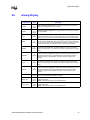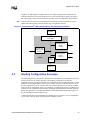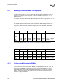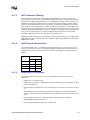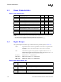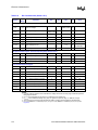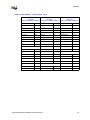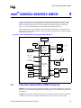
1
Intel® 845G/845GL/845GV Chipset
Datasheet
Intel® 82845G/82845GL/82845GV Graphics and Memory Controller
Hub (GMCH)
October 2002
Document Number: 290746-002
INFORMATION IN THIS DOCUMENT IS PROVIDED IN CONNECTION WITH INTEL® PRODUCTS. NO LICENSE, EXPRESS OR IMPLIED, BY
ESTOPPEL OR OTHERWISE, TO ANY INTELLECTUAL PROPERTY RIGHTS IS GRANTED BY THIS DOCUMENT. EXCEPT AS PROVIDED IN
INTEL'S TERMS AND CONDITIONS OF SALE FOR SUCH PRODUCTS, INTEL ASSUMES NO LIABILITY WHATSOEVER, AND INTEL DISCLAIMS
ANY EXPRESS OR IMPLIED WARRANTY, RELATING TO SALE AND/OR USE OF INTEL PRODUCTS INCLUDING LIABILITY OR WARRANTIES
RELATING TO FITNESS FOR A PARTICULAR PURPOSE, MERCHANTABILITY, OR INFRINGEMENT OF ANY PATENT, COPYRIGHT OR OTHER
INTELLECTUAL PROPERTY RIGHT. Intel products are not intended for use in medical, life saving, or life sustaining applications.
Intel may make changes to specifications and product descriptions at any time, without notice.
Designers must not rely on the absence or characteristics of any features or instructions marked “reserved” or “undefined.” Intel reserves these for
future definition and shall have no responsibility whatsoever for conflicts or incompatibilities arising from future changes to them.
The Intel 845G/845GL/845GV chipsets may contain design defects or errors known as errata which may cause the product to deviate from published
specifications. Current characterized errata are available on request.
Contact your local Intel sales office or your distributor to obtain the latest specifications and before placing your product order.
I2C is a two-wire communications bus/protocol developed by Philips. SMBus is a subset of the I 2C bus/protocol and was developed by Intel.
Implementations of the I2C bus/protocol may require licenses from various entities, including Philips Electronics N.V. and North American Philips
Corporation.
Intel, Pentium, and the Intel logo are trademarks or registered trademarks of Intel Corporation or its subsidiaries in the United States and other
countries.
*Other names and brands may be claimed as the property of others.
Copyright © 2002, Intel Corporation
2
Intel® 82845G/82845GL/82845GV GMCH Datasheet
Contents
1
Introduction ...........................................................................................................13
1.1
1.2
1.3
1.4
2
Signal Description ..............................................................................................21
2.1
2.2
2.3
2.4
2.5
2.6
2.7
2.8
2.9
2.10
2.11
2.12
3
Terminology ...................................................................................................13
Related Documents .......................................................................................14
Intel® 845G Chipset System Overview ..........................................................15
Intel® 82845G GMCH Overview....................................................................17
1.4.1 Host Interface....................................................................................17
1.4.2 System Memory Interface .................................................................17
1.4.3 Hub Interface ....................................................................................17
1.4.4 Multiplexed AGP and Intel® DVO Port Interface ...............................18
1.4.5 Graphics Overview............................................................................18
1.4.6 Display Interfaces .............................................................................19
Host Interface Signals....................................................................................23
Memory Interface ...........................................................................................25
2.2.1 DDR SDRAM Interface .....................................................................25
2.2.2 SDR SDRAM Interface .....................................................................26
Hub Interface .................................................................................................28
AGP Interface Signals....................................................................................29
2.4.1 AGP Addressing Signals...................................................................29
2.4.2 AGP Flow Control Signals ................................................................29
2.4.3 AGP Status Signals ..........................................................................30
2.4.4 AGP Strobes .....................................................................................30
2.4.5 PCI Signals–AGP Semantics............................................................31
2.4.6 PCI Pins during PCI Transactions on AGP Interface ........................32
Multiplexed Intel® DVO Device Signal Interfaces ..........................................32
2.5.1 Intel® DVO Signal Name to AGP Signal Name Pin Mapping............34
Analog Display ...............................................................................................35
Clocks, Reset, and Miscellaneous Signals ....................................................36
RCOMP, VREF, VSWING Signals.................................................................36
Power and Ground Signals ............................................................................37
Functional Straps ...........................................................................................38
GMCH Sequencing Requirements.................................................................38
Reset States ..................................................................................................39
2.12.1 Full and Warm Reset States .............................................................39
Register Description ..........................................................................................41
3.1
3.2
3.3
3.4
3.5
Register Terminology.....................................................................................41
Platform Configuration ...................................................................................42
Routing Configuration Accesses....................................................................43
3.3.1 Standard PCI Bus Configuration Mechanism ...................................44
3.3.2 PCI Bus #0 Configuration Mechanism ..............................................44
3.3.3 Primary PCI and Downstream Configuration Mechanism.................44
3.3.4 AGP/PCI_B Bus Configuration Mechanism ......................................44
I/O Mapped Registers ....................................................................................46
3.4.1 CONFIG_ADDRESS—Configuration Address Register ...................46
3.4.2 CONFIG_DATA—Configuration Data Register ................................47
Intel® GMCH Internal Device Registers .........................................................48
Intel® 82845G/82845GL/82845GV GMCH Datasheet
3
3.5.1
3.5.2
4
DRAM Controller/Host-Hub Interface Device Registers (Device 0) .. 48
3.5.1.1 VID—Vendor Identification Register (Device 0) ................ 50
3.5.1.2 DID—Device Identification Register (Device 0)................. 50
3.5.1.3 PCICMD—PCI Command Register (Device 0) ................. 51
3.5.1.4 PCISTS—PCI Status Register (Device 0) ......................... 52
3.5.1.5 RID—Revision Identification Register (Device 0) .............. 53
3.5.1.6 SUBC—Sub-Class Code Register (Device 0) ................... 53
3.5.1.7 BCC—Base Class Code Register (Device 0).................... 53
3.5.1.8 MLT—Master Latency Timer Register (Device 0) ............. 54
3.5.1.9 HDR—Header Type Register (Device 0) .......................... 54
3.5.1.10 APBASE—Aperture Base Configuration Register
(Device 0)............................................................................. 55
3.5.1.11 SVID—Subsystem Vendor Identification Register
(Device 0)............................................................................. 56
3.5.1.12 SID—Subsystem Identification Register (Device 0) .......... 56
3.5.1.13 CAPPTR—Capabilities Pointer Register (Device 0) ......... 56
3.5.1.14 AGPM—AGP Miscellaneous Configuration Register
(Device 0)............................................................................. 57
3.5.1.15 GC—Graphics Control Register (Device 0)....................... 58
3.5.1.16 DRB[0:3]—DRAM Row Boundary Register (Device 0) ..... 60
3.5.1.17 DRA—DRAM Row Attribute Register (Device 0) .............. 61
3.5.1.18 DRT—DRAM Timing Register (Device 0) ......................... 62
3.5.1.19 DRC—DRAM Controller Mode Register (Device 0) .......... 63
3.5.1.20 PAM[0:6]—Programmable Attribute Map Registers
(Device 0)............................................................................. 64
3.5.1.21 FDHC—Fixed SDRAM Hole Control Register (Device 0) . 67
3.5.1.22 SMRAM—System Management RAM Control Register
(Device 0)............................................................................. 67
3.5.1.23 ESMRAMC—Extended System Management RAM Control
Register (Device 0) .............................................................. 68
3.5.1.24 ACAPID—AGP Capability Identifier Register (Device 0) .. 69
3.5.1.25 AGPSTAT—AGP Status Register (Device 0) ................... 69
3.5.1.26 AGPCMD—AGP Command Register (Device 0) .............. 70
3.5.1.27 AGPCTRL—AGP Control Register (Device 0) .................. 70
3.5.1.28 APSIZE—Aperture Size Register (Device 0) .................... 71
3.5.1.29 ATTBASE—Aperture Translation Table Register
Device 0).............................................................................. 71
3.5.1.30 AMTT—AGP MTT Control Register (Device 0)................. 72
3.5.1.31 LPTT—AGP Low Priority Transaction Timer Register
(Device 0)............................................................................. 72
3.5.1.32 GMCHCFG—GMCH Configuration Register (Device 0) ... 73
3.5.1.33 ERRSTS—Error Status Register (Device 0) ..................... 74
3.5.1.34 ERRCMD—Error Command Register (Device 0).............. 75
3.5.1.35 SMICMD—SMI Command Register (Device 0) ................ 76
3.5.1.36 SCICMD—SCI Command Register (Device 0) ................. 76
3.5.1.37 SKPD—Scratchpad Data Register (Device 0) .................. 76
3.5.1.38 CAPREG—Capability Identification Register (Device 0) ... 77
Host-to-AGP Bridge Registers (Device 1)......................................... 78
3.5.2.1 VID1—Vendor Identification Register (Device 1) .............. 79
3.5.2.2 DID1—Device Identification Register (Device 1)............... 79
3.5.2.3 PCICMD1—PCI Command Register (Device 1) ............... 80
3.5.2.4 PCISTS1—PCI Status Register (Device 1)....................... 81
3.5.2.5 RID1—Revision Identification Register (Device 1) ............ 82
3.5.2.6 SUBC1—Sub-Class Code Register (Device 1) ................. 82
3.5.2.7 BCC1—Base Class Code Register (Device 1).................. 82
3.5.2.8 MLT1—Master Latency Timer Register (Device 1) ........... 83
Intel® 82845G/82845GL/82845GV GMCH Datasheet
3.5.3
3.5.4
4
3.5.2.9 HDR1—Header Type Register (Device 1).........................83
3.5.2.10 PBUSN1—Primary Bus Number Register (Device 1) .......83
3.5.2.11 SBUSN1—Secondary Bus Number Register (Device 1)...84
3.5.2.12 SUBUSN1—Subordinate Bus Number Register (Device 1)..
84
3.5.2.13 SMLT1—Secondary Bus Master Latency Timer Register
(Device 1).............................................................................84
3.5.2.14 IOBASE1—I/O Base Address Register (Device 1)............85
3.5.2.15 IOLIMIT1—I/O Limit Address Register (Device 1).............85
3.5.2.16 SSTS1—Secondary Status Register (Device 1) ...............86
3.5.2.17 MBASE1—Memory Base Address Register (Device 1) ....87
3.5.2.18 MLIMIT1—Memory Limit Address Register (Device 1) .....88
3.5.2.19 PMBASE1—Prefetchable Memory Base Address Register
(Device 1).............................................................................89
3.5.2.20 PMLIMIT1—Prefetchable Memory Limit Address Register
(Device 1).............................................................................89
3.5.2.21 BCTRL1—Bridge Control Register (Device 1) ..................90
3.5.2.22 ERRCMD1—Error Command Register (Device 1)............91
Integrated Graphics Device Registers (Device 2) .............................92
3.5.3.1 VID2—Vendor Identification Register (Device 2) ..............93
3.5.3.2 DID2—Device Identification Register (Device 2)...............93
3.5.3.3 PCICMD2—PCI Command Register (Device 2) ...............94
3.5.3.4 PCISTS2—PCI Status Register (Device 2) .......................95
3.5.3.5 RID2—Revision Identification Register (Device 2) ............95
3.5.3.6 CC—Class Code Register (Device 2) ...............................96
3.5.3.7 CLS—Cache Line Size Register (Device 2) ......................96
3.5.3.8 MLT2—Master Latency Timer Register (Device 2) ...........96
3.5.3.9 HDR2—Header Type Register (Device 2).........................97
3.5.3.10 GMADR —Graphics Memory Range Address Register
(Device 2).............................................................................97
3.5.3.11 MMADR—Memory Mapped Range Address Register
(Device 2).............................................................................98
3.5.3.12 SVID2—Subsystem Vendor Identification Register
(Device 2).............................................................................98
3.5.3.13 SID2—Subsystem Identification Register (Device 2) ........98
3.5.3.14 ROMADR—Video BIOS ROM Base Address Registers
(Device 2).............................................................................99
3.5.3.15 CAPPOINT—Capabilities Pointer Register (Device 2)......99
3.5.3.16 INTRLINE—Interrupt Line Register (Device 2)..................99
3.5.3.17 INTRPIN—Interrupt Pin Register (Device 2) ...................100
3.5.3.18 MINGNT—Minimum Grant Register (Device 2) ..............100
3.5.3.19 MAXLAT—Maximum Latency Register (Device 2)..........100
3.5.3.20 PMCAPID—Power Management Capabilities ID Register
(Device 2)...........................................................................100
3.5.3.21 PMCAP—Power Management Capabilities Register
(Device 2)...........................................................................101
3.5.3.22 PMCS—Power Management Control/Status Register
(Device 2)...........................................................................101
Device 6 Registers ..........................................................................102
3.5.4.1 DWTC—DRAM Write Throttling Control Register
(Device 6)...........................................................................102
3.5.4.2 DRTC—DRAM Read Throttling Control Register
(Device 6)...........................................................................103
Functional Description ...................................................................................105
4.1
Processor System Bus.................................................................................105
Intel® 82845G/82845GL/82845GV GMCH Datasheet
5
4.2
4.3
4.4
4.5
4.6
4.7
6
4.1.1 PSB Dynamic Bus Inversion........................................................... 105
4.1.2 System Bus Interrupt Delivery ........................................................ 106
4.1.3 Upstream Interrupt Messages......................................................... 106
System Memory Controller .......................................................................... 107
4.2.1 DDR SDRAM Interface Overview ................................................... 107
4.2.2 SDR SDRAM Interface Overview ................................................... 107
4.2.3 Memory Organization and Configuration ........................................ 108
4.2.3.1 Configuration Mechanism for DIMMs .............................. 108
4.2.4 Memory Address Translation and Decoding................................... 109
4.2.5 DRAM Performance Description..................................................... 110
AGP Interface .............................................................................................. 111
4.3.1 Overview ......................................................................................... 111
4.3.1.1 Lock Behavior.................................................................. 111
4.3.1.2 AGP Target Operations................................................... 112
4.3.1.3 AGP Transaction Ordering .............................................. 113
4.3.1.4 AGP Electrical Characteristics ........................................ 113
4.3.1.5 Support for PCI-66 Devices............................................. 113
4.3.1.6 4X AGP Protocol ............................................................. 114
4.3.1.7 Fast Writes ...................................................................... 114
4.3.1.8 AGP 1.5 V Connector...................................................... 114
4.3.2 PCI Semantic Transactions on AGP............................................... 115
4.3.2.1 GMCH Initiator and Target PCI Operations..................... 115
4.3.2.2 GMCH Retry/Disconnect Conditions ............................... 117
Integrated Graphics Device (IGD) ............................................................... 119
4.4.1 3D Engine ....................................................................................... 120
4.4.1.1 Setup Engine................................................................... 120
4.4.1.2 Scan Converter ............................................................... 121
4.4.1.3 2D Functionality............................................................... 121
4.4.1.4 Texture Engine ................................................................ 121
4.4.1.5 Raster Engine.................................................................. 124
4.4.1.6 2D Engine........................................................................ 126
4.4.1.7 GMCH VGA Registers..................................................... 127
4.4.1.8 Logical 128-Bit Fixed BLT and 256-Bit Fill Engine .......... 127
4.4.2 Video Engine .................................................................................. 128
4.4.2.1 Hardware Motion Compensation..................................... 128
4.4.2.2 Planes ............................................................................. 128
4.4.2.3 Cursor Plane ................................................................... 128
4.4.2.4 Overlay Plane.................................................................. 129
4.4.3 Pipes ............................................................................................... 130
4.4.3.1 Clock Generator Units (DPLL)......................................... 130
4.4.4 Ports ............................................................................................... 130
Display Interfaces ........................................................................................ 131
4.5.1 Analog Display Port Characteristics................................................ 132
4.5.2 Digital Display Interface .................................................................. 133
4.5.2.1 Digital Display Channels – DVOB and DVOC................. 133
4.5.2.2 Synchronous Display....................................................... 135
Power and Thermal Management ............................................................... 136
4.6.1 Power Management Support Overview .......................................... 136
4.6.2 Processor Power State Control....................................................... 136
4.6.3 Sleep State Control......................................................................... 136
4.6.4 Graphics Adapter State Control ...................................................... 136
4.6.5 Monitor State Control ...................................................................... 137
Clocking ....................................................................................................... 137
Intel® 82845G/82845GL/82845GV GMCH Datasheet
5
System Address ................................................................................................139
5.1
6
Electrical Characteristics ..............................................................................147
6.1
6.2
6.3
6.4
6.5
6.6
7
Intel® 82845G GMCH Ballout ......................................................................155
Package Information ....................................................................................170
Testability.............................................................................................................173
8.1
8.2
8.3
9
Absolute Maximum Ratings .........................................................................147
Thermal Characteristics ...............................................................................147
Power Characteristics ..................................................................................148
Signal Groups ..............................................................................................148
DC Parameters ............................................................................................150
DAC Characteristics.....................................................................................153
6.6.1 DAC DC Characteristics .................................................................153
6.6.2 DAC Reference and Output Specifications.....................................154
6.6.3 DAC AC Characteristics..................................................................154
Ballout and Package Information ...............................................................155
7.1
7.2
8
System Memory Address Ranges ...............................................................139
5.1.1 Compatibility Area...........................................................................141
5.1.2 Extended Memory Area ..................................................................143
5.1.2.1 15 MB–16 MB Window ....................................................143
5.1.2.2 Pre-Allocated Memory .....................................................143
5.1.3 AGP Memory Address Ranges.......................................................146
XOR Test Mode Initialization .......................................................................173
XOR Chain Definition...................................................................................173
XOR Chains Excluded Pins .........................................................................180
Intel® 82845GL/82845GV GMCH .................................................................181
9.1
9.2
9.3
9.4
9.5
9.6
Processor System Bus (PSB) Frequency ....................................................181
No AGP Interface.........................................................................................182
Intel® 82845G and Intel® 82845GL/82845GV Signal Differences ...............182
9.3.1 Functional Straps (82845GL only) ..................................................182
Intel® 82845G and Intel® 82845GL/82845GV Register Differences............183
9.4.1 DRAM Controller/Host-Hub Interface Device Registers (Device 0) 183
9.4.1.1 Device 0 Registers Not in 82845GL/82845GV ................183
9.4.1.2 Device 0 Register Bit Differences....................................184
9.4.2 Host-to-AGP Bridge Registers (Device 1).......................................186
Synchronous Display Differences ................................................................186
Intel® 82845GL\82845GV GMCH Ballout ....................................................186
Intel® 82845G/82845GL/82845GV GMCH Datasheet
7
Figures
1-1
2-1
2-2
2-3
3-1
3-2
3-3
3-4
4-1
4-2
5-1
5-2
6-1
7-1
7-2
7-3
7-4
9-1
8
Intel® 845G Chipset System Block Diagram.................................................. 16
Intel® 82845G GMCH Interface Block Diagram............................................. 22
Intel® GMCH System Clock and Reset Requirements .................................. 38
Full and Warm Reset Waveforms .................................................................. 39
Conceptual Intel® 845G Chipset Platform PCI Configuration Diagram ......... 43
Configuration Mechanism Type 0 Configuration Address to PCI Address
Mapping ......................................................................................................... 45
Configuration Mechanism Type 1 Configuration Address to PCI Address
Mapping ......................................................................................................... 46
PAM Register Attributes ................................................................................ 65
Intel® GMCH Graphics Block Diagram ........................................................ 119
Intel® 845G Chipset-Based System Clocking Diagram ............................... 138
Memory System Address Map..................................................................... 140
Detailed Memory System Address Map ...................................................... 140
System Bus HCLKP/N VCROSS Range ..................................................... 153
Intel® 82845G GMCH Ballout Footprint (Top View – Left Side) .................. 156
Intel® 82845G GMCH Ballout Footprint (Top View – Right Side) ................ 157
Intel® 82845G GMCH Package Dimensions (Top and Side Views) ............ 170
Intel® 82845G GMCH Package Dimensions (Bottom View)........................ 171
Intel® 845GL/845GV Chipset System Block Diagram ................................. 181
Intel® 82845G/82845GL/82845GV GMCH Datasheet
Tables
2-1
2-2
3-1
3-2
3-3
3-4
3-5
4-1
4-2
4-3
4-4
4-5
4-6
4-7
4-8
4-9
4-10
5-1
5-2
6-1
6-2
6-3
6-4
6-5
6-6
6-7
6-8
6-9
7-1
7-2
8-1
8-2
8-3
8-4
8-5
9-1
DDR-to-SDR Signal Mapping ........................................................................26
Voltage Levels and RCOMP for Various Interfaces.......................................37
DRAM Controller/Host-Hub Register Address Map (Device 0)......................48
PAM Register Attributes.................................................................................65
Host-to-AGP Register Address Map (Device 1).............................................78
VGAEN and MDAP Bit Definitions .................................................................91
Integrated Graphics Device Register Address Map (Device2) ......................92
DINV Signals vs. Data Bytes .......................................................................105
Supported DDR DIMM Configurations.........................................................108
Supported SDR DIMM Configurations .........................................................108
Data Bytes on DIMM Used for Programming DRAM Registers...................109
Address Translation and Decoding..............................................................110
AGP Commands Supported by GMCH When Acting As an AGP Target ....112
PCI Commands Supported by GMCH When Acting As a PCI Target .........115
PCI Commands Supported by GMCH When Acting As an
AGP/PCI_B Initiator .....................................................................................116
Display Port Characteristics.........................................................................131
Analog Port Characteristics .........................................................................132
Memory Segments and Their Attributes ......................................................141
Pre-allocated Memory..................................................................................144
Absolute Maximum Ratings .........................................................................147
Intel® 82845G GMCH Package Thermal Resistance ..................................147
Power Characteristics ..................................................................................148
Signal Groups ..............................................................................................148
DC Operating Characteristics ......................................................................150
DC Characteristics .......................................................................................151
DAC DC Characteristics: Functional Operating Range
(VCCDAC = 1.5 V ±5%)...............................................................................153
DAC Reference and Output Specifications..................................................154
DAC AC Characteristics...............................................................................154
Intel® 82845G GMCH Ballout by Ball Number.............................................158
Intel® 82845G GMCH Ballout by Signal Name ............................................164
XOR Chain Output Pins ...............................................................................173
XOR Chains 0, 1, and 2 ...............................................................................174
XOR Chains 3, 4, and 5 ...............................................................................176
XOR Chains 6, 7, and 8 ...............................................................................178
XOR Chains Excluded Pins .........................................................................180
Intel® 82845GL/82845GV Ballout by Signal Name......................................187
Intel® 82845G/82845GL/82845GV GMCH Datasheet
9
Revision History
Revision
10
Changes
Date
-001
Initial release
May 2002
-002
Added 82845GV information (see appendix A for details)
October 2002
Intel® 82845G/82845GL/82845GV GMCH Datasheet
Intel® 82845G GMCH Features
Host Interface Support
• One processor in a mPGA478 package
• Hyper-Threading Technology support
• 400/533 MHz PSB (100/133 MHz bus clock)
• PSB Dynamic Bus Inversion on the data bus
• 32-bit addressing for access to 4 GB of memory space
• 8 deep In Order Queue
• AGTL+ On-die Termination
■ System Memory Controller (SDR and DDR)
— One, 64-bit wide SDR or DDR SDRAM data channel
— Bandwidth up to 1 GB/s (SDR), and 2.1 GB/s (DDR266)
— Configurable to support either a DDR board or an SDR
board
— 64-Mb, 128-Mb, 256-Mb, and 512-Mb SDRAM
technologies
— Supports only x8 and x16 SDRAM devices with four
banks
— Unbuffered, unregistered 184-pin non-ECC DDR
SDRAM DIMMs only
— Opportunistic refresh
— Up to 16, simultaneously open pages
— SPD (Serial Presence Detect) scheme for DIMM
detection
— Suspend-to-RAM support using CKE
— Double Data Rate (DDR) SDRAM Configuration
- Up to 2.0 GB of 200 MHz or 266 MHz DDR SDRAM
- Two DDR DIMMs, single-sided and/or double-sided
- DDR200/266 unregistered, 184-pin non-ECC DDR
SDRAM DIMMs
- JEDEC DDR DIMM specification configurations only
- Does not support double-sided x16 DDR DIMMs
- Selective Command-Per-Clock (selective CPC)
accesses.
— Single Data Rate (SDR) SDRAM Configuration
- Up to 2.0 GB of 133 MHz SDR SDRAM
- Up to two SDR DIMMs, single-sided and/or
double-sided
- PC133 unregistered 168-pin non-ECC SDR SDRAM
DIMMs
- Does not support PC100
- Mixed-mode/uneven double-sided SDR DIMMs
not supported
- 3.3 V SDR DIMM configurations only
■ AGP Interface
— Supports a single 1.5 V Accelerated Graphics Port
Interface, Specification 2.0-compliant device
— Supports 1X/2X/4X data transfers and 2X/4X Fast
Writes
— 32-deep AGP request queue
— AGP signals muxed with two Intel® DVO ports:
Supports ADD cards
■
Intel® 82845G/82845GL/82845GV GMCH Datasheet
■
■
■
■
■
Integrated Graphics
— Core Frequency of 200 MHz
— 3D Setup and Render Engine
- Discrete Triangles, Strips and Fans Support
- Indexed Vertex and Flexible Vertex Formats
- Pixel Accurate Fast Scissoring and Clipping Operation
- Backface Culling Support
- Supports D3D and OGL Pixelization Rules
- Anti-Aliased Lines Support
- Sprite Points Support
— High Quality Texture Engine (see Section 1.4.5)
— 3D Graphics Rasterization Enhancements (see
Section 1.4.5)
— 2D Graphics (see Section 1.4.5)
— Video DVD/PC-VCR (see Section 1.4.5)
— Video Overlay (see Section 1.4.5)
Analog Display Support
— 350 MHz Integrated 24-bit RAMDAC
— Up to 2048x1536 at 60 Hz refresh
— Hardware Color Cursor Support
— DDC2B Compliant Interface
Digital Display Channels
— Two channels multiplexed with AGP
— 165 MHz dot clock on each 12-bit interface
— Can combine two, 12-bit channels to form one 24-bit
interface: Supports flat panels up to 2048x1536 at 60 Hz
or dCRT/HDTV at 1920x1080 at 85 Hz
— Supports Hot Plug and Display
— Supports LVDS, TMDS transmitters or TV-out encoders
— ADD card utilizes AGP connector
— Three Display Control interfaces (I2C/DDC)
multiplexed on AGP
Hub Interface
— Supports Hub Interface 1.5
— 266 MB/s point-to-point Hub Interface to the ICH4
— 66 MHz base clock
— 1.5 V operation
GMCH Package
— 37.5 mm x 37.5 mm FC-BGA package with 1 mm ball
pitch
11
This page is intentionally left blank
12
Intel® 82845G/82845GL/82845GV GMCH Datasheet
Introduction
1
Introduction
This Graphics and Memory Controller Hub (GMCH) datasheet is for the Intel® 82845G GMCH,
Intel® 82845GL GMCH, and Intel® 82845GV GMCH. The 82845G GMCH is part of the Intel®
845G chipset, the 82845GL GMCH is part of the Intel® 845GL chipset, and the 82845GV GMCH
is part of the Intel® 845GV chipset. Each chipset contains two main components: Graphics and
Memory Controller Hub (GMCH) for the host bridge and I/O Controller Hub for the I/O
subsystem. The GMCH provides the processor interface, system memory interface, hub interface,
and additional interfaces in an 845G / 845GL / 845GV chipset desktop platform. Each GMCH
contains an integrated graphics controller (IGD). The 845G chipset, 845GL chipset, and 845GV
chipset use the 82801DB ICH4 for the I/O Controller Hub.
The following are the key feature differences between the 82845G GMCH, 82845GL GMCH, and
82845GV GMCH:
• Processor System Bus (PSB) frequency
— 82845G and 82845GV support 533 MHz/400 MHz frequencies and Hyper-Threading
Technology.
— 82845GL supports 400 MHz only and does not support Hyper-Threading Technology.
• AGP Interface
— 82845G supports AGP. The AGP interface signals are multiplexed with the Intel® DVO
interface signals.
— 82845GL and 82845GV do not support AGP.
Chapter 1 through Chapter 8 describe the 82845G GMCH. The 82845GL GMCH and 82845GV
GMCH are described in Chapter 9.
1.1
Terminology
Term
Description
Accelerated
Graphics Port
(AGP)
This refers to the AGP/PCI_B interface on the GMCH. The GMCH AGP interface
supports only 1.5 V Accelerated Graphics Port Interface, Specification 2.0-compliant
devices using PCI (66 MHz), AGP 1X (66 MHz), 2X (133 MT/s) and 4X (266 MT/s)
transfers. The GMCH does NOT support 3.3 V devices. PIPE# and SBA addressing
cycles and their associated data phases are generally referred to as AGP transactions.
FRAME# cycles are generally referred to as AGP/PCI transactions.
AGP/PCI
AGP/PCI in the document refers to AGP/PCI_B.
Chipset Core
The GMCH internal base logic.
DDR
Double Data Rate SDRAM.
Full Reset
A Full GMCH Reset is defined in this document when RSTIN# is asserted.
GART
Graphics Aperture Re-Map Table. Table in memory containing the page re-map
information used during AGP aperture address translations.
GMCH
The Graphics and Memory Controller Hub (GMCH) component contains the processor
interface, SDRAM controller, AGP interface, and an integrated 3D/2D/display graphics
core. It communicates with the I/O Controller Hub 4 (ICH4) over a proprietary interconnect
called the hub interface.
Intel® 82845G/82845GL/82845GV GMCH Datasheet
13
Introduction
Term
Graphics Core
The internal graphics related logic in the GMCH. Also known as the Integrated Graphics
Device (IGD).
HI
Hub Interface. The proprietary hub interconnect that ties the GMCH to the ICH4. In this
document HI cycles originating from or destined for the primary PCI interface on the ICH4
are generally referred to as HI/PCI or simply HI cycles.
Host
®
1.2
Description
This term is used synonymously with processor or CPU.
Intel ICH4
Fourth generation I/O Controller Hub component.
IGD
Integrated Graphics Device. Graphics device integrated into the GMCH.
LVTTL
Low Voltage TTL 3.3 V (SDR).
Primary PCI
The physical PCI bus that is driven directly by the ICH4 component. Communication
between the PCI and the GMCH occurs over the hub interface. Note that even though the
Primary PCI bus is referred to as PCI, it is not PCI Bus #0 from a configuration standpoint.
PSB
Processor System Bus. This is the bus between the GMCH and processor (also referred
to as the Host, FSB, or processor bus).
Scalable Bus
Processor-to-GMCH interface. The Compatible Mode of the Scalable Bus is the P6 bus.
The Enhanced Mode of the Scalable Bus is the P6 Bus plus enhancements primarily
consisting of source synchronous transfers for address and data, and PSB interrupt
delivery. The Intel® Pentium 4 processor implements a subset of Enhanced Mode.
SDR
Single Data Rate SDRAM.
SDRAM
Synchronous Dynamic Random Access Memory.
Secondary PCI
The physical PCI interface that is a subset of the AGP bus driven directly by the GMCH. It
supports a subset of 32-bit, 66 MHz PCI Local Bus Specification, Revision 2.1-compliant
components, but only at 1.5 V (not 3.3 V or 5 V).
SSTL_2
Stub Series Terminated Logic for 2.5 V (DDR).
Related Documents
Document
Document Number/ Location
Intel® Pentium® 4 Processor in 478-Pin Package and Intel® 845G/845GL/
82845GV Chipset Platform Design Guide
298654
Intel® 845G/845GL/845GV Chipset Thermal Design Guide
298655
Intel® 82801DB I/O Controller Hub 4 (ICH4) Datasheet
290744
Intel® Pentium® 4 Processor in the 478-Pin Package Datasheet
249887
JEDEC Double Data Rate (DDR) SDRAM Specification
www.jedec.org
http://developer.intel.com/
technology/memory/pcsdram/
spec/index.htm
Intel® PC SDRAM Specification
Accelerated Graphics Port Interface Specification, Revision 2.0
http://www.intel.com/technology/
agp/agp_index.htm
Digital Visual Interface (DVI) Specification, Revision 1.0
NOTE: For additional related documents, refer to the Intel® Pentium® 4 Processor in 478-Pin Package and
Intel® 845G/845GL/845GV Chipset Platform Design Guide.
14
Intel® 82845G/82845GL/82845GV GMCH Datasheet
Introduction
1.3
Intel® 845G Chipset System Overview
Figure 1-1 shows an example block diagram of an 845G chipset-based platform. The 845G chipset
is designed for use in a desktop system based on an Intel® Pentium® 4 processor in a 478-pin
package. The 845G chipset supports the Pentium 4 processor with 256-KB L2 cache and the
Pentium 4 processor with 512-KB L2 cache on 0.13 micron process. The processor interface
supports the Pentium 4 processor subset of the Extended Mode of the Scalable Bus Protocol. In an
845G chipset-based platform, I/O functions are integrated onto the ICH4.
The chipset platform supports either the integrated graphics device (IGD) on the GMCH or an
external graphics device on AGP. The IGD has 3D, 2D, and video capabilities. The IGD also has
two multiplexed Intel DVO ports to support DVO devices. The GMCH’s AGP interface supports
1X/2X/4X AGP data transfers and 2X/4X AGP Fast Writes, as defined in the Accelerated Graphics
Port Interface Specification, Revision 2.0 for 1.5 V signaling.
In an 845G chipset, system memory can be either a single channel of SDR (Single Data Rate)
SDRAM or DDR (Double Data Rate) SDRAM, with a 64-bit wide data bus. The system memory
size can be up to 2 GB.
Section 1.4 provides an overview of the GMCH. The following sub-section provides an overview
of the ICH4.
Intel® 82801DB I/O Controller Hub 4 (ICH4)
The ICH4 is a highly integrated multifunctional I/O Controller Hub that provides the interface to
the PCI Bus and integrates many of the functions needed in today’s PC platforms. The GMCH and
ICH4 communicate over a dedicated hub interface. The 82801DB ICH4 functions and capabilities
include:
•
•
•
•
•
•
PCI Rev 2.2 compliant with support for 33 MHz PCI operations
Supports up to 6 Request/Grant pairs (PCI slots)
Power management logic support
Enhanced DMA controller, interrupt controller, and timer functions
Integrated IDE controller; Ultra ATA/100/66/33
USB host interface; 3 host controllers and supports 6 USB ports; includes a EHCI high-speed
2.0 USB controller
• Integrated LAN controller
• System Management Bus (SMBus) compatible with most I2C devices; ICH4 has both bus
master and slave capability
•
•
•
•
AC ’97 2.3 supported for audio and telephony codecs; up to 6 channels
Low Pin Count (LPC) interface
FWH Interface (FWH Flash BIOS support)
Alert on LAN* (AOL and AOL2)
Intel® 82845G/82845GL/82845GV GMCH Datasheet
15
Introduction
Figure 1-1. Intel® 845G Chipset System Block Diagram
Processor
VGA
AGP 4x
1.06 GB/s
Or
2 Intel® DVO
Ports
System Bus
400/533 MHz
845G Chipset
Intel® 82845G
Graphics and
Memory Controller
Hub (GMCH)
System Memory
Interface
DDRSDRAM
1.6 / 2.1 GB/s
Or
PCI133
SDRAM
1.06 GB/s
Hub
Interface
4 IDE Devices
PCI
Slots
UltraATA/100
PCI Bus
6 USB Ports,
3UHCI, EHCI
AC '97 Codec(s)
(optional)
AC'97 2.3
PCI
Agent
Intel® 82801DB
I/O Controller Hub 4
(ICH4)
LAN Connect
LPC I/F
Debug Port
SMBus
GPIO
Super I/O
Keyboard,
Mouse, FD, PP,
SP, IR
SMBus
Devices
FWH Flash
BIOS
blk G
16
Intel® 82845G/82845GL/82845GV GMCH Datasheet
Introduction
1.4
Intel® 82845G GMCH Overview
The GMCH provides the processor interface, SDRAM interface, AGP interface, hub interface, and
integrated graphics with several display interfaces.
1.4.1
Host Interface
The GMCH supports a single mPGA 478 processor with PSB frequencies of 400 MHz (100 MHz
HCLK) / 533 MHz (133 MHz HCLK) and it also supports Hyper-Threading Technology. The
GMCH uses a scalable PSB VTT between 1.15 V and 1.75 V and on-die termination.
The GMCH supports 32-bit host addressing (decoding up to 4 GB of the processor’s memory
address space). Host-initiated I/O cycles are decoded to the AGP/PCI_B, hub interface or GMCH
configuration space. Host-initiated memory cycles are decoded to AGP/PCI_B, the hub interface,
or system memory. All memory accesses from the host interface that hit the graphics aperture are
translated using an AGP address translation table. AGP/PCI_B device accesses to non-cacheable
system memory are not snooped on the host bus. Memory accesses initiated from AGP/PCI_B
using PCI semantics and from the hub interface to system memory are snooped on the host bus.
1.4.2
System Memory Interface
The GMCH supports either a single channel of SDR (Single Data Rate) SDRAM or DDR (Double
Data Rate) SDRAM. The channel can be either DDR 200/266 SDRAM memory or SDR PC133
SDRAM memory, with a 64-bit wide interface. Two DIMMs are supported in each configuration.
The system memory signals for DDR are multiplexed with signals for SDR. When DDR mode is
selected, the memory buffers support the SSTL_2 signal interface. When SDR mode is selected,
the memory buffers support the LVTTL signal interface. The memory controller interface is fully
configurable through a set of control registers.
The memory interface supports 64-Mb, 128-Mb, 256-Mb, and 512-Mb (megabit) SDRAM
technologies. Using 512-Mb SDRAM technology, up to 2 GB of DDR or SDR memory is
supported. The memory interface supports variable page sizes of 2 KB, 4 KB, 8 KB, and 16 KB.
Page size is individually selected by row, and up to 16 simultaneously open pages (four per row)
can be supported. Both DDR and SDR configurations support data masking, but do not support
ECC. The GMCH supports industry standard DIMMs. Only DIMM configurations defined in the
JEDEC DDR Specifications are supported for DDR. The DDR configuration supports noninverting selective command-per-clock (selective CPC) accesses.
1.4.3
Hub Interface
The hub interface connects the GMCH to the ICH4. Most communication between the GMCH and
the ICH4 occurs over this interface. The hub interface runs at 66 MHz/266 MB/s and is powered
with 1.5 V.
Intel® 82845G/82845GL/82845GV GMCH Datasheet
17
Introduction
1.4.4
Multiplexed AGP and Intel® DVO Port Interface
The GMCH multiplexes an AGP interface with two DVO ports. When an external AGP device is
installed in the system, the IGD functionality is disabled.
AGP Interface
A single AGP or PCI-66 component or connector (not both) is supported by the GMCH’s AGP
interface. Support for a single PCI-66 device is limited to the subset supported by the Accelerated
Graphics Port Interface Specification, Revision 2.0. The AGP/PCI_B buffers operate only in 1.5 V
mode and support the AGP 1.5 V Connector. An external graphics accelerator is not a requirement
due to the GMCH’s integrated graphics capabilities. The BIOS will disable the IGD if an external
AGP device is detected.
The AGP/PCI_B interface supports up to 4X AGP signaling and up to 4X Fast Writes. AGP
semantic cycles to system DRAM are not snooped on the host bus. PCI semantic cycles to system
memory are snooped on the host bus. The GMCH supports PIPE# or SBA_[7:0] AGP address
mechanisms, but not both simultaneously. Either the PIPE# or the SBA_[7:0] mechanism must be
selected during system initialization. The GMCH contains a 32-deep AGP request queue. High
priority accesses are supported.
Multiplexed Intel® DVO Port Interface
The GMCH supports two multiplexed DVO ports that each drive pixel clocks up to 165 MHz.
When an AGP connector is present, the GMCH can make use of these digital display channels via
an AGP Digital Display card.
1.4.5
Graphics Overview
The GMCH provides an integrated graphics accelerator delivering 3D, 2D and video capabilities.
The GMCH contains an extensive set of instructions for 3D operations, BLT and Stretch BLT
operations, motion compensation, overlay, and display control. The GMCH’s video engines
support video conferencing and other video applications. The GMCH does not support a dedicated
local graphics memory interface, it can only be used in a UMA configuration. In addition, the
GMCH supports external graphics accelerators via AGP, but cannot work concurrently with an
external AGP graphics device.
High bandwidth access to data is provided through the system memory port. The GMCH can
access graphics data located in system memory at 1.0 GB/s (SDR PC133), 1.6 GB/s (DDR200) or
2.2 GB/s (DDR266). The GMCH uses Intel’s Direct Memory Execution model to fetch textures
from system memory. The GMCH includes a cache controller to avoid frequent memory fetches of
recently used texture data.
The GMCH also provides 2D hardware acceleration for block-level transfers of data (BLTs). The
BLT engine provides the ability to copy a source block of data to a destination and perform raster
operations on the data using a pattern, and/or another destination. Performing these common tasks
in hardware reduces processor load; thus, improving performance. The internal graphics device
must be disabled when an attached AGP device is used.
18
Intel® 82845G/82845GL/82845GV GMCH Datasheet
Introduction
The graphics features on the GMCH include:
• 3D Setup and Render Engine
— Discrete Triangles, Strips and Fans Support
— Indexed Vertex and Flexible Vertex Formats
— Pixel Accurate Fast Scissoring and Clipping
Operation
— Backface Culling Support
— Supports D3D and OGL Pixelization Rules
— Anti-Aliased Lines Support
— Sprite Points Support
• High Quality Texture Engine
— Per Pixel Perspective Corrected Texture
Mapping
— Single Pass Texture Compositing (MultiTextures) at rate
— 12 Levels of Detail MIP Map Sizes from
1x1 to 2Kx2K
— All texture formats including 32-bit RGBA
— Alpha and Luminance Maps
— Texture ChromaKeying
— Bilinear, Trilinear, and Anisotropic MIPMapped Filtering
— Cubic Environment Reflection Mapping
— Embossed Bump-Mapping
— DOT3-based Bump-Mapping
— DXTn Texture Decompression
— FXT1 Texture Decompression
• 3D Graphics Rasterization Enhancements
— 200 MegaPixel/Sec Fill Rate
— Flat and Gouraud Shading
— Color Alpha Blending for Transparency
— Vertex and Programmable Pixel Fog and
Atmospheric Effects
— Color Specular Lighting
— Z Bias Support
— Dithering
— Anti-Aliasied Lines
— 16- and 24-bit Z Buffering
— 16- and 24-bit W Buffering
— 8-bit Stencil Buffering
— Double and Triple Render Buffer Support
— 16- and 32-bit Color
— Destination Alpha
— Maximum 3D Resolution Supported:
1600x1200x32 at 85 Hz
— Fast Clear Support
1.4.6
• 2D Graphics
— Optimized 256-bit BLT Engine
— GDI+* Feature Support
— Alpha Stretch Blitter
— Anti-Aliased Lines
— 32-bit Alpha Blended Cursor
— Programmable 3-Color Transparent Cursor
— Color Space Conversion
— 8-, 16- and 32-bit Color
— ROP Support
• Video DVD/PC-VCR
— Dynamic Bob and Weave Support for Video
Streams
— Synclock Display and TV-out to video source
— Source Resolution: up to 720x480 with
2-vertical taps
— Software DVD at 30 fps, Full Screen
• Video Overlay
— Single Scalable Overlay
— Multiple Overlay Functionality provided via
Stretch Blitter (PIP, Video Conferencing, etc.)
— 5-tap Horizontal, 2-tap Vertical Filtered
Scaling
— Independent Gamma Correction
— Independent Brightness/Contrast/Saturation
— Independent Tint/Hue Support
— Destination Color-keying
— Source Chroma-keying
— Maximum Source Resolution: 720x480 (576)
— Maximum Overlay Display Resolution:
1600x1200x32 at 60 Hz and 1280x1024x32
at 85 Hz
Display Interfaces
The GMCH provides interfaces to a progressive scan analog monitor and two DVOs (multiplexed
with AGP) that can drive an ADD card. The digital display channels can drive a variety of DVO
devices (e.g., TMDS, LVDS, and TV-Out).
• The GMCH has an integrated 350 MHz RAMDAC that can directly drive a progressive scan
analog monitor up to a resolution of 2048x1536 at 60 Hz.
• The GMCH provides two multiplexed DVOs that are can drive a 165 MHz pixel clock. The
two DVO ports can be combined to drive larger digital displays.
The GMCH is compliant with the Digital Visual Interface (DVI) Specification, Revision 1.0
(www.ddwg.org/register/download.htm). When combined with a DVI-compliant external device
and connector, the GMCH has a high-speed interface to a digital display (e.g., flat panel or digital
CRT).
Intel® 82845G/82845GL/82845GV GMCH Datasheet
19
Introduction
This page is intentionally left blank.
20
Intel® 82845G/82845GL/82845GV GMCH Datasheet
Signal Description
Signal Description
2
This section provides a detailed description of GMCH signals. The signals are arranged in
functional groups according to their associated interface.
The “#” symbol at the end of a signal name indicates that the active, or asserted state occurs when
the signal is at a low voltage level. When “#” is not present after the signal name the signal is
asserted when at the high voltage level.
The following notations are used to describe the signal type:
I
Input pin
O
Output pin
I/O
Bi-Directional Input/Output pin
s/t/s
Sustained Tri-State. This pin is driven to its inactive state prior to tri-stating.
The signal description also includes the type of buffer used for the particular signal:
AGTL+
Open Drain AGTL+ interface signal. The GMCH integrates AGTL+ termination
resistors, and supports Vtt of from 1.15 V to 1.75 V
AGP
AGP interface signals. These signals are compatible with the Accelerated
Graphics Port Interface Specification, Revision 2.0 1.5 V Signaling Environment
DC and AC Specifications. The buffers are not 3.3 V tolerant.
LVTTL
Low Voltage TTL 3.3 V compatible signals
SSTL_2
Stub Series Terminated Logic 2.5 V compatible signals.
CMOS
CMOS buffers.
Host Interface signals that perform multiple transfers per clock cycle may be marked as either
“4X” (for signals that are “quad-pumped”) or 2X (for signals that are “double-pumped”).
Note that processor address and data bus signals are logically inverted signals. In other words, the
actual values are inverted of what appears on the processor bus. This must be taken into account
and the addresses and data bus signals must be inverted inside the GMCH host bridge. All
processor control signals follow normal convention. A 0 indicates an active level (low voltage) if
the signal is followed by # symbol and a 1 indicates an active level (high voltage) if the signal has
no # suffix.
Intel® 82845G/82845GL/82845GV GMCH Datasheet
21
Signal Description
Figure 2-1. Intel® 82845G GMCH Interface Block Diagram
HA_[31:3]#
HD_[63:0]#
ADS#
BNR#
BPRI#
DBSY#
DEFER#
DRDY#
HIT#
HITM#
HLOCK#
HREQ_[4:0]#
HTRDY#
RS_[2:0]#
CPURST#
BREQ0#
DINV_[3:0]#
HADSTB_[1:0]#
HDSTB_P[3:0]#, HDSTB_N[3:0]#
SCS_[3:0]#
SMAA_[12:0], SMAB_[5,4,2,1]
SBA_[1:0]
SRAS#
SCAS#
SWE#
SDQ_[63:0]
SDM_[7:0]
SDQS_[8:0]
SCKE_[3:0]
SCMDCLK_[5:0]
SCMDCLK_[5:0]#
SRCVEN_OUT#
SRCVEN_IN#
SCS_[7:0]#
SMAA_[12:0]
SBA_[1:0]
SRAS#
SCAS#
SWE#
SDQ_[63:0]
SDM_[7:0]
SCKE_[3:0]
SCK_[7:0]
SRDCLK_OUT
SRDCLK_IN
System
Memory
DDR
SDRAM
Interface
AGP
Interface
DVO
Device
Interfaces
System
Memory
SDR
SDRAM
Interface
HI_[10:0]
HI_STBS
HI_STBF
Hub
Interface
HCLKP, HCLKN
GCLKIN
DREFCLK
RSTIN#
PWROK
TESTIN#
Clocks,
Reset, &
Test
HSYNC
VSYNC
RED, RED#
GREEN, GREEN#
BLUE, BLUE#
REFSET
DDCA_CLK
DDCA_DATA
22
Processor
System
Bus
Interface
Analog
Display
Voltage
Refernce,
RCOMP,
VSWING,
and Power
GSBA_[7:0]
GPIPE#
GST_[2:0]
GRBF#
GWBF#
GADSTB_[1:0], GADSTB_[1:0]#
GSBSTB, GSBSTB#
GFRAME#
GIRDY#
GTRDY#
GSTOP#
GDEVSEL#
GREQ#
GGNT#
GAD_[31:0]
GC/BE_[3:0]#
GPAR/ADD_DETECT
DVOB_CLK, DVOB_CLK#
DVOB_D[11:0]
DVOB_HSYNC
DVOB_VSYNC
DVOB_BLANK#
DVOBC_CLKINT#
DVOB_FLDSTL
DVOC_CLK, DVOC_CLK#
DVOC_D[11:0]
DVOC_HSYNC
DVOC_VSYNC
DVOC_BLANK#
DVOBC_INTR#
DVOC_FLDSTL
MI2C_CLK
MI2C_DATA
MDVI_CLK
MDVI_DATA
MDDC_CLK
MDDC_DATA
ADDID[7:0]
Multiplexed
Signals
HDVREF_[2:0]
HA_VREF
HCC_VREF
HX_RCOMP, HY_RCOMP
HX_SWING, HY_SWING
SM_VREF
SMX_RCOMP, SMY_RCOMP
AGP_VREF
AGP_RCOMP
HI_VREF
HI_RCOMP
HI_SWING
VCC
VCC
VCCAGP
VCCA_FSB
VTTFSB
VTTDECAP
VCCA_HI
VCCHL
VCCA_DPLL
VCCA_DAC
VSS
VSSA_DAC
VCCGPIO
VCCSM
VCCA_SM
VCCQSM
Intel® 82845G/82845GL/82845GV GMCH Datasheet
Signal Description
2.1
Host Interface Signals
Signal Name
Type
Description
ADS#
I/O
AGTL+
Address Strobe: The processor bus owner asserts ADS# to indicate the first of
two cycles of a request phase.
BNR#
I/O
AGTL+
Block Next Request: This signal is used to block the current request bus
owner from issuing a new requests. This signal is used to dynamically control
the processor bus pipeline depth.
BPRI#
O
AGTL+
Priority Agent Bus Request: The GMCH is the only Priority Agent on the
processor bus. It asserts this signal to obtain the ownership of the address bus.
This signal has priority over symmetric bus requests and will cause the current
symmetric owner to stop issuing new transactions unless the HLOCK# signal
was asserted.
O
AGTL+
Bus Request 0#: The GMCH pulls the processor bus’ BREQ0# signal low
during CPURST#. The signal is sampled by the processor on the active-toinactive transition of CPURST#. The minimum setup time for this signal is
4HCLKs. The minimum hold time is 2 clocks and the maximum hold time is 20
HCLKs. BREQ0# is terminated high (pulled up) after the hold time requirement
has been satisfied.
CPURST#
O
AGTL+
CPU Reset: The CPURST# pin is an output from the GMCH. The GMCH
asserts CPURST# while RSTIN# (PCIRST# from Intel® ICH4) is asserted and
for approximately 1 ms after RSTIN# is deasserted. The CPURST# allows the
processors to begin execution in a known state.
DBSY#
I/O
AGTL+
Data Bus Busy: This signal is used by the data bus owner to hold the data bus
for transfers requiring more than one cycle.
DEFER#
O
AGTL+
Defer: This signal, when asserted, indicates that the GMCH will terminate the
transaction currently being snooped with either a deferred response or with a
retry response.
DINV_[3:0]#
I/O
AGTL+
4X
Dynamic Bus Inversion: These signals are driven along with the HD_[63:0]#
signals. They indicates if the associated signals are inverted or not.
DINV_[3:0]# are asserted such that the number of data bits driven electrically
low (low voltage) within the corresponding 16-bit group never exceeds 8.
BREQ0#
DINV_[x]#
Data Bits
DINV_3#
HD_[63:48]#
DINV_2#
HD_[47:32]#
DINV_1#
HD_[31:16]#
DINV_0#
HD_[15:0]#
DRDY#
I/O
AGTL+
Data Ready: DRDY# is asserted for each cycle that data is transferred.
HA_[31:3]#
I/O
AGTL+
2X
Host Address Bus: HA_[31:3]# connect to the processor address bus. During
processor cycles, HA_[31:3]# are inputs. The GMCH drives HA_[31:3]# during
snoop cycles on behalf of the hub interface and AGP/Secondary PCI initiators.
HA_[31:3]# are transferred at 2X rate. Note that the address is inverted on the
processor bus.
HADSTB_[1:0]#
I/O
AGTL+
2X
Host Address Strobe: HADSTB_[1:0]# are the source synchronous strobes
used to transfer HA[31:3]# and HREQ_[4:0]# at the 2X transfer rate.
HD_[63:0]#
I/O
AGTL+
4X
Strobe
Address Bits
HADSTB_0#
A[16:3]#, REQ[_4:0]#
HADSTB_1#
A[31:17]#
Host Data: These signals are connected to the processor data bus. Data on
HD_[63:0]# is transferred at a 4X rate. Note that the data signals may be
inverted on the processor bus.
Intel® 82845G/82845GL/82845GV GMCH Datasheet
23
Signal Description
Signal Name
Type
Description
HDSTB_P[3:0]#
I/O
AGTL+
Differential Host Data Strobes: HDSTB_P[3:0]# and HDSTB_N[3:0]# are the
differential source synchronous strobes used to transfer HD_[63:0]# and
DINV_[3:0]# at the 4X transfer rate.
HDSTB_N[3:0]#
Strobe
Data Bits
HDSTB_P3#, HDSTB_N3#
HD_[63:48]#, DINV_3#
HDSTB_P2#, HDSTB_N2#
HD_[47:32]#, DINV_2#
HDSTB_P1#, HDSTB_N1#
HD_[31:16]#, DINV_1#
HDSTB_P0#, HDSTB_N0#
HD_[15:0]#, DINV_0#
HIT#
I/O
AGTL+
Hit: This signal indicates that a caching agent holds an unmodified version of
the requested line. Also, driven in conjunction with HITM# by the target to
extend the snoop window.
HITM#
I/O
AGTL+
Hit Modified: This signal indicates that a caching agent holds a modified
version of the requested line and that this agent assumes responsibility for
providing the line. HITM# is also driven in conjunction with HIT# to extend the
snoop window.
I
Host Lock: All processor bus cycles sampled with the assertion of HLOCK#
and ADS#, until the negation of HLOCK# must be atomic (i.e., no hub interface
or AGP snoopable access to SDRAM are allowed when HLOCK# is asserted
by the processor).
HLOCK#
AGTL+
HREQ_[4:0]#
I/O
AGTL+
2X
Host Request Command: These signals define the attributes of the request.
HREQ_[4:0]# are transferred at 2X rate. They are asserted by the requesting
agent during both halves of Request Phase. In the first half the signals define
the transaction type to a level of detail that is sufficient to begin a snoop
request. In the second half the signals carry additional information to define the
complete transaction type.
The transactions supported by the GMCH Host Bridge are defined in
Section 4.1.
HTRDY#
O
AGTL+
Host Target Ready: This signal indicates that the target of the processor
transaction is able to enter the data transfer phase.
RS_[2:0]#
O
AGTL+
Response Signals: RS_[2:0]# indicate the type of response according to the
encoding below:
000 = Idle state
001 = Retry response
010 = Deferred response
011 = Reserved (not driven by GMCH)
100 = Hard Failure (not driven by GMCH)
101 = No data response
110 = Implicit Writeback
111 = Normal data response
24
Intel® 82845G/82845GL/82845GV GMCH Datasheet
Signal Description
2.2
Memory Interface
2.2.1
DDR SDRAM Interface
Signal Name
Type
Description
SCMDCLK_[5:0]
O
SSTL_2
Differential DDR Clock: SCMDCLK and SCMDCLK# pairs are differential
clock outputs. The crossing of the positive edge of SCMDCLK and the
negative edge of SCMDCLK# is used to sample the address and control
signals on the SDRAM. There are 3 pairs to each DIMM.
SCMDCLK_[5:0]#
O
SSTL_2
Complementary Differential DDR Clock: These are the complementary
Differential DDR Clock signals.
SCS_[3:0]#
O
SSTL_2
Chip Select: These signals select particular SDRAM components during
the active state. There is one SCS# for each SDRAM row, toggled on the
positive edge of SCMDCLK.
SMAA_[12:0],
O
SSTL_2
Memory Address: These signals provide the multiplexed row and column
address to the SDRAM. SMAB_[5,4,2,1] signals are selective CPC signals
and are identical to SMAA_[5,4,2,1].
SBA[1:0]
O
SSTL_2
Bank Select (Bank Address): These signals define which banks are
selected within each SDRAM row. Bank select and memory address signals
combine to address every possible location within an SDRAM device.
SRAS#
O
SSTL_2
Row Address Strobe: SRAS# is used with SCAS# and SWE# (along with
SCS#) to define the SDRAM commands.
SCAS#
O
SSTL_2
Column Address Strobe: SCAS# is used with SRAS# and SWE# (along
with SCS#) to define the SDRAM commands.
SWE#
O
SSTL_2
Write Enable: SWE# is used with SCAS# and SRAS# (along with SCS#) to
define the SDRAM commands.
SDQ_[63:0]
I/O
SSTL_2
Data Lines: SDQ_[63:0] interface to the SDRAM data bus.
SDM_[7:0]
O
SSTL_2
Data Mask: When activated during writes, the corresponding data groups in
the SDRAM are masked. There is one SDM for every eight data lines. SDM
can be sampled on both edges of the data strobes.
SDQS_[7:0]
I/O
SSTL_2
Data Strobes: Data strobes are used for capturing data. During writes,
SDQS is centered in data. During reads, SDQS is edge aligned with data.
The following list matches the data strobe with the data bytes.
SMAB_[5,4,2,1]
SDQS_7 = SDQ_[63:56]
SDQS_6 = SDQ_[55:48]
SDQS_5 = SDQ_[47:40]
SDQS_4 = SDQ_[39:32]
SDQS_3 = SDQ_[31:24]
SDQS_2 = SDQ_[23:16]
SDQS_1 = SDQ_[15:8]
SDQS_0 = SDQ_[7:0]
SCKE_[3:0]
O
SSTL_2
Clock Enable: SCKE is used to initialize DDR SDRAM during power-up and
to place all SDRAM rows into and out of self-refresh during Suspend-toRAM. SCKE is also used to dynamically power down inactive SDRAM rows.
There is one SCKE per SDRAM row, toggled on the positive edge of
SCMD_CLK.
SRCVEN_OUT#
O
SSTL_2
Receive Enable Out: This signal is a feedback testpoint signal used to
enable the DQS input buffers during reads. This pin should be connect to
SRCVEN_IN through an un-populated backside resistor site.
SRCVEN_IN#
I
SSTL_2
Receive Enable In: This signal is a feedback testpoint signal used to
enable the DQS input buffers during reads.
Intel® 82845G/82845GL/82845GV GMCH Datasheet
25
Signal Description
2.2.2
SDR SDRAM Interface
The SDR interface signals are multiplexed with the DDR signals. At power up the functional strap
setting on MEMSEL determines whether the memory interface is set up for DDR or SDR. The
DDR-to-SDR signal mapping is provided in Table 2-1.
Signal Name
Type
Description
SCK_[7:0]
O LVTTL
SDR System Memory Clock: These signals provide the 133 MHz SDRAM
clocks for the DIMMs. Note that there are two SCK per SDRAM row.
SCS_[7:0]#
O
LVTTL
Chip Select: These pins select the particular SDRAM components during the
active state. Note that there are two SCS# per SDRAM row. These signals can
be toggled on every rising system memory clock edge.
SMAA_[12:0]
O
LVTTL
Memory Address: These signals provide the multiplexed row and column
address to SDRAM.
SBA_[1:0]
O
LVTTL
Bank Select (Bank Address): The bank select signals and memory address
signals combine to address every possible location within an SDRAM device.
SRAS#
O
LVTTL
Row Address Strobe: SRAS# is used with SCAS# and SWE# (along with
SCS#) to define the SDRAM commands.
SCAS#
O
LVTTL
Column Address Strobe: SCAS# is used with SRAS# and SWE# (along with
SCS#) to define the SDRAM commands.
SWE#
O
LVTTL
Write Enable: SWE# is used with SCAS# and SRAS# (along with SCS#) to
define the SDRAM commands.
SDQ_[63:0]
I/O
LVTTL
Data Lines: SDQ_[63:0] interface to the SDRAM data bus.
SDM_[7:0]
O LVTTL
Data Mask: When activated during writes, the corresponding data groups in the
SDRAM are masked. There is one SDM for every eight data lines.
SCKE_[3:0]
O
LVTTL
Clock Enable: These signals are used for placing all SDRAM rows into and out
of self-refresh during Suspend-to-RAM. SCKE is also used to dynamically
power down inactive SDRAM rows. There is one SCKE per SDRAM row.
SRDCLK_OUT
O
LVTTL
Read Clock Out: Feedback testpoint signal used to emulate source-synch
clocking for reads. This pin should be connect to SRDCLK_IN through an unpopulated backside resistor site.
SRDCLK_IN
I
LVTTL
Read Clock Input: Feedback testpoint signal used to emulate source-synch
clocking for reads.
Table 2-1. DDR-to-SDR Signal Mapping (Sheet 1 of 3)
26
DDR Ball Name
SDR Ball Name
Ball #
DDR Ball Name
SDR Ball Name
Ball #
SMXRCOMP
SMXRCOMP
AF10
SWE#
SCKE_3
AP29
SMYRCOMP
SMYRCOMP
AJ34
SDQ_5
SDQ_1
AP3
SDQ_59
SDQ_63
AJ36
SDQ_43
SDQ_54
AP30
SCKE_2
SWE#
AK14
SCS_1#
SCS_6#
AP31
SMAA_9
SCS_4#
AK16
SDQ_52
SDQ_24
AP32
SMAB_5
SCS_0#
AK18
SCMDCLK_5
SCMDCLK_2
AP33
SMAA_3
SMAA_0
AK20
SDQ_54
SDQ_57
AP34
SCMDCLK_0#
SMAA_5
AK22
SDQ_51
SDQ_27
AP35
SRCVEN_OUT#
SRCVEN_OUT#
AK24
SDQ_60
SDQ_59
AP36
SMAA_10
SBA_0
AK26
SDM_0
SDQ_2
AP4
Intel® 82845G/82845GL/82845GV GMCH Datasheet
Signal Description
Table 2-1. DDR-to-SDR Signal Mapping (Sheet 2 of 3)
DDR Ball Name
SDR Ball Name
Ball #
DDR Ball Name
SDR Ball Name
Ball #
SRAS#
SCKE_0
AK28
SDQ_3
SDQ_4
AP5
SCS_2#
SCS_3#
AK30
SDQ_13
SDQ_6
AP6
SDQ_63
SDQ_31
AK34
SDQ_15
SDQ_39
AP8
SDQ_62
SDQ_30
AK35
SCMDCLK_4
SCMDCLK_0
AP9
SDQ_58
SDQ_62
AK36
SDQ_11
SDQ_40
AR10
SCKE_3
SCAS#
AL13
SDQ_21
SDQ_42
AR12
SMAA_11
SCS_5#
AL15
SDQ_22
SDQ_12
AR14
SMAA_5
SRAS#
AL17
SDQ_28
SDQ_46
AR16
SMAA_4
SMAA_3
AL19
SDM_3
SDQ_15
AR18
SCMDCLK_0
SMAA_4
AL21
SDQS_0
Reserved
AR2
SRCVEN_IN#
SRCVEN_IN#
AL23
SDQ_31
SDM_5
AR20
SMAA_0
SMAA_10
AL25
SDQ_32
SDM_2
AR22
SCS_0#
SCS_2#
AL29
SDQS_4
Reserved
AR24
SCMDCLK_2#
SCMDCLK_7
AL33
SDQ_39
SDQ_49
AR26
SDM_7
SDQ_29
AL34
SDQ_45
SDQ_51
AR28
SDQS_7
Reserved
AL36
SDQ_42
SDQ_53
AR30
SM_VREF
SM_VREF
AM2
SDQ_48
SDQ_55
AR32
SCMDCLK_2
SCMDCLK_6
AM34
SDM_6
SDQ_25
AR34
SDQ_61
SDQ_28
AM35
SDQ_50
SDQ_58
AR36
SDQ_57
SDQ_61
AM36
SDQ_6
SDQ_3
AR4
SCMDCLK_1
SCMDCLK_4
AN11
SDQ_9
SDQ_5
AR6
SCKE_1
Reserved
AN13
SDM_1
SDQ_38
AR8
SMAA_12
SCS_1#
AN15
SDQ_20
SDQ_41
AT10
SMAA_8
Reserved
AN17
SDQ_17
SDQ_10
AT11
SMAB_4
SMAA_2
AN19
SDQS_2
Reserved
AT12
SDQ_4
SDQ_32
AN4
SDQ_18
SDQ_11
AT13
SCMDCLK_3#
SMAA_7
AN21
SDQ_19
SDQ_44
AT14
SMAB_2
SMAA_9
AN23
SDQ_24
SDQ_13
AT15
SMAA_1
SMAA_11
AN25
SDQ_29
SDQ_14
AT16
SBA_0
SCKE_2
AN27
SDQS_3
Reserved
AT17
SCAS#
SCKE_1
AN29
SDQ_26
SDM_0
AT18
SCS_3#
SCS_7#
AN31
SDQ_27
SDM_1
AT19
SCMDCLK_5#
SCMDCLK_3
AN34
SDQ_36
SDM_6
AT22
SDQ_56
SDQ_60
AN36
SDQ_37
SDM_7
AT23
SDQ_0
SDQ_0
AN4
SDM_4
SDQ_16
AT24
SCMDCLK_4#
SCMDCLK_1
AN9
SDQ_38
SDQ_17
AT25
SDQ_16
SDQ_9
AP10
SDQ_35
SDQ_18
AT26
SCMDCLK_1#
SCMDCLK_5
AP11
SDQ_44
SDQ_19
AT27
SDM_2
SDQ_43
AP12
SDQ_41
SDQ_20
AT28
Intel® 82845G/82845GL/82845GV GMCH Datasheet
27
Signal Description
Table 2-1. DDR-to-SDR Signal Mapping (Sheet 3 of 3)
2.3
DDR Ball Name
SDR Ball Name
Ball #
DDR Ball Name
SDR Ball Name
Ball #
SCKE_0
Reserved
AP13
SDQS_5
Reserved
AP29
SDQ_23
SDQ_45
AP14
SDQ_2
SDQ_34
AT3
SDQ_25
SDQ_47
AP16
SDQ_46
SDQ_21
AT30
SMAA_7
SMAA_1
AP17
SDQ_47
SDQ_22
AT31
SDQ_30
SDM_4
AP18
SDQ_49
SDQ_23
AT32
SMAA_6
Reserved
AP19
SDQ_53
SDQ_56
AT33
SDQ_1
SDQ_33
AP2
SDQS_6
Reserved
AT34
SCMDCLK_3
SMAA_6
AP21
SDQ_55
SDQ_26
AT35
SDQ_33
SDM_3
AP22
SDQ_7
SDQ_35
AT4
SMAA_2
SMAA_8
AP23
SDQ_8
SDQ_36
AT5
SDQ_34
SDQ_48
AP24
SDQ_12
SDQ_37
AT6
SMAB_1
SBA_1
AP25
SDQS_1
Reserved
AT7
SDQ_40
SDQ_50
AP26
SDQ_14
SDQ_7
AT8
SBA_1
SMAA_12
AP27
SDQ_10
SDQ_8
AT9
SDM_5
SDQ_52
AP28
Hub Interface
Signal
Name
28
Type
Description
HI_[10:0]
I/O
sts
Hub Interface Signals: HI[10:0] are used for the hub Interface.
HI_STBS
I/O
sts
Hub Interface Strobe: HI_STBS is one of two differential strobe signals used to
transmit or receive packet data over the hub Interface.
HI_STBF
I/O
sts
Hub Interface Strobe Complement: HI_STBF is one of two differential strobe
signals used to transmit or receive packet data over the hub Interface.
Intel® 82845G/82845GL/82845GV GMCH Datasheet
Signal Description
2.4
AGP Interface Signals
2.4.1
AGP Addressing Signals
Signal Name
GPIPE#
Type
I
AGP
Description
Pipelined Read: This signal is asserted by the current master to indicate a full
width address is to be queued by the target. The master queues one request each
rising clock edge while GPIPE# is asserted. When GPIPE# is deasserted, no new
requests are queued across the GAD bus.
GPIPE# is a sustained tri-state signal from the master (graphics controller) and is
an input to the GMCH.
GSBA[7:0]
Note:
2.4.2
I
AGP
Sideband Address: This bus provides an additional bus to pass addresses and
commands to the GMCH from the AGP master.
The above table contains two mechanisms to queue requests by the AGP master. Note that the
master can only use one mechanism. When PIPE# is used to queue addresses, the master is not
allowed to queue addresses using the sideband (SB) bus. During configuration time, if the master
indicates that it can use either mechanism, the configuration software indicates which mechanism
the master will use. Once this choice has been made, the master continues to use the mechanism
selected until the master is reset (and reprogrammed) to use the other mode. This change of modes
is not a dynamic mechanism but rather a static decision when the device is first being configured
after reset.
AGP Flow Control Signals
Signal Name
GRBF#
Type
I
AGP
Description
Read Buffer Full: This signal indicates if the master is ready to accept previously
requested low priority read data. When GRBF# is asserted, the GMCH is not
allowed to return low priority read data to the AGP master. GRBF# is only
sampled at the beginning of a cycle.
If the AGP master is always ready to accept return read data, it is not required to
implement this signal.
GWBF#
I
AGP
Write Buffer Full: This signal indicates if the master is ready to accept fast write
data from the GMCH. When GWBF# is asserted, the GMCH is not allowed to
drive fast write data to the AGP master. GWBF# is only sampled at the beginning
of a cycle.
If the AGP master is always ready to accept fast write data, it is not required to
implement this signal.
Intel® 82845G/82845GL/82845GV GMCH Datasheet
29
Signal Description
2.4.3
AGP Status Signals
Signal Name
Type
Description
O
Status: GST_[2:0] provide information from the arbiter to an AGP Master on
what it may do. GST_[2:0] only have meaning to the master when its GGNT#
is asserted. When GGNT# is deasserted, these signals have no meaning and
must be ignored. GST_[2:0] are always an output from the GMCH and an
input to the master.
GST_[2:0]
AGP
000 = Previously requested low priority read data is being returned to the
master
001 = Previously requested high priority read data is being returned to the
master.
010 = The master is to provide low priority write data for a previously queued
Write command.
011 = The master is to provide high priority write data for a previously queued
Write command.
100 = Reserved
101 = Reserved
110 = Reserved
111= The master has been given permission to start a bus transaction. The
master may queue AGP requests by asserting PIPE# or start a PCI
transaction by asserting FRAME#.
2.4.4
AGP Strobes
Signal Name
Description
GADSTB_0
I/O (s/t/s)
AGP
GAD Bus Strobe-0: This signal provides timing for 2X and 4X clocked data on
GAD_[15:0] and GC/BE_[1:0]#. The agent that is providing data drives this
signal.
GADSTB_0#
I/O (s/t/s)
AGP
GAD Bus Strobe-0 Complement: GADSTB_0# is the differential complement to
the GAD_STB_0 signal. It is used to provide timing for 4X clocked data.
GADSTB_1
I/O (s/t/s)
AGP
GAD Bus Strobe-1: This signal provides timing for 2X and 4X clocked data on
GAD_[31:16] and GC/BE_[3:2]#. The agent that is providing data drives this
signal.
GADSTB_1#
I/O (s/t/s)
AGP
GAD Bus Strobe-1 Complement: GADSTB_1# is the differential complement to
the GADSTB_1 signal. It is used to provide timing for 4X clocked data.
I
Sideband Strobe: This signal provides timing for 2X and 4X clocked data on the
GSBA[7:0] bus. It is driven by the AGP master after the system has been
configured for 2X or 4X clocked sideband address delivery.
GSBSTB
GSBSTB#
30
Type
AGP
I
AGP
Sideband Strobe Complement: GSBSTB# is the differential complement to the
GSBSTB signal. It is used to provide timing for 4X clocked data.
Intel® 82845G/82845GL/82845GV GMCH Datasheet
Signal Description
2.4.5
PCI Signals–AGP Semantics
PCI signals are redefined when used in AGP transactions carried using AGP protocol extension.
For transactions on the AGP interface carried using PCI protocol, these signals completely
preserve PCI Local Bus Specification, Revision 2.1 semantics. The exact roles of all PCI signals
during AGP transactions are defined below.
Signal Name
Type
Description
I/O s/t/s
AGP
Frame: GFRAME# is an output from the GMCH during Fast Writes.
I/O s/t/s
AGP
Initiator Ready: GIRDY# indicates the AGP compliant master is ready to
provide all write data for the current transaction. Once GIRDY# is asserted for a
write operation, the master is not allowed to insert wait states. The assertion of
GIRDY# for reads indicates that the master is ready to transfer to a subsequent
block (4 clocks) of read data. The master is never allowed to insert a wait state
during the initial data transfer (first 4 clocks) of a read transaction. However, it
may insert wait states after each 4 clock block is transferred.
NOTE: There is no GFRAME# – GIRDY# relationship for AGP transactions.
GTRDY#
I/O s/t/s
AGP
Target Ready: GTRDY# indicates the AGP compliant target is ready to provide
read data for the entire transaction (when the transfer size is less than or equal
to 4 clocks) or is ready to transfer the initial or subsequent block (four clocks) of
data when the transfer size is greater than four clocks. The target is allowed to
insert wait-states after each block (four clocks) is transferred on both read and
write transactions.
GSTOP#
I/O s/t/s
AGP
Stop: Same as PCI. Not used by AGP.
GDEVSEL#
I/O s/t/s
AGP
Device Select: Same as PCI. Not used by AGP.
GFRAME#
GIRDY#
GREQ#
GGNT#
GAD_[31:0]
GC/BE_[3:0]#
I
AGP
O
AGP
Request: Same as PCI. This signal is used to request access to the bus to
initiate a PCI or AGP request.
Grant: Same meaning as PCI but additional information is provided on
GST[2:0]. The additional information indicates that the selected master is the
recipient of previously requested read data (high or normal priority); it is to
provide write data (high or normal priority), for a previously queued write
command or has been given permission to start a bus transaction (AGP or PCI).
I/O AGP
Address: Same as PCI.
I/O AGP
Command/Byte Enable: These signals have a slightly different meaning for
AGP. Provides command information (different commands than PCI) when
requests are being queued when using GPIPE#. Provide valid byte information
during AGP write transactions and are not used during the return of read data.
PAR: Same as PCI. Not used on AGP transactions but used during PCI
transactions as defined by the PCI Local Bus Specification, Revision 2.1.
GPAR/
ADD_DETECT
I/O AGP
ADD_DETECT: The 82845G GMCH multiplexes an ADD_DETECT signal with
the GPAR signal on the AGP bus. This signal acts as a strap and indicates
whether the interface is in AGP or DVO mode. The 82845G GMCH has an
internal pull-up on this signal that will naturally pull it high. If an ADD card is
present, the signal will be pulled low on the ADD card and the AGP/DVO
multiplex select bit in the GMCHCFG register will be set to DVO mode.
Motherboards that use this interface in a DVO down scenario (no AGP
connector) should have a pull-down resistor on ADD_DETECT.
NOTES:
1. PCIRST# from the ICH4 is connected to RSTIN# and is used to reset AGP interface logic within the GMCH.
The AGP agent will also typically use PCIRST# provided by the ICH4 as an input to reset its internal logic.
2. The LOCK# signal is not supported on the AGP Interface (even for PCI operations).
3. The PERR# and SERR# signals are not supported on the AGP interface.
Intel® 82845G/82845GL/82845GV GMCH Datasheet
31
Signal Description
2.4.6
PCI Pins during PCI Transactions on AGP Interface
The PCI signals described in Section 2.4.5 behave according to PCI Local Bus Specification,
Revision 2.1, when used to perform PCI transactions on the AGP Interface.
2.5
Multiplexed Intel® DVO Device Signal Interfaces
The DVO signals, described in the following table, are multiplexed with the AGP signals.
Name
Type
Description
DVOB_CLK;
O
AGP
DVOB Clock Output: These signals provide a differential pair reference
clock that can run up to 165 MHz. Formerly known by:
DVOB_CLKOUT0=DVOB_CLK and DVOB_CLKOUT1=DVOB_CLK#. Care
should be taken to be sure that DVOB_CLK is connected to the primary clock
receiver of the Intel® DVO device.
DVOB_D[11:0]
O
AGP
DVOB Data: This data bus is used to drive 12-bit pixel data on each edge of
DVOB_CLK(#). This provides 24 bits of data per clock.
DVOB_HSYNC
O
AGP
Horizontal Sync: This is the HSYNC signal for the DVOB interface. The
active polarity of the signal is programmable.
DVOB_VSYNC
O
AGP
Vertical Sync: This is the VSYNC signal for the DVOB interface. The active
polarity of the signal is programmable.
DVOB_BLANK#
O
AGP
Flicker Blank or Border Period Indication: DVOB_BLANK# is a
programmable output pin driven by the GMCH. When programmed as a
blank period indication, this pin indicates active pixels excluding the border.
When programmed as a border period indication, this pin indicates active
pixel including the border pixels.
DVOBC_CLKINT#
I
AGP
DVOBC Pixel Clock Input/Interrupt: This signal may be selected as the
reference input to the dot clock PLL (DPLL) for the multiplexed DVO devices.
This pin may also be programmed to be an interrupt input for either of the
multiplexed DVO devices.
DVOB_CLK#
DVOB_FLDSTL
O
AGP
DVOC Clock Output: These pins provide a differential pair reference clock
that can run up to 165 MHz. Formerly known by:
DVOC_CLKOUT0=DVOC_CLK and DVOC_CLKOUT1=DVOC_CLK#. Care
should be taken to be sure that DVOC_CLK is connected to the primary
clock receiver of the DVO device.
DVOC_D[11:0]
O
AGP
DVOC Data: This data bus is used to drive 12-bit pixel data on each edge of
DVOC_CLK(#). This provides 24 bits of data per clock.
DVOC_HSYNC
O
AGP
Horizontal Sync: This is the HSYNC signal for the DVOC interface. The
active polarity of the signal is programmable.
DVOC_VSYNC
O
AGP
Vertical Sync: This is the VSYNC signal for the DVOC interface. The active
polarity of the signal is programmable.
DVOC_BLANK#
O
AGP
Flicker Blank or Border Period Indication: DVOC_BLANK# is a
programmable output pin driven by the GMCH. When programmed as a
blank period indication, this signal indicates active pixels excluding the
border. When programmed as a border period indication, this signal indicates
active pixel including the border pixels.
DVOC_CLK;
DVOC_CLK#
32
I
AGP
TV Field and Flat Panel Stall Signal: This input can be programmed to be
either a TV Field input from the TV encoder or Stall input from the flat panel.
When used as a Field input, it synchronizes the overlay field with the TV
encoder field when the overlay is displaying an interleaved source. When
used as the Stall input, it indicates that the pixel pipeline should stall one
horizontal line. The polarity is programmable for both modes and the input
may be disabled completely.
Intel® 82845G/82845GL/82845GV GMCH Datasheet
Signal Description
Name
DVOBC_INTR#
DVOC_FLDSTL
Type
Description
I
AGP
DVOBC Interrupt: This signal may be used as an interrupt input for either of
the multiplexed DVO devices.
I
AGP
TV Field and Flat Panel Stall Signal: This input can be programmed to be
either a TV Field input from the TV encoder or Stall input from the flat panel.
When used as a Field input, it synchronizes the overlay field with the TV
encoder field when the overlay is displaying an interleaved source. When
used as the Stall input, it indicates that the pixel pipeline should stall one
horizontal line. The polarity is programmable for both modes and the input
may be disabled completely.
MI2C_CLK: The specific function of this signal is I2C_CLK for a multiplexed
digital display. This signal is tri-stated during a hard reset.
MI2C_CLK
I/O AGP
MI2C_DATA
I/O
AGP
MI2C_DATA: The specific function of this signal is I2C_DATA for a
multiplexed digital display. This signal is tri-stated during a hard reset.
MDVI_CLK
I/O
AGP
MDVI_CLK: The specific function is DVI_CLK (DDC) for a multiplexed digital
display connector. This signal is tri-stated during a hard reset.
MDVI_DATA
I/O
AGP
MDVI_DATA: The specific function of this signal is DVI_DATA (DDC) for a
multiplexed digital display connector. This signal is tri-stated during a hard
reset.
MDDC_CLK
I/O
AGP
MDDC_CLK: This signal may be used as the DDC_CLK for a secondary
multiplexed digital display connector. This signal is tri-stated during a hard
reset.
MDDC_DATA
I/O AGP
MDDC_DATA: This signal may be used as the DDC_Data for a secondary
multiplexed digital display connector. This signal is tri-stated during a hard
reset.
ADDID[7:0]
I/O
AGP
ADD Card ID: These signals will be strapped on the ADD card for software
identification purposes. These signals may need pull-up or pull-down
resistors in a DVO device down scenario.
Intel® 82845G/82845GL/82845GV GMCH Datasheet
33
Signal Description
2.5.1
Intel® DVO Signal Name to AGP Signal Name Pin Mapping
The 82845G GMCH multiplexes an ADD_Detect signal with the G_PAR signal on the AGP bus.
This signal acts as a strap and indicates whether the interface is in AGP or DVO mode (See
ADD_DETECT signal description for further information). GSBA(7:0) act as straps for an
ADD_ID. When an ADD card is present, ADD_DETECT=0 (DVO mode).
DVO Signal Name
34
AGP Signal Name
DVO Signal Name
AGP Signal Name
DVOB_D0
GAD_3
DVOC_D0
GAD_19
DVOB_D1
GAD_2
DVOC_D1
GAD_20
DVOB_D2
GAD_5
DVOC_D2
GAD_21
DVOB_D3
GAD_4
DVOC_D3
GAD_22
DVOB_D4
GAD_7
DVOC_D4
GAD_23
DVOB_D5
GAD_6
DVOC_D5
GC/BE_3#
DVOB_D6
GAD_8
DVOC_D6
GAD_25
DVOB_D7
GC/BE_0#
DVOC_D7
GAD_24
DVOB_D8
GAD_10
DVOC_D8
GAD_27
DVOB_D9
GAD_9
DVOC_D9
GAD_26
DVOB_D10
GAD_12
DVOC_D10
GAD_29
DVOB_D11
GAD_11
DVOC_D11
GAD_28
DVOB_CLK
GADSTB_0
DVOC_CLK
GADSTB_1
DVOB_CLK#
GADSTB_0#
DVOC_CLK#
GADSTB_1#
DVOB_HSYNC
GAD_0
DVOC_HSYNC
GAD_17
DVOB_VSYNC
GAD_1
DVOC_VSYNC
GAD_16
DVOB_BLANK#
GC/BE_1#
DVOC_BLANK#
GAD_18
DVOB_CCLKINT#
GAD_13
DVOBC_INTR#
GAD_30
DVOB_FLDSTL
GAD_14
DVOC_FLDSTL
GAD_31
DVOBC_RCOMP
AGP RCOMP
ADDID[7:0]
GSBA_[7:0]
MI2CCLK
GIRDY#
MDVI DATA
GFRAME#
MI2CDATA
GDEVSEL#
MDDC CLK
GAD_15
MDVI CLK
GTRDY#
MDDC DATA
GSTOP#
Intel® 82845G/82845GL/82845GV GMCH Datasheet
Signal Description
2.6
Analog Display
Signal Name
Type
Description
HSYNC
O
3.3 V
GPIO
CRT Horizontal Synchronization: This signal is used as the horizontal sync
(polarity is programmable) or “sync interval”.
VSYNC
O
3.3 V
GPIO
CRT Vertical Synchronization: This signal is used as the vertical sync (polarity
is programmable).
RED
O
Analog
RED Analog Video Output: This signal is a CRT Analog video output from the
internal color palette DAC. The DAC is designed for a 37.5 Ω equivalent load on
each signal (e.g., 75 Ω resistor on the board, in parallel with a 75 Ω CRT load).
RED#
O
Analog
RED# Analog Output: This signal is a truly differential analog video output from
the internal color palette DAC. Refer to the Intel® Pentium® 4 Processor in 478Pin Package and Intel® 845G/845GL/845GV Chipset Platform Design Guide for
routing recommendations. This signal is used to provide noise immunity.
GREEN
O
Analog
GREEN Analog Video Output: This signal is a CRT Analog video output from
the internal color palette DAC. The DAC is designed for a 37.5 Ω equivalent
load on each signal (e.g., 75 Ω resistor on the board, in parallel with a 75 Ω CRT
load).
GREEN#
O
Analog
GREEN# Analog Output: This signal is a truly differential analog video output
from the internal color palette DAC. Refer to the Intel® Pentium® 4 Processor in
478-Pin Package and Intel® 845G/845GL/845GV Chipset Platform Design
Guide for routing recommendations. This signal is used to provide noise
immunity.
BLUE
O
Analog
BLUE Analog Video Output: This signal is a CRT Analog video output from
the internal color palette DAC. The DAC is designed for a 37.5 Ω equivalent
load on each signal (e.g., 75 Ω resistor on the board, in parallel with a 75 Ω CRT
load).
BLUE#
O
Analog
BLUE# Analog Output: This signal is a truly differential analog video output
from the internal color palette DAC. Refer to the Intel® Pentium® 4 Processor in
478-Pin Package and Intel® 845G/845GL/845GV Chipset Platform Design
Guide for routing recommendations. This signal is used to provide noise
immunity.
REFSET
I
Analog
Resistor Set: Set point resistor for the internal color palette DAC. A 137 Ω, 1%
resistor is required between REFSET and GND.
DDCA_CLK
I/O
3.3 V
GPIO
Analog DDC Clock: Clock signal for the I2C style interface that connects to
Analog CRT Display.
NOTE: This signal may need to be level shifted to 5 V.
DDCA_DATA
I/O
3.3 V
GPIO
Analog DDC Data: Data signal for the I2C style interface that connects to
Analog CRT Display.
NOTE: This signal may need to be level shifted to 5 V.
Intel® 82845G/82845GL/82845GV GMCH Datasheet
35
Signal Description
2.7
Clocks, Reset, and Miscellaneous Signals
Signal Name
2.8
Type
Description
HCLKP
HCLKN
I
CMOS
Differential Host Clock In: These pins receive a low voltage differential host clock
from the external clock synthesizer.
GCLKIN
I
LVTTL
66 MHz Clock In: This pin receives a 66 MHz clock from the clock synthesizer.
This clock is used by AGP and hub interface clock domains.
DREFCLK
I
LVTTL
Display Clock Input: This pin provides a 48 MHz input clock to the Display PLL
that is used for 2D/Video/Flat Panel and DAC.
RSTIN#
I
LVTTL
Reset In: When asserted, this signal asynchronously resets the GMCH logic. This
signal is connected to the PCIRST# output of the Intel® ICH4. All AGP/PCI output
and bi-directional signals will also tri-state compliant to PCI Local Bus
Specification, Revision 2.0 and PCI Local Bus Specification, Revision 2.1.
PWROK
I
3.3 V
GPIO
Power OK: When asserted, PWROK is an indication to the GMCH that the core
power and GCLKIN have been stable for at least 10 µs.
TESTIN#
I
1.5 V
CMOS
Test Input: This pin is used for manufacturing and board lever test purposes.
RCOMP, VREF, VSWING Signals
Signal Name
Type
Description
HDVREF_[2:0]
I
Host Data Reference Voltage: Reference voltage input for the data signals of the
Host AGTL+ interface.
HA_VREF
I
Host Address Reference Voltage: Reference voltage input for the address
signals of the Host AGTL+ interface.
HCC_VREF
I
Host Common Clock Reference Voltage: Reference voltage input for the
common clock signals of the Host AGTL+ interface.
HX_RCOMP
I/O
CMOS
HY_RCOMP
HX_SWING
HY_SWING
SM_VREF
SMXRCOMP
SMYRCOMP
AGP_VREF
AGP_RCOMP
HI_VREF
36
Host RCOMP: These pins are used to calibrate the Host AGTL+ I/O buffers.
I
Host Voltage Swing: These pins provide a reference voltage used by the PSB
RCOMP circuit. HX_SWING is used for the signals handled by HX_RCOMP, and
HY_SWING is used for the signals handled by HY_RCOMP.
I
Memory Reference Voltage: Reference voltage input for DQ, DQS &
SRCVEN_IN#.
I/O
CMOS
Memory RCOMP: These pins are used to calibrate the memory I/O buffers.
I
AGP Reference: The reference voltage for the AGP/DVO I/O buffers is 0.75 V.
I/O
CMOS
Compensation for AGP: This signal is used to calibrate the AGP/DVO buffers.
This signal should be connected to ground through a 40 Ω pull-down resistor.
I
HI_RCOMP
I/O
CMOS
HI_SWING
I
HI Reference: Reference voltage input for the hub interface.
Compensation for HI: This signal is used to calibrate the hub interface I/O
buffers. This signal should be connected to 1.5 V through a 68.1 Ω 1% pull-up
resistor
HI Voltage Swing: This signal provides a reference voltage used by the
HI_RCOMP circuit.
Intel® 82845G/82845GL/82845GV GMCH Datasheet
Signal Description
Table 2-2 shows the VTT/VDD, VREF, RCOMP, and VSWING levels for the various interfaces.
Table 2-2. Voltage Levels and RCOMP for Various Interfaces
VTT/VDD
(Volts)
Interface
Core
VREF
(volts)
RCOMP
(Ω)
RCOMP
term
Vswing
(Volts)
1.5 V
NA
NA
NA
1.15 -1.75 V(1)
2/3 * VTT
25
1/3*VTT
AGP/DVO
1.5 V
0.5 * VDD
40
HI1.5
1.5 V
0.35
69
1.25/2.5 V
0.5 * VDD
60
NA
3.3 V
0.5 * VDD
20
NA
AGTL+
DDR - SSTL_2
SDR - LVTTL
Note 2
NA
0.7
NOTE:
1. For the Pentium 4 processor with 512-KB L2 cache on 0.13 Micron Process, VTT range is 1.29 V–1.525 V.
For the Pentium 4 processor with 256-KB L2 cache, VTT range is 1.535 V– 1.75 V
2. Refer to the Intel® Pentium® 4 Processor in 478-Pin Package and Intel® 845G/845GL/845GV Chipset
Platform Design Guide for details.
2.9
Power and Ground Signals
Signal Name
Description
VCC
VCC for 1.5 V core.
VSS
GND supply.
VCCAGP
VCC for AGP – 1.5 V.
VCCA_FSB
Analog Vcc for the Host PLL – 1.5 V. This supply requires special filtering. Refer to the Intel®
Pentium® 4 Processor in 478-Pin Package and Intel® 845G/845GL/845GV Chipset Platform
Design Guide for details.
VTTFSB
VTT supply for PSB, having a range of 1.15 V–1.75 V.
VTTDECAP
VTT edge cap connection supply. Do not connect to MB VTT supply. Refer to the Intel®
Pentium® 4 Processor in 478-Pin Package and Intel® 845G/845GL/845GV Chipset Platform
Design Guide for implementation.
VCCA_HI
Analog VCC for the HI/AGP PLL – 1.5 V. Does not require special filtering.
VCCHL
VCC for Hub Interface – 1.5 V.
VCCA_DPLL
Analog Vcc for the Display PLL – 1.5 V. This supply requires special filtering. Refer to the
Intel® Pentium® 4 Processor in 478-Pin Package and Intel® 845G/845GL/845GV Chipset
Platform Design Guide for details.
VCCA_DAC
Analog Vcc for the DAC – 1.5 V. Refer to the Intel® Pentium® 4 Processor in 478-Pin
Package and Intel® 845G/845GL/845GV Chipset Platform Design Guide for supply
requirements.
VSSA_DAC
Analog Vss for the DAC. This supply should go directly to motherboard ground.
VCCGPIO
Vcc for GPIO – 3.3 V.
VCCSM
Vcc for System Memory – 3.3 V for SDR, 2.5 V for DDR.
VCCA_SM
Analog VCC for System Memory DLL – 1.5 V supply requires special filtering. Refer to the
Intel® Pentium® 4 Processor in 478-Pin Package and Intel® 845G/845GL/845GV Chipset
Platform Design Guide for details.
VCCQSM
Quiet VCC for System Memory – 3.3 V for SDR, 2.5 V for DDR. Supply requires special
filtering. Refer to the Intel® Pentium® 4 Processor in 478-Pin Package and Intel® 845G/
845GL/845GV Chipset Platform Design Guide for details.
Intel® 82845G/82845GL/82845GV GMCH Datasheet
37
Signal Description
2.10
Functional Straps
Signal Name
PSBSEL
MEMSEL
2.11
Type
Description
I
PSB Frequency Select: The PSBSEL is tied to the external BSEL resistor-divider
circuitry. The value of the PSBSEL pin reflects the PSB frequency. The PSB runs at
400 MHz when PSBSEL is a 0 and runs at 533 MHz when PSBSEL is a 1.
I
Memory Configuration Select: This pin selects the SDR or DDR board
configuration. The pin should be unconnected for DDR configuration. For SDR
configuration, a pull-down resistor is required. Refer to the Intel® Pentium® 4
Processor in 478-Pin Package and Intel® 845G/845GL/845GV Chipset Platform
Design Guide for details.
GMCH Sequencing Requirements
Power Plane and Sequencing Requirements:
•
•
•
•
Clock Valid Timing:
GCLKIN must be valid at least 10 µs prior to the rising edge of PWROK.
HCLKN/HCLKP must be valid at least 10 µs prior to the rising edge of RSTIN#.
There is no DREFCLK timing requirements relative to reset.
Figure 2-2. Intel® GMCH System Clock and Reset Requirements
POWER
~100 ms
PWROK
~1 ms
RSTIN#
10 µs
min
GCLKIN
valid
10 µs
min
HCLKN/HCLKP
38
valid
Intel® 82845G/82845GL/82845GV GMCH Datasheet
Signal Description
2.12
Reset States
2.12.1
Full and Warm Reset States
Figure 2-3. Full and Warm Reset Waveforms
ICH4 Power
ICH4 PWROK In
1 ms min
ICH4 PCIRST# Out
GMCH RSTIN# In
Write on CF9h
1 ms min
1 ms min
1 ms min
GMCH CPURST# Out
GMCH Power
GMCH PWROK In
GMCH Reset State
Unknown
Full Reset
Warm Reset
Running
Warm Reset
Running
All register bits assume their default values during full reset. A full reset occurs when PCIRST#
(GMCH RSTIN#) is asserted and PWROK is deasserted. A warm reset occurs when PCIRST#
(GMCH RSTIN#) is asserted and PWROK is also asserted. The following table describes the reset
states.
Reset State
RSTIN#
PWROK
Full Reset
L
L
Warm Reset
L
H
Does Not Occur
H
L
Normal Operation
H
H
Intel® 82845G/82845GL/82845GV GMCH Datasheet
39
Signal Description
This page is intentionally left blank.
40
Intel® 82845G/82845GL/82845GV GMCH Datasheet
Register Description
3
Register Description
This chapter describes the platform device PCI configuration structure and register accesses
mechanisms. The chapter also provides a detailed description of the GMCH PCI configuration
registers including bit/field descriptions. The GMCH contains two sets of software accessible
registers, accessed via the host processor I/O address space:
• Control registers I/O mapped into the processor I/O space, which control access to PCI and
AGP configuration space (see section entitled I/O Mapped Registers)
• Internal configuration registers residing within the GMCH are partitioned into three logical
device register sets (“logical” since they reside within a single physical device). The first
device register set is dedicated to Host-Hub Interface Bridge functionality (controls PCI Bus 0
including DRAM configuration, other chipset operating parameters, and optional features).
The second device register set is dedicated to Host-AGP/PCI_B Bridge functions (controls
AGP/PCI_B interface configurations and operating parameters). The third device register set
is dedicated to the Integrated Graphics Device (IGD).
Note:
This configuration scheme is necessary to accommodate the existing and future software
configuration model supported by Microsoft where the Host Bridge functionality will be supported
and controlled via dedicated and specific driver and “virtual” PCI-to-PCI bridge functionality will
be supported via standard PCI bus enumeration configuration software. The term “virtual” is used
to designate that no real physical embodiment of the PCI-to-PCI bridge functionality exists within
the GMCH, but that GMCH’s internal configuration register sets are organized in this particular
manner to create that impression to the standard configuration software.
The GMCH supports PCI configuration space accesses using the mechanism denoted as
Configuration Mechanism #1 in the PCI Local Bus Specification, Revision 2.1. The GMCH
internal registers (both I/O Mapped and Configuration registers) are accessible by the Host
processor. The registers can be accessed as Byte, Word (16-bit), or DWord (32-bit) quantities, with
the exception of CONFIG_ADDRESS which can only be accessed as a DWord. All multi-byte
numeric fields use “little-endian” ordering (i.e., lower addresses contain the least significant parts
of the field).
3.1
Register Terminology
Term
Description
RO
Read Only. In some cases, If a register is read only, writes to this register location have no effect.
WO
Write Only. In some cases, If a register is write only, reads to this register location have no
effect.
R/W
Read/Write. A register with this attribute can be read and written.
R/WC
Read/Write Clear. A register bit with this attribute can be read and written. However, a write of 1
clears (sets to 0) the corresponding bit and a write of 0 has no effect.
R/W/L
Read/Write/Lock. A register with this attribute can be read, written and locked.
R/WO
Read/Write Once. A register (bit) with this attribute can be written only once after power up.
After the first write, the register (bit) becomes read only.
L
Lock. A register bit with this attribute becomes read only after a lock bit is set.
Intel® 82845G/82845GL/82845GV GMCH Datasheet
41
Register Description
Term
3.2
Description
Reserved
Bits
Some of the GMCH registers described in this chapter contain reserved bits. These bits are
labeled Reserved (Rsvd). Software must deal correctly with fields that are reserved. On reads,
software must use appropriate masks to extract the defined bits and not rely on reserved bits
being any particular value. On writes, software must ensure that the values of reserved bit
positions are preserved. That is, the values of reserved bit positions must first be read, merged
with the new values for other bit positions, and then written back. Note the software does not
need to perform read, merge, and write operations for the configuration address register.
Reserved
Registers
In addition to reserved bits within a register, the GMCH contains address locations in the
configuration space of the Host-Hub Interface Bridge entity that are marked either “Reserved” or
“Intel Reserved.” The GMCH responds to accesses to “Reserved” address locations by
completing the host cycle. When a “Reserved” register location is read, a zero value is returned.
(“Reserved” registers can be 8-, 16-, or 32-bits in size). Writes to “Reserved” registers have no
effect on the GMCH. Registers that are marked as “Intel Reserved” must not be modified by
system software. Writes to “Intel Reserved” registers may cause system failure. Reads to “Intel
Reserved” registers may return a non-zero value.
Default
Value upon
Reset
Upon Reset, the GMCH sets all of its internal configuration registers to predetermined default
states. Some register values at reset are determined by external strapping options. The default
state represents the minimum functionality feature set required to successfully bring up the
system. Hence, it does not represent the optimal system configuration. It is the responsibility of
the system initialization software (usually BIOS) to properly determine the DRAM configurations,
operating parameters and optional system features that are applicable, and to program the
GMCH registers accordingly.
Platform Configuration
In some previous chipsets the MCH (or GMCH) component and the I/O Controller Hub component
were physically connected by PCI bus #0. From a configuration standpoint, both components
appeared to be on PCI bus #0 which was also the system’s primary PCI expansion bus. The north
bridge contained two PCI devices while the south bridge was considered one PCI device with
multiple functions.
In the 845G chipset the configuration structure is significantly different. The GMCH and the ICH4
are physically connected by the hub interface; thus, from a configuration standpoint, the hub
interface is logically PCI bus #0. As a result, all devices internal to the GMCH and ICH4 appear to
be on PCI bus #0. The system’s primary PCI expansion bus is physically attached to the ICH4 and,
from a configuration perspective, appears to be a hierarchical PCI bus behind a PCI-to-PCI bridge
and therefore has a programmable PCI Bus number. The AGP appears to system software to be a
real PCI bus behind PCI-to-PCI bridges resident as devices on PCI bus #0.
Note:
The primary PCI bus is referred to as PCI_A in this document and is not PCI bus #0 from a
configuration standpoint.
The GMCH contains the following PCI devices within a single physical component. The
configuration registers for the devices are mapped as devices residing on PCI bus #0.
• Device 0: Host-HI Bridge/DRAM controller. Logically this appears as a PCI device residing
•
•
•
42
on PCI bus #0. Physically Device 0 contains the standard PCI registers, DRAM registers, AGP
capabilities registers, the Graphics Aperture controller, and other GMCH specific registers.
Device 1: Host-AGP Bridge. Logically this appears as a “virtual” PCI-to-PCI bridge residing
on PCI bus #0. Physically Device 1 contains the standard PCI-to-PCI bridge registers and the
standard AGP/PCI configuration registers (including the AGP I/O and memory address
mapping).
Device 2: Integrated Graphics controller. Logically this appears as a PCI device residing on
PCI bus #0. Physically Device 2 contains the configuration registers for 3D, 2D and display
functions.
Device 6: Intel Reserved.
Intel® 82845G/82845GL/82845GV GMCH Datasheet
Register Description
Logically, the ICH4 appears as multiple PCI devices within a single physical component also
residing on PCI bus #0. One of the ICH4 devices is a PCI-to-PCI bridge. Logically, the primary
side of the bridge resides on PCI #0 while the secondary side is the standard PCI expansion bus.
Note:
A physical PCI bus #0 does not exist and that the hub interface and the internal devices in the
GMCH and ICH4 logically constitute PCI Bus #0 to configuration software.
Figure 3-1. Conceptual Intel® 845G Chipset Platform PCI Configuration Diagram
Processor
PCI Configuration Window
in I/O Space
Integrated
Graphics Device;
Bus #0,
Device 2
Host-to-AGP
Bridge; Bus #0,
Device 1
GMCH
Hub
Interface
DRAM Control/Hub
Interface Device;
Bus #0,
Device 0
Intel® ICH4
3.3
Routing Configuration Accesses
The GMCH supports two bus interfaces: Hub interface and AGP/PCI. PCI configuration cycles are
selectively routed to one of these interfaces. The GMCH is responsible for routing PCI
configuration cycles to the proper interface. PCI configuration cycles to ICH4 internal devices and
Primary PCI (including downstream devices) are routed to the ICH4 via the hub interface. AGP/
PCI_B configuration cycles are routed to AGP. The AGP/PCI_B interface is treated as a separate
PCI bus from the configuration point of view. Routing of configuration accesses to AGP/PCI_B is
controlled via the standard PCI-to-PCI bridge mechanism using information contained within the
Primary Bus Number, the Secondary Bus Number, and the Subordinate Bus Number registers of
the corresponding PCI-to-PCI bridge device.
A detailed description of the mechanism for translating processor I/O bus cycles to configuration
cycles on one of the two buses is described in the following sections.
Intel® 82845G/82845GL/82845GV GMCH Datasheet
43
Register Description
3.3.1
Standard PCI Bus Configuration Mechanism
The PCI Local Bus Specification, Revision 2.1 defines a slot based “configuration space” that
allows each device to contain up to eight functions with each function containing up to 256, 8-bit
configuration registers. The PCI Local Bus Specification, Revision 2.1 defines two bus cycles to
access the PCI configuration space: Configuration Read and Configuration Write. Memory and I/O
spaces are supported directly by the processor. Configuration space is supported by a mapping
mechanism implemented within the GMCH. The PCI Local Bus Specification, Revision 2.2 defines
the Configuration Mechanism to access configuration space.
The configuration access mechanism makes use of the CONFIG_ADDRESS Register (at I/O
address 0CF8h though 0CFBh) and CONFIG_DATA Register (at I/O address 0CFCh though
0CFFh). To reference a configuration register a DWord I/O write cycle is used to place a value into
CONFIG_ADDRESS that specifies the PCI bus, the device on that bus, the function within the
device, and a specific configuration register of the device function being accessed.
CONFIG_ADDRESS[31] must be 1 to enable a configuration cycle. CONFIG_DATA then
becomes a window into the four bytes of configuration space specified by the contents of
CONFIG_ADDRESS. Any read or write to CONFIG_DATA will result in the GMCH translating
the CONFIG_ADDRESS into the appropriate configuration cycle.
The GMCH is responsible for translating and routing the processor’s I/O accesses to the
CONFIG_ADDRESS and CONFIG_DATA registers to internal GMCH configuration registers,
Hub Interface or AGP/PCI_B.
3.3.2
PCI Bus #0 Configuration Mechanism
The GMCH decodes the Bus Number (bits 23:16) and the Device Number fields of the
CONFIG_ADDRESS register. If the Bus Number field of CONFIG_ADDRESS is 0 the
configuration cycle is targeting a PCI Bus #0 device. The Host-HI Bridge entity within the GMCH
is hardwired as Device 0 on PCI Bus #0. The Host-AGP/PCI_B Bridge entity within the GMCH is
hardwired as Device 1 on PCI Bus #0. The integrated Graphics entity within the GMCH is
hardwired as Device 2 on PCI Bus #0. Configuration cycles to any of the GMCH’s internal devices
are confined to the GMCH and not sent over the hub interface.
3.3.3
Primary PCI and Downstream Configuration Mechanism
If the Bus Number in the CONFIG_ADDRESS is non-zero, and is less than the value in the HostAGP/PCI_B device’s Secondary Bus Number register or greater than the value in the Host-AGP/
PCI_B device’s Subordinate Bus Number register, the GMCH will generate a Type 1 Hub Interface
Configuration Cycle.
If the cycle is forwarded to the ICH4 via the hub interface, the ICH4 compares the non-zero Bus
Number with the Secondary Bus Number and Subordinate Bus Number registers of its PCI-to-PCI
bridges to determine if the configuration cycle is meant for Primary PCI, or a downstream PCI bus.
3.3.4
AGP/PCI_B Bus Configuration Mechanism
From the chipset configuration perspective, AGP/PCI_B is seen as PCI bus interfaces residing on a
Secondary Bus side of the “virtual” PCI-to-PCI bridges referred to as the GMCH Host-PCI_B/
AGP bridge. On the Primary bus side, the “virtual” PCI-to-PCI bridge is attached to PCI Bus #0.
Therefore, the Primary Bus Number register is hardwired to 0. The “virtual” PCI-to-PCI bridge
entity converts Type #1 PCI Bus Configuration cycles on PCI Bus #0 into Type 0 or Type 1
configuration cycles on the AGP/PCI_B interface. Type 1 configuration cycles on PCI Bus #0 that
44
Intel® 82845G/82845GL/82845GV GMCH Datasheet
Register Description
have a Bus Number that matches the Secondary Bus Number of the GMCH’s “virtual” Host-toPCI_B/AGP bridge will be translated into Type 0 configuration cycles on the PCI_B/AGP
interface. The GMCH will decode the Device Number field [15:11] and assert the appropriate
GAD signal as an IDSEL in accordance with the PCI-to-PCI Bridge Type 0 configuration
mechanism. The remaining address bits will be mapped as described in Figure 3-2.
Figure 3-2. Configuration Mechanism Type 0 Configuration Address to PCI Address Mapping
CONFIG_ADDRESS
31
1
31
24
23
Reserved
16 15
Bus Number
24
23
14
16 15
IDSEL
11
Device Number
11
Reserved = 0
10
8
7
Function No.
10
8
Function No.
2
Register Number
7
2
Register Number
1
0
x
x
1
0
0
0
AGP GAD[31:0] Address
AGP/PCI_B Type 0 Configuration Cycle
Config Address
AD[15:11]
AGP GAD[31:16] IDSEL
Config Address
AD[15:11]
AGP GAD[31:16] IDSEL
00000
0000 0000 0000 0001
01000
0000 0001 0000 0000
00001
0000 0000 0000 0010
01001
0000 0010 0000 0000
00010
0000 0000 0000 0100
01010
0000 0100 0000 0000
00011
0000 0000 0000 1000
01011
0000 1000 0000 0000
00100
0000 0000 0001 0000
01100
0001 0000 0000 0000
00101
0000 0000 0010 0000
01101
0010 0000 0000 0000
00110
0000 0000 0100 0000
01110
0100 0000 0000 0000
00111
0000 0000 1000 0000
01111
1000 0000 0000 0000
1xxxx
0000 0000 0000 0000
NOTE: If the Bus Number is non-zero, greater than the value programmed into the Secondary Bus Number
register, and less than or equal to the value programmed into the Subordinate Bus Number register the
configuration cycle is targeting a PCI bus downstream of the targeted interface. The GMCH will
generate a Type 1 PCI configuration cycle on PCI_B/AGP. The address bits will be mapped as
described in Figure 3-3.
Intel® 82845G/82845GL/82845GV GMCH Datasheet
45
Register Description
Figure 3-3. Configuration Mechanism Type 1 Configuration Address to PCI Address Mapping
CONFIG_ADDRESS
24 23
8 7
2 1 0
16 15
11 10
31 30
1 Reserved Bus Number Device Number Function Number
Reg. Index X X
PCI Address
AD[31:0]
0
31
Bus Number Device Number
24 23
16 15
Function Number
11 10
87
Reg. Index 0 1
2 1 0
To prepare for mapping of the configuration cycles on AGP/PCI_B, the initialization software will
go through the following sequence:
1. Scan all devices residing on the PCI Bus #0 using Type 0 configuration accesses.
2. For every device residing at bus #0 which implements PCI-to-PCI bridge functionality, it will
configure the secondary bus of the bridge with the appropriate number and scan further down
the hierarchy. This process includes the configuration of the “virtual” PCI-to-PCI bridges
within the GMCH used to map the AGP device’s address spaces in a software specific manner.
Note:
3.4
Although initial AGP platform implementations will not support hierarchical buses residing below
AGP, this specification still must define this capability to support PCI-66 compatibility. Note also
that future implementations of the AGP devices may support hierarchical PCI or AGP-like buses
coming out of the root AGP device.
I/O Mapped Registers
The GMCH contains two registers that reside in the processor I/O address space − the
Configuration Address (CONFIG_ADDRESS) Register and the Configuration Data
(CONFIG_DATA) Register. The Configuration Address Register enables/disables the
configuration space and determines what portion of configuration space is visible through the
Configuration Data window.
3.4.1
CONFIG_ADDRESS—Configuration Address Register
I/O Address:
Default Value:
Access:
Size:
0CF8h Accessed as a DWord
00000000h
R/W
32 bits
CONFIG_ADDRESS is a 32-bit register that can be accessed only as a DWord. A Byte or Word
reference will “pass through” the Configuration Address Register and hub interface onto the
PCI_A bus as an I/O cycle. The CONFIG_ADDRESS register contains the Bus Number, Device
Number, Function Number, and Register Number for which a subsequent configuration access is
intended.
46
Intel® 82845G/82845GL/82845GV GMCH Datasheet
Register Description
Bit
Description
Configuration Enable (CFGE).
31
1 = Enable.
0 = Disable.
30:24
Reserved. These bits are read only and have a value of 0.
Bus Number. When the Bus Number is programmed to 00h the target of the Configuration Cycle is
a hub interface agent (GMCH, Intel® ICH4, etc.). The Configuration Cycle is forwarded to the hub
interface if the Bus Number is programmed to 00h and the GMCH is not the target.
If the Bus Number is non-zero and matches the value programmed into the Secondary Bus Number
Register of Device 1, a Type 0 PCI configuration cycle will be generated on AGP/PCI_B.
23:16
If the Bus Number is non-zero, greater than the value in the Secondary Bus Number register of
Device 1 and less than or equal to the value programmed into the Subordinate Bus Number Register
of Device 1, a Type 1 PCI configuration cycle is generated on AGP/PCI_B.
If the Bus Number is non-zero, and does not fall within the ranges enumerated by Device 1’s
Secondary Bus Number or Subordinate Bus Number Register, then a HI Type 1 configuration Cycle
is generated.
Device Number. This field selects one agent on the PCI bus selected by the Bus Number. When the
Bus Number field is “00” the GMCH decodes the Device Number field. The GMCH is always Device
Number 0 for the Host-HI bridge entity, Device Number 1 for the Host-PCI_B/AGP entity, and device
2 for the integrated graphics device. Therefore, when the Bus Number =0 and the Device Number
equals 0,1 or 2, the internal GMCH devices are selected.
15:11
If the Bus Number is non-zero and matches the value programmed into the Device#1 Secondary
Bus Number Register, a Type 0 PCI configuration cycle will be generated on AGP/PCI_B. The
Device Number field is decoded and the GMCH asserts one and only one GADxx signal as an
IDSEL. GAD16 is asserted to access Device 0, GAD17 for Device 1 and so forth up to Device 15 for
which will assert AD31. All device numbers higher than #15 cause a type 0 configuration access with
no IDSEL asserted, which will result in a Master Abort reported in the GMCH’s “virtual” PCI-to-PCI
bridge registers.
For Bus Numbers resulting in AGP/PCI_B Type 1 Configuration cycles the Device Number is
propagated as GAD[15:11].
3.4.2
10:8
Function Number. This field is mapped to GAD[10:8] during AGP/PCI_B Configuration cycles and
A[10:8] during HI configuration cycles. This allows the configuration registers of a particular function
in a multi-function device to be accessed. The GMCH ignores configuration cycles to its internal
Devices if the function number is not equal to 0.
7:2
Register Number. This field selects one register within a particular Bus, Device, and Function as
specified by the other fields in the Configuration Address Register. This field is mapped to GAD[7:2]
during AGP/PCI_B Configuration cycles and A[7:2] during HI Configuration cycles.
1:0
Reserved.
CONFIG_DATA—Configuration Data Register
I/O Address:
Default Value:
Access:
Size:
0CFCh
00000000h
Read/Write
32 bits
CONFIG_DATA is a 32-bit read/write window into configuration space. The portion of
configuration space that is referenced by CONFIG_DATA is determined by the contents of
CONFIG_ADDRESS.
Bit
Description
31:0
Configuration Data Window (CDW). If bit 31 of CONFIG_ADDRESS is 1 any I/O access that to
the CONFIG_DATA register will be mapped to configuration space using the contents of
CONFIG_ADDRESS.
Intel® 82845G/82845GL/82845GV GMCH Datasheet
47
Register Description
3.5
Intel® GMCH Internal Device Registers
3.5.1
DRAM Controller/Host-Hub Interface Device Registers
(Device 0)
The DRAM controller and host-hub interface registers are in Device 0. This section contains the
PCI configuration registers listed in order of ascending offset address. Table 3-1 provides the
register address map for this device.
Table 3-1. DRAM Controller/Host-Hub Register Address Map (Device 0) (Sheet 1 of 2)
48
Address
Offset
Symbol
00–01h
VID
02–03h
DID
04–05h
06–07h
08h
RID
09
—
0Ah
SUBC
Register Name
Default Value
Access
Vendor Identification
8086h
RO
Device Identification
2560h
RO
PCICMD
PCI Command Register
0006h
RO, R/W
PCISTS
PCI Status Register
0090h
RO, R/WC
see register
description
RO
—
—
Sub-Class Code
00h
RO
Base Class Code
06h
RO
—
—
Revision Identification
Intel Reserved
0Bh
BCC
0Ch
—
0Dh
MLT
Master Latency Timer
00h
RO
0Eh
HDR
Header Type
00h
RO
Intel Reserved
0Fh
—
10–13h
APBASE
14–2Bh
—
2C–2Dh
SVID
2E–2Fh
SID
30–33h
—
34h
CAPPTR
35–50h
—
51h
AGPM
52h
GC
Graphics Control
53–5Fh
—
Intel Reserved
60–63h
DRB[0:3]
64–6Fh
—
70–71h
DRA[0:3]
72–77h
—
78–7Bh
DRT
7C–7Fh
DRC
80–8Fh
—
Intel Reserved
—
—
00000008h
RO, R/W
—
—
Subsystem Vendor Identification
0000h
R/WO
Subsystem Identification
0000h
R/WO
—
—
E4h
RO
—
—
Aperture Base Configuration
Intel Reserved
Intel Reserved
Capabilities Pointer
Intel Reserved
AGP Miscellaneous Configuration
DRAM Row Boundary (4 registers)
Intel Reserved
00h
R/W
0000_1000b
R/W
—
—
01h
RW
—
—
00h
RW
—
—
DRAM Timing Register
00000000h
RW
DRAM Controller Mode
00000000h
RW, RO
—
—
DRAM Row Attribute (4 registers)
Intel Reserved
Intel Reserved
Intel® 82845G/82845GL/82845GV GMCH Datasheet
Register Description
Table 3-1. DRAM Controller/Host-Hub Register Address Map (Device 0) (Sheet 2 of 2)
Address
Offset
Symbol
90–96h
PAM[0:6]
97h
FDHC
98–9Ch
—
9D
SMRAM
9E
ESMRAMC
9Fh
—
Register Name
Default Value
Access
Programmable Attribute Map
00h
RO, R/W
Fixed SDRAM Hole Control
00h
RO, R/W
—
—
System Management RAM Control
02h
RO, R/W, L
Extended System Management RAM Control
38h
RO, R/W,
RWC, L
—
—
Intel Reserved
Intel Reserved
A0–A3h
ACAPID
AGP Capability Identifier
0020 0002h
RO
A4–A7h
AGPSTAT
AGP Status
1F00 0217h
RO
A8–ABh
AGPCMD
AGP Command
0000 0000h
RO, R/W
AC–AFh
—
Intel Reserved
—
—
B0–B3h
AGPCTRL
AGP Control
0000 0000h
RO, R/W
B4h
APSIZE
Aperture Size
00h
RO, R/W
B5–B7h
—
Intel Reserved
—
—
B8–BBh
ATTBASE
00000000h
RO, R/W
BCh
AMTT
AGP MTT Control R
10h
RO, R/W
BDh
LPTT
AGP Low Priority Transaction Timer
10h
RO, R/W
BE–C5h
—
—
—
C6–C7h
GMCHCFG
GMCH Configuration
0C01h
RWO, RO,
R/W
C8–C9h
ERRSTS
Error Status
0000h
R/WC
Aperture Translation Table
Intel Reserved
CA–CBh
ERRCMD
Error Command
0000h
RO, R/W
CC–CDh
SMICMD
SMI Command
0000h
RO, R/W
CE–CFh
SCICMD
SCI Command
0000h
RO, R/W
D0–DDh
—
Intel Reserved
—
—
DE–DFh
SKPD
0000h
R/W
E0–E3h
—
—
—
E4–E8h
CAPREG
0x_x105_A009h
RO
E9–FFh
—
—
—
Scratchpad Data
Intel Reserved
Capability Identification
Intel Reserved
Intel® 82845G/82845GL/82845GV GMCH Datasheet
49
Register Description
3.5.1.1
VID—Vendor Identification Register (Device 0)
Address Offset:
Default Value:
Access:
Size:
00–01h
8086h
RO
16 bits
The VID Register contains the vendor identification number. This 16-bit register combined with
the Device Identification Register uniquely identify any PCI device. Writes to this register have no
effect.
Bit
15:0
3.5.1.2
Description
Vendor Identification (VID). This register field contains the PCI standard identification for Intel,
8086h.
DID—Device Identification Register (Device 0)
Address Offset:
Default Value:
Access:
Size:
02–03h
2560h
RO
16 bits
This 16-bit register combined with the Vendor Identification register uniquely identifies any PCI
device. Writes to this register have no effect.
Bit
15:0
50
Description
Device Identification Number (DID). This is a 16-bit value assigned to the GMCH Host-HI Bridge
Function #0.
Intel® 82845G/82845GL/82845GV GMCH Datasheet
Register Description
3.5.1.3
PCICMD—PCI Command Register (Device 0)
Address Offset:
Default Value:
Access:
Size:
04–05h
0006h
RO, R/W
16 bits
Since GMCH Device 0 does not physically reside on PCI_A, many of the bits are not implemented.
Bit
15:10
9
Description
Reserved.
Fast Back-to-Back Enable (FB2B)—RO. Hardwired to 0. This bit controls whether or not the master
can do fast back-to-back write. Since Device 0 is strictly a target, this bit is not implemented.
SERR Enable (SERRE)—R/W. This bit is a global enable bit for Device 0 SERR messaging. The
GMCH does not have an SERR signal. The GMCH communicates the SERR condition by sending
an SERR message over HI to the ICH4.
0 = Disable. The GMCH does not generate the SERR message for Device 0.
8
1 = Enable. GMCH is enabled to generate SERR messages over the hub interface for specific
Device 0 error conditions that are individually enabled in the ERRCMD register. The error status
is reported in the ERRSTS and PCISTS registers.
NOTE: This bit only controls SERR messaging for the Device 0. Devices 1has its own SERRE bits
to control error reporting for error conditions occurring on their respective devices. The
control bits are used in a logical OR manner to enable the SERR HI message mechanism.
7
Address/Data Stepping Enable (ADSTEP)—RO. Hardwired to 0. Not implemented.
6
Parity Error Enable (PERRE)—RO. Hardwired to 0. PERR# is not implemented by the GMCH.
5
VGA Palette Snoop Enable (VGASNOOP)—RO. Hardwired to 0. Not implemented.
4
Memory Write and Invalidate Enable (MWIE)—RO. Hardwired to 0. The GMCH will never issue
memory write and invalidate commands.
3
Special Cycle Enable (SCE)—RO. Hardwired to 0. The GMCH does not implement this bit.
2
Bus Master Enable (BME)—RO. Hardwired to 1. The GMCH is always enabled as a master on the
hub interface.
1
Memory Access Enable (MAE)—RO. Hardwired to 1. Not implemented. The GMCH always allows
access to main memory.
0
I/O Access Enable (IOAE)—RO. Hardwired to 0. Not implemented.
Intel® 82845G/82845GL/82845GV GMCH Datasheet
51
Register Description
3.5.1.4
PCISTS—PCI Status Register (Device 0)
Address Offset:
Default Value:
Access:
Size:
06–07h
0090h
RO, R/WC
16 bits
PCISTS is a 16-bit status register that reports the occurrence of error events on Device 0’s PCI
interface. Bit 14 is read/write clear. All other bits are Read Only. Since GMCH Device 0 does not
physically reside on PCI_A, many of the bits are not implemented.
Bit
15
Description
Detected Parity Error (DPE)—RO. Hardwired to 0. Not implemented.
Signaled System Error (SSE)—R/WC.
0 = SERR message not generated for Device 0 SERR condition.
14
1 = GMCH Device 0 generated an SERR message over the hub interface for any enabled Device 0
error condition. Device 0 error conditions are enabled in the PCICMD and ERRCMD registers.
Device 0 error flags are read/reset from the PCISTS or ERRSTS registers. Software sets SSE
to 0 by writing a 1 to this bit.
NOTE: Software clears this bit by writing a 1 to it.
13
Received Master Abort Status (RMAS)—RO. This bit is set when the GMCH generates a hub
interface request that receives a Master Abort completion packet or Master Abort Special Cycle.
12
Received Target Abort Status (RTAS)—RO. This bit is set when the GMCH generates a hub
interface request that receives a Target Abort completion packet or Target Abort Special Cycle.
11
Signaled Target Abort Status (STAS)—RO. Hardwired to 0. Not implemented. The GMCH will not
generate a Target Abort HI completion packet or Special Cycle.
10:9
DEVSEL Timing (DEVT)—RO. Hardwired to 00. Device 0 does not physically connect to PCI_A.
These bits are set to “00” (fast decode) so that optimum DEVSEL timing for PCI_A is not limited by
the GMCH.
8
Master Data Parity Error Detected (DPD)—RO. Hardwired to 0. PERR signaling and messaging
are not implemented by the GMCH.
7
Fast Back-to-Back (FB2B)—RO. Hardwired to 1. Device 0 does not physically connect to PCI_A.
This bit is set to 1 (indicating fast back-to-back capability) so that the optimum setting for PCI_A is
not limited by the GMCH.
6:5
4
3:0
52
Reserved.
Capability List (CLIST)—RO. Hardwired to 1. This indicates to the configuration software that this
device/function implements a list of new capabilities. A list of new capabilities is accessed via
CAPPTR register (offset 34h). The CAPPTR register contains an offset pointing to the start address
within configuration space of this device where the AGP Capability standard register resides.
Reserved.
Intel® 82845G/82845GL/82845GV GMCH Datasheet
Register Description
3.5.1.5
RID—Revision Identification Register (Device 0)
Address Offset:
Default Value:
Access:
Size:
08h
See table below
RO
8 bits
This register contains the revision number of the GMCH Device 0.
Bit
Description
Revision Identification Number (RID). This is an 8-bit value that indicates the revision identification
number for the GMCH Device 0.
82845G and 82845GL GMCH
7:0
01h = A1 Stepping
03h = B1 Stepping
82845GV GMCH
01h = A1 Stepping
3.5.1.6
SUBC—Sub-Class Code Register (Device 0)
Address Offset:
Default Value:
Access:
Size:
0Ah
00h
RO
8 bits
This register contains the Sub-Class Code for the GMCH Device 0.
Bit
Description
7:0
Sub-Class Code (SUBC). This is an 8-bit value that indicates the category of Bridge into which the
GMCH falls.
00h = Host Bridge.
3.5.1.7
BCC—Base Class Code Register (Device 0)
Address Offset:
Default Value:
Access:
Size:
0Bh
06h
RO
8 bits
This register contains the Base Class Code of the GMCH Device 0.
Bit
7:0
Description
Base Class Code (BASEC). This is an 8-bit value that indicates the Base Class Code for the
GMCH.
06h = Bridge device.
Intel® 82845G/82845GL/82845GV GMCH Datasheet
53
Register Description
3.5.1.8
MLT—Master Latency Timer Register (Device 0)
Address Offset:
Default Value:
Access:
Size:
0Dh
00h
RO
8 bits
Device 0 in the GMCH is not a PCI master. Therefore this register is not implemented.
Bit
7:0
3.5.1.9
Description
Reserved.
HDR—Header Type Register (Device 0)
Address Offset:
Default Value:
Access:
Size:
0Eh
00h
RO
8 bits
This register identifies the header layout of the configuration space. No physical register exists at
this location.
54
Bit
Description
7:0
PCI Header (HDR). This field always returns 0 to indicate that the GMCH is a single function device
with standard header layout.
Intel® 82845G/82845GL/82845GV GMCH Datasheet
Register Description
3.5.1.10
APBASE—Aperture Base Configuration Register (Device 0)
Address Offset:
Default Value:
Access:
Size:
10–13h
00000008h
RO, R/W
32 bits
The APBASE is a standard PCI Base Address register that is used to set the base of the Graphics
Aperture. The standard PCI Configuration mechanism defines the base address configuration
register such that only a fixed amount of space can be requested (dependent on which bits are
hardwired to 0 or behave as hardwired to 0). To allow for flexibility (of the aperture) an additional
register called APSIZE is used as a “back-end” register to control which bits of the APBASE will
behave as hardwired to 0. This register will be programmed by the GMCH specific BIOS code that
will run before any of the generic configuration software is run.
Note:
Bit 1 of the AGPM register is used to prevent accesses to the aperture range before this register is
initialized by the configuration software and the appropriate translation table structure has been
established in the main memory.
Bit
Description
31:28
Upper Programmable Base Address (UPBITS)—R/W. These bits are part of the aperture base set
by configuration software to locate the base address of the graphics aperture. They correspond to
bits [31:28] of the base address in the processor’s address space that will cause a graphics aperture
translation to be inserted into the path of any memory read or write.
27:22
Middle Hardwired/Programmable Base Address (MIDBITS)—R/W. These bits are part of the
aperture base set by configuration software to locate the base address of the graphics aperture.
They correspond to bits [27:4] of the base address in the processor’s address space that will cause a
graphics aperture translation to be inserted into the path of any memory read or write. These bits can
behave as though they were hardwired to 0 if programmed to do so by the APSIZE bits of the
APSIZE register. This will cause configuration software to understand that the granularity of the
graphics aperture base address is either finer or more coarse, depending upon the bits set by
GMCH-specific configuration software in APSIZE.
21:4
Lower Bits (LOWBITS)—RO. Hardwired to zeros. This forces the minimum aperture size selectable
by this register to be 4 MB, without regard to the aperture size definition enforced by the APSIZE
register.
3
Prefetchable (PF)—RO. Hardwired to 1. This identifies the Graphics Aperture range as prefetchable
(per the PCI Local Bus Specification, Revision 2.1 for base address registers). This implies that there
are no side effects on reads, the device returns all bytes on reads (regardless of the byte enables)
and the GMCH may merge processor writes into this range without causing errors.
2:1
Addressing Type (TYPE)—RO. Hardwired to 00. This indicates that the address range defined by
the upper bits of this register can be located anywhere in the 32-bit address space as per the PCI
Local Bus Specification, Revision 2.1 for base address registers.
0
Memory Space Indicator (MSPACE)—RO. Hardwired to 0. This identifies the aperture range as a
memory range as per the PCI Local Bus Specification, Revision 2.1 for base address registers.
Intel® 82845G/82845GL/82845GV GMCH Datasheet
55
Register Description
3.5.1.11
SVID—Subsystem Vendor Identification Register (Device 0)
Address Offset:
Default Value:
Access:
Size:
2C–2Dh
0000h
R/W-Once
16 bits
This value is used to identify the vendor of the subsystem.
Bit
15:0
3.5.1.12
Description
Subsystem Vendor ID (SUBVID)—R/WO. This field should be programmed during boot-up to
indicate the vendor of the system board. After it has been written once, it becomes read only.
SID—Subsystem Identification Register (Device 0)
Address Offset:
Default Value:
Access:
Size:
2E–2Fh
0000h
R/W-Once
16 bits
This value is used to identify a particular subsystem.
3.5.1.13
Bit
Description
15:0
Subsystem ID (SUBID)—R/WO. This field should be programmed during BIOS initialization. After it
has been written once, it becomes read only.
CAPPTR—Capabilities Pointer Register (Device 0)
Address Offset:
Default Value:
Access:
Size:
34h
E4h
RO
8 bits
The CAPPTR provides the offset that is the pointer to the location of the first device capability in
the capability list.
Bit
7:0
56
Description
Pointer Address. This field provides an address that is the offset of the first capability ID register
block. For the GMCH, the first capability is the Product-Specific Capability that is located at offset
E4h.
Intel® 82845G/82845GL/82845GV GMCH Datasheet
Register Description
3.5.1.14
AGPM—AGP Miscellaneous Configuration Register (Device 0)
Address Offset:
Default Value:
Access:
Size:
51h
00h
R/W
8 bits
Bit
7:2
1
Description
Reserved.
Aperture Access Global Enable (APEN). This bit is used to prevent access to the graphics
aperture from any port (CPU, HI, or AGP/PCI_B) before the aperture range is established by the
configuration software and the appropriate translation table in the main SDRAM has been initialized.
0 = Disable. (Default). This field must be set after the system is fully configured in order to enable
aperture accesses.
1 = Enable.
0
Reserved.
Intel® 82845G/82845GL/82845GV GMCH Datasheet
57
Register Description
3.5.1.15
GC—Graphics Control Register (Device 0)
Address Offset:
Default Value:
Access:
Size:
52h
0000_1000b
R/W
8 bits
Bit
7
Description
Reserved. Default = 0
Graphics Mode Select (GMS)—R/W. This field is used to select the amount of Main Memory that is
pre-allocated to support the Internal Graphics device in VGA (non-linear) and Native (linear) modes.
These 3 bits are valid only when Internal graphics is enabled.
000 = No memory pre-allocated. Default
001 = Reserved.
6:4
010 = DVMT (UMA) mode, 512 KB of memory pre-allocated for frame buffer.
011 = DVMT (UMA) mode, 1 MB of memory pre-allocated for frame buffer.
100 = DVMT (UMA) mode, 8 MB of memory pre-allocated for frame buffer.
All other combinations reserved.
NOTE: These register bits are locked and become read only when the D_LCK bit in the SMRAM
register is set.
Integrated Graphics Disable (IGDIS)—R/W1.
0 = Enable (Internal Graphics is enabled). The GMCH’s Device 1 is disabled such that all
configuration cycles to Device 1 flow through to the hub interface. Also, the Next_Pointer field in
the CAPREG register (Dev 0, Offset E4h) will be RO at 00h.
3
1 = Disable (Internal Graphics is disabled and AGP Graphics is enabled). (default). The GMCH’s
Device 2 is disabled such that all configuration cycles to Device 2 flow through to the hub
interface.
NOTE:
1. When writing a new value to this bit, a warm reset through the ICH4 must be executed before the
bit becomes effective. This must be enforced by BIOS. However, changing this bit in software
requires a “warm reset”.
Internal Graphics IO Aliasing Enable (IGIOALIASEN)—R/W.
2
0 = Disable (Default). the IGD observes address bits 15:10 (must be all zeros) while decoding VGA
I/O transactions. No VGA IO alias addresses are claimed by the IGD. I/O addresses not
claimed by the IGD (excluding CONFIG_ADDRESS and CONFIG_DATA) subtractively decode
to the hub interface.
1 = Enable. The IGD ignores PSB address bits 15:10 (address bits 9:3 are always decoded) when
decoding VGA IO transactions. Subject to other qualifications documented elsewhere, VGA I/O
alias addresses are claimed by the IGD.
IGD VGA Disable (IVD)—R/W.
1
0 = Enable (Default). IGD claims VGA memory and IO cycles and the Sub-Class Code within
Device 2 Class Code register is 00.
1 = Disable. The IGD does Not claim VGA cycles (Mem and IO), and the Sub-Class Code field
within Device 2 Class Code register is 80h.
Graphics Memory Size (GMEMS)—R/W. This bit controls GMADR register in Device 2
0
0 = 128 MB (Default)
1 = 64 MB
58
Intel® 82845G/82845GL/82845GV GMCH Datasheet
Register Description
Notes on Pre-Allocated Memory for Graphics
These Register Bits control the allocation of memory from main memory space for use as graphics
local memory. The memory for TSEG is pre-allocated first and then the graphics local memory is
pre-allocated. An example of this allocation mechanism is:
TOM equals 64 MB,
TSEG selected as 512 KB in size,
Graphics Local Memory selected as 1 MB in size
General System RAM available in system = 62.5 MB
General System RAM Range
TSEG Address Range
TSEG pre-allocated from
Graphics Local Memory pre-allocated from
00000000h to 03E7FFFFh
03F80000h to 03FFFFFFh
03F80000h to 03FFFFFFh
03E80000h to 03F7FFFFh
VGA Memory and I/O Space Decode Priority
1. Integrated Graphics Device (IGD), Device 2.
2. PCI-to-PCI bridge, Device 1.
3. Hub Interface.
Intel® 82845G/82845GL/82845GV GMCH Datasheet
59
Register Description
3.5.1.16
DRB[0:3]—DRAM Row Boundary Register (Device 0)
Address Offset:
Default Value:
Access:
Size:
60–63h (64h–6Fh Reserved)
01h
Read/Write
8 bits
The DRAM Row Boundary Register defines the upper boundary address of each DRAM row with
a granularity of 32 MB. Each row has its own single-byte DRB register. For example, a value of 1
in DRB0 indicates that 32 MB of DRAM has been populated in the first row. Since the GMCH
supports a total of four rows of memory, only DRB[0:3] are used.
Row0:
Row1:
Row2:
Row3:
64h–6Fh:
60h
61h
62h
63h
Reserved
DRB0 = Total memory in row0 (in 32-MB increments)
DRB1 = Total memory in row0 + row1 (in 32-MB increments)
DRB2 = Total memory in row0 + row1 + row2 (in 32-MB increments)
DRB3 = Total memory in row0 + row1 + row2 + row3 (in 32-MB increments)
Each Row is represented by a byte. Each byte has the following format.
Bit
7:0
60
Description
DRAM Row Boundary Address. This 8-bit value defines the upper and lower addresses for each
SDRAM row. This 8-bit value is compared against a set of address lines to determine the upper
address limit of a particular row.
Intel® 82845G/82845GL/82845GV GMCH Datasheet
Register Description
3.5.1.17
DRA—DRAM Row Attribute Register (Device 0)
Address Offset:
Default Value:
Access:
Size:
70–71h (72–77h Reserved)
00h
R/W
8 bits
The DRAM Row Attribute Register defines the page sizes to be used when accessing different
pairs of rows. Each nibble of information in the DRA registers describes the page size of a pair of
rows:
Row0, 1:
Row2, 3:
7
6
R
7
R
70h
71h
4
Row Attribute for Row 1
6
Bit
7
2
R
4
Row Attribute for Row 3
3
3
0
Row Attribute for Row 0
2
R
0
Row Attribute for Row 2
Description
Reserved.
Row Attribute for Odd-numbered Row. This field defines the page size of the corresponding row.
000 = 2 KB
6:4
001 = 4 KB
010 = 8 KB
011 = 16 KB
Others = Reserved
3
Reserved.
Row Attribute for Even-numbered Row. This field defines the page size of the corresponding row.
000 = 2 KB
2:0
001 = 4 KB
010 = 8 KB
011 = 16 KB
Others = Reserved
Intel® 82845G/82845GL/82845GV GMCH Datasheet
61
Register Description
3.5.1.18
DRT—DRAM Timing Register (Device 0)
Address Offset:
Default Value:
Access:
Size:
78–7Bh
00000000h
Read/Write
32 bits
This register controls the timing of the DRAM controller.
Bit
31:18
Description
Intel Reserved.
DRAM Idle Timer. This field determines the number of clocks the SDRAM controller will remain in
the idle state before it begins pre-charging all pages.
17:15
14:12
11
000 = Infinite
001 = 0
010 = 8 DRAM clocks
011 = 16 DRAM clocks
100 = 64 DRAM clocks
Others = reserved
Intel Reserved.
Activate to Precharge Delay (tRAS), MAX. This bit controls the maximum number of clocks that a
DRAM (SDR or DDR) bank can remain open. After this time period, the DRAM controller will
guarantee to pre-charge the bank. Note that this time period may or may not be set to overlap with
time period that requires a refresh to happen.
The DRAM controller incudes a separate tRAS-MAX counter for every supported bank. With a
maximum of four row and four banks per row, there are 16 counters.
0 = 120 µs
1 = Reserved.
Activate to Precharge delay (tRAS), MIN. This bit controls the number of DRAM clocks for tRAS
minimum.
10:9
8:7
00 = 8 Clocks
01 = 7 Clocks
10 = 6 Clocks
11 = 5 Clocks
Intel Reserved.
CAS# Latency (tCL).
6:5
4
Encoding
SDR CL
DDR CL
00
01
10
11
Reserved
3
2
Reserved
2.5
2
Reserved
Reserved
Intel Reserved.
DRAM RAS# to CAS# Delay (tRCD). This bit controls the number of clocks inserted between a row
activate command and a read or write command to that row.
3:2
01 = 3 DRAM Clocks
10 = 2 DRAM Clocks
11 = Reserved
DRAM RAS# Precharge (tRP). This bit controls the number of clocks that are inserted between a
row precharge command and an activate command to the same row.
1:0
62
00 = Intel Reserved
01 = 3 DRAM Clocks
10 = 2 DRAM Clocks
11 = Reserved
Intel® 82845G/82845GL/82845GV GMCH Datasheet
Register Description
3.5.1.19
DRC—DRAM Controller Mode Register (Device 0)
Address Offset:
Default Value:
Access:
Size:
7C–7Fh
00000000h
R/W, RO
32 bits
Bit
31:30
29
Description
Revision Number (REV)—RO. This field reflects the revision number of the format used for SDR/
DDR register definition. Currently, this field must be 00, since this (rev “00”) is the only existing
version of the specification.
Initialization Complete (IC)—R/W. This bit is used for communication of software state between the
memory controller and the BIOS. BIOS sets this bit to 1 after initialization of the DRAM memory array
is complete.
Dynamic Power-Down Mode Enable—R/W. When set, the DRAM controller will put pair of rows
into power down mode when all banks are pre-charged (closed). Once a bank is accessed, the
relevant pair of rows is taken out of Power Down mode.
28
The entry into power-down mode is performed by de-activation of CKE. The exit is performed by
activation of CKE.
0 = Disable.
1 = Enable.
27:10
Intel Reserved.
Refresh Mode Select (RMS)—R/W. This field determines at what rate refreshes will be executed.
9:7
000 = Reserved
001 = Refresh enabled. Refresh interval 15.6 µs
010 = Refresh enabled. Refresh interval 7.8 µs
011 = Refresh enabled. Refresh interval 64 µs
111 = Refresh enabled. Refresh interval 64 clocks (fast refresh mode)
Other = Reserved
Mode Select (SMS)—R/W. These bits select the special operational mode of the DRAM interface.
The special modes are intended for initialization at power-up.
000 =Post Reset state: When the GMCH exits reset (power-up or otherwise), the mode select field is
cleared to 000.
During any reset sequence, while power is applied and reset is active, the GMCH deasserts all
CKE signals. After internal reset is deasserted, CKE signals remain deasserted until this field is
written to a value different than 000. On this event, all CKE signals are asserted.
6:4
During suspend (S3, S4), GMCH internal signal triggers SDRAM controller to flush pending
commands and enter all rows into Self-Refresh mode. As part of resume sequence, GMCH will
be reset – which will clear this bit field to 000 and maintain CKE signals deasserted. After
internal reset is deasserted, CKE signals remain de-asserted until this field is written to a value
different than 000. On this event, all CKE signals are asserted.
001 =NOP Command Enable: All processor cycles to DRAM result in a NOP command on the
DRAM interface.
010 =All Banks Pre-charge Enable: All processor cycles to DRAM result in an “all banks precharge”
command on the DRAM interface.
011 = Mode Register Set Enable: All processor cycles to DRAM result in a “mode register” set
command on the SDRAM interface. Host address lines are mapped to SDRAM address lines
in order to specify the command sent. Host address HA[13:3] are mapped to memory address
MA[11, 9:0].
100 =Extended Mode Register Set Enable: All processor cycles to SDRAM result in an “extended
mode register set” command on the SDRAM interface (DDR only). Host address lines are
mapped to SDRAM address lines in order to specify the command sent. Host address lines are
mapped to SDRAM address lines in order to specify the command sent. Host address
HA[13:3] are mapped to memory address MA[11, 9:0].
101 =Reserved
110 = CBR Refresh Enable: In this mode all processor cycles to SDRAM result in a CBR cycle on the
SDRAM interface
111 = Normal operation
Intel® 82845G/82845GL/82845GV GMCH Datasheet
63
Register Description
Bit
Description
3:1
Intel Reserved.
DRAM Type (DT)—RO. This bit indicates SDRAM type.
0
3.5.1.20
0 = Single Data Rate (SDR) SDRAM
1 = Double Data Rate (DDR) SDRAM
PAM[0:6]—Programmable Attribute Map Registers (Device 0)
Address Offset:
Default Value:
Attribute:
Size:
90–96h
00h
R/W, RO
8 bits
The GMCH allows programmable memory attributes on 13 Legacy memory segments of various
sizes in the 768-KB to 1-MB address range. Seven Programmable Attribute Map (PAM) Registers
are used to support these features. Cacheability of these areas is controlled via the MTRR registers
in the processor. Two bits are used to specify memory attributes for each memory segment. These
bits apply to host initiator only access to the PAM areas. The GMCH forwards to main memory for
any AGP, PCI or hub interface initiated accesses to the PAM areas. These attributes are:
• RE - Read Enable. When RE = 1, the host read accesses to the corresponding memory
segment are claimed by the GMCH and directed to main memory. Conversely, when RE = 0,
the host read accesses are directed to PCI_A.
• WE - Write Enable. When WE = 1, the host write accesses to the corresponding memory
segment are claimed by the GMCH and directed to main memory. Conversely, when WE = 0,
the host write accesses are directed to PCI_A.
The RE and WE attributes permit a memory segment to be Read Only, Write Only, Read/Write, or
disabled. For example, if a memory segment has RE = 1 and WE = 0, the segment is Read Only.
Each PAM Register controls two regions, typically 16 KB in size. Each of these regions has a 4-bit
field. The four bits that control each region have the same encoding and defined in the following
table.
Bits [7, 3]
Reserved
Bits [6, 2]
Reserved
Bits [5, 1]
WE
Bits [4, 0]
RE
Description
X
X
0
0
Disabled DRAM is disabled and all accesses are
directed to the Hub Interface A. The MCH does not
respond as a PCI target for any read or write
access to this area.
1
Read Only. Reads are forwarded to DRAM and
writes are forwarded to the Hub Interface A for
termination. This write protects the corresponding
memory segment. The MCH will respond as an
AGP or the Hub Interface A target for read
accesses but not for any write accesses.
0
Write Only. Writes are forwarded to DRAM and
reads are forwarded to the Hub Interface for
termination. The MCH will respond as an AGP or
Hub Interface A target for write accesses but not
for any read accesses.
1
Read/Write. This is the normal operating mode of
main memory. Both read and write cycles from the
host are claimed by the MCH and forwarded to
DRAM. The MCH will respond as an AGP or the
Hub Interface A target for both read and write
accesses.
X
X
X
64
X
X
X
0
1
1
Intel® 82845G/82845GL/82845GV GMCH Datasheet
Register Description
At the time that a hub interface or AGP accesses to the PAM region may occur, the targeted PAM
segment must be programmed to be both readable and writeable.
As an example, consider BIOS that is implemented on the expansion bus. During the initialization
process, the BIOS can be shadowed in main memory to increase the system performance. When
BIOS is shadowed in main memory, it should be copied to the same address location. To shadow
the BIOS, the attributes for that address range should be set to write only. The BIOS is shadowed
by first doing a read of that address. This read is forwarded to the expansion bus. The host then
does a write of the same address, which is directed to main memory. After the BIOS is shadowed,
the attributes for that memory area are set to read only so that all writes are forwarded to the
expansion bus. Figure 3-4 and Table 3-2 show the PAM registers and the associated attribute bits.
Figure 3-4. PAM Register Attributes
Offset
PAM6
PAM5
PAM4
PAM3
PAM2
PAM1
PAM0
96h
95h
94h
93h
92h
91h
90h
7
6
5
4
3
2
1
0
R
R
WE
RE
R
R
WE
RE
Reserved
Reserved
Write Enable (R/W)
1=Enable
0=Disable
Read Enable (R/W)
1=Enable
0=Disable
Read Enable (R/W)
1=Enable
0=Disable
Write Enable (R/W)
1=Enable
0=Disable
Reserved
Reserved
Table 3-2. PAM Register Attributes
PAM Reg
Attribute Bits
PAM0[3:0]
Reserved
Memory Segment
Comments
Offset
90h
PAM0[7:4]
R
R
WE
RE
0F0000h–0FFFFFh
BIOS Area
90h
PAM1[3:0]
R
R
WE
RE
0C0000h–0C3FFFh
ISA Add-on BIOS
91h
PAM1[7:4]
R
R
WE
RE
0C4000h–0C7FFFh
ISA Add-on BIOS
91h
PAM2[3:0]
R
R
WE
RE
0C8000h–0CBFFFh
ISA Add-on BIOS
92h
PAM2[7:4]
R
R
WE
RE
0CC000h–0CFFFFh
ISA Add-on BIOS
92h
PAM3[3:0]
R
R
WE
RE
0D0000h–0D3FFFh
ISA Add-on BIOS
93h
PAM3[7:4]
R
R
WE
PAM4[3:0]
R
R
PAM4[7:4]
R
R
PAM5[3:0]
R
R
PAM5[7:4]
R
PAM6[3:0]
R
PAM6[7:4]
R
RE
0D4000h–0D7FFFh
ISA Add-on BIOS
93h
RE
0D8000h–0DBFFFh
ISA Add-on BIOS
94h
WE
RE
0DC000h–0DFFFFh
ISA Add-on BIOS
94h
WE
RE
0E0000h–0E3FFFh
BIOS Extension
95h
R
WE
RE
0E4000h–0E7FFFh
BIOS Extension
95h
R
WE
RE
0E8000h–0EBFFFh
BIOS Extension
96h
R
WE
RE
0EC000h–0EFFFFh
BIOS Extension
96h
For details on overall system address mapping scheme, refer to Chapter 5.
Intel® 82845G/82845GL/82845GV GMCH Datasheet
65
Register Description
Microsoft MS-DOS* Application Area (00000h–9FFFh)
The MS-DOS* area is 640 KB in size and it is further divided into two parts. The 512-KB area at 0
to 7FFFFh is always mapped to the main memory controlled by the GMCH, while the 128-KB
address range from 080000h to 09FFFFh can be mapped to PCI_A or to main DRAM. By default
this range is mapped to main memory and can be declared as a main memory hole (accesses
forwarded to PCI_A) via the GMCH FDHC configuration register.
Video Buffer Area (A0000h–BFFFFh)
Attribute bits do not control this 128-KB area. The host -initiated cycles in this region are always
forwarded to either PCI_A or AGP unless this range is accessed in SMM mode. Routing of
accesses is controlled by the Legacy VGA control mechanism of the “virtual” PCI-to-PCI
bridge device embedded within the GMCH.
This area can be programmed as SMM area via the SMRAM register. When used as a SMM space,
this range cannot be accessed from the hub interface or AGP.
Expansion Area (C0000h–DFFFFh)
This 128-KB area is divided into eight, 16-KB segments that can be assigned with different
attributes via the PAM Control registers as defined by Table 3-2.
Extended System BIOS Area (E0000h–EFFFFh)
This 64-KB area is divided into four, 16-KB segments that can be assigned with different attributes
via the PAM Control registers as defined by Table 3-2.
System BIOS Area (F0000h–FFFFFh)
This area is a single, 64-KB segment, which can be assigned with different attributes via the PAM
Control registers as defined by Table 3-2.
66
Intel® 82845G/82845GL/82845GV GMCH Datasheet
Register Description
3.5.1.21
FDHC—Fixed SDRAM Hole Control Register (Device 0)
Address Offset:
Default Value:
Access:
Size:
97h
00h
R/W, RO
8 bits
This 8-bit register controls a fixed SDRAM hole from 15 MB–16 MB.
Bit
7
Description
Hole Enable (HEN). This field enables a memory hole in SDRAM space. The SDRAM that lies
“behind” this space is not remapped.
0 = No memory hole
1 = Memory hole from 15 MB to 16 MB.
6:0
3.5.1.22
Reserved.
SMRAM—System Management RAM Control Register (Device 0)
Address Offset:
Default Value:
Access:
Size:
9Dh
02h
R/W, RO, L
8 bits
The SMRAMC register controls how accesses to Compatible and Extended SMRAM spaces are
treated. The open, close, and lock bits function only when G_SMRAME bit is set to a 1. Also, the
open bit must be reset before the lock bit is set.
Bit
Description
7
Reserved.
6
SMM Space Open (D_OPEN)—R/W, L. When D_OPEN=1 and D_LCK=0, the SMM space SDRAM
is made visible even when SMM decode is not active. This is intended to help BIOS initialize SMM
space. Software should ensure that D_OPEN=1 and D_CLS=1 are not set at the same time.
5
SMM Space Closed (D_CLS)—R/W. When D_CLS = 1, SMM space SDRAM is not accessible to
data references, even if SMM decode is active. Code references may still access SMM space
SDRAM. This will allow SMM software to reference through SMM space to update the display even
when SMM is mapped over the VGA range. Software should ensure that D_OPEN=1 and D_CLS=1
are not set at the same time. Note that the D_CLS bit only applies to Compatible SMM space.
4
SMM Space Locked (D_LCK)—R/W, L. When D_LCK is set to 1, D_OPEN is reset to 0; D_LCK,
D_OPEN, C_BASE_SEG, H_SMRAM_EN, TSEG_SZ and TSEG_EN become read only. D_LCK
can be set to 1 via a normal configuration space write but can only be cleared by a Full Reset. The
combination of D_LCK and D_OPEN provide convenience with security. The BIOS can use the
D_OPEN function to initialize SMM space and then use D_LCK to “lock down” SMM space in the
future so that no application software (or BIOS itself) can violate the integrity of SMM space, even if
the program has knowledge of the D_OPEN function.
3
Global SMRAM Enable (G_SMRARE)—R/W, L. If set to a 1, Compatible SMRAM functions are
enabled, providing 128 KB of SDRAM accessible at the A0000h address while in SMM (ADS# with
SMM decode). To enable Extended SMRAM function this bit has be set to 1. Refer to Chapter 5 for
more details. Once D_LCK is set, this bit becomes read only.
2:0
Compatible SMM Space Base Segment (C_BASE_SEG)—R/W, L. This field indicates the location
of SMM space. SMM SDRAM is not remapped. It is simply made visible if the conditions are right to
access SMM space, otherwise the access is forwarded to the hub interface. Since the GMCH
supports only the SMM space between A0000h and BFFFFh, this field is hardwired to 010.
Intel® 82845G/82845GL/82845GV GMCH Datasheet
67
Register Description
3.5.1.23
ESMRAMC—Extended System Management RAM Control Register
(Device 0)
Address Offset:
Default Value:
Access:
Size:
9Eh
38h
R/W, R/WC, RO, L
8 bits
The Extended SMRAM register controls the configuration of Extended SMRAM space. The
Extended SMRAM (E_SMRAM) memory provides a write-back cacheable SMRAM memory
space that is above 1 MB.
Note:
When Extended SMRAM is used, the maximum amount of SDRAM accessible is limited to
256 MB.
Bit
Description
Enable High SMRAM (H_SMRAME)—R/W, L. This bit controls the SMM memory space location
(i.e., above 1 MB or below 1 MB).
0 = Disable
7
1 = Enable. When G_SMRAME is 1 and H_SMRAME this bit is set to 1, the high SMRAM memory
space is enabled. SMRAM accesses within the range 0FEDA0000h to 0FEDBFFFFh are
remapped to SDRAM addresses within the range 000A0000h to 000BFFFFh.
NOTE: Once D_LCK has been set, this bit becomes read only.
Invalid SMRAM Access (E_SMERR)—R/WC.
6
0 = Software must write a 1 to this bit to clear it.
1 = This bit is set when processor has accessed the defined memory ranges in Extended SMRAM
(High Memory and T-segment) while not in SMM space and with the D-OPEN bit = 0.
5
SMRAM Cacheable (SM_CACHE)—RO. Hardwired to 1.
4
L1 Cache Enable for SMRAM (SM_L1)—RO. Hardwired to 1.
3
L2 Cache Enable for SMRAM (SM_L2)—RO. Hardwired to 1.
TSEG Size (TSEG_SZ)—R/W, L. This field selects the size of the TSEG memory block if enabled.
This memory is taken from the top of SDRAM space (TOM – TSEG_SZ), which is no longer claimed
by the memory controller (all accesses to this space are sent to the hub interface if TSEG_EN is set).
00 = Reserved
2:1
01 = Reserved
10 = (TOM – 512 k) to TOM
11 = (TOM – 1 M) to TOM
NOTE: Once D_LCK is set, this bit becomes read only.
TSEG Enable (TSEG_EN)—R/W, L.
0 = Disable.
0
1 = Enable. Enabling of SMRAM memory for Extended SMRAM space only. When
G_SMRAME =1 and TSEG_EN = 1, the TSEG is enabled to appear in the appropriate physical
address space.
NOTE: Once D_LCK is set, this bit becomes read only.
68
Intel® 82845G/82845GL/82845GV GMCH Datasheet
Register Description
3.5.1.24
ACAPID—AGP Capability Identifier Register (Device 0)
Address Offset:
Default Value:
Access:
Size:
A0–A3h
00200002h
RO
32 bits
This register provides standard identifier for AGP capability.
Bit
3.5.1.25
Description
31:24
Reserved.
23:20
Major AGP Revision Number (MAJREV). These bits provide a major revision number of
Accelerated Graphics Port interface Specification, Revision 2.0 to which this version of GMCH
conforms. This field is hardwired to value of 0010b (i.e., implying Rev 2.0).
19:16
Minor AGP Revision Number (MINREV). These bits provide a minor revision number of
Accelerated Graphics Port Interface Specification, Revision 2.0 to which this version of GMCH
conforms. This number is hardwired to value of 0000 which implies that the revision is 2.0. Together
with major revision number this field identifies the GMCH as an Accelerated Graphics Port Interface
Specification, Revision 2.0 compliant device.
15:8
Next Capability Poin.ter (NCAPTR): AGP capability is the last capability described via the
capability pointer mechanism and therefore these bits are hardwired to 0 to indicate the end of the
capability linked list.
7:0
AGP Capability ID (CAPID). This field identifies the linked list item as containing AGP registers.
This field has a value of 0000_0010b assigned by the PCI SIG.
AGPSTAT—AGP Status Register (Device 0)
Address Offset:
Default Value:
Access:
Size:
A4–A7h
1F000217h
RO
32 bits
This register reports AGP device capability/status.
Bit
Description
31:24
Request Queue (RQ). This field is hardwired to 1Fh to indicate a maximum of 32 outstanding AGP
command requests can be handled by the GMCH. This field contains the maximum number of AGP
command requests the GMCH is configured to manage. Default =1Fh to allow a maximum of 32
outstanding AGP command requests.
23:10
Reserved.
9
8:6
Side Band Addressing Support (SBA). This bit indicates that the GMCH supports side band
addressing. It is hardwired to 1.
Reserved.
5
Greater Than Four Gigabyte Support (GT4GIG). This bit indicates that the GMCH does not
support addresses greater than 4 GB. It is hardwired to 0.
4
Fast Write Support (FW). This bit indicates that the GMCH supports Fast Writes from the processor
to the AGP master. It is hardwired to a 1.
3
Reserved.
2:0
Data Rate Support (RATE). After reset the GMCH reports its data transfer rate capability. Bit 0
identifies if the AGP device supports 1X data transfer mode, bit 1 identifies if AGP device supports
2X data transfer mode, bit 2 identifies if AGP device supports 4X data transfer
Intel® 82845G/82845GL/82845GV GMCH Datasheet
69
Register Description
3.5.1.26
AGPCMD—AGP Command Register (Device 0)
Address Offset:
Default Value:
Access:
Size:
A8–ABh
00000000h
RO, R/W
32 bits
This register provides control of the AGP operational parameters.
Bit
31:10
Description
Intel Reserved.
SideBand Addressing Enable (SBAEN).
9
0 = Disable.
1 = Enable.
8
7:5
AGP Enable (AGPEN). When this bit is reset to 0, the GMCH will ignore all AGP operations,
including the sync cycle. Any AGP operations received while this bit is set to 1 will be serviced even
if this bit is reset to 0. If this bit transitions from a 1 to a 0 on a clock edge in the middle of an SBA
command being delivered in 1X mode the command will be issued. When this bit is set to 1 the
GMCH will respond to AGP operations delivered via PIPE#, or to operations delivered via SBA if the
AGP Side Band Enable bit is also set to 1.
Intel Reserved.
Fast Write Enable (FWEN).
4
3
0 =Disable. When this bit is 0 or when the data rate bits are set to 1X mode, the Memory Write
transactions from the GMCH to the AGP master use standard PCI protocol.
1 =Enable. The GMCH uses the Fast Write protocol for Memory Write transactions from the GMCH
to the AGP master. Fast Writes will occur at the data transfer rate selected by the data rate bits
(2:0) in this register.
Intel Reserved.
Data Rate Enable (DRATE). The setting of these bits determines the AGP data transfer rate. One
(and only one) bit in this field must be set to indicate the desired data transfer rate. The same bit
must be set on both master and target.
2:0
001 = 1X Transfer Mode
010 = 2X Transfer Mode
100 = 4X Transfer Mode
3.5.1.27
AGPCTRL—AGP Control Register (Device 0)
Address Offset:
Default Value:
Access:
Size:
B0–B3h
00000000h
RO, R/W
32 bits
This register enables additional control of the AGP interface.
Bit
31:8
Description
Intel Reserved.
GTLB Enable (GTLBEN).
7
0 =Disable (default). The GTLB is flushed by clearing the valid bits associated with each entry.
1 =Enable. Normal operations of the Graphics Translation Lookaside Buffer.
6:0
70
Intel Reserved.
Intel® 82845G/82845GL/82845GV GMCH Datasheet
Register Description
3.5.1.28
APSIZE—Aperture Size Register (Device 0)
Address Offset:
Default Value:
Access:
Size:
B4h
00h
RO, R/W
8 bits
This register determines the effective size of the Graphics Aperture used for a particular GMCH
configuration. This register can be updated by the GMCH-specific BIOS configuration sequence
before the PCI standard bus enumeration sequence takes place. If the register is not updated then a
default value will select an aperture of maximum size (i.e., 256 MB). The size of the table that will
correspond to a 256-MB aperture is not practical for most applications and therefore these bits
must be programmed to a smaller practical value that will force adequate address range to be
requested via APBASE register from the PCI configuration software.
Bit
7:6
Description
Reserved.
Graphics Aperture Size (APSIZE. Each bit in APSIZE[5:0] operates on similarly ordered bits in
APBASE[27:22] of the Aperture Base configuration register. When a particular bit of this field is 0 it
forces the similarly ordered bit in APBASE[27:22] to behave as hardwired to 0. When a particular bit
of this field is set to 1 it allows corresponding bit of the APBASE[27:22] to be read/write accessible.
Default The default value (APSIZE[5:0]=000000b) forces the default APBASE[27:22] to read as
000000b (i.e. all bits respond as hardwired to 0). This provides the maximum aperture size of
256 MB. As another example, programming APSIZE[5:0] to 111000b hardwires APBASE[24:22] to
000b and enables APBASE[27:25] to be read/write programmable.
5:0
000000 = 256-MB Aperture Size
100000 = 128-MB Aperture Size
110000 = 64-MB Aperture Size
111000 = 32-MB Aperture Size
111100 = 16-MB Aperture Size
111110 = 8-MB Aperture Size
111111 = 4-MB Aperture Size
3.5.1.29
ATTBASE—Aperture Translation Table Register (Device 0)
Address Offset:
Default Value:
Access:
Size:
B8–BBh
00000000h
Read Only, Read/Write
32 bits
This register provides the starting address of the Graphics Aperture Translation Table Base located
in the main SDRAM. This value is used by the GMCH’s Graphics Aperture address translation
logic (including the GTLB logic) to obtain the appropriate address translation entry required during
the translation of the aperture address into a corresponding physical SDRAM address. The
ATTBASE register may be dynamically changed.
Bit
Description
31:12
Aperture Translation Table Base (TTABLE). This field contains a pointer to the base of the
translation table used to map memory space addresses in the aperture range to addresses in main
memory.
NOTE: This field should be modified only when the GTLB has been disabled.
11:0
Reserved.
Intel® 82845G/82845GL/82845GV GMCH Datasheet
71
Register Description
3.5.1.30
AMTT—AGP MTT Control Register (Device 0)
Address Offset:
Default Value:
Access:
Size:
BCh
10h
Read Only, Read/Write
8 bits
AMTT is an 8-bit register that controls the amount of time that the GMCH’s arbiter allows AGP/
PCI master to perform multiple back-to-back transactions. The GMCH’s AMTT mechanism is
used to optimize the performance of the AGP master (using PCI semantics) that performs multiple
back-to-back transactions to fragmented memory ranges (and as a consequence it can not use long
burst transfers). The AMTT mechanism applies to the host-AGP/PCI transactions as well and it
assures the processor of a fair share of the AGP/PCI interface bandwidth.
The number of clocks programmed in the AMTT represents the guaranteed time slice (measured in
66 MHz clocks) allotted to the current agent (either AGP/PCI master or Host bridge) after which
the AGP arbiter will grant the bus to another agent. The default value of AMTT is 00h and disables
this function. The AMTT value can be programmed with 8 clock granularity. For example, if the
AMTT is programmed to 18h, then the selected value corresponds to the time period of 24 AGP
(66 MHz) clocks.
3.5.1.31
Bit
Description
7:3
Multi-Transaction Timer Count Value (MTTC). The number programmed into these bits represents
the time slice (measured in eight, 66 MHz clock granularity) allotted to the current agent (either AGP/
PCI master or GMCH bridge) after which the AGP arbiter will grant the bus to another agent.
2:0
Reserved.
LPTT—AGP Low Priority Transaction Timer Register (Device 0)
Address Offset:
Default Value:
Access:
Size:
BDh
10h
R/W
8 bits
LPTT is an 8-bit register similar in function to AMTT. This register is used to control the minimum
tenure on the AGP for low priority data transaction (both reads and writes) issued using PIPE# or
SB mechanisms.
The number of clocks programmed in the LPTT represents the guaranteed time slice (measured in
66 MHz clocks) allotted to the current low priority AGP transaction data transfer state. This does
not necessarily apply to a single transaction but it can span over multiple low-priority transactions
of the same type. After this time expires the AGP arbiter may grant the bus to another agent if there
is a pending request. The LPTT does not apply in the case of high-priority request where ownership
is transferred directly to high-priority requesting queue. The default value of LPTT is 00h and
disables this function. The LPTT value can be programmed with 8-clock granularity. For example,
if the LPTT is programmed to 10h, then the selected value corresponds to the time period of
16 AGP (66 MHz) clocks.
Bit
72
Description
7:3
Low Priority Transaction Timer Count Value (LPTTC). The number of clocks programmed in
these bits represents the time slice (measured in eight, 66 MHz clock granularity) allotted to the
current low priority AGP transaction data transfer state).
2:0
Reserved.
Intel® 82845G/82845GL/82845GV GMCH Datasheet
Register Description
3.5.1.32
GMCHCFG—GMCH Configuration Register (Device 0)
Address Offset:
Default Value:
Access:
Size:
C6–C7h
0C01h
R/W, RO
16 bits
Bit
15:13
12
Description
Intel Reserved.
Core/PSB Frequency Select (PSBFREQ)—RO. The default value of this bit is set by the strap
assigned to pin PSBSEL and is latched at the rising edge of PWROK.
0 = PSB frequency is 400 MHz (PSBSEL sampled low on PWROK assertion)
1 = PSB frequency is 533 MHz (PSBSEL sampled high on PWROK assertion)
System Memory Frequency Select (SMFREQ)—R/W1.
00 = Intel Reserved
01 = Intel Reserved
11:10
9:6
5
10 = System Memory frequency is set to 133 MHz (SDR133, DDR266)
11 = System Memory frequency is set to 100 MHz (DDR200) (Default)
NOTE:
1. When writing a new value to this bit, a warm reset through the Intel® ICH4 must be executed
before the bit becomes effective. This must be enforced by BIOS/SW. However, changing this bit
in SW requires a “warm reset”
Intel Reserved.
MDA Present (MDAP). This bit works with the VGA enable bits in the BCTRL1 register of Device 1
to control the routing of processor initiated transactions targeting MDA compatible I/O and memory
address ranges. This bit should not be set if Device 1's VGA enable bit is not set. If Device 1's VGA
enable bit is set, then accesses to I/O address range x3BCh-x3BFh are forwarded to the hub
interface. If the VGA enable bit is not set then accesses to IO address range x3BCh-x3BFh are
treated just like any other I/O accesses. That is, the cycles are forwarded to AGP if the address is
within the corresponding IOBASE and IOLIMIT and ISA enable bit is not set; otherwise, they are
forwarded to the hub interface. MDA resources are:
Memory:
0B0000h–0B7FFFh
I/O:
3B4h, 3B5h, 3B8h, 3B9h, 3BAh, 3BFh
(including ISA address aliases, A[15:10] are not used in decode)
Any I/O reference that includes the I/O locations listed above, or their aliases, will be forwarded to
hub interface even if the reference includes I/O locations not listed above.
Refer to the Chapter 5 for further information.
4
Intel Reserved.
AGP Mode (AGP/DVO#)—RO. This bit is Read Only and reflects the ADD_DETECT strap value.
This strap bit determines the function of the AGP I/O signal.
0 = 2xDVO
3
RO
1 = AGP
When the strap is sampled low, this bit will be a 0 and DVO mode will be selected. When the strap is
sampled high, this bit will be a 1 and AGP mode will be selected.
Note that when this bit is set to 0 (DVO mode), Device 1 is disabled (configuration cycles fall-through
to HI) and the Next Pointer field in CAPREG will be hardwired to zeros.
PSB IOQ Depth (IOQD)—RO. This bit is RO and reflects the HA[7]# strap value. It indicates the
depth of the PSB IOQ.
0 = 1 deep
2
1 = 12 on the bus, 8 on the GMCH
When the strap is sampled low, this bit will be a 0 and the PSB IOQ depth is set to 1. When the strap
is sampled high, this bit will be a 1 and the PSB IOQ depth is set to the maximum (12 on the bus, 8
on the GMCH).
1:0
Intel Reserved.
Intel® 82845G/82845GL/82845GV GMCH Datasheet
73
Register Description
3.5.1.33
ERRSTS—Error Status Register (Device 0)
Address Offset:
Default Value:
Access:
Size:
C8–C9h
0000h
R/WC
16 bits
This register is used to report various error conditions via the SERR HI messaging mechanism. An
SERR HI message is generated on a zero to one transition of any of these flags (if enabled by the
ERRCMD and PCICMD registers). These bits are set regardless of whether or not the SERR is
enabled and generated.
Note:
Software clears bits in this register by writing a 1 to the bit position.
Bit
15:10
9
8
Description
Intel Reserved.
Non-DRAM Lock Error (NDLOCK).
1 = The GMCH has detected a lock operation to memory space that did not map into SDRAM.
Software Generated SMI Flag.
1 = This indicates the source of an SMI was a Software SMI Trigger.
7
Intel Reserved.
6
1 = GMCH has detected that an GMCH originated hub interface cycle was terminated with a Target
Abort completion packet or special cycle.
SERR on HI Target Abort (TAHLA).
5
4
GMCH Detects Unimplemented HI Special Cycle (HIAUSC).
1 = GMCH detected an Unimplemented Special Cycle on the hub interface.
AGP Access Outside of Graphics Aperture Flag (OOGF).
1 = AGP access occurred to an address that is outside of the graphics aperture range.
Invalid AGP Access Flag (IAAF).
3
1 = AGP access was attempted outside of the graphics aperture and either to the 640 KB –1 MB
range or above the top of memory.
2
1 = An invalid translation table entry was returned in response to an AGP access to the graphics
aperture.
Invalid Graphics Aperture Translation Table Entry (ITTEF).
1:0
74
Intel Reserved.
Intel® 82845G/82845GL/82845GV GMCH Datasheet
Register Description
3.5.1.34
ERRCMD—Error Command Register (Device 0)
Address Offset:
Default Value:
Access:
Size:
CA–CBh
0000h
RO, R/W
16 bits
This register controls the GMCH responses to various system errors. Since the GMCH does not
have an SERR# signal, SERR messages are passed from the GMCH to the ICH over HI. When a
bit in this register is set, a SERR message will be generated on HI whenever the corresponding flag
is set in the ERRSTS register. The actual generation of the SERR message is globally enabled for
Device 0 via the PCI Command register.
Bit
15:10
Description
Intel Reserved.
SERR on Non-DRAM Lock (LCKERR).
9
8:7
1 = Disable.
1 = Enable. GMCH generates a HI SERR special cycle when a processor lock cycle is detected that
does not hit SDRAM.
Intel Reserved.
SERR on Target Abort on HI Exception (TAHLA).
6
0 = Disable.
1 = Enable. GMCH generates an SERR special cycle over HI when an GMCH originated HI cycle is
completed with a Target Abort completion packet or special cycle.
SERR on Detecting HI Unimplemented Special Cycle (HIAUSCERR). SERR messaging for
Device 0 is globally enabled in the PCICMD register.
5
0 = Disable. GMCH does not generate an SERR message for this event.
1 = Enable. GMCH generates an SERR message over HI when an Unimplemented Special Cycle is
received on the HI.
SERR on AGP Access Outside of Graphics Aperture (OOGF).
4
0 = Disable. Reporting of this condition is disabled.
1 = Enable. GMCH generates an SERR special cycle over HI when an AGP access occurs to an
address outside of the graphics aperture.
SERR on Invalid AGP Access (IAAF).
0 = Disable. Invalid AGP Access condition is not reported.
3
1 = Enable. GMCH generates an SERR special cycle over HI when an AGP access occurs to an
address outside of the graphics aperture and either to the 640 KB –1 MB range or above the top
of memory. I
SERR on Invalid Translation Table Entry (ITTEF).
2
1:0
0 = Disable. Reporting of this condition is disabled.
1 = Enable. GMCH generates an SERR special cycle over HI when an invalid translation table entry
was returned in response to an AGP access to the graphics aperture.
Intel Reserved.
Intel® 82845G/82845GL/82845GV GMCH Datasheet
75
Register Description
3.5.1.35
SMICMD—SMI Command Register (Device 0)
Address Offset:
Default Value:
Access:
Size:
CC–CDh
0000h
RO, R/W
16 bits
This register enables various errors to generate a SMI message via the hub interface.
Bit
15:0
3.5.1.36
Description
Intel Reserved.
SCICMD—SCI Command Register (Device 0)
Address Offset:
Default Value:
Access:
Size:
CE–CDh
0000h
RO, R/W
16 bits
This register enables various errors to generate a SMI message via the hub interface.
Bit
15:0
3.5.1.37
Description
Intel Reserved.
SKPD—Scratchpad Data Register (Device 0)
Address Offset:
Default Value:
Access:
Size:
Bit
15:0
76
DEh
0000h
R/W
16 bits
Description
Scratchpad (SCRTCH). These bits are simply R/W storage bits that have no effect on the GMCH
functionality.
Intel® 82845G/82845GL/82845GV GMCH Datasheet
Register Description
3.5.1.38
CAPREG—Capability Identification Register (Device 0)
Address Offset:
Default:
Access:
Size
E4h–E8h
0x_x105_A009h
RO
40 bits
Bit
Description
Part Identifier.
0E1h = 82845GL
39:28
0B1h = 82845GV
000h = 82845G with Revision ID of 01h
030h = 82845G with Revision ID of 03h
27:24
CAPREG Version. This field has the value 0001b to identify the first revision of the CAPREG
definition.
23:16
Cap_length. This field has the value 05h indicating the structure length.
15:8
Next_Pointer. This field has the value A0h pointing to the next capabilities register, AGP Capability
Identifier Register (ACAPID). If AGP is disabled (IGDIS = 0), since this is the last pointer in the
device, it is set to 00h signifying the end of the capabilities linked list.
7:0
CAP_ID. This field has the value 09h to identify the CAP_ID assigned by the PCI SIG for Vendor
Dependent CAP_PTR.
Intel® 82845G/82845GL/82845GV GMCH Datasheet
77
Register Description
3.5.2
Host-to-AGP Bridge Registers (Device 1)
The host-to-AGP Bridge (virtual PCI-to-PCI) registers are in Device 1. This section contains the
PCI configuration registers listed in order of ascending offset address. Table 3-3 provides the
register address map for this device.
Table 3-3. Host-to-AGP Register Address Map (Device 1)
Address
Offset
78
Symbol
Register Name
Default Value
Access
00–01h
VID1
Vendor Identification
8086h
RO
02–03h
DID1
Device Identification
2561h
RO
04–05h
PCICMD1
PCI Command
0000h
RO, R/W
06–07h
PCISTS1
PCI Status
00A0h
RO, R/WC
08h
RID1
see register
description
RO
Revision Identification
09h
—
—
—
0Ah
SUBC1
Sub-Class Code
Intel Reserved
04h
RO
0Bh
BCC1
Base Class Code
06h
RO
0Ch
—
—
—
Intel Reserved
0Dh
MLT1
Master Latency Timer
00h
RO, R/W
0Eh
HDR1
Header Type
01h
RO
0F–17h
—
—
—
18h
PBUSN1
Primary Bus Number
00h
RO
Secondary Bus Number
00h
R/W
Subordinate Bus Number
00h
R/W
Secondary Bus Master Latency Timer
00h
RO, R/W
I/O Base Address
F0h
RO, R/W
19h
SBUSN1
1Ah
SUBUSN1
1Bh
SMLT1
1Ch
IOBASE1
Intel Reserved
1Dh
IOLIMIT1
I/O Limit Address
00h
RO, R/W
1E–1Fh
SSTS1
Secondary Status
02A0h
RO, R/WC
20–21h
MBASE1
Memory Base Address
FFF0h
RO, R/W
22–23h
MLIMIT1
Memory Limit Address
0000h
RO, R/W
24–25h
PMBASE1
Prefetchable Memory Base Limit
Address
FFF0h
RO, R/W
Prefetchable Memory Limit Address
26–27h
PMLIMIT1
0000h
RO, R/W
28–3Dh
—
Intel Reserved
—
—
3Eh
BCTRL1
Bridge Control
00h
RO, R/W
40h
ERRCMD1
Error Command
00h
RO, R/W
41–FFh
—
—
—
Intel Reserved
Intel® 82845G/82845GL/82845GV GMCH Datasheet
Register Description
3.5.2.1
VID1—Vendor Identification Register (Device 1)
Address Offset:
Default Value:
Access:
Size:
00–01h
8086h
RO
16 bits
The VID Register contains the vendor identification number. This 16-bit register combined with
the Device Identification Register uniquely identify any PCI device. Writes to this register have no
effect.
3.5.2.2
Bit
Description
15:0
Vendor Identification Device 1 (VID1). This register field contains the PCI standard identification for
Intel, 8086h.
DID1—Device Identification Register (Device 1)
Address Offset:
Default Value:
Access:
Size:
02–03h
2561h
RO
16 bits
This 16-bit register combined with the Vendor Identification register uniquely identifies any PCI
device.
Bit
15:0
Description
Device Identification Number (DID). A 16 bit-value assigned to the GMCH Device 1 = 2561h.
Intel® 82845G/82845GL/82845GV GMCH Datasheet
79
Register Description
3.5.2.3
PCICMD1—PCI Command Register (Device 1)
Address Offset:
Default Value:
Access:
Size:
04–05h
0000h
RO, R/W
16 bits
Bit
15:10
Description
Reserved.
9
Fast Back-to-Back Enable (FB2B)—RO. Hardwired to 0.
8
SERR Message Enable (SERRE). This bit is a global enable bit for Device 1 SERR messaging. The
GMCH communicates the SERR# condition by sending an SERR message to the ICH. If this bit is
set to a 1, the GMCH is enabled to generate SERR messages over HI for specific Device 1 error
conditions that are individually enabled in the BCTRL1 register. The error status is reported in the
PCISTS1 register. If SERRE1 is reset to 0, then the SERR message is not generated by the GMCH
for Device 1.
7
Address/Data Stepping (ADSTEP). Hardwired to 0. Address/data stepping is not implemented in
the GMCH.
6
Parity Error Enable (PERRE). Hardwired to 0. Parity checking is not supported on the primary side
of this device.
5
Reserved.
4
Memory Write and Invalidate Enable (MWIE). Hardwired to 0.
3
Special Cycle Enable (SCE). Hardwired to 0.
Bus Master Enable (BME).
2
0 = Disable (Default). AGP Master initiated Frame# cycles are ignored by the GMCH. The result is a
master abort. Ignoring incoming cycles on the secondary side of the PCI-to-PCI bridge
effectively disabled the bus master on the primary side.
1 = AGP master initiated Frame# cycles are accepted by the GMCH if they hit a valid address
decode range. This bit has no affect on AGP Master originated SBA or PIPE# cycles.
Memory Access Enable (MAE).
1
0 = Disable. All of Device 1’s memory space is disabled.
1 = Enable. This bit must be set to 1 to enable the Memory and Pre-fetchable memory address
ranges defined in the MBASE1, MLIMIT1, PMBASE1, and PMLIMIT1 registers.
IO Access Enable (IOAE).
0
80
0 = Disable. All of Device 1’s I/O space is disabled.
1 = Enable. This bit must be set to1 to enable the I/O address range defined in the IOBASE1, and
IOLIMIT1 registers.
Intel® 82845G/82845GL/82845GV GMCH Datasheet
Register Description
3.5.2.4
PCISTS1—PCI Status Register (Device 1)
Address Offset:
Default Value:
Access:
Size:
06–07h
00A0h
RO, R/WC
16 bits
PCISTS1 is a 16-bit status register that reports the occurrence of error conditions associated with
primary side of the “virtual” PCI-to-PCI bridge embedded within the GMCH.
Bit
15
Description
Detected Parity Error (DPE)—RO. Hardwired to 0. Parity is not supported on the primary side of
this device.
Signaled System Error (SSE)—R/WC.
0 = Software clears this bit by writing a 1 to it.
14
1 = This bit is set to 1 when GMCH Device 1 generates an SERR message over the hub interface
for any enabled Device 1 error condition. Device 1 error conditions are enabled in the
ERRCMD, PCICMD1 and BCTRL1 registers. Device 1 error flags are read/reset from the
ERRSTS and SSTS1 register.
13
Received Master Abort Status (RMAS)—RO. Hardwired to 0. The concept of a master abort does
not exist on primary side of this device.
12
Received Target Abort Status (RTAS)—RO. Hardwired to 0. The concept of a target abort does
not exist on primary side of this device. T
11
Signaled Target Abort Status (STAS)—RO. Hardwired to 0. The concept of a target abort does not
exist on primary side of this device.
10:9
DEVSEL# Timing (DEVT)—RO. Hardwired to 00. The GMCH does not support subtractive
decoding devices on bus 0. This bit field is therefore hardwired to 00 to indicate that Device 1 uses
the fastest possible decode.
8
Data Parity Detected (DPD)—RO. Hardwired to 0. Parity is not supported on the primary side of
this device.
7
Fast Back-to-Back (FB2B)—RO. Hardwired to 1. This indicates that the AGP/PCI_B interface
always supports fast back to back writes.
6
Reserved.
5
66/60MHz Capability (CAP66)—RO. Hardwired to 1. The AGP/PCI bus is 66 MHz capable.
4:0
Reserved.
Intel® 82845G/82845GL/82845GV GMCH Datasheet
81
Register Description
3.5.2.5
RID1—Revision Identification Register (Device 1)
Address Offset:
Default Value:
Access:
Size:
08h
see table below
RO
8 bits
This register contains the revision number of the GMCH Device 1.
Bit
Description
Revision Identification Number (RID). This is an 8-bit value that indicates the revision identification
number for the GMCH Device 1.
82845G and 82845GL GMCH
7:0
01h = A1 Stepping
03h = B1 Stepping
82845GV GMCH
01h = A1 Stepping
3.5.2.6
SUBC1—Sub-Class Code Register (Device 1)
Address Offset:
Default Value:
Access:
Size:
0Ah
04h
RO
8 bits
This register contains the Sub-Class Code for the GMCH Device 1.
Bit
Description
7:0
Sub-Class Code (SUBC). This is an 8-bit value that indicates the category of Bridge into which the
Device 1 of the GMCH falls.
04h = PCI-to-PCI bridge.
3.5.2.7
BCC1—Base Class Code Register (Device 1)
Address Offset:
Default Value:
Access:
Size:
0Bh
06h
RO
8 bits
This register contains the Base Class Code of the GMCH Device 1.
Bit
Description
7:0
Base Class Code (BASEC). This is an 8-bit value that indicates the Base Class Code for the GMCH
Device 1.
06h = Bridge device.
82
Intel® 82845G/82845GL/82845GV GMCH Datasheet
Register Description
3.5.2.8
MLT1—Master Latency Timer Register (Device 1)
Address Offset:
Default Value:
Access:
Size:
0Dh
00h
RO, R/W
8 bits
This functionality is not applicable. It is described here since these bits should be implemented as a
read/write to prevent standard PCI-to-PCI bridge configuration software from getting “confused.”
3.5.2.9
Bit
Description
7:3
Scratchpad MLT (NA7.3). These bits return the value with which they are written; however, they
have no internal function and are implemented as a scratchpad merely to avoid confusing software.
2:0
Reserved.
HDR1—Header Type Register (Device 1)
Address Offset:
Default Value:
Access:
Size:
0Eh
01h
RO
8 bits
This register identifies the header layout of the configuration space. No physical register exists at
this location.
3.5.2.10
Bit
Description
7:0
Header Type Register (HDR). This read only field always returns 01 to indicate that GMCH Device 1
is a single function device with bridge header layout.
PBUSN1—Primary Bus Number Register (Device 1)
Address Offset:
Default Value:
Access:
Size:
18h
00h
RO
8 bits
This register identifies that “virtual” PCI-to-PCI bridge is connected to bus #0.
Bit
Description
7:0
Primary Bus Number (BUSN). Configuration software typically programs this field with the number
of the bus on the primary side of the bridge. Since Device 1 is an internal device and its primary bus
is always 0, these bits are read only and are hardwired to 0.
Intel® 82845G/82845GL/82845GV GMCH Datasheet
83
Register Description
3.5.2.11
SBUSN1—Secondary Bus Number Register (Device 1)
Address Offset:
Default Value:
Access:
Size:
19h
00h
R/W
8 bits
This register identifies the bus number assigned to the second bus side of the “virtual” PCI-to-PCI
bridge (i.e., to PCI_B/AGP). This number is programmed by the PCI configuration software to
allow mapping of configuration cycles to PCI_B/AGP.
Bit
7:0
3.5.2.12
Description
Secondary Bus Number (BUSN). This field is programmed by configuration software with the bus
number assigned to PCI_B.
SUBUSN1—Subordinate Bus Number Register (Device 1)
Address Offset:
Default Value:
Access:
Size:
1Ah
00h
R/W
8 bits
This register identifies the subordinate bus (if any) that resides at the level below PCI_B/AGP. This
number is programmed by the PCI configuration software to allow mapping of configuration
cycles to PCI_B/AGP.
3.5.2.13
Bit
Description
7:0
Subordinate Bus Number (BUSN). This register is programmed by configuration software with the
number of the highest subordinate bus that lies behind the Device 1 bridge. When only a single PCI
device resides on the AGP/PCI_B segment, this register will contain the same value as the SBUSN1
register.
SMLT1—Secondary Bus Master Latency Timer Register (Device 1)
Address Offset:
Default Value:
Access:
Size:
1Bh
00h
RO, R/W
8 bits
This register control the bus tenure of the GMCH on AGP/PCI the same way Device 0 MLT
controls the access to the PCI_A bus.
Bit
84
Description
7:3
Secondary MLT Counter Value (MLT). Programmable, default = 0 (SMLT disabled)
2:0
Reserved.
Intel® 82845G/82845GL/82845GV GMCH Datasheet
Register Description
3.5.2.14
IOBASE1—I/O Base Address Register (Device 1)
Address Offset:
Default Value:
Access:
Size:
1Ch
F0h
RO, R/W
8 bits
This register controls the processor to PCI_B/AGP I/O access routing based on the following
formula:
IO_BASE ≤ address ≤ IO_LIMIT
Only the upper 4 bits are programmable. For the purpose of address decode, address bits A[11:0]
are treated as 0. Thus, the bottom of the defined I/O address range will be aligned to a 4-KB
boundary.
Bit
3.5.2.15
Description
7:4
I/O Address Base (IOBASE). Corresponds to A[15:12] of the I/O addresses passed by bridge 1 to
AGP/PCI_B.
3:0
Reserved.
IOLIMIT1—I/O Limit Address Register (Device 1)
Address Offset:
Default Value:
Access:
Size:
1Dh
00h
RO, R/W
8 bits
This register controls the processor to PCI_B/AGP I/O access routing based on the following
formula:
IO_BASE ≤ address ≤ IO_LIMIT
Only the upper four bits are programmable. For the purpose of address decode, address bits
A[11:0] are assumed to be FFFh. Thus, the top of the defined I/O address range will be at the top of
a 4-KB aligned address block.
Bit
Description
7:4
I/O Address Limit (IOLIMIT). This field corresponds to A[15:12] of the I/O address limit of Device 1.
Devices between this upper limit and IOBASE1 will be passed to AGP/PCI_B.
3:0
Reserved.
Intel® 82845G/82845GL/82845GV GMCH Datasheet
85
Register Description
3.5.2.16
SSTS1—Secondary Status Register (Device 1)
Address Offset:
Default Value:
Access:
Size:
1Eh
02A0h
RO, R/WC
16 bits
SSTS1 is a 16-bit status register that reports the occurrence of error conditions associated with
secondary side (i.e., PCI_B/AGP side) of the “virtual” PCI-to-PCI bridge embedded within the
GMCH.
Bit
Description
Detected Parity Error (DPE)—R/WC.
15
14
0 = Software sets DPE1 to 0 by writing a 1 to this bit.
1 = Indicates GMCH’s detection of a parity error in the address or data phase of PCI_B/AGP bus
transactions.
Received System Error (RSE)—RO. Hardwired to 0. GMCH does not have an SERR# signal pin on
the AGP interface.
Received Master Abort Status (RMAS)—R/WC.
13
0 = Software resets this bit to 0 by writing a 1 to it.
1 = GMCH terminated a Host-to-PCI_B/AGP with an unexpected master abort.
Received Target Abort Status (RTAS)—R/WC.
12
0 = Software resets RTAS1 to 0 by writing a 1 to it.
1 = GMCH-initiated transaction on PCI_B/AGP is terminated with a target abort.
11
10:9
DEVSEL# Timing (DEVT)—RO. Hardwired to a 00. This field indicates the timing of the DEVSEL#
signal when the GMCH responds as a target on PCI_B/AGP. It is hardwired to 01b (medium) to
indicate the time when a valid DEVSEL# can be sampled by the initiator of the PCI cycle.
8
Master Data Parity Error Detected (DPD)—RO. Hardwired to 0. GMCH does not implement
G_PERR# signal on PCI_B.
7
Fast Back-to-Back (FB2B)—RO. Hardwired to 1. GMCH, as a target, supports fast back-to-back
transactions on PCI_B/AGP.
6
Reserved.
5
66/60 MHz Capability (CAP66)—RO. Hardwired to 1. Indicates that the AGP/PCI_B bus is capable
of 66 MHz operation.
4:0
86
Signaled Target Abort Status (STAS)—RO. Hardwired to a 0. GMCH does not generate target
abort on PCI_B/AGP.
Reserved.
Intel® 82845G/82845GL/82845GV GMCH Datasheet
Register Description
3.5.2.17
MBASE1—Memory Base Address Register (Device 1)
Address Offset:
Default Value:
Access:
Size:
20–21h
FFF0h
R/W
16 bits
This register controls the processor to PCI_B non-prefetchable memory access routing based on
the following formula:
MEMORY_BASE ≤ address ≤ MEMORY_LIMIT
The upper 12 bits of the register are read/write and correspond to the upper 12 address bits
A[31:20] of the 32-bit address. The bottom four bits of this register are read only and return zeros
when read. This register must be initialized by the configuration software. For the purpose of
address decode, address bits A[19:0] are assumed to be 0. Thus, the bottom of the defined memory
address range will be aligned to a 1-MB boundary.
Bit
Description
15:4
Memory Address Base (MBASE). This field corresponds to A[31:20] of the lower limit of the
memory range that will be passed by the Device 1 bridge to AGP/PCI_B.
3:0
Reserved.
Intel® 82845G/82845GL/82845GV GMCH Datasheet
87
Register Description
3.5.2.18
MLIMIT1—Memory Limit Address Register (Device 1)
Address Offset:
Default Value:
Access:
Size:
22–23h
0000h
RO, R/W
16 bits
This register controls the CPU to PCI_B non-prefetchable memory access routing based on the
following formula:
MEMORY_BASE ≤ address ≤ MEMORY_LIMIT
The upper 12 bits of the register are read/write and correspond to the upper 12 address bits
A[31:20] of the 32-bit address. The bottom four bits of this register are read-only and return zeros
when read. This register must be initialized by the configuration software. For the purpose of
address decode, address bits A[19:0] are assumed to be FFFFFh. Thus, the top of the defined
memory address range will be at the top of a 1-MB aligned memory block.
88
Note:
Memory range covered by MBASE and MLIMIT registers are used to map non-prefetchable
PCI_B/AGP address ranges (typically, where control/status memory-mapped I/O data structures of
the graphics controller will reside) and PMBASE and PMLIMIT are used to map prefetchable
address ranges (typically graphics local memory). This segregation allows application of USWC
space attribute to be performed in a true plug-and-play manner to the prefetchable address range
for improved processor-AGP memory access performance.
Note:
Configuration software is responsible for programming all address range registers (prefetchable,
non-prefetchable) with the values that provide exclusive address ranges (i.e., prevent overlap with
each other and/or with the ranges covered with the main memory). There is no provision in the
GMCH hardware to enforce prevention of overlap and operations of the system in the case of
overlap are not guaranteed.
Bit
Description
15:4
Memory Address Limit (MLIMIT). Corresponds to A[31:20] of the memory address that corresponds
to the upper limit of the range of memory accesses that will be passed by the Device 1 bridge to AGP/
PCI_B.
3:0
Reserved.
Intel® 82845G/82845GL/82845GV GMCH Datasheet
Register Description
3.5.2.19
PMBASE1—Prefetchable Memory Base Address Register (Device 1)
Address Offset:
Default Value:
Access:
Size:
24–25h
FFF0h
R/W
16 bits
This register controls the processor to PCI_B prefetchable memory accesses routing based on the
following formula:
PREFETCHABLE_MEMORY_BASE ≤ address ≤ PREFETCHABLE_MEMORY_LIMIT
The upper 12 bits of the register are read/write and correspond to the upper 12 address bits
A[31:20] of the 32-bit address. The bottom four bits of this register are read only and return zeros
when read. This register must be initialized by the configuration software. For the purpose of
address decode, address bits A[19:0] are assumed to be 0. Thus, the bottom of the defined memory
address range will be aligned to a 1-MB boundary.
Bit
3.5.2.20
Description
15:4
Prefetchable Memory Address Base (PMBASE). This field corresponds to A[31:20] of the lower
limit of the address range passed by bridge Device 1 across AGP/PCI_B.
3:0
Reserved.
PMLIMIT1—Prefetchable Memory Limit Address Register (Device 1)
Address Offset:
Default Value:
Access:
Size:
26–27h
0000h
RO, R/W
16 bits
This register controls the processor to PCI_B prefetchable memory accesses routing based on the
following formula:
PREFETCHABLE_MEMORY_BASE ≤ address ≤ PREFETCHABLE_MEMORY_LIMIT
The upper 12 bits of the register are read/write and correspond to the upper 12 address bits
A[31:20] of the 32-bit address. The bottom four bits of this register are read-only and return zeroes
when read. This register must be initialized by the configuration software. For the purpose of
address decode, address bits A[19:0] are assumed to be FFFFFh. Thus, the top of the defined
memory address range will be at the top of a 1-MB aligned memory block. Note that prefetchable
memory range is supported to allow segregation by the configuration software between the
memory ranges that must be defined as UC and the ones that can be designated as a USWC
(i.e. prefetchable) from the processor perspective.
Bit
Description
15:4
Prefetchable Memory Address Limit (PMLIMIT). This field corresponds to A[31:20] of the upper
limit of the address range passed by bridge Device 1 across AGP/PCI_B.
3:0
Reserved.
Intel® 82845G/82845GL/82845GV GMCH Datasheet
89
Register Description
3.5.2.21
BCTRL1—Bridge Control Register (Device 1)
Address Offset:
Default Value:
Access:
Size:
3Eh
00h
RO, R/W
8 bits
This register provides extensions to the PCICMD1 register that are specific to PCI-to-PCI bridges.
The BCTRL1 provides additional control for the secondary interface (i.e., PCI_B/AGP) as well as
some bits that affect the overall behavior of the “virtual” PCI-to-PCI bridge embedded within the
GMCH (e.g., VGA compatible address ranges mapping).
Bit
Description
7
Fast Back-to-Back Enable (FB2BEN)—RO. Hardwired to 0. The GMCH does not generate fast
back-to-back cycles as a master on AGP.
6
Secondary Bus Reset (SRESET)—RO. Hardwired to 0. GMCH does not support generation of
reset via this bit on the AGP.
5
Master Abort Mode (MAMODE)—RO. Hardwired to 0. This means when acting as a master on
AGP/PCI_B the GMCH will drop writes on the floor and return all ones during reads when a Master
Abort occurs.
4
Reserved.
3
VGA Enable (VGAEN)—R/W. This bit controls the routing of processor-initiated transactions
targeting VGA compatible I/O and memory address ranges.
0 = Disable.
1 = Enable.
ISA Enable (ISAEN)—R/W. This bit modifies the response by the GMCH to an I/O access issued by
the processor that targets ISA I/O addresses. This applies only to I/O addresses that are enabled by
the IOBASE and IOLIMIT registers.
2
0 = Disable (default). All addresses defined by the IOBASE and IOLIMIT for processor I/O
transactions are mapped to PCI_B/AGP.
1 = Enable. GMCH does Not forward to PCI_B/AGP any I/O transactions addressing the last
768 bytes in each 1 KB block, even if the addresses are within the range defined by the IOBASE
and IOLIMIT registers. Instead of going to PCI_B/AGP these cycles will be forwarded to the hub
interface where they can be subtractively or positively claimed by the ISA bridge.
1
SERR Enable (SERREN)—RO. Hardwired to 0. This bit normally controls forwarding SERR# on the
secondary interface to the primary interface. The GMCH does not support the SERR# signal on the
AGP/PCI_B bus.
Parity Error Response Enable (PEREN)—R/W. This bit controls GMCH’s response to data phase
parity errors on PCI_B/AGP. G_PERR# is not implemented by the GMCH.
0
0 = Disable. Address and data parity errors on PCI_B/AGP are not reported via the GMCH HI SERR
messaging mechanism. Other types of error conditions can still be signaled via SERR
messaging independent of this bit’s state.
1 = Enable. Address and data parity errors detected on PCI_B are reported via the HI SERR
messaging mechanism, if further enabled by SERRE1.
90
Intel® 82845G/82845GL/82845GV GMCH Datasheet
Register Description
The bit field definitions for VGAEN and MDAP are detailed in Table 3-4.
Table 3-4. VGAEN and MDAP Bit Definitions
3.5.2.22
VGAEN
MDAP
Description
0
0
All References to MDA and VGA space are routed to hub interface.
0
1
Illegal combination
1
0
All VGA references are routed to this bus. MDA references are routed to the hub
interface.
1
1
All VGA references are routed to this bus. MDA references are routed to hub interface.
ERRCMD1—Error Command Register (Device 1)
Address Offset:
Default Value:
Access:
Size:
40h
00h
R/W
8 bits
Bit
7:1
Description
Reserved.
SERR on Receiving Target Abort (SERTA). SERR messaging for Device 1 is globally enabled in
the PCICMD1 register.
0
0 = Disable. The GMCH does not assert an SERR message upon receipt of a target abort on
PCI_B.
1 = Enable. The GMCH generates an SERR message over the hub interface upon receiving a
target abort on PCI_B.
Intel® 82845G/82845GL/82845GV GMCH Datasheet
91
Register Description
3.5.3
Integrated Graphics Device Registers (Device 2)
The Integrated Graphics Device registers are in Device 2. This section contains the PCI
configuration registers listed in order of ascending offset address. Table 3-5 provides the register
address map for this device.
Table 3-5. Integrated Graphics Device Register Address Map (Device2)
Address
Offset
92
Symbol
Register Name
Default
Value
Access
00–01h
VID2
Vendor Identification
8086h
RO
02–03h
DID2
Device Identification
2562h
RO
04–05h
PCICMD2
PCI Command
0000h
RO, R/W
06–07h
PCISTS2
PCI Status
0090h
RO, R/WC
08h
RID2
see register
description
RO
Revision Identification
09–0Bh
CC
Class Code
030000h
RO
0Ch
CLS
Cache Line Size
00h
RO
0Dh
MLT2
Master Latency Timer
00h
RO
0Eh
HDR2
Header Type
00h
RO
0Fh
—
—
—
10–13h
GMADR
Graphics Memory Range Address
Intel Reserved
00000008h
R/W, RO
14–17h
MMADR
Memory Mapped Range Address
00000000h
R/W, RO
18–2Bh
—
—
—
2C–2Dh
SVID2
2E–2Fh
SID2
30–33h
ROMADR
34h
CAPPOINT
Intel Reserved
Subsystem Vendor ID
0000h
R/WO
Subsystem ID
0000h
R/ WO
00000000h
R/W, RO
D0h
RO
Video Bids ROM Base Address
Capabilities Pointer
35–3Bh
—
Intel Reserved
—
—
3Ch
INTRLINE
Interrupt Line
00h
R/W
3Dh
INTRPIN
Interrupt Pin
01h
RO
3Eh
MINGNT
Minimum Grant
00h
RO
Maximum Latency
00h
RO
—
—
Power Management Capabilities ID
0001h
RO
Power Management Capabilities
0021h
RO
Power Management Control
0000h
R/W, RO
—
—
3Fh
MAXLAT
40–CFh
—
D0–D1h
PMCAPID
D2–D3h
PMCAP
D4–D5h
PMCS
D6–FFh
—
Intel Reserved
Intel Reserved
Intel® 82845G/82845GL/82845GV GMCH Datasheet
Register Description
3.5.3.1
VID2—Vendor Identification Register (Device 2)
Address Offset:
Default Value:
Access Attributes:
Size:
00h−01h
8086h
Read Only
16 bits
The VID Register contains the vendor identification number. This 16-bit register combined with
the Device Identification Register uniquely identify any PCI device. Writes to this register have no
effect.
Bit
15:0
3.5.3.2
Description
Vendor Identification Number. This is a 16-bit value assigned to Intel = 8086.
DID2—Device Identification Register (Device 2)
Address Offset:
Default Value:
Access Attributes:
Size:
02h−03h
2562h
RO
16 bits
This 16-bit register combined with the Vendor Identification register uniquely identifies any PCI
device.
Bit
15:0
Description
Device Identification Number. This is a 16-bit value assigned to the GMCH IGD = 2562h.
Intel® 82845G/82845GL/82845GV GMCH Datasheet
93
Register Description
3.5.3.3
PCICMD2—PCI Command Register (Device 2)
Address Offset:
Default:
Access:
Size:
04h−05h
0000h
RO, R/W
16 bits
This 16-bit register provides basic control over the IGD’s ability to respond to PCI cycles. The
PCICMD Register in the IGD disables the IGD PCI compliant master accesses to main memory.
Bit
15:10
Description
Reserved.
9
Fast Back-to-Back (FB2B)—RO. Hardwired to 0. Not Implemented.
8
SERR# Enable (SERRE)—RO. Hardwired to 0. Not Implemented.
7
Address/Data Stepping—RO. Hardwired to 0. Not Implemented.
6
Parity Error Enable (PERRE)—RO. Hardwired to 0. Not Implemented. Since the IGD belongs to
the category of devices that does not corrupt programs or data in system memory or hard drives, the
IGD ignores any parity error that it detects and continues with normal operation.
5
Video Palette Snooping (VPS)—RO. This bit is hardwired to 0 to disable snooping.
4
Memory Write and Invalidate Enable (MWIE)—RO. Hardwired to 0. The IGD does not support
memory write and invalidate commands.
3
Special Cycle Enable (SCE)—RO. Hardwired to 0. The IGD ignores Special cycles.
2
0 = Disable IGD bus mastering (default).
Bus Master Enable (BME)—R/W.
1 = Enable the IGD to function as a PCI compliant master.
1
Memory Access Enable (MAE)—R/W. This bit controls the IGD’s response to memory space
accesses.
0 = Disable (default).
1 = Enable.
I/O Access Enable (IOAE)—R/W. This bit controls the IGD’s response to I/O space accesses.
0
0 = Disable (default).
1 = Enable.
94
Intel® 82845G/82845GL/82845GV GMCH Datasheet
Register Description
3.5.3.4
PCISTS2—PCI Status Register (Device 2)
Address Offset:
Default Value:
Access:
Size:
06h−07h
0090h
RO, R/WC
16 bits
PCISTS is a 16-bit status register that reports the occurrence of a PCI compliant master abort and
PCI compliant target abort.
Bit
15
Detected Parity Error (DPE)—RO. Hardwired to 0. IGD does not detect parity.
14
Signaled System Error (SSE)—RO. Hardwired to 0. The IGD never asserts SERR#
13
Received Master Abort Status (RMAS)—RO. Hardwired to 0. The IGD never gets a Master Abort.
12
Received Target Abort Status (RTAS)—RO. Hardwired to 0. The IGD never gets a Target Abort.
11
Signaled Target Abort Status (STAS)—RO. Hardwired to 0. The IGD does not use target abort
semantics.
10:9
DEVSEL# Timing (DEVT)—RO. Hardwired to 00. Not applicable.
8
Data Parity Detected (DPD)—R/WC. Hardwired to 0. Device 2 does not detect Parity Error
Responses (the IGD does not do parity detection).
7
Fast Back-to-Back (FB2B)—RO. Hardwired to 1. The IGD accepts fast back-to-back when the
transactions are not to the same agent.
6
User Defined Format (UDF)—RO. Hardwired to 0.
5
66 MHz PCI Capable (66C)—RO. Hardwired to 0. Not applicable.
4
CAP LIST— RO. Hardwired to 1. This indicates that the register at 34h provides an offset into the
function’s PCI Configuration Space containing a pointer to the location of the first item in the list.
3:0
3.5.3.5
Description
Reserved.
RID2—Revision Identification Register (Device 2)
Address Offset:
Default Value:
Access:
Size:
08h
See table below
RO
8 bits
This register contains the revision number of the IGD.
Bit
Description
Revision Identification Number. This is an 8-bit value that indicates the revision identification
number for the IGD.
82845G and 82845GL GMCH
7:0
01h = A1 Stepping
03h = B1 Stepping
82845GV GMCH
01h = A1 Stepping
Intel® 82845G/82845GL/82845GV GMCH Datasheet
95
Register Description
3.5.3.6
CC—Class Code Register (Device 2)
Address Offset:
Default Value:
Access:
Size:
09h−0Bh
030000h
RO
24 bits
This register contains the device programming interface information related to the Sub-Class Code
and Base Class Code definition for the IGD. This register also contains the Base Class Code and
the function sub-class in relation to the Base Class Code.
Bit
23:16
Description
Base Class Code (BASEC). 03=Display controller
Sub-Class Code (SCC).
15:8
Function 0: 00h=VGA compatible or 80h=Non VGA; based on Device 0 GC bit 1.
Function 1: 80h=Non VGA;
7:0
3.5.3.7
Programming Interface (PI). 00h=Hardwired as a Display controller.
CLS—Cache Line Size Register (Device 2)
Address Offset:
Default Value:
Access:
Size:
0Ch
00h
RO
8 bits
The IGD does not support this register as a PCI slave.
3.5.3.8
Bit
Description
7:0
Cache Line Size (CLS). This field is hardwired to zeros. The IGD, as a PCI compliant master, does
not use the Memory Write and Invalidate command and, in general, does not perform operations
based on cache line size.
MLT2—Master Latency Timer Register (Device 2)
Address Offset:
Default Value:
Access:
Size:
0Dh
00h
RO
8 bits
The IGD does not support the programmability of the master latency timer because it does not
perform bursts.
Bit
7:0
96
Description
Master Latency Timer Count Value. Hardwired to zeros.
Intel® 82845G/82845GL/82845GV GMCH Datasheet
Register Description
3.5.3.9
HDR2—Header Type Register (Device 2)
Address Offset:
Default Value:
Access:
Size:
0Eh
00h
RO
8 bits
This register contains the Header Type of the IGD.
Bit
7:0
3.5.3.10
Description
Header Code (H). This is an 8-bit value that indicates the Header Code for the IGD.
00h = Single function device with a type 0 configuration space format.
GMADR —Graphics Memory Range Address Register (Device 2)
Address Offset:
Default Value:
Access:
Size:
10−13h
00000008h
R/W, RO
32 bits
This register requests allocation for the IGD graphics memory. The allocation is for either 64 MB
or 128 MB and the base address is defined by bits [31:27,26].
Bit
Description
31:27
Memory Base Address—R/W. Set by the operating system. These bits correspond to address
signals [31:26].
26
128MB Address Mask—RO, R/W. The operation of this bit is controlled via Device 0 register
GCCR. If the signal is low this bit is Read Only with a value of 0, indicating a memory range of
128 MB. If the signal is high, this bit becomes R/W, indicating a memory range of 64 MB (where
system software will program the bit to the appropriate address bit value).
25:4
3
2:1
0
Address Mask—RO. Hardwired to zeros to indicate (at least) a 32-MB address range.
Prefetchable Memory—RO. Hardwired to 1 to enable prefetching.
Memory Type—RO. Hardwired to 0 to indicate 32-bit address.
Memory/IO Space—RO. Hardwired to 0 to indicate memory space.
Intel® 82845G/82845GL/82845GV GMCH Datasheet
97
Register Description
3.5.3.11
MMADR—Memory Mapped Range Address Register (Device 2)
Address Offset:
Default Value:
Access:
Size:
14–
17h
00000000h
R/W, RO
32 bits
This register requests allocation for the IGD registers and instruction ports. The allocation is for
512 KB and the base address is defined by bits [31:19].
Bit
31:19
Memory Base Address— R/W. Set by the operating system. These bits correspond to address
signals [31:19].
18:4
Address Mask— RO. Hardwired to zeros to indicate 512-KB address range.
3
Prefetchable Memory— RO. Hardwired to 0 to prevent prefetching.
2:1
Memory Type— RO. Hardwired to zeros to indicate 32-bit address.
0
3.5.3.12
Description
Memory / IO Space— RO. Hardwired to 0 to indicate memory space.
SVID2—Subsystem Vendor Identification Register (Device 2)
Address Offset:
Default Value:
Access:
Size:
3.5.3.13
2Dh
Bit
Description
15:0
Subsystem Vendor ID. This value is used to identify the vendor of the subsystem. This register
should be programmed by BIOS during boot-up. Once written, this register becomes read only. This
register can only be cleared by a Reset.
SID2—Subsystem Identification Register (Device 2)
Address Offset:
Default Value:
Access:
Size:
98
2C–
0000h
R/WO
16 bits
2E–
0000h
R/WO
16 bits
2Fh
Bit
Description
15:0
Subsystem Identification. This value is used to identify a particular subsystem. This field should be
programmed by BIOS during boot-up. Once written, this register becomes read only. This register
can only be cleared by a Reset.
Intel® 82845G/82845GL/82845GV GMCH Datasheet
Register Description
3.5.3.14
ROMADR—Video BIOS ROM Base Address Registers (Device 2)
Address Offset:
Default Value:
Access:
Size:
30–33h
00000000h
R/W, RO
32 bits
The IGD does not use a separate BIOS ROM; therefore, this register is hardwired to zeros.
Bit
31:18
ROM Base Address—RO. Hardwired to zeros.
17:11
Address Mask—RO. Hardwired to zeros to indicate 256-KB address range.
10:1
Reserved. Hardwired to zeros.
0
3.5.3.15
Description
ROM BIOS Enable—RO. Hardwired to 0 to indicate that the ROM is not accessible.
CAPPOINT—Capabilities Pointer Register (Device 2)
Address Offset:
Default Value:
Access:
Size:
3.5.3.16
34h
D0h
RO
8 bits
Bit
Description
7:0
Capabilities Pointer Value. This field contains an offset into the function’s PCI Configuration Space
for the first item in the New Capabilities Linked List, the ACPI registers at address D0h.
INTRLINE—Interrupt Line Register (Device 2)
Address Offset:
Default Value:
Access:
Size:
3Ch
00h
R/W
8 bits
Bit
7:0
Description
Interrupt Connection. This field is used to communicate interrupt line routing information. POST
software writes the routing information into this register as it initializes and configures the system.
The value in this register indicates which input of the system interrupt controller that the device’s
interrupt pin is connected to. This register is needed for Plug N Play software.
Settings of this register field has no effect on GMCH operation as there is no hardware functionality
associated with this register, other than the hardware implementation of the R/W register itself.
Intel® 82845G/82845GL/82845GV GMCH Datasheet
99
Register Description
3.5.3.17
INTRPIN—Interrupt Pin Register (Device 2)
Address Offset:
Default Value:
Access:
Size:
3Dh
01h
RO
8 bits
Bit
7:0
3.5.3.18
Description
Interrupt Pin. As a single function device, the IGD specifies INTA# as its interrupt pin.
01h=INTA#.
MINGNT—Minimum Grant Register (Device 2)
Address Offset:
Default Value:
Access:
Size:
3Eh
00h
RO
8 bits
Bit
7:0
3.5.3.19
Description
Minimum Grant Value. The IGD does not burst as a PCI compliant master.
Bits[7:0]=00h.
MAXLAT—Maximum Latency Register (Device 2)
Address Offset:
Default Value:
Access:
Size:
Bit
7:0
3.5.3.20
Description
Maximum Latency Value. Bits[7:0]=00h. The IGD has no specific requirements for how often it
needs to access the PCI bus.
PMCAPID—Power Management Capabilities ID Register (Device 2)
Address Offset:
Default Value:
Access:
Size:
100
3Fh
00h
RO
8 bits
D0h−D1h
0001h
RO
16 bits
Bit
Description
15:8
NEXT_PTR. This contains a pointer to next item in capabilities list. This is the final capability in the
list and must be set to 00h.
7:0
CAP_ID. SIG defines this ID is 01h for power management.
Intel® 82845G/82845GL/82845GV GMCH Datasheet
Register Description
3.5.3.21
PMCAP—Power Management Capabilities Register (Device 2)
Address Offset:
Default Value:
Access:
Size:
D2h−D3h
0021h
RO
16 bits
Bit
15:11
PME Support. Hardwired to 0. This field indicates the power states in which the IGD may assert
PME#. The IGD does not assert the PME# signal.
10
D2. Hardwired to 0. The D2 power management state is not supported.
9
D1. Hardwired to 0. The D1 power management state is not supported.
8:6
Reserved. Read as zeros.
5
Device Specific Initialization (DSI). Hardwired to 1 to indicate that special initialization of the IGD is
required before generic class device driver is to use it.
4
Auxiliary Power Source. Hardwired to 0.
3
PME Clock. Hardwired to 0. The IGD does not support PME# generation.
2:0
3.5.3.22
Description
Version. Hardwired to 001b to indicate there are 4 bytes of power management registers
implemented.
PMCS—Power Management Control/Status Register (Device 2)
Address Offset:
Default Value:
Access:
Size:
D4h−D5h
0000h
R/W, RO
16 bits
Bit
15
Description
PME_Status—RO. Hardwired to 0. The IGD does not support PME# generation from D3 (cold).
14:13
Data Scale (Reserved)—RO. Hardwired to 0. The IGD does not support data register.
12:9
Data_Select (Reserved)—RO. Hardwired to 0. The IGD does not support data register.
8
7:2
PME_En—RO. Hardwired to 0. PME# assertion from D3 (cold) is disabled.
Reserved. Always returns 0 when read, write operations have no effect.
PowerState—R/W. This field indicates the current power state of the IGD and can be used to set the
IGD into a new power state. If software attempts to write an unsupported state to this field, the write
operation must complete normally on the bus, but the data is discarded and no state change occurs.
1:0
00 = D0 (Default)
01 = D1 Not Supported– Writes will be blocked and will return the previous value.
10 = D2 Not Supported– Writes will be blocked and will return the previous value.
11 = D3
Intel® 82845G/82845GL/82845GV GMCH Datasheet
101
Register Description
3.5.4
Device 6 Registers
Device 6 registers are Intel Reserved, except for the following two registers.
3.5.4.1
DWTC—DRAM Write Throttling Control Register (Device 6)
Address Offset
Default Value
Access
Size:
D0–D7h
0000000000000000h
R/W, L
64 bits
Bits
Description
63:41
Intel Reserved.
40:28
Global Write Hexword Threshold (GWHT). The thirteen-bit value held in this field is multiplied by
215 to arrive at the number of hexwords that must be written within the Global DRAM Write Sampling
Window to cause the throttling mechanism to be invoked.
27:22
Write Throttle Time (WTT). This value provides a multiplier between 0 and 63 which specifies how
long throttling remains in effect as a number of Global DRAM Write Sampling Windows. For
example, if GDWSW is programmed to 1000_0000b and WTT is set to 01_0000b, then throttling will
be performed for 8192*105 host clocks (at 100 MHz) seconds once invoked
(128 * 4*105 host clocks * 16).
21:15
Write Throttle Monitoring Window (WTMW). The value in this register is padded with 4 0’s to
specify a window of 0-2047 host clocks with 16 clock Granularity. While the throttling mechanism is
invoked, DRAM writes are monitored during this window. If the number of hexwords written during
the window reaches the Write Throttle Hexword Maximum, then write requests are blocked for the
remainder of the window.
14:3
Write Throttle Hexword Maximum (WTHM). The Write Throttle Hexword Maximum defines the
maximum number of hexwords between 0-4095 which are permitted to be written to DRAM within
one Write Throttle Monitoring Window.
Write Throttle Mode ((WTMode).
00 = Throttling via Counters and Hardware throttle_on signal mechanisms disabled.
01 = Reserved
2:1
10 = Counter mechanism controlled through GDWSW and GWHT is enabled. When the threshold
set in GDWSW and GWHT is reached, throttling start/stop cycles occur based on the settings
in WTT, WTMWand WTHM.
11 = Reserved
START Write Throttle (SWT). Software writes to this bit to start and stop write throttling.
0
102
0 = Write throttling stops and the counters associated with WTMW and WTHM are reset.
1 = Write throttling begins based on the settings in WTMW and WTHM, and remains in effect until
this bit is reset to 0.
Intel® 82845G/82845GL/82845GV GMCH Datasheet
Register Description
3.5.4.2
DRTC—DRAM Read Throttling Control Register (Device 6)
Address Offset
Default Value
Access
Size:
D8h
0000000000000000h
R/W, L
64 bits
Bits
Description
63:41
Intel Reserved.
40:28
Global Read Hexword Threshold (GRHT). The thirteen-bit value held in this field is multiplied by
2 15 to arrive at the number of hexwords that must be read within the Global DRAM Read Sampling
Window in order to cause the throttling mechanism to be invoked.
27:22
Read Throttle Time (RTT). This value provides a multiplier between 0 and 63 which specifies how
long Counter based read throttling remains in effect as a number of Global DRAM Read Sampling
Windows. For example, if GDRSW is programmed to 1000_0000b and RTT is set to 01_0000b, then
read throttling will be performed for 8192*105 host clocks (at 100 MHz) seconds once invoked
(128 * 4*105 host clocks * 16).
21:15
Read Throttle Monitoring Window (RTMW). The value in this register is padded with 4 zeros to
specify a window of 0–2047 host clocks with 16 clock granularity. While the throttling mechanism is
invoked, DRAM reads are monitored during this window. If the number of hexwords read during the
window reaches the Read Throttle Hexword Maximum, read requests are blocked for the remainder
of the window.
14:3
Read Throttle Hexword Maximum (RTHM). The Read Throttle Hexword Maximum defines the
maximum number of hexwords between 0–4095 which are permitted to be read from DRAM within
one Read Throttle Monitoring Window.
Read Throttle Mode (RTMode).
00 = Throttling via Counters and Hardware throttle_on signal mechanisms Disabled.
01 = Reserved
2:1
10 = Counter mechanism controlled through GDRSW and GRHT is enabled. When the threshold set
in GDRSW and GRHT is reached, throttling start/stop cycles occur based on the settings in
RTT, RTMW, and RTHM.
11 = Reserved
START Read Throttle (SRT). Software writes to this bit to start and stop read throttling.
0
0 = Read throttling stops and the counters associated with RTMW and RTHM are reset.
1 = Read throttling begins based on the settings in RTMW and RTHM, and remains in effect until
this bit is reset to 0.
Intel® 82845G/82845GL/82845GV GMCH Datasheet
103
Register Description
This page is intentionally left blank.
104
Intel® 82845G/82845GL/82845GV GMCH Datasheet
Functional Description
4
Functional Description
This chapter describes the GMCH interfaces and functional units including the processor system
bus interface, the AGP interface, system memory controller, integrated graphics device, DVO
interfaces, display interfaces, power management, and clocking.
4.1
Processor System Bus
The GMCH supports a single mPGA 478 processor with PSB frequencies of 400 MHz (100 MHz
HCLK) / 533 MHz (133 MHz HCLK) and it also supports Hyper-Threading Technology. The
GMCH uses a scalable PSB VTT between 1.15 V and 1.75 V and on-die termination. The GMCH
supports 32-bit host addressing (decoding up to 4 GB of the processor’s memory address space).
Host-initiated I/O cycles are decoded to the AGP/PCI_B, hub interface or GMCH configuration
space. Host-initiated memory cycles are decoded to AGP/PCI_B, the hub interface, or system
memory. All memory accesses from the host interface that hit the graphics aperture are translated
using an AGP address translation table. AGP/PCI_B device accesses to non-cacheable system
memory are not snooped on the host bus. Memory accesses initiated from AGP/PCI_B using PCI
semantics and from the hub interface to system memory are snooped on the host bus.
The GMCH supports the Pentium 4 processor subset of the Enhanced Mode Scaleable Bus. The
cache line size is 64 bytes. Source synchronous transfer is used for the address and data signals. At
100/133 MHz bus clock the address signals are double pumped to run at 200/266 MHz and a new
address can be generated every other bus clock. At 100/133 MHz bus clock the data signals are
quad pumped to run at 400/533 MHz and an entire 64-B cache line can be transferred in two bus
clocks.
The GMCH integrates AGTL+ termination resistors on die. The GMCH has an IOQ depth of 8.
The GMCH supports one outstanding Deferred transaction on the PSB.
4.1.1
PSB Dynamic Bus Inversion
The GMCH supports Dynamic Bus Inversion (DBI) when driving, and when receiving data from
the system bus. DBI limits the number of data signals that are driven to a low voltage on each quad
pumped data phase. This decreases the power consumption of the GMCH. DINV_[3:0]# indicate if
the corresponding 16 bits of data are inverted on the bus for each quad pumped data phase
(see Table 4-1).
Table 4-1. DINV Signals vs. Data Bytes
DINV[3:0]#
Data Bits
DINV_0#
HD_[15:0]#
DINV_1#
HD_[31:16]#
DINV_2#
HD_[47:32]#
DINV_3#
HD_[63:48]#
Intel® 82845G/82845GL/82845GV GMCH Datasheet
105
Functional Description
When the processor or the GMCH drives data, each 16-bit segment is analyzed. If more than 8 of
the 16 signals would normally be driven low on the bus, the corresponding DINV# signal is
asserted and the data is inverted prior to being driven on the bus. When the processor or the GMCH
receives data, it monitors DINV[3:0]# to determine if the corresponding data segment should be
inverted.
4.1.2
System Bus Interrupt Delivery
Pentium 4 processors support system bus interrupt delivery. They do not support the APIC serial
bus interrupt delivery mechanism. Interrupt-related messages are encoded on the system bus as
“Interrupt Message Transactions.” In an 845G chipset, system bus interrupts can originate from the
processor on the system bus, or from a downstream device on hub interface, or AGP. In the later
case the GMCH drives the “Interrupt Message Transaction” on the system bus.
In an 845G chipset, the ICH4 contains IOxAPICs, and its interrupts are generated as upstream hub
interface memory writes. Furthermore, PCI Local Bus Specification, Revision 2.2 defines MSIs
(Message Signaled Interrupts) that are also in the form of memory writes. A PCI Local Bus
Specification, Revision 2.2 device can generate an interrupt as an MSI cycle on it’s PCI bus instead
of asserting a hardware signal to the IOxAPIC. The MSI can be directed to the IOxAPIC, which in
turn generates an interrupt as an upstream hub interface memory write. Alternatively, the MSI can
be directed directly to the system bus. The target of an MSI is dependent on the address of the
interrupt memory write. The GMCH forwards inbound hub interface and AGP (PCI semantic only)
memory writes to address 0FEEx_xxxxh, to the system bus as “Interrupt Message Transactions.”
4.1.3
Upstream Interrupt Messages
The GMCH accepts message based interrupts from AGP (PCI semantics only) or its hub interface,
and forwards them to the system bus as Interrupt Message Transactions. The interrupt messages
presented to the GMCH are in the form of memory writes to address 0FEEx_xxxxh. At the hub
interface or AGP interface, the memory write interrupt message is treated like any other memory
write; it is either posted into the inbound data buffer (if space is available) or retried (if data buffer
space is not immediately available). Once posted, the memory write from AGP or the hub
interface, to address 0FEEx_xxxxh, is decoded as a cycle that needs to be propagated by the
GMCH to the system bus as an Interrupt Message Transaction.
106
Intel® 82845G/82845GL/82845GV GMCH Datasheet
Functional Description
4.2
System Memory Controller
The GMCH can be configured to support either SDR SDRAM or DDR SDRAM memory.
4.2.1
DDR SDRAM Interface Overview
The GMCH can support DDR266 and DDR200 in DDR mode with SSTL_2 signaling. The GMCH
includes support for:
•
•
•
•
Up to 2 GB of 266 MHz or 200 MHz DDR SDRAM
DDR266 or DDR200 unbuffered 184-pin non-ECC DDR SDRAM DIMMs
Maximum of two DIMMs, single-sided and/or double-sided
Byte masking on writes through data masking
The bank address lines and the address lines allow the GMCH to support 64-bit wide DIMMs using
64-Mb, 128-Mb, 256-Mb, and 512-Mb SDRAM technology. The four chip select lines support up
to four rows of double-sided SDRAM DIMMs. For write operations of less than a QWord, the
GMCH performs a byte-wise write. The GMCH does not support ECC DIMMs, registered
DIMMs, or double-sided x16 DIMMs.
4.2.2
SDR SDRAM Interface Overview
In addition to DDR SDRAM, the GMCH can support PC133 with LVTTL signaling. The GMCH
integrates a main memory SDRAM controller with a 64-bit wide interface and 8 system memory
clock signals, each at 133 MHz for SDR SDRAM. The GMCH supports the following:
•
•
•
•
Up to 2 GB of 133 MHz SDR SDRAM.
PC133 unbuffered 168-pin non-ECC SDR SDRAM DIMMs.
Maximum of two DIMMs, single-sided and/or double-sided.
Byte masking on writes through data masking
The bank address lines and the address lines allow the GMCH to support 64-bit wide DIMMs using
64-Mb, 128-Mb, 256-Mb, and 512-Mb SDRAM technology. The eight chip select lines support up
to four rows of double-sided SDRAM DIMMs. For write operations of less than a QWord, the
GMCH performs a byte-wise write. The GMCH does not support ECC DIMMs, registered
DIMMs, mixed-mode (uneven) DS DIMMs, or PC100 DIMMs.
Intel® 82845G/82845GL/82845GV GMCH Datasheet
107
Functional Description
4.2.3
Memory Organization and Configuration
In the following discussion the term “row” refers to a set of memory devices that are
simultaneously selected by a chip select signal. The GMCH supports a maximum of 4 rows of
memory. For the purposes of this discussion, a “side” of a DIMM is equivalent to a “row” of
SDRAM devices.
The memory bank address lines and the address lines allow the GMCH to support 64-bit wide x8
and x16 DIMMs using 64-Mb, 128-Mb, 256-Mb, and 512-Mb SDRAM technology.
For the DDR SDRAM interface, Table 4-2 lists the supported DDR DIMM configurations. Note
that the GMCH supports configurations defined in the JEDEC DDR DIMM specification only
(A,B,C). Non-JEDEC standard DIMMs (e.g., double-sided x16 DDR SDRAM DIMMs) are not
supported. For more information on DIMM configurations, refer to the JEDEC DDR DIMM
specification.
Table 4-2. Supported DDR DIMM Configurations
Density
64 Mbit
128 Mbit
256 Mbit
512 Mbit
Device
Width
X8
X16
X8
X16
X8
X16
X8
X16
Single /
Double
SS/DS
SS/DS
SS/DS
SS/DS
SS/DS
SS/DS
SS/DS
SS/DS
184 pin
DDR
DIMMs
64 MB /
128 MB
32 MB /
NA
128 MB /
256 MB
64 MB /
NA
256 MB /
512 MB
128 MB /
NA
512 MB /
1024 MB
256 MB/
NA
For the SDR SDRAM interface, Table 4-3 lists the supported SDR DIMM configurations.
Note:
Mixed mode or uneven, double-sided SDR SDRAM DIMMs are not supported.
Table 4-3. Supported SDR DIMM Configurations
Density
4.2.3.1
64 Mbit
128 Mbit
256 Mbit
512 Mbit
Device
Width
X8
X16
X8
X16
X8
X16
X8
X16
Single /
Double
SS/DS
SS/DS
SS/DS
SS/DS
SS/DS
SS/DS
SS/DS
SS/DS
168 pin
SDR
DIMMs
64 MB /
128 MB
32 MB /
64 MB
128 MB /
256 MB
64 MB /
128 MB
256 MB /
512 MB
128 MB /
256 MB
512 MB /
1024 MB
256 MB /
512 MB
Configuration Mechanism for DIMMs
Detection of the type of SDRAM installed on the DIMM is supported via Serial Presence Detect
(SPD) mechanism as defined in the JEDEC DIMM specification. This uses the SCL, SDA, and
SA[2:0] pins on the DIMMs to detect the type and size of the installed DIMMs. No special
programmable modes are provided on the GMCH for detecting the size and type of memory
installed. Type and size detection must be done via the serial presence detection pins and is
required to configure the GMCH.
108
Intel® 82845G/82845GL/82845GV GMCH Datasheet
Functional Description
Memory Detection and Initialization
Before any cycles to the memory interface can be supported, the GMCH SDRAM registers must be
initialized. The GMCH must be configured for operation with the installed memory types.
Detection of memory type and size is done via the System Management Bus (SMB) interface on
the ICH4. This two-wire bus is used to extract the SDRAM type and size information from the
Serial Presence Detect port on the SDRAM DIMMs. SDRAM DIMMs contain a 5-pin Serial
Presence Detect interface, including SCL (serial clock), SDA (serial data), and SA[2:0]. Devices
on the SMBus bus have a 7-bit address. For the SDRAM DIMMs, the upper four bits are fixed at
1010. The lower three bits are strapped on the SA[2:0] pins. SCL and SDA are connected to the
System Management Bus on the ICH4. Thus, data is read from the Serial Presence Detect port on
the DIMMs via a series of I/O cycles to the ICH4. BIOS needs to determine the size and type of
memory used for each of the rows of memory to properly configure the GMCH memory interface.
SMBus Configuration and Access of the Serial Presence Detect Ports
For more details, refer to the Intel® 82801DB I/O Controller Hub 4 (ICH4) Datasheet.
Memory Register Programming
This section provides an overview of how the required information for programming the SDRAM
registers is obtained from the Serial Presence Detect ports on the DIMMs. The Serial Presence
Detect ports are used to determine Refresh Rate, MA and MD Buffer Strength, Row Type (on a
row by row basis), SDRAM Timings, Row Sizes, and Row Page Sizes. Table 4-4 lists a subset of
the data available through the on board Serial Presence Detect ROM on each DIMM. Table 4-4 is
only a subset of the defined SPD bytes on the DIMMs. These bytes collectively provide enough
data for programming the GMCH SDRAM registers.
Table 4-4. Data Bytes on DIMM Used for Programming DRAM Registers
Byte
4.2.4
Function
2
Memory Type (SDR SDRAM or DDR SDRAM)
3
Number of Row Addresses, not counting Bank Addresses
4
Number of Column Addresses
5
Number of banks of SDRAM (single- or double-sided DIMM)
11
ECC, non-ECC (GMCH does not support ECC)
12
Refresh rate
17
Number of Banks on each device
Memory Address Translation and Decoding
The GMCH contains address decoders that translate the address received on the host bus or the hub
interface. Decoding and translation of these addresses vary with the four SDRAM types. Also, the
number of pages, page sizes, and densities supported vary with the type. The GMCH supports
64-Mb, 128-Mb, 256-Mb, and 512-Mb SDRAM devices. The multiplexed row/column address to
the SDRAM memory array is provided by the memory bank select and memory address signals.
These addresses are derived from the host address bus as defined by Table 4-5 for SDRAM
devices.
Intel® 82845G/82845GL/82845GV GMCH Datasheet
109
Functional Description
Addr
BA1
BA0
A12
A11
A10
A9
A8
A7
A6
A5
A4
A3
A2
A1
A0
R/C/B
Row/Page Size
(Mbyet)
Tech (Mbit)
Configuration
Table 4-5. Address Translation and Decoding
64
1 Meg
x 16
x 4 bks
32
12
x8
x2
R
o
w
24
11
12
x[26]
15
14
13
24
23
22
21
20
19
18
17
16
64
2 Meg
x8
x 4 bks
64
12
x9
x2
R
o
w
25
13
12
x[26]
15
14
25
24
23
22
21
20
19
18
17
16
128
2 Meg
x 16
x 4 bks
64
12
x9
x2
R
o
w
25
13
12
x[26]
15
14
25
24
23
22
21
20
19
18
17
16
256
4 Meg
x 16
x 4 bks
128
13
x9
x2
R
o
w
26
13
12
26
15
14
25
24
23
22
21
20
19
18
17
16
128
4 Meg
x8
x 4 bks
128
12
x 10
x2
R
o
w
26
14
13
x[27]
15
26
25
24
23
22
21
20
19
18
17
16
256
8 Meg
x8
x 4 bks
256
13
x 10
x2
R
o
w
27
14
13
27
15
26
25
24
23
22
21
20
19
18
17
16
4.2.5
DRAM Performance Description
The overall memory performance is controlled by the DRAM timing register, pipelining depth used
in the GMCH, memory speed grade, and the type of SDRAM used in the system. In addition, the
exact performance in a system is also dependent on the total memory supported, external buffering,
and memory array layout. The most important contribution to overall performance by the system
memory controller is to minimize the latency required to initiate and complete requests to memory,
and to support the highest possible bandwidth (full streaming, quick turnarounds). One measure of
performance is the total flight time to complete a cache line request. A true discussion of
performance involves the entire chipset, not just the system memory controller.
110
Intel® 82845G/82845GL/82845GV GMCH Datasheet
Functional Description
4.3
AGP Interface
See the Accelerated Graphics Port Interface Specification, Revision 2.0 for additional details about
the AGP interface.
4.3.1
Overview
The GMCH multiplexes an AGP interface with two DVO ports. The DVO ports can support single
channel DVO devices or can combine to support dual-channel devices, supporting higher
resolutions and refresh rates. When an external AGP device is used, the multiplexed DVO ports are
not available, as the GMCH’s IGD will be disabled. For more information on the multiplexed DVO
interface, refer to Section 4.5.
The GMCH supports 1.5 V AGP 1X/2X/4X devices. The AGP signal buffers have one mode of
operation; 1.5 V drive/receive (not 3.3 V tolerant). The GMCH supports 4X (266 MT/s) clocking
transfers for read and write data, and sideband addressing. The GMCH has a 32-deep AGP request
queue.
AGP semantic transactions to system SDRAM do not get snooped and are, therefore, not coherent
with the processor caches. PCI semantic transactions on AGP to system SDRAM are snooped.
AGP semantic accesses to the hub interface/PCI are not supported. PCI semantic accesses from an
AGP master to hub interface are also not supported.
4.3.1.1
Lock Behavior
If the processor has established a lock to AGP, the GMCH immediately retries incoming FRAME#
cycles. The reads will not be processed internally as a delayed transaction.
If the processor has established a lock to another resource other than AGP, the GMCH will accept
incoming FRAME# cycles based on the other retry/disconnect rules. Since snoops cannot be
generated to the processor while a lock is outstanding, eventually the GMCH’s PCI interface backs
up.
Intel® 82845G/82845GL/82845GV GMCH Datasheet
111
Functional Description
4.3.1.2
AGP Target Operations
As an initiator, the GMCH does not initiate cycles using AGP enhanced protocols. The GMCH
supports AGP target interface to main memory only. The GMCH supports interleaved AGP and
PCI transactions. The Table 4-6 summarizes target operation support of GMCH for AGP masters.
Table 4-6. AGP Commands Supported by GMCH When Acting As an AGP Target
AGP Command
GC/BE[3:0]#
Encoding
GMCH Host Bridge
Cycle Destination
Read
Hi-Priority Read
Response As AGP Target
0000
Main Memory
Low Priority Read
0000
Hub Interface
Complete with random data
0001
Main Memory
High Priority Read
0000
Hub Interface
Reserved
0010
N/A
No Response
Reserved
0011
N/A
No Response
0100
Main Memory
Low Priority Write
0100
Hub Interface
Cycle goes to SDRAM with BEs inactive
0101
Main Memory
High Priority Write
0101
Hub Interface
Cycle goes to SDRAM with BEs inactive does not go to hub interface
Reserved
0110
N/A
No Response
Reserved
0111
N/A
No Response
1000
Main Memory
Low Priority Read
Hub Interface
Complete locally with random data - does
not go to hub interface
Main Memory
High Priority Read
Hub Interface
Complete with random data
Write
Hi-Priority Write
Long Read
Complete with random data
Hi-Priority Long
Read
1001
Flush
1010
GMCH
Reserved
1011
N/A
Fence
1100
GMCH
Reserved
1101
N/A
No Response
Reserved
1110
N/A
No Response
Reserved
1111
N/A
No Response
Complete with QW of Random Data
No Response
No Response – Flag inserted in GMCH
request queue
NOTE: N/A refers to a function that is not applicable
As a target of an AGP cycle, the GMCH supports all the transactions targeted at main memory and
summarized in Table 4-6. The GMCH supports both normal and high priority read and write
requests. The GMCH does not support AGP cycles to the hub interface. AGP cycles do not require
coherency management and all AGP-initiator accesses to main memory using AGP protocol are
treated as non-snoopable cycles. These accesses are directed to the AGP aperture in main memory
that is programmed as either uncacheable (UC) memory or write combining (WC) in the
processor’s MTRRs.
112
Intel® 82845G/82845GL/82845GV GMCH Datasheet
Functional Description
4.3.1.3
AGP Transaction Ordering
The GMCH observes transaction ordering rules as defined by the Accelerated Graphics Port
Interface Specification, Revision 2.0. The GMCH implements read after write hazard protection for
normal priority commands through the use of a “pseudo FENCE.” When a normal priority read
command is placed in the command queue, it is checked for possible conflicts with any normal
priority write commands that have been received but not yet delivered to SDRAM. If a potential
conflict is detected, the GMCH inserts a FENCE between the read and all previous normal priority
commands in the queue. This ensures that any normal priority write that was received prior to the
read will be pushed to SDRAM before the read is serviced. As a result the read will be guaranteed
to receive the new data when it is serviced. Note that all reads received prior to the read that
potentially conflicts will also be serviced prior to the conflicting read.
High priority reads and writes are not checked for conflicts between themselves or normal priority
reads and writes. AGP commands (delivered via PIPE# or SBA, not FRAME#) snoop the global
SDRAM write buffer.
4.3.1.4
AGP Electrical Characteristics
The 4X data transfers use 1.5 V signaling levels as described in the Accelerated Graphics Port
Interface Specification, Revision 2.0. The GMCH supports 1X/2X/PCI data transfers using 1.5 V
signaling levels. The following table shows the data rates and signaling levels supported by the
GMCH:
Data Rate
4.3.1.5
Signaling Level
1.5 V
3.3 V
PCI-66
Yes
No
1X AGP
Yes
No
2X AGP
Yes
No
4X AGP
Yes
No
Support for PCI-66 Devices
The GMCH’s AGP interface can be used as a PCI-66 MHz interface with the following
restrictions:
• Support for 1.5 V operation only.
• Support for only one device. GMCH does not provide arbitration or electrical support for more
than one PCI-66 device.
• The PCI-66 device must meet the Accelerated Graphics Port Interface Specification, Revision
2.0.
• The GMCH does not provide full PCI-to-PCI bridge support between AGP/PCI and hub
interface. Traffic between AGP and hub interface is limited to hub interface-to-AGP memory
writes.
• LOCK# signal is not present. Neither inbound nor outbound locks are supported.
• SERR#/PERR# signals are not present.
• 16 clock Subsequent Data Latency timer (instead of 8).
Intel® 82845G/82845GL/82845GV GMCH Datasheet
113
Functional Description
4.3.1.6
4X AGP Protocol
In addition to the 1X and 2X AGP protocol, the GMCH supports 4X AGP read and write data
transfers and 4X sideband address generation. The 4X operation is compliant with the 4X AGP
specification as currently described in the Accelerated Graphics Port Interface Specification,
Revision 2.0.
The GMCH indicates that it supports 4X data transfers through RATE[2] (bit 2) of the AGP Status
register. When DATA_RATE[2] (bit 2) of the AGP Command register is set to 1 during system
initialization, the GMCH performs AGP read and write data transactions using 4X protocol. This
bit is not dynamic. Once this bit is set during initialization, the data transfer rate will not change.
The 4X data transfer protocol provides 1.06 GB/s transfer rates. The control signal protocol for the
4X data transfer protocol is identical to 1X/2X protocol. In 4X mode, 16 bytes of data are
transferred during each 66 MHz clock period. The minimum throttle-able block size remains four,
66 MHz clocks which means 64 bytes of data is transferred per block. Three additional signal pins
are required to implement the 4X data transfer protocol. These signal pins are complementary data
transfer strobes for the AD bus (2) and the SBA bus (1).
4.3.1.7
Fast Writes
The Fast Write (FW) transaction is from the core logic to the AGP master acting as a PCI target.
This type of access is required to pass data/control directly to the AGP master instead of placing
the data into main memory and then having the AGP master read the data. For 1X transactions, the
protocol simply follows the PCI Local Bus Specification, Revision 2.2. However, for higher speed
transactions (2X or 4X), FW transactions follow a combination for PCI and AGP bus protocols for
data movement.
4.3.1.8
AGP 1.5 V Connector
GMCH’s AGP buffers only support 1.5 V operation. Therefore, 845G chipsets only support 1.5 V
AGP connectors.
114
Intel® 82845G/82845GL/82845GV GMCH Datasheet
Functional Description
4.3.2
PCI Semantic Transactions on AGP
The GMCH accepts and generates PCI semantic transactions on the AGP bus. The GMCH
guarantees that PCI semantic accesses to SDRAM are kept coherent with the processor caches by
generating snoops to the processor bus.
4.3.2.1
GMCH Initiator and Target PCI Operations
Table 4-7 summarizes PCI target operation support of the GMCH for AGP/PCI_B bus initiators.
The cycles can be either destined to main memory or the hub interface bus.
Table 4-7. PCI Commands Supported by GMCH When Acting As a PCI Target
PCI Command
GC/BE[3:0]# Encoding
GMCH
Cycle Destination
Response As PCI
Target
Interrupt Acknowledge
0000
N/A
No Response
Special Cycle
0001
N/A
No Response
I/O Read
0010
N/A
No Response
I/O Write
0011
N/A
No Response
Reserved
0100
N/A
No Response
Reserved
0101
N/A
No Response
0110
Main Memory
Read
0110
Hub Interface
No Response
0111
Main Memory
Posts Data
0111
Hub Interface
No Response
1000
N/A
No Response
Memory Read
Memory Write
Reserved
Reserved
1001
N/A
No Response
Configuration Read
1010
N/A
No Response
Configuration Write
1011
N/A
No Response
1100
Main Memory
Read
1100
Hub Interface
No Response
1101
N/A
No Response
1110
Main Memory
Read
1110
Hub Interface
No Response
1111
Main Memory
Posts Data
1111
Hub Interface
No Response
Memory Read Multiple
Dual Address Cycle
Memory Read Line
Memory Write and Invalidate
NOTE: N/A refers to a function that is not applicable
As a target of an AGP/PCI cycle, the GMCH only supports the following transactions:
Memory Read: The GMCH issues one snoop and the entire cache line of read data is buffered. If
a memory read bursts across the cache line, another snoop is issued but the transaction will be
disconnected on the cache line boundary. Subsequent memory read transaction hitting the cache
line buffer return data from the buffer.
Intel® 82845G/82845GL/82845GV GMCH Datasheet
115
Functional Description
Memory Read Line, and Memory Read Multiple: These commands are treated identically
by the GMCH. The GMCH issues two snoops (a snoop followed by a snoop-ahead) on the host bus
and releases the processor bus for other traffic. When the first DWord of the first cache line is
delivered and GFRAME# is still asserted, the GMCH issues another snoop-ahead on the host bus.
This allows the GMCH to continuously supply data during memory read line and memory read
multiple bursts. When the transaction terminates, there may be a minimum of 2 cache lines and a
maximum of 2 cache lines plus 7 DWords buffered. Subsequent memory reads hitting the buffers
will return data from the buffer.
Memory Write and Memory Write and Invalidate: These commands are aliased and
processed identically. The GMCH supports data streaming for PCI-to-DRAM writes based on its
ability to buffer up to 128 bytes (16 QWords) of data before a snoop cycle must be completed on
the host bus. The GMCH is typically able to support longer write bursts, with the maximum length
dependent upon concurrent host bus traffic during PCI-DRAM write data streaming.
Fast Back-to-Back Transactions: The GMCH, as a target, supports fast back-to-back cycles
from a PCI initiator. As a PCI initiator, the GMCH is responsible for translating host cycles to
AGP/PCI_B cycles. The GMCH also transfers hub interface to AGP/PCI_B write cycles. Table 4-8
shows all the cycles that need to be translated.
Table 4-8. PCI Commands Supported by GMCH When Acting As an AGP/PCI_B Initiator
(Sheet 1 of 2)
Source Bus
Command
Other Encoded Information
GMCH Host Bridge
Corresponding
PCI_B Command
GC/BE[3:0]#
Encoding
None
N/A
Source Bus: Host
Deferred Reply
Don’t Care
Interrupt Acknowledge
Length ≤ 8 Bytes
None
N/A
Shutdown
None
N/A
Halt
None
N/A
Stop Clock Grant
None
N/A
Special Cycle
All Other Combinations
None
N/A
Branch Trace Message
None
None
N/A
I/O Read
Length ≤ 8 Bytes up to 4 BEx Asserted
I/O Read
0010
I/O Write
Length ≤ 8 Bytes up to 4 BEx Asserted
I/O Write
0011
Length ≤ 8 Bytes up to 4 BEx Asserted
Configuration Read
1010
Length ≤ 8 Bytes up to 4 BEx Asserted
Configuration Write
1011
Length < 8 Bytes without All BEs Asserted
Memory Read
0110
Length = 8 Bytes with All BEs Asserted
Memory Read
1110
None
N/A
Length = 32 Bytes Code Only
Memory Read
1110
Length < 8 Bytes without All BEs Asserted
Memory Write
0111
Length = 16 Bytes
None
N/A
Length = 32 Bytes
Memory Write
I/O Read to 0CFCh
I/O Write to 0CFCh
Memory Read (Code or
Data)
Memory Read
Invalidate
Memory Write
116
Length = 16 Bytes
0111
1
Locked Access
All Combinations
Unlocked Access
As Applicable
Reserved Encodings
All Combinations
None
N/A
Intel® 82845G/82845GL/82845GV GMCH Datasheet
Functional Description
Table 4-8. PCI Commands Supported by GMCH When Acting As an AGP/PCI_B Initiator
(Sheet 2 of 2)
Source Bus
Command
Other Encoded Information
GMCH Host Bridge
Corresponding
PCI_B Command
GC/BE[3:0]#
Encoding
None
N/A
Memory Write
0111
Source Bus: Host
EA Memory Access
Address ≥ 4 GB
Source Bus: Hub Interface
Memory Write
-
NOTES:
1. Processor to AGP/PCI_B bus can result in deadlocks. Locked access to AGP/PCI_B bus is strongly
discouraged.
2. N/A refers to a function that is not applicable, Not Supported refers to a function that is available but
specifically not implemented on the GMCH
As an initiator of AGP/PCI_B cycle, the GMCH only supports the following transactions:
• Memory Read: All processor to AGP/PCI_B reads will use the memory read command.
• Memory Write: The GMCH initiates AGP/PCI_B cycles on behalf of the processor or hub
interface. The GMCH does not issue memory write and invalidate as an initiator. The GMCH
does not support write merging or write collapsing. The GMCH combines processor-to-PCI
writes (DWord or QWord) to provide bursting on the AGP/PCI_B bus. The GMCH allows
non-snoopable write transactions from hub interface to the AGP/PCI_B bus.
• I/O Read and Write: I/O read and write from the processor are sent to the AGP/PCI_B bus.
I/O base and limit address range for PCI_B bus are programmed in AGP/PCI_B configuration
registers. All other accesses that do not correspond to this programmed address range are
forwarded to the hub interface.
• Exclusive Access: The GMCH does not issue a locked cycle on AGP/PCI_B bus on the behalf
of either the processor or the hub interface. The hub interface and processor locked
transactions to AGP/PCI_B are initiated as unlocked transactions by the GMCH on the AGP/
PCI_B bus.
4.3.2.2
GMCH Retry/Disconnect Conditions
The GMCH generates retry/disconnect according to the Accelerated Graphics Port Interface
Specification, Revision 2.0 rules when being accessed as a target from the AGP interface (using
PCI semantics).
Intel® 82845G/82845GL/82845GV GMCH Datasheet
117
Functional Description
Reads
• Read cycle is immediately retried (the GMCH retries the read cycle in three PCI clocks from
GFRAME# driven active) due to a pending processor-AGP or hub interface-AGP write
transaction. It is further handled using the Delayed Transaction mechanism described in a later
section. This can occur as a result of the processor posting memory write cycles to the AGP or
the GMCH storing a processor to AGP write cycle in the deferred queue. The SDRAM read
cycle is immediately retried and the GMCH initiates the Delayed Transaction activity by
issuing a single snoop on the processor bus. The Delayed transaction cannot complete until
after the pending processor-AGP or hub interface-AGP transactions have been completed on
the AGP.
• Processor-to-AGP write or hub interface-to-AGP write is posted after the processing of AGP/
PCI to SDRAM read has started but prior to data being returned. This scenario can occur due
to the level of concurrency supported by GMCH. The AGP/PCI cycle will be retried as soon as
condition is recognized and it is further handled as a Delayed Transaction.
• Processor-to-AGP read request is internally pending when an AGP-DRAM read is issued or
processor-to-AGP read request is issued after an AGP-DRAM read request is generated. The
AGP cycle is retried based on 32-clock timeout. The timer is triggered at the point when
internally pending processor-to-AGP read request is observed.
• Processor-to-AGP write occurs after AGP-to-SDRAM memory read line or memory read
multiple data has been returned. The GMCH stops snooping ahead when the processor-toAGP write occurs and the GMCH disconnects when the last DWord of data is read (between 2
and 3 cachelines).
• AGP-DRAM burst is disconnected after crossing the 4-KB address boundary.
• AGP-DRAM burst is disconnected if consecutive data phase can not complete within 8 clocks
and there is an AGP non-snoopable request or host bridge-to-AGP request pending.
• AGP-DRAM burst is disconnected after crossing a 2-KB address. No snoop is generated into
next 2-KB page.
Writes
• If the AGP/PCI Inbound buffer is full, the GMCH retries initial write request in the presence of
a pending AGP request issued by the AGP master using enhanced AGP protocol (i.e., nonsnoopable) or in the presence of host bridge request for AGP ownership (when there is a
pending processor-AGP or hub interface-AGP transaction).
• If the AGP Inbound buffer is full and there is no pending AGP non-snoopable request and no
host bridge request, the GMCH inserts wait states. It retries as soon as AGP non-snoopable
request is generated or an internal host bridge to AGP request is generated.
• If AGP Inbound buffers become full during the burst, the GMCH disconnects within 8 clocks
if there is an AGP non-snoopable request or host bridge-to-AGP request present.
An AGP-DRAM burst is disconnected after crossing the 2-KB address boundary.
118
Intel® 82845G/82845GL/82845GV GMCH Datasheet
Functional Description
4.4
Integrated Graphics Device (IGD)
The GMCH provides a highly integrated graphics accelerator while allowing a flexible integrated
system graphics solution (see Figure 4-1).
Figure 4-1. Intel® GMCH Graphics Block Diagram
Video Engine
VGA
DAC
2D Engine
Instr./
Data
Overlay
Overlay
Cursor
3D Engine
Setup/Tranform
Scan Conversion
Texture Engine
Raster Engine
Primary
Display
Alpha
Blend/
Gamm
/CRC
Cntl
Mux
Port
DVOB
DVOC
DDC
High-bandwidth access to data is provided through the system memory port. The GMCH can
access graphics data located in system memory at 1.0 GB/s (using SDR, PC133 memory),
1.6 GB/s (using DDR200 memory), and 2.1 GB/s (using DDR266). The GMCH uses Intel’s Direct
Memory Execution model to fetch textures from system memory. The GMCH includes a cache
controller to avoid frequent memory fetches of recently used texture data.
The GMCH is able to drive an integrated DAC, and/or two DVO ports (multiplexed with AGP)
capable of driving an ADD card. The DAC is capable of driving a standard progressive scan analog
monitor with resolutions up to 2048x1536 at 60 Hz. The DVO ports are capable of driving a variety
of TV-Out, TMDS, and LVDS transmitters.
The GMCH’s IGD contains several functional units (see Figure 4-1). The major components in the
IGD are the graphics engines, planes, pipe, and ports. The GMCH has a 3D/2D Instruction
Processing unit to control the 3D and 2D engines. Data is input to the IGD’s 2D and 3D engines
from the system memory controller. The output of the engines are surfaces sent to memory, which
are then retrieved and processed by GMCH’s planes.
The GMCH contains a variety of planes (e.g., primary display, overlay, cursor, and VGA). The
IGD does not support VGA memory accesses during graphics accelerator operations (e.g., 2D and
3D engine activity). The Intel graphics driver controls VGA and high-resolution graphics
interaction. VGA and high resolution interaction will remain exclusive.
A plane consists of a rectangular shaped image that has characteristics such as source, size,
position, method, and format. These planes get attached to source surfaces that are rectangular
memory surfaces with a similar set of characteristics. They are also associated with a destination
pipe.
A pipe consists of a set of combined planes and a timing generator. The GMCH has a single display
pipe, which means that the GMCH can support a single display stream. A port is the destination for
the result of the pipe. The GMCH contains three display ports, 1 analog (DAC), and two digital
(DVO ports B and C). The ports will be explained in more detail in a subsequent section.
Intel® 82845G/82845GL/82845GV GMCH Datasheet
119
Functional Description
The entire IGD is fed with data from the memory controller. The performance of the IGD is
directly related to the amount of bandwidth available. If the engines are not receiving data fast
enough from the memory controller (e.g., PC133), the rest of the IGD will also be affected.
The rest of this section focuses on explaining the IGD components and dependencies.
4.4.1
3D Engine
The 3D engine of the GMCH has been designed with a deep pipelined architecture, where
performance is maximized by allowing each stage of the pipeline to simultaneously operate on
different primitives or portions of the same primitive. The GMCH supports Perspective-correct
Texture Mapping, Multitextures, Bump-Mapping, Cubic Environment Maps, Bilinear, Trilinear
and Anisotropic MIP mapped filtering, Gouraud shading, Alpha-blending, Vertex and Per Pixel
Fog and Z/W Buffering.
The 3D pipeline subsystem performs the 3D rendering acceleration. The main blocks of the
pipeline are the Setup Engine, Scan Converter, Texture Pipeline, and Raster Pipeline. A typical
programming sequence would be to send instructions to set the state of the pipeline followed by
rendering instructions containing 3D primitive vertex data.
4.4.1.1
Setup Engine
The setup stage of the pipeline takes the input data associated with each vertex of a 3D primitive
and computes the various parameters required for scan conversion. In formatting this data, the
GMCH maintains sub-pixel accuracy.
3D Primitives and Data Formats Support
The 3D primitives rendered by GMCH are points, lines, discrete triangles, line strips, triangle
strips, triangle fans, polygons, indexed vertices as well as state variables. In addition to this, the
GMCH supports DirectX’s Flexible Vertex Format (FVF) that enables the application to specify a
variable length of parameter list obviating the need for sending unused information to the
hardware. Strips, Fans, and Indexed Vertices, as well as FVF, improves delivered vertex rate to the
setup engine significantly.
Pixel Accurate “Fast” Scissoring and Clipping Operation
The GMCH supports 2D clipping to a scissor rectangle within the drawing window. Objects are
clipped to the scissor rectangle, avoiding processing pixels that fall outside the rectangle. The
GMCH’s clipping and scissoring in hardware reduce the need for software to clip objects; this
improves performance. During the setup stage, the GMCH clips objects to the scissor window.
A scissor rectangle accelerates the clipping process by allowing the driver to clip to a bigger region
than the hardware renders to. The scissor rectangle needs to be pixel accurate, and independent of
line and point width. The GMCH will support a single scissor box rectangle, which can be enabled
or disabled.
120
Intel® 82845G/82845GL/82845GV GMCH Datasheet
Functional Description
Zone Rendering
Zone Rendering Technology is a unique mechanism that addresses memory bandwidth limitations
by reducing the required memory bandwidth for graphics. The 3D graphics engine divides the
frame buffer into rectangular zones and then sorts the triangles into memory by zone. The 3D
graphics engine then completely processes the zone, writing the pixel data to memory and then
proceeds to the next zone. By processing only a single zone of the frame buffer at a time, the use of
on-chip memory (cache) is highly optimized and each pixel in each scene is drawn only one time.
As a result, the system memory bandwidth required to render each scene is greatly reduced.
Depth-Bias
The GMCH supports source Depth biasing. The Depth bias value is specified in the vertex
command packet on a per primitive basis. The value ranges from -1 to 1. The Depth bias value is
added to the z or w value of the vertices. This is used for coplanar polygon priority. By using Depth
bias, it is possible to offset the destination z value (compare value) before comparing with the new
z value.
Backface Culling
The GMCH discards polygons from further processing, if they are facing away from or towards the
user’s viewpoint. This operation, referred to as “Back Face Culling,” is accomplished based on the
“clockwise” or “counter-clockwise” orientation of the vertices on a primitive. This can be enabled
or disabled by the driver.
4.4.1.2
Scan Converter
The Scan Converter takes the vertex and edge information is used to identify all pixels that are
affected by features being rendered. It works on a per-polygon basis.
Pixel Rasterization Rules
The GMCH supports both OpenGL and D3D pixel rasterization rules to determine whether a pixel
is filled by the triangle or line. For both D3D and OpenGL modes, a top-left filling convention for
filling geometry is used. Pixel rasterization rule on rectangle primitive is also supported using the
top-left fill convention.
4.4.1.3
2D Functionality
The alpha stretch BLT function can stretch source data in the X and Y directions to a destination
larger or smaller than the source. Stretch BLT functionality expands a region of memory into a
larger or smaller region using replication and interpolation. The stretch BLT function also provides
format conversion and data alignment.
4.4.1.4
Texture Engine
The GMCH allows an image, pattern, or video to be placed on the surface of a 3D polygon. The
texture processor performs texture color or chromakey matching, texture filtering (anisotropic,
trilinear and bilinear interpolation), and YUV-to-RGB conversions.
Intel® 82845G/82845GL/82845GV GMCH Datasheet
121
Functional Description
Perspective Correct Texture Support
A textured polygon is generated by mapping a 2D texture pattern onto each pixel of the polygon. A
texture map is like wallpaper pasted onto the polygon. Since polygons are rendered in perspective,
it is important that texture be mapped in perspective as well.
Texture Formats and Storage
The GMCH supports up to 32 bits of color for non-palettized textures.
Texture Decompression
DX Texture Compression reduces the bandwidth required to deliver textures. As the textures’
average sizes get larger with higher color depth and multiple textures become the norm, it becomes
increasingly important to provide a mechanism to compress textures. Texture decompression
formats supported include DXTn and FXT1.
Texture Chromakey
Chromakey describes a method of removing a specific color or range of colors from a texture map
before it is applied to an object. For “nearest” texture filter modes, removing a color simply makes
those portions of the object transparent (the previous contents of the back buffer show through).
For “linear” texture filtering modes, the texture filter is modified if only the non-nearest neighbor
texels match the key (range).
Anti-Aliasing
Aliasing is one of the artifacts that degrade image quality. In its simplest manifestation, aliasing
causes the jagged staircase effects on sloped lines and polygon edges. Another artifact is the moiré
patterns, which occur as a result of the fact that there is a very small number of pixels available on
screen to contain the data of a high resolution texture map. More subtle effects are observed in
animation, where very small primitives blink in and out of view.
Texture Map Filtering
Many texture mapping modes are supported. Perspective correct mapping is always performed. As
the map is fitted across the polygon, the map can be tiled, mirrored in either the U or V directions,
or mapped up to the end of the texture and no longer placed on the object (this is known as clamp
mode). The way a texture is combined with other object attributes is also definable.
The GMCH supports up to 12 Levels-of-Detail (LODs) ranging in size from 2048x2048 to 1x1
texels. (A texel is defined as a texture map element). Textures need not be square. Included in the
texture processor is a texture cache that provides efficient MIP-mapping.
122
Intel® 82845G/82845GL/82845GV GMCH Datasheet
Functional Description
GMCH supports 7 types of texture filtering:
• Nearest (aka Point Filtering): Texel with coordinates nearest to the desired pixel is used. (This
is used if only one LOD is present).
• Linear (aka Bilinear Filtering): A weighted average of a 2x2 area of texels surrounding the
desired pixel are used. (This is used if only one LOD is present).
• Nearest MIP Nearest (aka Point Filtering): This is used if many LODs are present. The nearest
LOD is chosen and the texel with coordinates nearest to the desired pixel are used.
• Linear MIP Nearest (Bilinear MIP Mapping): This is used if many LODs are present. The
nearest LOD is chosen and a weighted average of a 2x2 area of texels surrounding the desired
pixel are used (four texels). This is also referred to as Bilinear MIP Mapping.
• Nearest MIP Linear (Point MIP Mapping): This is used if many LODs are present. Two
appropriate LODs are selected and within each LOD the texel with coordinates nearest to the
desired pixel are selected. The Final texture value is generated by linear interpolation between
the two texels selected from each of the MIP Maps.
• Linear MIP Linear (Trilinear MIP Mapping): This is used if many LODs are present. Two
appropriate LODs are selected and a weighted average of a 2x2 area of texels surrounding the
desired pixel in each MIP Map is generated (four texels per MIP Map). The Final texture value
is generated by linear interpolation between the two texels generated for each of the MIP
Maps. Trilinear MIP Mapping is used to minimize the visibility of LOD transitions across the
polygon.
• Anisotropic MIP Nearest (Anisotropic Filtering): This is used if many LODs are present. The
nearest LOD-1 level will be determined for each of four sub-samples for the desired pixel.
These four sub-samples are then bilinear filtered and averaged together.
Both D3D and OGL (Rev.1.1) allow support for all these filtering modes.
Multiple Texture Composition
The GMCH also performs multiple texture composition. This allows the combination of two or
greater MIP Maps to produce a new one with new LODs and texture attributes in a single or
iterated pass.
Flexible vertex format support allows multitexturing because it makes it possible to pass multiple
texture information in the vertex structure.
Cubic Environment Mapping
Environment maps allow applications to render scenes with complex lighting and reflections while
significantly decreasing processor load. There are several methods to generate environment maps
(e.g., spherical, circular, and cubic). The GMCH supports cubic reflection mapping over spherical
and circular since it is the best choice to provide real-time environment mapping for complex
lighting and reflections.
Cubic Mapping requires a texture map for each of the six cube faces. These can be generated by
pointing a camera with a 90-degree field-of-view in the appropriate direction. Per-vertex vectors
(normal, reflection, or refraction) are interpolated across the polygon and the intersection of these
vectors with the cube texture faces is calculated. Texel values are then read from the intersection
point on the appropriate face and filtered accordingly.
Intel® 82845G/82845GL/82845GV GMCH Datasheet
123
Functional Description
4.4.1.5
Raster Engine
The Raster Engine is where the color data (e.g., fogging, specular RGB, texture map blending, etc.)
is processed. The final color of the pixel is calculated and the RGBA value combined with the
corresponding components resulting from the Texture Engine. These textured pixels are modified
by the specular and fog parameters. These specular highlighted, fogged, textured pixels are color
blended with the existing values in the frame buffer. In parallel, stencil, alpha and depth buffer tests
are conducted that will determine whether the Frame and Depth Buffers will be updated with the
new pixel values.
Texture Map Blending
Multiple Textures can be blended together in an iterative process and applied to a primitive. The
GMCH allows up to four texture coordinates and texture maps to be specified onto the same
polygon. Also, the GMCH supports using a texture coordinate set to access multiple texture maps.
State variables in multiple texture are bound to texture coordinates, texture map, or texture
blending.
Combining Intrinsic and Specular Color Components
The GMCH allows an independently specified and interpolated “specular RGB” attribute to be
added to the post-texture blended pixel color. This feature provides a full RGB specular highlight
to be applied to a textured surface, permitting a high-quality reflective colored lighting effect not
available in devices that apply texture after the lighting components have been combined. If
specular-add state variable is disabled, only the resultant colors from the map blending are used. If
this state variable is enabled, RGB values from the output of the map blending are added to values
for RS, GS, BS on a component by component basis.
Color Shading Modes
The Raster Engine supports the flat and Gouraud shading modes. These shading modes are
programmed by the appropriate state variables issued through the command stream.
Flat shading is performed by smoothly interpolating the vertex intrinsic color components (Red,
Green, Blue), Specular (RGB), Fog, and Alpha to the pixel, where each vertex color has the same
value. The setup engine substitutes one of the vertex’s attribute values for the other two vertices
attribute values thereby creating the correct flat shading terms. This condition is set up by the
appropriate state variables issued prior to rendering the primitive.
Gouraud shading is performed by smoothly interpolating the vertex intrinsic color components
(Red, Green, Blue), Specular (RGB), Fog, and Alpha to the pixel, where each vertex color has a
different value.
All the attributes can be selected independently to one of the shading mode by setting the
appropriate value state variables.
Color Dithering
Color Dithering helps to hide color quantization errors. Color Dithering takes advantage of the
human eye’s propensity to “average” the colors in a small area. Input color, alpha, and fog
components are converted from 8-bit components to 5- or 6- bit component by dithering. Dithering
is performed on blended texture pixels. In 32-bit mode, dithering is not performed on the
components.
124
Intel® 82845G/82845GL/82845GV GMCH Datasheet
Functional Description
Vertex and Per Pixel Fogging
Fogging is used to create atmospheric effects (e.g., low visibility conditions) in flight simulatortype games. It adds another level of realism to computer-generated scenes. Fog can be used for
depth cueing or hiding distant objects. With fog, distant objects can be rendered with fewer details
(less polygons), thereby improving the rendering speed or frame rate. Fog is simulated by
attenuating the color of an object with the fog color as a function of distance; the greater the
distance, the higher the density (lower visibility for distant objects). There are two ways to
implement the fogging technique: per-vertex (linear) fogging and per-pixel (non-linear) fogging.
The per-vertex method interpolates the fog value at the vertices of a polygon to determine the fog
factor at each pixel within the polygon. This method provides realistic fogging as long as the
polygons are small. With large polygons (e.g., a ground plane depicting an airport runway), the pervertex technique results in unnatural fogging.
The GMCH supports both types of fog operations, vertex and per pixel or table fog. If fog is
disabled, the incoming color intensities are passed unchanged to the destination blend unit.
Alpha Blending (Frame Buffer)
Alpha Blending adds the material property of transparency or opacity to an object. Alpha blending
combines a source pixel color (RsGsBs) and alpha(As) component with a destination pixel color
(RdGdBd) and alpha(Ad) component. Thus, for example, a glass surface on top (source) of a red
surface (destination) would allow much of the red base color to show through.
Blending allows the source and destination color values to be multiplied by programmable factors
and then combined via a programmable blend function. The combined and independent selection
of factors and blend functions for color and alpha is supported.
DXn and OGL Logic Ops
Both APIs provide a mode to use bitwise ops in place of alpha blending. This is used for rubberbanding (i.e., draw a rubber band outline over the scene using an XOR operation). Drawing it again
restores the original image without having to do a potentially expensive redraw.
Color Buffer Formats: 8, 16, or 32 bits per pixel (Destination Alpha)
The Raster Engine supports 8-bit, 16-bit, and 32-bit Color Buffer formats. The bit format of Color
and Z are allowed to mix. The GMCH supports both double and triple buffering, where one buffer
is the primary buffer used for display and one or two are the back buffer(s) used for rendering.
The frame buffer of the GMCH contains at least two hardware buffers—the Front Buffer (display
buffer) and the Back Buffer (rendering buffer). While the back buffer may actually coincide with
(or be part of) the visible display surface, a separate (screen or window-sized) back buffer is used
to permit double-buffered drawing. That is, the image being drawn is not visible until the scene is
complete and the back buffer made visible (via an instruction) or copied to the front buffer (via a
2D BLT operation). Rendering to one and displaying from the other removes the possibility of
image tearing. This also speeds up the display process over a single buffer. Additionally, triple back
buffering is also supported. The instruction set of the GMCH provides a variety of controls for the
buffers (e.g., initializing, flip, clear, etc.).
Intel® 82845G/82845GL/82845GV GMCH Datasheet
125
Functional Description
Depth Buffer
The Raster Engine can read and write from this buffer and use the data in per fragment operations
that determine whether resultant color and depth value of the pixel for the fragment are to be
updated or not.
Typical applications for entertainment or visual simulations with exterior scenes require far/near
ratios of 1000 to 10000. At 1000, 98% of the range is spent on the first 2% of the depth. This can
cause hidden surface artifacts in distant objects, especially when using 16-bit depth buffers. A
24-bit Z-buffer provides 16 million Z-values as opposed to only 64K with a 16-bit Z-buffer. With
lower Z-resolution, two distant overlapping objects may be assigned the same Z-value. As a result,
the rendering hardware may have a problem resolving the order of the objects, and the object in the
back may appear through the object in the front.
By contrast, when W (or eye-relative z) is used, the buffer bits can be more evenly allocated
between the near and far clip planes in world space. The key benefit is that the ratio of far and near
is no longer an issue, allowing applications to support a maximum range of miles, yet still get
reasonably accurate depth buffering within inches of the eye point.
The GMCH supports a flexible format for the floating-point W buffer, wherein the number of
exponent bits is programmable. This allows the driver to determine variable precision as a function
of the dynamic range of the W (screen-space Z) parameter.
The selection of depth buffer size is relatively independent of the color buffer. A 16-bit or 24-bit
Z/W buffer can be selected with a 16-bit color buffer. Z buffer is not supported in 8-bit mode.
Stencil Buffer
The Raster Engine provides 8-bit stencil buffer storage in 32-bit mode and the ability to perform
stencil testing. Stencil testing controls 3D drawing on a per pixel basis, conditionally eliminating a
pixel on the outcome of a comparison between a stencil reference value and the value in the stencil
buffer at the location of the source pixel being processed. They are typically used in multipass
algorithms to achieve special effects (e.g., decals, outlining, shadows, and constructive solid
geometry rendering).
Projective Textures
The GMCH supports projective textures. These textures require three floating-point texture
coordinates to be included in the FVF format. Projective textures enable special effects
(e.g., projecting spot light textures obliquely onto walls, etc.).
4.4.1.6
2D Engine
The GMCH provides 2D hardware acceleration for block transfers of data (BLTs). The BLT engine
provides the ability to copy a source block of data to a destination and perform operations on the
data using a pattern, and/or another destination. The Stretch BLT engine is used to move source
data to a destination that need not be the same size, with source transparency. Performing these
common tasks in hardware reduces processor load and, thus, improves performance.
126
Intel® 82845G/82845GL/82845GV GMCH Datasheet
Functional Description
4.4.1.7
GMCH VGA Registers
The 2D registers are a combination of registers defined by IBM when the Video Graphics Array
(VGA) was first introduced and others that Intel has added to support graphics modes that have
color depths, resolutions, and hardware acceleration features that go beyond the original VGA
standard.
4.4.1.8
Logical 128-Bit Fixed BLT and 256-Bit Fill Engine
Using this BLT engine accelerates the Graphical User Interface (GUI) of Microsoft Windows*.
The 128-bit GMCH BLT Engine provides hardware acceleration of block transfers of pixel data for
many common Windows operations. The term BLT refers to a block transfer of pixel data between
memory locations. The BLT engine can be used for the following:
• Move rectangular blocks of data between memory locations.
• Data Alignment.
• Perform logical operations (raster ops).
The GMCH BLT engine has the ability to expand monochrome data into a color depth of 8, 16, or
32 bits. BLTs can be either opaque or transparent. Opaque transfers, move the data specified to the
destination. Transparent transfers, compare destination color to source color and write according to
the mode of transparency selected.
Data is horizontally and vertically aligned at the destination. If the destination for the BLT overlaps
with the source memory location, the GMCH can specify which area in memory to begin the BLT
transfer. Hardware is included for all 256 raster operations (Source, Pattern, and Destination)
defined by Microsoft, including transparent BLT.
The GMCH has instructions to invoke BLT and STRBLT operations, permitting software to set up
instruction buffers and use batch processing. The GMCH can perform hardware clipping during
BLTs.
Intel® 82845G/82845GL/82845GV GMCH Datasheet
127
Functional Description
4.4.2
Video Engine
4.4.2.1
Hardware Motion Compensation
The Motion Compensation (MC) process consists of reconstructing a new picture by predicting
(either forward, backward, or bidirectionally) the resulting pixel colors from one or more reference
pictures. The GMCH receives the video stream and implements Motion Compensation and
subsequent steps in hardware. Performing Motion Compensation in hardware reduces the
processor demand of software-based MPEG-2 decoding, and thus improves system performance.
The Motion Compensation functionality is overloaded onto the texture cache and texture filter. The
texture cache is used to typically access the data in the reconstruction of the frames and the filter is
used in the actual motion compensation process. To support this overloaded functionality the
texture cache additionally supports the following input formats:
• YUV420 planar
Sub-Picture Support
Sub-picture is used for two purposes; one is Subtitles for movie captions, etc. which are
superimposed on a main picture, and another is for Menus to provide some visual operation
environments for the user of the player.
A DVD allows movie subtitles to be recorded as Sub-pictures. On a DVD disc, it is called
“Subtitle” because it has been prepared for storing captions. Since the disc can have a maximum of
32 tracks for Subtitles, they can be used for various applications; for example, as Subtitles in
different languages or other information to be displayed.
There are two kinds of Menus, the System Menus and other In-Title Menus. First, the System
Menus are displayed and operated at startup of or during the playback of the disc or from the stop
state. Second, In-Title menus can be programmed as a combination of Sub-picture and Highlight
commands to be displayed during playback of the disc.
The GMCH supports sub-picture for DVD and DBS by mixing the two video streams via alpha
blending. Unlike color keying, alpha blending provides a softer effect and each pixel that is
displayed is a composite between the two video stream pixels. The GMCH can utilize four methods
when dealing with sub-pictures. The flexibility enables the GMCH to work with all sub-picture
formats.
4.4.2.2
Planes
A plane consists of a rectangular shaped image that has characteristics such as source, size,
position, method, and format. These planes get attached to source surfaces, which are rectangular
memory surfaces with a similar set of characteristics. They are also associated with a particular
destination pipe.
4.4.2.3
Cursor Plane
The cursor plane is one of the simplest display planes. With a few exceptions, it has a fixed size of
64x64 and a fixed Z-order (top). In legacy modes, the cursor can cause the display data below it to
be inverted.
128
Intel® 82845G/82845GL/82845GV GMCH Datasheet
Functional Description
4.4.2.4
Overlay Plane
The overlay engine provides a method of merging either video capture data (from an external
Video Capture device) or data delivered by the processor, with the graphics data on the screen. The
source data can be mirrored horizontally or vertically or both.
Source/Destination Color Keying/Chromakeying
Overlay source/destination chromakeying enables blending of the overlay with the underlying
graphics background. Destination color/chromakeying can be used to handle occluded portions of
the overlay window on a pixel by pixel basis that is actually an underlay. Destination color keying
supports a specific color (8- or 15-bit) mode as well as 32-bit alpha blending.
Source color/chroma keying is used to handle transparency based on the overlay window on a pixel
by pixel basis. This is used when “blue screening” an image to overlay the image on a new
background later.
Gamma Correction
To compensate for overlay color intensity loss due to the non-linear response between display
devices, the overlay engine supports independent gamma correction. This allows the overlay data
to be converted to linear data or corrected for the display device when not blending.
YUV-to-RGB Conversion
The format conversion can be bypassed in the case of RGB source data. The format conversion
assumes that the YUV data is input in the 4:4:4 format and uses the full range scale.
Maximum Resolution and Frequency
The maximum frequency supported by the overlay logic is 170 MHz. The maximum resolution is
dependent on a number of variables.
Deinterlacing Support
For display on a progressive computer monitor, interlaced data that has been formatted for display
on interlaced monitors (TV), needs to be de-interlaced. The simple approaches to de-interlacing
create unwanted display artifacts. More advanced de-interlacing techniques have a large cost
associated with them. The compromise is to provide low cost but effective solutions and enable
both hardware and software based external solutions. Software-based solutions are enabled through
a high bandwidth transfer to system memory and back.
Intel® 82845G/82845GL/82845GV GMCH Datasheet
129
Functional Description
Dynamic Bob and Weave
Interlaced data that originates from a video camera creates two fields that are temporally offset by
1/60 of a second. There are several schemes to deinterlace the video stream: line replication,
vertical filtering, field merging, and vertical temporal filtering. Field merging takes lines from the
previous field and inserts them into the current field to construct the frame – this is known as
Weaving. This is the best solution for images with little motion; however; showing a frame that
consists of the two fields will have serration or feathering of moving edges when there is motion in
the scene. Vertical filtering or “Bob” interpolates adjacent lines rather replicating the nearest
neighbor. This is the best solution for images with motion; however, it will have reduced spatial
resolution in areas that have no motion and introduces “jaggies.” In absence of any other
deinterlacing, these form the baseline and are supported by the GMCH.
Scaling Filter and Control
The scaling filter has 2-vertical taps and 5-horizontal taps. Arbitrary scaling (per pixel granularity)
for any video source format is supported.
The overlay logic can scale an input image up to 1600x1200 with no major degradation in the filter
used as long as the maximum frequency limitation is met. Display resolution and refresh rate
combinations where the dot clock is greater than the maximum frequency require the overlay to use
pixel replication.
4.4.3
Pipes
The display consists of a single pipe. The pipe can operate in a single-wide or double-wide mode at
2X graphics core clock; however, it is effectively limited by its display port (350 MHz max). The
primary display plane and the cursor plane provides a “double wide” mode to feed the pipe.
4.4.3.1
Clock Generator Units (DPLL)
The clock generator units provide a stable frequency for driving display devices. It operates by
converting an input reference frequency into an output frequency. The timing generators take their
input from the internal DPLL device that is programmable to generate pixel clocks in the range of
25 MHz –350 MHz. Accuracy for VESA timing modes is required to be within ± 0.5%.
The DPLL can take a reference frequency from the external reference input (DREFCLK) or the TV
clock input (DVOBC_CLKINT).
4.4.4
Ports
For more information on ports, refer to Section 4.5.
130
Intel® 82845G/82845GL/82845GV GMCH Datasheet
Functional Description
4.5
Display Interfaces
The GMCH has three display ports, one analog and two digital. Each port can transmit data
according to one or more protocols. The digital ports are connected to an external device that
converts one protocol to another. Examples of this are TV encoders, external DACs, LVDS
transmitters, and TMDS transmitters. Each display port has control signals that may be used to
control, configure, and/or determine the capabilities of an external device.
The GMCH has one dedicated display port, the analog port. DVO ports B and C are multiplexed
with the AGP interface. When a system utilizes an AGP connector, DVO ports B and C can be
utilized via an ADD (AGP Digital Display) card. Ports B and C can also operate in dual channel
mode, where the data bus is connected to both display ports, allowing a single device to take data at
twice the pixel rate.
The GMCH’s analog port uses an integrated 350 MHz RAMDAC that can directly drive a standard
progressive scan analog monitor up to a resolution of 2048x1536 pixels with 32-bit color at 60 Hz.
The GMCH’s DVO ports are each capable of driving a 165 MHz pixel clock. Each port is capable
of driving a digital display up to 1600x1200 at 60 Hz. When in dual-channel mode, the GMCH can
drive a flat panel up to 2048x1536 at 60 Hz or dCRT/HDTV up to 1920x1080 at 85 Hz.
The GMCH is compliant with Digital Visual Interface (DVI) Specification, Revision 1.0. When
combined with a DVI compliant external device and connector, the GMCH has a high-speed
interface to a digital display (e.g., flat panel or digital CRT).
Table 4-9. Display Port Characteristics
SIGNALS
Interface Protocol
Analog
Digital Port B
Digital Port C
RGB DAC
Intel® DVO 2.0
DVO 2.0
HSYNC
Yes Enable/Polarity
VSYNC
Yes Enable/Polarity
BLANK
No
Yes(1)
Yes(1)
STALL
No
Yes
Yes
Field
No
Yes
Display_Enable
No
Image Aspect Ratio
Pixel Aspect Ratio
Voltage
Clock
Max Rate
Format
Control Bus
External Device
Connector
Special Functions
Yes
Yes(1)
Programmable and typically 1.33:1 or 1.78:1
Square(1)
RGB 0.7 V p-p
1.5 V
1.5 V
NA
Differential
350 Mpixel
165/330 Mpixel
Analog RGB
RGB 8:8:8 YUV 4:4:4
DDC1/DDC2B
DDC2B
No
TMDS/LVDS Transmitter /TV Encoder
VGA/DVI-I
DVI/CVBS/S-Video/Component/SCART
Monitor Sense
Dual Channel Mode
NOTE:
1. Single signal software selectable between display enable and Blank#.
Intel® 82845G/82845GL/82845GV GMCH Datasheet
131
Functional Description
4.5.1
Analog Display Port Characteristics
The analog display port provides a RGB signal output along with a HSYNC and VSYNC signal.
There is an associated DDC signal pair that is implemented using GPIO pins dedicated to the
analog port. The intended target device is for a CRT-based monitor with a VGA connector. Display
devices such as LCD panels with analog inputs may work satisfactory but no functionality has been
added to the signals to enhance that capability.
Table 4-10. Analog Port Characteristics
Signal
Port Characteristic
Voltage Range
Support
0.7 V p-p only
Monitor Sense
Analog Compare
Analog Copy Protection
No
Sync on Green
No
Voltage
LVTTL
Enable/Disable
Port control
HSYNC
Polarity adjust
VGA or port control
VSYNC
Composite Sync Support
No
Special Flat Panel Sync
No
Stereo Sync
No
Voltage
3.3 V – may need to be externally
buffered to 5 V
Control
Through GPIO interface
RGB
DDC
Integrated RAMDAC
The display function contains a RAM-based Digital-to-Analog Converter (RAMDAC) that
transforms the digital data from the graphics and video subsystems to analog data for the CRT
monitor. The GMCH’s integrated 350 MHz RAMDAC supports resolutions up to 1920x1080 at
85 Hz and 2048x1536 at 60 Hz. Three 8-bit DACs provide the R, G, and B signals to the monitor.
Sync Signals
The HSYNC and VSYNC signals are digital and conform to TTL signal levels at the connector.
Since the GMCH has 3.3 V buffers for these signals, external level shifting may be required. These
signals can be polarity adjusted and individually disabled in one of the two possible states. The
sync signals should power up disabled in the high state. No composite sync or special flat panel
sync support is included.
VESA/VGA Mode
VESA/VGA mode provides compatibility for pre-existing software that sets the display mode
using the VGA CRTC registers. Timings are generated based on the VGA register values and the
timing generator registers are not used.
132
Intel® 82845G/82845GL/82845GV GMCH Datasheet
Functional Description
DDC (Display Data Channel)
DDC is a standard defined by VESA. Its purpose is to allow communication between the host
system and display. Both configuration and control information can be exchanged allowing plugand-play systems to be realized. Support for DDC 1 and 2 is implemented. The GMCH uses the
DDCA_Clk and Data to communicate with the analog monitor.
4.5.2
Digital Display Interface
The GMCH has several options for driving digital displays. The GMCH contains two DVO ports
that are multiplexed on the AGP interface. When an external AGP graphics accelerator is not
present, the GMCH can use the multiplexed DVO ports to provide extra digital display options.
These additional digital display capabilities may be provided through an ADD card, which is
designed to plug in to a 1.5 V AGP connector.
4.5.2.1
Digital Display Channels – DVOB and DVOC
The shared DVO ports each support a pixel clock up to 165 MHz and can support a variety of
transmission devices. When using a 24-bit external transmitter, it will be possible to pair the two
DVO ports in dual-channel mode to support a single digital display with higher resolutions and
refresh rates. In this mode, the GMCH is capable of driving pixel clock up to 330 MHz.
The GMCH multiplexes an ADD_DETECT signal with the GPAR signal on the AGP bus. This
signal acts as a strap and indicates whether the interface is in AGP or DVO mode. The GMCH has
an internal pull-up on this signal that pulls it high. If an ADD card is present, the signal is pulled
low on the ADD card and the GMCH operates in DVO mode. Motherboards that do not use an
AGP connector should have a pull-down resistor on ADD_DETECT if digital display devices are
connected to the AGP/DVO interface.
ADD Card
When an 845G chipset utilizes an AGP connector, the multiplexed DVO ports can be used via an
ADD card. The ADD card fits in a 1.5 V AGP connector.
TMDS Capabilities
The GMCH is compliant with Digital Visual Interface (DVI) Specification, Revision 1.0. When
combined with a DVI compliant external device and connector, the GMCH has a high-speed
interface to a digital display (e.g., flat panel or digital CRT). When combining the two multiplexed
DVO ports, the GMCH can drive a flat panel up to 2048x1536 at 60 Hz or a dCRT/HDTV up to
1920x1080 at 85 Hz. Flat Panel is a fixed resolution display. While the GMCH has no native panel
fitting capabilities, it supports panel fitting in the transmitter, receiver, or an external device. The
GMCH, however, provides unscaled mode where the display is centered on the panel.
LVDS Capabilities
The GMCH can use the multiplexed DVO ports to drive an LVDS transmitter. A Flat Panel is a
fixed resolution display. While the GMCH has no native panel fitting capabilities, it supports panel
fitting in the transmitter, receiver, or an external device. The GMCH provides unscaled mode
where the display is centered on the panel. The GMCH supports scaling in the LVDS transmitter
through the DVOB (or DVOC)_STL pin, multiplexed with DVOB (or DVOC)_FLD.
Intel® 82845G/82845GL/82845GV GMCH Datasheet
133
Functional Description
TV-Out Capabilities
While traditional TVs are not digital displays, the GMCH uses a digital display channel to
communicate with a TV-Out transmitter. For that reason, the GMCH considers a TV-Output to be a
digital display. The GMCH supports NTSC/PAL/SECAM standard definition formats. The GMCH
generates the proper timing for the external encoder. The external encoder is responsible for
generation of the proper format signal. Since the multiplexed DVO interface is 1.5 V, care should
be taken to ensure that the TV encoder is operational at that signaling voltage.
A NTSC/PAL/SECAM display on the TV-Out port can be configured to be the boot device. It is
necessary to ensure that appropriate BIOS support is provided.
The TV-Out interface on the GMCH is addressable as a master device. This allows an external TV
encoder device to drive a pixel clock signal on DVOBC_CLKINT# that the GMCH uses as a
reference frequency. The frequency of this clock is dependent on the output resolution required.
Data is driven to the encoder across 12 data lines, along with a clock pair and sync signals. The
encoder can expect a continuous flow of data from the GMCH because data will not be throttled.
Flicker Filter and Overscan Compensation
The overscan compensation scaling and the flicker filter is done in the external TV encoder chip.
Care must be taken to allow for support of TV sets with high performance de-interlacers and
progressive scan displays connected to by way of a non-interlaced signal. Timing is generated with
pixel granularity to allow more overscan ratios to be supported.
Direct YUV from Overlay
When source material is in the YUV format and is destined for a device that can take YUV format
data in, it is desired to send the data without converting it to RGB. This avoids the truncation errors
associated with multiple color conversion steps. The common situation is that the overlay source
data is in the YUV format and bypasses the conversion to RBG as it is sent to the TV port directly.
Sync Lock Support
Sync lock to the TV is done using the external encoder’s PLL combined with the display phase
detector mechanism. The availability of this feature is determined by which external encoder is in
use.
Analog Content Protection
Analog content protection is provided through the external encoder using Macrovision 7.01. DVD
software must verify the presence of a Macrovision TV encoder before playback continues. Simple
attempts to disable the Macrovision operation must be detected.
Connectors
Target TV connector support includes the CVBS, S-Video, Component, and SCART connectors.
The external TV encoder in use determines the method of support.
134
Intel® 82845G/82845GL/82845GV GMCH Datasheet
Functional Description
DDC (Display Data Channel)
The multiplexed digital display interface uses the MDVI_CLK and MDVI_DATA signals to
interrogate the panel. The GMCH supports the DDC2B protocol to initiate the transfer of EDID
data. The multiplexed digital display interface uses the M_I2C bus to interrogate the external
transmitter.
Optional High Speed (Dual-Channel) Interface
The multiplexed digital display ports can operate in a single 24-bit mode. The 24-bit mode uses the
12-bit DVOC data pins combined with the DVOB data pins to make a 24-bit bus. This doubles the
transfer rate capabilities of the port. In the single port case, horizontal periods have a granularity of
a single pixel clock; in the double case, horizontal periods have a granularity of two pixel clocks. In
both cases, data is transferred on both edges of the differential clock. The GMCH can output the
data in a high-low fashion, with the lower 12 bits of the pixel on one DVO port and the upper
12 bits of data on the other DVO port. In this manner, the GMCH transfers an entire pixel per clock
edge (2 pixels per clock). In addition to this, the GMCH also can transfer dual-channel data in oddeven format. In this mode, the GMCH transfers all odd pixels on DVOC and all even pixels on
DVOB. In this format, each DVO port sees both the high and low half of the pixel, but only sees
half of the pixels transferred. As in high-low mode, two full pixels are transferred per clock period.
The high-low ordering within each pixel can be modified through DVO control registers.
Intel® DVO Modes
In single channel mode, the order of pixel transmission (high-low vs. low-high) can be adjusted via
the data ordering bit of that DVO port’s control register. As mentioned above, when in dual channel mode, the GMCH can transmit data in a high-low or odd-even format. In high-low mode,
software can choose which half goes to which port. A 0 = DVOB Lo/DVOC Hi, and a 1 = DVOB
Hi/ DVOC Lo. In odd/even mode, the odd pixels will always go out to DVOC and even pixels will
always go out to DVOB. Which DVO port is even and which is odd cannot be switched, but the
data order bit can be used to change the active data order within the even and odd pixels. The
GMCH considers the first pixel to be pixel zero and sends it out to DVOB.
4.5.2.2
Synchronous Display
Microsoft Windows* 98 and Windows* 2000 have enabled support for multi-monitor display.
Synchronous mode will display the same information on multiple displays.
Since the GMCH has several display ports available for its single pipe, it can support synchronous
display on two displays, unless one of the displays is a TV. No synchronous display is available
when a TV is in use. The GMCH does not support two synchronous digital displays. The GMCH
cannot drive multiple displays concurrently (different data or timings). In addition, the GMCH
cannot operate in parallel with an external AGP device. The GMCH can, however, work in
conjunction with a PCI graphics adapter.
Intel® 82845G/82845GL/82845GV GMCH Datasheet
135
Functional Description
4.6
Power and Thermal Management
4.6.1
Power Management Support Overview
•
•
•
•
4.6.2
ACPI Supported
System States: S0, S1(desktop), S3, S4, S5, C0, C1, C2 (desktop)
Graphics States: D0, D3
Monitor States: D0, D1, D2, D3
Processor Power State Control
• C0 (Full On): This is the only state that runs software. All clocks are running, STPCLK# is
deasserted and the processor core is active. The processor can service snoops and maintain
cache coherency in this state.
• C1 (Auto-Halt): The first level of power reduction occurs when the processor executes an
Auto-Halt instruction. This stops the execution of the instruction stream. The processor can
service snoops and maintain cache coherency in this state.
• C2 (Stop Grant): The next level of power reduction occurs when the processor is placed into
the Stop Grant state by the assertion of STPCLK#. The GMCH supports only the Stop Grant
state in C2.
4.6.3
Sleep State Control
• S0 (Awake): In this state all power planes are active.
• S1 (Stop Grant): S1 state is the same as C2 state (Stop Grant).
• S3 (Suspend-To-RAM): The next level of power reduction occurs when the clock synthesizer
and main power planes (ICH4, GMCH, and the processor) are shut down but the DRAM
memory plane and the ICH4 resume well remain active. This is the Suspend-To-RAM (STR)
state. All clocks from the synthesizer are shut down during the S3 state.
• S4 (Suspend-To-Disk) and S5 (Soft Off): The next level of power reduction occurs when the
memory power is shut down in addition to the clock synthesizer, ICH4, GMCH, and the
processor power planes. The ICH4 resume well is still powered.
• G3 (Mechanical Off): In this state only the RTC well is powered. The system can only
reactivate when the power switch is returned to the “on” position.
4.6.4
Graphics Adapter State Control
• D0 (Active): In this state, power planes are normal and active. This is the normal on state for
the GMCH graphics functions. The GMCH graphics functions enter this state out of power-onreset.
• D3 (Inactive): The D3 power state is the lowest power mode. Displays are off, and the
registers and memory need not be maintained. HSYNC and VSYNC are not pulsed in this
state.
136
Intel® 82845G/82845GL/82845GV GMCH Datasheet
Functional Description
4.6.5
Monitor State Control
•
•
•
•
4.7
D0 (On): In this state, both HSYNC and VSYNC are pulsed.
D1 (Standby): The D1 monitor state is the standby mode. VSYNC is pulsed.
D2 (Suspend): The D2 monitor state is the suspend mode. HSYNC is pulsed.
D3 (Off): The D3 power state is the off mode. HSYNC and VSYNC are not pulsed in this
state.
Clocking
Figure 4-2 shows a block diagram of an 845G chipset-based system. The GMCH has the following
clocks:
•
•
•
•
100/133 MHz, Spread spectrum, Low voltage (0.7 V) Differential HCLKP/HCLKN for PSB
66.667 MHz, Spread spectrum, 3.3 V GCLKIN for hub interface and AGP
48 MHz, Non-Spread spectrum, 3.3 V DREFCLK for the Display frequency syntheses
Up to 85 MHz, 1.5 V DVOBC_CLKINT for TV-Out mode
The GMCH has inputs for a low voltage, differential pair of clocks called HCLKP and HCLKN.
These pins receive a host clock from the external clock synthesizer. This clock is used by the host
interface and system memory logic. The graphics engine also uses this clock.
The graphics core and display interfaces are asynchronous to the rest of the GMCH. The Graphics
core runs at 200 MHz. The display PLL uses the Non-Spread Spectrum 48 MHz input to generate a
frequency range of 12 MHz–350 MHz.
Intel® 82845G/82845GL/82845GV GMCH Datasheet
137
Functional Description
Figure 4-2. Intel® 845G Chipset-Based System Clocking Diagram
Processor
Low Voltage Differential Clocks
100/133 MHz
Low Voltage Differential Clocks
DDR
Differential Pairs
100/133 MHz
200/266 MHz DDR
or
133 MHz SDR
Host
PLL
1
0
0
/
1
3
3
1
0
0
/
1
3
3
M
H
z
M
H
z
OR
A
G
P
Core
PLL
/2
Main PLL
400 MHz
14 MHz
OSC
0
1
DPLL
24 - 350
MHz
48 MHz DOT
66 MHz
Buffer
Section
CK- 408
D
I
M
M
GMCH
4
X
66 MHz
SDR
Differential Pairs
D
I
M
M
48 MHz
PLL
33 MHz
PCI Slot 0
33 MHz
PCI Slot 1
33 MHz
PCI Slot 2
33 MHz
PCI Dev 1
33 MHz
PCI Dev 2
33 MHz
PCI Dev 3
33 MHz
PCI Dev 4
33 MHz
PCI Dev 5
33 MHz
66 MHz
100/
133 MHz
Intel® ICH4
48 MHz USB
14 MHz
ITP
48 MHz DOT
138
Intel® 82845G/82845GL/82845GV GMCH Datasheet
System Address
System Address
5
An mPGA478 processor system based on the GMCH supports 4 GB of addressable memory space
and 64 KB+3 of addressable I/O space. There is a programmable memory address space under the
1-MB region that is divided into regions which can be individually controlled with programmable
attributes (e.g., disable, read/write, write only, or read only). Attribute programming is described in
Chapter 3. This section focuses on how the memory space is partitioned and what the separate
memory regions are used for. I/O address space has simpler mapping and is explained at the end of
this section.
The mPGA478 processor family supports addressing of memory ranges larger than 4 GB. The
GMCH claims any processor access over 4 GB and terminates the transaction without forwarding
it to the hub interface or AGP. Simply dropping the data terminates writes. For reads, the GMCH
returns all zeros on the host bus. Note that the 845G chipset does not support the PCI Dual Address
Cycle Mechanism; therefore, the GMCH does not allow addressing of greater than 4 GB on either
the hub interface or AGP interface.
In the following sections, it is assumed that all of the compatibility memory ranges reside on the
hub interface/PCI. The exception to this rule is VGA ranges, which may be mapped to AGP or to
the IGD. In the absence of more specific references, cycle descriptions referencing PCI should be
interpreted as the hub interface/PCI, while cycle descriptions referencing AGP are related to the
AGP bus. The 845G chipset memory address map includes a number of programmable ranges.
Warning:
5.1
All of these ranges must be unique and non-overlapping. There are no hardware interlocks to
prevent problems in the case of overlapping ranges. Accesses to overlapped ranges may produce
indeterminate results.
System Memory Address Ranges
The GMCH provides a maximum SDRAM address decode space of 2 GB. The GMCH does not
remap APIC memory space. The GMCH does not limit SDRAM space in hardware.
Note:
It is the BIOS or system designers’ responsibility to limit memory population so that adequate PCI,
AGP, High BIOS, and APIC memory space can be allocated.
Figure 5-1 shows the system memory address map in a simplified form. Figure 5-2 provides
additional details on mapping specific memory regions as defined and supported by the GMCH.
Intel® 82845G/82845GL/82845GV GMCH Datasheet
139
System Address
Figure 5-1. Memory System Address Map
4 GB
Graphics
Memory
PCI Memory
Address Range
AGP
Graphics
Aperture
Top of Main
Memory
Main Memory
Address Range
Independently Programmable
Non-overlapping Windows
Figure 5-2. Detailed Memory System Address Map
System Memory
Space
64 GB
Extended
Memory
4 GB Max TOM
AGP
Window
PCI
Memory
Range
Graphics
Aperture
0FFFFFh
1 MB
Upper BIOS Area
(64 KB)
2 GB
0F0000h
0EFFFFh
960 KB
Lower BIOS Area
(64 KB; 16 KB x 4)
0E0000h
0DFFFFh
896 KB
16 MB
Expansion Card
BIOS
and Buffer Area
(128 KB;
16 KB x 8)
Optional ISA Hole
15 MB
Main Memory
Range
1 MB
DOS
Compatibility
Memory
640 KB
Optionally
mapped to the
AGP
0A0000h
09FFFFh
Std PCI/ISA
Video Mem
(SMM Mem)
128 KB
768 KB
640 KB
DOS Area
(640 KB)
0 MB
140
0C0000h
0BFFFFh
000000h
0 KB
Intel® 82845G/82845GL/82845GV GMCH Datasheet
System Address
5.1.1
Compatibility Area
This area is divided into the following address regions:
•
•
•
•
•
0 – 640 KB DOS Area
640 – 768 KB Video Buffer Area
768 – 896 KB in 16-KB sections (total of 8 sections) - Expansion Area
896 – 960 KB in 16-KB sections (total of 4 sections) - Extended System BIOS Area
960 KB – 1 MB Memory (BIOS Area) - System BIOS Area
There are fifteen memory segments in the compatibility area. Thirteen of the memory ranges can
be enabled or disabled independently for both read and write cycles.
Table 5-1. Memory Segments and Their Attributes
Memory Segments
Attributes
Comments
000000h–09FFFFh
fixed - always mapped to main
SDRAM
0 to 640K – DOS Region
0A0000h–0BFFFFh
mapped to Hub Interface, AGP, or
IGD - configurable as SMM space
Video Buffer (physical SDRAM
configurable as SMM space)
0C0000h–0C3FFFh
WE, RE
Add-on BIOS
0C4000h–0C7FFFh
WE, RE
Add-on BIOS
0C8000h–0CBFFFh
WE, RE
Add-on BIOS
0CC000h–0CFFFFh
WE, RE
Add-on BIOS
0D0000h–0D3FFFh
WE, RE
Add-on BIOS
0D4000h–0D7FFFh
WE, RE
Add-on BIOS
0D8000h–0DBFFFh
WE, RE
Add-on BIOS
0DC000h–0DFFFFh
WE, RE
Add-on BIOS
0E0000h–0E3FFFh
WE, RE
BIOS Extension
0E4000h–0E7FFFh
WE, RE
BIOS Extension
0E8000h–0EBFFFh
WE, RE
BIOS Extension
0EC000h–0EFFFFh
WE, RE
BIOS Extension
0F0000h–0FFFFFh
WE, RE
BIOS Area
DOS Area (00000h–9FFFFh)
The DOS area is 640 KB in size and is always mapped to the main memory controlled by the
GMCH.
Legacy VGA Ranges (A0000h–BFFFFh)
The legacy 128-KB VGA memory range A0000h–BFFFFh (Frame Buffer) can be mapped to IGD
(Device 2), to AGP/PCI_B (Device 1), and/or to the Hub Interface depending on the programming
of the VGA steering bits. Priority for VGA mapping is constant in that the GMCH always decodes
internally mapped devices first. Internal to the GMCH, decode precedence is given to IGD. The
GMCH always positively decodes internally mapped devices (IGD and AGP/PCI_B). Subsequent
decoding of regions mapped to AGP/PCI_B or the hub interface depends on the Legacy VGA
configurations bits (VGA Enable and MDAP). This region is also the default for SMM space.
Intel® 82845G/82845GL/82845GV GMCH Datasheet
141
System Address
Compatible SMRAM Address Range (A0000h–BFFFFh)
When compatible SMM space is enabled, SMM-mode processor accesses to this range are routed
to physical system SDRAM at this address. Non-SMM-mode processor accesses to this range are
considered to be to the Video Buffer Area as described above. AGP and hub interface originated
cycles to enabled SMM space are not allowed and are considered to be to the Video Buffer Area.
Monochrome Adapter (MDA) Range (B0000h–B7FFFh)
Legacy support requires the ability to have a second graphics controller (monochrome) in the
system. Accesses in the standard VGA range are forwarded to IGD, AGP/PCI_B, and the hub
interface (depending on configuration bits). Since the monochrome adapter may be mapped to any
one of these devices, the GMCH must decode cycles in the MDA range and forward them either to
IGD, AGP/PCI_B, or the hub interface. This capability is controlled by a VGA steering bits and the
legacy configuration bit (MDAP bit). In addition to the memory range B0000h to B7FFFh, the
GMCH decodes I/O cycles at 3B4h, 3B5h, 3B8h, 3B9h, 3BAh and 3BFh and forwards them to the
either the IGD, AGP/PCI_B, and/or the hub interface.
Expansion Area (C0000h–DFFFFh)
This 128-KB ISA Expansion region is divided into eight, 16-KB segments. Each segment can be
assigned one of four read/write states: read-only, write-only, read/write, or disabled. Typically,
these blocks are mapped through GMCH and are subtractively decoded to ISA space. Memory that
is disabled is not remapped.
Extended System BIOS Area (E0000h–EFFFFh)
This 64-KB area is divided into four, 16-KB segments. Each segment can be assigned independent
read and write attributes so it can be mapped either to main SDRAM or to the hub interface.
Typically, this area is used for RAM or ROM. Memory segments that are disabled are not
remapped elsewhere.
System BIOS Area (F0000h–FFFFFh)
This area is a single, 64-KB segment. This segment can be assigned read and write attributes. It is
by default (after reset) read/write disabled and cycles are forwarded to the hub interface. By
manipulating the read/write attributes, the GMCH can “shadow” BIOS into the main SDRAM.
When disabled, this segment is not remapped.
142
Intel® 82845G/82845GL/82845GV GMCH Datasheet
System Address
5.1.2
Extended Memory Area
This memory area covers 100000h (1 MB) to FFFFFFFFh (4 GB–1 Byte) address range and it is
divided into the following regions:
• Main System SDRAM Memory from 1 MB to the Top of Memory; maximum of 2 GB
SDRAM.
• AGP or PCI Memory space from the Top of Memory to 4 GB with two specific ranges:
• APIC Configuration Space from FEC0_0000h (4 GB–20 MB) to FECF_FFFFh and
FEE0_0000h to FEEF_FFFFh
• High BIOS area from 4 GB to 4 GB – 2 MB
Main System SDRAM Address Range (0010_0000h to Top of Main Memory)
The address range from 1 MB to the top of main memory is mapped to main SDRAM address
range controlled by the GMCH. The Top of Memory (TOM) is limited to 2 GB SDRAM. All
accesses to addresses within this range will be forwarded by the GMCH to the SDRAM unless a
hole in this range is created using the fixed hole as controlled by the FDHC register. Accesses
within this hole are forwarded to the hub interface.
The GMCH provides a maximum SDRAM address decode space of 4 GB. The GMCH does not
remap APIC memory space. The GMCH does not limit SDRAM address space in hardware.
5.1.2.1
15 MB–16 MB Window
A hole can be created at 15 MB–16 MB as controlled by the fixed hole enable (FDHC register) in
Device 0 space. Accesses within this hole are forwarded to the hub interface. The range of physical
SDRAM memory disabled by opening the hole is not remapped to the Top of the Memory – that
physical SDRAM space is not accessible. This 15 MB–16 MB hole is an optionally enabled ISA
hole. Video accelerators originally used this hole. It is also used by validation and customer SV
teams for some of their test cards. That is why it is being supported. There is no inherent BIOS
request for the 15 MB–16 MB hole.
5.1.2.2
Pre-Allocated Memory
Voids of physical addresses that are not accessible as general system memory and reside within
system memory address range (< TOM) are created for SMM-mode and legacy VGA graphics
compatibility. For VGA graphics compatibility, pre-allocated memory is only required in non-local
memory configurations.
Note:
It is the responsibility of BIOS to properly initialize these regions.
Intel® 82845G/82845GL/82845GV GMCH Datasheet
143
System Address
Table 5-2 details the location and attributes of the regions. Enabling/disabling these ranges are
described in the GMCH Control Register Device 0 (GC).
Table 5-2. Pre-allocated Memory
Memory Segments
Attributes
Comments
00000000h–03E7FFFFh
R/W
03E80000h–03F7FFFFh
R/W
03F80000h–03FFFFFFh
SMM Mode Only - processor
reads
TSEG Address Range
03F80000h–03FFFFFFh
SMM Mode Only - processor
reads
TSEG Pre-allocated Memory
Available System Memory 62.5 MB
Pre-allocated Graphics VGA memory.
1 MB (or 512 K or 8 MB) when IGD is
enabled.
Extended SMRAM Address Range (HSEG and TSEG)
The HSEG and TSEG SMM transaction address spaces reside in this extended memory area.
HSEG
SMM-mode processor accesses to enabled HSEG are remapped to 000A0000h–000BFFFFh. NonSMM-mode processor accesses to enabled HSEG are considered invalid are terminated
immediately on the PSB. The exceptions to this rule are Non-SMM-mode Write Back cycles that
are remapped to SMM space to maintain cache coherency. AGP and hub interface-originated
cycles to enabled SMM space are not allowed. Physical SDRAM behind the HSEG transaction
address is not remapped and is not accessible.
TSEG
TSEG can be up to 1 MB in size and is at the top of physical memory. SMM-mode processor
accesses to enabled TSEG access the physical SDRAM at the same address. Non-SMM-mode
processor accesses to enabled TSEG are considered invalid and are terminated immediately on the
PSB. The exceptions to this rule are Non-SMM-mode Write Back cycles that are directed to the
physical SMM space to maintain cache coherency. AGP and hub interface-originated cycles to
enabled SMM space are not allowed.
The size of the SMRAM space is determined by the USMM value in the SMRAM register. When
the extended SMRAM space is enabled, non-SMM processor accesses and all other accesses in this
range are forwarded to the hub interface. When SMM is enabled, the amount of memory available
to the system is equal to the amount of physical SDRAM minus the value in the TSEG register.
144
Intel® 82845G/82845GL/82845GV GMCH Datasheet
System Address
PCI Memory Address Range (Top of Main Memory to 4 GB)
The address range from the top of main SDRAM to 4 GB (top of physical memory space supported
by the GMCH) is normally mapped via the hub interface to PCI.
As an internal graphics configuration, there are two exceptions to this rule:
• Addresses decoded to graphics configuration registers.
• Addresses decoded to the Memory Mapped Range of the Internal Graphics Device.
Both exception cases are forwarded to the Internal Graphics Device.
As an AGP configuration, there are two exceptions to this rule:
• Addresses decoded to the AGP Memory Window defined by the MBASE, MLIMIT,
PMBASE, and PMLIMIT registers are mapped to AGP.
• Addresses decoded to the Graphics Aperture range defined by the APBASE and APSIZE
registers are mapped to the main SDRAM.
Warning:
There are two sub-ranges within the PCI memory address range defined as APIC configuration
space and High BIOS address range. As an Internal Graphics Device, the memory-mapped range
of the Internal Graphics Device must not overlap with these two ranges. Similarly, as an AGP
device, the AGP memory window and graphics aperture window must not overlap with these two
ranges. These ranges are described in detail in the following paragraphs.
APIC Configuration Space (FEC0_0000h–FECF_FFFFh, FEE0_0000h–FEEF_FFFFh)
This range is reserved for APIC configuration space which includes the default I/O APIC
configuration space. The default local APIC configuration space is FEE0_0000h to FEEF_0FFFh.
Processor accesses to the local APIC configuration space do not result in external bus activity since
the local APIC configuration space is internal to the processor. However, an MTRR must be
programmed to make the local APIC range uncacheable (UC). The local APIC base address in each
processor should be relocated to the FEC0_0000h (4GB-20MB) to FECF_FFFFh range so that one
MTRR can be programmed to 64 KB for the Local and I/O APICs. The I/O APIC(s) usually reside
in the ICH4 portion of the chipset or as a stand-alone component(s).
I/O APIC units will be located beginning at the default address FEC0_0000h. The first I/O APIC
will be located at FEC0_0000h. Each I/O APIC unit is located at FEC0_x000h where x is I/O APIC
unit number 0 through F(hex). This address range will be normally mapped to Hub Interface.
Note:
There is no provision to support an I/O APIC device on AGP.
The address range between the APIC configuration space and the High BIOS (FED0_0000h to
FFDF_FFFFh) is always mapped to the hub interface.
High BIOS Area (FFE0_0000h–FFFF_FFFFh)
The top 2 MB of the extended memory region is reserved for system BIOS (High BIOS), extended
BIOS for PCI devices, and the A20 alias of the system BIOS. The processor begins execution from
the High BIOS after reset. This region is mapped to the hub interface so that the upper subset of
this region aliases to 16 MB–256 KB range. The actual address space required for the BIOS is less
than 2 MB but the minimum processor MTRR range for this region is 2 MB so that the full 2 MB
must be considered.
Intel® 82845G/82845GL/82845GV GMCH Datasheet
145
System Address
5.1.3
AGP Memory Address Ranges
The GMCH can be programmed to direct memory accesses to the AGP bus interface when
addresses are within either of two ranges specified via registers in the GMCH’s Device 1
configuration space. The first range is controlled via the Memory Base Register (MBASE) and
Memory Limit Register (MLIMIT) registers. The second range is controlled via the Prefetchable
Memory Base (PMBASE) and Prefetchable Memory Limit (PMLIMIT) registers.
Conceptually, address decoding for each range follows the same basic concept. The top 12 bits of
the respective Memory Base and Memory Limit registers correspond to address bits A[31:20] of a
memory address. For the purpose of address decoding, the GMCH assumes that address bits
A[19:0] of the memory base are zero and that address bits A[19:0] of the memory limit address are
FFFFFh. This forces each memory address range to be aligned to 1-MB boundary and to have a
size granularity of 1 MB.
The GMCH positively decodes memory accesses to AGP memory address space as defined by the
following equations:
• Memory_Base_Address ≤ Address ≤ Memory_Limit_Address
• Prefetchable_Memory_Base_Address ≤ Address ≤ Prefetchable_Memory_Limit_Address
The window size is programmed by the plug-and-play configuration software. The window size
depends on the size of memory claimed by the AGP device. Normally these ranges will reside
above the Top-of-Main-DRAM and below High BIOS and APIC address ranges. They normally
reside above the top of memory (TOM) so they do not steal any physical SDRAM memory space.
It is essential to support a separate Prefetchable range to apply the USWC attribute (from the
processor point of view) to that range. The USWC attribute is used by the processor for write
combining.
Note that the GMCH Device 1 memory range registers described above are used to allocate
memory address space for any devices sitting on AGP that require such a window. These devices
would include the AGP device, PCI-66 MHz/1.5 V agents, and multifunctional AGP devices where
one or more functions are implemented as PCI devices.
The PCICMD1 register can override the routing of memory accesses to AGP. In other words, the
Memory Access Enable bit must be set in the Device 1 PCICMD1 register to enable the memory
base/limit and prefetchable base/limit windows.
146
Intel® 82845G/82845GL/82845GV GMCH Datasheet
Electrical Characteristics
6
Electrical Characteristics
This chapter contains the thermal characteristics, power characteristics and DC characteristics for
the GMCH component.
Note:
6.1
SDR signals are multiplexed with DDR signals. The specific signal’s timing and voltage level is
dependent on the 845G GMCH memory mode selected. This document differentiates the two by
following each signal with either SDR or DDR, as appropriate.
Absolute Maximum Ratings
Table 6-1 lists the GMCH’s maximum environmental stress ratings. Functional operation at the
absolute maximum and minimum is neither implied nor guaranteed. Functional operating
parameters are listed in the DC characteristics tables.
Warning:
Stressing the device beyond the “Absolute Maximum Ratings” may cause permanent damage.
These are stress ratings only. Operating beyond the “operating conditions” is not recommended and
extended exposure beyond “operating conditions” may affect reliability.
Table 6-1. Absolute Maximum Ratings
Symbol
Parameter
Max
Unit
0
97
°C
Tstorage
Storage Temperature
-55
150
°C
VCC1_5
1.5 V Supply Voltage with respect to VSS
-0.3
1.75
V
AGTL+ buffer DC input voltage with respect to VSS
-0.3
1.75
V
Tdie
Die Temperature under Bias
VTT
6.2
Min
VCCSM(DDR)
2.5 V DDR Supply Voltage with respect to VSS
-0.5
3
V
VCCSM(SDR)
3.3 V Supply Voltage with respect to VSS
-0.3
3.6
V
Thermal Characteristics
The GMCH is designed for operation at die temperatures between 0 °C and 97 °C. The thermal
resistance of the package is given in Table 6-2. See the Intel® 845G/845GL /845GV Chipset:
Intel® 82845G/82845GL Graphics and Memory Controller Hub (GMCH) Thermal and
Mechanical Design Guidelines for more information.
Table 6-2. Intel® 82845G GMCH Package Thermal Resistance
Airflow Velocity in Meters/Second
Parameter
No Air Flow
1 m/s
Ψjt (°C/Watt)**
(see note)
(see note)
Θja (°C/Watt)**
(see note)
(see note)
NOTE: Refer to the Intel® 845G/845GL/845GV Chipset: Intel® 82845G/82845GL/82845GV Graphics and
Memory Controller Hub (GMCH) Thermal and Mechanical Design Guidelines for more information.
Intel® 82845G/82845GL/82845GV GMCH Datasheet
147
Electrical Characteristics
6.3
Power Characteristics
Table 6-3. Power Characteristics
Symbol
Parameter
PGMCH(DDR)
Thermal Design Power
PGMCH(SDR)
Thermal Design Power
IVCC(DDR)
1.5 V Core Supply Current
IVCC(SDR)
IVCCAGP
Max
Unit
W
Notes
1
W
1
2.46
A
2
1.5 V Core Supply Current
2.0
A
2
1.5 V AGP Supply Current (AGP mode)
0.37
A
2
IVCCAGP
1.5 V AGP Supply Current (DVO mode)
0.18
A
2
IVCCHI
1.5 V Hub Interface Supply Current
90
mA
2
IVTTFSB
GMCH VTT supply Current
2.4
A
IVCCSM(DDR)
DDR System Memory Interface (2.5 V) Supply Current
2.2
A
ISUS_2.5
2.5 V Standby Supply Current
95
mA
IVCCSM(SDR)
SDR System Memory Interface (3.3 V) Supply Current
1.6
A
ISUS_3.3
3.3 V Standby Supply Current
5
mA
NOTES:
1. See Intel® 845G/845GL/845GV Chipset: Intel® 82845G/82845GL/82845GV Graphics and Memory Controller
Hub (GMCH) Thermal and Mechanical Design Guidelines for more information.
2. These current levels may happen simultaneously and can be summed into one supply.
6.4
Signal Groups
The signal description includes the type of buffer used for the particular signal (see Table 6-4):
AGTL+
Open Drain AGTL+ interface signal. Refer to the AGTL+ I/O Specification
for complete details. The GMCH integrates most AGTL+ termination
resistors.
AGP
AGP interface signals. These signals are compatible with AGP 2.0 1.5 V
Signaling Environment DC and AC Specifications. The buffers are not 3.3 V
tolerant. (DVO signals use the same buffers as AGP)
HI CMOS
Hub Interface 1.5 V CMOS buffers.
DDR CMOS
DDR System memory 2.5 V CMOS buffers.
SDR CMOS
SDR System memory 3.3 V CMOS buffers.
Table 6-4. Signal Groups (Sheet 1 of 2)
Signal
Group
Signal Type
Signals
AGP Interface Signal Groups
148
(a)
AGP I/O
(b)
AGP Input
(c)
AGP Output
(d)
AGP Miscellaneous
GADSTB_[1:0], GADSTB_[1:0]#, GFRAME#, GIRDY#, GTRDY#,
GSTOP#, GDEVSEL#, GAD_[31:0], GC/BE_[3:0]#, GPAR
GPIPE#, GSBA_[7:0], GRBF#, GWBF#, GSBSTB, GSBSTB#, GREQ#
GST_[2:0], GGNT#
AGP_VREF, AGP_RCOMP
Intel® 82845G/82845GL/82845GV GMCH Datasheet
Electrical Characteristics
Table 6-4. Signal Groups (Sheet 2 of 2)
Signal
Group
Signal Type
Signals
Hub Interface Signal Groups
(e)
Hub Interface
CMOS I/O
HI_[10:0], HISTBS, HISTBF
(f)
Hub Interface
Miscellaneous
HI_SWING, HI_VREF, HI_RCOMP
Host Interface Signal Groups
(g)
AGTL+ I/O
(h)
AGTL+ Input
(i)
AGTL+ Output
(j)
Host Clock Input
(k)
Host Miscellaneous
ADS#, BNR#, DBSY#, DINV_[3:0]#, DRDY#, HA_[31:3]#, HADSTB_[1:0]
#, HD_[63:0]#,HDSTBP_[3:0]#, HDSTBN_[3:0]#, HIT#, HITM#,
HREQ_[4:0]#
HLOCK#
BPRI#, BREQ0#, CPURST#, DEFER#, HTRDY#, RS_[2:0]#
HCLKP, HCLKN
HDVREF_[2:0], HA_VREF, HCC_VREF, HX_RCOMP, HY_RCOMP,
HX_SWING, HY_SWING
DDR Interface Signal Groups
(l)
DDR SSTL_2 I/O
SDQ_[63:0], SDQS_[7:0]
SDM_[7:0], SCMDCLK_[5:0], SCMDCLK_[5:0]#, SMAA_[12:0],
SMAB_[5,4,2,1], SBA_[1:0], SRAS#, SCAS#, SWE#, SCS_[3:0]#,
SCKE_[3:0], SRCVEN_OUT#
(m)
DDR SSTL_2 Output
(n)
DDR SSTL_2 Input
SRCVEN_IN#
(o)
DDR Miscellaneous
SMXRCOMP, SMYRCOMP, SM_VREF
SDR Interface Signal Groups
(p)
SDRAM LVTTL I/O
(q)
SDRAM LVTTL Output
(r)
SDRAM LVTTL Input
(s)
SDRAM Miscellaneous
SDQ_[63:0]
SDM_[7:0], SMAA_[12:0], SBA_[1:0], SRAS#, SCAS#, SWE#, SCS[7:0]#,
SCK_[7:0], SCKE_[3:0], SRDCLK_OUT
SRDCLK_IN
SMXRCOMP, SMYRCOMP, SM_VREF
DAC Signal Groups
(t)
Display LVTTL Output
(u)
Display Analog
Outputs
(v)
Display Miscellaneous
Intel®
DVO Signal Groups
(w)
DVOx Input
(x)
DVOx Output
VSYNC, HSYNC
RED, GREEN, BLUE, RED#, GREEN#, BLUE#
REFSET
DVOBC_CLKINT, DVOx_FLD/STL, DVOBC_INTR#
DVOx_CLK, DVOx_CLK#, DVOx_D[11:0], DVOx_HSYNC,
DVOx_VSYNC, DVOx_BLANK#
Reset and Miscellaneous Signal Groups
(y)
CMOS I/O
GCLKIN, RSTIN#, PWROK, DREFCLK, DDCA_CLK, DDCA_DATA
Intel® 82845G/82845GL/82845GV GMCH Datasheet
149
Electrical Characteristics
6.5
DC Parameters
Table 6-5. DC Operating Characteristics
Signal Name
Parameter
Min
Nom
Max
Unit
I/O Buffer Supply Voltage
VCC
Core Voltage
1.425
1.5
1.575
V
VCCAGP
AGP I/O Voltage
1.425
1.5
1.575
V
VCCHI
Hub Interface I/O Voltage
1.425
1.5
1.575
V
VCCA_DAC
DAC Supply Voltage
1.425
1.5
1.575
V
VTT
Host AGTL+ Termination
Voltage
1.15
N/A
1.75
V
VCCSM(DDR)
DDR I/O Supply Voltage
2.375
2.5
2.625
V
VCCSM(SDR)
SDR I/O Supply Voltage
3.135
3.3
3.465
V
Reference Voltages
AGP_VREF
AGP Reference Voltage
1/2 VCCAGP
– 2%
1/2 x
VCCAGP
1/2 VCCAGP
+ 2%
V
HI_VREF
Hub Interface Reference
Voltage
0.343
0.35
0.357
V
HI_SWING
Hub Interface Compensation
Reference Voltage
0.686
0.7
0.714
V
Host Address and Data
Reference Voltage
2/3 x VTT – 2%
2/3 x VTT
2/3 x VTT + 2%
V
Host Compensation
Reference Voltage
1/3 x VTT – 2%
1/3 x VTT
1/3 x VTT + 2%
V
HCC_VREF
Host Common Clock
Reference Voltage
2/3 x VTT – 2%
2/3 x VTT
2/3 x VTT + 2%
V
SM_VREF
(DDR)
DDR Reference Voltage
0.5 VCCSM
(DDR) – 2%
1/2 x VCCSM
(DDR)
0.5 VCCSM
(DDR) + 2%
V
SM_VREF
(SDR)
SDR Reference Voltage
0.5 VCCSM
(SDR) – 2%
1/2 x VCCSM
(SDR)
0.5 VCCSM
(SDR) + 2%
V
HA_VREF/
HD_VREF
HX_SWING/
HY_SWING
NOTES:
1. HA_VREF/HD_VREF and HCC_VREF are generically referred to as GTLREF throughout the rest of this
document.
2. HI_VREF and HI_SWING are set according to the nominal VCC.
3. The DC specifications are intended solely for DC measurements and do not comprehend any AC noise
components.
150
Intel® 82845G/82845GL/82845GV GMCH Datasheet
Electrical Characteristics
Table 6-6.
Symbol
DC Characteristics (Sheet 1 of 2)
Signal
Group
Parameter
Min
Nom
Max
Unit
Notes
1.5 V AGP and Intel® DVO Interface: Functional Operating Range (VCC=1.5 V ± 5%)
VIL_AGP
(a,b,w) AGP/DVO Input Low Voltage
–0.5
0.4VDDQ
V
VIH_AGP
(a,b,w) AGP/DVO Input High Voltage
0.6VDDQ
VDDQ+0.5
V
VOL_AGP
(a,c,x)
AGP/DVO Output Low Voltage
0.15VDDQ
V
Iol = 1 mA
VOH_AGP
(a,c,x)
AGP/DVO Output High Voltage
V
Ioh = -0.2 mA
ILEAK_AGP
(a,b,w) AGP/DVO Input Leakage Current
±10
µA
0<Vin<VCC1_5
CIN_AGP
(a,b,w) AGP/DVO Input Capacitance
4
pF
FC=1 MHz
HI_VREF–0.1
V
0.85VDDQ
1.5 V Hub Interface: Functional Operating Range (VCC=1.5 V ± 5%)
VIL_HI
(e)
Hub Interface Input Low Voltage
-0.3
VIH_HI
(e)
Hub Interface Input High Voltage
HI_VREF+0.1
VOL_HI
(e)
Hub Interface Output Low Voltage
VOH_HI
(e)
Hub Interface Output High Voltage
ILEAK_HI
(e)
CIN_HI
(e)
1.2
V
0.066
V
IOL= 1 mA
1.2
V
IOUT=0.7/RCOMP
Hub Interface Input Leakage Current
25
µA
Hub Interface Input Capacitance
5
pF
(2/3*VTT) –
0.1*GTLREF
V
0.6
FC=1 MHz
VTT DC Characteristics: Functional Operating Range (VTT= 1.15 V – 1.75 V)
VIL_AGTL+
(g,h)
Host AGTL+ Input Low Voltage
VIH_AGTL+
(g,h)
Host AGTL+ Input High Voltage
(2/3*VTT) +
0.1*GTLREF
VOL_AGTL+
(g,I)
Host AGTL+ Output Low Voltage
1/3*VTT–0.1
VOH_AGTL+
(g,I)
Host AGTL+ Output High Voltage
VTT–0.1
IOL_AGTL+
(g,I)
Host AGTL+ Output Low Current
ILEAK_AGTL+
(g,h)
Host AGTL+ Input Leakage Current
(g,h)
Host AGTL+ Input
Capacitance
CPAD_AGTL+
1
V
1/3*VTT 1/3*VTT+0.1
VTT
V
V
VTTmax /
0.75Rttmin
mA
Rttmin=45 Ω
± 10
µA
VOL<Vpad<VTT
3.5
pF
FC=1 MHz
2.5 V DDR System Memory: Functional Operating Range (VCC=2.5 V±5%)
VIL_DDR(DC)
(l,n)
DDR Input Low Voltage
-0.1*VCC
SMVREF
(DDR) – 0.15
V
VIH_DDR(DC)
(l,n)
DDR Input High Voltage
SMVREF
(DDR) + 0.15
1.1*VCC
V
VIL_DDR(AC)
(l,n)
DDR Input Low Voltage
–0.1*VCC
SMVREF
(DDR)–0.31
V
VIH_DDR(AC)
(l,n)
DDR Input High Voltage
SMVREF
(DDR) + 0.31
1.1*VCC
V
VOL_DDR
(l,m)
DDR Output Low Voltage
0.6
V
IOL = 13 mA
VOH_DDR
(l,m)
DDR Output High Voltage
V
IOH = 13 mA
ILeak_DDR
(l,n)
Input Leakage Current
±10
uA
CIN_DDR
(l,n)
DDR Input/Output Pin Capacitance
5.5
pF
Intel® 82845G/82845GL/82845GV GMCH Datasheet
1.9
FC=1 MHz
151
Electrical Characteristics
Table 6-6.
Symbol
DC Characteristics (Sheet 2 of 2)
Signal
Group
Parameter
Min
Nom
Max
Unit
SMVREF
(SDR)–0.350
V
Notes
3.3V SDR System Memory: Functional Operating Range (VCC=3.3V±5%)
VIL_SDR
(p,r)
Input Low Voltage
VIH_SDR
(p,r)
Input High Voltage
VOL_SDR
(p,q)
Output Low Voltage
VOH_SDR
(p,q)
Output High Voltage
IOL_SDR
(p,q)
Output Low Current
IOH_SDR
(p,q)
Output High Current
ILEAK_SDR
(p,r)
Input Leakage Current
CIN_SDR
(p,r)
Input Capacitance
SMVREF
(SDR)+0.350
V
0.4
2.4
V
V
4
mA
@VOL_SDR max
mA
@VOH_SDR max
±10
µA
0<Vin<
VCCSM(SDR)
5.5
pF
FC=1 MHz
-4
3.3V Synchronization signals: Functional Operating Range (VCC=3.3V±5%)
VIH
(t)
Output High Voltage
2.4
3.465
V
VIL
(t)
Output Low Voltage
0.0
0.5
V
IOH
(t)
Output High Current
-8
MA
IOL
(t)
Output Low Current
8
mA
Clocks and Miscellaneous Signals
VIL
(y)
3.3 V CMOS Input Low Voltage
VIH
(y)
3.3 V CMOS Input High Voltage
VOL
(y)
3.3 V CMOS Output Low Voltage
VOH
(y)
3.3 V CMOS Output High Voltage
IOL
(y)
3.3 V CMOS Output Low Current
0.8
2.0
V
V
0.4
2.4
V
V
4
-4
mA
@VOL max
IOH
(y)
3.3 V CMOS Output High Current
mA
@VOH min
ILEAK
(y)
3.3 V CMOS Input Leakage Current
±10
µA
0<Vin<VCC3
CIN
(y)
3.3 V CMOS Input Capacitance
5.5
pF
FC=1 MHz
VCross(Abs)
(j)
Absolute Crossing Voltage
0.250
0.550
V
1,2,4,5
VCross(Rel)
(j)
Relative Crossing Voltage
Note 5
Note 5
V
1,2,3,4,5
NOTES:
1. Crossing voltage is defined as the instantaneous voltage value when the rising edge of HCLKP equals the
falling edge of HCLKN.
2. VIH(Ave) is the statistical average of the VIH measured by the oscilloscope.
3. VIH(Ave) can be measured directly using “Vtop” on Agilent* scopes and “High” on Tektronix* scopes.
4. The crossing point must meet the absolute and relative crossing point specifications simultaneously.
5. VCross(Rel) Maximum = 0.250+0.5(VIH(Ave)–0.71); VCross(Rel) Minimum = 0.550+0.5(VIH(Ave)–0.71). See
Figure 6-1.
152
Intel® 82845G/82845GL/82845GV GMCH Datasheet
Electrical Characteristics
Figure 6-1. System Bus HCLKP/N VCROSS Range
Vcross(rel) Max
550
Allowable
Crossing Point (mV)
500
450
Vcross Range
For VHigh > 0.71V
400
Vcross Range
For VHigh < 0.71V
350
300
Vcross(rel) Min
250
200
625
650
675
700
725
750
775
800
825
850
VHigh Average (mV) (Measured)
Vcross(rel) Max = 0.5 (Vhavg - 0.710) + .550
Vcross(rel) Min = 0.5 (Vhavg - 0.710) + .250
6.6
DAC Characteristics
The GMCH DAC (digital-to-analog converter) consists of three identical 8-bit DACs to provide
red, green, and blue color components. Each DAC can output a current from 0 to 255 units of
current, where one unit of current (LSB) is defined based on the VESA video signal standard.
6.6.1
DAC DC Characteristics
Table 6-7. DAC DC Characteristics: Functional Operating Range (VCCDAC = 1.5 V ±5%)
Parameter
DAC Resolution
Max Luminance (full-scale)
Min
Typical
Max
8
0.665
Units
Bits
0.700
0.770
Notes
Note 1
V
Notes 1, 2, 4, white video level
voltage
Notes 1, 3, 4, black video level
voltage
Min Luminance
0.000
V
LSB Current
73.2
µA
Notes 4, 5
Integral Linearity (INL)
–1.0
+1.0
LSB
Notes 1, 6
Differential Linearity (DNL)
–1.0
+1.0
LSB
Notes 1, 6
6
%
Video channel-channel voltage
amplitude mismatch
Monotonicity
Notes 7
Guaranteed
NOTES:
1. Measured at each R,G,B termination according to the VESA Test Procedure – Evaluation of Analog Display
Graphics Subsystems Proposal (Version 1, Draft 4, December 1, 2000)
2. Max steady-state amplitude
3. Min steady-state amplitude
4. Defined for a double 75 Ω termination
5. Set by external reference resistor value
6. INL and DNL measured & calculated according to VESA Video Signal Standards
7. Max full-scale voltage difference among R,G,B outputs (percentage of steady-state full-scale voltage)
Intel® 82845G/82845GL/82845GV GMCH Datasheet
153
Electrical Characteristics
6.6.2
DAC Reference and Output Specifications
Table 6-8. DAC Reference and Output Specifications
Parameter
Min
Typical
Max
Units
Notes
Reference resistor
137
Ω
1% tolerance, 1/16 W
RED, GREEN, BLUE
termination resistor
75
Ω
Note 1, 1% tolerance, 1/16 W
RED#,GREEN#,BLUE#
termination resistor
37.5
Ω
Note 2, 1% tolerance, 1/16 W
(applies to differential routing)
Video Filter Ferrite Bead
75
Ω
Note 3, @ 100 MHz, (each RED,
GREEN, BLUE output)
Video Filter Capacitors
3.3
pF
Note 3, two capacitors per RED,
GREEN, BLUE output
NOTES:
1. VESA Video Signal Standard
2. Complement DAC channel output termination resistors are only required for differential video routing to the
VGA connector.
3. Video filter capacitors and ferrite bead arranged in a PI configuration (one PI filter for RED, GREEN, BLUE
outputs)
6.6.3
DAC AC Characteristics
Table 6-9. DAC AC Characteristics
Parameter
Min
Pixel Clock Frequency
Typical
Max
Units
350
MHz
Notes
RED, GREEN, BLUE Video
Rise Time
0.57
1.43
ns
Notes 1, 2, (10–90% of black-towhite transition, at 350 MHz pixel
clock)
RED, GREEN, BLUE Video
Fall Time
0.57
1.43
ns
Notes 1, 3, (90–10% of white-toblack transition, at 350 MHz pixel
clock)
Settling Time
0.86
ns
Notes 1, 4, at 350 MHz pixel clock
Video channel-to-channel
output skew
0.714
ns
Notes 1, 5, at 350 MHz pixel clock
+0.084
V
Notes 1, 6, Full-scale voltage step
of 0.7 V
0.5
%
Notes 1, 7
Overshoot/ Undershoot
Noise Injection Ratio
-0.084
NOTES:
1. Measured at each RED, GREEN, BLUE termination according to the VESA Test Procedure – Evaluation of
Analog Display Graphics Subsystems Proposal (Version 1, Draft 4, December 1, 2000)
2. R,G,B Max Video Rise/Fall Time: 50% of minimum pixel clock period
3. R,G,B Min Video Rise/Fall Time: 20% of minimum pixel clock period
4. Max settling time: 30% of minimum pixel clock period
5. Video channel-channel output skew: 25% of minimum pixel clock period
6. Overshoot/undershoot: ± 12% of black-white video level (full-scale) step function
7. Noise injection ratio: 0.5% of maximum luminance voltage (dc to max. pixel frequency)
154
Intel® 82845G/82845GL/82845GV GMCH Datasheet
Ballout and Package Information
Ballout and Package Information
7
This chapter provides the ballout listing and the package dimensions for the 82845G GMCH.
Intel® 82845G GMCH Ballout
7.1
Figure 7-1 and Figure 7-2 show the 82845G GMCH footprint with the ball names listed for each
ball. Table 7-1 lists the ballout organized by ball number. Table 7-2 lists the ballout organized
alphabetically by signal name.
The following notes apply to the ballout:
Note:
For the multiplexed DDR and SDR interface signals, only the DDR signal names are listed in this
chapter. Refer to Section 2.2.2 for the SDR-to-DDR signal mapping.
Note:
For the multiplexed AGP and DVO signals, only the AGP signal names are listed in this chapter.
Refer to Section 2.5.1 for the DVO-to-AGP signal mapping.
Note:
NC = No Connect.
Note:
RSVD = These pins should not be connected and should be allowed to float.
Intel® 82845G/82845GL/82845GV GMCH Datasheet
155
Ballout and Package Information
Figure 7-1. Intel® 82845G GMCH Ballout Footprint (Top View – Left Side)
37
36
35
34
33
32
31
29
27
25
23
20
19
NC
VSS
SDQ_55
SDQS_6
SDQ_53
SDQ_49
SDQ_47
SDQ_46
SDQS_5
SDQ_41
SDQ_44
SDQ_35
SDQ_38
SDM4
SDQ_37
SDQ_36
AR
VSS
SDQ_50
VSS
SDM_6
VSS
SDQ_48
VSS
SDQ_42
VSS
SDQ_45
VSS
SDQ_39
VSS
SDQS_4
VSS
SDQ_32
VSS
SDQ_31
VSS
SDQ_60
SDQ_51
SDQ_54
SCMD
CLK_5
SDQ_52
SCS_1#
SDQ_43
SWE#
SDM_5
SBA_1
SDQ_40
SMAB_1
SDQ_34
SMAA_2
SDQ_33
SCMD
CLK_3
VCCSM
SMAA_6
SDQ_56
VSS
SCMD
CLK_5#
VSS
SDQ_57
SDQ_61
SCMD
CLK_2
SDQS_7
VSS
SDM_7
SDQ_58
SDQ_62
SDQ_63
SDQ_59
NC
SMY_
RCOMP
VSS
HA_29#
NC
AM
AL
VCCSM
AK
AJ
VSS
AH
AG
VSS
AF
AE
VSS
AD
AC
VTT_
DECAP
AB
AA
VSS
Y
HA_27#
VSS
HA_26#
HA_23#
HA_17#
HA_25#
HA_22#
VSS
HA_20#
HA_18#
HA_19#
HA_21#
HA_15#
VSS
HA_11#
HA_14#
HADSTB_
HA_12#
0#
HA_10#
VSS
HREQ_3
#
HA_7#
HA_9#
HA_13#
W
VSS
HREQ_4#
VSS
V
HREQ_0#
HY_
RCOMP
HA_6#
DRDY#
VSS
RS_1#
ADS#
HLOCK#
BNR#
RS_0#
VSS
HD_2#
U
VSS
T
R
VTT_
DECAP
P
N
VSS
SCS_2#
RSTIN#
VSS
HA_30#
HA_24#
VSS
HREQ_
2#
VSS
VSS
RS_2#
HITM#
HD_12#
BPRI#
VTT_
DECAP
HD_6#
VSS
HD_13#
HD_10#
HD_14#
HD_9#
HD_8#
VSS
HDSTB_
P1#
HD_15#
HD_26#
HD_23#
HD_17#
VSS
HD_16#
HD_20#
HD_24#
HD_21#
HD_22#
VSS
HD_28#
HD_27#
HD_25#
HD_19#
VSS
HD_32#
HD_36#
HD_39#
HD_33#
VTT_
DECAP
VSS
D
HDSTB_
N0#
VSS
HDSTB_
N1#
VCC
VCC
VSS
VSS
VCC
VCC
VSS
VCC
VTTFSB
HCLKP
VSS
VSS
HDVREF_
0
HD_30#
VSS
VCC
VSS
HCLKN
VSS
VCC
VSS
HD_11#
VSS
VCC
VSS
VSS
HDSTB_
P0#
HD_18#
VSS
VSS
VSS
HD_3#
VSS
VSS
VCC
VTTFSB
HCC_
VREF
VSS
HD_5#
VSS
HD_0#
HD_4#
DINV_0#
VTTFSB
VSS
DBSY#
HD_1#
VCCSM
VSS
VSS
HTRDY#
VSS
VSS
VCCSM
VTTFSB
HY_
SWING
HA_3#
BREQ0#
VCCSM
VSS
SMAA_4
SMAA_3
VSS
HA_5#
VSS
SCMD
CLK_0#
VSS
HA_VREF
VSS
SCMD
CLK_0
VSS
HREQ_
1#
HA_4#
VSS
SMAB_4
VSS
VSS
HA_16#
VSS
VCCSM
SRCVEN
_OUT#
VCCSM
VCCQSM VCCQSM SDQ_27
SCMD
CLK_3#
SRCVEN
_IN#
SMAA_0
VCCSM
VCCQSM
SMAB_2
VSS
SMAA_10
VSS
HADSTB_
1#
HA_28#
HA_8#
VSS
VSS
HA_31#
VSS
SMAA_1
VCCSM
SRAS#
VSS
HD_7#
F
E
VCCSM
VSS
SCS_0#
HIT#
H
G
VSS
DEFER#
K
J
SCMD
CLK_2#
VCCSM
VSS
M
L
VSS
SBA_0
VSS
21
VSS
SCAS#
VCCSM
22
NC
SCS_3#
VSS
24
NC
VSS
VCCSM
26
AT
AN
VSS
28
AU
AP
VCCSM
30
HX_SWI
NG
HD_40#
VSS
HD_52#
HD_50#
HD_60#
HD_49#
HDSTB_
N3#
HD_63#
VSS
VTTFSB
VTTFSB
VSS
VSS
HD_58#
HD_62#
VTTFSB
VSS
VSS
VSS
HDSTB_
P3#
HDVREF
_2
VTTFSB
VSS
HDVREF
_1
VSS
HD_46#
HD_34#
VSS
VSS
HD_53#
VSS
HDSTB_
P2#
HD_35#
VTTFSB
VSS
VTTFSB
VTTFSB
VSS
CPURST#
VSS
VTTFSB
VTTFSB
VTTFSB
C
VSS
HD_31#
DINV_1#
HD_37#
VSS
HD_41#
VSS
HDSTB_
N2#
VSS
HD_47#
VSS
DINV_3#
VSS
HD_55#
VSS
HD_59#
VSS
VTTFSB
VTTFSB
B
NC
VSS
HD_29#
HD_38#
DINV_2#
HD_43#
HD_42#
HD_44#
HD_45#
HX_
RCOMP
HD_48#
HD_51#
HD_54#
HD_57#
HD_56#
HD_61#
VSS
VTTFSB
VTTFSB
A
RSVD
NC
VSS
37
36
35
20
19
156
VTT_
DECAP
VSS
34
33
32
31
VSS
30
29
VSS
28
27
VSS
26
25
VSS
24
23
VSS
22
21
Intel® 82845G/82845GL/82845GV GMCH Datasheet
Ballout and Package Information
Figure 7-2. Intel® 82845G GMCH Ballout Footprint (Top View – Right Side)
18
17
16
15
SDQ_26
14
13
SDQS_3
SDQ_29
SDQ_24
SDQ_19
SDM_3
VSS
SDQ_28
VSS
SDQ_30
SMAA_7
SDQ_25
VCCSM
VCCSM
SMAA_5
SDQS_2
SDQ_22
VSS
SDQ_23
SCKE_0
SDQ_17
SDQ_20
SDQ_21
VSS
SDM_2
SCMD
CLK_1#
SDQ_10
SDQ_14
SDQS_1
SDQ_12
SDQ_11
VSS
SDM_1
VSS
SDQ_16
SCMD
CLK_4
SDQ_15
VCCSM
VCCSM
VCCSM
VSS
VCCSM
VCCSM
VCCSM
VSS
VSS
VCC
VCC
VSS
VSS
VSS
VSS
VSS
VTTFSB
VCC
BLUE#
VSS
VTTFSB
BLUE
VSS
RED#
VTTFSB
VSS
VSS
REFSET
VSS
VCCA_
FSB
18
17
VCC
VSS
VSS
VCC
AR
SDQ_5
SDQ_1
VCCSM
VCCSM
VCCSM
VCCSM
VCCSM
VCCSM
VCCSM
VCCSM
VCCSM
VSS
VSS
HI_5
HI_8
HI_10
HI_6
VCCHI
HI_9
AP
VSS
AN
AM
VCCSM
VCCSM
VCCA_SM VCCA_SM AG
AF
VSS
AE
HI_VREF HI_SWING
AD
RSVD
TESTIN#
RSVD
RSVD
RSVD
RSVD
GAD_3
GAD_2
VSS
AGP_
VREF
W
GAD_0
GAD_7
GAD_1
V
RSVD
GAD_5
VSS
GAD_6
GAD_9
GAD_8
VSS
GAD_11
GAD_15
GSTOP#
VSS
GDEVSEL#
GFRAME# GAD_20
GAD_21
GAD_27
VSS
GWBF#
VSS
GAD_22
VSS
GAD_17
GAD_25
Y
VSS
U
T
VCCAGP
R
VSS
N
P
GC/BE_2#
M
GAD_18
VSS
GAD_19
GAD_23
GAD_29
GC/BE_3#
GAD_31
VSS
GAD_24
GSBSTB
GSBA_6
GSBA_7
VSS
J
H
VCCAGP
VSS
GSBA_5
DDCA_
CLK
VCCAGP
GREQ#
VCCAGP
GSBA_2
GSBA_3
RED
VSSA_
DAC
VSS
VCC
VCC
VCC
VCC
VSS
DDCA_
DATA
VSYNC
VSS
GST_0
GSBA_0
GSBA_1
VCCAGP
VSSA_
DAC
VCCA_
DAC
VSS
VCC
VCC
VCC
VCC
VSS
HSYNC
VCCGPIO
GGNT#
GST_1
NC
13
12
11
10
Intel® 82845G/82845GL/82845GV GMCH Datasheet
9
8
7
VSS
6
5
4
GST_2
VSS
VCCAGP
NC
3
2
G
F
VSS
VCCAGP
L
K
VCC
14
GSBSTB# GSBA_4
AA
AGP_RCO
VCCAGP
MP
GAD_26
AC
AB
VSS
PSB_SEL MEM_SEL
GAD_10
GPAR
VCCHI
VCC
VCC
AJ
AH
VCC
VCC
AL
AK
VSS
VCCAGP
PWROK
VSS
VCC
VCCA_
DPLL
VCC
SDQS_0
AU
VSS
15
VCC
AT
VSS
VCCSM
GTRDY# GC/BE_1#
GRBF#
NC
HI_RCOMP
VSS
VSS
NC
VCCSM
GAD_12 GC/BE_0#
GAD_28
NC
VSS
VSS
VCCAGP
GPIPE#
VSS
SDQ_2
HI_STBF
GAD_4
GADSTB_
1#
1
VCCSM
HI_STBS
HI_3
GIRDY#
VSS
VCC
VCC
HI_7
GAD_13
GAD_30
VCC
VSS
2
DREFCLK
VSS
VCCA_
DAC
16
VCC
VCCSM
VSS
GADSTB_
1
VCC
VCC
VSS
GREEN
VSS
VTTFSB
VCC
VCC
GREEN#
VTTFSB
VCC
VCCSM
VCCAGP
GAD_16
VCCAGP
VCC
SM_VREF
VSS
GAD_14
VSS
VCC
SDQ_4
VSS
GADSTB_
0#
VCCAGP
VTTFSB
VSS
VSS
RSVD
VSS
VSS
SDQ_0
VSS
GADSTB_
0
VCCAGP
VSS
VCCHI
RSVD
VSS
SDM_0
HI_0
VCCAGP
VCC
SDQ_3
HI_2
HI_1
VCCAGP
SDQ_13
VSS
HI_4
VSS
SDQ_6
GCLKIN
VCCHI
VCC
VSS
VCCSM
VSS
VSS
SDQ_9
VCCSM
VSS
VCCAGP
SDQ_7
VCCSM
VCCSM
VCCA_HI
SDQ_8
VCCSM
VCCSM
VCCSM
SMXRCO
MP
3
VCCSM
VCCSM
5
VSS
VCCSM
VCCSM
4
VSS
VSS
VCCSM
6
VSS
SCMD
CLK_4#
VSS
VSS
VCCSM
7
SCMD
CLK_1
SCKE_3
VCCSM
8
VSS
VSS
SCKE_2
VSS
9
SCKE_1
SMAA_11
VSS
10
VCCSM
VCCSM
SMAA_9
VCCSM
SDQ_18
SMAA_12
VSS
SMAB_5
11
VSS
SMAA_8
VCCSM
12
VSS
E
D
C
B
A
1
157
Ballout and Package Information
Table 7-1. Intel® 82845G
GMCH Ballout by Ball
Number
Ball #
158
Signal Name
Table 7-1. Intel® 82845G
GMCH Ballout by Ball
Number
Ball #
Signal Name
Table 7-1. Intel® 82845G
GMCH Ballout by Ball
Number
Ball #
Signal Name
A2
NC
B25
HD_54#
C31
VSS
A3
VCCAGP
B26
HD_51#
C32
HD_41#
A5
VSS
B27
HD_48#
C33
VSS
A7
VCCAGP
B28
HX_RCOMP
C34
HD_37#
A9
VCC
B29
HD_45#
C35
DINV_1#
A11
VCC
B30
HD_44#
C36
HD_31#
A13
VCCA_DPLL
B31
HD_42#
C37
VSS
A15
VCCA_DAC
B32
HD_43#
D2
GSBA_3
A17
VCCA_FSB
B33
DINV_2#
D3
GSBA_2
A21
VSS
B34
HD_38#
D4
VCCAGP
A23
VSS
B35
HD_29#
D5
GREQ#
A25
VSS
B36
VSS
D6
VCCAGP
A27
VSS
B37
NC
D7
DDCA_CLK
A29
VSS
C1
VCCAGP
D8
VSS
A31
VTT_DECAP
C2
GSBA_1
D9
VCC
A33
VSS
C3
GSBA_0
D10
VCC
A35
VSS
C4
GST_0
D11
VCC
A36
NC
C5
VSS
D12
VCC
A37
RSVD
C6
VSYNC
D13
VSS
B1
NC
C7
DDCA_DATA
D14
DREFCLK
B2
VSS
C8
VSS
D15
VSS
B3
GST_2
C9
VCC
D16
RED#
B4
GST_1
C10
VCC
D17
VSS
B5
GGNT#
C11
VCC
D18
VTTFSB
B6
VCCGPIO
C12
VCC
D19
VTTFSB
B7
HSYNC
C13
VSS
D20
VTTFSB
B8
VSS
C14
VSSA_DAC
D21
VSS
B9
VCC
C15
RED
D22
CPURST#
B10
VCC
C16
VSS
D23
VSS
B11
VCC
C17
VSS
D24
HD_62#
B12
VCC
C18
VTTFSB
D25
HDSTB_N3#
B13
VSS
C19
VTTFSB
D26
HD_49#
B14
VCCA_DAC
C20
VTTFSB
D27
HDVREF_2
B15
VSSA_DAC
C21
VSS
D28
HD_50#
B16
REFSET
C22
HD_59#
D29
HD_34#
B17
VSS
C23
VSS
D30
HD_33#
B18
VTTFSB
C24
HD_55#
D31
HD_39#
B19
VTTFSB
C25
VSS
D32
HD_36#
B20
VTTFSB
C26
DINV_3#
D33
HD_32#
B21
VSS
C27
VSS
D34
VSS
B22
HD_61#
C28
HD_47#
D35
HD_19#
B23
HD_56#
C29
VSS
D36
HD_25#
B24
HD_57#
C30
HDSTB_N2#
E1
VSS
Intel® 82845G/82845GL/82845GV GMCH Datasheet
Ballout and Package Information
Table 7-1. Intel® 82845G
GMCH Ballout by Ball
Number
Ball #
Signal Name
Table 7-1. Intel® 82845G
GMCH Ballout by Ball
Number
Ball #
E2
GSBA_5
G2
E3
VSS
E4
GSBA_4
E5
E7
Signal Name
Table 7-1. Intel® 82845G
GMCH Ballout by Ball
Number
Ball #
Signal Name
GAD_24
J2
GAD_19
G3
VSS
J3
VSS
G4
GAD_31
J4
GAD_26
GSBSTB#
G5
GWBF#
J5
GAD_27
PWROK
G7
GRBF#
J7
GAD_28
E9
VCC
G9
VSS
J9
VSS
E11
VCC
G11
VCC
J11
VCC
E13
VSS
G13
VCC
J13
VCC
E15
GREEN
G15
BLUE
J15
VCC
E17
VSS
G17
VSS
J17
VSS
E19
VTTFSB
G19
VTTFSB
J19
VTTFSB
E21
VSS
G21
VSS
J21
VSS
E23
HD_58#
G23
HD_63#
J23
VSS
E25
HDSTB_P3#
G25
HD_60#
J25
VSS
E27
HD_46#
G27
HD_52#
J27
VSS
E29
HDSTB_P2#
G29
HD_40#
J29
VSS
E31
HD_35#
G31
HD_30#
J31
HCLKN
E33
HD_27#
G33
HDSTB_N1#
J33
HD_18#
E34
HD_28#
G34
HD_16#
J34
HDSTB_P1#
E35
VSS
G35
VSS
J35
VSS
E36
HD_22#
G36
HD_17#
J36
HD_8#
E37
VSS
G37
VTT_DECAP
J37
VSS
F2
GSBA_7
H2
GC/BE_3#
K2
GAD_18
F3
GSBA_6
H3
GAD_29
K3
GAD_25
F4
GSBSTB
H4
GAD_23
K4
GAD_17
F6
VSS
H6
VSS
K6
VCCAGP
F8
VSS
H8
GPIPE#
K8
GAD_30
F10
VCC
H10
VCC
K10
VCC
F12
VCC
H12
VCC
K12
VCC
F14
VSS
H14
VCC
K14
VCC
F16
GREEN#
H16
BLUE#
K16
VCC
F18
VTTFSB
H18
VTTFSB
K18
VTTFSB
F20
VTTFSB
H20
VTTFSB
K20
VTTFSB
F22
VSS
H22
VSS
K22
VTTFSB
F24
VSS
H24
HDVREF_1
K24
VSS
F26
VSS
H26
HD_53#
K26
VTTFSB
F28
VSS
H28
HX_SWING
K28
VSS
F30
VSS
H30
HDVREF_0
K30
HCLKP
F32
VSS
H32
VSS
K32
VSS
F34
HD_21#
H34
HD_23#
K34
HD_9#
F35
HD_24#
H35
HD_26#
K35
HD_14#
F36
HD_20#
H36
HD_15#
K36
HD_10#
G1
VCCAGP
J1
VSS
L1
VCCAGP
Intel® 82845G/82845GL/82845GV GMCH Datasheet
159
Ballout and Package Information
Table 7-1. Intel® 82845G
GMCH Ballout by Ball
Number
Ball #
160
Signal Name
Table 7-1. Intel® 82845G
GMCH Ballout by Ball
Number
Ball #
Signal Name
Table 7-1. Intel® 82845G
GMCH Ballout by Ball
Number
Ball #
Signal Name
L2
AGP_RCOMP
P8
GAD_16
U19
VCC
L3
VSS
P10
VCCAGP
U20
VSS
L4
GAD_22
P28
VSS
U21
VCC
L5
GAD_21
P30
HCC_VREF
U29
VSS
L7
GADSTB_1#
P32
VSS
U31
DBSY#
L9
VCCAGP
P34
RS_2#
U33
BREQ0#
L29
VSS
P35
HD_7#
U34
RS_1#
L31
HDSTB_P0#
P36
HIT#
U35
VSS
L33
HD_5#
R1
VCCAGP
U36
DRDY#
L34
HD_13#
R2
GAD_11
U37
VSS
L35
VSS
R3
VSS
V2
GAD_1
L36
HD_6#
R4
GC/BE_0#
V3
GAD_7
L37
VTT_DECAP
R5
GAD_12
V4
GAD_0
M2
GC/BE_2#
R7
GAD_13
V6
VCCAGP
M3
GAD_20
R9
VCCAGP
V8
GADSTB_0
M4
GFRAME#
R29
VSS
V10
VCCAGP
M6
VSS
R31
HD_4#
V17
VSS
M8
GADSTB_1
R33
HD_1#
V18
VSS
M10
VSS
R34
HD_2#
V19
VCC
M28
VTTFSB
R35
VSS
V20
VSS
M30
HD_11#
R36
RS_0#
V21
VSS
M32
VSS
R37
VTT_DECAP
V28
VSS
M34
BPRI#
T2
GAD_8
V30
HTRDY#
M35
HD_12#
T3
GAD_9
V32
VSS
M36
HITM#
T4
GAD_10
V34
HA_6#
N1
VSS
T6
VSS
V35
HY_RCOMP
N2
GDEVSEL#
T8
GAD_14
V36
HREQ_0#
N3
VSS
T10
VSS
W2
AGP_VREF
N4
GC/BE_1#
T28
VTTFSB
W3
VSS
N5
GTRDY#
T30
HD_0#
W4
GAD_2
N7
GIRDY#
T32
VSS
W5
GAD_3
N9
VSS
T34
BNR#
W7
RSVD
N29
VSS
T35
HLOCK#
W9
VCCAGP
N31
HDSTB_N0#
T36
ADS#
W17
VCC
N33
DINV_0#
U1
VSS
W18
VCC
N34
HD_3#
U2
GAD_6
W19
VCC
N35
VSS
U3
VSS
W20
VCC
N36
DEFER#
U4
GAD_5
W21
VCC
N37
VSS
U5
GAD_4
W29
VSS
P2
GSTOP#
U7
GADSTB_0#
W31
HA_3#
P3
GAD_15
U9
VSS
W33
HREQ_2#
P4
GPAR
U17
VCC
W34
VSS
P6
VCCAGP
U18
VSS
W35
HREQ_4#
Intel® 82845G/82845GL/82845GV GMCH Datasheet
Ballout and Package Information
Table 7-1. Intel® 82845G
GMCH Ballout by Ball
Number
Ball #
Signal Name
Table 7-1. Intel® 82845G
GMCH Ballout by Ball
Number
Ball #
Signal Name
Table 7-1. Intel® 82845G
GMCH Ballout by Ball
Number
Ball #
Signal Name
W36
VSS
AB28
VSS
AE35
VSS
Y2
MEM_SEL
AB30
HA_5#
AE36
HA_22#
Y3
PSB_SEL
AB32
VSS
AE37
VSS
Y4
RSVD
AB34
HA_12#
AF2
HI_10
Y6
VSS
AB35
HADSTB_0#
AF3
HI_8
Y8
RSVD
AB36
HA_14#
AF4
HI_5
Y10
VSS
AC1
VCCHI
AF6
VSS
Y17
VSS
AC2
HI_RCOMP
AF8
VSS
Y18
VSS
AC3
VSS
AF10
SMXRCOMP
Y19
VCC
AC4
HI_STBF
AF28
VSS
Y20
VSS
AC5
HI_3
AF30
HADSTB_1#
Y21
VSS
AC7
HI_2
AF32
VSS
Y28
VTTFSB
AC9
VCCHI
AF34
HA_25#
Y30
HY_SWING
AC29
VSS
AF35
HA_17#
Y32
VSS
AC31
HA_16#
AF36
HA_23#
Y34
HA_13#
AC33
HA_8#
AG1
VCCA_SM
Y35
HA_9#
AC34
HA_11#
AG2
VCCA_SM
Y36
HA_7#
AC35
VSS
AG3
VSS
AA1
VSS
AC36
HA_15#
AG4
VSS
AA2
RSVD
AC37
VTT_DECAP
AG5
VSS
AA3
RSVD
AD2
HI_SWING
AG7
VCCSM
AA4
RSVD
AD3
HI_VREF
AG9
VCCSM
AA5
RSVD
AD4
HI_STBS
AG29
VSS
AA7
HI_0
AD6
VCCHI
AG31
HA_31#
AA9
VSS
AD8
HI_4
AG33
HA_30#
AA17
VCC
AD10
VCCA_HI
AG34
HA_26#
AA18
VSS
AD28
VTTFSB
AG35
VSS
AA19
VCC
AD30
HA_VREF
AG36
HA_27#
AA20
VSS
AD32
VSS
AG37
VSS
AA21
VCC
AD34
HA_21#
AH2
VCCSM
AA29
VSS
AD35
HA_19#
AH3
VCCSM
AA31
HREQ_1#
AD36
HA_18#
AH4
VCCSM
AA33
HA_4#
AE1
VSS
AH6
VCCSM
AA34
HREQ_3#
AE2
HI_9
AH8
VCCSM
AA35
VSS
AE3
VCCHI
AH10
VCCSM
AA36
HA_10#
AE4
HI_6
AH12
VCCSM
AA37
VSS
AE5
HI_7
AH14
VCCSM
AB2
TESTIN#
AE7
GCLKIN
AH16
VSS
AB3
RSVD
AE9
VSS
AH18
VCCSM
AB4
VSS
AE29
VSS
AH20
VSS
AB6
VSS
AE31
HA_28#
AH22
VCCSM
AB8
HI_1
AE33
HA_24#
AH24
VSS
AB10
VCCAGP
AE34
HA_20#
AH26
VCCSM
Intel® 82845G/82845GL/82845GV GMCH Datasheet
161
Ballout and Package Information
Table 7-1. Intel® 82845G
GMCH Ballout by Ball
Number
Ball #
162
Signal Name
Table 7-1. Intel® 82845G
GMCH Ballout by Ball
Number
Ball #
Signal Name
Table 7-1. Intel® 82845G
GMCH Ballout by Ball
Number
Ball #
Signal Name
AH28
VSS
AK28
SRAS#
AM28
VSS
AH30
VSS
AK30
SCS_2#
AM30
VCCSM
AH32
VSS
AK32
VCCSM
AM32
VSS
AH34
NC
AK34
SDQ_63
AM34
SCMDCLK_2
AH35
HA_29#
AK35
SDQ_62
AM35
SDQ_61
AH36
VSS
AK36
SDQ_58
AM36
SDQ_57
AJ1
VCCSM
AL1
VCCSM
AN1
VSS
AJ2
VCCSM
AL2
VCCSM
AN2
SDQ_4
AJ3
VCCSM
AL3
VCCSM
AN3
VSS
AJ4
VCCSM
AL4
VCCSM
AN4
SDQ_0
AJ5
VCCSM
AL5
VCCSM
AN5
VSS
AJ7
VCCSM
AL7
VCCSM
AN7
VSS
AJ9
VCCSM
AL9
VCCSM
AN9
SCMDCLK_4#
AJ11
VCCSM
AL11
VCCSM
AN11
SCMDCLK_1
AJ13
VSS
AL13
SCKE_3
AN13
SCKE_1
AJ15
VCCSM
AL15
SMAA_11
AN15
SMAA_12
AJ17
VSS
AL17
SMAA_5
AN17
SMAA_8
AJ19
VCCSM
AL19
SMAA_4
AN19
SMAB_4
AJ21
VSS
AL21
SCMDCLK_0
AN21
SCMDCLK_3#
AJ23
VCCSM
AL23
SRCVEN_IN#
AN23
SMAB_2
AJ25
VSS
AL25
SMAA_0
AN25
SMAA_1
AJ27
VCCSM
AL27
VSS
AN27
SBA_0
AJ29
VSS
AL29
SCS_0#
AN29
SCAS#
AJ31
RSTIN#
AL31
VSS
AN31
SCS_3#
AJ33
VSS
AL33
SCMDCLK_2#
AN33
VSS
AJ34
SMYRCOMP
AL34
SDM_7
AN34
SCMDCLK_5#
AJ35
NC
AL35
VSS
AN35
VSS
AJ36
SDQ_59
AL36
SDQS_7
AN36
SDQ_56
AJ37
VSS
AL37
VCCSM
AN37
VSS
AK2
VCCSM
AM2
SM_VREF
AP2
SDQ_1
AK3
VCCSM
AM3
VSS
AP3
SDQ_5
AK4
VCCSM
AM4
VSS
AP4
SDM_0
AK6
VCCSM
AM6
VSS
AP5
SDQ_3
AK8
VCCSM
AM8
VSS
AP6
SDQ_13
AK10
VCCSM
AM10
VSS
AP7
VCCSM
AK12
VSS
AM12
VSS
AP8
SDQ_15
AK14
SCKE_2
AM14
VCCSM
AP9
SCMDCLK_4
AK16
SMAA_9
AM16
VSS
AP10
SDQ_16
AK18
SMAB_5
AM18
VCCSM
AP11
SCMDCLK_1#
AK20
SMAA_3
AM20
VSS
AP12
SDM_2
AK22
SCMDCLK_0#
AM22
VCCSM
AP13
SCKE_0
AK24
SRCVEN_OUT#
AM24
VSS
AP14
SDQ_23
AK26
SMAA_10
AM26
VCCSM
AP15
VCCSM
Intel® 82845G/82845GL/82845GV GMCH Datasheet
Ballout and Package Information
Table 7-1. Intel® 82845G
GMCH Ballout by Ball
Number
Ball #
Signal Name
Table 7-1. Intel® 82845G
GMCH Ballout by Ball
Number
Ball #
AP16
SDQ_25
AR23
AP17
SMAA_7
AP18
SDQ_30
AP19
Signal Name
Table 7-1. Intel® 82845G
GMCH Ballout by Ball
Number
Ball #
Signal Name
VSS
AT29
SDQS_5
AR24
SDQS_4
AT30
SDQ_46
AR25
VSS
AT31
SDQ_47
SMAA_6
AR26
SDQ_39
AT32
SDQ_49
AP20
VCCSM
AR27
VSS
AT33
SDQ_53
AP21
SCMDCLK_3
AR28
SDQ_45
AT34
SDQS_6
AP22
SDQ_33
AR29
VSS
AT35
SDQ_55
AP23
SMAA_2
AR30
SDQ_42
AT36
VSS
AP24
SDQ_34
AR31
VSS
AT37
NC
AP25
SMAB_1
AR32
SDQ_48
AU1
NC
AP26
SDQ_40
AR33
VSS
AU2
NC
AP27
SBA_1
AR34
SDM_6
AU3
VSS
AP28
SDM_5
AR35
VSS
AU5
VCCSM
AP29
SWE#
AR36
SDQ_50
AU7
VSS
AP30
SDQ_43
AR37
VSS
AU9
VCCSM
AP31
SCS_1#
AT1
NC
AU11
VSS
AP32
SDQ_52
AT2
VSS
AU13
VCCSM
AP33
SCMDCLK_5
AT3
SDQ_2
AU15
VSS
AP34
SDQ_54
AT4
SDQ_7
AU17
VCCSM
AP35
SDQ_51
AT5
SDQ_8
AU21
VCCQSM
AP36
SDQ_60
AT6
SDQ_12
AU23
VSS
AR1
VSS
AT7
SDQS_1
AU25
VCCSM
AR2
SDQS_0
AT8
SDQ_14
AU27
VSS
AR3
VSS
AT9
SDQ_10
AU29
VCCSM
AR4
SDQ_6
AT10
SDQ_20
AU31
VSS
AR5
VSS
AT11
SDQ_17
AU33
VCCSM
AR6
SDQ_9
AT12
SDQS_2
AU35
VSS
AR7
VSS
AT13
SDQ_18
AU36
NC
AR8
SDM_1
AT14
SDQ_19
AU37
NC
AR9
VSS
AT15
SDQ_24
AR10
SDQ_11
AT16
SDQ_29
AR11
VSS
AT17
SDQS_3
AR12
SDQ_21
AT18
SDQ_26
AR13
VSS
AT19
SDQ_27
AR14
SDQ_22
AT20
VCCQSM
AR15
VSS
AT21
VCCQSM
AR16
SDQ_28
AT22
SDQ_36
AR17
VSS
AT23
SDQ_37
AR18
SDM_3
AT24
SDM_4
AR19
VSS
AT25
SDQ_38
AR20
SDQ_31
AT26
SDQ_35
AR21
VSS
AT27
SDQ_44
AR22
SDQ_32
AT28
SDQ_41
Intel® 82845G/82845GL/82845GV GMCH Datasheet
163
Ballout and Package Information
Table 7-2. Intel® 82845G
GMCH Ballout by Signal
Name
Signal Name
164
Ball #
Table 7-2. Intel® 82845G
GMCH Ballout by Signal
Name
Signal Name
Ball #
Table 7-2. Intel® 82845G
GMCH Ballout by Signal
Name
Signal Name
Ball #
ADS#
T36
GAD_24
G2
HA_3#
W31
AGP_RCOMP
L2
GAD_25
K3
HA_4#
AA33
AGP_VREF
W2
GAD_26
J4
HA_5#
AB30
BLUE
G15
GAD_27
J5
HA_6#
V34
BLUE#
H16
GAD_28
J7
HA_7#
Y36
BNR#
T34
GAD_29
H3
HA_8#
AC33
BPRI#
M34
GAD_30
K8
HA_9#
Y35
BREQ0#
U33
GAD_31
G4
HA_10#
AA36
CPURST#
D22
GADSTB_0
V8
HA_11#
AC34
DBSY#
U31
GADSTB_0#
U7
HA_12#
AB34
DDCA_CLK
D7
GADSTB_1
M8
HA_13#
Y34
DDCA_DATA
C7
GADSTB_1#
L7
HA_14#
AB36
DEFER#
N36
GC/BE_0#
R4
HA_15#
AC36
DINV_0#
N33
GC/BE_1#
N4
HA_16#
AC31
DINV_1#
C35
GC/BE_2#
M2
HA_17#
AF35
DINV_2#
B33
GC/BE_3#
H2
HA_18#
AD36
DINV_3#
C26
GCLKIN
AE7
HA_19#
AD35
DRDY#
U36
GDEVSEL#
N2
HA_20#
AE34
DREFCLK
D14
GFRAME#
M4
HA_21#
AD34
GAD_0
V4
GGNT#
B5
HA_22#
AE36
GAD_1
V2
GIRDY#
N7
HA_23#
AF36
GAD_2
W4
GPAR
P4
HA_24#
AE33
GAD_3
W5
GPIPE#
H8
HA_25#
AF34
GAD_4
U5
GRBF#
G7
HA_26#
AG34
GAD_5
U4
GREEN
E15
HA_27#
AG36
GAD_6
U2
GREEN#
F16
HA_28#
AE31
GAD_7
V3
GREQ#
D5
HA_29#
AH35
GAD_8
T2
GSBA_0
C3
HA_30#
AG33
GAD_9
T3
GSBA_1
C2
HA_31#
AG31
GAD_10
T4
GSBA_2
D3
HA_VREF
AD30
GAD_11
R2
GSBA_3
D2
HADSTB_0#
AB35
GAD_12
R5
GSBA_4
E4
HADSTB_1#
AF30
GAD_13
R7
GSBA_5
E2
HCC_VREF
P30
GAD_14
T8
GSBA_6
F3
HCLKN
J31
GAD_15
P3
GSBA_7
F2
HCLKP
K30
GAD_16
P8
GSBSTB
F4
HD_0#
T30
GAD_17
K4
GSBSTB#
E5
HD_1#
R33
GAD_18
K2
GST_0
C4
HD_2#
R34
GAD_19
J2
GST_1
B4
HD_3#
N34
GAD_20
M3
GST_2
B3
HD_4#
R31
GAD_21
L5
GSTOP#
P2
HD_5#
L33
GAD_22
L4
GTRDY#
N5
HD_6#
L36
GAD_23
H4
GWBF#
G5
HD_7#
P35
Intel® 82845G/82845GL/82845GV GMCH Datasheet
Ballout and Package Information
Table 7-2. Intel® 82845G
GMCH Ballout by Signal
Name
Signal Name
HD_8#
Table 7-2. Intel® 82845G
GMCH Ballout by Signal
Name
Ball #
Signal Name
J36
HD_51#
HD_9#
K34
HD_10#
K36
HD_11#
Ball #
Table 7-2. Intel® 82845G
GMCH Ballout by Signal
Name
Signal Name
Ball #
B26
HREQ_0#
V36
HD_52#
G27
HREQ_1#
AA31
HD_53#
H26
HREQ_2#
W33
M30
HD_54#
B25
HREQ_3#
AA34
HD_12#
M35
HD_55#
C24
HREQ_4#
W35
HD_13#
L34
HD_56#
B23
HSYNC
B7
HD_14#
K35
HD_57#
B24
HTRDY#
V30
HD_15#
H36
HD_58#
E23
HX_RCOMP
B28
HD_16#
G34
HD_59#
C22
HX_SWING
H28
HD_17#
G36
HD_60#
G25
HY_RCOMP
V35
HD_18#
J33
HD_61#
B22
HY_SWING
Y30
HD_19#
D35
HD_62#
D24
MEM_SEL
Y2
HD_20#
F36
HD_63#
G23
NC
A2
HD_21#
F34
HDSTB_N0#
N31
NC
A36
HD_22#
E36
HDSTB_N1#
G33
NC
B1
HD_23#
H34
HDSTB_N2#
C30
NC
B37
HD_24#
F35
HDSTB_N3#
D25
NC
AH34
HD_25#
D36
HDSTB_P0#
L31
NC
AJ35
HD_26#
H35
HDSTB_P1#
J34
NC
AT1
HD_27#
E33
HDSTB_P2#
E29
NC
AT37
HD_28#
E34
HDSTB_P3#
E25
NC
AU1
HD_29#
B35
HDVREF_0
H30
NC
AU2
HD_30#
G31
HDVREF_1
H24
NC
AU36
HD_31#
C36
HDVREF_2
D27
NC
AU37
HD_32#
D33
HI_0
AA7
PSB_SEL
Y3
HD_33#
D30
HI_1
AB8
PWROK
E7
HD_34#
D29
HI_2
AC7
RED
C15
HD_35#
E31
HI_3
AC5
RED#
D16
HD_36#
D32
HI_4
AD8
REFSET
B16
HD_37#
C34
HI_5
AF4
RS_0#
R36
HD_38#
B34
HI_6
AE4
RS_1#
U34
HD_39#
D31
HI_7
AE5
RS_2#
P34
HD_40#
G29
HI_8
AF3
RSTIN#
AJ31
HD_41#
C32
HI_9
AE2
RSVD
A37
HD_42#
B31
HI_10
AF2
RSVD
W7
HD_43#
B32
HI_RCOMP
AC2
RSVD
Y4
HD_44#
B30
HI_STBF
AC4
RSVD
Y8
HD_45#
B29
HI_STBS
AD4
RSVD
AA2
HD_46#
E27
HI_SWING
AD2
RSVD
AA3
HD_47#
C28
HI_VREF
AD3
RSVD
AA4
HD_48#
B27
HIT#
P36
RSVD
AA5
HD_49#
D26
HITM#
M36
RSVD
AB3
HD_50#
D28
HLOCK#
T35
SBA_0
AN27
Intel® 82845G/82845GL/82845GV GMCH Datasheet
165
Ballout and Package Information
Table 7-2. Intel® 82845G
GMCH Ballout by Signal
Name
Signal Name
166
Ball #
Table 7-2. Intel® 82845G
GMCH Ballout by Signal
Name
Signal Name
Ball #
Table 7-2. Intel® 82845G
GMCH Ballout by Signal
Name
Signal Name
Ball #
SBA_1
AP27
SDQ_13
AP6
SDQ_56
AN36
SCAS#
AN29
SDQ_14
AT8
SDQ_57
AM36
SCKE_0
AP13
SDQ_15
AP8
SDQ_58
AK36
SCKE_1
AN13
SDQ_16
AP10
SDQ_59
AJ36
SCKE_2
AK14
SDQ_17
AT11
SDQ_60
AP36
SCKE_3
AL13
SDQ_18
AT13
SDQ_61
AM35
SCMDCLK_0
AL21
SDQ_19
AT14
SDQ_62
AK35
SCMDCLK_0#
AK22
SDQ_20
AT10
SDQ_63
AK34
SCMDCLK_1
AN11
SDQ_21
AR12
SDQS_0
AR2
SCMDCLK_1#
AP11
SDQ_22
AR14
SDQS_1
AT7
SCMDCLK_2
AM34
SDQ_23
AP14
SDQS_2
AT12
SCMDCLK_2#
AL33
SDQ_24
AT15
SDQS_3
AT17
SCMDCLK_3
AP21
SDQ_25
AP16
SDQS_4
AR24
SCMDCLK_3#
AN21
SDQ_26
AT18
SDQS_5
AT29
SCMDCLK_4
AP9
SDQ_27
AT19
SDQS_6
AT34
SCMDCLK_4#
AN9
SDQ_28
AR16
SDQS_7
AL36
SCMDCLK_5
AP33
SDQ_29
AT16
SM_VREF
AM2
SCMDCLK_5#
AN34
SDQ_30
AP18
SMAA_0
AL25
SCS_0#
AL29
SDQ_31
AR20
SMAA_1
AN25
SCS_1#
AP31
SDQ_32
AR22
SMAA_2
AP23
SCS_2#
AK30
SDQ_33
AP22
SMAA_3
AK20
SCS_3#
AN31
SDQ_34
AP24
SMAA_4
AL19
SDM_0
AP4
SDQ_35
AT26
SMAA_5
AL17
SDM_1
AR8
SDQ_36
AT22
SMAA_6
AP19
SDM_2
AP12
SDQ_37
AT23
SMAA_7
AP17
SDM_3
AR18
SDQ_38
AT25
SMAA_8
AN17
SDM_4
AT24
SDQ_39
AR26
SMAA_9
AK16
SDM_5
AP28
SDQ_40
AP26
SMAA_10
AK26
SDM_6
AR34
SDQ_41
AT28
SMAA_11
AL15
SDM_7
AL34
SDQ_42
AR30
SMAA_12
AN15
SDQ_0
AN4
SDQ_43
AP30
SMAB_1
AP25
SDQ_1
AP2
SDQ_44
AT27
SMAB_2
AN23
SDQ_2
AT3
SDQ_45
AR28
SMAB_4
AN19
SDQ_3
AP5
SDQ_46
AT30
SMAB_5
AK18
SDQ_4
AN2
SDQ_47
AT31
SMXRCOMP
AF10
SDQ_5
AP3
SDQ_48
AR32
SMYRCOMP
AJ34
SDQ_6
AR4
SDQ_49
AT32
SRAS#
AK28
SDQ_7
AT4
SDQ_50
AR36
SRCVEN_IN#
AL23
SDQ_8
AT5
SDQ_51
AP35
SRCVEN_OUT#
AK24
SDQ_9
AR6
SDQ_52
AP32
SWE#
AP29
SDQ_10
AT9
SDQ_53
AT33
TESTIN#
AB2
SDQ_11
AR10
SDQ_54
AP34
VCC
A9
SDQ_12
AT6
SDQ_55
AT35
VCC
A11
Intel® 82845G/82845GL/82845GV GMCH Datasheet
Ballout and Package Information
Table 7-2. Intel® 82845G
GMCH Ballout by Signal
Name
Signal Name
Table 7-2. Intel® 82845G
GMCH Ballout by Signal
Name
Ball #
Signal Name
Ball #
Table 7-2. Intel® 82845G
GMCH Ballout by Signal
Name
Signal Name
Ball #
VCC
B9
VCCA_DPLL
A13
VCCSM
AJ1
VCC
B10
VCCA_FSB
A17
VCCSM
AJ2
VCC
B11
VCCA_HI
AD10
VCCSM
AJ3
VCC
B12
VCCA_SM
AG1
VCCSM
AJ4
VCC
C9
VCCA_SM
AG2
VCCSM
AJ5
VCC
C10
VCCAGP
A3
VCCSM
AJ7
VCC
C11
VCCAGP
A7
VCCSM
AJ9
VCC
C12
VCCAGP
C1
VCCSM
AJ11
VCC
D9
VCCAGP
D4
VCCSM
AJ15
VCC
D10
VCCAGP
D6
VCCSM
AJ19
VCC
D11
VCCAGP
G1
VCCSM
AJ23
VCC
D12
VCCAGP
K6
VCCSM
AJ27
VCC
E9
VCCAGP
L1
VCCSM
AK2
VCC
E11
VCCAGP
L9
VCCSM
AK3
VCC
F10
VCCAGP
P6
VCCSM
AK4
VCC
F12
VCCAGP
P10
VCCSM
AK6
VCC
G11
VCCAGP
R1
VCCSM
AK8
VCC
G13
VCCAGP
R9
VCCSM
AK10
VCC
H10
VCCAGP
V6
VCCSM
AK32
VCC
H12
VCCAGP
V10
VCCSM
AL1
VCC
H14
VCCAGP
W9
VCCSM
AL2
VCC
J11
VCCAGP
AB10
VCCSM
AL3
VCC
J13
VCCGPIO
B6
VCCSM
AL4
VCC
J15
VCCHI
AC1
VCCSM
AL5
VCC
K10
VCCHI
AC9
VCCSM
AL7
VCC
K12
VCCHI
AD6
VCCSM
AL9
VCC
K14
VCCHI
AE3
VCCSM
AL11
VCC
K16
VCCQSM
AT20
VCCSM
AL37
VCC
U17
VCCQSM
AT21
VCCSM
AM14
VCC
U19
VCCQSM
AU21
VCCSM
AM18
VCC
U21
VCCSM
AG7
VCCSM
AM22
VCC
V19
VCCSM
AG9
VCCSM
AM26
VCC
W17
VCCSM
AH2
VCCSM
AM30
VCC
W18
VCCSM
AH3
VCCSM
AP7
VCC
W19
VCCSM
AH4
VCCSM
AP15
VCC
W20
VCCSM
AH6
VCCSM
AP20
VCC
W21
VCCSM
AH8
VCCSM
AU5
VCC
Y19
VCCSM
AH10
VCCSM
AU9
VCC
AA17
VCCSM
AH12
VCCSM
AU13
VCC
AA19
VCCSM
AH14
VCCSM
AU17
VCC
AA21
VCCSM
AH18
VCCSM
AU25
VCCA_DAC
A15
VCCSM
AH22
VCCSM
AU29
VCCA_DAC
B14
VCCSM
AH26
VCCSM
AU33
Intel® 82845G/82845GL/82845GV GMCH Datasheet
167
Ballout and Package Information
Table 7-2. Intel® 82845G
GMCH Ballout by Signal
Name
Signal Name
168
Ball #
Table 7-2. Intel® 82845G
GMCH Ballout by Signal
Name
Signal Name
Ball #
Table 7-2. Intel® 82845G
GMCH Ballout by Signal
Name
Signal Name
Ball #
VSS
A5
VSS
F14
VSS
R3
VSS
A21
VSS
F22
VSS
R29
VSS
A23
VSS
F24
VSS
R35
VSS
A25
VSS
F26
VSS
T6
VSS
A27
VSS
F28
VSS
T10
VSS
A29
VSS
F30
VSS
T32
VSS
A33
VSS
F32
VSS
U1
VSS
A35
VSS
G3
VSS
U3
VSS
B2
VSS
G9
VSS
U9
VSS
B8
VSS
G17
VSS
U18
VSS
B13
VSS
G21
VSS
U20
VSS
B17
VSS
G35
VSS
U29
VSS
B21
VSS
H6
VSS
U35
VSS
B36
VSS
H22
VSS
U37
VSS
C5
VSS
H32
VSS
V17
VSS
C8
VSS
J1
VSS
V18
VSS
C13
VSS
J3
VSS
V20
VSS
C16
VSS
J9
VSS
V21
VSS
C17
VSS
J17
VSS
V28
VSS
C21
VSS
J21
VSS
V32
VSS
C23
VSS
J23
VSS
W3
VSS
C25
VSS
J25
VSS
W29
VSS
C27
VSS
J27
VSS
W34
VSS
C29
VSS
J29
VSS
W36
VSS
C31
VSS
J35
VSS
Y6
VSS
C33
VSS
J37
VSS
Y10
VSS
C37
VSS
K24
VSS
Y17
VSS
D8
VSS
K28
VSS
Y18
VSS
D13
VSS
K32
VSS
Y20
VSS
D15
VSS
L3
VSS
Y21
VSS
D17
VSS
L29
VSS
Y32
VSS
D21
VSS
L35
VSS
AA1
VSS
D23
VSS
M6
VSS
AA9
VSS
D34
VSS
M10
VSS
AA18
VSS
E1
VSS
M32
VSS
AA20
VSS
E3
VSS
N1
VSS
AA29
VSS
E13
VSS
N3
VSS
AA35
VSS
E17
VSS
N9
VSS
AA37
VSS
E21
VSS
N29
VSS
AB4
VSS
E35
VSS
N35
VSS
AB6
VSS
E37
VSS
N37
VSS
AB28
VSS
F6
VSS
P28
VSS
AB32
VSS
F8
VSS
P32
VSS
AC3
Intel® 82845G/82845GL/82845GV GMCH Datasheet
Ballout and Package Information
Table 7-2. Intel® 82845G
GMCH Ballout by Signal
Name
Signal Name
Table 7-2. Intel® 82845G
GMCH Ballout by Signal
Name
Ball #
Signal Name
Ball #
Table 7-2. Intel® 82845G
GMCH Ballout by Signal
Name
Signal Name
Ball #
VSS
AC29
VSS
AM20
VTT_DECAP
A31
VSS
AC35
VSS
AM24
VTT_DECAP
G37
VSS
AD32
VSS
AM28
VTT_DECAP
L37
VSS
AE1
VSS
AM32
VTT_DECAP
R37
VSS
AE9
VSS
AN1
VTT_DECAP
AC37
VSS
AE29
VSS
AN3
VTTFSB
B18
VSS
AE35
VSS
AN5
VTTFSB
B19
VSS
AE37
VSS
AN7
VTTFSB
B20
VSS
AF6
VSS
AN33
VTTFSB
C18
VSS
AF8
VSS
AN35
VTTFSB
C19
VSS
AF28
VSS
AN37
VTTFSB
C20
VSS
AF32
VSS
AR1
VTTFSB
D18
VSS
AG3
VSS
AR3
VTTFSB
D19
VSS
AG4
VSS
AR5
VTTFSB
D20
VSS
AG5
VSS
AR7
VTTFSB
E19
VSS
AG29
VSS
AR9
VTTFSB
F18
VSS
AG35
VSS
AR11
VTTFSB
F20
VSS
AG37
VSS
AR13
VTTFSB
G19
VSS
AH16
VSS
AR15
VTTFSB
H18
VSS
AH20
VSS
AR17
VTTFSB
H20
VSS
AH24
VSS
AR19
VTTFSB
J19
VSS
AH28
VSS
AR21
VTTFSB
K18
VSS
AH30
VSS
AR23
VTTFSB
K20
VSS
AH32
VSS
AR25
VTTFSB
K22
VSS
AH36
VSS
AR27
VTTFSB
K26
VSS
AJ13
VSS
AR29
VTTFSB
M28
VSS
AJ17
VSS
AR31
VTTFSB
T28
VSS
AJ21
VSS
AR33
VTTFSB
Y28
VSS
AJ25
VSS
AR35
VTTFSB
AD28
VSS
AJ29
VSS
AR37
VSS
AJ33
VSS
AT2
VSS
AJ37
VSS
AT36
VSS
AK12
VSS
AU3
VSS
AL27
VSS
AU7
VSS
AL31
VSS
AU11
VSS
AL35
VSS
AU15
VSS
AM3
VSS
AU23
VSS
AM4
VSS
AU27
VSS
AM6
VSS
AU31
VSS
AM8
VSS
AU35
VSS
AM10
VSSA_DAC
B15
VSS
AM12
VSSA_DAC
C14
VSS
AM16
VSYNC
C6
Intel® 82845G/82845GL/82845GV GMCH Datasheet
169
Ballout and Package Information
7.2
Package Information
The GMCH is in a 37.5 mm x 37.5 mm FC-BGA package with 1 mm ball pitch. Figure 7-3 and Figure 7-4
show the package dimensions.
Figure 7-3. Intel® 82845G GMCH Package Dimensions (Top and Side Views)
Top View
Detail A
37.50 ±0.050
17.9250
18.75
Detail A
18.75 17.9250
37.50 ±0.05
16.9500
Detail B
Detail C
16.9500
Side View
0.500 ±0.070
Die
Substrate
See Detail D
1.08 ±0.06
A
0.200
0.203 C A B
ϕ 0.6500 ±0.05
ϕ 0.500
Detail C
Detail B
Detail A
Detail D
0.74 ±0.025
0.203 C A B
ϕ 1.1500 ±0.05
ϕ 1.00
1.5 ±0.05
3 x 0.07
0.57 ±0.1
0.100 ±0.025
Underfill
Epoxy
Die Solder
Bumps
0.57 ±0.1
Units = Millimeters
170
Intel® 82845G/82845GL/82845GV GMCH Datasheet
Ballout and Package Information
Figure 7-4. Intel® 82845G GMCH Package Dimensions (Bottom View)
Bottom View
Detail A
0.7500
1
2
3
4
6
5
7
8
9
10
11
12
13
14
15
16
17
18
19
20
21
22
23
24
25
26
27
28
29
30
31
32
33
34
35
36
0.7500
37
AU
AT
AR
AP
AN
AM
AL
AK
AJ
AH
AG
AF
AE
AD
AC
AB
AA
Y
W
V
U
T
R
P
N
M
L
K
J
H
G
1.0000
F
E
D
C
B
A
1.0000
Detail B
Detail B
Pin A1
0.57 ±0.1
Detail A
BGA Land; 760 balls
ϕ 0.600 (760 places)
0.203 L
0.7 ±0.05
0.7 ±0.05
0.57 ±0.1
0.7 ±0.05
0.071 L
0.435
A B S C S
A
ϕ 0.63 ±0.025
ϕ 0.47 ±0.04
Units = Millimeters
Pk 760 B tt
Intel® 82845G/82845GL/82845GV GMCH Datasheet
171
Ballout and Package Information
This page is intentionally left blank.
172
Intel® 82845G/82845GL/82845GV GMCH Datasheet
Testability
8
Testability
In the GMCH, testability for Automated Test Equipment (ATE) board level testing has been
implemented as an XOR chain. An XOR-tree is a chain of XOR gates, each with one input pin
connected to it.
8.1
XOR Test Mode Initialization
XOR test mode can be entered by driving GSBA[6] and GSBA[7] low, and TESTIN# low, and
PWROK low, and RSTIN# low, then drive PWROK high, then RSTIN# high. XOR test mode via
TESTIN# does not require a clock.
8.2
XOR Chain Definition
The GMCH has nine XOR chains. The XOR chain outputs are driven out on the DDR output pins
(see Table 8-1).
Table 8-1. XOR Chain Output Pins
XOR Chain
DDR Output Pin
Channel A
DDR Output Pin
Channel B
0
SMAA_0
SMAA_7
1
SMAA_1
SMAA_8
2
SMAA_2
SMAA_9
3
SMAA_3
SMAA_10
4
SMAA_4
SMAA_11
5
SMAA_5
SMAA_12
6
SMAA_6
SWE#
7
SRAS#
SCAS#
8
SBA_0
SBA_1
Table 8-2, Table 8-3, and Table 8-4 show the XOR chain pin mappings and their monitors for the
GMCH.
Note:
Only AGP differential STROBEs are on different chains but in the same channel group. The rest of
the interfaces’ STROBEs are on the same chain, since they do not require opposite polarity at all
the times. All XOR chains can be run in parallel except chains with AGP strobes. Thus, chain 0 and
chain 1 cannot be run in parallel; similarly chain 2 and chain 3.
Note:
The Channel A and Channel B output pins for each Chain show the same output.
Intel® 82845G/82845GL/82845GV GMCH Datasheet
173
Testability
Table 8-2. XOR Chains 0, 1, and 2 (Sheet 1 of 2)
XOR Chain 0
(42 inputs)
Output pins: SMAA_0,
SMAA_7
Signal Name
174
Ball #
XOR Chain 1
(18 inputs)
Output pins: SMAA_1, SMAA_8
Signal Name
Ball #
XOR Chain 2
(25 inputs)
Output pins: SMAA_2, SMAA_9
Signal Name
Ball #
HI_5
AF4
GADSTB_0#
V8
MEM_SEL
Y2
HI_4
AD8
GREQ#
D5
RSVD
AA2
HI_7
AE5
GRBF#
G7
RSVD
AA3
HI_STBS
AD4
GPIPE#
H8
PSB_SEL
Y3
HI_STBF
AC4
GSBA_5
E2
RSVD
Y4
HI_6
AE4
GSBA_6
F3
GAD_18
K2
HI_2
AC7
GSBA_7
F2
GAD_20
M3
HI_1
AB8
GSBA_3
D2
GAD_16
P8
HI_3
AC5
GSBA_2
D3
GAD_21
L5
HI_10
AF2
GSBSTB#
E5
GAD_25
K3
HI_0
AA7
GSBA_4
E4
GAD_17
K4
HI_8
AF3
GSBA_1
C2
GAD_22
L4
HI_9
AE2
GSBA_0
C3
GAD_19
J2
GAD_2
W4
GST_0
C4
GAD_26
J4
GAD_3
W5
GST_2
B3
GADSTB_1
M8
GAD_1
V2
HSYNC
B7
GAD_29
H3
GAD_6
U2
DDCA_CLK
D7
GAD_23
H4
GAD_0
V4
DDCA_DATA
C7
GAD_27
J5
GAD_7
V3
GAD_28
J7
GAD_5
U4
SMAA_1
AN25
GAD_31
G4
GAD_4
U5
SMAA_8
AN17
GAD_24
G2
GADSTB_0
V8
GAD_30
K8
GAD_8
T2
GST_1
B4
GAD_10
T4
GGNT#
B5
GAD_9
T3
VSYNC
C6
GAD_12
R5
GAD_15
P3
SMAA_2
AP23
GAD_11
R2
SMAA_9
AK16
GAD_13
R7
GAD_14
T8
GC/BE_0#
R4
GC/BE_1#
N4
GIRDY#
N7
GPAR
P4
Output Pins
Output Pins
Intel® 82845G/82845GL/82845GV GMCH Datasheet
Testability
Table 8-2. XOR Chains 0, 1, and 2 (Sheet 2 of 2)
XOR Chain 0
(42 inputs)
Output pins: SMAA_0,
SMAA_7
Signal Name
Ball #
GSTOP#
P2
GFRAME#
M4
GDEVSEL#
N2
GTRDY#
N5
GWBF#
G5
GC/BE_2#
M2
GC/BE_3#
H2
GSBSTB
F4
XOR Chain 1
(18 inputs)
Output pins: SMAA_1, SMAA_8
Signal Name
Ball #
XOR Chain 2
(25 inputs)
Output pins: SMAA_2, SMAA_9
Signal Name
Ball #
Output Pins
175
SMAA_0
AL25
SMAA_7
AP17
Intel® 82845G/82845GL/82845GV GMCH Datasheet
Testability
Table 8-3. XOR Chains 3, 4, and 5 (Sheet 1 of 2)
XOR Chain 3
(44 inputs)
Output pins: SMAA_3, SMAA_10
Signal Name
BPRI#
176
Ball #
M34
XOR Chain 4
(51 inputs)
Output pins: SMAA_4, SMAA_11
Signal Name
DINV_1#
Ball #
C35
XOR Chain 5
(46 inputs)
Output pins: SMAA_5, SMAA_12
Signal Name
SDQ_59
Ball #
AJ36
DEFER#
N36
HD_29#
B35
SDQ_62
AK35
RS_1#
U34
HD_27#
E33
SDQ_58
AK36
HADSTB_1#
AF30
HD_25#
D36
SDQ_63
AK34
GADSTB_1#
L7
HD_31#
C36
SDM_7
AL34
HD_61#
B22
HD_30#
G31
SDQ_57
AM36
HD_55#
C24
HD_19#
D35
SDQ_61
AM35
HD_56#
B23
HDSTBP_1#
J34
SDQ_60
AP36
HD_54#
B25
HDSTBN_1#
G33
SDQ_56
AN36
HD_57#
B24
HD_28#
E34
SDQ_51
P35
HD_59#
C22
HD_24#
F35
SCS_1#
AP31
HD_58#
E23
HD_21#
F34
SDQ_55
AT35
HD_51#
B26
HD_20#
F36
SDQ_54
AP34
HDSTBP_3#
E25
HD_17#
G36
SDQ_50
AR36
HDSTBN_3#
D25
HD_22#
E36
SDM_6
AR34
HD_62#
D24
HD_26#
H35
SDQ_49
AT32
HD_50#
D28
HD_16#
G34
SDQ_53
AT33
HD_48#
B27
HD_18#
J33
SDQ_48
AR32
HD_52#
G27
HD_23#
H34
SDQ_52
AP32
HD_63#
G23
HD_9#
K34
SCS_0#
AL29
HD_49#
D26
HD_15#
H36
SDQ_47
AT31
DINV_3#
C26
HD_14#
K35
SDQ_43
AP30
HD_53#
H26
HD_10#
K36
SDQ_42
AR30
HD_60#
G25
HD_8#
J36
SDQ_41
AT28
HD_45#
B29
HD_6#
L36
SDQ_44
AT27
HD_47#
C28
HD_5#
L33
SDM_5
AP28
HD_42#
B31
HD_12#
M35
SDQ_46
AT30
HD_46#
E27
HD_3#
N34
SDQ_45
AR28
HD_43#
B32
HD_13#
L34
SDQ_40
AP26
DINV_2#
B33
HD_11#
M30
SDQ_35
AT26
HD_44#
B30
HDSTBP_0#
L31
SDQ_39
AR26
HD_34#
D29
HDSTBN_0#
N31
SDQ_38
AT25
HD_38#
B34
DINVB_0
N33
SDQ_34
AP24
HDSTBP_2#
E29
HD_1#
R33
SDM_4
AT24
HDSTBN_2#
C30
HD_7#
P35
SDQ_37
AT23
Intel® 82845G/82845GL/82845GV GMCH Datasheet
Testability
Table 8-3. XOR Chains 3, 4, and 5 (Sheet 2 of 2)
XOR Chain 3
(44 inputs)
Output pins: SMAA_3, SMAA_10
Signal Name
XOR Chain 4
(51 inputs)
Output pins: SMAA_4, SMAA_11
Ball #
Signal Name
Ball #
XOR Chain 5
(46 inputs)
Output pins: SMAA_5, SMAA_12
Signal Name
CPURST#
D22
HD_4#
R31
HD_39#
D31
HD_0#
T30
SDQ_32
AR22
HD_33#
D30
HD_2#
R34
SDQ_36
AT22
HD_37#
C34
HIT#
P36
SRCVEN_OUT#
AK24
HD_36#
D32
RS_2#
P34
SRCVEN_IN#
AL23
HD_41#
C32
HITM#
M36
SCMD_CLK_2#
AL33
HD_35#
E31
RS_0#
R36
SCMD_CLK_0#
AK22
HD_32#
D33
BNR#
T34
SCMD_CLK_2
AM34
HD_40#
G29
DRDY#
U36
SCMD_CLK_0
AL21
HLOCK#
T35
SCMD_CLK_4
AP9
SCMD_CLK_4#
AN9
Output Pins
SDQ_33
Ball #
AP22
SMAA_3
AK20
BREQ0#
U33
SMAA_10
AK26
DBSY#
U31
HTRDY#
V30
SMAA_5
AL17
ADS#
T36
SMAA_12
AN15
HREQ_0#
V36
HREQ_4#
W35
Output Pins
Output Pins
SMAA_4
AL19
SMAA_11
AL15
Intel® 82845G/82845GL/82845GV GMCH Datasheet
177
Testability
Table 8-4. XOR Chains 6, 7, and 8 (Sheet 1 of 2)
XOR Chain 6
(20 inputs)
Output pins: SMAA_6, SWE#
Signal Name
SDQS_7
Ball #
AL36
Signal Name
SDQ_31
Ball #
AR20
XOR Chain 8
(33 inputs)
Output pins: SBA_0, SBA_1
Signal Name
Ball #
HA_7#
Y36
SDQS_6
AT34
SDM_3
AR18
HA_6#
V34
SDQS_5
AT29
SDQ_30
AP18
HREQ_2#
W33
SCS_3#
AN31
SDQ_26
AT18
HA_9#
Y35
SCS_2#
AK30
SDQ_27
AT19
HA_13#
Y34
SDQS_4
AR24
SDQS_3
AT17
HA_14#
AB36
SMAB_2
AN23
SDQ_29
AT16
HA_10#
AA36
SCMD_CLK_5#
AN34
SDQ_24
AT15
HA_4#
AA33
SCMD_CLK_5
AP33
SDQ_25
AP16
HREQ_3#
AA34
SCMD_CLK_3#
AN21
SDQ_28
AR16
HA_3#
W31
SCMD_CLK_1
AN11
SDQ_22
AR14
HADSTB_0#
AB35
SCMD_CLK_3
AP21
SDQ_19
AT14
HA_12#
AB34
SCMD_CLK_1#
AP11
SDQS_2
AT12
HA_11#
AC34
SMAB_5
AK18
SDM_2
AP12
HREQ_1#
AA31
SMAB_1
AP25
SDQ_23
AP14
HA_8#
AC33
SMAB_4
AN19
SDQ_21
AR12
HA_5#
AB30
SCKE_0
AP13
SDQ_20
AT10
HA_16#
AC31
SCKE_1
AN13
SDQ_17
AT11
HA_15#
AC36
SCKE_2
AK14
SDQ_16
AP10
HA_18#
AD36
SCKE_3
AL13
SDQ_18
AT13
HA_22#
AE36
SDQ_11
AR10
HA_19#
AD35
Output Pins
178
XOR Chain 7
(40 inputs)
Output pins: SRAS#, SCAS#
SMAA_6
AP19
SDQ_14
AT8
HA_20#
AE34
SWE#
AP29
SDQ_10
AT9
HA_24#
AE33
SDM_1
AR8
HA_21#
AD34
SDQS_1
AT7
HA_25#
AF34
SDQ_15
AP8
HA_23#
AF36
SDQ_12
AT6
HA_27#
AG36
SDQ_13
AP6
HA_17#
AF35
SDQ_9
AR6
HA_30#
AG33
SDQ_8
AT5
HA_28#
AE31
SDQ_7
AT4
HA_31#
AG31
SDQ_3
AP5
HA_29#
AH35
SDQ_5
AP3
HA_26#
AG34
SDQ_6
AR4
SDM_0
AP4
SBA_0
AN27
SDQ_4
AN2
SBA_1
AP27
SDQ_0
AN4
SDQS_0
AR2
Output Pins
Intel® 82845G/82845GL/82845GV GMCH Datasheet
Testability
Table 8-4. XOR Chains 6, 7, and 8 (Sheet 2 of 2)
XOR Chain 6
(20 inputs)
Output pins: SMAA_6, SWE#
Signal Name
Ball #
XOR Chain 7
(40 inputs)
Output pins: SRAS#, SCAS#
Signal Name
Ball #
SDQ_2
AT3
SDQ_1
AP2
XOR Chain 8
(33 inputs)
Output pins: SBA_0, SBA_1
Signal Name
Ball #
Output Pins
SRAS#
AK28
SCAS#
AN29
Intel® 82845G/82845GL/82845GV GMCH Datasheet
179
Testability
8.3
XOR Chains Excluded Pins
Table 8-5 lists the signals that are excluded from the XOR chains.
Table 8-5. XOR Chains Excluded Pins
Signal Name
180
Ball #
Signal Name
Ball #
RSVD
AB3
HY_SWING
Y30
RSVD
AA4
RSTIN#
AJ31
RSVD
W7
SMY_RCOMP
AJ34
RSVD
Y8
SMX_RCOMP
AD16, AF10
BLUE
G15
REFSET
B16
BLUE#
H16
VSSA_DAC
B15, C14
GREEN
E15
VCCA_DAC
A15, B14
GREEN#
F16
HD_VREF_2
D27
RED
C15
HX_RCOMP
B28
RED#
D16
HX_SWING
H28
RSVD
AA5
HD_VREF_1
H24
SM_VREF
AM2
VCCA_FSB
A17
VCCA_HI
AD10, AD14
HCLKN
J31
GCLKIN
AE7
HCLKP
K30
HI_VREF
AD3
HD_VREF_0
H30
HI_RCOMP
AC2
HCC_VREF
P30
HI_SWING
AD2
HA_VREF
AD30
RSVD
AB2
HY_RCOMP
V35
AGP_VREF
W2
PWROK
E7
AGP_RCOMP
L2
DREFCLK
D14
Intel® 82845G/82845GL/82845GV GMCH Datasheet
Intel® 82845GL/82845GV GMCH
Intel® 82845GL/82845GV GMCH
9
Chapter 1 through Chapter 8 of this datasheet described the 82845G component. The first eight
chapters also apply to the 82845GL/82845GV with the differences noted in this chapter. This
chapter describes the differences between the 82845G and 82845GL/82845GV components.
Figure 9-1 is a system block diagram of an 845GL/845GV chipset-based system.
The information in this chapter applies to both the 82845GL and 82845GV components, unless
otherwise noted. Also, unless otherwise noted in this chapter, GMCH applies to both the 82845GL
and 82845GV components.
Figure 9-1. Intel® 845GL/845GV Chipset System Block Diagram
Processor
VGA
845GL/845GV
Chipset
System Bus
400 MHz,
533 MHz (82845GV only)
®
®
2 Intel DVO
Ports
1.06 GB/s
Intel 82845GL/
82845GV
Graphics and
Memory Controller
Hub (GMCH)
System Memory
Interface
DDRSDRAM
1.6 / 2.1 GB/s
Or
PCI133
SDRAM
1.06 GB/s
Hub
Interface
4 IDE Devices
PCI
Slots
UltraATA/100
PCI Bus
6 USB Ports,
3UHCI, 1 EHCI
AC '97 Codec(s)
(optional)
AC'97 2.3
PCI
Agent
Intel® 82801DB
I/O Controller Hub 4
(ICH4)
LAN Connect
LPC I/F
Debug Port
SMBus
GPIO
Super I/O
Keyboard,
Mouse, FD, PP,
SP, IR
SMBus
Devices
FWH Flash
BIOS
9.1
Processor System Bus (PSB) Frequency
82845GL: The 82845GL GMCH supports PSB frequency of 400 MHz (100 MHz bus clock) only.
References in the main body of this datasheet to a PSB frequency of 533 MHz are not applicable to
the 82845GL.
82845GV: The 82845GV GMCH supports Processor System Bus (PSB) frequencies of 400 MHz
(100 MHz bus clock) and 533 MHz (133 MHz bus clock). This is the same as the 82845G.
Intel® 82845G/82845GL/82845GV GMCH Datasheet
181
Intel® 82845GL/82845GV GMCH
9.2
No AGP Interface
The 82845GL and 82845GV do not have an AGP interface. References to AGP in this document
only apply to the 82845G component. For example, Chapter 2 describes how the 82845G DVO
signals are multiplexed with the AGP signals. For the 82845GL/82845GV, the DVO signals are
NOT multiplexed. In addition, AGP related registers are NOT in the 82845GL/82845GV
components (see Section 9.4).
9.3
Intel® 82845G and Intel® 82845GL/82845GV Signal
Differences
The 82845GL and 82845GV have the same signals. The following lists the signal differences
between the 82845G and the 82845GL/82845GV:
• ADD_DETECT signal functionality is slightly different between the 82845G and
the82845GL/82845GV. For the 82845GL/82845GV, replace the ADD_DETECT signal
description in Section 2.4.5 with the following:
Signal Name
Type
Description
PAR: Same as PCI. Not used on AGP transactions but used during PCI
transactions as defined by the PCI Local Bus Specification, Revision 2.1.
GPAR/
ADD_DETECT
I/O AGP
ADD_DETECT: This signal acts as a strap and indicates whether the
interface is in DVO mode. The 82845GL/82845GV GMCH has an internal
pull-up on this signal that will naturally pull it high. If a DVO is utilized, the
signal should be pulled low and the DVO select bit in the GMCHCFG
register will be set to DVO mode. Motherboards that use this interface in a
DVO down scenario should have a pull-down resistor on ADD_DETECT.
• There are no AGP signals on the 82845GL/82845GV. The 82845GL/82845GV DVO signals
are not multiplexed. Section 2.5.1, Intel® DVO Signals Name to AGP Signal Name Pin
Mapping does not apply to the 82845GL/82845GV.
9.3.1
Functional Straps (82845GL only)
In Section 2.10, Functional Straps, the PSBSEL signal description is replaced by the following:
Signal Name
PSBSEL
Type
Description
I
PSB Frequency Select: The PSBSEL is tied to the external BSEL resistor-divider
circuitry. The value of the PSBSEL pin reflects the PSB frequency. The PSB runs at
400 MHz when PSBSEL is a 0. The 82845GL does not support PSB frequency of
533 MHz and a PSBSEL value of 1 would not allow the board to boot.
Intel® 82845G/82845GL/82845GV GMCH Datasheet
182
Intel® 82845GL/82845GV GMCH
9.4
Intel® 82845G and Intel® 82845GL/82845GV Register
Differences
Chapter 3 describes the registers for the 82845G GMCH. This section describes the changes to
Chapter 3 for the 82845GL/82845GV GMCH. The differences are in the Device 0 and Device 1
register sets. The Device 2 registers are the same for the 82845G and 82845GL/82845GV.
9.4.1
DRAM Controller/Host-Hub Interface Device Registers
(Device 0)
9.4.1.1
Device 0 Registers Not in 82845GL/82845GV
The following registers are not in the 82845GL82845GV and the address locations are Intel
Reserved.
APBASE
— Aperture Base Configuration Register (Device 0)
Address Offset:
Size:
10–13h
32 bits
AGPM — AGP Miscellaneous Configuration Register (Device 0)
Address Offset
Size:
51h
8 bits
ACAPID — AGP Capability Identifier Register (Device 0)
Address Offset
Size:
A0–A3h
32 bits
AGPSTAT — AGP Status Register (Device 0)
Address Offset
Size:
A4–A7h
32 bits
AGPCMD — AGP Command Register (Device 0)
Address Offset
Size:
A8–ABh
32 bits
AGPCTRL — AGP Control Register (Device 0)
Address Offset
Size:
B0–B3h
32 bits
APSIZE — Aperture Size Register (Device 0)
Address Offset
Size:
B4h
8 bits
Intel® 82845G/82845GL/82845GV GMCH Datasheet
183
Intel® 82845GL/82845GV GMCH
ATTBASE — Aperture Translation Table Register (Device 0)
Address Offset
Size:
B8–BBh
32 bits
AMTT — AGP MTT Control Register (Device 0)
Address Offset
Size:
BC–BFh
8 bits
LPTT — AGP Low Priority Transaction Timer Register (Device 0)
Address Offset
Size:
9.4.1.2
BDh
8 bits
Device 0 Register Bit Differences
The registers described in this section are in both the 82845G and 82845GL/82845GV. However,
some of the register bits have different functions/operations between the components. Only the bits
that are different are shown in this section. Thus, the bit descriptions shown in this section only
apply to the 82845GL or 82845GV. The remaining register bits are the same for all three
components and are described in Chapter 3.
GC—Graphics Control Register (Device 0)
Address Offset
Default Value
Access
Size:
Bits
3
52h
0000_0000b
RO
8 bits
Description
Integrated Graphics Disable (IGDIS). The GMCH’s Device 1 is disabled such that all
configuration cycles to Device 1 flow through to the hub interface. Also, the Next_Pointer field in
the CAPREG register (Device 0, Offset E4h) is RO at 00h. This enables internal graphics
capability.
0 = Enable. Internal Graphics is enabled (default)
184
Intel® 82845G/82845GL/82845GV GMCH Datasheet
Intel® 82845GL/82845GV GMCH
GMCHCFG—GMCH Configuration Register (Device 0)
Address Offset
Default Value
Access
Size:
C6–C7h
0C01h
R/W, RO
16 bits
Bits
Description
12
Core/PSB Frequency Select (PSBFREQ)—RO. The default value of this bit is set by the strap
assigned to pin PSBSEL and is latched at the rising edge of PWROK.
(82845GL
Only)
0 = PSB frequency is 400 MHz (PSBSEL sampled high on PWROK assertion)
1 = Indicates a processor running 533 MHz on the board. For the 82845GL, the board will not
boot.
AGP Mode (AGP/DVO#)—RO. This bit reflects the ADD_DETECT strap value. This strap bit
determines the function of the AGP I/O signal.
0 = 2xDVO
1 = no DVO mode, internal graphics only.
3
When the strap is sampled low, this bit will be a 0 and DVO mode will be selected. When the
strap is sampled high, this bit will be a 1 and DVO mode will not be selected, and the internal
graphics device would be running.
Note that when this bit is set to 0 (DVO mode), Device 1 is disabled (configuration cycles fallthrough to the hub interface) and the Next Pointer field in CAPREG will be hardwired to zeros.
ERRSTS—Error Status Register (Device 0)
Address Offset
Default Value
Access
Size:
C8–C9h
0000h
R/WC
16 bits
Bits
4:0
Description
Intel Reserved
ERRCMD—Error Command Register (Device 0)
Address Offset
Default Value
Access
Size:
Bits
4:0
CA–CBh
0000h
RO, R/W
16 bits
Description
Intel Reserved
Intel® 82845G/82845GL/82845GV GMCH Datasheet
185
Intel® 82845GL/82845GV GMCH
CAPREG—Capability Identification Register (Device 0)
Address Offset
Default Value
Access
Size:
9.4.2
E4h–E8h
0x_x105_A009h
RO
40 bits
Bits
Description
15:8
Next_Pointer. This field has the value A0h pointing to the next capabilities register, AGP
Capability Identifier Register (ACAPID). Since AGP is disabled (IGDIS = 0), this becomes the last
pointer in the device, and it is set to 00h signifying the end of the capabilities linked list.
Host-to-AGP Bridge Registers (Device 1)
Device 1 does not exist on the 82845GL/82845GV components. The Device 1 registers described
in Chapter 3. are not in the 82845GL/82845GV. For the 82845GL/82845GV, these register address
locations are Intel Reserved.
9.5
Synchronous Display Differences
The synchronous display is different between the 82845G and 82845GL\82845GV. For the
82845GL\82845GV, replace Section 4.5.2.2, Synchronous Display with the following:
Synchronous Display
Microsoft Windows 98 and Windows 2000 have enabled support for multi-monitor display.
Synchronous mode will display the same information on multiple displays.
Since the GMCH has several display ports available for its single pipe, it can support synchronous
display on two displays unless one of the displays is a TV. No synchronous display is available
when a TV is in use. The GMCH does not support two synchronous digital displays. The GMCH
cannot drive multiple displays concurrently (different data or timings). Since the GMCH does not
support AGP, it is incapable of operating in parallel with an external AGP device. The GMCH can,
however, work in conjunction with a PCI graphics adapter.
9.6
Intel® 82845GL\82845GV GMCH Ballout
Table 9-1 provides the 82845GL\82845GV ballout arranged alphabetically by signal name. The
differences between the ballout list in this chapter and the ballout list in Chapter 7 is that the AGP
signals have been replaced with their corresponding DVO signal names. Since not all 82845G AGP
signals are multiplexed, the remaining non-multiplexed 82845G AGP signal ballouts are shown in
Table 9-1 as No Connect (NC).
Intel® 82845G/82845GL/82845GV GMCH Datasheet
186
Intel® 82845GL/82845GV GMCH
Table 9-1. Intel® 82845GL/
82845GV Ballout by
Signal Name
Signal Name
Table 9-1. Intel® 82845GL/
82845GV Ballout by
Signal Name
Ball#
Signal Name
Ball#
Table 9-1. Intel® 82845GL/
82845GV Ballout by
Signal Name
Signal Name
Ball#
ADS#
T36
DVOC_BLANK#
K2
MDDC_DATA
P2
DVOB_CRCOMP
L2
DVOC_D0
J2
MDVI_CLK
N5
AGP_VREF
W2
DVOC_D1
M3
HA_3#
W31
BLUE
G15
DVOC_D2
L5
HA_4#
AA33
BLUE#
H16
DVOC_D3
L4
HA_5#
AB30
BNR#
T34
DVOC_D4
H4
HA_6#
V34
BPRI#
M34
DVOC_D7
G2
HA_7#
Y36
BREQ0#
U33
DVOC_D6
K3
HA_8#
AC33
CPURST#
D22
DVOC_D9
J4
HA_9#
Y35
DBSY#
U31
DVOC_D8
J5
HA_10#
AA36
DDCA_CLK
D7
DVOC_D11
J7
HA_11#
AC34
DDCA_DATA
C7
DVOC_D10
H3
HA_12#
AB34
DEFER#
N36
DVOBC_INTR#
K8
HA_13#
Y34
DINV_0#
N33
DVOC_FLDSTL
G4
HA_14#
AB36
DINV_1#
C35
DVOB_CLK
V8
HA_15#
AC36
DINV_2#
B33
DVOB_CLK#
U7
HA_16#
AC31
DINV_3#
C26
DVOC_CLK
M8
HA_17#
AF35
DRDY#
U36
DVOC_CLK#
L7
HA_18#
AD36
DREFCLK
D14
DVOB_D7
R4
HA_19#
AD35
DVOB_HSYNC
V4
DVOB_BLANK#
N4
HA_20#
AE34
DVOB_VSYNC
V2
GCBE_2#
M2
HA_21#
AD34
DVOB_D1
W4
DVOC_D5
H2
HA_22#
AE36
DVOB_D0
W5
GCLKIN
AE7
HA_23#
AF36
DVOB_D3
U5
MI2C_DATA
N2
HA_24#
AE33
DVOB_D2
U4
MDVI_DATA
M4
HA_25#
AF34
DVOB_D5
U2
MI2C_CLK
N7
HA_26#
AG34
DVOB_D4
V3
GPAR
P4
HA_27#
AG36
DVOB_D6
T2
GREEN
E15
HA_28#
AE31
DVOB_D9
T3
GREEN#
F16
HA_29#
AH35
DVOB_D8
T4
ADDID0
C3
HA_30#
AG33
DVOB_D11
R2
ADDID1
C2
HA_31#
AG31
DVOB_D10
R5
ADDID2
D3
HA_VREF
AD30
DVOBC_CLKINT#
R7
ADDID3
D2
HADSTB_0#
AB35
DVOB_FLDSTL
T8
ADDID4
E4
HADSTB_1#
AF30
MDDC_CLK
P3
ADDID5
E2
HCC_VREF
P30
DVOC_VSYNC
P8
ADDID6
F3
HCLKN
J31
DVOC_HSYNC
K4
ADDID7
F2
HCLKP
K30
Intel® 82845G/82845GL/82845GV GMCH Datasheet
187
Intel® 82845GL/82845GV GMCH
Table 9-1. Intel® 82845GL/
82845GV Ballout by
Signal Name
Signal Name
188
Ball#
Table 9-1. Intel® 82845GL/
82845GV Ballout by
Signal Name
Signal Name
Table 9-1. Intel® 82845GL/
82845GV Ballout by
Signal Name
Ball#
Signal Name
Ball#
HD_0#
T30
HD_37#
C34
HDVREF_2
D27
HD_1#
R33
HD_38#
B34
HI_0
AA7
HD_2#
R34
HD_39#
D31
HI_1
AB8
HD_3#
N34
HD_40#
G29
HI_2
AC7
HD_4#
R31
HD_41#
C32
HI_3
AC5
HD_5#
L33
HD_42#
B31
HI_4
AD8
HD_6#
L36
HD_43#
B32
HI_5
AF4
HD_7#
P35
HD_44#
B30
HI_6
AE4
HD_8#
J36
HD_45#
B29
HI_7
AE5
HD_9#
K34
HD_46#
E27
HI_8
AF3
HD_10#
K36
HD_47#
C28
HI_9
AE2
HD_11#
M30
HD_48#
B27
HI_10
AF2
HD_12#
M35
HD_49#
D26
HI_RCOMP
AC2
HD_13#
L34
HD_50#
D28
HI_STBF
AC4
HD_14#
K35
HD_51#
B26
HI_STBS
AD4
HD_15#
H36
HD_52#
G27
HI_SWING
AD2
HD_16#
G34
HD_53#
H26
HI_VREF
AD3
HD_17#
G36
HD_54#
B25
HIT#
P36
HD_18#
J33
HD_55#
C24
HITM#
M36
HD_19#
D35
HD_56#
B23
HLOCK#
T35
HD_20#
F36
HD_57#
B24
HREQ_0#
V36
HD_21#
F34
HD_58#
E23
HREQ_1#
AA31
HD_22#
E36
HD_59#
C22
HREQ_2#
W33
HD_23#
H34
HD_60#
G25
HREQ_3#
AA34
HD_24#
F35
HD_61#
B22
HREQ_4#
W35
HD_25#
D36
HD_62#
D24
HSYNC
B7
HD_26#
H35
HD_63#
G23
HTRDY#
V30
HD_27#
E33
HDSTB_N0#
N31
HX_RCOMP
B28
HD_28#
E34
HDSTB_N1#
G33
HX_SWING
H28
HD_29#
B35
HDSTB_N2#
C30
HY_RCOMP
V35
HD_30#
G31
HDSTB_N3#
D25
HY_SWING
Y30
HD_31#
C36
HDSTB_P0#
L31
MEM_SEL
Y2
HD_32#
D33
HDSTB_P1#
J34
NC
A2
HD_33#
D30
HDSTB_P2#
E29
NC
A36
HD_34#
D29
HDSTB_P3#
E25
NC
B1
HD_35#
E31
HDVREF_0
H30
NC
B37
HD_36#
D32
HDVREF_1
H24
NC
AH34
Intel® 82845G/82845GL/82845GV GMCH Datasheet
Intel® 82845GL/82845GV GMCH
Table 9-1. Intel® 82845GL/
82845GV Ballout by
Signal Name
Signal Name
Table 9-1. Intel® 82845GL/
82845GV Ballout by
Signal Name
Ball#
Signal Name
Ball#
Table 9-1. Intel® 82845GL/
82845GV Ballout by
Signal Name
Signal Name
Ball#
NC
AJ35
SCAS#
AN29
SDQ_8
AT5
NC
AT1
SCKE_0
AP13
SDQ_9
AR6
NC
AT37
SCKE_1
AN13
SDQ_10
AT9
NC
AU1
SCKE_2
AK14
SDQ_11
AR10
NC
AU2
SCKE_3
AL13
SDQ_12
AT6
NC
AU36
SCMDCLK_0
AL21
SDQ_13
AP6
NC
AU37
SCMDCLK_0#
AK22
SDQ_14
AT8
NC
B5
SCMDCLK_1
AN11
SDQ_15
AP8
NC
H8
SCMDCLK_1#
AP11
SDQ_16
AP10
NC
G7
SCMDCLK_2
AM34
SDQ_17
AT11
NC
D5
SCMDCLK_2#
AL33
SDQ_18
AT13
NC
F4
SCMDCLK_3
AP21
SDQ_19
AT14
NC
E5
SCMDCLK_3#
AN21
SDQ_20
AT10
NC
C4
SCMDCLK_4
AP9
SDQ_21
AR12
NC
B4
SCMDCLK_4#
AN9
SDQ_22
AR14
NC
B3
SCMDCLK_5
AP33
SDQ_23
AP14
NC
G5
SCMDCLK_5#
AN34
SDQ_24
AT15
PSB_SEL
Y3
SCS_0#
AL29
SDQ_25
AP16
PWROK
E7
SCS_1#
AP31
SDQ_26
AT18
RED
C15
SCS_2#
AK30
SDQ_27
AT19
RED#
D16
SCS_3#
AN31
SDQ_28
AR16
REFSET
B16
SDM_0
AP4
SDQ_29
AT16
RS_0#
R36
SDM_1
AR8
SDQ_30
AP18
RS_1#
U34
SDM_2
AP12
SDQ_31
AR20
RS_2#
P34
SDM_3
AR18
SDQ_32
AR22
RSTIN#
AJ31
SDM_4
AT24
SDQ_33
AP22
RSVD
A37
SDM_5
AP28
SDQ_34
AP24
RSVD
W7
SDM_6
AR34
SDQ_35
AT26
RSVD
Y4
SDM_7
AL34
SDQ_36
AT22
RSVD
Y8
SDQ_0
AN4
SDQ_37
AT23
RSVD
AA2
SDQ_1
AP2
SDQ_38
AT25
RSVD
AA3
SDQ_2
AT3
SDQ_39
AR26
RSVD
AA4
SDQ_3
AP5
SDQ_40
AP26
RSVD
AA5
SDQ_4
AN2
SDQ_41
AT28
RSVD
AB3
SDQ_5
AP3
SDQ_42
AR30
SBA_0
AN27
SDQ_6
AR4
SDQ_43
AP30
SBA_1
AP27
SDQ_7
AT4
SDQ_44
AT27
Intel® 82845G/82845GL/82845GV GMCH Datasheet
189
Intel® 82845GL/82845GV GMCH
Table 9-1. Intel® 82845GL/
82845GV Ballout by
Signal Name
Signal Name
190
Ball#
Table 9-1. Intel® 82845GL/
82845GV Ballout by
Signal Name
Signal Name
Ball#
Table 9-1. Intel® 82845GL/
82845GV Ballout by
Signal Name
Signal Name
Ball#
SDQ_45
AR28
SMAA_9
AK16
VCC
H14
SDQ_46
AT30
SMAA_10
AK26
VCC
J11
SDQ_47
AT31
SMAA_11
AL15
VCC
J13
SDQ_48
AR32
SMAA_12
AN15
VCC
J15
SDQ_49
AT32
SMAB_1
AP25
VCC
K10
SDQ_50
AR36
SMAB_2
AN23
VCC
K12
SDQ_51
AP35
SMAB_4
AN19
VCC
K14
SDQ_52
AP32
SMAB_5
AK18
VCC
K16
SDQ_53
AT33
SMX_RCOMP
AF10
VCC
U17
SDQ_54
AP34
SMY_RCOMP
AJ34
VCC
U19
SDQ_55
AT35
SRAS#
AK28
VCC
U21
SDQ_56
AN36
SRCVEN_IN#
AL23
VCC
V19
SDQ_57
AM36
SRCVEN_OUT#
AK24
VCC
W17
SDQ_58
AK36
SWE#
AP29
VCC
W18
SDQ_59
AJ36
TESTIN#
AB2
VCC
W19
SDQ_60
AP36
VCC
A9
VCC
W20
SDQ_61
AM35
VCC
A11
VCC
W21
SDQ_62
AK35
VCC
B9
VCC
Y19
SDQ_63
AK34
VCC
B10
VCC
AA17
SDQS_0
AR2
VCC
B11
VCC
AA19
SDQS_1
AT7
VCC
B12
VCC
AA21
SDQS_2
AT12
VCC
C9
VCCA_DAC
A15
SDQS_3
AT17
VCC
C10
VCCA_DAC
B14
SDQS_4
AR24
VCC
C11
VCCA_DPLL
A13
SDQS_5
AT29
VCC
C12
VCCA_FSB
A17
SDQS_6
AT34
VCC
D9
VCCA_HI
AD10
SDQS_7
AL36
VCC
D10
VCCA_SM
AG1
SM_VREF
AM2
VCC
D11
VCCA_SM
AG2
SMAA_0
AL25
VCC
D12
VCCAGP
A3
SMAA_1
AN25
VCC
E9
VCCAGP
A7
SMAA_2
AP23
VCC
E11
VCCAGP
C1
SMAA_3
AK20
VCC
F10
VCCAGP
D4
SMAA_4
AL19
VCC
F12
VCCAGP
D6
SMAA_5
AL17
VCC
G11
VCCAGP
G1
SMAA_6
AP19
VCC
G13
VCCAGP
K6
SMAA_7
AP17
VCC
H10
VCCAGP
L1
SMAA_8
AN17
VCC
H12
VCCAGP
L9
Intel® 82845G/82845GL/82845GV GMCH Datasheet
Intel® 82845GL/82845GV GMCH
Table 9-1. Intel® 82845GL/
82845GV Ballout by
Signal Name
Signal Name
Table 9-1. Intel® 82845GL/
82845GV Ballout by
Signal Name
Ball#
Signal Name
Ball#
Table 9-1. Intel® 82845GL/
82845GV Ballout by
Signal Name
Signal Name
Ball#
VCCAGP
P6
VCCSM
AJ15
VSS
A23
VCCAGP
P10
VCCSM
AJ19
VSS
A25
VCCAGP
R1
VCCSM
AJ23
VSS
A27
VCCAGP
R9
VCCSM
AJ27
VSS
A29
VCCAGP
V6
VCCSM
AK2
VSS
A33
VCCAGP
V10
VCCSM
AK3
VSS
A35
VCCAGP
W9
VCCSM
AK4
VSS
B2
VCCAGP
AB10
VCCSM
AK6
VSS
B8
VCCGPIO
B6
VCCSM
AK8
VSS
B13
VCCHI
AC1
VCCSM
AK10
VSS
B17
VCCHI
AC9
VCCSM
AK32
VSS
B21
VCCHI
AD6
VCCSM
AL1
VSS
B36
VCCHI
AE3
VCCSM
AL2
VSS
C5
VCCQSM
AT20
VCCSM
AL3
VSS
C8
VCCQSM
AT21
VCCSM
AL4
VSS
C13
VCCQSM
AU21
VCCSM
AL5
VSS
C16
VCCSM
AG7
VCCSM
AL7
VSS
C17
VCCSM
AG9
VCCSM
AL9
VSS
C21
VCCSM
AH2
VCCSM
AL11
VSS
C23
VCCSM
AH3
VCCSM
AL37
VSS
C25
VCCSM
AH4
VCCSM
AM14
VSS
C27
VCCSM
AH6
VCCSM
AM18
VSS
C29
VCCSM
AH8
VCCSM
AM22
VSS
C31
VCCSM
AH10
VCCSM
AM26
VSS
C33
VCCSM
AH12
VCCSM
AM30
VSS
C37
VCCSM
AH14
VCCSM
AP7
VSS
D8
VCCSM
AH18
VCCSM
AP15
VSS
D13
VCCSM
AH22
VCCSM
AP20
VSS
D15
VCCSM
AH26
VCCSM
AU5
VSS
D17
VCCSM
AJ1
VCCSM
AU9
VSS
D21
VCCSM
AJ2
VCCSM
AU13
VSS
D23
VCCSM
AJ3
VCCSM
AU17
VSS
D34
VCCSM
AJ4
VCCSM
AU25
VSS
E1
VCCSM
AJ5
VCCSM
AU29
VSS
E3
VCCSM
AJ7
VCCSM
AU33
VSS
E13
VCCSM
AJ9
VSS
A5
VSS
E17
VCCSM
AJ11
VSS
A21
VSS
E21
Intel® 82845G/82845GL/82845GV GMCH Datasheet
191
Intel® 82845GL/82845GV GMCH
Table 9-1. Intel® 82845GL/
82845GV Ballout by
Signal Name
Signal Name
192
Ball#
Table 9-1. Intel® 82845GL/
82845GV Ballout by
Signal Name
Signal Name
Ball#
Table 9-1. Intel® 82845GL/
82845GV Ballout by
Signal Name
Signal Name
Ball#
VSS
E35
VSS
M10
VSS
Y18
VSS
E37
VSS
M32
VSS
Y20
VSS
F6
VSS
N1
VSS
Y21
VSS
F8
VSS
N3
VSS
Y32
VSS
F14
VSS
N9
VSS
AA1
VSS
F22
VSS
N29
VSS
AA9
VSS
F24
VSS
N35
VSS
AA18
VSS
F26
VSS
N37
VSS
AA20
VSS
F28
VSS
P28
VSS
AA29
VSS
F30
VSS
P32
VSS
AA35
VSS
F32
VSS
R3
VSS
AA37
VSS
G3
VSS
R29
VSS
AB4
VSS
G9
VSS
R35
VSS
AB6
VSS
G17
VSS
T6
VSS
AB28
VSS
G21
VSS
T10
VSS
AB32
VSS
G35
VSS
T32
VSS
AC3
VSS
H6
VSS
U1
VSS
AC29
VSS
H22
VSS
U3
VSS
AC35
VSS
H32
VSS
U9
VSS
AD32
VSS
J1
VSS
U18
VSS
AE1
VSS
J3
VSS
U20
VSS
AE9
VSS
J9
VSS
U29
VSS
AE29
VSS
J17
VSS
U35
VSS
AE35
VSS
J21
VSS
U37
VSS
AE37
VSS
J23
VSS
V17
VSS
AF6
VSS
J25
VSS
V18
VSS
AF8
VSS
J27
VSS
V20
VSS
AF28
VSS
J29
VSS
V21
VSS
AF32
VSS
J35
VSS
V28
VSS
AG3
VSS
J37
VSS
V32
VSS
AG4
VSS
K24
VSS
W3
VSS
AG5
VSS
K28
VSS
W29
VSS
AG29
VSS
K32
VSS
W34
VSS
AG35
VSS
L3
VSS
W36
VSS
AG37
VSS
L29
VSS
Y6
VSS
AH16
VSS
L35
VSS
Y10
VSS
AH20
VSS
M6
VSS
Y17
VSS
AH24
Intel® 82845G/82845GL/82845GV GMCH Datasheet
Intel® 82845GL/82845GV GMCH
Table 9-1. Intel® 82845GL/
82845GV Ballout by
Signal Name
Signal Name
Table 9-1. Intel® 82845GL/
82845GV Ballout by
Signal Name
Ball#
Signal Name
Ball#
Table 9-1. Intel® 82845GL/
82845GV Ballout by
Signal Name
Signal Name
Ball#
VSS
AH28
VSS
AR9
VTTFSB
C19
VSS
AH30
VSS
AR11
VTTFSB
C20
VSS
AH32
VSS
AR13
VTTFSB
D18
VSS
AH36
VSS
AR15
VTTFSB
D19
VSS
AJ13
VSS
AR17
VTTFSB
D20
VSS
AJ17
VSS
AR19
VTTFSB
E19
VSS
AJ21
VSS
AR21
VTTFSB
F18
VSS
AJ25
VSS
AR23
VTTFSB
F20
VSS
AJ29
VSS
AR25
VTTFSB
G19
VSS
AJ33
VSS
AR27
VTTFSB
H18
VSS
AJ37
VSS
AR29
VTTFSB
H20
VSS
AK12
VSS
AR31
VTTFSB
J19
VSS
AL27
VSS
AR33
VTTFSB
K18
VSS
AL31
VSS
AR35
VTTFSB
K20
VSS
AL35
VSS
AR37
VTTFSB
K22
VSS
AM3
VSS
AT2
VTTFSB
K26
VSS
AM4
VSS
AT36
VTTFSB
M28
VSS
AM6
VSS
AU3
VTTFSB
T28
VSS
AM8
VSS
AU7
VTTFSB
Y28
VSS
AM10
VSS
AU11
VTTFSB
AD28
VSS
AM12
VSS
AU15
VSS
AM16
VSS
AU23
VSS
AM20
VSS
AU27
VSS
AM24
VSS
AU31
VSS
AM28
VSS
AU35
VSS
AM32
VSSA_DAC
B15
VSS
AN1
VSSA_DAC
C14
VSS
AN3
VSYNC
C6
VSS
AN5
VTT_DECAP
A31
VSS
AN7
VTT_DECAP
G37
VSS
AN33
VTT_DECAP
L37
VSS
AN35
VTT_DECAP
R37
VSS
AN37
VTT_DECAP
AC37
VSS
AR1
VTTFSB
B18
VSS
AR3
VTTFSB
B19
VSS
AR5
VTTFSB
B20
VSS
AR7
VTTFSB
C18
Intel® 82845G/82845GL/82845GV GMCH Datasheet
193